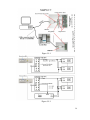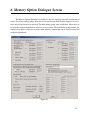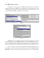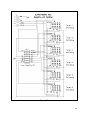
1
GangPro-CC
Flash Gang Programmer for the CC series devices
User’s Manual
Software version 1.7
PM025A01 Rev.5
June-19-2009
Elprotronic Inc.
16 Crossroads Drive
Richmond Hill,
Ontario, L4E-5C9
CANADA
Web site:
E-mail:
Fax:
Voice:
www.elprotronic.com
[email protected]
905-780-2414
905-780-5789
Copyright © Elprotronic Inc. All rights reserved.
Disclaimer:
No part of this document may be reproduced without the prior written consent of Elprotronic Inc.
The information in this document is subject to change without notice and does not represent a
commitment on any part of Elprotronic Inc. While the information contained herein is assumed to
be accurate, Elprotronic Inc. assumes no responsibility for any errors or omissions.
In no event shall Elprotronic Inc, its employees or authors of this document be liable for special,
direct, indirect, or consequential damage, losses, costs, charges, claims, demands, claims for lost
profits, fees, or expenses of any nature or kind.
The software described in this document is furnished under a licence and may only be used or copied
in accordance with the terms of such a licence.
Disclaimer of warranties: You agree that Elprotronic Inc. has made no express warranties to You
regarding the software, hardware, firmware and related documentation. The software, hardware,
firmware and related documentation being provided to You “AS IS” without warranty or support
of any kind. Elprotronic Inc. disclaims all warranties with regard to the software, express or implied,
including, without limitation, any implied warranties of fitness for a particular purpose,
merchantability, merchantable quality or noninfringement of third-party rights.
Limit of liability: In no event will Elprotronic Inc. be liable to you for any loss of use, interruption
of business, or any direct, indirect, special incidental or consequential damages of any kind
(including lost profits) regardless of the form of action whether in contract, tort (including
negligence), strict product liability or otherwise, even if Elprotronic Inc. has been advised of the
possibility of such damages.
2
END USER LICENSE AGREEMENT
PLEASE READ THIS DOCUMENT CAREFULLY BEFORE USING THE SOFTWARE AND
THE ASSOCIATED HARDWARE. ELPROTRONIC INC. AND/OR ITS SUBSIDIARIES
(“ELPROTRONIC”) IS WILLING TO LICENSE THE SOFTWARE TO YOU AS AN
INDIVIDUAL, THE COMPANY, OR LEGAL ENTITY THAT WILL BE USING THE
SOFTWARE (REFERENCED BELOW AS “YOU” OR “YOUR”) ONLY ON THE CONDITION
THAT YOU AGREE TO ALL TERMS OF THIS LICENSE AGREEMENT. THIS IS A LEGAL
AND ENFORCABLE CONTRACT BETWEEN YOU AND ELPROTRONIC. BY OPENING THIS
PACKAGE, BREAKING THE SEAL, CLICKING “I AGREE” BUTTON OR OTHERWISE
INDICATING ASSENT ELECTRONICALLY, OR LOADING THE SOFTWARE YOU AGREE
TO THE TERMS AND CONDITIONS OF THIS AGREEMENT. IF YOU DO NOT AGREE TO
THESE TERMS AND CONDITIONS, CLICK ON THE “I DO NOT AGREE” BUTTON OR
OTHERWISE INDICATE REFUSAL, MAKE NO FURTHER USE OF THE FULL PRODUCT
AND RETURN IT WITH THE PROOF OF PURCHASE TO THE DEALER FROM WHOM IT
WAS ACQUIRED WITHIN THIRTY (30) DAYS OF PURCHASE AND YOUR MONEY WILL
BE REFUNDED.
1. License.
The software, firmware and related documentation (collectively the “Product”) is the property of
Elprotronic or its licensors and is protected by copyright law. While Elprotronic continues to own
the Product, You will have certain rights to use the Product after Your acceptance of this license.
This license governs any releases, revisions, or enhancements to the Product that Elprotronic may
furnish to You. Your rights and obligations with respect to the use of this Product are as follows:
YOU MAY:
A.
use this Product on many computers;
B.
make one copy of the software for archival purposes, or copy the software onto the hard disk
of Your computer and retain the original for archival purposes;
C.
use the software on a network
YOU MAY NOT:
A.
sublicense, reverse engineer, decompile, disassemble, modify, translate, make any attempt
to discover the Source Code of the Product; or create derivative works from the Product;
B.
redistribute, in whole or in part, any part of the software component of this Product;
3
C.
use this software with a programming adapter (hardware) that is not a product of
Elprotronic Inc.
2. Copyright
All rights, title, and copyrights in and to the Product and any copies of the Product are owned by
Elprotronic. The Product is protected by copyright laws and international treaty provisions.
Therefore, you must treat the Product like any other copyrighted material.
3. Limitation of liability.
In no event shall Elprotronic be liable to you for any loss of use, interruption of business, or any
direct, indirect, special, incidental or consequential damages of any kind (including lost profits)
regardless of the form of action whether in contract, tort (including negligence), strict product
liability or otherwise, even if Elprotronic has been advised of the possibility of such damages.
4. DISCLAIMER OF WARRANTIES.
You agree that Elprotronic has made no express warranties to You regarding the software, hardware,
firmware and related documentation. The software, hardware, firmware and related documentation
being provided to You “AS IS” without warranty or support of any kind. Elprotronic disclaims all
warranties with regard to the software and hardware, express or implied, including, without
limitation, any implied warranties of fitness for a particular purpose, merchantability, merchantable
quality or noninfringement of third-party rights.
4
This device complies with Part 15 of the FCC Rules.
Operation is subject to the following two conditions:
(1) this device may not cause harmful interference and
(2) this device must accept any interference received,
including interference that may cause undesired
operation.
NOTE: This equipment has been tested and found to comply with the limits for a Class B digital devices,
pursuant to Part 15 of the FCC Rules. These limits are designed to provide reasonable protection against harmful
interference in a residential installation. This equipment generates, uses, and can radiate radio frequency energy
and, if not installed and used in accordance with the instruction manual, may cause harmful interference to
radio communications. However, there is no guarantee that interference will not occur in a particular
installation. If this equipment does cause harmful interference to radio or television reception, which can be
determined by turning the equipment off and on, the user is encouraged to try to correct the interference by one
of more of the following measures:
*
Reorient or relocate the receiving antenna
*
Increase the separation between the equipment and receiver
*
Connect the equipment into an outlet on a circuit different from that to which the receiver is connected
*
Consult the dealer or an experienced radio/TV technician for help.
Warning: Changes or modifications not expressly approved by Elprotronic Inc. could void the user’s authority
to operate the equipment.
This Class B digital apparatus meets all requirements of the Canadian
Interference-Causing Equipment Regulations.
Cet appereil numerique de la classe B respecte toutes les exigences du
Reglement sur le material brouilleur du Canada.
5
Table of Contents
1. Introduction . . . . . . . . . . . . . . . . . . . . . . . . . . . . . . . . . . . . . . . . . . . . . . . . . . . . . . . . . . . . . 9
2. Features . . . . . . . . . . . . . . . . . . . . . . . . . . . . . . . . . . . . . . . . . . . . . . . . . . . . . . . . . . . . . . .
2.1
Key features . . . . . . . . . . . . . . . . . . . . . . . . . . . . . . . . . . . . . . . . . . . . . . . . .
2.2
Custom features . . . . . . . . . . . . . . . . . . . . . . . . . . . . . . . . . . . . . . . . . . . . . .
2.2.1 Encrypted Project option . . . . . . . . . . . . . . . . . . . . . . . . . . . . . . . . . .
2.2.2 Script file . . . . . . . . . . . . . . . . . . . . . . . . . . . . . . . . . . . . . . . . . . . . . .
2.2.3 DLLs . . . . . . . . . . . . . . . . . . . . . . . . . . . . . . . . . . . . . . . . . . . . . . . . .
10
10
11
11
11
11
3. Getting Started . . . . . . . . . . . . . . . . . . . . . . . . . . . . . . . . . . . . . . . . . . . . . . . . . . . . . . . . . .
3.1
Software Installation . . . . . . . . . . . . . . . . . . . . . . . . . . . . . . . . . . . . . . . . . . .
3.1.1 Driver Installation . . . . . . . . . . . . . . . . . . . . . . . . . . . . . . . . . . . . . . .
3.2
Hardware Setup . . . . . . . . . . . . . . . . . . . . . . . . . . . . . . . . . . . . . . . . . . . . . . .
3.3
Starting up “GangPro-CC" Flash Programmer . . . . . . . . . . . . . . . . . . . . . . .
3.4
X-Pro Selector . . . . . . . . . . . . . . . . . . . . . . . . . . . . . . . . . . . . . . . . . . . . . . . .
13
13
13
17
19
19
4. Programming Dialogue Screen . . . . . . . . . . . . . . . . . . . . . . . . . . . . . . . . . . . . . . . . . . . . .
4.1
SoC Device Type . . . . . . . . . . . . . . . . . . . . . . . . . . . . . . . . . . . . . . . . . . . . . .
4.2
Code File Management . . . . . . . . . . . . . . . . . . . . . . . . . . . . . . . . . . . . . . . . .
4.3
Flash Protection Bits . . . . . . . . . . . . . . . . . . . . . . . . . . . . . . . . . . . . . . . . . . .
4.4
Power Device from Adapter . . . . . . . . . . . . . . . . . . . . . . . . . . . . . . . . . . . . .
4.5
Target Device selector and action result . . . . . . . . . . . . . . . . . . . . . . . . . . . .
4.6
Device Action box . . . . . . . . . . . . . . . . . . . . . . . . . . . . . . . . . . . . . . . . . . . . .
4.6.1 Auto Program button . . . . . . . . . . . . . . . . . . . . . . . . . . . . . . . . . . . . .
21
22
23
26
26
28
29
30
4.6.2 Verify LOCK bits . . . . . . . . . . . . . . . . . . . . . . . . . . . . . . . . . .
4.6.3 Erase Flash button . . . . . . . . . . . . . . . . . . . . . . . . . . . . . . . . . . . . . . .
4.6.4 Blank Check button . . . . . . . . . . . . . . . . . . . . . . . . . . . . . . . . . . . . . .
4.6.5 Write Flash button . . . . . . . . . . . . . . . . . . . . . . . . . . . . . . . . . . . . . . .
4.6.6 Verify Flash button . . . . . . . . . . . . . . . . . . . . . . . . . . . . . . . . . . . . . .
4.6.7 Read/ Copy Flash button . . . . . . . . . . . . . . . . . . . . . . . . . . . . . . . . . .
Next button . . . . . . . . . . . . . . . . . . . . . . . . . . . . . . . . . . . . . . . . . . . . . . . . . .
30
31
31
32
32
33
34
4.7
5. Data viewers . . . . . . . . . . . . . . . . . . . . . . . . . . . . . . . . . . . . . . . . . . . . . . . . . . . . . . . . . . . 35
6
6. Memory Option Dialogue Screen . . . . . . . . . . . . . . . . . . . . . . . . . . . . . . . . . . . . . . . . . . .
6.1
Memory Erase/Write/Verify Group . . . . . . . . . . . . . . . . . . . . . . . . . . . . . . . .
6.2
Read Group . . . . . . . . . . . . . . . . . . . . . . . . . . . . . . . . . . . . . . . . . . . . . . . . . .
6.3
Verification Group . . . . . . . . . . . . . . . . . . . . . . . . . . . . . . . . . . . . . . . . . . . . .
38
39
40
41
7. Adapter Options . . . . . . . . . . . . . . . . . . . . . . . . . . . . . . . . . . . . . . . . . . . . . . . . . . . . . . . . .
7.1
Communication Dialogue Box . . . . . . . . . . . . . . . . . . . . . . . . . . . . . . . . . . .
7.1.1 Communication Speed . . . . . . . . . . . . . . . . . . . . . . . . . . . . . . . . . . . .
7.2
Reset Dialogue Box . . . . . . . . . . . . . . . . . . . . . . . . . . . . . . . . . . . . . . . . . . . .
7.2.1 Reset pulse duration . . . . . . . . . . . . . . . . . . . . . . . . . . . . . . . . . . . . . .
7.2.2 Final Target Device action . . . . . . . . . . . . . . . . . . . . . . . . . . . . . . . . .
7.3
Options Dialogue Box . . . . . . . . . . . . . . . . . . . . . . . . . . . . . . . . . . . . . . . . . .
42
42
42
42
43
43
44
8. Serialization . . . . . . . . . . . . . . . . . . . . . . . . . . . . . . . . . . . . . . . . . . . . . . . . . . . . . . . . . . . .
8.1
Introduction . . . . . . . . . . . . . . . . . . . . . . . . . . . . . . . . . . . . . . . . . . . . . . . . . .
8.2
IEEE Address & Serialization Dialogue Screen . . . . . . . . . . . . . . . . . . . . . .
8.2.1 IEEE Address selection . . . . . . . . . . . . . . . . . . . . . . . . . . . . . . . . . . .
8.2.2 IEEE/SN Record File . . . . . . . . . . . . . . . . . . . . . . . . . . . . . . . . . . . . .
8.2.3 Serial number formats . . . . . . . . . . . . . . . . . . . . . . . . . . . . . . . . . . . .
8.2.4 Model, Group, Revision . . . . . . . . . . . . . . . . . . . . . . . . . . . . . . . . . . .
8.2.5 Device Serialization box . . . . . . . . . . . . . . . . . . . . . . . . . . . . . . . . . .
8.3
Serialization Report Dialogue Screen . . . . . . . . . . . . . . . . . . . . . . . . . . . . . .
45
45
47
48
50
51
59
60
62
9. IEEE /SN data file . . . . . . . . . . . . . . . . . . . . . . . . . . . . . . . . . . . . . . . . . . . . . . . . . . . . . . . 64
10. Check Sum Options . . . . . . . . . . . . . . . . . . . . . . . . . . . . . . . . . . . . . . . . . . . . . . . . . . . . . 69
10.1 Check Sum types . . . . . . . . . . . . . . . . . . . . . . . . . . . . . . . . . . . . . . . . . . . . . . 72
11. Script File - defined programming sequence . . . . . . . . . . . . . . . . . . . . . . . . . . . . . . . . . .
11.1 Script button . . . . . . . . . . . . . . . . . . . . . . . . . . . . . . . . . . . . . . . . . . . . . . . . .
11.2 Script file option . . . . . . . . . . . . . . . . . . . . . . . . . . . . . . . . . . . . . . . . . . . . . .
11.3 Script commands . . . . . . . . . . . . . . . . . . . . . . . . . . . . . . . . . . . . . . . . . . . . . .
77
77
78
79
12. Project and Configuration Load / Save . . . . . . . . . . . . . . . . . . . . . . . . . . . . . . . . . . . . . .
12.1 Load / Save Setup . . . . . . . . . . . . . . . . . . . . . . . . . . . . . . . . . . . . . . . . . . . . .
12.2 Load / Save Project . . . . . . . . . . . . . . . . . . . . . . . . . . . . . . . . . . . . . . . . . . . .
12.3 Commands combined with the executable file . . . . . . . . . . . . . . . . . . . . . . .
85
85
85
89
7
13. Target connection . . . . . . . . . . . . . . . . . . . . . . . . . . . . . . . . . . . . . . . . . . . . . . . . . . . . . . 93
14. Driver for the IAR C-Spy debugger . . . . . . . . . . . . . . . . . . . . . . . . . . . . . . . . . . . . . . . . . 99
15. Driver for the Keil uVision debugger . . . . . . . . . . . . . . . . . . . . . . . . . . . . . . . . . . . . . . 105
Appendix A - specification . . . . . . . . . . . . . . . . . . . . . . . . . . . . . . . . . . . . . . . . . . . . . . . . . 108
8
1. Introduction
The GangPro-CC programmer is designed to allow simultaneous programming of up to six
CC series SoC with 8051 MCU devices (Chipcon products from Texas Instruments). The
programmer configures target devices by using the debug interface.
The programmer package consist of a microcontroller based adapter (Figure 1-1), WindowsTM
based software, a Gang Splitter to connect up to 6 devices to the adapter, and cable to connect the
adapter with the computer’s USB
port. The internal firmware
software allows to communicate
with the programmed device with
high speed. The effective
programming speed (write only) is
around 20 kbytes/s simultaneously
up to six target devices that is
equivalent to 120 kbytes/s
programming speed per one
programmed target device. Due to
this high speed communication,
programming time is very short and
Figure 1-1
programmer can be used to program
flash devices in the production
process. For example, six devices with 128 kB Flash, such as CC2430F128, can be programmed in
12 seconds. This time includes initialization, erasing memory, blank checking, programming and
fast verification.
To simplify production process the programming software package can assign IEEE address,
serials number, model type, and revision. Each IEEE address and serial number are unique for each
programmed device and are assigned automatically. Several serial number formats are available.
There are a number of erase/write options available as well. This allows to erase/write all
flash memory, or just the specified fragment of memory. This feature is very useful when only part
of programmed data/code should be replaced. For example one can download the serial number,
calibration data or personality data without erasing existing program code.
9
2. Features
The GangPro-CC programmer is dedicated to simultaneously program up to six CC series
SoC with 8051 MCU Chipcon Product from Texas Instruments. To facilitate high speed
communication, an application software for the programming adapter has been optimized for the
maximum speed.
2.1
Key features
The key features of the GangPro-CC programmer are:
*
*
*
*
*
*
*
*
*
*
*
*
*
*
*
*
Support all CC Chipcon devices from Texas Instruments.
Programming speed via debug interface is approximately 20 kBytes/s per target device. Up
to six target devices can be programmed simultaneously, effectively programming at a rate
of 120 kbytes/s,
Our programmers are professionally made and are recommended by Texas Instruments
as the Third Party Tools source.
Full memory or sector memory erase capability.
Write Check Sum verification.
No code size limitations.
Target device can be powered from the programming adapter or from external source.
Easy to use WindowsTM based software.
Programmer accept TI (*.txt), Motorola (*.s19) and Intel (*.hex) data files for programming.
Combine code files capability.
Lock setup capability, useful in production.
Software package can assign and automatically increment IEEE address and serial number,
model type and revision. Serial Number with or without an automatically inserted current
date can be stored in the FLASH memory in HEX, BCD or ASCII format. Log file capability
allowing to review information about the flashed target devices.
DLL software package can control programmer from other programs.
Driver for the IAR CSpy - EW8051 for debugging using FPA and IAR Embedded
Workbench IDE software.
Programmer has been fully tested to comply with the FCC and CE requirements.
Uses USB-1.1 (12Mbits/s) Port to communicate with the Programming Adapter.
10
2.2
Custom features
The GangPro-CC programmer can be controlled from an external software as well as custom
scripts to specify programming sequences. These features are very useful in production environment.
2.2.1 Encrypted Project option
Contents of the project that include code contents downloaded to target device can be
encrypted and blocked against unauthorised access.
2.2.2 Script file
A user can define a sequence of programming steps by the means of a script file. The script
file is a sequence of programmer commands, where each command corresponds to a button in the
programming software. Each command can be accompanied by a few options. A script file of up to
1000 lines can be created. The detailed description of script commands is given in Chapter 10. Please
note that the script file is not available in the lite version of the programming software.
The second option allows to use command line interpreter (not available in the lite version),
that can fully control the programming adapter via Multi-FPA API-DLL.
2.2.3 DLLs
The programming adapter can also be controlled through user created applications. For this
purpose a DLL is provided to allow a user to develop custom application that can control the
programming adapter and allow the programming of target devices via the GangPro-CC adapter.
The Multi-FPA API-DLLs allows to fully control up to 16 programming adapters (to program
simultaneously up to 96 target devices) from external software written in MS Visual C++, MS Visual
Basic, LABView, DOS or other programming packages like Borland C++ etc. See the “GangProCC FlashProgrammer - Remote Control Programming User’s Guide” for details.
To speed up programming process it is recommended to program full panel with a lot of boards on
the panel before de-panelization. Access from FPAs to all target devices can be done via nails (see
Figure 2-1).
11
Figure 2-1
2.2.4 Driver for the IAR CSpy and KEIL uVision debugger
The FPA programming adapter can also be used with the IAR Embedded Workbench
or KEIL uVision IDE software for debugging. See chapters 12 and 13 for details.
12
3. Getting Started
1.
2.
3.
4.
5.
6.
7.
GangPro-CC programmer package contains:
One READ ME FIRST document.
One X-Pro-CC - Flash Programmer CD ROM (Software + Manual).
One GangPro-CC Flash Programming Adapter.
One 6 feets length USB-A to USB-B cable.
GangPro-CC Splitter that allows to connect six target devices to one USB-FPA adapter.
Six ribbon cables - with 10 pins connectors.
One 14-pins ribbon cable.
3.1
Software Installation
The X-Pro-CC Flash Programming Software runs on PC under Windows TM ME, WinNT, 2000 or
XP. Follow instructions below to install the software:
1.
2.
3.
4.
Insert X-Pro-CC Software CD into your CD-ROM drive.
The X-Pro-CC Setup wizard appears automatically. Click Install X-Pro-CC Programmer
to begin the installation process.
If the Setup wizard does not start automatically, click the Start button and choose the Run
dialogue box. Type “D:\SETUP.EXE”, where D represents the drive letter of your CD-ROM
drive. Then click the OK button.
Once the installation program starts, on-screen instructions will guide you through the
remainder of the installation. You must accept licence agreement before using software.
3.1.1 Driver Installation
Software installation program is placing the USB driver files in the windows directories
Windows\inf and Windows\system32\drivers that simplified driver installation.
1.
2.
Plug in USB-MSP430-FPA to the PC USB Port, using provided cable extender (USB-A to
USB-B).
==== Windows XP, VISTA ====
The “New hardware has been found” - USB-FPA-BOOT should be displayed.
13
Figure 3.1-1
Follow the wizard instruction to install the drivers.
1.
In the first Wizard dialogue screen (see Figure 3.1-1) select the “Yes, this time
only” option.
2.
In the second Wizard dialogue screen (see Figure 3.1-2) select the “Instal the
software automatically (Recommend)” and press NEXT button.
Figure 3.1-2
14
3.
Software will search the driver for the USB-FPA-BOOT. It can take one minute to
find it. When the driver is found then the following warning will be displayed (Figure
3.1-3)
Figure 3.1.3
4.
Ignore this message and press button “Continue Anyway”. The first USB-FPABOOT driver should be installed and following message displayed (Figure 3.1-4).
5.
Press “Finish” button.
15
Figure 3.1-4
After a few seconds the second new hardware will be found - the USB-FPA (Elprotronic).
Repeat the procedures 1,2,3,4,5 as above and on the end the second driver for the USB-FPA
(Elprotronic) will be installed (see Figure 3.1-5).
If from any reason the wizard cannot find the USB drivers location then repeat steps 2,3,4
Figure 3.1-5
using manual option and browse drivers from location software directory
C:\Program Files\Elprotronic\XPro USB Drivers\W2000,ME,XP
16
==== Windows - 2000, 98-SE ====
2.
The “New hardware has been found” should be displayed. Follow the wizard instruction
to install the drivers.
3.
Press ‘Next’ when the Device Wizard Driver screen appear.
4.
Select the following option on the wizard screen:
* select for a suitable driver for my device (recommended)”
and press ‘Next’.
5.
Select the third option - “Specify a location” for a location of the Driver Files.
6.
From the browser select the “D:\drivers\W2000,ME,XP” for Win-2000 or
“D:\drivers\W98” for Win-98SE directory, where D:CD-ROM drive location or in the
application software directory
C:\Program Files\Elprotronic\XPro USB Drivers\W98 and press ‘Next’.
7.
Driver installation process will start.
Driver installation procedures should be done twice. Software will install two USB drivers - the Boot
driver and the Application driver. Reboot computer on the end.
3.2
Hardware Setup
1.
Connect the USB-FPA Flash Programming Adapter to the PC USB Port or via USB-HUB
using provided cable extender (USB-A to USB-B) (see figure 3.2-1).
Plug in socket connector from the USB-FPA Flash Programming Adapter to the J1 connector
on the GangPro-CC Splitter (PN: PE014X03) using ribbon cable with 14-pins connectors.
Connect up to six target devices to GangPro-CC Splitter using ribbon cables with 10-pins
connectors. Make sure that pin 1 on your device board’s header is connected to pin 1 (red
wire) of the socket connector.
Target devices can be supplied form programming adapter ( programmable Vcc = 2.2V to
3.6V with step 0.2V, max total current 100 mA)(see Figure 3-2.2-top) or from external
power supply . When target devices are supplied from external power supply then power
supply ON/OFF can be controlled from programming adapter (see Figure 3-2.2-bottom).
2.
3.
17
Figure 3.2-1
Figure 3-2.2
18
3.3
Starting up “GangPro-CC" Flash Programmer
To start the GangPro-CC Flash Programmer click on the GangPro-CC Elprotronic icon.
Figure 3.3-1
Once started the software will attempt to access the programming adapter. If no error messages
appear then the software has initialized without a problem and you may begin using it. However, if
the programming adapter is not detected an error message will appear. To correct the problem, make
sure that the connection cable is properly attached and the USB driver is installed.
3.4
X-Pro Selector
The X-Pro430 software has a Multi-USB feature. Up to 16 Flash Programming Adapters can
be connected to one PC. Each adapter can be controlled by a separate instance of the programming
software application. Up to 16 applications can be opened at the same time. Each application can
have independent setup from the others (code file, controlled microcontroller type etc.).
When more then one X-Pro FPA Adapter is connected to a PC then each time you start the
programmer application a X-Pro FPA Selector dialogue screen will appear (see Figure 3.4-1). The
dialogue screen will list all adapters connected and allow you to choose the adapter you with the
application to control. Make a sure that the selected FPA is not used by another opened application.
The selected FPAs’s serial number will be displayed on the bottom left side of the programming
dialogue screen.
When the Multi-FPA API-DLL is used, then all adapters can be controlled from one
software. See the “GangPro-CC FlashProgrammer - Remote Control Programming User’s
Guide” for details.
19
Figure 3.4-1
20
4. Programming Dialogue Screen
The programming dialogue box (see Fig. 4-1.) contains a pull down menu, interface selection
box, lock protection bits box, device action buttons, report (status) window, open file buttons, target
device information box, IEEE addresses and serial number box, power DC status and check sum
result boxes.
Figure 4-1. Programming dialogue box screen.
21
All device action buttons, power ON/OFF button and the check sum result box have their
own status indicators. Each indicator can assume any of the following conditions:
- blank - idle status.
- yellow - Test in progress. For power on/off - DC voltage is correct.
- green - access enabled.
- red sign - access denied. For power on/off - DC voltage is too low (below 2.0V)
- device action has been finished successfully.
- device action has been finished, but result failed.
- applies to blank check only - Memory is not clean, but the specified memory segment is.
4.1
SoC Device Type
Target device type can be selected from the pull down field of
the SoC Device type group. The pull down field contains a list of all
devices in CC series family currently available. To automatically detect
the microcontroller type choose the ‘- - -’ option from the drop down
list.
When communication between the microcontroller and the
programming adapter is initialized, the software will detect the target
microcontroller automatically. The type of detected microcontroller is
displayed in the field ‘Target:’. This allows the software to warn you
if the connected microcontroller does not match the one specified by the
user.
Note: No warning message will appear when ‘- - -’ microcontroller
type is selected.
Note: If more then one target device is connected to GangPro-CC
programmer then all target devices should be the same type. It
is not possible to simultaneously program target devices of
different type.
Figure 4.1-1
22
4.2
Code File Management
The GangPro-CC flash programmer provides a few options to manage code files. These
options allow the user to open a code file, combine several code files into a single file, and save the
programming data into a code file. The Open Code File button, or the Open Code File from the
Figure 4.2-1
FILE pull down menu, prompts for opening the object file that contains the code data, as shown in
Figure 4.2-1. When the file is selected the contents of the object file are downloaded into the PC
memory. If the selected target device does not have enough memory to fit the data contained in the
code file, the warning message in Figure 4.2-2 will be displayed.
When code file is opened and read successfully the code file name and full path will be
displayed on the right side of the Open Code File button (see Fig.4-1 Programming dialogue box
screen). Contents of the selected file can be viewed by the selecting of ‘Code File Data’ from the
‘View’ menu (see chapter 5).
23
Figure 4.2-2
The Combine Code Files option allows up to 40 code files to be loaded into the PC memory.
When this option is selected the programmer will create a new data block, which will contain the
combined data of the user selected files. In order to add a code file to the newly created data block,
the user needs to press the ADD Code File button. The programmer will then prompt the user to
specify the code file to be appended to the newly created memory block, using the window in Figure
4.2-1. Every appended file will be verified, so that the total code size does not exceed the target
microcontroller’s memory space and that there is no overlap with previously selected code segments.
After the addition of each file the window in Figure 4.2-3 will be shown. The window shows the
status of previous append operations.
Figure 4.2-3
24
The Programmer is also able to append files of any type to the new data block. In order to do this the
user must specify the memory location into which the programmer is to load the file and then press
the Add file contents button. The window in Figure 4.2-1 will appear prompting the user to specify
the file to be added. Once the file is added to the new memory block, the programmer will display
the memory space occupied by the selected file. An example of this is shown in Figure 4.3-3 for the
file number 4.
The Save Code File option saves the data currently contained within the PC code data block
into a code file. When the user selects this option from the File menu, the window in Figure 4.2-4
will appear, prompting for the name of the file to be created.
All of the aforementioned Code File options work with three most popular code file formats.
These formats are the Texas Instruments, the Motorola and the Intel file formats. GangPro-CC will
work with any of these formats and will easily convert one file format to another by using the Open
Code File and Save Code File options.
Figure 4.2-4
25
4.3
Flash Protection Bits
The CC series devices memory can be protected against unauthorized access or can protect
a whole or part of flash against erase or write to the protected flash space. The GangPro-CC software
allows the user to program the protection bits. In the right top corner of the main dialogue screen the
selected option of the protection bits (Figure 4.3-1) is displayed. When the Enable option is selected,
then all protection bits will set in the CC device. Desired combination of the protection bits can be
selected in the Memory Option setup dialogue available from pull down menu “Setup->Memory
Option”. See chapter 6 for details.
To program the protection bits the check mark ‘Enable’ in the ‘Lock Protection Bits’ group
must be selected first (see Figure 4.3-1).
Figure 4.3-1
4.4
Power Device from Adapter
The programming adapter is powered from the
USB Port interface. Target device can be powered from
the programming adapter with voltage range from 2.2V
to 3.6V in step 0.2V selected in the voltage selector
located in the ‘Power Device from Adapter” box.
Figure 4.4-1
The target device will be powered from the adapter, if check box ‘Enable’ in the ‘Power
Device from Adapter’ group (figure 4.4-1) is selected. When the ‘Enable’ checkbox is selected a
warning message shown in figure 4.4-2 will be displayed. If you confirm this selection by clicking
YES, then POWER ON/OFF button is enabled. By clicking POWER ON/OFF button you can turn
the power on or off on the target device. Current DC voltage on the target device is continuously
26
monitored and displayed in the ‘Device Voltage’ field in the ‘Power Device from Adapter’ group,
even if the target device is powered from the external DC sources. If DC voltage is higher then 2.0
V, then yellow box will be displayed, indicating that DC voltage is OK and target device is fully
functional under this DC voltage. If DC level is below 2.0V, then access denied sign box will be
displayed (red sign with white line). If DC level is below 1V, then blank sign box will be displayed.
When the target device is powered from the external power supply then the check box ‘Enable’
Figure 4.4-2
should not be selected. External power supply ON/OFF can be controlled from programming adapter
(from pin-8) (see Figure 3-2.2-bottom). Voltage level on the pin-8 is over 3 V (typical 4.6V) when
external power supply should be enabled, and below 1V (typical 0V) when the external power supply
should be OFF. It is recommended to put pull-down resistor on the enable input of the external
power supply.
RESET button located on the right side on the POWER ON/OFF button (Figure 4.1) can
generate a reset pulse to the target device. Pressing this button the target devices can be reset
manually at any time, starting the target’s device application program from the beginning.
27
4.5
Target Device selector and action result
In the Target Devices Programming Result group box is possible to select target devices to
be activated - tested, programmed etc. Minimum one target devise should be selected. All target
devices connected to programming adapter should be the same type. Otherwise unpredicted state can
be created.
When action with programmer is started then access to all targets are verified. Each part of
process result is displayed in the test result icons (see figure 4.5-1).
All process result have their own status indicators. Each indicator can assume any of the
following conditions:
- blank - idle status.
- yellow - test in progress..
- green - access enabled.
- red sign - access denied.
- device action has been finished successfully.
- device action has been finished, but result failed.
- applies to blank check only - memory is not clean, but the specified memory segment is.
Figure 4.5-1
28
4.6
Device Action box
The Device Action box contains 7 buttons (see Figure 4.6-1)
Each button allows a specific action to be executed. Software
procedures related to each action allow you to fully execute the desired
task, without the need to follow a specific sequence of actions. Every
action starts by powering up the target device, if Power Device from the
Adapter is enabled. When the DC voltage level becomes higher then
2.0V, the communication with the target device is initiated via the debug
interface. The protection access bit is verified, if the access to the target
device is available. Once the specified action is completed successfully
the green check marks will appear (see Figure 4.5-1). Also, the device
will return to the state it was in before the action was executed.
Progress of all actions is displayed in the report window. If the
particular action has been finished successfully, then message ‘done’ or
‘OK’ will appear on the right side of processed procedure (Fig.4.6-2).
If not, a message ‘failed’ will be displayed and selected action will be
terminated. Final status is also displayed in the Status window (see
Fig.4.6-3) as Active (blue), Pass (green), or Fail (red). On the bottom
of the programmer dialogue screen the progress bar is displayed and the
total run time is shown in the report window. Run time does not include
the time when user interaction is required.
Figure 4.6-1
Figure 4.6-3
Figure 4.6-2
29
4.6.1 Auto Program button
The Auto Program button is the most frequently used button when programming target
microcontroller devices in a production process. Auto Program button activates all required
procedures to fully program and verify the flash memory contents. Typically, when the flash memory
needs to be erased, Auto Program executes the following procedures:
•
reload code file when “Reload Code File” is selected (useful for debugging when
the code file is frequently modified)
•
initialization
•
read retain data from the flash if specified (optional).
•
read label information (IEEE address, Serial Number, Model, Group,
Revision)(optional)
•
erase flash memory,
•
erased memory blank check,
•
flash programming and verification,
•
assign or retrieve label information,
•
restore retain data if specified,
•
retain data verification if specified,
•
assigned or retrieved label verification,
•
flash memory check sum verification,
•
set flash protection bits (if enabled).
In the report window you can see a typical report message during the Auto Program
procedure (see Fig. 4.6-2 ).
Status window (see fig. 4.6-3) has a counter that is useful in a production process. The total
number of programmed devices can be entered in the Total edit line. The Balance line shows the
number of devices that have not been programmed yet. The Balance counter is initialized to the value
entered in the Total edit line and is decremented every time Auto Program is completed successfully.
In the bottom box in the Status group is displayed number of the available IEEE addresses and serial
numbers taken from the used defined file.
Note: Balance counter works only with the Auto Program procedure.
4.6.2 Verify LOCK bits
30
This button allows the check the access to target device and read protection bits setup, if
access is available.
4.6.3 Erase Flash button
This button enables the flash memory segments, or mass (all) memory to be erased. If any
option other then ‘Erase All Memory’ is selected in the Memory Options Setup (see chapter 6.1
Memory Erase/Write/Verify Group for details), then the following question message box will be
displayed:
Figure 4.6.3-1
4.6.4 Blank Check button
When Blank Check button is clicked, the program checks if flash memory of the target
microcontroller is blank (all bytes contain the value 0xFF). This test performs two checks. The first
one determines if the entire memory contents is clean, while the second only checks a memory
segment specified by the user (see setup in Memory Erase/Write Group). The following conditions
can appear at the completion of this operation:
- all memory is blank
- all memory is not blank, but selected part of it is.
- memory is not blank.
31
4.6.5 Write Flash button
When write flash button is clicked, then contents from the code file will be written to the
flash memory. When the second time target device is programmed, then the following warning
message is displayed:
Figure 4.6.5-1
Note: See chapter 5.1 Memory Erase/Write Group for details on how to specify memory segment
for writing.
4.6.6 Verify Flash button
The Verify Flash function compares the contents of the flash memory with data from the code
file. Verify flash function can use the standard memory verification method (byte by byte) or
calculate only the check sum of the code and check sum of the content in the flash (see chapter 5.
Memory Option Dialogue Screen).
Note: During the verification process either all memory or just the selected part of the memory is
verified, depending on settings specified in the Memory Erase/Write Address Range in the
Memory Options setup. See chapter 5.1 Memory Erase/Write Group for details.
32
4.6.7 Read/ Copy Flash button
When ‘Read/Copy’ button is clicked then data can be read from the target microcontroller
and displayed in the Flash Memory Data window (see Fig.4.6.7-1). This window can also be opened
by selecting the ‘Flash Memory Data’ option from the ‘View’ menu. Flash memory data viewer,
shown in figure 4.6.7-1, displays the code address on the left side, data in hex format in the central
column, the same data in Ascii format in the right column. The contents of the code viewer can be
converted to Texas Instruments *.txt file format by clicking on the ‘Convert to TI format’ button.
Data will be viewed in the Notepad Editor.
The address range to be displayed in the Flash Memory Data window can be specified in the
Memory Options screen. See chapter 5.2 Read group for details.
When the ‘Copy’ button is clicked, then the contents of the read target device memory will
Figure 4.6.7-1
33
be saved in the specified by user file name and opened as a current Code File. Also programmer
setup will be modified for the copy procedure. Especially the serialization will be disabled and the
‘All Memory’ option will be selected in the ‘Write/Erase/Verify Address Range’. Following
message will be displayed.
Figure 4.6.7-2
When the button
pressed then programmer is ready to program the destination device.
4.7
‘OK’ is
Next button
The ‘Next’ button is a dynamically programmable device action button,
which is very useful in production process. After opening the program,
‘NEXT’ button is disabled (see Fig.4.7-1). When any button from the
Device Action group is pressed, then button ‘NEXT’ takes the name
and feature of that button. For example, if Auto Program button has
been used, then it’s name will be displayed on top of the ‘NEXT’ button
(see Fig.4.7-2). From now the button ‘NEXT’ will perform the same
function as the Auto Program button. The ‘NEXT’ button has a
shortcut to function key F5. Button ‘NEXT’ will retain its functionality
until some other device key is clicked. For example, if key ‘READ
FLASH’ is clicked, then from this moment button ‘NEXT’ will take
a name and feature of the ‘READ FLASH’ button (see Fig.4.7-3). The
read flash procedure will be called, if button ‘NEXT’ or function key
F5 is pressed.
Figure 4.7-1
Figure 4.7-2
Figure 4.7-3
34
5. Data viewers
The contents of the code file or the Flash memory can be displayed, or compared to one
another in a data viewer. To display the contents of a code file select the ‘Code File Data’ option
from the ‘View’ menu. Similarly, the contents of the Flash memory can be displayed by selecting the
‘Flash Memory Data’ option from the ‘View’ menu. Please note that in order to view the contents
of the Flash Memory the ‘Read Flash’ option must be selected first.
When one of the above options is selected the code data viewer, shown in figure 5-1, will
appear. The code viewer displays data in three columns. The leftmost column shows the code
address. The middle column shows the data at the specified address in a hex format. The data is
separated into byte size chunks for easy viewing. The data itself can be a hexadecimal value between
00 and FF, or ‘..’. If two dots appear at any location in the middle column of the code viewer then
Figure 5-1
35
it means that the code file does not specify the contents of that memory location. Alternatively, if the
data is read from the Flash memory then two dots will appear if the memory address specified is
outside of the Flash Memory Space. In such a case, the following warning message will appear:
‘:== Data out of the Flash Memory Space of the selected device ==’
The rightmost column of the code viewer shows the same data as in the middle column, except that
it is shown in the ASCII format.
The data displayed in the code viewer window can be converted to the Texas Instruments
*.txt file format by clicking on the ‘Convert to TI format’ button. The data will be displayed in the
Notepad Editor.
Finally, the contents of the Code File data and Flash Memory Data can be compared and
differences displayed in a the viewer by selecting ‘Compare Code & Flash Data’ from the ‘View’
menu. Only data that are not the same in the code file data and the Flash memory will be displayed.
In the first line code file data will be displayed, and in the second line - Flash memory data (Figure
Figure 5-2
36
5-2).
Note: Only data at the addresses specified in the code file can be displayed. Any data not specified
in code file will not be displayed, even if the Flash Memory data contains any not empty (FF) data.
37
6. Memory Option Dialogue Screen
The Memory Options Dialogue Screen (Fig.6-1) has five settings groups and one information
group. Two of the settings groups allow the user to specify four flash memory segments for erase,
write and read operation to be specified. The third settings group, write verification, allows the user
to select the verification method for Auto Program procedure. The information group contains the
start and stop address of the user specified main memory segment that can be erased, written and
verified independently.
Figure 6-1
38
6.1
Memory Erase/Write/Verify Group
The Memory Erase/Write/Verify Address Range group block (see Fig.6-1) specifies common
addresses range for erase, write and verify operations. Memory setup has five available options:
1.
Update only:
This option allows the user to perform an update
@1008
operation. This means that when the Auto Program
25 CA 80 40 39 E3 F8 02
procedure is executed then the contents of the code
@2200
48 35 59 72 AC B8
data taken from the Code File will be downloaded to
q
the flash memory without erasing any memory
segment. This option is useful when a relatively small
Figure 6.1-1
amount of data, such as calibration data, needs to be
added to the flash memory. Flash memory space defined by Code File should be blank and
the code file should contain ONLY data to be downloaded to flash memory. For example,
if code file contains only data as shown in figure 6.1-1 (in Texas Instruments format) then
8 bytes of data will be written starting at location 0x1008 and 6 bytes of data starting at
location 0x2200. Before writing operation, all data in the flash memory at the specified
location should be blank (contain value 0xFF). The software will verify automatically if this
part of memory is blank and will only proceed to program the device if verification is
successful.
Note: The addresses specified in the Code File as well as the number of bytes for each data block
must be EVEN. The software uses word (two bytes) operation for writing and reading data.
In case that the code file contains an odd number of bytes to write the data segment will be
appended by a single byte containing the value 0xFF. This value will not overwrite the
current memory contents, but verification process will return an error if the target device
does not contain the value 0xFF at that location.
2.
All Memory
This is the most frequently used option during flash memory programming process. The
entire memory space is cleared before programming. All contents from the code file can then
be downloaded to the target microcontroller’s flash memory.
3.
Main memory only
39
This option allows the user to erase and program only the main memory. Flash information
memory (segments A and B) will not be modified. If the code file contains data intended for
these segments, the data will be ignored.
4.
Used by code file:
This option allows main memory segments or/and information memory segments used by
data specified in code file to be erased. Flash memory segments, which do not contain any
data to be written to the memory from the code file, will not be erased. This option is useful,
if some data, such as calibration data, should be replaced in memory. If the code file contains
some new calibration data, such as described in figure 6.1-1, then the ENTIRE information
memory segment at addresses 0x1000 to 0x107F and the main memory segment at addresses
0x2200 to 0x23FF will be erased and new data at locations 0x1008 and 0x2200 will be
written.
5.
User Defined:
This option is functionally similar to options described before, but addresses range of the
erased/write/verify main memory and sectors of the information memory can be defined by
the user. When the User Defined option is selected, then on the right side of the Memory
Erase/Write/Verify Group two check boxes and two addresses edit lines will be enabled. The
check boxes allow the user to select the information memory sectors A, or/and B to be used
(erased, written, verified). Edit lines in the Main Memory group allow the user to specify the
main memory address range (start and stop addresses). Start address should specify the first
byte in the segment, and the stop address should specify the last byte in the segment. Since
the main memory segment size is 0x200, then the start address should be a multiple of
0x200, eg. 0x2200. The stop address should specify the last byte of the segment to be written.
Therefore, it should be greater than the start address and point to a byte that immediately
precedes a memory segment boundary, eg. 0x23FF or 0x55FF.
6.2
Read Group
The Read Address Range group block (see Fig.6-1) specifies the address range used in
reading process. Memory read setup has four options available:
1.
All Memory
2.
Main memory only
3.
Info memory only
4.
User Defined
40
The meaning of each option is the same as for the erase/write/verify procedure. The Info Memory
only option works the same way as Main memory only option described above, except that only
information memory is modified.
6.3
Verification Group
1.
2.
3.
Verification group setup allows the user to select one of the three write verification methods:
Fast Verification,
Standard Verification,
None.
Fast Verification:
During the fast verification, each byte is verified after being written and at the end of the
process the check sum is read from the flash memory and compared to calculated check sum
taken from the code file.
Standard verification:
Standard verification is performed after memory write process is completed. Contents of the
flash memory are read and compared with the contents of the code file. If they are the same,
then verification process is successful. Typically, the standard verification procedure requires
the same amount of time as the read/write procedure. Total programming time with standard
verification is around two times longer than read/write procedure time.
41
7. Adapter Options
7.1
Communication Dialogue Box
The “Communication Interface with Target Device” dialogue screen enables the user to
select the communication speed between programming adapter and target device - 3 or 1 Mbits/s.
Figure 7-1
7.1.1 Communication Speed
The default communication speed between programming adapter and target device is 3 Mb/s.
Under some conditions, for example when the cable between FPA and target device is long or some
protection components are installed in the debug interface, the fast communication can not be used.
In this case lower speed 1Mb/s can be used to establish communication between FPA and target
device (see Figure 7-1 - communication speed selector).
7.2
Reset Dialogue Box
The Target’s Reset Dialogue screen enables the user to select the Reset pulse duration and reset line
state at the end of programming process.
42
Figure 7.2
7.2.1 Reset pulse duration
The reset pulse allows the adapter to initiate communication with a microcontroller. In most
cases the pulse width of 10ms is sufficient to initiate communication process. However, this may be
affected by additional load on the reset line. Therefore, four additional settings, 100, 200, 500 ms
and custom, are available. When the RESET IC circuit is used then the custom defined reset pulse
duration can be used. Two parameters of the custom reset pulse are defined - initialization reset pulse
time (typically very short - 1 ms) and an idle reset time. Idle reset time must be set at least to
duration of the reset time generated by the RESET circuit.
7.2.2 Final Target Device action
Every device action, like AUTO Program, Read etc. starts with the activation of the RESET
line (active low). When the device programming action begins the RESET line is raised high. When
device action is finished, then RESET line is again asserted, protecting the target device from
running the application program. This method is commonly used to protect the programming adapter
from the DC overload. However, when target device is supplied from its own power supply, or a
battery, the overload protection of the programming adapter is no longer necessary.
43
The target device can be set to run an application immediately after the target device is
programmed. This permits verification of the programmed device if required. To do this check the
‘Hardware Reset (RST line) and start the application program’
or
‘ON/OFF Vcc and start the application program’
option in the Reset Options window, shown in Figure 7-2. Application run time can be unlimited
or limited up to 120 seconds. Limited time is specified in the “Program RUN time” box. When
entered ‘0' in the “Program RUN time” box then time is unlimited.
7.3
Options Dialogue Box
The Options Dialogue screen allows to enable or disable the report history in the report
window (see figure 4.1). When enabled then the report history is displayed up to 8 kB characters
(approximately 20 last communication messages). When disabled, then the only last programming
report is displayed.
All programming actions at the end can generate the Beep OK tone. When a lot of units is
programmed then the OK tone can be disabled just to not make a lot of noise. Error programming
tone is enabled permanently and can not be disabled.
Figure 7.3
44
8. Serialization
8.1
Introduction
The GangPro-CC programming software has the ability to automatically create the target
device’s IEEE Address and Serial Number and save it in the flash memory. These numbers are also
saved in the data base file. The new IEEE Address and Serial Number can be created automatically
by incrementing the IEEE Address and Serial Number or can be taken from a file created by the
user. Furthermore, model name, group, and revision can be downloaded to target device. The IEEE
Address format is fixed and contains 8 bytes located at the end of the flash memory. The Serial
Number format and location in the device’s flash memory must be specify by the user.
Note: The Serial Number assignment option is available only when the programming adapter
FPA with the standard access is used. The FPA - lite version does not have access to
serialization. The IEEE Address can be created with FPA standard and lite version.
IEEE Address and Serial Number are created when the Auto Program or Write SN /Write
IEEE Addr button is pressed and the Serialization feature is enabled. When the Auto Program
function is activated then the IEEE Address and/or Serial Number are programmed to the target
device’s memory along with the code data. If the Auto Program function fails for any reason then
new IEEE Address / Serial Number is not created.
The software also allows the device to retain its IEEE Address / Serial Number if one has
already been assigned to it. Every time a device is programmed and serialization is enabled the
contents of the target’s memory are scanned for existing IEEE Address and Serial Number. If
numbers are found in the database, the dialogue screen (see Figure 8.1) will appear and allow you
to decide if you wish to keep the old IEEE Address / Serial Number, new or manually entered
once. When the edited numbers are used, then it is possible to press the “Verify with Data Base”
button and check if the entered IEEE Address / Serial Number have been already used before. On
the right side of each edited number will be displayed message “OK” if the number has not been
used before, or “used” when it was (see Figure 8.1).
45
Figure 8.1
46
8.2
IEEE Address & Serialization Dialogue Screen
IEEE Address & Serialization dialogue box, shown in figure 8-2, allows the user to configure
of the IEEE Address and Serial Number serialization process. The IEEE Address Write option can
be selected from the pull down IEEE Address option list. Serialization (Serial Number) can be
enabled, or disabled, by selecting the check mark in the ENABLE Serialization box. When
serialization is disabled, then all edit lines and check boxes are disabled. When serialization is
enabled all fields must be set.
Figure 8-2
47
8.2.1 IEEE Address selection
The GangPro-CC software allows to create IEEE Address in the target device. Format and
location in flash of the created IEEE Address is fixed and contains 8 bytes located at the end of
available flash memory location. For example, the IEEE Address in a CC2431F128 device is saved
at location 0x1FFF8 to 0x1FFFF. All eight bytes must be specified.
Figure 8.3
Figure 8.4
The IEEE Address selection depends on the option used to program the target device. When
using the Autoprogram option, the IEEE Write Address is specified in the IEEE Address Setup (see
Figure 8.3). When the user wishes to manually program the target device, then the IEEE Address can
be specified in through the Device’s IEEE Address and Serialization group (see Figures 4.1 and 8.4).
The above settings are used by the software depending on which programming mode is used
(Autoprogram or manual). For example, in the main dialogue screen the option “Retain Code, Write
IEEE address” can be selected and in the serialization dialogue screen - the “Assign and write
48
IEEE address” option. When the Autoprogram button is pressed, then the IEEE address will be
assigned automatically (selected option “Assign and write IEEE address”) and when the saved
IEEE address should be modified, then the new number can be modified manually (editing required
number in the edit line) and downloaded to device using “Write IEEE addr” button. The “Retain
Code, Write IEEE address” option will be used when the “Write IEEE addr” button is pressed.
The following IEEE Address Write options are available:
1.
Autoprogram -> Disable
2.
Manual -> Write new IEEE address if flash is blank
3.
Manual -> Retain Code and write IEEE address
4.
Autoprogram -> Enforce BLANK Flash in IEEE location
5.
Autoprogram -> Retain IEEE address
6.
Autoprogram -> Assign and write IEEE address
7.
Autoprogram -> Write IEEE address from the file
1.
2.
3.
4.
5.
When the IEEE Address option is disabled, then the location in the IEEE address is not used
and not verified.
Manual -> Write new IEEE address if flash is blank - used only when the “Write IEEE
addr” button is pressed in the Main Dialogue screen (Figure 4.1 and Figure 8.4). The
software first verifies if all eight bytes are not programmed (all 0xFF). If they are not then
the action is terminated. Otherwise, the new IEEE address is downloaded and verified. The
verified IEEE address is then displayed in the grey line - on the left side of the edited line
(figure 8.2.1-2).
Manual -> Retain Code and write IEEE address - used only when the “Write IEEE addr”
button is pressed in the Main Dialogue screen. The software first verifies if all eight bytes
are not programmed (all 0xFF). If not then the action is terminated. Otherwise, the new IEEE
address is downloaded and verified. When the bytes in the IEEE address locations are not
blank, then whole sector (1 or 2 kB) is read, erased, and the new IEEE Address saved and
all data restored. The contents of the whole sector are verified. The new IEEE address is
displayed in the grey line.
Autoprogram -> Enforce BLANK Flash in IEEE location - used only when the
“Autoprogram” action is executed. The IEEE address location will be blank (all 0xFF). Any
specified data at this location (eg. in code file) will be ignored. This empty location can be
used in the future for the IEEE address assignment.
Autoprogram -> Retain IEEE address - used only when the “Autoprogram” action is
executed. When this option is selected, then the software reads the IEEE address saved in the
device, clears the flash memory contents (entire memory or just the specified segments), and
49
downloads the code to the target device and restores the IEEE address used initially by the
target device.
6.
7.
Autoprogram -> Assign and write IEEE address - used only when the “Autoprogram”
action is executed. This option allows to automatically assign the IEEE address and save it
in target device. Downloaded IEEE address is also saved in the data base file. When the next
IEEE address is created, then the data base file is scanned and the highest IEEE address is
selected. The new IEEE address is equal the highest number saved in the data base plus IEEE
address increment specified in the IEEE Address increment (see figure 8.2). If the new IEEE
address is lower then the address specified in the IEEE Address start from filed then the
higher IEEE address is used.
Autoprogram -> Write IEEE address from the file - used only when the “Autoprogram”
action is executed. This option allows the software to take IEEE address from the custom
defined IEEE addresses in the file and save it in target device. Downloaded IEEE address
is also saved in the database file. Any HEX numbers can be used as the IEEE address. See
chapter 9 for data format used in the file.
Location of the IEEE address data can be specified or used as default (see Figure 8.2). When the
default location is used then the IEEE address data are saved in the last eight bytes in the available
Flash memory. For example, when the flash size is 128 kbytes, then IEEE address is saved in
locations 0x1FFF8 to 0x1FFFF. The IEEE address data can be saved in the Flash starting from the
lowest byte (when the IEEE Address data in Flash - LSB First is selected) or from the highest byte
(when the IEEE Address data in Flash - LSB First is not selected).
8.2.2 IEEE/SN Record File
The ‘IEEE/SN Record File’ specifies the full path and file name where the database contents
will be saved. The IEEE Address and Serial Number file contains following data, separated by
tabulation:
1.
IEEE Address (16 characters - 8 bytes in hex),
1.
Serial Number Format (F0,F1,F2,F3,F4,F5,F6,F7),
2.
Serial Number,
3.
IEEE/SN action type (New SN, unmodified SN, overwritten SN, manual SN)
4.
Time and date, when SN has been created,
5.
Code File Name
6.
Model text.
50
Below is an example of the data file, containing data from the three consecutively created
serial numbers.
0123456789abcdef F0
001122334455678 F0
001122334455679 F0
200300011 . m ( Sat, Mar 29,2003, 10:09 ) AS010X02-1v2.txt
200300012 . . ( Sat, Mar 29,2003, 10:43 ) AS010X02-1v2.txt
200300013 . u ( Sat, Mar 29,2003, 10:43 ) AS010X02-1v2.txt
-01 R.0003-04-17
-01 R.0003-04-17
-01 R.0003-04-17
IEEE Address and Serial number can be created as a unique SN per target device’s type, or
as a unique SN for any device type.
8.2.3 Serial number formats
Programming software has seven methods for creating a serial number, referred to as Display
format, and four methods of storing the SN in the memory, referred to as In Memory Format in the
serialization dialogue screen. When a serial number is created, current date (if required) is taken
from the PC timer. Make a sure that your computer has the correct date and time.
Display Formats:
1. YYYY-1234(5)
- (SN Format - F0) Serial number has 8 or 9 characters. First four
characters contain current year, and remaining 4 or 5 characters
contain the serial number, eg. SN 20030123 or 200300123 has a
number 0123 (or 00123) created in the 2003 year.
2. YYMM-1234(5) - (SN Format - F1) Serial number has 8 or 9 characters. First two
characters contain last two digits of current year, next two characters
contains current month, and remaining 4 or 5 characters contain a
number, eg. SN 03030123.
3. YYMMDD-1234 - (SN Format - F5) Serial number has 10. First six characters contain
date ( year, month, day of month) and remaining 4 characters contain
a number, eg. 0405120123.
4. YYDDD-1234(5) - (SN Format - F4) Serial number has 9 or 10. First five characters
contain date ( year, day of year from 1 to 366) and remaining 4 or 5
characters contain a number, eg. 041230123.
5. 123456768
- (SN Format - F2) 8 digits serial number without date stamp.
6. 1234(5)
- (SN Format - F3) 4 or 5 digits serial number without date stamp.
7. Custom
- (SN Format - F6) 4 to 16 Ascii characters or hexadecimal numbers
entered manually or from the Bar-Code Reader.
8. From the file
- ( SN Format - F7) 4 to 16 ASCII characters or hexadecimal
numbers taken from the user created file.
51
When the serials number formats 1 through 6 are selected, then in the dialogue screen all
numbers are displayed and edited as a decimal numbers. Only numeric keystrokes from 0 to 9 will
be accepted. All displayed numbers (decimal) are converted to the format HEX, BCD or ASCII
before they are saved to flash memory.
When the Custom or From the file serial number is selected, then any keystroke is accepted.
When the ASCII format is selected, then entered SN is saved as is in the flash memory. When the
Hex format is selected, then only the HEX characters can be used (0...9,A,B,C,D,E,F).
HEX ( MSW first ) and HEX ( LSW first ) format:
When hex format is selected, then all SN display formats described above can be stored as
a one or two integer (16-bits - 2 bytes) numbers. First four display characters will be saved as one
hex integer number and remaining five characters will be saved as a second hex integer number.
When format HEX(MSW first) is selected then the first hex integer number is saved as a first word
and the second number - as a next word in the Flash memory location. When format HEX(LSW
first) is selected then the first hex integer number is saved as a second word and the second number as a first word in the Flash memory location.
Display Format: YYYY-1234(5) - size in FLASH - 4 bytes
SN 200300123 will be saved as
YYYY - 2003 (Decy)
-> 0x07D3 (hex)
12345 - 00123
-> 0x007B (hex)
In flash memory this number can be seen as
07D3 007B
-> HEX(MSW first)
007B 07D3
-> HEX(LSW first)
when integer numbers are viewed, or as
<--- Hex format bytes---> (Size - 4 bytes)
D3 07 7B 00
-> HEX(MSW first)
7B 00 D3 07
-> HEX(LSW first)
when bytes are viewed (first byte is the LSW byte from the integer number)
Displayed consecutive serial number (16-bits integer number) can have a value from 0 to
(2^16-1) equal 65535 and is displayed as the 5 digits serial number.
52
Display Format: YYMM-1234(5)
SN 030300123 will be saved as
YYMM - 0303 (Decy)
12345 - 00123
- size in FLASH - 4 bytes
-> 0x012F
-> 0x007B
(hex)
(hex)
In flash memory this number can be seen as
012F 007B
-> HEX(MSW first)
007B 012F
-> HEX(LSW first)
or
<--- Hex format bytes---> (Size - 4 bytes)
2F 01 7B 00
-> HEX(MSW first)
7B 00 2F 01
-> HEX(LSW first)
Display Format: YYMMDD-1234
- size in FLASH - 4 bytes
The format date is compressed to be able to fit data in only in two bytes as follows:
Bit 15 14 13 12 11 10 9 8 7 6 5 4 3 2 1 0
<---(year-2000)----> < month><— day -->
SN 0405110123 will be saved as
YYMMDD - 040511 (Decy) -> 0x08AB (hex)
1234 - 0123
-> 0x007B (hex)
In flash memory this number can be seen as
08AB 007B
-> HEX(MSW first)
007B 08AB
-> HEX(LSW first)
or
<--- Hex format bytes---> (Size - 4 bytes)
AB 08 7B 00
-> HEX(MSW first)
7B 00 AB 08
-> HEX(LSW first)
Display Format: YYDDD-1234
- size in FLASH - 4 bytes
The format date is compressed to be able to fit data only in two bytes as follows:
Bit 15 14 13 12 11 10 9 8 7 6 5 4 3 2 1 0
<---(year-2000)----> < –-- day of year --->
SN 041110123 will be saved as
53
YYDDD - 04111 (Decy)
1234 - 0123
-> 0x086F (hex)
-> 0x007B (hex)
In flash memory this number can be seen as
086F 007B
-> HEX(MSW first)
007B 086F
-> HEX(LSW first)
or
<--- Hex format bytes--->
(Size - 4 bytes)
6F 08 7B 00
-> HEX(MSW first)
7B 00 6F 08
-> HEX(LSW first)
Display Format: 123456768
- size in FLASH - 4 bytes
SN 12345678 will be saved as
12345678 (Decy) -> 0x00BC614E
(hex)
In flash memory this number can be seen as
00BC 614E
-> HEX(MSW first)
614E 00BC
-> HEX(MSW first)
or
<--- Hex format bytes---> (Size - 4 bytes)
00 BC 4E 61
-> HEX(MSW first)
4E 61 00 BC
-> HEX(LSW first)
Display Format: 1234(5)
SN 12345 will be saved as
12345 (Decy)
- size in FLASH - 2 bytes
---> 0x3039 (hex)
In flash memory this number can be seen as
3039 ( integer numbers ) -> HEX(MSW first) or HEX(LSW first)
or
<--- Hex format bytes---> (Size - 2 bytes)
39 30
(bytes)
-> HEX(MSW first) or HEX(LSW first)
BCD format:
When BCD format is selected, then all SN display formats described above can be stored as
a two or four separate bytes converted to BCD format, where first and last four bits of 8 bit byte
54
contains a value from 0 to 9. All consecutive serial number characters are converted to half byte
each. Finally two consecutive serial number characters will be converted to a single byte.
Display Format: YYYY-1234
SN 20030123 will be saved as
YYYY - 2003
1234 - 0123
- size in FLASH - 4 bytes
-> 0x20 0x03
-> 0x01 0x23
(bytes)
(bytes)
When flash memory bytes are viewed, then this number can be seen as
<--- Hex format bytes--->
20 03 01 23
(Size - 4 bytes)
The consecutive serial number ( 4 bytes BCD ) can have a value from 0 to 9999 and is
displayed as the 4 digit serial number.
Display Format: YYMM-1234
SN 03030123 will be saved as
YYMM - 0303
1234 - 0123
- size in FLASH - 4 bytes
-> 0x03 0x03 (bytes)
-> 0x01 0x23 (bytes)
In flash memory this number can be seen as
<--- Hex format bytes--->
03 03 01 23
Display Format: YYMMDD-1234
SN 0405110123 will be saved as
YYMMDD - 040511
1234 - 0123
(Size - 4 bytes)
- size in FLASH - 5 bytes
-> 0x04 0x05 0x11
-> 0x01 0x23
In flash memory this number can be seen as
<--- Hex format bytes--->
04 05 11 01 23
(Size - 5 bytes)
55
Display Format: YYDDD-1234
- size in FLASH - 4 bytes
The format date is compressed to be able to fit data only in two bytes as follows:
Bit 15...12
11,10
9, 8
7...4
3...0
- Year number - multiple of ones (9,8,...1,0)
- Year number - multiple of tens ( 3,2,1,0)
- Day number - multiple of hundreds ( 3,2,1,0)
- Day number - multiple of tens (9,8,...1,0)
- Day number - multiple of ones (9,8,...1,0)
SN 041110123 will be saved as
YYDDD - 04111 (Decy)
1234 - 0123
Display Format: 123456768
SN 12345678 will be saved as
12345678
-> 0x41 0x11 (hex)
-> 0x01 0x23 (hex)
- size in FLASH - 4 bytes
-> 0x12 0x34 0x56 0x78 (bytes)
In flash memory this number can be seen as
<--- Hex format bytes--->
12 34 56 78
Display Format: 1234
SN 1234 will be saved as
1234
(Size - 4 bytes)
- size in FLASH - 2 bytes
-> 0x12 0x34 (bytes)
In flash memory this number can be seen as
<--- Hex format bytes--->
12 34
(Size - 2 bytes)
ASCII format:
When Ascii format is selected, then all SN display formats described above can be stored as
a four or eight separate bytes converted to Ascii characters. All consecutive serial number characters
are converted to Ascii characters.
56
Display Format: YYYY-1234
SN 20030123 will be saved as
YYYY - 2003
1234
- 0123
- size in FLASH - 8 bytes
-> 0x32 0x30 0x30 0x33 (bytes)
or
‘2' ‘0' ‘0' ‘3'
-> 0x30 0x31 0x32 0x33 (bytes)
or
‘0' ‘1' ‘2' ‘3'
When flash memory bytes are viewed, then this number can be seen as
<------ Hex format ------>
32 30 30 33 30 31 32 33
Display Format: YYMM-1234
SN 03030123 will be saved as
YYMM - 0303
<– Ascii format –>
20030123
(Size - 8 bytes)
- size in FLASH - 8 bytes
-> 0x30 0x33 0x30 0x33 (bytes)
or
‘0' ‘3' ‘0' ‘3'
1234 - 0123
-> 0x30 0x31 0x32 0x33 (bytes)
or
‘0' ‘1' ‘2' ‘3'
In flash memory this number can be seen as
<------ Hex format ------>
30 33 30 33 30 31 32 33
Display Format: YYMMDD-1234
SN 0405110123 will be saved as
<– Ascii format –>
03030123
(Size - 8 bytes)
- size in FLASH - 10 bytes
YYMMDD - 040511
-> 0x30 0x34 0x30 0x35 0x31 0x31 (bytes)
or
‘0' ‘4' ‘0' ‘5' ‘1'
‘1'
1234 - 0123
-> 0x30 0x31 0x32 0x33 (bytes)
or
‘0' ‘1' ‘2' ‘3'
In flash memory this number can be seen as
<----------- Hex format ---------->
30 34 30 35 31 31 30 31 32 33
Display Format: YYDDD-1234
<– Ascii format –>
0405110123
(Size - 10 bytes)
- size in FLASH - 9 bytes
57
SN 042140123 will be saved as
YYDDD - 04214
-> 0x30 0x34 0x32 0x31 0x34 (bytes)
or
‘0' ‘4' ‘2' ‘1' ‘4'
1234 - 0123
-> 0x30 0x31 0x32 0x33 (bytes)
or
‘0' ‘1' ‘2' ‘3'
In flash memory this number can be seen as
<-------- Hex format ---------->
30 34 32 31 34 30 31 32 33
Display Format: 123456768
SN 12345678 will be saved as
12345678
<– Ascii format –>
042140123
(Size - 9 bytes)
- size in FLASH - 8 bytes
-> 0x31 0x32 0x33 0x34 0x35 0x36 0x37 0x38 (bytes)
In flash memory this number can be seen as
<------ Hex format ------>
31 32 33 34 35 36 37 38
<– Ascii format –>
12345678
(Size - 8 bytes)
Display Format: 1234
- size in FLASH - 4 bytes
SN 1234 will be saved as
1234
-> 0x31 0x32 0x33 0x34 (bytes)
In flash memory this number can be seen as
<------ Hex format ------>
31 32 33 34
<– Ascii format –>
1234
(Size - 4 bytes)
Display Format: Custom or from the file
- size in FLASH - defined size in bytes
Taken from the file or entered manually Ascii string will be saved in the flash memory.
When the Ascii format is selected, then the Ascii string is saved in memory “as is”.
All Ascii characters can be used. For example the entered following string
02WX24S234
58
will be saved in memory as
30 32 57 58 32 34 53 32 33 34 ->
“02WX24S234"
When the HEX format is selected, then the string is converted to HEX format (only hex
characters are accepted - 0, 1, 2, 3, 4, 5, 6, 7, 8, 9, A, B, C, D, E, F.
All two character pairs are converted to hex format and saved in memory.
For example the entered following string
02A3B109E12F
will be saved in memory as
HEX(MSW first) -> 02 A3 B1 09 E1 2F
or
HEX(LSW first) -> 2F E1 09 B1 A3 02
Location in the target device’s flash memory, where the described above bytes are saved, is
specify in the ‘Memory Location - SN Start Address in Memory’ field of the serialization dialogue
screen (see figure 8.2-1). Specified address must be even and should be specified in the empty
memory space, not used by program code or data block
8.2.4 Model, Group, Revision
Custom text or data (hex), saved in target device’s flash memory is a string or data, up to 32
characters (bytes) long, in Ascii or hex format. It can contain any text or data, but this feature is
intentionally created to allow the hardware model, revision and group to be saved. Typically the
object code does not contains this kind of information, but it may be useful in some applications.
This feature is enabled when the check box ENABLE in the Model/Group/Revision field
is marked (see figure 8.2-1). When enabled, the size of desired text or data must be specified in the
field ‘Size in Bytes’. Size value can be any even number between 2 and 32. The location of the
text/data in the flash memory can be specified in the field ‘Start Address in Memory’. Similarly to
the location of the serial number, the specified address must be even and must be specified in the
empty memory space, unused by program code or data block. Otherwise, the error message will be
displayed.
The text to be saved in the flash memory can be entered in the edit line. Bytes can be entered
as an Ascii, if Ascii option is selected, or in hex bytes, if the Hex option is selected. When the
Ascii/Hex selector is modified, then the contents data is displayed as an Ascii string or as a hex bytes
data.
59
8.2.5 Device Serialization box
Device Serialization box, located on the main programming dialogue screen (see figures 8-2
and 4-1) contains IEEE Addresses, serial number and model information. The left columns contains
information taken from the target devices, and the right columns - pending data to be saved.
Whenever a communication with the target device is performed the IEEE Address and serial number
is read and displayed in the Device Serialization group (Figure 8.5). IEEE address or serial number
displayed in the white fields can be manually modified if required. The manually entered numbers
can be saved using Autoprogram option, or using manual buttons located inside the Device’s IEEE
Address and Serialization group. When the next time the Autoprogram action is selected, then the
next IEEE Address or SN is generated automatically, according to the setup in the Serialization .
This means that any data entered in the‘Device Serialization’ group can be treated as temporary data
and downloaded to the target devices.
Figure 8.5
Current target’s label (IEEE Address, serial number and model text) can be read at any time
by pressing READ IEEE Addr. and READ SN buttons located in the ‘Device Serialization’ group
(see figure 8.5)
When the Autoprogram action is selected and the IEEE Address / Serialization is enabled,
then the current data saved in target device is read first. If target device already contains IEEE
60
Address and/or serial number, or the IEEE Address and/or serial number have been modified
manually, then the following IEEE/SN edit dialogue screen is displayed (Figure 8.1). In this screen
all IEEE Addresses and serial numbers are displayed - taken from current target devices, pending
new data created automatically, and data edited manually. Each line contains selector, that allows
to accept desired data to be downloaded to target device - taken from current device, created
automatically, or modified manually for each target device separately.
61
8.3
Serialization Report Dialogue Screen
Serialization Report Dialogue Screen reports the results of the serialization procedure. The
report contains the detailed information of the two highest serial number programmed units, quantity
of programmed units along with the new created serial numbers, unmodified SN (reprogrammed
units), manually created SN and quantity of the overwritten SN. Detailed information about all
programmed units can be viewed using the Notepad text editor by pressing the ‘NotePad’ button.
Short information of the created serial numbers, format, date and time of programming is
Figure 8.6
displayed on the white report box (see Figure 8.3-1). IEEE/ SN are created automatically via
software by incrementing the highest IEEE/SN taken from the serial number files. If from any
reason the highest IEEE Address or Serial Number is wrong it can be removed from the database by
62
pressing the ‘Delete’ button. Note that the delete operation is not reversible. Third line allows to
select any line from the report information and delete it if required. Selected line is marked in the
report window with character ‘>’ on the left of the selected line.
63
9. IEEE /SN data file
The GangPro-CC software allows the user to download the IEEE Address and/or serial
number from custom defined data file. When the data file is used then in the IEEE Address Write
to Flash option the Write IEEE address from the file option should be selected (see Figure 8.2),
and in serialization the Serial Number Format field should be set to From File.
The IEEE/SN data file can contains list of IEEE Addresses, list of serial numbers of both pairs of the IEEE Addresses and serial numbers. Format of the IEEE addresses data is fixed and
contain 8 bytes data in hex format. Format of the serial numbers can be specified in the serialization
dialogue screen (Figure 8.2). The IEEE/SN data file can be created in any text editor.
All data specified after semicolon (;) are ignored and can be used by user as a comments. On
the top of the data the IEEE/SN file should contain header data. When the header is specified, then
list of desired IEEE Addresses and/or serial numbers can be listed. Following list of commands
started from # can be specified in the header:
#IEEE_SN_LIST
Data file contains IEEE addresses and serial numbers.
#IEEE_LIST
Data file contains only IEEE addresses.
#SN_LIST
Data file contains only Serial number list.
#SN_SIZE
number
;optional
Overwrite size of the custom defined serial number size (see Figure 8.2). If the #SN_SIZE
is not specified, then the data specified in the serialization dialogue screen is used.
#IEEE_PREFIX
#IEEE_SUFFIX
#SN_PREFIX
#SN_SUFFIX
hex numbers
hex numbers
string
string
;optional
;optional
;optional
;optional
The IEEE Address that contains 8 bytes in hex (16 characters) can be specified in fully, or
can be combined from the fixed prefix, fixed suffix and listed part of the individual number.
In total this combination of data must contains 16 characters (8 bytes). For example
following IEEE addresses list
64
1111213330012222
1111213330022222
1111213330032222
.................................
1111213331202222
can be grouped from two the same data block and from one modified as follows
#IEEE_PREFIX
#IEEE_SUFFIX
111121333
2222
and list of variable IEEE Addresses list
001
002
003
.................................
120
Prefix and /or suffix numbers can be modified in the list if required, eg.
#IEEE_PREFIX
#IEEE_SUFFIX
001
002
003
#IEEE_PREFIX
001
002
003
111121333
2222
333121333
that defined IEEE addresses
1111213330012222
1111213330022222
1111213330032222
3331213330012222
3331213330022222
3331213330032222
#SN_PREFIX
#SN_SUFFIX
string
string
;optional
;optional
Similar to IEEE prefix/suffix - the serial number string can be combined from SN prefix,
suffix and variable SN part.
65
Example of the IEEE Address / Serial Number list ( 5 lines only in this example)
; =====================================================
;
IEEE Address /Serial Number List
; first col - IEEE address, second col - SN
; SN format - Ascii
; =====================================================
#IEEE_SN_LIST
#SN_SIZE
12
01C2220000010022
01C2220000020022
01C2220000030022
01C2220000040022
01C2220000050022
WX5E2007001P
WX5E2007002P
WX5E2007003P
WX5E2007004P
WX5E2007005P
The same IEEE Address / Serial Number list with specified prefix /suffix
; =====================================================
;
IEEE Address /Serial Number List
; first col - IEEE address, second col - SN
; SN format - Ascii
; =====================================================
#IEEE_SN_LIST
#SN_SIZE
12
#SN_PREFIX
WX5E2007
;any Ascii character
#SN_SUFFIX
P
#IEEE_PREFIX
01C222000
;hex only
#IEEE_SUFFIX
0022
001
002
003
004
005
001
002
003
004
005
The same IEEE Address / Serial Number list with specified prefix only
; =====================================================
;
IEEE Address /Serial Number List
; first col - IEEE address, second col - SN
; SN format - Ascii
66
; =====================================================
#IEEE_SN_LIST
#SN_SIZE
12
#SN_PREFIX
WX5E2007
;any Ascii character
#IEEE_PREFIX
01C222000
;hex only
0010022
0020022
0030022
0040022
0050022
001P
002P
003P
004P
005P
When writing a new IEEE Address, or SN, entry the IEEE Address/SN can be compared to those
stored in the IEEE/SN data file. To do so, the data file should be specified in the SN/IEEE Record
file field (see Figure 8.2). When the desired IEEE Address Write option and Serial Number Format
is selected using the data from the file, then using the SN/IEEE file button located in the main
dialogue screen (Figure 4.1) the desired IEEE/SN file should be opened. Selected file is converted
to final format and all listed IEEE addresses and serial numbers are verified in the data base file
against usage. If specified IEEE addresses or SN have been used before, then these numbers are
removed from the pending list. When the IEEE/SN file is read and verified, then the current pending
list is displayed in the screen (Figure 9.1) with extra information on the top
* number of the IEEE/SN found in data base and removed from the pending list
* number of the IEEE addresses with incorrect size and removed from the pending list
* number of the Serial Numbers with incorrect size and removed from the pending list
* number of the accepted IEEE/SN
67
Figure 9.1
When the “Paste to Notepad” button is pressed, then the pending IEEE addresses /Serial Number
list can be saved in format ready to be used as a valid IEEE/SN file if required.
68
10. Check Sum Options
Programming software has two groups of check sum (CS) calculation. The first group is used
for internal programming verification and the second group can be used for firmware verification
in application software.
The CS used for internal verification is calculating CS only for specified words in the code
file regardless of the flash memory size, location etc. This CS is useful only inside the programmer,
because programmer has all information about programmed and empty bytes location. This method
is also useful if only part of the code is programmed in the flash (append option). All not
programmed words in the programming process are ignored, even if these words are not empty in
the flash.
The check sum used for internal programming verification is displayed in the Check Sum
Group (Figure 10.1) ( see the Main Dialog screen - Figure 4.1 )
Figure 10.1
In the source line is displayed the arithmetic sum of the code contents with added contents
of the serialization, model etc. if selected. Arithmetic sum is calculated as the sum of 16-bits
unsigned words - result is 32 bits unsigned. Only programmed words are taken for calculation. All
other not used words are ignored. All bytes are converted to 16-bits words as follows (for simplicity format casting is not present in this example):
word = data[ address ] + ( data[ address+1 ]<<8 )
where address is even and incremented by 2.
In the memory line is displayed the CS result taken from the flash memory, calculated in the
same way as the CS taken from the source. Only words defined in the source are taken from the flash
memory for calculation.
69
Second group of the CS is custom defined Check Sum that can be used by firmware for code
verification in the flash. Up to four CS block can be specified and CS results can be saved in the
flash for verification. Size of each CS block and CS result location in flash are defined by the user.
The Check Sum Options dialog (figure 10-2) is selected from following pull down menu:
Setup -> Check Sum Options
Figure 10.2
Start Address should be even, and the Stop Address should be odd. CS result address in the flash
should be even. Make sure that the CS result is saved out of the CS block space. Otherwise the CS
result will modify the contents of the CS inside the specified block. CS result after the second
calculation would not be the same and CS result would be useless.
70
When the CS Result Save option is not selected then the CS of the selected block is
calculated and CS result displayed in the report window only (Figure 10.3). This option can be used
for CS code verification defined as the code form Start to End Addresses with 0xFF data in the not
specified code location.
Figure 10.3
Type of the CS can be selected from the following list (Figure 10.4)
Figure 10.4
Initial value for CS calculation can be selected as zero, all 0xFFs or as the Start Address from
pull down menu (Figure 10.5).
71
Figure 10.5
CS result can be used As Is or can be inverted (Figure 10.6).
Figure 10.6
Data size (byte or 16 bits word) used for calculation and CS result size is displayed in the
dialog screen as Data IN word size and CS Result size (Figure 10.2). Polynomial contents (if
required) can be specified in the POLY edit line in HEX format ( eg. 0x1234 ).
10.1 Check Sum types
Following Check Sum types are implemented (Figure 10.4)
Arithmetic Sum (8b / 16b)
Check Sum is calculated as modulo 16-bits sum of all bytes (unsigned) from Start to the End
Addresses as follows
CS = CS_initial_value;
for ( addr = StartAddress;
{
addr <= EndAddress; addr++ )
72
CS = CS + (unsigned int) data[addr];
}
CS = 0xFFFF & CS;
if( cs_inverted )
CS = 0xFFFF ^ CS;
Arithmetic Sum (8b / 32b)
Check Sum is calculated as modulo 32-bits sum of all bytes (unsigned) from Start to the End
Addresses as follows
CS = CS_initial_value;
for ( addr = StartAddress; addr <= EndAddress; addr++ )
{
CS = CS + (unsigned long) data[addr];
}
CS = 0xFFFFFFFF & CS;
if( cs_inverted )
CS = 0xFFFFFFFF ^ CS;
Arithmetic Sum (16b / 16b)
Check Sum is calculated as modulo 16-bits sum of all 2-byte words (unsigned) from Start
to the End Addresses as follows
CS = CS_initial_value;
for ( addr = StartAddress; addr <= EndAddress; addr=addr+2 )
{
CS = CS + (unsigned int)data[addr] + (unsigned int)data[addr+1];
}
CS = 0xFFFF & CS;
if( cs_inverted )
CS = 0xFFFF ^ CS;
Arithmetic Sum (16b / 32b)
Check Sum is calculated as modulo 32-bits sum of all 2-byte words (unsigned) from Start
to the End Addresses as follows
CS = CS_initial_value;
for ( addr = StartAddress; addr <= EndAddress; addr=addr+2 )
{
CS = CS+(unsigned long)data[addr] + (unsigned long)data[addr+1];
73
}
CS = 0xFFFFFFFF & CS;
if( cs_inverted )
CS = 0xFFFFFFFF ^ CS;
CRC16 (Poly 0x11201 ) - ( 16b / 16b ) (Named as CRCCCITT)
and
CRC16 defined polynomial - ( 16b / 16b )
Check Sum is calculated as CRC16 from each bytes from Startto the End Addresses as
follows
CS = CS_initial_value;
for ( addr = StartAddress; addr <= EndAddress; addr++ )
{
CS = CS_CRC16_8to16( (long)data[addr], CS );
}
CS = 0xFFFF & CS;
if( cs_inverted )
CS = 0xFFFF ^ CS;
where
unsigned long
CS_CRC16_8to16( long data, unsigned long crc )
{
unsigned long tmp;
tmp = 0xFF & ((crc >> 8) ^ data );
crc = (crc << 8) ^ crc_tab32[tmp];
return( 0xFFFF & crc );
}
The CRC table is generated first as follows:
CS_init_crc16_tab( 0x1021 );
CS_init_crc16_tab( CRC_def_POLY
);
for CRC CCITT
for CRC16 defined polynomial
where
void CS_init_crc16_tab( unsigned short poly )
{
int i, j;
74
unsigned short crc, c;
for (i=0; i<256; i++)
{
crc = 0;
c
= ((unsigned short) i) << 8;
for (j=0; j<8; j++)
{
if ( (crc ^ c) & 0x8000 )
crc = ( crc << 1 ) ^ poly;
else
crc =
crc << 1;
c = c << 1;
}
crc_tab32[i] = (unsigned long)(0xFFFF & crc);
}
}
CRC32 (Poly 0x04C11DB7 ) - ( 8b / 32b ) (Named as IEEE 802-3)
and
CRC32 defined polynomial - ( 8b / 32b )
Check Sum is calculated as CRC32 from each bytes from Start to the End Addresses as
follows
CS = CS_initial_value;
for ( addr = StartAddress; addr <= EndAddress; addr++ )
{
CS = CS_CRC32_8to32( (long)data[addr], CS );
}
CS = 0xFFFFFFFF & CS;
if( cs_inverted )
CS = 0xFFFFFFFF ^ CS;
where
unsigned long
CS_CRC32_8to32( long data, unsigned long crc )
{
return( ((crc >> 8) & 0x00FFFFFF) ^ crc_tab32[0xFF & (crc ^ data )] );
}
The CRC table is generated first as follows:
CS_init_crc32_tab( 0x04C11DB7 ) for IEEE 802-3
75
a polynomial of
x32 + x26 + x23 + x22 + x16 + x12 + x11 + x10 + x8 + x7 + x5 + x4 + x2 + x + 1
and
CS_init_crc32_tab( CRC_def_POLY ) for CRC32 defined polynomial
where
void CS_init_crc32_tab( unsigned long poly_in )
{
int n, k;
unsigned long c, poly;
poly = 0L;
for (n = 0; n < 32; n++)
{
poly <<= 1;
poly |= 1L & poly_in;
poly_in >>= 1;
}
for (n = 0; n < 256;
{
c = (unsigned long
for (k = 0; k < 8;
c = c & 1 ? poly
crc_tab32[n] = c;
}
n++)
)n;
k++)
^ (c >> 1) : c >> 1;
}
76
11. Script File - defined programming sequence
Programming sequence can be customized when is using a script file. Script file prepared as
a text file (using any editor like notepad) can contains customized programming sequences in any
order. Generally, all buttons available on the main dialogue screen can be used in the script file. All
other options available on others screens like memory options, serialization type etc. can not be
modified from the script file directly, but can be reloaded in fully using configuration file. From the
script file any configuration files can be called at any time that allows to modify programmer
configuration. This method can simplify programming process using script file and allows to use full
options available in the programmer. Programming sequence conditions can be taken from user
defined procedures attached as an independent DLL if required.
Programmer has two entry for taking the sequence from the script file
1.
2.
By pressing the Script File button in the Main dialog
By using the -rf with the executable file
11.1 Script button
The ‘Script ’ button is the dynamically programmable device action
button that allows to take a desired action taken from the script file. The
Script button has a name Script File - none (Figure 11-1) if the script file
is not defined or Script: with used file name when the script file is active
(Figure 11-2). When the Script button is pressed and the current script file
is not active, then the Open File dialog is displayed and the desired script
file should be selected. When the Script file button is not empty and the
new script file if required, then the new file can be selected from the pull
down menu - File-> Open Script File.
Figure 11-1
Figure 11-2
The Script button is very useful for implementing a short
programming sequence not present directly in the Device Action group buttons Below is an easy
script file used for downloading two independent codes to target device - first code used for
hardware test if possible, and when hardware is ok, then the second code is downloaded as the final
77
code to target device. The same sequence can be used with other buttons, but sequence should be
always repeated, that of course is not convenient.
Using the notepad editor create the script file and save it eg. as the file “test.sf” or any other file
name. See this chapter below for all available instructions that can be used in the script file.
;-------------------------------------------------------------------------; easy script file;
;-------------------------------------------------------------------------LOADCFGFILE C:\Program Files\Elprotronic\USB GangPro-CC\test.cfg
LOADCODEFILE C:\Program Files\Elprotronic\USB GangPro-CC\test.cfg
AUTOPROGRAM
; now the hardware is tested according to downloaded firmware
MESSAGEBOX
YESNO
"Press YES when the test finished successfully."
"Press NO when the test failed."
IF BUTTONNO GOTO finish
LOADCFGFILE C:\Program Files\Elprotronic\USB GangPro-CC\final.cfg
LOADCODEFILE C:\Program Files\Elprotronic\USB GangPro-CC\final.cfg
AUTOPROGRAM
>finish
END
;--------------------------------------------------------------------------
When the script file above is used then the first configuration file and the fist code file is downloaded
and Autoprogram function is executed. When finished then the MCU firmware started (make sure
that the first configuration allows to start the code when the Autoprogram is finished). Final code
is downloaded when the test has been finished successfully.
Before running the script file the configuration files named test.cfg and final.cfg required
in the project should be created using the GUI software first. To do that connect target devices to
programming adapter, select desired configuration and save the configuration file as test.cfg and
create final configuration file in similar way.
11.2 Script file option
78
Programming sequence can be customized when using the -rf with the executable file
(described in the “Project and Configuration Load/Save” chapter) .
When the executable file GangPro-CC.exe is called with a script path as an argument e.g.
FlashPro-CC.exe -rf C:\Program Files\Elprotronic\USB GangPro-CC\script.txt
or when the icon with the GangPro-CC.exe and script file path is executed then programmer
starts automatically programming sequences according to procedure specified in the script file.
Access to other buttons are blocked. When script file sequence is finished then program is
terminated. There is not option to modify the running sequence when script sequence is used. This
option is useful in production, because nobody can modify sequence that has been prepared for the
production purpose.
11.3 Script commands
LIMITATIONS:
1.
2.
Up to 1000 script lines commands can be used. Empty lines and lines with comments only are ignored and not
counted.
Up to 50 CALL’s deep stack is used (CALL in CALL in CALL......).
SYNTAX:
white spaces before instructions, labels etc are ignored.
; comment
- all contents after semicolon are ignored.
NOTE: Comment can not be used in the lines where the file name is specified.
>label
- character ‘>’ without spaces must be placed before label name.
NOTE: After label can not be specified any command in the same line. Line can contain label only.
LIST OF INSTRUCTIONS:
MESSAGEBOX type FCTEXT - pop-up message box with buttons.
- message taken from the FCONTROL function (User’s DLL)
MESSAGEBOX type
- pop-up message box with buttons.
“ message - line -1 “
- Text displayed in message box.
“ message - line -2 “
- Each line contents must be located between characters “ ”
“ max up to 50 lines “
- Number of content lines - up to 50 lines.
Message box type list
79
OK
OKCANCEL
YESNO
YESNOCANCEL
- One button OK
- Two buttons OK , CANCEL
- Two buttons YES , NO
- Three buttons YES , NO, CANCEL
GOTO label
CALL label
RETURN
- CALL procedure.
- return from CALL.
IF condition GOTO label
IF condition CALL label
condition list:
BUTTONOK
BUTTONYES
BUTTONNO
BUTTONCANCEL
DONE
FAILED
CONTROL = number
- if button OK pressed in the message box.
- if button YES pressed in the message box.
- if button NO pressed in the message box.
- if button CANCEL pressed in the message box.
- if selected process e.g. AUTOPROGRAM finished successfully.
- if selected process e.g. AUTOPROGRAM failed.
- if status from the FCONTROL function = NUMBER
FCONTROL type argument
PAUSE number
- call the external function from FxControl DLL
- pause in miliseconds - 1 to 100000 range (1ms to 100 s).
OPENDLLFILE filename
- FxControl DLL file - Full path and DLL File name.
LOADCFGFILE filename
- Configuration file - Full path and File name.
LOADCODEFILE filename
- Code file - Full path and File name.
LOADSNFILE filename
- IEEE/SN file - Full path and File name.
VCCOFF
- Turn OFF Vcc from programming adapter to target device.
VCCON
- Turn ON Vcc from programming adapter to target device.
Note: Vcc from FPA must be enabled first using configuration file.
RESET
-equivalent to pressed button RESET on the main dialogue screen.
AUTOPROGRAM
-equivalent to pressed button AUTOPROGRAM on the main dialogue screen.
VERIFYACCESS
-equivalent to pressed button VERIFY LOCK BIT on the main dialogue screen.
ERASEFLASH
-equivalent to pressed button ERASE FLASH on the main dialogue screen.
BLANKCHECK
-equivalent to pressed button BLANK CHECK on the main dialogue screen.
WRITEFLASH
-equivalent to pressed button WRITE FLASH on the main dialogue screen.
VERIFYFLASH
-equivalent to pressed button VERIFY FLASH on the main dialogue screen.
READFLASH
-equivalent to pressed button READ/COPY on the main dialogue screen.
READSN
-equivalent to pressed button READ SN on the main dialogue screen.
READIEEE
-equivalent to pressed button READ IEEE Addr on the main dialogue screen.
LOCKFLASH
-equivalent to pressed button LOCKFLASH on the main dialogue screen.
TRACEOFF
TRACEON
- trace OFF.
- trace ON and saved in the “Trace-Scr.txt” file in current working directory.
80
END
Option useful for debugging. Trace file contains sequence of all executed commands from script file in the run
time. On the left side of all lines the current line numbers correspondent to the line number in the script file
are printed. Line numbers are counted without empty lines and without lines contains comments only.
- end of script program.
Programming sequence conditions can be taken from user defined procedures attached as an
independent DLL and called in the script as a function.
FCONTROL type argument
- call the external function from FxControl DLL
Function should be created using Visual C++ and attached to FlashPro-CC software. When the DLL
is created then the full path and name of the used DLL should be specified in the script file. In the
script file the name of the desired DLL can be specified on-line few times. This means that more then
one DLL can be used in the programming sequence, but only one DLL at the time. When the new
DLL file is open, then the old DLL file is closed at the same time. One function is used in the user
defined DLL
_int32 F_Control( _int32 type, _int32 argument, char * message );
Parameters type and argument are specified in the script file and are transferred from the
programming software to DLL. Status from F_Control and message are transferred from DLL to
programming software.
Programming software package contains the source code of the user defined DLL. Package has been
prepared using MS Visual C++.net package. Source code is located in directory
C:\Program Files\Elprotronic\FxControl-DLL
User defined function should be inserted in empty place inside the FxControl.cpp file and
recompiled. Recompiled file FxControl.dll ready to be used will be located in directory
C:\Program Files\Elprotronic\FxControl-DLL\release
DLL file can be renamed to any file name and name and specified in the script file via command
OPENDLLFILE filename
Below is an easy script file contents that allows to create following sequence;
81
1.
2.
3.
4.
5.
Vcc supplied to target device is turn-OFF and first message box with buttons OK/CANCEL
is displayed. Programmer is waiting until button OK or CANCEL is pressed.
When confirmed, then first configuration file test-A.cfg is downloaded to programmer.
Configuration file test-A.cfg should be prepared first using programming software with
desired configuration, selected desired code file etc. Programmer’s configuration should be
saved using “Save setup us ..” option.
When test code is downloaded and processor started (if enabled in test-A.cfg file) then
message box is displayed and software is waiting until button YES / NO is press. Meantime
manual target’s device test can be done. If test is positive, then button OK should be pressed.
Or button NO if test failed.
When button OK has been pressed then programmer downloads finalcode.cfg configuration
file to programmer. Current configuration can activate serialization if required, reload final
code to be downloaded etc. When the new configuration is reloaded then final code is
downloaded to target device, serialization is created etc.
On the end programmer returns to beginning and waiting for the next target device to be
connected.
;=====================================================
;
Script file - demo program - without DLL file
;---------------------------------------------------->START
VCCOFF
MESSAGEBOX
OKCANCEL
"VCC if OFF now. Connect the test board."
"When ready press the button:"
" "
"OK
- to test the board"
"CANCEL - to exit from program"
IF BUTTONCANCEL GOTO finish
LOADCFGFILE
C:\Elprotronic\Project\Cpp-Net\GangPro-CC\test-A.cfg
MESSAGEBOX
OK
"Press OK to download the test program."
AUTOPROGRAM
MESSAGEBOX
YESNO
"Press YES when the test finished successfully."
"Press NO when the test failed."
IF BUTTONNO GOTO START
82
LOADCFGFILE
AUTOPROGRAM
GOTO START
C:\Elprotronic\Project\Cpp-Net\GangPro-CC\finalcode.cfg
>finish
END
;=======================================================
Below is the next script file examples uses DLL file that allows to control testing process via
function written in the DLL. Functionality is the same as in the example above, but instead manually
confirmation of the test result the result is taken automatically from the DLL function. Two functions
has bee used for this purpouse
FCONTROL - calls external user defined function in the DLL
IF CONTROL = 0 GOTO START - test status from the FCONTROL and if result is 0 (FALSE)
then procedure returns to start.
Required DLL file should be created first.
;=====================================================
;
Script file - demo program - with DLL file
;----------------------------------------------------OPENDLLFILE C:\Program Files\Elprotronic\FxControl-DLL\release\FxControl.dll
>START
VCCOFF
MESSAGEBOX
OKCANCEL
"VCC if OFF now. Connect the test board."
"When ready press the button:"
" "
"OK
- to test the board"
"CANCEL - to exit from program"
IF BUTTONCANCEL GOTO finish
LOADCFGFILE
C:\Elprotronic\Project\Cpp-Net\GangPro-CC\test-A.cfg
MESSAGEBOX
OK
"Press OK to download the test program."
AUTOPROGRAM
FCONTROL 1 0
IF CONTROL = 0 GOTO START
;type 1, argument 0, but can be any
;when false (0), return to start
IF BUTTONNO GOTO START
LOADCFGFILE
C:\Elprotronic\Project\Cpp-Net\GangPro-CC\finalcode.cfg
83
AUTOPROGRAM
GOTO START
>finish
END
;=======================================================
84
12. Project and Configuration Load / Save
Programming software can save configuration settings in the configuration files or save the
whole project configuration with used code contents and save it in the encrypted project file . This
allows the user to create several configuration or project fils, one for a particular task, and thus
eliminates the need to manually change settings every time a different configuration is desired.
Furthermore, the config.ini file contains the most recently used settings and those settings will be
used as default whenever the software is started.
12.1 Load / Save Setup
To create a configuration file simply select Save Setup from the File menu. Current settings
will be saved for future use. To restore configuration settings select Load Setup from File menu and
select a file containing the settings you wish to restore.
In order to prevent accidental setup changes the GangPro-CC Programmer provides the
option to Lock configuration settings. When the user selects the Lock/Unlock Setup option from the
Setup menu, the Flash Programmer will prevent the user from modifying the setup. The only options
that are available when the programmer is locked are Verify, Read, Autoprogram and Next. Notice
that the Next button will immediately change to implement the Autoprogram function. To unlock
the programmer the user must select the Lock/Unlock Setup option from the Setup menu.
12.2 Load / Save Project
The Project option (Save/Load) contains more then the programmer configuration only, but
can also the code used in the project. Contents of the project file is encrypted, so it is not possible
to read the contents of the used code downloaded to target device. When the project is opened then
the same decryption key must be used as it was used in the encryption process, otherwise decryption
will not succeed. Encryption key depends from the used type of software (FlashPro-CC, GangProCC, etc.) used password or destination’s PC “hardware fingerprint” number. So - the project file
created with the GangPro-CC software cannot be used with the FlashPro-CC and vice-verse. Each
project file should be create in the same type of software. Project file is CRC protected and CRC
check is performed when the file is loaded .
Project can be unprotected or protected with the destination PC “hardware fingerprint”
number or password protected. This allows to create the project that can be used only on the specific
PC when the project is encrypted with the destination PC “hardware fingerprint” number (useful in
85
production) or create the project that can be used only when the correct password is entered every
time when the project is open. Project can be unlocked or locked with almost all blocked buttons and
pull down menu items. When the project is locked, then only major buttons like Autoprogram or
Verify are active - and only a few pull-down menu items are accessible. All options that allows to
read the code contents are blocked.
When the new project is create then it is recommended to select the New Setup from pull
down menu and set the default option of all parameters and names used in the programmer. As the
next - the desired processor, code file, password file if required and all desired option (see all
available options described in this manual) should be selected. When it is done, it should be verified
if programmers works as expected. When all works, then the current setup can be saved as the
project file. Select the Save Project as.. from File pull down menu. Following dialogue will be
displayed (Figure 12.2-1) that allows to select desired project option
Following options can be selected:
Figure 12.2-1
86
Project protection:
Any PC - not protected.
When this option is selected then project is not protected and can be opened on any
PC without restrictions.
Any PC - Password protected.
When this option is selected then project can be opened when the password is
correct. The desired password should be entered in two edit lines. Password is case
sensitive and takes up to 16 characters - space including.
Selected PC - Hardware Fingerprint
When this option is selected then project can be opened only on one desired PC
where the PC’s “hardware fingerprint” number taken from the destination PC is the
same as the number used when the project has been created. This option is useful in
production because project can be opened automatically without password on the
desired PC. The same project file cannot work on other computers. When the project
is created for particular PC, then the PC “hardware fingerprint” number should be
taken from the desired PC and entered in the edit line in dialogue screen (figure 12.21). This number has hardcoded format and contains eight hex characters with dash
between 4th and 5th character eg.
6FA4-E397
Notice, that the project created with the desired PC’s “hardware fingerprint”
number will not work on the PC where the project has been created, because
“hardware fingerprint” numbers on the destination PC and the PC used for creating
a projet are not the same. It is possible to create the project with the PC’s “hardware
fingerprint” number taken from his own PC, create a project and check if work as
expected. When all is OK, then project should be saved again with the desired PC’s
“hardware fingerprint” number.
PC’s “Hardware fingerprint” number used with the project can be read by selecting
the “PC Hardware fingerprint number” option from pull down menu
About/Help -> PC Hardware fingerprint number
Following message box is displayed when the option above is selected (figure 12.2-2)
87
Figure 12.2-2
Locking option:
Locked Project
1. When not selected, then project is not locked. All contents can be modified and all
buttons are accessible.
2. When selected then project is locked. Almost all buttons are disabled (grayed) and
almost all items in the pull down menu are disabled.
When the project is locked, then it is possible to select - permanently lock project,
or select an option that it is possible to unlock the project under password. The
unlock password can be not the same as the password used for opening the project.
Locked Read options
When selected then the code viewers and READ button are blocked and not allows
to read the code contents downloaded to target device. If the security fuse is blown
after programming the target device, then code cannot be seen by the staff
downloading code to target devices.
Unlock with password
When project is locked then it is possible to select option “unlock with password”
and specify up to 16 characters unlocking password. Password is case sensitive.
On the figure 12.2-3 is a “Project Security Options” dialogue screen with selected
options
Project protected with PC’s “hardware fringerprint” number, locked and
unlocked with password.
88
Figure 12.2-3
By default, project is not protected and not locked. This allows to create unprotected project and
open it at any time on any PC without restrictions. All buttons and items on the dialogue screen are
not blocked.
12.3 Commands combined with the executable file
Project file or configuration setup file (or Code file) can be opened using Load Setup (Load
Code / Password File) option from File menu or can also be opened using command line combined
with the executable file name. Following command line switches are available
-prj Project file name ( Open Project file )
-sf Setup_file_name ( Open Setup file )
-cf Code_file_name ( Open Code file )
-nf IEEE/SN_ file_name ( Open IEEE addresses / Serial number list file )
-rf Script_file_name ( Run programming sequence from the Script File )
-lock
89
Note: When the -cf option is used, then code file name saved in the setup file (configuration
file) is ignored and code file name specified with key -cf is used.
When the -prj option is used, then the -sf, -cf, -rf options are ignored.
Using Windows START button (left bottom) select Run.. Using Browse.. find and select executable
file (see Figure 12.3-1)
“C:\Program Files\Elprotronic\USB GangPro-CC\GangPro-CC.exe"
and at the end enter the required key with name of the setup file eg.
Figure 12.3-1
“C:\Program Files\Elprotronic\USB GangPro-CC\GangPro-CC.exe” -sf E:\ElproTronic\MFG\prg-04.cfg
To fully lock the configuration setup the extra key “-lock” can be added in the command line eg.
Figure 12.3-2
90
“C:\Program Files\Elprotronic\USB GangPro-CC\GangPro-CC.exe” -lock -sf E:\ElproTronic\MFG\prg-04.cfg
or
“C:\Program Files\Elprotronic\USB GangPro-CC\GangPro-CC.exe” -sf E:\ElproTronic\MFG\prg-04.cfg
Following configuration setup can be created using Shortcut options that allows to create a lot of
icons located on the desktop - each icon with required independent configuration setup. To do that
move the cursor to inactive desktop area, click right mouse button and select New (see Figure 12.3-3)
Using Browse.. in the Create Shortcut dialogue box select the following executable file
Figure 12.3-3
“C:\Program Files\Elprotronic\USB GangPro-CC\GangPro-CC.exe"
(see Figure 12.3-4) and at the and add the required command keys (see Figure 12.3-5) eg.
“C:\Program Files\Elprotronic\USB GangPro-CC\GangPro-CC.exe" -lock -sf E:\ElproTronic\MFG\prg-04.cfg
91
Figure 12.4
Figure 12.5
Click button Next and follow instruction to create icon. Using Copy and Paste and modify required
configuration file names a lot of icons can be created with independent configuration setups.
Clicking on the selected icon GangPro-CC programming software will start with the selected
configuration setup, and locked if required.
92
13. Target connection
Texas Instruments’ boards uses 10 pins connector for communication with the CCxxxx
devices, that allows to program target device via “SoC debug” interface. This connector contains all
signals necessary to debug, program and interface the supported devices. In the table 13.1 and Figure
13.1 are listed and shown all pins used for debug mode. Not specified pins in this table are used for
other communication and should not be grounded, shorted etc.
Table 13.1 Target’s Device connector
Pin
#
Name
Description
1
GND
Ground
2
Vdd / Sense
Vdd used to set correct voltage for the
voltage level connector and can be used to
supply target device.
3
DC
Debug Clock
4
DD
Debug Data
5
do not use
do not use
6
do not use
do not use
7
RST
RESET - Active LOW
8
do not use
do not use
9
Vdd / alt NC
Deliver Vdd from external source
(OPTIONAL)
The GangPro-CC Flash Programmers use
the 14-pin connector’s pinout (Figure 13.2 Header - Top View) to facilitate connections with
six target devices. All clock signals (DC) are
connected in parallel to target devices and all six
bidirectional data lines (DD) are connected to each
target devices. Reminding lines (RST, Vdd, GND)
are connected to all target devices in parallel. In the
table 13.2 are listed all pins in the GangPro-CC
adapter (USB-FPA-5.x)
Header - Top View
Figure 13.1
Header - Top View
Figure 13.2
93
Table 13.2 GangPro-CC Interface connector
Pin #
Name
Description
1 (Red)
DD-1
Debug Data output / Input - 1
2
Vdd / Sense
Vdd supplied to the target ( 2.2 to 3.6V/ max 100 mA) and the target’s Vdd voltage sense.
This pis should be connected to target’s device Vdd if device is supplied from the Flash
Programming Adapter. If the target’s device is supplied from his own battery or from external
power supply then the pin 2 or 4 (Vdd sense) should be connected to device’s Vdd.
3
Busy
BUSY - 1 when the communication with target is active.
4
Sense
Target’s Device Vdd Sense (see pin-2 description)
5
do not use
do not use
6
DD-2
Debug Data output / Input - 2.
7
DC
Debug Clock - common clock to all target devices
8
Vdd-En
Used to control external power supply. Voltage 2 to 5V -> Power Supply ON
9
GND
Ground
10
DD-3
Debug Data output / Input - 3.
11
\RST
Reset output
12
DD-4
Debug Data output / Input - 4.
13
DD-6
Debug Data output / Input - 6.
14
DD-5
Debug Data output / Input - 5.
Figure13-3 shows interconnection between GangPro-CC programming adapter, GangPro-CC
Splitter and six target devices using debug interface.
Figure13-4 and 13-5 shows picture and schematic of the GangPro-CC Splitter.
Figure13-6 shows simplified schematic of the 14-pins Input/Output connection inside the
GangPro-CC Flash Programming Adapter.
For the connection between programmed target device and programming adapter or Gang
Splitter are used ribbon flat cables. Active signals DD (Data) and DC (Clock) are using pins 3 and
4 in the 10-pins connector, or wires no 3 and 4 in the flat ribbon cable. When these cable are long,
then signals between these wires can be coupled and communication can be degraded. When the
long cables are between GangSplitter and target devices - over 8 inches (over 20 cm) then it is
recommended twist the wires 2,3 that allows to insert the Vdd wire between signal lines. This
modification will significantly reduce coupling between signal wires and allows to increase the cable
length (see Figure 13.7). Communication degradation can also be reduced when the small capacitor
94
Figure 13.3
Figure 13.4
95
Figure 13.5
96
Figure 13.6
97
value 33 to 47 pF is connected between DD (Data) pin and ground on the target’s device. Do not
connect any components to the DC (Clock) pin.
Figure 13.7
98
14. Driver for the IAR C-Spy debugger
The FPA programming adapter can be used with the IAR Embedded Workbench IDE
software for debugging. When the FPA Gang adapter is used, then the only one target connected to
slot # 1 can be used for debugging. Adapter connection with the C-Spy debugger software can be
done easy in two steps.
First step:
Open the IAR C-Spy debugger software and under pull down menu
Project-> Options..
Select Debugger
In the Driver field of the Setup page select Third-Party Driver. See figure 14-1 for details.
Figure 14-1
Second step:
Open the IAR C-Spy debugger software and under pull down menu
Project-> Options..
Select Debugger -> Third-Party Driver
In the IAR debugger driver plugin field using browse button (marked as “....”) select following path
for the FPA driver and select a desired driver version versus the IAR software version
99
C:\Program Files\Elprotronic\CCxx\Driver-for-CSpy-IAR\cc8051_fpa_7v20.dll
for the IAR EW8051 version 7.20
C:\Program Files\Elprotronic\CCxx\Driver-for-CSpy-IAR\cc8051_fpa_7v40.dll
for the IAR EW8051 version 7.40
C:\Program Files\Elprotronic\CCxx\Driver-for-CSpy-IAR\cc8051_fpa_7v50.dll
for the IAR EW8051 version 7.50
etc.
See Figure 14-2 for details
It is possible to copy and paste the dll files from the
C:\Program Files\Elprotronic\CCxx\Driver-for-CSpy-IAR
Figure 14-2
directory to other location, eg. to IAR directory
.....\8051\bin
Note, that in the
C:\Program Files\Elprotronic\CCxx\Driver-for-CSpy-IAR
directory are located two dll files - the cc8051_fpa_xxxx.dll that should be called directly from the
IAR C-Spy debugger, and the second dll file - ccFPAhil.dll, that is used by the first DLL
(cc8051_fpa_xxxx.dll). These two dlls should be always located in the same directory.
100
The IAR C-Spy debugger is ready to work with FPA adapter. Connect programming adapter to target
device and try. By default - the Vcc = 3.0 volts is supplied from FPA to target device, and
communication speed is fast (3Mb/s). If other setup is required, then it is possible to add extra setups
in the IAR C-Spy software and modify it.
Modification can be added in the Debbuger - Extra Option page (see figure 14-3 for details)
Currently following options are implemented (note: dash ‘-‘ must be on the front of all commands):
Command -MCUtype
Figure 14-3
* If commands is not used, then any CCxx can be accepted (default)
* If MCU type is specified, then warning will be displayed, if MCU type is not the same then
specified. However, if the same type of the MCU is used with different flash size then
warning will not be displayed, because ID number taken from the MCU specified only MCU
type, not the MCU flash size.
Acceptable MCU type list:
101
CC1110F8
CC1110F16
CC1110F32
CC2430F32
CC2430F64
CC2430F128
CC2431F32
CC2431F64
CC2431F128
CC2510F8
CC2510F16
CC2510F32
CC2511F8
CC2511F16
CC2511F32
CC1111F8
CC1111F16
CC1111F32
RC11xx-8kB
RC11xx-16kB
RC11xx-32kB
RC2300
CC2530F32
CC2530F64
CC2530F128
CC2530F256
Command example
-MCUtype CC2430F128
Command -fpaVcc
By default, the Vcc from programming adapter is used with value Vcc= 3.0V. Vcc voltage
can be modified from external of from FPA Vcc=2.2V to 3.6 V step 0.2 V
keys 0.0
(external Vcc is used - Vcc from FPA is disabled)
2.2
(Vcc = 2.2 V from FPA is used)
2.4
(Vcc = 2.4 V from FPA is used)
2.6
(Vcc = 2.6 V from FPA is used)
2.8
(Vcc = 2.8 V from FPA is used)
3.0
(Vcc = 3.0 V from FPA is used)
3.2
(Vcc = 3.2 V from FPA is used)
3.4
(Vcc = 3.4 V from FPA is used)
3.6
(Vcc = 3.6 V from FPA is used)
102
Note: keys 0.0 — 3.6 uses double number. All data 1.0 and below are converted to 0.0. All data
over 1.0 and below 2.3 are converted to 2.2 etc.
Command example
-fpaVcc 3.2
Command -fpaSpeed
By default, the fast communication speed (up to 3 Mb/s) is used. When communication is
too fast (see communication speed in FlashPro-CC for details) then slower communication speed
can be used - up to 1 Mb/s
Acceptable keys
fast
(speed up to 3 Mb/s)
slow
(speed up to 1 Mb/s)
Command example
-fpaSpeed slow
Command -fpaSN
By default, the first detected FPA for the FlashPro-CC/GangPro-CC is used for debugging.
If more then one adapter is connected to PC, then the serial number of the desired FPA (8 characters
taken from the FPA label) for the IAR C-Spy debugger should be specified to avoid a problems
(when other then expected FPA would be used with IAR C-Spy debugger)
When SN is specified, then oly selected FPA with specified SN will be used. If adapter is not
detected, and even other adapters will be available, then communication will be ignored. Option with
specified SN also can be used when multi MCU for debugging are used. Each IAR C-Spy debugger
should call his own FPA serial number. This allows to open more then one IAR C-Spy debugger and
debug more then one MCU at the same time. One IAR C-Spy debugger will use FPA SN1, and
second one - the FPA SN2.
Command example
-fpaSN 20070867
The IEEE Address saved in the FLASH memory can be retained or defined by user and does not
need to be specified in the application code. Following commands can be used for IEEE address
contents in Flash manipulation
Command -IeeeAddrLocation
103
The IEEE address location (in hex) can be specified by the command -IeeeAddrLocation.The
full IEEE address must be located in one flash sector. Make sure that 64 bits (8 bytes) address will
not be located in more then one flash sector space.
Command example
-IeeeAddrLocation 0x1FFF8
Command -RetainIeeeAddr
The IEEE address located in the flash at the address defined in commands
-IeeeAddrLocation can be read before flash erase and saved together with the downloaded code
when the Retain IEEE Address is enabled. Retain the IEEE Address is enabled when the command
RetainIeeeAddress is defined
Command example
-RetainIeeeAddr
Command -IeeeAddrValue
The 64 bits (8 bytes) IEEE address contents in the flash at the address defined in commands
-IeeeAddrLocation can be defined using -IeeeAddrValue commands. The RetainIeeeAddr ust be
disabled, this means - the -RetainIeeeAddr cannot be specified.
Command example
-IeeeAddrValue 0x1234567890ABCDEF
104
15. Driver for the Keil uVision debugger
The FPA programming adapter can be used with the KEIL uVision software for debugging.
When the FPA Gang adapter is used, then the only one target connected to slot # 1 can be used for
debugging.
FPA- adapter setup with Keil software (Uv2 or Uv3 version)
Step 1:
Copy and paste following dll files
ccFPAhil.dll
ccfpaUv2.dll
to location
C:\Keil\C51\BIN
Step 2:
Open file
TOOLS.ini located in directory
C:\Keil
and add one line
TDRVx=BIN\CCfpaUv2.dll("Elprotronic FPA for Chipcon")
where x - consecutive number of the TDRVx - inexample below - x = 4
TDRV4=BIN\CCfpaUv2.dll("Elprotronic FPA for Chipcon")
See example below - when added this line - save the file
[C51]
BOOK0=HLP\RELEASE_NOTES.HTM("Release Notes")
BOOK1=HLP\GS51.PDF("uVision2 Getting Started")
BOOK2=HLP\C51.PDF("C51 User's Guide")
BOOK3=HLP\C51LIB.CHM("C51 Library Functions",C)
BOOK4=HLP\A51.PDF("Assembler/Utilities")
BOOK5=HLP\TR51.CHM("RTX51 Tiny User's Guide")
BOOK6=HLP\DBG51.CHM("uVision2 Debug Commands")
BOOK7=HLP\ISD51.CHM("ISD51 In System Debugger")
BOOK8=HLP\FlashMon51.CHM("Flash Monitor")
BOOK9=MON390\MON390.HTM("MON390: Dallas Contiguous Mode Monitor")
TDRV0=BIN\MON51.DLL ("Keil Monitor-51 Driver")
TDRV1=BIN\ISD51.DLL ("Keil ISD51 In-System Debugger")
TDRV2=BIN\MON390.DLL ("MON390: Dallas Contiguous Mode")
105
TDRV3=BIN\LPC2EMP.DLL ("LPC900 EPM Emulator/Programmer")
TDRV4=BIN\CCfpaUv2.dll("Elprotronic FPA for Chipcon")
RTOS1=RTXTINY.DLL ("RTX-51 Tiny")
RTOS2=RTX51.DLL ("RTX-51 Full")
Version=V7.0
PATH="C:\Keil\C51"
SN=MSC1210
Step 3:
Run Keil software
Open Project-> Option for Target .... -> Debug
and select Elprotronic FPA for Chipcon
Make sure to select “*” Use.
v - Load Application at Start-up add Go To main (optional)
Figure 15.1
Step 4
106
Press Setting button and in the FPA and Target Setup select desired Vcc, communication speed
and Any FPA (or selected FPA with desired FPA’s Serial Number (SN) if more then one FPA is
used)
Figure 15.2
Unit is ready to work.
107
Appendix A - specification
Specification:
PC Communication Interface:
- Full Speed USB-1.1 (12Mbits/s)
USB connector
- Adapter site: USB-type B,
Target connector
- 14 pins header connector.
Number of programmed target devices
- up to 6 programmed simultaneously via debug interface
DC Power - from USB Interface
- 5V +/- 20%, 50mA + target’s current (0-100mA)
Computer site: USB-type A
Target Device DC supply
- external
- 2.2 V to 3.6 V
- from programming adapter
- 2.2 V to 3.6 V in step 0.2V / 100 mA max.
Communication speed via debug interface
- selectable 3Mb/s or 1Mb/s
Size:
- 76 x 43 x 20 mm ( 3.0 x 1.68 x 0.8 inch )
Verification Compliance:
- CE
( European CISPR 22 and EN 55022 ).
- FCC
Part 15, Subpart B- Class B Unintentional Radiators for Uses
in Home, Commercial and Industrial Areas.
108