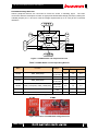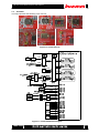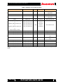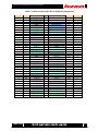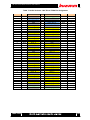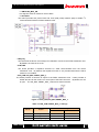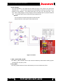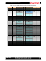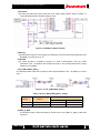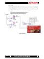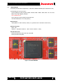
1
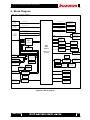
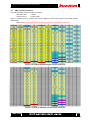
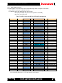
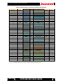
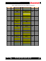
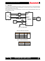
TB-6S-LX150T-IMG2 Hardware User Manual
TB-6S-LX150T-IMG2
Hardware User Manual
Rev.1.02
Rev.1.02
1
TB-6S-LX150T-IMG2 Hardware User Manual
Revision History
Version
Date
Description
Publisher
Rev.1.00
2011/01/20
Initial Release.
Yoshioka
Rev1.01
2011/02/17
Modified register number of TDI/TDO connection of FMC
Yoshioka
Rev1.02
2011/03/15
Brash up all of sections.
Modified configuration LED numbers
Rev.1.02
Yoshioka
2
TB-6S-LX150T-IMG2 Hardware User Manual
1.
2.
3.
4.
5.
6.
7.
Table of contents
Related Documents and Accessories .......................................................................................... 9
Overview ...................................................................................................................................... 9
Feature......................................................................................................................................... 9
Block Diagram ........................................................................................................................... 10
External view of board ............................................................................................................... 11
Board Specifications .................................................................................................................. 12
Description of Components ....................................................................................................... 14
7.1.
Power Supply Structure ........................................................................................................... 14
7.2.
Oscillator .................................................................................................................................. 17
7.3.
MGT reference clock ................................................................................................................ 19
7.3.1.
PLL/MMCX_CLK_P/N ...................................................................................................... 19
7.3.1.1.
7.3.2.
Clock Generator(CDCM61001RHBT) .......................................................................... 20
FB_CLEANUP_CLKP/N .................................................................................................. 21
7.3.2.1.
7.3.3.
7.4.
8.
Clock Generator(ICS810001DK-21LF) ........................................................................ 21
MGT reference clock selector .......................................................................................... 22
FMC Connector Interface......................................................................................................... 23
7.4.1.
HPC (High-Pin Count) ...................................................................................................... 24
7.4.2.
LPC(Low-Pin Count) LPC1 .............................................................................................. 31
7.4.3.
LPC (Low-Pin Count) LPC2 ............................................................................................. 35
7.5.
DDR3 SDRAM ......................................................................................................................... 39
7.6.
USB (UART)............................................................................................................................. 41
7.7.
LED .......................................................................................................................................... 42
7.8.
DIP Switch................................................................................................................................ 43
7.9.
Push Button Switches .............................................................................................................. 44
7.10.
Pin Header ........................................................................................................................... 45
7.11.
Battery ...................................................................................................................................... 46
Appendix .................................................................................................................................... 47
8.1.
Creating a Configuration File ................................................................................................... 47
8.2.
Writing a Configuration File into the Flash Memory ................................................................. 52
8.3.
Configuration Time ................................................................................................................... 58
8.4.
Factory Switch and Jumpper Settings ..................................................................................... 59
Rev.1.02
3
TB-6S-LX150T-IMG2 Hardware User Manual
List of Figures
Figure 4-1 Block Diagram ................................................................................................................. 10
Figure 5-1 component side ............................................................................................................... 11
Figure 5-2 Solder side ...................................................................................................................... 11
Figure 6-1 TB-6S-LX150T-IMG2 board dimensions ......................................................................... 12
Figure 6-2 Hole positions .................................................................................................................. 13
Figure 7-1 Power Supply Structure................................................................................................... 14
Figure 7-2 Structure of the AC adapter input power connection ...................................................... 14
Figure 7-4 FPGA Banks and Peripheral Devices ............................................................................. 16
Figure 7-6 Clock Sources ................................................................................................................. 17
Figure 7-7 Clock Distribution Diagram.............................................................................................. 17
Figure 7-9 PLL/MMCX_CLK_P/N structure ...................................................................................... 19
Figure 7-10 FB_CLEANUP_CLKP/N structure ................................................................................ 21
Figure 7-13 VITA-57 Standard Low-Pin Count Connector ............................................................... 23
Figure 7-14 SDA, SCL, GA1/0 TDI/TDO .......................................................................................... 29
Figure 7-15 PG_C2M, PG_M2C,PRSNT_M2C_L............................................................................ 29
Figure 7-17 SDA,SCL,GA1/0 TDI/TD0 ............................................................................................. 33
Figure 7-18 PG_C2M,PRSNT_M2C_L ............................................................................................ 33
Figure 7-20 SDA,SCL,GA1/0 TDI/TD0 ............................................................................................. 37
Figure 7-21 PG_C2M,PRSNT_M2C_L ............................................................................................ 37
Figure 7-23 DDR3 SDRAM .............................................................................................................. 39
Figure 7-25 LED ............................................................................................................................... 42
Figure 8-1 Creating a Configuration File with ISE 12.2 .................................................................... 47
Figure 8-2 iMPACT Window 1 .......................................................................................................... 47
Figure 8-3 iMPACT Window 2 .......................................................................................................... 48
Figure 8-4 iMPACT Window 3 .......................................................................................................... 48
Figure 8-5 iMPACT Window 4 .......................................................................................................... 49
Figure 8-6 iMPACT Window 5 .......................................................................................................... 49
Figure 8-7 iMPACT Window 6 .......................................................................................................... 50
Figure 8-8 iMPACT Window 7 .......................................................................................................... 50
Figure 8-9 iMPACT Window 8 .......................................................................................................... 50
Figure 8-10 iMPACT Window 9 ........................................................................................................ 51
Figure 8-11 iMPACT Window 10....................................................................................................... 51
Figure 8-12 Onboard JTAG Connector............................................................................................. 52
Figure 8-13 Writing into the Device 1 ............................................................................................... 52
Figure 8-14 Writing into the Device 2 ............................................................................................... 53
Figure 8-15 Writing into the Device 3 ............................................................................................... 53
Figure 8-16 Writing into the Device 4 ............................................................................................... 54
Figure 8-17 Writing into the Device 5 ............................................................................................... 54
Figure 8-18 Writing into the Device 6 ............................................................................................... 55
Figure 8-19 Write into the Device 7 .................................................................................................. 55
Figure 8-20 Write into the Device 8 .................................................................................................. 56
Figure 8-21 Reconfiguration Switch ................................................................................................. 57
Figure 8-22 Configuration Status ...................................................................................................... 57
Figure 8-23 Changing Configuration Time ....................................................................................... 58
Figure 8-24 positions ........................................................................................................................ 59
Rev.1.02
4
TB-6S-LX150T-IMG2 Hardware User Manual
List of Tables
Table 7-1 Power status LEDs ........................................................................................................... 15
Table 7-2 FPGA Banks and Corresponding Devices........................................................................ 16
Table 7-3 Details of On board Oscillator ........................................................................................... 18
Table 7-4 PLL/MMCX_CLK_P/N setting ........................................................................................... 20
Table 7-5 Clock Generator(CDCM61001RHBT)IC settings ............................................................. 20
Table 7-6 Clock Generator (ICS810001DK-21LF) IC settings ......................................................... 21
Table 7-7
MGT reference clock settings ........................................................................................ 22
Table 7-8 HPC Column A & B Pin to FPGA Pin Assignment ............................................................ 24
Table 7-9 HPC Column C & D Pin to FPGA Pin Assignment ........................................................... 25
Table 7-10 HPC Column E & F Pin to FPGA Pin Assignment .......................................................... 26
Table 7-11 HPC Column G & H Pin to FPGA Pin Assignment ......................................................... 27
Table 7-12 HPC Column J & K Pin to FPGA Pin Assignment .......................................................... 28
Table 7-13 PG_C2M, PRSNT_M2C_L settings ................................................................................ 29
Table 7-14 LPC1 (CN3) Column C & D Pin to FPGA Pin assignment ............................................. 31
Table 7-15 LPC1 (CN3) Column G & H pin Pin to FPGA Pin assignment ....................................... 32
Table 7-16 PG_C2M, PRSNT_M2C_L settings ................................................................................ 33
Table 7-17 LPC2 (CN4) Column C & D Pin to FPGA Pin Assignment ............................................. 35
Table 7-18 LPC2 (CN4) Column G & H Pin to FPGA Pin Assignment ............................................. 36
Table 7-19 PG_C2M, PRSNT_M2C_L settigs .................................................................................. 37
Table 7-20 DDR3 SDRAM pin assignment ....................................................................................... 40
Table 7-21 UART pin assignment ..................................................................................................... 41
Table 7-22 Serial EEPROM SCL ...................................................................................................... 41
Table 7-23 LED pin assignment........................................................................................................ 42
Table 7-24 DIP Switch Pin Assignment ............................................................................................ 43
Table 7-25 Push Button Switch Pin Assignment............................................................................... 44
Table 7-26 Pin Header pin assignment ............................................................................................ 45
Table 8-1 Initial settings .................................................................................................................... 59
Rev.1.02
5
TB-6S-LX150T-IMG2 Hardware User Manual
Introduction
Thank you for purchasing the TB-6S-LX150T-IMG2 board.
Before using the product, be sure to
carefully read this user manual and fully understand how to correctly use the product.
First read
through this manual, and then always keep it handy.
SAFETY PRECAUTIONS
Be sure to observe these precautions
Observe the precautions listed below to prevent injuries to you or other personnel or damage to property.
• Before using the product, read these safety precautions carefully to assure correct use.
• These precautions contain serious safety instructions that must be observed.
• After reading through this manual, be sure to always keep it handy.
The following conventions are used to indicate the possibility of injury/damage and classify precautions if
the product is handled incorrectly.
Danger
Indicates the high possibility of serious injury or death if the product is handled
incorrectly.
Indicates the possibility of serious injury or death if the product is handled
Warning
incorrectly.
Indicates the possibility of injury or physical damage in connection with houses or
Caution
household goods if the product is handled incorrectly.
The following graphical symbols are used to indicate and classify precautions in this manual.
(Examples)
Turn off the power switch.
Do not disassemble the product.
!
Rev.1.02
Do not attempt this.
6
TB-6S-LX150T-IMG2 Hardware User Manual
Warning
In the event of a failure, disconnect the power supply.
If the product is used as is, a fire or electric shock may occur.
Disconnect the power supply
immediately and contact our sales personnel for repair.
If an unpleasant smell or smoking occurs, disconnect the power supply.
If the product is used as is, a fire or electric shock may occur.
immediately.
Disconnect the power supply
After verifying that no smoking is observed, contact our sales personnel for
repair.
Do not disassemble, repair or modify the product.
Otherwise, a fire or electric shock may occur due to a short circuit or heat generation.
For
inspection, modification or repair, contact our sales personnel.
!
Do not touch a cooling fan.
As a cooling fan rotates in high speed, do not put your hand close to it.
cause injury to persons.
!
Otherwise, it may
Never touch a rotating cooling fan.
Do not place the product on unstable locations.
Otherwise, it may drop or fall, resulting in injury to persons or failure.
!
If the product is dropped or damaged, do not use it as is.
!
Do not touch the product with a metallic object.
!
Do not place the product in dusty or humid locations or where water may
Otherwise, a fire or electric shock may occur.
Otherwise, a fire or electric shock may occur.
splash.
Otherwise, a fire or electric shock may occur.
!
!
Do not get the product wet or touch it with a wet hand.
Otherwise, the product may break down or it may cause a fire, smoking or electric shock.
Do not touch a connector on the product (gold-plated portion).
Otherwise, the surface of a connector may be contaminated with sweat or skin oil, resulting
in contact failure of a connector or it may cause a malfunction, fire or electric shock due to
static electricity.
Rev.1.02
7
TB-6S-LX150T-IMG2 Hardware User Manual
Caution
Do not use or place the product in the following locations.
!
• Humid and dusty locations
• Airless locations such as closet or bookshelf
• Locations which receive oily smoke or steam
• Locations exposed to direct sunlight
• Locations close to heating equipment
• Closed inside of a car where the temperature becomes high
• Staticky locations
• Locations close to water or chemicals
Otherwise, a fire, electric shock, accident or deformation may occur due to a short circuit or heat
generation.
!
Do not place heavy things on the product.
Otherwise, the product may be damaged.
■ Disclaimer
This product is an evaluation board for Xilinx FPGA, Spartan6. Tokyo Electron Device Limited assumes
no responsibility for any damages resulting from the use of this product for purposes other than those
stated.
Even if the product is used properly, Tokyo Electron Device Limited assumes no responsibility for any
damages caused by:
(1) Earthquake, thunder, natural disaster or fire resulting from the use beyond our responsibility, acts by
a third party or other accidents, the customer’s willful or accidental misuse or use under other
abnormal conditions.
(2) Secondary impact arising from use of this product or its unusable state (business interruption or
others)
(3) Use of this product against the instructions given in this manual.
(4) Malfunctions due to connection to other devices.
Tokyo Electron Device Limited assumes no responsibility or liability for:
(1) Erasure or corruption of data arising from use of this product.
(2) Any consequences or other abnormalities arising from use of this product, or
(3) Damage of this product not due to our responsibility or failure due to modification
This product has been developed by assuming its use for research, testing or evaluation.
It is not
authorized for use in any system or application that requires high reliability.
Repair of this product is carried out by replacing it on a chargeable basis, not repairing the faulty devices.
However, non-chargeable replacement is offered for initial failure if such notification is received within
two weeks after delivery of the product.
The specification of this product is subject to change without prior notice.
The product is subject to discontinuation without prior notice.
Rev.1.02
8
TB-6S-LX150T-IMG2 Hardware User Manual
1. Related Documents and Accessories
Related documents:
All documents and reference designs relating to this board are available only for purchasing customers
and can be downloaded from our website at Tokyo Electron Device Ltd. TED SUPPORT WEB
(http://ppg.teldevice.co.jp/eng/index.htm).
Mounting parts
7 x rubber foots, 14 x M3 X 6mm screws and 7 x M3 X 10mm spacers
Accessories
Option board spacer set:
6 x M2.6 X 10mm spacers (Duracon) and 12 screws with Duracon washers
MMCX cable set:
2 x MMCX-SMA cables (Samtec RF174-03SP1-01SP1-0400)
2 x MMCX-MMCX cables (Samtec RF174-03SP1-03SP1-0400)
AC adaptor
1 x AC adaptor (Akizuki Denshi: LTE(GFP)451DA-1238 or equivalents)
2. Overview
®
The TB-6S-LX150T-IMG2 DDR3, 8 channel GTP, and Xilinx Spartan -6 evaluation board forms the
base for numerous Spartan-6 development platforms including the Consumer Video Kit 2.0.
3. Feature
-
XC6SLX150T-3FG900 FPGA
-
1 x VITA-57 standard FPGA Mezzanine Card (FMC) High Pin Count (HPC) connector
-
2 x FMC Low Pin Count (LPC) connectors.
Due to limitations on the number of FPGA pins, all defined FMC standard signals are not connected. For more information,
refer to the Connector Pinout Tables in this manual on pages 24, 31, and 35.
-
3 x DDR3 SDRAM (Chip): Micron MT41J64M16LA-15E(or equivalent) (1 Gbits 800Mbps)
-
4 x 4 LVDS crosspoint switch
-
Clocks (see Figure 7-7 Clock Distribution Diagram)
Multiple onboard clock sources (200 MHz, 27 MHz, 74.25 MHz)
User populated clock chip in 8-pin dip
External clock sources via single ended and differential MMCX connections with clock
cleaners
PLL clock generator programmable from the FPGA
MMCX clock output
DIP switch selectable MGT clock source selection
-
Push button switches, dip switches and pin headers
-
LEDs
-
USB connection to a PC (via USB-UART conversion device) for character based terminal I/O
-
128 Mbit SPI Flash configuration ROM
-
TI TPS 386000 Voltage Supervisor
Rev.1.02
9
TB-6S-LX150T-IMG2 Hardware User Manual
4. Block Diagram
TB-6S-LX150T-IMG2
FMC_LPC1
(low-pin count)
[Samtec]
ASP-134603-01
FMC_LPC2
(low-pin count)
[Samtec]
ASP-134603-01
GC:2 pair/IO:34 pair
ADR,CLK,CMD
DDR SDRAM(1Gbit)
[Micron]
MT41J64M16LA-15E
Data[0:15],DQS,DM
ADR,CLK,CMD
GC:2 pair/IO:34 pair
DDR SDRAM(1Gbit)
[Micron]
MT41J64M16LA-15E
Data[0:15],DQS,DM
Differential signal is Input only
ADR,CLK,CMD
DDR SDRAM(1Gbit)
[Micron]
MT41J64M16LA-15E
Data[0:15],DQS,DM
GTP:CLK:4 pair/IO:16 pair
LA:CLK:2 pair/IO:34 pair
FMC_HPC
(high-pin count)
[Samtec]
ASP-134486-01
MMCX Connector
[Samtec]
HA_HB:CLK:2 pair/HA_IO:24 pair, HB_IO:22 pair
MMCX-J-P-H-ST-TH1
pair
LVDS 4x4
CROSSPOINT
SWITCH
[TI]
SN65LVDS250DBT
2pair
pair
pair
LVDS BUFFER
[TI]
CDCLVD2102RGT
OSC 74.25MHz
[TamaDevice]
CX104BC
pair
LVDS BUFFER
[TI]
CDCLVD2102RGT
Option OSC
[omron]
XR2A-0811-N
4pair
Dip Switch(8 poles)
[omron]
A6H-8101
pair
FPGA
[Xilinx]
Spartan-6
MMCX Connector
[Samtec]
MMCX-J-P-H-ST-TH1
OSC 200MHz
[TamaDevice]
CL20VBC
Level Shifter
[TI]
SN74AVC4T774
SPI FLASH
[STMicroelectronics]
M25P64-VMF6P
XC6SLX150T
-3FFG900
JTAG Connector
[molex]
87831-1420
pair
OSC 27MHz
[TamaDevice]
CX104BC
Clock Generator
[TI]
CDCM61001RHBT
pair
Push Switch
[omron]
B3SN-3012
LVDS Buffer
[TI]
CDCLVD1204RGT
MMCX Connector
[Samtec]
MMCX-J-P-H-ST-TH1
MMCX Connector
[Samtec]
Level shifter
[TI] x2
SN74LVC2T45
Dip Switch(2 poles)
[omron]
A6H-2101
pair
EEPROM
[MICROCHIP]
24LC256I/P
MMCX-J-P-H-ST-TH1
XTAL 27MHz
[TamaDevice]
HC-49/U
MMCX Connector
[Samtec]
MMCX-J-P-H-ST-TH1
Dip Switch(4 poles)
[omron]
A6H-4101
Dip Switch(8 poles)
[omron]
A6H-8101
IC Socket
[omron]
XR2A-0811-N
USB Connector
[HIROSE]
UX60-MB-5ST
Resonator 12MHz
[TamaDevice]
HC-49U/S-SMD
PinHeader (14 pin)
[Samtec]
TSM-114-01-L-DV
CLK CLEANER
[IDT]
ICS810001DK-21LF
Push Switch x4
[omron]
B3SN-3012
Push Switch
[omron]
B3SN-3012
MMCX Connector
[Samtec]
USB-Serial IC
[TI]
TUSB3410RHB
Dip Switch (10 poles)
[omron]
A6S-0104-H
Clock Buffer
[TI]
CDCLVC1102PW
LED x8
[AVAGO]
HSMD-C191
MMCX-J-P-H-ST-TH1
Figure 4-1 Block Diagram
Rev.1.02
10
TB-6S-LX150T-IMG2 Hardware User Manual
5. External view of board
lock
lock
enerator Selector
leanup
lock
n
X Single
ut
_ P 1 onnector
ow Pin
ption
S
X
ifferential
nput
Power
V S 4x4
SSP
T
SW T
3S
A
P A
e onfig SW
_ P
onnector
igh Pin
S
3S
A
S 200
X ifferential nput
lash emory
4.25
Power
US
US
S T SW
_ P 2 onnector
ow Pin
ip SW
JTA
Push SW Pin eader
K
S T SW
Figure 5-1 component side
Figure 5-2 Solder side
Rev.1.02
11
TB-6S-LX150T-IMG2 Hardware User Manual
6. Board Specifications
External Dimensions:
W: 240.00mm x H: 175.00mm
Number of Layers:
12 layers
Board Thickness:
1.6mm
Material:
FR-4
FPGA:
Xilinx XC6SLX150T-3FGG900
PROM:
ST Micro M25P64-VMF6P
FMC Connector (High-Pin):
Samtec ASP-134486-01
FMC Connector (Low-Pin):
Samtec ASP-134603-01
DDR2 SDRAM:
Micron MT41J64M16LA-15E
MMCXConnector:
Samtec MMCX-J-P-H-ST-TH1
Figure 6-1 TB-6S-LX150T-IMG2 board dimensions
Rev.1.02
12
TB-6S-LX150T-IMG2 Hardware User Manual
Figure 6-2 Hole positions
Rev.1.02
13
TB-6S-LX150T-IMG2 Hardware User Manual
7. Description of Components
7.1.
Power Supply Structure
Figure 7-1 Power Supply Structure
Power Input
Power is supplied through the AC adaptor..
Figure 7-2 Structure of the AC adapter input power connection
Rev.1.02
14
TB-6S-LX150T-IMG2 Hardware User Manual
Power Status LED
The board provides 13 LEDs to signal the correct operational status of each voltage rail.
Table 7-1 Power status LEDs
Voltage
LED
Description
Color
12V
LED1
12V power supply
Blue
5.0V
LED2
Power for 1.2/1.5/2.5V
Red
1.2V
LED3
Power for FPGA VCCINT
Red
M1+0.75V
LED4
Power for FPGA VREF(DDR3)
Red
2.5V
LED5
Power for FPGA VCCIO
Red
1.5V
LED6
Power for FPGA VCCIO
Red
M2+0.75V
LED7
Power for FPGA VREF(DDR3)
Red
OP+2.5V
LED8
Power for FMC
Red
1.2V_A1
LED9
Power for MGT AVCC1/AVTT1
Red
M3+0.75V
LED10
Power for FPGA VREF(DDR3)
Red
OP+3.3V
LED11
Power for FMC
Red
1.2V_A2
LED12
Power for MGT AVCC2/AVTT2
Red
3.3V
LED13
Power for FPGA VCCIO
Red
Figure 7-3 Power status LED
Rev.1.02
15
TB-6S-LX150T-IMG2 Hardware User Manual
FPGA Bank Voltage Selection
Various peripheral devices are connected to FPGA as shown in following figure.
The FMC
connectors allow the developers to select an appropriate FPGA Bank voltage (VCCIO) by setting the
onboard jumpers (JP1, 2 and 3) to meet the voltage requirements (3.3V or 2.5V) for the connected
FMC(HPC) CN5
interfaces.
Figure 7-4 FPGA Banks and Peripheral Devices
Table 7-2 FPGA Banks and Corresponding Devices
Bank
Function
Bank0
FMC_HPC(CN5)
Bank1
DDR3,DSW,LED,PSW,USB
Bank2
FMC_HPC(CN5)
Bank3
FMC_LPC1(CN3), FMC_LPC2(CN4)
Bank4
DDR3
Bank5
DDR3
Voltage
Voltage Selection
SEL
2.5V
3.3V
JP2
1-2
2-3
-
-
-
JP3
1-2
2-3
JP1
1-2
2-3
1.5V
-
-
-
1.5V
-
-
-
Selectable
(3.3V/2.5V)
1.5V
Selectable
(3.3V/2.5V)
Selectable
(3.3V/2.5V)
Selectable voltage is initially 2.5V settings
Figure 7-5 Location of FPGA Bank Voltage Selection
Rev.1.02
16
TB-6S-LX150T-IMG2 Hardware User Manual
7.2. Oscillator
The board provides the following clock sources.
Figure 7-6 Clock Sources
Figure 7-7 Clock Distribution Diagram
Rev.1.02
17
TB-6S-LX150T-IMG2 Hardware User Manual
Table 7-3 Details of On board Oscillator
connection
name
I/F
FPGA PIN
Remakes
X1
CLK74.25M_P/N
LVDS
W5/W4
Single ended to differential
signal buffer
X2
CLK200M_P/N
LVDS
AJ17/AK17
DDR3(IDelay) clock
X3
CLK_OPTION_P/N
LVDS
C16/A16
Single ended to differential
signal buffer
CN6/7
MMCX_P/N
LVDS
AH16/AK16
MMCX external clock
IC32 (FB_CLEANUP_CLKP/N)
or
HPC_CLK_M101_P/N
B13/A13
CN5(HPC_GBTCLK0_M2C_P/N)
HPC_CLK_M245_P/N
AJ13/AK13
or
HPC_CLK_M123_P/N
CN5(HPC_GBTCLK1_M2C_P/N)
HPC_CLK_M267_P/N
LVDS
D18/C18
MGT reference clock
AG18/AH18
or
IC36(PLL/MMCX_CLKP/N)
FMC_HPC(CN5)
HPC_CLK0_M2C_P/N
LVDS
B15/A15
HPC_LA interface clock
FMC_HPC (CN5)
HPC_CLK1_M2C_P/N
LVDS
E16/D16
HPC_LA interface clock
FMC_HPC (CN5)
HPC_CLK2_M2C_P/N
LVDS
AC16/AD16
HPC_HA_HB interface
clock
FMC_HPC (CN5)
HPC_CLK3_M2C_P/N
LVDS
AF16/AG16
HPC_HA_HB interface
clock
FMC_LPC1(CN3)
LPC1_CLK0_M2C_P/N
LVDS
V4/V3
LPC1interface clock
FMC_LPC1(CN3)
LPC1_CLK1_M2C_P/N
LVDS
H15/G15
LPC1interface clock
FMC_LPC2(CN4)
LPC2_CLK0_M2C_P/N
LVDS
AA3/AA1
LPC2 interface clock
FMC_LPC2(CN4)
LPC2_CLK1_M2C_P/N
LVDS
AB2/AB1
LPC2 interface clock
Supplementary explanation: HPC_CLK*_M2C_P/N and LPC*_M2C_P/N can be used for single-end
signal.
Rev.1.02
18
TB-6S-LX150T-IMG2 Hardware User Manual
7.3.
MGT reference clock
FPGA
X5
LVDS
27MHz
DIPSW
SW6
DIPSW
SW7
SEL
SEL
LVDS
CDCM61001
(IC35)
LVDS
LVDS
MMCX_P(CN10)
MMCX_N(CN11)
LVDS
CDCLVD1204(I
C36)
LVDS
FMC
HPC LVDS
PLL/MMCX_CLK_P/N
FB_CLEANUP_CLKP/N
LVDS
CLK Cleaner
ICS810001-21(IC33)
MMCX_IN(CN9)
MGT101
B13:MGTREFCLK0P_101
A13:MGTREFCLK0N_101
MGT123
D18:MGTREFCLK0P_123
C18:MGTREFCLK0N_123
MGT245
AJ13:MGTREFCLK0P_245
AK13:MGTREFCLK0N_245
CLK0
DIPSW
SW4,5
LVCMOS33
Ctrl
LVDS
LVDS
ICS8545-02(IC32)
CLK1
CDCLVC1102
(IC31)
MGT267
AG18:MGTREFCLK0P_267
AH18:MGTREFCLK0N_267
SN65LVDS250
(IC37)
AH24:BANK2
MMCX_OUT(CN8)
Figure 7-8 MGT reference clock structure
7.3.1.
PLL/MMCX_CLK_P/N
PLL/MMCX_CLK_P/N is input clock for “SN65LVDS250DBT”. This is selected MMCX_P/N(CN10, 11) or
a clock generator(IC35: CDCM61001RHBT) by clock selector(IC36: CDCLVD1204RGT) and
SW6(DIP-SW)
The clock generator (IC35) uses 27MHz OSC(X5) for its master clock.
Figure 7-9 PLL/MMCX_CLK_P/N structure
Rev.1.02
19
TB-6S-LX150T-IMG2 Hardware User Manual
Table 7-4 PLL/MMCX_CLK_P/N setting
SW6
Selected clock
1
2
OUTP
OUTN
OFF
OFF
L
H
ON
OFF
MMCX
OFF
ON
PLL Clock
ON
ON
PLL Clock
7.3.1.1. Clock Generator(CDCM61001RHBT)
This board uses a low jitter clock generator(TI CDCM61001RHBT). For more detail settings, please refer
to the data sheet of CDCM61001RHBT.
The output frequency and reset of clock generator is controlled by FPGA. It has 27MHz OSC for XIN.
Table 7-5 Clock Generator(CDCM61001RHBT)IC settings
Signal
FPGA Pin No.
Used for
PR[1]
AE26
Setting for pre-scaler divider and feedback divider
PR[0]
AE25
OD[2]
Y23
OD[1]
Y22
OD[0]
AH27
RSTN
Y24
Reset from FPGA
OS[1:0]
-
OS[1:0] = 01 fixed
CE
-
CE = 1fixed
Setting for output divider
Calculation for frequency of clock output
Fout = VCO / Prescaler Divider / Output Divider
For example: Generate 135MHz clock output.
Conditions: Input clock is 27MHz (VCO=2025)
PR[1:0] = OFF,ON (Prescaler Divider = 5, Feedback Divider = 15)
OD[2:0] = OFF,ON,OFF(Output Divider = 3)
Rev.1.02
20
TB-6S-LX150T-IMG2 Hardware User Manual
7.3.2. FB_CLEANUP_CLKP/N
“FB_CLEANUP_CLKP/N” is differential input clock signal for the “SN65LVDS250DBT”. This differential
signal is converted from single-ended to differential by IC32. The single-ended clock is generated by
the IDT video clock generator (ICS810001DK-21LF).
Figure 7-10 FB_CLEANUP_CLKP/N structure
7.3.2.1. Clock Generator(ICS810001DK-21LF)
The board provides an onboard video clock generation circuit using the IDT ICS810001DK-21LF.
For details about setting clock frequencies, refer to the corresponding IDT data sheet.
This device accepts a clock sourced from the FPGA (AH24 pin) or from an external MMCX connector
(CN9). The clock source selection is made via DIP switch SW5. The user selects the output clock
frequency generated by this IDT video clock generator PLL via DIP switch SW5. The XTAL_IN is
connected a 27MHz oscillator. A reset to this device occurs during power-up or by pressing
pushbutton SW3.
Table 7-6 Clock Generator (ICS810001DK-21LF) IC settings
Signal
V[3:0]
SW No.
SW4
SW bit
Purpose
bit[4:1]
Input clock setting
CLK_SEL
bit[1]
Input clock selection (ON=MMCX/OFF=FPGA)
MF
bit[2]
PLL coefficient
bit[4:3]
Frequency dividing value: 00=4 / 01=8 / 10=12 / 11=18
nBP[1:0]
bit[6:5]
Output clock generation block structure setting
OE
bit[7]
Output clock enable (ON=Enable)
SW5
N[1:0]
Output clock formula in nBP[1:0]=11(ON,ON):
Fout = (in_CLK / P) x M x MF / N
Rev.1.02
21
TB-6S-LX150T-IMG2 Hardware User Manual
Example: 148.5MHz output
Condition: Input clock: 27MHz (V[3:0]=ALL OFF=(P=1000)=(M=1000))
MF=OFF (x22)
N[1:0]=OFF,OFF (divide-by-4 frequency)
7.3.3.
MGT reference clock selector
MGT
reference
clocks
are
selected
by LVDS
4x4
crosspoint
switch
IC37
(TI:
SN65LVDS250DBT). 4 clock sources are selected by SW7.
Figure 7-11 MGT reference clock selector IC
Table 7-7
OUTPUT CHANNEL 1
MGT reference clock settings
OUTPUT CHANNEL 2
OUTPUT CHANNEL 3
OUTPUT CHANNEL 4
S10
S11
1Y/1Z
S20
S21
2Y/2Z
S30
S31
3Y/3Z
S40
S40
4Y/4Z
OFF
OFF
1A/1B
OFF
OFF
1A/1B
OFF
OFF
1A/1B
OFF
OFF
1A/1B
OFF
ON
2A/2B
OFF
ON
2A/2B
OFF
ON
2A/2B
OFF
ON
2A/2B
ON
OFF
3A/3B
ON
OFF
3A/3B
ON
OFF
3A/3B
ON
OFF
3A/3B
ON
ON
4A/4B
ON
ON
4A/4B
ON
ON
4A/4B
ON
ON
4A/4B
For example: Selecting FB_CLEANUP_CLKP/N to HPC_CLK_M123/245_P/N
and HPC_GBTCLK0_M2C_P/N to HPC_CLK_M101/267_P/N.
SW7
Rev.1.02
1: OFF
2: OFF
3: OFF
4: ON
5: OFF
6: OFF
7: OFF
8: ON
22
TB-6S-LX150T-IMG2 Hardware User Manual
7.4. FMC Connector Interface
The board provides 3 Samtec FMC connectors.
High-Pin Count
: 1 (CN5)
Low-Pin Count
: 2 (CN3, CN4)
Figure 7-12 and Figure 7-13 show the VITA-57 High-Pin Count and Low-Pin Count FMC pinouts
respectively.
Notice: Not all pins of the HPC and LPC connectors are connected to the FPGA.
Figure 7-12 VITA-57 Standard High-Pin Count Connector
Figure 7-13 VITA-57 Standard Low-Pin Count Connector
Rev.1.02
23
TB-6S-LX150T-IMG2 Hardware User Manual
7.4.1.
HPC (High-Pin Count)
The FMC high-pin count connector connects the following number of signals to the FPGA:
High Speed: 8 ch(TX), 8 ch (RX) and 2 clocks
Low Speed: LA 34 pair (68 single-end) and 2 clocks.
HA 24 pair (48 single-end) and 2 clocks (common of HA/HB).
HB 22 pair (44 single-end).
Table 7-8 HPC Column A & B Pin to FPGA Pin Assignment
Bank No.
Pin No.
MGTRXP1_101
MGTRXN1_101
D12
C12
MGTRXP0_123
MGTRXN0_123
D20
C20
MGTRXP1_123
MGTRXN1_123
D22
C22
MGTRXP0_245
MGTRXN0_245
MGTRXP1_245
MGTRXN1_245
AG10
AH10
AG12
AH12
MGTTXP1_101
MGTTXN1_101
B11
A11
MGTTXP0_123
MGTTXN0_123
B21
A21
MGTTXP1_123
MGTTXN1_123
B23
A23
MGTTXP0_245
MGTTXN0_245
MGTTXP1_245
MGTTXN1_245
AJ9
AK9
AJ11
AK11
A
GND
DP1_M2C_P
DP1_M2C_N
GND
GND
DP2_M2C_P
DP2_M2C_N
GND
GND
DP3_M2C_P
DP3_M2C_N
GND
GND
DP4_M2C_P
DP4_M2C_N
GND
GND
DP5_M2C_P
DP5_M2C_N
GND
GND
DP1_C2M_P
DP1_C2M_N
GND
GND
DP2_C2M_P
DP2_C2M_N
GND
GND
DP3_C2M_P
DP3_C2M_N
GND
GND
DP4_C2M_P
DP4_C2M_N
GND
GND
DP5_C2M_P
DP5_C2M_N
GND
1
2
3
4
5
6
7
8
9
10
11
12
13
14
15
16
17
18
19
20
21
22
23
24
25
26
27
28
29
30
31
32
33
34
35
36
37
38
39
40
B
RES1
GND
GND
DP9_M2C_P
DP9_M2C_N
GND
GND
DP8_M2C_P
DP8_M2C_N
GND
GND
DP7_M2C_P
DP7_M2C_N
GND
GND
DP6_M2C_P
DP6_M2C_N
GND
GND
*1 GBTCLK1_M2C_P
*1 GBTCLK1_M2C_N
GND
GND
DP9_C2M_P
DP9_C2M_N
GND
GND
DP8_C2M_P
DP8_C2M_N
GND
GND
DP7_C2M_P
DP7_C2M_N
GND
GND
DP6_C2M_P
DP6_C2M_N
GND
GND
RES0
PinNo.
Bank No.
AG22
AH22
MGTRXP1_267
MGTRXN1_267
AG20
AH20
MGTRXP0_267
MGTRXN0_267
*1
*1
*1
*1
AJ23
AK23
MGTTXP1_267
MGTTXN1_267
AJ21
AK21
MGTTXP0_267
MGTTXN0_267
*1: GBTCLK1_M2C_P/n can be assigned to reference clock of 4 MGT tiles by IC37.
For more details, please refer to “7.3.3 NGT reference clock selector”.
Rev.1.02
24
TB-6S-LX150T-IMG2 Hardware User Manual
Table 7-9 HPC Column C & D Pin to FPGA Pin Assignment
Bank No.
MGTTXP0_101
MGTTXN0_101
MGTRXP0_101
MGTRXN0_101
Pin No.
B9
A9
D10
C10
0
0
G18
F18
0
0
F15
E15
0
0
J13
H13
0
0
L14
K14
0
0
K19
J19
C
GND
DP0_C2M_P
DP0_C2M_N
GND
GND
DP0_M2C_P
DP0_M2C_N
GND
GND
LA06_P
LA06_N
GND
GND
LA10_P
LA10_N
GND
GND
LA14_P
LA14_N
GND
GND
LA18_P_CC
LA18_N_CC
GND
GND
LA27_P
LA27_N
GND
GND
*2 SCL
*2 SDA
GND
GND
*3 GA0
*6 12P0V
GND
*6 12P0V
GND
*6 3P3V
GND
1
2
3
4
5
6
7
8
9
10
11
12
13
14
15
16
17
18
19
20
21
22
23
24
25
26
27
28
29
30
31
32
33
34
35
36
37
38
39
40
D
*5 PG_C2M
GND
GND
*1 GBTCLK0_M2C_P
*1 GBTCLK0_M2C_N
GND
GND
LA01_P_CC
LA01_N_CC
GND
LA05_P
LA05_N
GND
LA09_P
LA09_N
GND
LA13_P
LA13_N
GND
LA17_P_CC
LA17_N_CC
GND
LA23_P
LA23_N
GND
LA26_P
LA26_N
GND
TCK
*4 TDI
*4 TDO
*6 3P3VAUX
TMS
TRST_L
*3 GA1
*6 3P3V
GND
*6 3P3V
GND
*5 3P3V
Pin No.
Bank No.
*2
*2
*2
*2
F19
E19
0
0
F17
E17
0
0
J14
H14
0
0
G12
F12
0
0
M15
K15
0
0
H17
G17
0
0
M18
L18
0
0
*2: GBTCLK0_M2C_P/n can be assigned to reference clock of 4 MGT tiles by IC37.
For more details, please refer to Figure 7-8 MGT reference clock structure
Rev.1.02
25
TB-6S-LX150T-IMG2 Hardware User Manual
Table 7-10 HPC Column E & F Pin to FPGA Pin Assignment
Bank No.
2
2
Pin No.
Y21
AA21
2
2
Y17
AA17
2
2
AB17
AD17
2
2
AE15
AF15
2
2
AC19
AD19
2
2
AD22
AE22
2
2
AA11
AB11
2
2
AC9
AD9
2
2
AF7
AG7
2
2
AG8
AH8
2
2
AD12
AE12
2
2
AJ15
AK15
Rev.1.02
E
GND
HA01_P_CC
HA01_N_CC
GND
GND
HA05_P
HA05_N
GND
HA09_P
HA09_N
GND
HA13_P
HA13_N
GND
HA16_P
HA16_N
GND
HA20_P
HA20_N
GND
HB03_P
HB03_N
GND
HB05_P
HB05_N
GND
HB09_P
HB09_N
GND
HB13_P
HB13_N
GND
HB19_P
HB19_N
GND
HB21_P
HB21_N
GND
*6 VADJ
GND
1
2
3
4
5
6
7
8
9
10
11
12
13
14
15
16
17
18
19
20
21
22
23
24
25
26
27
28
29
30
31
32
33
34
35
36
37
38
39
40
F
*5 PG_M2C
GND
GND
HA00_P_CC
HA00_N_CC
GND
HA04_P
HA04_N
GND
HA08_P
HA08_N
GND
HA12_P
HA12_N
GND
HA15_P
HA15_N
GND
HA19_P
HA19_N
GND
HB02_P
HB02_N
GND
HB04_P
HB04_N
GND
HB08_P
HB08_N
GND
HB12_P
HB12_N
GND
HB16_P
HB16_N
GND
HB20_P
HB20_N
GND
*6 VADJ
Pin No.
Bank No.
W19
Y19
2
2
Y16
AB16
2
2
AC15
AD15
2
2
AE17
AF17
2
2
AE21
AF21
2
2
AE23
AF23
2
2
AB10
AB9
2
2
AD8
AE8
2
2
AG6
AH6
2
2
AD10
AE10
2
2
AE13
AF13
2
2
AC11
AD11
2
2
26
TB-6S-LX150T-IMG2 Hardware User Manual
Table 7-11 HPC Column G & H Pin to FPGA Pin Assignment
Bank No.
0
0
Pin No.
E16
D16
0
0
F21
E21
0
0
H19
G19
0
0
H16
G16
0
0
G14
F14
0
0
J12
H12
0
0
M13
L13
0
0
J18
H18
0
0
M19
L19
0
0
L21
K21
0
0
J22
H22
0
0
F24
E24
Rev.1.02
G
GND
CLK1_M2C_P
CLK1_M2C_N
GND
GND
LA00_P_CC
LA00_N_CC
GND
LA03_P
LA03_N
GND
LA08_P
LA08_N
GND
LA12_P
LA12_N
GND
LA16_P
LA16_N
GND
LA20_P
LA20_N
GND
LA22_P
LA22_N
GND
LA25_P
LA25_N
GND
LA29_P
LA29_N
GND
LA31_P
LA31_N
GND
LA33_P
LA33_N
GND
*6 VADJ
GND
1
2
3
4
5
6
7
8
9
10
11
12
13
14
15
16
17
18
19
20
21
22
23
24
25
26
27
28
29
30
31
32
33
34
35
36
37
38
39
40
H
*7 VREF_A_M2C
*5 PRSNT_M2C_L
GND
CLK0_M2C_P
CLK0_M2C_N
GND
LA02_P
LA02_N
GND
LA04_P
LA04_N
GND
LA07_P
LA07_N
GND
LA11_P
LA11_N
GND
LA15_P
LA15_N
GND
LA19_P
LA19_N
GND
LA21_P
LA21_N
GND
LA24_P
LA24_N
GND
LA28_P
LA28_N
GND
LA30_P
LA30_N
GND
LA32_P
LA32_N
GND
*6 VADJ
Pin No.
Bank No.
B15
A15
0
0
G20
F20
0
0
G22
F22
0
0
F23
E23
0
0
F13
E13
0
0
D24
C24
0
0
B25
A25
0
0
L17
K17
0
0
M20
L20
0
0
K20
J20
0
0
H21
G21
0
0
E25
D25
0
0
27
TB-6S-LX150T-IMG2 Hardware User Manual
Table 7-12 HPC Column J & K Pin to FPGA Pin Assignment
Bank No.
2
2
Pin No.
AF16
AG16
2
2
AB21
AC21
2
2
AA19
AB19
2
2
AD18
AE18
2
2
AE19
AF19
2
2
AE24
AF24
2
2
AB20
AC20
2
2
AB12
AC12
2
2
AE9
AF9
2
2
AH7
AK7
2
2
AE11
AF11
2
2
AD14
AE14
Rev.1.02
J
GND
CLK3_M2C_P
CLK3_M2C_N
GND
GND
HA03_P
HA03_N
GND
HA07_P
HA07_N
GND
HA11_P
HA11_N
GND
HA14_P
HA14_N
GND
HA18_P
HA18_N
GND
HA22_P
HA22_N
GND
HB01_P
HB01_N
GND
HB07_P
HB07_N
GND
HB11_P
HB11_N
GND
HB15_P
HB15_N
GND
HB18_P
HB18_N
GND
*8 VIO_B_M2C
GND
1
2
3
4
5
6
7
8
9
10
11
12
13
14
15
16
17
18
19
20
21
22
23
24
25
26
27
28
29
30
31
32
33
34
35
36
37
38
39
40
K
*7 VREF_B_M2C
GND
GND
CLK2_M2C_P
CLK2_M2C_N
GND
HA02_P
HA02_N
GND
HA06_P
HA06_N
GND
HA10_P
HA10_N
GND
HA17_P_CC
HA17_N_CC
GND
HA21_P
HA21_N
GND
HA23_P
HA23_N
GND
HB00_P_CC
HB00_N_CC
GND
HB06_P_CC
HB06_N_CC
GND
HB10_P
HB10_N
GND
HB14_P
HB14_N
GND
HB17_P_CC
HB17_N_CC
GND
*8 VIO_B_M2C
Pin No.
Bank No.
AC16
AD16
2
2
W20
Y20
2
2
AA18
AB18
2
2
AA22
AC22
2
2
AD20
AE20
2
2
AC24
AD24
2
2
AB23
AC23
2
2
W12
Y12
2
2
Y14
AA14
2
2
W14
Y13
2
2
AB13
AC13
2
2
AB14
AC14
2
2
28
TB-6S-LX150T-IMG2 Hardware User Manual
* 1 GBTCLK0_M2C_P,N
This signal is used for reference clock of MGT.
* 2 SCL,SDA
2
The board provides test points TP32 and TP33 (with pullup resistors pad) to enable I C
communications with the FPGA mezzanine card.
Figure 7-14 SDA, SCL, GA1/0 TDI/TDO
* 3 GA[1:0]
The board has the above circuit design for notification of an ID to the FPGA mezzanine card.
By default, the value is set to 00.
* 4 TDI,TDO
The board provides a loopback structure for JTAG communication from the FPGA
mezzanine card.
By default, this loopback function is not provided because the R510
resistor is not installed.
* 5 PG_C2M, PG_M2C, PRSNT_M2C_L
The board provides a structure to output to the FPGA mezzanine card.
It also provides a
similar structure for the column of F and H pins of the FMC connector.
By default, it is set
to open.
The PG_M2C, PRSNT_M2C_L also has a similar structure.
Figure 7-15 PG_C2M, PG_M2C,PRSNT_M2C_L
Table 7-13 PG_C2M, PRSNT_M2C_L settings
Rev.1.02
Pin No.
Signal
D1
Level settings
H
L
PG_C2M
R504
R505
F1
PG_M2C
R517
R518
H2
PRSNT_M2C_L
R523
R524
29
TB-6S-LX150T-IMG2 Hardware User Manual
* 6 Power Supply
The board provides a 12V output to the 12P0V pin and a 3.3V output to the 3P3V and
3P3VAUX pins.
3.3V and 2.5V output are also selectable for VADJ pins as shown in the
following circuit diagram.
The target FPGA pins are E39, F40, G39 and H40.
The
HPC_VADJ voltage supply is set by jumping across the identical pins on jumpers JP8 and
JP9.
The power status can be monitored by the adjacent LED.
Caution:
Do not jumper more than two portions of JP8 and JP9.
Always jumper the same pins of both JP8 and JP9.
Figure 7-16 VADJ
*7 VREF_A_M2C,VREF_B_M2C
The VREF_A_M2C terminal of the H1 pin can be monitored by TP36 and the VREF_B_M2C
terminal of the K1 pin by TP34.
*8 VIO_B_M2C
The VIO_B_M2C terminal of each J39 and K40 pin can be monitored by TP35.
Rev.1.02
30
TB-6S-LX150T-IMG2 Hardware User Manual
7.4.2. LPC(Low-Pin Count) LPC1
The FMC low-pin count connector connects the following number of signals:
Low Speed: LA 34 pair (68 single-end) and 2 clocks.
FPGA IO Bank3 cannot output LVDS signals. It is a limitation of the FPGA.
Table 7-14 LPC1 (CN3) Column C & D Pin to FPGA Pin assignment
Bank
Pin No.
0
0
L11
K11
0
0
F11
E11
0
0
B7
A7
0
0
H7
G7
0
0
D6
C6
Rev.1.02
C
GND
DP0_C2M_P
DP0_C2M_N
GND
GND
DP0_M2C_P
DP0_M2C_N
GND
GND
LA06_P
LA06_N
GND
GND
LA10_P
LA10_N
GND
GND
LA14_P
LA14_N
GND
GND
LA18_P_CC
LA18_N_CC
GND
GND
LA27_P
LA27_N
GND
GND
*1 SCL
*1 SDA
GND
GND
*2 GA0
*6 12P0V
GND
*6 12P0V
GND
*6 3P3V
GND
1
2
3
4
5
6
7
8
9
10
11
12
13
14
15
16
17
18
19
20
21
22
23
24
25
26
27
28
29
30
31
32
33
34
35
36
37
38
39
40
D
*4 PG_C2M
GND
GND
GBTCLK0_M2C_P
GBTCLK0_M2C_N
GND
GND
LA01_P_CC
LA01_N_CC
GND
LA05_P
LA05_N
GND
LA09_P
LA09_N
GND
LA13_P
LA13_N
GND
LA17_P_CC
LA17_N_CC
GND
LA23_P
LA23_N
GND
LA26_P
LA26_N
GND
TCK
*3 TDI
*3 TDO
*6 3P3VAUX
TMS
TRST_L
*2 GA1
*6 3P3V
GND
*6 3P3V
GND
*6 3P3V
Pin No.
Bank No.
M10
L10
0
0
K10
J10
0
0
G10
F10
0
0
D8
C8
0
0
H11
G11
0
0
F8
E8
0
0
E7
D7
0
0
31
TB-6S-LX150T-IMG2 Hardware User Manual
Table 7-15 LPC1 (CN3) Column G & H pin Pin to FPGA Pin assignment
Bank No.
0
0
Pin No.
H15
G15
0
0
F6
E6
0
0
J8
H8
0
0
L12
K12
0
0
F9
E9
0
0
B6
A6
3
3
V2
V1
3
3
R7
R6
3
3
R5
R4
3
3
P4
P3
3
3
P2
P1
3
3
T2
T1
Rev.1.02
G
GND
CLK1_M2C_P
CLK1_M2C_N
GND
GND
LA00_P_CC
LA00_N_CC
GND
LA03_P
LA03_N
GND
LA08_P
LA08_N
GND
LA12_P
LA12_N
GND
LA16_P
LA16_N
GND
LA20_P
LA20_N
GND
LA22_P
LA22_N
GND
LA25_P
LA25_N
GND
LA29_P
LA29_N
GND
LA31_P
LA31_N
GND
LA33_P
LA33_N
GND
*6 VADJ
GND
1
2
3
4
5
6
7
8
9
10
11
12
13
14
15
16
17
18
19
20
21
22
23
24
25
26
27
28
29
30
31
32
33
34
35
36
37
38
39
40
H
*5 VREF_A_M2C
*4 PRSNT_M2C_L
GND
CLK0_M2C_P
CLK0_M2C_N
GND
LA02_P
LA02_N
GND
LA04_P
LA04_N
GND
LA07_P
LA07_N
GND
LA11_P
LA11_N
GND
LA15_P
LA15_N
GND
LA19_P
LA19_N
GND
LA21_P
LA21_N
GND
LA24_P
LA24_N
GND
LA28_P
LA28_N
GND
LA30_P
LA30_N
GND
LA32_P
LA32_N
GND
*6 VADJ
Pin No.
Bank No.
V4
V3
3
3
U5
U4
3
3
U7
U6
3
3
N8
N7
3
3
M7
M6
3
3
T4
T3
3
3
T7
T6
3
3
P7
P6
3
3
N5
N4
3
3
N3
N
3
3
R
R1
3
3
U3
U1
3
3
32
TB-6S-LX150T-IMG2 Hardware User Manual
* 1 SCL,SDA
2
The board provides test points TP27 and TP28 (with pullup resistors pad) to enable I C
communications with the LPC1 (CN3) FPGA mezzanine card.
Figure 7-17 SDA,SCL,GA1/0 TDI/TD0
* 2 GA[1:0]
The board has the above circuit design for notification of an ID to the FPGA mezzanine card.
By default, the value is set to 01.
* 3 TDI,TDO
The board provides a loopback structure for JTAG communication from the FPGA
mezzanine card.
By default, this loopback function is not provided because the R448
resistor is not installed.
* 4 PG_C2M, PRSNT_M2C_L
The board provides a structure to output to the FPGA mezzanine card.
By default, it is set to
open.
Figure 7-18 PG_C2M,PRSNT_M2C_L
Table 7-16 PG_C2M, PRSNT_M2C_L settings
Pin No.
Signal
D1
H2
Level settings
H
L
PG_C2M
R442
R443
PRSNT_M2C_L
R440
R441
*5 VREF_A_M2C
The board provides a test pad (TP26) to monitor the H1 pin (VREF_A_M2C) of the FMC
connector.
Rev.1.02
33
TB-6S-LX150T-IMG2 Hardware User Manual
*6 Power Supply
The board provides a 12V output to the 12P0V pin and a 3.3V output to the 3P3V and
3P3VAUX pins.
3.3V and 2.5V output are also selectable for VADJ pins as shown in the
following circuit diagram. The LPC1_VADJ voltage supply is set by jumping across the
identical pins on jumpers JP4 and JP5.
The power status can be monitored by the
adjacent LED.
Caution:
Do not jumper more than two portions of JP4 and JP5.
Always jumper the same portion of JP4 and JP5.
Figure 7-19 VADJ
Rev.1.02
34
TB-6S-LX150T-IMG2 Hardware User Manual
7.4.3. LPC (Low-Pin Count) LPC2
The FMC low-pin count connector connects the following number of signals:
Low Speed: LA 34 pair(68 single-end) and 2 clocks.
FPGA IO Bank3 cannot output LVDS signals. It is a limitation of FPGA.
Table 7-17 LPC2 (CN4) Column C & D Pin to FPGA Pin Assignment
Bank No.
Pin No.
3
3
AE4
AF4
3
3
AJ4
AK4
3
3
Y9
Y8
3
3
AB4
AB3
3
3
AF1
AG1
Rev.1.02
C
GND
DP0_C2M_P
DP0_C2M_N
GND
GND
DP0_M2C_P
DP0_M2C_N
GND
GND
LA06_P
LA06_N
GND
GND
LA10_P
LA10_N
GND
GND
LA14_P
LA14_N
GND
GND
LA18_P_CC
LA18_N_CC
GND
GND
LA27_P
LA27_N
GND
GND
*1 SCL
*1 SDA
GND
GND
*2 GA0
*6 12P0V
GND
*6 12P0V
GND
*6 3P3V
GND
1
2
3
4
5
6
7
8
9
10
11
12
13
14
15
16
17
18
19
20
21
22
23
24
25
26
27
28
29
30
31
32
33
34
35
36
37
38
39
40
D
*4 PG_C2M
GND
GND
GBTCLK0_M2C_P
GBTCLK0_M2C_N
GND
GND
LA01_P_CC
LA01_N_CC
GND
LA05_P
LA05_N
GND
LA09_P
LA09_N
GND
LA13_P
LA13_N
GND
LA17_P_CC
LA17_N_CC
GND
LA23_P
LA23_N
GND
LA26_P
LA26_N
GND
TCK
*3 TDI
*3 TDO
*6 3P3VAUX
TMS
TRST_L
*2 GA1
*6 3P3V
GND
*6 3P3V
GND
*6 3P3V
Pin No.
Bank No.
W10
W9
3
3
AE5
AG5
3
3
AH3
AK3
3
3
AD7
AE7
3
3
Y2
Y1
3
3
AC3
AC1
3
3
AE3
AE1
3
3
35
TB-6S-LX150T-IMG2 Hardware User Manual
Table 7-18 LPC2 (CN4) Column G & H Pin to FPGA Pin Assignment
Bank No.
3
3
Pin No.
AB2
AB1
3
3
Y7
Y6
3
3
AA7
AA6
3
3
AC6
AD6
3
3
AH5
AK5
3
3
AA10
AA9
3
3
W3
W1
3
3
AD2
AD1
3
3
AF3
AG3
3
3
AF2
AH2
3
3
AC5
AC4
3
3
V8
V7
Rev.1.02
G
GND
CLK1_M2C_P
CLK1_M2C_N
GND
GND
LA00_P_CC
LA00_N_CC
GND
LA03_P
LA03_N
GND
LA08_P
LA08_N
GND
LA12_P
LA12_N
GND
LA16_P
LA16_N
GND
LA20_P
LA20_N
GND
LA22_P
LA22_N
GND
LA25_P
LA25_N
GND
LA29_P
LA29_N
GND
LA31_P
LA31_N
GND
LA33_P
LA33_N
GND
*6 VADJ
GND
1
2
3
4
5
6
7
8
9
10
11
12
13
14
15
16
17
18
19
20
21
22
23
24
25
26
27
28
29
30
31
32
33
34
35
36
37
38
39
40
H
*5 VREF_A_M2C
*4 PRSNT_M2C_L
GND
CLK0_M2C_P
CLK0_M2C_N
GND
LA02_P
LA02_N
GND
LA04_P
LA04_N
GND
LA07_P
LA07_N
GND
LA11_P
LA11_N
GND
LA15_P
LA15_N
GND
LA19_P
LA19_N
GND
LA21_P
LA21_N
GND
LA24_P
LA24_N
GND
LA28_P
LA28_N
GND
LA30_P
LA30_N
GND
LA32_P
LA32_N
GND
*6 VADJ
Pin No.
Bank No.
AA3
AA1
3
3
W7
W6
3
3
AB7
AB6
3
3
AJ2
AK2
3
3
AE6
AF6
3
3
W11
Y11
3
3
Y4
Y3
3
3
AH1
AJ1
3
3
AG4
AH4
3
3
AD4
AD3
3
3
AA5
AA4
3
3
V10
V9
3
3
36
TB-6S-LX150T-IMG2 Hardware User Manual
* 1 SCL,SDA
2
The board provides test points TP30 and TP31 (with pullup resistors pad) to enable I C
communications with the FPGA mezzanine card
Figure 7-20 SDA,SCL,GA1/0 TDI/TD0
* 2 GA[1:0]
The board has the above circuit design for notification of an ID to the FPGA mezzanine card.
By default, the value is set to 10.
* 3 TDI,TDO
The board provides a loopback structure for JTAG communication from the FPGA
mezzanine card.
By default, this loopback function is not provided because the R472
resistor is not installed.
* 4 PG_C2M, PRSNT_M2C_L
The board provides a structure to output to the FPGA mezzanine card.
By default, it is set to
open.
Figure 7-21 PG_C2M,PRSNT_M2C_L
Table 7-19 PG_C2M, PRSNT_M2C_L settigs
Pin No.
Signal
D1
H2
Settings
H
L
PG_C2M
R466
R467
PRSNT_M2C_L
R464
R465
* 5 VREF_A_M2C
The board provides a test pad (TP29) to monitor the H1 pin (VREF_A_M2C) of the FMC
connector.
Rev.1.02
37
TB-6S-LX150T-IMG2 Hardware User Manual
* 6 Power Supply
The board provides a 12V output to the 12P0V pin and a 3.3V output to the 3P3V and
3P3VAUX pins.
3.3V and 2.5V output are also selectable for VADJ pins as shown in the
following circuit diagram. The LPC2_VADJ voltage supply is set by jumping across the
identical pins on jumpers JP6 and JP7. The power status can be monitored by the adjacent
LED.
Caution:
Do not jumper more than two portions of JP6 and JP7.
Always jumper the same portion of JP6 and JP7.
Figure 7-22 VADJ
Rev.1.02
38
TB-6S-LX150T-IMG2 Hardware User Manual
7.5.
DDR3 SDRAM
The board provides three independent, 1 Gbit Micron DDR3 SDRAMs (MT41J64M16LA-15E)
The following pins are connected:
A[12:0], DQU[7:0], DQL[7:0],ODT, DQSU, /DQSU, DQSL, /DQSL, DMU, DML, CK, /CK, CKE,
/RAS, /CAS, /WE, BA[2:0], /RESET
/CS is hardwired low
A[14], A[13] are memory address expansion bits.
The board addresses 1 Gb using A[12:0].
Specifications
1Gbit (8Mword x 16bit x 8bank), 1066 (7-7-7) (Please refer to the Micron data sheet.)
Address Structure
Bank =3bit
Address = 13bit (Row address = 13bit / Column address = 10bit)
Data Bus Structure
Each byte data strobe with write and read DQS
Each byte data mask (DM)
Figure 7-23 DDR3 SDRAM
Rev.1.02
39
TB-6S-LX150T-IMG2 Hardware User Manual
Table 7-20 DDR3 SDRAM pin assignment
DDR3
Bank1
Bank4
Bank5
DDR3
Bank1
Bank4
Bank5
Pin Name
(IC27)
(IC28)
(IC23)
Pin Name
(IC27)
(IC28)
(IC23)
A0
U29
D4
D28
DQL0
Y26
H4
H28
A1
U30
D3
D30
DQL1
Y27
H3
H30
A2
T27
A3
C30
DQL2
AA27
J3
G29
A3
V28
E5
E29
DQL3
AA28
J1
G30
A4
R30
C5
F27
DQL4
W29
G3
G27
A5
V26
F2
H26
DQL5
W30
G1
G28
A6
V27
F1
H27
DQL6
Y28
H2
F28
A7
T26
B3
C29
DQL7
Y30
H1
F30
A8
P26
B2
B27
DQU0
AD28
M4
L27
A9
P27
A2
A27
DQU1
AD30
M3
L28
A10
R29
D5
F26
DQU2
AC27
L5
L29
A11
N28
G4
A26
DQU3
AC28
L4
L30
A12
P30
A4
B30
DQU4
AE29
L3
M26
A13
N29
B5
A28
DQU5
AE30
L1
M27
A14
N30
A5
A29
DQU6
AE27
M2
M28
BA0
T28
D2
D27
DQU7
AE28
M1
M30
BA1
T30
D1
C27
DQSL
AA29
J5
J29
BA2
R28
F3
D26
DQSLN
AA30
J4
J30
CK
U27
E3
E27
DQSU
AC29
K2
K28
CKN
U28
E1
E28
DQSUN
AC30
K1
K30
RASN
W27
C1
K26
DML
AB30
K3
J28
CASN
W28
B1
K27
DMU
AB28
K4
J27
CKE
P28
C4
B29
RESETN
N27
G5
C26
WE
R27
F4
E26
RZQ
M23
L7
G25
ODT
V30
E4
E30
ZIO
W24
J6
N24
Notice: Please refer to Xilinx answer record #34055 “MIG Spartan-6 FPGA MCB
- What are the requirements for the RZQ and ZIO pins?” for information on how
to use the peculiar signals RZQ/ZIO of the Memory Controller Block (MCB). The
default setting of RZQ is 100 Ohm pull-down and /ZIO is N.C.
Rev.1.02
40
TB-6S-LX150T-IMG2 Hardware User Manual
7.6. USB (UART)
The board provides a MiniUSB B-Type interface connector (CN13) as a means to communicate between
a computer terminal emulator (using the USB-RS232C conversion device (IC40) for bidirectional UART
based communication) and the FPGA.
JP10 enables the SCL pin of the USB-RS232C conversion device’s associated EEPROM. SW13 is the
reset push button for IC40.
Figure 7-24 USB (UART)
Table 7-21 UART pin assignment
Pin No.
Signal Name
Bank
Y25
FP_RXD
1
AG26
FP_TXD
1
AH26
FP_CTS
1
AA25
FP_RTS
1
Level
1.5V
Table 7-22 Serial EEPROM SCL
JP10
Rev.1.02
connection
1-2 Short
Connected
2-3 Short
Un connected
41
TB-6S-LX150T-IMG2 Hardware User Manual
7.7. LED
The board provides 8 onboard LEDs.
These LEDs will light when the corresponding FPGA output pin is
driven high.
Figure 7-25 LED
Table 7-23 LED pin assignment
Device
Rev.1.02
FPGA
Name
Signal Name
Pin No.
Bank
LED26
LED1
R21
1
LED27
LED2
R22
1
LED28
LED3
AF28
1
LED29
LED4
AF30
1
LED30
LED5
P22
1
LED31
LED6
P23
1
LED32
LED7
AG29
1
LED33
LED8
AG30
1
Level
1.5V
42
TB-6S-LX150T-IMG2 Hardware User Manual
7.8. DIP Switch
The board provides a 10 pole DIP switch. When a DIP switch is set to the ON side, it generates a high
input to the associated FPGA pin.
Figure 7-26 DIP Switch Diagram and Location
Table 7-24 DIP Switch Pin Assignment
Device
Name
SW8
Rev.1.02
FPGA
Signal Name
Pin No.
Bank
DSW1
P24
1
DSW2
P25
1
DSW3
AH30
1
DSW4
AJ30
1
DSW5
R24
1
DSW6
R25
1
DSW7
AJ29
1
DSW8
AK29
1
DSW9
T24
1
DSW10
T25
1
Level
1.5V
43
TB-6S-LX150T-IMG2 Hardware User Manual
7.9.
Push Button Switches
The board provides 4 push button switches. When a switch is depressed, it generates a high
input to the associated FPGA pin.
Figure 7-27 Push Button Switch
Table 7-25 Push Button Switch Pin Assignment
Device
Rev.1.02
FPGA
Name
Signal Name
Pin No.
Bank
SW9
PSW1
AJ28
1
SW10
PSW2
AK28
1
SW11
PSW3
U24
1
SW12
PSW4
U25
1
Level
1.5V
44
TB-6S-LX150T-IMG2 Hardware User Manual
7.10. Pin Header
The board provides a 14 header connector (CN12). 8 pins are connected to the FPGA.
Interface level is 1.5V.
Figure 7-28 PinHeader
Table 7-26 Pin Header pin assignment
FPGA
Pin Header
Bank No.
Pin No.
Signal Name
Signal Name
Pin No.
Bank No.
-
-
1.5V
1
2
1.5V
-
-
1
AG27
PH0
3
4
PH1
AG28
1
1
V23
PH2
5
6
PH3
V24
1
1
AD26
PH4
7
8
PH5
AD27
1
1
W21
PH6
9
10
PH7
W22
1
-
-
GND
11
12
GND
-
-
-
-
-
13
14
-
-
-
Rev.1.02
Pin No.
FPGA
45
TB-6S-LX150T-IMG2 Hardware User Manual
7.11. Battery
A Battery socket is not mounted on the solder side of the board at location CN2
Battery power is connected to VBATT (AB26) of FPGA. Please use “CR1220” size battery.
Figure 7-29 Battery
Rev.1.02
46
TB-6S-LX150T-IMG2 Hardware User Manual
8. Appendix
8.1.
Creating a Configuration File
This section describes how to create a configuration file using Xilinx ISE software version 12.2
Create a configuration file to write into the Flash memory.
1. Double-click Generate Target PROM/ACE File.
Figure 8-1 Creating a Configuration File with ISE 12.2
2. Double-click Create PROM File.
Figure 8-2 iMPACT Window 1
Rev.1.02
47
TB-6S-LX150T-IMG2 Hardware User Manual
3. Choose SPI Flash - Configure Single FPGA and then click the right-pointing arrow.
Figure 8-3 iMPACT Window 2
4. On Storage Device (bits) select 64M and then click Add Storage Device.
Figure 8-4 iMPACT Window 3
Rev.1.02
48
TB-6S-LX150T-IMG2 Hardware User Manual
5. Click the right-pointing arrow.
Enter a name of directory and location in the Output File Name
and Output File Location fields and then click OK.
Figure 8-5 iMPACT Window 4
6. Click OK.
Figure 8-6 iMPACT Window 5
Rev.1.02
49
TB-6S-LX150T-IMG2 Hardware User Manual
7. Select a bit file to create a configuration file.
Figure 8-7 iMPACT Window 6
8. Click No.
Figure 8-8 iMPACT Window 7
9. Click OK.
Figure 8-9 iMPACT Window 8
Rev.1.02
50
TB-6S-LX150T-IMG2 Hardware User Manual
10. Double-click Generate File.
Figure 8-10 iMPACT Window 9
11. If the configuration file has been successfully created, a message PROM File Generation
Succeeded will appear.
Figure 8-11 iMPACT Window 10
Rev.1.02
51
TB-6S-LX150T-IMG2 Hardware User Manual
8.2. Writing a Configuration File into the Flash Memory
Connect a Platform USB cable to the JTAG connector (CN3) as shown in Figure 8-13.
After powering
on the board, start the ISE iMPACT applicaton and write a configuration file into the Flash memory by
following the procedure described below.
Figure 8-12 Onboard JTAG Connector
1. Double-click Boundary Scan and then click Initialize Chain shown by the arrow.
Figure 8-13 Writing into the Device 1
Rev.1.02
52
TB-6S-LX150T-IMG2 Hardware User Manual
2.
A bit/jed file configuration window will appear.
Cancel it.
Select an FPGA and right-click to select Add SPI/BPI FlashK.
Figure 8-14 Writing into the Device 2
3.
Select a configuration file (xxx.mcs) to write into the Flash memory.
Figure 8-15 Writing into the Device 3
Rev.1.02
53
TB-6S-LX150T-IMG2 Hardware User Manual
4. Select the onboard Flash M25P64 and click OK.
Figure 8-16 Writing into the Device 4
5. On the iMPACT Processes window double-click Program.
Figure 8-17 Writing into the Device 5
Rev.1.02
54
TB-6S-LX150T-IMG2 Hardware User Manual
6. Click OK.
Figure 8-18 Writing into the Device 6
7.
The write operation into the Flash memory will start.
Figure 8-19 Write into the Device 7
Rev.1.02
55
TB-6S-LX150T-IMG2 Hardware User Manual
8. If the write operation into the Flash memory is successfully completed, a message Program
Succeeded will appear.
Figure 8-20 Write into the Device 8
Rev.1.02
56
TB-6S-LX150T-IMG2 Hardware User Manual
9. The data written in the Flash memory device is used for FPGA configuration using Master-SPI.
The FPGA configuration can be initiated either by turning on the power switch of the board or
holding down the reconfiguration switch (SW2) for more than two seconds (see Figure 8-21
below).
Figure 8-21 Reconfiguration Switch
10. The board provides two LEDs (15 and 16) for configuration status monitoring (see Figure 8-21
below).
Green LED15 indicates that the configuration process has been successfully completed.
Red LED16 indicates that the configuration process is in progress or failed.
Figure 8-22 Configuration Status
Rev.1.02
57
TB-6S-LX150T-IMG2 Hardware User Manual
8.3. Configuration Time
Time required to load configuration data into the Flash memory device can be changed by setting the
configuration clock on ISE Tool.
Due to the operational frequency of SPI-Flash, select 16MHz or below.
Method:
1. Right-click Generate Programming File
2. Choose Process Properties
3. Choose Configuration Options
4. Change the Value of Configuration Rate.
Configuration Clock Frequency (MHz) Setting
Figure 8-23 Changing Configuration Time
Target for Configuration Time:
Rev.1.02
Configuration Rate = 2MHz:
Configuration Time = approx. 17 seconds
Configuration Rate = 10MHz:
Configuration Time = approx. 6 seconds
58
TB-6S-LX150T-IMG2 Hardware User Manual
8.4.
Factory Switch and Jumpper Settings
Figure 8-24 positions
Table 8-1 Initial settings
No.
Silk No.
Initial Setting
Function
1
SW4,5
ALL OFF
Setting for Video Clock
2
SW6,7
ALL OFF
Clock select setting
3
SW8
ALL OFF
User Dip SW
4
JP2
1-2
Bank0 IO Power setting (2.5V / 3.3V)
5
JP3
1-2
Bank2 IO Power setting (2.5V / 3.3V)
6
JP1
1-2
Bank3 IO Power setting (2.5V / 3.3V)
7
JP4,5
1-2
*FMC_LPC1 VADJ Power setting (2.5V / 3.3V / None)
8
JP6,7
1-2
*FMC_LPC2 VADJ Power setting (2.5V / 3.3V / None)
9
JP8,9
1-2
*FMC_HPC VADJ Power setting (2.5V / 3.3V / None)
10
JP10
1-2
Setting of serial EEPROM SCL (Connect / Disconnect)
11
JP22
1-2
SUSPEND Mode (Enable | Disable)
*Bold character is factory setting.
*Setting of the two jumpers must be the same position.
Rev.1.02
59
TB-6S-LX150T-IMG2 Hardware User Manual
PLD Solution Division
URL: http://www.inrevium.jp/eng/x-fpga-board/
E-mail: [email protected]
HEAD Quarter : Yokohama East Square, 1-4 Kinko-cho, Kanagawa-ku, Yokohama City,
Kanagawa, Japan 221-0056
TEL:+81-45-443-4016
FAX:+81-45-443-4058
Rev.1.02
60