1
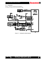
TB-6S-LX25-FANET Hardware User Manual TB-6S-LX25-FANET Hardware User Manual Rev.1.02 Rev.1.02 1 TB-6S-LX25-FANET Hardware User Manual Revision History Version Date Description Publisher Rev.1.00 2011/09/29 Release version Kiguchi Dan Rev.1.01 2011/12/12 Redesigned for mass production (Rev.3) Kiguchi Rev.1.02 2012/03/27 Part is changed from s/n xxxxxx-1.02. Kiguchi OSC 25MHz(U10): EPSON to Abracom. Odajima Modified following tables and figures Figure 4-1, Table 1, Figure 7-1, Figure 7-2, Figure7-4 Figure 7-7, Table 6, Table 7, Table 9, Table 10, Table 11 P17 and P18: Added comment. P19: modified pin name of DDR3 P36: modified comment. Rev.1.02 2 TB-6S-LX25-FANET Hardware User Manual Table of Contents 1. 2. 3. 4. 5. 6. Related Documents and Accessories ......................................................................................... 9 Overview ...................................................................................................................................... 9 Feature ........................................................................................................................................ 9 Block Diagram ........................................................................................................................... 10 External View of the Board .........................................................................................................11 Board Specifications .................................................................................................................. 12 6.1. 7. 8. 9. TB-6S-LX25-FANET Board Dimensions.................................................................................. 13 Description of Components ....................................................................................................... 14 7.1. Power Supply........................................................................................................................... 14 7.2. Power Supply Selector ............................................................................................................ 14 7.3. Power Connector (CN1) .......................................................................................................... 15 7.4. Clock Structure ........................................................................................................................ 15 7.5. Ethernet PHY (U4, U5) & RJ45 (CN7, CN8) ........................................................................... 16 7.6. External IO Connector (CN2, CN3) ......................................................................................... 17 7.7. DDR2 SDRAM (U12) ............................................................................................................... 19 7.8. Configuration ........................................................................................................................... 21 7.9. SPI Flash (U17) ....................................................................................................................... 22 7.10. I2C EEPROM (U11) ............................................................................................................. 22 7.11. LED .......................................................................................................................................... 23 7.12. SW ....................................................................................................................................... 23 7.13. Jumper ................................................................................................................................. 24 Default Settings ......................................................................................................................... 25 Appendix .................................................................................................................................... 26 9.1. Generating a configuration file................................................................................................. 26 9.2. Writing a configuration file to Flash Memory ........................................................................... 31 Rev.1.02 3 TB-6S-LX25-FANET Hardware User Manual List of Figures Figure 4-1 Board Block Diagram ................................................................................................... 10 Figure 5-1 Component Side ...........................................................................................................11 Figure 5-2 Solder Side ....................................................................................................................11 Figure 6-1 TB-6S-LX25-FANET Board Dimensions ...................................................................... 13 Figure 7-1 Power Supply Block Diagram ...................................................................................... 14 Figure 7-2 Power Supply Selector ................................................................................................. 14 Figure 7-3 Power Connector (CN1) ............................................................................................... 15 Figure 7-4 Clock Structure ............................................................................................................. 15 Figure 7-5 Ethernet PHY & RJ45 .................................................................................................. 16 Figure 7-6 DDR2SDRAM .............................................................................................................. 19 Figure 7-7 Configuration Block Diagram ....................................................................................... 21 Figure 7-8 SPI Flash ...................................................................................................................... 22 Figure 7-9 I2C EEPROM ............................................................................................................... 22 Figure 8-1 Default Settings on Component Side ........................................................................... 25 Figure 9-1 Generating a configuration file on ISE ......................................................................... 26 Figure 9-2 iMPACT Window - 1 ..................................................................................................... 26 Figure 9-3 iMPACT Window - 2 ..................................................................................................... 27 Figure 9-4 iMPACT Window - 3 ..................................................................................................... 27 Figure 9-5 iMPACT Window - 4 ..................................................................................................... 28 Figure 9-6 iMPACT Window - 5 ..................................................................................................... 28 Figure 9-7 iMPACT Window - 7 ..................................................................................................... 28 Figure 9-8 iMPACT Window - 8 ..................................................................................................... 29 Figure 9-9 iMPACT Window - 9 ..................................................................................................... 29 Figure 9-10 iMPACT Window - 10 ................................................................................................. 30 Figure 9-11 Onboard JTAG Connector .......................................................................................... 31 Figure 9-12 Writing to Device - 1 ................................................................................................... 31 Figure 9-13 Write to Device - 2 ...................................................................................................... 32 Figure 9-14 Write to Device - 3 ...................................................................................................... 32 Figure 9-15 Write to Device - 4 ...................................................................................................... 33 Figure 9-16 Write to Device - 5 ...................................................................................................... 34 Figure 9-17 Write to Device - 6 ...................................................................................................... 34 Figure 9-18 Write to Device - 7 ...................................................................................................... 35 Figure 9-19 Reconfiguration Switch .............................................................................................. 36 Figure 9-20 Configuration Status ................................................................................................... 36 Rev.1.02 4 TB-6S-LX25-FANET Hardware User Manual List of Tables Table 1 TB-6S-LX25-FANET Board Specifications ........................................................................ 12 Table 2 Ethernet PHY Pin Assignments ........................................................................................ 16 Table 3 CN2 Pin Assignments ....................................................................................................... 17 Table 4 CN3 Pin Assignments ....................................................................................................... 18 Table 5 DDR2SDRAM Pin Assignments........................................................................................ 20 Table 6 SPI Flash Pin Assignments ............................................................................................... 22 Table 7 I2C EEPROM Pin Assignments ........................................................................................ 22 Table 8 LED Functions .................................................................................................................. 23 Table 9 Switch Functions ............................................................................................................... 23 Table 10 Jumper Functions ........................................................................................................... 24 Table 11 Default Jumper and Switch Settings ............................................................................... 25 Rev.1.02 5 TB-6S-LX25-FANET Hardware User Manual Introduction Thank you for purchasing the TB-6S-LX25-FANET board. Before using the product, be sure to carefully read this user manual and fully understand how to correctly use the product. First read through this manual, then always keep it handy. SAFETY PRECAUTIONS Be sure to observe these precautions Observe the precautions listed below to prevent injuries to you or other personnel or damage to property. Before using the product, read these safety precautions carefully to assure correct use. These precautions contain serious safety instructions that must be observed. After reading through this manual, be sure to always keep it handy. The following conventions are used to indicate the possibility of injury/damage and classify precautions if the product is handled incorrectly. Danger Indicates the high possibility of serious injury or death if the product is handled incorrectly. Indicates the possibility of serious injury or death if the product is handled Warning incorrectly. Indicates the possibility of injury or physical damage in connection with houses Caution or household goods if the product is handled incorrectly. The following graphical symbols are used to indicate and classify precautions in this manual. (Examples) Turn off the power switch. Do not disassemble the product. ! Rev.1.02 Do not attempt this. 6 TB-6S-LX25-FANET Hardware User Manual Warning In the event of a failure, disconnect the power supply. If the product is used as is, a fire or electric shock may occur. Disconnect the power supply immediately and contact our sales personnel for repair. If an unpleasant smell or smoking occurs, disconnect the power supply. If the product is used as is, a fire or electric shock may occur. supply immediately. Disconnect the power After verifying that no smoking is observed, contact our sales personnel for repair. Do not disassemble, repair or modify the product. Otherwise, a fire or electric shock may occur due to a short circuit or heat generation. For inspection, modification or repair, contact our sales personnel. ! Do not touch a cooling fan. As a cooling fan rotates in high speed, do not put your hand close to it. may cause injury to persons. ! Otherwise, it Never touch a rotating cooling fan. Do not place the product on unstable locations. Otherwise, it may drop or fall, resulting in injury to persons or failure. ! If the product is dropped or damaged, do not use it as is. ! Do not touch the product with a metallic object. ! Do not place the product in dusty or humid locations or where water may Otherwise, a fire or electric shock may occur. Otherwise, a fire or electric shock may occur. splash. Otherwise, a fire or electric shock may occur. ! Do not get the product wet or touch it with a wet hand. Otherwise, the product may break down or it may cause a fire, smoking or electric shock. ! Do not touch a connector on the product (gold-plated portion). Otherwise, the surface of a connector may be contaminated with sweat or skin oil, resulting in contact failure of a connector or it may cause a malfunction, fire or electric shock due to static electricity. Rev.1.02 7 TB-6S-LX25-FANET Hardware User Manual Caution Do not use or place the product in the following locations. ! Humid and dusty locations Airless locations such as closet or bookshelf Locations which receive oily smoke or steam Locations exposed to direct sunlight Locations close to heating equipment Closed inside of a car where the temperature becomes high Staticky locations Locations close to water or chemicals Otherwise, a fire, electric shock, accident or deformation may occur due to a short circuit or heat generation. ! Do not place heavy things on the product. Otherwise, the product may be damaged. ■ Disclaimer This product is the Xilinx’s FPGA Spartan-6 evaluation board. Tokyo Electron Device Limited assumes no responsibility for any damages resulting from the use of this product for purposes other than those stated. Even if the product is used properly, Tokyo Electron Device Limited assumes no responsibility for any damages caused by: (1) Earthquake, thunder, natural disaster or fire resulting from the use beyond our responsibility, acts by a third party or other accidents, the customer’s willful or accidental misuse or use under other abnormal conditions. (2) Secondary impact arising from use of this product or its unusable state (business interruption or others) (3) Use of this product against the instructions given in this manual. (4) Malfunctions due to connection to other devices. Tokyo Electron Device Limited assumes no responsibility or liability for: (1) Erasure or corruption of data arising from use of this product. (2) Any consequences or other abnormalities arising from use of this product, or (3) Damage of this product not due to our responsibility or failure due to modification This product has been developed by assuming its use for research, testing or evaluation. It is not authorized for use in any system or application that requires high reliability. Repair of this product is carried out by replacing it on a chargeable basis, not repairing the faulty devices. However, non-chargeable replacement is offered for initial failure if such notification is received within two weeks after delivery of the product. The specification of this product is subject to change without prior notice. The product is subject to discontinuation without prior notice. Rev.1.02 8 TB-6S-LX25-FANET Hardware User Manual 1. Related Documents and Accessories Related documents All documents relating to this board can be downloaded from our website. Please see attached paper on the products. Board mounting kit - None Board accessories - AC adaptor: (1) AC adaptor (Akizuki Denshi: GF12-US03320 or equivalents, with a modified connector) 2. Overview This board is an embedded network evaluation platform module with Xilinx’s FPGA Spartan-6 Series LX25. 3. Feature - Xilinx’s XC6SLX25-2CSG324 - 10/100Mbps Ethernet PHY and 2-port RJ45 connector - 76-pin user GPIO on the soldered side of the board (2.54mm-pitch, 44-pin stack connector x 2) - DDR2 SDRAM (Chip) x 1: ESMT’s M14D5121632A (or equivalents) (512Mbits x 1) - 25MHz clock source. A 50MHz OSC can also be added. - Control switch: Push SW/DIP SW/Rotary SW - Monitor: LED Rev.1.02 9 TB-6S-LX25-FANET Hardware User Manual 4. Block Diagram The board block diagram is shown in Figure 4-1. RJ45 [HanRun] HR911105A PHY [Micrel] KSZ8721BL CN7 U4 RJ45 [HanRun] HR911105A PHY [Micrel] KSZ8721BL CN8 U5 Stack Connector [Samtec] SSM-122-L-DV-K-TR 40bit MII, PHY_LINK CN2 MII, PHY_LINK Stack Connector [Samtec] SSM-122-L-DV-K-TR 36bit CN3 Jumper [Samtec] TSM-103-01-L-SV J3 XOE ROTARY SW x 4 [COPAL] SC-1011 16bit Level Shifter [TI] SPI SN74AVC4T774 SW1 – SW4 PUSH SW x 3 [OMRON] B3FS-1012 U7 3bit JTAG SW5 – SW7 DIP SW [Apem] DMR02TV/TR 2bit XC6SLX25 -2CSG324 CFG_Done ADR, CMD, DM, CLK DQ, DQS U6 SPI Flash [Numonyx] M25P128-VMF6TPB U17 JTAG Connector [Hirose] A2-6PA-2.54D8A DDR2 SDRAM [ESMT] M14D5121632A U12 I2C D5 LED(G) x 5 [Rohm] SML-310MT Level Shifter [TI] SN74AVC4T774 CN6 SW8 LED(G) x 1 [Rohm] SML-310MT XOE EEPROM [MicroChip] 24LC32A-I/ST U11 5bit D6, D8-D11 LED(R) x 1 [Rohm] SML-310LT 1bit CLK D7 OSC 25MHz [Abracon] ASEMB-25.000MHZLY-T U10 U8 Figure 4-1 Board Block Diagram Rev.1.02 10 TB-6S-LX25-FANET Hardware User Manual 5. External View of the Board Figure 5-1 and 5-2 show the component side and the solder side of the board. Rotary Switch RJ45 Connector LED LED Config Done LED JTAG Ethernet PHY OSC 25M FPGA Push SW DIP SW Power Connector DDR2 SDRAM ReConfig SW Figure 5-1 Component Side Figure 5-2 Solder Side Rev.1.02 11 TB-6S-LX25-FANET Hardware User Manual 6. Board Specifications Table 1 shows the TB-6S-LX25-FANET Board Specifications. Table 1 TB-6S-LX25-FANET Board Specifications Item# Category 1 1 2 3 4 Board Composition 5 Category 2 Description Number of layers 8 layers External dimensions 100mm x Board thickness 1.6mm Board color Red Material FR-4 70mm 6 Component Component side Not specified 7 Height Solder side 2mm 8 Impedance Single signal 50Ω±10% 9 Control Differential signal 100Ω±10% 10 RoHS/Pbfree RoHS/Pbfree RoHS / lead-free solder ─ Gold flash 11 Surface finishing Rev.1.02 Remarks Without connectors 12 TB-6S-LX25-FANET Hardware User Manual 6.1. TB-6S-LX25-FANET Board Dimensions Figure 6-1 shows the TB-6S-LX25-FANET board dimensions. Figure 6-1 TB-6S-LX25-FANET Board Dimensions Rev.1.02 13 TB-6S-LX25-FANET Hardware User Manual 7. Description of Components 7.1. Power Supply Figure 7-1 shows the power supply block diagram. Figure 7-1 Power Supply Block Diagram 7.2. Power Supply Selector The power supply can be configured by setting J1 to switch the input pin to the Power Connector (CN1) or Stack Connectors (CN2 and CN3) as shown in Figure 7-2. J2 is selection for 3.3V or 2.5V. Figure 7-2 Power Supply Selector Rev.1.02 14 TB-6S-LX25-FANET Hardware User Manual 7.3. Power Connector (CN1) Figure 7-3 shows the power connector (CN1), JST’s B2P-VH (or JST’s VHR-2N compatible connector). Figure 7-3 Power Connector (CN1) 7.4. Clock Structure Figure 7-4 shows the board clock structure. PHY [Micrel] KSZ8721BL PHY [Micrel] KSZ8721BL OSC 25MHz [Abracon] ASEMB-25.000MHZ-LY-T XC6SLX25 -2CSG324 PHY_CLK H18 No Mounting SYS_CLK50M OSC 50MHz DDR2 SDRAM [ESMT] M14D5121632A Stack Connector [Samtec] SSM-122-L-DV-K-TR DDR2_CKP K16 J8 DDR2_CKN K8 USR_CLK_P E6 USR_CLK_N F7 U8 Figure 7-4 Clock Structure Note: If mounting OSC 50MHz, please use CB3LV-3C-50M0000(CTS-Frequency Controls) or compatible device. Rev.1.02 15 TB-6S-LX25-FANET Hardware User Manual 7.5. Ethernet PHY (U4, U5) & RJ45 (CN7, CN8) The board has two Micrel’s Ethernet PHY (KSZ8721BL). The RJ45 connector with pulse transformer has HanRun’s HR911105A. The Ethernet PHY TXER is fixed to “L” setting on the board. U4 U5 Figure 7-5 Ethernet PHY & RJ45 Table 2 Ethernet PHY Pin Assignments Ethernet PHY(U4) Pin Name FPGA Pin No. Level Ethernet PHY(U5) Pin Name FPGA Pin No. TXD0 G18 TXD0 L18 TXD1 G16 TXD1 K14 TXD2 F15 TXD2 N18 TXD3 G14 TXD3 M18 TXEN F18 TXEN K18 TXC K15 TXC L16 RXD0 F14 RXD0 K12 RXD1 E18 RXD1 J18 RXD2 E16 RXD2 J16 RXD3 D18 RXD3 H16 RXER F17 RXER K17 RXDV F16 RXDV K13 RXC H17 RXC L15 COL H14 COL N17 3.3V CRS G13 CRS L17 XINT H12 XINT M16 MDIO D17 MDIO J13 MDC C18 MDC H15 XRST C17 XRST H13 LED1 P18 LED1 N15 XI H18 XI Rev.1.02 Level 3.3V 16 TB-6S-LX25-FANET Hardware User Manual 7.6. External IO Connector (CN2, CN3) The board has two external I/O stack connectors, Samtec SSM-122-L-DV-K-TR (or compatible Samtec TSM-122-01-L-DV). Table 3 shows the CN2 pin assignments. Table 3 CN2 Pin Assignments Pin No. FPGA Pin No. Pin Name Pin Name FPGA Pin No. Pin No. 1 3 5 7 -T3 T4 T5 3.3V uC_ADR0 uC_ADR1 uC_ADR2 uC_DAT_ENA GND uC_nBUSY uC_nIRQ R3 -R5 V5 2 4 6 8 9 11 13 15 17 19 21 23 25 27 29 31 33 35 37 39 41 43 U5 V6 V7 P6 P7 T6 R7 U8 T8 P8 V9 M10 U10 R8 N10 P11 T10 -- uC_ADR3 uC_ADR4 uC_ADR5 uC_ADR6 uC_ADR7 uC_ADR8 uC_ADR9 uC_ADR10 uC_ADR11 uC_ADR12 uC_ADR13 uC_ADR14 uC_ADR15 uC_EMULATIO uC_nBHE uC_nRD uC_nWR 3.3V uC_nCS uC_DATA0 uC_DATA1 uC_DATA2 uC_DATA3 uC_DATA4 uC_DATA5 uC_DATA6 uC_DATA7 uC_DATA8 uC_DATA9 uC_DATA10 uC_DATA11 uC_DATA12 uC_DATA13 uC_DATA14 GND uC_DATA15 N6 T7 U7 N7 V4 M8 V8 N8 T9 N9 N11 V12 V11 U11 R10 V10 -V13 10 12 14 16 18 20 22 24 26 28 30 32 34 36 38 40 42 44 *Power Supply 3.3V pin on CN2 is connected to USER_3P3V on TB-6S-LX25-FANET. CN1 is available if setting J1. *IO Pin IO pin on CN2 is connected to Bank 2 on FPGA. Voltage can be selected by J2. Rev.1.02 17 TB-6S-LX25-FANET Hardware User Manual Table 4 shows the CN3 pin assignments. Table 4 CN3 Pin Assignments Pin No. FPGA Pin No. Pin Name Pin Name 1 3 5 7 9 11 13 15 17 19 21 23 25 27 29 31 33 35 37 39 41 43 B2 -A2 B4 A4 B6 A6 B8 A8 B9 A9 C10 A10 B12 A12 D11 C11 F13 E13 C13 USR_IOP0 GND USR_ION0 USR_IOP1 USR_ION1 USR_IOP2 USR_ION2 USR_IOP3 USR_ION3 USR_IOP4 USR_ION4 USR_IOP5 USR_ION5 USR_IOP6 USR_ION6 USR_IOP7 USR_ION7 SYNC_OUT0 SYNC_OUT1 LATCH_IN0 GND LATCH_IN1 3.3V USR_IOP10 USR_ION10 USR_IOP11 USR_ION11 USR_IOP12 USR_ION12 USR_IOP13 USR_ION13 USR_IOP14 USR_ION14 USR_IOP15 USR_ION15 USR_IOP16 USR_ION16 USR_CLKP USR_CLKN MOTH_MOSI MOTH_DIN MOTH_XCS MOTH_CCLK 3.3V A13 FPGA Pin No. Pin No. B3 A3 C5 A5 D6 C6 C7 A7 D8 C8 G9 F9 B11 A11 D9 C9 ------ 2 4 6 8 10 12 14 16 18 20 22 24 26 28 30 32 34 36 38 40 42 44 *Power Supply 3.3V pin on CN3 is connected to USER_3P3V on TB-6S-LX25-FANET. CN1 is available if setting J1. *IO Pin IO pin on CN3 is connected to Bank3 on FPGA. Voltage can be selected by J2 *MOTH_MOSI(36), MOTH_DIN(38), MOTH_XCS(40) and MOTH_CCLK(42) These pins are connected to SPI Flash (J3 setting: 1-2). Rev.1.02 18 TB-6S-LX25-FANET Hardware User Manual 7.7. DDR2 SDRAM (U12) The board has one ESMT DDR2 SDRAM (M14D5121632A) . Pin A[12:0], DQ[15:0], ODT, UDQS, /UDQS, LDQS, /LDQS, LDM, UDM, CK, /CK, CKE, /RAS, /CAS, /WE and BA[1:0] are connected. CSN is fixed to “L” setting on the board. Specifications 512Mbit (8Mword x 16bit x 4bank) DDR2-800 Address structure Bank=2bit Address=13bit(Row address=13bit / Column address=10bit) Data Bus Structure Data strobe (DQS) during a read/write operation: byte-by-byte control Data Mask (DM): byte-by-byte control Figure 7-6 DDR2SDRAM Rev.1.02 19 TB-6S-LX25-FANET Hardware User Manual Table 5 DDR2SDRAM Pin Assignments Rev.1.02 DDR2 FPGA Pin DDR2 FPGA Pin Pin Name No. Pin Name No. A0 J7 ODT K6 A1 J6 DQ0 L2 A2 H5 DQ1 L1 A3 L7 DQ2 K2 A4 F3 DQ3 K1 A5 H4 DQ4 H2 A6 H3 DQ5 H1 A7 H6 DQ6 J3 A8 D2 DQ7 J1 A9 D1 DQ8 M3 A10 F4 DQ9 M1 A11 D3 DQ10 N2 A12 G6 DQ11 N1 BA0 F2 DQ12 T2 BA1 F1 DQ13 T1 CLK G3 DQ14 U2 CLKN G1 DQ15 U1 RASN L5 LDQS L4 CASN K5 LDQSN L3 CKE H7 UDQS P2 WE E3 UDQSN P1 UDM K4 LDM K3 20 TB-6S-LX25-FANET Hardware User Manual 7.8. Configuration Figure 7-7 shows the configuration block diagram. J3 setting (1-2) allows access to SPI Flash from CN3. Figure 7-7 Configuration Block Diagram Rev.1.02 21 TB-6S-LX25-FANET Hardware User Manual 7.9. SPI Flash (U17) The board has a Numonyx SPI Flash 128Mbit (M25P128) as FPGA configuration memory. After an FPGA is configured, it can be used as user area. Figure 7-8 SPI Flash Table 6 SPI Flash Pin Assignments SPI Flash FPGA Pin No. Signal Name Pin No. 7 XS V3 8 Q R13 15 D T13 16 C R15 Level VCC_ADJ 7.10. I2C EEPROM (U11) The board has a Microchip I2C EEPROM 32Kbit (24LC32A) which can be used to store board specific configuration data and others. Figure 7-9 Table 7 I2C EEPROM I2C EEPROM Pin Assignments I2C EEPROM Rev.1.02 FPGA Pin No. Signal Name Pin No. 5 SDA U18 6 SDL U17 7 WP T18 Level 3.3V 22 TB-6S-LX25-FANET Hardware User Manual 7.11. LED Table 8 shows the onboard LEDs. Table 8 LED Functions BD Connect to Function Silk Connect to: Connect to: Pin No. Bank D6 FPGA debugging M14 1 D7 FPGA debugging N14 1 This LED will light when FPGA -- -- P16 1 D9 P15 1 D10 M13 1 D11 L14 1 D5 Config is complete D8 FPGA FPGA debugging Act Level L 3.3V -- -- L 3.3V Act Level 7.12. SW Table 9 shows the onboard switches. Table 9 Switch Functions SW Pin Connect Connect to: Connect to: Sequence to Pin No. Bank 8 C15 0 4 B14 0 2 A15 0 1 A14 0 8 P12 2 4 M11 2 2 B16 0 FPGA Config Rotary 1 A16 0 Switch 8 T14 2 4 T12 2 T11 2 R11 2 8 V14 2 4 V15 2 2 U16 2 1 U15 2 V2 2 2 F5 3 3 F6 3 1 P3 3 2 L6 3 BD Silk Function SW1 SW2 SW3 2 1 SW4 SW5 SW6 SW7 SW8 FPGA ReConfig Push SW FPGA Config Push SW FPGA Config DIP SW Rev.1.02 1 FPGA VCC _ADJ L 1.8V 23 TB-6S-LX25-FANET Hardware User Manual 7.13. Jumper Table 10 shows the onboard jumpers. Table 10 Jumper Functions BD Silk J1 Function Remarks Selection of 3.3V power supply to the 1-2: 3.3V is supplied from CN1 board 2-3: 3.3V is supplied from CN2, CN3 J2 Selection of external IO pin Vcco J3 Selection of SPI Flash connection Rev.1.02 1-2: Connecting VCC_ADJ to 2.5V 2-3: Connecting VCC_ADJ to 3.3V 1-2: Connecting to CN3 2-3: Connecting to JTAG 24 TB-6S-LX25-FANET Hardware User Manual 8. Default Settings Figure 8-1 shows the default jumper and SW settings. Check jumpers and switches in the area enclosed by a blue line. Figure 8-1 Default Settings on Component Side Table 11 shows the default jumper and switch settings. Table 11 Default Jumper and Switch Settings Default No. BD Silk 1 J1 1-2 VCC_3P3V is supplied from CN1. 2 J2 2-3 VCC_ADJ is supplied from VCC_3P3V. 3 J3 2-3 FPGA Config SPI Flash is connected in JTAG mode. 4 SW8 Undefined This switch is not used in default FPGA data. 5 SW1-4 Undefined These switches are not used in default FPGA data. Rev.1.02 Setting Function 25 TB-6S-LX25-FANET Hardware User Manual 9. Appendix 9.1. Generating a configuration file This section describes how to generate a configuration file using the Tool version ISE 13.3. First generate a configuration file to store the configuration in flash memory. 1. Double click Generate Target PROM/ACE File. Figure 9-1 Generating a configuration file on ISE 2. Double click Create PROM File. Figure 9-2 Rev.1.02 iMPACT Window - 1 26 TB-6S-LX25-FANET Hardware User Manual 3. Select SPI Flash - Configure Single FPGA and click Arrow. Figure 9-3 iMPACT Window - 2 4. In the Storage Device (bits) selection pane select 128M and click Add Storage Device. Figure 9-4 Rev.1.02 iMPACT Window - 3 27 TB-6S-LX25-FANET Hardware User Manual 5. Clock Arrow and enter any name (directory) you want in the Output File Name and Output File Location fields, and click OK. Figure 9-5 iMPACT Window - 4 Figure 9-6 iMPACT Window - 5 6. Click OK. 7. In the file selection dialog, select a bit file for generating a configuration file. 8. Click No. Figure 9-7 Rev.1.02 iMPACT Window - 7 28 TB-6S-LX25-FANET Hardware User Manual 9. Click OK. Figure 9-8 iMPACT Window - 8 10. Double click Generate File…. Figure 9-9 Rev.1.02 iMPACT Window - 9 29 TB-6S-LX25-FANET Hardware User Manual 11. If the configuration file is successfully generated, a Generate Succeeded message will appear. Figure 9-10 Rev.1.02 iMPACT Window - 10 30 TB-6S-LX25-FANET Hardware User Manual 9.2. Writing a configuration file to Flash Memory Connect a Platform USB cable to the JTAG connector (CN6) as shown in Figure 9-11. Turn on the power switch of the board, run iMPACT, and write the configuration to Flash Memory in accordance with the following procedure. Figure 9-11 Onboard JTAG Connector 1. Double click Boundary Scan and click Initialize Chain (indicated by an arrow). Figure 9-12 Rev.1.02 Writing to Device - 1 31 TB-6S-LX25-FANET Hardware User Manual 2. A bit/jed file configuration window will appear. Cancel it. After selecting FPGA, right click Add SPI/BPI Flash…. to select it. Figure 9-13 Write to Device - 2 3. In the file selection dialog, select a configuration file (xxx.mcs) to write it to Flash Memory. 4. Select the onboard Flash M25P128 and click OK. Figure 9-14 Rev.1.02 Write to Device - 3 32 TB-6S-LX25-FANET Hardware User Manual 5. Double click Program in the iMPACT Processes window. Figure 9-15 Rev.1.02 Write to Device - 4 33 TB-6S-LX25-FANET Hardware User Manual 6. Click OK. Figure 9-16 Write to Device - 5 7. Writing to Flash Memory will start. Figure 9-17 Rev.1.02 Write to Device - 6 34 TB-6S-LX25-FANET Hardware User Manual 8. Select the onboard Flash M25P128 and click OK. If writing to Flash Memory is successfully completed, a Program Succeeded message will appear. Figure 9-18 Rev.1.02 Write to Device - 7 35 TB-6S-LX25-FANET Hardware User Manual 9. The configuration data written to Flash Memory is loaded into the FPGA device in Master-SPI mode. The configuration can be enabled by turning on the power switch of the board or pressing and holding the reconfiguration switch (see Figure 9-19) for more than 2 seconds. Figure 9-19 Reconfiguration Switch 10. The board provides the status of FPGA configuration at location D5 (see Figure 9-20). If the configuration is successfully completed, the D5 green light will flash. Figure 9-20 Configuration Status Rev.1.02 36 TB-6S-LX25-FANET Hardware User Manual PLD Solution Dept. PLD Division URL: http://solutions.inrevium.com/ E-mail: [email protected] HEAD Quarter: Yokohama East Square, 1-4 Kinko-cho, Kanagawa-ku, Yokohama City, Kanagawa, Japan 221-0056 TEL: +81-45-443-4016 FAX: +81-45-443-4058 Rev.1.02 37