1
piconet ® –
USER MANUAL
I/O MODULES
All brand and product names are trademarks or registered trade
marks of the owner concerned.
Edition 06/2013
© Hans Turck GmbH & Co. KG, Mülheim an der Ruhr
All rights reserved, including those of the translation.
No part of this manual may be reproduced in any form (printed,
photocopy, microfilm or any other process) or processed, duplicated or distributed by means of electronic systems without written
permission of Hans Turck GmbH & Co. KG, Mülheim an der Ruhr.
Subject to alterations without notice.
Warning!
Dangerous electrical voltage!
Before commencing the installation
Disconnect the power supply of the device.
Ensure that devices cannot be accidentally restarted.
Verify isolation from the supply.
Earth and short circuit.
Cover or enclose neighbouring units that are live.
Follow the engineering instructions (AWA) of the device
concerned.
Only suitably qualified personnel in accordance with EN 50 1101/-2 (VDE 0 105 Part 100) may work on this device/system.
Before installation and before touching the device ensure that
you are free of electrostatic charge.
The functional earth (FE) must be connected to the protective
earth (PE) or to the potential equalisation. The system installer is
responsible for implementing this connection.
Connecting cables and signal lines should be installed so that
inductive or capacitive interference do not impair the automation
functions.
Install automation devices and related operating elements in
such a way that they are well protected against unintentional
operation.
Suitable safety hardware and software measures should be
implemented for the I/O interface so that a line or wire breakage
on the signal side does not result in undefined states in the
automation devices.
Ensure a reliable electrical isolation of the low voltage for the 24
volt supply. Only use power supply units complying with IEC 60
364-4-41 (VDE 0 100 Part 410) or HD 384.4.41 S2.
Deviations of the mains voltage from the rated value must not
exceed the tolerance limits given in the specifications, otherwise
this may cause malfunction and dangerous operation.
I
Emergency stop devices complying with IEC/EN 60 204-1 must
be effective in all operating modes of the automation devices.
Unlatching the emergency-stop devices must not cause restart.
Devices that are designed for mounting in housings or control
cabinets must only be operated and controlled after they have
been installed with the housing closed. Desktop or portable units
must only be operated and controlled in enclosed housings.
Measures should be taken to ensure the proper restart of
programs interrupted after a voltage dip or failure. This should
not cause dangerous operating states even for a short time. If
necessary, emergency-stop devices should be implemented.
Wherever faults in the automation system may cause damage to
persons or property, external measures must be implemented to
ensure a safe operating state in the event of a fault or
malfunction (for example, by means of separate limit switches,
mechanical interlocks etc.).
The electrical installation must be carried out in accordance with
the relevant regulations (e. g. with regard to cable cross
sections, fuses, PE).
All work relating to transport, installation, commissioning and
maintenance must only be carried out by qualified personnel.
(IEC 60 364 and HD 384 and national work safety regulations).
All shrouds and doors must be kept closed during operation.
II
Table of Contents
How to work with this manual
Introduction ................................................................................................... 0-2
Correct usage to the intended purpose .................................................. 0-2
Projecting guidelines/Product installation ............................................... 0-2
Meaning of the symbols used ..................................................................... 0-3
Release status and versions ......................................................................... 0-4
Documentation ........................................................................................ 0-4
Firmware and hardware status................................................................ 0-4
List of Revisions ............................................................................................ 0-6
1
The piconet® system
System overview ........................................................................................... 1-2
piconet® – Coupling and extension modules .......................................... 1-4
IP-Link – modular extension network...................................................... 1-4
Stand-alone modules .............................................................................. 1-7
2
IP-Link
General description....................................................................................... 2-2
Construction and Topology..................................................................... 2-3
Cycle time IP-Link ................................................................................... 2-5
Technical data ......................................................................................... 2-8
IP-link connector ................................................................................... 2-10
Trouble shooting in case of problems with the IP-Link......................... 2-16
3
Register communication
General description....................................................................................... 3-2
General register description.......................................................................... 3-3
Register R0-R7 ........................................................................................ 3-3
Register R8-R15 ...................................................................................... 3-4
Register R16-R30 .................................................................................... 3-6
Register R31-R47 .................................................................................... 3-6
Register R33-R47 .................................................................................... 3-7
Register R47-R63 .................................................................................... 3-7
Example of register communication ............................................................. 3-8
Control byte............................................................................................. 3-8
Read-out of the module type ................................................................ 3-11
D300778 0613 - piconet® I/O Modules
i
Table of Contents
4
General technical information
Technical data............................................................................................... 4-2
Supply voltage .............................................................................................. 4-4
Galvanic isolation .................................................................................... 4-5
Incoming line and power supply ............................................................. 4-6
Power loss of power cable ...................................................................... 4-8
Start-up performance of the piconet® modules............................................ 4-9
Dimension drawings.................................................................................... 4-10
5
Diagnostic LEDs for local errors
Error diagnostics via LEDs ............................................................................ 5-2
Flash codes ............................................................................................. 5-2
Local errors of a coupling module (SxxL-0404D-xxxx) ........................... 5-3
Local errors of an extension module ....................................................... 5-5
6
IP-Link coupling modules
Type overview ............................................................................................... 6-2
General description....................................................................................... 6-3
Connection modes .................................................................................. 6-3
I/O network with the IP-Link.................................................................... 6-3
Automatic input data mapping ................................................................ 6-4
SxxL-0404D-x00x, coupling module 4DI/4DO ........................................... 6-5
Technical data ......................................................................................... 6-6
Wiring diagrams ...................................................................................... 6-7
Parameters .............................................................................................. 6-9
Diagnosis................................................................................................. 6-9
7
Digital input modules
Type overview ............................................................................................... 7-2
Sxxx-0800D-x00x, 8-port digital input, filter 0.2 ms/3.0 ms ........... 7-3
Technical data ......................................................................................... 7-4
Wiring diagrams ..................................................................................... 7-5
Parameters .............................................................................................. 7-6
Diagnosis................................................................................................. 7-6
ii
D300778 0613 - piconet® I/O Modules
8
Digital output modules
Type overview ............................................................................................... 8-3
Sxxx-0008D-x006/ -x001, 8-port digital output, 24 VDC, Imax = 0.5 A...... 8-4
Technical data ......................................................................................... 8-5
Wiring diagrams ...................................................................................... 8-5
Parameters .............................................................................................. 8-6
Diagnosis................................................................................................. 8-6
Sxxx-0008D-x002/ -x003, 8-port digital output, 24 VDC, Imax = 2 A......... 8-7
Technical data ......................................................................................... 8-9
Wiring diagrams ...................................................................................... 8-9
Parameters ............................................................................................ 8-10
Diagnosis............................................................................................... 8-10
Sxxx-0008D-x004/ -x005, 8-port digital output, 24 VDC, Imax = 2 A....... 8-11
Technical data ....................................................................................... 8-12
Wiring diagrams .................................................................................... 8-13
Parameters ............................................................................................ 8-13
Diagnosis............................................................................................... 8-13
Potential groups .................................................................................... 8-14
SNNE-0016D-0001, 16 digital outputs 24 VDC, total current max. 4 A ..... 8-15
Technical data ....................................................................................... 8-16
Wiring diagram ...................................................................................... 8-17
Meaning of the channel LEDs ............................................................... 8-17
Parameters ............................................................................................ 8-17
Diagnosis............................................................................................... 8-17
Data mapping ........................................................................................ 8-18
Control and status byte ......................................................................... 8-18
Register overview .................................................................................. 8-21
Watchdog Feature (R32-R33)................................................................ 8-21
SNNE-0016D-0002, 16 digital outputs 24 VDC, total current max. 4 A ..... 8-23
Technical data ....................................................................................... 8-23
The module’s error behavior ................................................................. 8-23
9
Digital combined modules
Type overview ............................................................................................... 9-2
Sxxx-0404D-x003/-x004/-x001/-x002, 4-port digital input;
4-port digital output ...................................................................................... 9-3
Technical data ......................................................................................... 9-5
Wiring diagrams ...................................................................................... 9-6
Parameters .............................................................................................. 9-8
Diagnosis................................................................................................. 9-8
D300778 0613 - piconet® I/O Modules
iii
Table of Contents
Sxxx-0404D-x007/-x008/-x005/-x006,
4-port digital input; 4-port digital output....................................................... 9-9
Technical data ....................................................................................... 9-11
Wiring diagrams .................................................................................... 9-12
Parameters ............................................................................................ 9-14
Diagnosis............................................................................................... 9-14
Sxxx-0008D-x001, 8-port digital combined module ................................ 9-15
Technical data ....................................................................................... 9-17
Wiring diagrams .................................................................................... 9-18
Parameters ............................................................................................ 9-19
Diagnosis............................................................................................... 9-19
SNNE-0808D-0003, 8-port digital combined module with IP20 terminals . 9-20
Technical Data....................................................................................... 9-21
Wiring diagrams .................................................................................... 9-23
Parameters ............................................................................................ 9-24
Diagnosis............................................................................................... 9-24
10
Analogue input modules
Type overview ............................................................................................. 10-4
Sxxx-40A-x005, 4-port analogue input module,
-10/ 0 to +10 V ............................................................................................ 10-5
Technical data ....................................................................................... 10-7
Wiring diagrams .................................................................................... 10-8
Supply voltage....................................................................................... 10-9
Functions of the channel LEDs ........................................................... 10-10
Process data ....................................................................................... 10-10
Parameters .......................................................................................... 10-11
Diagnosis............................................................................................. 10-11
Data mapping ...................................................................................... 10-11
Control and status byte ....................................................................... 10-12
Register overview ................................................................................ 10-15
Sxxx-40A-x007,
4-port analogue input module, 0/(4) to 20 mA .......................................... 10-23
Technical data ..................................................................................... 10-25
Wiring diagrams .................................................................................. 10-26
Functions of the channel LEDs ........................................................... 10-27
Process data ....................................................................................... 10-27
Parameters .......................................................................................... 10-29
Diagnosis............................................................................................. 10-29
Data mapping ...................................................................................... 10-29
Control and status byte ....................................................................... 10-30
iv
D300778 0613 - piconet® I/O Modules
Register overview ................................................................................ 10-33
Feature register (R32) .......................................................................... 10-34
Sxxx-40A-x009,
4-port analogue input module for Pt100 (RTD)......................................... 10-37
Technical data ..................................................................................... 10-39
Wiring diagrams .................................................................................. 10-40
Supply voltage..................................................................................... 10-41
Functions of the channel LEDs ........................................................... 10-42
Process data ....................................................................................... 10-42
Parameters .......................................................................................... 10-43
Diagnosis............................................................................................. 10-43
Data mapping ...................................................................................... 10-43
Control and status byte ....................................................................... 10-44
Register overview ................................................................................ 10-46
Feature register (R32) .......................................................................... 10-48
Sxxx-40A-x004, 4-port analogue input module for thermoelements ..... 10-53
Technical data ..................................................................................... 10-55
Wiring diagrams .................................................................................. 10-56
Supply voltage..................................................................................... 10-58
Functions of the channel LEDs ........................................................... 10-58
Function principle ................................................................................ 10-59
Parameters .......................................................................................... 10-61
Diagnosis............................................................................................. 10-61
Data mapping ...................................................................................... 10-61
Control and status byte ....................................................................... 10-62
Register overview ................................................................................ 10-65
11
Analogue output modules
Type overview ............................................................................................. 11-2
Sxxx-04A-x007, 4-port analogue output module, ± 10 V ......................... 11-3
Technical data ....................................................................................... 11-5
Wiring diagrams .................................................................................... 11-6
Functions of the channel LEDs ............................................................. 11-6
Process data ......................................................................................... 11-7
Parameters ............................................................................................ 11-8
Diagnosis............................................................................................... 11-8
Data mapping ........................................................................................ 11-8
Control and status byte ......................................................................... 11-9
Register overview ................................................................................ 11-11
D300778 0613 - piconet® I/O Modules
v
Table of Contents
Sxxx-04A-x009,
4-port analogue output module, 0/4 to 20 mA ......................................... 11-15
Technical data ..................................................................................... 11-17
Wiring diagrams .................................................................................. 11-18
Functions of the channel LEDs ........................................................... 11-18
Process data ....................................................................................... 11-19
Parameters .......................................................................................... 11-20
Diagnosis............................................................................................. 11-20
Data mapping ...................................................................................... 11-20
Control and status byte ....................................................................... 11-21
12
Technology modules
Type overview ............................................................................................. 12-4
Sxxx-10S-x001,
1-channel incremental encoder interface ................................................... 12-5
Technical data ....................................................................................... 12-7
Wiring diagram ...................................................................................... 12-8
Functions of the channel LEDs ............................................................. 12-8
Process data ......................................................................................... 12-9
Parameters .......................................................................................... 12-10
Diagnosis............................................................................................. 12-10
Data mapping ...................................................................................... 12-10
Control and status byte ....................................................................... 12-11
Register overview ................................................................................ 12-16
Feature register (R32) .......................................................................... 12-18
Sxxx-10S-x002,
1-channel RS232 interface........................................................................ 12-20
Technical data ..................................................................................... 12-22
Wiring diagram .................................................................................... 12-23
Functions of the channel LEDs ........................................................... 12-23
Parameters .......................................................................................... 12-23
Diagnosis............................................................................................. 12-24
Data mapping ...................................................................................... 12-24
Control and status byte ....................................................................... 12-24
Register overview ................................................................................ 12-30
Data byte register (R35)....................................................................... 12-35
Sxxx-10S-x004,
1-channel RS485/422 interface ................................................................ 12-36
Technical data ..................................................................................... 12-38
Wiring diagram .................................................................................... 12-39
Functions of the channel LEDs ........................................................... 12-39
Parameters .......................................................................................... 12-40
vi
D300778 0613 - piconet® I/O Modules
Diagnosis............................................................................................. 12-40
Data mapping ...................................................................................... 12-41
Control and status byte ....................................................................... 12-41
Register overview ................................................................................ 12-41
Sxxx-10S-x005,
1-channel SSI interface............................................................................. 12-45
Technical data ..................................................................................... 12-47
Wiring diagram .................................................................................... 12-48
Functions of the channel LEDs ........................................................... 12-48
Process data ....................................................................................... 12-48
Parameters .......................................................................................... 12-49
Diagnosis............................................................................................. 12-49
Data mapping ...................................................................................... 12-49
Control and status byte ....................................................................... 12-50
Register overview ................................................................................ 12-53
Feature register (R32) .......................................................................... 12-54
Baud rate register (R33) ...................................................................... 12-55
Data length register (R34).................................................................... 12-56
Sxxx-0002D-x002,
2-channel pulse width output 24 VDC/2.5 A............................................. 12-57
Technical data ..................................................................................... 12-59
Wiring diagram .................................................................................... 12-60
Functions of the channel LEDs ........................................................... 12-60
Operating modes................................................................................. 12-61
Pulse width ratio in the process data .................................................. 12-70
Output power (Derating) ...................................................................... 12-71
Parameters .......................................................................................... 12-74
Diagnosis............................................................................................. 12-74
Data mapping ...................................................................................... 12-74
Control and status byte ....................................................................... 12-75
Register overview of the PWM module ............................................... 12-78
Feature register (R32) .......................................................................... 12-80
Sxxx-0202D-x003,
Up/down counter, 24 VDC, 100 kHz......................................................... 12-81
Technical data ..................................................................................... 12-83
Wiring diagram .................................................................................... 12-84
Meaning of the LEDs ........................................................................... 12-85
Function principle ................................................................................ 12-85
Parameters .......................................................................................... 12-87
Diagnosis............................................................................................. 12-87
Data mapping ...................................................................................... 12-88
Control and status byte ....................................................................... 12-88
D300778 0613 - piconet® I/O Modules
vii
Table of Contents
Register overview ................................................................................ 12-92
Feature register (R32) .......................................................................... 12-94
13
Third Party Products
CPV valve terminal from the company Festo.............................................. 13-2
General product description.................................................................. 13-2
Bus connection ..................................................................................... 13-2
Voltage supply....................................................................................... 13-2
Support.................................................................................................. 13-2
Ordering................................................................................................. 13-3
14
Appendix
Module types .............................................................................................. 14-2
Nominal current consumption of the piconet® modules............................. 14-3
Description of the module parameters........................................................ 14-6
Module-independent user parameters.................................................. 14-6
Digital coupling modules ....................................................................... 14-7
Analogue input modules........................................................................ 14-8
Analogue output modules Sxxx-04A-000x ......................................... 14-11
Technology modules ........................................................................... 14-12
15
Glossary of terms
16
Index
viii
D300778 0613 - piconet® I/O Modules
How to work with this manual
Introduction ....................................................................................... 2
Correct usage to the intended purpose ......................................................2
Projecting guidelines/Product installation ...................................................2
Meaning of the symbols used .......................................................... 3
Release status and versions.............................................................. 4
Documentation ............................................................................................4
Firmware and hardware status....................................................................4
– Downward compatibility ..........................................................................4
List of Revisions ................................................................................ 6
D300778 0613 - piconet® I/O Modules
0-1
Introduction
Attention
It is indispensable to lease this section because the safety in dealing
with electrical equipment should not be left to chance.
This manual contains all information pertaining to safe and proper
operation of the I/O modules of the TURCK product range piconet®.
It was specially edited for qualified staff with the required
specialized knowledge.
Correct usage to the intended purpose
Warning
The devices described in this manual may only be used in such
applications described in the technical sections of the manual and
only in conjunction with certified external devices and components.
Correct and safe operation of the devices relies on appropriate
transport and storage, correct set-up and installation as well as
careful operation and maintenance.
Projecting guidelines/Product installation
Warning
It is indispensable to observe the applicable safety and accident
prevention regulations of the specific application.
0-2
D300778 0613 - piconet® I/O Modules
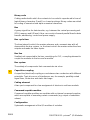
Meaning of the symbols used
Meaning of the symbols used
Warning
This sign is placed next to a warning indicating the presence of a
hazard. This can relate to personal injury as well as to system
damage (hardware and software).
The user should interpret this symbol as follows: exercise extreme
caution.
Attention
This sign is placed next to a warning indicating a potential hazard.
This can relate to personal injury as well as to system (hardware and
software) and equipment damage.
Note
This sign is located next to general hints providing important
information on individual or stepwise work procedures.
These hints may facilitate work and possibly help to avoid excess
work resulting from faulty proceedings.
D300778 0613 - piconet® I/O Modules
0-3
Release status and versions
Documentation
This documentation pertains to the hardware and firmware status at
the time of editing this manual. The features of the piconet® systems
are continuously developed and improved.
Changes in the documentation can be taken from
Modification index of this manual.
Firmware and hardware status
Downward compatibility
The modules of the piconet® series are downward compatible.
Older module cannot, however, feature the same characteristics
than newer module versions. However, existing characteristics have
been retained so that older modules can always be replaced with
new ones.
The documentation describes the differences between the modules.
0-4
D300778 0613 - piconet® I/O Modules
Release status and versions
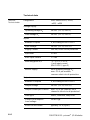
The firmware and hardware status of the piconet® modules can be
taken from the version number printed on the side of the module.
The version number can be identified by the prefix "D".
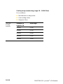
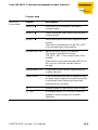
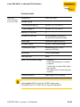
Table 1:
Firmware and
hardware status
Indication
on module
Explanation
D. kkjjxyzu
Example
D.22011501
kk
Calendar week
Calendar week 22
jj
Year
of the year 2001
x
Firmware bus board
Firmware bus, version 1
y
Hardware bus board
Hardware, version 5
z
Firmware I/O board
Firmware I/O, 0
(no firmware needed for
this board)
u
Hardware I/O board
Hardware I/O, version 1
D300778 0613 - piconet® I/O Modules
0-5
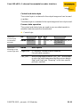
List of Revisions
In comparison to the previous manual edition, the following
changes/ revisions have been made:
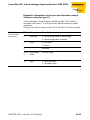
Table 2:
List of revisions
Chapter Subject/
Description
2
new
„IP-link connector”, page 2-10
changed
X
Note
The publication of this manual renders all previous editions invalid.
0-6
D300778 0613 - piconet® I/O Modules
1
The piconet® system
System overview................................................................................ 2
piconet® – Coupling and extension modules ..............................................4
IP-Link – modular extension network..........................................................4
– Extension modules ..................................................................................6
– Maximum system expansion of the IP-Link ............................................6
Stand-alone modules ..................................................................................7
– Combined modules .................................................................................7
D300778 0613 - piconet® I/O Modules
1-1
System overview
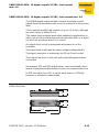
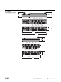
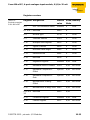
piconet®, the "smallest“ bus system within the TURCK programme,
offers I/0 modules with dimensions of only 1210/175/126 x 30 x
26,5 mm, ideally suited for application in serial machine engineering:
the coupling modules as the interface between the fieldbus and
the piconet®fibre-optic network (seePage 1-4),
the extension modules connected to the coupling module
(see Page 1-4) as well as
the stand-alone modules for direct connection to the fieldbus
(see Page 1-7).
All connections are screw connections and feature protection
degree IP67.
1-2
D300778 0613 - piconet® I/O Modules
System overview
SPS and PROFIBUS-DP
interface card
Power supply
BL20
PROFIBUSconnector IP20
D9T451-xM
RKSW451-xM
RKM52-xM
FKW-FSW45-M12
RSF-RKF57/22
RKM52-x-RSM52
RSM-2RKM50
BS4151-0/9
WKM52-xM
RKM52-x-RSM52
WKM52-x-WSM52
U0
Ui
WKM52-x-WSM52
Ui
U
Uo
1
5
2
6
0
I9
I1
4
FSDP-IM16-0001
I10
I2
I5
I1
1
5
2
6
1
I11
I3
DP-Address
FXDP-...
Emergency
stop switch
I8
I4
I0
0
4
FLDP-IM16-0001
FXDP-XSG16-0001
Power
4
U
Power
I0
Power
0
FLDP-...
5
F-Address
x1000 x100
I12
I4
I6
I2
2
I5
x10 x1
x10
I13
x1
6
FSDP-...
SIL3 Mode
BMWS8251-8,5
I14
I6
I7
I3
3
7
3
x100
1
0
SF
SF
2 3
8 7
1
0
9
2 3
8 7
1
0
9
4
5
6
2 3
8 7
4
5
6
1
0
9
x10
2 3
8 7
6
5
4
4
5
6
8
7
x1
Out
In
Out
In
9 0 1
6
5
4
2
8
3
7
9 0 1
6
5
4
2
3
6
5
4
In
7
SIL SIL
2
3
Bus
Slave Address (0-99)
x1
4
5
6
I15
I7
SIL SIL
2
3
Bus
x10
1
0
9
3
7
Bus
7 8
3 2
7 8
3 2
9
0
1
6
5
4
9
0
1
6
5
4
7 8
3 2
7 8
3 2
9
0
1
9
0
1
Out
RSSW451-xM
WSSW-WKSW451-xM
BL67
D
BL67
D
BL67
D
BL67
D
BL67
D
D
0
0
0
0
1
1
1
1
1
2
2
3
3
2
2
3
WSSW-WKSW451-xM
BL67
0
4
4
5
5
6
6
7
7
0
0
1
1
2
2
0
Sensor
0
0
WAK3-x-SSP3/S90
3
4
6
7
BL67-B-8M8
5
BL67-B-4M12-P
6
2
3
4
5
1
2
BL67-B-4M8
BL67-B-2M12
3
3
BL67-B-1RSM
1
Power
RSM-2RKM50
BL67
7
WKM52-x-RSM52
WSSW-WKSW451-xM
SDPL-...
WSSW-RKSW451-xM
WSSW-WKSW451-xM
SDPB-...
RSS4.5-PDP-TR
SDPB-...
Function
SNNE-...
Segment 2
Function
REP-DP
SNNE-... SNNE-10S-0001
RKSWS4.5[5]RSSWS
Segment 2
Segment 1
Segment 1
REP-DP0002
Power
RSS4.5-PDP-TR
Power
IPSKP4-x/S90
WSSW-RKSW451-xM
piconet® IP-Link
BS4151-0/9
RSM-2RKM50
WKM52-x-RSM52
further bus devices or
active terminating resistor
PDP-TRA
D300778 0613 - piconet® I/O Modules
BS4151-0/9
RKM52-x-RSM52
1-3
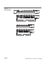
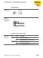
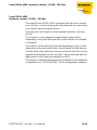
The coupling modules and the stand-alone modules are
connected directly to the respective fieldbus.
Up to 120 I/O extension modules can be interconnected via the
IP-Link, an extremely reliable internal bus based on fibre-optic
transmission, and integrated into the higher level fieldbus as a single
unit. Thus the user can determine any kind of I/O configuration that
matches his application.
The combined I/O modules feature 16 channels (8 inputs and
8 outputs) and can be optimally adapted to all applications.
piconet® – Coupling and extension modules
The coupling module is equipped with two bus connections:
via the fieldbus connection to the higher-level control, e. g. via
the PROFIBUS-DP
via the piconet® fibre-optic subnet for connection of extension
modules.
Note
Coupling modules with the type code SxxL-xxxx-100x are equipped
with an integrated T piece. This ensures even more space-saving
installation of the modules.
IP-Link – modular extension network
The coupling module detects the I/O data of the connected
extension modules via the interference immune and fast (2 Mbps)
IP-Link network.
The IP-Link is a fibre-optic cable with a transmission rate of 2 Mbps.
It transfers 1000 binary I/O data in approx. 1 ms quickly and reliably
- if smaller assemblies are concerned, the transmission rate
increases accordingly. Due to the high user data through-put it is
guaranteed, that the connection via IP-Link does not affect the
fieldbus performance perceivably.
Inexpensive connectors in protection degree IP67 have been
developed for fast and simple field-assembly of the IP-Link cables.
Connections do not require the use of any special tool and are
established quickly and conveniently. IP-Link cables are also
available with integral connectors.
Output groups can be turned off individually since the output
1-4
D300778 0613 - piconet® I/O Modules
System overview
voltage is fed separately. Further it is easily possible to work with
various potentials within an expansion ring because IP-Link is
inherently equipped with optimum potential isolation.
Note
A detailed description of the fibre-optic system IP-Link can be taken
from Chapter 2 of this manual.
D300778 0613 - piconet® I/O Modules
1-5
Extension modules
Just like stand-alone modules, extension modules also cover the
entire spectrum of I/O signals and may be mounted up to 15 m away
from each other. They are particularly small and thus provide an
especially cost-effective I/O solution in a high degree of protection.
The digital inputs and outputs are connected via threaded M8 and
M12 connectors. Analogue signal types feature M12 connections.
The threaded connectors have a high tensile strength.
Note
The maximum distance between the modules is limited to 15 m max.
due to the maximum admissible length of the fibre-optic cables.
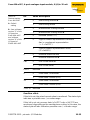
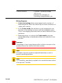
Maximum system expansion of the IP-Link
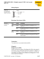
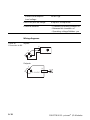
Up to 120 extension modules can be connected to a coupling
module. The length of the fibre-optic cable between two modules
and thus the distance from module to module may not exceed 15 m.
The first four digital inputs and outputs can be directly connected to
the coupling module. As with all digital piconet® modules, it is
possible to choose between threaded M8 or M12 connectors.
Further digital or analogue signals are integrated via the extension
modules.
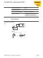
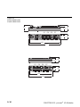
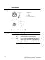
Figure 1:
Modular
extension network
PROFIBUS-DP
DeviceNet
Coupling module
Extension modules
piconet® IP-Link
1-6
D300778 0613 - piconet® I/O Modules
System overview
Stand-alone modules
piconet® stand-alone modules connect each piconet® I/O module
directly to the fieldbus. Thus a 100% transparent transmission is
ensured.
Note
Stand-alone modules with the type code SxxB-xxxx-100x are
equipped with an integrated T piece. This ensures even more spacesaving installation of the modules.
The module variety ranges from standardised digital industrial
signals to analogue input/output modules.
For temperature monitoring there are thermoelement and resistance
temperature detection modules available.
The compact robust housing with fully encapsulated electronics
allows usage directly on the machine.
Combined modules
In order to obtain the highest flexibility, novel 16-channel digital
combined I/O modules have been developed. The module channels
can be used either as inputs or outputs. The separate circuitry
ensures the isolated supply of the inputs and outputs. These
combined modules enable precise modular construction of the
system. The modules are powered via an M8 connector.
D300778 0613 - piconet® I/O Modules
1-7
1-8
D300778 0613 - piconet® I/O Modules
2
IP-Link
General description ........................................................................... 2
Construction and Topology.........................................................................3
– Construction of a ring ..............................................................................3
– Construction of a line structure ...............................................................4
Cycle time IP-Link .......................................................................................5
Technical data .............................................................................................8
– General guidelines on the installation of IP-Link cables ..........................8
– IP-Link network ........................................................................................8
– IP-Link cables ..........................................................................................9
IP-link connector .......................................................................................10
– Preparation of the IP-link connector ......................................................10
– Assembly of the IP-link connector .........................................................11
– Surface treatment ..................................................................................12
– Disassembly of the IP-link connector ....................................................13
– Examples of pre-moulded connectors ..................................................14
Trouble shooting in case of problems with the IP-Link.............................16
D300778 0613 - piconet® I/O Modules
2-1
General description
IP-Link is the sub-bus system of the piconet® system. The topology
is a ring structure. The IP-Link master is incorporated in the coupling
module. The extension modules are slaves. Up to 120 extension
modules may be connected. Each module in the IP-Link reproduces
the bus protocol. The spacing between two extension modules (IPout > IP-in) may not exceed 15 m. During planning and installation
of the extension modules, please observe that the fibre-optic cables
must form a ring structure.
2-2
D300778 0613 - piconet® I/O Modules
General description
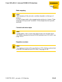
Construction and Topology
Note
If a coupling module is to be used without extension modules, then
the IP-Link connections must be bridged.
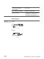
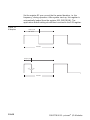
Construction of a ring
The first and last extension module may not be more than 15 m
away from the coupling module.
Figure 2:
Ring structure of
the IP-Link
D300778 0613 - piconet® I/O Modules
2-3
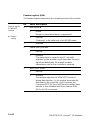
Construction of a line structure
If the distance between the last mounted extension module and the
IP-Link master, i.e. the coupling module, is too long, then a line
structure can be constructed with the IP-Link system. In this case,
only every second extension module is connected during
interconnection via the fibre-optic cable.
Attention
The length of a fibre-optic cable may never exceed 15 m.
For example:
You have 4 extension modules (4 x 15 m = 60 m). Since only every
second extension module is connected to the cable leading to the
coupling module, (15 m + 15 m = 30 m line length), then the last
extension module may have a maximum distance of 30 m from the
coupling module. This means that in this case, in comparison to an
arrangement of the modules in the ring, double the max. distance
between coupling module and the last extension module is
admissible.
Figure 3:
Line structure
of the IP-Link
Note
The more modules are interconnected in this way, the higher the
maximum admissible distance between coupling module and last
extension module.
2-4
D300778 0613 - piconet® I/O Modules
General description
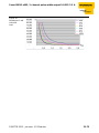
Cycle time IP-Link
Following piconet® modules with IP-Link connection are available:
1 Coupling module with IP-Link master for various fieldbuses:
- SxxL-0404D-xxxx
2 Digital extension modules
- SNNE-xxxx-xxxx (except those modules mentioned under 3)
3 Extension modules with interrupt operation
- SNNE-0202D-x003,
- SNNE-0002D-x00x,
- SNNE-40A-x009,
- SNNE-40A-x004
- SNNE-10S-x00x
- SNNE-0016D-0001
- CPV-Ventilinseln
4 Extension modules with polling operation
- SNNE-40A-x005
- SNNE-40A-x007
- SNNE-04A-x00x
The IP-Link cycle time of these modules may be increased because
the response time in polling operation depends on the internal cycle
of the extension module. This results in a minimum and maximum
cycle time.
Note
For cycle time calculations it is of no importance whether input our
output modules are concerned.
The internal processing time until the data are available for the
higher level fieldbus is negligible.
Tmin =
Coupling module base time
+ No. of digital extensions × DI time
+ ROUND OFF
(No. of all analogue extensions/16) × AM base time
+ No. of all analogue digital extensions × AM time
D300778 0613 - piconet® I/O Modules
2-5
Tmax.=
coupling module base time
+ coupling module jitter time
+ No. of digital extensions × DI time
+ ROUND OFF
(No. of all analogue extensions/16) × AM base time
+ No. of all analogue digital extensions × AM time
+ ROUND OFF
(No. of analogue polling extensions/16)
× AM jitter time
with:
2-6
coupling module base time
=
300 µs
coupling module jitter time
=
50 µs
DI time
=
15 µs
AM base time
=
800 µs
AM time
=
175 µs
AM jitter time
= 1000 µs
D300778 0613 - piconet® I/O Modules
General description
For example:
1 coupling module (SDPL-0404D-xxxx)
+ 3 SNNE-0800D-0007
+ 2 SNNE-10S-0001
+ 1 SNNE-0002D-0002
+ 2 SNNE-40A-0005
+ 1 SNNE-04A-0007
No. of digital extensions = 3
No. of all analogue digital extensions = 6
No. of analogue polling extensions = 3
Tmin
= 300 µs
+ 3 × 15 µs
+ ROUND-OFF(6/ 6) × 800 µs
+ 6 × 175 µs
= 2195 µs = 2.2 ms
Tmax
= 300 µs
+ 50 µs
+ ROUND-OFF(6/ 6) × 800 µs
+ 6 × 175 µs
+ ROUND-OFF(3/ 16) × 1000 µs
= 3245 µs = 3.3 ms
D300778 0613 - piconet® I/O Modules
2-7
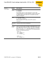
Technical data
General guidelines on the installation of IP-Link cables
Note
The installation instructions for fibre-optic cables must be observed.
Take more care when installing fibre-optic cables than
when using copper cables.
Attention
When installing the IP-Link cable, the minimum bend radius of 50
mm (static) and 55 mm (dynamic) must be
observed!
Note
When routing cables in conduits, loop forming
must be avoided.
Subsequent modification of the installation could cause the loops to
contract, while the minimum
bending radius could thus be possibly under-ranged unnoticed.
IP-Link network
Table 3:
Technical data
IP-Link
baud rate
2 Mbps
Number of nodes
120
Length between two
stations
15 m
Cable
– Plastic fibre-optics 1000 μm
– 1-core, PU jacket with Kevlar fibre
diameter 5.5 mm
IP-link connector
only SFOC permitted
Connector extraction force 20 N - 30 N
2-8
D300778 0613 - piconet® I/O Modules
General description
IP-Link cables
Table 4:
Technical data of
IP-Link cables
Outer diameter
Nominal value
5,5 mm
Material
optical fibre
PMA plastic fibre, Ø 1.0 mm
Fibre-optic sheating
PE, color black, Ø 2.2 mm
Outer jacket
PU with approx. 1.4 mm wall
thickness,
color orange, Ø 5,5 ± 0,2 mm
Transmission characteristics
Attenuation at 650 nm
typ. 170 up to 180 dB/km,
max. 200 dB/km
Mechanical Features
Bending radius, static
min. 50 mm
Bending radius, dynamic
min. 55 mm
Tensile strength (DIN VDE 0888 part 100, Verf.501)
permanent
100 N
short-term
400 N
Temperature
- 20 to + 70 °C
Weight/ Nominal value
25 kg/km
Alternating bending
resistance (DIN VDE 0888
part 100V Verf.509)
2 × 10⁶ cycles
Chemical characteristics
– Very good resistance against oil, fat,
acids, alkalis
– Long-term installation in water not
admissible
D300778 0613 - piconet® I/O Modules
2-9
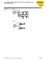
IP-link connector
The IP-Link connector is a field-wireable fibre-optic male connector
and provide an IP67 rated plug-in connection in combination with
the female connector of the respective coupling or extension
module.
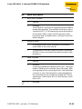
Preparation of the IP-link connector
Figure 4:
IP-link connector
(Exploded view)
A
B
C
D
E
F
G
H
I
fibre-optic
outer jacket
Kevlar fibre
fibre jacket
fibre core
locking cap
O-ring
sleeve
connector
housing
27
5,7
B
F
G
C D
A
E
H
I
1 Strip cable jacket according to indicated lengths of outer and
fibre jacket
ATTENTION:
The fibre core should not be damanged!
2 Cut the Kevlar fibre to the same length of the outer jacket.
ATTENTION:
In order to reach maximum clamping force outer and fibre jacket
have to be free of deformation (grooves, etc.) as well as of
grease, oil and lubricant.
2-10
D300778 0613 - piconet® I/O Modules
General description
Assembly of the IP-link connector
Figure 5:
Mounting the
connector
M
K
L
N
0,1
M
1 Pull the sleeve over the outer jacket and the O-ring over the
locking cap.
2
Insert the prepared optic fi ber in the connector housing until
outer jacket hooks on L and fibre jacket hooks on K simultaneously.
3 Align the connector housing as required in order to prevent cable
distort.
4 Pull the sleeve over the connector housing until it radially latches
5 Press the locking cap into the connector housing until all 4 nibs
latch. This operation can be implemented without tools or with
corresponding pliers. Keep locking cap in correct mounting
position M.
The correct mounting of the O-ring can be checked with the
latching holes N.
D300778 0613 - piconet® I/O Modules
2-11
Surface treatment
Figure 6:
Surface treatment
O
1 Treat the fibre core with the grinding gauge O up to the final
dimension and intended quality.
For this purpose take sand paper of grain size 600, and work on
a smooth surface.
2 Insert the mounted connector in the grinding gauge and treat the
surface with a circular movement.
3 Remove grinding dust with a clean lint-free cloth.
4 Check the qualitiy of the grinded surface.
The surface has to be smooth and free of scratches, grooves
and splinters.
2-12
D300778 0613 - piconet® I/O Modules
General description
Disassembly of the IP-link connector
Figure 7:
Disassembly of
the IP-link connector
P
Q
1
Apply appropriate tool at cut-out P or Q.
2
Lift out the locking cap from the closed connector housing.
ATTENTION:
Damaged or deformed components should not be applied again
after disassembly.
3
Prepare fibre-optic after disassembly according to „Preparation
of the IP-link connector”, Page 2-10 again.
D300778 0613 - piconet® I/O Modules
2-13
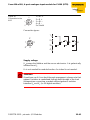
Examples of pre-moulded connectors
The photos were made using a pocket lamp with white light which
shines into the other end of the optical fibre.
Correct:
The optical fibre slightly projects the surface and has been polished
at right angles. There are no splinters etc. visible.
Figure 8:
Correctly
assembled
connector
Wrong:
The fibre was cut off too short before the connector so that it
splinters within the connector (dark section in the fibre centre).
It must be cut off again.
Figure 9:
Fibre-optic cable
too short and
splintered
2-14
D300778 0613 - piconet® I/O Modules
General description
Wrong:
The fibre-optic cable was cut off too short right from the beginning.
The fibre not even reaches into the connector end. It must be cut off
again.
Figure 10:
Fibre-optic cable
too short
Wrong:
The fibre was polished correctly. It shows a clear,
even light emission
But:
The fibre is too long and could thus damage the optical elements of
the module during plug-in.
Simply grind back the fibre a little more.
Figure 11:
Fibre-optic cable
is too long
D300778 0613 - piconet® I/O Modules
2-15
Trouble shooting in case of problems with the IP-Link
If the IP-Link error LED illuminates or flashes irregularly, there is no
message transmission or the telegrams are faulty. The modules
amplify every telegram but they cannot correct an error occurred
once. The error must thus be traced backward from the last module
to the first error-free module. The connection from this module to
the next module is the source of error.
This error is usually due to IP-Link lines with too high damping. A
possible cause could be the faulty assembly of cables and
connectors.
Note
The most simple test is visual inspection:
When held against a not too bright light source, the respective
connector surface should provide a uniformly lightened image
(check both sides).
In case of doubt, re-assemble the connector. Please take care not
to grind the optical fibre too far back (see Page 2-14, „Examples of
pre-moulded connectors”).
Note
During connector assembly please ensure that the specifications on
insulation stripping are observed.
The assembled cable can be tested simply when connected
between coupling and extension module. If the cable is correctly
connected, there will be no faulty telegrams.
2-16
D300778 0613 - piconet® I/O Modules
3
Register communication
General description ........................................................................... 2
General register description.............................................................. 3
Register R0-R7 ............................................................................................3
Register R8-R15 ..........................................................................................4
Register R16-R30 ........................................................................................6
Register R31-R47 ........................................................................................6
Register R33-R47 ........................................................................................7
Register R47-R63 ........................................................................................7
Example of register communication .................................................. 8
Control byte.................................................................................................8
– Writing the password ...............................................................................9
Read-out of the module type ....................................................................11
D300778 0613 - piconet® I/O Modules
3-1
General description
The parameterisable piconet® modules have an almost identical
data structure. The data area of the module is divided into words
and contains 64 memory locations (registers).
The main module data and parameters can be read and written via
these registers. In case of multichannel modules, each channel
features this register structure.
Each module has, depending on the module type, a specific register
assignment and number of registers used.
The following general register description contains the contents of
the registers which are identical for all complex modules.
Note
The module-specific registers and their configuration can be taken
from the respective module descriptions in the following
chapters of this manual.
3-2
D300778 0613 - piconet® I/O Modules
General register description
General register description
Complex modules have a processor of their own. They are thus
capable of exchanging data bi-directionally directly with the higher
level control. These modules will be referred to as intelligent
modules in the following. These comprise the analogue modules
and all other parameterisable modules.
The main features of the data structure of the intelligent modules are
internally more or less identical. The data area of the module is
divided into words and contains 64 memory locations. The main
module data and parameters can be read and adjusted via this
structure. Additional function call-ups with according parameters
are possible.
Each logical channel of an intelligent module features such a
structure (4-channel analogue modules thus possess 4 register
sets).
This structure is divided into the following fields:
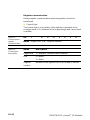
Table 5:
Register
Areas
Register address
Process variables
0-7
Manufacturer parameters
8-16
Type register
16-30
User parameters
31-47
Extended user area
48-63
Register R0-R7
In the internal RAM of the module: The process variables can be
used in addition to the actual process image and are modulespecific in their function.
Register R0-R5
These registers possess a module-type dependent function.
Register R6
Diagnostic register:
D300778 0613 - piconet® I/O Modules
3-3
The diagnostic register can contain the following additional
diagnostic information.
Contents:
Register R7
Command register:
1 High-Byte_Write = function parameter
2 Low-Byte_Write = function number
3 High-Byte_Read = function result
4 Low-Byte_Read = function number
Register R8-R15
(in the internal RAM of the module)
Type and system parameters are programmed by the manufacturer
and can only be read and not modified by the user.
Register R8
Module type:
The module type in register R8 is needed for identification of the
module.
Register R9
Software version x.y.:
The software version can only be read as ASCII character string.
Register R10
Data length:
R10 contains the number of multiplex shift registers and their length
in bit. The coupling module recognises this structure.
Register R11
Signal channels:
Compared to R10, this register contains the number of the logically
present channels. An existing shift register can thus, for instance,
consist of several signal channels.
3-4
D300778 0613 - piconet® I/O Modules
General register description
Register R12
Minimum data length:
The respective byte contains the minimal channel data length to be
transferred. If the MSB is sest, then the control / status byte is not
obligatory for function of the module and is not transferred to the
controller during module configuration. The information stands
– in the High Byte (with an output module)
– in the Low Byte (with an input module)
Register R13
Data type register:
Table 6:
Data type register
Data type register
Description
0x00
Module without valid data type
0x01
Byte array
0x02
Structure: 1 Byte, n Bytes
0x03
Word array
0x04
Structure: 1 Byte, n words
0x05
Double word array
0x06
Structure: 1 Byte, n double words
0x07
Structure: 1 byte, 1 double word
0x08
Structure: 1 byte, 1 double word
0x11
Byte array with variable logic channel
length
0x12
Structure: 1 byte, n bytes with variable
logical channel length (e.g. 60xx)
0x13
Byte array with variable logical channel
length
D300778 0613 - piconet® I/O Modules
3-5
Data type register Description
0x14
Structure: 1 byte n words with variable
logical channel length
0x15
Double word array with variable logical
channel length
0x16
Structure: 1 byte n double words with
variable logical channel length
Register R14
not used
Register R15
Alignment bits (RAM):
With the alignment bits the analogue module is assigned to a byte
limit in the internal bus.
Register R16-R30
Manufacturer parameters, serial EEPROM:
The manufacturer parameters are specfic for every module type.
They are programmed by the manufacturer but can also be changed
via the control sytem. The manufacturer parameters are stored in
the serial EEPROM of the module and are retained also in the event
of a power failure. These registers can only be changed after setting
a code word in R31.
Register R31-R47
User parameters, serial EEPROM:
The user parameters are specfic for every module type. The can be
changed by the programmer. The user parameters are stored in the
serial EEPROM of the module and are retained also in the event of a
power failure. The user area is write-protected via a code word.
3-6
D300778 0613 - piconet® I/O Modules
General register description
R31
Code word register in the RAM:
In order to change parameters in the user area, the code word
0x1235 must be registered here. If a different value is entered in this
register, then the write-protection is activated. With in-active write
protection the
code word is returned upon reading of the register; with active writeprotection the register is assigned to the value zero.
R32
Feature register:
This register defines the operating modes of the module. Thus it is
possible to activate, for example, a user-specific scaling function for
the analogue I/O modules.
Register R33-R47
Module-specific registers:
These registers depend on the module type.
Register R47-R63
Register extension for additional functions.
D300778 0613 - piconet® I/O Modules
3-7
Example of register communication
Access to the registers of the piconet® modules is enabled via an
upload of the register communication, a write or read command and
the entry of the register number in the control byte of the respective
module.
Control byte
The control byte is contained in the output image and can be read
or written.
Table 7:
Control byte
Bit 7
Bit 6
REG
R/W
Table 8:
Bit
Description of the
bits of the control 7
byte
6
Bit 5
Bit 3
Bit 2
Bit 1
Bit 0
Register number
Name
Description
REG
1
Register communication activated:
The first two user data bytes are not
used for process data exchange, but
written to or read from the register set
of the piconet® module.
R/W
0
– Read:
The register is to be read without
being modified.
1
– Write:
The register is to be written.
5
Register number
to 0
3-8
Bit 4
Number of the register that is to be
read or written. Up to 64 registers are
addressable.
D300778 0613 - piconet® I/O Modules
Example of register communication
Status byte
Table 9:
Status byte
Bit 7
Bit 6
REG
R
Table 10:
Bit
Description of the
bits of the control 7
byte
6
Bit 5
Bit 4
Bit 3
Bit 2
Bit 1
Bit 0
Register number
Name
Description
REG
1
Acknowledgement register access
R/W
0
Read
5
Register number
to 0
Number of the register that has been
read or written.
Writing the password
In order to make adjustments to a piconet® module via register
communication, it is first required to reset the write-protection of the
register.
For this, the password 0x1235 is written to register 31 of the
module. The command to write to the register and thus to enable
register communication via entry of the password is given by the
control byte of the module.
Table 11:
Writing the
register 31
(control byte)
Bit 7
Bit 6
Bit 5
Bit 4
Bit 3
Bit 2
Bit 1
Bit 0
1
1
0
1
1
1
1
1
D300778 0613 - piconet® I/O Modules
3-9
The data bytes of the output data map of the modules contain the
values which are to be transferred to the respective registers.
The password 0x1235 is written to data bytes 0 and 1 of the
according module. Data byte 0 presents the least significant byte
and data byte 1 the most significant byte.
Note
In which section of the output data map of the module data bytes 0
and 1 are contained, depends on the type of fieldbus system used
and thus of the data mapping of the modules.
For this please also read Chapter 4 of the bus-specific piconet®
manuals.
In our example 0x12 is written to data byte 1 and 0x35 to data byte
0.
Table 12:
High byte 0x1235
Table 13:
Low byte 0x1235
3-10
Bit 7
Bit 6
Bit 5
Bit 4
Bit 3
Bit 2
Bit 1
Bit 0
0
0
0
1
0
0
1
0
Bit 7
Bit 6
Bit 5
Bit 4
Bit 3
Bit 2
Bit 1
Bit 0
0
0
1
1
0
1
0
1
D300778 0613 - piconet® I/O Modules
Example of register communication
Read-out of the module type
Register 8 of each piconet® module contains information on the
module type.
The read command for register 8 is sent via the control byte to the
module as follows:
Table 14:
Bit 7
Reading register 8
1
Bit 6
Bit 5
Bit 4
Bit 3
Bit 2
Bit 1
Bit 0
0
0
0
1
0
0
0
Bit 7
=1
→ Register communication activated
Bit 6
=0
→ Register is read
Bit 5
up to Bit 0
=8
→ Register number
Upon request the module type is indicated by the input data bytes,
depending on the module and data mapping.
For example:
Counter module → read module type: 05DE hex = 1502
Note
The annex of this manual contains a description of the
module-specific coding.
D300778 0613 - piconet® I/O Modules
3-11
3-12
D300778 0613 - piconet® I/O Modules
4
General technical information
Technical data ................................................................................... 2
Supply voltage ................................................................................... 4
Galvanic isolation ........................................................................................5
– Digital modules ........................................................................................5
– Analogue modules ...................................................................................5
Incoming line and power supply .................................................................6
– General information .................................................................................6
Power loss of power cable ..........................................................................8
Start-up performance of the piconet® modules.................................. 9
Dimension drawings ........................................................................ 10
D300778 0613 - piconet® I/O Modules
4-1
Technical data
Table 15:
General
technical data
piconet®
Material
PA6 (Polyamid),
encapsulation compound: Polyurethane
Mounting
2 x through-holes Ø 3 mm
Contacts
CuZn, gold-plated
Connection of extension modules
Stand-alone module
not extendable
Coupling module
max. 120 with a total of 128 bytes input
and 128 bytes output data
Digital I/O signals
Stand-alone module
according I/O version
Coupling module
max. 960 inputs and outputs
Analogue I/O signals
Stand-alone module
according I/O version
Coupling module
max. 60 inputs and outputs
Configuration options
Stand-alone module
via the control system
(register communication or parameter
data) or I/O-ASSISTANT
Coupling module
via the control system (register
communication) or I/O-ASSISTANT
baud rate
4-2
automatic detection up to 12 Mbps
D300778 0613 - piconet® I/O Modules
Technical data
Voltage supply
Operating voltage UB 24 VDC (-15 %/+20 %)
Load voltage UL
24 VDC (-15 %/+20 %)
Connection
Power supply via:
1 x 4-pole male M8 connector
Feed through:
1 x 4-pole female M8 connector
Exception:
Sxxx-0008D-x004
Sxxx-0008D-x005
Power supply via:
2 x 4-pole male M8 connectors
Environmental
conditions
Operating
temperature
0 °C to +55 °C
Storage temperature
-25 °C to +85 °C
permissible relative
humidity
5...100 % with condensation
Vibration proofness
according to IEC 68, part 2-6 / IEC 68,
part 2-27
EMC
to EN 50082-2/IEC/EN 50081-2
Degree of protection
IP65/66/67 (to EN 60529)
Dimensions (W x H x D)
Stand-alone
modules/
Coupling modules
175 x 30 x 26.5 mm
(height up to upper edge of PB socket 30
mm, with bus tee height approx. 65 mm)
Extension modules
126 x 30 x 26.5 mm
XXL modules
210 x 30 x 26.5 mm
Weight
Stand-alone modules/ approx. 250 - 280 g, depending on
Coupling modules
module type
Extension modules
D300778 0613 - piconet® I/O Modules
approx. 120 - 200 g, depending on
module type
4-3
Supply voltage
The power supply is connected via 4-pole
M8 connectors on each module.
Operating voltage UB: 24 VDC (-15 %/+20 %)
The 24 VDC operating voltage UB is used to power the fieldbus
(termination), the processor logics, the inputs as well as the sensor
level.
The operating voltage is galvanically isolated from the fielbus
component (ASIC).
Load voltage UL: 24 VDC (-15 %/+20 %)
Load voltage UL powers the digital outputs. It can be fed separately.
If the load voltage is turned off (e.g. in an emergency stop), both the
fieldbus function and supply and the input function will be retained.
Generally, the modules are equipped with a 4-pole male and a
4-pole female M8 connector for voltage supply:
Figure 12:
Pin configuration
M8 male and M8
female connector
2
4
1
3
1 = 24 VDC UB
2 = 24 VDC UL
3 = GND
4 = GND
1 = BN
2 = WH
3 = BU
4 = BK
4
2
3
1
Exception for Sxxx-0008D-x004 und -x005
Note
With the digital output modules with a total current of IΣ = 12 A, the
supply voltage is provided by the male M8 connector.
Feed through of the supply voltage is not possible.
Three voltage circuits with 4 A each power the outputs.
4-4
D300778 0613 - piconet® I/O Modules
Supply voltage
Figure 13:
Connector 1:
Pin configuration:
Voltage
2
4
supply for
Sxxx-0008D-x004 1
3
and -x005
1 = 24 VDC UB
2 = 24 VDC UL, output 0...3
3 = GND
4 = GND
Connector 2:
2
4
1
3
1 = 24 VDC UL, output 4...5
2 = 24 VDC UL, output 6...7
3 = GND
4 = GND
Galvanic isolation
Digital modules
With the digital input/output modules, the ground potentials (GND)
of supply and load voltage are connected.
Analogue modules
With the analogue input/output modules, these ground potentials
are separated, in order to ensure galvanic isolation of the analogue
signals from the operating voltage.
Attention
Should you use UL for a feed-through arrangement, please observe
during connection of a module without galvanic isolation between
UB and UL (i.e. all digital modules) that galvanic isolation is
neutralized through a feed-through of UL.
D300778 0613 - piconet® I/O Modules
4-5
Incoming line and power supply
General information
The max. load applied to each of the connection pins of a piconet®
module may not exceed 4 A. This applies to both connection
variants (M8 and M12).
These details must be observed:
Current consumption of the modules
(see nominal current consumption of the modules in „Appendix”
of this manual)
Current consumption of the sensors
Current consumption of the actuators
Cable lengths and power losses on the cables
(see power loss)
If power is fed through, please ensure that the max. admissible
current of 4 A per pin is not exceeded.
Examples
1 If all 8 outputs of a piconet® module with an 0.5 A output power
rating are exposed to an output current load of 0.5 A
simultaneously (simultaneity factor 1), the feed-through power
line may not be used, because this could destroy the connection
or the device.
4-6
D300778 0613 - piconet® I/O Modules
Supply voltage
2 If channels 0...3 are to be connected to a piconet® module with
an output power rating of 2 A (IΣ = 12 A), the load of 2 A may only
be applied to 2 of the 4 channels.
Figure 14:
Load ratings of the
Connections
D300778 0613 - piconet® I/O Modules
4-7
Power loss of power cable
When using the power cables IPS(W)KP4-xxxx, do not exceed the
total length of 15 m at 4 A (with power feed-through).
Note
During connection please observe that with a nominal voltage of
24 VDC, the functionality of the modules cannot be ensured from a
voltage drop of 6 V on.
Further please observe the voltage fluctuations of the power supply
unit.
Example
At a load of 4 A, an 8 m power cable with 0.34 mm² has a
voltage drop of 3.2 V.
4-8
D300778 0613 - piconet® I/O Modules
Start-up performance of the piconet® modules
Start-up performance of the piconet® modules
Upon switch-on the module tests its status, configures the IP-Link
(coupling modules) and then compiles a set-up list according to the
detected extension modules.
During start-up of the modules, the I/O LEDs illuminate and flash. In
an error-free condition, the I/O LEDs should stop flashing after
2-3 seconds. If an error has occurred, it depends on the type of error
which LED starts flashing (see Chapter "Error treatment and
diagnostics" in the bus-specific piconet® manual).
Figure 15:
Start-up
performance
D300778 0613 - piconet® I/O Modules
4-9
Dimension drawings
Figure 16:
Dimensions of the
piconet® modules
4-10
D300778 0613 - piconet® I/O Modules
5
Diagnostic LEDs for local errors
Error diagnostics via LEDs ................................................................ 2
Flash codes .................................................................................................2
Local errors of a coupling module (SxxL-0404D-xxxx) ...............................3
Local errors of an extension module ...........................................................5
D300778 0613 - piconet® I/O Modules
5-1
Error diagnostics via LEDs
With the piconet® system, one distinguishes between the following
kind of errors:
Fieldbus errors
IP-Link errors or local module errors
Figure 17:
LEDs
Flash codes
Table 16:
LED flash codes
Flash sequence
Meaning
Fast flashing
Start
first slow sequence
Error code
second slow sequence
Error argument 1
third slow sequence
(optional)
Error argument 2
(with more than 20 extensions)
Figure 18:
Flash codes
pause
Pause
Anfang
start
5-2
Fehlercode
errorcode
pause
Pause
pause
Pause
Fehlerargument1
er
rorargum ent1
Fehlerargument
errorargum ent22
(optional)
D300778 0613 - piconet® I/O Modules
Error diagnostics via LEDs
Local errors of a coupling module (SxxL-0404D-xxxx)
Local errors are errors of the piconet® module or the IP-Link.
Table 17:
Local errors of a
SxxL-0404D-xxx
LED, LED
green red
Description
Remedy:
-
no
exchanging data
Module in
syncronous
mode → activate
cyclic data
Error Error
code argument
1
OFF
A Counting
begins with n = 1
with the last
connected
extension module OFF
against the
direction of the
fibre-optic cabling OFF
backwards in the
OFF
direction of the
coupling module.
OFF
2
1
0
-
EEPROM
check sum error
Set manufacturer
settings
2
-
-
reserved
-
3
n
-
Wire-break
detected C
Wire-break after
extension module n
A
B With more than
20 extensions on
the IP-Link the following applies:
n = stands for the
tens, m = stands
for the ones of the OFF
"module number“
C The wire brak
will be detected as
long as the error
occurs
OFF
OFF
Wire-breakage:
behind the
(n-module *10) +
m-module A
3B
n
m
Wire-break
detected C
4
n
-
Too many faulty
Error localisation:
telegrams detected in front of the
(more than 25 %)
extension module n
– check fibre-optic
cabling
5
n
-
Register access to
complex modules
failed
n-module
check
11
n
-
Faulty operation of
complex module
Replace n-module
D300778 0613 - piconet® I/O Modules
5-3
LED, LED
gree red
n
Description
Remedy:
Error Error
code argument
5-4
1
2
OFF
12
n
-
More than 120
Reduce no. of
modules connected modules
in IP-Link ring
within IP-Link
OFF
13
n
-
n-module unknown Firmware update
required
ON
OFF
-
-
Module is
exchanging data (no
errors)
D300778 0613 - piconet® I/O Modules
Error diagnostics via LEDs
Local errors of an extension module
Table 18:
Local errors of a
SNNE-0404D-xxx
LED,
green
LED
red
Description
OFF
ON
No data are received via the IP-Link
OFF
flashes,
flickers
Faulty IP-Link protocols are received (very
bad data connection)
flashes,
flickers
flashes,
flickers
Faulty IP-Link protocols are received (bad
data connection),
→ must not yet lead to an error
flashes,
flickers
OFF
IP-Link protocols are received, no errors
Note
IP-Link errors can usually be attributed to inappropriate
use of the fibre-optic cabling.
Faulty IP-Link protocols can be caused by:
badly assembled IP-Link connectors
IP-Link cables with increased damping
(e.g. through bends or similar in the cable)
a defect or contaminated emitter LED on the module prior to the
faulty module
defect or dirty receiver.
D300778 0613 - piconet® I/O Modules
5-5
5-6
D300778 0613 - piconet® I/O Modules
6
IP-Link coupling modules
Type overview.................................................................................... 2
General description ........................................................................... 3
Connection modes ......................................................................................3
I/O network with the IP-Link........................................................................3
Automatic input data mapping ....................................................................4
SxxL-0404D-x00x, coupling module 4DI/4DO .................................... 5
Technical data .............................................................................................6
Wiring diagrams ..........................................................................................7
Parameters ..................................................................................................9
Diagnosis.....................................................................................................9
– Diagnostics via LEDs ...............................................................................9
– Diagnostics via software ..........................................................................9
D300778 0613 - piconet® I/O Modules
6-1
Type overview
Table 19:
SxxL-0404D-x00x
Type overview of
IP-Link
Coupling modules SxxL-0404D-x003,
Page 6-3
SxxL-0404D-x004,
Page 6-3
6-2
Description
– 4 digital inputs,
24 V DC, filter 3.0 ms
– 4 digital outputs,
24 V DC; Imax = 0.5 A
Connection
technology
M8
M12
D300778 0613 - piconet® I/O Modules
General description
General description
The coupling modules transfer the I/O data of the digital and
analogue sensors or actuators connected to the module to the
fieldbus. They also collect the I/O data of the extension modules via
the interference immune fibre-optic connection (IP-Link). These data
are processed bus-specifically by the coupling modules and
transferred to the respective fieldbus.
Connection modes
The IP-Link coupling module, SxxL-0404D-x00x, is equipped with
two bus connections,
via the fieldbus connection to the higher level control
(e. g. PROFIBUS-DP, DeviceNet™)
via the piconet® fibre-optic subnet for connection of extension
modules.
In addition it is possible to connect 4 binary switches or sensors as
well as 4 binary actuators directly to the coupling module.
I/O network with the IP-Link
Up to 120 extension modules can be connected to a coupling
module. From the view of the fieldbus, the coupling module with all
the connected extension modules is a single node with an according
high number of I/O signals. Thus it can be regarded as an IP67
remote I/O network with a single fieldbus interface only.
D300778 0613 - piconet® I/O Modules
6-3
Automatic input data mapping
The coupling module automatically detects the connected
extension modules during the start-up phase and automatically
maps the I/O data to the fieldbus process image. Configuration is
thus not necessary.
6-4
D300778 0613 - piconet® I/O Modules
SxxL-0404D-x00x, coupling module 4DI/4DO
SxxL-0404D-x00x, coupling module 4DI/4DO
These digital I/O modules combine 4 digital inputs with an input filter
of 3 ms and 4 digital outputs in a single device.
The outputs are suited for load currents of 0.5 A.
They are short-circuit and reverse-polarity protected.
The signal status can be indicated separately for each channel via
LEDs.
The inputs are located on the upper half of the modules. With M8
connection technology modules, these are the upper four
connectors (C0 to C3), and with the M12 technology modules the
two upper connectors (C0, C1) with two inputs on one connector.
Figure 19:
SDPL-0404D-x003
33 36,5
33 26,5
C6 C4 C2 C0
C7 C5 C3 C1
30
23
C3 C2 C1 C0
168
175
210
D300778 0613 - piconet® I/O Modules
203
6-5
Technical data
Table 20:
Technical data
Designation
SxxL-0404D-x001, -x002,
-x003, -x004
Voltage supply
Operating voltage UB
24 VDC (-15 %/+20 %)
Load voltage UL
24 VDC (-15 %/+20 %)
Inputs
Number of inputs
4, according to EN 61131-2
Input voltage
24 VDC (-15 %/+ 20 %)
Supply current
500 mA, short-circuit protected
Input filter
3.0 ms
Max. input current
< 7 mA
Switching point 0/1
-3... 5 V / 11...30 V,
6 mA input current
(EN 61131-2, type 2)
Sensor supply
from operating voltage UB,
max. 0.5 A per module,
common short-circuit protection
Outputs
6-6
Number of outputs
4, according to EN 61131-2
Output voltage
24 VDC (-15 %/+ 20 %)
Output current per channel
max. 0.5 A per channel, each
channel is short-circuit protected
Load type
ohmic, inductive, lamp load
Current consumption
Load voltage
20 mA. typ.
Short-circuit current
typically 1.5 A (cyclic)
D300778 0613 - piconet® I/O Modules
SxxL-0404D-x00x, coupling module 4DI/4DO
Switching frequency
500 Hz
Simultaneity factor
1
Bits in the process image
4 input or 4 output bits
Potential isolation
– Channels/Operating voltage: no
– Between the channels: no
– Operating voltage/fieldbus: yes
Wiring diagrams
Figure 20:
Inputs:
Connection to the
M8
(+)
( )
()
4
3
1
Outputs:
4
3
(+)
1
+ 24 VDC
()
D300778 0613 - piconet® I/O Modules
6-7
Figure 21:
Inputs:
Connection to the
2
M12
1
5
()
( )
(+)
3
4
()
( )
(+)
outputs:
(+)
2
1
5
6-8
()
3
4
(+)
()
D300778 0613 - piconet® I/O Modules
SxxL-0404D-x00x, coupling module 4DI/4DO
Parameters
Detailed information on fieldbus-dependent parameterisation of the
modules is contained in the chapter "Parameters of the piconet®
I/O modules" of the following manuals:
Profibus-DP
German: „piconet® for PROFIBUS-DP“, D300775
English: „piconet® for PROFIBUS-DP“, D300776
DeviceNet
Not yet published
CANopen
Not yet published
Diagnosis
Diagnostics via LEDs
Please read the description of the diagnostic LEDs in the event of
local errors of the coupling and extension modules in Chapter 5 of
this manual: Fieldbus-specific diagnostic indications via LEDs are
described in the chapter "Error treatment and diagnostics" of the
above mentioned manuals.
Diagnostics via software
Detailed information on fieldbus-dependent diagnostics of the
modules is contained in the chapter "Error treatment and
diagnostics" of the above mentioned manuals.
D300778 0613 - piconet® I/O Modules
6-9
6-10
D300778 0613 - piconet® I/O Modules
7
Digital input modules
Type overview.................................................................................... 2
Sxxx-0800D-x00x, 8-port digital input, filter 0.2 ms/3.0 ms .............. 3
Technical data .............................................................................................4
Wiring diagrams .........................................................................................5
Parameters ..................................................................................................6
Diagnosis.....................................................................................................6
– Diagnostics via LEDs ...............................................................................6
– Diagnostics via software ..........................................................................6
D300778 0613 - piconet® I/O Modules
7-1
Type overview
The device type Sxxx-0800D is designed for connection of 8 binary
switches or sensors.
The devices come as stand-alone or extension modules and differ
in their connection technology and input filter speed.
Table 21:
Type overview
digital input
modules
Sxxx-0800D-x00x
Sxxx-0800D-x007,
Page 7-3
Description
– 8 digital inputs,
24 VDC, filter 3.0 ms
Sxxx-0800D-x004,
Page 7-3
Sxxx-0800D-x008,
Page 7-3
Sxxx-0800D-x002,
Page 7-3
7-2
Connection
technology
M8
M12
– 8 digital inputs,
24 VDC, filter 0,2 ms
M8
M12
D300778 0613 - piconet® I/O Modules
Sxxx-0800D-x00x, 8-port digital input, filter 0.2 ms/3.0 ms
Sxxx-0800D-x00x, 8-port digital input, filter 0.2 ms/3.0 ms
The digital input modules type Sxxx-0800D-x00x detect the binary
control signals at the process level and transfer these to the higher
level automation device. The signal status is indicated via LEDs.
The sensors are powered via the operating voltage UB. The load
voltage UL connection is not needed by the input module, but can
be used for optional power feed-through.
Figure 22:
SDPB-0800D-x00x
SNNE-0800D-x00x
33
26,5 33
C1
C3
C5
C7
C0 C2 C4 C6
C0 C1 C2 C3
23
30
168
175
26,5 33
C1
C3
C5
C7
C0 C2 C4 C6
C0 C1 C2 C3
23
30
119
126
D300778 0613 - piconet® I/O Modules
7-3
Technical data
Table 22:
Technical data
Designation
Sxxx-0800D-x007/ -x004
/ -x008, / -x002
Voltage supply
Operating voltage UB
24 VDC (- 15 %/+ 20 %)
Load voltage UL
24 VDC (- 15 %/+ 20 %)
Number of inputs
8, according to EN 61131-2
Input filter
...x007/...x004
...x008/...x002
7-4
3.0 ms
0,2 ms
Input voltage
24 VDC (- 15 %/+ 20 %)
Signal voltage "0"
-3 V...5 V (EN 61131-2, Type 2)
Signal voltage "1"
11 V...30 V (EN 61131-2, Type 2)
Input current, typical
6 mA (EN 61131-2, Type 2)
Sensor supply
via operating voltage,
max. 0.5 A per module,
common short-circuit protection
Bits in the process image
8 input bits
Potential isolation
– Channels/Operating voltage: no
– Between the channels: no
– Operating voltage/fieldbus: yes
D300778 0613 - piconet® I/O Modules
Sxxx-0800D-x00x, 8-port digital input, filter 0.2 ms/3.0 ms
Wiring diagrams
Figure 23:
Connection to the
M8
4
3
Figure 24:
Connection to the
M12
(+)
( )
()
1
2
1
5
3
4
D300778 0613 - piconet® I/O Modules
()
( )
(+)
()
( )
(+)
7-5
Parameters
Detailed information on fieldbus-dependent parameterisation of the
modules is contained in the chapter "Parameters of the piconet®
I/O modules" of the following manuals:
Profibus-DP
German: „piconet® für PROFIBUS-DP“, D300775
English: „piconet® for PROFIBUS-DP“, D300776
DeviceNet
Not yet published
CANopen
Not yet published
Diagnosis
Diagnostics via LEDs
Please read the description of the diagnostic LEDs in the event of
local errors of the coupling and extension modules in Chapter 5 of
this manual: Fieldbus-specific diagnostic indications via LEDs are
described in the chapter "Error treatment and diagnostics" of the
above mentioned manuals.
Diagnostics via software
Detailed information on fieldbus-dependent diagnostics of the
modules is contained in the chapter "Error treatment and
diagnostics" of the above mentioned manuals.
7-6
D300778 0613 - piconet® I/O Modules
8
Digital output modules
Type overview.................................................................................... 3
Sxxx-0008D-x006/ -x001, 8-port digital output, 24 VDC,
Imax = 0.5 A ......................................................................................... 4
Technical data .............................................................................................5
Wiring diagrams ..........................................................................................5
Parameters ..................................................................................................6
Diagnosis.....................................................................................................6
– Diagnostics via LEDs ...............................................................................6
– Diagnostics via software ..........................................................................6
Sxxx-0008D-x002/ -x003, 8-port digital output, 24 VDC,
Imax = 2 A ............................................................................................ 7
Technical data .............................................................................................9
Wiring diagrams ..........................................................................................9
Parameters ................................................................................................10
Diagnosis...................................................................................................10
– Diagnostics via LEDs .............................................................................10
– Diagnostics via software ........................................................................10
Sxxx-0008D-x004/ -x005, 8-port digital output, 24 VDC,
Imax = 2 A .......................................................................................... 11
Technical data ...........................................................................................12
Wiring diagrams ........................................................................................13
Parameters ................................................................................................13
Diagnosis...................................................................................................13
– Diagnostics via LEDs .............................................................................13
– Diagnostics via software ........................................................................14
Potential groups ........................................................................................14
SNNE-0016D-0001, 16 digital outputs 24 VDC, total current
max. 4 A ........................................................................................... 15
Technical data ...........................................................................................16
Wiring diagram ..........................................................................................17
Meaning of the channel LEDs ...................................................................17
Parameters ................................................................................................17
Diagnosis...................................................................................................17
– Diagnostics via LEDs .............................................................................17
– Diagnostics via software ........................................................................18
D300778 0613 - piconet® I/O Modules
8-1
Data mapping ............................................................................................18
Control and status byte .............................................................................18
– Process data operation .........................................................................18
– Register communication ........................................................................20
Register overview ......................................................................................21
Watchdog Feature (R32-R33)....................................................................21
SNNE-0016D-0002, 16 digital outputs 24 VDC, total current
max. 4 A ........................................................................................... 23
Technical data ...........................................................................................23
The module’s error behavior .....................................................................23
8-2
D300778 0613 - piconet® I/O Modules
Type overview
Type overview
The device type Sxxx-008D-x00x is designed for connection of 8
binary actuators. The devices come as stand-alone or extension
modules and differ in their connection technology, max. admissible
output current per channel and max. total current rating.
Table 23:
Type overview
digital output
modules
Sxxx-0008D-x00x
Sxxx-0008D-x006,
page 8-4
Description
– 8 digital outputs
24 VDC, Imax = 0.5 A
Sxxx-0008D-x001,
page 8-4
Sxxx-0008D-x002,
page 8-7
Sxxx-0008D-x003,
page 8-7
Sxxx-0008D-x004,
page 8-11
Sxxx-0008D-x005,
page 8-11
D300778 0613 - piconet® I/O Modules
Connection
technology
M8
M12
– 8 digital outputs
24 VDC, Imax = 2 A;
(IΣ = 4A)
M8
– 8 digital outputs
24 VDC, Imax = 2 A;
(IΣ = 12A)
M8
M12
M12
8-3
Sxxx-0008D-x006/ -x001, 8-port digital output, 24 VDC, Imax = 0.5 A
The digital output modules transfer the binary control signals of the
automation device to the actuators at the process level. The 8
outputs process load currents of up to 0.5 A and indicate their signal
status via LEDs.
The outputs are short-circuit and reverse-polarity protected.
Figure 25:
SDPB-0008D-x00x
SNNE-0008D-000x
33
26,5 33
C1
C3
C5
C7
C0 C2 C4 C6
C0 C1 C2 C3
23
30
168
175
26,5 33
C1
C3
C5
C7
C0 C2 C4 C6
C0 C1 C2 C3
23
30
119
126
8-4
D300778 0613 - piconet® I/O Modules
Sxxx-0008D-x006/ -x001, 8-port digital output,
24 VDC, Imax = 0.5 A
Technical data
Table 24:
Technical data
Designation
Sxxx-0008D-x006/ -x001
Voltage supply
Operating voltage UB
24 VDC (- 15 %/+ 20 %)
Load voltage UL
24 VDC (- 15 %/+ 20 %)
Number of outputs
8, according to EN 61131-2
Load type
ohmic, inductive, lamp load
Output voltage
24 VDC (- 15 %/+ 20 %)
Output current per channel
max. 0.5 A, each channel is shortcircuit protected
Short-circuit current
typically 1.5 A
Current consumption
Load voltage
20 mA. typ./per channel
Switching frequency
500 Hz
Simultaneity factor
1
Bits in the process image
8 bits output data
Wiring diagrams
Figure 26:
Connection to M8
4
3
(+)
1
+ 24 VDC
()
D300778 0613 - piconet® I/O Modules
8-5
Figure 27:
Connection to the
M12
(+)
2
1
5
()
3
4
(+)
()
Parameters
Detailed information on fieldbus-dependent parameterization of the
modules is contained in the chapter "Parameters of the piconet®
I/O modules" of the following manuals:
Profibus-DP
German: „piconet® for PROFIBUS-DP“, D300775
English: „piconet® for PROFIBUS-DP“, D300776
DeviceNet
Not yet published
CANopen
Not yet published
Diagnosis
Diagnostics via LEDs
Please read the description of the diagnostic LEDs in the event of
local errors of the coupling and extension modules in Chapter 5 of
this manual: Fieldbus-specific diagnostic indications via LEDs are
described in the chapter "Error treatment and diagnostics" of the
above mentioned manuals.
Diagnostics via software
Detailed information on fieldbus-dependent diagnostics of the
modules is contained in the chapter "Error treatment and diagnostics" of the above mentioned manuals.
8-6
D300778 0613 - piconet® I/O Modules
Sxxx-0008D-x002/ -x003, 8-port digital output,
24 VDC, Imax = 2 A
Sxxx-0008D-x002/ -x003, 8-port digital output, 24 VDC, Imax = 2 A
The digital output modules transfer the binary control signals of the
automation device to the actuators at the process level. The 8
outputs process load currents of up to 2 A each, yet the maximum
total current is limited to IΣ = 4 A. Thus these modules are particularly
suited for applications in which all outputs are not active at the same
time or not all actuators require signal currents of 2 A.
The signal status is indicated via LEDs.
The outputs are short-circuit and reverse-polarity protected.
D300778 0613 - piconet® I/O Modules
8-7
Figure 28:
SDPB-0008D-x00x
SNNE-0008D-000x
33
26,5 33
C1
C3
C5
C7
C0 C2 C4 C6
C0 C1 C2 C3
23
30
168
175
26,5 33
C1
C3
C5
C7
C0 C2 C4 C6
C0 C1 C2 C3
23
30
119
126
8-8
D300778 0613 - piconet® I/O Modules
Sxxx-0008D-x002/ -x003, 8-port digital output,
24 VDC, Imax = 2 A
Technical data
Table 25:
Technical data
Designation
Sxxx-0008D-x002/ -x003
Voltage supply
Operating voltage UB
24 VDC (- 15 %/+ 20 %)
Load voltage UL
24 VDC (- 15 %/+ 20 %)
Number of outputs
8, according to EN 61131-2
Load type
ohmic, inductive, lamp load
Output voltage
24 VDC (- 15 %/+ 20 %)
Output current per channel
max. 2.0 A per channel,
each channel is individually
short-circuit protected,
Total current 4 A max.
Short-circuit current
typically 4 A
Current consumption
Load voltage
30 mA. typ./per channel
Switching frequency
500 Hz
Simultaneity factor
0,25
Bits in the process image
8 bits output data
Potential isolation
– Channels/Operating voltage: no
– Between the channels: no
– Operating voltage/fieldbus: yes
Wiring diagrams
Figure 29:
Connection to M8
4
3
(+)
1
+ 24 VDC
()
D300778 0613 - piconet® I/O Modules
8-9
Figure 30:
Connection to the
M12
(+)
2
1
5
()
3
4
(+)
()
Parameters
Detailed information on fieldbus-dependent parameterization of the
modules is contained in the chapter "Parameters of the piconet®
I/O modules" of the following manuals:
Profibus-DP
German: „piconet® for PROFIBUS-DP“, D300775
English: „piconet® for PROFIBUS-DP“, D300776
DeviceNet
Not yet published
CANopen
Not yet published
Diagnosis
Diagnostics via LEDs
Please read the description of the diagnostic LEDs in the event of
local errors of the coupling and extension modules in Chapter 5 of
this manual: Fieldbus-specific diagnostic indications via LEDs are
described in the chapter "Error treatment and diagnostics" of the
above mentioned manuals.
Diagnostics via software
Detailed information on fieldbus-dependent diagnostics of the
modules is contained in the chapter "Error treatment and diagnostics" of the above mentioned manuals.
8-10
D300778 0613 - piconet® I/O Modules
Sxxx-0008D-x004/ -x005, 8-port digital output,
24 VDC, Imax = 2 A
Sxxx-0008D-x004/ -x005, 8-port digital output, 24 VDC, Imax = 2 A
The digital output modules transfer the binary control signals of the
automation device to the actuators at the process level. The
8 outputs process load currents of up to 2 A each, yet the maximum
total current is limited to IΣ = 12 A.
The signal status is indicated via LEDs.
The outputs are short-circuit and reverse-polarity protected.
Figure 31:
SDPB-0008D-x00x
SNNE-0008D-000x
33
26,5 33
C1
C3
C5
C7
C0 C2 C4 C6
C0 C1 C2 C3
23
30
168
175
26,5 33
C1
C3
C5
C7
C0 C2 C4 C6
C0 C1 C2 C3
23
30
119
126
D300778 0613 - piconet® I/O Modules
8-11
Technical data
Table 26:
Technical data
Designation
Sxxx-0008D-x004/ -x005
Voltage supply
8-12
Operating voltage UB
24 VDC (- 15 %/+ 20 %)
Load voltage UL
24 VDC (- 15 %/+ 20 %)
Number of outputs
8, according to EN 61131-2
Load type
ohmic, inductive, lamp load
Output voltage
24 VDC (- 15 %/+ 20 %)
Output current per channel
max. 2.0 A per channel,
each channel is individually shortcircuit protected,
total current 12 A
– Channels 0...3 Σ 4 A
– Channels 4...5 Σ 4 A
– Channels 6...7 Σ 4 A
Short-circuit current
typically 4 A
Current consumption
Load voltage
50 mA. typ./per channel
Switching frequency
500 Hz
Simultaneity factor
0,75
Connection
Voltage supply
Power supply via:
2 x 4-pole male M8 connectors
(see also page 4-6)
Bits in the process image
8 bits output data
Potential isolation
– Channels/Operating voltage: no
– Between the channels: no
– Operating voltage/fieldbus: yes
D300778 0613 - piconet® I/O Modules
Sxxx-0008D-x004/ -x005, 8-port digital output,
24 VDC, Imax = 2 A
Wiring diagrams
Figure 32:
Connection to M8
4
3
Figure 33:
Connection to the
M12
(+)
1
+ 24 VDC
()
(+)
2
1
5
()
3
4
(+)
()
Parameters
Detailed information on fieldbus-dependent parameterization of the
modules is contained in the chapter "Parameters of the piconet®
I/O modules" of the following manuals:
Profibus-DP
German: „piconet® for PROFIBUS-DP“, D300775
English: „piconet® for PROFIBUS-DP“, D300776
DeviceNet
Not yet published
CANopen
Not yet published
Diagnosis
Diagnostics via LEDs
Please read the description of the diagnostic LEDs in the event of
local errors of the coupling and extension modules in Chapter 5 of
this manual: Fieldbus-specific diagnostic indications via LEDs are
described in the chapter "Error treatment and diagnostics" of the
above mentioned manuals.
D300778 0613 - piconet® I/O Modules
8-13
Diagnostics via software
Detailed information on fieldbus-dependent diagnostics of the
modules is contained in the chapter "Error treatment and diagnostics" of the above mentioned manuals.
Potential groups
With this module the load voltage is fed via three circuits. UL1 for
channels 0-3 (total current 4 A), UL2 for channels 4-5 (total current 4
A) and UL3 for channels 6-7 (total current 4 A).
The total current may not be exceeded. That means that merely
2 channels of channels 0...3 with a load of 2 A each may be switched
on.
Figure 34:
Potential groups
8-14
D300778 0613 - piconet® I/O Modules
SNNE-0016D-0001, 16 digital outputs 24 VDC, total current
max. 4 A
SNNE-0016D-0001, 16 digital outputs 24 VDC, total current max. 4 A
The IE2808 digital output module connects the binary control
signals from the automation unit on to the actuators at the process
level.
The 16 outputs handle load currents of up to 0.5 A each, although
the total current is limited to 4 A.
This makes these modules particularly suitable for applications in
which not all of the outputs are active at the same time, or in which
not all of the actuators draw 0.5 A current.
An output short-circuit is recognized and passed on to the
controller.
The signal state is indicated by means of light emitting diodes.
The signal connection is realized by the 25-pin D-sub socket.
The outputs are short-circuit safe and protected against inverse
connection.
Via registers R32 and R33 default values can be activated, which
means, these values will be written in case of a communication loss.
In R33, the value On or OFF is set for each output, in R32 this
behavior is activated or deactivated.
Figure 35:
SNNE-0016D-0001
26,5 33
23
30
C0
119
126
D300778 0613 - piconet® I/O Modules
8-15
Technical data
Table 27:
Technical data
Designation
SNNE-0016D-0001
Voltage supply
8-16
Operating voltage UB
24 VDC (- 15 %/+ 20 %)
Load voltage UL
24 VDC (- 15 %/+ 20 %)
Number of outputs
16
Load type
ohmic, inductive, lamp load
Output voltage
24 VDC (- 15 %/+ 20 %)
Output current per channel
0.5 A (Σ max. 4 A)
Short circuit current
max 1,5 A
Load voltage current
consumption
typical 5 mA per channel
Connection
Power supply
Feed: 1 x M8 male socket, 4-pole
downstream connection:
1 x M8 female socket, 4-pole
Bits in process image
16 bit output, 16 bit input (diagnostic), optional: control/status
byte
Electrical isolation
– channels / control voltage: no
– between the channels: no
– control voltage / fieldbus: yes,
via IP-Link
D300778 0613 - piconet® I/O Modules
SNNE-0016D-0001, 16 digital outputs 24 VDC, total current
max. 4 A
Wiring diagram
Figure 36:
Connection via
25-pole SUB-D
female connector
v
1
13
Output
14
1...16 = output 1...16
17...24 = GND
25 = n.c.
25 è C0
Meaning of the channel LEDs
Table 28:
Channel-LED
displays
LED
Status
Meaning
ERR
1-8
Green
at least one output of the group 1-8 is
switched
Red
at least one output of the group 1-8 has a
short-circuit
Green
at least one output of the group 9-16 is
switched
Red
at least one output of the group 9-16 has a
short-circuit
ERR
9-16
Parameters
The module has no parameter data available.
Diagnosis
Diagnostics via LEDs
Please read the description of the diagnostic LEDs in the event of
local errors of the coupling and extension modules in Chapter 5 of
this manual: Fieldbus-specific diagnostic indications via LEDs are
described in the chapter "Error treatment and diagnostics" of the
above mentioned manuals.
D300778 0613 - piconet® I/O Modules
8-17
Diagnostics via software
Detailed information on fieldbus-dependent diagnostics of the
modules is contained in the chapter "Error treatment and diagnostics" of the above mentioned manuals.
Data mapping
Note
Data mapping of the piconet® modules depends on the type of
fieldbus.
For this, please refer to the mapping descriptions in chapter
"Data mapping of the piconet® modules" of the respective busspecific manuals.
Control and status byte
Process data operation
Control byte
The control byte is only visible, if the module is operated in the
complex mode. It is contained in the output image and can be read
or written.
Table 29:
Control byte
Bit
7
6
Name RegAccess
Table 30:
Control byte
description
5
4
3
2
1
0
ResetErr Set
Default
Status
Name
Description
RegAccess
– 0 = Register communication disabled
(Process data operation)
ResetErr
– Sets back errors, displayed at status byte
Set Default- – Sets outputs to default status defined by register
Status
R33
8-18
D300778 0613 - piconet® I/O Modules
SNNE-0016D-0001, 16 digital outputs 24 VDC, total current
max. 4 A
Status byte
The status byte is only visible, if the module is operated in the
complex mode. It is contained in the input image and can only be
read.
Table 31:
Status byte
Bit
7
6
5
4
3
2
Name Reg
Error Under- Ovr
Ovr
Access
Voltage Current Current
Grp1
Grp2
Table 32:
Name
Description of the
RegAccess
status byte
1
0
Default Status
Description
0 = Acknowledgement of process data operation
Error
General error bit
UnderVoltage
0 = Load voltage UL = 18 V
1 = Load voltage UL < 18 V, UL-LED shines red, but
the outputs stay switched
OvrCurrent
Grp2
1 = Short circuit detected at an output of group 2.
The concerned output is displayed by the input byte
Diag2. After repair this error display has to be set
back by bit CB.6 of control byte.
OvrCurrent
Grp1
1 = Short circuit detected at an output of group 1.
The concerned output is displayed by the input byte
Diag1. After repair this error display has to be set
back by bit CB.6 of control byte.
DefaultStatus
1 = Outputs have been set to default status, defined
by R33
D300778 0613 - piconet® I/O Modules
8-19
Register communication
During register communication measuring values cannot be transferred.
Control byte
The control byte is only visible, if the module is operated in the
complex mode. It is contained in the output image and can be read
or written.
Table 33:
Bit
Control byte in
register communi- Name
cation
Table 34:
Control byte
description
7
6
5
4
3
2
1
0
RegAccess R/W Register number
Name
Description
RegAccess
1 = Register communication enabled
R/W
0 = Read
1 = Write
Register
number
Number of the register that is to be read or written.
Status byte
The status byte is only visible, if the module is operated in the
complex mode. It is contained in the input image and can only be
read.
Table 35:
Status byte
Bit
7
Name RegAccess
Table 36:
Control byte
description
8-20
6
5
4
3
R/
W
Register number
2
1
Name
Description
RegAccess
1 = Acknowledgement for register access
R/W
0 = Read
Register
number
Number of the register that is to be read.
0
D300778 0613 - piconet® I/O Modules
SNNE-0016D-0001, 16 digital outputs 24 VDC, total current
max. 4 A
Register overview
Table 37:
Register Designation
Register overview
SNNE-0016D-001
Default
value
Read/ Memory
Write
(hex)
R 0 to
R5
reserved
0000
R
RAM
R6
diagnostic-Register - not
used
0000
R
RAM
R7
command register - not
used
0000
R
RAM
R8
module type
AF8
R
ROM
R9
firmware version number
3142
R
ROM
R 10
multiplex shift register
0118
R
ROM
R 11
signal channels
0118
R
ROM
R 12
minimum data length
9898
R
ROM
R 13
data structure
0001
R
ROM
R 14 to
R 30
reserved
0001
R
ROM
R 31
code word register
variable
R/W
RAM
R 32
enable default status
register
FFFF
R/W
SEEROM
R 33
default status register
0000
R/W
SEEROM
Watchdog Feature (R32-R33)
The behavior of the outputs in case of a communication error can be
defined via the Enable Default Status register R32 and the Default
Status register R33.
In order to write to the register, it is first required to reset the write
protection in the code word register
D300778 0613 - piconet® I/O Modules
8-21
Registers 32 and 33 define the behavior of every single channel.
Register R32 activates or deactivates the Watchdog Feature.
Register R33 defines the state of the output in case of an error (if
Watchdog has been activated).
Attention
When using the watchdog feature, please observe, that during the
start-up of an installation no communication is established. The output will thus be set to the default value.
The modules are delivered with an active watchdog feature. The
output status is set to "0". All outputs are switched of if an error
occurs.
Table 38:
Watchdog
Feature
Reg.
Description
Output
Description
Default
32
Watchdog
active
00-15
1 = activated;
0xFFFF
0 = deactivated
33
output state
00-15
1 = ON; 0 = OFF 0x0000
Example:
Register 32 = 1111 1111 1111 1111
Register 33 = 0000 0000 0000 1000
Process data = all outputs ON
In case of a communication error, all outputs are now set to OFF,
except for output 3.
Output 3 is set to ON.
8-22
D300778 0613 - piconet® I/O Modules
SNNE-0016D-0002, 16 digital outputs 24 VDC, total current
max. 4 A
SNNE-0016D-0002, 16 digital outputs 24 VDC, total current max. 4 A
Technical data
Note
The module SNNE-0016D-0002 differs from the module SNNE0016D-0001 (page 8-15) only in the one feature described in the
following. All other features of the modules are identical.
The module’s error behavior
The module provides an "auto-reset"-function for the error case.
Output errors are only shown (at the LED as well as in the status
byte) as long as the error occurs at the outputs.
Note
A manual reset of the error messages via bit 6 of the control byte
(see page 8-19) is thus not necessary using the module SNNE0016D-0002!
When the module is delivered, the "auto-reset"-function is activated
(R 34, Bit 1 = „1“).
In order to deactivate this function, please set bit 1 in register 34
back to "0". The module’s error behavior is now similar to the one of
the SNNE-0016D-0001 (page 8-19).
D300778 0613 - piconet® I/O Modules
8-23
8-24
D300778 0613 - piconet® I/O Modules
9
Digital combined modules
Type overview.................................................................................... 2
Sxxx-0404D-x003/-x004/-x001/-x002, 4-port digital input;
4-port digital output........................................................................... 3
Technical data .............................................................................................5
Wiring diagrams ..........................................................................................6
Parameters ..................................................................................................8
Diagnosis.....................................................................................................8
– Diagnostics via LEDs ...............................................................................8
– Diagnostics via software ..........................................................................8
Sxxx-0404D-x007/-x008/-x005/-x006,
4-port digital input; 4-port digital output........................................... 9
Technical data ...........................................................................................11
Wiring diagrams ........................................................................................12
Parameters ................................................................................................14
Diagnosis...................................................................................................14
– Diagnostics via LEDs .............................................................................14
– Diagnostics via software ........................................................................14
Sxxx-0008D-x001, 8-port digital combined module......................... 15
Technical data ...........................................................................................17
Wiring diagrams ........................................................................................18
Parameters ................................................................................................19
Diagnosis...................................................................................................19
– Diagnostics via LEDs .............................................................................19
– Diagnostics via software ........................................................................19
SNNE-0808D-0003, 8-port digital combined module with
IP20 terminals ................................................................................. 20
Technical Data...........................................................................................21
Wiring diagrams ........................................................................................23
Parameters ................................................................................................24
Diagnosis...................................................................................................24
– Diagnostics via LEDs .............................................................................24
– Diagnostics via software ........................................................................24
D300778 0613 - piconet® I/O Modules
9-1
Type overview
The device type Sxxx-0800D-xxxx is designed for connection of 4
binary switches or sensors as well as 4 binary actuators. The
devices come as stand-alone or extension modules and differ in
their connection technology, the input filter speed and the various
admissible output current ratings.
Table 39:
Type overview
digital
Combined
modules
Sxxx-0404D-x00x
Sxxx-0404D-x003,
Page 9-3
Sxxx-0404D-x004,
Page 9-3
Sxxx-0404D-x001,
Page 9-3
Sxxx-0404D-x002,
Page 9-3
Sxxx-0404D-x007,
Page 9-9
Sxxx-0404D-x008,
Page 9-9
Sxxx-0404D-x005,
Page 9-9
Sxxx-0404D-x006,
Page 9-9
9-2
Description
– 4 digital inputs,
24 V DC, filter 3.0 ms
– 4 digital outputs
24 V DC, Imax = 0.5 A
– 4 digital inputs,
24 V DC, filter 0,2 ms
– 4 digital outputs
24 V DC, Imax = 0.5 A
– 4 digital inputs,
24 V DC, filter 3.0 ms
– 4 digital outputs,
24 V DC, Imax = 2 A
(IΣ = 4 A)
– 4 digital inputs,
24 V DC, filter 0,2 ms
– 4 digital outputs,
24 V DC, Imax = 2 A
(IΣ = 4 A)
Connection
technology
M8
M12
M8
M12
M8
M12
M8
M12
Sxxx-0808D-x001,
Page 9-15
– 8 digital inputs,
24 V DC, filter 3.0 ms
– 8 digital outputs
24 V DC, Imax = 2 A
M8
SNNE-0808D-0003,
Page 9-15
– 8 digital inputs,
24 V DC, filter 3.0 ms
– 8 digital outputs
24 V DC, Imax = 0,5 A
IP20
terminals
D300778 0613 - piconet® I/O Modules
Sxxx-0404D-x003/-x004/-x001/-x002, 4-port digital input; 4port digital output
Sxxx-0404D-x003/-x004/-x001/-x002, 4-port digital input;
4-port digital output
These digital I/O modules combine 4 digital inputs with an input filter
of 3.0 ms or 0.2 ms and 4 digital 24 V DC outputs in a single device.
The outputs are suited for load currents of 0.5 A; they are shortcircuit-proof and reverse-polarity protected.
The signal status can be indicated separately for each channel via
LEDs.
The inputs are located on the upper half of the modules. With M8
connection technology modules, these are the upper four
connectors (C0 to C3), and with the M12 technology modules the
two upper connectors (C0, C1) with two inputs on one connector.
D300778 0613 - piconet® I/O Modules
9-3
Figure 37:
SDPB-0404D-x00x
SNNE-0404D-000x
33
26,5 33
C1
C3
C5
C7
C0 C2 C4 C6
C0 C1 C2 C3
23
30
168
175
26,5 33
C1
C3
C5
C7
C0 C2 C4 C6
C0 C1 C2 C3
23
30
119
126
9-4
D300778 0613 - piconet® I/O Modules
Sxxx-0404D-x003/-x004/-x001/-x002, 4-port digital input; 4port digital output
Technical data
Table 40:
Technical data
Designation
Sxxx-0404D-x003, -x004,
-x001, -x002
Voltage supply
Operating voltage UB
24 VDC (- 15 %/+ 20 %)
Load voltage UL
24 VDC (- 15 %/+ 20 %)
Inputs
Number of inputs
4, according to EN 61131-2
Input voltage
24 VDC (-15%/+ 20%)
Supply current
500 mA, short-circuit protected
Input filter
0.2 ms or 3.0 ms
Max. input current
< 7 mA
Switching point 0/1
-3... 5 V / 11...30 V,
6 mA input current
(EN 61131-2, type 2)
Sensor supply
from operating voltage UB, max.
0.5 A per module,
common short-circuit protection
Outputs
Number of outputs
4, according to EN 61131-2
Output voltage
24 VDC (-15%/+ 20%)
Output current per channel
max. 0.5 A per channel,
individually short-circuit protected
Load type
ohmic, inductive, lamp load
Short-circuit current
typically 1.5 A (cyclic)
Switching frequency
500 Hz
Simultaneity factor
1
D300778 0613 - piconet® I/O Modules
9-5
Current consumption
Load voltage
20 mA. typ.
Bits in the process image
4 input or 4 output bits
Potential isolation
– Channels/Operating voltage: no
– Between the channels: no
– Operating voltage/fieldbus: yes
Wiring diagrams
Figure 38:
Inputs:
Connection to M8
(+)
( )
()
4
3
1
Outputs:
4
3
9-6
(+)
1
+ 24 VDC
()
D300778 0613 - piconet® I/O Modules
Sxxx-0404D-x003/-x004/-x001/-x002, 4-port digital input; 4port digital output
Figure 39:
Inputs:
Connection to the
2
M12
1
5
()
( )
(+)
3
4
()
( )
(+)
outputs:
(+)
2
1
5
()
3
4
(+)
()
D300778 0613 - piconet® I/O Modules
9-7
Parameters
Detailed information on fieldbus-dependent parameterisation of the
modules is contained in the chapter "Parameters of the piconet®
I/O modules" of the following manuals:
Profibus-DP
German: „piconet® for PROFIBUS-DP“, D300775
English: „piconet® for PROFIBUS-DP“, D300776
DeviceNet
Not yet published
CANopen
Not yet published
Diagnosis
Diagnostics via LEDs
Please read the description of the diagnostic LEDs in the event of
local errors of the coupling and extension modules in Chapter 5 of
this manual: Fieldbus-specific diagnostic indications via LEDs are
described in the chapter "Error treatment and diagnostics" of the
above mentioned manuals.
Diagnostics via software
Detailed information on fieldbus-dependent diagnostics of the
modules is contained in the chapter "Error treatment and
diagnostics" of the above mentioned manuals.
9-8
D300778 0613 - piconet® I/O Modules
Sxxx-0404D-x007/-x008/-x005/-x006, 4-port digital input; 4port digital output
Sxxx-0404D-x007/-x008/-x005/-x006,
4-port digital input; 4-port digital output
These digital I/O modules combine 4 digital inputs with an input filter
of 3.0 ms or 0.2 ms and 4 digital 24 V DC outputs in a single device.
The 8 outputs process load currents of up to 2 A each; the maximum
total current is limited to IΣ = 4 A.
The outputs are short-circuit and reverse-polarity protected.
The signal status can be indicated separately for each channel via
LEDs.
The inputs are located on the upper half of the modules. With M8
connection technology modules, these are the upper four
connectors (C0 to C3), and with the M12 technology modules the
two upper connectors (C0, C1) with two inputs on one connector.
D300778 0613 - piconet® I/O Modules
9-9
Figure 40:
SDPB-0404D-x00x
SNNE-0404D-000x
33
26,5 33
C1
C3
C5
C7
C0 C2 C4 C6
C0 C1 C2 C3
23
30
168
175
26,5 33
C1
C3
C5
C7
C0 C2 C4 C6
C0 C1 C2 C3
23
30
119
126
9-10
D300778 0613 - piconet® I/O Modules
Sxxx-0404D-x007/-x008/-x005/-x006, 4-port digital input; 4port digital output
Technical data
Table 41:
Technical data
Designation
Sxxx-0404D-x007/ -x008/
-x005/ -x006
Voltage supply
Operating voltage UB
24 VDC (- 15 %/+ 20 %)
Load voltage UL
24 VDC (- 15 %/+ 20 %)
Inputs
Number of inputs
4, according to EN 61131-2
Input voltage
24 VDC (-15%/+ 20%)
Supply current
500 mA, short-circuit protected
Input filter
3.0 ms and 0.2 ms
Max. input current
< 7 mA
Switching point 0/1
-3... 5 V / 11...30 V, 6 mA
Input current
(EN 61131-2, type 2)
Sensor supply
from operating voltage UB, max.
0.5 A per module,
common short-circuit protection
Outputs
Number of outputs
4, according to EN 61131-2
Output voltage
24 VDC (-15%/+ 20%)
Output current per channel
max. 2 A per channel; IΣ = 4 A;
individually short-circuit protected
Load type
ohmic, inductive, lamp load
Short-circuit current
typically 1.5 A (cyclic)
Switching frequency
500 Hz
Simultaneity factor
1
D300778 0613 - piconet® I/O Modules
9-11
Current consumption
Load voltage
20 mA. typ.
Bits in the process image
4 input or 4 output bits
Potential isolation
– Channels/Operating voltage: no
– Between the channels: no
– Operating voltage/fieldbus: yes
Wiring diagrams
Figure 41:
Inputs:
Connection to M8
(+)
( )
()
4
3
1
Outputs:
4
3
9-12
(+)
1
+ 24 VDC
()
D300778 0613 - piconet® I/O Modules
Sxxx-0404D-x007/-x008/-x005/-x006, 4-port digital input; 4port digital output
Figure 42:
Inputs:
Connection to the
2
M12
1
5
()
( )
(+)
3
4
()
( )
(+)
outputs:
(+)
2
1
5
()
3
4
(+)
()
D300778 0613 - piconet® I/O Modules
9-13
Parameters
Detailed information on fieldbus-dependent parameterisation of the
modules is contained in the chapter "Parameters of the piconet®
I/O modules" of the following manuals:
Profibus-DP
German: „piconet® for PROFIBUS-DP“, D300775
English: „piconet® for PROFIBUS-DP“, D300776
DeviceNet
Not yet published
CANopen
Not yet published
Diagnosis
Diagnostics via LEDs
Please read the description of the diagnostic LEDs in the event of
local errors of the coupling and extension modules in Chapter 5 of
this manual: Fieldbus-specific diagnostic indications via LEDs are
described in the chapter "Error treatment and diagnostics" of the
above mentioned manuals.
Diagnostics via software
Detailed information on fieldbus-dependent diagnostics of the
modules is contained in the chapter "Error treatment and
diagnostics" of the above mentioned manuals.
9-14
D300778 0613 - piconet® I/O Modules
Sxxx-0008D-x001, 8-port digital combined module
Sxxx-0008D-x001, 8-port digital combined module
The device type Sxxx-0800D is designed for connection of 8 binary
switches or sensors and 8 binary actuators.
These digital I/O modules provide 8 digital inputs with an input filter
of 3.0 ms or alternatively 8 digital 24 V DC outputs.
A maximum current of 0.5 A per actuator is permitted. The outputs
are short-circuit and reverse-polarity protected.
An LED is assigned to each input and output for switching status
indications.
D300778 0613 - piconet® I/O Modules
9-15
Figure 43:
SDPB-0808D-x001
SNNE-0808D-0001
33
26,5 33
C1
C3
C5
C7
23
C0
168
C2
C4
30
C6
175
26,5 33
C1
C3
C5
C7
23
C0
9-16
30
C2 C4 C6
119
126
D300778 0613 - piconet® I/O Modules
Sxxx-0008D-x001, 8-port digital combined module
Technical data
Table 42:
Technical data
Designation
Sxxx-0808D-x001
Voltage supply
Operating voltage UB
24 VDC (- 15 %/+ 20 %)
Load voltage UL
24 VDC (- 15 %/+ 20 %)
Inputs
Number of inputs
8, according to EN 61131-2
Input voltage
24 VDC (-15%/+ 20%)
Supply current
500 mA, short-circuit protected
Input filter
3.0 ms
Max. input current
< 7 mA
Switching point 0/1
-3... 5 V / 11...30 V,
6 mA input current
(EN 61131-2, type 2)
Sensor supply
from operating voltage UB,
max. 0.5 A per module,
common short-circuit protection
Outputs
Number of outputs
8, according to EN 61131-2
Output voltage
24 VDC (-15%/+ 20%)
Output current per channel
0.5 A max.
individually short-circuit protected
Load type
ohmic, inductive, lamp load
Short-circuit current
typically 1.5 A (cyclic)
Switching frequency
500 Hz
Simultaneity factor
1
D300778 0613 - piconet® I/O Modules
9-17
Current consumption
Load voltage
20 mA. typ.
Bits in the process image
8 input or 8 output bits
Potential isolation
– Channels/Operating voltage: no
– Between the channels: no
– Operating voltage/fieldbus: yes
Wiring diagrams
Figure 44:
Inputs:
Connection to M8
()
( )
(+)
4
2
3
1
ç
C0...C7
Outputs:
4
3
2
(+)
1
()
ç
9-18
C0...C7
D300778 0613 - piconet® I/O Modules
Sxxx-0008D-x001, 8-port digital combined module
Parameters
Detailed information on fieldbus-dependent parameterisation of the
modules is contained in the chapter "Parameters of the piconet®
I/O modules" of the following manuals:
Profibus-DP
German: „piconet® for PROFIBUS-DP“, D300775
English: „piconet® for PROFIBUS-DP", D300776
DeviceNet
Not yet published
CANopen
Not yet published
Diagnosis
Diagnostics via LEDs
Please read the description of the diagnostic LEDs in the event of
local errors of the coupling and extension modules in Chapter 5 of
this manual: Fieldbus-specific diagnostic indications via LEDs are
described in the chapter "Error treatment and diagnostics" of the
above mentioned manuals.
Diagnostics via software
Detailed information on fieldbus-dependent diagnostics of the
modules is contained in the chapter "Error treatment and
diagnostics" of the above mentioned manuals.
D300778 0613 - piconet® I/O Modules
9-19
SNNE-0808D-0003, 8-port digital combined module with IP20 terminals
The digital combi module SNNE-0808D-0003 has 16 channels with
8 inputs and 8 outputs.
The device can therefore be flexibly adapted to the requirements of
the application.
The outputs handle load currents of up to 0.5 A. They are shortcircuit-proof and protected against inverse polarity.
IP20 terminal tension spring connectors are used for the signal
connection. These connectors are optionally available with 1 or 3
rows.
Note
The IP20 terminal tension spring connectors (1-row: SNNE-BL I/O
3,5-10/LED-SET, Ident.-No. 6824475 and 3-rows SNNE-BL I/O 3,530/LED-SET, Ident.-Nr. 6824474) are not supplied with the module
but can be ordered seperately.
Figure 45:
SNNE-0808D-0003
26,5 33
C0
44
C1
23
30
119
126
9-20
D300778 0613 - piconet® I/O Modules
SNNE-0808D-0003, 8-port digital combined module with IP20
terminals
Technical Data
Table 43:
Technical data
Designation
SNNE-0808D-0003
Voltage supply
Operating voltage UB
24 VDC (- 15 %/+ 20 %)
Load voltage UL
24 VDC (- 15 %/+ 20 %)
Inputs
Number of inputs
8, according to EN 61131-2
Input voltage
24 VDC (-15 %/+ 20 %)
Supply current
500 mA, short-circuit protected
Input filter
3.0 ms
Max. input current
< 7 mA
Input type
3-wire pnp sensors
Switching point 0/1
-3... 5 V / 11...30 V,
6 mA input current
(EN 61131-2, type 2)
Sensor supply
from operating voltage UB,
max. 0.5 A per module,
common short-circuit protection
Connection technology
terminals with spring connectors
Outputs
Number of outputs
8, according to EN 61131-2
Output voltage
24 VDC (-15 %/+ 20 %)
Output current per channel
0.5 A max.
individually short-circuit protected
Load type
ohmic, inductive, lamp load
Short-circuit current
typically 1.5 A (cyclic)
Switching frequency
500 Hz
D300778 0613 - piconet® I/O Modules
9-21
9-22
Simultaneity factor
1
Current consumption
Load voltage
20 mA. typ.
Connection technology
terminals with spring connectors
Bits in the process image
8 input or 8 output bits
Potential isolation
– Channels/Operating voltage: no
– Between the channels: no
– Operating voltage/fieldbus: yes
D300778 0613 - piconet® I/O Modules
SNNE-0808D-0003, 8-port digital combined module with IP20
terminals
Wiring diagrams
Figure 46:
Connection IP20
terminals
Inputs:
+ 24 V (RD)
P1 (GY)
P2 (GY)
P3 (GY)
P4 (GY)
P5 (GY)
P6 (GY)
P7 (GY)
P8 (GY)
SNNE-BL I/O 3,5-10/LED-SET
+ 24 V (RD)
P1 (GY)
P2 (GY)
P3 (GY)
P4 (GY)
P5 (GY)
P6 (GY)
P7 (GY)
P8 (GY)
0 V (BU)
SNNE-BL I/O 3,5-30/LED-SET
Outputs:
+
+
+
+
+
+
+
+
P1 (GY)
P2 (GY)
P3 (GY)
P4 (GY)
P5 (GY)
P6 (GY)
P7 (GY)
P8 (GY)
0 V (BU)
SNNE-BL I/O 3,5-10/LED-SET
D300778 0613 - piconet® I/O Modules
+ 24 V (RD)
+ P1 (GY)
+ P2 (GY)
+ P3 (GY)
+ P4 (GY)
+ P5 (GY)
+ P6 (GY)
+ P7 (GY)
+ P8 (GY)
0 V (BU)
SNNE-BL I/O 3,5-30/LED-SET
9-23
Parameters
Detailed information on fieldbus-dependent parameterisation of the
modules is contained in the chapter "Parameters of the piconet®
I/O modules" of the following manuals:
Profibus-DP
German: „piconet® for PROFIBUS-DP“, D300775
English: „piconet® for PROFIBUS-DP", D300776
DeviceNet
Not yet published
CANopen
Not yet published
Diagnosis
Diagnostics via LEDs
Please read the description of the diagnostic LEDs in the event of
local errors of the coupling and extension modules in Chapter 5 of
this manual: Fieldbus-specific diagnostic indications via LEDs are
described in the chapter "Error treatment and diagnostics" of the
above mentioned manuals.
Diagnostics via software
Detailed information on fieldbus-dependent diagnostics of the
modules is contained in the chapter "Error treatment and
diagnostics" of the above mentioned manuals.
9-24
D300778 0613 - piconet® I/O Modules
10
Analogue input modules
Type overview.................................................................................... 3
Sxxx-40A-x005, 4-port analogue input module,
-10/ 0 to +10 V ................................................................................... 4
Technical data .............................................................................................6
Wiring diagrams ..........................................................................................7
Supply voltage.............................................................................................8
Functions of the channel LEDs ...................................................................9
Process data ...............................................................................................9
Parameters ................................................................................................10
Diagnosis...................................................................................................10
– Diagnostics via LEDs .............................................................................10
– Diagnostics via software ........................................................................10
Data mapping ............................................................................................10
Control and status byte .............................................................................11
– Process data operation .........................................................................11
– Register communication ........................................................................13
Register overview ......................................................................................14
– Feature register (R32) ............................................................................15
– User offset (R33) ....................................................................................17
– User gain (R34) ......................................................................................18
– Filter register (R37) ................................................................................19
Sxxx-40A-x007,
4-port analogue input module, 0/(4) to 20 mA ................................. 22
Technical data ...........................................................................................24
Wiring diagrams ........................................................................................25
Functions of the channel LEDs .................................................................26
Process data .............................................................................................26
Parameters ................................................................................................28
Diagnosis...................................................................................................28
– Diagnostics via LEDs .............................................................................28
– Diagnostics via software ........................................................................28
Data mapping ............................................................................................28
Control and status byte .............................................................................29
– Process data operation .........................................................................29
– Register communication ........................................................................31
Register overview ......................................................................................32
Feature register (R32) ................................................................................33
– User offset (R33) and user gain (R34) ....................................................35
D300778 0613 - piconet® I/O Modules
10-1
– Filter register (R37) ................................................................................35
10-2
D300778 0613 - piconet® I/O Modules
Sxxx-40A-x009,
4-port analogue input module for Pt100 (RTD) ................................ 36
Technical data ...........................................................................................38
Wiring diagrams ........................................................................................39
Supply voltage...........................................................................................40
Functions of the channel LEDs .................................................................41
Process data .............................................................................................41
Parameters ................................................................................................42
Diagnosis...................................................................................................42
– Diagnostics via LEDs .............................................................................42
– Diagnostics via software ........................................................................42
Data mapping ............................................................................................42
Control and status byte .............................................................................43
– Process data operation .........................................................................43
– Register communication ........................................................................44
Register overview ......................................................................................45
Feature register (R32) ................................................................................47
– User offset (R33) and user gain (R34) ....................................................51
– Filter register (R37) ................................................................................51
Sxxx-40A-x004,
4-port analogue input module for thermoelements ......................... 52
Technical data ...........................................................................................54
Wiring diagrams ........................................................................................55
Supply voltage...........................................................................................57
Functions of the channel LEDs .................................................................57
Function principle ......................................................................................58
– Process data output format ...................................................................59
Parameters ................................................................................................60
Diagnosis...................................................................................................60
– Diagnostics via LEDs .............................................................................60
– Diagnostics via software ........................................................................60
Data mapping ............................................................................................60
Control and status byte .............................................................................61
– Process data operation .........................................................................61
– Register communication ........................................................................62
Register overview ......................................................................................64
– Feature register (R32) ............................................................................66
– User scaling ...........................................................................................68
– User offset (R33) and user gain (R34) ....................................................70
– Filter register (R37) ................................................................................70
D300778 0613 - piconet® I/O Modules
10-3
Type overview
Table 44:
Type overview
analogue input
modules
10-4
Sxxx-40A-x00x
Description
Connection
technology
Sxxx-40A-x005,
Page 10-5
– 4 analogue differential
voltage inputs +/- 10 V
M12
Sxxx-40A-x007,
Page 10-23
– 4 analogue differential
inputs 0/(4)...20 mA
M12
Sxxx-40A-x009,
Page 10-37
– 4 analogue inputs for
Pt100 (RTD)
M12
Sxxx-40A-x004,
Page 10-53
– 4 analogue inputs for
thermoelements
M12
D300778 0613 - piconet® I/O Modules
Sxxx-40A-x005, 4-port analogue input module, -10/ 0 to +10 V
Sxxx-40A-x005, 4-port analogue input module,
-10/ 0 to +10 V
The analogue input modules Sxxx-40A-x005 process signals in a
range of -10V to +10V. The voltage is digitised with a resolution of
16 bits, galvanically isolated and transferred to the higher level
automation device.
The 4 input channels are differential inputs and have a common
internal ground potential. The provided load voltage UL (freely
selectable up to 30 VDC) is used to power the connected sensors.
Thus it is possible, for instance, to power a measuring potentiometer
with 10 VDC via an external voltage source.
This module is equipped with various features. The default settings
have been selected in such a way that device configuration is
usually not necessary.
The input filters and thus the associated conversion times are
adjustable within wide ranges. There are multiple data output
formats available.
The input scaling may be modified if required; an automatic limit
value monitoring function is also provided.
The module is either parameterised via the fieldbus or the additional
configuration tool "I/O-ASSISTANT" via the configuration interface.
Parameters are stored permanently in the module, even in the event
of a power failure.
D300778 0613 - piconet® I/O Modules
10-5
Figure 47:
SDPB-40A-x005,
SNNE-40A-0005
33
26,5 33
C0
C1
C2
C3
23
30
168
175
26,5 33
C0
C1
C2
C3
23
30
119
126
10-6
D300778 0613 - piconet® I/O Modules
Sxxx-40A-x005, 4-port analogue input module, -10/ 0 to +10 V
Technical data
Table 45:
Technical data
Designation
Sxxx-40A-x005
Voltage supply
Operating voltage UB
24 VDC (- 15 %/+ 20 %)
Load voltage UL
24 VDC (- 15 %/+ 20 %)
Number of inputs
4
Input range
(nominal value)
-10 V/ 0 V to +10 V
Input resistance
> 100 kΩ
Common mode voltage
max. 35 V
Resolution
15 bits + sign
Conversion time
250 ms, configurable up to 5 ms
Relative measuring error
< ± 0,3%
of final measuring value
Current consumption
Load voltage
120 mA typ. (additional current
consumption of the module)
Input filter
10 versions
incl. average forming,
configurable
Sensor supply
from load voltage UL,
freely selectable up to 30 V
Bytes in the process image
D300778 0613 - piconet® I/O Modules
depending on mapping
– Compact:
2 input data bytes per channel
– Complex:
2 input and 2 output data bytes
per channel
+ 1 status and 1 control byte per
channel
10-7
Potential isolation
– Channels/Operating voltage:
500 Veff
– Between the channels: no
– Operating voltage/fieldbus: yes
Wiring diagrams
The analogue input signal is measured via a differential input. If the
sensor does not provide two lines for differential measurement (e.g.
24 V, GND and signal), then GND and input must be jumpered.
Note
Pin 5 (shield) is capacitively coupled to the conductive base surface
of the piconet ® module.
Figure 48:
Connection to the
M12
2
3
1
5
4
1 = Sensor supply
2 = Input +
3 = GNDL
4 = Input –
5 = Shield
Connection types:
1
2
1
5
10-8
3
4
2
RMess
3
4
D300778 0613 - piconet® I/O Modules
Sxxx-40A-x005, 4-port analogue input module, -10/ 0 to +10 V
Supply voltage
UB powers the fieldbus and the sensor electronics. It is galvanically
isolated from UL.
UL is not needed for module function. An infeed is not needed.
Attention
Should you use UL for a feed-through arrangement, please note that
galvanic isolation is neutralized through feed-through of the load
voltage when connecting a module without galvanic isolation
between UB and UL (i.e. all digital modules).
D300778 0613 - piconet® I/O Modules
10-9
Functions of the channel LEDs
Table 46:
Channel LED
indications
LED
Status
Meaning
R
"Run"
Green
Data are transferred to the D/A converter.
OFF
Presently, there is no data transfer.
E
"Error"
red
Data transmission error
Example:
– Wire-break
– Measuring value out of range
– Temperature compensation out of valid
range
OFF
Error-free data transfer
Process data
The analogue input module processes signals from -10 V to 10 V
with a resolution of 16 bits. The filter constants and thus the
associated conversion times are adjustable within wide ranges.
Table 47:
Presentation of
process data
10-10
Process data
Measuring
value
hex
Decimal
8000
-32768
-10 V
C001
-16383
-5 V
0000
0
0
3FFF
16383
5V
7FFF
32767
10 V
D300778 0613 - piconet® I/O Modules
Sxxx-40A-x005, 4-port analogue input module, -10/ 0 to +10 V
Parameters
Detailed information on fieldbus-dependent parameterisation of the
modules is contained in the chapter "Parameters of the piconet®
I/O modules" of the following manuals:
Profibus-DP
German: „piconet® for PROFIBUS-DP", D300775
English: „piconet® for PROFIBUS-DP", D300776
DeviceNet
Not yet published
CANopen
Not yet published
Diagnosis
Diagnostics via LEDs
Please read the description of the diagnostic LEDs in the event of
local errors of the coupling and extension modules in Chapter 5 of
this manual: Fieldbus-specific diagnostic indications via LEDs are
described in the chapter "Error treatment and diagnostics" of the
above mentioned manuals.
Diagnostics via software
Detailed information on fieldbus-dependent diagnostics of the
modules is contained in the chapter "Error treatment and
diagnostics" of the above mentioned manuals.
Data mapping
Note
Data mapping of the piconet® modules depends on the type of
fieldbus.
For this, please refer to the mapping descriptions in chapter
"Data mapping of the piconet® modules" of the respective busspecific manuals.
D300778 0613 - piconet® I/O Modules
10-11
Control and status byte
Process data operation
Control byte
The control byte is only visible, if the module is operated in the
complex mode. It is contained in the output image and can be read
or written.
Table 48:
Control byte
Bit
7
6
5
4
3
2
1
0
Name RegAccess
Table 49:
Control byte
description
Name
Description
RegAccess
– 0 = Register communication disabled
(Process data operation)
Status byte
The status byte is only visible, if the module is operated in the
complex mode. It is contained in the input image and can only be
read.
Table 50:
Status byte
Bit
7
6
5
4
3
2
1
0
Error Limit value 2Limit value 1Over- UnderName Reg
Access
range range
10-12
D300778 0613 - piconet® I/O Modules
Sxxx-40A-x005, 4-port analogue input module, -10/ 0 to +10 V
Table 51:
Name
Description of the
RegAccess
status byte
Error
Description
0 = Acknowledgement of process data operation
General error bit
Limit value 2 – 00 = Limit value not active
limit value 1 – 10 = Process data < Limit value
– 01 = Process data > Limit value
– 11 = Process data = Limit value
Overrange
– 0 = No over-range
– 1 = Over-range
→ measuring range exceeded (> 10 V/ > 0x7FFF),
if "Overflow-Offset inactive" (R32 Bit 4 = 0);
→ measuring value ≥ 10.5 V, if
"Overflow-Offset active" (R32 Bit 4 = 1)
Under
range
– 0 = No under-range
1 = Under-range
→ below measuring range (< -10 V/ > 0x7FFF), if
"Overflow-Offset inactive" (R32 Bit 4 = 0);
→ measuring value ≤ -10.5 V, if
"Overflow-Offset active" (R32 Bit 4 = 1)
Note
In order modifiy the "over" and "under"-range, it is required to adjust
the user scaling function.
For example:
You want to set an "over-range" of 10.6 V. For this you have to
activate the user scaling function and set the gain in register 34 to
0x00F0. The measuring range now goes up to 10.6 V (max. of 11.8 V
possible).
D300778 0613 - piconet® I/O Modules
10-13
Register communication
During register communication measuring values cannot be
transferred.
Control byte
The control byte is only visible, if the module is operated in the
complex mode. It is contained in the output image and can be read
or written.
Table 52:
Control byte in
register
communication
Table 53:
Control byte
description
Bit
7
6
5
4
3
2
1
0
Name RegAccess R/W Register number
Name
Description
RegAccess
1 = Register communication enabled
R/W
0 = Read
1 = Write
Register
number
Number of the register that is to be read or written.
Status byte
The status byte is only visible, if the module is operated in the
complex mode. It is contained in the input image and can only be
read.
Table 54:
Status byte
Bit
7
6
5
4
3
2
1
0
Name RegAccess R/W Register number
Table 55:
Control byte
description
10-14
Name
Description
RegAccess
1 = Acknowledgement for register access
R/W
0 = Read
Register
number
Number of the register that is to be read.
D300778 0613 - piconet® I/O Modules
Sxxx-40A-x005, 4-port analogue input module, -10/ 0 to +10 V
Register overview
Table 56:
Register Designation
Register overview
Sxxx-40A-x005
R0
ADC non-linearised value
Default
value
Read/ Memory
Write
(hex)
Variable
R
RAM
R 1 to R7 reserved
0000
R
R8
Module type
0C1E
R
ROM
R9
Software version
XXXX
R
ROM
R 10
Multiplex shift register
0418
R
ROM
R 11
Signal channels
0418
R
ROM
R 12
Minimum data length
0098
R
ROM
R 13
Data structure
0004
R
ROM
R 14
reserved
0000
R
R 15
Alignment register
Variable
R/W
RAM
R 16
Hardware version number
XXXX
R/W
SEEROM
R 17
Hardware comparison:
Offset
Specific
R/W
SEEROM
R 18
Hardware comparison:
Gain
Specific
R/W
SEEROM
R 19
Manufacturer scaling:
Offset
0000
R/W
SEEROM
R 20
Manufacturer scaling: Gain 0100
R/W
SEEROM
R 21 to R reserved
30
0000
R/W
R 31
Codeword register
Variable
R/W
RAM
R 32
Feature register
0010
R/W
SEEROM
D300778 0613 - piconet® I/O Modules
10-15
Register Designation
Default
value
Read/ Memory
Write
(hex)
R 33
User offset
0000
R/W
SEEROM
R 34
User gain
0100
R/W
SEEROM
R 35
Limit value 1
0000
R/W
SEEROM
R 36
Limit value 2
0000
R/W
SEEROM
R 37
Filter register
3200
R/W
SEEROM
R 38 to
R63
reserved
0000
R/W
Feature register (R32)
The basic settings of the module can be modified in the feature
register. In order to write to the register, it is first required to reset
the write protection in the code word register (R31).
Write the value [0x1235] to the register 31.
Default: 0x0010
Note
Detailed information on register communication can be taken from
chapter 3 "Register communication".
10-16
D300778 0613 - piconet® I/O Modules
Sxxx-40A-x005, 4-port analogue input module, -10/ 0 to +10 V
Table 57:
Feature register
Sxxx-40A-x005
A Default
setting
Bit
Value Description
0
0
User scaling inactive A
1
User scaling active
0
Manufacturer scaling inactive
1
Manufacturer scaling active A
2
0
reserved
3
0
Signed number representation inactive A
(two's-complement representation
→ -1 = 0xFFFF)
1
Signed number representation active (-1 =
0x8001)
0
Overflow offset inactive
1
Overflow offset active A
1
4
5 to 8
reserved
9
0
Limit value 1 inactive A
1
Limit value 1 active (R35)
0
Limit value 2 inactive A
1
Limit value 2 active (R36)
10
11 to 15
reserved
Overflow offset
If this bit is set, the actual voltage value is monitored. The status byte
indicates a possible over- / or under-range.
If this bit is not set, process data (> 0x7FFF oder > 0xFFFF) are
monitored, depending on the manufacturer scaling. In this case, the
status byte will also indicate a possible over- / or under-range.
D300778 0613 - piconet® I/O Modules
10-17
User offset (R33)
Register 33 is used to adjust the user offset. The following table
shows the assignment of register value to offset:
Table 58:
User offset
Value
R33 (hex)
Offset in % of the measuring
value
A Default
setting
8000
- 50%
...
...
C000
- 25%
...
...
...
...
FFFF
-100/65535% = - 0,0015269
0000 A
0%
0001
+100/65535% = +0,0015269
...
...
...
...
3FFF
+ 25%
...
...
7FFF
+ 50%
10-18
D300778 0613 - piconet® I/O Modules
Sxxx-40A-x005, 4-port analogue input module, -10/ 0 to +10 V
User gain (R34)
The following amplification (gain) factors apply to calculation of the
user gain:
Table 59:
User gain
Value R34
(hex)
Gain factor
A Default
setting
0800
x8
...
...
0400
x4
...
...
0200
x2
...
...
0100 A
x1
...
...
0080
x 0,5
...
...
0040
x 0,25
...
...
0020
x 0,125
...
0010
D300778 0613 - piconet® I/O Modules
x 0.0625
10-19
Filter register (R37)
The modules possess two low pass filter stages. The fist stage
consists of a sinc³ filter. This is always active.
The second stage consists of an FIR 22nd order filter which can be
deactivated.
The filter settings always apply to all channels and are set in the first
register of channel 1. Default settings: 0x3200.
Note
The settings will only be activated after a power reset.
Table 60:
Filter register
Sxxx-40A-x005
10-20
Bit
15 14
Name SF11SF10
13 12 11 10 9
8
7
6
5
4
3 2 1
SF9 SF8 SF7 SF6 SF5 SF4 SF 3 SF2 SF1 SF0 0
0
0
SKIP FAST
D300778 0613 - piconet® I/O Modules
Sxxx-40A-x005, 4-port analogue input module, -10/ 0 to +10 V
Table 61:
Filter register
Name
Description
FAST
0 = Disabled
1 = Enabled
If activated, there is a fast response to input step
changes (despite activated 2nd filter stage) and the filter
is skipped during the next A/D conversions and the
value is averaged.
SKIP
0 = FIR filter active
1 = FIR filter is skipped.
With activated SKIP mode, the FAST mode is
irrelevant.
Bit 2 and These two bits must be identical!
bit 3
SF0 to
SF11
This is the actual filter constant. It determines the 3 dB
limit frequency of the sinc³ filter. The value range goes
from 150 to 2047. The 3 dB limit frequency, or the 64.5
dB stop frequency Fstop are listed in the following table
and are calculated as follows:
– SKIP = 0
SF = 11981/ Flimit
SF = 43008/ Fstop
– SKIP = 1
SF = 80486/ Flimit
D300778 0613 - piconet® I/O Modules
10-21
For example:
You want to set a limit frequency of 75 Hz:
SF
= 11981/ Flimit
= 11981/75
= 160dec
= 0000_1010_0000 bin + Low-Byte
= 0000_1010_0000_0000 bin
= 0x0A00
Table 62:
Register
settings
SKIP = 0
FAST = 0
SKIP = 0
FAST = 1
SKIP = 1
FAST = x
10-22
Register 37 Fstop
[Hz]
Flimit
[Hz]
Cycle time
[ms]
0x0A00
270
75
50
0x1400
135
38
100
0x1E00
90
25
150
0x2800
68
19
200
0x3200
54
15
250
0x0781
5
0x0F01
10
0x1681
15
0x1E01
20
0x2581
25
0x0782
671
5
0x0F02
335
10
0x1682
224
15
0x1E02
168
20
0x2582
134
15
D300778 0613 - piconet® I/O Modules
Sxxx-40A-x007, 4-port analogue input module, 0/(4) to 20 mA
Sxxx-40A-x007,
4-port analogue input module, 0/(4) to 20 mA
The analogue input modules Sxxx-40A-x007 process signals in a
range of 0/(4) to 20 mA. The input current is digitised with a
resolution of 16 bits, galvanically isolated and transferred to the
higher level automation device.
The 4 input channels are differential inputs and have a common
internal ground potential.
This module is equipped with various features. The default settings
have been selected in such a way that device configuration is
usually not necessary.
The input filters and thus the associated conversion times are
adjustable within wide ranges and several data output formats are
available.
The input scaling may be modified if required; an automatic limit
value monitoring function is also provided.
The module is either parameterised via the fieldbus or the additional
configuration tool "I/O-ASSISTANT" via the configuration interface.
Parameters are stored permanently in the module, even in the event
of a power failure.
D300778 0613 - piconet® I/O Modules
10-23
Figure 49:
SDPB-40A-x007,
SNNE-40A-0007
33
26,5 33
C0
C1
C2
C3
23
30
168
175
26,5 33
C0
C1
C2
C3
23
30
119
126
10-24
D300778 0613 - piconet® I/O Modules
Sxxx-40A-x007, 4-port analogue input module, 0/(4) to 20 mA
Technical data
Table 63:
Technical data
Designation
Sxxx-40A-x007
Voltage supply
Operating voltage UB
24 VDC (- 15 %/+ 20 %)
Load voltage UL
24 VDC (- 15 %/+ 20 %)
Number of inputs
4
Input range
(nominal value)
0(4) to 20 mA
Input resistance
80 Ω measuring resistance
Common mode voltage
max. 35 V
Resolution
16 bits
Conversion time
250 ms, configurable up to 5 ms
Relative measuring error
< ± 0,3% of final measuring value
Current consumption
Load voltage
120 mA typ. (additional current
consumption of the module)
Input filter
10 versions incl. average forming,
configurable
Sensor supply
from load voltage UL,
freely selectable up to 30 V
Bytes in the process image
depending on mapping
– Compact:
2 input data bytes per channel
– Complex:
2 input and 2 output data bytes
per channel
+ 1 status and 1 control byte per
channel
Potential isolation
– Channels / operating voltage
500 Veff: no
– Between the channels: no
– Operating voltage/fieldbus: yes
D300778 0613 - piconet® I/O Modules
10-25
Wiring diagrams
The analogue input signal is measured via a differential input. If the
sensor does not provide two lines for differential measurement (e.g.
24 V, GND and signal), then GND and input must be jumpered.
Note
Pin 5 (shield) is capacitively coupled to the conductive base surface
of the piconet ® module.
Figure 50:
Connection to the
M12
2
3
1
5
4
1 = Sensor supply
2 = Input +
3= GNDL
4= Input –
5= Shield
Connection types:
1
2
1
5
3
4
2
RMess
3
4
Attention
Should you use UL for a feed-through arrangement, please observe
during connection of a module without galvanic isolation between
UB and UL (i.e. all digital modules) that galvanic isolation is
neutralized through a feed-through of the load voltage.
10-26
D300778 0613 - piconet® I/O Modules
Sxxx-40A-x007, 4-port analogue input module, 0/(4) to 20 mA
Functions of the channel LEDs
Table 64:
Channel LED
indications
LED
Status
Meaning
R
"Run"
Green
Data are transferred to the D/A converter.
OFF
Presently, there is no data transfer.
E
"Error"
red
Data transmission error
Example:
– Wire-break
– Measuring value out of range
OFF
Error-free data transfer
Process data
The analogue input module processes signals from 0/4 to 20 mA
with a resolution of 16 bits. The filter constants and thus the
associated conversion times are adjustable within wide ranges.
Table 65:
Process data
Adjustment of the
measuring values hex
"0 to 20 mA"
Measuring value
Decimal
0000
0
0 mA
3FFF
16383
10 mA
7FFF
32767
20 mA
Note
From software version "3" on of the I/0 board of the stand-alone
modules and software version "0" of the I/O board of the extension
modules, the range of 4 to 20 mA can be set in register 32 (bit 5 = 1).
This setting in feature register (R32) can be selected separately for
each channel.
D300778 0613 - piconet® I/O Modules
10-27
Table 66:
Process data
Adjustment of the
measuring values hex
"4 to 20 mA"
Measuring value
Decimal
0000
0
4 mA
3FFF
16383
12 mA
7FFF
32767
20 mA
Data representation accords to the integer number format (INT). The
process data are entered in the default settings in the two's
complement format (-1 accords to 0xFFFF).
10-28
D300778 0613 - piconet® I/O Modules
Sxxx-40A-x007, 4-port analogue input module, 0/(4) to 20 mA
Parameters
Detailed information on fieldbus-dependent parameterisation of the
modules is contained in the chapter "Parameters of the piconet®
I/O modules" of the following manuals:
Profibus-DP
German: „piconet® for PROFIBUS-DP", D300775
English: „piconet® for PROFIBUS-DP", D300776
DeviceNet
Not yet published
CANopen
Not yet published
Diagnosis
Diagnostics via LEDs
Please read the description of the diagnostic LEDs in the event of
local errors of the coupling and extension modules in Chapter 5 of
this manual: Fieldbus-specific diagnostic indications via LEDs are
described in the chapter "Error treatment and diagnostics" of the
above mentioned manuals.
Diagnostics via software
Detailed information on fieldbus-dependent diagnostics of the
modules is contained in the chapter "Error treatment and
diagnostics" of the above mentioned manuals.
Data mapping
Note
Data mapping of the piconet® modules depends on the type of
fieldbus.
For this, please refer to the mapping descriptions in chapter "Data
mapping of the piconet® modules" of the respective bus-specific
manuals.
D300778 0613 - piconet® I/O Modules
10-29
Control and status byte
Process data operation
Control byte
The control byte is only visible, if the module is operated in the
complex mode. It is contained in the output image and can be read
or written.
Table 67:
Control byte
Bit
7
6
5
4
3
2
1
0
Name RegAccess
Table 68:
Control byte
description
Name
Description
RegAccess
0 = Register communication disabled
(Process data operation)
Status byte
The status byte is only visible, if the module is operated in the
complex mode. It is contained in the input image and can only be
read.
Table 69:
Status byte
Bit
7
6
5
4
3
2
1
0
Name RegAccess Error Limit value 2Limit value 1Over- Underrange range
10-30
D300778 0613 - piconet® I/O Modules
Sxxx-40A-x007, 4-port analogue input module, 0/(4) to 20 mA
Table 70:
Name
Description of the
RegAccess
status byte
Error
Description
0 = Acknowledgement of process data operation
General error bit
– mode "0 to 20 mA" (R32, Bit 5 = 0):
Bit 6 = 1 at measurement value > 21 mA
– mode "4 to 20 mA" (R32, Bit 5 = 1):
Bit 6 = 1 at measurement value < 3 mA or > 21 mA
Limit value 2 00 = Limit value not active
limit value 1 10 = Process data < Limit value
01 = Process data > Limit value
11 = Process data = Limit value
Over-range
– 0 = No over-range
– 1 = Over-range
→ measuring range exceeded (> 21 mA), if
"Overflow-Offset inactive" (R32, Bit 4 = 0);
→ measuring value > 20 mA, if
"Overflow-Offset active" (R32, Bit 4 = 1)
Under-range – 0 = No under-range
1 = Under-range
→ below measuring range (< 3 mA), if "OverflowOffset inactive" (R32, Bit 4 = 0);
→ measuring value < 4 mA, if
"Overflow-Offset active" (R32, Bit 4 = 1)
D300778 0613 - piconet® I/O Modules
10-31
Register communication
During register communication measuring values cannot be
transferred.
Control byte
The control byte is only visible, if the module is operated in the
complex mode. It is contained in the output image and can be read
or written.
Table 71:
Control byte in
register
communication
Table 72:
Control byte
description
10-32
Bit
7
6
5
4
3
2
1
0
Name RegAccess R/W Register number
Name
Description
RegAccess
1 = Register communication enabled
R/W
0 = Read
1 = Write
Register
number
Number of the register that is to be read or written.
D300778 0613 - piconet® I/O Modules
Sxxx-40A-x007, 4-port analogue input module, 0/(4) to 20 mA
Register overview
Table 73:
Register Designation
Register overview
Sxxx-40A-x007
Default
value
Read/ Memory
Write
Variable
R
R 1 to R7 reserved
0000
R
R8
Module type
0C28
R
ROM
R9
Software version
XXXX
R
ROM
R 10
Multiplex shift register
0418
R
ROM
R 11
Signal channels
0418
R
ROM
R 12
Minimum data length
0098
R
ROM
R 13
Data structure
0004
R
ROM
R 14
reserved
0000
R
R 15
Alignment register
Variable
R/W
RAM
R 16
Hardware version number
XXXX
R/W
EEPROM
R 17
Hardware comparison:
Offset
Specific
R/W
EEPROM
R 18
Hardware comparison:
Gain
Specific
R/W
EEPROM
R 19
Manufacturer scaling:
Offset
0000
R/W
EEPROM
R 20
Manufacturer scaling: Gain 0080
R/W
EEPROM
R0
ADC non-linearised value
RAM
R 21 to R reserved
30
0000
R/W
R 31
Codeword register
Variable
R/W
RAM
R 32
Feature register
0012
R/W
EEPROM
D300778 0613 - piconet® I/O Modules
10-33
Register Designation
Default
value
Read/ Memory
Write
(in hex)
R 33
User offset
0000
R/W
EEPROM
R 34
User gain
0100
R/W
EEPROM
R 35
Limit value 1
0000
R/W
EEPROM
R 36
Limit value 2
0000
R/W
EEPROM
R 37
Filter register
3200
R/W
EEPROM
R 38
reserved
0000
R/W
...
...
...
...
R 63
reserved
0000
R/W
Feature register (R32)
The basic settings of the module can be modified in the feature
register. In order to write to the register, it is first required to reset
the write protection in the code word register (R31).
Write the value [0x1235] to the register 31.
Note
Detailed information on register communication can be taken from
Chapter 3: „Register communication".
10-34
D300778 0613 - piconet® I/O Modules
Sxxx-40A-x007, 4-port analogue input module, 0/(4) to 20 mA
Table 74:
Feature register
Sxxx-40A-x007
Bit
Value Description
0
0
User scaling inactive A
1
User scaling active
0
Manufacturer scaling inactive
1
Manufacturer scaling active A
2
0
reserved (value = ’0’)
3
0
Signed number representation inactive A
(two's-complement representation
→ -1 = 0xFFFF)
1
Signed number representation active
(-1 = 0x8001)
0
Overflow offset inactive
1
Overflow offset active A
0
0 to 20 mA mode A
1
4 to 20 mA mode
A Default
setting
B from software
version "3" of the
I/O board on
SxxB-40A-x007
and software
version "0" of the
I/O board of
SNNE-40A-x007
1
4
5B
6 to 8
reserved
9
0
Limit value 1 inactive A
1
Limit value 1 active (R35)
0
Limit value 2 inactive A
1
Limit value 2 active (R36)
10
11 to 15
reserved
Overflow offset
If this bit is set, the actual current value is monitored. The status byte
indicates a possible over- / or under-range.
If this bit is not set, process data (> 0x7FFF oder > 0xFFFF) are
monitored, depending on the manufacturer scaling. In this case, the
status byte will also indicate a possible over- / or under-range.
D300778 0613 - piconet® I/O Modules
10-35
User offset (R33) and user gain (R34)
Note
Adjustment of the user offset and gain of the module Sxxx-40Ax007 is identical to adjustment of module Sxxx-40A-x004:"User
offset (R33)", Page 10-18 and "User gain (R34)", Page 10-19.
Filter register (R37)
Note
Assignment of the filter register of the module Sxxx-40A-x007 is
identical to that of module Sxxx-40A-x004.
For this, please also read "User offset (R33)", Page 10-20.
10-36
D300778 0613 - piconet® I/O Modules
Sxxx-40A-x009, 4-port analogue input module for Pt100 (RTD)
Sxxx-40A-x009,
4-port analogue input module for Pt100 (RTD)
The analogue input modules Sxxx-40A-x009 allow direct
connection of resistance temperature detectors. The module is
designed for connection of Pt100 resistors in 2, 3 or 4-wire
technology.
Linear performance over the entire temperature range is
accomplished via a micro-processor. The temperature range is
freely selectable.
The module can also be used for resistance measurement. In this
case, the measuring value is output in a range of 10 Ω to 1.2/5.0 kΩ
with a resolution of 1/16 Ω (the internal resolution of the resistance
value is 1/255 Ω).
In the temperature range of the Pt100 sensor in 4-wire technology,
the module's setting is a resolution of 0.1 °C. Sensor malfunction,
e.g. wire-break, is indicated via error LEDs.
This module is equipped with various features. The default settings
have been selected in such a way that device configuration is
usually not necessary. The input filters and thus the associated
conversion times are adjustable within wide ranges and several data
output formats are available. The input scaling may be modified if
required; an automatic limit value monitoring function is also
provided.
The module is either parameterised via the fieldbus or the additional
configuration tool "I/O-ASSISTANT" via the configuration interface.
D300778 0613 - piconet® I/O Modules
10-37
Figure 51:
SDPB-40A-x009,
SNNE-40A-0009
33
26,5 33
C0
C1
C2
C3
23
30
168
175
26,5 33
C0
C1
C2
C3
23
30
119
126
10-38
D300778 0613 - piconet® I/O Modules
Sxxx-40A-x009, 4-port analogue input module for Pt100 (RTD)
Technical data
Table 75:
Technical data
Designation
Sxxx-40A-x009
Voltage supply
Operating voltage UB
24 VDC (- 15 %/+ 20 %)
Load voltage UL
24 VDC (- 15 %/+ 20 %)
Number of inputs
4
Sensor types
– Platinum sensors:
Pt100, Pt200, Pt500, Pt1000,
– Nickel sensors:
Ni100, Ni120, Ni1000
– Resistance measurement
(e.g. potentiometer)
Temperature ranges
– Platinum sensors: -200 to +850 °C
– Nickel sensors: -0 to +250 °C
Resolution
0.1 °C per digit
Measuring current
typ. 0.5 mA
Conversion time
approx. 250 ms
Measuring error
< ± 1 °C
Current consumption
Load voltage
300 mA typ. (additional current
consumption of the module)
Input filter
5 versions, configurable
Sensor supply
from operating voltage UB
Bytes in the process image depending on mapping
– Compact: 2 input data bytes per
channel
– Complex: 2 input and 2 output data
bytes per channel + 1 status and 1
control byte per channel
D300778 0613 - piconet® I/O Modules
10-39
Potential isolation
– Channels / operating voltage
500 Veff: no
– Between the channels: no
– Operating voltage/fieldbus: yes
Wiring diagrams
4-wire technology allows measurement and correction of
measuring errors, which are caused by the ohmic resistance of
cables and contacts.
In the 3-wire mode, line resistance is only measured in one
direction to the resistance sensor and then multiplied by two.
The in- and outgoing lines must have an almost identical ohmic
resistance.
Measuring errors, occuring in the 2-wire mode, may vary
greatly depending on temperature deltas and conductor cross
sections.
Attention
The settings of one channel always affect all other channels of the
module and are thus valid for the entire module.
Note
All module channels should be adjusted identically in order to
prevent operating problems.
Note
Pin 5 (shield) is capacitively coupled to the conductive base surface
of the piconet ® module.
10-40
D300778 0613 - piconet® I/O Modules
Sxxx-40A-x009, 4-port analogue input module for Pt100 (RTD)
Figure 52:
Connection to the
M12
2
3
1
5
4
1 = RL +
2=R+
3 = RL –
4=R–
5= Shield
Connection types:
1
2
1
5
3
4
2
3
J
J
J
4
Supply voltage
UB powers the fieldbus and the sensor electronics. It is galvanically
isolated from UL.
UL is not needed for module function. An infeed is not needed.
Attention
Should you use UL for a feed-through arrangement, please note that
galvanic isolation is neutralized through feed-through of the load
voltage when connecting a module without galvanic isolation
between UB and UL (i.e. all digital modules).
D300778 0613 - piconet® I/O Modules
10-41
Functions of the channel LEDs
Table 76:
Channel LED
indications
LED
Status
Meaning
R
"Run"
Green
Data are transferred to the D/A converter.
OFF
Presently, there is no data transfer.
E
"Error"
red
Data transmission error
Example:
– Wire-break
– Measuring value out of range
– Temperature compensation out of valid
range
OFF
Error-free data transfer
Process data
Table 77:
Presentation of
process data
10-42
Process data
Measuring
value
hex
decimal (integer)
0xF63C
-2500
-250 °C
0xF830
-2000
-200 °C
0xFC18
-1000
-100 °C
0xFFFF
-1
-0,1 °C
0x0000
0
0,0 °C
0x0001
1
0,1 °C
0x03E8
1000
100 °C
0x07D0
2000
200 °C
0x1388
5000
500 °C
0x2134
8500
850 °C
D300778 0613 - piconet® I/O Modules
Sxxx-40A-x009, 4-port analogue input module for Pt100 (RTD)
Parameters
Detailed information on fieldbus-dependent parameterisation of the
modules is contained in the chapter "Parameters of the piconet®
I/O modules" of the following manuals:
Profibus-DP
German: „piconet® for PROFIBUS-DP", D300775
English: „piconet® for PROFIBUS-DP", D300776
DeviceNet
Not yet published
CANopen
Not yet published
Diagnosis
Diagnostics via LEDs
Please read the description of the diagnostic LEDs in the event of
local errors of the coupling and extension modules in Chapter 5 of
this manual: Fieldbus-specific diagnostic indications via LEDs are
described in the chapter "Error treatment and diagnostics" of the
above mentioned manuals.
Diagnostics via software
Detailed information on fieldbus-dependent diagnostics of the
modules is contained in the chapter "Error treatment and
diagnostics" of the above mentioned manuals.
Data mapping
Note
Data mapping of the piconet® modules depends on the type of
fieldbus.
For this, please refer to the mapping descriptions in chapter "Data
mapping of the piconet® modules" of the respective bus-specific
manuals.
D300778 0613 - piconet® I/O Modules
10-43
Control and status byte
Process data operation
Control byte
The control byte is only visible, if the module is operated in the
complex mode. It is contained in the output image and can be read
or written.
Table 78:
Control byte
Bit
7
6
5
4
3
2
1
0
Name RegAccess
Table 79:
Control byte
description
Name
Description
RegAccess
0 = Register communication disabled
(Process data operation)
Status byte
The status byte is only visible, if the module is operated in the
complex mode. It is contained in the input image and can only be
read.
Table 80:
Status byte
Bit
7
6
5
4
Name RegAccess Error reserved
Table 81:
Name
Description of the
RegAccess
status byte
3
2
reserved
1
0
Over- Underrange range
Description
0 = Acknowledgement of process data operation
Error
General error bit
Over-range
R > 400 Ω
Under-range R < 18 Ω
10-44
D300778 0613 - piconet® I/O Modules
Sxxx-40A-x009, 4-port analogue input module for Pt100 (RTD)
Register communication
During register communication measuring values cannot be
transferred.
Control byte
The control byte is only visible, if the module is operated in the
complex mode. It is contained in the output image and can be read
or written.
Table 82:
Control byte in
register
communication
Table 83:
Control byte
description
Bit
7
6
5
4
3
2
1
0
Name RegAccess R/W Register number
Name
Description
RegAccess
1 = Register communication enabled
R/W
0 = Read
1 = Write
Register
number
Number of the register that is to be read or written.
Status byte
The status byte is only visible, if the module is operated in the
complex mode. It is contained in the input image and can only be
read.
Table 84:
Status byte
Bit
7
6
5
4
3
2
1
0
Name RegAccess R/W Register number
Table 85:
Control byte
description
Name
Description
RegAccess
1 = Acknowledgement for register access
R/W
0 = Read
Register
number
Number of the register that is to be read.
D300778 0613 - piconet® I/O Modules
10-45
Register overview
Table 86:
Register Designation
Register overview
Sxxx-40A-x009
10-46
Default
value
Read/ Memory
Write
R0
ADC non-linearised value
Variable
R
RAM
R1
ADC non-linearised value
of the line
Variable
R
RAM
R 2 to
R5
reserved
0000
R
R6
Diagnostic register
Variable
R
R7
reserved
0000
R
R8
Module type
0C82
R
ROM
R9
Software version
XXXX
R
ROM
R 10
Multiplex shift register
0418
R
ROM
R 11
Signal channels
0418
R
ROM
R 12
Minimum data length
0098
R
ROM
R 13
Data structure
0000
R
ROM
R 14
reserved
0000
R
R 15
Alignment register
Variable
R/W
RAM
R 16
Hardware version number
XXXX
R/W
SEEROM
R 17
Hardware comparison:
Offset
Specific
R/W
SEEROM
R 18
Hardware comparison:
Gain
Specific
R/W
SEEROM
R 19
Manufacturer scaling:
Offset
0000
R/W
SEEROM
R 20
Manufacturer scaling: Gain 00A0
R/W
SEEROM
R 21
Offset register 2-wire
connection mode
R/W
SEEROM
Specific
RAM
D300778 0613 - piconet® I/O Modules
Sxxx-40A-x009, 4-port analogue input module for Pt100 (RTD)
Register Designation
Default
value
Read/ Memory
Write
(in hex)
R 22
Offset register 3-wire
connection mode
Specific
R/W
SEEROM
R 23 to R reserved
30
0000
R/W
R 31
Codeword register
Variable
R/W
RAM
R 32
Feature register
0102
R/W
SEEROM
R 33
User offset
0000
R/W
SEEROM
R 34
User gain
0100
R/W
SEEROM
R 35 and reserved
R 36
0000
R/W
R 37
Filter register
0000
R/W
R 38 to
R63
reserved
0000
R/W
SEEROM
2-wire connection
A resistance can be directly measured via the 2-wire connection.
The ohmic component of the line resistance can be measured and
entered in register 21. In the 2-wire connection mode and with a
shorted line resistance (+RL; -RL), it is required to write the ADC
linearised value from register 1 into register 21.
D300778 0613 - piconet® I/O Modules
10-47
Feature register (R32)
The basic settings of the module can be modified in the feature
register.
Note
Selection of the 2, 3, or 4-wire measuring mode is read from the
feature register of the first channel.
In order to write to the register, it is first required to reset the write
protection in the code word register (R31).
Write the value [0x1235] to the register 31.
Default settings: 0x0010
Note
Detailed information on register communication can be taken from
chapter 3 "Register communication".
Table 87:
Feature register
Sxxx-40A-x009
Bit
Value
Description
0
0
User scaling inactive A
1
User scaling active
0
Manufacturer scaling inactive
1
Manufacturer scaling active A
2
0
reserved
3
0
Signed number representation inactive A
(two's-complement representation
→ -1 = 0xFFFF)
1
Signed number representation active
0
Hide Siemens additional bits A
1
Show Siemens additional bits
Diagnostic data (Page 10-51) are written to the
process data (Bit 0-2).
A Default
setting
1
4
5 and 6
10-48
reserved
D300778 0613 - piconet® I/O Modules
Sxxx-40A-x009, 4-port analogue input module for Pt100 (RTD)
Bit
7
A Default
setting
B Valid from
firmware version
„2" of the module
8
SxxB-40A-x007
and from firmware
version "0"
of the module
SNNE-40A-0009
Value
Description
0
Manual filter adjustment in R 37
Disable AA
1
Activate manual filter adjustment in R 37
0
De-activate over-range protection
1
Activate over-range protection A
If the temperature of 850 °C is exceeded, the
status bits are set accordingly and the output
value is limited to 850 °C.
10 and 9 00
4-wire connection activated A
01
3-wire connection activated B
10
2-wire connection activated
11
15, 14,
13, 12
reserved
0x0000
Pt100
-200 °C to 850 °C
0x0001
Ni100
-60 °C to 250 °C
0x0002
Pt1000
-200 °C to 850 °C
0x0003
Pt500
-200 °C to 850 °C
0x0004
Pt200
-200 °C to 850 °C
0x0005
Ni1000
-200 °C to 850 °C
0x0006
Ni120
-80 °C to 320 °C
0x0007
RSNE1000
Nickel 1000:
Special temperature curve of
the company Siemens
0x000E
Ohm
10 to 5000 Ω
0x000F
Ohm
10 to 1200 Ω
D300778 0613 - piconet® I/O Modules
10-49
Scaling range (measuring range 10 - 5000 Ohm)
Pre-conditions:
Manufacturer scaling active
User scaling active
Output in Ohm
Table 88:
Scaling
example
10-50
Settings in
register 34
Ohm/Digit
0x0500
0,100
0x0400
0,125
0x0200
0,250
0x0100
0,500
0x0080
1,000
D300778 0613 - piconet® I/O Modules
Sxxx-40A-x009, 4-port analogue input module for Pt100 (RTD)
Diagnostic information in the process data when using a
Siemens controller type S5
If the parameter "Show Siemens additional bits" (R32, Bit 4) is
activated, then bits 0...2 of the process data are used for status
evaluation.
The process date is shown in bits 15-3, with bit 15 as the sign bit.
Table 89:
Process data
diagnostics
Bits
Name
Description
0
Overflow
0 = measuring value in valid range
1 = measuring value overflow
1
Error
0 = no error
1 = error
2
-
reserved
14 to Measuring
3
value
Process date
15
0 = positive sign
1 = negative sign
Sign
D300778 0613 - piconet® I/O Modules
10-51
User offset (R33) and user gain (R34)
Note
The adjustment of the user offset and gain of the module Sxxx-40Ax009 accords to adjustment of module Sxxx-40A-x005: "User offset
(R33)", Page 10-18 and "User gain (R34)", Page 10-19.
Filter register (R37)
The filter time of the A/D converter can be modified in the filter
register. In order to write to the register, it is first required to reset
the write protection in the code word register.
The conversion time of the A/D converter changes with the filter
time. Both values correlate directly.
Filter settings always apply to all channels and are set in the first
register of channel 1. The settings will only be activated after a
power cycle (re-start).
Default 0x0000
Figure 53:
Filter register
10-52
Value
Filter First
Notch [Hz]
Conversion
time
0000
25
200 ms
0050
100
70 ms
00A0
50
120 ms
140
25
200 ms
280
12,5
400 ms
(in hex)
D300778 0613 - piconet® I/O Modules
Sxxx-40A-x004, 4-port analogue input module
for thermoelements
Sxxx-40A-x004, 4-port analogue input module for thermoelements
The analogue input modules Sxxx-40A-x004 allow direct
connection of thermoelements.
The module is designed for connection of thermoelement sensors in
in 2-wire technology. Linear performance over the entire
temperature range is accomplished via a micro-processor. The
temperature range is freely selectable.
The module can also be used for millivolt measurement.
The module's standard setting is: a resolution of 0.1 °C in the
temperature range of type K sensors.
Sensor malfunction, e.g. wire-break, is indicated via error LEDs.
Cold reference compensation is accomplished via temperature
measurement in the connector. Thus it is possible to connect
standard extension cables.
This module is equipped with various features. The default settings
have been selected in such a way that device configuration is
usually not necessary. The input filters and thus the associated
conversion times are adjustable within wide ranges and several data
output formats are available. The input scaling may be modified if
required; an automatic limit value monitoring function is also
provided.
The module is either parameterised via the fieldbus or the additional
configuration tool "I/O-ASSISTANT" via the configuration interface.
D300778 0613 - piconet® I/O Modules
10-53
Figure 54:
SDPB-40A-x004,
SNNE-40A-0004
33
26,5 33
C0
C1
C2
C3
23
30
168
175
26,5 33
C0
C1
C2
C3
23
30
119
126
10-54
D300778 0613 - piconet® I/O Modules
Sxxx-40A-x004, 4-port analogue input module
for thermoelements
Technical data
Table 90:
Technical data
Designation
Sxxx-40A-x004
Voltage supply
Operating voltage UB
24 VDC (- 15 %/+ 20 %)
Load voltage UL
24 VDC (- 15 %/+ 20 %)
Number of inputs
4
Sensor types
– Types J, K, L, B, E, N, R, S, T, U
(Default: type K),
– mV measurement
Temperature range
Sensor-dependent;
Default: Type K, -100 to 1370 °C
Resolution
0.1 °C per digit
Measuring current
typ. 0.5 mA
Conversion time
approx. 250 ms
Measuring error
< ± 0,5% of final measuring value
Current consumption
Load voltage
300 mA typ. (additional current
consumption of the module)
Input filter
5 versions, configurable
Cold reference point
compensation
Externally via compensation
connector "WAS5 Thermo".
Ident. no.: 6824260
Sensor supply
from load voltage UL
Bytes in the process image depending on mapping
– Compact: 2 input data bytes per
channel
– Complex: 2 input and 2 output data
bytes per channel + 1 status and
1 control byte per channel
D300778 0613 - piconet® I/O Modules
10-55
Potential isolation
– Channels/Operating voltage
500 Veff: no
– Between the channels: no
– Operating voltage/fieldbus: yes
Wiring diagrams
All modules feature external temperature compensation. This
means that temperature compensation is carried out via the
connector ("WAS5-Thermo"- Thermoelement connector with
integrated cold reference point compensation), ident.-no. 6824260)
directly at the connection point. This provides a significantly more
precise temperature measuring result.
Note
Temperature compensation can also be carried out remotely. For
this it is required to connect a Pt100 between pin 1 and 3. The longer
the cable, the more significant the measured error depending on the
length of the cable, power loss and interference.
Note
Pin 5 (shield) is capacitively coupled to the conductive base surface
of the piconet ® module.
10-56
D300778 0613 - piconet® I/O Modules
Sxxx-40A-x004, 4-port analogue input module
for thermoelements
Figure 55:
Connection to the
M12
2
3
1
5
4
1 = Compensation A
2 = Input +
3 = GND
4= Input –
5 = Shield
Connection types:
1
2
1
5
3
4
D300778 0613 - piconet® I/O Modules
2
PT1000
3
4
10-57
Supply voltage
UB powers the fieldbus and the sensor electronics. It is galvanically
isolated from UL.
UL is not needed for module function. An infeed is not needed.
Attention
Should you use UL for a feed-through arrangement, please note that
galvanic isolation is neutralized through feed-through of the load
voltage when connecting a module without galvanic isolation
between UB and UL (i.e. all digital modules).
Functions of the channel LEDs
Table 91:
Channel LED
indications
10-58
LED
Status
Meaning
R
"Run"
Green
Data are transferred to the D/A converter.
OFF
Presently, there is no data transfer.
E
"Error"
red
Data transmission error
Example:
– Wire-break
– Measuring value out of range
– Temperature compensation out of valid
range
OFF
Error-free data transfer
D300778 0613 - piconet® I/O Modules
Sxxx-40A-x004, 4-port analogue input module
for thermoelements
Function principle
Thermoelements belong to category of active measuring sensors.
The thermo-electrical effect is used for measurement (Seebeck,
Peltier, Thomson).
If two electrical conductors of different material (e.g. iron Konstantan) meet, a charge shift will occur at the contact surface. A
contact voltage is induced which is a correlating function of the
temperature. This thermo-voltage is both a function of the
measuring temperature T as well as the comparator voltage Tv at the
connection contacts of the thermoelement.
Since the coefficient is determined at a reference temperature of
0 °C, the influence of the reference temperature must be
compensated. For this, the reference temperature is converted into
a thermoelement-specific reference voltage and then added to the
measured thermo-voltage. The temperature is then determined via
the resulting voltage and the correlating temperature curve.
Figure 56:
Block diagram
D300778 0613 - piconet® I/O Modules
10-59
Temperatures are output as 1/10 °C (1 digit = 0.1 °C). A wire-break
condition, i.e. a missing cold junction compensation sensor, is
indicated and signalled via the error LED.
Process data output format
Table 92:
Process data
10-60
Process data (hex) Process data decimal (integer)
Measuring value
0xF63C
-2500
-250 °C
0xF830
-2000
-200 °C
0xFC18
-1000
-100 °C
0xFFFF
-1
-0,1 °C
0x0000
0
0,0 °C
0x0001
1
0,1 °C
0x02E8
1000
100 °C
0x07D0
2000
200 °C
0x1388
5000
500 °C
0x2134
8500
850 °C
D300778 0613 - piconet® I/O Modules
Sxxx-40A-x004, 4-port analogue input module
for thermoelements
Parameters
Detailed information on fieldbus-dependent parameterisation of the
modules is contained in the chapter "Parameters of the piconet®
I/O modules" of the following manuals:
Profibus-DP
German: „piconet® for PROFIBUS-DP", D300775
English: „piconet® for PROFIBUS-DP", D300776
DeviceNet
Not yet published
CANopen
Not yet published
Diagnosis
Diagnostics via LEDs
Please read the description of the diagnostic LEDs in the event of
local errors of the coupling and extension modules in Chapter 5 of
this manual: Fieldbus-specific diagnostic indications via LEDs are
described in the chapter "Error treatment and diagnostics" of the
above mentioned manuals.
Diagnostics via software
Detailed information on fieldbus-dependent diagnostics of the
modules is contained in the chapter "Error treatment and
diagnostics" of the above mentioned manuals.
Data mapping
Note
Data mapping of the piconet® modules depends on the type of
fieldbus.
For this, please refer to the mapping descriptions in chapter "Data
mapping of the piconet® modules" of the respective bus-specific
manuals.
D300778 0613 - piconet® I/O Modules
10-61
Control and status byte
Process data operation
Control byte
The control byte is only visible, if the module is operated in the
complex mode.
It is contained in the output image and can be read or written.
Table 93:
Control byte
Bit
7
6
Name RegAccess
Table 94:
Control byte
description
5
4
3
2
1
0
reserved
Name
Description
RegAccess
0 = Register communication disabled
(Process data operation)
Status byte
The status byte is only visible, if the module is operated in the
complex mode.
It is contained in the input image and can only be read.
Table 95:
Status byte
Bit
7
6
5 4 3
Name RegAccess Error -
10-62
-
2
1
0
No Cold Internal Over- UnderJunction Error
range range
D300778 0613 - piconet® I/O Modules
Sxxx-40A-x004, 4-port analogue input module
for thermoelements
Table 96:
Name
Description of the
RegAccess
status byte
Description
0 = Acknowledgement of process data operation
Error
General error bit
No Cold
Junction
Loss of the cold junction in the connector: If the cold
junction is outside the range of -50 to +100 °C, an
error is indicated
Internal
Error
The analogue component of the module is defect
Over-range
Wire-break
Under-range Below minimum value of the selected
thermoelement (feature register: bit 12 to bit 15)
Register communication
During register communication measuring values cannot be
transferred.
Control byte
The control byte is only visible, if the module is operated in the
complex mode. It is contained in the output image and can be read
or written.
Table 97:
Control byte in
register
communication
Table 98:
Control byte
description
Bit
7
6
5
4
3
2
1
0
Name RegAccess R/W Register number
Name
Description
RegAccess
– 1 = Register communication enabled
R/W
– 0 = Read
– 1 = Write
Register
number
– Number of the register that is to be read or written.
D300778 0613 - piconet® I/O Modules
10-63
Status byte
The status byte is only visible, if the module is operated in the
complex mode. It is contained in the input image and can only be
read.
Table 99:
Status byte
Bit
7
6
5
4
3
2
1
0
Name RegAccess R/W Register number
Table 100:
Control byte
description
10-64
Name
Description
RegAccess
1 = Acknowledgement for register access
R/W
0 = Read
Register
number
Number of the register that is to be read.
D300778 0613 - piconet® I/O Modules
Sxxx-40A-x004, 4-port analogue input module
for thermoelements
Register overview
Table 101:
Register Designation
Register overview
Sxxx-40A-x004
Default
value
Read/ Memory
Write
(in hex)
R0
ADC non-linearised value
Variable
R
RAM
R1
COMP- non-linearised
value
Variable
R
RAM
R2
TCOMP in 1/16 °C
Variable
R
RAM
R3 to R5 reserved
0000
R
R6
Diagnostic register
Variable
R
R7
reserved
0000
R
R8
Module type
0CF0
R
ROM
R9
Software version
XXXX
R
ROM
R 10
Multiplex shift register
0418
R
ROM
R 11
Signal channels
0418
R
ROM
R 12
Minimum data length
0098
R
ROM
R 13
Data structure
0000
R
ROM
R 14
reserved
0000
R
R 15
Alignment register
Variable
R/W
RAM
R 16
Hardware version number
XXXX
R/W
SEEROM
R 17
Hardware comparison:
Offset
Specific
R/W
SEEROM
R 18
Hardware comparison:
Gain
Specific
R/W
SEEROM
R 19
Manufacturer scaling:
Offset
0000
R/W
SEEROM
R 20
Manufacturer scaling: Gain 00A0
R/W
SEEROM
D300778 0613 - piconet® I/O Modules
RAM
10-65
Register Designation
Default
value
Read/ Memory
Write
(in hex)
10-66
R 21
Hardware comparison:
Reference temperature
Specific
R/W
R22
reserved
0000
R/W
...
...
...
...
R 30
reserved
0000
R/W
R 31
Codeword register
Variable
R/W
RAM
R 32
Feature register
1002
R/W
SEEROM
R 33
User offset
0000
R/W
SEEROM
R 34
User gain
0100
R/W
SEEROM
R 35
reserved
0000
R/W
R 36
reserved
0000
R/W
R 37
Filter register
0000
R/W
R 38 to
R 63
reserved
0000
R/W
SEEROM
SEEROM
D300778 0613 - piconet® I/O Modules
Sxxx-40A-x004, 4-port analogue input module
for thermoelements
Feature register (R32)
The basic settings of the module can be modified in the feature
register. In order to write to the register, it is first required to reset
the write protection in the code word register (R31).
Write the value [0x1235] to the register 31.
Note
Detailed information on register communication can be taken from
chapter 3 "Register communication".
Table 102:
Feature register
Sxxx-40A-x004
A Default
setting
Bit
Value
Description
0
0
User scaling inactive A
1
User scaling active
0
Manufacturer scaling inactive
1
Manufacturer scaling active A
2
0
reserved (value = ’0’)
3
0
Signed number representation inactive A
(two's-complement representation
→ -1 = 0xFFFF)
1
Signed number representation active
0
Hide Siemens additional bits A
1
Show Siemens additional bits
Diagnostic data are written to the process
data (bits 0-2).
0
Manual filter adjustment in R 37 disabled A
1
Activate manual filter adjustment in R 37
1
4
5
6 and 7
reserved
8
0
Reference temperature ON A
1
Reference temperature OFF
D300778 0613 - piconet® I/O Modules
10-67
Bit
Value
Description
9 and 10 reserved
11
0
One measuring point per channel A:
Do not accept reference point of first
channel for all other channels
1
Channel 1 for all channels:
Accept reference point of first channel for all
other channels
Type
Min.
value
Max.
value
0x0000
Thermocouple type L
-100 °C
900 °C
0x0001
Thermocouple type K A -100 °C
1370 °C
0x0002
Thermocouple type J
-100 °C
1000 °C
0x0003
Thermocouple type E
-100 °C
800 °C
0x0004
Thermocouple type T
-100 °C
400 °C
0x0005
Thermocouple type N
-100 °C
1300 °C
0x0006
Thermocouple type U
-100 °C
600 °C
0x0007
Thermocouple type B
600 °C
1800 °C
0x0008
Thermocouple type R
0 °C
1700 °C
0x0009
Thermocouple type S
0 °C
1700 °C
0x000D
Millivolt measurement
- 30 mV
+ 30 mV
0x000E
Millivolt measurement
- 60 mV
+ 60 mV
0x000F
Millivolt measurement
- 120 mV +120 mV
15, 14,
13, 12
10-68
D300778 0613 - piconet® I/O Modules
Sxxx-40A-x004, 4-port analogue input module
for thermoelements
User scaling
In order to adjust the module to Fahrenheit, the following formula
must be used and the user register must be written.
Formula:
°F = 9/5 x °C + 32
To adjust scaling to 1/10 °F, the constant part (offset) is multiplied
by 10.
That means:
For the offset
32 *10 = 320
For the gain
(9/5 *10/16 *256) = 288
Required register settings:
Register 31: Set code word = 0x1235
Register 32: De-activate manufacturer scaling
Register 32: Activate user scaling
Register 33: User offset = 320dec
Register 34: User gain = 288dec
The scaling modifications can be set individually for each channel
and are immediately valid.
D300778 0613 - piconet® I/O Modules
10-69
Diagnostic information in the process data when using a
Siemens controller type S5
If the parameter "Show Siemens additional bits" (R32, Bit 4) is
activated, then bits 0...2 of the process data are used for status
evaluation.
The process date is shown in bits 15-3, with bit 15 as the sign bit.
Table 103:
Process data
diagnostics
10-70
Bits
Name
Description
0
Overflow
0 = measuring value in valid range
1 = measuring value overflow
1
Error
0 = no error
1 = error
2
-
reserved
14 to Measuring
3
value
Process date
15
0 = positive sign
1 = negative sign
Sign
D300778 0613 - piconet® I/O Modules
Sxxx-40A-x004, 4-port analogue input module
for thermoelements
User offset (R33) and user gain (R34)
Note
The adjustment of the user offset and gain of the module Sxxx-40Ax009 accords to adjustment of module Sxxx-40A-x005: "User offset
(R33)", Page 10-18 and "User gain (R34)", Page 10-19.
Filter register (R37)
Note
Configuration of the filter register of the module Sxxx-40A-x004 is
identical to that of module Sxxx-40A-x009.
For this, please also read "Filter register (R37)", Page 10-52.
D300778 0613 - piconet® I/O Modules
10-71
10-72
D300778 0613 - piconet® I/O Modules
11
Analogue output modules
Type overview.................................................................................... 2
Sxxx-04A-x007, 4-port analogue output module, ± 10 V.................... 3
Technical data .............................................................................................5
Wiring diagrams ..........................................................................................6
Functions of the channel LEDs ...................................................................6
Process data ...............................................................................................7
Parameters ..................................................................................................8
Diagnosis.....................................................................................................8
– Diagnostics via LEDs ...............................................................................8
– Diagnostics via software ..........................................................................8
Data mapping ..............................................................................................8
Control and status byte ...............................................................................9
– Process data operation ...........................................................................9
– Register communication ........................................................................10
Register overview ......................................................................................11
– Feature register (R32) ............................................................................12
– User offset (R33) ....................................................................................13
– User gain (R34) ......................................................................................14
Sxxx-04A-x009,
4-port analogue output module, 0/4 to 20 mA................................. 15
Technical data ...........................................................................................17
Wiring diagrams ........................................................................................18
Functions of the channel LEDs .................................................................18
Process data .............................................................................................19
Parameters ................................................................................................20
Diagnosis...................................................................................................20
– Diagnostics via LEDs .............................................................................20
– Diagnostics via software ........................................................................20
Data mapping ............................................................................................20
Control and status byte .............................................................................21
– Register overview ..................................................................................22
– Feature register (R32) ............................................................................24
– User offset (R33) ....................................................................................26
– User gain (R34) ......................................................................................26
D300778 0613 - piconet® I/O Modules
11-1
Type overview
Table 104:
Type overview
analogue output
modules
11-2
Sxxx-04A-x00x
Description
Connectio
n
technology
Sxxx-04A-x007,
Page 11-3
– 4 analogue outputs
-10 V to +10 V
M12
Sxxx-40A-x009,
Page 11-15
– 4 analogue outputs
0/4 to 20 mA
M12
D300778 0613 - piconet® I/O Modules
Sxxx-04A-x007, 4-port analogue output module, ± 10 V
Sxxx-04A-x007, 4-port analogue output module, ± 10 V
The analogue output modules, type Sxxx-04A-x007, generate an
analogue output signal of ±10 V and come as stand-alone or
extension module.
The 4 output channels have a common ground with the 24 VDC
supply. The outputs are powered via the operating voltage. The
provided load voltage (freely selectable up to 30 VDC) is used to
supply connected actuators.
The resolution is specified with 16 bits, with an accuracy of
< ± 0.1 % of the upper measuring range value.
The outputs can be adjusted either via the fieldbus or the separately
available configuration tool
"I/O-ASSISTANT" via the configuration interface. The settings made
are stored in the module.
D300778 0613 - piconet® I/O Modules
11-3
Figure 57:
SDPB-04A-x007,
SNNE-04A-x007
33
26,5 33
C0
C1
C2
C3
23
30
168
175
26,5 33
C0
C1
C2
C3
23
30
119
126
11-4
D300778 0613 - piconet® I/O Modules
Sxxx-04A-x007, 4-port analogue output module, ± 10 V
Technical data
Table 105:
Technical data
Designation
Sxxx-04A-x007
Voltage supply
Operating voltage UB
24 VDC (-15 %/+20 %)
Load voltage UL
24 VDC (-15 %/+20 %)
Number of outputs
4
Output range
(nominal value)
-10/0...10 V
Load
> 5 kΩ
Resolution
16 bits
Conversion time
< 1 ms
Relative measuring error
< ± 0,1%
of final measuring value
Actuator supply
from load voltage UL
Bytes in the process image
depending on mapping
– Compact:
2 output data bytes per channel
– Complex:
2 input and 2 output data bytes
per channel
+ 1 status and 1 control byte per
channel
Potential isolation
– Channels/Operating voltage:
yes
– Between the channels: no
– Operating voltage/fieldbus:
depending on bus system
D300778 0613 - piconet® I/O Modules
11-5
Wiring diagrams
The actuator is connected via output +/-. An actuator can be
operated/supplied optionally with 24 VDC.
In order to ensure effective discharge of the immission, the ground
surface must be conductive and feature low-resistance earthing.
Note
Pin 5 (shield) is capacitively coupled with the base surface of the
piconet® module.
Figure 58:
Connection to the
M12
2
3
1
5
4
1 = Output +/–
2 = 24 VDC UL
3 = output GND
4= GNDL
5= Shield
Connection types:
1
2
1
5
3
4
2
3
+
+
+
4
Functions of the channel LEDs
Table 106:
LED indications
LED
Status
Meaning
R
"Run“
Green
Data are transferred to the D/A converter.
OFF
Presently, there is no data transfer.
E
"Error“
11-6
No function. Illuminates shortly during
power-up.
D300778 0613 - piconet® I/O Modules
Sxxx-04A-x007, 4-port analogue output module, ± 10 V
Process data
The analogue output module generates output signals in a range of
-10 to +10 V. The output voltage is output by the module with a
resolution of up to 16 bits.
Table 107:
Presentation of
process data
Process data
Measuring
value
hex
Decimal
8001
-32767
-10 V
C001
-16383
-5V
0000
0
0
3FFF
16383
5V
7FFF
32767
10 V
Data representation accords to the integer number format (INT).
The process data are entered in the default settings in the two's
complement format (-1 = 0xFFFF).
D300778 0613 - piconet® I/O Modules
11-7
Parameters
Detailed information on fieldbus-dependent parameterisation of the
modules is contained in the chapter "Parameters of the piconet®
I/O modules" of the following manuals:
Profibus-DP
German: „piconet® for PROFIBUS-DP“, D300775
English: „piconet® for PROFIBUS-DP“, D300776
DeviceNet
Not yet published
CANopen
Not yet published
Diagnosis
Diagnostics via LEDs
Please read the description of the diagnostic LEDs in the event of
local errors of the coupling and extension modules in Chapter 5 of
this manual: Fieldbus-specific diagnostic indications via LEDs are
described in the chapter "Error treatment and diagnostics" of the
above mentioned manuals.
Diagnostics via software
Detailed information on fieldbus-dependent diagnostics of the
modules is contained in the chapter "Error treatment and
diagnostics" of the above mentioned manuals.
Data mapping
Note
Data mapping of the piconet® modules depends on the type of
fieldbus.
For this, please refer to the mapping descriptions in chapter "Data
mapping of the piconet® modules" of the respective bus-specific
manuals.
11-8
D300778 0613 - piconet® I/O Modules
Sxxx-04A-x007, 4-port analogue output module, ± 10 V
Control and status byte
Process data operation
Control byte
The control byte is only visible, if the module is operated in the
complex mode. It is contained in the output image and can be read
or written.
Table 108:
Control byte
Bit
7
6
Name RegAccess
Table 109:
Control byte
description
5
4
3
2
1
0
reserved
Name
Description
RegAccess
0 = Register communication disabled
(Process data operation)
Status byte
The status byte is only visible, if the module is operated in the
complex mode. It is contained in the input image and can only be
read.
Table 110:
Status byte
Bit
7
6
Name RegAccess
Table 111:
Name
Description of the
RegAccess
status byte
5
4
3
2
1
0
reserved
Description
0 = Acknowledgement of process data operation
D300778 0613 - piconet® I/O Modules
11-9
Register communication
During register communication measuring values cannot be
transferred.
Control byte
The control byte is only visible, if the module is operated in the
complex mode. It is contained in the output image and can be read
or written.
Table 112:
Control byte in
register
communication
Table 113:
Control byte
description
Bit
7
6
5
4
3
2
1
0
Name RegAccess R/W Register number
Name
Description
RegAccess
1 = Register communication enabled
R/W
0 = Read
1 = Write
Register
number
Number of the register that is to be read or written.
Status byte
The status byte is only visible, if the module is operated in the
complex mode. It is contained in the input image and can only be
read.
Table 114:
Status byte
Bit
7
6
5
4
3
2
1
0
Name RegAccess R/W Register number
Table 115:
Control byte
description
11-10
Name
Description
RegAccess
1 = Acknowledgement for register access
R/W
0 = Read
Register
number
Number of the register that is to be read.
D300778 0613 - piconet® I/O Modules
Sxxx-04A-x007, 4-port analogue output module, ± 10 V
Register overview
Table 116:
Register Designation
Register overview
Sxxx-04A-x007
Default
value
Read/ Memory
Write
(in hex)
R 0 to
R4
reserved
0000
R
R5
DAC non-linearised value
Variable
R
R 6 and
R7
reserved
0000
R
R8
Module type
1024
R
ROM
R9
Software version
XXXX
R
ROM
R 10
Multiplex shift register
0418
R
ROM
R 11
Signal channels
0418
R
ROM
R 12
Minimum data length
9800
R
ROM
R 13
Data structure
0004
R
ROM
R 14
reserved
0000
R
R 15
Alignment register
Variable
R/W
RAM
R 16
Hardware version number
XXXX
R/W
SEEROM
R 17
Hardware comparison:
Offset
Specific
R/W
SEEROM
R 18
Hardware comparison:
Gain
Specific
R/W
SEEROM
R 19
Manufacturer scaling:
Offset
0000
R/W
SEEROM
R 20
Manufacturer scaling: Gain 0100
R/W
SEEROM
R 21 to
R 30
reserved
R
D300778 0613 - piconet® I/O Modules
0000
RAM
11-11
Register Designation
Default
value
Read/ Memory
Write
(in hex)
R 31
Codeword register
Variable
R/W
RAM
R 32
Feature register
0000
R/W
SEEROM
R 33
User offset
0000
R/W
SEEROM
R 34
User gain
0100
R/W
SEEROM
R 35
User switch-on value
0000
R/W
SEEROM
R 36 to
R 63
reserved
0000
R/W
Feature register (R32)
The basic settings of the module can be modified in the feature
register. In order to write to the register, it is first required to reset
the write protection in the code word register.
Table 117:
Feature register
Sxxx-04A-x007
Bit
Value
Description
0
0
User scaling inactive A
1
User scaling active
0
Manufacturer scaling inactive A
1
Manufacturer scaling active
0
Watchdog timer active A
1
Watchdog timer inactive
A Default
setting
1
2
3 to 7
8
9 to 15
11-12
reserved
0
Manufacturer switch-on value [0] A
1
User switch-on value R35
reserved
D300778 0613 - piconet® I/O Modules
Sxxx-04A-x007, 4-port analogue output module, ± 10 V
Explanation of the watch-dog timer
The ex factory settings include an active watch-dog timer. In case of
a watchdog overflow, either the manufacturer or the user switch-on
value is output via the module output.
User offset (R33)
Register 33 is used to adjust the user offset. The following table
shows the assignment of register value to offset:
Table 118:
User offset
Value
R33 (hex)
Offset in %
of the measuring value
A Default
setting
8000
- 50%
...
...
C000
- 25%
...
...
...
...
FFFF
-100/65535%= - 0.0015269
0000 A
0%
0001
+100/65535%= +0.0015269
...
...
...
...
3FFF
+ 25%
...
...
7FFF
+ 50%
D300778 0613 - piconet® I/O Modules
11-13
User gain (R34)
To calculate the user gain include the following
gain factors:
Table 119:
User gain
Value
R34 (hex)
A Default
setting
8000
x8
...
...
0400
x4
...
...
0200
x2
...
...
0100 A
x1
...
...
0080
...
0040
...
0020
Gain factor
x 0,5
...
x 0,25
...
x 0,125
...
0010
11-14
x 0.0625
D300778 0613 - piconet® I/O Modules
Sxxx-04A-x009, 4-port analogue output module, 0/4 to 20 mA
Sxxx-04A-x009,
4-port analogue output module, 0/4 to 20 mA
The analogue output modules, type Sxxx-04A-x009, generate an
analogue output signal of 0/4 to 20 mA and come as stand-alone or
extension module.
The four channels feature galvanic isolation from the supply voltage
and a common ground.
The resolution is pre-set (default) to 15 bits, but can also be
configured for 16 bits.
The module operates with an accuracy of < ± 0.1 % of the upper
measuring range value.
The outputs can be adjusted either via the fieldbus or the separately
available configuration tool "I/O-ASSISTANT" via the configuration
interface. The settings made are stored in the module.
D300778 0613 - piconet® I/O Modules
11-15
Figure 59:
SDPB-04A-x009,
SNNE-04A-x009
33
26,5 33
C0
C1
C2
C3
23
30
168
175
26,5 33
C0
C1
C2
C3
23
30
119
126
11-16
D300778 0613 - piconet® I/O Modules
Sxxx-04A-x009, 4-port analogue output module, 0/4 to 20 mA
Technical data
Table 120:
Technical data
Designation
Sxxx-04A-x009
Voltage supply
Operating voltage UB
24 VDC (-15 %/+20 %)
Load voltage UL
24 VDC (-15 %/+20 %)
Number of outputs
4
Output range
(nominal value)
0/4 to 20 mA
Load
< 500 Ω
Resolution
15 bits, configurable to 16 bits
Conversion time
< 4 ms
Accuracy
< ± 0.1% of
final measuring value
Actuator supply
from load voltage UL
Bytes in the process image
depending on mapping
– Compact:
2 output data bytes per channel
– Complex:
2 input and 2 output data bytes
per channel
+ 1 status and 1 control byte per
channel
Potential isolation
– Channels/Operating voltage:
yes
– Between the channels: no
– Operating voltage/fieldbus:
depending on bus system
D300778 0613 - piconet® I/O Modules
11-17
Wiring diagrams
The actuator is connected via output +/-. An actuator can be
operated/supplied optionally with 24 VDC.
In order to ensure effective discharge, the ground surface must be
conductive and feature low-resistance earthing.
Note
Pin 5 (shield) is capacitively coupled with the base surface of the
piconet® module.
Figure 60:
Connection to the
M12
2
3
1
5
4
1 = Output +
2 = 24 VDC UL
3 = Output –
4 = GNDL
5= Shield
Connection types:
1
2
1
5
3
4
2
3
+
+
+
4
Functions of the channel LEDs
Table 121:
LED indications
LED
Status
Meaning
R
"Run“
Green
Data are transferred to the D/A converter.
OFF
Presently, there is no data transfer.
E
"Error“
11-18
No function. Illuminates shortly during
power-up.
D300778 0613 - piconet® I/O Modules
Sxxx-04A-x009, 4-port analogue output module, 0/4 to 20 mA
Process data
The analogue output module generates output signals in a range of
0 to 20 mA. The output current is output by the module with a
resolution of up to 16 bits.
Table 122:
Presentation of
process data
Process data
Measuring
value
hex
Decimal
0x0000
0
0 mA
0x3FFF
16383
10 mA
0x7FFF
32767
20 mA
Note
From software version "3" on of the I/0 board of the stand-alone
modules and software version "0" of the I/O board of the extension
modules, the range of 4 to 20 mA can be set in register 32 (bit 5 = 1).
This setting in feature register (R32) can be set separately for each
channel.
Table 123:
Process data
Adjustment of the
measuring values
"4 to 20 mA"
hex
Decimal
Measuring
value
0000
0
4 mA
3FFF
16383
12 mA
7FFF
32767
20 mA
D300778 0613 - piconet® I/O Modules
11-19
Parameters
Detailed information on fieldbus-dependent parameterisation of the
modules is contained in the chapter "Parameters of the piconet®
I/O modules" of the following manuals:
Profibus-DP
German: „piconet® for PROFIBUS-DP“, D300775
English: „piconet® for PROFIBUS-DP“, D300776
DeviceNet
Not yet published
CANopen
Not yet published
Diagnosis
Diagnostics via LEDs
Please read the description of the diagnostic LEDs in the event of
local errors of the coupling and extension modules in Chapter 5 of
this manual: Fieldbus-specific diagnostic indications via LEDs are
described in the chapter "Error treatment and diagnostics" of the
above mentioned manuals.
Diagnostics via software
Detailed information on fieldbus-dependent diagnostics of the
modules is contained in the chapter "Error treatment and
diagnostics" of the above mentioned manuals.
Data mapping
Note
Data mapping of the piconet® modules depends on the type of
fieldbus.
For this, please refer to the mapping descriptions in chapter "Data
mapping of the piconet® modules" of the respective bus-specific
manuals.
11-20
D300778 0613 - piconet® I/O Modules
Sxxx-04A-x009, 4-port analogue output module, 0/4 to 20 mA
Control and status byte
Note
Control and status byte of the module Sxxx-04A-x009 are identical
to those of module Sxxx-04A-x007.
Please also read „Control and status byte”, Page 11-9.
D300778 0613 - piconet® I/O Modules
11-21
Register overview
Table 124:
Register Designation
Register overview
Sxxx-04A-x009
11-22
Default
value
Read/ Memory
Write
R 0 to
R4
reserved
0000
R
R5
DAC non-linearised value
Variable
R
R 6 and
R7
reserved
0000
R
R8
Module type
1010
R
ROM
R9
Software version
XXXX
R
ROM
R 10
Multiplex shift register
0418
R
ROM
R 11
Signal channels
0418
R
ROM
R 12
Minimum data length
9800
R
ROM
R 13
Data structure
0004
R
ROM
R 14
reserved
0000
R
R 15
Alignment register
Variable
R/W
RAM
R 16
Hardware version number
XXXX
R/W
EEPROM
R 17
Hardware comparison:
Offset
Specific
R/W
EEPROM
R 18
Hardware comparison:
Gain
Specific
R/W
EEPROM
R 19
Manufacturer scaling:
Offset
0000
R/W
EEPROM
R 20
Manufacturer scaling: Gain 0200
R/W
EEPROM
RAM
D300778 0613 - piconet® I/O Modules
Sxxx-04A-x009, 4-port analogue output module, 0/4 to 20 mA
Register Designation
Default
value
Read/ Memory
Write
(in hex)
R 21 to
R 30
reserved
0000
R
R 31
Codeword register
Variable
R/W
RAM
R 32
Feature register
0002
R/W
EEPROM
R 33
User offset
0000
R/W
EEPROM
R 34
User gain
0100
R/W
EEPROM
R35
User switch-on value
0000
R/W
EEPROM
R 36 to
R 63
reserved
0000
R/W
D300778 0613 - piconet® I/O Modules
11-23
Feature register (R32)
The basic settings of the module can be modified in the feature
register. In order to write to the register, it is first required to reset
the write protection in the code word register.
Bit
Value
Description
0
0
User scaling inactive A
A Default
setting
B from software 1
version "2" on of
the I/O board
SxxB-04A-x009
and version "0" of 2
the I/O board
SNNE-04A-x009
1
User scaling active
0
Manufacturer scaling inactive
1
Manufacturer scaling active A
0
Watchdog timer active A
1
Watchdog timer inactive
Table 125:
Feature register
Sxxx-04A-x009
3 and 4
5B
reserved
0
Mode: 0 to 20 mA A
1
Mode: 4 to 20 mA
6 and 7
8
9 to 15
reserved
0
Manufacturer switch-on value [0] A
1
User switch-on value
(substitute value, register 35)
reserved
Explanation of the watch-dog timer
The ex factory settings include an active watch-dog timer. In case of
a watch-dog overflow, either the manufacturer or the user switch-on
value is output as a substitute value via the module output.
11-24
D300778 0613 - piconet® I/O Modules
Sxxx-04A-x009, 4-port analogue output module, 0/4 to 20 mA
Note
The standard output format 16 Bit Signed Integer is activated for
compatibility reasons. The positive value range for 0 to 20 ranges
from 0x0000 bis 0x7FFF. This accords to 15 bits. In order to use all
16 bits, manufacturer scaling must be de-activated.
D300778 0613 - piconet® I/O Modules
11-25
User offset (R33)
Note
The adjustment of the user offset and gain of the module Sxxx-04Ax009 accords to adjustment of module Sxxx-04A-x007:„User offset
(R33)”, Page 11-13 and „User gain (R34)”, Page 11-14.
User gain (R34)
To calculate the user gain include the following
gain factors:
Table 126:
User gain
Value
R34 (hex)
A Default
setting
8000
...
0400
...
0200 A
...
0100
...
0080
...
0040
...
0020
Gain factor
×8
...
×4
...
×2
...
×1
...
× 0,5
...
× 0,25
...
× 0,125
...
0010
11-26
× 0,0625
D300778 0613 - piconet® I/O Modules
Sxxx-04A-x009, 4-port analogue output module, 0/4 to 20 mA
D300778 0613 - piconet® I/O Modules
11-27
11-28
D300778 0613 - piconet® I/O Modules
12
Technology modules
Type overview.................................................................................... 4
Sxxx-10S-x001,
1-channel incremental encoder interface ......................................... 5
Technical data .............................................................................................7
Wiring diagram ............................................................................................8
Functions of the channel LEDs ...................................................................8
Process data ...............................................................................................9
Parameters ................................................................................................10
Diagnosis...................................................................................................10
– Diagnostics via LEDs .............................................................................10
– Diagnostics via software ........................................................................10
Data mapping ............................................................................................10
Control and status byte .............................................................................11
– Process data operation .........................................................................11
– Register communication ........................................................................15
Register overview ......................................................................................16
– Data byte D2 ..........................................................................................17
Feature register (R32) ................................................................................18
Sxxx-10S-x002,
1-channel RS232 interface .............................................................. 20
Technical data ...........................................................................................22
Wiring diagram ..........................................................................................23
Functions of the channel LEDs .................................................................23
Parameters ................................................................................................23
Diagnosis...................................................................................................24
– Diagnostics via LEDs .............................................................................24
– Diagnostics via software ........................................................................24
Data mapping ............................................................................................24
Control and status byte .............................................................................24
– Process data operation .........................................................................24
– Examples ...............................................................................................27
– Register communication ........................................................................29
Register overview ......................................................................................30
– Diagnostic register (R6) .........................................................................31
– Buffer size (R18) ....................................................................................32
– Baud rate register (R32) .........................................................................32
– Data frame register (R33) .......................................................................33
– Feature register (R34) ............................................................................34
D300778 0613 - piconet® I/O Modules
12-1
Data byte register (R35).............................................................................35
Sxxx-10S-x004,
1-channel RS485/422 interface....................................................... 36
Technical data ...........................................................................................38
Wiring diagram ..........................................................................................39
Functions of the channel LEDs .................................................................39
Parameters ................................................................................................40
Diagnosis...................................................................................................40
– Diagnostics via LEDs .............................................................................40
– Diagnostics via software ........................................................................40
Data mapping ............................................................................................41
Control and status byte .............................................................................41
Register overview ......................................................................................41
– Feature register (R34) ............................................................................42
Sxxx-10S-x005,
1-channel SSI interface ................................................................... 45
Technical data ...........................................................................................47
Wiring diagram ..........................................................................................48
Functions of the channel LEDs .................................................................48
Process data .............................................................................................48
Parameters ................................................................................................49
Diagnosis...................................................................................................49
– Diagnostics via LEDs .............................................................................49
– Diagnostics via software ........................................................................49
Data mapping ............................................................................................49
Control and status byte .............................................................................50
– Process data operation .........................................................................50
– Register communication ........................................................................51
Register overview ......................................................................................53
Feature register (R32) ................................................................................54
Baud rate register (R33) ............................................................................55
Data length register (R34)..........................................................................56
Sxxx-0002D-x002,
2-channel pulse width output 24 VDC/2.5 A.................................... 57
Technical data ...........................................................................................59
Wiring diagram ..........................................................................................60
Functions of the channel LEDs .................................................................60
Operating modes.......................................................................................61
– PWM Mode ............................................................................................61
12-2
D300778 0613 - piconet® I/O Modules
– Frq-Cnt PWM mode ..............................................................................66
– Frq-Cnt Pulse Mode ..............................................................................67
– Cnt-Cnt-PWM Mode .............................................................................69
Pulse width ratio in the process data ........................................................70
Output power (Derating) ............................................................................71
Parameters ................................................................................................74
Diagnosis...................................................................................................74
– Diagnostics via LEDs .............................................................................74
– Diagnostics via software ........................................................................74
Data mapping ............................................................................................74
Control and status byte .............................................................................75
– Process data operation .........................................................................75
– Register communication ........................................................................76
Register overview of the PWM module .....................................................78
Feature register (R32) ................................................................................80
Sxxx-0202D-x003,
Up/down counter, 24 VDC, 100 kHz ................................................ 81
Technical data ...........................................................................................83
Wiring diagram ..........................................................................................84
Meaning of the LEDs .................................................................................85
Function principle ......................................................................................85
– Internal functions ...................................................................................86
– Pulse mode ............................................................................................86
– Process data ..........................................................................................87
Parameters ................................................................................................87
Diagnosis...................................................................................................87
– Diagnostics via LEDs .............................................................................87
– Diagnostics via software ........................................................................87
Data mapping ............................................................................................88
Control and status byte .............................................................................88
– Process data operation .........................................................................88
– Register communication ........................................................................90
Register overview ......................................................................................92
Feature register (R32) ................................................................................94
– Function register ....................................................................................96
D300778 0613 - piconet® I/O Modules
12-3
Type overview
Table 127:
Type overview
technology
modules
Module designation
Description
Connection
technology
Sxxx-10S-x00x
Sxxx-10S-x001,
Page 12-5
– 1-channel incremental
M12, M23
encoder interface, 1 MHz
Sxxx-10S-x002,
Page 12-20
– 1-channel serial
RS232 interface
M12
Sxxx-10S-x004,
Page 12-36
– 1-channel serial
RS422/422 interface
M12
Sxxx-10S-x005,
Page 12-45
– 1-channel serial
SSI interface
M23
Sxxx-0002D-x002,
Page 12-57
2 digital pulse width
outputs, 24 VDC,
IMAX = 2.5 A
M12
Sxxx-0202D-x003,
Page 12-81
Up/down counter, 24
VDC, 100 kHz
M12
Sxxx-xxxxD-x00x
12-4
D300778 0613 - piconet® I/O Modules
Sxxx-10S-x001, 1-channel incremental encoder interface
Sxxx-10S-x001,
1-channel incremental encoder interface
The incremental encoder interface module Sxxx-10S-x001 allows
connection of any 5 V PNP-incremental encoder to the fieldbus, or
the piconet® system. A 16-bit counter with quadrature decoder as
well as a 16-bit latch can be read, set or activated. Alongside the
encoder inputs A, B, C, there is an additional latch input (24 V) as
well as a gate input (24 V) available to inhibit the counter.
Additionally, the operating mode 16-bit up/down counter can be
selected. In this mode, input A is the counter input and input B
determines the counting direction.
A period duration measurement can also be implemented via the
feature register. The period between two positive edges of the input
signal A is determined with a resolution of 250 ns.
1, 2, 3, or 4-fold evaluation of the encoder signals A, B, C in simple
or complementary form can be programmed via the fieldbus. The
module comes as a 4-fold quadrature decoder with complementary
evaluation of the encoder signals A, B and C.
If the encoder is equipped with an alarm output, it can be connected
to the STATUS input of the module.
The encoder is powered via the module with the required voltage of
5 VDC.
The module is either parameterised via the fieldbus or the additional
configuration tool "I/O-ASSISTANT“ via the configuration interface.
Parameters are stored permanently in the module, even in the event
of a power failure.
D300778 0613 - piconet® I/O Modules
12-5
Figure 61:
SDPB-10S-x001,
SNNE-10S-x001
33
26,5 33
C0
48,5
C1
23
30
168
175
26,5 33
C0
48,5
C1
23
30
119
126
12-6
D300778 0613 - piconet® I/O Modules
Sxxx-10S-x001, 1-channel incremental encoder interface
Technical data
Table 128:
Technical data
SxxB-10S-x005
Designation
SxxB-10S-x001
Voltage supply
Operating voltage UB
24 VDC (-15 %/+20 %)
Load voltage UL
24 VDC (-15 %/+20 %)
Number of channels
1
Encoder connection
M23 threaded connectors,
12-pole
Gate/Latch connection
M12 threaded connectors
Sensor supply
via operating voltage, max. 0.5 A,
common short-circuit protection
Counter
16 bits binary
Encoder supply
5 VDC
Limit frequency
1 MHz (4-fold evaluation)
Quadrature decoder
1, 2, 4-fold evaluation
Zero pulse latch
16 bits
Commands
Read, set, activate
Bytes in the process image
– Only complex:
5 input and 5 output data bytes
per channel
+ 1 status and 1 control byte per
channel
Potential isolation
depending on bus system
Note
Field-wireable M23 connector (TURCK type code:
FW-M23ST12Q-G-LT-ME-XX-10, Ident-Nr: 6604070).
D300778 0613 - piconet® I/O Modules
12-7
Wiring diagram
Figure 62:
Pin configuration
N
1 9 8
2 10 12 7
3
11
4
5
6
1=B
7 = Status
2 = +5-VDC-Sensor 8 = B +
3 = Null +
9 = n.c.
4 = Null
10 = GND
5=A+
11 = GND
6=A
12 = +5-VDC-Sensor
è
C1
Gate/Latch input:
2
3
1
5
4
1 = 24 VDC UB
2 = Gate
3 = GND
4 = Latch
5 = Shield
Functions of the channel LEDs
Table 129:
Channel LED
indications
LED
Status
Meaning
A, B, C
Green
Show the levels of channels A, B and C.
OFF
Presently, there is no data transfer.
Red
If the encoder is equipped with an alarm or
status output, this can be connected to pin 7
of the module. If this is low (0 VDC), the LED
illuminates and bit 5 of the status byte is set.
OFF
No error
E
12-8
D300778 0613 - piconet® I/O Modules
Sxxx-10S-x001, 1-channel incremental encoder interface
Process data
Table 130:
Process data
Signals
Description
Inputs A, A
Pulse input in the module's encoder or
counter mode
Inputs B, B
Phase-displaced pulse input in the module's
counter mode
Inputs C, C
Zero pulse input for the latch register of the
module.
This input is activated via the bit "EN_LATC"
in the control byte of the module
External latch 24 V
Additional latch input of the module
This input is activated via the bit
"EN_LATC_EXT" in the control byte of the
module.
If this input is active and an edge shift of 0 to
24 V occurs, then the counter value is
latched.
External gate 24 V
A high level at this contact suppresses the
counter function.
Status input:
If the incremental encoder is equipped with
an alarm output, then this can be connected
to the status input (active low input with
internal pull-up circuitry).
UB
Voltage supply for electronics and encoder
UL, GND
A voltage supply of 0 V and 24 V must be
applied to these contacts for module
operation.
D300778 0613 - piconet® I/O Modules
12-9
Parameters
Detailed information on fieldbus-dependent parameterisation of the
modules is contained in the chapter "Parameters of the piconet®
I/O modules" of the following manuals:
Profibus-DP
German: „piconet® for PROFIBUS-DP“, D300775
English: „piconet® for PROFIBUS-DP“, D300776
DeviceNet
Not yet published
CANopen
Not yet published
Diagnosis
Diagnostics via LEDs
Please read the description of the diagnostic LEDs in the event of
local errors of the coupling and extension modules in Chapter 5 of
this manual: Fieldbus-specific diagnostic indications via LEDs are
described in the chapter "Error treatment and diagnostics" of the
above mentioned manuals.
Diagnostics via software
Detailed information on fieldbus-dependent diagnostics of the
modules is contained in the chapter "Error treatment and
diagnostics" of the above mentioned manuals.
Data mapping
Note
Data mapping of the piconet® modules depends on the type of
fieldbus.
For this, please refer to the mapping descriptions in chapter "Data
mapping of the piconet® modules" of the respective bus-specific
manuals.
12-10
D300778 0613 - piconet® I/O Modules
Sxxx-10S-x001, 1-channel incremental encoder interface
Control and status byte
The control byte is contained in the output image and can be read
or written.
The status byte is contained in the input image and can only be read.
Process data operation
The control and status byte are used in process data transfer to
establish data transmission (handshake).
Control byte
Table 131:
Control byte
Incremental
encoder
Bit
7
6 5 4 3 2
Table 132:
Meaning of the
control byte bits
Name
Description
RegAccess
0 = Register communication disabled,
Process data operation
CNT_SET
With a rising edge of the bit "CNT_SET“, the counter
is set to the value determined by the process data in
Reg0 and Reg1 (see "Mapping“ in the bus-specific
piconet® manual).
Name RegAccess -
D300778 0613 - piconet® I/O Modules
-
-
-
1
0
CNT_SET EN_LAT_EXT/ EN_LATC
RD_PERIOD
12-11
Name
Description
EN_LAT_EXT The external latch input "Gate/Latch" (M12 input) is
activated. Upon the first external latch pulse
following a valid "EN_LAT_EXT“ bit, the counter
value is saved in the latch register. The following
pulses have no influence on the latch register if the
bit is set. Please ensure that the according "latch
valid bit" (LAT_EXT_VAL) is reset prior to activating
the zero pulse. This function can be adjusted in the
feature register (default setting).
RD_PERIOD The period between two positive edges of the input
A is measured with a resolution of 250 ns. The
period is output by data bytes D3 and D4 if the bit
set. This function can be adjusted in the feature
register.
EN_LATC
12-12
The zero latch input (C input, M23 input) is activated.
Upon receipt of the first external latch pulse
following a valid "EN_LATC“ bit, the counter value is
saved in the latch register (priority over EN_LATEXT). The following pulses have no influence on the
latch register if the bit is set. Please ensure that the
according "latch valid bit" (LAT_VAL) is reset prior to
activating the zero pulse. (the latch valid bit can only
be reset by the module, if the C pulse features a low
level).
D300778 0613 - piconet® I/O Modules
Sxxx-10S-x001, 1-channel incremental encoder interface
Status byte
Table 133:
Status byte
incremental
encoder module
Bit
7
Table 134:
Meaning of the
status byte bits
Name
Description
RegAccess
0 = Acknowledgement of process data operation
(Control and status byte handshake)
STATUS_
INPUT
Shows the status of the status input, i.e. of the
connected encoder. It is activated via the feature
register.
OVERFLOW
If an overflow of the 16-bit counter occurs (65535 →
0), then this bit is set. It is reset, if the counter
exceeds the measuring range by a third (21845 →
21846) or as soon as an underflow occurs (see
Figure 63:).
Name Reg
Access
6 5
-
4
3
2
1
0
STATUS_I OVER UNDER CNTSET LAT_EXT_VAL/ LATC_VAL
NPUT
FLOW FLOW _ACC
RD_PERIOD_Q
UNDERFLOW If an underflow of the 16-bit counter occurs (0 →
65535), then this bit is set. It is reset, if the counter
underflow is below two-thirds of the measuring
range (43690 → 43689) or as soon as an overflow
occurs (see Figure 63:).
CNTSET_ACC Data to set the counter have been accepted by the
module.
LAT_EXT_VAL An external latch pulse applies to "Gate/Latch"
(M12 input). Data D3, D4 in the process image
accord to the actual counter value if the bit set. In
order to re-activate the latch input, EN_LAT_EXT
must first be reset and then set again.
RD_PERIOD_Q Data bytes D3 and D4 comprise the
period duration.
LATC_VAL
Zero latch at C input (M23). Data D3, D4 in the
process image accord to the actual counter value
if the bit set. In order to re-activate the latch input,
EN_LATC must first be reset and then set again.
D300778 0613 - piconet® I/O Modules
12-13
Figure 63:
Overflow/
Underflow
43690
65535/0
21845
Counter
Overflow
Underflow
12-14
D300778 0613 - piconet® I/O Modules
Sxxx-10S-x001, 1-channel incremental encoder interface
Register communication
Note
During register communication measuring values cannot be
transferred.
Control byte
Table 135:
Control byte
incremental
encoder module
Table 136:
Meaning of the
control byte bits
Bit
7
6
Name RegAccess
5
4
R/W
3
2
1
0
Register number
Name
Description
RegAccess
1 = Register communication enabled, no
process data operation
R/W
0 = Read: Registers can be read
1 = Write: Registers can be written
Register
number
Number of the register that is to be read or
written.
Status byte
Table 137:
Status byte
incremental
encoder module
Table 138:
Meaning of the
status byte bits
Bit
7
6
5
Name RegAccess R/W
4
3
2
1
0
Register number
Name
Description
RegAccess
1 = Acknowledgement for register access
R/W
0 = Read: Register has been read
Register
number
Number of the register that has been read or
written.
D300778 0613 - piconet® I/O Modules
12-15
Register overview
Table 139:
Register Designation
Register overview
Default
value
R/W
Memory
(in hex)
12-16
R0 up to reserved
R7
0000
R
R8
Module type
13F5
R
ROM
R9
Software version
XXXX
R
ROM
R10
Multiplex
shift register
0218/
0130
R
ROM
R11
Signal channels
0130
R
ROM
R12
Minimum data length
3030
R
ROM
R13
Data structure
0000
R
ROM
R14
reserved
0000
R
R15
Alignment register
Variable
R/W
RAM
R16
Hardware
version number
XXXX
R/W
SEEROM
R17 to
R30
reserved
0000
R
R31
Code word register
Variable
R/W
RAM
R32
Feature register
0000
R/W
SEEROM
R33 to
R47
reserved
0000
R
D300778 0613 - piconet® I/O Modules
Sxxx-10S-x001, 1-channel incremental encoder interface
Data byte D2
Note
During period measurement data byte D2 is not used.
Table 140:
Data byte D2
Bit
7 6 5
Name -
Table 141:
Description
-
4
3
2
1
0
INPUT_A INPUT_B INPUT_C INPUT_ERR LATCH Gate
Name
Description
INPUT_A
Status of input channel A
INPUT_B
Status of input channel B
INPUT_C
Status of input channel C
INPUT_ERR Status of alarm channel
LATCH
Status of LATCH input at M12 connector
GATE
Status of GATE input at M12 connector
D300778 0613 - piconet® I/O Modules
12-17
Feature register (R32)
The feature register determines the operating mode of the module.
Table 142:
Feature register
incremental
encoder module
Bit
Value Description
(bin)
0
-
1
Disabling the counter
A Default
setting
3, 2
4
12-18
reserved
0
The counter is inhibited with a high level at the gate
input A
1
The counter is inhibited with a low level at the gate
input
Status input
00
Status input (active low) is shown in the status byte,
bit 5 A
Status byte, bit 5 = Status input
01
reserved
10
Status input (active high) is shown in status byte,
bit 5 and in status byte, bit 6.
Status byte, bit 5 = Status input,
Status byte, bit 6 = Status input
11
Status input (active high) is shown in status byte,
bit 5 and inverted in status byte, bit 6.
Status byte, bit 5 = Status input,
Status byte, bit 6 = !Status input
0
External latch function active A
1
Period duration measurement active
6, 5
reserved
9 to 7
reserved
D300778 0613 - piconet® I/O Modules
Sxxx-10S-x001, 1-channel incremental encoder interface
Bit
Valu Description
e
(bin)
11,10 Encoder signal evaluation
00
4-fold evaluation of the encoder signals A, B and C,
i.e. both rising and falling edges of the encoder
signals A and B are counted A
01
1-fold evaluation of the encoder signals A, B and C,
i.e. each period of the encoder signal A is counted.
10
2-fold evaluation of the encoder signals A, B and C,
i.e. each edge of the encoder signal A is counted.
11
4-fold evaluation of the encoder signals A, B and C
14
to 12
15
reserved
Counter function
0
Encoder interface A
1
Counter mode is activated.
16-bit up/down counter
– Input A: Counter
– Input B: Counting direction
(5 V or open = up, 0 V = down)
– Input C: Latch
D300778 0613 - piconet® I/O Modules
12-19
Sxxx-10S-x002,
1-channel RS232 interface
The interface module Sxxx-10S-x002 is designed for connection of
devices with an RS232 interface. The interface complies with CCITT
V.28/DIN 66 259-1 standards.
The module provides fully transparent data transfer to the higher
level automation device via a status and control byte handshake
between module and controller. This does not affect the protocol of
the serial interface. The active serial communication channel
operates independently of the higher level bus system in full duplex
mode with up to 19,200 bit/s, with a 128-byte input and a 16-byte
send buffer.
The RS232 interface guarantees high interference immunity due to
galvanically isolated signal transfer.
The module is either parameterised via the fieldbus or the additional
configuration tool "I/O-ASSISTANT“ via the configuration interface.
Parameters are stored permanently in the module, even in the event
of a power failure.
12-20
D300778 0613 - piconet® I/O Modules
Sxxx-10S-x002, 1-channel RS232 interface
Figure 64:
SDPB-10S-x002,
SNNE-10S-x002
33
26,5 33
C3
23
30
168
175
26,5 33
C3
23
30
119
126
D300778 0613 - piconet® I/O Modules
12-21
Technical data
Table 143:
Technical data
SxxB-10S-x005
12-22
Designation
SxxB-10S-x002
Number of channels
1TxD and 1RxD, full duplex
Transmission rate
1200 to 19200 baud, 9600 baud
(8 data bits, no parity, one stop
bit)
Connection RS232
Female 5-pole M12 connector
Threaded connector
Bit distortion
<3%
RS232 line length
Max. 15 m
Signal voltage LOW
3 V to 18 V
Signal voltage HIGH
-18 V to -3 V
Data buffer
– Receive buffer: 128 bytes
– Send buffer: 16 bytes
Bytes in the process image
– Only complex:
5 input and 5 output data bytes
per channel
+ 1 status and 1 control byte per
channel
Potential isolation
RS232/Operating voltage: 500 Veff
Operating voltage/fieldbus:
depending on bus system
Operating temperature
0°C to +55°C
Storage temperature
-25°C to +85°C
Vibration proofness
according to IEC 68, part 2-6 /
IEC 68, part 2-27
EMC
to EN 50082-2 /EN 50081-2
Degree of protection
IP65/66/67 (to EN 60529)
Mounting position
any
D300778 0613 - piconet® I/O Modules
Sxxx-10S-x002, 1-channel RS232 interface
Wiring diagram
Figure 65:
Pin configuration
2
3
1
5
4
1 = n. c.
2 = TxD
3 = GND
4 = RxD
5 = Shield
Functions of the channel LEDs
Table 144:
Channel LED
indications
LED
Status
Meaning
R "Run“
Green
Active data transfer
OFF
Presently, there is no data transfer.
E „Error“ red
OFF
Data transmission error
Error-free data transfer
Parameters
Detailed information on fieldbus-dependent parameterisation of the
modules is contained in the chapter "Parameters of the piconet®
I/O modules" of the following manuals:
Profibus-DP
German: „piconet® for PROFIBUS-DP“, D300775
English: „piconet® for PROFIBUS-DP“, D300776
DeviceNet
Not yet published
CANopen
Not yet published
D300778 0613 - piconet® I/O Modules
12-23
Diagnosis
Diagnostics via LEDs
Please read the description of the diagnostic LEDs in the event of
local errors of the coupling and extension modules in Chapter 5 of
this manual: Fieldbus-specific diagnostic indications via LEDs are
described in the chapter "Error treatment and diagnostics" of the
above mentioned manuals.
Diagnostics via software
Detailed information on fieldbus-dependent diagnostics of the
modules is contained in the chapter "Error treatment and
diagnostics" of the above mentioned manuals.
Data mapping
Note
Data mapping of the piconet® modules depends on the type of
fieldbus.
For this, please refer to the mapping descriptions in chapter "Data
mapping of the piconet® modules" of the respective bus-specific
manuals.
Control and status byte
The control and status byte are only visible, if the module is
operated in the complex mode.
The control byte is contained in the output image and can be read
or written.
The status byte is contained in the input image and can only be read.
Process data operation
The control and status byte are used in process data transfer to
establish data transmission (handshake).
12-24
D300778 0613 - piconet® I/O Modules
Sxxx-10S-x002, 1-channel RS232 interface
Control byte
Table 145:
Control byte
RS232 module
Bit
7
6
Table 146:
Meaning of the
control byte bits
Name
Description
RegAccess
0 = Register communication disabled,
Process data operation
OL2-OL0
Number of data bytes sent
IR
Handshake bit for module initialisation.
If bit "IR" = 1, then the module is initialised. Send
and receive functions are inhibited, the FIFO
counters are reset and the interface is initialised with
the module register values (R32-R35, R18).
Initialisation is acknowledged with the bit "IA".
RA
Acknowledgement of acceptance of data from IL0IL2 in D0-D4. New data will only be transferred from
the module to the controller after acknowledgement.
TR
Handshake bit for data transmission.
A status change of "TR" initiates transfer of data to
the send FIFO. The data volume is determined by
OL0-OL2 (max. 5 bytes). The module signals
execution of this command via "TA".
Name RegAccess
D300778 0613 - piconet® I/O Modules
5
4
3
OL2 OL1 OL0 -
2
1
0
IR
RA
TR
12-25
Status byte
Table 147:
Status byte
RS232 module
Bit
7
Table 148:
Meaning of the
status byte bits
Name
Description
RegAccess
0 = Acknowledgement of process data operation
(control and status byte handshake)
IL2 - IL0
Number of data bytes received
BUF_F
Receive buffer full, further data will be lost
IA
Handshake bit for module initialisation.
Module initialisation acknowledgement
RR
Handshake bit for data receipt.
The controller is informed via a status change of
"RR" that the number of data indicated by IL0IL2 are contained in D0-D4. Data acceptance is
acknowledged by the control byte with RA; new
data will only be transferred to the controller after
acknowledgement.
TA
Handshake bit for data transmission.
A "TR" in the control byte confirms execution of
the send command.
Name Reg
Access
6
5
4
3
2
IL2
IL1
IL0
BUF_F IA
1
0
RR
TA
Note
Upon initial receipt of data there is only 1 byte in the buffer because
the module does not know whether further data will follow.
12-26
D300778 0613 - piconet® I/O Modules
Sxxx-10S-x002, 1-channel RS232 interface
Examples
Receipt of data
Table 149:
Receipt of data
Output
Control
Byte
Input
Status
Byte
Description
0000_0000
0xxx_x00x
Start of data transfer
0xxx_000x
0011_x01x
3 bytes in data bytes 0 to 4 are ready
for transfer.
0xxx_001x
0011_x01x
Acknowledgement that data have
been transferred
0xxx_001x
0101_x00x
5 bytes in data bytes 0 to 4 are ready
for transfer.
0xxx_000x
0101_x00x
Acknowledgement that data have
been transferred
Transfer of data
Table 150:
Transfer of data
Output
Control
Byte
Input
Status
Byte
Description
0000_0000
0xxx_x0x0
Start of data transfer
0010_00x1
0xxx_x0x0
2 bytes of the data bytes are to be
sent
0010_00x1
0xxx_x0x1
2 bytes data loaded to the send FIFO
→ data are being sent
0101_00x0
0xxx_x0x1
5 bytes of the data bytes are to be
sent
0101_00x0
0xxx_x0x0
5 bytes data loaded to the send FIFO,
data are being sent
D300778 0613 - piconet® I/O Modules
12-27
Module initialisation
Table 151:
Module
initialisation
Output
Control
Byte
Input
Status
Byte
Description
0xxx_xxxx
0xxx_xxxx
Start of data transfer
0000_0100
0xxx_xxxx
Module is to be initialised
0000_0100
0000_0100
Module has completed initialisation
0000_0000
0000_0100
Restore module data exchange mode
0000_0000
0000_0000
Module is operational
Attention
If a parity, framing or over-run error occurs, then the related
transmission data are lost and thus not transferred to the "Receive
FIFO" of the module.
If the buffer is full, then further incoming data will be ignored.
In the event of an error, the according diagnostic bits in register 6
are set.
12-28
D300778 0613 - piconet® I/O Modules
Sxxx-10S-x002, 1-channel RS232 interface
Register communication
Note
During register communication serial data cannot be transferred.
Control byte
Table 152:
Control byte
RS232 module
Table 153:
Meaning of the
control byte bits
Bit
7
6
Name RegAccess
5
4
R/W
3
2
1
0
Register number
Name
Description
RegAccess
1 = Register communication enabled, no
process data operation
R/W
0 = Read: Registers can be read
1 = Write: Registers can be written
Register
number
Number of the register that is to be read or
written.
Status byte
Table 154:
Status byte
RS485 module
Table 155:
Meaning of the
status byte bits
Bit
7
6
5
Name RegAccess R/W
4
3
2
1
0
Register number
Name
Description
RegAccess
1 = Acknowledgement for register access
R/W
0 = Read: Register has been read
Register
number
Number of the register that has been read or
written.
D300778 0613 - piconet® I/O Modules
12-29
Register overview
Table 156:
Register Designation
Register overview
Default
value
R/W
Memory
(in hex)
12-30
R0
Number of data bytes
in the send buffer
Variable
R
RAM
R1
Number of data bytes
in the receive buffer
Variable
R
RAM
R
RAM
R2 up to reserved
R5
0000h
R6
Diagnostic register
Variable
R7
reserved
0000
R8
Module type
1772
R
ROM
R9
Software version
XXXX
R
ROM
R10
Multiplex
shift register
0218
R
ROM
R11
Signal channels
0230
R
ROM
R12
Minimum data length
5050
R
ROM
R13
Data structure
0000
R
ROM
R14
reserved
0000
R
R15
Alignment register
Variable
R/W
RAM
R16
Hardware
version number
XXXX
R/W
SEEROM
R17
reserved
0000
R/W
R18
Buffer capacity
0080
R/W
R19 to
R30
reserved
0000
R/W
R31
Code word register
Variable
R/W
SEEROM
RAM
D300778 0613 - piconet® I/O Modules
Sxxx-10S-x002, 1-channel RS232 interface
R32
Baud rate register
0006
R/W
SEEROM
R33
Data frame register
0003
R/W
SEEROM
R34
Feature register
0000
R/W
SEEROM
R35
Diagnostic byte
register
0005
R/W
SEEROM
R36 to
R47
reserved
0000
R
Diagnostic register (R6)
Table 157:
Diagnostic
register
Bit no.
Value
Meaning
0
1
Receive buffer overflow, further data are lost
1
1
A parity error has occured
2
1
A framing error has occured
3
1
An overrun has occured
4
1
Buffer is full
5-15
-
reserved
Attention
If a parity, framing or over-run error occurs, then the related
transmission data are lost and thus not transferred to the "Receive
FIFO" of the module.
If the buffer is full, then further incoming data will be ignored.
In the event of an error, the according diagnostic bits in register 6
are set.
D300778 0613 - piconet® I/O Modules
12-31
Buffer size (R18)
The register R18 defines the number of data in the receive FIFO from
which on the bit register communication "BUF_F“ in the status byte
is set.
Low Byte: if this value is reached, then BUF_F in set in the status
byte
High Byte: reserved
Baud rate register (R32)
The required data transmission rate can be set in the baud rate
register.
Table 158:
Bit
Baud rate register
0-3
of the RS232
module
A Default
setting
4 to 15
12-32
Value
Description
0011
1200 Baud
0100
2400 Baud
0101
4800 Baud
0110
9600 Baud A
0111
19200 Baud
1000
38400 Baud
(in preparation)
1001
56600 Baud
(in preparation)
1010
115000 Baud
(in preparation)
reserved
D300778 0613 - piconet® I/O Modules
Sxxx-10S-x002, 1-channel RS232 interface
Data frame register (R33)
The required transmission frame can be set in the data frame
register.
Table 159:
Data frame
register of the
RS232 module
Bit
Value
Data frame
0-2
001
7 data bits, even parity
010
7 data bits, odd parity
011
8 data bits, no parity A
100
8 data bits, even parity
101
8 data bits, odd parity
0
1 stop bit A
1
2 stop bits
A Default
setting
3
4 to 15
reserved
D300778 0613 - piconet® I/O Modules
12-33
Feature register (R34)
The feature register determines the operating mode of the module.
Table 160:
Feature register
RS232 module
A Default
setting
Bit
Value Description
0
-
reserved
1
-
reserved
2
Status one cycle later
3
4
5
12-34
0
Inactive
1
Active A
The status byte is copied to the IP-Link shift
registers by the module a cycle later than the most
significant data bytes. As a result the data
transmission rate to the controller is reduced.
XON/ XOFF send
0
Inactive
1
Active A
The module supports the XON//XOFF protocol
during data transfer, i.e. the module transmits the
data sent by the controller, until it receives the
character XOFF (DC3== Ox13) from its partner. Data
transfer is then inhibited until the character XON
(DC1==0x11) is received.
XON/ XOFF receive
0
Inactive
1
Active A
The XON/XOFF protocol is supported by the module
during data transfer. The module sends the control
character XOFF, if 118 characters are in the buffer of
the module; XON is sent, if XOFF has been sent
previously and the buffer limit of 18 bytes has been
under-ranged.
-
reserved
D300778 0613 - piconet® I/O Modules
Sxxx-10S-x002, 1-channel RS232 interface
Bit
Value Description
6
Send 16 bytes
7 to
15
0
Inactive
1
Active A
Continuous sending of data from the FIFO. The send
buffer is filled by the controller (up to 16 bytes). With
a rising edge of the control byte, bit 3, the full buffer
contents is sent. Data transfer is acknowledged to
the controller via the module by setting bit 2 of the
status byte. Status byte, bit 2 is reset by the control
byte, bit 3.
1
reserved
Data byte register (R35)
Determines the number of data bytes transferred between controller
and module.
Table 161:
Bit
Data byte register
of the RS232
module
0
to 7
8 to 15
Value
Description
(in hex)
1h
1 bytes
2h
2 bytes
3h
3 bytes
4h
4 bytes
5h
5 bytes
-
reserved
D300778 0613 - piconet® I/O Modules
12-35
Sxxx-10S-x004,
1-channel RS485/422 interface
The interface module Sxxx-10S-x004 is designed for connection of
devices with an RS422 or RS485 interface. The module provides
fully transparent data transfer to the higher level automation device;
data transfer via the fieldbus is established via a simple handshake
protocol. This does not affect the protocol of the serial interface.
The active serial communication channel operates independently of
the higher level bus system in full duplex mode with up to 19.200
baud with a 128-byte receive and a 16-byte send buffer.
Differential signal transfer acc. to RS422 provides high interference
immunity based on galvanic signal isolation.
The module is either parameterised via the fieldbus or the additional
configuration tool "I/O-ASSISTANT“ via the configuration interface.
12-36
D300778 0613 - piconet® I/O Modules
Sxxx-10S-x004, 1-channel RS485/422 interface
Parameters are stored permanently in the module, even in the event
of a power failure.
Figure 66:
SDPB-10S-x004,
SNNE-10S-x004
33
26,5 33
C3
23
30
168
175
26,5 33
C3
23
30
119
126
D300778 0613 - piconet® I/O Modules
12-37
Technical data
Table 162:
Technical data
SxxB-10S-x004
12-38
Designation
SxxB-10S-x004
Voltage supply
Operating voltage UB
24 VDC (-15 %/+20 %)
Load voltage UL
24 VDC (-15 %/+20 %)
Number of channels
1RS422 (full duplex),
RS 485 (half duplex)
Transmission rate
1200 to 19200 baud, 9600 baud (8
data bits, no parity, one stop bit)
Connection RS232
Female 5-pole M12 connector
Threaded connector
Bit transmission
with differential signal
Line impedance
120 Ohm
422/485 line length
max. 500 m twisted pair
Data buffer
– Receive buffer: 128 bytes
– Send buffer: 16 bytes
Common mode voltage
-7 V to 12 V against ground
Bytes in the process image
– Only complex:
5 input and 5 output data bytes
per channel
+ 1 status and 1 control byte per
channel
Potential isolation
– RS422/485 operating voltage:
500 Veff
– Operating voltage/fieldbus:
depending on bus system
D300778 0613 - piconet® I/O Modules
Sxxx-10S-x004, 1-channel RS485/422 interface
Wiring diagram
Figure 67:
Pin configuration
2
3
1
5
Figure 68:
Connection
example RS485
transmission
4
1 = TxD–
2 = TxD+
3 = RxD–
4 = RxD+
5 = Shield
2
1
5
3
4
TxD/RxD +
RxD/TxD
è C3
Functions of the channel LEDs
Table 163:
Channel LED
indications
LED
Status
Meaning
R "Run“
Green
Active data transfer
OFF
Presently, there is no data transfer.
E „Error“ red
OFF
D300778 0613 - piconet® I/O Modules
Data transmission error
Error-free data transfer
12-39
Parameters
Detailed information on fieldbus-dependent parameterisation of the
modules is contained in the chapter "Parameters of the piconet®
I/O modules" of the following manuals:
Profibus-DP
German: „piconet® for PROFIBUS-DP“, D300775
English: „piconet® for PROFIBUS-DP“, D300776
DeviceNet
Not yet published
CANopen
Not yet published
Diagnosis
Diagnostics via LEDs
Please read the description of the diagnostic LEDs in the event of
local errors of the coupling and extension modules in Chapter 5 of
this manual: Fieldbus-specific diagnostic indications via LEDs are
described in the chapter "Error treatment and diagnostics" of the
above mentioned manuals.
Diagnostics via software
Detailed information on fieldbus-dependent diagnostics of the
modules is contained in the chapter "Error treatment and
diagnostics" of the above mentioned manuals.
12-40
D300778 0613 - piconet® I/O Modules
Sxxx-10S-x004, 1-channel RS485/422 interface
Data mapping
Note
Data mapping of the piconet® modules depends on the type of
fieldbus.
For this, please refer to the mapping descriptions in chapter "Data
mapping of the piconet® modules" of the respective bus-specific
manuals.
Control and status byte
Note
Configuration of the control and status byte of the module Sxxx10S-x004 is identical to that of RS232 module Sxxx-10S-x002, see
page 12-24.
Register overview
Note
The register overview of the module Sxxx-10S-x004 accords to that
of the RS232 module Sxxx-10S-x002, see page 12-30
D300778 0613 - piconet® I/O Modules
12-41
Feature register (R34)
The feature register determines the operating mode of the module.
Table 164:
Feature register
RS485/422
module
Bit
Value Description
0
Half duplex A
0
Active:
Receipt of transferred data is suppressed.
1
Inactive:
"Listening" to the data sent in the RS485 mode.
1
-
reserved
2
Status one cycle later
A Default
setting
3
12-42
0
Inactive
1
Active A
The status byte is copied to the IP-Link shift
registers by the module a cycle later than the most
significant data bytes. As a result the data
transmission rate to the controller is reduced.
XON/ XOFF send
0
Inactive
1
Active A
The module supports the XON//XOFF protocol
during data transfer, i.e. the module transmits the
data sent by the controller, until it receives the
character XOFF (DC3== Ox13) from its partner. Data
transfer is then inhibited until the character XON
(DC1==0x11) is received.
D300778 0613 - piconet® I/O Modules
Sxxx-10S-x004, 1-channel RS485/422 interface
Bit
Value Description
4
XON/ XOFF receive
5
6
7 to
15
0
Inactive
1
Active A
The XON/XOFF protocol is supported by the module
during data transfer. The module sends the control
character XOFF, if 118 characters are in the buffer of
the module; XON is sent, if XOFF has been sent
previously and the buffer limit of 18 bytes has been
under-ranged.
Interface mode
0
According to the RS485 standard, the module is
used within a bus structure. A
1
The module is used as a point-to-point connection
(RS422). It does not switch the data line with a high
resistance.
Send 16 bytes
0
Inactive
1
Active A
Continuous sending of data from the FIFO. The send
buffer is filled by the controller (up to 16 bytes). With
a rising edge of the control byte, bit 3, the full buffer
contents is sent. Data transfer is acknowledged to
the controller via the module by setting bit 2 of the
status byte. Status byte, bit 2 is reset by the control
byte, bit 3.
1
reserved
D300778 0613 - piconet® I/O Modules
12-43
Note
The registers R6 (diagnostic register), R18 (buffer capacity), R32
(baud rate register) and R33 (data frame register) of the module
Sxxx-10S-x004 accord to those of the RS232 module Sxxx-10Sx002, see page 12-31 see page 12-33.
12-44
D300778 0613 - piconet® I/O Modules
Sxxx-10S-x005, 1-channel SSI interface
Sxxx-10S-x005,
1-channel SSI interface
The SSI module Sxxx-10S-x005 is designed for direct connection of
an SSI encoder to the piconet® system. The encoder is powered via
the SSI interface.
The interface circuitry issues a cyclic signal for read-out of the
encoder and provides the incoming data flow as a data word in the
process image to the controller. The module outputs data as dual
numbers or binary numbers (gray code). The direction of rotation is
configurable. The baud rate is set to 250 kHz. Process data are
output in the input data bytes D0 - D3.
Various operating modes, transmission frequencies and bit lengths
can be permanently adjusted via the controlr registers. The
individual configuration is stored permanently in a register set.
The module is either parameterised via the fieldbus or the additional
configuration tool "I/O-ASSISTANT“ via the configuration interface.
Parameters are stored permanently in the module, even in the event
of a power failure.
D300778 0613 - piconet® I/O Modules
12-45
Figure 69:
SDPB-10S-x005,
SNNE-10S--x005
33
26,5 33
48,5
C1
23
30
168
175
26,5 33
48,5
C0
23
30
119
126
12-46
D300778 0613 - piconet® I/O Modules
Sxxx-10S-x005, 1-channel SSI interface
Technical data
Table 165:
Technical data
Sxxx-10S-x005
Designation
Sxxx-10S-x005
Voltage supply
Operating voltage UB
24 VDC (-15 %/+20 %)
Load voltage UL
24 VDC (-15 %/+20 %)
Number of channels
1
Encoder connection
M23 threaded connectors,
12-pole with external thread
Signal type
Differential signal (RS485)
Encoder supply
24 VDC, from load voltage
Transmission rate
adjustable up to 1 MHz,
preset to 250 kHz
serial input
24 bits (adjustable)
Data direction
Read
Bytes in the process image
– Compact:
4 input data bytes per channel
– Complex:
5 input and 5 output data bytes
per channel
+ 1 status and 1 control byte per
channel
Potential isolation
depending on bus system
Note
Field-wireable M23 connector (TURCK type code:
FW-M23ST12Q-G-LT-ME-XX-10, Ident-Nr: 6604070).
D300778 0613 - piconet® I/O Modules
12-47
Wiring diagram
Figure 70:
Pin configuration
of the M23
connector of the
piconet® module
v
N
9
1
8
2 10 12 7
3
11
4
6
5
1 = GND
7 = n.c.
2 = +24 VDC UB 8 = n.c.
3 = Clock +
9 = n.c.
4 = Clock
10 = n.c.
5 = Data +
11 = n.c.
6 = Data
12 = n.c.
Functions of the channel LEDs
Table 166:
Channel LED
indications
LED
Status
Meaning
R "Run“
Green
Active data transfer
OFF
Presently, there is no data transfer.
Process data
Table 167:
Process data
12-48
Signals
Description
Outputs clock+ / clock-
Pulse output for the SSI encoder
Inputs data+ / data-
Differential signal inputs (RS485)
24 VDC UB
Voltage output for encoder supply
UB
Voltage supply for electronics and
encoder
UL, GND
A voltage supply of 0 V and 24 V must
be applied to these contacts for
module operation.
D300778 0613 - piconet® I/O Modules
Sxxx-10S-x005, 1-channel SSI interface
Parameters
Detailed information on fieldbus-dependent parameterisation of the
modules is contained in the chapter "Parameters of the piconet®
I/O modules" of the following manuals:
Profibus-DP
German: „piconet® for PROFIBUS-DP“, D300775
English: „piconet® for PROFIBUS-DP“, D300776
DeviceNet
Not yet published
CANopen
Not yet published
Diagnosis
Diagnostics via LEDs
Please read the description of the diagnostic LEDs in the event of
local errors of the coupling and extension modules in Chapter 5 of
this manual: Fieldbus-specific diagnostic indications via LEDs are
described in the chapter "Error treatment and diagnostics" of the
above mentioned manuals.
Diagnostics via software
Detailed information on fieldbus-dependent diagnostics of the
modules is contained in the chapter "Error treatment and
diagnostics" of the above mentioned manuals.
Data mapping
Note
Data mapping of the piconet® modules depends on the type of
fieldbus.
For this, please refer to the mapping descriptions in chapter "Data
mapping of the piconet® modules" of the respective bus-specific
manuals.
D300778 0613 - piconet® I/O Modules
12-49
Control and status byte
The control and status byte are only visible, if the module is
operated in the complex mode.
The control byte is contained in the output image and can be read
or written.
The status byte is contained in the input image and can only be read.
Process data operation
Control byte
Table 168:
Control byte
SSI module
Bit
7
6
5
4
Table 169:
Meaning of the
control byte bits
Name
Description
RegAccess
0 = Register communication disabled, process
data operation
Name RegAccess
3
2
1
0
reserved
Status byte
Table 170:
Status byte
SSI module
12-50
Bit
7
6
5
4
3
2
1
0
Name RegAccess Error 0
0
0
0
FRAME_E SSI_IN_E
D300778 0613 - piconet® I/O Modules
Sxxx-10S-x005, 1-channel SSI interface
Table 171:
Meaning of the
status byte bits
Name
Description
RegAccess
0 = Acknowledgement of process data operation
Error
A general occur has occured. This bit is set, if an
error has occured in bit FRAME_E or SSI_IN_E.
FRAME_E
There is a faulty data frame, i.e. the data frame is
not terminated with zero.
– Possible causes: Wire-break on clock lines
SSI_IN_E
The SSI input of the terminal is at low level, if
there is no data transfer.
– Possible causes:
SSI without power supply, or wire-break at SSI
data inputs "D+" or "D-" or data lines
interchanged.
Register communication
Control byte
Table 172:
Control byte
SSI module
Table 173:
Meaning of the
control byte bits
Bit
7
6
Name RegAccess
5
R/W
4
3
2
1
Register number
Name
Description
RegAccess
1 = Register communication enabled, no
process data operation
R/W
0 = Read: Registers can be read
1 = Write: Registers can be written
Register
number
Number of the register that is to be read or
written.
D300778 0613 - piconet® I/O Modules
0
12-51
Status byte
Table 174:
Status byte
SSI module
Table 175:
Meaning of the
status byte bits
12-52
Bit
7
6
5
4
Name RegAccess R/W
3
2
1
0
Register number
Name
Description
RegAccess
1 = Acknowledgement for register access
R/W
0 = Read: Register has been read
Register
number
Number of the register that has been read or
written.
D300778 0613 - piconet® I/O Modules
Sxxx-10S-x005, 1-channel SSI interface
Register overview
Table 176:
Register Designation
Register overview
Default R/W
value
Memory
(in hex)
R0
reserved
0000
R
...
...
R8
Module type
1391
R
ROM
R9
Software version
XXXX
R
ROM
R10
Multiplex
shift register
0218/
0130
R
ROM
R11
Signal channels
0128
R
ROM
R12
Minimum data length
00A8
R
ROM
R13
Data structure
0000
R
ROM
R14
reserved
0000
R
R15
Alignment register
Variable R/W
RAM
R16
Hardware
version number
XXXX
SEEROM
R17
reserved
0000hex R
...
...
...
R30
reserved
0000hex R
R31
Code word register
Variable R/W
RAM
R32
Feature register
0001
R/W
SEEROM
R33
Baud rate
0002
R
R34
Data length
0018
R
R35
reserved
0000
R
...
...
...
...
D300778 0613 - piconet® I/O Modules
R/W
...
...
...
12-53
Feature register (R32)
The basic settings of the module can be modified in the feature
register.
Default settings: 0x0001
Table 177:
Feature register
SSI module
Bit
Valu Description
e
0
0
Binary output
→ Binary value output.
1
Gray code A
→ Gray code value output.
1
0
reserved
2
0
AsynchronousA)
1
Synchronous mode
The data are loaded synchronously to the read cycle
of the internal bus.
0
Multiturn evaluation of the encoder A
1
Single-turn evaluation of the encoder
0
Disable Frame Error A
After the last valid bit there is no verification whether
the data line provides a zero signal.
1
Enable Frame Error
After the last valid bit it is verified whether the data
line provides a zero signal.
A Default
setting
3
4
12-54
D300778 0613 - piconet® I/O Modules
Sxxx-10S-x005, 1-channel SSI interface
Baud rate register (R33)
In the baud rate register, the baud rate for reading the
SSI data is set.
Default settings: 0x0002
Table 178:
Value
Baud rate register
0x0000
of the
SSI module
A Default
setting
Description
reserved
0x0001
1 MHz
0x0002
250 kHz A
0x0003
125 kHz
0x0004
100 kHz
0x0005
83 kHz
0x0006
71 kHz
0x0007
62,5 kHz
0x0008
reserved
...
0xFFFF
reserved
D300778 0613 - piconet® I/O Modules
12-55
Data length register (R34)
In the data length register the data length, which is displayed in the
process image is set.
Default settings: 0x0018 (24 bits data length)
Table 179:
Data length
register of the
SSI module
Bit
Value
Description
(in hex)
0
to 7
A Default
setting
0h
0 bit data length
1h
1 bit data length
...
18h
24 bits data length A
...
8 to 15
12-56
20h
32 bit data length
21h
to FFh
reserved
reserved
D300778 0613 - piconet® I/O Modules
Sxxx-0002D-x002, 2-channel pulse width output 24 VDC/2.5 A
Sxxx-0002D-x002,
2-channel pulse width output 24 VDC/2.5 A
The outputs of the module Sxxx-0002D-x002D are used to
modulate the pulse width of the binary signal. Modulation implies
that either the frequency or the pulse width/pulse length is
influenced and continuously output. It is also possible to output a
defined number of pulses (Cnt_Cnt_PWM Modus).
The basic frequency and the pulse pause ratio can be adjusted via
16-bit values in the process image of the controller.
The module uses 6 bytes in the process image (ex factory setting).
The mapping can be adjusted via the control system or the
configuration software "I/O-ASSISTANT".
Alongside the operating mode PWM (pulse width modulation), the
module can also be operated in the modes FM (frequency
modulation or step motor control with preset pulse direction
(Frq-Cnt-Pulse-Mode). Per default the module is set to the PWM
mode with a fundamental frequency of 250 Hz and a resolution of 10
bits.
The field connection level of the module electronics features
galvanic isolation from the fieldbus, resp. the IP-Link.
The module is either parameterised via the fieldbus or the additional
configuration tool "I/O-ASSISTANT“ via the configuration interface.
Parameters are stored permanently in the module, even in the event
of a power failure.
Note
The module is temperature-monitored. In case of a temperature
overrange, the outputs are switched off, the red Error LED at the
output illuminates and an error bit in the status byte is set.
D300778 0613 - piconet® I/O Modules
12-57
Figure 71:
SDPB-0002D-x002,
SNNE-0002D-x002
33
26,5 33
C2
C3
23
30
168
175
26,5 33
C2
C3
23
30
119
126
12-58
D300778 0613 - piconet® I/O Modules
Sxxx-0002D-x002, 2-channel pulse width output 24 VDC/2.5 A
Technical data
Table 180:
Designation
Technical data
Sxxx-0002D-x002 Voltage supply
Sxxx-0002D-x002,
Operating voltage UB
24 VDC (-15 %/+20 %)
Load voltage UL
24 VDC (-15 %/+20 %)
Number of outputs
2
Signal connection
M12 threaded connectors
Load type
ohmic, inductive
Nominal load voltage
24 VDC (-15 %/+20 %)
Output current
– Sxxx-0002D-x002:
max. 2.5 A per channel,
individually short-circuit
protected
Fundamental frequency
2 Hz to 20 kHz, default: 250 Hz
Cycle rate
0 % to 100 %
(Ton > 750 ns, Toff > 500 ns)
Resolution
Max. 10 bits
Free-wheeling diode (output)
yes
Bytes in the process image
– Only complex:
2 input and 2 output data bytes
per channel
+ 1 status and 1 control byte per
channel
Potential isolation
– Channels/Operating voltage: no
– Between the channels: no
– Operating voltage/fieldbus: yes
D300778 0613 - piconet® I/O Modules
12-59
Wiring diagram
Figure 72:
Pin configuration
2
3
1
5
4
1 = 24 VDC UB
2 = V/R
3 = GND
4 = Ausgang
5 = n.c.
è
C2, C3
Functions of the channel LEDs
Table 181:
Channel LED
indications
LED
Status
Meaning
R "Run“
Green
Active data transfer
OFF
Presently, there is no data transfer.
E „Error“ red
OFF
Data transmission error
Error-free data transfer
Note
The modules have two channels whose signal status is signalled via
LEDs. The LEDs are pulsed with the outputs and indicate the cycle
rate via their brightness.
12-60
D300778 0613 - piconet® I/O Modules
Sxxx-0002D-x002, 2-channel pulse width output 24 VDC/2.5 A
Operating modes
The various operating modes of the module are set in the feature
register (R32). Three parameters are adjustable:
Pulse width ratio
Pulse length
Frequency (period duration)
These parameters may correlate, depending on the operating mode!
Attention
The frequency limit values are not monitored. If different frequencies
are adjusted in the various operating modes, device errors may
occur.
Attention
If the pulse motor function (Frq_Cnt_PWM, Frq_Cnt_Impuls,
Cnt_Cnt_PWM) has been selected, only channel 1 can be used.
PWM Mode
The frequency is entered via the register, whereas the pulse width is
set via the process data.
In the PWMH and PWML mode two channels can be used. In this
case the operating mode and the period settings apply to
both channels.
The ratio between "Duty cycle" and period duration is determined
via the process data (100 % ON period with the process data
0x7FFF). The "Duty cycle" defines the ratio between the ON and
OFF status.
D300778 0613 - piconet® I/O Modules
12-61
Via the register R2 you can set the the period duration, i.e. the
frequency, during operation. After system start-up, this register is
automatically loaded from the register R35 (SEEPROM). The
application default setting should thus be stored in the R35 register.
Figure 73:
Examples
Duty Cycle
z.B. 50 %
t
Periode
Duty Cycle
z.B. 25%
t
Periode
12-62
D300778 0613 - piconet® I/O Modules
Sxxx-0002D-x002, 2-channel pulse width output 24 VDC/2.5 A
PWMH Mode
Frequency range: 1 kHz to 80 kHz
(Default setting: 0xFA0 in R2 accords to 1 kHz).
The period duration (frequency) is defined in register R2 (R35).
Table 182:
PWMH Mode
Parameters
Memory location
Period duration
R2 (R35)
Duty cycle
Process data
Period duration: 1 digit = 0.25 µs.
The duty cycle is set via the process data.
0x7FFFhex = 100 %
0x1FFFhex = 25 %
Calculation example:
Calculation of the period duration in Hex:
1 Conversion frequency/period duration: (1Hz = 1/s):
1000Hz
= 1/100 Hz
= 0.001 s
= 1 ms
= 1000 μs
D300778 0613 - piconet® I/O Modules
12-63
2 Digit [dec] = Period duration [µs]
/Conversion factor [here 0.25 µs]
Digit
= 1000 µs/ 0,25 µs
= 4000dec
= 0FA0hex
=> This value is now entered in R35.
Table 183:
Conversion
Period duration/
Hex value
12-64
Frequency
Period duration
dec.
hex
1 kHz
1000 µs
4000dec
0FA0hex
2 kHz
500 µs
2000dec
07D0hex
5 kHz
200 µs
800dec
0320hex
10 kHz
100 µs
400dec
0190hex
20 kHz
50 µs
200dec
00C8hex
D300778 0613 - piconet® I/O Modules
Sxxx-0002D-x002, 2-channel pulse width output 24 VDC/2.5 A
PWML Mode
Frequency range: 8 Hz to 1 kHz.
The period duration (frequency) is defined in register R2 (R35).
Table 184:
PWML Mode
Parameters
Memory location
Period duration
R2 (R35)
Duty cycle
Process data
Period duration: 1 digit = 2 µsec.
The duty cycle is set via the process data:
0x7FFFhex = 100 %
0x1FFFhex = 25 %
The calculation of the hex values is identical to the PWMH mode.
Table 185:
Conversion
Period duration/
Hex value
Frequency
Period duration
dec.
hex
8Hz
125000 µs
62500 dec
F424hex
125Hz
8000 µs
4000 dec
0FA0hex
1kHz
1000 µs
500 dec
01F4hex
D300778 0613 - piconet® I/O Modules
12-65
Frq-Cnt PWM mode
The pulse width ratio is entered via the register, whereas the
frequency is set via the process data.
Frequency range: 8 Hz to 8 kHz.
Table 186:
Frq-Cnt PWM
mode
Parameters
Memory location
Pulse width ratio
R36
Frequency
Process data
The frequency in 8 Hz per digit is determined by the process output
data of the control system. The number of periods output by the
module are returned to the controller as process input data. The
counting direction in this operating mode is determined by the sign
of the output data:
8 Hz
= 0x0001hex
16 Hz = 0x0002hex
24 Hz = 0x0003hex
-8 Hz = 0xFFFFhex (signed integer)
etc.
The pulses are provided at the output marked with OUTPUT, the
counting direction at the UP/DOWN output. In this case there is the
following correlation:
the UP counting direction accords to level VCC
the DOWN counting direction accords to level GND
With a rising edge of bit 0 of the control byte, the process input data
are set to the value of the process output data (process data
operation, i.e. bit 7 of the control byte is 0).
The pulse-width ratio is determined via register R36 and remains
constant. Modifications will only be effective after a re-start of the
module.
12-66
D300778 0613 - piconet® I/O Modules
Sxxx-0002D-x002, 2-channel pulse width output 24 VDC/2.5 A
Frq-Cnt Pulse Mode
The pulse length is entered via the register, whereas the frequency
is set via the process data.
Frequency range: 8 Hz to 8 kHz.
Table 187:
Frq-Cnt Pulse
Mode
Parameters
Memory location
Pulse width
R37
Frequency
Process data
Pulse width: 1 Digit = 2 ms
The frequency in 8 Hz per digit is determined by the process output
data of the control system. The number of pulses output by the
module are returned to the controller as process input data. The
counting direction in this operating mode is determined by the sign
of the output data:
8 Hz = 0x0001hex
-8 Hz = 0xFFFFhex (signed integer)
The pulses are provided at the output marked with OUTPUT, the
counting direction at the UP/DOWN output. In this case there is the
following correlation:
the UP counting direction accords to level VCC
the DOWN counting direction accords to level GND
With a rising edge of bit 0 of the control byte, the process input data
are set to the value of the process output data (control byte in
process data operation, i.e. bit 7 = 0). The pulse width applying to all
frequencies is determined by R37 in increments of 2 µs per digit.
Note
Modifications will only be effective after a re-start of the module.
D300778 0613 - piconet® I/O Modules
12-67
Calculation example:
1 Adjustment of the pulse width:
10 ms = 10 000 μs
2 Digit [dec] = Pulse width [µs]
/Conversion factor [here 2 µs]
Digit
= 10 000 µs/ 2 µs
= 5000dec
= 1388hex
=> This value is now entered in register R37.
12-68
D300778 0613 - piconet® I/O Modules
Sxxx-0002D-x002, 2-channel pulse width output 24 VDC/2.5 A
Cnt-Cnt-PWM Mode
The pulse width ratio and the frequency are entered via the register,
whereas the pulse number is set via the process data.
Table 188:
Cnt-Cnt-Pulse
Mode
Parameters
Memory location
Pulse width ratio
R36
Period duration
R35
Number of pulses
Process data
The number of pulses is determined by the process output data. The
number of periods output by the module are returned to the
controller as process input data. The pulse width ratio and period
duration are set as follows:
Pulse width ratio via register R36
Period duration via register R35 (1 Digit = 0.25 µs).
The frequency range is specified with 1 kHz to 32 kHz.
A positive edge of bit 0 of the control byte triggers the pulse output.
With each further edge, this can re-triggered. The pulses are
provided at the output marked with OUTPUT. The UP/DOWN output
can be set via bit 2 of the control byte.
The controller is provided with status information, i.e. acceptance
and simultaneous start of the pulse output, via bit 0 of the status
byte. Bit 1 of the status bytes remains set as long as the output is
active. Bit 2 of the status byte indicates the status of channel 1.
D300778 0613 - piconet® I/O Modules
12-69
Pulse width ratio in the process data
Input format: Two's complement representation (the integer value
"1" is reproduced as 9xFFFF).
The ratio between duty cycle/period duration is determined with a
maximum resolution of 10 bits.
Table 189:
Pulse width ratio
12-70
Process date
Output value
0x0000
0 % Duty-Cycle
0x3FFF
50 % Duty-Cycle
0x7FFF
100 % Duty-Cycle
D300778 0613 - piconet® I/O Modules
Sxxx-0002D-x002, 2-channel pulse width output 24 VDC/2.5 A
Output power (Derating)
When using PWM modules, the power loss within the module must
be considered.
The maximum current value for the "inductive worst case", e.g.
when using proportional valves, is shown in the following schematic.
In an ohmic load situation the line is horizontal at 2.5, independent
of the frequency.
Figure 74:
Derating
Characteristic
curve
Current value
depending on the
duty cycle
Attention
Please note that the modules with hardware status D.xxxxxx00
feature the following different derating.
D300778 0613 - piconet® I/O Modules
12-71
When using PWM modules with hardware status D.xxxxxx00, the
power loss within the module must be considered.
It is composed of three factors and may not exceed 1 W
(P = PI + Pf + PL):
Current-dependent losses
PI = Imax2 × 0.15 Ω
Frequency-dependent losses
Pf = U x Imax × 10-6sec × f
Inductive recovery
PL = Imax2 × L /(2 × f)
Legend
Imax:
Max. output current (observe duty cycle)
U:
Output voltage
f:
Frequency
L:
Inductivity
The inductive component dissipates via an internal 39 V diode. Via
an external Schottky diode with an according power loss rating and
voltage (min. 45 V), the energy can be converted externally.
Connection is established via the cathode on pin 4 and the anode
on pin 3.
Illustration of the possible frequencies depending on the output
current (for various duty cycles).
Figure 75:
Derating without
inductive
component
12-72
D300778 0613 - piconet® I/O Modules
Sxxx-0002D-x002, 2-channel pulse width output 24 VDC/2.5 A
Figure 76:
Derating at 1 mH
inductive
load
D300778 0613 - piconet® I/O Modules
12-73
Parameters
Detailed information on fieldbus-dependent parameterisation of the
modules is contained in the chapter "Parameters of the piconet®
I/O modules" of the following manuals:
Profibus-DP
German: „piconet® for PROFIBUS-DP“, D300775
English: „piconet® for PROFIBUS-DP“, D300776
DeviceNet
Not yet published
CANopen
Not yet published
Diagnosis
Diagnostics via LEDs
Please read the description of the diagnostic LEDs in the event of
local errors of the coupling and extension modules in Chapter 5 of
this manual: Fieldbus-specific diagnostic indications via LEDs are
described in the chapter "Error treatment and diagnostics" of the
above mentioned manuals.
Diagnostics via software
Detailed information on fieldbus-dependent diagnostics of the
modules is contained in the chapter "Error treatment and
diagnostics" of the above mentioned manuals.
Data mapping
Note
Data mapping of the piconet® modules depends on the type of
fieldbus.
For this, please refer to the mapping descriptions in chapter "Data
mapping of the piconet® modules" of the respective bus-specific
manuals.
12-74
D300778 0613 - piconet® I/O Modules
Sxxx-0002D-x002, 2-channel pulse width output 24 VDC/2.5 A
Control and status byte
The control and status byte are only visible, if the module is
operated in the complex mode.
The control byte is contained in the output image and can be read
or written.
The status byte is contained in the input image and can only be read.
Process data operation
Control byte
Table 190:
Control byte
PWM module
Bit
7
6
5
4
3
2
1
0
Name RegAccess
0
0
0
0
0
0
Start pulses
Table 191:
Meaning of the
control byte bits
Name
Description
RegAccess
0 = Register communication disabled, process
data operation
Start pulses
In the Cnt_Cnt_PWM mode a positive edge of
this bit triggers pulse output. With each further
positive edge, this can be re-triggered.
D300778 0613 - piconet® I/O Modules
12-75
Status byte
Table 192:
Status byte
PWM encoder
Bit
7
6
5
4 3 2
Table 193:
Meaning of the
status byte bits
Name
Description
RegAccess
0 = Acknowledgement of process data
operation
Error
0 = general error bit, error applies
Name RegAccess Error OVR_TEMP_ERR-
0
1
0
StateCh1OUTStart
pulses
OVR_TEMP_ERR 0 = no error
1 = Over-temperature in module, outputs are
switched off.
StateCh1
In the Cnt_Cnt_PWM mode the status of
channel 1 is checked back.
OUT
In the Cnt_Cnt_PWM mode the status of the
output is shown (1 = write).
Start pulses
In the Cnt_Cnt_PWM mode the status of bit 0
of the control byte is shown.
Register communication
Control byte
Table 194:
Control byte
PWM module
12-76
Bit
7
Name RegAccess
6
R/W
5
4
3
2
1
0
Register number
D300778 0613 - piconet® I/O Modules
Sxxx-0002D-x002, 2-channel pulse width output 24 VDC/2.5 A
Table 195:
Meaning of the
control byte bits
Name
Description
RegAccess
1 = Register communication enabled, no
process data operation
R/W
0 = Read: Registers can be read
1 = Write: Registers can be written
Register
number
Number of the register that is to be read or
written.
Status byte
Table 196:
Status byte
PWM module
Table 197:
Meaning of the
control byte bits
Bit
7
6
5
Name RegAccess R/W
4
3
2
1
0
Register number
Name
Description
RegAccess
1 = Acknowledgement for register access
R/W
0 = Read: Register has been read
Register
number
Number of the register that has been read or
written.
D300778 0613 - piconet® I/O Modules
12-77
Register overview of the PWM module
Table 198:
Register Designation
Register overview
Default R/W
value
Memory
(in hex)
12-78
R0
reserved
0000
R
RAM
R1
reserved
0000
R
RAM
R2
Period duration
Variable R/W
RAM
R3
Fundamental
frequency
Variable R/W
RAM
R4
reserved
Variable R/W
RAM
R5
PWM non-linearised
value
Variable R/W
RAM
R6
Diagnostic register not used
0000
R
RAM
R7
Command register not used
0000
R
RAM
R8
Module type
09D0
R
ROM
R9
Software version
XXXX
R
ROM
R10
Multiplex
shift register
0218
R
ROM
R11
Signal channels
0218
R
ROM
R12
Minimum data length
1818
R
ROM
R13
Data structure
0000
R
ROM
R14
reserved
0000
R
R15
Alignment register
Variable R/W
RAM
R16
Hardware
version number
XXXX
SEEROM
R/W
D300778 0613 - piconet® I/O Modules
Sxxx-0002D-x002, 2-channel pulse width output 24 VDC/2.5 A
R17
reserved
0000
R
R18
reserved
0000
R
R19
Manufacturer scaling:
Offset
0000
R/W
R20
Manufacturer scaling:
Gain
0000
R/W
R21
reserved
0000
RW
...
...
...
...
R31
Code word register
Variable R/W
ROM
R32
Feature register
0004
R/W
SEEROM
R33
User offset
0000
R/W
SEEROM
R34
User gain
0000
R/W
SEEROM
R35
Period duration PWM
0FA0
R/W
SEEROM
R36
Duty cycle
0000
R/W
SEEROM
R37
Pulse duration
0000
R/W
SEEROM
R38 to
R63
reserved
0000
D300778 0613 - piconet® I/O Modules
...
12-79
Feature register (R32)
The basic settings of the module can be modified in the feature
register. In order to write the register, it is required to reset the writeprotection via the codeword register. Default 0x0004
Table 199:
Feature register
PWM module
A Default
setting
Bit
Valu Description
e
0
User scaling
1
2
12-80
0
Inactive A
1
Active
Manufacturer scaling
0
Inactive A
1
Active
Watchdog
0
Inactive
1
Watchdog active A
If the module does not receive any data for
100 ms, then the PWM signal is set to 0% ONperiod.
12-3
reserved
15, 14, 13
Operating mode
Frequency range
000
„PWMH Mode” A,
Page 12-63
1 kHz to 80 kHz
001
„PWML Mode”, Page 12-65 8 Hz to 1 kHz
011
„Frq-Cnt PWM mode”,
Page 12-66
8 Hz to 8 kHz
101
„Frq-Cnt Pulse Mode”,
Page 12-67
8 Hz to 8 kHz
111
„Cnt-Cnt-PWM Mode”,
Page 12-69
1 kHz to 32 kHz
D300778 0613 - piconet® I/O Modules
Sxxx-0202D-x003, Up/down counter, 24 VDC, 100 kHz
Sxxx-0202D-x003,
Up/down counter, 24 VDC, 100 kHz
The module Sxxx-0202D-x003 is equipped with two fast counters
up to 100 kHz. It counts binary pulses and transfers the count value
to the higher level automation device.
The input V/R can be used to select between up/down counting
(32 bit).
The counters can be triggered via gate signals (gate inputs).
Depending on the gate input level the counter function is inhibited
or activated.
The outputs can be switched or pulsed depending on the counter
value and can thus be used for fast control signals for field devices.
Counter values and outputs can be set and counter functions can be
triggered and disabled via the controller. The module indicates the
signal status of the inputs and outputs via LEDs.
The module is either parameterised via the fieldbus or the additional
configuration tool "I/O-ASSISTANT“ via the configuration interface.
D300778 0613 - piconet® I/O Modules
12-81
Parameters are stored permanently in the module, even in the event
of a power failure.
Figure 77:
SDPB-0202D-x003;
SNNE-0202D-x003
36,5
26,5 33
C0
C1
C2
C3
23
30
203
210
26,5 33
C0
C1
C2
C3
23
30
119
126
12-82
D300778 0613 - piconet® I/O Modules
Sxxx-0202D-x003, Up/down counter, 24 VDC, 100 kHz
Technical data
Table 200:
Designation
Technical data
Sxxx-0202D-x003 Voltage supply
Sxxx-0202D-x003
Operating voltage UB
24 VDC (-15 %/+20 %)
Load voltage UL
24 VDC (-15 %/+20 %)
Number of counters
2 mit 32 bit counting depth each
Switching frequency
100 kHz
(2 kHz during selection of up/
down)
Number of inputs
2 counter inputs, 2 gate inputs,
2 up/down selector switches
Nominal input voltage
24 VDC (-15 %/+20 %)
Signal voltage "0"
-3 V to 5 V (EN 61131-2, type 2)
Signal voltage "1"
11 V to 30 V (EN 61131-2, type 2)
Number of outputs
per counter
1 output, 0.5 A max.
short-circuit protected
Sensor supply
via operating voltage, total 0.5 A
max., short-circuit protection
Current consumption
80 mA. typ. load voltage
Bytes in the process image
– Only complex:
4 input and 4 output data bytes
per channel
+ 1 status and 1 control byte per
channel
Potential isolation
– Channels/Operating voltage: no
– Between the channels: no
– Operating voltage/fieldbus: yes
D300778 0613 - piconet® I/O Modules
12-83
Wiring diagram
Figure 78:
Pin configuration
v counter
up/down
gate signal
2
1 = 24 VDC UB
2 = up/down 2
3 = GND
4 = up/down 1
5 = shield
1 = 24 VDC UB
2 = gate 2
3 = GND
4 = gate 1
5 = shield
1
5
4
connection
1 = 24 VDC UB
2 = clock 2
3 3 = GND
4 = clock 1
5 = shield
C0
ç
ç
C1
ç
C2
Outputs:
v
2
3
1
5
4
output
1 = 24 VDC UB
2 = 24 VDC out 2
3 = GND
4 = 24 VDC out 1
5 = shield
è
C3
The counter pulses of counter 1 and 2 are connected via socket
A (counter connection).
The counting direction (up/down) is determined via socket B.
The gate signal can "freeze" the count, i.e. the clock signals are
ignored, at socket 3.
The outputs are provided at socket D.
The outputs are powered via UL. The module and the signals for
the sensor are powered via UB.
12-84
D300778 0613 - piconet® I/O Modules
Sxxx-0202D-x003, Up/down counter, 24 VDC, 100 kHz
Meaning of the LEDs
Table 201:
Channel LED
indications
LED
Status
Meaning
C
Green
Pulse count indication.
OFF
No counting procedure.
U
Green
The counter counts upwards.
D
Green
The counter counts downwards.
G
Green
The gate input is HIGH.
Q
Green
Output 1 and/or output 2 are set.
Function principle
The module is counting binary pulses and transfers the updated
value to the higher level control.
There are two independent 32-bit up/down gated counters
available. A low or high level at the GATE input will stop the
respective counter, depending on the setting in the feature register
(bit 8) of the channel.
The counting direction can be controlled via separate inputs (low
level = up; high level = down) In addition 2 digital outputs can be set.
The max. input frequency is limited to 100 kHz; the minimum pulse
width of the input signal is specified with approx. 1 microsecond.
The counters react to a rising edge of the input signal.
The counter value can be set (control byte, bit 5), the counting
function can be inhibited (control byte, bit 4) and the outputs can be
activated (control byte, bit 2) via the control byte and the controller.
Further it is possible to activate an internal function (control byte, bit
0), which enables automatic setting of outputs at defined counter
values. Via bit 2 in the feature register it is further possible to define
whether the counters are edge-triggered or status-controlled.
D300778 0613 - piconet® I/O Modules
12-85
Internal functions
Setting/re-setting of an output and reset of the counter
Note
The counter can only be set/reset in the
upwards counting direction.
With activated internal function (control byte, bit 0) the outputs are
set or reset depending on the settings in the feature register (bit 4 to
bit 6) and the preset values in registers 35-38. The bit for setting the
output (control byte, bit 2) is then disabled. Registers 39 and 40
determine the values at which the counter is set to zero; this function
is only activated via bit 6 in the feature register and does not depend
on the control byte.
Pulse mode
If the pulse mode is activated (register 32, bit 7 and control byte, bit
0), the respective output is set depending on the preset values in
registers 35 and 36 to a pre-defined pulse length (setting in register
41, unit:) 1 µs/digit or 64 µs/digit (timer factor, R32, bit 9), shortest
pulse: 250 µs, maximum pulse: 4 s). Bits 4 and 5 of the feature
register have no function in this case. The counter values are reset
in the same manner.
Bit 10 of the feature register affects the switch-off performance of
the output. The output can be reset via a counter reset or after expiry
of the pulse period.
The preset values of registers 35 to 41 are copied to registers 0 to 4
following a power ON reset (see register overview). These may be
modified during operation.
Note
After the feature register or other register values, which are stored in
the EEPROM, have been modified it is always required to carry out
a power ON reset to accept these values.
12-86
D300778 0613 - piconet® I/O Modules
Sxxx-0202D-x003, Up/down counter, 24 VDC, 100 kHz
Process data
With the counter module, 5 bytes (4 bytes user data and 1 byte
control/status) are mapped. If there is no process data exchange for
100 ms (activation via bit 3 of the feature register), the watch-dog
will switch off the outputs.
Parameters
Detailed information on fieldbus-dependent parameterisation of the
modules is contained in the chapter "Parameters of the piconet®
I/O modules" of the following manuals:
Profibus-DP
German: „piconet® for PROFIBUS-DP“, D300775
English: „piconet® for PROFIBUS-DP“, D300776
DeviceNet
Not yet published
CANopen
Not yet published
Diagnosis
Diagnostics via LEDs
Please read the description of the diagnostic LEDs in the event of
local errors of the coupling and extension modules in Chapter 5 of
this manual: Fieldbus-specific diagnostic indications via LEDs are
described in the chapter "Error treatment and diagnostics" of the
above mentioned manuals.
Diagnostics via software
Detailed information on fieldbus-dependent diagnostics of the
modules is contained in the chapter "Error treatment and
diagnostics" of the above mentioned manuals.
D300778 0613 - piconet® I/O Modules
12-87
Data mapping
Note
Data mapping of the piconet® modules depends on the type of
fieldbus.
For this, please refer to the mapping descriptions in chapter "Data
mapping of the piconet® modules" of the respective bus-specific
manuals.
Control and status byte
The control and status byte are only visible, if the module is
operated in the complex mode.
The control byte is contained in the output image and can be read
or written.
The status byte is contained in the input image and can only be read.
Process data operation
Control byte
Table 202:
Control byte
Counter module
12-88
Bit
7
6 5
Name RegAccess 0
4
3
2
1 0
CNT_SET CNT_INH GATE_A SET_A 0
EN_A
D300778 0613 - piconet® I/O Modules
Sxxx-0202D-x003, Up/down counter, 24 VDC, 100 kHz
Table 203:
Meaning of the
control byte bits
Name
Description
RegAccess
0 = Register communication disabled, process
data operation
CNT_SET
The module is set to the value determined by the
process data. The counter settings can be edge
or level-triggered (bit 3 of the feature register).
– Level-triggered:
The counter module accepts the preset values,
the counter is disabled until a reset of the
CNT_SET bit.
– Edge-triggered:
The counter module accepts the preset values
upon a positive edge of the SCNT_SET bit. The
counter can then immediately continue
counting.
CNT_INH
The counter is stopped when this bit is active.
The previous count is retained.
GATE_A
Bit = 1:
→ The state of the Gate input is shown in Bit 3 of
the status byte
(S××B-0202D-××××: from version D.xxxxxx23
SNNE-0202D-××××: from version D.xxxxxx11).
SET_A
Setting the output
EN_A
Via this bit the internal functions in register 32 are
enabled.
D300778 0613 - piconet® I/O Modules
12-89
Status byte
Table 204:
Status byte
Up/down counter
Bit
7
6
Name RegAcces 0
s
Table 205:
Meaning of the
status byte bits
5
4
3
2
SET_
ACC
INH_
ACC
GATE_ ST_A
ST
1
0
ST_V/R 0
Name
Description
RegAccess
0 = Acknowledgement of process data operation
SET_ACC
Data to set the counter have been accepted by
the module.
INH_ACC
The counter is stopped when this bit it set.
GATE_ST
Shows the actual state of the Gate input.
ST_A
The output status is reproduced by this bit.
ST_V/R
The status of the V/R input is reproduced by this
bit.
Register communication
Control byte
Table 206:
Control byte
Counter module
Table 207:
Meaning of the
control byte bits
12-90
Bit
7
6
Name RegAccess
5
R/W
4
3
2
1
0
Register number
Name
Description
RegAccess
1 = Register communication enabled, no
process data operation
R/W
0 = Read: Registers can be read
1 = Write: Registers can be written
Register
number
Number of the register that is to be read or
written.
D300778 0613 - piconet® I/O Modules
Sxxx-0202D-x003, Up/down counter, 24 VDC, 100 kHz
Status byte
Table 208:
Control byte
Counter module
Table 209:
Meaning of the
status byte bits
Bit
7
6
5
Name RegAccess R/W
4
3
2
1
0
Register number
Name
Description
RegAccess
1 = Acknowledgement for register access
R/W
0 = Read: Register has been read
Register
number
Number of the register that has been read or
written.
D300778 0613 - piconet® I/O Modules
12-91
Register overview
Table 210:
Register Designation
Register overview
Default R/W
value
Memory
(in hex)
12-92
R0
Switch-on threshold, least Variable R/W
significant word
RAM
R1
Switch-on threshold, most Variable R/W
significant word
RAM
R2
Switch-off threshold, least Variable R/W
significant word; pulse
length (1 µs/digit)
RAM
R3
Switch-off threshold, most Variable R/W
significant word
RAM
R4
Reset threshold, least
significant word
Variable R/W
RAM
R5
Reset threshold,
most significant word
Variable R/W
RAM
R6 and
R7
reserved
0000
R
RAM
R8
Module type
05DE
R
ROM
R9
Software version
XXXX
R
ROM
R10
Multiplex
shift register
0228
R
ROM
R11
Signal channels
0228
R
ROM
R12
Minimum data length
2828
R
ROM
R13
Data structure
0006
R
ROM
R14
reserved
0000
R
R15
Alignment register
Variable R/W
RAM
R16
Hardware
version number
XXXX
EEPROM
R/W
D300778 0613 - piconet® I/O Modules
Sxxx-0202D-x003, Up/down counter, 24 VDC, 100 kHz
R17 to
R30
reserved
0000
R31
Code word register
Variable R/W
ROM
R32
Feature register
0104
R/W
EEPROM
0000
R
R33 and reserved
R34
R
R35
Switch-on threshold, least 0000
significant word
R/W
EEPROM
R36
Switch-on threshold, most 0000
significant word
R/W
EEPROM
R37
Switch-off threshold, least 0000
significant word
R/W
EEPROM
R38
Switch-off threshold, most 0000
significant word
R/W
EEPROM
R39
Reset threshold, least
significant word
0000
R/W
EEPROM
R40
Reset threshold, most
significant word
0000
R/W
EEPROM
R41
Pulse length (1 µs or 64
µs/digit)
00FA
R/W
EEPROM
R42 to
R47
reserved
0000
R
Attention
The threshold values should not be entered directly in registers
0 to 5.
In case of a power reset of the module, the actual changes in the
RAM could be overwritten by invalid values of registers 35 to 40
stored in the EEPROM.
D300778 0613 - piconet® I/O Modules
12-93
Feature register (R32)
The basic settings of the module can be modified in the feature
register. In order to write the register, it is required to reset the writeprotection via the codeword register.
Default 0x0108
Table 211:
Feature register
counter module
A Default
setting
Bit
0
reserved
1
reserved
2
3
4
5
6
12-94
Value Description
Watchdog
0
Active A
1
Inactive
Setting the counter
0
Positive signal:
The counter is set upon a positive signal of the
CNT_SET bit in the control byte.
1
Positive edge:
The counter is set upon a positive edge of the
CNT_SET bit in the control byte A. Only the
momentary actual process value is accepted.
Setting the output
0
Inactive A
1
Active
Resetting the output
0
Inactive A
1
Active
Resetting the counter
0
Inactive A
1
Active
D300778 0613 - piconet® I/O Modules
Sxxx-0202D-x003, Up/down counter, 24 VDC, 100 kHz
Bit
Value Description
7
Pulse mode
8
9
10
11 to 15
0
Inactive A
1
Active
Disable counter
0
Gate 0:
Counter is disabled if the input
gate is 0.
1
Gate 1:
Counter is disabled if the input
gate is 1. A
Timer basis (pulse length register 41):
0
1 µs/digit (250 µs - 65 ms) A
1
64 µs/digit (10 ms - 4 s)
Resetting via a Reset
0
Inactive A
The output is reset via a reset of the counter
1
Active
The output is reset after expiry of the pulse time
reserved
Description of the watch-dog
The ex factory settings include an active watch-dog timer.
Following a watch-dog overflow (>100 ms) the output is reset.
D300778 0613 - piconet® I/O Modules
12-95
Function register
ON/OFF/Reset operation (RAM)
Table 212:
ON/OFF/Reset
operation (RAM)
Register Meaning
Location
Memory
R0
Switch-on threshold
Low word
RAM
R1
Switch-on threshold
High word
RAM
R2
Switch-off threshold
Low word
RAM
R3
Switch-off threshold
High word
RAM
R4
Reset threshold
Low word
RAM
R5
Reset threshold
High word
RAM
Register Meaning
Location
Memory
R35
Switch-on threshold
Low word
EEPROM
R36
Switch-on threshold
High word
EEPROM
R37
Switch-off threshold
Low word
EEPROM
R38
Switch-off threshold
High word
EEPROM
R39
Reset threshold
Low word
EEPROM
R40
Reset threshold
High word
EEPROM
ON/OFF/Reset operation (EEPR0M)
Table 213:
ON/OFF/Reset
operation
(EEPR0M)
Note
A counter underrange will not trigger a reset of the counter value, i.e.
the automatic setting of the counter to zero is only triggered if the
reset value is overranged.
Note
The following threshold values must be respected:
Switch-on threshold < Switch-off threshold < Reset threshold
12-96
D300778 0613 - piconet® I/O Modules
Sxxx-0202D-x003, Up/down counter, 24 VDC, 100 kHz
Pulse/Reset operation (RAM)
Table 214:
Pulse/Reset
operation (RAM)
Register Meaning
Location
Memory
R0
Switch-on threshold
Low word
RAM
R1
Switch-on threshold
High word
RAM
R2
Pulse length
1/64 µs/digit RAM
R3
-
-
-
R4
Reset threshold
Low word
RAM
R5
Reset threshold
High word
RAM
Register Meaning
Location
Memory
R35
Switch-on threshold
Low word
EEPROM
R36
Switch-on threshold
High word
EEPROM
R37
-
-
-
R38
-
-
-
R39
Reset threshold
Low word
EEPROM
R40
Reset threshold
High word
EEPROM
R41
Pulse length
1/64 µs/digit EEPROM
Pulse/Reset operation (EEPROM)
Table 215:
Pulse/Reset
operation
(EEPROM)
Note
The adjustable pulse length ranges from 0.25 ms to 4000 ms.
Note
In the pulse mode, the counter width may not exceed the counter
run time, i.e.:
max. pulse length< reset threshold/counting frequency.
D300778 0613 - piconet® I/O Modules
12-97
12-98
D300778 0613 - piconet® I/O Modules
13
Third Party Products
CPV valve terminal from the company Festo ..................................... 2
General product description........................................................................2
Bus connection ...........................................................................................2
Voltage supply.............................................................................................2
Support........................................................................................................2
Ordering.......................................................................................................3
D300778 0613 - piconet® I/O Modules
13-1
CPV valve terminal from the company Festo
General product description
The new CPV-valve terminals from FESTO are equipped with an IPLink interface (CPV fieldbus node) and can thus be integrated as an
extension module in the piconet® fieldbus system.
Thus the valve terminals are suited for field bus systems such as
PROFIBUS-DP, CANopen and DeviceNet™. Further bus systems
are in preparation.
The CPV fieldbus node is used for communication between a CPV
valve terminal and a piconet®-coupling module. It is used to control
a CPV valve terminal with 8 valve discs and 16 valve coils and their
switching status indication via LEDs.
The CPV valve terminals are controlled via an automatic current
suppression which reduces the energy consumption and thermal
dissipation.
The CPV valve terminals are available in two housing versions
featuring identical performance characteristics.
CPV10
CPV14
Bus connection
Like with all piconet® extension modules, the bus connection is
established via the IP-link fibre optic system.
Voltage supply
A 4-pole M8 connector (female) is used to feed the power. The
supply of the internal logic and valve coils is galvanically isolated.
It is possible to power further CPV IP-link valve terminals and IP-link
modules via the second M8 connector (male).
Support
The company Festo is exclusively responsible for customer support
regarding the valve terminals.
13-2
D300778 0613 - piconet® I/O Modules
CPV valve terminal from the company Festo
Ordering
The CPV valve terminals are exclusively sold via the company Festo
AG & Co..
Note
Detailed information on installation, set-up, configuration and
diagnostics of the valve terminals can be taken from the product
descriptions of the company Festo (534516 de 0211NH [667270]).
These can be downloaded via www.festo.com.
D300778 0613 - piconet® I/O Modules
13-3
13-4
D300778 0613 - piconet® I/O Modules
14
Appendix
Module types ..................................................................................... 2
Nominal current consumption of the piconet® modules..................... 3
Description of the module parameters .............................................. 6
Module-independent user parameters........................................................6
Digital coupling modules .............................................................................7
Analogue input modules..............................................................................8
– Sxxx-40A-0005 ........................................................................................8
– Sxxx-40A-0007 ........................................................................................9
– Sxxx-40A-0004 ........................................................................................9
– Sxxx-40A-0009 ......................................................................................10
Analogue output modules Sxxx-04A-000x ...............................................11
– Sxxx-04A-0007/Sxxx-04A-0009 ...........................................................11
Technology modules .................................................................................12
– Sxxx-10S-0002, RS232 interface ..........................................................13
– Sxxx-10S-0004, RS485/42 interface .....................................................14
– Sxxx-0202D-0003, up/down counter 24 VDC .......................................15
D300778 0613 - piconet® I/O Modules
14-1
Module types
Table 216:
Module types
Module type
hex.
Designation
Function
dec.
Analogue input modules
0C1E
3102 Sxxx-40A-x005
4-port analogue input
module, differential inputs
- 10 V to + 10 V
0C28
3112 Sxxx-40A-x007
4-port analogue input
module, differential inputs
0/4 to 20 mA
0C82
3202 Sxxx-40A-x009
4-port analogue input
module for Pt100 (RTD)
0CF0
3312 Sxxx-40A-x004
4-port analogue input
module for thermocouples
Analolgue output modules
1024
4132 Sxxx-04A-x007
4-port analogue output
module, -10 V to +10 V
1010
4112 Sxxx-04A-x009
4-port analogue output
module, 0/4 to 20mA
Technology modules
14-2
13F5
5109 Sxxx-10S-x001
1-channel incremental
encoder interface
1772
6002 Sxxx-10S-x002
1-channel RS232 interface
1786
6022 Sxxx-10S-x004
1-channel RS485/422
interface
1391
5009 Sxxx-10S-x005
1-channel SSI interface
09D0
2512 Sxxx-0002D-x002,
2-channel pulse width output
24 VDC/ 2.5 A
05DE
1502 Sxxx-0202D-x003
Up/down counter, 24 VDC,
100 kHz
D300778 0613 - piconet® I/O Modules
Nominal current consumption of the piconet® modules
Nominal current consumption of the piconet® modules
It is important to consider the current consumption of the individual
modules for power-feed through calculations, module protection
and assessment of the voltage drop on the power cable.
The following tables show the nominal current ratings of the
modules at 24 VDC.
The sensor supply or the current for outputs must be added to the
specified ratings.
D300778 0613 - piconet® I/O Modules
14-3
Stand-alone modules
Table 217:
Nominal current
ratings of the
stand-alone
modules
Profibus-DP
Digital input modules
IB = 85 mA
IL = 5 mA
Digital output modules
IB = 90 mA
IL = 5 mA
Digital combined modules
IB = 90 mA
IL = 5 mA
Analogue input modules
– SxxB-40A-x005 (-10 V to +10 V)
– SxxB-40A-x007 (0/4 to 20 mA)
IB = 140 mA
IL = 5 mA
– SxxB-40A-x004 (Thermo)
– SxxB-40A-x009 (Pt100)
IB = 110 mA
IL = 5 mA
Analogue output modules
– SxxB-04A-x007 (- 10 V to + 10 V)
IB = 140 mA
IL = 5 m
– SxxB-04A-x009 (0/4 to 20 mA)
IB = 115 mA
IL = 35 mA
Technology modules
14-4
– SxxB-10S-x001
(Incremental encoder)
IB = 140 mA
IL = 5 mA
– SxxB-10S-x002
(RS 232 Interface)
IB = 115 mA
IL = 35 mA
– SxxB-10S-x004
(RS 485/422 Interface)
IB = 115 mA
IL = 35 mA
– SxxB-10S-x005 (SSI Interface)
IB = 140 mA
IL = 5 mA
– SxxB-0002D-x002 (PWM)
IB = 85 mA
IL = 5 mA
– SxxB-0202S-x003
Up/down counter
IB = 85 mA
IL = 5 mA
D300778 0613 - piconet® I/O Modules
Nominal current consumption of the piconet® modules
Coupling modules
Table 218:
Nominal current
consumption of
the coupling
modules
Profibus-DP
SxxL-0404D-x00x
IB = 60 mA
IL = 5 mA
Extension modules
Table 219:
Nominal current
consumption of
the exension
modules
Digital input modules
IB = 25 mA
IL = 5 mA
Digital output modules
IB = 25 mA
IL = 5 mA
Digital combined modules
IB = 25 mA
IL = 5 mA
Analogue input modules
– SNNE-40A-x005 (0/4 to 20 mA)
– SNNE-40A-x007 (-10 V to +10 V)
IB = 55 mA
IL = 5 mA
– SNNE-40A-x004 (Thermo)
– SNNE-40A-x009 (Pt100)
IB = 40 mA
IL = 5 mA
Analogue output modules
– SNNE-04A-x007 (- 10 V to + 10 V)
– SNNE-04A-x009 (0/4 bis 20 mA)
IB = 40 mA
IL = 5 mA
Technology modules
– SNNE-10S-x001
(Incremental encoder)
IB = 55 mA
IL = 5 mA
– SNNE-10S-x002
(RS 232 Interface)
IB = 40 mA
IL = 35 mA
– SNNE-10S-x004
(RS 485/422 Interface)
IB = 40 mA
IL = 35 mA
– SNNE-10S-x005 (SSI Interface)
IB = 55 mA
IL = 5 mA
– SNNE-0002D-x002 (PWM)
IB = 25 mA
IL = 5 mA
– SNNE-0202S-x003
Up/down counter
IB = 30 mA
IL = 5 mA
D300778 0613 - piconet® I/O Modules
14-5
Description of the module parameters
Module-independent user parameters
The following parameters are identical for all PROFIBUS-DP nodes
of the piconet® system:
Table 220:
Moduleindependent
parameters
Parameters
Meaning
– IP module diagnosis
Activation of module diagnostics
– Data format
With this parameter the representation
format of the complex modules is
adjusted. You can choose between the
Intel and Motorola format.
– Updating of process
image
The internal bus cycle (IP-Link) can be
either trigger cyclically (process image
update: asynchronous) or synchronously
to receipt of the DP-Data_Exchange
telegram (process image update:
synchronous to cycle).
If the process image is updated
synchronously to the cycle, the internal
bus cycle is triggered upon receipt of the
Data_Exchange telegram.
If asynchronous process image up-date
has been selected, the bus cycle (IP-Link)
is triggered independently of the
Data_Exchange telegrams.
– Reaction on DP-Error Parameterisation of possible responses
to a DP-error:
– Stop of the IP-Link bus
– Resetting the outputs to 0
– Retaining the last output status
14-6
D300778 0613 - piconet® I/O Modules
Description of the module parameters
Digital coupling modules
Table 221:
Parameters
Parameters
– IP-Link-ErrorDigital
Coupling modules
Reaction
– SDPL-0404D-xxxx
BYTE-Align
D300778 0613 - piconet® I/O Modules
Meaning
Controls the IP-Link module performance
in the event of an IP-Link error.
The IP-Link data exchange is stopped,
the IP-Link inputs are set to "0" or retain
their last actual value.
The input and output data of the digital
IP-Link modules are mapped to the
process data image, using a full byte
input and/or output data.
14-7
Analogue input modules
Sxxx-40A-0005
Table 222:
Parameters
Sxxx-40A-0005
14-8
Parameters
Meaning
– Channel x
overflow offset
– If this bit is set, the actual voltage value
is monitored. The status byte indicates
a possible over- / or under-range.
– If this bit is not set, process data (>
0x7FFF oder > 0xFFFF) are monitored,
depending on the manufacturer
scaling. In this case, the status byte will
also indicate a possible over- / or
under-range.
– Channel x
threshold x
Activates the adjusted threshold x.
– Channel x
threshold x
Entry of the threshold x for channel x.
D300778 0613 - piconet® I/O Modules
Description of the module parameters
Sxxx-40A-0007
Table 223:
Parameters
Sxxx-40A-0007
Parameters
Meaning
– Channel 1 current
mode
Depending on parameterisation, the
module's measuring range is either 0 or 4
to 20 mA.
– Channel x
overflow offset
If this bit is set, the actual voltage value is
monitored. The status byte indicates a
possible over- / or under-range.
If this bit is not set, process data (>
0x7FFF oder > 0xFFFF) are monitored,
depending on the manufacturer scaling.
In this case, the status byte will also
indicate a possible over- / or underrange.
– Channel x
threshold x
Activates the adjusted threshold x.
– Channel x
threshold x
Entry of the threshold x for channel x.
Sxxx-40A-0004
Table 224:
Parameters
Sxxx-40A-0004
Parameters
Meaning
– Cold junction
compensation
Depending on parameterisation, the
cold reference compensation of channel
1 applies to all 4 channels, resp. each
channel has an own reference point.
– Channel x
Thermocouple
Selection of the thermoelement type or
the measuring range for channel x
– Channel x Siemens
additional bit
If this parameter is activated, bits 0 to 2
of the process data are used for status
evaluation.
– Channel x
reference junction
If this parameter is activated, then cold
reference compensation for the
respective channel is carried out.
D300778 0613 - piconet® I/O Modules
14-9
Sxxx-40A-0009
Table 225:
Parameters
Sxxx-40A-0009
Parameters
Meaning
– Channel x RTD
Defines the sensor type for the respective
channel.
– Channel x Siemens
additional bit
If this parameter is activated, bits 0 to 2 of
the process data are used for status
evaluation.
– Channel x overrange
protection
If the temperature of 850°C is exceeded,
the status bits are set accordingly and the
output value is limited to 850°C.
– Channel x 4-wire
The setting depends on the type of
sensor connection.
The settings must be identical for all
channels.
– Channel x 3-wire
– Channel x 2-wire
14-10
D300778 0613 - piconet® I/O Modules
Description of the module parameters
Analogue output modules Sxxx-04A-000x
Sxxx-04A-0007/Sxxx-04A-0009
Table 226:
Parameters
Sxxx-04A-000x
Parameters
Meaning
– Channel x watchdog
Monitors whether a message has been
sent from the master to the module
during the specified watchdog time.
If this is not the case, then the module will
perform as desribed under "Response to
DP errors".
– Current modus for all The measuring range is either adjusted to
channels
0...20 mA or 4...20 mA for all module
channels.
– User scaling
Activates or disables module user
scaling.
– Manufacturer scaling Activates or disables module
manufacturer scaling.
– User
switch-on value
D300778 0613 - piconet® I/O Modules
Entry of the user switch-on values.
14-11
Technology modules
Sxxx-10S-0001, Incremental encoder interface
Table 227:
Parameters
Sxxx-10S-x001
14-12
Parameters
Meaning
– Disabling the counter Depending on the parameterisation the
counter is disabled if the gate input is
either low or high (1).
– State input
How the input status is indicated
depends on parameterisation.
– External
latch function active
The external latch input "Gate/Latch"
(M12 input) is activated.
– Period duration
measurement active
The module is operating in the mode
"Period duration measurement"
– Evaluation of the
encoder signals
Either 1, 2 or 4-fold evaluation according
to parameterisation
– Module function
The module operates either as an
incremental encoder or as a 16 bit up/
down counter, depending on
parameterisation.
D300778 0613 - piconet® I/O Modules
Description of the module parameters
Sxxx-10S-0002, RS232 interface
Table 228:
Parameters
Sxxx-10S-0002
Parameters
Meaning
– Baud rate
Module transmission rate adjustment.
A Default
setting
– Data frame
Determines the number of data bits of the
module.
– Stop bits
Determines the number of stop bits
during data transfer.
– Status one cycle later The status byte is copied by the module
to the IP-Link shift register a cycle later
than the most significant data bytes, if
this parameter is activated. As a result the
data transmission rate to the controller is
reduced.
– XON/ XOFF send
If this parameter is activated, the XON/
XOFF protocol is supported by the
module during data sending.
– XON/ XOFF receive
If this parameter is activated, the XON/
XOFF protocol is supported by the
module during data receipt.
– send 16 bytes
If this parameter is activated, data from
the FIFO will be sent continuously. The
send buffer is filled by the controller (up to
16 bytes).
D300778 0613 - piconet® I/O Modules
14-13
Sxxx-10S-0004, RS485/42 interface
The parameters of the module Sxxx-10S-x004 accord to those of
the RS232 module Sxxx-10S-x002 (Page 14-13) with the following
exception:
Table 229:
Parameters
Sxxx-10S-0002
14-14
Parameters
Meaning
– Half duplex
If this parameter is activated, then receipt
of transferred data is suppressed.
– RS422 mode
The module is used as a point-to-point
connection (RS422).
D300778 0613 - piconet® I/O Modules
Description of the module parameters
Sxxx-0202D-0003, up/down counter 24 VDC
Table 230:
Parameters
Sxxx-10S-0002
Parameters
Meaning
– Channel x watchdog
Monitors whether a message has been
sent from the master to the module
during the specified watchdog time.
If this is not the case, then the module will
perform as desribed under "Response to
DP errors".
– Channel x set counter The counter is set either upon a positive
or negative signal of the CNT_SET bit in
the control byte.
– Channel x set output Activates or de-activates the function
determining that the output is set if the
switch-on threshold is reached.
– Channel x reset
output
Activates or de-activates the function
determining that the output is set if the
switch-off threshold is reached.
– Channel x reset
counter
Activates or de-activates the function
determining that the counter is set if the
reset threshold is reached.
– Channel x
pulse mode
Activates or de-activates the pulse mode.
– Channel x
disable counter
Depending on the parameterisation the
counter is disabled if the gate input is
either low or high (1).
– Channel x
timer basis
Defines the timer basis for the pulse
length in the pulse mode.
– Channel x set back
with reset
Activates an output reset via a counter
reset.
– Channel x power on
level
Contains the switch-on threshold.
D300778 0613 - piconet® I/O Modules
14-15
14-16
– Channel x
power-off/ pulse
Contains the switch-off threshold.
– Channel x
reset level
Contains the reset threshold.
D300778 0613 - piconet® I/O Modules
15
A
Glossary of terms
Acknowledge
Acknowledgement of the receiver to confirm receipt of the signal.
Active conductive part
Conductor or conductive component that is energised during operation.
Address
A number for identification, e.g. for a memory location, a system or a module
within a network.
Addressing
Allocation or setting of an address, e.g. for a module within a network.
Analogue
A value – e.g. a voltage - that is infinitely proportional. With analogue signals
the value of the signal can assume any value within certain limits.
Automation device
A device for connection of inputs and outputs, which is connected within a
technical process. Programmable logic controllers (PLC) belong to a certain
category of automation devices.
B
Baud
Unit of measure for the transmission speed of data. One baud accords to one
step per second. If one bit is transferred per step, then the baud rate is identical
to the transmission rate in bit per second.
Baud rate
see "Baud".
Bidirectional
Working in both directions.
D300778 0613 - piconet® I/O Modules
15-1
Binary code
Coding method with which the contents to be coded is reproduced in form of
logical binary characters (0 and 1) or character strings. Binary codes are suited
for coding of numerical and alpha-numerical characters.
Bus
A group signal line for data transfer, e.g. between the central processing unit
(CPU), memory and I/O level. A bus can consist of several parallel lines for data
transfer, addressing, control and power supply.
Bus cycle time
The time interval in which the master adresses and communicates with all
slaves within the bus system, i.e. the time in which the master writes the slave
outputs and reads the slave inputs.
Bus line
Smallest unit connected to the bus; consisting of a PLC, a coupling element to
couple the modules to the bus and a module.
Bus system
The entirety of components that communicate via a bus.
C
Capacitive coupling
A capacitive (electrical) coupling occurs between two conductors with different
potentials. Typical sources of interference are, for example, parallely routed
signal lines, contactors and static discharge.
Coding element
A two-part component for clear assignment of electronic and base module.
Command-capable modules
Command-capable modules are modules with an internal command rountine,
which are capable of executing certain commands (e.g. output of substitute
values).
Configuration
Systematic arrangement of the I/O modules of a station.
15-2
D300778 0613 - piconet® I/O Modules
CPU
The abbreviation for "Central Processing Unit". Central unit for data
processing, the core component of the computer.
D
Digital
A value – e.g. of a voltage – which can only assume a certain condition, usually
defined as 0 and 1.
DIN
The abbreviation for "Deutsches Institut for Normung e.V."
E
Earth
An electrotechnical term used to signify conductive earth whose electrical
potential is always zero. The electrical potential of the earth can be unequal
zero in the proximity of earthing systems. In this case the term "ground
reference plane" would be used.
Earth electrode
One or several components which are in direct and good contact with the
earth.
EIA
The abbreviation for "Electronic Industries Association“. An association of
companies belonging to the electronic industries in the USA.
Electrical equipment
All devices that are used for generation, conversion, transmission, distribution
and use of electrical energy, such as conductors, cables, machines, control
devices etc.
EMC
The abbreviation for "Electromagnetic Capability". The term EMC describes
the capability of an electrical apparatus to function correctly within a certain
environment without having a negative influence on the environment.
Equipotential bonding
Adaptation of the electrical levels of the frame of electrical apparatus and
external conductive components via an electrical connection.
D300778 0613 - piconet® I/O Modules
15-3
ESD
The abbreviation for "Electro Static Discharge".
Exposed conductive part
An exposed conductive part is electrically isolated from the active conductive
part but can become energised in the event of an error.
F
Fieldbus
Data network at the sensor/actuator level. The fieldbus connects the field
devices. The fieldbus is characterised by the high transmission reliability and
real time performance.
Field supply
Supply of voltage to power the field devices as well as the signal voltage.
Force mode
A software mode, in which it is possible to set certain fixed variables of input
and output modules to simulate certain system conditions.
Full duplex
Also called duplex. Physical or logical connection of two terminal points to
establish a data transmission channel. Data can be sent or received
simultaneously in both directions. Full duplex cables have two wires. In full
duplex operation either both channels or only one channel are used. If data are
transferred via a single channel, this takes place in the multiplex mode. That
means that data are transferred alternately but with a very high frequency so
that the impression of simultaneous data transfer is given.
G
Galvanic coupling
Galvanic coupling generally occurs if two current circuits share a common line.
Typical interference sources are, for example, starting motors, static
discharge, clocked devices and a potential difference between component
housings and the mutual power supply.
15-4
D300778 0613 - piconet® I/O Modules
GND
The abbreviation for "Ground" (zero potential)
Gray-Code
Binary code for reproduction of integers. Here one distinguishes between two.
Ground
All linked inactive parts of an electrical apparatus, which will not assume a
touch voltage even in the event of an error.
Grounding strip
Usually a flexible braided conductor that connects the inactive parts of the
electrical equipment, e.g. the door of a switching cabinet with the switching
cabinet corpus.
Ground reference plane
Ground potential in the proximity of earthing systems. In contrast to the
"earth", whose potential is always zero, it can have a different a potential than
zero.
Grouping
A power supply module forms a new potential group. Thus the load and sensor
supply can be fed separately.
GSD
The German term for device data base file (DDBF). The GSD file contains
standardised descriptions of PROFIBUS modules. GSD files are used to
simplify configuration of the DP master and the DP slaves.
H
Half duplex
Physical or logical connection of two terminal points to establish a data
transmission channel. In contrast to full duplex operation, data can be
transferred in both directions but, however, not simultaneously. Both terminal
stations are equipped with a switch to toggle between sending and receiving
data.
Hexadecimal
Numerical system with 16 as basis. One counts from 0 to 9 and then continues
with the letters A, B, C, D, E and F.
D300778 0613 - piconet® I/O Modules
15-5
Hysteresis
An encoder can stop at a certain point and then "swing" around this position.
This will lead to a fluctuation of the count at a certain value. If a reference value
is within this range of fluctuation, the associated output will switch on and off
in the rhythm of the oscillation.
I
I/O
The abbreviation for "Input/Output".
Impedance
The impedance of a component or a circuit of several components for an AC
current of a certain frequency.
Inductive coupling
An inductive (magnetic) coupling between two current-carrying conductors.
The magnetic effect caused by the currents induces an interference voltage.
Typical sources of interference are, for example, transfomers, motors, parallely
routed power cables and high-frequency signal lines.
L
Lightning protection
All measures, that can help protect a system against damage caused by
excessive voltages due to lightning.
Low impedance connection
Connection with a low AC resistance.
LSB
The abbreviation for "Least Significant Bit“. The bit with the lowest
significance.
M
Master
A bus station or a bus node which controls the communication between the
other bus devices.
Master Slave Mode
An operating mode in which one station or node controls the communication
over the bus as a master.
Mode
15-6
D300778 0613 - piconet® I/O Modules
The operating mode of a system, component etc.
Module bus
The module bus is the internal bus of a BL67 station. The BL67 modules
communicate via the module bus with the gateway. It is independent of the
fieldbus.
MSB
The abbreviation for "Most Significant Bit“. The bit with the highest
significance.
Multimaster Mode
An operating mode in which all stations or node have equal rights to
communicate over the bus.
N
NAMUR
The abbreviation for "Normen-Arbeitsgemeinschaft für Mess- und
Regeltechnik“. NAMUR sensors are special versions of 2-wire sensors. Due to
their special construction, i.e. low internal resistance, only very few
components, short housings, NAMUR initiators are particularly interference
immune and provide a high level of operational safety.
O
Overhead
System administration time required by the the system for each transmission
cycle.
P
Parameterisation
Determination of parameters of the individual bus stations, or their modules via
the configuration software of the DP master.
PLC
The abbreviation for "Programmable Logic Controller"
Potential-free
Galvanic isolation of the reference potentials of the control and load current
circuits of I/O modules.
D300778 0613 - piconet® I/O Modules
15-7
Potential-bound
Electrical connection of the reference potentials of the control and load current
circuits of I/O modules.
PROFIBUS-DP
PROFIBUS bus system with DP protocol. DP stands for "Decentralised
Periphery"
The PROFIBUS-DP is based on DIN 19245 part 1+4 and was integrated in the
European fieldbus standard EN 50170.
It is designed for fast cyclic data transfer between the central DP master and
the remote peripheral components, i.e. the DP slaves. Consistent usage is
realised by a multimaster concept.
PROFIBUS-DP address
Every PROFIBUS-DP module has a unique address via which it can be
addressed by the master.
PROFIBUS-DP Master
As the central bus component, the PROFIBUS-DP master controls the access
of all PROFIBUS-DP slaves to the PROFIBUS.
PROFIBUS-DP Slave
PROFIBUS-DP slaves are addressed by the PROFIBUS-DP master and
exchange data with the master upon receipt of a master poll request.
Protective earth conductor
A conductor needed for protection against dangerous shock currents, signified
by the abbreviation PE for "Protective Earth".
R
Radiated coupling
Radiative coupling occurs if an electromagnetic wave meets a conductor
structure. The wave will induce currents and voltages in the conductor. Typical
sources of interference are, for instance, sparking gaps (sparking plugs,
collectors of electro-motors) and emitters (e.g. radio interference), which are
operated near the affected conductor structure.
Reference potential
Potential, which serves as a reference for the measurement or assessment of
the voltage of all connected circuits.
15-8
D300778 0613 - piconet® I/O Modules
Response time
In a bus system this term is used to define the time interval between sending a
read command and the receipt of a response. If referring to an input module, it
describes the time interval between a signal change at the module input and
the signal output to the bus system.
Repeater
Amplifier for signals transferred via the bus.
RS 485
Serial interface according to EIA standards for fast data transfer via several
transmitters.
S
Serial
This term is used to define a data transmission mode with which data are
transferred consecutively - bit by bit - via a cable.
Shield
This term is used to describe the conductive sheath of cables, casings and
cabinets.
Shielding
The entirety of all measures and equipment used to connect the system parts
to the shield.
Short-circuit proof
Property of electrical apparatus. A short-circuit proof apparatus withstands the
thermal and dynamic stress which can occur at its place of installation due to
a short-circuit.
Slave
A bus station or a bus node that is subordinate to the master.
Station
A functional unit or module assembly consisting of several components.
D300778 0613 - piconet® I/O Modules
15-9
T
Terminating resistor
Resistor on both ends of the bus line to prevent disturbing signal reflections
and to adjust bus lines. Terminating resistors must always be the physically last
unit at the end of a bus segment.
Topology
Geometric construction of a network or arrangement of circuits.
U
UART
The abbreviation for "Universal Asynchronous Receiver/Transmitter“. UART is
a logic circuit which is used to transform an asynchronous serial data string into
a bit parallel data string or vice versa.
Unidirectional
Working in one direction.
15-10
D300778 0613 - piconet® I/O Modules
16
Index
A
accident prevention regulations .... 0-2
C
Combined module ......................... 1-7
Combined modules, digital ........... 9-1
correct operation ........................... 0-2
Correct usage to the intended purpose
........................................................ 0-2
Coupling module ........................... 1-2
Coupling modules ......................... 6-1
E
Error diagnostics, LEDs ................. 5-2
Extension module ................... 1-2, 1-6
F
Flash codes ................................... 5-2
I
Incremental encoder .................... 12-5
Input modules, analogue ............. 10-1
Input modules, digital .................... 7-1
IP-Link .................................... 1-4, 2-2
IP-Link, cables ............................... 2-9
IP-link, connector ........................ 2-10
IP-Link, cyle time ........................... 2-5
IP-Link, line structure .................... 2-4
IP-Link, ring structure .................... 2-3
IP-Link, system construction ......... 2-3
IP-Link, system expansion ............ 1-6
IP-Link, technical data ................... 2-8
IP-Link, topology ........................... 2-3
O
Output modules, analogue .......... 11-1
Output modules, digital ................. 8-1
P
Power loss, power cable ............... 4-8
Pulse width output ..................... 12-57
R
Register communication ................ 3-8
Register description, general ......... 3-3
RS232 interface ......................... 12-20
RS485/422 interface .................. 12-36
S
safety regulations .......................... 0-2
set-up ............................................ 0-2
Special function modules ............ 12-1
Specialised knowledge .................. 0-2
SSI interface .............................. 12-45
Staff, qualified ................................ 0-2
Stand-alone module ...................... 1-7
Start-up performance .................... 4-9
storage ........................................... 0-2
Supply voltage ............................... 4-4
symbols ......................................... 0-3
System overview ............................ 1-2
T
Technical data, general ................. 4-2
U
Up/down counter ....................... 12-81
L
LEDs .............................................. 5-2
Local errors, coupling module ....... 5-3
Local errors, extension module ..... 5-5
M
Mounting ....................................... 0-2
D300778 0613 - piconet® I/O Modules
16-1
TURCK WORLD-WIDE HEADQUARTERS
www.turck.com
GERMANY
Hans Turck GmbH & Co. KG
Witzlebenstraße 7
D-45472 Mülheim an der Ruhr
P. O. Box 45466 Mülheim an der Ruhr
Phone (+49) (208) 4952-0
Fax
(+49) (208) 4952-2 64
E-Mail [email protected]
D300778 0613
*D300782ßß0704*
Subject to change without notice