1
PCL-839+
3-Axis Stepping Motor Control
Card
User Manual
Copyright
The documentation and the software included with this product are copyrighted 2004 by Advantech Co., Ltd. All rights are reserved. Advantech
Co., Ltd. reserves the right to make improvements in the products
described in this manual at any time without notice. No part of this manual may be reproduced, copied, translated or transmitted in any form or
by any means without the prior written permission of Advantech Co., Ltd.
Information provided in this manual is intended to be accurate and reliable. However, Advantech Co., Ltd. assumes no responsibility for its use,
nor for any infringements of the rights of third parties, which may result
from its use.
Acknowledgements
PC-LabCard is a trademark of Advantech Co., Ltd.
IBM and PC are trademarks of International Business Machines Corporation.
MS-DOS, Microsoft C and Quick Basic are trademarks of Microsoft Corporation.
BASIC is a trademark of Dartmouth College.
Intel is a trademark of Intel Corporation.
Turbo C is a trademark of Borland International.
All other product names or trademarks are properties of their respective
owners.
Part No. 2003083902
2nd Edition
Printed in Taiwan
May 2005
PCL-839+ User Manual
ii
Product Warranty (2 years)
Advantech warrants to you, the original purchaser, that each of its products will be free from defects in materials and workmanship for two years
from the date of purchase.
This warranty does not apply to any products which have been repaired or
altered by persons other than repair personnel authorized by Advantech,
or which have been subject to misuse, abuse, accident or improper installation. Advantech assumes no liability under the terms of this warranty as
a consequence of such events.
Because of Advantech’s high quality-control standards and rigorous testing, most of our customers never need to use our repair service. If an
Advantech product is defective, it will be repaired or replaced at no
charge during the warranty period. For out-of-warranty repairs, you will
be billed according to the cost of replacement materials, service time and
freight. Please consult your dealer for more details.
If you think you have a defective product, follow these steps:
1.
Collect all the information about the problem encountered. (For
example, CPU speed, Advantech products used, other hardware
and software used, etc.) Note anything abnormal and list any
onscreen messages you get when the problem occurs.
2.
Call your dealer and describe the problem. Please have your manual, product, and any helpful information readily available.
3.
If your product is diagnosed as defective, obtain an RMA (return
merchandize authorization) number from your dealer. This allows
us to process your return more quickly.
4.
Carefully pack the defective product, a fully-completed Repair and
Replacement Order Card and a photocopy proof of purchase date
(such as your sales receipt) in a shippable container. A product
returned without proof of the purchase date is not eligible for warranty service.
5.
Write the RMA number visibly on the outside of the package and
ship it prepaid to your dealer.
iii
CE
This product has passed the CE test for environmental specifications
when shielded cables are used for external wiring. We recommend the use
of shielded cables. This kind of cable is available from Advantech. Please
contact your local supplier for ordering information.
Technical Support and Assistance
Step 1. Visit the Advantech web site at www.advantech.com/support
where you can find the latest information about the product.
Step 2. Contact your distributor, sales representative, or Advantech's customer service center for technical support if you need additional
assistance. Please have the following information ready before
you call:
- Product name and serial number
- Description of your peripheral attachments
- Description of your software (operating system, version, application software, etc.)
- A complete description of the problem
- The exact wording of any error messages
Packing List
Before setting up the system, check that the items listed below are
included and in good condition. If any item does not accord with the
table, please contact your dealer immediately.
The IPPC-9170 Series industrial panel PCs include the following models:
1.
PCL-839+ card
2.
Companion CD-ROM (DOS and DLL driver included)
3.
User Manual
PCL-839+ User Manual
iv
Contents
Chapter
1 General Information ....................................... 2
1.1Introduction ....................................................................................
1.2Features ..........................................................................................
1.3Applications....................................................................................
1.4Specifications .................................................................................
2
3
3
4
1.4.1Digital Input / Output ................................................................. 4
1.4.2General ....................................................................................... 4
1.5Block Diagram................................................................................ 5
Figure 1.1:PCL-839+ 3-Axis Stepping Motor Control
Card .................................................................... 5
Chapter
2 Installation ....................................................... 8
2.1Switch and Jumper Settings............................................................ 8
2.1.1Setting the PCL-839 Base I/O address (S1) ............................... 8
Table 2.1:Card I/O addresses (S1) ................................. 8
Figure 2.1:S1 - Base Address Setting ............................ 9
2.2Limit Switch Configuration (JP1, JP2, JP3)................................... 9
2.2.1EL+/ EL- ..................................................................................... 9
2.2.2SD+/SD- ..................................................................................... 9
2.2.3ORG ........................................................................................ 9
2.3Limit Switch Polarity Setting ....................................................... 10
2.3.1JP1, JP2 and JPJ Selection ........................................................ 10
Figure 2.2:Using Limit Switches (1) ........................... 10
Figure 2.3:Normally-Open Wiring .............................. 11
Figure 2.4:Normally-Closed Wiring ............................ 11
2.3.2Interrupt Level Selection (JP4) ................................................. 12
Figure 2.5:Setting the Interrupt Level .......................... 12
2.4Hardware Installation .................................................................. 12
2.4.1Installing the Card in Your Computer: ..................................... 13
2.5PCL-839+ Pin Connections.......................................................... 13
2.5.1The 37-pin Female Connector (CN3) ....................................... 14
2.5.2Example Input / Output Circuit Connections ........................... 15
Figure 2.6:Isolated Output Connection ........................ 15
Figure 2.7:Non-Isolated 12 V Bias Connection ........... 16
Figure 2.8:TTL Compatible Output Connection ......... 16
Figure 2.9:Current Driver Output Connection ............. 17
2.5.3Digital Input and Output Connectors (CN1, CN2) ................... 17
Figure 2.10:CN1 (Digital Output) ............................... 18
Figure 2.11:CN2 (Digital Input) .................................. 18
Chapter
3 PCL-839+ Software Library ........................ 20
3.1Introduction .................................................................................. 20
3.2The PCL839P.H Header File........................................................ 20
3.3The PCL839Px.LIB Library file................................................... 22
v
3.4Function Call Descriptions ........................................................... 23
3.4.1Function 1: set base .................................................................. 23
3.4.2Function 2: set mode ................................................................ 24
3.4.3Function 3: set_speed ............................................................... 25
3.4.4Function 4: status ...................................................................... 26
3.4.5Function 5: stop ........................................................................ 27
3.4.6Function 6: slowdown .............................................................. 28
3.4.7Function 7: sldn_stop ............................................................... 29
3.4.8Function 8: waitrdy ................................................................... 30
3.4.9Function 9: out_port ................................................................. 31
3.4.10Function 10: in_port ............................................................... 32
3.4.11Function 11: org ..................................................................... 33
3.4.12Function 12: cmove ................................................................ 34
3.4.13Function 13: pmove ................................................................ 35
3.4.14Function 14: line ..................................................................... 36
3.4.15Function 15: arc ...................................................................... 37
Chapter
4 Register Programming.................................. 40
4.1PCL-839+ Registers ..................................................................... 40
4.1.1R0 : Down-Counter (24 bits) .................................................... 40
4.1.2R1: FL Register (13 bits) .......................................................... 41
4.1.3R2: FH Register (13 bits) ......................................................... 41
4.1.4R3: Acc. / Dec. Rate Register (10 bits) .................................... 42
4.1.5R4: Multiplier Register (10 bits) .............................................. 43
4.1.6R5 :Ramping-down Point Register (16 bits) ............................ 44
Figure 4.1:Relation Between R5 and Ramping Down Velocity ................................................................ 45
4.1.7R6: Idling pulse register (3-bit) ................................................ 46
4.1.8R7: Output type register (1-bit) ................................................ 47
4.2Programming the PCL-839+ ........................................................ 47
4.3I/O Register Control Format......................................................... 47
Table 4.1:Register I/O Address Map ........................... 47
4.4Command Buffers: WRO, WR4 and WR8. ................................. 49
4.4.1Register Format ........................................................................ 49
Table 4.2:Register Format ........................................... 49
4.4.2Selection Modes ....................................................................... 49
Table 4.3:Selection Modes .......................................... 49
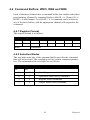
4.5Commands .................................................................................... 50
4.5.1Start-Stop Command ................................................................ 50
4.5.2Operation Mode Select Command ........................................... 52
4.5.3Register Select Command ........................................................ 53
4.5.4Output Mode Select Command ................................................ 55
Figure 4.2:Output Mode Select Command .................. 55
4.6Read Status ................................................................................... 56
4.6.1Channel Status Buffers (RD0, RD4 and RD8) ......................... 57
Figure 4.3:Status 0-bit Configuration .......................... 57
4.6.2Data Buffers: WR1, WR5 and WR9 ........................................ 57
PCL-839+ User Manual
vi
4.6.3Data Buffers: WR2, WR6 and WR10 ...................................... 57
4.6.4Data Buffers: WR3, WR4 and WR11 ...................................... 58
Figure 4.4:Status 1 Bit Configuration .......................... 58
Figure 4.5:Status 2 Bit Configuration .......................... 59
4.6.5Digital Outputs: WR12 and WR13 ........................................... 60
4.6.6Digital Inputs: RD12 and RD13 ............................................... 60
4.6.7Interrupt Control: WR14 .......................................................... 61
Figure 4.6:Interrupt Path of the PCL-839+ .................. 61
4.6.8Interrupt Status Register: RD14 ............................................... 61
4.6.9Example of reading Status Register ......................................... 62
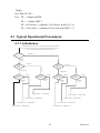
4.7Typical Operational Procedures .................................................. 63
4.7.1Initialization .............................................................................. 63
4.7.2Setting Speed Data ................................................................... 64
4.7.3Constant Speed Preset Model ................................................... 65
4.7.4High Speed Preset Model ......................................................... 66
4.7.5Constant Speed Continuous Mode ........................................... 67
4.7.6High Speed Continuous Mode .................................................. 68
4.7.7Constant Speed Origin Return Model ...................................... 69
4.7.8High Speed Origin Return Model ............................................. 70
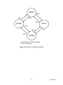
Appendix B Simple St. Motor Driver ............................... 72
Figure B.1:Simple Stepping Motor Drv Block Diag. .. 72
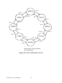
Figure B.2:Pattern Encoder Connection ...................... 72
Figure B.3:JP1 at Full Step Control ............................. 73
Figure B.4:JP1 at Half Step Control ............................ 74
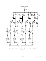
Figure B.5:4-Phase Stepping Motor Power Control Circuit ................................................................... 75
Appendix A Diagrams ........................................................ 78
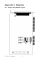
A.1Jumper and Switch Layout .......................................................... 78
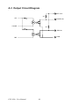
A.2PCL-839+ Block Diagram........................................................... 79
A.3Output Circuit Diagram ............................................................... 80
vii
PCL-839+ User Manual
viii
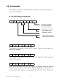
CHAPTER
1
2
General Information
If you have just purchased the PCL839+, or just need to brush up on its
features or specifications, you would
want to read this chapter.
Sections include:
• Introduction
• Features
• Applications
• Specifications
• Block Diagram
Chapter 1 General Information
1.1 Introduction
The PCL-839+ is a high-speed three-axis stepping motor control card that
simplifies stepping motor control, giving you added performance from
your stepping motors.
Three-Axis Control
The PCL-839+ has one single-chip pulse generator on-board, which
enables the simultaneous and independent control of three axes. The
PCL-839+ provides digital pulse and directional control (+ and -) for each
stepping motor axis.
User-Friendly Interface
The PCL-839+ has been designed to act as a user-friendly solution for
your stepping motor control applications. Programming the PCL-839+ is
very easy. 'C' Libraries are provided and they contain all the command
functions needed for total control of your stepping motors.
Stand-Alone Interpreter
A stand-alone, non-resident command interpreter, PROGg39.EXE, can
also be used to control your stepping motors without any programming.
Digital I/O
The PCL-839+ features 16 digital inputs and 16 digital outputs for general I/O use (on/off control etc.).
Isolation Protection
The PCL-839+'s PULSE and DIRECTION outputs and five limits input
switches are isolated from the PC side.
PCL-839+ User Manual
2
1.2 Features
• One on-board pulse generator that enables simultaneous independent
control of three stepping motors
• Two operating modes - two-pulse (+ and - direction pulse) or one-pulse
(pulse-direction) mode
• Programmable step rate from 1 to 16382 pps (pulses per second).
• Programmable initial speed, final speed and time duration. Automatic
trapezoidal acceleration/deceleration tamping is performed
16 I/O TTL Compatible Channels
• All inputs/outputs are optically isolated, providing 5000Vrms isolation
protection
• 'C' libraries containing device drivers provided
• Command Interpreter provided that eases learning the PCL-839+ command set
1.3 Applications
• Precise X-Y-Z position control
• Precise rotation control
• Robotics and assembly equipment
• Other stepping-motor applications
3
Chapter 1
1.4 Specifications
• Number of axes: Three independent axes (individually programmable)
• Operating modes: Two-pulse mode (+ or – direction) or one-pulse
(pulse-direction) mode
• Steps per command: ±16777215 steps
• Step Rate: 1-200K
• Acceleration/deceleration ramping: User programmable start, run and
ramping rates.
• Output polarity: Positive/negative going pulse (programmable)
• Pull-up voltage: external +5 V ~ +12 V
• Output protection: Opto-coupled with 1 kΩ pull-up resistor
• Output driving capacity: 20mA @ 0.4VDC
• Limit switch inputs: 2 “Emergency stop” inputs, 2 “Slow down/Accelerate” inputs and 1 “ORG” input. All limits switches are isolated from
the PC.
• Limit switch input voltage: external +5V to +12V
• Interrupt channels: IRQ 2, 4, 5, 7, 10, 11, 12 or 15 (jumper selectable)
• Limit switch types: Normal –open (NO) or normal-closed (NC) –
jumper selectable
1.4.1 Digital Input / Output
• Input channels: sixteen (+5V TTL compatible)
• Output channels: sixteen (+5V TTL compatible)
• I/O address range: sixteen consecutive I/O address
1.4.2 General
• Power Consumption: Typical 330mA, +5VDC
• Connector: 37-pin D-type connector
• Board Dimensions: 183.5 x 99.06 mm
• Operating Temperature: 0 ~70° C
PCL-839+ User Manual
4
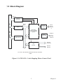
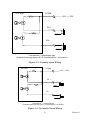
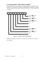
1.5 Block Diagram
Address
Address
Decoder
P
C
B
U
S
DATA
BUS
OUTPUT
ISOLATOR
Buffer
DIR &
PULSE
OUTPUT
S
PCD-4541
2 Phase Stepping
Motor Controller
System
INPUT
ISOLATOR
IRQ Selecteor
ORG,EL+
,
EL- &
SD+,SDINPUTS
DIGITAL
OUTPUTS
DIO
BLOCK
DIGITAL
INPUTS
PCL-839+ HIGH SPEED STEPPING MOTOR CONTROL
CARD
Figure 1.1: PCL-839+ 3-Axis Stepping Motor Control Card
5
Chapter 1
PCL-839+ User Manual
6
CHAPTER
2
2
Installation
If you have not yet configured and/or
installed your PCL-839+, or need to
change the configuration (e.g. set a different base address), this chapter will
give you the information you require.
Sections include:
• Switch and Jumper Settings
• Limit Switch Configuration
• Limit Switch Polarity Setting
• Hardware Installation
• PCL-839+ Pin Connections
Chapter 2 Installation
2.1 Switch and Jumper Settings
Before you install the PCL-839+, you need to select the card's base
address, and set the limit switch configurations as well as the interrupt
level that the card will use. This section describes this procedure in detail.
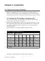
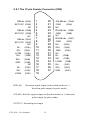
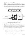
2.1.1 Setting the PCL-839 Base I/O address (S1)
The PCL-839+ requires 16 consecutive I/O addresses. DIP switch S1
(shown below) sets the base I/O address.
Choose a base address that is not in use by any other I/O device. A conflict with another device may cause one or both devices to fail. The factory address setting (hex 300) is usually free as it is reserved for PC
prototype boards.
Switch settings for various base addresses appear below:
Table 2.1: Card I/O addresses (S1)
Range (hex)
Switch position
9
8
7
6
5
4 <=Addr.
Line
200 - 20F
OFF
ON
ON
ON
ON
ON
210 - 21F
OFF
ON
ON
ON
ON
OFF
OFF
OFF
ON
ON
ON
ON
OFF
OFF
OFF
OFF
OFF
OFF
:
*300 - 30F
:
3F0 – 3FF
* = default
Switches 1-6 control the PC bus address lines as follows:
PCL-839+ User Manual
8
SWITCH
Line
1
A9
2
A8
3
A7
4
A6
5
A5
6
A4
ON
1
2
3
4
5
6
Figure 2.1: S1 - Base Address Setting
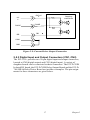
2.2 Limit Switch Configuration (JP1, JP2, JP3)
The PCL-839+ features 5 limit switches for additional control of the output.
2.2.1 EL+/ ELThese are the End Limit signal inputs. When the signal of the same direction as the pulse output (in direction or pulse mode) becomes active, pulse
output stops immediately.
2.2.2 SD+/SDThese are the Slow-Down signal inputs. They are in operation in the SDenable mode (refer to the control select modes). When the signal of the
same direction as the pulse output (in direction or pulse mode) becomes
active during high-speed start, the frequency ramps down. When the signal becomes inactive, the frequency ramps up again.
2.2.3 ORG
This is the Origin point input. When this signal becomes active during
origin return (refer to the control select modes), pulse output stops immediately.
Although the PCL-839+ caters to five limit switches, not all of them have
to be operation in one application. Refer to Fig 2.2 (on the next page) for
an example of the use of limit switches.
9
Chapter 2
2.3 Limit Switch Polarity Setting
JP1, JP2 and JP3 set the polarity for channels C, B and A respectively.
When the jumper is set to LO (normal), the limit switch uses 'normally
open' as default. When the jumper is set to HI, the limit switch uses' normally closed' as default.
2.3.1 JP1, JP2 and JPJ Selection
HI
Normally Closed
LO
Normally Open
The figures on below illustrate limit switch use and settings.
(+)DIRECTION
(-)DIRECTION
TABLE
MOTOR
DRIVER
EL+
PCL839+
SD+
ELINPUT
ISOLATOR
SDORG
DIR
OUTPUT
ISOLATOR
PULS
E
Figure 2.2: Using Limit Switches (1)
PCL-839+ User Manual
10
LCOM
PCL-839+
+5V ~ +12V
EL+
GND
EL-
GND
Limit switch is -- normalopen type
Limit switch polarity jumper (JP1,2,3) must be put to -- LO position
Figure 2.3: Normally-Open Wiring
PCL-839+
LCOM
+5V ~ +12V
EL +
GND
EL -
GND
Limit switch is -- normal closetype
Limit switch polarity jumper (JP1,2,3) must be put to -- HI position
Figure 2.4: Normally-Closed Wiring
11
Chapter 2
2.3.2 Interrupt Level Selection (JP4)
You have to set jumper JP4 to select the card's interrupt level (2, 4, 5, 7,
10, 11, 12 or 15), as shown below:
Card interrupt (default = 7)
IRQ
15 12 11
10 7
5
4
2
JP4
Figure 2.5: Setting the Interrupt Level
Do not select a level that is being used by another device unless you have
performed special programming to share several devices on one interrupt.
You can also control interrupt generation by software. If the interrupt is
enabled by software, and the PCL-839+ completes a motion, it will generate an interrupt. Your program can then determine which channel
caused the interrupt by reading the status register.
2.4 Hardware Installation
After you have set the base address, limit-switch configuration and the
interrupt level (as described in the previous section), you are ready to
install the card in your PC's chassis. The following section will assist you
in installing the PCL-839+.
Warning!
Disconnect power from your PC whenever you
install or remove the PCL-839+ or its cables
PCL-839+ User Manual
12
2.4.1 Installing the Card in Your Computer:
• Turn off the computer and all peripheral devices (such as printers and
monitors).
• Disconnect the power cord and any other cables from the back of the
computer. Turn the chassis so that the back of the unit faces you.
• Remove the chassis cover. (See your computer user manual if necessary).
• Locate the expansion slots at the rear of the unit and choose an unused
slot.
• Remove the screw that secures the expansion slot cover to the chassis.
Save the screw to secure the PCL-839+.
• Carefully grasp the upper edge of the PCL-839+ card+. Align the hole
in the retaining bracket with the hole on top of the expansion slot, and
align the gold striped edge connector with the expansion slot socket.
Press the board firmly into the socket.
• Replace the screw in the expansion slot-retaining bracket.
• Replace the chassis cover.
• Connect the D-37 male connector to the PCL-839+'s 37-pin female
connector Connect the connector to your stepping motor driver according to the specifications outlined in Section 3.1.
• Connect the cables you removed in step 2. Turn on the computer.
Hardware installation is now complete.
2.5 PCL-839+ Pin Connections
This section assists with connecting the PCL-839+'s 37-pin connector
(located at CN3) to a variety of stepping motor drivers.
The following diagrams give the PCL-839+'s pin connector assignments,
and offer some examples of input/output circuit connections from the
card to the driver. You should select the example that best supports your
application needs and the capabilities of your stepping motor driver.
Note: Output circuit diagrams of the stepping motor can be found in
Appendix A.
13
Chapter 2
2.5.1 The 37-pin Female Connector (CN3)
DIR/-dir (CHA)
EXT.VCC (CHA)
NC
DIR/-dir (CHB)
EXT.VCC (CHB)
NC
DIR/-dir (CHC)
EXT.VCC (CHC)
NC
EL(CHA)
SDLCOM
EL+
(CHA)
(CHA)
(CHB)
SD+
ORG
(CHB)
(CHB)
NC
(CHC)
ELSDLCOM
DIR/-dir:
(CHC)
(CHC)
1
2
3
4
5
6
7
8
9
10
11
12
13
14
15
16
17
18
19
20
21
22
23
24
25
26
27
28
29
30
31
32
33
34
35
36
37
PULSE/+dir (CHA)
COM
(CHA)
NC
PULSE/+dir (CHB)
COM
(CHB)
NC
PULSE/+dir (CHC)
COM
EL+
SD+
ORG
NC
ELSDLCOM
EL+
SD+
ORG
(CHC)
(CHA)
(CHA)
(CHA)
(CHB)
(CHB)
(CHB)
(CHC)
(CHC)
(CHC)
Direction signal output (in direction mode) or (-)
direction pulse output (in pulse mode)
PULSE/+dir:Pulse signal output (in direction mode) or (+)direction
pulse output (in pulse mode)
EXTVCC: External power input
PCL-839+ User Manual
14
COM :
Isolated outputs common point for each channel
EL+ :
(+) Direction emergency stop limit switch input
EL- :
(-) Direction emergency stop limit switch input
SD+ :
(+) Direction slowdown limit switch input
SD- :
(-) Direction slowdown limit switch input
ORG :
Original (home) point limit switch input
LCOM :
Limit switch common point for each channel
2.5.2 Example Input / Output Circuit Connections
The figure below illustrates an isolated output connection from the PCL839+ to the stepping motor driver.
EXT.VC
C
VCC OUT
PULSE/+dir
PULSE
DIR
DIR/-dir
COM
Stepping
Motor
Driver
GND
Figure 2.6: Isolated Output Connection
The next figure illustrates a non-isolated connection where the PC's +12
V output bias is used.
15
Chapter 2
EXT.VC
C
PULSE/+dir
PULSE
DIR
DIR/-dir
Stepping
Motor
Driver
GND
COM
+12
V
GND
Figure 2.7: Non-Isolated 12 V Bias Connection
The next two figures illustrate a TTL compatible output circuit connection and a current-drive output connection between the PCL-839+ and the
stepping motor driver.
.
EXT.VC
C
PULSE/+dir
PULSE
DIR
DIR/-dir
Stepping
Motor
Driver
GND
COM
+5V
GND
Figure 2.8: TTL Compatible Output Connection
PCL-839+ User Manual
16
+12
V
EXT.VC
C
Stepping
motordriver
PULSE
PULSE
DIR
DIR
COM
GND
Figure 2.9: Current Driver Output Connection
2.5.3 Digital Input and Output Connectors (CN1, CN2)
The PCL-839+ provides two 20-pin digital input and output connectors,
located at CNI (digital output) and CN2 (digital input). A variety of
daughter-boards can be connected to these connectors. The PCLD-782B
Isolated D/I board, the PCLD-785B Relay Output Board and the PCLD786 SSR & Relay Driver Board are just three examples. The pin assignments for these connectors are given below.
17
Chapter 2
D/O 0
1
2
D/O 1
D/O 2
3
4
D/O 3
D/O 4
5
6
D/O 5
D/O 6
D/O 8
7
9
8
10
D/O 7
D/O 9
D/O 10
11
12
D/O 11
D/O 12
13
14
D/O 13
D/O 14
15
16
D/O 15
GND
17
18
+5V
19
20
G ND
+12
V
Figure 2.10: CN1 (Digital Output)
D/I 0
1
2
D/I 1
D/I 2
3
4
D/I 3
D/I 4
5
6
D/I 5
D/I 6
D/I 8
7
8
9
10
D/I 7
D/I 9
D/I10
11
12
D/I11
D/I12
13
14
D/I13
D/I14
15
16
D/I15
GND
17
18
+5V
19
20
GND
+12
V
Figure 2.11: CN2 (Digital Input)
PCL-839+ User Manual
18
CHAPTER
3
2
PCL-839+ Software
Library
This chapter describes the 'C' libraries
and the functions they contain. If you
want to write your own applications in
'C', this chapter will give you all the
information you need.
Sections include:
• Introduction
• The PCL839P.H Header File
• The PCL839Px.Lib Library file
• Function Call Descriptions
Chapter 3 PCL-839+ Software Library
3.1 Introduction
On the floppy disk that came with your PCL-839+ card, there are 'C'
library files. These libraries were developed in 'Turbo C', and you should
be able to develop your own stepping motor applications (in 'C') using
these files. The source code for the programming library ('LIB839P.C')
can also be found on the floppy disk. This enables you to recompile the
libraries for any 'C' compiler (although some minor changes may be necessary).
The following sections describe the files and functions that will assist you
when you write applications for the PCL-839+.
3.2 The PCL839P.H Header File
To be able to use the functions contained in the software library, you have
to include this header file in your source program (#include
"PCL839P.H"). This file contains the headers (Prototypes) for all the
functions defined in PCL839Px.LIB.
PCL839P.H contains the following:
int base = 0x300 ; /* base address , default = 0x300 */
int run_mode[3] ;
int run_comd[3] ;
int pulse_dir[3] ;
int P0 = 0 ;
/* DIO port #0 (8-bit) */
int P1 = 1 ;
/* DIO port #1 (8-bit) */
int P01 = 2 ;
/* DIO port #0 & #1 */
int CH1 = 1 ;
/* Channel #1 */
int CH2 = 2 ;
/* Channel #2 */
int CH3 = 3 ;
/* Channel #3 */
int CH12 = 4 ;
/* Channel #1 & #2 */
PCL-839+ User Manual
20
int CH13 = 5 ;
/* Channel #1 & #3 */
int CH23 = 6 ;
/* Channel #2 & #3 */
int CH123 = 7 ;
/* Channel #1,#2 and #3 */
int P_DIR = 0 ;
/* Positive (+) dirction */
int N_DIR = 1 ;
/* Negative (-) direction */
int FL = 0 ;
/* FL speed */
int FH = 1 ;
/* FH speed */
int DIR = 0 ;
/* Direction mode */
int PUS = 1 ;
/* Pulse mode */
int out_port(int port_no , int value);
int in_port(int port_no);
int set_base(int b);
int set_mode(int ch , int mode);
int set_speed(int ch , long r1 , long r2 , long r4);
int status(int ch);
int stop(int ch);
int sldn_stop(int ch);
int waitrdy(int ch);
int slowdown(int ch);
int arc(int plan_ch , int dirc , long x1 , long y1 , long x2 , long y2 ) ;
int line(int plan_ch , int dx , int dy );
int org(int ch , int dir1 , int speed1 ,
int dir2 , int speed2 ,
int dir3 , int speed3 );
int cmove(int ch , int dir1 , int speed1 ,
int dir2 , int speed2 ,
int dir3 , int speed3 );
int pmove(int ch , int dir1 , int speed1 , long step1 ,
int dir2 , int speed2 , long step2 ,
int dir3 , int speed3 , long step3 );
21
Chapter 3
/* NOTE : port_no = 0 , 1 , 2
ch
= 1 , 2 , 3 , 4 , 5 , 6 , 7 beside
function status_ch(ch) that ch = 1 , 2 , 3
dirc
= 0 : CW direction
1 : CCW direction
plan_ch = CH12 , CH13 or CH23
dir
=0,1
speed = 0 , 1
mode
=0,1
*/
3.3 The PCL839Px.LIB Library file
Four library files have been included with the software. Although all
these libraries contain the same functions, they have been compiled for
different memory models:
PCL839PS.LIB 'Small model' library
PCL839PM.LIB 'Medium model' library
PCL839PC.LIB 'Compact model' library
PCL839PL.LIB 'Large model' library.
If you are using 'Turbo C' - one of the above libraries have to be included
in the 'C' project-file that you are working on.
PCL-839+ User Manual
22
3.4 Function Call Descriptions
This section gives a detailed description of the functions available in the
library files.
There are 15 functions in the PCL839 library. They are the following:
3.4.1 Function 1: set base
This function sets the base address of the PCL-839+. This enables the use
of multiple PCL839s, if you require doing so.
Prototype:
int set_base(int BASE)
Parameters:
BASE:
base address of PCL839 card
Return values:
0: No error occurred when setting the base address
-1: An error occurred when setting the base address
Example(s):
int error_code = set_base(0x2C0);
23
Chapter 3
3.4.2 Function 2: set mode
This function sets the output mode for a channel, or a group of channels.
Prototype:
int set_mode (int ch, int mode);
Parameters:
channel:
channel number
1 for channel 1
2 for channel 2
3 for channel 3
4 for channels 1 & 2
5 for channels 1 & 3
6 for channels 2 & 3
7 for channels 1, 2 & 3
mode:
0 for Direction (one-pulse) mode
1 for Pulse (two-pulse) mode
Return values:
0: No error occurred
1: An error occurred
Example(s):
error_code = set_mode(CH4, DIR);
error_code = set_mode(CH3, PUS);
Channel 1 and 2 are set to direction mode, and channel 3 is set to pulse
mode.
PCL-839+ User Manual
24
3.4.3 Function 3: set_speed
This function sets the low-speed pulse output frequency, high-speed pulse
output frequency and acceleration/deceleration rate for a channel.
Prototype:
int set_speed(int ch, int FL, int FH, int AD);
Parameters:
ch
channel number
(See Function 2).
FL
Low-speed frequency1 - 16382 pps.
FH
High-speed frequency1 - 16382 pps.
AD
Acceleration/deceleration Rate2 – 1023
Return values:
0: No error occurred
1: An error occurred
Example(s):
error_code = set_speed (CH123, 400, 3000, 500);
Channels 1, 2 and 3% FL are set to 400 pps, FH is set to 3000 pps and AD
is set to 500 pps2.
25
Chapter 3
3.4.4 Function 4: status
This function reads and returns the status of a channel.
Prototype:
int status(int ch);
Parameters:
ch
channel number
1 - channel 1
2 - channel 2
3 - channel 3
Return values:
-1: An error occurred
Other: The high byte will contain the value of 'Status 1' and the low byte
the value of 'Status 0'.
Example(s):
int channel_status;
channel_status = status (CH1);
PCL-839+ User Manual
26
3.4.5 Function 5: stop
This function stops channel ch.
Prototype:
int stop(int ch);
Parameters:
ch
channel number
(See Function 2).
Return values:
0: No error occurred
1: An error occurred
Example(s):
int error_code;
error_code = stop(CH123) ;
Channels 1, 2 and 3 are stopped.
27
Chapter 3
3.4.6 Function 6: slowdown
This function ramps the output frequency of channel(s) ch down to FL.
Prototype:
int slowdown (int ch)
Parameters:
ch
channel number
(See Function 2).
Return values:
0: No error occurred
-1: An error occurred
Example(s):
int error_code = slowdown(CH23) ;
Channel 2 and 3's speed is ramped down to FL.
PCL-839+ User Manual
28
3.4.7 Function 7: sldn_stop
This function ramps the output frequency of channel(s) ch down to FL.
Prototype:
int sldn_stop(int ch);
Parameters:
ch
channel number
(See Function 2).
Return values:
0: No error occurred
-l: An error occurred
Example(s):
error_code = sldn_stop(CH 12);
Channels t and 2's are ramped down to FL, and then stopped.
29
Chapter 3
3.4.8 Function 8: waitrdy
This function checks the 'Stares0' of channel(s) ch and waits until bit 6 of
'Status0' is 0
Prototype:
int waitrdy (int ch)
Parameters:
ch
channel number
(See Function 2).
Return values:
0: No error occurred
-1: An error occurred
Example(s):
error_code = waitrdy (CH12);
A delay is caused until channels 1 and 2's 'Status0' is 0.
PCL-839+ User Manual
30
3.4.9 Function 9: out_port
This function outputs a value to the assigned port .
Prototype:
int out_port(int port_no, int value) ;
Parameters:
port_no: digital output port number
0 for port 0 (DO7-0)
1 for port 1 (DO15-8)
2 for ports 0 & l
If port_no was set as “2” (output to both ports), the high-byte of the word
will be output to port 1, and the low-byte of the word to port 0.
Return values:
0 ~ No error occurred
-1' An error occurred
Example(s):
error_code : outport(PO, 0XAA) ; /* 0XAA to port O */
error_code = out~ort(P01,0X55AA) ; /'* 0X55 to port 1 and 0XAA to
port 0 */
31
Chapter 3
3.4.10 Function 10: in_port
This function reads and returns the value of a digital input port.
Prototype:
int in_port (int port_no) ;
Parameters:
port_no: D/I port number
0 for port 0 (DI7-0)
1 for port 1 (DI15-8)
2 for ports 0 & 1
If port_no was set as “2” (input from both ports), the high-byte of the
returned value will contain the value of port 1, and the low-byte the value
of port 0.
Return values:
-1: Aah error occurred
Other: Port Value
Example(s):
port_value = in_port (PO) ;
port_value = in. oft (P01) ;
PCL-839+ User Manual
32
3.4.11 Function 11: org
This function returns all three channels to the 'ORIGIN' point. The direction and speed (frequency) that each channel has to use are supplied.
Prototype:
int org(int ch,
int DiR1, int SPEED1,
int DIR2, int SPEED2,
int DIR3, int SPEED3) ;
Parameters:
ch
channel number
(See Function 2).
DIRn
channel n direction
0 = (+) and I = (-)
SPEEDn
channel n frequency
0 =- FL and 1 = FH
Return values:
0: No error occurred
-1: An error occurred
Example(s):
error_code = org (CH12, P_DIR, FL, N_DIR, FH, 0, 0),
Channels 1 and 2 are returned to origin point - channel 1 pulses at FL frequency in the (+) direction, and channel 2 pulses at FH frequency in the () direction. Channel 3 is ignored.
33
Chapter 3
3.4.12 Function 12: cmove
This function starts channel(s) ch in continuous mode. Channel 1 will
move in DIR1 direction at SPEED1 speed, etc.
The channel(s) will stay in continuous move mode until 'stop' or
'stdn_stop' is executed.
Prototype:
int cmove (int ch, int DIR1, int SPEED1,
int DIR2, int SPEED2,
int DIR3, int SPEED3);
Parameters:
ch
channel number
(See Function 2).
DIRn
channel n direction
0 = (+) and 1 = (-)
SPEEDn
channel n frequency
0 = FL and 1 - FH
Return values:
0: No error occurred
-1: An error occurred
Example(s):
error_code = cmove {CH2,0,0, P_DIR, FH, 0, 0 },
Channel 2 is placed in continuous move mode, and pulses at FH in the (+)
direction.
PCL-839+ User Manual
34
3.4.13 Function 13: pmove
This function starts channel(s) ch in continuous mode, for a certain
amount of steps. Channel 1 will move in DIR1 direction at SPEED1
speed and will stop when it has completed STEP 1 steps, etc.
Prototype:
int pmove (int ch, int DIR1, int SPEED1, long STEP1,
int DIR2, int SPEED2, long STEP2,
int DIR3, int SPEED3, long STEP3);
Parameters:
ch
channel number
(See Function 2).
DIRn
channel n direction
SPEEDn
channel n frequency
STEPn
channel n steps
0 = (+) and 1 - (-)
0 = FL and 1 - FH
max. long.
Return values:
0: No error occurred
-1: An error occurred
Example(s):
error_code = pmove (CH123, P DIR, FL, 2000, P DIR, FH, 3000,
N_DIR, FH, 2000);
Channel 1 moves in (+) direction at speed FL for 2000 steps,
Channel 2 moves in (+) direction at speed FH for 3000 steps and
Channel 3 moves in (-) direction at speed FH for 2000 steps.
Then they stop.
35
Chapter 3
3.4.14 Function 14: line
If you are using two stepping motors simultaneously (in a plotter-type
configuration), you can move to position (X, Y) from the current position,
(0, 0). Both axes are measured in steps.
Prototype:
int line(int ch_plan, int X, int Y);
Parameters:
ch_plan channel numbers CH12 for channels 1 &2
CH13 for channels 1 &3
CH23 for channels 2 &3
Return values:
0: No error occurred
-1: An error occurred
Example(s):
error_code = line(CH23, 200, -300) ;
Current
point
(0,0)
200
-300
PCL-839+ User Manual
36
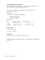
3.4.15 Function 15: arc
If you are using two stepper motors simultaneously (in a plotter-type configuration), you can "draw an arc" from (X1, Y1) to (X2, Y2)
Prototype:
int arc (int ch_plan, int dir, long X1, long Y1, long X2, long Y2);
Parameters:
ch_plan: channel numbers CH12 for channels 1&2
CH13 for channels 1&3
CH23 for channels 2&3
dir:
direction
0 for clockwise
1 for counterclockwise
X1, Y1
coordinates of starting point
X2, Y2
coordinates of final point
Return values:
0: No error occurred
-1: An error occurred
37
Chapter 3
Example(s):
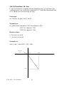
error_code = arc (CH13, 1, 200, 50, 50, 200) ;
Y
(50,200)
200
(200,50)
50
X
(0,0)
50
200
Central point of ARC
PCL-839+ User Manual
38
Current
position
CHAPTER
4
2
Register Programming
This chapter describes the PCL-839+'s
hardware registers. It also contains typical operational procedures that will
assist you in program design. This
chapter is a good place to start getting
to know and use the capabilities of the
PCL-839+ to best suit your application.
Sections include:
• PCL-839+ Registers
• Programming the PCL-839+
• I/O Register Control Format
• Command buffers: WR0, WR4 and
WR8
• Commands
• Read Status
• Typical Operational Procedures
Chapter 4 Register Programming
4.1 PCL-839+ Registers
Several registers are used to control the PCL-839+. The PCL-839+ uses
these registers to store commands, speed, mode, number of pulses etc.
The following sections describe these registers in detail.
4.1.1 R0 : Down-Counter (24 bits)
The down counter counts down when a pulse is output in manual mode,
origin mode or preset mode. If the counter is stopped in operation mode,
counting ceases. If a pulse is output when the counter has reached 0, the
counter reverts to its maximum number (FFFFFF in Hex, 16777215 in
Decimal).
The counter value can be read at any stage - in operation or during standstill. When reading the value in operation, two quick reads must be done
before the next pulse changes the value of the counter. Compare the two
values - if they are the same then this is the true number of the residual
pulses.
In preset mode you set the required number of pulses on the counter. The
counter counts down when a pulse is output and pulse generation will
stop when the counter reaches 0. The starting range is 00001 (hex) to
FFFFFF (hex) (1 to 16777215 in decimal notation). If the counter is set to
0 when operation is started, no pulse generation will occur. At that time
the operation flag will indicate the halt condition, but the INT signal is
not output.
If counting is interrupted by a deceleration-stop or reset command, the
current counter value is stored, and counting will continue as soon as the
start command is received. As the counter will be at 0 when operation is
complete, it is necessary to supply an initial value every time preset mode
is started.
PCL-839+ User Manual
40
4.1.2 R1: FL Register (13 bits)
This register is used to set the FL (initial/low) speed. When started in
high-speed mode, the generator starts at FL and ramps up to reach FH
(Final/High speed). If the deceleration-stop command is received during
high-speed operation, it ramps down to FL speed and then stops. Make
sure that you set a FL speed.
The range for FL is 1 to 8191 (0001 to 1FFF in hexadecimal notation).
For the relation between a set value and the output pulse frequency please
refer to 4.1.5.
4.1.3 R2: FH Register (13 bits)
This register is used to set the FH speed. The range for FH is also 1 to
8191 (0001 to 1FFF in hexadecimal notation). Please ensure that FH is
greater than FL. For the relation between a set value and the output pulse
frequency, please refer to 4.1.5.
Speed
Speed
FH
FH
FL
FL
High
Speed
Start
time
time
Deceleration
StopInput
41
Chapter 4
4.1.4 R3: Acc. / Dec. Rate Register (10 bits)
This register is used to set acceleration (ramping up) and deceleration
(ramping down) characteristics. During high-speed mode, the generator
starts at FL and accelerates to FH.
If the reference clock frequency is (TCLK)[sec], TSUD(the time required
for the ramping-up/ramping-down) is:
TSUD = [(R2)-(R1)]x (R3)x(TCLK) [sec]
Alternatively, if the ramping-up/ramping-down time is known, R3 can be
calculated as:
R3 = TSUD /{[(R2)-(R1)] x(TCLK)}
The range for R3 is 002 (hex) to 3FF (hex) (2 to 1023 in decimal).
Note: For PCL-839+, Tclk = 203 ns
PCL-839+ User Manual
42
Speed
FH
FL
TSUD
TSUD
time
4.1.5 R4: Multiplier Register (10 bits)
For the speed registers, Rl and R2, a number of steps can be selected (1 to
8191). This register (R4) is used to assign an output frequency for one
step. The reference clock inputted through the CLOCK terminal is
divided and multiplied by the variable frequency divider and the frequency multiplier, and then outputted to the PULSE OUTPUT terminal.
When a set value on the speed register is Rf (where Rf is a value set at R1
and R2), the frequency outputted at the PULSE OUTPUT terminal is
Fpout = {(Reference clock freq. [Hz] x (Rf)) / (8192 x (R4)}
= (Rf) x {(Reference clock freq.)} / {8192 x (R4)}
When (reference clock)/ [8192 x (R4)]= 1 ... 1x mode
When (reference clock)/ [8192 x (R4)]= 2 ... 2x mode
43
Chapter 4
For the PCL-839+, the reference clock frequency is 4.9152 [MHz],
Therefore
(R4)= 600 (=258 hex) 1x mode
(R4)= 300 (=12C hex) 2x mode
The setting range is 002 (hex) to 3FF (hex), which corresponds to 2 to
1023 in decimal notation. The smaller the set value, the higher the output
frequency.
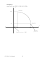
4.1.6 R5 :Ramping-down Point Register (16 bits)
During high-speed operation, the value of the down counter is compared
with the value of this register. As soon as the value of the counter is less
than the value of this register, ramping-down will start. If the value of R5
is higher than the down counter, when high-speed mode starts, rampingup will not occur and the pulse generation will proceed at FL.
The range for R5 is 0001 (hex) to FFFF (hex) (1 to 65535 in decimal).
The ramping-down point is set in pulses.
Please note that in PCL-839+, the R5 value is calculated by user. The system will not define the R5 value automatically.
* Setting of the ramping-down point
When determining the ramping-down point, the FL frequency, the FH
frequency and the deceleration rate has to be taken into account. If an
improper value is set, pulse output may be terminated halfway during
ramping-down (Fig. A) or may continue after ramping-down, causing
longer FL speed operation (Fig. C).
PCL-839+ User Manual
44
Speed
Speed
Speed
FH
FH
FH
FL
FL
FL
A
R6 setting value is
too small
B
time
C
R6 setting value is optimal
(several pulses at FL)
time
R6 setting value is
too large
time
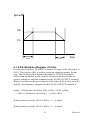
Figure 4.1: Relation Between R5 and Ramping Down Velocity
A ramping-down point is set based on the number of pulses output during
ramping-down. Therefore the area marked by oblique lines in the chart
below is the number of pulses to be calculated. FL and FH are the output
pulse frequencies.
PPS
A
FH
F
FL
E
D
t
B
Ts d
C
Tsd [sec], the time required for the deceleration is:
Tsd = [(R2)-(R1)]x(R3)/(CLOCK) (1)
where CLOCK = 4.9152 MHz
45
Chapter 4
The relationship between the set value on speed register (Rf) and output
frequency (F [PPS]) is:
F = (Rf)x(CLOCK)/[8192x(R4)] (2)
Therefore, FL output frequency FL [PPS] and FH output frequency FH
[PPS] are:
FL = (Rl)x(CLOCK)/[8192x(R4) ] (3)
FH = (R2)x(CLOCK)/[8192x(R4) ] (4)
Psd, the number of pulses during T, [sec] is represented by the area of the
trapezoid A-B-C-F:
Psd = {[(FL) + (FH)]*Ted}/2(5)
Substitute equations (1), (3) and (4) into equation (5):
Psd = [(R2)2 – (R1)2] x (R3) / [16384 x (R4)]
When output 5 pulses at FL speed after the completion of the rampingdown, the set value of the ramping-down point register (R5) is
(R5) = Psd +5
(R5) = [(R2)2 – (R1)2] x (R3)/ [16384 x (R4)] + 5
4.1.7 R6: Idling pulse register (3-bit)
To operate at high speed, the motor is accelerated quickly after start.
Therefore, the speed calculated from the output pulse frequency will be
higher than the FL speed that is set. If FL is set to a value lower than the
self-start frequency, the motor will not start. Therefore, in order to be able
to start from near the self-start frequency, the acceleration using the FL
speed can be started from 1 to 7 pulses after the start command. The
pulses that the start is delayed by are referred to as idling pulses.
The allowable range is 0 to 7. This is effective in high-speed operation.
Setting this register to 0 will provide a normal start.
PCL-839+ User Manual
46
4.1.8 R7: Output type register (1-bit)
The allowable range is 0 or 1
0: CW/CCW pulse type
1: Pulse/DIR type
4.2 Programming the PCL-839+
The PCL-839+ stores a selected command in a buffer. This command
remains there until a new command is received. The only command that
can be RESET is the 'starting mode' command.
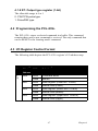
4.3 I/O Register Control Format
The following table depicts the PCL-839+ register’s I/O address map.
Table 4.1: Register I/O Address Map
Axis
Offset
Address
R/W
Definition
X
(0)
0x00
Write
Command Buffer
Read
Status0
Write
Data Register (Lower Bit7 To Bit0)
Read
Internal Data (Lower)
Write
Data Register (Middle Bit15 To Bit8)
Read
Internal Data (Middle)
Write
Data Register (Upper Bit23 To Bit16)
Read
Internal Data (Upper)
0x01
0x02
0x03
47
Chapter 4
Table 4.1: Register I/O Address Map
Axis
Offset
Address
R/W
Definition
Y
(1)
0x04
Write
Command Buffer
Read
Status0
Write
Data Register (Lower Bit7 To Bit0)
Read
Internal Data (Lower)
0x06
Write
Data Register (Middle Bit15 To Bit8)
Read
Internal Data (Middle)
0x07
Write
Data Register (Upper Bit23 To Bit16)
Read
Internal Data (Upper)
Write
Command Buffer
0x05
Z
(2)
0x08
Read
Status0
Write
Data Register (Lower Bit7 To Bit0)
Read
Internal Data (Lower)
0x0A
Write
Data Register (Middle Bit15 To Bit8)
Read
Internal Data (Middle)
0x0B
Write
Data Register (Upper Bit23 To Bit16)
Read
Internal Data (Upper)
0x0C
Write
Digital Output 0 ~ 7 (port0)
Read
Digital Input 0 ~ 7 (port0)
0x0D
Write
Digital Output 8 ~ 15 (port1)
Read
Digital Input 8 ~ 15 (port1)
Write
IRQ control
Read
IRQ status
Write
IRQ control
Read
IRQ status
0x09
0x0E
0x0F
PCL-839+ User Manual
48
4.4 Command Buffers: WRO, WR4 and WR8.
Each of the three channels has a command buffer that enables individual
programming. Channel l's command buffer is BASE + 0, Channel 2's is
BASE + 4 and Channel 3's is BASE + 8. A command can be written to
any of the three buffers, and the appropriate channel will respond to the
command.
4.4.1 Register Format
The register format is as follows:
Table 4.2: Register Format
D7
D6
C1
C0
D5
Mode
D4
D3
D2
D1
D0
Command
4.4.2 Selection Modes
The two high-order bits of the command buffer specifies the command
that will be executed. The remaining six bits contain command parameters. The command modes available are as follows:
Table 4.3: Selection Modes
C1
C0
0
0
Start-Stop command selection
0
1
Operation Mode Select command
1
0
Register Select command
1
1
Output Mode select command
49
Chapter 4
4.5 Commands
The following sections describe all the available commands and their
parameters in detail.
4.5.1 Start-Stop Command
7
6
o
o
5
4
3
2
1
0
o
Frequency Selection
0: Use FL frequency
1: Use FH frequency
0: Constant speed mode
1: High Speed mode
1:Start/stop control
0: Stop interrupt reset
1: Stop interrupt enable
0
0
*
1
0
0
0
0
Constant speed operation with the FL register. Operates at the speed set
for the FL register.
0
0
*
1
0
0
0
1
Constant speed operation with the FH register. Operates at the speed set
for the FH register.
0
0
*
1
0
1
0
1
High speed operation with the FH register. Frequency ramps up halfway
from the rate of the FL to that of the FH. During high-speed start this
command lets the frequency ramp up/down to the rate of the FH speed.
PCL-839+ User Manual
50
0
0
*
1
0
1
0
0
Dual rate operation (ramping down). Frequency ramps down to the level
of the FL.
*
0 (no output of INT signal at stop)
1 (output of INT signal at stop)
0
0
*
1
1
1
0
0
Decelerating stop (reset command is required after stop). Frequency
ramps down to the rate of the FL, then stops.
0
0
0
0
1
0
0
0
Reset command. This stops pulse generation under any condition. If you
start with the start-command, be sure to reset with the reset command
before the next start. This gives INT signal and the start command has to
be reset. Contents in registers R0 through R7 are not changed.
*
0 (no output of INT signal at stop)
1 (output of INT signal at stop)
51
Chapter 4
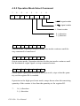
4.5.2 Operation Mode Select Command
7
6
5
4
0
1
0
0
3
2
1
0
1: ORG signal enable
1: SD+ signal enable
1: Preset enable
0: (+)direction
1: (-)direction
0
1
0
0
*
0
0
0
Manual mode. Operation initiated in the start mode continues until the
stop command is transferred.
0
1
0
0
*
0
0
1
Origin return mode. Operation initiated in the start mode continues until
the mechanical origin signal or stop command comes.
0
1
0
0
*
1
0
0
Preset mode. Operation initiated in the start mode, stops when the quantity set for register R0 is reached.
Operation in the high speed start mode, ramps down when the remaining
quantity of the counter is less than the quantity set for register R5.
*:
0 (+) direction
1 (-) direction
PCL-839+ User Manual
52
4.5.3 Register Select Command
7
6
1
0
5
4
3
2
1
0
Register Selection
0
0
0
0
1
1
1
1
0
0
1
1
0
0
1
1
0
1
0
1
0
1
0
1
R0: Preset Counter Data
R1: FL register
R2: FH register
R3: Acceleration/deceleration rate register
R4: Multiplier register
R5: Ramping-dow n point register
R6: Set idling pulse
R7: Output type register
Preset counter operation control
0 Counts output pulse
1 Do not count
Ramping-dow n point interrupt control
0 Ramping-dow n reset
1 Ramping-dow n interrupt enable
Do not care
Register Select Code
Selects an access register with last 3 bits.
Preset Counter Operation Control
When this bit is 1, the preset counter will stop counting. When this bit is
0, the preset counter will decrement by one for each pulse output.
53
Chapter 4
Ramping-Down Point Interrupt Control
This bit controls whether or not the INT signal is output when the ramping-down point is reached. When this bit is 1 and the preset counter value
becomes smaller than the ramping-down point setting in R5, it will output
an INT signal. To reset the INT signal, set this bit to 0. If you want to
mask this operation, leave this bit set to 0. The INT terminal output is the
result of logically ‘ORing’ this signal with the interrupt signal when
stopped. To determine which source has caused the INT signal to be output, check Status0.
Kinds of Registers and Data Bits
Description
Bits R/W
Setting Range
R0
Preset counter data
24
0 to 16,777,215
(FFFFFF)
R1
FL register
13
W(R) 1 to 8,191 (1FFF)
R2
FH register
13
W(R) 1 to 8, 191 (1FFF)
R3
Acceleration / deceleration
rate register
10
W(R) 2 to 1, 023 (3FF)
R4
Multiplier register
10
W(R) 2 to 1, 023 (3FF)
R5
Set ramping-down point
16
W(R) 0 to 65, 535 (FFFF)
R6
Set idling pulse
3
W(R) 0 to 7
R7
Output type register
1
W(R) 0 to (1)
R/W
Note1: * R/W: Read/Write register
W(R): Write only register. However, it can be read using the extension
monitor setting.
Note2: R7 is allowed to be 0 or 1.
R7 = 0, CW/CCW output type
R7= 1, Pulse/Direction output type
PCL-839+ User Manual
54
4.5.4 Output Mode Select Command
OutputModeSelectCommand
7
6
1
1
5
4
3
2
1
0
0
Logic setting of +/-PO output
0: Negative logic
1: Positive logic
Pulse output
0: Output
1: No output
Intermediate stop accel/decel operation
0: Enable accel/decel operation (continuous)
1: Disable accel/decel operation (change to
constant speed)
Input signal sensitivity setting for ORG , EL and
EMG (*)
0: High sensitivity
1: Low sensitivity
Monitor mode selection
0: Standard monitor
1: Extension monitor
* Sensitivity setting:
Low : the input signal will be ignored when pulse width < 800ns
High: the input signal will be recognized when pulse width < 800ns
Figure 4.2: Output Mode Select Command
PULSE/DIRECTION logic control
PULSE/+dir and DIR/-dir output logic be changed as follows:
55
Chapter 4
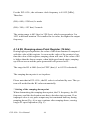
4.6 Read Status
Users can set the standard monitor or extension monitor by the “Output
mode select command”
Mode
Address\ RD0,
Register RD4,
RD8
RD1,
RD5,
RD9
RD2,
RD6,
RD10
RD3, RD7,
RD11
Standard
Monitor
R0
Status0
R0 lower
byte
R0 middle byte
R0 upper byte
R1 to R7
Status0
Status1
0
0
R0
Status0
R0 lower
byte
R0 middle byte
R0 upper byte
R1
Status0
R1 lower
byte
R1 upper
byte
Start mode
command
R2
Status0
R2 lower
byte
R2 upper
byte
Control mode
command
R3
Status0
R3 lower
byte
R3 upper
byte
Register
select command
R4
Status0
R4 lower
byte
R4 upper
byte
Output mode
command
R5
Status0
R5 lower
byte
R5 upper
byte
R7 data
R6
Status0
R6 data
Speed
lower
byte
Speed upper
byte
R7
Status0
Status1
Status2
Status3
Extension
Monitor
PCL-839+ User Manual
56
4.6.1 Channel Status Buffers (RD0, RD4 and RD8)
There is a status buffer for each channel (status 0). These buffers are
found at BASE +0, BASE +4 and BASE +8 for channel 1, channel 2 and
channel 3 respectively. These buffers enable you to read the internal status of each channel, and also get certain information on input signals or
conditions.
7
6
5
4
3
2
1
0
Monitor INT output When operation is stopp
0: INT is being output
Monitor INT output at ramping-dow n point
0: INT is being output
N/A
Operation status
0: Stopped
1: Operating
Pulse counter zero status
0: Non zero
1: Zero
Pulse counter and R5 comparison
0: Pulse counter > R5
1: Pulse counter < R5
Monitor acceleration status
0: Not accelerating
1: Accelerating
Monitor deceleration status
0: Not decelerating
1: Decelerating
Figure 4.3: Status 0-bit Configuration
4.6.2 Data Buffers: WR1, WR5 and WR9
One data-buffer for each channel is found at BASE 1, BASE 5 and BASE
9, for channel 1, channel 2 and channel 3 respectively. When writing (output), these buffers contain data bits 0-7 of the respective channels.
4.6.3 Data Buffers: WR2, WR6 and WR10
One data-buffer for each channel is found at BASE+2, BASE+6 and
BASE+ 10, for channel 1, channel 2 and channel 3 respectively. When
writing (output), these buffers contain data bits 8-15 of the respective
channels
57
Chapter 4
4.6.4 Data Buffers: WR3, WR4 and WR11
One data-buffer for each channel is found at BASE+3, BASE+7 and
BASE+I 1, for channel 1, channel 2 and channel 3 respectively. When
writing (output), these buffers contain data bits 16 -24 of the respective
channels.
7
6
5
4
3
2
1
0
Monitor -EL terminal
0: Off
1: On
Monitor +EL terminal
0: Off
1: On
Monitor ORG terminal
0: Off
1: On
NA
NA
Monitor -SD terminal
0: Off
1: On
Monitor +SD terminal
0: Off
1: On
NA
Figure 4.4: Status 1 Bit Configuration
When the Extension Monitor is selected, users can check the value of
each register
PCL-839+ User Manual
58
7
6
5
4
3
2
1
0
NA
NA
NA
NA
Monitor -PO terminal
0: Off
1: On
Monitor +PO terminal
0: Off
1: On
NA
Monitor interrupt (each axis)
0: No interrupt,
1: Interrupt occurred
Figure 4.5: Status 2 Bit Configuration
For the value of Status3, it should be “0100-0000”, which represents the
PCD4541 chipset.
59
Chapter 4
4.6.5 Digital Outputs: WR12 and WR13
WR12 is the low byte of the digital output and WR13 the high byte. To
write to these buffers write to BASE12 and BASE13 respectively. The bit
definition is as follows:
Bit
7
6
DO1
5
DO1
4
5
4
3
2
1
0
DO1
3
DO1
2
DO1
1
DO1
0
DO9
DO8
WR13
Bit
7
6
5
4
3
2
1
0
DO7
DO6
DO5
DO4
DO3
DO2
DO1
DO0
WR12
4.6.6 Digital Inputs: RD12 and RD13
RD12 is the low byte of the digital input, and RD13 the high byte. To read
these buffers, address BASE+12 and BASE+13 respectively. The bit definition is as follows:
Bit
7
6
DI15
DI14
5
4
3
2
DI13
DI12
DI11
DI10
1
DI9
0
DI8
RD13
Bit
7
6
DI7
DI6
5
DI5
4
DI4
3
DI3
RD12
PCL-839+ User Manual
60
2
DI2
1
DI1
0
DI0
4.6.7 Interrupt Control: WR14
WR14 is the interrupt control register for the PCL-839+, and is found at
BASE +14. Only one bit, b0, of the byte is used. When b0=1, interrupts
are enabled, and when b0-0, disabled, ifb0=1, and the channel-interrupt
of the specific channel is also enabled (see Start-Stop command, bit 5), an
interrupt will be generated when that channel reaches its 'stop position'.
7
Bit
6
----
----
5
----
4
----
3
----
2
1
----
----
0
IRQ
WR14
CH#1 interrupt
Control by start-stop command bit5 of CH#1
CH#2 interrupt
TO PC
Control by start-stop command bit5 of CH#2
CH#3 interrupt
Control by start-stop command bit5 of CH#3
IRQEN
(BASE + 14 BIT0)
Figure 4.6: Interrupt Path of the PCL-839+
4.6.8 Interrupt Status Register: RD14
RD14 is used to obtain the interrupt status for each channel. It is found at
BASE+14, and contains the interrupt status for all channels. When an
interrupt occurs, this register will be set. If the bit = 1, then an interrupt
has occured for that channel. The bit configuration is as follows:
bit
7
6
5
4
3
2
1
0
...
...
...
...
...
...
...
IRQ
Note: When this register is read, bit 0 w ill be cleared
61
Chapter 4
4.6.9 Example of reading Status Register
In this section, we will demonstrate how to get the emergency stop limit
switch status by reading the Status Register.
Step1:
Setting the “Output Mode Select Command” and you can choose the
“Monitor mode” as Standard monitor or Extension monitor. In Standard
monitor mode user can get Status0 ~ 1, and in Extension monitor mode
Status0 ~ 3 can be read. Since the status of emergency stop limit switch is
defined in Status1, so both Standard and Extension monitor mode is
workable. In this case, we set the monitor mode as “Extension”
outportb(base+(CH*4+CommandBufferIndex),DATA);
//CH : Axes 0 ~ 2
//CommandBufferIndex = 0
//DATA is just setting The [Output Mode Command] Monitor Mode
Selection Bit5
//DATA = ( CurrentAxesOutputModeCommandValue &
(~FORCE_EXTENSION_MODE)) | (FORCE_EXTENSION_MODE)
Step2:
Select R7 Register. (If you want to read another status such as R0, R1, or
Current Speed.., then you must select another Register such as R0, R1…
R6. Please refer to the Table in section 4.6)
outportb(base+(CH*4+CommandBufferIndex,DATA);
//DATA is just setting The [Register Select Command] As R7
//DATA = ( CurrentAxesRegisterSelectCommandValue & (~0x07)) |
(FORCE_SELECT_R7)
Step3:
Read the Status1 register. For X-Axes (RD0, RD1, RD2, RD3), Y-Axes
(RD4 ~ RD7), Z-Axes (RD8 ~ RD11) Please refer to the Table in section
4.6
Status0 Of n-Axes = inportb(base+(CH*4+0))
Status1 Of n-Axes = inportb(base+(CH*4+1))
Status2 Of n-Axes = inportb(base+(CH*4+2))
Status3 Of n-Axes = inportb(base+(CH*4+3))
PCL-839+ User Manual
62
Step4:
Get The EL+/ELFor
EL- = Status1.BIT0
EL+ = Status1.BIT1
EL- Of n-Axes = ((Status1 Of n-Axes) & 0x01 )>>0
EL+ Of n-Axes = ((Status1 Of n-Axes) & 0x02 )>>1
4.7 Typical Operational Procedures
4.7.1 Initialization
Note: Before following the flow chart, user need to define the output mode first
by setting R7. If user set R7 as “0”, then the output will be CW/CCW mode. Or
user can choose Pulse/Direction Mode by setting R7 as “1”.
Negative Logic
Pulse output
Logic?
Positive
Logic
Counter
operation
mode?
Count stop
Counter
operation
mode?
Output pulse
EL,ORG
sensitivity?
Count stop
Output pulse
4 Clocks
EL,ORG
sensitivity?
4 Clocks
Immediate
stop
Immediate
stop
EL,ORG
sensitivity?
4 Clocks
Immediate
stop
Command buffer -- 11010010(D2H)
4 Clocks
EL,ORG
sensitivity?
Immediate
stop
Command buffer -- 11010011(D3H)
Command buffer -- 11000010(C2H)
Command buffer -- 11000011(C3H)
Command buffer -- 11010000(D0H)
Command buffer -- 11010001(D1H)
Command buffer -- 11000000(C0H)
Command buffer -- 11000001(C1H)
63
Chapter 4
4.7.2 Setting Speed Data
Select the FL Register
Set FL data
Select the FH Register
Set FH data
Select the acceleration rate
register
Set acceleration rate data
Select the ramping-down
point register
Command buffer <- 10000001(81H)
Set middle byte (8:15)
Set lower byte (0:7)
Wait 400 ns
The order is important!
Command Buffer <- 10000010(82H)
Set middle byte (8:15)
Set lower byte (0:7)
Wait 400 ns
The order is important!
Command Buffer <- 10000011(83H)
Set middle byte (8:15)
Set lower byte (0:7)
Wait 400 ns
The order is important!
Command Buffer <- 10000101(85H)
Set ramping-down point data
Set middle byte (8:15)
Set lower byte (0:7)
Wait 400 ns
(setting is not required if automatic rampingdown setting mode is selected)
Select the multiplier register
Command Buffer <- 10000100(84H)
Set multiplier data
Set middle byte (8:15)
Set lower byte (0:7)
Wait 400 ns
The order is important!
END
PCL-839+ User Manual
64
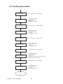
4.7.3 Constant Speed Preset Model
f
Ramp down at
set point
Stop at preset count
Execute the reset
command
Effect the ramping
mode and select the
direction
t
Command buffer <- 00001000(08H)
For(+)direction: command buffer <- 01000100(44H)
For(-)direction: command buffer <- 01001100(4CH)
Select the counter
Command Buffer <- 10000000(80H)
Set the number of
output pulse
Register bits 23-16 <- data, high-order 8 bits
Register bits 15-8 <- data, mid-order 8 bits
Register bits 7-0 <- data, low-order 8 bits
Wait for 400ns
The order is important!
Start
Command Buffer <- 00010101(15H)
The status (0)is read
Waiting for completion of operation
NO
Bit 3=0?
YES
Completion of
operation
65
Chapter 4
4.7.4 High Speed Preset Model
f
Ramp down at
set point
Stop at preset count
Execute the reset
command
Effect the ramping
mode and select the
direction
t
Command buffer <- 00001000(08H)
For(+)direction: command buffer <- 01000100(44H)
For(-)direction: command buffer <- 01001100(4CH)
Select the counter
Command Buffer <- 10000000(80H)
Set the number of
output pulse
Register bits 23-16 <- data, high-order 8 bits
Register bits 15-8 <- data, mid-order 8 bits
Register bits 7-0 <- data, low-order 8 bits
Wait for 400ns
The order is important!
Start
Command Buffer <- 00010101(15H)
The status (0)is read
Waiting for completion of operation
NO
Bit 3=0?
YES
Completion of
operation
PCL-839+ User Manual
66
4.7.5 Constant Speed Continuous Mode
f
Immediate
stop
command
Execute the reset
command
Effect the manual mode
and set the direction
Enter the start
command
Enter the immediate
stop command
t
Command buffer <- 00001000(08H)
For(+)direction: command buffer <- 01000000(40H)
For(-)direction: command buffer <- 01001000(48H)
For FL: Command Buffer <- 00010000(10H)
For FH: Command Buffer <- 00010001(11H)
Command buffer <-00001000(08H) (reset command)
Completion of
operation
67
Chapter 4
4.7.6 High Speed Continuous Mode
f
Decelerationstop command
Stop after
deceleration
Execute the reset
command
Effect the manual
mode and select the
direction
Enter the start
command
Enter the deceleration
stop command
t
Command buffer <- 00001000(08H)
For(+)direction: command buffer <- 01000000(40H)
For(-)direction: command buffer <- 01001000(48H)
For FH: Command Buffer <- 00010101(15H)
Command Buffer <00011100(1CH)
The status (0)is read
Waiting for deceleration stop
NO
Bit 3=0?
YES
Completion of
operation
PCL-839+ User Manual
68
4.7.7 Constant Speed Origin Return Model
f
Stop by origin
switch = ON
Execute the reset
command
Effect the origin return
mode and select the
direction
Enter the start
command
t
Command buffer <- 00001000(08H)
For(+)direction: command buffer <- 01000001(41H)
For(-)direction: command buffer <- 01001001(49H)
For FH: Command Buffer <- 00010000(10H)
For FL: Command Buffer <- 00010001(11H)
When the ORG signal is ON,pulse output stops
and bit 3 of status 0 becomes 0
The status (0)is read
NO
Bit 3=0?
YES
Completion of
operation
69
Chapter 4
4.7.8 High Speed Origin Return Model
f
Ramp down by
SD switch
¡˚ON¡±
Stop by origin
switch ¡˚ON¡±
t
Execute the reset
command
Effect the origin return
mode and set the
direction
Enter the start
command
Command buffer <- 00001000(08H)
For(+)direction: command buffer <- 01000011(43H)
For(-)direction: command buffer <- 01001011(4BH)
For FH: Command Buffer <- 00010101(15H)
When the SD limit switch of the same direction as the preset direction in
¡˚ON¡±,the frequency ramps down to the rate of FL
The status (0)is read
When the ORG limit switch is ¡˚ON¡±, pulse output
stops and bit 3 of status 0 becomes 0
NO
Bit 3=0?
YES
Completion of
operation
PCL-839+ User Manual
70
B
APPENDIX
2
Simple Stepping Motor
Driver
This chapter provides extra diagrams
related to the simple stepping motor
driver.
Appendix B Simple St. Motor Driver
Full/Halfstep
select
PULSE
Power
Control
Circuit
Pattern
Encoder
Stepping
Motor
DIRECTION
DC Power of Motor
DC Power of Control Circuit
Figure B.1: Simple Stepping Motor Driver Block Diagram
4.7K
+5V
CLK
Pulse
CLR
Direction
FH
+5V
FB
EN_
D
EN_
C
EN_
B
EN_
A
HALF FULL
JP
1
10
K
1uF
GND
1
20
2
19
3
18
4
5
17
18CV8
16
6
15
7
14
8
13
9
12
10
11
Figure B.2: Pattern Encoder Connection
PCL-839+ User Manual
72
OD
OC
OB
OA
TO
POWER
CONT ROL
CIRCUIT
[0001]
FB=1
FB=1
FB=0
FB=0
[1000]
0010
FB=0
FB=0
FB=1
FB=1
[0100]
Output Pattern = [OD OC OB OA]
FH = 1 in all states
Figure B.3: JP1 at Full Step Control
73
Appendix B
[0001]
FB = 1
FB = 1
FB = 0
[1001]
FB = 0
[0011]
FB = 1
FB = 1
FB = 0
FB = 0
[1000]
[0010]
FB = 0
FB = 0
FB = 1
[1100]
[0110]
FB = 0
FB = 1
FB = 0
[0100]
FB = 1
Output Pattern = [OD OC OB OA]
FH = 0 In all states
Figure B.4: JP1 at Half Step Control
PCL-839+ User Manual
74
FB = 1
Motor¡¯sPower
RD
RF
RL
+5V
RL
+5V
OA
PH
B
PH RF
A
PH
C RF
RF
RL
+5V
RL
+5V
OC
OB
PH
D
OD
FromPatternEncoder
Figure B.5: 4-Phase Stepping Motor Power Control Circuit
75
Appendix B
PCL-839+ User Manual
76
APPENDIX
A
2
Diagrams
This chapter provides diagrams for
some of the major functions of PCL839+.
Sections include:
• Jumper and Switch Layout
• PCL-839+ Block Diagram
• Output Circuit Diagram
Appendix A Diagrams
A.1 Jumper and Switch Layout
PCL-839+ User Manual
78
A.2 PCL-839+ Block Diagram
Address
Address
Decoder
P
C
B
U
S
DATA
BUS
OUTPUT
ISOLATOR
Buffer
DIR &
PULSE
OUTPUT
S
PCD-4541
2 phase stepping
controller system
INPUT
ISOLATOR
IRQ Selecteor
ORG,EL+
,
EL- &
SD+,SDINPUTS
DIGITAL
OUTPUTS
DIO
BLOCK
DIGITAL
INPUTS
PCL-839+ HIGH SPEED STEPPING MOTOR CONTROL
CARD
79
Appendix A
A.3 Output Circuit Diagram
EXT.VCC
1K
+5V
PULSE/+dir
PULSE
1K
DIR/-dir
COM
DIR
PCL-839+ User Manual
80