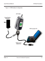
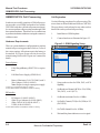
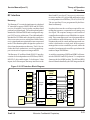
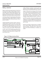
1
Service Manual
Level 3
Draft 1.0
Model V975/V980
UMTS 2100MHz/PCS 1900MHz/DCS 1800MHz/GSM 900MHz
Distribution Policy and Copyright
Copyright
© 2005 by Motorola. All rights reserved. No part of this publication may be reproduced, transmitted,
transcribed, stored in a retrieval system or translated into any language in any form by any means
without the written permission of Motorola.
Software License
The Agreement sets forth the license terms and conditions for using the enclosed Software. You may
use this Software on a single computer, and you may transfer it to another computer as long as it is
used on only one computer at a time. You may copy the Software for backup purposes only. You may
not rent, sell, lease, sublicense, time-share or lend the Software to a third party or otherwise transfer
this License without written consent of Motorola. You shall not decompile, disassemble, reverseengineer or modify the Software. This License is effective until terminated. You may terminate it at any
time by destroying the Software together with all copies. The License also terminates if you fail to
comply with the terms and conditions of this Agreement. United States copyright laws as well as
international treaty provisions protect this Software and accompanying documentation. Any use of the
Software in violation of these laws constitutes termination of the License.
Limited Liability
The Software and accompanying documentation is provided “AS IS” without warranty of any kind.
Motorola specifically disclaims all other warranties, expressed or implied, including but not limited to
implied warranties of merchantability and fitness for a particular purpose. With respect to the use of
this product, in no event shall Motorola be liable for any loss of profit or any other commercial damage,
including but not limited to special, incidental, consequential or other damages.
ii
Motorola Confidential Proprietary
Draft 1.0
Table of Contents
3G Flash Procedures ................................................................................................................. 1-1
Introduction ............................................................................................................................. 1-1
Hardware Requirements ......................................................................................................... 1-1
Power Hardware .............................................................................................................................................. 1-1
Interface Options ............................................................................................................................................ 1-1
Software Requirements .......................................................................................................... 1-1
Flashing .................................................................................................................................. 1-2
Power Solutions .............................................................................................................................................. 1-2
RSD Firmware Upgrade Procedure .................................................................................................................. 1-2
Figure 1-1. RSD Hardware Configuration ................................................................................................... 1-3
Figure 1-2. RSD General Release GUI ...................................................................................................... 1-4
Figure 1-3. Firmware Upgrade ................................................................................................................... 1-5
Force Flash Procedures.......................................................................................................... 1-6
Manual Test Procedures ............................................................................................................ 2-1
Introduction ............................................................................................................................. 2-1
Call-Processing Tests ...................................................................................................................................... 2-1
Non-Signaling Test Measurements ................................................................................................................... 2-1
GSM/DCS/PCS Call Processing ............................................................................................ 2-2
Hardware Requirements .................................................................................................................................. 2-2
Call Origination ................................................................................................................................................ 2-2
Figure 2-1. GSM Signaling Setup .............................................................................................................. 2-2
Figure 2-2. GSM Connection Control ......................................................................................................... 2-3
Figure 2-3. GSM Call Connected ............................................................................................................... 2-3
Call Test Parameters (GSM/DCS/PCS) ............................................................................................................ 2-3
Table 2-1. GSM Call Parameters ............................................................................................................... 2-3
Table 2-2. DCS Call Parameters ................................................................................................................ 2-3
Table 2-3. PCS Call Parameters ................................................................................................................ 2-3
Figure 2-4. Burst Output Shape ................................................................................................................. 2-4
Table 2-4. GSM/DCS/PCS Handover ......................................................................................................... 2-4
Figure 2-5. Manual Test Hardware Configuration ........................................................................................ 2-5
WCDMA Call Processing........................................................................................................ 2-6
Hardware Requirements .................................................................................................................................. 2-6
Software Requirements ................................................................................................................................... 2-6
Call Origination (WCDMA) ............................................................................................................................... 2-6
Figure 2-6. WCDMA Signalling Setup ........................................................................................................ 2-6
Figure 2-7. Channel Uplink(UE Signal) ...................................................................................................... 2-6
Figure 2-8. TPC Pattern Type(UE Signal) ................................................................................................... 2-7
WCDMA Call Test Parameters ......................................................................................................................... 2-7
Figure 2-9. WCDMA Call Connected .......................................................................................................... 2-7
Table 2-5. WCDMA Call Parameters .......................................................................................................... 2-7
Draft 1.0
©2005 Motorola, Inc.
iii
Table of Contents
V975/V980
Figure 2-10. WCDMA Modulation .............................................................................................................. 2-7
Figure 3-11. ACLR Screen ........................................................................................................................ 2-7
Figure 2-11. ACLR Screen ........................................................................................................................ 2-7
Non-Signaling Test Procedures (GSM/DCS/PCS) .................................................................. 2-8
Hardware Requirements .................................................................................................................................. 2-8
Software Requirements ................................................................................................................................... 2-8
Verify TX Power Output (GSM/DCS/PCS) ....................................................................................................... 2-8
Table 2-6. TX Power Limits ........................................................................................................................ 2-8
GSM RSSI ...................................................................................................................................................... 2-9
Non-signaling Test Procedures (WCDMA) ............................................................................ 2-10
Hardware Requirements ................................................................................................................................ 2-10
Software Requirements ................................................................................................................................. 2-10
Verify TX Power Output (WCDMA) ................................................................................................................. 2-10
Table 2-7. WCDMA TX Power Output ....................................................................................................... 2-10
Audio/Vibrator Test Procedures............................................................................................. 2-11
Vibrator Test .................................................................................................................................................. 2-11
Handset Mic/Speaker test ............................................................................................................................. 2-11
Mono Headset Mic/Speaker test ................................................................................................................... 2-11
Stereo Headset Mic/Speaker test .................................................................................................................. 2-12
Melody Speaker test ..................................................................................................................................... 2-12
Display Test Procedures ....................................................................................................... 2-13
Display Backlight Test ................................................................................................................................... 2-13
Display Color Test ......................................................................................................................................... 2-13
Figure 20. Eight Color Box Pattern .......................................................................................................... 2-13
Display Linearity Test .................................................................................................................................... 2-14
Figure 21. Grey Scale Block ................................................................................................................... 2-14
Display Flicker Test ....................................................................................................................................... 2-14
Figure 22. Zebra Pattern .......................................................................................................................... 2-14
Display Pixel Defect (Bright) ......................................................................................................................... 2-15
Display Pixel Defect (Dark) ........................................................................................................................... 2-15
LEDS and Keypad Backlight ................................................................................................. 2-15
Keypad Backlight .......................................................................................................................................... 2-15
Camera Testing ..................................................................................................................... 2-16
Data Line Integrity Check .............................................................................................................................. 2-16
Camera Flash Check ..................................................................................................................................... 2-16
Theory of Operation ................................................................................................................... 3-1
V975/V980 Overview .............................................................................................................. 3-1
Figure 3-1. V975 Transceiver ..................................................................................................................... 3-1
Front End Module .................................................................................................................... 3-2
Figure 3-2. RF Top ..................................................................................................................................... 3-2
Figure 3-3. FEM Module (FL001) ............................................................................................................... 3-3
Table 3-1. FEM Truth Table ........................................................................................................................ 3-3
RF GSM Receiver ................................................................................................................... 3-4
BALUN ............................................................................................................................................................ 3-4
Figure 3-4. Balun Transformer .................................................................................................................... 3-4
BLUE MODULE IC (ALGAE) ........................................................................................................................... 3-4
Figure 3-5. ALGAE MB (Receiver) ............................................................................................................ 3-4
HARMONY GSM_RX (U100) ........................................................................................................................... 3-5
Figure 3-6. Harmony (GSM RX) ................................................................................................................ 3-5
iv
©2005 Motorola, Inc.
Draft 1.0
Level 3 Service Manual
Table of Contents
RF GSM Transmitter ................................................................................................................ 3-6
BLUE MODULE IC (PRIMSYN GSM_TX) ....................................................................................................... 3-6
Figure 3-7. PRIMSYN (GSM TX) ............................................................................................................... 3-6
BLUE MODULE (ALGAE) ............................................................................................................................... 3-6
Figure 3-8. ALGAE MB (Transceiver) ........................................................................................................ 3-6
GSM PA (U800) ............................................................................................................................................... 3-7
Figure 3-9. Durango 9E3G (U800) ............................................................................................................ 3-7
RF WCDMA Receiver ............................................................................................................. 3-8
MC13820 (U001) ............................................................................................................................................. 3-8
BLUE MODULE (ONELife) .............................................................................................................................. 3-8
Figure 3-10. WCDMA LNA ......................................................................................................................... 3-8
Figure 3-11. ONELife ................................................................................................................................ 3-8
Harmony WCDMA_RX (U100) ......................................................................................................................... 3-9
Figure 3-12. Harmony WCDMA RX (U100) ................................................................................................ 3-9
RF WCDMA Transmitter ........................................................................................................ 3-10
Harmony WCDMA TX (U100) ......................................................................................................................... 3-10
Figure 3-13. Harmony WCDMA TX (U100) ............................................................................................... 3-10
MC13786 (U200) ........................................................................................................................................... 3-11
Figure 3-14. Rattler (U200) ...................................................................................................................... 3-11
WCDMA PA (U850) ....................................................................................................................................... 3-12
Figure 3-15. Durango 5W (WCDMA PA) ................................................................................................... 3-12
RF Interface .......................................................................................................................... 3-13
Harmony ....................................................................................................................................................... 3-13
Figure 3-16. RF Interface Block Diagram ................................................................................................ 3-13
Baseband Electrical (Digital) ................................................................................................ 3-15
POG (U1000) ................................................................................................................................................ 3-15
Figure 3-18. POG Block Diagram ............................................................................................................ 3-15
Graphics Accelerator ..................................................................................................................................... 3-15
Figure 3-19. GPU Interface ..................................................................................................................... 3-15
MMC/SD Flash Interface ............................................................................................................................... 3-16
Figure 3-20. MMC Interface ..................................................................................................................... 3-16
Keypad Interface ........................................................................................................................................... 3-16
Figure 3-21. Keyboard Interface .............................................................................................................. 3-16
POG Memory ................................................................................................................................................ 3-17
Figure 3-22. POG Memory ...................................................................................................................... 3-17
Power Supply Architecture ............................................................................................................................ 3-17
Table 3-1. Power Distribution 1 ................................................................................................................ 3-17
Table 3-2. Power Distribution 2 ................................................................................................................ 3-17
Clock Generation .......................................................................................................................................... 3-18
Figure 3-24. RTC Clock ........................................................................................................................... 3-18
Audio Circuits ....................................................................................................................... 3-19
PCAP (U3000) ............................................................................................................................................... 3-19
TX Audio ....................................................................................................................................................... 3-19
Figure 3-25. Internal Mic Path ................................................................................................................. 3-19
Figure 3-26. Headset Mic Path ................................................................................................................ 3-19
RX Audio ....................................................................................................................................................... 3-20
Figure 3-27. RX Audio Block ................................................................................................................... 3-20
Figure 3-28. Handset Speaker Path ......................................................................................................... 3-20
Figure 3-29. Headset Speaker Path ......................................................................................................... 3-21
Draft 1.0
©2005 Motorola, Inc.
v
Table of Contents
V975/V980
Figure 3-30. External Speaker Path ......................................................................................................... 3-21
Figure 3-31. Alert Path ............................................................................................................................ 3-21
Battery Interface .................................................................................................................... 3-22
Figure 3-32. Battery Interface Block ........................................................................................................ 3-22
Parts List ..................................................................................................................................... 4-1
Introduction ............................................................................................................................. 4-1
Electrical Parts List ................................................................................................................. 4-2
Table 4-1. Electrical Parts List - A1 to C400 .............................................................................................. 4-2
Table 4-2. Electrical Parts List - C401 to C908 .......................................................................................... 4-3
Table 4-3. Electrical Parts List - C909 to C3002 ........................................................................................ 4-4
Table 4-4. Electrical Parts List - C3050 to C4208 ...................................................................................... 4-5
Table 4-5. Electrical Parts List - C4209 to C5200 ...................................................................................... 4-6
Table 4-6. Electrical Parts List - C5201 to L002 ......................................................................................... 4-7
Table 4-7. Electrical Parts List - L003 to R113 ........................................................................................... 4-8
Table 4-8. Electrical Parts List - R114 to R1404 ........................................................................................ 4-9
Table 4-9. Electrical Parts List - R1405 to R5101 .................................................................................... 4-10
Table 4-10. Electrical Parts List - R5102 to U880 .................................................................................... 4-11
Table 4-11. Electrical Parts List - U900 to Y3982 ..................................................................................... 4-12
V980 Parts List ............................................................................................................................ 5-1
Introduction ............................................................................................................................. 5-1
Electrical Parts List ................................................................................................................. 5-2
Table 4-1. Electrical Parts List - A1 to C501 .............................................................................................. 5-2
Table 4-2. Electrical Parts List - C800 to C1020 ........................................................................................ 5-3
Table 4-3. Electrical Parts List - C1021 to C3401 ...................................................................................... 5-4
Table 4-4. Electrical Parts List - C3500 to C4300 ...................................................................................... 5-5
Table 4-5. Electrical Parts List - C4300 to C5203 ...................................................................................... 5-6
Table 4-6. Electrical Parts List - C5204 to J5100 ....................................................................................... 5-7
Table 4-7. Electrical Parts List - J5212 to R105 ......................................................................................... 5-8
Table 4-8. Electrical Parts List - R106 to R1404 ........................................................................................ 5-9
Table 4-9. Electrical Parts List - R1405 to R5001 .................................................................................... 5-10
Table 4-10. Electrical Parts List - R5100 to U200 .................................................................................... 5-11
Table 4-11. Electrical Parts List - U3971 to Y3982 ................................................................................... 5-12
vi
©2005 Motorola, Inc.
Draft 1.0
3G Flash
Procedures
Introduction
Hardware Requirements
This document is intended to describe the flashing (firmware upgrade) procedures for 3G terminals. The 3G
terminal described in this document will be limited to
the V975, V980, C975, and C980.
The following hardware will be required to properly
flash the 3G terminal.
Firmware upgrades need to be handled in a controlled
manner. Carrier software approvals need to be considered before initializing a flashing procedure. Consult a
Motorola representative to ensure that the firmware
upgrade application database is up-to-date.
1.
Fully Charged battery (SNN5743A or equivalent)
2.
Full-rate Charger (SPN5049 or equivalent)
Power Hardware
Interface Options
Firmware upgrades allows the service organization to
resolve field software issues that customers may be experiencing. Some issues may pertain to specific circumstances, therefore, not all units will contain identical software versions.
1.
USB Data Kit (S8951)
USB Cable (SKN6311A)
Data Software CD
Software Requirements
The RSD (Remote Software Download) General Release is used to allow functions such as firmware upgrade, Phone Swap, and Multi-refurbish. Contact your
local Motorola service representative to receive download information for the RSD and related support files.
Also insure that the RSD database has the latest update.
Draft 1.0
Motorola Confidential Proprietary
1-1
3G Flash Procedures
V975/V980/C975/C980
Flashing
Flashing
Before beginning any flashing procedure, always insure
that all hardware connections are secured. Refer to figure 1-1 for flash connection guides. Any intermittent
hardware connections may cause the procedure to fail
and result in a nonfunctional (Bricked) 3G terminal.
Power Solutions
There are two types of power solutions to perform a
flashing procedure.
8.
In the Main information Panel, select desired
restore and logging options
9.
In the Main information Panel, click on the Start
button to begin Firmware upgrade.
NOTE: DO NOT interrupt any hardware connections
during the flash process. Connection interruptions may cause the flashing process to fail and
render the 3G terminal non-operational.
10.
When the process is complete, the Main Information Panel will indicate whether the process
was successful. At this time you may safely disconnect the 3G terminal.
11.
Power up the 3G terminal to insure that the flash
procedure was successful.
1. Fully Charged Battery
2. Full-Rate Charger w/battery (recommended)
If the user decides on using the battery only solution,
he/she must verify that the battery is fully charged. Failing to verify the capacity of the battery may result in
battery depletion prior to completing the flash process.
This action may cause unrecoverable failures to the 3G
terminal.
RSD Firmware Upgrade Procedure
Use the listed procedure to complete the flash procedure for a 3G terminal.
1.
Launch the RSD General application
2.
Connect the unit as illustrated in figure 1-1.
3.
Power up the 3G terminal
4.
If the 3G terminal doesn’t power up, refer to
the Force Flash section.
5.
Once the phone is fully powered up, the Radio
Information Panel will be updated.
7.
In the Utilities Panel, select Firmware Upgrade.
1-2
Motorola Confidential Proprietary
Draft 1.0
Level 3 Service Manual
3G Flash Procedures
Figure 1-1. RSD Hardware Configuration
V975/V980
Power Supply
SPN5049A
RSD equipped PC
SKN6311A
USB Interface
SKN6311A
Draft 1.0
Motorola Confidential Proprietary
1-3
3G Flash Procedures
V975/V980/C975/C980
Figure 1-2. RSD General Release GUI
Radio Information Panel
Utilities Panel
1-4
Main Information Panel
Progress Indicator
Motorola Confidential Proprietary
Status Log Panel
Draft 1.0
Level 3 Service Manual
3G Flash Procedures
Figure 1-3. Firmware Upgrade
Backup and Restore
Customer information
Maintain Request
History
Draft 1.0
Motorola Confidential Proprietary
1-5
3G Flash Procedures
V975/V980/C975/C980
Force Flash Procedures
Force Flash Procedures
The procedures described in this section apply only to
situations where the 3G terminal will not initiate it’s normal power up sequence, but may recover functionality
by a repeat flash procedure.
There are two possible alternatives to place the 3G terminal in force flash mode.
Key Hold Solution
Hardware: Refer to Figure 1 (USB solution)
Step 1. Remove the battery from the 3G terminal
Step 2. Prior to connecting the USB cable, press and
hold “#” and “*” keys from the 3G terminal
Step 3. Attach the USB cable
Step 4. Verify that the RSD application detects the 3G
terminal, if it’s not detected, press and hold the
gaming keys once again.
Force Flash USB Cable Solution
Hardware: Refer to Figure 1-1 (USB solution), except,
replace USB cable (SKN6311A) with
force flash cable (SKN6168A)
Step 1. Connect the force flash cable in the same manner described in Figure 1-1.
Step 2. The 3G terminal will automatically be placed in
force flash mode. There’s no need to press the
power key. The RSD application will now detect the 3G terminal
1-6
Motorola Confidential Proprietary
Draft 1.0
Manual Test
Procedures
Introduction
Non-Signaling Test Measurements
The phone allows computer controlled testing of various test parameters.
In an event that the phone exhibits RF failures that prevent call processing, the service technician may need to
perform some non-signaling tests. These tests will provide information regarding which stage of the phone is
failing prior to opening the phone for troubleshooting.
The following tests will be described in this chapter.
This chapter includes the computer functions and recommended equipment setup to use when testing a phone
manually.
Call-Processing Tests
Most communications analyzers can simulate a cell site
in order to perform automatic call-processing tests.
Automatic call processing tests can be performed while
the phone is in standby mode.
Refer to the communications analyzer’s manual for details about performing call-processing tests. The following call-processing test sequence is recommended:
1.
2.
3.
4.
5.
GSM Mobile Originated Call
WCDMA Mobile Originated Call
GSM handover
DCS handover
PCS handover
Draft 1.0
•
•
•
GSM/DCS/PCS TX Power Output
GSM RSSI
WCDMA TX Power Output
The phasing parameters are stored in an EPROM in
the transceiver board. Each transceiver is shipped from
the factory with these parameters already calibrated.
However, if a board is repaired, these parameters should
be measured and, if necessary, adjusted (phased) with
the GP-Gate System. Checking and adjusting calibration parameters is also useful as a troubleshooting/diagnostic tool to isolate defective assemblies.
Motolora Confidential Proprietary
2-1
Manual Test Procdures
V975/V980/C975/C980
GSM/DCS/PCS Call Processing
GSM/DCS/PCS Call Processing
Call Origination
In order to successfully complete a GSM call processing procedure, a test USIM card needs to be available.
Test USIM cards have default call parameters that allow users to perform call processing tests through GSM
base station simulators. This allows service technicians
to perform simulations without accessing the customer’s
cellular account.
Use the following procedures for call processing. The
screen shots are from a Rohde and Schwarz CMU 200.
The procedures can be adopted to any other test box
that will be used to perform call processing.
1.
Install the test USIM in phone.
2.
Connect hardware as illustrated in figure 2-5.
Hardware Requirements
Figure 2-1. GSM Signaling Setup
There are various hardware configurations to perform
manual call processing procedures. Below, is a list of
the various options. All options require the battery to
be attached. A GP-gate system can also be used for
manual testing. Refer to the GP-gate user’s manual for
details.
Ch. 1
Ch. 2
Selection
GSM Mobile Station(GSM 1800/Signalling/Overview/P/t Normal GMSK
Basic Functions
GSM Mobile Station
GSM 850
GSM 900
GSM 1800
GSM 1900
3G UMTS User Equipment
WCDMA FDD
Non-Signalling
Signalling
Hotkeys - Set 1
RF
Analyzer/Generator
Analyzer/Generator
Overview
AUDIO
Analyzer/Generator
GSM 850
Analyzer/Generator
P/t Normal GMSK
GSM 850
Overview
P/t Normal GMSK
GSM 850
Analyzer/Generator
P/t Normal GMSK
Fully Charged Battery (SNN5743A¹ or equivalent)
•
Full-Rate Power Supply (SPN5049A¹)
•
Battery Eliminator (5-00-3Y-12000²) with 2Wire Adapter (2-00-68-10000²)
Note: Requires a single output power supply
¹Contact your local Motorola dealer for ordering
²Contact AMS Software and Elektronik GmbH for ordering
GSM 850
Overview
P/t Normal GMSK
RF Adapter (2-00-4E-10000²)
SMA/N type Adapter (0-00-00-40042)
SMA Cable 0.5m (0-00-00-40047²)
USIM (0-00-00-40810²)
HotKeys
HotKeys
Set 1
Set 2
Menu
Select
HotKeys
Set 3
HotKeys
Assign.
3.
Setup up the test box for GSM, DCS, or PCS
Signaling
4.
Set Broadcast Channel (BCH) to 120 (GSM),
700 (DCS), or 661 (PCS)
5.
Set Broadcast channel level to -85dBm
6.
Set Traffic Channel (TCH) to 38 (GSM) or 512
(DCS/PCS)
7.
Set Traffic channel level to -85dBm
8.
Wait until the phone indicates a receive signal
RF Interface
•
•
•
•
Connect
Control
Menu Select
Power Options
•
Circuit
Switched
Single Slot
GSM1900 Overview
²Contact AMS Software and Elektronik GmbH for ordering
2-2
Motorola Confidential Proprietary
Draft 1.0
Level 3 Service Manual
Manual Test Procedures
GSM/DCS/PCS Call Processing
Figure 2-2. GSM Connection Control
GSM 900 Connection Control
Frequency
Offset
+0
Single Slot
Hz
While the phone under test is in an active call, the parameters for each band should be verified as described.
Slot
Mode
Table 2-1. GSM Call Parameters
BCCH and TCH
Mode
BCCH
Level
- 85.0
RF
Channel
37
- 85.0
dBm
- 20.0
dBm
used
975
dB
unused
925.2
Hopping
Timeslot
3
MS Signal
9.
BS Signal
Network
TCH
Level
RF
Channel
MHz
Off
Connection
AF/RF
Sync
1
2
Dial a number from the phone and press the
send button.
10.
Call Test Parameters (GSM/DCS/PCS)
Signal On
The phone is now connected.
Pa ra m e te r
Burst Avg Power Out¹
Burst Output Shape
Time Advance Error
RMS Phase Error
Peak Phase Error
Frequency Error
RX Level Error@-105 dBm²
RX Quality @-105 dBm²
BER @-105, 10k bits³
Low
Lim it
27
1
-1
0
-20
-90
1
0
0
High
Lim it
31
1
1
5
20
90
9
4
2
Unit
dBm
P/F
bit/sym
deg
deg
Hz
%
¹Power Level = 5
²Set BS TCH level to -105 dBm
³Set BER TCH level to -105 dBm with 10k bits or 128 Frames
Table 2-2. DCS Call Parameters
Figure 2-3. GSM Call Connected
Circuit
Switched
Single Slot
GSM1800 Overview
Ch. 1
Ch. 2
RUN P/t Norm GMSK
1(28.0 dBm ) Reported Power
25.5 dBm Avg. Burst Power (Current)
25.7 dBm Peak Burst Power
Ok Power Ramp
1(28.0
- 0.75
RUN
Sym. Time Advance Error
Ext. Phase Error GMSK
- 30
6.2
2.1
Frequency Error
Hz
Peak
Phase Error(Current)
RMS
MS Receiver Reports
17 (
0(
- 94 to - 93 dBm)
RX Level
0.0 to
RX Quality
Off
Discontinuous Transmission(DTX)
PCL
0.2 % )
Timing
Advance
R P/t Norm,
U
N GMSK
Settings
Signalling States
MS Capabililties
Signalling Info
IMSI
IMEI
Dialled Number
Traffic Mode
Meas. Control
Repetition
Stop Condition
Display Mode
Statistic Count
Analyzer Level
RF Mode
RF Attenuation
Triiger Source
Trigger Slope
MS Signal
CIrcuit Switched
Timing Advance
Single Slot
PCL (MS)
Connect
Control
--- -------------123655
Full Rate Version 1
Continuous
None
Current
100 Bursts
Auto
Low Noise
Signalling
Rising Edge
Application
Analyzer
Level
MS Signal
BS Signal
Network
0 Sym.
1 (28.0 dBm)
Menus
Pa ra m e te r
Burst Avg Power Out¹
Burst Output Shape
Time Advance Error
RMS Phase Error
Peak Phase Error
Frequency Error
RX Level Error@-103 dBm²
RX Quality @-103 dBm²
BER @-103, 10k bits³
Low
Lim it
-5
1
-1
0
-20
-180
3
0
0
High
Lim it
5
1
1
5
20
180
11
4
2
Unit
dBm
P/F
bit/sym
deg
deg
Hz
%
¹Power Level = 15
²Set BS TCH level to -103 dBm
³Set BER TCH level to -103 dBm with 10k bits or 128 Frames
Table 2-3. PCS Call Parameters
Pa ra m e te r
Burst Avg Power Out¹
Burst Output Shape
Time Advance Error
RMS Phase Error
Peak Phase Error
Frequency Error
RX Level Error@-104 dBm²
RX Quality @-104 dBm²
BER @-104, 10k bits³
Low
Lim it
-5
1
-1
0
-20
-190
2
0
0
High
Lim it
5
1
1
5
20
190
10
4
2
Unit
dBm
P/F
bit/sym
deg
deg
Hz
%
¹Power Level = 15
²Set BS TCH level to -104 dBm
³Set BER TCH level to -104 dBm with 10k bits or 128 Frames
Draft 1.0
Motorola Confidential Proprietary
2-3
Manual Test Procdures
V975/V980/C975/C980
GSM/DCS/PCS Call Processing
Figure 2-4. Burst Output Shape
Ch. 2
dB
Circuit
Switched
Single Slot
GSM1800 Overview
Ch. 1
Max. Level:
R:
---
Auto
/ Off
Low Noise
1:
PCL:
---
1 / 28.0 dBm
/
Off
+0
Connect
Control
Chan. / Meas Slot:
740
/ 3
2:
--/
Off
Current
R P/t Norm,
U
N GMSK
Applic. 1
-10
Applic. 2
-20
Analyzer
Level
-30
MS Signal
-40
Ok
-50
25.57 dBm
- 0.75 Sym.
-60
GSM 0
100 Bursts
-70
BS Signal
Avg.BurstPower(Cur.)
Timing Adv. Error
TSC detected
Network
Statiatical Counr
0.00 %
Out of Tolerance
60
80
Marker
-80
0
20
40
Power
Overview
Modulation
100
Spectrum
120
Display
140
Receiver
Quality
Audio
Menus
Burst Output Shape should fall within the standard limits of the Power Ramp.
BER measurements is only required if RX Quality reads
a value of 4 or greater.
It is recommended that handover procedures be performed as shown in the following table.
Table 2-4. GSM/DCS/PCS Handover
Ba nd
GSM
DCS
PCS
2-4
From
Tra ffic
Pow e r
Cha nne l Control
975
5
512
0
512
0
To
Tra ffic
Pow e r
Cha nne l Control
124
19
885
15
810
15
Motorola Confidential Proprietary
Draft 1.0
Level 3 Service Manual
Manual Test Procedures
Figure 2-5. Manual Test Hardware Configuration
CMU200 Test Box
or Equivalent
SMA/N-type Adapter
0-00-00-40042
RF Adapter
2-00-4E-10000
SMA Cable 0.5m
0-00-00-40047
3G Terminal
Power Supply
(3.6Vdc, 2A)
2-Wire Adapter
2-00-68-10000
Battery Eliminator
5-00-3Y-12000
P2K USB Cable
SKN6311A
RS232 to CE
SYN0279B
OR
CONTROL INTERFACE
Radio Comm equipped
Computer
Draft 1.0
Motorola Confidential Proprietary
P2K Serial Cable
SKN6315A
2-5
Manual Test Procdures
V975/V980/C975/C980
WCDMA Call Processing
Figure 2-6. WCDMA Signalling Setup
WCDMA Call Processing
Ch. 1
In order to successfully complete a GSM call processing procedure, a test USIM card needs to be available.
Test USIM cards have default call parameters that allow users to perform call processing tests through GSM
base station simulators. This allows service technicians
perform simulations without accessing the customer’s
cellular account.
Ch. 2
WCDMA FDD
Band
I
Connect
Control
Spectrum
Menu Select
Selection
GSM Mobile Station(GSM 1800/Signalling/Overview/P/t Normal GMSK
Basic Functions
GSM Mobile Station
GSM 850
GSM 900
GSM 1800
GSM 1900
3G UMTS User Equipment
WCDMA FDD
Non-Signalling
Signalling
Hotkeys - Set 1
RF
Analyzer/Generator
Power
Spectrum
AUDIO
Analyzer/Generator
GSM 850
Analyzer/Generator
P/t Normal GMSK
GSM 850
Overview
P/t Normal GMSK
GSM 850
Analyzer/Generator
P/t Normal GMSK
GSM 850
Overview
P/t Normal GMSK
Hardware Requirements
Refer to , “Hardware requirements,” under, “GSM/
DCS/PCS Call Processing.” Also Refer to Figure 2-5.
Software Requirements
None.
HotKeys
HotKeys
Set 1
Set 2
Menu
Select
HotKeys
Set 3
3.
Setup up the test box for WCDMA FDD Signaling
4.
Set UE Signal, RF Channel Uplink to 9400
5.
Set UE Signal, RF Channel Downlink to 9800
Figure 2-7. Channel Uplink(UE Signal)
Call Origination (WCDMA)
WCDMA FDD Connection Control
1.
Install the test USIM in phone.
2.
Connect hardware as illustrated in figure 4.
Note: Control interface doesn’t need to be connected at this time.
Signal On
Setup
Use the following procedures for call processing. The
screen shots are from a Rohde and Schwarz CMU 200
with WCDMA signaling options installed. The procedures can be adopted to any other test box that will be
used to perform call processing.
Analyzer Settings/RF Channel Uplink
Default All Settings
Analyzer Settings
RF Channel Uplink
Band [|]
Frequency Offset
RX/TX Separation
Measurement Settings
Default Settings
UL Scrambling Code
Analysis Mode
Sync. Mode
Measurement Slot Number
Correlatoin Mode
Threshold
UE Power Control
Default Settings
Connection
6.
2-6
HotKeys
Assign.
UE Signal
Channel
Frequency
Downlink
9750
1922.4 MHz
+ 0.000 kHz
190.000 MHz
2112.4 MHz
0
With Origin Offset
All Slots
0
DPCCH
- 25 dB
BS Signal
Network
RF
Sync.
1
2
Set TPC Pattern Type to All 1
Motorola Confidential Proprietary
Draft 1.0
Level 3 Service Manual
Manual Test Procedures
WCDMA Call Processing
Figure 2-8. TPC Pattern Type(UE Signal)
WCDMA FDD Connection Control
Setup
Connection
UE Signal
Parameter
Avg. RMS Power Out¹
Avg. Frequency Error²
Avg. RMS EVM²
Avg. RMS ACLR - 2³
Avg. RMS ACLR - 1³
Avg. RMS ACLR + 1³
Avg. RMS ACLR + 2³
- 5.0 dB
3
- 3.0 dB
6
- 7.0 dB
6
0.0 dB
1
Algorithm 2
1 dB
All 1
0000000000000000000000 bin
Off
BS Signal
Network
RF
Sync.
1
2
Ch. 1
Ch. 2
Dial a number from the phone and press the
send button.
Max. Level: + 30.0 dBm
Low Noise
Multiple Signal DPCCH+DPDCH 1
CCMode Manual
Scr Code 0
The phone is now connected.
Peak
Peak
RMS
I/Q Origin Offset
I/Q Imbalance
Carrier Frequency Error
Waveform Quality
Ch. 2
WCDMA FDD
Max. Level: + 30.0 dBm
Low Noise
Band
I
Connect
Control
Power
Freq/Offset: + 0.000 kHz:
Chan. /Freq: 9750 / 1950 MHz
Peak Code Dom Error
PCDE Code
UE Power (Peak)
UE Power (RMS)
24.77
24.02
dBm
dBm
24.73
24.01
dBm
dBm
Maximum
24.94 dBm
24.09 dBm
Minimum
20.69 dBm
UE Signal
Ana. Set
0
Slot Number
20.81 dBm
UE Power
10
Ch. 1
BS Signal
Level
dBm
+40
Modulation
Spectrum
Code Dom.
Power
Menus
Receiver
Quality
Ch. 2
Band
I
WCDMA FDD
Max. Level: + 30.0 dBm
Freq. Offset: + 0.000 kHz
Low Noise
Connect
Control
Spectrum
R ACLR
U
N Filter
Chan. /Freq: 9750 / 1950 MHz
Current
+20
640
+10
Chip
Power
Modulation
Spectrum
Code Dom.
Power
Receiver
Quality
Menus
- 10
----
- 20
UE Power
10
- 40
Statistic Count
- 50
-2
- 10.00 MHz
WCDMA Call Test Parameters
While the phone under test is in an active call, the parameters for each band should be verified as described.
Draft 1.0
Application
Meas. Length
- 30
Overview
BS Signal
Settings
Statistic Count
+0
100.00 %
Out of Tolerance
BS Signal
Level
Figure 2-11. ACLR Screen
Analyzer
Settings
BS Signal
Settings
10
Analyzer
Lev. Trigg
Out of Tolerance
Power
+30
Statistic Count
Application
26.5 %
10.2 %
15.3 %
5.6 %
15.4 °
4.9 °
- 32.37 dB
- 20.07 dB
- 76 Hz
0.9897
- 25.49 dB
I
0
100.00 %
Analyzer
Lev. Trigg
Average
Connect
Control
R Overview
U
N WCDMA
Chan. /Freq: 9750 / 1950 MHz
Max /Min
22.16 %
8.80 %
14.03 %
5.52 %
12.47 °
3.95 °
- 32.95 dB
- 21.38 dB
4 Hz
0.99226
- 28.12 dB
R Maximum
U
N Power
Application
Current
Average
20.8 %
8.5 %
15.3 %
5.6 %
- 11.5 °
3.7 °
- 33.06 dB
- 21.74 dB
5 Hz
0.9929
- 29.11 dB
Q
1
Peak
RMS
Phase Error
Figure 2-9. WCDMA Call Connected
Freq/Offset: + 0.000 kHz:
SR1 15
CC1 64
Current
Err Vect Magn
RMS
Ch. 1
Unit
dBm
Hz
%
dB
dB
dB
dB
Figure 2-10. WCDMA Modulation
Band
Figure
Screen
WCDMA3-11.
FDD ACLR
Modulation
I
Magn Error
9.
High
Limit
21.5
195
13.5
-43
-33
-33
-43
¹Refer to Figure 10
²Refer to Figure 11
³Refer to Figure 12
Wait until the phone indicates a signal
8.
Low
Limit
20.5
-195
0
-100
-100
-100
-100
TPC Settings/TPC Pattern Type
PICH
PICH Channel Code
AICH
AICH Channel Code
DPDCH
DPCH Channel Code
Power Offset (DPCCH/DPDH)
Secondary Scrambling Code
TPC Settings
Default Settings
TPC Algorithm
TPC Step Size
TPC Pattern Type
Pattern
Repeat Pattern
7.
Table 2-5. WCDMA Call Parameters
Signal On
-1
0
- 5.00 MHz
- 47.4
- 55.7
- 34.9
- 41.5
- 55.7
- 45.1
- 55.2
- 41.5
- 34.6
- 41.3
Power
1
0 MHz
+ 24.7
+ 20.7
dBm
dBm
All
Values
in
dB
Modulation
Motorola Confidential Proprietary
2
Ch
100.00 %
Out of Tolerance
+ 5.00 MHz
+ 10.00 MHz
- 34.7
- 41.3
- 51.4
- 57.8
ACLR (Peak) Curr.
- 41.3
- 33.7
- 41.0
- 57.8
- 49.0
- 57.4
ACLR (RMS) Avg.
Spectrum
Code Dom.
Power
ACLR (RMS) Curr.
Analyzer
Lev. Trigg
Analyzer
Settings
BS Signal
Level
BS Signal
Settings
ACLR (Peak) Avg.
ACLR (RMS) Max.
Receiver
Quality
Menus
2-7
Manual Test Procdures
V975/V980/C975/C980
Non-Signaling Test Procedures (GSM/DCS/PCS)
Non-Signaling Test Procedures
(GSM/DCS/PCS)
To perform non-signaling test procedures, the user is
required to be familiarized with sending test commands
to the phone under test. The test commands are sent
using a computer.
In order to successfully send test commands to the phone
under test, the phone needs to be in suspend mode.
Follow the listed procedure to place the phone in suspend mode.
Click AT+MODE then SUSPEND
(Serial Only)
Verify TX Power Output (GSM/DCS/PCS)
Verify the TX Power output by initiating the commands
in this section. Verify that the results fall within the following limits.
Table 2-6. TX Power Limits
Parameter
GSM TX Power Out
DCS TX Power Out
PCS TX Power Out
Low
Limit
High
Limit
31
28.2
28.2
33
30
30
Unit
dBm
dBm
dBm
¹10*0*5 for PCS mode
²20*700*0 for DCS Channel 700; 20*661*0 for PCS Channel 661
³45*0 for DCS/PCS Power level 0
Click on 900/1800 (GSM/
DCS) or 1900 (PCS)
Click SUSPEND (USB Only)
Hardware Requirements
Enter 38 (GSM), 700 (DCS), or 661
(PCS) and then click Set
Control Interface Options
•
•
USB Cable (SKN6311A¹)
Serial Cable (SKN6315A¹) with CE converter
(SYN0279B¹)
¹Contact your local Motorola dealer for ordering
Enter 5 (GSM) or 0 (DCS/PCS)
and then click Set
Refer to page 2-2 for a list of Hardware. Refer to Figure 2-5 for a configuration illustration.
Software Requirements
Radio Comm (latest release)
Select 06 and then
click ON
NOTE: Set Training Sequence to 4 on the test equipment.
2-8
Motorola Confidential Proprietary
Draft 1.0
Level 3 Service Manual
Manual Test Procedures
Non-Signaling Test Procedures (GSM/DCS/PCS)
GSM RSSI
Verify GSM RSSI by initiating the commands in this
section. Verify that the RSSI results are equal to the
Broadcast Channel (BCH) level. The user will need to
set the RF generator with the following parameters.
Broadcast Channel (BCH):
Broadcast Channel (BCH) Level:
38
-105 dBm
Click on 850/1900 (GSM/
DCS) or 1800 (DCS)
Enter Channel 38
Click INIT
Click Execute
Verify return data is approximately -105 dBm
Draft 1.0
Motorola Confidential Proprietary
2-9
Manual Test Procdures
V975/V980/C975/C980
Non-signaling Test Procedures (WCDMA)
Non-signaling Test Procedures
(WCDMA)
Click on WCDMA
To perform non-signaling test procedures, the user is
required to be familiarized with sending test commands
to the phone under test.
In order to successfully send test commands to the phone
under test, the phone needs to be in suspend mode.
Follow the listed procedure to place the phone in suspend mode.
Click AT+MODE then SUSPEND
(Serial Only)
Click SUSPEND (USB Only)
Hardware Requirements
Refer to page 2-2 for a list of Hardware. Refer to Figure 2-5 for a configuration illustration.
For W_CARRIER assign these actions to each field
Freq ID (Dec)
Action
Channelization
Data Pattern
Scrambling
DPCCH
DPDCH
Channelization Code
Transmit Power
Max Power
Min Power
Scram Code
9750
Enable
Enable
PN 9
Long
SF256, SF0
SF256, SF0
00
15¹
15¹
80²
00
¹0x0015 -> 21 dec -> +21dBm
²0x0080 -> 128 dec -> (128-256 = -128 dBm)
Software Requirements
Radio Comm (latest release)
Verify TX Power Output (WCDMA)
Verify the TX Power output by initiating the commands
in this section. Verify that the results fall within the following limits.
Table 2-7. WCDMA TX Power Output
Parameter
WCDMA Power Out
2-10
Low
Limit
High
Limit
19.5
22
Unit
dBm
Motorola Confidential Proprietary
Draft 1.0
Level 3 Service Manual
Manual Test Procedures
Audio/Vibrator Test Procedures
Audio/Vibrator Test Procedures
Verification
This section describes how to use test commands to
verify audio and vibrate functions.
Speak into the handset mic and listen for undistorted
speech in the handset speaker.
In order to successfully send test commands to the phone
under test, the phone needs to be in suspend mode.
Follow the listed procedure to place the phone in suspend mode.
Mono Headset Mic/Speaker test
Set as illustrated
Click Set
Click AT+MODE then SUSPEND
(Serial Only)
Click SUSPEND (USB Only)
Vibrator Test
Select Enhanced Full Rate and
click Vocoder
Enable or Disable Vibrator
Verification
Verfiy vibration function when enabled.
Verification
Handset Mic/Speaker test
Speak into the headset mic and listen for undistorted
speech in the headset speaker.
Set as illustrated.
Click Set
Select Enhanced Full Rate and
click Vocoder
Draft 1.0
Motorola Confidential Proprietary
2-11
Manual Test Procdures
V975/V980/C975/C980
Audio/Vibrator Test Procedures
Stereo Headset Mic/Speaker test
Set AUD_PATH as ilustrated and Click Set
Set as illustrated
Click Set
Select Enhanced Full Rate and
click Vocoder
Verification
Listen for undistorted audio on the Alert.
Verification
Speak into the headset mic and listen for undistorted
speech in the headset speaker.
Melody Speaker test
Set AUD_TN_GEN as illustrated and click Start Tones
2-12
Motorola Confidential Proprietary
Draft 1.0
Level 3 Service Manual
Manual Test Procedures
LEDS and Keypad Backlight
Display Test Procedures
Display Color Test
This section will describe the proper test procedures to
determine the functionality of the color display.
Select Eight Color
Box and click “Set”
In order to successfully send test commands to the phone
under test, the phone needs to be in suspend mode.
Follow the listed procedure to place the phone in suspend mode.
Click AT+MODE then SUSPEND
(Serial Only)
Click SUSPEND (USB Only)
Verification
Verify that the color pattern on the phone’s display
matches the color box in figure 23. Also verify edges
(uniform/smooth).
Figure 20. Eight Color Box Pattern
Display Backlight Test
Click “FL Off” to disable backlight
Click “FL On-Full” to enable backlight
Verification
Verify that the backlights respond for each issued command.
Draft 1.0
Motorola Confidential Proprietary
2-13
Manual Test Procdures
V975/V980/C975/C980
Display Linearity Test
Display Flicker Test
Select Grey Scale and
click “Set”
Select Horizontal Zebra and click “Set”
Verification
Verification
Verify that the Grey scale block on the phone’s display
matches the Grey scale block in figure 14. This test can
also be used to confirm that the color intensity is linear.
Verify that no noticable flicker exists.
Figure 21. Grey Scale Block
2-14
Figure 22. Zebra Pattern
Motorola Confidential Proprietary
Draft 1.0
Level 3 Service Manual
Manual Test Procedures
Display Pixel Defect (Bright)
LEDS and Keypad Backlight
Use the following procedures to verify status LED and
keypad backlight.
Select All Pixels Off
and click “Set”
In order to successfully send test commands to the phone
under test, the phone doesn’t need to be in suspend
mode. Follow the listed procedure to configure the
phone to accept test commands.
Verification
Verify that no greater than two pixels are off.
Click AT+MODE (Serial Only)
Display Pixel Defect (Dark)
Keypad Backlight
Select All Pixels On
and click “Set”
Select Keypad to enable. Deselect
Keypad to disable.
Verification
Verify that no greater than two pixels are on.
Verification
Verify that all keypad backlight LEDs activate.
Draft 1.0
Motorola Confidential Proprietary
2-15
Manual Test Procdures
V975/V980/C975/C980
Camera Testing
Select User Defined Command, enter 06A0 for data,
and click Execute
This section is intended to describe the procedures that
will determine whether the camera function of a
Motorola terminal is under normal operating conditions.
In order to successfully send test commands to the phone
under test, the phone needs to be in suspend mode.
Follow the listed procedure to configure the phone to
accept test commands.
Click AT+MODE then SUSPEND
(Serial Only)
Click SUSPEND (USB Only)
Verification
Data Line Integrity Check
Verify that the response data returned 00.
When performing this test, RadioComm needs to be
switched to GSM for proper responses. Go to the Menu
bar and select Main>MA>GSM.
Camera Flash Check
Select Start External Viewfinder
Select Camera Flash to enable. Deselect Camera Flash to disable.
Verification
Verify that Camera Flash LED activates.
2-16
Motorola Confidential Proprietary
Draft 1.0
Theory of Operation
V975/V980 Overview
Motorola V975 and V980 telephones deliver 3G features in a smalle and lightweight package. These Global
System for Mobile communications (GSM) General
Packet Radio Service (GPRS) Wireless Application
Protocol (WAP)-enabled mobile phones incorporate
an icon based User Interface (UI) for easier operation,
allows Short Message Service (SMS) text messaging,
Multi-media Messaging Services (MMS), and includes
Personal Information Manager (PIM) functionality. V975
and V980 are tri-band phones that allow roaming within
the GSM 900 MHz, 1800 MHz Digital Cellular System (DCS), the GSM 850 MHz, and PCS 1900 MHz
bands, in addition to the UMTS WCDMA 2100 MHz
band.
V975 and V980 telephones have a clam form factor.
They feature an externally viewable 96 x 80 4K color
STN CLI display for caller identification with date/time,
and an internal 167 x 220 65K TFT color display located in the flip. The bottom part of the clam (front
housing) contains the keypad, transceiver printed circuit board (PCB), microphone, flex connection, external accessory connector, smart button, volume buttons,
and voice button. The standard 820 mAh Lithium Ion
(Li Ion) battery fits behind a removable back cover.
V975 and V980 telephones use advanced, self-contained, sealed, custom integrated circuits to perform the
complex functions required for GSM/WCDMA communication.
Features available in this family of telephones include:
•
•
•
•
•
•
•
WCDMA 2100 MHz, GSM/GPRS 900/1800/
1900 MHz
Volume 105 cc
176 x 220, 1.9”, 65K TFT color display
96 x 80, 1”, 4K color STN CLI display
VGA image capture w/ 4X zoom and lighting
solution
CIF camera for video conferencing
5 way navigation key
Figure 3-1. V975 Transceiver
The phone accepts both 3V Subscriber Identity Module (SIM) cards that fit into the SIM holder under the
battery. The antenna is a fixed stub type antenna. Inexpensive direct connection to a computer or handheld
device through USB for data and fax calls, and for synchronizing phonebook entries with Motorola mobile
Phone Tools™ software, can be accomplished using
the optional data cable and soft modem.
Draft 1.0
Motorola Confidential Proprietary
3-1
Theory of Operation
V975/V980
Front End Module
•
•
•
•
•
•
•
Dedicated camera key
Accepts removable TransFlash memory (16,
32 64, 128, or 256MB) modules
Talk time: up to 215 minutes (WCDMA, CS)
Standby time: up to 260 hours
Video clip playback
2MB user memory-V980
8MB user memory-V975
Front End Module
GSM receive signals from the antenna are fed into the
FEM (Front End Module) through an antenna matching network and RF connector (N001). The WCDMA
receive signal is directly tapped into the antenna matching network. This WCDMA receive configuration allows the mobile transceiver to receive WCDMA and
GSM signals simultaneously, facilitating the ability to
handover from a GSM network to UMTS network and
vise-versa.
Figure 3-2. RF Top
Antenna
11
N001
16
GSM
20
PCS
18
DCS
8
FL002
U002
FEM
5
15
13
4
3
2
WCDMA and GSM (all bands) transmit signals are
passed through the FEM and fed into the antenna for
transmission. If N001 is used, all WCDMA and GSM
signals are fed into N001. Also, the internal antenna
path will be in an open state when N001 is used.
3-2
Motorola Confidential Proprietary
Draft 1.0
Service Manual(Level 3)
Theory of Operation
Front End Module
The FEM integrates a 4-position GaAs antenna switch,
diplexers, transmit harmonic filters, SAW filters and
matching components on a multilayer low-temperature
cofired ceramic (LTCC) module. The module provides
band selection and filtering between the EGSM, DCS,
PCS, and WCDMA (UMTS) receive and transmit
bands in the 3G terminal.
Figure 3-3. FEM Module (FL001)
from the EGSM transmitter are diplexed with DCS Rx,
sharing switch position 4. Switch position 3 is used solely
by the DCS/PCS transmitter, and switch position 2 is
used only by PCS Rx.
Band Selection in the Front End Module follows the
Truth Table shown in table 3-1.
Table 3-1. FEM Truth Table
Band Selected
WCDMA Rx
WCDMA Tx, EGSM Rx
PCS Rx
DCS/PCS Tx
EGSM Tx, DCS Rx
V1
x
1
0
0
0
V2
x
0
1
0
0
V3
x
0
0
1
0
V4
x
0
0
0
1
Antenna Switch
GSM RX
SAW filters
1
2
3
4
WCDMA Rx is available in any switch position.
Logic “1” is defined as 2.5 volts minimum.
Logic “0” is defined as 0 volts.
Diplexing
Networks
Harmonic Filters
There is a network on each port of the antenna switch
that serves several functions. The primary function is to
make each switch path behave as an open circuit to
incoming signals in the WCDMA receive band (2110 –
2170 MHz). Signals in the WCDMA Rx band are
thereby reflected back to the WCDMA receiver. Received signals in the EGSM, DCS or PCS bands are
allowed to pass through the switch and undergo some
pre-filtering, then pass through SAW filters before leaving the module.
Signals from the WCDMA transmitter are diplexed with
EGSM Rx, sharing switch position 1. Similarly, signals
Draft 1.0
Motorola Confidential Proprietary
3-3
Theory of Operation
V975/V980
RF GSM Receiver
RF GSM Receiver
BLUE MODULE IC (ALGAE)
BALUN
Three LNAs are used for each receiver frequency band.
Two hi-band LNAs are used for DCS and PCS frequencies and one low-band LNA is used for EGSM.
Both hi-band LNAs are grouped together to share the
same impedance matching transformer at the output.
The low-band EGSM LNAs uses a separate impedance matching transformer at the the output.
From the FEM, the GSM singled-end, unbalanced received signals are fed into the Algae MB section of the
Blue Module (900). Since the Algae MB expects a balanced differential receive input signal, the EGSM, PCS,
and DCS signals must first pass through a differential
conversion. Balun transformers provide the conversions
from an unbalanced to a balanced line condition.
Figure 3-5. ALGAE MB (Receiver)
Figure 3-4. Balun Transformer
LNA AGC
MIXER
ALGAE MB
(U900)
GSM
BB_OUT
MB_RX_I
MB_RX_IX
PCS
PMA IFF IFA AAF
DCS
MB_RX_Q
MB_RX_QX
RX VCO
RX_TUNE
SYNTH_FDBK
Each GSM band will contain a Balun transformer for
differential conversions. The expected insertion loss for
the Balun transformer is approximately 0.6 dBm.
Automatic gain control is provided by an AGC current
steering differential pair. This current steering stage diverts current from the LNA load to supply in order to
reduce the gain. The current steering differential pair
alone would not have the desired transfer function, therefore an AGC linearizer is needed to provide a response
that is linear in dB/V.
The LNAs drive AGC current steering stages that feed
integrated transformer matching networks. The transformer drives the quadrature mixers that convert the
RF signal to baseband quadrature I and Q.
The downmixer converts the RF signal to baseband so
that the signal can pass through a low-pass antialiasing
filter and be converted to a digital format.
The output of the mixer connects directly to the post-
3-4
Motorola Confidential Proprietary
Draft 1.0
Service Manual(Level 3)
Theory of Operation
RF GSM Receiver
mixer amplifier. Large integrated capacitors are used to
provide a low-frequency, low-pass corner at the output of the mixer. The signal then passes through baseband
amplification and anti-aliasing filtering. The output of
ALGAE MB will be balanced RXI and RXQ signal. It
will have a 100kHz Very Low Intermediate Frequency
(VLIF) signal that will be sent to the Harmony for Analog to digital conversion.
The LO signal is provided by a fully integrated VCO
that drives either a divide-by-two or divide-by-four
quadrature generator. In addition, a divide-by-3or5 circuit is used to feed back the LO signal to the synthesizer. The divide-by-3or5 circuit drives a differential
output stage that provides the appropriate power level
to the synthesizer. This output stage is shared with the
TX path and provides the synthesizer feedback signal
in both transmit and receive.
The RxCPROC includes the digital signal processing
hardware required for the receive transceiver (Rx) after the initial conversion done by the sigma-delta modulator. It’s configured to be used in the very low intermediate frequency mode (VLIF). The RxCPROC supports the GSM and EDGE standards.
The RxCPROC is represented by blocks listed as “decimation filters”, “digital IF mixer”, “digital LO” and “serial interface”. The RxCPROC decimates and filters the
I and Q quadrature input signals and converts them to
baseband. Processed signals are sent serially to the Base
Band Port (BBP) to be further handled by the DSP and
VIAC.
A serial bus consisting of SDFS and SDRX will transmit the RXI and RXQ data to the BBP module in the
POG. SDFS is a framing signal which marks the beginning of an I,Q transfer. SDRX is the serial data. The
clock used for the serial transfer is SCLK.
HARMONY GSM_RX (U100)
The RXI and RXQ VLIF signal entering the Harmony
is sent to the Sigma-Delta modulator which transforms
the slow moving analog signal into a high speed digital
output. The Sigma-Delta modulator is set as an Analog-to-Digital Converter (ADC). The output of the
Sigma-Delta modulator is then fed into the Receive
Coprocessor (RxCPROC).
The RxCPROC is controlled via the SEQUENCE
MANGER or SPI. Each control line of the Seq. Manager can be overridden by a corresponding line from
the SPI (MB_SPI_CLK, MB_SPI_MOSI). Layer One
timer signals (MB_RX_ON, MBRX_ACQ,
MBRX_SLOT) from POG control the start of major
sequences of events.
Figure 3-6. Harmony (GSM RX)
MB_RX_I
MB_RX_IX
MB_RX_Q
MB_RX_QX
HARMONY
(U100)
Draft 1.0
Motorola Confidential Proprietary
3-5
Theory of Operation
V975/V980
RF GSM Transmitter
RF GSM Transmitter
BLUE MODULE (ALGAE)
BLUE MODULE IC (PRIMSYN GSM_TX)
TRANSMIT SECTION
The PRIMSYN receives SSI TX data at DMCS (digital input to start Tx modulation), TXCLK (clock for
serial transfer) and SDTX (serial Tx data) from POG.
This data pattern input to a fractional N synthesizer with
a 24-bit resolution. For EGSM the synthesizer output
is 880 – 915MHz, DCS is 1710 – 1785MHz with
GMSK modulation and is directly amplified to the transmitter output.
An integrated VCO is used for the transmit path. A single
VCO is used for transmit. A low noise floor divide-by2 stage drives the high band output. The low band output is driven by a divide-by-4 stage.
Figure 3-8. ALGAE MB (Transceiver)
RX VCO
ALGAE MB
(U900)
RX_TUNE
Figure 3-7. PRIMSYN (GSM TX)
DP
DAC
GMSK
TX
SSI
SYNTH_FDBK
SYNTH_FDBK
BDX
BCLKX
DMCS
TX_OUT_LO
TX_TUNE
RX_TUNE
LP
FILTER
/2
/2
TX_TUNE
/2
FracN
LP
FILTER
TX VCO
TX_OUT_HI
Y500
PLL
/2
PRIMSYN
(U900)
Two transmit output stages are provided. Both stages
have integrated output matches in order to reduce the
required number of discrete components. The integrated
matches are implemented as differential to single-ended
transformers.
The transmit signal is fed back to the synthesizer through
a differential output stage that is shared with the receiver.
3-6
Motorola Confidential Proprietary
Draft 1.0
Service Manual(Level 3)
Theory of Operation
RF GSM Transmitter
GSM PA (U800)
The TX VCO output signal from the ALGAE MB is
injected in the Durango 9E3G via the TX_OUT_LO
(Low Band) and TX_OUT_HI (Hi Band). Durango
Figure 3-9. Durango 9E3G (U800)
controls the PA output level. The voltage applied at the
pin is proportionally related to the output power of the
PA, as the voltage increases the gain or power level
increases.
The power detector is internal to the PA and is shared
among all GSM bands as well as WCDMA.
WB_VDET connects WCDMA TX to the power detector
HB_EN enables the high band (DCS/PCS) amplifier
lineup. LB_EN enables the low band (EGSM) amplifier lineup. TX_EN_2V7 enables the detector.
GSM PA
(U800)
9E_VMODE sets the operating mode of the PA.
GMSK and EDGE modes are supported, but only
GMSK mode is used in this design. 9E_VMODE is set
high during GMSK TX mode. 9E-VMODE is set low
when the transmitter is in standby mode. This line is
also enabled in WCDMA mode to allow proper
WCDMA power detection.
9E3G is a quad band PA Module for GSM applications in 3G phones. The module uses a dual amplifier
lineup which operates in the three separate EGSM,
DCS1800, and PCS1900 bands. It is compatible with
GSM/GPRS operating modes. The integrated module
incorporates coupler/detector for power control, Low
pass filtering for harmonic rejection, and is internally
input and output matched to 50 ohms.
This Transmit module is to be used as the final amplification stages in the A1000 for the EGSM (900 MHz),
DCS (1800 MHz) and PCS (1900 MHz).
The nominal expected maximum gain is ~30dB.
The VDET (output) is the RF feedback along the DC
reference V_REF_DET (output) are used in backend
PA Control (PAC) processing by the HARMONY.
VBA_1 and VBA_2 are inputs from HARMONY that
Draft 1.0
Motorola Confidential Proprietary
3-7
Theory of Operation
V975/V980
RF WCDMA Receiver
Figure 3-11. ONELife
RF WCDMA Receiver
WB_RX_TUNE
MC13820 (U001)
RX SYNTH FDBK
/3 OR /5
The first IC in the WCDMA Rx line up is U001
(MC13820), which is a Low Noise Amplifier. The RX
frequency will be amplified and passed on to OneLife
WB through FL005. The LNA is controlled by Harmony (U100) through two enable lines. MBC_EN1
enables gain for the LNA while MBC_EN2 enables
the IC. Both lines can be probed at testpoints located
near Harmony (TP120 and TP121).
Figure 3-10. WCDMA LNA
U001
FL005
BLUE MODULE (ONELife)
ONELife is a full custom mixed signal BiCMOS IC
with the SiGe option with electroplated copper inductors. This IC is a fully differential direct-conversion frontend IC and is comprised of a multiband RF section and
a single path baseband section. The RF section is
comprised of three Low Noise Amplifiers, two sets of
quadrature mixers and an integrated 4GHz VCO with
a divided prescaler output. Only one LNA is used in
this design to cover the WCDMA/UMTS band (21101710). The LNA has two gain states; a high gain state
and a bypass state with no reverse isolation. The LNA
drives the quadrature mixers, via an integrated transformer matching network, that convert the RF signal to
baseband, quadrature I and Q. The LO signal is provided by fully integrated VCOs that drives a divide-bytwo quadrature generator. In addition, a divide-by-three/
five circuit is used to feed back the LO signal to the
synthesizer via an open collector output stage.
PMA IFF
MIXER
ONE LIFE
IFA AAF BB_OUT
SYNTH_FDBK
WB_RX_I
WB_RX_IX
WB_RX_Q
WB_RX_QX
WB_CMODE
WB_DCOC_I
WB_DCOC_IX
WB_DCOC_Q
WB_DCOC_QX
and Q paths each containing a PMA, an anti-aliasing
filter made up of an IFA with an active pole and DCOC,
two bi-quad sections, and an output buffer. The
baseband signal path has six poles of baseband filtering
distributed between mixer pole, the active IFA pole,
and the two bi-quad blocks. The PMA has pseudocontinuous gain capability and is part of the AGC system along with the LNAs. The PMA AGC is controlled
through five dedicated IC pins. At the output of the PMA
stage, a baseband detector circuit provides broadband,
strong signal information to the baseband part. DC Offset correction is provided through external differential
pins to provide offset corrections to the internal IFA
stage. The output buffer receives an input voltage via
feedback from the Harmony WB_CMODE line so that
OneLifeWB’s output signal drives the A/D with the correct common mode voltage.
Control and programming are done through a SPI interface from Harmony. Two supplies are required to
power the IC, VRF_DIG_1.875V for SPI lines and
VRF_2.775V for RF portions.
The baseband section is comprised of two separate I
3-8
Motorola Confidential Proprietary
Draft 1.0
Service Manual(Level 3)
Theory of Operation
RF WCDMA Receiver
Harmony WCDMA_RX (U100)
The RX I an Q baseband signals are fed into the SigmaDelta modulator of the Harmony. The Sigma-Delta
modulator is an A/D converter that converts the I and
Q baseband inputs to noise shaped 6-bit digital outputs. These outputs are then next decimated by a ratio
of 3 using 3-stage cascaded comb type filters to a sampling rate of 15.36 MHz.
DC offset correction is performed next immediately to
minimize the amount of delay in this mixed mode control loop to achieve rapid DC acquisition during normal mode warmup sequences. The DC offset correction unit has feedback to the OneLife-WB IC to be
able to correct for DC offsets at the inputs to IF amplifier stage.
The matched selectivity filter is designed such that it
provides the desired selectivity to meet adjacent channel and blocker specifications in the 2100 and 1800
MHz frequency bands.
I/Q gain and phase imbalance equalization units located
next in the lineup is used to correct for I/Q mismatches
due to both the base station transmitter as well as the
mobile device.
Next, the outputs of the I/Q gain equalization unit feed
into the RF/IF AGC as well as the digital gain compen-
sation control units. These outputs from the I/Q gain
equalizer are used by the AGC unit for on-channel power
detection. In addition, the AGC unit also receives offchannel power indication from a 2-bit SOS detector
data bus from OneLife-WB IC. The on-channel and
off-channel power levels are used by the RF/IF AGC
unit to control internal and external LNA step attenuator stages as well as the variable gain PMA stage in
OneLife-WB IC.
Two bit control lines are used to control each of the
external LNA step attenuator stages. Alternately, a 1bit control line is employed to control the internal LNA
in the OneLife IC. In addition, a 5-bit parallel digital
bus is employed to control the PMA variable gain control stage in OneLife-WB IC. The AGC unit also supplies the detected RSSI level to the external host device (e.g. POG IC) based upon the current RF, IF, and
digital baseband gain control settings as well as the onchannel RSSI detected.
Following the I/Q gain equalization stage, a digital gain
compensation unit is located next. The purpose of this
gain compensation unit is to provide a 6-bit gain compensated output signal to the WCSP unit given that the
input signal’s dynamic range is 13 bits. The 15.36 MHz
rate I and Q outputs are then interleaved in the BBIF
(baseband interface) unit to generate the output I/Q data
at a 30.72 MHz rate on a single 6-bit data bus to the
external host device.
Figure 3-12. Harmony WCDMA RX (U100)
WB_AGC(4:0)
MB_RX_I
MB_RX_IX
MB_RX_Q
MB_RX_QX
WB_DCOC_I
WB_DCOC_IX
WB_DCOC_Q
WB_DCOC_QX
Draft 1.0
HARMONY
(U100)
Motorola Confidential Proprietary
3-9
Theory of Operation
V975/V980
RF WCDMA Transmitter
RF WCDMA Transmitter
Harmony WCDMA TX (U100)
The Harmony provides pulse shaping and modulation
of the 8-bit interleaved TX data coming from the POG.
RF carrier suppression and baseband DC offset, I/Q
gain and phase equilization will be then be performed.
Finally, the I/Q signal is passed through a DAC and fed
into the Rattler IC.
lowing the DACs, there is an analog gain stage with 5
attenuation settings available for the baseband gain control system. Following this stage, a 2-pole passive filter
and a 4th order Butterworth filter is employed in the
quadrature signal path to eliminate the shaped noise from
the sigma delta D/A’s. The outputs of these reconstruction filters feed into the RF modulator IC (Rattler).
An 8-bit parallel interleaved data interface (BBIF_TX)
is used to load the I and Q chip data from POG into the
WCDMA signal path. Alternately, a PN calibration signal may also be loaded into this signal path for correction of baseband DC offsets and I/Q imbalances during
transmitter warmup sequences. The parallel I and Q
data from POG is first pulse shaped at a 7.68 MHz
sampling rate using 31-tap SRRC FIR filters for the I
and Q channels. These filters’ outputs are then interpolated to a 30.72 MHz sampling rate using two stages of
halfband interpolation filters.
The 12-bit outputs from the baseband pulse shaping
and modulation system are fed into this DC and I/Q
correction system. The specified 12 bit inputs first pass
through the DC offset, I/Q phase and gain equalization
blocks. The output samples from the gain equalizer are
then fed into the sigma delta DACs at a higher sampling
rate to minimize anti-aliasing filtering requirements. FolFigure 3-13. Harmony WCDMA TX (U100)
HARMONY
(U100)
BB_QX
BB_Q
BB_IX
BB_I
3-10
LPF
I/Q Gain
& Phase
Equilizer
DC Offset
Correction &
Input
Baseband
Attenuator
PN Cal
Source
WCDMA
Interpolation
WCDMA
FIR Filter
Motorola Confidential Proprietary
WCDMA
Xmit Data
Input Word
BBIF_TX(7:0)
Draft 1.0
Service Manual(Level 3)
Theory of Operation
RF WCDMA Transmitter
MC13786 (U200)
The MC13786 is an integrated I/Q modulator, IF and
RF variable gain amplifier, UHF frequency synthesizer
with a fully integrated VCO, image-reject upconverter
mixer, and linear PA driver.
The synthesizer or phase locked loop (PLL) consists of
a buffer amplifier, multi-modulus prescaler (divide by 4,
5, 6, and 7), a sixbit programmable post divider, reference divider, phase detector, and charge pump. The
PLL uses a reference frequency of 15.36 MHz. One
frequency synthesizer/VCO provides both the main and
offset LO functions. The VCO operates over a frequency range of 2114 MHz to 2263 MHz and is fully
integrated.
linearity requirements of the VGA stage. An input
polyphase filter shall provide the necessary phase shift
for the IR mixer. The TXIF signal is upconverted to a
TX carrier frequency ranging from 1920MHz to
1980MHz. An on-chip copper balun shall provide the
differential to single ended conversion necessary for the
following stages.
The VGA provides a reduction in gain and current to
optimize the TX lineup for lower output power levels.
The PA driver amplifies the signal to provide sufficient
drive for the radio power amplifier.
The I/Q Modulator consists of a quadrature generator
and two Gilbert Cell active mixers. Using the offset LO
and quadrature generator, the active mixers modulate
the differential baseband I/Q signals onto a TXIF signal. Depending on the channel selection, the TXIF frequency will range from 274 MHz to 283 MHz.
From the active mixers, the TXIF signal is fed into a IF
Variable Gain Amplified (IF VGA). The IF VGA has
70 dB of total typical gain control range and is controlled by the VGC line. The output of the VGA shall
have a single pole bandpass tank circuit to provide attenuation to far-out noise.
The upconverter has an image-reject configuration so
that the unwanted sideband is rejected to decrease the
Figure 3-14. Rattler (U200)
MIXER
VGC
MIXER
VGC
BB_QX
BB_Q
BB_IX
BB_I
RATTX_OUT
/2
RATTLER
Draft 1.0
VCO
FracN
TANK
LP
PS_CLK_RAT
TX_EN
RAT_VCA_AOC
Motorola Confidential Proprietary
3-11
Theory of Operation
V975/V980
RF WCDMA Transmitter
WCDMA PA (U850)
Durango5W is a three-stage power amplifier handling
the band of WCDMA Tx frequencies between 1920 –
1980MHz. The nominal expected maximum gain is
~30dB.
protects the PA from interfering with other frequency
bands. Finally, it guards against IM products being produced by the transmitter and affecting receiver circuits.
A Motorola proprietary high power / low power efficiency enhancement load switch (5W_VLD) is included
in the output match. VLD adjusts the output load for
optimum efficiency from low power to high power out.
Figure 3-15. Durango 5W (WCDMA PA)
Load
Control
FL40
Adj
Match
Final
Driver
PreDrv
Match
Bias
Control
WCDMA PA
Match
Match
In conjunction with VLD, bias control
(WB_PA_VBA1/WB_PA_VBA2) is performed between high and low power ranges.
The amplified WCDMA carrier is fed into a RF coupler device which has an integrated RF detector. An
RF detect will pass through the Durango 9E3G (GSM
PA) before being fed to the Harmony for power detection.
U880 is used to measure temperature. Its linear output
is a voltage signal that corresponds to its physical device temperature. TEMP_SENSE is measured by
PCAP and the MCU (POG) retreives the temperature
readings every 5 seconds and passes it to the DSP
(POG) so that the temperature compensation tables are
updated.
The isolator provides a stable 50 ohm PA load. It also
3-12
Motorola Confidential Proprietary
Draft 1.0
Service Manual(Level 3)
Theory of Operation
RF Interface
RF Interface
Harmony
The Harmony IC is a mixed-signal transceiver backend
IC intended to support GSM, EDGE and WCDMA
services. It includes 2 receive paths: a medium-band
path and a wideband path. The medium-band path is
intended for GSM and EDGE and is configured to support VLIF receiver architecture. The wideband path is
intended for WCDMA and is designed to operate in a
direct conversion receiver architecture. Both of these
receive signal paths are optimized for non-compressed
mode. The transmitter path is designed to operate in a
direct-launch transmitter architecture. The IC also includes dual clock synthesizers, as well as general support circuit such as sequence manager and SPI.
The Harmony IC and Base-Band (POG) IC interface
consists of two independent sets of SPI lines (WB I/F,
MB I/F); 2 chip-enable inputs, 2 clock inputs, 2 data
inputs, and 2 data outputs. Harmony interfaces to the
Base-band IC as a slave IC, however, it is also a master to two auxiliary ICs (Algae MB and Rattler) using
two independent sets of SPI lines (TX AUX, RX AUX).
The two auxiliary ICs are programmed by the BaseBand via Harmony.
In order to decrease the overall area required for controlling the sequences, a sequential access strategy was
developed. The sequence manager would consist of
controllers that would access an SRAM device sequentially. These controllers run of a set of programs that are
pre loaded in to an SRAM memory device. In order to
eliminate the need for a stack and interrupts each controller is dedicated to a single task. In the sequence
manager there exists a controller per task, where the
number of maximum tasks would be equivalent to the
number of input TIMER lines.
A serial bus consisting of SDFS and SDRX will transmit the GSM RXI and RXQ data in 2’s complement
format to the Serial BBP module. The RXI and RXQ
data will then be handled by the DSP integrated in the
Figure 3-16. RF Interface Block Diagram
WCDMA
PA
ONELife
GSM
PA
FEM
Sequence
Manager
GPIO
Temp
Sensor
Harmony
(U100)
POG
(U1000)
System
Clocks
CKIH
Parallel
BBP
Parallel
BBP
Sequence Mgr
Triggers
L1T_1/2
WB I/F
MQSPI
SPI
ALGAE
MB
Rattler
MB I/F
Serial
BBP
Serial
BBP
RX Aux SPI
PrimSyn
TX Aux SPI
Draft 1.0
Motorola Confidential Proprietary
3-13
Theory of Operation
V975/V980
RF Interface
POG. The Serial BBP module for TX is not used in this
design.
The WCDMA path receive path has a parallel BBP
interface to send data to the Base Band processor. The
interface is programmed to run at 15.36mhz. An 8-bit
parallel interleaved data interface (Parallel BBP) is used
to load the TX I and Q chip data from the external host
processor (POG) IC into the WCDMA signal path of
Harmony.
3-14
Motorola Confidential Proprietary
Draft 1.0
Service Manual(Level 3)
Theory of Operation
Baseband Electrical (Digital)
Baseband Electrical (Digital)
cordance with the 3GPP specifications.
POG (U1000)
The 32bit MCU RISC core is the M*Core M341 designed for high performance and low power embedded
systems. The M341 embodies an 16K unified cache,
integer multiplier and MMU in support of virtual memory
management OSes.
POG is the baseband processor IC of the 3G chipset
solution. POG is crafted to provide a high performance
embedded solution at low power for 3G mobile devices. POG is a TriCore processor IC integrating a powerful DSP core, a 32bit MCU RISC core with unified
cache and a custom 32bit RISC engine for data movement across the processing domains.
Figure 3-18. POG Block Diagram
USB
VIDEO SAP
(VSAP)
UART3
MMC
UART1
RS232/IrDa
UART2
RS232/IrDa
GPIO
3&4
StarCore
Platform
Q2IP
WCSP
EBIF
IPCM
Platform
Keypad
M*Core
Platform
DMA 2
SRAM
Watchdog
One Wire
QMDA
(8)
SIM _1/2
SGPT
MDI
GQSPI
Data communication across the cores is handled by a
flexible 32bit RISC machine, the Inter Processor Communication Module (IPCM). The IPCM supports flexible data flow between the MCU, DSP and the multimedia peripherals.
Graphics Accelerator
U5201 is a high performance, low power, Graphics/
Media Processor IC (GPU) that supports advanced
multimedia applications for W-CDMA, UMTS, and
GSM. This IC enables the user to capture, view, and
share high quality images and video. A hardware-based
2 Clk Mon
Clk Control
2 PLLs
EIM
Figure 3-19. GPU Interface
MQSPI
GEM
GPU_INTb
PCAP_RESETb
DATA(15:0)
HACC
GPU_IND_ADDR
SDRAM Ctl.
POG
(U1000)
GPIO
1&2
LCD SRAM
Controller
Video
Buffer
Not used in this design
POG
(U1000)
The DSP core is a high performance StarCore with four
parallel ALUs, the SC140, with a novel Variable Length
Execution Set (VLES) architecture which maximizes the
execution of multiple instructions in a single clock cycle.
The SC140 is assisted by 3G specific hardware accelerators and timers to optimize performance and power.
As part of the 3G support, the Wideband CDMA Signal Processor (WCSP) module implements modem
functions required by the CDMA subscriber unit in ac-
Draft 1.0
Graphics
Accelerator
(U5201)
LCD
External
Interface
Module
(EIM)
Audio
SAP
J7500
Main
Display
CIF_OFF
Watchdog
VIP_SDA
VIP_SLD
VIP_DATA(9:2)
IMG_RESETb
VGA_OFF
Debug
Timer
L1T_1/2
LCD_BLU(5:0)
LCD_GRN(5:0)
LCD_RED(5:0)
DISP_HSYNC
DISP_VSYNC
DISP_MCLK
Serial
BBP
J7900
VGA
Cam
CIF
Cam
MPEG-4 encoder captures video at up to CIF resolution at 30fps. A hardware-based video decoder allows
playback of the video recorded, or any other MPEG-4
clip or streaming video. A full hardware codec is uti-
Motorola Confidential Proprietary
3-15
Theory of Operation
V975/V980
Baseband Electrical (Digital)
lized for video conferencing – QCIF image size at up to
30fps. Support of VGA (680x480) resolution LCD at
16 and 18-bpp (with dithering) using only an embedded frame buffer and up to 3MP cameras with resolutions up to 2048x1536 image capture with a 10fps preview and 2MP cameras with a 15fps preview. The video
processing engine is coupled with a JPEG encoder capable of encoding still images with 3MP resolution and
a JPEG decoder capable of playback motion JPEG at
up to 30fps at VGA resolution. The host interface bus
provides an 8, 16, or 32-bit asynchronous interface that
supports both direct and indirect addressing modes.
Keypad Interface
The keypad provides the primary physical user interface for the radio. The 5-way NAV joystick has a center keypress in addition to the four primary directions.
White LED’s will be used for backlighting. The keypad
implementation to be used is the 2-contact, 1-pole keypad scanning architecture.
Figure 3-21. Keyboard Interface
POG
(U1000)
MMC/SD Flash Interface
KYBD
I/F
The MMC/SD host controller provides an interface
between the POG and Triflash-R memory card.
Figure 3-20. MMC Interface
MMC_CLK
MMC_DATO
J3901
MMC_CMD
KBC(5:0)
KEY
BOARD
The Keypad Port (KPP) of POG decodes keypad
presses. The Keypad Port is a 16-bit peripheral which
is used for keypad matrix scanning. Keypad matrix uses
5 rows and 4 columns for key scanning. The KPP on
POG can support up to an 8 x 8 row-by-column keypad matrix. The KPP will use a 32.768 KHz clock.
POG
(U1000)
MMC
I/F
KBR(4:0)
T-FLASH-R
The Power/End key will not be part of the matrix but
instead will connect directly to PCAP2.
The MMC/SD host controller handles MMC/SD protocol at transmission level, packing data, adding cyclic
redundancy check (CRC), start/end bit, and checking
for syntactical correctness.
3-16
Motorola Confidential Proprietary
Draft 1.0
Service Manual(Level 3)
Theory of Operation
Baseband Electrical (Digital)
POG Memory
Power Supply Architecture
The POG flash memory uses a 128 (128 Mbit) 1.8
Volt wireless memory which delivers high density flash
memory in a single package. Individually erasable
memory blocks are optimally sized for code and data
storage. Four 16-Kword blocks and seven 64-Kword
blocks are located in the parameter partition. The rest
of the flash memory is divided into fifteen partitions of
eight 64-Kword main blocks. By dividing the flash
memory into partitions, program or erase can take place
simultaneously during read operations. The device is
available in a 56-ball vfBGA* package with 0.75 mm
ball pitch.
Voltage regulation is provided by the PCAP IC. Multiple regulators are used to provide better isolation between sensitive load circuitry and noisy circuitry. The
regulators and their load circuitry are illustrated below.
Figure 3-22. POG Memory
FLASH_ECB*
FLASH_CLK
Table 3-1. Power Distribution 1
Physical name Logical name(s)
Voltage
Supplies
SW1
VLVIO_1.875
1.875
AP/BP Flash cores, AP flash I/O
SW2
Not Used
1.725
SW3
VBOOST_5.5V
5.5
V10, Keypad backlights
V1
V1
1.875
Camera processors
Audio
V2
VA_2.775V
2.775
V3
Not Used
1.875
V4
VPOG_VLVIO_1.875V 1.875
Low voltage I/O
V5
VHVIO_2.775
2.775
PCAP internal components
V6
VRF_TX_2.775V
2.775
Harmony, Rattler, RF TX
V7
Not Used
2.775
FLASH_CE*
FLASH OE*
1x128Mbit
FLASH
(U1310)
FLASH_LRW*_DQM2
Table 3-2. Power Distribution 2
FLASH_URW*_DQM0
POG_RESET*
FLASH_LBA
ADDR(24:0)
DATA(31:0)
ADDR(24:0)
External
Interface
Module
(EIM)
POG
(U1000)
DATA(31:0)
SDRAM_CLK
4MB x16
SDRAM
(U1400)
SDRAM_CKE
SDRAM_CS*
SDRAM_WE*
SDRAM_RAS*
SDRAMCAS*
Physical name Logical name(s)
Voltage
Supplies
V8
VMMC_2.775
2.775
MMC
V9
VRF_REF_2.475V 2.775
RF Reference
V10
VRF_HV_5V
RF HV
VAUX1
Not Used
2.775
VAUX2
VRF_RX_2.775V
2.775
Harmony, Algae, RF RX
VAUX3
VCAM_2.6
2.6
Transflash
VAUX4
Not Used
3
U3206
VMAIN_1.55V
1.55
5
POG Core
DQM0
DQM1
SDRAM_MA(11:10)
The POG SDRAM device is a JEDEC standard
SDRAM with 1.8V core supply, 1.8V I/O supply, four
banks, and density of 4Mb x 16 (64 Mb). It is low
power with special function support including partial
array self refresh and temperature compensated refresh.
It has a max frequency of 104MHz with CAS latency
of three.
Draft 1.0
Motorola Confidential Proprietary
3-17
Theory of Operation
V975/V980
Baseband Electrical (Digital)
Clock Generation
PCAP can generate a 32kHz clock either from an internal RC Oscillator or an external crystal. The internal
RC oscillator doesn’t provide the stability that the Rainbow requires for optimal performance, therefore, an
external 32.768kHz crystal is used.
Figure 3-24. RTC Clock
PCAP
Debounce
Logic
RC
Oscillator
8x PLL
Clock
Detect
Control
Logic
Xtal1
32kHz
Oscillator
Xtal2
32kHz
32out_en
The PGM2 pin of PCAP is tied to LCELL_BYP, to
prevent the internal RC oscillator from being routed to
the 32kHz pin under any circumstances. The 32kHz
oscillator will run at all times. It is powered by LCELL,
a coincell battery that is also used to maintain the real
time clock. The phone will only power up when the
32kHz becomes stable.
3-18
Motorola Confidential Proprietary
Draft 1.0
Service Manual(Level 3)
Theory of Operation
Audio Circuits
Audio Circuits
PCAP (U3000)
The PCAP2 IC is an ASIC intended for use in Colorado platform mobile phones. It integrates several functional modules:
•
Voltage regulators of both linear and switching
types designed for use in the Colorado power
scheme
•
Audio codecs and amplifiers
•
RS-232 and USB transceivers
•
LED controllers for the service light and display/keypad backlights
•
Digital interfaces for two controlling processors.
TX Audio
The 3G termianl supports three microphone input paths
identified as Internal Microphone (AUX_MIC-), Headset Microphone (MICIN-), and External Microphone
(EXT_MIC). These three inputs are single-ended with
respect to VAG. The proper Microphone path is selected by the MUX controller and path gain is programmable at the PGA.
Figure 3-25. Internal Mic Path
MIC_BIAS of 2.0V from pin MIC_BIAS1 of PCAP.
C4198 is connected to MIC_BIAS1 and MB_CAP1
pin on PCAP to bypass the gain from the VAG to
MIC_BIAS1 which keeps the noise balanced. From
there, the signal is routed through C4100 and R4101 to
AUX_MIC- pin on PCAP, which is the input to the A5
amplifier. The microphone path is tapped off by R4102
to connect the AUX_OUT pin of PCAP, which is the
output of the A5 amplifier.
The headset microphone path is biased through R4396,
which is connected to pin MIC_BIAS2 on PCAP and
bypassed with C4199 connected to pin MB_CAP2.
From here the signal is routed through C4395 and R4388
to MIC_IN- pin on PCAP, which is the input to the A3
Amplifier. The Microphone path is tapped off after
R4388 before the MIC_IN- input to R4389 connected
to the MIC_OUT pin on PCAP, which is the output of
the A3 Amplifier. The HS_MAKE_DET line monitors
the presence of a headset by using R4399 as a pull-up
resistor and detecting the voltage at A1_INT of PCAP,
which passes through R4398. A switching mechanism
integrated in the headset jack will open or close the
HS_MAKE_DET path to ground, depending on
whether the headset is attached or not.
Figure 3-26. Headset Mic Path
MIC
J4100
Audio
Filter
Circuit
AUX_OUT
HS_MIC
AUX_MIC-
Audio
Filter
Circuit
PCAP
MIC_OUT
NC
VAG
A3
A5
NC
MIC_BIAS1
MIC_BIAS2
The Internal Microphone is a single ended through hole part. Following the Internal microphone path, the
microphone is biased by R4103 to provide a
Draft 1.0
J4300
HS_MAKE_DETECT
PCAP
The External Microphone input is connected to the accessory connector for the mobile phone. The path is
routed through C4401 and R4401 to the EXT_MIC
pin on PCAP. This signal feeds directly to the input multiplexer without an intervening gain stage.
Motorola Confidential Proprietary
3-19
Theory of Operation
V975/V980
Audio Circuits
RX Audio
The mobile phone supports four audio output paths.
The output of PCAP’s internal DAC drives the internal
PGA. The output of the PGA can be routed to one of
the four supported outputs via the internal multiplexer.
These outputs connect to the SPKR+/- amplifier (Handset Earpiece Speaker), the ALERT+/- amplifier (Handset Loudspeaker/Alert Speaker), the EXTOUT amplifier (Accessory connector output), and the ARight/ALeft
Out amplifier (Headset Speaker). The single ended
Alert mode amplifier (A2) is not used in this design. All
outputs use the same D/A converter so only one output
can be active at one time. The user can adjust the gain
of the audio outputs with the volume control buttons.
then connected to the transducer. Off the Speakerpath, SPKR_IN is routed through C4002 for the inverting input of the speaker amp A1. SPKR_OUT1
from PCAP is routed through C4000 and C4002 to
Speaker- which is the DAC output of the CODEC.
SPKR_IN and SPKR_OUT1 will output their respective bias voltages on these pins during standby times.
This is to maintain the voltage across an external coupling capacitor to avoid audio “pops” when the amplifier is enabled.
Figure 3-28. Handset Speaker Path
Handset
Speaker
PCAP
The Handset Speaker is driven by PCAP’s internal
SPKR differential amplifier. Following the speaker path
from the PCAP pins Speaker- and Speaker+, they are
routed through R34003 and R34002 respectively, and
J4001
EARSPKREARSPKR+
FL4000
J4000
SPKRAudio
Filter
Circuit
SPKR+
A1
SPKR_IN
SPKROUT1
Figure 3-27. RX Audio Block
CDC_EN
ALRT+
CDC_SW
SPKR_OUT2
A2
A4_EN
Phone
DAC
L
ALRT-
ALRT-
Amplitude
Control
ST_DAC_IN ST_DAC_SW
A2
PGA_R_EN
Stereo
DAC
MONO_SW_CTL
A1_EN
Right
PGA
R
SPKR+
SPKR_OUT1
SPKR_IN
A1
SPKR-
A4_EN
PGA_IN_SW
PGA_INR
ALRT_IN
AUDOG
EXT_OUT
Mono
Adder
A4
ARIGHT_EN
PGA_INL
Left
PGA
HS_OUT_R
ARight_Out
AR_IN
ARIGHT
MONO_SW_CTL
ALEFT_EN
HS_OUT_L
ALeft_Out
AL_IN
ALEFT
3-20
Motorola Confidential Proprietary
Draft 1.0
Service Manual(Level 3)
Theory of Operation
Audio Circuits
The headset uses a standard 2.5mm stereo phone jack.
The phone will detect the presence of a stereo headset
using HS_SPKR_L of the headset jack, which is pulled
high by R4395 and connected to the ST_COMP of
PCAP (this is an interrupt of PCAP which gets sent to
MCU over the SPI bus). This pin will be pulled to a
logic low whenever the stereo headset plug is inserted
into the jack. The headset may contain a momentary
switch, which is normally closed and is in series with the
microphone cartridge. When the momentary switch is
pressed, the bias current being supplied to the microphone will be interrupted. The phone will detect this
action and make an appropriate response to this action, which could be to answer a call, end a call, or dial
the last number from scratchpad.
used to externally command the phone to toggle it’s
ON/OFF state. The Audio_Out signal connects to
PCAP’s ON2 pin via R5053 to provide this capability.
When a DC level of <0.4V is applied by an accessory
for a minimum of 700 milliseconds on the Audio_Out
line, the phone will toggle it’s ON/ OFF state.
Figure 3-30. External Speaker Path
PCAP
EXTOUT
AUDIO_OUT
R5053
A4
ON2
Figure 3-29. Headset Speaker Path
ST_CMP
R4395
Stereo
Headset
ST_REF
PCAP
ALEFT_IN
HS_SPKR_L
FL4300
J4300
HS_SPKR_R
Audio
Filter
Circuit
ALEFT_OUT
ARIGHT_IN
Audio
Filter
Circuit
ARIGHT_OUT
The Headset Speaker is driven by PCAP’s internal Left
and Right amplifier. Following the speaker path from
the PCAP pins ARight_Out and ALeft_Out, they are
routed through C4356, R34304 and C4306, R34303
respectively, and then connected to the headset jack.
Off the ARight _Out path, AR_IN is tapped off through
C4354 for the inverting input of the audio amp ARIGHT.
Off the ARight_Out path, AL_IN is tapped off through
C4354 for the inverting input of the audio amp ALEFT.
The Alert Transducer is driven by PCAP’s ALRT amplifier (A2). The alert path from the PCAP pins ALRTand ALRT+ are routed directly to the alert transducer.
Off the ALRT- path, ALRT_IN is routed through R4201
for the inverting input of the alert amp A2. SPKROUT2
from PCAP is routed through C4200 and R4200 to
ALRT- which is the DAC output of the CODEC.
Figure 3-31. Alert Path
PCAP
Loudspeaker
J5501
J5500
ALRTALRT+
Audio
Filter
Circuit
ALRTALRT+
A2
ALRT_IN
SPKROUT2
The External Speaker is connected to pin 15 of J5000
(AUDIO_OUT ON/OFF), the accessory connector
for the mobile phone. The audio path is routed through
R4400 and C4400 and connected to EXTOUT of
PCAP. The DC level of this Audio_Out signal is also
Draft 1.0
Motorola Confidential Proprietary
3-21
Theory of Operation
V975/V980
Battery Interface
Battery Interface
Lithium Ion/Polymer charging is internally supported in
the phone. Full rate charging is supported when a valid
full rate charger is detected on the accessory interface
(J5000). During full rate charging, Q3966 is turned
ON so that current can be supplied from the external
source to B+. Q5400 will be turned OFF to disconnect the Battery from B+. Based on battery voltage
and radio status, charging current will be set by controlling the voltage at the gate of Q3960. A sense resistor (R3961) provides current sense feedback to the
charger circuit. Battery charging will be disabled if an
invalid battery is detected, if the radio is transmitting, if
temperature is too high or too low, or if the battery voltage is too high.
Batteries interface to the main transceiver board via a
4-pin connector (J5400). Motorola approved removable Lithium Ion and Lithium Polymer batteries are supported. Upon power-up, the MCU (through it’s integrated One-Wire Interface Module) will interrogate the
EPROM located inside the battery package to determine battery characteristics that impact radio and charging operations. Battery validity will also be verified. A
thermistor element in the battery package provides temperature feedback.
During normal phone operation, without a charger attached, Q5400 is turned ON so that current can be
supplied from the battery to the B+ power node on the
transceiver board. When the phone is ‘ON’, the PCAP
IC (U3000) will enable its internal regulators so that
transceiver circuitry can be enabled. When the phone
is ‘OFF’, the PCAP IC disables its regulators to disable most active circuitry. In the OFF state, only minimal circuitry will be connected to B+ to minimize ‘OFF’
state leakage current.
Reduced rate charging is supported when a compatible
lower capacity charger is detected on the accessory
interface (J5000). Operation with a reduced rate
charger will not allow dead battery or ‘no battery’ operation.
Figure 3-32. Battery Interface Block
EXT_B+
Q3963
CE
Conn
RAW_EXT_B+
ISENSE
R3961
Q3960
Q3967
OV_SENSE
CHRGC
PCAP
U3000
Charger
OV_GATE
PCAP
U3000
CR3960
MIDRATE_1
BattSense
Q3966
R5480
MAIN_FET
CR3961
CE
Conn
BATT_FDBK
SPI
Q5401
BATT+
Q5400
AD6
B+
BATT+
BATT_THERM
Batt
Conn
Motorola Confidential Proprietary
SPI
BATT_IO
BATT_FDBK_SW
3-22
MUX
POG
Draft 1.0
V975 Parts List
Introduction
Motorola maintains a parts office staffed to process parts
orders, identify part numbers, and otherwise assist in
the maintenance and repair of Motorola Cellular products.
Orders for all parts listed in this document should be
directed to the following Motorola International Logistics Department:
To order parts please use the following link:
https://wissc.motorola.com/wissc_root/main/BrowserOK.html
(Password is Required)
For information on ordering parts please contact EMEA
at +49 461 803 1638.
When ordering replacement parts or equipment information, the complete identification number should be
included. This applies to all components, kits, and chassis.
If the component part number is not known, the order
should include the number of the chassis or kit of which
it is a part, and sufficient description of the desired component to identify it.
Draft 1.0
©2005 Motorola, Inc.
4-1
Parts List
V975
Electrical Parts List
Electrical Parts List
The following table lists the electrical parts list for the
V975 UMTS/GSM handset.
Table 4-1. Electrical Parts List - A1 to C400
Reference
Number
A1
B5400
C001
C004
C007
C008
C003DNP
C005DNP
C010
C011DNP
C020
C021
C022
C023
C100
C101
C102
C103
C104
C105
C106
C110
C111
C112
C113
C115
C114DNP
C200
C201DNP
C202DNP
C203DNP
C212
C221
C222DNP
C3911DNP
C3971DNP
C3985DNP
C400
4-2
Part
Number
3989013L05
0990107N01
2113944A02
2189687Y06
2113945B02
2113944A25
2113944A63
2113944A63
2113944A63
2113944A05
2113944A31
2113944A31
2113944A31
2113944A31
2113946F03
2113946F03
2113944A31
2113946D02
2113946D02
2113946D02
2187893N01
2113944A41
2113945B02
2113945A10
2113945B02
2113944A32
2113946K02
2113946F03
2113944A25
2113944A25
2113944A25
2113944A11
2113944A26
2113944A26
2113946D02
2113946K02
2113946K02
2113946F03
Description
CONTACT
CONN_J
CAP, 1.2pF
CAP, 0.3pF
CAP, .01uF
CAP, 10pF
CAP, 1pF
CAP, 1pF
CAP, 1pF
CAP, 1.5pF
CAP, 33pF
CAP, 33pF
CAP, 33pF
CAP, 33pF
CAP, 4.7uF
CAP, 4.7uF
CAP, 33pF
CAP, 1.0uF
CAP, 1.0uF
CAP, 1.0uF
CAP, 1.0uF
CAP, 120pF
CAP, .01uF
CAP, 1500pF
CAP, .01uF
CAP, 39pF
CAP, 0.10uF
CAP, 4.7uF
CAP, 10pF
CAP, 10pF
CAP, 10pF
CAP, 2.7pF
CAP, 12pF
CAP, 12pF
CAP, 1.0uF
CAP, 0.10uF
CAP, 0.10uF
CAP, 4.7uF
©2005 Motorola, Inc.
Draft 1.0
Service Manual (Level 3)
Parts List
Electrical Parts List
Table 4-2. Electrical Parts List - C401 to C908
Reference
Number
C401
C402
C403
C404
C406
C407
C408
C4000DNP
C4003DNP
C409DNP
C4101DNP
C4102DNP
C4308DNP
C4402DNP
C4500DNP
C4504DNP
C501
C5501DNP
C5502DNP
C5505DNP
C800
C801
C802
C803
C804
C806
C807
C808
C809
C810
C811
C812
C813
C815DNP
C816DNP
C881
C882
C901
C902
C903
C904
C906
C907
C908
Draft 1.0
Part
Number
2113946D02
2113946D02
2113945B02
2113944A25
2113944A32
2113946D02
2113944A63
2113944A31
2113944A31
2113944A63
2113944A31
2113944A31
2113944A31
2113944A31
2113944A31
2113944A31
2113945B02
2113944A25
2113944A25
2113944A25
2113946F05
2113946B04
2113946B04
2113946B04
2113946B04
2113946B04
2113944A25
2113944A25
2113944A08
2113944A08
2113944A32
2113944A09
2113944A25
2113944A25
2113944A25
2113945B02
2113945B02
2113946F03
2113946F03
2113946F03
2113946F03
2113944A08
2113945B02
2113945B02
Description
CAP, 1.0uF
CAP, 1.0uF
CAP, .01uF
CAP, 10pF
CAP, 39pF
CAP, 1.0uF
CAP, 1pF
CAP, 33pF
CAP, 33pF
CAP, 1pF
CAP, 33pF
CAP, 33pF
CAP, 33pF
CAP, 33pF
CAP, 33pF
CAP, 33pF
CAP, .01uF
CAP, 10pF
CAP, 10pF
CAP, 10pF
CAP, 10uF
CAP, 0.1uF
CAP, 0.1uF
CAP, 0.1uF
CAP, 0.1uF
CAP, 0.1uF
CAP, 10pF
CAP, 10pF
CAP, 2.0pF
CAP, 2.0pF
CAP, 39pF
CAP, 2.2pF
CAP, 10pF
CAP, 10pF
CAP, 10pF
CAP, .01uF
CAP, .01uF
CAP, 4.7uF
CAP, 4.7uF
CAP, 4.7uF
CAP, 4.7uF
CAP, 2.0pF
CAP, .01uF
CAP, .01uF
©2005 Motorola, Inc.
4-3
Parts List
V975
Electrical Parts List
Table 4-3. Electrical Parts List - C909 to C3002
Reference
Number
C909
C915
C916
C917
C918
C921
C1000
C1002
C1003
C1004
C1005
C1007
C1008
C1009
C1012
C1013
C1014
C1015
C1016
C1017
C1018
C1020
C1021
C1023
C1024
C1025
C1026
C1028
C1031
C1032
C1038
C1300
C1301
C1302
C1303
C1305
C1402
C1403
C1404
C1405
C1406
C3000
C3001
C3002
4-4
Part
Number
2113945B02
2113944A32
2113944A32
2113944A32
2113944A32
2113944A32
2113944A32
2113947H01
2113947H01
2113947H01
2113946K02
2113947H01
2113947H01
2113946K02
2113947H01
2113947H01
2113947H01
2113946K02
2113947H01
2113947H01
2113947H01
2113946K02
2113947H01
2113947H01
2113947H01
2113946K02
2113946K02
2113946K02
2113947H01
2113946K02
2113946K02
2113947H01
2113947H01
2113947H01
2113947H01
2113946K02
2113946K02
2113946K02
2113946K02
2113946K02
2113946K02
2113946F05
2113946F05
2113946K02
Description
CAP, .01uF
CAP, 39pF
CAP, 39pF
CAP, 39pF
CAP, 39pF
CAP, 39pF
CAP, 39pF
CAP, 0.1uF
CAP, 0.1uF
CAP, 0.1uF
CAP, 0.10uF
CAP, 0.1uF
CAP, 0.1uF
CAP, 0.10uF
CAP, 0.1uF
CAP, 0.1uF
CAP, 0.1uF
CAP, 0.10uF
CAP, 0.1uF
CAP, 0.1uF
CAP, 0.1uF
CAP, 0.10uF
CAP, 0.1uF
CAP, 0.1uF
CAP, 0.1uF
CAP, 0.10uF
CAP, 0.10uF
CAP, 0.10uF
CAP, 0.1uF
CAP, 0.10uF
CAP, 0.10uF
CAP, 0.1uF
CAP, 0.1uF
CAP, 0.1uF
CAP, 0.1uF
CAP, 0.10uF
CAP, 0.10uF
CAP, 0.10uF
CAP, 0.10uF
CAP, 0.10uF
CAP, 0.10uF
CAP, 10uF
CAP, 10uF
CAP, 0.10uF
©2005 Motorola, Inc.
Draft 1.0
Service Manual (Level 3)
Parts List
Electrical Parts List
Table 4-4. Electrical Parts List - C3050 to C4208
Reference
Number
C3050
C3100
C3101
C3102
C3150
C3151
C3200
C3201
C3202
C3205
C3250
C3300
C3350
C3400
C3401
C3500
C3501
C3550
C3600
C3654
C3800
C3801
C3850
C3851
C3906
C3910
C3951
C3960
C3961
C3962
C3965
C3970
C3983
C3984
C3990
C4001
C4002
C4100
C4103
C4104
C4105
C4203
C4204
C4208
Draft 1.0
Part
Number
2113946D02
2113946F05
2113946F05
2113946K02
2113946D02
2113944A31
2113944A34
2113946F05
2113944A42
2113946F05
2113946K02
2113946D02
2113946F03
2113946F08
2113946K02
2113946F08
2113946K02
2113946D02
2113946D02
2113946D02
2113946D02
2113946D02
2113946D02
2113946D02
2113944A31
2113946K02
2113946F03
2113946F05
2113946F05
2113946K02
2113946K02
2113946D02
2113944A25
2113944A25
2113946K02
2113945A10
2113946B04
2113946B04
2113944A31
2113944A25
2113946D02
2113944A31
2113944A31
2113944A31
Description
CAP, 1.0uF
CAP, 10uF
CAP, 10uF
CAP, 0.10uF
CAP, 1.0uF
CAP, 33pF
CAP, 56pF
CAP, 10uF
CAP, 150pF
CAP, 10uF
CAP, 0.10uF
CAP, 1.0uF
CAP, 4.7uF
CAP, 22uF
CAP, 0.10uF
CAP, 22uF
CAP, 0.10uF
CAP, 1.0uF
CAP, 1.0uF
CAP, 1.0uF
CAP, 1.0uF
CAP, 1.0uF
CAP, 1.0uF
CAP, 1.0uF
CAP, 33pF
CAP, 0.10uF
CAP, 4.7uF
CAP, 10uF
CAP, 10uF
CAP, 0.10uF
CAP, 0.10uF
CAP, 1.0uF
CAP, 10pF
CAP, 10pF
CAP, 0.10uF
CAP, 1500pF
CAP, 0.1uF
CAP, 0.1uF
CAP, 33pF
CAP, 10pF
CAP, 1.0uF
CAP, 33pF
CAP, 33pF
CAP, 33pF
©2005 Motorola, Inc.
4-5
Parts List
V975
Electrical Parts List
Table 4-5. Electrical Parts List - C4209 to C5200
Reference
Number
C4209
C4210
C4211
C4212
C4213
C4214
C4300
C4301
C4302
C4304
C4305
C4306
C4310
C4356
C4392
C4393
C4400
C4401
C4403
C4501
C4502
C4503
C4550
C4551
C4901
C4902
C4903
C5000
C5001
C5002
C5003
C5111
C5112
C5113
C5114
C5115
C5116
C5118
C5119
C5120
C5121
C5122
C5123
C5200
4-6
Part
Number
2113944A31
2113946F03
2113944A31
2113945A07
2113946B04
2113944A31
2113944A31
2113945B02
2113945B02
2113946B04
2113946B04
2113946F08
2113946B04
2113946F08
2113944A32
2113944A32
2113946D02
2113946B04
2113946D02
2113946B04
2113946D02
2113946B04
2113945A13
2113946B04
2113946B04
2113945B02
2113945B02
2113946K02
2113944A31
2113944A31
2113946D02
2113944A31
2113944A31
2113944A31
2113944A31
2113944A31
2113944A31
2113944A31
2113944A31
2113944A31
2113944A31
2113944A32
2113945B02
2113946K02
Description
CAP, 33pF
CAP, 4.7uF
CAP, 33pF
CAP, 680pF
CAP, 0.1uF
CAP, 33pF
CAP, 33pF
CAP, .01uF
CAP, .01uF
CAP, 0.1uF
CAP, 0.1uF
CAP, 22uF
CAP, 0.1uF
CAP, 22uF
CAP, 39pF
CAP, 39pF
CAP, 1.0uF
CAP, 0.1uF
CAP, 1.0uF
CAP, 0.1uF
CAP, 1.0uF
CAP, 0.1uF
CAP, 4700pF
CAP, 0.1uF
CAP, 0.1uF
CAP, .01uF
CAP, .01uF
CAP, 0.10uF
CAP, 33pF
CAP, 33pF
CAP, 1.0uF
CAP, 33pF
CAP, 33pF
CAP, 33pF
CAP, 33pF
CAP, 33pF
CAP, 33pF
CAP, 33pF
CAP, 33pF
CAP, 33pF
CAP, 33pF
CAP, 39pF
CAP, .01uF
CAP, 0.10uF
©2005 Motorola, Inc.
Draft 1.0
Service Manual (Level 3)
Parts List
Electrical Parts List
Table 4-6. Electrical Parts List - C5201 to L002
Reference
Number
C5201
C5202
C5203
C5204
C5205
C5206
C5207
C5208
C5400
C5503
C5508
C910DNP
C911DNP
C912DNP
C913DNP
C914DNP
C919DNP
C920DNP
CR3000
CR5401
D901
D3100
D3961
D3962
E501
E800
E801
FL001
FL002
FL003
FL004
FL100
FL900
FL4300
FL5200
FL5201
J3901
J4100
J4300
J5000
J5100
J5212
J5500
L002
Draft 1.0
Part
Number
2113946K02
2113946K02
2113947H01
2113946K02
2113947H01
2113946K02
2113944A31
2113944A31
2113946F03
2113944A25
2113944A25
2113945B02
2113945B02
2113945B02
2113944A25
2113944A25
2113743N15
2113743N15
4809924D29
4888722V02
4809948D52
4809653F10
4809653F10
4809653F10
SHORT_RES0402
SHORT_RES0201
SHORT_RES0201
4889729N03
9109674L25
9188736Y01
9109674L17
9188695K05
9109239M38
4889526L14
9188916Y01
9188916Y01
3989655N02
0909195E05
0989675N03
0988794Y02
0987817K06
0989851N01
0185923C01
2488090Y09
Description
CAP, 0.10uF
CAP, 0.10uF
CAP, 0.1uF
CAP, 0.10uF
CAP, 0.1uF
CAP, 0.10uF
CAP, 33pF
CAP, 33pF
CAP, 4.7uF
CAP, 10pF
CAP, 10pF
CAP, .01uF
CAP, .01uF
CAP, .01uF
CAP, 10pF
CAP, 10pF
CAP, 3.6pF
CAP, 3.6pF
BAS52
RB751V-40FTE17
BA892
MBRM120ET3
MBRM120ET3
MBRM120ET3
SHORT
SHORT
SHORT
FEM3203_ES6D
CF61A4203
CF61A6001
74L17
CSPRC032AG
SAFSD2G14
CSPEMI202AG
NFA21SL
NFA21SL
CONTACT
CONN_J
CONN_J
CONN_J
CONN_J
CONN_J
CONN_J
IDCTR, 4.7nH
©2005 Motorola, Inc.
4-7
Parts List
V975
Electrical Parts List
Table 4-7. Electrical Parts List - L003 to R113
Reference
Number
L003
L004
L005
L006
L009
L007DNP
L008DNP
L800
L801
L802
L803
L901
L3000
L3100
L3206
L4399
L4400
M100DNP
M101DNP
M102DNP
M103DNP
M3000
M5400
N001
Q3401
Q3501
Q3960
Q3961
Q3963
Q3964
Q3974
Q5001
Q5100
R001
R002
R003
R006
R103
R104
R105
R106
R1032DNP
R111
R113
4-8
Part
Number
2488090Y08
2489711L11
2488090Y05
2415427H01
2488090Y17
2488090Y08
2488090Y17
2487996L04
2488090Y07
2488090Y12
2488090Y12
2488090Y09
2588079Y03
2590031N05
2588079Y03
2414017G14
2414017G14
1188983Y01
1188983Y01
1188983Y01
1188983Y01
5987774N01
3987697Y02
0987378K01
4813973M76
4813973M76
4805585Q23
4805585Q23
4888585Y01
4805585Q23
4809579E67
5186626U10
4813973A13
0613952R66
0613952Q87
0613952Q80
0613952R66
SHORT_RES0402
SHORT_RES0402
SHORT_RES0402
SHORT_RES0402
0613952R66
0613952Q77
0613952Q77
Description
IDCTR, 3.9nH
IDCTR, 10nH
IDCTR, 2.2nH
IDCTR, 1.0nH
IDCTR, 22nH
IDCTR, 3.9nH
IDCTR, 22nH
EXCML16
IDCTR, 3.3nH
IDCTR, 8.2nH
IDCTR, 8.2nH
IDCTR, 4.7nH
IDCTR, 10uH
IDCTR, 6.8uH
IDCTR, 10uH
IDCTR, 39nH
IDCTR, 39nH
1188983Y01
1188983Y01
1188983Y01
1188983Y01
MR-2561
CONTACT
SWITCH
NSL12AW
NSL12AW
SI8401DB
SI8401DB
SI8405DB
SI8401DB
2SK3019FTL
LM619
73A13
RES, 0
RES, 3.9K
RES, 2K
RES, 0
SHORT
SHORT
SHORT
SHORT
RES, 0
RES, 1.5K
RES, 1.5K
©2005 Motorola, Inc.
Draft 1.0
Service Manual (Level 3)
Parts List
Electrical Parts List
Table 4-8. Electrical Parts List - R114 to R1404
Reference
Number
R114
R200
R201
R203
R204
R206
R207
R208
R209
R217
R3250DNP
R3970DNP
R406
R407
R801
R802
R804
R803DNP
R812
R813
R830DNP
R882
R901
R902
R903
R904
R906
R907
R908
R909
R910
R913
R914
R915
R916
R917
R1010
R1011
R1034
R1035
R1038
R1300
R1301
R1404
Draft 1.0
Part
Number
0613952R25
0613952Q39
0613952R66
0613952R66
0613952R66
SHORT_RES0402
SHORT_RES0402
SHORT_RES0402
SHORT_RES0402
0613952R66
0613952R66
0613952R66
0613952R66
0613952R66
SHORT_RES0402
0613952R66
0613952R66
0613952R66
0613952R66
0613952Q49
0613952R66
0613952Q65
SHORT_RES0402
0613952R66
SHORT_RES0402
0613952Q33
SHORT_RES0402
SHORT_RES0402
SHORT_RES0201
SHORT_RES0201
SHORT_RES0402
0613952R66
0613952R66
0613952R01
SHORT_RES0402
0613952R66
SHORT_RES0402
SHORT_RES0402
SHORT_RES0402
SHORT_RES0402
0613952R66
SHORT_RES0402
SHORT_RES0402
SHORT_RES0402
Description
RES, 100K
RES, 39
RES, 0
RES, 0
RES, 0
SHORT
SHORT
SHORT
SHORT
RES, 0
RES, 0
RES, 0
RES, 0
RES, 0
SHORT
RES, 0
RES, 0
RES, 0
RES, 0
RES, 100
RES, 0
RES, 470
SHORT
RES, 0
SHORT
RES, 22
SHORT
SHORT
SHORT
SHORT
SHORT
RES, 0
RES, 0
RES, 10K
SHORT
RES, 0
SHORT
SHORT
SHORT
SHORT
RES, 0
SHORT
SHORT
SHORT
©2005 Motorola, Inc.
4-9
Parts List
V975
Electrical Parts List
Table 4-9. Electrical Parts List - R1405 to R5101
Reference
Number
R1405
R3001
R3100
R3101
R3150
R3210
R3211
R3350
R3650
R3651
R3652
R3654
R3900
R3901
R3902
R3960
R3961
R3962
R3963
R3965
R3971
R3975
R4100
R4300
R4301
R4302
R4303
R4304
R4306
R4400
R4401
R4402
R4550
R4901
R4902
R4903
R4904
R4905
R4906
R4907
R5000
R5001
R5100
R5101
4-10
Part
Number
SHORT_RES0402
0687874L02
SHORT_RES0402
0687874L02
SHORT_RES0402
0613952P43
0613952P09
SHORT_RES0402
0613952Q77
0613952Q33
0613952Q33
0613952R17
0613952R01
0613952R22
SHORT_RES0402
0687874L01
0688044N02
0613952Q91
0613952R32
SHORT_RES0402
0613952R66
SHORT_RES0402
0613952Q89
0613952R17
0613952R17
0613952Q89
0613952N34
0613952P02
0613952P43
0613952Q49
0613952Q73
0613952R08
0613952Q91
0613952R17
0613952P42
0613952N34
0613952P51
0613952N01
0613952N58
0613952N01
0613952R25
0613952R17
0613952R01
0613952Q03
Description
SHORT
RES, 0.1
SHORT
RES, 0.1
SHORT
RES, 274K
RES, 121K
SHORT
RES, 1.5K
RES, 22
RES, 22
RES, 47K
RES, 10K
RES, 75K
SHORT
RES, 0.24
RES, 20m
RES, 5.6K
RES, 200K
SHORT
RES, 0
SHORT
RES, 4.7K
RES, 47K
RES, 47K
RES, 4.7K
RES, 22.1K
RES, 102K
RES, 274K
RES, 100
RES, 1K
RES, 20K
RES, 5.6K
RES, 47K
RES, 267K
RES, 22.1K
RES, 332K
RES, 10K
RES, 39.2K
RES, 10K
RES, 100K
RES, 47K
RES, 10K
RES, 1.2
©2005 Motorola, Inc.
Draft 1.0
Service Manual (Level 3)
Parts List
Electrical Parts List
Table 4-10. Electrical Parts List - R5102 to U880
Reference
Number
R5102
R5117
R5270
R5271
R5272
R5273
R5274
R5275
R5279
R5401
R5402
R5501
R5502
R5503
R5504
R5505
SH1
SH2
SH3
SH4
SH5
SH6
SH7
SH8
SH9
SW5100
SW5101
SW5102
SW5103
T901
T902
T903
TP4200
TP4201
U001
U100
U1019DNP
U101DNP
U1020DNP
U200
U3971DNP
U400
U800
U880
Draft 1.0
Part
Number
SHORT_RES0402
0613952R25
0613952Q37
0613952Q37
0613952Q37
0613952Q37
0613952Q37
0613952Q37
0613952R25
0613952Q89
0613952Q49
0613952Q91
0613952R66
0613952R66
0613952R66
SHORT_RES0402
2687855Y01
2687854Y01
2688505Y02
2687859Y01
2687856Y01
2687858Y01
2687857Y01
2687860Y01
2688064Y01
4087635K01
4087635K01
4087635K01
4087635K01
5885949K04
5885949K06
5885949K06
TPSM2_032SQ
TPSM2_032SQ
5109944C61
5188450M23
5114007M39
5113837M44
5109522E82
5188450M21
5109522E90
5189552N01
5188220Y02
5109768D12
Description
SHORT
RES, 100K
RES, 33
RES, 33
RES, 33
RES, 33
RES, 33
RES, 33
RES, 100K
RES, 4.7K
RES, 100
RES, 5.6K
RES, 0
RES, 0
RES, 0
SHORT
SHIELD
SHIELD
SHIELD
SHIELD
SHIELD
SHIELD
SHIELD
SHIELD
SHIELD
SWITCH
SWITCH
SWITCH
SWITCH
HHM1515
HHM1526
HHM1526
TEST_POINT
TEST_POINT
MC13820
50M23
NL17SZ08
NL17SZ16
NC7SB3157
50M21
NC7SP125
MMM5092
20Y02
LM20BIM
©2005 Motorola, Inc.
4-11
Parts List
V975
Electrical Parts List
Table 4-11. Electrical Parts List - U900 to Y3982
Reference
Number
U900
U1000
U1300
U1305
U1306
U1400
U3000
U3200
U3650
U5000
U5001
U5100
U5101
U5104
U5200
U5201
U5202
U5203
U5204
VS4200
VS4300
VS4301
VS5001
VS5002
VS5003
VS5100
VS5101
VS5102
VS5103
VS5104
VS5201
VS5202
VS5400
Y500
Y3982
4-12
Part
Number
4889717N03
5199169K06
5199187J01
5114007M44
5114007M44
5199188J01
5185941F02
5188128Y01
5164751E03
4889526L12
4889526L13
4889526L12
4889526L12
4889526L14
5114007M40
5114007M40
4889526L12
4889526L12
4889526L12
4809948D49
4809788E21
4809788E22
4888581Y01
4813979M40
4809948D49
4809948D49
4813979M41
4813979M41
4809948D49
4809948D49
4813979M41
4813979M41
4809788E21
4809718L24
4809995L20
Description
17N03
DSPIO
PF48F4400L0YBP0
NL17SV08
NL17SV08
HYB18L128160BF
TWL93010DGZGR
TPS62021
MC74VHC1GT50
CSPEMI306AG
CSPEMI307AG
CSPEMI306AG
CSPEMI306AG
CSPEMI202AG
74VCXH245MNR2G
74VCXH245MNR2G
CSPEMI306AG
CSPEMI306AG
CSPEMI306AG
CSPESD304G
MM3Z6V8ST1G
MM3Z8V2ST1G
SD15C_TCT
SD05T1G
CSPESD304G
CSPESD304G
NZQA6V8AXV5T1
NZQA6V8AXV5T1
CSPESD304G
CSPESD304G
NZQA6V8AXV5T1
NZQA6V8AXV5T1
MM3Z6V8ST1G
18L24
MC146
©2005 Motorola, Inc.
Draft 1.0
V980 Parts List
Introduction
Motorola maintains a parts office staffed to process parts
orders, identify part numbers, and otherwise assist in
the maintenance and repair of Motorola Cellular products.
Orders for all parts listed in this document should be
directed to the following Motorola International Logistics Department:
To order parts please use the following link:
https://wissc.motorola.com/wissc_root/main/BrowserOK.html
(Password is Required)
For information on ordering parts please contact EMEA
at +49 461 803 1638.
When ordering replacement parts or equipment information, the complete identification number should be
included. This applies to all components, kits, and chassis.
If the component part number is not known, the order
should include the number of the chassis or kit of which
it is a part, and sufficient description of the desired component to identify it.
Draft 1.0
©2005 Motorola, Inc.
5-1
Parts List
V980
Electrical Parts List
Electrical Parts List
The following table lists the electrical parts list for the
V980 UMTS/GSM handset.
Table 4-1. Electrical Parts List - A1 to C501
Reference
Number
A1
B5400
C001
C004
C007
C008
C003DNP
C005DNP
C010
C011DNP
C020
C021
C022
C023
C100
C101
C102
C103
C104
C105
C106
C110
C111
C112
C113
C115
C114DNP
C200
C221
C400
C401
C402
5-2
Part
Number
3989013L05
0990107N01
2113743N05
2186463Z07
2113743L41
2113743N26
2113743N03
2113743N03
2113743N03
2113743N07
2113743N38
2113743N38
2113743N38
2113743N38
2113928C04
2113928C04
2113743N38
2113928P04
2113928P04
2113928P04
2113928P04
2113743L21
2113743L41
2113743L21
2113743L41
2113743N40
2113743M24
2113928C04
2113743N28
2113928C04
2113946D02
2113946D02
Description
CONTACT
CONN_J
CAP, 1.2pF
CAP, 0.3pF
CAP, .01uF
CAP, 10pF
CAP, 1pF
CAP, 1pF
CAP, 1pF
CAP, 1.5pF
CAP, 33pF
CAP, 33pF
CAP, 33pF
CAP, 33pF
CAP, 4.7uF
CAP, 4.7uF
CAP, 33pF
CAP, 1.0uF
CAP, 1.0uF
CAP, 1.0uF
CAP, 1.0uF
CAP, 1500pF
CAP, .01uF
CAP, 1500pF
CAP, .01uF
CAP, 39pF
CAP, 0.1uF
CAP, 4.7uF
CAP, 12pF
CAP, 4.7uF
CAP, 1.0uF
CAP, 1.0uF
©2005 Motorola, Inc.
Draft 1.0
Service Manual (Level 3)
V980 Parts List
Electrical Parts List
Table 4-2. Electrical Parts List - C800 to C1020
Reference
Number
C403
C404
C406
C407
C408
C501
C800
C801
C802
C803
C804
C806
C807
C808
C809
C810
C811
C812
C813
C881
C882
C901
C902
C903
C904
C906
C907
C908
C909
C915
C916
C917
C918
C921
C1000
C1002
C1003
Draft 1.0
Part
Number
2113743L41
2113743N26
2113743N40
2113946D02
2113743N03
2113743L41
2113928C12
2113743E20
2113743E20
2113743E20
2113743E20
2113743E20
2113743N26
2113743N26
2113743N09
2113743N09
2113743N40
2113743N10
2113743N26
2113743L41
2113743L41
2113928C04
2113928C04
2113928C04
2113928C04
2113743N15
2113743L41
2113743L41
2113743L41
2113743N40
2113743N40
2113743N40
2113743N40
2113743N40
2113743N40
2113947H01
2113947H01
Description
CAP, .01uF
CAP, 10pF
CAP, 39pF
CAP, 1.0uF
CAP, 1pF
CAP, .01uF
CAP, 10uF
CAP, 0.1uF
CAP, 0.1uF
CAP, 0.1uF
CAP, 0.1uF
CAP, 0.1uF
CAP, 10pF
CAP, 10pF
CAP, 2pF
CAP, 2pF
CAP, 39pF
CAP, 2.2pF
CAP, 10pF
CAP, .01uF
CAP, .01uF
CAP, 4.7uF
CAP, 4.7uF
CAP, 4.7uF
CAP, 4.7uF
CAP, 3.6pF
CAP, .01uF
CAP, .01uF
CAP, .01uF
CAP, 39pF
CAP, 39pF
CAP, 39pF
CAP, 39pF
CAP, 39pF
CAP, 39pF
CAP, 0.1uF
CAP, 0.1uF
©2005 Motorola, Inc.
5-3
Parts List
V980
Electrical Parts List
Table 4-3. Electrical Parts List - C1021 to C3401
Reference
Number
C1004
C1005
C1007
C1008
C1009
C1012
C1013
C1014
C1015
C1016
C1017
C1018
C1020
C1021
C1023
C1024
C1025
C1026
C1028
C1031
C1032
C1038
C1300
C1301
C1302
C1304
C1306
C1307
C1308
C1310
C1402
C1403
C1404
C1405
C1406
C201DNP
C202DNP
5-4
Part
Number
2113947H01
2113743M24
2113947H01
2113947H01
2113743M24
2113947H01
2113947H01
2113947H01
2113743M24
2113947H01
2113947H01
2113947H01
2113743M24
2113947H01
2113947H01
2113947H01
2113743M24
2113743M24
2113743M24
2113947H01
2113743M24
2113743M24
2113947H01
2113743M24
2113743M24
2113947H01
2113743M24
2113743M24
2113743M24
2113743M24
2113743M24
2113743M24
2113743M24
2113743M24
2113743M24
2113743N26
2113743N26
Description
CAP, 0.1uF
CAP, 0.1uF
CAP, 0.1uF
CAP, 0.1uF
CAP, 0.1uF
CAP, 0.1uF
CAP, 0.1uF
CAP, 0.1uF
CAP, 0.1uF
CAP, 0.1uF
CAP, 0.1uF
CAP, 0.1uF
CAP, 0.1uF
CAP, 0.1uF
CAP, 0.1uF
CAP, 0.1uF
CAP, 0.1uF
CAP, 0.1uF
CAP, 0.1uF
CAP, 0.1uF
CAP, 0.1uF
CAP, 0.1uF
CAP, 0.1uF
CAP, 0.1uF
CAP, 0.1uF
CAP, 0.1uF
CAP, 0.1uF
CAP, 0.1uF
CAP, 0.1uF
CAP, 0.1uF
CAP, 0.1uF
CAP, 0.1uF
CAP, 0.1uF
CAP, 0.1uF
CAP, 0.1uF
CAP, 10pF
CAP, 10pF
©2005 Motorola, Inc.
Draft 1.0
Service Manual (Level 3)
V980 Parts List
Electrical Parts List
Table 4-4. Electrical Parts List - C3500 to C4300
Reference
Number
C203DNP
C222DNP
C3000
C3001
C3002
C3050
C3100
C3101
C3102
C3150
C3151
C3200
C3201
C3202
C3205
C3250
C3300
C3350
C3400
C3401
C3500
C3501
C3550
C3600
C3654
C3800
C3801
C3850
C3851
C3906
C3910
C3911DNP
C3951
C3960
C3961
C3962
C3965
Draft 1.0
Part
Number
2113743N26
2113743N28
2113928C12
2113928C12
2113743M24
2113928P04
2113928C12
2113928C12
2113743M24
2113928P04
2113743N38
2113743N44
2113928C12
2113743N54
2113928C12
2113743M24
2113928P04
2113928C04
2113928Z11
2113743M24
2113928Z11
2113743M24
2113928P04
2113928P04
2113928P04
2113928P04
2113928P04
2113928P04
2113928P04
2113743N38
2113743M24
2113928P04
2113928C04
2113928C12
2113928C12
2113743M24
2113743M24
Description
CAP, 10pF
CAP, 12pF
CAP, 10uF
CAP, 10uF
CAP, 0.1uF
CAP, 1.0uF
CAP, 10uF
CAP, 10uF
CAP, 0.1uF
CAP, 1.0uF
CAP, 33pF
CAP, 56pF
CAP, 10uF
CAP, 150pF
CAP, 10uF
CAP, 0.1uF
CAP, 1.0uF
CAP, 4.7uF
CAP, 22uF
CAP, 0.1uF
CAP, 22uF
CAP, 0.1uF
CAP, 1.0uF
CAP, 1.0uF
CAP, 1.0uF
CAP, 1.0uF
CAP, 1.0uF
CAP, 1.0uF
CAP, 1.0uF
CAP, 33pF
CAP, 0.1uF
CAP, 1.0uF
CAP, 4.7uF
CAP, 10uF
CAP, 10uF
CAP, 0.1uF
CAP, 0.1uF
©2005 Motorola, Inc.
5-5
Parts List
V980
Electrical Parts List
Table 4-5. Electrical Parts List - C4300 to C5203
Reference
Number
C3970
C3971DNP
C3983
C3984
C3985DNP
C3990
C4001
C4002
C4000DNP
C4003DNP
C409DNP
C4100
C4103
C4104
C4105
C4101DNP
C4102DNP
C4203
C4204
C4208
C4209
C4210
C4211
C4212
C4213
C4214
C4300
C4301
C4302
C4304
C4305
C4306
C4308DNP
C4310
C4356
C4392
C4393
5-6
Part
Number
2113928P04
2113743M24
2113743N26
2113743N26
2113743M24
2113743M24
2113743L21
2113928N01
2113743N38
2113743N38
2113743N03
2113928N01
2113743N38
2113743N26
2113928P04
2113743N38
2113743N38
2113743N38
2113743N38
2113743N38
2113743N38
2113928C04
2113743N38
2113743L13
2113928N01
2113743N38
2113743N38
2113743L41
2113743L41
2113928N01
2113928N01
2113928Z11
2113743N38
2113928N01
2113928Z11
2113743N40
2113743N40
Description
CAP, 1.0uF
CAP, 0.1uF
CAP, 10pF
CAP, 10pF
CAP, 0.1uF
CAP, 0.1uF
CAP, 1500pF
CAP, 0.1uF
CAP, 33pF
CAP, 33pF
CAP, 1pF
CAP, 0.1uF
CAP, 33pF
CAP, 10pF
CAP, 1.0uF
CAP, 33pF
CAP, 33pF
CAP, 33pF
CAP, 33pF
CAP, 33pF
CAP, 33pF
CAP, 4.7uF
CAP, 33pF
CAP, 680pF
CAP, 0.1uF
CAP, 33pF
CAP, 33pF
CAP, .01uF
CAP, .01uF
CAP, 0.1uF
CAP, 0.1uF
CAP, 22uF
CAP, 33pF
CAP, 0.1uF
CAP, 22uF
CAP, 39pF
CAP, 39pF
©2005 Motorola, Inc.
Draft 1.0
Service Manual (Level 3)
V980 Parts List
Electrical Parts List
Table 4-6. Electrical Parts List - C5204 to J5100
Reference
Number
C4400
C4401
C4403
C4402DNP
C4501
C4502
C4503
C4500DNP
C4504DNP
C4550
C4551
C4901
C4902
C4903
C5000
C5001
C5002
C5003
C5111
C5112
C5113
C5114
C5115
C5116
C5118
C5119
C5120
C5121
C5122
C5123
C5200
C5201
C5202
C5203
C5204
C5205
C5206
Draft 1.0
Part
Number
2113928P04
2113928N01
2113928P04
2113743N38
2113928N01
2113928P04
2113928N01
2113743N38
2113743N38
2113743L33
2113928N01
2113928N01
2113743L41
2113743L41
2113743M24
2113743N38
2113743N38
2113928P04
2113743N38
2113743N38
2113743N38
2113743N38
2113743N38
2113743N38
2113743N38
2113743N38
2113743N38
2113743N38
2113743N40
2113743L41
2113743M24
2113743M24
2113743M24
2113947H01
2113743M24
2113947H01
2113743M24
Description
CAP, 1.0uF
CAP, 0.1uF
CAP, 1.0uF
CAP, 33pF
CAP, 0.1uF
CAP, 1.0uF
CAP, 0.1uF
CAP, 33pF
CAP, 33pF
CAP, 4700pF
CAP, 0.1uF
CAP, 0.1uF
CAP, .01uF
CAP, .01uF
CAP, 0.1uF
CAP, 33pF
CAP, 33pF
CAP, 1.0uF
CAP, 33pF
CAP, 33pF
CAP, 33pF
CAP, 33pF
CAP, 33pF
CAP, 33pF
CAP, 33pF
CAP, 33pF
CAP, 33pF
CAP, 33pF
CAP, 39pF
CAP, .01uF
CAP, 0.1uF
CAP, 0.1uF
CAP, 0.1uF
CAP, 0.1uF
CAP, 0.1uF
CAP, 0.1uF
CAP, 0.1uF
©2005 Motorola, Inc.
5-7
Parts List
V980
Electrical Parts List
Table 4-7. Electrical Parts List - J5212 to R105
Reference
Number
Part
Number
C5207
C5208
C5400
C5503
C5508
C5501DNP
C5502DNP
C5505DNP
C815DNP
C816DNP
C910DNP
C911DNP
C912DNP
C913DNP
C914DNP
C919DNP
C920DNP
CR3000
CR5401
D901
D3100
D3961
D3962
D5000DNP
E501
E800
E801
FL001
FL002
FL003
FL004
FL100
FL900
FL4300
FL5200
FL5201
J3901
2113743N38
2113743N38
2113928C04
2113743N26
2113743N26
2113743N26
2113743N26
2113743N26
2113743N26
2113743N26
2113743L41
2113743L41
2113743L41
2113743N26
2113743N26
2113743N15
2113743N15
4809924D18
4809948D42
4809948D37
4809653F07
4809653F07
4809653F07
4809948D42
SHORT_RES0402
SHORT_RES0201
SHORT_RES0201
4889729N03
9109674L20
9109674L21
9109674L17
9188695K05
9109239M38
4889526L14
9188916Y01
9188916Y01
3989655N02
5-8
Description
CAP, 33pF
CAP, 33pF
CAP, 4.7uF
CAP, 10pF
CAP, 10pF
CAP, 10pF
CAP, 10pF
CAP, 10pF
CAP, 10pF
CAP, 10pF
CAP, .01uF
CAP, .01uF
CAP, .01uF
CAP, 10pF
CAP, 10pF
CAP, 3.6pF
CAP, 3.6pF
RB520S-30
RB751V40
BA892
MBRM120ET3
MBRM120ET3
MBRM120ET3
RB751V40
SHORT
SHORT
SHORT
FEM3203_ES6D
S0351
CF61A5601
74L17
CSPRC032AG
SAFSD2G14
CSPEMI202AG
NFA21SL
NFA21SL
CONTACT
©2005 Motorola, Inc.
Draft 1.0
Service Manual (Level 3)
V980 Parts List
Electrical Parts List
Table 4-8. Electrical Parts List - R106 to R1404
Reference
Number
J4100
J4300
J5000
J5100
J5212
J5500
L002
L003
L004
L005
L006
L009
L007DNP
L008DNP
L201
L800
L801
L802
L803
L901
L3000
L3100
L3206
L4399
L4400
M100
M101
M102
M103
M3000
M5400
N001
Q3401
Q3501
Q3960
Q3961
Q3963
Draft 1.0
Part
Number
0909195E05
0989675N03
0987636K07
0987817K06
0989851N01
0185923C01
2488090Y09
2488090Y08
2489711L11
2488090Y05
2487319K01
2488090Y17
2488090Y08
2488090Y17
2488090Y17
2487996L04
2488090Y07
2488090Y12
2488090Y12
2488090Y09
2588079Y03
2590031N05
2588079Y03
2409646M13
2409646M13
1188983Y01
1188983Y01
1188983Y01
1188983Y01
5987774N01
3987697Y02
0987378K01
4813824M88
4813824M88
4805585Q23
4805585Q23
4888585Y01
Description
CONN_J
CONN_J
CONN_J
CONN_J
CONN_J
CONN_J
IDCTR, 4.7nH
IDCTR, 3.9nH
IDCTR, 10nH
IDCTR, 2.2nH
IDCTR, 1.0nH
IDCTR, 22nH
IDCTR, 3.9nH
IDCTR, 22nH
IDCTR, 22nH
EXCML16
IDCTR, 3.3nH
IDCTR, 8.2nH
IDCTR, 8.2nH
IDCTR, 4.7nH
IDCTR, 10uH
IDCTR, 6.8uH
IDCTR, 10uH
IDCTR, 39nH
IDCTR, 39nH
1188983Y01
1188983Y01
1188983Y01
1188983Y01
MR-2561
CONTACT
SWITCH
NSL12AW
NSL12AW
SI8401DB
SI8401DB
SI8405DB
©2005 Motorola, Inc.
5-9
Parts List
V980
Electrical Parts List
Table 4-9. Electrical Parts List - R1405 to R5001
Reference
Number
Q3964
Q3974
Q5001
Q5100
R001
R002
R003
R006
R103
R104
R105
R106
R111
R113
R114
R200
R203
R204
R206
R207
R208
R209
R212
R217
R406
R407
R801
R802
R804
R812
R813
R882
R901
R902
R903
R904
R906
5-10
Part
Number
4805585Q23
4809579E02
5109817F58
4813824A17
0662057M01
0662057M88
0662057M81
0662057M01
SHORT_RES0402
SHORT_RES0402
SHORT_RES0402
SHORT_RES0402
0662057M78
0662057M78
0662057N23
0662057M40
0662057M01
0662057M01
SHORT_RES0402
SHORT_RES0402
SHORT_RES0402
SHORT_RES0402
0662057M62
0662057M01
0662057M01
0662057M01
SHORT_RES0402
0662057M01
0662057M01
0662057M01
0662057M50
0662057M66
SHORT_RES0402
0662057M01
SHORT_RES0402
0662057M34
SHORT_RES0402
Description
SI8401DB
2SK1830
17F58
MMBT3906
RES, 0
RES, 3.9K
RES, 2K
RES, 0
SHORT
SHORT
SHORT
SHORT
RES, 1.5K
RES, 1.5K
RES, 100K
RES, 39
RES, 0
RES, 0
SHORT
SHORT
SHORT
SHORT
RES, 330
RES, 0
RES, 0
RES, 0
SHORT
RES, 0
RES, 0
RES, 0
RES, 100
RES, 470
SHORT
RES, 0
SHORT
RES, 22
SHORT
©2005 Motorola, Inc.
Draft 1.0
Service Manual (Level 3)
V980 Parts List
Electrical Parts List
Table 4-10. Electrical Parts List - R5100 to U200
Reference
Number
Part
Number
R907
R908
R909
R910
R913
R914
R915
R916
R917
R1010
R1011
R1034
R1035
R1038
R1032DNP
R1300
R1303
R1404
R1405
R3001
R3100
R3101
R3150
R3210
R3211
R3250DNP
R3350
R3650
R3651
R3652
R3654
R3900
R3901
R3902
R3960
R3961
R3962
SHORT_RES0402
SHORT_RES0201
SHORT_RES0201
SHORT_RES0402
0662057M01
0662057M01
0662057M98
SHORT_RES0402
0662057M01
SHORT_RES0402
SHORT_RES0402
SHORT_RES0402
SHORT_RES0402
0662057M01
0662057M01
SHORT_RES0402
SHORT_RES0402
SHORT_RES0402
SHORT_RES0402
0687874L02
SHORT_RES0402
0687874L02
SHORT_RES0402
0662057V41
0662057V29
0662057M01
SHORT_RES0402
0662057M78
0662057M34
0662057M34
0662057N15
0662057M98
0662057N20
SHORT_RES0402
0687874L01
0688044N02
0662057M92
Draft 1.0
Description
SHORT
SHORT
SHORT
SHORT
RES, 0
RES, 0
RES, 10K
SHORT
RES, 0
SHORT
SHORT
SHORT
SHORT
RES, 0
RES, 0
SHORT
SHORT
SHORT
SHORT
RES, 0.1
SHORT
RES, 0.1
SHORT
RES, 270K
RES, 120K
RES, 0
SHORT
RES, 1.5K
RES, 22
RES, 22
RES, 47K
RES, 10K
RES, 75K
SHORT
RES, 0.24
RES, 20m
RES, 5.6K
©2005 Motorola, Inc.
5-11
Parts List
V980
Electrical Parts List
Table 4-11. Electrical Parts List - U3971 to Y3982
Reference
Number
Part
Number
R3963
R3965
R3971
R3975
R3970DNP
R4100
R4300
R4301
R4302
R4303
R4304
R4306
R4400
R4401
R4402
R4550
R4901
R4902
R4903
R4904
R4905
R4906
R4907
R5000
R5001
R5100
R5101
R5102
R5117
R5270
R5271
R5272
R5273
R5274
R5275
R5279
R5401
0662057N30
SHORT_RES0402
0662057M01
SHORT_RES0402
0662057M01
0662057M90
0662057N15
0662057N15
0662057M90
0662057V11
0662057V27
0662057V41
0662057M50
0662057M74
0662057N06
0662057M92
0662057N15
0662057V41
0662057V11
0662057V43
0662057V02
0662057V17
0662057V02
0662057N23
0662057N15
0662057M98
0662057M03
SHORT_RES0402
0662057N23
0662057M38
0662057M38
0662057M38
0662057M38
0662057M38
0662057M38
0662057N23
0662057M90
5-12
Description
RES, 200K
SHORT
RES, 0
SHORT
RES, 0
RES, 4.7K
RES, 47K
RES, 47K
RES, 4.7K
RES, 22K
RES, 100K
RES, 270K
RES, 100
RES, 1K
RES, 20K
RES, 5.6K
RES, 47K
RES, 270K
RES, 22K
RES, 330K
RES, 10K
RES, 39K
RES, 10K
RES, 100K
RES, 47K
RES, 10K
RES, 1.2
SHORT
RES, 100K
RES, 33
RES, 33
RES, 33
RES, 33
RES, 33
RES, 33
RES, 100K
RES, 4.7K
©2005 Motorola, Inc.
Draft 1.0