1
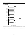
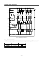
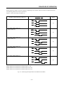
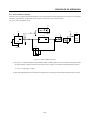
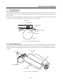
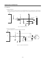
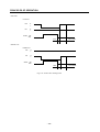
THERMAL PRINTER
TSP200 Series
TECHNICAL MANUAL
[SECOND EDITION]
NOTICE
• All rights reserved. Reproduction of any part of this manual in any form whatsoever,
without STAR’s express permission, is strictly forbidden.
• The contents of this manual are subject to change without notice.
• All efforts have been made to ensure the accuracy of the contents of this manual at the time
of printing. However, should any errors be found, STAR would greatly appreciate being
informed of them.
• The above notwithstanding, STAR can assume no responsibility for any errors in this
manual.
© Copyright 1997 Star Micronics Co., LTD.
INTRODUCTION
This manual describes the thermal printer TSP200 series.
It is designed for use as a reference for periodic inspections and maintenance procedures to be executed by
service personnel. It is not intended for the general user. Users of this manual should have a basic knowledge
and understanding of the English language.
• This manual is comprised of the following chapters.
Chapter 1 Specifications and Operation
Chapter 2 Theory of Operation
Chapter 3 Parts Replacement and Related Adjustments
Chapter 4 Maintenance and Lubrication
Chapter 5 Parts Lists
• First edition
: Mar. 1997
Second edition : Aug. 1999
■ Model Name
TSP 2
1
2
—
120
Voltage
24 : 24VDC
120 : 120VAC
230 : 230VAC
Mechanism type
2: 48 columns
Printer type
1: Standard
4: With auto-cutter
TSP200-series thermal printer
1
2
3
4
5
CHAPTER 1
SPECIFICATIONS AND OPERATION
1.
General Specifications.......................................................................................... 3
2.
External Appearance............................................................................................. 4
3.
DIP-Switch Settings .............................................................................................. 5
4.
Using the control panel to adjust the sensors, select the head rank, and set
the memory switches. ........................................................................................... 6
5.
Running a test print .............................................................................................. 8
6.
HEX dump mode.................................................................................................... 8
1
SPECIFICATIONS AND OPERATION
–2–
SPECIFICATIONS AND OPERATION
General Specifications
Printing method
Resolution
Printable width
Printing speeds
Printable characters
Bar codes
Character matrix
Interfaces
Dimensions
Weight
Power
Power consumption
Operating environment
Storage environment
300, 000 cuts
25.4mm (1 inch)
193mm
Automatic paper cutter
Life
Min. cut length
Line thermal direct
8 dots/mm (H) × 8 dots/mm (V)
72 mm
50 mm/sec (max.)
ANK, International
JAN, EAN, UPC, Code 39, ITF, Code 128, Code 93, NW-7
12 × 24 dots
RS-232C, Parallel
TSP212-120/230 : 158(W) × 234(D) × 193(H) mm
TSP242-120/230 : 158(W) × 234(D) × 193(H) mm
TSP212-24
: 158(W) × 239(D) × 193(H) mm
TSP242-24
: 158(W) × 239(D) × 193(H) mm
TSP212-120/230 : 2.8kg
TSP242-120-230 : 3.0kg
TSP212-24
: 1.8kg
TSP242-24
: 2.0kg
AC adapter
: 350g
AC cable
: 150g
AC120V, AC230V, DC24V
Max. 43 W Avg. 19W (During continuous printing of ASCII characters)
+5˚C ~ +40˚C
25% ~ 85% RH
–20˚C ~ +60˚C
10% ~ 90% RH
15
8m
m
193mm
1.
)
30
0/2
2
1
)
24
12
P2 212S
T
m( (TSP
4m
23 9mm
23
15
8m
m
(TSP212)
)
30
0/2
2
1
)
42 2-24
P2
TS SP24
(
m
(T
4m
23 9mm
23
(TSP242)
Fig. 1-1 External Dimensions
–3–
SPECIFICATIONS AND OPERATION
2.
External Appearance
Printer cover
Protects the printer from
dust and reduces noise.
Do not open the cover
while printing.
Control panel
Features two control
switches and two
indicators to indicate
printer status.
AC power cord
Plugs into an outlet of
the specified voltage.
Shape of AC power plug
will vary according to
destinations.
Interface connector
Connects the printer
with host computer.
[ TSP200-120/230 ]
Peripheral unit drive circuit connector
Connects to peripheral units such
as cash drawers, etc.
Do not connect this to a telephone.
AC adapter cable connector
For connection of the AC adapter.
Never unplug the AC adapter
while the printer is on.
[ TSP200-24 ]
Fig. 1-2 External Appearance
–4–
SPECIFICATIONS AND OPERATION
3.
DIP-Switch Settings
Be sure to turn the power to both the printer and host computer off before changing the setting of the DIP
switches.
Power off
DIP switch
1
ON
OFF
8
DIP switch 1
1
4
DIP switch 2
Fig.1-3 DIP switch array
DIP switch #1
The factory settings of DIP switch 1 are all on.
Switch
1-1
1-2
1-3
1-4
1-5
1-6
1-7
1-8
Baud Rate
2400BPS
4800BPS
9600BPS
19200BPS
Contents
Baud Rate
ON
Data Length
Parity Check
Parity Selection
Handshake
Operating Mode
Interface
8 bit
Disabled
Odd
DTR/DSR
Star
RS232C
1-1
OFF
ON
ON
OFF
OFF
7 bit
Enabled
Even
XON/XOFF
ESC/POS
Parallel
1-2
OFF
OFF
ON
ON
DIP Switch #2
Factory settings: 2-1 and 2-2 are on; 2-3 and 2-4 are off.
Switch
2-1
2-2
2-3
2-4
Contents
Print Density
ON
Serial I/F No. 6 Pin Reset Signal
Serial I/F No. 9 Pin Reset Signal
Print Density
Light
Standard
Somewhat Heavy
Heavy
2-1
OFF
ON
ON
OFF
Enabled
Enabled
2-2
OFF
ON
OFF
ON
–5–
OFF
Disabled
Disabled
SPECIFICATIONS AND OPERATION
4.
Using the control panel to adjust the sensors, select the head rank, and set the
memory switches.
Hold down the FEED and ONLINE switches while setting power on, then continue to hold the switches down for the time
necessary to enter the required mode, as indicated below.
Start
Buzzer beeps 1 time.
Press both
switches.
Continue to
hold down.
Release within 2 seconds.
Enters "Adjust Paper-Out Sensor" mode.
Buzzer beeps twice.
Release within 2 seconds.
Both switches
Continue to
hold down.
Enters "Adjust Paper-Near-End Sensor"
mode.
Buzzer beeps 3 times.
Release within 2 seconds.
Both switches
Enters "Set Head Rank" mode.
Continue to
hold down.
Buzzer beeps 4 times.
Release within 2 seconds.
Both switches.
Enters "Set Memory Switches" mode.
Continue to
hold down.
Buzzer beeps 5 times.
Release within 2 seconds.
Both switches
Continue to
hold down.
Resets, then executes test print.
–6–
SPECIFICATIONS AND OPERATION
(1) “Adjust Paper-Out Sensor” mode.
Adjustment is not necessary if the ONLINE lamp is ON when you enter this mode. If the lamp is OFF, the turn VR1
clockwise until it the lamp comes ON.
To exit this mode, press ONLINE. To move back to the start of the sequence, press both ONLINE and FEED at the same
time.
Please be sure that paper is inserted before entering this mode.
(2) “Adjust Paper-Near-End Sensor” mode
When you enter this mode, the POWER lamp will be lit if the near-end sensor is detecting paper. The lamp will be off
if no paper is detected.
To exit the mode, press ONLINE. To move back to the start of the sequence, press both ONLINE and FEED at the same
time.
(3) “Set Head Rank” mode
When you enter the mode, the ONLINE and POWER lamps will both be OFF. Press the FEED switch as necessary to
select the desired rank. The rank is indicated by the ONLINE and POWER lamp pattern, which changes each time you
press the switch. The change sequence is indicated below. (Note that you can move back to the start of the sequence by
pressing the ONLINE and FEED switches at the same time.)
ONLINE lamp
OFF
OFF
ON
ON
(4)
FEED lamp
OFF
ON
OFF
ON
Head Rank
A
B
C
C
“Set Memory Switches” mode
1 When you first enter this mode, memory switch 0 is selected. You can change the selection by pressing FEED
as many times as necessary. Specifically, the selection cycle is 0 -> 1 -> 2 -> 3 -> 4 -> 0 -> 1 ->... In other words,
press 0 times to select Switch 0, 1 time to select Switch 1, and so on.
2 Press ONLINE once to confirm your selection. The buzzer beeps one time in response.
3 Set a value for each bit in turn, starting from Bit F and proceeding sequentially to Bit 0. Note that the lamps
indicate each bit’s current value: ONLINE lamp ON means that the current value is “1”, while POWER lamp
ON means that the current value is “1”.
To set to 0: Press FEED. (The buzzer will beep once.)
To set to 1: Press ONLINE. (The buzzer will beep once.)
When you complete setting of Bit 0, the buzzer will beep again.
4 When you have set all bit values and are ready to enter the new value, press the ONLINE switch. The buzzer
beeps once and the value is written to memory.
If you wish to cancel your changes, press the FEED switch instead. The buzzer will beep twice and the process
will return to the beginning of Step (3) above.
5 Press the ONLINE and FEED switches at the same time to move back to the start of the sequence.
–7–
SPECIFICATIONS AND OPERATION
5.
Running a test print
To generate a test print, hold down the FEED switch while setting the power on.
6.
HEX dump mode
To enter HEX dump mode, hold down the ONLINE switch while setting the power on, and then release the switch after
the buzzer beeps once.
When this mode is active, all data sent from the host will be printed in HEX form.
–8–
CHAPTER 2
PRINCIPLES OF OPERATION
This chapter describes the operating principles of the circuitry and printer mechanism.
1.
Block Diagram ..................................................................................................... 11
2.
Interface ............................................................................................................... 13
2-1.
Interface Types ..................................................................................................... 13
2-1-1. RS232 interface ................................................................................................ 13
2-1-2. Parallel interface ............................................................................................... 14
2-2.
Data Arrangement and Printing ........................................................................... 15
2-2-1. Arrangement ..................................................................................................... 15
2-2-2. Thermal printhead ............................................................................................ 15
2-2-3. Head current control ........................................................................................ 16
2-2-4. Head current control ........................................................................................ 18
2-2-5. Head burnout protection ................................................................................. 18
3.
2-3.
Feed-Motor Drive Circuit ...................................................................................... 19
2-4.
Power-On Reset Circuit ....................................................................................... 21
2-5.
+5V Line Voltage Detector Circuit ....................................................................... 22
Printer Mechanism .............................................................................................. 23
3-1.
Thermal Printhead ................................................................................................ 23
3-2.
Paper-Feed Mechanism ....................................................................................... 23
3-3.
Detectors ............................................................................................................... 24
3-4.
Auto-Cutter Drive circuit (on TSP242-24/120/230 only) .................................... 25
2
PRINCIPLES OF OPERATION
– 10 –
PRINCIPLES OF OPERATION
1.
Block Diagram
The following diagram illustrates the relation between the main logic board and its peripherals.
Main Logic Board
Host computer
Parallel I/F
Dipswitch
Lamp
EEPROM
Printer mechanism
Head driver
Thermal
head
PSRAM
128K × 8 bits
Motor driver
Paper-feed
motor
Kanji ROM
512K × 8 bits
Cutter driver
Auto-cutter
Sensor circuit
Sensor
Gate array
EPROM
256K × 8 bits
Peripheral unit
driver
CPU
Host computer
RS232C I/F
5V
Switch
24V
Power supply unit
Fig. 2-1 Block Diagram
– 11 –
Peripheral unit
PRINCIPLES OF OPERATION
(1) Main Logic Board
The main logic board’s CPU passes data transmitted from the host computer into the local RAM. It then reads the data
from the RAM, arranges it in accordance with the ROM program, and prints the results by issuing appropriate drive signals
to the printer mechanism.
[Block Descriptions]
a. CPU: HD6413002F16
CMOS single-chip computer.
Controls overall printer operation.
b. EPROM: 256K × 8 bits
Stores the CPU control program.
c. PSRAM: 128K × 8 bits
Work area and data buffer.
d. EEPROM: 1024 bits
Stores printer settings. Settings can be changed by software. (Used in place of dip switches.)
e. Interface
Interfaces the main board with the host computer.
Two versions available: RS232C and Centronics.
f. Gate array
Handles signal input, output, and conversions.
g. Drivers
The various drivers convert signals received from the CPU and gate array into drive signals that directly control
the printer mechanism.
(2)
Printer Mechanism
Comprised of thermal head, platen, paper-feed motor, auto-cutter, and sensor mechanism.
(3)
Power Supply Unit
Converts primary power to DC5V, DC24V.
(4)
Peripheral Unit
External device (such as cash drawer) driven by signals issued from the main logic board.
– 12 –
PRINCIPLES OF OPERATION
2.
Interface
2-1. Interface Types
2-1-1. RS232 interface
CN6
IC10
IC1 CPU
RXD
RXD 0
TXD
TXD 0
DSR
P93
DTR
P91
ADM232LJR
RTS
TTL
232C
FAULT
TTL
232C
INIT
P94
Comparator
Dipswitch 2-3
Comparator
Dipswitch 2-4
Fig. 2-2 Serial Interface
Data flow from host to printer: IC10 receives serial data from the host through RXD, converts the voltage level from
RS232C to TTL, and passes the result to the CPU. The CPU converts the serial data to
parallel form and stores the result into buffer memory.
Data flow from printer to host: The CPU generates the data, converts it into serial form, then passes it to IC10. IC10
converts the level from TTL to RS232C and outputs the result over the TXD line.
– 13 –
PRINCIPLES OF OPERATION
2-1-2. Parallel interface
CN4
IC4
IC1
DATA 1
CD0
DATA 2
CD1
DARA 3
CD2
DATA 4
CD3
DATA 5
CD4
DARA 6
CD5
DATA 7
CD6
DATA 8
CD7
STROBE
CSTB
IC5
BUSY
BUSY
ACK
ACK
CPU
ERROR
ERROR
SELECT
SELECT
PAPER OUT
POUT
Gate array
LS05
Fig. 2-3 Parallel interface
When the printer is ready (BUSY is LOW), the host computer transmits eight bits of parallel data (DATA1,...,DATA8)
to CN4. The data passes through the gate array and moves into the CPU.
Printer signals from the CPU (ACK, ERROR, SELECT, PAPER OUT, etc.) pass through the gate array and are output
over the appropriate connector pins.
– 14 –
PRINCIPLES OF OPERATION
2-2. Data Arrangement and Printing
2-2-1. Arrangement
The CPU reads data sequentially from RAM and arranges this data in accordance with program instructions stored in
EPROM. The arranged data is then converted from parallel to serial form. The gate array then outputs the resulting serial
data to the drive controller in the thermal printhead.
2-2-2. Thermal printhead
The thermal printhead has 576 heat elements. Printing is executed by switching these elements ON and OFF as required.
The printhead contains a built-in dedicated drive controller. The controller consists of shift register, latch circuit, and
driver circuit, as illustrated below. The controller receives serial data (SI) from the gate array in sync with the CLK signal.
It latches this incoming data (by LATCH signal), then outputs the data to the elements in sync with the falling edge of
the STROBE signal. A data value of LOW corresponds to an element value of ON (generating print).
R576
R1
VH
DATE IN
(SI)
1
2
3
4
5
6
7
B. E. O
LATCH
CLOCK
STROBE4
STROBE3
STROBE2
STROBE1
Fig. 2-4 Drive Circuitry of Thermal Printhead
– 15 –
8
9
SO
PRINCIPLES OF OPERATION
DO1
DO2
DO3
DO62
DO63
DO64
GNDH
VDD
BUFFER
GNDL
VDD
CHECKER
VDD
STB
BEO
Q
L
Q
D
L
Q
D
L
LATCH
Q
L
D
Q
D
L
Q
D
L
D
LAT
CTL
D Q
SI
C
D Q
C
D Q
C
SHIFT
REGISTER
D Q
D Q
D Q
C
C
C
SO
CLK
Fig. 2-5 Block Diagram of Drive IC
2-2-3. Head current control
Although the thermal printhead has four different STROBE lines, in fact it uses only three strobe signals to control its 576
elements. Specifically, each signal drives 192 of these elements. The signal/element arrangement is shown below.
Thermal Printhead
STROBE1
STROBE2
STROBE3
STROBE4
Elements
1 – 192
193 – 256
257 – 384
385 – 576
Strobe Signal
STB1
STB2
STB3
– 16 –
PRINCIPLES OF OPERATION
Strobe signals are output in one of five patterns, depending on the number of dot lines that are simultaneously ON.
The following table shows each of the patterns.
Figure 2-7 shows the timing for Pattern (5).
Strobe Signal Output
STB1 STB2 STB3
Number of ON Elements per Dot Line
Pattern
0 STB1+STB2+STB3 384
STB1
STB2
1
STB3
193 STB1+STB2+STB3 384
STB1+STB2 192
STB1
STB2
2
STB3
193 STB1+STB2+STB3 384
STB1+STB3 192
STB1
STB2
3
STB3
193 STB1+STB2+STB3 384
STB2+STB3 192
STB1
STB2
4
STB3
385 STB1+STB2+STB3 576
STB1
STB2
STB3
STB1: Number of ON elements in element range 1 to 192.
STB2: Number of ON elements in element range 193 to 384.
STB3: Number of ON elements in element range 385 to 576.
Fig. 2-6 Strobe Signal Output Patterns for Different Print Rates
– 17 –
5
PRINCIPLES OF OPERATION
CLOCK
SI
LATCH
24V
COMMON
STB1
STB2
STB3
Fig. 2-7 Timing Chart
2-2-4. Head current control
Heat buildup in the thermal printhead can cause print quality to degrade. To maintain uniform quality, the printer varies
the energizing time (time that STROBE remains LOW) in accordance with the head temperature.
The print head’s surface temperature is calculated based on the resistance value of the attached thermistor, and energizing
time is controlled accordingly.
2-2-5. Head burnout protection
Misoperation of the CPU may cause head current to remain on too long, resulting in burn damage to the elements unless
current is shut off by other means. The printer therefore includes a burnout protection circuit that automatically forces
current off at some fixed time tw following current startup. Control is implemented through the head’s BEO terminal,
which is active on HIGH; setting the terminal LOW forces current off regardless of the STROBE state.
CEXT
REXT
+5V
CN6
IC1
CPU
HD ON
B
Q
BEO
IC6
tw=(CEXT) (REXT)
Fig. 2-8 Head Burnout Protection Circuit
– 18 –
PRINCIPLES OF OPERATION
STB1
STB2
STB3
HD ON
(B)
Trigger
Retrigger
Retrigger
BEO
(Q)
tw
Fig. 2-9 Timing Chart
2-3. Feed-Motor Drive Circuit
The printer uses a 4-phase step motor (phase 1-2 excitation) to implement paper feed. The motor rotates through a certain
angle each time it receives a pulse from the drive circuit. The following diagram illustrates the excitation method. Figure
2-11 shows the feed-motor drive circuit.
ON
1
ON
ON
2
ON
3
ON
4
Step
1
2
3
4
5
6
7
8
Forward Feed
Reverse Feed
Fig. 2-10 Motor Control by Phase 1-2 Excitation
IC1
CPU
+24V
DT9
TR5
PB4
CN7
1
2
TA1
TP8
TP9
TP10
TP11
6
1
3
2
5
3
4
4
M-GND
Fig. 2-11 Feed-Motor Drive Circuit
– 19 –
PRINCIPLES OF OPERATION
The feed-motor pulse width varies according to the strobe output pattern (where the output pattern is determined by the
print rate, as described above). The following diagram shows the pulse width for each pattern.
Pattern 1
STB1
STB2
STB3
LF COMMON
T1
T1
T1
Pattern 2
STB1
STB2
STB3
LF COMMON
T2
T2
T2
Pattern 5
STB1
STB2
STB3
LF COMMON
T3
T3
Fig. 2-12 Pulse Width by Pattern
– 20 –
T3
PRINCIPLES OF OPERATION
2-4. Power-On Reset Circuit
The power-on reset signal initializes all elements so as to protect against possible operating errors at power-on. The signal
is held for approximately 160ms when power comes on. The reset circuit is shown below.
Fig. 2-13 Power-On Reset Circuit
+5V
+5V
+5V
IC4
Drive circuit
+5V
IC3
IC1 : CPU
VCC
+5V
RESET
CPU
CD
RES
OUT
RESO
+
C9
Gate
array
GND
D1
RESET IC
Fig. 2-13 Power-On Reset Circuit
1 At power-on, voltage detector IC3 (M51953BL) outputs a LOW signal from its OUT terminal. The signal is held
for approximately 160ms by the action of capacitor C9 (0.47µF), in accordance with the following relation:
T = 0.34 × C9 (pF) [µs] = 160ms
2 The LOW signal generates reset of the CPU and gate array, and stops operation of the mechanism drive circuitry.
– 21 –
PRINCIPLES OF OPERATION
2-5. +5V Line Voltage Detector Circuit
The voltage-detection IC (IC3 in Fig. 2-13) detects momentary drops or unstable levels in the +5V line voltage. The
following shows an IC3-equivalent circuit.
VCC
1
SµA typ
R1
5
–
OUT
–
+
R2
1.25V
3
GND
4
Cd
Fig. 2-14 Equivalent Circuit, Voltage Detection IC
Figure 2-15 shows the IC’s operational timing. The IC asserts a reset signal at its output terminal when the -5V line voltage
falls below 4.25V, thereby resetting the CPU and the gate array.
VCC Voltage
4.25V
0.8V
t
Output
Voltage
td
td
t
td = 0.34 × Cd (pF) [µs]
Fig. 2-15 Operation Timing Chart
– 22 –
PRINCIPLES OF OPERATION
3.
Printer Mechanism
3-1. Thermal Printhead
The TSP400 printers utilize thermal line printing. The thermal printhead consists of a horizontal line of 576 heat elements.
These elements print one line of dots at a time as the paper passes over the head. The printhead is fixed in position; only
the paper moves.
The printer prints a dot by heating the corresponding heat element. The heated element generates a chemical reaction in
the coloring layer of the thermal paper, resulting in the formation of a visible dot.
Thermal head
Heat element
Coloring layer
Thermal paper
Printed point
Platen
Fig. 2-16 Principle of Thermal Printing
3-2. Paper-Feed Mechanism
The paper-feed mechanism is comprised of paper-feed motor, gear train, platen, and thermal printhead. The paper-feed
motor drives the gear train, which in turn rotates the platen. The platen carries the thermal paper past the printhead.
The paper-feed motor is a PM (permanent magnet) type, 4-phase 48-pole step motor. 3 steps feed the paper approximately
0.125mm.
Thermal paper
Gear train
Platen
Paper-feed motor
Thermal head
Fig. 2-17 Paper-Feed Machanism
– 23 –
PRINCIPLES OF OPERATION
3-3. Detectors
1 Paper-Out Detector
The paper-out detector (reflective photosensor) is located at the paper entry slit. The photosensor’s phototransistor
remains ON while paper is present. It goes OFF when paper runs out, generating output of a paper-out signal.
IC1
CPU
CN2
+5V
+5V
Paper
4
–
P45
Photosensor
+
+5V
5
3
Fig. 2-18 Paper-Out Detector
2 Paper-Near-End Detector
The near-end detector is mounted in the paper-roll holder.
CN3
IC1
CPU
2
+5V
+5V
Paper-roll
P47
1
3
Fig. 2-19 Paper-Near-End Detector
– 24 –
PRINCIPLES OF OPERATION
3 Head-Up Detector
This detector senses the position of the thermal printhead. The leaf switch closes when the printhead is in contact
with the platen, and opens when the printhead is separated from the platen.
IC1
CPU
+5V
CN7
Leaf Switch
2
P44
1
Fig. 2-20 Head-Up Detector
4 Cover-Open Detector
This detector senses whether the upper cover is open or closed. The leaf switch closes when the cover closes,
and opens when the cover opens.
IC1
CPU
+5V
CN1
Leaf Switch
1
P46
2
Fig. 2-21 Cover-Open Detector
3-4. Auto-Cutter Drive circuit (on TSP242-24/120/230 only)
The TSP242 includes a guillotine-type cutter. The motor rotation direction determines whether the cutter executes a full
cut or a partial cut. (The partial cut leaves paper attached at one point.)
Note that Memory Switch 2 Bit 8 must be set ON to enable use of the cutter.
VCC
IC3
VCC
OUT
CN9
2
P42
Switch
3
VM
VM VM
6
2
8
4
P40
P41
B
B
B
B
10
E
C
C
C
C
E
1
M-GND
IC1
CPU
Fig. 2-22 Auto-Cutter Drive Circuit
– 25 –
GND GND
TA2
TH3C10
4
7
3
9
5
5
Motor
M
PRINCIPLES OF OPERATION
<Full Cut>
< Full Cut >
P40
H
L
P41
H
L
Switch
ON
OFF
40ms
100ms Brake
<Partial Cut>
< Partial Cut >
P40
H
L
P41
H
L
Switch
ON
OFF
40ms
Fig. 2-23 Auto-Cutter Timing Chart
– 26 –
100ms Brake
CHAPTER 3
PART REPLACEMENT AND RELATED ADJUSTMENT
This chapter presents printer disassembly and reassembly procedures. Please note the following important
points.
1. Always disconnect the power cord from the AC outlet before beginning work.
2. Except where otherwise indicated, the reassembly procedure is the reverse of the disassembly
procedure.
3. Coat screw heads with locking sealant after completing of reassembly.
4. Refer to Chapter 4 Section 2 for information about lubrication. (Chapter 3 does not include any
lubrication information.)
Note : This printer has no adjustment sites.
1.
Upper Case Unit ..................................................................................................29
2.
Auto-Cutter Unit ..................................................................................................29
3.
Printer Mechanism ..............................................................................................30
4.
Near-End-Sensor Unit .........................................................................................30
5.
Power Unit............................................................................................................31
6.
Main Logic Board ................................................................................................32
7.
Fuses ....................................................................................................................32
8.
Thermal-head Unit ...............................................................................................33
3
PARTS REPLACEMENT
– 28 –
PARTS REPLACEMENT
1
1.
Upper Case Unit
(1)
Switch off the power, and unplug the power cord
from the power outlet.
Remove:
• Cover 1
• Four tapping screws 2
• Upper case unit 3
Remove the upper case unit by lifting it up and
off.
(2)
2
3
2.
1
5
2
4
6
1
Auto-Cutter Unit
<Model TSP242-24/120/230 only>
(1) Remove:
• Upper case unit (See 1. above.)
• Two tapping screws 1
• Wire band 2
• Cutter Holder Plates R,L 3, 4
• Cutter Unit 5
• Connector 6
3
– 29 –
PARTS REPLACEMENT
5
3.
4
7
3
2
1
6
1
<TSP212-24/120/230>
(1) Remove the upper case unit (see 1. above), then
proceed to (2) below.
<TSP242-24/120/230>
(1) Remove the auto-cutter unit. (See 2. above.)
(2) Remove:
• Two screws 1
• Sub-chassis 2
• Guide 3
• Two tapping screws 4
• Three tapping screws 5
• Flat cable 6
• Connector
• Printer mechanism 7
4.
Near-End-Sensor Unit
(1)
(2)
Remove the upper case unit. (See 1. above.)
Remove:
• Two screws 1
• Mechanism sub-chassis 2
• One tapping screw 3
• Connectors 4
• Near-end-sensor unit 5
2
3
Printer Mechanism
5
4
– 30 –
PARTS REPLACEMENT
5
5.
Power Unit (TSP200-120/230)
(1)
(2)
(3)
Remove the upper case unit. (See 1. above.)
Remove the connector cover 1.
Remove the main chassis unit 5 from the lower
casing unit 2.
Remove:
• Two screws 3
• Cord bushing 4
• Connector
• Power unit 6 from main chassis 5
(4)
6
4
3
1
2
Power Unit (TSP200-24)
5
(1)
(2)
(3)
(4)
6
3
4
3
1
2
– 31 –
Remove the upper case unit. (See 1. above.)
Remove the connector cover 1.
Remove the main chassis unit 5 from the lower
casing unit 2.
Remove:
• Three screws 3
• Connector 4
• Power unit 6 from main chassis 5
PARTS REPLACEMENT
3
6.
Main Logic Board
(1)
(2)
(3)
Remove the upper case unit. (See 1. above.)
Remove the connector cover 1.
Remove the main chassis unit 3 from the lower
casing unit 2.
Remove:
• Two tapping screws 4
• Board chassis unit 5
• Two tapping screws 6
• Two screws 7
• Connector
• Main logic board 8
(4)
6
7 6
4
7
8
4
5
1
2
7.
Fuses (TSP200-120/230)
(1)
Remove the main chassis unit from the lower casing
unit. (See 5. above.)
Check the fuses in the power unit.
• Fuse F1 1
• Fuse F2 2
If fuse is blown, replace it with the fuse type
indicated below.
(2)
1
Destination
F1
U.S.A.
5TT1A
EC
EAWK630mA
United Kingdom EAWK630mA
2
F2
5TT3A
EAK3.15A
5TT3A
If the replacement fuse also blows out, replace the
power unit or check the main logic board.
– 32 –
PARTS REPLACEMENT
Fuses (TSP200-24)
(1)
1
(2)
Remove the main chassis unit from the lower casing
unit. (See 5. above.)
Check the fuses in the power unit.
• Fuse F1 1
If fuse is blown, replace it with the fuse type
indicated below.
F1
5TT3A
If the replacement fuse also blows out, replace the
power unit or check the main logic board.
9
7
6
8
6
8.
Thermal-head Unit
(1)
(2)
Remove the printer mechanism. (See 3. above.)
Be sure that the unit is in head-down state (that the
head-lift lever 1 is back).
Press the two head-opening levers 2 and remove the
set cover 3 from the printer mechanism.
Remove:
• Three stop rings 4
• Stay 5
• Three springs 6
• Two screws 7
• Head plate 8
• Thermal head 9
Attach the replacement thermal head. as follows.
(a)Be sure that the unit is in head-open state.
(b)Hold the replacement head in position, and screw
the right end loosely into place with the one of the
screws 7.
(c)Set the unit into head-closed state.
(d)Fit the remaining screw 7 into the left side, and
tighten both of the screws to a torque of 5g-cm.
Caution:
Keep hands clear of the head’s heat elements when
making the replacement.
(3)
6
(4)
4
3
4
7
5
2
(5)
4
2
1
(6)
– 33 –
CHAPTER 4
MAINTENANCE AND LUBRICATION
1.
2.
Maintenance......................................................................................................... 35
1-1.
Cleaning................................................................................................................. 35
1-2.
Checks ................................................................................................................... 35
Lubrication ........................................................................................................... 36
2-1.
Lubricants ............................................................................................................. 36
2-2.
Application Method .............................................................................................. 36
2-3.
Lubrication Points ................................................................................................ 36
4
MAINTENANCE AND LUBRICATION
1.
Maintenance
Proper maintenance is necessary to maintain printer performance and forestall potential problems. Please carry out
maintenance as described below.
1-1. Cleaning
(1)
Surface dirt
Clear away dirt with a soft cloth. If necessary, apply a small quantity of alcohol to the cloth to improve cleaning
power. NEVER use thinner, trichlene, or ketone solvents, as these can cause damage to plastic components.
When cleaning, take care to avoid damaging or moistening of electronic parts, mechanical parts, and wires.
(2)
Internal dust
For best results, use an electric vacuum cleaning device to remove dust from the inside of the printer. Note that such
cleaning may also remove lubrication; when you have finished cleaning, check lubrication levels and apply
lubricant as necessary.
1-2. Checks
There are two types of maintenance checks. Simple “daily checks” can be performed by users during the course of daily
operation. “Periodic checks” must be carried out by qualified service personnel.
(1) Daily checks
• Check whether dirt or other foreign matter has worked its way into the printer, and remove as necessary.
• Check the thermal head for excessive dirt. If the head is very dirty, clean it with a cotton stick or a soft cloth soaked
in alcohol.
(2) Periodic checks
Periodic checks and lubrication should be carried out once every six months or once every million lines of printing.
• Check the integrity of springs.
• Clear dust from areas around the detectors.
– 35 –
MAINTENANCE AND LUBRICATION
2.
Lubrication
Proper lubrication is essential for maintaining the printer’s performance level and preventing breakdowns or other
problems.
2-1. Lubricants
Choice of lubrication can significantly affect the printer’s performance, longevity, and low-temperature characteristics.
We recommend the following lubricant for this printer.
Type
Name
Manufacturer
Grease
Molykote EM
Dow Corning
2-2. Application Method
If you are lubricating parts during disassembly or reassembly, be sure to wash or wipe the parts thoroughly to remove all
dirt and dust prior to lubricating.
Remember that cleaning can remove necessary lubrication. Always lubricate after cleaning, disassembly, or replacement.
2-3. Lubrication Points
Apply lubricants at the following locations.
Lubrication points
– 36 –
CHAPTER 5
PARTS LIST
HOW TO USE PARTS LIST
(1)
(2)
(3)
(4)
(5)
(6)
(7)
1.
2.
3.
4.
5.
DRWG. NO.
This column shows the drawing number of the illustration.
REVISED EDITION MARK
This column shows a revision number.
Parts that have been added in the revised edition are indicated with “#”.
Parts that have been abolished in the revised edition are indicated with “*”.
#1:First edition → Second edition
*1:First edition → Second edition
PARTS NO.
Parts numbers must be notified when ordering replacement parts. Parts described as “NPN” have no parts number and are not
in stock, i.e., unavailable.
PARTS NAME
Parts names must be notified when ordering replacement parts.
Q’TY
This column shows the number of the part used as indicated in the figure.
REMARKS
Where differences in specifications exist depending on location/destination.
RANK
Parts marked “S” are service parts. Service parts are recommended to be in stock for maintenance.
Printer Assembly ................................. 38
6.
Power Supple Unit (120VAC/230VAC) .... 61
1-1.
Disassembly Drawing..................... 38
6-1.
Circuit Diagram ............................... 61
1-2.
Parts List ......................................... 41
6-2.
Parts List ......................................... 62
Printer Mechanism .............................. 43
7.
Power Supple Unit (24VDC) ................... 63
2-1.
Disassembly Drawing..................... 43
7-1.
Circuit Diagram ............................... 63
2-2.
Parts List ......................................... 45
7-2.
Component Layout ......................... 63
Cutter Unit ............................................ 46
7-3.
Parts List ......................................... 63
8.
Paper Near-End Sensor ...................... 64
3-1.
TSP200-120/230 .............................. 46
3-2.
TSP200-24 ....................................... 47
8-1.
Circuit Diagram ............................... 64
Wiring Scheme of Printer ................... 48
8-2.
Parts List ......................................... 64
4-1.
TSP212/242 ...................................... 48
4-2.
TSP212-24/242-24 ........................... 49
Main Logic Board ................................ 50
5-1.
Circuit Diagram ............................... 50
5-2.
Component Layout ......................... 56
5-3.
Parts List ......................................... 57
5
1.
Printer Assembly
1-1. Disassembly Drawing
1-1-1. TSP212-120/230
25
24
22
17
18
12
13
D
A
11
7
26
E
10
9
35
D
8
31
33
G
F
20
23
C
6
3
29
28
B
C
A
F
G
E
2
32
27
21
5
27
19
B
34
4
1
– 38 –
1-1-2. TSP242-120/230
25
18
17
24
22
13
12
11
A
10
9
D
30
E
26
33
G
20
20
16
7
8
30
14
H
23
F
D
15
29
C
H
B
6
28
C
A
F
G
E
3
2
32
27
21
5
27
19
B
34
4
1
– 39 –
37
1-1-3. TSP242-24
34
25
33
25
25
18
25
17
36
22
24
36
22
13
11
A
E
9
12
D
30 16
10
23
26
14
27
26
G
20
20
7
8
H
30
15
F
D
20
6
C
29
3
H
B
B
C
F
A GE
32
27
21
26
2
26
5
28
27
19
4
1
– 40 –
1-2. Parts List
1-2-1. TSP200-120/230
Printer Assembly(TSP200-120/230)
DRWG.NO.
1
2
3
4
5
6
7
8
9
10
11
12
13
14
15
16
17
18
19
20
21
22
23
24
25
26
27
28
29
30
31
32
33
34
35
-
REV. PARTS NO.
37300011
37309010
37309030
37309040
*1
32010011
#1
32010012
32010030
37437010
37437110
30722000
32010050
37432200
32043500
33020500
37437400
33900060
38420000
38420100
37432000
32043210
32043220
33020022
33020060
37431000
83911720
04991204
04991204
04991220
00926603
00926803
01902618
01903058
01903059
*1
01903064
#1
01903101
01903026
01903069
01903077
00930603
01903033
*1
01903077
#1
01903101
01914003
32970010
04991204
09990723
30970030
PARTS NAME
LOWER CASE UNIT
SP2
POWER SUPPLY UNIT
SP2-120 US
POWER SUPPLY UNIT
SP2-230 EC
POWER SUPPLY UNIT
SP2-240 UK
MAIN CHASSIS
SP2
MAIN CHASSIS
SP2
BOARD CHASSIS P
SP2
TBD212-24 UNIT
TSP2
TBD242-24 UNIT
TSP2
FLAT CABLE 24X105
TSP2
SUB-CHASSIS
TSP2
COVER OPEN SWITCH UNIT
TSP2
DETECTOR HOLDER PLATE
TSP2
NEAR-END DETECTOR COVER TSP2
DETECTOR BOARD ASSY
TSP2
ASSIST GUIDE
TSP2
TMP212A-24
TMP212B-24
CUTTER 4022-24V UNIT
TSP2
CUTTER HOLDER PLATE R
TSP2
CUTTER HOLDER PLATE L
TSP2
COVER
SP2
COVER
TSP2
UPPER CASE UNIT
TSP2
CONNECTOR COVER
SP312
FASTENER T18S
FASTENER T18S
CORD BUSHING SR-5N-4
SCREW TAT 2.6-6 CT
SCREW TAT 2.6-8 PT
SCREW TAT 2.6-4
SCREW TAT 3-10 PT
SCREW TR 3-5 FL
SCREW TAT 3-5 CT
SCREW TAT 3-6 CT-FL
SCREW TR 3-5 WB
SCREW TAT 3-5 ST-FL
SCREW TAT 3-5 CT-FL
SCREW TAT 3-6 PT
SCREW TR 3-12
SCREW TAT 3-5 CT-FL
SCREW TAT 3-6 CT-FL
SCREW TR 4-10 WS/WF
TEAR BAR
SP2
FASTENER T18S
FERRITE CORE TFC-23-11-14
THERMAL ROLL PAPER 76X35D
– 41 –
Q’TY
1
1
1
1
1
1
1
1
1
1
1
1
1
1
1
1
1
1
1
1
1
1
1
1
1
1
2
1
2
1
3
4
2
2
2
1
2
2
2
2
1
1
2
1
1
1
1
REMARKS
FOR US
FOR EC
FOR UK
TSP212
TSP242
RANK
S
S
S
S
S
S
S
S
S
TSP212
TSP242
TSP242
TSP242
TSP242
TSP212
TSP242
S
S
S
TSP212
TSP242
S
S
S
S
S
S
S
S
S
S
S
S
S
S
S
S
S
S
TSP242
TSP212
TSP212
FOR EC,UK :ACCESSARY
FOR EC,UK :ACCESSARY
:ACCESSARY
S
S
S
1-2-2. TSP200-24
Printer Assembly(TSP200-24)
DRWG.NO.
1
2
3
4
5
6
7
8
9
10
11
12
13
14
15
16
17
18
19
20
21
22
23
24
25
26
27
28
29
30
31
32
33
34
35
36
37
-
REV. PARTS NO.
37300011
37439000
32010130
32010030
37437010
37437110
30722000
32010050
37432200
32043500
33020500
37437400
33900070
38420400
38420300
37432010
32043210
32043220
33020170
33020091
37431050
83911720
04991204
30781130
30781140
30781150
30781160
00926603
00926803
01902618
01903058
01903059
01903101
09990713
01903069
01903077
00930603
01903033
01903055
37430300
32970010
33900080
33910150
30970040
09990723
PARTS NAME
LOWER CASE UNIT
SP2
POWER SUPPLY UNIT
TSP2-24
MAIN CHASSIS
TSP2-24
BOARD CHASSIS P
SP2
TBD212-24 UNIT
TSP2
TBD242-24 UNIT
TSP2
FLAT CABLE 24X105
TSP2
SUB-CHASSIS
TSP2
COVER OPEN SWITCH UNIT
TSP2
DETECTOR HOLDER PLATE
TSP2
NEAR-END DETECTOR COVER TSP2
DETECTOR BOARD ASSY
TSP2
ASSIST GUIDE A
TSP2
TMP212E-24
TMP212D-24
CUTTER ACS230 UNIT
TSP2
CUTTER HOLDER PLATE R
TSP2
CUTTER HOLDER PLATE L
TSP2
Q’TY
1
1
1
1
1
1
1
1
1
1
1
1
1
1
1
1
1
1
COVER B
TSP2
COVER A
TSP2
UPPER CASE UNIT
TSP2-24
CONNECTOR COVER
SP312
FASTENER T18S
ADAPTER SET PS48 US
ADAPTER SET PS48 EC
ADAPTER SET PS48 UK
ADAPTER SET PS48 AS
SCREW TAT 2.6-6 CT
SCREW TAT 2.6-8 PT
SCREW TAT 2.6-4
SCREW TAT 3-10 PT
SCREW TR 3-5 FL
SCREW TAT 3-6 CT-FL
FERRITE CORE TFC-16-8-16
SCREW TAT 3-5 ST-FL
SCREW TAT 3-5 CT-FL
SCREW TAT 3-6 PT
SCREW TR 3-12
SCREW TR 3-8 WS/WF
HOLDER LEVER UNIT
TSP2
TEAR BAR
SP2
ASSIST SPACER
TSP2
HOLDER
SP24
THERMAL ROLL PAPER 80X35D
FERRITE CORE TFC-23-11-14
1
1
1
1
3
1
1
1
1
2
1
3
4
5
3
1
2
2
2
2
1
1
1
2
2
1
1
– 42 –
REMARKS
TSP212-24
TSP242-24
RANK
S
S
S
S
S
S
S
TSP212-24
TSP242-24
TSP242-24
TSP242-24
TSP242-24
S
S
S
TSP212-24
TSP242-24
S
S
S
FOR
FOR
FOR
FOR
US
EC
UK
AS
TSP242-24
TSP212-24
TSP212-24
ACCESSARY
ACCESSARY
S
S
S
S
S
S
S
S
S
S
S
S
S
S
S
S
S
2.
Printer Mechanism
2-1. Disassembly Drawing
2-1-1. TSP212
9
3
4
15
24
22
5
13
11
3
19
28
18
2
26
12
26
1
13
14
11
30
10
24 16
21
25
17
6
27
29
20
29
29
23
7
23
27
8
23
– 43 –
28
2-1-2. TSP242
9
3
4
15
24
22
5
13
11
3
19
28
18
2
26
26
1
13
14
11
30
10
24 16
21
25
17
6
27
29
20
29
29
23
7
23
27
8
23
– 44 –
28
2-2. Parts List
Printer Mechanism
DRWG.NO.
1
2
3
4
5
6
7
8
9
10
11
12
13
14
15
16
17
18
19
20
21
22
23
24
25
26
27
28
29
30
REV. PARTS NO.
37440400
33910070
33900050
33210020
30365020
37447000
32025030
31360000
30375010
33490020
04310403
33910080
32490020
33020300
33101510
33990000
30905021
30905030
33102230
33102220
32042030
37442400
04020002
04020010
04020004
01901709
00820304
00626404
30510300
30520040
82500860
PARTS NAME
FRAME ASSY
PAPER GUIDE A
SUB-GUIDE
HOLDER ROLLER
HOLDER ROLLER SHAFT
DETECTOR UNIT
SET COVER
STAY
PLATEN
HEAD-UP LEVER
OILESS BUSHING F4X6X5
PAPER GUIDE B
HEAD OPEN LEVER
MOTOR COVER
PLATEN GEAR
PLATEN KNOB
THERMAL HEAD M22E
THERMAL HEAD RJ072-8S63
GEAR 20X43X0.35
GEAR 13X44X0.35
HEAD PLATE
MOTOR ASSY
STOP RING SE1.5
STOP RING SE2.0
STOP RING SE2.5
SCREW TAT 1.7-5 CT FL
SCREW TR 2-3
SCREW TR 2.6-4
SPRING E032-035-0109
SPRING C048-054-0110
WAVE WASHER
– 45 –
TMP2
TMP2
TMP2
TMP2
TMP2
TMP2
TMP2
TMP2
TMP2
TMP2
TMP2
TMP2
TMP2
TMP2
TMP2
TMP2
TMP2
TMP2
TMP2
834G
Q’TY
1
1
2
1
1
1
1
1
1
1
2
1
2
1
1
1
1
1
1
1
1
1
1
3
2
1
2
2
2
3
1
REMARKS
RANK
TSP212/242
S
S
S
TSP212/212-24
S
TSP212-24/242-24
TSP212/242
S
S
S
S
S
S
S
S
S
S
S
S
S
S
S
3.
Cutter Unit
3-1. TSP200-120/230
8
9
7
2
3
6
9
1
5
4
8
DRWG.NO.
1
2
3
4
5
6
7
8
9
REV. PARTS NO.
04991512
32025040
45049930
32045430
32045440
37433500
37433510
00820304
00626404
PARTS NAME
CUTTER 4022-24V
CUTTER EJECT COVER
POLARITY LABEL
CUTTER GUIDE A
CUTTER GUIDE B
CUTTER SUPPORT R ASSY
CUTTER SUPPORT L ASSY
SCREW TR 2-3
SCREW TR 2.6-4
– 46 –
Q’TY
TSP2
QMB-06S
TSP2
TSP2
TSP2
TSP2
1
1
1
1
1
1
1
6
2
REMARKS
RANK
S
S
S
3-2. TSP200-24
7
5
1
6
7
2
3
8
8
4
8
DRWG.NO.
1
2
3
4
5
6
7
8
REV. PARTS NO.
04991516
30990240
30040020
32045470
37433530
37433520
00926503
01902018
PARTS NAME
CUTTER ACS-230STR
PAPER GUIDE
MOUSE PLATE F2
CUTTER GUIDE C
CUTTER SUPPORT L ASSY
CUTTER SUPPORT R ASSY
SCREW TAT 2.6-5 CT
SCREW TAT 2-4
– 47 –
Q’TY
TSP2
TSP2
TSP2
TSP2A
TSP2A
1
1
1
1
1
1
2
4
REMARKS
RANK
S
S
S
4.
Wiring Scheme of Printer
4-1. TSP200-120/230
MAIN LOGIC BOARD
1
2
3
( 36 PIN )
4
CENTRONICS CONNECTOR 5
FOR PARALELL I/F
6
7
8
9
10
11
12
13
14
15
16
17
18
19
·
30
31
32
33
34
35
36
( 9 PIN )
DSUB CONNECTOR
FOR SERIAL I/F
COVER OPEN SW
1
2
3
4
5
6
7
8
9
PAPER NEAR END SENSOR
TR(E)
WHT
+5V
BLU
GND
GRN
CN6
F-GND
RXD
TXD
DTR
S-GND
DSR
RTS
INIT
FAULT
CN1
1 COVER-OP
2 GND
HEAD UP SW
PAPER END
SENSOR
CN4
STROBE
DATA1
DATA2
DATA3
DATA4
DATA5
DATA6
DATA7
DATA8
ACK
BUSY
PE
SELECT
NC
NC
GND
F-GND
VCC
GND
·
GND
INIT
ERROR
GND
NC
NC
SLCT IN
1
2
3
4
5
CN2
GND
HEAD-UP
LED(-)
PE
+5V
CN3
1 PNE
2 +5V
3 GND
THERMAL HEAD
1 VH
2 VH
3 VH
4 DI
5 STB4
6 LAT
7 VCC
8 BEO
9 GNDH
10 GNDH
11 GNDL
12 CLK
13 STB3
14 STB2
15 GNDH
16 GNDH
17 STB1
18 GNDH
19 GNDH
20 DO
21 TH
22 TH
23 VH
24 VH
CN5
VH
1
VH
2
VH
3
DI
4
STB4 5
6
LAT
VCC
7
BEO
8
GNDH 9
GNDH 10
GNDL 11
CLK 12
STB3 13
STB2 14
GNDH 15
GNDH 16
STB1 17
GNDH 18
GNDH 19
DO
20
TH
21
TH
22
VH
23
VH
24
CN7
CMN
CMN
LF#2
LF#4
LF#3
LF#1
1
2
3
4
5
6
PAPER FEED MOTOR
GRN CMN
GRN CMN
RED LF#2
WHT LF#4
YEL LF#3
BLU LF#1
CN9
N/C
HP
GND
CUT
CUT
1
2
3
4
5
AUTO CUTTER
NC
WHT SENSER
WHT SENSER
RED MOTOR
BLK MOTOR
CN8
F-GND
EXT1
+24V
+24V
EXT2
CSW
1
2
3
4
5
6
CN10
+24V
M-GND
+5V
GND
1
2
3
4
– 48 –
CONNECTOR FOR PERIPHERAL UNIT
POWER
SUPPLY
BOARD
CN1
RED +24V
RED M-GND
BLU +5V
BLU GND
4-2. TSP200-24
MAIN LOGIC BOARD
1
2
3
( 36 PIN )
4
CENTRONICS CONNECTOR 5
FOR PARALELL I/F
6
7
8
9
10
11
12
13
14
15
16
17
18
19
·
30
31
32
33
34
35
36
( 9 PIN )
DSUB CONNECTOR
FOR SERIAL I/F
COVER OPEN SW
1
2
3
4
5
6
7
8
9
PAPER NEAR END SENSOR
TR(E)
WHT
+5V
BLU
GND
GRN
CN6
F-GND
RXD
TXD
DTR
S-GND
DSR
RTS
INIT
FAULT
CN1
1 COVER-OP
2 GND
HEAD UP SW
PAPER END
SENSOR
CN4
STROBE
DATA1
DATA2
DATA3
DATA4
DATA5
DATA6
DATA7
DATA8
ACK
BUSY
PE
SELECT
NC
NC
GND
F-GND
VCC
GND
·
GND
INIT
ERROR
GND
NC
NC
SLCT IN
1
2
3
4
5
CN2
GND
HEAD-UP
LED(-)
PE
+5V
CN3
1 PNE
2 +5V
3 GND
THERMAL HEAD
1 VH
2 VH
3 VH
4 DI
5 STB4
6 LAT
7 VCC
8 BEO
9 GNDH
10 GNDH
11 GNDL
12 CLK
13 STB3
14 STB2
15 GNDH
16 GNDH
17 STB1
18 GNDH
19 GNDH
20 DO
21 TH
22 TH
23 VH
24 VH
CN5
VH
1
VH
2
VH
3
DI
4
STB4 5
6
LAT
VCC
7
BEO
8
GNDH 9
GNDH 10
GNDL 11
CLK 12
STB3 13
STB2 14
GNDH 15
GNDH 16
STB1 17
GNDH 18
GNDH 19
DO
20
TH
21
TH
22
VH
23
VH
24
CN7
CMN
CMN
LF#2
LF#4
LF#3
LF#1
1
2
3
4
5
6
PAPER FEED MOTOR
GRN CMN
GRN CMN
RED LF#2
WHT LF#4
YEL LF#3
BLU LF#1
CN9
N/C
HP
GND
CUT
CUT
1
2
3
4
5
AUTO CUTTER
NC
WHT SENSER
WHT SENSER
RED MOTOR
BLK MOTOR
CN8
F-GND
EXT1
+24V
+24V
EXT2
CSW
1
2
3
4
5
6
CN10
+24V
M-GND
+5V
GND
1
2
3
4
– 49 –
CONNECTOR FOR PERIPHERAL UNIT
POWER
SUPPLY
BOARD
CN2
RED +24V
RED M-GND
BLU +5V
BLU GND
+24V
GND
N.C.
1
2
3
AC
Adapter
5.
Main Logic Board
5-1. Circuit Diagram
Main Logic Board (1/6)
– 50 –
Main Logic Board (2/6)
– 51 –
Main Logic Board (3/6)
– 52 –
Main Logic Board (4/6)
– 53 –
Main Logic Board (5/6)
– 54 –
Main Logic Board (6/6)
– 55 –
5-2. Component Layout
– 56 –
5-3. Parts List
Main Logic Board
DRWG.NO.
IC1
IC2
IC3
IC4
IC5
IC6
IC7
IC8
IC9
IC10
IC11
IC12
IC13
IC14
IC15
IC16
IC17-19
TA1
TA2
TR1
TR2
TR3
TR4
TR5
TR6-7
TR8
TR9
TR10
ZD1
DSW1
DSW2
SW1-2
LED1-2
XTAL1
C1
C2-3
C4
C5
C6-8
C9
C10-11
C12
C13-17
C18-22
C23-24
C25-26
C27
C28-31
C32
C33
C34-35
REV. PARTS NO.
08251008
08201013
08200109
08240076
08210126
08231054
08222047
08222095
09110121
*1
08221049
#1
08221062
08200157
08201013
08231042
08231053
08210127
PARTS NAME
CPU
HD6413002F-16MHZ
IC-LIN UPC393G2*T1
IC-RESET M51953BL
GATE ARRAY D65622GF-TSP
TTL IC 74LS05FP*EL
CMOS
74HC123AFP*EL
EEPROM KM93C46
EPROM M27C2001-10F1
IC SOCKET DILB-32P-8J
PSRAM LC338128M-80
PSRAM LC338128M80*ER
IC-I/F ADM232LJR*SOL16
IC-LIN UPC393G2*T1
CMOS
74HC04FP*EL
CMOS
74HC08AP*EL
TTL IC 74LS06FP*EL
Q’TY
1
1
1
1
1
1
1
1
1
1
1
1
1
1
1
1
08202011
IC-REG UPC7824
1
07650054
07650037
07016492
07013381
07238754
07011793
07113591
07320101
07238754
07238754
07011793
TRANSISTOR ARRAY MP4020
TRANSISTOR ARRAY TH3C10
CHIP TRANSISTOR 2SA1649Z*
CHIP TRANSISTOR 2SA1338-67*TA
CHIP TRANSISTOR 2SC3875S-G*AL
CHIP TRANSISTOR 2SA1179M6-STR
TRANSISTOR 2SB1359
TRANSISTOR 2SD2010
CHIP TRANSISTOR 2SC3875S-G*AL
CHIP TRANSISTOR 2SC3875S-G*AL
CHIP TRANSISTOR 2SA1179M6-STR
1
1
1
1
1
1
1
2
1
1
1
09090034
09090068
09090033
09090039
09010055
08300136
09250064
05751045
05752236
05751045
05752236
05751045
05054745
05751045
05751025
05751045
05051054
05752236
05751045
05752236
05751045
05751045
05751045
05751045
DIP SWITCH KSS08-1
DIP SWITCH 210B008MS
DIP SWITCH KSS04-1
LEAF SWITCH LSA1119H
PUSH SWITCH SKHHLN
LED SLZ-390B
CERA. OSCILLATOR EFO-EX1605X4
CERA. CAPA. CHIP 0.1UF 50V
CERA. CAPA. CHIP 0.022UF 50V
CERA. CAPA. CHIP 0.1UF 50V
CERA. CAPA. CHIP 0.022UF 50V
CERA. CAPA. CHIP 0.1UF 50V
CHEM. CAPA. 0.47UF 50V
CERA. CAPA. CHIP 0.1UF 50V
CERA. CAPA. CHIP 1000PF 50V
CERA. CAPA. CHIP 0.1UF 50V
CHEM. CAPA.
1UF 50V
CERA. CAPA. CHIP 0.022UF 50V
CERA. CAPA. CHIP 0.1UF 50V
CERA. CAPA. CHIP 0.022UF 50V
CERA. CAPA. CHIP 0.1UF 50V
CERA. CAPA. CHIP 0.1UF 50V
CERA. CAPA. CHIP 0.1UF 50V
CERA. CAPA. CHIP 0.1UF 50V
1
1
1
1
2
2
1
1
2
1
1
3
1
2
1
5
5
2
2
1
4
1
1
2
REMARKS
RANK
S
S
S
S
TS2.**
S
S
S
S
S
TSP242/242-24
TSP242/242-24
TSP242/242-24
NOT MOUNTED
NOT MOUNTED
TSP242/242-24
S
TSP242/242-24
NOT MOUNTED
*1
#1
*1
#1
– 57 –
S
S
S
S
TSP242/242-24
TSP242/242-24
TSP242/242-24
Main Logic Board
DRWG.NO.
C36-41
CRA1-3
CRA4-8
CRA9-10
D1-2
D3
D4-5
D6
D7-9
DT1
DT2-4
DT5
DT6
DT7
DT8-9
DT10-11
DT12
DT13
DT14
DT15
DT16
L1-6
L7
L8-10
L11-17
L18-20
VR1
RA1
RA2
R1-3
R4-7
R8-9
R10-14
R15-17
R18
R19-20
R21
R22-23
R24
R25
R26
R27
R28
R29
R30
R31
R32
R33
R34
R35-39
R40
R41
R42
R43
R44
REV. PARTS NO.
PARTS NAME
Q’TY
06542211
06544711
06542211
08000047
08000068
08000059
RESIS. ARRAY CHIP V8V221J
RESIS. ARRAY CHIP V8V471J
RESIS. ARRAY CHIP V8V221J
DIODE CHIP DCB010
DIODE CHIP MC2836
DIODE CHIP MC2840
3
5
2
2
1
2
08000091
07603017
07603016
07603017
07603016
07603017
07603016
07603017
07603016
07603017
07603017
07603016
07603017
09990730
09990725
09990730
06750004
09990730
06451035
06584729
06581824
06754711
06753324
06751031
06754711
06751031
06754711
06752215
06754711
DIODE DSM1SD2*A
DIGITAL TRANSISTOR FN1A4P
DIGITAL TRANSISTOR FA1A4P
DIGITAL TRANSISTOR FN1A4P
DIGITAL TRANSISTOR FA1A4P
DIGITAL TRANSISTOR FN1A4P
DIGITAL TRANSISTOR FA1A4P
DIGITAL TRANSISTOR FN1A4P
DIGITAL TRANSISTOR FA1A4P
DIGITAL TRANSISTOR FN1A4P
DIGITAL TRANSISTOR FN1A4P
DIGITAL TRANSISTOR FA1A4P
DIGITAL TRANSISTOR FN1A4P
BEADS INDUCTOR BK2125HS601
BEADS INDUCTOR RIB-6-6-C-C8
BEADS INDUCTOR BK2125HS601
CHIP RESISTOR
0 OHM 1/10W
BEADS INDUCTOR BK2125HS601
RP RESISTOR RH0614C-10K
RESIS. ARRAY 4.7K-OHM 1/8W 8EL
RESIS. ARRAY 1.8K-OHM 1/8W 6EL
CHIP RESISTOR 470 OHM 1/10W
CHIP RESISTOR 3.3 K-OHM 1/10W
CHIP RESISTOR 10 K-OHM 1/10W
CHIP RESISTOR 470 OHM 1/10W
CHIP RESISTOR 10 K-OHM 1/10W
CHIP RESISTOR 470 OHM 1/10W
CHIP RESISTOR 220 OHM 1/10W
CHIP RESISTOR 470 OHM 1/10W
3
1
3
1
1
1
2
2
1
1
1
1
1
6
1
3
7
3
1
1
1
3
4
2
5
3
1
2
1
06751031
06754721
06751031
06754721
06752215
06754721
06751031
06754721
06751824
06753334
06751031
06754721
06751525
06751021
06751031
06753314
06751014
06751021
CHIP
CHIP
CHIP
CHIP
CHIP
CHIP
CHIP
CHIP
CHIP
CHIP
CHIP
CHIP
CHIP
CHIP
CHIP
CHIP
CHIP
CHIP
1
1
1
1
1
1
1
1
1
1
1
5
1
1
1
1
1
1
REMARKS
NOT MOUNTED
NOT MOUNTED
TSP242/242-24
NOT MOUNTED
*1
#1
RESISTOR
RESISTOR
RESISTOR
RESISTOR
RESISTOR
RESISTOR
RESISTOR
RESISTOR
RESISTOR
RESISTOR
RESISTOR
RESISTOR
RESISTOR
RESISTOR
RESISTOR
RESISTOR
RESISTOR
RESISTOR
10 K-OHM 1/10W
4.7 K-OHM 1/10W
10 K-OHM 1/10W
4.7 K-OHM 1/10W
220 OHM 1/10W
4.7 K-OHM 1/10W
10 K-OHM 1/10W
4.7 K-OHM 1/10W
1.8 K-OHM 1/10W
33 K-OHM 1/10W
10 K-OHM 1/10W
4.7 K-OHM 1/10W
1.5 K-OHM 1/10W
1 K-OHM 1/10W
10 K-OHM 1/10W
330 OHM 1/10W
100 OHM 1/10W
1 K-OHM 1/10W
– 58 –
RANK
Main Logic Board
DRWG.NO.
R45-53
R54
R55
R56-58
R59
R60-61
R62-63
R64
R65-67
R68-70
R71
R72
R73
R74
R75-76
R77-80
R81
R82
R83
R84
R85-86
R87-88
R89
R90-91
R92
R93
R94-95
T96-98
R99
R100-101
R102
R103-105
R106
R107
R108
R109
R110
R111
R112
R113-114
R115-116
R117-123
R124
R125
R126
R127
R128
R129-133
BZ1
CN1
CN2
CN3
CN4
CN5
CN6
CN7
REV. PARTS NO.
PARTS NAME
Q’TY
06754721
06751021
06751014
06754711
06751031
06751031
06754711
06752215
06754711
CHIP
CHIP
CHIP
CHIP
CHIP
CHIP
CHIP
CHIP
CHIP
RESISTOR
RESISTOR
RESISTOR
RESISTOR
RESISTOR
RESISTOR
RESISTOR
RESISTOR
RESISTOR
4.7 K-OHM 1/10W
1 K-OHM 1/10W
100 OHM 1/10W
470 OHM 1/10W
10 K-OHM 1/10W
10 K-OHM 1/10W
470 OHM 1/10W
220 OHM 1/10W
470 OHM 1/10W
9
1
1
3
1
2
2
1
3
06754711
06753334
06754711
06752031
06751021
06754711
06751031
06753324
06751021
06753334
06751014
06751031
06751041
06751031
06751031
06753324
06751014
06751031
06751041
06751031
06752725
06751031
06751021
06751031
06751021
06751031
06752031
06751031
06754721
06753324
06751534
CHIP
CHIP
CHIP
CHIP
CHIP
CHIP
CHIP
CHIP
CHIP
CHIP
CHIP
CHIP
CHIP
CHIP
CHIP
CHIP
CHIP
CHIP
CHIP
CHIP
CHIP
CHIP
CHIP
CHIP
CHIP
CHIP
CHIP
CHIP
CHIP
CHIP
CHIP
RESISTOR
RESISTOR
RESISTOR
RESISTOR
RESISTOR
RESISTOR
RESISTOR
RESISTOR
RESISTOR
RESISTOR
RESISTOR
RESISTOR
RESISTOR
RESISTOR
RESISTOR
RESISTOR
RESISTOR
RESISTOR
RESISTOR
RESISTOR
RESISTOR
RESISTOR
RESISTOR
RESISTOR
RESISTOR
RESISTOR
RESISTOR
RESISTOR
RESISTOR
RESISTOR
RESISTOR
470 OHM 1/10W
33 K-OHM 1/10W
470 OHM 1/10W
20 K-OHM 1/10W
1 K-OHM 1/10W
470 OHM 1/10W
10 K-OHM 1/10W
3.3 K-OHM 1/10W
1 K-OHM 1/10W
33 K-OHM 1/10W
100 OHM 1/10W
10 K-OHM 1/10W
100 K-OHM 1/10W
10 K-OHM 1/10W
10 K-OHM 1/10W
3.3 K-OHM 1/10W
100 OHM 1/10W
10 K-OHM 1/10W
100 K-OHM 1/10W
10 K-OHM 1/10W
2.7 K-OHM 1/10W
10 K-OHM 1/10W
1 K-OHM 1/10W
10 K-OHM 1/10W
1 K-OHM 1/10W
10 K-OHM 1/10W
20 K-OHM 1/10W
10 K-OHM 1/10W
4.7 K-OHM 1/10W
3.3 K-OHM 1/10W
15 K-OHM 1/10W
1
1
1
1
2
4
1
1
1
1
2
2
1
2
1
1
2
3
1
2
1
3
1
1
1
1
1
1
1
2
2
06751031
CHIP RESISTOR 10 K-OHM 1/10W
1
06751021
06753334
06753324
CHIP RESISTOR 1 K-OHM 1/10W
CHIP RESISTOR 33 K-OHM 1/10W
CHIP RESISTOR 3.3 K-OHM 1/10W
1
1
1
45060201
09100270
09100516
09100460
09100582
09100664
09100665
09100267
BUZZER QMB-111P
CONNECTOR 5483-02A
CONNECTOR 53014-0510
CONNECTOR 53014-0310
CONNECTOR 57GE-40360-751
CONNECTOR 6216-024-000
CONNECTOR 17JE-13090-37
CONNECTOR 5483-06A
1
1
1
1
1
1
1
1
REMARKS
NOT MOUNTED
TSP242/242-24
TSP242/242-24
TSP242/242-24
NOT MOUNTED
NOT MOUNTED
NOT MOUNTED
– 59 –
RANK
Main Logic Board
DRWG.NO.
CN8
CN9
CN10
CN11
REV. PARTS NO.
09100567
09100038
09100317
PARTS NAME
CONNECTOR 95003-2661
CONNECTOR 5045-05A
CONNECTOR 5483-04A
Q’TY
1
1
1
REMARKS
TSP242/242-24
NOT MOUNTED
– 60 –
RANK
6.
Power Supple Unit (120VAC/230VAC)
6-1. Circuit Diagram
– 61 –
6-2. Parts List
Power Supply Unit(120VAC/230VAC)
DRWG.NO.
IC1
DB1
R1
R2
R3
R4
C1
C2-3
C4
C5
C6-7
C8
C9
SW1
REV. PARTS NO.
*1
#1
L1
L2
L3
F1
F2
FB1
CN1
TRNS1
-
*1
#1
08202025
08990227
06214721
06230031
06230021
06201022
05291045
05192224
05054782
05051058
05152223
05043385
05044771
09030026
09030036
09251106
09251037
09251036
09990058
09990021
09991011
09990050
09990706
80703850
30780010
30780030
09110090
09110158
09110129
09110067
04991204
04991204
82911071
01903087
09990023
09990708
09992307
PARTS NAME
IC-REG 7573B
DIODE STACK D3SB20
RN RESISTOR 4.7 K-OHM 1W
RN RESISTOR 0.33 OHM 3W
RN RESISTOR 0.22 OHM 3W
RN RESISTOR 1 K-OHM 2W
FILM CAPA.
0.1UF 275V
CERA. CAPA. 2200PF 400V
CHEM. CAPA. 4700UF 50V
CHEM. CAPA.
1UF 50V
CERA. CAPA. 2200PF 50V
CHEM. CAPA. 3300UF 35V
CHEM. CAPA. 470UF 35V
SEESAW SWITCH T-883S3BBR1-W
SEESAW SWITCH SF-W1P1A03BB
LINE FILTER SU10V-05050
CHOKE COIL NM-1-200
CHOKE COIL NM-16-300
FUSE 5TT1A 250V
FUSE EAWK630MA 250V
FUSE 5TT3A 250V
FUSE EAK3.15A 250V
BEADS INDUCTOR B-01AT
CABLE UNIT 4X120TT
SP300II
TRANSFORMER 120V SP200 US
TRANSFORMER 230V SP200 EC
CORD SET US-PN
SP300
CORD SET US-PN L=1.8M
SP3
CORD SET EC-PN
SP300II
CORD SET UK-PN
LC
FASTENER T18S
FASTENER T18S
RADIATION PLATE
SP312
SCREW TAT 3-14
FUSE HOLDER UF-0033
FERRITE CORE ESD-R-16C
HEAT-SHRINK TUBE F2-18X30
– 62 –
Q’TY
1
1
1
1
1
1
1
2
1
1
2
1
1
1
1
1
1
1
1
1
1
1
1
1
1
1
1
1
1
1
1
2
1
2
4
1
1
REMARKS
FOR
FOR
FOR
FOR
US
EC,UK
US,UK
EC
FOR
FOR
FOR
FOR
FOR
FOR
FOR
FOR
US
EC,UK
US
US
EC
UK
US
EC,UK
FOR EC,UK
FOR EC,UK
RANK
S
S
S
S
7.
Power Supple Unit (24VDC)
7-1. Circuit Diagram
7-2. Component Layout
7-3. Parts List
Power Supply Unit(24VDC)
DRWG.NO.
IC1
ZD1
C1
C2
C3
SW1
F1
CN1
CN2
JP1
-
REV. PARTS NO.
PARTS NAME
Q’TY
08202048
08020090
05043387
IC-REG SI-8401L
ZENER DIODE RD7.5EB1T
CHEM. CAPA. 3300UF 35V
1
1
1
05014775
09030036
09991011
09991024
09100636
30720080
93930006
09991910
CHEM. CAPA. 470UF 10V
SEESAW SWITCH SF-W1P1A03BB
FUSE 5TT3A 250V
FUSE HOLDER EYF52BC
CONNECTOR TCS7960-53-2010
CABLE UNIT 4X200CC
SP23
JUMPER WIRE STP122
S/N SEAL KEI-802
1
1
1
2
1
1
1
1
REMARKS
NOT USED
– 63 –
RANK
8.
Paper Near-End Sensor
8-1. Circuit Diagram
CN3
2
BLU
1
WHT
3
TRI
C1740
PSI
PS6002A
R3
3.3K
R1
12K
GRN
R2
750
C1
0.022µF
8-2. Parts List
DRWG.NO.
TR1
PS1
R1
R2
R3
C1
-
REV. PARTS NO.
07227853
08300082
06051235
06057514
06053324
05532234
30721241
PARTS NAME
TRANSISTOR 2SC1740SE
PHOTO-INTERRUPTER PS6002A-KS
RD RESISTOR 12 K-OHM 1/6W
RD RESISTOR 750 OHM 1/6W
RD RESISTOR 3.3 K-OHM 1/6W
CAPACITOR 0.022UF 25V
CABLE UNIT 3X270C
TSP2
– 64 –
Q’TY
1
1
1
1
1
1
1
REMARKS
RANK
ELECTRONIC PRODUCTS DIVISION
STAR MICRONICS CO., LTD.
536 Nanatsushinya,
Shimizu, Shizuoka, 424-0066 Japan
Tel : 0543-47-0112
Fax : 0543-48-5271
OVERSEAS SUBSIDIARY COMPANIES
STAR MICRONICS AMERICA, INC.
70-D Ethel Road West,
Piscataway, NJ 08854 U.S.A
Tel : 732-572-9512
Fax : 732-572-5095
STAR MICRONICS U.K. LTD.
Star House, Peregrine Business
Park, Gomm Road, High Wycombe,
Bucks, HP13 7DL, U.K.
Tel : 01494-471111
Fax : 01494-473333
Please access the following URL
http://www.star-micronics.co.jp/service/t_mans_e.htm
for the lastest revision of the manual.
Distributed by
Printed in Japan, 80873016