1
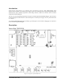
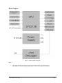
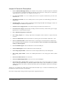
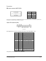
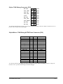
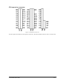
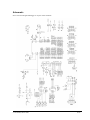
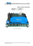
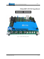
_
V1.7
User’s Guide
Philips/NXP LPC2138 Target Board
Ordering code
Dimensions
ITLPC2138
100 x 96 mm
Figure 1: ITLPC2138FE Target Board
© iSYSTEM, March 2007
1/13
Contents
Contents.............................................................................................................................. 2
Introduction ......................................................................................................................... 3
Description .......................................................................................................................... 3
View of the ITLPC2138 ................................................................................................................................... 3
Block Diagram ................................................................................................................................................ 4
Components List .............................................................................................................................................. 5
Power Supply................................................................................................................................................... 5
Jumper & Connector Descriptions.................................................................................................................. 6
Connectors....................................................................................................................................................... 7
Schematic ......................................................................................................................... 10
Use of the on-board integrated debugger ......................................................................... 11
Use of an external debugger............................................................................................. 12
Troubleshooting ................................................................................................................ 13
© iSYSTEM, March 2007
2/13
Introduction
NXP LPC2138 Target Board is an evaluation and a development system for NXP ARM7TDMI-S based
LPC2138 microcontroller. The ITLPC2138 package consists of a USB cable and a target board populated with
NXP LPC2138 CPU, minimum peripherals, JTAG debug connector, ETM trace connector and an on-board
integrated iSYSTEM debugger.
The user can write and debug the application using the on-board integrated iSYSTEM debugger, which connects
to the PC through the USB connection. The board requires no external power supply since it’s powered from the
PC USB port.
An external ARM7TDMI-S debugger (including e.g. ETM support) can be used for debugging as an alternative
to the on-board integrated debugger.
Description
View of the ITLPC2138
Figure 2: Top View of the ITLPC2138
© iSYSTEM, March 2007
3/13
Block Diagram
Figure 3: ITLPC2138 Block diagram
Notes
1.
The board provides 16-pin connector for the optional LCD display (type CMC216x04 or
EW162B0GLY, checkout backlight LED polarity), which is not included in the package.
© iSYSTEM, March 2007
4/13
Components List
Name
P1
P2
P3
P4
P5
P6
P11
P12
P13
P21
P31
P32
P33
P34
P35
J1, J2, J7 J10, J15 - J20,
J22,J25
LD0 – LD3
LD11
LD12
T0 – T3
Reset (T4)
TR2
R25, R26
Description
Expansion connector GPIO pins P0.0 – P0.7
Expansion connector GPIO pins P0.8 – P0.15
Expansion connector GPIO pins P0.16 – P0.23
Expansion connector GPIO pins P0.25 – P0.31
Expansion connector GPIO pins P1.16 – P1.23
Expansion connector GPIO pins P1.24 and P1.25
RTC power supply input (3.3V)
Connector for manufacturing purpose
DA converter output
16-pin LCD connector
Connector for manufacturing purpose
ETM Trace connector
JTAG debug connector
USB connector (integrated debugger)
DB9 connector, serial port (UART1)
Jumpers
User LEDs
Power LED 5V
Power LED 3,3V
Push buttons
Reset button
Trimmer potentiometer
Resistors for adjusting LCD contrast*
*See schematic for details.
Power Supply
The target board is powered from the PC USB port, through which winIDEA (IDE) running on a PC, connects to
the on-board integrated debugger. Connection is made using a standard USB cable. Battery power supply for
RTC can be optionally connected to P11 (see P11 description for more details).
© iSYSTEM, March 2007
5/13
Jumper & Connector Descriptions
•
J1, J2: LCD LED Backlight Polarity: If J1 and J2 is set in position 1-2, then LCD pin15 is connected
to +5V and pin16 is connected to GND. If J1 and J2 is set in position 2-3 then pin15 is connected to
GND and pin16 is connected to +5V. Default set in position 1-2.
•
J7: Trace Port Enable: J7 is set to enable pins P1.25:16 to operate as ETM Trace port after reset.
Default not set.
•
J8: Debug Port Enable: J8 is set to enable pins P1.31:26 to operate as a JTAG Debug port after reset.
Default is set.
•
J9: Debug Mode: J9 selects whether iSYSTEM on-board integrated USB-JTAG debugger is used or an
external debug tool. Default set in position 1-2.*
•
J10: RTC Power Supply Selector: J10 connects Vbat pin of LPC2138 to the main 3.3V.
•
P11: RTC Power supply: PCB terminal providing connection for battery. When battery power supply
applied to P11 is used, J10 must be open.
•
P12: Manufacturing purpose connections
•
P13: Analog Output: P13 is analog output from OP amplifier, which connects to output of the DA
converter.
•
J15: User LEDs Enable: enables the LED driver connecting the on-board LEDs to GPIO P0.4 – P0.7.
•
J16: User Buttons Enable: enables buttons driver connecting the on-board buttons to GPIO P0.12 –
P0.15. Pushing the button generates a low signal. If J16 is set, the CPU will not start in Boot-loader
mode (see J25 description).
•
J17: LCD Enable Signal: connects GPIO P0.21 to the LCD enable pin.
•
J18: LCD R/W Signal: connects GPIO P0.22 to the LCD R/W pin.
•
J19: Analog Output Enable: connects DA converter output (GPIO P0.25) to the OP amplifier.
•
J20: Analog Input Enable: connects the TRIM potentiometer to the analog input AD0.0 (GPIO
P0.27).
•
P21: 16 Pin LCD Connector: see connectors
•
J22: LCD LED Backlight Enable: J22 is set to turn on LCD backlight.
•
J25 (bottom side): Startup mode (populated on the bottom side of the target board): J25 connects
either a pull-up (USER mode) or a pull-down (BOOT-loader mode) to P0.14. Default set in position
USER (User mode). J16 must be removed when setting J25 in position BOOT, otherwise J25 setting is
not effective.
*Jumper pin 1 is marked with a white square on the ITLPC2138 PCB. If pin 1 cannot be located directly from
the ITLPC2138, please use Figure 2 for assistance.
Note: Don’t change jumper settings while the target board is supplied with power!
© iSYSTEM, March 2007
6/13
Connectors
DB9 male connector UART1 (P35)
Pin No.
2
3
5
7
8
Symbol
RxD
TxD
GND
RTS
CTS
The serial port is configured as a standard RS232 interface with RTS/CTS control. Cross female to female cable
is needed for connection with PC computer COM port.
16-pin LCD connector (P21)
Top View
Pin Assignment for Crystal Clear technology CMC216x04 or EDT EW162B0GLY LCD
Pin No.
1
2
3
4
5
6
7
8
9
10
11
12
13
14
15
16
Symbol
GND
Vdd
Vo
RS
R/W
E
DB0
DB1
DB2
DB3
DB4
DB5
DB6
DB7
BL+
BL-
Function
Ground Terminal
Supply Terminal
Power Supply for LCD Driver
Register Select Signal
Read/Write Selection
Enable Signal
Data Bus Line (Not used)
Data Bus Line (Not used)
Data Bus Line (Not used)
Data Bus Line (Not used)
Data Bus Line
Data Bus Line
Data Bus Line
Data Bus Line
LED Backlight Power Supply
LED Backlight Ground
Verify polarity of LED backlight on your LCD display!
© iSYSTEM, March 2007
7/13
20-pin JTAG Debug Connector (P33)
Not used
1
2
T3V3
CPU_TRST
3
4
GND
CPU_TDI
5
6
GND
CPU_TMS
7
8
GND
CTCK
9
10
GND
Not used
11
12
GND
CPU_TDO
13
14
GND
CPU_RESET
15
16
GND
Not used
17
18
GND
Not used
19
20
GND
An external JTAG debug tool can be connected to a 20-pin P33 debug connector. Jumper J9 must be set to 2-3
position when using an external debugger.
38-pin Mictor JTAG Debug & ETM Trace Connector (P32)
Signal
Not used
Not used
GND
Not used
CPU_RESET
CPU_TDO
GND
CTCK
CPU_TMS
CPU_TDI
CPU_TRST
GND
GND
GND
GND
GND
GND
GND
GND
Pin
1
3
5
7
9
11
13
15
17
19
21
23
25
27
29
31
33
35
37
Pin
2
4
6
8
10
12
14
16
18
20
22
24
26
28
30
32
34
36
38
Signal
Not used
Not used
TRACECLK
Not used
Not used
T3V3
Not used
GND
GND
GND
GND
P1.19
P1.18
P1.17
P1.16
P1.20
P1.23
P1.22
P1.21
An external JTAG & ETM debug tool can be connected to a 38-pin Mictor P32 debug connector. Jumper J9
must be set to 2-3 position when using an external debugger.
© iSYSTEM, March 2007
8/13
CPU expansion connectors
Figure 4: Expansion connectors
All CPU signals are available on the expansion connectors, which are standard connectors with a 2.54 mm raster.
© iSYSTEM, March 2007
9/13
Schematic
Note: On-board integrated debugger is not part of the schematic.
© iSYSTEM, March 2007
10/13
Use of the on-board integrated debugger
Follow below instructions, in order to get a sample application running with “out of the box” experience. All
jumpers are set in the default position during the final tests in the manufacturing.
If winIDEA 2006 CD is not part of the package, please obtain winIDEA 2006 setup from your local iSYSTEM
office or from www.isystem.com.
•
Install winIDEA 2006 (IDE) full setup on a PC
•
Verify jumpers J15-J20 (see Jumpers description for their default position)
•
Verify that jumper J8 is set
•
Verify that jumper J7 is not set.
•
Verify that jumper J9 is set in position 1-2 (on-board integrated debugger enabled).
•
Open winIDEA 2006 application and open a sample workspace for the ITLPC2138 running from the
internal flash.
•
Connect the USB cable to the PC and to the ITLPC2138.
•
Windows should auto-detect a new USB device and install belonging USB driver. In case of any
problems, the driver is located under winIDEA install directory (e.g. c:\winIDEA\2006\USBDrv).
•
Disconnect the USB cable from the ITLPC2138 and then connect it again. The two power LEDs
should turn on. The target board is not powered if the LEDs don’t lit and the problem needs to be
resolved before proceeding to the next step!
•
Finally, execute Debug/Debug Reset. This should initialize the development system and the user
should be able to write to the internal CPU RAM through the memory window.
•
Next, execute Debug/Download. This should program and run the application until main function. The
development system is now ready for the debugging.
© iSYSTEM, March 2007
11/13
Use of an external debugger
An external debugger can be:
•
a JTAG debugger, which connects to a 20-pin P33 connector
•
a development tool supporting JTAG debugging and ETM (on-chip trace), which connects to a 38-pin
Mictor P32 connector
Setting up a debug environment for the first time
•
Verify jumpers J15-J20 (see Jumpers description for their default position)
•
Verify that jumper J8 is set
•
Verify that jumper J7 is set if your development tool connects to P32
•
Verify that jumper J9 is set in position 2-3 (on-board integrated debugger disabled)
•
winIDEA 2006 application must to be installed and run once in order to power the ITLPC2138 board
through the USB connection.
•
Connect the USB cable to the PC and to the ITLPC2138.
•
Windows should auto-detect a new USB device and install belonging USB driver. In case of any
problems, the driver is located under winIDEA install directory (e.g. c:\winIDEA\2006\USBDrv).
•
Disconnect the USB cable from the ITLPC2138 and then connect it again. The two power LEDs
should turn on. The target board is not powered if the LEDs don’t lit and the problem needs to be
resolved before proceeding to the next step!
•
Disconnect the USB cable from the ITLPC2138 once again, connect the external development system
to P32 or P33 (depending on the development system), turn it on and then connect back the USB cable.
•
Execute a debug command equivalent to the CPU reset debug command. This should initialize the
development system and the user should be able to write to the internal CPU RAM through the
memory window. The development system should be now ready for use.
© iSYSTEM, March 2007
12/13
Troubleshooting
The flash boot loader code is executed every time the CPU is powered or reset. The loader can execute the ISP
command handler or the user application code. P0.14 is sensed on a rising edge on the RST (CPU reset) pin. If a
low level is detected, ISP command handler starts and takes over control of the CPU after reset. If there is no
request for the ISP command handler execution (a high-level detected), a search is made for a valid user
program. If a valid user program is found then the execution control is transferred to it. Refer to CPU User
Manual for more details on CPU startup mode.
Normally, jumper J25 is set for ‘User mode’ by default. Boot-loader mode should be normally selected only for
troubleshooting or when the user explicitly wants to use Boot-loader mode. J16 must be removed when Bootloader mode is selected (see J16 description for more details).
There was a case, where the code was programmed in the flash, which disabled the JTAG debug port shortly
after reset. Due to the NXP implementation, the debugger cannot take over control over the CPU immediately
after reset, but a part of code is executed before the CPU can be stopped by the debugger. In this particular case,
the application disabled JTAG port before the debugger took control over the CPU and the debugger could not
connect to the CPU at all. Thereby, note that if the debugger cannot connect to the CPU (winIDEA reports
“Cannot stop CPU”), it may be due to bad program in the flash. In this case, Boot-loader mode has to be selected
(in order for the CPU to start executing ISP command handler), in which the debugger can always stop the
program and take over control over the CPU. Then a new valid program can be programmed in the flash or flash
erased. Then the User mode can be used again.
Disclaimer: iSYSTEM assumes no responsibility for any errors which may appear in this document, reserves the
right to change devices or specifications detailed herein at any time without notice, and does not make any
commitment to update the information herein.
© iSYSTEM. All rights reserved.
© iSYSTEM, March 2007
13/13