1
Intel® Server Board S3420GP
Technical Product Specification
Intel order number E65697-003
Revision 1.0
August 2009
Enterprise Platforms and Services Division
Revision History
IntelP®P Server Board S3420GP TPS
Revision History
Date
Feb. 2009
Revision
Number
0.3
Modifications
Initial version
May 2009
0.5
Update
July. 2009
0.9
Update POST error code and diagram
Aug. 2009
1.0
Update MTBF
Revision 1.0
ii
Intel order number E65697-003
IntelP®P Server Board S3420GP TPS
Disclaimers
Disclaimers
Information in this document is provided in connection with Intel® products. No license, express
or implied, by estoppel or otherwise, to any intellectual property rights is granted by this
document. Except as provided in Intel's Terms and Conditions of Sale for such products, Intel
assumes no liability whatsoever, and Intel disclaims any express or implied warranty, relating to
sale and/or use of Intel products including liability or warranties relating to fitness for a particular
purpose, merchantability, or infringement of any patent, copyright or other intellectual property
right. Intel products are not intended for use in medical, life saving, or life sustaining applications.
Intel may make changes to specifications and product descriptions at any time, without notice.
Designers must not rely on the absence or characteristics of any features or instructions marked
"reserved" or "undefined." Intel reserves these for future definition and shall have no
responsibility whatsoever for conflicts or incompatibilities arising from future changes to them.
This document contains information for a product that is still in development. Do not
finalize a design with this information. Information provided in this preliminary document may be
incomplete (as denoted by TBD) or may change. Revised information will be published in a later
release of this document and when the product is made available. Verify with your local sales
office that you have the latest datasheet before finalizing a design.
The Intel® Server Board S3420GP may contain design defects or errors known as errata which
may cause the product to deviate from published specifications. Current characterized errata
are available on request.
Intel Corporation server boards contain a number of high-density VLSI and power delivery
components that need adequate airflow to cool. Intel’s own chassis are designed and tested to
meet the intended thermal requirements of these components when the fully integrated system
is used together. It is the responsibility of the system integrator that chooses not to use Intel
developed server building blocks to consult vendor datasheets and operating parameters to
determine the amount of airflow required for their specific application and environmental
conditions. Intel Corporation cannot be held responsible if components fail or the server board
does not operate correctly when used outside any of their published operating or non-operating
limits.
Intel, Pentium, Itanium, and Xeon are trademarks or registered trademarks of Intel Corporation.
*Other brands and names may be claimed as the property of others.
Copyright © Intel Corporation 2009.
Revision 1.0
iii
Intel order number E65697-003
Table of Contents
IntelP®P Server Board S3420GP TPS
Table of Contents
1.
2.
3.
Introduction .......................................................................................................................... 2
1.1
Chapter Outline........................................................................................................ 2
1.2
Server Board Use Disclaimer .................................................................................. 2
Overview ............................................................................................................................... 1
2.1
Intel® Server Board S3420GP Feature Set.............................................................. 1
2.2
Server Board Layout................................................................................................ 3
2.2.1
Server Board Connector and Component Layout.................................................... 4
2.2.2
Intel® Server Board S3420GP Mechanical Drawings .............................................. 6
2.2.3
Server Board Rear I/O Layout ............................................................................... 12
Functional Architecture ..................................................................................................... 13
3.1
Processor Sub-System .......................................................................................... 14
3.1.1
Intel® Xeon® 3400 Processor ................................................................................. 14
3.1.2
Intel® Turbo Boost Technology .............................................................................. 15
3.1.3
Simultaneous Multithreading (SMT) ...................................................................... 15
3.1.4
Enhanced Intel SpeedStep® Technology............................................................... 15
3.2
Memory Subsystem ............................................................................................... 15
3.2.1
Memory Sizing and Configuration.......................................................................... 16
3.2.2
Post Error Codes ................................................................................................... 16
3.2.3
Publishing System Memory ................................................................................... 17
3.2.4
Support for Mixed-speed Memory Modules ........................................................... 18
3.2.5
Memory Map and Population Rules....................................................................... 18
3.3
Intel® 3420 Chipset PCH........................................................................................ 21
3.4
I/O Sub-system ...................................................................................................... 21
3.4.1
PCI Express Interface............................................................................................ 21
3.4.2
Serial ATA Support ................................................................................................ 22
3.4.3
USB 2.0 Support.................................................................................................... 22
3.5
Optional Intel® SAS Entry RAID Module AXX4SASMOD ...................................... 23
3.6
Integrated Baseboard Management Controller...................................................... 23
3.6.1
Integrated BMC Embedded LAN Channel ............................................................. 25
3.6.2
Optional RMM3 Advanced Management Board .................................................... 25
3.6.3
Serial Ports ............................................................................................................ 26
3.6.4
Floppy Disk Controller ........................................................................................... 26
Revision 1.0
iv
Intel order number E65697-003
IntelP®P Server Board S3420GP TPS
3.6.5
Keyboard and Mouse Support ............................................................................... 26
3.6.6
Wake-up Control.................................................................................................... 27
3.7
Video Modes.......................................................................................................... 27
3.7.2
Dual Video ............................................................................................................. 27
GigE Controller 82574L ......................................................................................... 28
3.8.2
GigE PHY 82578DM .............................................................................................. 28
3.8.3
MAC Address Definition......................................................................................... 28
3.9.1
3.10
Intel® I/O Acceleration Technolgy 2 (Intel® I/OAT2) ............................................... 29
Direct Cache Access (DCA) .................................................................................. 29
Intel® Virtualization Technology for Directed I/O (Intel® VT-d) ............................... 29
Platform Management........................................................................................................ 30
4.1
Feature Support..................................................................................................... 30
4.1.1
IPMI 2.0 Features .................................................................................................. 30
4.1.2
Non-IPMI Features ................................................................................................ 31
4.2
Optional Advanced Management Feature Support ............................................... 32
4.2.1
Enabling Advanced Management Features........................................................... 32
4.2.2
Keyboard, Video, Mouse (KVM) Redirection ......................................................... 32
4.2.3
Media Redirection.................................................................................................. 33
4.2.4
Web Services for Management (WS-MAN) ........................................................... 34
4.2.5
Local Directory Authentication Protocol (LDAP) .................................................... 34
4.2.6
Embedded Webserver ........................................................................................... 34
4.3
Management Engine (ME) ..................................................................................... 34
BIOS User Interface............................................................................................................ 35
5.1
Logo / Diagnostic Screen....................................................................................... 35
5.2
BIOS Boot Popup Menu ........................................................................................ 35
5.3
BIOS Setup utility................................................................................................... 35
5.3.1
Operation ............................................................................................................... 35
5.3.2
Server Platform Setup Utility Screens ................................................................... 38
5.4
6.
Network Interface Controller (NIC) ........................................................................ 28
3.8.1
3.9
5.
Video Support ........................................................................................................ 27
3.7.1
3.8
4.
Table of Contents
Loading BIOS Defaults .......................................................................................... 63
Connector / Header Locations and Pin-outs.................................................................... 65
6.1
Board Connector Information................................................................................. 65
6.2
Power Connectors ................................................................................................. 65
6.3
System Management Headers .............................................................................. 66
Revision 1.0
v
Intel order number E65697-003
Table of Contents
6.3.1
Intel® Remote Management Module 3 (Intel® RMM3) Connector .......................... 66
6.3.2
LCP / IPMB Header ............................................................................................... 67
6.3.3
HSBP Header ........................................................................................................ 67
6.3.4
SGPIO Header....................................................................................................... 67
6.4
Front Control Panel Connector .............................................................................. 68
6.4.1
Power Button ......................................................................................................... 68
6.4.2
Reset Button .......................................................................................................... 69
6.4.3
NMI Button............................................................................................................. 69
6.4.4
System Status Indicator LED................................................................................. 69
6.5
7.
I/O Connectors....................................................................................................... 71
6.5.1
VGA Connector...................................................................................................... 71
6.5.2
Rear NIC and USB connector................................................................................ 71
6.5.3
SATA ..................................................................................................................... 72
6.5.4
SAS Connectors .................................................................................................... 72
6.5.5
Serial Port Connectors........................................................................................... 72
6.5.6
USB Connector...................................................................................................... 73
6.6
PCI Express* Slot / PCI Slot / Riser Card Slot /..................................................... 75
6.7
Fan Headers .......................................................................................................... 79
Jumper Blocks.................................................................................................................... 80
7.1
CMOS Clear and Password Reset Usage Procedure ........................................... 81
7.1.1
Clearing the CMOS................................................................................................ 81
7.1.2
Clearing the Password........................................................................................... 81
7.2
Integrated BMC Force Update Procedure ............................................................. 82
7.3
ME Force Update Jumper...................................................................................... 82
7.4
8.
9.
IntelP®P Server Board S3420GP TPS
BIOS Recovery Jumper ......................................................................................... 83
®
Intel Light Guided Diagnostics........................................................................................ 84
8.1
System Status LED................................................................................................ 84
8.2
Post Code Diagnostic LEDs .................................................................................. 85
Design and Environmental Specifications....................................................................... 86
9.1
Intel® Server Board S3420GP Design Specifications ............................................ 86
9.2
Board-level Calculated MTBF................................................................................ 86
9.3
Server Board Power Requirements ....................................................................... 87
9.3.1
9.4
9.4.1
Processor Power Support...................................................................................... 88
Power Supply Output Requirements ..................................................................... 88
Grounding .............................................................................................................. 89
Revision 1.0
vi
Intel order number E65697-003
IntelP®P Server Board S3420GP TPS
Table of Contents
9.4.2
Standby Outputs .................................................................................................... 89
9.4.3
Remote Sense ....................................................................................................... 89
9.4.4
Voltage Regulation ................................................................................................ 89
9.4.5
Dynamic Loading ................................................................................................... 89
9.4.6
Capacitive Loading ................................................................................................ 90
9.4.7
Closed-loop Stability .............................................................................................. 90
9.4.8
Common Mode Noise ............................................................................................ 90
9.4.9
Ripple / Noise ........................................................................................................ 90
9.4.10
Timing Requirements............................................................................................. 90
9.4.11
Residual Voltage Immunity in Standby Mode ........................................................ 93
9.4.12
Protection Circuits.................................................................................................. 93
10. Regulatory and Certification Information......................................................................... 95
10.1
Product Regulatory Compliance ............................................................................ 95
10.1.1
Product Safety Compliance ................................................................................... 95
10.1.2
Product EMC Compliance – Class A Compliance ................................................. 95
10.1.3
Certifications / Registrations / Declarations ........................................................... 95
10.1.4
Product Ecology Requirements ............................................................................. 96
10.2
Product Regulatory Compliance Markings ............................................................ 97
10.3
Electromagnetic Compatibility Notices .................................................................. 99
10.3.1
FCC Verification Statement (USA) ........................................................................ 99
10.3.2
ICES-003 (Canada) ............................................................................................. 100
10.3.3
Europe (CE Declaration of Conformity) ............................................................... 100
10.3.4
VCCI (Japan) ....................................................................................................... 100
10.3.5
BSMI (Taiwan) ..................................................................................................... 101
10.3.6
RRL (Korea)......................................................................................................... 101
10.3.7
CNCA (CCC-China) ............................................................................................. 101
Appendix A: Integration and Usage Tips.............................................................................. 102
Appendix B: Integrated BMC Sensor Tables........................................................................ 103
Appendix C: POST Code Diagnostic LED Decoder ............................................................. 109
Appendix D: POST Code Errors ............................................................................................ 113
Appendix E: Supported Intel® Server Chassis ..................................................................... 118
Glossary................................................................................................................................... 119
Reference Documents ............................................................................................................ 122
Revision 1.0
vii
Intel order number E65697-003
List of Figures
IntelP®P Server Board S3420GP TPS
List of Figures
Figure 1. Intel® Server Board S3420GPLX Picture ....................................................................... 3
Figure 2. Intel® Server Board S3420GP Layout............................................................................ 4
Figure 3. Intel® Server Board S3420GP – Key Connector and LED Indicator IDENTIFICATION. 6
Figure 4. Intel® Server Board S3420GP – Hole and Component Positions .................................. 7
Figure 5. Intel® Server Board S3420GP – Major Connector Pin Location (1 of 2)........................ 8
Figure 6. Intel® Server Board S3420GP –Major Connector Pin Location (2 of 2)......................... 9
Figure 7. Intel® Server Board S3420GP – Primary Side Keepout Zone ..................................... 10
Figure 8. Intel® Server Board S3420GP – Secondary Side Keepout Zone................................. 11
Figure 9. Intel® Server Board S3420GP Rear I/O Layout ........................................................... 12
Figure 10. Intel® Server Board S3420GP Functional Block Diagram For S3420GPLX .............. 13
Figure 11. Intel® Server Board S3420GP Functional Block Diagram From S3420GPLC ........... 14
Figure 12. Intel® Server Board S3420GP Functional Block Diagram From S3420GPV ............. 14
Figure 13. Integrated BMC Hardware ......................................................................................... 25
Figure 14. Server Management Bus (SMBUS) Block Diagram................................................... 30
Figure 15. Setup Utility – Main Screen Display........................................................................... 39
Figure 16. Setup Utility – Advanced Screen Display .................................................................. 41
Figure 17. Setup Utility – Processor Configuration Screen Display............................................ 42
Figure 18. Setup Utility – Memory Configuration Screen Display ............................................... 45
Figure 19. Setup Utility – Mass Storage Controller Configuration Screen Display ..................... 46
Figure 20. Setup Utility – Serial Port Configuration Screen Display ........................................... 48
Figure 21. Setup Utility – USB Controller Configuration Screen Display .................................... 49
Figure 22. Setup Utility – PCI Configuration Screen Display ...................................................... 50
Figure 23. Setup Utility – System Acoustic and Performance Configuration Screen Display ..... 52
Figure 24. Setup Utility – Security Configuration Screen Display ............................................... 53
Figure 25. Setup Utility – Server Management Configuraiton Screen Display............................ 55
Figure 26. Setup Utility – Console Redirection Screen Display .................................................. 56
Figure 27. Setup Utility – Server Management System Information Screen Display .................. 58
Figure 28. Setup Utility – Boot Options Screen Display.............................................................. 59
Figure 29. Setup Utility – Delete Boot Option Screen Display .................................................... 60
Figure 30. Setup Utility — Hard Disk Order Screen Display ....................................................... 61
Figure 31. Setup Utility – CDROM Order Screen Display........................................................... 61
Figure 32. Setup Utility — Floppy Order Screen Display ............................................................ 62
Revision 1.0
viii
Intel order number E65697-003
IntelP®P Server Board S3420GP TPS
List of Figures
Figure 33. Setup Utility – Network Device Order Screen Display ............................................... 62
Figure 34. Setup Utility – Boot Manager Screen Display............................................................ 63
Figure 35. Jumper Blocks (J1A2, J1F1, J1F3, J1F2 and J1F5).................................................. 80
Figure 36. Power Distribution Block Diagram ............................................................................. 87
Figure 37. Output Voltage Timing ............................................................................................... 91
Figure 38. Turn On/Off Timing (Power Supply Signals).............................................................. 92
Figure 39. Diagnostic LED Placement Diagram ....................................................................... 109
Revision 1.0
ix
Intel order number E65697-003
List of Tables
IntelP®P Server Board S3420GP TPS
List of Tables
Table 1. Intel® Server Board S3420GP Feature Set ..................................................................... 1
Table 2. Major Board Components ............................................................................................... 5
Table 3. Standard Platform DIMM Nomenclature ....................................................................... 18
Table 4. Memory Configuration Table......................................................................................... 20
Table 5. Optional RMM3 Advanced Management Board Features ............................................ 26
Table 6. Serial B Header (J1B1) Pin-out..................................................................................... 26
Table 7. Video Modes ................................................................................................................. 27
Table 8. Dual Video Modes......................................................................................................... 27
Table 9. BIOS Setup Page Layout.............................................................................................. 36
Table 10. BIOS Setup: Keyboard Command Bar........................................................................ 37
Table 11. Setup Utility – Main Screen Fields .............................................................................. 39
Table 12. Setup Utility – Advanced Screen Display Fields ......................................................... 41
Table 13. Setup Utility – Processor Configuration Screen Fields ............................................... 42
Table 14. Setup Utility – Memory Configuration Screen Fields .................................................. 45
Table 15. Setup Utility – Mass Storage Controller Configuration Screen Fields......................... 46
Table 16. Setup Utility – Serial Ports Configuration Screen Fields............................................. 48
Table 17. Setup Utility – USB Controller Configuration Screen Fields ....................................... 49
Table 18. Setup Utility – PCI Configuration Screen Fields ......................................................... 51
Table 19. Setup Utility – System Acoustic and Performance Configuration Screen Fields ........ 52
Table 20. Setup Utility – Security Configuration Screen Fields .................................................. 53
Table 21. Setup Utility – Server Management Configuration Screen Fields ............................... 55
Table 22. Setup Utility – Console Redirection Configuration Fields ........................................... 57
Table 23. Setup Utility – Server Management System Information Fields.................................. 58
Table 24. Setup Utility – Boot Options Screen Fields ................................................................. 59
Table 25. Setup Utility – Delete Boot Option Fields.................................................................... 60
Table 26. Setup Utility — Hard Disk Order Fields....................................................................... 61
Table 27. Setup Utility – CDROM Order Fields .......................................................................... 61
Table 28. Setup Utility — Floppy Order Fields............................................................................ 62
Table 29. Setup Utility – Network Device Order Fields ............................................................... 63
Table 30. Setup Utility – Boot Manager Screen Fields ............................................................... 63
Table 31. Board Connector Matrix .............................................................................................. 65
Table 32. Baseboard Power Connector Pin-out (J9A1).............................................................. 66
Revision 1.0
x
Intel order number E65697-003
IntelP®P Server Board S3420GP TPS
List of Tables
Table 33. SSI Processor Power Connector Pin-out (J9C1) ........................................................ 66
Table 34. Intel® RMM3 Connector Pin-out (J2C1) ...................................................................... 66
Table 35. LPC / IPMB Header Pin-out (J1H2) ............................................................................ 67
Table 36. HSBP Header Pin-out (J1J1) ...................................................................................... 67
Table 37. SGPIO Header Pin-out (J1J3) .................................................................................... 67
Table 38. Front Panel SSI Standard 24-pin Connector Pin-out (J1C1) ...................................... 68
Table 39. System Status LED Indicator States........................................................................... 70
Table 40. VGA Connector Pin-out (J7A1)................................................................................... 71
Table 41. RJ-45 10/100/1000 NIC Connector Pin-out (J5A1)..................................................... 71
Table 42. RJ-45 10/100/1000 NIC Connector Pin-out (J6A1)..................................................... 71
Table 43. SATA Connector Pin-out (J1H4, J1H1, J1G1, J1H3, J1G3, J1F4) ............................. 72
Table 44. SAS Connector Pin-out (J2H1) ................................................................................... 72
Table 45. External Serial A Port Pin-out (J8A1).......................................................................... 73
Table 46. Internal 9-pin Serial B Header Pin-out (J1B2)............................................................. 73
Table 47. Internal USB Connector Pin-out ( J1E1, J1D1)........................................................... 74
Table 48. Pin-out of Internal USB Connector for Floppy ( J1J2)................................................. 74
Table 49. Pin-out of Internal USB Connector for low-profile Intel® Z-U130 Value Solid State
Drive (J3F2).......................................................................................................................... 74
Table 50. Pin-out of adaptive riser slot / PCI Express slot 6....................................................... 75
Table 51. SSI 4-pin Fan Header Pin-out (J6E1, J1J4, J6J2, J7J1, J6B1) .................................. 79
Table 52. Server Board Jumpers (J1F1, J1F2, J1F3, J1F5, J1A2) ............................................ 80
Table 53. Front Panel Status LED Behavior Summary............................................................... 84
Table 54. POST Code Diagnostic LED Location ........................................................................ 85
Table 55. Server Board Design Specifications ........................................................................... 86
Table 56. Intel® Xeon® Processor TDP Guidelines ..................................................................... 88
Table 57. 350-W Load Ratings ................................................................................................... 88
Table 58. Voltage Regulation Limits ........................................................................................... 89
Table 59. Transient Load Requirements..................................................................................... 89
Table 60. Capacitve Loading Conditions .................................................................................... 90
Table 61. Ripple and Noise......................................................................................................... 90
Table 62. Output Voltage Timing ................................................................................................ 91
Table 63. Turn On/Off Timing ..................................................................................................... 92
Table 64. Over-Current Protection (OCP)................................................................................... 93
Table 65. Over-voltage Protection (OVP) Limits ......................................................................... 93
Table 66. Integrated BMC Core Sensors.................................................................................. 105
Revision 1.0
xi
Intel order number E65697-003
List of Tables
IntelP®P Server Board S3420GP TPS
Table 67. POST Progress Code LED Example ........................................................................ 109
Table 68. Diagnostic LED POST Code Decoder ...................................................................... 109
Table 69. POST Error Messages and Handling........................................................................ 113
Table 70. POST Error Beep Codes .......................................................................................... 117
Revision 1.0
xii
Intel order number E65697-003
IntelP®P Server Board S3420GP TPS
List of Tables
<This page intentionally left blank.>
Revision 1.0
xiii
Intel order number E65697-003
Introduction
1.
IntelP®P Server Board S3420GP TPS
Introduction
This Technical Product Specification (TPS) provides board specific information detailing the
features, functionality, and high-level architecture of the Intel® Server Board S3420GP.
In addition, you can obtain design-level information for specific subsystems by ordering the
External Product Specifications (EPS) or External Design Specifications (EDS) for a given
subsystem. EPS and EDS documents are not publicly available and must be ordered through
your local Intel representative.
1.1
Chapter Outline
This document is divided into the following chapters:
1.2
Chapter 1 – Introduction
Chapter 2 – Server Board Overview
Chapter 3 – Functional Architecture
Chapter 4 – Platform Management
Chapter 5 – BIOS User Interface
Chapter 6 – Connector / Header Locations and Pin-outs
Chapter 7 –Jumpers Blocks
Chapter 8 – Intel® Light-Guided Diagnostics
Chapter 9 – Design and Environmental Specifications
Chapter 10 – Regulatory and Certification Information
Appendix A – Integration and Usage Tips
Appendix B – Integrated BMC Sensor Tables
Appendix C – POST Code Diagnostic LED Decoder
Appendix D – POST Code Errors
Appendix E – Supported Intel® Server Chassis
Server Board Use Disclaimer
Intel Corporation server boards contain a number of high-density VLSI and power delivery
components that need adequate airflow to cool. Intel ensures through its own chassis
development and testing that when Intel server building blocks are used together, the fully
integrated system meets the intended thermal requirements of these components. It is the
responsibility of the system integrator who chooses not to use Intel developed server building
blocks to consult vendor datasheets and operating parameters to determine the amount of
airflow required for their specific application and environmental conditions. Intel Corporation
cannot be held responsible if components fail or the server board does not operate correctly
when used outside any of their published operating or non-operating limits.
Revision 1.0
2
Intel order number E65697-003
IntelP®P Server Board S3420GP TPS
2.
Overview
Overview
The Intel® Server Board S3420GP is a monolithic printed circuit board (PCB) with features
designed to support entry-level severs. It has three board SKUs: S3420GPLX, S3420GPLC,
and S3420GPV.
2.1
Intel® Server Board S3420GP Feature Set
Table 1. Intel® Server Board S3420GP Feature Set
Feature
Processor
Description
Support for one Xeon® 3400 Series Processor in FC-LGA 1156 socket package.
2.5 GT/s point-to-point DMI interface to PCH
Memory
Two memory channels with support for 1066/1333 MHz ECC Unbuffered (UDIMM) or
ECC Registered (RDIMM) (Intel® Xeon® 3400 Series only) DDR3.
®
•
Intel Server Board S3420GPLX and S3420GPLC
Up to 2 UDIMMs or 3 RDIMM (Intel® Xeon® 3400 Series only) per channel
32 GB max with x8 ECC RDIMM (2 Gb DRAM) and 16 GB max with x8
ECC UDIMM (2 Gb DRAM)
•
Chipset
Intel® Server Board S3420GPV
Up to 2 UDIMMs per channel
16 GB max with x8 ECC UDIMM (2 Gb DRAM)
•
Intel® Server board S3420GPLX
Support for Intel® 3420 Chipset Plaftorm Controller Hub (PCH)
ServerEngines* LLC Pilot II BMC controller (Integrated BMC)
•
I/O
LGA 1156 pin socket
PCI Express* switch
Intel® Server board S3420GPLC
Support for Intel® 3420 Chipset Platform Controller Hub (PCH)
ServerEngines* LLC Pilot II BMC controller (Integrated BMC)
External connections:
DB-15 video connectors
DB-9 serial Port A connector
Four ports on two USB/LAN combo connectors at rear of board.
Internal connections:
Two USB 2x5 pin headers, each supporting two USB 2.0 ports
One 2x5 Serial Port B header
Six SATA II connectors
One Intel® SAS Entry RAID Module AXX4SASMOD connector
One SAS mezzanine slot supports for optional Intel® Remote Management
Module 3
Revision 1.0
1
Intel order number E65697-003
Overview
Feature
Add-in PCI Card, PCI
Express* Card
IntelP®P Server Board S3420GP TPS
Description
Intel® Server Board S3420GPLX
•
Slot1: One 5V PCI 32 bit / 33 MHz connector.
Slot2: One PCI Express* Gen1 x4 (x1 throughput) connector.
Slot3: One PCI Express* Gen1 x8 (x4 throughput) connector.
Slot4: One PCI Express* Gen2 x8 (x4 throughput) connector.
Slot5: One PCI Express* Gen2 x8 (x8 throughput) connector.
Slot6: One PCI Express* Gen2 x16 (x8 throughput) connector.
•
Intel® Server Board S3420GPLC/ S3420GPV
Slot1: One 5V PCI 32 bit / 33 MHz connector.
Slot3: One PCI Express* Gen1 x8 (x4 throughput) connector.
Slot5: One PCI Express* Gen2 x8 (x8 throughput) connector.
Slot6: One PCI Express* Gen2 x16 (x8 throughput) connector.
System Fan Support
Five 4-pin fan headers supporting four system fans and one processor.
Video
Onboard ServerEngines* LLC Pilot II BMC Controller
Integrated 2D Video Controller
Onboard Hard Drive
Support for six Serial ATA II hard drives through six onboard SATA II connectors with
SW RAID 0, 1, 5, and 10.
•
Intel® Server Board S3420GPLX:
LAN
Up to four SAS hard drives through option Intel® SAS Entry RAID Module
AXX4SASMOD card
One Gigabit Ethernet device 82574L connect to PCI-E x1 interfaces on the PCH.
Intel® Server Board S3420GPLX/S3420GPLC:
Server Management
64-MB DDR2 667 MHz Memory
One Gigabit Ethernet PHY 82578DM connected to PCH through PCI-E x1
interface
Onboard LLC Pilot II Controller (iBMC)
Integrated Baseboard Management Controller (Integrated BMC), IPMI 2.0
compliant
•
Integrated 2D video controller on PCI-E x1
Intel® Server Board S3420GPLX
Intel® Remote Management Module III (RMM3)
Revision 1.0
2
Intel order number E65697-003
IntelP®P Server Board S3420GP TPS
2.2
Overview
Server Board Layout
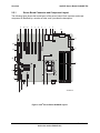
Figure 1. Intel® Server Board S3420GPLX Picture
Revision 1.0
3
Intel order number E65697-003
Overview
IntelP®P Server Board S3420GP TPS
2.2.1
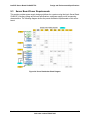
Server Board Connector and Component Layout
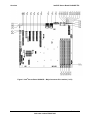
The following figure shows the board layout of the server board. Each connector and major
component is identified by a number or letter, and 2 provides the description.
A
B C D
E
F
G
H
J
I
K
L
M
N
DD
O
CC
BB
P
AA
Z
W
T
V
S
R
Q
U
X
AF003290
Y
Figure 2. Intel® Server Board S3420GP Layout
Revision 1.0
4
Intel order number E65697-003
IntelP®P Server Board S3420GP TPS
Overview
Table 2. Major Board Components
Description
A
B
C
D
E
F
G
H
I
J
K
L
M
N
O
P
Description
Slot 1, 32 Mbit/33 MHz PCI
Slot 2, PCI Express* Gen1 x1 (x4 connector)
(Intel Server Board S3420GPLX only)
Intel RMM3 Connector(Intel Server Board
S3420GPLX only)
Slot 3, PCI Express* Gen1 x4 (PCI Express*
Gen2 compliant)
Slot 4, PCI Express* Gen2 x4 (x8 connector)
(x8 connector)( Intel® Server Board S3420GPLX
only)
Slot 5. PCI Express* Gen2 x8 (x8 connector)
Slot 6, PCI Express* Gen2 x8 (x16 connector)
CMOS battery
Ethernet and Dual USB COMBO
Ethernet and Dual USB COMBO
System FAN 4
Video port
External Serial port
Main Power Connector
CPU Power connector
DIMM slots
Q
R
System FAN2 and System FAN 3
CPU connector
S
CPU Fan connector
T
USB SSD connector
U
SAS Module connector ( Intel® Server Board
S3420GPLX only)
V
W
X
Y
Z
AA
BB
CC
DD
System FAN 1
IPMB
SATA_SGPIO
HSBP
USB Floppy
Six SATA ports
Internal USB Connector
Front Panel Connector
Internal Serial Port
Revision 1.0
5
Intel order number E65697-003
Overview
2.2.2
IntelP®P Server Board S3420GP TPS
Intel® Server Board S3420GP Mechanical Drawings
Figure 3. Intel® Server Board S3420GP – Key Connector and LED Indicator IDENTIFICATION
Revision 1.0
6
Intel order number E65697-003
IntelP®P Server Board S3420GP TPS
Overview
Figure 4. Intel® Server Board S3420GP – Hole and Component Positions
Revision 1.0
7
Intel order number E65697-003
Overview
IntelP®P Server Board S3420GP TPS
Figure 5. Intel® Server Board S3420GP – Major Connector Pin Location (1 of 2)
Revision 1.0
8
Intel order number E65697-003
IntelP®P Server Board S3420GP TPS
Overview
Figure 6. Intel® Server Board S3420GP –Major Connector Pin Location (2 of 2)
Revision 1.0
9
Intel order number E65697-003
Overview
IntelP®P Server Board S3420GP TPS
Figure 7. Intel® Server Board S3420GP – Primary Side Keepout Zone
Revision 1.0
10
Intel order number E65697-003
IntelP®P Server Board S3420GP TPS
Overview
Figure 8. Intel® Server Board S3420GP – Secondary Side Keepout Zone
Revision 1.0
11
Intel order number E65697-003
Overview
2.2.3
IntelP®P Server Board S3420GP TPS
Server Board Rear I/O Layout
The following figure shows the layout of the rear I/O components for the server board.
A
Serial Port A
C
NIC Port 1 (1 Gb) and Dual USB Port
Connector
B
Video
D
NIC port 2 (1 Gb) and Dual USB Port
Connector
Figure 9. Intel® Server Board S3420GP Rear I/O Layout
Revision 1.0
12
Intel order number E65697-003
IntelP®P Server Board S3420GP TPS
3.
Functional Architecture
Functional Architecture
The architecture and design of the Intel® Server Board S3420GP is based on the Intel® 3420
Chipset. The chipset is designed for systems based on the Intel® Xeon® processor in the FCLGA 1156 socket package. The chipset contains two main components:
Intel® 3420 Chipset
PCI Express* switch (Intel® Server Board S3420GPLX only).
This chapter provides a high-level description of the functionality associated with each chipset
component and the architectural blocks that make up the server board.
S3420GPLX Block Diagram
(x16 connector)
Slot 6
ATX - 12" x 9.6"
PCIe Gen2 x8
(x8 connector)
Slot 5
PCIe Gen2 x8
(x8 connector)
Slot 4
PCIe Gen2 x4
ICH
G2PS
ICH1
9/
0
PCIe Gen2 x4
4 unbuffered
or
6 registered
DIMMs
DDR3 (Ch B)
Intel® Xeon®
3400
DDR3 (Ch A)
PCIe Gen2 x8
SAS
Ch A
Ch B
XDP0
x4 DMI Gen1
82578DM
(x8 connector)
Slot 3
(x4 connector)
Slot 2
PCIe
Gen1
N/C
PCIe
Gen1
PCI32
FLASH
PCIe
Gen1
Intel® 3420
PCH
x1
PCI
Slot 1
GbE
PHY
( PCIe Gen1 x1 )
x4
x1
SPI
RMII
x1
6
GbE
82574L
PCIe
Gen1
SPI
SATA-II
GbE
FLASH
BMC Boot
Flash
DDR2
FLASH
12
SATA
IBMC
Zoar
LPC
SERIAL 2
USB
1.1
6 onboard
PORT 80
USB
2.0
USB
2
(FP
headers)
1
2
(User Bay
headers)
VIDEO
RMII
RMM3
USB
Floppy
Header
SPI
1
Z-U130
SERIAL 1
Notes:
2
USB
2
1. Video integrated into BMC.
USB
ejd
Figure 10. Intel® Server Board S3420GP Functional Block Diagram For S3420GPLX
Revision 1.0
13
Intel order number E65697-003
Functional Architecture
IntelP®P Server Board S3420GP TPS
S3420GPLC Block Diagram
(x16 connector)
(x8 connector)
Slot 6
ATX - 12" x 9.6"
PCIe Gen2 x8
Slot 5
Intel® Xeon®
3400
Processor
PCIe Gen2 x8
4 unbuffered
or
6 registered
DIMMs
DDR3 (Ch B)
DDR3 (Ch A)
Ch A
Ch B
XDP0
x4 DMI Gen1
82578DM
(x8 connector)
Slot 3
PCIe
Gen1
Intel®
®
Intel
3420
3420
Chipset
Chipset
PCI
Slot 1
PCI32
FLASH
GbE
PHY
( PCIe Gen1 x1 )
x4
PCIe
Gen1
x1
SPI
RMII
x1
6
GbE
82574
PCIe
Gen1
SPI
SATA-II
GbE
FLASH
BMC Boot
Flash
DDR2
FLASH
12
SATA
IBMC
Zoar
LPC
SERIAL 2
USB
1.1
6 onboard
PORT 80
USB
2.0
USB
2
(FP
headers)
1
2
(User Bay
headers)
VIDEO
RMII
SPI
1
Z-U130
USB
Floppy
Header
SERIAL 1
Notes:
2
USB
2
1. Video integrated into BMC.
USB
ejd
Figure 11. Intel® Server Board S3420GP Functional Block Diagram From S3420GPLC
<TBD>
Figure 12. Intel® Server Board S3420GP Functional Block Diagram From S3420GPV
3.1
Processor Sub-System
The Intel® Server Board S3420GP supports the following processor:
Intel® Xeon® 3400 Processor series
The Intel® Xeon® 3400 Series processors processors are made up of multi-core processors
based on the 45 nm process technology.
3.1.1
Intel® Xeon® 3400 Processor
The Intel® Xeon® 3400 Series processors highly integrated solution variant is composed of four
Nehalem-based processor cores.
FC-LGA 1156 socket package with 2.5 GT/s.
Up to 95 W Thermal Design Power (TDP); processors with higher TDP are not
supported.
Revision 1.0
14
Intel order number E65697-003
IntelP®P Server Board S3420GP TPS
Functional Architecture
The server board does not support previous generations of the Intel® Xeon® processors.
Intel® Turbo Boost Technology
3.1.2
Intel® Turbo Boost Technology is featured on certain processors in the Intel® Xeon® Processor
3400 Series. Intel® Turbo Boost Technology opportunistically and automatically allows the
processor to run faster than the marked frequency if the processor is operating below power,
temperature, and current limits. This results in increased performance for both multi-threaded
and single-threaded workloads.
Intel® Turbo Boost Technology operation:
Turbo Boost operates under Operating System control – It is only entered when the
operating system requests the highest (P0) performance state.
Turbo Boost operation can be enabled or disabled by BIOS.
Turbo Boost converts any available power and thermal headroom into higher frequency
on active cores. At nominal marked processor frequency, many applications consume
less than the rated processor power draw.
Turbo Boost availability is independent of the number of active cores.
Maximum Turbo Boost frequency depends on the number of active cores and varies by
processor configuration.
The amount of time the system spends in Turbo Boost operation depends on workload,
operating environment, and platform design.
If the processor supports the Intel® Turbo Boost Technology feature, the BIOS Setup provides
an option to enable or disable this feature. The default state is enabled.
3.1.3
Simultaneous Multithreading (SMT)
®
Most Intel Xeon® processors support Simultaneous Multithreading (SMT). The BIOS detects
processors that support this feature and enables the feature during POST.
If the processor supports this feature, the BIOS Setup provides an option to enable or disable
this feature. The default is enabled.
Enhanced Intel SpeedStep® Technology
3.1.4
Intel® Xeon® processors support the Geyserville3 feature of the Enhanced Intel SpeedStep®
technology. This feature changes the processor operating ratio and voltage similar to the
Thermal Monitor 1 (TM1) feature. The BIOS implements the Geyserville3 feature in conjunction
with the TM1 feature. The BIOS enables a combination of TM1 and TM2 according to the
processor BIOS writer's guide.
3.2
Memory Subsystem
The Intel® Xeon® 3400 series processor has an Integrated Memory Controller (IMC) in its
package. Each Intel® Xeon® 3400 series processor produces up to two DDR3 channels of
memory. Each DDR3 channel in the IMC supports up to three DDR3 RDIMM slots or up to two
UDIMM slots. The DDR3 RDIMM frequency can be 800/1066/1333 MHz. DDR3 UDIMM
Revision 1.0
15
Intel order number E65697-003
Functional Architecture
IntelP®P Server Board S3420GP TPS
frequency can be 1066/1333 MHz. All RDIMMs and UDIMMs include ECC (Error Correction
Code) operation. Various speeds and memory technologies are supported.
RAS (Reliability, Availability, and Serviceability) is not supported on the Intel® Server Board
S3420GP.
3.2.1
Memory Sizing and Configuration
®
The Intel Server Board S3420GP supports various memory module sizes and configurations.
These combinations of sizes and configurations are valid only for DDR3 DIMMs approved by
Intel Corporation.
S3420GP BIOS supports:
z
DIMM sizes of 1 GB, 2 GB, 4 GB, and 8 GB.
z
DIMMs composed of DRAM using 2 Gb technology.
z
DRAMs organized as single rank, dual rank, or quad rank DIMMS.
z
DIMM speeds of 800, 1066, or 1333 MT/s.
z
Registered or Unregistered (unbuffered) DIMMs (RDIMMs or UDIMMs).
Note: UDIMMs should be ECC, and may or may not have thermal sensors; RDIMMs must have
ECC and must have thermal sensors.
S3420GP BIOS has the below limitations:
3.2.2
256 Mb technology, x4 DRAM on UDIMM, and quad rank UDIMM are NOT supported
x16 DRAM on UDIMM is not supported on combo routing
Memory suppliers not productizing native 800 ECC UDIMMs
Intel® Xeon® 3400 Series support all timings defined by JEDEC.
256 Mb/512 Mb technology, x4 and x16 DRAMs on RDIMM are NOT supported
All channels in a system will run at the fastest common frequency
No mixing of registered and unbuffered DIMMs
Post Error Codes
The range {0xE0 - 0xEF} of POST codes is used for memory errors in early POST. In late POST,
this range is used for reporting other system errors.
z
z
z
0xE8 - No Usable Memory Error: If no memory is available, the system emits POST
Diagnostic LED code 0xE8 and halts the system.
0xE8 - Configuration Error: If a DDR3 DIMM has no SPD information, the BIOS treats
the DIMM slot as if no DDR3 DIMM is present on it. Therefore, if this is the only DDR3
DIMM installed in the system, the BIOS halts with POST Diagnostic LED code 0xE8 (no
usable memory) and halts the system.
0xEB - Memory Test Error: If a DDR3 DIMM or a set of DDR3 DIMMs on the same
memory channel (row) fails HW Memory BIST but usable memory remains available,
the BIOS emits a beep code and displays POST Diagnostic LED code 0xEB
momentarily during the beeping and then continues POST. If all of the memory fails HW
Revision 1.0
16
Intel order number E65697-003
IntelP®P Server Board S3420GP TPS
Functional Architecture
Memory BIST, the system acts as if no memory is available, beeping and halting with
the POST Diagnostic LED code 0xE8 (No Usable Memory) displayed.
z
z
z
0xEA - Channel Training Error: If the memory initialization process is unable to
properly perform the DQ/DQS training on a memory channel, the BIOS emits a beep
code and displays POST Diagnostic LED code 0xEA momentarily during the beeping. If
there is usable memory in the system on other channels, POST memory initialization
continues. Otherwise, the system halts with POST Diagnostic LED code 0xEA staying
displayed.
0xED - Population Error: If the installed memory contains a mix of RDIMMs and
UDIMMs, the system halts with POST Diagnostic LED code 0xED.
0xEE - Mismatch Error: If more than two quad-ranked DIMMs are installed on any
channel in the system, the system halts with POST Diagnostic LED code 0xEE.
3.2.3
Publishing System Memory
•
The BIOS displays the Total Memory of the system during POST if Quiet Boot is
disabled in the BIOS setup. This is the total size of memory discovered by the BIOS
during POST, and is the sum of the individual sizes of installed DDR3 DIMMs in the
system.
•
The BIOS displays the Effective Memory of the system in the BIOS Setup. The term
Effective Memory refers to the total size of all active DDR3 DIMMs (not disabled) and not
used as redundant units.
•
The BIOS provides the total memory of the system in the main page of the BIOS setup.
This total is the same as the amount described by the first bullet in this section.
•
If Quiet Boot is disabled, the BIOS displays the total system memory on the diagnostic
screen at the end of POST. This total is the same as the amount described by the first
bullet in this section.
•
The BIOS provides the total amount of memory in the system.
3.2.3.1
Memory Reservation for Memory-mapped Functions
A region of size 40 MB of memory below 4 GB is always reserved for mapping chipset,
processor, and BIOS (flash) spaces as memory-mapped I/O regions. This region appears as a
loss of memory to the operating system. In addition to this loss, the BIOS creates another
reserved region for memory-mapped PCIe functions, including a standard 64 MB or 256 MB of
standard PCI Express* MMIO configuration space.
If PAE is turned on in the operating system, the operating system reclaims all these reserved
regions.
In addition to this memory reservation, the BIOS creates another reserved region for memorymapped PCI Express* functions, including a standard 64 MB or 256 MB of standard PCI
Express* Memory Mapped I/O (MMIO) configuration space. This is based on the selection of
Maximize Memory below 4 GB in the BIOS Setup.
If this is set to Enabled, the BIOS maximizes usage of memory below 4 GB for an operating
system without PAE capability by limiting PCI Express* Extended Configuration Space to 64
buses rather than the standard 256 buses. This is done using the MAX_BUS_NUMBER feature
Revision 1.0
17
Intel order number E65697-003
Functional Architecture
IntelP®P Server Board S3420GP TPS
offered by the Intel® S3420 I/O Hub and a variably-sized Memory Mapped I/O region for the PCI
Express* functions.
3.2.3.2
High-Memory Reclaim
When 4 GB or more of physical memory is installed (physical memory is the memory installed
as DDR3 DIMMs), the reserved memory is lost. However, the Intel® 3420 chipset provides a
feature called high-memory reclaim, which allows the BIOS and operating system to remap the
lost physical memory into system memory above 4 GB (the system memory is the memory the
processor can see).
The BIOS always enables high-memory reclaim if it discovers installed physical memory equal
to or greater than 4 GB. For the operating system, the reclaimed memory is recoverable only if
the PAE feature in the processor is supported and enabled. Most operating systems support
this feature. For details, see the relevant operating system manuals.
3.2.3.3
ECC Support
Only ECC memory is supported on this platform.
3.2.4
Support for Mixed-speed Memory Modules
The BIOS supports memory modules of mixed speed by automatic selection of the lowest
common frequency of all memory modules (DDR3 DIMM). Each DDR3 DIMM advertises its
lowest supported clock speed through the TCKMIN parameter in its Serial-presence Data (SPD).
The BIOS uses this information to arrive at the common lowest frequency that satisfies all
installed DDR3 DIMMs.
This section describes the expected outcome on the installation of DDR3 DIMMs of different
frequencies in the system for a given user-selected frequency. The following rules apply:
3.2.5
If all three single-rank/dual-rank RDIMM slots are populated on a channel, the BIOS
forces a global common frequency of 800 MHz.
If two quad-rank RDIMM are populated on one channel, the BIOS forces a global
common frequency of 800 MHz.
If one quad-rank RDIMM are populated on one channel, the BIOS forces a global
common frequency of 1066 MHz.
If a maximum of only two DIMM slots are populated in the system among all channels
and one or more DIMMs support DDR3 frequency greater than 1333 MHz, the BIOS
forces a global common frequency of 1333 MHz.
Memory Map and Population Rules
The following nomenclature is followed for DIMM sockets:
Note: Intel® Server Board S3420GP may support up to three DIMM sockets per channel.
Table 3. Standard Platform DIMM Nomenclature
Channel A
A1
A2
Channel B
A3
B1
B2
B3
Revision 1.0
18
Intel order number E65697-003
IntelP®P Server Board S3420GP TPS
3.2.5.1
Functional Architecture
TableMemory Subsystem Operating Frequency Determination
The rules for determining the operating frequency of the memory channels are simple, but not
necessarily straightforward. There are several limiting factors, including the number of DIMMs
on a channel and organization of the DIMM - that is, either single-rank (SR), dual-rank (DR), or
quad-rank (QR):
The speed of the processor’s IMC is the maximum speed possible.
The speed of the slowest component – the slowest DIMM or the IMC – determines the
maximum frequency, subject to further limitations.
A single 1333-MHz DIMM (SR or DR) on a channel may run at full 1333-MHz speed.
If two SR/DR DIMMs are installed on a channel, the speed is limited to 1066 MHZ.
A single QR RDIMM on a channel is limited to 1066 MHz.
Two QR RDIMMs or a mix of QR + SR/DR on a channel is limited to 800 MHz.
3.2.5.2
Memory Subsystem Nomenclature
1. DIMMs are organized into physical slots on DDR3 memory channels that belong to
processor sockets.
2. The memory channels are identified as channels A, B.
3. For Intel® Xeon® 3400 Series, each socket can support a maximum of six DIMM
sockets (three DIMM sockets per channel), which can support a maximum of six
DIMM sockets.
4. The Intel® Xeon® 3400 Series processor on the Intel® Server Board S3420GP is
populated on the processor socket. It has an Integrated Memory Controller (IMC).
The IMC provides two DDR3 channels and groups DIMMs on the board into an
autonomous memory.
5. The DIMM identifiers on the silkscreen on the board provide information about the
channel and the processor socket to which they belong. For example, DIMM_A1 is
the first slot on channel A.
3.2.5.3
Memory Upgrade Rules
Upgrading the system memory requires careful positioning of the DDR3 DIMMs based on the
following factors:
Existing DDR3 DIMM population
DDR3 DIMM characteristics
Optimization techniques used by the Intel® Nehalem processor to maximize memory
bandwidth
In the Independent Channel mode, all DDR3 channels operate independently. Slot-to-slot DIMM
matching is not required across channels (for example, A1 and B1 do not have to match each
other in terms of size, organization, and timing). DIMMs within a channel do not have to match
in terms of size and organization, but they operate in the minimal common frequency. Also,
Independent Channel mode can be used to support single DIMM configuration in channel A and
in the Single Channel mode.
Revision 1.0
19
Intel order number E65697-003
Functional Architecture
IntelP®P Server Board S3420GP TPS
Channel A
A1
RDIMM
A2
Channel B
A3
B2
B3
X
X
X
X
X
X
X
UDIMM
B1
X
X
X
X
X
X
X
X
X
X
X
X
X
X
X
X
X
X
X
X
X
X
X
X
X
X
X
X
X
X
X
X
X
X
X
You must observe the following general rules when selecting and configuring memory to obtain
the best performance from the system.
1. DDR3 RDIMMs must always be populated using a fill-farthest method.
2. DDR3 UDIMMs must always be populated on DIMM A1/A2/B1/B2.
3. Intel® Xeon® 3400 Series Processors support either RDIMMs or UDIMMs.
4. RDIMM and UDIMM CANNOT be mixed.
5. The minimal memory set is {DIMMA1}.
6. DDR3 DIMMs on adjacent slots on the same channel do not need to be identical.
Each socket supports a maximum of six slots. Standard Intel® server boards and systems that
use the Intel® 3420 chipset support three slots per DDR3 channel, two DDR3 channels per
socket, and only one socket is supported on the Intel® Server Board S3420GP.
3.2.5.4
Memory Configuration Table
Table 4. Memory Configuration Table
This table defines half of the valid memory configurations. You can exchange Channel A DIMMs
with the DIMMs on Channel B to get another half.
Revision 1.0
20
Intel order number E65697-003
IntelP®P Server Board S3420GP TPS
3.3
Functional Architecture
Intel® 3420 Chipset PCH
The Intel® 3420 Chipset component is the Platform Controller Hub (PCH). The PCH is designed
for use with Intel® processor in a UP server platform. The role of the PCH in Intel® Server Board
S3420GP is to manage the flow of information between its eleven interfaces:
DMI interface to Processor
PCI Express* Interface
PCI Interface
SATA Interface
USB Host Interface
SMBus Host Interface
SPI Interface
LPC interface to IBMC
JTAG interface
LAN interface
ACPI interface
3.4
I/O Sub-system
Intel® 3420 Chipset PCH provides extensive I/O support.
3.4.1
PCI Express Interface
Two different PCI-E configurations on single board are dependent on different board SKUs:
Intel® Server Board S3420GPLX
One PCI-E X16 slot connected to the PCI-E ports of CPU. Two PCI-E x8 slots and one SAS
module connected to PCI-E ports of PCIe switch. One PCI-E X8 slot and one PCI-E x4 slot
connected to the PCI-E ports of PCH.
z
Intel® Server Board S3420GPLC
One PCI-E X16 slot and one PCI-E X8 slot connected to the PCI-E ports of CPU. One PCIE x8 slot connected to the PCI-E ports of PCH.
z
Intel® Server Board S3420GPV
<TBD>
There is one 32-bit, 33-MHz 5-V PCI slot.
z
Compatibility with the PCI addressing model is maintained to ensure all existing applications
and drivers operate unchanged.
The PCI Express* configuration uses standard mechanisms as defined in the PCI Plug-andPlay specification. The initial recovered clock speed of 1.25 GHz results in 2.5 Gb/s/direction,
which provides a 250-MB/s communications channel in each direction (500 MB/s total). This is
close to twice the data rate of classic PCI. The fact that 8b/10b encoding is used accounts for
the 250 MB/s where quick calculations would imply 300 MB/s. The external graphics ports
support 5.0 GT/s speed as well. Operating at 5.0 GT/s results in twice as much bandwidth per
lane as compared to 2.5 GT/s operation.
Revision 1.0
21
Intel order number E65697-003
Functional Architecture
IntelP®P Server Board S3420GP TPS
When operating with two PCI Express* controllers, each controller can operate at either 2.5
GT/s or 5.0 GT/s. The PCI Express* architecture is specified in three layers: Transaction Layer,
Data Link Layer, and Physical Layer. The partitioning in the component is not necessarily along
these same boundaries.
3.4.2
Serial ATA Support
®
The Intel 3420 Chipset has two integrated SATA host controllers that support independent
DMA operation on up to six ports and supports data transfer rates of up to 3.0 GB/s (300 MB/s).
The SATA controller contains two modes of operation – a legacy mode using I/O space and an
AHCI mode using memory space.
Software that uses legacy mode does not have AHCI capabilities. The Intel® 3420 Chipset
supports the Serial ATA Specification, Revision 1.0a. The Ibex Peak also supports several
optional sections of the Serial ATA II: Extensions to Serial ATA 1.0 Specification, Revision 1.0
(AHCI support is required for some elements).
3.4.2.1 Intel® Matrix Storage Technology
The Intel® 3420 Chipset provides support for Intel® Matrix Storage Technology, providing both
AHCI (see above for details on AHCI) and integrated RAID functionality. The industry leading
RAID capability provides high-performance RAID 0, 1, 5, and 10 functionality on up to six SATA
ports of PCH. Matrix RAID support is provided to allow multiple RAID levels to be combined on
a single set of hard drives, such as RAID 0 and RAID 1 on two disks. Other RAID features
include hot spare support, SMART alerting, and RAID 0 autos replace. Software components
include an Option ROM for pre-boot configuration and boot functionality, a Microsoft Windows*
compatible driver, and a user interface to configure and manage the RAID capability of the
Intel® 3420 Chipset.
3.4.3
USB 2.0 Support
®
On the Intel 3420 Chipset, the USB controller functionality is provided by the dual EHCI
controllers with an interface for up to ten USB 2.0 ports. All ports are high-speed, full-speed,
and low-speed capable.
Four external connectors are located on the back edge of the server board.
Two internal 2x5 header (J1E2 and J1D1) are provided, each supporting two optional
USB 2.0 ports.
One port on internal vertical connector to support NIC.
One port on 1x4pin (J1J2) on-board header to support floppy.
3.4.3.1 Native USB Support
During the power-on self test (POST), the BIOS initializes and configures the USB subsystem.
The BIOS is capable of initializing and using the following types of USB devices.
USB Specification-compliant keyboards
USB Specification-compliant mouse
USB Specification-compliant storage devices that utilize bulk-only transport mechanism
USB devices are scanned to determine if they are required for booting.
Revision 1.0
22
Intel order number E65697-003
IntelP®P Server Board S3420GP TPS
Functional Architecture
The BIOS supports USB 2.0 mode of operation, and as such supports USB 1.1 and USB 2.0
compliant devices and host controllers.
During the pre-boot phase, the BIOS automatically supports the hot addition and hot removal of
USB devices and a short beep is emitted to indicate such an action. For example, if a USB
device is hot plugged, the BIOS detects the device insertion, initializes the device, and makes it
available to the user. During POST, when the USB controller is initialized, it emits a short beep
for each USB device plugged into the system as they were all just “hot added”.
Only on-board USB controllers are initialized by BIOS. This does not prevent the operating
system from supporting any available USB controllers including add-in cards.
3.4.3.2 Legacy USB Support
The BIOS supports PS/2 emulation of USB keyboards and mouse. During POST, the BIOS
initializes and configures the root hub ports and searches for a keyboard and/or a mouse on the
USB hub and then enables the devices that are recognized.
3.5
Optional Intel® SAS Entry RAID Module AXX4SASMOD
The Intel® Server Board S3420GPLX provides a SAS Mezzanine slot (J2H1) for the installation
of an optional Intel® SAS Entry RAID Module AXX4SASMOD. Once the optional Intel® SAS
Entry RAID Module AXX4SASMOD is detected, the x4 PCI Express* links from the PCI
switches to the SAS Mezzanine slot. The optional Intel® SAS Entry RAID Module
AXX4SASMOD includes a SAS1064e controller that supports x4 PCI Express* link widths and
is a single-function PCI Express* end-point device.
The SAS controller supports the SAS protocol as described in the Serial Attached SCSI
Standard, version 1.0, and also supports SAS 1.1 features. A 32-bit external memory bus off the
SAS1064e controller provides an interface for Flash ROM and NVSRAM (Non-volatile Static
Random Access Memory) devices.
The optional Intel® SAS Entry RAID Module AXX4SASMOD provides four SAS connectors that
support up to four hard drives with a non-expander backplane or up to eight hard drives with an
expander backplane.
3.6
Integrated Baseboard Management Controller
The ServerEngines* LLC Pilot II Integrated BMC is provided by an embedded ARM9 controller
and associated peripheral functionality that is required for IPMI-based server management.
Firmware usage of these hardware features is platform-dependant.
The following is a summary of the Integrated BMC management hardware features used by the
ServerEngines* LLC Pilot II Integrated BMC:
250 MHz 32-bit ARM9 Processor
Memory Management Unit (MMU)
Two 10/100 Ethernet Controllers with NC-SI support
16-bit DDR2 667 MHz interface
Dedicated RTC
Revision 1.0
23
Intel order number E65697-003
Functional Architecture
IntelP®P Server Board S3420GP TPS
12 10-bit ADCs
Eight Fan Tachometers
Four PWMs
Battery-backed Chassis Intrusion I/O Register
JTAG Master
Six I2C interfaces
General-purpose I/O Ports (16 direct, 64 serial)
Additionally, the ServerEngines* Pilot II part integrates a super I/O module with the following
features:
KCS/BT Interface
Two 16C550 Serial Ports
Serial IRQ Support
12 GPIO Ports (shared with BMC)
LPC to SPI Bridge
SMI and PME Support
The Pilot II contains an integrated KVMS subsystem and graphics controller with the following
features:
USB 2.0 for keyboard, mouse, and storage devices
USB 1.1 interface for legacy PS/2 to USB bridging
Hardware Video Compression for text and graphics
Hardware encryption
2D Graphics Acceleration
DDR2 graphics memory interface
Up to 1600x1200 pixel resolution
PCI Express* x1 support
Revision 1.0
24
Intel order number E65697-003
IntelP®P Server Board S3420GP TPS
Functional Architecture
Integrated BMC Block Diagram
Interrupt
Controller
Fan Tach (12)
PWM (4)
ADC
Thermal
USB
to Host
Code
Memory
USB 1.1
&
USB 2.0
LPC Master,
JTAG Master,
& SPI FLash
JTAG
Master
ARM926EJ-S
16K D & I
Cache
RTC &
General Purpose
TImers (3)
UART
(3)
Ethernet
MAC with
RMII (2)
I2C
(6)
Crypto
Accelerator
DDR-II
16-bit
Memory
Controller
BMC & KVMS Subsystem
UART (3)
LPC
Interface
To Host
GPIO
KCS
BT &
Mailboxes
System
Wakeup
Control
DDR-II
(up to
667MHz)
Video
Output
LPC
Interface
Graphics
Controller
LPC to SPI
Flash Bridge
Watchdog
Timer
Real Time Clock
Interface
(external RTC)
BMC & KVMS Subsystem
PCIe x1
Interface
Graphics Subsystem
Figure 13. Integrated BMC Hardware
3.6.1
Integrated BMC Embedded LAN Channel
The Integrated BMC hardware includes two dedicated 10/100 network interfaces.
Interface 1: This interface is available from either of the available NIC ports in system that can
be shared with the host. Only one NIC may be enabled for management traffic at any time. To
change the NIC enabled for management traffic, please use the “Write LAN Channel Port” OEM
IPMI command. The default active interface is port 1 (NIC1).
Interface 2: This interface is available from the optional RMM3 which is a dedicated
management NIC that is not shared with the host.
For these channels, support can be enabled for IPMI-over-LAN and DHCP.
For security reasons, embedded LAN channels have the following default settings:
IP Address: Static
All users disabled
3.6.2
Optional RMM3 Advanced Management Board
On the Intel® Server Board S3420GPLX provides RMM3 module. RMM3 advanced
management board serves two purposes:
Revision 1.0
25
Intel order number E65697-003
Functional Architecture
IntelP®P Server Board S3420GP TPS
•
Give the customer the option to add a dedicated management 100 Mbit LAN interface to
the product.
•
Provide additional flash space, enabling the Advanced Management functions to support
WS-MAN and CIMON.
Table 5. Optional RMM3 Advanced Management Board Features
Feature
Description
KVM Redirection
Remote console access via keyboard, video, and mouse redirection over LAN.
USB Media Redirection
Remote USB media access over LAN.
WS-MAN
Full SMASH profiles for WS-MAN based consoles.
3.6.3
Serial Ports
The server board provides two serial ports: an external DB9 serial port connector and an
internal DH-10 serial header.
The rear DB9 serial A port is a fully-functional serial port that can support any standard serial
device.
The Serial B port is an optional port accessed through a 9-pin internal DH-10 header (J1B1).
You can use a standard DH-10 to DB9 cable to direct serial A port to the rear of a chassis. The
serial B interface follows the standard RS-232 pin-out as defined in the following table.
Table 6. Serial B Header (J1B1) Pin-out
3.6.4
Pin
1
Signal Name
DCD
2
DSR
3
RX
4
RTS
5
TX
6
CTS
7
DTR
8
RI
9
GND
Serial Port B Header Pin-out
Floppy Disk Controller
The server board does not support a floppy disk controller interface. However, the system BIOS
recognizes USB floppy devices.
3.6.5
Keyboard and Mouse Support
The server board does not support PS/2 interface keyboards and mouse. However, the system
BIOS recognizes USB specification-compliant keyboard and mouse.
Revision 1.0
26
Intel order number E65697-003
IntelP®P Server Board S3420GP TPS
3.6.6
Functional Architecture
Wake-up Control
The super I/O contains functionality that allows various events to power on and power off the
system.
3.7
Video Support
The server board includes a video controller in an on-board Server Engines* Integrated
Baseboard Management Controller along with 64 MB of video DDR2 SDRAM. The SVGA
subsystem supports a variety of modes, up to 1600 x 1200 resolution in 8 / 16 / 32 bpp modes
under 2D. It also supports both CRT and LCD monitors up to a 100 Hz vertical refresh rate.
The video is accessed using a standard 15-pin VGA connector found on the back edge of the
server board. The on-board video controller can be disabled using the BIOS Setup utility or
when an add-in video card is detected. The system BIOS provides the option for dual-video
operation when an add-in video card is configured in the system.
3.7.1
Video Modes
The integrated video controller supports all standard IBM VGA modes. The following table
shows the 2D modes supported for both CRT and LCD.
Table 7. Video Modes
2D Mode
Refresh Rate (Hz)
640x480
800x600
1024x768
1152x864
1280x1024
1600x1200
60, 72, 75, 85, 90, 100, 120, 160, 200
60, 70, 72, 75, 85, 90, 100, 120,160
60, 70, 72, 75,85,90,100
43,47,60,70,75,80,85
60,70,74,75
52
3.7.2
2D Video Mode Support
8 bpp
16 bpp
32 bpp
Supported
Supported
Supported
Supported
Supported
Supported
Supported
Supported
Supported
Supported
Supported
Supported
Supported
Supported
Supported
Supported
Supported
Supported
Dual Video
The BIOS supports both single-video and dual-video modes. The dual-video mode is disabled
by default.
In the single mode (dual monitor video = disabled), the on-board video controller is
disabled when an add-in video card is detected.
In single mode, the onboard video controller is disabled when an add-in video card is
detected.
In dual mode, the onboard video controller is enabled and is the primary video device.
The external video card is allocated resources and is considered the secondary video
device.
When KVM is enabled in iBMC FW, dual video is enabled.
Table 8. Dual Video Modes
Revision 1.0
27
Intel order number E65697-003
Functional Architecture
3.8
IntelP®P Server Board S3420GP TPS
Onboard Video
Enabled
Disabled
Onboard video controller.
Warning: System video is completely disabled if
this option is disabled and an add-in video
adapter is not installed.
Dual Monitor Video
Enabled
Disabled
If enabled, both the onboard video controller and
an add-in video adapter are enabled for system
video. The onboard video controller becomes
the primary video device.
Network Interface Controller (NIC)
The Intel® Server Board S3420GPLX and S3420GPLC support two network interfaces, One is
provided from the onboard Intel® 82574L GbE PCI Express network controller; the other is the
onboard Intel® 82578 Gigabit Network controller.
The Intel® Server Board S3420GPV only supports one network interface, which is provided from
the onboard Intel® 82574L GbE PCI Express* network controller.
3.8.1
GigE Controller 82574L
The 82574 family (82574L and 82574IT) are single, compact, low-power components that offer
a fully-integrated Gigabit Ethernet Media Access Control (MAC) and Physical Layer (PHY) port.
The 82574 uses the PCI Express* architecture and provides a single-port implementation in a
relatively small area so it can be used for server and client configurations as a LAN on
Motherboard (LOM) design.
External interfaces provided on the 82574:
• PCIe Rev. 2.0 (2.5 GHz) x1
• MDI (Copper) standard IEEE 802.3 Ethernet interface for 1000BASE-T, 100BASETX,
and 10BASE-T applications (802.3, 802.3u, and 802.3ab)
• NC-SI or SMBus connection to a Manageability Controller (MC)
• EEE 1149.1 JTAG (note that BSDL testing is NOT supported)
3.8.2
GigE PHY 82578DM
The 82578 is a single port Gigabit Ethernet Physical Layer Transceiver (PHY). It connects to the
Media Access Controller (MAC) through a dedicated interconnect. The 82578DM supports
operation at 1000/100/10 Mb/s data rates. The PHY circuitry provides a standard IEEE 802.3
Ethernet interface for 1000BASE-T, 100BASE-TX, and 10BASE-T applications (802.3, 802.3u,
and 802.3ab).
The 82578 operates with the Platform Controller Hub (PCH) chipset that incorporates the MAC.
The 82578 interfaces with its MAC through two interfaces: PCIe-based and SMBus. The PCIe
(main) interface is used for all link speeds when the system is in an active state (S0) while the
SMBus is used only when the system is in a low power state (Sx). In SMBus mode, the link
speed is reduced to 10 Mb/s. The PCIe interface incorporates two aspects: a PCIe SerDes
(electrically) and a custom logic protocol.
3.8.3
MAC Address Definition
Each Intel® Server Board S3420GPLX has the following four MAC addresses assigned to it at
the Intel factory:
NIC 1 MAC address
Revision 1.0
28
Intel order number E65697-003
IntelP®P Server Board S3420GP TPS
Functional Architecture
NIC 2 MAC address – Assigned the NIC 1 MAC address +1
Integrated BMC LAN Channel MAC address – Assigned the NIC 1 MAC address +2
Intel® Remote Management Module 3 (Intel® RMM3) MAC address – Assigned the NIC 1
MAC address +3
Each Intel® Server Board S3420GPLC has the following three MAC addresses assigned to it at
the Intel factory:
NIC 1 MAC address
NIC 2 MAC address – Assigned the NIC 1 MAC address +1
Integrated BMC LAN Channel MAC address – Assigned the NIC 1 MAC address +2
Each Intel® Server Board S3420GPV has the following two MAC addresses assigned to it at the
Intel® factory:
<TBD>
3.9
Intel® I/O Acceleration Technolgy 2 (Intel® I/OAT2)
The Intel® 3420 chipset series platforms do not support Intel® I/O Acceleration Technology.
3.9.1
Direct Cache Access (DCA)
Direct Cache Access (DCA) is not supported on Intel® Xeon® 3400 Series processors.
3.10 Intel® Virtualization Technology for Directed I/O (Intel® VT-d)
The Intel® 3420 chipset provides hardware support for implementation of Intel® Virtualization
Technology with Directed I/O (Intel® VT-d). Intel VT-d Technology consists of technology
components that support the virtualization of platforms based on Intel® Architecture Processor.
Intel VT-d Technology enables multiple operating systems and applications to run in dependent
partitions. A partition behaves like a virtual machine (VM) and provides isolation and protection
across partitions. Each partition is allocated its own subset of host physical memory.
The Intel® Virtualization Technology is designed to support multiple software environments
sharing the same hardware resources. The Intel® Virtualization Technology can be enabled or
disabled in the BIOS setup. The default behavior is disabled.
Note: If the setup options are changed to enable or disable the Virtualization Technology setting
in the processor, the user must perform an AC power cycle for the changes to take effect.
Revision 1.0
29
Intel order number E65697-003
Platform Management
4.
IntelP®P Server Board S3420GP TPS
Platform Management
The platform management subsystem is based on the Integrated BMC features of the
ServerEngines* Pilot II. The onboard platform management subsystem consists of
communication buses, sensors, system BIOS, and server management firmware. The following
diagram provides an overview of the Server Management Bus (SMBUS) architecture used on
this server board.
Figure 14. Server Management Bus (SMBUS) Block Diagram
4.1 Feature Support
4.1.1
IPMI 2.0 Features
Integrated Baseboard Management Controller (Integrated BMC).
IPMI Watchdog timer.
Messaging support, including command bridging and user/session support.
Chassis device functionality, including power/reset control and BIOS boot flags support.
Event receiver device: The Integrated BMC receives and processes events from other
platform subsystems.
Field replaceable unit (FRU) inventory device functionality: The Integrated BMC supports
access to system FRU devices using IPMI FRU commands.
Revision 1.0
30
Intel order number E65697-003
IntelP®P Server Board S3420GP TPS
Platform Management
System event log (SEL) device functionality: The Integrated BMC supports and provides
access to a SEL.
Sensor device record (SDR) repository device functionality: The Integrated BMC
supports storage and access of system SDRs.
Sensor device and sensor scanning/monitoring: The Integrated BMC provides IPMI
management of sensors. It polls sensors to monitor and report system health.
IPMI interfaces.
o Host interfaces include system management software (SMS) with receive
message queue support and server management mode (SMM).
o
Terminal mode serial interface
o
IPMB interface
o
LAN interface that supports the IPMI-over-LAN protocol (RMCP, RMCP+)
Serial-over-LAN (SOL)
ACPI state synchronization: The Integrated BMC tracks ACPI state changes provided by
the BIOS.
Integrated Baseboard Management Controller (Integrated BMC) self test: The Integrated
BMC performs initialization and run-time self tests, and makes results available to
external entities.
For more information, refer to the IPMI 2.0 Specification.
4.1.2
Non-IPMI Features
The Integrated BMC supports the following non-IPMI features. This list does not preclude
support for future enhancements or additions.
In-circuit Integrated BMC firmware update.
Fault resilient booting (FRB): FRB2 is supported by the watchdog timer functionality
Chassis intrusion detection and chassis intrusion cable presence detection.
Basic fan control using TControl version 2 SDRs.
Acoustic management: Support for multiple fan profiles.
Signal testing support: The Integrated Baseboard Management Controller (Integrated
BMC) provides test commands for setting and getting platform signal states.
The Integrated Baseboard Management Controller (Integrated BMC) generates
diagnostic beep codes for fault conditions.
System GUID storage and retrieval.
Front panel management: The Integrated Baseboard Management Controller (Integrated
BMC) controls the system status LED and chassis ID LED. It supports secure lockout of
certain front panel functionality and monitors button presses. The chassis ID LED is
turned on using a front panel button or a command.
Power state retention
Power fault analysis
Intel® Light-Guided Diagnostics
Revision 1.0
31
Intel order number E65697-003
Platform Management
IntelP®P Server Board S3420GP TPS
Power unit management: Support for power unit sensor. The Integrated Baseboard
Management Controller (Integrated BMC) handles power-good dropout conditions.
DIMM temperature monitoring: New sensors and improved acoustic management using
closed-loop fan control algorithm taking into account DIMM temperature readings.
Address Resolution Protocol (ARP): The Integrated BMC sends and responds to ARPs
(supported on embedded NICs)
Dynamic Host Configuration Protocol (DHCP): The Integrated BMC performs DHCP
(supported on embedded NICs).
Platform environment control interface (PECI) thermal management support.
E-mail alerting
Embedded web server
Integrated KVM
Integrated Remote Media Redirection
Lightweight Directory Authentication Protocol (LDAP) support
4.2
Optional Advanced Management Feature Support
This section explains the advanced management features supported by the Integrated
Baseboard Management Controller (Integrated BMC) firmware.
4.2.1
Enabling Advanced Management Features
The Integrated BMC enables the advanced management features only when it detects the
presence of the Intel® Remote Management Module 3 (Intel® RMM3) card. Without the Intel®
RMM3, the advanced features are dormant. Only the Intel® Server Board S3420GPLX has a
RMM3 module interface.
4.2.1.1
Intel® RMM3
The Intel® RMM3 provides the Integrated BMC with an additional dedicated network interface.
The dedicated interface consumes its own LAN channel. Additionally, the Intel® RMM3 provides
additional flash storage for advanced features like Web Services for Management (WS-MAN).
4.2.2
Keyboard, Video, Mouse (KVM) Redirection
The Integrated BMC firmware supports keyboard, video, and mouse redirection over LAN. This
feature is available remotely from the embedded web server as a Java applet. This feature is
enabled only when the Intel® RMM3 is present. The client system must have a Java Runtime
Environment (JRE) version 5.0 or later to run the KVM or media redirection applets.
4.2.2.1
Keyboard and Mouse
The keyboard and mouse are emulated by the Integrated BMC as USB human interface devices.
4.2.2.2
Video
Video output from the KVM subsystem is equivalent to the video output on the local console.
Video redirection is available after video is initialized by the system BIOS. The KVM video
resolution and refresh rates will always match the values set in the operating system.
Revision 1.0
32
Intel order number E65697-003
IntelP®P Server Board S3420GP TPS
4.2.2.3
Platform Management
Availability
Up to two remote KVM sessions are supported. The default inactivity timeout is 30 minutes;
however, this can be changed through the embedded web server. Remote KVM activation does
not disable the local system keyboard, video, or mouse. Unless the feature is disabled locally,
remote KVM is not deactivated by local system input.
KVM sessions persist across system reset but not across an AC power loss.
4.2.3
Media Redirection
The embedded web server provides a Java applet to enable remote media redirection. This may
be used in conjunction with the remote KVM feature or as a standalone applet.
The media redirection feature is intended to allow system administrators or users to mount a
remote IDE or USB CD-ROM, floppy drive, or a USB flash disk as a remote device to the server.
Once mounted, the remote device appears just like a local device to the server, allowing system
administrators or users to install software (including operating systems), copy files, update the
BIOS, and so forth, or boot the server from this device.
The following capabilities are supported:
The operation of remotely mounted devices is independent of the local devices on the
server. Both remote and local devices are usable in parallel
Either IDE (CD-ROM, floppy) or USB devices can be mounted as a remote device to the
server.
It is possible to boot all supported operating systems from the remotely mounted device
and to boot from disk IMAGE (*.IMG) and CD-ROM or DVD-ROM ISO files. Refer to the
Tested/supported Operating System List for more information.
It is possible to mount at least two devices concurrently.
The mounted device is visible to (and useable by) the managed system’s operating
system and BIOS in both pre-boot and post-boot states.
The mounted device shows up in the BIOS boot order and it is possible to change the
BIOS boot order to boot from this remote device.
It is possible to install an operating system on a bare metal server (no operating system
present) using the remotely mounted device. This may also require the use of KVM-r to
configure the operating system during install.
If either a virtual IDE or virtual floppy device is remotely attached during system boot, both
virtual IDE and virtual floppy are presented as bootable devices. It is not possible to present
only a single mounted device type to the system BIOS.
4.2.3.1
Availability
The default inactivity timeout is 30 minutes, but may be changed through the embedded web
server.
Media redirection sessions persist across system reset but not across an AC power loss.
Revision 1.0
33
Intel order number E65697-003
Platform Management
4.2.4
IntelP®P Server Board S3420GP TPS
Web Services for Management (WS-MAN)
The Integrated BMC firmware supports the Web Services for Management (WS-MAN)
specification, version 1.0.
4.2.5
Local Directory Authentication Protocol (LDAP)
The Integrated BMC firmware supports the Local Directory Authentication Protocol (LDAP)
protocol for user authentication. Note that IPMI users/passwords and sessions are not
supported over LDAP.
4.2.6
Embedded Webserver
The Integrated BMC provides an embedded web server for out-of-band management. User
authentication is handled by IPMI user names and passwords. Base functionality for the
embedded web server includes:
Power Control – Limited control based on IPMI user privilege.
Sensor Reading – Limited access based on IPMI user privilege.
SEL Reading – Limited access based on IPMI user privilege.
KVM/Media Redirection – Limited access based on IPMI user privilege. Only available
when the Intel® RMM3 is present.
IPMI User Management – Limited access based on IPMI user privilege.
The web server is available on all enabled LAN channels.
See Appendix B for Integrated BMC core sensors.
4.3
Management Engine (ME)
Intel Management Engine is tied to essential platform functionality. This Management Engine
firmware includes the following applications:
Platform Clocks – Tune PCH clock silicon to the parameters of a specific board,
configure clocks at run time, power management clocks.
Thermal Report – ME FW reports thermal and power information available only on PECI
to host accessible registers / Embedded Controller via SMBus.
Revision 1.0
34
Intel order number E65697-003
IntelP®P Server Board S3420GP TPS
5.
5.1
BIOS User Interface
BIOS User Interface
Logo / Diagnostic Screen
The logo / Diagnostic Screen displays in one of two forms:
z
z
If Quiet Boot is enabled in the BIOS setup, a logo splash screen displays. By default,
Quiet Boot is enabled in the BIOS setup. If the logo displays during POST, press <Esc>
to hide the logo and display the diagnostic screen.
If a logo is not present in the flash ROM or if Quiet Boot is disabled in the system
configuration, the summary and diagnostic screen displays.
The diagnostic screen displays the following information:
z
BIOS ID
z
Platform name
z
Total memory detected (Total size of all installed DDR3 DIMMs)
z
Processor information (Intel branded string, speed, and number of physical processor
identified)
z
Keyboards detected (if plugged in)
z
Mouse devices detected (if plugged in)
5.2
BIOS Boot Popup Menu
The BIOS Boot Specification (BBS) provides for a Boot Popup Menu invoked by pressing the
<F6> key during POST. The BBS popup menu displays all available boot devices. The list order
in the popup menu is not the same as the boot order in the BIOS setup; it simply lists the
bootable devices from which the system can be booted.
When a User Password or Administrator Password is active in Setup, the password is to access
the Boot Popup Menu.
5.3
BIOS Setup utility
The BIOS setup utility is a text-based utility that allows the user to configure the system and
view current settings and environment information for the platform devices. The Setup utility
controls the platform’s built-in devices, boot manager, and error manager.
The BIOS setup interface consists of a number of pages or screens. Each page contains
information or links to other pages. The advanced tab in Setup displays a list of general
categories as links. These links lead to pages containing a specific category’s configuration.
The following sections describe the look and behavior for platform setup.
5.3.1
Operation
The BIOS Setup has the following features:
Revision 1.0
35
Intel order number E65697-003
BIOS User Interface
z
z
IntelP®P Server Board S3420GP TPS
Localization - The BIOS Setup uses the Unicode standard and is capable of displaying
setup forms in all languages currently included in the Unicode standard. The Intel®
server board BIOS is only available in English.
Console Redirection - The BIOS Setup is functional through console redirection over
various terminal emulation standards. This may limit some functionality for compatibility
(for example, color usage or some keys or key sequences or support of pointing
devices).
5.3.1.1
Setup Page Layout
The setup page layout is sectioned into functional areas. Each occupies a specific area of the
screen and has dedicated functionality. The following table lists and describes each functional
area.
Table 9. BIOS Setup Page Layout
Functional Area
Title Bar
Setup Item List
Item Specific Help Area
Keyboard Command Bar
5.3.1.2
Description
The title bar is located at the top of the screen and displays the title of the form
(page) the user is currently viewing. It may also display navigational information.
The Setup Item List is a set of controllable and informational items. Each item in the
list occupies the left column of the screen.
A Setup Item may also open a new window with more options for that functionality
on the board.
The Item Specific Help area is located on the right side of the screen and contains
help text for the highlighted Setup Item. Help information may include the meaning
and usage of the item, allowable values, effects of the options, and so forth.
The Keyboard Command Bar is located at the bottom right of the screen and
continuously displays help for keyboard special keys and navigation keys.
Entering BIOS Setup
To enter the BIOS Setup, press the F2 function key during boot time when the OEM or Intel logo
displays. The following message displays on the diagnostics screen and under the Quiet Boot
logo screen:
Press <F2> to enter setup
When the Setup is entered, the Main screen displays. However, serious errors cause the
system to display the Error Manager screen instead of the Main screen.
5.3.1.3
Keyboard Commands
The bottom right portion of the Setup screen provides a list of commands used to navigate
through the Setup utility. These commands display at all times.
Each Setup menu page contains a number of features. Each feature is associated with a value
field except those used for informative purposes. Each value field contains configurable
parameters. Depending on the security option chosen and, in effect, by the password, a menu
feature’s value may or may not be changed. If a value cannot be changed, its field is made
inaccessible and appears grayed out.
Revision 1.0
36
Intel order number E65697-003
IntelP®P Server Board S3420GP TPS
BIOS User Interface
Table 10. BIOS Setup: Keyboard Command Bar
Key
<Enter>
Option
Execute
Command
Description
The <Enter> key is used to activate sub-menus when the selected feature is a submenu, or to display a pick list if a selected option has a value field, or to select a
sub-field for multi-valued features like time and date. If a pick list is displayed, the
<Enter> key selects the currently highlighted item, undoes the pick list, and returns
the focus to the parent menu.
<Esc>
Exit
The <Esc> key provides a mechanism for backing out of any field. When the <Esc>
key is pressed while editing any field or selecting features of a menu, the parent
menu is re-entered.
When the <Esc> key is pressed in any sub-menu, the parent menu is re-entered.
When the <Esc> key is pressed in any major menu, the exit confirmation window is
displayed and the user is asked whether changes can be discarded. If “No” is
selected and the <Enter> key is pressed, or if the <Esc> key is pressed, the user is
returned to where they were before <Esc> was pressed, without affecting any
existing settings. If “Yes” is selected and the <Enter> key is pressed, the setup is
exited and the BIOS returns to the main System Options Menu screen.
↑
Select Item
The up arrow is used to select the previous value in a pick list, or the previous
option in a menu item's option list. The selected item must then be activated by
pressing the <Enter> key.
↓
Select Item
The down arrow is used to select the next value in a menu item’s option list, or a
value field’s pick list. The selected item must then be activated by pressing the
<Enter> key.
↔
Select Menu
The left and right arrow keys are used to move between the major menu pages.
The keys have no affect if a sub-menu or pick list is displayed.
<Tab>
Select Field
The <Tab> key is used to move between fields. For example, <Tab> can be used
to move from hours to minutes in the time item in the main menu.
-
Change Value
The minus key on the keypad is used to change the value of the current item to the
previous value. This key scrolls through the values in the associated pick list
without displaying the full list.
+
Change Value
The plus key on the keypad is used to change the value of the current menu item to
the next value. This key scrolls through the values in the associated pick list without
displaying the full list. On 106-key Japanese keyboards, the plus key has a different
scan code than the plus key on the other keyboards, but will have the same effect.
<F9>
Setup Defaults
Pressing <F9> causes the following to display:
Load Optimized Defaults?
Yes
No
If “Yes” is highlighted and <Enter> is pressed, all Setup fields are set to their
default values. If “No” is highlighted and <Enter> is pressed, or if the <Esc> key is
pressed, the user is returned to where they were before <F9> was pressed without
affecting any existing field values.
<F10>
Save and Exit
Pressing <F10> causes the following message to display:
Save configuration and reset?
Yes
No
If “Yes” is highlighted and <Enter> is pressed, all changes are saved and the Setup
is exited. If “No” is highlighted and <Enter> is pressed, or the <Esc> key is pressed,
the user is returned to where they were before <F10> was pressed without affecting
any existing values.
Revision 1.0
37
Intel order number E65697-003
BIOS User Interface
5.3.1.4
IntelP®P Server Board S3420GP TPS
Menu Selection Bar
The Menu Selection Bar is located at the top of the BIOS Setup Utility screen. It displays the
major menu selections available to the user. By using the left and right arrow keys, the user can
select the menus listed here. Some menus are hidden and become available by scrolling off the
left or right of the current selections.
5.3.2
Server Platform Setup Utility Screens
The following sections describe the screens available for the configuration of a server platform.
In these sections, tables are used to describe the contents of each screen. These tables follow
the following guidelines:
z
z
z
z
z
z
5.3.2.1
The Setup Item, Options, and Help Text columns in the tables document the text and
values displayed on the BIOS Setup screens.
In the Options column, the default values display in bold. These values are not
displayed in bold on the BIOS Setup screen; the bold text in this document serves as a
reference point.
The Comments column provides additional information where it may be helpful. This
information does not display on the BIOS Setup screens.
Information enclosed in angular brackets (< >) in the screen shots identifies text that
can vary, depending on the option(s) installed. For example, <Current Date> is replaced
by the actual current date.
Information enclosed in square brackets ([ ]) in the tables identifies areas where the
user must type in text instead of selecting from a provided option.
Whenever information is changed (except Date and Time), the system requires a save
and reboot to take place. Pressing <ESC> discards the changes and boots the system
according to the boot order set from the last boot.
Main Screen
The Main screen is the first screen displayed when the BIOS Setup is entered, unless an error
occurred. If an error occurred, the Error Manager screen displays instead.
Revision 1.0
38
Intel order number E65697-003
IntelP®P Server Board S3420GP TPS
Main
Advance
d
Security
BIOS User Interface
Server Management
Boot Options
Boot Manager
Logged in as <Administrator or User>
<Platform Identification String>
Platform ID
System BIOS
Version
SXXXX.86B.xx.yy.zzzz
Build Date
<MM/DD/YYYY>
Memory
Total Memory
<How much memory is installed>
Quiet Boot
Enabled/Disabled
POST Error Pause
Enabled/Disabled
System Date
<Current Date>
System Time
<Current Time>
Figure 15. Setup Utility – Main Screen Display
Table 11. Setup Utility – Main Screen Fields
Setup Item
Logged in as
Options
Help Text
Platform ID
Comments
Information only. Displays
password level that setup is
running in: Administrator or User.
With no passwords set,
Administrator is the default mode.
Information only. Displays the
Platform ID.
LX SKU: S3420GPLX
LC SKU: S3420GPLC
V SKU: S3420GPV
System BIOS
Version
Information only. Displays the
current BIOS version.
xx = major version
yy = minor version
zzzz = build number
Build Date
Information only. Displays the
current BIOS build date.
Memory
Revision 1.0
39
Intel order number E65697-003
BIOS User Interface
Setup Item
IntelP®P Server Board S3420GP TPS
Options
Help Text
Size
Quiet Boot
Comments
Information only. Displays the
total physical memory installed in
the system, in MB or GB. The term
physical memory indicates the total
memory discovered in the form of
installed DDR3 DIMMs.
[Enabled] – Display the logo screen
during POST.
Enabled
Disabled
[Disabled] – Display the diagnostic
screen during POST.
POST Error Pause
Enabled
Disabled
[Enabled] – Go to the Error
Manager for critical POST errors.
[Disabled] – Attempt to boot and do
not go to the Error Manager for
critical POST errors.
System Date
[Day of week
MM/DD/YYYY]
System Date has configurable
fields for Month, Day, and Year.
Use [Enter] or [Tab] key to select
the next field.
Use [+] or [-] key to modify the
selected field.
System Time
[HH:MM:SS]
System Time has configurable
fields for Hours, Minutes, and
Seconds.
Hours are in 24-hour format.
Use [Enter] or [Tab] key to select
the next field.
Use [+] or [-] key to modify the
selected field.
5.3.2.2
If enabled, the POST Error Pause
option takes the system to the error
manager to review the errors when
major errors occur. Minor and fatal
error displays are not affected by
this setting.
Advanced Screen
The Advanced screen provides an access point to configure several options. On this screen, the
user selects the option they want to configure. Configurations are performed on the selected
screen, and not directly on the Advanced screen.
To access this screen from the Main screen, press the right arrow until the Advanced screen is
chosen.
Revision 1.0
40
Intel order number E65697-003
IntelP®P Server Board S3420GP TPS
Main
Advance
d
Security
BIOS User Interface
Server Management
Boot Options
Boot Manager
► Processor Configuration
► Memory Configuration
► Mass Storage Controller Configuration
► Serial Port Configuration
► USB Configuration
► PCI Configuration
► System Acoustic and Performance Configuration
Figure 16. Setup Utility – Advanced Screen Display
Table 12. Setup Utility – Advanced Screen Display Fields
Setup Item
Processor Configuration
Help Text
View/Configure processor information and
settings.
Memory Configuration
View/Configure memory information and
settings.
Mass Storage Controller Configuration
View/Configure mass storage controller
information and settings.
Serial Port Configuration
View/Configure serial port information and
settings.
USB Configuration
View/Configure USB information and
settings.
PCI Configuration
View/Configure PCI information and
settings.
System Acoustic and Performance
Configuration
View/Configure system acoustic and
performance information and settings.
5.3.2.2.1
Processor Screen
The Processor screen allows the user to view the processor core frequency, system bus
frequency, and to enable or disable several processor options. This screen also allows the user
to view information about a specific processor.
To access this screen from the Main screen, select Advanced > Processor.
Revision 1.0
41
Intel order number E65697-003
BIOS User Interface
IntelP®P Server Board S3420GP TPS
Advanced
Processor Configuration
Processor Socket
Processor ID
Processor Frequency
Microcode Revision
L1 Cache RAM
L2 Cache RAM
L3 Cache RAM
CPU 1
<CPUID>
<Proc Freq>
<Rev data>
Size of Cache
Size of Cache
Size of Cache
Processor 1 Version
<ID string from Processor 1>
Current QPI Link Speed
QPI Link Frequency
Intel® Turbo Boost Technology
<Slow / Fast >
<Unknown GT/s / 4.8 GT/s / 5.866 GT/s / 6.4 GT/s>
Enabled / Disabled
Enhanced Intel SpeedStep® Tech
Enabled / Disabled
Intel® Hyper-Threading Technology
Core Multi-Processing
Execute Disable Bit
Intel® Virtualization Technology
Intel® VT for Directed I/O
Interrupt Remapping
Coherency Support
ATS Support
Pass-through DMA Support
Hardware Prefetcher
Adjacent Cache Line Prefetch
Enabled / Disabled
All / 1 / 2
Enabled / Disabled
Enabled/ Disabled
Enabled/ Disabled
Enabled / Disabled
Enabled/ Disabled
Enabled / Disabled
Enabled / Disabled
Enabled / Disabled
Enabled / Disabled
Figure 17. Setup Utility – Processor Configuration Screen Display
Table 13. Setup Utility – Processor Configuration Screen Fields
Setup Item
Processor ID
Options
Help Text
Comments
Information only. Processor
CPUID.
Processor Frequency
Information only. Current
frequency of the processor.
Core Frequency
Information only. Frequency
at which the processor are
currently running.
Revision 1.0
42
Intel order number E65697-003
IntelP®P Server Board S3420GP TPS
Setup Item
Microcode Revision
BIOS User Interface
Options
Help Text
Comments
Information only. Revision of
the loaded microcode.
L1 Cache RAM
Information only. Size of the
Processor L1 Cache.
L2 Cache RAM
Information only. Size of the
Processor L2 Cache
L3 Cache RAM
Information only. Size of the
Processor L3 Cache.
Processor Version
Information only. ID string
from the Processor.
Current QPI Link Speed
Information only. Current
speed that the QPI Link is
using.
QPI Link Frequency
Information only. Current
frequency that the QPI Link is
using.
Intel® Turbo Boost
Technology
Enabled
Disabled
Intel Turbo Boost Technology allows the
processor to automatically increase its
frequency if it is running below power,
temperature, and current specifications.
Enhanced Intel
SpeedStep® Technology
Enabled
Disabled
®
Enhanced Intel SpeedStep Technology
allows the system to dynamically adjust
processor voltage and core frequency, which
can result in decreased average power
consumption and decreased average heat
production.
Contact your OS vendor regarding OS
support of this feature.
Intel® Hyper-Threading
Technology
Enabled
Disabled
Intel HT Technology allows multithreaded
software applications to execute threads in
parallel within the processor.
Contact your OS vendor regarding OS
support of this feature.
Core Multi-Processing
All
1
2
Enable 1, 2 or All cores of installed
processor packages.
Execute Disable Bit
Enabled
Disabled
Execute Disable Bit can help prevent certain
classes of malicious buffer overflow attacks.
Contact your OS vendor regarding OS
support of this feature.
Intel® Virtualization
Technology
Enabled
Disabled
Intel Virtualization Technology allows a
platform to run multiple operating systems
and applications in independent partitions.
Note: A change to this option requires the
system to be powered off and then back on
before the setting takes effect.
Enabled
Disabled
Enable/Disable Intel® Virtualization
Technology for Directed I/O.
Report the I/O device assignment to VMM
through DMAR ACPI Tables
Enabled
Disabled
®
Enable/Disable Intel VT-d Interrupt
Remapping support.
Intel® Virtualization
Technology for Directed
I/O
Interrupt Remapping
®
This option is only visible if all
processor in the system
support Intel® Turbo Boost
Technology.
®
®
Revision 1.0
Only visible when Intel®
Virtualization Technology for
Directed I/O is enabled.
43
Intel order number E65697-003
BIOS User Interface
IntelP®P Server Board S3420GP TPS
Setup Item
Coherency Support
Options
Enabled
Disabled
Help Text
Enable/Disable Intel® VT-d Coherency
support.
Comments
Only visible when Intel®
Virtualization Technology for
Directed I/O is enabled.
ATS Support
Enabled
Disabled
®
Enable/Disable Intel VT-d Address
Translation Services (ATS) support.
Only visible when Intel®
Virtualization Technology for
Directed I/O is enabled.
Pass-through DMA
Support
Enabled
Disabled
®
Enable/Disable Intel VT-d Pass-through
DMA support.
Only visible when Intel®
Virtualization Technology for
Directed I/O is enabled.
Hardware Prefetcher
Enabled
Disabled
Hardware Prefetcher is a speculative
prefetch unit within the processor(s).
Note: Modifying this setting may affect
system performance.
Adjacent Cache Line
Prefetch
Enabled
Disabled
[Enabled] - Cache lines are fetched in pairs
(even line + odd line).
[Disabled] - Only the current cache line
required is fetched.
Note: Modifying this setting may affect
system performance.
5.3.2.2.2
Memory Screen
The Memory screen allows the user to view details about the system memory DDR3 DIMMs
installed. This screen also allows the user to open the Configure Memory RAS and Performance
screen.
To access this screen from the Main screen, select Advanced > Memory.
Revision 1.0
44
Intel order number E65697-003
IntelP®P Server Board S3420GP TPS
BIOS User Interface
Advanced
Memory Configuration
Total Memory
Effective Memory
Current Configuration
Current Memory Speed
►
DIMM Information
DIMM_A1
DIMM_A2
DIMM_A3
DIMM_B1
DIMM_B2
DIMM_B3
<Total Physical Memory Installed in System>
<Total Effective Memory>
<Independent >
<Speed that installed memory is running at.>
Installed/Not Installed/Failed/Disabled/Spare Unit
Installed/Not Installed/Failed/Disabled/Spare Unit
Installed/Not Installed/Failed/Disabled/Spare Unit
Installed/Not Installed/Failed/Disabled/Spare Unit
Installed/Not Installed/Failed/Disabled/Spare Unit
Installed/Not Installed/Failed/Disabled/Spare Unit
Figure 18. Setup Utility – Memory Configuration Screen Display
Table 14. Setup Utility – Memory Configuration Screen Fields
Setup Item
Total Memory
Comments
Information only. The amount of memory available in the system
in the form of installed DDR3 DIMMs in units of MB or GB.
Effective Memory
Information only. The amount of memory available to the
operating system in MB or GB.
The Effective Memory is the difference between the Total Physical
Memory and the sum of all memory reserved for internal usage,
RAS redundancy and SMRAM. This difference includes the sum of
all DDR3 DIMMs that failed Memory BIST during POST, or were
disabled by the BIOS during memory discovery phase to optimize
memory configuration.
Current Configuration
Information only. Displays one of the following:
Independent Mode: System memory is configured for optimal
performance and efficiency and no RAS is enabled.
Sparing Mode: System memory is configured for RAS with
optimal effective memory.
Revision 1.0
45
Intel order number E65697-003
BIOS User Interface
5.3.2.2.3
IntelP®P Server Board S3420GP TPS
Setup Item
Current Memory
Speed
Comments
Information only. Displays the speed the memory is running at.
DIMM_ XY
Displays the state of each DIMM socket present on the board.
Each DIMM socket field reflects one of the following possible
states:
Installed: There is a DDR3 DIMM installed in this slot.
Not Installed: There is no DDR3 DIMM installed in this slot.
Disabled: The DDR3 DIMM installed in this slot was disabled by
the BIOS to optimize memory configuration.
Failed: The DDR3 DIMM installed in this slot is faulty /
malfunctioning.
Spare Unit: The DDR3 DIMM is functioning as a spare unit for
memory RAS purposes.
Note: X denotes the Channel Identifier and Y denote the DIMM
Identifier within the Channel.
Mass Storage Controller Screen
The Mass Storage screen allows the user to configure the SATA/SAS controller when it is
present on the baseboard, midplane, or backplane of an Intel system.
To access this screen from the Main menu, select Advanced > Mass Storage.
Advanced
Mass Storage Controller Configuration
Intel® Entry SAS RAID Module
Configure Intel® Entry SAS RAID Module
Onboard SATA Controller
Configure SATA Mode
Enabled / Disabled
LSI ® Integrated RAID / Intel® ESRTII
Enabled / Disabled
ENHANCED / COMPATIBILITY / AHCI / SW
RAID
► SATA Port 0
Not Installed/<Drive Info.>
► SATA Port 1
Not Installed/<Drive Info.>
► SATA Port 2
Not Installed/<Drive Info.>
► SATA Port 3
Not Installed/<Drive Info.>
► SATA Port 4
Not Installed/<Drive Info.>
► SATA Port 5
Not Installed/<Drive Info.>
Figure 19. Setup Utility – Mass Storage Controller Configuration Screen Display
Table 15. Setup Utility – Mass Storage Controller Configuration Screen Fields
Setup Item
Options
Help Text
Comments
Revision 1.0
46
Intel order number E65697-003
IntelP®P Server Board S3420GP TPS
Setup Item
BIOS User Interface
Options
Help Text
Comments
Unavailable if the SAS Module
(AXX4SASMOD) is not present.
Note: This option is not
available on some models.
Intel® Entry SAS RAID
Module
Enabled
Disabled
®
Enabled or Disable the Intel SAS
Entry RAID Module
Configure Intel® Entry
SAS RAID Module
LSI® Integrated
RAID
Intel® ESRTII
LSI Integrated RAID - Supports
RAID 0, RAID 1, and RAID 1e, as
well as IT (JBOD) mode;
Intel® ESRTII - Intel® Embedded
Server RAID Technology II, which
supports RAID 0, RAID 1, RAID
10.
Onboard SATA
Controller
Enabled
Disabled
Onboard Serial ATA (SATA)
controller.
SATA Mode
ENHANCED
Compatibility
AHCI
SW RAID
[ENHANCED] - Supports up to 6
SATA ports with IDE Native
Mode.
[COMPATIBILITY] - Supports up
to 4 SATA ports[0/1/2/3] with IDE
Legacy mode and 2 SATA
ports[4/5] with IDE Native Mode.
[AHCI] - Supports all SATA ports
using the Advanced Host
Controller Interface.
[SW RAID] - Supports
configuration of SATA ports for
RAID via RAID configuration
software.
Intel® Matrix RAID Technology
with Software RAID levels 0/1/10
and 5.
SATA Port 0
< Not Installed /
Drive
information>
Information only. This field is
unavailable when RAID Mode is
enabled.
SATA Port 1
< Not Installed /
Drive
information>
Information only. This field is
unavailable when RAID Mode is
enabled.
SATA Port 2
< Not Installed /
Drive
information>
Information only. This field is
unavailable when RAID Mode is
enabled.
SATA Port 3
< Not Installed /
Drive
information>
Information only. This field is
unavailable when RAID Mode is
enabled.
SATA Port 4
< Not Installed /
Drive
information>
Information only. This field is
unavailable when RAID Mode is
enabled.
SATA Port 5
< Not Installed /
Drive
information>
Information only. This field is
unavailable when RAID Mode is
enabled.
5.3.2.2.4
®
Unavailable if the SAS Module
(AXX4SASMOD) is disabled or
not present
Note: This option is not
available on some models.
Disappears when the Onboard
SATA Controller is disabled.
Serial Ports Screen
The Serial Ports screen allows the user to configure the Serial A [COM 1] and Serial B [COM2]
ports.
To access this screen from the Main screen, select Advanced > Serial Port.
Revision 1.0
47
Intel order number E65697-003
BIOS User Interface
IntelP®P Server Board S3420GP TPS
Advanced
Serial Port Configuration
Serial A Enable
Enabled/Disabled
Address
3F8h / 2F8h / 3E8h / 2E8h
IRQ
3 or 4
Serial B Enable
Enabled/Disabled
Address
3F8h / 2F8h / 3E8h / 2E8h
IRQ
3 or 4
Figure 20. Setup Utility – Serial Port Configuration Screen Display
Table 16. Setup Utility – Serial Ports Configuration Screen Fields
5.3.2.2.5
Setup Item
Serial A
Enable
Options
Enabled
Disabled
Help Text
Enable or Disable Serial port A.
Address
3F8h
2F8h
3E8h
2E8h
Select Serial port A base I/O address.
IRQ
3
4
Select Serial port A interrupt request (IRQ) line.
Serial B
Enable
Enabled
Disabled
Enable or Disable Serial port B.
Address
3F8h
2F8h
3E8h
2E8h
Select Serial port B base I/O address.
IRQ
3
4
Select Serial port B interrupt request (IRQ).
USB Configuration Screen
The USB Configuration screen allows the user to configure the USB controller options.
To access this screen from the Main screen, select Advanced > USB Configuration.
Revision 1.0
48
Intel order number E65697-003
IntelP®P Server Board S3420GP TPS
BIOS User Interface
Advanced
USB Configuration
Detected USB Devices
<Total USB Devices in System>
USB Controller
Enabled / Disabled
Legacy USB Support
Enabled / Disabled / Auto
Port 60/64 Emulation
Enabled / Disabled
Make USB Devices Non-Bootable
Enabled / Disabled
USB Mass Storage Device Configuration
10 seconds / 20 seconds / 30 seconds / 40
seconds
Device Reset timeout
Mass Storage Devices:
<Mass storage devices one line/device>
Auto / Floppy/Forced FDD/Hard Disk/CD-ROM
USB 2.0 controller
Enabled / Disabled
Figure 21. Setup Utility – USB Controller Configuration Screen Display
Table 17. Setup Utility – USB Controller Configuration Screen Fields
Setup Item
Detected USB
Devices
Options
Help Text
Comments
Information only. Shows the number
of USB devices in the system.
USB Controller
Enabled
Disabled
[Enabled] - All onboard USB controllers are turned on and
accessible by the OS.
[Disabled] - All onboard USB controllers are turned off and
inaccessible by the OS.
Legacy USB
Support
Enabled
Disabled
Auto
USB device boot support and PS/2 emulation for USB
keyboard and USB mouse devices.
[Auto] - Legacy USB support is enabled if a USB device is
attached.
Grayed out if the USB Controller is
disabled.
Port 60/64
Emulation
Enabled
Disabled
I/O port 60h/64h emulation support.
Note: This may be needed for legacy USB keyboard
support when using an OS that is USB unaware.
Grayed out if the USB Controller is
disabled.
Make USB
Devices NonBootable
Enabled
Disabled
Exclude USB in Boot Table.
[Enabled] - This removes all USB Mass Storage devices
as Boot options.
[Disabled] - This allows all USB Mass Storage devices as
Boot options.
Grayed out if the USB Controller is
disabled.
Revision 1.0
49
Intel order number E65697-003
BIOS User Interface
IntelP®P Server Board S3420GP TPS
Setup Item
Device Reset
timeout
Options
10 sec
20 sec
30 sec
40 sec
Help Text
USB Mass Storage device Start Unit command timeout.
Setting to a larger value provides more time for a mass
storage device to be ready, if needed.
Comments
Grayed out if the USB Controller is
disabled.
One line for each
mass storage
device in system
Auto
Floppy
Forced FDD
Hard Disk
CD-ROM
[Auto] - USB devices less than 530 MB are emulated as
floppies.
[Forced FDD] - HDD formatted drive are emulated as a
FDD (e.g., ZIP drive).
Hidden if no USB Mass storage
devices are installed.
Grayed out if the USB Controller is
disabled.
This setup screen can show a
maximum of eight devices on this
screen. If more than eight devices
are installed in the system, the USB
Devices Enabled shows the correct
count, but only displays the first
eight devices here.
USB 2.0
controller
Enabled
Disabled
Onboard USB ports are enabled to support USB 2.0 mode. Grayed out if the USB Controller is
disabled.
Contact your OS vendor regarding OS support of this
feature.
5.3.2.2.6
PCI Screen
The PCI Screen allows the user to configure the PCI add-in cards, onboard NIC controllers, and
video options.
To access this screen from the Main screen, select Advanced > PCI.
Advanced
PCI Configuration
Maximize Memory below 4GB
Enabled / Disabled
Memory Mapped I/O above 4GB
Enabled / Disabled
Onboard Video
Enabled / Disabled
Dual Monitor Video
Enabled / Disabled
Onboard NIC1 ROM
Enabled / Disabled
Onboard NIC2 ROM
Enabled / Disabled
Onboard NIC iSCSI ROM
Enabled / Disabled
NIC 1 MAC Address
<MAC #>
NIC 2 MAC Address
<MAC #>
Figure 22. Setup Utility – PCI Configuration Screen Display
Revision 1.0
50
Intel order number E65697-003
IntelP®P Server Board S3420GP TPS
BIOS User Interface
Table 18. Setup Utility – PCI Configuration Screen Fields
Setup Item
Maximize Memory
below 4GB
Options
Enabled
Disabled
Help Text
If enabled. the BIOS maximizes usage of memory
below 4 GB for OS without PAE by limiting PCIE
Extended Configuration Space to 64 buses.
Memory Mapped I/O
above 4GB
Enabled
Disabled
Enable or disable memory mapped I/O of 64-bit
PCI devices to 4 GB or greater address space.
Onboard Video
Enabled
Disabled
Onboard video controller.
Warning: System video is completely disabled if
this option is disabled and an add-in video adapter
is not installed.
When disabled, the system
requires an add-in video
card for the video to be
seen.
Note: This option is not
available on some models.
Dual Monitor Video
Enabled
Disabled
If enabled. both the onboard video controller and
an add-in video adapter are enabled for system
video. The onboard video controller becomes the
primary video device.
Note: This option does not
appear on some models.
Onboard NIC1 ROM
Enabled
Disabled
If enabled. loads the embedded option ROM for
the onboard network controllers.
Warning: If [Disabled] is selected, NIC1 cannot
be used to boot or wake the system.
Onboard NIC2 ROM
Enabled
Disabled
If enabled. loads the embedded option ROM for
the onboard network controllers.
Warning: If [Disabled] is selected, NIC2 cannot
be used to boot or wake the system.
Onboard NIC iSCSI
ROM
Enabled
Disabled
If enabled. loads the embedded option ROM for
the onboard network controllers.
Warning: If [Disabled] is selected, NIC1 and NIC2
cannot be used to boot or wake the system.
Comments
This option is grayed out
and not accessible if either
the NIC1 or NIC2 ROMs
are enabled.
Note: This option is not
available on some models.
NIC 1 MAC Address
No entry
allowed
Information only. 12 hex
digits of the MAC address.
NIC 2 MAC Address
No entry
allowed
Information only. 12 hex
digits of the MAC address.
5.3.2.2.7
System Acoustic and Performance Configuration
The System Acoustic and Performance Configuration screen allows the user to configure the
thermal characteristics of the system.
To access this screen from the Main screen, select Advanced > System Acoustic and
Performance Configuration.
Revision 1.0
51
Intel order number E65697-003
BIOS User Interface
IntelP®P Server Board S3420GP TPS
Advanced
System Acoustic and Performance Configuration
Set Throttling Mode
Auto / CLTT / OLTT
Altitude
300m or less / 301m-900m / 901m – 1500m / Higher than 1500m
Set Fan Profile
Performance, Acoustic
Figure 23. Setup Utility – System Acoustic and Performance Configuration Screen Display
Table 19. Setup Utility – System Acoustic and Performance Configuration Screen Fields
Setup Item
Set Throttling
Mode
Options
Auto
CLTT
OLTT
Help Text
[Auto] – Auto Throttling mode.
[CLTT] – Closed Loop Thermal Throttling Mode.
[OLTT] – Open Loop Thermal Throttling Mode.
Comments
Note: The OLTT
option is shown for
informational
purposes only. If
the user selects
OLTT, the BIOS
overrides that
selection if the
system can support
CLTT. OLTT is
configured only when
UDIMMs without
Thermal Sensors are
installed.
Altitude
300m or less
301m-900m
901m-1500m
Higher than 1500m
[300m or less] (980ft or less)
Optimal performance setting near sea level.
[301m - 900m] (980ft - 2950ft)
Optimal performance setting at moderate elevation.
[901m – 1500m] (2950ft – 4920ft)
Optimal performance setting at high elevation.
[Higher than 1500m] (4920ft or greater)
Optimal performance setting at the highest elevations.
Note: This option is
not available on
some models.
Revision 1.0
52
Intel order number E65697-003
IntelP®P Server Board S3420GP TPS
Setup Item
Set Fan Profile
Options
Performance
Acoustics
5.3.2.3
BIOS User Interface
Help Text
[Performance] - Fan control provides primary system
cooling before attempting to throttle memory.
[Acoustic] - The system will favor using throttling of
memory over boosting fans to cool the system if
thermal thresholds are met.
Comments
This option is grayed
out if CLTT is
enabled.
Note: This option is
not available on
some models.
Security Screen
The Security screen allows the user to enable and set the user and administrative password
and to lock out the front panel buttons so they cannot be used.
Trusted Platform Module (TPM) security is NOT supported on the Intel® Server S3420GP board.
To access this screen from the Main screen, select Security.
Main
Advanced
Security
Server Management
Boot Options
Administrator Passw ord Status
<Installed/Not Installed>
User Password Status
<Installed/Not Installed>
Set Administrator Password
[1234aBcD]
Set User Password
[1234aBcD]
Front Panel Lockout
Enabled / Disabled
Boot Manager
Figure 24. Setup Utility – Security Configuration Screen Display
Table 20. Setup Utility – Security Configuration Screen Fields
Setup Item
Administrator Password
Status
Options
<Installed
Not Installed>
User Password Status
<Installed
Not Installed>
Help Text
Revision 1.0
Comments
Information only. Indicates
the status of the
administrator password.
Information only. Indicates
the status of the user
password.
53
Intel order number E65697-003
BIOS User Interface
IntelP®P Server Board S3420GP TPS
Setup Item
Set Administrator
Password
Options
[123aBcD]
Help Text
Administrator password is used to
control change access in BIOS Setup
Utility.
Only alphanumeric characters can be
used. Maximum length is 7 characters. It
is case sensitive.
Note: Administrator password must be
set in order to use the user account.
Comments
This option is only to control
access to the setup.
Administrator has full
access to all the setup
items. Clearing the
Administrator password also
clears the user password.
Set User Password
[123aBcD]
User password is used to control entry
access to BIOS Setup Utility.
Only alphanumeric characters can be
used. Maximum length is 7 characters. It
is case sensitive.
Note: Removing the administrator
password also automatically removes
the user password.
Available only if the
administrator password is
installed. This option only
protects the setup.
User password only has
limited access to the setup
items.
Front Panel Lockout
Enabled
Disabled
If enabled, locks the power button and
reset button on the system's front panel.
If [Enabled] is selected, power and reset
must be controlled via a system
management interface.
5.3.2.4
Server Management Screen
The Server Management screen allows the user to configure several server management
features. This screen also provides an access point to the screens for configuring console
redirection and displaying system information.
To access this screen from the Main screen, select Server Management.
Revision 1.0
54
Intel order number E65697-003
IntelP®P Server Board S3420GP TPS
Advance
d
Main
Security
BIOS User Interface
Server Management
Boot Options
Boot Manager
Assert NMI on SERR
Enabled / Disabled
Assert NMI on PERR
Enabled / Disabled
Resume on AC Power Loss
Stay Off / Last state / Reset
Clear System Event Log
Enabled / Disabled
FRB-2 Enable
Enabled / Disabled
O/S Boot Watchdog Timer
Enabled / Disabled
O/S Boot Watchdog Timer Policy
Power off / Reset
O/S Boot Watchdog Timer Timeout
ACPI 1.0 Support
5 minutes / 10 minutes / 15 minutes / 20 minutes
Enabled / Disabled
Plug & Play BMC Detection
Enabled / Disabled
► Console Redirection
► System Information
Figure 25. Setup Utility – Server Management Configuraiton Screen Display
Table 21. Setup Utility – Server Management Configuration Screen Fields
Setup Item
Assert NMI on SERR
Options
Enabled
Disabled
Help Text
On SERR, generate an NMI and log an error.
Note: [Enabled] must be selected for the Assert NMI
on PERR setup option to be visible.
Assert NMI on PERR
Enabled
Disabled
On PERR, generate an NMI and log an error.
Note: This option is only active if the Assert NMI on
SERR option is [Enabled] selected.
Resume on AC Power Stay Off
Loss
Last state
Reset
System action to take on AC power loss recovery.
[Stay Off] - System stays off.
[Last State] - System returns to the same state before
the AC power loss.
[Reset] - System powers on.
Clear System Event
Log
Enabled
Disabled
If enabled, clears the System Event Log. All current
entries will be lost.
Note: This option is reset to [Disabled] after a reboot.
FRB-2 Enable
Enabled
Disabled
Fault Resilient Boot (FRB).
If enabled, the BIOS programs the BMC watchdog
timer for approximately 6 minutes. If the BIOS does
not complete POST before the timer expires, the BMC
resets the system.
Revision 1.0
Comments
55
Intel order number E65697-003
BIOS User Interface
IntelP®P Server Board S3420GP TPS
Setup Item
O/S Boot Watchdog
Timer
Options
Enabled
Disabled
Help Text
If enabled, the BIOS programs the watchdog timer
with the timeout value selected. If the OS does not
complete booting before the timer expires, the BMC
resets the system and an error is logged.
Requires OS support or Intel Management Software.
O/S Boot Watchdog
Timer Policy
Power Off
Reset
If the OS boot watchdog timer is enabled, this is the
system action taken if the watchdog timer expires.
[Reset] - System performs a reset.
[Power Off] - System powers off.
Grayed out when the O/S
Boot Watchdog Timer is
disabled.
O/S Boot Watchdog
Timer Timeout
5 minutes
10 minutes
15 minutes
20 minutes
If the OS watchdog timer is enabled, this is the
timeout value used by the BIOS to configure the
watchdog timer.
Grayed out when the O/S
Boot Watchdog Timer is
disabled.
Plug & Play BMC
Detection
Enabled
Disabled
If enabled, the BMC is detectable by OSs that support
plug and play loading of an IPMI driver. Do not enable
if your OS does not support this driver.
ACPI 1.0 Support
Enabled
Disabled
[Enabled] - Publish ACPI 1.0 version of FADT in Root
System Description Table.
This may be required for compatibility with OS
versions that only support ACPI 1.0.
Needs to be [Enabled] for
Microsoft Windows 2000*
support.
Console Redirection
View/Configure console redirection information and
settings.
Takes the user to the
Console Redirection
screen.
System Information
View system information
Takes the user to the
System Information
screen.
5.3.2.4.1
Comments
Console Redirection Screen
The Console Redirection screen allows the user to enable or disable console redirection and to
configure the connection options for this feature.
To access this screen from the Main screen, select Server Management > Console
Redirection.
Server Management
Console Redirection
Console Redirection
Disabled / Serial Port A / Serial Port B
Flow Control
None / RTS/CTS
Baud Rate
9.6k / 19.2k / 38.4k / 57.6k / 115.2k
Terminal Type
PC-ANSI / VT100 / VT100+ / VT-UTF8
Legacy OS Redirection
Disabled / Enabled
Figure 26. Setup Utility – Console Redirection Screen Display
Revision 1.0
56
Intel order number E65697-003
IntelP®P Server Board S3420GP TPS
BIOS User Interface
Table 22. Setup Utility – Console Redirection Configuration Fields
Setup Item
Options
Help Text
Console Redirection
Disabled
Serial Port A
Serial Port B
Console redirection allows a serial port to be used for server
management tasks.
[Disabled] - No console redirection.
[Serial Port A] - Configure serial port A for console redirection.
[Serial Port B] - Configure serial port B for console redirection.
Enabling this option disables the display of the Quiet Boot logo
screen during POST.
Flow Control
None
RTS/CTS
Flow control is the handshake protocol.
Setting must match the remote terminal application.
[None] - Configure for no flow control.
[RTS/CTS] - Configure for hardware flow control.
Baud Rate
9600
19.2K
38.4K
57.6K
115.2K
Serial port transmission speed. Setting must match the remote
terminal application.
Terminal Type
PC-ANSI
VT100
VT100+
VT-UTF8
Character formatting used for console redirection. Setting must
match the remote terminal application.
Legacy OS
Redirection
Disabled
Enabled
This option enables legacy OS redirection (i.e., DOS) on serial
port. If it is enabled, the associated serial port is hidden from the
legacy OS.
5.3.2.5
Server Management System Information Screen
The Server Management System Information screen allows the user to view part numbers,
serial numbers, and firmware revisions.
To access this screen from the Main screen, select Server Management > System
Information.
Revision 1.0
57
Intel order number E65697-003
BIOS User Interface
IntelP®P Server Board S3420GP TPS
Server Management
System Information
Board Part Number
Board Serial Number
System Part Number
System Serial Number
Chassis Part Number
Chassis Serial Number
BMC Firmware Revision
HSC Firmware Revision
ME Firmware Revision
SDR Revision
UUID
Figure 27. Setup Utility – Server Management System Information Screen Display
Table 23. Setup Utility – Server Management System Information Fields
5.3.2.6
Setup Item
Board Part Number
Comments
Information only
Board Serial Number
Information only
System Part Number
Information only
System Serial Number
Information only
Chassis Part Number
Information only
Chassis Serial Number
Information only
BMC Firmware Revision
Information only
HSC Firmware Revision
Information only
ME Firmware Revision
Information only
SDR Revision
Information only
UUID
Information only
Boot Options Screen
The Boot Options screen displays any bootable media encountered during POST, and allows
the user to configure the preferred boot device.
To access this screen from the Main screen, select Boot Options.
Revision 1.0
58
Intel order number E65697-003
IntelP®P Server Board S3420GP TPS
Main
Advance
d
Security
BIOS User Interface
Server Management
Boot Options
System Boot Timeout
<0 - 65535>
Boot Option #1
<Available Boot devices>
Boot Option #2
<Available Boot devices>
Boot Option #x
<Available Boot devices>
Boot Manager
Hard Disk Order
CDROM Order
Network Device Order
►Delete Boot Option
EFI Optimized Boot
Enabled / Disabled
Boot Option Retry
Enabled / Disabled
Figure 28. Setup Utility – Boot Options Screen Display
Table 24. Setup Utility – Boot Options Screen Fields
Setup Item
Boot Timeout
Options
0 - 65535
Help Text
The number of seconds the BIOS
should pause at the end of POST to
allow the user to press the [F2] key for
entering the BIOS Setup utility.
Valid values are 0-65535. Zero is the
default. A value of 65535 causes the
system to go to the Boot Manager
menu and wait for user input for every
system boot.
Boot Option #x
Available boot
devices.
Set system boot order by selecting the
boot option for this position.
Comments
After entering the preferred
timeout, press the Enter key
to register that timeout value
to the system. These
settings are in seconds.
Hard Disk Order
Set the order of the legacy devices in
this group.
Visible when one or more
hard disk drives are in the
system.
CDROM Order
Set the order of the legacy devices in
this group.
Visible when one or more
CD-ROM drives are in the
system.
Floppy Order
Set the order of the legacy devices in
this group.
Visible when one or more
floppy drives are in the
system.
Revision 1.0
59
Intel order number E65697-003
BIOS User Interface
IntelP®P Server Board S3420GP TPS
Setup Item
Network Device Order
Options
Help Text
Set the order of the legacy devices in
this group.
Comments
Visible when one or more of
these devices are available
in the system.
BEV Device Order
Set the order of the legacy devices in
this group.
Visible when one or more of
these devices are available
in the system.
Add New Boot Option
Add a new EFI boot option to the boot
order.
This option is only visible if
an EFI bootable device is
available to the system (for
example, a USB drive).
Delete Boot Option
Remove an EFI boot option from the
boot order.
If the EFI shell is deleted,
you can restore it by setting
CMOS defaults (F9).
EFI Optimized Boot
Enabled
Disabled
If enabled, the BIOS only loads
modules required for booting EFIaware Operating Systems.
Boot Option Retry
Enabled
Disabled
If enabled, this continually retries nonEFI-based boot options without
waiting for user input.
If all types of bootable devices are installed in the system, the default boot order is:
1.
2.
3.
4.
5.
6.
CD/DVD-ROM
Floppy Disk Drive
Hard Disk Drive
PXE Network Device
BEV (Boot Entry Vector) Device
EFI Shell and EFI Boot paths
5.3.2.6.1
Delete Boot Option Screen
The Delete Boot Option screen allows the user to remove an EFI boot option from the boot
order.
To access this screen from the Main screen, select Boot Options > Delete Boot Options.
Boot Options
Delete Boot Option
Delete Boot Option
Select one to Delete / Internal EFI Shell
Figure 29. Setup Utility – Delete Boot Option Screen Display
Table 25. Setup Utility – Delete Boot Option Fields
Setup Item
Options
Help Text
Revision 1.0
60
Intel order number E65697-003
IntelP®P Server Board S3420GP TPS
Setup Item
Delete Boot Option
5.3.2.6.2
BIOS User Interface
Options
Select one to Delete
Internal EFI Shell
Help Text
Remove an EFI boot option from the
boot order.
Hard Disk Order Screen
The Hard Disk Order screen allows the user to control the hard disks.
To access this screen from the Main screen, choose Boot Options > Hard Disk Order.
Boot Options
Hard Disk #1
< Available Hard Disks >
Hard Disk #2
< Available Hard Disks >
Figure 30. Setup Utility — Hard Disk Order Screen Display
Table 26. Setup Utility — Hard Disk Order Fields
Setup Item
Hard Disk #1
Options
Available
Legacy devices
for this Device
group.
Help Text
Set system boot order by selecting the boot
option for this position.
Hard Disk #2
Available
Legacy devices
for this Device
group.
Set system boot order by selecting the boot
option for this position.
5.3.2.6.3
Comments
CDROM Order Screen
The CDROM Order screen allows the user to control the CDROM devices.
To access this screen from the Main screen, select Boot Options > CDROM Order.
Boot Options
CDROM #1
CDROM #2
<Available CDROM devices>
<Available CDROM devices>
Figure 31. Setup Utility – CDROM Order Screen Display
Table 27. Setup Utility – CDROM Order Fields
Revision 1.0
61
Intel order number E65697-003
BIOS User Interface
5.3.2.6.4
IntelP®P Server Board S3420GP TPS
Setup Item
CDROM #1
Options
Available
Legacy devices
for this Device
group.
Help Text
Set system boot order by selecting the boot
option for this position.
CDROM #2
Available
Legacy devices
for this Device
group.
Set system boot order by selecting the boot
option for this position.
Floppy Order Screen
The Floppy Order screen allows the user to control the floppy drives.
To access this screen from the Main screen, choose Boot Options > Floppy Order.
Boot Options
Floppy Disk #1
Floppy Disk #2
<Available Floppy Disk >
<Available Floppy Disk >
Figure 32. Setup Utility — Floppy Order Screen Display
Table 28. Setup Utility — Floppy Order Fields
5.3.2.6.5
Setup Item
Floppy Disk #1
Options
Available
Legacy devices
for this Device
group.
Help Text
Set system boot order by selecting the boot
option for this position.
Floppy Disk #2
Available
Legacy devices
for this Device
group.
Set system boot order by selecting the boot
option for this position.
Network Device Order Screen
The Network Device Order screen allows the user to control the network bootable devices.
To access this screen from the Main screen, select Boot Options > Network Device Order.
Boot Options
Network Device #1
Network Device #2
<Available Network devices>
<Available Network devices>
Figure 33. Setup Utility – Network Device Order Screen Display
Revision 1.0
62
Intel order number E65697-003
IntelP®P Server Board S3420GP TPS
BIOS User Interface
Table 29. Setup Utility – Network Device Order Fields
Setup Item
Network Device #1
Options
Available
Legacy devices
for this Device
group.
Help Text
Set system boot order by selecting the boot
option for this position.
Network Device #2
Available
Legacy devices
for this Device
group.
Set system boot order by selecting the boot
option for this position.
5.3.2.7
Boot Manager Screen
The Boot Manager screen allows the user to view a list of devices available for booting, and to
select a boot device for immediately booting the system.
To access this screen from the Main screen, select Boot Manager.
Main
Advance
d
Security
Server Management
Boot Options
Boot Manager
[Internal EFI Shell]
<Boot device #1>
<Boot Option #x>
Figure 34. Setup Utility – Boot Manager Screen Display
Table 30. Setup Utility – Boot Manager Screen Fields
5.4
Setup Item
Internal EFI Shell
Help Text
Select this option to boot now.
Note: This list is not the system boot option order. Use the
Boot Options menu to view and configure the system boot
option order.
Boot Device #x
Select this option to boot now.
Note: This list is not the system boot option order. Use the
Boot Options menu to view and configure the system boot
option order.
Loading BIOS Defaults
Different mechanisms exist for resetting the system configuration to the default values. When a
request to reset the system configuration is detected, the BIOS loads the default system
configuration values during the next POST. You can send the request to reset the system to the
defaults in the following ways:
•
Pressing <F9> from within the BIOS Setup utility.
Revision 1.0
63
Intel order number E65697-003
BIOS User Interface
IntelP®P Server Board S3420GP TPS
•
Moving the clear system configuration jumper.
•
IPMI command (set System Boot options command)
•
Int15 AX=DA209
•
Choosing Load User Defaults from the Exit page of the BIOS Setup loads user set defaults instead of
the BIOS factory defaults.
The recommended steps to load the BIOS defaults are:
1. Power down the system (Do not remove AC power).
2. Move the Clear CMOS jumper from pins 1-2 to pins 2-3.
3. Move the Clear CMOS jumper from pins 2-3 to pins 1-2.
4. Power up the system.
Revision 1.0
64
Intel order number E65697-003
IntelP®P Server Board S3420GP TPS
6.
6.1
Connector/Header Locations and Pin-outs
Connector / Header Locations and Pin-outs
Board Connector Information
The following section provides detailed information regarding all connectors, headers, and
jumpers on the server board. It lists all connector types available on the board and the
corresponding reference designators printed on the silkscreen.
Table 31. Board Connector Matrix
Connector
Power supply
3
J9A1, J9C1, J9J1
Main power
CPU power
P/S aux
Pin
Count
24
8
5
CPU
1
J6G1
CPU sockets
1156
Main memory
6
J8J3, J8J2, J8J1, J9J3, J9J2, J8J4
DIMM sockets
240
®
Quantity
Reference Designators
Connector Type
Intel RMM3
1
J2C1
Header
34
SAS Module
1
J2H1
Header
?
CPU Fan
1
J6E1
Header
4
System Fans
4
J1J4, J6J2, J7J1, J6B1
Header
4
Battery
1
BT5C1
Battery holder
3
NIC/Stack 2x USB
2
J5A1, J6A1
Dual USB
8
Video
1
J7A1
External DSub
15
Serial port A
1
J8A1
Connector
9
Serial port B
1
J1B2
Header
9
Front panel
1
J4H3
Header
24
USB floopy
1
J1C1
Header
4
Dual- USB Internal
Header
2
J1D1, J1E1
Header
10
PCI-E x16
1
J4B3
Card Edge
164
PCI-E x8
3
J2B2, J3B1, J4B2
Card Edge
98
PCI-E x4
1
J2B1
Card Edge
64
PCI 32
1
J1B1
Card Edge
120
XDP Connector
1
J5J1
Connector
60
Chassis Intrusion
1
J1J1
Header
2
Serial ATA
6
J1H4, J1H1, J1G1, J1H3, J1G3, J1F4
Header
7
IPMB
1
J1H2
Header
4
HSBP
1
J1J1
Header
4
Z-U130 USB
1
J3F2
Header
10
SATA_SGPIO
1
J1J3
Header
4
6.2
Power Connectors
The main power supply connection uses an SSI-compliant 2x12 pin connector (J9A1). In
addition, there is one additional power related connector:
Revision 1.0
65
Intel order number E65697-003
Connector/Header Locations and Pin-outs
IntelP®P Server Board S3420GP TPS
One SSI-compliant 2x4 pin power connector (J9C1), which provides 12-V power to the
CPU VRD.
The following tables define the connector pin-outs.
Table 32. Baseboard Power Connector Pin-out (J9A1)
Pin
Signal
Color
Pin
Signal
Color
1
+3.3 Vdc
Orange
13
+3.3 Vdc
Orange
2
+3.3 Vdc
Orange
14
-12 Vdc
Blue
3
GND
Black
15
GND
Black
4
+5 Vdc
Red
16
PS_ON#
Green
5
GND
Black
17
GND
Black
6
+5 Vdc
Red
18
GND
Black
7
GND
Black
19
GND
Black
8
PWRGD_PS Gray
20
NC
White
9
5 VSB
Purple
21
+5 Vdc
Red
10
+12 Vdc
Yellow
22
+5 Vdc
Red
11
+12 Vdc
Yellow
23
+5 Vdc
Red
12
+3.3 Vdc
Orange
24
GND
Black
Table 33. SSI Processor Power Connector Pin-out (J9C1)
Pin
1
6.3
6.3.1
Signal
GND
Color
Black
2
GND
Black
3
GND
Black
4
GND
Black
5
+12 Vdc
Yellow / black
6
+12 Vdc
Yellow / black
7
+12 Vdc
Yellow / black
8
+12 Vdc
Yellow / black
System Management Headers
Intel® Remote Management Module 3 (Intel® RMM3) Connector
A 34-pin Intel® RMM 3 connector (J2C1) is included on the server board to support the optional
Intel® Remote Management Module 3. This server board does not support third-party
management cards.
Note: This connector is not compatible with the Intel® Remote Management Module (Intel®
RMM) or the Intel® Remote Management Module 2 (Intel® RMM2).
Table 34. Intel® RMM3 Connector Pin-out (J2C1)
Revision 1.0
66
Intel order number E65697-003
IntelP®P Server Board S3420GP TPS
Pin
Connector/Header Locations and Pin-outs
1
Signal Name
P3V3_AUX
2
Signal Name
RMII_IBMC_RMM3_MDIO
3
P3V3_AUX
4
RMII_IBMC_RMM3_MDC
5
GND
6
RMII_IBMC_RMM3_RXD1
7
GND
8
RMII_IBMC_RMM3_RXD0
9
GND
10
RMII_IBMC_RMM3_CRS_DV
11
GND
12
CLK_50M_RMM3
13
GND
14
RMII_IBMC_RMM3_RX_ER
15
GND
16
RMII_IBMC_RMM3_TX_EN
17
GND
18
KEY
19
GND
20
RMII_IBMC_RMM3_TXD0
21
GND
22
RMII_IBMC_RMM3_TXD1
23
P3V3_AUX
24
SPI_IBMC_BK_CS_N
25
P3V3_AUX
26
TP_RMM3_SPI_WE
27
P3V3_AUX
28
SPI_IBMC_BK_DO
29
GND
30
SPI_IBMC_BK_CLK
31
GND
32
SPI_IBMC_BK_DI
33
GND
34
FM_RMM3_Present_N
6.3.2
Pin
LCP / IPMB Header
Table 35. LPC / IPMB Header Pin-out (J1H2)
6.3.3
Pin
1
Signal Name
SMB_IPMB_5VSB_DAT
Description
Integrated BMC IMB 5V standby
data line
2
GND
Ground
3
SMB_IPMB_5VSB_CLK
Integrated BMC IMB 5V standby
clock line
4
P5V_STBY
+5 V standby power
HSBP Header
Table 36. HSBP Header Pin-out (J1J1)
Pin
1
2
3
4
6.3.4
Signal Name
SMB_HSBP_5V_DAT
GND
SMB_HSBP_5V_CLK
FM_HSBP_ADD_C2
SGPIO Header
Table 37. SGPIO Header Pin-out (J1J3)
Pin
1
Signal Name
SGPIO_CLOCK
Description
SGPIO Clock Signal
Revision 1.0
67
Intel order number E65697-003
Connector/Header Locations and Pin-outs
2
3
4
6.4
IntelP®P Server Board S3420GP TPS
SGPIO_LOAD
SGPIO_DATAOUT0
SGPIO_DATAOUT1
SGPIO Load Signal
SGPIO Data Out
SGPIO Data In
Front Control Panel Connector
The server board provides a 24-pin SSI front panel connector (J1C1) for use with Intel® and
third-party chassis. The following table provides the pin-out for this connector.
Table 38. Front Panel SSI Standard 24-pin Connector Pin-out (J1C1)
1
Pin
Signal Name
P3V3_AUX
2
Pin
Signal Name
P3V3_AUX
3
Key
4
P5V_STBY
5
FP_PWR_LED_N
6
FP_ID_LED_N
7
P3V3
8
LED_GREEN_R_N
9
LED_HDD_ACTIVITY_N
10
LED_AMBER_R_N
11
FP_PWR_BTN_N
12
LED_NIC1_ACT_R
13
GND
14
LED_NIC1_LINK_FP_N
15
RST_FP_BTN_N
16
SMB_SENS_DAT
17
GND
18
SMB_SENSOR_CLK
19
FP_ID_BTN_N
20
21
PU_FM_SIO_TEMP_SENSOR 22
LED_NIC2_ACT_R
23
FP_NMI_BTN_N
LED_NIC2_LINK_FP_N
24
INTRU_HDR_N
Combined system BIOS and the Integrated BMC support provide the functionality of the various
supported control panel buttons and LEDs. The following sections describe the supported
functionality of each control panel feature.
Note: Control panel features are also routed through the bridge board connector at location
J1C1 as is implemented in Intel® Server Systems configured using a bridge board and a hotswap backplane.
6.4.1
Power Button
The BIOS supports a front control panel power button. Pressing the power button initiates a
request that the Integrated BMC forwards to the ACPI power state machines in the chipset. It is
monitored by the Integrated BMC and does not directly control power on the power supply.
Power Button — Off to On
The Integrated BMC monitors the power button and the wake-up event signals from the
chipset. A transition from either source results in the Integrated BMC starting the powerup sequence. Since the processor are not executing, the BIOS does not participate in
this sequence. The hardware receives the power good and reset signals from the
Integrated BMC and then transitions to an ON state.
Power Button — On to Off (Operating system absent)
The System Control Interrupt (SCI) is masked. The BIOS sets up the power button event
to generate an SMI and checks the power button status bit in the ACPI hardware
registers when an SMI occurs. If the status bit is set, the BIOS sets the ACPI power
state of the machine in the chipset to the OFF state. The Integrated BMC monitors
Revision 1.0
68
Intel order number E65697-003
IntelP®P Server Board S3420GP TPS
Connector/Header Locations and Pin-outs
power state signals from the chipset and de-asserts PS_PWR_ON to the power supply.
As a safety mechanism, if the BIOS fails to service the request, the Integrated BMC
automatically powers off the system in 4 to 5 seconds.
Power Button — On to Off (Operating system present)
If an ACPI operating system is running, pressing the power button switch generates a
request using SCI to the operating system to shut down the system. The operating
system retains control of the system and the operating system policy determines the
sleep state into which the system transitions, if any. Otherwise, the BIOS turns off the
system.
6.4.2
Reset Button
The platform supports a front control panel reset button. Pressing the reset button initiates a
request forwarded by the Integrated BMC to the chipset. The BIOS does not affect the behavior
of the reset button.
6.4.3
NMI Button
®
The Intel S3420GP Server Board family BIOS does not support the NMI button.
6.4.4
System Status Indicator LED
®
The Intel Server Board S3420GP that uses the Intel® Xeon® 3400 Series processor has a
system status indicator LED on the front panel. This indicator LED has specific states and
corresponding interpretation as shown in the following table.
Revision 1.0
69
Intel order number E65697-003
Connector/Header Locations and Pin-outs
IntelP®P Server Board S3420GP TPS
Table 39. System Status LED Indicator States
Color
Green
Green
Amber
Amber
Off
State
Solid on
~1 Hz blink
~1 Hz blink
Solid on
N/A
Criticality
Ok
Degraded
Non-critical
Critical, nonrecoverable
Not ready
Description
System booted and ready
System degraded:
Non-critical temperature threshold asserted.
Non-critical voltage threshold asserted.
Non-critical fan threshold asserted.
Fan redundancy lost, sufficient system cooling maintained.
This does not apply to non-redundant systems.
Power supply predictive failure.
Power supply redundancy lost. This does not apply to nonredundant systems.
Correctable errors over a threshold of 10 and migrating to a
spare DIMM (memory sparing). This indicates the user no
longer has spared DIMMs indicating a redundancy lost
condition. Corresponding DIMM LED should light up.1
Non-fatal alarm – system is likely to fail:
CATERR asserted.
Critical temperature threshold asserted.
Critical voltage threshold asserted.
Critical fan threshold asserted.
VRD hot asserted.
SMI Timeout asserted.
Fatal alarm – system has failed or shutdown:
Thermtrip asserted.
Non-recoverable temperature threshold asserted.
Non-recoverable voltage threshold asserted.
Power fault / Power Control Failure.
Fan redundancy lost, insufficient system cooling. This does
not apply to non-redundant systems.
AC power off, if no degraded, non-critical, critical, or non-recoverable
conditions exist.
Notes:
1. The BIOS detects these conditions and sends a Set Fault Indication command to the Integrated BMC to provide
the contribution to the system status LED.
2. Support for upper non-critical limit is not provided in the default SDR configuration. However, if a user does
enable this threshold in the SDR, then the system status LED should behave as described.
There is no precedence or lock-out mechanism for the control sources. When a new request
arrives, all previous requests are terminated. For example, if the chassis ID LED is blinking and
the chassis ID button is pressed, then the chassis ID LED changes to solid on. If the button is
pressed again with no intervening commands, the chassis ID LED turns off.
Revision 1.0
70
Intel order number E65697-003
IntelP®P Server Board S3420GP TPS
6.5
Connector/Header Locations and Pin-outs
I/O Connectors
6.5.1
VGA Connector
The following table details the pin-out definition of the VGA connector (J7A1).
Table 40. VGA Connector Pin-out (J7A1)
Pin
6.5.2
1
Signal Name
V_IO_R_CONN
Description
Red (analog color signal R)
2
V_IO_G_CONN
Green (analog color signal G)
3
V_IO_B_CONN
Blue (analog color signal B)
4
TP_VID_CONN_B4
No connection
5
GND
Ground
6
GND
Ground
7
GND
Ground
8
GND
Ground
9
TP_VID_CONN_B9
No connection
10
GND
Ground
11
TP_VID_CONN_B11
No connection
12
V_IO_DDCDAT
DDCDAT
13
V_IO_HSYNC_CONN
HSYNC (horizontal sync)
14
V_IO_VSYNC_CONN
VSYNC (vertical sync)
15
V_IO_DDCCLK
DDCCLK
Rear NIC and USB connector
The server board provides two stacked RJ-45 / 2xUSB connectors side-by-side on the back
edge of the board (J6A1, J5A1). The pin-out for NIC connectors are identical and defined in the
following table.
Table 41. RJ-45 10/100/1000 NIC Connector Pin-out (J5A1)
Pin
1
3
5
7
9
11
13
Signal Name
P5V_USB_PWR75
USB_PCH_11_FB_DP
P5V_USB_PWR75
USB_PCH_10_FB_DP
P1V9_LAN2_R
NIC2_MDIN<0>
NIC2_MDIN<1>
Pin
2
4
6
8
10
12
14
Signal Name
USB_PCH_11_FB_DN
GND
USB_PCH_10_FB_DN
GND
NIC2_MDIP<0>
NIC2_MDIP<1>
15
NIC2_MDIN<2>
16
NIC2_MDIP<3>
17
NIC2_MDIN<3>
18
GND
19
21
LED_NIC2_1
LED_NIC2_LINK100_R_0
20
22
P3V3_AUX
LED_NIC2_LINK1000_2
NIC2_MDIP<2>
Table 42. RJ-45 10/100/1000 NIC Connector Pin-out (J6A1)
Revision 1.0
71
Intel order number E65697-003
Connector/Header Locations and Pin-outs
6.5.3
IntelP®P Server Board S3420GP TPS
Pin
1
3
5
7
9
11
13
15
Signal Name
P5V_USB_PWR75
USB_PCH_11_FB_DP
P5V_USB_PWR75
USB_PCH_10_FB_DP
P1V8_PHY_VCT_R
NIC1_MDIN<0>
NIC1_MDIN<1>
Pin
2
4
6
8
10
12
14
16
Signal Name
USB_PCH_11_FB_DN
GND
USB_PCH_10_FB_DN
GND
NIC1_MDIP<0>
NIC1_MDIP<1>
NIC2_MDIP<2>
NIC1_MDIN<2>
17
NIC1_MDIN<3>
18
GND
19
21
LED_NIC1_LINK_ACT_0_R
LED_NIC1_2
20
22
P3V3_AUX
LED_NIC1_LINK1000_1
NIC2_MDIP<3>
SATA
The sever board provides up to six SATA connectors. The pin configuration for each connector
is identical and defined in the following table.
Table 43. SATA Connector Pin-out (J1H4, J1H1, J1G1, J1H3, J1G3, J1F4)
Pin
1
6.5.4
Signal Name
GND
Description
Ground
2
SATA/SAS_TX_P_C
Positive side of transmit differential pair
3
SATA/SAS_TX_N_C
Negative side of transmit differential pair
4
GND
Ground
5
SATA/SAS_RX_N_C
Negative side of receive differential pair
6
SATA/SAS_RX_P_C
Positive side of receive differential pair
7
GND
Ground
SAS Connectors
®
The Intel Server Board S3420GPLX provides one SAS connector.
The pin configuration is identical and defined in the following table.
Table 44. SAS Connector Pin-out (J2H1)
Pin
1
6.5.5
Signal Name
GND
Description
Ground
2
SATA/SAS_TX_P_C
Positive side of transmit differential pair
3
SATA/SAS_TX_N_C
Negative side of transmit differential pair
4
GND
Ground
5
SATA/SAS_RX_N_C
Negative side of receive differential pair
6
SATA/SAS_RX_P_C
Positive side of receive differential pair
7
GND
Ground
Serial Port Connectors
The server board provides one external DB9 Serial A port (J8A1) and one internal 9-pin serial B
header (J1B2). The following tables define the pin-outs.
Revision 1.0
72
Intel order number E65697-003
IntelP®P Server Board S3420GP TPS
Connector/Header Locations and Pin-outs
Table 45. External Serial A Port Pin-out (J8A1)
1
Pin
Signal Name
SPA_DCD
Description
DCD (carrier detect)
2
SPA_SIN_L
RXD (receive data)
3
SPA_SOUT_N
TXD (Transmit data)
4
SPA_DTR
DTR (Data terminal ready)
5
GND
Ground
6
SPA_DSR
DSR (data set ready)
7
SPA_RTS
RTS (request to send)
8
SPA_CTS
CTS (clear to send)
9
SPA_RI
RI (Ring Indicate)
10
NC
Table 46. Internal 9-pin Serial B Header Pin-out (J1B2)
6.5.6
Pin
1
Signal Name
SPB_DCD
Description
DCD (carrier detect)
2
SPB_DSR
DSR (data set ready)
3
SPB_SIN_L
RXD (receive data)
4
SPB_RTS
RTS (request to send)
5
SPB_SOUT_N
TXD (Transmit data)
6
SPB_CTS
CTS (clear to send)
7
SPB_DTR
DTR (Data terminal ready)
8
SPB_RI
RI (Ring indicate)
9
SPB_EN_N
Enable
10
NC
USB Connector
There are four external USB ports on two NIC/USB combination. Section 5.5.2 details the pinout of the connector.
Two 2x5 connector on the server board (J1E1, J1D1) provides an option to support an
additional USB port, each connector supporting two USB ports. The following table defines the
pin-out of the connector.
Revision 1.0
73
Intel order number E65697-003
Connector/Header Locations and Pin-outs
IntelP®P Server Board S3420GP TPS
Table 47. Internal USB Connector Pin-out ( J1E1, J1D1)
Pin
1
Signal Name
USB2_VBUS4
Description
USB power (port 4)
2
USB2_VBUS5
USB power (port 5)
3
USB_ICH_P4N_CONN
USB port 4 negative signal
4
USB_ICH_P5N_CONN
USB port 5 negative signal
5
USB_ICH_P4P_CONN
USB port 4 positive signal
6
USB_ICH_P5P_CONN
USB port 5 positive signal
7
Ground
8
Ground
9
Key
No pin
10
TP_USB_ICH_NC
Test point
One x connector (J1J2) on the server board provides an option to support a USB floppy
connector.
Table 48. Pin-out of Internal USB Connector for Floppy ( J1J2)
Pin
1
2
3
4
Signal Name
+5V
USB_N
USB_P
GND
One 2x5 connectors (J3F2) on the server board provides an option to support an Intel® Z-U130
Value Solid State Drive. The following table defines the pin-out of the connector.
Table 49. Pin-out of Internal USB Connector for low-profile Intel® Z-U130 Value Solid State Drive
(J3F2)
Pin
1
Signal Name
+5V
Description
USB power
2
NC
N/A
3
USB Data -
USB port ## negative signal
4
NC
N/A
5
USB Data +
USB port ## positive signal
6
NC
N/A
7
Ground
N/A
8
NC
N/A
9
Key
No pin
10
LED#
Activity LED
Revision 1.0
74
Intel order number E65697-003
IntelP®P Server Board S3420GP TPS
6.6
Connector/Header Locations and Pin-outs
PCI Express* Slot / PCI Slot / Riser Card Slot /
A PCI-E Riser card will enable a PCI-E add-on card to be accommodated in the 1U chassis.
The following table shows the pin-out for this riser slot.
Table 50. Pin-out of adaptive riser slot / PCI Express slot 6
Pin
Signal
Description
Pin
B1
B2
B3
B4
B5
B6
B7
B8
B9
B10
+12V
+12V
RSVD
GND
SMCLK
SMDATA
GND
+3.3V
JTAG1
+3.3VAUX
P12V
P12V
P12V
GND
PU_S6_SMBCLK
PU_S6_SMBDAT
GND
P3V3
JTAG_S6_TRST_N
P3V3_AUX
A1
A2
A3
A4
A5
A6
A7
A8
A9
A10
Signal
PRSNT1_N
+12V
+12V
GND
JTAG2
JTAG3
JTAG4
JTAG5
+3_3V
+3_3V
B11
WAKE_N
FM_PE_WAKE_N
A11
PERST_N
NC
GND
P2E_CPU_C_S6_TXP<7>
P2E_CPU_C_S6_TXN<7>
GND
NC
GND
P2E_CPU_C_S6_TXP<6>
P2E_CPU_C_S6_TXN<6>
GND
GND
P2E_CPU_C_S6_TXP<5>
P2E_CPU_C_S6_TXN<5>
GND
GND
P2E_CPU_C_S6_TXP<4>
P2E_CPU_C_S6_TXN<4>
GND
NC
NC
GND
A12
A13
A14
A15
A16
A17
A18
A19
A20
A21
A22
A23
A24
A25
A26
A27
A28
A29
A30
A31
A32
GND
REFCLKP
REFCLKN
GND
PERP0
PERN0
GND
RSVD
GND
PERP1
PERN1
GND
GND
PERP2
PERN2
GND
GND
PERP3
PERN3
GND
RSVD
End of x4
P2E_CPU_C_S6_TXP<3>
P2E_CPU_C_S6_TXN<3>
GND
GND
P2E_CPU_C_S6_TXP<2>
P2E_CPU_C_S6_TXN<2>
A33
A34
A35
A36
A37
A38
RSVD
GND
PERP4
PERN4
GND
GND
KEY
KEY
B12
B13
B14
B15
B16
B17
B18
B19
B20
B21
B22
B23
B24
B25
B26
B27
B28
B29
B30
B31
B32
RSVD
GND
PETP0
PETN0
GND
PRSNT2_N
GND
PETP1
PETN1
GND
GND
PETP2
PETN2
GND
GND
PETP3
PETN3
GND
RSVD
PRSNT2_N
GND
B33
B34
B35
B36
B37
B38
PETP4
PETN4
GND
GND
PETP5
PETN5
Description
GND
P12V
P12V
GND
P3V3_RISER_A5
JTAG_S6_TDI
NC
P3V3_RISER_A8
P3V3
P3V3
RST_PE_S236_N_R1
KEY
KEY
GND
CLK_100M_SLOT6A_DP
CLK_100M_SLOT6A_DPN
GND
P2E_CPU_S6_RXP<7>
P2E_CPU_S6_RXN<7>
GND
NC
GND
P2E_CPU_S6_RXP<6>
P2E_CPU_S6_RXN<6>
GND
GND
P2E_CPU_S6_RXP<5>
P2E_CPU_S6_RXN<5>
GND
GND
P2E_CPU_S6_RXP<4>
P2E_CPU_S6_RXN<4>
GND
NC
End of x4
Revision 1.0
NC
GND
P2E_CPU_S6_RXN<3>
P2E_CPU_S6_RXP<3>
GND
GND
75
Intel order number E65697-003
Connector/Header Locations and Pin-outs
B39
B40
B41
B42
B43
B44
B45
B46
B47
B48
B49
GND
GND
PETP6
PETN6
GND
GND
PETP7
PETN7
GND
PRSNT2_N
GND
GND
GND
P2E_CPU_C_S6_TXP<1>
P2E_CPU_C_S6_TXN<1>
GND
GND
P2E_CPU_C_S6_TXP<0>
P2E_CPU_C_S6_TXN<0>
GND
NC
GND
B50
B51
B52
B53
B54
B55
B56
B57
B58
B59
B60
B61
B62
B63
B64
B65
B66
B67
B68
B69
B70
B71
B72
B73
B74
B75
B76
B77
B78
B79
B80
B81
B82
PETP8
PETN8
GND
GND
PETP9
PETN9
GND
GND
PETP10
PETN10
GND
GND
PExP11
PETN11
GND
GND
PETP12
PETN12
GND
GND
PETP13
PETN13
GND
GND
PETP14
PETN14
GND
GND
PETP15
PETN15
GND
PRSNT2_N
NC
NC
GND
GND
NC
NC
GND
GND
NC
NC
GND
GND
NC
NC
GND
GND
NC
NC
GND
GND
NC
NC
GND
GND
NC
NC
GND
GND
NC
NC
GND
NC
RSVD
NC
IntelP®P Server Board S3420GP TPS
A39
A40
A41
A42
A43
A44
A45
A46
A47
A48
A49
PERP5
PERN5
GND
GND
PERP6
PERN6
GND
GND
PERP7
PERN7
GND
A50
A51
A52
A53
A54
A55
A56
A57
A58
A59
A60
A61
A62
A63
A64
A65
A66
A67
A68
A69
A70
A71
A72
A73
A74
A75
A76
A77
A78
A79
A80
A81
A82
RSVD
GND
PERP8
PERN8
GND
GND
PERP9
PERN9
GND
GND
PERP10
PERN10
GND
GND
PERP11
PERN11
GND
GND
PERP12
PERN12
GND
GND
PERP13
PERN13
GND
GND
PERP14
PERN14
GND
GND
PERP15
PERN15
NC
GND
NC
NC
GND
GND
NC
NC
GND
GND
NC
NC
GND
GND
NC
NC
GND
GND
NC
NC
GND
GND
NC
NC
GND
GND
NC
NC
GND
GND
NC
NC
GND
GND
End of x8
P2E_CPU_S6_RXN<2>
P2E_CPU_S6_RXP<2>
GND
GND
P2E_CPU_S6_RXN<1>
P2E_CPU_S6_RXP<1>
GND
GND
P2E_CPU_S6_RXN<0>
P2E_CPU_S6_RXP<0>
GND
End of x8
Revision 1.0
76
Intel order number E65697-003
IntelP®P Server Board S3420GP TPS
Connector/Header Locations and Pin-outs
Three PCI Express* x8 connectors (J2B2, J3B1 and J4B2)
Pin
Signal
Pin
Signal
Pin
Signal
Pin
Signal
A1
PRSNT1#
B1
+12V
A26
HSIP[2]
B26
GND
A2
+12V
B2
+12V
A27
GND
B27
HSOP[3]
A3
+12V
B3
RESERVED
A28
GND
B28
HSON[3]
A4
GND
B4
GND
A29
HSIP[3]
B29
GND
A5
JTAG2/TCk
B5
SMCLK
A30
HSIN[3]
B30
RESERVED
A6
JTAG3/TDI
B6
SMDAT
A31
GND
B31
PRSNT2#
A7
JTAG4/TDO
B7
GND
A32
RESERVED
B32
GND
A8
JTAG5/TMS
B8
+3.3V
A33
RESERVED
B33
HSOP[4]
A9
+3.3V
B9
JTAG1/TRST#
A34
GND
B34
HSON[4]
A10
+3.3V
B10
3.3VAUX
A35
HSIP[4]
B35
GND
A11
PERST#
B11
WAKE#
A36
HSIN[4]
B36
GND
A12
GND
B12
RESERVED
A37
GND
B37
HSOP[5]
A13
REFCLK+
B13
GND
A38
GND
B38
HSON[5]
A14
REFCLK-
B14
HSOP[0]
A39
HSIP[5]
B39
GND
A15
GND
B15
HSON[0]
A40
HSIN[5]
B40
GND
A16
HSIP[0]
B16
GND
A41
GND
B41
HSOP[6]
A17
HSIN[0]
B17
PRSNT2#
A42
GND
B42
HSON[6]
A18
GND
B18
GND
A43
HSIP[6]
B43
GND
A19
RESERVED
B19
HSOP[1]
A44
HSIN[6]
B44
GND
A20
GND
B20
HSON[1]
A45
GND
B45
HSOP[7]
A21
HSIP[1]
B21
GND
A46
GND
B46
HSON[7]
A22
HSIN[1]
B22
GND
A47
HSIP[7]
B47
GND
A23
GND
B23
HSOP[2]
A48
HSIN[7]
B48
PRSNT2#
A24
GND
B24
HSON[2]
A49
GND
B49
GND
A25
HSIP[2]
B25
GND
One PCI Express* X4 connector (J2B1)
Pin#
Signal
Pin#
Signal
Pin#
Signal
Pin#
Signal
A1
PRSNT1_N
B1
+12V
A17
PERN0
B17
PRSNT2_N
A2
+12V
B2
+12V
A18
GND
B18
GND
A3
+12V
B3
RSVD
A19
RSVD
B19
PETP1
A4
GND
B4
GND
A20
GND
B20
PETN1
Revision 1.0
77
Intel order number E65697-003
Connector/Header Locations and Pin-outs
IntelP®P Server Board S3420GP TPS
Pin#
Signal
Pin#
Signal
Pin#
Signal
Pin#
Signal
A5
JTAG2
B5
SMCLK
A21
PERP1
B21
GND
A6
JTAG3
B6
SMDAT
A22
PERN1
B22
GND
A7
JTAG4
B7
GND
A23
GND
B23
PETP2
A8
JTAG5
B8
+3.3V
A24
GND
B24
PETN2
A9
+3.3V
B9
JTAG1
A25
PERP2
B25
GND
A10
+3.3V
B10
3.3VAUX
A26
PERN2
B26
GND
A11
PERST_N
B11
WAKE_N
A27
GND
B27
PETP3
A12
GND
B12
RSVD
A28
GND
B28
PETN3
A13
REFCLK+
B13
GND
A29
PERP3
B29
GND
A14
REFCLK-
B14
PETP0
A30
PERN3
B30
RSVD
A15
GND
B15
PETN0
A31
GND
B31
PRSNT2_N
A16
PERP0
B16
GND
A32
RSVD
B32
GND
One PCI X32 connector (J1B1)
Pin #
Signal
Pin #
Signal
Pin #
Signal
Pin #
Signal
B1
-12V
A1
TRST#
B32
AD[17]
A32
AD[16]
B2
TCK
A2
+12V
B33
C/BE[2]#
A33
+3.3V
B3
Ground
A3
TMS
B34
Ground
A34
FRAME#
B4
TDO
A4
TDI
B35
IRDY#
A35
Ground
B5
+5V
A5
+5V
B36
+3.3V
A36
TRDY#
B6
+5V
A6
INTA#
B37
DEVSEL#
A37
Ground
B7
INTB#
A7
INTC#
B38
Ground
A38
STOP#
B8
INTD#
A8
+5V
B39
LOCK#
A39
+3.3V
B9
PRSNT1#
A9
RSVD
B40
PERR#
A40
RSVD
B10
RSVD
A10
V_IO
B41
+3.3V
A41
RSVD
B11
PRSNT2#
A11
RSVD
B42
SERR#
A42
Ground
B12
GND
A12
GND
B43
+3.3V
A43
PAR
B13
GND
A13
GND
B44
C/BE[1]#
A44
AD[15]
B14
RSVD
A14
3.3Vaux
B45
AD[14]
A45
+3.3V
B15
Ground
A15
RST#
B46
Ground
A46
AD[13]
B16
CLK
A16
V_IO
B47
AD[12]
A47
AD[11]
B17
Ground
A17
GNT#
B48
AD[10]
A48
Ground
B18
REQ#
A18
Ground
B49
M66EN
A49
AD[09]
B19
V_IO
A19
PME#
B50
KEY
A50
KEY
B20
AD[31]
A20
AD[30]
B51
KEY
A51
KEY
B21
AD[29]
A21
+3.3V
B52
AD[08]
A52
C/BE[0]#
B22
Ground
A22
AD[28]
B23
B24
AD[27]
AD[25]
A23
A24
AD[26]
Ground
B53
B54
AD[07]
+3.3V
A53
A54
+3.3V
AD[06]
B55
AD[05]
A55
AD[04]
B25
+3.3V
A25
AD[24]
B56
AD[03]
A56
Ground
Revision 1.0
78
Intel order number E65697-003
IntelP®P Server Board S3420GP TPS
6.7
Connector/Header Locations and Pin-outs
Pin #
Signal
Pin #
Signal
Pin #
Signal
B26
C/BE[3]#
A26
B27
AD[23]
A27
B28
Ground
A28
Pin #
Signal
IDSEL
B57
+3.3V
B58
Ground
A57
AD[02]
AD[01]
A58
AD[22]
AD[00]
B59
V_IO
A59
V_IO
B29
AD[21]
A29
AD[20]
B60
ACK64#
A60
REQ64#
B30
AD[19]
A30
Ground
B61
+5V
A61
+5V
B31
+3.3V
A31
AD[18]
B62
+5V
A62
+5V
Fan Headers
The server board provides five SSI-compliant 4-pin fan headers to be used as the CPU and
chassis. The pin configuration for each of the 4-pin fan headers is identical and defined in the
following table.
One 4-pin fan headers are designated as processor cooling fans:
-
CPU fan (J6D1)
SYS1 fan (J1J4)
SYS2 fan (J6J2)
SYS3 fan (J7J1)
SYS4 fan (J6B1)
Table 51. SSI 4-pin Fan Header Pin-out (J6E1, J1J4, J6J2, J7J1, J6B1)
Pin
Signal Name
Ground
Type
GND
2
12 V
Power
Power supply 12 V
3
Fan Tach
In
FAN_TACH signal is connected to the Integrated BMC to monitor the fan
speed
4
Fan PWM
Out
FAN_PWM signal to control fan speed
1
Description
Ground is the power supply ground
Revision 1.0
79
Intel order number E65697-003
Jumper Blocks
7.
IntelP®P Server Board S3420GP TPS
Jumper Blocks
The server board has several 3-pin jumper blocks that can be used to configure, protect, or
recover specific features of the server board.
Figure 35. Jumper Blocks (J1A2, J1F1, J1F3, J1F2 and J1F5)
Table 52. Server Board Jumpers (J1F1, J1F2, J1F3, J1F5, J1A2)
Jumper Name
J1F5: CMOS
Clear
Pins
1-2
2-3
J1F1: ME Force
Update
J1F2:
Password Clear
1-2
2-3
1-2
2-3
J1F3: BIOS
Recovery
1-2
2-3
J1A2: BMC
1-2
System Results
These pins should have a jumper in place for normal system operation. (Default)
If these pins are jumpered with AC power plugged, the CMOS settings are cleared within
five seconds. These pins should not be jumpered for normal operation.
ME Firmware Force Update Mode – Disabled (Default)
ME Firmware Force Update Mode – Enabled
These pins should have a jumper in place for normal system operation. (Default)
If these pins are jumpered, administrator and user passwords are cleared within 5-10
seconds after the system is powered on. These pins should not be jumpered for normal
operation.
These pins should have a jumper in place for normal system operation. (Default)
Given that the main system BIOS will not boot with these pins jumpered, system can only
boot from EFI-bootable recovery media with the recovery BIOS image.
Integrated BMC Firmware Force Update Mode – Disabled (Default)
Revision 1.0
80
Intel order number E65697-003
IntelP®P Server Board S3420GP TPS
Jumper Name
Force Update
7.1
Pins
2-3
Jumper Blocks
System Results
Integrated BMC Firmware Force Update Mode – Enabled
CMOS Clear and Password Reset Usage Procedure
The CMOS Clear (J1F5) and Password Reset (J1F2) recovery features are designed such that
the desired operation can be achieved with minimal system downtime. The usage procedure for
these two features has changed from previous generation Intel server boards. The following
procedure outlines the new usage model.
7.1.1
Clearing the CMOS
To clear the CMOS, perform the following steps:
1. Power down the server. Do not unplug the power cord.
2. Open the server chassis. For instructions, see your server chassis documentation.
3. Move jumper (J1F5) from the default operating position (covering pins 1 and 2) to the
reset / clear position (covering pins 2 and 3).
4. Wait five seconds.
5. Remove AC power.
6. Move the jumper back to the default position (covering pins 1 and 2).
7. Close the server chassis.
8. Power up the server.
The CMOS is now cleared and can be reset by going into the BIOS setup.
Note: Removing AC power before performing the CMOS clear operation causes the system to
automatically power up and immediately power down, after the procedure is followed and AC
power is re-applied. If this happens, remove the AC power cord again, wait 30 seconds, and reinstall the AC power cord. Power up the system and proceed to the <F2> BIOS Setup utility to
reset the preferred settings.
7.1.2
Clearing the Password
To clear the password, perform the following steps:
1. Power down the server. Do not unplug the power cord.
2. Open the chassis. For instructions, see your server chassis documentation.
3. Move jumper (J1F2) from the default operating position (covering pins 1 and 2) to the
password clear position (covering pins 2 and 3).
4. Close the server chassis.
5. Power up the server and wait 10 seconds or until POST completes.
6. Power down the server.
Revision 1.0
81
Intel order number E65697-003
Jumper Blocks
IntelP®P Server Board S3420GP TPS
7. Open the chassis and move the jumper back to the default position (covering pins 1 and
2).
8. Close the server chassis.
9. Power up the server.
The password is now cleared and can be reset by going into the BIOS setup.
7.2
Integrated BMC Force Update Procedure
When performing the standard Integrated BMC firmware update procedure, the update utility
places the Integrated BMC into an update mode, allowing the firmware to load safely onto the
flash device. In the unlikely event the Integrated BMC firmware update process fails due to the
Integrated BMC not being in the proper update state, the server board provides an Integrated
BMC Force Update jumper (J1A2), which forces the Integrated BMC into the proper update
state. The following procedure should be completed in the event the standard Integrated BMC
firmware update process fails.
1. Power down and remove the AC power cord.
2. Open the server chassis. For instructions, see your server chassis documentation.
3. Move jumper from the default operating position (covering pins 1 and 2) to the enabled
position (covering pins 2 and 3).
4. Close the server chassis.
5. Reconnect the AC cord and power up the server.
6. Perform the Integrated BMC firmware update procedure as documented in the
README.TXT file that is included in the given Integrated BMC firmware update package.
After successful completion of the firmware update process, the firmware update utility
may generate an error stating that the Integrated BMC is still in update mode.
7. Power down and remove the AC power cord.
8. Open the server chassis.
9. Move jumper from the enabled position (covering pins 2 and 3) to the disabled position
(covering pins 1 and 2).
10. Close the server chassis.
11. Reconnect the AC cord and power up the server.
Note: Normal Integrated BMC functionality is disabled with the Force Integrated BMC Update
jumper set to the enabled position. The server should never be run with the Integrated BMC
Force Update jumper set in this position. This jumper setting should only be used when the
standard firmware update process fails. This jumper should remain in the default / disabled
position when the server is running normally.
7.3
ME Force Update Jumper
When performing the standard ME force update procedure, the update utility places the ME into
an update mode, allowing the ME to load safely onto the flash device. In the unlikely event ME
Revision 1.0
82
Intel order number E65697-003
IntelP®P Server Board S3420GP TPS
Jumper Blocks
firmware update process fails due to ME not being in the proper update state, the server board
provides an Integrated BMC Force Update jumper (J1F1), which forces the ME into the proper
update state. The following procedure should be completed in the event the standard ME
firmware update process fails.
1.
Power down and remove the AC power cord.
2.
Open the server chassis. For instructions, see your server chassis documentation.
3.
Move jumper from the default operating position (covering pins 1 and 2) to the enabled
position (covering pins 2 and 3).
4.
Close the server chassis.
5.
Reconnect the AC cord and power up the server.
6.
Perform the ME firmware update procedure as documented in the README.TXT file
that is included in the given ME firmware update package (same package as BIOS).
7.
Power down and remove the AC power cord.
8.
Open the server chassis.
9.
Move jumper from the enabled position (covering pins 2 and 3) to the disabled position
(covering pins 1 and 2).
10. Close the server chassis.
11. Reconnect the AC cord and power up the server.
7.4
BIOS Recovery Jumper
The following procedure boots the recovery BIOS and flashes the normal BIOS:
1.
2.
3.
4.
Turn off the system power.
Move the BIOS recovery jumper to the recovery state.
Insert a bootable BIOS recovery media containing the new BIOS image files.
Turn on the system power.
The BIOS POST screen will appear displaying the progress, and the system will boot to the EFI
shell. The EFI shell then executes the Startup.nsh batch file to start the flash update process.
The user should then switch off the power and return the recovery jumper to its normal position.
The user should not interrupt the BIOS POST on the first boot after recovery.
When the flash update completes:
1.
2.
3.
4.
5.
Remove the recovery media.
Turn off the system power.
Restore the jumper to its original position.
Turn on the system power.
Re-flash any custom blocks, such as user binary or language blocks.
The system should now boot using the updated system BIOS.
Revision 1.0
83
Intel order number E65697-003
Intel® Light Guided Diagnostics
8.
IntelP®P Server Board S3420GP TPS
Intel® Light Guided Diagnostics
The server board has several on-board diagnostic LEDs to assist in troubleshooting board-level
issues. This section shows where each LED is located on the server board and describes the
function of each LED.
8.1
System Status LED
The server board provides a system status indicator LED on the front panel. This indicator LED
has specific states and corresponding interpretation as shown in the following table.
Table 53. Front Panel Status LED Behavior Summary
Color
Off
State
N/A
Criticality
Not ready
Amber
Solid on
Critical, nonrecoverable
Amber
Blink
Non-critical
Green
Solid on
System OK
Green
Blink
Degraded
Description
AC power off. If no degraded, non-critical, critical, or non-recoverable
conditions exist.
Fatal alarm – system has failed or shutdown:
Thermtrip asserted.
Non-recoverable temperature threshold asserted.
Non-recoverable voltage threshold asserted.
Power fault / Power Control Failure.
Fan redundancy lost, insufficient system cooling. This does
not apply to non-redundant systems.
Uncorrectable memory error.
Non-fatal alarm – system is likely to fail:
CATERR asserted.
Critical temperature threshold asserted.
Critical voltage threshold asserted.
Critical fan threshold asserted.
VRD hot asserted.
SMI Timeout asserted.
Correctable error threshold has been reached for a failing
DDR3 DIMM.
System booted and ready.
System degraded:
Non-critical temperature threshold asserted.
Non-critical voltage threshold asserted.
Non-critical fan threshold asserted.
Fan redundancy lost, sufficient system cooling maintained.
This does not apply to non-redundant systems.
Power supply predictive failure.
Unable to use all of the installed memory (more than one
DDR3 DIMM installed).
Correctable error threshold has been reached for a failing
DDR3 DIMM on a given channel.
Revision 1.0
84
Intel order number E65697-003
IntelP®P Server Board S3420GP TPS
8.2
Intel® Light Guided Diagnostics
Post Code Diagnostic LEDs
During the system boot process, the BIOS executes several platform configuration processes,
each of which is assigned a specific hex POST code number. As each configuration routine is
started, the BIOS displays the POST code on the POST code diagnostic LEDs found on the
back edge of the server board. To assist in troubleshooting a system hang during the POST
process, The diagnostic LEDs can be used to identify the last POST process executed.
Table 54. POST Code Diagnostic LED Location
A
B
C
D
E
Status LED
ID LED
Diagnostic LED #7 (MSB LED)
Diagnostic LED #6
Diagnostic LED #5
F
G
H
I
J
Diagnostic LED #4
Diagnostic LED #3
Diagnostic LED #2
Diagnostic LED #1
Diagnostic LED #0 (LSB LED)
Revision 1.0
85
Intel order number E65697-003
Design and Environmental Specifications
9.
9.1
IntelP®P Server Board S3420GP TPS
Design and Environmental Specifications
Intel® Server Board S3420GP Design Specifications
The operation of the server board at conditions beyond those shown in the following table may
cause permanent damage to the system. Exposure to absolute maximum rating conditions for
extended periods may affect system reliability.
Table 55. Server Board Design Specifications
Operating Temperature
0º C to 55º C 1 (32º F to 131º F)
Non-Operating Temperature
-40º C to 70º C (-40º F to 158º F)
DC Voltage
± 5% of all nominal voltages
Shock (Unpackaged)
Trapezoidal, 50 G, 170 inches / sec
Shock (Packaged)
<20 pounds
20 to <40 pounds
40 to <80 pounds
80 to <100 pounds
100 to <120 pounds
120 pounds
36 inches
30 inches
24 inches
18 inches
12 inches
9 inches
Vibration (Unpackaged)
5 Hz to 500 Hz 3.13 g RMS random
1
Chassis design must provide proper airflow to avoid exceeding the Intel® Xeon® processor maximum case
temperature.
Disclaimer Note: Intel Corporation server boards contain a number of high-density VLSI and
power delivery components that need adequate airflow to cool. Intel ensures through its own
chassis development and testing that when Intel server building blocks are used together, the
fully integrated system will meet the intended thermal requirements of these components. It is
the responsibility of the system integrator who chooses not to use Intel developed server
building blocks to consult vendor datasheets and operating parameters to determine the amount
of airflow required for their specific application and environmental conditions. Intel Corporation
cannot be held responsible, if components fail or the server board does not operate correctly
when used outside any of their published operating or non-operating limits.
9.2
Board-level Calculated MTBF
This section provides results of MTBF (Mean Time Between Failures) testing done by a third
party testing facility. MTBF is a standard measure for the reliability and performance of the
board under extreme working conditions. The MTBF was measured at 20000 hours at 35
degrees Celsius.
The following table shows the MTBF for the server boards as configured from the factory;
Product Code
Intel® Server Board S3420GPLX
Intel® Server Board S3420GPLC
Calculated MTBF
335000 hours
335000 hours
Operating Temperature
35 degrees C
35 degrees C
Revision 1.0
86
Intel order number E65697-003
IntelP®P Server Board S3420GP TPS
9.3
Design and Environmental Specifications
Server Board Power Requirements
This section provides power supply design guidelines for a system using the Intel® Server Board
S3420GP, including voltage and current specifications, and power supply on/off sequencing
characteristics. The following diagram shows the power distribution implemented on this server
board.
Figure 36. Power Distribution Block Diagram
Revision 1.0
87
Intel order number E65697-003
Design and Environmental Specifications
9.3.1
IntelP®P Server Board S3420GP TPS
Processor Power Support
The server board supports the Thermal Design Power (TDP) guideline for Intel® Xeon®
processor. The Flexible Motherboard Guidelines (FMB) were also followed to help determine
the suggested thermal and current design values for anticipating future processor needs. The
following table provides maximum values for Icc, TDP power and TCASE for the Intel® Xeon®
3400 Series processor.
Table 56. Intel® Xeon® Processor TDP Guidelines
TDP Power
95 W
9.4
Maximum TCASE
67.0º C
Icc Maximum
150 A
Power Supply Output Requirements
This section is for reference purposes only. The intent is to provide guidance to system
designers to determine a power supply for use with this server board. This section specifies the
power supply requirements Intel used to develop a power supply for the Intel® Server System
SR1630GP and SR1630HGP.
The following tables define two power and current ratings for this 350-W power supply. The
combined output power of all outputs should not exceed the rated output power. The power
supply must meet both static and dynamic voltage regulation requirements for the minimum
loading conditions.
Table 57. 350-W Load Ratings
Voltage
+3.3 V
Minimum Continuous
0.2A
Maximum Continuous
14 A
+5 V
1.0 A
18A
+12 V
1.5A
24 A
-12 V
0A
0.3A
+5 VSB
0.1 A
2.0 A
1.
Peak
28A
2.5 A
Notes:
1. Maximum continuous total DC output power should not exceed 350 W.
2. Peak total DC output power should not exceed 400 W.
3. Peak power and peak current loading should be supported for a minimum of 12 seconds.
4. Combined 3.3 V/5 V power should not exceed 100 W.
Revision 1.0
88
Intel order number E65697-003
IntelP®P Server Board S3420GP TPS
9.4.1
Design and Environmental Specifications
Grounding
The grounds of the power supply output connector pins provide the power return path. The
output connector ground pins are connected to the safety ground (power supply enclosure).
This grounding is designed to ensure passing the maximum allowed common mode noise levels.
The power supply is provided with a reliable protective earth ground. All secondary circuits are
connected to protective earth ground. Resistance of the ground returns to chassis does not
exceed 1.0 mΩ. This path may be used to carry DC current.
9.4.2
Standby Outputs
The 5 VSB output is present when an AC input greater than the power supply turn on voltage is
applied.
9.4.3
Remote Sense
The power supply has remote sense return (ReturnS) to regulate out ground drops for all output
voltages: +3.3 V, +5 V, +12 V, -12 V, and 5 VSB. The power supply uses remote sense to
regulate out drops in the system for the +3.3 V, +5 V, and 12 V outputs. The power supply must
operate within specification over the full range of voltage drops from the power supply’s output
connector to the remote sense points.
9.4.4
Voltage Regulation
The power supply output voltages must stay within the following voltage limits when operating at
steady state and dynamic loading conditions. These limits include the peak-peak ripple/noise.
All outputs are measured with reference to the return remote sense signal (ReturnS).
Table 58. Voltage Regulation Limits
Parameter
+ 3.3 V
Tolerance
- 5% / +5%
Minimum
+3.14
Normal
+3.30
Maximum
+3.46
Units
Vrms
+5V
- 5% / +5%
+4.75
+5.00
+5.25
Vrms
+ 12 V
- 5% / +5%
+11.40
+12.00
+12.60
Vrms
- 12 V
- 10% / +10%
-13.20
-12.00
-10.80
Vrms
+ 5 VSB
- 5% / +5%
+4.75
+5.00
+5.25
Vrms
9.4.5
Dynamic Loading
The output voltages remain within limits for the step loading and capacitive loading specified in
the following table. The load transient repetition rate is tested between 50 Hz and 5 kHz at duty
cycles ranging from 10%-90%. The load transient repetition rate is only a test specification. The
∆ step load may occur anywhere within the Min load to the Max load conditions.
Table 59. Transient Load Requirements
+3.3 V
∆ Step Load Size
(See note 2)
5.0 A
0.25 A/µsec
250 µF
+5 V
6.0 A
0.25 A/µsec
400 µF
12 V
11.0 A
0.25 A/µsec
500 µF
Output
Load Slew Rate
Revision 1.0
Test capacitive Load
89
Intel order number E65697-003
Design and Environmental Specifications
+5 VSB
Notes:
1.
9.4.6
0.5 A
IntelP®P Server Board S3420GP TPS
20 µF
0.25 A/µsec
Step loads on each 12 V output may happen simultaneously and should be tested that way.
Capacitive Loading
The power supply is stable and meets all requirements with the following capacitive loading
ranges.
Table 60. Capacitve Loading Conditions
9.4.7
Output
+3.3 V
Minimum
100
Maximum
2200
Units
µF
+5 V
400
2200
µF
+12 V
500
2200
µF
-12 V
1
350
µF
+5 VSB
20
350
µF
Closed-loop Stability
The power supply is unconditionally stable under all line/load/transient load conditions including
capacitive load ranges. A minimum of 45° phase margin and -10 dB-gain margin is required.
The power supply manufacturer provides proof of the unit’s closed-loop stability with local
sensing through the submission of Bode plots. Closed-loop stability is ensured at the maximum
and minimum loads as applicable.
9.4.8
Common Mode Noise
The Common Mode noise on any output does not exceed 350 mV pk-pk over the frequency
band of 10 Hz to 20 MHz.
9.4.9
The measurement is made across a 100Ω resistor between each of the DC outputs,
including ground, at the DC power connector and chassis ground (power subsystem
enclosure).
The test setup uses a FET probe such as Tektronix* model P6046 or equivalent.
Ripple / Noise
The maximum allowed ripple/noise output of the power supply is defined in the following table.
This is measured over a bandwidth of 0 Hz to 20 MHz at the power supply output connectors. A
10 µF tantalum capacitor is placed in parallel with a 0.1 µF ceramic capacitor at the point of
measurement.
Table 61. Ripple and Noise
+3.3 V
50 mVp-p
9.4.10
+5 V
50 mVp-p
+12 V
120 mVp-p
-12 V
120 mVp-p
+5 VSB
50 mVp-p
Timing Requirements
The timing requirements for the power supply operation are as follows:
Revision 1.0
90
Intel order number E65697-003
IntelP®P Server Board S3420GP TPS
Design and Environmental Specifications
The output voltages must rise from 10% to within regulation limits (Tvout_rise) within 5 ms
to 70 ms, except for 5 VSB, in which case it is allowed to rise from 1.0 ms to 25 ms.
The +3.3 V, +5 V, and +12 V output voltages should start to rise approximately at the
same time.
All outputs must rise monotonically.
The +5 V output must be greater than the +3.3 V output during any point of the voltage
rise.
The +5 V output must never be greater than the +3.3 V output by more than 2.25 V.
Each output voltage should reach regulation within 50 ms (Tvout_on) of each other when
the power supply is turned on.
Each output voltage should fall out of regulation within 400 msec (Tvout_off) of each other
when the power supply is turned off.
Figure 37 and Figure 38 shows the timing requirements for the power supply being turned on
and off via the AC input with PSON held low and the PSON signal with the AC input applied.
Table 62. Output Voltage Timing
Item
Tvout_rise
Tvout_on
Tvout_off
Description
Output voltage rise time from each main output.
All main outputs must be within regulation of each
other within this time.
All main outputs must leave regulation within this
time.
Minimum
5.01
Maximum
701
50
Units
Msec
Msec
700
Msec
Note:
1.
The 5 VSB output voltage rise time should be from 1.0 ms to 25.0 ms.
Figure 37. Output Voltage Timing
Revision 1.0
91
Intel order number E65697-003
Design and Environmental Specifications
IntelP®P Server Board S3420GP TPS
Table 63. Turn On/Off Timing
Item
Tsb_on_delay
Tac_on_delay
Tvout_holdup
Tpwok_holdup
Tpson_on_delay
Tpson_pwok
Tpwok_on
Tpwok_off
Tpwok_low
Tsb_vout
T5VSB_holdup
Description
Delay from AC being applied to 5 VSB being
within regulation.
Delay from AC being applied to all output voltages
being within regulation.
Duration for which all output voltages stay within
regulation after loss of AC. Measured at 80% of
maximum load.
Delay from loss of AC to de-assertion of PWOK.
Measured at 80% of maximum load.
Delay from PSON# active to output voltages within
regulation limits.
Delay from PSON# deactive to PWOK being deasserted.
Delay from output voltages within regulation limits
to PWOK asserted at turn on.
Delay from PWOK de-asserted to output voltages
(3.3 V, 5 V, 12 V, -12 V) dropping out of regulation
limits.
Duration of PWOK being in the de-asserted state
during an off/on cycle using AC or the PSON
signal.
Delay from 5 VSB being in regulation to O/Ps
being in regulation at AC turn on.
Duration for which the 5 VSB output voltage stays
within regulation after loss of AC.
Minimum
Maximum
N/A
1500
N/A
2500
21
N/A
20
N/A
5
400
N/A
50
100
500
1
N/A
100
N/A
50
1000
70
N/A
Units
Msec
Msec
Msec
Msec
Msec
Msec
Msec
Msec
Msec
Msec
Msec
Figure 38. Turn On/Off Timing (Power Supply Signals)
Revision 1.0
92
Intel order number E65697-003
IntelP®P Server Board S3420GP TPS
9.4.11
Design and Environmental Specifications
Residual Voltage Immunity in Standby Mode
The power supply is immune to any residual voltage placed on its outputs (typically, a leakage
voltage through the system from standby output) up to 500 mV. There is no additional heat
generated nor stressing of any internal components with this voltage applied to any individual
output and all outputs simultaneously. It also does not trip the power supply protection circuits
during turn on.
The residual voltage at the power supply outputs for a no-load condition does not exceed 100
mV when AC voltage is applied and the PSON# signal is de-asserted.
9.4.12
Protection Circuits
Protection circuits inside the power supply should cause only the power supply’s main outputs
to shut down. If the power supply latches off due to a protection circuit tripping, an AC cycle
OFF for 15 seconds and a PSON# cycle HIGH for 1 second should reset the power supply.
9.4.12.1
Over-current Protection (OCP)
The power supply has current limits to prevent the +3.3 V, +5 V, and +12 V outputs from
exceeding the values shown in the following table. If the current limits are exceeded, the power
supply shuts down and latches off. The latch is cleared by toggling the PSON# signal or using
an AC power interruption. The power supply is not damaged from repeated power cycling in this
condition. -12 V and 5 VSB are protected under over-current or shorted conditions so no
damage can occur to the power supply. Auto-recovery feature is a requirement on 5 VSB rail.
Table 64. Over-Current Protection (OCP)
VOLTAGE
9.4.12.2
OVER CURRENT LIMIT
Min
Max
21A
+3.3V
15A
+5V
20A
27A
+12V
30A
40A
-12V
0.625A
2A
5VSB
N/A
4A
Over-Voltage Protection (OVP)
The power supply over-voltage protection is locally sensed. The power supply shuts down and
latches off after an over-voltage condition occurs. You can clear this latch by toggling the
PSON# signal or using an AC power interruption. The following table contains the over-voltage
limits. The values are measured at the output of the power supply’s connectors. The voltage
never exceeds the maximum levels when measured at the power pins of the power supply
connector during any single point of fail. The voltage never trips any lower than the minimum
levels when measured at the power pins of the power supply connector.
Exception: +5 VSB rail should be able to recover after an over-voltage condition occurs.
Table 65. Over-voltage Protection (OVP) Limits
Output Voltage
+3.3 V
Minimum (V)
3.9
Maximum (V)
4.5
Revision 1.0
93
Intel order number E65697-003
Design and Environmental Specifications
IntelP®P Server Board S3420GP TPS
+5 V
5.7
6.2
+12 V
13.3
14.5
-12 V
-13.3
-14.5
+5 VSB
5.7
6.5
Revision 1.0
94
Intel order number E65697-003
IntelP®P Server Board S3420GP TPS
Regulatory and Certification Information
10. Regulatory and Certification Information
10.1 Product Regulatory Compliance
Intended Application –This product is to be evaluated and certified as Information Technology
Equipment (ITE), which may be installed in offices, schools, computer rooms, and similar
commercial type locations. The suitability of this product for other product certification
categories and/or environments (such as: medical, industrial, telecommunications, NEBS,
residential, alarm systems, test equipment, etc.), other than an ITE application, will require
further evaluation and may require additional regulatory approvals.
Note: The use and/or integration of telecommunication devices such as modems and/or
wireless devices have not been planned for with respect to these systems. If there is any
change of plan to use such devices, then telecommunication type certifications will require
additional planning. If NEBS compliance is required for system level products, additional
certification planning and design will be required.
10.1.1 Product Safety Compliance
CSA 60950-1 Certification (Canada) or cUL
CE Declaration to EU Low Voltage Directive 2006/95/EC (Europe – EN60950-1)
IEC60950-1 (International) CB Certificate & Report, (report to include all CB country
national deviations)
BSMI Declaration of Conformity (Taiwan)
UL 60950-1 Recognition (USA)
10.1.2 Product EMC Compliance – Class A Compliance
Note: This product requires complying with Class A EMC requirements. However, Intel targets a
10 db margin to support customer enablement.
AS/NZS CISPR 22 Emissions (Australia / New Zealand)
ICES-003 – (Canada)
EN55022 - Emissions (Europe)
EN55024 - Immunity (Europe)
CE – EMC Directive 2004/108/EC (Europe)
CISPR 22 – Emissions (International)
KCC MIC Notice No. 1997-41 (EMC) & 1997-42
(EMI) (Korea)
BSMI CNS13438 Emissions (Taiwan)
FCC – Part 15 Emissions (USA) Verification
10.1.3 Certifications / Registrations / Declarations
UL Certification (US/Canada)
CE Declaration of Conformity (CENELEC Europe)
Revision 1.0
95
Intel order number E65697-003
Regulatory and Certification Information
FCC/ICES-003 Class A Attestation (USA/Canada)
C-Tick Declaration of Conformity (Australia)
MED Declaration of Conformity (New Zealand)
BSMI Declaration (Taiwan)
RRL Certification (Korea)
GOST – Listed on one System License (Russia)
Belarus – Listed on one System License (Belarus)
Ecology Declaration (International)
IntelP®P Server Board S3420GP TPS
10.1.4 Product Ecology Requirements
Intel restricts the use of banned substances in accordance with world wide product ecology
regulatory requirements. Suppliers Declarations of Conformity to the banned substances must
be obtained from all suppliers; and a Material Declaration Data Sheet (MDDS) must be
produced to illustrate compliance. Due verification of random materials is required as a
screening / audit to verify suppliers declarations.
The server board complies with the following ecology regulatory requirements:
All materials, parts, and subassemblies must not contain restricted materials as defined
in Intel’s Environmental Product Content Specification of Suppliers and Outsourced
Manufacturers – http://supplier.intel.com/ehs/environmental.htm.
Europe - European Directive 2002/95/EC - Restriction of Hazardous Substances (RoHS)
Threshold limits and banned substances are noted below.
Quantity limit of 0.1% by mass (1000 PPM) for Lead, Mercury, Hexavalent Chromium,
Polybrominated Biphenyls Diphenyl Ethers (PBB/PBDE)
Quantity limit of 0.01% by mass (100 PPM) for Cadmium
China RoHS
All plastic parts that weigh >25gm shall be marked with the ISO11469 requirements for
recycling. Example >PC/ABS<
EU Packaging Directive
CA. Lithium Perchlorate insert Perchlorate Material – Special handling may apply. Refer
to http://www.dtsc.ca.gov/hazardouswaste/perchlorate.
This notice is required by California Code of Regulations, Title 22, Division 4.5, Chapter
33: Best Management Practices for Perchlorate Materials. This product / part includes a
battery which contains Perchlorate material.
German Green Dot
Japan Recycling
Revision 1.0
96
Intel order number E65697-003
IntelP®P Server Board S3420GP TPS
Regulatory and Certification Information
10.2 Product Regulatory Compliance Markings
The server board is provided with the following regulatory marks.
Regulatory Compliance
UL Mark
Region
USA/Canada
CE Mark
Europe
EMC Marking (Class A)
Canada
BSMI Marking (Class A)
Taiwan
Marking
CANADA ICES-003 CLASS A
D33025
C-tick Marking
Australia / New Zealand
N232
RRL MIC Mark
Korea
: CPU-S3420GP (A)
Country of Origin
Exporting Requirements
MADE IN xxxxx (Provided by label, not silk
screen)
Model Designation
Regulatory Identification
S3420GP
PB Free Marking?
Environmental
Requirements
Refer to Jedec Standard J-STD609
China RoHS Marking
China
China Recycling Package
Marking
(Marked on packaging
label)
China
Revision 1.0
97
Intel order number E65697-003
Regulatory and Certification Information
Other Recycling Package
Marking
(Marked on packaging
label)
Other Recycling
Package Marks
Other Recycling Package
Marking
(Marked on packaging
label)
CA. Lithium Perchlorate
insert
IntelP®P Server Board S3420GP TPS
Perchlorate Material – Special handling may
apply. See
www.dtsc.ca.gov/hazardouswaste/perchlorate
This notice is required by California Code of
Regulations, Title 22, Division 4.5, Chapter 33:
Best Management Practices for Perchlorate
Materials. This product / part includes a battery
which contains Perchlorate material.
Revision 1.0
98
Intel order number E65697-003
IntelP®P Server Board S3420GP TPS
Regulatory and Certification Information
10.3 Electromagnetic Compatibility Notices
10.3.1 FCC Verification Statement (USA)
This device complies with Part 15 of the FCC Rules. Operation is subject to two conditions: (1)
This device may not cause harmful interference, and (2) this device must accept any
interference received, including interference that may cause undesired operation.
Intel Corporation
5200 N.E. Elam Young Parkway
Hillsboro, OR 97124-6497
Phone: 1-800-628-8686
This equipment has been tested and found to comply with the limits for a Class B digital device,
pursuant to Part 15 of the FCC Rules. These limits are designed to provide reasonable
protection against harmful interference in a residential installation. This equipment generates,
uses, and can radiate radio frequency energy and, if not installed and used in accordance with
the instructions, may cause harmful interference to radio communications. However, there is no
guarantee that interference will not occur in a particular installation. If this equipment does
cause harmful interference to radio or television reception, which can be determined by turning
the equipment off and on, the user is encouraged to try to correct the interference by one or
more of these measures:
Reorient or relocate the receiving antenna.
Increase the separation between the equipment and the receiver.
Connect the equipment into an outlet on a circuit different from that to which the
receiver is connected.
Consult the dealer or an experienced radio/TV technician for help.
Any changes or modifications not expressly approved by the grantee of this device could void
the user’s authority to operate the equipment. The customer is responsible for ensuring
compliance of the modified product.
All cables used to connect to peripherals must be shielded and grounded. Operation with cables,
connected to peripherals that are not shielded and grounded may result in interference to radio
and TV reception.
Revision 1.0
99
Intel order number E65697-003
Regulatory and Certification Information
IntelP®P Server Board S3420GP TPS
10.3.2 ICES-003 (Canada)
Cet appareil numérique respecte les limites bruits radioélectriques applicables aux
appareils numériques de Classe B prescrites dans la norme sur le matériel brouilleur:
“Appareils Numériques”, NMB-003 édictée par le Ministre Canadian des Communications.
English translation of the notice above:
This digital apparatus does not exceed the Class B limits for radio noise emissions from digital
apparatus set out in the interference-causing equipment standard entitled “Digital Apparatus,”
ICES-003 of the Canadian Department of Communications.
10.3.3 Europe (CE Declaration of Conformity)
This product has been tested in accordance too, and complies with the Low Voltage Directive
(73/23/EEC) and EMC Directive (89/336/EEC). The product has been marked with the CE Mark
to illustrate its compliance.
10.3.4 VCCI (Japan)
English translation of the notice above:
This is a Class B product based on the standard of the Voluntary Control Council for
Interference (VCCI) from Information Technology Equipment. If this is used near a radio or
television receiver in a domestic environment, it may cause radio interference. Install and use
the equipment according to the instruction manual.
Revision 1.0
100
Intel order number E65697-003
IntelP®P Server Board S3420GP TPS
Regulatory and Certification Information
10.3.5 BSMI (Taiwan)
The BSMI Certification Marking and EMC warning is located on the outside rear area of the
product.
10.3.6 RRL (Korea)
Following is the RRL certification information for Korea.
English translation of the notice above:
1.
2.
3.
4.
5.
Type of Equipment (Model Name): On License and Product
Certification No.: On RRL certificate. Obtain certificate from local Intel representative
Name of Certification Recipient: Intel Corporation
Date of Manufacturer: Refer to date code on product
Manufacturer/Nation: Intel Corporation/Refer to country of origin marked on product
10.3.7 CNCA (CCC-China)
The CCC Certification Marking and EMC warning is located on the outside rear area of
the product.
Revision 1.0
101
Intel order number E65697-003
Appendix A: Integration and Usage Tips
IntelP®P Server Board S3420GP TPS
Appendix A: Integration and Usage Tips
When adding or removing components or peripherals from the server board, AC power
must be removed. With AC power plugged into the server board, 5-Volt standby is still
present even though the server board is powered off.
Supports only Intel® Xeon® 3400 Series processor with 95 W and less Thermal Design
Power (TDP). Does not support previous generations of the Intel® Xeon® processor.
On the back edge of the server board are diagnostic LEDs that display a sequence of
amber POST codes during the boot process. If the server board hangs during POST, the
LEDs displays the last POST event run before the hang.
Supports only registered DDR3 DIMMs (RDIMMs) and unbuffered DDR3 DIMMs
(UDIMMs). Does not support the mixing of RDIMMs and UDIMMs.
For the best performance, the number of DDR3 DIMMs installed should be balanced
across both processor sockets and memory channels. For example, a two-DIMM
configuration performs better than a one-DIMM configuration. In a two-DIMM
configuration, DIMMs should be installed in DIMM sockets A1 and A2. A six-DIMM
configuration (DIMM socketsA1, A2, A3, B1, B2 and B3) performs better than a threeDIMM configuration (DIMM sockets A1, A2, and A3).
The Intel® Remote Management Module 3 (Intel® RMM3) connector is not compatible
with the Intel® Remote Management Module (Product Order Code - AXXRMM) or Intel®
Remote Management Module 2 (Product Order Code - AXXRMM2).
Clear the CMOS with the AC power cord plugged in. Removing the AC power before
performing the CMOS clear operation causes the system to automatically power up and
immediately power down after the CMOS clear procedure is followed and AC power is
re-applied. If this happens, remove the AC power cord, wait 30 seconds, and then reconnect the AC power cord. Power up the system and proceed to the <F2> BIOS Setup
utility to reset the needed settings.
Normal Integrated BMC functionality is disabled with the force Integrated BMC update
jumper set to the “enabled” position (pins 2-3). The server should never be run with the
Integrated BMC force update jumper set in this position and should only be used when
the standard firmware update process fails. This jumper should remain in the default
(disabled) position (pins 1-2) when the server is running normally.
When performing a normal BIOS update procedure, the BIOS recovery jumper must be
set to its default position (pins 1-2).
Revision 1.0
102
Intel order number E65697-003
IntelP®P Server Board S3420GP TPS
Appendix B: Integrated BMC Sensor Tables
Appendix B: Integrated BMC Sensor Tables
This appendix lists the sensor identification numbers and information about the sensor type,
name, supported thresholds, assertion and de-assertion information, and a brief description of
the sensor purpose. See the Intelligent Platform Management Interface Specification, Version
2.0, for sensor and event/reading-type table information.
Sensor Type
The Sensor Type values are the values enumerated in the Sensor Type Codes table in
the IPMI specification. The Sensor Type provides the context in which to interpret the
sensor, such as the physical entity or characteristic that is represented by this sensor.
Event / Reading Type
The Event/Reading Type values are from the Event/Reading Type Code Ranges and
Generic Event/Reading Type Codes tables in the IPMI specification. Digital sensors are
a specific type of discrete sensor, which have only two states.
Event Offset/Triggers
Event Thresholds are event-generating thresholds for threshold types of sensors.
[u,l][nr,c,nc]: upper non-recoverable, upper critical, upper non-critical, lower nonrecoverable, lower critical, lower non-critical
- uc, lc: upper critical, lower critical
Event Triggers are supported event-generating offsets for discrete type sensors. The
offsets can be found in the Generic Event/Reading Type Codes or Sensor Type Codes
tables in the IPMI specification, depending on whether the sensor event/reading type is
generic or a sensor-specific response.
-
Assertion / De-assertion Enables
Assertion and de-assertion indicators reveal the type of events the sensor generates:
- As: Assertions
- De: De-assertion
Readable Value / Offsets
Readable Value indicates the type of value returned for threshold and other nondiscrete type sensors.
- Readable Offsets indicate the offsets for discrete sensors that are readable with the
Get Sensor Reading command. Unless otherwise indicated, all event triggers are
readable; Readable Offsets consist of the reading type offsets that do not generate
events.
Event Data
-
Event data is the data that is included in an event message generated by the sensor. For
threshold-based sensors, the following abbreviations are used:
-
R: Reading value
T: Threshold value
Revision 1.0
103
Intel order number E65697-003
Appendix B: Integrated BMC Sensor Tables
IntelP®P Server Board S3420GP TPS
Rearm Sensors
The rearm is a request for the event status for a sensor to be rechecked and updated
upon a transition between good and bad states. Rearming the sensors can be done
manually or automatically. This column indicates the type supported by the sensor. The
following abbreviations are used to describe a sensor:
- A: Auto-rearm
- M: Manual rearm
Default Hysteresis
The hysteresis setting applies to all thresholds of the sensor. This column provides the
count of hysteresis for the sensor, which can be 1 or 2 (positive or negative hysteresis).
Criticality
Criticality is a classification of the severity and nature of the condition. It also controls the
behavior of the Control Panel Status LED
Standby
Some sensors operate on standby power. These sensors may be accessed and / or
generate events when the main (system) power is off, but AC power is present.
Revision 1.0
104
Intel order number E65697-003
IntelP®P Server Board S3420GP TPS
Appendix B: Integrated BMC Sensor Tables
Table 66. Integrated BMC Core Sensors
Sensor Name3
IPMI Watchdog
Sensor
#
03h
Platform
Applicabilit
y
All
Sensor
Type
Event /
Reading
Type
Watchdog 2
23h
Sensor
Specific
6Fh
Event Offset
Triggers
Contrib.
To System
Status
00 - Timer
expired, status
only
OK
Assert /
Deassert
Readabl
e
Value /
Offsets
Event
Data
Rearm
Stand
-by
As
–
A
X
As and
De
–
Trig Offset
A
As
–
Trig Offset
A
–
As
–
Trig Offset
A
X
As
-
Trig Offset
A,I
X
As and
De
Analog
R, T
A
–
01 - Hard reset
02 - Power
down
Trig Offset
03 - Power
cycle
08 - Timer
interrupt
Physical Scrty
FP Interrupt
(NMI)
System Event Log
04h
05h
07h
Chassis
Intrusion is
chassisspecific
All
All
Physical
Security
Sensor
Specific
05h
6Fh
Critical
Interrupt
Sensor
Specific
13h
6Fh
Event
Logging
Disabled
Sensor
Specific
10h
System Event
(System Event)
BB +1.05 PCH
08h
10h
All
All
6Fh
System
Event
Sensor
Specific
12h
6Fh
Voltage
02h
Threshold
01h
00 - Chassis
intrusion
OK
04 - LAN least
lost
Degraded
00 - Front
panel NMI /
diagnostic
interrupt
OK
02 - Log area
reset / cleared
OK
OK
04 – PEF
action
[u,l] [c,nc]
X
nc =
Degraded
c = Nonfatal
Revision 1.0
105
Intel order number E65697-003
Appendix B: Integrated BMC Sensor Tables
Sensor Name3
BB +1.1V P1 Vccp
BB +1.1V P2 Vccp
BB +1.5V P1 DDR3
BB +1.5V P2 DDR3
BB +1.8V AUX
BB +3.3V
Sensor
#
11h
12h
13h
14h
15h
16h
Platform
Applicabilit
y
IntelP®P Server Board S3420GP TPS
Sensor
Type
Event /
Reading
Type
All
Voltage
02h
Threshold
01h
All
Voltage
02h
Threshold
01h
All
Voltage
02h
Threshold
01h
All
Voltage
02h
Threshold
01h
All
Voltage
02h
Threshold
01h
All
Voltage
02h
Threshold
01h
Threshold
01h
[u,l] [c,nc]
Generic
01 - Limit
exceeded
BB +3.3V STBY
17h
All
Voltage
02h
BB Vbat
18h
All
Voltage
02h
05h
Event Offset
Triggers
[u,l] [c,nc]
[u,l] [c,nc]
[u,l] [c,nc]
[u,l] [c,nc]
[u,l] [c,nc]
[u,l] [c,nc]
Contrib.
To System
Status
nc =
Degraded
c = Nonfatal
nc =
Degraded
c = Nonfatal
nc =
Degraded
c = Nonfatal
nc =
Degraded
c = Nonfatal
nc =
Degraded
c = Nonfatal
nc =
Degraded
c = Nonfatal
nc =
Degraded
c = Nonfatal
Non-fatal
Assert /
Deassert
Readabl
e
Value /
Offsets
Event
Data
Rearm
Stand
-by
As and
De
Analog
R, T
A
–
As and
De
Analog
R, T
A
–
As and
De
Analog
R, T
A
–
As and
De
Analog
R, T
A
–
As and
De
Analog
R, T
A
X
As and
De
Analog
R, T
A
–
As and
De
Analog
R, T
A
X
As and
De
–
Trig Offset
A
X
Revision 1.0
106
Intel order number E65697-003
IntelP®P Server Board S3420GP TPS
Sensor Name3
BB +5.0V
BB +5.0V STBY
BB +12.0V
BB -12.0V
Server board Temp
Sensor
#
19h
1Ah
1Bh
1Ch
20h
Platform
Applicabilit
y
Appendix B: Integrated BMC Sensor Tables
Sensor
Type
Event /
Reading
Type
All
Voltage
02h
Threshold
01h
All
Voltage
02h
Threshold
01h
All
Voltage
02h
Threshold
01h
All
Voltage
02h
Threshold
01h
Temperatur
e
Threshold
All
01h
Front panel temp
21h
All
Temperatur
e
01h
PCH Thermal Margin
22h
All
Temperatur
e
01h
Processor MEMTHRM
MRGN
23h
All
Temperatur
e
01h
01h
Threshold
01h
Threshold
01h
Threshold
01h
Event Offset
Triggers
[u,l] [c,nc]
[u,l] [c,nc]
[u,l] [c,nc]
[u,l] [c,nc]
[u,l] [c,nc]
[u,l] [c,nc]
Contrib.
To System
Status
nc =
Degraded
c = Nonfatal
nc =
Degraded
c = Nonfatal
nc =
Degraded
c = Nonfatal
nc =
Degraded
c = Nonfatal
nc =
Degraded
c = Nonfatal
nc =
Degraded
c = Nonfatal
Assert /
Deassert
Readabl
e
Value /
Offsets
Event
Data
Rearm
Stand
-by
As and
De
Analog
R, T
A
–
As and
De
Analog
R, T
A
X
As and
De
Analog
R, T
A
–
As and
De
Analog
R, T
A
–
As and
De
Analog
R, T
A
X
As and
De
Analog
R, T
A
X
-
-
-
Analog
-
-
-
-
-
-
Analog
-
-
-
Revision 1.0
107
Intel order number E65697-003
Appendix B: Integrated BMC Sensor Tables
Sensor Name3
IntelP®P Server Board S3420GP TPS
Sensor
#
Platform
Applicabilit
y
Sensor
Type
Event /
Reading
Type
Fan Tach Sensors
30h–
34h
Chassisspecific
Fan
Threshold
04h
01h
Processor Therm
Margin
62h
All
Temperatur
e
Threshold
Processor Therm Ctrl %
01h
64h
All
Temperatur
e
01h
Processor VRD Temp
CATERR
PCH Thermal Trip
66h
68h
6Ah
All
All
All
01h
Threshold
01h
Temperatur
e
Digital
Discrete
01h
05h
Processor
Digital
Discrete
07h
03h
Temperatur
e
Digital
Discrete
01h
03h
Event Offset
Triggers
[l] [c,nc]
Contrib.
To System
Status
nc =
Degraded
c = Nonfatal2
Assert /
Deassert
Readabl
e
Value /
Offsets
Event
Data
Rearm
As and
De
Analog
R, T
M
Stand
-by
–
–
–
Analog
–
–
–
[u] [c]
Non-fatal
As and
De
Analog
Trig Offset
A
–
01 - Limit
exceeded
Fatal
As and
De
–
Trig Offset
M
–
01 – State
Asserted
Non-fatal
As and
De
–
Trig Offset
M
–
01 – State
Asserted
Fatal
As and
De
–
Trig Offset
M
–
Revision 1.0
108
Intel order number E65697-003
IntelP®P Server Board S3420GP TPS
Appendix C: POST Code Diagnostic LED Decoder
Appendix C: POST Code Diagnostic LED Decoder
During the system boot process, the BIOS executes a number of platform configuration
processes, each of which is assigned a specific hex POST code number. As each configuration
routine is started, the BIOS displays the POST code to the POST Code Diagnostic LEDs on the
back edge of the server board. To assist in troubleshooting a system hang during the POST
process, you can use the diagnostic LEDs to identify the last POST process executed.
Each POST code is represented by the eight amber diagnostic LEDs. The POST codes are
divided into two nibbles: an upper nibble and a lower nibble. The upper nibble bits are
represented by diagnostic LEDs #4, #5, #6, and #7. The lower nibble bits are represented by
diagnostics LEDs #0, #1, #2, and #3. If the bit is set in the upper and lower nibbles, then the
corresponding LED is lit. If the bit is clear, then the corresponding LED is off.
The diagnostic LED #7 is labeled as “MSB”, and the diagnostic LED #0 is labeled as “LSB”.
Figure 39. Diagnostic LED Placement Diagram
In the following example, the BIOS sends a value of ACh to the diagnostic LED decoder. The
LEDs are decoded as follows:
Table 67. POST Progress Code LED Example
Upper Nibble LEDs
LEDs
Status
Results
Lower Nibble LEDs
MSB
LED #7
8h
ON
LED #6
4h
LED #5
2h
LED #4
1h
LED #3
8h
LED #2
4h
LED #1
2h
LSB
LED #0
1h
OFF
ON
OFF
ON
OFF
ON
OFF
1
0
1
0
1
1
0
0
Ah
Ch
Upper nibble bits = 1010b = Ah; Lower nibble bits = 1100b = Ch; the two are
concatenated as ACh.
Table 68. Diagnostic LED POST Code Decoder
Checkpoint
Diagnostic LED Decoder
O = On, X=Off
Upper Nibble
Lower Nibble
Revision 1.0
Description
109
Intel order number E65697-003
Appendix C: POST Code Diagnostic LED Decoder
MSB
8h 4h
LED
#7 #6
Host Processor
0x04h
X
X
0x10h
X
X
0x11h
X
X
0x12h
X
X
0x13h
X
X
Chipset
0x21h
X
X
Memory
0x22h
X
X
0x23h
X
X
0x24h
X
X
0x25h
X
X
0x26h
X
X
0x27h
X
X
0x28h
X
X
PCI Bus
0x50h
X
O
0x51h
X
O
0x52h
X
O
0x53h
X
O
0x54h
X
O
0x55h
X
O
0x56h
X
O
0x57h
X
O
USB
0x58h
X
O
0x59h
X
O
ATA/ATAPI/SATA
0x5Ah
X
O
0x5Bh
X
O
0x5Ch
X
O
0x5Dh
X
O
SMBUS
0x5Eh
X
O
0x5Fh
X
O
Local Console
0x70h
X
O
0x71h
X
O
0x72h
X
O
Remote Console
0x78h
X
O
0x79h
X
O
0x7Ah
X
O
Keyboard (only USB)
0x90h
O
X
0x91h
O
X
0x92h
O
X
IntelP®P Server Board S3420GP TPS
2h
#5
1h
#4
8h
#3
4h
#2
2h
#1
LSB
1h
#0
X
X
X
X
X
X
O
O
O
O
X
X
X
X
X
O
X
X
X
X
X
X
X
O
O
X
X
O
X
O
O
X
X
X
X
O Initializing a chipset component
O
O
O
O
O
O
O
X
X
X
X
X
X
X
X
X
X
X
X
X
O
X
X
O
O
O
O
X
O
O
X
X
O
O
X
X
O
X
O
X
O
X
Reading configuration data from memory (SPD on FBDIMM)
Detecting presence of memory
Programming timing parameters in the memory controller
Configuring memory parameters in the memory controller
Optimizing memory controller settings
Initializing memory, such as ECC init
Testing memory
X
X
X
X
X
X
X
X
O
O
O
O
O
O
O
O
X
X
X
X
X
X
X
X
X
X
X
X
O
O
O
O
X
X
O
O
X
X
O
O
X
O
X
O
X
O
X
O
Enumerating PCI buses
Allocating resources to PCI buses
Hot Plug PCI controller initialization
Reserved for PCI bus
Reserved for PCI bus
Reserved for PCI bus
Reserved for PCI bus
Reserved for PCI bus
X
X
O
O
O
O
X
X
X
X
X Resetting USB bus
O Reserved for USB devices
X
X
X
X
O
O
O
O
O
O
O
O
X
X
O
O
O
O
X
X
X
O
X
O
X
X
O
O
O
O
O
O
O
O
X Resetting SMBUS
O Reserved for SMBUS
O
O
O
O
O
O
X
X
X
X
X
X
X
X
O
X Resetting the video controller (VGA)
O Disabling the video controller (VGA)
X Enabling the video controller (VGA)
O
O
O
O
O
O
O
O
O
X
X
X
X
X
O
X Resetting the console controller
O Disabling the console controller
X Enabling the console controller
X
X
X
O
O
O
X
X
X
X
X
X
X
X
O
X Resetting the keyboard
O Disabling the keyboard
X Detecting the presence of the keyboard
Early processor initialization (flat32.asm) where system BSP is selected
Power-on initialization of the host processor (Boot Strap Processor)
Host processor cache initialization (including AP)
Starting application processor initialization
SMM initialization
Resetting SATA bus and all devices
Detecting the presence of ATA device
Enable SMART if supported by ATA device
Reserved for ATA
Revision 1.0
110
Intel order number E65697-003
IntelP®P Server Board S3420GP TPS
Appendix C: POST Code Diagnostic LED Decoder
Diagnostic LED Decoder
O = On, X=Off
Checkpoint
Upper Nibble
Lower Nibble
MSB
LSB
8h 4h 2h 1h 8h 4h 2h 1h
LED
#7 #6 #5 #4 #3 #2 #1 #0
0x93h
O
X
X
O
X
X
O
O
0x94h
O
X
X
O
X
O
X
X
0x95h
O
X
X
O
X
O
X
O
Mouse (only USB)
0x98h
O
X
X
O
X
X
O
X
0x99h
O
X
X
O
X
X
O
O
0x9Ah
O
X
X
O
X
O
O
X
0x9Bh
O
X
X
O
X
O
O
O
Fixed Media
0xB0h
O
X
O
O
X
X
X
X
0xB1h
O
X
O
O
X
X
X
O
0xB2h
O
Description
Enabling the keyboard
Clearing keyboard input buffer
Reserved for keyboard
Resetting the mouse
Detecting the mouse
Detecting the presence of mouse
Enabling the mouse
Resetting fixed media device
Disabling fixed media device
Detecting presence of a fixed media device (SATA hard drive detection,
X
etc.)
O Enabling / configuring a fixed media device
X
O
O
X
X
O
X
O
O
X
X
O
X
X
O
O
O
O
O
O
X
X
X
X
X
O
O
O
X
O
O
O
O
X
O
O
O
O
O
X
X
X
X
X
X
X
X
X
O
X
X
X
O
O
X
O
O
X X
O
X
O
X
O Transfer control to EFI boot
0xD6
X
O
O
O
X
O
0xDF
O
O
X
O
O
O
Pre-EFI Initialization (PEI) Core
0xE0h
O
O
O
X
X
X
0xE1h
O
O
O
X
X
X
0xE2h
O
O
O
X
X
X
0xE3h
O
O
O
X
X
X
Driver eXecution Environment (DXE) Core
0xE4h
O
O
O
X
X
O
0xE5h
O
O
O
X
X
O
0xE6h
O
O
O
X
X
O
DXE Drivers
0xE7h
O
O
O
X
O
O
0xE8h
O
O
O
X
O
X
0xE9h
O
O
O
X
O
X
0xEAh
O
O
O
X
O
O
0xEEh
O
O
O
X
O
O
0xEFh
O
O
O
X
O
O
O
O
X Trying to boot device selection
O Reserved for boot device selection
X
X
O
O
X
O
X
O
X
X
O
X Entered EFI driver execution phase (DXE)
O Started dispatching drivers
X Started connecting drivers
X
X
X
X
X
X
O
X
O
X
X
O
0xB3h
O
Removable Media
0xB8h
O
0xB9h
O
0xBAh
O
0xBCh
O
X
O
Boot Device Selection (BDS)
0xD0
O
O
X
0xD1
O
O
X
0xD2
O
O
X
0xD3
O
O
X
0xD4
O
O
X
0xD5
O
O
X
X Resetting removable media device
O Disabling removable media device
Detecting presence of a removable media device (SATA CDROM
X
detection, etc.)
X Enabling / configuring a removable media device
Entered the Boot Device Selection phase (BDS)
Return to last good boot device
Setup boot device selection policy
Connect boot device controller
Attempt flash update boot mode
Entered Pre-EFI Initialization phase (PEI)
Started dispatching early initialization modules (PEIM)
Initial memory found, configured, and installed correctly
Transfer control to the DXE Core
Waiting for user input
Checking password
Entering BIOS setup
Flash Update
Calling Int 19. One beep unless silent boot is enabled.
Unrecoverable boot failure
Revision 1.0
111
Intel order number E65697-003
Appendix C: POST Code Diagnostic LED Decoder
Diagnostic LED Decoder
O = On, X=Off
Checkpoint
Upper Nibble
Lower Nibble
MSB
LSB
8h 4h 2h 1h 8h 4h 2h 1h
LED
#7 #6 #5 #4 #3 #2 #1 #0
Pre-EFI Initialization Module (PEIM) / Recovery
0x30h
X
X
O
O
X
X
X
X
0x31h
X
X
O
O
X
X
X
O
0x34h
X
X
O
O
X
O
X
X
0x35h
X
X
O
O
X
O
X
O
0x3Fh
X
X
O
O
O
O
O
O
Runtime Phase / EFI Operating System Boot
0XF2h
IntelP®P Server Board S3420GP TPS
Description
Crisis recovery has been initiated because of a user request
Crisis recovery has been initiated by software (corrupt flash)
Loading crisis recovery capsule
Handing off control to the crisis recovery capsule
Crisis recovery capsule failed integrity check of capsule descriptors
O
O
O
O
O
O
O
O
O
O
O
O
X
X
O
0XF4h
0XF5h
X
X
O
O
X X Entering the sleep state
X O Exiting the sleep state
X Signal that the OS has switched to virtual memory mode
0XF8h
O
O
O
O
O
X
X
X cancelled.
X
X
X
X
O
O
X
X
X
X
X
X
X Resetting the keyboard
O Disabling the keyboard
Operating system has requested EFI to close boot services has been
Progress Code
0XF9h
0xFAh
O
O
Revision 1.0
112
Intel order number E65697-003
IntelP®P Server Board S3420GP TPS
Appendix D: POST Code Errors
Appendix D: POST Code Errors
Whenever possible, the BIOS outputs the current boot progress codes on the video screen.
Progress codes are 32-bit quantities plus optional data. The 32-bit numbers include class,
subclass, and operation information. The class and subclass fields point to the type of hardware
that is being initialized. The operation field represents the specific initialization activity. Based on
the data bit availability to display progress codes, a progress code can be customized to fit the
data width. The higher the data bit, the higher the granularity of information that can be sent on
the progress port. The progress codes may be reported by the system BIOS or option ROMs.
The Response section in the following table is divided into three types:
No Pause: The message displays on the screen during POST or in the Error Manager.
The system continues booting with a degraded state. The user may want to replace the
erroneous unit. The setup POST error Pause setting does not have any effect with this
error.
Pause: The message displays on the Error Manager screen, and an error is logged to
the SEL. The setup POST error Pause setting determines whether the system pauses to
the Error Manager for this type of error, where the user can take immediate corrective
action or choose to continue booting.
Halt: The message displays on the Error Manager screen, an error is logged to the SEL,
and the system cannot boot unless the error is resolved. The user must replace the
faulty part and restart the system. The setup POST error Pause setting does not have
any effect with this error.
Table 69. POST Error Messages and Handling
Error Code
0012
Error Message
Response
CMOS date / time not set
Pause
0048
Password check failed
Halt
0108
Keyboard component encountered a locked error.
No Pause
0109
Keyboard component encountered a stuck key error.
No Pause
0113
Fixed Media The SAS RAID firmware cannot run properly. The user should attempt to
reflash the firmware.
Pause
0140
PCI component encountered a PERR error.
Pause
0141
PCI resource conflict
Pause
0146
PCI out of resources error
Pause
0192
L3 cache size mismatch
Halt
0194
CPUID, processor family are different
Halt
0195
Front side bus mismatch
Pause
0196
Processor Model mismatch
Pause
0197
Processor speeds mismatched
Pause
0198
Processor family is unsupported.
Pause
019F
Processor and chipset stepping configuration is unsupported.
Pause
5220
CMOS/NVRAM Configuration Cleared
Pause
5221
Passwords cleared by jumper
Pause
5224
Password clear Jumper is Set.
Pause
8110
Processor 01 internal error (IERR) on last boot
Pause
Revision 1.0
113
Intel order number E65697-003
Appendix D: POST Code Errors
IntelP®P Server Board S3420GP TPS
Error Code
8111
Error Message
Processor 02 internal error (IERR) on last boot
Pause
Response
8120
Processor 01 thermal trip error on last boot
Pause
8121
Processor 02 thermal trip error on last boot
Pause
8130
Processor 01 disabled
Pause
8131
Processor 02 disabled
Pause
8140
Processor 01 Failed FRB-3 Timer.
No Pause
8141
Processor 02 Failed FRB-3 Timer.
No Pause
8160
Processor 01 unable to apply BIOS update
Pause
8161
Processor 02 unable to apply BIOS update
Pause
8170
Processor 01 failed Self Test (BIST).
Pause
8171
Processor 02 failed Self Test (BIST).
Pause
8180
Processor 01 BIOS does not support the current stepping for processor
No Pause
8181
Processor 02 BIOS does not support the current stepping for processor
No Pause
8190
Watchdog timer failed on last boot
Pause
8198
Operating system boot watchdog timer expired on last boot
Pause
8300
Integrated Baseboard Management Controller failed self-test
Pause
84F2
Integrated Baseboard Management Controller failed to respond
Pause
84F3
Integrated Baseboard Management Controller in update mode
Pause
84F4
Sensor data record empty
Pause
84FF
System event log full
No Pause
8500
Memory component could not be configured in the selected RAS mode.
Pause
8520
DIMM_A1 failed Self Test (BIST).
Pause
8521
DIMM_A2 failed Self Test (BIST).
Pause
8522
DIMM_A3 failed Self Test (BIST).
Pause
8523
DIMM_A4 failed Self Test (BIST).
Pause
8524
DIMM_B1 failed Self Test (BIST).
Pause
8525
DIMM_B2 failed Self Test (BIST).
Pause
8526
DIMM_B3 failed Self Test (BIST).
Pause
8527
DIMM_B4 failed Self Test (BIST).
Pause
8528
DIMM_C1 failed Self Test (BIST).
Pause
8529
DIMM_C2 failed Self Test (BIST).
Pause
852A
DIMM_C3 failed Self Test (BIST).
Pause
852B
DIMM_C4 failed Self Test (BIST).
Pause
852C
DIMM_D1 failed Self Test (BIST).
Pause
852D
DIMM_D2 failed Self Test (BIST).
Pause
852E
DIMM_D3 failed Self Test (BIST).
Pause
852F
DIMM_D4 failed Self Test (BIST).
Pause
8540
DIMM_A1 Disabled.
Pause
8541
DIMM_A2 Disabled.
Pause
8542
DIMM_A3 Disabled.
Pause
8543
DIMM_A4 Disabled.
Pause
8544
DIMM_B1 Disabled.
Pause
8545
DIMM_B2 Disabled.
Pause
8546
DIMM_B3 Disabled.
Pause
8547
DIMM_B4 Disabled.
Pause
8548
DIMM_C1 Disabled.
Pause
Revision 1.0
114
Intel order number E65697-003
IntelP®P Server Board S3420GP TPS
Appendix D: POST Code Errors
Error Code
8549
DIMM_C2 Disabled.
Error Message
Pause
Response
854A
DIMM_C3 Disabled.
Pause
854B
DIMM_C4 Disabled.
Pause
854C
DIMM_D1 Disabled.
Pause
854D
DIMM_D2 Disabled.
Pause
854E
DIMM_D3 Disabled.
Pause
854F
DIMM_D4 Disabled.
Pause
8560
DIMM_A1 Component encountered a Serial Presence Detection (SPD) fail error.
Pause
8561
DIMM_A2 Component encountered a Serial Presence Detection (SPD) fail error.
Pause
8562
DIMM_A3 Component encountered a Serial Presence Detection (SPD) fail error.
Pause
8563
DIMM_A4 Component encountered a Serial Presence Detection (SPD) fail error.
Pause
8564
DIMM_B1 Component encountered a Serial Presence Detection (SPD) fail error.
Pause
8565
DIMM_B2 Component encountered a Serial Presence Detection (SPD) fail error.
Pause
8566
DIMM_B3 Component encountered a Serial Presence Detection (SPD) fail error.
Pause
8567
DIMM_B4 Component encountered a Serial Presence Detection (SPD) fail error.
Pause
8568
DIMM_C1 Component encountered a Serial Presence Detection (SPD) fail error.
Pause
8569
DIMM_C2 Component encountered a Serial Presence Detection (SPD) fail error.
Pause
856A
DIMM_C3 Component encountered a Serial Presence Detection (SPD) fail error.
Pause
856B
DIMM_C4 Component encountered a Serial Presence Detection (SPD) fail error.
Pause
856C
DIMM_D1 Component encountered a Serial Presence Detection (SPD) fail error.
Pause
856D
DIMM_D2 Component encountered a Serial Presence Detection (SPD) fail error.
Pause
856E
DIMM_D3 Component encountered a Serial Presence Detection (SPD) fail error.
Pause
856F
DIMM_D4 Component encountered a Serial Presence Detection (SPD) fail error.
Pause
8580
DIMM_A1 Correctable ECC error encountered.
Pause after 10 occurrences
8581
DIMM_A2 Correctable ECC error encountered.
Pause after 10 occurrences
8582
DIMM_A3 Correctable ECC error encountered.
Pause after 10 occurrences
8583
DIMM_A4 Correctable ECC error encountered.
Pause after 10 occurrences
8584
DIMM_B1 Correctable ECC error encountered.
Pause after 10 occurrences
8585
DIMM_B2 Correctable ECC error encountered.
Pause after 10 occurrences
8586
DIMM_B3 Correctable ECC error encountered.
Pause after 10 occurrences
8587
DIMM_B4 Correctable ECC error encountered.
Pause after 10 occurrences
8588
DIMM_C1 Correctable ECC error encountered.
Pause after 10 occurrences
8589
DIMM_C2 Correctable ECC error encountered.
Pause after 10 occurrences
858A
DIMM_C3 Correctable ECC error encountered.
Pause after 10 occurrences
858B
DIMM_C4 Correctable ECC error encountered.
Pause after 10 occurrences
858C
DIMM_D1 Correctable ECC error encountered.
Pause after 10 occurrences
858D
DIMM_D2 Correctable ECC error encountered.
Pause after 10 occurrences
858E
DIMM_D3 Correctable ECC error encountered.
Pause after 10 occurrences
858F
DIMM_D4 Correctable ECC error encountered.
Pause after 10 occurrences
85A0
DIMM_A1 Uncorrectable ECC error encountered.
Pause
85A1
DIMM_A2 Uncorrectable ECC error encountered.
Pause
85A2
DIMM_A3 Uncorrectable ECC error encountered.
Pause
85A3
DIMM_A4 Uncorrectable ECC error encountered.
Pause
85A4
DIMM_B1 Uncorrectable ECC error encountered.
Pause
85A5
DIMM_B2 Uncorrectable ECC error encountered.
Pause
85A6
DIMM_B3 Uncorrectable ECC error encountered.
Pause
Revision 1.0
115
Intel order number E65697-003
Appendix D: POST Code Errors
IntelP®P Server Board S3420GP TPS
Error Code
85A7
Error Message
DIMM_B4 Uncorrectable ECC error encountered.
Pause
Response
85A8
DIMM_C1 Uncorrectable ECC error encountered.
Pause
85A9
DIMM_C2 Uncorrectable ECC error encountered.
Pause
85AA
DIMM_C3 Uncorrectable ECC error encountered.
Pause
85AB
DIMM_C4 Uncorrectable ECC error encountered.
Pause
85AC
DIMM_D1 Uncorrectable ECC error encountered.
Pause
85AD
DIMM_D2 Uncorrectable ECC error encountered.
Pause
85AE
DIMM_D3 Uncorrectable ECC error encountered.
Pause
85AF
DIMM_D4 Uncorrectable ECC error encountered.
Pause
8601
Override jumper is set to force boot from lower alternate BIOS bank of flash ROM
No Pause
8602
WatchDog timer expired (secondary BIOS may be bad!)
No Pause
8603
Secondary BIOS checksum fail
No Pause
8604
Chipset Reclaim of non critical variables complete.
No Pause
9000
Unspecified processor component has encountered a non specific error.
Pause
9223
Keyboard component was not detected.
No Pause
9226
Keyboard component encountered a controller error.
No Pause
9243
Mouse component was not detected.
No Pause
9246
Mouse component encountered a controller error.
No Pause
9266
Local Console component encountered a controller error.
No Pause
9268
Local Console component encountered an output error.
No Pause
9269
Local Console component encountered a resource conflict error.
No Pause
9286
Remote Console component encountered a controller error.
No Pause
9287
Remote Console component encountered an input error.
No Pause
9288
Remote Console component encountered an output error.
No Pause
92A3
Serial port component was not detected
Pause
92A9
Serial port component encountered a resource conflict error
Pause
92C6
Serial Port controller error
No Pause
92C7
Serial Port component encountered an input error.
No Pause
92C8
Serial Port component encountered an output error.
No Pause
94C6
LPC component encountered a controller error.
No Pause
94C9
LPC component encountered a resource conflict error.
Pause
9506
ATA/ATPI component encountered a controller error.
No Pause
95A6
PCI component encountered a controller error.
No Pause
95A7
PCI component encountered a read error.
No Pause
95A8
PCI component encountered a write error.
No Pause
9609
Unspecified software component encountered a start error.
No Pause
9641
PEI Core component encountered a load error.
No Pause
9667
PEI module component encountered an illegal software state error.
Halt
9687
DXE core component encountered an illegal software state error.
Halt
96A7
DXE boot services driver component encountered an illegal software state error.
Halt
96AB
DXE boot services driver component encountered invalid configuration.
No Pause
96E7
SMM driver component encountered an illegal software state error.
Halt
0xA022
Processor component encountered a mismatch error.
Pause
0xA027
Processor component encountered a low voltage error.
No Pause
0xA028
Processor component encountered a high voltage error.
No Pause
0xA421
PCI component encountered a SERR error.
Halt
Revision 1.0
116
Intel order number E65697-003
IntelP®P Server Board S3420GP TPS
Appendix D: POST Code Errors
Error Code
0xA500
Error Message
ATA/ATPI ATA bus SMART not supported.
Response
No Pause
0xA501
ATA/ATPI ATA SMART is disabled.
No Pause
0xA5A0
PCI Express* component encountered a PERR error.
No Pause
0xA5A1
PCI Express* component encountered a SERR error.
Halt
0xA5A4
PCI Express* IBIST error.
Pause
0xA6A0
DXE boot services driver Not enough memory available to shadow a legacy option ROM.
No Pause
POST Error Beep Codes
The following table lists POST error beep codes. Prior to system video initialization, the BIOS
uses these beep codes to inform users on error conditions. The beep code is followed by a
user-visible code on POST Progress LEDs.
Table 70. POST Error Beep Codes
Beeps
3
Error Message
Memory error
POST Progress Code
Multiple
Description
System halted because a fatal error related to the memory
was detected.
Revision 1.0
117
Intel order number E65697-003
Appendix E: Supported IntelP®P Server Chassis
IntelP®P Server Board S3420GP TPS
Appendix E: Supported Intel® Server Chassis
P
P
The Intel® Server Board S3420GP is supported in the following Intel server chassis:
P
P
Intel® Server Chassis SR1630
P
P
®
Intel Server Chassis SC5650UP
P
P
Revision 1.0
118
Intel order number E65697-003
IntelP®P Server Board S3420GP TPS
Glossary
Glossary
This appendix contains important terms used in this document. For ease of use, numeric entries
are listed first (for example, “82460GX”) followed by alpha entries (for example, “AGP 4x”).
Acronyms are followed by non-acronyms.
Term
ACPI
Definition
Advanced Configuration and Power Interface
AP
Application Processor
APIC
Advanced Programmable Interrupt Control
ARP
Address Resolution Protocal
ASIC
Application Specific Integrated Circuit
ASMI
Advanced Server Management Interface
BIOS
Basic Input / Output System
BIST
Built-In Self Test
BMC
Baseboard Management Controller
Bridge
Circuitry connecting one computer bus to another, allowing an agent on one to access the other
BSP
Bootstrap Processor
Byte
8-bit quantity
CBC
Chassis Bridge Controller (A microcontroller connected to one or more other CBCs, together they
bridge the IPMB buses of multiple chassis.
CEK
Common Enabling Kit
CHAP
Challenge Handshake Authentication Protocol
CMOS
Complementary Metal-oxide-semiconductor
In terms of this specification, this describes the PC-AT compatible region of battery-backed 128 bytes
of memory, which normally resides on the server board.
DHCP
Dynamic Host Configuration Protocal
DPC
Direct Platform Control
EEPROM
Electrically Erasable Programmable Read-Only Memory
EHCI
Enhanced Host Controller Interface
EMP
Emergency Management Port
EPS
External Product Specification
ESB2
Enterprise South Bridge 2
FBD
Fully Buffered DIMM
F MB
Flexible Mother Board
FRB
Fault Resilient Booting
FRU
Field Replaceable Unit
FSB
Front Side Bus
GB
1024 MB
GPA
Guest Physical Address
GPIO
General Purpose I/O
GTL
Gunning Transceiver Logic
HPA
Host Physical Address
HSC
Hot-swap Controller
Hz
Hertz (1 cycle / second)
I2 C
Inter-Integrated Circuit Bus
IA
Intel® Architecture
IBF
Input Buffer
P
P
P
P
Revision 1.0
119
Intel order number E65697-003
Glossary
IntelP®P Server Board S3420GP TPS
Term
Definition
ICH
I/O Controller Hub
ICMB
Intelligent Chassis Management Bus
IERR
Internal Error
IFB
I/O and Firmware Bridge
ILM
Independent Loading Mechanism
IMC
Integrated Memory Controller
INTR
Interrupt
I/OAT
I/O Acceleration Technology
IOH
I/O Hub
IP
Internet Protocol
IPMB
Intelligent Platform Management Bus
IPMI
Intelligent Platform Management Interface
IR
Infrared
ITP
In-Target Probe
KB
1024 bytes
KCS
Keyboard Controller Style
KVM
Keyboard, Video, Mouse
LAN
Local Area Network
LCD
Liquid Crystal Display
LDAP
Local Directory Authentication Protocol
LED
Light Emitting Diode
LPC
Low Pin Count
LUN
Logical Unit Number
MAC
Media Access Control
MB
1024 KB
MCH
Memory Controller Hub
MD2
Message Digest 2 – Hashing Algorithm
MD5
Message Digest 5 – Hashing Algorithm – Higher Security
ME
Management Engine
MMU
Memory Management Unit
ms
Milliseconds
MTTR
Memory Type Range Register
Mux
Multiplexor
NIC
Network Interface Controller
NMI
Nonmaskable Interrupt
OBF
Output Buffer
OEM
Original Equipment Manufacturer
Ohm
Unit of electrical resistance
OVP
Over-voltage Protection
PECI
Platform Environment Control Interface
PEF
Platform Event Filtering
PEP
Platform Event Paging
PIA
Platform Information Area (This feature configures the firmware for the platform hardware)
PLD
Programmable Logic Device
PMI
Platform Management Interrupt
POST
Power-On Self Test
Revision 1.0
120
Intel order number E65697-003
IntelP®P Server Board S3420GP TPS
Term
PSMI
Power Supply Management Interface
PWM
Pulse-Width Modulation
QPI
QuickPath Interconnect
RAM
Random Access Memory
Glossary
Definition
RASUM
Reliability, Availability, Serviceability, Usability, and Manageability
RISC
Reduced Instruction Set Computing
RMII
Reduced Media-Independent Interface
ROM
Read Only Memory
RTC
Real-Time Clock (Component of ICH peripheral chip on the server board)
SDR
Sensor Data Record
SECC
Single Edge Connector Cartridge
SEEPROM
Serial Electrically Erasable Programmable Read-Only Memory
SEL
System Event Log
SIO
Server Input / Output
SMBUS
System Management BUS
SMI
Server Management Interrupt (SMI is the highest priority non-maskable interrupt)
SMM
Server Management Mode
SMS
Server Management Software
SNMP
Simple Network Management Protocol
SPS
Server Platform Services
SSE2
Streaming SIMD Extensions 2
SSE3
Streaming SIMD Extensions 3
SSE4
Streaming SIMD Extensions 4
TBD
To Be Determined
TDP
Thermal Design Power
TIM
Thermal Interface Material
UART
Universal Asynchronous Receiver / Transmitter
UDP
User Datagram Protocol
UHCI
Universal Host Controller Interface
URS
Unified Retention System
UTC
Universal time coordinare
VID
Voltage Identification
VRD
Voltage Regulator Down
VT
Virtualization Technology
Word
16-bit quantity
WS-MAN
Web Services for Management
ZIF
Zero Insertion Force
Revision 1.0
121
Intel order number E65697-003
Reference Documents
IntelP®P Server Board S3420GP TPS
Reference Documents
Refer to the following documents for additional information:
Intel® Server Board S3420GP BIOS External Product Specification
P
P
®
Intel Server Board S3420GP Common Core Integrated BMC External Product
Specification
P
P
Revision 1.0
122
Intel order number E65697-003