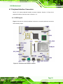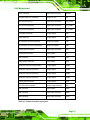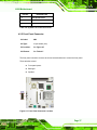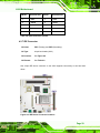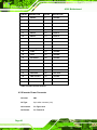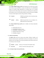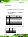
1
A300 Motherboard
A300 Motherboard
Page i
A300 Motherboard
Revision
MODEL
A300 Intel® Pentium® M/Celeron® M Motherboard
Revision Number
Description
Date of Issue
1.0
Initial release
March 2007
Page ii
A300 Motherboard
Copyright
COPYRIGHT NOTICE
The information in this document is subject to change without prior notice in order to
improve reliability, design and function and does not represent a commitment on the part
of the manufacturer.
In no event will the manufacturer be liable for direct, indirect, special, incidental, or
consequential damages arising out of the use or inability to use the product or
documentation, even if advised of the possibility of such damages.
This document contains proprietary information protected by copyright. All rights are
reserved. No part of this manual may be reproduced by any mechanical, electronic, or
other means in any form without prior written permission of the manufacturer.
TRADEMARKS
IBM PC is a registered trademark of International Business Machines Corporation. INTEL
is a registered trademark of INTEL Corporation. Other product names mentioned herein
are used for identification purposes only and may be trademarks and/or registered
trademarks of their respective owners.
Page iii
A300 Motherboard
Packing List
NOTE:
If any of the components listed in the checklist below are missing,
please do not proceed with the installation. Contact the IEI reseller or
vendor you purchased the A300 from or contact an IEI sales
representative directly. To contact an IEI sales representative, please
send an email to [email protected].
The items listed below should all be included in the A300 package.
1 x A300 single board computer
1 x IDE flat cable 44p/40p/40p
1 x IDE flat cable 44p/44p
2 x Single port RS-232 cable
1 x RS-232/422/485 cable
1 x Mini jumper pack
1 x Utility CD
1 x QIG (quick installation guide)
Images of the above items are shown in Chapter 3.
Page iv
A300 Motherboard
Table of Contents
1
INTRODUCTION..................................................................................................... 2
1.1 A300 OVERVIEW ........................................................................................................ 3
1.1.1 A300 Applications .............................................................................................. 3
1.1.2 A300 Benefits ..................................................................................................... 4
1.1.3 A300 Features .................................................................................................... 4
1.2 A300 BOARD OVERVIEW ........................................................................................... 5
1.2.1 A300 Connectors................................................................................................ 6
1.2.2 Technical Specifications..................................................................................... 7
2
DETAILED SPECIFICATIONS ........................................................................... 10
2.1 OVERVIEW ................................................................................................................11
2.2 DIMENSIONS .............................................................................................................11
2.2.1 Board Dimensions.............................................................................................11
2.2.2 External Interface Panel Dimensions .............................................................. 12
2.3 DATA FLOW .............................................................................................................. 12
2.4 COMPATIBLE PROCESSOR ......................................................................................... 13
2.4.1 CPU Overview ................................................................................................. 13
2.4.2 Supported Processors ...................................................................................... 13
2.5 INTEL® 855GME CHIPSET GRAPHICS MEMORY CONTROLLER HUB ........................ 14
2.5.1 Intel® 855GME Overview ................................................................................ 14
2.5.2 Intel® 855GME Memory Support .................................................................... 14
2.5.3 Intel® 855GME Internal Graphics Controller ................................................. 14
2.5.4 Intel® 855GME Power Management ............................................................... 16
2.6 INTEL® 82801DB I/O CONTROLLER HUB (ICH4).................................................... 16
2.6.1 Intel® ICH4 Overview ...................................................................................... 16
2.6.2 Intel® ICH4 IDE Interface ............................................................................... 17
2.6.3 Intel® ICH4 Compact Flash Interface ............................................................. 17
2.6.4 Intel® ICH4 Audio Codec 97 (AC’97) Controller............................................ 17
2.6.5 Intel® ICH4 USB Controller ............................................................................ 18
2.6.6 Intel® ICH4 PCI Interface ............................................................................... 18
2.6.7 Intel® ICH4 Low Pin Count (LPC) Interface................................................... 18
Page v
A300 Motherboard
2.6.8 BIOS................................................................................................................. 19
2.7 PCI BUS COMPONENTS ............................................................................................ 19
2.7.1 PCI Bus Overview............................................................................................ 19
2.7.2 GbE Ethernet ................................................................................................... 19
2.7.3 PCMCIA Slot.................................................................................................... 20
2.8 LPC BUS COMPONENTS ........................................................................................... 20
2.8.1 LPC Bus Overview........................................................................................... 20
2.8.2 BIOS Chipset.................................................................................................... 20
2.8.3 Super I/O Chipset............................................................................................. 21
2.8.3.1 Super I/O 16C550 UARTs ........................................................................ 21
2.8.3.2 Super I/O Enhanced Hardware Monitor ................................................... 22
2.8.3.3 Super I/O Fan Speed Controller................................................................ 22
2.8.3.4 Super I/O Keyboard Controller................................................................. 22
2.8.4 LPC I/O Chipset............................................................................................... 22
2.9 ENVIRONMENTAL AND POWER SPECIFICATIONS ....................................................... 22
2.9.1 System Monitoring ........................................................................................... 22
2.9.2 Operating Temperature and Temperature Control........................................... 23
2.9.3 Power Consumption......................................................................................... 23
3
UNPACKING .......................................................................................................... 24
3.1 ANTI-STATIC PRECAUTIONS ...................................................................................... 25
3.2 UNPACKING.............................................................................................................. 25
3.2.1 Unpacking Precautions.................................................................................... 25
3.3 UNPACKING CHECKLIST ........................................................................................... 26
3.3.1 Package Contents............................................................................................. 26
4
CONNECTOR PINOUTS...................................................................................... 28
4.1 PERIPHERAL INTERFACE CONNECTORS .................................................................... 29
4.1.1 A300 Layout ..................................................................................................... 29
4.1.2 Peripheral Interface Connectors ..................................................................... 30
4.1.3 External Interface Panel Connectors............................................................... 32
4.2 INTERNAL PERIPHERAL CONNECTORS ...................................................................... 32
4.2.1 ATX Power Connector ..................................................................................... 32
4.2.2 Audio Connector .............................................................................................. 33
4.2.3 Compact Flash Socket...................................................................................... 34
Page vi
A300 Motherboard
4.2.4 Fan Connectors................................................................................................ 36
4.2.5 Front Panel Connector .................................................................................... 37
4.2.6 GPIO Connector .............................................................................................. 38
4.2.7 IDE Connector ................................................................................................. 39
4.2.8 Inverter Power Connector ............................................................................... 40
4.2.9 IrDA Infrared Interface Connector.................................................................. 41
4.2.10 LED Connector .............................................................................................. 42
4.2.11 Power Button Connector................................................................................ 43
4.2.12 Serial Port Connector (RS-422/485) ............................................................. 44
4.2.13 Serial Port Connector (RS-232)..................................................................... 45
4.2.14 System Panel Connector ................................................................................ 47
4.2.15 TFT LCD LVDS Connector............................................................................ 48
4.2.16 Internal USB Connectors (8-Pin) .................................................................. 50
4.2.17 Internal USB Connectors (5-Pin) .................................................................. 51
4.3 EXTERNAL PERIPHERAL INTERFACE CONNECTORS .................................................. 52
4.3.1 External Peripheral Interface Connector Overview........................................ 52
4.3.2 Audio Connectors............................................................................................. 52
4.3.3 DVI-I Connector .............................................................................................. 53
4.3.4 RJ-45 Ethernet Connector ............................................................................... 54
4.3.5 Keyboard/Mouse Connector ............................................................................ 55
4.3.6 Serial Port Connector (COM 1) ...................................................................... 56
4.3.7 Serial Port Connectors (COM 2 and COM3) .................................................. 57
4.3.8 USB Combo Ports ............................................................................................ 58
4.3.9 VGA Connector ................................................................................................ 58
5
INSTALLATION .................................................................................................... 60
5.1 ANTI-STATIC PRECAUTIONS ...................................................................................... 61
5.2 INSTALLATION CONSIDERATIONS ............................................................................. 62
5.2.1 Installation Notices .......................................................................................... 62
5.2.2 Installation Checklist ....................................................................................... 63
5.3 CPU AND CPU COOLING KIT INSTALLATION ........................................................... 64
5.3.1 Socket 479 CPU Installation............................................................................ 64
5.3.2 Cooling Kit CF-479B-RS Installation.............................................................. 66
5.4 DIMM MODULE INSTALLATION AND CF CARD INSTALLATION ............................... 68
5.4.1 DIMM Module Installation .............................................................................. 68
Page vii
A300 Motherboard
5.4.2 CF Card Installation........................................................................................ 69
5.5 JUMPER SETTINGS .................................................................................................... 70
5.5.1 CF Card Setup Jumper Settings....................................................................... 71
5.5.2 Clear CMOS Jumper........................................................................................ 72
5.5.3 COM Port Setting Jumper ............................................................................... 73
5.5.4 LCD Voltage Selection ..................................................................................... 75
5.5.5 LCD Rotation Jumper ...................................................................................... 76
5.6 CHASSIS INSTALLATION ........................................................................................... 77
5.6.1 Airflow.............................................................................................................. 77
5.6.2 Motherboard Installation................................................................................. 78
5.7 INTERNAL PERIPHERAL DEVICE CONNECTIONS........................................................ 78
5.7.1 Peripheral Device Cables ................................................................................ 78
5.7.2 ATA Flat Cable Connection ............................................................................. 78
5.7.3 Single Port RS-232 Cable ................................................................................ 79
5.8 EXTERNAL PERIPHERAL INTERFACE CONNECTION ................................................... 80
6
AMI BIOS................................................................................................................ 82
6.1.1.1 IDE Master, IDE Slave ............................................................................. 84
6.1.2 Super IO Configuration.................................................................................... 91
6.1.3 Hardware Health Configuration...................................................................... 94
6.1.4 ACPI Configuration ......................................................................................... 96
6.1.4.1 Advanced ACPI Configuration ................................................................. 97
6.1.5 MPS Configuration .......................................................................................... 99
6.1.6 USB Configuration......................................................................................... 100
6.1.6.1 USB Mass Storage Device Configuration............................................... 103
6.2 PCI/PNP ................................................................................................................ 105
6.3 BOOT ......................................................................................................................110
6.3.1 Boot Settings Configuration............................................................................ 111
6.3.2 Boot Device Priority .......................................................................................115
6.3.3 Removable Drives ...........................................................................................116
6.3.4 CD/DVD Drives ..............................................................................................118
6.4 SECURITY................................................................................................................118
6.5 CHIPSET ................................................................................................................. 120
6.5.1 NorthBridge Configuration............................................................................ 120
6.5.2 SouthBridge Configuration............................................................................ 124
Page viii
A300 Motherboard
6.6 POWER ................................................................................................................... 126
6.7 EXIT ....................................................................................................................... 129
7
SOFTWARE DRIVERS ....................................................................................... 133
7.1 AVAILABLE SOFTWARE DRIVERS ............................................................................ 134
7.2 CHIPSET DRIVER INSTALLATION............................................................................. 134
7.3 REALTEK AUDIO DRIVER INSTALLATION ............................................................... 138
7.4 INTEL CHIPSET GRAPHICS DRIVER ......................................................................... 142
7.5 SATA - ALI RAID DRIVER INSTALLATION ............................................................ 145
7.5.1 Installation Steps During Windows XP Installation....................................... 146
7.5.2 Installation Steps under Existing Windows XP .............................................. 147
A
BIOS OPTIONS .................................................................................................... 149
B
GPIO CONNECTION.......................................................................................... 155
B.1 GPIO SETTINGS AND DEFAULT VALUES ................................................................ 156
B.1.1 GPIO Settings................................................................................................ 156
B.1.2 Default Settings ............................................................................................. 156
B.2 ASSEMBLY LANGUAGE SAMPLES ........................................................................... 157
B.2.1 GPIO Initialization Procedure ...................................................................... 157
B.2.2 General Purpose Output Procedure .............................................................. 157
B.2.3 General Purpose Input Procedure................................................................. 158
C
WATCHDOG TIMER .......................................................................................... 159
D
ADDRESS MAPPING.......................................................................................... 163
D.1 ADDRESS MAP ...................................................................................................... 164
D.2 1ST MB MEMORY ADDRESS MAP ......................................................................... 164
D.3 IRQ MAPPING TABLE ............................................................................................ 165
D.4 DMA CHANNEL ASSIGNMENTS ............................................................................. 165
E
EXTERNAL AC’97 AUDIO CODEC ................................................................. 167
E.1 INTRODUCTION ...................................................................................................... 168
E.1.1 Accessing the AC’97 CODEC ....................................................................... 168
E.1.2 Driver Installation ......................................................................................... 168
E.2 SOUND EFFECT CONFIGURATION ........................................................................... 168
E.2.1 Accessing the Sound Effects Manager........................................................... 168
Page ix
A300 Motherboard
E.2.2 Sound Effect Manager Configuration Options.............................................. 170
F
INDEX.................................................................................................................... 173
Page x
A300 Motherboard
List of Figures
Figure 1-1: A300 Overview ...........................................................................................5
Figure 1-2: A300 Solder Side Overview ......................................................................6
Figure 2-1: A300 Dimensions (mm) ...........................................................................11
Figure 2-2: External Interface Panel Dimensions (mm)...........................................12
Figure 2-3: Data Flow Block Diagram........................................................................12
Figure 4-1: Connector and Jumper Locations .........................................................29
Figure 4-2: Connector and Jumper Locations (Solder Side) ..................................30
Figure 4-3: ATX Power Connector Location.............................................................33
Figure 4-4: Audio Connector Pinouts (10-pin) .........................................................34
Figure 4-5: CF Card Socket Location ........................................................................35
Figure 4-6: Fan Connector Locations .......................................................................36
Figure 4-7: Front Panel Connector Location............................................................37
Figure 4-8: GPIO Connector Pinout Locations ........................................................38
Figure 4-9: IDE Device Connector Locations ...........................................................39
Figure 4-10: Inverter Connector Location ................................................................41
Figure 4-11: IR Connector Location ..........................................................................42
Figure 4-12: LED Connector Locations.....................................................................43
Figure 4-13: Power Button Connector Location ......................................................44
Figure 4-14: Serial Port Connector Location............................................................45
Figure 4-15: RS-232 Serial Port Connector Locations ............................................46
Figure 4-16: Front Panel Connector Location..........................................................48
Figure 4-17: TFT LCD LVDS Connector Pinout Locations......................................49
Figure 4-18: Internal USB Connector Locations (8-pin) ..........................................50
Figure 4-19: Internal USB Connector Locations (5-pin) ..........................................51
Figure 4-20: A300 On-board External Interface Connectors ..................................52
Figure 4-21: Audio Connector....................................................................................53
Figure 4-22 DVI-I Connector Pinout Locations ........................................................53
Page xi
A300 Motherboard
Figure 4-23: J7 Connector..........................................................................................55
Figure 4-24: PS/2 Pinouts...........................................................................................56
Figure 4-25: Serial Port Pinout Locations.................................................................57
Figure 4-26: VGA Connector ......................................................................................59
Figure 5-1: Make sure the CPU socket retention screw is unlocked .....................65
Figure 5-2: Lock the CPU Socket Retention Screw .................................................66
Figure 5-3: IEI CF-518-RS and CF-479A-RS Cooling Kit..........................................66
Figure 5-4: Cooling Kit Support Bracket...................................................................67
Figure 5-5: Connect the cooling fan cable ...............................................................68
Figure 5-6: Installing the DIMM Module ....................................................................69
Figure 5-7: CF Card Installation.................................................................................70
Figure 5-8: CF Card Setup Jumper Location............................................................72
Figure 5-9: JP2 Clear CMOS Jumper.........................................................................73
Figure 5-10: COM Port Setting Jumper Location.....................................................75
Figure 5-11: LCD Voltage Selection Jumper Location ............................................76
Figure 5-12: LCD Rotate Jumper Location ...............................................................77
Figure 5-13: IDE Cable Connection ...........................................................................79
Figure 5-14: Single Port RS-232 Cable Connection.................................................80
Figure 7-1: InstallShield Wizard Preparation Screen............................................ 135
Figure 7-2: Welcome Screen ................................................................................... 135
Figure 7-3: License Agreement............................................................................... 136
Figure 7-4: Readme Information ............................................................................. 137
Figure 7-5: Restart the Computer ........................................................................... 138
Figure 7-6: Audio Driver Install Shield Wizard Starting ....................................... 139
Figure 7-7: Audio Driver Welcome Screen ............................................................ 140
Figure 7-8: Audio Driver Software Configuration ................................................. 140
Figure 7-9: Audio Driver Digital Signal .................................................................. 141
Figure 7-10: Audio Driver Installation Complete................................................... 142
Figure 7-11: VGA Driver Installation InstallShield Wizard Screen ...................... 143
Figure 7-12: VGA Driver Welcome Screen............................................................. 144
Figure 7-13: GMA Driver Installation Complete .................................................... 145
Page xii
A300 Motherboard
List of Tables
Table 1-1: Technical Specifications ............................................................................9
Table 2-1: Supported Processors..............................................................................13
Table 2-2: Supported HDD Specifications ................................................................17
Table 2-3: Power Consumption .................................................................................23
Table 3-1: Package List Contents..............................................................................27
Table 4-1: Peripheral Interface Connectors..............................................................31
Table 4-2: Rear Panel Connectors.............................................................................32
Table 4-3: ATX Power Connector Pinouts ................................................................33
Table 4-4: Audio Connector Pinouts (3-pin).............................................................34
Table 4-5: CF Card Socket Pinouts ...........................................................................36
Table 4-6: System Fan Connector Pinouts ...............................................................37
Table 4-7: Front Panel Connector Pinouts ...............................................................38
Table 4-8: GPIO Connector Pinouts ..........................................................................39
Table 4-9: IDE Connector Pinouts .............................................................................40
Table 4-10: Inverter Power Connector Pinouts ........................................................41
Table 4-11: IR Connector Pinouts..............................................................................42
Table 4-12: LED Connector Pinouts ..........................................................................43
Table 4-13: Power Button Connector Pinouts..........................................................44
Table 4-14: RS-422/485 Serial Port Connector Pinouts...........................................45
Table 4-15: COM4 Serial Port Connector Pinouts....................................................46
Table 4-16: COM5 Serial Port Connector Pinouts....................................................46
Table 4-17: COM6 Serial Port Connector Pinouts....................................................47
Table 4-18: Front Panel Connector Pinouts .............................................................48
Table 4-19: TFT LCD LVDS Port Connector Pinouts ...............................................49
Table 4-20: Internal USB Connector Pinouts (8-pin) ...............................................50
Table 4-21: Internal USB Connector Pinouts (5-pin) ...............................................51
Table 4-22: DVI-I Connector Pinouts .........................................................................54
Page xiii
A300 Motherboard
Table 4-23: RJ-45 Ethernet Connector Pinouts........................................................55
Table 4-24: RJ-45 Ethernet Connector LEDs............................................................55
Table 4-25: Keyboard Connector Pinouts ................................................................56
Table 4-26: RS-232 Serial Port (COM 1) Pinouts ......................................................57
Table 4-27: RS-232 Serial Port (COM2, COM3) Pinouts...........................................57
Table 4-28: USB Connector Pinouts..........................................................................58
Table 4-29: VGA Connector Pinouts .........................................................................59
Table 5-1: Jumpers ....................................................................................................71
Table 5-2: CF Card Setup Jumper Settings ..............................................................71
Table 5-3: JP2 Clear CMOS Jumper Settings...........................................................73
Table 5-4: COM Port Setting Jumper Settings .........................................................74
Table 5-5: LCD Voltage Selection Jumper Settings.................................................75
Table 5-6: LCD Rotate Jumper Settings....................................................................76
Table 5-7: IEI Provided Cables...................................................................................78
Page xiv
A300 Motherboard
BIOS Menus
BIOS Menu 1: IDE Master Configuration...................................................................84
BIOS Menu 2: IDE Slave Configuration.....................................................................88
BIOS Menu 3: Super IO Configuration ......................................................................91
BIOS Menu 4: Hardware Health Configuration.........................................................95
BIOS Menu 5: ACPI Configuration.............................................................................97
BIOS Menu 6: Advanced ACPI Configuration ..........................................................98
BIOS Menu 7: MPS Configuration .......................................................................... 100
BIOS Menu 8: USB Configuration........................................................................... 101
BIOS Menu 9: USB Mass Storage Device Configuration...................................... 103
BIOS Menu 10: PCI/PnP Configuration .................................................................. 106
BIOS Menu 11: Boot................................................................................................. 111
BIOS Menu 12: Boot Settings Configuration......................................................... 112
BIOS Menu 13: Boot Device Priority Settings ....................................................... 116
BIOS Menu 14: Removable Drives.......................................................................... 117
BIOS Menu 15: Security........................................................................................... 119
BIOS Menu 16: Chipset............................................................................................ 120
BIOS Menu 17: NorthBridge Chipset Configuration............................................. 121
BIOS Menu 18: SouthBridge Chipset Configuration ............................................ 125
BIOS Menu 19: Power .............................................................................................. 127
BIOS Menu 20: Exit ................................................................................................. 130
Page xv
A300 Motherboard
Glossary
AC ’97
Audio Codec 97
IDE
Integrated Data Electronics
ACPI
Advanced Configuration and
I/O
Input/Output
Power Interface
ICH4
I/O Controller Hub 4
APM
Advanced Power Management
L1 Cache Level 1 Cache
ARMD
ATAPI Removable Media Device
L2 Cache Level 2 Cache
ASKIR
Shift Keyed Infrared
LCD
Liquid Crystal Display
ATA
Advanced Technology
LPT
Parallel Port Connector
Attachments
LVDS
Low Voltage Differential Signaling
BIOS
Basic Input/Output System
MAC
Media Access Controller
CFII
Compact Flash Type 2
OS
Operating System
CMOS
Complementary Metal Oxide
PCI
Peripheral Connect Interface
Semiconductor
PIO
Programmed Input Output
CPU
Central Processing Unit
PnP
Plug and Play
Codec
Compressor/Decompressor
POST
Power On Self Test
COM
Serial Port
RAM
Random Access Memory
DAC
Digital to Analog Converter
SATA
Serial ATA
DDR
Double Data Rate
S.M.A.R.T Self Monitoring Analysis and
DIMM
Dual Inline Memory Module
DIO
Digital Input/Output
SPD
Serial Presence Detect
DMA
Direct Memory Access
S/PDI
Sony/Philips Digital Interface
EIDE
Enhanced IDE
SDRAM
Synchronous Dynamic Random
EIST
Enhanced Intel SpeedStep
Reporting Technology
Access Memory
Technology
SIR
Serial Infrared
FFIO
Flexible File Input/Output
UART
Universal Asynchronous
FIFO
First In/First Out
FSB
Front Side Bus
USB
Universal Serial Bus
IrDA
Infrared Data Association
VGA
Video Graphics Adapter
HDD
Hard Disk Drive
Page xvi
Receiver-transmitter
A300 Motherboard
Chapter
1
1 Introduction
Page 2
A300 Motherboard
1.1 A300 Overview
®
The A300 is a multimedia Pentium Mobile processor-based motherboard that powers a
Point-of-Care terminal or panel PC for varied purposes. To facilitate multimedia
performance, the A300 can connect to slim Combo CD/DVD-ROM, a PCMCIA card
socket, and the multimedia and wireless 802.11g functionality. The A300 also comes
with an expansion PCI slot which allows flexible implementations making it the perfect
platform for comprehensive lifestyle computing applications.
1.1.1 A300 Applications
The A300 is designed for applications in the following areas:
Surveillance
o
o
o
o
Digital surveillance
X-ray imaging terminal
Bedside entertainment
Multimedia advertising platform
General Computing
o
o
o
o
Computer-based testing center
General purpose information system
Mobile nursing station
Interactive education uses
Automation & Control
o
o
o
Plant environment monitoring
Factory automation HMI terminal
Shop-floor/MES control
Self-service Kiosk
o
o
o
o
o
Full-service receptionist kiosk
Hospital self-registering terminal
Interactive photo kiosk
Video rental kiosk
Self-service POS terminal
Page 3
A300 Motherboard
1.1.2 A300 Benefits
Some of the A300 benefits include:
Clinical Information System (CIS) integration
Filmless solution by PACS
Reduced maintenance costs
Client crash prevention
Central resource control
1.1.3 A300 Features
Some of the A300 features are listed below:
LPX form factor
RoHS compliant
Intel Pentium M / Celeron M processor supported
Digital dual-independent display functionality
Low power consumption
Two high performance gigabit Ethernet controllers on-board
Medical power input fully supported
CompactFlash® card and PCMCIA socket solutions
Integrated audio
Page 4
A300 Motherboard
1.2 A300 Board Overview
Figure 1-1: A300 Overview
Page 5
A300 Motherboard
Figure 1-2: A300 Solder Side Overview
1.2.1 A300 Connectors
The A300 has the following connectors on-board:
1 x ATX power connector
1 x Audio connector
1 x CompactFlash® card socket
3 x Cooling fan connectors
1 x Front panel connector
1 x 8 bits GPIO connector
2 x 44-pin IDE connectors
1 x Inverter connector
1 x IR interface connector
Page 6
A300 Motherboard
1 x Disk LED connector
1 x PCMCIA slot
1 x Power button connector
3 x RS-232 serial port connectors
1 x RS-422/485 serial port connector
1 x System panel connector
1 x LCD LVDS connector
3 x USB2.0 connectors
The A300 has the following connectors on the board rear panel:
1 x Audio connector
1 x COM port jumper
1 x DVI-I connector
3 x Serial port connectors
1 x CRT connector
1 x PS/2 keyboard connector
1 x PS/2 mouse connector
2 x USB 2.0 connectors
2 x LAN RJ-45 connectors
The A300 has the following on-board jumpers:
Clear CMOS
CF Card Setup
COM Port Jumper Settings
LCD Voltage Setup
LCD Rotate Setup
1.2.2 Technical Specifications
A300 technical specifications are listed in Table 1-1. Detailed descriptions of each
specification can be found in Chapter 2.
Page 7
A300 Motherboard
Specification
A300
CPU
Intel® Pentium M/Celeron M 400Mhz FSB up to 2.10GHz
System Chipset
Intel® 855GME + ICH4
CRT integrated in Intel® 855GME
Display
DVI integrated in Silicon Image SiI164
Dual channel 18-bit LVDS integrated in Intel® 855GME
TTL/LVDS
Supports independent dual display
Memory
Supports two DDR 266/333 184-pin DIMM modules up to 2GB
BIOS
AMI BIOS
SSD
Compact Flash (CF)
Audio
AC'97 Codec Realtek ALC655
LAN
Dual Realtek RTL8110S/SC GbE
Five RS-232 and
COM
One RS-232/422/RS-485
USB2.0
Six USB 1.1 or USB 2.0 devices supported
IDE
Two 44-pin IDE connects to four Ultra ATA33/66/100 devices
Watchdog Timer
Software programmable 1-255 sec. by supper I/O
Digital I/O
One GPIO connector
One PCI slot
Expansion
One PCMCIA slot
Power Supply
ATX power support
Temperature
0ºC - 60ºC
Humidity (operating)
5%~95% non-condensing
Page 8
A300 Motherboard
Dimensions
235mm x 220mm
Weight (GW/NW)
1200g/680g
Table 1-1: Technical Specifications
Page 9
A300 Motherboard
Chapter
2
2 Detailed Specifications
Page 10
A300 Motherboard
2.1 Overview
This chapter describes the specifications and on-board features of the A300 in detail.
2.2 Dimensions
2.2.1 Board Dimensions
The dimensions of the board are listed below:
Length:
235mm
Width:
220mm
Figure 2-1: A300 Dimensions (mm)
Page 11
A300 Motherboard
2.2.2 External Interface Panel Dimensions
External peripheral interface connector panel dimensions are shown in Figure 2-2.
Figure 2-2: External Interface Panel Dimensions (mm)
2.3 Data Flow
The A300 motherboard comes with an Intel® Pentium M / Celeron M CPU. Figure 2-3
shows the data flow between the system chipset, the CPU and other components installed
on the motherboard.
Figure 2-3: Data Flow Block Diagram
Page 12
A300 Motherboard
2.4 Compatible Processor
2.4.1 CPU Overview
Socket 479 Intel® Pentium® M processors with enhanced Intel SpeedStep® Technology
and Socket 479 Intel® Celeron® M processors can be installed on the A300 motherboard.
2.4.2 Supported Processors
Specifications for the compatible processors are listed in Table 2-1 below:
Family
Number
Architecture
Cache
Clock Speed
FSB
Pentium® M
765
90 nm
2 MB L2
2.10 GHz
400 MHz
Pentium® M
755
90 nm
2 MB L2
2.0 GHz
400 MHz
Pentium® M
745
90 nm
2 MB L2
1.80 GHz
400 MHz
Pentium® M
735
90 nm
2 MB L2
1.70 GHz
400 MHz
Pentium® M
725
90 nm
2 MB L2
1.60 GHz
400 MHz
Pentium® M
715
90 nm
2 MB L2
1.50 GHz
400 MHz
Pentium® M
710
90 nm
2 MB L2
1.40 GHz
400 MHz
Celeron® M
390
90 nm
1 MB L2
1.70 GHz
400 MHz
Celeron® M
380
90 nm
1 MB L2
1.60 GHz
400 MHz
Celeron® M
370
90 nm
1 MB L2
1.50 GHz
400 MHz
Celeron® M
360
90 nm
1 MB L2
1.40 GHz
400 MHz
Celeron® M
350
90 nm
1 MB L2
1.30 GHz
400 MHz
Table 2-1: Supported Processors
Page 13
A300 Motherboard
2.5 Intel® 855GME Chipset Graphics Memory Controller Hub
2.5.1 Intel® 855GME Overview
The Intel® 855GME chipset comes with the following features:
400 MHz system bus delivers a high-bandwidth connection between the
processor and the platform
Integrated graphics utilizing Intel® Extreme Graphics 2 technology
AGP 4X support
Three USB host controllers provide high-performance peripherals with 480
Mbps of bandwidth, while enabling support for up to six USB 2.0 ports.
The latest AC '97 implementation delivers 20-bit audio for enhanced sound
quality and full surround sound capability
LAN Connect Interface (LCI) provides flexible network solutions such as
10/100 Mbps Ethernet and 10/100 Mbps Ethernet with LAN manageability
Dual Ultra ATA/100 controllers, coupled with the Intel® Application Accelerator
support faster IDE transfers to storage devices
The Intel Application Accelerator software provides additional performance
over native ATA drivers by improving I/O transfer rates and enabling faster
O/S load time, resulting in accelerated boot times
Communication and Network Riser (CNR) offers flexibility in system
configuration with a baseline feature set that can be upgraded with an audio
card, modem card, or network card
Error Correcting Code (ECC) support in integrated graphics mode only
2.5.2 Intel® 855GME Memory Support
The Intel® 855GME supports two DDR memory modules with frequencies up to 333MHz.
The A300 has two 184-pin DDR DIMM SDRAM socket that supports two 200MHz,
266MHz or 333MHz DDR DIMM memory module with a maximum capacity of 2GB.
2.5.3 Intel® 855GME Internal Graphics Controller
The Intel® 855GME supports both CRT and TFT in a dual display mode. The following
display specifications.
Page 14
A300 Motherboard
Graphics Core Frequency
o
Display/Render frequency up to 250 MHz (with 1.35 V core voltage)
3D Graphics Engine
o
o
o
3D Setup and Render Engine
Zone Rendering
High-quality performance Texture Engine
Analog Display Support
o
o
o
350-MHz integrated 24-bit RAMDAC
Hardware color cursor support
Accompanying I2C and DDC channels provided through multiplexed
interface
o
o
Dual independent pipe for dual independent display
Simultaneous display: same images and native display timings on each
display device
Digital Video Out Port (DVOB & DVOC) support
o
o
DVOB & DVOC with 165-MHz dot clock support for each 12-bit interface
Compliant with DVI Specification 1.5
Dedicated LFP (local flat panel) support
o
Single or dual channel LVDS panel support up to UXGA panel resolution
with frequency range from 25 MHz to 112 MHz per channel
o
SSC support of 0.5%, 1.0%, and 2.5% center and down spread with
external SSC clock
o
o
o
o
o
Supports data format of 18 bpp
LCD panel power sequencing compliant with SPWG timing specification
Compliant with ANSI/TIA/EIA 644-1995 spec
Integrated PWM interface for LCD backlight inverter control
Bi-linear Panel fitting
Internal Graphics Features (Intel 855GME chipset)
o
Core Vcc = 1.2 V or 1.35 V (to support higher graphics core frequency
and DDR333)
o
Graphics core frequency
Display core frequency at 133 MHz, 200 MHz, 250 MHz
Render core frequency at 100 MHz, 133 MHz, 166 MHz, 200 MHz, 250 MHz
Intel® Dual-Frequency Graphics Technology
o
3D Graphics Engine
Page 15
A300 Motherboard
Enhanced Hardware Binning Instruction Set supported
Bi-Cubic Filtering supported
Linear Gamma Blending for Video Mixer Rendering (VMR)
Video Mixer Rendering (VMR) supported
o
Graphics Power Management
Dynamic Core Frequency Switching
Intel® Smart 2D Display Technology
Memory Self-Refresh During C3
Intel® Display Power Saving Technology
2.5.4 Intel® 855GME Power Management
The power management for the Intel® 855GME is listed below:
Optimized Clock Gating for 3D and Display Engines
On-die thermal sensor
2.6 Intel® 82801DB I/O Controller Hub (ICH4)
2.6.1 Intel® ICH4 Overview
The Intel® ICH4 I/O controller hub comes with the following features:
PCI Local Bus Specification, Revision 2.2-compliant with support for 33 MHz
PCI operations.
ACPI Power Management Logic Support
Enhanced DMA controller, Interrupt controller, and timer functions
Integrated IDE controller supports Ultra ATA100/66/33
USB host interface with support for 6 USB ports; 3 UHCI host controllers; 1
EHCI high-speed
USB 2.0 Host controller
Integrated LAN controller
System Management Bus (SMBus) Specification, Version 2.0 with additional
support for I2C devices
Supports Audio Codec ’97, Revision 2.3 specification
Low Pin Count (LPC) interface
Firmware Hub (FWH) interface support
Page 16
A300 Motherboard
Alert On LAN* (AOL) and Alert On LAN 2* (AOL2)
2.6.2 Intel® ICH4 IDE Interface
The single A300 IDE connector supports two IDE hard disks and ATAPI devices. PIO IDE
transfers up to 16MB/s and Ultra ATA transfers of 100MB/s. The integrated IDE interface
is able to support the following IDE HDDs:
The onboard ATA-6 controller is able to support the following IDE HDDs:
Ultra ATA/100, with data transfer rates up to 100MB/s
Ultra ATA/66, with data transfer rates up to 66MB/s
Ultra ATA/33, with data transfer rates up to 33MB/s
Specification
Ultra ATA/100
Ultra ATA/66
Ultra ATA/100
IDE devices
2
2
2
PIO Mode
0–4
0–4
0–4
PIO Max Transfer Rate
16.6 MB/s
16.6 MB/s
16.6 MB/s
DMA/UDMA designation
UDMA 3 - 4
UDMA 3 – 4
UDMA 2
DMA/UDMA Max Transfer
100MB/s
66MB/s
33MB/s
Controller Interface
5V
5V
5V
Table 2-2: Supported HDD Specifications
2.6.3 Intel® ICH4 Compact Flash Interface
The A300 CompactFlash socket supports standard CF Type I and CF Type II cards. The
chipset flash interface is multiplexed with an IDE interface and can be connected to an
array of industry standard NAND Flash or NOR Flash devices.
2.6.4 Intel® ICH4 Audio Codec 97 (AC’97) Controller
The Audio Codec ’97 (AC’97) controller integrated into the ICH4 complies with AC’97
Component Specification, Version 2.3. The AC’97 controller is connected to the onboard
Page 17
A300 Motherboard
audio connector. The audio connector is connected to an audio kit with an embedded
AC’97 audio codec. The AC’97 controller supports up to six PCM audio output channels.
Complete surround sound requires six-channel audio consisting of:
Front left
Front right
Back left
Back right
Center
Subwoofer
2.6.5 Intel® ICH4 USB Controller
Two external USB ports on the A300 board are interfaced to the chipset USB controller.
Six USB 1.1 or USB 2.0 devices can be connected simultaneously to the A300. The
chipset USB controller has the following specifications:
6 USB ports
USB 1.1 and USB 2.0 compliant
3 Universal Host Controller Interface (UHCI) controllers
High-speed, full-speed and low-speed capable
2.6.6 Intel® ICH4 PCI Interface
The PCI interface on the ICH4 is compliant with the PCI Revision 2.2 implementation.
Some of the features of the PCI interface are listed below.
PCI Revision 2.2 compliant
33MHz
5V tolerant PCI signals (except PME#)
Integrated PCI arbiter supports up to six PCI bus masters
2.6.7 Intel® ICH4 Low Pin Count (LPC) Interface
The ICH4 LPC interface complies with the LPC 1.0 specifications. The LPC bus from the
ICH4 is connected to the following components:
Page 18
A300 Motherboard
BIOS chipset
Super I/O chipset
2.6.8 BIOS
The BIOS flash memory chip on the A300 has a licensed copy of AMI BIOS loaded onto it.
The BIOS flash memory chip is connected to the chipset via the LPC bus. The flash BIOS
features are listed below:
SMIBIOS (DMI) compliant
Console redirection function support
PXE (Pre-Boot Execution Environment) support
USB booting support
2.7 PCI Bus Components
2.7.1 PCI Bus Overview
The PCI bus controller on the ICH4 is compliant with PCI Revision 2.2 specifications and
has a 33MHz PCI clock. The components listed below are all connected to the PCI bus:
PCI socket
Realtek RTL8110S GbE interface
One PCMCIA slot
2.7.2 GbE Ethernet
A highly integrated and cost-effective single-chip, fast RealTek RTL8110S/SC GbE
Ethernet controller is interfaced through first the PCI bus to the CPU and system chipset.
The RealTek RTL8110S/SC controller provides 10Mbps, 100Mbps or 1000Mbps Ethernet
connectivity to the A300. Some of the features of the RealTek RTL8110S/SC are listed
below.
Integrated 10/100/1000 transceiver
Auto-Negotiation with Next Page capability
Supports PCI rev.2.3, 32-bit, 33/66MHz
Supports pair swap/polarity/skew correction
Page 19
A300 Motherboard
Crossover Detection & Auto-Correction
Wake-on-LAN and remote wake-up support
Microsoft® NDIS5 Checksum Offload (IP, TCP, UDP) and largesend offload
support
Supports Full Duplex flow control (IEEE 802.3x)
Fully compliant with IEEE 802.3, IEEE 802.3u, IEEE 802.3ab
Supports IEEE 802.1P Layer 2 Priority Encoding
Supports IEEE 802.1Q VLAN tagging
Serial EEPROM
3.3V signaling, 5V PCI I/O tolerant
Transmit/Receive FIFO (8K/64K) support
Supports power down/link down power saving
Supports PCI Message Signaled Interrupt (MSI)
2.7.3 PCMCIA Slot
The PCMCIA slot supports PCMCIA cards that are compliant with PCMCIA 2.0 standard.
The PCMCIA cards are easily installed into the socket. PCMCIA cards are 54.0mm wide,
85.6mm long. Supported PCMCIA cards include wireless LAN cards and GPRS card.
2.8 LPC Bus Components
2.8.1 LPC Bus Overview
The LPC bus is connected to components listed below:
BIOS chipset
Super I/O chipset
2.8.2 BIOS Chipset
The BIOS chipset has a licensed copy of AMI BIOS installed on the chipset. Some of the
BIOS features are listed below:
AMI Flash BIOS
SMIBIOS (DMI) compliant
Console redirection function support
Page 20
A300 Motherboard
PXE (Pre-boot Execution Environment) support
USB booting support
2.8.3 Super I/O Chipset
The iTE IT8712F Super I/O chipset is connected to the ICH4 through the LPC bus. The
iTE IT8712F is an LPC interface-based Super I/O device that comes with Environment
Controller integration. Some of the features of the iTE IT8712F chipset are listed below:
LPC Interface
PC98/99/2001, ACPI and LANDesk Compliant
Enhanced Hardware Monitor
Fan Speed Controller
SmartGuardian Controller
Single +5V Power Supply
Two 16C550 UARTs for serial port control
One IEEE 1284 Parallel Port
Keyboard Controller
Watchdog Timer
Serial IRQ Support
Vbat & Vcch Support
Single +5V Power Supply
Some of the Super I/O features are described in more detail below:
2.8.3.1 Super I/O 16C550 UARTs
The onboard Super I/O has two integrated 16C550 UARTs that can support the following:
Two standard serial ports (COM1 and COM2)
IrDa 1.0 and ASKIR protocols
Another two chipsets connected to the LPC bus provided connectivity to another four
serial port connectors (COM3, COM4, COM5 and COM6).
Page 21
A300 Motherboard
2.8.3.2 Super I/O Enhanced Hardware Monitor
The Super I/O Enhanced Hardware Monitor monitors three thermal inputs, VBAT
internally, and eight voltage monitor inputs. These hardware parameters are reported in
the BIOS and can be read from the BIOS Hardware Health Configuration menu.
2.8.3.3 Super I/O Fan Speed Controller
The Super I/O fan speed controller enables the system to monitor the speed of the fan.
One of the pins on the fan connector is reserved for fan speed detection and interfaced to
the fan speed controller on the Super I/O. The fan speed is then reported in the BIOS.
2.8.3.4 Super I/O Keyboard Controller
The Super I/O keyboard controller can execute the 8042 instruction set. Some of the
keyboard controller features are listed below:
The 8042 instruction is compatible with a PS/2 keyboard and PS/2 mouse
Gate A20 and Keyboard reset output
Supports multiple keyboard power on events
Supports mouse double-click and/or mouse move power on events
2.8.4 LPC I/O Chipset
The LPC I/O chipset is connected to the ICH4 through the LPC bus and complies with the
Intel® Low Pin Count Specification Rev. 1.0. The LPC I/O chipset supports two standard
serial ports.
2.9 Environmental and Power Specifications
2.9.1 System Monitoring
Three thermal inputs on the A-300 Super I/O Enhanced Hardware Monitor monitor the
following temperatures:
System temperature
Temperature Sensor #1
Page 22
A300 Motherboard
Eight voltage inputs on the A-300 Super I/O Enhanced Hardware Monitor monitor the
following voltages:
Vcore
+3.30Vin
+5.00Vin
+12Vin
The A-300 Super I/O Enhanced Hardware Monitor also monitors the CPU fan speeds.
2.9.2 Operating Temperature and Temperature Control
The maximum and minimum operating temperatures for the A300 are listed below.
Minimum Operating Temperature: 0ºC (32°F)
Maximum Operating Temperature: 60°C (140°F)
A cooling fan and heat sink must be installed on the CPU. Thermal paste must be
smeared on the lower side of the heat sink before it is mounted on the CPU. Heat sinks
are also mounted on the northbridge and southbridge chipsets to ensure the operating
temperature of these chips remain low.
2.9.3 Power Consumption
Table 2-3 shows the power consumption parameters for the A300 when an Intel®
Pentium® M 1.6GHz CPU is running with one 256MB DDR333 SDRAM memory module.
Voltage
Current
3.3V
0.46A
5V
1.05A
12V
0.41A
5VSB
0.29A
-12V
0.74A
Table 2-3: Power Consumption
Page 23
A300 Motherboard
Chapter
3
3 Unpacking
Page 24
A300 Motherboard
3.1 Anti-static Precautions
WARNING:
Failure to take ESD precautions during the installation of the A300 may
result in permanent damage to the A300 and severe injury to the user.
Electrostatic discharge (ESD) can cause serious damage to electronic components,
including the A300. Dry climates are especially susceptible to ESD. It is therefore critical
that whenever the A300, or any other electrical component is handled, the following
anti-static precautions are strictly adhered to.
Wear an anti-static wristband: - Wearing a simple anti-static wristband can
help to prevent ESD from damaging the board.
Self-grounding:- Before handling the board touch any grounded conducting
material. During the time the board is handled, frequently touch any
conducting materials that are connected to the ground.
Use an anti-static pad: When configuring the A300, place it on an antic-static
pad. This reduces the possibility of ESD damaging the A300.
Only handle the edges of the PCB:-: When handling the PCB, hold the PCB
by the edges.
3.2 Unpacking
3.2.1 Unpacking Precautions
When the A300 is unpacked, please do the following:
Follow the anti-static precautions outlined in Section 3.1.
Make sure the packing box is facing upwards so the A300 does not fall out of
the box.
Make sure all the components shown in Section 3.3 are present.
Page 25
A300 Motherboard
3.3 Unpacking Checklist
NOTE:
If some of the components listed in the checklist below are missing,
please do not proceed with the installation. Contact the IEI reseller or
vendor you purchased the A300 from or contact an IEI sales
representative directly. To contact an IEI sales representative, please
send an email to [email protected].
3.3.1 Package Contents
The A300 is shipped with the following components:
Quantity
Item
1
A300 single board computer
1
IDE flat cable 44p/40p/40p
1
IDE flat cable 44p/44p
2
Single port RS-232 cable
1
RS-232/422/485 cable
Page 26
Image
A300 Motherboard
1
Mini jumper pack
1
Quick installation guide
1
Utility CD
Table 3-1: Package List Contents
Page 27
A300 Motherboard
Chapter
4
4 Connector Pinouts
Page 28
A300 Motherboard
4.1 Peripheral Interface Connectors
Section 4.1.2 shows peripheral interface connector locations. Section 4.1.2 lists all the
peripheral interface connectors seen in Section 4.1.2.
4.1.1 A300 Layout
Figure 4-1 shows the on-board peripheral connectors, rear panel peripheral connectors
and on-board jumpers.
Figure 4-1: Connector and Jumper Locations
Page 29
A300 Motherboard
Figure 4-2: Connector and Jumper Locations (Solder Side)
4.1.2 Peripheral Interface Connectors
Table 4-1 shows a list of the peripheral interface connectors on the A300. Detailed
descriptions of these connectors can be found below.
Connector
Type
Label
ATX power connector
20-pin connector
PW1
Page 30
A300 Motherboard
Audio connector
3-pin wafer connector
AUDIO1
Compact Flash (CF) connector
50-pin CF slot
CN7
Fan connector (CPU)
3-pin wafer connector
CPU_FAN1
Fan connector (System)
3-pin wafer connector
SYS_FAN1
Fan connector (System)
3-pin wafer connector
SYS_FAN2
Front panel connector
10-pin header
CN5
GPIO connector
10-pin header
DIO1
IDE Interface connector (primary)
44-pin box header
IDE1
IDE Interface connector (secondary)
44-pin box header
IDE2
Inverter power connector
6-pin wafer connector
CN3
IR interface connector
5-pin header
IR1
LED connector
2-pin header
CN9
Power button connector
2-pin header
CN15
Serial port connector (RS-422/485)
14-pin header
COM3
Serial port connector (RS-232)
10-pin header
COM4
Serial port connector (RS-232)
10-pin header
COM5
Serial port connector (RS-232)
10-pin header
COM6
System panel connector
12-pin header
CN12
TFT LCD LVDS connector
30-pin crimp connector
CN8
USB connector
8-pin header
USB2
USB connector
5-pin wafer connector
USB3
USB connector
5-pin wafer connector
USB4
Table 4-1: Peripheral Interface Connectors
Page 31
A300 Motherboard
4.1.3 External Interface Panel Connectors
Table 4-2 lists the rear panel connectors on the A300. Detailed descriptions of these
connectors can be found in Section 0 on page 50.
Connector
Type
Label
Audio connectors
Audio jack
CN11
DVI-I connector
Female DVI-I
DVI1
Ethernet connectors
RJ-45 connector
LAN1
Keyboard/mouse connector
PS/2 connector
KB_MS1
RS-232 serial port connector (COM1)
DB-9 connector
CN1.B
RS-232 serial port connectors (COM2, COM3)
DB-9 connector
J5
USB ports
USB port
USB1
VGA port connector
15-pin female
CN1.A
Table 4-2: Rear Panel Connectors
4.2 Internal Peripheral Connectors
Internal peripheral connectors are found on the motherboard and are only accessible
when the motherboard is outside of the chassis. This section has complete descriptions of
all the internal, peripheral connectors on the A300.
4.2.1 ATX Power Connector
CN Label:
PW1
CN Type:
20-pin ATX power connector (2x10)
CN Location:
See Figure 4-3
CN Pinouts:
See Table 4-3
Page 32
A300 Motherboard
The 20-pin ATX power connector is connected to an AT power supply.
Figure 4-3: ATX Power Connector Location
PIN NO.
DESCRIPTION
PIN NO.
DESCRIPTION
1
3.3V
11
3.3V
2
3.3V
12
-12V
3
GND
13
GND
4
5V
14
PSON
5
GND
15
GND
6
5V
16
GND
7
GND
17
GND
8
PWR OK
18
-5V
9
5VSB
19
5V
10
12V
20
5V
Table 4-3: ATX Power Connector Pinouts
4.2.2 Audio Connector
CN Label:
AUDIO1
CN Type:
3-pin wafer connector
CN Location:
See Figure 4-4
Page 33
A300 Motherboard
CN Pinouts:
See Table 4-4
The 3-pin audio connector is connected to speakers the output of audio signals from the
system.
Figure 4-4: Audio Connector Pinouts (10-pin)
PIN NO.
DESCRIPTION
1
Speaker Out R
2
GND
3
Speaker Out L
Table 4-4: Audio Connector Pinouts (3-pin)
4.2.3 Compact Flash Socket
CN Label:
CN7 (solder side)
CN Type:
50-pin CF slot (2x25)
CN Location:
See Figure 4-5
CN Pinouts:
See Table 4-5
Page 34
A300 Motherboard
A CF Type I or Type II memory card is inserted to the CF socket on the solder side of the
A300.
Figure 4-5: CF Card Socket Location
PIN NO.
DESCRIPTION
PIN NO.
DESCRIPTION
1
GROUND
26
VCC-IN CHECK1
2
DATA 3
27
DATA 11
3
DATA 4
28
DATA 12
4
DATA 5
29
DATA 13
5
DATA 6
30
DATA 14
6
DATA 7
31
DATA 15
7
HDC_CS0#
32
HDC_CS1
8
N/C
33
N/C
9
GROUND
34
IOR#
10
N/C
35
IOW#
11
N/C
36
VCC_COM
12
N/C
37
IRQ15
13
VCC_COM
38
VCC_COM
14
N/C
39
CSEL
15
N/C
40
N/C
16
N/C
41
HDD_RESET
Page 35
A300 Motherboard
17
N/C
42
IORDY
18
SA2
43
SDREQ
19
SA1
44
SDACK#
20
SA0
45
HDD_ACTIVE#
21
DATA 0
46
66DET
22
DATA 1
47
DATA 8
23
DATA 2
48
DATA 9
24
N/C
49
DATA 10
25
VCC-IN CHECK2
50
GROUND
Table 4-5: CF Card Socket Pinouts
4.2.4 Fan Connectors
CN Label:
CPU_FAN1, SYS_FAN1 and SYS_FAN2
CN Type:
3-pin wafer connector
CN Location:
See Figure 4-6
CN Pinouts:
See Table 4-6
The cooling fan connectors on the A300 provide a 12V, 500mA current to a CPU cooling
fan and a system cooling fan.
Figure 4-6: Fan Connector Locations
Page 36
A300 Motherboard
PIN NO.
DESCRIPTION
1
Fan Speed Detect
2
+12V
3
GND
Table 4-6: System Fan Connector Pinouts
4.2.5 Front Panel Connector
CN Label:
CN5
CN Type:
10-pin header (2x5)
CN Location:
See Figure 4-7
CN Pinouts:
See Table 4-7
The front panel connector connects to several external switches to control the front panel.
These switches control:
Front panel power
Backlight
Speaker
Figure 4-7: Front Panel Connector Location
Page 37
A300 Motherboard
PIN
DESCRIPTION
PIN
DESCRIPTION
1
Speaker Up
2
LCD On/Off
3
Speaker Down
4
5V Power
5
GND
6
Power Button
7
BKLT Up
8
Standby Power
9
BKLT Down
10
GND
Table 4-7: Front Panel Connector Pinouts
4.2.6 GPIO Connector
CN Label:
DIO1
CN Type:
10-pin header (2x5)
CN Location:
See Figure 4-8
CN Pinouts:
See Table 4-8
The GPIO connector can be connected to external I/O control devices including sensors,
lights, alarms and switches.
Figure 4-8: GPIO Connector Pinout Locations
Page 38
A300 Motherboard
PIN NO.
DESCRIPTION
PIN NO.
DESCRIPTION
1
GND
2
VCC5
3
GPIO0
4
GPIO1
5
GPIO2
6
GPIO3
7
GPIO4
8
GPIO5
9
GPIO6
10
GPIO7
Table 4-8: GPIO Connector Pinouts
4.2.7 IDE Connector
CN Label:
IDE1 (Primary) and IDE2 (Secondary)
CN Type:
44-pin box header (2x22)
CN Location:
See Figure 4-9
CN Pinouts:
See Table 4-9
One 44-pin IDE device connector on the A300 supports connectivity to two hard disk
drives.
Figure 4-9: IDE Device Connector Locations
Page 39
A300 Motherboard
PIN NO.
DESCRIPTION
PIN NO.
DESCRIPTION
1
RESET#
2
GROUND
3
DATA 7
4
DATA 8
5
DATA 6
6
DATA 9
7
DATA 5
8
DATA 10
9
DATA 4
10
DATA 11
11
DATA 3
12
DATA 12
13
DATA 2
14
DATA 13
15
DATA 1
16
DATA 14
17
DATA 0
18
DATA 15
19
GROUND
20
N/C
21
IDE DRQ
22
GROUND
23
IOW#
24
GROUND
25
IOR#
26
GROUND
27
IDE CHRDY
28
GROUND
29
IDE DACK
30
GROUND–DEFAULT
31
INTERRUPT
32
N/C
33
SA1
34
N/C
35
SA0
36
SA2
37
HDC CS0#
38
HDC CS1#
39
HDD ACTIVE#
40
GROUND
41
VCC
42
VCC
43
GROUND
44
N/C
Table 4-9: IDE Connector Pinouts
4.2.8 Inverter Power Connector
CN Label:
CN3
CN Type:
6-pin wafer connector (1x6)
CN Location:
See Figure 4-10
CN Pinouts:
See Table 4-10
Page 40
A300 Motherboard
The inverter connector is connected to the LCD backlight.
Figure 4-10: Inverter Connector Location
PIN NO.
DESCRIPTION
PIN NO.
DESCRIPTION
1
VCC12
2
VCC12
3
BKLT_EN
4
BKLT_ADJ
5
GND
6
GND
Table 4-10: Inverter Power Connector Pinouts
4.2.9 IrDA Infrared Interface Connector
CN Label:
IR1
CN Type:
5-pin header (1x5)
CN Location:
See Figure 4-11
CN Pinouts:
See Table 4-11
The integrated infrared (IrDA) connector supports both Serial Infrared (SIR) and Amplitude
Shift Key Infrared (ASKIR) interfaces.
Page 41
A300 Motherboard
Figure 4-11: IR Connector Location
PIN NO.
DESCRIPTION
1
VCC5
2
NC
3
IRRX
4
GND
5
IRTX
Table 4-11: IR Connector Pinouts
4.2.10 LED Connector
CN Label:
CN9
CN Type:
2-pin header (1x2)
CN Location:
See Figure 4-12
CN Pinouts:
See Table 4-12
The LED connector connects to a backlight indicator LED on the system chassis to inform
the user about the backlight status.
Page 42
A300 Motherboard
Figure 4-12: LED Connector Locations
PIN NO.
DESCRIPTION
1
+LED
2
-LED
Table 4-12: LED Connector Pinouts
4.2.11 Power Button Connector
CN Label:
CN15
CN Type:
2-pin header (1x2)
CN Location:
See Figure 4-13
CN Pinouts:
See Table 4-13
The power button connector is connected to a power switch on the system chassis to
enable users to turn the system on and off.
Page 43
A300 Motherboard
Figure 4-13: Power Button Connector Location
PIN NO.
DESCRIPTION
1
Power Button
2
GND
Table 4-13: Power Button Connector Pinouts
4.2.12 Serial Port Connector (RS-422/485)
CN Label:
COM3
CN Type:
14-pin header (2x7)
CN Location:
See Figure 4-14
CN Pinouts:
See Table 4-14
The serial ports connectors connect to RS-422 or RS-485 serial port device.
Page 44
A300 Motherboard
Figure 4-14: Serial Port Connector Location
PIN NO. DESCRIPTION
PIN NO. DESCRIPTION
1
DCD3
2
DSR3
3
RX3
4
RTS3
5
TX3
6
CTS3
7
DTR3
8
RI3
9
GND
10
GND
11
TX3+
12
TX3-
13
RX3+
14
RX3-
Table 4-14: RS-422/485 Serial Port Connector Pinouts
4.2.13 Serial Port Connector (RS-232)
CN Label:
COM4, COM5 and COM6
CN Type:
10-pin header (2x5)
CN Location:
See Figure 4-15
CN Pinouts:
See Table 4-15, Table 4-16 and Table 4-17
Page 45
A300 Motherboard
The serial ports connectors connect to RS-232 serial port device.
Figure 4-15: RS-232 Serial Port Connector Locations
PIN NO. DESCRIPTION
PIN NO. DESCRIPTION
1
DCD4
2
DSR4
3
RX4
4
RTS4
5
TX4
6
CTS4
7
DTR4
8
RI4
9
5V
10
GND
Table 4-15: COM4 Serial Port Connector Pinouts
PIN NO. DESCRIPTION
PIN NO. DESCRIPTION
1
DCD5
2
DSR5
3
RX5
4
RTS5
5
TX5
6
CTS5
7
DTR5
8
RI5
9
GND
10
GND
Table 4-16: COM5 Serial Port Connector Pinouts
Page 46
A300 Motherboard
PIN NO. DESCRIPTION
PIN NO. DESCRIPTION
1
DCD6
2
DSR6
3
RX6
4
RTS6
5
TX6
6
CTS6
7
DTR6
8
RI6
9
GND
10
GND
Table 4-17: COM6 Serial Port Connector Pinouts
4.2.14 System Panel Connector
CN Label:
CN12
CN Type:
12-pin header (2x6)
CN Location:
See Figure 4-16
CN Pinouts:
See Table 4-18
The front panel connector connects to several external switches and indicators to monitor
and control the motherboard. These indicators and switches include:
Power LED
ATX Power button
Reset button
HDD LED
Speaker
Page 47
A300 Motherboard
Figure 4-16: Front Panel Connector Location
PIN
DESCRIPTION
PIN
DESCRIPTION
1-3
POWER LED
2-8
SPEAKER
5-7
PWR BUTTON
10-12
RESET
9-11
HDLED
Table 4-18: Front Panel Connector Pinouts
4.2.15 TFT LCD LVDS Connector
CN Label:
CN8
CN Type:
30-pin crimp connector (2x15)
CN Location:
See Figure 4-17
CN Pinouts:
See Table 4-19
The 30-pin TFT LCD LVDS can be connected to a TFT LCD screen directly.
Page 48
A300 Motherboard
Figure 4-17: TFT LCD LVDS Connector Pinout Locations
PIN NO. DESCRIPTION
PIN NO. DESCRIPTION
1
GND
2
GND
3
Rin0+
4
Rin0-
5
Rin1+
6
Rin1-
7
Rin2+
8
Rin2-
9
CLK1+
10
CLK1-
11
Rin3+
12
Rin3-
13
GND
14
GND
15
Rin4+
16
Rin4-
17
Rin5+
18
Rin5-
19
Rin6+
20
Rin6-
21
CLK2+
22
CLK2-
23
Rin7+
24
Rin7-
25
GND
26
GND
27
LCD_VDD
28
LCD_VDD
29
LCD_VDD
30
LCD_VDD
Table 4-19: TFT LCD LVDS Port Connector Pinouts
Page 49
A300 Motherboard
4.2.16 Internal USB Connectors (8-Pin)
CN Label:
USB2
CN Type:
8-pin header (2x4)
CN Location:
See Figure 4-18
CN Pinouts:
See Table 4-20
One 2x4 pin connector provides connectivity to two USB 2.0 ports. The USB ports are
used for I/O bus expansion.
Figure 4-18: Internal USB Connector Locations (8-pin)
PIN NO. DESCRIPTION PIN NO. DESCRIPTION
1
USBVCC2
2
USBGND3
3
D2-
4
D3+
5
D2+
6
D3-
7
USBGND2
8
USBVCC3
Table 4-20: Internal USB Connector Pinouts (8-pin)
Page 50
A300 Motherboard
4.2.17 Internal USB Connectors (5-Pin)
CN Label:
USB3 and USB4
CN Type:
5-pin wafer connector (1x5)
CN Location:
See Figure 4-19
CN Pinouts:
See Table 4-21
One 1x5 pin connector provides connectivity to one USB 2.0 ports. The USB ports are
used for I/O bus expansion.
Figure 4-19: Internal USB Connector Locations (5-pin)
PIN NO. DESCRIPTION PIN NO. DESCRIPTION
1
GND
2
USBVCC4
3
GND
4
D4+
5
D4-
Table 4-21: Internal USB Connector Pinouts (5-pin)
Page 51
A300 Motherboard
4.3 External Peripheral Interface Connectors
4.3.1 External Peripheral Interface Connector Overview
The A300 external peripheral interface connectors are listed below and shown in Figure
4-20:
3 x Audio jack
1 x DVI-I connector
2 x RJ-45 Ethernet connector
1 x Keyboard/mouse connector
3 x Serial communications port
2 x USB combo port
1 x VGA port
Figure 4-20: A300 On-board External Interface Connectors
4.3.2 Audio Connectors
CN Label:
CN11
CN Type:
Audio jack
CN Location:
See Figure 4-20
CN Pinouts:
See Figure 4-21
Line In port (Light Blue): Connects a CD-ROM, DVD player, or other audio
devices.
Speaker Out port (Lime): Connects to a headphone or a speaker. With
multi-channel configurations, this port can also connect to front speakers.
Page 52
A300 Motherboard
Microphone (Pink): Connects a microphone.
Figure 4-21: Audio Connector
4.3.3 DVI-I Connector
CN Label:
DVI1
CN Type:
DVI interface with analog RGB signal
CN Location:
See Figure 4-20
CN Pinouts:
See Table 4-22 or Figure 4-22
The A300 has an external DVI-I connector.
Figure 4-22 DVI-I Connector Pinout Locations
PIN NO.
DESCRIPTION
PIN NO.
DESCRIPTION
PIN NO.
DESCRIPTION
1
DTX2-
9
DTX1-
17
DTX0-
2
DTX2+
10
DTX1+
18
DTX0+
3
GND
11
GND
19
GND
4
N/C
12
N/C
20
N/C
Page 53
A300 Motherboard
5
N/C
13
N/C
21
N/C
6
SB_CK_C
14
PVDD1
22
GND
6
SB_DA_C
15
GND
23
DTXC+
8
V_SYNC
16
GND
24
DTXC-
C1
R
C3
B
25
GND
C5
GND
C6
GND
26
GND
C2
G
C4
H_SYNC
Table 4-22: DVI-I Connector Pinouts
4.3.4 RJ-45 Ethernet Connector
CN Label:
LAN1
CN Type:
RJ-45
CN Location:
See Figure 4-20
CN Pinouts:
See Table 4-23
The RJ-45 Ethernet connector on the A300 provides connectivity to a GbE Ethernet
connection between the A300 and a Local Area Network (LAN) through a network hub.
PIN NO.
DESCRIPTION
PIN NO.
DESCRIPTION
A1
MDIOA0+
B1
MDIOB0+
A2
MDIOA0-
B2
MDIOB0-
A3
MDIOA1+
B3
MDIOB1+-
A4
MDIOA1-
B4
MDIOB1-
A5
MDIOA2+
B5
MDIOB2+
A6
MDIOA2-
B6
MDIOB2-
A7
MDIOA3+
B7
MDIOB3+
A8
MDIOA3-
B8
MDIOB3-
A9
NC
B9
NC
A10
NC
B10
NC
A11
LINK1000
B11
VCC
A12
LINK100
B12
LINK100
Page 54
A300 Motherboard
A13
ACT
B13
ACT
A14
LINK
B14
LINK
A15-17
GND
B15-17
GND
Table 4-23: RJ-45 Ethernet Connector Pinouts
Figure 4-23: J7 Connector
The RJ-45 Ethernet connector has two status LEDs, one green and one yellow. The green
LED indicates activity on the port and the yellow LED indicates the port is linked. See
Table 4-24.
SPEED LED
STATUS
DESCRIPTION
ACT/LINK LED
STATUS
DESCRIPTION
OFF
10Mbps connection
OFF
No link
ORANGE
100Mbps connection
YELLOW
Linked
GREEN
1Gbps connection
BLINKING
Data Activity
Table 4-24: RJ-45 Ethernet Connector LEDs
4.3.5 Keyboard/Mouse Connector
CN Label:
KB_MS1
CN Type:
PS/2 connector
CN Location:
See Figure 4-20 (labeled number 1)
CN Pinouts:
See Table 4-25
The A300 keyboard and mouse connectors are standard PS/2 connectors.
Page 55
A300 Motherboard
Figure 4-24: PS/2 Pinouts
PIN NO. DESCRIPTION PIN NO. DESCRIPTION
1
KB DATA
7
MS DATA
2
NC
8
NC
3
GND
9
GND
4
5V
10
5V
5
KB CLK
11
MS CLK
6
NC
12
NC
Table 4-25: Keyboard Connector Pinouts
4.3.6 Serial Port Connector (COM 1)
CN Label:
CN1.B
CN Type:
DB-9 connector
CN Location:
See Figure 4-20
CN Pinouts:
See Table 4-26 and Figure 4-25
The 9-pin DB-9 COM 1 serial port connector is connected to RS-232 serial
communications devices.
PIN NO. DESCRIPTION PIN NO. DESCRIPTION
1
DCD1
2
DSR1
3
RX1
4
RTS1
Page 56
A300 Motherboard
5
TX1
6
CTS1
7
DTR1
8
RI1
9
GND
10
GND
Table 4-26: RS-232 Serial Port (COM 1) Pinouts
Figure 4-25: Serial Port Pinout Locations
4.3.7 Serial Port Connectors (COM 2 and COM3)
CN Label:
J5
CN Type:
DB-9 connector
CN Location:
See Figure 4-20
CN Pinouts:
See Table 4-27 and Figure 4-25
The 9-pin DB-9 COM 2 and COM3 serial port connectors are connected to RS-232 serial
communications devices.
PIN NO. DESCRIPTION PIN NO. DESCRIPTION
1
DCD3
2
DSR3
3
RX3
4
RTS3
5
TX3
6
CTS3
7
DTR3
8
RI3
9
GND
10
GND
Table 4-27: RS-232 Serial Port (COM2, COM3) Pinouts
Page 57
A300 Motherboard
4.3.8 USB Combo Ports
CN Label:
USB1
CN Type:
USB Combo port
CN Location:
See Figure 4-20
CN Pinouts:
See Table 4-28
The two USB combo ports provide connectivity to USB devices. The USB port support
both USB 1.1 and USB 2.0.
PIN NO. DESCRIPTION PIN NO. DESCRIPTION
1
USBVCC0
2
USBVCC1
3
D0-
4
D1-
5
D0+
6
D1+
7
USBGND0
8
USBGND1
Table 4-28: USB Connector Pinouts
4.3.9 VGA Connector
CN Label:
CN1.A
CN Type:
DB15
CN Location:
See Figure 4-20
CN Pinouts:
See Figure 4-26 and Table 4-29
The standard 15-pin female DB15 VGA connector connects to a CRT or LCD monitor
directly.
PIN
DESCRIPTION
PIN
DESCRIPTION
1
RED
9
NC
2
GREEN
10
GROUND
3
BLUE
11
NC
Page 58
A300 Motherboard
4
NC
12
DDCDAT
5
GROUND
13
HSYNC
6
GROUND
14
VSYNC
7
GROUND
15
DDCCLK
8
GROUND
Table 4-29: VGA Connector Pinouts
Figure 4-26: VGA Connector
Page 59
A300 Motherboard
Chapter
5
5 Installation
Page 60
A300 Motherboard
5.1 Anti-static Precautions
WARNING:
Failure to take ESD precautions during the installation of the A300 may
result in permanent damage to the A300 and severe injury to the user.
Electrostatic discharge (ESD) can cause serious damage to electronic components,
including the A300. Dry climates are especially susceptible to ESD. It is therefore critical
that whenever the A300, or any other electrical component is handled, the following
anti-static precautions are strictly adhered to.
Wear an anti-static wristband: - Wearing a simple anti-static wristband can
help to prevent ESD from damaging the board.
Self-grounding:- Before handling the board touch any grounded conducting
material. During the time the board is handled, frequently touch any
conducting materials that are connected to the ground.
Use an anti-static pad: When configuring the A300, place it on an antic-static
pad. This reduces the possibility of ESD damaging the A300.
Only handle the edges of the PCB:-: When handling the PCB, hold the PCB
by the edges.
Page 61
A300 Motherboard
5.2 Installation Considerations
NOTE:
The following installation notices and installation considerations should
be read and understood before the A300 is installed. All installation
notices pertaining to the installation of the A300 should be strictly
adhered to. Failing to adhere to these precautions may lead to severe
damage of the A300 and injury to the person installing the
motherboard.
5.2.1 Installation Notices
WARNING:
The installation instructions described in this manual should be carefully
followed in order to prevent damage to the A300, A300 components and
injury to the user.
Before and during the installation please DO the following:
Read the user manual:
o
The user manual provides a complete description of the A300 installation
instructions and configuration options.
Wear an electrostatic discharge cuff (ESD):
o
Electronic components are easily damaged by ESD. Wearing an ESD cuff
removes ESD from the body and helps prevent ESD damage.
Place the A300 on an antistatic pad:
o
When installing or configuring the motherboard, place it on an antistatic
pad. This helps to prevent potential ESD damage.
Turn all power to the A300 off:
Page 62
A300 Motherboard
o
When working with the A300, make sure that it is disconnected from all
power supplies and that no electricity is being fed into the system.
Before and during the installation of the A300 DO NOT:
Remove any of the stickers on the PCB board. These stickers are required for
warranty validation.
Use the product before verifying all the cables and power connectors are
properly connected.
Allow screws to come in contact with the PCB circuit, connector pins, or its
components.
5.2.2 Installation Checklist
The following checklist is provided to ensure the A300 is properly installed.
All the items in the packing list are present (see Chapter 4)
A compatible memory module is properly inserted into the slot (see Chapter
2)
The CF Type I or CF Type II card is properly installed into the CF socket
The jumpers have been properly configured
The A300 is installed into a chassis with adequate ventilation
The correct power supply is being used
The following devices are properly connected
o
o
o
Audio kit
Power supply
Serial port cables
The following external peripheral devices are properly connected to the
chassis:
o
o
o
VGA screen
RS-232 serial communications device
USB devices
Page 63
A300 Motherboard
5.3 CPU and CPU Cooling Kit Installation
WARNING:
A CPU should never be turned on without the specified cooling kit
being installed. If the cooling kit (heat sink and fan) is not properly
installed and the system turned on, permanent damage to the CPU,
A300 and other electronic components attached to the system may be
incurred. Running a CPU without a cooling kit may also result in injury
to the user.
The CPU, CPU cooling kit and DIMM are the most critical components of the A300. If one
of these component is not installed the A300 cannot run.
5.3.1 Socket 479 CPU Installation
WARNING:
CPUs are expensive and sensitive components. When installing the
CPU please be careful not to damage it in anyway. Make sure the CPU
is installed properly and ensure the correct cooling kit is properly
installed.
To install a socket 479 CPU onto the A300, follow the steps below:
WARNING:
When handling the CPU, only hold it on the sides. DO NOT touch the
pins at the bottom of the CPU.
Page 64
A300 Motherboard
Step 1: Unlock the CPU retention screw. When shipped, the retention screw of the
CPU socket should be in the unlocked position. If it is not in the unlocked
position, use a screwdriver to unlock the screw. See Figure 5-1.
Figure 5-1: Make sure the CPU socket retention screw is unlocked
Step 2: Inspect the CPU socket. Make sure there are no bent pins and make sure the
socket contacts are free of foreign material. If any debris is found, remove it with
compressed air.
Step 3: Correctly Orientate the CPU. Make sure the IHS (integrated heat sink) side is
facing upwards.
Step 4: Correctly position the CPU. Match the Pin 1 mark with the cut edge on the
CPU socket. See Figure 5-1.
Step 5: Align the CPU pins. Carefully align the CPU pins with the holes in the CPU
socket.
Step 6: Insert the CPU. Gently insert the CPU into the socket. If the CPU pins are
properly aligned, the CPU should slide into the CPU socket smoothly.
Step 7: Lock the retention screw. Rotate the retention screw into the locked position.
Page 65
A300 Motherboard
See Figure 5-2.Step 0:
Figure 5-2: Lock the CPU Socket Retention Screw
5.3.2 Cooling Kit CF-479B-RS Installation
Figure 5-3: IEI CF-518-RS and CF-479A-RS Cooling Kit
An IEI Socket 479 CPU cooling kit can be purchased separately. See Figure 5-3. The
cooling kit comprises a CPU heat sink and a cooling fan.
Page 66
A300 Motherboard
WARNING:
Do not wipe off (accidentally or otherwise) the pre-sprayed layer of
thermal paste on the bottom of the CF-479A-RS/CF-518-RS heat sink.
The thermal paste between the CPU and the heat sink is important for
optimum heat dissipation.
To install the CF-479A-RS/CF-518-RS cooling kit, please follow the steps below.
Step 1: Place the cooling kit onto the CPU. Make sure the CPU cooling fan cable
can be properly routed when the cooling kit is installed.
Step 2: Properly align the cooling kit. Make sure its four spring screw fasteners can
pass through the pre-drilled holes on the PCB.
Step 3: Secure the cooling kit. From the solder side of the PCB, align the support
bracket to the screw threads on heat sink that were inserted through the PCB
holes. (See Figure 5-4)
Figure 5-4: Cooling Kit Support Bracket
Step 4: Tighten the screws. Use a screwdriver to tighten the four screws. Tighten each
nut a few turns at a time and do not over-tighten the screws.
Page 67
A300 Motherboard
Step 5: Connect the fan cable. Connect the cooling kit fan cable to the fan connector
on the motherboard. Carefully route the cable and avoid heat generating chips
and fan blades. See Figure 5-5. Step 0:
Figure 5-5: Connect the cooling fan cable
5.4 DIMM Module Installation and CF Card Installation
5.4.1 DIMM Module Installation
WARNING:
Using incorrectly specified DIMM may cause permanently damage the
A300. Please make sure the purchased DIMM complies with the
memory specifications of the A300. DIMM specifications compliant with
the A300 are listed in Chapter 2.
The A300 has one DDR SDRAM DIMM socket. Follow the steps below to install the DIMM
module.
Step 1: Make sure the two handles of the DIMM socket are in the "open" position,
leaning outward (Figure 5-6).
Page 68
A300 Motherboard
Figure 5-6: Installing the DIMM Module
Step 2: Slowly slide the DIMM module along the plastic guides on both ends of the
socket. Press the DIMM module down into the socket until it clicks into position
and the two handles have automatically locked the memory module into place
(Figure 5-6).
Step 3: To remove the memory module, push both handles outward, and the memory
module is ejected by the mechanism in the socket.Step 0:
5.4.2 CF Card Installation
Note:
The A300 can support both CF Type I cards and CF Type II cards. For
the complete specifications of the supported CF cards please refer to
Chapter 2.
To install the a CF card (Type 1 or Type 2) onto the A300, please follow the steps below:
Step 1: Locate the CF card socket. Place the A300 on an anti-static pad with the
solder side facing up. Locate the CF card.
Step 2: Align the CF card. Make sure the CF card is properly aligned with the CF
Page 69
A300 Motherboard
socket.
Step 3: Insert the CF card. Gently insert the CF card into the socket making sure the
socket pins are properly inserted into the socket. See Figure 5-7. Step 0:
Figure 5-7: CF Card Installation
5.5 Jumper Settings
NOTE:
A jumper is a metal bridge that is used to
close an electrical circuit. It consists of
two metal pins and a small metal clip
(often protected by a plastic cover) that
slides over the pins to connect them.
To CLOSE/SHORT a jumper means
connecting the pins of the jumper with
the plastic clip and to OPEN a jumper
means removing the plastic clip from a
jumper.
Page 70
Jumper
A300 Motherboard
Before the A300 is installed in the system, the jumpers must be set in accordance with the
desired configuration. The jumpers on the A300 are listed in Table 5-1.
Description
Label
Type
CF card setup
JP4
2-pin header
Clear CMOS
JP2
3-pin header
COM port select
CN13
12-pin box header
LCD voltage select
JP5
3-pin header
LCD rotate
CN16
2-pin header
Table 5-1: Jumpers
5.5.1 CF Card Setup Jumper Settings
Jumper Label:
JP4
Jumper Type:
2-pin header
Jumper Settings:
See Table 5-2
Jumper Location:
See Figure 5-8
The CF Card Setup jumper sets the compact flash card as either the slave device or the
master device. Make the necessary jumper setting in accordance with the settings shown
in Table 5-2.
CF Card Setup
Description
Open
Slave
Short
Master
Default
Table 5-2: CF Card Setup Jumper Settings
The location of the CF Card Setup jumper is shown in Figure 5-8 below.
Page 71
A300 Motherboard
Figure 5-8: CF Card Setup Jumper Location
5.5.2 Clear CMOS Jumper
Jumper Label:
JP2
Jumper Type:
3-pin header
Jumper Settings:
See Table 5-3
Jumper Location:
See Figure 5-9
If the A300 fails to boot due to improper BIOS settings, the CMOS can be cleared using
the battery connector. Disconnect the battery from the connector for a few seconds then
reconnect the battery. The CMOS should be cleared.
If the “CMOS Settings Wrong” message is displayed during the boot up process, the fault
may be corrected by pressing the F1 to enter the CMOS Setup menu. Do one of the
following:
Enter the correct CMOS setting
Load Optimal Defaults
Load Failsafe Defaults.
Page 72
A300 Motherboard
After having done one of the above, save the changes and exit the CMOS Setup menu.
The clear CMOS jumper settings are shown in Table 5-3.
Clear CMOS
Description
Short 1-2
Keep CMOS Setup
Open 2-3
Clear CMOS Setup
Default
Table 5-3: JP2 Clear CMOS Jumper Settings
The location of the clear CMOS jumper is shown in Figure 5-9 below.
Figure 5-9: JP2 Clear CMOS Jumper
5.5.3 COM Port Setting Jumper
Jumper Label:
CN13
Jumper Type:
12-pin header
Jumper Settings:
See Table 5-4
Jumper Location:
See Figure 5-10
Page 73
A300 Motherboard
The COM Port Setting jumper configures pin 9 on COM 1, COM 3 or COM 2 as either a
+5V, +12V power source. The CN13 jumper also sets the communication protocol used by
the second serial communications port (COM 3) as RS-232, RS-422 or RS-485. The COM
Port Setting jumper selection options are shown in Table 5-4.
PIN NO.
Description
PIN NO.
Description
Short 1, 3
COM1 Pin9 use +5V
Short 2, 4
COM2 Pin9 use +5V
Short 3, 5
COM1 Pin9 use +12V
Short 4, 6
COM2 Pin9 use +12V
Short 7, 9
COM3 Pin9 use +5V
Short 8, 10
COM3 is RS-232 (default)
Short 9, 11
COM3 Pin9 use +12V
Short 10, 12
COM3 is RS-422/485r
Table 5-4: COM Port Setting Jumper Settings
The COM Port Setting jumper location is shown in Figure 5-10 below.
Page 74
A300 Motherboard
Figure 5-10: COM Port Setting Jumper Location
5.5.4 LCD Voltage Selection
WARNING:
Permanent damage to the screen and A300 may occur if the wrong
voltage is selected with this jumper. Please refer to the user guide that
came with the monitor to select the correct voltage.
Jumper Label:
JP5
Jumper Type:
3-pin header
Jumper Settings:
See Table 5-5
Jumper Location:
See Figure 5-11
The LCD Voltage Selection jumper allows the LCD screen voltage to be set. The LCD
Voltage Selection jumper settings are shown in Table 5-5.
AT Power Select
Description
Short 1-2
+3.3V LVDS
Short 2-3
+5V LVDS
Default
Table 5-5: LCD Voltage Selection Jumper Settings
The LCD Voltage Selection jumper location is shown in Figure 5-11.
Page 75
A300 Motherboard
Figure 5-11: LCD Voltage Selection Jumper Location
5.5.5 LCD Rotation Jumper
Jumper Label:
CN16
Jumper Type:
2-pin header
Jumper Settings:
See Table 5-6
Jumper Location:
See Figure 5-12
Use the LCD Rotate jumper to rotate the LCD. The LCD Rotate settings are shown in
Table 5-6.
LCD Rotate
Description
1
LCD Rotate
2
GND
Table 5-6: LCD Rotate Jumper Settings
Page 76
A300 Motherboard
The LCD Rotate jumper location is shown in Figure 5-12.
Figure 5-12: LCD Rotate Jumper Location
5.6 Chassis Installation
5.6.1 Airflow
WARNING:
Airflow is critical to the cooling of the CPU and other onboard
components. The chassis in which the A300 must have air vents to
allow cool air to move into the system and hot air to move out.
The A300 must be installed in a chassis with ventilation holes on the sides allowing airflow
to travel through the heat sink surface. In a system with an individual power supply unit,
Page 77
A300 Motherboard
the cooling fan of a power supply can also help generate airflow through the board
surface.
5.6.2 Motherboard Installation
To install the A300 motherboard into the chassis please refer to the reference material that
came with the chassis.
5.7 Internal Peripheral Device Connections
5.7.1 Peripheral Device Cables
The cables listed in Table 5-7 are shipped with the A300.
Quantity
Type
1
IDE flat cable 44p/40p/40p
1
IDE flat cable 44p/44p
2
Single port RS-232 cable
1
RS-232/422/485 cable
Table 5-7: IEI Provided Cables
5.7.2 ATA Flat Cable Connection
The IDE flat cable connects to the A300 to one or two IDE devices. To connect an IDE
HDD to the A300 please follow the instructions below.
Step 1: Locate the IDE connector. The location/s of the IDE device connector/s is/are
shown in Chapter 3.
Step 2: Insert the connector. Connect the IDE cable connector to the onboard
connector. See Figure 5-13. A key on the front of the cable connector ensures it
can only be inserted in one direction.
Page 78
A300 Motherboard
Figure 5-13: IDE Cable Connection
Step 3: Connect the cable to an IDE device. Connect the two connectors on the other
side of the cable to one or two IDE devices. Make sure that pin 1 on the cable
corresponds to pin 1 on the connectorStep 0:
5.7.3 Single Port RS-232 Cable
The A300 is shipped with two single port RS-232 cables. The single port RS-232 cable
connects one serial port connector on the cable to the 10-pin serial port connector on the
A300. To connect the single port RS-232 cable, please follow the steps below.
Step 1: Locate the serial port connector. The location of the 10-pin serial port
connector is shown in Chapter 3.
Step 2: Align the connectors. Correctly align pin 1 on the cable connector with pin 1 on
Page 79
A300 Motherboard
the A300 keyboard/mouse connector. See Figure 5-14.
Step 3: Insert the cable connectors. Once the cable connector is properly aligned with
the keyboard/mouse connector on the A300, connect the cable connector to the
onboard connectors. See Figure 5-14.
Figure 5-14: Single Port RS-232 Cable Connection
Step 4: Attach DB-9 serial port connectors to the chassis. The DB-9 single port
connector can be inserted into the preformed hole in the chassis. Once, inserted
the DB-9 connectors should be secured to the chassis with the retention
screws.Step 0:
5.8 External Peripheral Interface Connection
The following external peripheral devices can be connected to the external peripheral
interface connectors.
Audio devices
DVI-I devices
Keyboard and mouse
RJ-45 Ethernet cable connectors
Serial port devices
USB devices
VGA monitors
Page 80
A300 Motherboard
To install these devices, connect the corresponding cable connector from the actual
device to the corresponding A300 external peripheral interface connector making sure the
pins are properly aligned.
Page 81
A300 Motherboard
Chapter
6
6 AMI BIOS
Page 82
A300 Motherboard
I
Prevents the system from using the on-board IDE
Disabled
controller
Only allows the system to detect the Primary IDE
Primary
channel, including both the Primary Master and Primary
Slave)
Only allows the system to detect the Secondary IDE
Secondary
channel, including both the Secondary Master and
Secondary Slave)
Both
(Default)
Allows the system to detect both the Primary and
Secondary IDE channels including the Primary Master,
Primary Slave, Secondary Master and Secondary
Slave.
IDE Master and IDE Slave
When entering setup, BIOS auto detects the presence of IDE devices. This displays the
status of the auto detected IDE devices. The following IDE devices are detected and are
shown in the IDE Configuration menu:
Primary IDE Master
Primary IDE Slave
Secondary IDE Master
Secondary IDE Slave
The IDE Configuration menu (BIOS Menu 1) allows changes to the configurations for the
IDE devices installed in the system. If an IDE device is detected, and one of the above
listed four BIOS configuration options are selected, the IDE configuration options shown in
Section 6.1.1.1 appear.
Page 83
A300 Motherboard
6.1.1.1 IDE Master, IDE Slave
IDE Master and IDE Slave configuration options for both primary and secondary IDE
devices are shown in the BIOS menu below.
BIOS Menu 1: IDE Master Configuration
Auto-Detected Drive Parameters
The “grayed-out” items in the left frame are IDE disk drive parameters automatically
detected from the firmware of the selected IDE disk drive. The drive parameters are listed
as follows:
Device: Lists the device type (e.g. hard disk, CD-ROM etc.)
Vendor: Lists the device manufacturer
Size: The size of the device.
LBA Mode: Indicates whether the LBA (Logical Block Addressing) is a
Page 84
A300 Motherboard
method of addressing data on a disk drive is supported or not.
Block Mode: Block mode boosts IDE drive performance by increasing the
amount of data transferred. Only 512 bytes of data can be transferred per
interrupt if block mode is not used. Block mode allows transfers of up to 64 KB
per interrupt.
PIO Mode: Indicates the PIO mode of the installed device.
Async DMA: Indicates the highest Asynchronous DMA Mode that is
supported.
Ultra DMA: Indicates the highest Synchronous DMA Mode that is supported.
S.M.A.R.T.: Indicates whether or not the Self-Monitoring Analysis and
Reporting Technology protocol is supported.
Type [Auto]
The Type BIOS option determines the type of device that the AMIBIOS attempts to boot
from after the Power-On Self-Test (POST) has completed.
Selecting this value prevents the BIOS from searching
Not Installed
for an IDE disk drive on the specified channel.
Auto
(Default)
This selection enables the BIOS to auto detect the
IDE disk drive type attached to the specified channel.
This setting should be used if an IDE hard disk drive is
attached to the specified channel.
CD/DVD
The CD/DVD option specifies that an IDE CD-ROM
drive is attached to the specified IDE channel. The
BIOS does not attempt to search for other types of
IDE disk drives on the specified channel.
ARMD
This option specifies an ATAPI Removable Media
Device. These include, but are not limited to:
ZIP
Page 85
A300 Motherboard
LS-120
LBA/Large Mode [Auto]
The LBA/Large Mode BIOS option disables or auto detects LBA (Logical Block
Addressing). LBA is a method of addressing data on a disk drive. In LBA mode, the
maximum drive capacity is 137 GB.
This selection prevents the BIOS from using the LBA
Disabled
mode control on the specified channel.
(Default)
Auto
This option allows the BIOS to auto detect the LBA mode
control on the specified channel.
Block (Multi Sector Transfer) [Auto]
Selecting this option prevents the BIOS from using
Disabled
Multi-Sector Transfer on the specified channel. The data
to and from the device occurs one sector at a time.
(Default)
Auto
Selecting this value to allows the BIOS to auto detect the
device support for Multi-Sector Transfers on the specified
channel. If supported. Select this value to allow the BIOS
to auto detect the number of sectors per block for transfer
from the hard disk drive to the memory. The data transfer
to and from the device occurs multiple sectors at a time.
PIO Mode [Auto]
The PIO Mode option selects the IDE PIO (Programmable I/O) mode program timing
cycles between the IDE drive and the programmable IDE controller. As the PIO mode
increases, the cycle time decreases.
Auto
Page 86
(Default)
This setting allows the BIOS to auto detect the PIO mode. Use
A300 Motherboard
this value if the IDE disk drive support cannot be determined.
0
PIO mode 0 selected with a maximum transfer rate of 3.3MBps
1
PIO mode 1 selected with a maximum transfer rate of 5.2MBps
2
PIO mode 2 selected with a maximum transfer rate of 8.3MBps
3
PIO mode 3 selected with a maximum transfer rate of 11.1MBps
4
PIO mode 4 selected with a maximum transfer rate of 16.6MBps
(This setting generally works with all hard disk drives
manufactured after 1999. For other disk drives, such as IDE
CD-ROM drives, check the specifications of the drive.)
DMA Mode [Auto]
The DMA Mode BIOS selection adjusts the DMA mode options.
Auto
(Default)
The BIOS auto detects the DMA mode. Use this value if the
IDE disk drive support cannot be determined.
S.M.A.R.T [Auto]
Self-Monitoring Analysis and Reporting Technology (SMART) feature can help predict
impending drive failures. The S.M.A.R.T BIOS option enables or disables this function.
Auto
(Default)
BIOS to auto detects if the hard disk drive supports
S.M.A.R.T. Use this setting if the IDE disk drive support
cannot be determined.
Disabled
Select this value to prevent the BIOS from using the
SMART feature.
Enabled
Select this value to allow the BIOS to use the SMART
feature on support hard disk drives.
Page 87
A300 Motherboard
32Bit Data Transfer [Disabled]
The 32Bit Data Transfer BIOS option enables or disables 32-bit data transfers.
Prevents the BIOS from using 32-bit data transfers.
Disabled
Enabled
(Default)
Allows BIOS to use 32-bit data transfers on support hard
disk drives.
BIOS Menu 2: IDE Slave Configuration
Type [Auto]
The Type BIOS option determines the type of device that the AMIBIOS attempts to boot
from after the Power-On Self-Test (POST) has completed.
Not Installed
Selecting this value prevents the BIOS from searching
for an IDE disk drive on the specified channel.
Page 88
A300 Motherboard
(Default)
Auto
This selection enables the BIOS to auto detect the
IDE disk drive type attached to the specified channel.
This setting should be used if an IDE hard disk drive is
attached to the specified channel.
CD/DVD
The CD/DVD option specifies that an IDE CD-ROM
drive is attached to the specified IDE channel. The
BIOS does not attempt to search for other types of
IDE disk drives on the specified channel.
This option specifies an ATAPI Removable Media
ARMD
Device. These include, but are not limited to:
ZIP
LS-120
PIO Mode [Auto]
The PIO Mode option selects the IDE PIO (Programmable I/O) mode program timing
cycles between the IDE drive and the programmable IDE controller. As the PIO mode
increases, the cycle time decreases.
Auto
(Default)
This setting allows the BIOS to auto detect the PIO mode. Use
this value if the IDE disk drive support cannot be determined.
0
PIO mode 0 selected with a maximum transfer rate of 3.3MBps
1
PIO mode 1 selected with a maximum transfer rate of 5.2MBps
2
PIO mode 2 selected with a maximum transfer rate of 8.3MBps
3
PIO mode 3 selected with a maximum transfer rate of 11.1MBps
4
PIO mode 4 selected with a maximum transfer rate of 16.6MBps
(This setting generally works with all hard disk drives
Page 89
A300 Motherboard
manufactured after 1999. For other disk drives, such as IDE
CD-ROM drives, check the specifications of the drive.)
DMA Mode [Auto]
The DMA Mode BIOS selection adjusts the DMA mode options.
Auto
(Default)
The BIOS auto detects the DMA mode. Use this value if the
IDE disk drive support cannot be determined.
SWDMA0
Single Word DMA mode 0 selected with a maximum data
transfer rate of 2.1MBps
SWDMA1
Single Word DMA mode 1 selected with a maximum data
transfer rate of 4.2MBps
SWDMA2
Single Word DMA mode 2 selected with a maximum data
transfer rate of 8.3MBps
MWDMA0
Multi Word DMA mode 0 selected with a maximum data
transfer rate of 4.2MBps
MWDMA1
Multi Word DMA mode 1 selected with a maximum data
transfer rate of 13.3MBps
MWDMA2
Multi Word DMA mode 2 selected with a maximum data
transfer rate of 16.6MBps
UDMA0
Ultra DMA mode 0 selected with a maximum data transfer
rate of 16.6MBps
UDMA1
Ultra DMA mode 1 selected with a maximum data transfer
rate of 25MBps
UDMA2
Ultra DMA mode 2 selected with a maximum data transfer
rate of 33.3MBps
Page 90
A300 Motherboard
6.1.2 Super IO Configuration
The Super IO Configuration menu (BIOS Menu 3) sets or changes the configurations for
the serial ports.
BIOS Menu 3: Super IO Configuration
Serial Port1 Address [3F8/IRQ4]
The Serial Port1 Address option allows BIOS to select the Serial Port 1 base address.
No base address is assigned to Serial Port 1
Disabled
3F8/IRQ4
(Default)
Serial Port 1 I/O port address is 3F8 and the interrupt
address is IRQ4
3E8/IRQ4
Serial Port 1 I/O port address is 3E8 and the interrupt
address is IRQ4
2E8/IRQ3
Serial Port 1 I/O port address is 2E8 and the interrupt
Page 91
A300 Motherboard
address is IRQ3
Serial Port2 Address [2F8/IRQ3]
The Serial Port2 Address option allows BIOS to select the Serial Port 2 base address.
No base address is assigned to Serial Port 2
Disabled
2F8/IRQ3
(Default)
Serial Port 2 I/O port address is 3F8 and the interrupt
address is IRQ3
Serial Port 2 I/O port address is 3E8 and the interrupt
3E8/IRQ4
address is IRQ4
Serial Port 2 I/O port address is 2E8 and the interrupt
2E8/IRQ3
address is IRQ3
Serial Port3 Address [3E8]
This option allows BIOS to select the base addresses for serial port 3
No base address is assigned to serial port 3
Disabled
3E8
(Default)
Serial port 3 I/O port address is 3E8
2E8
Serial port 3 I/O port address is 2E8
2E0
Serial port 3 I/O port address is 2E0
Serial Port3 IRQ [11]
The Serial Port3 IRQ selection sets the interrupt address for serial port 3.
Serial port 3 IRQ address is 10
10
11
(Default)
Serial port 3 IRQ address is 11
Serial Port4 Address [2E8]
Page 92
A300 Motherboard
This option allows BIOS to select the base addresses for serial port 4.
Disabled
No base address is assigned to serial port 4
3E8
Serial port 4 I/O port address is 3E8
(Default)
2E8
Serial port 4 I/O port address is 2E8
Serial port 4 I/O port address is 2E0
2E0
Serial Port4 IRQ [10]
The Serial Port4 IRQ selection sets the interrupt address for serial port 4.
10
(Default)
Serial port 4 IRQ address is 10
Serial port 4 IRQ address is 11
11
Serial Port5 Address [2F0]
This option allows BIOS to select the base addresses for serial port 5.
Disabled
No base address is assigned to serial port 5
3E8
Serial port 5 I/O port address is 3E8
2E8
Serial port 5 I/O port address is 2E8
2F0
(Default)
Serial port 5 I/O port address is 2F0
2D8
Serial port 5 I/O port address is 2D8
2D0
Serial port 5 I/O port address is 2D0
Serial Port5 IRQ [11]
The Serial Port5 IRQ selection sets the interrupt address for serial port 5.
10
Serial port 5 IRQ address is 10
Page 93
A300 Motherboard
11
(Default)
Serial port 5 IRQ address is 11
Serial Port6 Address [2E0]
This option allows BIOS to select the base addresses for serial port 6.
Disabled
No base address is assigned to serial port 6
3E8
Serial port 6 I/O port address is 3E8
2E8
Serial port 6 I/O port address is 2E8
2E0
(Default)
Serial port 6 I/O port address is 2E0
2D8
Serial port 6 I/O port address is 2D8
2D0
Serial port 6 I/O port address is 2D0
Serial Port6 IRQ [10]
The Serial Port6 IRQ selection sets the interrupt address for serial port 6.
10
11
(Default)
Serial port 6 IRQ address is 10
Serial port 6 IRQ address is 11
6.1.3 Hardware Health Configuration
The Hardware Health Configuration menu (BIOS Menu 4) shows the operating
temperature, fan speeds and system voltages.
Page 94
A300 Motherboard
BIOS Menu 4: Hardware Health Configuration
FAN 1 Mode Setting: [Full On]
The FAN 1 Mode Setting has the following options:
Full On
(Default)
If selected, there are no additional configurable options.
Automatic
If selected, the following options will appear with values
Mode
that can be configured:
Temperature 1 Limit of OFF
Temperature 1 Limit of Start
Temperature 1 Limit of Full
Fan 1 Start PWM
Page 95
A300 Motherboard
Slop PWM 1: 0 PWM , 2 PWM (Default), 4
PWM or 8 PWM, 16 PWM, 32 PWM, 64 PWM
FAN 2 Mode Setting: [Full On]
The FAN 2 Mode Setting has the following options:
(Default)
Full On
If selected, there are no additional configurable options.
Automatic
If selected, the following options will appear with values
Mode
that can be configured:
Temperature 2 Limit of OFF
Temperature 2 Limit of Start
Temperature 2 Limit of Full
Fan 2 Start PWM
Slop PWM 1: 0 PWM , 2 PWM (Default), 4
PWM or 8 PWM, 16 PWM, 32 PWM, 64 PWM
The following system parameters and values are shown. The system parameters that are
monitored are:
System Temperatures: The following system temperatures are monitored
o
o
Temperature Sensor #1
System Temperature
Fan Speeds: The CPU cooling fan speed is monitored.
o
Fan1 Speed
Voltages: The following system voltages are monitored
o
o
o
o
Vcore
+3.30Vin
+5.00Vin
+12Vin
6.1.4 ACPI Configuration
Page 96
A300 Motherboard
The ACPI Configuration menu (BIOS Menu 5) configures the Advanced Configuration
and Power Interface (ACPI) and Power Management (APM) options.
BIOS Menu 5: ACPI Configuration
6.1.4.1 Advanced ACPI Configuration
Use the Advanced ACPI Configuration menu (BIOS Menu 6) to select the ACPI state
when the system is suspended.
Page 97
A300 Motherboard
BIOS Menu 6: Advanced ACPI Configuration
ACPI APIC Support [Enabled]
Use the ACPI APIC Support option to add a pointer to an ACPI APIC table in the RSDT
(Root System Description Table). The RSDT is an array of pointers that direct the system
to the physical addresses of other description tables. The RSDT is the main ACPI table.
The RSDP is located in low memory space of the system and provides the physical
address of the RSDT. The RSDT itself is identified in memory because it starts with the
signature "RSDT."
Pointers to the APIC APIC table are not be provided in the
Disabled
RSDT
Enabled
DEFAULT
Pointers to the APIC APIC table are provided in the RSDT
APIC ACPI SCI IRQ [Disabled]
Page 98
A300 Motherboard
Use APIC ACPI SCI IRQ option to enable the system to send a flag report to the ACPI OS
if a SCI IRQ interrupt event is made via the APIC.
Disabled
DEFAULT
No flag report is sent to the ACPI OS when there is a
"SCI IRQ" interrupt event.
Flag report is sent to the ACPI OS when there is a "SCI
Enabled
IRQ" interrupt event is made via the APIC.
BIOS AML ACPI table [Enabled]
The AMI OEMB table allows the ACPI BIOS to add a pointer to an AML ACPI table in the
Root System Description Table (RSDT). The OEMB table is used to pass POST data to
the AML code during ACPI O/S operations."
Disabled
(Default)
BIOS will not add a pointer to an AML ACPI table
BIOS adds a pointer to an AML ACPI table
Enabled
Headless Mode [Disabled]
Use the Headless Mode option to update the ACPI FACP (Fixed ACPI Description Table)
to indicate headless operations, i.e. a computer without a monitor, keyboard and mouse.
Disabled
(Default)
Enabled
The FACP is not updated to indicate headless mode
The FACP is updated to indicate headless mode
6.1.5 MPS Configuration
The MPS Configuration menu (BIOS Menu 7) configures the multi-processor table.
Page 99
A300 Motherboard
BIOS Menu 7: MPS Configuration
MPS Revision [1.4]
The Multiprocessor Specification (MPS) for OS specifies the MPS version to be used.
MPS version 1.1 is used
1.1
1.4
(Default)
MPS version 1.4 is used
6.1.6 USB Configuration
The USB Configuration menu (BIOS Menu 8) gives USB configuration information and
configures some USB features.
Page 100
A300 Motherboard
BIOS Menu 8: USB Configuration
USB Configuration
The USB Configuration field shows the system USB configuration. The items listed are:
Module Version: 2.24.0-10.4
USB Devices Enabled:
Lists the USB devices that are enabled on the system
USB Function [Enabled]
The USB Function BIOS option enables or disables the USB function
USB function disabled
Disabled
Enabled
(Default)
USB function enabled
Page 101
A300 Motherboard
Legacy USB Support [Enabled]
The Legacy USB Support BIOS option refers to USB mouse and USB keyboard support.
Normally if this option is not enabled, any attached USB mouse or USB keyboard does not
become available until a USB compatible operating system is fully booted with all USB
drivers loaded. When this option is enabled, any attached USB mouse or USB keyboard
can control the system even when there is no USB driver loaded on the system.
Legacy USB support disabled
Disabled
Enabled
(Default)
Legacy USB support enabled
Legacy USB support is automatically detected
Auto
USB 2.0 Controller [Enabled]
The USB 2.0 Controller BIOS option enables or disables the USB 2.0 controller
Enabled
(Default)
USB function enabled
USB function disabled
Disabled
USB2.0 Controller Mode [HiSpeed]
The USB2.0 Controller Mode BIOS option sets the speed of the USB2.0 controller.
The controller is capable of operating at full speed
FullSpeed
(12Mbits/second)
HiSpeed
(Default)
The controller is capable of operating at high speed
(480Mbits/second)
Page 102
A300 Motherboard
6.1.6.1 USB Mass Storage Device Configuration
Use the USB Mass Storage Device Configuration menu (BIOS Menu 9) to configure
USB mass storage class devices.
BIOS Menu 9: USB Mass Storage Device Configuration
USB Mass Storage Reset Delay [20 Sec]
Use the USB Mass Storage Reset Delay option to set the number of seconds POST
waits for the USB mass storage device after the start unit command.
POST waits 10 seconds for the USB mass storage
10 Sec
device after the start unit command.
20 Sec
(Default)
POST waits 20 seconds for the USB mass storage
device after the start unit command.
30 Sec
POST waits 30 seconds for the USB mass storage
device after the start unit command.
Page 103
A300 Motherboard
POST waits 40 seconds for the USB mass storage
40 Sec
device after the start unit command.
Device ##
The Device## field lists the USB devices that are connected to the system.
Emulation Type [Auto]
Use the Emulation Type BIOS option to specify the type of emulation BIOS has to
provide for the USB device.
NOTE:
Please note that the device’s formatted type and the emulation type
provided by the BIOS must match for a device to boot properly. If both
types do not match then device’s behavior is undefined. To make sure both
types match, format the device using BIOS INT13h calls after selecting the
proper emulation option in BIOS setup. The FORMAT utility provided by
Microsoft® MS-DOS®, Microsoft® Windows® 95, and Microsoft®
Windows® 98 can be used for this purpose.
Auto
Floppy
(Default)
BIOS auto-detects the current USB.
The USB device will be emulated as a floppy drive.
The device can be either A: or B: responding to
INT13h calls that return DL = 0 or DL = 1
respectively.
Forced FDD
Page 104
Allows a hard disk image to be connected as a
A300 Motherboard
floppy image. This option works only for drives
formatted with FAT12, FAT16 or FAT32.
Hard Disk
Allows the USB device to be emulated as hard disk
responding to INT13h calls that return DL values of
80h or above.
Assumes the CD-ROM is formatted as bootable
CDROM
media. All the devices that support block sizes
greater than 512 bytes can only be booted using this
option.
6.2 PCI/PnP
Use the PCI/PnP menu (BIOS Menu 8) to configure advanced PCI and PnP settings.
WARNING!
Setting wrong values for the BIOS selections in the PCIPnP BIOS menu
may cause the system to malfunction.
Page 105
A300 Motherboard
BIOS Menu 10: PCI/PnP Configuration
Plug & Play O/S [No]
Use the Plug & Play O/S BIOS option to specify whether system plug and play devices
are configured by the operating system or the BIOS.
No
DEFAULT
If the operating system does not meet the Plug and Play
specifications, this option allows the BIOS to configure all the
devices in the system.
Yes
This setting allows the operating system to change the
interrupt, I/O, and DMA settings. Set this option if the system
is running Plug and Play aware operating systems.
PCI Latency Timer [64]
Page 106
A300 Motherboard
Use the PCI Latency Timer option to specify the PCI latency time. The latency time is
measured in units of PCI clock cycles for the PCI device latency timer register.
Configuration options are:
32
64
DEFAULT
96
128
160
192
224
248
Allocate IRQ to PCI VGA [Yes]
Use the Allocate IRQ to PCI VGA option to restrict the system from giving the VGA
adapter card an interrupt address.
Yes
(Default)
No
Assigns an IRQ to a PCI VGA card if card requests IRQ
Does not assign IRQ to a PCI VGA card even if the card
requests an IRQ
Palette Snooping [Disabled]
Use the Palette Snooping option to enable or disable the palette snooping function.
Disabled
DEFAULT
Unless the VGA card manufacturer requires palette
snooping to be enabled, this option should be
disabled.
No/Enabled
PCI devices are informed that an ISA based
Graphics device is installed in the system so the ISA
based Graphics card functions correctly. This does
not necessarily indicate a physical ISA adapter card.
Page 107
A300 Motherboard
The graphics chipset can be mounted on a PCI card.
Always check with the adapter card manual first,
before modifying the default settings in the BIOS.
PCI IDE BusMaster [Disabled]
Use the PCI IDE BusMaster BIOS option to enable or prevent PCI IDE busmastering.
Disabled
Busmastering is prevented
DEFAULT
IDE controller on the PCI local bus has
No/Enabled
mastering capabilities
OffBoard PCI/ISA IDE Card [Auto]
Use the OffBoard PCI/ISA IDE Card BIOS option to select the OffBoard PCI/ISA IDE
Card.
Auto
DEFAULT
The location of the Off Board PCI IDE adapter card is
automatically detected by the AMIBIOS.
PCI Slot 1
PCI Slot 1 is selected as the location of the OffBoard
PCI IDE adapter card. Only select this slot if the
adapter card is installed in PCI Slot 1.
PCI Slot 2
PCI Slot 2 is selected as the location of the OffBoard
PCI IDE adapter card. Only select this slot if the
adapter card is installed in PCI Slot 2.
PCI Slot 3
PCI Slot 3 is selected as the location of the OffBoard
PCI IDE adapter card. Only select this slot if the
adapter card is installed in PCI Slot 3.
PCI Slot 4
PCI Slot 4 is selected as the location of the OffBoard
PCI IDE adapter card. Only select this slot if the
Page 108
A300 Motherboard
adapter card is installed in PCI Slot 4.
PCI Slot 5 is selected as the location of the OffBoard
PCI Slot 5
PCI IDE adapter card. Only select this slot if the
adapter card is installed in PCI Slot 5.
PCI Slot 6 is selected as the location of the OffBoard
PCI Slot 6
PCI IDE adapter card. Only select this slot if the
adapter card is installed in PCI Slot 6.
IRQ# [Available]
Use the IRQ# address to specify what IRQs can be assigned to a particular peripheral
device.
Available
DEFAULT
The specified IRQ is available to be used by
PCI/PnP devices
Reserved
The specified IRQ is reserved for use by Legacy ISA
devices
Available IRQ addresses are:
IRQ3
IRQ4
IRQ5
IRQ7
IRQ9
IRQ10
IRQ 11
IRQ 14
IRQ 15
DMA Channel# [Available]
Page 109
A300 Motherboard
Use the DMA Channel# option to assign a specific DMA channel to a particular PCI/PnP
device.
Available
DEFAULT
The specified DMA is available to be used by
PCI/PnP devices
The specified DMA is reserved for use by Legacy
Reserved
ISA devices
Available DMA Channels are:
DM Channel 0
DM Channel 1
DM Channel 3
DM Channel 5
DM Channel 6
DM Channel 7
Reserved Memory Size [Disabled]
Use the Reserved Memory Size BIOS option to specify the amount of memory that
should be reserved for legacy ISA devices.
Disabled
DEFAULT
No memory block reserved for legacy ISA devices
16K
16KB reserved for legacy ISA devices
32K
32KB reserved for legacy ISA devices
64K
54KB reserved for legacy ISA devices
6.3 Boot
The Boot menu (BIOS Menu 11) configures system boot options.
Page 110
A300 Motherboard
BIOS Menu 11: Boot
6.3.1 Boot Settings Configuration
The Boot Settings Configuration menu (BIOS Menu 12) configures advanced system boot
options.
Page 111
A300 Motherboard
BIOS Menu 12: Boot Settings Configuration
Quick Boot [Enabled]
The Quick Boot BIOS option makes the computer speed up the boot process.
System does not skip any POST procedures
Disabled
Enabled
(Default)
Allows system to skip some POST procedures to
decrease the system boot time
Boot From LAN Support [Disabled]
Use the BOOT From LAN Support option to enable the system to be booted from a
remote system.
Disabled
(Default)
Cannot be booted from a remote system through the
LAN
Page 112
A300 Motherboard
Enabled
(Default)
Can be booted from a remote system through the
LAN
Quiet Boot [Disabled]
The Quiet Boot BIOS option allows the boot up screen options to be modified between
POST messages or an OEM logo.
Disabled
(Default)
Displays normal POST messages
Displays OEM Logo instead of POST messages
Enabled
AddOn ROM Display Mode [Force BIOS]
Use the AddOn ROM Display Mode option to allow add-on ROM (read-only memory)
messages to be displayed.
Force BIOS
DEFAULT
The system forces third party BIOS to display
during system boot.
The system displays normal information during
Keep Current
system boot.
Bootup Num-Lock [On]
The Bootup Num-Lock BIOS option allows the Number Lock setting to be modified
during boot up.
Does not enable the keyboard Number Lock automatically. To
Off
use the 10-keys on the keyboard, press the Number Lock key
located on the upper left-hand corner of the 10-key pad. The
Number Lock LED on the keyboard lights up when the Number
Lock is engaged.
On
(Default)
Allows the Number Lock on the keyboard to be enabled
Page 113
A300 Motherboard
automatically when the computer system boots up. This allows
the immediate use of the 10-key numeric keypad located on
the right side of the keyboard. To confirm this, the Number
Lock LED light on the keyboard is lit.
PS/2 Mouse Support [Enabled]
The PS/2 Mouse Support BIOS option allows the PS/2 mouse support to be adjusted.
Disables PS/2 mouse support and prevents the PS/2
Disabled
mouse port from using system resources.
Enabled
(Default)
Allows the system to use a PS/2 mouse.
Allows the system to automatically detect if a PS/2
Auto
mouse is being used.
Wait For ‘F1’ If Error [Enabled]
The Wait For ‘F1’ if Error option specifies how the system responds when the system
detects an error on boot up.
If there is an error when booting up, the system does not
Disabled
wait for user intervention but continues to boot up in the
operating system. Only use this setting if there is a
known reason for a BIOS error to appear. An example
would be a system administrator must remote boot the
system. The computer system does not have a keyboard
currently attached.
Enabled
(Default)
If there is an error during boot up, the system waits for a
user to press “F1” and enter the BIOS to rectify the
problem. The BIOS can then be adjusted to the correct
Page 114
A300 Motherboard
settings.
Hit ‘DEL’ Message Display [Enabled]
The Hit “DEL” Message Display option allows specifies whether the instruction to hit the
delete button to enter BIOS during POST appears or not.
No message displayed during POST
Disabled
Enabled
(Default)
Displays “Press DEL to run Setup” message in
POST
Interrupt 19 Capture [Disabled]
Use the Interrupt 19 Capture option to allow optional ROMs such as network controllers
to trap BIOS interrupt 19.
Disabled
DEFAULT
Enabled
Does not allow optional ROM to trap interrupt 19
Allows optional ROM to trap interrupt 19
6.3.2 Boot Device Priority
The Boot Device Priority menu (BIOS Menu 13) specifies the boot sequence from the
available devices. Possible boot devices may include:
1st FLOPPY DRIVE
HDD
CD/DVD
Page 115
A300 Motherboard
BIOS Menu 13: Boot Device Priority Settings
6.3.3 Removable Drives
The Removable Drives menu (BIOS Menu 14) specifies the boot sequence of the
available USB drives.
NOTE:
Only the drives connected to the system are shown. For example, if only
one USB is connected only “1st Drive” is listed.
The boot sequence from the available devices is selected. If the “1st Drive” option is
selected a list of available USB drives is shown. Select the first USB drive system boots
from. If the “1st Drive” is not used for booting this option may be disabled.
Page 116
A300 Motherboard
BIOS Menu 14: Removable Drives
Page 117
A300 Motherboard
6.3.4 CD/DVD Drives
The CD/DVD Drives menu is similar to the Removable Drives BIOS Menu 14 and it
specifies the boot sequence of the available CD/DVD drives. When the menu is opened,
the CD drives and DVD drives connected to the system are listed as shown below:
1st Drive
[CD/DVD: PM-(part ID)]
NOTE:
Only the drives connected to the system are shown. For example, if only
two CDs or DVDs are connected only “1st Drive” and “2nd Drive” are
listed.
The boot sequence from the available devices is selected. If the “1st Drive” option is
selected a list of available CD/DVD drives is shown. Select the first CD/DVD drive the
system boots from. If the “1st Drive” is not used for booting this option may be disabled.
6.4 Security
The Security menu (BIOS Menu 15) allows system security settings including passwords
to be configured.
Page 118
A300 Motherboard
BIOS Menu 15: Security
Change Supervisor Password
The default setting for the Change Supervisor Password is Not Installed. If a supervisor
password must be installed, select this field and enter the password. After the password
has been added, Install appears next to Change Supervisor Password.
Change User Password
The default setting for the Change User Password is Not Installed. If a user password
must be installed, select this field and enter the password. After the password has been
added, Install appears next to Change User Password.
Page 119
A300 Motherboard
6.5 Chipset
The Chipset menu (BIOS Menu 16) has two sub-menus, NorthBridge Configuration and
SouthBridge Configuration. The NorthBridge Configuration menu configures the
northbridge chipset and the SouthBridge Configuration menu configures the southbridge
chipset.
WARNING!
Setting the wrong values for the Chipset BIOS selections in the Chipset
BIOS menu may cause the system to malfunction.
BIOS Menu 16: Chipset
6.5.1 NorthBridge Configuration
Page 120
A300 Motherboard
The NorthBridge Configuration menu (BIOS Menu 17) allows the northbridge chipset to
be configured.
BIOS Menu 17: NorthBridge Chipset Configuration
DRAM Frequency [Auto]
The DRAM Frequency option allows specifies the DRAM frequency or allow the system
to automatically detect the DRAM frequency.
200MHz
Sets the DRAM frequency to 200MHz
266MHz
Sets the DRAM frequency to 266MHz
333MHz
Sets the DRAM frequency to 333MHz
Auto
(Default)
Automatically selects the DRAM frequency
Configure DRAM Timing by SPD [Enabled]
Page 121
A300 Motherboard
The Configure DRAM Timing by SPD option determines if the system uses the SPD
(Serial Presence Detect) EEPROM to configure the DRAM timing. The SPD EEPROM
contains all necessary DIMM specifications the including speed of the individual
components such as CAS and bank cycle time as well as valid settings for the module and
the manufacturer's code. The SPD enables the BIOS to read the spec sheet of the DIMMs
on boot-up and then adjust the memory timing parameters accordingly.
DRAM timing parameters can be manually set using
Disabled
the DRAM sub-items
Enabled
(Default)
DRAM timing parameter are set according to the
DRAM Serial Presence Detect (SPD)
The Configure DRAM Timing by SPD option is disabled, the following configuration
options appear.
DRAM CAS# Latency [2.5]
DRAM RAS# Precharge [3 clocks]
DRAM RAS# to CAS# Delay [3 clocks]
DRAM Precharge Delay [7 clocks]
DRAM Burst Length [8]
Memory Hole [Disabled]
The Memory Hole reserves the memory space between 15MB and 16MB for ISA
expansion cards that require a specified area of memory to work properly. If an older ISA
expansion card is used, please refer to the documentation that came with the card to see if
it is necessary to reserve the space.
Disabled
15M– 16M
(Default)
Memory is not reserved for ISA expansion cards
Memory is reserved for ISA expansion cards
Init. Graphic Adapter Priority [PCI/Int-VGA ]
Page 122
A300 Motherboard
The Init. Graphic Adapter Priority option selects the graphics controller the system uses
as a primary boot device. The options are:
Internal VGA
PCI/Int-VGA
Internal Graphics Mode Select [Enable, 32MB]
The Internal Graphic Mode Select option determines the amount of system memory that
can be used by the Internal graphics device.
Disable
Enable, 1MB
1MB of memory used by internal graphics device
Enable, 4MB
4MB of memory used by internal graphics device
Enable, 8MB
8MB of memory used by internal graphics device
Enable, 16MB
16MB of memory used by internal graphics device
Enable, 32MB
(Default)
32MB of memory used by internal graphics device
Graphics Aperture Size [64MB]
The Graphics Aperture Size option selects the size of the AGP aperture. The aperture is
a portion of the PCI memory address range dedicated as graphics memory address
space.
64MB
(Default)
Graphics aperture size set as 64MB
128MB
Graphics aperture size set as 128MB
256MB
Graphics aperture size set as 256MB
Boot Display Device [CRT+LEP]
The Boot Display Device BIOS option selects the display device the system uses when it
boots. The available options are listed below:
Page 123
A300 Motherboard
CRT
EFP
LFP
CRT + EFP
CRT + LFP (Default)
Flat Panel Type [1280x1024 48bits ]
The Flat Panel Type BIOS option specifies the flat panel PC type being used.
NOTE:
Please refer to the technical documents that came with the flat panel PC to
ensure the correct settings are selected.
The following options are available:
640x480 LVDS (Default)
800x600 LVDS
1024x768 LVDS
24bits
1280x1024 LVDS
1400x1050 LVDS
1024x768 LVDS
18bits
1600x1200 LVDS
1280x1024 48bits
800x600 24bits
800x600 18bits
1024x768 36bits
6.5.2 SouthBridge Configuration
The SouthBridge Configuration menu (BIOS Menu 18) the southbridge chipset to be
configured.
Page 124
A300 Motherboard
BIOS Menu 18: SouthBridge Chipset Configuration
OnBoard AC’97 Audio [Auto]
The OnBoard AC’97 Audio option enables or disables the AC’97 CODEC.
The on-board AC’97 is disabled
Disabled
Auto
(Default)
The on-board AC’97 automatically detected and enabled
Spread Spectrum Mode [Disabled]
The Spread Spectrum Mode option enables or disables the spread spectrum mode.
Disabled
(Default)
Enabled
The spread spectrum mode is disabled
The spread spectrum mode is enabled
OnBoard LAN1 [Enabled]
Page 125
A300 Motherboard
The OnBoard LAN1 option enables or disables the on-board LAN1.
On-board LAN1 device manually disabled
Disabled
Enabled
(Default)
The on-board LAN1 device automatically detected and
enabled
OnBoard LAN2 [Enabled]
The OnBoard LAN2 option enables or disables the on-board LAN2.
On-board LAN2 device manually disabled
Disabled
Enabled
(Default)
The on-board LAN2 device automatically detected and
enabled
6.6 Power
The Power menu (BIOS Menu 19) allows the advanced power management options to be
configured.
Page 126
A300 Motherboard
BIOS Menu 19: Power
Power Management/APM [Enabled]
The Power Management/APM BIOS option allows access to the advanced power
management features. If this option is disabled, the only other option on the screen is the
“Resume On RTC Alarm.”
Disables the Advanced Power Management (APM)
Disabled
feature
Enabled
(Default)
Enables the APM feature
Power Button Mode [On/Off]
The Power Button Mode BIOS specifies how the power button functions.
On/Off
(Default)
When the power button is pressed the system is either
Page 127
A300 Motherboard
turned on or off
When the power button is pressed the system goes into
Suspend
suspend mode
Restore on AC Power Loss [Last State]
The Restore on AC Power Loss BIOS option specifies what state the system returns to if
there is a sudden loss of power to the system.
Power Off
The system remains turned off
Power On
The system turns on
Last State
(Default)
The system returns to its previous state. If it was on, it
turns itself on. If it was off, it remains off.
Resume on Ring [Disabled]
The Resume on Ring BIOS option specifies if the system will be roused from a
suspended or standby state when there is activity on the RI (ring in) modem line. That is,
the system will be roused by an incoming call on a modem.
Disabled
(Default)
Wake event not generated by an incoming call
Wake event generated by an incoming call
Enabled
Resume on PME#/Onboard LAN [Disabled]
The Resume on PME# BIOS option specifies if the system will be roused from a
suspended or standby state when there is activity on the PCI PME (power management
event) controller or on-board LAN controller.
Disabled
(Default)
Wake event not generated by PCI PME controller or
on-board LAN controller activity
Enabled
Page 128
Wake event generated by PCI PME controller or
A300 Motherboard
on-board LAN controller activity
Resume On RTC Alarm [Disabled]
The Resume On RTC Alarm determines when the computer is roused from a suspended
state.
Disabled
(Default)
The real time clock (RTC) cannot generate a wake
event
If selected, the following appears with values that
Enabled
can be selected:
RTC Alarm Date (Days)
System Time
After setting the alarm, the computer turns itself on
from a suspend state when the alarm goes off.
Power Switch Mode [ATX]
The Power Switch Mode option specifies the power switch mode.
ATX
(Default)
AT
specifies the power switch mode as ATX
specifies the power switch mode as AT
6.7 Exit
The Exit menu (BIOS Menu 20) loads default BIOS values, optimal failsafe values and to
save configuration changes.
Page 129
A300 Motherboard
BIOS Menu 20: Exit
Save Changes and Exit
If configuration changes are complete, select this option to save them and exit the BIOS
menus.
Discard Changes and Exit
If configuration changes are complete but do need to be saved, select this option to exit
the BIOS menus.
Discard Changes
If configuration changes are complete but do need to be saved but BIOS still needs to be
run , select this option.
Load Optimal Defaults
Page 130
A300 Motherboard
This option loads optimal default values for each of the parameters on the Setup menus.
F9 key can be used for this operation.
Load Failsafe Defaults
This option loads failsafe default values for each of the parameters on the Setup menus.
F8 key can be used for this operation.
Page 131
A300 Motherboard
THIS PAGE IS INTENTIONALLY LEFT BLANK
Page 132
A300 Motherboard
Chapter
7
7 Software Drivers
Page 133
A300 Motherboard
7.1 Available Software Drivers
NOTE:
The contents of the CD may vary throughout the life cycle of the product
and is subject to change without prior notice. Visit the IEI website or contact
technical support for the latest updates.
The A300 board has four software drivers:
Chipset
Audio
VGA
SATA
Touch Panel
All four drivers can be found on the CD that came with the A300. To install the drivers
please follow the instructions in the sections below. The optional touch panel driver
installation is described in Appendix C.
7.2 Chipset Driver Installation
To install the chipset driver, please follow the steps below:
Step 1:
Insert the CD into the system that contains the A300 board. Open the INF
directory and locate the icon for the Setup installation file. Once located, use the
mouse to double click the icon.
Step 2:
Page 134
The “InstallShield Wizard Preparation Screen” in Figure 7-1 appears.
A300 Motherboard
Figure 7-1: InstallShield Wizard Preparation Screen
Step 1: The “Welcome” window in Figure 7-2 appears next.
Figure 7-2: Welcome Screen
Step 2: Click “Next” and the license agreement shown in Figure 7-3 appears.
Page 135
A300 Motherboard
Figure 7-3: License Agreement
Step 3: Agree to the license terms by clicking “Yes”. The “Readme” in Figure 7-4
appears.
Page 136
A300 Motherboard
Figure 7-4: Readme Information
Step 4: Click “Yes”. The driver is installed on the computer. After the installation is
complete, the installation complete screen shown in Figure 7-5 appears. Select
the preferred option and click “Finish” to complete the installation process.
Step 0:
Page 137
A300 Motherboard
Figure 7-5: Restart the Computer
7.3 RealTek Audio Driver Installation
To install the RealTek AC’97 Audio driver, please follow the steps below:
Step 1: Insert the CD into the system that contains the A300 board. Open the CD folder
and locate the REALTEK/AC655 directory. Open the directory and look for icon
for the WDM_A380 installation file. Once located, use the mouse to double click
the icon.
Step 2: Once double clicking the icon, the install shield wizard for the audio driver starts.
See Figure 7-6.
Page 138
A300 Motherboard
Figure 7-6: Audio Driver Install Shield Wizard Starting
Step 3: The RealTek Audio Setup prepares the install shield to guide through the rest of
the setup process.
Step 4: After install shield is prepared, the welcome screen shown in Figure 7-7
appears. To continue the installation process, click the “Next” button. The install
shield starts to configure the new software as shown in Figure 7-8.
Page 139
A300 Motherboard
Figure 7-7: Audio Driver Welcome Screen
Figure 7-8: Audio Driver Software Configuration
Step 5: At this stage the “Hardware Installation” screen shown in Figure 7-9 appears.
Page 140
A300 Motherboard
To continue the installation process, click the “Continue Anyway” button.
Figure 7-9: Audio Driver Digital Signal
Step 6: After the driver installation process is complete, a confirmation screen shown in
Figure 7-10 appears
Page 141
A300 Motherboard
Figure 7-10: Audio Driver Installation Complete
Step 7: The confirmation screen shown in Figure 7-10 allows user to restart the
computer immediately after the installation is complete or to restart the computer
later. For the settings to take effect the computer must be restarted. Once
decided when to restart the computer, click the “Finish” button. Step 0:
7.4 Intel Chipset Graphics Driver
To install the Intel Chipset Graphics driver, please follow the steps below:
Step 1: Insert the CD into the system that contains the A300. Open the
G82855GME/AGP directory and locate the win2k_xp1415 installation file. Once
located, use the mouse to double click the icon.
Step 2: Once double clicking the Setup icon, an InstallShield Wizard screen shown in
Figure 7-11 appears.
Page 142
A300 Motherboard
Figure 7-11: VGA Driver Installation InstallShield Wizard Screen
Step 3: To continue installing click “Next” and a welcome screen shown in Figure 7-12
appears.
Page 143
A300 Motherboard
Figure 7-12: VGA Driver Welcome Screen
Step 4: To continue installing click “Next”. After the driver installation process is
complete, a confirmation screen shown in Figure 7-13 appears.
Page 144
A300 Motherboard
Figure 7-13: GMA Driver Installation Complete
Step 5: The confirmation screen shown in Figure 7-13 allows user to restart the
computer immediately after the installation is complete or to restart the computer
later. For the settings to take effect the computer must be restarted. Once
decided when to restart the computer, click the “Finish” button. Step 0:
7.5 SATA - ALi RAID Driver Installation
CAUTION!
Because of the inherent limitations by Intel’s ICH4 chipset, the ALi M5283
SATA and RAID controller is implemented as a device that requires device
driver during the Windows installation process. To successfully install the
device driver, please carefully read the following instructions.
The ALi driver is especially required if SATA drives are the only hard disk drives in the
A300 system. Otherwise, the Windows installation program may fail to locate the hard
Page 145
A300 Motherboard
drives whether configuring the SATA disk drives into RAID volumes or using them as
individual disk drives.
The system BIOS can identify SATA disk drives, but cannot control their operation. The
separately installed driver therefore is necessary.
7.5.1 Installation Steps During Windows XP Installation
Step 1: Enable SATA ROM using the BIOS configuration utility. The process has been
detailed in Appendix E.
Step 2: Locate the ALi installation driver folder within the Utility CD that came with the
motherboard.
Step 3: Copy files under a sub-directory named “SATA50XX” (taking Windows XP
installation as the example) to the root directory of floppy diskette (labeled driver
diskette). The file names are listed below:
disk1
5283096D.bin
txtsetup.oem
Step 4: Also copy the OS option directory “win98_me”, “win_nt”, or “win_xp”, and related
driver files in each directory.
Step 5: Boot from Windows installation CD-ROM (set CD-ROM as the 1st Boot Device),
when the Windows XP Setup blue screen appears and prompts users to Press
F6. Please press the F6 key, if third-party SCSI or RAID driver installation is
needed.
Step 6: The setup program continues, later when the setup program prompts users to
specify additional adapters, please press the S key.
Step 7: The setup program prompts user to insert the driver diskette. Please insert the
driver diskette, and press ENTER to continue.
Step 8: The follow-up window lists out the installation choices, please select ALi
Page 146
A300 Motherboard
SATA/RAID Controller for Windows XP and press ENTER to continue.
Step 9: The follow-up window lists out the devices to be installed, in which selected ALi
controller(s) should be included.
Step 10: Repeat step 5, but select ALi ATA/RAID Controller at step 7. If both controllers
are installed, go to next step.
Step 11: If users want to install other devices, please operate at this time. If all devices
have been successfully installed, please go to next step.
Step 12: Press ENTER to continue Windows XP setup. Step 0:
7.5.2 Installation Steps under Existing Windows XP
After Windows XP is started, Windows system automatically finds the newly installed
adapter and prompts user to install its driver. Please follow these steps to install the driver:
Step 1: When the Found New Hardware Wizard windows appear (Mass Storage
Controller), select Install from a list or specify location (Advanced) and click Next
to continue.
Step 2: In the follow-up window, please select "Don't search, I will choose the driver to
install", then click Next to continue.
Step 3: In the follow-up window, please select SCSI and RAID controllers, and then click
Next to continue.
Step 4: In the follow-up window, click Have Disk, then insert the driver diskette and type
in the driver location: e.g., a CD-ROM, then click OK to continue.
Step 5: In the follow-up window, select ALi SATA/RAID Controller, then click Next to
continue.
Step 6: Confirm the follow-up windows and click the Finish button to continue.
Step 7: Please "confirm" the Digital Signature Not Found window when it appears, when
finished, please restart the computer.
Page 147
A300 Motherboard
Step 8: Repeat step 1, but select ALi ATA/RAID Controller at step 4.
Page 148
A300 Motherboard
Appendix
A
A BIOS Options
Page 149
A300 Motherboard
IDE Master and IDE Slave .....................................................................................83
Auto-Detected Drive Parameters..........................................................................84
Type [Auto]
....................................................................................................85
ZIP
....................................................................................................85
LS-120
....................................................................................................86
LBA/Large Mode [Auto].........................................................................................86
Block (Multi Sector Transfer) [Auto] ....................................................................86
PIO Mode [Auto] ....................................................................................................86
DMA Mode [Auto]...................................................................................................87
S.M.A.R.T [Auto] ....................................................................................................87
32Bit Data Transfer [Disabled] .............................................................................88
Type [Auto]
....................................................................................................88
ZIP
....................................................................................................89
LS-120
....................................................................................................89
PIO Mode [Auto] ....................................................................................................89
DMA Mode [Auto]...................................................................................................90
Serial Port1 Address [3F8/IRQ4] ..........................................................................91
Serial Port2 Address [2F8/IRQ3] ..........................................................................92
Serial Port3 Address [3E8]....................................................................................92
Serial Port3 IRQ [11] ..............................................................................................92
Serial Port4 Address [2E8]....................................................................................92
Serial Port4 IRQ [10] ..............................................................................................93
Serial Port5 Address [2F0]....................................................................................93
Serial Port5 IRQ [11] ..............................................................................................93
Serial Port6 Address [2E0]....................................................................................94
Serial Port6 IRQ [10] ..............................................................................................94
FAN 1 Mode Setting: [Full On]..............................................................................95
Temperature 1 Limit of OFF..................................................................................95
Temperature 1 Limit of Start.................................................................................95
Temperature 1 Limit of Full...................................................................................95
Fan 1 Start PWM ....................................................................................................95
Page 150
A300 Motherboard
Slop PWM 1
....................................................................................................96
FAN 2 Mode Setting: [Full On]..............................................................................96
Temperature 2 Limit of OFF..................................................................................96
Temperature 2 Limit of Start.................................................................................96
Temperature 2 Limit of Full...................................................................................96
Fan 2 Start PWM ....................................................................................................96
Slop PWM 1
....................................................................................................96
ACPI APIC Support [Enabled] ..............................................................................98
APIC ACPI SCI IRQ [Disabled]..............................................................................98
BIOS AML ACPI table [Enabled] ........................................................................99
Headless Mode [Disabled] ....................................................................................99
MPS Revision [1.4].............................................................................................. 100
USB Configuration.............................................................................................. 101
USB Devices Enabled: ....................................................................................... 101
USB Function [Enabled]..................................................................................... 101
Legacy USB Support [Enabled]......................................................................... 102
USB 2.0 Controller [Enabled]............................................................................. 102
USB Mass Storage Reset Delay [20 Sec] .......................................................... 103
Device ##
................................................................................................. 104
Emulation Type [Auto] ....................................................................................... 104
Plug & Play O/S [No]........................................................................................... 106
PCI Latency Timer [64] ....................................................................................... 106
Allocate IRQ to PCI VGA [Yes] .......................................................................... 107
Palette Snooping [Disabled] .............................................................................. 107
PCI IDE BusMaster [Disabled] ........................................................................... 108
OffBoard PCI/ISA IDE Card [Auto] .................................................................... 108
IRQ# [Available]................................................................................................ 109
DMA Channel# [Available] ................................................................................. 109
Reserved Memory Size [Disabled] .................................................................... 110
Quick Boot [Enabled] ......................................................................................... 112
Boot From LAN Support [Disabled] .................................................................. 112
Page 151
A300 Motherboard
Quiet Boot [Disabled] ......................................................................................... 113
AddOn ROM Display Mode [Force BIOS] ......................................................... 113
Bootup Num-Lock [On] ...................................................................................... 113
PS/2 Mouse Support [Enabled] ......................................................................... 114
Wait For ‘F1’ If Error [Enabled].......................................................................... 114
Hit ‘DEL’ Message Display [Enabled] ............................................................... 115
Interrupt 19 Capture [Disabled] ......................................................................... 115
Change Supervisor Password........................................................................... 119
Change User Password...................................................................................... 119
DRAM Frequency [Auto] .................................................................................... 121
Configure DRAM Timing by SPD [Enabled] ..................................................... 121
Memory Hole [Disabled]..................................................................................... 122
Init. Graphic Adapter Priority [PCI/Int-VGA ].................................................... 122
Internal Graphics Mode Select [Enable, 32MB] ............................................... 123
Graphics Aperture Size [64MB] ......................................................................... 123
Boot Display Device [CRT+LEP] ....................................................................... 123
Flat Panel Type [1280x1024 48bits ].................................................................. 124
OnBoard AC’97 Audio [Auto] ............................................................................ 125
Spread Spectrum Mode [Disabled] ................................................................... 125
OnBoard LAN1 [Enabled]................................................................................... 125
OnBoard LAN2 [Enabled]................................................................................... 126
Power Management/APM [Enabled].................................................................. 127
Power Button Mode [On/Off] ............................................................................. 127
Restore on AC Power Loss [Last State] ........................................................... 128
Resume on Ring [Disabled] ............................................................................... 128
Resume on PME#/Onboard LAN [Disabled]..................................................... 128
Resume On RTC Alarm [Disabled].................................................................... 129
RTC Alarm Date (Days) ...................................................................................... 129
System Time
................................................................................................. 129
Power Switch Mode [ATX] ................................................................................. 129
Save Changes and Exit ...................................................................................... 130
Page 152
A300 Motherboard
Discard Changes and Exit ................................................................................. 130
Discard Changes................................................................................................. 130
Load Optimal Defaults........................................................................................ 130
Load Failsafe Defaults........................................................................................ 131
Page 153
A300 Motherboard
THIS PAGE IS INTENTIONALLY LEFT BLANK
Page 154
A300 Motherboard
Appendix
B
B GPIO Connection
Page 155
A300 Motherboard
B.1 GPIO Settings and Default Values
B.1.1 GPIO Settings
Two addresses (320h and 321h) on the LVC chipset are reserved to control the GPIO
connector.
Port 320h stores the data that is inputted to or outputted from the specified pin
on the GPIO connector.
Port 321h is the input/output setting register for each pin on the GPIO
connector. If a pin outputs data, the corresponding bit is set to “0.” If a pin
inputs data, the corresponding bit is set to “1.” The table below outlines the
status of each GPIO pin.
Bit Number
Corresponding GPIO pin
GPIO N Status
Bit N = 0
Bit N = 1
Bit 0
GPIO 0
Output
Input
Bit 1
GPIO 1
Output
Input
Bit 2
GPIO 2
Output
Input
Bit 3
GPIO 3
Output
Input
Bit 4
GPIO 4
Output
Input
Bit 5
GPIO 5
Output
Input
Bit 6
GPIO 6
Output
Input
Bit 7
GPIO 7
Output
Input
B.1.2 Default Settings
The default settings for all the bits (Bit 0 to Bit 7) for both Port 320h and Port 321h are 00h.
Bit Number
Port 320h
Port 321h
Bit 0
00h
00h
Bit 1
00h
00h
Bit 2
00h
00h
Bit 3
00h
00h
Page 156
A300 Motherboard
Bit 4
00h
00h
Bit 5
00h
00h
Bit 6
00h
00h
Bit 7
00h
00h
B.2 Assembly Language Samples
B.2.1 GPIO Initialization Procedure
The following instruction set initializes one pin on the GPIO connector.
MOV
DX, 320h
Moves 320h into the DX data register for one of the GPIO
pins
MOV
AL, XXh
Moves the user defined output value XXh into the low bit
accumulator register AL
OUT
DX, AL
The content of the low bit accumulator register AL is
transmitted to the address stored in the DX data register
The following instruction set initializes the input/output setting register for one pin on the
GPIO connector to specify whether that pin inputs or outputs data.
MOV
DX, 321h
Moves 320h into the DX data register for one of the GPIO
pins
MOV
AL, YYh
Moves the user defined output value YYh into the low bit
accumulator register AL. If YY is specified as 0, the pin is
an output pin. If YY is specified as 1, the pin is an input
pin.
OUT
DX, AL
The content of the low bit accumulator register AL is
transmitted to the address stored in the DX data register
B.2.2 General Purpose Output Procedure
The following instruction set is for a GPO procedure for one pin on the GPIO connector.
Page 157
A300 Motherboard
MOV
DX, 320h
Moves 320h into the DX data register for one of the GPIO
pins
MOV
AL, ZZh
Moves the user defined output data ZZh into the low bit
accumulator register AL
OUT
DX, AL
The ouput data in the low bit accumulator register AL is
transmitted out from the address stored in the DX data
register
B.2.3 General Purpose Input Procedure
The following instruction set is for a GPI procedure for one pin on the GPIO connector.
MOV
DX, 320h
Moves 320h into the DX data register for one of the GPIO
pins
IN
AL, DX
The input data in the low bit accumulator register AL is
transmitted to the address stored in the DX data register
Page 158
A300 Motherboard
Appendix
C
C Watchdog Timer
Page 159
A300 Motherboard
NOTE:
The following discussion applies to DOS environment. IEI support is
contacted or the IEI website visited for specific drivers for more
sophisticated operating systems, e.g., Windows and Linux.
The Watchdog Timer is provided to ensure that standalone systems can always recover
from catastrophic conditions that cause the CPU to crash. This condition may have
occurred by external EMI or a software bug. When the CPU stops working correctly,
Watchdog Timer either performs a hardware reset (cold boot) or a Non-Maskable Interrupt
(NMI) to bring the system back to a known state.
A BIOS function call (INT 15H) is used to control the Watchdog Timer:
INT 15H:
AH – 6FH Sub-function:
AL – 2:
Sets the Watchdog Timer’s period.
BL:
Time-out value (Its unit-second is dependent on the item “Watchdog
Timer unit select” in CMOS setup).
Table C-1: AH-6FH Sub-function
Call sub-function 2 to set the time-out period of Watchdog Timer first. If the time-out value
is not zero, the Watchdog Timer starts counting down. While the timer value reaches zero,
the system resets. To ensure that this reset condition does not occur, calling sub-function
2 must periodically refresh the Watchdog Timer. However, the Watchdog timer is disabled
if the time-out value is set to zero.
A tolerance of at least 10% must be maintained to avoid unknown routines within the
operating system (DOS), such as disk I/O that can be very time-consuming.
Page 160
A300 Motherboard
NOTE:
When exiting a program it is necessary to disable the Watchdog Timer,
otherwise the system resets.
Example program:
; INITIAL TIMER PERIOD COUNTER
;
W_LOOP:
MOV
AX, 6F02H
;setting the time-out value
MOV
BL, 30
;time-out value is 48 seconds
INT
15H
;
; ADD THE APPLICATION PROGRAM HERE
;
CMP
EXIT_AP, 1
JNE
W_LOOP
;is the application over?
;No, restart the application
MOV
AX, 6F02H
;disable Watchdog Timer
MOV
BL, 0
;
INT
15H
;
; EXIT ;
Page 161
A300 Motherboard
THIS PAGE IS INTENTIONALLY LEFT BLANK
Page 162
A300 Motherboard
Appendix
D
D Address Mapping
Page 163
A300 Motherboard
D.1 Address Map
I/O address Range
Description
000-01F
DMA Controller
020-021
Interrupt Controller
040-043
System time
060-06F
Keyboard Controller
070-07F
System CMOS/Real time Clock
080-09F
DMA Controller
0A0-0A1
Interrupt Controller
0C0-0DF
DMA Controller
0F0-0FF
Numeric data processor
1F0-1F7
Primary IDE Channel
2F8-2FF
Serial Port 2 (COM2)
378-37F
Parallel Printer Port 1 (LPT1)
3B0-3BB
Intel Graphics Controller
3C0-3DF
Intel Graphics Controller
3F6-3F6
Primary IDE Channel
3F8-3FF
Serial Port 1 (COM1)
Table D-1: IO Address Map
D.2 1st MB Memory Address Map
Memory address
Description
00000-9FFFF
System memory
A0000-BFFFF
VGA buffer
F0000-FFFFF
System BIOS
1000000-
Extend BIOS
Table D-2: 1st MB Memory Address Map
Page 164
A300 Motherboard
D.3 IRQ Mapping Table
IRQ0
System Timer IRQ8
RTC clock
IRQ1
Keyboard
IRQ9
ACPI
IRQ2
Available
IRQ10
COM4/COM6
IRQ3
COM2
IRQ11
COM3/COM5
IRQ4
COM1
IRQ12
PS/2 mouse
IRQ5
SMBus Controller IRQ13
FPU
IRQ6
FDC
IRQ14
Primary IDE
IRQ7
Available
IRQ15
Secondary IDE
Table D-3: IRQ Mapping Table
D.4 DMA Channel Assignments
Channel
Function
0
Available
1
Available
3
Available
4
Cascade for DMA controller 1
5
Available
6
Available
7
Available
Table D-4: IRQ Mapping Table
Page 165
A300 Motherboard
THIS PAGE IS INTENTIONALLY LEFT BLANK
Page 166
A300 Motherboard
Appendix
E
E External AC’97 Audio
CODEC
Page 167
A300 Motherboard
E.1 Introduction
The motherboard comes with an on-board Realtek ALC203 CODEC. Realtek ALC203 is a
16-bit, full duplex AC’97 Rev. 2.3 compatible audio CODECwith a sampling rate of 48KHz.
E.1.1 Accessing the AC’97 CODEC
The CODEC is accessed through a connector on the A300 motherboard. Connect the
audio kit to the connector.
E.1.2 Driver Installation
The driver installation has been described in Chapter 7
After rebooting the sound effect configuration utility appears in the Windows Control Panel
(see Figure E-1). If the peripheral speakers are properly connected, sound effects should
be heard.
Figure E-1: Sound Effect Manager Control Panel
E.2 Sound Effect Configuration
E.2.1 Accessing the Sound Effects Manager
Page 168
A300 Motherboard
To access the Sound Effects Manager, please do the following:
Step 9: Install the audio CODEC driver.
Step 10: Click either:
The Sound Effect Manager icon in the Notification Area of the system task bar
(see Figure E-2), or
The Sound Effect Manager icon in the Control Panel (Figure E-3).
Figure E-2: Sound Effect Manager Icon [Task Bar]
Figure E-3: Sound Effect Manager Icon [Control Panel]
Step 11: The sound effect manager appears.
Page 169
A300 Motherboard
Note:
The Sound Effect Manager shown above is for the RealTek ALC655
audio CODEC. Different CODECs may have different sound manager
appearances.
The following section describes the different configuration options in the Sound Effect
Manager.
E.2.2 Sound Effect Manager Configuration Options
The Sound Effects Manager enables configuration of the items listed below. To configure
these items click the corresponding menu tab in the Sound Effects Manager.
Note:
The Karaoke Mode is configured in the Sound Effect menu. To
access Karaoke configuration settings, click on the Sound Effect
menu tab.
Sound Effect
Karaoke Mode
Equalizer
Speaker Configuration
Speaker Test
S/PDIF-In
S/PDIF-Out
Connector Sensing
HRTF Demo
Microphone Effect
General
Page 170
A300 Motherboard
NOTE:
Not all RealTek Sound Effect Managers have all the above listed options.
The Sound Effect Manager loaded onto the system may only have some of
the options listed above.
Below is a brief description of the available configuration options in the Sound Effects
Manager.
Sound Effect:- Select a sound effect from the 23 listed options in the drop
down menu. Selected sound effect properties can be edited. To edit the sound
effect click “EDIT.”
Karaoke Mode:- The Karaoke Mode is accessed in the Sound Effect window.
The Voice Cancellation disables the vocal part of the music being played.
The Key adjustment up or down arrow icons enables users to define a key
that fits a certain vocal range.
Equalizer Selection:- Preset equalizer settings enable easy audio range
settings. Ten frequency bands can be configured.
Speaker Configuration:- Multi-channel speaker settings are configured in
this menu. Configurable options include:
o
o
o
o
o
Headphone
Channel mode for stereo speaker output
Channel mode for 4 speaker output
Channel mode for 5.1 speaker output
Synchronize the phonejack switch with speakers settings
Speaker Test:- Each speaker connected to the system is tested individually
to see if the 4-channel or 6-channel audio operates properly.
S/PDIF-In & S/PDIF-Out:- These functions are currently not supported.
Page 171
A300 Motherboard
Connector Sensing:- Realtek ALC655 detects if an audio device is plugged
into the wrong connector. If an incorrect device is plugged in a warning
message appears.
HRTF Demo:- Adjust HRTF (Head Related Transfer Functions) 3D positional
audio here before running 3D applications.
Microphone Effect:- Microphone noise suppression is enabled in this menu.
General:- General information about the installed AC’97 audio configuration
utility is listed here.
Page 172
A300 Motherboard
F Index
Page 173
A300 Motherboard
location
A
ACPI
chassis
97, 98
airflow
77
anti-static precautions
25, 61
anti-static pad
25, 61
anti-static wristband
25, 61
handling
25, 61
self-grounding
25, 61
ATA flat cable
78
ATX Power button
48
ATX power connector
33
location and pinouts
33
Audio Codec ’97
17
audio connector
34
location and pinouts
Audio jack
71
34
32, 52
B
77
installation
Chipset
77
119, 120, 124, 133, 141
Clear CMOS
clear CMOS jumper
7
72
location
73
settings
73
CMOS
clear CMOS jumper
codec
AC’97
COM port setting jumper
72
72
17
17
73
location
74
settings
74
CompactFlash
34
socket location and pinouts
34
connectors, external
Audio connector
52
COM 1 serial port
56
backlight
43
COM2 and COM3 serial port
57
Backlight
37
DVI-I connector
53
RJ-45 Ethernet connector
54
USB port
58
VGA
58
BIOS
20, 105, 112
BIOS chipset
20
C
cables
CF card
connectors, pinouts and location
78
34, 69, 71
CF card setup jumper
71
installation
69
location and pinouts
34
socket
34
CF card setup jumper
Page 174
71
ATX power
32
audio
33
CompactFlash
34
Fan
36
Front panel
37
GPIO
38
IDE
39
inverter
41
A300 Motherboard
IrDA
42
RJ-45 cable connector
80
LED
43
RJ-45 connector
54
power button
44
RS-232
46
connection
80
RS-422/485
45
connectors
80
system panel
47
TFT LCD LVDS (20-pin)
48
USB (5-pin)
51
USB (8-pin)
50
cooling
77
airflow
external peripheral interface
F
fan speed controller
22
form factor, LPX
77
cooling fan
80
4
G
66, 68
cooling kit installation
66
CPU
cooling fan
66
heat sink
66
installation
64
gigabit Ethernet
4
GPIO
39
GPIO connector
38
location and pinouts
38
H
CPU
compatible
13
heat sink
66
D
I
dimensions
11
board
11
external peripheral interface connector
panel
12
DIMM
specifcations
68
Dual-independent display
DVI-I connector
4
7, 32, 52, 53
ICH4
16, 144
IDE connector, 44-pin
location and pinouts
IDE device
Enhanced Hardware Monitor
Ethernet
Page 2
39
78
ATA flat cable
78
connector
78
installation checklist
63
®
Intel SpeedStep Technology
E
electrostatic discharge
39
13
J
25, 61
22
54, 80
jumper
CF card setup
70, 71
71
A300 Motherboard
clear CMOS
72
COM port setting
73
jumper configuration
71
jumper settings
70
LCD rotation
76
LCD voltage selection
75
K
Keyboard
56
keyboard controller
22
Keyboard/mouse connector
32, 52
L
LAN Connect Interface
LCD display
14
75, 76
LCD rotation
76
voltage select
75
LCD rotation jumper
76
location
77
settings
76
LCD Voltage
7
LCD voltage selection jumper
installation
78
P
PCI bus
19
PCI interface
18
PCMCIA
7
peripheral connectors
32
peripheral device cables
78
power button connector
44
location and pinouts
44
power consumption
23
Power LED
48
power management
16
Intel® 855GME
16
power supply
33
ATX power supply
33
processors
13
PS/2
7, 56, 113
R
Reset button
48
75
RJ-45
location
75
RJ-45 Ethernet connector
settings
75
LED connector
location and pinouts
7, 55
pinouts
43
RoHS compliant
43
RS-232
52, 54, 55
54
4
46, 57, 74
LEDs
55
COM 1 location and pinouts
57
LPC bus
20
connector location and pinouts
57
LPC interface
18
M
memory module
14
motherboard
78
RS-232 cables
79
RS-422
xiii, 7, 8, 31, 45, 74
RS-485
45, 74
Page 3
A300 Motherboard
S
Serial port
7, 92, 93, 94
serial port connector
location and pinouts
serial port devices
unpacking checklist
26
unpacking precautions
25
USB
18, 58
57
devices
57
port
18, 58
80
USB 1.1
18, 58
USB 2.0
18, 58
socket 479 CPU
58
cooling kit
66
USB 1.1
18, 58
cooling kit installation
66
USB 2.0
18, 50, 51, 58
installation
64
USB combo port
srial communications port
Super I/O chipset
52
21, 22
TFT LCD LVDS connector, 20-pin
location and pinouts
V
VGA
T
technical specifications
Page 4
59
connector
52
connector pinouts
59
48
DB15 connector
59
48
monitor
80
7
U
unpacking
52
W
25
warranty validation
63