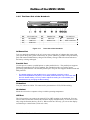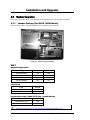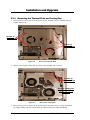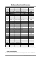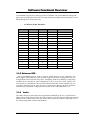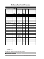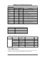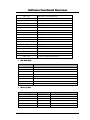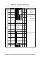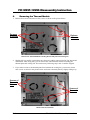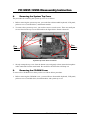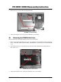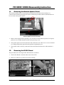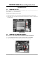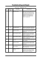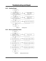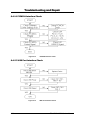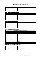
1
FIC M295 / M296 Intel® Pentium® 4 Notebooks M295 / M296 Reference and Service Manual Legal Notice Information in this document is subject to change without notice. Please contact FIC Portable Computing Group (PCG) Customer Service Dept. for the latest editions of this manual. Furthermore, FIC does not make any representations or warranties (implied or otherwise) regarding the accuracy and completeness of this document and shall in no event be liable for any loss of profit or any other commercial damage, including but not limited to special, incidental, consequential, or other damages. Copyright (©) 2002 FIC, Inc. ALL RIGHTS RESERVED - Printed in Taiwan. No part of this document may be reproduced or transmitted in any form by any means, electronic or mechanical, including photocopying, recording or information recording and retrieval systems without the express written permission of FIC. All brand names and product names used in this document are trademarks, or registered trademarks of their respective holders. How to Contact FIC Portable Computing Group SALES & MARKETING E-mail: [email protected] TECHNICAL SUPPORT E-mail: [email protected] CUSTOMER SERVICE (RMA) E-mail: [email protected] PCG WEB SITE FIC Portable Computing Group http://pcg.fic.com.tw FIC HOMEPAGE First International Computer, Inc. http://www.fic.com.tw FIC M295/M296 MODEL INTEL® PENTIUM® 4 NOTEBOOKS Reference and Service Manual September 2002, Volume 1 First International Computer, Inc. Portable Computing Group 7F, #266, Wen-Hua 2 Rd., Linko, 244 Taipei, Taiwan, R.O.C. Preface This manual contains operation, specifications, technical references, maintenance and troubleshooting instructions for the FIC M295 / M296 notebook. Intended Audience This manual is primarily intended for use by qualified service technicians assigned to FIC notebook PC repair operations. However, several sections contain overview technical information useful to a general (less-technical) audience. Contents This manual contains the following: • Chapter 1: Outline of the M295 / M296 - Introduces the notebook and identifies all standard and optional features including outlines on the BIOS SETUP program. • Chapter 2: Installation and Upgrade - Provides information on installing the device drivers and utility programs of the notebook as well as important system upgrade procedures. • Chapter 3: Software Functional Overview - Provides a functional overview of the notebook’s BIOS and software operation. This includes the power management function and system resource listing. • Chapter 4: Hardware Functional Overview - Provides a functional overview of the notebook’s hardware and sub-assemblies as well as description of every component and chipset used to control each operation. • Chapter 5: Maintenance & Disassembly - Describes the preventive and corrective maintenance procedures for the notebook. This includes primarily the disassembly and assembly procedures of the notebook. • Chapter 6: Troubleshooting and Repair - Provides instructions in handling BIOS POST Error codes and messages as well as guidelines in doing board-level troubleshooting. • Appendix A: Notebook Specification - Provides detailed information on the entire notebook’s specification including system specification, mechanical specification, and environmental specification. • Appendix B: Pin Assignment - Contains lists of all pin assignments for ports, connectors, and slots. • Appendix C: FRU Parts Listing - Contains lists of field replaceable parts for RMA purpose. 1 Chapter Outline of the M295 / M296 1.1 Introduction This chapter provides the outline features and operation of the M295 / M296 including the BIOS Setup program and other system options. The M295 / M296 notebook offers the latest in advanced portable computing and multimedia technology that even outperforms most desktop computers. It incorporates the latest Intel Pentium 4 Processor running at 400/533MHz Front Side Bus. It combines support for the new high-bandwidth Double Data Rate (DDR) 266 SDRAM, Integrated VGA and the AC 97 audio codec. Built-in Windows 2000 / XP keyboard, glide pad pointing device, sound system, PCMCIA slots, USB (Universal Serial Bus) port, advanced power management and more new multimedia features. The Intel® Pentium® 4 processor is the evolutionary step for desktop / mobile processor technology. Based on Intel® Net Burst™ micro architecture, the Pentium 4 processor offers higher-performance processing than ever before. Built with Intel's 0.13-micron technology, the Pentium 4 processor delivers significant performance gains for use in home computing, business solutions and all your processing needs. 1.2 Feature Highlights The M285 / M288 includes a variety of innovative features: Category Specification CPU Intel Pentium 4 NORTHWOOD 2.0/2.2/2.4 GHz Processor (DESKTOP, FSB 400/533 MHz) Core Logic SIS 645DX (North Bridge) CPU Interface AGP Bus Controller DDR DRAM Controller MuTIOL Media I/O SIS 962L (South Bridge ) Integrated MuTIOL Connect to PCI Bridge Dual IDE Master/Slave Controller ,Integrated DMA Controller Universal Serial Bus Host Controller Integrated Fast Ethernet MAC Controller(Not use) Integrated Audio Controller with AC97 Interface Advanced Power Management, RTC Integrated PCI to LPC Bridge Integrated keyboard Controller(Not use) Integrated Audio Controller with AC97 Interface PCI Bus Interface (PCI 2.2 compliant) Cache Memory L1 Cache (Pentium Processor internal): 12KB code and 8KB data FIC M295 / M296 Service Manual Stepping 1-1 Outline of the M295 / M296 8-way cache associativity provides L2 Cache (Pentium Processor internal): 512KB Advanced Transfer Cache,8 way associativity 8-way set associative, 32-byte line size, 1 line per sector System Memory BIOS ROM Base Memory: 1 SO-DIMM Slot (1.25”) Size: 128/256/512MB Type: DDR SDRAM, 2.5V Data Path: 64Bit Frequency: 200MHz/266/333MHz Refresh: CBR Refresh Expansion Memory: 1 SO-DIMM Slot (1.25”) Size: 128/256/512MB Type: DDR SDRAM, 2.5V Data Path: 64Bit Frequency : 200MHz/266/333MHz Refresh: CBR Refresh Please refer to the M295 M296 Key component list in detail. Flash ROM 1st Vendor : SST 49LF040A PLCC Package 4Mbit LPC flash ROM 2nd Vendor : <TBD> 4Mbit, 32 pin PLCC package Super I/O SMSC LPC47N267 FDC, IEEE 1284 Printer Port Serial Port x 2ports IR Port ASKIR, SIR, FIR, HPSIR, Consumer IR Plug and Play Support RTC + NVRAM Integrated in South Bridge (SIS 962L) Real Time Clock with 256 byte extended CMOS. IBM AT Clock/Calendar/Alarm (14 Bytes) K/B Controller ENE KB3886 Internal K/B, Touch Pad, External K/B or M/S Supported A20Gate,firmware version 1.47 PMU New PMU08 Mitsubishi M38859FFHP Embedded Controller VGA Controller M295 NVIDIA MAP17 High Performance and high quality 3D accelerator AGP 4X BUS High performance 2D accelerator Complete TV-OUT/Digital Flat Panel Solution M296 ATI M9CSP32 High Performance and high quality 3D accelerator AGP 4X BUS High performance 2D accelerator 1-2 FIC M295 / M296 Service Manual Outline of the M295 / M296 Complete TV-OUT/Digital Flat Panel Solution VRAM Internal VRAM up to 32MB TV out encoder Embedded ATI M9CSP32 LVDS Transmitter CardBus Controller Embedded ATI M9CSP32 M295 ENE CB1410 Single Slot PCI-CARDBUS BRIDGE M296 O2Micro OZ6912 Single Slot PCI-CARDBUS BRIDGE Sound AC’97 CODEC Realtek ALC201 AC’97 Revision 2.1 Compliant Supports Consumer IEC958 Output Port (SPDIF OUT) Audio DJ (Option) O2Micro OZ168T CD-Player Mode support Direct Mode support Pass through Mode support ATAPI CDROM compliant Modem ASKEY 1456VQL19R-4 Mini-PCI Solution (Type-3B) V.90, K56flex, ITU-T V.34, V.32, RJ11 Jack TIA/EIA 602, V.42 ITU-T V.17, V.29, V.27ter, V.21 Ch2 TIA/EIA 578 Class1 FAX Wake up on Ring MDC modem support (None) On board LAN Realtek 8100BL Support LAN boot Support for auto-negotiation (10BASE-T and 100BASE-TX) Wake up On LAN ASKEY Combo(None) GPRS Module(None) Mini-PCI Solution (Type-3A) Bluetooth(None) Embedded in SIS962L USB interface 802.11b(None) Support by PC-Card 1394 Agere FW322, support one port Cellular I/F Support PDC/PIAFS/CdmaOne/Dupa(None) USB2.0 (SIS 962L) Integrated in South Bridge (SIS 962L) USB v.1.1 and Intel Universal HCI v.1.1 compatible Eighteen level (doublewords) data FIFO with full scatter and gather capability Support GSM 900/1800MHZ Transmission voice,data,sms,fax FIC M295 / M296 Service Manual <Design Ready Only> Support by Cellular I/F USB Cable BTO with Bluetooth Module 1-3 Outline of the M295 / M296 Root hub and four function ports Integrated physical layer transceivers with optional over-current detection status on USB inputs Legacy keyboard and PS/2 mouse support 1-4 FIC M295 / M296 Service Manual Outline of the M295 / M296 1.3 System Configuration Diagram Figure 1-1 FIC M295 / M296 Service Manual M296 System Configuration Diagram 1-5 Outline of the M295 / M296 Figure 1-2 1-6 M295 System Configuration Diagram FIC M295 / M296 Service Manual Outline of the M295 / M296 1.4 Quick Tour of the Notebook Please take a moment to become familiar with the location and purpose of every control, the LED status panel, connectors and ports, which are illustrated in this section. It is recommended to first go through the User Guide of the notebook, which is shipped together with the notebook for information on how to operate its features. 1.4.1 Inside the Notebook To open the LCD cover of the notebook, find the cover latch located at the front center of the LCD cover. Push the latch to the right to release and tilt the LCD cover up. Inside, you will see the LCD display panel, keyboard, touch pad, status LED, and power switch. n Color LCD Panel o Easy Button p q Touch Pad Pointing Device Keyboard r Power Status LED Indicator Integrated Microphone s t u Figure 1-2 Power On / Resume Button Status LED Indicator Inside the Notebook Color LCD Display Panel The notebook comes with several LCD option sizes at 15” SXGA+ (1400x1050) or 14.1” XGA (1024x768) active-matrix TFT color liquid crystal display (LCD). You can adjust and o tilt (up to 180 ) the LCD screen panel to your desired viewing position. The notebook computer comes with a color LCD that you can adjust for a comfortable viewing position. The LCD can be 14.1” TFT color LVDS with 1024x768 XGA (Extended Graphics Array) resolution panels or 15” TFT color LVDS with 1400x1050 resolution. The features of the Color LCD Display are summarized as follows: FIC M295 / M296 Service Manual 1-7 Outline of the M295 / M296 • TFT color LVDS with 14.1" 1024x768 XGA or 15" 1400x1050 resolution panels. • Capable of displaying 16M colors (32-bit true color) on either size panels. • LVDS display control hot-keys allows you to adjust the brightness of the LCD. • Simultaneous display capability for LCD and external desktop computer monitor. • LCD display can be 14.1” or 15" TFT. You adjust the brightness level of the LCD by pressing the display control hot-keys. You activate the hot-keys by pressing the <Fn> key along with another function key: • • <Fn> + <F8> Key = Increases the brightness of the LCD display <Fn> + <F9> Key = Decreases the brightness of the LCD display Keyboard Panel − Standard QWERTY-key layout and full-sized 87 / 90 keys keyboard with Windows hot-keys, embedded numeric keypad, hot keys, inverted “T” cursor arrow keys, and separate page screen control keys. Wide extra space below the keyboard panel for your wrist or palm to sit-on comfortably during typing. (The keypad F4, F5, F7 on the following keyboard should no words print on it.) − n Function Keys r Windows Short-cut Key Figure 1-3 o q s Control Keys p Windows Start Menu Key Cursor Control Keys Keyboard Layout The notebook keyboard is a little bit different from a standard desktop keyboard. Aside from the normal alphanumeric characters and the standard keyboard function keys, the notebook keyboard includes an embedded numeric keypad, and special function keys that activates by pressing the <Fn> key together with another key. These special function keys or “hot-keys” allow you to control and adjust some of the functions of the notebook like display controls, power saving features, and others. (1) Function Keys — These function keys, out of <F1> through <F12>, are available on the notebook keyboard. These keys also work together with the <Fn> key to activate 1-8 FIC M295 / M296 Service Manual Outline of the M295 / M296 special functions. The following function-key combinations are pre-programmed: Hot Key Fn + F3 Fn + F5 Fn + F6 Fn + F8 Fn + F9 Power button Function Toggle Display (LCD/CRT/Simul) Display stretching Speaker On/Off Brightness Increase Brightness Decrease System Suspend to disk Handler BIOS Handler BIOS Handler BIOS Handler Controlled by PMU07 Controlled by PMU07 BIOS Handler (2) Control keys – <Ctrl>, <Alt>, <Fn>, and <Shift> keys are controls used in conjunction with other keys to change their functions. To use control keys, press and hold the control key while pressing another key. For example, “Press <Ctrl>+ <C>” means to hold down the <Ctrl> key and type the letter <C>. (3) Windows keys (Windows Start Menu Key) – Use this key to activate the Start Menu of Windows. (4) Shortcut/Application key – provides quick access to shortcut menus. (This key acts like a right mouse button.) (5) Cursor Control keys – Cursor control keys let you position the cursor on the screen where you want. On the screen, the cursor is a blinking underline, block, or vertical bar depending on the application. (6) Typewriter keys – Typewriter keys (also called alphanumeric keys) are used to enter text and characters. Keys with blue print on them behave differently when combined with control keys or the <Fn> key. (7) Numeric Keypad – Pressing <NumLock> on the keyboard activates the embedded numeric keypad numbers and functions printed in blue on top of the keys. When you press <NumLock> again, the keys revert to their normal functions as typewriter keys. Figure 1-4 Embedded Numeric Keypad Integrated Microphone This allows you to instantly record voice annotations (normally saved as WAV files) and later attached them to documents and presentation using the notebook integrated audio system and application software. Since the notebook also supports full-duplex audio capabilities, you can talk to the microphone and at the same time listen to others talk when connected to a speakerphone modem, Internet live chat, or video conferencing. FIC M295 / M296 Service Manual 1-9 Outline of the M295 / M296 Power Status LED Indicator Located just on TFT LED panel assembly, you will find three LEDs for the power and battery charge status. These LEDs are positioned to be visible even if the LCD cover is closed. n Power Indicator o Figure 1-5 Battery Charging LED p Mail LED Power Status LED Indicator 1. Power Indicator – lets you know if power to the system is turned on and if system is in Suspend-to-RAM mode. This LED is positioned so that you can see it on both sides whether the LCD panel is opened or closed. − Lights green when the system is powered on using the AC adapter or battery. − Lights green blinking when in Suspend to RAM mode and critically low battery power. We strongly recommend that users create the partition "Save to Disk" (for Win98 only) as this will prevent your data from loss when power is critically low. For Windows version later then Win98, please use hibernation mode instead. 2. Battery Charging LED – lights to indicate battery in charging status. − Lights organge to indicate the battery is charging. − Lights off to indicate the battery is fully charged or no battery installed. 3. Mail LED – Lights green to indicate that a new mail is arrived. Status LED Panel The Status LED Panel keeps you informed of the notebook’s current operating status. Each LED is marked with an icon to designate a system status. Figure 1-6 Icon Represents n IDE Drive Access 1-10 Status LED Panel Icons Indicates This LED will turn on when the system is accessing the hard disk drive (HDD) or CD-ROM / DVD-ROM / CD-RW /Combo. FIC M295 / M296 Service Manual Outline of the M295 / M296 o RF Access This LED will turn on when the system is accessing the data from wireless device. p Caps Lock This LED will turn on when the Caps Lock key is activated. When activated, all alphabet keys typed in will be in upper case or in capital letters. q Scroll Lock This LED will turn on when the Scroll Lock key is activated. r Num Lock This LED will turn on when the Num Lock key is activated. When activated, the embedded numeric keypad (blue print numeric keys) will be enabled. Easy Buttons There are three easy buttons, two use for accessing Internet and e-mail functions instantly and easily, the other one lets you define certain functions by yourself. Description of the easy buttons appears in the latter part of this section. n Internet Button o E-Mail Button p User-Defined Button Figure 1-7 Easy Button − Internet Button This technology is designed specifically for providing a very convenient way in connecting Internet only by pressing Internet button as shown in the graphics. For more understanding and interesting, you can refer Section 2.5 of user manual to recognize the driver installation procedures in activating Internet button. − E-mail Button This is the most convenient way to access the outlook 98/2000... just by pressing this button, you can omit several procedures in entering into Outlook environment. − User-Defined Button You can define these one of buttons to activate command file (like execution file or batch file) by yourself. FIC M295 / M296 Service Manual 1-11 Outline of the M295 / M296 Power Button Press the Power button either to power on or power off the system. The Power button is also a “Smart” switch, meaning that it recognizes when the system is in Suspend mode. If in Suspend mode, pressing the Power button will bring it out of Suspend mode and resume to the system’s last state. You can set the function of power button from the power management setting in Windows Control Panel. Always check the Power LED after pressing the power button to know the power status of the notebook. o If you are unable to power off the system, use the power override function. Press the power button and hold it in place for four seconds. The system will then power off. Touch Pad Pointing Device Built in just below the keyboard panel is the glide pad pointing device. The left and right select buttons of the glide pad is found below the glide pad surface. The left select button is configured (by default) as the left button you normally click on the left button of your mouse, while the right select key is configured as the right mouse button. The scroll button makes it easy to browse upwards or downwards in the software screen. To move cursor, place your finger lightly on the glide pad and move in the desired direction. If you reach the end of the pad, lift your finger and place it back down on the other side. The glide pad is compatible with the standard PS/2 mouse and can be activated using the normal DOS or Windows PS/2 mouse driver. You can also disable the glide pad in the BIOS Setup program. o 1-12 You can execute a left button click function by simply tapping on the glide pad surface once. Refer to the User Guide of the notebook for more information. FIC M295 / M296 Service Manual Outline of the M295 / M296 1.4.2 Front Side of the Notebook n Built-in Stereo Speakers o Rewind Button p Forward Button q Stop Button r Play Button s Cover Switch Figure 1-8 Front Side of the Notebook Woofer These speakers produce heavy bass voice output for music listening. Built-in Stereo Speakers At the front left and right sides of the base unit are two built-in stereo mini speakers with sound boxes. The speakers are controlled by the audio controller of the notebook and activated by installing the audio driver. For adjusting the volume of the speakers, you can use the volume control program under Microsoft OS or by adjusting the thumb-wheel volume knob also found on the right side of the notebook. Lock ON/OFF Switch Push the switch to left side to lock the status of your Audio DJ. If you lock this switch when the music is playing, the music will continue to play no matter what button is pressed. Audio DJ will not allow it to activate. The function of this switch is to prevent you from touching any button accidentally. Push the switch to right side can turn on or turn off the power of the Audio DJ. Remind Button Press the button for reverting to previous music. Press and hold this button to fast rewind the audio CD. Cover Switch The Cover Switch is found inside the notebook assembly just underneath the latch opening where you insert the LCD cover hook. Whenever the LCD cover is closed, it activates the Suspend mode or shut down the computer. The action can be set on Power Option of Windows Control Panel. o When Suspend-to-RAM mode is activated, make sure not to leave the system for a long period when running at battery mode. The battery will continue to drain some power even in Suspend mode. It is better to save all files and shutdown the power instead or run Suspend-to-Disk mode. Audio-DJ Display The display shows the number of the music currently playing. FIC M295 / M296 Service Manual 1-13 Outline of the M295 / M296 Forward Button Press the button for playing the next music. Press and hold this button to fast forward the audio CD Stop Button Press the button to stop the music. Play Button Press the button to starting to play music o The function of Audio DJ can be workable either in Windows system or operate it without powering on the computer. For execute this function, you should first install the EZ system driver. Please refer to Section 5 of Chapter 2 of user manual for installation procedures. However, if your OS is Windows 98, you should download and install the "Windows Media Player 7" from Microsoft's Website to activate this function. 1.4.3 The Right Side of the Notebook n Blue Tooth LED o Air-Outlet Vent p Volume Control q IR Port r Microphone Jack s Headphone Jack t Air Inhalant u USB Port v PS/2 Port Figure 1-9 Right Side of the Notebook Blue Tooth LED The LED is light when you activate with the Bluetooth function. (BTO option only) Air-Outlet Vent Emits the heat out of your computer and keeps it within operating temperature. Volume Control Allows you to control the speaker volume. IR Port Wireless data transfer of files between your notebook computer and an IR-equipped device or notebook computer. You can also print to an IR-equipped printer without using cables. The SIR mode provides up to 115.2Kbps of data transfer rate. 1-14 FIC M295 / M296 Service Manual Outline of the M295 / M296 Audio Port There are Microphone jack, and Headphone jack which are described as follows: • Microphone Jack Allows you to connect an external microphone for monophonic sound recording directly into your notebook computer. Plugging in an external microphone disables the built-in microphone. • Headphone Jack Lets you plug in a stereo headphone, powered speakers, or earphone set with 1/8 inch plug for personal listening. Air Inhalant Inhale the air into your computer to keep it within operating temperature. USB Port The Universal Serial Bus (USB) port allows you to connect up to 127 USB-equipped peripheral devices (for example, printers, scanners and so on) to your notebook computer. 1.4.4 n q The Left Side of the Notebook Locking Device Keyhole PC Card Slots o Figure 1-10 CD-ROM, DVD-ROM, CD-RW/DVD Combo p USB Port Left Side of the Notebook Locking Device Keyhole This latch allows you to attach a Kensington security lock or other compatible lock for securing the notebook from theft. It is found on the left side of the notebook. CD-ROM, DVD-ROM, CD-RW or Combo Drive The notebook comes with a standard 24X+ speed ATAPI IDE CD-ROM drive that supports all major CD formats like CD-R, Photo CD, and Video CD. The drive utilizes a pop-out tray loading mechanism and supports bootable CD by setting the BIOS Setup program. The notebook also comes with the 8X+ speed DVD-ROM drive, 8X+ speed CD-RW or CDRW/DVD combo drive options. USB Port The Universal Serial Bus (USB) port allows you to connect up to 127 USB-equipped peripheral devices (for example, printers, scanners and so on) to your notebook computer. FIC M295 / M296 Service Manual 1-15 Outline of the M295 / M296 PC Card Slot The PCMCIA slot compartment houses one-card slots that support one PCMCIA Type II cards. The notebook uses a CardBus PCMCIA controller that supports 5V and 3V 32-bit CardBus and 16-bit PC cards. The PCMCIA slot compartment comes with sliding dummy plastic with protection. Before you can directly insert the PC card, please remove it first. To remove the inserted PC card, slightly push the button found on the right side of the PC slot to release the eject button. Then push it again to release the Dummy Plastic Device. When the PC card has moved out a space out of the slot, hold the edges of the card and slowly slide it out. o o For full functionality of PC cards, always ask for the latest driver from your PCMCIA card dealer or download it from their Internet website. For network PC cards, you need first to stop the device under the PC Card properties of Windows Control Panel. Otherwise, this may cause system hang or system fatal error. Please use the LAN port of this notebook instead of using other network PC card. 1-16 FIC M295 / M296 Service Manual Outline of the M295 / M296 1.4.5 The Rear Side of the Notebook n q t w AC Power Port Air Inhalant LAN Port USB Port Figure 1-11 o r u Parallel Port CRT Port Modem Port p/ s v TV-Out Port Serial Port IEEE 1394 Port Rear Side of the Notebook AC Power Port Lets you attach the notebook to the AC power source using the AC adapter that comes with your system. Keep the system connected to AC power whenever possible to keep the battery pack and internal CMOS battery charged. The Battery Charge LED will activate whenever the battery is being recharged. Parallel Port Use this port to connect a parallel printer or other parallel device. The parallel port supports Enhanced Capabilities Port (ECP) standard. The standard provides you with a greater processing speed than the conventional parallel port. The port also supports Bi-directional and EPP protocols. o The default setting for the parallel port on your notebook computer is set to Enhanced Capabilities Port (ECP). Some older parallel devices may not function with the ECP default setting. You may need to adjust the setting to accommodate your parallel device by changing the BIOS setting. TV-Out Port Lets you connect to a RCA TV connector for presentation or VCD, DVD watching. Air Inhalant Inhale the air into the computer to keep it within operating temperature. CRT Port The VGA port lets you connect an external VGA (CRT) monitor to the notebook. You can also run the LCD and the external CRT monitor display simultaneously; or switch it to CRT only using the function hot key (Fn+F3). When switch to CRT only, you can set the display resolution up to 1024x768 at (16-bit true color). FIC M295 / M296 Service Manual 1-17 Outline of the M295 / M296 Serial Port (COM 1) The 9-pin serial port provides a serial interface to which you can connect an RS-232C device such as external serial mouse or modem. This port is commonly referred to as COM1. o o When connecting an external serial mouse, you must first power off the system before connecting the external mouse. It can auto-detect the serial mouse hardware and run both glide pad and serial mouse simultaneously. Whenever using an external mouse in place of the built-in glide pad, it is recommended to switch the mouse driver to the default standard Microsoft mouse driver. LAN Port If you purchase an internal 10Base-T/100Base-TX LAN module, it connects your computer to other computers/networks through a local area network (LAN). Modem Port The modem port provides a reserve jack for installing an internal modem with RJ-11 jack. The internal modem is a 56Kbps-fax/data PCI modem and supports the latest V.90 standard. The internal module uses MDC (AC'97) S/W Modem technology. IEEE1394 Port IEEE 1394 port is a high speed I/O port that can transfer high levels of data in real-time, such as external hard disk, Digital Video Camera. USB (Universal Serial Bus) Ports . This 4-pin slim port allows The USB (Universal Serial Bus) Port is a port with the symbol you to connect multiple USB devices through daisy chaining or through a USB hub and use them all simultaneously. The USB specification states it can support up to 127 USB devices running at up to 12Mbps based on USB specification v1.1. This notebook provides four USB ports. o When you resume the system from suspend mode, the USB port may not initialize properly. If in case the USB device does not work, unplug and plug the USB device again. This is a known bug released by Intel and Microsoft Windows. 1-18 FIC M295 / M296 Service Manual Outline of the M295 / M296 1.4.6 The Under Side of the Notebook n/r p s Tilt Foot Battery Release Latch Mini-PCI Socket Compartment Figure 1-12 o q Memory Compartment Battery Bay Under Side of the Notebook Tilt Foot (Left and Right) Allow you to tilt the rear of the notebook upward for more comfortable typing. Memory Compartment Found on the underside of the notebook is the memory compartment. Underneath the cover are two 144-pin SODIMM memory slots for inserting and upgrading the system memory using 64MB to 512MB SODIMM. The notebook uses DDR 266Mhz SDRAM modules for faster memory access. You can upgrade the total memory up to 1GMB. One is inserted with a SDRAM configured by the factory. The other is empty for upgrade use. Battery Release Latch Also found on the underside of the notebook is the battery bay latch. To remove the battery pack, you need to push aside this latch and at the same time pull the battery pack. Battery Bay The battery compartment stores the Lithium-Ion (Li-Ion) battery pack for off-the-cord operation. The battery pack is instantly charge whenever you connect the AC adapter to the notebook. It is very important to always have the battery installed on the notebook to have it always charged and conditioned by the AC adapter. Normal operating time using Li-Ion battery pack is close to 2.5 hours with power management. Mini-PCI Socket Compartment This compartment houses the mini-PCI socket for inserting the internal LAN. Refer to Chapter 2 of User Manual for installing the LAN module. FIC M295 / M296 Service Manual 1-19 Outline of the M295 / M296 1.5 System BIOS SETUP Program The notebook uses the Phoenix BIOS Setup program that allows you to set several system configurations in changing the way the system performs. This includes your system time and date, disk drive configuration, I/O device controls, boot drive sequence, and power management settings. The information is then stored in the CMOS RAM chip and will remain permanent unless you change it again. The notebook also uses EPROM Flash BIOS that allows you to update the system BIOS by simply overwriting it using the Phoenix Flash programming utility. Before boot-up, the system will read the BIOS settings and compare them to the equipment check conducted during the POST (Power-On Self-Test). If an error occurs, an error message will be displayed on the screen, and you will then be prompted to run the BIOS Setup Program. Press the <F2> key to run the BIOS Setup program. The BIOS Setup program is organized into five menus which you can select using the <Å> and <Æ> keys. To move from one option to another, you use the up and down arrow keys. On the BIOS Setup program, you will find the following parts on the screen: • Menu Bar - found on the top line of the screen. Each of the five items has a separate menu screen. • Parameters - found on the left side of the screen. This area lists the parameters and their current settings. • Item Specific Help - found on the right side of the screen. This area describes each parameter and its available settings. • Key Status Bar- the bottom part of the screen. These lines display the keys available to move the cursor, select a particular function and so forth. The following table lists the keys on how to edit and move around the setup menus inside. o KEY WHAT IT DOES <F1> Shows on-line help on key functions. ↑ ↓ Moves the cursor between the displayed parameters. +/- Modifies the current parameter settings. <F9> Load default configuration. Esc Exits the current menu and returns to the main menu or go directly to the Exit menu. ÅÆ Changes between displayed menus. <Enter> For some parameter settings, select and moves the cursor between the sub-menu. Also moves the cursor to the next line or selection. <F10> Save changes and exit. Some information here may not be available or different from other date code versions of the notebook BIOS. Always check for the latest BIOS update from the FIC Internet homepage. ftp://pcg.fic.com.tw/NBTECH 1.5.1 Using the Main Menu The BIOS Setup Main Menu contains the settings for system time and date, and disk drives as 1-20 FIC M295 / M296 Service Manual Outline of the M295 / M296 well as CPU and system memory information. PhoenixBIOS Setup Utility Main Advanced Security Boot Exit Item Specific Help 4 F1 System Time: [07:24:00] System Date: [07/16/2002] Language: [English Boot Display Device: [Both] Primary Master [FUJITSU MHR2020AT] Secondary Master Installed CD/DVD System Memory 640 KB Extended Memory 228352 KB CPU Type Intel® Pentium® 4 CPU Speed 2000 MHz BIOS Version 1.0A-1.10-0812 Help Esc Exit <Tab>, <Shift-Tab>, or <Enter> selects field. (US)] K Select Item -/+ Change Values F9 st Select Menu Enter Select 4Sub-Menu F10 Save and Exit Figure 1-12 Setup Defaults BIOS Setup Main Menu System Time: [07:24:00] <Tab>, <Shift-Tab>, or <Enter> selects field. System Date: [07/16/2002] Language : [English (US)] <Tab>, <Shift-Tab>, or <Enter> selects field. (BIOS auto detect, for information only) Boot Display Device: [Both] / [LCD] / [CRT] Select the display device. Primary Master [FUJITSU MHR2020AT] Secondary Master Installed CD/DVD (BIOS auto detect, for information only) System Memory 640 KB (BIOS auto detect, for information only) Extended Memory 228352 KB (BIOS auto detect, for information only) CPU Type Intel® Pentium® 4 (BIOS auto detect, for information only) CPU Speed 2000MHz (BIOS auto detect, for information only) BIOS Version 1.0A-1.10-0812 (BIOS auto detect, for information only) System Time – To set the time, enter the current hour, minute, and second on hr/min/sec, 24-hour format. System Date – This field lets you set the calendar month, day, and year. The calendar clock remains in memory even after you turn off the system. FIC M295 / M296 Service Manual 1-21 Outline of the M295 / M296 Language – Language for each country. Default setting as US language. Boot Display Device – This field allows you to set the output boot display to the LCD, CRT, or Both. Primary Master – This field displays various parameters for the hard disk drive. If type [Auto] is selected, the system automatically sets these parameters. If type [User] is selected, Cylinders, Heads and Sectors can be edited. Secondary Master – This field displays various parameters for the internal CD-ROM or a DVD-ROM / Combo Drive. System Memory, Extended Memory, CPU Type, CPU Speed and BIOS Version – These fields are for information only as the BIOS automatically detects related values. PhoenixBIOS Setup Utility Main Internal HDD [FUJITSU MHR2020AT] Item Specific Help Type: [Auto] LBA Format User = you enter Parameters of hard-disk Total Sectors: 39070080 Drive installed at this Maximum Capacity: 20004MB connection. Auto = autotypes Multi-Sector Transfers: [16 Sectors] Hard-disk drive LBA Mode Control: [Enabled] Installed here. 32 Bit I/O: [Disabled] 1-39 = you select Transfer Mode: [Fast PIO 4] Pre-determined type of Ultra DMA Mode: [Mode 2] Hard-disk drive Install here. CD-ROM = a CD-ROM drive Is installed here. ATAPI Removable = Removable disk drive is installed here. Help K Esc Exit ÅÆ F1 Select Item −/+ Change Values F9 Setup Defaults Select Menu Enter Select Sub-Menu F10 Save and Exit Figure 1-13 1-22 Internal HDD/CD-ROM Sub-Menu FIC M295 / M296 Service Manual Outline of the M295 / M296 Type: [None] / [ATAPI Removable] / [CD-ROM] / [User] / [Auto] Select the drive type corresponding to the fixed disk installed in your system. If type USER is selected, Cylinders, Heads & Sectors edited directly. Total Sectors: 39070080 (BIOS auto detect, for information only) Maximum Capacity: 20004MB (BIOS auto detect, for information only) Multi-Sector Transfers: [Disabled] / [2 Sectors] / [4 Sectors] / [8 Sectors] / [16 Sectors] Determine the number of sectors per block for multiple sector transfers. LBA Mode Control: [Disabled] / [Enabled] Enabling LBA causes Logical Block Addressing to be used in place of Cylinders, Heads & Sectors 32 Bit I/O: [Disabled] / [Enabled] This setting enables or disables 32 bit IDE data transfers Transfer Mode: [Standard] / [Fast PIO 1] / [Fast PIO 2] / [Fast PIO 3] / [Fast PIO 4] / [FPIO 3 / DMA1] / [FPIO 4 / DMA2] Select the method for moving data to/from the drive. Autotype the drive to select the optimum transfer mode Ultra DMA Mode: [Disabled] / [Mode 1] [Mode 2] (BIOS auto detect, for information only) 1.5.2 Using the Advanced Menu The Advanced Menu allows you to configure the OS and I/O device settings. PhoenixBIOS Setup Utility Main Advanced Security Boot Exit Item Specific Help NumLock: [Off] Selects Power-on TV System [PAL] State for NumLock Sub-System Select 4 F1 [Normal PAL TV] PS/2 Mouse [Both] LCD Panel View Expansion [Enabled] Embedded Share Memory [32MB] Graphics Aperture [256MB] EmbedDed Audio Device [Enabled] Summary Screen: [Disabled] I/O Device Configuration Help Esc Exit K Select Item -/+ st Select Menu Enter Select Sub-Menu F10 Figure 1-14 FIC M295 / M296 Service Manual Change Values F9 Setup Defaults Save and Exit BIOS Setup Advanced Menu 1-23 Outline of the M295 / M296 NumLock: [On] / [Off] Selects Power-on state for NumLock TV System [NTSC] / [PAL] Switch TV System Mode Sub-System Select [Normal PAL TV] / [PAL –M] / [PAL-N] PAL TV Sub-System select PS/2 Mouse [Disabled] / [Both] / [Auto] [Disabled] prevents any installed PS/2 mouse from functioning, but frees up IRQ12. [Both] allows both internal and external PS/2 mouse to be active. [Auto] will enable the PS/2 mouse only if present. LCD Panel View Expansion: [Disabled] / [Enabled] [Disabled] – Reduces the panel view in some video mode [Enabled] – Expands the panel view, but it may adversely affect the graphic/text quality Embedded Share Memory [8MB] / [16MB] / [32MB] / [64MB] Embedded Share Memory size for AGP VGA memory. Graphics Aperture: [4MB] / [8MB] / [16MB] / [32MB] / [64MB] [128MB] / [256MB] Select the size of the Graphics Aperture for the AGP video device. EmbedDed Audio Device [Enabled] / [Disabled] Enabled or Disabled SiS Embeded Audio ( SiS 7018 AC97 Audio ) Summary screen: [Disable] / [Enabled] Display system configuration on boot 4I/O Device Submenu Peripheral Configuration Configuration Num-Lock on Boot – Allows you to set the power-on state for the <NumLock> key. Set this to [LockOn] if you want to enable <NumLock> during power on. TV System – [PAL] for the most of TV in Europe region and China. [NTSC] for the most of TV in North America, Japan, & Taiwan. Sub-System Select – [Normal PAL TV] for standard PAL TV of the country in Europe region. [PAL-M] for PAL standard TV especially in Brazil country. [PAL-N] for standard PAL TV especially in Argentina country. PS/2 Mouse – [Disabled] prevents any installed PS/2 mouse from functioning, but frees up IRQ12. [Both] allows both internal and external PS/2 mouse to be active. [Auto] will only allow the external PS/2 mouse to be active if it is detected. LCD Panel View Expansion – [Disabled] – Reduces the panel view in some video mode. [Enabled] - Expands the panel view, but it may adversely affect the graphic/text quality. Embedded Share Memory – [8MB] [16MB] [32MB] [64MB] – Embedded Share Memory AGP VGA Memory Size. Graphics Aperture - [4MB] [8MB] [16MB][32MB] [64MB] [128MB] [256MB] – Select the size of the Graphics Aperture for the AGP video device. 1-24 FIC M295 / M296 Service Manual Outline of the M295 / M296 EmbedDed Audio Device – [Enabled] or [Disabled] SiS Embeded Audio ( SiS 7018 AC97 Audio ) Summary Screen – Select the display of configuration on Boot. I/O Device Configuration – Lets you configure input/output device such as Serial Port, Parallel Port, and Floppy disk controller. PhoenixBIOS Setup Utility Advanced I/O Device Configuration Item Specific Help Configure serial port A using options: Serial port A: [Auto] Serial port B: [Enabled] [Disabled] Mode: [Bi-directional] Base I/O address/IRQ [2F8] Parallel port: [Enabled] Mode: No configuration [Enabled] [Bi-directional] User configuration [Auto] BIOS or OS chooses configuration (OS Controlled) Displayed when Controlled by OS Help K Esc Exit st F1 Select Item -/+ Change Values F9 Setup Defaults Select Menu Enter Select Sub-Menu F10 Save and Exit Figure 1-15 Serial port A I/O Device Configuration Sub-Menu [Disabled] / [Enabled] / [Auto] Configure serial port A using options: Disabled - No configuration, Enabled - User configuration, Auto - BIOS or OS configuration. (OS Controlled) – Displayed when controlled by OS Serial port B [Disabled] / [Enabled] / [Auto] Configure serial port A using options: Disabled - No configuration, Enabled - User configuration, Auto - BIOS or OS configuration. Mode: Base I/O address/IRQ [IrDA] [FIR] [3F8] / [2F8] / [3E8] / [2E8] FIC M295 / M296 Service Manual (OS Controlled) – Displayed when controlled by OS Enabled the IrDA transmission Set the base I/O address and IRQ for serial port B. 1-25 Outline of the M295 / M296 Interrupt [IRQ 3] / [IRQ4] Set the interrupt for serial port B. Parallel port [Disabled] / [Auto] / [Enabled] Configure parallel port using options: Disabled - No configuration, Enabled - User configuration, o Mode [Bi-directional] / [EPP] / [ECP]/ Base I/O address [378] / [278] / [3BC] Auto - BIOS or OS configuration. Set the mode for the parallel port using options: Output only, Bi-directional Select the base I/O address for the parallel port when port is Enabled. If you disable a device in BIOS Setup, you cannot enable or assign it using the Windows (98 or 2000) Device Manager. The device is not listed in the Windows device list. You need to select any setting other than “Disable” in Setup. Serial Port A – You can press <Enter> to select Enabled, Disabled, or Auto option for enabled or disabled the port, or automatically sensed the address assignment by BIOS or OS. Serial Port B – You can press <Enter> to select Enabled, Disabled, or Auto option for enabled or disabled the IrDA, or automatically sensed the address assignment by BIOS or OS. Mode – Allows you to press <Enter> to select a serial mode B as 3F8, 2F8, 3E8 & 2E8 when the serial port B is configured. When you set the configured serial port B to Enabled rather than Auto, you should also set the parameter of Base I/O address and IRQ for this port. Parallel Port – Allows you to press <Enter> to select the Enabled, Disabled, or Auto option for enabled or disabled this port, or automatically sensed the address assignment by BIOS or OS. Mode – Allows you to press <Enter> to select a parallel mode as Bi-directional, EPP, or ECP when the parallel port is configured. When you set the configured parallel port to Enabled rather than Auto, you should also set the parameter of Base I/O address and IRQ for this port. 1-26 FIC M295 / M296 Service Manual Outline of the M295 / M296 1.5.3 Using the Security Menu The Security menu allows you to set the system password as well as disk-protection security. PhoenixBIOS Setup Utility Main Advanced Security Boot Exit Item Specific Help Supervisor Password Is: User Password Is: Clear Clear Set Supervisor Password [Enter] Set User Password [Enter] Diskette access: [Supervisor] Fixed disk boot sector: [Normal] Password on boot: [Disabled] Supervisor Password controls access to the F1 Help Esc Exit K Select Item -/+ setup utility. Change Values st Select Menu Enter Select Sub-Menu Figure 1-16 F9 Setup Defaults F10 Save and Exit BIOS Setup Security Menu Supervisor Password Is: Clear / Set While the Supervisor Password had been enabled, the item will show Set. If disabled. The item will show Clear. User Password Is: Clear / Set While the User Password had been enabled, the item will show Set. If disabled. The item will show Clear. Set Supervisor Password Press [Enter] Supervisor Password controls access to the setup utility. Set User Password Press [Enter] User Password controls access to the system. Diskette access [User] / [Supervisor] Control access to diskette drives. Fixed disk boot sector [Normal] / [Write protect] Write protects boot sector on hard disk, to protect against viruses. Password on boot [Disabled] / [Enabled] Enabled password entry on boot Supervisor Password Is: Clear / Set –While the Supervisor Password had been enabled, the item will show Set. If disabled. The item will show Clear. User Password Is: -- Clear / Set – While the User Password had been enabled, the item will show Set. If disabled. The item will show Clear. FIC M295 / M296 Service Manual 1-27 Outline of the M295 / M296 Set Supervisor Password – Specifies if the system prompts you to enter a password when entering Setup. Set User Password – Specifies if the system prompts you to enter a password when accessing the system. The Set User Password function will be enabled once a Supervisor password is set. Enter a new password with up to eight alphanumeric characters, and then enter this same new password again for confirmation. Diskette access – Controls access to diskette drive. Fixed disk boot sector – [Write Protect] enables write protect boot sector on hard disk to prevent against viruses. [Normal] disables this write protect function. Password on boot – Enables password check when booting. 1-28 FIC M295 / M296 Service Manual Outline of the M295 / M296 1.5.4 Using the Boot Menu The Boot menu lets you decide the boot order of booting devices including: PhoenixBIOS Setup Utility Main Advanced Security Boot Exit Item Specific Help CD-ROM Drive + Hard Drive Keys Used to views or Removable Devices Configure devices: <Enter> expands or collapses devices with a + or <Ctrl+Enter> expands All <Shift + 1> enables or Disables a device. <+> and <-> moves the Device up or down. <n>May move removable Device between Hard Disk or Removable Disk <d> Remove a device That is not installed. F1 Help K Esc Exit st Select Menu Enter Select Item -/+ Figure 1-17 Change Values F9 Setup Defaults Select Sub-Menu F10 Save and Exit BIOS Setup Boot Menu CD-ROM Drive – Move the option on top if you want to boot from a bootable CD-ROM like Windows NT/2000/XP (Optical Drive D:\). Hard Drive – Move the option on top if you want to boot from a bootable hard disk drive (Drive C:\) Diskette Devices – Move the option on top if you want to boot from a bootable floppy diskette (Drive A:\). FIC M295 / M296 Service Manual 1-29 Outline of the M295 / M296 1.5.5 How to Exit the Setup Program There are two choices to escape from the Setup program. PhoenixBIOS Setup Utility Main Advanced Security Boot Exit Item Specific Help Exit Saving Changes Exit Discarding Changes Exit System Setup and save your changes to Load Setup Defaults CMOS. Discard Changes Save Changes Battery Refresh F1 Help Esc Exit K Select Item -/+ st Select Menu Enter Figure 1-18 Change Values F9 Select Sub-Menu F10 Save and Exit Setup Defaults BIOS Setup Exit Menu Exit Saving Changes – Exits System Setup and saves your changes to CMOS. Exit Discard Changes – Exits Setup utility without saving Setup data to CMOS. Load Setup Defaults – Loads the default settings for all items in Setup. Discard Changes – Reverts to previously selected settings. Save Changes – Saves Setup data to CMOS. Battery Refresh – Reactivate both Li-Ion and Ni-MH battery. 1-30 FIC M295 / M296 Service Manual Outline of the M295 / M296 1.6 Notebook Accessories and System Options It is also important to understand the accessories that come along with the notebook and the options for fully utilizing the capabilities of the computer. This section describes briefly what these accessories and options are. 1.6.1 AC Adapter and Power Cord The AC Adapter supplies external power to your computer and at the same time charges the internal battery pack. The AC adapter has an auto-switching design that can connect to any 100VAC ~ 240VAC power outlets. Connect the adapter to the AC wall outlet using the power cord. There is an LED on the AC adapter to indicate if DC power is already available. 1.6.2 Battery Pack Aside from the AC adapter, your computer can also be powered through the removable battery pack. The battery pack uses rechargeable or Lithium-Ion (Li-Ion) battery cells that can run for 2 to 2.5 hours when fully charged and power management enabled. Recharging the battery takes around 2.5 to 3 hours when the computer is off. You should always leave the battery inside your computer even when using the AC adapter as it also acts as back-up power supply in case power from the AC adapter is cut off. It is also very important to have the battery pack always charged to prevent battery cell degradation. If the AC adapter is not connected or not available, and the notebook is not going to be used for some period, it is advisable to remove the battery pack from the notebook to prevent any current leak. 1.6.3 Internal Modem Module The notebook provides S/W modem. The internal modem supports only fax and data communication and is V.90-compliant. You connect the telephone line to the RJ-11 jack found on the rear side of the notebook. 1.6.4 Internal Ethernet LAN Module This notebook comes with an optional 10Base-T/100Base-TX LAN module that supports data transfer rates at 10Mbps and can be up to 100Mbps. 1.6.5 DVD-ROM Drive Other than the internal CD-ROM drive, the notebook also provides optional factory built-in DVD-ROM drive. DVD-ROM drives are also backward compatible with CD-ROM, so you can also use any audio CDs, video CDs, photo CDs, and CD-R. Using a software MPEG2/DVD program, the notebook can playback any commercial DVD movie titles. 1.6.6 CD-RW Drive This device pack can write data to CD-R or CD-RW CD for you to backup the data. 1.6.7 CD-RW/DVD Combo Drive This device pack can write data to CD-R or CD-RW CD for you to backup the data and also can read DVD/CD title. FIC M295 / M296 Service Manual 1-31 Outline of the M295 / M296 1.6.8 Audio-DJ This notebook comes with optional built-in Audio DJ panel. It can play your Audio CD like the CD player without powering on the whole computer. 1.6.9 Blue Tooth Module This notebook is ready for Bluetooth technology. This is a wireless connection standard in a short-range radio technology. It aims at simplifying communication between each device with Bluetooth module. Bluetooth is in essence a “personal-area network” technology for connecting computers to peripherals and mobile phones. 1-32 FIC M295 / M296 Service Manual 2 Chapter Installation and Upgrade 2.1 Overview This chapter provides guidelines on installing the device drivers for the built-in features of the M295 / M296 Most of the driver installation procedures mentioned here are only for Windows XP. This chapter also includes procedures on how to upgrade major internal system components like CPU, memory, hard disk, and feature card modules. 2.2 Notebook Drivers and Utilities The notebook requires several device drivers that you need to install and setup before you can fully operate the notebook. These are: • • • • • • • L 2.2.1 Nvidia & ATI VGA Driver – Windows 2000/XP Realtek PCI Audio controller Driver – Windows 2000/XP Synaptics Touch Pad Driver – Windows 2000/XP Creatix Modem Driver – Windows 2000/XP Realtek LAN Driver– Windows 2000/XP EzButton Driver – Windows 2000/XP Easy Mail Light Driver – Windows 2000/XP Visit FIC Support website FTP://FTP.PCG.FIC.COM.TW/NBTECH latest driver updates. Installing Windows XP from Optical Devices This section provides Windows XP installation guide from the Optical Devices (Such as CDROM or DVD-ROM device.) Installing Windows XP from Optical Devices To install Windows XP directly from your CD-ROM or DVD-ROM, please go to Boot menu of BIOS setup menu. Use arrow key to select "CD-ROM Drive", then use "+" or "-" to move it to the top. Go to Exit menu and select “Exit Saving Changes”. To install Windows XP directly from your CD-ROM or DVD-ROM, insert Windows XP installation CD into CD-ROM drive and boot on the notebook. Follows the screen instructions on the screen. 2.2.2 Installing the VGA Device Driver Your notebook computer uses the high-performance NVIDIA Map 17 and ATI M7-C VGA controller, which is an AGP 4X video local bus, 2D/3D Graphic Engine. Following is the procedure for installing the VGA Driver for Windows XP: Installing VGA Driver for Windows XP Following is the procedure for installing the Video Accelerator 3D Adapter (English) VGA FIC M295/M296 Service Manual 2-1 Installation and Upgrade driver to your computer: 1. Click the Start button, and then point to Run. The Run dialog box appears. 2. Click the Browse button and specify the directory as. "E:\Drivers\WinXP\VGA\Setup.exe" 3. Implement the setup program to install this driver. The Welcome dialog box appears. 4. Click Next to process the further step continuously when screen displays this command. 5. Press Finish to restart your system. 2.2.3 Installing the Audio Device Driver for Windows XP Your notebook computer uses Realtek Audio Controller. 1. Click the Start button, and then point to Run. The Run dialog box appears. 2. Click the Browse button and specify the directory as. "E:\Drivers\WinXP\Audio\Setup.exe" where the audio driver is located 3. Implement the setup program to install this driver. The Welcome dialog box appears. 4. Click Next to process the further step continuously when screen displays this command. 5. Press Finish to restart your system. 2.2.4 Installing EzButton Driver for Windows XP Following is the procedure for installing the Internet, e-mail button and Audio DJ keys. Installing EzButton driver for Windows XP 1. Boot WinXP from your hard disk and insert the disc containing the EzButton driver for WinXP. 2. Double-click on the System icon, Hardware and then click on the Device Manager folder tab. 3. Double-click Standard 101/102 key or Microsoft Natural PS/2 keyboard... and Select Update Driver 4. Select Install from a list of specific location (Advanced) and then click Next 5. Tick on "Include this location in the search". Then, click Browse button and navigate to the EzButton driver location as "E:\Drivers\WinXP\EzButton". Click Next to begin searching the driver. 6. The Add New Hardware will found Keyboard en3886... Click Next to continue the driver installation. 7. Click Finish button to finish installing EzButton driver. 2-2 FIC M295/M296 Service Manual Installation and Upgrade 8. Click Yes to restart the computer 2.2.5 Installing Easy Mail Light Driver for Microsoft Outlook 98/2000... 1. Installing Easy Mail Light driver for Windows XP 2. Boot Windows from your hard disk and insert the disc containing the Easy Mail Light button driver. 3. Click the Start button, then click Run. In the Run dialog box, click Browse button and navigate to the directory as "E:\Drivers\WinXP\EzMail\EzMail.exe" 4. Run the execution file for installing the EzMail driver, and then click Finish after complete the installing procedure. 2.2.6 Installing Touch Pad Driver for Windows XP Following is the procedure for installing Synaptics touch pad driver. 1. Click the Start button, and then point to Run to appear the Run dialog box. 2. Click the Browse button to specify the directory as "E:\Drivers\WinXP\Touch Pad\Setup.exe" 3. Execute the setup program and then the Welcome dialog box appears. 4. Select the language version that you want to install and then click "OK" to continue. 5. Click Next button several times. 6. Click Finish to restart your system. 2.2.7 Installing the Internal Modem for Windows XP Your notebook computer may come with an optional internal modem. The internal modem is a 56Kps V.90 Askey Data Fax modem. Installing Internal Modem for Windows XP FIC M295/M296 Service Manual 2-3 Installation and Upgrade n/p q s o r Tilt Foot Memory Compartment Mini-PCI Socket Compartment Battery Compartment Battery Release Latch Figure 2-1 Mini-PCI Socket Compartment Door Locate the modem module socket. Align the notch with the notch in the socket connector and insert the module as follows: 1. 2. 3. Insert the cable into the modem module. Hold the modem module at an angle and align the modem module connector with the socket in the system. Push the connector into the socket. Press down on the edge of the modem module until the locking tabs on the sides snap into place, securing the module. Cable socket Figure 2-2 4. 2-4 Mini-PCI Socket Compartment Boot Windows from your hard disk and insert the disc containing the Modem driver for Windows. FIC M295/M296 Service Manual Installation and Upgrade 5. Click the Start button and then click Run. In the Run dialog box, click Browse button and navigate to the directory as "E:\Drivers\WinXP\modem\setup.exe" where the modem driver is located. 6. The system may prompt you the message to restart the computer to finish the installation. Cable Figure 2-3 Mini-PCI Socket Compartment Figure 2-4 Mini-PCI Socket Compartment FIC M295/M296 Service Manual 2-5 Installation and Upgrade 2.3 System Upgrades This section provides an easy step in doing system upgrades for your notebook computer. 2.3.1 Jumper Settings (For M295 / M296 Model) This section provides a jumper setting lists of configuring the notebook. Figure 2-5 Switch 5 Jumper Setting SW1 Keyboard Type Select K/B Type Pos #1 POS #2 US KEYBOARD OFF OFF RESERVE OFF ON JP KEYBOARD ON OFF UK KEYBOARD ON ON Logo Select Logo Pos #3 RESERVE OFF RESERVE ON Password Override ( CMOS / RTC Data ) Jumper Setting L 2-6 Password Override Pos#4 Password Normal OFF Clear Password ON Before doing password override, take off AC adapter and battery first. FIC M295/M296 Service Manual Installation and Upgrade Main Board ID Select Main Board ID Pos #5 POS #6 RESERVE OFF OFF RESERVE OFF ON RESERVE ON OFF RESERVE ON ON CD-ROM Master / Slave Select CD-ROM Pos #7 RESERVE OFF RESERVE ON CMOS Clear Select L CD-ROM Pos #8 Normal OFF Clear CMOS ON Pos # 8 is N/A Pin for reserve SW7 / CPU VID SELECT Processor Pins PIN5 PIN4 PIN3 PIN2 PIN1 Vcc_max OFF OFF OFF OFF OFF VRM output off OFF OFF OFF OFF ON 1.100 OFF OFF OFF ON OFF 1.125 OFF OFF OFF ON ON 1.150 OFF OFF ON OFF OFF 1.175 OFF OFF ON OFF ON 1.200 OFF OFF ON ON OFF 1.225 OFF OFF ON ON ON 1.250 OFF ON OFF OFF OFF 1.275 OFF ON OFF OFF ON 1.300 OFF ON OFF ON OFF 1.325 OFF ON OFF ON ON 1.350 OFF ON ON OFF OFF 1.375 OFF ON ON OFF ON 1.400 OFF ON ON ON OFF 1.425 FIC M295/M296 Service Manual 2-7 Installation and Upgrade OFF ON ON ON ON 1.450 ON OFF OFF OFF OFF 1.475 ON OFF OFF OFF ON 1.500 ON OFF OFF ON OFF 1.525 ON OFF OFF ON ON 1.550 ON OFF ON OFF OFF 1.575 ON OFF ON OFF ON 1.600 ON OFF ON ON OFF 1.625 ON OFF ON ON ON 1.650 ON ON OFF OFF OFF 1.675 ON ON OFF OFF ON 1.700 ON ON OFF ON OFF 1.725 ON ON OFF ON ON 1.750 ON ON ON OFF OFF 1.775 ON ON ON OFF ON 1.800 ON ON ON ON ON ON ON ON OFF ON 1.825 1.850 SW7 CD-ROM Pos #6 Desktops OFF Mobile ON SW6 SW6 1 2 3 4 CPU 100MHZ(FSB 400) OFF OFF ON ON CPU 133MHZ(FSB 533) ON OFF OFF OFF 2-8 FIC M295/M296 Service Manual Installation and Upgrade 2.3.2 CPU Upgrade Procedure The M295 / M296 features Intel Pentium 4 SFF Processors. It is located on the middle-right side of the system motherboard. How to Access the CPU Socket To install or replace the CPU, follow the steps below: 1. Turn off the system and remove both AC adapter and the battery pack from the notebook unit. 2. Remove keyboard cover by gently bending it and sliding it towards in front of you. Keyboard Cover Bend Up Figure 2-6 Remove keyboard cover 3. Release keyboard cable by sliding the ZIF connector towards upward direction. Release Keyboard latch towards upward Figure 2-7 FIC M295/M296 Service Manual Release Keyboard Latch 2-9 Installation and Upgrade 2.3.3 Removing the Thermal Plate and Cooling Fan 1. Release nine screws as shown in the picture below, and then remove Thermal Plate by slightly lifting it up. Screws of Thermal Plate Screws of Thermal Plate Figure 2-8 Remove the Thermal Plate 2. Before removing the cooling fan, you need to disassemble four of screws. Screws of Thermal Plate Remove cooling fan module by slightly lifting it up Figure 2-9 Remove the Cooling Fan 3. Release four screws as shown in the picture above, and then remove cooling fan module by slightly lifting it up. Be careful about the cable connected to Glide Pad Board. 2-10 FIC M295/M296 Service Manual Installation and Upgrade 2.3.4 Removing the CPU The M295 / M296 features Intel Pentium 4 SFF uFCPGA Processors. It is located on the upper left side of the system motherboard. To install or replace the CPU, follow the steps below: 1. Before removing the CPU module, you need first to disassemble keyboard and heat sink plate. 2. Using a flat screwdriver, turn the socket lock counter-clockwise direction to unlock CPU from the socket. To unlock CPU, use flat-screw driver and turn lock counter clockwise direction. To lock CPU, turn lock clockwise direction. Figure 2-10 Lock CPU Unlock CPU CPU Assembly 3. Remove CPU and insert the preferred CPU. 4. Using a flat screwdriver, turn the socket lock clockwise direction to lock CPU onto the socket. FIC M295/M296 Service Manual 2-11 Installation and Upgrade 2.3.6 Memory Upgrade Procedure The notebook computer offers two 64-bit memory slot using 144-pin SODIMM (Small Outline Dual Inline Memory Module) at 128MB and 512MB SDRAM. Two memory slots are found inside the memory compartment. The memory compartment is located on the underside of your computer inside the memory compartment. The notebook has no memory on-board so you should have at least one SODIMM module inserted. With two memory slots, you can have several combinations up to 1024MB. n/p q s Tilt Foot Memory Compartment o r Mini-PCI Socket Compartment Battery Compartment Battery Release Latch Figure 2-11 Memory Compartment Door Using the Memory Slot inside the Memory Compartment Follow the steps below on how to upgrade the memory modules: 1. Make sure the system is powered off and that no peripheral devices are attached. 2. Turn the system over and locate the screw on the memory compartment. 3. Remove the screw and open the memory compartment. Locate the alignment notch on the module. 2-12 FIC M295/M296 Service Manual Installation and Upgrade 4. Locate the memory module socket. Align the notch with the notch in the socket connector and insert the module as follows: − Hold the SODIMM at a 60-degree angle and align the SODIMM connector with the socket in the system. Push the connector into the socket. − Press down on the edge of the SODIMM until the locking tabs on the sides snap into place, securing the module. 45 ~ 60 degrees Figure 2-12 Insert Memory Module 5. To remove a SODIMM, press the locking tabs away from the sides of the module until the module pops up. Then, remove the SODIMM. 6. Reassemble the notebook components as follows. − Put the DIMM door back. − Replace the screw and turn the system over. 2.3.7 Removing the Internal Hard Disk Drive The notebook provides a built-in hard disk for the primary IDE controller. The HDD is an industry standard 2.5” IDE disk drive with a maximum height of 9.5mm, and can be upgraded with another standard 2.5” HDD with a maximum height of 9.5mm. 1. Find out the built-in hard disk secured with one screw at the upper right corner of the hard disk. Remove this screw and carefully pull the hard disk module from the connector. Screw Figure 2-13 FIC M295/M296 Service Manual Remove One Screw Securing HDD 2-13 Installation and Upgrade 2. Remove six screws of frame HDD bracket plate. Two small ones of them are at the front side, and others are at the both sides Screws Screws Figure 2-14 2.3.8 Screws Locations of the frame HDD bracket plate System BIOS Upgrade Procedure The notebook supports EPROM Flash BIOS that allows you to easily update the system BIOS using the Phoenix BIOS Flash utility program called “PHLASH.COM”. This program runs under MS-DOS and requires the system not to load high memory like HIMEM.SYS. It also needs the “PLATFORM.BIN” file in order to activate. Follow the steps below on how to update the system BIOS: 1. Prepare a clean bootable diskette without loading the HIMEM.SYS. Copy the files PHLASH.COM and PLATFORM.BIN into the diskette along with the BIOS ROM file. 2. Restart the computer and boot from the diskette. At the DOS prompt, type the command “PHLASH <BIOSfile.ROM>” to activate Flash BIOS programming utility. The computer will then start to update the system BIOS inside the notebook. 3. After programming is complete, the system will prompt you to press any key to shutdown the computer. The BIOS version is displayed inside the BIOS Setup Main menu. Press <F2> after power on to run CMOS Setup program. BIOS Version: 1.0A-0716-0724 L L 2-14 It is very important not to power off the system whenever the FLASH BIOS program is running. Otherwise, the system may not be able to power on and you need to replace the BIOS EPROM chip from another working notebook. Always plug in the AC adapter when updating the BIOS. FIC M295/M296 Service Manual 3 Chapter Software Functional Overview 3.1 Overview The M295 / M296M is an IBM PC/AT compatible Notebook PC which supports the Intel uFCPGA Socket Pentium IV processor family. The following are the major features that M295M supports. Microsoft PC99 logo and WinXP logo approval. 14.1” XGA and SXGA+ TFT panel support. 15” SXGA+ TFT panel support. APM 1.2 compliance Support ACPI 1.0B (or above). Support PCI 2.2 (or above). Support AGP 2.0. Support USB 1.1. Support SMBIOS 2.3. Support 100/133 Mhz CPU front side bus. 3.2 Summary of the BIOS Specification Below is the summary of the BIOS software specification: Controller Chip BIOS Feature CPU DRAM Cache Shadow Description Microsoft PC99 logo and WinXP logo approval. Support Boot Block / Crisis Rescue. APM 1.2 Compliance Support ACPI 1.0B (or above) Spec. Support PCI 2.1 (or above) Spec. Support SMBIOS 2.3 Spec Support AGP 2.0 Spec. Support Windows XP Home Edition. Support flash function including both DOS and Windows interface for new BIOS update. Support 3 Mode FDD. Support 2 different keyboards on same BIOS. Support boot from FDD, HDD and CDROM Drive. Auto detecting the CPU type and speed for Intel Pentium 4 based system. Auto sizing and detection. Support PC-200/266 DDR SDRAM. Level 2 SRAM auto sizing and detection. Always enable CPU L1 and L2 cache. Always enable VGA and System BIOS shadow FIC M295 / M296 Service Manual 3-1 Software Functional Overview Controller Chip Description System auto detects LCD or CRT presence on boot and lid closed. Support Panning while LCD in a display resolution greater than supported. Support Microsoft Direct 3D. Support AGP 4x BUS Hard Disk Enhanced IDE spec. Support auto IDE detection. Support LBA mode for larger capacity HDD. Support Ultra DMA 33/66/100. Support Fast PIO mode 1-4 transfer. Support 32 bit PIO transfer. Support Multi-Sector transfer. Support SMART monitoring Multi Boot Allow the user to select boot from USB FDD, HDD and CDROM Plug and Play Support PnP Run Time Service and conflict-free allocation of resource during POST Smart Battery Support BIOS interface to pass battery information to the application via SMBus. Keyboard Controller Support Fn hot keys, one Win95 hot keys, built-in Glide Pad and external PS/2 mouse/keyboard PCMCIA Compliant with PCMCIA 2.1 specification. Power Management The power management is compliant with ACPI 1.0B Support specification and supports the following power state: S0 (Full-On) Mode S3 (Doze) Mode S4 (STD) Mode S5 (Soft-Off) Mode Display 3-2 FIC M295 / M296 Service Manual Software Functional Overview 3.3 Subsystem Software Functions This section provides introduction on the software functions of the notebook subsystems and BIOS related function. 3.3.1 Key Chipset Summary Following are the main chipsets used in the notebook: Controller Chip Processor North Bridge South Bridge Video Controller M295 Video Controller M296 PCMCIA Controller M295 PCMCIA Controller M296 Supper I/O Controller Audio Controller Audio Codec Keyboard Controller PMU Controller ROM BIOS Clock Generator Temperature Sensor IEEE 1394 LAN BlueTooth GPRS MC35 Vendor Intel SIS SIS NVIDIA Description Pentium 4 SIS 645DX SIS 962L NVIDIA-MAP17 ATI ATI M9CSP32 ENE CB1410 O2Micro OZ6912 SMSC LPC47N267 SIS Realtek Mitsubishi South Bridge Integrated ALC201 M38869M8 Mitsubishi SST IMI NS PMU08 49LF040A ICS952001 MAX6690 AGERE Realtek SIS FW322-05 8100BL Embedded in SIS 961 USB interface C166 MCU Modem ASKEY 1456VQL19R-4 Mini-PCI Solution Audio DJ O2Micro OZ168T 3.3.2 System Memory The system memory consists of DDR memory on 64-bit bus and the module size options are 128/256/512MB upward. The BIOS will automatically detect the amount of memory in the system and configure CMOS accordingly during the POST (Power-On Self Test) process. This must be done in a way that requires no user interaction. FIC M295 / M296 Service Manual 3-3 Software Functional Overview Base SO-DIMM DRAM slot Base SO-DIMM DRAM slot (Bank 0 & 1) (Bank 2 & 3) NIL NIL NIL 128MB 128MB 128MB 128MB 256MB 256MB 256MB 256MB 512MB 512MB 512MB 512MB 128MB 256MB 512MB NIL 128MB 256MB 512MB NIL 128MB 256MB 512MB NIL 128MB 256MB 512MB Total Size 128MB 256MB 512MB 128MB 256MB 384MB 640MB 256MB 384MB 512MB 768MB 512MB 640MB 768MB 1024MB 3.3.3 Video The Video subsystem use External DDR memory of Video memory. The system will support Microsoft direct 3D, Dual display support ,simultaneous display, monitor sense for auto display on boot and VESA Super VGA function call. 3.3.4 Supported Video Mode The following is the display modes supported by the SIS Mobility Video control in LCD only, CRT only, and simultaneous mode. The VGA BIOS will allow mode sets of resolutions greater than the panel size but only show as much mode display as will fit on the panel. • Supported Standard VGA Mode The VGA BIOS supports the IBM VGA Standard 7-bit VGA modes numbers. 3-4 Mode Pixel Resolution Colors Memory 00h/01h 02h/03h 04h/05h 06h 07h 40*25 80*25 320*200 640*200 80*25 16 16 4 2 Mono Text Text 2-bit Planar 1-bit Planar Text FIC M295 / M296 Service Manual Software Functional Overview 0Dh 0Eh 0Fh 320*200 640*200 640*350 16 16 Mono 4-bit Planar 4-bit Planar 1-bit Planar Mode Pixel Resolution Colors Memory 10h 11h 12h 13h 640*350 640*480 640*480 320*200 16 2 16 256 4-bit Planar 2-bit Planar 4-bit Planar 8-bit Planar Note: All Standard VGA Modes are limited to the standard VGA refresh rates. • Supported extended video modes CRT device will support all listed VESA mode; and other devices such as PANEL & TV may be limited to the mode support due to their characteristics CRT device will support all listed VESA mode; and other devices such as PANEL & TV may be limited to the mode support due to their characteristics. VESA Mode Pixel Resolution Memory Model 100h 101h 640 x 400 640 x 480 8-bit Packed 8-bit Packed 70 60, 72, 75, 85 2MB 2MB 102h 103h 800 x 600 800 x 600 4-bit Planar 8-bit Packed 60, 72, 75, 85, 100 60, 72, 75, 85, 100 2MB 2MB 104h 1024 x 768 4-bit Planar 2MB 105h 1024 x 768 8-bit Packed 106h 1280 x 1024 4-bit Planar 43(I), 60, 70, 75, 85, 100 43(I), 60, 70, 75, 85, 100 43(I), 60, 75, 85 107h 10Eh 10Fh 1280 x 1024 8-bit Packed 43(I), 60, 75, 85 320 x 200 16-bit Packed 70 320 x 200 32-bit Unpacked 70 111h 112h 640 x 480 640 x 480 114h 115h 117h 800 x 600 800 x 600 1024 x 768 118h 11Ah Refresh Rates In (Hz) 16-bit Packed 60, 72, 75, 85 32-bit Unpacked 60, 72, 75, 85 16-bit Packed 60, 72, 75, 85, 100 32-bit Unpacked 60, 72, 75, 85, 100 16-bit Packed 43(I), 60, 70, 75, 85, 100 1028 x 768 32-bit Unpacked 43(I), 60, 70, 75, 85, 100 1280 x 1024 16-bit Packed 43(I), 60, 75, 85 FIC M295 / M296 Service Manual Minimm Memory 2MB 2MB 2MB 2MB 2MB 2MB 2MB 2MB 2MB 2MB 4MB 4MB 3-5 Software Functional Overview 11Bh 11Dh 11Eh 1280 x 1024 32-bit Unpacked 43(I), 60, 75, 85 640 x 400 16-bit Packed 70 640 x 400 32-bit Packed 70 8MB 2MB 2MB 120h VESA Mode 122h 1600 x 1200 8-bit Packed 48(I), 60, 75, 85 Pixel Memory Model Refresh Rates In Resolution (Hz) 1600 x 1200 16-bit Packed 48(I), 60, 75, 85 2MB Minimum Memory 4MB 124h 12Ah 12Bh 1600 x 1200 32-bit Unpacked 48(I), 60, 75, 85 640 x 480 24-bit Packed 60, 72, 75, 85 800 x 600 24-bit Packed 60, 72, 75, 85, 100 8MB 2MB 2MB 12Ch 1024 x 768 24-bit Packed 4MB 12Dh 12Eh 1280 x 1024 320 x 200 131h 133h 24-bit Packed 8-bit Packed 43(I), 60, 70, 75, 85, 100 43(I), 60, 75, 85 70 4MB 2MB 320 x 200 320 x 200 8-bit Packed 16-bit Packed 72 72 2MB 2MB 134h 13Bh* 13Ch* 320 x 200 1400 x 1050 1400 x 1050 32-bit Packed 8-bit Packed 16-bit Packed 72 60, 75 60, 75 2MB 2MB 4MB 13Eh* 141h 1400 x 1050 400 x 300 32-bitUnpacked 60, 75 8-bit Packed 72 8MB 2MB 143h 144h 400 x 300 400 x 300 16-bit Packed 72 32-bitUnpacked 72 2MB 2MB 151h 153h 154h 512 x 384 512 x 384 512 x 384 8-bit Packed 70 16-bit Packed 70 32-bitUnpacked 70 2MB 2MB 2MB 171h 173h 720 x 480 720 x 480 174h 175h 176h 178h 179h 17Ah 75 75 2MB 2MB 720 x 480 720 x 480 720 x 576 24-bit Packed 75 32-bitUnpacked 75 8-bit Packed 75 2MB 2MB 2MB 720 x 576 720 x 576 720 x 576 16-bit Packed 75 24-bit Packed 75 32-bitUnpacked 75 2MB 2MB 2MB 8-bit Packed 16-bit Packed Note: “*” The modes may not be available. Their availability should be determined by VESA function calls. z Panel Type Initialization The VGA BIOS will issue INT 15h function call during POST. This function call allows the 3-6 FIC M295 / M296 Service Manual Software Functional Overview system BIOS to specify the panel type to the VGA BIOS. The system BIOS should get the panel type from GPI pins before the VGA chip initialized, and pass this information to VGA BIOS through INT 15 Function code. − LCD Panel ID pin Definition: GPI[45] GPI[46] GPI[10] GPI[22] 0 0 0 0 0 0 0 0 1 1 1 1 1 1 1 1 0 0 0 0 1 1 1 1 0 0 0 0 1 1 1 1 0 0 1 1 0 0 1 1 0 0 1 1 0 0 1 1 0 1 0 1 0 1 0 1 0 1 0 1 0 1 0 1 Panel Type B141XN04V2 (AU) B150XN01 (AU) 3.3.5 Enhanced IDE The system BIOS must be ready to support 4 IDE devises on two controllers. The BIOS support Ultra DMA33/66/100 and also supports automatic configuration of drives using both the LBA and CHS large drive remapping method. In addition to supporting standard drives through an auto-configuration process that does NOT require user involvement or confirmation. The system should automatically do this at POST time in a way that is transparent to the user. If a drive is connected to the bus, the drive should be automatically recognized, configured and available for use under MS-DOS 6.2x. 3.3.6 Audio The audio subsystem will support the requirements identified by the AC’97 specification. Both software and hardware will control the volume level for the internal audio subsystem. In addition to the volume control, the user will be able to mute the sound to completely cut off the volume using both software and hardware. FIC M295 / M296 Service Manual 3-7 Software Functional Overview 3.3.7 Super I/O This controller contains 16550A or FIFO Enabled UART, ECP/Standard/Bidirectional Parallel Port meeting the 1284 specification, and an Infrared port that supports IrDA Super IR. 3.3.8 PCMCIA Individually accessed, dual-buffer implemented. Support for 1 CardBus slots (one type II stacked). Support for 3.3v, 5v and 12v (flash programming) cards. 3.3.9 LED Indicator The table below lists down the functions of the Status LED indicator: Indicator IDE accessing LEDn Function Description This LED will turn on while accessing the IDE Device. FDD accessing LEDn This LED will turn on while accessing the FDD Device. Battery Charging LED Turn on (Amber) – Battery is under charging mode Turn off – Battery full charged or no battery CapsLock LEDn This LED will turn on when the function of CapsLock is active. ScrollLock LEDn This LED will turn on when the function of ScrollLock is active. NumLock LEDn This LED will turn on when the function of NumLock is active. Power Status LED Green – System is powered on. Green Blinking- System is entered suspend mode. Amber – Battery Low. Mail LEDn This LED will turn on while Mail was arrived. GPRS statusn This LED will turn on while GPRS module power on. L n - There LEDs will be turned off during Suspend mode. 3.3.10 Hot Keys Definition All Hot keys must be active at all times under all operation systems. z Hot Keys by Internal Keyboard Hot Key Fn + F3 Fn + F6 Fn + F8 Fn + F9 3-8 Function Toggle Display (LCD/CRT/TV/LCD&CRT) System Speaker On/Off Brightness Increase Brightness Decrease Handler BIOS Handler BIOS Handler Controlled by PMU08 Controlled by PMU08 FIC M295 / M296 Service Manual Software Functional Overview ScrLock Scroll Lock Internet Button Internet Function Key Controlled by Driver Mail Button Mail Function Key Controlled by Driver 3.3.11 Plug & Play The BIOS supports the Plug and Play Specification 1.0A. (Include ESCD) This section describes the device management. The system board devices and its resources are as follows: FIC M295 / M296 Service Manual 3-9 Software Functional Overview Resources IRQ DMA Connect Type I/O Static Static Static Static Static Static Static Static Static 00~0F, 81~8F 20~21, A0~A1 40~43 70~71 61 80 60, 64 IRQ2 IRQ0 IRQ8 IRQ1 DMA5 - E0000~FFFFF - 68, 6C F0~FF - IRQ13 IRQ12 - - Video Controller Static Static Enable/ Disable Static IRQ5 - Serial Port ECP, Parallel port Static Static IRQ4 IRQ7 DMA1 A0000~BFFFF, C0000~CFFFF - FDC Dual IDE Controller Static Static CardBus Controller Audio chip Dynamic Dynamic 3B0~3BB, 3C0~3DF 3F8~3FF 378~37F, 778~77F 3F0~3F5, 3F7 170~177, 1F0~1F7, 3F6 3E0~3E1 220~22F, 300~301, 388~38B IEEE1394 Modem LAN SIR Dynamic Dynamic 3E8~3EF Dynamic 1080~10FF Enable/ 158~15F, 2F8Disable 2FF Dynamic EF80~EF9F Device DMA Controller Interrupt Controller System Timer RTC ISA Bus System Speaker System Board PnP Mother Board Keyboard Controller PMU08 Controller Math Coprocessor PS/2 Mouse USB Host Controller Memory IRQ6 DMA2 IRQ14, 15 IRQ11 IRQ5 DMA3 - IRQ11 IRQ10 IRQ10 IRQ3 - - IRQ5 - - • PCI Device The table below summarizes the PCI IDSEL Pin Allocation: IDSEL Pin 3-10 PCI Device FIC M295 / M296 Service Manual Software Functional Overview AD11 AD19 AD13 Device Number Function Number Device 00 Function 0 SIS645DX - Host to PCI bridge Device 01 Function 0 SIS961 – PCI to PCI bridge Device 08 Function 0 LAN / Modem Function 0 SIS961 - PCI to ISA bridge Function 5 SIS961 - IDE interface Function 2 SIS961 - USB Port 0-1 interface Function 3 SIS961 - USB Port 2-3 interface Function 4 SIS961 - PMU and SMBus interface Function 7 SIS961 - AC97 Audio interface Function 6 SIS961 - AC97 Modem interface Device 02 Device Name AD23 Device 0C Function 0 OZ6912 - Card Bus Socket A AD24 Device 0D Function 0 IEEE1394 The table below summarizes the INT Pin Allocation: INT Pin PCI Device INTA CardBus/1394/LAN/Modem INTB LAN/Modem INTC NVIDIA INTD USB (Embedded in SIS961) The table below summarizes the PCI bus master Allocation: Arbiter SIS 961 Signal Agents (Master) Function REQ00/GNT00 Realtek 8100BL LAN Controller REQ10/GNT10 REQ20/GNT20 Card Bus Controller MODEM Controller REQ30/GNT30 OZ6912 ASKEY 1456VQL19R-4 Lucent FW 323 REQ40/GNT40 None Use 1394 controller None 3.3.12 SMBus Devices The SMBus is a two-wire interface through which the system can communicate with powerrelated chips. The BIOS should initialize the SMBus devices during POST. FIC M295 / M296 Service Manual 3-11 Software Functional Overview SIS961 SMBus Connection Devices SMBus Device Master/Slave Address BIOS Need to Initialization SIS645DX - Core Logic Both Host and Slave 02h Enable SMBus interface and SMBus interrupt SO-DIMM Slave A0h Not Need ICS952001, ICS93722 Slave D2h Program the desired clock frequency (Pin23 output 24MHz, Pin22 output 48MHz) CLK Generator PMU 08 SMBus Connection Devices SMBus Device Host/Slave Address BIOS Need to Initialization A7 ~ A1 PMU08 Master 10h Enable PS01 decode interface MAX6690 (Thermal sensor) Slave 9Ch Program the desired temperature range OZ168 (Audio DJ) Slave 34h Audio DJ Slave A8h No Need st Battery (1 Battery) 3.3.13 Resource Allocation This section summarizes the resource allocation of the notebook computer. z I/O Map Hex Address 000 - 01F 020 - 021 022 040 - 05F 060 - 064 068 – 06C 070 - 07F 080 - 08F 092 0A0 - 0A1 0B2 0B3 0C0 – 0DF 0F0 – 0FF 170 - 177 3-12 Device 8237-1 8259-1 SIS 961 8254 Keyboard Controller PMU08 Controller RTC & NMI Mask DMA Page Registers System Control Port 8259-2 Advanced Power Management Control Port Advanced Power Management Status Port 8237-2 Math Coprocessor IDE Secondary Command Block FIC M295 / M296 Service Manual Software Functional Overview 1F0 - 1F7 200 - 20F 220 - 22F 279 330 - 333 376 378 – 37F 388 - 38B 398 - 399 3B0 - 3DF 3E0 - 3E1 3E8 - 3EF 3F0 - 3F5, 3F7 3F6 3F8 - 3FF z 778 – 77F A79 ECP port ISA PnP Address CF8 – CFF PCI BUS configuration Register ISA DMA Map DMA Channel DMA 0 DMA 1 DMA 2 DMA 3 DMA 4 DMA 5 DMA 6 DMA 7 z IDE Primary Command Block Game Port Sound Blaster ISA PnP Address MIDI IDE Secondary Control Block Parallel Port FM Synthesizer Super I/O Chip Video Controller PCMCIA Controller Fax/Modem Floppy Disk Controller IDE Primary Control Block Serial Port 1 Device Unused ECP Floppy Disk Audio [Cascade] Unused Unused Unused Memory Map Address Range 00000 ~ 9FBFFh 9FC00 ~ 9FFFFh A0000 ~ BFFFFh C0000 ~ CFFFFh D0000 ~ DFFFFh E0000 ~ FFFFFh Length 640 KB 128 KB 40 KB 72 KB 16 KB 128 KB FIC M295 / M296 Service Manual Description System Memory Video Memory Video ROM Unused DMI information System ROM BIOS 3-13 Software Functional Overview z 3.4 IRQ Map IRQ# Description IRQ 0 IRQ 1 IRQ 2 IRQ 3 IRQ 4 IRQ 5 IRQ 6 IRQ 7 IRQ 8 IRQ 9 IRQ10 IRQ11 IRQ12 IRQ13 IRQ14 IRQ15 System Timer Keyboard [Cascade] PHS (Serial) Serial Port Audio/VGA/USB Floppy Disk Drive Parallel Port RTC Alarm ACPI LAN / Modem or Combo, (Card Bus), IEEE 1394 Reserved for PCMCIA card PS/2 Mouse FPU (FERR) Hard Disk Drive CD-ROM or DVD-ROM GPIO Pin Assignment The GPI and GPO pins connected to system devices. The BIOS can get device’s status and control the device via the GPI and GPO pins. • SiS645DX GPI pin assignment GPIO Number GPIO0 Default I/O LPC_PME0 1 I GPIO1 PMUFLASH0 1 O GPIO2 MB_ID0 1 I GPIO3 Q_SMI0 1 I GPIO4 N.C. -- -- GPIO5 GPRSFW_DET 1 I GPIO6 N.C. -- -- GPIO7 EC_SCI0 1 I GPIO8 PM_RI0 1 I 3-14 Signal Name Notes 0 : LPC_PME0 Event Enable 1 : normal operation 0 : Flash PMU08 firmware 1 : normal operation 0 : Mother Board ID0 Select 1 : normal operation 0 : External K/B SMI0 1 : normal operation -0 : Updated GPRS F/W 1 : normal operation -0 : PMU SCI Detect 1 : PMU SCI Not Detect 0 : wakeup event input enable 1 : wakeup event input disable FIC M295 / M296 Service Manual Software Functional Overview GPIO9 GPIO10 N.C. MB_ID1 -1 -I GPIO11 PM_SLP_S10 1 O GPIO12 STPCPU0 1 O GPIO13 GPIO14 GPIO15 N.C. SPDMUX0 N.C. -1 -- --- -0 : Mother Board ID1 Select 1 : normal operation 0 : When system into S1 1 : normal operation 0 : Stop CPU Clock 1 : normal operation -SM BUS Select0 -- GPIO16 GPO17 GPIO18 N.C. N.C. SPDMUX1 --1 --O --SM BUS Select1 GPIO19 ICH_SMBCLK 1 O SM BUS Clock GPIO20 ICH_SMBDATA 1 I/O SM BUS Data 3.4.1 PMU08 GPIO Signal Description PIN GPIOA0 GPIOA1 GPIOA2 GPIOA3 Signal LID# N.C. Mail LED# QGSMI# I/O Normal I LID Switch X O Mail LED I M38869M8 GPIOA4 PCMUTE# O GPIOA5 PSTMSK# O GPIOA6 PCMRI# I OZ711E0 GPIOA7 RI1# I Serial Port GPIOB0 X O GPIOB2 N.C. GPRS_SWEN A# N.C. GPIOB3 PDCOM# O GPIOB4 N.C. X GPIOB5 N.C. X GPIOB6 PM_SLP_S1# GPIOB7 GPIOC0 GPIOB1 O Runtime / Wake event Low = LCD Close. Function Low = Mail Arrival Low = Keyboard SMI Low = Mute PC speaker Low = PCI Reset Mask, Hi = PCI Reset Enable Low = Ring Signal from PCMCIA Low = Ring Signal from Serial Port Low = GPRS Software Enable X MAX3243 Low = Power down RS232 I SIS961 Low = POS, STR and STD suspend state PM_RI# O SIS961 Low = Wake Up Event (SMI or SCI) N.C. X FIC M295 / M296 Service Manual 3-15 Software Functional Overview GPIOC1 N.C. X GPIOC2 CHGLED O GPIOC3 N.C. X 3.4.2 Charge LED High = Turn Charge LED ON M38869 GPIO Signal Description Address 0060h 0060h 0064h 0064h Bit 7:0 7:0 7:0 7:0 r/w r w r w Description Read Data from Output Data Bus Buffer Write Data to into Input Data Bus Buffer Status Write Command into Input Data Bus Buffer Remark Port Assign: Port PORT 0 PORT 1 PORT 3 PORT 2 PORT 4 PORT 5 PORT 6 3-16 Pin Name P07 : P00 P17 : P10 P37 : P30 P27 P26 P25 P24 P23 P22 P21 P20 P46 P45 P44 P43 P42 P41 P40 P57 P56 P55 P54 In/Out OUT OUT IN OUT OUT OUT OUT OUT OUT IN OUT OUT OUT OUT OUT OUT OUT OUT OUT OUT IN IN Description Key Scan Data Output Key Scan Data Output Key Scan Data Input SCROLL Lock LED NUM Lock LED CAPS Lock LED BLEN1 Wireless_RFON NC PULL DOWN 1K ohm NC NC PULL UP 10Kohm PULL UP 10Kohm IRQ12 IRQ1 NC KBCSMI0 NC NC GPRS_PWRENA GPRS_VDDPD P50 P61 P60 P62 P63 OUT IN IN IN IN ISA ADDRESS (SA2) KBSEL2 KBSEL1 GPRS_ON/OFF LOGSEL FIC M295 / M296 Service Manual Software Functional Overview PORT 7 P64 P65 P66 P67 P70 P73 P72 P75 P74 P71 P76 P77 OUT IN OUT OUT I/O I/O I/O I/O I/O I/O I/O I/O FIC M295 / M296 Service Manual PASS0 NC BT_FETON1 BT_SENSE0 PS2 DATA PS2 CLOCK EXTERNAL KB DATA EXTERNAL KB CLOCK EXTERNAL MOUSE CLOCK EXTERNAL MOUSE DATA SMDAT_KBC SMCLK_KBC 3-17 Software Functional Overview 3.5 Power Management This section provides the Power Management software function of the notebook. 3.5.1 General Requirements The BIOS meet the following general Power Management requirements: Refers to the portion of the firmware that is compatible with the ACPI 1.0 specifications. Support for Suspend-to-RAM (S3 state) and Suspend-to-Disk mode (S4 state). Support the Wake up event from Modem Ring in S3~S4 state. This is enabled by a CMOS Setup option. Support the Wake up event from RTC Time/Date alarm in S3~S4 state. This is enabled by a CMOS Setup option. Power Management must not substantially affect or degrade system performance. 3.5.2 System Power Plane The system components are grouped as the following parties to let the system to control the On/Off of power under different power management modes. The power plane is divided as following: Power Group Power Control Pin Controlled Devices +B +3VA +12V +5V +3V Nil Nil PWRON PWRON PWRON +5VS SUSB# +3VS SUSB# +RTCVCCS Nil 3.5.3 z IMM, (9V~20V) SIS961 (RTC I/F), Internal Modem Ring, PMU08 PCMCIA Card, AC97 Codec PCMCIA Slot 5V VGA, PCMCIA, PCMCIA Slot 3V, DRAM, Twister(DRAM I/F), M38869M8, MAX3243 FLASH ROM, HDD, CD-ROM, USB, Internal K/B, Glide Pad, External P/S2 Mouse, FDD, Audio AMP, Fan SIS961 (ISA I/F Power), Clock Generator & Buffer (W137) SIS961 (RTC) Power Management Mode Full On Mode The system state where no devices are power managed and the system can respond to applications with maximum performance. z 3-18 Doze mode FIC M295 / M296 Service Manual Software Functional Overview The CPU clock is slow down and all other devices are full-on. z Stand by mode A suspend state where all motherboard components are still powered-on except for the system clock generator device. The PCI and CPU buses are driven to the inactive idle state. The system memory is powered and refreshed by the memory bridge, and the graphics frame buffer is powered and refreshed by the graphic chip. The system provides a 32Khz clock (SUSCLK) in this suspend mode to support refresh of these memory subsystems. Only an enabled “resume event” can bring the system out of the stand by state. The SIS 961 also provides a resume timer that allows the system to resume after a programmed time has elapsed. z Suspend to RAM mode (STR) A suspend state where all motherboard components are powered-off. The CPU/L2 and PCI busses are powered off. All devices connected to the CPU/L2 and PCI busses must either be powered-off or isolate their bus interfaces. The system memory is powered and refreshed by the memory bridge, and the graphics frame buffer is powered and refreshed by the graphics chip. The system provides a 32 kHz clock (SUSCLK) in this suspend mode to support refresh of these memory subsystems. Only an enabled “resume event” can bring the platform out of the suspend to RAM (STR) state. z Suspend to Disk mode (STD) A suspend state where the context of the entire system is saved to disk, all motherboard components are powered-off, and all clocks are stopped. Any enabled “resume event”, such as PowerBTN or RTC, can bring the platform out of the suspend to disk (STD) state. z Soft off mode (SOFF) The This is the same as suspend to disk except the context of memory is not saved. The system will resume from Soft Off as if a hard reset had occurred. z Mechanical off mode All power except the RTC has been removed from the system. FIC M295 / M296 Service Manual 3-19 Software Functional Overview 3.5.4 Power Management Mode Transition Flow * Idle time expire activity monitor Keyboard, VGA, Audio, Mouse, Parallel port, COM port Suspend button FULL ON * expire * IRQ [0-15] Suspend Power button button DOZE Lid switch Idle time expire * Suspend Press power button to Soff Lid switch Battery OK PMU Check 3 Battery OK? IRQ [0-15] Ring in button Standby Battery low Power Lid switch Idle time button Ring in Power button RCT alarm Lan Remote wakeup Internet / Mail key expire * Lid switch Select STR/STD Select STR Select STD Battery low to STD STD/Soff Remove AC adapter and all battery Suspend button Ring in Suspend button RCT alarm Lan Remote wakeup Internet / Mail key 3-20 STR Moff Plug in AC adapter or battery and press power button Internet / Mail key FIC M295 / M296 Service Manual Software Functional Overview 3.5.5 Power Management Mode Transition Event The following table summarizes the entry events and wake-up events of each power Power State Entry Event Wake up Event Doze Doze Time out Predefined Mem/IO range access Ring Indicator Keystroke(Int., Ex. and USB keyboard) Mouse movement IRQ 1-15 Stand by Stand by Time out Predefined Mem/IO range access Battery Warning Battery Low Keystroke (Int., Ex. and USB keyboard ) Mouse movement STR Suspend Time out Lid close Power Button Power Button Ring Indicator Schedule Alarm Battery Low Lid Open Internet / Mail key Mini-PCI Lan / Wireless Lan STD Suspend Time out Battery Low Power Button Power Button Schedule Alarm Internet / Mail key Mini-PCI Lan / Wireless Lan Soft Off Power Button Execute Windows shutdown Command Power Button Ring Indicator (By internal Modem only ) Schedule Alarm Internet / Mail key Mini-PCI Lan / Wireless Lan 3.5.6 Lid Switch Display mode LCD CRT Both L Power State Full on Stand by STR Full on Stand by STR Full on Stand by STR Lid close Backlight Off STR Backlight Off STR Backlight Off STR No activity No activity No activity No activity No activity No activity No activity No activity CRT CRT CRT CRT No activity No activity Lid open Resume Resume Resume No activity No activity Resume Both Both Resume If dual view enable lid close always suspend. FIC M295 / M296 Service Manual 3-21 Software Functional Overview 3.5.7 Power button and suspend button Button Power Suspend OFF Power on Power on Full on Power off STR/STD* State Doze Stand by Power off Full on STR/STD STR/STD STR Full on Full on L As pressed Sleep button over 4~6 sec, the system will force to power off. L *The mode of STR/STD can be selected via CMOS setup. 3.5.8 z STD Full on Full on Device Power management Power state of local devices table PowerState Component Doze Stand By STR STD/SOff Stop Grant ON ON Stop Clock Power Off Power Off Power Down Stop Clock Power Off Power Off SIS961 ON ON DRAM Clock Synthesizer CDROM HDD FDD KBC PMU08 VGA/VRAM PCMCIA Super I/O AUDIO Audio AMP LCD Backlight Serial Port IR Module LAN Internal Modem ON ON ON ON ON ON ON ON ON ON ON ON ON ON ON ON ON Self Refresh Low Power Power Down Power Down Power Down ON ON Power Down Power Down Power Down Power Down Power Down Power Off Power Down Power Down Power Down Power Down Power Off Power Off (except Vcc) Power Off (except SUSVcc, RTCVcc ) Self Refresh Power Off Power Off Power Off Power Off Power Down Power Down Power Down Power Down Power Off Power Off Power Off Power Off Power Down Power Off Power Down Power Down CPU L2 CACHE SIS645 3-22 Power Off (except SUSVcc, RTCVcc) Power Off Power Off Power Off Power Off Power Off Power Off Power Down Power Off Power Off Power Off Power Off Power Off Power Off Power Off Power Off Power Down Power Down FIC M295 / M296 Service Manual Software Functional Overview z Device PM control during Stand By mode Device Power Controlled by Description CPU L2 CACHE SIS645 SIS961 DRAM Clock Synthesizer CDROM HDD FDD KBC VGA/VRAM PCMCIA Super I/O AUDIO Audio AMP LCD Backlight Serial Port Hardware Hardware Hardware Working Hardware Hardware Software Software Software Working Software Software Software Software Software Hardware Software Controlled by NVIDIA Controlled by Driver enter Dx status Controlled by SIS961 Controlled by SIS961 Controlled by BIOS Controlled by VGA chip Controlled by PMU08 GPIO[B3] pin IR Module Software IR module support power down command LAN Software LAN support power down command Internal Modem Software Modem support power down command z Controlled by SUS_STAT1# pin Controlled by BIOS Controlled by SUS_STAT1# pin Self Refresh Controlled by SUSA# pin CDROM support power down command HDD support power down command FDD support power down command Device PM control during STR mode Device Power Down Controlled by CPU L2 CACHE SIS961 DRAM Clock Synthesizer CDROM HDD FDD KBC Hardware Hardware Hardware Software Hardware Hardware Hardware Hardware Software PMU08 VGA/VRAM PCMCIA Super I/O Sofeware Software Software Hardware FIC M295 / M296 Service Manual Description Controlled by SUSB# pin Power off Controlled by SUSB# pin Self Refresh Controlled by SUSB# pin Power off Power off Power off Controlled by M38869M8 power down command Controlled by PMU08 power down command Controlled by NVIDIA Controlled by SUSB# pin Controlled by SIS961 3-23 Software Functional Overview AUDIO Audio AMP LCD Backlight Serial Port IR Module LAN Hardware Hardware Hardware Software Hardware Hardware Controlled by SIS961 Controlled by BIOS Power off Controlled by PMU08 GPIO[B3] pin Controlled by SUSB# pin Controlled by Driver enter Dx status Internal Modem Hardware Controlled by Driver enter Dx ststus 3-24 FIC M295 / M296 Service Manual Software Functional Overview 3.6 ACPI 3.6.1 Expanding Event Through the Embedded Controller The following figure shows the relationships between the devices that are wired to the embedded controller, the embedded controller queries, and ACPI general FIC M295 / M296 Service Manual 3-25 Software Functional Overview z SCI Source and Query Event from M38867 PMU08 ADPIN# BAT0# GPIOA0 GPIOA3 GPIOA6 GPIOA7 THRM Input Event GPE Event Handler AC Plug In/Out Battery Plug In/Out LID Event Keyboard SMI PCMCIA Ring In COM Port Ring In Thermal Event GPI1 GPI1 RI RI RI RI GPI1 AML Handler AML Handler AML Handler AML Handler AML Handler AML Handler AML Handler The system will issue a beep to inform user while the following SCI alerted: AC (AC status change) update battery information. BAT ( Battery status change) update battery information. Lid (Lid close/open event) update Lid position status. RI10 COM Port Ring Event PCMRI10 PCMCIA Ring Event THRM0 (Thermal event) update thermal level information z Control Method Battery Subsystem EC should support all the battery information to ACPI-OS − Designed Battery capacity − Designed Voltage − Designed Low battery capacity − Designed Low – Low battery capacity − Latest Full charged capacity − Present Remaining capacity − Present drain rate − Present voltage − Present Battery Status ACPI BIOS should support an independent device object in the name space, and implement the following methods. 3-26 FIC M295 / M296 Service Manual Software Functional Overview z Battery Control Methods Object Description _BIF Return static information about a battery (i.e., model number, serial number, design voltage, etc.) _BST Returns the current battery status (i.e., dynamic information about the battery such as whether the battery is currently charging, an estimate of the remaining battery capacity, etc.). _BTP Sets the Battery Trip point, which generates an SCI when the battery(s) capacity reaches the specified point _PCL List of pointers to the device objects representing devices powered by the battery. _STA Returns general status of the battery (for a description of the _STA control method. 3.6.2 Thermal Control ACPI allows OS to be proactive in its system cooling policies. With OS in control of the operating environment, cooling decisions can be made based on application load on the CPU and the thermal heuristics of the system. Graceful shutdown of OS at critical heat levels becomes possible as well. The following sections describe the thermal objects available to OS to control platform temperature. ACPI expects all temperatures to be given in tenths of Kelvin. The ACPI thermal design is based around regions called thermal zones. Generally, the entire PC is one large thermal zone, but an OEM can partition the system into several thermal zones if necessary. z Active, Passive, and Critical Policies There are three primary cooling policies that the OS uses to control the thermal state of the hardware. The policies are Active, Passive and Critical: − − − Passive cooling: The OS reduces the power consumption of the system to reduce the thermal output of the machine by slowing the processor clock. The _PSV control method is used to declare the temperature to start passive cooling. Active cooling: The OS takes a direct action such as turning on a fan. The _ACx control methods declare the temperatures to start different active cooling levels. Critical trip point: This is the threshold temperature at which the OS performs an orderly, but critical, shut down of the system. The _CRT object declares the critical temperature at which the OS must perform a critical shutdown. When a thermal zone appears, the OS runs control methods to retrieve the three temperature points at which it executes the cooling policy. When the OS receives a thermal SCI it will run the _TMP control method, which returns the current temperature of the thermal zone. The OS checks the current temperature against the thermal event temperatures. If _TMP is greater than or equal to _ACx then the OS will turn on the associated active cooling device(s). If _TMP is greater than or equal to _PSV then the OS will perform CPU throttling. Finally if _TMP is greater than or equal to _CRT then the OS will shutdown the system. FIC M295 / M296 Service Manual 3-27 Software Functional Overview An optimally designed system that uses several SCI events can notify the OS of thermal increase or decrease by raising an interrupt every several degrees. This enables the OS to anticipate _ACx, PSV, or _CRT events and incorporate heuristics to better manage the systems temperature.The operating system can request that the hardware change the priority of active cooling vs passive cooling. z Dynamically Changing Cooling Temperatures An OEM can reset _ACx and _PSV and notify the OS to reevaluate the control methods to retrieve the new temperature settings. The following three causes are the primary uses for this thermal notification: − − − When a user changes from one cooling mode to the other. When a swappable bay device is inserted or removed. A swappable bay is a slot that can accommodate several different devices that have identical form factors, such as a CD-ROM drive, disk drive, and so on. Many mobile PCs have this concept already in place. When the temperature reaches an _ACx or the _PSV policy settings In each situation, the OEM-provided AML code must execute a Notify ( thermal_zone, 0x80) statement to request the OS to re-evaluate each policy temperature by running the _PSV and _ACx control methods. Resetting Cooling Temperatures from the User Interface When the user employs the UI to change from one cooling mode to the other, the following occurs: 1. The OS notifies the hardware of the new cooling mode by running the Set Cooling Policy (_SCP) control method. 2. When the hardware receives the notification, it can set a new temperature for both cooling policies and notify the OS that the thermal zone policy temperatures have changed. 3. The OS re-evaluates _PSV and _ACx. Resetting Cooling Temperatures to Adjust to Bay Device Insertion or Removal The hardware can adjust the thermal zone temperature to accommodate the maximum operating temperature of a bay device as necessary. For example, 1. Hardware detects that a device was inserted into or removed from the bay and resets the _PSV and/or _ACx and then notifies the OS of the thermal and device insertion events. 2. The OS reenumerates the devices and reevaluates _PSV and _ACx. Resetting Cooling Temperatures to Implement Hysteresis An OEM can build hysteresis into platform thermal design by dynamically 3-28 FIC M295 / M296 Service Manual Software Functional Overview resetting cooling temperatures. For example, 1. When the heat increases to the temperature designated by _ACx, the OS will turn on the associated active cooling device and the hardware will reset the ACx value to a lower temperature. 2. The hardware will then run the Notify command and the OS will reevaluate the new temperatures. Because of the lower _ACx value now, the fan will be turned off at a lower temperature than when turned on. 3. When the temperature hits the lower _ACx value, the OS will turn off the fan and reevaluate the control methods when notified. 3.6.3 Hardware Thermal Events An ACPI-compatible OS expects the hardware to generate a thermal event notification through the use of the SCI. When the OS receives the SCI event, it will run the _TMP control method to evaluate the current temperature. Then the OS will compare the value to the cooling policy temperatures. If the temperature has crossed over one of the three policy thresholds, then the OS will actively or passively cool (or stop cooling) the system, or shutdown the system entirely. This is an SCI and you can define how ever many as necessary 90 85 80 75 60 55 50 45 40 35 30 25 20 15 10 5 _CRT _AC0 _AC1 _PSV Method SCI Event Both the number of SCI events to be implemented and the granularity of the temperature separation between each SCI event is OEM-specific. However, it is important to note that since the OS can use heuristic knowledge to help cool the system, the more events the OS receives the better understanding it will have of the system thermal characteristic. 3.6.4 Active Cooling Strength The Active cooling methods (_Acx) in conjunction with active cooling lists (_ALx), allows an OEM to use a device that offers varying degrees of cooling capability or multiple cooling devices. The _ACx method designates the temperature at which the Active cooling is enabled or disabled (depending upon the direction in which the temperature is changing). The _ALx method evaluates to a list of devices that actively cool the zone. For example: FIC M295 / M296 Service Manual 3-29 Software Functional Overview • If a standard single-speed fan is the Active cooling device, then the policy is represented by the temperature to which _AC0 evaluates, and the fan is listed in _AL0. If the zone uses two independently-controlled single-speed fans to regulate the temperature, then _AC0 will evaluate to the maximum cooling temperature using two fans, and _AC1 will evaluate to the standard cooling temperature using one fan. If a zone has a single fan with a low speed and a high speed, the _AC0 will evaluate to the temperature associated with running the fan at high-speed, and _AC1 will evaluate to the temperature associated with running the fan at low speed. _AL0 and _AL1 will both point to different device objects associated with the same physical fan, but control the fan at different speeds. • • 3.6.5 Passive Cooling Equation 100% Tn - 1 ΔP Tn Tt CPU Performance Temperature Unlike the case for _ACx, during passive cooling the OS takes the initiative to actively monitor the temperature in order to cool the platform. On an ACPI-compatible platform that properly implements CPU throttling, the temperature transitions will be similar to the following figure. _TSP (Sampling period) 50% Time For the OS to assess the optimum CPU performance change required to bring the temperature down, the following equation must be incorporated into the OS. ΔP [%] = _TC1 * ( Tn - Tn-1 ) + _TC2 * (Tn - Tt) where Tn = current temperature Tt = target temperature (_PSV) The two coefficients _TC1 and _TC2 and the sampling period _TSP are hardware-dependent constants the OEM must supply to the OS (for more information, see section 12.3). The object _TSP contains a time interval that the OS uses to poll the hardware to sample the temperature. Whenever _TSP time has elapsed, the OS will run _TMP to sample the current temperature (shown as Tn in the above equation). Then the OS will use the sampled temperature and _PSV (which is the target temperature Tt) to evaluate the equation for ΔP. 3-30 FIC M295 / M296 Service Manual Software Functional Overview The granularity of ΔP is determined by the CPU duty width of the system. A detailed explanation of this thermal feedback equation is beyond the scope of this specification. 3.6.6 Critical Shutdown When the heat reaches the temperature indicated by _CRT, the OS must immediately shutdown the system. The system must disable the power either after the temperature reaches some hardware-determined level above _CRT or after a predetermined time has passed. Before disabling power, platform designers should incorporate some time that allows the OS to run its critical shutdown operation. There is no requirement for a minimum shutdown operation window that commences immediately after the temperature reaches _CRT. This is because − − Heat might rise rapidly in some systems and slower on others, depending on casing design and environmental factors. Shutdown can take several minutes on a server and only a few short seconds on a hand-held device. Because of this indistinct discrepancy and the fact that a critical heat situation is a remarkably rare occurrence, ACPI does not specify a target window for a safe shutdown. It is entirely up to the OEM to build in a safe buffer that it sees fit for the target platform. 3.6.7 Other Implementation of Thermal Controllable Devices The ACPI thermal event model is flexible enough to accommodate control of almost any system device capable of controlling heat. For example, if a mobile PC requires the battery charger to reduce the charging rate in order to reduce heat it can be seamlessly implemented as an ACPI cooling device. Associating the charger as an active cooling device and reporting to the OS target temperatures that will enable or disable the power resource to the device do this. Figure as following illustrates the implementation. Because the example does not create noise, this will be an implementation of silence mode. 90 85 80 75 60 55 50 45 40 35 30 25 20 15 10 5 FIC M295 / M296 Service Manual _CRT _AC0 Fan on/off _PSV Throttle CPU _AC1 Reduce charge rate 3-31 Software Functional Overview 3.6.8 Thermal Control Methods Control methods and objects related to thermal management are listed in the table below. Object Description _ACx Returns Active trip point in tenths Kelvin _ALx List of pointers to active cooling device objects _CRT Returns critical trip point in tenths Kelvin _PSL List of pointers to passive cooling device objects _PSV Returns Passive trip point in tenths Kelvin _SCP Sets user cooling policy (Active or Passive) _TC1 Thermal constant for Passive cooling _TC2 Thermal constant for Passive cooling _TMP Returns current temperature in tenths Kelvin _TSP Thermal sampling period for Passive cooling in tenths of seconds z _Acx This control method returns the temperature at which the OS must start or stop Active cooling, where x is a value between 0 and 9 that designates multiple active cooling levels of the thermal zone. If the Active cooling device has one cooling level (that is, n”) then that cooling level is named _AC0. If the cooling device has two levels of capability, such as a high fan speed and a low fan speed, then they are named _AC0 and _AC1 respectively. The smaller the value of x, the greater the cooling strength _ACx represents. In the above example, _AC0 represents the greater level of cooling (the faster fan speed) and _AC1 represents the lesser level of cooling (the slower fan speed). For every ACx method, there must be a matching ALx method. Arguments: None. Result Code: Temperature in tenths Kelvin The result code is an integer value that describes up to 0.1 precisions in Kelvin. For example, 300.0K are represented by the integer 3000. z _ALx This object evaluates to a list of Active cooling devices to be turned on when the associated _ACx trip point is exceeded. For example, these devices could be fans. z _CRT This control method returns the critical temperature at which the OS must shutdown the system. Arguments: None. Result Code: Temperature in tenths Kelvin 3-32 FIC M295 / M296 Service Manual Software Functional Overview The result is an integer value that describes up to 0.1 precisions in Kelvin. For example, 300.0K are represented by the integer 3000. z _PSL This object evaluates to a list of processor objects to be used for Passive cooling. z _PSV This control method returns the temperature at which the OS must activate CPU throttling. Arguments: None. Result Code: Temperature in tenths Kelvin. The result code is an integer value that describes up to 0.1 precision in Kelvin. For example, 300.0 Kelvin is represented by 3000. z _SCP This control method notifies the hardware of the current user cooling mode setting. The hardware can use this as a trigger to reassign _ACx and _PSV temperatures. The operating system will automatically evaluate _ACx and _PSV objects after executing _SCP. Arguments: 0 - Active; 1 - Passive Result Code: None. z _TC1 This is a thermal object that evaluates to the constant _ TC1 for use in the Passive cooling formula: ΔPerformance [%]= _TC2 * ( Tn - Tn-1 ) + _TC1 * (Tn. - Tt) z _TC2 This is a thermal object that evaluates to the constant _TC2 for use in the Passive cooling formula: ΔPerformance [%]= _TC2 * ( Tn - Tn-1 ) + _TC1 *.(Tn. - Tt) z _TMP This control method returns the thermal zone current operating temperature in Kelvin. Argument: None. Result Code: Temperature in tenths Kelvin. The result is an integer value that describes up to 0.1 precision in Kelvin. For example, 300.0K is represented by the integer 3000. z _TSP This is an object that evaluates to a thermal sampling period used by the OS to implement the Passive cooling equation. This value, along with _TC1 and _TC2, will enable the OS to provide the proper hysteresis required by the system to accomplish an effective passive cooling policy. The granularity of the sampling period is 0.1second. For example, if the sampling period is 30.0 seconds, then _TSP needs to report 300; if the sampling period is 0.5 seconds, then it will report 5. The OS can normalize the sampling over a longer period if FIC M295 / M296 Service Manual 3-33 Software Functional Overview necessary. 3.6.9 AC Adapters and Power Source Objects The Power Source objects describe the power source used to run the system. Object Description _PSR Returns present power source device _PCL List of pointers to powered devices. z _PSR Returns the current power source devices. Used for the AC adapter and is located under the AC adapter object in name space. Used to determine if system is running off the AC adapter. Arguments: None Results code: 0x00000000 = Off-line; 0x00000001 = On-line z _PCL This object evaluates to a list of pointers, each pointing to a device or a bus powered by the power source device. Pointing a bus means that all devices under the bus is powered by it power source device. 3.7 Battery Management This notebook supports only Li-Ion Battery Pack. There is only one battery pack activating at one time. The special designed Bridge Battery module can backup the system under Suspend To RAM mode for a short period of time. 3.7.1 Battery Sub-system The charger will stop charge the battery when the following condition is detected. • • • L 3.7.2 The temperature of the system is too high Battery reading methodology is through PMU08 SMBus Battery Life is around 2.5 to 3 Hours.(T.B.D) Note that the battery life depends on different configuration running. (e.g. the battery life is shorter with CDROM running, the battery life is longer with document keyin only; battery life is short while PMU disabled, battery life is longer while PMU enabled.) Battery Low Warning When the battery capacity remains 8%, the PMU08 will generate a battery warning SMI. The system will do the following action. − − 3.7.3 The Power LED Indicator will continually blinking with 1 Hz. The system issues a warning beep (3 beeps at once) Battery Low When the battery capacity remains 3%, the system will generate a battery low SMI. The system will do the following action. 3-34 FIC M295 / M296 Service Manual Software Functional Overview − 3.7.4 The system will enter Suspend To Disk mode even the power management is disabled. The function of power-on or Resume will be inhibited until the battery low condition is removed. AC Adapter When plug in the AC adapter, the system will do the following action: − − − 3.8 The charger will charge the battery if it is possible. The Battery Charging Indicator will turn on if the battery is in changing mode. The power management function will be disabled, if the Setup item of “Power Management Mode” is set to “Battery Only” PMU08 The embedded controller PMU08 acts as a supplement for power management control. It supports a lot of functions via SMBus interface. 3.8.1 The System EC RAM With PMU08 Embedded Controller Command Set The EC I/F command set allows the OS to communicate with the PMU08. For detail information refer to ACPI 1.0B specification. Command EC I/F Command Byte Byte Register #1 EC_SC #2 EC_DA TA EC_DA TA EC_SC R / W Description Interrupt Encoding Read Embedded Controller (RD_EC) 0x80 #3 Write Embedded Controller (WR_EC) 0x81 #1 #2 #3 Burst Enable Embedded Controller (BE_EC) Burst Disable Embedded Controller (BD_EC) Query Embedded 0x82 #1 #2 EC_DA TA EC_DA TA EC_SC 0x83 #1 EC_DA TA EC_SC 0x84 #1 EC_SC FIC M295 / M296 Service Manual W Command byte Header W Address byte to read R Read data to host W Command byte Header W Address byte to write W Data to write W Command byte Header R Burst acknowledge byte W Command byte Header W Command byte Header Interrupt on IBF=0 No Interrupt Interrupt on OBF=1 Interrupt on IBF=0 Interrupt on IBF=0 Interrupt on IBF=0 No Interrupt Interrupt on OBF=1 Interrupt on IBF=0 No Interrupt 3-35 Software Functional Overview Controller (QR_EC) 3.8.2 #2 EC_DA TA R Query value to host Interrupt on OBF=1 PMU08 EC RAM List The micro controller PMU08 acts as a supplement for power management control. It supports the following functions via SMBus Command ( 0x80 , 0xC0 ) Function Address 00h *3 02h *3 04h *3 08h *3 Design Voltage Design capacity of Warning Design capacity of Low Battery capacity Granularity 1 Battery capacity Granularity 2 Model number Serial Number 0Eh *3 3-36 Design capacity Last Full Charge Capacity Battery Technology 0Ch *3 *1: *3: R(/W): Power unit 06h *3 0Ah *3 1st Battery [ _BIF ] Register Name 10h *3 12h *3 14h *3 R/W 7 Bit Number Logic Default Description 6 5 4 3 2 1 0 0x0000: mWh [Fixed value] 0xffff: Unknown 0x0000-0xfffe(mWh) 0xffff 0xffff: Unknown R(/W) DATA[15:0] *1 - R(/W) DATA[15:0] *1 - R(/W) DATA[15:0] *1 - R(/W) DATA[15:0] *1 - R(/W) DATA[15:0] *1 - R(/W) DATA[15:0] *1 - 0xffff 0x0000-0xfffe(mWh) 0xffff: Unknown R(/W) DATA[15:0] *1 - 0xffff 0x0000-0xfffe(mWh) 0xffff: Unknown R(/W) DATA[15:0] *1 - 0xffff 0x0000-0xfffe(mWh) 0xffff: Unknown R(/W) DATA[15:0] *1 - 0xffff 0x0000-0xfffe(mWh) 0xffff: Unknown R(/W) DATA[15:0] *1 - 0xffff 0x0000 [Not support] R(/W) DATA[15:0] *1 - 0xffff 0x0000 [Not support] 16h *3 Battery type R(/W) 18h *3 OEM Information R(/W) DATA[15:8] CELL_TYP *1 E All bits are 0 [7:0] DATA [15:8] *1 All bits are 0 Vender[7:0] - - 0xffff 0xffff 0x0000-0xfffe(mWh) 0xffff: Unknown 0x0000 : Primary 0xffff 0x0001: Secondary [Fixed value] 0xffff: Unknown. 0x0000-0xfffe(mV) 0xffff 0xffff: Unknown CELL_TYPE [3:0] This code depends on battery data format. In the future, this code may be added. 0xffff 0x00: NiMH 0x01: Li-ion 0x10: Non-rechargeable battery (Reserved) Vender [7:0] This code depends on battery data format. And the following name should be described in the ASL with the same character code. In the future, these codes will be 0xffff added. 0: “MoliEnergy” 1: “Panasonic” 2: (SANYO does not agree the vender name display) 3: “TBCL” (Toshiba) 4: “Sony” The register type is word. This register is not cleared if the system is in S4-S5 state. This is the read only register, but the written data will be able to read back till PMU updates the data periodically, or PMU detects the status change. FIC M295 / M296 Service Manual Software Functional Overview Function Address 1Ah *3 1st Battery [ _BST ] 1Ch *3 1Eh *3 20h *3 1st Battery [ _BTP ] 2nd Battery [ _BIF ] 2nd Battery [ _BST ] 2nd Battery [ _BTP ] - 22h 24h to 3Ch *3 3Eh to 44h *3 46h The battery is discharged DCHG=1: The battery is CHG =1 : charged CRIT =1 : The battery is critical (Empty) 0x0000-0xfffe(mW) 0xffff 0xffff: Unknown - R(/W) DATA[15:0] *1 - R(/W) DATA[15:0] *1 - 0xffff 0x0000-0xfffe(mWh) 0xffff: Unknown R(/W) DATA[15:0] *1 - 0xffff 0x0000-0xfffe(mV) 0xffff: Unknown DATA[15:0] *1 - 0x0000 Battery Trip R/W Point 0x0000 :Clear the trip point 0x0001-0xffff(mWh) *2 *2 *2 *2 *2 *2 *2 *2 *2 *2 *2 *2 *2 *2 *2 *2 *2 *2 0x01 : DATA size is 3byte.(PMU06A) 0x00 :DATA size is 2 byte. (PMU06) *8 R(/W) DATA[7:0] - - 49h Design capacity R(/W) DATA[23:16] *1 *7 - 0xff PMU06A use this data with 02/03h. *7 *8 R(/W) DATA[23:16] *1 *7 - 0xff PMU06A use this data with 04/05h. *7 *8 R(/W) DATA[23:16] *1 *7 - 0xff PMU06A use this data with 1E/1Fh. *7 *8 R(/W) DATA[23:16] *1 *7 - 0x00 R(/W) DATA[23:16] *1 *7 - 0xff R/(/W) DATA[23:16] *1 *7 - 0xff PMU06A use this data with 28/29h. *7 *8 R(/W) DATA[23:16] *1 *7 - 0xff PMU06A use this data with 42/43h. *7 *8 50h Battery Trip R(/W) Point DATA[23:16] *1 *7 0x00 PMU06A use this data with 46/47h. *7 *8 51h to 6Bh *3 Reserved 4Ah 1st Battery [_BST] 4Bh 1st Battery [_BTP] 4Ch *1: *2: *3: R(/W): Bit Number Logic Default Description 6 5 4 3 2 1 0 C D C DATA[15:3] *1 R C H All bits are 0 I H G T G Battery State R(/W) Battery Present rate Battery Remaining Capacity Battery present Voltage 7 Battery data Size 1 Battery [_BIF] 2nd Battery [_BST] 2nd Battery [_BTP] R/W 48h st 2nd Battery [_BIF] Register Name 4Dh 4Eh 4Fh Last Full Charge Capacity Battery Remaining Capacity Battery Trip Point Design capacity Last Full Charge Capacity Battery Remaing Capacity R/W Don’t care - PMU06A use this data with 22/23h. *7 *8 PMU06A use this data with 26/27h. *7 *8 - The register type is word. Same as 1st Battery CMBatt Data This register is not cleared if the system is in S4-S5 state. This is the read only register, but the written data will be able to read back till PMU updates the data periodically, or PMU detects the status change. FIC M295 / M296 Service Manual 3-37 Software Functional Overview Function Address 6Ch PMU Access SMBus Reserved *7: R(/W): 3-38 Register Name PMU_LOW_ ADR PMU_HIG_ ADR CHECK_ SUM R/W Bit Number Logic Default Description 7 6 5 4 3 2 1 0 R/W DATA [7:0] - - R/W DATA [15:8] - - R/W DATA [7:0] - - 6Fh PMU_DATA R/W DATA [7:0] - - 70h *7 SMB_PTCL R/W PROTOCOL[7:0] - - 71h *7 SMB_STS R/W - - 72h SMB_ADDR R/W 73h SMB_CMD 74h to 93h SMB_DATA R/W [0-31] 94h SMB_BCNT R/W 95h SMB_ ALARM_ ADDR R(/W) 96h to 97h AMB_ ALARM_ DATA[0-1] R(/W) 98h SMB_CNRL R/W 99h to 9Fh Reserved 6Dh 6Eh R/W R/W D O N E A R L E R S M STATUS [4:0] ADDRESS [6:0] R E S - - COMMAND - - DATA - - RES[7:5] BCNT[4:0] ADDRESS[6:0] R E S DATA RES[7:1] Don't care - - - - - - P R T 0x00 - These registers are available when PMU slave mode or charger mode is selected. For detail information, refer to PMU slave communication section in this document For detail information, refer to ACPI 1.0 specification [ 13.9 SMBus Host controller Interface via Embedded controller] These registers are not available when PMU slave mode or charger mode is selected. The PMU06 has access protect function for the EEPROM in the battery, to cancel the protection, set the access protect cancel bit. For detail, refer to SMBus section PRT =1 : The SMBus address (A8-AE) protection is cancelled. - When this register is checked by polling, the interval time is necessary more than 500usec. This is the read only register, but the written data will be able to read back till PMU updates the data periodically, or PMU detects the status change. FIC M295 / M296 Service Manual Software Functional Overview Function Address R/W A0h *3 ADP_STS A1h *3 BAT1_STS R(/W) (1st Battery) A2h *3 A3h *3 A4h *3 A5h *3 A6h *3 Status Register Name R(/W) Bit Number 7 6 5 4 3 2 1 0 C RES[7:1] O N - DeDescription fault - - - - - Don’t care - - BAT1_CAP R(/W) BCAP - - BAT2_CAP R(/W) BCAP - - Don’t care - - BAT2_STS R(/W) (2nd Battery) Reserved Reserved D B E L W E C C C T M O A R H O H P P W R R G N G R/W R/W A7h SMB_Alert_ R/W ADDR A8h *5 A9h *5 GPIO-A_ EVT_STS GPIO-B_ EVT_STS AAh *5 ABh *5 ADDRESS[6:0] R/W R E S - CON = 1 : AC adapter is connected BTP =1: EMP =1: LOW =1: WAR=1: ERR =1: DCHG=1: CHG=1: CON=1: Battery trip point is detected. Battery is empty. Battery is Low battery Battery is warning state. Battery is Warning state. Battery is Error state. Battery is discharged. Battery is charged. Battery is connected. 0x00-0x64 = 0-100(%) 0x7F = Unknown 0x80 = Not installed SMBAlert output device address The alert response function is available when this register is cleared (0x00) only. 0x00 When the several devices assert the alert signal at the same time, the least address is stored to this register. And when this register is cleared , next alert address is stored to this register. Read 0x00 To clear the notified event flag 0:No without unexpected event loss, clear event STS_B [6:0] 0x00 the corresponding bit flag only. 1:EVT For this operation, this register has detection special writing manner as follows. STS Write 0 0 0 0 _C 0:Clear 0x00 STS_X Å (STS_X) AND (Written data) [1:0] event 1:Ignore BTP2 event is detected SMBus event is detected. BTP2 =1: Read 0x00 SMB =1 : SMBAlert is detected. 0:No GPIO event is detected. ALRT=1 : event Battery event is detected. GPIO =1 : A G B B 1:EVT Battery event is detected. R A BATn=1 : L P A A detection Thermal event is E D ADP =1 : R I T T Write detected S P TH =1 : T O 2 1 0:Clear High alarm point is HIGH=1 : event 0x00 LOW =1 : detected. 1:Ignore Low alarm point is ERR =1 : detected. Polling communication failure with retry. STS_A [7:0] R/W 0 GPIO-C_ EVT_STS R/W 0 0 RUN_ EVT_STS R/W B S T M P B 2 *3: *5: Logic ACh *5 WAKE_ EVT_STS ADh *5 RUN_ R/W EVT_STS_2 Reserved [7:1] AEh *5 WAKE R/W EVT_STS_2 Reserved [7:1] AFh *5 THERMAL_ R/W EVT_STS R/W Reserved [7:3] T H T H H E L I R O G R W H 0x00 To clear the notified event flag without unexpected event loss, clear the corresponding bit flag only. 0x00 For this operation, this register has special writing manner as follows. STS_X Å (STS_X) AND (Written 0x00 data) This register is not cleared if the system is in S4-S5 state. After writing to this register, Set the “00h” to the BURST_FLG_CLR register. FIC M295 / M296 Service Manual 3-39 Software Functional Overview Function Address B0h Event/ GPIO Control *4: 3-40 Register Name EC_RUN_ ENB R/W R/W B1h EC_WAKE_ ENB B2h BATT_RUN_ R/W ENB R/W Bit Number 7 6 5 4 3 2 1 0 B A S T L M P R B 2 T RES[4:1] A D P B E L W E C C C T M O A R A / O P P W R R P D N B3h BATT_WAKE R/W _ENB B4h GPIO-A_ IO_CONF R/W CONF_A [7:0] B5h GPIO-A_ DATA R/W DATA_A [7:0] B6h GPIO-A_ RUN_ENB R/W RUN_ENB_A [7:0] B7h GPIO-A_ EVT_POL R/W POL_A [7:0] B8h GPIO-A_ WAKE_ENB R/W WAKE_ENB_A [7:0] B9h GPIO-B_ IO_CONF R/W 1 CONF_B [6:0] BAh GPIO-B_ DATA R/W 0 DATA_B [6:0] BBh GPIO-B_ RUN_ENB R/W 0 BCh GPIO-B_ EVT_POL R/W BDh GPIO-B_ WAKE_ENB R/W BEh GPIO-C_ DATA R/W BFh GPIO-C_ RUN_ENB R/W Logic 0: Disable 1: Enable 0: Disable 1: Enable 0: Disable 1: Enable 0: Disable 1: Enable 0: Input 1: Output DeDescription fault 0x00 0x00 BTP2: SMB : ALRT: ADP: BTP: EMP: LOW: WAR: ERR: CAP: 0x00 C/D: CON: 0x00 BTP2 event SMBus event. SMBAlert event. Adapter event. Battery trip point Empty. Low battery Warning Error Capacity learning Charge/Discharge Battery presence 0x00 - 0: Disable 1: Enable 0: Falling edge 1: Rising edge 0: Disable 1: Enable 0: Input 1: Output 0x00 0x00 0x00 0x80 For detail information, refer to GPIO section in this document. - 0: Disable 0x00 1: Enable 0: Falling edge 0 POL_B [6:0] 0x00 1: Rising edge 0: Disable 0 WAKE_ENB_B [6:0] 0x00 1: Enable RES [7 :4] DATA_C [3:0] *4 RUN_ 0: ENB_ Disable 0 0 0 0 0 0 0x00 C 1: [1:0] Enable RUN_ENB_B [6:0] Should be 0. FIC M295 / M296 Service Manual Software Functional Overview Function Address Register Name R/W C0h GPIO-C_ EVT_POL R/W C1h GPIO-C_ WAKE_ENB R/W Bit Number 7 6 5 4 3 2 1 0 Logic 0: Falling POL_ edge C 0 0 0 0 0 0 1: [1:0] Rising edge WAK 0: E_ Disable 0 0 0 0 0 0 ENB 1: _C Enable [1:0] DeDescription fault 0x00 0x00 WAKE =0: Wake# output is “Level”. =1: Wake# output is “Pulse”. =0: SCI is always output by event detection and SCI_EVT shows the query data is stored. And next SCI is not output until SCI_EVT is cleared. =1: SCI is output when the command set is not executed and OBF=0. SCI_EVT shows the output SCI is for event Q_RU notification. N =0: Runtime event ststus is 0x00 reflected to RUN_EVT_STS register. =1: Runtime event status is reflected to Query data. WAKE =0: Wake event output is _OUT always enable.( in S0-S3) =1: Wake event output is enable when SUS_X=L. =0: Runtime and Wakeup is SUS_X selected by SUS_B. (GPIO B6 is enable) =1: Runtime and Wakeup is selected by SUS_A. (GPIO B6 is used as SUS_A input.) SCI C2h EVT_CONT R/W C3h EC_RUN_ ENB_2 R/W Q W R _ RES S A E R C K S U [7:6] I E N *4 W A K E _ O U T S U S _ X Event/ GPIO Control Reserved [7:1] C4h C5h To C7h C8h *6 C9h *6 CAh *6 *4: *6: EC_WAKE_ ENB_2 R/W Reserved R/W GPI_AD0 0: Disable 1: T Enable H 0: Disable 1: Enable 0x00 TH: Thermal event 0x00 Don’t care - - R AD0_DATA [7:0] - - GPI_AD1 R AD1_DATA [7:0] - - Reserved R/W Don’t care - - CBh D/A_CONT R/W DATA [7:0] - 0xff 0x00-0xfe: D/A converter output data 0xff : Battery capacity(%) output CCh WAKE_DIS R/W DATA [7:0] - 0x00 0x00 : WAKE# output enable 0x01 : WAKE# output disable For detail information, refer to GPIO section in this document. Should be 0. This register’s response time is 150usec max. FIC M295 / M296 Service Manual 3-41 Software Functional Overview Function Address D0h D1h R/W BAT_CHG_ CONT R/W BAT_DCH_ PRI R/W Bit Number 7 6 5 4 3 2 C H G _ RES RES[7:5] R [3:2] D Y # RES[7:3] 1 0 C H G 2 C H G 1 PAT [2:0] D C H G 2 Logic - D C H G 1 R/W RES[7:2] D3h BAT_WAR_ ABS R/W DATA[15:0] *1 - D5h BAT_LOW_ ABS R/W DATA[15:0] *1 - D7h BAT_WAR_ REL R/W DATA [7:0] - D8h BAT_LOW_ REL R/W DATA [7:0] - D9h *3 FULL_DATA R/W DATA [7:0] - Dah CC_CUR_ DATA R DATA [7:0] - DBh To DCh BTP2 R/W DATA [15:0] - DDh To DFh Reserved R/W Don't care - *3: R(/W): CHG_RDY# =0 : Charge ready CHGn =1 : The nth battery is charged Battery discharge priority 0:21 1:12 2:21 3:21 0x00 4 : 1 2 5:12 6 : Same as 0 7 : Simultaneously discharge (Read only :This data can be set using PMU register) 0: Not discharge 1: Discharge D2h DeDescription fault - - BAT_DCH_ CONT Battery control 3-42 Register Name - The discharge battery can be selected one of the batteries can be discharged. Absolute capacity battery Warning 0x000 detection point 0 0x0000-0xffff (mWh) Absolute capacity battery Low 0x000 detection point 0 0x0000-0xffff (mWh) Relative capacity battery Warning 0x10 detection point 00-C8h (0-100% step 0.5%) Relative capacity battery Low 0x06 detection point 00-C8h (0-100% step 0.5%) Full charge cancel point 0xbe 00-C8h (0-100% step 0.5%) Battery charging current setting 0x01-0xff (0.02-5.10A step 0.02A) 0x00 Depends on the battery 0x00 This register is “read only”, to change the value, use the register in PMU registers area. 0x0000: Clear the trip point 0x0001-0xffff : (mWh) 0x000 When all of the battery’s capacities 0 lesser than this setting value, the BTP2 is detected if event is enabled. - This register is not cleared if the system is in S4-S5 state. This is the read only register, but the written data will be able to read back till PMU updates the data periodically, or PMU detects the status change. FIC M295 / M296 Service Manual Software Functional Overview Function Address E0h Register Name PMU_CONT R/W Bit Number 7 6 5 4 3 2 1 0 R/W RES[7:3] E C _ R E G B A Y _ L E D PMU control E1h ACPI_ACC_ ENB R/W RES [7:1] E2h OFF_TIME R/W DATA [7:0] E3h POLLING_ ADDRESS R/W E4h E5h HIGH_ ALARM LOW_ ALARM Slave Address [6:0] R/W DATA [7:0] R/W DATA [7:0] Logic P O W _ L E D - PMU does not initialize E register when system BAY_LED power is off. =1: PMU indicates the Battery 0x00 discharge status to the LED_BAY#n, when the battery is installed. POW_LED The Power LED blink =1: O S _ S T S - 0x00 R E S Signed value Signed value E6h POLLING_ INTERVAL R/W DATA [7:0] E7h POLLING_ DATA R(/W) DATA [7:0] Signed value E8h HARDWARE_ R/W SHUT_DOWN DATA [7:0] Signed value E9h POLLING_ COMMAND R/W DATA [7:0] EAh RETRY_ COUNT R/W DATA [7:0] EBh To EFh Reserved R/W Don't care F0h BURST_FLG_ R/W CLR F1h To FFh Reserved Thermal Sensor Polling PMU control R(/W): R/W DATA [7:0] DeDescription fault EC_REG =1 ACPI mode Legacy mode Power switch over ride function timer 0x64 01h-FFh (0.1-25.5esc step 0.1sec) 00h : Reserved Address: 0x00-0x7F The polling slave address setting 0x00 If this address is 00, the Polling is disabled. If the received data GE this value, the 0x00 event will be detected. If the received data LE this value, the 0x00 event will be detected. 0x00 :Polling disable 0x00 0x01 – 0xFF [x 250ms] (250ms to 63.75sec) This register shows data at latest 0x00 polling. If the thermal sensor read value GE 0x7D this value, the PMU automatically off the power. Polling command (data register) 0x00 address. 0x10 - OS_STS = 1: = 0: - 0x00 - 0xFF: Retry count value (0255) After writing to the register addressed A8h-AFh, Set the 00h to this register. Don't care This is the read only register, but the written data will be able to read back till PMU updates the data periodically, or PMU detects the status change. FIC M295 / M296 Service Manual 3-43 Software Functional Overview 3.9 Miscellaneous 3.9.1 Power Button The system may have different action upon pressing the Power Button when the system is in the different state. System Power State Full-on Stand by STR STD SOff/MOff 3.9.2 Action for Pressing Power Button Power Off Power Off Resume from STR Resume from STD Power On Security The user may enter up to 8 standard text characters for a password. The password includes two levels. The higher priority is the Supervisor Password. The lower priority is the User Password. The Supervisor Password can access all the system resource, while the User Password may not access the floppy disk when it is protected by Supervisor Password. Also, the User Password may not access the floppy disk when the Supervisor Password protects it. When the security function is enabled, the system will request the user to enter password during the following situation: • Power On → The system will prompt the user to enter the password before booting the OS. If the user key in the wrong password for 3 times, then the system will halt. • Resume → The system will prompt the user to enter password while resuming from STR or STD mode. If the user keys in the wrong password for 3 times, the system will not resume and should return to Suspend mode. • Entering CMOS Setup → The system will prompt the user to enter the password before entering the CMOS Setup. If the user keys in the wrong password for 3 times, then the system will halt. 3.10 CMOS Setup Utility The Setup utility is used to configure the system. The Setup contains the information regarding the hardware for boot purpose. The changed settings will take effect after the system rebooted. Refer to Chapter 1 on running BIOS Setup Program for more detailed information. 3.11 Definitions of Terms 10Base-T (Ethernet) - A networking standard that supports data transfer rates up to 10Mbps (10 megabits per second). 100Base-T (Fast Ethernet) - A relatively new networking standard that supports data transfer rates up to 100Mbps. ACPI - Advanced Configuration and Power Management Interface, a power management specification developed by Intel, Microsoft, and Toshiba. CardBus - The 32-bit version of the PCMCIA PC Card standard. In addition to 3-44 FIC M295 / M296 Service Manual Software Functional Overview supporting a wider bus (32 bits instead of 16 bits), CardBus also supports bus mastering and operation speeds up to 33MHz. Clock Throttling – South bridge function that allows the CPU clock to be stopped and started at a known duty cycle using the STPCLK# pin to enter and exit Stop Grant mode. Clock throttling is used for power saving, thermal management, and reducing the processing speed. DIMM (SODIMM) - Dual In-line Memory Module, a small circuit board that holds memory chips. A Single In-line Memory Module (SIMM) has a 32-bit path to the memory chips whereas a DIMM has 64-bit path. Because the Pentium processor requires a 64-bit path to memory, you need to install SIMMs two at a time. With DIMMs, you can install one DIMM at a time. SODIMM is Small Outline Dual In-line Memory Module used in notebook computers. DMI - Desktop Management Interface, an API to enable software to collect information about a computer environment about a computer environment. For example, using DMI a program can determine what hardware and expansion boards are installed on a computer. GPI - General Purpose Input. GPO - General Purpose Output. Lid Switch - A switch that indicates the notebook LCD Panel has been closed and it can be turned off. MPEG-2 - Moving Picture Experts Group, a working group of ISO. The term also refers to the family of digital video compression standards developed by the group. There are two major MPEG standards : MPEG-1 and MPEG-2. The most common implementations of the MPEG-1 standard provide a video resolution 352x240 at 30 frames per second(fps). A newer standard, MPEG-2, offers resolution of 720x480 and 1280x720 at 60 fps, with full CD-quality audio. North Bridge - The CPU to PCI interface, also contains the memory and cache controllers. South Bridge - The PCI to ISA interface, also contains many legacy devices. SMM - System Management Mode, Mode of operation while an SMI is active. SMI - System Management Interrupt, non-maskable interrupt that causes the system to enter SMM. SMM functions include power management, USB legacy keyboard control, security, hot keys, and thermal monitoring. SMB - System Management Bus, that is used for managing smart batteries, reading SDRAM configuration information, and other miscel1aneous system function. TBD -To Be Discussed. The mentioned specification is not final that should be discussed with related engineers. Ultra DMA-33 - A protocol developed by Quantum Corporation and Intel that supports burst mode data transfer rates of 33.3 MBps. USB - A new external bus standard that supports data transfer rates of 12 MBps. A single USB port can be used to connect up to 127 peripheral devices, such as mice, modems, and keyboards. USB also supports Plug-and-Play installation and hot plugging. FIC M295 / M296 Service Manual 3-45 4 Chapter Hardware Functional Overview 4.1 Overview The FIC M295 / M296 notebook consists of several important functions and subsystems including: • System Processor – implemented on the motherboard using the Intel uFCPGA Pentium 4 1.6/1.8/2.0/2.26/2.3/2.4/2.5 GHZ Support FSB 400/533 • System North Bridge Core Logic – implemented on the motherboard using the SIS 645DX chipset. • - CPU Interface - AGP BUS Controller - DDR DRAM Controller - MuTIOL Media I/O System South Bridge Core Logic – implemented on the motherboard using the SIS 962L chipset. - Integrated MuTIOL Connect to PCI Bridge - Dual IDE Master/Slave Controller, Integrated DMA - USB 2.0 • Clock Frequency Generator – implemented on the motherboard using the ICS 952001 clock generator chip. • Cache Memory Subsystem – implemented on-die on the Intel CPU. - L1 cache (Pentium Processor Internal) - - • 12KB code and 8KB data, which implemented 8 way set associative and write back L2 cache (Pentium Processor Internal) - 256KB Advanced Transfer Cache,8 way associativity - 8-way set associative, 32-byte line size, 1 line per sector Video Subsystem – M295 NVIDIA MAP17 High Performance and high quality 3D accelerator AGP 4X BUS High performance 2D accelerator Complete TV-OUT/Digital Flat Panel Solution M296 ATI Mobility Radeon 8500 M9CSP32 - High Performance and high quality 3D accelerator - Integrated VB bridge - High performance 2D accelerator - Complete TV-OUT/Digital Flat Panel Solution FIC M295 / M296 Service Manual 4-1 Hardware Functional Overview • VRAM –Internal VRAM up to 32MB • PCMCIA Subsystem – M295 ENE CB1410 Single Slot PCI-CARDBUS BRIDGE controller chip. Support Type II (without door) M296 O2Micro OZ6912 PCI-CARDBUS BRIDGE controller chip. Support Type II (without door) • • • Audio DJ Subsystem – implement included on the SIS 962L chipset. - O2Micro OZ168T - CD-Player Mode support - Direct Mode support - Pass through Mode support - ATAPI CD-ROM compliant Sound – implemented or integrated in south bridge (SIS 962L) - AC’97 CODEC - Realtek ALC201 - AC’97 Revision 2.1 Compliant - Supports Consumer IEC958 Output Port (SPDIF OUT) USB and Bluetooth – implemented or integrated in south bridge (SIS 962L) - USB v1.1 and Intel Universal HCI v.1.1 Compatible - Eighteen level (doublewords) data FIFO with full scatter and gather capability - Root hub and four function ports - Integrated physical layer transceivers with optional over-current detection status on USB inputs - Legacy keyboard and PS/2 mouse support • Keyboard and Pointing Device Subsystem – implemented on the motherboard using the Keyboard assembly, and the Glidepad assembly. • I/O Subsystem – implement included on the SIS 962L. • RTC + NVRAM – integrated in south bridge (SIS 962L) • - Real Time Clock with 256 byte extend CMOS - IBM AT Clock/ Calendar/ Alarm (14 Bytes) Modem /LAN or Combo Feature Card – implemented on the motherboard using the mini-PCI bus module socket. - 4-2 Modem ASKEY 1456VQL19R-4 Mini-PCI Solution (Type-3A) - V.90, K56flex, ITU-T V.34, V.32, RJ11 Jack - TIA/EIA 602, V.42 - ITU-T V.17, V.29, V.27ter, V.21 Ch2 - TIA/EIA 578 Class1 FAX - Wake up on Ring FIC M295 / M296 Service Manual Hardware Functional Overview - - LAN Mini-PCI (Realtek) - Support for auto-negotiation (10BASE-T and 100BASE-TX) - Wake up On LAN 3Com Combo Mini-PCI Solution (Type-3A) • Power Subsystem – implemented on the motherboard, LCD Inverter Board, Battery Pack, and AC adapter. • Micro-P Subsystem – embedded controller on the motherboard using Mitsubishi PMU08 FIC M295 / M296 Service Manual 4-3 Hardware Functional Overview 4.2 System Hardware Block Diagram M295 Block Diagram Figure 4-1 M295 Block Diagram 4-4 FIC M295 / M296 Service Manual Hardware Functional Overview M296 Block Diagram Figure 4-2 M296 Block Diagram FIC M295 / M296 Service Manual 4-5 Hardware Functional Overview 4.3 Chipset Summary The M295 / M296 notebook consists of following major chipsets: Controller Chip Processor North Bridge South Bridge Video Controller M295 Video Controller M296 PCMCIA Controller M295 PCMCIA Controller M296 Supper I/O Controller Audio Controller Audio Codec Keyboard Controller PMU Controller ROM BIOS Clock Generator Temperature Sensor IEEE 1394 LAN BlueTooth GPRS MC35 Modem Audio DJ 4.4 Vendor Intel SIS SIS NVIDIA Description Pentium 4 SIS 645DX SIS 961L NVIDIA-MAP17 ATI ATI M9CSP32 ENE CB1410 O2Micro OZ6912 SMSC SIS Realtek Mitsubishi Mitsubishi SST IMI NS AGERE Realtek SIS ASKEY LPC47N267 South Bridge Integrated ALC201 M38869M8 PMU08 49LF040A ICS952001 MAX6690 FW322-05 8100BL Embedded in SIS 961 USB interface C166 MCU 1456VQL19R-4 Mini-PCI Solution O2Micro OZ168T System Processor (CPU) The FIC M295 / M296 runs on Intel Pentium 4 based on Flip-Chip Pin Grid Array (FC-PGA2) 478-pin packaging. It supports CPU with up to 2.5GHz clock speed rating. The processor operates in conjunction with the RAM and ROM memory and the system control logic (e.g. SIS 645DX) to process software instructions (BIOS, Windows, and Applications). 4.4.1 Intel Pentium 4 Features Using Intel’s advanced 0.13u process technology enables the Pentium 4 processor to further extend its leadership with larger cache, higher frequency, and lower power. The Intel® Pentium® 4 processor with 512KB L2 cache on 0.13 micron process is designed for highperformance desktops and entry level workstations. It is binary compatible with previous Intel Architecture processors. The Pentium 4 processor provides great performance for applications 4-6 FIC M295 / M296 Service Manual Hardware Functional Overview running on advanced operating systems such as Windows* 2000, and Windows* XP. Systems based on Pentium 4 processors also include the latest features to simplify system management and lower the total cost of ownership for large and small business environments. The Pentium 4 processor at 2.5 GHz delivers headroom to take advantage of tomorrow’s emerging business and consumer usages The Pentium 4 processor has been designed for the next decade of computing. The product will clearly deliver better performance on basic everyday usages; however, the product is designed for much more interactive, highly integrative usage models such as collaborative workgroups, Internet audio and streaming video, image processing, video content creation, speech, 3-D, games, multimedia and multi-tasking user environments. It also delivers a world-class user experience across basic standalone office applications. The Pentium 4 processor offers great performance for today’s and tomorrow’s applications. Intel's Pentium 4 processor, based on the Intel® NetBurst™ micro-architecture, includes several new performance enhancing features : • Hyper Pipelined Technology: A deeper pipeline enables instructions inside the processor to be queued and executed at a much faster rate, and allows the Pentium 4 processor to achieve the world's highest clock speeds for desktop PCs. • Streaming SIMD Extensions 2: Streaming SIMD Extensions 2 consists of 144 new instructions including SIMD double precision floating point, SIMD 128-bit integer, and new cache and memory management instructions. Streaming SIMD Extensions 2 enhances performance to accelerate video, speech, encryption, imaging, and the most demanding of Internet computing, and non-threaded workstation applications. • 400-MHz Intel NetBurst Micro-Architecture System Bus: With three times the bandwidth of previous processors, the 400 MHz system bus speeds the transfer of information from the processor to the rest of the system, improving throughput and performance. This breakthrough technology extends the potential for superior processing speeds to the rest of the system. • Dynamic Execution: Extends the Dynamic Execution features found in the previous generation P6 microarchitecture. Improved branch prediction accelerates the flow of work to the processor and helps overcome the deeper pipeline. Very deep out-of-order speculative execution carries out over 100 instructions speculatively, ensuring that the processor's superscalar execution units remain busy, improving overall execution. • Enhanced Floating Point/Multimedia Unit: A 128-bit floating-point port and a second port for data movement enable smooth lifelike 3D and graphics. • Execution Trace Cache: Advanced L1 instruction cache removes decoder pipeline latency, and caches "decoded" instructions, thus improving efficiency and hit rate to cached instructions. The 12 Kµop portion of the L1 cache supplies decoded instructions into the processor FIC M295 / M296 Service Manual 4-7 Hardware Functional Overview pipeline. There is also an 8 KB data portion of L1 cache. • 4.4.2 Rapid Execution Engine: The Integer Arithmetic Logic Unit (ALU) clocked at twice the frequency provides four ALUs of computing bandwidth and allows lower latency execution increasing performance for certain integer operations. Mobile Intel Pentium 4 Processor – M Features The new mobile Intel® Pentium® 4 Processor-M is Intel's next generation processor for fullsize and thin-and-light mobile PCs offered at speeds up to 1.70GHz. Using Intel's advanced 0.13-micron process technology, which features the smallest production transistors in the world, the Mobile Pentium 4 Processor-M enables higher processor frequency at lower power. Key performance features of the mobile Intel® Pentium® 4 Processor - M includes 512kb on-die L2 Cache and Intel NetBurst™ Micro-Architecture, consisting of a 400 MHz processor system bus, Hyper Pipelined Technology, new Execution Trace Cache, Rapid Execution Engine, and 144 new Streaming SIMD instruction extensions. This advanced mobile processor, together with the Mobile Intel® 845MP chipset, provides a more stable platform and OS environment, decreasing deployment time and reducing qualification, support and maintenance costs. The mobile Intel® Pentium® 4 Processor - M also features Intel's low power technologies including support for Enhanced Intel SpeedStep™ technology, which enables real-time dynamic switching of the voltage and frequency between two performance modes based on CPU demand. The processor also features a new ultra low power alert state called Deeper Sleep, which enables the processor to retain critical data at very low voltages and minimizes power dissipation when the processor is not active. These low power features extend battery life, increasing the efficiency and productivity of mobile PC users. Features summary of the mobile Intel® Pentium® 4 Processor - M: • • • • • • 4-8 CPU Clock Speeds up to 1.7 GHz - Fastest Mobile Intel® processor speed, outstanding performance for demanding applications Stores twice the data of previous mobile processors in on-chip memory for quick access and fast response Advanced Transfer Cache: 512 KB On-Die Full-Speed Level 2 (L2) cache - Stores twice the data of previous mobile processors in on-chip memory for quick access and fast response 400 MHz Processor System Bus - 3X faster bus bandwidth (3.2GB/s) than P6 (1 GB/s) for moving data between memory, I/O devices, graphics, and other bus devices Execution Trace Cache - New innovative cache stores 12K of decoded instructions allowing quicker response and improved cache efficiency by reducing the time required to fetch and decode instructions Hyper-pipelined Technology - Twice the pipeline length from previous Intel® architecture with 20 stages for storing instructions and data which allows for higher frequency scalability and performance Second-Generation Streaming SIMD Extensions (SSE2) - 144 new instructions providing software developers with new capabilities for accelerating video, multimedia, 3D, imaging, and encryption. These new instructions can FIC M295 / M296 Service Manual Hardware Functional Overview • • • • reduce the number of instructions required to execute a particular program task providing overall performance increase Rapid Execution Engine - Arithmetic Logic Units (ALUs) run at twice core frequency for faster processing of certain instructions for higher execution throughput and less wait time Enhanced Intel® SpeedStep™ Technology - Real-time dynamic switching of voltage and frequency between maximum performance and battery-optimized operation, based on CPU demand, for longer battery life 0.13 Micron Process Technology - Smallest, fastest, transistors enable higher speeds, lower power consumption in small mobile package Thin & Small Package Technology (Micro FCPGA chip packaging) - Intel packaging technology requires less space, for higher performance in thinner, lighter systems 4.5 System Core Logic The system core logic function of the notebook is implemented on the CPU module and motherboard using the SiS645DX IGUI HMAC. The SiS645DX Host & Memory & AGP Controller integrates a high performance host interface for Intel Pentium 4 processor, a high performance memory controller, a AGP interface, and SiS MuTIOL Technology connecting w/ SiS962L MuTIOL Media IO. The SiS645DX Host Interface features the AGTL & AGTL+ compliant bus driver technology with integrated on-die termination to support Intel Pentium 4 series processors with FSB 100 MHz and over clocking up to 133MHz. It provides a 12-level In-Order-Queue to support maximum outstanding transactions on host bus up to 12. The host interface plays the role of processor transactions’ dispatcher. It dispatches transactions to Memory, I/O interface and AGP bus. Transactions to different destinations can be dispatched concurrently in order to maximum pipeline efficiency. In addition to dispatching processor’s transactions to corresponding destinations, host interface also forward DMA transactions from AGP masters and I/O masters to host bus for snooping, including master interrupt delivery. The memory controller can support both DDR and SDR. It can offer bandwidth up to 2.7GB/s under DDR333 and 1GB/s under PC133 in order to sustain the bandwidth demand from host processor, as well as the multi I/O masters and AGP masters. The Memory Controller mainly comprises the Memory Arbiter, the M-data/M-Command Queues, and the Memory Interface. The Memory Arbiter arbitrates a plenty of memory access Host Controller, and I/O bus masters based on a default optimized priority list with the capability of dynamically prioritizing the I/O bus master requests in a bid to offering privileged service to 1) the isochronous downstream transfer to guarantee the min. latency & timely delivery,or 2) the PCI master upstream transfer to curb the latency within the maximum tolerant period of 10us. Prior to the memory access requests pushed into the M-data queue, any command compliant to the paging mechanism is generated and pushed into the M-CMD queue. The M-data/M-CMD Queues further orders and forwards these queuing requests to the Memory Interface in an effort to utilizing the memory bandwidth to its utmost by scheduling the command requests in the background when the data requests streamlines in the foreground. The memory controller also supports the Suspend to RAM function by retaining the CKE# pins asserted in ACPI S3 state in which only AUX source deliver power. The AGP interface can support external AGP slot with AGP 1X/2X/4X capability and Fast Write Transactions. A high bandwidth and mature SiS MuTIOL technology is incorporated to connect SiS645DX and SiS962L MuTIOL Media I/O together. SiS MuTIOL technology is developed into three layers, the Multi-threaded I/O Link Channels Layer delivering 1.2GB bandwidth to connect embedded DMA Master devices and external PCI masters to interface to Multi-threaded I/O Link Packet layer, the Multi-threaded I/O Link Packet Layer in SiS961 to transfer data w/ 533 MB/s bandwidth from/to Multi-threaded I/O Link Channels layer to/from SiS645DX, and the Multi threaded I/O Link Packet Layer in SiS645DX to transfer FIC M295 / M296 Service Manual 4-9 Hardware Functional Overview data w/ 533 MB/s from/to memory sub-system to/from the Multi-threaded I/O Link Packet Layer in SiS962L. The SiS645DX functions and capabilities include: PC2001 Compliance High Performance Host Interface . Support Intel Pentium 4 series CPU with data transfer rate of 400MHz and Over Clocking up to 533MHz. . Support 12 Outstanding Transactions . Synchronous/Asynchronous Host-t-DRAM Timing . Master deliver System Bus Interrupt support . Smart Pre-fetch mechanism to boost memory read performance . Support 2M/4M/8M/16M TSEG SMRAM . Support Defer function to maximize bus utilization . Support Dynamic Bus Inversion . AGTL+ & AGTL compliant bus driver auto compensation 64 Bit High Performance DDR333/DDR266/PC133 Memory Controller . Supports DDR333/DDR266/DDR200 SDRAM or PC133/100 SDRAM . Support Up to 2 un-buffer DIMM DDR333 or up to 3 un-buffer Double-sided DIMM DDR266/200 . Up to 1 GB per DIMM with max. memory size up to 3 GB . Supports 16Mb, 64Mb, 128Mb, 256Mb, & 512Mb SDRAM technology with page size from 2KB up to 16 KB . Sustains DDR SDRAM CAS Latency at options of 2, 2.5, & 3 clocks . Programmable buffer strength optimizing performance and stability . Dynamic Clock Enable(CKE) control placing the SDRAM into Suspend to DRAM state . High performance unified memory controller optimizing the DRAM bus utilization . 128KB SMRAM space re-mapping to A0000h, B0000h, or E0000h Integrated A.G.P. Compliant Target/66Mhz Host-to-PCI Bridge . AGP v2.0 Compliant . Supports Graphic Window Size from 4MBytes to 256MBytes . Supports Pipelined Process in CPU-to- A.G.P. Access . Supports 8 Way, 16 Entries Page Table Cache for GART to Enhance A.G.P. Controller Read/Write Performance . Supports PCI-to-PCI Bridge Function for Memory Write from 33Mhz PCI Bus to A.G.P. device . Supports AGP 4X/2X Interface w/ Fast Write Transaction HighThroughput SiS MuTIOL connect to SiS962L MuTIOL Media I/O 4-10 FIC M295 / M296 Service Manual Hardware Functional Overview . Bi-directional 16 bit data bus . Perform 533MB/s bandwidth in 66MHz x 4 mode . Distributed arbitration strategy with enhanced mode of contiguous DMA data streaming . Packet based, pipelining, and split transaction scheme Dedicated Isochronous Response Queue . Serves Isochronous downstream transfers responsive to the memory read requests originated from USB or audio/modem controllers . Offers privilege service to guarantee minimum latency & timely delivery NAND Tree for Ball Connectivity Testing. 702-Balls BGA Package. 1.8V Core with Mixed 1.2V 1.5V 1.8V, 2.5V and 3.3V I/O CMOS Technology 4.5.1 SiS 962L MuTIOL Media I/O Features The SiS962L MuTIOL Media I/O integrates one Universal Serial Bus 2.0 Host Controllers, the Audio Controller with AC 97 Interface, the Ethernet MAC Controller w/ standard MII interface, three Universal Serial Bus 1.1 Host Controllers, the IDE Master/Slave controllers, and SiS MuTIOL technology. The PCI to LPC bridge, I/O Advanced Programmable Interrupt Controller, legacy system I/O and legacy power management functionalities are integrated as well. The USB2.0 Host Controller includes one high-speed mode host controller and three USB1.1 host controllers. The high-speed host controller implements an EHCI interface that provides 480Mb/s bandwidth for six USB 2.0 ports. The three USB1.1 host controllers implement an OHCI interface and each USB1.1 host controller provides 12Mb/s bandwidth for two USB 1.1 ports. Each of six USB ports can be automatically routed to support a Highspeed USB 2.0 device or Full- or Low-speed USB 1.1 device. Besides, each port can be optionally configured as the wake-up source. Legacy USB devices as well as over current detection are also implemented. The Integrated AC97 v2.2 compliance Audio Controller that features a 6-channels of audio speaker out and HSP v.90 modem support. Additionally, the AC97 interface supports 4 separate SDATAIN pins that is capable of supporting multiple audio codecs with one separate modem codec. The integrated Fast Ethernet MAC Controller features an IEEE 802.3 and IEEE 802.3x compliant MAC with external LAN physical layer chip supporting full duplex 10 Base-T, 100 Base-T Ethernet, or with external Home networking physical layer chip supporting 1Mb/s & 10Mb/s Home networking. Additionally, 5 wake-up Frames, Magic Packet and link status changed wake-up function in G1/G2 states are supported. For storing Mac address, two schemes are provided: 1. Store in internal APC register or 2. Store in external EEPROM. The integrated IDE Master/Slave controllers features Dual Independent IDE channels supporting PIO mode 0,1,2,3,4, and Ultra DMA 33/66/100/133. It provides two separate data paths for the dual IDE channels that sustain the high data transfer rate in the multitasking environment. SiS962L supports 6 PCI masters and complies with PCI 2.2 specification. It also incorporates the legacy system I/O like: two 8237A compatible DMA controllers, three 8254 compatible programmable 16-bit counters, hardwired keyboard controller and PS2 mouse interface, Real Time clock with 512B CMOS SRAM and two 8259A compatible Interrupt controllers. Besides, the I/O APIC managing up to 24 interrupts with both Serial and FSB interrupt delivery modes is supported. The FIC M295 / M296 Service Manual 4-11 Hardware Functional Overview integrated power management module incorporates the ACPI 1.0b compliance functions, the APM 1.2 compliance functions, and the PCI bus power management interface spec. v1.1. Numerous power-up events and power down events are also supported. 24 general purposed I/O pins are provided to give an easy to use logic for specific application. In addition, the SiS962L supports Deeper Sleep power state for Intel Mobile processor. For AMD processor, the SiS962L use the CPUSTP# signal to reduce processor voltage during C3 and S1 state. A high bandwidth and mature SiS MuTIOL technology is incorporated to connect SiS645DX and SiS962L MuTIOL Media I/O together. SiS MuTIOL technology is developed into three layers, the Multi-threaded I/O Channels Layer delivering 1.2GB bandwidth to connect embedded DMA Master devices and external PCI masters to interface to Multi-threaded I/O Channels layer, the Multi-threaded I/O Packet Layer in SiS962L to transfer data w/ 533 MB/s bandwidth from/to Multi-threaded I/O Channels layer to/from SiS645DX, and the Multithreaded I/O Packet Layer in SiS645DX to transfer data w/ 533 MB/s from/to memory subsystem to/from the Multi-threaded I/O Packet Layer in SiS962L. The SiS 962L MuTIOL Media I/O functions and capabilities include: High performance SiS MuTIOL Technology Interconnecting SiS North bridge and South bridge chips • • • • Bi-directional 16-bit data bus 533MB/s performance in 4x66 MHz mode Distributed Arbitration Scheme Supports Back to Back Transaction Integrated Multi-threaded I/O link ensures concurrency of upstream/down stream data transfer with 1.2GB/s bandwidth Multiple DMA Bus Architecture • • • • Concurrent Servicing of all DMA Devices: Dual IDE Controllers, Dual USB HCs, MAC Controller, and Audio/Modem DMA Controller Separate 32 Bit Input and Output Data Bus Scheme for each DMA Device Advanced Performance Merits of Split & Pipelined Transaction and Concurrent Execution among Multi-I/O Devices Integrated MuTIOL Connect to PCI Bridge • • • • • PCI 2.2 Specification Compliance Supports up to 6 PCI Masters Two Prefetch cache Buffers support 2 delayed transactions Fairness Rotating PCI Arbiter Scheme with Option to Place PCI Master 0 as the Highest Priority Write Promotion Mechanism to Guarantee the 10 µs Time Limit of PCI Memory Write Dual IDE Master/Slave Controller • • • • Integrated Multithreaded I/O Link Mastering with Read Pipelined Streaming Dual Independent IDE Channels Each with 32 DW FIFO Native and Compatibility Mode PIO Mode 0, 1, 2, 3, 4 and Multiword DMA Mode 0, 1, 2 4-12 FIC M295 / M296 Service Manual Hardware Functional Overview • • • • • • Ultra DMA 33/66/100/133 ATA/ATAPI 48-bit addressing compliance and support greater than 137Gbytes device. Silicon Integrated Series Termination Resistors Silicon Integrated IDE Bus pull up / down resistors PCI 2.2 Specification Compliance Bus master programming interface (SFF-8038i) specification compliance Universal Serial Bus Host Controller • • • • • Integrated Multithreaded IO Link Mastering Three Independent OHCI USB 1.1 Host Controllers and One EHCI USB 2.0 Host Controller, support up to six ports Supports wake-up from S1-S3 Legacy Keyboard/Mouse support Supports only one Debug port at port 1(first port), it is at USB 2.0 transfer rate. Integrated Audio Controller with AC97 Interface • • • • • • • AC97 v2.2 compliance 6 Channels of AC97 Audio to Present 5.1-channel Dolby Digital Material (Found in DVD Movies) or to Generate Stereo Audio with V9.0 HSP-Modem Operation 4 Separate SDATAIN pins supporting multiple Audio Codecs and one Modem Codec Effectuating the Realization of 5.1 Channel Dolby Digital Material in Theater Quality Sound Supports Audio and Modem function with Multithreaded I/O link mastering Supports two Consumer Audio Digital interface: traditional Consumer Digital Audio Out and AC97 V2.2 Compliance Consumer Audio Digital Interface Supports VRA Mode for both AC97 Audio Link and Consumer Audio Digital Interface Advanced Power Management • • • • • • • • • • • • • • Meets ACPI 1.0b Requirements Meets APM 1.2 Requirements ACPI Sleep States Include S1, S3, S4, S5 CPU Power States Include C0, C1, C2 C3, C4 Supports Intel Deeper Sleep Power State for Intel mobile processor. Reduce AMD processor voltage during S1/C3 state Power Button with Override only wake up by Power Button RTC Day-of-Month, Month-of-Year Alarm 24-bit Power Management Timer LED Blinking in S0, S1 and S3 States ACPI System Wake-up Events ACPI S1 Wake-up Events: Power Button, PS/2 Keyboard Password/ Hot-Key/Any-key and Mouse, RTC Alarm, Modem, Ring-In, LAN, PME#, AC’97 Wake-Up, USB WakeUp ACPI S3 Wake-up Events: Power Button, PS/2 Keyboard Password/ Hot-Key/Any-key and Mouse, RTC Alarm, Modem, Ring-In, GPIO7, LAN, PME#, AC’97 Wake-Up, USB Wake-Up. ACPI S4/S5 Wake-up Events: Power Button, PS/2 Keyboard Password/ Hot-Key/Any- FIC M295 / M296 Service Manual 4-13 Hardware Functional Overview • • • • • • • Key and Mouse, RTC Alarm, Modem, Ring-In, GPIO7, LAN, PME#, AC’97 Wake-Up. Software Watchdog Timer PCI Bus Power Management Interface Spec. 1.1 Support PCI CLKRUN and STP_PCI function (for Mobile only) Support RTC32KHz output from GPIO18 (for Mobile only). Integrated 32-bit Random Number Generator Support one GTL-level input signal used to instantly power off the system Support one GTL-level input signal used to assert SMI#/SCI# Integrated DMA Controller • • • Two 8237A Compatible DMA Controllers 8/16- bit DMA Data Transfer Distributed DMA Support Integrated Interrupt Controller • • • • • • Two 8259A Compatible Interrupt Controllers for up to 15 interrupts Programmable Level or Edge Triggered Interrupts Support Serial Interrupt Support 8 PCI interrupts for internal device Support Message Interrupt Delivery Mode Integrated I/O APIC in Serial Mode or FSB Interrupt Delivery Model for up to 24 Interrupts Integrated Keyboard Controller • • • • • Hardwired Logic Provides Instant Response Supports PS/2 Mouse Interface Password Security and Password Power-Up System Sleep and Power-Up by Hot-Key KBC and PS2 Mouse Can Be Individually Disabled Integrated PCI to LPC Bridge • • LPC 1.0 Compliance Support Two Master/DMA devices Integrated Real Time Clock (RTC) with 512B CMOS SRAM • • Supports ACPI Day-of-Month and Month-of-Year Alarm 512 Bytes of CMOS SRAM NAND Tree for Ball Connectivity Testing 371-Balls BGA Package 1.8V Core with Mixed 1.5V, 1.8V, 2.65V and 3.3V I/O CMOS Technology 4-14 FIC M295 / M296 Service Manual Hardware Functional Overview 4.6 Clock Frequency Generator The notebook utilizes the ICS 952001 chip to supply the system clock needed to run the computer. The following are the available clock frequencies: System clock: Clock generator ICS 952001 support: - 66/100 MHz for Pentium III Mobile CPU - 30/33 MHz for PCI device bus clock use - 48 MHz for PIIX4M - 14.318 MHz for PIIX4M refresh use • 14.318 MHz XTAL for Clock Generator use • 32.768 KHz XTAL for RTC real time clock • 8.0 MHz XTAL for K/B controller use • 14.318 MHz OSC for sound blaster use 4.7 Cache Memory The primary (L1) and secondary (L2) level cache are integrated on the CPU. By incorporating the cache on-die (meaning it is combined with the CPU into one component), Intel eliminates the need for separate components. The 512KB on-die L2 cache provides three (3X) times faster processor access, resulting in significant improvements in performance. Likewise, an integrated cache means a reduction of connections resulting in increased reliability. 4.8 System Memory The memory subsystem, implemented on the motherboard, includes System and Video memory. The SiS 645DX System Controller chip provides primary control for the system memory. 4.8.1 System Memory The notebook offers two 64-bit DDR SODIMM (Small Outline Dual Inline Memory Module) sockets for main memory configuration. The memory sockets accept any standard 144-pin DDR SODIMM modules at 64MB, 128MB, 256MB and 512MB sizes. Memory modules are 3.3V SDRAM type. 4.8.2 Video Memory The video memory of the notebook is embedded inside the VGA controller chip NVIDIAMAP17 (M295) and ATI M9CSP32 (M296) with 32MB video memory that can support display resolutions of up to 1024 x 768 at 32-bit 16M color (TFT LCD). 4.9 System BIOS The notebook utilizes the Phoenix BIOS 4.0 Release 6.0 (Basic I/O System) that contains both the main system BIOS and the VGA BIOS with Shadow BIOS capability. It utilizes Flash EPROM BIOS that allows instant erasing and programming without replacing the EPROM chip. The BIOS is stored in a 32-pin PLCC package FLASH ROM SST 49LF040A with 4Mbit size and is mounted into the motherboard. While posting the system, the Shadow RAM will be enabled and the ROM will be disabled. FIC M295 / M296 Service Manual 4-15 Hardware Functional Overview 4.10 Video Subsystem The video subsystem, embedded inside the North Bridge chip and the LCD panel, controls the display output to both the LCD Panel screen and to the external VGA port. 4.10.1 Video Chip Controller M295 Features summary of the NVIDIA-MAP17 Video Chip Controller: • • • • • • • • • • • • • • 256-bit 3D and 2D graphics accelerator Integrated second-generation Transform and Lighting engines 25 million triangles per second setup engine with Z-cull and Z-clear One Billion texels per second and 800 million pixel per second fill rate NVIDIA Shading Rasterizer with 24 of 26 DX8 pixel shading functions and full set of OpenGL 1.3 pixel combiner operations 32-bit color with 32-bit z/stencil Cube environment mapping DirectX and S3TC texture compression Digital Vibrance Control Enhanced TwinView dual-display architecture supporting any combination of notebook LCD, desktop VGA monitor, DVI display or TV set Dual CRTC/Simultaneous Dual Display (same or different surfaces) Integrated dual LVDS Transmitter supporting LCD panels up to 2048x1536 Integrated 350 MHz Palette-DAC for analog VGA monitors up to 2048x1536 Integrated NTSC/PAL TV encoder supporting resolutions up to 1024x768 CONFIDENTIAL • • • • • • • • • • • • 4-16 Integrated TMDS transmitter for Digital Visual Interface support with scaling and filtering for flat panels up to 1600x1200 DVD- and HDTV-ready MPEG-2 decoding up to 1920x1080i ATSC format MPEG-2 hardware decode, including Inverse Discrete Cosine Transform and Motion Compensation Support for VIP1.1 interface Supports Microsoft DirectX 8.0, 7.0, 6.0, and 5.0 (IDCT) Fully compliant support for OpenGL 1.2 for all Windows operating systems and Linux PowerMizer technology for maximum performance and long battery life Up to 3.2 GB/second memory bandwidth Supports 128-bit DDR, 64-bit DDR, and 32-bit DDR SDRAM AGP 4x with Fast Writes TSMC 0.15um process 31x31mm, 604 PBGA package FIC M295 / M296 Service Manual Hardware Functional Overview M296 Features summary of the ATI M9CSP32 Video Chip Controller: • 32-bit PCI bus (Rev 2.2), 3.3 V with bus mastering support. • Comprehensive AGP support including 3.3 Volt (AGP 2X) and 1.5 Volt (AGP 4X) mode operation, sideband addressing, AGP texturing (direct memory execution), and support for AGP reads and writes, including fast write capability. • Single channel 128/64-bit memory interface using SGRAM or SDRAM to build 8/16/32/64 MB configurations. Operating frequency is 67MHz minimum to 220MHz maximum, SDR or DDR. • 16-bit Zoom Video port. • Support for ROM or Flash RAM parallel or serial video BIOS. • Two independent CRT controllers to support two asynchronous simultaneous display paths. • Integrated DAC for CRT with stereoscopic display support. • Integrated second DAC for the second CRT (TV) support. • Integrated LVDS interface: single and dual pixel per clock, up to 85MHz per channel. • LCD panel detection. • Integrated TMDS transmitter running up to 165MHz for support up to 1600x1200 at 60Hz. Fully compliant with DVI and DFP connection standards. • Support for external TMDS transmitter via 24-bit digital output to drive most popular TMDS transmitters up to 165MHz frequency. • Internal and external Spread Spectrum support. • Integrated enhanced TV encoder with 10-bit DAC (shared between second CRT DAC and TV). • Independent DDC lines for DAC and TMDS connections. Also full AppleSense support on DAC connection. • Static and dynamic Power Management support (APM as well as ACPI) with full VESA DPMS and Energy Star compliance. • PCI bus power management 1.1 and AGP Busy and Stop signals Rev 1.61 and Solano 2-M. • Full POWERPLAYTM and POWER ON DEMAND support. • Comprehensive testability including full internal scan, memory BIST, I/O XOR tree and Iddq. • Ideal accelerator for Windows 2000 and Windows XP - includes patent pending hardware support for the Windows 2000 andWindows XP alpha cursor, as well as acceleration of new GDI extensions such as Alpha BLTs, Transparent BLTs, and Gradient Fills. • Fully compliant with PC 2001 requirements. • Fully complient with Mobile PCI rev 1.0. • Full ACPI 1.0b, OnNow, and IAPC (Instantly Available PC) power management, including PCI power management registers. • Bi-endian support for compliance on a variety of processor platforms. • Unique enhanced TCA (Triple-Cache Architecture) incorporates texture, pixel and vertex caches to maximize effective memory bandwidth. • CCE high-speed pull architecture software interface optimized for Pentium III/4 and Athlon FIC M295 / M296 Service Manual 4-17 Hardware Functional Overview systems: • Bus mastering of 2D&3D display lists. • Direct walk of Direct3D/OpenGL vertex list. • Ultra-thin driver layer. • Maximizes concurrency between Mobility Radeon 8500 and host. • Triple 10-bit palette DAC supports pixel rates to 350MHz. • DVI-compliant integrated 165MHz TMDS transmitter. • Up to UXGA (1600x1200) resolution. • Supports VESA proposed reduced blanking timings. • Ratiometric expansion. • DDC1 and DDC2ci for plug and play monitors. • Hydravision for dual monitor support. • Harware I2C. • Flexible memory support: • SGRAM or SDRAM. • SDR or DDR. • DDR support for both system memory SDRAM and graphics SGRAM devices. • 128-bit or 64-bit interface. • 8MB to 64MB. • Integrated hardware diagnostic tests performed automatically upon initialization. • High quality components through at-speed testing, built-in Scan, Iddq, CRC, chip diagnostics, and XOR tree. • Single chip solution in 0.15 micron, 1.2V-1.5V CMOS technology in 696 BGA and 648 BGA package. • Comprehensive HDKs, SDKs and utilities augmented by full engineering support. • Complete local language support (contact ATI for current list). • Dual RGB CRT output with DDC. • Integrated enhanced TV encoder based on Rage Theater support at 1024x768. • HDCP 1.0 support on integrated TMDS transmitter. • Digital interface with external TMDS Tx with dedicated DDC, configurable as a 24 bit SDR bus or a 12 bit DDR bus. • Independent h/w icon & h/w cursor on both display paths (simultaneous h/w cursor & icon). • IEEE 1149.1 Scan path interface. • VIP 2.0 with multi channel DMA transfer. Support for Rage Theater via VIP. 4.11 PCMCIA Controller The PCMCIA controller of the notebook is implemented on the motherboard using the O2Micro OZ6912 CardBus Controller. The M295/296 notebook only supports single PCMCIA slot for PCI-Cardbus Bridge. CARDBUS CONTROLLERS The OZ6912 is an ACPI and PC98/99 logo certified high performance, single slot PC Card controller with a synchronous 32-bit bus master/target PCI interface. This PC Card to PCI bridge host controller is compliant with the 2000 PC Card Standard. This standard incorporates the new 32-bit CardBus while retaining the 16-bit PC Card specification as defined by PCMCIA release 2.1. CardBus is intended to support "temporal" add-in functions on PC Cards, such as Memory cards, Network interfaces, FAX/Modems and other wireless communication cards, etc. The high performance and capability of the CardBus interface will enable the new development of many new functions and applications. 4-18 FIC M295 / M296 Service Manual Hardware Functional Overview The OZ6912 CardBus controller is compliant with the latest ACPI-PCI Bus Power Management interface Specification. It supports all four power states and the PME# function for maximum power savings and ACPI compliance. Additional compliance to On Now Power Management includes D3 cold state support, paving the way for low sleep state power consumption and minimized resume times. To allow host software to reduce power consumption further, the OZ6912 provides a power-down mode in which internal clock distribution and the PC Card socket clocks are stopped. An advanced CMOS process is also used to minimize system power consumption. The OZ6912 single PCMCIA socket supports the 3.3V/5V 8/16-bit PC Card R2 cards or 32bit CardBus R3 cards. The R2 card support is compatible with the Intel 82365SL PCIC controller, and the R3 card support is fully compliant with the 2000 PC Card Standard CardBus specification. The OZ6912 is an additional buffer chip for the PC Card socket interface. In addition, the OZ6912 supports dynamic PC Card hot insertion and removal, with auto configuration capabilities. The OZ6912 is fully complains with the 33Mhz PCI Bus specification, v2.2. It supports a master device with internal CardBus direct data transfer. The OZ6912 implements FIFO data buffer architecture between the PCI bus and CardBus socket interface to enhance data transfers to CardBus Devices. The bi-directional FIFO buffer permits the OZ6912 to accept data from a target bus (PCI or CardBus interface) while simultaneously transferring data. This architecture not only speeds up data transfers but also prevents system deadlocks. The OZ6912 is a PCMCIA R2/CardBus controller, providing the most advanced design flexibility for PC Cards that interface with advanced notebook designs. OZ6912 FEATURES – only Single Slot Solution • Supports only one PCMCIA 2.1 and JEIDA 4.2 R2 cards or 2 CardBus cards • ACPI-PCI Bus Power Management Interface Specification Rev 1.1 Compliant • Supports OnNow LAN wakeup, OnNow Ring Indicate, PCI CLKRUN#, PME#, and CardBus CCLKRUN# • Compliant with the 33Mhz PCI Specification V2.2, 2000 PC Card Standard 7.1 for OZ6912 • Yenta™ PCI to PCMCIA CardBus Bridge register compatible • ExCA (Exchangeable Card Architecture) compatible registers map-able in memory and I/O space • Intel™ 82365SL PCIC Register Compatible • Supports PCMCIA_ATA Specification • Supports 5V/3.3V PC and 3.3V Cardbus cards • Supports two PC Card or CardBus slots with hot insertion and removal • Supports multiple FIFOs for PCI/CardBus data transfer FIC M295 / M296 Service Manual 4-19 Hardware Functional Overview • Supports Direct Memory Access for PC/PCI and PCI/Way on PC Card socket • Programmable interrupt protocol: PCI, PCI+ISA, PCI/Way, or PC/PCI interrupt signaling modes • Win'98 IRQ and PC-98/99 compliant • Parallel or Serial interface for socket power control devices including Micrel and TI • Integrated PC 98/99 -Subsystem Vendor ID support, with auto lock bit • LED Activity Pins • OZ6912 supports D3cold state PME# wakeup; 3.3Vaux Power; and Zoomed video buffer enable pins • OZ6912: "Built-in" live video, high throughput, multimedia ZV ports support without additional buffers; 3V card protection during host system suspend with Auto Card VS# resensing; dedicated ZV output port to LCD controller SmartCardBus™ (OZ711E1/OZ711E2) combines a Smart Card reader and CardBus controller in a single IC. In addition to meeting PC Card standards, SmartCardBus is compliant to Microsoft PC/SC, ISO 7816-1, -2, -3 electrical specifications, standard protocols including T = 0, T = 1, and synchronous and asynchronous formats. SmartCardBus lowers the cost of ownership of e-commerce and corporate security Smart Card applications. 4.12 Audio Subsystem The audio subsystem is integrated inside the South Bridge chip on the motherboard. Refer to the System Core Logic section of this chapter. An internal two-way mini speaker and microphone provide the notebook with mobile sound generation and recording capabilities. In addition, a set of 3.5mm bayonet socket (1/8” minijack) connectors allow for external microphone, line inputs, and headphone outputs. 4.13 Keyboard and Pointing Device The Keyboard Subsystem of the notebook is implemented on the Motherboard and Keyboard Assembly using the Mitsubishi 38869M8 keyboard controller chip and the Phoenix MultiKey/M3886L keyboard controller firmware. This chip controls the internal built-in keyboard, the built-in touchpad pointing device, as well as the external PS/2 keyboard and mouse port. The keyboard controller allows simultaneous use of both the internal and external keyboard and PS/2 mouse. The M285 membrane keyboard is an 86-key IBM 101-key enhanced compatible keyboard with standard characters and 12 function keys including an embedded numeric keypad. See Chapter 1 for more information. 4-20 FIC M295 / M296 Service Manual Hardware Functional Overview The pointing device subsystem consists of the built-in Synaptics touch pad pointing device module on the system top cover assembly and a pre-programmed Mitsubishi 38869M8 microcontroller that interfaces the mouse device to the Motherboard. The touch pad module is connected to battery board through a 6-pin FPC cable. An external PS/2 port also supports the use of an external PS/2 compatible mouse where the system automatically detects on system power up and runs both internal and external mouse simultaneously. The Synaptic touch pad, a pointing device for personal computers, detects the position of a finger over a touch-sensitive area. To move the cursor, the user lightly slides a finger over the smooth sensor area. To ‘click’, the user gently taps on the surface. The ultra-thin module is the thinnest PCB based touchpad available today. It is a capacitive sensor - the finger is detected by measuring its effect on an array of capacitive lines integrated into the PC board. The pad senses both the finger’s position and its contact area (X, Y, and Z). The area of contact is a measure of applied pressure. One side of the module PC board is the sensor surface; electronic components are mounted on the other side. The sensitive area is protected by a layer of smooth and durable mylar. The Synaptic touch pad communicates with the host via a standard PS/2 mouse or trackball interface. It is fully compatible with the standard Microsoft mouse driver. The module connector includes the PS/2 signal pins, power supply pins and two connections for external button switches. The Synaptic touch pad includes a special “edge-motion” feature that allows the user to extend a drag operation when the finger reaches the edge of the sensor pad. The cursor continues to coast in the indicated direction when the finger is held against the edge. 4.14 Disk Drives Subsystem The disk drives subsystem, implemented on the Motherboard and on the associated internal hard disk drive assembly and device bay, provides disk storage for all system software and user files. The notebook is equipped with high capacity hard disk drive using Enhanced IDE controller with LBA (Logical Block Addressing) and Ultra DMA mode support. The SiS 692L controller chip provides the Primary IDE controller for the internal hard disk, and the Secondary Master for the CD-ROM. The floppy disk drive supports standard 3.5-inch 720KB and 1.44MB mini-diskettes while adding support for 1.2MB (3 Mode) mini-diskettes for Japanese market. The notebook uses the 24X-speed IDE CD-ROM Drive that reads digital data stored on CDROM at 24 times faster rotational speed. The CD-ROM drive supports CD-DA transfer over ATAPI function that the host system can read CD audio data. The drive also supports PhotoCD Multi-session disc compatibility and Multimedia PC-3 specification compatibility. The notebook also could use the 8X+ speed IDE DVD-ROM Drive that reads DVD digital data stored on DVD-ROM at 8 times faster rotational speed. FIC M295 / M296 Service Manual 4-21 Hardware Functional Overview 4.15 Power Subsystem The Power Subsystem consists of the following major sections: 4.15.1 AC Power Adapter The computer is equipped with a 60W universal AC power adapter that converts AC voltage (100 to 240VAC, 50 to 60Hz) into DC voltage used to operate the notebook and charge the batteries. 4.15.2 Internal Battery Pack The computer utilizes Lithium-Ion (Li-Ion) that provides DC power for the notebook and real time clock battery on the motherboard when the AC Adapter is not connected to the computer. The normal charging time for the battery is around 2.5 hours when computer is turn off while it should take around 8 hours when the computer is running. Running time of battery is around 2 to 2.5 hours. 4.15.3 DC-DC Module of Motherboard The DC-DC module receives approximately 12VDC from the battery pack and uses this input voltage to generate multiple regulated output voltages to provide power for all internal notebook board assemblies. 4.15.4 LCD Inverter Board Assembly The LCD Inverter Board Assembly is located in the LCD Panel Assembly. It converts the +12VDC input directly from the Battery Pack into a high voltage AC output used to light the CCFT (Cold-Cathode Fluorescent Tube). 4.16 Micro-P Subsystem (PMU-08) The micro controller Mitsubishi PMU08 acts as a supplement for the power management control. It supports many functions via the SMBus interface. The system communicates with the PMU08 via the SMBus interface. The SMBus host (M38869) should be first initialized before starting the transaction. The following is the procedure for system communication with PMU08: 1. 2. 3. 4. 5. 6. 7. 8. 4-22 Enable SMBus interface by writing 01h to SmbHstCfg register. Get SMBus I/O port base address by reading from SmbBA register. Clear SMBus status by writing 1Eh to SmbHstSts register. Write the PMU07 slave address to SmbHstAdd register. − Send command to PMU08 -- Slave address is 04h. − Read data from PMU08 -- Slave address is 05h. Write the desired command to SmbHstCmd register. Write the desired parameters to SmbHstDat0 (High byte) and SmbHstDat1 (Low byte) registers if the system wants to send command to PMU08. Wait for SMBus interrupt occurred by monitoring SmbHstSts register INTR bit. Get the desired data by reading from SmbHstDat0 (High byte) and SmbHstDat1 FIC M295 / M296 Service Manual Hardware Functional Overview (Low byte) registers if the system wants to read data from PMU08. Features Summary of the Micro-P: • • • • • • • • • • • • 5 channels 8-bit analog to digital converter Timer0: 8-bit tuner/counter with 8-bit prescaler Timer1: 16-bit timer/counter. TMR1 can be incremented during sleep via external crystal/clock Timer2: 8-bit timer/counter with 8-bit period register, prescaler and postscaler Capture, Compare, PWM module 2 Synchronous Serial port (SSP) with SPI and I C Universal Synchronous Asynchronous Receiver Transmitter (USART/SCI) Brown-out detection circuitry for Brown-out Reset (BOR) 2K bytes program memory 128 bytes data memory 22 I/O pin 8 interrupt sources FIC M295 / M296 Service Manual 4-23 FIC M295 / M296 Disassembly Instruction Parts Removal and Replacement Procedures This section contains the field service-level removal/ replacement procedures for the notebook. The notebook is designed for optimum modularity in order to make field replacement and maintenance easy and efficient. 1. Removing the Battery Pack The procedure for removing and replacing the battery pack is as follows: 1. The battery pack is located on the right side of the system unit. 2. To release the battery pack, locate the battery latch found underneath the unit. 3. Push the latch to release the lock and at the same time pull the battery pack out. 2. Removing the Keyboard The internal keyboard is located above the system top unit and is fitted in without screws on the top unit case. Follow the steps below on how to remove the keyboard and heat sink plate: 1. Remove keyboard cover by gently bending it from a gap between key “F6” and “F7” and sliding it towards in front of you. Keyboard Cover Bend Up Remove Keyboard Cover 2. Release keyboard cable by sliding the ZIF connector towards upward direction. Release keyboard latch towards d Release Keyboard Latch FIC M295 / M296 Disassembly Instruction P-1 FIC M295 / M296 Disassembly Instruction 3. Removing the LCD Panel The procedure for removing the LCD Panel is as follows: 1. Follow the steps above in removing the keyboard cover and keyboard. 2. You will find the LCD panel connector with a cover attached to the system unit using two screws. Remove the screws of the cover and pull out the coaxial connector. Two screws of LCD panel connector Two Screws of LCD Panel Connector 3. There are four screws securing both LCD hinges to the system unit. Two screws are at the rear side of notebook, and the other two screws are at the under side. Remove the screws to separate the LCD panel from the system unit. Two Screws Two Screws Four Screws Securing the LCD Hinges 4. Slowly pullout the LCD panel from the system unit. P -2 FIC M295 / M296 Disassembly Instruction FIC M295 / M296 Disassembly Instruction 5. To remove the LCD panel, you need to disassemble the LCD bezel and LCD cover back. Remove four screws on the front bezel as shown in the figure below. Then, carefully separate the front bezel cover from the LCD assembly. Four Screws Hinge LCD Bezel Screw Locations 4. Removing the Palm Rest Cover and Glide Pad The glide pad module is assembled underneath the palm rest cover. Follow the procedure below on how to remove the module: Glide Pad Module Palm Rest Cover Glide Pad Location 1. Before removing the glide pad module, you need first to disassemble keyboard and palm rest cover first. FIC M295 / M296 Disassembly Instruction P-3 FIC M295 / M296 Disassembly Instruction 2. To remove the palm rest cover, you need to remove five screws on the under side as indicated on the figure below. Five Screws Bottom Case Palm Rest Cover Screws underneath the under side 3. Turn the machine upward. Slowly lift the palm rest cover, and you will find two cables connected from the glide pad and audio DJ panel to DC-DC board. Pull them out in order to separate the palm rest cover from the system unit. Glide Pad Module Two Screws Glide Pad Disassembly 4. Underneath the palm rest cover, you will see the glide pad module assembly. Remove the two screws on the glide pad module. When the glide pad board is removed, you can remove the select-button bracket casing covering the glide pad board. P -4 FIC M295 / M296 Disassembly Instruction FIC M295 / M296 Disassembly Instruction 5. Removing the Internal Hard Disk Drive The notebook provides a built-in hard disk for the primary IDE controller. The HDD is an industry standard 2.5” IDE disk drive with a maximum height of 9.5mm, and can be upgraded with another standard 2.5” HDD with a maximum height of 9.5mm. 1. Before removing the internal hard disk drive, you need first to disassemble keyboard and palm rest cover first. 2. Find out the built-in hard disk secured with one screw at the upper right corner of the hard disk. Remove this screw and carefully pull the hard disk module from the connector. One Screws Remove One Screw Securing HDD 3. Remove four screws are at the both sides of frame HDD bracket plate. Screws Screws Screw Locations of the frame HDD bracket plate FIC M295 / M296 Disassembly Instruction P-5 FIC M295 / M296 Disassembly Instruction 6. Removing the Thermal Module 1. Release four screws and remove four screws as shown in the picture below. Remove 4 Screws Release 4 Screws Remove the Thermal Module including the thermal plate and cooling fan 2. Slightly lift it up and be careful about two fan power cables connected to DC-DC board and main board. After doing that, you can remove the whole thermal module including the thermal plate and cooling fan. The unnecessary following step 3 and 4 could be skipped. 3. If you want to remove the thermal plate first and then the cooling fan, you need to release nine screws as shown in the picture below and remove thermal plate by slightly lifting it up. Screws of Thermal Plate Screws of Thermal Plate Remove the Thermal Plate P -6 FIC M295 / M296 Disassembly Instruction FIC M295 / M296 Disassembly Instruction Screws of Heat Sink Plate Remove cooling fan module by slightly lifting it up Remove the Cooling Fan 4. Release four screws as shown in the picture above and then remove cooling fan module by slightly lifting it up. Be careful about two fan power cables connected to DC-DC board and main board. 7. Removing the CD-ROM Drive The procedures for removing and replacing the CD-ROM drive is as follows: 1. Before removing the CD-ROM drive, you need to disassemble keyboard first. 2. To remove the CD-ROM drive, just remove one screw securing the CD-ROM bracket and push out the drive from the connector. 3. Slowly slide the CD-ROM drive out of the base unit. Screws Push & Slide This Way Remove CD-ROM Drive FIC M295 / M296 Disassembly Instruction P-7 FIC M295 / M296 Disassembly Instruction 8. Removing the System Top Cover The procedure for removing the system top cover is as follows: 1. Before removing the system top case, you need first to disassemble keyboard, LCD panel, palm rest cover, hard disk drive, and thermal module. 2. To remove the system top cover, you need to remove several screws. There are totally ten screws found on the top case as indicated on the figure below. Remove them all. Five Screws Five Screws System Top Cover Screw Locations 3. Slowly unsnap the top cover from the bottom case and gently release internal microphone cable connected from the main board. Be careful for the IrDA lens will drop out. 9. Removing the CD-ROM Cover To remove the CD-ROM cover then you have to follows below procedure. 1. Before removing the CD-ROM cover, you need first to disassemble keyboard, LCD panel, palm rest cover, hard disk drive, thermal module, and system top cover. P -8 FIC M295 / M296 Disassembly Instruction FIC M295 / M296 Disassembly Instruction 2. Remove the two screws and two hexagonal bolts. Two Hex-bolts Two Screws CD-ROM Cover Disassembly 3. After removing the screw, lift up the CD-ROM cover carefully. 10. Removing the PCMCIA Slot Cover The procedures for removing PCMCIA slot cover are as follows: 1. Before removing the PCMCIA slot cover, you need first to disassemble keyboard, palm rest cover, LCD panel, HDD, thermal module, CD-ROM drive, system top cover, and CD-ROM cover. 2. The PCMCIA slot cover can find at lower-left side of the motherboard. Totally there are four screws on it. Four Screws PCMCIA Slot Cover Disassembly 3. After removing the screws, lift up the PCMCIA slot cover carefully. FIC M295 / M296 Disassembly Instruction P-9 FIC M295 / M296 Disassembly Instruction 11. Removing the Build-In Speaker Panel The internal speaker panel is connected on the front side of the base unit assembly. It’s connected to the main board using wire cable. Follow the procedures below and illustration on how to remove the speaker panel. Connector Build-In Speaker Build-In Speaker Panel Disassembly 1. Before removing the built-in speakers, you need first to disassemble keyboard, LCD panel, palm rest cover, HDD, thermal module, and system top cover. 2. The speaker panel is located on the front side of the base unit. There are no screws attached to it. Simply unhook the panel from the speaker compartment case. 3. The speaker cable is directly connected to the main board. Pull the wire cable and take it out. 12. Removing the DC-DC Board The procedures for removing the DC-DC Board are as follows: 1. The DC-DC Board is located at the lower side of CPU. 2. Remove it and life it up from two sockets carefully. Lift it up from two sockets gently P -10 FIC M295 / M296 Disassembly Instruction FIC M295 / M296 Disassembly Instruction DC-DC Board Disassembly 13. Removing the CPU The M295 / M296 models feature Intel Pentium 4 SFF uFC-PGA Processors. It is located on the upper-right side of the system motherboard. To replace the CPU, follows the below steps. 1. Before removing the CPU, you need first to disassemble keyboard and thermal module. 2. Using a flat screw-driver, turn the socket lock to counter-clockwise direction to unlock CPU from the socket. To unlock CPU, use flat screw-driver and turn lock to counter– clockwise direction. To lock CPU, turn lock to clockwise direction. Lock Unlock CPU Disassembly 14. Removing the CMOS (RTC) Battery The procedures for removing and replacing the CMOS (RTC) battery are as follows: 1. To use the IC remover to remove the power connector cable of CMOS battery. 2. After remove the power connector, life it up from the main board gently. CMOS Battery Connector FIC M295 / M296 Disassembly Instruction P - 11 FIC M295 / M296 Disassembly Instruction Remove CMOS RTC Battery P -12 FIC M295 / M296 Disassembly Instruction FIC M295 / M296 Disassembly Instruction 15. Removing the Motherboard The motherboard contains the major chipset and components needed to run the notebook. Follow the steps below on how to remove the motherboard:. 1. Before removing the motherboard, you need first to disassemble the all basis unit modules mentioned in the previous sections. 2. On the motherboard, there are ten hex bolts and four screws as showed below. Remove these hex bolts and screws. Six Hex Bolts at Rear Side of Notebook Hex bolts USB Board Cable Screws Motherboard Screw Locations 3. When all screws and bolts are removed, you have to release the USB board cable from the latches first. Then slowly detached the motherboard from the base unit casing. FIC M295 / M296 Disassembly Instruction P - 13 FIC M295 / M296 Disassembly Instruction 16. Removing the USB Board The procedures for removing USB Board are as follows. 4. Before removing the USB Module Board, you need first to remove all basis unit modules mentioned in the previous sections including main board. 1. The USB Board is configured at the lower-left side of the base unit, just under PCMCIA slot cover. 2. Release the connector cable first which is connected to main board. Three Screws Remove USB board 3. Remove three screws securing the USB board as indicated on the figure above. 4. Slowly lift the entire USB board from the base unit. P -14 FIC M295 / M296 Disassembly Instruction 6 Chapter Troubleshooting & Repair 6.1 Introduction This chapter provides the most common problem encountered with the M295 / M296 notebook computer and some troubleshooting means. Some of the common problems are: • • • • • • • • 6.1.1 System BIOS Related Problems LCD Display Problems System Power and Boot-Up Problems External Interface Problems (Serial, Printer, CRT, USB, PS/2) Audio Problems PCMCIA Problems Power Management Problems Input Device Problems (Keyboard and Glidepad) Helpful Starters Here are a few helpful starters to begin with before troubleshooting the notebook: • Is there any external power source connected to the computer? • Does the battery installed been fully charged? • Is the computer turn on and the POWER LED activated? • Are all cables connected properly and securely? • Are all needed device drivers been installed properly? • Is the Power Management function enabled under OS Setup? Press any key to wake system up again. 6.2 System BIOS Related Problems This section provides you with information on how the BIOS handles errors encountered during POST (Power On Self Test) and translate them to beep codes and error messages. Refer to this whenever you encounter error messages or beep codes generated by the computer during startup. 6.2.1 POST Messages The following is a summary of the Phoenix BIOS startup error messages that is displayed on the notebook’s screen. These messages help you in understanding some of the notebook’s problems that may be corrected by entering the BIOS SETUP program and checking the original values. FIC M295 / M296 Service Manual 6-1 Troubleshooting and Repair Table 6-1(a) Message Diskette drive A failure POST Error Messages Possible Cause Action The drive failed or is missing. Check the drive to determine the problem. Floppy Disk Controller is disabled. Enabled the FDD Controller. Diskette read failure - press F1 to retry boot, F2 for SETUP utility The diskette is either not formatted or is defective. Replace the diskette with a bootable diskette and retry. Display adapter failed, using alternate The primary video adapter failed. Check the primary video adapter. Gate A20 failure The keyboard controller is not accepting command, specifically, the enable and disable A20 command. Check the keyboard controller and system board. Turn the power off, then back on again. If the problem persists contact qualified service personnel. Fixed disk configuration error The specified configuration is not supported or doesn't match the actual hardware installed. Correct the fixed disk configuration. Fixed disk controller failure The fixed disk may be defective. Try rebooting. If that doesn't work, replace the fixed disk. Fixed disk read failurepress F1 to retry boot, F2 for SETUP utility The fixed disk may be configured incorrectly or is defective. Check the drive type selected in SETUP. Try rebooting. If that does not work, replace the fixed disk. Pointer device failure The PS/2-style mouse failed. Try rebooting. If problem persists, check the mouse, it's cable and connector. No boot device available press F1 to retry boot, F2 for SETUP utility Either diskette drive A:, the fixed disk, or both the diskette and fixed disk are defective. Try rebooting. If problem persists, replace the diskette or the fixed disk. No boot sector on fixed disk – press F1 to retry boot, F2 for SETUP utility The C: drive is not formatted or is not bootable. Format the C: drive and make it bootable. Not a boot diskette - press F1 to retry boot, F2 for SETUP utility The diskette in drive A: is not formatted as a bootable diskette. Replace the diskette with a bootable diskette and try rebooting. No timer tick interrupt The timer chip has failed. Check the system board, Turn the power off, then back on again. If the problem persists, contact qualified service personnel. Shutdown failure Either the keyboard controller is not accepting the reset command or the associated reset logic has failed. Check the keyboard controller and system board. Turn the power off, then back on again. If the problem persists, contact qualified service personnel. Time of day not set - run SETUP program Real Time Clock not set. Run SETUP utility. 6-2 FIC M295 / M296 Service Manual Troubleshooting and Repair Table 6-1(b) Message POST Error Messages Possible Cause Action Timer 2 failure The timer chip has failed. Check the system board. Turn the power off, then back on again. If the problem persists, contact qualified service personnel. F2 to enter ROM-based SETUP Invalid configuration information must be changed. You must run SETUP utility and correct configuration information. Invalid configuration information - please run SETUP Display adapter is configured incorrectly. Run the SETUP utility. Memory size is incorrect. Wrong number of diskette drives. Other configuration errors. Keyboard clock line failure The keyboard, the keyboard cable connection, or the keyboard controller is defective. Make sure the keyboard cable and keyboard are connected properly. Check the keyboard controller and the system board. Turn the power off, then back on again. If the problem persists, contact qualified service personnel. Keyboard data line failure The keyboard controller firmware has failed. Check the keyboard controller and system board. Turn the power off, then back on again. If the problem persists, contact qualified service personnel. Keyboard stuck key failure A key is jammed. Locate the jammed key and fix it. Make sure the keyboard cable and keyboard are connected properly. Turn the power off, then back on again. If the problem persists, contact qualified service personnel. Memory failure at hexvalue, read hex-value, expecting hex-value Circuitry associated with the memory chips has failed. Turn the power off, then back on again. If the problem persists, contact qualified service personnel. Unexpected interrupt in protected mode Hardware interrupt or NMI occurred while in protected mode. Check the timer chip or the interrupt controller on the system board. Real time clock failure The RTC or battery failed. Run SETUP and turn the power off and on. If the problem persists, replace the RTC battery. If the problem remains, contact qualified service personnel. FIC M295 / M296 Service Manual 6-3 Troubleshooting and Repair 6.2.2 Informational Messages This section lists the messages that provide information to the user but require no action. Table 6-2 BIOS Informational Messages Message Meaning nnnK Base Memory The amount of base memory that tested successfully. nnnK Extended The amount of extended memory that tested successfully. Memory tests terminated by keystroke The message indicates that a user pressed the spacebar while memory tests were running and stopped the memory tests. Press the F1 key to continue This message indicates that an error was found during POST. Pressing the F1 key allows the system to attempt to reboot. Beginning memory test A user can stop the memory tests by pressing the spacebar. Press the F1 key to continue, F2 to run the Setup utility This message indicates that an error was found during POST. Pressing the F1 key allows the system to attempt to boot. Press F2 allows users to run the ROM-based SETUP utility to correct configuration information. 6.2.3 Beep Codes Beep codes are used to identify a POST error that occurs when the screen is not available. Once the screen is operating, diagnostic messages are reported to the screen. There are beep codes for both fatal and non-fatal system board errors. L No beep code is generated if a test is aborted while in progress. However, diagnostic cards can be installed in order to display the contents of the diagnostic port 80h and identify the area of failure. Explanation of test terms for beep code table The following terms are used in the Test Performed column of the beep code table: 1. Pattern test - One or more particular patterns are written to a location then read back from the same location. Examples of patterns used are 55h and AAh. If the value read does not match the value written, the test is considered a failure. 2. Rolling ones test - Several patterns are constructed. These patterns represent a one rolling through the given location. For example, to roll a one through three bits, the following patterns would be constructed: 001, 010, 011, 100, 101, 110, and 111. The patterns are written to the location and then read back, one by one. If the value read does not match the value written, the test is considered a failure. 3. Rolling zeros test - Several patterns are constructed. These patterns represent a zero rolling through the given location. For example, to roll a zero through three bits, the following patterns would be constructed: 011, 001, and 000. The patterns are written to the location and then read back, one by one. If the value read does not match the value written, the test is considered a failure. 4. Checksum test - All of the values in a given range of locations are added together. The range includes a location which when added to sum of the ranges, will produce a known result, such as zero. 6-4 FIC M295 / M296 Service Manual Troubleshooting and Repair Beep codes for system board errors Table 6-3 (a) BIOS Beep Codes Beep Code Diagnostic none 01h CPU registers test in progress or failure Pattern test of most of the 16-bit CPU registers. Failure will result in a system halt. 1-1-3 02h CMOS write/read test in progress or failure. Rolling ones test in the shutdown byte (offset 0Eh) of the CMOS RAM. Failure will result in a system halt. 1-1-4 03h ROM BIOS checksum test in progress or failure. The range of ROM that includes the BIOS is checksummed. Failure will result in a system halt. 1-2-1 04h Programmable interval timer 0 test in progress or failure. Over a period of time, the current count values in timer 0 are read and accumulated by ORing them into the values read so far. It is expected that during the time period, all bits will be set. Failure will result in a system halt. 1-2-2 05h DMA channel 0 address and count register test in progress or failure. Rolling ones and rolling zeros test of the address and count registers of DMA channel 0. Failure will result in a system halt. 1-2-3 06h DMA page register write/read test in progress of failure. Pattern test of DMA page registers. Failure will result in a system halt. 1-3-1 08h RAM refresh verification test in progress or failure. Over a period of time, the refresh bit (bit 4) in port 60h is read and tested. The refresh bit should toggle from 0 to 1, then 1 to 0 within the time period. Failure will result in system halt. none 09h First 64K RAM test in progress. No specific test is performed - just indicates that the test is beginning. 1-3-3 0Ah First 64K RAM chip or data line failure, multi-bit. The first 64K of RAM is tested with a rolling ones test and a pattern test. If any of the pattern tests fail, then the BIOS reports that multiple data bits failure. Failure results in a system halt. 1-4-2 0Dh Parity failure first 64K RAM At the completion of the rolling ones and pattern tests of the first 64K, the BIOS checks the parity error bits (bits 7 and 6) of port 60h. Failure results in a system halt. Description Test Performed Code FIC M295 / M296 Service Manual 6-5 Troubleshooting and Repair Table 6-3 (b) BIOS Beep Codes Beep Code Diagnostic 2-1-1 10h-1Fh First 64K RAM chip or data line failure on bit x The first 64K of RAM is tested with a rolling ones test and a pattern test. If any of the rolling ones tests fail, then the BIOS reports the specific bit that failed. To determine the bit number from the diagnostic code, subtract 10h. For example, if 12h is displayed at the diagnostic port, bit 2 failed. Failure results in a system halt. 3-3-1 20h Slave DMA register test in progress or failure. Pattern test of channels 1 through 3 of the slave controller (starting port address = 02h). Failure results in a system halt. 3-1-2 21h Master DMA register test in progress or failure. Pattern test of channels 1 through 3 of the master DMA controller (starting port address = C4h). Failure results in a system halt. 3-1-3 22h Master interrupt mask register test in progress or failure. Rolling ones and zeros tests of the mask register of the master programmable interrupt controller (port 21h). Failure results in a system halt. 3-1-4 23h Slave interrupt mask register test in progress or failure. Rolling ones and zeros tests of the mask register of the master programmable interrupt controller (port A1h). Failure results in a system halt. none 25h Interrupt vector loading in progress. No specific test is performed - just indicates that the Interrupt Vector table is being initialized. 3-2-4 27h Keyboard controller test in progress or failure. The self-test command (AAh) is issued to the 8042 (keyboard controller) and the results are monitored. Failure results in a system halt. None 28h CMOS RAM power failure and checksum calculation test in progress. The power-fail bit in CMOS RAM is tested and the lower CMOS RAM area is being checksummed. A failure does not result in system halt. None 29h CMOS RAM configuration validation for video in progress. No specific test is performed - just indicates that the configuration specified in CMOS for video is being matched against the actual installation. A failure does not result in a system halt. Description Test Performed Code 2-1-2 2-1-3 2-1-4 2-2-1 2-2-2 2-2-3 2-2-4 2-3-1 2-3-2 2-3-3 2-3-4 2-4-1 2-4-2 2-4-3 2-4-4 6-6 FIC M295 / M296 Service Manual Troubleshooting and Repair Table 6-3 (c) BIOS Beep Codes Beep Code Diagnostic 3-3-4 2Bh Screen memory test in progress or failure. The video buffers (B0000h and B8000h) are tested with a pattern test and a rolling ones test. Failure will result in a beep code but not a system halt. 3-4-1 2Ch Screen initialization in progress. Until the video installation is confirmed, any calls to INT 10h Function 0 (set mode) will be prefaced with the diagnostic code. There is no expected failure from this. 3-4-2 2Dh Screen retrace test in progress or failure. Over a period of time, the retrace bit (bit0) in the appropriate CRT controller status register (either port 3BAh or 3DAh) is read and tested. The retrace bit should toggle from 0 to 1, then 1 to 0 within the time period. None 2Eh Search for video ROM in progress. No specific test is performed by the system BIOS - just indicates that the BIOS is about to jump to the initialization code in the video option ROM. none 30h Screen running with video ROM. No specific test is performed - just indicates that a video option ROM was found and believed to be operating. none 31h Monochrome monitor operable. No specific test is performed - just indicates that the BIOS believes a monochrome monitor is installed and is operating. none 32h Color monitor (40-column) operable. No specific test is performed - just indicates that the BIOS believes a color monitor is installed and is operating. The mode has been set to 40-column as selected by the user in CMOS RAM. none 33h Color monitor (80-column) operable. No specific test is performed - just indicates that the BIOS believes a color monitor is installed and is operating. The mode has been set to 80-column as selected by the user in CMOS RAM. 4-2-1 34h Timer-tick interrupt test in progress or failure. All interrupts expect the timer-tick interrupt are masked off at the interrupt controllers. If a timer-tick interrupt does not occur during a specific time period, an error message is displayed on the screen. The system does not halt. 4-2-2 35h Shutdown test in progress or failure. A return address is stored in 40:67h and the processor is reset via the keyboard controller. If a timer tick occurs during this time period, an error message is displayed on the screen. Other failures are hard to detect. If possible, the BIOS will continue with POST, skipping the memory tests. Description Test Performed Code FIC M295 / M296 Service Manual 6-7 Troubleshooting and Repair Table 6-3 (d) BIOS Beep Codes Beep Code Diagnostic 4-2-3 36h Gate A20 failure. To test extended memory, the processor must be placed in protected mode and the A20 line must be enabled. For the memory tests, the BIOS generally uses the keyboard controller to enable A20. If the A20 line is not properly set during the memory test, an error message is displayed on the screen and the memory test are suspended. The system does not halt. 4-2-4 37h Unexpected interrupt in protected mode. During the memory tests, the processor is placed in protected mode. All interrupts in the interrupt descriptor table are initialized to point to special handler that displays a message on the screen. All hardware interrupt are disabled. The system does not halt when an unexpected interrupt occurs. 4-3-1 38h RAM test of memory above 64K in progress or failure. The memory above the first 64K is tested with a rolling ones test and a pattern test. All success and failure messages are displayed on the screen and POST will continue. 4-3-2 3Ah Programmable interval timer channel 2 test in progress or failure. Over a period of time, the current count values in timer 2 are read and accumulated by ORing them into the values read so far. It is expected that during the time period, all bits will be set. If an error is detected, an error message will be displayed on the screen and POST will continue. 4-3-4 3Bh Real-time clock test in progress or failure. Over a period of time, the Update-InProgress bit of Status Register A of the real-time clock is read and tested. The bit should toggle from 0 to 1 within the time period. 4-4-1 3Ch Serial port test in progress or failure. Pattern test of one or more of the installed serial ports. If a failure is detected, an error message will be displayed and POST will continue. 4-4-2 3Dh Parallel port test in progress or failure. Rolling ones test is done to one or more of the installed parallel ports. If a failure is detected, an error message will be displayed and POST will continue. 4-4-3 3Eh Math coprocessor test in progress or failure. An integer load and store is performed with the math coprocessor. If the values do not match, an error message will be displayed and POST will continue. 6-8 Description Test Performed Code FIC M295 / M296 Service Manual Troubleshooting and Repair 6.2.4 Run-time Error Messages Table 6-4 BIOS Run-time Error Messages Message Cause Action I/O card parity interrupt at address. Type (S)hut off NMI, (R)eboot, other keys to continue Memory on a peripheral card has failed. Check the memory cards installed in the system. Memory parity interrupt at address. Type (S)hut off NMI, (R)eboot, other keys to continue A memory chip(s) has failed. Check the memory on the system board. Unexpected HW interrupt interrupt at address. Type (R)eboot, other keys to continue Hardware problem. Not displayed if the expected interrupt handler is not enabled. Check all hardware in the system. Unexpected SW interrupt interrupt at address. Type (R)eboot, other keys to continue Error(s) in the software program. Not displayed if the extended interrupt handler is not enabled. Turn the machine off and then on again. If doesn’t work, check the program. Unexpected type 02 interrupt at xxxxh. Type (S)hut off NMI, (R)eboot, other keys to continue A parity error occurred, but the source can not be determined. Turn the power off and then on again. FIC M295 / M296 Service Manual 6-9 Troubleshooting and Repair 6.3 Quick Troubleshooting This section summarizes problems that may develop during system operation and lists suggested corrective actions to isolate problem properly. Table 6-5 (a) Problem or Symptoms No power (Power LED not on) Power LED is on but no display and system does not turn on Display on the LCD is unreadable LCD screen does not show display Battery Power does not last or does not read properly under Win98 / Win Me 6-10 Quick Troubleshooting Corrective Actions 1. Check that the AC adapter is plugged into the DC-IN connector of the notebook. Also, that the AC adapter is plugged into a properly grounded AC power outlet. 2. If using the battery as main power source, check if the battery pack is of the right type, charged and is inserted correctly. 3. Check the internal Battery board of the notebook if it is inserted into the main board connector properly. Otherwise, replace the Battery board. 1. Press power button for 4 seconds to reset hardware settings. Check if Power LED turns off. 2. Check memory module if it is inserted properly. Try to check also the module on the internal slot. 3. Reset CMOS RTC. 4. Replace memory module, CPU module, or Battery board. 1. Adjust the brightness display controls. 2. Check if installed VGA driver is correct and resolution is set according to LCD size and type. 3. Check if the LCD cables are inserted properly. Check also connections inside the LCD panel. 4. Check LCD inverter board inside LCD panel if faulty. 5. Check the North Bridge chip on the main board if there is any cold or loosed soldering. 6. Replace the main board. 1. Check the LED Status Bar if Power Saving mode is activated. Press any key or press the power button to resume operation and display. 2. Check if the display output is switched to the external monitor. 3. Check if there is power. 4. Check if LCD cables are disconnected or loosed. 5. Replace LCD Inverter board found inside the LCD Panel. 1. Make sure that the power management options under OS Setup are enabled and set properly. 2. Recharge the battery pack for at 3 least hours before using again. 3. Discharge and recharge the battery twice (Battery LowLow Suspend Off) to allow more accurate reading of battery meter under Windows 98 or Windows Me. 4. Replace the battery pack. FIC M295 / M296 Service Manual Troubleshooting and Repair Table 6-5 (b) Problem or Symptoms System halts during boot sequence I/O processing malfunctions Diskette drive does not work Hard disk drive malfunction CD-ROM drive malfunction Memory malfunction External keyboard or PS/2 mouse doesn’t work PCMCIA card does not work FIC M295 / M296 Service Manual Quick Troubleshooting Corrective Actions 1. Check condition of selected boot-load device (diskette or hard disk) for bad boot track or incorrect OS files. 2. Try booting from a new bootable diskette and recopy or repartition hard disk. 3. Check for any BIOS error messages on the display. 4. Replace main board. 1. Check the connections of all internal devices. 2. Replace main board. 1. Check if FDD option is DISABLED under BIOS Setup program. 2. Check if floppy drive cable is connected properly. 3. Check diskette type if correct and not faulty. 4. Replace diskette drive. 5. Replace main board. 1. Check if hard disk drive is set properly on BIOS SETUP. 2. Check cables and connections. 3. Check if disk drive is good. Replace the drive. 4. Replace the main board. 1. Check if drive is set properly on BIOS Setup. 2. Check if device driver is installed properly. Do not use other CD-ROM driver. 3. Check cables and connections. 4. Replace drive or main board. 1. Check if the memory module is inserted properly. Try to insert it also to the other slot. 2. Replace the memory module. 3. Replace the main board. 1. Check if keyboard or mouse is connected properly. Check PS/2 Y-cable if it is being used. Power off system first before plugging in the device. 2. Check PS/2 mouse driver if it is installed properly. 3. Replace the keyboard or mouse. 4. Replace the main board. 1. Check if the PCMCIA card is inserted properly and all cables and connections are set. 2. Check the PCMCIA card driver installation for any IRQ or IO address conflict. Try to disable the COM2 port (SIR) inside the BIOS Setup menu to free up unused IRQ. 3. If PC card is not detected, insert it to the other PCMCIA slot. Otherwise, replace PC card. 4. Contact the PC card manufacturer for support. 5. Replace the main board. 6-11 Troubleshooting and Repair Table 6-5 (c) Problem or Symptoms Glide pad does not work Serial device does not work Parallel device does not work USB Port does not work Audio components does not work 6-12 Quick Troubleshooting Corrective Actions 1. Check if PS/2 mouse driver is properly installed. Remove any external PS/2 mouse. 2. Check the glide pad cable inside the system if it is inserted properly. 3. Replace the glide pad module. 4. Check the keyboard controller chip for any cold or loosed soldering. 5. Replace the main board. 1. Check if Serial Port is set to ENABLED under BIOS Setup program (Advanced menu). 2. Check if serial device is connected properly. 3. If using serial mouse, check if internal glide pad is disabled under BIOS Setup. On Windows 98 or Me, check if it detects the serial mouse in System Device Manager under the Control Panel. 4. Check if mouse driver is installed properly. 5. Replace serial device. 6. Check the South Bridge chip on the main board for any cold or loosed soldering. 7. Replace the main board. 1. Check if Printer is set to ENABLED under BIOS Setup program (Advanced menu). 2. Check if all connections are properly set. 3. Check if external device is turned on. 4. Check if Printer Mode is set properly. 5. Check the South Bridge chip on the main board for any cold or loosed soldering. 6. Replace the main board. 1. Check if USB port option under BIOS Setup is ENABLED. 2. Check if USB device connection is OK. Unplug and replug the device. 3. Check if the USB port driver and the USB device driver are installed. 4. Replace USB device or contact USB device manufacturer for support. 5. Replace main board. 1. Check external connections if OK and volume mixer is set properly. 2. Check audio source (CD, tape, etc.) if faulty. 3. Check if audio driver is installed. 4. Check internal connections for speaker and microphone if not working. 5. Check audio board, cables and connections. 6. Replace main board FIC M295 / M296 Service Manual Troubleshooting and Repair 6.4 Component-Level Troubleshooting This section provides an easy to follow flowcharts for performing component-level troubleshooting on the M285 / M288 notebook. 6.4.1 General Overview The component-level troubleshooting is broken down as follows: Troubleshooting Item Figure Starting Check Figure 6-1 Memory Interface Check Figure 6-2 CRT Interface Check Figure 6-3 HDD Interface Check Figure 6-4 Internal Keyboard Interface Check Figure 6-5 Glide Pad Interface Check Figure 6-6 CD-ROM Interface Check Figure 6-7 Serial Port Interface Check Figure 6-8 External Keyboard Interface Check Figure 6-9 PS/2 Mouse Interface Check Figure 6-10 Printer Port Interface Check Figure 6-11 Audio Port Interface Check Figure 6-12 PCMCIA Interface Check Figure 6-13 USB Port Interface Check Figure 6-14 LCD Panel Interface Check Figure 6-15 TV-OUT Interface Check Figure 6-16 LED Indicator Function Check Figure 6-17 Cover Switch Function Check Figure 6-18 Mini-PCI Modem, LAN, or Combo Device Check Figure 6-19 FIR Interface Check Figure 6-20 IEEE1394 Interface Check Figure 6-21 FIC M295 / M296 Service Manual 6-13 Troubleshooting and Repair 6.4.2 Starting Check Figure 6-1 6.4.3 Memory Interface Check Figure 6-2 6-14 Starting Check Memory Interface Check FIC M295 / M296 Service Manual Troubleshooting and Repair 6.4.4 CRT Interface Check Figure 6-3 6.4.5 CRT Interface Check HDD Interface Check Figure 6-4 FIC M295 / M296 Service Manual HDD Interface Check 6-15 Troubleshooting and Repair 6.4.6 Internal Keyboard Check Figure 6-5 6.4.7 Glidepad Interface Check Figure 6-6 6-16 Internal Keyboard Check Glidepad Interface Check FIC M295 / M296 Service Manual Troubleshooting and Repair 6.4.8 CD-ROM Interface Check Figure 6-7 6.4.9 CD-ROM Interface Check Serial Port Interface Check Figure 6-8 FIC M295 / M296 Service Manual Serial Port Interface Check 6-17 Troubleshooting and Repair 6.4.10 External Keyboard Check Figure 6-9 Internal Keyboard Check 6.4.11 PS/2 Mouse Interface Check Figure 6-10 6-18 PS/2 Mouse Inteface Check FIC M295 / M296 Service Manual Troubleshooting and Repair 6.4.12 Printer Port Interface Check Figure 6-11 Printer Port Interface Check 6.4.13 Audio Port Interface Check Figure 6-12 FIC M295 / M296 Service Manual Audio Port Interface Check 6-19 Troubleshooting and Repair 6.4.14 PCMCIA Interface Check Figure 6-13 PCMCIA Interface Check 6.4.15 USB Port Interface Check Figure 6-14 6-20 USB Port Interface Check FIC M295 / M296 Service Manual Troubleshooting and Repair 6.4.16 LCD Panel Interface Check Figure 6-15 LCD Panel Interface Check 6.4.17 TV-Out Interface Check Figure 6-16 FIC M295 / M296 Service Manual TV-Out Interface Check 6-21 Troubleshooting and Repair 6.4.18 LED Indicator Function Check Figure 6-17 6-22 LED Indicator Function Check FIC M295 / M296 Service Manual Troubleshooting and Repair 6.4.19 Cover Switch Function Check Figure 6-18 Cover Switch Function Check 6.4.20 Mini-PCI Modem , LAN, or Combo Device Check Figure 6-19 Mini-PCI Modem, LAN, or Combo Device Check FIC M295 / M296 Service Manual 6-23 Troubleshooting and Repair 6.4.21 FIR Interface Check Figure 6-20 FIR Interface Check 6.4.22 IEEE1394 Interface Check Figure 6-21 6-24 IEEE1394 Interface Check FIC M295 / M296 Service Manual A Appendix Notebook Specification This appendix provides the technical specification of the M295 / M296 notebook: A.1 System Specification MICRO PROCESSOR CPU Type Intel Pentium-4 Processor Clock Speed Pentium-4 CPU at 2.0/2.2/2.4+GHz Internal L1 Cache 12KB code and 8KB data Internal L2 Cache 512 KB CPU Package uFCPGA packaging SYSTEM LOGIC CHIPSET Chipset Type • SIS 645DX - North Bridge • SIS 962L - South Bridge Thermal controller Integrated in South Bridge SYSTEM CLOCK System Clock ICS 952001 Package 48-pin SSOP Clock Summary • CPUCLK = 60/66.6/100/133.3 MHz • PCICLK = 30/33.3 MHz Maximun Power Supply 5.5V MEMORY MODULE Package 200 Pins SO-DIMM (1.25”) Size 128 / 256 / 512MB Mode DDR SDRAM Frequency 200 / 266 MHz (Northwood) Data Path 64 Bit Refresh CBR Refresh Supply Voltage 2.5V Extension Upgradable to max. 1024MB using 512 MB SODIMM x 2 Parity Support No parity bit for all memory FIC M295 / M296 Service Manual A-1 Notebook Specification BIOS ROM ROM Type 512K x 8 CMOS Flash Memory – 49LF040A (SST) ROM Size 4M-bit Boot Code Sector 64KB Top Sector Package 32-pin lead PLCC Package Erase / Program • 70 ms (typical) Chip-Erase Time • 18 ms (typical) Sector-Erase / Block-Erase Time • 14 us (typical) Byte-Program Time • 8 seconds (typical) Chip-Rewrite Time • Single-Pulse Program or Erase Program Voltage 3.0V~3.6V Supply Current • Active = 6mA (typical) • Standby = 10uA (typical) VIDEO SUBSYSTEM Video Chipset M295 NVIDIA MAP17 Video Chipset M296 ATI M9CSP32 Video RAM 32 MB Bus Interface • 66Mhz Host-to-PCI Bridge • A.G.P. v2.0 Compliant Addressing Linear Addressing 3D engine clock speed Up to 143 Mhz Maximum Resolution at CRT 2048 x 1536 at 32-bit color (16 million colors) Maximum Color at CRT 32-bit color (16 million colors) External CRT connector 15-pin D-Sub female I/O SUBSYSTEM I/O Controller SMSC LPC47N267 Parallel / Printer Port (LPT1) 25-pin D-sub female connector (with EPP/ECP support) Serial / COM Port (COM1) • Type: 9-pin D-sub male RS-232 connector • Baud Rate: 300 – 38400 bps (UART 16C550A) • Drivers / Receiver: Maxim MAX3243 (SSOP, 28-pin) KEYBOARD SUBSYSTEM Keyboard Controller ENE KB3886 Firmware Version Version: 1.47 Package 64-pin TQFP Host Interface 8042-style host interface Keyboard Scan Local 16 x 8 keyboard switch matrix External PS/2 Keyboard Mini-DIN PS/2 connector A-2 FIC M295 / M296 Service Manual Notebook Specification SOUND SUBSYSTEM Audio Controller Integrated in South Bridge Audio Codec ALC 201 CODEC (Analog Devices) Compatibility Sound Blaster 16 (Pro) & AC’97 Revision 2.2 Wavetable Function Software Connection Full-Duplex Volume Analog H/W Volume Built-in Speaker 2-way (left and right) mini stereo 1W 8Ω speakers Built-in Microphone Mono Line-Out Jack 1 x line-out jack with 50mW/20ohm driving capability supported S/PDIF out Microphone Jack 1 x 3.5p microphone jack with 50mW/20ohm driving capability POINTING DEVICE SUBSYSTEM Chipset Controller Mitsubishi M38867E4HP Version 1.47 Package 64-pin TQFP Touchpad Type Synaptics TM41PDG351-1 Glide Point Interface PS/2 External PS/2 Mouse Mini-DIN PS/2 connector (share with PS/2 keyboard) PCMCIA SUBSYSTEM Chipset Controller M295 ENE CB1410 PCI-cardbus bridge Chipset Controller M296 O2Micro OZ6912 PCI-cardbus bridge PCMCIA Slot Configuration 1 Type I or Type II Bus Type 32-bit PCI CardBus Compatibility Yenta ™ PCI to PCMCIA CardBus Bridge Registers Compliance ACPI-PCI Bus Power Management Interface Spec Rev 1.1 POWER MANAGEMENT UNIT (PMU) PMU Controller Mitsubishi M38859FFHP (PMU08) PMU Modes Video Timeout, Hard Disk Timeout, Suspend to RAM (STR) mode, Suspend to Disk (STD) mode Others LCD Cover-Switch STR, ACPI, DMI 2.0, Thermal Control STATUS LED INDICATORS Number of LEDs Power Status LED 8 LEDs Green color when powering on Green color blinking when in STR or STD Battery Charge LED Amber color in Battery Low. Green color in charging status Lights off when the battery is fully charged or no battery installed Internet / Mail LED Green color blinking when a new mail is arriving HDD LED Green color when accessing the HDD FDD LED Green color when accessing the FDD Num Lock LED Green color for Num Lock activate on keyboard Caps Lock LED Green color for Caps Lock activate on keyboard FIC M295 / M296 Service Manual A-3 Notebook Specification Scroll Lock LED A-4 Green color for Scroll Lock activate on keyboard FIC M295 / M296 Service Manual Notebook Specification HOT-KEY DEFINITION Number of hot-keys 8 <Fn> key combinations Display Mode Fn + F3 (LCD/ CRT/ TV/ LCD&CRT) Display Stretch / Normal Fn + F5 PC Speaker On / Off (Mute) Fn + F6 Brightness Up Fn + F8 Brightness Down Fn + F9 Internet Function Key Internet Button Mail Function Key Mail Button A.2 Display Specification 14.1” XGA TFT LCD (AU) LCD Model AU B141XN04 LCD Type 14.1” XGA TFT Display Area H285.696 x V214.272 [mm] Display Pixels H1024 x V768 pixels Pixel Pitch H0.279 x H0.279 [mm] Display colors 262K Colors Module Size 298.5(W) x 227.5(H) x 5.8(D) [mm] Weight Approx. 550g Contrast Ratio 200:1 (typ.) Power Supply 3.3V Response Time 30ms (max) Operating Temperature 0 to 50 degrees Celsius Storage Temperature -20 to 60 degrees Celsius 15.0” SXGA TFT LCD (HANNSTAR) LCD Model 15” Hannstar LCD Type 15.0” SXGA+ TFT Active Area H304.1 x V228.1 [mm] Display Pixels H1400 x V1050 pixels Pixel Pitch 0.218 [mm] Display colors 262K Colors Module Size 315.7(W) x 240.5(H) x 7(D) [mm] Weight Approx. 650g Contrast Ratio 250:1 (typ.) Brightness 150 (cd/m²) Viewing Angle (U/D/L/R) 10/30/45/45 Power Supply 3.3V Response Time 40ms (max) Operating Temperature 0 to 50 degrees Celsius Storage Temperature -20 to 60 degrees Celsius FIC M295 / M296 Service Manual A-5 Notebook Specification A.3 DVD/CD-RW Combo Drive Specification Drive Manufacturer QSI SBW-161 Physical Dimension 128.0 x 12.7 x 129 [mm] ( W * H * D ) Weight 300g Loading Manual tray loading Ejection Manual eject using the eject button Auto eject using the eject command on software Host Interface Enhanced IDE (ATAPI) Access Time (1/3 stroke) DVD-ROM 180ms Typ. CD-ROM 130ms Typ. Data Transfer Rate 16.7 MByte/s (PIO Mode 4) (ATAPI Interface) 16.7 MByte/s (Multi word DMA transfer mode-2) 33.3 MByte/s (Ultra DMA transfer mode-2) Data Transfer Rate (sustained) Max. 10,800Kbyte/s (DVD); Max.3,600Kbyte/s(CD) Data Write Rate Max. 1,200Kbyte/s (CD-R) ; Max.600Kbyte/s(CD-RW) Starting Time Max. 15 sec (Except Multi Session) Stop Time Max. 6 sec (Except DVD-RAM) Data Buffer Capacity 2MB Supply Voltage +5VDC +/- 0.25V MTBF 60,000H (Duty 20%) A.4 Keyboard Specification Keyboard Type JME K9801 Type of key switch Membrane (PE) Switch Number of keys 87 keys with embedded numeric keypad Compatibility Enhanced 101/102 emulation Travel 3.0 mm ± 0.3 mm Keyboard Height 6.8 ± 0.3 mm 7.0 ± 0.3 mm (SPACE Key) Keycap Pull Off Force ≥ 500g Supply Voltage 6V Operating Temperature -10 to 60 degrees Celsius A.5 Touch Pad Specification Touch Pad Type Synaptics GlidePoint TM41PDG351-1 Interface PS/2 (compatible with Microsoft Mouse Driver) Supply Voltage 5V Supply Current 4.0mA (Max) Operating Dimension W65 x H49 x D2.82 (D1.07 PCB ) mm Weight 8g. Operating Temperature 0 to 60 degrees Celsius Storage Temperature -40 to 65 degrees Celsius A-6 FIC M295 / M296 Service Manual Notebook Specification A.6 Internal Modem Specification Modem Type Askey 1456VQL1U Chipset Lucent Mars3 1648 Modem Chipset Interface Mini-PCI Interface (Type 3B) Wake Up Function Supports Ring-in Resume Wake Up function Connection Mode V.90 Kbps Speakerphone Full duplex speakerphone (FDSP) Fax Transmission Way Half Duplex Modem Speed 56 Kbps Modulation Format V.90 PCM A.7 Internal LAN Specification LAN Type Realtek 8100BL LAN Chip Interface On-Board Speed 10/100 Mbps Auto-Negotiation Wake Up Function Supports Wake-on-LAN (WOL) & LAN-BOOT function A.8 Power Supply AC POWER ADAPTER (LITEON) Adapter Type Liteon PA1900-06F6 Input Voltage 100 to 240VAC Input Frequency 50 to 60 Hz Input Current 1.5A Max at 110VAC 0.7A Max at 220VAC Efficiency 83% Min with the AC input set at 115v/50Hz In-Rush Current (Cold Start) 50A Max at 100 VAC 100A Max at 240 VAC Output Power 90W Output Voltage +19Vdc (main) Output Current Limit 5.2A~6.0A Over Voltage Protection 25V Max Over Temperature protection 110~130 degree C LED Display Green LED (On / Off) Dimension L133 x W58 x H29 [mm] LITHIUM ION (LI-ION) BATTERY PACK Model Sanyo Li-Ion Rechargeable Smart Battery Cell Number 8 Rating (Nominal) Voltage 14.4V Typical Capacity 4000 mAH Watts 51.84 W Charging Voltage 16.8V FIC M295 / M296 Service Manual A-7 Notebook Specification Charging Efficiency 100% EVD1 14.0V EVDF 12.0V A.9 Inverter Specification Input Voltage 5.0V Start Voltage 1200Vrms (min) Output Current 6mA (max) Frequency 30~70KHz Efficiency 75% (min) Brightness Control Voltage 0.94~1.86V A.10 DC/DC Specification Controller MAX1631 Input Voltage 8 ~ 20V Output Current 7A (5V) / 4.5A (3.3V) / 120mA (12V) Frequency 200KHz Support Mode OVP / OCP A.11 Charger Specification LITHIUM ION (LI-ION) BATTERY PACK Max. Temperature 60 degrees Controller Mitsubishi 3886X Input Voltage 18.5 ~ 20V Charger Entry Temperature 0 – 50 degrees Max. Timer 300 minutes Trickle Charger Detect 0 < V < 3V / cell Output Current (system off) 1.6A (Min) / 1.7A (Typ) / 1.8A (Max) Output Current (system on) constant power Trickle Charger Current 120mA Ripple & Noise 500mV Efficiency 90% A.12 Mechanical Specification Unit Dimensions 308 x 268 x 39.9 mm (Front), 42.9 mm (Rear) (W x D x H) in millimeters Unit Weight A-8 Approximately 3Kg (6.6 lbs) with 14.1” LCD System with HDD, FDD, CD-Rom & One Li-Ion Battery Pack FIC M295 / M296 Service Manual Notebook Specification A.13 Environmental Requirements Temperature Operating Temperature 0oC to 40oC Storage Temperature -20oC to 60oC Humidity Operating & Storage 40oC / 85% RH Over 48 hours Shock (Non-operating) Unpacked Acceleration: 50G Duration Time: 11ms No. of Times: 3 Times Direction: 6 face Drop Package Drop Height: 91cm (under 10Kg) 76cm (over 10Kg) Drop Phase: 1 corner, 3 line, 6 face Electro-Static Discharge (ESD) Contact: +/- 6KV Air: +/- 10KV FIC M295 / M296 Service Manual A-9 B Appendix Pin Assignments B.1 CRT (VGA) Connector The pin assignment of the VGA connector is as follows: No PIN ASSIGEMENT(by: sort) DESCRIPTION 1 RED Video_5 :O (analog) Red this DAC analog output drives the CRT interface. 2 GREEN Video_5 :O (analog) Green this DAC analog output drives the CRT interface. 3 BLUE Video_5 :O (analog) Blue this DAC analog output drives the CRT interface. 4 Monitor ID Bit 2 : Option 5 GROUND : Ground 6 RED Return (ground) : Ground 7 GREEN Return (ground) : Ground 8 BLUE Return (ground) : Ground 9 KEY (no connector) : VCC 10 SYNC Return (ground) : Ground 11 MONITOR ID Bit 0_5 : Monitor Sense Indicator 12 MONITOR ID Bit 1_5 :I 13 HORIZONTAL SYNC_5 :O (t/s) 14 VERTICAL SYNC_5 :O (t/s) DDC monitor data CRT Horizontal Sync this output is The Horizontal sync pulse for the CRT Monitor. CRT Vertical Sync this output is the Vertical sync pulse for the CRT Monitor. 15 MONITOR ID Bit 3_5 :I/O DDC monitor clock Absolute Maximum Conditions Below parameters are maximum ratings for VGA. Permanent device damage may occur if these rating are exceeded. Extended exposure to these ratings may also cause device failure. PARAMETER I/O VOLTAGE MIN -0.5 MAX +6.00V -12mA(source) +24mA(sink) OUTPUT CURRENT UNIT V mA B.2 Serial Port Connector The pin assignment of the serial (COM1) port connector is as follows: No 1 2 3 4 5 6 7 8 9 PIN ASSIGMENT (by: sort) DCDA#_T:I SINA_T:I SOUTA_12:O DTRA#_6:O GND DSRA#_T:I RTSA#_6:O CTSA#_T:I RI#_T:I FIC M295 / M296 Service Manual DESCRIPTION Active low Data Carrier Detect inputs for the serial port. Receiver serial data input for port 1. Transmit serial data output for port 1. Active low Data Terminal Ready outputs for the serial port. Ground Active low Data Set Ready inputs for the serial port. Active low Request to Send Outputs for the serial port. Active low Clear to Send inputs for the serial port. Active low Ring Indicator inputs for the serial port. B-1 Pin Assignments B.3 Parallel Port Connector The pin assignment of the parallel/printer (LPT1) port connector is as follows: No PIN ASSIGMENT(by: sort) 1 STB#/DS0#_D14/_P14/_D12:O 2 PD0/INDEX3#_P14/_S:IO/I 3 PD1/TRK0#_P14/_S:IO/I 4 PD2/WRTPRT#_P14/_S:IO/I 5 PD3/RDATA#_P14/_S:IO/I 6 PD4/DSKCHG_P14/_S:IO/I 7 8 PD5_P14:IO PD6/MTR0#_P14/_D12:IO/O 9 PD7_P14:IO 10 ACK#/DS1#_T_D12:I/O 11 BUSY/MRT1#_T/_D12:_I/O 12 PE/WDATA#_T/_D12:I/O 13 SLCT/WGATE#_T/_D12:I/O B-2 Description An active low pulse on this output is used to strobe the printer data into the printer. The STROBE output is the complement of Bit 0 of the printer control register. Refer to parallel port description for use of this pin in ECP and EPP mode. Active low outputs select driver 0 Port data 0 This active low Schmidt trigger input senses from the disk drive that the head is positioned over the beginning of a track as marked by an index hole. Port data 1 This active low Schmidt trigger input senses from the disk drive that the head is positioned over the outermost track. Port data 2 This active low Schmidt trigger input senses from the disk drive that a disk is write protected. Any write command is ignored. Port data 3 Raw serial bit stream from the disk drive, low active. Each falling edge represents a flux transition of the encoded data. Port data 4 This input senses that the driver door is open or that the diskette has possibly been changed since the last drive selection. Port data 5 Port data 6 This active low outputs select motor drives 0. Port data 7 A low active output from the printer indicating that it has received the data and is ready to accept new data. Bit 6 of the printer status register reads the ACK# Input. Refer to parallel port description for use of this pin in ECP and EPP mode. This is a status output from the printer, a high indicating that the printer is not ready to receive new data. Bit 7 of the Printer status register is the complement Of the BUSY input. Refer to parallel port description for use of this pin in ECP and EPP mode. This active low outputs select motor Drives 1. Another status output from the printer, a high indicating that printer is out of paper. Bit 5 of the printer status register reads the PE input. Refer to parallel port description for use of this pin in ECP and EPP mode. This active low high current driver provide the encoded data to the disk drive. Each falling edge cause a flux transfer on the media. This high active output from the printer indicates that it has power on. Bit 4 of the printer status register read the SLCT input. Refer to parallel port description for use of this pin in ECP and EPP mode. This active low high current driver allows current to flow through the write head. It become active just prior to writing to the diskette. FIC M295 / M296 Service Manual Pin Assignments 14 AFD#/DSB#_D14,_P14/_D12:O,O/O 15 ERR#/HDSEL_T/D12:I/O 16 INIT#/DIR#_D14,_P14/D12:O,O/O 17 SLIN#/STEP#_D14,_P14/_D12:O,O/O 18 19 20 21 22 23 24 25 GND: GND: GND: GND: GND: GND: GND: GND: This output goes low to cause the printer to automatically feed one line after each line is printed. The AFD# output is the complement of bit 1 of the printer control register. Refer to parallel pot description for use of this pin in ECP and EPP mode. A low on this input from the printer indicates that there is a error condition at the printer. Bit 3 of the printer status register reads the ERR# input. Refer to parallel port description for use of this pin in ECP and EPP mode. This high current output selects the floppy disk side for reading or writing. A logic “1” on this pin means side 0 will be accessed while a logic “0” means side 1 will be acessed. This output is bit 2 of the printer control register. This is used to initiate the printer when low. Refer to parallel port description for use of this pin in ECP and EPP mode. This high current low active output determines the direction of the head movement. A logic “1” on this pin means outward motion, while a logic “0” means inward motion. This active low output selects the printer. This is the complement of bit 3 of the printer control register. Refer to parallel port description for use of this pin in ECP and EPP mode. This active low high current driver issues s low pulse for each track to track movement of the head. Ground Ground Ground Ground Ground Ground Ground Ground B.4 PS/2 Mouse / Ext. Keyboard Mini-DIN Connector Following is the pin assignment of the PS/2 connector: No 1 2 3 4 5 6 Signal MOUSE_CLK EKB_CLK +5vs Gnd EKB_DATA MOUSE_DATA Description External clock for mouse or keyboard External clock for mouse or keyboard 5v power supply Ground External data for mouse or keyboard External data for mouse or keyboard FIC M295 / M296 Service Manual Type I/O I/O O I I/O I/O B-3 Pin Assignments B.5 USB Connector The pin assignment of the USB port connector is as follows: No 1, 5, 9, 10, 11, 12 2 3 4 6 7 8 Signal GND USBP0+ USBP0+5VS USBP1+ USBP1+5VS Description Ground USB port0 bus signal USB port0 bus signal USB port0 power USB port1 bus signal USB port1 bus signal USB port1 power Type O O O B.6 CD-ROM IDE Connector The following is the pin assignment for the CD-ROM IDE connector: NO. Signal Description 5 CDROMRESET# Reset secondary disk 33 RSDA0 Secondary disk address 0 31 RSDA1 Secondary disk address 1 34 RSDA2 Secondary disk address 2 21 RSDD0 Secondary disk data 0 19 RSDD1 Secondary disk data 1 17 RSDD2 Secondary disk data 2 15 RSDD3 Secondary disk data 3 13 RSDD4 Secondary disk data 4 11 RSDD5 Secondary disk data 5 9 RSDD6 Secondary disk data 6 7 RSDD7 Secondary disk data 7 6 RSDD8 Secondary disk data 8 8 RSDD9 Secondary disk data 9 10 RSDD10 Secondary disk data 10 12 RSDD11 Secondary disk data 11 14 RSDD12 Secondary disk data 12 16 RSDD13 Secondary disk data 13 18 RSDD14 Secondary disk data 14 20 RSDD15 Secondary disk data 15 35 RSDCS1# Secondary disk chip select for 100 range 36 RSDCS3# Secondary disk chip select for 300 range 28 RSDDACK# Secondary DMA acknowledge 22 RSDDREQ Secondary DMA request 24 RSDIOR# Secondary disk IO read 25 RSDIOW# Secondary disk IO write 27 RSIORDY Secondary disk IO channel ready 29 IRQ15 Secondary disk interrupt 50 NC 49 NC 37 CDROMLED# CDROM access indicator 2 CD_R CDROM sound right signal 4 GND Ground 1 CD_L CDROM sound left signal 3 CD_RGND Left Ground 39,41,38,40,42 +5Vs +5V power supply 23,43,44,45,46,48 Gnd Ground 47 CSEL SELECT MASTER OR SLAVE B-4 Type O O O O I/O I/O I/O I/O I/O I/O I/O I/O I/O I/O I/O I/O I/O I/O I/O I/O O O O I O O I I NC NC O O I O I I O I FIC M295 / M296 Service Manual Pin Assignments B.7 DC-IN Jack Pin Assignment The pin assignment of the DC-IN connector is as follows: No Signal 1 2 ADAPV+ Gnd Description Adapter input voltage Ground Type I O B.8 LCD Connector Pin Assignment The pin assignment of the LCD connector is as follows: NO. Signal 22 INVENA 2 4 6 LCDID0 LCDID1 LCDID2 8 20 23 21 17 15 11 9 5 3 16 Description Flat panel backlight signal control the LCD backlight. LCD type bit0 LCD type bit1 LCD type bit2 LCDID3 LCD type bit3 BRIGHTNESS LCD brightness adjust voltage TXOUTU0TXOUTU0+ TXOUTU1TXOUTU1+ TXOUTU2TXOUTU2+ TXCLKTXCLK+ MAIL LED 10 LED GREEN 12 LED AMBER 14 LED CHG 46,48,50 +3V 24,26,28,30,32 +5V 1,7,13,19,25,31,37,43,49,34,36,38, 40,42,44 18 Type O I I I O O O O O O O O O GND NC B.9 HDD Pin Assignment The pin assignment of the internal HDD is as follows: NO. 1 35 33 36 17 15 13 11 9 7 5 Signal HDDRESET# RPDA0 RPDA1 RPDA2 RPDD0 RPDD1 RPDD2 RPDD3 RPDD4 RPDD5 RPDD6 Description Reset primary disk Primary disk address 0 Primary disk address 1 Primary disk address 2 Primary disk data 0 Primary disk data 1 Primary disk data 2 Primary disk data 3 Primary disk data 4 Primary disk data 5 Primary disk data 6 FIC M295 / M296 Service Manual Type O O O O I/O I/O I/O I/O I/O I/O I/O B-5 Pin Assignments 3 4 6 8 10 12 14 16 18 37 38 29 21 25 23 27 31 39 2,19,22,24,26 ,28,3040,43 41,42 RPDD7 RPDD8 RPDD9 RPDD10 RPDD11 RPDD12 RPDD13 RPDD14 RPDD15 RPDCS1# RPDCS3# RPDDACK# RPDDREQ RPDIOR# RPDIOW# RPIORDY IRQ14 HDDLED# Gnd +5Vs Primary disk data 7 Primary disk data 8 Primary disk data 9 Primary disk data 10 Primary disk data 11 Primary disk data 12 Primary disk data 13 Primary disk data 14 Primary disk data 15 Primary disk chip select for 100 range Primary disk chip select for 300 range Primary DMA acknowledge Primary DMA request Primary disk IO read Primary disk IO write Primary disk IO channel ready Primary disk interrupt HDD access indicator Ground I/O I/O I/O I/O I/O I/O I/O I/O I/O O O O I O O I I O +5v power supply O I B.10 Internal Keyboard FPC Connector The pin assignment of the internal keyboard connector is as follows: No 1,25 2,26 3,27 4,28 5,29 6,30 7,31 8,32 9,33 10,34 11,35 12,36 13,37 14,38 15,39 16,40 17,41 18,42 19,43 20,44 21,45 22,46 23,47 24,48 B-6 Signal X15 X14 X13 X12 X11 X10 X9 X8 X7 X6 X5 XY7 XY6 XY5 XY4 X4 X3 XY3 XY2 XY1 XY0 X2 X1 X0 Description Keyboard matrix column 15 Keyboard matrix column 14 Keyboard matrix column 13 Keyboard matrix column 12 Keyboard matrix column 11 Keyboard matrix column 10 Keyboard matrix column 9 Keyboard matrix column 8 Keyboard matrix column 7 Keyboard matrix column 6 Keyboard matrix column 5 Keyboard matrix row 7 Keyboard matrix row 6 Keyboard matrix row 5 Keyboard matrix row 4 Keyboard matrix column 4 Keyboard matrix column 3 Keyboard matrix row 3 Keyboard matrix row 2 Keyboard matrix row 1 Keyboard matrix row 0 Keyboard matrix column 2 Keyboard matrix column 1 Keyboard matrix column 0 Type I I I I I I I I I I I O O O O I I O O O O I I I FIC M295 / M296 Service Manual Pin Assignments B.11 Battery Connector The pin assignment for the battery connector is as follows: No 1 2 3 4 5 6 7 8 Signal Gnd B_PMU5V BAT+ CLK DTA TH1 BIN1 GND Description Ground Battery output/input voltage SMBus clock signal SMBus data signal THERMAL GROUND Type I I/O I/O I/O O O - B.12 Audio Jack The audio jack comprises of the headphone jack, line-out jack, and microphone jack: SPDIF & Headphone Jack The pin assignment of the headphone jack is as follows: No 4 2 3 5 1 8 7 9 Signal GND HP_L HP_R SPDIFDET HPDET SPDIF PWR SPDIF GND Description Ground Headphone left sound Headphone right sound SPDIF insert detect Headphone insert detect SPDIF power SPDIF signal Ground Type I O O I I O O I Microphone Jack The pin assignment of the microphone jack is as follows: No 1 2 3 4 5 Signal GND MICIN GND EXTMICDET GND Description Ground External Microphone input signal Ground EXTERNAL MIC detect Ground Type I I I I I B.13 Internal Microphone Connector The pin assignment of the internal microphone is as follows: No 1 2 Signal MICIN GND Description External Microphone input signal Ground FIC M295 / M296 Service Manual Type B-7 C Appendix FRU Parts Listing This appendix provides you with the field replaceable unit (FRU) parts listing of the M295 / M296 Series. Refer to this appendix whenever ordering for spare parts or requesting for RMA (Returned Merchandise Authorization) number. Please contact FIC account manager for latest unit price. ITEM FRU FRU Level ABC 1 2 3 4 5 6 7 8 9 10 11 12 13 14 15 16 17 18 19 20 21 22 23 24 25 26 27 28 29 30 31 32 33 CPU P4-2.26G INTEL x DDRAM-M 256M/PC-133 Apacer x Module - DVD/CD-RW COMBO QSI x DVD/CD-RW COMBO SBW-161 QSI S/W EASY CD CREATOR S/W Power DVD XP4.0 CD-ROM BRACKET PLASTIC-M DVD-ROM PANEL Module HDD _30GB _HIT x HDD 30GB HIT F-CABLE FRAME HDD Module HDD _40GB _HIT x HDD 40GB HIT F-CABLE FRAME HDD Battery Pack LI-LON 4000MA FAX MODEM MODULE CABLE-M LAN/MODEM Main Module x Main Board DC/DC Board Audio Board USB Board BOTTOM CASE MODULE USB Module TOP CASE x K/B Cover TOP PLATE Thermal Plate Module PALM REST (14.1") x F-CABLE GLIDE PAD CABLE GLIDE PAD GLIDE PAD/B FIC M295 / M296 Service Manual FIC Part Number 01-10660-01 02-33031-00 25-03095-00 x 23-40421-01 x 26-01129-00 x 26-01152-00 x 24-51883-00 x 80-40622-10 25-02855-00 x 23-20813-03 x 22-21170-00 x 24-51297-00 25-02858-10 x 23-20862-00 x 22-21170-00 x 24-51297-00 21-92130-30 71-40221-01 80-30238-21 N/A x 51-71417-00 x 51-71418-20 x 51-71419-20 x 51-71400-00 x 80-40577-40 80-40578-10 x 80-40422-10 1 80-50177-00 1 80-50178-00 25-03094-00 x 22-21099-00 x 71-20186-00 x 51-70469-23 Lead Return to Warranty Time FIC/Customer Period (days) for Repair N/A N/A N/A N/A 30 30 30 30 N/A N/A 30 30 N/A N/A 30 30 90 N/A N/A N/A 30 30 30 30 35 30 30 30 30 N/A 35 30 30 consign consign N/A consign N/A N/A N/A N/A N/A consign N/A N/A N/A consign N/A N/A consign consign N/A 24Mth 24Mth 24Mth 24Mth N/A N/A N/A N/A N/A N/A N/A 24Mth 24Mth N/A N/A N/A N/A N/A N/A N/A N/A N/A N/A N/A N/A N/A N/A N/A N/A FIC N/A N/A N/A FIC FIC FIC FIC N/A N/A N/A N/A N/A N/A N/A FIC FIC C-1 FRU Parts Listing PLASTIC-M PALM-REST Module FRAME MODULE Module PALM REST (15") x F-CABLE GLIDE PAD CABLE GLIDE PAD GLIDE PAD/B PLASTIC-M PALM-REST Module FRAME MODULE Module AUDIO DJ COVER (14.1") x F-CABLE GLIDE PAD CABLE DJ SWITCH BOARD CASE BUTTON AUDIO DJ-R CASE BUTTON AUDIO DJ-L AUDIO DJ COVER ASS'Y Module AUDIO DJ COVER (15") x F-CABLE GLIDE PAD CABLE DJ SWITCH BOARD CASE BUTTON AUDIO DJ-R CASE BUTTON AUDIO DJ-L AUDIO DJ COVER ASS'Y Module LCD TFT 14'1 AU x LCD 14.1" B141XN04 AU INVETER/B CABLE-M LCD FPC/CABLE 14.1' AUT CASE LCD CABLE BOX CASE HINGE COVER RUBBER FOR LCD BEZEL LCD BEZEL FOR 14.1 LCD COVER BACK FOR 14.1 FRAME HINGE-R FRAME HINGE-L Module LCD TFT 15" HANNSTAR x LCD 15" HANNSTAR INVETER/B CABLE-M LCD FPC/CABLE 15" HANNSTAR CASE LCD CABLE BOX CASE HINGE COVER RUBBER FOR LCD BEZEL LCD BEZEL LCD COVER BACK FRAME HINGE-R FRAME HINGE-L AC ADAPTOR x Keyboard(GER) x Keyboard(UK) x C-2 x 80-40599-10 x 80-00065-01 25-03075-00 x 22-21099-00 x 71-20186-00 x 51-70469-23 x 80-40676-10 x 80-00065-01 80-00090-00 x 22-21101-00 x 51-71380-20 x 24-45199-30 x 24-45198-30 x 24-45416-10 80-00090-01 x 22-21101-00 x 51-71380-20 x 24-45199-30 x 24-45198-30 x 24-45417-10 56-10597-00 x 71-10629-00 x 12-01475-01 x 22-10732-02 x 24-42255-60 x 24-42275-60 x 24-82601-11 x 80-40672-10 x 80-40673-60 x 24-51308-00 x 24-51307-00 56-10604-00 x 71-10639-00 x 12-01475-01 x 22-11002-00 x 24-42255-60 x 24-42275-60 x 24-82601-11 x 80-40473-11 x 80-40474-60 x 24-51467-00 x 24-51466-00 12-01468-02 71-30411-24 71-30411-25 30 30 N/A 35 30 30 30 30 N/A 35 30 30 30 30 N/A 35 30 30 30 30 N/A 60 60 60 60 60 30 30 30 30 30 N/A 60 60 60 60 60 30 30 30 30 30 35 35 35 N/A N/A N/A N/A 24 Mth 24Mth N/A N/A N/A N/A 24 Mth N/A N/A N/A N/A N/A 24 Mth N/A N/A N/A N/A N/A N/A N/A N/A N/A N/A N/A N/A N/A N/A N/A N/A N/A N/A N/A 24 Mth 24 Mth N/A N/A N/A N/A FIC FIC N/A N/A N/A N/A FIC N/A N/A N/A N/A N/A FIC N/A N/A N/A N/A FIC FIC N/A N/A N/A N/A N/A N/A N/A N/A N/A FIC FIC N/A N/A N/A N/A N/A N/A N/A N/A FIC FIC FIC FIC M295 / M296 Service Manual FRU Parts Listing Keyboard(US) Keyboard(IT) FIC M295 / M296 Service Manual x x 71-30411-26 35 71-30411-28 35 24 Mth 24 Mth FIC FIC C-3