1
Intel® Xeon® Processor E7 v2
2800/4800/8800 Product Family
Datasheet - Volume Two
March 2014
Reference Number: 329595-002
INFORMATION IN THIS DOCUMENT IS PROVIDED IN CONNECTION WITH INTEL® PRODUCTS. NO LICENSE, EXPRESS OR IMPLIED,
BY ESTOPPEL OR OTHERWISE, TO ANY INTELLECTUAL PROPERTY RIGHTS IS GRANTED BY THIS DOCUMENT. EXCEPT AS
PROVIDED IN INTEL'S TERMS AND CONDITIONS OF SALE FOR SUCH PRODUCTS, INTEL ASSUMES NO LIABILITY WHATSOEVER,
AND INTEL DISCLAIMS ANY EXPRESS OR IMPLIED WARRANTY, RELATING TO SALE AND/OR USE OF INTEL PRODUCTS INCLUDING
LIABILITY OR WARRANTIES RELATING TO FITNESS FOR A PARTICULAR PURPOSE, MERCHANTABILITY, OR INFRINGEMENT OF ANY
PATENT, COPYRIGHT OR OTHER INTELLECTUAL PROPERTY RIGHT. Intel products are not intended for use in medical, life saving,
life sustaining, critical control or safety systems, or in nuclear facility applications.
L
A “Mission Critical Application” is any application in which failure of the Intel Product could result, directly or indirectly, in personal
injury or death. SHOULD YOU PURCHASE OR USE INTEL'S PRODUCTS FOR ANY SUCH MISSION CRITICAL APPLICATION, YOU
SHALL INDEMNIFY AND HOLD INTEL AND ITS SUBSIDIARIES, SUBCONTRACTORS AND AFFILIATES, AND THE DIRECTORS,
OFFICERS, AND EMPLOYEES OF EACH, HARMLESS AGAINST ALL CLAIMS COSTS, DAMAGES, AND EXPENSES AND REASONABLE
ATTORNEYS' FEES ARISING OUT OF, DIRECTLY OR INDIRECTLY, ANY CLAIM OF PRODUCT LIABILITY, PERSONAL INJURY, OR DEATH
ARISING IN ANY WAY OUT OF SUCH MISSION CRITICAL APPLICATION, WHETHER OR NOT INTEL OR ITS SUBCONTRACTOR WAS
NEGLIGENT IN THE DESIGN, MANUFACTURE, OR WARNING OF THE INTEL PRODUCT OR ANY OF ITS PARTS.
Intel may make changes to specifications and product descriptions at any time, without notice.
The Intel® Xeon® Processor E7 v2 2800/4800/8800 Product Family may contain design defects or errors known as errata, which
may cause the product to deviate from published specifications. Current characterized errata are available upon request.
Designers must not rely on the absence or characteristics of any features or instructions marked “reserved” or “undefined.” Intel
reserves these for future definition and shall have no responsibility whatsoever for conflicts or incompatibilities arising from future
changes to them. The information here is subject to change without notice. Do not finalize a design with this information.
Contact your local Intel sales office or your distributor to obtain the latest specifications and before placing your product order.
Copies of documents which have an order number and are referenced in this document, or other Intel literature, may be obtained
by calling 1-800-548-4725 or by visiting Intel's website at http://www.intel.com/design/literature.htm
64-bit computing on Intel architecture requires a computer system with a processor, chipset, BIOS, operating system, device
drivers and applications enabled for Intel® 64 architecture. Performance will vary depending on your hardware and software
configurations. Consult with your system vendor for more information. For more information, visit
http://www.intel.com/info/em64t.
Intel® AES-NI requires a computer system with an AES-NI enabled processor, as well as non-Intel software to execute the
instructions in the correct sequence. AES-NI is available on select Intel® processors. For availability, consult your reseller or
system manufacturer. For more information, see http://software.intel.com/en-us/articles/intel-advanced-encryption-standardinstructions-aes-ni/
Enhanced Intel SpeedStep Technology: See the Processor Spec Finder at http://ark.intel.com or contact your Intel representative
for more information.
Enabling Execute Disable Bit functionality requires a PC with a processor with Execute Disable Bit capability and a supporting
operating system. Check with your PC manufacturer to determine whether your system delivers this functionality. For more
information, visit http://www.intel.com/technology/xdbit/index.htm
Intel® Virtualization Technology requires a computer system with an enabled Intel® processor, BIOS, virtual machine monitor
(VMM) and for some uses, certain computer system software enabled for it. Functionality, performance or other benefits will vary
depending on hardware and software configurations and may require a BIOS update. Software applications may not be compatible
with all operating systems. Please check with your application vendor.
Intel processor numbers are not a measure of performance. Processor numbers differentiate features within each processor family,
not across different processor families. Go to: http://www.intel.com/products/processor_number
Intel® Turbo Boost Technology requires a PC with a processor with Intel® Turbo Boost Technology capability. Intel Turbo Boost
Technology performance varies depending on hardware, software and system configuration. Consult your PC manufacturer on
whether your system delivers Intel Turbo Boost Technology. For more information, visit
http://www.intel.com/technology/turboboost
No computer system can provide absolute security under all conditions. Intel® Trusted Execution Technology (Intel® TXT) requires
a computer system with Intel® Virtualization Technology, an Intel TXT-enabled processor, chipset, BIOS, Authenticated Code
Modules and an Intel TXT-compatible measured launched environment (MLE). Intel TXT also requires the system to contain a TPM
v1.s. For more information, visit http://www.intel.com/technology/security
I2C is a two-wire communications bus/protocol developed by Philips. SMBus is a subset of the I2C bus/protocol and was developed
by Intel. Implementations of the I2C bus/protocol may require licenses from various entities, including Philips Electronics N.V. and
North American Philips Corporation
Intel, Xeon, Enhanced Intel SpeedStep Technology, Core Duo, Intel Core, and the Intel logo are trademarks of Intel Corporation in
the U. S. and/or other countries.
*Other names and brands may be claimed as the property of others.
Copyright © 2013-2014, Intel Corporation. All Rights Reserved.
2
Intel® Xeon® Processor E7 v2 2800/4800/8800 Product Family
Datasheet Volume Two: Functional Description, February 2014
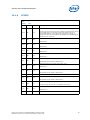
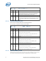
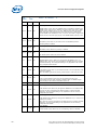
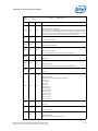
Contents
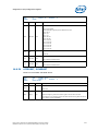
1
Overview ................................................................................................................. 17
1.1
Introduction ..................................................................................................... 17
1.2
Terminology ..................................................................................................... 18
1.3
Related Documents ........................................................................................... 21
1.4
State of Data .................................................................................................... 22
2
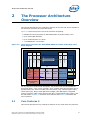
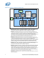
The Processor Architecture Overview ...................................................................... 23
2.1
Core Features 2 ................................................................................................ 23
2.1.1 Frequency ............................................................................................. 24
2.1.2 Caching Hierarchy .................................................................................. 24
2.1.3 Addressing Space ................................................................................... 24
2.1.4 Multi-threaded Cores .............................................................................. 24
2.1.5 Power Management ................................................................................ 24
2.1.6 Intel® Technologies ................................................................................ 24
2.2
Uncore Features................................................................................................ 25
2.2.1 The Ring ............................................................................................... 25
2.2.2 Last Level Cache (LLC)............................................................................ 25
2.2.3 Caching Agent (Cbo)............................................................................... 25
2.2.4 Intel® QuickPath Interconnect (Intel® QPI)................................................ 25
2.2.5 Home Agent (HA) ................................................................................... 26
2.2.6 Integrated Memory Controller (iMC).......................................................... 27
2.2.7 Power Control Unit (PCU) ........................................................................ 27
2.2.8 Integrated I/O module (IIO) .................................................................... 27
2.2.9 Config Agent (Ubox) ............................................................................... 28
2.2.10 Performance Monitor (PerfMon) ................................................................ 28
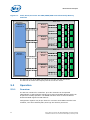
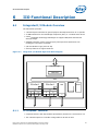
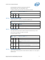
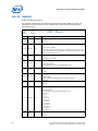
3
Cbo Functional Description ...................................................................................... 29
3.1
Basic Flows....................................................................................................... 29
3.1.1 Handling Core/IIO Request ...................................................................... 29
3.2
Source Address Decoder..................................................................................... 30
3.2.1 System Address Spaces .......................................................................... 30
3.2.2 Uncore SAD Relationship to Other Address Decoders ................................... 30
3.2.3 SAD Address Spaces ............................................................................... 31
3.2.4 DRAM/MMIO Decoders ............................................................................ 32
3.2.5 Legacy Decoder ..................................................................................... 32
3.2.6 TSEG Range (CSR_TSEG <= addr) ........................................................... 33
3.2.7 Configuration Address Space.................................................................... 33
3.2.8 NO_EGO Range...................................................................................... 33
3.2.9 I/O Address Space.................................................................................. 33
3.2.10 SAD Glossary......................................................................................... 33
3.3
Viral Support .................................................................................................... 34
4
Home Agent Functional Description ......................................................................... 35
4.1
Home Agent Architecture Overview...................................................................... 35
4.1.1 Ring Interface for Home Agent ................................................................. 35
4.1.2 Backup Tracker and Home Tracker ........................................................... 35
4.1.3 Intel QPI Home Logic .............................................................................. 36
4.1.4 Home Agent Data Buffer (HADB) .............................................................. 36
4.1.5 Memory Controller Interface .................................................................... 36
4.2
Directory Support.............................................................................................. 36
4.3
RTID Allocation ................................................................................................. 36
4.4
Backup Tracker (BT) .......................................................................................... 36
4.4.1 Backup Tracker Mode.............................................................................. 36
4.5
NodeID Conventions .......................................................................................... 36
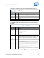
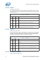
Intel® Xeon® Processor E7-2800/4800/8800 v2 Product Family
Datasheet Volume Two: Functional Description, February 2014
3
4.6
iMC Interface ....................................................................................................37
4.6.1 HA to MC Interface .................................................................................37
4.6.2 Target Address Decode (TAD)...................................................................37
5
iMC Functional Description .......................................................................................39
5.1
Overview ..........................................................................................................39
5.2
Operation .........................................................................................................40
5.2.1 Overview ...............................................................................................40
5.2.2 Logical and Physical Channels...................................................................41
5.2.3 Lockstep................................................................................................41
5.2.4 Independent Channel Mode ......................................................................41
5.3
Memory Address Decode.....................................................................................41
5.3.1 Summary of Address Translation ..............................................................42
5.3.2 DRAM Maintenance Operations .................................................................42
5.3.3 Refresh .................................................................................................42
6
IIO Functional Description .......................................................................................45
6.1
Integrated I/O Module Overview ..........................................................................45
6.1.1 PCI Express* Features.............................................................................45
6.1.2 Direct Media Interface (DMI2) Features .....................................................46
6.1.3 PCIe* 3.0 ..............................................................................................46
6.1.4 Intel® I/O Acceleration Technology (Intel® I/OAT) 4....................................46
6.1.5 Intel® Virtualization Technology (Intel® VT) for Directed I/O
(Intel® VT-d 2) Features..........................................................................46
6.1.6 Power Management Support Features........................................................46
6.1.7 Security Features....................................................................................46
6.2
PECI and JTAG ..................................................................................................47
6.2.1 PECI .....................................................................................................47
6.2.2 JTAG .....................................................................................................47
6.3
PCI Express and DMI Interfaces ...........................................................................47
6.3.1 PCI Express ...........................................................................................47
6.3.2 Speed Support .......................................................................................47
6.3.3 PCI Express Link Characteristics - Bifurcation, Link
Training, Downgrading and Lane Reversal Support ......................................47
6.3.4 Technologies Supported over PCI Express ..................................................49
6.3.5 32/64 Bit Addressing...............................................................................49
6.3.6 Direct Media Interface (DMI) ....................................................................49
6.4
Power Management............................................................................................49
6.5
Intel Virtualization Technology.............................................................................49
7
Reliability, Availability, Serviceability, and Manageability ........................................51
7.1
RASM Overview .................................................................................................51
7.1.1 Error Sources .........................................................................................52
7.1.2 Error Classification ..................................................................................52
7.1.3 RASM Feature Summary ..........................................................................53
7.2
Error Detection and Correction ............................................................................54
7.3
Error Reporting via Machine Check Architecture .....................................................54
7.3.1 Viral Alert ..............................................................................................54
7.4
Memory RAS .....................................................................................................55
7.4.1 Features and Capabilities .........................................................................55
7.4.2 Write Data Buffer Parity...........................................................................55
7.4.3 Mirroring ...............................................................................................55
7.4.4 Sparing and Scrubber..............................................................................55
7.4.5 Single Device Data Correction (SDDC) .......................................................56
7.4.6 Double Device Data Correction (DDDC)......................................................56
7.4.7 +1 Bit Correction Beyond Device Correction ...............................................56
7.4.8 PECI Write Accessibility to iMC Registers ....................................................56
7.4.9 iMC Error Handling ..................................................................................56
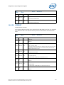
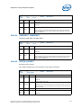
4
Intel® Xeon® Processor E7-2800/4800/8800 v2 Product Family
Datasheet Volume Two: Functional Description, February 2014
7.5
7.6
7.4.10 Intel SMI2 Half-Width Failover Mode ......................................................... 56
7.4.11 Memory Migration .................................................................................. 57
IIO RAS ........................................................................................................... 57
7.5.1 IIO RAS Overview .................................................................................. 57
7.5.2 IIO Module Error Reporting ...................................................................... 57
7.5.3 PCI Express RAS .................................................................................... 58
System Level RAS Features ................................................................................ 59
8
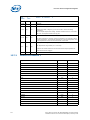
Reset Flow............................................................................................................... 61
8.1
Introduction ..................................................................................................... 61
8.1.1 Cold Reset............................................................................................. 61
8.1.2 Warm Reset .......................................................................................... 61
9
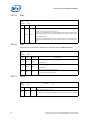
Ubox
9.1
9.2
9.3
9.4
10
PCU Functional Description...................................................................................... 65
10.1 Introduction ..................................................................................................... 65
10.2 Platform Environment Control Interface (PECI) ...................................................... 66
10.2.1 PECI Client Capabilities ........................................................................... 66
10.3 Platform Power Limits (RAPL).............................................................................. 67
10.4 ACPI P-States ................................................................................................... 67
10.5 Turbo Modes..................................................................................................... 67
10.6 DDR3 Power and Thermal Management ................................................................ 68
10.6.1 DRAM Power Management ....................................................................... 68
10.6.2 DRAM Thermal Throttling ........................................................................ 68
10.7 Miscellaneous Functions ..................................................................................... 68
11
Performance Monitoring .......................................................................................... 69
11.1 Terminology ..................................................................................................... 69
11.2 Infrastructure ................................................................................................... 69
11.3 PCU PerfMon..................................................................................................... 69
11.3.1 High-Level Overview ............................................................................... 69
12
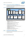
Registers Overview and Configuration Process ........................................................ 71
12.1 Platform Configuration Structure ......................................................................... 71
12.1.1 Processor IIO Devices (CPUBUSNO (0))..................................................... 71
12.1.2 Processor Uncore Devices (CPUBUSNO (1))................................................ 73
12.2 Configuration Register Rules ............................................................................... 73
12.2.1 CSR Access ........................................................................................... 74
12.2.2 MSR Access ........................................................................................... 79
12.2.3 Memory-Mapped I/O Registers ................................................................. 79
12.3 Register Terminology ......................................................................................... 79
12.4 Notational Conventions ...................................................................................... 81
12.4.1 Socket ID.............................................................................................. 81
12.4.2 Hexadecimal and Binary Numbers ............................................................ 81
13
Processor Uncore Configuration Registers ............................................................... 83
13.1 PCI Standard Registers ...................................................................................... 83
13.1.1 VID ...................................................................................................... 83
13.1.2 DID ...................................................................................................... 84
13.1.3 PCICMD ................................................................................................ 84
13.1.4 PCISTS ................................................................................................. 85
13.1.5 RID ...................................................................................................... 86
Functional Description .................................................................................... 63
Ubox Overview ................................................................................................. 63
Interrupt and Event Delivery............................................................................... 63
Scratchpad Registers ......................................................................................... 63
Sideband Interfaces........................................................................................... 63
9.4.1 PECI Access........................................................................................... 63
9.4.2 TAP Access ............................................................................................ 64
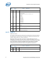
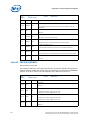
Intel® Xeon® Processor E7-2800/4800/8800 v2 Product Family
Datasheet Volume Two: Functional Description, February 2014
5
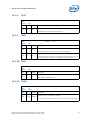
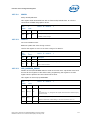
13.2
13.3
13.4
13.5
13.6
13.7
14
6
13.1.6 CCR ......................................................................................................86
13.1.7 CLSR.....................................................................................................86
13.1.8 PLAT .....................................................................................................87
13.1.9 HDR......................................................................................................87
13.1.10BIST .....................................................................................................87
13.1.11SVID.....................................................................................................87
13.1.12SDID ....................................................................................................88
13.1.13CAPPTR .................................................................................................88
13.1.14INTL .....................................................................................................88
13.1.15INTPIN ..................................................................................................88
13.1.16MINGNT ................................................................................................89
13.1.17MAXLAT.................................................................................................89
Integrated Memory Controller (iMC) Configuration Registers ....................................89
13.2.1 Device 15, 29 Function 0 .........................................................................90
13.2.2 Device 15, 29 Function 1 ....................................................................... 110
13.2.3 Device 15, 29 Functions 2-5 ................................................................... 119
13.2.4 Device 16, 30 Functions 0, 1, 4, 5........................................................... 122
13.2.5 Device 16, 30 Functions 2, 3, 6, 7........................................................... 147
Home Agent Registers ...................................................................................... 155
13.3.1 Device 14, 28 Function 0 ....................................................................... 156
PCIe* Ring Interface (R2PCIE) Registers ............................................................. 157
13.4.1 Device 19 Function 0............................................................................. 157
Intel® QuickPath Interconnect (Intel® QPI) Agent Registers ................................. 157
13.5.1 Device 8, 9, 24 Function 0 ..................................................................... 157
13.5.2 Device 8, 9, 24 Function 4 ..................................................................... 158
Processor Utility Box (UBOX) Registers ............................................................... 160
13.6.1 Device 11 Function 0............................................................................. 161
13.6.2 Device 11 Function 2............................................................................. 165
13.6.3 Device 11 Function 3............................................................................. 166
Power Controller Unit (PCU) Register .................................................................. 167
13.7.1 Device 10 Function 0............................................................................. 167
13.7.2 Device 10 Function 1............................................................................. 172
13.7.3 Device 10 Function 2............................................................................. 174
13.7.4 Device 10 Function 3............................................................................. 178
Integrated I/O (IIO) Configuration Registers ....................................................... 189
14.1 Registers Overview .......................................................................................... 189
14.1.1 Configuration Registers (CSR) ................................................................ 189
14.1.2 BDF:BAR# for various MMIO BARs in IIO ................................................. 189
14.1.3 Unimplemented Devices/Functions and Registers ...................................... 189
14.1.4 PCI Vs. PCIe* Device / Function.............................................................. 190
14.2 Device 0 Function 0 DMI, Device 0 Function 0 PCIe*, Device 2 Function
0-3 PCIe*, Device 3 Function 0-3 PCIe*.............................................................. 190
14.2.1 VID..................................................................................................... 194
14.2.2 DID .................................................................................................... 195
14.2.3 PCICMD............................................................................................... 195
14.2.4 PCISTS................................................................................................ 198
14.2.5 RID..................................................................................................... 200
14.2.6 CCR .................................................................................................... 200
14.2.7 CLSR................................................................................................... 200
14.2.8 PLAT ................................................................................................... 201
14.2.9 HDR.................................................................................................... 201
14.2.10BIST ................................................................................................... 201
14.2.11PBUS .................................................................................................. 202
14.2.12SECBUS .............................................................................................. 202
14.2.13SUBBUS .............................................................................................. 202
14.2.14IOBAS ................................................................................................. 203
Intel® Xeon® Processor E7-2800/4800/8800 v2 Product Family
Datasheet Volume Two: Functional Description, February 2014
14.2.15IOLIM ................................................................................................. 203
14.2.16SECSTS .............................................................................................. 204
14.2.17MBAS ................................................................................................. 205
14.2.18MLIM .................................................................................................. 206
14.2.19PBAS .................................................................................................. 206
14.2.20PLIM................................................................................................... 207
14.2.21PBASU ................................................................................................ 207
14.2.22PLIMU................................................................................................. 208
14.2.23CAPPTR............................................................................................... 208
14.2.24INTL ................................................................................................... 209
14.2.25INTPIN................................................................................................ 209
14.2.26BCTRL ................................................................................................ 209
14.2.27SCAPID............................................................................................... 211
14.2.28SNXTPTR............................................................................................. 211
14.2.29SVID .................................................................................................. 211
14.2.30SDID .................................................................................................. 212
14.2.31DMIRCBAR .......................................................................................... 212
14.2.32MSICAPID ........................................................................................... 213
14.2.33MSINXTPTR ......................................................................................... 213
14.2.34MSIMSGCTL ........................................................................................ 213
14.2.35MSGADR ............................................................................................. 214
14.2.36MSGDAT ............................................................................................. 215
14.2.37MSIMSK .............................................................................................. 215
14.2.38MSIPENDING ....................................................................................... 215
14.2.39PXPCAPID ........................................................................................... 216
14.2.40PXPNXTPTR ......................................................................................... 216
14.2.41PXPCAP............................................................................................... 216
14.2.42DEVCAP .............................................................................................. 218
14.2.43DEVCTRL............................................................................................. 219
14.2.44DEVSTS .............................................................................................. 221
14.2.45LNKCAP .............................................................................................. 222
14.2.46LNKCON.............................................................................................. 224
14.2.47LNKSTS .............................................................................................. 226
14.2.48SLTCAP............................................................................................... 227
14.2.49SLTCON .............................................................................................. 230
14.2.50SLTSTS............................................................................................... 232
14.2.51ROOTCON ........................................................................................... 233
14.2.52ROOTCAP ............................................................................................ 236
14.2.53ROOTSTS ............................................................................................ 236
14.2.54DEVCAP2 ............................................................................................ 237
14.2.55DEVCTRL2 ........................................................................................... 238
14.2.56LNKCAP2............................................................................................. 239
14.2.57LNKCON2 ............................................................................................ 241
14.2.58LNKSTS2............................................................................................. 243
14.2.59PMCAP ................................................................................................ 244
14.2.60PMCSR................................................................................................ 245
14.2.61XPREUT_HDR_EXT................................................................................ 246
14.2.62XPREUT_HDR_CAP ............................................................................... 247
14.2.63XPREUT_HDR_LEF ................................................................................ 247
14.2.64ACSCAPHDR ........................................................................................ 248
14.2.65ACSCAP .............................................................................................. 248
14.2.66ACSCTRL............................................................................................. 249
14.2.67APICBASE ........................................................................................... 250
14.2.68APICLIMIT ........................................................................................... 250
14.2.69VSECPHDR .......................................................................................... 251
14.2.70VSHDR ............................................................................................... 251
Intel® Xeon® Processor E7-2800/4800/8800 v2 Product Family
Datasheet Volume Two: Functional Description, February 2014
7
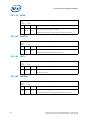
14.3
8
14.2.71ERRCAPHDR......................................................................................... 252
14.2.72UNCERRSTS ......................................................................................... 252
14.2.73UNCERRMSK ........................................................................................ 253
14.2.74UNCERRSEV......................................................................................... 253
14.2.75CORERRSTS......................................................................................... 255
14.2.76CORERRMSK ........................................................................................ 255
14.2.77ERRCAP............................................................................................... 256
14.2.78HDRLOG[0:3]....................................................................................... 256
14.2.79RPERRCMD .......................................................................................... 256
14.2.80RPERRSTS ........................................................................................... 257
14.2.81ERRSID ............................................................................................... 258
14.2.82PERFCTRLSTS_0 ................................................................................... 259
14.2.83PERFCTRLSTS_1 ................................................................................... 260
14.2.84MISCCTRLSTS_0 .................................................................................. 261
14.2.85MISCCTRLSTS_1 .................................................................................. 263
14.2.86PCIE_IOU_BIF_CTRL ............................................................................. 265
14.2.87DMICTRL ............................................................................................. 266
14.2.88DMISTS............................................................................................... 267
14.2.89ERRINJCAP .......................................................................................... 267
14.2.90ERRINJHDR.......................................................................................... 268
14.2.91ERRINJCON.......................................................................................... 268
14.2.92CTOCTRL ............................................................................................. 269
14.2.93XPCORERRSTS ..................................................................................... 269
14.2.94XPCORERRMSK..................................................................................... 270
14.2.95XPUNCERRSTS ..................................................................................... 270
14.2.96XPUNCERRMSK..................................................................................... 271
14.2.97XPUNCERRSEV ..................................................................................... 272
14.2.98XPUNCERRPTR ..................................................................................... 272
14.2.99UNCEDMASK ........................................................................................ 272
14.2.100COREDMASK ...................................................................................... 273
14.2.101RPEDMASK ......................................................................................... 274
14.2.102XPUNCEDMASK ................................................................................... 274
14.2.103XPCOREDMASK ................................................................................... 275
14.2.104XPGLBERRSTS .................................................................................... 275
14.2.105XPGLBERRPTR .................................................................................... 275
14.2.106PXP2CAP ............................................................................................ 276
14.2.107LNKCON3 ........................................................................................... 277
14.2.108LNERRSTS.......................................................................................... 277
14.2.109LN[0:3]EQ.......................................................................................... 278
14.2.110LN[4:7]EQ.......................................................................................... 280
14.2.111LN[8:15]EQ ........................................................................................ 282
14.2.112LER_CAP ............................................................................................ 284
14.2.113LER_HDR ........................................................................................... 284
14.2.114LER_CTRLSTS ..................................................................................... 284
14.2.115LER_UNCERRMSK................................................................................ 286
14.2.116LER_XPUNCERRMSK ............................................................................ 287
14.2.117LER_RPERRMSK .................................................................................. 287
14.2.118XPPMDL[0:1] ...................................................................................... 287
14.2.119XPPMCL[0:1] ...................................................................................... 289
14.2.120XPPMDH............................................................................................. 289
14.2.121XPPMCH ............................................................................................. 289
14.2.122XPPMR[0:1]........................................................................................ 290
14.2.123XPPMEVL[0:1] .................................................................................... 293
14.2.124XPPMEVH[0:1] .................................................................................... 297
14.2.125XPPMER[0:1] ...................................................................................... 298
Device 0 Function 0 Region DMIRCBAR ............................................................... 299
Intel® Xeon® Processor E7-2800/4800/8800 v2 Product Family
Datasheet Volume Two: Functional Description, February 2014
14.4
14.5
14.3.1 DMIVC0RCAP ....................................................................................... 299
14.3.2 DMIVC0RCTL ....................................................................................... 300
14.3.3 DMIVC0RSTS ....................................................................................... 301
14.3.4 DMIVC1RCAP ....................................................................................... 301
14.3.5 DMIVC1RCTL ....................................................................................... 302
14.3.6 DMIVC1RSTS ....................................................................................... 303
14.3.7 DMIVCPRCAP ....................................................................................... 303
14.3.8 DMIVCPRCTL ....................................................................................... 304
14.3.9 DMIVCPRSTS ....................................................................................... 305
14.3.10DMIVCMRCAP ...................................................................................... 305
14.3.11DMIVCMRCTL....................................................................................... 306
14.3.12DMIVCMRSTS ...................................................................................... 306
14.3.13DMIVC1CDTTHROTTLE .......................................................................... 307
14.3.14DMIVCPCDTTHROTTLE .......................................................................... 307
14.3.15DMIVCMCDTTHROTTLE ......................................................................... 308
Device 4 Function 0-7 ...................................................................................... 309
14.4.1 VID .................................................................................................... 310
14.4.2 DID .................................................................................................... 310
14.4.3 PCICMD .............................................................................................. 310
14.4.4 PCISTS ............................................................................................... 312
14.4.5 RID .................................................................................................... 313
14.4.6 CCR.................................................................................................... 313
14.4.7 CLSR .................................................................................................. 314
14.4.8 HDR ................................................................................................... 315
14.4.9 CB_BAR .............................................................................................. 315
14.4.10SVID .................................................................................................. 316
14.4.11SDID .................................................................................................. 316
14.4.12CAPPTR............................................................................................... 316
14.4.13INTL ................................................................................................... 316
14.4.14INTPIN................................................................................................ 317
14.4.15DEVCFG .............................................................................................. 317
14.4.16MSIXCAPID ......................................................................................... 318
14.4.17MSIXNXTPTR ....................................................................................... 318
14.4.18MSIXMSGCTL....................................................................................... 319
14.4.19TABLEOFF_BIR..................................................................................... 319
14.4.20PBAOFF_BIR ........................................................................................ 319
14.4.21CAPID................................................................................................. 320
14.4.22NEXTPTR............................................................................................. 320
14.4.23EXPCAP............................................................................................... 320
14.4.24DEVCAP .............................................................................................. 321
14.4.25DEVCON ............................................................................................. 322
14.4.26DEVSTS .............................................................................................. 323
14.4.27DEVCAP2 ............................................................................................ 324
14.4.28DEVCON2............................................................................................ 324
14.4.29PMCAP ................................................................................................ 325
14.4.30PMCSR................................................................................................ 325
14.4.31DMAUNCERRSTS .................................................................................. 327
14.4.32DMAUNCERRMSK ................................................................................. 327
14.4.33DMAUNCERRSEV .................................................................................. 327
14.4.34DMAUNCERRPTR .................................................................................. 328
14.4.35DMAGLBERRPTR................................................................................... 328
14.4.36CHANERR_INT ..................................................................................... 329
14.4.37CHANERRMSK_INT ............................................................................... 331
14.4.38CHANERRSEV_INT................................................................................ 332
14.4.39CHANERRPTR....................................................................................... 333
Device 4 Function 0 - 7 MMIO Region CB_BARs ................................................... 333
Intel® Xeon® Processor E7-2800/4800/8800 v2 Product Family
Datasheet Volume Two: Functional Description, February 2014
9
14.6
10
14.5.1 CHANCNT ............................................................................................ 334
14.5.2 XFERCAP ............................................................................................. 335
14.5.3 GENCTRL ............................................................................................. 335
14.5.4 INTRCTRL ............................................................................................ 335
14.5.5 ATTNSTATUS ....................................................................................... 336
14.5.6 CBVER ................................................................................................ 336
14.5.7 INTRDELAY .......................................................................................... 337
14.5.8 CS_STATUS ......................................................................................... 337
14.5.9 DMACAPABILITY ................................................................................... 337
14.5.10DCAOFFSET ......................................................................................... 339
14.5.11CBPRIO ............................................................................................... 340
14.5.12CHANCTRL ........................................................................................... 340
14.5.13DMA_COMP.......................................................................................... 341
14.5.14CHANCMD ........................................................................................... 341
14.5.15DMACOUNT.......................................................................................... 342
14.5.16CHANSTS_0 ......................................................................................... 342
14.5.17CHANSTS_1 ......................................................................................... 344
14.5.18CHAINADDR_0 ..................................................................................... 344
14.5.19CHAINADDR_1 ..................................................................................... 344
14.5.20CHANCMP_0 ........................................................................................ 345
14.5.21CHANCMP_1 ........................................................................................ 345
14.5.22CHANERR ............................................................................................ 345
14.5.23CHANERRMSK ...................................................................................... 348
14.5.24DCACTRL ............................................................................................. 348
14.5.25DCA_VER............................................................................................. 348
14.5.26DCA_REQID_OFFSET............................................................................. 349
14.5.27QPI_CAPABILITY................................................................................... 349
14.5.28PCIE_CAPABILITY ................................................................................. 349
14.5.29QPI_CAP_ENABLE ................................................................................. 350
14.5.30PCIE_CAP_ENABLE................................................................................ 350
14.5.31APICID_TAG_MAP ................................................................................. 350
14.5.32DCA_REQID[0:1].................................................................................. 352
14.5.33MSGADDR ........................................................................................... 352
14.5.34MSGUPADDR........................................................................................ 353
14.5.35MSGDATA ............................................................................................ 353
14.5.36VECCTRL ............................................................................................. 353
14.5.37PENDINGBITS ...................................................................................... 353
Device 5 Function 0 ......................................................................................... 354
14.6.1 VID..................................................................................................... 356
14.6.2 DID .................................................................................................... 356
14.6.3 PCICMD............................................................................................... 356
14.6.4 PCISTS................................................................................................ 357
14.6.5 RID..................................................................................................... 358
14.6.6 CCR .................................................................................................... 358
14.6.7 CLSR................................................................................................... 359
14.6.8 HDR.................................................................................................... 359
14.6.9 SVID................................................................................................... 359
14.6.10SDID .................................................................................................. 360
14.6.11CAPPTR ............................................................................................... 360
14.6.12INTL ................................................................................................... 360
14.6.13INTPIN ................................................................................................ 360
14.6.14PXPCAPID ............................................................................................ 361
14.6.15PXPNXTPTR.......................................................................................... 361
14.6.16PXPCAP ............................................................................................... 361
14.6.17HDRTYPECTRL ...................................................................................... 361
14.6.18MMCFG_BASE ...................................................................................... 362
Intel® Xeon® Processor E7-2800/4800/8800 v2 Product Family
Datasheet Volume Two: Functional Description, February 2014
14.7
14.6.19MMCFG_LIMIT ..................................................................................... 362
14.6.20TSEG .................................................................................................. 363
14.6.21GENPROTRANGE[1:0]_BASE .................................................................. 363
14.6.22GENPROTRANGE[1:0]_LIMIT ................................................................. 364
14.6.23GENPROTRANGE2_BASE ....................................................................... 364
14.6.24GENPROTRANGE2_LIMIT ....................................................................... 364
14.6.25TOLM.................................................................................................. 365
14.6.26TOHM ................................................................................................. 365
14.6.27NCMEM_BASE ...................................................................................... 366
14.6.28NCMEM_LIMIT ..................................................................................... 366
14.6.29MENCMEM_BASE .................................................................................. 367
14.6.30MENCMEM_LIMIT ................................................................................. 367
14.6.31CPUBUSNO.......................................................................................... 367
14.6.32LMMIOL_BASE ..................................................................................... 368
14.6.33LMMIOL_LIMIT..................................................................................... 368
14.6.34LMMIOH_BASE..................................................................................... 369
14.6.35LMMIOH_LIMIT .................................................................................... 369
14.6.36CIPCTRL.............................................................................................. 369
14.6.37CIPSTS ............................................................................................... 372
14.6.38CIPDCASAD ......................................................................................... 372
14.6.39CIPINTRC ............................................................................................ 373
14.6.40CIPINTRS ............................................................................................ 374
14.6.41VTBAR ................................................................................................ 375
14.6.42VTGENCTRL ......................................................................................... 375
14.6.43VTGENCTRL2 ....................................................................................... 376
14.6.44IOTLBPARTITION.................................................................................. 377
14.6.45VTUNCERRSTS..................................................................................... 379
14.6.46VTUNCERRMSK .................................................................................... 380
14.6.47VTUNCERRSEV..................................................................................... 381
14.6.48VTUNCERRPTR ..................................................................................... 382
14.6.49IIOMISCCTRL....................................................................................... 382
14.6.50LTDPR ................................................................................................ 388
14.6.51IRP_MISC_DFX0 .................................................................................. 389
14.6.52IRP_MISC_DFX1 .................................................................................. 390
14.6.53IRP[0:1]DELS ...................................................................................... 391
14.6.54IRP[0:1]DBGRING0 .............................................................................. 392
14.6.55IRP[0:1]DBGRING1 .............................................................................. 392
14.6.56IRPSPAREREGS .................................................................................... 392
14.6.57IRP[0:1]RNG ....................................................................................... 392
14.6.58IRPEGCREDITS .................................................................................... 394
14.6.59IRP_MISC_DFX2 .................................................................................. 396
14.6.60IRP_MISC_DFX3 .................................................................................. 398
Device 5 Function 0 MMIO Region VTBAR ........................................................... 399
14.7.1 VTD[0:1]_VERSION .............................................................................. 401
14.7.2 VTD[0:1]_CAP ..................................................................................... 401
14.7.3 VTD[0:1]_EXT_CAP .............................................................................. 402
14.7.4 VTD[0:1]_GLBCMD............................................................................... 404
14.7.5 VTD[0:1]_GLBSTS................................................................................ 406
14.7.6 VTD[0:1]_ROOTENTRYADD.................................................................... 407
14.7.7 VTD[0:1]_CTXCMD ............................................................................... 407
14.7.8 VTD[0:1]_FLTSTS ................................................................................ 409
14.7.9 NONISOCH_FLTEVTCTRL ....................................................................... 410
14.7.10NONISOCH_FLTEVTDATA ...................................................................... 410
14.7.11VTD[0:1]_FLTEVTADDR......................................................................... 411
14.7.12VTD[0:1]_FLTEVTUPRADDR ................................................................... 411
14.7.13VTD[0:1]_PMEN ................................................................................... 411
Intel® Xeon® Processor E7-2800/4800/8800 v2 Product Family
Datasheet Volume Two: Functional Description, February 2014
11
14.8
12
14.7.14VTD[0:1]_PROT_LOW_MEM_BASE .......................................................... 412
14.7.15VTD[0:1]_PROT_LOW_MEM_LIMIT .......................................................... 412
14.7.16VTD[0:1]_PROT_HIGH_MEM_BASE ......................................................... 412
14.7.17VTD[0:1]_PROT_HIGH_MEM_LIMIT ......................................................... 413
14.7.18VTD[0:1]_INV_QUEUE_HEAD ................................................................. 413
14.7.19VTD[0:1]_INV_QUEUE_TAIL................................................................... 413
14.7.20VTD[0:1]_INV_QUEUE_ADD................................................................... 414
14.7.21VTD[0:1]_INV_COMP_STATUS ............................................................... 414
14.7.22NONISOCH_INV_CMP_EVTCTRL.............................................................. 414
14.7.23NONISOCH_INVEVTDATA....................................................................... 415
14.7.24VTD[0:1]_INV_COMP_EVT_ADDR ........................................................... 415
14.7.25VTD[0:1]_INV_COMP_EVT_UPRADDR ...................................................... 415
14.7.26VTD[0:1]_INTR_REMAP_TABLE_BASE ..................................................... 416
14.7.27VTD0_FLTREC[0:7]_GPA, VTD1_FLTREC0_GPA ......................................... 416
14.7.28VTD0_FLTREC[0:7]_SRC, VTD1_FLTREC0_SRC ......................................... 417
14.7.29VTD[0:1]_INVADDRREG ........................................................................ 417
14.7.30VTD[0:1]_IOTLBINV.............................................................................. 418
Device 5 Function 2 ......................................................................................... 420
14.8.1 VID..................................................................................................... 422
14.8.2 DID .................................................................................................... 423
14.8.3 PCICMD............................................................................................... 423
14.8.4 PCISTS................................................................................................ 424
14.8.5 RID..................................................................................................... 425
14.8.6 CCR .................................................................................................... 425
14.8.7 CLSR................................................................................................... 425
14.8.8 HDR.................................................................................................... 426
14.8.9 SVID................................................................................................... 426
14.8.10SDID .................................................................................................. 426
14.8.11CAPPTR ............................................................................................... 426
14.8.12INTL ................................................................................................... 427
14.8.13INTPIN ................................................................................................ 427
14.8.14PXPCAPID ............................................................................................ 427
14.8.15PXPNXTPTR.......................................................................................... 427
14.8.16PXPCAP ............................................................................................... 428
14.8.17IRPPERRSV .......................................................................................... 428
14.8.18IIOERRSV ............................................................................................ 429
14.8.19MIERRSV ............................................................................................. 430
14.8.20PCIERRSV............................................................................................ 430
14.8.21SYSMAP .............................................................................................. 431
14.8.22VIRAL ................................................................................................. 432
14.8.23ERRPINCTL .......................................................................................... 433
14.8.24ERRPINSTS .......................................................................................... 433
14.8.25ERRPINDAT.......................................................................................... 434
14.8.26VPPCTL ............................................................................................... 435
14.8.27VPPSTS ............................................................................................... 436
14.8.28VPPFREQ ............................................................................................. 436
14.8.29VPPMEM .............................................................................................. 437
14.8.30GNERRMASK ........................................................................................ 438
14.8.31GFERRMASK......................................................................................... 439
14.8.32GCERRMASK ........................................................................................ 440
14.8.33GCERRST............................................................................................. 442
14.8.34GCFERRST, GCNERRST .......................................................................... 443
14.8.35GNERRST ............................................................................................ 444
14.8.36GFERRST ............................................................................................. 445
14.8.37GERRCTL ............................................................................................. 446
14.8.38GSYSST............................................................................................... 448
Intel® Xeon® Processor E7-2800/4800/8800 v2 Product Family
Datasheet Volume Two: Functional Description, February 2014
14.9
14.8.39GSYSCTL............................................................................................. 448
14.8.40GFFERRST, GFNERRST .......................................................................... 448
14.8.41GNFERRST, GNNERRST ......................................................................... 449
14.8.42IRPP[0:1]ERRST................................................................................... 449
14.8.43IRPP[0:1]ERRCTL ................................................................................. 450
14.8.44IRPP[0:1]FFERRST, IRPP[0:1]FNERRST ................................................... 451
14.8.45IRPP[0:1]FFERRHD[0:3]........................................................................ 452
14.8.46IRPP[0:1]NFERRST, IRPP[0:1]NNERRST .................................................. 465
14.8.47IRPP[0:1]NFERRHD[0:3] ....................................................................... 466
14.8.48IRPP[0:1]ERRCNTSEL ........................................................................... 466
14.8.49IRPP[0:1]ERRCNT ................................................................................ 466
14.8.50IIOERRST............................................................................................ 467
14.8.51IIOERRCTL .......................................................................................... 467
14.8.52IIOFFERRST, IIOFNERRST ..................................................................... 468
14.8.53IIOFFERRHD_[0:3] ............................................................................... 469
14.8.54IIONFERRST, IIONNERRST .................................................................... 469
14.8.55IIONFERRHD_[0:3] .............................................................................. 470
14.8.56IIOERRCNTSEL .................................................................................... 470
14.8.57IIOERRCNT.......................................................................................... 471
14.8.58MIERRST............................................................................................. 471
14.8.59MIERRCTL ........................................................................................... 472
14.8.60MIFFERRST, MIFNERRST ....................................................................... 472
14.8.61MIFFERRHDR_[0:3] .............................................................................. 472
14.8.62MINFERRST, MINNERRST ...................................................................... 474
14.8.63MINFERRHDR_[0:3].............................................................................. 474
14.8.64MIERRCNTSEL ..................................................................................... 475
14.8.65MIERRCNT........................................................................................... 475
Device 5 Function 4 ......................................................................................... 475
14.9.1 VID .................................................................................................... 476
14.9.2 DID .................................................................................................... 476
14.9.3 PCICMD .............................................................................................. 477
14.9.4 PCISTS ............................................................................................... 478
14.9.5 RID .................................................................................................... 479
14.9.6 CCR.................................................................................................... 479
14.9.7 CLSR .................................................................................................. 479
14.9.8 HDR ................................................................................................... 480
14.9.9 MBAR ................................................................................................. 480
14.9.10SVID .................................................................................................. 480
14.9.11SID .................................................................................................... 481
14.9.12CAPPTR............................................................................................... 481
14.9.13INTLIN................................................................................................ 481
14.9.14INTPIN................................................................................................ 481
14.9.15ABAR.................................................................................................. 482
14.9.16PXPCAP............................................................................................... 482
14.9.17SNAPSHOT_INDEX ............................................................................... 483
14.9.18SNAPSHOT_WINDOW ........................................................................... 483
14.9.19IOAPICTETPC....................................................................................... 484
14.9.20PMCAP ................................................................................................ 485
14.9.21PMCSR................................................................................................ 485
14.9.22IOADSELS0 ......................................................................................... 486
14.9.23IOADSELS1 ......................................................................................... 487
14.9.24IOINTSRC0.......................................................................................... 487
14.9.25IOINTSRC1.......................................................................................... 488
14.9.26IOREMINTCNT ..................................................................................... 488
14.9.27IOREMGPECNT ..................................................................................... 489
14.9.28FAUXGV .............................................................................................. 489
Intel® Xeon® Processor E7-2800/4800/8800 v2 Product Family
Datasheet Volume Two: Functional Description, February 2014
13
14.10 Device 5 Function 4 I/OxAPIC............................................................................ 489
14.10.1INDEX ................................................................................................. 490
14.10.2WINDOW ............................................................................................. 490
14.10.3EOI..................................................................................................... 490
14.10.4Device 5 Function 4 Window 0 ................................................................ 490
14.11 Device 6 Function 0, 3 and Device 7 Function 0 ................................................... 496
14.11.1VID..................................................................................................... 496
14.11.2DID .................................................................................................... 497
14.11.3PCICMD............................................................................................... 497
14.11.4PCISTS................................................................................................ 498
14.11.5RID..................................................................................................... 499
14.11.6CCR .................................................................................................... 499
14.11.7CLSR................................................................................................... 499
14.11.8PLAT ................................................................................................... 500
14.11.9HDR.................................................................................................... 500
14.11.10BIST.................................................................................................. 500
14.11.11SVID ................................................................................................. 500
14.11.12SDID ................................................................................................. 501
14.11.13CAPPTR.............................................................................................. 501
14.11.14INTL .................................................................................................. 501
14.11.15INTPIN............................................................................................... 501
14.11.16MINGNT ............................................................................................. 502
14.11.17MAXLAT ............................................................................................. 502
14.11.18PXPCAP.............................................................................................. 502
14.11.19RX_CTLE_PEAK_GEN2.......................................................................... 503
14.11.20RX_CTLE_PEAK_GEN3.......................................................................... 503
Figures
Intel® Xeon® Processor E7-2800/4800/8800 v2 Product Family
High Level Block Diagram ...................................................................................23
3-1
SAD Address Map ..............................................................................................31
5-1
Intel® Xeon® Processor E7-2800/4800/8800 v2 Product Family Memory Interface......40
6-1
Integrated I/O Module High-level Block Diagram ....................................................45
6-2
PCI Express Lane Partitioning ..............................................................................48
7-1
Error Classification .............................................................................................52
10-1 Power and Thermal Management Architecture Overview..........................................66
12-1 Processor integrated I/O device map ....................................................................72
12-2 Processor uncore devices map .............................................................................73
2-1
Tables
1-1
1-2
1-3
2-1
12-1
12-2
12-3
14-1
14-2
14-3
14
Processor Terminology .......................................................................................18
Processor Documents .........................................................................................21
Public Specifications ...........................................................................................21
Technologies in the Processor Core ......................................................................24
Functions specifically handled by the processor ......................................................75
RW_LB CSRs list allowed PECI write when not in BMC_INIT mode ............................78
Register attribute definitions ...............................................................................79
BDF:BAR# for various MMIO BARs in IIO ............................................................ 189
Function number of active root ports in port 2(Dev#2) based on port bifurcation...... 190
Function number of active root ports in port 3(Dev#3) based on port bifurcation...... 190
Intel® Xeon® Processor E7-2800/4800/8800 v2 Product Family
Datasheet Volume Two: Functional Description, February 2014
Revision History
Doc ID
Description
Date
329595-001
Initial Release
February 2014
329595-002
Added Chapters 12 through 15
February 2014
§
Intel® Xeon® Processor E7-2800/4800/8800 v2 Product Family
Datasheet Volume Two: Functional Description, February 2014
15
16
Intel® Xeon® Processor E7-2800/4800/8800 v2 Product Family
Datasheet Volume Two: Functional Description, February 2014
Overview
1
Overview
1.1
Introduction
The Intel® Xeon® Processor E7-2800/4800/8800 v2 Product Family processors are the
next generation of 64-bit, multi-core enterprise processors built on 22-nanometer
process technology. The Intel Xeon processor E7 v2 product family implements multiple
multi-threaded (two threads) cores based upon the Intel Xeon processor E7 v2 product
family core design. A large, up to 37.5 MB, last-level cache (LLC) has been
implemented to be shared across all active cores.The Intel Xeon processor E7 v2
product family supports two on-chip memory controllers. It is designed primarily for
glueless four- or eight-socket multiprocessor systems, and features three Intel®
QuickPath Interconnects (Intel® QPI) and four Intel® Scalable Memory Interconnect
(Intel® SMI) channels.
The Intel® Xeon® E7 v2 product family-based platform supports four fully-connected
Intel Xeon processor E7 v2 product family sockets, where each Intel Xeon processor E7
v2 product family uses three Intel QuickPath Interconnects to connect to the other
sockets and can connect to the PCH via the x4 DMI Gen 2 channel. The Intel Xeon
processor E7 v2 product family maintains cache coherence at the platform level by
supporting the Intel QuickPath Interconnect source broadcast snoopy protocol.
The Intel Xeon processor E7 v2 product family is designed to support Intel QuickPath
Interconnects at speeds of 8, 7.2 and 6.4 GT/s and DDR3 - 1067, 1333 and 1600 MT/s
memory speeds. It uses a power-through-the-pins power delivery system and new
socket R1.
Note:
Unless specifically required for clarity, this document will use ‘processor’ in place of the
specific product name.
The Intel® Xeon® Processor E7-2800/4800/8800 v2 Product Family Datasheet Volume
Two: Functional Description provides register documentation and functional description
of major functional areas of the processor non-core design, and additional features
pertinent to implementation and operation of the processor.
The key features of the processor chip are as follows:
• Multi-threaded cores, two threads per core
• Socket types: Socket R1 (2011-0 land FC-LGA package)
• Operating Frequency: Base/TDP frequency range is 1.9 GHz - 3.4 GHz (Please
review the SKU specific details in the spec update)
• Target TDP (Thermal Design Power) Consumption: up to 155 W
• Last Level Cache: Up to 37.5 MB
• Intel QPI interfaces: up to three interfaces each operating at up to 8.0 GT/s
• Supports 48-bit virtual addressing and 46-bit physical addressing
• Two integrated Memory Controllers provide ample memory bandwidth and memory
capacity for demanding enterprise applications:
— Each memory controller manages two Intel SMI2 channels, operated in either
independent or lockstep mode.
Intel® Xeon® Processor E7-2800/4800/8800 v2 Product Family
Datasheet Volume Two: Functional Description, February 2014
17
Overview
— One Intel® C102/C104 Scalable Memory Buffer per Intel SMI2 channel, with up
to two DDR3 channels per Intel C102/C104 Scalable Memory Buffer and up to
eight DDR3 channels per socket.
— Supports 1067, 1333 and 1600 MT/s DDR3 frequencies.
— Supports up to 3 DIMMs per DDR3 channel.
— Supports 2 GB, 4 GB and 8 GB DRAM technologies
• PCI Express* interfaces: Up to 32 lanes each operating at PCI Express 3.0 speed
(PCIe* 3.0) and 4 lanes of DMI2/PCI Express 2.0 (PCIe* 2.0) interface.
• Supports C states C0, C1, C3 and C6.
• Advanced Reliability Features
• Platform Technologies supported are Intel® Turbo Boost Technology, Intel® Trusted
Execution Technology (Intel® TXT), Intel® Dynamic Power, Intel® Virtualization
Technology (Intel® VT) for IA-32, Intel® 64 and Intel® Architecture (Intel® VT-x),
Intel VT for Directed I/O (Intel® VT-d), Intel® I/O Acceleration Technology (Intel®
I/OAT)/CB3, Intel® Intelligent Power Node Manager, TPM 1.2, Digital RNG,
and more.
1.2
Terminology
A ‘_N’ symbol after a signal name refers to an active low signal, indicating a signal is in
the active state when driven to a low level. For example, when RESET_N is low, a reset
has been requested.
Table 1-1.
Processor Terminology (Sheet 1 of 4)
Term
ASPM
18
Description
Active State Power Management
BMC
Baseboard Management Controller
Cbo
Cache and Core Box. It is a term used for internal logic providing ring interface to
LLC and Core.
DCU
Data Cache Unit
DDR3
Third generation Double Data Rate SDRAM memory technology that is the
successor to DDR2 SDRAM
DMA
Direct Memory Access
DMI2
Direct Media Interface operating at PCI Express* 2.0 speed.
DSB
Data Stream Buffer. This is part of the Intel Xeon processor E7 v2 product family
core architecture.
DTLB
Data Translation Look-aside Buffer. Part of the Intel Xeon processor E7 v2
product family core architecture.
DTS
Digital Thermal Sensor
ECC
Error Correction Code
Enhanced Intel
SpeedStep® Technology
Allows the operating system to reduce power consumption when performance is
not needed.
Execute Disable Bit
The Execute Disable bit allows memory to be marked as executable or nonexecutable, when combined with a supporting operating system. If code
attempts to run in non-executable memory the processor raises an error to the
operating system. This feature can prevent some classes of viruses or worms
that exploit buffer overrun vulnerabilities and can thus help improve the overall
security of the system. See the Intel® 64 and IA-32 Architectures Software
Developer's Manuals for more detailed information.
Flit
Flow Control Unit. Data transfer unit of Intel QPI Link Layer. 1 Flit = 80-bits.
Intel® Xeon® Processor E7-2800/4800/8800 v2 Product Family
Datasheet Volume Two: Functional Description, February 2014
Overview
Table 1-1.
Processor Terminology (Sheet 2 of 4)
Term
Description
Functional Operation
Refers to the normal operating conditions in which all processor
specifications, including DC, AC, system bus, signal quality, mechanical, and
thermal, are satisfied.
GSSE
Extension of the SSE/SSE2 (Streaming SIMD Extensions) floating point
instruction set to 256b operands.
ICU
Instruction Cache Unit. Part of the Intel Xeon processor E7 v2 product family
core architecture.
IFU
Instruction Fetch Unit. Part of the processor core.
IIO
The Integrated I/O Controller. An I/O controller that is integrated in the
processor die.
iMC
The Integrated Memory Controller. A Memory Controller that is integrated in the
processor die.
IQ
Instruction Queue. Part of the Intel Xeon processor E7 v2 product family core
architecture.
Intel® ME
Intel® Management Engine
Intel®
QuickData
Technology
Intel® QuickData Technology is a platform solution designed to maximize the
throughput of server data traffic across a broader range of configurations and
server environments to achieve faster, scalable, and more reliable I/O.
Intel® QuickPath
Interconnect (Intel® QPI)
A cache-coherent, link-based Interconnect specification for Intel processors,
chipsets, and I/O bridge components.
Intel® 64 Technology
64-bit memory extensions to the IA-32 architecture. Further details on Intel 64
architecture and programming model can be found at
http://developer.intel.com/technology/intel64/.
Intel SSE
Intel® Streaming SIMD Extensions (Intel® SSE)
Intel®
Turbo Boost
Technology
Intel® Turbo Boost Technology is a way to automatically run the processor core
faster than the marked frequency if the part is operating under power,
temperature, and current specifications limits of the Thermal Design Power
(TDP). This results in increased performance of both single and multi-threaded
applications.
Intel® Trusted Execution
Technology (Intel® TXT)
Intel® Trusted Execution Technology uses features in processor, chipset and TPM
to enable more secure and robust systems against software attacks.
Intel® Virtualization
Technology (Intel® VT)
Processor Virtualization which when used in conjunction with Virtual Machine
Monitor software enables multiple, robust independent software environments
inside a single platform.
Intel® VT-d
Intel® Virtualization Technology (Intel® VT) for Directed I/O. Intel VT-d is a
hardware assist, under system software (Virtual Machine Manager or OS)
control, for enabling I/O device Virtualization. Intel VT-d also brings robust
security by providing protection from errant DMAs by using DMA remapping, a
key feature of Intel VT-d.
Integrated Heat Spreader
(IHS)
A component of the processor package used to enhance the thermal
performance of the package. Component thermal solutions interface with the
processor at the IHS surface.
Jitter
Any timing variation of a transition edge or edges from the defined Unit Interval
(UI).
Intel Xeon processor E7 v2
product familyr
Intel’s 22-nm process based product used in Intel Xeon processor E7 v2 product
family-based platform.
IOV
I/O Virtualization
LGA 2011-0 Socket
The 2011-0 land FC-LGA package mates with the system board through this
surface mount, 2011-0 contact socket.
LLC
Last Level Cache
LRDIMM
Load Reduced Dual In-line Memory Module
LRU
Least Recently Used. A term used in conjunction with cache hierarchy.
MESIF
Modified/Exclusive/Shared/Invalid/Forwarded. States used in conjunction with
cache coherency
Intel® Xeon® Processor E7-2800/4800/8800 v2 Product Family
Datasheet Volume Two: Functional Description, February 2014
19
Overview
Table 1-1.
Processor Terminology (Sheet 3 of 4)
Term
20
Description
MLC
Mid Level Cache
NCTF
Non-Critical to Function: NCTF locations are typically redundant ground or noncritical reserved, so the loss of the solder joint continuity at end of life conditions
will not affect the overall product functionality.
NEBS
Network Equipment Building System. NEBS is the most common set of
environmental design guidelines applied to telecommunications equipment in the
United States.
PCH
Platform Controller Hub. The next generation chipset with centralized platform
capabilities including the main I/O interfaces along with display connectivity,
audio features, power management, manageability, security and storage
features.
PCU
Power Control Unit.
PCI Express 3.0
The third generation PCI Express specification that operates at 8 GT/s data
transfer rate per lane per direction. PCI Express 3.0 is completely backward
compatible with PCI Express 1.0 and 2.0.
PCI Express
PCI Express Generation 2.0/3.0
PCI Express 2.0
PCI Express Generation 2.0
PECI
Platform Environment Control Interface
Phit
Physical Unit. Data transfer unit of Intel® QPI Physical Layer. 1 Phit is equal to18
bits in ‘full width mode’ and 9 bits in ‘half width mode’.
Processor
The 64-bit, single-core or multi-core component (package)
Processor Core
A processing and execution unit which has an instruction cache, data cache, and
256-KB L2 cache. All processor cores share the LLC.
R3QPI
Ring to Intel® QPI agent interface. An internal logic block providing interface
between internal Ring and Intel® QPI Agents.
Rank
A unit of DRAM corresponding four to eight devices in parallel, ignoring ECC.
These devices are usually, but not always, mounted on a single side of a DDR3
DIMM.
RDIMM
Registered Dual In-line Memory Module
Scalable
Intel Xeon processor E7 v2 product family-platform targeted for scalable designs
using third party Node Controller chip. In these designs, Node Controller is used
to scale the design beyond one/two/four sockets.
SCI
System Control Interrupt. Used in ACPI protocol.
Server SKU
A processor Stock Keeping Unit (SKU) to be installed in either server or
workstation platforms. Electrical, power and thermal specifications for these
SKU’s are based on specific use condition assumptions. Server processors may
be further categorized as Efficient Performance server, workstation and HPC
SKUs. For further details on use condition assumptions, please refer to the latest
Product Release Qualification (PRQ) Report available via your Customer Quality
Engineer (CQE) contact.
SMBus
System Management Bus. A two-wire interface through which simple system and
power management related devices can communicate with the rest of the
system. It is based on the principals of the operation of the I2C* two-wire serial
bus from Philips Semiconductor.
Storage Conditions
A non-operational state. The processor may be installed in a platform, in a tray,
or loose. Processors may be sealed in packaging or exposed to free air. Under
these conditions, processor landings should not be connected to any supply
voltages, have any I/Os biased or receive any clocks. Upon exposure to “free air”
(that is, unsealed packaging or a device removed from packaging material) the
processor must be handled in accordance with moisture sensitivity labeling
(MSL) as indicated on the packaging material.
TAC
Thermal Averaging Constant
TDP
Thermal Design Power
TSOD
Temperature Sensor On DIMM
Intel® Xeon® Processor E7-2800/4800/8800 v2 Product Family
Datasheet Volume Two: Functional Description, February 2014
Overview
Table 1-1.
Processor Terminology (Sheet 4 of 4)
Term
Description
Uncore
The portion of the processor comprising the shared cache, iMC, HA, PCU, UBox,
and Intel QPI link interface.
Unit Interval
Signaling convention that is binary and unidirectional. In this binary signaling,
one bit is sent for every edge of the forwarded clock, whether it be a rising edge
or a falling edge. If a number of edges are collected at instances t1, t2, tn,...., tk
then the UI at instance “n” is defined as:
UI
1.3
n
= t n- t
n-1
VCC
Processor core power supply
VSS
Processor ground
x1
Refers to a Link or Port with one Physical Lane
x4
Refers to a Link or Port with four Physical Lanes
x8
Refers to a Link or Port with eight Physical Lanes
x16
Refers to a Link or Port with sixteen Physical Lanes
XNC
eXtended Node Controller. OEM proprietary silicon that is used to interface with
processor to build up scalable systems.
Related Documents
Refer to the following documents for additional information.
Table 1-2.
Processor Documents
Document
Table 1-3.
Document Number
Intel® Xeon® Processor E7-2800/4800/8800 v2 Product Family Datasheet Volume One
329594-001
Intel® Xeon® Processor E7-2800/4800/8800 v2 Processor Thermal/Mechanical
Design Guide
329596-001
Intel® Xeon® Processor E7-2800/4800/8800 v2 Product Family
Specification Update
329597-001
Intel® Xeon® Processor E7-2800/4800/8800 v2 Product Family BSDL
(Boundary Scan Description Language)
329598-001
Public Specifications (Sheet 1 of 2)
Document
Advanced Configuration and Power Interface Specification 3.0
Document Number/ Location
http://www.acpi.info
PCI Local Bus Specification 3.0
http://www.pcisig.com/specifications
PCI Express® Base Specification - Revision 1.1
PCI Express® Base Specification - Revision 2.1
PCI Express® Base Specification - Revision 3.0 Draft
http://www.pcisig.com
DDR3 SDRAM Specification and Register Specification
http://www.jedec.org
Intel® 64 and IA-32 Architectures Software Developer's Manuals
• Volume 1: Basic Architecture
• Volume 2A: Instruction Set Reference, A-M
• Volume 2B: Instruction Set Reference, N-Z
• Volume 3A: System Programming Guide
• Volume 3B: System Programming Guide
Intel® 64 and IA-32 Architectures Optimization Reference Manual
Intel® Virtualization Technology Specification for Directed I/O
Architecture Specification
Intel® Xeon® Processor E7-2800/4800/8800 v2 Product Family
Datasheet Volume Two: Functional Description, February 2014
http://www.intel.com/products/processor/
manuals/index.htm
http://download.intel.com/technology/com
puting/vptech/Intel(r)_VT_for_Direct_IO.p
df
21
Overview
Table 1-3.
Public Specifications (Sheet 2 of 2)
Document
Document Number/ Location
Intel® Trusted Execution Technology Software Development
Guide
1.4
http://www.intel.com/technology/security/
State of Data
The data contained within this document is preliminary. It is the most accurate
information available by the publication date of this document. The information in this
revision of the document is based on early data. Processor feature set and capabilities
may change prior to production.
§
22
Intel® Xeon® Processor E7-2800/4800/8800 v2 Product Family
Datasheet Volume Two: Functional Description, February 2014
The Processor Architecture Overview
2
The Processor Architecture
Overview
This section describes the key architecture features of the core and uncore modules of
the Intel Xeon processor E7 v2 product family.
Figure 2-1 shows a high level view of the processor integrating:
• Multiple Intel Xeon processor E7-2800/4800/8800 v2 product family cores
• Up to 3 Intel QPI interfaces
• Up to 32 PCI Express* 3.0 lanes
• 1 x4 DMI2/PCIe* 2.0 interface
Figure 2-1.
Intel® Xeon® Processor E7-2800/4800/8800 v2 Product Family High Level
Block Diagram
Core/ Cbo n
Core/ Cbo n-1
Core/ Cbo2
Core/ Cbo1
Core/ Cbo0
LLC
Ubox
HA0
MC0
HA1
MC1
2x Intel® SMI2
Interfaces per Memory
controller
R-QPI 0
R-QPI 1
R-QPI 2
3x Intel QuickPath Interconnects
Internal IO (IIO)
32 PCIe 3.0
Lanes
PMU
1 x 4 DMI2/
PCIe 2.0
Interface
For the purpose of architectural description, the processor can be sub-divided into
three main areas - core, uncore, and IIO. “Core” includes Intel Xeon processor E7 v2
product family core. Uncore includes Last Level Cache (LLC), Caching agents (Cbo),
Home Agent (HA), Ring to Intel QPI blocks (R3QPI), Intel QPI Agents, integrated
memory controller (iMC), Power Control Unit (PCU), Configuration Agent (Ubox), and
the IIO module. Section 2.1 describes Core features and Section 2.2 describes the
uncore features.
2.1
Core Features 2
This section describes the key architecture features of core used within the processor.
Intel® Xeon® Processor E7-2800/4800/8800 v2 Product Family
Datasheet Volume Two: Functional Description, February 2014
23
The Processor Architecture Overview
2.1.1
Frequency
The processor cores are designed to run at a rated frequency and the architecture
allows operating at lower frequencies in order to make appropriate power/performance
trade-off. Along with the ability to slow down cores for power optimization, “Intel Turbo
Boost Technology” allows the ability to increase a core’s speed to optimize single
threaded applications.
2.1.2
Caching Hierarchy
Caching for the processor spans three levels - dedicated instruction and data cache
(ICU and DCU), mid-level cache (MLC) for each core, and last level cache (LLC) for the
socket.
• ICU and DCU: 32 KB each
• MLC per core: 256 KB (instructions and data)
• LLC per socket: Up to 37.5 MB (instructions and data)
— Each core slice brings 2.5 MB slices
2.1.3
Addressing Space
The processor supports a virtual address space of 48 bits and a physical address space
of 46 bits.
2.1.4
Multi-threaded Cores
Each core supports two threads.
2.1.5
Power Management
The processor core implements a number of energy efficiency features. Additionally,
the processor implements a sophisticated power management scheme to throttle
cores and the memory traffic of each memory controller independently through
internal protocols.
2.1.6
Intel® Technologies
The processor core offers several key Intel® Technologies. Table 2-1 enumerates the
key technologies implemented in the processor core.
Table 2-1.
Technologies in the Processor Core
Abbreviated Name
24
Short Description
GSSE
Extension of the SSE/SSE2 floating point instruction set to 256b operands.
Xsave/Xrestore
New instructions to streamline OS/VMM support for features with new state.
Better software control over state saved, restored and initialized.
Intel® Advanced Encryption
Standard New Instructions
(Intel® AES-NI)
Speed up encryption tasks to enable broader Intel AES-NI use.
OS/VMM Features
Real mode Intel VT support. Always running timer enabling “tick-less” OS
1 GB large page support
Support for larger 1 GB pages in server applications.
Intel TXT for servers
Server-focused security technology.
Intel® Xeon® Processor E7-2800/4800/8800 v2 Product Family
Datasheet Volume Two: Functional Description, February 2014
The Processor Architecture Overview
2.2
Uncore Features
This section describes key features supported by each of the uncore modules designed
specifically for the server and workstation market space. Further details of the key
modules is provided in subsequent chapters.
2.2.1
The Ring
The processor implements a proprietary, ring topology, interconnect between the core
and uncore elements as used by the Intel QPI interface. The processor ring provides a
high-bandwidth interconnect between the cores and uncore modules.
2.2.2
Last Level Cache (LLC)
The processor last level cache comprises a 2.5 MB section for each core slice
instantiated but together they represent one logical cache.
The LLC tracks the MESIF (Modified, Exclusive, Shared, Invalid, and Forwarded) states
for maintaining cache coherency between cores and sockets. For any given cache line,
the LLC implements core valid bits to track which local core(s) have cached the line in
their MLC. Core valid bits are also used by LLC to determine which local core(s) are
needed to be snooped during responding to snoop request. The replacement policy is
pseudo-least recently used (LRU) with the Invalid way being replaced first. The LLC is a
20 way cache with the ability to allocate any number of ways.
2.2.3
Caching Agent (Cbo)
Similar to the last level cache, the caching agent for the processor socket is addresshashed across Cbo slices. When system BIOS/Firmware disables cores the active Cbo’s
are not impacted.
The Cbo provides several functions for agent requests:
• Request/snoop proxy: Core/PCIe requests are address hashed to select a Cbo to
translate and place the request onto the Intel QPI domain. If the last level cache
slice attached to that Cbo indicates that a core within the socket owns the line (for
a coherent read), the request is snooped to that local core.
• Source Address Decoding: The system address decoder is used to determine the
destination node id for a given request. The source address decoder is replicated in
all Cbo’s.
• Local Conflict Manager: The Cbo is responsible for ensuring that only one
coherent request is issued to the system for a specific cache-line in one socket.
This manages conflicts between all the cores local to the socket.
2.2.4
Intel® QuickPath Interconnect (Intel® QPI)
The Intel QPI module includes two sub-modules: Intel QPI Agent and the ring stop
which is referred to as R3QPI.
The processor is implemented based on Intel QPI v1.1 spec. The physical/link layers
are implemented in the Intel QPI Agent sub-module, which provides primary interface
between the Intel QPI agents on the platform, that is, processors and node controllers.
This is an Intel proprietary interface for coherent and non-coherent traffic.
Intel® Xeon® Processor E7-2800/4800/8800 v2 Product Family
Datasheet Volume Two: Functional Description, February 2014
25
The Processor Architecture Overview
Note that in a 2S configuration, if parallel Intel QPI ports are to be used, Port 2 cannot
be used in the parallel topology. Only ports 0 and 1 support a parallel topology.
The Intel Xeon processor E7 v2 product family supports 3 Intel QPI interfaces. Ports 0,
1 must always operate at the same link frequency, and link 2 can operate at its own
supported link frequency. The supported link frequencies for top SKU processor is
targeting 6.4, 7.2, and 8.0 GT/s.
The Ring to Intel QPI sub-module (R3QPI) provides several functions:
• Interface between the Processor Ring and Intel QPI Agent: One of the
primary attributes of the processor ring is its ability to convey Intel QPI semantics
with no translation. For example, this architecture enables initiators to
communicate with a local Home Agent in exactly the same way as a remote Home
Agent on another processor socket.
• Intel QPI routing: In order to optimize latency, Intel QPI ports 0, 1 share the
same processor ring stop. Therefore, an Intel QPI packet might be received on one
interface and simply forwarded along on the other Intel QPI interface, achieving a
better average latency over the route-through traffic via port 2. The R3QPI has
sufficient routing logic to determine if a request, snoop, or response is targeting the
local socket or if it should be forwarded along to the other interface.
• Router snoop fanout: The R3QPI supports router snoop fanout which allows
snoops to be broadcast. This is an important feature for topologies which are not
fully connected because it reduces the average number of snoops sent over each
Intel QPI link. Intel Xeon processor E7 v2 product family will support only the
Snoop Fanout mode, no directed snoops, so router snoop fanout is expected to be
always enabled.
2.2.5
Home Agent (HA)
The Home Agent is the Intel QPI specification term for the coherent agent responsible
for guarding the iMC module and handles all the memory read/write requests. The
Home Agent provides several functions:
• Interface between modular ring and iMC module: Regardless of the memory
technology, the Home Agent receives the memory read and write requests via the
modular ring. It checks the memory transaction type, detects and resolves the
coherent conflict, and finally schedules a corresponding transaction to the iMC
module. It is also responsible for returning the requested data, certain coherent
protocol messages, and transaction completion.
• Conflict Manager for Intel QPI transactions: All coherent requests between
sockets via Intel QPI interface must go through conflict management logic in order
to ensure the coherent consistency across different sockets. In other words, the
view of data must be the same across all coherent agents regardless of which
socket modifies the data. Home Agent is responsible for tracking all requests to a
given main memory address and ensures that the results are consistent.
• Memory Access Ordering and Data Consistency Control: The Home Agent
guarantees the ordering of RAW (Read after Write), WAW (Write after Write) and
WAR (Write after Read). It ensures the iMC module requirement of no write to the
memory if there is an outstanding read to the same address.
• Memory RAS features Support: Home Agent manages several memory RAS
features, for example, demand scrubbing, DDR channel lockstep, memory
mirroring with fail-over recovery, MCA error reporting and recovery.
26
Intel® Xeon® Processor E7-2800/4800/8800 v2 Product Family
Datasheet Volume Two: Functional Description, February 2014
The Processor Architecture Overview
• Home Snoop Protocol Support: The Home Agent implements Intel QPI v1.1
“home snoop protocol” by initiating snoops on behalf of the requestor. The HA also
offers Opportunistic Snoop Broadcast to further optimize performance.
• Directory Mode Support: The HA only operates in the directory mode.
2.2.6
Integrated Memory Controller (iMC)
The internal memory controller provides the interface to DDR3 DIMMs via Intel®
Scalable Memory Interconnect (Intel® SMI) 2 and Intel® C102/C104 Scalable Memory
Buffer expansion silicon. The memory controller communicates to the rest of the
processor through the Home Agent. Key features are as follows:
• Supports two Intel SMI2 interfaces per memory controller
• One Intel C102/C104 Scalable Memory Buffer per Intel SMI2 interface, with up to
two DDR3 channels Intel C102/C104 Scalable Memory Buffer
• Up to 3 DDR3 DIMMs on each DDR channel
• Support up to 8 ranks per channel
• Support 1067, 1333, 1600 MT/s DDR3 frequencies.
• Support 2 GB, 4 GB and 8 GB DRAM technologies
• Support “Corrupt Data Containment” and “MCA Recovery”
• Support memory power management features, that is, CLTT and
MEM_HOT_C{01/23}_N
2.2.7
Power Control Unit (PCU)
The processor implements a power control unit acting as a core/uncore power and
thermal manager. It runs its firmware on an internal micro-controller and coordinates
the socket for its power states.
The PCU algorithmically governs the P-states of the processor, C-states of the core and
the package C-states of the socket. It also enables the core to go to a higher
performance state (Intel® Turbo Boost Technology) when the proper set of conditions
are met. Conversely, the PCU could throttle the processor to a lower performance state
when thermal violation occurrs.
Through specific events, the OS and the PCU will either promote or demote the C-state
of each core by altering the voltage and frequency. The system power state (S-state)
of all the sockets in the system is managed by an external device such as PCH or BMC
in coordination with all socket PCUs.
The OS and BIOS communicates to the PCU via standardized MSR registers and ACPI.
The PCU acts as the interface to external management controllers (BMC) via PECI and
voltage regulators.
2.2.8
Integrated I/O module (IIO)
The I/O module provides features traditionally supported through chipset components.
One of the benefits is that a server does not require auxiliary chipset components aside
from the legacy southbridge. The Integrated I/O module provides the following
features:
Intel® Xeon® Processor E7-2800/4800/8800 v2 Product Family
Datasheet Volume Two: Functional Description, February 2014
27
The Processor Architecture Overview
• PCI Express Interfaces: The I/O module incorporates PCI Express interface. The
processor can support up to 32 lanes of PCI Express. Following are key attributes of
the PCI Express interface:
— Gen3 speeds at 8 GT/s (no 8b/10b encoding)
— 2 X16 interfaces, each can be bifurcated down to two x8 or four x4 (or
combinations)
• DMI2 Interface to the PCH: The platform requires an interface to the legacy
Southbridge (PCH) which provides basic, legacy functions required for the
server/workstation platforms and operating systems. Since only one PCH is
required for the system, any sockets which do not connect to PCH could use this
port as a standard x4 PCI Express 2.0 interface.
• Integrated IOAPIC: Provides support for PCI Express devices implementing
legacy interrupt messages without interrupt sharing
• Intel® QuickData Technology: Used for efficient, high bandwidth data
movement between two locations in memory or from memory to I/O
2.2.9
Config Agent (Ubox)
The UBox acts as the centralized unit for a variety of non-coherent type of transactions
and functions:
• The target for interrupts. The UBox dispatches interrupts to the appropriate core.
• Decodes and routes transactions to uncore registers.
• Implements time stamp counters, scratch pad registers, PerfMon infrastructure
support, and so forth.
• Serializes locks/unlock, Quiescent messages to the Lock Master in the legacy
socket.
Note:
The Lock Master must be legacy socket with socket ID[3,1:0]=[0,0,0].
2.2.10
Performance Monitor (PerfMon)
The processor implements an exhaustive set of counters designed to count and monitor
events used for tracking performance. By combining the counts from different events,
system software can determine the performance characteristics of the processor
platform.
§
28
Intel® Xeon® Processor E7-2800/4800/8800 v2 Product Family
Datasheet Volume Two: Functional Description, February 2014
Cbo Functional Description
3
Cbo Functional Description
The Intel Xeon processor E7 v2 product family core to the last level cache (LLC)
interface is managed by the LLC coherence unit (Cbo). The Cbo handles all core and
PCIe to Intel QuickPath Interconnect messages and system interface logic. There is at
most one Cbo per core in a given socket. The LLC is 20-ways associative, and is an
inclusive cache for the mid level cache in the cores.
Cbo cache coherence engine maintains cache coherency that handles access to the last
level cache and generates transactions back to the core or system interconnect. The
Cbo also ensures transaction conflicts are properly handled. The Cbo contains the TOR
(Table Of Requests) that holds all pending transactions.
3.1
Basic Flows
The Cbo supports three types of transactions:
1. Core/IIO initiated requests
2. Intel QPI external snoops
3. LLC capacity eviction
Each transaction has an associated entry in the Table of Requests (the TOR). The TOR
entry holds information required by the Cbo to uniquely identify the request, in addition
to the address and transaction type, and state elements required to track the current
status of the transaction.
3.1.1
Handling Core/IIO Request
In general, there are two kinds of core/IIO requests:
Coherent request: Coherent requests are requests to access a memory address that
is mapped to the coherent address space. They are usually used to transfer data at a
cache line granularity and/or to change the state of a cache line. The most common
coherent requests are Data and Code Reads, RFOs (Read for ownership), ItoMs
(acquire ownership w/o reading the line) and Writebacks (write a Modified data from
MLC to LLC).
The Coherent requests are serviced by the Cbo that holds the LLC slice for the specified
address, determined by the hashing function.
Non Coherent request: Non-coherent requests are either data accesses that map to
non-coherent address space (like Memory Mapped IO), or they are non-memory
requests like IO read/write, interrupts/events, and so forth.
When non-coherent requests accesses to non-coherent memory, they are sent to the
Cbo according to the hash of the address just like coherent requests. The non-coherent
requests which do not target memory are always sent to the Cbo that is attached to the
core which generates the request (also referred to as the collocated slice).
Intel® Xeon® Processor E7-2800/4800/8800 v2 Product Family
Datasheet Volume Two: Functional Description, February 2014
29
Cbo Functional Description
3.2
Source Address Decoder
Within the Cbo, requests go through the Source Address Decoder (SAD) at the same
time that they are allocating into the TOR and are sent to the LLC. Non-LLC message
class types go through the SAD when they are allocating into the TOR as well.
The SAD receives the address, the address space, opcode, and a few other transaction
details. It outputs the type of the target of the transaction (DRAM, MMIO, IO, LT, CFG)
with proper NodeID or whether it should be serviced in the Local Crab (Ubox).
The SAD contains rules for the address decoding. Some of these rules are hardwired,
and can be used before the SAD is initialized. Some rules must be enabled before they
can be used. Some rules have parts that may be configured.
3.2.1
System Address Spaces
The Intel Xeon processor E7 v2 product family cores and the IIO issue transactions to
the memory address space, the I/O address space, and configuration address space.
Intel QPI virtual channels target the following address spaces:
• Hardware cache coherent address space, HOM
• Non-coherent (NC) address space, NCS/NCB
• I/O address space, IO
• PCI Express configuration address space, CFG
• LT special cycle address space, LT
HOM is used if the address is to be snooped. NC is used by the local or remote IIO if the
address is not to be snooped. NC contains memory mapped I/O (MMIO) and various
configuration register regions.
The processor always accesses system DRAM using the HOM channel, even if the
memory type from the core is UC or WC. This allows the IA-32 preservation of memory
type aliasing.
The processor can access MMIO with memory type UC (Un-Cached), WP (Write
Protected), WT (Write Through), or WC (Write Combining) using the NC channel. The
processor can also access MMIO with WB (Write Back) however the core/software must
be in place such that dirty data is never evicted to the Uncore for this range. The
system does not implement hardware cache coherence in WP, WT, or WC, WB memory
types; it is up to the programmer to maintain any needed cache coherence or memory
ordering concerns with these memory types.
3.2.2
Uncore SAD Relationship to Other Address Decoders
3.2.2.1
Core Address Decoders
Addresses come from executing instructions and are translated by the segmentation
and paging logic of the IA-32 core. The Cbo and the rest of Uncore always see host
physical addresses.
30
Intel® Xeon® Processor E7-2800/4800/8800 v2 Product Family
Datasheet Volume Two: Functional Description, February 2014
Cbo Functional Description
3.2.2.2
IIO Address Decoders
Although many of the address ranges for the IIO address decoders are now integrated
into Cbo system address decoder, there are still significant portions of IIO address
decoding logic that reside inside IIO. IIO Address decoders will provide protection,
address translation and proper sub decoding to support IO related transactions.
3.2.3
SAD Address Spaces
The memory address space primarily contains cache coherent DRAM. The DRAM
decoder defines the location of the cache coherent DRAM segments of the system
address map. It also contains MMIO, and many legacy address ranges. Legacy address
ranges are decoded by the legacy address decoder and are described later. Figure 3-1
shows the system address map as seen by the SAD.
Figure 3-1. SAD Address Map
1 _ 0000_ 0000
65536G
FLASH
MMIOH
FF00_ 0000
TOHM
PCI Express Additional
Segments
ICH
LT
FED0_ 0000
IOAPIC
FEC0_ 0000
DRAM_ HI
Reserved
FEB8 _ 0000
CRAB
_ ABORT
BOHM = 4 G
FEB0_ 0000
NO_ EARLY_ GO
No_ Early_ Go
Configuration
FE 00_ 0000
MMIOL
CSR_ PCIE
Tseg
16 M
1M
PCI Express
configuration
TSeg
DRAM
DRAM_ LO
MMIO
LEGACY
PAM hole
VGA hole
0100_ 0000
00 F 0 _ 0000
0010_ 0000
000 C _ 0000
TSeg Stolen Memory
000 A_ 0000
0
Intel® Xeon® Processor E7-2800/4800/8800 v2 Product Family
Datasheet Volume Two: Functional Description, February 2014
31
Cbo Functional Description
3.2.3.1
SAD Decoders and Priority
There are a total of four types of decoders in the SAD. Each of them covers a
different part of the address map. These decoders do sometimes overlap, with explicit
priorities defined for the cases when matches in multiple decoders occur in parallel so
that we can ensure no holes in the address map exist. Below are the four types of
decoders in SAD:
• DRAM decoders: These are the decoders used to program DRAM configuration in
the system.
• MMIO decoder: These are decoders used to define MMIO-L and MMIO-H region.
• Interleave decoder: This is a special decoder to decode MMCFG region. It has up to
8 interleave targets and can be configured to cover either the whole segment 0
region or some part of the higher segments in the case we have higher segments.
• Legacy decoder: Used to define various legacy ranges.
3.2.4
DRAM/MMIO Decoders
3.2.4.1
DRAM Decoders
The Intel Xeon processor E7 v2 product family Cbo DRAM decoders will support 2, 4,
and 8 way interleaving. In Intel Xeon processor E7 v2 product family, we employ a
hierarchical address decode approach, therefore the way definition here corresponds to
a node ID as opposed to a channel in the memory itself. The Intel Xeon processor E7 v2
product family home agent handles channel interleaving internally.
3.2.4.2
MMIO Decoders
MMIO decoders are very similar to DRAM decoders. The only difference is that MMIO
decoders do not require interleaving. Each range is designated toward one target as
opposed to a list of targets (that is, no interleaving).
MMIO decoders covers the range of MMIO-L and MMIO-H in the system address map.
Intel Xeon processor E7 v2 product family supports 16 address match rules with MMIO
decoders and with granularity of 16 MB. This means that there can be up to 16 different
segments within MMIO-L and MMIO-H regions.
3.2.5
Legacy Decoder
The Legacy decoder outputs on of the following types:
1. HOM: the target lies in Coherent DRAM
2. CFG: the target is PCI configuration register. The Intel QPI opcodes are:
NcCfgRd/NcCfgWr
3. LT: trusted register regions (not config): The Intel QPI opcodes are: NcLtRd/NcLtWr
4. MMIO: if none of the above rules applied, this is the default option that will be
decoded by MMIO decoders. The Intel QPI opcodes are: NcRd/NcWr{Ptl}
5. IO: IO space, The Intel QPI opcodes are: NcIoRd/NcIoWr
6. ABORT: Cbo would return data of all ‘1s for reads and complete writes (throw away
data) when abort is indicated by decoder.
7. NO_EGO region will be covered by MMIO-L. BIOS must program this properly by
ensuring MMIO decoder overlaps the NO_EGO region.
32
Intel® Xeon® Processor E7-2800/4800/8800 v2 Product Family
Datasheet Volume Two: Functional Description, February 2014
Cbo Functional Description
3.2.6
TSEG Range (CSR_TSEG <= addr)
The TSEG range is used to manage the SMM memory region for DMA accesses. The
protection is done by the core (through SMRR) and the IIO (through registers) thus it is
not the responsibility of the uncore Cbo SAD.
3.2.7
Configuration Address Space
Configuration accesses to Uncore control registers are originally in the I/O address
space. There is also a range for PCI Express* configuration registers access in the
memory address space.
Note that Legacy PCI configuration register accesses are done using I/O accesses to
CFC/CF8. These PCI configuration accesses are translated to PCI Express configuration
accesses by CPU.
3.2.8
NO_EGO Range
NO_EGO range in Intel Xeon processor E7 v2 product family is 32 MB in size and will
contain Flash, ICH, LT, IOAPIC and Abort regions as specified in the following
subsections. Access to undefined region in NO_EGO range will be aborted by the
processor and will not result in alias access to DRAM or MMIO range.
3.2.9
I/O Address Space
The processor's I/O address space is used for VGA aliasing, CFC/CF8 accesses for the
configuration space of PCI Express segment 0, and other I/O devices.
3.2.10
SAD Glossary
ASEG – CSEG is sometimes called the ASEG because it is located at A_0000 segment
in memory.
CSEG – An uncacheable, compatibility segment used for 16b code for system
management mode and SMI handlers for patches.
HOM – The coherent Intel QPI channel.
MMIO – Memory Mapped I/O
NC – Non-coherent Intel QPI channel
PAM – Legacy BIOS ROM area in MMIO and when overlaid with DRAM it is used as a
faster ROM storage area.
SMM – System Management Mode
SMRR – System Management Mode Range Register
TSEG – A cacheable region of DRAM used for 32b code for SMM
Intel® Xeon® Processor E7-2800/4800/8800 v2 Product Family
Datasheet Volume Two: Functional Description, February 2014
33
Cbo Functional Description
3.3
Viral Support
The Intel Xeon processor E7 v2 product family supports Viral mode of the operation
where the processor report fatal error conditions by setting the viral bit in the Intel QPI
header packets, as well as assertion of the Error pin on the processor package. The
system wide attempt to detect viral error conditions is another way to improve on the
data reliability and error containment.
§
34
Intel® Xeon® Processor E7-2800/4800/8800 v2 Product Family
Datasheet Volume Two: Functional Description, February 2014
Home Agent Functional Description
4
Home Agent Functional
Description
The Intel Xeon processor E7 v2 product family supports up to two Home Agents (HA)
on-die. The HA is responsible for handling all DRAM requests homed at its node. It
accepts incoming home requests, snoop responses, and write back messages from the
ring, and in turn it sends data, completion, and snoop packets to the ring. The
aggregate of HAs enforce the memory coherency for the system. The HA also schedules
memory access requests to the local integrated memory controller (iMC) for DDR
memory reads and writes. After a requested memory access is completed, the HA
sends the corresponding response message back to the requester.
The implementation of the HA is closely tied to the Ring and the iMC. The ring stop in
the HA implements the necessary flow control and credit exchange for the messages
that are sent and received at HA. The HA interface to the iMC is responsible for the
memory access scheduling. The memory access scheduler, error handler, and
transaction control logic in the HA also support DRAM RAS features such as the
memory channel mirroring, DDR channel lockstep, and memory access retry. The Intel
Xeon processor E7 v2 product family will support channel mirroring, cross-socket HA
memory migration (no migration within socket HAs is allowed), Intel SMI2 channel retry and support for viral error conditions.
4.1
Home Agent Architecture Overview
There are below primary parts of the Home Agent:
1) Ring interface for Home Agent
2) Backup Tracker (BT) and Home Tracker (HT)
3) Intel QPI home control logic
4) Home Agent Data Buffer (HADB)
5) Memory controller interface.
4.1.1
Ring Interface for Home Agent
The ring interface is used for Intel QPI protocol packet communication to and from the
HA.
4.1.2
Backup Tracker and Home Tracker
The HA contains a tracker, which is a pool of pre-allocated buffers for tracking system
requests. The Intel Xeon processor E7 v2 product family HA implements a 128-entry In
flight Memory Buffer (also called Home tracker, HT), a 512-entry Tracker (also called
Backup Tracker, BT).
Intel® Xeon® Processor E7-2800/4800/8800 v2 Product Family
Datasheet Volume Two: Functional Description, February 2014
35
Home Agent Functional Description
4.1.3
Intel QPI Home Logic
The home logic is responsible for detecting and resolving the coherency conflict and
memory access ordering for memory accesses.
4.1.4
Home Agent Data Buffer (HADB)
The HADB is a set of data buffers. It is a temporary storage for transferring the data
between the ring and memory controller. It has 128 entries, one for each Home Tracker.
4.1.5
Memory Controller Interface
The interface to MC first decodes the appropriate DRAM channel from the address. This
process is called “Target Address Decode” (TAD). After the target channel is decoded
the request is forward to corresponding BGF (bubble generator fifo). On a read, the
data will be returned from the MC and is forwarded to the HADB. On a write, the data
will be downloaded from the ring to the HADB and is forwarded to the MC.
4.2
Directory Support
The HA supports a 2-bit directory which is stored with each cacheline in DRAM ECC bits.
The directory is used to filter snoops to remote sockets and/or node controllers. The
directory can reduce the snoop traffic and latency in multiple socket topologies.
4.3
RTID Allocation
Intel QPI specification v1.1 allows each caching agent to be allocated only up to 64
RTIDs per HA.
4.4
Backup Tracker (BT)
All home channel messages incoming to the HA will go through the BT (if the BT is
enabled). The BT maintains a set of FIFOs to order the requests that are waiting to get
into the HT such that the HT entry is allocated to the oldest waiting request when it
becomes available.
4.4.1
Backup Tracker Mode
The backup tracker supports 3 different modes below:
• BT_Mode1 is the extended RTID mode for up to 4 sockets which allocates >64 (up
to 128) BT entries for the local CA and up to 128 BT entries for the remote CAs.
• BT_Mode2 is the extended RTID mode for 8S configurations which allocates up to
128 BT entries for the local CA and up to 48 BT entries for the remote CAs.
• BT_Mode3 is the extended RTID mode for 4S+xNC configurations and allows up to
128 BT entries for the local CA and up to 64 BT entries for the remote CA.
BT_Mode3 allows for a maximum of 7 CA, and hence cannot be used for 8S.
4.5
NodeID Conventions
Intel Xeon processor E7 v2 product family implements 4-bits of NodeID (NID). Intel
Xeon processor E7 v2 product family can support up to 2 HAs in each socket. The HAs
in the same socket will be differentiated by NID[2].
36
Intel® Xeon® Processor E7-2800/4800/8800 v2 Product Family
Datasheet Volume Two: Functional Description, February 2014
Home Agent Functional Description
4.6
iMC Interface
The HA operates at the same frequency as Cbo in the uncore clock domain, whereas
the iMC is operated at the fixed DRAM clock domain, called Dclock domain.
The HA sends the DRAM reads, writes, and other commands to the MC interface. It
receives the return data, completion, error signals, and other request and
acknowledgements from the MC.
4.6.1
HA to MC Interface
The HA can send a request to MC when the request acquired its MC credit and the BGF
allows to store the requester on its available HA to MC control BGF input buffer. The
control interface is a shared by all memory channels between the HA and MC. The
control interface BGF is a non-backpressure BGF. The HA writes to control BGF when
the BGF input buffer is valid and the HA has a write credit. It assumes the MC receives
the command after given clock cycles.
Each memory channel has its own data interface individually. Each memory channel
interface consists of an individual data BGF. T The MC write credit can only be credited
back to the credit pool after the HA received the ack back from the MC. The channel is
decoded based on rules programmed in the Target Address Decoder (TAD).
4.6.2
Target Address Decode (TAD)
The target address decoder is responsible for resolving the channel interleave based on
the system address decoding results. The target address decode assumptions and
mechanism are consistent with the system address decode (SAD) at Cbo and the
memory address decode (MAD) at MC.
The system address decoder (SAD) is responsible for mapping the address to the Home
Agent. It occurs before the request is sent to the Home Agent. The target address
decode (TAD) is responsible for the logical channel address mapping and interleaving at
Home Agent. The target address decoder is located at the Home Agent. The memory
address decode at MC will map the channel address to meet DRAM requirements.
§
Intel® Xeon® Processor E7-2800/4800/8800 v2 Product Family
Datasheet Volume Two: Functional Description, February 2014
37
Home Agent Functional Description
38
Intel® Xeon® Processor E7-2800/4800/8800 v2 Product Family
Datasheet Volume Two: Functional Description, February 2014
iMC Functional Description
5
iMC Functional Description
5.1
Overview
The Intel Xeon processor E7 v2 product family implements two internal memory
controllers (iMC). Each memory controller supports two Intel SMI 2 interfaces and two
Intel C102/C104 Scalable Memory Buffer expansion per iMC. Intel C102/C104 Scalable
Memory Buffer provides support for two DDR3 buses. Intel SMI 2 is the technology
used covering communication across the iMC and Intel C102/C104 Scalable Memory
Buffer silicon.
The memory controller can be configured to operate in one of two modes:
• Independent mode: The performance mode. Each DDR3 channel is addressed
individually via burst lengths of 8 bytes. The Intel SMI channel will operate at twice
the DDR3 data rates.
• Lockstep mode: The high RAS mode supporting DDDC with x4 DRAMs. The
memory controller handles all cache lines across two DDR3 channels behind one
Intel C102/C104 Scalable Memory Buffer. The Intel SMI 2 channel operates at the
DDR3 transfer rate.
The processor iMC will interface with the rest of the uncore via the Home Agent (HA),
each socket will have two iMC’s instantiated per processor die, each with its own HA.
Intel® Xeon® Processor E7-2800/4800/8800 v2 Product Family
Datasheet Volume Two: Functional Description, February 2014
39
iMC Functional Description
Figure 5-1.
Intel® Xeon® Processor E7-2800/4800/8800 v2 Product Family Memory
Interface
Riser card
Processor
DI MM1
DIMM0
DD R3Ch1
DI MM1
DI MM0
DD R3Ch0
DI MM2
DI MM1
DI MM0
DD R3Ch1
DI MM2
M em ory
eXtension
Buffer
DD R3Ch0
DI MM2
Intel SM I2Ch0
M em ory
eXtension
Buffer
DI MM2
M em ory
Controller 0
Intel SM I2 Ch1
DI MM1
DI MM0
DDR3Ch0
DIMM2
DIMM1
DIMM0
DDR3Ch1
DIMM2
DIMM1
DI MM0
DDR3Ch0
DI MM2
DI MM1
DI MM0
DDR3Ch1
DI MM2
DI MM1
DI MM0
Riser card
M em ory
Controller 1
Intel SM I2 Ch2
M em ory
eXtension
Buffer
M em ory
eXtension
Buffer
Intel SM I2 Ch3
The iMC logic runs at the DDR CLK frequency to match the DDR bandwidth.
The HA runs at Uncore CLK frequency like the rest of the uncore.
5.2
Operation
5.2.1
Overview
The iMC unit contains four controllers. Up to four channels can be operated
independently or DDR Channels behind Intel C102/C104 Scalable Memory Buffer can
be paired for lockstep operation. The DRAM controllers share a common address
decode and DMA engines for RAS features.
Configuration registers may be per channel or common. Each DRAM controller has a
scheduler, write and read data paths, ECC logic and auxiliary structures.
40
Intel® Xeon® Processor E7-2800/4800/8800 v2 Product Family
Datasheet Volume Two: Functional Description, February 2014
iMC Functional Description
In Intel Xeon processor E7 v2 product family channel 0 can be used to control two
DDR3 DRAM channels behind the Intel SMI 2 bus in Sub channel lockstep mode, while
Channel 2 controls two DRAM channels behind a second Intel SMI 2 bus. Each pair of
channels (Channels 0&1, Channels 2&3) shares a Write Push Logic unit, while each
channel has a Intel SMI 2 Retry buffer and a Intel SMI 2 Command Encoder.
Read and Write addresses from the HA are steered according to address decode to one
of the four channels or a pair of channels (in the mirroring or lockstep cases). The
channels decompose the reads and writes into precharge, activate and column
commands and schedule their command to the DDR command/address lines. Write
data is enqueued in the Write Data Buffers where partial writes are merged to form full
line writes. The Channels drive write data to the DRAMs and the DRAMs return read
data on the bidirectional data bus. Read returns from the 4 channels are corrected if
necessary multiplexed back to the HA data buffer.
5.2.2
Logical and Physical Channels
The Memory controller channels exposed to the HA are logical. The HA sends requests
and maintains credits on a logical channel basis. The memory controller may translate
the channel select sent by the HA to one or two physical channels.
5.2.3
Lockstep
Lockstep refers to splitting cache lines across DDR sub channels (off Intel C102/C104
Scalable Memory Buffer). This is done to support SDDC for DRAM devices with 8-bit
wide data ports. The same address is used on both channels, such that an address
error on any channel is detectable by bad ECC. The ECC code used by the memory
controller can correct 1/18th of the data in a codeword. Since there are 9 x8 DRAMs on
a DIMM, a codeword must be split across 2 DIMMs to allow the ECC to correct all the
bits corrupted by a x8 DRAM failure. The MC always accumulates 32B before forwarding
data so there is no latency benefit for disabling ECC.
5.2.4
Independent Channel Mode
In x4 DRAM use case, SDDC is supported, and x8 DRAM provides ECC coverage only.
Each channel is running independently (non-lock-step), that is, each line from memory
is provided by a channel. To deliver the 64B line of data, each channel is bursting eight
8B chunks of data. Back to back data transfer in the same direction and within the
same rank may incur no dead-cycle. The independent channel mode is the
recommended method to deliver most efficient power and bandwidth.
For each channel, these connections are made to every rank of every connected DIMM.
5.3
Memory Address Decode
The memory address decoder (mc_dec) translates a system address into a DRAM
device address. The main input to the decoder comes from the HA. These inputs are
the full system address, the target DDR channel, and the TAD range the system
address falls into. The decoder uses this input and the TAD, RIR, and MTR MSR settings
to control the decode. The decoder outputs are row, column, and bank DRAM
addresses, as well as the target rank. While the HA performs some analysis of the
system address, such as determining the target channel, the MC decoder implements
all the steps to translate the system address, including removing gaps in the system
address space that do not map to main memory.
Intel® Xeon® Processor E7-2800/4800/8800 v2 Product Family
Datasheet Volume Two: Functional Description, February 2014
41
iMC Functional Description
The memory address decoder supports channel and rank interleaving, several DIMM
and DRAM device types, and both open and closed page optimized address mappings.
There is a requirement that at each level of interleaving, the set of targets must each
contribute an equal amount of memory. For example, 8 GB of system space can be 2way socket interleaved, and then 4-way channel interleaved on one socket and 2-way
channel interleaved on the other. This results in both sockets contributing 4 GB each to
the interleave, one socket with 4 channels contributing 1 GB each, and the other with 2
channels contributing 2 GB each.
The decode process is broken into three address translation steps: system to channel,
channel to rank, and finally rank to DRAM device. The first two steps each involve
division and subtraction. The division reduces the address space based on the number
of interleave ways, and the subtraction adjusts for offsets between the different
address spaces. The rank to DRAM address translation step requires only muxing
because of the matching address space sizes and lack of interleaving at this level.
5.3.1
Summary of Address Translation
The address map is optimized to speed decode. As many DRAM bits as possible are
assigned to a single rank address bit, and require no logic to map. The number of times
a DRAM bit appears in the table indicates the width of the mux used to map address
bits to the DRAM bit.
Channel address bits are mapped to DRAM bits according to the number of rows,
columns, banks in the target DIMM, lockstep or independent channels, and scheduling
policies. Each DIMM may have a different address assignment.
The following tables describe the translation from System Address to Rank Address to
the DRAM bits in the memory channel. There are two main tables, for page open and
closed. Minor variations are shown for independent and lockstep channels. The columns
on the right show the mapping of system address to rank address for all possible
combinations of channel and rank interleaves. (The 3 way interleaves represent the
truncation case. The divide by 3 scheme, the channel address is system address/3).
Row, Column and Bank bits which are present in all DRAM organizations are
indicated by a box around the cell in the tables. The other DRAM bits are only present
in larger DRAMs.
5.3.2
DRAM Maintenance Operations
The maintenance operations consist of Refresh, DRAM temperature monitoring, Host
Driver Impedance calibration, and DRAM driver Impedance Calibration. They are made
as infrequent as the physical process they address to reduce performance impact.
5.3.3
Refresh
The iMC supports three types of refresh – opportunistic refresh, high-priority refresh
and panic refresh. Opportunistic refresh is executed when the refresh execution affect
on normal operation is low. High-priority and panic refreshes are executed when the
refresh time constrains are close to expire, and refresh must be executed.
The DDR refresh rules are defined in two levels:
1. Refresh of a given page has to occur once every 64 / 32 ms. In order to obtain this,
the average time between two refreshes is tREFI = 7.8 / 3.9 us (times are for
normal / high temperature operation).
2. The gap between two successive refreshes may not be more than 9* tREFI.
42
Intel® Xeon® Processor E7-2800/4800/8800 v2 Product Family
Datasheet Volume Two: Functional Description, February 2014
iMC Functional Description
Execution of a single refresh is tRFC, and it takes 110 – 350 ns according to
DDR3 density.
iMC is equipped with CLTT temperature monitor and be able to issue auto refresh at the
2x rate (3.9 us).
5.3.3.1
Refresh Priorities
There are 3 levels of refresh priorities
1. Opportunistic
2. High-priority
3. Panic
The opportunistic refresh is executed when the scheduler thinks that it can issue it
without a significant penalty. High-priority is used when a backlog of refresh requests
has accumulated. At this point the refresh has higher priority than any other
transaction except for transactions. Panic is when refresh must be executed. Panicrefresh is in higher priority than transactions.
§
Intel® Xeon® Processor E7-2800/4800/8800 v2 Product Family
Datasheet Volume Two: Functional Description, February 2014
43
iMC Functional Description
44
Intel® Xeon® Processor E7-2800/4800/8800 v2 Product Family
Datasheet Volume Two: Functional Description, February 2014
IIO Functional Description
6
IIO Functional Description
6.1
Integrated I/O Module Overview
The IIO module provides:
• x32 PCI Express interface for general purpose PCI Express devices at 3.0 speeds
• x4 DMI interface for the southbridge component (PCH) or a x4 PCIe Gen2 device
• Intel® QuickData Technology DMA Engine to support IOAT, ROL and External
Storage Usages
• IOxAPIC controller used to convert legacy interrupts from I/O devices into
messages to the CPU’s Local APIC
• I/O Virtualization Logic (Intel VT-d2)
• Security features to support Intel TXT
Figure 6-1.
Integrated I/O Module High-level Block Diagram
Coherency Engine
Write Cache
Vtd-2
PCIe Gen3
PCIe Gen3
HP
HP
x16
6.1.1
x4
Crystal
Beach
DMA
IOAPIC
x16
x8
x8
x4
DMI
x4
x8
x4
x4
x8
x4
x4
x4
x4
PCI Express* Features
• Compliant with the PCI Express Base Specification, Revision 2.0 and Revision 3.0
• Two x16 PCI Express 3.0 interface configurable to x8 and x4 links.
Intel® Xeon® Processor E7-2800/4800/8800 v2 Product Family
Datasheet Volume Two: Functional Description, February 2014
45
IIO Functional Description
• 2.5 GHz (1.0) and 5 GHz (2.0) and 8 GHz (3.0)
• Full peer-to-peer support between PCI Express interfaces
• Full support for software-initiated PCI Express power management
• x8 Server I/O Module (SIOM)
6.1.2
Direct Media Interface (DMI2) Features
• One x4 DMI 2.0 link interface supporting 2.5 GB/s/direction (PCIe physical layer)
peak bandwidth
• Can also operate as a x4 2.0 PCIe link
6.1.3
PCIe* 3.0
• 8 GT/s rate
• TLP Processing Hints (TPH) for data push to cache
• Address Translation Services (ATS 1.0)
• PCIe Atomic Operations Completer Capability
6.1.4
Intel® I/O Acceleration Technology (Intel® I/OAT) 4
• 3.0 I/O caching hints used for Intel® I/O Acceleration Technology (Intel® I/OAT)
• ATR enhancements (SocketID returned on reads)
• 3.0 caching hints extend to Intel QuickData Technology DMA traffic
6.1.5
Intel® Virtualization Technology (Intel® VT) for Directed
I/O (Intel® VT-d 2) Features
• Original Intel VT-d features
• Improved invalidation architecture
• End point caching support (ATS)
• Interrupt remapping
• 4K/2M/1G/512G super page support
• Posted Interrupts
6.1.6
Power Management Support Features
• PCI Express Link states (L0, L1)
• System states (S0, S4, S5)
6.1.7
Security Features
• TPM1.2 and Intel VT-d for server security
• Intel TXT for client security
• HW for integrated TPM via the integrated Intel ME
46
Intel® Xeon® Processor E7-2800/4800/8800 v2 Product Family
Datasheet Volume Two: Functional Description, February 2014
IIO Functional Description
6.2
PECI and JTAG
6.2.1
PECI
PECI provides access to both DMI and PCIe CSRs.
6.2.2
JTAG
6.2.2.1
JTAG Configuration Register Access
JTAG provides an access mechanism that allows a user to access any register in the IO
module and PCH components connected to the processor via the DMI link.
6.2.2.2
JTAG Initiated Southbound Configuration Cycles
The processor allows access to registers in other components in the system which are
connected to the PCIe ports.
6.3
PCI Express and DMI Interfaces
6.3.1
PCI Express
The IIO module supports 32 lanes of PCIe that can be configured as up to 8
independent PCIe ports. All ports can operate as a standard PCI Express Root Port.
6.3.2
Speed Support
The PCI Express speeds supported are 1.0 (2.5 GB/s), 2.0 (5 GB/s) and 3.0 (8 GB/s).
These speeds are supported on all the 32 lanes. When the DMI port is operating as
PCIe, it supports only 2.0 and 1.0 speeds.
6.3.3
PCI Express Link Characteristics - Bifurcation, Link
Training, Downgrading and Lane Reversal Support
There is support for 32 PCI Express lanes and 4 DMI lanes. The DMI lanes can also be
strapped to operate in PCIe mode. Each x16 PCI Express port can be bifurcated as 2 x8
or 4 x4 or any combination there-of.
Intel® Xeon® Processor E7-2800/4800/8800 v2 Product Family
Datasheet Volume Two: Functional Description, February 2014
47
IIO Functional Description
Figure 6-2.
PCI Express Lane Partitioning
Port 0
DMI / PCIe
Port 2
PCIe
Port 3
PCIe
IOU2
IOU0
IOU1
Transaction
Transaction
Transaction
Link
Link
Link
Physical
6.3.3.1
Physical
Physical
0...3
0...3
4...7
8...11
12...15
0...3
4...7
8...11
12...15
x4
x4
x4
x4
x4
x4
x4
x4
x4
DMI
Port 2a
Port 2b
Port 2c
Port 2d
Port 3a
Port 3b
Port 3c
Port 3d
x8
x8
x8
x8
Port 2a
Port 2c
Port 3a
Port 3c
x16
x16
Port 2a
Port 3a
Port Bifurcation
Port bifurcation for each of the three ports is configured via BIOS.
6.3.3.2
Lane Reversal
Lane reversal is supported on all PCI Express ports, regardless of the link width i.e.
lane reversal works in x16, x8, x4 and x2 link widths.
48
Intel® Xeon® Processor E7-2800/4800/8800 v2 Product Family
Datasheet Volume Two: Functional Description, February 2014
IIO Functional Description
6.3.4
Technologies Supported over PCI Express
6.3.4.1
3.0 Protocol Enhancements
Supported enhancements are
• Transaction Processing Hints (TPH)
• Atomic Operation Completer Capability
6.3.5
32/64 Bit Addressing
For inbound and outbound memory reads and writes, the IIO module supports the 64bit address format. If an outbound transaction’s address is less than 4 GB, the IIO
module will issue the transaction with a 32-bit addressing format on PCI Express. Only
if the address is greater than 4 GB will the IIO module initiate a transaction with 64-bit
addressing format.
Note:
The IIO allows, as a receiver, a 64bit address format packet for requests below the
4 GB boundary (where the upper 32 bit address bits are zero).
6.3.6
Direct Media Interface (DMI)
The Direct Media Interface (legacy Port) in the IIO module is responsible for sending
and receiving packets/commands to the PCH. The DMI port is typically strapped to
work with PCH but can also be strapped to operate as a standard PCI Express port.
6.4
Power Management
The IIO module power management is compatible with the PCI Bus Power Management
Interface Specification (PCI-PM). It is also compatible with the Advanced Configuration
and Power Interface (ACPI) Specification. The IIO module is designed to operate
seamlessly with operating systems employing these specifications.
6.5
Intel Virtualization Technology
Intel Virtualization Technology (Intel VT) is the technology that makes a single system
appear as multiple independent systems to software. This allows for multiple
independent operating systems to be running simultaneously on a single system.
Intel® Xeon® Processor E7-2800/4800/8800 v2 Product Family
Datasheet Volume Two: Functional Description, February 2014
49
IIO Functional Description
50
Intel® Xeon® Processor E7-2800/4800/8800 v2 Product Family
Datasheet Volume Two: Functional Description, February 2014
Reliability, Availability, Serviceability, and Manageability
7
Reliability, Availability,
Serviceability, and
Manageability
This chapter describes RASM (Reliability, Availability, Serviceability and Manageability)
features of the Intel Xeon processor E7 v2 product family. RASM refers to feature sets
that are associated with system robustness and is defined as follows:
Reliability: System capability to detect errors, report errors, and correct errors.
Reliability is typically measured in FITs (Failure in Time). 1 FIT = 1 error in 1 Billion
Hours. Alternatively it can also be measured as MTBF (Mean Time Between Failure).
1FIT is equivalent to approximately 114K Years of MTBF!.
Availability: System capability to redistribute (or reallocate) resources and maintain
normal operation if an error event occurs. Availability is typically measured in “Uptime
or downtime” over a given time interval, for example, 99.999% availability (also known
as ‘Five 9’s). A “Five 9’s Available” system would assure an average “down time” of 5
seconds over one year of continuous operation.
Serviceability: System capability to effectively report a failure and to expedite the
servicing efforts. Incorporating serviceability features typically results in more efficient
product maintenance, reduces operational costs, and results in minimizing the
“downtime”.
Manageability: System capability to monitor the health of the individual components,
to predict failures, and to manage various resources. Incorporating manageability
features typically results in maximizing the ‘uptime’ of a system.
The primary objective of this chapter is to cover the Reliability features of the processor
since Availability, Serviceability, and Manageability features are generally applicable at
system level. Any feature that also addresses the Availability, Serviceability, and
Manageability will be clarified where applicable.
7.1
RASM Overview
Refer to Figure 2-1 in Chapter 2, “The Processor Architecture Overview” for a high level
view of the processor’s key modules. Intel Xeon processor E7 v2 product family
incorporates several features to address system reliability, availability, serviceability,
and manageability requirements. In order to meet the target reliability requirements
and to minimize the impact of the errors, processor incorporates various techniques
such as parity, ECC, CRC, and redundancy within individual modules. Most of these
errors are corrected by the built-in error correction logic and are called as “Corrected
Errors”. Intel Xeon processor E7 v2 product family also incorporates Corrupt Data
Containment and MCA Recovery features to minimize the impact due to certain errors
known as ‘Uncorrected Recoverable” (UCR) errors. This section first describes the
sources of errors, classifies the errors based upon processor’s error handling capability,
and finally briefly documents all the available RASM features. Subsequent sections
describe these RASM features in more detail.
Intel® Xeon® Processor E7-2800/4800/8800 v2 Product Family
Datasheet Volume Two: Functional Description, February 2014
51
Reliability, Availability, Serviceability, and Manageability
7.1.1
Error Sources
In general two kinds of errors could occur in a system - Hard Errors or Soft Errors. Hard
Errors are caused by various sources of electrical noise or by electrical marginality of
the physical links and power supplies. Hard errors generally manifest as ‘stuck-lane’ or
‘stuck-bit’.
Note:
Within the silicon, often “Hard Errors” are defined as permanent circuit level faults.
Such hard errors are usually associated with manufacturing defects or marginality that
can be screened out by the silicon testing process.
While Hard errors are easy to comprehend, Soft errors requires additional explanation.
7.1.1.1
Soft Errors
VLSI circuits are in general susceptible to Soft Errors. Soft Errors are random false logic
values that are caused by the outside environment. Soft Errors could occur in any good
part in a system.
Unless indicated specifically, this chapter uses term “Errors” to represent both soft
errors and hard errors.
7.1.2
Error Classification
Processor detected errors can be classified as Figure 7-1.
Figure 7-1.
Error Classification
Some of detected errors can be easily corrected using built-in features such as ECC in
iMC modules and these types of errors are called “Corrected Errors” (CE). Uncorrected
non-data errors such as DDR3 address/control parity errors are considered as fatal
errors. The other remaining detected errors are uncorrected data errors (UC errors).
When Intel Xeon processor E7 v2 product family is configured in “Legacy IA-32 MCA”
52
Intel® Xeon® Processor E7-2800/4800/8800 v2 Product Family
Datasheet Volume Two: Functional Description, February 2014
Reliability, Availability, Serviceability, and Manageability
mode all the UC errors are reported as ‘Fatal’, and lead to MCE1 (Machine Check
Exception) which is an abort class exception resulting in system reset. Such errors are
also called as DUE (Detected but Uncorrected Error).
When the Intel Xeon processor E7 v2 product family is configured in Corrupt Data
Containment mode and when certain types of UC error are detected, it does not lead to
MCE (Machine Check Exception) at the time of detection. Such errors are called as UCR
(Uncorrected Recoverable) errors. Depending upon the point of detection of such UCR
error, it is further classified as UCNA, SRAO, or SRAR and are described below:
• UCNA (Uncorrected No Action Required) - Data is detected with an
uncorrected error and an ‘Error Containment’ bit (also known as Poison Bit) is
attached to the data. It is allowed to reach to its destination without any further
Software or Hardware action, MCE is not triggered at the source of the uncorrected
error.
• SRAO (Software Recoverable Action Optional) - Data is detected with an
uncorrected error in a non-execution path. SRAO type of UCR error would trigger
MCE but a system reset is not required.
• SRAR (Software Recoverable Action Required) - Data or instruction is
detected with UCR error in execution path within the core. SRAR type of UCR error
would trigger MCE and immediate action is required.
There can still be some errors that would be detected but might not be correctable or
recoverable and are considered either Catastrophic or Fatal. Such catastrophic and fatal
errors are also called “Detectable but Uncorrected Errors (DUE). All the DUEs would
eventually lead to system reset. Signaling of these two kinds of DUEs is different and
further assists in identifying the source of error.
7.1.3
RASM Feature Summary
The Intel Xeon processor E7 v2 product family RAS features can be classified into
following categories:
1. Core and Uncore Error Handling features: The processor core and uncore (including
Cbo/LLC, HA, iMC, Intel® QPI, and PCU) implement various types of error
detection, correction, containment, and reporting features.
2. Memory RASM features: Features incorporated in the HA and iMC module
supporting robustness of the memory subsystem. Memory RASM features includes
error detection, Error Correction Code (ECC), Sparing, Scrubbing, Mirroring,
Corrupt Data Containment and MCA Recovery.
3. Intel® QPI RASM Features: Features include protocol protection via CRC, Corrupt
Data Containment, and error reporting.
4. IIO Module RASM Features: Integrated Input/Output (IIO) module RASM features
including error detection/correction, PCI Express CRC and retry, and Corrupt Data
Containment. Intel Xeon processor E7 v2 product family IIO also supports IO MCA
to report IIO internal and PCIe uncorrected non-fatal and fatal errors from root
ports and downstream ports/devices.
5. System Level RASM and miscellaneous Features: Platform or system level features
including in-band system management, out-of-band system management, and outof-band access to MCA banks, socket migration etc.
1. In this document, MCE (Machine Check Exception) and MCERR (Machine Check Error) are used
interchangeably.
Intel® Xeon® Processor E7-2800/4800/8800 v2 Product Family
Datasheet Volume Two: Functional Description, February 2014
53
Reliability, Availability, Serviceability, and Manageability
Several of the RASM features require BIOS/SMM and SW1 support. Therefore, system
architects implementing RASM features are advised to comprehend software
implications and any feature limitation due to a given software architecture.
7.2
Error Detection and Correction
Intel® Xeon® Processor E7-2800/4800/8800 v2 Product Family incorporates error
detection and correction logic within each module to meet the desired reliability
requirements.
7.3
Error Reporting via Machine Check Architecture
MCA provides a mechanism to report errors occurring within the processor. MCA applies
to all the core and uncore modules of the Intel® Xeon® Processor E7-2800/4800/8800
v2 Product Family processor including the IIO module. There are three MCA modes of
operation supported by Intel Xeon processor E7 v2 product family:
1. The legacy IA-32 MCA mode
2. The Corrupt Data Containment mode (aka Data Poisoning mode)
3. Viral mode
The legacy IA-32 MCA mode is already supported by several generations of Intel
processors. It is architecturally defined and supported by most operating systems. The
Corrupt Data Containment feature was first introduced on the Intel Xeon processor E7
v2 product family. The Intel Xeon processor E7 v2 product family expands the Corrupt
Data Containment feature coverage further and offer handling of such errors within the
core (SRAR type of UCR errors) including features such as MCA Recovery - Execution
Path and MCA Recovery - Non-execution Path.
The Intel Xeon processor E7 v2 product family also supports viral mode (or viral alert).
Viral mode takes additional steps in hardware to improve error containment over data
poisoning mode. Poisoning enables containment for data errors, while viral does the
same for address, control, or miscellaneous fatal errors. The goal is to contain the error
and prevent it from being committed to permanent storage or network.
MCA Error reporting includes two key functions:
1. Error Logging, and
2. Error Signaling
7.3.1
Viral Alert
7.3.1.1
Feature Description
Viral alert is a method of providing enhanced error containment in case of fatal errors.
Viral is propagated to all sockets and I/O entities for containment. Once an agent
becomes viral, all future packets from that agent are considered compromised.
It is important to note that errors that result in a viral condition are not recoverable or
continuable. A system reset is required. Viral condition is cleared on reset. However,
error logs in the machine check banks are preserved across warm reset.
1. Here ‘SW’ implies architecturally defined OS specific procedures. For further details, refer to
Intel® 64 and IA-32 Architectures Software Developers’s Manual, Volume 3A: System
Programming Guide, Part 1
54
Intel® Xeon® Processor E7-2800/4800/8800 v2 Product Family
Datasheet Volume Two: Functional Description, February 2014
Reliability, Availability, Serviceability, and Manageability
The expectation is that a system cold reset must be performed when a fatal error/viral
condition is detected.
7.4
Memory RAS
This chapter describes the Intel Xeon processor E7 v2 product family memory
RAS features.
7.4.1
Features and Capabilities
The memory controller implements several RAS features that provide increasing levels
of reliability in exchange for certain system costs.
7.4.2
Write Data Buffer Parity
The iMC write buffers will store one parity bit per 64 data bits. Parity will be checked
when the data is read out of the buffer to perform a write.
7.4.3
Mirroring
Memory mirroring is the mechanism by which a component of memory is mirrored. In
mirrored mode, typically, when a write is performed to one copy, a write is generated to
the target location as well. This guarantees that the target is always updated with the
latest data from the main copy.
7.4.4
Sparing and Scrubber
There is one common hardware engine used for sparing and patrol scrubbing, so only
one such operation can be performed at a time.
7.4.4.1
Demand and Patrol Scrubbing
Demand scrubbing is the ability to write corrected data back to the memory once a
correctable error is detected on a read transaction. This allows for correction of data in
memory at detect, and decrease the chances of a second error on the same address
accumulating to cause a multi-bit error condition.
Patrol scrubbing is accomplished using an engine that generates requests to memory
addresses in a stride. The engine will generate a memory request at the preprogrammed frequency, and the demand scrubbing flow corrects the error, if any. Patrol
scrubbing finds opportunities on idle cycles to scrub the memory and get rid of any
detectable correctable errors.
7.4.4.1.1
Patrol Scrubbing
Patrol scrubs are intended to ensure that data with a correctable error does not remain
in DRAM long enough to stand a significant chance of further corruption to a
uncorrectable error.
7.4.4.1.2
Demand Scrubbing
Demand scrubbing is an insurance policy for when an error is encountered during a
system read. Demand scrubbing in Intel Xeon processor E7 v2 product family is
handled by the HA.
Intel® Xeon® Processor E7-2800/4800/8800 v2 Product Family
Datasheet Volume Two: Functional Description, February 2014
55
Reliability, Availability, Serviceability, and Manageability
7.4.4.2
Rank Sparing
7.4.4.2.1
Usage
Rank sparing enables a failing rank to be replaced by ranks installed in an
unused space. An unused spare rank on the channel can be used to copy the contents
of a failing rank on that channel.
Note:
The iMC will not support sparing across sockets or SMI2 channels.
7.4.5
Single Device Data Correction (SDDC)
Single Device Data Correction refers to the ability of the error correction code to correct
errors resulting from the failure of a single DRAM device. In independent channel
mode, Intel Xeon processor E7 v2 product family’s ECC hardware can correct errors in a
single x4 DRAM device. In lockstep mode, Intel Xeon processor E7 v2 product family’s
ECC hardware can correct errors in a single x8 DRAM device.
7.4.6
Double Device Data Correction (DDDC)
Double Device Data Correction refers to the ability of the error correction code to
correct errors resulting from the failure of two DRAM devices. In lockstep mode, Intel
Xeon processor E7 v2 product family’s ECC hardware can correct errors in two x4 DRAM
devices provided the failures are separated in time.
7.4.7
+1 Bit Correction Beyond Device Correction
Intel Xeon processor E7 v2 product family’s ECC hardware will support correcting single
bit errors beyond the device failure corrected by SDDC/DDDC after the device has been
tagged.
7.4.8
PECI Write Accessibility to iMC Registers
PECI has full read access to CSRs in iMC, but write access is limited to a select few
registers.
7.4.9
iMC Error Handling
Memory Controller errors are handled according to the IA-32 Machine
Check Architecture.
7.4.9.1
Error Severity
Intel Xeon processor E7 v2 product family supports 3 of the 4 possible combinations of
“Uncorrectable Error” and “Processor State Corrupted” bits in the IA-32 Machine Check
Bank. Thus, all Memory Controller errors are categorized as either Corrected,
Uncorrected Non-Fatal, or Fatal.
7.4.10
Intel SMI2 Half-Width Failover Mode
When persistent SouthBound errors are detected on either the Intel SMI2 data bus or
the Intel SMI2 CMD# bus, rather than shutting down the entire system, the memory
controller will transition to Half-Width Failover mode.
56
Intel® Xeon® Processor E7-2800/4800/8800 v2 Product Family
Datasheet Volume Two: Functional Description, February 2014
Reliability, Availability, Serviceability, and Manageability
7.4.11
Memory Migration
The Intel Xeon processor E7 v2 product family will provide support for migration of
memory to a spare FRU. Only one migration target in the system will be supported at a
time which means that there will only be one master home and one slave home in the
system.
7.5
IIO RAS
7.5.1
IIO RAS Overview
The IIO module RAS features aim to achieve the following:
• Error Containment
• PCI Express soft, uncorrectable error detection and recovery on links
7.5.2
IIO Module Error Reporting
The IIO module logs and reports the detected errors via “system event” generations. In
the context of error reporting, a system event is an event that notifies the system of
the error. Two types of system events can be generated -- an inband message to the
CPU, and/or out-of-band signaling to the platform. In the case of inband messaging,
the CPU is notified of the error by the inband message (interrupt, failed response, and
so forth). Out-of-band signaling (Error Pins) informs an external agent of the error
events. An external agent such as BMC may collect the errors from the error pins to
determine the health of the system and sends interrupts to CPU accordingly.
7.5.2.1
Error Severity Classification
In the IO module, errors are classified into three severities: Correctable, Uncorrectable,
Fatal. This classification separates those errors resulting in functional failures from
those errors resulting in degraded performance or errors resulting in system resets.
7.5.2.1.1
Correctable Errors (Severity 0 Error)
Hardware correctable errors include those error conditions where the system can
recover without any loss of information. Hardware corrects these errors and no
software intervention is required.
7.5.2.1.2
Recoverable Errors (Severity 1 Error)
Recoverable errors are software correctable or software/hardware uncorrectable errors
which cause a particular transaction to be unreliable but the system hardware is
otherwise fully functional. Isolating recoverable from fatal errors provides system
management software the opportunity to recover from the error without reset and
disturbing other transactions in progress. Devices not associated with the transaction in
error are not impacted by the error.
7.5.2.1.2.2
Software Correctable Errors
Software correctable errors are considered “recoverable” errors. These errors include
those error conditions where the system can recover without any loss of information.
Software intervention is required to correct these errors.
Intel® Xeon® Processor E7-2800/4800/8800 v2 Product Family
Datasheet Volume Two: Functional Description, February 2014
57
Reliability, Availability, Serviceability, and Manageability
7.5.2.1.3
Fatal Errors (Severity 2 Error)
Fatal errors are uncorrectable error conditions which render the IO module hardware
unreliable. For fatal error, inband reporting to the CPU is still possible. A reset may be
required to return to reliable operation.
7.5.2.2
Inband Error Reporting
Inband error reporting signals the system of a detected error via inband cycles.
7.5.2.2.1
IIO Viral
Viral containment is now supported in the IIO. The logic implemented in the IIO is part
of a global viral mechanism.
7.5.2.2.2
Error Counters
This feature allows the system management controller to monitor the component’s
health by periodically reporting the correctable error count.
Note:
At the high bit rate of Gen. 3 PCIe, a higher bit error rate (BER) is possible due to the
thermal fluctuations caused by ASPM. To deal with this issue, it is necessary to monitor
bit errors per unit time (CRC errors during a sliding window). If the number of errors
per unit time exceeds a programmable threshold, the link will need to be placed in
Recovery to recalibrate the equalization. See the PCI Express 3.0 specification for more
details.
7.5.3
PCI Express RAS
PCI Express Base Specification, Revision 3.0 defines a standard set of error reporting
mechanisms and the IO module supports them all including the error poisoning and
Advanced Error Reporting. Any exceptions are called out where appropriate.
7.5.3.1
PCI Express Link CRC and Retry
PCIe supports link CRC and link level retry for CRC error. Refer to PCIe Base
specification 3.0 for the details.
7.5.3.2
Link Retraining and Recovery
PCIe interface provides a mechanism to recover from a failed link. PCIe link is capable
of operating in different link width. The IO module will support PCIe port operation in
x16, x8, x4, x2, and x1. In case of a persistent link failure, the PCIe link can fall back to
a smaller link width in attempt to recover from the error. This mechanism enables
continuation of system operation in case of PCIe link failures. Refer to PCIe Base
specification 3.0 for further details.
7.5.3.3
PCI Express Error Reporting Mechanism
The IO module supports the standard and advanced PCIe error reporting for its PCIe
ports. Since the IO module belongs to root complex, its PCIe ports are implemented
as root ports. Refer to PCIe Base specification 3.0 for the details of PCIe error
reporting. The following sections highlight the important aspects of PCIe error
reporting mechanism.
58
Intel® Xeon® Processor E7-2800/4800/8800 v2 Product Family
Datasheet Volume Two: Functional Description, February 2014
Reliability, Availability, Serviceability, and Manageability
7.5.3.3.1
PCIe Error Severity Mapping
PCIe errors can be classified as two types: Uncorrectable errors and Correctable errors.
Uncorrectable errors can further be classified as Fatal or Non-Fatal. This classification is
compatible and mapped with IO module’s error classification: Correctable as
Correctable, Non-Fatal as Recoverable, and Fatal as Fatal.
7.5.3.3.2
Unsupported Transactions and Unexpected Completions
If the IO module receives a legal PCIe defined packet that is not included in PCIe
supported transactions, then the IO module treats that packet as an unsupported
transaction and follows the PCIe rules for handling unsupported requests. If the IO
module receives a completion with a requester ID set to the root port requester ID and
there is no matching request outstanding, then this is considered an “Unexpected
Completion”. Also, the IO module detects malformed packets from Express and reports
them as errors per the Express specification rules.
7.5.3.3.3
Error Forwarding
PCIe has a concept called Error Forwarding or Data Poisoning. This feature allows a
PCIe device to forward data errors across the interface without it being interpreted as
an error originating on that interface. The IO module forwards the poison bit from the
coherency interface to PCIe and vice-versa and also between PCI Express ports on peer
to peer.
7.5.3.3.4
Unconnected Ports
If a transaction targets a PCIe link that is not connected to any device or the link is
down (DL_Down status), the IO module treats that as a master abort situation.
7.6
System Level RAS Features
The Intel Xeon processor E7 v2 product family processor incorporates several features
and interfaces to support system manageability, system debugging, system
configuration, performance, and other miscellaneous functions. SMBus, PECI and JTAG
Test Access Port provide the protocol interfaces for access to configuration registers.
The Intel Xeon processor E7 v2 product family provides PECI (Platform Environment
Control Interface) for external management devices such as BMC to monitor and
manage fan speed and power/thermal states, and to read out the MCA global and MC
bank MSRs. The Intel Xeon processor E7 v2 product family processor supports the PECI
revision 3.0.
The Intel Xeon processor E7 v2 product family processor also implements three SMbus
masters.
Following sections describe a few key system level RASM features:
• Time-out Timer Schemes
• Processor BIST
• Fault Resilient Boot - Socket disable and core disable
§
Intel® Xeon® Processor E7-2800/4800/8800 v2 Product Family
Datasheet Volume Two: Functional Description, February 2014
59
Reliability, Availability, Serviceability, and Manageability
60
Intel® Xeon® Processor E7-2800/4800/8800 v2 Product Family
Datasheet Volume Two: Functional Description, February 2014
Reset Flow
8
Reset Flow
This chapter describes the reset flow for the Intel Xeon processor E7 v2 product family
as applicable to the platform.
8.1
Introduction
The processor supports the following reset types: Cold Reset (also known as PowerOn
Reset) and Warm Reset.
The Cold Reset provides the baseline framework for the Warm Reset flow: in general,
the flows are identical, except in cases where a particular step required for Cold Reset
may be skipped.
8.1.1
Cold Reset
Cold reset is the power on reset, and is the first time when the platform asserts
PWRGOOD and asserts RESET_N to the CPU. The platform has to wait for the Base
Clock (BCLK) and the power to be stable before asserting PWRGOOD.
This results in reset of all the states in the processor, including the sticky state that is
preserved on a warm reset. All the PLLs are calibrated and clocked, I/O (DMI2, Intel®
QPI, PCI Express, and DDR3) links undergo initialization and calibration according to
the strap setting. Components in fixed and variable power planes are brought up. Ring,
router, SAD, and various lookup tables in the core/cbo are initialized. Once the uncore
initialization has completed, then the power is enabled to the cores and cores are
brought out of reset. BIOS is fetched either from PCH (if the socket is strapped as such)
or fetched over the Intel® QPI links.
8.1.2
Warm Reset
Warm reset is typically a platform-wide event and is indicated to the processor socket
by assertion and de-assertion of the RESET_N signal pin; CPU Hot-Add/-Onlining is an
obvious exception. The warm reset preserves the error log state and machine check
bank states for use by platform for post error event analysis and debug.
§
Intel® Xeon® Processor E7-2800/4800/8800 v2 Product Family
Datasheet Volume Two: Functional Description, February 2014
61
Reset Flow
62
Intel® Xeon® Processor E7-2800/4800/8800 v2 Product Family
Datasheet Volume Two: Functional Description, February 2014
Ubox Functional Description
9
Ubox Functional Description
9.1
Ubox Overview
The UBOX is the piece of logic that deals with the non mainstream flows in the system.
This includes transactions like the register accesses, interrupt flows, lock flows and
events. The UBOX also serves as the coordination point for the PCU for power
management flows. In addition, the UBOX houses co-ordination for the perfmon
architecture, and also houses scratch pad registers and semaphore registers.
The Intel Xeon processor E7 v2 product family Ubox supports the
following functionalities:
• Interrupt delivery. The UBOX broadcast interrupt indications to all cores in the
package and also across sockets. In the process, it also takes into account interrupt
redirection and filtering in order to ensure overall power savings.
• UBOX handshakes with PCU to wake-up cores when interrupt request arrives. The
UBOX also co-ordinates various power management flows from the PCU.
• The UBOX also serves as the Intel QPI lock and quiesce master in the system.
• UBOX decodes and routes transactions to uncore control registers.
• The UBOX also serves as the point for event handling and delivery in the uncore.
• The UBOX also implements miscellaneous functionality in the uncore, such as time
stamp counters, scratch pads, semaphores, perfmon infrastructure support, etc.
9.2
Interrupt and Event Delivery
There are several types of events that are handled by the UBOX:
• IPI - interrupt messages sent by one core to other cores
• MSI - interrupt messages sent by devices (including IOAPIC)
• VLW - special messages that replace wires uses in previous generations
• Internal Events - events generated in various uncore functions (except PCU) and
are sent to the core.
9.3
Scratchpad Registers
In addition to registers, which are part of UBOX functionality, UBOX provides
scratchpad registers for BIOS to use.
9.4
Sideband Interfaces
There are various kinds of sideband interfaces that are supported in Intel Xeon
processor E7 v2 product family. These include PECI and TAP.
9.4.1
PECI Access
PECI is a sideband interface that allows the manageability engine, or a BMC (baseboard
management controller) to access the uncore registers using a sideband interface.
Intel® Xeon® Processor E7-2800/4800/8800 v2 Product Family
Datasheet Volume Two: Functional Description, February 2014
63
Ubox Functional Description
9.4.2
TAP Access
The TAP port into the socket will be a master on the message channel. Just like any
other access, the TAP will be able to send in a transaction on the uncore and access any
register in the uncore.
§
64
Intel® Xeon® Processor E7-2800/4800/8800 v2 Product Family
Datasheet Volume Two: Functional Description, February 2014
PCU Functional Description
10
PCU Functional Description
This chapter describes the PCU module features along with PECI interfaces in more
detail.
10.1
Introduction
Power and thermal management functions require the collection of inputs from a wide
variety of sources on the platform. These sources could be dedicated sensors in the
processor or a collection of microarchitectural events. The inputs from these sources
can be used to calculate macro parameters such as temperature, power and energy
consumption.
The operating system also provides performance requirements in the form of P-state
requests and idle information in the form of C-state requests. This information can be
used to optimize the current operating point to consume the minimum amount of
power required.
The platform also provides inputs which are generally invisible to the OS. The
PROCHOT_N signal is one such example, it indicates an overheating condition in one of
the platform agents. Similarly platform agents like Board Management Controller
(BMC) and Intel® Management Engine (Intel® ME) can monitor and set limits through
PECI or DMI2 interfaces. The large variety of agents, sensors and the complex
calculations required to compute optimal parameters has made power management a
very complex function. The complexity has reached a point, where it justifies its own
dedicated processing agent.
The PCU consists of a dedicated microcontroller; RAM for firmware (PCU microcode),
HW state machines, I/O registers for interfacing to the microcontroller and interfaces to
the hardware units in the processor. Figure 10-1 below shows the high level
organization of power and thermal management architecture. There are two masters to
the power management architecture, the operating system and HW agents in the
platform. HW agents can be Intel ME in the PCH, BMC, Hardware Monitor in workstation
segment. HW agents may override the OS requests when in conflict. For example; if
the OS requests a P-state which exceeds the power limit set by the Intel ME, IT will be
ignored.
Intel® Xeon® Processor E7-2800/4800/8800 v2 Product Family
Datasheet Volume Two: Functional Description, February 2014
65
PCU Functional Description
Figure 10-1. Power and Thermal Management Architecture Overview
10.2
Platform Environment Control Interface (PECI)
The Platform Environment Control Interface (PECI) uses a single wire for self-clocking
and data transfer. The bus requires no additional control lines. PECI also includes
variable data transfer rate established with every message. In this way, it is highly
flexible even though underlying logic is simple.
The PECI bus offers:
• A wide speed range from 2 Kbps to 2 Mbps
• CRC check byte used to efficiently and automatically confirm accurate data delivery
• Synchronization at the beginning of every message minimizes device timing
accuracy requirements
Note:
The PECI commands described in this document apply primarily to the processor E7 v2
product family.
10.2.1
PECI Client Capabilities
The processor PECI client is designed to support the following sideband functions:
• Processor, Memory Buffer and DRAM thermal management
• Platform manageability functions including thermal, power, and error monitoring
66
Intel® Xeon® Processor E7-2800/4800/8800 v2 Product Family
Datasheet Volume Two: Functional Description, February 2014
PCU Functional Description
— Note that platform ‘power’ management includes monitoring and
control for both the processor and DRAM subsystem to assist with data center
power limiting.
10.2.1.1
Thermal Management
Processor fan speed control is managed by comparing Digital Thermal Sensor (DTS)
thermal readings acquired via PECI against the processor-specific fan speed control
reference point, or TCONTROL. Both TCONTROL and DTS thermal readings are accessible
via the processor PECI client.
PECI-based access to the processor package configuration space provides a means for
Baseboard Management Controllers (BMCs) or other platform management devices to
actively manage the processor and memory power and thermal features.
10.2.1.2
Platform Manageability
PECI allows read access to certain error registers in the processor MSR space and
status monitoring registers in the PCI configuration space within the processor and
downstream devices.
PECI permits writes to certain Memory Controller RAS-related registers in the processor
PCI configuration space.
10.3
Platform Power Limits (RAPL)
Every platform is designed to meet the specifications of the CPU’s in the platform. Each
CPU requires a specific amount of electrical power and cooling capability. There are two
distinct classes of specification, electrical and thermal. The electrical parameters
pertain to the design of power delivery, specifically the sizing of the VRs, capacitors,
etc. The thermal parameters refer to the design of the cooling system.
• EDP - Electrical design parameters for example ICCMax, Itdp, Voltage, AC load-line,
DC load-line, and so forth.
• TDP - Thermal Design Power - maximum amount of the heat that can be dissipated
by the cooling system without exceeding maximum junction temperature. (AES256 excluded).
During normal operation, processor can increase its voltage and frequency as long
as it stays below the EDP and TDP specifications of the platform.
10.4
ACPI P-States
In ACPI terminology, a P-state is a software visible frequency / voltage operating point.
The OS, BIOS or any ring 0 software has the permissions to make P-state change
requests. In the Intel Xeon processor E7 v2 product family processor, P-state targets
correspond to the core clock ratio that is requested.
10.5
Turbo Modes
The past frequency definition has a nominal (or guaranteed) frequency of a processor.
When all cores are executing a TDP workload, the power of the processor will be less
than or equal to the TDP spec at the nominal frequency and associated voltage. The
OEM should design a thermal solution to cool the TDP power of the processor at any
time. This cooling needs to assume worse case ambient temperature, heavy platform
load and worse case tolerance of power delivery and cooling components. There are
Intel® Xeon® Processor E7-2800/4800/8800 v2 Product Family
Datasheet Volume Two: Functional Description, February 2014
67
PCU Functional Description
many operating conditions under which one or more cores in the processor would be
capable of running at much higher frequency without exceeding the power related
constraints for the part. Furthermore, there are cases that the processor could exceed
its rated power without exceeding the cooling capability of the platform, for significant
duration or infinitely.
10.6
DDR3 Power and Thermal Management
10.6.1
DRAM Power Management
The memory power meter uses Voltage Regulator (VR) current readings and/or
activity counters to provide a running estimate of DRAM subsystem power.
10.6.2
DRAM Thermal Throttling
10.6.2.1
Motivation
The iMC module should estimate or sense the temperature of the DDR3 chips for two
purposes. First is to tune the refresh rate to the temperature. Second reason is for
thermal throttling. The system should use the best possible mean to sense the
temperature.
10.7
Miscellaneous Functions
PCU performs many functions which are not directly related to power and thermal
management. Some of examples are:
• Socket Reset Flow: A significant portion of the socket reset flow is controlled
by PCU
• Always ON APIC Timer: This function provides better support for Tickless OS. When
cores are sleeping, PCU still keeps track of their APIC timers values and wakes the
core up when necessary
• DRAM Throttling: PCU participates in DRAM thermal throttling solution. By taking
advantage of PCU microcode, it is feasible to better model the temperature of
DRAMs and reduce guardbands in open loop thermal throttling
• Manageability Support: PCU is the master of PECI interface which also carries
processor manageability functions. PCU supports manageability functions which
allow external BMC to read status information periodically (MSRs, CSRs, Error
register, and so forth)
§
68
Intel® Xeon® Processor E7-2800/4800/8800 v2 Product Family
Datasheet Volume Two: Functional Description, February 2014
Performance Monitoring
11
Performance Monitoring
This chapter will provide an overview of the Intel Xeon processor E7 v2 product family
performance monitoring (perfmon) features and describe how the architecture works at
a high level.
11.1
Terminology
• UNIT: A UNIT means any non IA-Core unit supporting PerfMon including: Cbos,
Home Agent (HA), Memory Controller (iMC), Intel QPI Agent, Ubox, and PCU.
• PMI: Performance Monitoring Interrupt - triggered by counter overflows and used
to cause PerfMon counters in selected cores to stall and to trigger software
interrupt handlers to process the information stores in the perfmons.
• Counter: A counter is a physical register inside of the uncore that can be
programmed to count a specific “event.”
• Event: An event is what you program a counter to count. For example, one might
program a “counter” to count the “LLC hits” event.
11.2
Infrastructure
The Intel Xeon processor E7 v2 product family uncore performance monitor utilizes a
distributed design. There are essential PerfMon counter blocks stamped throughout the
uncore which have numerous event signals fed into them and control logic to select
which events to count and how to count.
There are two global Registers that exist inside of the counter reporting agent. The
“Global Control” Register controls how the Uncore Perfmon behaves at a global level.
The “Global Status” CR provides information about the status of the system.
Each unit has a single “Unit Control Register” that can be used to perform global
operations across the unit such as freezing and resetting the counters. They will also
have a “Unit Status” register that provides information about which register
overflowed.
Some units have a separate special control register that allow for special event
filtering/control within the unit.
11.3
PCU PerfMon
11.3.1
High-Level Overview
Perfmon for the PCU is very similar to the standard uncore perfmon used throughout
the Intel Xeon processor E7 v2 product family uncore. The PCU perfmon has some
adaptations from the standard uncore perfmon to enable some special usage models
and to push some of the complexity out of the hardware and into PCU microcode.
§
Intel® Xeon® Processor E7-2800/4800/8800 v2 Product Family
Datasheet Volume Two: Functional Description, February 2014
69
Performance Monitoring
70
Intel® Xeon® Processor E7-2800/4800/8800 v2 Product Family
Datasheet Volume Two: Functional Description, February 2014
Registers Overview and Configuration Process
12
Registers Overview and
Configuration Process
This volume of the Intel® Xeon® Processor E7-2800/4800/8800 v2 Product Family
Datasheet documents a part of the Configuration Status Registers (CSRs) of each
individual functional block in the uncore logic. Refer to Intel® Xeon® Processor E72800/4800/8800 v2 Product Family External Design Specification (EDS) for a complete
CSRs.
The Intel® Xeon® Processor E7-2800/4800/8800 v2 Product Family contains one or
more PCI devices within each individual functional block. The configuration registers for
these devices are mapped as devices residing on the PCI Bus assigned for the
processor socket. CSRs are the basic hardware elements that configure the uncore logic
to support various system topologies, memory configuration and densities, and all the
hardware hooks required for RAS operations. For the complete
12.1
Platform Configuration Structure
The DMI2 physically connects the processor and the PCH. From a configuration
standpoint the DMI2 is a logical extension of PCI Bus 0. DMI2 and the internal devices
in the processor IIO and PCH logically constitute PCI Bus 0 to configuration software.
As a result, all devices internal to the processor IIO and the PCH appear to be on PCI
Bus 0.
12.1.1
Processor IIO Devices (CPUBUSNO (0))
The processor IIO contains 10 PCI devices within a single, physical component. The
configuration registers for the devices are mapped as devices residing on PCI Bus
“CPUBUSNO(0) ” where CPUBUSNO(0) is programmable by BIOS.
Intel® Xeon® Processor E7-2800/4800/8800 v2 Product Family
Datasheet Volume Two: Functional Description, February 2014
71
Registers Overview and Configuration Process
Figure 12-1. Processor integrated I/O device map
Processor
DMI2 Host
Bridge or PCIe*
Root Port
(Device 0)
PCIe DFx
(Device 6, 7)
PCIe Port 2
PCIe Port 3d
(Dev#3, F#3)
PCIe Port 3c
(Dev#3, F#2)
PCIe Port 3b
(Dev#3, F#1)
PCIe Port 3a
(Dev#3, F#0)
PCIe Port 2d
(Dev#2, F#3)
PCIe Port 2c
(Dev#2, F#2)
PCIe Port 2b
(Dev#2, F#1)
Bus= CPUBUSNO(0)
PCIe Port 2a
(Dev#2, F#0)
PCH
DMA
Engine
(Device 4)
Integrated I/O Core
(Device 5)
Memory Map/VTd
(Function 0)
Memory Hot Plug
(Function 1)
RAS (Function 2)
IOAPIC (Function 4)
PCIe Port 3
• Device 0: DMI2 Root Port. Logically this appears as a PCI device residing on PCI
Bus 0. Device 0 contains the standard PCI header registers, extended PCI
configuration registers and DMI2 device specific configuration registers.
• Device 2: PCI Express Root Port 2a, 2b, 2c and 2d. Logically this appears as a
“virtual” PCI-to-PCI bridge residing on PCI bus 0 and is compliant with PCI Express
Specification Revision 2.0. Device 2 contains the standard PCI Express/PCI
configuration registers including PCI Express Memory Address Mapping registers. It
also contains the extended PCI Express configuration space that include PCI
Express Link status/control registers and Virtual Channel controls.
• Device 3: PCI Express Root Port 3a, 3b, 3c and 3d. Logically this appears as a
“virtual” PCI-to-PCI bridge residing on PCI Bus 0 and is compliant with PCI Express
Local Bus Specification Revision 2.0. Device 3 contains the standard PCI
Express/PCI configuration registers including PCI Express Memory Address Mapping
registers. It also contains the extended PCI Express configuration space that
include PCI Express error status/control registers and Virtual Channel controls.
• Device 4: Intel® Quick Data DMA. This device contains the Standard PCI registers
for each of its functions. This device implements 8 functions for the 8 DMA
Channels and also contains Memory Map I/O registers.
• Device 5: Integrated I/O Core. This device contains the Standard PCI registers for
each of its functions. This device implements three functions; Function 0 contains
Address Mapping, Intel® Virtualization Technology (Intel® VT) for Directed I/O
(Intel® VT-d) related registers and other system management registers. Function 1
contains PCIe* and Memory Hot Plug registers. Function 2 contains I/O RAS
registers. Function 4 contains System Control/Status registers and miscellaneous
control/status registers on power management and throttling.
• Device 6, 7: PCI Express DFx. Contains the PCI Express Debug (DFx), Lock, Error
Injection Registers.
72
Intel® Xeon® Processor E7-2800/4800/8800 v2 Product Family
Datasheet Volume Two: Functional Description, February 2014
Registers Overview and Configuration Process
12.1.2
Processor Uncore Devices (CPUBUSNO (1))
The configuration registers for these devices are mapped as devices residing on the PCI
bus assigned for the processor socket. Bus number is derived by the max bus range
setting and processor socket number.
Figure 12-2. Processor uncore devices map
Processor
Intel QPI
Link 0
(Device 8)
Intel QPI
Link 1
(Device 9)
Intel QPI
Link 2
(Device 24)
Core
Broadcast(CBO)
(Device 12,13 and
22)
CPU Interrupt
Handling(UBOX)
(Device 11)
CPU Home
Agents
(Device 14
and 28)
Bus= CPUBUSNO(1)
Power
Control
Unit(PCU)
(Device 10)
VMSE (Device
17 and 31)
Integrated Memory
Controller 0
(Device 15 and 16)
Integrated Memory
Controller 1
(Device 29 and 30)
Performance
Monitoring
(Device
8,9,14,16,18,
19, 24, 28
and 30)
• Device 8: Intel® QPI Link 0.
• Device 9: Intel® QPI Link 1.
• Device 10: Processor Power Control Unit.
• Device 11: Processor Interrupt Event Handling (UBox).
• Device 12, 13 and 22: Processor Core Broadcast.
• Device 14: Processor Home Agent 0.
• Device 15 and 16: Integrated Memory Controller 0.
• Device 17: Intel® SMI2 (VMSE0 & VMSE1).
• Device 18 and 19: Processor Performance Monitoring and Ring.
• Device 24: Intel® QPI Link 2.
• Device 28: Processor Home Agent 1.
• Device 29 and 30: Integrated Memory Controller 1.
• Device 31: Intel® SMI2 (VMSE2 & VMSE3).
12.2
Configuration Register Rules
The Intel® Xeon® Processor E7-2800/4800/8800 v2 Product Family supports
configuration register types:
Intel® Xeon® Processor E7-2800/4800/8800 v2 Product Family
Datasheet Volume Two: Functional Description, February 2014
73
Registers Overview and Configuration Process
• PCI Configuration Registers (CSRs): CSRs are chipset specific registers that are
located in PCI defined address space.
• Machine Specific Registers (MSRs): MSRs are machine specific registers that can be
accessed by specific read and write instructions. MSRs are OS ring 0 and BIOS
accessible.
• Memory-mapped I/O registers: These registers are mapped into the system
memory map as MMIO low or MMIO high. They are accessed by any code, typically
an OS driver running on the platform. This register space is introduced with the
integration of some of the chipset functionality.
12.2.1
CSR Access
Configuration space registers are accessed via the well known configuration transaction
mechanism defined in the PCI specification and this uses the bus:device:function
number concept to address a specific device’s configuration space. If initiated by a
remote CPU, accesses to PCI configuration registers are achieved via NcCfgRd/Wr
transactions on Intel® QPI.
All configuration register accesses are accessed over Message Channel through the
UBox but might come from a variety of different sources:
• Local cores
• Remote cores (over Intel® QuickPath Interconnect)
• PECI or JTAG
Configuration registers can be read or written in Byte, WORD (16-bit), or DWORD
(32-bit) quantities. Accesses larger than a DWORD to PCI Express configuration space
will result in unexpected behavior. All multibyte numeric fields use “little-endian”
ordering (that is, lower addresses contain the least significant parts of the field).
12.2.1.1
PCI Bus Number
In the tables shown for IIO devices (0 - 7), the PCI Bus numbers are all marked as “Bus
0”. This means that the actual bus number is variable depending on which socket is
used. The specific bus number for all PCIe* devices in Intel® Xeon® Processor E72800/4800/8800 v2 Product Family is specified in the CPUBUSNO(0) which exists in the
I/O module’s configuration space. Bus number is derived by the max bus range setting
and processor socket number.
12.2.1.2
Uncore Bus Number
In the tables shown for Uncore devices (8 - 19), the PCI Bus numbers are all marked as
“bus 1”. This means that the actual bus number is CPUBUSNO(1), where CPUBUSNO(1)
is programmable by BIOS depending on which socket is used. The specific bus number
for all PCIe* devices in Intel® Xeon® Processor E7-2800/4800/8800 v2 Product Family
is specified in the CPUBUSNO register.
12.2.1.3
Device Mapping
Each component in the processor is uniquely identified by a PCI bus address consisting
of Bus Number, Device Number and Function Number. Device configuration is based on
the PCI Type 0 configuration conventions. All processor registers appear on the PCI bus
assigned for the processor socket. Bus number is derived by the max bus range setting
and processor socket number.
74
Intel® Xeon® Processor E7-2800/4800/8800 v2 Product Family
Datasheet Volume Two: Functional Description, February 2014
Registers Overview and Configuration Process
Table 12-1. Functions specifically handled by the processor (Sheet 1 of 3)
Register Group
DMI2
DID
E00h
Device
Function
Comment
0
0
x4 Link from Processor to PCH
0
0
Device 0 will work as a x4 PCI Express
Port
x16, x8 or x4 max link width
PCI Express Root Port in DMI2
Mode
E01h
PCI Express Root Port 2
E04h,
E05h,
E06h,
E07h
2
0,
1,
2,
3
PCI Express Root Port 3
E08h,
E09h,
E0Ah,
E0Bh
3
0,
1,
2,
3
x16, x8 or x4 max link width
IIO Core
E28h
5
0
Address Map, VTd_Misc, System
Management
IIO Core
E29h
5
1
Hot Plug
IIO Core
E2Ah
5
2
RAS, Control Status and Global Errors
IIO Core
E2Ch
5
4
I/O APIC
PCI Express DFx
E10h,
E13h,
E17h
6
0,
3,
7
PCI Express DFx
PCI Express* DFx
E18h,
E1Ch
7
0,
4
PCI Express DFx
Intel® Quick Data DMA
E20h,
E21h,
E22h,
E23h,
E24h,
E25h,
E26h,
E27h
4
0,
1,
2,
3,
4,
5,
6,
7
DMA
DMA
DMA
DMA
DMA
DMA
DMA
DMA
Intel® Quick Data DMA
E2Eh,
E2Fh
4
0,
1
RAID 5/6
Intel® QPI Link 0
E80h
8
0
Intel® QPI Link 0 General Registers
Intel® QPI Link 1
E90h
9
0
Intel® QPI Link 1 General Registers
Intel®
QPI Link 2
E40h
24
0
Intel® QPI Link 2 General Registers
Intel® QPI Link 0 PMON
E32h
8
2
Intel® QPI Link 0 Performance
Monitoring
Intel® QPI Link 1 PMON
E33h
9
2
Intel® QPI Link 1 Performance
Monitoring
Intel® QPI Link 2 PMON
E3Ah
24
2
Intel® QPI Link 2 Performance
Monitoring
Intel® QPI Link 0 REUT
E83h,
E84h,
E85h
8
3,
4,
5
Intel® QPI Link 0 REUT
Intel® QPI Link 1 REUT
E93h,
E94h,
E95h
9
3,
4,
5
Intel® QPI Link 1 REUT
Intel® QPI Link 2 REUT
E43h,
E44h,
E45h
24
3,
4,
5
Intel® QPI Link 2 REUT
Intel® QPI Link 0 &1 DFX
E87h
8
7
Intel® QPI Link 0 & 1 DFX
Intel® QPI Link 2 DFX
E47h
24
7
Intel® QPI Link 2 DFX
Intel® Xeon® Processor E7-2800/4800/8800 v2 Product Family
Datasheet Volume Two: Functional Description, February 2014
Channel
Channel
Channel
Channel
Channel
Channel
Channel
Channel
0
1
2
3
4
5
6
7
75
Registers Overview and Configuration Process
Table 12-1. Functions specifically handled by the processor (Sheet 2 of 3)
Register Group
76
DID
Device
Function
Comment
PCU
EC0h,
EC1h,
EC2h,
EC3h,
EC4h
10
0,
1,
2,
3,
4
Power Control Unit
UBOX
E1Eh
11
0
Interrupt Control
UBOX
E7Dh
11
2
Debug
UBOX
E1Fh
11
3
Scratchpad and Semaphores
Caching Agent (CBo)
EE0h,
EE2h,
EE4h,
EE6h,
EE8h,
EEAh,
EECh,
EEEh
12
0,
1,
2,
3,
4,
5,
6,
7
CBo
CBo
CBo
CBo
CBo
CBo
CBo
CBo
0 Unicast Registers
2 Unicast Registers
4 Unicast Registers
6 Unicast Registers
8 Unicast Registers
10 Unicast Registers
12 Unicast Registers
14 Unicast Registers
Caching Agent (CBo)
EE1h,
EE3h,
EE5h,
EE7h,
EE9h,
EEBh,
EEDh
13
0,
1,
2,
3,
4,
5,
6
CBo
CBo
CBo
CBo
CBo
CBo
CBo
1 Unicast Registers
3 Unicast Registers
5 Unicast Registers
7 Unicast Registers
9 Unicast Registers
11 Unicast Registers
13 Unicast Registers
Caching Agent (CBo)
EC8h
22
0
System Address Decoder
Caching Agent (CBo)
EC9h,
ECAh
22
1,
2
Broadcast Registers
Home Agent (HA) 0
EA0h,
E30h
14
0,
1
Home Agent 0 Target Address Config
Home Agent 0 Performance Monitor
Home Agent (HA) 1
E60h,
E38h
28
0,
1
Home Agent 1 Target Address Config
Home Agent 1 Performance Monitor
Integrated Memory Controller 0
EA8h
15
0
General and MemHot Registers
Integrated Memory Controller 0
E71h
15
1
Extended and RAS Registers
Integrated Memory Controller 0
EAAh,
EABh,
EACh,
EADh
15
2,
3,
4,
5
Channel
Channel
Channel
Channel
0
1
2
3
TAD
TAD
TAD
TAD
Integrated Memory Controller 0
EF2h,
EF3h,
EF6h,
EF7h
16
2,
3,
6,
7
Channel
Channel
Channel
Channel
2
3
0
1
ERROR
ERROR
ERROR
ERROR
Integrated Memory Controller 0
EF0h,
EF1h,
EF4h,
EF5h
16
0,
1,
4,
5
Channel
Channel
Channel
Channel
2
3
0
1
Thermal
Thermal
Thermal
Thermal
Integrated Memory Controller 1
E68h
29
0
General and MemHot Registers
Integrated Memory Controller 1
E79h
29
1
Extended and RAS Registers
Integrated Memory Controller 1
E6Ah,
E6Bh,
E6Ch,
E6Dh
29
2,
3,
4,
5
Channel
Channel
Channel
Channel
0
1
2
3
TAD
TAD
TAD
TAD
Integrated Memory Controller 1
EB2h,
EB3h,
EB6h,
EB7h
30
2,
3,
6,
7
Channel
Channel
Channel
Channel
2
3
0
1
ERROR
ERROR
ERROR
ERROR
Registers,
Registers,
Registers,
Registers
Registers,
Registers,
Registers,
Registers
Control,
Control,
Control,
Control
Registers,
Registers,
Registers,
Registers
Registers,
Registers,
Registers,
Registers
Intel® Xeon® Processor E7-2800/4800/8800 v2 Product Family
Datasheet Volume Two: Functional Description, February 2014
Registers Overview and Configuration Process
Table 12-1. Functions specifically handled by the processor (Sheet 3 of 3)
Register Group
12.2.1.4
DID
Device
Function
Comment
30
0,
1,
4,
5
Channel
Channel
Channel
Channel
17
0,
1,
2,
3,
4,
5
SMI2
SMI2
SMI2
SMI2
SMI2
SMI2
(VMSE)
(VMSE)
(VMSE)
(VMSE)
(VMSE)
(VMSE)
1 Normal
1 EXT
MCAST 0+1 Normal
MCAST 0+1 EXT
0 Normal
0 EXT
0,
1,
4,
5,
6,
7
SMI2
SMI2
SMI2
SMI2
SMI2
SMI2
(VMSE)
(VMSE)
(VMSE)
(VMSE)
(VMSE)
(VMSE)
3 Normal
3 EXT
2 Normal
2 EXT
MCAST 2+3 Normal
MCAST 2+3 EXT
2
3
0
1
Thermal
Thermal
Thermal
Thermal
Control,
Control,
Control,
Control
Integrated Memory Controller 1
EB0h,
EB1h,
EB4h,
EB5h
Integrated Memory Controller
EF8h,
EF9h,
EFAh,
EFBh,
EFCh,
EFDh
Integrated Memory Controller
ED8h,
ED8h,
EDCh,
EDDh,
EDEh,
EDFh
31
R2PCIe
E1Dh
19
0
Processor Ring to PCIE
R2PCIe
E74h,
E75h
20
2,
3
R2PCIE
R2PCIe
E34h
19
1
Processor Ring to PCIE Performance
Monitoring
R3 Intel® QPI Link 0 & 1
Performance
E36h,
E37h
19
5,
6
Intel® QPI 0 & 1 Ring Performance
Monitoring
R3 Intel® QPI Link 2 Performance
E3Eh,
E3Fh
18
5,
6
Intel® QPI 2 Ring Performance
Monitoring
R3 Intel® QPI 0 & 1
E81h
19
4
Intel® QPI 0 & 1 Ring Registers
R3 Intel® QPI 2
E41h
18
4
Intel® QPI 2 Ring Registers
Unimplemented Devices/Functions and Registers
Configuration reads to unimplemented functions and devices will return all ones
emulating a master abort response. Note that there is no asynchronous error reporting
that happens when a configuration read master aborts. Configuration writes to
unimplemented functions and devices will return a normal response.
Software should not attempt or rely on reads or writes to unimplemented registers or
register bits. Unimplemented registers should return all zeroes when read. Writes to
unimplemented registers are ignored. For configuration writes to these register (require
a completion), the completion is returned with a normal completion status (not masteraborted).
12.2.1.5
Device Hiding
The Intel® Xeon® Processor E7-2800/4800/8800 v2 Product Family provides a
mechanism by which various PCI devices or functions within the unit can be hidden
from the host configuration software i.e. all PCI configuration accesses to the devices’
configuration space from Intel® QPI will be master aborted. This mechanism is needed
in cases where a device or function is not used or is available for use, because either
the device is turned off or the device is not serving any meaningful purpose in a given
platform configuration.
This hiding mechanism is implemented via the DEVHIDE register:
Intel® Xeon® Processor E7-2800/4800/8800 v2 Product Family
Datasheet Volume Two: Functional Description, February 2014
77
Registers Overview and Configuration Process
• Devices that are hidden from host configuration space via the DEVHIDE register are
not hidden from the configuration space as seen from the JTAG/SMBus/PECI port of
an IIO. All PCI devices are always visible via JTAG/SMBus/PECI.
• Devices or functions when turned off are always hidden (and not programmable to
be unhidden) from host configuration space and also from JTAG/SMBus/PECI.
• Devices that are not turned off, but are otherwise not used in a given platform
configuration can be hidden from host configuration space by BIOS appropriately
programming the DEVHIDE register.
• The only change DEVHIDE register makes is to abort Type0 configuration accesses
to the device space itself.
12.2.1.6
CSR Access Via PECI
CSR access via PECI will use the hardcode Bus 0 and Bus 1 and not use the value in
CPUBUSNO(0) and CPUBUSNO(1).
CSR read via PECI is always allowed.
CSR write via PECI to RW_LB registers is allowed in the following cases:
• In BMC_INIT mode, the CSR write via PECI is allowed unconditionally.
• If not in BMC_INIT mode, the CSR write via PECI is allowed to a subset of RW_LB
registers after BIOS sets the “PECI is Trusted bit” in related PCU register. For the
subset of the CSRs, refer to the following.
Table 12-2. RW_LB CSRs list allowed PECI write when not in BMC_INIT mode
Offset Range
Device Range
Function Range
Min
78
Max
0
0
000h
FFFh
2, 3
0, 1, 2, 3
000h
FFFh
4
0, 1, 2, 3, 4, 5, 6, 7
000h
FFFh
5
0, 1, 2, 4
000h
FFFh
8, 9, 24
0
0FCh
0FFh
8, 9, 24
3
12Ch
130h
15
0
104h
1AFh
15
1
080h
0CFh
16
0, 1, 4, 5
104h
18Bh
16
0, 1, 4, 5
1F4h
1FFh
16
2, 3, 6, 7
104h
147h
16
2, 6
308h
418h
16
2, 6
608h
610h
29
0
104h
1AFh
29
1
080h
0CFh
30
0, 1, 4, 5
104h
18Bh
30
0, 1, 4, 5
1F4h
1FFh
30
2, 3, 6, 7
104h
147h
30
2, 6
308h
418h
30
2, 6
608h
610h
Intel® Xeon® Processor E7-2800/4800/8800 v2 Product Family
Datasheet Volume Two: Functional Description, February 2014
Registers Overview and Configuration Process
12.2.2
MSR Access
Machine Specific Registers are architectural and accessed by using specific
ReadMSR/WriteMSR instructions. MSRs are also accessible for Reads via PECI. MSRs
are always accessed as a naturally aligned 4- or 8-byte quantity.
12.2.3
Memory-Mapped I/O Registers
The PCI standard provides not only configuration space registers but also registers
which reside in memory-mapped space. For PCI devices, this is typically where the
majority of driver programming occurs and the specific register definitions and
characteristics are provided by the device manufacturer. Access to these registers are
typically accomplished via CPU reads and writes to noncoherent (UC) or writecombining (WC) space.
The Intel® Xeon® Processor E7-2800/4800/8800 v2 processor has relatively few of
these, however, the integration of some of the chipset functionality has brought with it
some I/O devices (e.g. the Intel® Quick Data DMA engine). These devices include
memory-mapped I/O registers.
Reads and writes to memory-mapped registers can be accomplished with 1, 2, 4, or 8
byte transactions.
12.3
Register Terminology
The bits in configuration register descriptions will have an assigned attribute from the
following table. Bits without a Sticky attribute are set to their default value by a hard
reset.
Note:
The table below is a comprehensive list of all possible attributes and included for
completeness.
Table 12-3. Register attribute definitions (Sheet 1 of 2)
Attribute
Description
RO
Read Only: These bits can only be read by software, writes have no effect. The value of the bits
is determined by the hardware only.
RO_FW
Read Only Forced Write: These bits are read only from the perspective of the cores. However,
PCU microcode is able to write to these registers.
RO_V
Read Only - Variant: These bits are read-only by software but hardware can modify the value.
Typical example is a status register which is read-only.
ROS_V
Read Only Sticky - Variant: These bits can only be read by software, writes have no effect.
Hardware can modify the value The value of the bits is determined by the hardware only. These
bits are only reinitialized to their default value by a PWRGOOD reset.
WO
Write Only: These bits can only be written by microcode, reads return indeterminate values.
Microcode that wants to ensure this bit was written must read wherever the side-effect takes
place.
RW
Read / Write: These bits can be read and written by software.
RW_O
Read / Write Once: These bits can be read by software. After reset, these bits can only be
written by software once, after which the bits becomes ‘Read Only’.
RW_L
Read / Write Lock: These bits can be read and written by software. Hardware can make these
bits ‘Read Only’ via a separate configuration bit or other logic.
Intel® Xeon® Processor E7-2800/4800/8800 v2 Product Family
Datasheet Volume Two: Functional Description, February 2014
79
Registers Overview and Configuration Process
Table 12-3. Register attribute definitions (Sheet 2 of 2)
Attribute
Description
RW_LB
Read/Write Lock Bypass: Similar to RW_L, these bits can be read and written by software.
HW can make these bits “Read Only” via a separate configuration bit or other logic. However,
RW_LB is a special case where the locking is controlled by the lock-bypass capability that is
controlled by the lock-bypass enable bits. Each lock-bypass enable bit enables a set of configure
request sources that can bypass the lock. The requests sourced from the corresponding bypass
enable bits will be lock-bypassed (i.e. RW) while requests sourced from other sources are under
lock control (RO). The lock bit and bypass enable bit are generally defined with RW_O attributes.
Sticky can be used with this attribute (RWS_LB).
RW_LV
Read / Write Lock - Variant: These bits can be read and written by software. In addition,
hardware can modify the value. Hardware can make these bits ‘Read Only’ via a separate
configuration bit or other logic.
RW_LBV
Read / Write Lock Bypass - Variant: Similar to RW_LB. In addition, hardware can modify the
value.
RW_V
Read/Write - Variant: These bits are readable or writable by software. In addition, hardware
can modify the value.
RW1C
Read / Write 1 to Clear: These bits can be read and cleared by software. Writing a ‘1’ to a bit
clears it, while writing a ‘0’ to a bit has no effect.
RW1CS
Read / Write 1 Clear Sticky: These bits can be read and cleared by software. Writing a ‘1’ to a
bit clears it, while writing a ‘0’ to a bit has no effect. These bits are only reinitialized to their
default value by a PWRGOOD reset.
RWS
80
Read / Write Sticky: These bits can be read and written by software. These bits are only
reinitialized to their default value by a PWRGOOD reset.
RWS_L
Read / Write Sticky Lock: These bits can be read and written by software. These bits are only
reinitialized to their default value by a PWRGOOD reset. Hardware can make these bits ‘Read
Only’ via a separate configuration bit or other logic.
RWS_O
Read/Write Sticky Once: If a register is both sticky and “once” then the sticky value applies to
both the register value and the “once” characteristic. Only a PWRGOOD reset will reset both the
value and the “once” so that the register can be written to again.
RWS_V
Read / Write Sticky - Variant: These bits can be read and written by software. In addition,
hardware can modify the value. These bits are only reinitialized to their default value by a
PWRGOOD reset.
RWS_LB
Read/Write Lock with selective lock-Bypass Sticky: Similar to RW_LB except that the
register is Sticky. These bits are only reinitialized to their default value by a PWRGOOD reset.
Note that the lock bits may not be sticky. In order to maintain the locked behavior through hardreset, software/firmware/BIOS must write the write-once lock bits after reset in order to prevent
the lock bit being changed by others.
RV
Reserved: These bits are reserved for future expansion and their value must not be modified by
software. When writing these bits, software must preserve the value read.
Intel® Xeon® Processor E7-2800/4800/8800 v2 Product Family
Datasheet Volume Two: Functional Description, February 2014
Registers Overview and Configuration Process
12.4
Notational Conventions
12.4.1
Socket ID
In cases where the target is only 3 bits, NID[2] is assumed to be zero. Therefore, the
socket ID will be NID[3,1:0].
12.4.2
Hexadecimal and Binary Numbers
Base 16 numbers are represented by a string of hexadecimal digits followed by the
character H (for example, F82EH). A hexadecimal digit is a character from the following
set: 0, 1, 2, 3, 4, 5, 6, 7, 8, 9, A, B, C, D, E, and F. Hexadecimal numbers can also be
shown using an “x” character (for example 0x2A).
Base 2 (binary) numbers are represented by a string of 1s and 0s, sometimes followed
by the character B (for example, 101B). The “B” designation is only used in situations
where confusion as to the type of the number might arise.
Base 10 numbers are represented by a string of decimal digits followed by the
character D (for example, 23D). The “D” designation is only used in situations where
confusion as to the type of the number might arise.
§
Intel® Xeon® Processor E7-2800/4800/8800 v2 Product Family
Datasheet Volume Two: Functional Description, February 2014
81
Registers Overview and Configuration Process
82
Intel® Xeon® Processor E7-2800/4800/8800 v2 Product Family
Datasheet Volume Two: Functional Description, February 2014
Processor Uncore Configuration Registers
13
Processor Uncore Configuration
Registers
This chapter contains the Intel® Xeon® Processor E7-2800/4800/8800 v2 Product
Family Processor Uncore Configuration Registers, including Intel® Integrated Memory
Controller, R2PCIE, Intel® QuickPath Interconnect, Processor Utility Box (UBox) and
Power Control Unit (PCU).
13.1
PCI Standard Registers
Register name
13.1.1
Offset
Size
VID
0x0
16
DID
0x2
16
PCICMD
0x4
16
PCISTS
0x6
16
RID
0x8
8
CCR
0x9
24
CLSR
0xc
8
PLAT
0xd
8
HDR
0xe
8
BIST
0xf
8
SVID
0x2c
16
SDID
0x2e
16
CAPPTR
0x34
8
INTL
0x3c
8
INTPIN
0x3d
8
MINGNT
0x3e
8
MAXLAT
0x3f
8
VID
Type:
Bus:
Offset:
CFG
1
0x0
PortID:
Bit
Attr
Default
15:0
RO
0x8086
N/A
Description
Vendor Identification Number (vendor_identification_number):
The value is assigned by PCI-SIG to Intel.
Intel® Xeon® Processor E7-2800/4800/8800 v2 Product Family
Datasheet Volume Two: Functional Description, February 2014
83
Processor Uncore Configuration Registers
13.1.2
DID
Type:
Bus:
Offset:
CFG
1
0x2
PortID:
N/A
Device Identification Number (device_identification_number):
15:0
13.1.3
RO
Varies
Device ID values vary from function to function. Bits 15:8 are equal to
0xE. Refer to Table 12-1 for the DID of each device.
PCICMD
Type:
Bus:
Offset:
CFG
1
0x4
PortID:
Bit
Attr
Default
15:11
RV
-
N/A
Description
Reserved.
INTx Disable (intx_disable):
10:10
RO
0x0
N/A for these devices
Fast Back-to-Back Enable (fast_back_to_back_enable):
9:9
RO
0x0
Not applicable to PCI Express and is hardwired to 0
SERR Enable (serr_enable):
8:8
RO
0x0
This bit has no impact on error reporting from these devices
IDSEL Stepping/Wait Cycle Control (idsel_stepping_wait_cycle_control):
7:7
RO
0x0
Not applicable to internal devices. Hardwired to 0.
Parity Error Response (parity_error_response):
6:6
RO
0x0
This bit has no impact on error reporting from these devices
VGA palette snoop Enable (vga_palette_snoop_enable):
5:5
RO
0x0
Not applicable to internal devices. Hardwired to 0.
Memory Write and Invalidate Enable (memory_write_and_invalidate_enable):
4:4
RO
0x0
Not applicable to internal devices. Hardwired to 0.
Special Cycle Enable (special_cycle_enable):
3:3
RO
0x0
Not applicable. Hardwired to 0.
Bus Master Enable (bus_master_enable):
2:2
RO
0x0
Hardwired to 0 since these devices don't generate any transactions
Memory Space Enable (memory_space_enable):
1:1
RO
0x0
Hardwired to 0 since these devices don't decode any memory BARs
IO Space Enable (io_space_enable):
0:0
RO
0x0
Hardwired to 0 since these devices don't decode any IO BARs
84
Intel® Xeon® Processor E7-2800/4800/8800 v2 Product Family
Datasheet Volume Two: Functional Description, February 2014
Processor Uncore Configuration Registers
13.1.4
PCISTS
Type:
Bus:
Offset:
Bit
CFG
1
0x6
Attr
PortID:
Default
N/A
Description
Detected Parity Error (detected_parity_error):
15:15
RO
0x0
14:14
RO
0x0
This bit is set when the device receives a packet on the primary side with an
uncorrectable data error including a packet with poison bit set or an
uncorrectable address / control parity error. The setting of this bit is
regardless of the Parity Error Response bit (PERRE) in the PCICMD register.
R2PCIe will never set this bit.
Signaled System Error (signaled_system_error):
Hardwired to 0
Received Master Abort (received_master_abort):
13:13
RO
0x0
Hardwired to 0
Received Target Abort (received_target_abort):
12:12
RO
0x0
Hardwired to 0
Signaled Target Abort (signaled_target_abort):
11:11
RO
0x0
Hardwired to 0
DEVSEL# Timing (devsel_timing):
10:9
RO
0x0
Not applicable to PCI Express. Hardwired to 0.
Master Data Parity Error (master_data_parity_error):
8:8
RO
0x0
Hardwired to 0
Fast Back-to-Back (fast_back_to_back):
7:7
RO
0x0
Not applicable to PCI Express. Hardwired to 0.
6:6
RV
-
Reserved (reserved):
pci66MHz capable (pci66mhz_capable):
5:5
RO
0x0
Not applicable to PCI Express. Hardwired to 0.
Capabilities List (capabilities_list):
4:4
RO
0x1
This bit indicates the presence of a capabilities list structure
INTx Status (intx_status):
3:3
RO
0x0
Hardwired to 0
2:0
RV
-
Reserved.
Intel® Xeon® Processor E7-2800/4800/8800 v2 Product Family
Datasheet Volume Two: Functional Description, February 2014
85
Processor Uncore Configuration Registers
13.1.5
RID
Type:
Bus:
Offset:
CFG
1
0x8
Bit
Attr
PortID:
N/A
Default
Description
revision_id:
7:0
RO_V
Reflects the Uncore Revision ID after reset.
Reflects the Compatibility Revision ID after BIOS writes 0x69 to any RID register
in any Intel® Xeon® Processor E7-2800/4800/8800 v2 Product Family function.
0x0
Implementation Note:
Read and write requests from the host to any RID register in any Intel® Xeon®
Processor E7-2800/4800/8800 v2 Product Family function are redirected to the
UBox.
13.1.6
CCR
Accesses to the CCR field are redirected to the UBox due to DWORD alignment.
Type:
Bus:
Offset:
CFG
1
0x9
Bit
Attr
PortID:
N/A
Default
Description
base_class:
23:16
RO_V
0x08
Generic Device
sub_class:
15:8
RO_V
0x80
Generic Device
register_level_programming_interface:
7:0
RO_V
0x0
Set to 00h for all non-APIC devices.
13.1.7
CLSR
Type:
Bus:
Offset:
Bit
CFG
1
0xc
Attr
PortID:
Device:
Default
N/A
29
Description
Cacheline Size (cacheline_size):
7:0
86
RW
0x0
This register is set as RW for compatibility reasons only. Cacheline size is always
64B.
Intel® Xeon® Processor E7-2800/4800/8800 v2 Product Family
Datasheet Volume Two: Functional Description, February 2014
Processor Uncore Configuration Registers
13.1.8
PLAT
Type:
Bus:
Offset:
CFG
1
0xd
PortID:
Bit
Attr
Default
7:0
RO
0x0
N/A
Description
Primary Latency Timer (primary_latency_timer):
Not applicable to PCI Express. Hardwired to 00h.
13.1.9
HDR
Type:
Bus:
Offset:
CFG
1
0xe
PortID:
Device:
Bit
Attr
Default
7:7
RO
0x1
N/A
29
Description
Multifunction Device (multi_function_device):
This bit defaults to 1b since all these devices are multifunction
Configuration Layout (configuration_layout):
6:0
13.1.10
RO
0x0
This field identifies the format of the configuration header layout. It is Type 0
for all these devices. The default is 00h, indicating a 'endpoint device'.
BIST
Type:
Bus:
Offset:
CFG
1
0xf
PortID:
Bit
Attr
Default
7:0
RO
0x0
N/A
Description
BIST Tests (bist_tests):
Not supported. Hardwired to 00h
13.1.11
SVID
Type:
Bus:
Offset:
Bit
15:0
CFG
1
0x2c
Attr
RW_O
PortID:
Default
0x8086
N/A
Description
Subsystem Vendor Identification Number.
(subsystem_vendor_identification_number):
The default value specifies Intel but can be set to any value once after reset.
Intel® Xeon® Processor E7-2800/4800/8800 v2 Product Family
Datasheet Volume Two: Functional Description, February 2014
87
Processor Uncore Configuration Registers
13.1.12
SDID
Type:
Bus:
Offset:
CFG
1
0x2e
PortID:
Bit
Attr
Default
15:0
RW_O
0x0
N/A
Description
Subsystem Device Identification Number
(subsystem_device_identification_number):
Assigned by the subsystem vendor to uniquely identify the subsystem
13.1.13
CAPPTR
Type:
Bus:
Offset:
CFG
1
0x34
PortID:
Bit
Attr
Default
7:0
RO
0x40
N/A
Description
Capability Pointer (capability_pointer):
Points to the first capability structure for the device.
13.1.14
INTL
Type:
Bus:
Offset:
CFG
1
0x3c
PortID:
Bit
Attr
Default
7:0
RO
0x0
N/A
Description
Interrupt Line (interrupt_line):
N/A for these devices
13.1.15
INTPIN
Type:
Bus:
Offset:
CFG
1
0x3d
PortID:
Bit
Attr
Default
7:0
RO
0x0
N/A
Description
Interrupt Pin (interrupt_pin):
N/A since these devices do not generate any interrupt on their own
88
Intel® Xeon® Processor E7-2800/4800/8800 v2 Product Family
Datasheet Volume Two: Functional Description, February 2014
Processor Uncore Configuration Registers
13.1.16
MINGNT
Type:
Bus:
Offset:
CFG
1
0x3e
PortID:
Bit
Attr
Default
7:0
RO
0x0
N/A
Description
Minimum Grant Value (mgv):
Not applicable and hardwired to 0.
13.1.17
MAXLAT
Type:
Bus:
Offset:
CFG
1
0x3f
PortID:
Bit
Attr
Default
7:0
RO
0x0
N/A
Description
Maximum Latency Value (mlv):
Not applicable and hardwired to 0.
13.2
Integrated Memory Controller (iMC) Configuration
Registers
Intel® Xeon® Processor E7-2800/4800/8800 v2 Product Family has two integrated
Memory Controllers. Device 15 and 16 address iMC 0 and Device 29 and 30 address
iMC 1. Each Memory Controller has four DDR3 Channels.
Bus
1
1
1
1
1
Device
Function
Memory Channel
15
2
3
4
5
Memory
Memory
Memory
Memory
Channel
Channel
Channel
Channel
0
1
2
3
16
4
5
0
1
Memory
Memory
Memory
Memory
Channel
Channel
Channel
Channel
0
1
2
3
16
6
7
2
3
Memory
Memory
Memory
Memory
Channel
Channel
Channel
Channel
0
1
2
3
29
2
3
4
5
Memory
Memory
Memory
Memory
Channel
Channel
Channel
Channel
0
1
2
3
30
4
5
0
1
Memory
Memory
Memory
Memory
Channel
Channel
Channel
Channel
0
1
2
3
Intel® Xeon® Processor E7-2800/4800/8800 v2 Product Family
Datasheet Volume Two: Functional Description, February 2014
Comments
iMC 0 Target Address Decode, Channels
Rank and Memory Timing Registers
iMC 0 Thermal Control Registers
iMC 0 Test Registers
iMC 1 Target Address Decode, Channels
Rank and Memory Timing registers
iMC 1 Thermal Control Registers
89
Processor Uncore Configuration Registers
Bus
1
13.2.1
Device
30
Function
6
7
2
3
Memory Channel
Memory
Memory
Memory
Memory
Channel
Channel
Channel
Channel
0
1
2
3
Comments
iMC 1 Test Registers
Device 15, 29 Function 0
The Device 15 and 29 Function 0 contains general and MemHot registers. The registers
in Device 29 Function 0 are identical to those in Device 15 Function 0, respectively. The
Device 15 registers address iMC 0, while the Device 29 registers address iMC 1.
Register name
90
Offset
Size
VID
0x0
16
DID
0x2
16
PCICMD
0x4
16
PCISTS
0x6
16
RID
0x8
8
CCR
0x9
24
CLSR
0xc
8
PLAT
0xd
8
HDR
0xe
8
BIST
0xf
8
SVID
0x2c
16
SDID
0x2e
16
CAPPTR
0x34
8
INTL
0x3c
8
INTPIN
0x3d
8
MINGNT
0x3e
8
MAXLAT
0x3f
8
PXPCAP
0x40
32
MCMTR
0x7c
32
TADWAYNESS_0
0x80
32
TADWAYNESS_1
0x84
32
TADWAYNESS_2
0x88
32
TADWAYNESS_3
0x8c
32
TADWAYNESS_4
0x90
32
TADWAYNESS_5
0x94
32
TADWAYNESS_6
0x98
32
TADWAYNESS_7
0x9c
32
TADWAYNESS_8
0xa0
32
TADWAYNESS_9
0xa4
32
TADWAYNESS_10
0xa8
32
TADWAYNESS_11
0xac
32
Intel® Xeon® Processor E7-2800/4800/8800 v2 Product Family
Datasheet Volume Two: Functional Description, February 2014
Processor Uncore Configuration Registers
Register name
Offset
MCMTR2
0xb0
32
MC_INIT_STATE_G
0xb4
32
RCOMP_TIMER
13.2.1.1
Size
0xc0
32
PXPENHCAP
0x100
32
MH_MAINCNTL
0x104
32
MH_SENSE_500NS_CFG
0x10c
32
MH_DTYCYC_MIN_ASRT_CNTR_0
0x110
32
MH_DTYCYC_MIN_ASRT_CNTR_1
0x114
32
MH_IO_500NS_CNTR
0x118
32
MH_CHN_ASTN
0x11c
32
MH_TEMP_STAT
0x120
32
MH_EXT_STAT
0x124
32
SMB_STAT_0
0x180
32
SMBCMD_0
0x184
32
SMBCNTL_0
0x188
32
SMB_TSOD_POLL_RATE_CNTR_0
0x18c
32
SMB_STAT_1
0x190
32
SMBCMD_1
0x194
32
SMBCNTL_1
0x198
32
SMB_TSOD_POLL_RATE_CNTR_1
0x19c
32
SMB_PERIOD_CFG
0x1a0
32
SMB_PERIOD_CNTR
0x1a4
32
SMB_TSOD_POLL_RATE
0x1a8
32
PXPCAP
PCI Express Capability.
Type:
Bus:
Bus:
Offset:
CFG
1
1
0x40
PortID:
Device:
Device:
15
29
N/A
Function:
Function:
Bit
Attr
Default
Description
31:30
RV
-
Reserved.
29:25
RO
0x0
0
0
Interrupt Message Number (interrupt_message_number):
N/A for this device
Slot Implemented (slot_implemented):
24:24
RO
0x0
N/A for integrated endpoints
Device/Port Type (device_port_type):
23:20
RO
0x9
Device type is Root Complex Integrated Endpoint
Intel® Xeon® Processor E7-2800/4800/8800 v2 Product Family
Datasheet Volume Two: Functional Description, February 2014
91
Processor Uncore Configuration Registers
Type:
Bus:
Bus:
Offset:
Bit
CFG
1
1
0x40
Attr
PortID:
Device:
Device:
Default
15
29
N/A
Function:
Function:
0
0
Description
Capability Version (capability_version):
PCI Express Capability is Compliant with Version 1.0 of the PCI Express
Spec.
19:16
RO
0x1
Note:
This capability structure is not compliant with Versions beyond 1.0, since
they require additional capability registers to be reserved. The only purpose
for this capability structure is to make enhanced configuration space
available. Minimizing the size of this structure is accomplished by reporting
version 1.0 compliancy and reporting that this is an integrated root port
device. As such, only three Dwords of configuration space are required for
this structure.
Next Capability Pointer (next_ptr):
15:8
RO
0x0
7:0
RO
0x10
Pointer to the next capability. Set to 0 to indicate there are no more
capability structures.
Capability ID (capability_id):
Provides the PCI Express capability ID assigned by PCI-SIG.
13.2.1.2
MCMTR
MC Memory Technology
Type:
Bus:
Bus:
Offset:
CFG
1
1
0x7c
PortID:
Device:
Device:
N/A
15 Function:
29 Function:
Bit
Attr
Default
Description
31:20
RV
-
Reserved.
0
0
CHN_DISABLE (chn_disable):
19:16
RW_LB
0x0
Channel disable control. When set, the corresponding channel is disabled.
Note: Message Channel may not work if all channels are set to disable in
this field.
15:14
RV
-
Reserved:
IMC_MODE (imc_mode):
13:12
92
RW_LB
0x0
Memory mode:
00: Reserved
01: Reserved
10: VMSE 1:1 Subchannel Lockstep Mode
11: VMSE 2:1 Performance Mode
Note that in EX mode, both MC0 and MC1 need set this field to the
correspondent VMSE mode. Not doing that might cause Msg Channel access
to hang.
Intel® Xeon® Processor E7-2800/4800/8800 v2 Product Family
Datasheet Volume Two: Functional Description, February 2014
Processor Uncore Configuration Registers
Type:
Bus:
Bus:
Offset:
Bit
CFG
1
1
0x7c
Attr
PortID:
Device:
Device:
Default
N/A
15 Function:
29 Function:
0
0
Description
CPGC_IOSAV (trng_mode):
11:10
RW_LB
0x0
00: IOSAV mode
01: CPGC Mode- Setting to be used post VMSE CMD training (including EV)
10: CPGC VMSE CMD training mode - Set until VMSE CMD (coarse/fine) bus
is trained
11: Normal Mode
Converged Pattern Generation and Checking (CPGC) is described in the
System Agent BIOS specification.
Reserved2:
9:9
RV
Reserved.
NORMAL (normal):
8:8
RW_LB
0x0
7:4
RV
-
0: Training mode
1: Normal Mode
Reserved1:
Reserved.
DIR_EN (dir_en):
3:3
RW_LBV
0x0
Should always be set with VMSE. It is important to know that changing this
bit will require BIOS to reinitialize the memory.
ECC_EN (ecc_en):
2:2
RW_LBV
0x0
ECC enable.
Note: This bit may be overridden to 0 when disable ECC via fuse.
LS_EN (ls_en):
1:1
RW_LBV
0x0
Use lock-step channel mode if set; otherwise, independent channel mode.
This field should only be set for native ddr3 lockstep.
VMSE Lockstep 1:1 mode should always set this bit to 0
Note: This bit will only work if the SKU is enabled for this feature.
CLOSE_PG (close_pg):
0:0
RW_LB
0x0
Use close page address mapping if set; otherwise, open page.
13.2.1.3
TADWAYNESS_[0:11]
TAD Range Wayness, Limit and Target.
There are total of 12 TAD ranges (N + P + 1 = number of TAD ranges; P = how many
times channel interleave changes within the SAD ranges.).
Note for mirroring configuration:
For 1-way interleave, channel 0-2 mirror pair: target list = <0,2,x,x>,
TAD ways = “00”
Intel® Xeon® Processor E7-2800/4800/8800 v2 Product Family
Datasheet Volume Two: Functional Description, February 2014
93
Processor Uncore Configuration Registers
For 1-way interleave, channel 1-3 mirror pair: target list = <1,3,x,x>, TAD ways =
“00”
For 2-way interleave, 0-2 mirror pair and 1-3 mirror pair: target list = <0,1,2,3>, TAD
ways = “01”
For 1-way interleave, lockstep + mirroring, target list = <0,2,x,x>, TAD ways = “00”
Type:
Bus:
Bus:
Offset:
Bit
CFG
PortID:
1
Device:
1
Device:
0x80, 0x84, 0x88, 0x8c,
Attr
Default
N/A
15 Function:
0
29 Function:
0
0x90, 0x94, 0x98, 0x9c, 0xa0, 0xa4, 0xa8, 0xac
Description
TAD_LIMIT (tad_limit):
31:12
RW_LB
0x0
highest address of the range in system address space, 64MB granularity,
i.e. TADRANGLIMIT[45:26].
TAD_SKT_WAY (tad_skt_way):
11:10
RW_LB
0x0
socket interleave wayness
00 = 1 way,
01 = 2 way,
10 = 4 way,
11 = 8 way.
TAD_CH_WAY (tad_ch_way):
9:8
RW_LB
0x0
channel interleave wayness
00 - interleave across 1 channel or mirror pair
01 - interleave across 2 channels or mirror pairs
10 - interleave across 3 channels
11 - interleave across 4 channels
This parameter effectively tells iMC how much to divide the system address
by when adjusting for the channel interleave. Since both channels in a pair
store every line of data, divide by 1 when interleaving across one pair and 2
when interleaving across two pairs. For HA, it tells how may channels to
distribute the read requests across. When interleaving across 1 pair, this
distributes the reads to two channels, when interleaving across 2 pairs, this
distributes the reads across 4 pairs. Writes always go to both channels in
the pair when the read target is either channel.
TAD_CH_TGT3 (tad_ch_tgt3):
7:6
RW_LB
0x0
target channel for channel interleave 3 (used for 4-way TAD interleaving).
This register is used in the iMC only for reverse address translation for
logging spare/patrol errors, converting a rank address back to a system
address.
TAD_CH_TGT2 (tad_ch_tgt2):
5:4
RW_LB
0x0
target channel for channel interleave 2 (used for 3/4-way TAD interleaving).
TAD_CH_TGT1 (tad_ch_tgt1):
3:2
RW_LB
0x0
target channel for channel interleave 1 (used for 2/3/4-way TAD
interleaving).
TAD_CH_TGT0 (tad_ch_tgt0):
1:0
94
RW_LB
0x0
target channel for channel interleave 0 (used for 1/2/3/4-way TAD
interleaving).
Intel® Xeon® Processor E7-2800/4800/8800 v2 Product Family
Datasheet Volume Two: Functional Description, February 2014
Processor Uncore Configuration Registers
13.2.1.4
MCMTR2
MC Memory Technology Register 2
Type:
Bus:
Bus:
Offset:
CFG
1
1
0xb0
PortID:
Device:
Device:
Bit
Attr
Default
31:4
RV
-
N/A
15 Function:
29 Function:
0
0
Description
Reserved.
MONROE_CHN_FORCE_SR (monroe_chn_force_sr):
3:0
13.2.1.5
RW_L
0x0
Monroe Technology software channel force SRcontrol. When set, the
corresponding channel is ignoring the ForceSRExit. A new transaction arrive at
this channel will still cause the SR exit.
MC_INIT_STATE_G
Initialization state for boot, training and IOSAV.
Type:
Bus:
Bus:
Offset:
CFG
1
1
0xb4
PortID:
Device:
Device:
N/A
15 Function:
29 Function:
Bit
Attr
Default
Description
31:15
RV
-
Reserved.
0
0
reset_io_vmse_rhs:
14:14
RWS_L
0x0
Training Reset for DDRIO. It resets TX/RX FIFO pointers and some read related
FSMs inside MCIO. This signal goes to VMSE channel 1 on Intel Xeon processor
E7 v2 Series-based platform. Make sure this bit is cleared before enabling
DDRIO in VMSE mode.
reset_vmse2to1:
13:13
RWS_L
0x0
12:9
RWS_L
0x0
This is actually a DDRIO reset control, which will reset entire MCIO logic except
CSRs. One usage model is to set up VMSE 2:1 mode correctly in DDRIO. The
register must be set and reset after the IMC mode register is configured to
VMSE 2:1 mode.
cs_oe_en:
MC is in SR (safe_sr):
8:8
RWS_L
0x1
This bit indicates if it is safe to keep the MC in SR during MC-reset. If it is clear
when reset occurs, it means that the reset is without warning and the DDRreset should be asserted. If set when reset occurs, it indicates that DDR is
already in SR and it can keep it this way. This bit can also indicate MRC if reset
without warning has occurred, and if it has, cold-reset flow should be selected.
BIOS need to clear this bit at MRC entry.
MRC_DONE (mrc_done):
7:7
RW_L
0x0
6:6
RV
-
This bit indicates the PCU that the MRC is done, MC is in normal mode, ready to
serve
MRC should set this bit when MRC is done, but it doesn’t need to wait until
training results are saved in BIOS flash.
Reserved2:
Reserved.
Intel® Xeon® Processor E7-2800/4800/8800 v2 Product Family
Datasheet Volume Two: Functional Description, February 2014
95
Processor Uncore Configuration Registers
Type:
Bus:
Bus:
Offset:
Bit
CFG
1
1
0xb4
Attr
PortID:
Device:
Device:
Default
N/A
15 Function:
29 Function:
0
0
Description
DDRIO Reset (internal logic) (reset_io):
5:5
RW_L
0x1
Training Reset for DDRIO. It resets TX/RX FIFO pointers, and some read related
FSMs inside MCIO.
It goes to both the left and right DDRIO blocks on MC on only the left side
DDRIO block on Intel Xeon processor E7 v2 Series-based platform. Make sure
this bit is cleared before enabling DDRIO.
IOSAV sequence channel sync (sync_iosav):
4:4
RW_L
0x1
This bit is used in order to sync the IOSAV operation in four channels. It is
expect the BIOS to clear the bit after IOSAV test. Clearing the bit during test
may lead to unknown behavior. By setting it four channels get the enable
together.
Refresh Enable (refresh_enable):
3:3
RW_L
0x0
2:2
RW_L
0x0
If cold reset, this bit should be set by BIOS after
1) Initializing the refresh timing parameters
2) Running DDR through reset ad init sequence.
If warm reset or S3 exit, this bit should be set immediately after SR exit.
DCLK Enable (for all channels) (dclk_enable):
DDR_RESET (ddr_reset):
1:1
RW_L
0x1
0:0
RV
-
DDR reset for all DIMM’s from all channels within this socket. No IMC/DDRIO
logic is reset by asserting this register.
It is important to note that this bit is negative logic. (that is, writing 0 to induce
a reset and write 1 for not reset.)
In Intel Xeon Processor E7 v2 product family, this field in both MC0 and MC1
need be programmed.
Reserved1:
Reserved.
13.2.1.6
RCOMP_TIMER
RCOMP wait timer.
Defines the time from IO starting to run RCOMP evaluation until RCOMP results are
definitely ready. This counter is added in order to keep determinism of the process if
operated in different mode.
This register also indicates that first RCOMP has been done.
Type:
Bus:
Bus:
Offset:
CFG
1
1
0xc0
PortID:
Device:
Device:
Bit
Attr
Default
31:31
RW_V
0x0
N/A
15 Function:
29 Function:
0
0
Description
rcomp_in_progress:
rcomp in progress status bit.
30:22
96
RV
-
Reserved.
Intel® Xeon® Processor E7-2800/4800/8800 v2 Product Family
Datasheet Volume Two: Functional Description, February 2014
Processor Uncore Configuration Registers
Type:
Bus:
Bus:
Offset:
CFG
1
1
0xc0
PortID:
Device:
Device:
Bit
Attr
Default
21:21
RW
0x0
N/A
15 Function:
29 Function:
0
0
Description
ignore_mdll_locked_bit:
Ignore DDRIO MDLL lock status during rcomp when set
no_mdll_fsm_override:
20:20
RW
0x0
19:17
RV
-
Do not force DDRIO MDLL on during rcomp when set
Reserved.
First RCOMP has been done in DDRIO (first_rcomp_done):
16:16
RW_LV
0x0
This is a status bit that indicates the first RCOMP has been completed. It is
cleared on reset, and set by MC HW when the first RCOMP is completed. BIOS
should wait until this bit is set before executing any DDR command.
COUNT (count):
15:0
13.2.1.7
RW
0xc00
DCLK cycle count that MC needs to wait from the point it has triggered RCOMP
evaluation until it can trigger the load to registers.
PXPENHCAP
This field points to the next Capability in extended configuration space.
Type:
Bus:
Bus:
Offset:
Bit
CFG
1
1
0x100
Attr
PortID:
Device:
Device:
Default
N/A
15 Function:
29 Function:
0
0
Description
Next Capability Offset (next_capability_offset):
31:20
RO
0x0
19:16
RO
0x1
Indicates there are no capability structures in the enhanced configuration
space.
Capability Version (capability_version):
Capability Version.
Capability ID (capability_id):
15:0
RO
0xb
Capability ID.
13.2.1.8
MH_MAINCNTL
MEMHOT Main Control.
Type:
Bus:
Bus:
Offset:
CFG
1
1
0x104
PortID:
Device:
Device:
N/A
15 Function:
29 Function:
Bit
Attr
Default
Description
31:19
RV
-
Reserved.
18:18
RW
0x0
0
0
MHOT_SMI_EN (mhot_smi_en):
Generate SMI during internal MEM_HOT# event assertion
Intel® Xeon® Processor E7-2800/4800/8800 v2 Product Family
Datasheet Volume Two: Functional Description, February 2014
97
Processor Uncore Configuration Registers
Type:
Bus:
Bus:
Offset:
CFG
1
1
0x104
PortID:
Device:
Device:
Bit
Attr
Default
17:17
RW
0x0
N/A
15 Function:
29 Function:
0
0
Description
MHOT_EXT_SMI_EN (mhot_ext_smi_en):
Generate SMI event when either MEM_HOT[1:0]# is externally asserted.
Enabling external MEM_HOT sensing logic (mh_sense_en):
16:16
RW
0x0
Externally asserted MEM_HOT sense control enable bit.
When set, the MEM_HOT sense logic is enabled.
Enabling mem_hot output generation logic (mh_output_en):
MEMHOT output generation logic enable control.
15:15
RW
0x1
When 0, the MEM_HOT output generation logic is disabled, i.e.
MEM_HOT[1:0]# outputs are in deasserted state, no assertion regardless of
the memory temperature. Sensing of externally asserted MEM_HOT[1:0]#
is not affected by this bit. iMC will always reset the MH1_DIMM_VAL and
MH0_DIMM_VAL bits in the next DCLK so there is no impact to the PCU
microcode update to the MH_TEMP_STAT registers.
When 1, the MEM_HOT output generation logic is enabled.
Reserved1:
14:0
RV
Reserved.
13.2.1.9
MH_SENSE_500NS_CFG
MEMHOT Sense and 500ns Config.
Type:
Bus:
Bus:
Offset:
CFG
1
1
0x10c
PortID:
Device:
Device:
N/A
15 Function:
29 Function:
Bit
Attr
Default
Description
31:26
RV
-
Reserved.
0
0
MH_SENSE_PERIOD (mh_sense_period):
25:16
RW
0xc8
MEMHOT Input Sense Period in number of CNTR_500_NANOSEC. BIOS
calculate number of CNTR_500_NANOSEC for 50 micro-sec / 100 micro-sec
/200 micro-sec / 400 micro-sec.
MH_IN_SENSE_ASSERT (mh_in_sense_assert):
15:13
RW
0x2
MEMHOT Input Sense Assertion Time in number of CNTR_500_NANOSEC. BIOS
calculate number of CNFG_500_NANOSEC for 1 micro-sec / 2 micro-sec
input_sense duration
Here is MH_IN_SENSE_ASSERT ranges:
0 or 1 Reserved
2 - 7 1 micro-sec - 3.5 micro-sec sense assertion time in 500nsec increment
12:10
98
RV
-
Reserved.
Intel® Xeon® Processor E7-2800/4800/8800 v2 Product Family
Datasheet Volume Two: Functional Description, February 2014
Processor Uncore Configuration Registers
Type:
Bus:
Bus:
Offset:
Bit
CFG
1
1
0x10c
Attr
Default
PortID:
Device:
Device:
N/A
15 Function:
29 Function:
0
0
Description
CNFG_500_NANOSEC (cnfg_500_nanosec):
500 ns equivalent in DCLK. BIOS calculate number of DCLK to be equivalent to
500 nanoseconds. This value is loaded into CNTR_500_NANOSEC when it is
decremented to zero. For presilicon validation, minimum 2 can be set to speed
up the simulation.
9:0
13.2.1.10
RWS
0x190
The following are the recommended CNFG_500_NANOSEC values based from
each DCLK frequency:
DCLK = 400 MHz, CNFG_500_NANOSEC = 0C8h
DCLK = 533 MHz, CNFG_500_NANOSEC = 10Ah
DCLK = 667 MHz, CNFG_500_NANOSEC = 14Dh
DCLK = 800 MHz, CNFG_500_NANOSEC = 190h
DCLK = 933 MHz, CNFG_500_NANOSEC = 1D2h
MH_DTYCYC_MIN_ASRT_CNTR_[0:1]
MEMHOT Duty Cycle Period and Min Assertion Counter.
Type:
Bus:
Bus:
Offset:
Bit
CFG
PortID:
1
Device:
1
Device:
0x110, 0x114
Attr
Default
N/A
15 Function:
29 Function:
0
0
Description
MH_MIN_ASRTN_CNTR (mh_min_asrtn_cntr):
31:20
RO_V
0x0
MEM_HOT[1:0]# Minimum Assertion Time Current Count in number of
CNTR_500_NANOSEC decrement by 1 every CNTR_500_NANOSEC. When the
counter is zero, the counter is remain at zero and it is only loaded with
MH_MIN_ASRTN only when MH_DUTY_CYC_PRD_CNTR is reloaded.
MH_DUTY_CYC_PRD_CNTR (mh_duty_cyc_prd_cntr):
19:0
13.2.1.11
RW_LV
0x0
MEM_HOT[1:0]# DUTY Cycle Period Current Count in number of
CNTR_500_NANOSEC decrement by 1 every CNTR_500_NANOSEC. When the
counter is zero, the next cycle is loaded with MH_DUTY_CYC_PRD. PMSI pause
(at quiencense) and resume (at wipe).
MH_IO_500NS_CNTR
MEMHOT Input Output and 500ns Counter.
Intel® Xeon® Processor E7-2800/4800/8800 v2 Product Family
Datasheet Volume Two: Functional Description, February 2014
99
Processor Uncore Configuration Registers
Type:
Bus:
Bus:
Offset:
Bit
CFG
1
1
0x118
Attr
PortID:
Device:
Device:
Default
N/A
15 Function:
29 Function:
0
0
Description
MH1_IO_CNTR (mh1_io_cntr):
31:22
RW_LV
0x0
MEM_HOT[1:0]# Input Output Counter in number of CNTR_500_NANOSEC.
When MH_IO_CNTR is zero, the counter is loaded with MH_SENSE_PERIOD
in the next CNTR_500_NANOSEC. When count is greater than
MH_IN_SENSE_ASSERT, the MEM_HOT[1:0]# output driver may be turn on
if the corresponding MEM_HOT# event is asserted. The receiver is turned
off during this time. When count is equal or less than
MH_IN_SENSE_ASSERT, MEM_HOT[1:0]# output is disabled and receiver is
turned on. Hardware will decrement this counter by 1 every time
CNTR_500_NANOSEC is decremented to zero. When the counter is zero,
the next CNFG_500_NANOSEC count is loaded with
MH_IN_SENSE_ASSERT. This counter is subject to PMSI pause (at
quiencense) and resume (at wipe).
MH0_IO_CNTR (mh0_io_cntr):
21:12
RW_LV
0x0
11:10
RV
-
MEM_HOT[1:0]# Input Output Counter in number of CNTR_500_NANOSEC.
When MH_IO_CNTR is zero, the counter is loaded with MH_SENSE_PERIOD
in the next CNTR_500_NANOSEC. When count is greater than
MH_IN_SENSE_ASSERT, the MEM_HOT[1:0]# output driver may be turn on
if the corresponding MEM_HOT# event is asserted. The receiver is turned
off during this time. When count is equal or less than
MH_IN_SENSE_ASSERT, MEM_HOT[1:0]# output is disabled and receiver is
turned on. BIOS calculate number of CNTR_500_NANOSEC hardware will
decrement this register by 1 every CNTR_500_NANOSEC. When the counter
is zero, the next CNTR_500_NANOSEC count is loaded with
MH_IN_SENSE_ASSERT. This counter is subject to PMSI pause (at
quiencense) and resume (at wipe).
Reserved.
CNTR_500_NANOSEC (cntr_500_nanosec):
9:0
13.2.1.12
RW_LV
0x0
500ns base counters used for the MEM_HOT counters and the SMBus
counters. BIOS calculate number of DCLK to be equivalent to 500
nanoseconds. CNTR_500_NANOSEC hardware will decrement this register
by 1 every CNTR_500_NANOSEC. When the counter is zero, the next
CNTR_500_NANOSEC count is loaded with CNFG_500_NANOSEC. This
counter is subject to PMSI pause (at quiencense) and resume (at wipe).
MH_CHN_ASTN
MEMHOT Domain Channel Association.
Type:
Bus:
Bus:
Offset:
CFG
1
1
0x11c
PortID:
Device:
Device:
N/A
15 Function:
29 Function:
Bit
Attr
Default
Description
31:24
RV
-
Reserved.
0
0
MH1_2ND_CHN_ASTN (mh1_2nd_chn_astn):
23:20
100
RO
0xb
MemHot[1]# 2nd Channel Association bit 23: is valid bit. Note: Valid bit
means the association is valid and it does not implies the channel is
populated.
bit 22-20: 2nd channel ID within this MEMHOT domain.
Note: This register is hardcoded in design. It is read-accessible by firmware.
Intel® Xeon® Processor E7-2800/4800/8800 v2 Product Family
Datasheet Volume Two: Functional Description, February 2014
Processor Uncore Configuration Registers
Type:
Bus:
Bus:
Offset:
Bit
CFG
1
1
0x11c
Attr
PortID:
Device:
Device:
Default
N/A
15 Function:
29 Function:
0
0
Description
MH1_1ST_CHN_ASTN (mh1_1st_chn_astn):
19:16
RO
0xa
15:8
RV
-
MemHot[1]# 1st Channel Association bit 19: is valid bit. Note: Valid bit
means the association is valid and it does not implies the channel is
populated.
bit 18-16: 1st channel ID within this MEMHOT domain
Note: This register is hardcoded in design. It is read-accessible by firmware.
Design must make sure this register is not removed by downstream tools.
Reserved.
MH0_2ND_CHN_ASTN (mh0_2nd_chn_astn):
7:4
RO
0x9
MemHot[0]# 2nd Channel Association bit 7: is valid bit. Note: Valid bit
means the association is valid and it does not implies the channel is
populated.
bit 6-4: 2nd channel ID within this MEMHOT domain
Note: This register is hardcoded in design. It is read-accessible by firmware.
Design must make sure this register is not removed by downstream tools.
MH0_1ST_CHN_ASTN (mh0_1st_chn_astn):
3:0
13.2.1.13
RO
0x8
MemHot[0]# 1st Channel Association bit 3: is valid bit. Note: Valid bit
means the association is valid and it does not implies the channel is
populated or exist.
bit 2-0: 1st channel ID within this MEMHOT domain
Note: This register is hardcoded in design. It is read-accessible by firmware.
Design must make sure this register is not removed by downstream tools.
MH_TEMP_STAT
MEMHOT TEMP Status.
Type:
Bus:
Bus:
Offset:
Bit
CFG
1
1
0x120
Attr
PortID:
Device:
Device:
Default
N/A
15 Function:
29 Function:
0
0
Description
MH1_DIMM_VAL (mh1_dimm_val):
31:31
RW_V
0x0
Valid if set. PCU microcode search the hottest DIMM temperature and write
the hottest temperature and the corresponding Hottest DIMM CID/ID and
set the valid bit. MEMHOT hardware logic process the corresponding
MEMHOT data when there is a MEMHOT event. Upon processing, the valid
bit is reset. PCU microcode can write over existing valid temperature since a
valid temperature may not occur during a MEMHOT event. If PCU microcode
set the valid bit occur at the same cycle that the MEMHOT logic processing
and try to clear, the PCU microcode set will dominate since it is a new
temperature is updated while processing logic tries to clear an existing
temperature.
Intel® Xeon® Processor E7-2800/4800/8800 v2 Product Family
Datasheet Volume Two: Functional Description, February 2014
101
Processor Uncore Configuration Registers
Type:
Bus:
Bus:
Offset:
Bit
CFG
1
1
0x120
Attr
PortID:
Device:
Device:
Default
N/A
15 Function:
29 Function:
0
0
Description
MH1_DIMM_CID (mh1_dimm_cid):
30:28
RW
0x0
Hottest DIMM Channel ID for MEM_HOT[1]#. PCU microcode search the
hottest DIMM temperature and write the hottest temperature and the
corresponding Hottest DIMM CID/ID.
000 - Channel0
001 - Channel1
010 - Channel2
011 - Channel3
100- 111 Reserved.
MH1_DIMM_ID (mh1_dimm_id):
27:24
RW
0x0
Hottest DIMM ID for MEM_HOT[1]#. PCU microcode search the hottest
DIMM temperature and write the hottest temperature and the
corresponding Hottest DIMM CID/ID.
000 - DIMM0
001 - DIMM1
010 - DIMM2
011- 111 Reserved.
MH1_TEMP (mh1_temp):
23:16
RW
0x0
Hottest DIMM Sensor Reading for MEM_HOT[1]# - This reading represents
the temperature of the hottest DIMM. PCU microcode search the hottest
DIMM temperature and write the hottest temperature and the
corresponding Hottest DIMM CID/ID. Note: iMC hardware load this value
into the MEMHOT duty cycle generator counter since PCU microcode may
update this field at different rate/time. This field is ranged from 0 to 127,
i.e. the most significant bit is always zero.
MH0_DIMM_VAL (mh0_dimm_val):
15:15
RW_V
0x0
Valid if set. PCU microcode search the hottest DIMM temperature and write
the hottest temperature and the corresponding Hottest DIMM CID/ID and
set the valid bit. MEMHOT hardware logic process the corresponding
MEMHOT data when there is a MEMHOT event. Upon processing, the valid
bit is reset. PCU microcode can write over existing valid temperature since a
valid temperature may not occur during a MEMHOT event. If PCU microcode
set the valid bit occur at the same cycle that the MEMHOT logic processing
and try to clear, the PCU microcode set will dominate since it is a new
temperature is updated while processing logic tries to clear an existing
temperature.
MH0_DIMM_CID (mh0_dimm_cid):
14:12
102
RW
0x0
Hottest DIMM Channel ID for MEM_HOT[0]#. PCU microcode search the
hottest DIMM temperature and write the hottest temperature and the
corresponding Hottest DIMM CID/ID.
000 - Channel0
001 - Channel1
010 - Channel2
011 - Channel3
100- 111 Reserved.
Intel® Xeon® Processor E7-2800/4800/8800 v2 Product Family
Datasheet Volume Two: Functional Description, February 2014
Processor Uncore Configuration Registers
Type:
Bus:
Bus:
Offset:
Bit
CFG
1
1
0x120
Attr
PortID:
Device:
Device:
Default
N/A
15 Function:
29 Function:
0
0
Description
MH0_DIMM_ID (mh0_dimm_id):
11:8
RW
0x0
Hottest DIMM ID for MEM_HOT[0]#. PCU microcode search the hottest
DIMM temperature and write the hottest temperature and the
corresponding Hottest DIMM CID/ID.
000 - DIMM0
001 - DIMM1
010 - DIMM2
011- 111 Reserved.
MH0_TEMP (mh0_temp):
7:0
13.2.1.14
RW
0x0
Hottest DIMM Sensor Reading for MEM_HOT[0]# - This reading represents
the temperature of the hottest DIMM. PCU microcode search the hottest
DIMM temperature and write the hottest temperature and the
corresponding Hottest DIMM CID/ID. Note: iMC hardware load this value
into the MEMHOT duty cycle generator counter since PCU microcode may
update this field at different rate/time. This field is ranged from 0 to 127,
i.e. the most significant bit is always zero.
MH_EXT_STAT
Capture externally asserted MEM_HOT[1:0]# assertion detection.
Type:
Bus:
Bus:
Offset:
CFG
1
1
0x124
PortID:
Device:
Device:
Bit
Attr
Default
31:2
RV
-
N/A
15 Function:
29 Function:
0
0
Description
Reserved.
MH_EXT_STAT_1 (mh_ext_stat_1):
1:1
RW1C
0x0
MEM_HOT[1]# assertion status at this sense period.
Set if MEM_HOT[1]# is asserted externally for this sense period, this running
status bit will automatically updated with the next sensed value in the next
MEM_HOT input sense phase.
MH_EXT_STAT_0 (mh_ext_stat_0):
0:0
13.2.1.15
RW1C
0x0
MEM_HOT[0]# assertion status at this sense period.
Set if MEM_HOT[0]# is asserted externally for this sense period, this running
status bit will automatically updated with the next sensed value in the next
MEM_HOT input sense phase.
SMB_STAT_[0:1]
SMBus Status
This register provides the interface to the SMBus / I2C SCL and SDA signals that is
used to access the Serial Presence Detect EEPROM (SPD) or Thermal Sensor on DIMM
(TSOD) that defines the technology, configuration, and speed of the DIMMs controlled
by iMC.
Intel® Xeon® Processor E7-2800/4800/8800 v2 Product Family
Datasheet Volume Two: Functional Description, February 2014
103
Processor Uncore Configuration Registers
Type:
Bus:
Bus:
Offset:
Bit
CFG
PortID:
1
Device:
1
Device:
0x180, 0x190
Attr
Default
N/A
15 Function:
29 Function:
0
0
Description
SMB_RDO (smb_rdo):
31:31
RO_V
0x0
Read Data Valid
This bit is set by iMC when the Data field of this register receives read data
from the SPD/TSOD after completion of an SMBus read command. It is
cleared by iMC when a subsequent SMBus read command is issued.
SMB_WOD (smb_wod):
30:30
RO_V
0x0
Write Operation Done
This bit is set by iMC when a SMBus Write command has been completed on
the SMBus. It is cleared by iMC when a subsequent SMBus Write command
is issued.
SMB_SBE (smb_sbe):
29:29
RO_V
0x0
SMBus Error
This bit is set by iMC if an SMBus transaction (including the TSOD polling or
message channel initiated SMBus access) that does not complete
successfully (non-Ack has been received from slave at expected Ack slot of
the transfer). If a slave device is asserting clock stretching, IMC does not
have logic to detect this condition to set the SBE bit directly; however, the
SMBus master will detect the error at the corresponding transaction's
expected ACK slot.
Once SMBUS_SBE bit is set, iMC stops issuing hardware initiated TSOD
polling SMBUS transactions until the SMB_SBE is cleared. iMC will not
increment the SMB_STAT_x.TSOD_SA until the SMB_SBE is cleared. Manual
SMBus command interface is not affected, i.e. new command issue will
clear the SMB_SBE like A0 silicon behavior.
SMB_BUSY (smb_busy):
28:28
ROS_V
0x0
SMBus Busy state. This bit is set by iMC while an SMBus/I2C command
(including TSOD command issued from IMC hardware) is executing. Any
transaction that is completed normally or gracefully will clear this bit
automatically. By setting the SMB_SOFT_RST will also clear this bit.
This register bit is sticky across reset so any surprise reset during pending
SMBus operation will sustain the bit assertion across surprised warm-reset.
BIOS reset handler can read this bit before issuing any SMBus transaction
to determine whether a slave device may need special care to force the
slave to idle state (e.g. via clock override toggling SMB_CKOVRD and/or via
induced timeout by asserting SMB_CKOVRD for 25-35 ms).
104
Intel® Xeon® Processor E7-2800/4800/8800 v2 Product Family
Datasheet Volume Two: Functional Description, February 2014
Processor Uncore Configuration Registers
Type:
Bus:
Bus:
Offset:
Bit
CFG
PortID:
1
Device:
1
Device:
0x180, 0x190
Attr
Default
N/A
15 Function:
29 Function:
0
0
Description
Last Issued TSOD Slave Address (tsod_sa):
This field captures the last issued TSOD slave address. Here is the slave
address and the DDR CHN and DIMM slot mapping:
27:24
RO_V
0x7
Slave
Slave
Slave
Slave
Slave
Slave
Slave
Slave
Address:
Address:
Address:
Address:
Address:
Address:
Address:
Address:
0
1
2
3
4
5
6
7
---------
Channel:
Channel:
Channel:
Channel:
Channel:
Channel:
Channel:
Channel:
Even Chn; Slot #: 0
Even Chn; Slot #: 1
Even Chn; Slot #: 2
Even Chn; Slot #: 3 (reserved)
Odd Chn; Slot #: 0
Odd Chn; Slot #: 1
Odd Chn; Slot #: 2
Odd Chn; Slot #: 3 (reserved)
A value of 0x8 in this register indicates to poll MXB temperature rather than
a DIMM temperature, values above 0x8 are invalid.
A value of 0x3 and 0x7 (reserved) in this fields can be used as an indication
that the FSM has not yet started.
Since this field only captures the TSOD polling slave address. During SMB
error handling, software should check the hung SMB_TSOD_POLL_EN state
before disabling the SMB_TSOD_POLL_EN in order to qualify whether this
field is valid.
23:16
RV
-
Reserved.
SMB_RDATA (smb_rdata):
Read DataHolds data read from SMBus Read commands.
15:0
RO_V
0x0
Since TSOD/EEPROM are I2C* devices and the byte order is MSByte first in
a word read, reading of I2C using word read should return
SMB_RDATA[15:8] = I2C_MSB and SMB_RDATA[7:0] = I2C_LSB. If reading
of I2C using byte read, the SMB_RDATA[15:8] = don’t care;
SMB_RDATA[7:0] = read_byte.
If we have a SMB slave connected on the bus, reading of the SMBus slave
using word read should return SMB_RDATA[15:8] = SMB_LSB and
SMB_RDATA[7:0] = SMB_MSB.
If the software is not sure whether the target is I2C or SMBus slave, use
byte access.
13.2.1.16
SMBCMD_[0:1]
A write to this register initiates a DIMM EEPROM access through the SMBus/I2C.
Type:
Bus:
Bus:
Offset:
Bit
CFG
PortID:
1
Device:
1
Device:
0x184, 0x194
Attr
Default
N/A
15 Function:
29 Function:
0
0
Description
SMB_CMD_TRIGGER (smb_cmd_trigger):
31:31
RW_V
0x0
CMD trigger: After setting this bit to 1, the SMBus master will issue the SMBus
command using the other fields written in SMBCMD_[0:1] and SMBCntl_[0:1].
Note: the '-V' in the attribute implies the hardware will reset this bit when the
SMBus command is being started.
Intel® Xeon® Processor E7-2800/4800/8800 v2 Product Family
Datasheet Volume Two: Functional Description, February 2014
105
Processor Uncore Configuration Registers
Type:
Bus:
Bus:
Offset:
Bit
CFG
PortID:
1
Device:
1
Device:
0x184, 0x194
Attr
Default
N/A
15 Function:
29 Function:
0
0
Description
SMB_PNTR_SEL (smb_pntr_sel):
30:30
RWS
0x0
Pointer Selection: SMBus/I2C present pointer based access enable when set;
otherwise, use random access protocol. Hardware based TSOD polling will also
use this bit to enable the pointer word read.
Important Note: Cpu hardware based TSOD polling can be configured with
pointer based access. If software manually issue SMBus transaction to other
address, i.e. changing the pointer in the slave device, it is software's
responsibility to restore the pointer in each TSOD before returning to hardware
based TSOD polling while keeping the SMB_PNTR_SEL = 1.
SMB_WORD_ACCESS (smb_word_access):
29:29
RWS
0x0
Word access: SMBus/I2C word (2B) access when set; otherwise, it is a
byte access.
SMB_WRT_PNTR (smb_wrt_pntr):
Bit[28:27] = 00: SMBus Read
28:28
RWS
0x0
Bit[28:27] = 01: SMBus Write
Bit[28:27] = 10: illegal combination
Bit[28:27] = 11: Write to pointer register SMBus/I2C pointer update (byte). bit
30, and 29 are ignored. Note: SMBCntl_[0:1] [26] will NOT disable WrtPntr
update command.
SMB_WRT_CMD (smb_wrt_cmd):
27:27
RWS
0x0
26:24
RWS
0x0
When '0', it's a read command
When '1', it's a write command
SMB_SA (smb_sa):
Slave Address: This field identifies the DIMM SPD/TSOD to be accessed.
SMB_BA (smb_ba):
23:16
RWS
0x0
Bus Txn Address: This field identifies the bus transaction address to be
accessed.
Note: in WORD access, 23:16 specifies 2B access address. In Byte access,
23:16 specified 1B access address.
SMB_WDATA (smb_wdata):
Write Data: Holds data to be written by SPDW commands.
15:0
13.2.1.17
RWS
0x0
Since TSOD/EEPROM are I2C devices and the byte order is MSByte first in a
word write, writing of I2C using word write should use SMB_WDATA[15:8] =
I2C_MSB and SMB_WDATA[7:0] = I2C_LSB. If writing of I2C using byte write,
the SMB_WDATA[15:8] = don’t care; SMB_WDATA[7:0] = write_byte.
If we have a SMB slave connected on the bus, writing of the SMBus slave using
word write should use SMB_WDATA[15:8] = SMB_LSB and SMB_WDATA[7:0]
= SMB_MSB.
It is software responsibility to figure out the byte order of the slave access.
SMBCNTL_[0:1]
SMBus Control.
106
Intel® Xeon® Processor E7-2800/4800/8800 v2 Product Family
Datasheet Volume Two: Functional Description, February 2014
Processor Uncore Configuration Registers
Type:
Bus:
Bus:
Offset:
Bit
CFG
PortID:
1
Device:
1
Device:
0x188, 0x198
Attr
Default
N/A
15 Function:
29 Function:
0
0
Description
SMB_DTI (smb_dti):
31:28
RWS
0xa
Device Type Identifier: This field specifies the device type identifier. Only
devices with this device-type will respond to commands.
'0011' specifies TSOD.
'1010' specifies EEPROM's.
'0110' specifies a write-protect operation for an EEPROM.
Other identifiers can be specified to target non-EEPROM devices on the SMBus.
Note: IMC based hardware TSOD polling uses hardcoded DTI. Changing this
field has no effect on the hardware based TSOD polling.
SMB_CKOVRD (smb_ckovrd):
Clock Override
'0' Clock signal is driven low, overriding writing a '1' to CMD.
'1' Clock signal is released high, allowing normal operation of CMD.
Toggling this bit can be used to 'budge' the port out of a 'stuck' state.
Software can write this bit to 0 and the SMB_SOFT_RST to 1 to force hung
SMBus controller and the SMB slaves to idle state without using power good
reset or warm reset.
27:27
RWS_V
0x1
Note: software need to set the SMB_CKOVRD back to 1 after 35ms in order to
force slave devices to timeout in case there is any pending transaction. The
corresponding SMB_STAT_x.SMB_SBE error status bit may be set if there was
such pending transaction timeout (ungraceful termination). If the pending
transaction was a write operation, the slave device content may be corrupted
by this clock override operation. A subsequent SMB command will automatically
cleared the SMB_SBE.
iMC added SMBus timeout control timer in B0. When the timeout control timer
expired, the SMBCKOVRD# will "deassert", i.e. return to 1 value.
SMB_DIS_WRT (smb_dis_wrt):
Disable SMBus Write
26:26
RW_LB
0x1
Writing a '0' to this bit enables CMD to be set to 1; Writing a 1 to force CMD bit
to be always 0, i.e. disabling SMBus write. This bit can only be written in
SMMode. SMBus Read is not affected. I2C Write Pointer Update Command is not
affected.
Important Note to BIOS: Since BIOS is the source to update SMBCNTL_x
register initially after reset, it is important to determine whether the SMBus can
have write capability before writing any upper bits (bit24-31) via byte-enable
config write (or writing any bit within this register via 32b config write) within
the SMBCNTL register.
Reserved1:
25:11
RV
Reserved.
Intel® Xeon® Processor E7-2800/4800/8800 v2 Product Family
Datasheet Volume Two: Functional Description, February 2014
107
Processor Uncore Configuration Registers
Type:
Bus:
Bus:
Offset:
Bit
CFG
PortID:
1
Device:
1
Device:
0x188, 0x198
Attr
Default
N/A
15 Function:
29 Function:
0
0
Description
SMB_SOFT_RST (smb_soft_rst):
SMBus software reset strobe to graceful terminate pending transaction (after
ACK) and keep the SMB from issuing any transaction until this bit is cleared. If
slave device is hung, software can write this bit to 1 and the SMB_CKOVRD to 0
(for more than 35ms)to force hung the SMB slaves to timeout and put it in idle
state without using power good reset or warm reset.
10:10
RW
0x0
Note: software need to set the SMB_CKOVRD back to 1 after 35ms in order to
force slave devices to timeout in case there is any pending transaction. The
corresponding SMB_STAT_x.SMB_SBE error status bit may be set if there was
such pending transaction timeout (ungraceful termination). If the pending
transaction was a write operation, the slave device content may be corrupted
by this clock override operation. A subsequent SMB command will automatically
cleared the SMB_SBE.
If the IMC HW perform SMB timeout with the SMB_SBE_EN = 1. Software
should simply clear the SMB_SBE and SMB_SOFT_RST sequentially after
writing the SMB_CKOVRD = 0 and SMB_SOFT_RST = 1 asserting clock override
and perform graceful txn termination. Hardware will automatically deassert the
SMB_CKOVRD update to 1 after the preconfigured 35ms/65ms timeout.
9:9
RV
-
Reserved.
SMB_TSOD_POLL_EN (smb_tsod_poll_en):
8:8
RW_LB
0x0
TSOD polling enable
'0': disable TSOD polling and enable SPDCMD accesses.
'1': disable SPDCMD access and enable TSOD polling.
It is important to make sure no pending SMBus transaction and the TSOD
polling must be disabled (and pending TSOD polling must be drained) before
changing the TSOD_POLL_EN.
TSOD_PRESENT for the lower and upper channels (tsod_present):
7:0
13.2.1.18
RW_LB
0x0
DIMM slot mask to indicate whether the DIMM is equipped with TSOD sensor.
Bit 7: must be programmed to zero. Upper channel slot #3 is not supported
Bit 6: TSOD PRESENT at upper channel (ch 1 or ch 3) slot #2
Bit 5: TSOD PRESENT at upper channel (ch 1 or ch 3) slot #1
Bit 4: TSOD PRESENT at upper channel (ch 1 or ch 3) slot #0
Bit 3: must be programmed to zero. Lower channel slot #3 is not supported
Bit 2: TSOD PRESENT at lower channel (ch 0 or ch 2) slot #2
Bit 1: TSOD PRESENT at lower channel (ch 0 or ch 2) slot #1
Bit 0: TSOD PRESENT at lower channel (ch 0 or ch 2) slot #0
SMB_TSOD_POLL_RATE_CNTR_[0:1]
Type:
Bus:
Bus:
Offset:
CFG
1
1
0x18c, 0x19c
PortID:
Device:
Device:
N/A
15 Function:
29 Function:
Bit
Attr
Default
Description
31:18
RV
-
Reserved.
0
0
SMB_TSOD_POLL_RATE_CNTR (smb_tsod_poll_rate_cntr):
17:0
108
RW_LV
0x0
TSOD poll rate counter. When it is decremented to zero, reset to zero or written
to zero, SMB_TSOD_POLL_RATE value is loaded into this counter and appear
the updated value in the next DCLK.
Intel® Xeon® Processor E7-2800/4800/8800 v2 Product Family
Datasheet Volume Two: Functional Description, February 2014
Processor Uncore Configuration Registers
13.2.1.19
SMB_PERIOD_CFG
SMBus Clock Period Config.
Type:
Bus:
Bus:
Offset:
CFG
1
1
0x1a0
Bit
Attr
Default
31:16
RV
-
PortID:
Device:
Device:
N/A
15 Function:
29 Function:
0
0
Description
Reserved1:
Reserved
SMB_CLK_PRD (smb_clk_prd):
15:0
RWS
0xfa0
This field specifies both SMBus Clock in number of DCLK. Note: In order to
generate a 50% duty cycle SCL, half of the SMB_CLK_PRD is used to generate
SCL high. SCL must stay low for at least another half of the SMB_CLK_PRD
before pulling high. It is recommend to program an even value in this field
since the hardware is simply doing a right shift for the divided by 2 operation.
For presilicon validation, minimum 8 can be set to speed up the simulation.
Note the 100 KHz SMB_CLK_PRD default value is calculated based on 800 MTs
(400 MHz) DCLK.
13.2.1.20
SMB_PERIOD_CNTR
SMBus Clock Period Counter.
Type:
Bus:
Bus:
Offset:
CFG
1
1
0x1a4
Bit
Attr
Default
31:16
RO_V
0x0
PortID:
Device:
Device:
N/A
15 Function:
29 Function:
0
0
Description
SMB1_CLK_PRD_CNTR (smb1_clk_prd_cntr):
SMBus #1 Clock Period Counter for Ch 23. This field is the current SMBus Clock
Period Counter Value.
SMB0_CLK_PRD_CNTR (smb0_clk_prd_cntr):
15:0
13.2.1.21
RO_V
0x0
SMBus #0 Clock Period Counter for Ch 01. This field is the current SMBus Clock
Period Counter Value.
SMB_TSOD_POLL_RATE
Type:
Bus:
Bus:
Offset:
CFG
1
1
0x1a8
PortID:
Device:
Device:
N/A
15 Function:
29 Function:
Bit
Attr
Default
Description
31:18
RV
-
Reserved.
0
0
SMB_TSOD_POLL_RATE (smb_tsod_poll_rate):
17:0
RWS
0x3e800
TSOD poll rate configuration between consecutive TSOD accesses to the TSOD
devices on the same SMBus segment. This field specifies the TSOD poll rate in
number of 500 ns per CNFG_500_NANOSEC register field definition.For
presilicon validation, minimum TBD can be set (along with the
CNFG_500_NANOSEC set to 8) to speed up the simulation.
Intel® Xeon® Processor E7-2800/4800/8800 v2 Product Family
Datasheet Volume Two: Functional Description, February 2014
109
Processor Uncore Configuration Registers
13.2.2
Device 15, 29 Function 1
The Device 15 and 29 Function 1 contain the extended and RAS registers. The registers
in Device 29 Function 1 are identical to those in Device 15 Function 1, respectively. The
Device 15 registers address iMC 0, while the Device 29 registers address iMC 1.
Register name
13.2.2.1
Offset
Size
VID
0x0
16
DID
0x2
16
PCICMD
0x4
16
PCISTS
0x6
16
RID
0x8
8
CCR
0x9
24
CLSR
0xc
8
PLAT
0xd
8
HDR
0xe
8
BIST
0xf
8
SVID
0x2c
16
SDID
0x2e
16
CAPPTR
0x34
8
INTL
0x3c
8
INTPIN
0x3d
8
MINGNT
0x3e
8
MAXLAT
0x3f
8
PXPCAP
0x40
32
SPAREADDRESSLO
0x80
32
SPARECTL
0x90
32
SSRSTATUS
0x94
32
SCRUBADDRESSLO
0x98
32
SCRUBADDRESSHI
0x9c
32
SCRUBCTL
0xa0
32
SPAREINTERVAL
0xa8
32
RASENABLES
0xac
32
SMISPARECTL
0xb4
32
LEAKY_BUCKET_CFG
0xb8
32
LEAKY_BUCKET_CNTR_LO
0xc0
32
LEAKY_BUCKET_CNTR_HI
0xc4
32
PXPCAP
Type:
Bus:
Bus:
Offset:
110
CFG
1
1
0x40
PortID:
Device:
Device:
N/A
15 Function:
29 Function:
Bit
Attr
Default
Description
31:30
RV
-
Reserved.
1
1
Intel® Xeon® Processor E7-2800/4800/8800 v2 Product Family
Datasheet Volume Two: Functional Description, February 2014
Processor Uncore Configuration Registers
Type:
Bus:
Bus:
Offset:
CFG
1
1
0x40
PortID:
Device:
Device:
Bit
Attr
Default
29:25
RO
0x0
N/A
15 Function:
29 Function:
1
1
Description
Interrupt Message Number (interrupt_message_number):
N/A for this device
Slot Implemented (slot_implemented):
24:24
RO
0x0
N/A for integrated endpoints
Device/Port Type (device_port_type):
23:20
RO
0x9
Device type is Root Complex Integrated Endpoint
Capability Version (capability_version):
PCI Express Capability is Compliant with Version 1.0 of the PCI Express
Spec.
19:16
RO
0x1
15:8
RO
0x0
7:0
RO
0x10
Note:
This capability structure is not compliant with Versions beyond 1.0, since
they require additional capability registers to be reserved. The only purpose
for this capability structure is to make enhanced configuration space
available. Minimizing the size of this structure is accomplished by reporting
version 1.0 compliancy and reporting that this is an integrated root port
device. As such, only three Dwords of configuration space are required for
this structure.
Next Capability Pointer (next_ptr):
Pointer to the next capability. Set to 0 to indicate there are no more
capability structures.
Capability ID (capability_id):
Provides the PCI Express capability ID assigned by PCI-SIG.
13.2.2.2
SPAREADDRESSLO
Spare Address Low
Always points to the lower address for the next sparing operation. This register will not
be affected by the HA access to the spare source rank during the HA window.
Type:
Bus:
Bus:
Offset:
CFG
1
1
0x80
PortID:
Device:
Device:
N/A
15 Function:
29 Function:
Bit
Attr
Default
Description
31:31
RV
-
Reserved.
1
1
RANKADD (rankadd):
30:0
RW_LV
0x0
Always points to the lower address for the next sparing operation. This register
will not be affected by the HA access to the spare source rank during the HA
window.
Intel® Xeon® Processor E7-2800/4800/8800 v2 Product Family
Datasheet Volume Two: Functional Description, February 2014
111
Processor Uncore Configuration Registers
13.2.2.3
SPARECTL
Type:
Bus:
Bus:
Offset:
CFG
1
1
0x90
PortID:
Device:
Device:
N/A
15 Function:
29 Function:
Bit
Attr
Default
Description
31:30
RV
0x0
Reserved.
1
1
DisWPQWM (diswpqwm):
Disable WPQ level based water mark, so that sparing wm is only based on
HaFifoWM.
29:29
RW_LB
0x0
If DisWPQWM is clear, the spare window is started when the number of hits to
the failed DIMM exceed max (# of credits in WPQ not yet returned to the HA,
HaFifoWM)
If DisWPQWM is set, the spare window starts when the number of hits to the
failed DIMM exceed HaFifoWM.
In either case, if the number of hits to the failed DIMM do not hit the WM, the
spare window will still start after SPAREINTERVAL.NORMOPDUR timer
expiration.
HaFifoWM (hafifowm):
minimum water mark for HA writes to failed rank. Actual wm is max of WPQ
credit level and HaFifoWM. When wm is hit the HA is backpressured and a
sparing window is started.
28:24
RW_LB
0x0
If DisWPQWM is clear, the spare window is started when the number of hits to
the failed DIMM exceed max (# of credits in WPQ not yet returned to the HA,
HaFifoWM)
If DisWPQWM is set, the spare window starts when the number of hits to the
failed DIMM exceed HaFifoWM.
SCRATCH_PAD (scratch_pad):
23:16
RW
0x0
This field is available as a scratch pad for SSR operations
15:11
RV
-
10:8
RW_LB
0x0
Reserved.
DST_RANK (dst_rank):
Destination logical rank used for the memory copy.
7:7
RV
-
Reserved.
SRC_RANK (src_rank):
6:4
RW_LB
0x0
Source logical rank that provides the data to be copied.
112
Intel® Xeon® Processor E7-2800/4800/8800 v2 Product Family
Datasheet Volume Two: Functional Description, February 2014
Processor Uncore Configuration Registers
Type:
Bus:
Bus:
Offset:
Bit
CFG
1
1
0x90
Attr
PortID:
Device:
Device:
Default
N/A
15 Function:
29 Function:
1
1
Description
CHANNEL SELECT FOR THE SPARE COPY (chn_sel):
Since there is only one spare-copy logic for all channels, this field selects the
channel or channel-pair for the spare-copy operation.
3:2
RW_LB
0x0
For independent channel operation:
00 = channel 0 is selected for the spare-copy
01 = channel 1 is selected for the spare-copy
10 = channel 2 is selected for the spare-copy
11 = channel 3 is selected for the spare-copy
operation
operation
operation
operation
For lock-step channel operation:
0x = channel 0 and channel 1 are selected for the spare-copy operation
1x = channel 2 and channel 3 are selected for the spare-copy operation
1:1
RV
-
Reserved.
SPARE_ENABLE (spare_enable):
0:0
13.2.2.4
RW_LBV
0x0
Spare enable when set to 1. Hardware clear after the sparing completion. This
bit shall be mutex wit DDDCSPARECTL.SPARE_ENABLE.
SSRSTATUS
Provides the status of a spare-copy memory Init operation.
Type:
Bus:
Bus:
Offset:
CFG
1
1
0x94
PortID:
Device:
Device:
N/A
15 Function:
29 Function:
Bit
Attr
Default
Description
31:3
RV
-
Reserved.
1
1
PATCMPLT (patcmplt):
2:2
RW1C
0x0
All memory has been scrubbed. Hardware sets this bit each time the patrol
engine steps through all memory locations. If software wants to monitor 0 --> 1 transition after the bit has been set, the software will need to clear the
bit by writing a one to clear this bit in order to distinguish the next patrol
scrub completion. Clearing the bit will not affect the patrol scrub operation.
SPRCMPLT (sprcmplt):
1:1
RO_V
0x0
Spare Operation Complete. Set by hardware once operation is complete. Bit
is cleared by hardware when a new operation is enabled.
Note: just before MC release the HA block prior to the completion of the
sparing operation, iMC logic will automatically update the corresponding
RIR_RNK_TGT target to reflect new DST_RANK.
SPRINPROGRESS (sprinprogress):
0:0
RO_V
0x0
Spare Operation in progress. This bit is set by hardware once operation has
started. It is cleared once operation is complete or fails.
Intel® Xeon® Processor E7-2800/4800/8800 v2 Product Family
Datasheet Volume Two: Functional Description, February 2014
113
Processor Uncore Configuration Registers
13.2.2.5
SCRUBADDRESSLO
Scrub Address Low.
This register contains part of the address of the last patrol scrub request issued. When
running memtest, the failing address is logged in this register on memtest errors.
Software can write the next address to be scrubbed into this register. The STARTSCRUB
bit will then trigger the specified address to be scrubbed. Patrol scrubs must be
disabled to reliably write this register.
Type:
Bus:
Bus:
Offset:
CFG
1
1
0x98
PortID:
Device:
Device:
Bit
Attr
Default
31:31
RV
-
N/A
15 Function:
29 Function:
1
1
Description
Reserved.
RANKADD (rankadd):
30:0
13.2.2.6
RW_V
0x0
Contains the rank address of the last scrub issued. Can be written to specify the
next scrub address with STARTSCRUB. RESTRICTIONS: Patrol Scrubs must be
disabled when writing to this field.
SCRUBADDRESSHI
Scrub Address High.
This register pair contains part of the address of the last patrol scrub request issued.
Software can write the next address into this register. Scrubbing must be disabled to
reliably read and write this register. The STARTSCRUB bit will then trigger the specified
address to be scrubbed.
Type:
Bus:
Bus:
Offset:
CFG
1
1
0x9c
PortID:
Device:
Device:
N/A
15 Function:
29 Function:
Bit
Attr
Default
Description
31:12
RV
-
Reserved.
1
1
CHNL (chnl):
11:10
RW_V
0x0
Can be written to specify the next scrub address with STARTSCRUB. This
register is updated with channel address of the last scrub address issued.
Restriction: Patrol Scrubs must be disabled when writing to this field.
9:8
RV
-
Reserved.
RANK (rank):
13.2.2.7
7:4
RW_V
0x0
Contains the physical rank ID of the last scrub issued. Can be written to specify
the next scrub address with STARTSCRUB. RESTRICTION: Patrol Scrubs must
be disabled when writing to this field.
3:0
RV
-
Reserved.
SCRUBCTL
This register contains the Scrub control parameters and status.
114
Intel® Xeon® Processor E7-2800/4800/8800 v2 Product Family
Datasheet Volume Two: Functional Description, February 2014
Processor Uncore Configuration Registers
Type:
Bus:
Bus:
Offset:
CFG
1
1
0xa0
PortID:
Device:
Device:
Bit
Attr
Default
31:31
RW_L
0x0
N/A
15 Function:
29 Function:
1
1
Description
Scrub Enable (scrub_en):
Scrub Enable when set.
Stop on complete (stop_on_cmpl):
30:30
RW
0x0
Stop patrol scrub at end of memory range. This mode is meant to be used as
part of memory migration flow. SMI is signalled by default
patrol range complete (ptl_cmpl):
29:29
RW_V
0x0
When stop_on_cmpl is enabled, patrol will stop at the end of the address range
and set this bit.
Patrol will resume from beginning of address range when this bit or
stop_on_cmpl is cleared by BIOS and patrol scrub is still enabled by scrub_en.
Stop on error (stop_on_err):
28:28
RW
0x0
Stop patrol scrub on poison or uncorrectable. On poison, patrol will log error
then stop. On uncorr, patrol will convert to poison (if enabled) then stop.
This mode is meant to be used as part of memory migration flow. SMI is
signalled by default.
patrol stopped (ptl_stopped):
27:27
RW_V
0x0
26:26
RW_V
0x0
When stop_on_err is set, patrol will stop on error and set this bit.
Patrol will resume at the next address when this bit or stop_on_err is cleared
by BIOS and patrol scrub is still enabled by scrub_en.
SCRUBISSUED (scrubissued):
When Set, the scrub address registers contain the last scrub address issued
ISSUEONCE (issueonce):
25:25
RW
0x0
When Set, the patrol scrub engine will issue the address in the scrub address
registers only once and stop.
STARTSCRUB (startscrub):
24:24
RW_V
0x0
When Set, the Patrol scrub engine will start from the address in the scrub
address registers. Once the scrub is issued this bit is reset.
SCRUBINTERVAL (scrubinterval):
23:0
RW
0x0
Defines the interval in DCLKS between patrol scrub requests.
The calculation for this register to get a scrub to every line in 24 hours is: (
(36400))/ (memory capacity/64))/cycle time of DCLK.
RESTRICTIONS: Can only be changed when patrol scrubs are disabled.
Intel® Xeon® Processor E7-2800/4800/8800 v2 Product Family
Datasheet Volume Two: Functional Description, February 2014
115
Processor Uncore Configuration Registers
13.2.2.8
SPAREINTERVAL
Defines the interval between normal and sparing operations. Interval is defined in dclk.
Type:
Bus:
Bus:
Offset:
CFG
1
1
0xa8
PortID:
Device:
Device:
Bit
Attr
Default
31:29
RV
-
N/A
15 Function:
29 Function:
1
1
Description
Reserved.
NUMSPARE (numspare):
28:16
RW
0x320
15:0
RW
0xc80
Sparing operation duration. System requests will be blocked during this interval
and only sparing copy operations will be serviced.
NORMAL OPERATION DURATION (normopdur):
13.2.2.9
Normal operation duration. System requests will be serviced during this
interval.
RASENABLES
RAS Enables Register
Type:
Bus:
Bus:
Offset:
CFG
1
1
0xac
PortID:
Device:
Device:
Bit
Attr
Default
31:1
RV
-
N/A
15 Function:
29 Function:
1
1
Description
Reserved.
MIRROREN (mirroren):
0:0
13.2.2.10
RW_LB
0x0
Mirror mode enable. The channel mapping must be set up before this bit will
have an effect on iMC operation. This changes the error policy.
SMISPARECTL
Scalable Memory Interconnect Spare control register.
Type:
Bus:
Bus:
Offset:
CFG
1
1
0xb4
PortID:
Device:
Device:
Bit
Attr
Default
31:18
RV
-
N/A
15 Function:
29 Function:
1
1
Description
Reserved.
INTRPT_SEL_PIN (intrpt_sel_pin):
17:17
RW
0x0
Enable pin signaling. When set the interrupt is signaled via the ERROR_N[0] pin
to get the attention of a BMC.
INTRPT_SEL_CMCI (intrpt_sel_cmci):
16:16
116
RW
0x0
(CMCI used as a proxy for NMI signaling). Set to enable CMCI (NMI) signaling.
Clear to disable CMCI (NMI) signaling. If both CMCI (NMI) and SMI enable bits
are set then only SMI is sent
Intel® Xeon® Processor E7-2800/4800/8800 v2 Product Family
Datasheet Volume Two: Functional Description, February 2014
Processor Uncore Configuration Registers
Type:
Bus:
Bus:
Offset:
CFG
1
1
0xb4
PortID:
Device:
Device:
Bit
Attr
Default
15:15
RW
0x0
N/A
15 Function:
29 Function:
1
1
Description
INTRPT_SEL_SMI (intrpt_sel_smi):
SMI enable. Set to enable SMI signaling. Clear to disable SMI signaling.
14:0
13.2.2.11
RV
-
Reserved.
LEAKY_BUCKET_CFG
The leaky bucket is implemented as a 53-bit DCLK counter. The upper 42-bit of the 53bit counter is captured in LEAKY_BUCKET_CNTR_LO and LEAKY_BUCKET_CNTR_HI
registers. The carry “strobe” from the not-shown least significant 11-bit counter will
trigger this 42-bit counter-pair to count.
LEAKY_BUCKET_CFG contains two hot encoding thresholds LEAKY_BKT_CFG_HI and
LEAKY_BKT_CFG_LO. The 42-bit counter-pair is compared with the two thresholds pair
specified by LEAKY_BKT_CFG_HI and LEAKY_BKT_CFG_LO. When both counter bits
specified by the LEAKY_BKT_CFG_HI and LEAKY_BKT_CFG_LO are set, the 53-bit leaky
bucket counter will be reset and the logic will generate a “Primary Leak Strobe” which is
used by a 2-bit LEAKY_BKT_2ND_CNTR_REG.LEAKY_BKT_2ND_CNTR_LIMIT specifies
the value to generate LEAK pulse which is used to decrement the correctable error
counter by 1 as shown below table:
Note:
LEAKY_BKT_2ND_CNTR_LIMIT
LEAK pulse to decrement CE counter by 1
00b (Default)
4x Primary leak strobe (four times the value programmed by the
LEAKY_BKT_CFG_HI and LEAKY_BKT_CFG_LO)
01b
1x Primary leak strobe (same as the value programmed by the
LEAKY_BKT_CFG_HI and LEAKY_BKT_CFG_LO)
10b
2x Primary leak strobe (two times the value programmed by the
LEAKY_BKT_CFG_HI and LEAKY_BKT_CFG_LO)
11b
3x Primary leak strobe (two times the value programmed by the
LEAKY_BKT_CFG_HI and LEAKY_BKT_CFG_LO)
A value of all zeroes in LEAKY_BUCKET_CFG register is equivalent to no leaky
bucketing.
Type:
Bus:
Bus:
Offset:
CFG
1
1
0xb8
PortID:
Device:
Device:
N/A
15 Function:
29 Function:
Bit
Attr
Default
Description
31:12
RV
-
Reserved.
Intel® Xeon® Processor E7-2800/4800/8800 v2 Product Family
Datasheet Volume Two: Functional Description, February 2014
1
1
117
Processor Uncore Configuration Registers
Type:
Bus:
Bus:
Offset:
Bit
CFG
1
1
0xb8
Attr
PortID:
Device:
Device:
Default
N/A
15 Function:
29 Function:
1
1
Description
LEAKY_BKT_CFG_HI (leaky_bkt_cfg_hi):
11:6
RW
0x0
This is the higher order bit select mask of the two hot encoding threshold.
The value of this field specify the bit position of the mask:
00h: reserved
01h: LEAKY_BUCKET_CNTR_LO bit 1, i.e. bit 12 of the full 53b counter
...
1Fh: LEAKY_BUCKET_CNTR_LO bit 31, i.e. bit 42 of the full 53b counter
20h: LEAKY_BUCKET_CNTR_HI bit 0, i.e. bit 43 of the full 53b counter
...
29h: LEAKY_BUCKET_CNTR_HI bit 9, i.e. bit 52 of the full 53b counter
2Ah - 3F: reserved
MRC BIOS must program this register to any nonzero value before switching
to NORMAL mode.
LEAKY_BKT_CFG_LO (leaky_bkt_cfg_lo):
5:0
RW
0x0
This is the lower order bit select mask of the two hot encoding threshold.
The value of this field specify the bit position of the mask:
00h: reserved
01h: LEAKY_BUCKET_CNTR_LO bit 1, i.e. bit 12 of the full 53b counter
...
1Fh: LEAKY_BUCKET_CNTR_LO bit 31, i.e. bit 42 of the full 53b counter
20h: LEAKY_BUCKET_CNTR_HI bit 0, i.e. bit 43 of the full 53b counter
...
29h: LEAKY_BUCKET_CNTR_HI bit 9, i.e. bit 52 of the full 53b counter
2Ah - 3F: reserved
MRC BIOS must program this register to any nonzero value before switching
to NORMAL mode.
13.2.2.12
LEAKY_BUCKET_CNTR_LO
Type:
Bus:
Bus:
Offset:
Bit
CFG
1
1
0xc0
Attr
PortID:
Device:
Device:
Default
N/A
15 Function:
29 Function:
1
1
Description
Leaky Bucket Counter Low (leaky_bkt_cntr_lo):
31:0
118
RW_V
0x0
This is the lower 32-bit of the leaky bucket counter. The full counter is
actually a 53b “DCLK” counter. There is a least significant 11b of the 53b
counter is not captured in CSR. The carry “strobe” from the not-shown least
significant 11b counter will trigger this 42b counter pair to count. The 42b
counter-pair is compared with the two-hot encoding threshold specified by
the LEAKY_BUCKET_CFG_HI and LEAKY_BUCKET_CFG_LO pair. When the
counter bits specified by the LEAKY_BUCKET_CFG_HI and
LEAKY_BUCKET_CFG_LO are both set, the 53b counter is reset and the
leaky bucket logic will generate a LEAK strobe last for 1 DCLK.
Intel® Xeon® Processor E7-2800/4800/8800 v2 Product Family
Datasheet Volume Two: Functional Description, February 2014
Processor Uncore Configuration Registers
13.2.2.13
LEAKY_BUCKET_CNTR_HI
Type:
Bus:
Bus:
Offset:
CFG
1
1
0xc4
PortID:
Device:
Device:
N/A
15 Function:
29 Function:
Bit
Attr
Default
Description
31:10
RV
-
Reserved.
1
1
Leaky Bucket Counter High Limit (leaky_bkt_cntr_hi):
9:0
13.2.3
RW_V
0x0
This is the upper 10-bit of the leaky bucket counter. The full counter is actually
a 53b “DCLK” counter. There is a least significant 11b of the 53b counter is not
captured in CSR. The carry “strobe” from the not-shown least significant 11b
counter will trigger this 42b counter pair to count. The 42b counter-pair is
compared with the two-hot encoding threshold specified by the
LEAKY_BUCKET_CFG_HI and LEAKY_BUCKET_CFG_LO pair. When the counter
bits specified by the LEAKY_BUCKET_CFG_HI and LEAKY_BUCKET_CFG_LO are
both set, the 53b counter is reset and the leaky bucket logic will generate a
LEAK strobe last for 1 DCLK.
Device 15, 29 Functions 2-5
The Device 15 and 29 Function 2-5 contain Target Address Decode, Channels Rank and
Memory Timing registers. The registers in Device 29 Functions 2 to 5 are identical to
those in Device 15 Functions 2 to 5, respectively. The Device 15 Function 2, 3, 4 and 5
registers address iMC 0 Channel 0, 1, 2 and 3, while the Device 29 Function 2, 3, 4 and
5 registers address iMC 1 Channel 0, 1, 2 and 3.
Register name
Offset
Size
VID
0x0
16
DID
0x2
16
PCICMD
0x4
16
PCISTS
0x6
16
RID
0x8
8
CCR
0x9
24
CLSR
0xc
8
PLAT
0xd
8
HDR
0xe
8
BIST
0xf
8
SVID
0x2c
16
SDID
0x2e
16
CAPPTR
0x34
8
INTL
0x3c
8
INTPIN
0x3d
8
MINGNT
0x3e
8
MAXLAT
0x3f
8
PXPCAP
0x40
32
DIMMMTR_0
0x80
32
DIMMMTR_1
0x84
32
Intel® Xeon® Processor E7-2800/4800/8800 v2 Product Family
Datasheet Volume Two: Functional Description, February 2014
119
Processor Uncore Configuration Registers
Register name
13.2.3.1
Offset
Size
DIMMMTR_2
0x88
32
PXPENHCAP
0x100
32
PXPCAP
Type:
Bus:
Bus:
Offset:
CFG
1
1
0x40
PortID:
Device:
Device:
N/A
15 Function:
29 Function:
Bit
Attr
Default
Description
31:30
RV
-
Reserved.
29:25
RO
0x0
2,3,4,5
2,3,4,5
Interrupt Message Number (interrupt_message_number):
N/A for this device
Slot Implemented (slot_implemented):
24:24
RO
0x0
N/A for integrated endpoints
Device/Port Type (device_port_type):
23:20
RO
0x9
Device type is Root Complex Integrated Endpoint
Capability Version (capability_version):
PCI Express Capability is Compliant with Version 1.0 of the PCI Express
Spec.
19:16
RO
0x1
Note:
This capability structure is not compliant with Versions beyond 1.0, since
they require additional capability registers to be reserved. The only purpose
for this capability structure is to make enhanced configuration space
available. Minimizing the size of this structure is accomplished by reporting
version 1.0 compliancy and reporting that this is an integrated root port
device. As such, only three Dwords of configuration space are required for
this structure.
Next Capability Pointer (next_ptr):
15:8
RO
0x0
7:0
RO
0x10
Pointer to the next capability. Set to 0 to indicate there are no more
capability structures.
Capability ID (capability_id):
Provides the PCI Express capability ID assigned by PCI-SIG.
13.2.3.2
DIMMMTR_[0:2]
DIMM Memory Technology.
Type:
Bus:
Bus:
Offset:
120
CFG
PortID:
1
Device:
1
Device:
0x80, 0x84, 0x88
N/A
15 Function:
29 Function:
Bit
Attr
Default
Description
31:20
RV
-
Reserved.
2,3,4,5
2,3,4,5
Intel® Xeon® Processor E7-2800/4800/8800 v2 Product Family
Datasheet Volume Two: Functional Description, February 2014
Processor Uncore Configuration Registers
Type:
Bus:
Bus:
Offset:
Bit
CFG
PortID:
1
Device:
1
Device:
0x80, 0x84, 0x88
Attr
Default
N/A
15 Function:
29 Function:
2,3,4,5
2,3,4,5
Description
RANK_DISABLE control (rank_disable):
RANK Disable Control to disable patrol, refresh and ZQCAL operation. This
bit setting must be set consistently with TERM_RNK_MSK, i.e. both
corresponding bits cannot be set at the same time. In the other word, a
disabled rank must not be selected for the termination rank.
19:16
RW_LB
0x0
RANK_DISABLE[3], i.e. bit 19:
DIMMMTR_2.RANKDISABLE[3]
quad-rank
RANK_DISABLE[2], i.e. bit 18:
DIMMMTR_2.RANKDISABLE[2]
quad-rank
RANK_DISABLE[1], i.e. bit 17:
RANK_DISABLE[0], i.e. bit 16:
rank 3 disable. Note
is don't care since DIMM 2 must not be
rank 2 disable. Note
is don't care since DIMM 2 must not be
rank 1 disable
rank 0 disable
when set, no patrol or refresh will be perform on this rank. ODT termination
is not affected by this bit.
15:15
RV
-
Reserved.
DIMM_POP (dimm_pop):
14:14
RW_LB
0x0
In VMSE 2:1 mode:
This DIMM_POP field reports the real DIMM population. DIMM populated if
set; otherwise, unpopulated. If none of the fields from DIMMMTR 0/1/2 is
set, DDRIO DLL will not be enabled.
In VMSE 1:1 mode:
When populates DIMMs in the two Lock-step Channel DIMM slots, only one
of the DIMM_POP will be set to 1, the other DIMM_POP will still be 0.
RANK_CNT (rank_cnt):
13:12
RW_LB
0x0
11:9
RV
-
00
01
10
11
-
SR
DR
QR
reserved
Reserved.
DDR3_WIDTH (ddr3_width):
8:7
RW_LB
0x0
00
01
10
11
-
x4
x8
x16
reserved
Used to determine if a configuration is capable of supporting DDDC.
6:5
RV
-
Reserved.
Intel® Xeon® Processor E7-2800/4800/8800 v2 Product Family
Datasheet Volume Two: Functional Description, February 2014
121
Processor Uncore Configuration Registers
Type:
Bus:
Bus:
Offset:
Bit
CFG
PortID:
1
Device:
1
Device:
0x80, 0x84, 0x88
Attr
Default
N/A
15 Function:
29 Function:
2,3,4,5
2,3,4,5
Description
RA_WIDTH (ra_width):
4:2
RW_LB
0x0
000 - Reserved
001 - Reserved
010 - 14 bits
011 - 15 bits
100 - 16 bits
101 - 17 bits HDRL, if DISABLE_EXTENDED_ADDR_DIMM is 1, setting 101
is decoded as 100.. (Such configuration is not supported)
110 - 18 bits HDRL, if DISABLE_EXTENDED_ADDR_DIMM is 1, setting 110
is decoded as 100. (Such configuration is not supported)
111: reserved
CA_WIDTH (ca_width):
1:0
13.2.3.3
RW_LB
0x0
00
01
10
11
-
10 bits
11 bits
12 bits
reserved
PXPENHCAP
This field points to the next Capability in extended configuration space.
Type:
Bus:
Bus:
Offset:
CFG
1
1
0x100
Bit
Attr
Default
31:20
RO
0x0
19:16
RO
0x1
PortID:
Device:
Device:
N/A
15 Function:
29 Function:
2,3,4,5
2,3,4,5
Description
Next Capability Offset (next_capability_offset):
Indicates there are no capability structures in the enhanced configuration
space.
Capability Version (capability_version):
Capability Version.
Capability ID (capability_id):
15:0
RO
0xb
Capability ID.
13.2.4
Device 16, 30 Functions 0, 1, 4, 5
The Device 16 and 30 Function 0, 1, 4 and 5 contains Thermal Control registers. The
registers in Device 16 Functions 0, 1, 4, 5 are identical to those in Device 30 Functions
0, 1, 4, 5, respectively. The Device 16 Function 0, 1, 4 and 5 registers address iMC 0
Channel 2, 3, 0 and 1, while the Device 30 Function 0, 1, 4 and 5 registers address iMC
1 Channel 2, 3, 0 and 1.
Register Name
122
Offset
Size
VID
0x0
16
DID
0x2
16
Intel® Xeon® Processor E7-2800/4800/8800 v2 Product Family
Datasheet Volume Two: Functional Description, February 2014
Processor Uncore Configuration Registers
Register Name
Offset
Size
PCICMD
0x4
16
PCISTS
0x6
16
RID
0x8
8
CCR
0x9
24
CLSR
0xc
8
PLAT
0xd
8
HDR
0xe
8
BIST
0xf
8
SVID
0x2c
16
SDID
0x2e
16
CAPPTR
0x34
8
INTL
0x3c
8
INTPIN
0x3d
8
MINGNT
0x3e
8
MAXLAT
0x3f
8
PXPCAP
0x40
32
PMONCNTR_0
0xa0
64
PMONCNTR_1
0xa8
64
PMONCNTR_2
0xb0
64
PMONCNTR_3
0xb8
64
PMONCNTR_4
0xc0
64
PMONCNTR_FIXED
0xd0
64
PMONCNTRCFG_0
0xd8
32
PMONCNTRCFG_1
0xdc
32
PMONCNTRCFG_2
0xe0
32
PMONCNTRCFG_3
0xe4
32
PMONCNTRCFG_4
0xe8
32
PMONUNITCTRL
0xf4
32
PMONUNITSTATUS
0xf8
32
PXPENHCAP
0x100
32
CHN_TEMP_CFG
0x108
32
CHN_TEMP_STAT
0x10c
32
DIMM_TEMP_OEM_0
0x110
32
DIMM_TEMP_OEM_1
0x114
32
DIMM_TEMP_OEM_2
0x118
32
DIMM_TEMP_TH_0
0x120
32
DIMM_TEMP_TH_1
0x124
32
DIMM_TEMP_TH_2
0x128
32
DIMM_TEMP_THRT_LMT_0
0x130
32
DIMM_TEMP_THRT_LMT_1
0x134
32
DIMM_TEMP_THRT_LMT_2
0x138
32
DIMM_TEMP_EV_OFST_0
0x140
32
DIMM_TEMP_EV_OFST_1
0x144
32
Intel® Xeon® Processor E7-2800/4800/8800 v2 Product Family
Datasheet Volume Two: Functional Description, February 2014
123
Processor Uncore Configuration Registers
Register Name
Offset
Size
PCICMD
0x4
16
PCISTS
0x6
16
RID
0x8
8
CCR
0x9
24
CLSR
0xc
8
PLAT
0xd
8
HDR
0xe
8
BIST
0xf
8
SVID
0x2c
16
SDID
0x2e
16
CAPPTR
0x34
8
INTL
0x3c
8
INTPIN
0x3d
8
MINGNT
0x3e
8
MAXLAT
0x3f
8
PXPCAP
0x40
32
PMONCNTR_0
0xa0
64
PMONCNTR_1
0xa8
64
PMONCNTR_2
0xb0
64
PMONCNTR_3
0xb8
64
PMONCNTR_4
0xc0
64
PMONCNTR_FIXED
0xd0
64
PMONCNTRCFG_0
0xd8
32
PMONCNTRCFG_1
0xdc
32
PMONCNTRCFG_2
0xe0
32
PMONCNTRCFG_3
0xe4
32
PMONCNTRCFG_4
0xe8
32
PMONUNITCTRL
0xf4
32
PMONUNITSTATUS
124
0xf8
32
PXPENHCAP
0x100
32
CHN_TEMP_CFG
0x108
32
CHN_TEMP_STAT
0x10c
32
DIMM_TEMP_OEM_0
0x110
32
DIMM_TEMP_OEM_1
0x114
32
DIMM_TEMP_OEM_2
0x118
32
DIMM_TEMP_TH_0
0x120
32
DIMM_TEMP_TH_1
0x124
32
DIMM_TEMP_TH_2
0x128
32
DIMM_TEMP_THRT_LMT_0
0x130
32
DIMM_TEMP_THRT_LMT_1
0x134
32
DIMM_TEMP_THRT_LMT_2
0x138
32
DIMM_TEMP_EV_OFST_0
0x140
32
DIMM_TEMP_EV_OFST_1
0x144
32
Intel® Xeon® Processor E7-2800/4800/8800 v2 Product Family
Datasheet Volume Two: Functional Description, February 2014
Processor Uncore Configuration Registers
Register Name
13.2.4.1
Offset
Size
DIMM_TEMP_EV_OFST_2
0x148
32
DIMMTEMPSTAT_0
0x150
32
DIMMTEMPSTAT_1
0x154
32
DIMMTEMPSTAT_2
0x158
32
THRT_PWR_DIMM_0
0x190
16
THRT_PWR_DIMM_1
0x192
16
THRT_PWR_DIMM_2
0x194
16
TCDBP
0x200
32
TCRAP
0x204
32
TCRWP
0x208
32
TCOTHP
0x20c
32
TCRFP
0x210
32
TCRFTP
0x214
32
TCSRFTP
0x218
32
TCMR2SHADOW
0x21c
32
TCZQCAL
0x220
32
TCSTAGGER_REF
0x224
32
TCMR0SHADOW
0x22c
32
RPQAGE
0x234
32
IDLETIME
0x238
32
RDIMMTIMINGCNTL
0x23c
32
RDIMMTIMINGCNTL2
0x240
32
TCMRS
0x244
32
MC_INIT_STAT_C
0x280
32
PXPCAP
Type:
Bus:
Bus:
Offset:
CFG
1
1
0x40
PortID:
Device:
Device:
N/A
16 Function:
30 Function:
Bit
Attr
Default
Description
31:30
RV
-
Reserved.
29:25
RO
0x0
0,1,4,5
0,1,4,5
Interrupt Message Number (interrupt_message_number):
N/A for this device
Slot Implemented (slot_implemented):
24:24
RO
0x0
N/A for integrated endpoints
Device/Port Type (device_port_type):
23:20
RO
0x9
Device type is Root Complex Integrated Endpoint
Intel® Xeon® Processor E7-2800/4800/8800 v2 Product Family
Datasheet Volume Two: Functional Description, February 2014
125
Processor Uncore Configuration Registers
Type:
Bus:
Bus:
Offset:
Bit
CFG
1
1
0x40
Attr
PortID:
Device:
Device:
Default
N/A
16 Function:
30 Function:
0,1,4,5
0,1,4,5
Description
Capability Version (capability_version):
PCI Express Capability is Compliant with Version 1.0 of the PCI Express Spec.
19:16
RO
0x1
Note:
This capability structure is not compliant with Versions beyond 1.0, since they
require additional capability registers to be reserved. The only purpose for this
capability structure is to make enhanced configuration space available.
Minimizing the size of this structure is accomplished by reporting version 1.0
compliancy and reporting that this is an integrated root port device. As such,
only three Dwords of configuration space are required for this structure.
Next Capability Pointer (next_ptr):
15:8
RO
0x0
7:0
RO
0x10
Pointer to the next capability. Set to 0 to indicate there are no more capability
structures.
Capability ID (capability_id):
Provides the PCI Express capability ID assigned by PCI-SIG.
13.2.4.2
PMONCNTR_[0:4]
This register is a perfmon counter. Software can both read it and write it.
Type:
Bus:
Bus:
Offset:
CFG
PortID:
1
Device:
1
Device:
0xa0, 0xa8, 0xb0, 0xb8
Bit
Attr
Default
63:48
RV
-
N/A
16 Function:
30 Function:
, 0xc0
0,1,4,5
0,1,4,5
Description
Reserved.
Counter Value (countervalue):
47:0
RW_V
0x0
This is the current value of the counter.
13.2.4.3
PMONCNTR_FIXED
This register is a perfmon counter. Software can both read it and write it.
Type:
Bus:
Bus:
Offset:
CFG
1
1
0xd0
PortID:
Device:
Device:
N/A
16 Function:
30 Function:
Bit
Attr
Default
Description
63:48
RV
-
Reserved.
47:0
RW_V
0x0
0,1,4,5
0,1,4,5
Counter Value (countervalue):
This is the current value of the counter.
126
Intel® Xeon® Processor E7-2800/4800/8800 v2 Product Family
Datasheet Volume Two: Functional Description, February 2014
Processor Uncore Configuration Registers
13.2.4.4
PMONCNTRCFG_[0:4]
Perfmon Counter Control Register
Type:
Bus:
Bus:
Offset:
Bit
CFG
1
1
0xd8
Attr
PortID: N/A
Device: 16 Function:
Device: 30 Function:
, 0xdc, 0xe0, 0xe4, 0xe8
Default
0,1,4,5
0,1,4,5
Description
Threshold (threshold):
31:24
RW_V
0x0
This field is compared directly against an incoming event value for events
that can increment by 1 or more in a given cycle. Since the widest event
from the UnCore is 7bits (queue occupancy), bit 31 is unused. The result of
the comparison is effectively a 1 bit wide event, i.e., the counter will be
incremented by 1 when the comparison is true (the type of comparison
depends on the setting of the 'invert' bit - see bit 23 below) no matter how
wide the original event was. When this field is zero, threshold comparison is
disabled and the event is passed without modification.
Invert (invert):
23:23
RW_V
0x0
This bit indicates how the threshold field will be compared to the incoming
event. When 0, the comparison that will be done is threshold >= event.
When set to 1, the comparison that will be done is inverted from the case
where this bit is set to 0, i.e., threshold < event. The invert bit only works
when Threshold != 0. So, if one would like to invert a non-occupancy event
(like LLC Hit), one needs to set the threshold to 1.
Counter Enable (counterenable):
22:22
RW_V
0x0
21:21
RV
-
This field is the local enable for the PerfMon Counter. This bit must be
asserted in order for the PerfMon counter to begin counting the events
selected by the ‘event select’, and ‘unit mask’ bits see the fields below.
There is one bit per PerfMon Counter. Note that if this bit is set to 1 but the
Unit Control Registers have determined that counting is disabled, then the
counter will not count.
Reserved1:
Reserved.
Overflow Enable (overflowenable):
20:20
RW_V
0x0
Setting this bit will enable the counter to send an overflow signal. If this bit
is not set, the counter will wrap around when it overflows without triggering
anything. If this bit is set and the Unit's configuration register has Overflow
enabled, then a signal will be transmitted to the Ubox.
19:19
RV
-
Reserved.
Edge Detect (edgedetect):
Edge Detect allows one to count either 0 to 1 or 1 to 0 transitions of a given
event. For example, we have an event that counts the number of cycles in
L0s mode in Intel® QPI. By using edge detect, one can count the number of
times that we entered L0s mode (by detecting the rising edge).
18:18
RW_V
0x0
Edge detect only works in conjunction with thresholding. This is true even
for events that can only increment by 1 in a given cycle (like the L0s
example above). In this case, one should set a threshold of 1. One can also
use Edge Detect with queue occupancy events. For example, if one wanted
to count the number of times when the TOR occupancy was larger than 5,
one would select the TOR occupancy event with a threshold of 5 and set the
Edge Detect bit.
Edge detect can also be used with the invert. This is generally not
particularly useful, as the count of falling edges compared to rising edges
will always on differ by 1.
Intel® Xeon® Processor E7-2800/4800/8800 v2 Product Family
Datasheet Volume Two: Functional Description, February 2014
127
Processor Uncore Configuration Registers
Type:
Bus:
Bus:
Offset:
Bit
CFG
1
1
0xd8
PortID: N/A
Device: 16 Function:
Device: 30 Function:
, 0xdc, 0xe0, 0xe4, 0xe8
Attr
Default
0,1,4,5
0,1,4,5
Description
Counter Reset (counterreset):
17:17
WO
0x0
When this bit is set, the corresponding counter will be reset to 0. This allows
for a quick reset of the counter when changing event encodings.
Queue Occupancy Reset (queueoccupancyreset):
16:16
WO
0x0
This write only bit causes the queue occupancy counter of the PerfMon
counter for which this Perf event select register is associated to be cleared
to all zeroes when a ‘1’ is written to it. No action is taken when a ‘0’ is
written. Note: Since the queue occupancy counters never drop below zero,
it is possible for the counters to 'catch up' with the real occupancy of the
queue in question when the real occupancy drop to zero.
Unit Mask (unitmask):
15:8
RW_V
0x0
7:0
RW_V
0x0
This mask selects the subevents to be selected for creation of the event.
The selected subevents are bitwise OR-ed together to create event. At least
one subevent must be selected otherwise the PerfMon event signals will not
ever get asserted. Events with no subevents listed effectively have only one
subevent = event -1 -- bit 8 must be set to 1 in this case.
Event Select (eventselect):
This field is used to decode the PerfMon event which is selected.
13.2.4.5
PMONUNITCTRL
Type:
Bus:
Bus:
Offset:
CFG
1
1
0xf4
PortID:
Device:
Device:
N/A
16 Function:
30 Function:
Bit
Attr
Default
Description
31:18
RV
-
Reserved.
0,1,4,5
0,1,4,5
Overflow Enable (overflowenable):
17:17
RW_L
0x1
This bit controls the behavior of counters when they overflow. When set, the
system will trigger the overflow handling process throughout the rest of the
uncore, potentially triggering a PMI and freezing counters. When it is not set,
the counters will simply wrap around and continue to count.
Freeze Enable (freezeenable):
16:16
RW_L
0x1
This bit controls what the counters in the unit will do when they receive a freeze
signal. When set, the counters will be allowed to freeze. When not set, the
counters will ignore the freeze signal.
15:9
RV
-
Reserved.
8:8
RW_V
0x0
7:2
RV
-
1:1
WO
0x0
Freeze Counters (freezecounters):
This bit is written to when the counters should be frozen. If this bit is written to
and freeze is enabled, the counters in the unit will stop counting.
Reserved.
Reset Counters (resetcounters):
128
When this bit is written to, the counters data fields will be reset. The
configuration values will not be reset.
Intel® Xeon® Processor E7-2800/4800/8800 v2 Product Family
Datasheet Volume Two: Functional Description, February 2014
Processor Uncore Configuration Registers
Type:
Bus:
Bus:
Offset:
Bit
CFG
1
1
0xf4
Attr
PortID:
Device:
Device:
Default
N/A
16 Function:
30 Function:
0,1,4,5
0,1,4,5
Description
Reset Counter Configs (resetcounterconfigs):
0:0
13.2.4.6
WO
0x0
When this bit is written to, the counter configuration registers will be reset. This
does not effect the values in the counters.
PMONUNITSTATUS
This field shows which registers have overflowed in the unit.
Whenever a register overflows, it should set the relevant bit to 1. An overflow should
not effect the other status bits. This status should only be cleared by software.
We have defined 7 bits for this status. This is overkill for many units. See below for the
bits that are used in the different units.
In general, if the unit has a fixed counter, it will use bit 0. Counter 0 would use the next
LSB, and the largest counter would use the MSB.
HA: [4:0] w/ [4] = Counter4 and [0] = Counter 0
iMC: [5:0] w/ [0] = Fixed; 1 = Counter0 and 5 = Counter4
Intel® QPI: [4:0] (same as HA)
PCU: [3:0]: [0] = Counter0 and [3] = Counter 3
IO IRP0: [0] = Counter0; [1] = Counter1
IO IRP1: [2] = Counter0; [3] = Counter1
Type:
Bus:
Offset:
CFG
1
0xf8
PortID:
Device:
Bit
Attr
Default
31:7
RV
-
N/A
16 Function:
0,1,4,5
Description
Reserved.
Counter Overflow Bitmask (counteroverflowbitmask):
6:0
13.2.4.7
RW1C
0x0
This is a bitmask that specifies which counter (or counters) have overflowed.
If the unit has a fixed counter, its corresponding bitmask will be stored at
position 0.
PXPENHCAP
This field points to the next Capability in extended configuration space.
Intel® Xeon® Processor E7-2800/4800/8800 v2 Product Family
Datasheet Volume Two: Functional Description, February 2014
129
Processor Uncore Configuration Registers
Type:
Bus:
Bus:
Offset:
Bit
CFG
1
1
0x100
Attr
PortID:
Device:
Device:
Default
N/A
16 Function:
30 Function:
0,1,4,5
0,1,4,5
Description
Next Capability Offset (next_capability_offset):
31:20
RO
0x0
19:16
RO
0x1
Indicates there are no capability structures in the enhanced configuration
space.
Capability Version (capability_version):
Capability Version.
Capability ID (capability_id):
15:0
RO
0xb
Capability ID.
13.2.4.8
CHN_TEMP_CFG
Type:
Bus:
Bus:
Offset:
CFG
1
1
0x108
PortID:
Device:
Device:
Bit
Attr
Default
31:31
RW
0x1
30:30
RV
-
N/A
16 Function:
30 Function:
0,1,4,5
0,1,4,5
Description
OLTT_EN (oltt_en):
Enable OLTT temperature tracking
Reserved.
CLTT_OR_PCODE_TEMP_MUX_SEL (cltt_or_pcode_temp_mux_sel):
29:29
RW
0x0
The TEMP_STAT byte update mux select control to direct the source to
update DIMMTEMPSTAT_[0:3][7:0]:
0: Corresponding to the DIMM TEMP_STAT byte from
PCODE_TEMP_OUTPUT.
1: TSOD temperature reading from CLTT logic.
CLTT_DEBUG_DISABLE_LOCK (cltt_debug_disable_lock):
28:28
RW_O
0x1
lock bit of DIMMTEMPSTAT_[0:3][7:0]:Set this lock bit to disable
configuration write to DIMMTEMPSTAT_[0:3][7:0]. When this bit is clear,
system debug / test software can update the DIMMTEMPSTAT_[0:3][7:0] to
verify various temperature scenarios.
27:27
RW
0x1
Enables thermal bandwidth throttling limit (bw_limit_thrt_en):
26:24
RV
-
Reserved.
23:16
RW
0x0
15:11
RV
0x0
THRT_EXT (thrt_ext):
Max number of throttled transactions to be issued during BWLIMITTF due to
externally asserted MEMHOT#.
Reserved:
Reserved.
BW_LIMIT_TF (bw_limit_tf):
10:0
RW
0x3ff
BW Throttle Window Size in DCLK
130
Intel® Xeon® Processor E7-2800/4800/8800 v2 Product Family
Datasheet Volume Two: Functional Description, February 2014
Processor Uncore Configuration Registers
13.2.4.9
CHN_TEMP_STAT
Type:
Bus:
Bus:
Offset:
CFG
1
1
0x10c
PortID:
Device:
Device:
Bit
Attr
Default
31:4
RV
-
N/A
16 Function:
30 Function:
0,1,4,5
0,1,4,5
Description
Reserved.
Event Asserted MXB (ev_asrt_mxb):
3:3
RW1C
0x0
Event Asserted on MXB
Event Asserted on DIMM ID 2 (ev_asrt_dimm2):
2:2
RW1C
0x0
Event Asserted on DIMM ID 2
Event Asserted on DIMM ID 1 (ev_asrt_dimm1):
1:1
RW1C
0x0
Event Asserted on DIMM ID 1
Event Asserted on DIMM ID 0 (ev_asrt_dimm0):
0:0
RW1C
0x0
Event Asserted on DIMM ID 0
13.2.4.10
DIMM_TEMP_OEM_[0:2]
Type:
Bus:
Bus:
Offset:
CFG
1
1
0x110, 0x114,
PortID:
Device:
Device:
0x118
N/A
16 Function:
30 Function:
Bit
Attr
Default
Description
31:27
RV
-
Reserved.
0,1,4,5
0,1,4,5
TEMP_OEM_HI_HYST (temp_oem_hi_hyst):
26:24
RW
0x0
Positive going Threshold Hysteresis Value. This value is subtracted from
TEMP_OEM_HI to determine the point where the asserted status for that
threshold will clear. Set to 00h if sensor does not support positive-going
threshold hysteresis
23:19
RV
-
Reserved.
TEMP_OEM_LO_HYST (temp_oem_lo_hyst):
18:16
RW
0x0
Negative going Threshold Hysteresis Value. This value is added to
TEMP_OEM_LO to determine the point where the asserted status for that
threshold will clear. Set to 00h if sensor does not support negative-going
threshold hysteresis.
TEMP_OEM_HI (temp_oem_hi):
15:8
RW
0x50
Upper Threshold value - TCase threshold at which to Initiate System
Interrupt (SMI or MEMHOT#) at a+ going rate. Note: the default value is
listed in decimal.valid range: 32 to 127°C.
Others: reserved.
TEMP_OEM_LO (temp_oem_lo):
7:0
RW
0x4b
Lower Threshold Value - TCase threshold at which to Initiate System
Interrupt (SMI or MEMHOT#) at a - going rate. Note: the default value is
listed in decimal.valid range: 32 to 127°C.
Others: reserved.
Intel® Xeon® Processor E7-2800/4800/8800 v2 Product Family
Datasheet Volume Two: Functional Description, February 2014
131
Processor Uncore Configuration Registers
13.2.4.11
DIMM_TEMP_TH_[0:2]
Type:
Bus:
Bus:
Offset:
CFG
1
1
0x120, 0x124,
Bit
Attr
Default
31:27
RV
-
PortID:
Device:
Device:
0x128
N/A
16 Function:
30 Function:
0,1,4,5
0,1,4,5
Description
Reserved.
TEMP_THRT_HYST (temp_thrt_hyst):
26:24
RW
0x0
Positive going Threshold Hysteresis Value. Set to 00h if sensor does not support
positive-going threshold hysteresis. This value is subtracted from
TEMP_THRT_XX to determine the point where the asserted status for that
threshold will clear.
TEMP_HI (temp_hi):
23:16
RW
0x5f
TCase threshold at which to Initiate THRTCRIT and assert THERMTRIP# valid
range: 32 to 127°C. Note: the default value is listed in decimal.
FF: Disabled
Others: reserved.
TEMP_HI should be programmed so it is greater than TEMP_MID
TEMP_MID (temp_mid):
TCase threshold at which to Initiate THRTHI and assert valid range: 32 to
127°C.
15:8
RW
0x5a
Note: the default value is listed in decimal.
FF: Disabled
Others: reserved.
TEMP_MID should be programmed so it is less than TEMP_HI
TEMP_LO (temp_lo):
TCase threshold at which to Initiate 2x refresh and/or THRTMID and initiate
Interrupt (MEMHOT#).
7:0
RW
0x55
Note: the default value is listed in decimal.valid range: 32 to 127°C.
FF: Disabled
Others: reserved.
TEMP_LO should be programmed so it is less than TEMP_MID
13.2.4.12
DIMM_TEMP_THRT_LMT_[0:2]
All three THRT_CRIT, THRT_HI and THRT_MID are per DIMM BW limit, that is, all
activities (ACT, READ, WRITE) from all ranks within a DIMM are tracked together in one
DIMM activity counter.
Type:
Bus:
Bus:
Offset:
132
CFG
1
1
0x130, 0x134,
PortID:
Device:
Device:
0x138
N/A
16 Function:
30 Function:
Bit
Attr
Default
Description
31:24
RV
-
Reserved.
0,1,4,5
0,1,4,5
Intel® Xeon® Processor E7-2800/4800/8800 v2 Product Family
Datasheet Volume Two: Functional Description, February 2014
Processor Uncore Configuration Registers
Type:
Bus:
Bus:
Offset:
Bit
CFG
1
1
0x130, 0x134,
Attr
Default
PortID:
Device:
Device:
0x138
N/A
16 Function:
30 Function:
0,1,4,5
0,1,4,5
Description
THRT_CRIT (thrt_crit):
23:16
RW
0x0
15:8
RW
0xf
Max number of throttled transactions (ACT, READ, WRITE) to be issued during
BWLIMITTF.
THRT_HI (thrt_hi):
Max number of throttled transactions (ACT, READ, WRITE) to be issued during
BWLIMITTF.
THRT_MID (thrt_mid):
7:0
13.2.4.13
RW
0xff
Max number of throttled transactions (ACT, READ, WRITE) to be issued during
BWLIMITTF.
DIMM_TEMP_EV_OFST_[0:2]
Type:
Bus:
Bus:
Offset:
Bit
CFG
1
1
0x140, 0x144,
Attr
Default
PortID:
Device:
Device:
0x148
N/A
16 Function:
30 Function:
0,1,4,5
0,1,4,5
Description
TEMP_AVG_INTRVL (temp_avg_intrvl):
31:24
RO
0x0
23:15
RV
-
Temperature data is averaged over this period. At the end of averaging period
(ms) , averaging process starts again. 0x1 - 0xFF = Averaging data is read via
TEMPDIMM STATUSREGISTER (Byte 1/2) as well as used for generating
hysteresis based interrupts.
00 = Instantaneous Data (not averaged) is read via TEMPDIMM
STATUSREGISTER (Byte 1/2) as well as used for generating hysteresis based
interrupts.
Note: Cpu does not support temp averaging.
Reserved.
Initiate THRTMID on TEMPLO (ev_thrtmid_templo):
14:14
RW
0x0
Initiate THRTMID on TEMPLO
Initiate 2X refresh on TEMPLO (ev_2x_ref_templo_en):
Initiate 2X refresh on TEMPLO
13:13
RW
0x1
DIMM with extended temperature range capability will need double refresh rate
in order to avoid data lost when DIMM temperature is above 85C but below
95C.
Warning: If the 2x refresh is disable with extended temperature range DIMM
configuration, system cooling and power thermal throttling scheme must
guarantee the DIMM temperature will not exceed 85C.
Assert MEMHOT Event on TEMPHI (ev_mh_temphi_en):
12:12
RW
0x0
Assert MEMHOT# Event on TEMPHI
Assert MEMHOT Event on TEMPMID (ev_mh_tempmid_en):
11:11
RW
0x0
Assert MEMHOT# Event on TEMPMID
Intel® Xeon® Processor E7-2800/4800/8800 v2 Product Family
Datasheet Volume Two: Functional Description, February 2014
133
Processor Uncore Configuration Registers
Type:
Bus:
Bus:
Offset:
CFG
1
1
0x140, 0x144,
Bit
Attr
Default
10:10
RW
0x0
PortID:
Device:
Device:
0x148
N/A
16 Function:
30 Function:
0,1,4,5
0,1,4,5
Description
Assert MEMHOT Event on TEMPLO (ev_mh_templo_en):
Assert MEMHOT# Event on TEMPLO
Assert MEMHOT Event on TEMPOEMHI (ev_mh_tempoemhi_en):
9:9
RW
0x0
Assert MEMHOT# Event on TEMPOEMHI
Assert MEMHOT Event on TEMPOEMLO (ev_mh_tempoemlo_en):
8:8
RW
0x0
Assert MEMHOT# Event on TEMPOEMLO
7:4
RV
-
Reserved.
DIMM_TEMP_OFFSET (dimm_temp_offset):
3:0
RW
0x0
Bit 3-0 - Temperature Offset Register
13.2.4.14
DIMMTEMPSTAT_[0:2]
Type:
Bus:
Bus:
Offset:
CFG
1
1
0x150
PortID:
Device:
Device:
, 0x154,
N/A
16 Function:
30 Function:
0x158
Bit
Attr
Default
Description
31:29
RV
-
Reserved.
0,1,4,5
0,1,4,5
Event Asserted on TEMPHI going HIGH (ev_asrt_temphi):
28:28
RW1C
0x0
Event Asserted on TEMPHI going HIGH
It is assumed that each of the event assertion is going to trigger Configurable
interrupt (Either MEMHOT# only or both SMI and MEMHOT#) defined in bit 30
of CHN_TEMP_CFG
Event Asserted on TEMPMID going High (ev_asrt_tempmid):
27:27
RW1C
0x0
Event Asserted on TEMPMID going High
It is assumed that each of the event assertion is going to trigger configurable
interrupt (Either MEMHOT# only or both SMI and MEMHOT#) defined in bit 30
of CHN_TEMP_CFG
Event Asserted on TEMPLO Going High (ev_asrt_templo):
26:26
RW1C
0x0
Event Asserted on TEMPLO Going High
It is assumed that each of the event assertion is going to trigger Configurable
interrupt (Either MEMHOT# only or both SMI and MEMHOT#) defined in bit 30
of CHN_TEMP_CFG
Event Asserted on TEMPOEMLO Going Low (ev_asrt_tempoemlo):
25:25
134
RW1C
0x0
Event Asserted on TEMPOEMLO Going Low
It is assumed that each of the event assertion is going to trigger Configurable
interrupt (Either MEMHOT# only or both SMI and MEMHOT#) defined in bit 30
of CHN_TEMP_CFG
Intel® Xeon® Processor E7-2800/4800/8800 v2 Product Family
Datasheet Volume Two: Functional Description, February 2014
Processor Uncore Configuration Registers
Type:
Bus:
Bus:
Offset:
Bit
CFG
1
1
0x150
Attr
PortID:
Device:
Device:
, 0x154,
Default
N/A
16 Function:
30 Function:
0x158
0,1,4,5
0,1,4,5
Description
Event Asserted on TEMPOEMHI Going High (ev_asrt_tempoemhi):
24:24
RW1C
0x0
Event Asserted on TEMPOEMHI Going High
It is assumed that each of the event assertion is going to trigger Configurable
interrupt (Either MEMHOT# only or both SMI and MEMHOT#) defined in bit 30
of CHN_TEMP_CFG
23:8
RV
-
Reserved.
DIMM_TEMP (dimm_temp):
7:0
RW_LV
0x55
Current DIMM Temperature for thermal throttlingLock by
CLTT_DEBUG_DISABLE_LOCK
When the CLTT_DEBUG_DISABLE_LOCK is cleared (unlocked), debug software
can write to this byte to test various temperature scenarios.
When the CLTT_DEBUG_DISABLE_LOCK is set, this field becomes read-only,
i.e. configuration write to this byte is aborted. This byte is updated from
internal logic from a 2:1 Mux which can be selected from either CLTT
temperature or from the corresponding temperature registers output
(PCODE_TEMP_OUTPUT) updated from PCU microcode. The mux select is
controlled by CLTT_OR_PCODE_TEMP_MUX_SEL defined in CHN_TEMP_CFG
register.
Valid range from 0 to 127 (i.e. 0C to +127C). Any negative value read
from TSOD is forced to 0. TSOD decimal point value is also truncated to
integer value.
The default value is changed to 85C to avoid missing refresh during S3 resume
or during warm-reset flow after the DIMM is exiting self-refresh. The correct
temperature may not be fetched from TSOD yet but the DIMM temperature
may be still high and need to be refreshed at 2x rate.
13.2.4.15
THRT_PWR_DIMM_[0:2]
bit[10:0]: Max number of transactions (ACT, READ, WRITE) to be allowed during the 1
usec throttling timeframe per power throttling.
Type:
Bus:
Bus:
Offset:
CFG
1
1
0x190, 0x192,
Bit
Attr
Default
15:15
RW
0x1
PortID:
Device:
Device:
0x194
N/A
16 Function:
30 Function:
0,1,4,5
0,1,4,5
Description
THRT_PWR_EN (thrt_pwr_en):
bit[15]: set to one to enable the power throttling for the DIMM.
14:12
RV
-
Reserved.
Power Throttling Control (thrt_pwr):
11:0
RW
0xfff
bit[11:0]: Max number of transactions (ACT, READ, WRITE) to be allowed
(per DIMM) during the 1 micro-sec throttling timeframe per power
throttling.
PCU microcode can update this register dynamically.
Intel® Xeon® Processor E7-2800/4800/8800 v2 Product Family
Datasheet Volume Two: Functional Description, February 2014
135
Processor Uncore Configuration Registers
13.2.4.16
TCDBP
Timing Constraints DDR3 Bin Parameter.
Type:
Bus:
Bus:
Offset:
13.2.4.17
CFG
1
1
0x200
Bit
Attr
31:27
26:26
PortID:
Device:
Device:
N/A
16 Function:
30 Function:
Default
Description
RV
-
Reserved.
RW
0x0
cmd_oe_cs:
25:25
RW
0x0
cmd_oe_on:
24:19
RW
0x1c
T_RAS (t_ras):
18:14
RW
0x7
T_CWL (t_cwl):
13:9
RW
0xa
T_CL (t_cl):
8:5
RW
0xa
T_RP (t_rp):
4:0
RW
0xa
T_RCD (t_rcd):
0,1,4,5
0,1,4,5
TCRAP
Timing Constraints DDR3 Regular Access Parameter.
Type:
Bus:
Bus:
Offset:
Bit
CFG
1
1
0x204
Attr
Default
PortID:
Device:
N/A
16 Function:
Device:
0,1,4,5
30Function:0,1,4,5
Description
CMD_STRETCH (cmd_stretch):
31:30
RW
0x0
29:29
RV
-
defines for how many cycles the command is stretched
00: 1N operation
01: Reserved
10: 2N operation
11: 3N operation
Reserved2:
Reserved.
T_WR (t_wr):
28:24
RW
0xc
WRITE recovery time (must be at least 15ns equivalent)
T_PRPDEN (t_prpden):
23:22
RW
0x1
21:16
RW
0x20
tPRPDEN, tACTPDEN, tREFPDEN will use this single value. It only needs to have
value of 2+ for DDR3 2133+.
T_FAW (t_faw):
Four activate window (must be at least 4 * tRRD and at most 63)
136
Intel® Xeon® Processor E7-2800/4800/8800 v2 Product Family
Datasheet Volume Two: Functional Description, February 2014
Processor Uncore Configuration Registers
Type:
Bus:
Bus:
Offset:
Bit
CFG
1
1
0x204
Attr
PortID:
Device:
Default
N/A
16 Function:
Device:
0,1,4,5
30Function:0,1,4,5
Description
T_WTR (t_wtr):
DCLK delay from start of internal write transaction to internal read command
(must be at least the larger value of 4 DCLK or 7.5ns)
iMC's Write to Read Same Rank (T_WRSR) is automatically calculated based
from TCDBP.T_CWL + 4 + T_WTR.
15:12
RW
0x6
11:8
RW
0x3
For LRDIMM running in rank multiplication mode, iMC will continue to use the
above equation for T_WRSR even if the WRITE and READ are targeting same
logical rank but at different physical ranks behind the LRDIMM buffer, In the
other word, iMC will not be able to dynamically switch to TWRDR timing. In
order to avoid timing violation in this scenario, BIOS must configure the TWTR
parameter to be the MAX (T_WTR of LRDIMM, (T_WRDR' - TCL + 2)). Note:
Due to the lighter electrical loading behind the LRDIMM buffer, further
optimization can be tuned during post-silicon to reduce the T_WRDR'
parameter instead of directly using the TCRWP.T_WRDR parameter.
T_CKE (t_cke):
CKE minimum pulse width (must be at least the larger value of 3 DCLK or 5ns)
T_RTP (t_rtp):
7:4
RW
0xa
3:3
RV
-
Internal READ Command to PRECHARGE Command delay, (must be at least the
larger value of 4 DCLK or 7.5ns)
Reserved1:
Reserved.
T_RRD (t_rrd):
2:0
13.2.4.18
RW
0x5
ACTIVE to ACTIVE command period, (must be at least the larger value of 4
DCLK or 6ns)
TCRWP
Timing Constraints DDR3 Read Write Parameter.
Type:
Bus:
Bus:
Offset:
CFG
1
1
0x208
PortID:
Device:
Device:
Bit
Attr
Default
31:30
RW
0x0
N/A
16 Function:
30 Function:
0,1,4,5
0,1,4,5
Description
T_WRDR_UPPER (t_wrdr_upper):
Upper 2 bits (Bits 4:3) of t_wrdr field.
T_CCD (t_ccd):
29:27
RW
0x0
back to back READ to READ or CAS to CAS from same rank separation
parameter.The actual JEDEC CAS to CAS command separation is (T_CCD +
4) DCLKs measured between the clock assertion edges of the two
corresponding asserted command CS#.
Intel® Xeon® Processor E7-2800/4800/8800 v2 Product Family
Datasheet Volume Two: Functional Description, February 2014
137
Processor Uncore Configuration Registers
Type:
Bus:
Bus:
Offset:
Bit
CFG
1
1
0x208
Attr
PortID:
Device:
Device:
Default
N/A
16 Function:
30 Function:
0,1,4,5
0,1,4,5
Description
T_RWSR (t_rwsr):
26:24
RW
0x2
This field is used as read ODT delay bits 2:0 in Intel® Xeon® Processor E72800/4800/8800 v2 Product Family. Refer to TCOTHP2 for the new register
field location for T_RWSR.
T_WRDD (t_wrdd):
23:21
RW
0x2
Back to back WRITE to READ from different DIMM separation parameter.The
actual WRITE to READ command separation is
TCDBP.T_CWL - TCDBP.TCL + T_WRDD + 6 DCLKs measured between the
clock assertion edges of the two corresponding asserted command CS#.
T_WRDR (t_wrdr):
20:18
RW
0x2
Back to back WRITE to READ from different RANK separation parameter.The
actual WRITE to READ command separation is
TCDBP.T_CWL - TCDBP.TCL + T_WRDR + 6 DCLKs measured between the
clock assertion edges of the two corresponding asserted command CS#.
T_RWDD (t_rwdd):
17:15
RW
0x2
This field is not used starting in Intel® Xeon® Processor E72800/4800/8800 v2 Product Family. Refer to TCOTHP2 for the new register
field location.
T_RWDR (t_rwdr):
14:12
RW
0x2
Bits 2:1 of this field is not used starting in Intel® Xeon® Processor E72800/4800/8800 v2 Product Family. Refer to TCOTHP2 for the new register
field location of T_RWDR.
Bit 0 of this field is used as bit 3 of read ODT delay. Find bits 2:0 of read
ODT delay in T_RWSR field of this register.
T_WWDD (t_wwdd):
Back to back WRITE to WRITE from different DIMM separation parameter.
The actual WRITE to WRITE command separation is
11:9
RW
0x2
T_WWDD + 5 DCLKs measured between the clock assertion edges of the
two corresponding asserted command CS#. Note that the minimum setting
of the field must meet the DDRIO requirement for WRITE to WRITE
turnaround time to be at least 6 DClk at the DDRIO pin.
The maximum design range from the above calculation is 15.
T_WWDR (t_wwdr):
Back to back WRITE to WRITE from different RANK separation parameter.
The actual WRITE to WRITE command separation is
8:6
RW
0x2
T_WWDR + 5 DCLKs measured between the clock assertion edges of the
two corresponding asserted command CS#. Note that the minimum setting
of the field must meet the DDRIO requirement for WRITE to WRITE
turnaround time to be at least 6 DClk at the DDRIO pin.
The maximum design range from the above calculation is 15.
138
Intel® Xeon® Processor E7-2800/4800/8800 v2 Product Family
Datasheet Volume Two: Functional Description, February 2014
Processor Uncore Configuration Registers
Type:
Bus:
Bus:
Offset:
Bit
CFG
1
1
0x208
Attr
PortID:
Device:
Device:
Default
N/A
16 Function:
30 Function:
0,1,4,5
0,1,4,5
Description
T_RRDD (t_rrdd):
5:3
RW
0x2
Back to back READ to READ from different DIMM separation parameter. The
actual READ to READ command separation is TRRDD + 5 DCLKs measured
between the clock assertion edges of the two corresponding asserted
command CS#. Note that the minimum setting of the field must meet the
DDRIO requirement for READ to READ turnaround time to be at least 5 DClk
at the DDRIO pin.
The maximum design range from the above calculation is 31.
T_RRDR (t_rrdr):
2:0
RW
0x2
Back to back READ to READ from different RANK separation parameter. The
actual READ to READ command separation is TRRDR + 5 DCLKs measured
between the clock assertion edges of the two corresponding asserted
command CS#. Note that the minimum setting of the field must meet the
DDRIO requirement for READ to READ turnaround time to be at least 5 DClk
at the DDRIO pin.
The maximum design range from the above calculation is 31.
13.2.4.19
TCOTHP
Timing Constraints DDR3 Other Timing Parameter.
Type:
Bus:
Bus:
Offset:
Bit
CFG
1
1
0x20c
Attr
Default
PortID:
Device:
Device:
N/A
16 Function:
30 Function:
0,1,4,5
0,1,4,5
Description
t_cs_oe:
31:28
RW
0x6
When t_cs_oe = 0, CS[9:0]# will not tristate
Otherwise, this field defines delay in Dclks to disable CS output after all CKE
pins are low
t_odt_oe:
27:24
RW
0x6
When t_odt_oe = 0, ODT will not tristate
Otherwise, this field defines delay in Dclks to disable ODT output after all CKE
pins are low and either in self-refresh or in IBTOff mode
23:20
RV
-
Reserved
19:16
RV
-
Reserved
15:12
RW
0x2
t_rwdr:
shift_odt_early:
11:11
RW
0x0
This shifts the ODT waveform one cycle early relative to the timing set up in the
ODT_TBL2 register, when in 2N or 3N mode.
This bit has no effect in 1N mode.
Intel® Xeon® Processor E7-2800/4800/8800 v2 Product Family
Datasheet Volume Two: Functional Description, February 2014
139
Processor Uncore Configuration Registers
Type:
Bus:
Bus:
Offset:
Bit
CFG
1
1
0x20c
Attr
PortID:
Device:
Device:
Default
N/A
16 Function:
30 Function:
0,1,4,5
0,1,4,5
Description
T_CWL_ADJ (t_cwl_adj):
10:8
RW
0x0
7:5
RW
0x3
This register defines additional WR data delay per channel in order to overcome
the WR-flyby issue.
The total CAS write latency that the DDR sees is the sum of T_CWL and the
T_CWL_ADJ.
000 - no added latency (default)
001 - 1 Dclk of added latency
010 - 2 Dclk of added latency
011 - 3 Dclk of added latency
1xx - Reduced latency by 1 Dclk. Not supported at tCWL = 5
T_XP (t_xp):
Exit Power Down with DLL on to any valid command; Exit Precharge Power
Down with DLL frozen to commands not requiring a locked DLL.
T_XPDLL (t_xpdll):
4:0
13.2.4.20
RW
0xa
Exit Precharge Power Down with DLL frozen to commands requiring a locked
DLL.
TCRFP
Timing Constraints DDR3 Refresh Parameter.
Type:
Bus:
Bus:
Offset:
CFG
1
1
0x210
PortID:
Device:
Device:
N/A
16 Function:
30 Function:
Bit
Attr
Default
Description
31:16
RV
-
Reserved.
0,1,4,5
0,1,4,5
REF_PANIC_WM (ref_panic_wm):
15:12
RW
0x9
11:8
RW
0x8
tREFI count level in which the refresh priority is panic (default is 9)
It is recommended to set the panic WM at least to 9, in order to utilize the
maximum no-refresh period possible
REF_HI_WM (ref_hi_wm):
tREFI count level that turns the refresh priority to high (default is 8)
OREFNI (orefni):
7:0
RW
0x3f
Rank idle period that defines an opportunity for refresh, in DCLK cycles
13.2.4.21
TCRFTP
Timing Constraints Refresh Timing Parameter.
140
Intel® Xeon® Processor E7-2800/4800/8800 v2 Product Family
Datasheet Volume Two: Functional Description, February 2014
Processor Uncore Configuration Registers
Type:
Bus:
Bus:
Offset:
Bit
CFG
1
1
0x214
Attr
PortID:
Device:
Device:
Default
N/A
16 Function:
30 Function:
0,1,4,5
0,1,4,5
Description
T_REFIX9 (t_refix9):
31:25
RW
0x9
period of min between 9 * T_REFI and tRAS maximum (normally 70 micro-sec)
in 1024 * DCLK cycles.The default value will need to reduce 100 DCLK cycles uncertainty on timing of panic refresh
T_RFC (t_rfc):
Time of refresh - from beginning of refresh until next ACT or refresh is allowed
(in DCLK cycles)
24:15
RW
0x80
Here are the recommended T_RFC for 2Gb DDR3:
0800 MT/s : 040h
1067 MT/s : 056h
1333 MT/s : 06Bh
1600 MT/s : 080h
1867 MT/s : 096h
T_REFI (t_refi):
Defines the average period between refreshes in DCLK cycles. This register
defines the upper 15b of the 16b tREFI counter limit. The least significant bit of
the counter limit is always zero.
14:0
13.2.4.22
RW
0x62c
Here are the recommended T_REFI[14:0] setting for 7.8 micro-sec:
0800 MT/s : 0C30h
1067 MT/s : 1040h
1333 MT/s : 1450h
1600 MT/s : 1860h
1867 MT/s : 1C70h
TCSRFTP
Timing Constraints Self-Refresh Timing Parameter.
Type:
Bus:
Bus:
Offset:
CFG
1
1
0x218
PortID:
Device:
Device:
Bit
Attr
Default
31:27
RW
0xc
26:26
RV
-
25:16
RW
0x100
N/A
16 Function:
30 Function:
0,1,4,5
0,1,4,5
Description
T_MOD (t_mod):
Mode Register Set command update delay.
Reserved.
T_ZQOPER (t_zqoper):
Normal operation Full calibration time
T_XSOFFSET (t_xsoffset):
15:12
RW
0xb
tXS = T_RFC + 10ns. Setup of T_XSOFFSET is # of cycles for 10 ns. Range
is between 3 and 11 DCLK cycles
Intel® Xeon® Processor E7-2800/4800/8800 v2 Product Family
Datasheet Volume Two: Functional Description, February 2014
141
Processor Uncore Configuration Registers
Type:
Bus:
Bus:
Offset:
Bit
CFG
1
1
0x218
Attr
PortID:
Device:
Device:
Default
N/A
16 Function:
30 Function:
0,1,4,5
0,1,4,5
Description
T_XSDLL (t_xsdll):
11:0
13.2.4.23
RW
0x100
Exit Self Refresh to commands requiring a locked DLL in the range of 128 to
4095 DCLK cycles
TCMR2SHADOW
Timing Constraints MR2 Shadow Timing Parameter
Type:
Bus:
Bus:
Offset:
CFG
1
1
0x21c
PortID:
Device:
Device:
N/A
16 Function:
30 Function:
Bit
Attr
Default
Description
31:27
RV
-
Reserved.
0,1,4,5
0,1,4,5
ADDR_BIT_SWIZZLE (addr_bit_swizzle):
26:24
RW_LV
0x0
Each bit is set in case of the corresponding 2-rank UDIMM or certain
LRDIMM requires address mirroring/swizzling. It indicates that some of the
address bits are swizzled for rank 1 (or rank 3), and this has to be
considered in MRS command. The address swizzling bits:
A3 and A4
A5 and A6
A7 and A8
BA0 and BA1
Bit 24 refers to DIMM 0
Bit 25 refers to DIMM 1
Bit 26 refers to DIMM 2
MR2_SHDW_A15TO8 (mr2_shdw_a15to8):
23:16
RW
0x2
15:15
RV
-
Copy of MR2 A[15:8] shadow.
Bit 23-19: zero, copy of MR2 A[15:11], reserved for future JEDEC use
Bit 18-17: Rtt_WR, that is, copy of MR2 A[10:9]
Bit 16: zero, copy of MR2 A[8], reserved for future JEDEC use
Reserved.
MR2_SHDW_A7_SRT (mr2_shdw_a7_srt):
14:12
RW
0x0
11:11
RV
-
Copy of MR2 A[7] shadow which defines per DIMM availability of SRT mode set if extended temperature range and ASR is not supported, otherwise
cleared
Bit 14: DIMM 2
Bit 13: DIMM 1
Bit 12:
DIMM 0
Reserved.
MR2_SHDW_A6_ASR (mr2_shdw_a6_asr):
10:8
142
RW
0x0
Copy of MR2 A[6] shadow which defines per DIMM availability of ASR mode
- set if Auto Self-Refresh (ASR) is supported, otherwise cleared
Bit 10: DIMM 2
Bit 9: DIMM 1
Bit 8: DIMM 0
Intel® Xeon® Processor E7-2800/4800/8800 v2 Product Family
Datasheet Volume Two: Functional Description, February 2014
Processor Uncore Configuration Registers
Type:
Bus:
Bus:
Offset:
CFG
1
1
0x21c
PortID:
Device:
Device:
N/A
16 Function:
30 Function:
Bit
Attr
Default
Description
7:6
RV
-
Reserved.
5:0
RW
0x18
0,1,4,5
0,1,4,5
MR2_SHDW_A5TO0 (mr2_shdw_a5to0):
Copy of MR2 A[5:0] shadow
13.2.4.24
TCZQCAL
Timing Constraints ZQ Calibration Timing Parameter.
Type:
Bus:
Bus:
Offset:
CFG
1
1
0x220
PortID:
Device:
Device:
Bit
Attr
Default
31:16
RV
-
N/A
16 Function:
30 Function:
0,1,4,5
0,1,4,5
Description
Reserved.
T_ZQCS (t_zqcs):
15:8
RW
0x40
tZQCS in DCLK cycles (32 to 255, default is 64)
ZQCSPERIOD (zqcsperiod):
7:0
13.2.4.25
RW
0x80
Time between ZQ-FSM initiated ZQCS operations in tREFI * 128 (2 to 255,
default is 128).
Note: ZQCx is issued at SRX.
TCSTAGGER_REF
tRFC like timing constraint parameter except it is a timing constraint applicable to REFREF separation between different ranks on a channel.
Type:
Bus:
Bus:
Offset:
CFG
1
1
0x224
PortID:
Device:
Device:
Bit
Attr
Default
31:10
RV
-
N/A
16 Function:
30 Function:
0,1,4,5
0,1,4,5
Description
Reserved.
T_STAGGER_REF (t_stagger_ref):
tRFC like timing constraint parameter except it is a timing constraint
applicable to REF-REF separation between different ranks on a channel.
9:0
13.2.4.26
RW
0x80
It is recommended to set T_STAGGER_REF equal or less than the T_RFC
parameter which is defined as:
0800 MT/s : 040h
1067 MT/s : 056h
1333 MT/s : 06Bh
1600 MT/s : 080h
1867 MT/s : 096h
TCMR0SHADOW
MR0 Shadow Register
Intel® Xeon® Processor E7-2800/4800/8800 v2 Product Family
Datasheet Volume Two: Functional Description, February 2014
143
Processor Uncore Configuration Registers
Type:
Bus:
Bus:
Offset:
CFG
1
1
0x22c
PortID:
Device:
Device:
N/A
16 Function:
30 Function:
Bit
Attr
Default
Description
31:12
RV
-
Reserved.
0,1,4,5
0,1,4,5
MR0_SHADOW (mr0_shadow):
11:0
13.2.4.27
RW
0x0
BIOS program this field for MR0 register A11:A0 for all DIMMs in this channel.
iMC hardware is dynamically issuing MRS to MR0 to control the fast and slow
exit PPD (MRS MR0 A12). Other address bits (A[11:0]) is defined by this
register field. A15:A13 are always zero.
RPQAGE
Read Pending Queue Age Counters.
Type:
Bus:
Bus:
Offset:
CFG
1
1
0x234
PortID:
Device:
Device:
N/A
16 Function:
30 Function:
Bit
Attr
Default
Description
31:26
RV
-
Reserved.
0,1,4,5
0,1,4,5
IOCount (iocount):
13.2.4.28
25:16
RW
0x0
15:0
RV
-
This is the RPQ Age Counter for the Medium and Low priority (VC0)
nonisochronous transactions issued from HA. The counter is increased by
one every time there's a CAS command sent. When the RPQ Age Counter is
equal to this configured field value, the nonisochronous transaction is aged
to the next priority level. When programming this field, BIOS must set this
field to nonzero value before setting the MCMTR.NORMAL = 1.
Reserved
IDLETIME
At a high level, the goal of any page closing policy is to trade off some Premature Page
Closes (PPCs) in order to avoid more Overdue Page Closes (OPCs). In other words, we
want to avoid costly Page Misses and turn them into Page Empties at the expense of
occasionally missing a Page Hit and instead getting a Page Empty. The scheme achieves
this by tracking the number of PPCs and OPCs over a certain configurable window (of
requests). It then compares the two values to configurable thresholds, and adjusts the
amount of time before closing pages accordingly.
Type:
Bus:
Bus:
Offset:
144
CFG
1
1
0x238
PortID:
Device:
Device:
N/A
16 Function:
30 Function:
Bit
Attr
Default
Description
31:29
RV
-
Reserved.
0,1,4,5
0,1,4,5
Intel® Xeon® Processor E7-2800/4800/8800 v2 Product Family
Datasheet Volume Two: Functional Description, February 2014
Processor Uncore Configuration Registers
Type:
Bus:
Bus:
Offset:
Bit
CFG
1
1
0x238
Attr
Default
PortID:
Device:
Device:
N/A
16 Function:
30 Function:
0,1,4,5
0,1,4,5
Description
ADAPT_PG_CLSE (adapt_pg_clse):
28:28
RW
0x1
This register is programmed in conjunction with MCMTR.CLOSEPG to enable three
different modes:
1: Closed Page Mode = Mode -1 MCMTR.CLOSE_PG = 1 and ADAPT_PG_CLSE = 0
2: Open Page Mode = Mode -1 MCMTR.CLOSE_PG = 0 and ADAPT_PG_CLSE = 0
3: Adaptive Open = Open -1 MCMTR.CLOSE_PG = 0 and ADAPT_PG_CLSE = 1
MCMTR.CLOSE_PG = 1 and ADAPT_PG_CLSE = 1 is illegal.
When ADAPT_PG_CLSE = 0, the page close idle timer gets set with
IDLE_PAGE_RST_VAL times 4.
OPC_TH (opc_th):
27:21
RW
0x6
Overdue Page Close (OPC) Threshold
If the number of OPCs in a given window is larger than this threshold, we
decrease the RV.
PPC_TH (ppc_th):
20:14
RW
0x6
Premature Page Close (PPC) Threshold
If the number of PPCs in a given window is larger than this threshold, we increase
the RV
WIN_SIZE (win_size):
13:6
RW
0x40
Window Size (WS): The number of requests that we track before making a
decision to adapt the RV.
IDLE_PAGE_RST_VAL (idle_page_rst_val):
5:0
13.2.4.29
RW
0x8
Idle Counter Reset Value (RV): This is the value that effectively adapts. It
determines what value the various ICs are set to whenever they are reset. It
therefore controls the number of cycles before an automatic page close is
triggered for an entire channel.
RDIMMTIMINGCNTL
RDIMM Timing Control.
Type:
Bus:
Bus:
Offset:
CFG
1
1
0x23c
PortID:
Device:
Device:
N/A
16 Function:
30 Function:
Bit
Attr
Default
Description
31:29
RV
-
Reserved.
Intel® Xeon® Processor E7-2800/4800/8800 v2 Product Family
Datasheet Volume Two: Functional Description, February 2014
0,1,4,5
0,1,4,5
145
Processor Uncore Configuration Registers
Type:
Bus:
Bus:
Offset:
Bit
CFG
1
1
0x23c
Attr
Default
PortID:
Device:
Device:
N/A
16 Function:
30 Function:
0,1,4,5
0,1,4,5
Description
T_STAB (t_stab):
Stabilizing time in number of DCLK, i.e. the DCLK must be stable for T_STAB
before any access to the device take place. We have included tCKSRX in the
T_STAB programming since processor does not have separate tCKSRX
parameter control to delay self-refresh exit latency from clock stopped
conditions.
Note #1: zero value in T_STAB is reserved and it is important to AVOID
programming a zero value in the T_STAB.
Recommended settings Note: contains stretch goal and/or over-clock
frequency examples:
28:16
15:4
RW
RV
0x12c0
-
FREQ
0800
1067
1333
1600
1867
2133
TSTAB for RDIMM (including tCKSRX value)
0960h + 5h = 0965h
0C80h + 5h = 0c85h
0FA0h + 7h = 0FA7h
12C0h + 8h = 12C8h
15E0h + Ah = 15EAh
1900h + Bh651 = 190Bh
FREQ
0800
1067
1333
1600
1867
2133
TSTAB for UDIMM (i.e. tCKSRX value)
7h
7h
9h
Ah
Ch
Dh
Reserved.
T_MRD (t_mrd):
3:0
RW
0x8
Command word to command word programming delay in DCLK
13.2.4.30
RDIMMTIMINGCNTL2
Type:
Bus:
Bus:
Offset:
CFG
1
1
0x240
Bit
Attr
Default
31:4
RV
-
PortID:
Device:
Device:
N/A
16 Function:
30 Function:
0,1,4,5
0,1,4,5
Description
Reserved1:
Reserved.
T_CKOFF (t_ckoff):
tCKOFF timing parameter:
3:0
RW
0x5
Number of tCK required for both DCKE0 and DCKE1 to remain LOW before both
CK/CK# are driven Low
Minimum setting is 2.
146
Intel® Xeon® Processor E7-2800/4800/8800 v2 Product Family
Datasheet Volume Two: Functional Description, February 2014
Processor Uncore Configuration Registers
13.2.4.31
TCMRS
Type:
Bus:
Bus:
Offset:
CFG
1
1
0x244
Bit
Attr
Default
31:4
RV
-
PortID:
Device:
Device:
N/A
16 Function:
30 Function:
0,1,4,5
0,1,4,5
Description
Reserved.
TMRD_DDR3 (tmrd_ddr3):
3:0
RW
0x8
DDR3 tMRD timing parameter. MRS to MRS minimum delay in number of DCLK.
13.2.4.32
MC_INIT_STAT_C
State register per channel. Sets control signals static values. Power-up default is state
0x0 set by global reset.
BIOS should leave this register default to zero since PCU microcode has Read/Write
ODT table logic to control ODT dynamically during IOSAV or NORMAL modes.
Type:
Bus:
Bus:
Offset:
CFG
1
1
0x280
Bit
Attr
Default
31:6
RV
-
PortID:
Device:
Device:
N/A
16 Function:
30 Function:
0,1,4,5
0,1,4,5
Description
Reserved.
CKE ON OVERRIDE (cke_on):
5:0
13.2.5
RW_L
0x0
When set, the bit overrides and asserts the corresponding CKE[5:0] output
signal during IOSAV mode. When cleared, the CKE pin is controlled by the IMC
IOSAV logic.
Device 16, 30 Functions 2, 3, 6, 7
The Device 16 and 30 Function 2, 3, 6 and 7 contain Test registers. The registers in
Device 30 Functions 2, 3, 6, 7 are identical to those in Device 16 Functions 2, 3, 6, 7
respectively. The Device 16 Function 2, 3, 6 and 7 registers address iMC 0 Channel 2,
3, 0 and 1, while the Device 30 Function 2, 3, 6 and 7 registers address iMC 1 Channel
2, 3, 0 and 1.
Register Name
Offset
Size
Functions
VID
0x0
16
2,3,6,7
DID
0x2
16
2,3,6,7
PCICMD
0x4
16
2,3,6,7
PCISTS
0x6
16
2,3,6,7
RID
0x8
8
2,3,6,7
CCR
0x9
24
2,3,6,7
CLSR
0xc
8
2,3,6,7
PLAT
0xd
8
2,3,6,7
HDR
0xe
8
2,3,6,7
BIST
0xf
8
2,3,6,7
Intel® Xeon® Processor E7-2800/4800/8800 v2 Product Family
Datasheet Volume Two: Functional Description, February 2014
147
Processor Uncore Configuration Registers
Register Name
13.2.5.1
Offset
Size
Functions
SVID
0x2c
16
2,3,6,7
SDID
0x2e
16
2,3,6,7
CAPPTR
0x34
8
2,3,6,7
INTL
0x3c
8
2,3,6,7
INTPIN
0x3d
8
2,3,6,7
MINGNT
0x3e
8
2,3,6,7
MAXLAT
0x3f
8
2,3,6,7
PXPCAP
0x40
32
2,3,6,7
PXPENHCAP
0x100
32
2,3,6,7
CORRERRCNT_0
0x104
32
2,3,6,7
CORRERRCNT_1
0x108
32
2,3,6,7
CORRERRCNT_2
0x10c
32
2,3,6,7
CORRERRCNT_3
0x110
32
2,3,6,7
CORRERRTHRSHLD_0
0x11c
32
2,3,6,7
CORRERRTHRSHLD_1
0x120
32
2,3,6,7
CORRERRTHRSHLD_2
0x124
32
2,3,6,7
CORRERRTHRSHLD_3
0x128
32
2,3,6,7
CORRERRORSTATUS
0x134
32
2,3,6,7
LEAKY_BKT_2ND_CNTR_REG
0x138
32
2,3,6,7
DEVTAG_CNTL_0
0x140
8
2,3,6,7
DEVTAG_CNTL_1
0x141
8
2,3,6,7
DEVTAG_CNTL_2
0x142
8
2,3,6,7
DEVTAG_CNTL_3
0x143
8
2,3,6,7
DEVTAG_CNTL_4
0x144
8
2,3,6,7
DEVTAG_CNTL_5
0x145
8
2,3,6,7
DEVTAG_CNTL_6
0x146
8
2,3,6,7
DEVTAG_CNTL_7
0x147
8
2,3,6,7
PXPCAP
Type:
Bus:
Bus:
Offset:
CFG
1
1
0x40
Bit
Attr
Default
31:30
RV
-
PortID:
Device:
Device:
N/A
16 Function:
30 Function:
2,3,6,7
2,3,6,7
Description
Reserved.
Interrupt Message Number (interrupt_message_number):
29:25
RO
0x0
N/A for this device
Slot Implemented (slot_implemented):
24:24
RO
0x0
N/A for integrated endpoints
Device/Port Type (device_port_type):
23:20
RO
0x9
Device type is Root Complex Integrated Endpoint
148
Intel® Xeon® Processor E7-2800/4800/8800 v2 Product Family
Datasheet Volume Two: Functional Description, February 2014
Processor Uncore Configuration Registers
Type:
Bus:
Bus:
Offset:
Bit
CFG
1
1
0x40
Attr
PortID:
Device:
Device:
Default
N/A
16 Function:
30 Function:
2,3,6,7
2,3,6,7
Description
Capability Version (capability_version):
PCI Express Capability is Compliant with Version 1.0 of the PCI Express Spec.
19:16
RO
0x1
Note:
This capability structure is not compliant with Versions beyond 1.0, since they
require additional capability registers to be reserved. The only purpose for this
capability structure is to make enhanced configuration space available.
Minimizing the size of this structure is accomplished by reporting version 1.0
compliancy and reporting that this is an integrated root port device. As such,
only three Dwords of configuration space are required for this structure.
Next Capability Pointer (next_ptr):
15:8
RO
0x0
7:0
RO
0x10
Pointer to the next capability. Set to 0 to indicate there are no more capability
structures.
Capability ID (capability_id):
Provides the PCI Express capability ID assigned by PCI-SIG.
13.2.5.2
PXPENHCAP
This field points to the next Capability in extended configuration space.
Type:
Bus:
Bus:
Offset:
CFG
1
1
0x100
PortID:
Device:
Device:
Bit
Attr
Default
31:20
RO
0x0
19:16
RO
0x1
N/A
16 Function:
30 Function:
2,3,6,7
2,3,6,7
Description
Next Capability Offset (next_capability_offset):
Indicates there are no capability structures in the enhanced configuration
space.
Capability Version (capability_version):
Capability Version.
Capability ID (capability_id):
15:0
RO
0xb
Capability ID.
13.2.5.3
CORRERRCNT_0
Per Rank corrected error counters.
Type:
Bus:
Bus:
Offset:
CFG
1
1
0x104
Bit
Attr
Default
31:31
RW1CS
0x0
PortID:
Device:
Device:
N/A
16 Function:
30 Function:
2,3,6,7
2,3,6,7
Description
RANK 1 OVERFLOW (overflow_1):
The corrected error count for this rank has been overflowed. Once set it can
only be cleared via a write from BIOS.
Intel® Xeon® Processor E7-2800/4800/8800 v2 Product Family
Datasheet Volume Two: Functional Description, February 2014
149
Processor Uncore Configuration Registers
Type:
Bus:
Bus:
Offset:
Bit
CFG
1
1
0x104
Attr
Default
PortID:
Device:
Device:
N/A
16 Function:
30 Function:
2,3,6,7
2,3,6,7
Description
RANK 1 CORRECTABLE ERROR COUNT (cor_err_cnt_1):
30:16
RWS_V
0x0
15:15
RW1CS
0x0
The corrected error count for this rank. Hardware automatically clears this field
when the corresponding OVERFLOW_x bit is changing from 0 to 1.
RANK 0 OVERFLOW (overflow_0):
The corrected error count for this rank has been overflowed. Once set it can
only be cleared via a write from BIOS.
RANK 0 CORRECTABLE ERROR COUNT (cor_err_cnt_0):
14:0
13.2.5.4
RWS_V
0x0
The corrected error count for this rank. Hardware automatically clear this field
when the corresponding OVERFLOW_x bit is changing from 0 to 1.
CORRERRCNT_1
Per Rank corrected error counters.
Type:
Bus:
Bus:
Offset:
Bit
CFG
1
1
0x108
Attr
Default
PortID:
Device:
Device:
N/A
16 Function:
30 Function:
2,3,6,7
2,3,6,7
Description
RANK 3 OVERFLOW (overflow_3):
31:31
RW1CS
0x0
30:16
RWS_V
0x0
The corrected error count has crested over the limit for this rank. Once set it
can only be cleared via a write from BIOS.
RANK 3 COR_ERR_CNT (cor_err_cnt_3):
The corrected error count for this rank.
RANK 2 OVERFLOW (overflow_2):
15:15
RW1CS
0x0
14:0
RWS_V
0x0
The corrected error count has crested over the limit for this rank. Once set it
can only be cleared via a write from BIOS.
RANK 2 COR_ERR_CNT (cor_err_cnt_2):
The corrected error count for this rank.
13.2.5.5
CORRERRCNT_2
Per Rank corrected error counters.
Type:
Bus:
Bus:
Offset:
CFG
1
1
0x10c
Bit
Attr
Default
31:31
RW1CS
0x0
PortID:
Device:
Device:
N/A
16 Function:
30 Function:
2,3,6,7
2,3,6,7
Description
RANK 5 OVERFLOW (overflow_5):
150
The corrected error count has crested over the limit for this rank. Once set it
can only be cleared via a write from BIOS.
Intel® Xeon® Processor E7-2800/4800/8800 v2 Product Family
Datasheet Volume Two: Functional Description, February 2014
Processor Uncore Configuration Registers
Type:
Bus:
Bus:
Offset:
CFG
1
1
0x10c
Bit
Attr
Default
30:16
RWS_V
0x0
PortID:
Device:
Device:
N/A
16 Function:
30 Function:
2,3,6,7
2,3,6,7
Description
RANK 5 COR_ERR_CNT (cor_err_cnt_5):
The corrected error count for this rank.
RANK 4 OVERFLOW (overflow_4):
15:15
RW1CS
0x0
14:0
RWS_V
0x0
The corrected error count has crested over the limit for this rank. Once set it
can only be cleared via a write from BIOS.
RANK 4 COR_ERR_CNT (cor_err_cnt_4):
The corrected error count for this rank.
13.2.5.6
CORRERRCNT_3
Per Rank corrected error counters.
Type:
Bus:
Bus:
Offset:
CFG
1
1
0x110
Bit
Attr
Default
31:31
RW1CS
0x0
PortID:
Device:
Device:
N/A
16 Function:
30 Function:
2,3,6,7
2,3,6,7
Description
RANK 7 OVERFLOW (overflow_7):
The corrected error count for this rank.
RANK 7 COR_ERR_CNT_7 (cor_err_cnt_7):
30:16
RWS_V
0x0
The corrected error count for this rank.
RANK 6 OVERFLOW (overflow_6):
15:15
RW1CS
0x0
14:0
RWS_V
0x0
The corrected error count has crested over the limit for this rank. Once set it
can only be cleared via a write from BIOS.
RANK 6 COR_ERR_CNT (cor_err_cnt_6):
The corrected error count for this rank.
13.2.5.7
CORRERRTHRSHLD_0
This register holds the per rank corrected error thresholding value.
Type:
Bus:
Bus:
Offset:
CFG
1
1
0x11c
PortID:
Device:
Device:
N/A
16 Function:
30 Function:
Bit
Attr
Default
Description
31:31
RV
-
Reserved.
2,3,6,7
2,3,6,7
RANK 1 COR_ERR_TH (cor_err_th_1):
30:16
RW
0x7fff
15:15
RV
-
The corrected error threshold for this rank that will be compared to the per
rank corrected error counter.
Reserved.
Intel® Xeon® Processor E7-2800/4800/8800 v2 Product Family
Datasheet Volume Two: Functional Description, February 2014
151
Processor Uncore Configuration Registers
Type:
Bus:
Bus:
Offset:
Bit
CFG
1
1
0x11c
Attr
Default
PortID:
Device:
Device:
N/A
16 Function:
30 Function:
2,3,6,7
2,3,6,7
Description
RANK 0 COR_ERR_TH (cor_err_th_0):
14:0
13.2.5.8
RW
0x7fff
The corrected error threshold for this rank that will be compared to the per
rank corrected error counter.
CORRERRTHRSHLD_1
This register holds the per rank corrected error thresholding value.
Type:
Bus:
Bus:
Offset:
CFG
1
1
0x120
PortID:
Device:
Device:
N/A
16 Function:
30 Function:
Bit
Attr
Default
Description
31:31
RV
-
Reserved.
30:16
RW
0x7fff
15:15
RV
-
14:0
RW
0x7fff
2,3,6,7
2,3,6,7
RANK 3 COR_ERR_TH (cor_err_th_3):
The corrected error threshold for this rank that will be compared to the per rank
corrected error counter.
Reserved.
RANK 2 COR_ERR_TH (cor_err_th_2):
13.2.5.9
The corrected error threshold for this rank that will be compared to the per rank
corrected error counter.
CORRERRTHRSHLD_2
This register holds the per rank corrected error thresholding value.
Type:
Bus:
Bus:
Offset:
CFG
1
1
0x124
PortID:
Device:
Device:
Bit
Attr
Default
Description
31:31
RV
-
Reserved.
N/A
16Function:2,3,6,7
30Function:2,3,6,7
RANK 5 COR_ERR_TH (cor_err_th_5):
30:16
RW
0x7fff
15:15
RV
-
The corrected error threshold for this rank that will be compared to the per
rank corrected error counter.
Reserved.
RANK 4 COR_ERR_TH (cor_err_th_4):
14:0
152
RW
0x7fff
The corrected error threshold for this rank that will be compared to the per
rank corrected error counter.
Intel® Xeon® Processor E7-2800/4800/8800 v2 Product Family
Datasheet Volume Two: Functional Description, February 2014
Processor Uncore Configuration Registers
13.2.5.10
CORRERRTHRSHLD_3
This register holds the per rank corrected error thresholding value.
Type:
Bus:
Bus:
Offset:
CFG
1
1
0x128
PortID:
Device:
Device:
N/A
16 Function:
30 Function:
Bit
Attr
Default
Description
31:31
RV
-
Reserved.
2,3,6,7
2,3,6,7
RANK 7 COR_ERR_TH (cor_err_th_7):
30:16
RW
0x7fff
15:15
RV
-
The corrected error threshold for this rank that will be compared to the per rank
corrected error counter.
Reserved.
RANK 6 COR_ERR_TH (cor_err_th_6):
14:0
13.2.5.11
RW
0x7fff
The corrected error threshold for this rank that will be compared to the per rank
corrected error counter.
CORRERRORSTATUS
Per rank corrected error status. These bits are reset by bios.
Type:
Bus:
Bus:
Offset:
CFG
1
1
0x134
PortID:
Device:
Device:
N/A
16 Function:
30 Function:
2,3,6,7
2,3,6,7
Bit
Attr
Default
Description
31:8
RV
-
Reserved.
0x0
ERR_OVERFLOW_STAT (err_overflow_stat):
This 8 bit field is the per rank error over-threshold status bits. The organization
is as follows:
Bit 0 : Rank 0
Bit 1 : Rank 1
Bit 2 : Rank 2
Bit 3 : Rank 3
Bit 4 : Rank 4
Bit 5 : Rank 5
Bit 6 : Rank 6
Bit 7 : Rank 7
Note: The register tracks which rank has reached or exceeded the
corresponding CORRERRTHRSHLD threshold settings.
7:0
RW1C
Intel® Xeon® Processor E7-2800/4800/8800 v2 Product Family
Datasheet Volume Two: Functional Description, February 2014
153
Processor Uncore Configuration Registers
13.2.5.12
LEAKY_BKT_2ND_CNTR_REG
Type:
Bus:
Bus:
Offset:
Bit
CFG
1
1
0x138
Attr
PortID:
Device:
Device:
Default
N/A
16 Function:
30 Function:
2,3,6,7
2,3,6,7
Description
LEAKY_BKT_2ND_CNTR_LIMIT (leaky_bkt_2nd_cntr_limit):
Secondary Leaky Bucket Counter Limit (2b per DIMM). This register defines
secondary leaky bucket counter limit for all 8 logical ranks within channel.
The counter logic will generate the secondary LEAK pulse to decrement the
rank's correctable error counter by 1 when the corresponding rank leaky
bucket rank counter roll over at the predefined counter limit. The counter
increment at the primary leak pulse from the LEAKY_BUCKET_CNTR_LO and
LEAKY_BUCKET_CNTR_HI logic.
31:16
RW
0x0
Bit[31:30]:
Bit[29:28]:
Bit[27:26]:
Bit[25:24]:
Bit[23:22]:
Bit[21:20]:
Bit[19:18]:
Bit[17:16]:
Rank
Rank
Rank
Rank
Rank
Rank
Rank
Rank
7
6
5
4
3
2
1
0
Secondary
Secondary
Secondary
Secondary
Secondary
Secondary
Secondary
Secondary
Leaky
Leaky
Leaky
Leaky
Leaky
Leaky
Leaky
Leaky
Bucket
Bucket
Bucket
Bucket
Bucket
Bucket
Bucket
Bucket
Counter
Counter
Counter
Counter
Counter
Counter
Counter
Counter
Limit
Limit
Limit
Limit
Limit
Limit
Limit
Limit
The value of the limit is defined as the following:
00b: 4x Primary leak strobe (four times the value programmed by the
LEAKY_BKT_CFG_HI and LEAKY_BKT_CFG_LO).
01b: 1x Primary leak strobe (the value programmed by the
LEAKY_BKT_CFG_HI and LEAKY_BKT_CFG_LO).
10b: 2x Primary leak strobe (two times the value programmed by the
LEAKY_BKT_CFG_HI and LEAKY_BKT_CFG_LO).
11b: 3x Primary leak strobe (three times the value programmed by the
LEAKY_BKT_CFG_HI and LEAKY_BKT_CFG_LO).
LEAKY_BKT_2ND_CNTR (leaky_bkt_2nd_cntr):
15:0
13.2.5.13
RW_V
0x0
Per rank secondary leaky bucket counter (2b per rank)
bit [15:14]: rank 7 secondary leaky bucket counter
bit [13:12]: rank 6 secondary leaky bucket counter
bit [11:10]: rank 5 secondary leaky bucket counter
bit [9:8]: rank 4 secondary leaky bucket counter
bit [7:6]: rank 3 secondary leaky bucket counter
bit [5:4]: rank 2 secondary leaky bucket counter
bit [3:2]: rank 1 secondary leaky bucket counter
bit [1:0]: rank 0 secondary leaky bucket counter
DEVTAG_CNTL_[0:7]
SDDC Usage model.
When the number of correctable errors (CORRERRCNT_x) from a particular rank
exceeds the corresponding threshold (CORRERRTHRSHLD_y), hardware will generate a
SMI interrupt and preserve the failing device in the FailDevice field. SMM software will
read the failing device on the particular rank. Software then set the EN bit to enable
substitution of the failing device/rank with the parity from the rest of the devices inline.
For independent channel configuration, each rank can tag once. Up to 8 ranks can
be tagged.
154
Intel® Xeon® Processor E7-2800/4800/8800 v2 Product Family
Datasheet Volume Two: Functional Description, February 2014
Processor Uncore Configuration Registers
For lock-step channel configuration, only one x8 device can be tagged per rank-pair.
SMM software must copy the faildevice log from Channel 0/2 to the corresponding
register in Channel 1/3, then set EN for both channels in lockstepped pair.
There is no hardware logic to report incorrect programming error. Unpredictable error
and / or silent data corruption will be the consequence of such programming error.
If the rank-sparing is enabled, it is recommended to prioritize the rank-sparing before
triggering the device tagging due to the nature of the device tagging would drop the
correction capability and any subsequent ECC error from this rank would cause
uncorrectable error.
Type:
Bus:
Bus:
Offset:
Bit
CFG
1
1
0x140, 0x141
Attr
Default
PortID:
Device:
Device:
, 0x142
N/A
16 Function:
2,3,6,7
30 Function:
2,3,6,7
, 0x143, 0x144, 0x145, 0x146, 0x147
Description
Device tagging enable for this rank (en):
7:7
RWS_LB
0x0
6:6
RV
-
Device tagging (SDDC) enable for this rank. Once set, the parity device of
the rank is used for the replacement device content. After tagging, the rank
will no longer have the “correction” capability. ECC error “detection”
capability will not degrade after setting this bit.
Warning: For DDR3 lock-step channel configuration, only one x8 device can
be tagged per rank-pair. SMM software must copy the faildevice log from
Channel 0/2 to the corresponding register in Channel 1/3, then set EN for
both channels in lockstepped pair.
Must never be enable prior using IOSAV
DDDC:
On DDDC supported systems, BIOS has the option to enable SDDC in
conjunction with DDDC_CNTL:SPARING to enable faster sparing with SDDC
substitution. This field is cleared by HW on completion of DDDC sparing.
Reserved.
Fail Device ID for this rank (faildevice):
Hardware will capture the fail device ID of the rank in the FailDevice field
upon successful correction from the device correction engine. After SDDC is
enabled HW may not update this field.
In DDR3 lockstep mode, the faildevice will only be logged by hardware on
Channel 0/2 of lockstepped pair. SMM must copy faildevice to the other
lockstepped channel before enabling SDDC.
5:0
RWS_V
0x3f
Native DDR/VMSE2:1/VMSE1:1x8:
Valid Range is decimal 0-17 to indicate which x4 device (independent
channel) or x8 device (lock-step mode) has failed.
VMSE1:1x4 (DDDC):
Valid Range is decimal 0-35 to indicate which x4 device has failed.
Note that when DDDC has been enabled on the nonspare device, and a
subsequent failure of the spare device occurs, the value logged here will be
equal to the DDDC faildevice.
Since the device tagging should not be enabled at first boot, the default
value in this field is chosen to be out of the range.
13.3
Home Agent Registers
The Home Agent is responsible for memory transactions and interacts with the
processor’s ring and handles incoming and outgoing transactions.
Intel® Xeon® Processor E7-2800/4800/8800 v2 Product Family
Datasheet Volume Two: Functional Description, February 2014
155
Processor Uncore Configuration Registers
Intel® Xeon® Processor E7-2800/4800/8800 v2 Product Family has two Home Agents:
HA0 and HA1. Device 14 registers address HA0, while Device 28 registers address HA1.
The registers in Device 14 and Device 28 are identical.
13.3.1
Device 14, 28 Function 0
Register name
13.3.1.1
Offset
Size
VID
0x0
16
DID
0x2
16
PCICMD
0x4
16
PCISTS
0x6
16
RID
0x8
8
CCR
0x9
24
CLS
0xc
8
MLT
0xd
8
HDR
0xe
8
BIST
0xf
8
TMBAR
0x10
64
SVID
0x2c
16
SID
0x2e
16
CAPPOINT
0x34
8
INTRLINE
0x3c
8
INTRPIN
0x3d
8
MINGNT
0x3e
8
MAXLAT
0x3f
8
TMBAR
This is the base address for the Thermal Controller Memory Mapped space. There is no
physical memory within this 32 KB window that can be addressed. The 32 KB reserved
by this register does not alias to any PCI 2.2 compliant memory mapped space.
Type:
Bus:
Bus:
Offset:
CFG
1
1
0x10
PortID:
Device:
Device:
N/A
14 Function:
28 Function:
Bit
Attr
Default
Description
63:39
RV
-
Reserved
0
0
Thermal Memory Map Base Address (TMMBA):
38:15
RO
0x0
This field corresponds to bits 31 to 15 of the base address TMBAR address
space.
BIOS will program this register resulting in a base address for a 32KB block of
contiguous memory address space. This register ensures that a naturally
aligned 32KB space is allocated within total addressable memory space.
14:0
156
RV
-
Reserved
Intel® Xeon® Processor E7-2800/4800/8800 v2 Product Family
Datasheet Volume Two: Functional Description, February 2014
Processor Uncore Configuration Registers
13.4
PCIe* Ring Interface (R2PCIE) Registers
13.4.1
Device 19 Function 0
Register name
13.5
Offset
Size
VID
0x0
16
DID
0x2
16
PCICMD
0x4
16
PCISTS
0x6
16
RID
0x8
8
CCR
0x9
24
CLSR
0xc
8
PLAT
0xd
8
HDR
0xe
8
BIST
0xf
8
SVID
0x2c
16
SDID
0x2e
16
CAPPTR
0x34
8
INTL
0x3c
8
INTPIN
0x3d
8
MINGNT
0x3e
8
MAXLAT
0x3f
8
Intel® QuickPath Interconnect (Intel® QPI)
Agent Registers
Device 8 corresponds to QPI0, Device 9 to QPI1, and Device 24 to QPI2.
13.5.1
Device 8, 9, 24 Function 0
Register name
Offset
Size
Device
VID
0x0
16
8, 9, 24
DID
0x2
16
8, 9, 24
PCICMD
0x4
16
8, 9, 24
PCISTS
0x6
16
8, 9, 24
RID
0x8
8
8, 9, 24
CCR
0x9
24
8, 9, 24
CLSR
0xc
8
8, 9, 24
PLAT
0xd
8
8, 9, 24
HDR
0xe
8
8, 9, 24
BIST
0xf
8
8, 9, 24
SVID
0x2c
16
8, 9, 24
SDID
0x2e
16
8, 9, 24
Intel® Xeon® Processor E7-2800/4800/8800 v2 Product Family
Datasheet Volume Two: Functional Description, February 2014
157
Processor Uncore Configuration Registers
Register name
13.5.1.1
Offset
Size
Device
CAPPTR
0x34
8
8, 9, 24
INTL
0x3c
8
8, 9, 24
INTPIN
0x3d
8
8, 9, 24
MINGNT
0x3e
8
8, 9, 24
MAXLAT
0x3f
8
8, 9, 24
QPIMISCSTAT
0xd4
32
8, 9, 24
QPIMISCSTAT
Intel® QPI MISC Status.
This is a status register for Common logic in Intel® QPI.
Type:
Bus:
Bus:
Bus:
Offset:
CFG
1
1
1
0xd4
PortID:
Device:
Device:
Device:
N/A
8
Function:
9
Function:
24 Function:
Bit
Attr
Default
Description
31:3
RV
-
reserved.
0
0 (From B stepping)
0
qpi_rate:
This reflects the current Intel® QPI rate setting into the PLL.
2:0
13.5.2
RO_V
011 - 6.4 GT/s
100 - 7.2 GT/s
101 - 8 GT/s
other - Reserved
Device 8, 9, 24 Function 4
Register name
158
0x3
Offset
Size
VID
0x0
16
DID
0x2
16
PCICMD
0x4
16
PCISTS
0x6
16
RID
0x8
8
CCR
0x9
24
CLSR
0xc
8
PLAT
0xd
8
HDR
0xe
8
BIST
0xf
8
SVID
0x2c
16
SDID
0x2e
16
CAPPTR
0x34
8
INTL
0x3c
8
INTPIN
0x3d
8
Intel® Xeon® Processor E7-2800/4800/8800 v2 Product Family
Datasheet Volume Two: Functional Description, February 2014
Processor Uncore Configuration Registers
Register name
Offset
Size
MINGNT
0x3e
8
MAXLAT
0x3f
8
PXPCAP
13.5.2.1
0x40
32
PXPENHCAP
0x100
32
FWDC_LCPKAMP_CFG
0x390
32
PXPCAP
Type:
Bus:
Bus:
Bus:
Offset:
CFG
1
1
1
0x40
PortID:
Device:
Device:
Device:
N/A
8
Function:
9
Function:
24 Function:
Bit
Attr
Default
Description
31:30
RV
-
reserved.
29:25
RO
0x0
4
4
4
interrupt_message_number:
N/A for this device
slot_implemented:
24:24
RO
0x0
N/A for integrated endpoints
device_port_type:
23:20
RO
0x9
Device type is Root Complex Integrated Endpoint
capability_version:
PCI Express Capability is Compliant with Version 1.0 of the PCI Express Spec.
19:16
RO
0x1
15:8
RO
0x0
7:0
RO
0x10
Note:
This capability structure is not compliant with Versions beyond 1.0, since
they require additional capability registers to be reserved. The only purpose
for this capability structure is to make enhanced configuration space
available. Minimizing the size of this structure is accomplished by reporting
version 1.0 compliancy and reporting that this is an integrated root port
device. As such, only three Dwords of configuration space are required for
this structure.
next_ptr:
Pointer to the next capability. Set to 0 to indicate there are no more
capability structures.
capability_id:
Provides the PCI Express capability ID assigned by PCI-SIG.
13.5.2.2
PXPENHCAP
This field points to the next Capability in extended configuration space.
Intel® Xeon® Processor E7-2800/4800/8800 v2 Product Family
Datasheet Volume Two: Functional Description, February 2014
159
Processor Uncore Configuration Registers
Type:
Bus:
Bus:
Bus:
Offset:
Bit
CFG
1
1
1
0x100
Attr
PortID:
Device:
Device:
Device:
Default
N/A
8
Function:
9
Function:
24 Function:
4
4
4
Description
next_capability_offset:
31:20
RO
0x0
19:16
RO
0x1
Indicates there are no capability structures in the enhanced configuration
space.
capability_version:
Capability Version.
capability_id:
15:0
RO
0xb
Capability ID.
13.5.2.3
FWDC_LCPKAMP_CFG
Type:
Bus:
Bus:
Bus:
Offset:
CFG
1
1
1
0x390
PortID:
Device:
Device:
Device:
Bit
Attr
Default
Description
31:30
RV
-
reserved.
29:25
RWS_L
0xe
fwdc_lcampcapctl_8g:
24:20
RWS_L
0x1b
fwdc_lcampcapctl_6g:
19:17
RV
-
reserved.
N/A
8Function:4
9Function:4
24Function:4
fwdc_fca_lcamp_byp_en:
16:16
13.6
RWS_L
0x0
Enable signal for LC peak amplifier. when this path is enabled, the other
parallel forwarded clock path is disabled
0 = LC peak amplifier is enabled, normal mode
1 = LC peak amplifier bypassed
affects AFE pin: csfwdc_fca_lcamp_byp_en_u<0-1>_f0csnnnh
15:13
RV
-
reserved.
12:8
RWS_L
0x14
fwdc_lcampcapctl:
7:0
RV
-
reserved.
Processor Utility Box (UBOX) Registers
The UBOX is the piece of processor logic that deals with the non mainstream flows in
the system. This includes transactions like the register accesses, interrupt flows, lock
flows, and events. In addition, the UBOX houses coordination for the performance
architecture, and also houses scratchpad and semaphore registers.
160
Intel® Xeon® Processor E7-2800/4800/8800 v2 Product Family
Datasheet Volume Two: Functional Description, February 2014
Processor Uncore Configuration Registers
13.6.1
Device 11 Function 0
Register name
13.6.1.1
Offset
Size
VID
0x0
16
DID
0x2
16
PCICMD
0x4
16
PCISTS
0x6
16
RID
0x8
8
CCR
0x9
24
CLSR
0xc
8
PLAT
0xd
8
HDR
0xe
8
BIST
0xf
8
SVID
0x2c
16
SDID
0x2e
16
CAPPTR
0x34
8
INTL
0x3c
8
INTPIN
0x3d
8
MINGNT
0x3e
8
MAXLAT
0x3f
8
CPUNODEID
0x40
32
INTCONTROL
0x48
32
GIDNIDMAP
0x54
32
CORECOUNT
0x60
32
UBOXERRSTS
0x64
32
CPUNODEID
Node ID Configuration Register
Type:
Bus:
Offset:
CFG
1
0x40
PortID:
Device:
N/A
11 Function:
Bit
Attr
Default
Description
31:16
RV
-
Reserved.
15:13
RW_LB
0x0
0
Node Controller Node Id (NodeCtrlId):
Node ID of the Node Controller. Set by the BIOS.
NodeID of the legacy socket (LgcNodeId):
12:10
RW_LB
0x0
NodeID of the legacy socket
9:8
RV
-
Reserved.
NodeId of the lock master (LockNodeId):
7:5
RW_LB
0x0
NodeId of the lock master
4:3
RV
-
Reserved.
Intel® Xeon® Processor E7-2800/4800/8800 v2 Product Family
Datasheet Volume Two: Functional Description, February 2014
161
Processor Uncore Configuration Registers
Type:
Bus:
Offset:
CFG
1
0x40
PortID:
Device:
Bit
Attr
Default
2:0
RW_LB
0x0
N/A
11 Function:
0
Description
NodeId of the local register (LclNodeId):
Node Id of the local Socket
13.6.1.2
INTCONTROL
Interrupt Configuration Register
Type:
Bus:
Offset:
CFG
1
0x48
PortID:
Device:
N/A
11 Function:
Bit
Attr
Default
Description
31:19
RV
-
Reserved.
0
IA32 Logical Flat or Cluster Mode Override Enable (LogFlatClustOvrEn):
18:18
RW_LB
0x0
0 : IA32 Logical Flat or Cluster Mode bit is locked as Read only bit.
1 : IA32 Logical Flat or Cluster Mode bit may be written by SW, values
written by xTPR update are ignored.
For one time override of the IA-32 Logical Flat or Cluster Mode value, return
this bit to its default state after the bit is changed. Leaving this bit as “1” will
prevent automatic update of the filter.
IA32 Logical Flat or Cluster Mode (LogFltClustMod):
17:17
RW_LBV
0x0
Set by BIOS to indicate if the OS is running logical flat or logical cluster
mode. This bit can also be updated by IntPrioUpd messages.
This bit reflects the setup of the filter at any given time.
0 - flat,
1 - cluster.
Cluster Check Sampling Mode (ClastChkSmpMod):
16:16
RW_LB
0x0
0: Disable checking for Logical_APICID[31:0] being nonzero when sampling
flat / cluster mode bit in the IntPrioUpd message as part of setting bit 1 in
this register
1: Enable the above checking
15:11
RV
-
Reserved.
Vecor Based Hash Mode Control (HashModCtr):
Indicates the hash mode control for the interrupt control.
162
10:8
RW_LB
0x0
7:7
RV
-
Select the hush function for the Vector based Hash Mode interrupt
redirection control :
000 select bits 7:4 / 5:4 for vector cluster / flat algorithm
001 select bits 6:3 / 4:3
010 select bits 4:1 / 2:1
011 select bits 3:0 / 1:0
other - reserved
Reserved.
Intel® Xeon® Processor E7-2800/4800/8800 v2 Product Family
Datasheet Volume Two: Functional Description, February 2014
Processor Uncore Configuration Registers
Type:
Bus:
Offset:
Bit
CFG
1
0x48
PortID:
Device:
Attr
Default
N/A
11 Function:
0
Description
Redirection Mode Select for Logical Interrupts (RdrModSel):
6:4
RW_LB
0x0
3:2
RV
-
Selects the redirection mode used for MSI interrupts with lowest-priority
delivery mode. The following schemes are used:
000 : Fixed Priority - select the first enabled APIC in the cluster.
001: Redirect last - last vector selected (applicable only in extended mode)
010 : Hash Vector - select the first enabled APIC in round robin manner
starting form the hash of the vector number.
default: Fixed Priority
Reserved.
Force to X2 APIC Mode (ForceX2APIC):
1:1
RW_LB
Write:
0x0
1: Forces the system to move into X2APIC Mode.
0: No affect
Extended APIC Enable (xApicEn):
0:0
13.6.1.3
RW_LB
0x1
Set this bit if you would like extended XAPIC configuration to be used. This
bit can be written directly, and can also be updated using XTPR messages
GIDNIDMAP
Node ID Mapping Register.
Mapping between group id and nodeid
Type:
Bus:
Offset:
CFG
1
0x54
PortID:
Device:
N/A
11 Function:
Bit
Attr
Default
Description
31:24
RV
-
Reserved.
23:21
RW_LB
0x0
0
Node Id 7 (NodeId7):
NodeId for group id 7
Node Id 6 (NodeId6):
20:18
RW_LB
0x0
Node Id for group 6
Node Id 5 (NodeId5):
17:15
RW_LB
0x0
Node Id for group 5
Node Id 4 (NodeId4):
14:12
RW_LB
0x0
Node Id for group id 4
Node Id 3 (NodeId3):
11:9
RW_LB
0x0
Node Id for group 3
Node Id 2 (NodeID2):
8:6
RW_LB
0x0
Node Id for group Id 2
Intel® Xeon® Processor E7-2800/4800/8800 v2 Product Family
Datasheet Volume Two: Functional Description, February 2014
163
Processor Uncore Configuration Registers
Type:
Bus:
Offset:
CFG
1
0x54
PortID:
Device:
Bit
Attr
Default
5:3
RW_LB
0x0
N/A
11 Function:
0
Description
Node Id 1 (NodeId1):
Node Id for group Id 1
Node Id 0 (NodeId0):
2:0
RW_LB
0x0
Node Id for group 0
13.6.1.4
CORECOUNT
Number of Cores
Reflection of the LTCount2 register
Type:
Bus:
Offset:
CFG
1
0x60
PortID:
Device:
Bit
Attr
Default
31:5
RV
-
N/A
11 Function:
0
Description
Reserved.
Core Count (CoreCount):
4:0
RO_V
0x0
Reflection of the LTCount2
13.6.1.5
UBOXERRSTS
This is error status register in the UBOX and covers most of the interrupt related errors.
Type:
Bus:
Offset:
CFG
1
0x64
PortID:
Device:
N/A
11 Function:
Bit
Attr
Default
Description
31:24
RV
-
Reserved.
0
Message Channel Tracker TimeOut (Msg_Ch_Tkr_TimeOut):
23:18
RWS_V
0x0
17:17
RWS_V
0x0
Message Channel Tracker TimeOut. This error occurs when any NP request
doesn’t receive response in 4K cycles. The event is SV use and logging only, not
signaling
Message Channel Tracker Error (Msg_Ch_Tkr_Err):
This field is don’t care since it no use any more.
SMI delivery valid (SMI_delivery_valid):
16:16
RW_V
0x0
SMI interrupt delivery status valid, write 1'b1 to clear valid status
reserved:
15:8
RV
reserved
MasterLock Timeout received by UBOX (MasterLockTimeOut):
7:7
RWS_V
0x0
Master Lock Timeout received by UBOX
164
Intel® Xeon® Processor E7-2800/4800/8800 v2 Product Family
Datasheet Volume Two: Functional Description, February 2014
Processor Uncore Configuration Registers
Type:
Bus:
Offset:
CFG
1
0x64
Bit
Attr
Default
6:6
RWS_V
0x0
PortID:
Device:
N/A
11 Function:
0
Description
SMI Timeout received by UBOX (SMITimeOut):
SMI Timeout received by UBOX
MMCFG Write Address Misalignment received by UBOX (CFGWrAddrMisAligned):
5:5
RWS_V
0x0
MMCFG Write Address Misalignment received by UBOX
MMCFG Read Address Misalignment received by UBOX (CFGRdAddrMisAligned):
4:4
RWS_V
0x0
MMCFG Read Address Misalignment received by UBOX
Unsupported Opcode received by UBOX (UnsupportedOpcode):
3:3
RWS_V
0x0
Unsupported opcode received by UBOX
Poison was received by UBOX (PoisonRsvd):
2:2
RWS_V
0x0
UBOX received a poisoned transaction
SMI source iMC (SMISrciMC):
1:1
RWS_V
0x0
SMI is caused due to an indication from the iMC
SMI is caused due to a locally generated UMC (SMISrcUMC):
0:0
13.6.2
RWS_V
0x0
This is a bit that indicates that an SMI was caused due to a locally generated
UMC
Device 11 Function 2
Register name
Offset
Size
VID
0x0
16
DID
0x2
16
PCICMD
0x4
16
PCISTS
0x6
16
RID
0x8
8
CCR
0x9
24
CLSR
0xc
8
PLAT
0xd
8
HDR
0xe
8
BIST
0xf
8
SVID
0x2c
16
SDID
0x2e
16
CAPPTR
0x34
8
INTL
0x3c
8
INTPIN
0x3d
8
MINGNT
0x3e
8
MAXLAT
0x3f
8
Intel® Xeon® Processor E7-2800/4800/8800 v2 Product Family
Datasheet Volume Two: Functional Description, February 2014
165
Processor Uncore Configuration Registers
13.6.3
Device 11 Function 3
Register name
13.6.3.1
Offset
Size
VID
0x0
16
DID
0x2
16
PCICMD
0x4
16
PCISTS
0x6
16
RID
0x8
8
CCR
0x9
24
CLSR
0xc
8
PLAT
0xd
8
HDR
0xe
8
BIST
0xf
8
SVID
0x2c
16
SDID
0x2e
16
CAPPTR
0x34
8
INTL
0x3c
8
INTPIN
0x3d
8
MINGNT
0x3e
8
MAXLAT
0x3f
8
CPUBUSNO
0xd0
32
SMICTRL
0xd8
32
CPUBUSNO
Bus Number Configuration for the Intel® Xeon® Processor E7-2800/4800/8800 v2
Product Family.
Type:
Bus:
Offset:
CFG
1
0xd0
PortID:
Device:
Bit
Attr
Default
31:31
RW_LB
0x0
30:16
RV
-
15:8
RW_LB
0x0
N/A
11 Function:
3
Description
Valid:
Indicates whether the bus numbers have been initialized or not
Reserved.
CPU Bus Number 1 (CPUBUSNO1):
Bus Number for non IIO devices in the uncore
CPU Bus Number 0 (CPUBUSNO0):
7:0
RW_LB
0x0
Bus Number for IIO devices
166
Intel® Xeon® Processor E7-2800/4800/8800 v2 Product Family
Datasheet Volume Two: Functional Description, February 2014
Processor Uncore Configuration Registers
13.6.3.2
SMICTRL
SMI generation control.
Type:
Bus:
Offset:
CFG
1
0xd8
PortID:
Device:
N/A
11 Function:
Bit
Attr
Default
Description
31:28
RV
-
Reserved.
3
Mask SMI Generation on Intel QPI Clock/Data Failover (SMIDis3):
27:27
RW_LB
0x0
Mask SMI generation Intel QPI clock/data failover.
1 - Masked
0 - Unmasked.
Note:
To get SMI for this Intel QPI Clock/Data Failover event, the QPIERRDIS.smi_en
should be set to 1.
Mask SMI Generation on Misaligned Access and Lock Timeout (SMIDis2):
26:26
RW_LB
0x1
Mask SMI generation misaligned access and Lock timeout.
1 - Masked
0 - Unmasked.
Mask SMIs Generation for All Errors enabled in UBOXERRCTL (SMIDis):
25:25
RW_LB
0x0
Mask generation of SMI for ALL errors enabled in UBOXERRCTL register (Except
SMI Time out, bit 6).
1 - Masked.
0 - Unmasked.
If set, will override bits 24 and bit 26.
UMC SMI Enable (UMCSMIEn):
This is the enable bit that enables SMI generation due to a UMC.
24:24
RW_LB
0x0
23:20
RV
-
19:0
RW_LB
0x0
1 - Generate SMI after the threshold counter expires.
0 - Disable generation of SMI
Need to set 0 in eMCA Gen1 mode.
Reserved.
SMI generation threshold (Threshold):
This is the countdown that happens in the hardware before an SMI is generated
due to a UMC.
13.7
Power Controller Unit (PCU) Register
13.7.1
Device 10 Function 0
Register name
Offset
Size
VID
0x0
16
DID
0x2
16
PCICMD
0x4
16
Intel® Xeon® Processor E7-2800/4800/8800 v2 Product Family
Datasheet Volume Two: Functional Description, February 2014
167
Processor Uncore Configuration Registers
Register name
13.7.1.1
Offset
Size
PCISTS
0x6
16
RID
0x8
8
CCR
0x9
24
CLSR
0xc
8
PLAT
0xd
8
HDR
0xe
8
BIST
0xf
8
SVID
0x2c
16
SDID
0x2e
16
CAPPTR
0x34
8
INTL
0x3c
8
INTPIN
0x3d
8
MINGNT
0x3e
8
MAXLAT
0x3f
8
MEM_TRML_TEMPERATURE_REPORT
0x60
32
MEM_ACCUMULATED_BW_CH_0
0x64
32
MEM_ACCUMULATED_BW_CH_1
0x68
32
MEM_ACCUMULATED_BW_CH_2
0x6c
32
MEM_ACCUMULATED_BW_CH_3
0x70
32
PACKAGE_POWER_SKU
0x84
64
PACKAGE_POWER_SKU_UNIT
0x8c
32
PACKAGE_ENERGY_STATUS
0x90
32
PACKAGE_TEMPERATURE
0xc8
32
P_STATE_LIMITS
0xd8
32
TEMPERATURE_TARGET
0xe4
32
MEM_TRML_TEMPERATURE_REPORT
This register is used to report the thermal status of the memory.
The channel max temperature field is used to report the maximal temperature of
all ranks.
Type:
Bus:
Offset:
CFG
1
0x60
PortID:
Device:
Bit
Attr
Default
31:24
RO_V
0x0
N/A
10 Function:
0
Description
Channel 3 Maximum Temperature (Channel3_Max_Temperature):
Temperature in Degrees (C).
Channel 2 Maximum Temperature (Channel2_Max_Temperature):
23:16
RO_V
0x0
Temperature in Degrees (C).
Channel 1 Maximum Temperature (Channel1_Max_Temperature):
15:8
RO_V
0x0
Temperature in Degrees (C).
168
Intel® Xeon® Processor E7-2800/4800/8800 v2 Product Family
Datasheet Volume Two: Functional Description, February 2014
Processor Uncore Configuration Registers
Type:
Bus:
Offset:
CFG
1
0x60
PortID:
Device:
Bit
Attr
Default
7:0
RO_V
0x0
N/A
10 Function:
0
Description
Channel 0 Maximum Temperature (Channel0_Max_Temperature):
Temperature in Degrees (C).
13.7.1.2
MEM_ACCUMULATED_BW_CH_[0:3]
This register contains a measurement proportional to the weighted DRAM BW for the
channel including all ranks. The weights are configured in the memory controller
channel register PM_CMD_PWR.
Type:
Bus:
Offset:
Bit
CFG
1
0x64, 0x68, 0x6c, 0x70
Attr
Default
PortID:
Device:
N/A
10Function:0
Description
Data (DATA):
31:0
RO_V
0x0
The weighted BW value is calculated by the memory controller based on the
following formula:
NumPrecharge * PM_CMD_PWR[PWR_RAS_PRE] +
NumReads * PM_CMD_PWR[PWR_CAS_R] +
NumWrites * PM_CMD_PWR[PWR_CAS_W]
13.7.1.3
PACKAGE_POWER_SKU
Defines allowed SKU power and timing parameters.
Type:
Bus:
Offset:
CFG
1
0x84
PortID:
Device:
Bit
Attr
Default
63:55
RV
-
N/A
10 Function:
0
Description
Reserved.
Maximal Time Window (PKG_MAX_WIN):
54:48
RO_V
0x2f
The maximum allowed time window for a processor that could be used in
various power limit MSRs.
Package Max Time = (float) (1+ X/4) * (2 ^ Y)* (time unit)
Where
X = PACKAGE_MAX_TIME [54:53]
Y = PACKAGE_MAX_TIME [52:48] The unit of measurement for this field is
defined in the TIME_UNIT field in the PACKAGE_POWER_SKU_UNIT register.
Note: For some processors, this value may be 0 indicating that there is no limit
on time window to be programmed in PACKAGE_POWER_LIMIT MSR and
PP0_POWER_LIMIT MSR.
47:47
RV
-
Reserved.
Maximal Package Power (PKG_MAX_PWR):
46:32
RO_V
Varies
The maximum allowed power limit for a processor that could be used in the
PACKAGE_POWER_LIMIT register. The value is in the units identified in
POWER_UNIT field in PACKAGE_POWER_SKU_UNIT resistor.
31:31
RV
-
Reserved.
Intel® Xeon® Processor E7-2800/4800/8800 v2 Product Family
Datasheet Volume Two: Functional Description, February 2014
169
Processor Uncore Configuration Registers
Type:
Bus:
Offset:
Bit
CFG
1
0x84
Attr
PortID:
Device:
Default
N/A
10 Function:
0
Description
Minimal Package Power (PKG_MIN_PWR):
30:16
RO_V
Varies
15:15
RV
-
The minimum allowed power limit for a processor that could be used in the
PACKAGE_POWER_LIMIT register. The value is in the units identified in
POWER_UNIT field in PACKAGE_POWER_SKU_UNIT register.
Reserved.
TDP Package Power (PKG_TDP):
14:0
13.7.1.4
RO_V
Varies
The package’s Thermal Design Power allowed for this processor. The value is in
the units identified in POWER_UNIT field in PACKAGE_POWER_SKU_UNIT
register.
PACKAGE_POWER_SKU_UNIT
Defines units for calculating SKU power and timing parameters.
PCU microcode will update the contents of this register.
Type:
Bus:
Offset:
CFG
1
0x8c
PortID:
Device:
Bit
Attr
Default
Description
31:20
RV
-
Reserved.
N/A
10Function:0
Time Unit (TIME_UNIT):
Time Units used for power control registers.
19:16
RO_V
0xa
The actual unit value is calculated by 1 / Power (2,TIME_UNIT) second.
The default value of 0Ah corresponds to 976 usec.
15:13
RV
-
Reserved.
Energy Units (ENERGY_UNIT):
Energy Units used for power control registers.
12:8
RO_V
0x10
The actual unit value is calculated by 1 / Power (2,ENERGY_UNIT) J.
The default value of 10h corresponds to 15.3 uJ.
7:4
RV
-
Reserved.
Power Units (PWR_UNIT):
Power Units used for power control registers.
3:0
RO_V
0x3
The actual unit value is calculated by 1 / Power (2,PWR_UNIT) W.
The default value of 0011b corresponds to 1 / 8 W.
13.7.1.5
PACKAGE_ENERGY_STATUS
Package energy consumed by the entire PCU microcode (including IA, GT and uncore).
The counter will wrap around and continue counting when it reaches its limit.
170
Intel® Xeon® Processor E7-2800/4800/8800 v2 Product Family
Datasheet Volume Two: Functional Description, February 2014
Processor Uncore Configuration Registers
The energy status is reported in units which are defined in
PACKAGE_POWER_SKU_UNIT_MSR[ENERGY_UNIT].
The data is updated by PCU microcode and is Read Only for all SW.
Type:
Bus:
Offset:
CFG
1
0x90
PortID:
Device:
Bit
Attr
Default
31:0
RO_V
0x0
N/A
10 Function:
0
Description
Energy Value (DATA):
Energy Value
13.7.1.6
PACKAGE_TEMPERATURE
Package temperature in degrees (C). This field is updated by FW.
Type:
Bus:
Offset:
CFG
1
0xc8
PortID:
Device:
N/A
10 Function:
Bit
Attr
Default
Description
31:8
RV
-
Reserved.
7:0
RO_V
0x0
0
Temperature (DATA):
Package temperature in degrees (C).
13.7.1.7
P_STATE_LIMITS
This register allows SW to limit the maximum frequency allowed during run-time.
PCU microcode will sample this register in slow loop.
Functionality added in B-step.
Type:
Bus:
Offset:
CFG
1
0xd8
PortID:
Device:
Bit
Attr
Default
31:31
RW_KL
0x0
N/A
10 Function:
0
Description
Lock (LOCK):
This bit will lock all settings in this register.
30:16
RV
-
Reserved.
P-State Offset (PSTT_OFFSET):
15:8
RW_L
0x0
7:0
RW_L
0xff
HW P-State control on the relative offset from P1. The offset field determines
the number of bins to drop P1 (dynamically).
P-State Limitation (PSTT_LIM):
This field indicates the maximum frequency limit allowed during run-time.
13.7.1.8
TEMPERATURE_TARGET
Legacy register holding temperature related constants for Platform use. This register is
updated by FW.
Intel® Xeon® Processor E7-2800/4800/8800 v2 Product Family
Datasheet Volume Two: Functional Description, February 2014
171
Processor Uncore Configuration Registers
Type:
Bus:
Offset:
CFG
1
0xe4
PortID:
Device:
N/A
10 Function:
Bit
Attr
Default
Description
31:28
RV
-
Reserved.
0
TJ Max TCC Offset (TJ_MAX_TCC_OFFSET):
27:24
RO_V
0x0
Temperature offset in degrees (C) from the TJ Max. Used for throttling
temperature.
Will not impact temperature reading. If offset is allowed and set - the throttle
will occur and reported at lower than Tj_max
Thermal Monitor Reference Temperature (REF_TEMP):
23:16
RO_V
0x0
This field indicates the maximum junction temperature, also referred to as the
throttle temperature, TCC activation temperature or prochot temperature. This
is the temperature at which the Thermal Monitor is activated.
Fan Temperature target offset (FAN_TEMP_TARGET_OFST):
15:8
RO_V
0x0
Fan Temperature target offset (a.k.a. T-Control).
Indicates the relative offset from the Thermal Monitor Trip Temperature at
which fans should be engaged.
7:0
13.7.2
RV
-
Device 10 Function 1
Register name
172
Reserved.
Offset
Size
VID
0x0
16
DID
0x2
16
PCICMD
0x4
16
PCISTS
0x6
16
RID
0x8
8
CCR
0x9
24
CLSR
0xc
8
PLAT
0xd
8
HDR
0xe
8
BIST
0xf
8
SVID
0x2c
16
SDID
0x2e
16
CAPPTR
0x34
8
INTL
0x3c
8
INTPIN
0x3d
8
MINGNT
0x3e
8
MAXLAT
0x3f
8
SSKPD
0x6c
64
C2C3TT
0x74
32
CSR_DESIRED_CORES
0xa4
32
Intel® Xeon® Processor E7-2800/4800/8800 v2 Product Family
Datasheet Volume Two: Functional Description, February 2014
Processor Uncore Configuration Registers
13.7.2.1
SSKPD
Sticky Scratchpad Data.
This register holds 64 writable bits with no functionality behind them. It is for the
convenience of BIOS and graphics drivers.
Type:
Bus:
Offset:
CFG
1
0x6c
PortID:
Device:
Bit
Attr
Default
63:0
RWS
0x0
N/A
10 Function:
1
Description
Scratchpad Data (SKPD):
4 WORDs of data storage.
13.7.2.2
C2C3TT
C2 to C3 Transition Timer.
BIOS can update this value during run-time.
Unit for this register is usec. So we have a range of 0-4095 us.
Type:
Bus:
Offset:
CFG
1
0x74
PortID:
Device:
N/A
10 Function:
Bit
Attr
Default
Description
31:12
RV
-
Reserved.
11:0
RW
0x32
1
Pop Down Initialization Value (PPDN_INIT):
Value in micro-seconds.
13.7.2.3
CSR_DESIRED_CORES
Number of cores/threads BIOS wants to exist on the next reset. A processor reset must
be used for this register to take effect. Note, programming this register to a value
higher than the product has cores should not be done.
This register is reset only by PWRGOOD.
Type:
Bus:
Offset:
Bit
CFG
1
0xa4
Attr
PortID:
Device:
Default
N/A
10 Function:
1
Description
Lock (LOCK):
31:31
RWS_KL
0x0
30:30
RWS_L
0x0
29:16
RV
-
Lock:
once written to a “1”, changes to this register cannot be done. Cleared only by
a power-on reset
SMT Disable (SMT_DISABLE):
Disable simultaneous multithreading in all cores if this bit is set to “1”.
Reserved.
Intel® Xeon® Processor E7-2800/4800/8800 v2 Product Family
Datasheet Volume Two: Functional Description, February 2014
173
Processor Uncore Configuration Registers
Type:
Bus:
Offset:
Bit
CFG
1
0xa4
Attr
PortID:
Device:
Default
N/A
10 Function:
1
Description
Cores Off Mask (CORE_OFF_MASK):
BIOS will set this bit to request that the matching core should not be activated
coming out of reset.
15:0
RWS_L
0x0
The default value of this registers means that all cores are enabled.
Restrictions: At least one core needs to be left active. Otherwise, FW will
ignore the setting altogether.
13.7.3
Device 10 Function 2
Register Name
174
Offset
Size
VID
0x0
16
DID
0x2
16
PCICMD
0x4
16
PCISTS
0x6
16
RID
0x8
8
CCR
0x9
24
CLSR
0xc
8
PLAT
0xd
8
HDR
0xe
8
BIST
0xf
8
SVID
0x2c
16
SDID
0x2e
16
CAPPTR
0x34
8
INTL
0x3c
8
INTPIN
0x3d
8
MINGNT
0x3e
8
MAXLAT
0x3f
8
PACKAGE_RAPL_PERF_STATUS
0x88
64
DRAM_POWER_INFO
0x90
64
DRAM_ENERGY_STATUS
0xa0
64
DRAM_ENERGY_STATUS_CH0
0xa8
64
DRAM_ENERGY_STATUS_CH1
0xb0
64
DRAM_ENERGY_STATUS_CH2
0xb8
64
DRAM_ENERGY_STATUS_CH3
0xc0
64
DRAM_RAPL_PERF_STATUS
0xd8
64
MCA_ERR_SRC_LOG
0xec
32
THERMTRIP_CONFIG
0xf8
32
Intel® Xeon® Processor E7-2800/4800/8800 v2 Product Family
Datasheet Volume Two: Functional Description, February 2014
Processor Uncore Configuration Registers
13.7.3.1
PACKAGE_RAPL_PERF_STATUS
This register is used by PCU microcode to report Package Power limit violations in the
Platform PBM.
Type:
Bus:
Offset:
Bit
CFG
1
0x88
Attr
PortID:
Device:
Default
N/A
10 Function:
2
Description
Power Limit Throttle Counter (PWR_LIMIT_THROTTLE_CTR):
31:0
RO_V
0x0
Reports the number of times the Power limiting algorithm had to clip the power
limit due to hitting the lowest power state available.
Accumulated PACKAGE throttled time
13.7.3.2
DRAM_POWER_INFO
Defines allowed DRAM power and timing parameters.
PCU microcode will update the contents of this register.
Type:
Bus:
Offset:
CFG
1
0x90
PortID:
Device:
Bit
Attr
Default
63:63
RW_KL
0x0
N/A
10 Function:
2
Description
Lock:
Lock bit to lock the Register
62:55
RV
-
Reserved.
Maximal Time Window (DRAM_MAX_WIN):
The maximal time window allowed for the DRAM. Higher values will be clamped
to this value.
54:48
RW_L
0x28
x = PKG_MAX_WIN[54:53]
y = PKG_MAX_WIN[52:48]
The timing interval window is Floating Point number given by 1.x * power
(2,y).
The unit of measurement is defined in
DRAM_POWER_INFO_UNIT_MSR[TIME_UNIT].
47:47
RV
-
Reserved.
Maximal Package Power (DRAM_MAX_PWR):
46:32
RW_L
0x258
The maximal power setting allowed for DRAM. Higher values will be clamped to
this value. The maximum setting is typical (not guaranteed).
The units for this value are defined in
DRAM_POWER_INFO_UNIT_MSR[PWR_UNIT].
31:31
RV
-
Reserved.
Intel® Xeon® Processor E7-2800/4800/8800 v2 Product Family
Datasheet Volume Two: Functional Description, February 2014
175
Processor Uncore Configuration Registers
Type:
Bus:
Offset:
Bit
CFG
1
0x90
Attr
PortID:
Device:
Default
N/A
10 Function:
2
Description
Minimal DRAM Power (DRAM_MIN_PWR):
30:16
RW_L
0x78
The minimal power setting allowed for DRAM. Lower values will be clamped to
this value. The minimum setting is typical (not guaranteed).
The units for this value are defined in
DRAM_POWER_INFO_UNIT_MSR[PWR_UNIT].
15:15
RV
-
Reserved.
Spec DRAM Power (DRAM_TDP):
14:0
RW_L
0x118
The Spec power allowed for DRAM. The TDP setting is typical (not guaranteed).
The units for this value are defined in
DRAM_POWER_INFO_UNIT_MSR[PWR_UNIT].
13.7.3.3
DRAM_ENERGY_STATUS
DRAM energy consumed by all the DIMMS in all the Channels. The counter will wrap
around and continue counting when it reaches its limit.
The energy status is reported in units which are defined in
DRAM_POWER_INFO_UNIT_MSR[ENERGY_UNIT].
The data is updated by PCU microcode and is Read Only for all SW.
Type:
Bus:
Offset:
CFG
1
0xa0
PortID:
Device:
Bit
Attr
Default
31:0
RO_V
0x0
N/A
10 Function:
2
Description
Energy Value (DATA):
Energy Value
13.7.3.4
DRAM_ENERGY_STATUS_CH[0:3]
DRAM energy consumed by all the DIMMS in ChannelX (X = 0, 1, 2, 3). The counter will
wrap around and continue counting when it reaches its limit.
The data is updated by PCU microcode and is Read Only for all SW.
Type:
Bus:
Offset:
CFG
PortID: N/A
1
Device: 10 Function:
0xa8, 0xb0, 0xb8, 0xc0
Bit
Attr
Default
31:0
RO_V
0x0
2
Description
Energy Value (DATA):
Energy Value
13.7.3.5
DRAM_RAPL_PERF_STATUS
This register is used by PCU microcode to report DRAM Plane Power limit violations in
the Platform PBM.
176
Intel® Xeon® Processor E7-2800/4800/8800 v2 Product Family
Datasheet Volume Two: Functional Description, February 2014
Processor Uncore Configuration Registers
Dual mapped as PCU IOREG
Type:
Bus:
Offset:
Bit
CFG
1
0xd8
Attr
PortID:
Device:
Default
N/A
10 Function:
2
Description
Power Limit Throttle Counter (PWR_LIMIT_THROTTLE_CTR):
31:0
RO_V
0x0
Reports the number of times the Power limiting algorithm had to clip the power
limit due to hitting the lowest power state available.
Accumulated DRAM throttled time
13.7.3.6
MCA_ERR_SRC_LOG
MCA Error Source Log.
MCSourceLog is used by the PCU to log the error sources. This register is initialized to
zeroes during reset. The PCU will set the relevant bits when the condition they
represent appears. The PCU never clears the registers-the UBox or off-die entities
should clear them when they are consumed, unless their processing involves taking
down the platform.
Type:
Bus:
Offset:
Bit
CFG
1
0xec
Attr
PortID:
Device:
Default
N/A
10 Function:
2
Description
CATERR:
31:31
RWS_V
0x0
30:30
RWS_V
0x0
External error: The package sampled the CATERR# asserted (for any reason).
It is or (bit 30, bit29); functions as a Valid bit for the other two package
conditions. It has no effect when a local core is associated with the error.
IERR:
External error: The remote socket asserted IERR.
MCERR:
29:29
RWS_V
0x0
External error: The remote socket asserted MCERR.
28:16
RV
-
15:0
RWS_V
0x0
Reserved.
Core Mask (CORE_MASK):
Bit i is on if core i asserted an error.
13.7.3.7
THERMTRIP_CONFIG
This register is used to configure whether the Thermtrip signal only carries the
processor Trip information, or does it carry the Mem trip information as well. The
register will be used by HW to enable ORing of the memtrip info into the thermtrip OR
tree.
Type:
Bus:
Offset:
CFG
1
0xf8
PortID:
Device:
N/A
10 Function:
Bit
Attr
Default
Description
31:4
RV
-
Reserved.
Intel® Xeon® Processor E7-2800/4800/8800 v2 Product Family
Datasheet Volume Two: Functional Description, February 2014
2
177
Processor Uncore Configuration Registers
Type:
Bus:
Offset:
CFG
1
0xf8
PortID:
Device:
Bit
Attr
Default
3:1
RV
-
N/A
10 Function:
2
Description
Reserved1:
Reserved.
Enable MEM Trip (EN_MEMTRIP):
0:0
RW
0x0
If set to 1, PCU will OR in the MEMtrip information into the ThermTrip OR Tree
If set to 0, PCU will ignore the MEMtrip information and ThermTrip will just have
the processor indication.
Expect BIOS to Enable this in Phase4
13.7.4
Device 10 Function 3
Register name
13.7.4.1
Offset
Size
VID
0x0
16
DID
0x2
16
PCICMD
0x4
16
PCISTS
0x6
16
RID
0x8
8
CCR
0x9
24
CLSR
0xc
8
PLAT
0xd
8
HDR
0xe
8
BIST
0xf
8
SVID
0x2c
16
SDID
0x2e
16
CAPPTR
0x34
8
INTL
0x3c
8
INTPIN
0x3d
8
MINGNT
0x3e
8
MAXLAT
0x3f
8
CAP_HDR
0x80
32
CAPID0
0x84
32
CAPID1
0x88
32
CAPID2
0x8c
32
CAPID3
0x90
32
CAPID4
0x94
32
RESOLVED_CORES_MASK
0xb0
32
CAP_HDR
This register is a Capability Header.It enumerates the CAPID registers available, and
points to the next CAP_PTR.
178
Intel® Xeon® Processor E7-2800/4800/8800 v2 Product Family
Datasheet Volume Two: Functional Description, February 2014
Processor Uncore Configuration Registers
Type:
Bus:
Offset:
CFG
1
0x80
PortID:
Device:
Bit
Attr
Default
31:28
RV
-
N/A
10 Function:
3
Description
Reserved.
CAPID_Version:
27:24
RO_FW
0x1
23:16
RO_FW
0x18
This field has the value 0001b to identify the first revision of the CAPID register
definition.
CAPID_Length:
This field indicates the structure length including the header in Bytes.
Next_Cap_Ptr:
15:8
RO_FW
0x0
This field is hardwired to 00h indicating the end of the capabilities linked list.
CAP_ID:
7:0
13.7.4.2
RO_FW
0x9
This field has the value 1001b to identify the CAP_ID assigned by the PCI SIG
for vendor dependent capability pointers.
CAPID0
This register is a Capability Register used to expose enable/disable for BIOS use.
Type:
Bus:
Offset:
CFG
1
0x84
PortID:
Device:
Bit
Attr
Default
31:31
RO_FW
0x0
N/A
10 Function:
3
Description
PCLMULQ_DIS:
Disable PCLMULQ instructions
DCU_MODE:
30:30
RO_FW
0x0
29:29
RO_FW
0x0
DCU mode
0: normal
1: 16K 1/2 size ECC mode
PECI_EN:
Enable PECI to the Processor
ART_DIS:
28:28
RO_FW
0x0
SparDisable support for Always Running APIC Timer.
Disable the ART (Always Running APIC Timer) function in the APIC (enable
legacy timer)
SLC64_DIS:
27:27
RO_FW
0x0
26:26
RO_FW
0x0
25:25
RO_FW
0x0
Disable Segment-Limit Checking 64-Bit Mode - Segment limit checks also in
long mode (currently only supported in compatibility mode)
GSSE256_DIS:
Disable all GSSE instructions and Disables setting GSSE XFeatureEnabledMask
[GSSE] bit.
XSAVEOPT_DIS:
Disable XSAVEOPT.
Intel® Xeon® Processor E7-2800/4800/8800 v2 Product Family
Datasheet Volume Two: Functional Description, February 2014
179
Processor Uncore Configuration Registers
Type:
Bus:
Offset:
Bit
CFG
1
0x84
Attr
PortID:
Device:
Default
N/A
10 Function:
3
Description
XSAVE_DIS:
24:24
RO_FW
0x0
23:23
RO_FW
0x0
Disable the following instructions: XSAVE, XSAVEOPT, XRSTOR, XSETBV and
XGETBV.
AES_DIS:
Disable AES
TSC_DEADLINE_DIS:
22:22
RO_FW
0x0
21:21
RO_FW
0x0
APIC timer last tick relative mode:
Disable support for TSC Deadline
LT_SMM_INHIBIT:
Intel TXT for handling of SMI inhibit with opt-out SMM
LT_SX_EN:
20:20
RO_FW
0x0
Intel® TXT and FIT-boot Enable
LT_PRODUCTION:
Intel® TXT Production
1. Intel® TXT-enable == SMX enable
2. LTSX enable == FIT boot enable
3. Intel® TXT production
19:19
RO_FW
0x0
18:18
RO_FW
0x0
Legal combination (assume 0/1 == disable/enable)
SMX (LT) enable FIT boot enable Intel TXT Production Remark
0
0
0
Intel TXT is disabled
1
1
1
Intel TXT/LTSX enabled (production)
1
1
0
Intel TXT/LTSX enabled (non production)
1
0
1
Intel TXT enabled (no LTSX)-single package
(production)
1
0
0
Intel TXT enabled (no LTSX)-single package (non
production)
SMX_DIS:
Disable SMX
VMX_DIS:
17:17
RO_FW
0x0
Disable VMX
CORECONF_RES12:
16:16
RO_FW
0x0
Core configuration reserved bit 12
VT_X3_EN:
15:15
RO_FW
0x0
Enable VT-x3
VT_REAL_MODE:
14:14
RO_FW
0x0
VT Real mode
VT_CPAUSE_EN:
13:13
180
RO_FW
0x0
Enable CPAUSE - conditional PAUSE loop exiting; New VMX control to allow exit
on PAUSE loop that are longer than a specified Window
Intel® Xeon® Processor E7-2800/4800/8800 v2 Product Family
Datasheet Volume Two: Functional Description, February 2014
Processor Uncore Configuration Registers
Type:
Bus:
Offset:
CFG
1
0x84
PortID:
Device:
Bit
Attr
Default
12:12
RO_FW
0x0
N/A
10 Function:
3
Description
HT_DIS:
Disable Multi threading
LLC_WAY_EN:
11:9
RO_FW
0x0
8:8
RO_FW
0x0
Enable LLC ways
value
Cache size
'000:
0.5 M (4 lower ways)
'001:
1 M (8 lower ways)
'010:
1.5 M (12 lower ways)
'011:
2 M (16 lower ways)
'100:
2.5M (20 lower ways)
PRG_TDP_LIM_EN:
Allows usage of TURBO_POWER_LIMIT MSRs
CACHESZ:
7:5
RO_FW
0x0
4:4
RO_FW
0x0
Minimal LLC size / ways.
Can be upgraded through SSKU up to LLC_WAYS_EN.
Value
LLC Size per slice (Enabled ways per slice)
'000:
0.5 M (4 lower ways)
'001:
1 M (8 lower ways)
'010:
1.5 M (12 lower ways)
'011:
2 M (16 lower ways)
'100:
2.5M (20 lower ways)
DE_SKTR1_EX:
Socket R1, EX
DE_SKTR_EP4S:
3:3
RO_FW
0x0
SKU configuration indication to BIOS. Definition depends upon DE_SKTR1_EX
bit
Intel Xeon processor E7 v2 Series-based platform: When 0, indicates UP/2S,
depending up CAPID0[2]; When 1, indicates 4S/8S, depending upon CAPID0[2]
DE_SKTR_EP2S:
2:2
RO_FW
0x0
SKU configuration indication to BIOS. Definition depends upon DE_SKTR1_EX
bit
Intel® Xeon® Processor E7-2800/4800/8800 v2 product family-based
platform: When 0, indicates UP or 4S, depending upon CAPID0[3]; When 1,
indicates 2S or 8S, depending upon CAPID0[3]
DE_SKTB2_EN:
1:1
RO_FW
0x0
SKU configuration indication to BIOS. Definition depends upon DE_SKTR1_EX
bit
Intel Xeon processor E7 v2 Series-based platform: Unused
DE_SKTB2_UP:
0:0
RO_FW
0x0
SKU configuration indication to BIOS. Definition depends upon DE_SKTR1_EX
bit
Intel Xeon processor E7 v2 Series-based platform: Indicates that this SKU is
scalable, support determined by CAPID[3:2] settings
Intel® Xeon® Processor E7-2800/4800/8800 v2 Product Family
Datasheet Volume Two: Functional Description, February 2014
181
Processor Uncore Configuration Registers
13.7.4.3
CAPID1
This register is a Capability Register used to expose enable/disable BIOS use.
Type:
Bus:
Offset:
Bit
CFG
1
0x88
Attr
PortID:
Device:
Default
N/A
10 Function:
3
Description
DIS_MEM_MIRROR:
31:31
RO_FW
0x0
30:30
RO_FW
0x0
Disable memory channel mirroring mode. In the mirroring mode, the server
maintains two identical copies of all data in memory. The contents of branch 0
(containing channel 0/1) is duplicated in the DIMMs of branch 1 (containing
channel 2/3). In the event of an uncorrectable error in one of the copies, the
system can retrieve the mirrored copy of the data. The use of memory
mirroring means that only half of the installed memory is available to the
operating system.
DIS_MEM_LT_SUPPORT:
Disable Intel TXT support
DMFC:
This field controls which values may be written to the Memory Frequency Select
field 6:4 of the Clocking Configuration registers (MCHBAR Offset C00h). Any
attempt to write an unsupported value will be ignored.
29:26
RO_FW
0x0
[3:3] - If set, over-clocking is supported and bits [2:0] are ignored.
[2:0] - Maximum allowed memory frequency.
3b111 - up to DDR-1066 (4 x 266)
3b110 - up to DDR-1333 (5 x 266)
3b101 - up to DDR-1600 (6 x 266)
3b100 - up to DDR-1866 (7 x 266)
3b011
3b010
3b001
3b000
-
up
up
up
up
to
to
to
to
DDR-2133
DDR-2400
DDR-2666
DDR-2933
(8 x 266) -- reserved, not supported
(9 x 266) -- reserved, not supported
(10 x 266) -- reserved, not supported
(11 x 266) -- reserved, not supported
MEM_PA_SIZE:
25:23
RO_FW
0x0
22:17
RO_FW
0x0
16:11
RO_FW
0x0
10:10
RV
-
9:9
RO_FW
0x0
Physical address size supported in the core low two bits (Assuming uncore is 44
by default)
000: 46
010: 44
101: 36
110: 40
111: 39
reserved
High order bit was the “do fault” bit it is not currently hooked up MUST MATCH
UNCORE MISC, IFF exists
SSKU_P0_RATIO:
SSKU_P1_RATIO:
Reserved
QOS_DIS:
Disable Quality of Service
8:8
182
RV
-
Reserved
Intel® Xeon® Processor E7-2800/4800/8800 v2 Product Family
Datasheet Volume Two: Functional Description, February 2014
Processor Uncore Configuration Registers
Type:
Bus:
Offset:
Bit
CFG
1
0x88
Attr
PortID:
Device:
Default
N/A
10 Function:
3
Description
X2APIC_EN:
7:7
RO_FW
0x0
6:6
RO_FW
0x0
Enable Extended APIC support.
When set the enables the support of x2APIC (Extended APIC) in the core and
uncore. The being set will impact:
a. CPUID indication x2APIC support
b. CPU ability to enable x2APIC support
c. Uncore ability to generate and send x2APIC messages.
CPU_HOT_ADD_EN:
Intel® TXT - ENABLE CPU HOT ADD
PWRBITS_DIS:
5:5
RO_FW
0x0
0b Power features activated during reset
1b Power features (especially clock gating) are not activated
GV3_DIS:
4:4
RO_FW
0x0
3:2
RO_FW
0x0
Disable GV3. Does not allow for the writing of the IA32_PERF_CONTROL
register in order to change ratios
PPPE:
PPPE_ENABLE
CORE_RAS_EN:
1:1
RO_FW
0x0
Enable Data Poisoning, MCA recovery
DCA_EN:
0:0
RO_FW
0x0
DCA Enable
13.7.4.4
CAPID2
This register is a Capability Register used to expose enable/disable for BIOS use.
Type:
Bus:
Offset:
CFG
1
0x8c
PortID:
Device:
N/A
10 Function:
Bit
Attr
Default
Description
31:31
RO_FW
0x0
QPI_SPARE:
30:30
RO_FW
0x0
3
QPI_LINK2_DIS:
When set Intel® QPI link 2 will be disabled.
QPI_ALLOWED_CFCLK_RATIO_DIS:
29:25
RO_FW
0x0
Allowed CFCLK ratio is 12,11,10,9, 8 (default),7; One bit is allocated for each
supported ratio except 8, the default ratio. Intel® QPI transfer rate = 8 *
CFCLK. Bits are organized as r12_r11_r10_r9_r7 format. 0/1 --> ratio
supported/not supported. Default ratio of 8 is always supported, hence can not
be disabled. Ex: 00000 ==> Supported ratio: 12,11,10,9,8 (default),7; ratio
not supported:
none 00001 ==> Supported ratio: 12,11,10,9,8 (default); ratio not supported:
7
........ 11111 ==> Supported ratio: 8 (default); ratio not supported:
12,11,10,9,7
Intel® Xeon® Processor E7-2800/4800/8800 v2 Product Family
Datasheet Volume Two: Functional Description, February 2014
183
Processor Uncore Configuration Registers
Type:
Bus:
Offset:
CFG
1
0x8c
PortID:
Device:
Bit
Attr
Default
24:24
RO_FW
0x0
N/A
10 Function:
3
Description
QPI_LINK1_DIS:
When set Intel® QPI link 1 will be disabled.
QPI_LINK0_DIS:
23:23
RO_FW
0x0
When set Intel® QPI link 0 will be disabled.
SPARE_SIGNED_FW:
22:22
RO_FW
0x0
Spare
(THERMAL_PROFILE):
21:20
RO_FW
0x0
Spare
Reserved:
19:19
RV
Reserved.
PCIE_DISROL:
18:18
RO_FW
0x0
Disable Raid-on-load
PCIE_DISLTSX:
17:17
RO_FW
0x0
Disable LTSX
PCIE_DISLT:
16:16
RO_FW
0x0
Disable Intel TXT
PCIE_DISPCIEG3:
15:15
RO_FW
0x0
Disable PCIe* Gen 3
PCIE_DISDMA:
14:14
RO_FW
0x0
Disable DMA engine and supporting functionality
PCIE_DISDMI:
13:13
RO_FW
0x0
Disable DMI interface
PCIE_DISXPDEV:
12:3
RO_FW
0x0
2:1
RO_FW
0x0
Disable specific PCIe* port (example: 2x20 (EP), 1x20 (EN2), 2x20 (EN1)
speed supported here)
PCIE_DISx16:
Disable the PCIe* x16 ports (limit to x8’s only)
PCIE_DISWS:
0:0
RO_FW
0x0
Disable WS features such as graphics cards in PCIe* gen 2 slots
184
Intel® Xeon® Processor E7-2800/4800/8800 v2 Product Family
Datasheet Volume Two: Functional Description, February 2014
Processor Uncore Configuration Registers
13.7.4.5
CAPID3
This register is a Capability Register used to expose enable/disable features for BIOS.
Type:
Bus:
Offset:
CFG
1
0x90
PortID:
Device:
N/A
10 Function:
Bit
Attr
Default
Description
31:30
RO_FW
0x0
MC_SPARE:
3
MC2GD:
29:24
RO_FW
0x0
MC2GD Bit[5:4]: Tx Pulse Width Control Bit[1:0]. 00 = Short, 01 = Medium, 10
= Long, 11 = Reserved
MC2GDBit3: DLL VRM: Increase Resistance in the VRM Feedback loop
MC2GDBit2: DLL VRM: Increase Amp Current in the VRM Feedback loop
MC2GDBit1: DLL Startup Time setting. 1 = 16cycles, 0 = 32cycles
MC2GDBit0: 1.35V DDR3L LVDDR disable
DISABLE MONROE TECHNOLOGY (DISABLE_MONROE):
23:23
RO_FW
0x0
22:22
RO_FW
0x0
Monroe Technology Disable download. When set, the
MONROE_CHN_FORCE_SR register field in MCMTR and the channel
MCMTR_SHDW becomes read-only.
DISABLE_SMBUS_WRT:
SMBUS write capability disable control. When set, SMBus write is disabled.
DISABLE_ROL_OR_ADR:
21:21
RO_FW
0x0
20:20
RO_FW
0x0
RAID-On-LOAD disable control. When set, memory ignores ADR event.
download may change the default value after reset deassertion.
DISABLE_EXTENDED_ADDR_DIMM:
Extended addressing DIMM disable control. When set, DIMM with extended
addressing (MA[17/16] is forced to be zero when driving MA[17:16]).
DISABLE_EXTENDED_LATENCY_DIMM:
19:19
RO_FW
0x0
18:18
RO_FW
0x0
extended latency DIMM disable control. When set, DIMM with extended latency
is forced to CAS to be less than or equal to 14.
DISABLE_PATROL_SCRUB:
Patrol scrub disable control. When set, rank patrol scrub is disabled.
DISABLE_SPARING:
17:17
RO_FW
0x0
Sparing disable control. When set, rank sparing is disabled.
DISABLE_LOCKSTEP:
16:16
RO_FW
0x0
LOCKSTEP disable control. When set, channel lockstep operation is disabled by
forcing independent channel mode.
DISABLE_CLTT:
15:15
RO_FW
0x0
14:14
RO_FW
0x0
CLTT disable control. When set, CLTT support is disabled by disabling TSOD
polling.
DISABLE_UDIMM:
UDIMM disable control. When set, UDIMM support is disabled by disabling
address bit swizzling.
Intel® Xeon® Processor E7-2800/4800/8800 v2 Product Family
Datasheet Volume Two: Functional Description, February 2014
185
Processor Uncore Configuration Registers
Type:
Bus:
Offset:
Bit
CFG
1
0x90
Attr
PortID:
Device:
Default
N/A
10 Function:
3
Description
DISABLE_RDIMM:
13:13
RO_FW
0x0
RDIMM disable control. When set, RDIMM support is disabled by disabling the
RDIMM control word access. In addition, the upper 5 bits of the 13b_T_STAB
register will be treated as zeros, i.e. the T_STAB can only have max of 255
DCLK delay after clock-stopped power down mode which is in sufficient for
normal RDIMM clock stabilization; hence, users will not be able to support selfrefresh with clock off mode (S3, pkg C6) if the RDIMM disable is blown to one.
DISABLE_3N:
12:12
RO_FW
0x0
11:11
RO_FW
0x0
3N disable control. When set, 3N mode under normal/IOSAV operation
(excluding MRS) is disabled
DISABLE_DIR:
DIR disable control. When set, directory is disabled.
DISABLE_ECC:
10:10
RO_FW
0x0
ECC disable control. When set, ECC is disabled.
DISABLE_QR_DIMM:
9:9
RO_FW
0x0
QR DIMM disable control. When set, CS signals for QR-DIMM in slot 0-1 is
disabled. Note: some CS may have multiplexed with address signal to support
extended addressing. The CS signal disabling is only applicable to CS not the
being multiplexed with address
DISABLE_4GBIT_DDR3:
8:8
RO_FW
0x0
4 Gb disable control. When set, the address decode to the corresponding 4 Gb
mapping is disabled.
Note: LR-DIMM’s logical device density is also limited to 4 Gb when this is set.
DISABLE_8GBIT_DDR3:
7:7
RO_FW
0x0
6:6
RV
-
8 Gb or higher disable control. When set, the address decode to the
corresponding 8 Gb or higher mapping is disabled. Note: LR-DIMM’s logical
device density is also limited to 8 Gb when this is set.
Reserved.
DISABLE_3_DPC:
5:5
RO_FW
0x0
3 DPC disable control. When set, CS signals for DIMM slot 2 are disabled. Note:
some CS may have multiplexed with address signal to support extended
addressing. The CS signal disabling is only applicable to CS not the being
multiplexed with address.
DISABLE_2_DPC:
4:4
RO_FW
0x0
3:0
RO_FW
0x0
2 DPC disable control. When set, CS signals for DIMM slot 1-2 (i.e. slots 0 is not
disabled) are disabled.
Note: some CS may have multiplexed with address signal to support extended
addressing. The CS signal disabling is only applicable to CS not the being
multiplexed with address
CHN_DISABLE:
channel disable control. When set, the corresponding channel is disabled.
186
Intel® Xeon® Processor E7-2800/4800/8800 v2 Product Family
Datasheet Volume Two: Functional Description, February 2014
Processor Uncore Configuration Registers
13.7.4.6
CAPID4
This register is a Capability Register used to expose enable/disable for BIOS use.
Type:
Bus:
Offset:
CFG
1
0x94
PortID:
Device:
N/A
10 Function:
3
Bit
Attr
Default
Description
31:31
RO_FW
0x0
Disable DRAM Power Meter (DRAM_POWER_METER_DISABLE)
30:30
RO_FW
0x0
Disable DRAM RAPL (DRAM_RAPL_DISABLE)
29:29
RO_FW
0x0
Enable Intelligent Turbo (I_TURBO_ENABLE)
28:15
RV
-
14:0
RO_FW
0x0
Reserved:
Reserved
13.7.4.7
LLC_SLICE_IA_CORE_EN
RESOLVED_CORES_MASK
This RESOLVED_CORES_MASK register contains the Cores 0-7 enabled information in
the package.
Type:
Bus:
Offset:
CFG
1
0xb0
PortID:
Device:
Bit
Attr
Default
Description
31:25
RV
-
Reserved.
N/A
10Function:3
SMT Capability (SMT_CAPABILITY):
24:24
RO_V
0x0
Enabled threads in the package.
0b - 1 thread
1b - 2 threads
23:16
RV
-
Reserved
Thread Mask (THREAD_MASK):
9:8
RO_V
0x0
Thread Mask indicates which threads are enabled in the core. The LSB is the
enable bit for Thread 0, whereas the MSB is the enable bit for Thread 1.
This field is determined by FW based on CSR_DESIRED_CORES[SMT_DISABLE].
Core Mask (CORE_MASK):
The Core Mask indicates the enabled / active (non-defeatured) IA cores. The
mask is indexed by logical ID.
It is normally contiguous, unless BIOS defeature is activated on a particular
core. Processor will read this mask in order to decide on BSP and APIC IDs.
7:0
RO_V
0x0
Note:
This field contains Core 0-7 information. The Core 8-14 can refer to
RESOLVED_CORES_MASK2[CORE_MASK].
This field is updated by the HW after reset based upon the value programed in
the CSR_DESIRED_CORES[CORE_OFF_MASK] field by the FW.
§
Intel® Xeon® Processor E7-2800/4800/8800 v2 Product Family
Datasheet Volume Two: Functional Description, February 2014
187
Processor Uncore Configuration Registers
188
Intel® Xeon® Processor E7-2800/4800/8800 v2 Product Family
Datasheet Volume Two: Functional Description, February 2014
Integrated I/O (IIO) Configuration Registers
14
Integrated I/O (IIO)
Configuration Registers
14.1
Registers Overview
14.1.1
Configuration Registers (CSR)
There are two distinct CSR register spaces supported by the IIO Module.
The first one is the traditional PCI-defined configuration registers. These registers are
accessed via the well known configuration transaction mechanism defined in the PCI
specification and this uses the bus:device:function number concept to address a
specific device’s configuration space. Accesses to PCI configuration registers is
achieved via NcCfgRd/Wr transactions on Intel® QPI.
The second is via MMIO space for Intel® Quick Data DMA, Intel® VT-d, RCRB and
I/OxAPIC runtime registers. These memory-mapped accesses use the
NcWrPtl/NcRd/NcRdPtl transactions on Intel® QPI.
14.1.2
BDF:BAR# for various MMIO BARs in IIO
This is needed for any entity trying to access MMIO registers in the IIO module over
message channel.
Table 14-1. BDF:BAR# for various MMIO BARs in IIO
BAR name
14.1.3
B
D
F
BAR#
DMIRCBAR
DC
0
0
0
Quick Data DMA-BAR0
DC
4
0
0
Quick Data DMA-BAR1
DC
4
1
0
Quick Data DMA-BAR2
DC
4
2
0
Quick Data DMA-BAR3
DC
4
3
0
Quick Data DMA-BAR4
DC
4
4
0
Quick Data DMA-BAR5
DC
4
5
0
Quick Data DMA-BAR6
DC
4
6
0
Quick Data DMA-BAR7
DC
4
7
0
VT-d VTBAR
DC
5
0
0
I/OxAPIC-MBAR
DC
5
4
0
I/OxAPIC-ABAR
DC
5
4
1
Unimplemented Devices/Functions and Registers
If the IIO module receives a configuration access over message channel or directly via
the JTAG miniport, to a device/function or BAR# that does not exist in the IIO module,
the IIO module will abort these accesses. Software should not attempt or rely on reads
or writes to unimplemented registers or register bits.
Intel® Xeon® Processor E7-2800/4800/8800 v2 Product Family
Datasheet Volume Two: Functional Description, February 2014
189
Integrated I/O (IIO) Configuration Registers
14.1.4
PCI Vs. PCIe* Device / Function
PCI devices/functions do NOT have a PCIe* capability register set and do not decode
offsets 100h and beyond. Accesses to 100h and beyond are master aborted by these
devices. I/OxAPIC functions are PCI functions. All other functions in the IIO module are
PCIe* functions and these have a PCIe* capability register set and also decode address
offsets 100h and beyond.
14.2
Device 0 Function 0 DMI, Device 0
Function 0 PCIe*, Device 2 Function 0-3 PCIe*,
Device 3 Function 0-3 PCIe*
Intel Xeon processor E7-2800/4800/8800 v2 product family does not have Port 1
(Device 1) and does not support Non Transparent Bridge (NTB) Mode.
Device 0 Function 0 PCIe* Mode - Port 0 (X4)
Device 2 - Port 2 (X16)
Device 3 - Port 3 (X16)
Table 14-2. Function number of active root ports in port 2(Dev#2) based on port
bifurcation
Function# of Active Root Port
Port bifurcation
15:12
11:8
7:4
x16
3:0
0
x8x8
2
x8x4x4
0
2
1
x4x4x8
3
2
x4x4x4x4
3
2
0
0
1
0
Table 14-3. Function number of active root ports in port 3(Dev#3) based on port
bifurcation
Function# of active root port
Port bifurcation
15:12
11:8
7:4
x16
0
x8x8
2
x8x4x4
0
2
1
x4x4x8
3
2
x4x4x4x4
3
2
Register name
190
3:0
Offset
Size
0
0
1
Device 0
function
Device 2
function
0
Device 3
function
VID
0x0
16
0
0-3
0-3
DID
0x2
16
0
0-3
0-3
PCICMD
0x4
16
0
0-3
0-3
PCISTS
0x6
16
0
0-3
0-3
Intel® Xeon® Processor E7-2800/4800/8800 v2 Product Family
Datasheet Volume Two: Functional Description, February 2014
Integrated I/O (IIO) Configuration Registers
Register name
Offset
Size
Device 0
function
Device 2
function
Device 3
function
RID
0x8
8
0
0-3
0-3
CCR
0x9
24
0
0-3
0-3
CLSR
0xc
8
0
0-3
0-3
PLAT
0xd
8
0
0-3
0-3
HDR
0xe
8
0
0-3
0-3
BIST
0xf
8
0
0-3
0-3
PBUS
0x18
8
0 (PCIe)
0-3
0-3
SECBUS
0x19
8
0 (PCIe)
0-3
0-3
SUBBUS
0x1a
8
0 (PCIe)
0-3
0-3
IOBAS
0x1c
8
0 (PCIe)
0-3
0-3
IOLIM
0x1d
8
0 (PCIe)
0-3
0-3
SECSTS
0x1e
16
0 (PCIe)
0-3
0-3
MBAS
0x20
16
0 (PCIe)
0-3
0-3
MLIM
0x22
16
0 (PCIe)
0-3
0-3
PBAS
0x24
16
0 (PCIe)
0-3
0-3
PLIM
0x26
16
0 (PCIe)
0-3
0-3
PBASU
0x28
32
0 (PCIe)
0-3
0-3
PLIMU
0x2c
32
0 (PCIe)
0-3
0-3
CAPPTR
0x34
8
0
0-3
0-3
INTL
0x3c
8
0
0-3
0-3
INTPIN
0x3d
8
0
0-3
0-3
BCTRL
0x3e
16
0 (PCIe)
0-3
0-3
SCAPID
0x40
8
0 (PCIe)
0-3
0-3
SNXTPTR
0x41
8
0 (PCIe)
0-3
0-3
0-3
0-3
0-3
0-3
SVID
0x2c
16
0 (DMI2)
SVID
0x44
16
0 (PCIe)
SDID
0x2e
16
0 (DMI2)
SDID
0x46
16
0 (PCIe)
DMIRCBAR
0x50
32
0
MSICAPID
0x60
8
0 (PCIe)
0-3
0-3
MSINXTPTR
0x61
8
0 (PCIe)
0-3
0-3
MSIMSGCTL
0x62
16
0 (PCIe)
0-3
0-3
MSGADR
0x64
32
0 (PCIe)
0-3
0-3
MSGDAT
0x68
32
0 (PCIe)
0-3
0-3
MSIMSK
0x6c
32
0 (PCIe)
0-3
0-3
MSIPENDING
0x70
32
0 (PCIe)
0-3
0-3
PXPCAPID
0x90
8
0
0-3
0-3
PXPNXTPTR
0x91
8
0
0-3
0-3
PXPCAP
0x92
16
0
0-3
0-3
DEVCAP
0x94
32
0
0-3
0-3
DEVCTRL
0xf0
16
0 (DMI2)
DEVCTRL
0x98
16
0 (PCIe)
0-3
0-3
Intel® Xeon® Processor E7-2800/4800/8800 v2 Product Family
Datasheet Volume Two: Functional Description, February 2014
191
Integrated I/O (IIO) Configuration Registers
Register name
192
Offset
Size
Device 0
function
Device 2
function
Device 3
function
DEVSTS
0xf2
16
0 (DMI2)
DEVSTS
0x9a
16
0 (PCIe)
0-3
0-3
LNKCAP
0x9c
32
0
0-3
0-3
LNKCON
0x1b0
16
0 (DMI2)
LNKCON
0xa0
16
0 (PCIe)
0-3
0-3
LNKSTS
0x1b2
16
0 (DMI2)
LNKSTS
0xa2
16
0 (PCIe)
0-3
0-3
SLTCAP
0xa4
32
0 (PCIe)
0-3
0-3
SLTCON
0xa8
16
0 (PCIe)
0-3
0-3
SLTSTS
0xaa
16
0 (PCIe)
0-3
0-3
ROOTCON
0xac
16
0
0-3
0-3
ROOTCAP
0xae
16
0 (PCIe)
0-3
0-3
ROOTSTS
0xb0
32
0 (PCIe)
0-3
0-3
DEVCAP2
0xb4
32
0
0-3
0-3
DEVCTRL2
0xf8
16
0 (DMI2)
DEVCTRL2
0xb8
16
0 (PCIe)
0-3
0-3
LNKCAP2
0xbc
32
0
0-3
0-3
LNKCON2
0x1c0
16
0 (DMI2)
LNKCON2
0xc0
16
0 (PCIe)
0-3
0-3
LNKSTS2
0x1c2
16
0 (DMI2)
LNKSTS2
0xc2
16
0 (PCIe)
0-3
0-3
PMCAP
0xe0
32
0
0-3
0-3
PMCSR
0xe4
32
0
0-3
0-3
XPREUT_HDR_EXT
0x100
32
0
0-3
0-3
XPREUT_HDR_CAP
0x104
32
0
0-3
0-3
XPREUT_HDR_LEF
0x108
32
0
0-3
0-3
ACSCAPHDR
0x110
32
0 (PCIe)
0-3
0-3
ACSCAP
0x114
16
0 (PCIe)
0-3
0-3
ACSCTRL
0x116
16
0 (PCIe)
0-3
0-3
APICBASE
0x140
16
0
0-3
0-3
0-3
0-3
APICLIMIT
0x142
16
0
VSECPHDR
0x144
32
0 (DMI2)
VSHDR
0x148
32
0 (DMI2)
ERRCAPHDR
0x148
32
0 (PCIe)
0-3
0-3
UNCERRSTS
0x14c
32
0
0-3
0-3
UNCERRMSK
0x150
32
0
0-3
0-3
UNCERRSEV
0x154
32
0
0-3
0-3
CORERRSTS
0x158
32
0
0-3
0-3
CORERRMSK
0x15c
32
0
0-3
0-3
ERRCAP
0x160
32
0
0-3
0-3
HDRLOG0
0x164
32
0
0-3
0-3
HDRLOG1
0x168
32
0
0-3
0-3
Intel® Xeon® Processor E7-2800/4800/8800 v2 Product Family
Datasheet Volume Two: Functional Description, February 2014
Integrated I/O (IIO) Configuration Registers
Register name
Offset
Size
Device 0
function
Device 2
function
Device 3
function
HDRLOG2
0x16c
32
0
0-3
0-3
HDRLOG3
0x170
32
0
0-3
0-3
RPERRCMD
0x174
32
0
0-3
0-3
RPERRSTS
0x178
32
0
0-3
0-3
ERRSID
0x17c
32
0
0-3
0-3
PERFCTRLSTS_0
0x180
32
0
0-3
0-3
PERFCTRLSTS_1
0x184
32
0
0-3
0-3
MISCCTRLSTS_0
0x188
32
0
0-3
0-3
MISCCTRLSTS_1
0x18c
32
0
0-3
0-3
PCIE_IOU_BIF_CTRL
0x190
16
0
0
0
DMICTRL
0x1a0
64
0 (DMI2)
DMISTS
0x1a8
32
0 (DMI2)
ERRINJCAP
0x1d0
32
0
0-3
0-3
ERRINJHDR
0x1d4
32
0
0-3
0-3
ERRINJCON
0x1d8
16
0
0-3
0-3
CTOCTRL
0x1e0
32
0
0-3
0-3
XPCORERRSTS
0x200
32
0
0-3
0-3
XPCORERRMSK
0x204
32
0
0-3
0-3
XPUNCERRSTS
0x208
32
0
0-3
0-3
XPUNCERRMSK
0x20c
32
0
0-3
0-3
XPUNCERRSEV
0x210
32
0
0-3
0-3
XPUNCERRPTR
0x214
8
0
0-3
0-3
UNCEDMASK
0x218
32
0
0-3
0-3
COREDMASK
0x21c
32
0
0-3
0-3
RPEDMASK
0x220
32
0
0-3
0-3
XPUNCEDMASK
0x224
32
0
0-3
0-3
XPCOREDMASK
0x228
32
0
0-3
0-3
XPGLBERRSTS
0x230
16
0
0-3
0-3
XPGLBERRPTR
0x232
16
0
0-3
0-3
PXP2CAP
0x250
32
0-3
0-3
LNKCON3
0x254
32
0-3
0-3
LNERRSTS
0x258
32
0-3
0-3
LN0EQ
0x25c
16
0-3
0-3
LN1EQ
0x25e
16
0-3
0-3
LN2EQ
0x260
16
0-3
0-3
LN3EQ
0x262
16
0-3
0-3
LN4EQ
0x264
16
0, 2
0, 2
LN5EQ
0x266
16
0, 2
0, 2
LN6EQ
0x268
16
0, 2
0, 2
LN7EQ
0x26a
16
0, 2
0, 2
LN8EQ
0x26c
16
0
0
LN9EQ
0x26e
16
0
0
Intel® Xeon® Processor E7-2800/4800/8800 v2 Product Family
Datasheet Volume Two: Functional Description, February 2014
193
Integrated I/O (IIO) Configuration Registers
Register name
14.2.1
Offset
Size
Device 0
function
Device 2
function
Device 3
function
LN10EQ
0x270
16
0
0
LN11EQ
0x272
16
0
0
LN12EQ
0x274
16
0
0
LN13EQ
0x276
16
0
0
LN14EQ
0x278
16
0
0
LN15EQ
0x27a
16
0
0
LER_CAP
0x280
32
0
0-3
0-3
LER_HDR
0x284
32
0
0-3
0-3
LER_CTRLSTS
0x288
32
0
0-3
0-3
LER_UNCERRMSK
0x28c
32
0
0-3
0-3
LER_XPUNCERRMSK
0x290
32
0
0-3
0-3
LER_RPERRMSK
0x294
32
0
0-3
0-3
XPPMDL0
0x480
32
0
0
0
XPPMDL1
0x484
32
0
0
0
XPPMCL0
0x488
32
0
0
0
XPPMCL1
0x48c
32
0
0
0
XPPMDH
0x490
16
0
0
0
XPPMCH
0x492
16
0
0
0
XPPMR0
0x494
32
0
0
0
XPPMR1
0x498
32
0
0
0
XPPMEVL0
0x49c
32
0
0
0
XPPMEVL1
0x4a0
32
0
0
0
XPPMEVH0
0x4a4
32
0
0
0
XPPMEVH1
0x4a8
32
0
0
0
XPPMER0
0x4ac
32
0
0
0
XPPMER1
0x4b0
32
0
0
0
VID
Type:
Bus:
Bus:
Bus:
Offset:
CFG
0
0
0
0x0
PortID:
Device:
Device:
Device:
Bit
Attr
Default
15:0
RO
0x8086
N/A
0Function:0
2Function:0-3
3Function:0-3
Description
vendor_identification_number:
The value is assigned by PCI-SIG to Intel.
194
Intel® Xeon® Processor E7-2800/4800/8800 v2 Product Family
Datasheet Volume Two: Functional Description, February 2014
Integrated I/O (IIO) Configuration Registers
14.2.2
DID
Type:
Bus:
Bus:
Bus:
Offset:
Bit
CFG
0
0
0
0x2
Attr
PortID:
Device:
Device:
Device:
Default
N/A
0Function:0
2Function:0-3
3Function:0-3
Description
For Device 0 Function 0:
0xe00 (DMI2 Mode)
0xe01 (PCIe* Mode)
RO
15:0
14.2.3
RO_V (Device 0
and 3 Function 0)
For Device 2:
0xe04 (Function
0xe05 (Function
0xe06 (Function
0xe07 (Function
0)
1)
2)
3)
For Device 3:
0xe08 (Function
0xe09 (Function
0xe0a (Function
0xe0b (Function
0)
1)
2)
3)
device_identification_number:
Device ID values vary from function to function. Bits
15:8 are equal to 0x0E.
PCICMD
Type:
Bus:
Bus:
Bus:
Offset:
CFG
0
0
0
0x4
PortID:
Device:
Device:
Device:
Bit
Attr
Default
15:11
RV
-
N/A
0Function:0
2Function:0-3
3Function:0-3
Description
Reserved.
interrupt_disable:
10:10
RW
0x0
9:9
RO
0x0
Interrupt Disable. Controls the ability of the PCI Express port to
generate INTx messages. This bit does not affect the ability of the
processor to route interrupt messages received at the PCI Express
port. However, this bit controls the generation of legacy interrupts
to the DMI for PCI Express errors detected internally in this port (for
example, Malformed TLP, CRC error, completion timeout, and so
forth) or when receiving RP error messages or interrupts due to Hot
Plug/PM events generated in legacy mode within the processor.
1: Legacy Interrupt mode is disabled
0: Legacy Interrupt mode is enabled
fast_back_to_back_enable:
Fast Back-to-Back Enable
Not applicable to DMI or PCI Express and is hardwired to 0.
Intel® Xeon® Processor E7-2800/4800/8800 v2 Product Family
Datasheet Volume Two: Functional Description, February 2014
195
Integrated I/O (IIO) Configuration Registers
Type:
Bus:
Bus:
Bus:
Offset:
Bit
CFG
0
0
0
0x4
Attr
PortID:
Device:
Device:
Device:
Default
N/A
0Function:0
2Function:0-3
3Function:0-3
Description
serre:
8:8
RW
0x0
7:7
RO
0x0
SERR Enable
For PCI Express/DMI ports, this field enables notifying the internal
core error logic of occurrence of an uncorrectable error (fatal or
nonfatal) at the port. The internal core error logic of the IIO module
then decides if/how to escalate the error further (pins/message, and
so forth). This bit also controls the propagation of PCI Express
ERR_FATAL and ERR_NONFATAL messages received from the port to
the internal IIO core error logic.
1: Fatal and Nonfatal error generation and Fatal and Nonfatal error
message forwarding is enabled
0: Fatal and Nonfatal error generation and Fatal and Nonfatal error
message forwarding is disabled
Refer to PCI Express Base Specification, Revision 2.0 for details of
how this bit is used in conjunction with other control bits in the Root
Control register for forwarding errors detected on the PCI Express
interface to the system core error logic.
idsel_stepping_wait_cycle_control:
IDSEL Stepping/Wait Cycle Control
Not applicable to internal IIO devices and is hardwired to 0.
perre:
6:6
RW
0x0
5:5
RO
0x0
Parity Error Response
For PCI Express/DMI ports, the IIO module ignores this bit and
always does ECC/parity checking and signaling for data/address of
transactions both to and from IIO. This bit though affects the setting
of bit 8 in the PCISTS register.
vga_palette_snoop_enable:
Not applicable to internal IIO device and is hardwired to 0.
mwie:
4:4
RO
0x0
Not applicable to internal IIO device and is hardwired to 0.
sce:
3:3
RO
0x0
Not applicable to PCI Express and is hardwired to 0.
196
Intel® Xeon® Processor E7-2800/4800/8800 v2 Product Family
Datasheet Volume Two: Functional Description, February 2014
Integrated I/O (IIO) Configuration Registers
Type:
Bus:
Bus:
Bus:
Offset:
Bit
CFG
0
0
0
0x4
Attr
PortID:
Device:
Device:
Device:
Default
N/A
0Function:0
2Function:0-3
3Function:0-3
Description
bme:
RW
2:2
RO (Device 0
Function 0 DMI
mode)
0x0
Bus Master Enable.
Controls the ability of the PCI Express port in generating and also in
forwarding memory (including MSI writes) or I/O transactions (and
not messages) or configuration transactions from the secondary
side to the primary side.
1: Enables the PCI Express port to
a) generate MSI writes internally for AER/Hot Plug/ PM events
(note: there are several other RP MSI related control/enable bits.
See the RAS Chapter and PCI Express Base Specification, Revision
2.0 for complete details) and also to
b) forward memory (including MSI writes from devices south of the
RP), config or I/O read/write requests from secondary to primary
side
0: The Bus Master is disabled. When this bit is 0, IIO root ports will
a) treat upstream PCI Express memory writes/reads, IO
writes/reads, and configuration reads and writes as unsupported
requests (and follow the rules for handling unsupported requests).
This behavior is also true towards transactions that are already
pending in the IIO root port’s internal queues when the BME bit is
turned off.
b) mask the root port from generating MSI writes internally for
AER/Hot Plug/PM events at the root port.
mse:
RW
1:1
RO (Device 0
Function 0 DMI
mode)
0x0
Memory Space Enable.
1: Enables a PCI Express port’s memory range registers to be
decoded as valid target addresses for transactions from secondary
side.
0: Disables a PCI Express port’s memory range registers (including
the Configuration Registers range registers) to be decoded as valid
target addresses for transactions from secondary side. All memory
accesses received from secondary side are UR’ed.
iose:
I/O Space Enable
Controls a device’s response to I/O Space accesses.
1: Enables the I/O address range, defined in the IIOBASE and IOLIM
registers of the PCI-PCI bridge header, for target decode from
primary side.
RW
0:0
RO (Device 0
Function 0 DMI
mode)
0x0
0: Disables the I/O address range, defined in the IOBASE and IOLIM
registers of the PCI-to-PCI bridge header, for target decode from
primary side.
Notes:
This is bit is not ever used by hardware to decode transactions from
the secondary side of the root port.
This bit is hardwired to 0 in DMI Mode, since the DMI is not a P2P
bridge and does not claim any IO resource on its own. Hardware
should not use this bit to determine if it can forward memory
requests to DMI while in DMI Mode.
Intel® Xeon® Processor E7-2800/4800/8800 v2 Product Family
Datasheet Volume Two: Functional Description, February 2014
197
Integrated I/O (IIO) Configuration Registers
14.2.4
PCISTS
Type:
Bus:
Bus:
Bus:
Offset:
Bit
CFG
0
0
0
0x6
Attr
PortID:
Device:
Device:
Device:
Default
N/A
0Function:0
2Function:0-3
3Function:0-3
Description
dpe:
15:15
RW1C
0x0
Detected Parity Error
This bit is set by a root port when it receives a packet on the primary side
with an uncorrectable data error (including a packet with poison bit set) or
an uncorrectable address/control parity error. The setting of this bit is
regardless of the Parity Error Response bit (PERRE) in the PCICMD register.
sse:
14:14
RW1C
0x0
Signaled System Error
1: The root port reported fatal/nonfatal (and not correctable) errors it
detected on its PCI Express interface to the IIO core error logic (which might
eventually escalate the error through the ERR[2:0] pins or message to cpu
core or message to PCH). Note that the SERRE bit in the PCICMD register
must be set for a device to report the error the IIO core error logic.Software
clears this bit by writing a ‘1’ to it. This bit is also set (when SERR enable bit
is set) when a FATAL/NONFATAL message is forwarded to the IIO core error
logic. Note that the IIO internal ‘core’ errors (like parity error in the internal
queues) are not reported via this bit.
0: The root port did not report a fatal/nonfatal error
rma:
13:13
RW1C
0x0
Received Master Abort
This bit is set when a root port experiences a master abort condition on a
transaction it mastered on the primary interface (uncore internal bus).
Note that certain errors might be detected right at the PCI Express interface
and those transactions might not ’propagate’ to the primary interface before
the error is detected (for example, accesses to memory above TOCM in
cases where the PCIe* interface logic itself might have visibility into TOCM).
Such errors do not cause this bit to be set, and are reported via the PCI
Express interface error bits (secondary status register).
Conditions that cause bit 13 to be set, include:
Device receives a completion on the primary interface (internal bus of
uncore) with Unsupported Request or master abort completion Status. This
includes UR status received on the primary side of a PCI Express port on
peer-to-peer completions also.
Hardware will not set this bit while in DMI mode.
rta:
12:12
198
RW1C
0x0
Received Target Abort
This bit is set when a device experiences a completer abort condition on a
transaction it mastered on the primary interface (uncore internal bus). Note
that certain errors might be detected right at the PCI Express interface and
those transactions might not ’propagate’ to the primary interface before the
error is detected (for example, accesses to memory above VTBAR). Such
errors do not cause this bit to be set, and are reported via the PCI Express
interface error bits (secondary status register).
Conditions that cause bit 12 to be set, include:
Device receives a completion on the primary interface (internal bus of
uncore) with completer abort completion Status. This includes CA status
received on the primary side of a PCI Express port on peer-to-peer
completions also.
Hardware will not set this bit while in DMI mode.
Intel® Xeon® Processor E7-2800/4800/8800 v2 Product Family
Datasheet Volume Two: Functional Description, February 2014
Integrated I/O (IIO) Configuration Registers
Type:
Bus:
Bus:
Bus:
Offset:
Bit
CFG
0
0
0
0x6
Attr
PortID:
Device:
Device:
Device:
Default
N/A
0Function:0
2Function:0-3
3Function:0-3
Description
sta:
11:11
RW1C
0x0
10:9
RO
0x0
Signaled Target Abort
This bit is set when a root port signals a completer abort completion status
on the primary side (internal bus of uncore). This condition includes a PCI
Express port forwarding a completer abort status received on a completion
from the secondary.
Hardware will not set this bit while in DMI mode.
devsel_timing:
Not applicable. Hardwired to 0.
mdpe:
8:8
RW1C
0x0
7:7
RO
0x0
6:6
RV
-
5:5
RO
0x0
Master Data Parity Error
This bit is set by a root port if the Parity Error Response bit in the PCI
Command register is set and it either receives a completion with poisoned
data from the primary side or it forwards a packet with data (including MSI
writes) to the primary side with poison.
Hardware will not set this bit while in DMI mode.
fast_back_to_back:
Not applicable to PCI Express. Hardwired to 0.
Reserved.
pci66mhz_capable:
Not applicable to PCI Express. Hardwired to 0.
capabilities_list:
4:4
RO
0x1
This bit indicates the presence of a capabilities list structure.
intx_status:
3:3
RO_V
0x0
2:0
RV
-
This Read-only bit reflects the state of the interrupt in the PCI Express Root
Port. Only when the Interrupt Disable bit in the command register is a 0 and
this Interrupt Status bit is a 1, will this device generate INTx interrupt.
Setting the Interrupt Disable bit to a 1 has no effect on the state of this
bit.This bit does not get set for interrupts forwarded to the root port from
downstream devices in the hierarchy. When MSI are enabled, Interrupt
status should not be set.
Hardware will not set this bit while in DMI mode.
Reserved.
Intel® Xeon® Processor E7-2800/4800/8800 v2 Product Family
Datasheet Volume Two: Functional Description, February 2014
199
Integrated I/O (IIO) Configuration Registers
14.2.5
RID
Type:
Bus:
Bus:
Bus:
Offset:
Bit
CFG
0
0
0
0x8
Attr
PortID:
Device:
Device:
Device:
Default
N/A
0Function:0
2Function:0-3
3Function:0-3
Description
revision_id:
7:0
RO_V
0x0
Reflects the Uncore Revision ID after reset.
Reflects the Compatibility Revision ID after BIOS writes 0x69 to any RID
register in any Intel Xeon processor E7-2800/4800/8800 v2 product family
Product Family function.
Implementation Note:
Read and write requests from the host to any RID register in any Intel Xeon
processor E7-2800/4800/8800 v2 product family Product Family function are
redirected to the UBox.
14.2.6
CCR
Accesses to the CCR field are redirected to the UBox due to DWORD alignment.
Type:
Bus:
Bus:
Bus:
Offset:
CFG
0
0
0
0x9
PortID:
Device:
Device:
Device:
Bit
Attr
Default
23:16
RO_V
0x06
N/A
0Function:0
2Function:0-3
3Function:0-3
Description
base_class:
Generic Device
0x04
15:8
RO_V
sub_class:
0x0 (Device 0
Function 0)
Generic Device
interface:
7:0
RO_V
0x0
This field is hardwired to 00h for PCI Express port and DMI port.
14.2.7
CLSR
Type:
Bus:
Bus:
Bus:
Offset:
Bit
CFG
0
0
0
0xc
Attr
PortID:
Device:
Device:
Device:
Default
N/A
0Function:0
2Function:0-3
3Function:0-3
Description
cacheline_size:
7:0
200
RW
0x0
This register is set as RW for compatibility reasons only. Cacheline size is
always 64B. IIO hardware ignores this setting.
Intel® Xeon® Processor E7-2800/4800/8800 v2 Product Family
Datasheet Volume Two: Functional Description, February 2014
Integrated I/O (IIO) Configuration Registers
14.2.8
PLAT
Type:
Bus:
Bus:
Bus:
Offset:
CFG
0
0
0
0xd
PortID:
Device:
Device:
Device:
Bit
Attr
Default
7:0
RO
0x0
N/A
0Function:0
2Function:0-3
3Function:0-3
Description
primary_latency_timer:
Not applicable to PCI Express*. Hardwired to 00h.
14.2.9
HDR
Type:
Bus:
Bus:
Bus:
Offset:
Bit
CFG
0
0
0
0xe
PortID:
Device:
Device:
Device:
Attr
Default
N/A
0Function:0
2Function:0-3
3Function:0-3
Description
mfd:
7:7
RO_V
0x1
RO (Device 0
Function 0)
0x0 (Device 0
Function 0)
Multifunction Device
This bit defaults to 0 for Device 0.
This bit defaults to 1 for Devices 2-3.
BIOS can individually control the value of this bit in Function 0 of
these devices, based on HDRTYPCTRL register. BIOS will write to
that register to change this field to 0 in Function 0 of these
devices, if it exposes only Function 0 in the device to OS.
Note: In product SKUs where only Function 0 of the device is
exposed to any software (BIOS/OS), BIOS would have to still set
the control bits mentioned above to set the this bit in this
register to be compliant per PCI rules.
cl:
6:0
14.2.10
RO
0x1
RO_V (Device 0
Function 0)
0x0 (Device 0
Function 0)
Configuration Layout
This field identifies the format of the configuration header layout.
In DMI mode, default is 00h indicating a conventional type 00h
PCI header.
In PCIe* mode, the default is 01h, corresponding to Type 1 for a
PCIe* root port.
BIST
Type:
Bus:
Bus:
Bus:
Offset:
CFG
0
0
0
0xf
PortID:
Device:
Device:
Device:
Bit
Attr
Default
7:0
RO
0x0
N/A
0Function:0
2Function:0-3
3Function:0-3
Description
bist_tests:
Not Supported. Hardwire to 00h.
Intel® Xeon® Processor E7-2800/4800/8800 v2 Product Family
Datasheet Volume Two: Functional Description, February 2014
201
Integrated I/O (IIO) Configuration Registers
14.2.11
PBUS
Primary Bus Number Register.
Type:
Bus:
Bus:
Bus:
Offset:
Bit
CFG
0
0
0
0x18
Attr
Default
PortID:
Device:
Device:
Device:
N/A
0Function:0 (PCIe* Mode)
2Function:0-3
3Function:0-3
Description
pbn:
7:0
14.2.12
RW
0x0
Configuration software programs this field with the number of the bus on the
primary side of the bridge. This register has to be kept consistent with the
Internal Bus Number 0 in the CPUBUSNO01 register. BIOS (and OS if internal
bus number gets moved) must program this register to the correct value
since IIO hardware would depend on this register for inbound configuration
cycle decode purposes.
SECBUS
Secondary Bus Number Register.
Type:
Bus:
Bus:
Bus:
Offset:
Bit
CFG
0
0
0
0x19
Attr
Default
PortID:
Device:
Device:
Device:
N/A
0Function:0 (PCIe* Mode)
2Function:0-3
3Function:0-3
Description
sbn:
7:0
14.2.13
RW
0x0
This field is programmed by configuration software to assign a bus number to
the secondary bus of the virtual P2P bridge. IIO uses this register to either
forward a configuration transaction as a Type 1 or Type 0 to PCI Express.
SUBBUS
Subordinate Bus Number Register.
Type:
Bus:
Bus:
Bus:
Offset:
Bit
CFG
0
0
0
0x1a
Attr
Default
PortID:
Device:
Device:
Device:
N/A
0Function:0 (PCIe* Mode)
2Function:0-3
3Function:0-3
Description
subordinate_bus_number:
7:0
202
RW
0x0
This register is programmed by configuration software with the number of the
highest subordinate bus that is behind the PCI Express port. Any transaction
that falls between the secondary and subordinate bus number (both
inclusive) of an Express port is forwarded to the express port.
Intel® Xeon® Processor E7-2800/4800/8800 v2 Product Family
Datasheet Volume Two: Functional Description, February 2014
Integrated I/O (IIO) Configuration Registers
14.2.14
IOBAS
I/O Base Register.
Type:
Bus:
Bus:
Bus:
Offset:
Bit
CFG
0
0
0
0x1c
Attr
Default
PortID:
Device:
Device:
Device:
N/A
0Function:0 (PCIe* Mode)
2Function:0-3
3Function:0-3
Description
i_o_base_address:
7:4
RW
0xf
Corresponds to A[15:12] of the I/O base address of the PCI Express port.
See also the IOLIM register description.
more_i_o_base_address:
3:2
RW_L
0x0
When EN1K is set in the IIOMISCCTRL register, these bits become RW and
allow for 1K granularity of I/O addressing, otherwise these are RO.
Note: To write this field, the bit 0 of LT_MEMORY_LOCK (MSR 0x2e7) must be
0 also.
i_o_address_capability:
1:0
RO
0x0
IIO supports only 16 bit addressing
14.2.15
IOLIM
I/O Limit Register.
Type:
Bus:
Bus:
Bus:
Offset:
Bit
CFG
0
0
0
0x1d
Attr
Default
PortID:
Device:
Device:
Device:
N/A
0Function:0 (PCIe* Mode)
2Function:0-3
3Function:0-3
Description
i_o_address_limit:
Corresponds to A[15:12] of the I/O limit address of the PCI Express port.The
I/O Base and I/O Limit registers define an address range that is used by the
PCI Express port to determine when to forward I/O transactions from one
interface to the other using the following formula:
IO_BASE <= A[15:12] <= IO_LIMIT
7:4
RW
0x0
The bottom of the defined I/O address range will be aligned to a 4KB
boundary (1KB if EN1K bit is set. Refer to the IIOMISCCTRL register for
definition of EN1K bit) while the top of the region specified by IO_LIMIT will
be one less than a 4 KB (1KB if EN1K bit is set) multiple.
Notes:
Setting the I/O limit less than I/O base disables the I/O range altogether.
General the I/O base and limit registers won’t be programmed by software
without clearing the IOSE bit first.
more_i_o_address_limit:
3:2
RW_L
0x0
When EN1K is set in the IIOMISCCTRL register, these bits become RW and
allow for 1K granularity of I/O addressing, otherwise these are RO.
Note: To write this field, the bit 0 of LT_MEMORY_LOCK (MSR 0x2e7) must be
0 also.
Intel® Xeon® Processor E7-2800/4800/8800 v2 Product Family
Datasheet Volume Two: Functional Description, February 2014
203
Integrated I/O (IIO) Configuration Registers
Type:
Bus:
Bus:
Bus:
Offset:
CFG
0
0
0
0x1d
PortID:
Device:
Device:
Device:
Bit
Attr
Default
1:0
RO
0x0
N/A
0Function:0 (PCIe* Mode)
2Function:0-3
3Function:0-3
Description
i_o_address_limit_capability:
IIO only supports 16 bit addressing
14.2.16
SECSTS
Secondary Status Register.
Type:
Bus:
Bus:
Bus:
Offset:
Bit
CFG
0
0
0
0x1e
Attr
PortID:
Device:
Device:
Device:
Default
N/A
0Function:0 (PCIe* Mode)
2Function:0-3
3Function:0-3
Description
dpe:
15:15
RW1C
0x0
Detected Parity Error
This bit is set by the root port whenever it receives a poisoned TLP in the PCI
Express port. This bit is set regardless of the state the Parity Error Response
Enable bit in the Bridge Control register.
rse:
14:14
RW1C
0x0
Received System Error
This bit is set by the root port when it receives a ERR_FATAL or
ERR_NONFATAL message from PCI Express. Note this does not include the
virtual ERR* messages that are internally generated from the root port when
it detects an error on its own.
rma:
13:13
RW1C
0x0
Received Master Abort Status
This bit is set when the root port receives a Completion with ’Unsupported
Request Completion’ Status or when the root port master aborts a Type0
configuration packet that has a nonzero device number.
rta:
12:12
RW1C
0x0
Received Target Abort Status
This bit is set when the root port receives a Completion with ’Completer
Abort’ Status.
sta:
11:11
RW1C
0x0
10:9
RO
0x0
Signaled Target Abort
This bit is set when the root port sends a completion packet with a
’Completer Abort’ Status (including peer-to-peer completions that are
forwarded from one port to another).
devsel_timing:
Not applicable to PCI Express. Hardwired to 0.
204
Intel® Xeon® Processor E7-2800/4800/8800 v2 Product Family
Datasheet Volume Two: Functional Description, February 2014
Integrated I/O (IIO) Configuration Registers
Type:
Bus:
Bus:
Bus:
Offset:
CFG
0
0
0
0x1e
Bit
Attr
PortID:
Device:
Device:
Device:
Default
N/A
0Function:0 (PCIe* Mode)
2Function:0-3
3Function:0-3
Description
mdpe:
8:8
RW1C
0x0
7:7
RO
0x0
6:6
RV
-
5:5
RO
0x0
4:0
RV
-
Master Data Parity Error
This bit is set by the root port on the secondary side (PCI Express link) if the
Parity Error Response Enable bit (PERRE) is set in Bridge Control register and
either of the following two conditions occurs:
The PCI Express port receives a Completion from PCI Express marked
poisoned.
The PCI Express port poisons an outgoing packet with data.
If the Parity Error Response Enable bit in Bridge Control Register is cleared,
this bit is never set.
fast_back_to_back_transactions_capable:
Not applicable to PCI Express. Hardwired to 0.
Reserved.
pci66_mhz_capability:
Not applicable to PCI Express. Hardwired to 0.
14.2.17
Reserved.
MBAS
Memory Base.
Type:
Bus:
Bus:
Bus:
Offset:
Bit
CFG
0
0
0
0x20
Attr
Default
PortID:
Device:
Device:
Device:
N/A
0Function:0 (PCIe* Mode)
2Function:0-3
3Function:0-3
Description
memory_base_address:
15:4
RW
0xfff
3:0
RV
-
Corresponds to A[31:20] of the 32 bit memory window’s base address of the
PCI Express port. See also the MLIM register description.
Reserved.
Intel® Xeon® Processor E7-2800/4800/8800 v2 Product Family
Datasheet Volume Two: Functional Description, February 2014
205
Integrated I/O (IIO) Configuration Registers
14.2.18
MLIM
Memory Limit Register.
Type:
Bus:
Bus:
Bus:
Offset:
Bit
CFG
0
0
0
0x22
Attr
Default
PortID:
Device:
Device:
Device:
N/A
0Function:0 (PCIe* Mode)
2Function:0-3
3Function:0-3
Description
memory_limit_address:
Corresponds to A[31:20] of the 32 bit memory window’s limit address that
corresponds to the upper limit of the range of memory accesses that will be
passed by the PCI Express bridge.The Memory Base and Memory Limit
registers define a memory mapped I/O nonprefetchable address range (32bit addresses) and the IIO directs accesses in this range to the PCI Express
port based on the following formula:
MEMORY_BASE <= A[31:20] <= MEMORY_LIMIT
15:4
RW
0x0
The upper 12 bits of both the Memory Base and Memory Limit registers are
read / write and corresponds to the upper 12 address bits, A[31:20] of 32-bit
addresses. Thus, the bottom of the defined memory address range will be
aligned to a 1 MB boundary and the top of the defined memory address range
will be one less than a 1 MB boundary.
Notes:
Setting the memory limit less than memory base disables the 32-bit memory
range altogether.
Note that in general the memory base and limit registers won’t be
programmed by software without clearing the MSE bit first.
3:0
14.2.19
RV
-
Reserved.
PBAS
Prefetchable Memory Base Register.
Type:
Bus:
Bus:
Bus:
Offset:
Bit
CFG
0
0
0
0x24
Attr
Default
PortID:
Device:
Device:
Device:
N/A
0Function:0 (PCIe* Mode)
2Function:0-3
3Function:0-3
Description
prefetchable_memory_base_address:
15:4
RW
0xfff
3:0
RO
0x1
Corresponds to A[31:20] of the prefetchable memory address range’s base
address of the PCI Express port. See also the PLIMU register description.
prefetchable_memory_base_address_capability:
IIO sets this bit to 01h to indicate 64bit capability.
206
Intel® Xeon® Processor E7-2800/4800/8800 v2 Product Family
Datasheet Volume Two: Functional Description, February 2014
Integrated I/O (IIO) Configuration Registers
14.2.20
PLIM
Prefetchable Memory Limit Register.
Type:
Bus:
Bus:
Bus:
Offset:
Bit
CFG
0
0
0
0x26
Attr
Default
PortID:
Device:
Device:
Device:
N/A
0Function:0 (PCIe* Mode)
2Function:0-3
3Function:0-3
Description
prefetchable_memory_limit_address:
15:4
RW
0x0
3:0
RO
0x1
Corresponds to A[31:20] of the prefetchable memory address range’s limit
address of the PCI Express port. See also the PLIMU register description.
prefetchable_memory_limit_address_capability:
IIO sets this field to 01h to indicate 64bit capability.
14.2.21
PBASU
Prefetchable Memory Base Upper 32 bits.
Type:
Bus:
Bus:
Bus:
Offset:
Bit
CFG
0
0
0
0x28
Attr
Default
PortID:
Device:
Device:
Device:
N/A
0Function:0 (PCIe* Mode)
2Function:0-3
3Function:0-3
Description
prefetchable_upper_32_bit_memory_base_address:
31:0
RW
0xffffffff
Corresponds to A[63:32] of the prefetchable memory address range’s base
address of the PCI Express port. See also the PLIMU register description.
Intel® Xeon® Processor E7-2800/4800/8800 v2 Product Family
Datasheet Volume Two: Functional Description, February 2014
207
Integrated I/O (IIO) Configuration Registers
14.2.22
PLIMU
Prefetchable Memory Limit Upper 32 bits.
Type:
Bus:
Bus:
Bus:
Offset:
Bit
CFG
0
0
0
0x2c
Attr
Default
PortID:
Device:
Device:
Device:
N/A
0Function:0 (PCIe* Mode)
2Function:0-3
3Function:0-3
Description
prefetchable_upper_32_bit_memory_limit_address:
Corresponds to A[63:32] of the prefetchable memory address range’s limit
address of the PCI Express port.The Prefetchable Memory Base and Memory
Limit registers define a memory mapped I/O prefetchable address range (64bit addresses) which is used by the PCI Express bridge to determine when to
forward memory transactions based on the following formula:
PREFETCH_MEMORY_BASE_UPPER :: PREFETCH_MEMORY_BASE <= A[63:20]
<= PREFETCH_MEMORY_LIMIT_UPPER :: PREFETCH_MEMORY_LIMIT
31:0
RW
0x0
The upper 12 bits of both the Prefetchable Memory Base and Memory Limit
registers are read/write and corresponds to the upper 12 address bits,
A[31:20] of 32-bit addresses. The bottom of the defined memory address
range will be aligned to a 1 MB boundary and the top of the defined memory
address range will be one less than a 1 MB boundary.
The bottom 4 bits of both the Prefetchable Memory Base and Prefetchable
Memory Limit registers are read-only, contain the same value, and encode
whether or not the bridge supports 64-bit addresses.
If these four bits have the value 0h, then the bridge supports only 32 bit
addresses.
If these four bits have the value 1h, then the bridge supports 64-bit addresses
and the Prefetchable Base Upper 32 Bits and Prefetchable Limit Upper 32 Bits
registers hold the rest of the 64-bit prefetchable base and limit addresses
respectively.
Setting the prefetchable memory limit less than prefetchable memory base
disables the 64-bit prefetchable memory range altogether.
Notes:
In general the memory base and limit registers won’t be programmed by
software without clearing the MSE bit first.
14.2.23
CAPPTR
Capability Pointer.
Type:
Bus:
Bus:
Bus:
Offset:
Bit
7:0
CFG
0
0
0
0x34
Attr
Default
RO_V (Device 0
Function 0, Device 2
Function 0-3)
0x40
RW_V (Device 3
Function 0)
RO (Device 3
Function 1-3)
208
PortID:
Device:
Device:
Device:
0x60 (Device 3
Function 0)
0x90 (Device 0
Function 0)
N/A
0Function:0
2Function:0-3
3Function:0-3
Description
capability_pointer:
Points to the first capability structure for the device
In DMI mode, it points to the PCIe* capability.
In PCIe* mode, it points to the SVID/SDID capability.
Intel® Xeon® Processor E7-2800/4800/8800 v2 Product Family
Datasheet Volume Two: Functional Description, February 2014
Integrated I/O (IIO) Configuration Registers
14.2.24
INTL
Interrupt Line Register.
Type:
Bus:
Bus:
Bus:
Offset:
Bit
CFG
0
0
0
0x3c
Attr
PortID:
Device:
Device:
Device:
Default
Description
RW
7:0
14.2.25
N/A
0Function:0
2Function:0-3
3Function:0-3
interrupt_line:
RO (Device 0
Function 0)
0x0
N/A for these devices
INTPIN
Interrupt Pin Register.
Type:
Bus:
Bus:
Bus:
Offset:
CFG
0
0
0
0x3d
Bit
Attr
Default
7:0
RW_O
0x1
PortID:
Device:
Device:
Device:
N/A
0Function:0
2Function:0-3
3Function:0-3
Description
intp:
N/A since these devices do not generate any interrupt on their own
14.2.26
BCTRL
Bridge Control Register.
Type:
Bus:
Bus:
Bus:
Offset:
CFG
0
0
0
0x3e
PortID:
Device:
Device:
Device:
Bit
Attr
Default
Description
15:7
RV
-
Reserved.
N/A
0Function:0 (PCIe* Mode)
2Function:0-3
3Function:0-3
sbr:
6:6
RW
0x0
5:5
RV
-
1: Setting this bit triggers a hot reset on the link for the corresponding PCI
Express port and the PCI Express hierarchy domain subordinate to the port.
This sends the LTSSM into the Training (or Link) Control Reset state, which
necessarily implies a reset to the downstream device and all subordinate
devices. The transaction layer corresponding to port will be emptied by virtue
of the link going down when this bit is set. This means that in the outbound
direction, all posted transactions are dropped and nonposted transactions are
sent a UR response. In the inbound direction, completions for inbound NP
requests are dropped when they arrive. Inbound posted writes are retired
normally.Note also that a secondary bus reset will not reset the virtual PCIto-PCI bridge configuration registers of the targeted PCI Express port.
0: No reset happens on the PCI Express port.
Reserved.
Intel® Xeon® Processor E7-2800/4800/8800 v2 Product Family
Datasheet Volume Two: Functional Description, February 2014
209
Integrated I/O (IIO) Configuration Registers
Type:
Bus:
Bus:
Bus:
Offset:
Bit
CFG
0
0
0
0x3e
Attr
Default
PortID:
Device:
Device:
Device:
N/A
0Function:0 (PCIe* Mode)
2Function:0-3
3Function:0-3
Description
vga16b:
This bit enables the virtual PCI-to-PCI bridge to provide 16-bit decoding of
VGA I/O address precluding the decoding of alias addresses every 1 KB.
4:4
RW
0x0
0: execute 10-bit address decodes on VGA I/O accesses.
1: execute 16-bit address decodes on VGA I/O accesses.
Notes:
This bit only has meaning if bit 3 of this register is also set to 1, enabling VGA
I/O decoding and forwarding by the bridge.
Refer to PCI-PCI Bridge Specification Revision 1.2 for further details of this bit
behavior.
vgaen:
3:3
RW
0x0
Controls the routing of CPU initiated transactions targeting VGA compatible
I/O and memory address ranges. This bit must only be set for one p2p port in
the entire system.
isaen:
Modifies the response by the root port to an I/O access issued by the core
that target ISA I/O addresses. This applies only to I/O addresses that are
enabled by the IOBASE and IOLIM registers.
2:2
RW
0x0
1: The root port will not forward to PCI Express any I/O transactions
addressing the last 768 bytes in each 1KB block even if the addresses are
within the range defined by the IOBASE and IOLIM registers.
0: All addresses defined by the IOBASE and IOLIM for core issued I/O
transactions will be mapped to PCI Express.
serre:
1:1
RW
0x0
0:0
RW
0x0
SERR Response Enable
This bit controls forwarding of ERR_COR, ERR_NONFATAL and ERR_FATAL
messages from the PCI Express port to the primary side.
1: Enables forwarding of ERR_COR, ERR_NONFATAL and ERR_FATAL
messages.
0: Disables forwarding of ERR_COR, ERR_NONFATAL and ERR_FATAL
perre:
210
Parity Error Response Enable
This only effect this bit has is on the setting of bit 8 in the SECSTS register
Intel® Xeon® Processor E7-2800/4800/8800 v2 Product Family
Datasheet Volume Two: Functional Description, February 2014
Integrated I/O (IIO) Configuration Registers
14.2.27
SCAPID
Subsystem Capability Identity.
Type:
Bus:
Bus:
Bus:
Offset:
Bit
CFG
0
0
0
0x40
Attr
PortID:
Device:
Device:
Device:
Default
RO
7:0
14.2.28
N/A
0Function:0 (PCIe* Mode)
2Function:0-3
3Function:0-3
Description
capability_id:
RW_O (Device 0
Function 0)
0xd
Assigned by PCI-SIG for subsystem capability ID
SNXTPTR
Subsystem ID Next Pointer.
Type:
Bus:
Bus:
Bus:
Offset:
CFG
0
0
0
0x41
Bit
Attr
Default
7:0
RO
0x60
PortID:
Device:
Device:
Device:
N/A
0Function:0 (PCIe* Mode)
2Function:0-3
3Function:0-3
Description
next_ptr:
14.2.29
This field is set to 60h for the next capability list MSI capability structure in
the chain.
SVID
Subsystem Vendor ID.
Type:
Bus:
Offset:
CFG
0
0x2c
PortID:
Device:
N/A
0Function:0 (DMI2 Mode)
Bus:
Bus:
Bus:
Offset:
0
0
0
0x44
Device:
Device:
Device:
0Function:0 (PCIe* Mode)
2Function:0-3
3Function:0-3
Bit
Attr
Default
15:0
RW_O
0x8086
Description
subsystem_vendor_id:
Assigned by PCI-SIG for the subsystem vendor. The default value specifies
Intel but can be set to any value once after reset.
Intel® Xeon® Processor E7-2800/4800/8800 v2 Product Family
Datasheet Volume Two: Functional Description, February 2014
211
Integrated I/O (IIO) Configuration Registers
14.2.30
SDID
Subsystem Identity.
Type:
Bus:
Offset:
CFG
0
0x2e
PortID:
Device:
N/A
0Function:0 (DMI2 Mode)
Bus:
Bus:
Bus:
Offset:
0
0
0
0x46
Device:
Device:
Device:
0Function:0 (PCIe* Mode)
2Function:0-3
3Function:0-3
Bit
Attr
Default
Description
subsystem_device_id:
15:0
14.2.31
RW_O
0x0
Assigned by the subsystem vendor to uniquely identify the subsystem. The
default value specifies Intel but can be set to any value once after reset.
DMIRCBAR
DMI Root Complex Register Block Base Address.
Type:
Bus:
Offset:
Bit
CFG
0
0x50
Attr
PortID:
Device:
Default
N/A
0Function:0
Description
dmircbar:
31:12
RW_LB
0x0
This field corresponds to bits 32 to 12 of the base address DMI Root
Complex register space. BIOS will program this register resulting in a base
address for a 4KB block of contiguous memory address space. This register
ensures that a naturally aligned 4KB space is allocated within the first 64GB
of addressable memory space. System Software uses this base address to
program the DMI Root Complex register set.
All the Bits in this register are locked in LT mode.
Note that this register is kept around on Device#0 even if that port is
operating as PCIe* port, to provide flexibility of using the VCs in PCIe*
mode as well. Nobody is asking for this capability right now but maintaining
that flexibility.
11:1
RV
-
Reserved.
dmircbaren:
0: DMIRCBAR is disabled and does not claim any memory
1: DMIRCBAR memory mapped accesses are claimed and decoded
0:0
RW_LB
0x0
Notes:
Accesses to registers pointed to by the DMIRCBAR, via message channel or
JTAG mini-port are not gated by this enable bit that is, accesses these
registers are honored regardless of the setting of this bit.
BIOS sets this bit only when it wishes to update the registers in the
DMIRCBAR. It must clear this bit when it has finished changing values. This
is required to ensure that the registers cannot be changed during an LT
lock. This bit is protected by LT mode, but the registers in DMIRCBAR are
not protected except by this bit.
212
Intel® Xeon® Processor E7-2800/4800/8800 v2 Product Family
Datasheet Volume Two: Functional Description, February 2014
Integrated I/O (IIO) Configuration Registers
14.2.32
MSICAPID
MSI Capability ID.
Type:
Bus:
Bus:
Bus:
Offset:
CFG
0
0
0
0x60
Bit
Attr
Default
7:0
RO
0x5
PortID:
Device:
Device:
Device:
N/A
0Function:0 (PCIe* Mode)
2Function:0-3
3Function:0-3
Description
capability_id:
Assigned by PCI-SIG for MSI root ports.
14.2.33
MSINXTPTR
MSI Next Pointer.
Type:
Bus:
Bus:
Bus:
Offset:
CFG
0
0
0
0x61
Bit
Attr
Default
7:0
RW_O
0x90
PortID:
Device:
Device:
Device:
N/A
0Function:0 (PCIe* Mode)
2Function:0-3
3Function:0-3
Description
next_ptr:
14.2.34
This field is set to 90h for the next capability list (PCI Express capability
structure) in the chain.
MSIMSGCTL
MSI Control.
Type:
Bus:
Bus:
Bus:
Offset:
CFG
0
0
0
0x62
PortID:
Device:
Device:
Device:
Bit
Attr
Default
Description
15:9
RV
-
Reserved.
8:8
RO
0x1
N/A
0Function:0 (PCIe* Mode)
2Function:0-3
3Function:0-3
pvmc:
This bit indicates that PCI Express ports support MSI per-vector masking.
b64ac:
7:7
RO
0x0
This field is hardwired to 0h since the message addresses are only 32-bit
addresses (e.g. FEEx_xxxxh).
Intel® Xeon® Processor E7-2800/4800/8800 v2 Product Family
Datasheet Volume Two: Functional Description, February 2014
213
Integrated I/O (IIO) Configuration Registers
Type:
Bus:
Bus:
Bus:
Offset:
Bit
CFG
0
0
0
0x62
Attr
Default
PortID:
Device:
Device:
Device:
N/A
0Function:0 (PCIe* Mode)
2Function:0-3
3Function:0-3
Description
mme:
6:4
RW
0x0
Multiple Message Enable.
Applicable only to PCI Express ports. Software writes to this field to indicate
the number of allocated messages which is aligned to a power of two. When
MSI is enabled, the software will allocate at least one message to the device.
A value of 000 indicates 1 message. Any value greater than or equal to 001
indicates a message of 2.
See MSIDR for discussion on how the interrupts are distributed amongst the
various sources of interrupt based on the number of messages allocated by
software for the PCI Express ports.
mmc:
3:1
RO
0x1
Multiple Message Capable.
Intel Xeon processor E7-2800/4800/8800 v2 product family Product Family’s
Express ports support two messages for all their internal events.
msien:
Software sets this bit to select INTx style interrupt or MSI interrupt for root
port generated interrupts.
0:0
RW
0x0
0: INTx interrupt mechanism is used for root port interrupts, provided the
override bits in MISCCTRLSTS allow it
1: MSI interrupt mechanism is used for root port interrupts, provided the
override bits in MISCCTRLSTS allow it
Note there bits 4:2 and bit 2 MISCCTRLSTS can disable both MSI and INTx
interrupt from being generated on root port interrupt events.
14.2.35
MSGADR
The MSI Address Register (MSIAR) contains the system specific address information to
route MSI interrupts from the root ports and is broken into its constituent fields.
Type:
Bus:
Bus:
Bus:
Offset:
Bit
CFG
0
0
0
0x64
Attr
Default
PortID:
Device:
Device:
Device:
N/A
0Function:0 (PCIe* Mode)
2Function:0-3
3Function:0-3
Description
address_id:
214
31:2
RW
0x0
Refer to the Interrupt Chapter for details of how this field is interpreted by
IIO hardware. The definition of this field depends on whether interrupt
remapping is enabled or disabled.
1:0
RV
-
Reserved.
Intel® Xeon® Processor E7-2800/4800/8800 v2 Product Family
Datasheet Volume Two: Functional Description, February 2014
Integrated I/O (IIO) Configuration Registers
14.2.36
MSGDAT
MSI Data Register.
Type:
Bus:
Bus:
Bus:
Offset:
CFG
0
0
0
0x68
PortID:
Device:
Device:
Device:
Bit
Attr
Default
Description
31:16
RV
-
Reserved.
N/A
0Function:0 (PCIe* Mode)
2Function:0-3
3Function:0-3
data:
15:0
14.2.37
RW
0x0
Refer to the Interrupt Chapter for details of how this field is interpreted by
IIO hardware. The definition of this field depends on whether interrupt
remapping is enabled or disabled.
MSIMSK
MSI Mask Bit.
Type:
Bus:
Bus:
Bus:
Offset:
CFG
0
0
0
0x6c
PortID:
Device:
Device:
Device:
Bit
Attr
Default
Description
31:2
RV
-
Reserved.
N/A
0Function:0 (PCIe* Mode)
2Function:0-3
3Function:0-3
mask_bits:
1:0
14.2.38
RW
0x0
Relevant only when MSI is enabled and used for interrupts generated by the
root port. For each Mask bit that is set, the PCI Express port is prohibited
from sending the associated message. When only one message is allocated to
the root port by software, only mask bit 0 is relevant and used by hardware.
MSIPENDING
MSI Pending Bit.
Type:
Bus:
Bus:
Bus:
Offset:
CFG
0
0
0
0x70
PortID:
Device:
Device:
Device:
Bit
Attr
Default
Description
31:2
RV
-
Reserved.
Intel® Xeon® Processor E7-2800/4800/8800 v2 Product Family
Datasheet Volume Two: Functional Description, February 2014
N/A
0Function:0 (PCIe* Mode)
2Function:0-3
3Function:0-3
215
Integrated I/O (IIO) Configuration Registers
Type:
Bus:
Bus:
Bus:
Offset:
Bit
CFG
0
0
0
0x70
Attr
Default
PortID:
Device:
Device:
Device:
N/A
0Function:0 (PCIe* Mode)
2Function:0-3
3Function:0-3
Description
pending_bits:
1:0
RO_V
0x0
Relevant only when MSI is enabled and used for interrupts generated by the
root port. When MSI is not enabled or used by the root port, this register
always reads a value 0. For each Pending bit that is set, the PCI Express port
has a pending associated message. When only one message is allocated to
the root port by software, only pending bit 0 is set /cleared by hardware and
pending bit 1 always reads 0.
Hardware sets this bit whenever it has an interrupt pending to be sent. This
bit remains set till either the interrupt is sent by hardware or the status bits
associated with the interrupt condition are cleared by software.
Refer to the RAS/PM chapters for details of how this bit is set and cleared.
14.2.39
PXPCAPID
PCI Express Capability Identity
Type:
Bus:
Bus:
Bus:
Offset:
CFG
0
0
0
0x90
Bit
Attr
Default
7:0
RO
0x10
PortID:
Device:
Device:
Device:
N/A
0Function:0
2Function:0-3
3Function:0-3
Description
capability_id:
Provides the PCI Express capability ID assigned by PCI-SIG.
14.2.40
PXPNXTPTR
PCI Express Next Pointer.
Type:
Bus:
Bus:
Bus:
Offset:
CFG
0
0
0
0x91
Bit
Attr
Default
7:0
RO
0xe0
PortID:
Device:
Device:
Device:
N/A
0Function:0
2Function:0-3
3Function:0-3
Description
next_ptr:
This field is set to the PCI PM capability.
14.2.41
PXPCAP
PCI Express Capabilities Register.
216
Intel® Xeon® Processor E7-2800/4800/8800 v2 Product Family
Datasheet Volume Two: Functional Description, February 2014
Integrated I/O (IIO) Configuration Registers
Type:
Bus:
Bus:
Bus:
Offset:
CFG
0
0
0
0x92
PortID:
Device:
Device:
Device:
Bit
Attr
Default
Description
15:14
RV
-
Reserved.
N/A
0Function:0
2Function:0-3
3Function:0-3
interrupt_message_number:
13:9
RO
0x0
Applies to root ports. This field indicates the interrupt message number that
is generated for PM/Hot Plug/BW-change events. When there are more than
one MSI interrupt Number allocated for the root port MSI interrupts, this
register field is required to contain the offset between the base Message
Data and the MSI Message that is generated when there are PM/Hot
Plug/BW-change interrupts. IIO assigns the first vector for PM/Hot Plug/BWchange events and so this field is set to 0.
slot_implemented:
8:8
RW_O
0x0
Applies only to the root ports.
1: indicates that the PCI Express link associated with the port is connected
to a slot.
0: indicates no slot is connected to this port.
Notes:
This register bit is of type “write once” and is set by BIOS.
device_port_type:
7:4
RO_V
0x4
This field identifies the type of device. It is set to 0x4 for all the Express
ports.
capability_version:
3:0
RW_O
0x2
This field identifies the version of the PCI Express capability structure, which
is 2h as of now. This register field is left as RW_O to cover any unknowns
with Gen3.
Intel® Xeon® Processor E7-2800/4800/8800 v2 Product Family
Datasheet Volume Two: Functional Description, February 2014
217
Integrated I/O (IIO) Configuration Registers
14.2.42
DEVCAP
The PCI Express Device Capabilities register identifies device specific information for
the device.
Type:
Bus:
Bus:
Bus:
Offset:
CFG
0
0
0
0x94
PortID:
Device:
Device:
Device:
Bit
Attr
Default
Description
31:28
RV
-
Reserved.
27:26
RO
0x0
N/A
0Function:0
2Function:0-3
3Function:0-3
captured_slot_power_limit_scale:
Does not apply to root ports or integrated devices.
captured_slot_power_limit_value:
25:18
RO
0x0
Does not apply to root ports or integrated devices.
role_based_error_reporting:
15:15
RO
0x1
IIO is 1.1 compliant and so supports this feature
power_indicator_present_on_device:
14:14
RO
0x0
Does not apply to root ports or integrated devices.
attention_indicator_present:
13:13
RO
0x0
Does not apply to root ports or integrated devices.
attention_button_present:
12:12
RO
0x0
Does not apply to root ports or integrated devices.
endpoint_l1_acceptable_latency:
11:9
RO
0x0
Does not apply to IIO RCiEP (link does not exist between host and
RCiEP)
endpoint_l0s_acceptable_latency:
8:6
RO
5:5
RW_O
0x0
0x0
0x1 (Device 3
Function 0)
Does not apply to IIO RCiEP (link does not exist between host and
RCiEP)
extended_tag_field_supported:
Not Supported.
phantom_functions_supported:
4:3
RO
0x0
IIO does not support phantom functions.
2:0
218
RO
0x1
max_payload_size_supported:
0x0 (Device 0
Function 0)
Max payload is 128B on the DMI/PCIe* port corresponding to Port 0.
Support 256B payload on PCI Express Ports 2 and 3.
Intel® Xeon® Processor E7-2800/4800/8800 v2 Product Family
Datasheet Volume Two: Functional Description, February 2014
Integrated I/O (IIO) Configuration Registers
14.2.43
DEVCTRL
PCI Express Device Control.
Type:
Bus:
Offset:
CFG
0
0xf0
PortID:
Device:
N/A
0Function:0 (DMI2 Mode)
Bus:
Bus:
Bus:
Offset:
0
0
0
0x98
Device:
Device:
Device:
0Function:0 (PCIe* Mode)
2Function:0-3
3Function:0-3
Bit
Attr
Default
Description
15:15
RV
-
Reserved.
14:12
RO
0x0
max_read_request_size:
PCI Express/DMI ports in Processor do not generate requests greater
than 64B and this field is RO.
enable_no_snoop:
11:11
RO
0x0
10:10
RO
0x0
Not applicable to DMI or PCIe* root ports since they never set the ‘No
Snoop’ bit for transactions they originate (not forwarded from peer) to
PCI Express/DMI. This bit has no impact on forwarding of NoSnoop
attribute on peer requests.
auxiliary_power_management_enable:
Not applicable to Processor
phantom_functions_enable:
9:9
RO
0x0
extended_tag_field_enable:
RW
8:8
RO (Device 0
Function 0)
Not applicable to IIO since it never uses phantom functions as a
requester.
0x0
N/A since IIO it never generates any requests on its own that uses
tags 7:5. Note though that on peer to peer writes, IIO forwards the
tag field along without modification and tag fields 7:5 could be set
and that is not impacted by this bit.
max_payload_size:
RW_LV
7:5
RW (Device 0
Function 0)
0x0
000: 128B max payload size
001: 256B max payload size
others: alias to 128B
IIO can receive packets equal to the size set by this field.
IIO generate read completions as large as the value set by this field.
IIO generates memory writes of max 64B.
enable_relaxed_ordering:
4:4
RO
0x0
Not applicable to root/DMI ports since they never set relaxed ordering
bit as a requester (this does not include tx forwarded from peer
devices). This bit has no impact on forwarding of relaxed ordering
attribute on peer requests.
unsupported_request_reporting_enable:
3:3
RW
0x0
This bit controls the reporting of unsupported requests that IIO itself
detects on requests its receives from a PCI Express/DMI port.
0: Reporting of unsupported requests is disabled
1: Reporting of unsupported requests is enabled.
Refer to PCI Express Base Specification, Revision 2.0 for complete
details of how this bit is used in conjunction with other bits to UR
errors.
Intel® Xeon® Processor E7-2800/4800/8800 v2 Product Family
Datasheet Volume Two: Functional Description, February 2014
219
Integrated I/O (IIO) Configuration Registers
Type:
Bus:
Offset:
CFG
0
0xf0
PortID:
Device:
N/A
0Function:0 (DMI2 Mode)
Bus:
Bus:
Bus:
Offset:
0
0
0
0x98
Device:
Device:
Device:
0Function:0 (PCIe* Mode)
2Function:0-3
3Function:0-3
Bit
Attr
Default
Description
fatal_error_reporting_enable:
2:2
RW
0x0
Controls the reporting of fatal errors that IIO detects on the PCI
Express/DMI interface.
0: Reporting of Fatal error detected by device is disabled
1: Reporting of Fatal error detected by device is enabled
Refer to PCI Express Base Specification, Revision 2.0 for complete
details of how this bit is used in conjunction with other bits to report
errors.
This bit is not used to control the reporting of other internal
component uncorrectable fatal errors (at the port unit) in any way.
non_fatal_error_reporting_enable:
1:1
RW
0x0
Controls the reporting of nonfatal errors that IIO detects on the PCI
Express/DMI interface.
0: Reporting of Non Fatal error detected by device is disabled
1: Reporting of Non Fatal error detected by device is enabled
Refer to PCI Express Base Specification, Revision 2.0 for complete
details of how this bit is used in conjunction with other bits to report
errors.
This bit is not used to control the reporting of other internal
component uncorrectable nonfatal errors (at the port unit) in any way.
correctable_error_reporting_enable:
0:0
220
RW
0x0
Controls the reporting of correctable errors that IIO detects on the
PCI Express/DMI interface
0: Reporting of link Correctable error detected by the port is disabled
1: Reporting of link Correctable error detected by port is enabled
Refer to PCI Express Base Specification, Revision 2.0 for complete
details of how this bit is used in conjunction with other bits to report
errors.
This bit is not used to control the reporting of other internal
component correctable errors (at the port unit) in any way.
Intel® Xeon® Processor E7-2800/4800/8800 v2 Product Family
Datasheet Volume Two: Functional Description, February 2014
Integrated I/O (IIO) Configuration Registers
14.2.44
DEVSTS
PCI Express Device Status.
Type:
Bus:
Offset:
CFG
0
0xf2
PortID:
Device:
N/A
0Function:0 (DMI2 Mode)
Bus:
Bus:
Bus:
Offset:
0
0
0
0x9a
Device:
Device:
Device:
0Function:0 (PCIe* Mode)
2Function:0-3
3Function:0-3
Bit
Attr
Default
Description
15:6
RV
-
Reserved.
5:5
RO
0x0
4:4
RO
0x0
transactions_pending:
Does not apply to Root/DMI ports, that is, bit hardwired to 0 for these
devices.
aux_power_detected:
Does not apply to the IIO.
unsupported_request_detected:
3:3
RW1C
0x0
This bit indicates that the root port or DMI port detected an Unsupported
Request. Errors are logged in this register regardless of whether error
reporting is enabled or not in the Device Control Register.
1: Unsupported Request detected at the device/port. These unsupported
requests are NP requests inbound that the root port or DMI port received and
it detected them as unsupported requests (for example, address decoding
failures that the root port detected on a packet, receiving inbound lock reads,
BME bit is clear and so forth).
0: No unsupported request detected by the root or DMI port
Note: This bit is not set on peer-to-peer completions with UR status that are
forwarded by the root port or DMI port to the PCIe/DMI link.
fatal_error_detected:
2:2
RW1C
0x0
This bit indicates that a fatal (uncorrectable) error is detected by the root or
DMI port. Errors are logged in this register regardless of whether error
reporting is enabled or not in the Device Control register.
1: Fatal errors detected
0: No fatal errors detected
non_fatal_error_detected:
1:1
RW1C
0x0
This bit gets set if a nonfatal uncorrectable error is detected by the root or
DMI port. Errors are logged in this register regardless of whether error
reporting is enabled or not in the Device Control register.
1: Nonfatal errors detected
0: No nonfatal errors detected
correctable_error_detected:
0:0
RW1C
0x0
This bit gets set if a correctable error is detected by the root or DMI port.
Errors are logged in this register regardless of whether error reporting is
enabled or not in the PCI Express Device Control register.
1: Correctable errors detected
0: No correctable errors detected
Intel® Xeon® Processor E7-2800/4800/8800 v2 Product Family
Datasheet Volume Two: Functional Description, February 2014
221
Integrated I/O (IIO) Configuration Registers
14.2.45
LNKCAP
PCI Express Link Capabilities
The Link Capabilities register identifies the PCI Express specific link capabilities. The
link capabilities register needs some default values setup by the local host.
Type:
Bus:
Bus:
Bus:
Offset:
Bit
CFG
0
0
0
0x9c
Attr
PortID:
Device:
Device:
Device:
Default
N/A
0Function:0
2Function:0-3
3Function:0-3
Description
port_number:
31:24
RW_O
0x0
23:23
RV
-
Reserved.
22:22
RW_O
0x1
aspm_optionality_compliance:
This field indicates the PCI Express port number for the link and is
initialized by software/BIOS. IIO hardware does nothing with this bit.
link_bandwidth_notification_capability:
A value of 1b indicates support for the Link Bandwidth Notification status
and interrupt mechanisms.
21:21
RO_V
0x1
Notes:
This bit will only be set if either “Report Speed Change” or “Report
Configuration Change” bits are set in the DBG2STAT register bits 22 and
20 respectively.
data_link_layer_link_active_reporting_capable:
20:20
RO
0x1
19:19
RO
0x1
IIO supports reporting status of the data link layer so software knows
when it can enumerate a device on the link or otherwise know the status
of the link.
surprise_down_error_reporting_capable:
IIO supports reporting a surprise down error condition
clock_power_management:
18:18
RO
0x0
Does not apply to processor
l1_exit_latency:
17:15
RW_O
0x2
This field indicates the L1 exit latency for the given PCI Express* port. It
indicates the length of time this port requires to complete transition from
L1 to L0.
000: Less than 1us
001: 1 us to less than 2 us
010: 2 us to less than 4 us
011: 4 us to less than 8 us
100: 8 us to less than 16 us
101: 16 us to less than 32 us
110: 32 us to 64 us
111: More than 64us
This register is made writable once by BIOS so that the value is settable
based on experiments post-si.
222
Intel® Xeon® Processor E7-2800/4800/8800 v2 Product Family
Datasheet Volume Two: Functional Description, February 2014
Integrated I/O (IIO) Configuration Registers
Type:
Bus:
Bus:
Bus:
Offset:
Bit
CFG
0
0
0
0x9c
Attr
PortID:
Device:
Device:
Device:
Default
N/A
0Function:0
2Function:0-3
3Function:0-3
Description
l0s_exit_latency:
14:12
RW_O
0x3
This field indicates the L0s exit latency (i.e L0s to L0) for the
PCI Express* port.
000: Less than 64 ns
001: 64 ns to less than 128 ns
010: 128 ns to less than 256 ns
011: 256 ns to less than 512 ns
100: 512 ns to less than 1 us
101: 1 is to less than 2 us
110: 2 is to 4 us
111: More than 4 us
This register is made writable once by BIOS so that the value is settable
based on experiments post-si.
active_state_link_pm_support:
11:10
RW_O
0x2
This field indicates the level of active state power management
supported on the given PCI Express* port.
00: Disabled
01: L0s Entry Supported
10: L1 Entry Supported.
11: L0s and L1 Supported
maximum_link_width:
9:4
RW_O
0x4
This field indicates the maximum width of the given PCI Express Link
attached to the port.
000001: x1
000010: x2
000100: x4
001000: x8
010000: x16
Others: Reserved
This is left as a RW_O register for bios to update based on the platform
usage of the links.
maxlnkspd:
This field indicates the maximum link speed of this Port.
3:0
RW_O
0x3
The encoding is the binary value of the bit location in the Supported Link
Speeds Vector in LNKCAP2 that corresponds to the maximum link speed.
Intel Xeon processor E7-2800/4800/8800 v2 product family Product
Family supports a maximum of 8Gbps.
Intel® Xeon® Processor E7-2800/4800/8800 v2 Product Family
Datasheet Volume Two: Functional Description, February 2014
223
Integrated I/O (IIO) Configuration Registers
14.2.46
LNKCON
PCI Express Link Control
The PCI Express Link Control register controls the PCI Express Link specific parameters.
The link control register needs some default values setup by the local host.
Type:
Bus:
Offset:
CFG
0
0x1b0
PortID:
Device:
N/A
0Function:0 (DMI2 Mode)
Bus:
Bus:
Bus:
Offset:
0
0
0
0xa0
Device:
Device:
Device:
0Function:0 (PCIe* Mode)
2Function:0-3
3Function:0-3
Bit
Attr
Default
Description
15:12
RV
-
Reserved.
link_autonomous_bandwidth_interrupt_enable:
11:11
RW
0x0
For root ports, when set to 1b this bit enables the generation of an
interrupt to indicate that the Link Autonomous Bandwidth Status
bit has been set.For DMI mode on Dev#0, interrupt is not
supported and hence this bit is not useful. Expectation is that BIOS
will set bit 27 in MISCCTRLSTS to notify the system of autonomous
BW change event on that port.
link_bandwidth_management_interrupt_enable:
10:10
RW
0x0
For root ports, when set to 1b this bit enables the generation of an
interrupt to indicate that the Link Bandwidth Management Status
bit has been set.For DMI mode on Dev#0, interrupt is not
supported and hence this bit is not useful. Expectation is that BIOS
will set bit 27 in MISCCTRLSTS to notify the system of autonomous
BW change event on that port.
hardware_autonomous_width_disable:
9:9
RW
0x0
8:8
RO
0x0
When Set, this bit disables hardware from changing the Link width
for reasons other than attempting to correct unreliable Link
operation by reducing Link width. Note that IIO does not by itself
change width for any reason other than reliability. So this bit only
disables such a width change as initiated by the device on the other
end of the link.
enable_clock_power_management:
N/A for processor.
extended_synch:
7:7
RW
0x0
This bit when set forces the transmission of additional ordered sets
when exiting L0s and when in recovery. See PCI Express Base
Specification, Revision 2.0 for details.
common_clock_configuration:
6:6
224
RW_V (Function 0)
RW (Function 1-3)
0x0
Software sets this bit to indicate that this component and the
component at the opposite end of the Link are operating with a
common clock source. A value of 0b indicates.
that this component and the component at the opposite end of the
Link are operating with separate reference clock sources. Default
value of this bit is 0b.
Components utilize this common clock configuration information to
report the correct L0s and L1 Exit Latencies in the NFTS.
The values used come from these registers depending on the value
of this bit:
0: Use NFTS values from CLSPHYCTL3
1: Use NFTS values from CLSPHYCTL4
Intel® Xeon® Processor E7-2800/4800/8800 v2 Product Family
Datasheet Volume Two: Functional Description, February 2014
Integrated I/O (IIO) Configuration Registers
Type:
Bus:
Offset:
CFG
0
0x1b0
PortID:
Device:
N/A
0Function:0 (DMI2 Mode)
Bus:
Bus:
Bus:
Offset:
0
0
0
0xa0
Device:
Device:
Device:
0Function:0 (PCIe* Mode)
2Function:0-3
3Function:0-3
Bit
Attr
Default
Description
retrain_link:
5:5
WO
0x0
A write of 1 to this bit initiates link retraining in the given PCI
Express/DMI port by directing the LTSSM to the recovery state if
the current state is [L0, L0s or L1]. If the current state is anything
other than L0, L0s, L1 then a write to this bit does nothing. This bit
always returns 0 when read.It is permitted to write 1b to this bit
while simultaneously writing modified values to other fields in this
register. If the LTSSM is not already in Recovery or Configuration,
the resulting Link training must use the modified values. If the
LTSSM is already in Recovery or Configuration, the modified values
are not required to affect the Link training that’s already in
progress.
link_disable:
4:4
RW
0x0
This field controls whether the link associated with the PCI
Express/DMI port is enabled or disabled. When this bit is a 1, a
previously configured link would return to the ’disabled’ state as
defined in the PCI Express Base Specification, Revision 2.0. When
this bit is clear, an LTSSM in the ’disabled’ state goes back to the
detect state.
0: Enables the link associated with the PCI Express port
1: Disables the link associated with the PCI Express port
read_completion_boundary:
3:3
RO
0x0
1:0
RW_V (Function 0)
RW (Function 1-3)
0x0
Set to zero to indicate IIO could return read completions at 64B
boundaries
active_state_link_pm_control:
When 01b or 11b, L0s on transmitter is enabled, otherwise it is
disabled. 10 and 11 enables L1 ASPM.
Intel® Xeon® Processor E7-2800/4800/8800 v2 Product Family
Datasheet Volume Two: Functional Description, February 2014
225
Integrated I/O (IIO) Configuration Registers
14.2.47
LNKSTS
PCI Express Link Status
The PCI Express Link Status register provides information on the status of the PCI
Express Link such as negotiated width, training, and so forth. The link status register
needs some default values setup by the local host.
Type:
Bus:
Offset:
CFG
0
0x1b2
PortID:
Device:
N/A
0Function:0 (DMI2 Mode)
Bus:
Bus:
Bus:
Offset:
0
0
0
0xa2
Device:
Device:
Device:
0Function:0 (PCIe* Mode)
2Function:0-3
3Function:0-3
Bit
Attr
Default
Description
link_autonomous_bandwidth_status:
15:15
RW1C
0x0
This bit is set to 1b by hardware to indicate that hardware has autonomously
changed link speed or width, without the port transitioning through
DL_Down status, for reasons other than to attempt to correct unreliable link
operation. IIO does not, on its own, change speed or width autonomously
for unreliability reasons. IIO only sets this bit when it receives a width or
speed change indication from downstream component that is not for link
reliability reasons.
link_bandwidth_management_status:
14:14
RW1C
0x0
This bit is set to 1b by hardware to indicate that either of the following has
occurred without the port transitioning through DL_Down status:
a) A link retraining initiated by a write of 1b to the Retrain Link bit has
completed
b) Hardware has autonomously changed link speed or width to attempt to
correct unreliable link operation
Note IIO also sets this bit when it receives a width or speed change
indication from downstream component that is for link reliability reasons.
data_link_layer_link_active:
13:13
RO_V
0x0
Set to 1b when the Data Link Control and Management State Machine is in
the DL_Active state, 0b otherwise.When this bit is 0b, the transaction layer
associated with the link will abort all transactions that would otherwise be
routed to that link.
slot_clock_configuration:
12:12
226
RW_O
0x1
This bit indicates whether the processor receives clock from the same xtal
that also provides clock to the device on the other end of the link.
1: indicates that same xtal provides clocks to the processor and the slot or
device on other end of the link
0: indicates that different xtals provide clocks to the processor and the slot
or device on other end of the link
In general, this field is expected to be set to 1b by BIOS based on board
clock routing. This bit has to be set to 1b on DMI mode operation on
Device#0.
Intel® Xeon® Processor E7-2800/4800/8800 v2 Product Family
Datasheet Volume Two: Functional Description, February 2014
Integrated I/O (IIO) Configuration Registers
Type:
Bus:
Offset:
CFG
0
0x1b2
PortID:
Device:
N/A
0Function:0 (DMI2 Mode)
Bus:
Bus:
Bus:
Offset:
0
0
0
0xa2
Device:
Device:
Device:
0Function:0 (PCIe* Mode)
2Function:0-3
3Function:0-3
Bit
Attr
Default
Description
link_training:
11:11
RO_V
0x0
10:10
RV
-
This field indicates the status of an ongoing link training session in the PCI
Express port
0: LTSSM has exited the recovery/configuration state.
1: LTSSM is in recovery/configuration state or the Retrain Link was set but
training has not yet begun.
The IIO hardware clears this bit once LTSSM has exited the
recovery/configuration state. Refer to PCI Express Base Specification,
Revision 2.0 for details of which states within the LTSSM would set this bit
and which states would clear this bit.
Reserved.
negotiated_link_width:
9:4
RO_V
0x0
This field indicates the negotiated width of the given PCI Express link after
training is completed.
Only x1, x2, x4, x8 and x16 link width negotiations are possible in the
processor for Device#2-3 and only x1, x2 and x4 on Device#0.
A value of 0x01 in this field corresponds to a link width of x1, 0x02 indicates
a link width of x2 and so on, with a value of 0x10 for a link width of x16.The
value in this field is reserved and could show any value when the link is not
up. Software determines if the link is up or not by reading bit 13 of this
register.
current_link_speed:
3:0
14.2.48
RO_V
0x1
This field indicates the negotiated link speed of the given PCI Express Link.
0001: 2.5Gbps
0010: 5Gbps (This value will not be set in Port 0 if the DMIGEN2EN strap is
‘0’)
0011: 8Gbps (Port 0 does not support this speed, and processor will never
set this value when Gen3_OFF fuse is blown)
Others: Reserved.
The value in this field is not defined when the link is not up. Software
determines if the link is up or not by reading bit[13] of this register.
SLTCAP
PCI Express Slot Capabilities
The Slot Capabilities register identifies the PCI Express specific slot capabilities.
Type:
Bus:
Bus:
Bus:
Offset:
CFG
0
0
0
0xa4
PortID:
Device:
Device:
Device:
Bit
Attr
Default
31:19
RW_O
0x0
N/A
0Function:0 (PCIe* Mode)
2Function:0-3
3Function:0-3
Description
physical_slot_number:
This field indicates the physical slot number of the slot connected to the PCI
Express port and is initialized by BIOS.
Intel® Xeon® Processor E7-2800/4800/8800 v2 Product Family
Datasheet Volume Two: Functional Description, February 2014
227
Integrated I/O (IIO) Configuration Registers
Type:
Bus:
Bus:
Bus:
Offset:
Bit
CFG
0
0
0
0xa4
Attr
PortID:
Device:
Device:
Device:
Default
N/A
0Function:0 (PCIe* Mode)
2Function:0-3
3Function:0-3
Description
command_complete_not_capable:
18:18
RO
0x0
Intel Xeon processor E7-2800/4800/8800 v2 product family Product Family
is capable of command complete interrupt.
electromechanical_interlock_present:
17:17
RW_O
0x0
This bit when set indicates that an Electromechanical Interlock is
implemented on the chassis for this slot and that lock is controlled by bit 11
in Slot Control register. This field is initialized by BIOS based on the system
architecture.BIOS note: this capability is not set if the Electromechanical
Interlock control is connected to main slot power control.
This is expected to be used only for Express Module hotpluggable slots.
slot_power_limit_scale:
16:15
RW_O
0x0
This field specifies the scale used for the Slot Power Limit Value and is
initialized by BIOS. IIO uses this field when it sends a Set_Slot_Power_Limit
message on PCI Express.Range of Values: 00: 1.0x 01: 0.1x 10: 0.01x 11:
0.001x Writes to this register trigger a Set_Slot_Power_Limit message to be
sent.
slot_power_limit_value:
14:7
RW_O
0x0
This field specifies the upper limit on power supplied by slot in conjunction
with the Slot Power Limit Scale value defined previously Power limit (in
Watts) = SPLS x SPLV. This field is initialized by BIOS. IIO uses this field
when it sends a Set_Slot_Power_Limit message on PCI Express. Writes to
this register trigger a Set_Slot_Power_Limit message to be sent. Design
Note: IIO sends the Set_Slot_Power_Limit message on the link at first link
up condition (except on the DMI link operating in DMI mode) without
regards to whether this register and the Slot Power Limit Scale register are
programmed yet by BIOS.
hot_plug_capable:
6:6
RW_O
0x0
This field defines hot-plug support capabilities for the PCI Express port.
0: indicates that this slot is not capable of supporting Hot-plug operations.
1: indicates that this slot is capable of supporting Hot-plug operations
This bit is programmed by BIOS based on the system design. This bit must
be programmed by bios to be consistent with the VPP enable bit for the port.
hot_plug_surprise:
5:5
228
RW_O
0x0
This field indicates that a device in this slot may be removed from the
system without prior notification. This field is initialized by BIOS.
0: indicates that hot-plug surprise is not supported
1: indicates that hot-plug surprise is supported
Generally this bit is not expected to be set because the only know usage
case for this is the ExpressCard FF. But that is not really expected usage in
Intel Xeon processor E7-2800/4800/8800 v2 product family Product Family
context. But this bit is present regardless to allow a usage if it arises.
This bit is used by IIO hardware to determine if a transition from DL_active
to DL_Inactive is to be treated as a surprise down error or not. If a port is
associated with a hotpluggable slot and the hotplug surprise bit is set, then
any transition to DL_Inactive is not considered an error. Refer to PCI Express
Base Specification, Revision 2.0 for further details.
Intel® Xeon® Processor E7-2800/4800/8800 v2 Product Family
Datasheet Volume Two: Functional Description, February 2014
Integrated I/O (IIO) Configuration Registers
Type:
Bus:
Bus:
Bus:
Offset:
Bit
CFG
0
0
0
0xa4
Attr
PortID:
Device:
Device:
Device:
Default
N/A
0Function:0 (PCIe* Mode)
2Function:0-3
3Function:0-3
Description
power_indicator_present:
4:4
RW_O
0x0
This bit indicates that a Power Indicator is implemented for this slot and is
electrically controlled by the chassis.
0: indicates that a Power Indicator that is electrically controlled by the
chassis is not present
1: indicates that Power Indicator that is electrically controlled by the chassis
is present
BIOS programs this field with a 1 for CEM/Express Module FFs, if the slot is
hotplug capable.
attention_indicator_present:
3:3
RW_O
0x0
This bit indicates that an Attention Indicator is implemented for this slot and
is electrically controlled by the chassis
0: indicates that an Attention Indicator that is electrically controlled by the
chassis is not present
1: indicates that an Attention Indicator that is electrically controlled by the
chassis is present
BIOS programs this field with a 1 for CEM/Express Module FFs, if the slot is
hotplug capable.
mrl_sensor_present:
2:2
RW_O
0x0
This bit indicates that an MRL Sensor is implemented on the chassis for this
slot.
0: indicates that an MRL Sensor is not present
1: indicates that an MRL Sensor is present
BIOS programs this field with a 0 for Express Module FF always. If CEM slot
is hotplug capable, BIOS programs this field with either 0 or 1 depending on
system design.
power_controller_present:
1:1
RW_O
0x0
This bit indicates that a software controllable power controller is
implemented on the chassis for this slot.
0: indicates that a software controllable power controller is not present
1: indicates that a software controllable power controller is present
BIOS programs this field with a 1 for CEM/Express Module FFs, if the slot is
hotplug capable.
attention_button_present:
0:0
RW_O
0x0
This bit indicates that the Attention Button event signal is routed (from slot
or on-board in the chassis) to the IIO’s hotplug controller.
0: indicates that an Attention Button signal is routed to IIO
1: indicates that an Attention Button is not routed to IIO
BIOS programs this field with a 1 for CEM/Express Module FFs, if the slot is
hotplug capable.
Intel® Xeon® Processor E7-2800/4800/8800 v2 Product Family
Datasheet Volume Two: Functional Description, February 2014
229
Integrated I/O (IIO) Configuration Registers
14.2.49
SLTCON
PCI Express Slot Control.
Any write to this register will set the Command Completed bit in the SLTSTS register,
ONLY if the VPP enable bit for the port is set. If the port’s VPP enable bit is set (that is,
hotplug for that slot is enabled), then the required actions on VPP are completed before
the Command Completed bit is set in the SLTSTS register. If the VPP enable bit for the
port is clear, then the write simply updates this register see individual bit definitions for
details but the Command Completed bit in the SLTSTS register is not set.
Type:
Bus:
Bus:
Bus:
Offset:
CFG
0
0
0
0xa8
PortID:
Device:
Device:
Device:
Bit
Attr
Default
Description
15:13
RV
-
Reserved.
12:12
RWS
0x0
N/A
0Function:0 (PCIe* Mode)
2Function:0-3
3Function:0-3
data_link_layer_state_changed_enable:
When set to 1, this field enables software notification when Data Link Layer
Link Active bit in the LNKSTS register changes state
electromechanical_interlock_control:
11:11
RW
0x0
When software writes either a 1 to this bit, IIO pulses the EMIL pin per PCI
Express Server/Workstation Module Electromechanical Spec Rev 1.0. Write of
0 has no effect. This bit always returns a 0 when read. If electromechanical
lock is not implemented, then either a write of 1 or 0 to this register has no
effect.
power_controller_control:
10:10
RWS
0x1
If a power controller is implemented, when writes to this field will set the
power state of the slot per the defined encodings. Reads of this field must
reflect the value from the latest write, even if the corresponding hot-plug
command is not executed yet at the VPP, unless software issues a write
without waiting for the previous command to complete in which case the
read value is undefined.
0: Power On
1: Power Off
Note: If the link experiences an unexpected DL_Down condition that is not
the result of a Hot Plug removal, the processor follows the PCI Express
specification for logging Surprise Link Down. SW is required to set
SLTCON[10] to 0 (Power On) in all devices that do not connect to a slot that
supports Hot-Plug to enable logging of this error in that device.
For devices connected to slots supporting Hot-Plug operations, SLTCON[10]
usage to control PWREN# assertion is as described elsewhere.
power_indicator_control:
9:8
230
RW
0x3
If a Power Indicator is implemented, writes to this field will set the Power
Indicator to the written state. Reads of this field must reflect the value from
the latest write, even if the corresponding hot-plug command is not executed
yet at the VPP, unless software issues a write without waiting for the previous
command to complete in which case the read value is undefined.
00: Reserved.
01: On
10: Blink (IIO drives 1 Hz square wave for Chassis mounted LEDs)
11: Off
IIO does not generated the Power_Indicator_On/Off/Blink messages on PCI
Express when this field is written to by software.
Intel® Xeon® Processor E7-2800/4800/8800 v2 Product Family
Datasheet Volume Two: Functional Description, February 2014
Integrated I/O (IIO) Configuration Registers
Type:
Bus:
Bus:
Bus:
Offset:
Bit
CFG
0
0
0
0xa8
Attr
Default
PortID:
Device:
Device:
Device:
N/A
0Function:0 (PCIe* Mode)
2Function:0-3
3Function:0-3
Description
attention_indicator_control:
7:6
RW
0x3
If an Attention Indicator is implemented, writes to this field will set the
Attention Indicator to the written state. Reads of this field reflect the value
from the latest write, even if the corresponding hot-plug command is not
executed yet at the VPP, unless software issues a write without waiting for
the previous command to complete in which case the read value is
undefined.
00: Reserved.
01: On
10: Blink (Processor drives 1 Hz square wave)
11: Off
IIO does not generated the Attention_Indicator_On/Off/Blink messages on
PCI Express when this field is written to by software.
hot_plug_interrupt_enable:
5:5
RW
0x0
When set to 1b, this bit enables generation of Hot-Plug interrupt MSI or INTx
interrupt depending on the setting of the MSI enable bit in MSICTRL on
enabled Hot-Plug events, provided ACPI mode for hotplug is disabled.
0: disables interrupt generation on Hot-plug events
1: enables interrupt generation on Hot-plug events
command_completed_interrupt_enable:
4:4
RW
0x0
This field enables software notification Interrupt - MSI/INTx or WAKE when a
command is completed by the Hot-plug controller connected to the PCI
Express port
0: disables hot-plug interrupts on a command completion by a hot-plug
Controller
1: Enables hot-plug interrupts on a command completion by a hot-plug
Controller
presence_detect_changed_enable:
3:3
RW
0x0
This bit enables the generation of hot-plug interrupts or wake messages via a
presence detect changed event.
0: disables generation of hot-plug interrupts or wake messages when a
presence detect changed event happens.
1- Enables generation of hot-plug interrupts or wake messages when a
presence detect changed event happens.
mrl_sensor_changed_enable:
2:2
RW
0x0
This bit enables the generation of hot-plug interrupts or wake messages via a
MRL Sensor changed event.
0: disables generation of hot-plug interrupts or wake messages when an MRL
Sensor changed event happens.
1: Enables generation of hot-plug interrupts or wake messages when an MRL
Sensor changed event happens.
power_fault_detected_enable:
1:1
RW
0x0
This bit enables the generation of hot-plug interrupts or wake messages via a
power fault event.
0: disables generation of hot-plug interrupts or wake messages when a
power fault event happens.
1: Enables generation of hot-plug interrupts or wake messages when a
power fault event happens.
Intel® Xeon® Processor E7-2800/4800/8800 v2 Product Family
Datasheet Volume Two: Functional Description, February 2014
231
Integrated I/O (IIO) Configuration Registers
Type:
Bus:
Bus:
Bus:
Offset:
Bit
CFG
0
0
0
0xa8
Attr
Default
PortID:
Device:
Device:
Device:
N/A
0Function:0 (PCIe* Mode)
2Function:0-3
3Function:0-3
Description
attention_button_pressed_enable:
0:0
14.2.50
RW
0x0
This bit enables the generation of hot-plug interrupts or wake messages via
an attention button pressed event.
0: disables generation of hot-plug interrupts or wake messages when the
attention button is pressed.
1: Enables generation of hot-plug interrupts or wake messages when the
attention button is pressed.
SLTSTS
PCI Express Slot Status
The PCI Express Slot Status register defines important status information for
operations such as hot-plug and Power Management.
Type:
Bus:
Bus:
Bus:
Offset:
CFG
0
0
0
0xaa
PortID:
Device:
Device:
Device:
Bit
Attr
Default
Description
15:9
RV
-
Reserved.
N/A
0Function:0 (PCIe* Mode)
2Function:0-3
3Function:0-3
data_link_layer_state_changed:
8:8
RW1C
0x0
This bit is set (if it is not already set) when the state of the Data Link Layer
Link Active bit in the Link Status register changes. Software must read Data
Link Layer Active field to determine the link state before initiating
configuration cycles to the hot plugged device.
electromechanical_latch_status:
7:7
RO_V
0x0
When read this register returns the current state of the Electromechanical
Interlock (the EMILS pin) which has the defined encodings as:
0: Electromechanical Interlock Disengaged
1: Electromechanical Interlock Engaged
presence_detect_state:
6:6
232
RO_V
0x0
For ports with slots (where the Slot Implemented bit of the PCI Express
Capabilities Registers is 1b), this field is the logical OR of the Presence Detect
status determined via an in-band mechanism and sideband Present Detect
pins. Refer to how PCI Express Base Specification, Revision 2.0 for how the
inband presence detect mechanism works (certain states in the LTSSM
constitute “card present” and others don’t).
0: Card/Module slot empty
1: Card/module Present in slot (powered or unpowered)
For ports with no slots, IIO hardwires this bit to 1b.
Note: OS could get confused when it sees an empty PCI Express root port
that is, 'no slots + no presence', since this is now disallowed in the spec. So
bios must hide all unused root ports devices in IIO config space, via the
DEVHIDE register.
Refer to RAS Chapter for details of how this bit is shifted in on the VPP bit
stream.
Intel® Xeon® Processor E7-2800/4800/8800 v2 Product Family
Datasheet Volume Two: Functional Description, February 2014
Integrated I/O (IIO) Configuration Registers
Type:
Bus:
Bus:
Bus:
Offset:
Bit
CFG
0
0
0
0xaa
Attr
PortID:
Device:
Device:
Device:
Default
N/A
0Function:0 (PCIe* Mode)
2Function:0-3
3Function:0-3
Description
mrl_sensor_state:
5:5
RO_V
This bit reports the status of an MRL sensor if it is implemented.
0: MRL Closed
1: MRL Open
Refer to RAS Chapter for details of how this bit is shifted in on the VPP bit
stream.
0x0
command_completed:
4:4
RW1C
This bit is set by IIO when the hot-plug command has completed and the
hot-plug controller is ready to accept a subsequent command. It is
subsequently cleared by software after the field has been read and
processed. This bit provides no guarantee that the action corresponding to
the command is complete.Any write to SLTCON (regardless of the port is
capable or enabled for hot-plug) is considered a 'hot-plug' command.
If the port is not hot-plug capable or hot-plug enabled, then the hot-plug
command does not trigger any action on the VPP port but the command is
still completed via this bit.
0x0
presence_detect_changed:
3:3
RW1C
0x0
2:2
RW1C
0x0
This bit is set by IIO when the value reported in bit 6 is changes. It is
subsequently cleared by software after the field has been read and
processed.
mrl_sensor_changed:
This bit is set if the value reported in bit 5 changes. It is subsequently
cleared by software after the field has been read and processed.
power_fault_detected:
1:1
RW1C
This bit is set by IIO when a power fault event is detected by the power
controller (which is reported via the VPP bit stream). It is subsequently
cleared by software after the field has been read and processed.Refer to RAS
Chapter for details of how this bit is shifted in on the VPP bit stream.
0x0
attention_button_pressed:
0:0
14.2.51
RW1C
This bit is set by IIO when the attention button is pressed. It is subsequently
cleared by software after the field has been read and processed.Refer to RAS
Chapter for details of how this bit is shifted in on the VPP bit stream.
IIO silently discards the Attention_Button_Pressed message if received from
PCI Express link without updating this bit.
0x0
ROOTCON
PCI Express Root Control.
Type:
Bus:
Bus:
Bus:
Offset:
CFG
0
0
0
0xac
PortID:
Device:
Device:
Device:
Bit
Attr
Default
Description
15:5
RV
-
Reserved.
Intel® Xeon® Processor E7-2800/4800/8800 v2 Product Family
Datasheet Volume Two: Functional Description, February 2014
N/A
0Function:0
2Function:0-3
3Function:0-3
233
Integrated I/O (IIO) Configuration Registers
Type:
Bus:
Bus:
Bus:
Offset:
Bit
CFG
0
0
0
0xac
Attr
PortID:
Device:
Device:
Device:
Default
N/A
0Function:0
2Function:0-3
3Function:0-3
Description
crsswvisen:
4:4
RW
0x0
CRS software visibility Enable
This bit, when set, enables the Root Port to return Configuration
Request Retry Status (CRS) Completion Status to software.
pmeinten:
RW
3:3
RW_L (Device 3
Function 0 only
0x0
This field controls the generation of MSI interrupts/INTx interrupts
for PME messages.
1: Enables interrupt generation upon receipt of a PME message
0: Disables interrupt generation for PME messages
sefeen:
2:2
234
RW
0x0
System Error on Fatal Error Enable
This field enables notifying the internal IIO core error logic of
occurrence of an uncorrectable fatal error at the port or below its
hierarchy. The internal core error logic of IIO then decides if/how to
escalate the error further (pins/message etc).
1: indicates that an internal IIO core error logic notification should
be generated if a fatal error (ERR_FATAL) is reported by any of the
devices in the hierarchy associated with and including this port.
0: No internal IIO core error logic notification should be generated
on a fatal error (ERR_FATAL) reported by any of the devices in the
hierarchy associated with and including this port.
Note that generation of system notification on a PCI Express fatal
error is orthogonal to generation of an MSI/INTx interrupt for the
same error. Both a system error and MSI/INTx can be generated on
a fatal error or software can chose one of the two.
Refer to PCI Express Base Specification, Revision 2.0 for details of
how this bit is used in conjunction with other error control bits to
generate core logic notification of error events in a PCI Express port.
Note that since this register is defined only in PCIe* mode for
Device#0, this bit will read a 0 in DMI mode. So, to enable core
error logic notification on DMI mode fatal errors, BIOS must set bit
35 of MISCCTRLSTS to a 1 (to override this bit) on Device#0 in DMI
mode.
Intel® Xeon® Processor E7-2800/4800/8800 v2 Product Family
Datasheet Volume Two: Functional Description, February 2014
Integrated I/O (IIO) Configuration Registers
Type:
Bus:
Bus:
Bus:
Offset:
Bit
CFG
0
0
0
0xac
Attr
PortID:
Device:
Device:
Device:
Default
N/A
0Function:0
2Function:0-3
3Function:0-3
Description
senfeen:
1:1
RW
0x0
System Error on Nonfatal Error Enable
This field enables notifying the internal IIO core error logic of
occurrence of an uncorrectable nonfatal error at the port or below its
hierarchy. The internal IIO core error logic then decides if/how to
escalate the error further (pins/message etc).
1: indicates that a internal IIO core error logic notification should be
generated if a nonfatal error (ERR_NONFATAL) is reported by any of
the devices in the hierarchy associated with and including this port.
0: No internal core error logic notification should be generated on a
nonfatal error (ERR_NONFATAL) reported by any of the devices in
the hierarchy associated with and including this port.
Note that generation of system notification on a PCI Express
nonfatal error is orthogonal to generation of an MSI/INTx interrupt
for the same error. Both a system error and MSI/INTx can be
generated on a nonfatal error or software can chose one of the two.
Refer to PCI Express Base Specification, Revision 2.0 for details of
how this bit is used in conjunction with other error control bits to
generate core logic notification of error events in a PCI Express port.
Note that since this register is defined only in PCIe* mode for
Device#0, this bit will read a 0 in DMI mode. So, to enable core
error logic notification on DMI mode nonfatal errors, BIOS must set
bit 34 of MISCCTRLSTS to a 1 (to override this bit) on Device#0 in
DMI mode.
seceen:
0:0
RW
0x0
System Error on Correctable Error Enable
This field controls notifying the internal IIO core error logic of the
occurrence of a correctable error in the device or below its hierarchy.
The internal core error logic of IIO then decides if/how to escalate
the error further (pins/message etc).
1: indicates that an internal core error logic notification should be
generated if a correctable error (ERR_COR) is reported by any of the
devices in the hierarchy associated with and including this port.
0: No internal core error logic notification should be generated on a
correctable error (ERR_COR) reported by any of the devices in the
hierarchy associated with and including this port.
Note that generation of system notification on a PCI Express
correctable error is orthogonal to generation of an MSI/INTx
interrupt for the same error. Both a system error and MSI/INTx can
be generated on a correctable error or software can chose one of the
two.
Refer to PCI Express Base Specification, Revision 2.0 for details of
how this bit is used in conjunction with other error control bits to
generate core logic notification of error events in a PCI Express port.
Note that since this register is defined only in PCIe* mode for
Device#0, this bit will read a 0 in DMI mode. So, to enable core
error logic notification on DMI mode correctable errors, BIOS must
set bit 33 of MISCCTRLSTS to a 1 (to override this bit) on Device#0
in DMI mode.
Intel® Xeon® Processor E7-2800/4800/8800 v2 Product Family
Datasheet Volume Two: Functional Description, February 2014
235
Integrated I/O (IIO) Configuration Registers
14.2.52
ROOTCAP
PCI Express Root Capabilities.
Type:
Bus:
Bus:
Bus:
Offset:
PortID:
Device:
Device:
Device:
Bit
Attr
Default
Description
15:1
RV
-
Reserved.
RO
0x1
RW_O (Device 0
Function 0)
0x0 (Device 0
Function 0)
0:0
14.2.53
CFG
0
0
0
0xae
N/A
0Function:0 (PCIe* Mode)
2Function:0-3
3Function:0-3
crs_software_visibility:
This bit, when set, indicates that the Root Port is capable of
returning Configuration Request Retry Status (CRS) Completion
Status to software. Intel Xeon processor E7-2800/4800/8800 v2
product family Product Family supports this capability.
ROOTSTS
PCI Express Root Status.
Type:
Bus:
Bus:
Bus:
Offset:
CFG
0
0
0
0xb0
PortID:
Device:
Device:
Device:
Bit
Attr
Default
Description
31:18
RV
-
Reserved.
N/A
0Function:0 (PCIe* Mode)
2Function:0-3
3Function:0-3
pme_pending:
17:17
RO_V
0x0
This field indicates that another PME is pending when the PME Status bit is
set. When the PME Status bit is cleared by software; the pending PME is
delivered by hardware by setting the PME Status bit again and updating the
Requestor ID appropriately. The PME pending bit is cleared by hardware if no
more PMEs are pending.
pme_status:
16:16
RW1C
0x0
This field indicates a PM_PME message (either from the link or internally from
within that root port) was received at the port.
1: PME was asserted by a requester as indicated by the PME Requester ID
field
This bit is cleared by software by writing a '1'. Note that the root port itself
could be the source of a PME event when a hotplug event is observed when
the port is in D3hot state.
pme_requester_id:
15:0
236
RO_V
0x0
This field indicates the PCI requester ID of the last PME requestor. If the root
port itself was the source of the (virtual) PME message, then a RequesterID
of CPUBUSNO0:DevNo:FunctionNo is logged in this field.
Intel® Xeon® Processor E7-2800/4800/8800 v2 Product Family
Datasheet Volume Two: Functional Description, February 2014
Integrated I/O (IIO) Configuration Registers
14.2.54
DEVCAP2
PCI Express Device Capabilities 2 Register.
Type:
Bus:
Bus:
Bus:
Offset:
CFG
0
0
0
0xb4
PortID:
Device:
Device:
Device:
Bit
Attr
Default
Description
31:14
RV
-
Reserved.
N/A
0Function:0
2Function:0-3
3Function:0-3
tph_completer_supported:
13:12
RW_O
0x1
11:10
RV
-
9:9
RO
0x1
Indicates the support for TLP Processing Hints. Processor does not support
the extended TPH header.
00: TPH and Extended TPH Completer not supported.
01: TPH Completer supported; Extended TPH Completer not supported.
10: Reserved.
11: Both TPH and Extended TPH Completer supported.
Reserved.
atomic128bcascompsup:
Unsupported.
atomic64bcompsup:
8:8
RO
0x1
Unsupported.
atomic32bcompsup:
7:7
RO
0x1
Unsupported.
atomicroutsup:
6:6
RO
0x0
Unsupported.
ari_en:
5:5
RW_O
0x1
Alternative RID InterpretationCapable
The value 0x1 indicates Root Port supports this capability.
cmpltodissup:
4:4
RO
0x1
Completion Timeout Disable Supported
IIO supports disabling completion timeout
Intel® Xeon® Processor E7-2800/4800/8800 v2 Product Family
Datasheet Volume Two: Functional Description, February 2014
237
Integrated I/O (IIO) Configuration Registers
Type:
Bus:
Bus:
Bus:
Offset:
Bit
CFG
0
0
0
0xb4
Attr
PortID:
Device:
Device:
Device:
Default
N/A
0Function:0
2Function:0-3
3Function:0-3
Description
cmpltovalsup:
3:0
14.2.55
RO
0xe
Completion Timeout Values Supported
This field indicates device support for the optional Completion Timeout
programmability mechanism. This mechanism allows system software to
modify the Completion Timeout range. Bits are one-hot encoded and set
according to the table below to show timeout value ranges supported. A
device that supports the optional capability of Completion Timeout
Programmability must set at least two bits.Four time values ranges are
defined:
Range A: 50 us to 10 ms
Range B: 10 ms to 250 ms
Range C: 250 ms to 4 s
Range D: 4 s to 64 s
Bits are set according to table below to show timeout value ranges
supported.
0000b: Completions Timeout programming not supported – values is fixed by
implementation in the range 50 us to 50 ms.
0001b: Range A
0010b: Range B
0011b: Range A & B
0110b: Range B & C
0111b: Range A, B, & C
1110b: Range B, C D
1111b: Range A, B, C & D
All other values are reserved.
IIO supports timeout values up to 10 ms-64 s
DEVCTRL2
PCI Express Device Control Register 2.
Type:
Bus:
Offset:
CFG
0
0xf8
PortID:
Device:
N/A
0Function:0 (DMI2 Mode)
Bus:
Bus:
Bus:
Offset:
0
0
0
0xb8
Device:
Device:
Device:
0Function:0 (PCIe* Mode)
2Function:0-3
3Function:0-3
Bit
Attr
Default
Description
15:8
RV
-
Reserved.
7:7
RO
0x0
atomicegressblock:
6:6
RO
0x0
atomicreqen:
ari:
5:5
238
RW_L
0x0
Alternative RID InterpretationEnable
Applies only to root ports. When set to 1b, ARI is enabled
for the Root Port. For Device#0 in DMI mode, this bit is
ignored
Intel® Xeon® Processor E7-2800/4800/8800 v2 Product Family
Datasheet Volume Two: Functional Description, February 2014
Integrated I/O (IIO) Configuration Registers
Type:
Bus:
Offset:
CFG
0
0xf8
PortID:
Device:
N/A
0Function:0 (DMI2 Mode)
Bus:
Bus:
Bus:
Offset:
0
0
0
0xb8
Device:
Device:
Device:
0Function:0 (PCIe* Mode)
2Function:0-3
3Function:0-3
Bit
Attr
Default
Description
compltodis:
RW_V (Device 2 and 3
Function 0)
4:4
RW (Device 0
Function0, Device 2
and 3 Function 1-3)
0x0
0x1 (Device 0
Function 0)
Completion Timeout Disable
When set to 1b, this bit disables the Completion Timeout
mechanism for all NP tx that IIO issues on the PCIe/DMI
link.
When 0b, completion timeout is enabled. Software can
change this field while there is active traffic in the
root/DMI port.
compltoval:
Completion Timeout Value on NP Tx that IIO issues on
PCIe/DMI
In Devices that support Completion Timeout
programmability, this field allows system software to
modify the Completion Timeout range. The following
encodings and corresponding timeout ranges are defined:
0000b = 10 ms to 50 ms
0001b = Reserved (IIO aliases to 0000b)
0010b = Reserved (IIO aliases to 0000b)
0101b = 16 ms to 55 ms
0110b = 65 ms to 210 ms
1001b = 260 ms to 900 ms
1010b = 1 s to 3.5 s
1101b = 4 s to 13 s
1110b = 17 s to 64 s
When software selects 17 s to 64 s range, CTOCTRL
further controls the timeout value within that range. For
all other ranges selected by OS, the timeout value within
that range is fixed in IIO hardware.
Software can change this field while there is active traffic
in the root port.
This value will also be used to control PME_TO_ACK
Timeout. That is this field sets the timeout value for
receiving a PME_TO_ACK message after a PME_TURN_OFF
message has been transmitted. The PME_TO_ACK Timeout
has meaning only if bit 6 of MISCCTRLSTS register is set
to a 1b.
RW_V (Device 2 and 3
Function 0)
3:0
14.2.56
RW (Device 0
Function0, Device 2
and 3 Function 1-3)
0x0
LNKCAP2
PCI Express Link Capabilities 2.
Type:
Bus:
Bus:
Bus:
Offset:
CFG
0
0
0
0xbc
PortID:
Device:
Device:
Device:
Bit
Attr
Default
Description
31:8
RV
-
Reserved.
Intel® Xeon® Processor E7-2800/4800/8800 v2 Product Family
Datasheet Volume Two: Functional Description, February 2014
N/A
0Function:0
2Function:0-3
3Function:0-3
239
Integrated I/O (IIO) Configuration Registers
Type:
Bus:
Bus:
Bus:
Offset:
Bit
CFG
0
0
0
0xbc
Attr
Default
PortID:
Device:
Device:
Device:
N/A
0Function:0
2Function:0-3
3Function:0-3
Description
lnkspdvec:
0x7
7:1
0:0
240
RW_O
RV
0x3 (Device 0
Function 0)
-
Supported Link Speeds Vector - This field indicates the supported Link
speeds of the associated Port. For each bit, a value of 1b indicates that
the corresponding Link speed is supported; otherwise, the Link speed is
not supported.
Bit definitions are:
Bit 1 2.5 GT/s set in CPU
Bit 2 5.0 GT/s set in CPU
Bit 3 8.0 GT/s set in CPU
Bits 7:4 reserved
Reserved.
Intel® Xeon® Processor E7-2800/4800/8800 v2 Product Family
Datasheet Volume Two: Functional Description, February 2014
Integrated I/O (IIO) Configuration Registers
14.2.57
LNKCON2
Type:
Bus:
Offset:
CFG
0
0x1c0
PortID:
Device:
N/A
0Function:0 (DMI2 Mode)
Bus:
Bus:
Bus:
Offset:
0
0
0
0xc0
Device:
Device:
Device:
0Function:0 (PCIe* Mode)
2Function:0-3
3Function:0-3
Bit
Attr
Default
Description
compliance_de_emphasis:
For 8GT/s Data Rate:
This bit sets the Transmitter Preset level in Polling.Compliance
state if the entry occurred due to the Enter Compliance bit
being 1b. The Encodings are defined as follows:
15:12
12:12 (Device 0
Function 0)
RWS
0x0
0000b: -6 dB for deemphasis, 0 dB for preshoot
0001b: -3.5 dB for deemphasis, 0 dB for preshoot
0010b: -4.5 dB for deemphasis, 0 dB for preshoot
0011b: -2.5 dB for deemphasis, 0 dB for preshoot
0100b: 0 dB for deemphasis, 0 dB for preshoot
0101b: 0 dB for deemphasis, 2 dB for preshoot
0110b: 0 dB for deemphasis, 2.5 dB for preshoot
0111b: -6 dB for deemphasis, 3.5 dB for preshoot
1000b: -3.5 dB for deemphasis, 3.5 dB for preshoot
1001b: 0 dB for deemphasis, 3.5 dB for preshoot
Others: reserved
For 5GT/s Data Rate:
This bit sets the deemphasis level in Polling.Compliance state
if the entry occurred due to the Enter Compliance bit being
1b. Encodings:
0001b: -3.5 dB
0000b: -6 dB
For 2.5GT/s Data Rate:
The setting of this field has no effect. Components that
support only 2.5 GT/s speed are permitted to hardwire this
field to 0h.
Notes:
This bit is intended for debug, compliance testing purposes.
System firmware and software is allowed to modify this bit
only during debug or compliance testing.
compliance_sos:
11:11
RWS
0x0
When set to 1b, the LTSSM is required to send SKP Ordered
Sets periodically in between the (modified) compliance
patterns.
enter_modified_compliance:
10:10
RWS
0x0
9:7
RWS_V
0x0
When this bit is set to 1b, the device transmits Modified
Compliance Pattern if the LTSSM enters Polling.Compliance
substate.
transmit_margin:
Intel® Xeon® Processor E7-2800/4800/8800 v2 Product Family
Datasheet Volume Two: Functional Description, February 2014
This field controls the value of the nondeemphasized voltage
level at the Transmitter pins.
241
Integrated I/O (IIO) Configuration Registers
Type:
Bus:
Offset:
CFG
0
0x1c0
PortID:
Device:
N/A
0Function:0 (DMI2 Mode)
Bus:
Bus:
Bus:
Offset:
0
0
0
0xc0
Device:
Device:
Device:
0Function:0 (PCIe* Mode)
2Function:0-3
3Function:0-3
Bit
Attr
Default
Description
selectable_de_emphasis:
6:6
RW_O
0x0
When the Link is operating at 5.0 GT/s speed, this bit selects
the level of deemphasis for an Upstream
component.Encodings:
1b -3.5 dB
0b -6 dB
When the Link is operating at 2.5 GT/s speed, the setting of
this bit has no effect.
hardware_autonomous_speed_disable:
5:5
RWS
0x0
When Set, this bit disables hardware from changing the Link
speed for device specific reasons other than attempting to
correct unreliable Link operation by reducing Link speed.
enter_compliance:
4:4
RWS_V
0x0
Software is permitted to force a link to enter Compliance
mode at the speed indicated in the Target Link Speed field by
setting this bit to 1b in both components on a link and then
initiating a hot reset on the link.
target_link_speed:
0x3
3:0
242
RWS_V
0x2 (Device 0
Function 0)
This field sets an upper limit on link operational speed by
restricting the values advertised by the upstream component
in its training sequences. Defined encodings are:
0001b 2.5Gb/s Target Link Speed
0010b 5Gb/s Target Link Speed
0011b 8Gb/s Target Link Speed (Reserved for Device 0
Function 0)
All other encodings are reserved.
If a value is written to this field that does not correspond to a
speed included in the Supported Link Speeds field, IIO will
default to Gen1 speed.
This field is also used to set the target compliance mode
speed when software is using the Enter Compliance bit to
force a link into compliance mode.
Intel® Xeon® Processor E7-2800/4800/8800 v2 Product Family
Datasheet Volume Two: Functional Description, February 2014
Integrated I/O (IIO) Configuration Registers
14.2.58
LNKSTS2
PCI Express Link Status Register 2.
Type:
Bus:
Offset:
CFG
0
0x1c2
PortID:
Device:
N/A
0Function:0 (DMI2 Mode)
Bus:
Bus:
Bus:
Offset:
0
0
0
0xc2
Device:
Device:
Device:
0Function:0 (PCIe* Mode)
2Function:0-3
3Function:0-3
Bit
Attr
Default
Description
15:6
RV
-
Reserved.
lnkeqreq:
5:5
RW1CS
0x0
This bit is Set by hardware to request Link equalization process to be
performed on the link.
Reserved for Device 0 Function 0.
eqph3_succ:
4:4
RO_V
0x0
When set to 1b, this indicates that Phase 3 of the Transmitter Equalization
procedure has successfully completed.
Reserved for Device 0 Function 0.
eqph2_succ:
3:3
RO_V
0x0
When set to 1b, this indicates that Phase 2 of the Transmitter Equalization
procedure has successfully completed.
Reserved for Device 0 Function 0.
eqph1_succ:
2:2
RO_V
0x0
When set to 1b, this indicates that Phase 1 of the Transmitter Equalization
procedure has successfully completed.
Reserved for Device 0 Function 0.
eqcmp:
1:1
RO_V
0x0
When set to 1b, this indicates that the Transmitter Equalization procedure
has completed.
Reserved for Device 0 Function 0.
current_de_emphasis_level:
0:0
RO_V
0x0
When operating at Gen2 speed, this reports the current deemphasis level.
This field is Unused for Gen1 speeds
1b: -3.5 dB
0b: -6 dB
Intel® Xeon® Processor E7-2800/4800/8800 v2 Product Family
Datasheet Volume Two: Functional Description, February 2014
243
Integrated I/O (IIO) Configuration Registers
14.2.59
PMCAP
Power Management Capabilities
The PM Capabilities Register defines the capability ID, next pointer and other power
management related support. The following PM registers/capabilities are added for
software compliance.
Type:
Bus:
Bus:
Bus:
Offset:
Bit
CFG
0
0
0
0xe0
Attr
PortID:
Device:
Device:
Device:
Default
N/A
0Function:0
2Function:0-3
3Function:0-3
Description
pme_support:
0x0
(Device 0 Function 0 DMI mode)
31:27
RO_V
0x19
(Device 0 Function 0 PCIe* mode,
Device 2, Device 3)
For Device 0 Function 0 DMI mode,
Bit 31, 30 and 27 must be ‘0’. PME is not supported
in this device/function.
For Device 0 Function 0 PCIe* mode, Device 2 and
Device 3,
Bits 31, 30 and 27 must be set to ‘1’ for PCI-PCI
bridge structures representing ports on root
complexes.
d2_support:
26:26
RO
0x0
25:25
RO
0x0
24:22
RO
0x0
I/OxAPIC does not support power management
state D2.
d1_support:
I/OxAPIC does not support power management
state D1.
aux_current:
21:21
RO
0x0
device_specific_initialization:
20:20
RV
-
Reserved.
19:19
RO
0x0
pme_clock:
This field is hardwired to 0h as it does not apply to
PCI Express.
version:
18:16
RO
0x3
15:8
RO
0x0
7:0
RO
0x1
This field is set to 3h (PM 1.2 compliant) as version
number. Bit is RW_O to make the version 2h incase
legacy OSes have any issues.
next_capability_pointer:
This is the last capability in the chain and hence set
to 0.
capability_id:
Provides the PM capability ID assigned by PCI-SIG.
244
Intel® Xeon® Processor E7-2800/4800/8800 v2 Product Family
Datasheet Volume Two: Functional Description, February 2014
Integrated I/O (IIO) Configuration Registers
14.2.60
PMCSR
Power Management Control and Status Register
This register provides status and control information for PM events in the PCI Express
port of the IIO.
Type:
Bus:
Bus:
Bus:
Offset:
CFG
0
0
0
0xe4
PortID:
Device:
Device:
Device:
Bit
Attr
Default
31:24
RO
0x0
N/A
0Function:0
2Function:0-3
3Function:0-3
Description
data:
Not relevant for I/OxAPIC
bus_power_clock_control_enable:
23:23
RO
0x0
Not relevant for I/OxAPIC
b2_b3_support:
22:22
RO
0x0
Not relevant for I/OxAPIC
21:16
RV
-
Reserved.
pme_status:
15:15
RW1CS
0x0
Not relevant for I/OxAPIC
data_scale:
14:13
RO
0x0
Not relevant for I/OxAPIC
data_select:
12:9
RO
0x0
Not relevant for I/OxAPIC
RWS
8:8
RWS_L (Device 3
Function 0)
pme_enable:
0x0
Not relevant for I/OxAPIC
7:4
RV
-
3:3
RW_O
0x1
2:2
RV
-
Reserved.
no_soft_reset:
Indicates I/OxAPIC does not reset its registers when transitioning
from D3hot to D0.
Reserved.
Intel® Xeon® Processor E7-2800/4800/8800 v2 Product Family
Datasheet Volume Two: Functional Description, February 2014
245
Integrated I/O (IIO) Configuration Registers
Type:
Bus:
Bus:
Bus:
Offset:
Bit
CFG
0
0
0
0xe4
Attr
PortID:
Device:
Device:
Device:
Default
N/A
0Function:0
2Function:0-3
3Function:0-3
Description
power_state:
RW
1:0
14.2.61
RW_L (Device 0
Function 0)
0x0
This 2-bit field is used to determine the current power state of the
function and to set a new power state as well.
00: D0
01: D1 (not supported by IIO)
10: D2 (not supported by IIO)
11: D3hot
If Software tries to write 01 or 10 to this field, the power state
does not change from the existing power state which is either D0
or D3hot and nor do these bits1:0 change value.
When in D3hot state, I/OxAPIC will
a) respond to only Type 0 configuration transactions targeted at
the device’s configuration space, when in D3hot state
c) will not respond to memory that is, D3hot state is equivalent to
MSE , accesses to MBAR region note: ABAR region access still go
through in D3hot state, if it enabled
d) will not generate any MSI writes
XPREUT_HDR_EXT
REUT PCIe* Header Extended.
Type:
Bus:
Bus:
Bus:
Offset:
Bit
CFG
0
0
0
0x100
Attr
PortID:
Device:
Device:
Device:
Default
N/A
0Function:0
2Function:0-3
3Function:0-3
Description
pcienextptr:
RO
31:20
RO_V (Device 0
Function 0)
0x110
Next Capability Pointer This field contains the offset to the next PCI
capability structure or 00h if no other items exist in the linked list of
capabilities.
In DMI Mode, it points to the Vendor Specific Error Capability.
In PCIe* Mode, it points to the ACS Capability.
pciecapversion:
19:16
RO
0x1
Capability Version: This field is a PCI-SIG defined version number
that indicates the nature and format of the extended capability. This
indicates the version of the REUT Capability.
pciecapid:
15:0
246
RO
0xb
PCIe* Extended CapID: This field has the value 0Bh to identify the
CAP_ID assigned by the PCI SIG indicating a vendor specific
capability.
Intel® Xeon® Processor E7-2800/4800/8800 v2 Product Family
Datasheet Volume Two: Functional Description, February 2014
Integrated I/O (IIO) Configuration Registers
14.2.62
XPREUT_HDR_CAP
REUT PCIe* Header Capability.
Type:
Bus:
Bus:
Bus:
Offset:
Bit
CFG
0
0
0
0x104
Attr
Default
PortID:
Device:
Device:
Device:
N/A
0Function:0
2Function:0-3
3Function:0-3
Description
vseclength:
31:20
RO
0xc
VSEC Length This field defines the length of the REUT ‘capability body’. The
size of the leaf body is 12 bytes including the _EXT, _CAP and _LEF registers
vsecidrev:
19:16
RO
0x0
REUT VSECID Rev This field is defined as the version number that indicates
the nature and format of the VSEC structure. Software must quality the
Vendor ID before interpreting this field.
vsecid:
15:0
14.2.63
RO
0x2
REUT Engine VSECID This field is a Intel-defined ID number that indicates the
nature and format of the VSEC structure. Software must qualify the Vendor ID
before interpreting this field.
Notes:
A value of ‘00h’ is reserved
A value of ‘01h’ is the ID Council defined for REUT engines.
A value of ‘02h’ is specified for the REUT ‘leaf’ capability structure which
resides in each link which in supported by a REUT engine.
XPREUT_HDR_LEF
REUT Header Leaf Capability.
Type:
Bus:
Bus:
Bus:
Offset:
CFG
0
0
0
0x108
Bit
Attr
Default
31:16
RV
0x38
15:8
RO_V
0x30 (Device 0
Function 0)
PortID:
Device:
Device:
Device:
N/A
0Function:0
2Function:0-3
3Function:0-3
Description
Reserved.
leafreutdevnum:
This field identifies the PCI Device/Function # where the REUT engine
associated with this link resides.
Device6 = 00110b & function0 = 000b = 30h
leafreutengid:
7:0
RO_V
0x7
This field identifies the REUT engine associated with the link (same as
the REUT ID).
Intel® Xeon® Processor E7-2800/4800/8800 v2 Product Family
Datasheet Volume Two: Functional Description, February 2014
247
Integrated I/O (IIO) Configuration Registers
14.2.64
ACSCAPHDR
Access Control Services Extended Capability Header.
Type:
Bus:
Bus:
Bus:
Offset:
Bit
CFG
0
0
0
0x110
Attr
Default
PortID:
Device:
Device:
Device:
N/A
0Function:0 (PCIe* Mode)
2Function:0-3
3Function:0-3
Description
next_capability_offset:
31:20
RO_V
0x148
19:16
RO
0x1
This field points to the next Capability in extended configuration space.
In PCIe* Mode, it points to the Advanced Error Capability.
capability_version:
Set to 1h for this version of the PCI Express logic
pci_express_extended_cap_id:
15:0
RO
0xd
Assigned for Access Control Services capability by PCISIG.
14.2.65
ACSCAP
Access Control Services Capability Register.
Type:
Bus:
Bus:
Bus:
Offset:
CFG
0
0
0
0x114
PortID:
Device:
Device:
Device:
Bit
Attr
Default
15:8
RO
0x0
N/A
0Function:0 (PCIe* mode)
2Function:0-3
3Function:0-3
Description
egress_control_vector_size:
N/A for IIO
7:7
RV
-
Reserved.
t:
6:6
RO
0x0
5:5
RO
0x0
4:4
RO_V (Device 2 and 3
Function 0)
RO (Device 0 Function 0,
Device 2 and 3 Function 1-3)
0x1
3:3
RO_V (Device 2 and 3
Function 0)
RO (Device 0 Function 0,
Device 2 and 3 Function 1-3)
0x1
2:2
RO_V (Device 2 and 3
Function 0)
RO (Device 0 Function 0,
Device 2 and 3 Function 1-3)
Applies only to root ports. Indicates that the component
does not implement ACS Direct Translated P2P.
e:
248
Applies only to root ports. Indicates that the component
does not implement ACS P2P Egress Control.
u:
Applies only to root ports. Indicates that the component
implements ACS Upstream Forwarding.
c:
Applies only to root ports. Indicates that the component
implements ACS P2P Completion Redirect.
r:
0x1
Applies only to root ports. Indicates that the component
implements ACS P2P Request Redirect.
Intel® Xeon® Processor E7-2800/4800/8800 v2 Product Family
Datasheet Volume Two: Functional Description, February 2014
Integrated I/O (IIO) Configuration Registers
Type:
Bus:
Bus:
Bus:
Offset:
14.2.66
CFG
0
0
0
0x114
PortID:
Device:
Device:
Device:
Bit
Attr
Default
1:1
RO_V (Device 2 and 3
Function 0)
RO (Device 0 Function 0,
Device 2 and 3 Function 1-3)
0x1
0:0
RO_V (Device 2 and 3
Function 0)
RO (Device 0 Function 0,
Device 2 and 3 Function 1-3)
0x1
N/A
0Function:0 (PCIe* mode)
2Function:0-3
3Function:0-3
Description
b:
Applies only to root ports. Indicates that the component
implements ACS Translation Blocking.
v:
Applies only to root ports. Indicates that the component
implements ACS Source Validation.
ACSCTRL
Access Control Services Control Register.
Type:
Bus:
Bus:
Bus:
Offset:
CFG
0
0
0
0x116
PortID:
Device:
Device:
Device:
Bit
Attr
Default
15:7
RV
-
N/A
0Function:0 (PCIe* Mode)
2Function:0-3
3Function:0-3
Description
Reserved.
t:
6:6
RO
0x0
Applies only to root ports. This is hardwired to 0b as the
component does not implement ACS Direct Translated
P2P.
e:
5:5
RO
0x0
u:
RW_L (Device 2 and 3
Function 0)
4:4
0x0
RW (Device 0 Function 0,
Device 2 and 3 Function 1-3)
0x0
RW (Device 0 Function 0,
Device 2 and 3 Function 1-3)
0x0
RW (Device 0 Function 0,
Device 2 and 3 Function 1-3)
RW_L (Device 2 and 3
Function 0)
1:1
Applies only to root ports. Determines when the
component redirects peer-to-peer Completions
upstream; applicable only to Read Completions whose
Relaxed Ordering Attribute is clear.
r:
RW_L (Device 2 and 3
Function 0)
2:2
When this bit is set, transactions arriving from a root
port that target the same port back down, will be
forwarded. Normally such traffic would be aborted.
Applies only to root ports.
c:
RW_L (Device 2 and 3
Function 0)
3:3
Applies only to root ports. The component does not
implement ACS P2P Egress Control and hence this bit
should not be used by SW.
When this bit is set, transactions arriving from a root
port that target the same port back down, will be
forwarded. Normally such traffic would be aborted.
Applies only to root ports.
b:
0x0
RW (Device 0 Function 0,
Device 2 and 3 Function 1-3)
Intel® Xeon® Processor E7-2800/4800/8800 v2 Product Family
Datasheet Volume Two: Functional Description, February 2014
Applies only to root ports. When set, the component
blocks all upstream Memory Requests whose Address
Translation AT field is not set to the default value.
249
Integrated I/O (IIO) Configuration Registers
Type:
Bus:
Bus:
Bus:
Offset:
Bit
CFG
0
0
0
0x116
PortID:
Device:
Device:
Device:
Attr
Default
Description
v:
RW_L (Device 2 and 3
Function 0)
0:0
Applies only to root ports. When set, the component
validates the Bus Number from the Requester ID of
upstream Requests against the secondary subordinate
Bus Numbers.
0x0
RW (Device 0 Function 0,
Device 2 and 3 Function 1-3)
14.2.67
N/A
0Function:0 (PCIe* Mode)
2Function:0-3
3Function:0-3
APICBASE
ACPI Base Register.
Type:
Bus:
Bus:
Bus:
Offset:
CFG
0
0
0
0x140
PortID:
Device:
Device:
Device:
Bit
Attr
Default
Description
15:12
RV
-
Reserved.
N/A
0Function:0
2Function:0-3
3Function:0-3
addr:
11:1
RW
0x0
Bits 31:20 are assumed to be 0xFECh. Bits 8:0 are a don’t care for address
decode. Address decoding to the APIC range is done as
APICBASE.ADDR[31:8] <= A[31:8] <= APICLIMIT.ADDR[31:8].
Outbound accesses to the APIC range are claimed by the root port and
forwarded to PCIe, if bit 0 is set, even if the MSE bit of the root port is clear or
the root port itself is in D3hot state.
en:
0:0
RW
0x0
enables the decode of the APIC window
14.2.68
APICLIMIT
ACPI Limit Register.
Type:
Bus:
Bus:
Bus:
Offset:
250
CFG
0
0
0
0x142
PortID:
Device:
Device:
Device:
Bit
Attr
Default
Description
15:12
RV
-
Reserved.
N/A
0Function:0
2Function:0-3
3Function:0-3
Intel® Xeon® Processor E7-2800/4800/8800 v2 Product Family
Datasheet Volume Two: Functional Description, February 2014
Integrated I/O (IIO) Configuration Registers
Type:
Bus:
Bus:
Bus:
Offset:
Bit
CFG
0
0
0
0x142
Attr
Default
PortID:
Device:
Device:
Device:
N/A
0Function:0
2Function:0-3
3Function:0-3
Description
addr:
Applies only to root ports.
11:1
RW
0x0
Bits 31:20 are assumed to be 0xFECh. Bits 8:0 are a don’t care for address
decode. Address decoding to the APIC range is done as
APICBASE.ADDR[31:8] <= A[31:8] <= APICLIMIT.ADDR[31:8].
Outbound accesses to the APIC range are claimed by the root port and
forwarded to PCIe, if the range is enabled, even if the MSE bit of the root port
is clear or the root port itself is in D3hot state.
14.2.69
VSECPHDR
PCI Express Enhanced Capability Header - DMI2 Mode.
Type:
Bus:
Offset:
Bit
CFG
0
0x144
Attr
Default
PortID:
Device:
N/A
0Function:0 (DMI2 Mode)
Description
next_capability_offset:
31:20
RO
0x1d0
19:16
RO
0x1
This field points to the next Capability in extended configuration space or is 0
if it is that last capability.
capability_version:
Set to 1h for this version of the PCI Express logic
pci_express_extended_cap_id:
15:0
RO
0xb
Assigned for Vendor Specific Capability
14.2.70
VSHDR
Vendor Specific Header - DMI2 Mode.
Type:
Bus:
Offset:
CFG
0
0x148
Bit
Attr
Default
31:20
RO
0x3c
19:16
RO
0x1
PortID:
Device:
N/A
0Function:0 (DMI2 Mode)
Description
vsec_length:
This field points to the next Capability in extended configuration space which
is the ACS capability at 150h.
vsec_version:
Set to 1h for this version of the PCI Express logic
vsec_id:
15:0
RO
0x4
Identifies Intel Vendor Specific Capability for AER on DMI
Intel® Xeon® Processor E7-2800/4800/8800 v2 Product Family
Datasheet Volume Two: Functional Description, February 2014
251
Integrated I/O (IIO) Configuration Registers
14.2.71
ERRCAPHDR
PCI Express Enhanced Capability Header - Root Ports.
Type:
Bus:
Bus:
Bus:
Offset:
Bit
CFG
0
0
0
0x148
Attr
Default
PortID:
Device:
Device:
Device:
N/A
0Function:0 (PCIe* Mode)
2Function:0-3
3Function:0-3
Description
next_capability_offset:
31:20
RO
0x1d0
19:16
RO
0x1
This field points to the next Capability in extended configuration space or is 0
if it is that last capability.
capability_version:
Set to 1h for this version of the PCI Express logic
pci_express_extended_cap_id:
15:0
RO
0x1
Assigned for advanced error reporting
14.2.72
UNCERRSTS
Uncorrectable Error Status.
This register identifies uncorrectable errors detected for PCI Express/DMI port.
Type:
Bus:
Bus:
Bus:
Offset:
252
CFG
0
0
0
0x14c
PortID:
Device:
Device:
Device:
N/A
0Function:0
2Function:0-3
3Function:0-3
Bit
Attr
Default
Description
31:22
RV
-
Reserved.
21:21
RW1CS
0x0
acs_violation_status:
20:20
RW1CS
0x0
received_an_unsupported_request:
19:19
RV
-
Reserved.
18:18
RW1CS
0x0
malformed_tlp_status:
17:17
RW1CS
0x0
receiver_buffer_overflow_status:
16:16
RW1CS
0x0
unexpected_completion_status:
15:15
RW1CS
0x0
completer_abort_status:
14:14
RW1CS
0x0
completion_time_out_status:
13:13
RW1CS
0x0
flow_control_protocol_error_status:
12:12
RW1CS
0x0
poisoned_tlp_status:
11:6
RV
-
Reserved.
5:5
RW1CS
0x0
surprise_down_error_status:
4:4
RW1CS
0x0
data_link_protocol_error_status:
3:0
RV
-
Reserved.
Intel® Xeon® Processor E7-2800/4800/8800 v2 Product Family
Datasheet Volume Two: Functional Description, February 2014
Integrated I/O (IIO) Configuration Registers
14.2.73
UNCERRMSK
Uncorrectable Error Mask.
This register masks uncorrectable errors from being signaled.
Type:
Bus:
Bus:
Bus:
Offset:
14.2.74
CFG
0
0
0
0x150
PortID:
Device:
Device:
Device:
Bit
Attr
Default
Description
31:22
RV
-
Reserved.
N/A
0Function:0
2Function:0-3
3Function:0-3
21:21
RWS
0x0
acs_violation_mask:
20:20
RWS
0x0
unsupported_request_error_mask:
19:19
RV
-
Reserved.
18:18
RWS
0x0
malformed_tlp_mask:
17:17
RWS
0x0
receiver_buffer_overflow_mask:
16:16
RWS
0x0
unexpected_completion_mask:
15:15
RWS
0x0
completer_abort_mask:
14:14
RWS
0x0
completion_time_out_mask:
13:13
RWS
0x0
flow_control_protocol_error_mask:
12:12
RWS
0x0
poisoned_tlp_mask:
11:6
RV
-
Reserved.
5:5
RWS
0x0
surprise_down_error_mask:
4:4
RWS
0x0
data_link_layer_protocol_error_mask:
3:0
RV
-
Reserved.
UNCERRSEV
Uncorrectable Error Severity.
This register indicates the severity of the uncorrectable errors.
Type:
Bus:
Bus:
Bus:
Offset:
CFG
0
0
0
0x154
PortID:
Device:
Device:
Device:
Bit
Attr
Default
Description
31:22
RV
-
Reserved.
21:21
RWS
0x0
acs_violation_severity:
N/A
0Function:0
2Function:0-3
3Function:0-3
20:20
RWS
0x0
unsupported_request_error_severity:
19:19
RV
-
Reserved.
18:18
RWS
0x1
malformed_tlp_severity:
17:17
RWS
0x1
receiver_buffer_overflow_severity:
16:16
RWS
0x0
unexpected_completion_severity:
15:15
RWS
0x0
completer_abort_severity:
14:14
RWS
0x0
completion_time_out_severity:
13:13
RWS
0x1
flow_control_protocol_error_severity:
Intel® Xeon® Processor E7-2800/4800/8800 v2 Product Family
Datasheet Volume Two: Functional Description, February 2014
253
Integrated I/O (IIO) Configuration Registers
Type:
Bus:
Bus:
Bus:
Offset:
254
CFG
0
0
0
0x154
PortID:
Device:
Device:
Device:
Bit
Attr
Default
Description
12:12
RWS
0x0
poisoned_tlp_severity:
N/A
0Function:0
2Function:0-3
3Function:0-3
11:6
RV
-
Reserved.
5:5
RWS
0x1
surprise_down_error_severity:
4:4
RWS
0x1
data_link_protocol_error_severity:
3:0
RV
-
Reserved.
Intel® Xeon® Processor E7-2800/4800/8800 v2 Product Family
Datasheet Volume Two: Functional Description, February 2014
Integrated I/O (IIO) Configuration Registers
14.2.75
CORERRSTS
Correctable Error Status.
This register identifies the status of the correctable errors that have been detected by
the PCI Express port.
Type:
Bus:
Bus:
Bus:
Offset:
14.2.76
CFG
0
0
0
0x158
PortID:
Device:
Device:
Device:
Bit
Attr
Default
Description
31:14
RV
-
Reserved.
N/A
0Function:0
2Function:0-3
3Function:0-3
13:13
RW1CS
0x0
advisory_non_fatal_error_status:
12:12
RW1CS
0x0
replay_timer_time_out_status:
11:9
RV
-
Reserved.
8:8
RW1CS
0x0
replay_num_rollover_status:
7:7
RW1CS
0x0
bad_dllp_status:
6:6
RW1CS
0x0
bad_tlp_status:
5:1
RV
-
Reserved.
0:0
RW1CS
0x0
receiver_error_status:
CORERRMSK
Correctable Error Mask.
This register masks correctable errors from being signaled.
Type:
Bus:
Bus:
Bus:
Offset:
CFG
0
0
0
0x15c
PortID:
Device:
Device:
Device:
Bit
Attr
Default
Description
31:14
RV
-
Reserved.
N/A
0Function:0
2Function:0-3
3Function:0-3
13:13
RWS
0x1
advisory_non_fatal_error_mask:
12:12
RWS
0x0
replay_timer_time_out_mask:
11:9
RV
-
Reserved.
8:8
RWS
0x0
replay_num_rollover_mask:
7:7
RWS
0x0
bad_dllp_mask:
6:6
RWS
0x0
bad_tlp_mask:
5:1
RV
-
Reserved.
0:0
RWS
0x0
receiver_error_mask:
Intel® Xeon® Processor E7-2800/4800/8800 v2 Product Family
Datasheet Volume Two: Functional Description, February 2014
255
Integrated I/O (IIO) Configuration Registers
14.2.77
ERRCAP
Advanced Error capabilities and Control Register.
Type:
Bus:
Bus:
Bus:
Offset:
CFG
0
0
0
0x160
PortID:
Device:
Device:
Device:
Bit
Attr
Default
Description
31:9
RV
-
Reserved.
8:8
RO
0x0
N/A
0Function:0
2Function:0-3
3Function:0-3
ecrc_check_enable:
N/A for IIO.
ecrc_check_capable:
7:7
RO
0x0
N/A for IIO.
ecrc_generation_enable:
6:6
RO
0x0
N/A for IIO.
ecrc_generation_capable:
5:5
RO
0x0
N/A for IIO.
first_error_pointer:
4:0
14.2.78
ROS_V
0x0
The First Error Pointer is a read-only register that identifies the bit position of
the first unmasked error reported in the Uncorrectable Error register. In case
of two errors happening at the same time, the highest error type (MSB>LSB) in UNCERRSTS will be the one that is logged. This field is rearmed to
capture new errors when the status bit indicated by this field is cleared by
software.
HDRLOG[0:3]
Header Log 0-3.
This register contains the header log when the first error occurs. Headers of the
subsequent errors are not logged.
Type:
Bus:
Bus:
Bus:
Offset:
CFG
PortID:
0
Device:
0
Device:
0
Device:
0x164, 0x168, 0x16c, 0x170
Bit
Attr
Default
31:0
ROS_V
0x0
N/A
0Function:0
2Function:0-3
3Function:0-3
Description
hdr:
Logs the first DWORD of the header on an error condition.
14.2.79
RPERRCMD
Root Port Error Command.
256
Intel® Xeon® Processor E7-2800/4800/8800 v2 Product Family
Datasheet Volume Two: Functional Description, February 2014
Integrated I/O (IIO) Configuration Registers
This register controls behavior upon detection of errors.
Type:
Bus:
Bus:
Bus:
Offset:
CFG
0
0
0
0x174
Bit
Attr
Default
31:3
RV
-
PortID:
Device:
Device:
Device:
N/A
0Function:0
2Function:0-3
3Function:0-3
Description
Reserved.
fatal_error_reporting_enable:
2:2
RW
0x0
Applies to root ports only. Enable MSI/INTx interrupt on fatal errors when set.
non_fatal_error_reporting_enable:
1:1
RW
0x0
Applies to root ports only. Enable interrupt on a nonfatal error when set.
correctable_error_reporting_enable:
0:0
RW
0x0
Applies to root ports only. Enable interrupt on correctable errors when set.
14.2.80
RPERRSTS
Root Port Error Status.
The Root Error Status register reports status of error Messages (ERR_COR),
ERR_NONFATAL, and ERR_FATAL) received by the Root Complex in IIO, and errors
detected by the Root Port itself (which are treated conceptually as if the Root Port had
sent an error Message to itself). The ERR_NONFATAL and ERR_FATAL Messages are
grouped together as uncorrectable. Each correctable and uncorrectable (Nonfatal and
Fatal) error source has a first error bit and a next error bit associated with it
respectively. When an error is received by a Root Complex, the respective first error bit
is set and the Requestor ID is logged in the Error Source Identification register. A set
individual error status bit indicates that a particular error category occurred; software
may clear an error status by writing a 1 to the respective bit. If software does not clear
the first reported error before another error Message is received of the same category
(correctable or uncorrectable), the corresponding next error status bit will be set but
the Requestor ID of the subsequent error Message is discarded. The next error status
bits may be cleared by software by writing a 1 to the respective bit as well.
Type:
Bus:
Bus:
Bus:
Offset:
Bit
CFG
0
0
0
0x178
Attr
Default
PortID:
Device:
Device:
Device:
N/A
0Function:0
2Function:0-3
3Function:0-3
Description
advanced_error_interrupt_message_number:
31:27
RO
0x0
26:7
RV
-
Advanced Error Interrupt Message Number offset between base message
data an the MSI message if assigned more than one message number. IIO
hardware automatically updates this register to 0x1h if the number of
messages allocated to the root port is 2.
Reserved.
fatal_error_messages_received:
6:6
RW1CS
0x0
Set when one or more Fatal Uncorrectable error Messages have been
received.
Intel® Xeon® Processor E7-2800/4800/8800 v2 Product Family
Datasheet Volume Two: Functional Description, February 2014
257
Integrated I/O (IIO) Configuration Registers
Type:
Bus:
Bus:
Bus:
Offset:
Bit
CFG
0
0
0
0x178
Attr
Default
PortID:
Device:
Device:
Device:
N/A
0Function:0
2Function:0-3
3Function:0-3
Description
non_fatal_error_messages_received:
5:5
RW1CS
0x0
4:4
RW1CS
0x0
Set when one or more nonFatal Uncorrectable error Messages have been
received.
first_uncorrectable_fatal:
Set when bit 2 is set (from being clear) and the message causing bit 2 to be
set is an ERR_FATAL message.
multiple_error_fatal_nonfatal_received:
3:3
RW1CS
0x0
Set when either a fatal or a nonfatal error message is received and Error
Fatal/Nonfatal Received is already set, that is, log from the 2nd Fatal or No
fatal error message onwards.
error_fatal_nonfatal_received:
2:2
RW1CS
0x0
Set when either a fatal or a nonfatal error message is received and this bit is
already not set. that is, log the first error message. Note that when this bit
is set bit 3 could be either set or clear.
multiple_correctable_error_received:
1:1
RW1CS
0x0
0:0
RW1CS
0x0
Set when either a correctable error message is received and Correctable
Error Received bit is already set, that is, log from the 2nd Correctable error
message onwards .
correctable_error_received:
14.2.81
Set when a correctable error message is received and this bit is already not
set, that is, log the first error message.
ERRSID
Error Source Identification.
Type:
Bus:
Bus:
Bus:
Offset:
Bit
CFG
0
0
0
0x17c
Attr
Default
PortID:
Device:
Device:
Device:
N/A
0Function:0
2Function:0-3
3Function:0-3
Description
fatal_non_fatal_error_source_id:
31:16
ROS_V
0x0
Requestor ID of the source when an Fatal or Non Fatal error message is
received and the Error Fatal/Nonfatal Received bit is not already set, that is,
log ID of the first Fatal or Non Fatal error message. Note that when the root
port itself is the cause of the received message (virtual message), then a
Source ID of CPUBUSNO0:DevNo:0 is logged into this register.
correctable_error_source_id:
15:0
258
ROS_V
0x0
Requestor ID of the source when a correctable error message is received
and the Correctable Error Received bit is not already set, that is, log ID of
the first correctable error message. Note that when the root port itself is the
cause of the received message (virtual message), then a Source ID of
CPUBUSNO0:DevNo:0 is logged into this register.
Intel® Xeon® Processor E7-2800/4800/8800 v2 Product Family
Datasheet Volume Two: Functional Description, February 2014
Integrated I/O (IIO) Configuration Registers
14.2.82
PERFCTRLSTS_0
Performance Control and Status Register 0.
Type:
Bus:
Bus:
Bus:
Offset:
CFG
0
0
0
0x180
PortID:
Device:
Device:
Device:
Bit
Attr
Default
Description
31:21
RV
-
Reserved.
N/A
0Function:0
2Function:0-3
3Function:0-3
20:16
RW
0x18
outstanding_requests_gen1:
15:14
RV
-
Reserved.
13:8
RW
0x30
outstanding_requests_gen2:
use_allocating_flow_wr:
Use Allocating Flows for ‘Normal Writes’ on VC0 and VCp
1: Use allocating flows for the writes that meet the following criteria.
0: Use nonallocating flows for writes that meet the following criteria.
(TPH=0 OR TPHDIS=1 OR (TPH=1 AND Tag=0 AND CIPCTRL[28]=1)) AND
(NS=0 OR NoSnoopOpWrEn=0) AND
Non-DCA Write
7:7
RW
0x1
6:6
RW
0x0
Note:
VC1/VCm traffic is not impacted by this bit in Dev#0
When allocating flows are used for the above write types, IIO does not send
a Prefetch Hint message.
Current recommendation for BIOS is to just leave this bit at default of 1b for
all but DMI port. For DMI port when operating in DMI mode, this bit must be
left at default value and when operating in PCIe* mode, this bit should be set
by BIOS.
Note there is a coupling between the usage of this bit and bits 2 and 3.
TPHDIS is bit 0 of this register
NoSnoopOpWrEn is bit 3 of this register
vcp_roen_nswr:
Only available for Device 0 Function 0.
vcp_nsen_rd:
5:5
RW
0x0
4:4
RW
0x1
Only available for Device 0 Function 0.
read_stream_interleave_size:
nosnoopopwren:
3:3
RW
0x0
Enable No-Snoop Optimization on VC0 writes and VCp writes
This applies to writes with the following conditions:
NS=1 AND (TPH=0 OR TPHDIS=1)
1: Inbound writes to memory with above conditions will be treated as
noncoherent (no snoops) writes on Intel® QPI
0: Inbound writes to memory with above conditions will be treated as
allocating or nonallocating writes, depending on bit 4 in this register.
If TPH=1 and TPHDIS=0 then NS is ignored and this bit is ignored
VC1/VCm writes are not controlled by this bit since they are always nonsnoop and can be no other way.
Current recommendation for BIOS is to just leave this bit at default of 0b.
Intel® Xeon® Processor E7-2800/4800/8800 v2 Product Family
Datasheet Volume Two: Functional Description, February 2014
259
Integrated I/O (IIO) Configuration Registers
Type:
Bus:
Bus:
Bus:
Offset:
Bit
CFG
0
0
0
0x180
Attr
Default
PortID:
Device:
Device:
Device:
N/A
0Function:0
2Function:0-3
3Function:0-3
Description
nosnoopoprden:
2:2
14.2.83
RW
0x0
Enable No-Snoop Optimization on VC0 reads and VCp reads
This applies to reads with the following conditions:
NS=1 AND (TPH=0 OR TPHDIS=1)
1: When the condition is true for a given inbound read request to memory, it
will be treated as noncoherent (no snoops) reads on Intel® QPI.
0: When the condition is true for a given inbound read request to memory, it
will be treated as normal snooped reads from PCIe* (which trigger a
PCIRdCurrent or DRd.UC on IDI).
Notes:
If TPH=1 and TPHDIS=0 then NS is ignored and this bit is ignored
VC1 and VCm reads are not controlled by this bit and those reads are always
non-snoop.
Current recommendation for BIOS is to just leave this bit at default of 0b.
1:1
RW
0x0
read_passing_read_disable:
0:0
RW
0x1
read_stream_policy:
PERFCTRLSTS_1
Performance Control and Status Register 1.
Type:
Bus:
Bus:
Bus:
Offset:
CFG
0
0
0
0x184
PortID:
Device:
Device:
Device:
Bit
Attr
Default
Description
31:10
RV
-
Reserved.
N/A
0Function:0
2Function:0-3
3Function:0-3
tphdis:
9:9
RW
0x0
TLP Processing Hint Disable
When set, writes or reads with TPH=1, will be treated as if TPH=0.
dca_reqid_override:
8:8
RW
0x0
7:4
RV
-
DCA Requester ID Override
When this bit is set, Requester ID match for DCA writes is bypassed. All writes
from the port are treated as DCA writes and the tag field will convey if DCA is
enabled or not and the target information.
Reserved.
max_read_completion_combine_size:
3:3
RW
0x0
Selects the maximum completion combining size.
1: Completions are combined up to 256B
0: Completions are combined up to 128B
Notes:
This bit is no longer used in the RTL. Completions are always combined up to
the maximum allowed by the Max Payload Size field in the Device Control
register.
2:0
260
RV
-
Reserved.
Intel® Xeon® Processor E7-2800/4800/8800 v2 Product Family
Datasheet Volume Two: Functional Description, February 2014
Integrated I/O (IIO) Configuration Registers
14.2.84
MISCCTRLSTS_0
MISC Control and Status Register 0.
Type:
Bus:
Bus:
Bus:
Offset:
Bit
CFG
0
0
0
0x188
Attr
PortID:
Device:
Device:
Device:
Default
N/A
0Function:0
2Function:0-3
3Function:0-3
Description
disable_l0s_on_transmitter:
31:31
RW
0x0
30:30
RW_O
0x1
When set, IIO never puts its tx in L0s state, even if OS
enables it via the Link Control register.
inbound_io_disable:
cfg_to_en:
29:29
RW
0x1
28:28
RW
0x0
Disables/enables config timeouts, independently of other
timeouts.
to_dis:
Disables timeouts completely.
system_interrupt_only_on_link_bw_management_status:
27:27
RWS
0x0
eoifd:
RW_LV (Device 2 and 3
Function 0)
26:26
25:25
RW (Device 0 Function 0,
Device 2 and 3 Function 13)
RV
This bit, when set, will disable generating MSI and Intx
interrupts on link bandwidth (speed and/or width) and
management changes, even if MSI or INTx is enabled that
is, will disable generating MSI or INTx when LNKSTS bits 15
and 14 are set. Whether or not this condition results in a
system event like SMI/PMI/CPEI is dependent on whether
this event masked or not in the XPCORERRMSK register.
0x0
-
EOI Forwarding Disable - Disable EOI broadcast to this
PCIe* link
When set, EOI message will not be broadcast down this
PCIe* link. When clear, the port is a valid target for EOI
broadcast.
Reserved.
peer2peer_memory_read_disable:
24:24
RW
0x0
When set, peer-to-peer memory reads are master aborted
otherwise they are allowed to progress per the peer-to-peer
decoding rules.
phold_disable:
23:23
RW
0x0
Applies only to Dev#0When set, the IIO responds with
Unsupported request on receiving assert_phold message
from ICH and results in generating a fatal error.
22:22
RWS
0x0
check_cpl_tc:
zero_ob_tc:
21:21
RW_O
0x0
Intel® Xeon® Processor E7-2800/4800/8800 v2 Product Family
Datasheet Volume Two: Functional Description, February 2014
Forces the TC field to zero for outbound requests.
1: TC is forced to zero on all outbound transactions
regardless of the source TC value
0: TC is not altered
Note:
In DMI mode, TC is always forced to zero and this bit has
no effect.
261
Integrated I/O (IIO) Configuration Registers
Type:
Bus:
Bus:
Bus:
Offset:
Bit
CFG
0
0
0
0x188
Attr
PortID:
Device:
Device:
Device:
Default
N/A
0Function:0
2Function:0-3
3Function:0-3
Description
maltlp_32baddr64bhdr_en:
20:20
RW
0x1
19:19
RV
-
When set, enables reporting a Malformed packet when the
TLP is a 32 bit address in a 4DW header. PCI Express
forbids using 4DW header sizes when the address is less
than 4 GB, but some cards may use the 4DW header
anyway. In these cases, the upper 32 bits of address are all
0.
Reserved.
max_read_completion_combine_size:
18:18
RWS
0x0
17:16
RV
0x0
15:15
RWS
0x0
14:14
RWS
0x0
When set, all completions are returned without combining.
Completions are naturally broken on cacheline boundaries,
so all completions will be 64B or less.
Reserved1:
Reserved. BIOS should not change the value in this field.
dis_hdr_storage:
allow_one_np_os:
tlp_on_any_lane:
13:13
RWS
0x0
BIOS should not change the value in this field.
12:12
RWS
0x1
disable_ob_parity_check:
allow_1nonvc1_after_10vc1s:
11:11
RWS
0x1
Allow a non-VC1 request from DMI to go after every ten
VC1 request (to prevent starvation of non-VC1).
Only avaiable for Device 0 Function 0.
10:10
RV
-
Reserved.
dispdspolling:
9:9
RWS
0x0
Disables gen2 if timeout happens in polling.cfg.
8:7
RW
0x0
pme2acktoctrl:
enable_timeout_for_receiving_pme_to_ack:
6:6
RW
0x0
When set, IIO enables the timeout to receiving the
PME_TO_ACK
send_pme_turn_off_message:
5:5
262
RW_V
0x0
When this bit is written with a 1b, IIO sends a
PME_TURN_OFF message to the PCIe* link. Hardware
clears this bit when the message has been sent on the link.
Intel® Xeon® Processor E7-2800/4800/8800 v2 Product Family
Datasheet Volume Two: Functional Description, February 2014
Integrated I/O (IIO) Configuration Registers
Type:
Bus:
Bus:
Bus:
Offset:
Bit
CFG
0
0
0
0x188
Attr
PortID:
Device:
Device:
Device:
Default
N/A
0Function:0
2Function:0-3
3Function:0-3
Description
enable_system_error_only_for_aer:
4:4
14.2.85
RW
Applies only to root ports. For Dev#0 in DMI mode, this bit
is to be left at default value always.When this bit is set, the
PCI Express errors do not trigger an MSI or Intx interrupt,
regardless of the whether MSI or INTx is enabled or not.
Whether or not PCI Express errors result in a system event
like NMI/SMI/PMI/CPEI is dependent on whether the
appropriate system error or override system error enable
bits are set or not.
See section titled PCI Express Error Reporting Specifics in
the RAS chapter for details of how this bit interacts with
other control bits in signalling errors to the IIO global error
reporting logic.
When this bit is clear, PCI Express errors are reported via
MSI or INTx and/or NMI/SMI/MCA/CPEI. When this bit is
clear, and ‘System Error on Fatal Error Enable’ bit in
ROOTCON register is set, then NMI/SMI/MCA is (also)
generated for a PCI Express fatal error. Similar behavior for
nonfatal and corrected errors.
0x0
3:3
RW
0x0
enable_acpi_mode_for_hotplug:
2:2
RW
0x0
enable_acpi_mode_for_pm:
1:1
RW_O
0x0
inbound_configuration_enable:
0:0
RV
-
Reserved.
MISCCTRLSTS_1
MISC Control and Status Register 1.
Type:
Bus:
Bus:
Bus:
Offset:
CFG
0
0
0
0x18c
PortID:
Device:
Device:
Device:
Bit
Attr
Default
Description
31:20
RV
-
Reserved.
19:19
RW
0x1
N/A
0Function:0
2Function:0-3
3Function:0-3
vcm_arb_in_vc1:
Only available for Device 0 Function 0.
no_vcm_throttle_in_quiesce:
18:18
RW
0x0
Only available for Device 0 Function 0
locked_read_timed_out:
17:17
RW1CS
0x0
Indicates that a locked read request incurred a completion timeout on PCI
Express/DMI
received_pme_to_ack:
16:16
RW1C
0x0
15:10
RV
-
Indicates that IIO received a PME turn off ack packet or it timed out waiting
for the packet
Reserved.
Intel® Xeon® Processor E7-2800/4800/8800 v2 Product Family
Datasheet Volume Two: Functional Description, February 2014
263
Integrated I/O (IIO) Configuration Registers
Type:
Bus:
Bus:
Bus:
Offset:
Bit
CFG
0
0
0
0x18c
Attr
Default
PortID:
Device:
Device:
Device:
N/A
0Function:0
2Function:0-3
3Function:0-3
Description
override_socketid_in_cplid:
9:9
RW
0x0
8:7
RV
-
For TPH/DCA requests, the Completer ID can be returned with SocketID
when this bit is set.
Reserved.
problematic_port_for_lock_flows:
6:6
RW
0x0
5:5
RW
0x0
This bit is set by BIOS when it knows that this port is connected to a device
that creates Posted-Posted dependency on its In-Out queues.
Briefly, this bit is set on a link if:
IIO lock flows depend on the setting of this bit to treat this port in a special
way during the flows. Note that if BIOS is setting up the lock flow to be in
the ’Intel® QPI compatible’ mode, then this bit must be set to 0.
Notes:
An inbound MSI request can block the posted channel until EOI’s are posted
to all outbound queues enabled to receive EOI. Because of this, this bit
cannot be set unless EOIFD is also set.
disable_mctp_broadcast_to_this_link:
When set, this bit will prevent a broadcast MCTP message (w/ Routing Type
of ‘Broadcast from RC’) from being sent to this link.
formfactor:
4:4
RWS
0x0
Indicates what form-factor a particular root port controls
0 - CEM
1 - Express Module
This bit is used to interpret bit 6 in the VPP serial stream for the port as
either MRL# (CEM) input or EMLSTS# (Express Module) input.
override_system_error_on_pcie_fatal_error_enable:
3:3
RW
0x0
When set, fatal errors on PCI Express (that have been successfully
propagated to the primary interface of the port) are sent to the IIO core
error logic (for further escalation) regardless of the setting of the equivalent
bit in the ROOTCTRL register. When clear, the fatal errors are only
propagated to the IIO core error logic if the equivalent bit in ROOTCTRL
register is set.
For Dev#0 in DMI mode and Dev#3/Fn#0, unless this bit is set, DMI link
related fatal errors will never be notified to system software.
override_system_error_on_pcie_non_fatal_error_enable:
2:2
264
RW
0x0
When set, nonfatal errors on PCI Express (that have been successfully
propagated to the primary interface of the port) are sent to the IIO core
error logic (for further escalation) regardless of the setting of the equivalent
bit in the ROOTCTRL register. When clear, the nonfatal errors are only
propagated to the IIO core error logic if the equivalent bit in ROOTCTRL
register is set.
For Dev#0 in DMI mode and Dev#3/Fn#0, unless this bit is set, DMI link
related nonfatal errors will never be notified to system software.
Intel® Xeon® Processor E7-2800/4800/8800 v2 Product Family
Datasheet Volume Two: Functional Description, February 2014
Integrated I/O (IIO) Configuration Registers
Type:
Bus:
Bus:
Bus:
Offset:
Bit
CFG
0
0
0
0x18c
Attr
PortID:
Device:
Device:
Device:
Default
N/A
0Function:0
2Function:0-3
3Function:0-3
Description
override_system_error_on_pcie_correctable_error_enable:
1:1
RW
When set, correctable errors on PCI Express (that have been successfully
propagated to the primary interface of the port) are sent to the IIO core
error logic (for further escalation) regardless of the setting of the equivalent
bit in the ROOTCTRL register. When clear, the correctable errors are only
propagated to the IIO core error logic if the equivalent bit in ROOTCTRL
register is set.
For Dev#0 in DMI mode and Dev#3/Fn#0, unless this bit is set, DMI link
related correctable errors will never be notified to system software.
0x0
acpi_pme_inten:
0:0
14.2.86
RW
When set, Assert/Deassert_PMEGPE messages are enabled to be generated
when ACPI mode is enabled for handling PME messages from PCI Express.
See Power Management Chapter for more details of this bit’s usage. When
this bit is cleared (from a 1), a Deassert_PMEGPE message is scheduled on
behalf of the root port if an Assert_PMEGPE message was sent last from the
root port.
0x0
PCIE_IOU_BIF_CTRL
PCIe* Port Bifurcation Control.
Type:
Bus:
Bus:
Bus:
Offset:
CFG
0
0
0
0x190
PortID:
Device:
Device:
Device:
N/A
0Function:0
2Function:0
3Function:0
Bit
Attr
Default
Description
15:4
RV
-
Reserved.
iou_start_bifurcation:
3:3
WO
0x0
When software writes a 1 to this bit, IIO starts the port 0
bifurcation process. After writing to this bit, software can poll
the Data Link Layer link active bit in the LNKSTS register to
determine if a port is up and running. Once a port bifurcation
has been initiated by writing a 1 to this bit, software cannot
initiate any more write-1 to this bit (write of 0 is ok).
Notes:
That this bit can be written to a 1 in the same write that
changes values for bits 2:0 in this register and in that case, the
new value from the write to bits 2:0 take effect.
This bit always reads a 0b.
Intel® Xeon® Processor E7-2800/4800/8800 v2 Product Family
Datasheet Volume Two: Functional Description, February 2014
265
Integrated I/O (IIO) Configuration Registers
Type:
Bus:
Bus:
Bus:
Offset:
Bit
CFG
0
0
0
0x190
Attr
PortID:
Device:
Device:
Device:
Default
N/A
0Function:0
2Function:0
3Function:0
Description
iou_bifurcation_control:
To select a IOU bifurcation, software sets this field and then
either
a) sets bit 3 in this register to initiate training OR
b) resets the entire Intel Xeon processor E7-2800/4800/8800
v2 product family Product Family and on exit from that reset,
CPU will bifurcate the ports per the setting in this field.
2:0
RWS
0x4
RO (Device 0
Function 0)
0x0 (Device 0
Function 0)
For Device 2 and Device 3 Function 0:
000: x4x4x4x4 (operate lanes 15:12 as x4, 11:8 as x4, 7:4 as
x4 and 3:0 as x4)
001: x4x4x8 (operate lanes 15:12 as x4, 11:8 as x4 and 7:0 as
x8)
010: x8x4x4 (operate lanes 15:8 as x8, 7:4 as x4 and 3:0 as
x4)
011: x8x8 (operate lanes 15:8 as x8, 7:0 as x8)
100: x16
others: Reserved
For Device 0 Function 0, read only.
14.2.87
DMICTRL
Type:
Bus:
Offset:
CFG
0
0x1a0
Bit
Attr
Default
63:2
RO
0x0
PortID:
Device:
N/A
0Function:0 (DMI2 Mode)
Description
rsvd:
auto_complete_pm:
1:1
RW
0x1
This bit, if set, enables the DMI port to automatically complete PM message
handshakes by generating an Ack_Sx or Rst_Warn_Ack message down DMI
for the following DMI messages received:
Go_S0
Go_S1_RW
Go_S1_Temp
Go_S1_Final
Go_S3
Go_S4
Go_S5
Rst_Warn
Notes:
This is used by PCU microcode to indicate periods of time when it is not ready
to accept messages and there is a risk the messages will be lost.
266
Intel® Xeon® Processor E7-2800/4800/8800 v2 Product Family
Datasheet Volume Two: Functional Description, February 2014
Integrated I/O (IIO) Configuration Registers
Type:
Bus:
Offset:
Bit
CFG
0
0x1a0
Attr
Default
PortID:
Device:
N/A
0Function:0 (DMI2 Mode)
Description
abort_inbound_requests:
0:0
RW
0x1
Setting this bit causes IIO to abort all inbound requests on the DMI port. This
will be used during specific power state and reset transitions to prevent
requests from PCH. This bit does not apply in PCI Express mode.
Inbound posted requests will be dropped and inbound nonposted requests
will be completed with Unsupported Request completion. Completions flowing
inbound (from outbound requests) will not be dropped, but will be forwarded
normally. This bit will not affect S-state auto-completion, if it is enabled.
Note: Requires CPU reset sequence to be completed.
14.2.88
DMISTS
Type:
Bus:
Offset:
14.2.89
CFG
0
0x1a8
PortID:
Device:
N/A
0Function:0 (DMI2 Mode)
Bit
Attr
Default
Description
31:1
RO
0x0
reserved:
0:0
RW1C
0x0
received_cpu_reset_done_ack:
ERRINJCAP
PCI Express Error Injection Capability.
Defines a vendor specific capability for WHEA error injection.
Type:
Bus:
Bus:
Bus:
Offset:
Bit
CFG
0
0
0
0x1d0
Attr
PortID:
Device:
Device:
Device:
Default
N/A
0Function:0
2Function:0-3
3Function:0-3
Description
nxtptr:
0x250
31:20
RO
0x280 (Device 0 Function 0)
Next Capability Offset
This field points to the next capability or 0 if there isn’t a
next capability.
capver:
19:16
RO
0x1
Capability Version.
Set to 1h for this version of the PCI Express specification
extcapid:
15:0
RO
0xb
Intel® Xeon® Processor E7-2800/4800/8800 v2 Product Family
Datasheet Volume Two: Functional Description, February 2014
PCI Express Extended Capability ID
Vendor Defined Capability
267
Integrated I/O (IIO) Configuration Registers
14.2.90
ERRINJHDR
PCI Express Error Injection Capability Header.
Type:
Bus:
Bus:
Bus:
Offset:
Bit
CFG
0
0
0
0x1d4
Attr
Default
PortID:
Device:
Device:
Device:
N/A
0Function:0
2Function:0-3
3Function:0-3
Description
vseclen:
31:20
RO
0xa
Vendor Specific Capability Length
Indicates the length of the capability structure, including header bytes.
vsecrev:
19:16
RO
0x1
Vendor Specific Capability Revision
Set to 1h for this version of the WHEA Error Injection logic.
vsecid:
15:0
14.2.91
RO
0x3
Vendor Specific ID
Assigned for WHEA Error Injection
ERRINJCON
PCI Express Error Injection Control Register.
Type:
Bus:
Bus:
Bus:
Offset:
CFG
0
0
0
0x1d8
PortID:
Device:
Device:
Device:
Bit
Attr
Default
Description
15:3
RV
-
Reserved.
N/A
0Function:0
2Function:0-3
3Function:0-3
cause_ctoerr:
2:2
RW
0x0
Cause a Completion Timeout Error
When this bit is written to transition from 0 to 1, one and only one error
assertion pulse is produced on the error source signal for the given port. This
error will appear equivalent to an actual error assertion because this event is
OR’d into the existing error reporting structure. To log another error, this bit
must be cleared first, before setting again. Leaving this bit in a 1 state does
not produce a persistent error condition.
Note:
This bit is used for an uncorrectable error test
This bit must be cleared by software before creating another event.
This bit is disabled by bit 0 of this register
268
Intel® Xeon® Processor E7-2800/4800/8800 v2 Product Family
Datasheet Volume Two: Functional Description, February 2014
Integrated I/O (IIO) Configuration Registers
Type:
Bus:
Bus:
Bus:
Offset:
Bit
CFG
0
0
0
0x1d8
Attr
Default
PortID:
Device:
Device:
Device:
N/A
0Function:0
2Function:0-3
3Function:0-3
Description
cause_rcverr:
1:1
RW
0x0
Cause a Receiver Error
When this bit is written to transition from 0 to 1, one and only one error
assertion pulse is produced on the error source signal for the given port. This
error will appear equivalent to an actual error assertion because this event is
OR’d into the existing error reporting structure. To log another error, this bit
must be cleared first, before setting again. Leaving this bit in a 1 state does
not produce a persistent error condition.
Note:
This bit is used for an correctable error test
This bit must be cleared by software before creating another event.
This bit is disabled by bit 0 of this register
errinjdis:
0:0
RW_O
0x0
Error Injection Disable
This bit disables the use of the PCIe* error injection bits.
Note:
This is a write once bit.
14.2.92
CTOCTRL
Completion Timeout Control.
Type:
Bus:
Bus:
Bus:
Offset:
CFG
0
0
0
0x1e0
Bit
Attr
Default
31:10
RV
-
PortID:
Device:
Device:
Device:
N/A
0Function:0
2Function:0-3
3Function:0-3
Description
Reserved.
xp_to_pcie_timeout_select:
14.2.93
9:8
RW
0x0
7:0
RV
-
When OS selects a timeout range of 17s to 64s for XP (that affect NP tx
issued to the PCIe/DMI) using the root port’s DEVCTRL2 register, this field
selects the subrange within that larger range, for additional controllability.
00 : 17s-30s
01 : 31s-45s
10 : 46s-64s
11 : Reserved
Reserved.
XPCORERRSTS
XP Correctable Error Status
The contents of the next set of registers - XPCORERRSTS, XPCORERRMSK,
XPUNCERRSTS, XPUNCERRMSK, XPUNCERRSEV, XPUNCERRPTR. The architecture
model for error logging and escalation of internal errors is similar to that of PCI Express
AER, except that these internal errors never trigger an MSI and are always reported to
Intel® Xeon® Processor E7-2800/4800/8800 v2 Product Family
Datasheet Volume Two: Functional Description, February 2014
269
Integrated I/O (IIO) Configuration Registers
the system software. Mask bits mask the reporting of an error and severity bit controls
escalation to either fatal or nonfatal error to the internal core error logic. Note that
internal errors detected in the PCI Express cluster are not dependent on any other
control bits for error escalation other than the mask bit defined in these registers. All
these registers are sticky.
Type:
Bus:
Bus:
Bus:
Offset:
CFG
0
0
0
0x200
Bit
Attr
Default
31:1
RV
-
PortID:
Device:
Device:
Device:
N/A
0Function:0
2Function:0-3
3Function:0-3
Description
Reserved.
pci_link_bandwidth_changed_status:
0:0
14.2.94
RW1CS
0x0
This bit is set when the logical OR of LNKSTS[15] and LNKSTS[14] goes from
0 to 1.
XPCORERRMSK
XP Correctable Error Mask.
Type:
Bus:
Bus:
Bus:
Offset:
CFG
0
0
0
0x204
Bit
Attr
Default
31:1
RV
-
PortID:
Device:
Device:
Device:
N/A
0Function:0
2Function:0-3
3Function:0-3
Description
Reserved.
pci_link_bandwidth_changed_mask:
0:0
14.2.95
RWS
0x0
Masks the BW change event from being propagated to the IIO core error logic
as a correctable error
XPUNCERRSTS
XP Uncorrectable Error Status.
Type:
Bus:
Bus:
Bus:
Offset:
CFG
0
0
0
0x208
PortID:
Device:
Device:
Device:
N/A
0Function:0
2Function:0-3
3Function:0-3
Bit
Attr
Default
Description
31:10
RV
-
Reserved.
9:9
RW1CS
0x0
8:8
RW1CS
0x0
7:7
RV
-
6:6
RW1CS
0x0
received_pcie_completion_with_ur_status:
5:5
RW1CS
0x0
received_pcie_completion_with_ca_status:
outbound_poisoned_data:
Set when outbound poisoned data (from Intel® QPI or peer, write or read
completion) is received by this port
received_msi_writes_greater_than_a_dword_data:
Reserved3:
Reserved
270
Intel® Xeon® Processor E7-2800/4800/8800 v2 Product Family
Datasheet Volume Two: Functional Description, February 2014
Integrated I/O (IIO) Configuration Registers
Type:
Bus:
Bus:
Bus:
Offset:
CFG
0
0
0
0x208
PortID:
Device:
Device:
Device:
N/A
0Function:0
2Function:0-3
3Function:0-3
Bit
Attr
Default
Description
4:4
RW1CS
0x0
sent_completion_with_unsupported_request:
3:3
RW1CS
0x0
sent_completion_with_completer_abort:
Reserved2:
2:2
RV
Reserved
1:1
RW1CS
0x0
outbound_switch_fifo_data_parity_error_detected:
Reserved1:
0:0
RV
Reserved.
14.2.96
XPUNCERRMSK
XP Uncorrectable Error Mask.
Type:
Bus:
Bus:
Bus:
Offset:
CFG
0
0
0
0x20c
PortID:
Device:
Device:
Device:
N/A
0Function:0
2Function:0-3
3Function:0-3
Bit
Attr
Default
Description
31:10
RV
-
Reserved.
9:9
RWS
0x0
8:8
RWS
0x0
7:7
RV
-
6:6
RWS
0x0
received_pcie_completion_with_ur_status_mask:
5:5
RWS
0x0
received_pcie_completion_with_ca_status_mask:
4:4
RWS
0x0
sent_completion_with_unsupported_request_mask:
3:3
RWS
0x0
outbound_poisoned_data_mask:
Masks signaling of stop and scream condition to the core error logic.
received_msi_writes_greater_than_a_dword_data_mask:
Reserved3:
Reserved.
sent_completion_with_completer_abort_mask:
Reserved2:
2:2
RV
Reserved.
1:1
RWS
0x0
outbound_switch_fifo_data_parity_error_detected_mask:
Reserved1:
0:0
RV
Reserved.
Intel® Xeon® Processor E7-2800/4800/8800 v2 Product Family
Datasheet Volume Two: Functional Description, February 2014
271
Integrated I/O (IIO) Configuration Registers
14.2.97
XPUNCERRSEV
XP Uncorrectable Error Severity
Type:
Bus:
Bus:
Bus:
Offset:
CFG
0
0
0
0x210
PortID:
Device:
Device:
Device:
Bit
Attr
Default
Description
31:10
RV
-
Reserved.
N/A
0Function:0
2Function:0-3
3Function:0-3
9:9
RWS
0x0
outbound_poisoned_data_severity:
8:8
RWS
0x0
received_msi_writes_greater_than_a_dword_data_severity:
7:7
RV
-
6:6
RWS
0x0
received_pcie_completion_with_ur_status_severity:
5:5
RWS
0x0
received_pcie_completion_with_ca_status_severity:
4:4
RWS
0x0
sent_completion_with_unsupported_request_severity:
3:3
RWS
0x0
Reserved3:
Reserved.
sent_completion_with_completer_abort_severity:
Reserved2:
2:2
RV
Reserved.
1:1
RWS
0x1
outbound_switch_fifo_data_parity_error_detected_severity:
Reserved1:
0:0
RV
Reserved.
14.2.98
XPUNCERRPTR
XP Uncorrectable Error Pointer.
Type:
Bus:
Bus:
Bus:
Offset:
CFG
0
0
0
0x214
Bit
Attr
Default
7:5
RV
-
PortID:
Device:
Device:
Device:
N/A
0Function:0
2Function:0-3
3Function:0-3
Description
Reserved.
xp_uncorrectable_first_error_pointer:
4:0
14.2.99
ROS_V
0x0
This field points to which of the unmasked uncorrectable errors happened
first. This field is only valid when the corresponding error is unmasked and
the status bit is set and this field is rearmed to load again when the status
bit indicated to by this pointer is cleared by software from 1 to 0.Value of
0x0 corresponds to bit 0 in XPUNCERRSTS register, value of 0x1 corresponds
to bit 1 and so forth.
UNCEDMASK
Uncorrectable Error Detect Status Mask
272
Intel® Xeon® Processor E7-2800/4800/8800 v2 Product Family
Datasheet Volume Two: Functional Description, February 2014
Integrated I/O (IIO) Configuration Registers
This register masks PCIe* link related uncorrectable errors from causing the associated
AER status bit to be set.
Type:
Bus:
Bus:
Bus:
Offset:
CFG
0
0
0
0x218
PortID:
Device:
Device:
Device:
N/A
0Function:0
2Function:0-3
3Function:0-3
Bit
Attr
Default
Description
31:22
RV
-
Reserved.
21:21
RWS
0x0
acs_violation_detect_mask:
20:20
RWS
0x0
received_an_unsupported_request_detect_mask:
19:19
RV
-
Reserved.
18:18
RWS
0x0
malformed_tlp_detect_mask:
17:17
RWS
0x0
receiver_buffer_overflow_detect_mask:
16:16
RWS
0x0
unexpected_completion_detect_mask:
15:15
RWS
0x0
completer_abort_detect_mask:
14:14
RWS
0x0
completion_time_out_detect_mask:
13:13
RWS
0x0
flow_control_protocol_error_detect_mask:
12:12
RWS
0x0
poisoned_tlp_detect_mask:
11:6
RV
-
Reserved.
5:5
RWS
0x0
surprise_down_error_detect_mask:
4:4
RWS
0x0
data_link_layer_protocol_error_detect_mask:
3:0
RV
-
Reserved.
14.2.100 COREDMASK
Correctable Error Detect Status Mask
This register masks PCIe* link related correctable errors from causing the associated
status bit in AER status register to be set.
Type:
Bus:
Bus:
Bus:
Offset:
CFG
0
0
0
0x21c
PortID:
Device:
Device:
Device:
N/A
0Function:0
2Function:0-3
3Function:0-3
Bit
Attr
Default
Description
31:14
RV
-
Reserved.
13:13
RWS
0x0
advisory_non_fatal_error_detect_mask:
12:12
RWS
0x0
replay_timer_time_out_detect_mask:
11:9
RV
-
Reserved.
8:8
RWS
0x0
replay_num_rollover_detect_mask:
7:7
RWS
0x0
bad_dllp_detect_mask:
6:6
RWS
0x0
bad_tlp_detect_mask:
5:1
RV
-
Reserved.
0:0
RWS
0x0
receiver_error_detect_mask:
Intel® Xeon® Processor E7-2800/4800/8800 v2 Product Family
Datasheet Volume Two: Functional Description, February 2014
273
Integrated I/O (IIO) Configuration Registers
14.2.101 RPEDMASK
Root Port Error Detect Status Mask
This register masks the associated error messages (received from PCIe* link and NOT
the virtual ones generated internally), from causing the associated status bits in AER to
be set.
Type:
Bus:
Bus:
Bus:
Offset:
Bit
CFG
0
0
0
0x220
Attr
PortID:
Device:
Device:
Device:
Default
Description
N/A
0Function:0
2Function:0-3
3Function:0-3
31:3
RV
-
Reserved.
2:2
RWS
0x0
fatal_error_detected_status_mask:
1:1
RWS
0x0
non_fatal_error_detected_status_mask:
0:0
RWS
0x0
correctable_error_detected_status_mask:
14.2.102 XPUNCEDMASK
XP Uncorrectable Error Detect Mask
This register masks other uncorrectable errors from causing the associated
XPUNCERRSTS status bit to be set
Type:
Bus:
Bus:
Bus:
Offset:
CFG
0
0
0
0x224
PortID:
Device:
Device:
Device:
Bit
Attr
Default
Description
31:10
RV
-
Reserved.
N/A
0Function:0
2Function:0-3
3Function:0-3
9:9
RWS
0x0
outbound_poisoned_data_detect_mask:
8:8
RWS
0x0
received_msi_writes_greater_than_a_dword_data_detect_mask:
7:7
RV
-
6:6
RWS
0x0
received_pcie_completion_with_ur_detect_mask:
5:5
RWS
0x0
received_pcie_completion_with_ca_detect_mask:
4:4
RWS
0x0
sent_completion_with_unsupported_request_detect_mask:
3:3
RWS
0x0
Reserved3:
Reserved.
sent_completion_with_completer_abort_detect_mask:
Reserved2:
2:2
RV
Reserved.
1:1
RWS
0x0
outbound_switch_fifo_data_parity_error_detect_mask:
Reserved1:
0:0
RV
Reserved.
274
Intel® Xeon® Processor E7-2800/4800/8800 v2 Product Family
Datasheet Volume Two: Functional Description, February 2014
Integrated I/O (IIO) Configuration Registers
14.2.103 XPCOREDMASK
XP Correctable Error Detect Mask
This register masks other correctable errors from causing the associated
XPCORERRSTS status bit to be set.
Type:
Bus:
Bus:
Bus:
Offset:
CFG
0
0
0
0x228
PortID:
Device:
Device:
Device:
N/A
0Function:0
2Function:0-3
3Function:0-3
Bit
Attr
Default
Description
31:1
RV
-
Reserved.
0:0
RWS
0x0
pci_link_bandwidth_changed_detect_mask:
14.2.104 XPGLBERRSTS
XP Global Error Status
This register captures a concise summary of the error logging in AER registers so that
sideband system management software can view the errors independent of the main
OS that might be controlling the AER errors.
Type:
Bus:
Bus:
Bus:
Offset:
CFG
0
0
0
0x230
PortID:
Device:
Device:
Device:
Bit
Attr
Default
Description
15:3
RV
-
Reserved.
N/A
0Function:0
2Function:0-3
3Function:0-3
pcie_aer_correctable_error:
2:2
RW1CS
0x0
A PCIe* correctable error (ERR_COR message received from externally or
through a virtual ERR_COR message generated internally) was detected
anew. Note that if that error was masked in the PCIe* AER, it is not reported
in this field. Software clears this bit by writing a 1 and at that stage, only
‘subsequent’ PCIe* unmasked correctable errors will set this bit.Conceptually, per the flow of PCI Express Base Spec 2.0 defined Error message
control, this bit is set by the ERR_COR message that is enabled to cause a
System Error notification.
pcie_aer_non_fatal_error:
1:1
RW1CS
0x0
A PCIe* nonfatal error (ERR_NONFATAL message received from externally or
through a virtual ERR_NONFATAL message generated internally) was
detected anew. Note that if that error was masked in the PCIe* AER, it is not
reported in this field. Software clears this bit by writing a 1 and at that stage
only ‘subsequent’ PCIe* unmasked nonfatal errors will set this bit again.
pcie_aer_fatal_error:
0:0
RW1CS
0x0
A PCIe* fatal error (ERR_FATAL message received from externally or through
a virtual ERR_FATAL message generated internally) was detected anew. Note
that if that error was masked in the PCIe* AER, it is not reported in this field.
Software clears this bit by writing a 1 and at that stage, only ‘subsequent’
PCIe* unmasked fatal errors will set this bit.
14.2.105 XPGLBERRPTR
XP Global Error Pointer
Intel® Xeon® Processor E7-2800/4800/8800 v2 Product Family
Datasheet Volume Two: Functional Description, February 2014
275
Integrated I/O (IIO) Configuration Registers
Check that the perfmon registers are per “cluster”.
Type:
Bus:
Bus:
Bus:
Offset:
CFG
0
0
0
0x232
Bit
Attr
Default
15:3
RV
-
PortID:
Device:
Device:
Device:
N/A
0Function:0
2Function:0-3
3Function:0-3
Description
Reserved.
xp_cluster_global_first_error_pointer:
2:0
ROS_V
0x0
This field points to which of the 3 errors indicated in the XPGLBERRSTS
register happened first. This field is only valid when the corresponding status
bit is set and this field is rearmed to load again when the status bit indicated
to by this pointer is cleared by software from 1 to 0.Value of 0x0 corresponds
to bit 0 in XPGLBERRSTS register, value of 0x1 corresponds to bit 1, and so
forth.
14.2.106 PXP2CAP
Secondary PCI Express Extended Capability Header.
Type:
Bus:
Bus:
Offset:
Bit
CFG
0
0
0x250
Attr
Default
PortID:
Device:
Device:
N/A
2Function:0-3
3Function:0-3
Description
nxtptr:
31:20
RO
0x280
19:16
RW_O
0x1
Next Capability Offset.
This field contains the offset to the next PCI Express Extended Capability
structure or 000h if no other items exist in the linked list of capabilities.
version:
This field is a PCI-SIG defined version number that indicates the version of
the Capability structure present.
id:
15:0
276
RW_O
0x19
This field is a PCI SIG defined ID number that indicates the nature and
format of the Extended Capability. PCI Express Extended Capability ID for
the Secondary PCI Express Extended Capability is 0019h.
Intel® Xeon® Processor E7-2800/4800/8800 v2 Product Family
Datasheet Volume Two: Functional Description, February 2014
Integrated I/O (IIO) Configuration Registers
14.2.107 LNKCON3
Link Control 3 Register.
Type:
Bus:
Bus:
Offset:
CFG
0
0
0x254
PortID:
Device:
Device:
Bit
Attr
Default
Description
31:2
RV
-
Reserved.
N/A
2Function:0-3
3Function:0-3
lnkeqreqinten:
1:1
RW
0x0
Link Equalization Request Interrupt Enable.
When Set, this bit enables the generation of interrupt to indicate that the Link
Equalization Request bit has been set.
perfeq:
0:0
RW
0x0
Performance Equalization.
When this register is 1b and a 1b is written to the “Link Retrain” register with
“Target Link Speed” set to 8GTs, the Upstream component must perform
Transmitter Equalization.
14.2.108 LNERRSTS
Lane Error Status Register
Type:
Bus:
Bus:
Offset:
CFG
0
0
0x258
Bit
Attr
Default
31:16
RV
-
PortID:
Device:
Device:
N/A
2Function:0-3
3Function:0-3
Description
Reserved.
lane:
A value of 1b in any bit indicates whether the corresponding PCIe* lane
detected lane-based error.
15:0
RW1CS
0x0
bit
bit
bit
bit
bit
bit
bit
bit
bit
bit
bit
bit
bit
bit
bit
bit
0 Lane 0 Error Detected
1 Lane 1 Error Detected
2 Lane 2 Error Detected
3 Lane 3 Error Detected
4 Lane 4 Error Detected (not used when the link is bifurcated as x4)
5 Lane 5 Error Detected (not used when the link is bifurcated as x4)
6 Lane 6 Error Detected (not used when the link is bifurcated as x4)
7 Lane 7 Error Detected (not used when the link is bifurcated as x4)
8 Lane 8 Error Detected (not used when the link is bifurcated as x4 or x8)
9 Lane 9 Error Detected (not used when the link is bifurcated as x4 or x8)
10 Lane 10 Error Detected (not used when the link is bifurcated as x4 or x8)
11 Lane 11 Error Detected (not used when the link is bifurcated as x4 or x8)
12 Lane 12 Error Detected (not used when the link is bifurcated as x4 or x8)
13 Lane 13 Error Detected (not used when the link is bifurcated as x4 or x8)
14 Lane 14 Error Detected (not used when the link is bifurcated as x4 or x8)
15 Lane 15 Error Detected (not used when the link is bifurcated as x4 or x8)
Intel® Xeon® Processor E7-2800/4800/8800 v2 Product Family
Datasheet Volume Two: Functional Description, February 2014
277
Integrated I/O (IIO) Configuration Registers
14.2.109 LN[0:3]EQ
Lane 0 through Lane 3 Equalization Control
Type:
Bus:
Bus:
Offset:
CFG
PortID:
0
Device:
0
Device:
0x25c, 0x25e, 0x260, 0x262
Bit
Attr
Default
Description
15:15
RV
-
Reserved.
N/A
2Function:0-3
3Function:0-3
dnrxpreset:
14:12
RW_O
0x7
Downstream Component Receiver Preset Hint
Receiver Preset Hint for Downstream Component with the following
encoding. The Upstream component must pass on this value in the EQ
TS2’es.
000b: -6 dB
001b: -7 dB
010b: -8 dB
011b: -9 dB
100b: -10 dB
101b: -11 dB
110b: -12 dB
111b: Reserved
For a Downstream Component, this field reflects the latest Receiver Preset
value requested from the Upstream Component on Lane 0. The default value
is 111b.
dntxpreset:
11:8
RW_O
0x8
Downstream Component Transmitter Preset
Transmitter Preset for Downstream Component with the following encoding.
The Upstream component must pass on this value in the EQ TS2’es.
0000b: -6.0 dB for deemphasis, 0 dB for preshoot
0001b: -3.5 dB for deemphasis, 0 dB for preshoot
0010b: -4.5 dB for deemphasis, 0 dB for preshoot
0011b: -2.5 dB for deemphasis, 0 dB for preshoot
0100b: 0 dB for deemphasis, 0 dB for preshoot
0101b: 0 dB for deemphasis, 2.0 dB for preshoot
0110b: 0 dB for deemphasis, 2.5 dB for preshoot
0111b: -6.0 dB for deemphasis, 3.5 dB for preshoot
1000b: -3.5 dB for deemphasis, 3.5 dB for preshoot
1001b: 0 dB for deemphasis, 3.5 dB for preshoot
others: reserved
For a Downstream Component, this field reflects the latest Transmitter
Preset requested from the Upstream Component on Lane N.
Notes:
1) P0, P1, P4, P7, P8 and P9 are used for normal situation.
2) P2, P3, P5 and P6 are used only for validation purpose, such as to run
PCIe* Tx CEM test.
7:7
278
RV
-
Reserved.
Intel® Xeon® Processor E7-2800/4800/8800 v2 Product Family
Datasheet Volume Two: Functional Description, February 2014
Integrated I/O (IIO) Configuration Registers
Type:
Bus:
Bus:
Offset:
Bit
CFG
PortID:
0
Device:
0
Device:
0x25c, 0x25e, 0x260, 0x262
Attr
Default
N/A
2Function:0-3
3Function:0-3
Description
uprxpreset:
6:4
RO
0x7
Upstream Component Receiver Preset Hint
Receiver Preset Hint for Upstream Component. The upstream component
uses this hint for receiver equalization. The Root Ports are upstream
components. The encodings are defined below.
000b: -6 dB
001b: -7 dB
010b: -8 dB
011b: -9 dB
100b: -10 dB
101b: -11 dB
110b: -12 dB
111b: reserved
uptxpreset:
3:0
RW_O
0x8
Upstream Component Transmitter Preset
Transmitter Preset for an Upstream Component. The Root Ports are
upstream components. The encodings are defined below.
0000b: -6.0 dB for deemphasis, 0 dB for preshoot
0001b: -3.5 dB for deemphasis, 0 dB for preshoot
0010b: -4.5 dB for deemphasis, 0 dB for preshoot
0011b: -2.5 dB for deemphasis, 0 dB for preshoot
0100b: 0 dB for deemphasis, 0 dB for preshoot
0101b: 0 dB for deemphasis, 2.0 dB for preshoot
0110b: 0 dB for deemphasis, 2.5 dB for preshoot
0111b: -6.0 dB for deemphasis, 3.5 dB for preshoot
1000b: -3.5 dB for deemphasis, 3.5 dB for preshoot
1001b: 0 dB for deemphasis, 3.5 dB for preshoot
others: reserved
Notes:
1) P0, P1, P4, P7, P8 and P9 are used for normal situation.
2) P2, P3, P5 and P6 are used only for validation purpose, such as to run
PCIe* Tx CEM test.
Intel® Xeon® Processor E7-2800/4800/8800 v2 Product Family
Datasheet Volume Two: Functional Description, February 2014
279
Integrated I/O (IIO) Configuration Registers
14.2.110 LN[4:7]EQ
Lane 4 through Lane 7 Equalization Control
This register is unused when the link is configured at x4 in the bifurcation register.
Type:
Bus:
Bus:
Offset:
CFG
PortID:
0
Device:
0
Device:
0x264, 0x266, 0x268, 0x26a
Bit
Attr
Default
Description
15:15
RV
-
Reserved.
N/A
2Function:0, 2
3Function:0, 2
dnrxpreset:
14:12
RW_O
0x7
Downstream Component Receiver Preset Hint
Receiver Preset Hint for Downstream Component with the following
encoding. The Upstream component must pass on this value in the EQ
TS2’es.
000b: -6 dB
001b: -7 dB
010b: -8 dB
011b: -9 dB
100b: -10 dB
101b: -11 dB
110b: -12 dB
111b: Reserved
For a Downstream Component, this field reflects the latest Receiver Preset
value requested from the Upstream Component on Lane 0. The default value
is 111b.
dntxpreset:
11:8
RW_O
0x8
Downstream Component Transmitter Preset
Transmitter Preset for Downstream Component with the following encoding.
The Upstream component must pass on this value in the EQ TS2’es.
0000b: -6.0 dB for deemphasis, 0 dB for preshoot
0001b: -3.5 dB for deemphasis, 0 dB for preshoot
0010b: -4.5 dB for deemphasis, 0 dB for preshoot
0011b: -2.5 dB for deemphasis, 0 dB for preshoot
0100b: 0 dB for deemphasis, 0 dB for preshoot
0101b: 0 dB for deemphasis, 2.0 dB for preshoot
0110b: 0 dB for deemphasis, 2.5 dB for preshoot
0111b: -6.0 dB for deemphasis, 3.5 dB for preshoot
1000b: -3.5 dB for deemphasis, 3.5 dB for preshoot
1001b: 0 dB for deemphasis, 3.5 dB for preshoot
others: reserved
For a Downstream Component, this field reflects the latest Transmitter
Preset requested from the Upstream Component on Lane N.
Notes:
1) P0, P1, P4, P7, P8 and P9 are used for normal situation.
2) P2, P3, P5 and P6 are used only for validation purpose, such as to run
PCIe* Tx CEM test.
7:7
280
RV
-
Reserved.
Intel® Xeon® Processor E7-2800/4800/8800 v2 Product Family
Datasheet Volume Two: Functional Description, February 2014
Integrated I/O (IIO) Configuration Registers
Type:
Bus:
Bus:
Offset:
Bit
CFG
PortID:
0
Device:
0
Device:
0x264, 0x266, 0x268, 0x26a
Attr
Default
N/A
2Function:0, 2
3Function:0, 2
Description
uprxpreset:
6:4
RO
0x7
Upstream Component Receiver Preset Hint
Receiver Preset Hint for Upstream Component. The upstream component
uses this hint for receiver equalization. The Root Ports are upstream
components. The encodings are defined below.
000b: -6 dB
001b: -7 dB
010b: -8 dB
011b: -9 dB
100b: -10 dB
101b: -11 dB
110b: -12 dB
111b: reserved
uptxpreset:
3:0
RW_O
0x8
Upstream Component Transmitter Preset
Transmitter Preset for an Upstream Component. The Root Ports are
upstream components. The encodings are defined below.
0000b: -6.0 dB for deemphasis, 0 dB for preshoot
0001b: -3.5 dB for deemphasis, 0 dB for preshoot
0010b: -4.5 dB for deemphasis, 0 dB for preshoot
0011b: -2.5 dB for deemphasis, 0 dB for preshoot
0100b: 0 dB for deemphasis, 0 dB for preshoot
0101b: 0 dB for deemphasis, 2.0 dB for preshoot
0110b: 0 dB for deemphasis, 2.5 dB for preshoot
0111b: -6.0 dB for deemphasis, 3.5 dB for preshoot
1000b: -3.5 dB for deemphasis, 3.5 dB for preshoot
1001b: 0 dB for deemphasis, 3.5 dB for preshoot
others: reserved
Notes:
1) P0, P1, P4, P7, P8 and P9 are used for normal situation.
2) P2, P3, P5 and P6 are used only for validation purpose, such as to run
PCIe* Tx CEM test.
Intel® Xeon® Processor E7-2800/4800/8800 v2 Product Family
Datasheet Volume Two: Functional Description, February 2014
281
Integrated I/O (IIO) Configuration Registers
14.2.111 LN[8:15]EQ
Lane 8 though Lane 15 Equalization Control
This register is unused when the link is configured at x4 or x8 in the bifurcation
register.
Type:
Bus:
Bus:
Offset:
CFG
PortID:
N/A
0
Device:
2Function:0
0
Device:
3Function:0
0x26c, 0x26e, 0x270, 0x272, 0x274, 0x276, 0x278, 0x27a
Bit
Attr
Default
Description
15:15
RV
-
Reserved.
dnrxpreset:
14:12
RW_O
0x7
Downstream Component Receiver Preset Hint
Receiver Preset Hint for Downstream Component with the following
encoding. The Upstream component must pass on this value in the EQ
TS2’es.
000b: -6 dB
001b: -7 dB
010b: -8 dB
011b: -9 dB
100b: -10 dB
101b: -11 dB
110b: -12 dB
111b: Reserved
For a Downstream Component, this field reflects the latest Receiver Preset
value requested from the Upstream Component on Lane 0. The default value
is 111b.
dntxpreset:
11:8
RW_O
0x8
Downstream Component Transmitter Preset
Transmitter Preset for Downstream Component with the following encoding.
The Upstream component must pass on this value in the EQ TS2’es.
0000b: -6.0 dB for deemphasis, 0 dB for preshoot
0001b: -3.5 dB for deemphasis, 0 dB for preshoot
0010b: -4.5 dB for deemphasis, 0 dB for preshoot
0011b: -2.5 dB for deemphasis, 0 dB for preshoot
0100b: 0 dB for deemphasis, 0 dB for preshoot
0101b: 0 dB for deemphasis, 2.0 dB for preshoot
0110b: 0 dB for deemphasis, 2.5 dB for preshoot
0111b: -6.0 dB for deemphasis, 3.5 dB for preshoot
1000b: -3.5 dB for deemphasis, 3.5 dB for preshoot
1001b: 0 dB for deemphasis, 3.5 dB for preshoot
others: reserved
For a Downstream Component, this field reflects the latest Transmitter
Preset requested from the Upstream Component on Lane N.
Notes:
1) P0, P1, P4, P7, P8 and P9 are used for normal situation.
2) P2, P3, P5 and P6 are used only for validation purpose, such as to run
PCIe* Tx CEM test.
7:7
282
RV
-
Reserved.
Intel® Xeon® Processor E7-2800/4800/8800 v2 Product Family
Datasheet Volume Two: Functional Description, February 2014
Integrated I/O (IIO) Configuration Registers
Type:
Bus:
Bus:
Offset:
Bit
CFG
PortID:
N/A
0
Device:
2Function:0
0
Device:
3Function:0
0x26c, 0x26e, 0x270, 0x272, 0x274, 0x276, 0x278, 0x27a
Attr
Default
Description
uprxpreset:
6:4
RO
0x7
Upstream Component Receiver Preset Hint
Receiver Preset Hint for Upstream Component. The upstream component
uses this hint for receiver equalization. The Root Ports are upstream
components. The encodings are defined below.
000b: -6 dB
001b: -7 dB
010b: -8 dB
011b: -9 dB
100b: -10 dB
101b: -11 dB
110b: -12 dB
111b: reserved
uptxpreset:
3:0
RW_O
0x8
Upstream Component Transmitter Preset
Transmitter Preset for an Upstream Component. The Root Ports are
upstream components. The encodings are defined below.
0000b: -6.0 dB for deemphasis, 0 dB for preshoot
0001b: -3.5 dB for deemphasis, 0 dB for preshoot
0010b: -4.5 dB for deemphasis, 0 dB for preshoot
0011b: -2.5 dB for deemphasis, 0 dB for preshoot
0100b: 0 dB for deemphasis, 0 dB for preshoot
0101b: 0 dB for deemphasis, 2.0 dB for preshoot
0110b: 0 dB for deemphasis, 2.5 dB for preshoot
0111b: -6.0 dB for deemphasis, 3.5 dB for preshoot
1000b: -3.5 dB for deemphasis, 3.5 dB for preshoot
1001b: 0 dB for deemphasis, 3.5 dB for preshoot
others: reserved
Notes:
1) P0, P1, P4, P7, P8 and P9 are used for normal situation.
2) P2, P3, P5 and P6 are used only for validation purpose, such as to run
PCIe* Tx CEM test.
Intel® Xeon® Processor E7-2800/4800/8800 v2 Product Family
Datasheet Volume Two: Functional Description, February 2014
283
Integrated I/O (IIO) Configuration Registers
14.2.112 LER_CAP
Live Error Recovery Capability.
Type:
Bus:
Bus:
Bus:
Offset:
Bit
CFG
0
0
0
0x280
Attr
Default
PortID:
Device:
Device:
Device:
N/A
0Function:0
2Function:0-3
3Function:0-3
Description
nxtptr:
31:20
RO
0x0
19:16
RO
0x1
Next Capability Offset.This field points to the next Capability in extended
configuration space.
capver:
Capability Version. Set to 1h for this version of the PCI Express logic.
capid:
15:0
RO
0xb
PCI Express Extended CAP_ID. Assigned for advanced error reporting.
14.2.113 LER_HDR
Live Error Recovery Capability Header
Type:
Bus:
Bus:
Bus:
Offset:
CFG
0
0
0
0x284
Bit
Attr
Default
31:20
RO
0x18
19:16
RO
0x3
PortID:
Device:
Device:
Device:
N/A
0Function:0
2Function:0-3
3Function:0-3
Description
vseclen:
VSEC Length. This field indicates the length of the LER capability in bytes. It
includes the capability headers.
vsecrev:
VSEC revision. Set to 2h for this version of the Live Error Recovery logic.
vsecid:
15:0
RO
0x5
Vendor Specific ID. Assigned for Live Error Recovery.
14.2.114 LER_CTRLSTS
Live Error Recovery Control and Status
284
Intel® Xeon® Processor E7-2800/4800/8800 v2 Product Family
Datasheet Volume Two: Functional Description, February 2014
Integrated I/O (IIO) Configuration Registers
Type:
Bus:
Bus:
Bus:
Offset:
Bit
CFG
0
0
0
0x288
Attr
Default
PortID:
Device:
Device:
Device:
N/A
0Function:0
2Function:0-3
3Function:0-3
Description
LER_Status:
31:31
RW1CS
0x0
Indicates that an error was detected that caused the PCIe* port to go into a
live error recovery (LER) mode. While in LER mode, the link goes into a
LinkDown “Disabled” state and all outbound transactions are aborted
(including packets that may have caused the error).
This bit cannot be cleared until all the associated unmasked status bits are
cleared. or the corresponding LER mask bits are set. Once the unmasked
error condition are cleared, then this bit may be cleared by software writing
a ‘1’. The link will retrain into LinkUp state and outbound transactions will no
longer be aborted. Also, inbound transactions will also no longer be blocked.
A link that is forced into a LinkDown “Disabled” state due to LER does not
trigger a “surprise LinkDown” error in the UNCERRSTS register.
It should be noted that many PCIe* cards will go into internal reset when
they receive training sequences that indicate the “Disabled” state.
LER_Port_Quesced:
30:30
ROS_V
0x0
Indicates when the port has no more pending inbound or outbound packets
after the port has entered LER mode. It is used by software to determine
when it is safe to clear the LER_Status bit to bring the port out of LER
mode.
29:4
RV
-
Reserved:
3:3
RWS
0x0
2:2
RWS
0x0
LER_INTEN:
If set, causes an INTx or MSI interrupt from the root port (if enabled in the
root port) to be generated when LER_Status is set.
LER_Drop_TXN:
If set, after entering LER subsequent transactions will be dropped as soon
as the port configuration allows.
LER_Severity_En:
1:1
RWS
0x0
If set, forces the errors that trigger LER mode to be signaled as a
correctable error of Severity 0. If cleared, then errors are signaled as
Uncorrectable Nonfatal Severity 1 or Uncorrectable Fatal Severity 2 as
specified for the given error.
LER_Enable:
0:0
RWS
0x0
When set, allows the LER_Status to assert on error. When the status bit is
set, the port is in LER mode. When this bit is cleared, the LER_Status bit
can no longer be set on an error.
Note: If this bit is cleared when the LER_Status bit is already set, then
clearing this bit does not clear the status bit and does not exit LER mode. To
exit LER mode, the Status bit must be cleared by software.
Intel® Xeon® Processor E7-2800/4800/8800 v2 Product Family
Datasheet Volume Two: Functional Description, February 2014
285
Integrated I/O (IIO) Configuration Registers
14.2.115 LER_UNCERRMSK
Live Error Recovery Uncorrectable Error Mask
This register masks uncorrectable errors from being signaled as LER events.
Type:
Bus:
Bus:
Bus:
Offset:
CFG
0
0
0
0x28c
Bit
Attr
Default
31:22
RV
-
PortID:
Device:
Device:
Device:
N/A
0Function:0
2Function:0-3
3Function:0-3
Description
Reserved4:
Reserved.
acs_violation_mask:
21:21
RWS
0x0
ACS Violation Mask.
unsupported_request_error_mask:
20:20
RWS
0x0
Unsupported Request Error Mask.
Reserved3:
19:19
RV
Reserved.
malformed_tlp_mask:
18:18
RWS
0x0
Malformed TLP Mask.
17:17
RV
-
Reserved.
unexpected_completion_mask:
16:16
RWS
0x0
Unexpected Completion Mask.
completer_abort_mask:
15:15
RWS
0x0
Completer Abort Mask.
completion_time_out_mask:
14:14
RWS
0x0
Completion Timeout Mask.
flow_control_protocol_error_mask:
13:13
RWS
0x0
Flow Control Protocol Error Mask.
poisoned_tlp_mask:
12:12
RWS
0x0
Poisoned TLP Mask.
Reserved2:
11:6
RV
Reserved.
surprise_down_error_mask:
5:5
RWS
0x0
Surprise Down Error Mask.
data_link_layer_protocol_error_mask:
4:4
RWS
0x0
Data Link Layer Protocol Error Mask.
Reserved1:
3:0
RV
Reserved.
286
Intel® Xeon® Processor E7-2800/4800/8800 v2 Product Family
Datasheet Volume Two: Functional Description, February 2014
Integrated I/O (IIO) Configuration Registers
14.2.116 LER_XPUNCERRMSK
Live Error Recovery XP Uncorrectable Error Mask.
Type:
Bus:
Bus:
Bus:
Offset:
CFG
0
0
0
0x290
PortID:
Device:
Device:
Device:
Bit
Attr
Default
Description
31:10
RV
-
Reserved.
9:9
RWS
0x0
8:7
RV
-
N/A
0Function:0
2Function:0-3
3Function:0-3
outbound_poisoned_data_mask:
Masks signaling of stop and scream condition to the core error logic
Reserved.
6:6
RWS
0x0
received_pcie_completion_with_ur_status_mask:
5:5
RWS
0x0
received_pcie_completion_with_ca_status_mask:
4:4
RWS
0x0
sent_completion_with_ur_mask:
3:3
RWS
0x0
sent_completion_with_ca_mask:
2:0
RV
-
Reserved.
14.2.117 LER_RPERRMSK
Live Error Recovery Root Port Error Mask.
Type:
Bus:
Bus:
Bus:
Offset:
CFG
0
0
0
0x294
PortID:
Device:
Device:
Device:
Bit
Attr
Default
Description
31:7
RV
-
Reserved.
6:6
RWS
0x0
N/A
0Function:0
2Function:0-3
3Function:0-3
fatal_error_message_received_mask:
Masks LER response to Fatal Error Messages received
non_fatal_error_message_received_mask:
5:5
RWS
0x0
Masks LER response to Nonfatal Error Messages received
4:0
RV
-
Reserved.
14.2.118 XPPMDL[0:1]
XP PM Data Low Bits
This is the performance monitor counter. This counter is reset at the beginning of a
sample period unless preloaded with a sample value. Therefore, the counter can cause
an early overflow condition with values loaded into the register.
Intel® Xeon® Processor E7-2800/4800/8800 v2 Product Family
Datasheet Volume Two: Functional Description, February 2014
287
Integrated I/O (IIO) Configuration Registers
Type:
Bus:
Bus:
Bus:
Offset:
Bit
CFG
0
0
0
0x480
Attr
, 0x484
Default
PortID:
Device:
Device:
Device:
N/A
0Function:0
2Function:0
3Function:0
Description
pm_data_counter_low_value:
31:0
288
RW_V
0x0
PM data counter low value
Low order bits [31:0] for PM data counter[1:0].
Intel® Xeon® Processor E7-2800/4800/8800 v2 Product Family
Datasheet Volume Two: Functional Description, February 2014
Integrated I/O (IIO) Configuration Registers
14.2.119 XPPMCL[0:1]
XP PM Compare Low Bits
The value of PMD is compared to the value of PMC. If PMD is greater than PMC, this
status is reflected in the PERFCON register and/or on the GE[3:0] (TBD) as selected in
the Event Status Output field of the PMR register.
Type:
Bus:
Bus:
Bus:
Offset:
Bit
CFG
0
0
0
0x488, 0x48c
Attr
Default
PortID:
Device:
Device:
Device:
N/A
0Function:0
2Function:0
3Function:0
Description
pm_compare_low_value:
31:0
RW_V
0xffffffff
PM compare low value
Low order bits [31:0] for PM compare register [1:0].
14.2.120 XPPMDH
XP PM Data High Bits
This register contains the high nibbles from each of the PMD 36-bit counter register.
Type:
Bus:
Bus:
Bus:
Offset:
CFG
0
0
0
0x490
PortID:
Device:
Device:
Device:
Bit
Attr
Default
Description
15:12
RV
-
Reserved.
N/A
0Function:0
2Function:0
3Function:0
high_nibble_pex_counter1_value:
11:8
RW_V
0x0
7:4
RV
-
3:0
RW_V
0x0
High Nibble PEX Counter1 value
High order bits [35:32] of the 36-bit PM Data1 register.
Reserved.
high_nibble_pex_counter0_value:
High Nibble PEX Counter0 value
High order bits [35:32] of the 36-bit PM Data0 register.
14.2.121 XPPMCH
XP PM Compare High Bits
This register contains the high nibbles from each of the PMC 36-bit compare registers.
Type:
Bus:
Bus:
Bus:
Offset:
CFG
0
0
0
0x492
PortID:
Device:
Device:
Device:
Bit
Attr
Default
Description
15:12
RV
-
Reserved.
Intel® Xeon® Processor E7-2800/4800/8800 v2 Product Family
Datasheet Volume Two: Functional Description, February 2014
N/A
0Function:0
2Function:0
3Function:0
289
Integrated I/O (IIO) Configuration Registers
Type:
Bus:
Bus:
Bus:
Offset:
Bit
CFG
0
0
0
0x492
Attr
Default
PortID:
Device:
Device:
Device:
N/A
0Function:0
2Function:0
3Function:0
Description
high_nibble_pex_compare1_value:
11:8
RW_V
0xf
7:4
RV
-
3:0
RW_V
0xf
High Nibble PEX Compare1 value
High order bits [35:32] of the 36-bit PM Compare1 register.
Reserved.
high_nibble_pex_compare0_value:
High Nibble PEX Compare0 value
High order bits [35:32] of the 36-bit PM Compare0 register.
14.2.122 XPPMR[0:1]
XP PM Response Control
The PMR register controls operation of its associated counter, and provides overflow or
max compare status information.
Type:
Bus:
Bus:
Bus:
Offset:
CFG
0
0
0
0x494, 0x498
PortID:
Device:
Device:
Device:
Bit
Attr
Default
Description
31:31
RV
-
Reserved
N/A
0Function:0
2Function:0
3Function:0
not_greater_than_comparison:
30:30
RW
0x0
Not greater than comparison
0: PMC will compare a greater than function. When clear the perfmon status
will assert when the PMD is greater than the PMC.
1: PMC will compare with NOT (greater than) function. When set the perfmon
status will assert when the PMD is less than or equal to the PMC.
force_pmd_counter_to_add_zero_to_input:
29:29
RW
0x0
Force PMD counter to add zero to input
This feature is used with the queue measurement bus. When this bit is set the
value on the queue measurement bus is added to zero so the result in PMD will
always reflect the value from the queue measurement bus.
0: Do not add zero. Normal PerfMon operation.
1: Add zero with input queue bus.
latched_count_enable_select:
28:28
RW
0x0
Latched Count Enable Select
0: Normal PM operation. Use CENS as count enable.
1: Use Latched count enable from queue empty events
reset_pulse_enable:
27:27
290
RW
0x0
Reset Pulse Enable
Setting this bit will select a pulsed version of the reset signal source in the
reset block.
0: Normal reset signaling
1: Select a pulsed reset from the reset signal sources.
Intel® Xeon® Processor E7-2800/4800/8800 v2 Product Family
Datasheet Volume Two: Functional Description, February 2014
Integrated I/O (IIO) Configuration Registers
Type:
Bus:
Bus:
Bus:
Offset:
CFG
0
0
0
0x494, 0x498
PortID:
Device:
Device:
Device:
Bit
Attr
Default
Description
26:22
RV
-
Reserved
21:21
RW
0x0
N/A
0Function:0
2Function:0
3Function:0
local_dft_event_select:
event_group_selection:
20:19
RW
0x0
Event Group Selection
Selects which event register to use for performance monitoring.00: Bus events
(XPMEVL,H register) and also Resource Utilizations (XP_PMER Registers) when
all XP_PMEH and XP_PMEL Registers are set to ’0’. that is, When monitoring
PMER events, all PMEV events are to be deselected; when monitoring PMEV
events, all PMER events are to be deselected.
01: Reserved
10: Queue measurement (in the XPPMER register). Note: To enable FIFO
queue histogramming write bit field CNTMD =’11’ and select queues in the
XPPMER register.
11: Reserved
count_event_select:
18:17
RW
0x0
Count Event Select
Selects the condition for incrementing the performance monitor counter.
00: Event source selected by PMEV{L,H}
01: Partner event status (max compare or overflow)
10: All clocks when enabled
11: Reserved
event_polarity_invert:
16:16
RW
0x0
Event Polarity Invert
This bit inverts the polarity of the conditioned event signal.
0: No inversion
1: Invert the polarity of the conditioned event signal
count_mode:
15:14
RW
0x0
Count Mode
This field sets how the events will be counted.
00: Count clocks when event is logic high. Counting is level sensitive,
whenever the event is logic 1 the counter is enabled to count.
01: Count rising edge events. Active low signals should be inverted with
EVPOLINV for correct measurements.
10: Latch event and count clocks continuously. After the event is asserted,
latch this state and count clocks continuously. The latched state of this
condition is cleared by xxxPMRx.CNTRST bit, or PERFCON.GBRST, or GE[3:0].
11: Enable FIFO (push/pop) queue histogram measurement.
This mode will enable histogram measurements on PM0. This mode enable
logic to perform the function listed in the table below. The measurement cycle
will not begin until the Qempty signal is asserted. Refer to xref.
FIFO queue histogram table
FIFOn_Push.......FIFOn_POP............PMD Adder control
....0............................0........................Add zero
....1............................0........................Add queue bus value*
....0............................1........................Sub queue bus value*
....1............................1........................Add zero
The latched condition of the Qempty signal cannot be cleared by
PMR.CLREVLAT. A new measurement cycle requires clearing all counters and
the latched value by asserting either PMRx.CNTRST or PERFCON.GBRST.
Intel® Xeon® Processor E7-2800/4800/8800 v2 Product Family
Datasheet Volume Two: Functional Description, February 2014
291
Integrated I/O (IIO) Configuration Registers
Type:
Bus:
Bus:
Bus:
Offset:
Bit
CFG
0
0
0
0x494, 0x498
Attr
Default
PortID:
Device:
Device:
Device:
N/A
0Function:0
2Function:0
3Function:0
Description
counter_enable_source:
13:11
RW
0x0
Counter enable source
These bits identify which input enables the counter. Default value disables
counting.
000: Disabled
001: Local Count Enabled (LCEN). This bit is always a logic 1.
010: Partner counter’s event status (max compare or overflow)
011: Reserved
100: GE[0], from the Global Debug Event Block
101: GE[1], from the Global Debug Event Block
110: GE[2], from the Global Debug Event Block
111: GE[3], from the Global Debug Event Block
Note: Address/Header MatchOut signal must align with PMEVL,H events for
this to be effective.
reset_event_select:
10:8
RW
0x0
Reset Event Select
Counter and event status will reset and counting will continue.
000: No reset condition
001: Partner’s event status: When the partner counter causes an event status
condition to be activated, either by a counter overflow or max comparison,
then this counter will reset and continue counting.
010: Partners PME register event: When the partner counter detects a match
condition which meets its selected PME register qualifications, then this
counter will reset and continue counting.
011: This PM counter’s status output.
100: GE[0], from the Global Debug Event Block.
101: GE[1], from the Global Debug Event Block.
110: GE[2], from the Global Debug Event Block.
111: GE[3], from the Global Debug Event Block.
compare_mode:
7:6
RW
0x0
Compare Mode
This field defines how the PMC (compare) register is to be used.
00: compare mode disabled (PMC register not used)
01: max compare only: The PMC register value is compared with the counter
value. If the counter value is greater then the Compare Status (CMPSTAT) will
be set.
10: max compare with update of PMC at end of sample: The PMC register
value is compared with the counter value, and if the counter value is greater,
the PMC register is updated with the counter value. Note, the Compare Status
field is not affected in this mode.
11: Reserved
pm_status_signal_output:
5:5
292
RW
0x0
PM Status Signal Output
0: Level output from status/overflow signals.
1: Pulsed output from status/overflow signals.
Intel® Xeon® Processor E7-2800/4800/8800 v2 Product Family
Datasheet Volume Two: Functional Description, February 2014
Integrated I/O (IIO) Configuration Registers
Type:
Bus:
Bus:
Bus:
Offset:
Bit
CFG
0
0
0
0x494, 0x498
Attr
Default
PortID:
Device:
Device:
Device:
N/A
0Function:0
2Function:0
3Function:0
Description
cto:
4:3
RW
0x0
PerfMon Trigger Output
This field selects what the signal is communicated to the chip’s event logic
structure.
00: No cluster trigger output from PerfMons or header match.
01: PM Status.
10: PM Event Detection.
11: Reserved
compare_status:
2:2
RW1C
0x0
Compare Status
This status bit captures a count compare event. The Compare Status field can
be programmed to allow this bit to be driven to Global Event (GE[3:0]) signals
which will then distribute the event to the debug logic.
0: no event
1: count compare - PMD counter greater than PMC register when in compare
mode.
This bit remains set once an event is reported even though the original
condition is no longer valid. Writing a logic ’1’ clears the bit.
overflow_status_bit:
1:1
RW1C
0x0
Overflow Status Bit
This status bit captures the overflow event from the PMD counter.This bit
remains set once an event is reported even though the original condition is no
longer valid. Writing a logic ’1’ clears the bit.
counter_reset:
0:0
RW
0x0
Counter Reset
Setting this bit resets the PMD counter, the associated adder storage register
and the count mode state latch (see bits CNTMD) to the default state. It does
not change the state of this PMR register, the event selections, or the value in
the compare register. Note: This bit must be cleared by software, otherwise
the counters remain in reset. There is also a reset bit in the PERFCON register
which clears all PM registers including the PMR.
14.2.123 XPPMEVL[0:1]
XP PM Events Low
Selections in this register correspond to fields within the PCIe* header. Each field
selection is logically combined according to the match equation. The qualifications for
fields in this register are listed below. It should be noted that the bit selections are
generic for packet and for either inbound or outbound direction. Because of this, there
will be bit fields that do not make sense. For these packet matching situations the user
should select “Either” which acts as a don’t care for the match equation
PCIe* PerfMon Match Equation
PMEV Match = ((IO_Cfg_Write_event + IO_Cfg_Read_event _+ Mem_Write_event +
Mem_Read_event + Trusted_write_event + Trusted_read_event + General_event) &
INOUTBND) + GESEL
Intel® Xeon® Processor E7-2800/4800/8800 v2 Product Family
Datasheet Volume Two: Functional Description, February 2014
293
Integrated I/O (IIO) Configuration Registers
IO_Cfg_Write_event = (REQCMP[0] & CMPR[1] & RDWR[1] & DATALEN & (TTYP[2] +
(TTYP[1] & CFGTYP)))
IO_Cfg_Read_event = (REQCMP[0] & CMPR[1] & RDWR[0] & DATALEN & (TTYP[2] +
(FMTTYP[1] & CFGTYP)))
Mem_Write_event = (REQCMP[0] & CMPR[0] & RDWR[1] & DATALEN & TTYP[3] &
LOCK & EXTADDR & SNATTR)
Note: An outbound memory write does not have a snoop attribute as an inbound
memory write has. So the user should set SNATTR=”11” for outbound memory write
transaction event counting.
Mem_Read_event = (REQCMP[0] & CMPR[1] & RDWR[0] & DATALEN & (( TTYP[3] &
LOCK & EXTADDR & SNATTR) + TTYP[2] + (TTYP[1] & CFGTYP)))
Note: For outbound memory reads there is no concept of issuing a snoop cycle. The
user should select SNATTR=“11” for either snoop attribute.
Msg_event = (TTYP[0] & DND)
(INOUTBND[0] & (MatchEq) + (IOBND[1] & (MatchEq)
Setting both bits in INOUTBND is acceptable however the performance data
gathered will not be accurate since once one header can be counted at a time.
Type:
Bus:
Bus:
Bus:
Offset:
Bit
CFG
0
0
0
0x49c, 0x4a0
Attr
Default
PortID:
Device:
Device:
Device:
N/A
0Function:0
2Function:0
3Function:0
Description
data_or_no_data_attribute:
31:30
RW
0x0
Data or no data attribute
x1: Request/completion/message with data
1x: Request/completion/message packet without data
snoop_attribute:
29:28
RW
0x0
Snoop Attribute
x1: No snoop required1x: Snoop required
11: Either
request_or_completion_packet_selection:
27:26
RW
0x0
Request or Completion Packet Selection
x1: Request packet
1x: Completion packet
11: Either
read_or_write_selection:
25:24
294
RW
0x0
Read or Write Selection
x1: Read
1x: Write
11: Either
Intel® Xeon® Processor E7-2800/4800/8800 v2 Product Family
Datasheet Volume Two: Functional Description, February 2014
Integrated I/O (IIO) Configuration Registers
Type:
Bus:
Bus:
Bus:
Offset:
Bit
CFG
0
0
0
0x49c, 0x4a0
Attr
Default
PortID:
Device:
Device:
Device:
N/A
0Function:0
2Function:0
3Function:0
Description
request_packet_only:
23:22
RW
0x0
Completion Required
x1: No completion required
1x: Completion required
11: Either
lock_attribute_selection:
21:20
RW
0x0
Lock Attribute Selection
x1: No lock
1x: Lock
11: Either
extended_addressing_header:
19:18
RW
0x0
Extended Addressing Header
x1: 32b addressing
1x: 64b addressing
11: Either
cfgtyp:
17:16
RW
0x0
Configuration Type
x1: Type 0
1x: Type 1
11: Either
fmttyp:
15:11
RW
0x0
Transaction Type Encoding
1_xxxx: Trusted
x_1xxx: Memory
x_x1xx: I/O
x_xx1x: Configuration
x_xxx1: Messages
1_1111: Any transaction type
data_length:
10:4
RW
0x0
Data Length
1xx_xxxx: (129 to 256 bytes)
x1x_xxxx: (65 to 128 bytes)
xx1_xxxx: (33 to 64 bytes)
xxx_1xxx: (17 to 32 bytes)
xxx_x1xx: (9 to 16 bytes)
xxx_xx1x: (0 to 8 bytes)
xxx_xxx1: 0 bytes, used for a special zero length encoded packets
111_1111: Any Data length
Intel® Xeon® Processor E7-2800/4800/8800 v2 Product Family
Datasheet Volume Two: Functional Description, February 2014
295
Integrated I/O (IIO) Configuration Registers
Type:
Bus:
Bus:
Bus:
Offset:
Bit
CFG
0
0
0
0x49c, 0x4a0
Attr
Default
PortID:
Device:
Device:
Device:
N/A
0Function:0
2Function:0
3Function:0
Description
for_completion_packet_or_message_encoding_for_request_packet:
3:0
296
RW
0x0
Completion Status.
1xxx: Completer abort
x1xx: Configuration request retry status (only used for inbound completions)
xx1x: Unsupported request
xxx1: Successful completion
1111: Any status
The completion feature is not supported . This field should not be used by
software (reserved): write 0 always, read return random.
Intel® Xeon® Processor E7-2800/4800/8800 v2 Product Family
Datasheet Volume Two: Functional Description, February 2014
Integrated I/O (IIO) Configuration Registers
14.2.124 XPPMEVH[0:1]
XP PM Events High
Selections in this register correspond to fields within the PEX packet header. Each field
selection is ANDed with all other fields in this register including the XPPMEVL except for
the Global Event signals. These signals are OR’ed with any event in the XPPMEVL and
enables for debug operations requiring the accumulation of specific debug signals.The
qualifications for fields in this register are as follows:
Type:
Bus:
Bus:
Bus:
Offset:
CFG
0
0
0
0x4a4, 0x4a8
PortID:
Device:
Device:
Device:
Bit
Attr
Default
Description
31:8
RV
-
Reserved
N/A
0Function:0
2Function:0
3Function:0
global_event_selection:
7:2
RW
0x0
Global Event Selection
Selects which GE[3:0] is used for event counting. This field is OR’d with other
fields in this register. The GEs cannot be qualified with other PerfMon signals.If
more than 1 GE is selected then the resultant event is the OR between each GE.
However, properly counting Global Event based on design, XP PM Response
Control Register bit [13:11] CENS must be set to choose GE[3:0] and also
bit[18:17] CNTEVSEL must be set to 2’b10.
1x_xxxx: GE[5]
x1_xxxx: GE[4]
xx_1xxx: GE[3]
xx_x1xx: GE[2]
xx_xx1x: GE[1]
xx_xxx1: GE[0]
inbound_or_outbound_selection
1:0
RW
0x0
Inbound or Outbound Selection
Selects which path to count transactions.
1x: Outbound
x1: Inbound (from PCI bus)
11: Either
Intel® Xeon® Processor E7-2800/4800/8800 v2 Product Family
Datasheet Volume Two: Functional Description, February 2014
297
Integrated I/O (IIO) Configuration Registers
14.2.125 XPPMER[0:1]
XP PM Resource Event.
This register is used to select queuing structures for measurement. Use of this event
register is mutually exclusive with the XPPMEV{L,H} registers. The Event Register
Select field in the PMR register must select this register for to enable monitoring
operations of the queues.
Type:
Bus:
Bus:
Bus:
Offset:
CFG
0
0
0
0x4ac, 0x4b0
Bit
Attr
Default
31:21
RV
-
PortID:
Device:
Device:
Device:
N/A
0Function:0
2Function:0
3Function:0
Description
Reserved.
xp_resource_assignment:
20:17
RW
0x0
This selects which PCI Express links are being monitored.A logic 1 selects
that PCIe* link for monitoring.
1000: Select N/A / PXP6 / PXP10 (depending on device number) for
monitoring.
0100: Select PXP2 / PXP5 / PXP9 (depending on device number) for
monitoring.
0010: Select PXP1 / PXP4 / PXP8 (depending on device number) for
monitoring.
0001: Select PXP / PXP3 / PXP7 (depending on device number) for
monitoring.
link_send_utilization:
This level signal that is active when the link could send a packet or an idle.
The choices are a logic idle flit, a link layer packet, or a transaction layer
packet. The user can count the number of clocks that the link is not active by
inverting this signal in the event conditioning logic (PMR.EVPOLINV = 1).The
selection listed combines all the links for clarity. If the user is operating on
XP3 then the bit field selects Links[6:3] only.
0000: No event selected
1000: Link 6 (xp3), link 10 (xp7), reserved, reserved
0100: Link 5 (xp3), link 9 (xp7), reserved, reserved
0010: Link 4 (xp3), link 8 (xp7), port 2 (xp0), reserved
0001: Link 3 (xp3), link 7 (xp7), link 1 (xp0), link 0 (xp0 -DMI)
16:13
RW
0x0
12:8
RV
-
Reserved.
7:6
RW
0x0
flowcntrclass:
qbussel:
5:0
298
RW
0x0
Queue Measurement Bus Select: This field selects a queue to monitor. These
queues are connected the QueueMeasBus that is derived from the difference
in the write and read pointers.
000000: No queues selected
010001: xp0, xp3, xp7 - Inbound data payload
010010: xp1, xp4, xp8 - Inbound data payload
010100: xp2, xp5, xp9 - Inbound data payload
011000: N/A, xp6, xp10 - Inbound data payload
100001: xp0, xp3, xp7 - Outbound data payload
100010: xp1, xp4, xp8 - Outbound data payload
100100: xp2, xp5, xp9 - Outbound data payload
101000: N/A, xp6, xp10 - Outbound data payload
others: reserved
N/A: not applicable.
Intel® Xeon® Processor E7-2800/4800/8800 v2 Product Family
Datasheet Volume Two: Functional Description, February 2014
Integrated I/O (IIO) Configuration Registers
14.3
Device 0 Function 0 Region DMIRCBAR
DMI Root Complex Registers Block (RCRB). This block is mapped into memory space,
using register DMIRCBAR [Device 0:Function 0, offset 0x50].
Register name
14.3.1
Offset
Size
DMIVC0RCAP
0x10
32
DMIVC0RCTL
0x14
32
DMIVC0RSTS
0x1a
16
DMIVC1RCAP
0x1c
32
DMIVC1RCTL
0x20
32
DMIVC1RSTS
0x26
16
DMIVCPRCAP
0x28
32
DMIVCPRCTL
0x2c
32
DMIVCPRSTS
0x32
16
DMIVCMRCAP
0x34
32
DMIVCMRCTL
0x38
32
DMIVCMRSTS
0x3e
16
DMIVC1CDTTHROTTLE
0x60
32
DMIVCPCDTTHROTTLE
0x64
32
DMIVCMCDTTHROTTLE
0x68
32
DMIVC0RCAP
DMI VC0 Resource Capability
Type:
Bus:
Offset:
MEM
0
0x10
Bit
Attr
Default
31:16
RO
0x0
PortID:
Device:
8’h7e
0Function:0
Description
maxtimeslots:
Max Time Slots
rejsnpt:
15:15
RO
0x0
14:0
RV
-
Reject Snoop Transactions
0: Transactions with or without the No Snoop bit set within the TLP header
are allowed on this VC.
1: Any transaction without the No Snoop bit set within the TLP header will be
rejected as an Unsupported Request.
Reserved
Intel® Xeon® Processor E7-2800/4800/8800 v2 Product Family
Datasheet Volume Two: Functional Description, February 2014
299
Integrated I/O (IIO) Configuration Registers
14.3.2
DMIVC0RCTL
DMI VC0 Resource Control
Controls the resources associated with PCI Express Virtual Channel 0.
Type:
Bus:
Offset:
Bit
MEM
0
0x14
Attr
Default
PortID:
Device:
8’h7e
0Function:0
Description
vc0e:
31:31
RO
0x1
30:27
RV
-
Virtual Channel 0 Enable
For VC0 this is hardwired to 1 and read only as VC0 can never be disabled.
Reserved
vc0id:
26:24
RO
0x0
23:8
RV
-
Virtual Channel 0 ID
Assigns a VC ID to the VC resource. For VC0 this is hardwired to 0 and read
only.
Reserved
tc7vc0m:
7:7
RO
0x0
Traffic Class 7/ Virtual Channel 0 Map
Traffic Class 7 is always routed to VCm.
tcvc0m:
6:1
RW_LB
0x3f
Traffic Class / Virtual Channel 0 Map
Indicates the TCs (Traffic Classes) that are mapped to the VC resource. Bit
locations within this field correspond to TC values.For example, when bit 6
is set in this field, TC6 is mapped to this VC resource. When more than one
bit in this field is set, it indicates that multiple TCs are mapped to the VC
resource. In order to remove one or more TCs from the TC/VC Map of an
enabled VC, software must ensure that no new or outstanding transactions
with the TC labels are targeted at the given Link.
tc0vc0m:
0:0
300
RO
0x1
Traffic Class 0 / Virtual Channel 0 Map
Traffic Class 0 is always routed to VC0.
Intel® Xeon® Processor E7-2800/4800/8800 v2 Product Family
Datasheet Volume Two: Functional Description, February 2014
Integrated I/O (IIO) Configuration Registers
14.3.3
DMIVC0RSTS
DMI VC0 Resource Status.
Reports the Virtual Channel specific status.
Type:
Bus:
Offset:
MEM
0
0x1a
PortID:
Device:
Bit
Attr
Default
Description
15:2
RV
-
Reserved
8’h7e
0Function:0
vc0np:
14.3.4
1:1
RO_V
0x1
0:0
RV
-
Virtual Channel 0 Negotiation Pending
0: The VC negotiation is complete.
1: The VC resource is still in the process of negotiation (initialization or disabling).
This bit indicates the status of the process of Flow Control initialization. It is set by
default on Reset, as well as whenever the corresponding Virtual Channel is
Disabled or the Link is in the DL_Down state.
It is cleared when the link successfully exits the FC_INIT2 state.
BIOS Requirement: Before using a Virtual Channel, software must check whether
the VC Negotiation Pending fields for that Virtual Channel are cleared in both
Components on a Link.
Reserved
DMIVC1RCAP
DMI VC1 Resource Capability
Type:
Bus:
Offset:
MEM
0
0x1c
Bit
Attr
Default
31:16
RV
0x0
PortID:
Device:
8’h7e
0Function:0
Description
Reserved
rejsnpt:
15:15
RO
0x1
14:0
RV
-
Reject Snoop Transactions
0: Transactions with or without the No Snoop bit set within the TLP header are
allowed on this VC.
1: Any transaction without the No Snoop bit set within the TLP header will be
rejected as an Unsupported Request.
Reserved
Intel® Xeon® Processor E7-2800/4800/8800 v2 Product Family
Datasheet Volume Two: Functional Description, February 2014
301
Integrated I/O (IIO) Configuration Registers
14.3.5
DMIVC1RCTL
DMI VC1 Resource Control
Controls the resources associated with PCI Express Virtual Channel 1.
Type:
Bus:
Offset:
Bit
MEM
0
0x20
Attr
Default
PortID:
Device:
8’h7e
0Function:0
Description
vc1e:
31:31
RW_LB
0x0
30:27
RV
-
Virtual Channel 1 Enable
0: Virtual Channel is disabled.
1: Virtual Channel is enabled. See exceptions below.
Software must use the VC Negotiation Pending bit to check whether the VC
negotiation is complete. When VC Negotiation Pending bit is cleared, a 1 read from
this VC Enable bit indicates that the VC is enabled (Flow Control Initialization is
completed for the PCI Express port). A 0 read from this bit indicates that the
Virtual Channel is currently disabled.
BIOS Requirement:
1. To enable a Virtual Channel, the VC Enable bits for that Virtual Channel must be
set in both Components on a Link.
2. To disable a Virtual Channel, the VC Enable bits for that Virtual Channel must be
cleared in both Components on a Link.
3. Software must ensure that no traffic is using a Virtual Channel at the time it is
disabled.
4. Software must fully disable a Virtual Channel in both Components on a Link
before reenabling the Virtual Channel.
Reserved
vc1id:
26:24
RW_LB
0x1
Virtual Channel 1 ID
Assigns a VC ID to the VC resource. Assigned value must be nonzero. This field
can not be modified when the VC is already enabled.
23:8
RV
-
Reserved
tc7vc1m:
7:7
RO
0x0
Traffic Class 7/ Virtual Channel 1 Map
Traffic Class 7 is always routed to VCm.
tcvc1m:
6:1
RW_LB
0x0
Traffic Class / Virtual Channel 1 Map
Indicates the TCs (Traffic Classes) that are mapped to the VC resource. Bit
locations within this field correspond to TC values.For example, when bit 6 is set in
this field, TC6 is mapped to this VC resource. When more than one bit in this field
is set, it indicates that multiple TCs are mapped to the VC resource. In order to
remove one or more TCs from the TC/VC Map of an enabled VC, software must
ensure that no new or outstanding transactions with the TC labels are targeted at
the given Link.
tc0vc1m:
0:0
302
RO
0x0
Traffic Class 0 / Virtual Channel 0 Map
Traffic Class 0 is always routed to VC0.
Intel® Xeon® Processor E7-2800/4800/8800 v2 Product Family
Datasheet Volume Two: Functional Description, February 2014
Integrated I/O (IIO) Configuration Registers
14.3.6
DMIVC1RSTS
DMI VC1 Resource Status
Reports the Virtual Channel specific status.
Type:
Bus:
Offset:
MEM
0
0x26
PortID:
Device:
Bit
Attr
Default
Description
15:2
RV
-
Reserved
8’h7e
0Function:0
vc1np:
14.3.7
1:1
RO_V
0x1
0:0
RV
-
Virtual Channel 1 Negotiation Pending
0: The VC negotiation is complete.1: The VC resource is still in the process of
negotiation (initialization or
disabling).
This bit indicates the status of the process of Flow Control initialization. It is set by
default on Reset, as well as whenever the corresponding Virtual Channel is
Disabled or the Link is in the DL_Down state.
It is cleared when the link successfully exits the FC_INIT2 state.
BIOS Requirement: Before using a Virtual Channel, software must check whether
the VC Negotiation Pending fields for that Virtual Channel are cleared in both
Components on a Link.
Reserved
DMIVCPRCAP
DMI VCP Resource Capability
Type:
Bus:
Offset:
MEM
0
0x1a
PortID:
Device:
Bit
Attr
Default
Description
31:16
RV
0x0
Reserved
8’h7e
0Function:0
rejsnpt:
15:15
RO
0x0
Reject Snoop Transactions
0: Transactions with or without the No Snoop bit set within the TLP header are
allowed on this VC.1: Any transaction without the No Snoop bit set within the TLP
header will be rejected as an Unsupported Request.
14:0
RV
-
Reserved
Intel® Xeon® Processor E7-2800/4800/8800 v2 Product Family
Datasheet Volume Two: Functional Description, February 2014
303
Integrated I/O (IIO) Configuration Registers
14.3.8
DMIVCPRCTL
DMI VCP Resource Control
Controls the resources associated with the DMI Private Channel (VCp).
Type:
Bus:
Offset:
Bit
MEM
0
0x1a
Attr
Default
PortID:
Device:
8’h7e
0Function:0
Description
vcpe:
31:31
RW_LB
0x0
30:27
RV
-
Virtual Channel Private Enable
0: Virtual Channel is disabled.
1: Virtual Channel is enabled. See exceptions below.
Software must use the VC Negotiation Pending bit to check whether the VC
negotiation is complete. When VC Negotiation Pending bit is cleared, a 1 read from
this VC Enable bit indicates that the VC is enabled (Flow Control Initialization is
completed for the PCI Express port). A 0 read from this bit indicates that the
Virtual Channel is currently disabled.
BIOS Requirement:
1. To enable a Virtual Channel, the VC Enable bits for that Virtual Channel must be
set in both Components on a Link.
2. To disable a Virtual Channel, the VC Enable bits for that Virtual Channel must be
cleared in both Components on a Link.
3. Software must ensure that no traffic is using a Virtual Channel at the time it is
disabled.
4. Software must fully disable a Virtual Channel in both Components on a Link
before reenabling the Virtual Channel.
Reserved
vcpid:
26:24
RW_LB
0x2
Virtual Channel Private ID
Assigns a VC ID to the VC resource. This field can not be modified when the VC is
already enabled. No private VCs are precluded by hardware and private VC
handling is implemented the same way as nonprivate VC handling.
23:8
RV
-
Reserved
tc7vcpm:
7:7
RO
0x0
Traffic Class 7/ Virtual Channel 0 Map
Traffic Class 7 is always routed to VCm.
tcvcpm:
6:1
RW_LB
0x0
Traffic Class / Virtual Channel private Map
Indicates the TCs (Traffic Classes) that are mapped to the VC resource. Bit
locations within this field correspond to TC values.For example, when bit 6 is set in
this field, TC6 is mapped to this VC resource. When more than one bit in this field
is set, it indicates that multiple TCs are mapped to the VC resource. In order to
remove one or more TCs from the TC/VC Map of an enabled VC, software must
ensure that no new or outstanding transactions with the TC labels are targeted at
the given Link.
tc0vcpm:
0:0
304
RO
0x0
Traffic Class 0 / Virtual Channel Private Map
Traffic Class 0 is always routed to VC0.
Intel® Xeon® Processor E7-2800/4800/8800 v2 Product Family
Datasheet Volume Two: Functional Description, February 2014
Integrated I/O (IIO) Configuration Registers
14.3.9
DMIVCPRSTS
DMI VCP Resource Status
Reports the Virtual Channel specific status.
Type:
Bus:
Offset:
MEM
0
0x32
PortID:
Device:
Bit
Attr
Default
Description
15:2
RV
-
Reserved
8’h7e
0Function:0
vcpnp:
14.3.10
1:1
RO_V
0x1
0:0
RV
-
Virtual Channel Private Negotiation Pending
0: The VC negotiation is complete.
1: The VC resource is still in the process of negotiation (initialization or disabling).
This bit indicates the status of the process of Flow Control initialization. It is set by
default on Reset, as well as whenever the corresponding Virtual Channel is
Disabled or the Link is in the DL_Down state.
It is cleared when the link successfully exits the FC_INIT2 state.
BIOS Requirement: Before using a Virtual Channel, software must check whether
the VC Negotiation Pending fields for that Virtual Channel are cleared in both
Components on a Link.
Reserved
DMIVCMRCAP
DMI VCM Resource Capability
Type:
Bus:
Offset:
MEM
0
0x34
Bit
Attr
Default
31:16
RV
-
PortID:
Device:
8’h7e
0Function:0
Description
Reserved
rejsnpt:
15:15
RO
0x1
14:0
RV
-
Reject Snoop Transactions
0: Transactions with or without the No Snoop bit set within the TLP header are
allowed on this VC.
1: Any transaction without the No Snoop bit set within the TLP header will be
rejected as an Unsupported Request.
Reserved
Intel® Xeon® Processor E7-2800/4800/8800 v2 Product Family
Datasheet Volume Two: Functional Description, February 2014
305
Integrated I/O (IIO) Configuration Registers
14.3.11
DMIVCMRCTL
DMI VCM Resource Control
Controls the resources associated with PCI Express Virtual Channel 0.
Type:
Bus:
Offset:
Bit
MEM
0
0x38
Attr
Default
PortID:
Device:
8’h7e
0Function:0
Description
vcme:
31:31
RW_LB
0x0
30:27
RV
-
Virtual Channel M Enable
0: Virtual Channel is disabled.
1: Virtual Channel is enabled. See exceptions below.
Software must use the VC Negotiation Pending bit to check whether the VC
negotiation is complete. When VC Negotiation Pending bit is cleared, a 1 read
from this VC Enable bit indicates that the VC is enabled (Flow Control
Initialization is completed for the PCI Express port). A 0 read from this bit
indicates that the Virtual Channel is currently disabled.
BIOS Requirement:
1. To enable a Virtual Channel, the VC Enable bits for that Virtual Channel must
be set in both Components on a Link.
2. To disable a Virtual Channel, the VC Enable bits for that Virtual Channel must
be cleared in both Components on a Link.
3. Software must ensure that no traffic is using a Virtual Channel at the time it
is disabled.
4. Software must fully disable a Virtual Channel in both Components on a Link
before reenabling the Virtual Channel.
Reserved
vcmid:
26:24
RW_LB
0x4
VCm ID
23:8
RV
-
Reserved
tc7vcpm:
7:7
RO
0x1
Traffic Class 7/ Virtual Channel 0 Map
Traffic Class 7 is always routed to VCm.
tcvcmm:
6:1
RO
0x0
0:0
RO
0x0
Traffic Class / Virtual Channel M Map
No other traffic class is mapped to VCM
tc0vcmm:
Traffic Class 0 Virtual Channel Map
14.3.12
DMIVCMRSTS
DMI VCM Resource Status
Reports the Virtual Channel specific status.
Type:
Bus:
Offset:
306
MEM
0
0x3e
PortID:
Device:
Bit
Attr
Default
Description
15:2
RV
-
Reserved
8’h7e
0Function:0
Intel® Xeon® Processor E7-2800/4800/8800 v2 Product Family
Datasheet Volume Two: Functional Description, February 2014
Integrated I/O (IIO) Configuration Registers
Type:
Bus:
Offset:
Bit
MEM
0
0x3e
Attr
Default
PortID:
Device:
8’h7e
0Function:0
Description
vcmnp:
14.3.13
1:1
RO_V
0x1b
0:0
RV
-
Virtual Channel M Negotiation Pending
0: The VC negotiation is complete.
1: The VC resource is still in the process of negotiation (initialization or disabling).
This bit indicates the status of the process of Flow Control initialization. It is set by
default on Reset, as well as whenever the corresponding Virtual Channel is
Disabled or the Link is in the DL_Down state.
It is cleared when the link successfully exits the FC_INIT2 state.
BIOS Requirement: Before using a Virtual Channel, software must check whether
the VC Negotiation Pending fields for that Virtual Channel are cleared in both
Components on a Link.
Reserved
DMIVC1CDTTHROTTLE
DMI VC1 Credit Throttle
Type:
Bus:
Offset:
Bit
MEM
0
0x60
Attr
Default
PortID:
Device:
8’h7e
0Function:0
Description
prd:
31:24
RWS
0x0
23:22
RV
-
Posted Request Data VC1 Credit Withhold
Number of VC1 Posted Data credits to withhold from being reported or used.
Reserved
prh:
21:16
RWS
0x0
Posted Request Header VC1 Credit Withhold
Number of VC1 Posted Request credits to withhold from being reported or used.
nprd:
15:8
RWS
0x0
7:6
RV
-
Non-Posted Request Data VC1 Credit Withhold
Number of VC1 Non-Posted Data credits to withhold from being reported or used.
Reserved
nprh:
5:0
14.3.14
RWS
0x0
Non-Posted Request Header VC1 Credit Withhold
Number of VC1 Non-Posted Request credits to withhold from being reported or
used.
DMIVCPCDTTHROTTLE
DMI VCp Credit Throttle
Intel® Xeon® Processor E7-2800/4800/8800 v2 Product Family
Datasheet Volume Two: Functional Description, February 2014
307
Integrated I/O (IIO) Configuration Registers
Type:
Bus:
Offset:
Bit
MEM
0
0x64
Attr
Default
PortID:
Device:
8’h7e
0Function:0
Description
prd:
31:24
RWS
0x0
23:22
RV
-
21:16
RWS
0x0
15:8
RWS
0x0
7:6
RV
-
Posted Request Data VCp Credit Withhold
Number of VCp Posted Data credits to withhold from being reported or used.
Reserved
prh:
Posted Request Header VCp Credit Withhold
Number of VCp Posted Request credits to withhold from being reported or used.
nprd:
Nonposted Request Data VCp Credit Withhold
Number of VCp Nonposted Data credits to withhold from being reported or used.
Reserved
nprh:
5:0
14.3.15
RWS
0x0
Nonposted Request Header VCp Credit Withhold
Number of VCp Nonposted Request credits to withhold from being reported or
used.
DMIVCMCDTTHROTTLE
DMI VCm Credit Throttle
Type:
Bus:
Offset:
Bit
MEM
0
0x68
Attr
Default
PortID:
Device:
8’h7e
0Function:0
Description
prd:
31:24
RWS
0x0
23:22
RV
-
Posted Request Data VCm Credit Withhold
Number of VCm Posted Data credits to withhold from being reported or used.
Reserved
prh:
21:16
RWS
0x0
Posted Request Header VCm Credit Withhold
Number of VCm Posted Request credits to withhold from being reported or used.
nprd:
15:8
RWS
0x0
7:6
RV
-
Non-Posted Request Data VCm Credit Withhold
Number of VCm Non-Posted Data credits to withhold from being reported or used.
Reserved
nprh:
5:0
308
RWS
0x0
Non-Posted Request Header VCm Credit Withhold
Number of VCm Non-Posted Request credits to withhold from being reported or
used.
Intel® Xeon® Processor E7-2800/4800/8800 v2 Product Family
Datasheet Volume Two: Functional Description, February 2014
Integrated I/O (IIO) Configuration Registers
14.4
Device 4 Function 0-7
Intel® Quick Data DMA Registers.
Register name
Offset
Size
Function
VID
0x0
16
0-7
DID
0x2
16
0-7
PCICMD
0x4
16
0-7
PCISTS
0x6
16
0-7
RID
0x8
8
0-7
CCR
0x9
24
0-7
CLSR
0xc
8
0-7
0xe
8
0-7
0x10
64
0-7
HDR
CB_BAR
SVID
0x2c
16
0-7
SDID
0x2e
16
0-7
CAPPTR
0x34
8
0-7
INTL
0x3c
8
0-7
INTPIN
0x3d
8
0-7
DEVCFG
0x60
16
0
MSIXCAPID
0x80
8
0-7
MSIXNXTPTR
0x81
8
0-7
MSIXMSGCTL
0x82
16
0-7
TABLEOFF_BIR
0x84
32
0-7
PBAOFF_BIR
0x88
32
0-7
CAPID
0x90
8
0-7
NEXTPTR
0x91
8
0-7
EXPCAP
0x92
16
0-7
DEVCAP
0x94
32
0-7
DEVCON
0x98
16
0-7
DEVSTS
0x9a
16
0-7
DEVCAP2
0xb4
32
0-7
DEVCON2
0xb8
16
0-7
PMCAP
0xe0
32
0-7
PMCSR
0xe4
32
0-7
0x148
32
0
DMAUNCERRMSK
0x14c
32
0
DMAUNCERRSEV
0x150
32
0
DMAUNCERRPTR
0x154
8
0
DMAGLBERRPTR
0x160
8
0
CHANERR_INT
0x180
32
0-7
CHANERRMSK_INT
0x184
32
0-7
CHANERRSEV_INT
0x188
32
0-7
CHANERRPTR
0x18c
8
0-7
DMAUNCERRSTS
Intel® Xeon® Processor E7-2800/4800/8800 v2 Product Family
Datasheet Volume Two: Functional Description, February 2014
309
Integrated I/O (IIO) Configuration Registers
14.4.1
VID
Type:
Bus:
Offset:
CFG
0
0x0
PortID:
Device:
Bit
Attr
Default
15:0
RO
0x8086
N/A
4Function:0-7
Description
vendor_identification_number:
The value is assigned by PCI-SIG to Intel.
14.4.2
DID
Type:
Bus:
Offset:
Bit
15:0
CFG
0
0x2
Attr
RO
PortID:
Device:
Default
0xe20
0xe21
0xe22
0xe23
0xe24
0xe25
0xe26
0xe27
N/A
4Function:0-7
Description
(Function
(Function
(Function
(Function
(Function
(Function
(Function
(Function
0)
1)
2)
3)
4)
5)
6)
7)
device_identification_number:
Device ID values vary from function to function. Bits
15:8 are equal to 0x0E.
RAID on Load:
0xe2e (Function 0)
0xe2f (Function 1)
14.4.3
PCICMD
Type:
Bus:
Offset:
CFG
0
0x4
PortID:
Device:
Bit
Attr
Default
Description
15:11
RV
-
Reserved.
N/A
4Function:0-7
intx_interrupt_disable:
10:10
RW
0x0
Controls the ability of Intel® Quick Data DMA to generate legacy INTx
interrupt (when legacy INTx mode is enabled).
1: Legacy Interrupt message generation is disabled
0: Legacy Interrupt message generation is enabled
If this bit transitions from 1->0 when a previous Assert_INTx message was
sent but no corresponding Deassert_INTx message sent yet, a
Deassert_INTx message is sent on this bit transition
fast_back_to_back_enable:
9:9
RO
0x0
Not applicable to PCI Express and is hardwired to 0
serre:
8:8
RO
0x0
This bit has no impact on error reporting from Intel® Quick Data DMA.
310
Intel® Xeon® Processor E7-2800/4800/8800 v2 Product Family
Datasheet Volume Two: Functional Description, February 2014
Integrated I/O (IIO) Configuration Registers
Type:
Bus:
Offset:
CFG
0
0x4
PortID:
Device:
Bit
Attr
Default
7:7
RO
0x0
N/A
4Function:0-7
Description
idsel_stepping_wait_cycle_control:
N/A
perre:
6:6
RO
0x0
This bit has no impact on error reporting from Intel® Quick Data DMA.
vga_palette_snoop_enable:
5:5
RO
0x0
Not applicable to internal IIO devices. Hardwired to 0.
mwie:
4:4
RO
0x0
Not applicable to internal IIO devices. Hardwired to 0.
sce:
3:3
RO
0x0
Not applicable to PCI Express. Hardwired to 0.
bme:
This bit enables Intel® Quick Data DMA to generate memory write/MSI and
memory read transactions.
2:2
RW
0x0
1: Enables Intel® Quick Data DMA to generate memory read/write requests.
0: Intel® Quick Data DMA cannot generate new memory read/write
requests. Those that are pending to be issued on the internal datapath on
completion of an outstanding RFO, can be completed even if this bit is 0.
mse:
1: Enables Intel® Quick Data DMA device’s memory BAR to be decoded as
valid target address for accesses from OS/BIOS.
0: Disables Intel® Quick Data DMA device’s memory BAR to be decoded as
valid target address for accesses from OS/BIOS.
1:1
RW
0x0
0:0
RO
0x0
Notes:
Any accesses via message channel or JTAG mini port to registers pointed to
by the Intel® Quick Data DMA BAR address, are not gated by this bit being
set that is, even if this bit is a 0, message channel/JTAG accesses to the
registers pointed to by Intel® Quick Data DMA BAR address are
allowed/completed normally. These accesses are accesses from internal
microcode/PCU microcode and JTAG and they are allowed to access the
registers normally even if this bit is clear.
iose:
N/A
Intel® Xeon® Processor E7-2800/4800/8800 v2 Product Family
Datasheet Volume Two: Functional Description, February 2014
311
Integrated I/O (IIO) Configuration Registers
14.4.4
PCISTS
Type:
Bus:
Offset:
Bit
CFG
0
0x6
Attr
PortID:
Device:
Default
N/A
4Function:0-7
Description
dpe:
15:15
RW1C
0x0
14:14
RO
0x0
This bit is set by a device when it receives a packet on the primary side with
an uncorrectable data error or an uncorrectable address/control parity error.
The setting of this bit is regardless of the Parity Error Response bit (PERRE)
in the PCICMD register.
sse:
N/A for Intel® Quick Data DMA
rma:
13:13
RO
0x0
Intel® Quick Data DMA never sets this bit.
rta:
12:12
RO
0x0
Intel® Quick Data DMA never sets this bit.
sta:
11:11
RW1C
0x0
10:9
RO
0x0
Intel® Quick Data DMA sets this bit when it receives
a) memory transactions larger than a QWORD or crosses a QWORD
boundary or
b) config transactions larger than a DWORD or cross a DWORD boundary.
devsel_timing:
Not applicable to PCI Express. Hardwired to 0.
mdpe:
8:8
RW1C
0x0
7:7
RO
0x0
This bit is set by Intel® Quick Data DMA if the Parity Error Response bit in
the PCI Command register is set and it receives a completion with poisoned
data from the internal bus or if it forwards a packet with data (including MSI
writes) to the internal bus with poison.
fast_back_to_back:
Not applicable to PCI Express. Hardwired to 0.
6:6
RV
-
5:5
RO
0x0
Reserved.
pci66mhz_capable:
Not applicable to PCI Express. Hardwired to 0.
capabilities_list:
4:4
RO
0x1
This bit indicates the presence of a capabilities list structure
312
Intel® Xeon® Processor E7-2800/4800/8800 v2 Product Family
Datasheet Volume Two: Functional Description, February 2014
Integrated I/O (IIO) Configuration Registers
Type:
Bus:
Offset:
Bit
CFG
0
0x6
Attr
PortID:
Device:
Default
N/A
4Function:0-7
Description
intxsts:
14.4.5
3:3
RO_V
0x0
2:0
RV
-
Indicates that a legacy INTx interrupt condition is pending internally in the
Intel® Quick Data DMA device. This bit has meaning only in the legacy
interrupt mode. This bit is always 0 when MSI-X (see xref ) has been
selected for DMA interrupts. Note that the setting of the INTx status bit is
independent of the INTx enable bit in the PCI command register that is, this
bit is set anytime the DMA engine is setup by software to generate a INTx
interrupt and the condition that triggers the interrupt has occurred,
regardless of whether a legacy interrupt message was signaled or not. Note
that the INTx enable bit has to be set in the PCICMD register for DMA to
generate a INTx message to the ICH. This is cleared when the internal
interrupt condition is cleared by software.
Reserved.
RID
Type:
Bus:
Offset:
Bit
CFG
0
0x8
Attr
PortID:
Device:
Default
N/A
4Function:0-7
Description
revision_id:
7:0
RO_V
0x0
Reflects the Uncore Revision ID after reset.
Reflects the Compatibility Revision ID after BIOS writes 0x69 to any RID
register in any Intel Xeon processor E7-2800/4800/8800 v2 product family
Product Family function.
Implementation Note:
Read and write requests from the host to any RID register in any Intel Xeon
processor E7-2800/4800/8800 v2 product family Product Family function are
redirected to the UBox.
14.4.6
CCR
Accesses to the CCR field are redirected to the UBox due to DWORD alignment.
Type:
Bus:
Offset:
CFG
0
0x9
PortID:
Device:
Bit
Attr
Default
23:16
RO_V
0x08
N/A
4Function:0-7
Description
base_class:
Generic Device
sub_class:
15:8
RO_V
0x80
Generic Device
register_level_programming_interface:
7:0
RO_V
0x0
Set to 00h for all non-APIC devices.
Intel® Xeon® Processor E7-2800/4800/8800 v2 Product Family
Datasheet Volume Two: Functional Description, February 2014
313
Integrated I/O (IIO) Configuration Registers
14.4.7
CLSR
Type:
Bus:
Offset:
CFG
0
0xc
PortID:
Device:
Bit
Attr
Default
7:0
RW
0x0
N/A
4Function:0-7
Description
cacheline_size:
314
This register is set as RW for compatibility reasons only. Cacheline size is
always 64B.
Intel® Xeon® Processor E7-2800/4800/8800 v2 Product Family
Datasheet Volume Two: Functional Description, February 2014
Integrated I/O (IIO) Configuration Registers
14.4.8
HDR
Type:
Bus:
Offset:
CFG
0
0xe
PortID:
Device:
Bit
Attr
Default
7:7
RO
0x1
N/A
4Function:0-7
Description
multi_function_device:
This bit defaults to 1b since all these devices are multifunction
configuration_layout:
6:0
14.4.9
RO
0x0
This field identifies the format of the configuration header layout. It is Type 0
for all these devices. The default is 00h, indicating a “endpoint device”.
CB_BAR
Intel® Quick Data Base Address Register.
Type:
Bus:
Offset:
Bit
CFG
0
0x10
Attr
Default
PortID:
Device:
N/A
4Function:0-7
Description
bar:
63:14
RW
0x0
13:4
RV
-
3:3
RO
0x0
This marks the 16 KB aligned 64-bit base address for memory-mapped
registers of Intel® Quick Data DMA Through the rest of the CSPEC, the BAR
register in the 8 functions will be referenced with a logical name of
CB_BAR[0:7].
Note that accesses to registers pointed to by the CB_BAR, via message
channel or JTAG mini-port are not gated by the Memory Space Enable (MSE)
bit in the PCICMD register of the particular function. I.E. accesses via these
two paths (which are used for internal micro-code/PCU microcode and JTAG)
to the CB_BAR registers are honored regardless of the setting of MSE bit
Reserved.
prefetchable:
The DMA registers are not prefetchable.
type:
2:1
RO
0x2
0:0
RO
0x0
The DMA registers is 64-bit address space and can be placed anywhere within
the addressable region of the system.
memory_space:
This Base Address Register indicates memory space.
Intel® Xeon® Processor E7-2800/4800/8800 v2 Product Family
Datasheet Volume Two: Functional Description, February 2014
315
Integrated I/O (IIO) Configuration Registers
14.4.10
SVID
Type:
Bus:
Offset:
CFG
0
0x2c
Bit
Attr
Default
15:0
RW_O
0x8086
PortID:
Device:
N/A
4Function:0-7
Description
vendor_identification_number:
14.4.11
The default value specifies Intel. Each byte of this register will be writeable
once. Second and successive writes to a byte will have no effect.
SDID
Type:
Bus:
Offset:
CFG
0
0x2e
Bit
Attr
Default
15:0
RW_O
0x0
PortID:
Device:
N/A
4Function:0-7
Description
subsystem_identification_number:
14.4.12
The default value specifies Intel. Each byte of this register will be writeable
once. Second and successive writes to a byte will have no effect.
CAPPTR
Type:
Bus:
Offset:
CFG
0
0x34
Bit
Attr
Default
7:0
RO
0x80
PortID:
Device:
N/A
4Function:0-7
Description
capability_pointer:
Points to the first capability structure for the device.
14.4.13
INTL
Type:
Bus:
Offset:
CFG
0
0x3c
Bit
Attr
Default
7:0
RW
0x0
PortID:
Device:
N/A
4Function:0-7
Description
interrupt_line:
N/A for these devices
316
Intel® Xeon® Processor E7-2800/4800/8800 v2 Product Family
Datasheet Volume Two: Functional Description, February 2014
Integrated I/O (IIO) Configuration Registers
14.4.14
INTPIN
Type:
Bus:
Offset:
Bit
7:0
14.4.15
CFG
0
0x3d
Attr
PortID:
Device:
Default
RW_O
0x1
0x2
0x3
0x4
0x1
0x2
0x3
0x4
N/A
4Function:0-7
Description
(Function
(Function
(Function
(Function
(Function
(Function
(Function
(Function
0)
1)
2)
3)
4)
5)
6)
7)
cb_intpin0:
cb_intpin1:
cb_intpin2:
cb_intpin3:
cb_intpin4:
cb_intpin5:
cb_intpin6:
cb_intpin7:
(Function
(Function
(Function
(Function
(Function
(Function
(Function
(Function
0)
1)
2)
3)
4)
5)
6)
7)
BIOS writes this register to specify an association between a Intel®
Quick Data DMA channel interrupt and a legacy interrupt pin INTA,
INTB, INTC, or INTD. Hardware will use this value to remap this
channel’s legacy interrupt to the legacy interrupt pin. OS will read
this register to determine which virtual interrupt pin this function
uses.
01h: INTA
02h: INTB
03h: INTC
04h: INTD
Channel 0, 2, 4 and 6 share INTA, channels 1, 3, 5 and 7 share
INTB.
DEVCFG
This DEVCFG is for Function 0 only.
Type:
Bus:
Offset:
Bit
CFG
0
0x60
Attr
PortID:
Device:
Default
N/A
4Function:0
Description
numrd_xorgalois:
15:12
RWS
0x0
This register controls how many CL-size memory read requests for XOR with
Galois Field Multiply Descriptor Operations that the DMA engine can have
outstanding to main memory. Setting this field to 0h will allow maximum
number of reads to be outstanding. Setting this to a value other than 0h
(max 15 or Fh) will allow only that many memory reads to be
outstanding.
f1extop_diden:
11:11
RW_O
0x0
When set, this bit switches in the Function 1 Device ID that are typically used
in storage applications. When clear, the function 1 DID remains at the default
value associated with applications (for example, networking).
This bit should be written by BIOS prior to enumeration.
f0extop_diden:
10:10
RW_O
0x0
When set, this bit switches in the Function 0 Device ID that are typically used
in storage applications. When clear, the function 0 DID remains at the default
value associated with applications (e.g.,networking).
This bit should be written by BIOS prior to enumeration.
Intel® Xeon® Processor E7-2800/4800/8800 v2 Product Family
Datasheet Volume Two: Functional Description, February 2014
317
Integrated I/O (IIO) Configuration Registers
Type:
Bus:
Offset:
Bit
CFG
0
0x60
Attr
PortID:
Device:
Default
N/A
4Function:0
Description
enable_no_snoop:
9:9
RWS
0x0
This bit is akin to the NoSnoop enable bit in the PCI Express capability
register, only that this bit is controlled by bios rather than OS. When set, the
no snoop optimization is enabled (provided the equivalent bit in the
PCIExpress DEVCON register is set) on behalf of Intel® Quick Data DMA
otherwise it is not.
Notes:
Due to severe performance degradation, it is not recommended that this bit
be set except in debug mode.
Reserved1:
8:8
RV
Reserved.
numrd:
7:4
RWS
0x0
This register controls how many CL-size memory read requests that the DMA
engine can have outstanding to main memory. Setting this field to 0h will
allow maximum number of reads to be outstanding. Setting this to a value
other than 0h (max 15 or Fh) will allow only that many memory reads to be
outstanding.
numrfo:
3:0
14.4.16
RWS
0xf
This register controls how many RFOs the DMA engine can have outstanding
to main memory. Setting this field to 0h will allow maximum number of RFOs
to be outstanding. Setting this to a value other than 0h (max 15 or Fh) will
allow only that many RFOs to be
outstanding.
MSIXCAPID
MSI-X Capability ID.
Type:
Bus:
Offset:
CFG
0
0x80
Bit
Attr
Default
7:0
RO
0x11
PortID:
Device:
N/A
4Function:0-7
Description
cb_msixcapid:
Assigned by PCI-SIG for MSI-X (Intel® Quick Data DMA)
14.4.17
MSIXNXTPTR
MSI-X Next Pointer.
Type:
Bus:
Offset:
Bit
CFG
0
0x81
Attr
Default
PortID:
Device:
N/A
4Function:0-7
Description
cb_msixnxtptr:
7:0
318
RO
0x90
This field is set to 90h for the next capability list (PCI Express capability
structure) in the chain.
Intel® Xeon® Processor E7-2800/4800/8800 v2 Product Family
Datasheet Volume Two: Functional Description, February 2014
Integrated I/O (IIO) Configuration Registers
14.4.18
MSIXMSGCTL
MSI-X Message Control.
Type:
Bus:
Offset:
Bit
CFG
0
0x82
Attr
Default
PortID:
Device:
N/A
4Function:0-7
Description
msi_x_enable:
15:15
RW
0x0
Software uses this bit to select between MSI-X or INTx method for signaling
interrupts from the DMA
0: INTx method is chosen for DMA interrupts
1: MSI-X method is chosen for DMA interrupts
function_mask:
14:14
RW
0x0
13:11
RV
-
10:0
RO
0x0
If 1, the 1 vector associated with the dma is masked, regardless of the pervector mask bit state.
If 0, the vector’s mask bit determines whether the vector is masked or not.
Setting or clearing the MSI-X function mask bit has no effect on the state of
the per-vector Mask bit.
Reserved.
table_size:
Indicates the MSI-X table size which for IIO is 1, encoded as a value of 0h.
14.4.19
TABLEOFF_BIR
MSI-X Table Offset and BAR Indicator.
Type:
Bus:
Offset:
Bit
CFG
0
0x84
Attr
Default
PortID:
Device:
N/A
4Function:0-7
Description
table_offset:
31:3
RO
0x400
MSI-X Table Structure is at offset 8K from the Intel® Quick Data DMA BAR
address. See “MSI-X Lower Address Registers (MSGADDR)” for the start of
details relating to MSI-X registers.
table_bir:
2:0
14.4.20
RO
0x0
Intel® Quick Data DMA BAR is at offset 10h in the DMA config space and
hence this register is 0.
PBAOFF_BIR
Type:
Bus:
Offset:
CFG
0
0x88
Bit
Attr
Default
31:3
RO
0x600
PortID:
Device:
N/A
4Function:0-7
Description
table_offset:
MSI-X PBA Structure is at offset 12K from the Intel® Quick Data DMA BAR
address. See xref for details.
Intel® Xeon® Processor E7-2800/4800/8800 v2 Product Family
Datasheet Volume Two: Functional Description, February 2014
319
Integrated I/O (IIO) Configuration Registers
Type:
Bus:
Offset:
Bit
CFG
0
0x88
Attr
Default
PortID:
Device:
N/A
4Function:0-7
Description
table_bir:
2:0
14.4.21
RO
0x0
Intel® Quick Data DMA BAR is at offset 10h in the DMA config space and
hence this register is 0.
CAPID
The PCI Express Capability List register enumerates the PCI Express Capability
structure in the PCI 3.0 configuration space
Type:
Bus:
Offset:
CFG
0
0x90
Bit
Attr
Default
7:0
RO
0x10
PortID:
Device:
N/A
4Function:0-7
Description
capability_id:
Provides the PCI Express capability ID assigned by PCI-SIG.
14.4.22
NEXTPTR
The PCI Express Capability List register enumerates the PCI Express Capability
structure in the PCI 3.0 configuration space
Type:
Bus:
Offset:
CFG
0
0x91
Bit
Attr
Default
7:0
RO
0xe0
PortID:
Device:
N/A
4Function:0-7
Description
next_ptr:
This field is set to the PCI PM capability.
14.4.23
EXPCAP
The PCI Express Capabilities register identifies the PCI Express device type and
associated capabilities
Type:
Bus:
Offset:
CFG
0
0x92
PortID:
Device:
Bit
Attr
Default
Description
15:14
RV
-
Reserved.
13:9
RO
0x0
N/A
4Function:0-7
interrupt_message_number:
N/A
slot_implemented:
8:8
RO
0x0
N/A
320
Intel® Xeon® Processor E7-2800/4800/8800 v2 Product Family
Datasheet Volume Two: Functional Description, February 2014
Integrated I/O (IIO) Configuration Registers
Type:
Bus:
Offset:
Bit
CFG
0
0x92
Attr
PortID:
Device:
Default
N/A
4Function:0-7
Description
device_port_type:
7:4
RO
0x9
This field identifies the type of device. It is set to for the DMA to indicate root
complex integrated endpoint device.
capability_version:
3:0
14.4.24
RO
0x2
This field identifies the version of the PCI Express capability structure. Set to
2h for PCI Express and DMA devices for compliance with the extended base
registers.
DEVCAP
The PCI Express Device Capabilities register identifies device specific information for
the device.
Type:
Bus:
Offset:
CFG
0
0x94
PortID:
Device:
Bit
Attr
Default
Description
31:29
RV
-
Reserved:
28:28
RWS_O
0x0
flr_supported:
27:26
RO
0x0
N/A
4Function:0-7
captured_slot_power_limit_scale:
Does not apply to Intel® Quick Data DMA
captured_slot_power_limit_value:
25:18
RO
0x0
Does not apply to Intel® Quick Data DMA
17:16
RV
-
Reserved.
role_based_error_reporting:
15:15
RO
0x1
IIO is 1.1 compliant and so supports this feature
power_indicator_present_on_device:
14:14
RO
0x0
Does not apply to Intel® Quick Data DMA
attention_indicator_present:
13:13
RO
0x0
Does not apply to Intel® Quick Data DMA
attention_button_present:
12:12
RO
0x0
Does not apply to Intel® Quick Data DMA
endpoint_l1_acceptable_latency:
11:9
RO
0x0
N/A
endpoint_l0s_acceptable_latency:
8:6
RO
0x0
5:5
RO
0x0
N/A
extended_tag_field_supported:
Intel® Xeon® Processor E7-2800/4800/8800 v2 Product Family
Datasheet Volume Two: Functional Description, February 2014
321
Integrated I/O (IIO) Configuration Registers
Type:
Bus:
Offset:
CFG
0
0x94
PortID:
Device:
Bit
Attr
Default
4:3
RO
0x0
N/A
4Function:0-7
Description
phantom_functions_supported:
Intel® Quick Data DMA does not support phantom functions.
max_payload_size:
2:0
RO
0x0
Intel® Quick Data DMA supports max 128B on writes to PCIExpress
14.4.25
DEVCON
The PCI Express Device Control register controls PCI Express specific capabilities
parameters associated with the device.
Type:
Bus:
Offset:
CFG
0
0x98
Bit
Attr
Default
15:15
RW
0x0
14:12
RO
0x0
PortID:
Device:
N/A
4Function:0-7
Description
initiate_flr:
Intel® Quick Data DMA does a reset of that function only per the FLR ECN.
This bit always returns 0 when read and a write of 0 has no impact
max_read_request_size:
N/A to Intel® Quick Data DMA since it does not issue tx on PCIE
enable_no_snoop:
11:11
RW
0x1
10:10
RO
0x0
For Intel® Quick Data DMA, when this bit is clear, all DMA transactions must
be snooped. When set, DMA transactions to main memory can utilize No
Snoop optimization under the guidance of the device driver.
auxiliary_power_management_enable:
Not applicable to Intel® Quick Data DMA
phantom_functions_enable:
9:9
RO
0x0
8:8
RO
0x0
7:5
RO
0x0
Not applicable to Intel® Quick Data DMA since it never uses phantom
functions as a requester.
extended_tag_field_enable:
max_payload_size:
N/A for Intel® Quick Data DMA
enable_relaxed_ordering:
4:4
RW
0x0
3:3
RO
0x0
For most parts, writes from Intel® Quick Data DMA are relaxed ordered,
except for DMA completion writes. But the fact that Intel® Quick Data DMA
writes are relaxed ordered is not very useful except when the writes are also
non-snooped. If the writes are snooped, relaxed ordering does not provide
any particular advantage based on IIO uArch. But when writes are nonsnooped, relaxed ordering is required to get good BW and this bit is expected
to be set. If this bit is clear, NS writes will get terrible performance.
unsupported_request_reporting_enable:
N/A for Intel® Quick Data DMA
322
Intel® Xeon® Processor E7-2800/4800/8800 v2 Product Family
Datasheet Volume Two: Functional Description, February 2014
Integrated I/O (IIO) Configuration Registers
Type:
Bus:
Offset:
CFG
0
0x98
Bit
Attr
Default
2:2
RO
0x0
PortID:
Device:
N/A
4Function:0-7
Description
fatal_error_reporting_enable:
N/A for Intel® Quick Data DMA
non_fatal_error_reporting_enable:
1:1
RO
0x0
N/A for Intel® Quick Data DMA
correctable_error_reporting_enable:
0:0
RO
0x0
N/A for Intel® Quick Data DMA
14.4.26
DEVSTS
The PCI Express Device Status register provides information about PCI Express device
specific parameters associated with the device
Type:
Bus:
Offset:
CFG
0
0x9a
PortID:
Device:
Bit
Attr
Default
Description
15:6
RV
-
Reserved.
N/A
4Function:0-7
transactions_pending:
5:5
RO
0x0
4:4
RO
0x0
1: indicates that the Intel® Quick Data DMA device has outstanding NonPosted Request which it has issued either towards main memory, which have
not been completed.
0: Intel® Quick Data DMA reports this bit cleared only when all Completions
for any outstanding Non-Posted Requests it owns have been received.
aux_power_detected:
Does not apply to IIO
unsupported_request_detected:
3:3
RO
0x0
N/A for Intel® Quick Data DMA
fatal_error_detected:
2:2
RO
0x0
N/A for Intel® Quick Data DMA
non_fatal_error_detected:
1:1
RO
0x0
N/A for Intel® Quick Data DMA
correctable_error_detected:
0:0
RO
0x0
N/A for Intel® Quick Data DMA
Intel® Xeon® Processor E7-2800/4800/8800 v2 Product Family
Datasheet Volume Two: Functional Description, February 2014
323
Integrated I/O (IIO) Configuration Registers
14.4.27
DEVCAP2
Type:
Bus:
Offset:
CFG
0
0xb4
PortID:
Device:
N/A
4Function:0-7
Bit
Attr
Default
Description
31:5
RV
-
Reserved.
4:4
RO
0x1
completion_timeout_disable_supported:
3:0
RO
0x0
completion_timeout_values_supported:
Not Supported
14.4.28
DEVCON2
Type:
Bus:
Offset:
Bit
324
CFG
0
0xb8
Attr
Default
PortID:
Device:
N/A
4Function:0-7
Description
15:5
RV
-
Reserved.
4:4
RW
0x0
completion_timeout_disable:
3:0
RO
0x0
completion_timeout_value:
Intel® Xeon® Processor E7-2800/4800/8800 v2 Product Family
Datasheet Volume Two: Functional Description, February 2014
Integrated I/O (IIO) Configuration Registers
14.4.29
PMCAP
Power Management Capability.
The PM Capabilities Register defines the capability ID, next pointer and other power
management related support. The following PM registers /capabilities are added for
software compliance.
Type:
Bus:
Offset:
CFG
0
0xe0
PortID:
Device:
Bit
Attr
Default
31:27
RO
0x0
N/A
4Function:0-7
Description
pme_support:
Bits 31, 30 and 27 must be ‘0’. PME is not supported in this device/function.
d2_support:
26:26
RO
0x0
I/OxAPIC does not support power management state D2.
d1_support:
25:25
RO
0x0
24:22
RO
0x0
aux_current:
21:21
RO
0x0
device_specific_initialization:
20:20
RV
-
Reserved.
19:19
RO
0x0
I/OxAPIC does not support power management state D1.
pme_clock:
This field is hardwired to 0h as it does not apply to PCI Express.
version:
18:16
RWS_O
0x3
15:8
RO
0x0
This field is set to 3h (PM 1.2 compliant) as version number. Bit is RW_O to
make the version 2h incase legacy OSes have any issues.
next_capability_pointer:
This is the last capability in the chain and hence set to 0.
capability_id:
7:0
RO
0x1
Provides the PM capability ID assigned by PCI-SIG.
14.4.30
PMCSR
Power Management Control and Status.
This register provides status and control information for PM events in the PCI Express
port of the IIO.
Type:
Bus:
Offset:
CFG
0
0xe4
PortID:
Device:
Bit
Attr
Default
31:24
RO
0x0
N/A
4Function:0-7
Description
data:
Not relevant for I/OxAPIC
Intel® Xeon® Processor E7-2800/4800/8800 v2 Product Family
Datasheet Volume Two: Functional Description, February 2014
325
Integrated I/O (IIO) Configuration Registers
Type:
Bus:
Offset:
CFG
0
0xe4
PortID:
Device:
Bit
Attr
Default
23:23
RO
0x0
N/A
4Function:0-7
Description
bus_power_clock_control_enable:
Not relevant for I/OxAPIC
b2_b3_support:
22:22
RO
0x0
21:16
RV
-
15:15
RO
0x0
Not relevant for I/OxAPIC
Reserved.
pme_status:
Not relevant for I/OxAPIC
data_scale:
14:13
RO
0x0
Not relevant for I/OxAPIC
data_select:
12:9
RO
0x0
Not relevant for I/OxAPIC
pme_enable:
8:8
RO
0x0
Not relevant for I/OxAPIC
7:4
RV
-
Reserved.
no_soft_reset:
3:3
RO
0x1
2:2
RV
-
Indicates I/OxAPIC does not reset its registers when transitioning from
D3hot to D0.
Reserved.
power_state:
1:0
326
RW_V
0x0
This 2-bit field is used to determine the current power state of the function
and to set a new power state as well.
00: D0
01: D1 (not supported by IOAPIC)
10: D2 (not supported by IOAPIC)
11: D3_hot
If Software tries to write 01 or 10 to this field, the power state does not
change from the existing power state which is either (D0 or D3_hot) and nor
do these bits[1:0] change value.
When in D3_hot state, I/OxAPIC will
a) respond to only Type 0 configuration transactions targeted at the device’s
configuration space, when in D3_hot state
c) will not respond to memory that is, D3hot state is equivalent to MSE,
accesses to MBAR region note: ABAR region access still go through in
D3_hot state, if it enabled
d) will not generate any MSI writes
Intel® Xeon® Processor E7-2800/4800/8800 v2 Product Family
Datasheet Volume Two: Functional Description, February 2014
Integrated I/O (IIO) Configuration Registers
14.4.31
DMAUNCERRSTS
DMA Cluster Uncorrectable Error Status.
Type:
Bus:
Offset:
CFG
0
0x148
PortID:
Device:
Bit
Attr
Default
Description
31:13
RV
-
Reserved.
12:12
RW1CS
0x0
11:11
RV
-
N/A
4Function:0
syndrome:
Multiple errors
14.4.32
Reserved.
10:10
RW1CS
0x0
read_address_decode_error_status:
9:8
RV
-
Reserved.
7:7
RW1CS
0x0
rd_cmpl_header_error_status:
6:4
RV
-
Reserved.
3:3
RW1CS
0x0
dma_internal_hw_parity_error_status:
2:2
RW1CS
0x0
received_poisoned_data_from_dp_status:
1:0
RV
-
Reserved.
DMAUNCERRMSK
DMA Cluster Uncorrectable Error Mask.
Type:
Bus:
Offset:
CFG
0
0x14c
PortID:
Device:
Bit
Attr
Default
Description
31:13
RV
-
Reserved.
12:12
RWS
0x0
11:11
RV
-
N/A
4Function:0
syndrome:
Multiple errors
14.4.33
Reserved.
10:10
RWS
0x0
read_address_decode_error_mask:
9:8
RV
-
Reserved.
7:7
RWS
0x0
rd_cmpl_header_error_mask:
6:4
RV
0x0
Reserved:
3:3
RWS
0x0
dma_internal_hw_parity_error_mask:
2:2
RWS
0x0
received_poisoned_data_from_dp_mask:
1:0
RV
-
Reserved.
DMAUNCERRSEV
DMA Cluster Uncorrectable Error Severity.
Intel® Xeon® Processor E7-2800/4800/8800 v2 Product Family
Datasheet Volume Two: Functional Description, February 2014
327
Integrated I/O (IIO) Configuration Registers
This register controls severity of uncorrectable DMA unit errors between fatal and nonfatal.
Type:
Bus:
Offset:
CFG
0
0x150
Bit
Attr
Default
31:13
RV
-
PortID:
Device:
N/A
4Function:0
Description
Reserved.
syndrome:
12:12
RWS
0x0
Multiple errors
14.4.34
11:11
RV
-
Reserved.
10:10
RWS
0x0
read_address_decode_error_severity:
9:8
RV
-
Reserved.
7:7
RWS
0x1
rd_cmpl_header_error_severity:
6:4
RV
0x1
Reserved:
3:3
RWS
0x1
dma_internal_hw_parity_error_severity:
2:2
RWS
0x0
received_poisoned_data_from_dp_severity:
1:0
RV
-
Reserved.
DMAUNCERRPTR
DMA Cluster Uncorrectable Error Pointer.
Type:
Bus:
Offset:
CFG
0
0x154
PortID:
Device:
Bit
Attr
Default
Description
7:5
RV
-
Reserved.
N/A
4Function:0
uncerrptr:
4:0
14.4.35
ROS_V
0x0
Points to the first unmasked uncorrectable error logged in the
DMAUNCERRSTS register. This field is only valid when the corresponding
error is unmasked and the status bit is set and this register is rearmed to
load again once the error pointed by this field in the uncorrectable error
status register is cleared.Value of 0x0 corresponds to bit 0 in
DMAUNCERRSTS register, value of 0x1 corresponds to bit 1 and so forth.
DMAGLBERRPTR
DMA Cluster Global Error Pointer.
Type:
Bus:
Offset:
328
CFG
0
0x160
PortID:
Device:
Bit
Attr
Default
Description
7:4
RV
-
Reserved.
N/A
4Function:0
Intel® Xeon® Processor E7-2800/4800/8800 v2 Product Family
Datasheet Volume Two: Functional Description, February 2014
Integrated I/O (IIO) Configuration Registers
Type:
Bus:
Offset:
Bit
CFG
0
0x160
Attr
Default
PortID:
Device:
N/A
4Function:0
Description
global_error_pointer:
3:0
14.4.36
ROS_V
0x0
Points to one of 8 possible sources of uncorrectable errors - DMA channels 07 and DMA core errors - as the source of the first error. The DMA channel
errors are logged in CHANERRx_INT registers and DMA core errors are
logged in the DMAUNCERRSTS register. This register is only valid when the
register group pointed to by this register has at least one unmasked error
status bit set and this register is rearmed to load again once all the
unmasked uncorrectable errors in the source pointed to by this field are
cleared.
Value of 0x0 corresponds to channel#0, value of 0x1 corresponds to
channel#1, and value of 0x8 corresponds to DMA core uncorrectable errors
CHANERR_INT
Internal DMA Channel Error Status Registers.
Type:
Bus:
Offset:
CFG
0
0x180
PortID:
Device:
N/A
4Function:0-7
Bit
Attr
Default
Description
31:19
RV
-
Reserved.
desccnterr: (Function 0-1)
18:18
RW1CS (Function 0-1)
RO (Function 2-7)
0x0
The hardware sets this bit when it encounters a base descriptor
that requires an extended descriptor (such as an XOR with 8
sources), but DMACount indicates that the Base descriptor is
the last descriptor that can be processed.
Reserved. (Function 2-7)
xorqerr:
17:17
RW1CS (Function 0-1)
RO (Function 2-7)
0x0
The hardware sets this bit when the Q validation part of the
XOR with Galois Field Multiply Validate operation fails.
Reserved. (Function 2-7)
crc_xorp_err:
16:16
RW1CS
0x0
15:15
RO
0x0
The hardware sets this bit when a CRC Test operation or XOR
Validity operation fails or when the P validation part of the XOR
with Galois Field Multiply Validate operation fails.
unaffil_err:
Unaffiliated Error. IIO never sets this bit
14:14
RO
0x0
unused:
int_cfg_err:
13:13
RW1CS
0x0
Intel® Xeon® Processor E7-2800/4800/8800 v2 Product Family
Datasheet Volume Two: Functional Description, February 2014
Interrupt Configuration Error. The DMA channel sets this bit
indicating that the interrupt registers were not configured
properly when the DMA channel attempted to generate an
interrupt e.g. interrupt address is not 0xFEE.
329
Integrated I/O (IIO) Configuration Registers
Type:
Bus:
Offset:
Bit
CFG
0
0x180
Attr
PortID:
Device:
Default
N/A
4Function:0-7
Description
cmp_addr_err:
12:12
RW1CS
0x0
Completion Address Error. The DMA channel sets this bit
indicating that the completion address register was configured
to an illegal address or has not been configured.
desc_len_err:
11:11
RW1CS
0x0
Descriptor Length Error. The DMA channel sets this bit
indicating that the current transfer has an illegal length field
value. When this bit has been set, the address of the failed
descriptor is in the Channel Status register.
desc_ctrl_err:
10:10
RW1CS
0x0
Descriptor Control Error. The DMA channel sets this bit
indicating that the current transfer has an illegal control field
value. When this bit has been set, the address of the failed
descriptor is in the Channel Status register.
wr_data_err:
9:9
RW1CS
0x0
Write Data Error. The DMA channel sets this bit indicating that
the current transfer has encountered an error while writing the
destination data. This error could be because of an internal ram
error in the write queue that stores the write data before being
written to main memory. When this bit has been set, the
address of the failed descriptor is in the Channel Status
register.
rd_data_err:
8:8
RW1CS
0x0
Read Data Error. The DMA channel sets this bit indicating that
the current transfer has encountered an error while accessing
the source data. This error could be a read data that is received
poisoned. When this bit has been set, the address of the failed
descriptor is in the Channel Status register.
dma_data_parerr:
7:7
RW1CS
0x0
DMA Data Parity Error. The DMA channel sets this bit indicating
that the current transfer has encountered an uncorrectable
ECC/parity error reported by the DMA engine.
cdata_parerr:
6:6
RW1CS
0x0
Data Parity Error. The DMA channel sets this bit indicating that
the current transfer has encountered a parity error. When this
bit has been set, the address of the failed descriptor is in the
Channel Status register.
chancmd_err:
5:5
RW1CS
0x0
CHANCMD Error. The DMA channel sets this bit indicating that a
write to the CHANCMD register contained an invalid value (e.g.
more than one command bit set).
chn_addr_valerr:
4:4
330
RW1CS
0x0
Chain Address Value Error. The DMA channel sets this bit
indicating that the CHAINADDR register has an illegal address
including an alignment error (not on a 64-byte boundary).
Intel® Xeon® Processor E7-2800/4800/8800 v2 Product Family
Datasheet Volume Two: Functional Description, February 2014
Integrated I/O (IIO) Configuration Registers
Type:
Bus:
Offset:
Bit
CFG
0
0x180
PortID:
Device:
Attr
Default
N/A
4Function:0-7
Description
descriptor_error:
3:3
RW1CS
The DMA channel sets this bit indicating that the current
transfer has encountered an error (not otherwise covered
under other error bits) when reading or executing a DMA
descriptor. When this bit has been set and the channel returns
to the Halted state, the address of the failed descriptor is in the
Channel Status register.
0x0
nxt_desc_addr_err:
2:2
RW1CS
Next Descriptor Address Error. The DMA channel sets this bit
indicating that the current descriptor has an illegal next
descriptor address including an alignment error (not on a 64byte boundary). When this bit has been set and the channel
returns to the Halted state, the address of the failed descriptor
is in the Channel Status register.
0x0
dma_xfrer_daddr_err:
1:1
RW1CS
DMA Transfer Destination Address Error. The DMA channel sets
this bit indicating that the current descriptor has an illegal
destination address. When this bit has been set, the address of
the failure descriptor has been stored in the Channel Status
register.
0x0
dma_trans_saddr_err:
0:0
14.4.37
RW1CS
DMA Transfer Source Address Error. The DMA channel sets this
bit indicating that the current descriptor has an illegal source
address. When this bit has been set, the address of the failure
descriptor has been stored in the Channel Status register.
0x0
CHANERRMSK_INT
Internal DMA Channel Error Mask Registers.
Type:
Bus:
Offset:
CFG
0
0x184
PortID:
Device:
Bit
Attr
Default
31:19
RV
-
N/A
4Function:0-7
Description
Reserved.
mask18:
18:18
RWS (Function 0-1)
RO (Function 2-7)
0x0
This register is a bit for bit mask for the CHANERR_INT register
0: enable
1: disable
mask17:
17:17
RWS (Function 0-1)
RO (Function 2-7)
0x0
This register is a bit for bit mask for the CHANERR_INT register
0: enable
1: disable
mask16:
16:16
RWS
0x0
This register is a bit for bit mask for the CHANERR_INT register
0: enable
1: disable
15:15
RO
0x0
chanerrintmskro:
Intel® Xeon® Processor E7-2800/4800/8800 v2 Product Family
Datasheet Volume Two: Functional Description, February 2014
331
Integrated I/O (IIO) Configuration Registers
Type:
Bus:
Offset:
CFG
0
0x184
PortID:
Device:
Bit
Attr
Default
Description
14:14
RV
-
Reserved.
N/A
4Function:0-7
mask13_0:
13:0
14.4.38
RWS
0x0
This register is a bit for bit mask for the CHANERR_INT register
0: enable
1: disable
CHANERRSEV_INT
Internal DMA Channel Error Severity Registers.
Type:
Bus:
Offset:
CFG
0
0x188
PortID:
Device:
Bit
Attr
Default
31:19
RV
-
N/A
4Function:0-7
Description
Reserved.
severity18:
18:18
RWS (Function 0-1)
RO (Function 2-7)
0x0
1: Corresponding error logged in the CHANERR_INT register is
escalated as fatal error to the IIO internal core error logic.
0: That error is escalated as non-fatal to the IIO internal core
error logic.
Notes:
This bit is reserved for functions 2-7.
severity17:
17:17
RWS (Function 0-1)
RO (Function 2-7)
0x0
1: Corresponding error logged in the CHANERR_INT register is
escalated as fatal error to the IIO internal core error logic.
0: That error is escalated as non-fatal to the IIO internal core
error logic.
Notes:
This bit is reserved for functions 2-7.
severity16:
16:16
RWS
0x0
1: Corresponding error logged in the CHANERR_INT register is
escalated as fatal error to the IIO internal core error logic.
0: That error is escalated as non-fatal to the IIO internal core
error logic.
15:15
RO
0x0
chanerrsevro1_0:
14:14
RV
-
Reserved.
severity13_0:
13:0
332
RWS
0x0
1: Corresponding error logged in the CHANERR_INT register is
escalated as fatal error to the IIO internal core error logic.
0: That error is escalated as non-fatal to the IIO internal core
error logic.
Intel® Xeon® Processor E7-2800/4800/8800 v2 Product Family
Datasheet Volume Two: Functional Description, February 2014
Integrated I/O (IIO) Configuration Registers
14.4.39
CHANERRPTR
DMA Channel Error Pointer.
Type:
Bus:
Offset:
CFG
0
0x18c
PortID:
Device:
Bit
Attr
Default
Description
7:5
RV
-
Reserved.
N/A
4Function:0-7
dma_chan_err_pointer:
4:0
14.5
ROS_V
0x0
Points to the first uncorrectable, unmasked error logged in the
CHANERR_INT register. This register is only valid when the corresponding
error is unmasked and its status bit is set and this register is rearmed to load
again once the error pointed to by this register, in the CHANERR_INT status
register, is cleared.
Device 4 Function 0 - 7 MMIO Region CB_BARs
Intel® Quick Data MMIO Register used to control the DMA functionality. The CB_BAR
register points to the based address to these registers.
All of these registers are accessible from only the processor. The IIO supports accessing
the Intel® Quick Data device memory-mapped registers via QWORD reads and writes.
The offsets indicated in the following table are from the CB_BAR value.
Register name
Offset
Size
CHANCNT
0x0
8
XFERCAP
0x1
8
GENCTRL
0x2
8
INTRCTRL
0x3
8
ATTNSTATUS
0x4
32
CBVER
0x8
8
INTRDELAY
0xc
16
CS_STATUS
0xe
16
DMACAPABILITY
0x10
32
DCAOFFSET
0x14
16
CBPRIO
0x40
8
CHANCTRL
0x80
16
DMA_COMP
0x82
16
CHANCMD
0x84
8
DMACOUNT
0x86
16
CHANSTS_0
0x88
32
CHANSTS_1
0x8c
32
CHAINADDR_0
0x90
32
CHAINADDR_1
0x94
32
CHANCMP_0
0x98
32
CHANCMP_1
0x9c
32
CHANERR
0xa8
32
Intel® Xeon® Processor E7-2800/4800/8800 v2 Product Family
Datasheet Volume Two: Functional Description, February 2014
333
Integrated I/O (IIO) Configuration Registers
Register name
Offset
CHANERRMSK
0xac
32
DCACTRL
0xb0
32
DCA_VER
0x100
8
DCA_REQID_OFFSET
0x102
16
QPI_CAPABILITY
0x108
16
PCIE_CAPABILITY
0x10a
16
QPI_CAP_ENABLE
0x10c
16
PCIE_CAP_ENABLE
0x10e
16
APICID_TAG_MAP
0x110
64
DCA_REQID0
0x180
32
DCA_REQID1
14.5.1
Size
0x184
32
MSGADDR
0x2000
32
MSGUPADDR
0x2004
32
MSGDATA
0x2008
32
VECCTRL
0x200c
32
PENDINGBITS
0x3000
32
CHANCNT
Channel Count.
The Channel Count register specifies the number of channels that are implemented.
Type:
Bus:
Offset:
MEM
0
0x0
PortID:
Device:
Bit
Attr
Default
Description
7:5
RV
-
Reserved.
4:0
RO
0x1
8’h7e
4Function:0-7
num_chan:
334
Number of channels. Specifies the number of DMA channels. The IIO supports
1 DMA Channel per function so this register will always read 1.
Intel® Xeon® Processor E7-2800/4800/8800 v2 Product Family
Datasheet Volume Two: Functional Description, February 2014
Integrated I/O (IIO) Configuration Registers
14.5.2
XFERCAP
Transfer Capacity.
The Transfer Capacity specifies the minimum of the maximum DMA transfer size
supported on all channels.
Type:
Bus:
Offset:
MEM
0
0x1
PortID:
Device:
Bit
Attr
Default
Description
7:5
RV
-
Reserved.
8’h7e
4Function:0-7
trans_size:
4:0
14.5.3
RO
0x14
Transfer size. This field specifies the number of bytes that may be specified in
a DMA descriptor’s Transfer Size field. This defines the maximum transfer size
supported by IIO as a power of 2. CPU will support 1M max.
GENCTRL
DMA General Control.
The DMA Control register provides for general control operations.
Type:
Bus:
Offset:
MEM
0
0x2
PortID:
Device:
Bit
Attr
Default
Description
7:1
RV
-
Reserved.
0:0
RW
0x0
8’h7e
4Function:0-7
dbgen:
Debug Enable
14.5.4
INTRCTRL
The Interrupt Control register provides for control of DMA interrupts.
Type:
Bus:
Offset:
MEM
0
0x3
PortID:
Device:
Bit
Attr
Default
Description
7:4
RV
-
Reserved.
3:3
RW
0x0
8’h7e
4Function:0-7
msix_vecctrl:
Intel® Quick Data DMA ignores this bit
intp:
2:2
RO
0x0
Interrupt. This bit is set whenever the channel status bit in the Attention
Status register is set and the Master Interrupt Enable bit is set. That is, it is
the logical AND of Interrupt Status and Master Interrupt Enable bits of this
register. This bit represents the legacy interrupt drive signal (when in legacy
interrupt mode). In MSI-X mode, this bit is not used by software and is a
don’t care.
Intel® Xeon® Processor E7-2800/4800/8800 v2 Product Family
Datasheet Volume Two: Functional Description, February 2014
335
Integrated I/O (IIO) Configuration Registers
Type:
Bus:
Offset:
Bit
MEM
0
0x3
Attr
Default
PortID:
Device:
8’h7e
4Function:0-7
Description
intp_sts:
1:1
RO
0x0
Interrupt Status. This bit is set whenever the bit in the Attention Status
register is set. This bit is not used by software in MSI-X mode and is a don’t
care.
mstr_intp_en:
0:0
14.5.5
RW
0x0
Master Interrupt Enable. Setting this bit enables the generation of an
interrupt in legacy interrupt mode. This bit is automatically reset each time
this register is read. When this bit is clear ed, the IIO will not generate a
legacy interrupt under otherwise valid conditions. This bit is not used when
DMA is in MSI-X mode.
ATTNSTATUS
Attention Status.
Type:
Bus:
Offset:
MEM
0
0x4
Bit
Attr
Default
31:1
RV
-
PortID:
Device:
8’h7e
4Function:0-7
Description
Reserved.
chanattn:
0:0
14.5.6
RO_V
0x0
Channel Attention. Represents the interrupt status of the channel. This bit
clears when read. Writes have no impact on this bit.
CBVER
The Intel® Quick Data version register field indicates the version of the Intel® Quick
Data specification that the IIO implements. The most significant 4-bits (range 7:4) are
the major version number and the least significant 4-bits (range 3:0) are the minor
version number. The IIO implementation for this Intel® Quick Data version is 3.2
encoded as 0b0011 0010.
Type:
Bus:
Offset:
MEM
0
0x8
Bit
Attr
Default
7:4
RO
0x3
PortID:
Device:
8’h7e
4Function:0-7
Description
mjrver:
Major Version. Specifies Major version of the Intel® Quick Data
implementation. Current value is 2h
mnrver:
3:0
336
RO
0x2
Minor Version. Specifies Minor version of the Intel® Quick Data
implementation. Current value is 0h
Intel® Xeon® Processor E7-2800/4800/8800 v2 Product Family
Datasheet Volume Two: Functional Description, February 2014
Integrated I/O (IIO) Configuration Registers
14.5.7
INTRDELAY
Interrupt Delay.
Type:
Bus:
Offset:
MEM
0
0xc
PortID:
Device:
Bit
Attr
Default
15:15
RO
0x1
8’h7e
4Function:0-7
Description
interrupt_coalescing_supported:
The IIO does support interrupt coalescing by delaying interrupt generation.
14:14
RV
-
Reserved.
interrupt_delay_time:
13:0
14.5.8
RW
Specifies the number of microseconds that the IIO delays generation of an
interrupt (legacy or MSI or MSI-X) from the time that interrupts are enabled
(that is,, Master Interrupt Enable bit in the CSIPINTRCTRL register is set or,
for MSI-X when Vector Control bit=1, when CHANCTRL:Interrupt Disable for
that channel is reset).
0x0
CS_STATUS
Chipset Status.
Type:
Bus:
Offset:
MEM
0
0xe
PortID:
Device:
Bit
Attr
Default
Description
15:4
RV
-
Reserved.
3:3
RO
0x0
8’h7e
4Function:0-7
address_remapping:
This bit reflects the TE bit of the non-VC1 Intel® VT-d engine
14.5.9
2:2
RO
0x0
memory_bypass:
1:1
RO
0x0
mmio_restriction:
0:0
RV
-
Reserved.
DMACAPABILITY
Type:
Bus:
Offset:
MEM
0
0x10
PortID:
Device:
Bit
Attr
Default
Description
31:10
RV
-
Reserved.
Intel® Xeon® Processor E7-2800/4800/8800 v2 Product Family
Datasheet Volume Two: Functional Description, February 2014
8’h7e
4Function:0-7
337
Integrated I/O (IIO) Configuration Registers
Type:
Bus:
Offset:
Bit
MEM
0
0x10
Attr
PortID:
Device:
Default
8’h7e
4Function:0-7
Description
xor_raid6:
9:9
RO_V (Function 0-1)
RO (Function 2-7)
0x0
If set, specifies XOR with Galios Field Multiply Parity and Quotient
opcodes for RAID5 and RAID6 are supported. The opcodes are:
0x89 - XOR with Galios Field Multiply Generation
0x8A - XOR with Galios Field Multiply Validate
0x8B - XOR with Galios Field Multiply Update Generation
Notes:
When this bit is zero, the DMA engine will halt if it encounters a
descriptor with these opcodes.
xor_raid5:
8:8
RO
0x0
If set, specifies XOR without Galios Field Multiply parity only
opcodes for RAID5 are supported. The opcodes are:
0x87 - XOR Generation
0x88 - XOR Validate
Notes:
When this bit is zero, the DMA engine will halt if it encounters a
descriptor with these opcodes.
extended_apic_id:
7:7
RO
0x1
Set if 32b APIC IDs are supported.
1: 32b APIC IDs supported
0: 8b APIC IDs supported
block_fill:
6:6
RO
0x1
If set, specifies the Block Fill opcode is supported. The opcode is:
0x01 - Block Fill
Notes:
When this bit is zero, the DMA engine will abort if it encounters a
descriptor with these opcodes.
move_crc:
5:5
RO
0x1
If set, specifies Move and CRC opcodes are supported. The
opcodes are:
0x41 - Move and Generate CRC-32
0x42 - Move and Test CRC-32
0x43 - Move and Store CRC-32
Notes:
When this bit is zero, the DMA engine will abort if it encounters a
descriptor with these opcodes.
dca:
If set, specifies DMA DCA operations are supported according to
the settings in the descriptors.
4:4
338
RW_O
0x1
Notes:
When this bit is zero, the DMA engine ignores the DCA hints in
DMA descriptors.
This bit is RW_O to give bios the ability to turn off DCA operation
from Intel® Quick Data DMA.
Intel® Xeon® Processor E7-2800/4800/8800 v2 Product Family
Datasheet Volume Two: Functional Description, February 2014
Integrated I/O (IIO) Configuration Registers
Type:
Bus:
Offset:
Bit
MEM
0
0x10
Attr
PortID:
Device:
Default
8’h7e
4Function:0-7
Description
xor:
If set, specifies XOR opcodes are supported. Opcodes are:
3:3
RO
0x0
0x85 - original XOR Generation
0x86 - original XOR Validate
Notes:
These opcodes have been deprecated in Intel® Quick Data DMA
v3.
The DMA engine will abort if it encounters a descriptor with these
opcodes.
marker_skipping:
2:2
RO
0x1
If set, specifies the Marker Skipping opcode is supported. The
opcode is:
0x84 - Marker Skipping
Notes:
When this bit is zero, the DMA engine will abort if it encounters a
descriptor with this opcode.
crc:
1:1
RO
0x1
If set, specifies CRC Generation opcodes are supported. Opcodes
are:
0x81 - CRC-32 Generation
0x82 - CRC-32 Generation & Test
0x83 - CRC-32 Generation & Store
Notes:
When this bit is zero, the DMA engine will abort if it encounters a
descriptor with these opcodes.
page_break:
If set, specifies a transfer crossing physical pages is supported.
0:0
14.5.10
RO
0x1
Notes:
When this bit is zero, software must not set SPBrk nor DPBrk bits
in the DMA descriptor and the DMA engine generates an error if
either of those bits are set
DCAOFFSET
Type:
Bus:
Offset:
MEM
0
0x14
PortID:
Device:
Bit
Attr
Default
Description
15:0
RO
0x100
dcaregptr:
Intel® Xeon® Processor E7-2800/4800/8800 v2 Product Family
Datasheet Volume Two: Functional Description, February 2014
8’h7e
4Function:0-7
339
Integrated I/O (IIO) Configuration Registers
14.5.11
CBPRIO
Intel® Quick Data DMA Priority Register.
Type:
Bus:
Offset:
14.5.12
MEM
0
0x40
PortID:
Device:
Bit
Attr
Default
Description
7:0
RO
0x0
not_used:
8’h7e
4Function:0-7
CHANCTRL
The Channel Control register controls the behavior of the DMA channel when specific
events occur such as completion or errors.
Type:
Bus:
Offset:
MEM
0
0x80
PortID:
Device:
Bit
Attr
Default
Description
15:10
RV
-
Reserved.
8’h7e
4Function:0-7
cmpwr_dca_enable:
9:9
RW_L
0x0
When this bit is set, and the DMA engine supports DCA, then completion
writes will be directed to the CPU indicated in Target CPU.This field is RW if
CHANCNT register is 1 otherwise this register is RO.
in_use:
8:8
RW_LV
0x0
7:6
RV
-
In Use. This bit indicates whether the DMA channel is in use. The first time
this bit is read after it has been cleared, it will return 0 and automatically
transition from 0 to 1, reserving the channel for the first consumer that reads
this register. All subsequent reads will return 1 indicating that the channel is
in use. This bit is cleared by writing a 0 value, thus releasing the channel. A
consumer uses this mechanism to atomically claim exclusive ownership of
the DMA channel. This should be done before attempting to program any
register in the DMA channel register set. This field is RW if CHANCNT register
is 1 otherwise this register is RO.
Reserved.
desc_addr_snp_ctrl:
5:5
RW_L
0x0
Descriptor address snoop control.
1: When set, this bit indicates that the descriptors are not in coherent space
and should not be snooped.
0: When cleared, the descriptors are in coherent space and each descriptor
address must be snooped on Intel® QPI.
This field is RW if CHANCNT register is 1 otherwise this register is RO.
err_int_en:
4:4
340
RW_L
0x0
Error Interrupt Enable. This bit enables the DMA channel to generate an
interrupt (MSI or legacy) when an error occurs during the DMA transfer. If
Any Error Abort Enable (see below) is not set, then unaffiliated errors do not
cause an interrupt.This field is RW if CHANCNT register is 1 otherwise this
register is RO.
Intel® Xeon® Processor E7-2800/4800/8800 v2 Product Family
Datasheet Volume Two: Functional Description, February 2014
Integrated I/O (IIO) Configuration Registers
Type:
Bus:
Offset:
Bit
MEM
0
0x80
Attr
Default
PortID:
Device:
8’h7e
4Function:0-7
Description
anyerr_abrt_en:
3:3
RW_L
0x0
Any Error Abort Enable. This bit enables an abort operation when any error is
encountered during the DMA transfer. When the abort occurs, the DMA
channel generates an interrupt and a completion update as per the Error
Interrupt Enable and Error Completion Enable bits. When this bit is reset,
only affiliated errors cause the DMA channel to abort.This field is RW if
CHANCNT register is 1 otherwise this register is RO.
err_cmp_en:
2:2
RW_L
0x0
1:1
RV
-
Error Completion Enable. This bit enables a completion write to the address
specified in the CHANCMP register upon encountering an error during the
DMA transfer. If Any Error Abort is not set, then unaffiliated errors do not
cause a completion write.This field is RW if CHANCNT register is 1 otherwise
this register is RO.
Reserved.
intp_dis:
0:0
14.5.13
RW1C
0x0
Interrupt Disable. Upon completing a descriptor, if an interrupt is specified
for that descriptor and this bit is reset, then the DMA channel generates an
interrupt and sets this bit. The choice between MSI or legacy interrupt mode
is determined with the MSICTRL register. Legacy interrupts are further gated
through intxDisable in thePCICMD register of the Intel® Quick Data DMA PCI
configuration space. The controlling process can reenable this channel’s
interrupt by writing a one to this bit, which clears the bit. Writing a zero has
no effect. Thus, each time this bit is reset, it enables the DMA channel to
generate one interrupt.
DMA_COMP
DMA Compatibility Register.
Type:
Bus:
Offset:
MEM
0
0x82
PortID:
Device:
Bit
Attr
Default
Description
15:3
RV
-
Reserved.
2:2
RO
0x1
8’h7e
4Function:0-7
v3_compatibility:
Compatible with version 3 Intel® Quick Data spec
v2_compatibility:
1:1
RO
0x1
Compatible with version 2 Intel® Quick Data spec
v1_compatibility:
0:0
RO
0x0
Not compatible with version 1
14.5.14
CHANCMD
DMA Channel Command Register.
Intel® Xeon® Processor E7-2800/4800/8800 v2 Product Family
Datasheet Volume Two: Functional Description, February 2014
341
Integrated I/O (IIO) Configuration Registers
Setting more than one of these bits with the same write operation will result in an Fatal
error affiliated.
Type:
Bus:
Offset:
MEM
0
0x84
Bit
Attr
Default
7:6
RV
-
PortID:
Device:
8’h7e
4Function:0-7
Description
Reserved.
reset_dma:
5:5
RW_LV
0x0
4:3
RV
-
Set this bit to reset the DMA channel. Setting this bit is a last resort to
recover the DMA channel from a programming error or other problem such
as dead lock from cache coherency protocol. Execution of this command does
not generate an interrupt or generate status. This command causes the DMA
channel to return to a known state Halted.This field is RW if CHANCNT
register is 1 otherwise this register is RO.
Reserved.
susp_dma:
14.5.15
2:2
RW_LV
0x0
1:0
RV
-
Suspend DMA. Set this bit to suspend the current DMA transfer. This field is
RW if CHANCNT register is 1 otherwise this register is RO.
Reserved.
DMACOUNT
DMA Descriptor Count Register.
Type:
Bus:
Offset:
Bit
MEM
0
0x86
Attr
Default
PortID:
Device:
8’h7e
4Function:0-7
Description
numdesc:
15:0
14.5.16
RW_L
0x0
This is the absolute value of the number of valid descriptors in the chain. The
hardware sets this register and an internal counter to zero whenever the
CHAINADDR register is written. When this register does not equal the value
of the internal register, the DMA channel processes descriptors, incrementing
the internal counter each time that it completes (or skips) a descriptor.This
register is RW if CHANCNT register is 1 otherwise this register is RO.
CHANSTS_0
Channel Status 0 Register.
The Channel Status Register records the address of the last descriptor completed by
the DMA channel. Refer to Intel® Quick Data Architecture Specification 2.0 Rev 1.0 for
special hardware requirements when software reads this register.
342
Intel® Xeon® Processor E7-2800/4800/8800 v2 Product Family
Datasheet Volume Two: Functional Description, February 2014
Integrated I/O (IIO) Configuration Registers
Type:
Bus:
Offset:
Bit
MEM
0
0x88
Attr
Default
PortID:
Device:
8’h7e
4Function:0-7
Description
cmpdscaddr:
31:6
RO
0x0
5:3
RV
-
This register stores the upper address bits (64B aligned) of the last descriptor
processed. The DMA channel automatically updates this register when an
error or successful completion occurs. For each completion, the DMA channel
over-writes the previous value regardless of whether that value has been
read.
Reserved.
dma_trans_state:
2:0
RO
0x3
DMA Transfer Status. The DMA engine sets these bits indicating the state of
the current DMA transfer. The cause of an abort can be either error during the
DMA transfer or invoked by the controlling process via the CHANCMD
register.000 - Active
001 - Idle, DMA Transfer Done (no hard errors)
010 - Suspended
011 - Halted, operation aborted (refer to Channel Error register for further
detail)
100 - Armed
Intel® Xeon® Processor E7-2800/4800/8800 v2 Product Family
Datasheet Volume Two: Functional Description, February 2014
343
Integrated I/O (IIO) Configuration Registers
14.5.17
CHANSTS_1
Channel Status 1 Register.
The Channel Status Register records the address of the last descriptor completed by
the DMA channel. Refer to Intel® Quick Data Architecture Specification for special
hardware requirements when software reads this register.
Type:
Bus:
Offset:
Bit
MEM
0
0x8c
Attr
Default
PortID:
Device:
8’h7e
4Function:0-7
Description
cmpdscaddr:
31:0
14.5.18
RO
0x0
This register stores the upper address bits (64B aligned) of the last descriptor
processed. The DMA channel automatically updates this register when an
error or successful completion occurs. For each completion, the DMA channel
over-writes the previous value regardless of whether that value has been
read.
CHAINADDR_0
Descriptor Chain Address 0 Register.
This register is written by the processor to specify the first descriptor to be fetched by
the DMA channel.
Type:
Bus:
Offset:
Bit
MEM
0
0x90
Attr
Default
PortID:
Device:
8’h7e
4Function:0-7
Description
dscaddrlo:
31:0
14.5.19
RW_L
0x0
This 64 bit field marks the address of the first descriptor to be fetched by the
DMA channel. The least significant 6 bits must be zero for the address to be
valid.
This register is RW if CHANCNT register is 1 otherwise this register is RO.
CHAINADDR_1
Descriptor Chain Address 1 Register.
This register is written by the processor to specify the first descriptor to be fetched by
the DMA channel.
Type:
Bus:
Offset:
Bit
MEM
0
0x94
Attr
Default
PortID:
Device:
8’h7e
4Function:0-7
Description
dscaddrhi:
31:0
344
RW_L
0x0
This 64 bit field marks the address of the first descriptor to be fetched by the
DMA channel. The least significant 6 bits must be zero for the address to be
valid.
This register is RW if CHANCNT register is 1 otherwise this register is RO.
Intel® Xeon® Processor E7-2800/4800/8800 v2 Product Family
Datasheet Volume Two: Functional Description, February 2014
Integrated I/O (IIO) Configuration Registers
14.5.20
CHANCMP_0
Channel Completion Address 0 Register.
This register specifies the address where the DMA channel writes the completion status
upon completion or an error condition that is, it writes the contents of the CHANSTS
register to the destination as pointed by the CHANCMP register.
Type:
Bus:
Offset:
Bit
MEM
0
0x98
Attr
Default
PortID:
Device:
8’h7e
4Function:0-7
Description
chcmpladdr_lo:
14.5.21
31:3
RW_L
0x0
This 64-bit field specifies the address where the DMA engine writes the
completion status (CHANSTS). This address can fall within system memory or
memory-mapped I/O space but should be 8-byte aligned.This register is RW
if CHANCNT register is 1 otherwise this register is RO.
2:0
RV
-
Reserved.
CHANCMP_1
Channel Completion Address 1 Register.
This register specifies the address where the DMA channel writes the completion status
upon completion or an error condition that is, it writes the contents of the CHANSTS
register to the destination as pointed by the CHANCMP register.
Type:
Bus:
Offset:
Bit
MEM
0
0x9c
Attr
Default
PortID:
Device:
8’h7e
4Function:0-7
Description
chcmpladdr_hi:
31:0
14.5.22
RW_L
0x0
This 64-bit field specifies the address where the DMA engine writes the
completion status (CHANSTS). This address can fall within system memory or
memory-mapped I/O space but should be 8-byte aligned.This register is RW
if CHANCNT register is 1 otherwise this register is RO.
CHANERR
The Channel Error Register records the error conditions occurring within a given DMA
channel.
Type:
Bus:
Offset:
MEM
0
0xa8
PortID:
Device:
8’h7e
4Function:0-7
Bit
Attr
Default
Description
31:19
RV
-
Reserved.
desccnterr:
18:18
RW1CS (Function 0-1)
RO (Function 2-7)
0x0
Intel® Xeon® Processor E7-2800/4800/8800 v2 Product Family
Datasheet Volume Two: Functional Description, February 2014
The hardware sets this bit when it encounters a base
descriptor that requires an extended descriptor (such as an
XOR with 8 sources), but DMACount indicates that the Base
descriptor is the last descriptor that can be processed.
345
Integrated I/O (IIO) Configuration Registers
Type:
Bus:
Offset:
MEM
0
0xa8
Bit
Attr
17:17
RW1CS (Function 0-1)
RO (Function 2-7)
PortID:
Device:
Default
8’h7e
4Function:0-7
Description
xorqerr:
0x0
The hardware sets this bit when the Q validation part of the
XOR with Galois Field Multiply Validate operation fails.
crc_xorp_err:
16:16
RW1CS
0x0
15:15
RO
0x0
14:14
RV
-
The hardware sets this bit when a CRC Test operation or XOR
Validity operation fails or when the P validation part of the
XOR with Galois Field Multiply Validate operation fails.
unaffil_err:
Unaffiliated Error . IIO never sets this bit
Reserved.
int_cfg_err:
13:13
RW1CS
0x0
Interrupt Configuration Error. The DMA channel sets this bit
indicating that the interrupt registers were not configured
properly when the DMA channel attempted to generate an
interrupt. E.g. interrupt address is not 0xFEE.
cmp_addr_err:
12:12
RW1CS
0x0
Completion Address Error. The DMA channel sets this bit
indicating that the completion address register was configured
to an illegal address or has not been configured.
desc_len_err:
11:11
RW1CS
0x0
Descriptor Length Error. The DMA channel sets this bit
indicating that the current transfer has an illegal length field
value. When this bit has been set, the address of the failed
descriptor is in the Channel Status register.
desc_ctrl_err:
10:10
RW1CS
0x0
Descriptor Control Error. The DMA channel sets this bit
indicating that the current transfer has an illegal control field
value. When this bit has been set, the address of the failed
descriptor is in the Channel Status register.
wr_data_err:
9:9
RW1CS
0x0
Write Data Error. The DMA channel sets this bit indicating that
the current transfer has encountered an error while writing
the destination data. This error could be because of an
internal ram error in the write queue that stores the write data
before being written to main memory. When this bit has been
set, the address of the failed descriptor is in the Channel
Status register.
rd_data_err:
8:8
RW1CS
0x0
Read Data Error. The DMA channel sets this bit indicating that
the current transfer has encountered an error while accessing
the source data. This error could be a read data that is
received poisoned. When this bit has been set, the address of
the failed descriptor is in the Channel Status register.
dma_data_parerr:
7:7
346
RW1CS
0x0
DMA Data Parity Error. The DMA channel sets this bit
indicating that the current transfer has encountered an
uncorrectable ECC/parity error reported by the DMA engine.
Intel® Xeon® Processor E7-2800/4800/8800 v2 Product Family
Datasheet Volume Two: Functional Description, February 2014
Integrated I/O (IIO) Configuration Registers
Type:
Bus:
Offset:
Bit
MEM
0
0xa8
Attr
PortID:
Device:
Default
8’h7e
4Function:0-7
Description
cdata_parerr:
6:6
RW1CS
0x0
Chipset Data Parity Error. The DMA channel sets this bit
indicating that the current transfer has encountered a parity
error reported by the chipset. When this bit has been set, the
address of the failed descriptor is in the Channel Status
register.
chancmd_err:
5:5
RW1CS
0x0
CHANCMD Error. The DMA channel sets this bit indicating that
a write to the CHANCMD register contained an invalid value
(e.g. more than one command bit set).
chn_addr_valerr:
4:4
RW1CS
0x0
Chain Address Value Error. The DMA channel sets this bit
indicating that the CHAINADDR register has an illegal address
including an alignment error (not on a 64-byte boundary).
descriptor_error:
3:3
RW1CS
0x0
The DMA channel sets this bit indicating that the current
transfer has encountered an error (not otherwise covered
under other error bits) when reading or executing a DMA
descriptor. When this bit has been set and the channel returns
to the Halted state, the address of the failed descriptor is in
the Channel Status register.
nxt_desc_addr_err:
2:2
RW1CS
0x0
Next Descriptor Address Error. The DMA channel sets this bit
indicating that the current descriptor has an illegal next
descriptor address including an alignment error (not on a 64byte boundary). When this bit has been set and the channel
returns to the Halted state, the address of the failed
descriptor is in the Channel Status register.
dma_xfrer_daddr_err:
1:1
RW1CS
0x0
DMA Transfer Destination Address Error. The DMA channel
sets this bit indicating that the current descriptor has an
illegal destination address. When this bit has been set, the
address of the failure descriptor has been stored in the
Channel Status register.
dma_trans_saddr_err:
0:0
RW1CS
0x0
Intel® Xeon® Processor E7-2800/4800/8800 v2 Product Family
Datasheet Volume Two: Functional Description, February 2014
DMA Transfer Source Address Error. The DMA channel sets this
bit indicating that the current descriptor has an illegal source
address. When this bit has been set, the address of the failure
descriptor has been stored in the Channel Status register.
347
Integrated I/O (IIO) Configuration Registers
14.5.23
CHANERRMSK
Channel Error Mask Register.
Type:
Bus:
Offset:
MEM
0
0xac
PortID:
Device:
8’h7e
4Function:0-7
Bit
Attr
Default
Description
31:19
RV
-
Reserved.
mask18:
18:18
RWS (Function 0-1)
RO (Function 2-7)
0x0
This register is a bit for bit mask for the CHANERR register
0: enable
1: disable
mask17:
17:17
RWS (Function 0-1)
RO (Function 2-7)
0x0
This register is a bit for bit mask for the CHANERR register
0: enable
1: disable
mask16:
16:16
RWS
0x0
This register is a bit for bit mask for the CHANERR register
0: enable
1: disable
15:14
RV
-
Reserved.
mask13_0:
13:0
14.5.24
RWS
0x0
This register is a bit for bit mask for the CHANERR register
0: enable
1: disable
DCACTRL
DCA Control.
Type:
Bus:
Offset:
MEM
0
0xb0
PortID:
Device:
Bit
Attr
Default
Description
31:16
RV
-
Reserved.
15:0
RW_L
0x0
8’h7e
4Function:0-7
target_cpu:
14.5.25
Specifies the APIC ID of the target CPU for Completion Writes. This field is
RW if CHANCNT register is 1 otherwise this register is RO.
DCA_VER
DCA Version Number Register.
Type:
Bus:
Offset:
348
MEM
0
0x100
PortID:
Device:
Bit
Attr
Default
Description
7:4
RO
0x1
major_revision:
8’h7e
4Function:0-7
Intel® Xeon® Processor E7-2800/4800/8800 v2 Product Family
Datasheet Volume Two: Functional Description, February 2014
Integrated I/O (IIO) Configuration Registers
Type:
Bus:
Offset:
14.5.26
MEM
0
0x100
PortID:
Device:
Bit
Attr
Default
Description
3:0
RO
0x0
minor_revision:
8’h7e
4Function:0-7
DCA_REQID_OFFSET
DCA Requester ID Offset.
Type:
Bus:
Offset:
MEM
0
0x102
Bit
Attr
Default
15:0
RO
0x180
PortID:
Device:
8’h7e
4Function:0-7
Description
dca_reqid_regs:
registers are at offset 180h
14.5.27
QPI_CAPABILITY
Intel® QPI Compatibility Register.
Type:
Bus:
Offset:
MEM
0
0x108
PortID:
Device:
Bit
Attr
Default
Description
15:1
RV
-
Reserved.
0:0
RO
0x1
8’h7e
4Function:0-7
prefetch_hint:
IIO supports Prefetch Hint only method on the coherent interface
14.5.28
PCIE_CAPABILITY
PCI Express Capability Register.
Type:
Bus:
Offset:
MEM
0
0x10a
PortID:
Device:
Bit
Attr
Default
Description
15:1
RV
-
Reserved.
0:0
RO
0x1
8’h7e
4Function:0-7
memwr:
IIO supports only memory write method on PCI Express
Intel® Xeon® Processor E7-2800/4800/8800 v2 Product Family
Datasheet Volume Two: Functional Description, February 2014
349
Integrated I/O (IIO) Configuration Registers
14.5.29
QPI_CAP_ENABLE
Intel® QPI Capability Enable Register.
Type:
Bus:
Offset:
MEM
0
0x10c
PortID:
Device:
Bit
Attr
Default
Description
15:1
RV
-
Reserved.
8’h7e
4Function:0-7
enable_prefetch_hint:
0:0
14.5.30
RW
0x0
When set in function 0, DCA on Intel® QPI is enabled, else disabled. IIO
hardware does not use this bit from functions 1-7. In these functions, this bit
is provided primarily for BIOS to communicate to driver that DCA is enabled
in the IIO.
PCIE_CAP_ENABLE
PCI Express Capability Enable Register.
Type:
Bus:
Offset:
MEM
0
0x10e
PortID:
Device:
Bit
Attr
Default
Description
15:1
RV
-
Reserved.
8’h7e
4Function:0-7
enable_memwr_on_pcie:
0:0
14.5.31
RW
0x0
When set in function 0, DCA on PCIe* is enabled, else disabled. IIO hardware
does not use this bit from functions 1-7. In these functions, this bit is
provided primarily for BIOS to communicate to driver that DCA is enabled in
the IIO.
APICID_TAG_MAP
APICID to Tagged Map Register.
When DCA is disabled, DMA engine uses all 1s in the tag field of the write.
This register is setup by BIOS for the Intel® Quick Data driver to read. BIOS will map
APICID[7:5] to bits Tag[2:0]. BIOS should set Tag[4] to prevent implicit TPH cache
target unless it is intended.
Type:
Bus:
Offset:
350
MEM
0
0x110
PortID:
Device:
Bit
Attr
Default
Description
63:40
RV
-
Reserved.
8’h7e
4Function:0-7
Intel® Xeon® Processor E7-2800/4800/8800 v2 Product Family
Datasheet Volume Two: Functional Description, February 2014
Integrated I/O (IIO) Configuration Registers
Type:
Bus:
Offset:
Bit
MEM
0
0x110
Attr
Default
PortID:
Device:
8’h7e
4Function:0-7
Description
tag_map_4:
This field is used by the Intel® Quick Data DMA engine to populate Tag field
bit 4 of the memory write transaction it issues with either 1, 0, or a selected
APICID bit.
39:32
RW
0x80
[7:6]
00: Tag[4] = Tag_Map_4[0]
01: Tag[4] = APICID[ Tag_Map_4[3:0] ]
10: Tag[4] = NOT( APICID [Tag_Map_4[3:0] ] )
11: reserved
tag_map_3:
This field is used by the Intel® Quick Data DMA engine to populate Tag field
bit 3 of the memory write transaction it issues with either 1, 0, or a selected
APICID bit.
31:24
RW
0x80
[7:6]
00: Tag[3] = Tag_Map_3[0]
01: Tag[3] = APICID[ Tag_Map_3[3:0] ]
10: Tag[3] = NOT( APICID[ Tag_Map_3[3:0] ] )
11: reserved
tag_map_2:
This field is used by the Intel® Quick Data DMA engine to populate Tag field
bit 2 of the memory write transaction it issues with either 1, 0, or a selected
APICID bit.
23:16
RW
0x80
[7:6]
00: Tag[2] = Tag_Map_2[0]
01: Tag[2] = APICID[ Tag_Map_2[3:0] ]
10: Tag[2] = NOT( APICID[ Tag_Map_2[3:0] ] )
11: reserved
tag_map_1:
This field is used by the Intel® Quick Data DMA engine to populate Tag field
bit 1 of the memory write transaction it issues with either 1, 0, or a selected
APICID bit.
15:8
RW
0x80
[7:6]
00: Tag[1] = Tag_Map_1[0]
01: Tag[1] = APICID[ Tag_Map_1[3:0] ]
10: Tag[1] = NOT( APICID[ Tag_Map_1[3:0] ] )
11: reserved
tag_map_0:
This field is used by the Intel® Quick Data DMA engine to populate Tag field
bit 0 of the memory write transaction it issues with either 1, 0, or a selected
APICID bit.
7:0
RW
0x80
[7:6]
00: Tag[0] = Tag_Map_0[0]
01: Tag[0] = APICID[ Tag_Map_0[3:0] ]
10: Tag[0] = NOT (APICID[ Tag_Map_0[3:0] ] )
11: reserved
Intel® Xeon® Processor E7-2800/4800/8800 v2 Product Family
Datasheet Volume Two: Functional Description, February 2014
351
Integrated I/O (IIO) Configuration Registers
14.5.32
DCA_REQID[0:1]
Global DCA Requester ID Table Registers.
Type:
Bus:
Offset:
Bit
MEM
0
0x180
Attr
, 0x184
Default
PortID:
Device:
8’h7e
4Function:0-7
Description
last:
31:31
RO
0x0
30:30
RV
-
This bit is set only in the last RequesterID register for this port. Thus, it
identifies that this is the last DCA RequesterID register for this port.
Reserved.
valid:
29:29
RW
0x0
28:28
RW
0x0
27:16
RV
-
15:8
RW
0x0
when set the requester id programmed into bits 15:0 is used by hardware for
DCA write identification, otherwise the bits are ignored.
ignore_function_number:
When set, the function number field in the RequesterID is ignored when
authenticating a DCA write, otherwise the function number is included
Reserved.
bus_number:
PCI bus number of the DCA requester
device_number:
7:3
RW
0x0
Device number of the day requester
function_number:
2:0
RW
0x0
Function number of the day requester
14.5.33
MSGADDR
MSI-X Lower Address Registers.
Type:
Bus:
Offset:
MEM
0
0x2000
Bit
Attr
Default
31:2
RW_V
0x0
PortID:
Device:
8’h7e
4Function:0-7
Description
chmsgaddr:
Specifies the local APIC to which this MSI-X interrupt needs to be sent
1:0
352
RO
0x0
chmsgaddr_const:
Intel® Xeon® Processor E7-2800/4800/8800 v2 Product Family
Datasheet Volume Two: Functional Description, February 2014
Integrated I/O (IIO) Configuration Registers
14.5.34
MSGUPADDR
MSI-X Upper Address Registers.
Type:
Bus:
Offset:
Bit
MEM
0
0x2004
Attr
Default
PortID:
Device:
8’h7e
4Function:0-7
Description
chmsgupaddr_const:
31:0
14.5.35
RW_V
0x0
Reserved to 0 because does not apply to IA. This field is RW for compatibility
reason only.
MSGDATA
MSI-X Data Registers.
Type:
Bus:
Offset:
Bit
MEM
0
0x2008
Attr
Default
PortID:
Device:
8’h7e
4Function:0-7
Description
chmsgdata:
31:0
14.5.36
RW_V
0x0
Specifies the vector that needs to be used for interrupts from the DMA
engine. IIO uses the lower 16 bits of this field to form the data portion of the
interrupt on the coherent interface. The upper 16 bits are not used by IIO
and left as RW only for compatibility reasons.
VECCTRL
MSI-X Vector Control Registers.
Type:
Bus:
Offset:
MEM
0
0x200c
Bit
Attr
Default
31:1
RO
0x0
PortID:
Device:
8’h7e
4Function:0-7
Description
chvecctrlcnst:
1
chmask:
0:0
14.5.37
RW_V
0x1
When a bit is set, the channel is prohibited from sending a message, even if
all other internal conditions for interrupt generation are valid.
PENDINGBITS
MSI-X Interrupt Pending Bits Registers.
Intel® Xeon® Processor E7-2800/4800/8800 v2 Product Family
Datasheet Volume Two: Functional Description, February 2014
353
Integrated I/O (IIO) Configuration Registers
Type:
Bus:
Offset:
MEM
0
0x3000
Bit
Attr
Default
31:1
RO
0x0
PortID:
Device:
8’h7e
4Function:0-7
Description
chmsipendcnst:
unused
chmsipend:
0:0
14.6
RW_V
0x0
Pending Bit (when set) indicates that the DMA engine has a pending MSI-X
message for the DMA Channel. This bit is cleared by hardware as soon as it
issues the MSI-X message. Note that a Pending Bit is set only if all internal
conditions for generation of an MSIX interrupt (like the Channel Interrupt
Disable bit being cleared, and so forth) are valid. This does not include the
MSI-X Mask bit for the channel and the MSI-X Function Mask bit. Once set, a
Pending Bit remains set until:
The corresponding MSI-X Mask bit and the MSI-X Function Mask bit are both
cleared, at which time the IIO issues the pending message and clears the bit.
Pending bit is cleared when the Interrupt Disable bit in the corresponding
'Channel Control Register (CHANCTRL)' transitions from 1b to 0b and there is
not another interrupt pending for that channel - no MSI-X message issued.
Implementation Note: Implementations can consider an MSI message
“issued to the system”, as soon as the message is “posted” internally in the
device.
Device 5 Function 0
Intel® Virtualization Technology (Intel® VT) for Directed I/O (Intel® VT-d), Address
Mapping, System Management, Coherent Interface, Misc Registers.
Register name
354
Offset
Size
VID
0x0
16
DID
0x2
16
PCICMD
0x4
16
PCISTS
0x6
16
RID
0x8
8
CCR
0x9
24
CLSR
0xc
8
HDR
0xe
8
SVID
0x2c
16
SDID
0x2e
16
CAPPTR
0x34
8
INTL
0x3c
8
INTPIN
0x3d
8
PXPCAPID
0x40
8
PXPNXTPTR
0x41
8
PXPCAP
0x42
16
HDRTYPECTRL
0x80
8
MMCFG_BASE
0x84
32
MMCFG_LIMIT
0x88
32
TSEG
0xa8
64
Intel® Xeon® Processor E7-2800/4800/8800 v2 Product Family
Datasheet Volume Two: Functional Description, February 2014
Integrated I/O (IIO) Configuration Registers
Register name
Offset
Size
GENPROTRANGE1_BASE
0xb0
64
GENPROTRANGE1_LIMIT
0xb8
64
GENPROTRANGE2_BASE
0xc0
64
GENPROTRANGE2_LIMIT
0xc8
64
TOLM
0xd0
32
TOHM
0xd4
64
NCMEM_BASE
0xe0
64
NCMEM_LIMIT
0xe8
64
MENCMEM_BASE
0xf0
64
MENCMEM_LIMIT
0xf8
64
CPUBUSNO
0x108
32
LMMIOL_BASE
0x10c
16
LMMIOL_LIMIT
0x10e
16
LMMIOH_BASE
0x110
64
LMMIOH_LIMIT
0x118
64
GENPROTRANGE0_BASE
0x120
64
GENPROTRANGE0_LIMIT
0x128
64
CIPCTRL
0x140
32
CIPSTS
0x144
32
CIPDCASAD
0x148
32
CIPINTRC
0x14c
64
CIPINTRS
0x154
32
VTBAR
0x180
32
VTGENCTRL
0x184
16
VTGENCTRL2
0x18c
32
IOTLBPARTITION
0x194
32
VTUNCERRSTS
0x1a8
32
VTUNCERRMSK
0x1ac
32
VTUNCERRSEV
0x1b0
32
VTUNCERRPTR
0x1b4
8
IIOMISCCTRL
0x1c0
64
LTDPR
0x290
32
IRP_MISC_DFX0
0x800
32
IRP_MISC_DFX1
0x804
32
IRP0DELS
0x808
64
IRP1DELS
0x810
64
IRP0DBGRING0
0x818
64
IRP1DBGRING0
0x820
64
IRP0DBGRING1
0x828
8
IRP1DBGRING1
0x829
8
IRPSPAREREGS
0x82a
8
IRP0RNG
0x830
32
IRP1RNG
0x834
32
Intel® Xeon® Processor E7-2800/4800/8800 v2 Product Family
Datasheet Volume Two: Functional Description, February 2014
355
Integrated I/O (IIO) Configuration Registers
14.6.1
Register name
Offset
Size
IRPEGCREDITS
0x840
64
IRP_MISC_DFX2
0x850
32
IRP_MISC_DFX3
0x854
32
VID
Type:
Bus:
Offset:
CFG
0
0x0
PortID:
Device:
Bit
Attr
Default
15:0
RO
0x8086
N/A
5Function:0
Description
vendor_identification_number:
The value is assigned by PCI-SIG to Intel.
14.6.2
DID
Type:
Bus:
Offset:
CFG
0
0x2
PortID:
Device:
Bit
Attr
Default
15:0
RO
0xe28
N/A
5Function:0
Description
device_identification_number:
Device ID values vary from function to function. Bits 15:8 are equal to 0x0E.
14.6.3
PCICMD
Type:
Bus:
Offset:
CFG
0
0x4
PortID:
Device:
Bit
Attr
Default
Description
15:11
RV
-
Reserved.
10:10
RO
0x0
N/A
5Function:0
intx_disable:
N/A for this device
fast_back_to_back_enable:
9:9
RO
0x0
Not applicable to PCI Express and is hardwired to 0
serr_enable:
8:8
RO
0x0
This bit has no impact on error reporting from these devices
idsel_stepping_wait_cycle_control:
7:7
RO
0x0
Not applicable to internal devices. Hardwired to 0.
parity_error_response:
6:6
RO
0x0
This bit has no impact on error reporting from these devices
356
Intel® Xeon® Processor E7-2800/4800/8800 v2 Product Family
Datasheet Volume Two: Functional Description, February 2014
Integrated I/O (IIO) Configuration Registers
Type:
Bus:
Offset:
CFG
0
0x4
PortID:
Device:
Bit
Attr
Default
5:5
RO
0x0
N/A
5Function:0
Description
vga_palette_snoop_enable:
Not applicable to internal devices. Hardwired to 0.
memory_write_and_invalidate_enable:
4:4
RO
0x0
Not applicable to internal devices. Hardwired to 0.
special_cycle_enable:
3:3
RO
0x0
Not applicable. Hardwired to 0.
bus_master_enable:
2:2
RO
0x0
Hardwired to 0 since these devices don’t generate any transactions
memory_space_enable:
1:1
RO
0x0
Hardwired to 0 since these devices don’t decode any memory BARs
io_space_enable:
0:0
RO
0x0
Hardwired to 0 since these devices don’t decode any I/O BARs
14.6.4
PCISTS
Type:
Bus:
Offset:
Bit
CFG
0
0x6
Attr
PortID:
Device:
Default
N/A
5Function:0
Description
detected_parity_error:
15:15
RO
0x0
14:14
RO
0x0
This bit is set when the device receives a packet on the primary side with an
uncorrectable data error (including a packet with poison bit set) or an
uncorrectable address/control parity error. The setting of this bit is
regardless of the Parity Error Response bit (PERRE) in the PCICMD register.
R2PCIe will never set this bit.
signaled_system_error:
Hardwired to 0
received_master_abort:
13:13
RO
0x0
Hardwired to 0
received_target_abort:
12:12
RO
0x0
Hardwired to 0
signaled_target_abort:
11:11
RO
0x0
Hardwired to 0
devsel_timing:
10:9
RO
0x0
Not applicable to PCI Express. Hardwired to 0.
Intel® Xeon® Processor E7-2800/4800/8800 v2 Product Family
Datasheet Volume Two: Functional Description, February 2014
357
Integrated I/O (IIO) Configuration Registers
Type:
Bus:
Offset:
CFG
0
0x6
PortID:
Device:
Bit
Attr
Default
8:8
RO
0x0
N/A
5Function:0
Description
master_data_parity_error:
Hardwired to 0
fast_back_to_back:
7:7
RO
0x0
6:6
RV
-
5:5
RO
0x0
Not applicable to PCI Express. Hardwired to 0.
Reserved.
pci66mhz_capable:
Not applicable to PCI Express. Hardwired to 0.
capabilities_list:
4:4
RO
0x1
This bit indicates the presence of a capabilities list structure
intx_status:
3:3
RO
0x0
2:0
RV
-
Hardwired to 0
14.6.5
Reserved.
RID
Type:
Bus:
Offset:
Bit
CFG
0
0x8
Attr
PortID:
Device:
Default
N/A
5Function:0
Description
revision_id:
7:0
RO_V
0x0
Reflects the Uncore Revision ID after reset.
Reflects the Compatibility Revision ID after BIOS writes 0x69 to any RID
register in any Intel Xeon processor E7-2800/4800/8800 v2 product family
Product Family function.
Implementation Note:
Read and write requests from the host to any RID register in any Intel Xeon
processor E7-2800/4800/8800 v2 product family Product Family function are
redirected to the UBox.
14.6.6
CCR
Accesses to the CCR field are redirected to the UBox due to DWORD alignment.
Type:
Bus:
Offset:
CFG
0
0x9
PortID:
Device:
Bit
Attr
Default
23:16
RO_V
0x08
N/A
5Function:0
Description
base_class:
Generic Device
358
Intel® Xeon® Processor E7-2800/4800/8800 v2 Product Family
Datasheet Volume Two: Functional Description, February 2014
Integrated I/O (IIO) Configuration Registers
Type:
Bus:
Offset:
CFG
0
0x9
PortID:
Device:
Bit
Attr
Default
15:8
RO_V
0x80
N/A
5Function:0
Description
sub_class:
Generic Device
register_level_programming_interface:
7:0
RO_V
0x0
Set to 00h for all non-APIC devices.
14.6.7
CLSR
Type:
Bus:
Offset:
Bit
CFG
0
0xc
Attr
PortID:
Device:
Default
N/A
5Function:0
Description
cacheline_size:
7:0
14.6.8
RW
0x0
This register is set as RW for compatibility reasons only. Cacheline size is
always 64B.
HDR
Type:
Bus:
Offset:
CFG
0
0xe
PortID:
Device:
Bit
Attr
Default
7:7
RO
0x1
N/A
5Function:0
Description
multi_function_device:
This bit defaults to 1b since all these devices are multifunction
configuration_layout:
6:0
14.6.9
RO
0x0
This field identifies the format of the configuration header layout. It is Type 0
for all these devices. The default is 00h, indicating a “endpoint device”.
SVID
Type:
Bus:
Offset:
CFG
0
0x2c
Bit
Attr
Default
15:0
RW_O
0x8086
PortID:
Device:
N/A
5Function:0
Description
subsystem_vendor_identification_number:
The default value specifies Intel but can be set to any value once after reset.
Intel® Xeon® Processor E7-2800/4800/8800 v2 Product Family
Datasheet Volume Two: Functional Description, February 2014
359
Integrated I/O (IIO) Configuration Registers
14.6.10
SDID
Type:
Bus:
Offset:
CFG
0
0x2e
Bit
Attr
Default
15:0
RW_O
0x0
PortID:
Device:
N/A
5Function:0
Description
subsystem_device_identification_number:
Assigned by the subsystem vendor to uniquely identify the subsystem
14.6.11
CAPPTR
Type:
Bus:
Offset:
CFG
0
0x34
Bit
Attr
Default
7:0
RO
0x40
PortID:
Device:
N/A
5Function:0
Description
capability_pointer:
Points to the first capability structure for the device.
14.6.12
INTL
Type:
Bus:
Offset:
CFG
0
0x3c
Bit
Attr
Default
7:0
RO
0x0
PortID:
Device:
N/A
5Function:0
Description
interrupt_line:
N/A for these devices
14.6.13
INTPIN
Type:
Bus:
Offset:
CFG
0
0x3d
Bit
Attr
Default
7:0
RO
0x0
PortID:
Device:
N/A
5Function:0
Description
interrupt_pin:
N/A since these devices do not generate any interrupt on their own
360
Intel® Xeon® Processor E7-2800/4800/8800 v2 Product Family
Datasheet Volume Two: Functional Description, February 2014
Integrated I/O (IIO) Configuration Registers
14.6.14
PXPCAPID
Type:
Bus:
Offset:
CFG
0
0x40
Bit
Attr
Default
7:0
RO
0x10
PortID:
Device:
N/A
5Function:0
Description
capability_id:
Provides the PCI Express capability ID assigned by PCI-SIG.
14.6.15
PXPNXTPTR
Type:
Bus:
Offset:
CFG
0
0x41
Bit
Attr
Default
7:0
RO
0x0
PortID:
Device:
N/A
5Function:0
Description
next_ptr:
This field is set to the PCI PM capability.
14.6.16
PXPCAP
Type:
Bus:
Offset:
CFG
0
0x42
PortID:
Device:
N/A
5Function:0
Bit
Attr
Default
Description
15:14
RV
-
Reserved.
13:9
RO
0x0
interrupt_message_number_n_a:
8:8
RO
0x0
slot_implemented_n_a:
device_port_type:
7:4
RO
0x9
This field identifies the type of device. It is set to for the DMA to indicate root
complex integrated endpoint device.
capability_version:
3:0
14.6.17
RO
0x2
This field identifies the version of the PCI Express capability structure. Set to
2h for PCI Express and DMA devices for compliance with the extended base
registers.
HDRTYPECTRL
PCI Header Type Control
Type:
Bus:
Offset:
CFG
0
0x80
PortID:
Device:
Bit
Attr
Default
Description
7:3
RV
-
Reserved.
Intel® Xeon® Processor E7-2800/4800/8800 v2 Product Family
Datasheet Volume Two: Functional Description, February 2014
N/A
5Function:0
361
Integrated I/O (IIO) Configuration Registers
Type:
Bus:
Offset:
Bit
CFG
0
0x80
Attr
PortID:
Device:
Default
N/A
5Function:0
Description
clr_hdrmfd:
When set, function#0 with in the indicated device shows a value of 0 for bit 7
of the HDR register, indicating a single function device. BIOS sets this bit,
when only function#0 is visible within the device, either because SKU reasons
or BIOS has hidden all functions but function#0 within the device via the
DEVHIDE register.
2:0
RW
0x0
Bit 0 is for Device#1
Bit 1 is for Device#2
Bit 2 is for Device#3
Currently this is defined only for devices 1, 2 and 3 because in other devices
it is expected that at least 2 functions are visible to OS or the entire device is
hidden.
14.6.18
MMCFG_BASE
MMCFG Address Base
Type:
Bus:
Offset:
CFG
0
0x84
PortID:
Device:
Bit
Attr
Default
31:26
RW_LB
0x3f
N/A
5Function:0
Description
mmcfg_base_addr:
Indicates the base address which is aligned to a 64 MB boundary.
25:0
14.6.19
RV
-
Reserved.
MMCFG_LIMIT
MMCFG Address Limit.
Type:
Bus:
Offset:
Bit
CFG
0
0x88
Attr
PortID:
Device:
Default
N/A
5Function:0
Description
mmcfg_limit_addr:
362
31:26
RW_LB
0x0
25:0
RV
-
Indicates the limit address which is aligned to a 64MB boundary. Any access
that decodes to be between MMCFG.BASE<= Addr <= MMCFG.LIMIT
targets the MMCFG region and is aborted by IIO.
Address bits[25:0] are ignored and may be any value.
Address bits[63:32] must be 0.
Setting the MMCFG.BASE greater than MMCFG.LIMIT, disables this region.
Reserved.
Intel® Xeon® Processor E7-2800/4800/8800 v2 Product Family
Datasheet Volume Two: Functional Description, February 2014
Integrated I/O (IIO) Configuration Registers
14.6.20
TSEG
Type:
Bus:
Offset:
Bit
CFG
0
0xa8
Attr
PortID:
Device:
Default
N/A
5Function:0
Description
limit:
63:52
RW_LB
Indicates the limit address which is aligned to a 1MB boundary.
Any access to falls within TSEG.BASE[31:20] <= Addr[31:20] <=
TSEG.LIMIT[31:20] is considered to target the Tseg region and IIO aborts
it.
0x0
Note that address bits 19:0 are ignored and not compared. The result is
that BASE[19:0] is effectively 00000h and LIMIT is effectively FFFFFh.
Setting the TSEG.BASE greater than the limit, disable this region.
51:32
RV
-
Reserved.
base:
14.6.21
31:20
RW_LB
0xfe0
19:0
RV
-
Indicates the base address which is aligned to a 1MB boundary. Bits [31:20]
corresponds to A[31:20] address bits.
Reserved.
GENPROTRANGE[1:0]_BASE
Generic Protected Memory Range X Base Address. (X = 1, 0)
Type:
Bus:
Offset:
CFG
0
0xb0
, 0x120
PortID:
Device:
Bit
Attr
Default
Description
63:51
RV
-
Reserved.
N/A
5Function:0
base_address:
50:16
RW_LB
0x7ffffffff
15:0
RV
-
[50:16] of generic memory address range that needs to be protected from
inbound dma accesses. The protected memory range can be anywhere in
the memory space addressable by the processor. Addresses that fall in this
range that is, GenProtRange.Base[63:16] <= Address [63:16] <=
GenProtRange.Limit [63:16], are completer aborted by IIO.
Setting the Protected range base address greater than the limit address
disables the protected memory region. Note that this range is orthogonal to
Intel® VT-d spec defined protected address range.
Since this register provides for a generic range, it can be used to protect
any
system dram region or MMIO region from DMA accesses. But the expected
usage for this range is to abort all PCIe* accesses to the PCI-Segments
region.
Reserved.
Intel® Xeon® Processor E7-2800/4800/8800 v2 Product Family
Datasheet Volume Two: Functional Description, February 2014
363
Integrated I/O (IIO) Configuration Registers
14.6.22
GENPROTRANGE[1:0]_LIMIT
Generic Protected Memory Range X Limit Address. (X = 1, 0)
Type:
Bus:
Offset:
CFG
0
0xb8
, 0x128
PortID:
Device:
Bit
Attr
Default
Description
63:51
RV
-
rsvd:
N/A
5Function:0
limit_address:
14.6.23
50:16
RW_LB
0x0
15:0
RV
0x0
[50:16] of generic memory address range that needs to be protected from
inbound dma accesses. The protected memory range can be anywhere in
the memory space addressable by the processor. Addresses that fall in this
range that is, GenProtRange.Base[63:16] <= Address [63:16] <=
GenProtRange.Limit [63:16], are completer aborted by IIO.
Setting the Protected range base address greater than the limit address
disables the protected memory region.
Note that this range is orthogonal to Intel® VT-d spec defined protected
address range. This register is programmed once at boot time and does not
change after that, including any quiesce flows. Since this register provides
for a generic range, it can be used to protect any system dram region from
DMA accesses. The expected usage for this range is to abort all PCIe*
accesses to the PCI-Segments region.
rsvd:
GENPROTRANGE2_BASE
Generic Protected Memory Range 2 Base Address.
Type:
Bus:
Offset:
CFG
0
0xc0
PortID:
Device:
Bit
Attr
Default
63:51
RV
-
N/A
5Function:0
Description
Reserved.
base_address:
14.6.24
50:16
RW_LB
0x7ffffffff
15:0
RV
-
[50:16] of generic memory address range that needs to be protected from
inbound dma accesses. The protected memory range can be anywhere in
the memory space addressable by the processor. Addresses that fall in this
range that is, GenProtRange.Base[63:16] <= Address [63:16] <=
GenProtRange.Limit [63:16], are completer aborted by IIO.
Setting the Protected range base address greater than the limit address
disables the protected memory region.
Note that this range is orthogonal to Intel® VT-d spec defined protected
address range. This register is programmed once at boot time and does not
change after that, including any quiesce flows.
This region is expected to be used to protect against PAM region accesses
inbound, but could also be used for other purposes, if needed.
Reserved.
GENPROTRANGE2_LIMIT
Generic Protected Memory Range 2 Limit Address.
364
Intel® Xeon® Processor E7-2800/4800/8800 v2 Product Family
Datasheet Volume Two: Functional Description, February 2014
Integrated I/O (IIO) Configuration Registers
Type:
Bus:
Offset:
CFG
0
0xc8
PortID:
Device:
Bit
Attr
Default
Description
63:51
RV
-
Reserved:
N/A
5Function:0
limit_address:
14.6.25
50:16
RW_LB
0x0
15:0
RV
-
[50:16] of generic memory address range that needs to be protected from
inbound dma accesses. The protected memory range can be anywhere in
the memory space addressable by the processor. Addresses that fall in this
range that is, GenProtRange.Base[63:16] <= Address [63:16] <=
GenProtRange. Limit [63:16], are completer aborted by IIO.
Setting the Protected range base address greater than the limit address
disables the protected memory region.
Note that this range is orthogonal to Intel® VT-d spec defined protected
address range. This register is programmed once at boot time and does not
change after that, including any quiesce flows.
This region is expected to be used to protect against PAM region accesses
inbound, but could also be used for other purposes, if needed.
Reserved:
TOLM
Top of Low Memory
Type:
Bus:
Offset:
Bit
CFG
0
0xd0
Attr
PortID:
Device:
Default
N/A
5Function:0
Description
addr:
14.6.26
31:26
RW_LB
0x0
TOLM Address. Indicates the top of low dram memory which is aligned to a
64MB boundary. A 32 bit transaction that satisfies ’0 <= Address[31:26]
<= TOLM[31:26]’ is a transaction towards main memory.
25:0
RV
-
Reserved.
TOHM
Top of High Memory.
Type:
Bus:
Offset:
Bit
CFG
0
0xd4
Attr
PortID:
Device:
Default
N/A
5Function:0
Description
addr:
63:26
RW_LB
0x0
25:0
RV
-
TOHM Address. Indicates the limit of an aligned 64 MB granular region that
decodes >4 GB addresses towards system dram memory. A 64-bit
transaction that satisfies ’4G <= A[63:26] <= TOHM[63:26]’ is a
transaction towards main memory. This register is programmed once at
boot time and does not change after that, including during quiesce flows.
Reserved.
Intel® Xeon® Processor E7-2800/4800/8800 v2 Product Family
Datasheet Volume Two: Functional Description, February 2014
365
Integrated I/O (IIO) Configuration Registers
14.6.27
NCMEM_BASE
Noncoherent Memory Base Address.
Type:
Bus:
Offset:
Bit
CFG
0
0xe0
Attr
PortID:
Device:
Default
N/A
5Function:0
Description
addr:
14.6.28
63:26
RW_LB
0x3ffffffff
25:0
RV
-
Noncoherent memory base address. Describes the base address of a 64MB
aligned dram memory region on Intel® QPI that is not coherent. Address
bits [63:26] of an inbound address if it satisfies ’NcMem.Base[63:26] <=
A[63:26] <= NcMem.Limit[63:26]’ is considered to be towards the
noncoherent Intel® QPI memory region. This means that IIO cannot ever
use ’allocating’ write commands for accesses to this region, over IDI. This,
in effect, means that DCA/TH writes cannot ever target this address region.
The range indicated by the noncoherent memory base and limit registers
does not necessarily fall within the low dram or high dram memory regions
as described via the corresponding base and limit registers.
Usage Model for this range is ROL. Accesses to this range default to NSWr
and NSRd accesses on Intel® QPI. But accesses to this range will use nonallocating reads and writes, when enabled.
This register is programmed once at boot time and does not change after
that, including any quiesce flows
Reserved.
NCMEM_LIMIT
Noncoherent Memory Limit.
Type:
Bus:
Offset:
Bit
CFG
0
0xe8
Attr
PortID:
Device:
Default
N/A
5Function:0
Description
addr:
366
63:26
RW_LB
0x0
25:0
RV
-
Noncoherent memory limit address. Describes the limit address of a 64 MB
aligned dram memory region on Intel® QPI that is noncoherent. Address
bits [63:26] of an inbound address if it satisfies ’NcMem.Base[63:26] <=
A[63:26] <= NcMem.Limit[63:26]’ is considered to be towards the
noncoherent Intel® QPI memory region. This means that IIO cannot ever
use ’allocating’ write commands for accesses to this region, over IDI. This in
effect means that DCA/TH writes cannot ever target this address region.
The range indicated by the noncoherent memory base and limit registers
does not necessarily fall within the low dram or high dram memory regions
as described via the corresponding base and limit registers.
This register is programmed once at boot time and does not change after
that, including any quiesce flows.
Reserved.
Intel® Xeon® Processor E7-2800/4800/8800 v2 Product Family
Datasheet Volume Two: Functional Description, February 2014
Integrated I/O (IIO) Configuration Registers
14.6.29
MENCMEM_BASE
Intel® Management Engine (Intel® ME) noncoherent memory base address.
Type:
Bus:
Offset:
Bit
CFG
0
0xf0
Attr
PortID:
Device:
Default
N/A
5Function:0
Description
addr:
14.6.30
63:19
RW_LB
0x1fffffffffff
Intel® Management Engine (Intel® ME) UMA Base Address. Indicates the
base address which is aligned to a 1MB boundary. Bits [63:19]
corresponds to A[63:19] address bits.
18:0
RV
-
Reserved.
MENCMEM_LIMIT
Intel® Management Engine (Intel® ME) noncoherent Memory Base Limit.
Type:
Bus:
Offset:
Bit
CFG
0
0xf8
Attr
PortID:
Device:
Default
N/A
5Function:0
Description
addr:
14.6.31
63:19
RW_LB
0x0
18:0
RV
-
Intel® ME UMA Limit Address. Indicates the limit address which is aligned to
a 1MB boundary. Bits [63:19] corresponds to A[63:19] address bits.Any
address that falls within MENCMEMBASE <= Addr <= MENCMEMLIMIT
range is considered to target the UMA range. Setting the MCNCMEMBASE
greater than the MCNCMEMLIMIT disables this range.
The range indicated by this register must fall within the low dram or high
dram memory regions as described via the corresponding base and limit
registers.
Reserved.
CPUBUSNO
CPU Internal Bus Numbers.
Type:
Bus:
Offset:
CFG
0
0x108
PortID:
Device:
Bit
Attr
Default
Description
31:25
RV
-
Reserved.
24:17
RW_LB
0x0
segment:
N/A
5Function:0
valid:
16:16
RW_LB
0x0
1: IIO claims PCI config accesses from ring if:
the bus# matches the value in bits 7:0 of this register and Dev# >= 16
OR
the bus# does not match either the value in bits 7:0 or 15:8 of this register
0: IIO does not claim PCI config accesses from ring
Intel® Xeon® Processor E7-2800/4800/8800 v2 Product Family
Datasheet Volume Two: Functional Description, February 2014
367
Integrated I/O (IIO) Configuration Registers
Type:
Bus:
Offset:
Bit
CFG
0
0x108
Attr
Default
PortID:
Device:
N/A
5Function:0
Description
bus1:
15:8
RW_LB
0x0
Is the internal bus# of rest of uncore. All devices are claimed by UBOX on
behalf of this component. Devices that do not exist within this component
on this bus number are master aborted by the UBOX.
bus0:
7:0
14.6.32
RW_LB
0x0
Is the internal bus# of IIO and also PCH. Configuration requests that target
Devices 16-31 on this bus number must be forwarded to the PCH by the
IIO. Devices 0-15 on this bus number are claimed by the UBOX to send to
IIO internal registers. UBOX master aborts devices 8-15 automatically,
since these devices do not exist.
LMMIOL_BASE
Local MMIO Low Base.
Type:
Bus:
Offset:
Bit
CFG
0
0x10c
Attr
Default
PortID:
Device:
N/A
5Function:0
Description
base:
14.6.33
15:8
RW_LB
0x0
7:0
RV
-
Corresponds to A[31:24] of MMIOL base address. An inbound memory
address that satisfies ‘local MMIOL base[15:8] <= A[31:24] <= local MMIOL
limit[15:8]’ is treated as a local peer-to-peer transaction that do not cross
coherent interface.
Note:
Setting LMMIOL.BASE greater than LMMIOL.LIMIT disables local MMIOL
peer-to-peer.
This register is programmed once at boot time and does not change after
that, including any quiesce flows.
Reserved.
LMMIOL_LIMIT
Local MMIO Low Limit.
Type:
Bus:
Offset:
Bit
CFG
0
0x10e
Attr
Default
PortID:
Device:
N/A
5Function:0
Description
limit:
368
15:8
RW_LB
0x0
7:0
RV
-
Corresponds to A[31:24] of MMIOL limit. An inbound memory address that
satisfies ‘local MMIOL base[15:8] <= A[31:24] <= local MMIOL limit[15:8]’
is treated as a local peer-to-peer transaction that does not cross the
coherent interface.
Note:
Setting LMMIOL.BASE greater than LMMIOL.LIMIT disables local MMIOL
peer-to-peer.
This register is programmed once at boot time and does not change after
that, including any quiesce flows.
Reserved.
Intel® Xeon® Processor E7-2800/4800/8800 v2 Product Family
Datasheet Volume Two: Functional Description, February 2014
Integrated I/O (IIO) Configuration Registers
14.6.34
LMMIOH_BASE
Local MMIO High Base.
Type:
Bus:
Offset:
CFG
0
0x110
PortID:
Device:
Bit
Attr
Default
Description
63:51
RV
-
Reserved.
N/A
5Function:0
base:
50:26
RW_LB
0x0
Corresponds to A[50:26] of MMIOH base. An inbound memory address that
satisfies local MMIOH base [50:26] <= A[63:26] <= local MMIOH limit
[50:26] is treated as a local peer-to-peer transaction that does not cross
the coherent interface.
Notes:
Setting LMMIOH.BASE greater than LMMIOH.LIMIT disables local MMIOH
peer-to-peer.
This register is programmed once at boot time and does not change after
that, including any quiesce flows.
25:0
14.6.35
RV
-
Reserved.
LMMIOH_LIMIT
Local MMIO High Limit.
Type:
Bus:
Offset:
CFG
0
0x118
Bit
Attr
Default
63:51
RV
-
PortID:
Device:
N/A
5Function:0
Description
Reserved.
limit:
50:26
RW_LB
0x0
Corresponds to A[50:26] of MMIOH limit. An inbound memory address that
satisfies local MMIOH base [50:26] <= A[63:26] <= local MMIOH limit
[50:26] is treated as local a peer-to-peer transactions that does not cross
the coherent interface.
Notes:
Setting LMMIOH.BASE greater than LMMIOH.LIMIT disables local MMIOH
peer-to-peer.
This register is programmed once at boot time and does not change after
that, including any quiesce flows.
25:0
14.6.36
RV
-
Reserved.
CIPCTRL
Coherent Interface Protocol Control.
Intel® Xeon® Processor E7-2800/4800/8800 v2 Product Family
Datasheet Volume Two: Functional Description, February 2014
369
Integrated I/O (IIO) Configuration Registers
Type:
Bus:
Offset:
Bit
CFG
0
0x140
Attr
Default
PortID:
Device:
N/A
5Function:0
Description
flushpendwr:
31:31
RW
0x0
30:30
RW
0x0
29:29
RV
-
Whenever this bit is written to 1 (regardless what the current value of this bit
is), IRP block first clears bit 0 in CIPSTS register and takes a snapshot of the
currently pending write transactions to dram in Write Cache, wait for them to
complete fully (that is, deallocate the corresponding Write Cache/RRB entry)
and then set bit 0 in CIPSTS register.
adr_snapshot_req:
Whenever this bit is written to 1, this implies wr$ snapshot request was due
to ADR. This is a status indication and does not cause the snapshot to occur.
Reserved.
diswrupdtflow:
28:28
RW
0x0
When set, PCIWriteUpdate command is never issued on IDI and the writes
that triggered this flow would be treated as “normal” writes and the rules
corresponding to the “normal writes” apply.
27:17
RV
-
Reserved.
16:16
RW
0x0
15:15
RW
0x0
rrbsize_3:
This is the MSB bit for the rrbsize. The lower 3-bits of the rrbsize reside in
CIPCTRL[11:9]
rd_merge_enable:
socketid:
This is the BIOS programmed field that indicates the “SocketID” of this
particular socket. “SocketID” is the unique value that each socket in the
system gets for DCA/DIO target determination. Normally this value is the
same as the APICID[7:5] of the cores in the socket, but it can be other
values as well, if system topology were to not allow that straight mapping.
14:12
RW
0x0
IIO uses strapped NodeID to compare against the target NodeID determined
by using the target SocketID value as a lookup into the CIPDCASAD register.
If there is a match, then a PCIDCAHint is not sent (since the data is already
located in the same LLC).
This register is not used for this comparison. It is not used by hardware at
all.
370
Intel® Xeon® Processor E7-2800/4800/8800 v2 Product Family
Datasheet Volume Two: Functional Description, February 2014
Integrated I/O (IIO) Configuration Registers
Type:
Bus:
Offset:
Bit
CFG
0
0x140
Attr
Default
PortID:
Device:
N/A
5Function:0
Description
rrbsize:
Specifies the number of entries used in each half of the write cache. The
default is to use all entries.
11:9
RW
0x0
0000: 104 each side (208 total)
0001: 96 each side (192 total)
0010: 88 each side (176 total)
0011: 80 each side (160 total)
0100: 72 each side (144 total)
0101: 64 each side (128 total)
0110: 56 each side (112 tota)l
0111: 48 each side (96 total)
1000: 40 each side (80 total)
1001: 32 each side (64 total)
1010: 24 each side (48 total)
1011: 16 each side (32 total)
1100: 8 each side (16 total)
Others = Invalid
Used to limit performance for tuning purposes. rrbsize3 is located at
CIPCTRL bit 16.
This mode should not be used in conjunction with ctagentry_avail_mask in
IRP_MISC_DFX2 / IRP_MISC_DFX3.
numrtid_vcp:
8:6
RW
0x1
000: 0
001: 1
010: 2
011: 3
100: 4
Others: Reserved
numrtids_vc1:
5:3
RW
0x0
000: 0
001: 1
010: 2
011: 3
100: 4
Others: Reserved
pcirdcurr_drduc_sel_vcp:
2:2
RW
0x0
VCp selection of PCIRdCurrent or DRd.UC
0: PCIRdCurrent
1: DRd.UC
Note: This CSR should always be set to '0' due to Cbo issues in handling VCp
requests as DRd.UC.
diswrcomb:
1:1
RW
0x0
Causes all writes to send a WB request as soon as M-state is acquired. See
Section 3.12.2 for details.
0: Enable b2b Write Combining for writes from same port
1: Disable b2b Write Combining for writes from same port
Intel® Xeon® Processor E7-2800/4800/8800 v2 Product Family
Datasheet Volume Two: Functional Description, February 2014
371
Integrated I/O (IIO) Configuration Registers
Type:
Bus:
Offset:
Bit
CFG
0
0x140
Attr
Default
PortID:
Device:
N/A
5Function:0
Description
pcirdcurr_drduc_sel:
0:0
14.6.37
RW
0x0
On Inbound Coherent Reads selection of RdCur or DRd is done based on this
configuration bit.
0: PCIRdCurrent
1: DRd.UC
CIPSTS
Coherent Interface Protocol Status.
Type:
Bus:
Offset:
CFG
0
0x144
PortID:
Device:
Bit
Attr
Default
Description
31:3
RV
-
Reserved.
N/A
5Function:0
rrb_non_phold_arb_empty:
2:2
RO_V
0x1
This indicates that there are no pending requests in the RRB with the
exception of ProcLock / Unlock messages to the lock arbiter.0 - Pending RRB
requests
1 - RRB Empty except for any pending Proclock / Unlock
This is a live bit and hence can toggle clock by clock. This is provided mostly
as a debug visibility feature.
rrb_empty:
1:1
RO_V
0x1
This indicates that there are no pending requests in the RRB.0 - Pending RRB
requests
1 - RRB Empty
This is a live bit and hence can toggle clock by clock. This is provided mostly
as a debug visibility feature.
flush_pending_writes:
0:0
14.6.38
RO_V
0x0
This bit gets cleared whenever bit 31 in CPICTRL is written to 1 by software
and gets set by h/w when the pending writes in the Write Cache (at the time
bit 31 in CIPCTRL is written to 1 by software) complete that is, the Write
Cache/RRB entry is deallocated for all those writes.
CIPDCASAD
Coherent Interface Protocol DCA Source Address Decode.
Type:
Bus:
Offset:
Bit
CFG
0
0x148
Attr
Default
PortID:
Device:
N/A
5Function:0
Description
dcalt7:
31:29
372
RW
0x0
For a TPH/DCA request, specifies the target NodeID[2:0] when the inverted
Tag[2:0] is 7
Intel® Xeon® Processor E7-2800/4800/8800 v2 Product Family
Datasheet Volume Two: Functional Description, February 2014
Integrated I/O (IIO) Configuration Registers
Type:
Bus:
Offset:
Bit
CFG
0
0x148
Attr
Default
PortID:
Device:
N/A
5Function:0
Description
dcalt6:
28:26
RW
0x0
25:23
RW
0x0
For a TPH/DCA request, specifies the target NodeID[2:0] when the inverted
Tag[2:0] is 6
dcalt5:
For a TPH/DCA request, specifies the target NodeID[2:0] when the inverted
Tag[2:0] is 5
dcalt4:
22:20
RW
0x0
19:17
RW
0x0
For a TPH/DCA request, specifies the target NodeID[2:0] when the inverted
Tag[2:0] is 4
dcalt3:
For a TPH/DCA request, specifies the target NodeID[2:0] when the inverted
Tag[2:0] is 3
dcalt2:
16:14
RW
0x0
13:11
RW
0x0
For a TPH/DCA request, specifies the target NodeID[2:0] when the inverted
Tag[2:0] is 2
dcalt1:
For a TPH/DCA request, specifies the target NodeID[2:0] when the inverted
Tag[2:0] is 1
dcalt0:
10:8
RW
0x0
7:1
RV
-
For a TPH/DCA request, specifies the target NodeID[2:0] when the inverted
Tag[2:0] is 0
Reserved.
dcaen:
When disabled, PrefetchHint will not be sent on the coherent interface.
0:0
RW
0x0
0: Disable TPH/DCA Prefetch Hints
1: Enable TPH/DCA Prefetch Hints
Notes:
This table is programmed by BIOS and this bit is set when the table is valid
14.6.39
CIPINTRC
Coherent Interface Protocol Interrupt Control.
Type:
Bus:
Offset:
CFG
0
0x14c
PortID:
Device:
Bit
Attr
Default
Description
63:26
RV
-
Reserved.
Intel® Xeon® Processor E7-2800/4800/8800 v2 Product Family
Datasheet Volume Two: Functional Description, February 2014
N/A
5Function:0
373
Integrated I/O (IIO) Configuration Registers
Type:
Bus:
Offset:
Bit
CFG
0
0x14c
Attr
Default
PortID:
Device:
N/A
5Function:0
Description
dis_intx_route2ich:
25:25
RW
0x0
24:19
RV
-
When this bit is set. Local INTx messages received from the Intel® Quick
Data DMA/PCI Express ports are not routed to legacy PCH - they are either
converted into MSI via the integrated I/OxAPIC (if the I/OxAPIC mask bit is
clear in the appropriate entries) or cause no further action (when mask bit is
set)
Reserved.
smi_msi_en:
18:18
RW
0x0
17:17
RV
-
When set the generated messages will be routed to IntPhysical message,
otherwise a VLW message is used instead.
Reserved.
nmi_msi_en:
16:16
RW
0x0
15:11
RV
-
10:10
RW
0x1
When set the generated messages will be routed to IntPhysical message,
otherwise a VLW message is used instead.
Reserved.
smi_mask:
When set, the interrupt will not be set.
9:9
RV
-
Reserved.
nmi_mask:
8:8
RW
0x1
When set, the interrupt will not be set.
ia32_or_ipf:
14.6.40
7:7
RW_L
0x0
6:0
RV
-
This bit should always be programmed to zero. The setting of zero indicates
an IA32 system.
Reserved.
CIPINTRS
Coherent Interface Protocol Interrupt Status.
This register is to be polled by BIOS to determine if internal pending system interrupts
are drained out of IIO. General usage model is for software to quiesce the source e.g.
IOM global error logic of a system event like SMI, then poll this register till this register
indicates that the event is not pending inside IIO. One additional read is required from
software, after the register first reads 0 for the associated event.
Type:
Bus:
Offset:
Bit
CFG
0
0x154
Attr
Default
PortID:
Device:
N/A
5Function:0
Description
smi:
31:31
374
RW1CS
0x0
This is set whenever IIO forwards a VLW from PCH that had the SMI bit
asserted
Intel® Xeon® Processor E7-2800/4800/8800 v2 Product Family
Datasheet Volume Two: Functional Description, February 2014
Integrated I/O (IIO) Configuration Registers
Type:
Bus:
Offset:
Bit
CFG
0
0x154
Attr
Default
PortID:
Device:
N/A
5Function:0
Description
nmi:
30:30
RW1CS
0x0
This is set whenever IIO forwards a VLW from PCH that had the NMI bit
asserted
29:7
RV
-
Reserved.
6:6
RO_V
0x0
nmi_ras_evt_pending:
5:5
RO_V
0x0
smi_ras_evt_pending:
4:4
RO_V
0x0
intr_evt_pending:
3:2
RV
-
Reserved.
1:1
RO_V
0x0
nmi_evt_pending:
0:0
RO_V
0x0
vlw_msgpend:
either generated internally or externally
14.6.41
VTBAR
Base Address Register for Intel® VT-d.
Type:
Bus:
Offset:
Bit
CFG
0
0x180
Attr
Default
PortID:
Device:
N/A
5Function:0
Description
vtd_chipset_base_address:
31:13
RW_LB
0x0
Provides an aligned 8K base address for IIO registers relating to
Intel® VT-d. All inbound accesses to this region are completer aborted by
the IIO.
12:1
RV
-
Reserved.
vtd_chipset_base_address_enable:
0:0
RW_LB
0x0
Note that accesses to registers pointed to by VTBAR are accessible via
message channel or JTAG mini-port, irrespective of the setting of this
enable bit that is, even if this bit is clear, read/write to Intel® VT-d registers
are completed normally (writes update registers and reads return the value
of the register) for accesses from message channel or JTAG mini-port.
This bit is RW_LB that is, lock is determined based on the “trusted” bit in
message channel when VTGENCTRL[15] is set, else it is RO.
14.6.42
VTGENCTRL
Intel® VT-d General Control.
Type:
Bus:
Offset:
CFG
0
0x184
Bit
Attr
Default
15:15
RW_O
0x0
PortID:
Device:
N/A
5Function:0
Description
lockvtd:
When this bit is 0, the VTBAR[0] is RW_LB, else it is RO.
Intel® Xeon® Processor E7-2800/4800/8800 v2 Product Family
Datasheet Volume Two: Functional Description, February 2014
375
Integrated I/O (IIO) Configuration Registers
Type:
Bus:
Offset:
CFG
0
0x184
PortID:
Device:
Bit
Attr
Default
Description
14:8
RV
-
Reserved.
N/A
5Function:0
hpa_limit:
Represents the host processor addressing limit
7:4
RW_LB
0xa
0000: 2^36 (that is, bits 35:0)
0001: 2^37 (that is, bits 36:0)
...
1010: 2^46 (that is, bits 45:0)
When Intel® VT-d translation is enabled on a Intel® VT-d engine, all host
addresses (during page walks) that go beyond the limit specified in this
register will be aborted by IIO. Note that pass-through and “translated” ATS
accesses carry the host-address directly in the access and are subject to
this check as well.
gpa_limit:
Represents the guest virtual addressing limit for the nonisochronous
Intel® VT-d engine.
3:0
RW_LB
0x8
0000: 2^40 (that is, bits 39:0)
0001: 2^41 (that is, bits 40:0)
..
0111: 2^47
1000: 2^48
Others: Reserved
When Intel® VT-d translation is enabled, all incoming guest addresses from
PCI Express, associated with the nonisochronous Intel® VT-d engine, that
go beyond the limit specified in this register will be aborted by IIO and a UR
response returned. This register is not used when translation is not enabled.
Note that “translated” and “pass-through” addresses are in the “hostaddressing” domain and NOT “guest-addressing” domain and hence
GPA_LIMIT checking on those accesses are bypassed and instead
HPA_LIMIT checking applies.
14.6.43
VTGENCTRL2
Intel® VT-d General Control 2.
Type:
Bus:
Offset:
CFG
0
0x18c
PortID:
Device:
Bit
Attr
Default
Description
31:19
RV
-
Reserved:
18:12
RW_LB
0x0
N/A
5Function:0
tlb_free_entry_limit:
Retry prefetch request when number of entries available for allocation in the
IOTLB is less than the programmed value.
lructrl:
11:11
376
RW_LB
0x0
Controls what increments the LRU counter that is used to degrade the LRU
bits in the IOTLB, L1/L2, and L3 caches.
0: Count Cycles (same as TB)
1: Count Requests
Intel® Xeon® Processor E7-2800/4800/8800 v2 Product Family
Datasheet Volume Two: Functional Description, February 2014
Integrated I/O (IIO) Configuration Registers
Type:
Bus:
Offset:
Bit
CFG
0
0x18c
Attr
Default
PortID:
Device:
N/A
5Function:0
Description
lt:
Controls the rate at which the LRU buckets should degrade.
10:7
RW_LB
0x7
If we are in “Cycles” mode (LRUCTRL = 0), then we will degrade LRU after
256 * N requests where N is the value of this field.
If we are in “Request” mode (LRUCTRL = 1), then we will degrade LRU after
16 * N cycles where N is the value of this field.
The default value of 0x7 (along with LRUCTRL=0) will give us a default
behavior of decreasing the LRU buckets every 112 requests.
prefetch_control:
Queued invalidation, interrupt table read, context table reads and root table
reads NEVER have prefetch/snarf/reuse capability. This is a general rule.
Beyond that the Prefetch Control bits control additional behavior as shown
below. This field controls which Intel® VT-d reads are to be considered for
prefetchsnarfreuse in the Intel® QPI buffers.
6:5
RW_LB
0x1
4:4
RV
-
00: Prefetch/snarf/reuse is turned off that is, IRP cluster never reuses the
Intel® VT-d read data
01: Prefetch/snarf/reuse is enabled for all leaf/non-leaf Intel® VT-d page
walk reads.
10: Prefetch/snarf/reuse is enabled only on leaf not non-leaf Intel® VT-d
page walks reads with CC.ALH bit set
11: Prefetch/snarf/reuse is enabled on ALL leaf not non-leaf Intel® VT-d
page walks reads regardless of the setting of the CC.ALH bit
Reserved.
ignoreubitleafeviction:
3:3
RW_LB
0x0
2:2
RW_LB
0x0
Don’t use U bit in leaf entry for leaf eviction policy on untranslated DMA
requests (AT=00b)
evictnonleafat01:
Mark non-leaf entries on translation requests with AT=01 for early eviction
dontevictleafat01:
14.6.44
1:1
RW_LB
0x0
0:0
RV
-
Don’t mark leaf entries with U=0 on translation requests with AT=01 for
early eviction
Reserved.
IOTLBPARTITION
IOTLB Partitioning Control.
Type:
Bus:
Offset:
Bit
CFG
0
0x194
Attr
Default
PortID:
Device:
N/A
5Function:0
Description
31:29
RV
-
Reserved.
28:27
RW
0x0
rangesel_dmi_20_22:
26:25
RW
0x0
rangesel_iou24_upper_x2:
Intel® Xeon® Processor E7-2800/4800/8800 v2 Product Family
Datasheet Volume Two: Functional Description, February 2014
377
Integrated I/O (IIO) Configuration Registers
Type:
Bus:
Offset:
CFG
0
0x194
PortID:
Device:
N/A
5Function:0
Bit
Attr
Default
Description
24:23
RW
0x0
rangesel_iou23_upper_x2:
22:15
RV
-
Reserved.
14:13
RW
0x0
rangesel_me:
12:11
RW
0x0
rangesel_cb:
10:9
RW
0x0
rangesel_intr:
8:1
RV
-
Reserved.
iotlb_parten:
0:0
378
RW_LB
0x0
0: Disabled
1: Enabled
Intel® Xeon® Processor E7-2800/4800/8800 v2 Product Family
Datasheet Volume Two: Functional Description, February 2014
Integrated I/O (IIO) Configuration Registers
14.6.45
VTUNCERRSTS
Intel® VT-d Uncorrectable Error Status.
Type:
Bus:
Offset:
Bit
CFG
0
0x1a8
Attr
Default
PortID:
Device:
N/A
5Function:0
Description
vtderr:
31:31
RW1CS
0x0
30:9
RV
-
When set, this bit is set when a Intel® VT-d spec defined error has been
detected (and logged in the Intel® VT-d fault registers)
Reserved1:
Reserved.
protmemviol:
8:8
RW1CS
0x0
Protected memory region space violated status
miscerrs:
7:7
RW1CS
0x0
This error bit is set:
1. When TE is off DMA/INTR request has AT set to nonzero value.
2. When TE is on and vtdprivc0 bit 30 is set to 1:
a. The DMA read request is in interrupt address range 0XFEE.
b. The DMA request is a translated write request(AT=10)
unsucc_ci_rdcp:
6:6
RW1CS
0x0
5:5
RW1CS
0x0
Unsuccessful status received in the coherent interface read completion
status.
perr_tlb1:
TLB1 Parity Error Status.
perr_tlb0:
4:4
RW1CS
0x0
TLB0 Parity Error Status.
perr_l3_lookup:
3:3
RW1CS
0x0
Data Parity error while doing a L3 lookup status.
perr_l2_lookup:
2:2
RW1CS
0x0
Data Parity error while doing a L2 lookup status.
perr_l1_lookup:
1:1
RW1CS
0x0
Data Parity error while doing a L1 lookup status.
perr_context_cache:
0:0
RW1CS
0x0
Data Parity error while doing a context cache lookup status.
Intel® Xeon® Processor E7-2800/4800/8800 v2 Product Family
Datasheet Volume Two: Functional Description, February 2014
379
Integrated I/O (IIO) Configuration Registers
14.6.46
VTUNCERRMSK
Intel® VT-d Uncorrectable Error Mask.
Mask out error reporting to IIO. Bit 31 should always be set to 1. We recommend that
the other bits be left as zero so these internal errors are reported out.
Setting bits will not prevent any error collecting INSIDE of Intel® VT-d in the
Intel® VT-d Fault Recording Registers.
Type:
Bus:
Offset:
Bit
CFG
0
0x1ac
Attr
Default
PortID:
Device:
N/A
5Function:0
Description
vtderr_msk:
31:31
RWS
0x1
This bit should be set to 1 by BIOS. It is highly recommended that this bit is
never set to 0.
If Intel® VT-d errors are configured to be fatal, leaving this bit set to 0 will
cause Fatal errors to be reported when devices send illegal requests. This is
generally undesirable.
Reserved1:
30:9
RV
Reserved.
protmemviol_msk:
8:8
RWS
0x0
Protected memory region space violated mask
7:7
RWS
0x0
miscerrm:
unsucc_ci_rdcp_msk:
6:6
RWS
0x0
5:5
RWS
0x0
Unsuccessful status received in the coherent interface read completion
mask.
perr_tlb1_msk:
TLB1 Parity Error mask
perr_tlb0_msk:
4:4
RWS
0x0
TLB0 Parity Error mask
perr_l3_lookup_msk:
3:3
RWS
0x0
Data Parity error while doing a L3 lookup mask
perr_l2_lookup_msk:
2:2
RWS
0x0
Data Parity error while doing a L2 lookup mask
perr_l1_lookup_msk:
1:1
RWS
0x0
Data Parity error while doing a L1 lookup mask
perr_context_cache_msk:
0:0
RWS
0x0
Data Parity error while doing a context cache lookup mask.
380
Intel® Xeon® Processor E7-2800/4800/8800 v2 Product Family
Datasheet Volume Two: Functional Description, February 2014
Integrated I/O (IIO) Configuration Registers
14.6.47
VTUNCERRSEV
Intel® VT-d Uncorrectable Error Severity.
Type:
Bus:
Offset:
Bit
CFG
0
0x1b0
Attr
Default
PortID:
Device:
N/A
5Function:0
Description
vtderr_sev:
31:31
RWS
0x0
When set, this bit escalates reporting of Intel® VT-d spec defined errors, as
FATAL errors. When clear, those errors are escalated as Nonfatal errors.
Setting this bit to a 1 can allow a guest VM to trigger an unrecoverable FATAL
error at the platform. It is HIGHLY recommended that BIOS keep this bit set
to 0, as such behavior is generally undesirable.
Reserved1:
30:9
RV
Reserved.
protmemviol_sev:
8:8
RWS
0x1
Protected memory region space violated severity.
7:7
RWS
0x1
6:6
RWS
0x0
5:5
RWS
0x1
miscerrsev:
unsucc_ci_rdcp_sev:
Unsuccessful status received in the coherent interface read completion
severity.
perr_tlb1_sev:
TLB1 Parity Error severity.
perr_tlb0_sev:
4:4
RWS
0x1
TLB1 Parity Error severity.
perr_l3_lookup_sev:
3:3
RWS
0x1
Data Parity error while doing a L3 lookup severity
perr_l2_lookup_sev:
2:2
RWS
0x1
Data Parity error while doing a L2 lookup severity
perr_l1_lookup_sev:
1:1
RWS
0x1
Data Parity error while doing a L1 lookup severity
perr_context_cache_sev:
0:0
RWS
0x1
Data Parity error while doing a context cache lookup severity.
Intel® Xeon® Processor E7-2800/4800/8800 v2 Product Family
Datasheet Volume Two: Functional Description, February 2014
381
Integrated I/O (IIO) Configuration Registers
14.6.48
VTUNCERRPTR
Intel® VT-d Uncorrectable Error Pointer.
Type:
Bus:
Offset:
CFG
0
0x1b4
Bit
Attr
Default
7:5
RV
-
PortID:
Device:
N/A
5Function:0
Description
Reserved1:
Reserved.
vt_uncferr_ptr:
4:0
ROS_V
0x0
This field points to which of the unmasked uncorrectable errors happened
first. This field is only valid when the corresponding error is unmasked and
the status bit is set and this field is rearmed to load again when the status bit
indicated to by this pointer is cleared by software from 1 to 0.
Value of 0x0 corresponds to bit 0 in VTUNCERRSTS register, value of 0x1
corresponds to bit 1 and so forth.
14.6.49
IIOMISCCTRL
IIO MISC Control.
Type:
Bus:
Offset:
CFG
0
0x1c0
PortID:
Device:
Bit
Attr
Default
Description
63:43
RV
-
Reserved.
N/A
5Function:0
enable_pcc_eq0_sev1:
42:42
382
RW_LB
0x0
0: IIO will report severity-1 errors with an encoding of UC=1, PCC=1
1: IIO will report severity-1 errors with an encoding of UC=1, PCC=0
Note: BIOS must NOT set the bit to 1.
Intel® Xeon® Processor E7-2800/4800/8800 v2 Product Family
Datasheet Volume Two: Functional Description, February 2014
Integrated I/O (IIO) Configuration Registers
Type:
Bus:
Offset:
Bit
CFG
0
0x1c0
Attr
Default
PortID:
Device:
N/A
5Function:0
Description
en_poismsg_spec_behavior:
A received poison packet is treated as a Fatal error if its severity bit is set,
but treated as a correctable if the severity bit is cleared and logged in both
the UNCERRSTS register and the Advisory Non-Fatal Error bit in the
CORERRSTS register.
In Intel Xeon processor E7-2800/4800/8800 v2 product family Product
Family B0 stepping, a POISFEN bit forces the poison error to be logged as
an Advisory Non-Fatal error. When this bit is set, the poison severity bit can
force Fatal behavior regardless of POISFEN. Generally, however, MCA needs
to have priority over AER drivers, so this bit default is 0. Note that the
PCIe* spec requires this bit to be 0.
41:41
RW
0x0
When
sev
0
0
1
1
this bit is clear:
pfen error
0
non-fatal
1
correctable
0
fatal
1
correctable
When
sev
0
0
1
1
this bit is set:
pfen error
0
non-fatal
1
correctable
0
fatal
1
fatal
enable_io_mca:
40:40
RW
0x0
Enable IIO MCA error signaling.
disable_new_apic_ordering:
39:39
RW
0x0
When this bit is set, behavior returns to the original behavior.
38:38
RWS_O
0x1
uniphy_en_fuse4_pwrdn:
poisfen:
Enables poisoned data received inbound (either inbound posted data or
completions for outbound reads that have poisoned data) to be forwarded
to the destination (DRAM or Cache or PCIe* Peer).
37:37
RW
0x0
0: Poison indication is not forwarded with the data
(this may result in silent corruption if AER poison reporting is disabled.)
1: Poison indication is forwarded with the data
(this may result in a conflict with MCA poison reporting if AER poison
reporting is enabled)
36:35
RV
-
Reserved.
Intel® Xeon® Processor E7-2800/4800/8800 v2 Product Family
Datasheet Volume Two: Functional Description, February 2014
383
Integrated I/O (IIO) Configuration Registers
Type:
Bus:
Offset:
Bit
CFG
0
0x1c0
Attr
Default
PortID:
Device:
N/A
5Function:0
Description
showportid:
A Port Identifier that identifies which PCI Express port a transaction comes
from will be placed in the AD Ring TNID[2:0] field of the request packet,
when enabled. This field is normally used for DCAHint and is not used for
normal demand read.
Since there are up to 11 specific ports, then Port ID is encoded in 4 bits.
Only three bits can be selected to be sent in TNID as follows:
100:
011:
010:
001:
000:
34:32
RWS
0x0
TNID[2:0] = PortID[3:1]
TNID[2:0] = PortID[3:2, 0]
TNID[2:0] = PortID[3, 1:0]
TNID[2:0] = PortID[2:0]
IIO will not send Port ID information in the TNID[2:0] field
The PortIDs are mapped as follows:
0: Device 0 Function 0 DMI/PCIe* port 0 (IOU2)
1: Unused
2: Unused
3: Device 2 Function 0 Port 2a x4, x8, or x16 (IOU0)
4: Device 2 Function 1 Port 2b x4 (IOU0)
5: Device 2 Function 2 Port 2c x4 or x8 (IOU0)
6: Device 2 Function 3 Port 2d x4 (IOU0)
7: Device 3 Function 0 Port 3a x4, x8, or x16 or NTB port x4 or x8 (IOU1)
8: Device 3 Function 1 Port 3b x4 (IOU1)
9: Device 3 Function 2 Port 3c x4 or x8 (IOU1)
10: Device 3 Function 3 Port 3d x4 (IOU1)
11: Intel® Quick Data
12: Intel® VT
Notes:
The TNID[2:0] value will be copied to the TORID[4:0] by CBo, if the packet
is to be sent to the Intel® QPI port.
31:31
RV
-
Reserved.
treat_last_write_in_descriptor_specially:
30:30
RW
0x1
Treat Intel® Quick Data DMA writes with NS = RO = 1 NS is enabled in
Intel® Quick Data DMA 'last write in descriptor', as-if NS = 1 and RO = 0
write
29:26
RV
-
Reserved.
cballocen:
25:25
RWS
0x1
When set, use Allocating Flows for non-DCA writes from Intel® Quick Data
DMA. This bit does not affect DCA requests when DCA requests are enabled
(bit 21 of this register). A DCA request is identified as matching the DCA
requestor ID and having a Tag of non-zero. All DCA requests are always
allocating, unless they are disabled, or unless all allocating flows are
disabled (bit 24). If all allocating flows are disabled, then DCA requests are
also disabled.
BIOS is to leave this bit at default of 1b for all but DMI port. See the
transaction flow chapter for when non-snoop can be enabled from Intel®
Quick Data DMA and its relationship to the setting of this bit.
384
Intel® Xeon® Processor E7-2800/4800/8800 v2 Product Family
Datasheet Volume Two: Functional Description, February 2014
Integrated I/O (IIO) Configuration Registers
Type:
Bus:
Offset:
Bit
CFG
0
0x1c0
Attr
Default
PortID:
Device:
N/A
5Function:0
Description
disable_all_allocating_flows:
When this bit is set, IIO will no more issue any new inbound IDI command
that can allocate into LLC. Instead, all the writes will use one of the nonallocating commands - PCIWiL/PCIWiLF/PCINSWr/PCINSWrF. Software
should set this bit only when no requests are being actively issued on IDI.
So either a lock/quiesce flow should be employed before this bit is
set/cleared or it should be set up before DMA is enabled in system.
24:24
RW
0x0
23:23
RV
-
Reserved.
22:22
RW
0x0
disable_ro_on_writes_from_cb_dma:
21:21
RV
-
Reserved.
switch_arbitration_weight_for_CB_DMA:
20:20
RW
0x0
Switch Arbitration Weight for Intel® Quick Data DMA.
When set, Intel® Quick Data DMA arbitration weight is treated equivalent
to a x16 PCIe* port. When clear, it is equivalent to a x8 PCIe* port.
Note: It is recommended that this bit never be set.
rvgaen:
19:19
RW
0x0
Remote VGA Enable. Enables VGA accesses to be sent to remote node.
If set, accesses to the VGA region (A_0000 to B_FFFF) will be forwarded to
the CBo where it will determine the node ID where the VGA region resides.
It will then be forwarded to the given remote node.
If clear, then VGA accesses will be forwarded to the local PCIe* port that
has its VGAEN set. If none have their VGAEN set, then the request will be
forwarded to the local DMI port, if operating in DMI mode. If it is not
operating in DMI mode, then the request will be aborted.
disable_inbound_ro_for_vc0:
18:18
RW
0x1
When enabled this mode will treat all inbound write traffic as RO = 0 for
VC0. This affects all PCI Express ports,the DMI port, and internal Intel®
Quick DataDMA engine.
0 - Ordering of inbound transactions is based on RO bit for VC0
1 - RO bit is treated as '0' for all inbound VC0 traffic
Note that this pretty much impacts only the NS write traffic because for
snooped traffic RO bit is ignored by h/w. When this bit is set, the NS write if
enabled BW is going to be generally bad.
Note that this bit does not impact VC1 and VCm writes
dmi_vc1_write_ordering:
17:16
RW
0x1
Mode is used to control VC1 write traffic from DMI (Intel® VT).
00: Reserved
01: Serialize writes on CSI issuing one at a time
10: Pipeline writes on CSI except for writes with Tag value of 0x21 which
are issued only after prior writes have all completed and reached global
observability
11: Pipeline writes on CSI based on RO bit, that is, if RO = 1, pipeline a
write on Intel® QPI without waiting for prior write to have reached global
observability. If RO=0, then it needs to wait till prior writes have all reached
global observability.
Intel® Xeon® Processor E7-2800/4800/8800 v2 Product Family
Datasheet Volume Two: Functional Description, February 2014
385
Integrated I/O (IIO) Configuration Registers
Type:
Bus:
Offset:
Bit
CFG
0
0x1c0
Attr
Default
PortID:
Device:
N/A
5Function:0
Description
dmi_vc1_vt_d_fetch_ordering:
15:15
RW
0x0
This mode is to allow VC1 Intel® VT-d conflicts with outstanding VC0
Intel® VT-d reads on IDI to be pipelined. This can occur when Intel® VT-d
tables are shared between Intel® VT (VC1) and other devices. To ensure
QoS the Intel® VT-d reads from VC1 need to be issued in parallel with nonIsoc accesses to the same cacheline.
0: Serialize all IDI address conflicts to DRAM
1: Pipeline Intel® VT-d reads from VC1 with address conflict on IDI
Notes:
A maximum of 1 VC1 Intel® VT-d read and 1 non-VC1 Intel® VT-d read to
the same address can be outstanding on IDI.
pipeline_ns_writes_on_csi:
14:14
RW
0x0
When set, allows inbound non-snooped writes to pipeline at the coherent
interface - issuing the writes before previous writes are completed in the
coherent domain.
vc1_reads_bypass_writes:
13:13
RW
0x0
0: VC1 Reads push VC1 writes
1: VC1 Reads are allowed to bypass VC1 writes
lock_thaw_mode:
Mode controls how inbound queues in the south agents (PCIE, DMI) thaw
when they are target of a locked read. See xref for details on when this
should be used and on the restrictions in its use.
12:12
RW
0x0
0: Thaw only posted requests
1: Thaw posted and non-posted requests.
Note that if the lock target is also a “problematic” port (as indicated by bit
TBD in MISCCTRLSTS register), then this becomes meaningless because
both posted and non-posted requests are thawed.
11:11
386
RV
-
Reserved.
Intel® Xeon® Processor E7-2800/4800/8800 v2 Product Family
Datasheet Volume Two: Functional Description, February 2014
Integrated I/O (IIO) Configuration Registers
Type:
Bus:
Offset:
Bit
CFG
0
0x1c0
Attr
Default
PortID:
Device:
N/A
5Function:0
Description
legacy_port:
Sockets where the NodeID = 0 are generally identified as having the legacy
DMI port. But there is still a possibility that another socket also has a
NodeID = 0. The system is configured by software to route legacy
transactions to the correct socket. However, inbound legacy messages
received on a PCIe* port of a socket with NodeID = 0, that is not the true
legacy port need to be routed to a remote socket, that is the true legacy
port.
For a local NodeID is zero, this bit is used to determine if inbound messages
should be routed to a DMI port on a remote socket with NodeID = 0, or if
the messages should be sent to the local DMI port, since the local NodeID is
also 0. If the local NodeID is not zero, then this bit is ignored.
10:10
RW
0x0
0: indicates this socket has the true DMI legacy port, send legacy
transactions to local DMI port
1: indicates this is a non-legacy socket, send legacy transactions to the
Coherent Interface
Notes:
This bit does not affect routing for non-message transactions. It only affects
inbound messages that need to be routed to the true legacy port.
This bit is NOT used for any outbound address decode/routing purposes.
Outbound traffic, that is, subtractively decoded will always be forwarded to
local DMI port, if one exists, or it will be aborted.
The default value of this field is based on the NodeID and
FWAGENT_DMIMODE straps.
Software can only change this bit after reset during early boot phase, but
must guarantee there is no traffic flowing through the system, except for
the write that changes this bit.
9:9
RV
-
8:8
RW
0x0
Reserved.
tocmvalid:
Enables the TOCM field.
tocm:
Indicates the top of Core physical addressability limit.
7:3
RW
0xe
00000-00100: Reserved
00101: 2^37
00110: 2^38
...
1110: 2^46
01111 -11111: Reserved
iio uses this to abort all inbound transactions that cross this limit.
en1k:
2:2
RW
0x0
1:1
RWS_O
0x0
This bit when set, enables 1K granularity for I/O space decode in each of
the virtual P2P bridges corresponding to root ports, and DMI ports.
uniphy_disable:
Place entire UNIPHY in L2 (for when no ports are used, as in some
multisocket configurations)
Intel® Xeon® Processor E7-2800/4800/8800 v2 Product Family
Datasheet Volume Two: Functional Description, February 2014
387
Integrated I/O (IIO) Configuration Registers
Type:
Bus:
Offset:
Bit
CFG
0
0x1c0
Attr
Default
PortID:
Device:
N/A
5Function:0
Description
enable_isa_hole:
0:0
RW_LB
0x0
When this bit is set, inbound DMA accesses to the ISA Hole region are
aborted by IIO. If clear, inbound DMA accesses to the ISA hole region are
forwarded to dram. Refer to the Address Map chapter for more details.
The ISA Hole is no longer supported by Intel Xeon processor E72800/4800/8800 v2 product family Product Family (ISA segment exists but
the feature is defeatured). This bit must never be set.
14.6.50
LTDPR
LT DMA Protected Range.
General Description: This register holds the address and size of the DMA protected
memory region for LT-SX MP usage.
Type:
Bus:
Offset:
Bit
CFG
0
0x290
Attr
Default
PortID:
Device:
N/A
5Function:0
Description
topofdpr:
31:20
RO_V
0x0
19:12
RV
-
Top address + 1 of DPR. This is RO, and it is copied by HW from
TSEGBASE[31:20].
Reserved.
size:
This is the size of memory, in MB, that will be protected from DMA accesses.
A value of 0x00 in this field means no additional memory is protected. The
maximum amount of memory that will be protected is 255 MB.
The amount of memory reported in this field will be protected from all DMA
accesses. The top of the protected range is typically the BASE of TSEG -1.
BIOS is expected to program that in to bits 31:20 of this register.
388
11:4
RW_L
0x0
3:3
RV
-
Notes:
If TSEG is not enabled, then the top of this range becomes the base ME
stolen space, whichever would have been the location of TSEG, assuming it
had been enabled.
The DPR range works independently of any other range - Generic Protected
ranges, TSEG range, Intel® VT-d tables, Intel® VT-d protection ranges,
MMCFG protection range and is done post any Intel® VT-d translation or LT
checks. Therefore incoming cycles are checked against this range after the
Intel® VT-d translation and faulted if they hit this protected range, even if
they passed the Intel® VT-d translation.
All the memory checks are ORed with respect to NOT being allowed to go to
memory. So if either Generic protection range, DPR, Intel® VT-d, TSEG
range disallows the cycle, then the cycle is not allowed to go to memory. Or
in other words, all the above checks must pass before a cycle is allowed to
DRAM.
DMA remap engines are allowed to access the DPR region without any
faulting. It is always legal for any DMA remap engine to read or write into
the DPR region, thus DMA remap accesses must not be checked against the
DPR range.
Reserved.
Intel® Xeon® Processor E7-2800/4800/8800 v2 Product Family
Datasheet Volume Two: Functional Description, February 2014
Integrated I/O (IIO) Configuration Registers
Type:
Bus:
Offset:
Bit
CFG
0
0x290
Attr
Default
PortID:
Device:
N/A
5Function:0
Description
commandbit:
2:2
RW_L
0x0
Writing a '1' to this bit will enable protection.
Writing a '0' to this bit will disable protection.
protregsts:
1:1
RO
0x0
0:0
RW_O
0x0
IIO sets this bit when the protection has been enabled in hardware and for
all practical purposes this should be immediate. When protection is disabled,
then this bit is clear
lock:
14.6.51
Bits 19:0 are locked down in this register when this bit is set. Can this be set
while other bits are being written to in the same write transaction
IRP_MISC_DFX0
Type:
Bus:
Offset:
Bit
CFG
0
0x800
Attr
Default
PortID:
Device:
N/A
5Function:0
Description
disable_pf_ack_bypass_path:
31:31
RW_L
0x0
30:30
RW_L
0x0
A bypass path for the pf_ack reduces latency by 3 cycles. This bit disables
the bypass.
enable_parity_err_checking:
Enables Parity Error Checking in the IRP on the data received from the IIO
switch
force_no_snp_on_vc1_vcm:
29:29
RW_L
0x0
This force no snp on vc1 vcm transactions. this needs to be used in
conjunction with fast path disable for vc1 vcm transactions. otherwise switch
will receive an additional prh_done
dump_pf_with_conflicts:
28:28
RW_L
0x0
This is a performance optimization. if there is a wr pf that is followed by a
conflicting transaction, this just sends a fake pf_ack without sending it to
CBO.
use_latest_rd_pf:
27:27
RW_L
0x0
26:26
RW_L
0x0
This is a performance optimization. if a rd pf 1, rd pf 2, rd f 1, rd f 2 is sent,
then the data from rd pf 2 is used for rd f 1. this is ok since the data being
sent is an even later version than what is ok.
disregard_snum_while_merging:
Merges non back to back writes. might cause deadlock. needs to be used
with flush transactions on timeout knob
disregard_posted_ordering:
25:25
RW_L
0x0
Writes are sent in any random order. might cause deadlock. needs to be
used with aging timer rollover
Intel® Xeon® Processor E7-2800/4800/8800 v2 Product Family
Datasheet Volume Two: Functional Description, February 2014
389
Integrated I/O (IIO) Configuration Registers
Type:
Bus:
Offset:
CFG
0
0x800
Bit
Attr
Default
24:24
RW_L
0x1
PortID:
Device:
N/A
5Function:0
Description
enable_vtd_reuse:
disregards the reuse hint from vtd. results in a fetch to CBO every time
aging_timer_rollover:
23:22
RW_L
0x0
0:
1:
2:
3:
disabled
32us
128us
512us
There is an error of abt + 100%. numbers maybe moved around a little to
facilitate presilicon validation
threshold_to_flush_reusable_lines:
21:15
RW_L
0x3
The number of free lines left before some of the older vtd reuse lines are
flushed
repeat_dumped_pf:
14:14
RW_L
0x0
This is a performance optimization to quickly reissue a prefetch when
ownership is lost due to a tickle. Specifically, if ownership is lost due to a
tickle, it is reissued independent of the switch coming back without a fetch
from switch.
Note:
This bit should never be set.
min_free_cq_entries:
13:9
RW_L
0x9
8:8
RW_L
0x1
The number of free conflictq entries at which the non-isoc transactions are
throttled. There are a total of 32 entries to begin with. Valid programming
values are 0x0 to 0x1E.
0x1F is an invalid programming value and should not be used.
check_iocfg_format:
does some format checking address alignment for io and cfg transactions.
check_ltrd_format:
7:7
RW_L
0x1
does some format checking for lt transactions.
use_isoc_ovf_q:
6:6
RW_L
0x1
use a different queue between switch and IRP for isoc transaction.
enable_spl_isoc_vt_reqs:
14.6.52
390
5:5
RW_L
0x1
4:1
RW_L
0x4
min_free_isoc_hq_entry:
0:0
RV
0x0
Reserved:
issue an isoc Intel VT transaction irrespective of whether another trans to
the same address is pending or not.
IRP_MISC_DFX1
Intel® Xeon® Processor E7-2800/4800/8800 v2 Product Family
Datasheet Volume Two: Functional Description, February 2014
Integrated I/O (IIO) Configuration Registers
Type:
Bus:
Offset:
CFG
0
0x804
PortID:
Device:
Bit
Attr
Default
Description
31:14
RV
-
Reserved:
N/A
5Function:0
13:13
RW_L
0x1
use_bgf_cdt_for_bgf_empty:
12:12
RV
-
Reserved.
cfg_retry_timeout:
11:10
RW_L
0x2
0:
1:
2:
3:
256ms
4s
Disabled
2us
has a +100% timeout error
9:8
RW_L
0x0
dbg_field_sel:
7:2
RW_L
0x0
dbg_entry_num_sel:
1:1
RW_L
0x1
auto_dbg_sig_en:
puts out cache entry related info on a round robin basis
dbg_sig_en:
0:0
RW_L
0x0
enables reading address CAM in unused cycles.
14.6.53
IRP[0:1]DELS
Type:
Bus:
Offset:
CFG
0
0x808, 0x810
PortID:
Device:
Bit
Attr
Default
Description
63:36
RV
-
Reserved.
35:32
RW_L
0x0
dbg_ev_set_ln_sel8:
31:28
RW_L
0x0
dbg_ev_set_ln_sel7:
27:24
RW_L
0x0
dbg_ev_set_ln_sel6:
23:20
RW_L
0x0
dbg_ev_set_ln_sel5:
19:16
RW_L
0x0
dbg_ev_set_ln_sel4:
15:12
RW_L
0x0
dbg_ev_set_ln_sel3:
11:8
RW_L
0x0
dbg_ev_set_ln_sel2:
7:4
RW_L
0x0
dbg_ev_set_ln_sel1:
3:0
RW_L
0x0
dbg_ev_set_ln_sel0:
Intel® Xeon® Processor E7-2800/4800/8800 v2 Product Family
Datasheet Volume Two: Functional Description, February 2014
N/A
5Function:0
391
Integrated I/O (IIO) Configuration Registers
14.6.54
IRP[0:1]DBGRING0
Type:
Bus:
Offset:
14.6.55
CFG
0
0x818, 0x820
Bit
Attr
Default
Description
63:0
RO
0x0
dbg_ring_sig:
N/A
5Function:0
IRP[0:1]DBGRING1
Type:
Bus:
Offset:
14.6.56
PortID:
Device:
CFG
0
0x828, 0x829
PortID:
Device:
Bit
Attr
Default
Description
7:0
RO
0x0
dbg_ring_sig:
N/A
5Function:0
IRPSPAREREGS
Type:
Bus:
Offset:
CFG
0
0x82a
Bit
Attr
Default
7:0
RW_L
0xf0
PortID:
Device:
N/A
5Function:0
Description
spare_csr:
For ECOs
14.6.57
IRP[0:1]RNG
Type:
Bus:
Offset:
Bit
CFG
0
0x830, 0x834
Attr
Default
PortID:
Device:
N/A
5Function:0
Description
select_trig:
31:31
RWS_L
0x0
Selects the cluster trigger output signals (ClusterTrigOut[1:0]) from this
cluster and places them onto the two LSBs of the lane selected by primary
lane bits[30:27].
pri_trig_ln_sel:
30:27
392
RWS_L
0x0
Selects the lane this cluster will use to place the designated trigger enabled
by bit 31. When cluster trigger out is enabled by bit 31 then the lane
selected with bits [30:27] will display the CTO triggers on its two LSB bits.
Only if this cluster support CTO outputs.
Intel® Xeon® Processor E7-2800/4800/8800 v2 Product Family
Datasheet Volume Two: Functional Description, February 2014
Integrated I/O (IIO) Configuration Registers
Type:
Bus:
Offset:
Bit
CFG
0
0x830, 0x834
Attr
Default
PortID:
Device:
N/A
5Function:0
Description
orng_ln_8_sel:
Select the source of data to be driven to the next cluster on lane 8.
26:24
RWS_L
0x0
000: Select ring contents from previous cluster
001: Select cluster outgoing data
010: Select cluster incoming data
011: Select debug bus lane 8
111: Select debug bus lane 3
Others: reserved
orng_ln_7_sel:
Select the source of data to be driven to the next cluster on lane 7.
23:21
RWS_L
0x0
000: Select ring contents from previous cluster
001: Select cluster outgoing data
010: Select cluster incoming data
011: Select debug bus lane 7
111: Select debug bus lane 2
Others: reserved
orng_ln_6_sel:
Select the source of data to be driven to the next cluster on lane 6.
20:18
RWS_L
0x0
000: Select ring contents from previous cluster
001: Select cluster outgoing data
010: Select cluster incoming data
011: Select debug bus lane 6
111: Select debug bus lane 1
Others: reserved
orng_ln_5_sel:
Select the source of data to be driven to the next cluster on lane 5.
17:15
RWS_L
0x0
000: Select ring contents from previous cluster
001: Select cluster outgoing data
010: Select cluster incoming data
011: Select debug bus lane 5
111: Select debug bus lane 0
Others: reserved
orng_ln_4_sel:
Select the source of data to be driven to the next cluster on lane 4.
14:12
RWS_L
0x0
000: Select ring contents from previous cluster
001: Select cluster outgoing data
010: Select cluster incoming data
011: Select debug bus lane 4
111: Select debug bus lane 8
Others: reserved
Intel® Xeon® Processor E7-2800/4800/8800 v2 Product Family
Datasheet Volume Two: Functional Description, February 2014
393
Integrated I/O (IIO) Configuration Registers
Type:
Bus:
Offset:
Bit
CFG
0
0x830, 0x834
Attr
Default
PortID:
Device:
N/A
5Function:0
Description
orng_ln_3_sel:
Select the source of data to be driven to the next cluster on lane 3.
11:9
RWS_L
0x0
000: Select ring contents from previous cluster
001: Select cluster outgoing data
010: Select cluster incoming data
011: Select debug bus lane 3
111: Select debug bus lane 7
Others: reserved
orng_ln_2_sel:
Select the source of data to be driven to the next cluster on lane 2.
8:6
RWS_L
0x0
000: Select ring contents from previous cluster
001: Select cluster outgoing data
010: Select cluster incoming data
011: Select debug bus lane 2
111: Select debug bus lane 6
Others: reserved
orng_ln_1_sel:
Select the source of data to be driven to the next cluster on lane 1.
5:3
RWS_L
0x0
000: Select ring contents from previous cluster
001: Select cluster outgoing data
010: Select cluster incoming data
011: Select debug bus lane 1
111: Select debug bus lane 5
Others: reserved
orng_ln_0_sel:
Select the source of data to be driven to the next cluster on lane 0.
2:0
14.6.58
RWS_L
0x0
000: Select ring contents from previous cluster
001: Select cluster outgoing data
010: Select cluster incoming data
011: Select debug bus lane 0
111: Select debug bus lane 4
Others: reserved
IRPEGCREDITS
IRP Egress Credits.
Credits used by IRP when transmitting messages to various destinations on various
rings. PCU microcode/BIOS should leave this register at default unless noted otherwise
in the individual bit descriptions. These registers are made CSR only for the scenario
that this might be needed for testing purposes.
394
Intel® Xeon® Processor E7-2800/4800/8800 v2 Product Family
Datasheet Volume Two: Functional Description, February 2014
Integrated I/O (IIO) Configuration Registers
Type:
Bus:
Offset:
CFG
0
0x840
PortID:
Device:
Bit
Attr
Default
Description
63:34
RV
-
Reserved.
N/A
5Function:0
fifo_cdt_threshold:
33:30
RW_L
0x8
The IRP has a FIFO on the inbound path feeding the R2PCIe. This is only a
staging FIFO to assist in the flow of inbound traffic. This field specifies the
number of FIFO entries to use in this IRP staging FIFO.
ncbncs_cdt_threshold:
29:28
RW_L
0x1
Number of credits allocated for IIO to UBox NCB and NCS combined. Uses
entries in R2PCIe BL Pool B.
idi_cdt_threshold:
27:24
RW_L
0x8
23:22
RW_L
0x1
21:20
RW_L
0x1
19:18
RW_L
0x1
17:14
RW_L
0x9
Specifies the credits used for
I2U data for VC0
I2U data VC1/VCm
I2U data VCp
DRS to CBox
These use R2PCIe BL Pool A entries.
qpi_drs_cdt_threshold:
vc1_cdt_threshold:
Specifies the credits used for VC1 and VCm combined. Uses R2PCIe AD Pool
A credits.
vcp_cdt_threshold:
vc0_wr_cdt_threshold:
vc0_rd_cdt_threshold:
These are the total credits allocated for read requests for VC0. There are
three transaction types that can use this pool:
Non-posted read requests (used for remote peer-to-peer)
A credit from this pool will be used to send these.
13:10
RW_L
0xb
Posted read requests (used for read requests to HA, either local or remote)
A credit from this pool will be used to send these.
A credit from the vc0_rdp0_cdt_threshold pool will be used.
NDR to Intel® QPI requests
A credit from the qpi_ndr_cdt_threshold will be used.
If more than one credit is used, then a credit will be used from this pool too.
The total number of credits reserved for all three types is 12, regardless of
how these registers are programmed.
vc0_rd_p0_cdt_threshold:
9:6
RW_L
0x7
These represent how many of the vc0_rd_cdt_threshold credits may be used
for non-posted reads (remote peer-to-peer).
Posted read requests (used for read requests to HA, either local or remote)
A credit from this pool will be used to send these.
A credit from the vc0_rd_cdt_threshold pool will be used.
Intel® Xeon® Processor E7-2800/4800/8800 v2 Product Family
Datasheet Volume Two: Functional Description, February 2014
395
Integrated I/O (IIO) Configuration Registers
Type:
Bus:
Offset:
CFG
0
0x840
PortID:
Device:
Bit
Attr
Default
Description
5:3
RW_L
0x6
cbo_ndr_cdt_threshold:
N/A
5Function:0
qpi_ndr_cdt_threshold:
These are the total credits allocated for NDR packets.
2:0
RW_L
0x4
NDR to Intel® QPI requests
If more than one credit is used, a credit from the vc0_rd_cdt_threshold pool
will be used.
A credit from this pool will be used.
The first credit out of this pool is not shared with vc0_rd_cdt_threshold, but
all additional credits are shared from that pool.
14.6.59
IRP_MISC_DFX2
Type:
Bus:
Offset:
Bit
CFG
0
0x850
Attr
Default
PortID:
Device:
N/A
5Function:0
Description
dbg_entry_num_sel_bit6:
31:31
RW_L
0x0
Notes:
Locked by DBGBUSLCK
disable_wr_merge_flush_hang_fix:
30:29
RW_L
0x0
Performance optimization to induce a flush when a write merged entry has P
F allocated to a different entry. Normally aging timer rollover would have to
trigger the flush. This change will accelerate the flush in lieu of aging timer
rollover. Should only be used when write combining is enabled. This is only
for IRP0.
“00”: Disable performance optimization
“11”: Enable performance optimization
Locked by DBGBUSLCK
396
Intel® Xeon® Processor E7-2800/4800/8800 v2 Product Family
Datasheet Volume Two: Functional Description, February 2014
Integrated I/O (IIO) Configuration Registers
Type:
Bus:
Offset:
Bit
CFG
0
0x850
Attr
Default
PortID:
Device:
N/A
5Function:0
Description
ctagentry_avail_mask:
This feature will mask out write cache entries in strides of 8. Each bit maps
to the relevant write cache entries noted below:
28:16
RW_L
0x1fff
bit0: write cache entries 7 down to 0 Note: This bit should always be set to
'1'
bit1: write cache entries 15 down to 8
bit2: write cache entries 23 down to 16
bit3: write cache entries 31 down to 24
bit4: write cache entries 39 down to 32
bit5: write cache entries 47 down to 40
bit6: write cache entries 55 down to 48
bit7: write cache entries 63 down to 56
bit8: write cache entries 71 down to 64
bit9: write cache entries 79 down to 72
bit10: write cache entries 87 down to 80
bit11: write cache entries 95 down to 88
bit12: write cache entries 103 down to 96
where a bit is defined as:
'0': Mask out write cache entries
'1': Don’t mask out write cache entries
This mode should not be used in conjunction with rrbsize mode in CIPCTRL.
bogus_wr_for_second_p_pf_after_wrpull:
15:15
RW_L
0x0
Suppress bogus write-back if second P PF for write mergeable case comes in
after WritePull for first P PF.
revert_snum_to_prefetch_snum_on_flush:
14:14
RW_L
0x0
Revert effective flush sequence number to prefetch/fetch issued seqnum for
flush index
'0' : prefetch issued seqnum
'1' : fetch issued seqnum
drop_ncs_with_error:
13:13
RW_L
0x0
Drop outbound NCS messages that have errors in formatting. Do not forward
to Switch. This is consistent with Intel Xeon processor E7-2800/4800/8800
v2 product family Product Family behavior.
disable_trigger_pf_ack2_fix:
Defeature mode to disable fix related to issuing second PF ack for a write
merged entry. This is only for IRP0.
12:12
RW_L
0x0
0: Enable changes
1: Disable changes
Locked by DBGBUSLCK
11:11
RV
-
10:10
RW_L
0x0
Reserved:
lterr_log_dis:
Disable error logging for LT transactions.
9:0
RV
-
Reserved:
Intel® Xeon® Processor E7-2800/4800/8800 v2 Product Family
Datasheet Volume Two: Functional Description, February 2014
397
Integrated I/O (IIO) Configuration Registers
14.6.60
IRP_MISC_DFX3
Type:
Bus:
Offset:
CFG
0
0x854
Bit
Attr
Default
31:31
RW_L
0x0
PortID:
Device:
N/A
5Function:0
Description
dbg_entry_num_sel_bit6:
Notes:
Locked by DBGBUSLCK
disable_wr_merge_flush_hang_fix:
30:29
RW_L
0x0
Performance optimization to induce a flush when a write merged entry has P
F allocated to a different entry. Normally aging timer rollover would have to
trigger the flush. This change will accelerate the flush in lieu of aging timer
rollover. Should only be used when write combining is enabled. This is only
for IRP1.
"00": Disable performance optimization
"11": Enable performance optimization
Locked by DBGBUSLCK
ctagentry_avail_mask:
This feature will mask out write cache entries in strides of 8. Each bit maps
to the
relevant write cache entries noted below:
28:16
RW_L
0x1fff
bit0: write cache entries 7 down to 0 Note: This bit should always be set to
'1'
bit1: write cache entries 15 down to 8
bit2: write cache entries 23 down to 16
bit3: write cache entries 31 down to 24
bit4: write cache entries 39 down to 32
bit5: write cache entries 47 down to 40
bit6: write cache entries 55 down to 48
bit7: write cache entries 63 down to 56
bit8: write cache entries 71 down to 64
bit9: write cache entries 79 down to 72
bit10: write cache entries 87 down to 80
bit11: write cache entries 95 down to 88
bit12: write cache entries 103 down to 96
where a bit is defined as:
'0': Mask out write cache entries
'1': Don’t mask out write cache entries
This mode should not be used in conjunction with rrbsize mode in CIPCTRL.
bogus_wr_for_second_p_pf_after_wrpull:
15:15
RW_L
0x0
14:14
RV
-
Sup re ss bogus write-back if second P PF for write mergeable case comes in
after WritePull for first P PF.
Reserved:
drop_ncs_with_error:
13:13
398
RW_L
0x0
Drop outbound NCS messages that have errors in formatting. Do not forward
to Switch. This is consistent with Intel Xeon processor E7-2800/4800/8800
v2 product family Product Family behavior.
Intel® Xeon® Processor E7-2800/4800/8800 v2 Product Family
Datasheet Volume Two: Functional Description, February 2014
Integrated I/O (IIO) Configuration Registers
Type:
Bus:
Offset:
Bit
CFG
0
0x854
Attr
Default
PortID:
Device:
N/A
5Function:0
Description
disable_trigger_pf_ack2_fix:
Defeature mode to disable fix related to issuing second PF ack for a write
merged entry. This is only for IRP1.
12:12
RW_L
0x0
0: Enable changes
1: Disable changes
Locked by DBGBUSLCK
11:11
RV
-
10:10
RW_L
0x0
9:0
RV
-
Reserved:
lterr_log_dis:
Disable error logging for LT transactions.
14.7
Reserved:
Device 5 Function 0 MMIO Region VTBAR
Intel® VT-d registers are all addressed using aligned dword or aligned qword accesses.
Any combination of bits is allowed within a dword or qword access. The Intel® VT-d
remap engine registers corresponding to the port represented by Device 0, occupy the
first 4 K of offset starting from the base address defined by VTBAR register.
Register name
Offset
Size
VTD0_VERSION
0x0
32
VTD0_CAP
0x8
64
VTD0_EXT_CAP
0x10
64
VTD0_GLBCMD
0x18
32
VTD0_GLBSTS
0x1c
32
VTD0_ROOTENTRYADD
0x20
64
VTD0_CTXCMD
0x28
64
VTD0_FLTSTS
0x34
32
NONISOCH_FLTEVTCTRL
0x38
32
NONISOCH_FLTEVTDATA
0x3c
32
VTD0_FLTEVTADDR
0x40
32
VTD0_FLTEVTUPRADDR
0x44
32
VTD0_PMEN
0x64
32
VTD0_PROT_LOW_MEM_BASE
0x68
32
VTD0_PROT_LOW_MEM_LIMIT
0x6c
32
VTD0_PROT_HIGH_MEM_BASE
0x70
64
VTD0_PROT_HIGH_MEM_LIMIT
0x78
64
VTD0_INV_QUEUE_HEAD
0x80
64
VTD0_INV_QUEUE_TAIL
0x88
64
VTD0_INV_QUEUE_ADD
0x90
64
VTD0_INV_COMP_STATUS
0x9c
32
Intel® Xeon® Processor E7-2800/4800/8800 v2 Product Family
Datasheet Volume Two: Functional Description, February 2014
399
Integrated I/O (IIO) Configuration Registers
Register name
Size
NONISOCH_INV_CMP_EVTCTRL
0xa0
32
NONISOCH_INVEVTDATA
0xa4
32
VTD0_INV_COMP_EVT_ADDR
0xa8
32
VTD0_INV_COMP_EVT_UPRADDR
0xac
32
VTD0_INTR_REMAP_TABLE_BASE
400
Offset
0xb8
64
VTD0_FLTREC0_GPA
0x100
64
VTD0_FLTREC0_SRC
0x108
64
VTD0_FLTREC1_GPA
0x110
64
VTD0_FLTREC1_SRC
0x118
64
VTD0_FLTREC2_GPA
0x120
64
VTD0_FLTREC2_SRC
0x128
64
VTD0_FLTREC3_GPA
0x130
64
VTD0_FLTREC3_SRC
0x138
64
VTD0_FLTREC4_GPA
0x140
64
VTD0_FLTREC4_SRC
0x148
64
VTD0_FLTREC5_GPA
0x150
64
VTD0_FLTREC5_SRC
0x158
64
VTD0_FLTREC6_GPA
0x160
64
VTD0_FLTREC6_SRC
0x168
64
VTD0_FLTREC7_GPA
0x170
64
VTD0_FLTREC7_SRC
0x178
64
VTD0_INVADDRREG
0x200
64
VTD0_IOTLBINV
0x208
64
VTD1_VERSION
0x1000
32
VTD1_CAP
0x1008
64
VTD1_EXT_CAP
0x1010
64
VTD1_GLBCMD
0x1018
32
VTD1_GLBSTS
0x101c
32
VTD1_ROOTENTRYADD
0x1020
64
VTD1_CTXCMD
0x1028
64
VTD1_FLTSTS
0x1034
32
VTD1_FLTEVTADDR
0x1040
32
VTD1_FLTEVTUPRADDR
0x1044
32
VTD1_PMEN
0x1064
32
VTD1_PROT_LOW_MEM_BASE
0x1068
32
VTD1_PROT_LOW_MEM_LIMIT
0x106c
32
VTD1_PROT_HIGH_MEM_BASE
0x1070
64
VTD1_PROT_HIGH_MEM_LIMIT
0x1078
64
VTD1_INV_QUEUE_HEAD
0x1080
64
VTD1_INV_QUEUE_TAIL
0x1088
64
VTD1_INV_QUEUE_ADD
0x1090
64
VTD1_INV_COMP_STATUS
0x109c
32
VTD1_INV_COMP_EVT_ADDR
0x10a8
32
Intel® Xeon® Processor E7-2800/4800/8800 v2 Product Family
Datasheet Volume Two: Functional Description, February 2014
Integrated I/O (IIO) Configuration Registers
Register name
14.7.1
Offset
Size
VTD1_INV_COMP_EVT_UPRADDR
0x10ac
32
VTD1_INTR_REMAP_TABLE_BASE
0x10b8
64
VTD1_FLTREC0_GPA
0x1100
64
VTD1_FLTREC0_SRC
0x1108
64
VTD1_INVADDRREG
0x1200
64
VTD1_IOTLBINV
0x1208
64
VTD[0:1]_VERSION
Intel® VT-d Version Number.
Type:
Bus:
Offset:
14.7.2
MEM
0
0x0
, 0x1000
PortID:
Device:
Bit
Attr
Default
Description
31:8
RV
-
Reserved.
7:4
RO
0x1
major_revision:
3:0
RO
0x0
minor_revision:
8’h7e
5Function:0
VTD[0:1]_CAP
Intel® VT-d Capabilities.
Type:
Bus:
Offset:
MEM
0
0x8, 0x1008
PortID:
Device:
Bit
Attr
Default
Description
63:56
RV
-
Reserved.
55:55
RO
0x1
8’h7e
5Function:0
dma_read_draining:
The processor supports hardware based draining
dma_write_draining:
54:54
RO
0x1
The processor supports hardware based write draining
mamv:
53:48
RO
0x12
The processor support MAMV value of 12h (up to 1G super pages).
number_of_fault_recording_registers:
47:40
RO
0x7
The processor supports 8 fault recording registers
page_selective_invalidation:
39:39
RO
0x1
38:38
RV
-
37:34
RW_O
0x3
Supported in IIO
Reserved.
super_page_support:
2 MB, 1G supported.
Intel® Xeon® Processor E7-2800/4800/8800 v2 Product Family
Datasheet Volume Two: Functional Description, February 2014
401
Integrated I/O (IIO) Configuration Registers
Type:
Bus:
Offset:
MEM
0
0x8, 0x1008
Bit
Attr
Default
33:24
RO
0x10
PortID:
Device:
8’h7e
5Function:0
Description
fault_recording_register_offset:
Fault registers are at offset 100h
23:23
RO
0x0
spatial_separation:
zlr:
22:22
RO
0x1
Zero-length DMA requests to write-only pages supported.
mgaw:
21:16
RO_V
0x2f
This register is set by the processor-based on the setting of the GPA_LIMIT
register. The value is the same for both the VT and non-VT engines. This is
because the translation for VT has been extended to be 4-level (instead of 3).
15:13
RV
-
Reserved.
12:8
RO
0x4
sagaw:
Supports 4-level walk on both VT and non-VT engines
tcm:
7:7
RO
0x0
6:6
RO
0x1
The processor does not cache invalid pages.
This bit should always be set to 0 on HW. It can be set to one when we are
doing software virtualization of Intel® VT-d.
phmr_support:
The processor supports protected high memory range.
plmr_support:
5:5
RO
0x1
The processor supports protected low memory range.
rwbf:
4:4
RO
0x0
N/A to processor.
advanced_fault_logging:
3:3
RO
0x0
The processor does not support advanced fault logging.
number_of_domains_supported:
2:0
RO
0x6
The processor supports 256 domains with 8 bit domain ID.
14.7.3
VTD[0:1]_EXT_CAP
Extended Intel® VT-d Capability.
Type:
Bus:
Offset:
402
MEM
0
0x10
, 0x1010
PortID:
Device:
Bit
Attr
Default
Description
63:24
RV
-
Reserved.
8’h7e
5Function:0
Intel® Xeon® Processor E7-2800/4800/8800 v2 Product Family
Datasheet Volume Two: Functional Description, February 2014
Integrated I/O (IIO) Configuration Registers
Type:
Bus:
Offset:
Bit
MEM
0
0x10
Attr
PortID:
Device:
, 0x1010
Default
8’h7e
5Function:0
Description
maximum_handle_mask_value:
23:20
RO
0xf
19:18
RV
-
IIO supports all 16 bits of handle being masked. Note IIO always
performs global interrupt entry invalidation on any interrupt cache
invalidation command and h/w never really looks at the mask
value.
Reserved.
invalidation_unit_offset:
17:8
RO
0x20
IIO has the invalidation registers at offset 200h
snoop_control:
7:7
RO
0x1
0: Hardware does not support 1-setting of the SNP field in the
page-table entries.
1: Hardware supports the 1-setting of the SNP field in the pagetable entries.
IIO supports snoop override only for the nonisochronous
Intel® VT-d engine
pass_through:
6:6
RO
0x1
5:5
RV
-
IIO supports pass through. This bit is RW_O for defeaturing in case
of post-si bugs.
Reserved.
ia32_extended_interrupt_mode:
4:4
RW_O
0x1
IIO supports the extended interrupt mode
interrupt_remapping_support:
3:3
RO
0x1
IIO supports this
0x1
(VTD0_EXT_CAP)
2:2
RW_O
0x0
(VTD1_EXT_CAP)
device_tlb_support:
IIO supports ATS for the nonisochronous Intel® VT-d engine. This
bit is RW_O for nonisochronous engine in case we might have to
defeature ATS post-si.
queued_invalidation_support:
1:1
RO
0x1
IIO supports this
coherency_support:
0:0
RW_O
0x0
BIOS can write to this bit to indicate to hardware to either snoop or
not-snoop the DMA/Interrupt table structures in memory
(root/context/pd/pt/irt). Note that this bit is expected to be always
set to 0 for the Intel® VT-d engine and programmability is only
provided for that engine for debug reasons.
Intel® Xeon® Processor E7-2800/4800/8800 v2 Product Family
Datasheet Volume Two: Functional Description, February 2014
403
Integrated I/O (IIO) Configuration Registers
14.7.4
VTD[0:1]_GLBCMD
Intel® VT-d Global Command.
Type:
Bus:
Offset:
Bit
MEM
0
0x18, 0x1018
Attr
Default
PortID:
Device:
8’h7e
5Function:0
Description
translation_enable:
31:31
RW
0x0
Software writes to this field to request hardware to enable/disable DMAremapping hardware.0: Disable DMA-remapping hardware
1: Enable DMA-remapping hardware
Hardware reports the status of the translation enable operation through the
TES field in the Global Status register. Before enabling (or reenabling) DMAremapping hardware through this field, software must:
- Setup the DMA-remapping structures in memory
- Flush the write buffers (through WBF field), if write buffer flushing is
reported as required.
- Set the root-entry table pointer in hardware (through SRTP field).
- Perform global invalidation of the context-cache and global invalidation of
IOTLB
- If advanced fault logging supported, setup fault log pointer (through SFL
field) and enable advanced fault logging (through EAFL field).
There may be active DMA requests in the platform when software updates
this field. Hardware must enable or disable remapping logic only at
deterministic transaction boundaries, so that any in-flight transaction is
either subject to remapping or not at all.
set_root_table_pointer:
30:30
RW_V
0x0
29:29
RO
0x0
Software sets this field to set/update the root-entry table pointer used by
hardware. The root-entry table pointer is specified through the Root-entry
Table Address register.Hardware reports the status of the root table pointer
set operation through the RTPS field in the Global Status register. The root
table pointer set operation must be performed before enabling or reenabling
(after disabling) DMA remapping hardware.
After a root table pointer set operation, software must globally invalidate the
context cache followed by global invalidate of IOTLB. This is required to
ensure hardware uses only the remapping structures referenced by the new
root table pointer, and not any stale cached entries. While DMA-remapping
hardware is active, software may update the root table pointer through this
field. However, to ensure valid in-flight DMA requests are deterministically
remapped, software must ensure that the structures referenced by the new
root table pointer are programmed to provide the same remapping results
as the structures referenced by the previous root table pointer.
Clearing this bit has no effect.
set_fault_log_pointer:
N/A to processor.
enable_advanced_fault_logging:
28:28
RO
0x0
N/A to processor.
write_buffer_flush:
27:27
RO
0x0
N/A to processor.
404
Intel® Xeon® Processor E7-2800/4800/8800 v2 Product Family
Datasheet Volume Two: Functional Description, February 2014
Integrated I/O (IIO) Configuration Registers
Type:
Bus:
Offset:
Bit
MEM
0
0x18, 0x1018
Attr
Default
PortID:
Device:
8’h7e
5Function:0
Description
queued_invalidation_enable:
26:26
RW
0x0
Software writes to this field to enable queued invalidations.0: Disable
queued invalidations. In this case, invalidations must be performed through
the Context Command and IOTLB Invalidation Unit registers.
1: Enable use of queued invalidations. Once enabled, all invalidations must
be submitted through the invalidation queue and the invalidation registers
cannot be used till the translation has been disabled. The invalidation queue
address register must be initialized before enabling queued invalidations.
Also software must make sure that all invalidations submitted prior via the
register interface are all completed before enabling the queued invalidation
interface.
Hardware reports the status of queued invalidation enable operation through
QIES field in the Global Status register. Value returned on read of this field is
undefined.
interrupt_remapping_enable:
25:25
RW
0x0
0: Disable Interrupt Remapping Hardware1: Enable Interrupt Remapping
Hardware
Hardware reports the status of the interrupt-remap enable operation
through the IRES field in the Global Status register.
Before enabling (or reenabling) Interrupt-remapping hardware through this
field, software must:
- Setup the interrupt-remapping structures in memory
- Set the Interrupt Remap table pointer in hardware (through IRTP field).
- Perform global invalidation of IOTLB
There may be active interrupt requests in the platform when software
updates this field. Hardware must enable or disable remapping logic only at
deterministic transaction boundaries, so that any in-flight interrupts are
either subject to remapping or not at all. IIO must drain any in-flight
translated DMA read/write, MSI interrupt requests queued within the root
complex before completing the translation enable command and reflecting
the status of the command through the IRES field in the GSTS_REG. Value
returned on read of this field is undefined.
set_interrupt_remap_table_pointer:
24:24
RW_V
0x0
Software sets this field to set/update the interrupt remapping table pointer
used by hardware. The interrupt remapping table pointer is specified
through the Interrupt Remapping Table Address register.Hardware reports
the status of the interrupt remapping table pointer set operation through the
IRTPS field in the Global Status register.
The interrupt remap table pointer set operation must be performed before
enabling or reenabling (after disabling) interrupt remapping hardware
through the IRE field.
After an interrupt remap table pointer set operation, software must globally
invalidate the interrupt entry cache. This is required to ensure hardware
uses only the interrupt remapping entries referenced by the new interrupt
remap table pointer, and not any stale cached entries.
While interrupt remapping is active, software may update the interrupt
remapping table pointer through this field. However, to ensure valid in-flight
interrupt requests are deterministically remapped, software must ensure
that the structures referenced by the new interrupt remap table pointer are
programmed to provide the same remapping results as the structures
referenced by the previous interrupt remap table pointer. Clearing this bit
has no effect. IIO hardware internally clears this field before the ’set’
operation requested by software has take effect.
Intel® Xeon® Processor E7-2800/4800/8800 v2 Product Family
Datasheet Volume Two: Functional Description, February 2014
405
Integrated I/O (IIO) Configuration Registers
Type:
Bus:
Offset:
Bit
MEM
0
0x18, 0x1018
Attr
Default
PortID:
Device:
8’h7e
5Function:0
Description
cfi:
14.7.5
23:23
RW
0x0
22:0
RV
-
Compatibility Format Interrupt
Software writes to this field to enable or disable Compatibility Format
interrupts on Intel® 64 platforms. The value in this field is effective only
when interrupt-remapping
is enabled and Legacy Interrupt Mode is active.
0: Block Compatibility format interrupts.
1: Process Compatibility format interrupts as pass-through (bypass interrupt
remapping).
Hardware reports the status of updating this field through the CFIS field in
the
Global Status register.
This field is not implemented on Itanium® platforms.
Reserved.
VTD[0:1]_GLBSTS
Intel® VT-d Global Status.
Type:
Bus:
Offset:
MEM
0
0x1c, 0x101c
Bit
Attr
Default
31:31
RO_V
0x0
PortID:
Device:
8’h7e
5Function:0
Description
translation_enable_status:
When set, indicates that translation hardware is enabled and when clear
indicates the translation hardware is not enabled.
set_root_table_pointer_status:
30:30
RO_V
0x0
29:29
RO
0x0
This field indicates the status of the root- table pointer in hardware.This field
is cleared by hardware when software sets the SRTP field in the Global
Command register. This field is set by hardware when hardware finishes the
set root-table pointer operation (by performing an implicit global invalidation
of the context-cache and IOTLB, and setting/updating the root-table pointer
in hardware with the value provided in the Root-Entry Table Address
register).
set_fault_log_pointer_status:
N/A to processor.
advanced_fault_logging_status:
28:28
RO
0x0
N/A to processor.
write_buffer_flush_status:
27:27
RO
0x0
N/A to processor.
queued_invalidation_interface_status:
26:26
RO_V
0x0
25:25
RO_V
0x0
IIO sets this bit once it has completed the software command to enable the
queued invalidation interface. Till then this bit is 0.
interrupt_remapping_enable_status:
406
OH sets this bit once it has completed the software command to enable the
interrupt remapping interface. Till then this bit is 0.
Intel® Xeon® Processor E7-2800/4800/8800 v2 Product Family
Datasheet Volume Two: Functional Description, February 2014
Integrated I/O (IIO) Configuration Registers
Type:
Bus:
Offset:
Bit
MEM
0
0x1c, 0x101c
Attr
Default
PortID:
Device:
8’h7e
5Function:0
Description
interrupt_remapping_table_pointer_status:
24:24
RO_V
0x0
This field indicates the status of the interrupt remapping table pointer in
hardware. This field is cleared by hardware when software sets the SIRTP
field in the Global Command register. This field is set by hardware when
hardware completes the set interrupt remap table pointer operation using
the value provided in the Interrupt Remapping Table Address register.
cfis:
14.7.6
23:23
RO_V
0x0
22:0
RV
-
Compatibility Format Interrupt Status
The value reported in this field is applicable only when interrupt-remapping
is enabled and Legacy interrupt mode is active.
0: Compatibility format interrupts are blocked.
1: Compatibility format interrupts are processed as pass-through (bypassing
interrupt remapping).
Reserved.
VTD[0:1]_ROOTENTRYADD
Intel® VT-d Root Entry Table Address.
Type:
Bus:
Offset:
Bit
MEM
0
0x20, 0x1020
Attr
Default
PortID:
Device:
8’h7e
5Function:0
Description
root_entry_table_base_address:
14.7.7
63:12
RW
0x0
4K aligned base address for the root entry table. Software specifies the base
address of the root-entry table through this register, and enables it in
hardware through the SRTP field in the Global Command register. Reads of
this register returns value that was last programmed to it.
11:0
RV
-
Reserved.
VTD[0:1]_CTXCMD
Intel® VT-d Context Command.
Intel® Xeon® Processor E7-2800/4800/8800 v2 Product Family
Datasheet Volume Two: Functional Description, February 2014
407
Integrated I/O (IIO) Configuration Registers
Type:
Bus:
Offset:
Bit
MEM
0
0x28
Attr
, 0x1028
Default
PortID:
Device:
8’h7e
5Function:0
Description
icc:
63:63
RW_V
0x0
Invalidate Context Entry Cache
Software requests invalidation of context-cache by setting this field.
Software must also set the requested invalidation granularity by
programming the CIRG field. Software must read back and check the ICC
field to be clear to confirm the invalidation is complete. Software must not
update this register when this field is set. Hardware clears the ICC field to
indicate the invalidation request is complete. Hardware also indicates the
granularity at which the invalidation operation was performed through the
CAIG field. Software must not submit another invalidation request through
this register while the ICC field is set.Software must submit a context cache
invalidation request through this field only when there are no invalidation
requests pending at this DMA-remapping hardware unit. Since information
from the context-cache may be used by hardware to tag IOTLB entries,
software must perform domain-selective (or global) invalidation of IOTLB
after the context cache invalidation has completed.
cirg:
62:61
RW
0x0
Context Invalidation Request Granularity
When requesting hardware to invalidate the context-entry cache (by setting
the ICC field), software writes the requested invalidation granularity through
this field.Following are the encoding for the 2-bit IRG field.
00: Reserved. Hardware ignores the invalidation request and reports
invalidation complete by clearing the ICC field and reporting 00 in the CAIG
field.
01: Global Invalidation request.
10: Domain-selective invalidation request. The target domain-id must be
specified in the DID field.
11: Device-selective invalidation request. The target SID must be specified
in the SID field, and the domain-id (programmed in the context-entry for
this device) must be provided in the DID field. The processor aliases the h/w
behavior for this command to the ‘Domain-selective invalidation request’.
Hardware indicates completion of the invalidation request by clearing the
ICC field. At this time, hardware also indicates the granularity at which the
actual invalidation was performed through the CAIG field.
caig:
60:59
RO_V
0x0
58:34
RV
-
33:32
RW
0x0
31:16
RW
0x0
Context Actual Invalidation Granularity
Hardware reports the granularity at which an invalidation request was
processed through the CAIG field at the time of reporting invalidation
completion (by clearing the ICC field). The following are the encoding for the
2-bit CAIG field. 00: Reserved. This is the value on reset.
01: Global Invalidation performed. The processor sets this in response to a
global invalidation request.
10: Domain-selective invalidation performed using the domain-id that was
specified by software in the DID field. The processor set this in response to a
domain-selective or device-selective invalidation request.
11: Device-selective invalidation. The processor never sets this encoding.
Reserved.
fm:
Function Mask
Used by the processor when performing device selective invalidation.
source_id:
408
Used by the processor when performing device selective context cache
invalidation
Intel® Xeon® Processor E7-2800/4800/8800 v2 Product Family
Datasheet Volume Two: Functional Description, February 2014
Integrated I/O (IIO) Configuration Registers
Type:
Bus:
Offset:
Bit
MEM
0
0x28
Attr
, 0x1028
Default
PortID:
Device:
8’h7e
5Function:0
Description
domain_id:
15:0
14.7.8
RW
Indicates the id of the domain whose context-entries needs to be selectively
invalidated. S/W needs to program this for both domain and device selective
invalidates. The processor ignores bits 15:8 since it supports only a 8 bit
Domain ID.
0x0
VTD[0:1]_FLTSTS
Intel® VT-d Fault Status.
Type:
Bus:
Offset:
MEM
0
0x34
, 0x1034
PortID:
Device:
Bit
Attr
Default
Description
31:16
RV
-
Reserved.
8’h7e
5Function:0
fault_record_index:
15:8
ROS_V
0x0
This field is valid only when the Primary Fault Pending field is set. This field
indicates the index (from base) of the fault recording register to which the
first pending fault was recorded when the Primary Fault pending field was set
by hardware.
7:7
RV
-
Reserved.
invalidation_timeout_error:
6:6
RW1CS
0x0
Hardware detected a Device-IOTLB invalidation completion timeout. At this
time, a fault event may be generated based on the programming of the Fault
Event Control register.
invalidation_completion_error:
5:5
RW1CS
0x0
Hardware received an unexpected or invalid Device-IOTLB invalidation
completion. At this time, a fault event is generated based on the
programming of the Fault Event Control register.
invalidation_queue_error:
4:4
RW1CS
0x0
Hardware detected an error associated with the invalidation queue. For
example, hardware detected an erroneous or unsupported Invalidation
Descriptor in the Invalidation Queue. At this time, a fault event is generated
based on the programming of the Fault Event Control register.
3:2
RV
-
Reserved.
primary_fault_pending:
1:1
ROS_V
0x0
0:0
RW1CS
0x0
This field indicates if there are one or more pending faults logged in the fault
recording registers. Hardware computes this field as the logical OR of Fault
(F) fields across all the fault recording registers of this DMA-remap hardware
unit.0: No pending faults in any of the fault recording registers
1: One or more fault recording registers has pending faults. The fault
recording index field is updated by hardware whenever this field is set by
hardware. Also, depending on the programming of fault event control
register, a fault event is generated when hardware sets this field.
primary_fault_overflow:
Hardware sets this bit to indicate overflow of fault recording registers
Intel® Xeon® Processor E7-2800/4800/8800 v2 Product Family
Datasheet Volume Two: Functional Description, February 2014
409
Integrated I/O (IIO) Configuration Registers
14.7.9
NONISOCH_FLTEVTCTRL
Fault Event Control.
Type:
Bus:
Offset:
Bit
MEM
0
0x38
Attr
PortID:
Device:
Default
8’h7e
5Function:0
Description
fault_nonisoch_msgmsk:
31:31
RW
0x1
1: Hardware is prohibited from issuing interrupt message requests.
0: Software has cleared this bit to indicate interrupt service is available.
When a faulting condition is detected, hardware may issue a interrupt
request (using the fault event data and fault event address register values)
depending on the state of the interrupt mask and interrupt pending bits.
fault_nonisoch_msi_pend:
14.7.10
30:30
RO_V
0x0
29:0
RO
0x0
Hardware sets the IP field whenever it detects an interrupt condition.
Interrupt condition is defined as when an interrupt condition occurs when
hardware records a fault through one of the Fault Recording registers and
sets the PPF field in Fault Status register. - Hardware detected error
associated with the Invalidation Queue, setting the IQE field in the Fault
Status register.
- Hardware detected invalidation completion timeout error, setting the ICT
field in the Fault Status register.
- If any of the above status fields in the Fault Status register was already set
at the time of setting any of these fields, it is not treated as a new interrupt
condition.
The IP field is kept set by hardware while the interrupt message is held
pending. The interrupt message could be held pending due to interrupt mask
(IM field) being set, or due to other transient hardware conditions.
The IP field is cleared by hardware as soon as the interrupt message pending
condition is serviced. This could be due to either
(a) Hardware issuing the interrupt message due to either change in the
transient hardware condition that caused interrupt message to be held
pending or due to software clearing the IM field.
(b) Software servicing all the pending interrupt status fields in the Fault
Status register.
- PPF field is cleared by hardware when it detects all the Fault Recording
registers have Fault (F) field clear.
- Other status fields in the Fault Status register is cleared by software
writing back the value read from the respective fields.
fault_nonisoch_msgmsk_const:
NONISOCH_FLTEVTDATA
Fault Event Data.
Type:
Bus:
Offset:
410
MEM
0
0x3c
PortID:
Device:
8’h7e
5Function:0
Bit
Attr
Default
Description
31:16
RO
0x0
fault_nonisoch_data_const:
15:0
RW
0x0
fault_nonisoch_data:
Intel® Xeon® Processor E7-2800/4800/8800 v2 Product Family
Datasheet Volume Two: Functional Description, February 2014
Integrated I/O (IIO) Configuration Registers
14.7.11
VTD[0:1]_FLTEVTADDR
Intel® VT-d Fault Event Address.
Type:
Bus:
Offset:
Bit
MEM
0
0x40, 0x1040
Attr
Default
PortID:
Device:
8’h7e
5Function:0
Description
interrupt_address:
31:2
RW
0x0
1:0
RV
-
The interrupt address is interpreted as the address of any other interrupt
from a PCI Express port.
Reserved (Rsvd):
Reserved.
14.7.12
VTD[0:1]_FLTEVTUPRADDR
Type:
Bus:
Offset:
14.7.13
MEM
0
0x44
, 0x1044
PortID:
Device:
Bit
Attr
Default
Description
31:0
RW
0x0
address:
8’h7e
5Function:0
VTD[0:1]_PMEN
Intel® VT-d Protect Memory Enable.
Type:
Bus:
Offset:
Bit
MEM
0
0x64
Attr
, 0x1064
Default
PortID:
Device:
8’h7e
5Function:0
Description
protmemen:
31:31
RW
0x0
30:1
RV
-
0:0
RO_V
0x0
Enable Protected Memory PROT_LOW_BASE/LIMIT and
PROT_HIGH_BASE/LIMIT memory regions.
Software can use the protected low/high address ranges to protect both the
DMA remapping tables and the interrupt remapping tables. There is no
separate set of registers provided for each.
Reserved.
protregionsts:
This bit is set by the processor whenever it has completed enabling the
protected memory region per the rules stated in the Intel® VT-d spec
Intel® Xeon® Processor E7-2800/4800/8800 v2 Product Family
Datasheet Volume Two: Functional Description, February 2014
411
Integrated I/O (IIO) Configuration Registers
14.7.14
VTD[0:1]_PROT_LOW_MEM_BASE
Intel® VT-d Protected Memory Low Base.
Type:
Bus:
Offset:
Bit
MEM
0
0x68
Attr
, 0x1068
Default
PortID:
Device:
8’h7e
5Function:0
Description
addr:
14.7.15
31:21
RW
0x0
20:0
RV
-
16 MB aligned base address of the low protected DRAM region
Note that Intel® VT-d engine generated reads/writes (page walk, interrupt
queue, invalidation queue read, invalidation status) themselves are allowed
toward this region, but no DMA accesses (non-translated DMA or ATS
translated DMA or pass through DMA, that is, no DMA access of any kind)
from any device is allowed toward this region (regardless of whether TE is 0
or 1), when enabled.
Reserved.
VTD[0:1]_PROT_LOW_MEM_LIMIT
Intel® VT-d Protected Memory Low Limit.
Type:
Bus:
Offset:
Bit
MEM
0
0x6c, 0x106c
Attr
Default
PortID:
Device:
8’h7e
5Function:0
Description
addr:
14.7.16
31:21
RW
0x0
20:0
RV
-
16 MB aligned limit address of the low protected DRAM region
Note that Intel® VT-d engine generated reads/writes (page walk, interrupt
queue, invalidation queue read, invalidation status) themselves are allowed
toward this region, but no DMA accesses (non-translated DMA or ATS
translated DMA or pass through DMA, that is, no DMA access of any kind)
from any device is allowed toward this region (regardless of whether TE is 0
or 1), when enabled.
Reserved.
VTD[0:1]_PROT_HIGH_MEM_BASE
Intel® VT-d Protected Memory High Base.
Type:
Bus:
Offset:
Bit
MEM
0
0x70
Attr
, 0x1070
Default
PortID:
Device:
8’h7e
5Function:0
Description
addr:
412
63:21
RW
0x0
20:0
RV
-
16 MB aligned base address of the high protected DRAM region
Note that Intel® VT-d engine generated reads/writes (page walk, interrupt
queue, invalidation queue read, invalidation status) themselves are allowed
toward this region, but no DMA accesses (non-translated DMA or ATS
translated DMA or pass through DMA, that is, no DMA access of any kind)
from any device is allowed toward this region (regardless of whether TE is 0
or 1), when enabled.
Reserved.
Intel® Xeon® Processor E7-2800/4800/8800 v2 Product Family
Datasheet Volume Two: Functional Description, February 2014
Integrated I/O (IIO) Configuration Registers
14.7.17
VTD[0:1]_PROT_HIGH_MEM_LIMIT
Intel® VT-d Protected Memory High Limit.
Type:
Bus:
Offset:
Bit
MEM
0
0x78
Attr
, 0x1078
Default
PortID:
Device:
8’h7e
5Function:0
Description
addr:
14.7.18
63:21
RW
0x0
20:0
RV
-
16 MB aligned limit address of the high protected DRAM region
Note that Intel® VT-d engine generated reads/writes (page walk, interrupt
queue, invalidation queue read, invalidation status) themselves are allowed
toward this region, but no DMA accesses (non-translated DMA or ATS
translated DMA or pass through DMA, that is, no DMA access of any kind)
from any device is allowed toward this region (regardless of whether TE is 0
or 1), when enabled.
Reserved.
VTD[0:1]_INV_QUEUE_HEAD
Intel® VT-d Invalidation Queue Header Pointer.
Type:
Bus:
Offset:
MEM
0
0x80
, 0x1080
Bit
Attr
Default
63:19
RV
-
PortID:
Device:
8’h7e
5Function:0
Description
Reserved.
queue_head:
14.7.19
18:4
RO_V
0x0
Specifies the offset (128-bit aligned) to the invalidation queue for the
command that will be fetched next by hardware. This field is incremented
after the command has been fetched successfully and has been verified to be
a valid/supported command.
3:0
RV
-
Reserved.
VTD[0:1]_INV_QUEUE_TAIL
Intel® VT-d Invalidation Queue Tail Pointer.
Type:
Bus:
Offset:
MEM
0
0x88, 0x1088
PortID:
Device:
Bit
Attr
Default
Description
63:19
RV
-
Reserved.
8’h7e
5Function:0
queue_tail:
18:4
RW
0x0
3:0
RV
-
Specifies the offset (128-bit aligned) to the invalidation queue for the
command that will be written next by software.
Reserved.
Intel® Xeon® Processor E7-2800/4800/8800 v2 Product Family
Datasheet Volume Two: Functional Description, February 2014
413
Integrated I/O (IIO) Configuration Registers
14.7.20
VTD[0:1]_INV_QUEUE_ADD
Intel® VT-d Invalidation Queue Address.
Type:
Bus:
Offset:
MEM
0
0x90
, 0x1090
Bit
Attr
Default
63:12
RW
0x0
PortID:
Device:
8’h7e
5Function:0
Description
invreq_queue_base_address:
This field points to the base of size-aligned invalidation request queue.
11:3
RV
-
Reserved.
queue_size:
2:0
14.7.21
RW
0x0
This field specifies the length of the invalidation request queue. The number
of entries in the invalidation queue is defined as 2^(X + 8), where X is the
value programmed in this field.
VTD[0:1]_INV_COMP_STATUS
Intel® VT-d Invalidation Completion Status.
Type:
Bus:
Offset:
MEM
0
0x9c
, 0x109c
Bit
Attr
Default
31:1
RV
-
PortID:
Device:
8’h7e
5Function:0
Description
Reserved.
invalidation_wait_descriptor_complete:
0:0
14.7.22
RW1CS
0x0
Indicates completion of Invalidation Wait Descriptor with Interrupt Flag (IF)
field set. Hardware clears this field whenever it is executing a wait descriptor
with IF field set and sets this bit when the descriptor is complete.
NONISOCH_INV_CMP_EVTCTRL
Invalidation Completion Event Control.
Type:
Bus:
Offset:
Bit
MEM
0
0xa0
Attr
PortID:
Device:
Default
8’h7e
5Function:0
Description
inval_nonisoch_msgmsk:
31:31
414
RW
0x1
0: No masking of interrupt. When a invalidation event condition is detected,
hardware issues an interrupt message (using the Invalidation Event Data &
Invalidation Event Address register values).
1: This is the value on reset. Software may mask interrupt message
generation by setting this field. Hardware is prohibited from sending the
interrupt message when this field is set.
Intel® Xeon® Processor E7-2800/4800/8800 v2 Product Family
Datasheet Volume Two: Functional Description, February 2014
Integrated I/O (IIO) Configuration Registers
Type:
Bus:
Offset:
Bit
MEM
0
0xa0
Attr
PortID:
Device:
Default
8’h7e
5Function:0
Description
inval_nonisoch_msi_pend:
14.7.23
30:30
RO_V
0x0
29:0
RO
0x0
Hardware sets the IP field whenever it detects an interrupt condition.
Interrupt condition is defined as:- An Invalidation Wait Descriptor with
Interrupt Flag (IF) field set completed, setting the IWC field in the Fault
Status register.
- If the IWC field in the Invalidation Event Status register was already set at
the time of setting this field, it is not treated as a new interrupt condition.
The IP field is kept set by hardware while the interrupt message is held
pending. The interrupt message could be held pending due to interrupt mask
(IM field) being set, or due to other transient hardware conditions.
The IP field is cleared by hardware as soon as the interrupt message pending
condition is serviced. This could be due to either:
(a) Hardware issuing the interrupt message due to either change in the
transient hardware condition that caused interrupt message to be held
pending or due to software clearing the IM field.
(b) Software servicing the IWC field in the Fault Status register.
inval_nonisoch_msgmsk_const:
NONISOCH_INVEVTDATA
Invalidation Event Data.
Type:
Bus:
Offset:
Bit
14.7.24
MEM
0
0xa4
Attr
Default
PortID:
Device:
8’h7e
5Function:0
Description
31:16
RO
0x0
inval_nonisoch_data_const:
15:0
RW
0x0
inval_nonisoch_data:
VTD[0:1]_INV_COMP_EVT_ADDR
Intel® VT-d Invalidation Completion Event Address.
Type:
Bus:
Offset:
Bit
14.7.25
MEM
0
0xa8, 0x10a8
Attr
Default
PortID:
Device:
8’h7e
5Function:0
Description
31:2
RW
0x0
interrupt_address:
1:0
RV
-
reserved:
VTD[0:1]_INV_COMP_EVT_UPRADDR
Type:
Bus:
Offset:
MEM
0
0xac, 0x10ac
PortID:
Device:
Bit
Attr
Default
Description
31:0
RW
0x0
address:
Intel® Xeon® Processor E7-2800/4800/8800 v2 Product Family
Datasheet Volume Two: Functional Description, February 2014
8’h7e
5Function:0
415
Integrated I/O (IIO) Configuration Registers
14.7.26
VTD[0:1]_INTR_REMAP_TABLE_BASE
Intel® VT-d Interrupt Remapping Table Based Address.
Type:
Bus:
Offset:
Bit
MEM
0
0xb8, 0x10b8
Attr
Default
PortID:
Device:
8’h7e
5Function:0
Description
intr_remap_base:
63:12
RW
0x0
This field points to the base of page-aligned interrupt remapping table. If
the Interrupt Remapping Table is larger than 4 KB in size, it must be sizealigned.Reads of this field returns value that was last programmed to it.
ia32_extended_interrupt_enable:
11:11
RW_LB
0x0
10:4
RV
-
0: IA32 system is operating in legacy IA32 interrupt mode. Hardware
interprets only 8-bit APICID in the Interrupt Remapping Table entries.
1: IA32 system is operating in extended IA32 interrupt mode. Hardware
interprets 32-bit APICID in the Interrupt Remapping Table entries.
Reserved.
size:
3:0
14.7.27
RW
0x0
This field specifies the size of the interrupt remapping table. The number of
entries in the interrupt remapping table is 2^(X+1), where X is the value
programmed in this field.
VTD0_FLTREC[0:7]_GPA, VTD1_FLTREC0_GPA
Intel® VT-d Fault Record.
Type:
Bus:
Offset:
MEM
PortID:
8’h7e
0
Device:
5Function:0
VTD0: 0x100, 0x110, 0x120, 0x130, 0x140, 0x150, 0x160, 0x170
VTD1: 0x1100
Bit
Attr
Default
63:12
ROS_V
0x0
11:0
RV
-
Description
gpa:
4K aligned GPA for the faulting transaction. valid only when F field is set.
416
Reserved.
Intel® Xeon® Processor E7-2800/4800/8800 v2 Product Family
Datasheet Volume Two: Functional Description, February 2014
Integrated I/O (IIO) Configuration Registers
14.7.28
VTD0_FLTREC[0:7]_SRC, VTD1_FLTREC0_SRC
Intel® VT-d Fault Record.
Type:
Bus:
Offset:
Bit
MEM
PortID:
8’h7e
0
Device:
5Function:0
VTD0: 0x108, 0x118, 0x128, 0x138, 0x148, 0x158, 0x168, 0x178
VTD1: 0x1108
Attr
Default
Description
f:
63:63
RW1CS
Fault.
Hardware sets this field to indicate a fault is logged in this fault recording
register. The F field is set by hardware after the details of the fault is
recorded in the PADDR, SID, FR and T fields.When this field is set, hardware
may collapse additional faults from the same requestor (SID).
Software writes the value read from this field to clear it.
0x0
type:
62:62
ROS_V
0x0
61:60
ROS_V
0x0
59:40
RV
-
39:32
ROS_V
0x0
31:16
RV
-
15:0
ROS_V
0x0
Type of the first faulted DMA request
0: DMA write
1: DMA read request
This field is only valid when Fault (F) bit is set.
address_type:
This field captures the AT field from the faulted DMA request. This field is
valid only when the F field is set.
Reserved.
fault_reason:
Reason for the first translation fault. See Intel® VT-d spec for details.This
field is only valid when Fault bit is set.
Reserved.
source_identifier:
Requester ID of the dma request that faulted. Valid only when F bit is set
14.7.29
VTD[0:1]_INVADDRREG
Intel® VT-d Invalidate Address.
Type:
Bus:
Offset:
Bit
MEM
0
0x200
Attr
, 0x1200
Default
PortID:
Device:
8’h7e
5Function:0
Description
addr:
63:12
RW
0x0
Invalidation Address.
To request a page-specific invalidation request to hardware, software must
first write the corresponding guest physical address to this register, and then
issue a page-specific invalidate command through the IOTLB_REG.
11:7
RV
-
Reserved.
Intel® Xeon® Processor E7-2800/4800/8800 v2 Product Family
Datasheet Volume Two: Functional Description, February 2014
417
Integrated I/O (IIO) Configuration Registers
Type:
Bus:
Offset:
Bit
MEM
0
0x200
Attr
, 0x1200
Default
PortID:
Device:
8’h7e
5Function:0
Description
ih:
6:6
RW
0x0
5:0
RW
0x0
Invalidation Hint.
The field provides hint to hardware to preserve or flush the respective nonleaf page-table entries that may be cached in hardware.0: Software may
have modified both leaf and non-leaf page-table entries corresponding to
mappings specified in the ADDR and AM fields. On a page-selective
invalidation request, IIO must flush both the cached leaf and nonleaf pagetable entries corresponding to mappings specified by ADDR and AM fields.
IIO performs a domain-level invalidation on non-leaf entries and pageselective-domain-level invalidation at the leaf level
1: Software has not modified any non-leaf page-table entries corresponding
to mappings specified in the ADDR and AM fields. On a page-selective
invalidation request, IIO preserves the cached non-leaf page-table entries
corresponding to mappings specified by ADDR and AM fields and performs
only a page-selective invalidation at the leaf level
am:
14.7.30
Address Mask.
IIO supports values of 0-9. All other values result in undefined results.
VTD[0:1]_IOTLBINV
Intel® VT-d IOTLB Invalidate.
Type:
Bus:
Offset:
Bit
MEM
0
0x208
Attr
, 0x1208
Default
PortID:
Device:
8’h7e
5Function:0
Description
ivt:
63:63
RW_V
0x0
62:62
RV
-
Invalidate IOTLB cache
Software requests IOTLB invalidation by setting this field. Software must
also set the requested invalidation granularity by programming the IIRG
field.Hardware clears the Intel® VT field to indicate the invalidation request
is complete. Hardware also indicates the granularity at which the
invalidation operation was performed through the IAIG field. Software must
read back and check the CPU field to be clear to confirm the invalidation is
complete.
When CPU field is set, software must not update the contents of this register
(and Invalidate Address register, if it is being used), nor submit new IOTLB
invalidation requests.
rsz2:
Reserved.
418
Intel® Xeon® Processor E7-2800/4800/8800 v2 Product Family
Datasheet Volume Two: Functional Description, February 2014
Integrated I/O (IIO) Configuration Registers
Type:
Bus:
Offset:
Bit
MEM
0
0x208
Attr
, 0x1208
Default
PortID:
Device:
8’h7e
5Function:0
Description
iirg:
61:60
RW
0x0
59:59
RV
-
IOTLB Invalidation Request Granularity
When requesting hardware to invalidate the I/OTLB (by setting the
Intel® VT field), software writes the requested invalidation granularity
through this IIRG field. Following are the encoding for the 2-bit IIRG field.
00: Reserved. Hardware ignores the invalidation request and reports
invalidation complete by clearing the Intel® VT field and reporting 00 in the
AIG field.
01: Global Invalidation request.
10: Domain-selective invalidation request. The target domain-id must be
specified in the DID field.
11: Page-selective invalidation request. The target address, mask and
invalidation hint must be specified in the Invalidate Address register, the
domain-id must be provided in the DID field.
rsz1:
Reserved.
iaig:
58:57
RO_V
0x0
56:50
RV
-
49:49
RW
0x0
48:48
RW
0x0
IOTLB Actual Invalidation Granularity
Hardware reports the granularity at which an invalidation request was
proceed through the AIG field at the time of reporting invalidation
completion (by clearing the Intel® VT field).The following are the encoding
for the 2-bit IAIG field.
00: Reserved. This indicates hardware detected an incorrect invalidation
request and ignored the request. Examples of incorrect invalidation requests
include detecting an unsupported address mask value in Invalidate Address
register for page-selective invalidation requests or an
unsupported/undefined encoding in IIRG.
01: Global Invalidation performed. The processor sets this in response to a
global IOTLB invalidation request.
10: Domain-selective invalidation performed using the domain-id that was
specified by software in the DID field. The processor sets this in response to
a domain selective IOTLB invalidation request.
11: CPU sets this in response to a page selective invalidation request.
Reserved.
dr:
Drain Reads.
CPU uses this to drain or not drain reads on an invalidation request.
dw:
Drain Writes.
CPU uses this to drain or not drain writes on an invalidation request.
did:
47:32
RW
0x0
Domain ID.
Domain to be invalidated and is programmed by software for both page and
domain selective invalidation requests. CPU ignores the bits 47:40 since it
supports only an 8 bit Domain ID.
31:0
RV
-
Reserved.
Intel® Xeon® Processor E7-2800/4800/8800 v2 Product Family
Datasheet Volume Two: Functional Description, February 2014
419
Integrated I/O (IIO) Configuration Registers
14.8
Device 5 Function 2
Global System Control and Error Registers.
Register name
420
Offset
Size
VID
0x0
16
DID
0x2
16
PCICMD
0x4
16
PCISTS
0x6
16
RID
0x8
8
CCR
0x9
24
CLSR
0xc
8
HDR
0xe
8
SVID
0x2c
16
SDID
0x2e
16
CAPPTR
0x34
8
INTL
0x3c
8
INTPIN
0x3d
8
PXPCAPID
0x40
8
PXPNXTPTR
0x41
8
PXPCAP
0x42
16
IRPPERRSV
0x80
64
IIOERRSV
0x8c
32
MIERRSV
0x90
32
PCIERRSV
0x94
32
SYSMAP
0x9c
32
VIRAL
0xa0
32
ERRPINCTL
0xa4
32
ERRPINSTS
0xa8
32
ERRPINDAT
0xac
32
VPPCTL
0xb0
64
VPPSTS
0xb8
32
VPPFREQ
0xbc
32
VPPMEM
0xc0
64
GNERRMASK
0x19c
32
GFERRMASK
0x1a0
32
GCERRMASK
0x1a4
32
GCERRST
0x1a8
32
GCFERRST
0x1ac
32
GCNERRST
0x1b8
32
GNERRST
0x1c0
32
GFERRST
0x1c4
32
GERRCTL
0x1c8
32
GSYSST
0x1cc
32
GSYSCTL
0x1d0
32
Intel® Xeon® Processor E7-2800/4800/8800 v2 Product Family
Datasheet Volume Two: Functional Description, February 2014
Integrated I/O (IIO) Configuration Registers
Register name
Offset
Size
GFFERRST
0x1dc
32
GFNERRST
0x1e8
32
GNFERRST
0x1ec
32
GNNERRST
0x1f8
32
IRPP0ERRST
0x230
32
IRPP0ERRCTL
0x234
32
IRPP0FFERRST
0x238
32
IRPP0FNERRST
0x23c
32
IRPP0FFERRHD0
0x240
32
IRPP0FFERRHD1
0x244
32
IRPP0FFERRHD2
0x248
32
IRPP0FFERRHD3
0x24c
32
IRPP0NFERRST
0x250
32
IRPP0NNERRST
0x254
32
IRPP0NFERRHD0
0x258
32
IRPP0NFERRHD1
0x25c
32
IRPP0NFERRHD2
0x260
32
IRPP0NFERRHD3
0x264
32
IRPP0ERRCNTSEL
0x268
32
IRPP0ERRCNT
0x26c
32
IRPP1ERRST
0x2b0
32
IRPP1ERRCTL
0x2b4
32
IRPP1FFERRST
0x2b8
32
IRPP1FNERRST
0x2bc
32
IRPP1FFERRHD0
0x2c0
32
IRPP1FFERRHD1
0x2c4
32
IRPP1FFERRHD2
0x2c8
32
IRPP1FFERRHD3
0x2cc
32
IRPP1NFERRST
0x2d0
32
IRPP1NNERRST
0x2d4
32
IRPP1NFERRHD0
0x2d8
32
IRPP1NFERRHD1
0x2dc
32
IRPP1NFERRHD2
0x2e0
32
IRPP1NFERRHD3
0x2e4
32
IRPP1ERRCNTSEL
0x2e8
32
IRPP1ERRCNT
0x2ec
32
IIOERRST
0x300
32
IIOERRCTL
0x304
32
IIOFFERRST
0x308
32
IIOFFERRHD_0
0x30c
32
IIOFFERRHD_1
0x310
32
IIOFFERRHD_2
0x314
32
IIOFFERRHD_3
0x318
32
Intel® Xeon® Processor E7-2800/4800/8800 v2 Product Family
Datasheet Volume Two: Functional Description, February 2014
421
Integrated I/O (IIO) Configuration Registers
Register name
14.8.1
Offset
Size
IIOFNERRST
0x31c
32
IIONFERRST
0x320
32
IIONFERRHD_0
0x324
32
IIONFERRHD_1
0x328
32
IIONFERRHD_2
0x32c
32
IIONFERRHD_3
0x330
32
IIONNERRST
0x334
32
IIOERRCNTSEL
0x33c
32
IIOERRCNT
0x340
32
MIERRST
0x380
32
MIERRCTL
0x384
32
MIFFERRST
0x388
32
MIFFERRHDR_0
0x38c
32
MIFFERRHDR_1
0x390
32
MIFFERRHDR_2
0x394
32
MIFFERRHDR_3
0x398
32
MIFNERRST
0x39c
32
MINFERRST
0x3a0
32
MINFERRHDR_0
0x3a4
32
MINFERRHDR_1
0x3a8
32
MINFERRHDR_2
0x3ac
32
MINFERRHDR_3
0x3b0
32
MINNERRST
0x3b4
32
MIERRCNTSEL
0x3bc
32
MIERRCNT
0x3c0
8
VID
Type:
Bus:
Offset:
CFG
0
0x0
PortID:
Device:
Bit
Attr
Default
15:0
RO
0x8086
N/A
5Function:2
Description
vendor_identification_number:
The value is assigned by PCI-SIG to Intel.
422
Intel® Xeon® Processor E7-2800/4800/8800 v2 Product Family
Datasheet Volume Two: Functional Description, February 2014
Integrated I/O (IIO) Configuration Registers
14.8.2
DID
Type:
Bus:
Offset:
CFG
0
0x2
PortID:
Device:
Bit
Attr
Default
15:0
RO
0xe2a
N/A
5Function:2
Description
device_identification_number:
Device ID values vary from function to function. Bits 15:8 are equal to 0x0E.
14.8.3
PCICMD
Type:
Bus:
Offset:
CFG
0
0x4
PortID:
Device:
Bit
Attr
Default
15:11
RV
-
N/A
5Function:2
Description
Reserved.
intx_disable:
10:10
RO
0x0
N/A for these devices
fast_back_to_back_enable:
9:9
RO
0x0
Not applicable to PCI Express and is hardwired to 0
serr_enable:
8:8
RO
0x0
This bit has no impact on error reporting from these devices
idsel_stepping_wait_cycle_control:
7:7
RO
0x0
Not applicable to internal devices. Hardwired to 0.
parity_error_response:
6:6
RO
0x0
This bit has no impact on error reporting from these devices
vga_palette_snoop_enable:
5:5
RO
0x0
Not applicable to internal devices. Hardwired to 0.
memory_write_and_invalidate_enable:
4:4
RO
0x0
Not applicable to internal devices. Hardwired to 0.
special_cycle_enable:
3:3
RO
0x0
Not applicable. Hardwired to 0.
bus_master_enable:
2:2
RO
0x0
Hardwired to 0 since these devices don’t generate any transactions
memory_space_enable:
1:1
RO
0x0
Hardwired to 0 since these devices don’t decode any memory BARs
io_space_enable:
0:0
RO
0x0
Hardwired to 0 since these devices don’t decode any I/O BARs
Intel® Xeon® Processor E7-2800/4800/8800 v2 Product Family
Datasheet Volume Two: Functional Description, February 2014
423
Integrated I/O (IIO) Configuration Registers
14.8.4
PCISTS
Type:
Bus:
Offset:
Bit
CFG
0
0x6
Attr
PortID:
Device:
Default
N/A
5Function:2
Description
detected_parity_error:
15:15
RO
0x0
14:14
RO
0x0
This bit is set when the device receives a packet on the primary side with an
uncorrectable data error (including a packet with poison bit set) or an
uncorrectable address/control parity error. The setting of this bit is
regardless of the Parity Error Response bit (PERRE) in the PCICMD register.
R2PCIe will never set this bit.
signaled_system_error:
Hardwired to 0
received_master_abort:
13:13
RO
0x0
Hardwired to 0
received_target_abort:
12:12
RO
0x0
Hardwired to 0
signaled_target_abort:
11:11
RO
0x0
Hardwired to 0
devsel_timing:
10:9
RO
0x0
Not applicable to PCI Express. Hardwired to 0.
master_data_parity_error:
8:8
RO
0x0
Hardwired to 0
fast_back_to_back:
7:7
RO
0x0
Not applicable to PCI Express. Hardwired to 0.
6:6
RV
-
5:5
RO
0x0
Reserved.
pci66mhz_capable:
Not applicable to PCI Express. Hardwired to 0.
capabilities_list:
4:4
RO
0x1
This bit indicates the presence of a capabilities list structure
intx_status:
3:3
RO
0x0
Hardwired to 0
2:0
424
RV
-
Reserved.
Intel® Xeon® Processor E7-2800/4800/8800 v2 Product Family
Datasheet Volume Two: Functional Description, February 2014
Integrated I/O (IIO) Configuration Registers
14.8.5
RID
Type:
Bus:
Offset:
Bit
CFG
0
0x8
Attr
PortID:
Device:
Default
N/A
5Function:2
Description
revision_id:
7:0
RO_V
0x0
Reflects the Uncore Revision ID after reset.
Reflects the Compatibility Revision ID after BIOS writes 0x69 to any RID
register in any Intel Xeon processor E7-2800/4800/8800 v2 product family
Product Family function.
Implementation Note:
Read and write requests from the host to any RID register in any Intel Xeon
processor E7-2800/4800/8800 v2 product family Product Family function are
redirected to the UBox.
14.8.6
CCR
Accesses to the CCR field are redirected to the UBox due to DWORD alignment.
Type:
Bus:
Offset:
CFG
0
0x9
PortID:
Device:
Bit
Attr
Default
23:16
RO_V
0x08
N/A
5Function:2
Description
base_class:
Generic Device
sub_class:
15:8
RO_V
0x80
Generic Device
register_level_programming_interface:
7:0
RO_V
0x0
Set to 00h for all non-APIC devices.
14.8.7
CLSR
Type:
Bus:
Offset:
Bit
CFG
0
0xc
Attr
PortID:
Device:
Default
N/A
5Function:2
Description
cacheline_size:
7:0
RW
0x0
This register is set as RW for compatibility reasons only. Cacheline size is
always 64B.
Intel® Xeon® Processor E7-2800/4800/8800 v2 Product Family
Datasheet Volume Two: Functional Description, February 2014
425
Integrated I/O (IIO) Configuration Registers
14.8.8
HDR
Type:
Bus:
Offset:
CFG
0
0xe
PortID:
Device:
Bit
Attr
Default
7:7
RO
0x1
N/A
5Function:2
Description
multi_function_device:
This bit defaults to 1b since all these devices are multifunction
configuration_layout:
6:0
14.8.9
RO
0x0
This field identifies the format of the configuration header layout. It is Type 0
for all these devices. The default is 00h, indicating a “endpoint device”.
SVID
Type:
Bus:
Offset:
CFG
0
0x2c
Bit
Attr
Default
15:0
RW_O
0x8086
PortID:
Device:
N/A
5Function:2
Description
subsystem_vendor_identification_number:
The default value specifies Intel but can be set to any value once after reset.
14.8.10
SDID
Type:
Bus:
Offset:
CFG
0
0x2e
Bit
Attr
Default
15:0
RW_O
0x0
PortID:
Device:
N/A
5Function:2
Description
subsystem_device_identification_number:
Assigned by the subsystem vendor to uniquely identify the subsystem
14.8.11
CAPPTR
Type:
Bus:
Offset:
CFG
0
0x34
Bit
Attr
Default
7:0
RO
0x40
PortID:
Device:
N/A
5Function:2
Description
capability_pointer:
Points to the first capability structure for the device.
426
Intel® Xeon® Processor E7-2800/4800/8800 v2 Product Family
Datasheet Volume Two: Functional Description, February 2014
Integrated I/O (IIO) Configuration Registers
14.8.12
INTL
Type:
Bus:
Offset:
CFG
0
0x3c
PortID:
Device:
Bit
Attr
Default
7:0
RO
0x0
N/A
5Function:2
Description
interrupt_line:
N/A for these devices
14.8.13
INTPIN
Type:
Bus:
Offset:
CFG
0
0x3d
PortID:
Device:
Bit
Attr
Default
7:0
RO
0x0
N/A
5
Function:
2
Description
interrupt_pin:
N/A since these devices do not generate any interrupt on their own
14.8.14
PXPCAPID
Type:
Bus:
Offset:
CFG
0
0x40
PortID:
Device:
Bit
Attr
Default
7:0
RO
0x10
N/A
5
Function:
2
Description
capability_id:
Provides the PCI Express capability ID assigned by PCI-SIG.
14.8.15
PXPNXTPTR
Type:
Bus:
Offset:
CFG
0
0x41
PortID:
Device:
Bit
Attr
Default
7:0
RO
0x0
N/A
5
Function:
2
Description
next_ptr:
This field is set to the PCI PM capability.
Intel® Xeon® Processor E7-2800/4800/8800 v2 Product Family
Datasheet Volume Two: Functional Description, February 2014
427
Integrated I/O (IIO) Configuration Registers
14.8.16
PXPCAP
Type:
Bus:
Offset:
Bit
CFG
0
0x42
Attr
PortID:
Device:
Default
N/A
5
Function:
2
Description
15:14
RV
-
Reserved.
13:9
RO
0x0
interrupt_message_number_n_a:
8:8
RO
0x0
slot_implemented_n_a:
device_port_type:
7:4
RO
0x9
This field identifies the type of device. It is set to for the DMA to indicate root
complex integrated endpoint device.
capability_version:
3:0
14.8.17
RO
0x2
This field identifies the version of the PCI Express capability structure. Set to
2h for PCI Express and DMA devices for compliance with the extended base
registers.
IRPPERRSV
IRP Protocol Error Severity.
Type:
Bus:
Offset:
CFG
0
0x80
PortID:
Device:
N/A
5
Function:
Bit
Attr
Default
Description
63:30
RV
-
Reserved.
2
protocol_parity_error: (DB)
29:28
RWS
0x2
00:
01:
10:
11:
Error Severity Level 0 (Correctable)
Error Severity Level 1 (Recoverable)
Error Severity Level 2 (Fatal)
Reserved
protocol_qt_overflow_underflow: (DA)
27:26
RWS
0x2
25:22
RV
-
00:
01:
10:
11:
Error Severity Level 0 (Correctable)
Error Severity Level 1 (Recoverable)
Error Severity Level 2 (Fatal)
Reserved
Reserved.
protocol_rcvd_unexprsp: (D7)
428
21:20
RWS
0x2
19:10
RV
-
00:
01:
10:
11:
Error Severity Level 0 (Correctable)
Error Severity Level 1 (Recoverable)
Error Severity Level 2 (Fatal)
Reserved
Reserved.
Intel® Xeon® Processor E7-2800/4800/8800 v2 Product Family
Datasheet Volume Two: Functional Description, February 2014
Integrated I/O (IIO) Configuration Registers
Type:
Bus:
Offset:
Bit
CFG
0
0x80
Attr
PortID:
Device:
Default
N/A
5
Function:
2
Description
csr_acc_32b_unaligned: (C3)
9:8
RWS
00: Error Severity Level 0 (Correctable)
01: Error Severity Level 1 (Recoverable)
10: Error Severity Level 2 (Fatal)
11: Reserved
Note: Inband misaligned to or sideband/PECI misaligned to configuration
registers won’t be logged by this registers.
0x1
wrcache_uncecc_error: (C2)
7:6
RWS
00:
01:
10:
11:
0x1
Error Severity Level 0 (Correctable)
Error Severity Level 1 (Recoverable)
Error Severity Level 2 (Fatal)
Reserved
protocol_rcvd_poison: (C1)
5:4
RWS
00:
01:
10:
11:
0x1
Error Severity Level 0 (Correctable)
Error Severity Level 1 (Recoverable)
Error Severity Level 2 (Fatal)
Reserved
wrcache_correcc_error: (B4)
14.8.18
3:2
RWS
0x0
1:0
RV
-
00:
01:
10:
11:
Error Severity Level 0 (Correctable)
Error Severity Level 1 (Recoverable)
Error Severity Level 2 (Fatal)
Reserved
Reserved.
IIOERRSV
IIO Core Error Severity.
This register associates the detected IIO internal core errors to an error severity level.
An individual error is reported with the corresponding severity in this register. Software
can program the error severity to one of the three severities supported by IIO. This
register is sticky and can only be reset by PWRGOOD.
Type: CFG
Bus:
0
Offset:
PortID:
Device:
0x8c
N/A
5
Function:2
Bit
Attr
Default
Description
31:14
RV
-
Reserved.
c6_overflow_underflow_error:
13:12
RWS_L
0x1
00:
01:
10:
11:
Error Severity Level 0 (Correctable)
Error Severity Level 1 (Recoverable)
Error Severity Level 2 (Fatal)
Reserved
Notes:
Locked by RSPLCK
Intel® Xeon® Processor E7-2800/4800/8800 v2 Product Family
Datasheet Volume Two: Functional Description, February 2014
429
Integrated I/O (IIO) Configuration Registers
Type: CFG
Bus:
0
Offset:
PortID:
Device:
0x8c
N/A
5
Bit
Attr
Default
11:10
RV
-
Function:2
Description
Reserved2:
Reserved
c4_master_abort_address_error:
9:8
RWS_L
00:
01:
10:
11:
0x1
Error Severity Level 0 (Correctable)
Error Severity Level 1 (Recoverable)
Error Severity Level 2 (Fatal)
Reserved
Notes:
Locked by RSPLCK
Reserved1:
7:0
RV
Reserved.
14.8.19
MIERRSV
Miscellaneous Error Severity.
Type: CFG
Bus:
0
Offset:
PortID:
Device:
0x90
N/A
5
Bit
Attr
Default
31:8
RV
-
Function:
2
Description
Reserved2:
Reserved.
vpp_err_sts:
7:6
RWS
0x0
VPP Port Error Status Severity.
00: Error Severity Level 0 (Correctable)
01: Error Severity Level 1 (Recoverable)
10: Error Severity Level 2 (Fatal)
11: Reserved
It is recommended to programme this bit to 1.
Reserved1:
5:0
RV
Reserved.
14.8.20
PCIERRSV
PCIe* Error Severity Map.
430
Intel® Xeon® Processor E7-2800/4800/8800 v2 Product Family
Datasheet Volume Two: Functional Description, February 2014
Integrated I/O (IIO) Configuration Registers
This register allows remapping of the PCIe* errors to the IIO error severity.
Type:
Bus:
Offset:
CFG
0
0x94
PortID:
Device:
Bit
Attr
Default
31:6
RV
-
N/A
5
Function:
2
Description
Reserved.
pciefaterr_map:
5:4
RWS
0x2
10: Map this PCIe* error type to Error Severity 2
01: Map this PCIe* error type to Error Severity 1
00: Map this PCIe* error type to Error Severity 0
pcienonfaterr_map:
3:2
RWS
0x1
10: Map this PCIe* error type to Error Severity 2
01: Map this PCIe* error type to Error Severity 1
00: Map this PCIe* error type to Error Severity 0
pciecorerr_map:
1:0
14.8.21
RWS
0x0
10: Map this PCIe* error type to Error Severity 2
01: Map this PCIe* error type to Error Severity 1
00: Map this PCIe* error type to Error Severity 0
SYSMAP
System Error Event map.
This register maps the error severity detected by the IIO to on of the system events.
When an error is detected by the IIO, its corresponding error severity determines which
system event to generate according to this register.
Type:
Bus:
Offset:
CFG
0
0x9c
PortID:
Device:
N/A
5
Function:
Bit
Attr
Default
Description
31:11
RV
-
Reserved.
2
sev2_map:
10:8
RWS
0x1
7:7
RV
-
010: Generate NMI
001: Generate SMI/PMI
000: No inband message
Others: Reserved
Reserved.
sev1_map:
6:4
RWS
0x2
3:3
RV
-
010: Generate NMI
001: Generate SMI/PMI
000: No inband message
Others: Reserved
Reserved.
Intel® Xeon® Processor E7-2800/4800/8800 v2 Product Family
Datasheet Volume Two: Functional Description, February 2014
431
Integrated I/O (IIO) Configuration Registers
Type:
Bus:
Offset:
Bit
CFG
0
0x9c
Attr
PortID:
Device:
Default
N/A
5
Function:
2
Description
sev0_map:
2:0
14.8.22
RWS
0x0
010: Generate NMI
001: Generate SMI/PMI
000: No inband message
Others: Reserved
VIRAL
This register provides the option to generate viral alert upon the detection of fatal error.
Note:
• Bit 0 and Bit 2 must be set to b’1 to enable viral.
• Bit 1 must be set to b’1 IF and ONLY IF BIOS also enables IOMCA in Viral mode. If
IOMCA is disabled, then leave the bit at default of b’0.
Type:
Bus:
Offset:
Bit
CFG
0
0xa0
Attr
PortID:
Device:
Default
N/A
5Function:2
Description
iio_viral_state:
31:31
RW1C
0x0
Indicates the IIO cluster is in a viral state. When set, all outbound requests
are master aborted, all inbound requests are master aborted. This includes
traffic to and from the DMI port, except the Reset_Warn message, which
will be auto-completed by the DMI port.
If cleared by software by setting a ‘1’, the IIO cluster will exit the viral state.
This state bit is cleared by warm reset.
iio_viral_status:
30:30
RW1CS
0x0
29:3
RV
-
Indicates the IIO cluster had gone to viral. This bit has no effect on
hardware and does not indicate the IIO is currently in the viral state. This
bit is persistent through warm reset (sticky), even though the viral state is
not.
Reserved (Rsvd):
Reserved
iio_global_viral_mask:
2:2
RW
0x0
0: IIO Viral State assertion will NOT cause IIO hardware packet
containment.
1: IIO Viral State assertion will cause IIO hardware packet containment.
iio_signal_global_fatal:
1:1
RW
0x0
0:0
RW
0x0
Enables IIO to signal Global Fatal for an internal fatal error.
When in Viral mode and IOMCA is enabled, this will result in signaling
CATERR# when IIO detects an internal fatal error.
Note that CATERR# assertion in this case will be in addition to assertion of
IIO ERRx# pin.
iio_fatal_viral_alert_enable:
Enables IIO viral alert.
432
Intel® Xeon® Processor E7-2800/4800/8800 v2 Product Family
Datasheet Volume Two: Functional Description, February 2014
Integrated I/O (IIO) Configuration Registers
14.8.23
ERRPINCTL
This register provides the option to configure an error pin to either as a special purpose
error pin which is asserted based on the detected error severity, or as a general
purpose output which is asserted based on the value in the ERRPINDAT. The assertion
of the error pins can also be completely disabled by this register.
Type:
Bus:
Offset:
CFG
0
0xa4
PortID:
Device:
Bit
Attr
Default
31:6
RV
-
N/A
5Function:2
Description
Reserved.
pin2:
5:4
RW
11: Reserved.
10: Assert Error Pin when error severity 2 is set in the system event status
reg.
01: Assert and Deassert Error pin according to error pin data register.
00: Disable Error pin assertion
0x0
pin1:
3:2
RW
11: Reserved.
10: Assert Error Pin when error severity 1 is set in the system event status
reg.
01: Assert and Deassert Error pin according to error pin data register.
00: Disable Error pin assertion
0x0
pin0:
1:0
14.8.24
RW
11: Reserved.
10: Assert Error Pin when error severity 0 is set in the system event status
reg.
01: Assert and Deassert Error pin according to error pin data register.
00: Disable Error pin assertion
0x0
ERRPINSTS
This register reflects the state of the error pin assertion. The status bit of the
corresponding error pin is set upon the deassertion to assertion transition of the error
pin. This bit is cleared by the software with writing 1 to the corresponding bit.
Type:
Bus:
Offset:
CFG
0
0xa8
PortID:
Device:
Bit
Attr
Default
31:3
RV
-
N/A
5
Function:
2
Description
Reserved1:
Reserved.
pin2:
2:2
RW1CS
0x0
This bit is set upon the transition of deassertion to assertion of the Error pin.
Software write 1 to clear the status. Hardware will only set this bit when the
corresponding ERRPINCTL field is set to 10b.
pin1:
1:1
RW1CS
0x0
This bit is set upon the transition of deassertion to assertion of the Error pin.
Software write 1 to clear the status. Hardware will only set this bit when the
corresponding ERRPINCTL field is set to 10b.
Intel® Xeon® Processor E7-2800/4800/8800 v2 Product Family
Datasheet Volume Two: Functional Description, February 2014
433
Integrated I/O (IIO) Configuration Registers
Type:
Bus:
Offset:
Bit
CFG
0
0xa8
Attr
PortID:
Device:
Default
N/A
5
Function:
2
Description
pin0:
0:0
14.8.25
RW1CS
0x0
This bit is set upon the transition of deassertion to assertion of the Error pin.
Software write 1 to clear the status. Hardware will only set this bit when the
corresponding ERRPINCTL field is set to 10b.
ERRPINDAT
This register provides the data value when the error pin is configured as a general
purpose output.
Type:
Bus:
Offset:
CFG
0
0xac
PortID:
Device:
N/A
5
Function:
Bit
Attr
Default
Description
31:3
RV
-
Reserved.
2
pin2:
This bit acts as the general purpose output for the Error[2] pin. Software
sets/clears this bit to assert/deassert Error[2] pin. This bit applies only when
ERRPINCTL[5:4] = 01; otherwise it is reserved.
2:2
RW_LB
0x0
0: Assert ERR#[2] pin (drive low)
1: Deassert ERR#[2] pin (float high)
Notes:
This pin is open drain and must be pulled high by external resistor when
deasserted.
BIOS needs to write 1 to this bit for security reasons if this register is not
used.
pin1:
This bit acts as the general purpose output for the Error[1] pin. Software
sets/clears this bit to assert/deassert Error[1] pin. This bit applies only when
ERRPINCTL[3:2] = 01; otherwise it is reserved.
1:1
RW_LB
0x0
0: Assert ERR#[1] pin (drive low)
1: Deassert ERR#[1] pin (float high)
Notes:
This pin is open drain and must be pulled high by external resistor when
deasserted.
BIOS needs to write 1 to this bit for security reasons if this register is not
used.
434
Intel® Xeon® Processor E7-2800/4800/8800 v2 Product Family
Datasheet Volume Two: Functional Description, February 2014
Integrated I/O (IIO) Configuration Registers
Type:
Bus:
Offset:
Bit
CFG
0
0xac
Attr
PortID:
Device:
Default
N/A
5
Function:
2
Description
pin0:
This bit acts as the general purpose output for the Error[0] pin. Software
sets/clears this bit to assert/deassert Error[0] pin. This bit applies only when
ERRPINCTL[1:0] = 01; otherwise it is reserved.
0:0
RW_LB
0: Assert ERR#[0] pin (drive low)
1: Deassert ERR#[0] pin (float high)
0x0
Notes:
This pin is open drain and must be pulled high by external resistor when
deasserted.
BIOS needs to write 1 to this bit for security reasons if this register is not
used.
14.8.26
VPPCTL
This register defines the control/command for PCA9555.
Type:
Bus:
Offset:
Bit
CFG
0
0xb0
Attr
PortID:
Device:
Default
N/A
5
Function:
2
Description
vpp_version:
63:60
RO
0x1
Specified the version of this structure for BIOS use.
0: VPPCTL with 11 PCIe* ports.
1: VPPCTL with 11 PCIe* ports + VPPMEM with 4 memory ports.
59:56
RV
-
Reserved
vpp_reset_mode:
55:55
RWS
0x0
0: Power good reset will reset the VPP state machines and hard reset will
cause the VPP state machine to terminate at the next ’logical’ VPP stream
boundary and then reset the VPP state machines
1: Both power good and hard reset will reset the VPP state machines
vpp_en:
54:44
RWS
0x0
When set, the VPP function for the corresponding root port is enabled.
Enable Root Port
[54]
Port 3d
[53]
Port 3c
[52]
Port 3b
[51]
Port 3a
[50]
Port 2d
[49]
Port 2c
[48]
Port 2b
[47]
Port 2a
[46]
Unused
[45]
Unused
[44]
Port 0 (PCIe* mode only)
Intel® Xeon® Processor E7-2800/4800/8800 v2 Product Family
Datasheet Volume Two: Functional Description, February 2014
435
Integrated I/O (IIO) Configuration Registers
Type:
Bus:
Offset:
Bit
CFG
0
0xb0
Attr
PortID:
Device:
Default
N/A
5
Function:
2
Description
vpp_enaddr:
43:0
14.8.27
RWS
Assigns the VPP address of the device on the VPP interface and assigns the
port address for the ports within the VPP device. There are more address bits
then root ports so assignment must be spread across VPP ports.
Addr
Port Root Port
[43:41] [40] Port 3d
[39:37] [36] Port 3c
[35:33] [32] Port 3b
[31:29] [28] Port 3a
[27:25] [24] Port 2d
[23:21] [20] Port 2c
[19:17] [16] Port 2b
[15:13] [12] Port 2a
[11:9]
[8]
Unused
[7:5]
[4]
Unused
[3:1]
[0]
Port 0 (PCIe* mode only)
0x0
VPPSTS
This register defines the status from PCA9555
Type:
Bus:
Offset:
CFG
0
0xb8
PortID:
Device:
N/A
5
Function:
Bit
Attr
Default
Description
31:1
RV
-
Reserved.
0:0
RW1CS
0x0
2
vpp_error:
14.8.28
VPP Port error happened that is, an unexpected STOP of NACK was seen on
the VPP port
VPPFREQ
Type:
Bus:
Offset:
Bit
CFG
0
0xbc
Attr
PortID:
Device:
Default
N/A
5
Function:
2
Description
vpp_tpf:
31:24
RWS
0x1e
23:16
RWS
0x96
15:12
RV
-
Pulse Filter should be set to 60 nS. The value used is dependent on the
internal clock frequency. In this case, internal clock frequency is 500 MHz, so
the default value represents 60 nS at that rate.
vpp_thd_data:
436
Hold time for Data is 300 nS. The default value is set to 300 nS when the
internal clock rate is 500 MHz.
Reserved.
Intel® Xeon® Processor E7-2800/4800/8800 v2 Product Family
Datasheet Volume Two: Functional Description, February 2014
Integrated I/O (IIO) Configuration Registers
Type:
Bus:
Offset:
Bit
CFG
0
0xbc
Attr
PortID:
Device:
Default
N/A
5
Function:
2
Description
vpp_tsu_thd:
11:0
14.8.29
RWS
0x9c4
Represents the high time and low time of the SCL pin. It should be set to
5uS for a 100 kHz SCL clock 5uS high time and 5uS low time. The default
value represents 5 uS with an internal clock of 500 MHz.
VPPMEM
Type:
Bus:
Offset:
CFG
0
0xc0
PortID:
Device:
Bit
Attr
Default
63:40
RV
-
N/A
5Function:2
Description
Reserved:
vpp_en:
39:32
RWS
0x0
When set, the VPP function for the corresponding root port is enabled.
Enable
Root Port
[39]
reserved.
[38]
reserved.
[37]
reserved.
[36]
reserved.
[35]
Memory Channel 3
[34]
Memory Channel 2
[33]
Memory Channel 1
[32]
Memory Channel 0
vpp_enaddr:
31:0
RWS
0x0
Assigns the VPP address of the device on the VPP interface and assigns the
port address for the ports within the VPP device. There are for memory
channel hot-plug.
Port Addr
Root Port
[31] [30:28]
Reserved
[27] [27:24]
Reserved
[23] [22:20]
Reserved
[19] [18:16]
Reserved
[15] [14:12]
Memory Channel 3
[11] [10:8]
Memory Channel 2
[7] [6:4]
Memory Channel 1
[3] [2:0]
Memory Channel 0
Intel® Xeon® Processor E7-2800/4800/8800 v2 Product Family
Datasheet Volume Two: Functional Description, February 2014
437
Integrated I/O (IIO) Configuration Registers
14.8.30
GNERRMASK
Global Non-Fatal Error Mask.
This register masks the reporting of non-fatal errors detected by the IIO local
interfaces. An individual error control bit that is set masks error signaling of the
particular local interface; software may set or clear the mask bit.
Note that bit fields in this register can become reserved depending on the port
configuration. For example, if the PCIe* port is configured as 2X8 ports, then only the
corresponding PCIe* X8 bit fields are valid
Type:
Bus:
Offset:
CFG
0
0x19c
Bit
Attr
Default
31:26
RV
-
PortID:
Device:
N/A
5Function:2
Description
Reserved4:
Reserved.
vtd_err_msk:
25:25
RW1CS
0x0
Intel® VT-d Error Mask
mi_err_msk:
24:24
RW1CS
0x0
Miscellaneous Error Mask
iio_err_msk:
23:23
RW1CS
0x0
IIO Core Error Mask
Reserved3:
22:21
RV
Reserved
dmi_err_msk:
20:20
RW1CS
0x0
DMI Error Mask
Reserved2:
19:16
RV
Reserved
pcie_err_msk:
15:5
RW1CS
0x0
4:2
RV
-
PCIe* Error Mask
Mask bit for associated PCIe* logical ports:
Bit 5: Port 0
Bit 6: n/a
Bit 7: n/a
Bit 8: Port 2a
Bit 9: Port 2b
Bit 10: Port 2c
Bit 11: Port 2d
Bit 12: Port 3a
Bit 13: Port 3b
Bit 14: Port 3c
Bit 15: Port 3d
Reserved1:
Reserved
438
Intel® Xeon® Processor E7-2800/4800/8800 v2 Product Family
Datasheet Volume Two: Functional Description, February 2014
Integrated I/O (IIO) Configuration Registers
Type:
Bus:
Offset:
CFG
0
0x19c
Bit
Attr
Default
1:1
RW1CS
0x0
PortID:
Device:
N/A
5Function:2
Description
irp1_err_msk:
IRP1 Coherent Interface Error Mask
irp0_err_msk:
0:0
RW1CS
0x0
IRP0 Coherent Interface Error Mask
14.8.31
GFERRMASK
Global Fatal Error Mask.
This register masks the reporting of fatal errors detected by the IIO local interfaces. An
individual error control bit that is set masks error signaling of the particular local
interface; software may set or clear the mask bit.
Note that bit fields in this register can become reserved depending on the port
configuration. For example, if the PCIe* port is configured as 2X8 ports, then only the
corresponding PCIe* X8 bit fields are valid.
Type:
Bus:
Offset:
CFG
0
0x1a0
Bit
Attr
Default
31:26
RV
-
PortID:
Device:
N/A
5Function:2
Description
Reserved4:
Reserved.
vtd_err_msk:
25:25
RW1CS
0x0
Intel® VT-d Error Mask
mi_err_msk:
24:24
RW1CS
0x0
Miscellaneous Error Mask
iio_err_msk:
23:23
RW1CS
0x0
IIO Core Error Mask
Reserved3:
22:21
RV
Reserved
dmi_err_msk:
20:20
RW1CS
0x0
DMI Error Mask
Reserved2:
19:16
RV
Reserved
Intel® Xeon® Processor E7-2800/4800/8800 v2 Product Family
Datasheet Volume Two: Functional Description, February 2014
439
Integrated I/O (IIO) Configuration Registers
Type:
Bus:
Offset:
Bit
CFG
0
0x1a0
Attr
Default
PortID:
Device:
N/A
5Function:2
Description
pcie_err_msk:
15:5
RW1CS
0x0
4:2
RV
-
PCIe* Error Mask
Mask bit for associated PCIe* logical ports:
Bit 5: Port 0
Bit 6: n/a
Bit 7: n/a
Bit 8: Port 2a
Bit 9: Port 2b
Bit 10: Port 2c
Bit 11: Port 2d
Bit 12: Port 3a
Bit 13: Port 3b
Bit 14: Port 3c
Bit 15: Port 3d
Reserved1:
Reserved
irp1_err_msk:
1:1
RW1CS
0x0
IRP1 Coherent Interface Error Mask
irp0_err_msk:
0:0
RW1CS
0x0
IRP0 Coherent Interface Error Mask
14.8.32
GCERRMASK
Global Corrected Error Mask.
This register masks the reporting of corrected errors detected by the IIO local
interfaces. An individual error control bit that is set masks error signaling of the
particular local interface; software may set or clear the mask bit.
Note that bit fields in this register can become reserved depending on the port
configuration. For example, if the PCIe* port is configured as 2X8 ports, then only the
corresponding PCIe* X8 bit fields are valid.
Type:
Bus:
Offset:
CFG
0
0x1a4
Bit
Attr
Default
31:27
RV
-
PortID:
Device:
N/A
5Function:2
Description
Reserved4:
Reserved.
mc_err_msk:
26:26
440
RW1CS
0x0
Memory Controller Error Mask.
Note: This bit is only available for Intel Xeon processor E7-2800/4800/8800
v2 product family Product Family processor B0 stepping. For A0, the bit is
Reserved.
Intel® Xeon® Processor E7-2800/4800/8800 v2 Product Family
Datasheet Volume Two: Functional Description, February 2014
Integrated I/O (IIO) Configuration Registers
Type:
Bus:
Offset:
CFG
0
0x1a4
Bit
Attr
Default
25:25
RW1CS
0x0
PortID:
Device:
N/A
5Function:2
Description
vtd_err_msk:
Intel® VT-d Error Mask
mi_err_msk:
24:24
RW1CS
0x0
Miscellaneous Error Mask
iio_err_msk:
23:23
RW1CS
0x0
IIO Core Error Mask
Reserved3:
22:21
RV
Reserved
dmi_err_msk:
20:20
RW1CS
0x0
DMI Error Mask
Reserved2:
19:16
RV
Reserved
pcie_err_msk:
15:5
RW1CS
0x0
4:2
RV
-
PCIe* Error Mask
Mask bit for associated PCIe* logical ports:
Bit 5: Port 0
Bit 6: n/a
Bit 7: n/a
Bit 8: Port 2a
Bit 9: Port 2b
Bit 10: Port 2c
Bit 11: Port 2d
Bit 12: Port 3a
Bit 13: Port 3b
Bit 14: Port 3c
Bit 15: Port 3d
Reserved1:
Reserved
irp1_err_msk:
1:1
RW1CS
0x0
IRP1 Coherent Interface Error Mask
irp0_err_msk:
0:0
RW1CS
0x0
IRP0 Coherent Interface Error Mask
Intel® Xeon® Processor E7-2800/4800/8800 v2 Product Family
Datasheet Volume Two: Functional Description, February 2014
441
Integrated I/O (IIO) Configuration Registers
14.8.33
GCERRST
Global Corrected Error Status.
This register indicates the corrected error reported to the IIO global error logic. An
individual error status bit that is set indicates that a particular local interface has
detected an error.
Type:
Bus:
Offset:
CFG
0
0x1a8
PortID:
Device:
Bit
Attr
Default
31:27
RV
-
N/A
5
Function:
2
Description
Reserved4:
Reserved.
mc:
26:26
RW1CS
0x0
Memory Controller Error Status.
Note: This bit is only available for Intel Xeon processor E7-2800/4800/8800
v2 product family Product Family processor B0 stepping. For A0, the bit is
Reserved.
vtd:
25:25
RW1CS
0x0
24:24
RW1CS
0x0
Intel® VT-d Error Status
This register indicates the corrected error reported to the Intel® VT-d error
logic. An individual error status bit that is set indicates that a particular local
interface has detected an error.
mi:
Miscellaneous Error Status
iio:
23:23
RW1CS
0x0
22:21
RV
-
IIO Core Error Status
This bit indicates that IIO core has detected an error
Reserved3:
Reserved
dmi:
20:20
RW1CS
0x0
19:16
RV
-
DMI Error Status
This bit indicates that IIO DMI port 0 has detected an error.
Reserved2:
Reserved
442
Intel® Xeon® Processor E7-2800/4800/8800 v2 Product Family
Datasheet Volume Two: Functional Description, February 2014
Integrated I/O (IIO) Configuration Registers
Type:
Bus:
Offset:
Bit
CFG
0
0x1a8
Attr
PortID:
Device:
Default
N/A
5
Function:
2
Description
pcie:
15:5
RW1CS
0x0
4:2
RV
-
PCIe* Error Status
Associated PCIe* logical port has detected an error.
Bit 5: Port 0
Bit 6: n/a
Bit 7: n/a
Bit 8: Port 2a
Bit 9: Port 2b
Bit 10: Port 2c
Bit 11: Port 2d
Bit 12: Port 3a
Bit 13: Port 3b
Bit 14: Port 3c
Bit 15: Port 3d
Reserved1:
Reserved
irp1_err:
1:1
RW1CS
0x0
IRP1 Coherent Interface Error
irp0_err:
0:0
RW1CS
0x0
IRP0 Coherent Interface Error
14.8.34
GCFERRST, GCNERRST
Global Corrected FERR and NERR Status.
Type:
Bus:
Offset:
CFG
PortID:
0
Device:
0x1ac, 0x1b8
Bit
Attr
Default
31:27
RV
-
N/A
5
Function:
2
Description
Reserved1:
Reserved
log:
26:0
ROS_V
0x0
This field logs the global error status register content when the first
corrected error is reported. This has the same format as the global corrected
error status register (GCERRST).
Intel® Xeon® Processor E7-2800/4800/8800 v2 Product Family
Datasheet Volume Two: Functional Description, February 2014
443
Integrated I/O (IIO) Configuration Registers
14.8.35
GNERRST
Global Nonfatal Error Status.
This register indicates the non-fatal error reported to the IIO global error logic. An
individual error status bit that is set indicates that a particular local interface has
detected an error.
Type:
Bus:
Offset:
CFG
0
0x1c0
Bit
Attr
Default
31:26
RV
-
PortID:
Device:
N/A
5Function:2
Description
Reserved4:
Reserved.
vtd:
25:25
RW1CS
0x0
24:24
RW1CS
0x0
Intel® VT-d Error Status
This register indicates the non-fatal error reported to the Intel® VT-d error
logic. An individual error status bit that is set indicates that a particular local
interface has detected an error.
mi:
Miscellaneous Error Status
iio:
23:23
RW1CS
0x0
22:21
RV
-
IIO Core Error Status
This bit indicates that IIO core has detected an error
Reserved3:
Reserved
dmi:
20:20
RW1CS
0x0
19:16
RV
-
DMI Error Status
This bit indicates that IIO DMI port 0 has detected an error.
Reserved2:
Reserved
pcie:
15:5
RW1CS
0x0
4:2
RV
-
PCIe* Error Status
Associated PCIe* logical port has detected an error.
Bit 5: Port 0
Bit 6: n/a
Bit 7: n/a
Bit 8: Port 2a
Bit 9: Port 2b
Bit 10: Port 2c
Bit 11: Port 2d
Bit 12: Port 3a
Bit 13: Port 3b
Bit 14: Port 3c
Bit 15: Port 3d
Reserved1:
Reserved
444
Intel® Xeon® Processor E7-2800/4800/8800 v2 Product Family
Datasheet Volume Two: Functional Description, February 2014
Integrated I/O (IIO) Configuration Registers
Type:
Bus:
Offset:
CFG
0
0x1c0
Bit
Attr
Default
1:1
RW1CS
0x0
PortID:
Device:
N/A
5Function:2
Description
irp1_err:
IRP1 Coherent Interface Error
irp0_err:
0:0
RW1CS
0x0
IRP0 Coherent Interface Error
14.8.36
GFERRST
Global Fatal Error Status.
This register indicates the fatal error reported to the IIO global error logic. An individual
error status bit that is set indicates that a particular local interface has detected an
error.
Type:
Bus:
Offset:
CFG
0
0x1c4
Bit
Attr
Default
31:26
RV
-
PortID:
Device:
N/A
5Function:2
Description
Reserved4:
Reserved.
vtd:
25:25
RW1CS
0x0
24:24
RW1CS
0x0
Intel® VT-d Error Status
This register indicates the fatal error reported to the Intel® VT-d error logic.
An individual error status bit that is set indicates that a particular local
interface has detected an error.
mi:
Miscellaneous Error Status
iio:
23:23
RW1CS
0x0
22:21
RV
-
IIO Core Error Status
This bit indicates that IIO core has detected an error
Reserved3:
Reserved
dmi:
20:20
RW1CS
0x0
19:16
RV
-
DMI Error Status
This bit indicates that IIO DMI port 0 has detected an error.
Reserved2:
Reserved
Intel® Xeon® Processor E7-2800/4800/8800 v2 Product Family
Datasheet Volume Two: Functional Description, February 2014
445
Integrated I/O (IIO) Configuration Registers
Type:
Bus:
Offset:
Bit
CFG
0
0x1c4
Attr
Default
PortID:
Device:
N/A
5Function:2
Description
pcie:
15:5
RW1CS
0x0
4:2
RV
-
PCIe* Error Status
Associated PCIe* logical port has detected an error.
Bit 5: Port 0
Bit 6: n/a
Bit 7: n/a
Bit 8: Port 2a
Bit 9: Port 2b
Bit 10: Port 2c
Bit 11: Port 2d
Bit 12: Port 3a
Bit 13: Port 3b
Bit 14: Port 3c
Bit 15: Port 3d
Reserved1:
Reserved
irp1_err:
1:1
RW1CS
0x0
IRP1 Coherent Interface Error
irp0_err:
0:0
RW1CS
0x0
IRP0 Coherent Interface Error
14.8.37
GERRCTL
Global Error Control.
This register controls/masks the reporting of errors detected by the IIO local interfaces.
An individual error control bit that is set masks error reporting of the particular local
interface; software may set or clear the control bit.
Note that bit fields in this register can become reserved depending on the port
configuration. For example, if the PCIe* port is configured as 2X8 ports, then only the
corresponding PCIe* X8 bit fields are valid; other bits are unused and reserved. Global
error control register masks errors reported from the local interface to the global
register. If the an error reporting is disabled in this register, all errors from the
corresponding local interface will not set any of the global error status bits.
Type:
Bus:
Offset:
CFG
0
0x1c8
Bit
Attr
Default
31:27
RV
-
PortID:
Device:
N/A
5Function:2
Description
Reserved4:
Reserved
446
Intel® Xeon® Processor E7-2800/4800/8800 v2 Product Family
Datasheet Volume Two: Functional Description, February 2014
Integrated I/O (IIO) Configuration Registers
Type:
Bus:
Offset:
Bit
CFG
0
0x1c8
Attr
Default
PortID:
Device:
N/A
5Function:2
Description
mc_err_msk:
26:26
RW
0x0
25:25
RW
0x0
Memory Controller Error Mask.
Note: This bit is only available for Intel Xeon processor E7-2800/4800/8800
v2 product family Product Family processor B0 stepping in Global Corrected
Error type (refer to the corresponding status registers GC**ERRST). For A0
and other (Fatal and Non-Fatal) error type, the bit is Reserved.
vtd_err_msk:
Intel® VT-d Error Mask
mi_err_msk:
24:24
RW
0x0
Miscellaneous Error Mask
iio_err_msk:
23:23
RW
0x0
22:21
RV
-
IIO Core Error Enable
This bit enables/masks the error detected in the IIO Core.
Reserved3:
Reserved
dmi_err_msk:
20:20
RW
0x0
19:16
RW
0x0
DMI Error Enable
This bit enables/masks the error detected in the DMI[0] Port.
Reserved2:
Reserved
pcie_err_msk:
15:5
RW
0x0
4:2
RV
-
PCIe* Error Mask
Masks the error detected with the associated
PCIe* port.
Bit 5: Port 0
Bit 6: n/a
Bit 7: n/a
Bit 8: Port 2a
Bit 9: Port 2b
Bit 10: Port 2c
Bit 11: Port 2d
Bit 12: Port 3a
Bit 13: Port 3b
Bit 14: Port 3c
Bit 15: Port 3d
Reserved1:
Reserved
irp1_err_msk:
1:1
RW
0x0
IRP1 Error Mask
irp0_err_msk:
0:0
RW
0x0
IRP0 Error Mask
When set, disables logging of this error
Intel® Xeon® Processor E7-2800/4800/8800 v2 Product Family
Datasheet Volume Two: Functional Description, February 2014
447
Integrated I/O (IIO) Configuration Registers
14.8.38
GSYSST
Global System Event Status.
This register indicates the error severity signaled by the IIO global error logic. Setting
of an individual error status bit indicates that the corresponding error severity has been
detected by the IIO.
Type:
Bus:
Offset:
CFG
0
0x1cc
Bit
Attr
Default
31:3
RV
-
PortID:
Device:
N/A
5Function:2
Description
Reserved1:
Reserved.
sev2:
2:2
ROS_V
0x0
When set, IIO has detected an error of error severity 2
sev1:
1:1
ROS_V
0x0
When set, IIO has detected an error of error severity 1
sev0:
0:0
ROS_V
0x0
When set, IIO has detected an error of error severity 0
14.8.39
GSYSCTL
Global System Event Control.
The system event control register controls/masks the reporting the errors indicated by
the system event status register. When cleared, the error severity does not cause the
generation of the system event. When set, detection of the error severity generates
system events according to system event map register (SYSMAP).
Type:
Bus:
Offset:
CFG
0
0x1d0
Bit
Attr
Default
31:3
RV
-
PortID:
Device:
N/A
5Function:2
Description
Rserved1:
Reserved.
sev2_en:
2:2
RW
0x0
When set, the detection of error severity 2 generates system events.
sev1_en:
1:1
RW
0x0
When set, the detection of error severity 1 generates system events.
sev0_en:
0:0
RW
0x0
When set, the detection of error severity 0 generates system events.
14.8.40
GFFERRST, GFNERRST
Global Fatal FERR and NERR Status.
448
Intel® Xeon® Processor E7-2800/4800/8800 v2 Product Family
Datasheet Volume Two: Functional Description, February 2014
Integrated I/O (IIO) Configuration Registers
Type:
Bus:
Offset:
CFG
0
0x1dc
, 0x1e8
Bit
Attr
Default
31:26
RV
-
PortID:
Device:
N/A
5Function:2
Description
Reserved1:
Reserved
log:
25:0
14.8.41
ROS_V
0x0
This field logs the global error status register content when the first fatal
error is reported. This has the same format as the global fatal error status
register (GFERRST).
GNFERRST, GNNERRST
Global Non-Fatal FERR and NERR Status
Type:
Bus:
Offset:
CFG
0
0x1ec
, 0x1f8
Bit
Attr
Default
31:26
RV
-
PortID:
Device:
N/A
5Function:2
Description
Reserved1:
Reserved
log:
25:0
14.8.42
ROS_V
0x0
This filed logs the global error status register content when the first non-fatal
error is reported. This has the same format as the global non-fatal error
status register (GNERRST).
IRPP[0:1]ERRST
IRP Protocol Error Status.
This register indicates the error detected by the Coherent Interface.
Type:
Bus:
Offset:
CFG
0
0x230, 0x2b0
Bit
Attr
Default
31:15
RV
-
PortID:
Device:
N/A
5Function:2
Description
Reserved4:
Reserved
protocol_parity_error: (DB)
14:14
RW1CS
0x0
13:13
RW1CS
0x0
Originally used for detecting parity error on coherent interface, however, no
parity checks exist. So this logs parity errors on data from the IIO switch on
the inbound path.
protocol_qt_overflow_underflow: (DA)
Reserved3:
12:11
RV
Reserved
Intel® Xeon® Processor E7-2800/4800/8800 v2 Product Family
Datasheet Volume Two: Functional Description, February 2014
449
Integrated I/O (IIO) Configuration Registers
Type:
Bus:
Offset:
Bit
CFG
0
0x230, 0x2b0
Attr
Default
PortID:
Device:
N/A
5Function:2
Description
protocol_rcvd_unexprsp: (D7)
10:10
RW1CS
0x0
9:5
RV
-
A completion has been received from the Coherent Interface that was
unexpected.
Reserved2:
Reserved
csr_acc_32b_unaligned: (C3):
4:4
RW1CS
0x0
CSR access crossing 32-bit boundary.
wrcache_uncecc_error: (C2)
3:3
RW1CS
0x0
A double bit ECC error was detected within the Write Cache.
protocol_rcvd_poison: (C1)
2:2
RW1CS
0x0
A poisoned packet has been received from the Coherent Interface.
wrcache_correcc_error: (B4)
1:1
RW1CS
0x0
A single bit ECC error was detected and corrected within the Write Cache.
Reserved1:
0:0
RV
Reserved
14.8.43
IRPP[0:1]ERRCTL
IRP Protocol Error Control.
This register enables the error status bit setting for a Coherent Interface detected error.
Setting of the bit enables the setting of the corresponding error status bit in IRPPERRST
register. If the bit is cleared, the corresponding error status will not be set.
Type:
Bus:
Offset:
CFG
0
0x234, 0x2b4
Bit
Attr
Default
31:15
RV
-
PortID:
Device:
N/A
5Function:2
Description
Reserved4:
Reserved
protocol_parity_error: (DB)
14:14
RWS
0x0
0: Disable error status logging for this error
1: Enable Error status logging for this error
protocol_qt_overflow_underflow: (DA)
13:13
RWS
0x0
12:11
RV
-
0: Disable error status logging for this error
1: Enable Error status logging for this error
Reserved3:
Reserved
450
Intel® Xeon® Processor E7-2800/4800/8800 v2 Product Family
Datasheet Volume Two: Functional Description, February 2014
Integrated I/O (IIO) Configuration Registers
Type:
Bus:
Offset:
Bit
CFG
0
0x234, 0x2b4
Attr
Default
PortID:
Device:
N/A
5Function:2
Description
protocol_rcvd_unexprsp: (D7)
10:10
RWS
0x0
9:5
RV
-
0: Disable error status logging for this error
1: Enable Error status logging for this error
Reserved2:
Reserved
csr_acc_32b_unaligned: (C3)
4:4
RWS
0x0
3:3
RWS
0x0
2:2
RWS
0x0
1:1
RWS
0x0
0:0
RV
-
0: Disable error status logging for this error
1: Enable Error status logging for this error
wrcache_uncecc_error: (C2)
0: Disable error status logging for this error
1: Enable Error status logging for this error
protocol_rcvd_poison: (C1)
0: Disable error status logging for this error
1: Enable Error status logging for this error
wrcache_correcc_error: (B4)
0: Disable error status logging for this error
1: Enable Error status logging for this error
Reserved1:
Reserved
14.8.44
IRPP[0:1]FFERRST, IRPP[0:1]FNERRST
IRP Protocol Fatal FERR and NERR Status.
The error status log indicates which error is causing the report of the first fatal error
event.
Type:
Bus:
Offset:
CFG
PortID:
0
Device:
IRP0: 0x238, 0x23c
IRP1: 0x2b8,
0x2bc
Bit
Attr
Default
31:15
RV
-
N/A
5Function:2
Description
Reserved4:
Reserved
protocol_parity_error: (DB)
14:14
ROS_V
0x0
13:13
ROS_V
0x0
Originally used for detecting parity error on coherent interface, however, no
parity checks exist. So this logs parity errors on data from the IIO switch on
the inbound path.
protocol_qt_overflow_underflow: (DA)
Used for queue/table overflow or underflow in coherent Interface protocol
layer.
Intel® Xeon® Processor E7-2800/4800/8800 v2 Product Family
Datasheet Volume Two: Functional Description, February 2014
451
Integrated I/O (IIO) Configuration Registers
Type:
Bus:
Offset:
CFG
PortID:
0
Device:
IRP0: 0x238, 0x23c
IRP1: 0x2b8,
0x2bc
Bit
Attr
Default
12:11
RV
-
N/A
5Function:2
Description
Reserved3:
Reserved
protocol_rcvd_unexprsp: (D7)
10:10
ROS_V
0x0
9:5
RV
-
A completion has been received from the Coherent Interface that was
unexpected.
Reserved2:
Reserved
4:4
ROS_V
0x0
csr_acc_32b_unaligned: (C3)
wrcache_uncecc_error: (C2)
3:3
ROS_V
0x0
A double bit ECC error was detected within the Write Cache.
protocol_rcvd_poison: (C1)
2:2
ROS_V
0x0
A poisoned packet has been received from the Coherent Interface.
wrcache_correcc_error: (B4)
1:1
ROS_V
0x0
A single bit ECC error was detected and corrected within the Write Cache.
Reserved1:
0:0
RV
Reserved
14.8.45
IRPP[0:1]FFERRHD[0:3]
IRP Protocol Fatal FERR Header Log.
Header log stores the IIO data path header information of the associated IRP Protocol
error. The header indicates where the error is originating from and the address of the
cycle. The header information will be varies according the four error types: Message,
Memory/IO Request, Configure Request and Completion.
The IRP Protocol Fatal FERR Header totally has 128 bits. Refer to the below table for the
mapping between Header and IRPP[0:1]FFERRHD[0:3] registers.
Bit
Register
Offset
127:96
IRPP[0:1]FFERRHD3
0x24c(IRPP0), 0x2cc(IRPP1)
95:64
IRPP[0:1]FFERRHD2
0x248(IRPP0), 0x2c8(IRPP1)
63:32
IRPP[0:1]FFERRHD1
0x244(IRPP0), 0x2c4(IRPP1)
31:0
IRPP[0:1]FFERRHD0
0x240(IRPP0), 0x2c0(IRPP1)
For the Message Type, the IRP Protocol Fatal FERR Header information as below:
452
Intel® Xeon® Processor E7-2800/4800/8800 v2 Product Family
Datasheet Volume Two: Functional Description, February 2014
Integrated I/O (IIO) Configuration Registers
Type:
Bus:
Offset:
Bit
CFG
0
IRPP0: 0x240,
IRPP1: 0x2c0
Attr
Default
PortID:
N/A
Device:
5Function:2
Size: 128 bits
Description
MsgFields[63:32]:
127:96
ROS_V
0x0
Message-Related Fields.
This field is valid for messages only. These bits contain several message
related fields as defined in the PCIe* specification.
MsgFields[31:0]:
95:64
ROS_V
0x0
Message-Related Fields.
This field is valid for messages only. These bits contain several message
related fields as defined in the PCIe* specification.
MsgCode[7:0]:
63:56
ROS_V
0x0
Message Code.
This field is valid for message requests only. The message code encodings
are as defined in the PCIe* specification.
55:48
RV
-
Reserved.
ReqID[15:0]:
47:32
ROS_V
0x0
Requester ID.
This field is located here only for memory, configuration, I/O, and
message requests. This field is located elsewhere for completions. This
field in combination with the Tag field form a unique Transaction ID. The
Requester ID is comprised as follows: {device[4:0], function[2:0],
bus[7:0]}. The value from the original request must be preserved into the
completion.
TD:
31:31
ROS_V
0x0
TLP Digest.
A value of “1” in this field indicates the presence of a single DW TLP digest
at the end of the packet for use in ECRC protection as defined by the
PCIe* specification.
Note: Intel Xeon processor E7-2800/4800/8800 v2 product family Product
Family IIO does not support ECRC generation/checking so the switch does
not store/forward ECRC.
EP:
30:30
ROS_V
0x0
Error Poisoned.
This field is used to indicate that the data payload contained in the packet
is poisoned.
Attr[1:0]:
29:28
ROS_V
0x0
Attributes.
These provide hints as to how the packet should be handled:
Bit 1 set to “1” indicates Relaxed Ordering.
Bit 0 set to “1” indicates No Snoop.
This field must be set to all 0’s for configuration requests, I/O requests,
message requests, and message signaled interrupts.
Intel® Xeon® Processor E7-2800/4800/8800 v2 Product Family
Datasheet Volume Two: Functional Description, February 2014
453
Integrated I/O (IIO) Configuration Registers
Type:
Bus:
Offset:
Bit
CFG
0
IRPP0: 0x240,
IRPP1: 0x2c0
Attr
Default
PortID:
N/A
Device:
5Function:2
Size: 128 bits
Description
SwRID[6:5]:
27:26
ROS_V
0x0
Switch Routing ID.
This field is concatenated with SwRID[4:0] to form SwRID[6:0].
SwRID[6:0] is not part of the PCIe* specification (that is, these bit
positions are reserved in the PCIe* spec.).This field facilitates routing of
completions through the switch.
The upper five bits correspond to the switch port number assigned to the
agent that originated the request and are used by the switch to route the
completion. The lower two bits are provided for each agent to assign
according to its own internal algorithm if needed for facilitating routing
within the agent.
The value in this field must be preserved from the original request
requiring a completion and transferred into the completion.
Length[9:0]:
25:16
ROS_V
0x0
Data Length.
The data length is specified in DW (4-byte). For I/O and configuration
requests, this field must be set to 1. This field is reserved for packets that
do not contain or refer to data payloads.
MAbort:
15:15
ROS_V
0x0
Master Abort Hint.
This field is not part of the PCIe* spec. This field is used by the PCIe*/DMI
interface block to indicate that the switch should master abort a request;
this would happen if the PCIe* block received an unsupported request.
TC[2:0]:
14:12
ROS_V
0x0
Traffic Class.
This allows differentiation of transactions into eight traffic service classes
within the PCIe* interconnect fabric only. For I/O and configuration
requests, this field must be set to all 0’s.
SwRID[4:0]:
11:7
454
ROS_V
0x0
Switch Routing ID.
This field is concatenated with SwRID[6:5] to form SwRID[6:0]. See
description for SwRID[6:5].
Intel® Xeon® Processor E7-2800/4800/8800 v2 Product Family
Datasheet Volume Two: Functional Description, February 2014
Integrated I/O (IIO) Configuration Registers
Type:
Bus:
Offset:
Bit
CFG
0
IRPP0: 0x240,
IRPP1: 0x2c0
Attr
Default
PortID:
N/A
Device:
5Function:2
Size: 128 bits
Description
Fmt[1:0]:
6:5
ROS_V
0x0
Format.
This field combined with the Type field specifies the transaction type.
The encodings for valid {Fmt[1:0], Type[4:0]} combinations:
{2'b00, 5'b0_0000}: Memory Read
{2'b01, 5'b0_0000}: Memory Read with extended (64-bit) address
{2'b00, 5'b0_0001}: Memory Read Locked
{2'b01, 5'b0_0001}: Memory Read with extended address Locked
{2'b10, 5'b0_0000}: Memory Write
{2'b11, 5'b0_0000}: Memory Write with extended address
{2'b00, 5'b0_0010}: I/O Read
{2'b10, 5'b0_0010}: I/O Write
{2'b00, 5'b0_0100}: Configuration Read Type 0
{2'b10, 5'b0_0100}: Configuration Write Type 0
{2'b00, 5'b0_0101}: Configuration Read Type 1
{2'b10, 5'b0_0101}: Configuration Write Type 1
{2'b00, 5'b1_1011}: Trusted Configuration Read
{2'b10, 5'b1_1011}: Trusted Configuration Write
{2'b00, 5'b0_1010}: Completion without Data
{2'b10, 5'b0_1010}: Completion with Data
{2'b00, 5'b0_1011}: Completion without Data Locked
{2'b10, 5'b0_1011}: Completion with Data Locked
{2'b01, 5'b1_0r2r1r0}: Message (r[2:0] are as defined in the PCIe*
spec.)
{2'b11, 5'b1_0r2r1r0}: Message with Data
{2'b10, 5'b0_1100}: FetchAdd
{2'b11, 5'b0_1100}: FetchAdd
{2'b10, 5'b0_1101}: Swap
{2'b11, 5'b0_1101}: Swap
{2'b10, 5'b0_1110}: CAS
{2'b11, 5'b0_1110}: CAS
Type[4:0]:
4:0
ROS_V
0x0
Type.
This field combined with the Format field specifies the transaction type.
See the encodings in the description for the Fmt[1:0] field.
For the Memory/IO Request Type, the IRP Protocol Fatal FERR Header information as
below:
Type:
Bus:
Offset:
Bit
CFG
0
IRPP0: 0x240,
IRPP1: 0x2c0
Attr
Default
PortID:
N/A
Device:
5Function:2
Size: 128 bits
Description
Addr[63:32]:
127:96
ROS_V
0x0
Upper Address.
This field is valid for 64-bit memory request only. This field should be set
to all 0’s for 32-bit memory requests, I/O requests, configuration
requests, and completions.
Intel® Xeon® Processor E7-2800/4800/8800 v2 Product Family
Datasheet Volume Two: Functional Description, February 2014
455
Integrated I/O (IIO) Configuration Registers
Type:
Bus:
Offset:
CFG
0
IRPP0: 0x240,
IRPP1: 0x2c0
Bit
Attr
Default
95:66
ROS_V
0x0
PortID:
N/A
Device:
5Function:2
Size: 128 bits
Description
Addr[31:2]:
32-bit Address.
65:64
RV
-
Reserved.
Last_DW_BE[3:0]:
63:60
ROS_V
0x0
Last DW Byte Enables.
This field is valid for memory, I/O, and configuration requests only. The
value in this field is set to all 0’s for I/O and configuration requests.
1st_DW_BE[3:0]:
59:56
ROS_V
0x0
First DW Byte Enables.
This field is valid for memory, I/O and configuration requests only.
Tag[7:0]:
55:48
ROS_V
0x0
Tag.
This field is valid for memory, I/O and configuration requests only. This
field in combination with the Requester ID field form a unique Transaction
ID. The value from the original request must be preserved into the
completion.
ReqID[15:0]:
47:32
ROS_V
0x0
Requester ID.
This field is located here only for memory, configuration, I/O, and
message requests. This field is located elsewhere for completions. This
field in combination with the Tag field form a unique Transaction ID. The
Requester ID is comprised as follows: {device[4:0], function[2:0],
bus[7:0]}. The value from the original request must be preserved into the
completion.
TD:
31:31
ROS_V
0x0
TLP Digest.
A value of “1” in this field indicates the presence of a single DW TLP digest
at the end of the packet for use in ECRC protection as defined by the
PCIe* specification.
Note: Intel Xeon processor E7-2800/4800/8800 v2 product family Product
Family IIO does not support ECRC generation/checking so the switch does
not store/forward ECRC.
EP:
30:30
ROS_V
0x0
Error Poisoned.
This field is used to indicate that the data payload contained in the packet
is poisoned.
Attr[1:0]:
29:28
456
ROS_V
0x0
Attributes.
These provide hints as to how the packet should be handled:
Bit 1 set to “1” indicates Relaxed Ordering.
Bit 0 set to “1” indicates No Snoop.
This field must be set to all 0’s for configuration requests, I/O requests,
message requests, and message signaled interrupts.
Intel® Xeon® Processor E7-2800/4800/8800 v2 Product Family
Datasheet Volume Two: Functional Description, February 2014
Integrated I/O (IIO) Configuration Registers
Type:
Bus:
Offset:
Bit
CFG
0
IRPP0: 0x240,
IRPP1: 0x2c0
Attr
Default
PortID:
N/A
Device:
5Function:2
Size: 128 bits
Description
SwRID[6:5]:
27:26
ROS_V
0x0
Switch Routing ID.
This field is concatenated with SwRID[4:0] to form SwRID[6:0].
SwRID[6:0] is not part of the PCIe* specification (that is, these bit
positions are reserved in the PCIe* spec.).This field facilitates routing of
completions through the switch.
The upper five bits correspond to the switch port number assigned to the
agent that originated the request and are used by the switch to route the
completion. The lower two bits are provided for each agent to assign
according to its own internal algorithm if needed for facilitating routing
within the agent.
The value in this field must be preserved from the original request
requiring a completion and transferred into the completion.
Length[9:0]:
25:16
ROS_V
0x0
Data Length.
The data length is specified in DW (4-byte). For I/O and configuration
requests, this field must be set to 1. This field is reserved for packets that
do not contain or refer to data payloads.
MAbort:
15:15
ROS_V
0x0
Master Abort Hint.
This field is not part of the PCIe* spec. This field is used by the PCIe*/DMI
interface block to indicate that the switch should master abort a request;
this would happen if the PCIe* block received an unsupported request.
TC[2:0]:
14:12
ROS_V
0x0
Traffic Class.
This allows differentiation of transactions into eight traffic service classes
within the PCIe* interconnect fabric only. For I/O and configuration
requests, this field must be set to all 0’s.
SwRID[4:0]:
11:7
ROS_V
0x0
Switch Routing ID.
This field is concatenated with SwRID[6:5] to form SwRID[6:0]. See
description for SwRID[6:5].
Intel® Xeon® Processor E7-2800/4800/8800 v2 Product Family
Datasheet Volume Two: Functional Description, February 2014
457
Integrated I/O (IIO) Configuration Registers
Type:
Bus:
Offset:
Bit
CFG
0
IRPP0: 0x240,
IRPP1: 0x2c0
Attr
Default
PortID:
N/A
Device:
5Function:2
Size: 128 bits
Description
Fmt[1:0]:
6:5
ROS_V
0x0
Format.
This field combined with the Type field specifies the transaction type.
The encodings for valid {Fmt[1:0], Type[4:0]} combinations:
{2'b00, 5'b0_0000}: Memory Read
{2'b01, 5'b0_0000}: Memory Read with extended (64-bit) address
{2'b00, 5'b0_0001}: Memory Read Locked
{2'b01, 5'b0_0001}: Memory Read with extended address Locked
{2'b10, 5'b0_0000}: Memory Write
{2'b11, 5'b0_0000}: Memory Write with extended address
{2'b00, 5'b0_0010}: I/O Read
{2'b10, 5'b0_0010}: I/O Write
{2'b00, 5'b0_0100}: Configuration Read Type 0
{2'b10, 5'b0_0100}: Configuration Write Type 0
{2'b00, 5'b0_0101}: Configuration Read Type 1
{2'b10, 5'b0_0101}: Configuration Write Type 1
{2'b00, 5'b1_1011}: Trusted Configuration Read
{2'b10, 5'b1_1011}: Trusted Configuration Write
{2'b00, 5'b0_1010}: Completion without Data
{2'b10, 5'b0_1010}: Completion with Data
{2'b00, 5'b0_1011}: Completion without Data Locked
{2'b10, 5'b0_1011}: Completion with Data Locked
{2'b01, 5'b1_0r2r1r0}: Message (r[2:0] as defined in the PCIe* spec.)
{2'b11, 5'b1_0r2r1r0}: Message with Data
{2'b10, 5'b0_1100}: FetchAdd
{2'b11, 5'b0_1100}: FetchAdd
{2'b10, 5'b0_1101}: Swap
{2'b11, 5'b0_1101}: Swap
{2'b10, 5'b0_1110}: CAS
{2'b11, 5'b0_1110}: CAS
Type[4:0]:
4:0
ROS_V
0x0
Type.
This field combined with the Format field specifies the transaction type.
See the encodings in the description for the Fmt[1:0] field.
For the Configuration Request Type, the IRP Protocol Fatal FERR Header information
as below:
Type:
Bus:
Offset:
Bit
CFG
0
IRPP0: 0x240,
IRPP1: 0x2c0
Attr
Default
PortID:
N/A
Device:
5Function:2
Size: 128 bits
Description
Addr[63:32]:
127:96
458
ROS_V
0x0
Upper Address. This field is valid for 64-bit memory request only.
This field should be set to all 0’s for 32-bit memory requests, I/O
requests, configuration requests, and completions.
Intel® Xeon® Processor E7-2800/4800/8800 v2 Product Family
Datasheet Volume Two: Functional Description, February 2014
Integrated I/O (IIO) Configuration Registers
Type:
Bus:
Offset:
Bit
CFG
0
IRPP0: 0x240,
IRPP1: 0x2c0
Attr
Default
PortID:
N/A
Device:
5Function:2
Size: 128 bits
Description
Reg[5:0]:
95:90
ROS_V
0x0
89:84
RV
-
83:80
ROS_V
0x0
Register Number.
This field is valid for configuration requests only.
Reserved.
ExtReg[3:0]:
Extended Register Number.
This field is valid for configuration requests only.
RouteID[15:0]:
79:64
ROS_V
0x0
ID Routing Fields.
This field is valid for configuration requests only. This contains information
to route the packet to the target and is comprised as follows:
{device[4:0], function[2:0], bus[7:0]}
Last_DW_BE[3:0]:
63:60
ROS_V
0x0
59:56
ROS_V
0x0
Last DW Byte Enables.
This field is valid for memory, I/O, and configuration requests only. The
value in this field is set to all 0’s for I/O and configuration requests.
1st_DW_BE[3:0]:
First DW Byte Enables.
This field is valid for memory, I/O and configuration requests only.
Tag[7:0]:
55:48
ROS_V
0x0
Tag.
This field is valid for memory, I/O and configuration requests only. This
field in combination with the Requester ID field form a unique Transaction
ID. The value from the original request must be preserved into the
completion.
ReqID[15:0]:
47:32
ROS_V
0x0
Requester ID.
This field is located here only for memory, configuration, I/O, and
message requests. This field is located elsewhere for completions. This
field in combination with the Tag field form a unique Transaction ID. The
Requester ID is comprised as follows: {device[4:0], function[2:0],
bus[7:0]}. The value from the original request must be preserved into the
completion.
TD:
31:31
ROS_V
0x0
TLP Digest.
A value of “1” in this field indicates the presence of a single DW TLP digest
at the end of the packet for use in ECRC protection as defined by the
PCIe* specification.
Note: Intel Xeon processor E7-2800/4800/8800 v2 product family Product
Family IIO does not support ECRC generation/checking so the switch does
not store/forward ECRC.
EP:
30:30
ROS_V
0x0
Error Poisoned.
This field is used to indicate that the data payload contained in the packet
is poisoned.
Intel® Xeon® Processor E7-2800/4800/8800 v2 Product Family
Datasheet Volume Two: Functional Description, February 2014
459
Integrated I/O (IIO) Configuration Registers
Type:
Bus:
Offset:
Bit
CFG
0
IRPP0: 0x240,
IRPP1: 0x2c0
Attr
Default
PortID:
N/A
Device:
5Function:2
Size: 128 bits
Description
Attr[1:0]:
29:28
ROS_V
0x0
Attributes.
These provide hints as to how the packet should be handled:
Bit 1 set to “1” indicates Relaxed Ordering.
Bit 0 set to “1” indicates No Snoop.
This field must be set to all 0’s for configuration requests, I/O requests,
message requests, and message signaled interrupts.
SwRID[6:5]:
27:26
ROS_V
0x0
Switch Routing ID.
This field is concatenated with SwRID[4:0] to form SwRID[6:0].
SwRID[6:0] is not part of the PCIe* specification (that is, these bit
positions are reserved in the PCIe* spec.).This field facilitates routing of
completions through the switch.
The upper five bits correspond to the switch port number assigned to the
agent that originated the request and are used by the switch to route the
completion. The lower two bits are provided for each agent to assign
according to its own internal algorithm if needed for facilitating routing
within the agent.
The value in this field must be preserved from the original request
requiring a completion and transferred into the completion.
Length[9:0]:
25:16
ROS_V
0x0
Data Length.
The data length is specified in DW (4-byte). For I/O and configuration
requests, this field must be set to 1. This field is reserved for packets that
do not contain or refer to data payloads.
MAbort:
15:15
ROS_V
0x0
Master Abort Hint.
This field is not part of the PCIe* spec. This field is used by the PCIe*/DMI
interface block to indicate that the switch should master abort a request;
this would happen if the PCIe* block received an unsupported request.
TC[2:0]:
14:12
ROS_V
0x0
Traffic Class.
This allows differentiation of transactions into eight traffic service classes
within the PCIe* interconnect fabric only. For I/O and configuration
requests, this field must be set to all 0’s.
SwRID[4:0]:
11:7
460
ROS_V
0x0
Switch Routing ID.
This field is concatenated with SwRID[6:5] to form SwRID[6:0]. See
description for SwRID[6:5].
Intel® Xeon® Processor E7-2800/4800/8800 v2 Product Family
Datasheet Volume Two: Functional Description, February 2014
Integrated I/O (IIO) Configuration Registers
Type:
Bus:
Offset:
Bit
CFG
0
IRPP0: 0x240,
IRPP1: 0x2c0
Attr
Default
PortID:
N/A
Device:
5Function:2
Size: 128 bits
Description
Fmt[1:0]:
6:5
ROS_V
0x0
Format.
This field combined with the Type field specifies the transaction type.
The encodings for valid {Fmt[1:0], Type[4:0]} combinations:
{2'b00, 5'b0_0000}: Memory Read
{2'b01, 5'b0_0000}: Memory Read with extended (64-bit) address
{2'b00, 5'b0_0001}: Memory Read Locked
{2'b01, 5'b0_0001}: Memory Read with extended address Locked
{2'b10, 5'b0_0000}: Memory Write
{2'b11, 5'b0_0000}: Memory Write with extended address
{2'b00, 5'b0_0010}: I/O Read
{2'b10, 5'b0_0010}: I/O Write
{2'b00, 5'b0_0100}: Configuration Read Type 0
{2'b10, 5'b0_0100}: Configuration Write Type 0
{2'b00, 5'b0_0101}: Configuration Read Type 1
{2'b10, 5'b0_0101}: Configuration Write Type 1
{2'b00, 5'b1_1011}: Trusted Configuration Read
{2'b10, 5'b1_1011}: Trusted Configuration Write
{2'b00, 5'b0_1010}: Completion without Data
{2'b10, 5'b0_1010}: Completion with Data
{2'b00, 5'b0_1011}: Completion without Data Locked
{2'b10, 5'b0_1011}: Completion with Data Locked
{2'b01, 5'b1_0r2r1r0}: Message (r[2:0] are as defined in the PCIe*
spec.)
{2'b11, 5'b1_0r2r1r0}: Message with Data
{2'b10, 5'b0_1100}: FetchAdd
{2'b11, 5'b0_1100}: FetchAdd
{2'b10, 5'b0_1101}: Swap
{2'b11, 5'b0_1101}: Swap
{2'b10, 5'b0_1110}: CAS
{2'b11, 5'b0_1110}: CAS
Type[4:0]:
4:0
ROS_V
0x0
Type.
This field combined with the Format field specifies the transaction type.
See the encodings in the description for the Fmt[1:0] field.
For the Completion Type, the IRP Protocol Fatal FERR Header information as below:
Type:
Bus:
Offset:
Bit
CFG
0
IRPP0: 0x240,
IRPP1: 0x2c0
Attr
Default
PortID:
N/A
Device:
5Function:2
Size: 128 bits
Description
Addr[63:32]:
127:96
ROS_V
0x0
Upper Address. This field is valid for 64-bit memory request only.
This field should be set to all 0’s for 32-bit memory requests, I/O
requests, configuration requests, and completions.
95:95
RV
-
Reserved.
Intel® Xeon® Processor E7-2800/4800/8800 v2 Product Family
Datasheet Volume Two: Functional Description, February 2014
461
Integrated I/O (IIO) Configuration Registers
Type:
Bus:
Offset:
Bit
CFG
0
IRPP0: 0x240,
IRPP1: 0x2c0
Attr
Default
PortID:
N/A
Device:
5Function:2
Size: 128 bits
Description
Lower_Address[6:0]:
94:88
ROS_V
0x0
Lower Address.
This field is valid for completions only. For memory read completions, this
is the byte address for the first enabled byte of data returned. For all other
completions, this field is set to all 0’s.
Tag[7:0]:
87:80
ROS_V
0x0
Tag.
This field is valid for completions only. This field in combination with the
Requester ID field form a unique Transaction ID. The value from the
original request must be preserved into the completion.
ReqID[15:0]:
79:64
ROS_V
0x0
Requester ID.
This field is located here for completions only. It’s located elsewhere for
memory, configuration, I/O, and message requests. This field in
combination with the Tag field form a unique Transaction ID. The
Requester ID is comprised as follows: {device[4:0], function[2:0],
bus[7:0]}. The value from the original request must be preserved into the
completion.
ByteCnt[7:0]:
63:56
ROS_V
0x0
Byte Count.
This field is valid for completions only. For memory read completions, this
specifies the remaining byte count to satisfy the request including the
current packet payload. For all other completions, this field must be set to
4. This field is concatenated with ByteCnt[11:8] to form ByteCnt[11:0].
CplStat[2:0]:
55:53
ROS_V
0x0
Completion Status.
This field is valid for completions only. This indicates the status for the
completion, encoded as follows:
3'b000: Successful Completion
3'b001: Unsupported Request/Master Abort
3'b010: Configuration Request Retry Status
3'b100: Completer Abort
All other encodings are reserved.
BCM:
52:52
ROS_V
0x0
Byte Count Modified.
This field is valid for completions only. This field is set only in initial
completion packets and only by PCI-X completer. A value of “1” indicates
that the Byte Count field reports only the size of the current packet.
ByteCnt[11:8]:
51:48
ROS_V
0x0
Byte Count.
This field is valid for completions only. This field is concatenated with
ByteCnt[7:0] to form ByteCnt[11:0]. See description for ByteCnt[7:0].
CplID[15:0]:
47:32
462
ROS_V
0x0
Completer ID.
This field is valid for completions only. This uniquely identifies the
completer and is comprised as follows: {device[4:0], function[2:0],
bus[7:0]}.
Intel® Xeon® Processor E7-2800/4800/8800 v2 Product Family
Datasheet Volume Two: Functional Description, February 2014
Integrated I/O (IIO) Configuration Registers
Type:
Bus:
Offset:
Bit
CFG
0
IRPP0: 0x240,
IRPP1: 0x2c0
Attr
Default
PortID:
N/A
Device:
5Function:2
Size: 128 bits
Description
TD:
31:31
ROS_V
0x0
TLP Digest.
A value of “1” in this field indicates the presence of a single DW TLP digest
at the end of the packet for use in ECRC protection as defined by the
PCIe* specification.
Note: Intel Xeon processor E7-2800/4800/8800 v2 product family Product
Family IIO does not support ECRC generation/checking so the switch does
not store/forward ECRC.
EP:
30:30
ROS_V
0x0
Error Poisoned.
This field is used to indicate that the data payload contained in the packet
is poisoned.
Attr[1:0]:
29:28
ROS_V
0x0
Attributes.
These provide hints as to how the packet should be handled:
Bit 1 set to “1” indicates Relaxed Ordering.
Bit 0 set to “1” indicates No Snoop.
This field must be set to all 0’s for configuration requests, I/O requests,
message requests, and message signaled interrupts.
SwRID[6:5]:
27:26
ROS_V
0x0
Switch Routing ID.
This field is concatenated with SwRID[4:0] to form SwRID[6:0].
SwRID[6:0] is not part of the PCIe* specification (that is, these bit
positions are reserved in the PCIe* spec.).This field facilitates routing of
completions through the switch.
The upper five bits correspond to the switch port number assigned to the
agent that originated the request and are used by the switch to route the
completion. The lower two bits are provided for each agent to assign
according to its own internal algorithm if needed for facilitating routing
within the agent.
The value in this field must be preserved from the original request
requiring a completion and transferred into the completion.
Length[9:0]:
25:16
ROS_V
0x0
Data Length.
The data length is specified in DW (4-byte). For I/O and configuration
requests, this field must be set to 1. This field is reserved for packets that
do not contain or refer to data payloads.
MAbort:
15:15
ROS_V
0x0
Master Abort Hint.
This field is not part of the PCIe* spec. This field is used by the PCIe*/DMI
interface block to indicate that the switch should master abort a request;
this would happen if the PCIe* block received an unsupported request.
TC[2:0]:
14:12
ROS_V
0x0
Traffic Class.
This allows differentiation of transactions into eight traffic service classes
within the PCIe* interconnect fabric only. For I/O and configuration
requests, this field must be set to all 0’s.
Intel® Xeon® Processor E7-2800/4800/8800 v2 Product Family
Datasheet Volume Two: Functional Description, February 2014
463
Integrated I/O (IIO) Configuration Registers
Type:
Bus:
Offset:
Bit
CFG
0
IRPP0: 0x240,
IRPP1: 0x2c0
Attr
Default
PortID:
N/A
Device:
5Function:2
Size: 128 bits
Description
SwRID[4:0]:
11:7
ROS_V
0x0
Switch Routing ID.
This field is concatenated with SwRID[6:5] to form SwRID[6:0]. See
description for SwRID[6:5].
Fmt[1:0]:
6:5
ROS_V
0x0
Format.
This field combined with the Type field specifies the transaction type.
The encodings for valid {Fmt[1:0], Type[4:0]} combinations:
{2'b00, 5'b0_0000}: Memory Read
{2'b01, 5'b0_0000}: Memory Read with extended (64-bit) address
{2'b00, 5'b0_0001}: Memory Read Locked
{2'b01, 5'b0_0001}: Memory Read with extended address Locked
{2'b10, 5'b0_0000}: Memory Write
{2'b11, 5'b0_0000}: Memory Write with extended address
{2'b00, 5'b0_0010}: I/O Read
{2'b10, 5'b0_0010}: I/O Write
{2'b00, 5'b0_0100}: Configuration Read Type 0
{2'b10, 5'b0_0100}: Configuration Write Type 0
{2'b00, 5'b0_0101}: Configuration Read Type 1
{2'b10, 5'b0_0101}: Configuration Write Type 1
{2'b00, 5'b1_1011}: Trusted Configuration Read
{2'b10, 5'b1_1011}: Trusted Configuration Write
{2'b00, 5'b0_1010}: Completion without Data
{2'b10, 5'b0_1010}: Completion with Data
{2'b00, 5'b0_1011}: Completion without Data Locked
{2'b10, 5'b0_1011}: Completion with Data Locked
{2'b01, 5'b1_0r2r1r0}: Message (r[2:0] are as defined in the PCIe*
spec.)
{2'b11, 5'b1_0r2r1r0}: Message with Data
{2'b10, 5'b0_1100}: FetchAdd
{2'b11, 5'b0_1100}: FetchAdd
{2'b10, 5'b0_1101}: Swap
{2'b11, 5'b0_1101}: Swap
{2'b10, 5'b0_1110}: CAS
{2'b11, 5'b0_1110}: CAS
Type[4:0]:
4:0
464
ROS_V
0x0
Type.
This field combined with the Format field specifies the transaction type.
See the encodings in the description for the Fmt[1:0] field.
Intel® Xeon® Processor E7-2800/4800/8800 v2 Product Family
Datasheet Volume Two: Functional Description, February 2014
Integrated I/O (IIO) Configuration Registers
14.8.46
IRPP[0:1]NFERRST, IRPP[0:1]NNERRST
IRP Protocol Non-Fatal FERR and NERR Status.
The error status log indicates which error is causing the report of the first non-fatal
error event.
Type:
Bus:
Offset:
CFG
0
IRP0: 0x250, 0x254,
IRP1: 0x2d0, 0x2d4
Bit
Attr
Default
31:15
RV
-
PortID:
Device:
N/A
5Function:2
Description
Reserved4:
Reserved
protocol_parity_error:
14:14
ROS_V
0x0
Originally used for detecting parity error on coherent interface, however, no
parity checks exist. So this logs parity errors on data from the IIO switch on
the inbound path.
13:13
ROS_V
0x0
protocol_qt_overflow_underflow:
12:11
RV
-
Reserved3:
Reserved
protocol_rcvd_unexprsp:
10:10
ROS_V
0x0
9:5
RV
-
4:4
ROS_V
0x0
3:3
ROS_V
0x0
A completion has been received from the Coherent Interface that was
unexpected.
Reserved2:
Reserved
csr_acc_32b_unaligned:
wrcache_uncecc_error:
A double bit ECC error was detected within the Write Cache.
protocol_rcvd_poison:
2:2
ROS_V
0x0
A poisoned packet has been received from the Coherent Interface.
wrcache_correcc_error:
1:1
ROS_V
0x0
A single bit ECC error was detected and corrected within the Write Cache.
Reserved1:
0:0
RV
Reserved
Intel® Xeon® Processor E7-2800/4800/8800 v2 Product Family
Datasheet Volume Two: Functional Description, February 2014
465
Integrated I/O (IIO) Configuration Registers
14.8.47
IRPP[0:1]NFERRHD[0:3]
IRP Protocol Non-Fatal FERR Header Log.
Type:
Bus:
Offset:
CFG
PortID: N/A
0
Device: 5
Function: 2
IRPP0NFERRHD: 0x258, 0x25c, 0x260, 0x264
IRPP1NFERRHD: 0x2d8, 0x2dc, 0x2e0, 0x2e4
Bit
Attr
Default
31:0
ROS_V
0x0
Description
hdr:
Logs the first DWORD of the header on an error condition
14.8.48
IRPP[0:1]ERRCNTSEL
IRP Protocol Error Counter Select.
Type:
Bus:
Offset:
CFG
PortID:
0
Device:
0x268, 0x2e8
Bit
Attr
Default
31:19
RV
-
N/A
5
Function:
2
Description
Reserved1:
Reserved
irp_error_count_select:
18:0
14.8.49
RW
0x0
See IRPP0ERRST for per bit description of each error. Each bit in this field has
the following behavior:
0: Do not select this error type for error counting
1: Select this error type for error counting
IRPP[0:1]ERRCNT
IRP Protocol Error Count.
Type:
Bus:
Offset:
CFG
PortID:
0
Device:
0x26c, 0x2ec
Bit
Attr
Default
31:8
RV
-
N/A
5
Function:
2
Description
Reserved1:
Reserved
errovf:
7:7
RW1CS
0x0
Error Accumulator Overflow
0: No overflow occurred
1: Error overflow. The error count may not be valid.
errcnt:
6:0
RW1CS
0x0
This counter accumulates errors that occur when the associated error type is
selected in the ERRCNTSEL register.
Notes:
This register is cleared by writing 7Fh.
Maximum counter available is 127d (7Fh)
466
Intel® Xeon® Processor E7-2800/4800/8800 v2 Product Family
Datasheet Volume Two: Functional Description, February 2014
Integrated I/O (IIO) Configuration Registers
14.8.50
IIOERRST
IIO Core Error Status.
This register indicates the IIO internal core errors detected by the IIO error logic. An
individual error status bit that is set indicates that a particular error occurred; software
may clear an error status by writing a 1 to the respective bit. This register is sticky and
can only be reset by PWRGOOD. Clearing of the IIO**ERRST is done by clearing the
corresponding IIOERRST bits.
Type:
Bus:
Offset:
CFG
0
0x300
PortID:
Device:
Bit
Attr
Default
31:7
RV
-
N/A
5
Function:
2
Description
Reserved3:
Reserved.
c6:
6:6
RW1CS
0x0
C6 Error Status. (Overflow/Underflow)
Reserved2:
5:5
RV
Reserved
c4:
4:4
RW1CS
0x0
C4 Error Status. (Master Abort)
Reserved1:
3:0
RV
Reserved.
14.8.51
IIOERRCTL
IIO Core Error Control.
This register controls the reporting of IIO internal core errors detected by the IIO error
logic. An individual error control bit that is cleared masks reporting of that a particular
error; software may set or clear the respective bit. This register is sticky and can only
be reset by PWRGOOD.
Type:
Bus:
Offset:
CFG
0
0x304
PortID:
Device:
Bit
Attr
Default
31:10
RV
-
N/A
5
Function:
2
Description
Reserved.
c4_viral_disable:
9:9
RWS_L
0x0
Disables logging C4 error and PCIe* UR in VIRAL state when set to one.
Notes: Locked by RSPLCK
Disabling C4 error logging is dependent on viral state being asserted not viral
status. It is recommended that traffic towards the IIO be quiesced before
clearing the viral state to avoid a race condition between clearing the register
bit and the IIO exiting Viral.
Intel® Xeon® Processor E7-2800/4800/8800 v2 Product Family
Datasheet Volume Two: Functional Description, February 2014
467
Integrated I/O (IIO) Configuration Registers
Type:
Bus:
Offset:
Bit
CFG
0
0x304
Attr
PortID:
Device:
Default
N/A
5
Function:
2
Description
c4_inbound_ler_disable:
8:8
RWS_L
0x0
Disables logging C4 error due to the PCIe* port being down due to being in
LER mode. when set to one.
Notes: Locked by RSPLCK
c4_outbound_ler_disable:
7:7
RWS_L
0x0
Disables logging C4 error due to the PCIe* being down due to being in LER
mode when set to one.
Notes: Locked by RSPLCK
c6:
6:6
RWS_L
0x0
5:5
RV
-
Enable C6 Error (Overflow/Underflow)
Notes: Locked by RSPLCK
Reserved2:
Reserved
c4:
4:4
RWS_L
0x0
3:0
RV
-
Enable C4 Error (Master Abort Enable).
Notes: Locked by RSPLCK
Reserved1:
Reserved
14.8.52
IIOFFERRST, IIOFNERRST
IIO Core Fatal FERR and NERR Status.
Type:
Bus:
Offset:
CFG
PortID:
0
Device:
0x308, 0x31c
Bit
Attr
Default
31:7
RV
-
N/A
5
Function:
2
Description
Reserved.
iio_core_error_status_log:
6:0
468
ROS_V
0x0
The error status log indicates which error is causing the report of the first
error event. The encoding indicates the corresponding bit position of the
error in the error status register.
Intel® Xeon® Processor E7-2800/4800/8800 v2 Product Family
Datasheet Volume Two: Functional Description, February 2014
Integrated I/O (IIO) Configuration Registers
14.8.53
IIOFFERRHD_[0:3]
IIO Core Fatal FERR Header.
Header log stores the IIO data path header information of the associated IIO core error.
The header indicates where the error is originating from and the address of the cycle.
The IIO Core Fatal FERR Header totally has 128 bits. Refer to the below table for the
mapping between Header and IIOFFERRHD_[0:3] registers.
Bit
Register
Offset
127:96
IIOFFERRHD_3
0x318
95:64
IIOFFERRHD_2
0x314
63:32
IIOFFERRHD_1
0x310
31:0
IIOFFERRHD_0
0x30c
Type:
Bus:
Offset:
CFG
0
0x30c
PortID:
N/A
Device:
5Function:2
Size: 128 bits
Bit
Attr
Default
Description
127:90
RV
-
Reserved.
Error Type:
14.8.54
89:89
ROS_V
0x0
88:81
ROS_V
0x0
Message Code.
80:65
ROS_V
0x0
MSI Data.
64:58
ROS_V
0x0
Internal Routing ID.
57:56
ROS_V
0x0
Fmt.
0: MA
1: CA
55:51
ROS_V
0x0
Type.
50:0
ROS_V
0x0
Address.
IIONFERRST, IIONNERRST
IIO Core Non-Fatal FERR and NERR Status.
Type:
Bus:
Offset:
CFG
PortID:
0
Device:
0x320, 0x334
N/A
5
Function:
Bit
Attr
Default
Description
31:7
RV
-
Reserved.
2
iio_core_error_status_log:
6:0
ROS_V
0x0
The error status log indicates which error is causing the report of the first
error event. The encoding indicates the corresponding bit position of the
error in the error status register.
Intel® Xeon® Processor E7-2800/4800/8800 v2 Product Family
Datasheet Volume Two: Functional Description, February 2014
469
Integrated I/O (IIO) Configuration Registers
14.8.55
IIONFERRHD_[0:3]
IIO Core Non-Fatal FERR Header.
Header log stores the IIO data path header information of the associated IIO core error.
The header indicates where the error is originating from and the address of the cycle.
The IIO Core Non-Fatal FERR Header totally has 128 bits. Refer to the below table for
the mapping between Header and IIONFERRHD_[0:3] registers.
Bit
Register
Offset
127:96
IIONFERRHD_3
0x330
95:64
IIONFERRHD_2
0x32c
63:32
IIONFERRHD_1
0x328
31:0
IIONFERRHD_0
0x324
Type:
Bus:
Offset:
CFG
0
0x324
PortID: N/A
Device: 5
Size: 128 bits
Function:
Bit
Attr
Default
Description
127:90
RV
-
Reserved.
2
Error Type:
14.8.56
89:89
ROS_V
0x0
88:81
ROS_V
0x0
Message Code.
80:65
ROS_V
0x0
MSI Data.
0: MA
1: CA
64:58
ROS_V
0x0
Internal Routing ID.
57:56
ROS_V
0x0
Fmt.
55:51
ROS_V
0x0
Type.
50:0
ROS_V
0x0
Address.
IIOERRCNTSEL
IIO Core Error Counter Selection.
Type:
Bus:
Offset:
CFG
0
0x33c
PortID:
Device:
N/A
5
Bit
Attr
Default
Description
31:7
RV
-
Reserved.
6:6
RW_L
0x0
Function:
2
c6:
C6 Error Count Select.
Reserved2:
5:5
RV
Reserved.
c4:
4:4
RW_L
0x0
C4 Error Count Select.
470
Intel® Xeon® Processor E7-2800/4800/8800 v2 Product Family
Datasheet Volume Two: Functional Description, February 2014
Integrated I/O (IIO) Configuration Registers
Type:
Bus:
Offset:
CFG
0
0x33c
PortID:
Device:
Bit
Attr
Default
3:0
RV
-
N/A
5
Function:
2
Function:
2
Description
Reserved1:
Reserved
14.8.57
IIOERRCNT
IIO Core Error Counter.
Type:
Bus:
Offset:
CFG
0
0x340
PortID:
Device:
Bit
Attr
Default
31:8
RV
-
N/A
5
Description
Reserved1:
Reserved
errovf:
7:7
RW1CS
0x0
0: No overflow occurred
1: Error overflow. The error count may not be valid.
errcnt:
6:0
RW1CS
This counter accumulates errors that occur when the associated error type is
selected in the ERRCNTSEL register.
0x0
Notes:
This register is cleared by writing 7Fh.
Maximum counter available is 127d (7Fh).
14.8.58
MIERRST
Miscellaneous Error Status.
Type:
Bus:
Offset:
CFG
0
0x380
PortID:
Device:
Bit
Attr
Default
31:4
RV
-
N/A
5
Function:
2
Description
Reserved2:
Reserved.
vpp_err_sts:
3:3
RW1CS
0x0
2:0
RV
-
VPP Hot-plug I/O Extender Port Error Status. I/O module encountered
persistent VPP failure. The VPP is unable to operate.
Reserved1:
Reserved.
Intel® Xeon® Processor E7-2800/4800/8800 v2 Product Family
Datasheet Volume Two: Functional Description, February 2014
471
Integrated I/O (IIO) Configuration Registers
14.8.59
MIERRCTL
Miscellaneous Error Control.
Type:
Bus:
Offset:
CFG
0
0x384
PortID:
Device:
Bit
Attr
Default
31:4
RV
-
N/A
5
Function:
2
Description
Reserved2:
Reserved.
vpp_err_sts:
3:3
RWS
0x0
VPP Error Status Enable.
Reserved1:
2:0
RV
Reserved.
14.8.60
MIFFERRST, MIFNERRST
Miscellaneous Fatal FERR and NERR Status.
Type:
Bus:
Offset:
14.8.61
CFG
PortID:
0
Device:
0x388, 0x39c
N/A
5
Function:
Bit
Attr
Default
Description
31:11
RV
-
Reserved.
10:0
ROS_V
0x0
mi_err_st_log:
2
MIFFERRHDR_[0:3]
Miscellaneous Fatal FERR Header Log. The header totally has 128 bits. Refer to the
below table for the mapping between Header and MIFFERRHDR_[0:3] registers.
Bit
Register
Offset
127:96
MIFFERRHDR_3
0x398
95:64
MIFFERRHDR_2
0x394
63:32
MIFFERRHDR_1
0x390
31:0
MIFFERRHDR_0
0x38c
Type:
Bus:
Offset:
CFG
0
0x38c
PortID:
Device:
N/A
5
Function: 2
Size: 128 bits
Bit
Attr
Default
Description
127:96
RV
-
Reserved.
vpp_reset_mode:
95:95
472
ROS_V
0x0
0: Power good reset will reset the VPP state machines and hard reset will
cause the VPP state machine to terminate at the next ’logical’ VPP stream
boundary and then reset the VPP state machines
1: Both power good and hard reset will reset the VPP state machines
Intel® Xeon® Processor E7-2800/4800/8800 v2 Product Family
Datasheet Volume Two: Functional Description, February 2014
Integrated I/O (IIO) Configuration Registers
Type:
Bus:
Offset:
Bit
CFG
0
0x38c
Attr
PortID:
Device:
Default
N/A
5
Function: 2
Size: 128 bits
Description
vpp_en:
94:87
ROS_V
0x0
When set, the VPP function for the corresponding root port is enabled.
Enable
Root Port
[39]
reserved.
[38]
reserved.
[37]
reserved.
[36]
reserved.
[35]
Memory Channel 3
[34]
Memory Channel 2
[33]
Memory Channel 1
[32]
Memory Channel 0
vpp_enaddr:
86:55
ROS_V
0x0
Assigns the VPP address of the device on the VPP interface and assigns
the port address for the ports within the VPP device. There are for
memory channel hotplug.
Port Addr
Root Port
[31] [30:28]
Reserved
[27] [27:24]
Reserved
[23] [22:20]
Reserved
[19] [18:16]
Reserved
[15] [14:12]
Memory Channel 3
[11] [10:8]
Memory Channel 2
[7] [6:4]
Memory Channel 1
[3] [2:0]
Memory Channel 0
vpp_en:
54:44
ROS_V
0x0
When set, the VPP function for the corresponding root port is enabled.
Enable Root Port
[54]
Port 3d
[53]
Port 3c
[52]
Port 3b
[51]
Port 3a
[50]
Port 2d
[49]
Port 2c
[48]
Port 2b
[47]
Port 2a
[46]
Unused
[45]
Unused
[44]
Port 0 (PCIe* mode only)
Intel® Xeon® Processor E7-2800/4800/8800 v2 Product Family
Datasheet Volume Two: Functional Description, February 2014
473
Integrated I/O (IIO) Configuration Registers
Type:
Bus:
Offset:
Bit
CFG
0
0x38c
Attr
PortID:
Device:
Default
N/A
5
Function: 2
Size: 128 bits
Description
vpp_enaddr:
43:0
14.8.62
ROS_V
Assigns the VPP address of the device on the VPP interface and assigns
the port address for the ports within the VPP device. There are more
address bits then root ports so assignment must be spread across VPP
ports.
Port Addr
Root Port
[43] [42:40]
Port 3d
[39] [38:36]
Port 3c
[35] [34:32]
Port 3b
[31] [30:28] Port 3a
[27] [27:24] Port 2d
[23] [22:20] Port 2c
[19] [18:16] Port 2b
[15] [14:12] Port 2a
[11] [10:8]
Unused
[7] [6:4]
Unused
[3] [2:0]
Port 0 (PCIe* mode only)
0x0
MINFERRST, MINNERRST
Miscellaneous Non-Fatal FERR and NERR Status.
Type:
Bus:
Offset:
14.8.63
CFG
PortID:
0
Device:
0x3a0, 0x3b4
N/A
5
Function:
Bit
Attr
Default
Description
31:11
RV
-
Reserved.
10:0
ROS_V
0x0
mi_err_st_log:
2
MINFERRHDR_[0:3]
Miscellaneous Non-Fatal FERR Header Log.
Type:
Bus:
Offset:
CFG
PortID: N/A
0
Device: 5
Function:
0x3a4, 0x3a8, 0x3ac, 0x3b0
Bit
Attr
Default
31:0
ROS_V
0x0
2
Description
hdr:
Logs the first DWORD of the header on an error condition.
474
Intel® Xeon® Processor E7-2800/4800/8800 v2 Product Family
Datasheet Volume Two: Functional Description, February 2014
Integrated I/O (IIO) Configuration Registers
14.8.64
MIERRCNTSEL
Miscellaneous Error Count Select.
Type:
Bus:
Offset:
CFG
0
0x3bc
PortID:
Device:
Bit
Attr
Default
31:4
RV
-
N/A
5
Function:
2
Description
Reserved2:
Reserved.
vpp_err_sts:
3:3
RW
0x0
VPP Error Status Count Select.
Reserved1:
2:0
RV
Reserved.
14.8.65
MIERRCNT
Miscellaneous Error Count.
Type:
Bus:
Offset:
Bit
CFG
0
0x3c0
Attr
PortID:
Device:
Default
N/A
5
Function:
2
Description
errovflow:
7:7
RW1CS
0x0
0: No overflow occurred
1: Error overflow.
The error count may not be valid.
errcnt:
6:0
RW1CS
0x0
This counter accumulates errors that occur when the associated error type is
selected in the ERRCNTSEL register.
Notes:
This register is cleared by writing 7Fh.
Maximum counter available is 127d (7Fh).
14.9
Device 5 Function 4
I/OxAPIC Configuration Space.
Register name
Offset
Size
VID
0x0
16
DID
0x2
16
PCICMD
0x4
16
PCISTS
0x6
16
RID
0x8
8
CCR
0x9
24
CLSR
0xc
8
Intel® Xeon® Processor E7-2800/4800/8800 v2 Product Family
Datasheet Volume Two: Functional Description, February 2014
475
Integrated I/O (IIO) Configuration Registers
Register name
Offset
HDR
0xe
8
0x10
32
SVID
0x2c
16
SID
0x2e
16
CAPPTR
0x34
8
INTLIN
0x3c
8
MBAR
14.9.1
Size
INTPIN
0x3d
8
ABAR
0x40
16
PXPCAP
0x44
32
SNAPSHOT_INDEX
0x80
8
SNAPSHOT_WINDOW
0x90
32
IOAPICTETPC
0xa0
32
PMCAP
0xe0
32
PMCSR
0xe4
32
IOADSELS0
0x288
32
IOADSELS1
0x28c
32
IOINTSRC0
0x2a0
32
IOINTSRC1
0x2a4
32
IOREMINTCNT
0x2a8
32
IOREMGPECNT
0x2ac
32
FAUXGV
0x2c4
32
VID
Type:
Bus:
Offset:
CFG
0
0x0
PortID:
Device:
Bit
Attr
Default
15:0
RO
0x8086
N/A
5Function:4
Description
vendor_identification_number:
The value is assigned by PCI-SIG to Intel.
14.9.2
DID
Type:
Bus:
Offset:
Bit
CFG
0
0x2
Attr
PortID:
Default
N/A
Device:
5Function:4
Description
device_identification_number:
15:0
476
RO
0xe2c
Device ID values very from function to function. Bits 15:8 are equal to 0xE for
Intel Xeon processor E7-2800/4800/8800 v2 product family.
Intel® Xeon® Processor E7-2800/4800/8800 v2 Product Family
Datasheet Volume Two: Functional Description, February 2014
Integrated I/O (IIO) Configuration Registers
14.9.3
PCICMD
Type:
Bus:
Offset:
CFG
0
0x4
PortID:
Device:
Bit
Attr
Default
Description
15:11
RV
-
Reserved.
10:10
RO
0x0
N/A
5Function:4
intxdisable:
N/A for these devices.
fb2be:
9:9
RO
0x0
Not applicable to PCI Express and is hardwired to 0.
serre:
8:8
RO
0x0
This bit has no impact on error reporting from I/OxAPIC.
idsel:
7:7
RO
0x0
Not applicable to internal device. Hardwired to 0.
perrrsp:
6:6
RO
0x0
This bit has no impact on error reporting from I/OxAPIC.
vga:
5:5
RO
0x0
Not applicable to internal device. Hardwired to 0.
memwrinv:
4:4
RO
0x0
Not applicable to internal device. Hardwired to 0.
spcen:
3:3
RO
0x0
Not applicable. Hardwired to 0.
bme:
2:2
RW
0x0
When this bit is set, I/OxAPIC can generate MSI interrupts else not.
mse:
1:1
RW
0x0
0:0
RO
0x0
When this bit is set, I/OxAPIC decodes the MBAR address region for accesses
from OS/BIOS, else it cannot. Note ABAR range decode is not affected by
this bit. Side note: Any accesses via message channel or JTAG mini port to
registers pointed to by the MBAR address, are not gated by this bit being set
that is, even if this bit is a 0, message channel accesses to the registers
pointed to by MBAR address are allowed/completed normally. These
accesses are accesses from internal microcode/PCU microcode and JTAG and
they are allowed to access the registers normally even if this bit is clear.
iose:
Hardwired to 0 since these devices don’t decode any IO BARs.
Intel® Xeon® Processor E7-2800/4800/8800 v2 Product Family
Datasheet Volume Two: Functional Description, February 2014
477
Integrated I/O (IIO) Configuration Registers
14.9.4
PCISTS
Type:
Bus:
Offset:
Bit
CFG
0
0x6
Attr
PortID:
Device:
Default
N/A
5Function:4
Description
dpe:
15:15
RO_V
0x0
14:14
RO
0x0
This bit is set when the device receives a packet on the primary side with an
uncorrectable data error (including a packet with poison bit set) or an
uncorrectable address/control parity error. The setting of this bit is
regardless of the Parity Error Response bit (PERRE) in the PCICMD register.
R2PCIe will never set this bit.
sse:
Hardwired to 0.
rma:
13:13
RO
0x0
Hardwired to 0.
rta:
12:12
RO
0x0
Hardwired to 0.
sta:
11:11
RW1C
0x0
Hardwired to 0.
devselt:
10:9
RO
0x0
Hardwired to 0.
medierr:
8:8
RO
0x0
Hardwired to 0.
fb2bcap:
7:7
RO
0x0
Hardwired to 0.
6:6
RV
-
5:5
RO
0x0
Reserved.
sixtysixmhzcap:
Hardwired to 0.
capl:
4:4
RO
0x1
This bit indicates the presence of a capabilities list structure.
intxst:
3:3
RO
0x0
Hardwired to 0.
2:0
478
RV
-
Reserved.
Intel® Xeon® Processor E7-2800/4800/8800 v2 Product Family
Datasheet Volume Two: Functional Description, February 2014
Integrated I/O (IIO) Configuration Registers
14.9.5
RID
Type:
Bus:
Offset:
Bit
CFG
0
0x8
Attr
PortID:
Device:
Default
N/A
5Function:4
Description
revision_id:
7:0
RO_V
0x0
Reflects the Uncore Revision ID after reset.
Reflects the Compatibility Revision ID after BIOS writes 0x69 to any RID
register in any Intel Xeon processor E7-2800/4800/8800 v2 product family
Product Family function.
Implementation Note:
Read and write requests from the host to any RID register in any Intel Xeon
processor E7-2800/4800/8800 v2 product family Product Family function are
redirected to the UBox.
14.9.6
CCR
Accesses to the CCR field are redirected to the UBox due to DWORD alignment.
Type:
Bus:
Offset:
CFG
0
0x9
PortID:
Device:
Bit
Attr
Default
23:16
RO_V
0x08
N/A
5Function:4
Description
base_class:
Generic Device
sub_class:
15:8
RO_V
0x0
Generic Device
interface:
7:0
RO_V
0x20
Set to 0x20h for IOxAPIC devices.
14.9.7
CLSR
Type:
Bus:
Offset:
CFG
0
0xc
PortID:
Device:
Bit
Attr
Default
7:0
RW
0x0
N/A
5Function:4
Description
clsr_reg:
Intel® Xeon® Processor E7-2800/4800/8800 v2 Product Family
Datasheet Volume Two: Functional Description, February 2014
479
Integrated I/O (IIO) Configuration Registers
14.9.8
HDR
Type:
Bus:
Offset:
CFG
0
0xe
PortID:
Device:
Bit
Attr
Default
7:7
RO
0x1
N/A
5Function:4
Description
multi_function_device:
This bit defaults to 1b since all these devices are multifunction
configuration_layout:
6:0
14.9.9
RO
0x0
This field identifies the format of the configuration header layout. It is Type 0
for all these devices. The default is 00h, indicating a “endpoint device”.
MBAR
I/OxAPIC Based Address.
Type:
Bus:
Offset:
Bit
CFG
0
0x10
Attr
Default
PortID:
Device:
N/A
5Function:4
Description
bar:
31:12
RW
0x0
11:4
RV
-
3:3
RO
0x0
This marks the 4KB aligned 32-bit base address for memory-mapped
registers of I/OxAPICSide note: Any accesses via message channel or JTAG
mini port to registers pointed to by the MBAR address, are not gated by MSE
bit (in PCICMD register) being set that is, even if MSE bit is a 0, message
channel accesses to the registers pointed to by MBAR address are
allowed/completed normally. These accesses are accesses from internal
micro-code/PCU microcode and JTAG and they are allowed to access the
registers normally even if this bit is clear.
Reserved.
prefetchable:
The I/OxAPIC registers are not prefetchable.
type:
2:1
RO
0x0
The IOAPIC registers can only be placed below 4G system address space.
memory_space:
0:0
RO
0x0
This Base Address Register indicates memory space.
14.9.10
SVID
Type:
Bus:
Offset:
CFG
0
0x2c
Bit
Attr
Default
15:0
RW_O
0x8086
PortID:
Device:
N/A
5Function:4
Description
svid_reg:
The default value specifies Intel but can be set to any value once after reset.
480
Intel® Xeon® Processor E7-2800/4800/8800 v2 Product Family
Datasheet Volume Two: Functional Description, February 2014
Integrated I/O (IIO) Configuration Registers
14.9.11
SID
This value is used to identify a particular subsystem.
Type:
Bus:
Offset:
CFG
0
0x2e
Bit
Attr
Default
15:0
RW_O
0x0
PortID:
Device:
N/A
5Function:4
Description
sid_reg:
Assigned by the subsystem vendor to uniquely identify the subsytem.
14.9.12
CAPPTR
Type:
Bus:
Offset:
CFG
0
0x34
Bit
Attr
Default
7:0
RO
0x44
PortID:
Device:
N/A
5Function:4
Description
capability_pointer:
Points to the first capability structure for the device.
14.9.13
INTLIN
Type:
Bus:
Offset:
14.9.14
CFG
0
0x3c
PortID:
Device:
Bit
Attr
Default
Description
7:0
RO
0x0
intlin_reg:
N/A
5Function:4
INTPIN
Type:
Bus:
Offset:
CFG
0
0x3d
PortID:
Device:
Bit
Attr
Default
Description
7:0
RO
0x0
intpin_reg:
Intel® Xeon® Processor E7-2800/4800/8800 v2 Product Family
Datasheet Volume Two: Functional Description, February 2014
N/A
5Function:4
481
Integrated I/O (IIO) Configuration Registers
14.9.15
ABAR
I/OxAPIC Alternate BAR.
Type:
Bus:
Offset:
Bit
CFG
0
0x40
Attr
Default
PortID:
Device:
N/A
5Function:4
Description
abar_enable:
15:15
RW
0x0
14:12
RV
-
When set, the range FECX_YZ00 to FECX_YZFF is enabled as an alternate
access method to the I/OxAPIC registers and these addresses are claimed by
the IIO’s internal I/OxAPIC regardless of the setting the MSE bit in the
I/OxAPIC config space. Bits “XYZ” are defined below.Side note: Any accesses
via message channel or JTAG mini port to registers pointed to by the ABAR
address, are not gated by this bit being set that is, even if this bit is a 0,
message channel accesses to the registers pointed to by ABAR address are
allowed/completed normally. These accesses are accesses from internal
micro-code/PCU microcode and JTAG and they are allowed to access the
registers normally even if this bit is clear.
Reserved.
base_address_19:
11:8
RW
0x0
16 (XBAD) These bits determine the high order bits of the I/O APIC address
map. When a memory address is recognized by the IIO which matches
FECX_YZ00-to-FECX_YZFF, the IIO will respond to the cycle and access the
internal I/O APIC.
base_address_15:
7:4
RW
0x0
12 (YBAD) These bits determine the low order bits of the I/O APIC address
map. When a memory address is recognized by the IIO which matches
FECX_YZ00-to-FECX_YZFF, the IIO will respond to the cycle and access the
internal I/O APIC.
base_address_11:
3:0
14.9.16
RW
0x0
8 (ZBAD) These bits determine the low order bits of the I/O APIC address
map. When a memory address is recognized by the IIO which matches
FECX_YZ00-to-FECX_YZFF, the IIO will respond to the cycle and access the
internal I/O APIC.
PXPCAP
Type:
Bus:
Offset:
CFG
0
0x44
PortID:
Device:
Bit
Attr
Default
Description
31:30
RV
-
Reserved.
29:25
RO
0x0
N/A
5Function:4
interrupt_message_numnber:
1
24:24
RO
0x0
23:20
RO
0x9
slot_implemented:
device_port_type:
Device type is Root Complex Integrated Endpoint
482
Intel® Xeon® Processor E7-2800/4800/8800 v2 Product Family
Datasheet Volume Two: Functional Description, February 2014
Integrated I/O (IIO) Configuration Registers
Type:
Bus:
Offset:
Bit
CFG
0
0x44
Attr
Default
PortID:
Device:
N/A
5Function:4
Description
capability_version:
PCI Express Capability is Compliant with Version 1.0 of the PCI Express Spec.
19:16
RO
0x1
Note:
This capability structure is not compliant with Versions beyond 1.0, since
they require additional capability registers to be reserved. The only purpose
for this capability structure is to make enhanced configuration space
available. Minimizing the size of this structure is accomplished by reporting
version 1.0 compliancy and reporting that this is an integrated root port
device. As such, only three Dwords of configuration space are required for
this structure.
next_ptr:
15:8
RO
0xe0
7:0
RO
0x10
Pointer to the next capability. If set to 0 to indicate there are no more
capability structures.
capability_id:
Provides the PCI Express capability ID assigned by PCI-SIG.
14.9.17
SNAPSHOT_INDEX
Type:
Bus:
Offset:
Bit
CFG
0
0x80
Attr
Default
PortID:
Device:
N/A
5Function:4
Description
ssidx:
7:0
14.9.18
RW
0x0
When PECI/JTAG wants to read the indirect RTE registers of I/OxAPIC, this
register is used to point to the index of the indirect register, as defined in the
I/ OxAPIC indirect memory space. Software writes to this register and then
does a read of the RDWINDOW register to read the contents at that
index.Note h/w does not preclude software from accessing this register over
the coherent interface but that is not what this register is defined for.
SNAPSHOT_WINDOW
Type:
Bus:
Offset:
Bit
CFG
0
0x90
Attr
Default
PortID:
Device:
N/A
5Function:4
Description
sswindow:
31:0
RO_V
0x0
When SMBUS/JTAG reads this register, the data contained in the indirect
register pointed to by the RDINDEX register is returned on the read.
Intel® Xeon® Processor E7-2800/4800/8800 v2 Product Family
Datasheet Volume Two: Functional Description, February 2014
483
Integrated I/O (IIO) Configuration Registers
14.9.19
IOAPICTETPC
Type:
Bus:
Offset:
CFG
0
0xa0
Bit
Attr
Default
31:17
RV
-
PortID:
Device:
N/A
5Function:4
Description
Reserved.
cbdma0_inta:
16:16
RW
0x0
0: src/int is connected to IOAPIC table entry 7
1: src/int is connected to IOAPIC table entry 23
Notes:
This bit should never be set due to a sighting.
15:13
RV
-
Reserved.
ntb_int:
12:12
RW
0x0
0: src/int is connected to IOAPIC table entry 16
1: src/int is connected to IOAPIC table entry 23
Notes:
This bit was not used by RTL. NTB interrupt is always mapped to entry 23.
11:11
RV
-
Reserved.
port3c_intb:
10:10
RW
0x0
9:9
RV
-
8:8
RW
0x0
7:7
RV
-
0: src/int is connected to IOAPIC table entry 21
1: src/int is connected to IOAPIC table entry 19
Reserved.
port3a_intb:
0: src/int is connected to IOAPIC table entry 20
1: src/int is connected to IOAPIC table entry 17
Reserved.
port2c_intb:
6:6
RW
0x0
5:5
RV
-
4:4
RW
0x0
3:1
RV
-
0: src/int is connected to IOAPIC table entry 13
1: src/int is connected to IOAPIC table entry 11
Reserved.
port2a_intb:
0: src/int is connected to IOAPIC table entry 12
1: src/int is connected to IOAPIC table entry 9
Reserved.
port0_intb:
0:0
484
RW
0x0
0: src/int is connected to IOAPIC table entry 1
1: src/int is connected to IOAPIC table entry 3
Intel® Xeon® Processor E7-2800/4800/8800 v2 Product Family
Datasheet Volume Two: Functional Description, February 2014
Integrated I/O (IIO) Configuration Registers
14.9.20
PMCAP
Power Management Capabilities.
Type:
Bus:
Offset:
CFG
0
0xe0
PortID:
Device:
Bit
Attr
Default
31:27
RO
0x0
N/A
5Function:4
Description
pme_support:
Bits 31, 30 and 27 must be ‘0’. PME is not supported in this device/function.
d2_support:
26:26
RO
0x0
I/OxAPIC does not support power management state D2
d1_support:
25:25
RO
0x0
I/OxAPIC does not support power management state D1
24:22
RO
0x0
aux_current:
21:21
RO
0x0
device_specific_initalization:
20:20
RV
-
Reserved.
pme_clock:
19:19
RO
0x0
This field is hardwired to 0h as it does not apply to PCI Express.
version:
18:16
RW_O
0x3
15:8
RO
0x0
This field is set to 3h (PM 1.2 compliant) as version number. Bit is RW_O to
make the version 2h incase legacy OS’es have any issues.
next_pointer:
This is the last capability in the chain and hence set to 0.
capability_id:
7:0
RO
0x1
Provides the PM capability ID assigned by PCI-SIG.
14.9.21
PMCSR
Power Management Control and Status.
Type:
Bus:
Offset:
CFG
0
0xe4
PortID:
Device:
Bit
Attr
Default
31:24
RO
0x0
N/A
5Function:4
Description
data:
Not relevant for I/OxAPIC
bpcce:
23:23
RO
0x0
Not relevant for I/OxAPIC
b2b3:
22:22
RO
0x0
Not relevant for I/OxAPIC
21:16
RV
-
Reserved.
Intel® Xeon® Processor E7-2800/4800/8800 v2 Product Family
Datasheet Volume Two: Functional Description, February 2014
485
Integrated I/O (IIO) Configuration Registers
Type:
Bus:
Offset:
CFG
0
0xe4
PortID:
Device:
Bit
Attr
Default
15:15
RO
0x0
N/A
5Function:4
Description
pmests:
Not relevant for I/OxAPIC
dscl:
14:13
RO
0x0
Not relevant for I/OxAPIC
dsel:
12:9
RO
0x0
Not relevant for I/OxAPIC
pmeen:
8:8
RO
0x0
7:4
RV
-
3:3
RO
0x1
2:2
RV
-
Not relevant for I/OxAPIC
Reserved.
rstd3hotd0:
Indicates I/OxAPIC does not reset its registers when transitioning from
D3hot to D0.
Reserved.
power_state:
1:0
14.9.22
RW_V
0x0
This 2-bit field is used to determine the current power state of the function
and to set a new power state as well.
00: D0
01: D1 (not supported by IOAPIC)
10: D2 (not supported by IOAPIC)
11: D3_hot
If Software tries to write 01 or 10 to this field, the power state does not
change from the existing power state (which is either D0 or D3hot) and nor
do these bits1:0 change value.
When in D3hot state, I/OxAPIC will
a) respond to only Type 0 configuration transactions targeted at the device’s
configuration space, when in D3hot state
c) will not respond to memory (that is, D3hot state is equivalent to MSE),
accesses to MBAR region (note: ABAR region access still go through in
D3hot state, if it enabled)
d) will not generate any MSI writes
IOADSELS0
I/OxAPIC DSELS Register 0.
Type:
Bus:
Offset:
CFG
0
0x288
PortID:
Device:
N/A
5Function:4
Bit
Attr
Default
Description
31:29
RV
-
Reserved.
28:28
RWS
0x0
sw2ipc_aer_negedge_msk:
27:27
RWS
0x0
sw2ipc_aer_event_sel:
26:0
RWS
0x0
gttcfg2SIpcIOADels0:
gttcfg2SIpcIOADels0[26:0]
486
Intel® Xeon® Processor E7-2800/4800/8800 v2 Product Family
Datasheet Volume Two: Functional Description, February 2014
Integrated I/O (IIO) Configuration Registers
14.9.23
IOADSELS1
I/OxAPIC DSELS Register 1.
Type:
Bus:
Offset:
CFG
0
0x28c
PortID:
Device:
Bit
Attr
Default
Description
31:18
RV
-
Reserved.
17:0
RWS
0x0
N/A
5Function:4
gttcfg2SIpcIOADels1:
gttcfg2SIpcIOADels1[17:0]
14.9.24
IOINTSRC0
I/O Interrupt Source Register 0.
Type:
Bus:
Offset:
Bit
CFG
0
0x2a0
Attr
Default
PortID:
Device:
N/A
5Function:4
Description
int_src0:
31:0
RW_V
0x0
bit
31:
30:
29:
28:
27:
26:
25:
24:
23:
22:
21:
20:
19:
18:
17:
16:
15:
14:
13:
12:
11:
10:
9:
8:
7:
6:
5:
4:
3:
2:
1:
0:
interrupt
INTD
INTC
INTB
INTA
INTD
INTC
INTB
INTA
Unused
Unused
Unused
Unused
Unused
Unused
Unused
Unused
INTD
INTC
INTB
INTA
INTD
INTC
INTB
INTA
INTD
INTC
INTB
INTA
INTD
INTC
INTB
INTA
Intel® Xeon® Processor E7-2800/4800/8800 v2 Product Family
Datasheet Volume Two: Functional Description, February 2014
source
Port 3b
Port 3b
Port 3b
Port 3b
Port 3a
Port 3a
Port 3a
Port 3a
Port
Port
Port
Port
Port
Port
Port
Port
Port
Port
Port
Port
Port
Port
Port
Port
2d
2d
2d
2d
2c
2c
2c
2c
2b
2b
2b
2b
2a
2a
2a
2a
487
Integrated I/O (IIO) Configuration Registers
14.9.25
IOINTSRC1
I/O Interrupt Source Register 1.
Type:
Bus:
Offset:
CFG
0
0x2a4
PortID:
Device:
Bit
Attr
Default
Description
31:21
RV
-
Reserved.
N/A
5Function:4
int_src1:
20:0
14.9.26
RW_V
0x0
bit
20:
19:
18:
17:
16:
15:
14:
13:
12:
11:
10:
9:
8:
7:
6:
5:
4:
3:
2:
1:
0:
interrupt
INTA
INTB
INTC
INTD
INTA
INTD
INTC
INTB
INTA
INTD
INTC
INTB
INTA
INTD
INTC
INTB
INTA
INTD
INTC
INTB
INTA
source
Root Port Core
ME KT
ME IDE-R
ME HECI
ME HECI
Intel® Quick Data
Intel® Quick Data
Intel® Quick Data
Intel® Quick Data
Port 0/DMI
Port 0/DMI
Port 0/DMI
Port 0/DMI
Port 3d
Port 3d
Port 3d
Port 3d
Port 3c
Port 3c
Port 3c
Port 3c
DMA
DMA
DMA
DMA
IOREMINTCNT
Remote I/O Interrupt Count.
Type:
Bus:
Offset:
CFG
0
0x2a8
Bit
Attr
Default
31:0
RW_V
0x0
PortID:
Device:
N/A
5Function:4
Description
rem_int_cnt:
Number of remote interrupts received.
488
Intel® Xeon® Processor E7-2800/4800/8800 v2 Product Family
Datasheet Volume Two: Functional Description, February 2014
Integrated I/O (IIO) Configuration Registers
14.9.27
IOREMGPECNT
Remote I/O GPE Count.
Type:
Bus:
Offset:
CFG
0
0x2ac
PortID:
Device:
Bit
Attr
Default
Description
31:24
RV
-
Reserved.
23:16
RW_V
0x0
N/A
5Function:4
hpgpe_cnt:
Number of remote HPGPEs received.
pmgpe_cnt:
15:8
RW_V
0x0
Number of remote PMGPEs received.
gpe_cnt:
7:0
RW_V
0x0
Number of remote GPEs received.
14.9.28
FAUXGV
Type:
Bus:
Offset:
CFG
0
0x2c4
PortID:
Device:
Bit
Attr
Default
Description
31:1
RV
-
Reserved.
0:0
RWS_L
0x0
N/A
5Function:4
FauxGVEn:
Enable Fault GV.
14.10
Device 5 Function 4 I/OxAPIC
I/OxAPIC has a direct memory mapped space. An index/data register pair is located
within the directed memory mapped region and is used to access the redirection table
entries. The offsets shown in the table are from the base address in either ABAR or
MBAR or both.
Note:
Access to addresses beyond 0x40h return all 0s.
Only addresses up to offset 0xFF can be accessed via the ABAR register whereas offsets
up to 0xFFF can be accessed via MBAR.
Only aligned DWORD reads and write are allowed towards the I/OxAPIC memory space.
Any other accesses will result in an error.
Register name
Offset
Size
0x0
8
WINDOW
0x10
32
EOI
0x40
8
INDEX
Intel® Xeon® Processor E7-2800/4800/8800 v2 Product Family
Datasheet Volume Two: Functional Description, February 2014
489
Integrated I/O (IIO) Configuration Registers
14.10.1
INDEX
The Index Register will select which indirect register appears in the window register to
be manipulated by software. Software will program this register to select the desired
APIC internal register.
Type:
Bus:
Offset:
MEM
0
0x0
PortID:
Device:
Bit
Attr
Default
7:0
RW_L
0x0
8’h7e
5Function:4
Description
idx:
Indirect register to access.
14.10.2
WINDOW
Type:
Bus:
Offset:
Bit
MEM
0
0x10
Attr
Default
PortID:
Device:
8’h7e
5Function:4
Description
window_reg:
31:0
14.10.3
RW_LV
0x0
Data to be written to the indirect registers on writes, and location of read
data from the indirect register on reads.
EOI
Type:
Bus:
Offset:
Bit
MEM
0
0x40
Attr
Default
PortID:
Device:
8’h7e
5Function:4
Description
eoi_reg:
7:0
14.10.4
RW_L
Device 5 Function 4 Window 0
Register name
490
0x0
The EOI register is present to provide a mechanism to efficiently convert level
interrupts to edge triggered MSI interrupts. When a write is issued to this
register, the I/O(x)APIC will check the lower 8 bits written to this register,
and compare it with the vector field for each entry in the I/O Redirection
Table. When a match is found, the Remote_IRR bit for that I/O Redirection
Entry will be cleared. Note that if multiple I/O Redirection entries, for any
reason, assign the same vector, each of those entries will have the
Remote_IRR bit reset to ’0’. This will cause the corresponding I/OxAPIC
entries to resample their level interrupt inputs and if they are still asserted,
cause more MSI interrupts (if unmasked) which will again set the
Remote_IRR bit.
Offset
Size
APICID__WINDOW
0x0
32
VER__WINDOW
0x1
32
ARBID__WINDOW
0x2
32
Intel® Xeon® Processor E7-2800/4800/8800 v2 Product Family
Datasheet Volume Two: Functional Description, February 2014
Integrated I/O (IIO) Configuration Registers
Register name
Offset
Size
BCFG__WINDOW
0x3
32
RTL0__WINDOW
0x10
32
RTH0__WINDOW
0x11
32
RTL1__WINDOW
0x12
32
RTH1__WINDOW
0x13
32
RTL2__WINDOW
0x14
32
RTH2__WINDOW
0x15
32
RTL3__WINDOW
0x16
32
RTH3__WINDOW
0x17
32
RTL4__WINDOW
0x18
32
RTH4__WINDOW
0x19
32
RTL5__WINDOW
0x1a
32
RTH5__WINDOW
0x1b
32
RTL6__WINDOW
0x1c
32
RTH6__WINDOW
0x1d
32
RTL7__WINDOW
0x1e
32
RTH7__WINDOW
0x1f
32
RTL8__WINDOW
0x20
32
RTH8__WINDOW
0x21
32
RTL9__WINDOW
0x22
32
RTH9__WINDOW
0x23
32
RTL10__WINDOW
0x24
32
RTH10__WINDOW
0x25
32
RTL11__WINDOW
0x26
32
RTH11__WINDOW
0x27
32
RTL12__WINDOW
0x28
32
RTH12__WINDOW
0x29
32
RTL13__WINDOW
0x2a
32
RTH13__WINDOW
0x2b
32
RTL14__WINDOW
0x2c
32
RTH14__WINDOW
0x2d
32
RTL15__WINDOW
0x2e
32
RTH15__WINDOW
0x2f
32
RTL16__WINDOW
0x30
32
RTH16__WINDOW
0x31
32
RTL17__WINDOW
0x32
32
RTH17__WINDOW
0x33
32
RTL18__WINDOW
0x34
32
RTH18__WINDOW
0x35
32
RTL19__WINDOW
0x36
32
RTH19__WINDOW
0x37
32
RTL20__WINDOW
0x38
32
RTH20__WINDOW
0x39
32
Intel® Xeon® Processor E7-2800/4800/8800 v2 Product Family
Datasheet Volume Two: Functional Description, February 2014
491
Integrated I/O (IIO) Configuration Registers
Register name
14.10.4.1
Offset
Size
RTL21__WINDOW
0x3a
32
RTH21__WINDOW
0x3b
32
RTL22__WINDOW
0x3c
32
RTH22__WINDOW
0x3d
32
RTL23__WINDOW
0x3e
32
RTH23__WINDOW
0x3f
32
APICID__WINDOW
This register uniquely identifies an APIC in the system. This register is not used by
OS’es anymore and is still implemented in hardware because of FUD.
Type:
Bus:
Offset:
MEM
0
0x0
PortID:
Device:
Bit
Attr
Default
Description
31:28
RV
-
Reserved.
27:24
RW
0x0
N/A
5Function:4
apicid:
Allows for up to 16 unique APIC IDs in the system.
23:0
14.10.4.2
RV
-
Reserved.
VER__WINDOW
This register uniquely identifies an APIC in the system. This register is not used by
OSes anymore and is still implemented in hardware because of FUD.
Type:
Bus:
Offset:
MEM
0
0x1
PortID:
Device:
Bit
Attr
Default
Description
31:24
RV
-
Reserved.
N/A
5Function:4
max:
23:16
RO
0x17
This is the entry number of the highest entry in the redirection table. It is
equal to the number of interrupt inputs minus one. This field is hardwired to
17h to indicate 24 interrupts.
prq:
15:15
RO
0x0
This bit is set to 0 to indicate that this version of the I/OxAPIC does not
implement the IRQ Assertion register and does not allow PCI devices to write
to it to cause interrupts.
14:8
RV
-
Reserved.
7:0
RO
0x20
vs:
492
This identifies the implementation version. This field is hardwired to 20h
indicate this is an I/OxAPIC.
Intel® Xeon® Processor E7-2800/4800/8800 v2 Product Family
Datasheet Volume Two: Functional Description, February 2014
Integrated I/O (IIO) Configuration Registers
14.10.4.3
ARBID__WINDOW
This is a legacy register carried over from days of serial bus interrupt delivery. This
register has no meaning in IIO. It just tracks the APICID register for compatibility
reasons.
Type:
Bus:
Offset:
MEM
0
0x2
PortID:
Device:
Bit
Attr
Default
Description
31:28
RV
-
Reserved.
27:24
RO
0x0
23:0
RV
-
N/A
5Function:4
arbitration_id:
Just tracks the APICID register.
14.10.4.4
Reserved.
BCFG__WINDOW
Type:
Bus:
Offset:
MEM
0
0x3
PortID:
Device:
Bit
Attr
Default
Description
31:1
RV
-
Reserved.
0:0
RW
0x1
N/A
5Function:4
boot_configuration:
14.10.4.5
This bit is a default1 to indicate FSB delivery mode. A value of 0 has no effect.
Its left as RW for software compatibility reasons.
RTL[0:23]__WINDOW
The information in this register along with Redirection Table High DWORD register is
used to construct the MSI interrupt. There is one of these pairs of registers for every
interrupt. The first interrupt has the redirection registers at offset 10h. The second
interrupt at 12h, third at 14h, and so forth, until the final interrupt (interrupt 23) at
3Eh.
Type:
Bus:
Offset:
MEM
PortID:
N/A
0
Device:
5Function:4
0x10, 0x12, 0x14, 0x16, 0x18, 0x1a, 0x1c, 0x1e,
0x20, 0x22, 0x24, 0x26, 0x28, 0x2a, 0x2c, 0x2e,
0x30, 0x32, 0x34, 0x36, 0x38, 0x3a, 0x3c, 0x3e
Bit
Attr
Default
Description
31:18
RV
-
Reserved.
17:17
RW
0x0
disable_flushing:
This bit has no meaning in IIO. This bit is R/W for software compatibility
reasons only
Intel® Xeon® Processor E7-2800/4800/8800 v2 Product Family
Datasheet Volume Two: Functional Description, February 2014
493
Integrated I/O (IIO) Configuration Registers
Type:
Bus:
Offset:
Bit
MEM
PortID:
N/A
0
Device:
5Function:4
0x10, 0x12, 0x14, 0x16, 0x18, 0x1a, 0x1c, 0x1e,
0x20, 0x22, 0x24, 0x26, 0x28, 0x2a, 0x2c, 0x2e,
0x30, 0x32, 0x34, 0x36, 0x38, 0x3a, 0x3c, 0x3e
Attr
Default
Description
msk:
16:16
RW
0x1
When cleared, an edge assertion or level (depending on bit 15 in this
register) on the corresponding interrupt input results in delivery of an MSI
interrupt using the contents of the corresponding redirection table high/low
entry. When set, an edge or level on the corresponding interrupt input does
not cause MSI Interrupts and no MSI interrupts are held pending as well
(that is, if an edge interrupt asserted when the mask bit is set, no MSI
interrupt is sent and the hardware does not remember the event to cause an
MSI later when the mask is cleared). When set, assertion/deassertion of the
corresponding interrupt input causes Assert/Deassert_INTx messages to be
sent to the legacy ICH, provided the ‘Disable PCI INTx Routing to ICH’ bit is
clear. If the latter is set, Assert/Deassert_INTx messages are not sent to the
legacy ICH.
When mask bit goes from 1 to 0 for an entry and the entry is programmed
for level input, the input is sampled and if asserted, an MSI is sent. Also, if
an Assert_INTx message was previously sent to the legacy ICH/internalcoalescing logic on behalf of the entry, when the mask bit is clear, then a
Deassert_INTx event is scheduled on behalf of the entry (whether this event
results in a Deassert_INTx message to the legacy ICH depends on whether
there were other outstanding Deassert_INTx messages from other sources).
When the mask bit goes from 0 to 1, and the corresponding interrupt input is
already asserted, an Assert_INTx event is scheduled on behalf of the entry.
Note though that if the interrupt is deasserted when the bit transitions from
0 to 1, a Deassert_INTx is not scheduled on behalf of the entry.
tm:
15:15
RW
0x0
This field indicates the type of signal on the interrupt input that triggers an
interrupt. 0 indicates edge sensitive, 1 indicates level sensitive.
rirr:
14:14
RO
0x0
This bit is used for level triggered interrupts; its meaning is undefined for
edge triggered interrupts. For level triggered interrupts, this bit is set when
an MSI interrupt has been issued by the I/OxAPIC into the system fabric
(noting that if BME bit is clear or when the mask bit is set, no new MSI
interrupts cannot be generated and this bit cannot transition from 0 to 1 in
those conditions). It is reset (if set) when an EOI message is received from a
local APIC with the appropriate vector number, at which time the level
interrupt input corresponding to the entry is resampled causing one more
MSI interrupt (if other enable bits are set) and causing this bit to be set
again.
ip:
13:13
RW
0x0
0=active high; 1=active low. Strictly, speaking this bit has no meaning in IIO
since the Assert/Deassert_INTx messages are level in-sensitive. But the core
I/OxAPIC logic that is reused from PXH might be built to use this bit to
determine the correct polarity. Most OS’es today support only active low
interrupt inputs for PCI devices. Given that, the OS is expected to program a
1 into this register and so the ’internal’ virtual wire signals in the IIO need to
be active low that is, 0=asserted and 1=deasserted.
delivery_status:
12:12
RO
0x0
11:11
RW
0x0
When trigger mode is set to level and the entry is unmasked, this bit
indicates the state of the level interrupt that is, 1b if interrupt is asserted
else 0b. When the trigger mode is set to level but the entry is masked, this
bit is always 0b. This bit is always 0b when trigger mode is set to edge.
dstm:
0 - Physical1 - Logical
494
Intel® Xeon® Processor E7-2800/4800/8800 v2 Product Family
Datasheet Volume Two: Functional Description, February 2014
Integrated I/O (IIO) Configuration Registers
Type:
Bus:
Offset:
Bit
MEM
PortID:
N/A
0
Device:
5Function:4
0x10, 0x12, 0x14, 0x16, 0x18, 0x1a, 0x1c, 0x1e,
0x20, 0x22, 0x24, 0x26, 0x28, 0x2a, 0x2c, 0x2e,
0x30, 0x32, 0x34, 0x36, 0x38, 0x3a, 0x3c, 0x3e
Attr
Default
Description
delm:
10:8
RW
0x0
7:0
RW
0x0
This field specifies how the APICs listed in the destination field should act
upon reception of the interrupt. Certain Delivery Modes will only operate as
intended when used in conjunction with a specific trigger mode. The
encodings are:000 - Fixed: Trigger Mode can be edge or level. Examine TM
bit to determine.
001 - Lowest Priority: Trigger Mode can be edge or level. Examine TM bit to
determine.
010 - SMI/PMI: Trigger mode is always edge and TM bit is ignored.
011 - Reserved
100 - NMI. Trigger mode is always edge and TM bit is ignored.
101 - INIT. Trigger mode is always edge and TM bit is ignored.
110 - Reserved
111 - ExtINT. Trigger mode is always edge and TM bit is ignored.
vct:
This field contains the interrupt vector for this interrupt
14.10.4.6
RTH[0:23]__WINDOW
Type:
Bus:
Offset:
MEM
PortID:
N/A
0
Device:
5Function:4
0x11, 0x13, 0x15, 0x17, 0x19, 0x1b, 0x1d, 0x1f,
0x21, 0x23, 0x25, 0x27, 0x29, 0x2b, 0x2d, 0x2f,
0x31, 0x33, 0x35, 0x37, 0x39, 0x3b, 0x3d, 0x3f
Bit
Attr
Default
31:24
RW
0x0
Description
did:
They are bits [19:12] of the MSI address.
edid:
23:16
RW
0x0
15:0
RV
-
These bits become bits [11:4] of the MSI address.
Reserved.
Intel® Xeon® Processor E7-2800/4800/8800 v2 Product Family
Datasheet Volume Two: Functional Description, February 2014
495
Integrated I/O (IIO) Configuration Registers
14.11
Device 6 Function 0, 3 and Device 7 Function 0
Offset
Size
Device 6
Functions
Device 7
Functions
VID
0x0
16
0, 3
0
DID
0x2
16
0, 3
0
PCICMD
0x4
16
0, 3
0
PCISTS
0x6
16
0, 3
0
RID
0x8
8
0, 3
0
CCR
0x9
24
0, 3
0
CLSR
0xc
8
0, 3
0
PLAT
0xd
8
0, 3
0
HDR
0xe
8
0, 3
0
Register name
BIST
0xf
8
0, 3
0
SVID
0x2c
16
0, 3
0
SDID
0x2e
16
0, 3
0
CAPPTR
0x34
8
0, 3
0
INTL
0x3c
8
0, 3
0
INTPIN
0x3d
8
0, 3
0
MINGNT
0x3e
8
0, 3
0
MAXLAT
0x3f
8
0, 3
0
PXPCAP
14.11.1
0x40
16
0, 3
0
RX_CTLE_PEAK_GEN2
0x694
32
0, 3
0
RX_CTLE_PEAK_GEN3
0x698
32
3
0
VID
Type:
Bus:
Bus:
Offset:
CFG
0
0
0x0
PortID:
Device:
Device:
Bit
Attr
Default
15:0
RO
0x8086
N/A
6Function:0,3
7Function:0
Description
vendor_identification_number:
The value is assigned by PCI-SIG to Intel.
496
Intel® Xeon® Processor E7-2800/4800/8800 v2 Product Family
Datasheet Volume Two: Functional Description, February 2014
Integrated I/O (IIO) Configuration Registers
14.11.2
DID
Type:
Bus:
Bus:
Offset:
Bit
15:0
CFG
0
0
0x2
Attr
RO
PortID:
Device:
Device:
Default
Description
Device 6:
0xe10 (Function 0)
0xe13 (Function 3)
device_identification_number:
Device 7:
0xe18 (Function 0)
14.11.3
N/A
6Function:0,3
7Function:0
Device ID values vary from function to function. Bits 15:8 are
equal to 0x0E.
PCICMD
Type:
Bus:
Bus:
Offset:
CFG
0
0
0x4
PortID:
Device:
Device:
Bit
Attr
Default
Description
15:11
RV
-
Reserved.
10:10
RO
0x0
N/A
6Function:0,3
7Function:0
intx_interrupt_disable:
N/A for these devices.
fast_back_to_back_enable:
9:9
RO
0x0
Not applicable to PCI Express and is hardwired to 0
serre:
8:8
RW
0x0
Not applicable to DFx and is hardwired to 0
idsel_stepping_wait_cycle_control:
7:7
RO
0x0
Not applicable to internal devices. Hardwired to 0.
perre:
6:6
RW
0x0
Not applicable to DFx and is hardwired to 0
vga_palette_snoop_enable:
5:5
RO
0x0
Not applicable to internal devices. Hardwired to 0.
mwie:
4:4
RO
0x0
Not applicable to DFx and is hardwired to 0
sce:
3:3
RO
0x0
Not applicable to DFx and is hardwired to 0
bme:
2:2
RO
0x0
Not applicable to DFx and is hardwired to 0
mse:
1:1
RO
0x0
Not applicable to DFx and is hardwired to 0
Intel® Xeon® Processor E7-2800/4800/8800 v2 Product Family
Datasheet Volume Two: Functional Description, February 2014
497
Integrated I/O (IIO) Configuration Registers
Type:
Bus:
Bus:
Offset:
CFG
0
0
0x4
PortID:
Device:
Device:
Bit
Attr
Default
0:0
RO
0x0
N/A
6Function:0,3
7Function:0
Description
iose:
Not applicable to DFx and is hardwired to 0
14.11.4
PCISTS
Type:
Bus:
Bus:
Offset:
CFG
0
0
0x6
PortID:
Device:
Device:
Bit
Attr
Default
15:15
RO
0x0
N/A
6Function:0,3
7Function:0
Description
dpe:
Not applicable to DFx and is hardwired to 0
sse:
14:14
RO
0x0
Not applicable to DFx and is hardwired to 0
rma:
13:13
RO
0x0
Not applicable to DFx and is hardwired to 0
rta:
12:12
RO
0x0
Not applicable to DFx and is hardwired to 0
sta:
11:11
RO
0x0
Not applicable to DFx and is hardwired to 0
devselt:
10:9
RO
0x0
Not applicable to DFx and is hardwired to 0
mdpe:
8:8
RO
0x0
Not applicable to DFx and is hardwired to 0
fb2b:
7:7
RO
0x0
Not applicable to DFx and is hardwired to 0
6:6
RV
-
5:5
RO
0x0
Reserved.
pci66mhz_capable:
Not applicable to PCI Express. Hardwired to 0.
capl:
4:4
RO
0x1
This bit indicates the presence of a capabilities list structure.
intxstat:
3:3
RO
0x0
Not applicable to DFx and is hardwired to 0
2:0
498
RV
-
Reserved.
Intel® Xeon® Processor E7-2800/4800/8800 v2 Product Family
Datasheet Volume Two: Functional Description, February 2014
Integrated I/O (IIO) Configuration Registers
14.11.5
RID
Type:
Bus:
Bus:
Offset:
Bit
CFG
0
0
0x8
Attr
PortID:
Device:
Device:
Default
N/A
6Function:0,3
7Function:0
Description
revision_id:
7:0
RO_V
0x0
Reflects the Uncore Revision ID after reset.
Reflects the Compatibility Revision ID after BIOS writes 0x69 to any RID
register in any Intel Xeon processor E7-2800/4800/8800 v2 product family
Product Family function.
Implementation Note:
Read and write requests from the host to any RID register in any Intel Xeon
processor E7-2800/4800/8800 v2 product family Product Family function are
redirected to the UBox.
14.11.6
CCR
Accesses to the CCR field are redirected to the UBox due to DWORD alignment.
Type:
Bus:
Bus:
Offset:
CFG
0
0
0x9
PortID:
Device:
Device:
Bit
Attr
Default
23:16
RO
0x08
N/A
6Function:0,3
7Function:0
Description
base_class:
Generic Device
sub_class:
15:8
RO
0x80
Generic Device
interface:
7:0
RO
0x0
Set to 00h for all non-APIC devices.
14.11.7
CLSR
Type:
Bus:
Bus:
Offset:
Bit
CFG
0
0
0xc
Attr
PortID:
Device:
Device:
Default
N/A
6Function:0,3
7Function:0
Description
cacheline_size:
7:0
RW
0x0
This register is set as RW for compatibility reasons only. Cacheline size is
always 64B.
Intel® Xeon® Processor E7-2800/4800/8800 v2 Product Family
Datasheet Volume Two: Functional Description, February 2014
499
Integrated I/O (IIO) Configuration Registers
14.11.8
PLAT
Type:
Bus:
Bus:
Offset:
CFG
0
0
0xd
PortID:
Device:
Device:
Bit
Attr
Default
7:0
RO
0x0
N/A
6Function:0,3
7Function:0
Description
primary_latency_timer:
Not applicable to PCI Express*. Hardwired to 00h.
14.11.9
HDR
Type:
Bus:
Bus:
Offset:
CFG
0
0
0xe
PortID:
Device:
Device:
Bit
Attr
Default
7:7
RO
0x1
N/A
6Function:0,3
7Function:0
Description
multi_function_device:
This bit defaults to 1b since all these devices are multifunction
configuration_layout:
6:0
RO
0x0
This field identifies the format of the configuration header layout. It is Type 0
for all these devices. The default is 00h, indicating a “endpoint device”.
14.11.10 BIST
Type:
Bus:
Bus:
Offset:
CFG
0
0
0xf
PortID:
Device:
Device:
Bit
Attr
Default
7:0
RO
0x0
N/A
6Function:0,3
7Function:0
Description
bist_tests:
Not supported. Hardwired to 00h
14.11.11 SVID
Type:
Bus:
Bus:
Offset:
CFG
0
0
0x2c
Bit
Attr
Default
15:0
RW_O
0x8086
PortID:
Device:
Device:
N/A
6Function:0,3
7Function:0
Description
subsystem_vendor_identification_number:
The default value specifies Intel but can be set to any value once after reset.
500
Intel® Xeon® Processor E7-2800/4800/8800 v2 Product Family
Datasheet Volume Two: Functional Description, February 2014
Integrated I/O (IIO) Configuration Registers
14.11.12 SDID
Type:
Bus:
Bus:
Offset:
CFG
0
0
0x2e
Bit
Attr
Default
15:0
RW_O
0x0
PortID:
Device:
Device:
N/A
6Function:0,3
7Function:0
Description
subsystem_device_identification_number:
Assigned by the subsystem vendor to uniquely identify the subsystem
14.11.13 CAPPTR
Type:
Bus:
Bus:
Offset:
CFG
0
0
0x34
Bit
Attr
Default
7:0
RO
0x40
PortID:
Device:
Device:
N/A
6Function:0,3
7Function:0
Description
capability_pointer:
Points to the first capability structure for the device.
14.11.14 INTL
Type:
Bus:
Bus:
Offset:
CFG
0
0
0x3c
Bit
Attr
Default
7:0
RO
0x0
PortID:
Device:
Device:
N/A
6Function:0,3
7Function:0
Description
interrupt_line:
N/A for these devices
14.11.15 INTPIN
Type:
Bus:
Bus:
Offset:
CFG
0
0
0x3d
Bit
Attr
Default
7:0
RO
0x0
PortID:
Device:
Device:
N/A
6Function:0,3
7Function:0
Description
interrupt_pin:
N/A since these devices do not generate any interrupt on their own
Intel® Xeon® Processor E7-2800/4800/8800 v2 Product Family
Datasheet Volume Two: Functional Description, February 2014
501
Integrated I/O (IIO) Configuration Registers
14.11.16 MINGNT
Type:
Bus:
Bus:
Offset:
CFG
0
0
0x3e
Bit
Attr
Default
7:0
RO
0x0
PortID:
Device:
Device:
N/A
6Function:0,3
7Function:0
Description
mgv:
Not applicable and hardwired to 0.
14.11.17 MAXLAT
Type:
Bus:
Bus:
Offset:
CFG
0
0
0x3f
PortID:
Device:
Device:
Bit
Attr
Default
7:0
RO
0x0
N/A
6Function:0,3
7Function:0
Description
mlv:
Not applicable and hardwired to 0.
14.11.18 PXPCAP
Type:
Bus:
Bus:
Offset:
CFG
0
0
0x40
PortID:
Device:
Device:
Bit
Attr
Default
Description
31:30
RV
-
Reserved.
29:25
RO
0x0
N/A
6Function:0,3
7Function:0
interrupt_message_number:
N/A for this device
slot_implemented:
24:24
RO
0x0
N/A for integrated endpoints
device_port_type:
23:20
RO
0x9
Device type is Root Complex Integrated Endpoint
capability_version:
PCI Express Capability is Compliant with Version 1.0 of the PCI Express
Spec.
19:16
502
RO
0x1
Note:
This capability structure is not compliant with Versions beyond 1.0, since
they require additional capability registers to be reserved. The only purpose
for this capability structure is to make enhanced configuration space
available. Minimizing the size of this structure is accomplished by reporting
version 1.0 compliancy and reporting that this is an integrated root port
device. As such, only three Dwords of configuration space are required for
this structure.
Intel® Xeon® Processor E7-2800/4800/8800 v2 Product Family
Datasheet Volume Two: Functional Description, February 2014
Integrated I/O (IIO) Configuration Registers
Type:
Bus:
Bus:
Offset:
Bit
CFG
0
0
0x40
Attr
PortID:
Device:
Device:
Default
N/A
6Function:0,3
7Function:0
Description
next_ptr:
15:8
RO
0x80
7:0
RO
0x10
Pointer to the next capability. If set to 0 to indicate there are no more
capability structures.
capability_id:
Provides the PCI Express capability ID assigned by PCI-SIG.
14.11.19 RX_CTLE_PEAK_GEN2
This register controls the Continuous Time Linear Equalizer (CTLE) setting for the
named receiver bundles on the selected port on the PCIe* interface in Gen. 2 mode.
Type:
Bus:
Offset:
CFG
0
0x694
PortID:
Device:
Bit
Attr
Default
Description
31:8
RV
-
Reserved.
7:4
RWS_L
0x8
bndl1:
3:0
RWS_L
0x8
bndl0:
Type:
Bus:
Bus:
Offset:
CFG
0
0
0x694
PortID:
Device:
Device:
Bit
Attr
Default
Description
31:28
RWS_L
0x8
bndl7:
27:24
RWS_L
0x8
bndl6:
23:20
RWS_L
0x8
bndl5:
19:16
RWS_L
0x8
bndl4:
15:12
RWS_L
0x8
bndl3:
11:8
RWS_L
0x8
bndl2:
7:4
RWS_L
0x8
bndl1:
3:0
RWS_L
0x8
bndl0:
N/A
6Function:0
N/A
6Function:3
7Function:0
14.11.20 RX_CTLE_PEAK_GEN3
This register controls the Continuous Time Linear Equalizer (CTLE) setting for the
named receiver bundles on the selected port on the PCIe* interface in Gen. 3 mode.
Intel® Xeon® Processor E7-2800/4800/8800 v2 Product Family
Datasheet Volume Two: Functional Description, February 2014
503
Integrated I/O (IIO) Configuration Registers
Type:
Bus:
Bus:
CFG
0
0
PortID:
Device:
Device:
Offset:
0x698
Bit
Attr
Default
Description
31:28
RWS_L
0xd
bndl7:
27:24
RWS_L
0xd
bndl6:
23:20
RWS_L
0xd
bndl5:
19:16
RWS_L
0xd
bndl4:
15:12
RWS_L
0xd
bndl3:
11:8
RWS_L
0xd
bndl2:
7:4
RWS_L
0xd
bndl1:
3:0
RWS_L
0xd
bndl0:
N/A
6Function:3
7Function:0
§
504
Intel® Xeon® Processor E7-2800/4800/8800 v2 Product Family
Datasheet Volume Two: Functional Description, February 2014