1
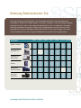
Product Selection Guide
LCD, Memory and Storage - 1H 2011
Samsung Semiconductor, Inc
Samsung continues to lead the industry with the broadest portfolio of memory products and
technology. Its DRAM, flash, SRAM products are found in computers—from ultra-mobile notebooks
to powerful servers—and in a wide range of handheld devices such as smartphones and tablets.
Samsung also delivers the industry’s widest line of storage products from the consumer to the
enterprise level. These include optical and hard disk drives as well as flash storage, such as the
all-flash Solid State Drive and a range of embedded and removable flash storage products.
Markets
DRAM
SRAM
Mobile / Wireless
Notebook PCs
Desktop PCs /
Workstations
Servers
Networking /
Communications
Consumer
Electronics
samsung.com/us/business/oem-solutions
FLASH
ASIC
LOGIC
TFT/LCD ODD/HDD
DRAM
Pages 4-12
• DDR3 SDRAM
• DDR2 SDRAM
• DDR SDRAM
• SDRAM
• Mobile DRAM
• Graphics DDR SDRAM
• DRAM Ordering
Information
FLASH
Pages 13-15
samsung.com/semi/flash
• SLC Flash
• MLC Flash
• SD and microSD Cards
• moviNAND™ (eMMC)
• Solid State Drive
• SATA SSD
• Flash Ordering
Information
HIGH-SPEED SRAM
Pages 16-20
samsung.com/semi/sram
• Asychronous
• Synchronous
• NtRAM™
• Late-Write RR SRAM
• DDR Synchronous SRAM
• QDR Synchronous SRAM
• SRAM Ordering
Information
MULTI-CHIP PACKAGE
Page 21
samsung.com/semi/mcp
• NAND + MDDR
• moviNAND + LPDDR2
• NOR + UtRAM
storage
Pages 22-24
samsung.com/greenmemory • Solid State Drive
• SATA SSD
samsung.com/hdd
• Hard Disk Drive
samsungodd.com
• Optical Disk Drive
LCD
Pages 25-27
tftlcd.com
• Exclusive Digital
samsung.com/semi/dram
1H 2011
Information Display (E-DID)
• Performance Digital
Information Display (P-DID)
• Basic Digital Information
Display (B-DID)
• Tablets
• Notebooks/PCs
• Monitors
3
DRAM
samsung.com/semi/dram
DDR3 SDRAM REGISTERED MODULES
Density Voltage Organization Part Number
1GB
2GB
4GB
1.5V
1.5V
1.5V
128Mx72
256Mx72
512Mx72
Composition
Compliance
Speed (Mbps)
Ranks Production
M393B2873FH0-C(F8/H9/K0)(04/05)
1Gb (128M x8) * 9
Lead Free & Halogen Free
1066/1333/1600
1
Now
M393B2873GB0-C(F8/H9/K0/MA)(08/09)
1Gb (128M x8) * 9
Lead Free & Halogen Free, Flip Chip 1066/1333/1600/1866
1
Now
M393B5673FH0-C(F8/H9/K0)(04/05)
1Gb (128M x8) * 18
Lead Free & Halogen Free
M393B5673GB0-C(F8/H9/K0/MA)(08/09)
1Gb (128M x8) * 18
Lead Free & Halogen Free, Flip Chip 1066/1333/1600/1866
1.5V
1Gx72
16GB
1.5V
2Gx72
8GB
1.5V
1Gx72
16GB
1.5V
2Gx72
32GB
1.5V
4Gx72
8GB
1.35V
1Gx72
16GB
1.35V
2Gx72
32GB
1.35V
4Gx72
2GB
1.35V
256Mx72
4GB
8GB
16GB
Notes:
4
1.35V
1.35V
1.35V
512Mx72
1Gx72
2Gx72
Now
Now
M393B5670FH0-C(F8/H9/K0)(04/05)
1Gb (256M x4) * 18
Lead Free & Halogen Free
1Gb (256M x4) * 18
Lead Free & Halogen Free, Flip Chip 1066/1333/1600/1866
M393B5773CH0-C(F8/H9/K0)(04/05)
2Gb (256M x8) * 9
Lead Free & Halogen Free
1066/1333/1600
1
Now
M393B5773DH0-C(F8/H9/K0/MA)(08/09) 2Gb (256M x8) * 9
Lead Free & Halogen Free
1066/1333/1600/1866
1
Now
1066/1333/1600
M393B5173FH0-C(F8/H9/K0)(04/05)
1Gb (128M x8) * 36
Lead Free & Halogen Free
M393B5173GB0-C(F8/H9)(08/09)
1Gb (128M x8) * 36
Lead Free & Halogen Free, Flip Chip 1066/1333
1066/1333/1600
1
Now
1
Now
4
Now
4
Now
M393B5170FH0-C(F8/H9/K0)(04/05)
1Gb (256M x4) * 36
Lead Free & Halogen Free
M393B5170GB0-C(F8/H9/K0/MA)(08/09)
1Gb (256M x4) * 36
Lead Free & Halogen Free, Flip Chip 1066/1333/1600/1866
M393B5273CH0-C(F8/H9/K0)(04/05)
2Gb (256M x8) * 18
Lead Free & Halogen Free
1066/1333/1600
2
Now
M393B5273DH0-C(F8/H9/K0/MA)(08/09) 2Gb (256M x8) * 18
Lead Free & Halogen Free
1066/1333/1600/1866
2
Now
2
Now
2
Now
2Gb (512M x4) * 18
Lead Free & Halogen Free
1066/1333/1600
1
Now
M393B5270DH0-C(F8/H9/K0/MA)(08/09) 2Gb (512M x4) * 18
Lead Free & Halogen Free
1066/1333/1600/1866
1
Now
M393B1K73CH0-C(F8/H9)(04/05)
2Gb (256M x8) * 36
Lead Free & Halogen Free
1066/1333
4
Now
M393B1K73DH0-C(F8/H9)(08/09)
2Gb (256M x8) * 36
Lead Free & Halogen Free
1066/1333
4
Now
M393B1K70CH0-C(F8/H9/K0)(04/05)
2Gb (512M x4) * 36
Lead Free & Halogen Free
1066/1333/1600
2
Now
M393B1K70DH0-C(F8/H9/K0/MA)(08/09) 2Gb (512M x4) * 36
Lead Free & Halogen Free
1066/1333/1600/1866
2
Now
M393B2K70CM0-C(F8/H9)(04/05)
2Gb DDP (1024M x4) * 36
Lead Free & Halogen Free
1066/1333
4
Now
M393B2K70DM0-C(F8/H9)(08/09)
2Gb DDP (1024M x4) * 36
Lead Free & Halogen Free
1066/1333
4
Now
M393B1G70BH0-C(F8/H9/K0/MA)(08/09) 4Gb (1G x4) * 18
Lead Free & Halogen Free
1066/1333/1600/1866
1
Now
M393B1G73BH0-C(F8/H9/K0/MA)(08/09) 4Gb (512M x8) * 18
Lead Free & Halogen Free
1066/1333/1600/1866
2
Now
M393B2G70AH0-C(F8/H9/K0)(04/05)
4Gb (1024M x4) * 36
Lead Free & Halogen Free
1066/1333/1600
2
Now
M393B2G70BH0-C(F8/H9/K0)(08/09)
4Gb (1024M x4) * 36
Lead Free & Halogen Free
1066/1333/1600
2
Now
M393B2G73AH0-C(F8/H9)(04/05)
4Gb (512M x8) * 36
Lead Free & Halogen Free
1066/1333
4
Now
M393B2G73BH0-C(F8/H9)(08/09)
4Gb (512M x8) * 36
Lead Free & Halogen Free
1066/1333
4
Now
M393B4G70AM0-C(F8/H9)(04/05)
4Gb DDP (2048M x4) * 36
Lead Free & Halogen Free
1066/1333
4
Now
M393B4G70BM0-C(F8/H9)(08/09)
4Gb DDP (2048M x4) * 36
Lead Free & Halogen Free
1066/1333
4
Now
M393B1G70BH0-Y(F8/H9/K0/MA)(08/09)
4Gb (1G x4) * 18
Lead Free & Halogen Free
1066/1333/1600
1
Now
M393B1G73BH0-Y(F8/H9/K0/MA)(08/09)
4Gb (512M x8) * 18
Lead Free & Halogen Free
1066/1333/1600
2
Now
M393B2G70AH0-Y(F8/H9)(04/05)
4Gb (1024M x4) * 36
Lead Free & Halogen Free
1066/1333
2
Now
M393B2G70BH0-Y(F8/H9/K0)(08/09)
4Gb (1024M x4) * 36
Lead Free & Halogen Free
1066/1333/1600
2
Now
M393B2G73AH0-Y(F8/H9)(04/05)
4Gb (512M x8) * 36
Lead Free & Halogen Free
1066/1333
4
Now
M393B2G73AH0-Y(F8/H9)(04/05)
4Gb (512M x8) * 36
Lead Free & Halogen Free
1066/1333
4
Now
M393B4G70AM0-Y(F8/H9)(04/05)
4Gb DDP (2048M x4) * 36
Lead Free & Halogen Free
1066/1333
4
Now
M393B4G70BM0-Y(F8/H9)(08/09)
4Gb DDP (2048M x4) * 36
Lead Free & Halogen Free
1066/1333
4
Now
M393B5773CH0-Y(F8/H9/K0)(04/05)
2Gb (256M x4) * 9
Lead Free & Halogen Free
1066/1333/1600
1
Now
M393B5773DH0-Y(F8/H9/K0)(08/09)
2Gb (256M x4) * 9
Lead Free & Halogen Free
1066/1333/1600
1
Now
M393B5173FH0-Y(F8/H9)(04/05)
1Gb (128M x8) * 36
Lead Free & Halogen Free
1066/1333
4
Now
M393B5173GB0-Y(F8/H9)(08/09)
1Gb (128M x8) * 36
Lead Free & Halogen Free, Flip Chip 1066/1333
4
Now
M393B5170FH0-Y(F8/H9/K0)(04/05)
1Gb (256M x4) * 36
Lead Free & Halogen Free
M393B5170GB0-Y(F8/H9/K0)(08/09)
1Gb (256M x4) * 36
Lead Free & Halogen Free, Flip Chip 1066/1333/1600
1066/1333
2
Now
2
Now
M393B5273CH0-Y(F8/H9/K0)(04/05)
2Gb (256M x8) * 18
Lead Free & Halogen Free
1066/1333/1600
2
Now
M393B5273DH0-Y(F8/H9/K0)(08/09)
2Gb (256M x8) * 18
Lead Free & Halogen Free
1066/1333/1600
2
Now
M393B5270CH0-Y(F8/H9/K0)(04/05)
2Gb (512M x4) * 18
Lead Free & Halogen Free
1066/1333/1600
1
Now
M393B5270DH0-Y(F8/H9/K0)(08/09)
2Gb (512M x4) * 18
Lead Free & Halogen Free
1066/1333/1600
1
Now
M393B1K73CH0-Y(F8/H9)(04/05)
2Gb (256M x8) * 36
Lead Free & Halogen Free
1066/1333
4
Now
M393B1K73DH0-Y(F8/H9)(08/09)
2Gb (256M x8) * 36
Lead Free & Halogen Free
1066/1333
4
Now
M393B1K70CH0-Y(F8/H9/K0)(04/05)
2Gb (512M x4) * 36
Lead Free & Halogen Free
1066/1333/1600
2
Now
M393B1K70DH0-Y(F8/H9/K0)(08/09)
2Gb (512M x4) * 36
Lead Free & Halogen Free
1066/1333/1600
2
Now
M393B2K70CM0-Y(F8/H9)(04/05)
2Gb DDP (1024M x4) * 36
Lead Free & Halogen Free
1066/1333
4
Now
M393B2K70DM0-Y(F8/H9)(08/09)
2Gb DDP (1024M x4) * 36
Lead Free & Halogen Free
1066/1333
4
Now
F7 = DDR3-800 (6-6-6)
F8 = DDR3-1066 (7-7-7)
H9 = DDR3-1333 (9-9-9)
K0 = DDR3-1600 (11-11-11)
MA = DDR3-1866 (13-13-13)
DDR3 SDRAM
1066/1333/1600
2
2
M393B5670GB0-C(F8/H9/K0/MA)(08/09)
M393B5270CH0-C(F8/H9/K0)(04/05)
8GB
1066/1333/1600
04 = IDT B0 register
05 = Inphi C0 register
08 = IDT
09 = Inphi
* K0 (1600Mbps) available in ES only
1H 2011
samsung.com/semi/dram
Density
Voltage
Organization
1GB
1.5V
128Mx72
2GB
4GB
8GB
16GB
8GB
16GB
2GB
4GB
8GB
Notes:
1.5V
1.5V
1.5V
1.5V
1.35V
1.35V
1.35V
1.35V
1.35V
256Mx72
512Mx72
1Gx72
2Gx72
1Gx72
2Gx72
256Mx72
512Mx72
1Gx72
F7 = DDR3-800 (6-6-6)
F8 = DDR3-1066 (7-7-7)
H9 = DDR3-1333 (9-9-9)
samsung.com/semi/dram
Part Number
Composition
Compliance
Speed (Mbps)
Ranks
Production
M392B2873FH0-C(F8/H9/K0)(04/05)
1Gb (128M x8) * 9
Lead Free & Halogen Free
1066/1333/1600
1
Now
M392B2873GB0-C(F8/H9/K0/MA)(08/09) 1Gb (128M x8) * 9
Lead Free & Halogen Free,
Flip Chip
1066/1333/1600/1866
1
Now
M392B5673FH0-C(F8/H9/K0)(04/05)
1Gb (128M x8) * 18
Lead Free & Halogen Free
1066/1333/K0
2
Now
M392B5673GB0-C(F8/H9/K0/MA)(08/09) 1Gb (128M x8) * 18
Lead Free & Halogen Free,
Flip Chip
1066/1333/1600/1866
2
Now
M392B5670FH0-C(F8/H9/K0)(04/05)
1Gb (256M x8) * 18
Lead Free & Halogen Free
1066/1333/1600
1
Now
M392B5670GB0-C(F8/H9/K0/MA)(08/09) 1Gb (256M x8) * 18
Lead Free & Halogen Free,
Flip Chip
1066/1333/1600/1866
1
Now
M392B5773CH0-C(F8/H9/K0)(04/05)
Lead Free & Halogen Free
1066/1333/1600
1
Now
2Gb (256M x8) * 9
M392B5773DH0-C(F8/H9/K0/MA)(08/09) 2Gb (256M x8) * 9
Lead Free & Halogen Free
1066/1333/1600/1866
1
Now
M392B5170FM0-C(F8/H9/K0)(04/05)
1Gb DDP (512M x4) * 18
Lead Free & Halogen Free
1066/1333/1600
2
Now
M392B5273CH0-C(F8/H9/K0)(04/05)
2Gb (256M x8) * 18
Lead Free & Halogen Free
1066/1333/1600
2
Now
M392B5273DH0-C(F8/H9/K0/MA)(08/09) 2Gb (256M x8) * 18
Lead Free & Halogen Free
1066/1333/1600/1866
2
Now
M392B5270CH0-C(F8/H9/K0)(04/05)
2Gb (512M x4) * 18
Lead Free & Halogen Free
1066/1333/1600
1
Now
M392B5270DH0-C(F8/H9/K0/MA)(08/09) 2Gb (512M x4) * 18
Lead Free & Halogen Free
1066/1333/1600/1866
1
Now
M392B1K73CM0-C(F8/H9)(04/05)
2Gb DDP (512M x8) * 18
Lead Free & Halogen Free
1066/1333
4
Now
M392B1K73DM0-C(F8/H9)(08/09)
2Gb DDP (512M x8) * 18
Lead Free & Halogen Free
1066/1333
4
Now
M392B1K70CM0-C(F8/H9/K0)(04/05)
2Gb DDP (1024M x4) * 18
Lead Free & Halogen Free
1066/1333/1600
2
Now
M392B1K70DM0-C(F8/H9/K0/MA)(08/09) 2Gb DDP (1024M x4) * 18
Lead Free & Halogen Free
1066/1333/1600/1866
2
Now
M392B1G73BH0-C(F8/H9/K0/MA)(08/09) 4Gb (512M x8) * 18
Lead Free & Halogen Free
1066/1333/1600/1866
1
Now
M392B1G70BH0-C(F8/H9/K0/MA)(08/09) 4Gb (1024M x4) * 18
Lead Free & Halogen Free
1066/1333/1600/1866
1
Now
M392B2G70AM0-C(F8/H9/K0)(04/05)
4Gb DDP (2048M x4) * 18
Lead Free & Halogen Free
1066/1333/1600
2
Now
M392B2G70BM0-C(F8/H9/K0/MA)(08/09) 4Gb DDP (2048M x4) * 18
Lead Free & Halogen Free
1066/1333/1600/1866
2
Now
M392B2G73AM0-C(F8/H9)(04/05)
4Gb DDP (1024M x8) * 18
Lead Free & Halogen Free
1066/1333
4
Now
M392B2G73BM0-C(F8/H9)(08/09)
4Gb DDP (1024M x8) * 18
Lead Free & Halogen Free
1066/1333
4
Now
M392B1G73BH0-Y(F8/H9/K0)(08/09)
4Gb (512M x8) * 18
Lead Free & Halogen Free
1066/1333/1600
1
Now
M392B1G70BH0-Y(F8/H9/K0)(08/09)
4Gb (1024M x4) * 18
Lead Free & Halogen Free
1066/1333/1600
1
Now
M392B2G70AM0-Y(F8/H9)(04/05)
4Gb DDP (2048M x4) * 18
Lead Free & Halogen Free
1066/1333
2
Now
M392B2G70BM0-Y(F8/H9/K0)(08/09)
4Gb DDP (2048M x4) * 18
Lead Free & Halogen Free
1066/1333/1600
2
Now
M392B2G70AM0-Y(F8/H9)(04/05)
4Gb DDP (1024M x8) * 18
Lead Free & Halogen Free
1066/1333
4
Now
M392B2G70BM0-Y(F8/H9)(08/09)
4Gb DDP (1024M x8) * 18
Lead Free & Halogen Free
1066/1333
4
Now
M392B5773CH0-Y(F8/H9/K0)(04/05)
2Gb (256M x8) * 9
Lead Free & Halogen Free
1066/1333/1600
1
Now
M392B5773DH0-Y(F8/H9/K0)(08/09)
2Gb (256M x8) * 9
Lead Free & Halogen Free
1066/1333/1600
1
Now
M392B5170FM0-Y(F8/H9/K0)(04/05)
1Gb DDP (512M x4) * 18
Lead Free & Halogen Free
1066/1333/1600
2
Now
M392B5273CH0-Y(F8/H9/K0)(04/05)
2Gb (256M x8) * 18
Lead Free & Halogen Free
1066/1333/1600
2
Now
M392B5273DH0-Y(F8/H9/K0)(08/09)
2Gb (256M x8) * 18
Lead Free & Halogen Free
1066/1333/1600
2
Now
M392B5270CH0-Y(F8/H9/K0)(04/05)
2Gb (512M x4) * 18
Lead Free & Halogen Free
1066/1333/1600
1
Now
M392B5270DH0-Y(F8/H9/K0)(08/09)
2Gb (512M x4) * 18
Lead Free & Halogen Free
1066/1333/1600
1
Now
M392B1K73CM0-Y(F8/H9/K0)(04/05)
2Gb DDP (512M x8) * 18
Lead Free & Halogen Free
1066/1333/1600
4
Now
M392B1K73DM0-Y(F8/H9)(08/09)
2Gb DDP (512M x8) * 18
Lead Free & Halogen Free
1066/1333
4
Now
M392B1K70CM0-Y(F8/H9/K0)(04/05)
2Gb DDP (1024M x4) * 18
Lead Free & Halogen Free
1066/1333/1600
2
Now
M392B1K70DM0-Y(F8/H9/K0)(08/09)
2Gb DDP (1024M x4) * 18
Lead Free & Halogen Free
1066/1333/1600
2
Now
K0 = DDR3-1600 (11-11-11)
MA = DDR3-1866 (13-13-13)
04 = IDT B0 register
05 = Inphi C0 register
08 = IDT
09 = Inphi
1H 2011
DDR3 SDRAM
5
DRAM
DDR3 SDRAM VLP REGISTERED MODULES
DDR3 SDRAM UNBUFFERED MODULES
Density Voltage
1GB
1.5V
2GB
1.5V
4GB
1.5V
Organization
128Mx64
256Mx64
512Mx64
1024Mx64
8GB
1.5V
1024Mx64
Part Number
Composition
Compliance
Speed (Mbps)
Ranks Production
M378B2873FH0-C(F8/H9/K0)
1Gb (128M x8) * 8
Lead Free & Halogen Free
Lead Free & Halogen Free,
Flip Chip
Lead Free & Halogen Free
Lead Free & Halogen Free,
Flip Chip
Lead Free & Halogen Free
Lead Free & Halogen Free
Lead Free & Halogen Free
Lead Free & Halogen Free
Lead Free & Halogen Free
Lead Free & Halogen Free
Lead Free & Halogen Free
1066/1333/1600
1
Now
1066/1333/1600/1866
1
Now
1066/1333/1600
2
Now
1066/1333/1600/1866
2
Now
1066/1333/1600
1066/1333/1600/1866
1066/1333/1600
1066/1333/1600/1866
1066/1333/1600/1866
1066/1333/1600
1066/1333/1600/1866
1
1
2
2
1
2
2
Now
Now
Now
Now
Now
Now
Now
M378B2873GB0-C(F8/H9/K0/MA)
1Gb (128M x8) * 8
M378B5673FH0-C(F8/H9/K0)
1Gb (128M x8) * 16
M378B5673GB0-C(F8/H9/K0/MA)
1Gb (128M x8) * 16
M378B5773CH0-C(F8/H9/K0)
M378B5773DH0-C(F8/H9/K0/MA)
M378B5273CH0-C(F8/H9/K0)
M378B5273DH0-C(F8/H9/K0/MA)
M378B5173BH0-C(F8/H9/K0/MA)
M378B1G73AH0-C(F8/H9/K0)
M378B1G73BH0-C(F8/H9/K0/MA)
2Gb (256M x8) * 8
2Gb (256M x8) * 8
2Gb (256M x8) * 16
2Gb (256M x8) * 16
4Gb (512M x8) * 8
4Gb (512M x8) * 16
4Gb (512M x8) * 16
DDR3 SDRAM UNBUFFERED MODULES (ECC)
Density
1GB
Voltage
1.5V
Organization
128Mx72
2GB
1.5V
256Mx72
4GB
1.5V
512Mx72
4GB
1.5V
1024Mx64
8GB
1.5V
1024Mx72
4GB
1.35V
1024Mx64
8GB
1.35V
1024Mx72
1GB
1.35V
128Mx72
2GB
1.35V
256Mx72
4GB
1.35V
512Mx72
Notes:
F7 = DDR3-800 (6-6-6)
Part Number
Composition
Compliance
Speed (Mbps)
Ranks
Production
M391B2873FH0-C(F8/H9/K0)
1Gb (128M x8) * 9
1066/1333/1600
1
Now
1066/1333/1600
1
Now
1066/1333/1600
1066/1333/1600
1066/1333/1600
1066/1333/1600
1066/1333/1600
2
1
1
2
2
Now
Now
Now
Now
Now
MA = DDR3-1866 (13-13-13)
M391B2873GB0-Y(F8/H9/K0)
1Gb (128M x8) * 9
M391B5673FH0-Y(F8/H9/K0)
M391B5773CH0-Y(F8/H9/K0)
M391B5773DH0-Y(F8/H9/K0)
M391B5273CH0-Y(F8/H9/K0)
M391B5273DH0-Y(F8/H9/K0)
1Gb (128M x8) * 18
2Gb (256M x8) * 9
2Gb (256M x8) * 9
2Gb (256M x8) * 18
2Gb (256M x8) * 18
Lead Free & Halogen Free
Lead Free & Halogen Free,
Flip Chip
Lead Free & Halogen Free
Lead Free & Halogen Free
Lead Free & Halogen Free
Lead Free & Halogen Free
Lead Free & Halogen Free
Lead Free & Halogen Free
Lead Free & Halogen Free
Lead Free & Halogen Free
Lead Free & Halogen Free
Lead Free & Halogen Free
Lead Free & Halogen Free
Lead Free & Halogen Free
Lead Free & Halogen Free,
Flip Chip
Lead Free & Halogen Free
Lead Free & Halogen Free
Lead Free & Halogen Free
Lead Free & Halogen Free
Lead Free & Halogen Free
F8 = DDR3-1066 (7-7-7)
H9 = DDR3-1333 (9-9-9)
K0 = DDR3-1600 (11-11-11)
M391B2873GB0-C(F8/H9/K0/MA)
1Gb (128M x8) * 9
M391B5673FH0-C(F8/H9/K0)
M391B5773CH0-C(F8/H9/K0)
M391B5773DH0-C(F8/H9/K0/MA)
M391B5273CH0-C(F8/H9/K0)
M391B5273DH0-C(F8/H9/K0/MA)
M391B5173BH0-C(F8/H9/K0/MA)
M391B1G73AH0-C(F8/H9/K0)
M391B1G73BH0-C(F8/H9/K0/MA)
M391B5173BH0-Y(F8/H9/K0)
M391B1G73AH0-Y(F8/H9/K0)
M391B1G73BH0-Y(F8/H9/K0)
M391B2873FH0-Y(F8/H9/K0)
1Gb (128M x8) * 18
2Gb (256M x8) * 9
2Gb (256M x8) * 9
2Gb (256M x8) * 18
2Gb (256M x8) * 18
4Gb (512M x8) * 9
4Gb (512M x8) * 18
4Gb (512M x8) * 18
4Gb (512M x8) * 9
4Gb (512M x8) * 18
4Gb (512M x8) * 18
1Gb (128M x8) * 9
1066/1333/1600/1866
1
Now
1066/1333/1600
1066/1333/1600
1066/1333/1600/1866
1066/1333/1600
1066/1333/1600/1866
1066/1333/1600/1866
1066/1333/1600
1066/1333/1600/1866
1066/1333/1600
1066/1333/1600
1066/1333/1600
1066/1333/1600
2
1
1
2
2
1
2
2
1
2
2
1
Now
Now
Now
Now
Now
Now
Now
Now
Now
Now
Now
Now
DDR3 SDRAM SODIMM MODULES
Density
1GB
Voltage
1.5V
Organization
128Mx64
2GB
1.5V
256Mx64
4GB
1.5V
512Mx64
4GB
1.5V
1024Mx64
8GB
1.5V
1024Mx64
2GB
1.35V
256Mx64
4GB
1.35V
512Mx64
4GB
1.35V
1024Mx64
8GB
1.35V
1024Mx64
Notes:
F7 = DDR3-800 (6-6-6)
6
DDR3 SDRAM
Part Number
Composition
Compliance
Speed (Mbps)
Ranks Production
M471B2873FHS-C(F8/H9/K0)
1Gb (128M x8) * 8
1066/1333/1600
1
Now
M471B2873GB0-C(F8/H9/K0/MA)
1Gb (128M x8) * 8
1066/1333/1600/1866
1
Now
M471B5673FH0-C(F8/H9/K0)
1Gb (128M x8) * 16
1066/1333/1600
2
Now
M471B5673GB0-C(F8/H9/K0/MA)
1Gb (128M x8) * 16
1066/1333/1600/1866
2
Now
M471B5773CHS-C(F8/H9/K0)
M471B5773DH0-C(F8/H9/K0/MA)
M471B5273CH0-C(F8/H9/K0)
M471B5273DH0-C(F8/H9/K0/MA)
M471B5173BH0-C(F8/H9/K0)
M471B1G73AH0-C(F8/H9/K0)
M471B1G73BH0-C(F8/H9/K0/MA)
M471B5773CHS-Y(F8/H9)
M471B5773DH0-Y(F8/H9/K0)
M471B5273CH0-Y(F8/H9)
M471B5273DH0-Y(F8/H9/K0)
M471B5173BH0-Y(F8/H9/K0)
M471B1G73AH0-Y(F8/H9/K0)
M471B1G73BH0-Y(F8/H9/K0)
2Gb (256M x8) * 8
2Gb (256M x8) * 8
2Gb (256M x8) * 16
2Gb (256M x8) * 16
4Gb (512M x8) * 8
4Gb (512M x8) * 16
4Gb (512M x8) * 16
2Gb (256M x8) * 8
2Gb (256M x8) * 8
2Gb (256M x8) * 16
2Gb (256M x8) * 16
4Gb (512M x8) * 8
4Gb (512M x8) * 16
4Gb (512M x8) * 16
Lead Free & Halogen Free
Lead Free & Halogen Free,
Flip Chip
Lead Free & Halogen Free
Lead Free & Halogen Free,
Flip Chip
Lead Free & Halogen Free
Lead Free & Halogen Free
Lead Free & Halogen Free
Lead Free & Halogen Free
Lead Free & Halogen Free
Lead Free & Halogen Free
Lead Free & Halogen Free
Lead Free & Halogen Free
Lead Free & Halogen Free
Lead Free & Halogen Free
Lead Free & Halogen Free
Lead Free & Halogen Free
Lead Free & Halogen Free
Lead Free & Halogen Free
1066/1333/1600
1066/1333/1600/1866
1066/1333/1600
1066/1333/1600/1866
1066/1333/1600
1066/1333/1600
1066/1333/1600/1866
1066/1333/1600
1066/1333/1600
1066/1333/1600
1066/1333/1600
1066/1333/1600
1066/1333/1600
1066/1333/1600
1
1
2
2
1
2
2
1
1
2
2
1
2
2
Now
Now
Now
Now
Now
Now
Now
Now
Now
Now
Now
Now
Now
Now
F8 = DDR3-1066 (7-7-7)
H9 = DDR3-1333 (9-9-9) K0 = DDR3-1600 (11-11-11)
1H 2011
MA = DDR3-1866 (13-13-13)
samsung.com/semi/dram
Density Voltage Organization
1Gb
1.5V
256M x4
1Gb
1.5V
128M x8
1Gb
1.5V
128M x16
2Gb
1.5V
512M x4
2Gb
1.5V
256M x8
2Gb
1.5V
128Mx16
4Gb
1.5V
1024M x4
4Gb
1.5V
512M x8
1Gb
1.35V
256M x4
1Gb
1.35V
128M x8
2Gb
1.35V
512M x4
2Gb
1.35V
256M x8
4Gb
1.35V
1024M x4
4Gb
1.35V
512M x8
Notes:
F7 = DDR3-800 (6-6-6)
F8 = DDR3-1066 (7-7-7)
Part Number
# Pins-Package Compliance
Speed (Mbps)
Dimensions Production
K4B1G0446F-HC(F8/H9/K0)
78 Ball -FBGA
1066/1333/1600
7.5x11mm
Now
K4B1G0446G-BC(F8/H9/K0/MA)
78 Ball -FBGA
1066/1333/1600/1866
7.5x11mm
Now
K4B1G0846F-HC(F8/H9/K0)
78 Ball -FBGA
1066/1333/1600
7.5x11mm
Now
K4B1G0846G-BC(F8/H9/K0/MA)
78 Ball -FBGA
1066/1333/1600/1866
7.5x11mm
Now
K4B1G1646G-BC(F8/H9/K0/MA/NB)
96 Ball -FBGA
K4B2G0446C-HC(F8/H9/K0)
K4B2G0446D-HC(F8/H9/K0/MA)
K4B2G0846C-HC(F8/H9/K0)
K4B2G0846D-HC(F8/H9/K0/MA)
K4B2G1646C-HC(F8/H9/K0/MA)
K4B4G0446A-HC(F8/H9/K0)
K4B4G0446B-HC(F8/H9/K0/MA)
K4B4G0846A-HC(F8/H9/K0)
K4B4G0846B-HC(F8/H9/K0/MA)
K4B1G0446F-HY(F8/H9/K0)
78 Ball -FBGA
78 Ball -FBGA
78 Ball -FBGA
78 Ball -FBGA
96 Ball -FBGA
78 Ball -FBGA
78 Ball -FBGA
78 Ball -FBGA
78 Ball -FBGA
78 Ball -FBGA
K4B1G0446G-BY(F8/H9/K0)
78 Ball -FBGA
K4B1G0846F-HY(F8/H9/K0)
78 Ball -FBGA
K4B1G0846G-BY(F8/H9/K0)
78 Ball -FBGA
K4B2G0446C-HY(F8/H9/K0)
K4B2G0446D-HY(F8/H9/K0)
K4B2G0846C-HY(F8/H9/K0)
K4B2G0846D-HY(F8/H9/K0)
K4B4G0446A-HY(F8/H9/K0)
K4B4G0446B-HY(F8/H9/K0)
K4B4G0846A-HY(F8/H9/K0)
K4B4G0846B-HY(F8/H9/K0)
78 Ball -FBGA
78 Ball -FBGA
78 Ball -FBGA
78 Ball -FBGA
78 Ball -FBGA
78 Ball -FBGA
78 Ball -FBGA
78 Ball -FBGA
H9 = DDR3-1333 (9-9-9)
K0 = DDR3-1600 (11-11-11)
MA = DDR3-1866 (13-13-13)
NB = DDR3-2133 (14-14-14)
Lead Free & Halogen Free
Lead Free & Halogen Free,
Flip Chip
Lead Free & Halogen Free
Lead Free & Halogen Free,
Flip Chip
Lead Free & Halogen Free,
Flip Chip
Lead Free & Halogen Free
Lead Free & Halogen Free
Lead Free & Halogen Free
Lead Free & Halogen Free
Lead Free & Halogen Free
Lead Free & Halogen Free
Lead Free & Halogen Free
Lead Free & Halogen Free
Lead Free & Halogen Free
Lead Free & Halogen Free
Lead Free & Halogen Free,
Flip Chip
Lead Free & Halogen Free
Lead Free & Halogen Free,
Flip Chip
Lead Free & Halogen Free
Lead Free & Halogen Free
Lead Free & Halogen Free
Lead Free & Halogen Free
Lead Free & Halogen Free
Lead Free & Halogen Free
Lead Free & Halogen Free
Lead Free & Halogen Free
1066/1333/1600/1866/2133 7.5x13.3mm Now
1066/1333/1600
1066/1333/1600/1866
1066/1333/1600
1066/1333/1600/1866
1066/1333/1600/1866
1066/1333/1600
1066/1333/1600/1866
1066/1333/1600
1066/1333/1600/1866
1066/1333/1600
7.5x11mm
7.5x11mm
7.5x11mm
7.5x11mm
7.5x13.3mm
7.5x11mm
7.5x11mm
7.5x11mm
7.5x11mm
7.5x11mm
Now
Now
Now
Now
Now
Now
Now
Now
Now
Now
1066/1333/1600
7.5x11mm
Now
1066/1333
7.5x11mm
Now
1066/1333/1600
7.5x11mm
Now
1066/1333/1600
1066/1333/1600
1066/1333/1600
1066/1333/1600
1066/1333/1600
1066/1333/1600
1066/1333/1600
1066/1333/1600
7.5x11mm
7.5x11mm
7.5x11mm
7.5x11mm
7.5x11mm
7.5x11mm
7.5x11mm
7.5x11mm
Now
Now
Now
Now
Now
Now
Now
Now
* MA, and NB are available in ES only
DDR2 SDRAM REGISTERED MODULES
Density
Organization
Part Number
Composition
Compliance
Speed (Mbps)
Register
Rank
Production
1GB
128Mx72
2GB
256Mx72
M393T2863FBA-C(E6/F7)
M393T5660FBA-C(E6/F7)
M393T5663FBA-C(E6/E7)
M393T5160FBA-C(E6/F7)
(128M x8)*9
(256M x4)*18
(128M x8)*18
(256M x4)*36
Lead free
Lead free
Lead free
Lead free
667/800
667/800
667/800
667/800
Y
Y
Y
Y
1
1
2
2
Now
Now
Now
Now
4GB
512Mx72
Notes:
E6 = PC2-5300 (DDR2-667 @ CL=5)
F7 = PC2-6400 (DDR2-800 @ CL=6)
E7 = PC2-6400 (DDR2-800 @ CL=5)
Voltage = 1.8V
DDR2 SDRAM VLP REGISTERED MODULES
Density
Organization
Part Number
Composition
Compliance
Speed (Mbps)
Register
Rank
Production
2GB
256Mx72
M392T5660FBA-CE6
(256M x4)*18
Lead free
667
Y
1
Now
DDR2 SDRAM FULLY BUFFERED MODULES
Density
Organization
Part Number
Composition
Compliance
Speed (Mbps)
Voltage
Rank
Production
2GB
256Mx72
4GB
512Mx72
M395T5663FB4-CE68
M395T5160FB4-CE68
M395T5163FB4-CE68
(128M x8)*18
(256M x4)*36
(128M x8)*36
Lead free
Lead free
Lead free
667
667
667
1.8V
1.8V
1.8V
2
2
4
Now
Now
Now
Notes:
E6 = PC2-5300 (DDR2-667 @ CL=5)
samsung.com/semi/dram
Voltage = 1.8V (AMB Voltage = 1.5V)
1H 2011
AMB = IDT L4
DDR3 & DDR2 SDRAM
7
DRAM
DDR3 SDRAM COMPONENTS
DDR2 SDRAM UNBUFFERED MODULES
Density
Organization
Part Number
Composition
Compliance
Speed (Mbps)
Rank
Production
1GB
2GB
128Mx64
256Mx64
M378T2863FBS-C(E6/F7/E7)
M378T5663FB3-C(E6/F7/E7)
(128M x8)*8
(128M x8)*16
Lead free
Lead free
667/800
667/800
1
2
Now
Now
Notes:
E6 = PC2-5300 (DDR2-667 @ CL=5)
E7 = PC2-6400 (DDR2-800 @ CL=5)
F7 = PC2-6400 (DDR2-800 @ CL=6)
Voltage = 1.8V
DDR2 SDRAM UNBUFFERED MODULES (ECC)
Density
Organization
Part Number
Composition
Compliance
Speed (Mbps)
Rank
Production
1GB
2GB
128Mx72
256Mx64
M391T2863FB3-C(E6/F7)
M391T5663FB3-C(E6/F7)
(128Mx8)*9
(128Mx8)*18
Lead free
Lead free
667/800
667/800
1
2
Now
Now
Notes:
E6 = PC2-5300 (DDR2-667 @ CL=5)
E7 = PC2-6400 (DDR2-800 @ CL=5)
F7 = PC2-6400 (DDR2-800 @ CL=6)
Voltage = 1.8V
DDR2 SDRAM SODIMM MODULES
Density
Organization
Part Number
Composition
Compliance
Speed (Mbps)
Rank
Production
1GB
2GB
128Mx64
256Mx64
M470T2863FB3-C(E6/F7/E7)
M470T5663FB3-C(E6/F7/E7)
(64Mx16)*8
(128M x8)*8
Lead free
Lead free
667/800
667/800
2
2
Now
Now
Notes:
E6 = PC2-5300 (DDR2-667 @ CL=5)
E7 = PC2-6400 (DDR2-800 @ CL=5)
F7 = PC2-6400 (DDR2-800 @ CL=6)
Voltage = 1.8V
DDR2 SDRAM COMPONENTS
Density
Organization
Part Number
# Pins-Package
Dimensions
Package
Speed (Mbps)
Production
256Mb
16Mx16
128M x4
64M x8
32M x16
128M x4
64M x8
32M x16
256M x4
128M x8
64M x16
K4T56163QN-HC(E6/F7/E7/F8)
K4T51043QI-HC(E6/F7/E7)
K4T51083QI-HC(E6/F7/E7/F8)
K4T51163QI-HC(E6/F7/E7/F8)
K4T51043QJ-HC(E6/F7/E7)
K4T51083QJ-HC(E6/F7/E7/F8)
K4T51163QJ-HC(E6/F7/E7/F8)
K4T1G044QF-BC(E6/F7/E7)
K4T1G084QF-BC(E6/F7/E7/F8)
K4T1G164QF-BC(E6/F7/E7/F8)
84-FBGA
60-FBGA
60-FBGA
84-FBGA
60-FBGA
60-FBGA
84-FBGA
60-FBGA
60-FBGA
84-FBGA
7.5x12.5mm
7.5x9.5mm
7.5x9.5mm
7.5x12.5mm
7.5x9.5mm
7.5x9.5mm
7.5x12.5mm
7.5x9.5mm
7.5x9.5mm
7.5x12.5mm
Lead free & Halogen free
Lead free & Halogen free
Lead free & Halogen free
Lead free & Halogen free
Lead free & Halogen free
Lead free & Halogen free
Lead free & Halogen free
Lead free & Halogen free
Lead free & Halogen free
Lead free & Halogen free
667/800/1066
667/800
667/800/1066
667/800/1066
667/800
667/800/1066
667/800/1066
667/800
667/800/1066
667/800/1066
Now
Now
Now
Now
Q3
Q3
Q3
Now
Now
Now
E6 = DDR2-667 (5-5-5)
F7 = DDR2-800 (6-6-6)
E7 = DDR2-800 (5-5-5)
F8 = DDR2-1066 (7-7-7)
Voltage = 1.8V
Package Type
H = FBGA (Lead-free & Halogen-free)
B = FBGA (Lead-free & Halogen-free, Flip Chip)
512Mb
1Gb
Notes:
DDR SDRAM COMPONENTS
Density
Organization
Part Number
# Pins - Package
Speed (Mbps)
128Mb
32Mx16
64Mx4
32Mx8
16Mx16
8Mx16
K4H510438J-LCB3/B0
K4H510438J-HCCC/B3
K4H510838J-LCCC/B3
K4H510838J-HCCC/B3
K4H511638J-LCCC/B3
K4H560438N-LCB3/B0
K4H560838N-LCCC/B3
K4H561638N-LCCC/B3
K4H281638O-LCCC
66-TSOP
60-FBGA
66-TSOP
60-FBGA
66-TSOP
66-TSOP
66-TSOP
66-TSOP
66-TSOP
266/333
333/400
333/400
333/400
333/400
266/333
333/400
333/400
400
Notes:
B0 = DDR266 (133MHz @ CL=2.5)
A2 = DDR266 (133MHz @ Cl=2)
B3 = DDR333 (166MHz @ CL=2.5)
CC = DDR400 (200MHz @ CL=3)
128Mx4
512Mb
256Mb
64Mx8
SDRAM COMPONENTS
Density
256Mb
128Mb
Notes:
8
Organization
Part Number
# Pins - Package
Speed (Mbps)
Refresh
64Mx4
32Mx8
16Mx16
16Mx8
8Mx16
K4S560432N-LC(L)75000
K4S560832N-LC(L)75000
K4S561632N-LC(L)(75/60)000
K4S280832O-LC(L)75000
K4S281632O-LC(L)(75/60)000
54-TSOP
54-TSOP
54-TSOP
54-TSOP
54-TSOP
133
133
133/166
133
133/166
8K
8K
8K
4K
4K
Banks: 4
All products are Lead Free
Voltage: 3.3V
Speed: PC133 (133MHz CL=3/PC100 CL2)
L = Commercial Temp., Low Power
For Industrial Temperature, check with SSI Marketing
DDR2, DDR & SDRAM Components
1H 2011
samsung.com/semi/dram
Type
MSDR
Density
Organization
Part Number
Package
Power
Production
16Gb
32Mx16
16Mx32
16Mx16
8Mx32
32Mx16
16Mx32
32Mx32
64Mx32
x32 (2CS, 2CKE)
x32 (2CS, 2CKE)
1CH x32
1CH x32
2CH x32/ch
1CH x32
1CH x32
1CH x32
2CH x32/ch
2CH x32/ch
1CH x32
2CH x32/ch
2CH x32/ch
2CH x32/ch
2CH x32/ch
K4M51163PI-BG(1)
K4M51323PI-HG(1)
K4X56163PN-FG(1)
K4X56323PN-8G(1)
K4X51163PI-FG(1)
K4X51323PI-8G(1)
K4X1G323PF-8G(1)
K4X2G323PC-8G(1)
K4X4G303PC-AG(1)
K4X4G303PC-7G(1)
K4P1G324EE-AG(1)
K4P2G324EC-AG(1)
K3PE3E300M-XG(1)
K4P4G304EC-AG(1)
K4P4G154EC-FG(1)
K4P4G324EB-FG(1)
K3PE4E400M-XG(1)
K3PE4E400A-XG(1)
K4P8G304EC-FC(1)
K3PE8E800M-XG(1)
K3PE7E700M-XG(1)
K3PE7E700A-XG(1)
K3PE0E00M-XG(1)
54-FBGA
90-FBGA
60-FBGA
90-FBGA
60-FBGA
90-FBGA
90-FBGA
90-FBGA
168-FBGA, 12x12 PoP, DDP
240-FBGA, 14x14 PoP, DDP
168-FBGA, 12x12 PoP
168-FBGA, 12x12 PoP
216-FBGA, 12x12 PoP
168-FBGA, 12x12 PoP, DDP, 64Mx32*2
134-FBGA, 11x11.5 PoP, DDP, 128x16*2
168-FBGA, 12x12 PoP, MONO, 128Mx32
216-FBGA, 12x12 PoP, QDP, 64Mx32*2
240-FBGA, 14x14 PoP, QDP, 64Mx32*2
134-FBGA, 11x11.5 PoP, QDP, 128x16*4
216-FBGA, 12x12 PoP, QDP, 64Mx32*4
216-FBGA, 12x12 PoP, DDP, 128Mx32*2
240-FBGA, 14x14 PoP, DDP, 128Mx32*2
216-FBGA, 12x12 PoP, QDP, 128Mx32*4
1.8V
1.8V
1.8V
1.8V
1.8V
1.8V
1.8V
1.8V
1.8V
1.8V
1.2V
1.2V
1.2V
1.2V
1.2V
1.2V
1.2V
1.2V
1.2V
1.2V
1.2V
1.2V
1.2V
Now
Now
Now
Now
Now
Now
Now
Now
Now
Now
Now
Now
Now
Now
Now
Now
Now
Now
Now
Now
Now
Now
Now
(1) Speed:
Mobile-SDR
60: 166MHz, CL3
75: 133MHz, CL3
Mobile-DDR
D8: 200MHz, CL3
C6: 166MHz, CL3
LPDDR2
C1: 800Mbps
512Mb
256Mb
512Mb
MDDR
1Gb
2Gb
4Gb
1Gb
2Gb
4Gb
LPDDR2
8Gb
Notes:
DRAM
Mobile DRAM Components
All products offered at Extended, Low, i-TCSR & PASR & DS (Temp, Power)
GRAPHICS DRAM COMPONENTS
Type
Density
Organization
2Gb
64Mx32
1Gb
32Mx32
1Gb
512Mb
2Gb
1Gb
1Gb
32Mx32
16Mx32
128Mx16
64Mx16
64Mx16
GDDR5
GDDR3
gDDR3
gDDR2
Notes:
Part Number
Package
VDD/VDDQ
Speed Bin (MHz)
K4G20325FC-HC(1)
K4G20325FC-HC04
K4G20325FC-HC03
K4G10325FE-HC(1)
K4G10325FE-HC04
K4J10324KE-HC(1)
K4J52324KI-HC(1)
K4W2G1646C-HC(1)
K4W1G1646G-BC(1)
K4N1G164QE-HC(1)
170-FBGA
170-FBGA
170-FBGA
170-FBGA
170-FBGA
136-FBGA
136-FBGA
96 FBGA
96 FBGA
84-FBGA
1.5/1.5V
1.35V/1.35V
1.35V/1.35V
1.5/1.5V
1.35V/1.35V
1.8V/1.8V
1.8/1.8V
1.5V/1.5V
1.5V/1.5V
1.8/1.8V
2000/2500/3000
1800
2000
2000/2500
1800
700/800/1000/1200
700/800/1000
800/933/1066
800/933/1066
400/500
Package
H: FBGA (Halogen Free & Lead Free)
B: FBGA (Halogen Free & Lead Free)
samsung.com/semi/dram
(1) Speeds (clock cycle - speed bin)
03: 0.3ns (3000MHz)
5C: 0.555 (1800MHz)
04: 0.4ns (2500MHz)
08: 0.83ns (1200MHz)
05: 0.5ns (2000MHz)
1A: 1ns (1000MHz GDDR3)
1H 2011
1A: 1ns (1066MHz gDDR3) 14: 1.429ns (700MHz)
11: 1.1ns (933MHz)
20: 2.0ns (500MHz)
12: 1.25ns (800MHz)
25: 2.5ns (400MHz)
Mobile & Graphics DRAM Components
9
COMPONENT DRAM ORDERING INFORMATION
1
2
3
4
5
6
7
8
9
10
11
K
4
T
XX
XX
X
X
X
X
X
XX
Speed
Temp & Power
Package Type
Revision
Interface (VDD, VDDQ)
Number of Internal Banks
SAMSUNG Memory
DRAM
DRAM Type
Density
Bit Organization
1. Memory (K)
2. DRAM: 4
3. DRAM Type
B: DDR3 SDRAM
D: GDDR SDRAM
G: GDDR5 SDRAM
H: DDR SDRAM
J: GDDR3 SDRAM
M: Mobile SDRAM
N: SDDR2 SDRAM
S: SDRAM
T: DDR SDRAM
U: GDDR4 SDRAM
V: Mobile DDR SDRAM Power Efficient Address
W: SDDR3 SDRAM
X: Mobile DDR SDRAM
Y: XDR DRAM
Z: Value Added DRAM
4. Density
10: 1G, 8K/32ms
16: 16M, 4K/64ms
26: 128M, 4K/32ms
28: 128M, 4K/64ms
32: 32M, 2K/32ms
50: 512M, 32K/16ms
51: 512M, 8K/64ms
52: 512M, 8K/32ms
54: 256M, 16K/16ms
55: 256M, 4K/32ms
56: 256M, 8K/64ms
62: 64M, 2K/16ms
64: 64M, 4K/64ms
68: 768M, 8K/64ms
1G: 1G, 8K/64ms
2G: 2G, 8K/64ms
4G: 4G, 8K/64ms
5. Bit Organization
02: x2
04: x4
06: x4 Stack (Flexframe)
07: x8 Stack (Flexframe)
10
DRAM Ordering Information
08: x8
15: x16 (2CS)
16: x16
26: x4 Stack (JEDEC Standard)
27: x8 Stack (JEDEC Standard)
30: x32 (2CS, 2CKE)
31: x32 (2CS)
32: x32
6. # of Internal Banks
2: 2 Banks
3: 4 Banks
4: 8 Banks
5: 16 Banks
7. Interface ( VDD, VDDQ)
2: LVTTL, 3.3V, 3.3V
4: LVTTL, 2.5V, 2.5V
5: SSTL-2 1.8V, 1.8V
6: SSTL-15 1.5V, 1.5V
8: SSTL-2, 2.5V, 2.5V
A: SSTL, 2.5V, 1.8V
F: POD-15 (1.5V,1.5V)
H: SSTL_2 DLL, 3.3V, 2.5V
M: LVTTL, 1.8V, 1.5V
N: LVTTL, 1.5V, 1.5V
P: LVTTL, 1.8V, 1.8V
Q: SSTL-2 1.8V, 1.8V
R: SSTL-2, 2.8V, 2.8V
U: DRSL, 1.8V, 1.2V
8. Revision
A: 2nd Generation
B: 3rd Generation
C: 4th Generation
D: 5th Generation
E: 6th Generation
F: 7th Generation
G: 8th Generation
H: 9th Generation
I: 10th Generation
J: 11th Generation
K: 12th Generation
M: 1st Generation
N: 14th Generation
Q: 17th Generation
1H 2011
9. Package Type
DDR SDRAM
L: TSOP II (Lead-free & Halogen-free)
H: FBGA (Lead-free & Halogen-free)
F: FBGA for 64Mb DDR (Lead-free & Halogen-free)
6: sTSOP II (Lead-free & Halogen-free)
T: TSOP II
N: sTSOP II
G: FBGA
U: TSOP II (Lead-free)
V: sTSOP II (Lead-free)
Z: FBGA (Lead-free)
DDR2 SDRAM
Z: FBGA (Lead-free)
J: FBGA DDP (Lead-free)
Q: FBGA QDP (Lead-free)
H: FBGA (Lead-free & Halogen-free)
M: FBGA DDP (Lead-free & Halogen-free)
E: FBGA QDP (Lead-free & Halogen-free)
T: FBGA DSP (Lead-free & Halogen-free, Thin)
DDR3 SDRAM
Z: FBGA (Lead-free)
H: FBGA (Halogen-free & Lead-free)
Graphics Memory
Q: TQFP
U: TQFP (Lead Free)
G: 84/144 FBGA
V: 144 FBGA (Lead Free)
Z: 84 FBGA(Lead Free)
T: TSOP
L: TSOP (Lead Free)
A: 136 FBGA
B: 136 FBGA(Lead Free)
H: FBGA(Hologen Free & Lead Free)
E: 100 FBGA(Hologen Free & Lead Free)
SDRAM
L TSOP II (Lead-free & Halogen-free)
N: STSOP II
T: TSOP II
U: TSOP II (Lead-free)
V: sTSOP II (Lead-free)
samsung.com/semi/dram
1
2
3
4
5
6
7
8
9
10
11
K
4
T
XX
XX
X
X
X
X
X
XX
Speed
Temp & Power
Package Type
Revision
Interface (VDD, VDDQ)
Number of Internal Banks
SAMSUNG Memory
DRAM
DRAM Type
Density
Bit Organization
XDR DRAM
J: BOC(LF) P: BOC
Mobile DRAM
Leaded / Lead Free
G/A: 52balls FBGA Mono
R/B: 54balls FBGA Mono
X /Z: 54balls BOC Mono
J /V: 60(72)balls FBGA Mono 0.5pitch
L /F: 60balls FBGA Mono 0.8pitch
S/D: 90balls FBGA
Monolithic (11mm x 13mm)
F/H: Smaller 90balls FBGA Mono
Y/P: 54balls CSP DDP
M/E: 90balls FBGA DDP
10. Temp & Power - COMMON
(Temp, Power)
C: Commercial, Normal (0’C – 95’C) & Normal
Power
C: (Mobile Only) Commercial (-25 ~ 70’C), Normal
Power
J: Commercial, Medium
L: Commercial, Low (0’C – 95’C) & Low Power
L: (Mobile Only) Commercial, Low, i-TCSR
F: Commercial, Low, i-TCSR & PASR & DS
E: Extended (-25~85’C), Normal
N: Extended, Low, i-TCSR
G: Extended, Low, i-TCSR & PASR & DS
I: Industrial, Normal (-40’C – 85’C) & Normal
Power
P: Industrial, Low (-40’C – 85’C) & Low Power
H: Industrial, Low, i-TCSR & PASR & DS
11. Speed (Wafer/Chip Biz/BGD: 00)
DDR SDRAM
CC: DDR400 (200MHz @ CL=3, tRCD=3, tRP=3)
B3: DDR333 (166MHz @ CL=2.5, tRCD=3,
tRP=3) *1
A2: DDR266 (133MHz @ CL=2 , tRCD=3, tRP=3)
B0: DDR266 (133MHz @ CL=2.5, tRCD=3,
tRP=3)
Note 1: "B3" has compatibility with "A2" and "B0"
samsung.com/semi/dram
DRAM
COMPONENT DRAM ORDERING INFORMATION
DDR2 SDRAM
CC: DDR2-400 (200MHz @ CL=3, tRCD=3,
tRP=3)
D5: DDR2-533 (266MHz @ CL=4, tRCD=4,
tRP=4)
E6: DDR2-667 (333MHz @ CL=5, tRCD=5,
tRP=5)
F7: DDR2-800 (400MHz @ CL=6, tRCD=6,
tRP=6)
E7: DDR2-800 (400MHz @ CL=5, tRCD=5,
tRP=5)
1 : 1.1ns (900MHz)
55: 5.5ns (183MHz)
12: 1.25ns (800MHz)
60: 6.0ns (166MHz)
14: 1.4ns (700MHz)
16: 1.6ns (600MHz)
DDR3 SDRAM
F7: DDR3-800 (400MHz @ CL=6, tRCD=6,
tRP=6)
F8: DDR3-1066 (533MHz @ CL=7, tRCD=7,
tRP=7)
G8: DDR3-1066 (533MHz @ CL=8, tRCD=8,
tRP=8)
H9: DDR3-1333 (667MHz @ CL=9, tRCD=9,
tRP=9)
K0: DDR3-1600 (800MHz @ CL=11, tRCD=11,
tRP=11)
XDR DRAM
A2: 2.4Gbps, 36ns, 16Cycles
B3: 3.2Gbps, 35ns, 20Cycles
C3: 3.2Gbps, 35ns, 24Cycles
C4: 4.0Gbps, 28ns, 24Cycles
DS: Daisychain Sample
Graphics Memory
18: 1.8ns (550MHz)
04: 0.4ns (2500MHz)
20: 2.0ns (500MHz)
05: 0.5ns (2000MHz)
22: 2.2ns (450MHz)
5C: 0.56ns (1800MHz)
25: 2.5ns (400MHz)
06: 0.62ns (1600MHz)
2C: 2.66ns (375MHz)
6A: 0.66ns (1500MHz)
2A: 2.86ns (350MHz)
07: 0.71ns (1400MHz)
33: 3.3ns (300MHz)
7A: 0.77ns (1300MHz)
36: 3.6ns (275MHz)
08: 0.8ns (1200MHz)
40: 4.0ns (250MHz)
09: 0.9ns (1100MHz)
45: 4.5ns (222MHz)
1 : 1.0ns (1000MHz)
50/5A: 5.0ns (200MHz)
1H 2011
SDRAM (Default CL=3)
50: 5.0ns (200MHz CL=3)
60: 6.0ns (166MHz CL=3)
67: 6.7ns
75: 7.5ns PC133 (133MHz CL=3)
Mobile-SDRAM
60: 166MHz, CL 3
75: 133MHz, CL 3
80: 125MHz, CL 3
1H: 105MHz, CL 2
1L: 105MHz, CL 3
15: 66MHz, CL 2 & 3
Mobile-DDR
C3: 133MHz, CL 3
C2: 100MHz, CL 3
C0: 66MHz, CL 3
Note: All of Lead-free or Halogen-free product are in
compliance with RoHS
DRAM Ordering Information
11
Module DRAM Ordering Information
1
2
3
4
5
6
7
8
9
10
11
12
13
M
X
XX
T
XX
X
X
X
X
X
X
XX
X
AMB Vendor
Speed
Temp & Power
PCB Revision
Package
Component Revision
SAMSUNG Memory
DIMM
Data bits
DRAM Component Type
Depth
Number of Banks
Bit Organization
1. Memory Module: M
2. DIMM Type
3: DIMM
4: SODIMM
3. Data bits
12: x72 184pin Low Profile Registered DIMM
63: x63 PC100 / PC133 μSODIMM with SPD for
144pin
64: x64 PC100 / PC133 SODIMM with SPD for
144pin (Intel/JEDEC)
66: x64 Unbuffered DIMM with SPD for
144pin/168pin (Intel/JEDEC)
68: x64 184pin Unbuffered DIMM
70: x64 200pin Unbuffered SODIMM
71: x64 204pin Unbuffered SODIMM
74: x72 /ECC Unbuffered DIMM with SPD for
168pin (Intel/JEDEC)
77: x72 /ECC PLL + Register DIMM with SPD for
168pin (Intel PC100)
78: x64 240pin Unbuffered DIMM
81: x72 184pin ECC unbuffered DIMM
83: x72 184pin Registered DIMM
90: x72 /ECC PLL + Register DIMM
91: x72 240pin ECC unbuffered DIMM
92: x72 240pin VLP Registered DIMM
93: x72 240pin Registered DIMM
95: x72 240pin Fully Buffered DIMM with SPD for
168pin (JEDEC PC133)
4. DRAM Component Type
B: DDR3 SDRAM (1.5V VDD)
L: DDR SDRAM (2.5V VDD)
S: SDRAM
T: DDR2 SDRAM (1.8V VDD)
5. Depth
9. Package
09: 8M (for 128Mb/512Mb)
17: 16M (for 128Mb/512Mb)
16: 16M
28: 128M
29: 128M (for 128Mb/512Mb)
32: 32M
33: 32M (for 128Mb/512Mb)
51: 512M
52: 512M (for 512Mb/2Gb)
56: 256M
57: 256M (for 512Mb/2Gb)
59: 256M (for 128Mb/512Mb)
64: 64M
65: 64M (for 128Mb/512Mb)
1G: 1G
1K: 1G (for 2Gb)
6. # of Banks in Comp. & Interface
1: 4K/64mxRef., 4Banks & SSTL-2
2 : 8K/ 64ms Ref., 4Banks & SSTL-2
2: 4K/ 64ms Ref., 4Banks & LVTTL (SDR Only)
5: 8K/ 64ms Ref., 4Banks & LVTTL (SDR Only)
5: 4Banks & SSTL-1.8V
6: 8Banks & SSTL-1.8V
7. Bit Organization
0: x 4
3: x 8
4: x16
6: x 4 Stack (JEDEC Standard)
7: x 8 Stack (JEDEC Standard)
8: x 4 Stack
9: x 8 Stack
8. Component Revision
A: 2nd Gen.
B: 3rd Gen.
C: 4th Gen.
D: 5th Gen.
E: 6th Gen.
F: 7th Gen.
G: 8th Gen.
M: 1st Gen.
Q: 17th Gen.
12
DRAM Ordering Information
E: FBGA QDP (Lead-free & Halogen-free)
G: FBGA
H: FBGA (Lead-free & Halogen-free)
J: FBGA DDP (Lead-free)
M: FBGA DDP (Lead-free & Halogen-free)
N: sTSOP
Q: FBGA QDP (Lead-free)
T: TSOP II (400mil)
U: TSOP II (Lead-Free)
V: sTSOP II (Lead-Free)
Z: FBGA(Lead-free)
10. PCB Revision
0: Mother PCB
1: 1st Rev
2: 2nd Rev.
3: 3rd Rev.
4: 4th Rev.
A: Parity DIMM
S: Reduced PCB
U: Low Profile DIMM
11. Temp & Power
C: Commercial Temp. (0°C ~ 95°C) & Normal
Power
L: Commercial Temp. (0°C ~ 95°C) & Low Power
12. Speed
CC: (200MHz @ CL=3, tRCD=3, tRP=3)
D5: (266MHz @ CL=4, tRCD=4, tRP=4)
E6: (333MHz @ CL=5, tRCD=5, tRP=5)
F7: (400MHz @ CL=6, tRCD=6, tRP=6)
E7: (400MHz @ CL=5, tRCD=5, tRP=5)
F8: (533MHz @ CL=7, tRCD=7, tRP=7)
G8: (533MHz @ CL=8, tRCD=8, tRP=8)
H9: (667MHz @ CL=9, tRCD=9, tRP=9)
K0: (800MHz @ CL=10, tRCD=10, tRP=10)
7A: (133MHz CL=3/PC100 CL2)
13. AMB Vendor for FBDIMM
0, 5: Intel
1, 6, 8: IDT
9: Montage
Note: All of Lead-free or Halogen-free product are in
compliance with RoHS
1H 2011
samsung.com/semi/dram
SLC Flash
MOQ
Density
128Gb ODP
64Gb QDP
16Gb Based
32Gb DDP
16Gb Mono
16Gb QDP
4Gb Based
8Gb DDP
4Gb Mono
2Gb Based
1Gb Based
2Gb Mono
1Gb Mono
Part Number
Package Type
Org.
Vol(V)
Tray
T/R
-xxxx0xx
-xxx0Txx
Status
K9QDGD8S5M-HCB*
BGA
x8
1.8
960
1000
C/S
K9QDGD8U5M-HCB*
BGA
x8
3.3
960
1000
C/S
K9QDG08U5M-HCB*
BGA
x8
3.3
960
1000
C/S
K9WCGD8S5M-HCB*
BGA
x8
1.8
960
1000
C/S
K9WCGD8U5M-HCB*
BGA
x8
3.3
960
1000
C/S
K9WCG08U5M-HCB*
BGA
x8
3.3
960
1000
C/S
FLASH
Family
K9WCG08U5M-HIB*
BGA
x8
3.3
960
1000
C/S
K9KBGD8S1M-HCB*
BGA
x8
1.8
960
1000
C/S
K9KBGD8U1M-HCB*
BGA
x8
3.3
960
1000
C/S
K9KBGD8U1M-HIB*
BGA
x8
3.3
960
1000
C/S
K9KBG08U1M-HCB*
BGA
x8
3.3
960
1000
C/S
K9KBG08U1M-HIB*
BGA
x8
3.3
960
1000
C/S
K9FAG08U0M-HCB*
BGA
x8
3.3
960
1000
C/S
K9FAG08U0M-HIB*
BGA
x8
3.3
960
1000
C/S
K9WAG08U1D-SCB0
TSOP1 HF&LF
x8
3.3
960
1000
C/S
K9WAG08U1D-SIB0
TSOP1 HF&LF
x8
3.3
960
1000
C/S
K9WAG08U1B-PCB0
TSOP1
x8
3.3
960
1000
EOL Scheduled
K9WAG08U1B-PIB0
TSOP1
x8
3.3
960
1000
EOL Scheduled
K9WAG08U1B-KIB0
ULGA HF & LF
x8
3.3
960
2000
EOL Scheduled
K9K8G08U0D-SCB0
TSOP1 HF&LF
X8
3.3
960
1000
C/S
K9K8G08U0D-SIB0
TSOP1 HF&LF
x8
3.3
960
1000
C/S
K9K8G08U0B-PCB0
TSOP1
x8
3.3
960
1000
EOL Scheduled
K9K8G08U0B-PIB0
TSOP1
x8
3.3
960
1000
EOL Scheduled
K9K8G08U1B-KIB0
ULGA HF & LF
x8
3.3
960
2000
EOL Scheduled
K9F4G08U0D-SCB0
TSOP1 HF & LF
x8
3.3
960
1000
C/S
K9F4G08U0D-SIB0
TSOP1 HF& LF
X8
3.3
960
1000
C/S
K9F4G08U0B-PCB0
TSOP1
x8
3.3
960
1000
EOL Scheduled
K9F4G08U0B-PIB0
TSOP1
x8
3.3
960
1000
EOL Scheduled
K9F4G08U0B-KIB0
ULGA HF & LF
x8
3.3
960
2000
EOL Scheduled
K9F2G08U0C-SCB0
TSOP-LF/HF
x8
3.3
960
1000
C/S
K9F2G08U0C-SIB0
TSOP-LF/HF
x8
3.3
960
1000
C/S
K9F2G08U0B-PCB0
TSOP1
x8
3.3
960
1000
EOL Scheduled
K9F2G08U0B-PIB0
TSOP1
x8
3.3
960
1000
EOL Scheduled
K9F1G08U0D-SCB0
TSOP-LF/HF
x8
3.3
960
1000
C/S
K9F1G08U0D-SIB0
TSOP-LF/HF
x8
3.3
960
1000
C/S
K9F1G08U0C-PCB0
TSOP1
x8
3.3
960
1000
EOL Scheduled
K9F1G08U0C-PIB0
TSOP1
x8
3.3
960
1000
EOL Scheduled
*D=DDR and 0=SDR
Please contact your local Samsung sales representative for latest product offerings.
Note: All parts are lead free
samsung.com/semi/flash
1H 2011
SLC Flash
13
MLC Flash
Type
2bit
3bit
Family
Density
Technology
Part Number
MOQ
Package
Type
Org.
Vol(V)
Tray
T/R
-xxxx0xx
-xxx0Txx
Status
256Gb ODP
32nm Ep-MLC
K9PFGD8U5M-HCE*
BGA
x8
3.3
720
-
C/S Now
32Gb Based
128Gb QDP
32nm Ep-MLC
K9HDGD8U5M-HCE*
BGA
x8
3.3
720
-
C/S Now
64Gb DDP
32nm Ep-MLC
K9LCGD8U1M-HCE*
BGA
x8
3.3
720
-
C/S Now
64Gb Based
256Gb ODP
35nm
K9ACGD8U0M-SCB*
52LGA
x8
3.3
720
2000
MP
128Gb QDP
27nm
K9HDG08U1A-SCB*
48TSOP
x8
3.3
960
1000
MP
64Gb DDP
27nm
K9LCG08U0A-SCB*
48TSOP
x8
3.3
960
1000
MP
32Gb mono
27nm
K9GBG08U0A-SCB*
48TSOP
x8
3.3
960
1000
MP
32Gb Based
64Gb QDP
32nm
K9HCG08U1E-SCB*
48TSOP
x8
3.3
960
1000
MP
16GB Based
32Gb DDP
32nm
K9LBG08U0E-SCB*
48TSOP
x8
3.3
960
1000
MP
16Gb mono
32nm
K9GAG08U0E-SCB*
48TSOP
x8
3.3
960
1000
MP
8Gb Based
8Gb
32nm
K9G8G08U0C-SCB*
48TSOP
x8
3.3
960
1000
MP
256Gb QDP
3bit_27nm DDR
K9CFGD8U1M-SCB*
TSOP
x8
3.3
960
-
C/S Now
128Gb DDP
3bit_27nm DDR
K9BDGD8U0M-SCB*
TSOP
x8
3.3
960
-
C/S Now
64Gb mono
3bit_27nm DDR
K9ACGD8U0M-SCB*
TSOP
x8
3.3
960
-
C/S Now
64Gb Based
*D=DDR and 0=SDR
Please contact your local Samsung sales representative for latest product offerings.
Note: All parts are lead free
SD and MicroSD FLASH CARDS
Application
Density
2GB
4GB
8GB
SD Cards
16GB
32GB
2GB
4GB
uSD Cards
8GB
16GB
32GB
Please contact your local Samsung sales representative for part numbers and latest product offerings.
moviNAND™ (eMMC)
Density
Part Number
Package Type
Org.
Vol (V)
Status
2GB
KLM2G1DEHE-B101xxx
11.5x13
x8
1.8/3.3
C/S MP
4GB
KLM4G1FEQA-A001xxx
12x16
x8
1.8/3.3
CS-April
8GB
KLMCGAFEJA-B001xxx
12x16
x8
1.8/3.3
C/S MP
16GB
KLMBG8FEJA-A001xxx
12x16
x8
1.8/3.3
C/S MP
32GB
64GB
KLMAG4FEJA-A001xxx
KLM8G2FEJA-A001xxx
12x16
14x18
x8
x8
1.8/3.3
1.8/3.3
C/S MP
C/S MP
Solid State Drives (SSD)
Interface
Size
2.5"
7mmT
SATA II - MLC
2.5"
9.5mmT
mSATA
Connector
Thin SATA
Thin SATA
PCle
Controller
PM810
PM810
PM810
Component
16Gb
16Gb
16Gb
Density
Part Number
64GB
MZ7PA064HMCD-01000
128GB
MZ7PA128HMCD-01000
256GB
MZ7PA256HMDR-01000
64GB
MZ5PA064HMCD-01000
128GB
MZ5PA128HMCD-01000
256GB
MZ5PA256HMDR-01000
32GB
MZMPA032HMCD-00000
64GB
MZMPA064HMDR-00000
MZMPA128HMFU-00000
128GB
Please contact your local Samsung sales representative for latest product offerings
14
MLC Flash, SD/MicroSD Flash, moviNAND & SSD
Note: All parts are lead free
1H 2011
samsung.com/semi/flash
FLASH Product Ordering Information
1
2
3
4
5
6
7
8
9
10
11
12
13
14
15
K
9
X
X
X
X
X
X
X
X
-
X
X
X
X
1. Memory (K)
2. NAND Flash : 9
3. Small Classification
(SLC : Single Level Cell, MLC : Multi Level Cell)
7 : SLC moviNAND
8 : MLC moviNAND
F : SLC Normal
G : MLC Normal
H : MLC QDP
K : SLC DDP
L : MLC DDP
M : MLC DSP
N : SLC DSP
P : MLC 8 Die Stack
Q : SLC 8 Die Stack
S : SLC Single SM
T : SLC SINGLE (S/B)
U : 2 Stack MSP
W : SLC 4 Die Stack
4~5. Density
12 : 512M
56 : 256M
1G : 1G
2G : 2G
4G : 4G
8G : 8G
AG : 16G BG :
32G CG : 64G
DG : 128G
EG : 256G
LG : 24G
NG : 96G
ZG : 48G
00 : NONE
6~7. Organization
00 : NONE
08 : x8
16 : x16
samsung.com/semi/flash
8. Vcc
A : 1.65V~3.6V B : 2.7V (2.5V~2.9V)
C : 5.0V (4.5V~5.5V)
D : 2.65V (2.4V~2.9V)
E : 2.3V~3.6V R : 1.8V (1.65V~1.95V)
Q : 1.8V (1.7V~1.95V) T : 2.4V~3.0V
U : 2.7V~3.6V V : 3.3V (3.0V~3.6V)
W : 2.7V~5.5V, 3.0V~5.5V 0 : NONE
9. Mode
0 : Normal
1 : Dual nCE & Dual R/nB
3 : Tri /CE & Tri R/B
4 : Quad nCE & Single R/nB
5 : Quad nCE & Quad R/nB
9 : 1st block OTP
A : Mask Option 1
L : Low grade
FLASH
Pre-Program Version
Customer Bad Block
Temp
Package
--Generation
Mode
SAMSUNG Memory
NAND Flash
Small Classification
Density
Density
Organization
Organization
Vcc
13. Temp
C : Commercial I : Industrial
0 : NONE (Containing Wafer, CHIP, BIZ, Exception
handling code)
14. Customer Bad Block
B : Include Bad Block
D : Daisychain Sample
L : 1~5 Bad Block
N : ini. 0 blk, add. 10 blk
S : All Good Block
0 : NONE (Containing Wafer, CHIP, BIZ, Exception
handling code)
15. Pre-Program Version
0 : None
Serial (1~9, A~Z)
10. Generation
M : 1st Generation
A : 2nd Generation
B : 3rd Generation
C : 4th Generation
D : 5th Generation
11. “ ----”
12. Package
A : COB
B : FBGA (Halogen-Free, Lead-Free)
C : CHIP BIZ D : 63-TBGA
F : WSOP (Lead-Free) G : FBGA
H : TBGA (Lead-Free)
I : ULGA (Lead-Free) (12*17)
J : FBGA (Lead-Free)
L : ULGA (Lead-Free) (14*18)
M : TLGA N : TLGA2
P : TSOP1 (Lead-Free)
Q : TSOP2 (Lead-Free)
S : TSOP1 (Halogen-Free, Lead-Free)
T : TSOP2 U : COB (MMC)
V : WSOP W : Wafer
Y : TSOP1 Z : WELP (Lead-Free)
1H 2011
Flash Ordering Information
15
High-Speed Asynchronous SRAM
Density
Organization
256Kx16
4Mb
512Kx8
Part Number
Package
Vcc (V)
Speed (ns)
Operating
Temp.
Operating
Current (mA)
Standby
Current (uA)
Production
Status
K6R4016C1D
44-SOJ, 44-TSOP2
5
10
I
65, 55
20, 5
Mass Production
K6R4016V1D
44-SOJ, 44-TSOP2
3.3
10
I
80, 65
20, 5 (1.2)
Mass Production
K6R4008C1D
36-SOJ, 44-TSOP2
5
10
I
65, 55
20, 5
Mass Production
K6R4008V1D
36-SOJ, 44-TSOP2
3.3
10
I
80, 65
20, 5
Mass Production
Synchronous SRAM SPB & SB
Density
Organization
2Mx18
36Mb
1Mx36
1Mx36
18Mb
1Mx18
256Kx36
8Mb
512Kx18
128Kx36
4Mb
256Kx18
NOTES:
16
Part
Number
Package
Operating
Mode
Vdd
(V)
Access Time
tCD (ns)
Cycle Time
(MHz)
I/O Voltage
(V)
Production
Status
Comments
K7A321830C
100-TQFP
SPB
3.3, 2.5
3.1
200
3.3, 2.5
Mass Production
2E1D
K7B321835C
100-TQFP
SB
3.3, 2.5
7.5
118
3.3, 2.5
Mass Production
K7A323630C
100-TQFP
SPB
3.3, 2.5
3.1
200
3.3, 2.5
Mass Production
K7B323635C
100-TQFP
SB
3.3, 2.5
7.5
118
3.3, 2.5
Mass Production
K7A163630B
100-TQFP
SPB
3.3, 2.5
2.6, 3.5
250, 167
3.3, 2.5
Mass Production
2E1D
K7A163631B
100-TQFP
SPB
3.3, 2.5
3.1
200
3.3, 2.5
Mass Production
2E2D
K7B163635B
100-TQFP
SB
3.3, 2.5
7.5
117
3.3, 2.5
Mass Production
K7A161830B
100-TQFP
SPB
3.3, 2.5
2.6, 3.5
250, 167
3.3, 2.5
Mass Production
2E1D
K7A161831B
100-TQFP
SPB
3.3, 2.5
3.1
200
3.3, 2.5
Mass Production
2E2D
K7B161835B
100-TQFP
SB
3.3, 2.5
7.5
117
3.3, 2.5
Mass Production
K7A803609B
100-TQFP
SPB
3.3
2.6
250
3.3,2.5
Not for new designs
2E1D
K7A803600B
100-TQFP
SPB
3.3
3.5
167
3.3,2.5
Not for new designs
2E1D
K7B803625B
100-TQFP
SB
3.3
6.5
133
3.3,2.5
Not for new designs
K7A801809B
100-TQFP
SPB
3.3
2.6
250
3.3,2.5
Not for new designs
2E1D
K7A801800B
100-TQFP
SPB
3.3
3.5
167
3.3,2.5
Not for new designs
2E1D
K7B801825B
100-TQFP
SB
3.3
6.5
133
3.3,2.5
Not for new designs
K7A403609B
100-TQFP
SPB
3.3
2.4
250
3.3, 2.5
Not for new designs
2E1D
K7A403600B
100-TQFP
SPB
3.3
3.5
167
3.3, 2.5
Not for new designs
2E1D
K7B403625B
100-TQFP
SB
3.3
6.5
133
3.3, 2.5
Not for new designs
K7A403200B
100-TQFP
SPB
3.3
3.5
167
3.3, 2.5
Not for new designs
2E1D
K7A401809B
100-TQFP
SPB
3.3
2.4
250
3.3, 2.5
Not for new designs
2E1D
K7A401800B
100-TQFP
SPB
3.3
3.5
167
3.3, 2.5
Not for new designs
2E1D
K7B401825B
100-TQFP
SB
3.3
6.5
133
3.3, 2.5
Not for new designs
All TQFP products are Lead Free
2E1D = 2-cycle Enable and 1-cycle Disable
2E2D = 2-cycle Enable and 2-cycle Disable
Asynchronous & Synchronous SDRAM
2E1D
SPB speed recommendations: For 200MHz use 250MHz; For 133MHz use 167MHz
SB speed recommendation: Use 7.5ns Access Time; Use 6.5ns Access Time
1H 2011
samsung.com/semi/sram
Type
Density
72Mb
36Mb
18Mb
NtRAM
8Mb
4Mb
Organization
Part Number
Package
Operating
Mode
Vdd (V)
Access Time
tCD (ns)
Speed
tCYC (MHz)
I/O Voltage
(V)
Production Status
2Mx36
K7N643645M
100-TQFP
SPB
2.5
2.6, 3.5
250, 167
2.5
Mass Production
4Mx18
K7N641845M
100-TQFP
SPB
2.5
2.6, 3.5
250, 167
2.5
Mass Production
1Mx36
K7N323631C
100-TQFP, 165FBGA
SPB
3.3, 2.5
2.6, 3.5
250, 167
3.3, 2.5
Mass Production
2Mx18
K7N321831C
100-TQFP, 165FBGA
SPB
3.3, 2.5
2.6, 3.5
250, 167
3.3, 2.5
Mass Production
1Mx36
K7M323635C
100-TQFP
FT
3.3, 2.5
7.5
118
3.3, 2.5
Mass Production
2Mx18
K7M321835C
100-TQFP
FT
3.3, 2.5
7.5
118
3.3, 2.5
Mass Production
1Mx18
K7N161831B
100-TQFP, 165FBGA
SPB
3.3, 2.5
2.6, 3.5
250, 167
3.3, 2.5
Mass Production
512Kx36
K7N163631B
100-TQFP, 165FBGA
SPB
3.3, 2.5
2.6, 3.5
250, 167
3.3, 2.5
Mass Production
1Mx18
K7M161835B
100-TQFP
FT (SB)
3.3
6.5
133
3.3, 2.5
Mass Production
512Kx36
K7M163635B
100-TQFP
FT (SB)
3.3
6.5
133
3.3, 2.5
Mass Production
256Kx36
K7N803601B
100-TQFP
SPB
3.3
3.5
167
3.3,2.5
Not for new designs
512Kx18
K7N801801B
100-TQFP
SPB
3.3
3.5
167
3.3,2.5
Not for new designs
256Kx36
K7N803609B
100-TQFP
SPB
3.3
2.6
250
3.3,2.5
Not for new designs
512Kx18
K7N801809B
100-TQFP
SPB
3.3
2.6
250
3.3,2.5
Not for new designs
256Kx36
K7N803645B
100-TQFP
SPB
2.5
3.5
167
2.5
Not for new designs
512Kx18
K7N801845B
100-TQFP
SPB
2.5
3.5
167
2.5
Not for new designs
256Kx36
K7N803649B
100-TQFP
SPB
2.5
2.6
250
2.5
Not for new designs
512Kx18
K7N801849B
100-TQFP
SPB
2.5
2.6
250
2.5
Not for new designs
512Kx18
K7M801825B
100-TQFP
FT
3.3
6.5
133
3.3, 2.5
Not for new designs
256Kx36
K7M803625B
100-TQFP
FT
3.3
6.5
133
3.3, 2.5
Not for new designs
128Kx36
K7N403609B
100-TQFP
SPB
3.3
3
200
3.3,2.5
Not for new designs
256Kx18
K7N401809B
100-TQFP
SPB
3.3
3
200
3.3,2.5
Not for new designs
256Kx18
K7B401825B
100-TQFP
SB
3.3
6.5
133
3.3, 2.5
Not for new designs
SPB and FT
4Mb
NOTES:
All TQFP products are lead free
NtRAM speed recommendations: For 200MHz use 250MHz; For 133MHz use 167MHz
NtRAM speed recommendation: Use 7.5ns Access Time use 6.5ns Access Time
Recommended SPB speeds are 250MHz and 167MHz Recommended SB Acess Speed is 7.5ns
Late-Write RR SRAM
Density
32Mb
8Mb
Organization
Part Number
Package
Operating
Mode
Vdd (V)
Access Time
tCD (ns)
Speed tCYC
(MHz)
I/O Voltage
(V)
Production Status
1Mx36
K7P323674C
119-BGA
SP
1.8 / 2.5V
1.6, 2.0
300,250
1.5 (Max 1.8)
Mass Production
2Mx18
K7P321874C
119-BGA
SP
1.8 / 2.5V
1.6, 2.0
300,250
1.5 (Max 1.8)
Mass Production
256Kx36
K7P803611B
119-BGA
SP
3.3
1.6
300
1.5 (Max.2.0)
Mass Production
512Kx18
K7P801811B
119-BGA
SP
3.3
1.6
300
1.5 (Max.2.0)
Mass Production
256Kx36
K7P803666B
119-BGA
SP
2.5
2
250
1.5 (Max.2.0)
Mass Production
512Kx18
K7P801866B
119-BGA
SP
2.5
2
250
1.5 (Max.2.0)
Mass Production
samsung.com/semi/sram
1H 2011
NtRAM & Late Write RR SRAM
17
SR AM
NtRAM
DDR Synchronous SRAM
Type
Density
16Mb
DDR
8Mb
Organization
Part Number
Package
Vdd (V)
Access Time
tCD (ns)
Cycle Time
I/O Voltage
(V)
Production
Status
512Kx36
K7D163674B
153-BGA
1.8~2.5
2.3
330, 300
1.5~1.9
Mass Production
1Mx18
K7D161874B
153-BGA
1.8~2.5
2.3
330, 300
1.5~1.9
Mass Production
256Kx36
K7D803671B
153-BGA
2.5
1.7/1.9/2.1
333, 330, 250
1.5 (Max 2.0)
Not for new designs
512Kx18
K7D801871B
153-BGA
2.5
1.7/1.9/2.1
333, 330, 250
1.5 (Max 2.0)
Not for new designs
K7I641882M
165-FBGA
1.8
0.45,0.45,0.45,0.50
300,250,200,167
1.5,1.8
Mass Production
CIO-2B
4Mx18
K7I641884M
165-FBGA
1.8
0.45,0.45,0.45,0.50
300,250,200,167
1.5,1.8
Mass Production
CIO-4B
72Mb
2Mx36
2Mx18
DDR II
CIO/SIO
36Mb
1Mx36
1Mx18
18Mb
512Kx36
K7J641882M
165-FBGA
1.8
0.45,0.45,0.45,0.50
300,250,200,167
1.5,1.8
Mass Production
SIO-2B
K7I643682M
165-FBGA
1.8
0.45,0.45,0.45,0.50
300,250,200,167
1.5,1.8
Mass Production
CIO-2B
K7I643684M
165-FBGA
1.8
0.45,0.45,0.45,0.50
300,250,200,167
1.5,1.8
Mass Production
CIO-4B
K7J643682M
165-FBGA
1.8
0.45,0.45,0.45,0.50
300,250,200,167
1.5,1.8
Mass Production
SIO-2B
K7I321882C
165-FBGA
1.8
0.45
300,250
1.5,1.8
Mass Production
CIO-2B
K7I321884C
165-FBGA
1.8
0.45
300,250
1.5,1.8
Mass Production
CIO-4B
K7J321882C
165-FBGA
1.8
0.45
300,250
1.5,1.8
Mass Production
SIO-2B
K7I323682C
165-FBGA
1.8
0.45
300,250
1.5,1.8
Mass Production
CIO-2B
K7I323684C
165-FBGA
1.8
0.45
300,250
1.5,1.8
Mass Production
CIO-4B
K7J323682C
165-FBGA
1.8
0.45
300,250
1.5,1.8
Mass Production
SIO-2B
K7I161882B
165-FBGA
1.8
0.45,0.45,0.45,0.50
300,250,200,167
1.5,1.8
Mass Production
CIO-2B
K7I161884B
165-FBGA
1.8
0.45,0.45,0.45,0.50
250,200,167
1.5,1.8
Mass Production
CIO-4B
K7J161882B
165-FBGA
1.8
0.45,0.45,0.45,0.50
300,250,200,167
1.5,1.8
Mass Production
SIO-2B
K7J163682B
165-FBGA
1.8
0.45,0.45,0.45,0.50
300,250,200,167
1.5,1.8
Mass Production
SIO-2B
K7I163682B
165-FBGA
1.8
0.45,0.45,0.45,0.50
300,250,200,167
1.5,1.8
Mass Production
CIO-2B
K7I163684B
165-FBGA
1.8
0.45,0.45,0.45,0.50
250,200,167
1.5,1.8
Mass Production
CIO-4B
K7K3218T2C
165-FBGA
1.8
0.45
400
1.5
Mass Production
DDRII + CIO-2B,
2 clocks latancy
K7K3218U2C
165-FBGA
1.8
0.45
400
2.5
Mass Production
DDRII + CIO-2B,
2.5 clocks latancy
K7K3236T2C
165-FBGA
1.8
0.45
400, 333
1.5
Mass Production
DDRII + CIO-2B,
2 clocks latancy
K7K3236U2C
165-FBGA
1.8
0.45
400, 334
2.5
Mass Production
DDRII + CIO-2B,
2.5clocks latancy
K7K1618T2C
165-FBGA
1.8
0.45
400, 333
1.5
Mass Production
DDRII + CIO-2B,
2 clocks latancy
K7K1618U2C
165-FBGA
1.8
0.45
400, 334
2.5
Mass Production
DDRII + CIO-2B,
2.5clocks latancy
K7K1636T2C
165-FBGA
1.8
0.45
400, 333
1.5
Mass Production
DDRII + CIO-2B,
2 clocks latancy
2Mx18
36Mb
1Mx36
DDR II+
CIO
1Mx18
18Mb
512Kx36
NOTES:
18
Comments
2B = Burst of 2
4B = Burst of 4
SIO = Separate I/O
CIO = Common I/O
DDR I / II / II+
For DDR II CIO/SIO: C-die use 330, 300, or 250MHz instad of 200MHz or 167MHz using a stable DLL circuit
For DDR II+ CIO: 2-clock latency is available. A 2.5-clock latency can be supported on 18Mb at 500Mhz and 36Mb at 450MHz
1H 2011
samsung.com/semi/sram
QDR SYNCHRONOUS SRAM
Density
Organization
1Mx18
QDR I
18Mb
512Kx36
8Mx9
72Mb
4Mx18
2Mx36
4Mx9
QDR II
36Mb
2Mx18
1Mx36
2Mx9
18Mb
1Mx18
Part
Number
Package
Vdd
(V)
Access Time
tCD (ns)
Cycle Time
I/O Voltage
(V)
Production
Status
Comments
K7Q161862B
165-FBGA
1.8v / 2.5v
2.5
167
1.5,1.8
Mass Production
QDR I - 2B
K7Q161864B
165-FBGA
1.8v / 2.5v
2.5
167
1.5,1.8
Mass Production
QDR I - 4B
K7Q163662B
165-FBGA
1.8v / 2.5v
2.5
167
1.5,1.8
Mass Production
QDR I - 2B
K7Q163664B
165-FBGA
1.8v / 2.5v
2.5
167
1.5,1.8
Mass Production
QDR I - 4B
K7R640982M
165-FBGA
1.8
0.45,0.45,0.50
250,200,167
1.5,1.8
Mass Production
QDR II-2B
K7R641882M
165-FBGA
1.8
0.45,0.45,0.50
250,200,167
1.5,1.8
Mass Production
QDR II-2B
K7R641884M
165-FBGA
1.8
0.45,0.45,0.45,0.50
300,250,200,167
1.5,1.8
Mass Production
QDR II-4B
K7R643682M
165-FBGA
1.8
0.45,0.45,0.50
250,200,167
1.5,1.8
Mass Production
QDR II-2B
K7R643684M
165-FBGA
1.8
0.45,0.45,0.45,0.50
300,250,200,167
1.5,1.8
Mass Production
QDR II-4B
K7R320982C
165-FBGA
1.8
0.45
167, 250, 200
1.5,1.8
Mass Production
QDR II-2B
K7R321882C
165-FBGA
1.8
0.45
167, 250, 200
1.5,1.8
Mass Production
QDR II-2B
K7R321884C
165-FBGA
1.8
0.45
200, 300, 250
1.5,1.8
Mass Production
QDR II-4B
K7R323682C
165-FBGA
1.8
0.45
300, 250, 200
1.5,1.8
Mass Production
QDR II-2B
K7R323684C
165-FBGA
1.8
0.45
200, 300, 250
1.5,1.8
Mass Production
QDR II-4B
K7R160982B
165-FBGA
1.8
0.45,0.45,0.50
250,200,167
1.5,1.8
Mass Production
QDR II - 2B
K7R161882B
165-FBGA
1.8
0.45,0.45,0.50
250,200,167
1.5,1.8
Mass Production
QDR II - 2B
K7R161884B
165-FBGA
1.8
0.45,0.45,0.45,0.50
300,250,200,167
1.5,1.8
Mass Production
QDR II - 4B
K7R163682B
165-FBGA
1.8
0.45,0.45,0.50
250,200,167
1.5,1.8
Mass Production
QDR II - 2B
K7R163684B
165-FBGA
1.8
0.45,0.45,0.45,0.50
300,250,200,167
1.5,1.8
Mass Production
QDR II - 4B
K7S3236T4C
165-FBGA
1.8
0.45
400
1.5
Mass Production
QDR II + 4B,
2 clocks latancy
K7S3236U4C
165-FBGA
1.8
0.45
400
2.5
Mass Production
QDR II + 4B,
2.5 clocks latancy
K7S3218T4C
165-FBGA
1.8
0.45
400
1.5
Mass Production
QDR II + 4B,
2 clocks latancy
K7S3218U4C
165-FBGA
1.8
0.45
400
1.5
Mass Production
QDR II + 4B,
2.5 clocks latancy
1Mx18
K7S1618T4C
165-FBGA
1.8
0.45
400, 333
1.5
Mass Production
QDR II + 4B,
2 clocks latancy
512Kx36
K7S1636U4C
165-FBGA
1.8
0.45
400, 333
1.5
Mass Production
QDR II + 4B,
2.5 clocks latancy
512Kx36
1Mx36
36Mb
QDR II+
2Mx18
18Mb
NOTES:
SR AM
Type
For QDR I, QDR II: 2B = Burst of 2, 4B = Burst of 4
For QDR II (36Mb): C-die use 300, 250MHz or 200MHz instead of 167MHz using a stable DLL circuit
For QDR II (72Mb): 2B = Burst of 2 and 250MHz or 200MHz is recommended, 4B = Burst of 4 and 300MHz or 250MHz is recommended
For QDR II+: 2-clock latency supported. 2.5-clock latency can be supported with 450MHz speed
samsung.com/semi/sram
1H 2011
QDR I / II / II+
19
Synchronous SRAM Ordering Information
1
2
3
4
5
6
7
8
9
10
11
12
13
14
15
16
K
7
X
X
X
X
X
X
X
X
-
X
X
X
X
X
Packaging Type
Speed
Speed
Temp, Power
Package
--Generation
Vcc, Interface, Mode
SAMSUNG Memory
Sync SRAM
Small Classification
Density
Density
Organization
Organization
Vcc, Interface, Mode
1. Memory (K)
2. Sync SRAM: 7
3. Small Classification
A: Sync Pipelined Burst
B: Sync Burst
D: Double Data Rate
I: Double Data Rate II, Common I/O
J: Double Data Rate, Separate I/O
K: Double Data II+, Common I/O
M: Sync Burst + NtRAM
N: Sync Pipelined Burst + NtRAM
P: Sync Pipe
Q: Quad Data Rate I
R: Quad Data Rate II
S: Quad Data Rate II+
4~5. Density
80: 8M
40: 4M 64: 72M 16: 18M
32: 36M
09: x9
32: x32
8~9. Vcc, Interface, Mode
00: 3.3V,LVTTL,2E1D WIDE
01: 3.3V,LVTTL,2E2D WIDE
08: 3.3V,LVTTL,2E2D Hi SPEED
09: 3.3V,LVTTL,Hi SPEED
11: 3.3V,HSTL,R-R
12: 3.3V,HSTL,R-L
14: 3.3V,HSTL,R-R Fixed ZQ
22: 3.3V,LVTTL,R-R
23: 3.3V,LVTTL,R-L
25: 3.3V,LVTTL,SB-FT WIDE
30: 1.8/2.5/3.3V,LVTTL,2E1D
31: 1.8/2.5/3.3V,LVTTL,2E2D
35: 1.8/2.5/3.3V,LVTTL,SB-FT
44: 2.5V,LVTTL,2E1D
45: 2.5V,LVTTL,2E2D
20
10. Generation
M: 1st Generation
A: 2nd Generation
B: 3rd Generation
C: 4th Generation
D: 5th Generation
11. “--”
6~7. Organization
08: x8 18: x18 36: x36 49: 2.5V,LVTTL,Hi SPEED
52: 2.5V,1.5/1.8V,HSTL,Burst2
54: 2.5V,1.5/1.8V,HSTL,Burst4
62: 2.5V/1.8V,HSTL,Burst2
64: 2.5V/1.8V,HSTL,Burst4
66: 2.5V,HSTL,R-R
74: 1.8V,2.5V,HSTL,All
82: 1.8V,HSTL,Burst2
84: 1.8V,HSTL,Burst4
88: 1.8V,HSTL,R-R
T2: 1.8V,2Clock Latency,Burst2
T4: 1.8V,2Clock Latency,Burst4
U2: 1.8V,2.5Clock Latency,Burst2
U4: 1.8V,2.5Clock Latency,Burst4
SRAM Ordering Information
WAFER, CHIP BIZ Level Division
0: NONE,NONE
1: Hot DC sort
2: Hot DC, selected AC sort
14~15. Speed
Sync Burst,Sync Burst + NtRAM
< Mode is R-L > (Clock Accesss Time)
65: 6.5ns
70: 7ns
75: 7.5ns
80: 8ns
85: 8.5ns
Other Small Classification (Clock Cycle Time)
10: 100MHz 11: 117MHz
13: 133MHz 14: 138MHz
16: 166MHz
20: 200MHz
25: 250MHz
26: 250MHz(1.75ns) 27: 275MHz
30: 300MHz 33: 333MHz
35: 350MHz
37: 375MHz
40: 400MHz(t-CYCLE) 42: 425MHz
45: 450MHz
50: 500MHz (except Sync Pipe)
16. Packing Type (16 digit)
12. Package
H: BGA,FCBGA,PBGA
G: BGA, FCBGA, FBGA (LF)
F: FBGA
E: FBGA (LF)
Q: (L)QPF
P: (L)QFP(LF)
C: CHIP BIZ W: WAFER
13. Temp, Power
COMMON (Temp,Power)
0: NONE,NONE (Containing of error
handling code)
C: Commercial,Normal
E: Extended,Normal
I: Industrial,Normal
1H 2011
- Common to all products, except of Mask ROM
- Divided into TAPE & REEL (In Mask ROM,
divided into TRAY, AMMO packing separately)
Type Packing Type New Marking
ComponentTAPE & REEL T Other (Tray, Tube, Jar) 0 (Number)
Stack S
ComponentTRAY Y
(Mask ROM) AMMO PACKING A
Module
MODULE TAPE & REEL P
MODULE Other Packing M
samsung.com/semi/sram
MCP: NAND + MDDR
Memory
NAND Density
1Gb (x16)
2Gb (x16)
NAND & MDRAM
4Gb (x16)
DRAM Density/Organization
Voltage (NAND-DRAM)
Package
256/512Mb (x16)
1.8V - 1.8V
130/137FBGA
512Mb (x32)
1.8V - 1.8V
137FBGA
1Gb (x16,x32)
1.8V - 1.8V
130/137FBGA
2Gb (x32)
1.8V - 1.8V
137FBGA
2Gb*2 (x32, 2CS/2CKE)
1.8V - 1.8V
137FBGA
2Gb*2 (x32)
1.8V - 1.8V
240FBGA POP
4Gb*2 (x16)
2Gb*2 (x32, 2CS/2CKE)
1.8V - 1.8V
137FBGA
8Gb (x16)
2Gb*2 (x32)
1.8V - 1.8V
240FGBA POP
DRAM Density/Organization
Voltage
Package
2Gb*2 (x32, 1ch, 2CS)
1.8V - 1.8V
186FBGA/162FBGA
MCP: moviNAND + LPDDR2
Memory
moviNAND Density
4GB
moviNAND & MDRAM
4Gb*2 (x32, 1ch, 2CS)
1.8V - 1.8V
186FBGA/162FBGA
2Gb*2 (x32, 1ch, 2CS)
1.8V - 1.8V
186FBGA
2Gb*2 (x32, 1ch, 2CS)
1.8V - 1.8V
186FBGA
4Gb*2 (x32, 1ch, 2CS)
1.8V - 1.8V
186FBGA
NOR Density
UtRAM Density/Organization
Voltage
MCP Package
512Mb (Mux)
256Mb
1.8V - 1.8V
56FBGA
512Mb (Demux)
128Mb
1.8V - 1.8V
84FBGA
256Mb (Mux)
128Mb
1.8V - 1.8V
56FBGA
8GB
16GB
Memory
NOR & UtRAM
256Mb (Mux)
64Mb
1.8V - 1.8V
56FBGA
256Mb (Demux)
64Mb
1.8V - 1.8V
56FBGA
128Mb (Mux)
64Mb
1.8V - 1.8V
52FBGA
128Mb (Demux)
64Mb
1.8V - 1.8V
84FBGA
samsung.com/semi/mcp
1H 2011
MCP
MCP: NOR + UtRAM
Multi-Chip Packages
21
3.5" Hard Disk Drives
Family
F4
F4EG-3
F3
EcoGreen F3
EcoGreen F2 (F2EG)
F1DT
F3EG
22
Capacity (GB)
RPM
Interface
Buffer
Sector
Model
160
7200
SATA 3.0 Gbps
8
512
HD165GJ
160
7200
SATA 3.1 Gbps
16
512
HD166GJ
250
7200
SATA 3.2 Gbps
8
512
HD255GJ
250
7200
SATA 3.3 Gbps
16
512
HD256GJ
320
7200
SATA 3.4 Gbps
16
512
HD322GJ
1500
5400
SATA 3.5 Gbps
32
4K
HD155UI
2000
5400
SATA 3.6 Gbps
32
4K
HD204UI
160
7200
SATA 3.0 Gbps
8
512
HD164GJ
250
7200
SATA 3.0 Gbps
8
512
HD254GJ
320
7200
SATA 3.0 Gbps
8
512
HD324HJ
160
7200
SATA 3.0 Gbps
16
512
HD163GJ
250
7200
SATA 3.0 Gbps
16
512
HD253GJ
320
7200
SATA 3.0 Gbps
16
512
HD323HJ
500
7200
SATA 3.0 Gbps
16
512
HD502HJ
1TB
7200
SATA 3.0 Gbps
32
512
HD103SJ
250
5400
SATA 3.0 Gbps
16
512
HD253GI
500
5400
SATA 3.0 Gbps
16
512
HD503HI
1 TB
5400
SATA 3.0 Gbps
32
512
HD105SI
500
5400
SATA 3.0 Gbps
16
512
HD502HI
1 TB
5400
SATA 3.0 Gbps
32
512
HD103SI
1.5 TB
5400
SATA 3.0 Gbps
32
512
HD154UI
160
7200
SATA 3.0 Gbps
8
512
HD161GJ
250
7200
SATA 3.0 Gbps
8
512
HD251HJ
320
7200
SATA 3.0 Gbps
8
512
HD321HJ
320
7200
SATA 3.0 Gbps
16
512
HD322HJ
1 TB
7200
SATA 3.0 Gbps
32
512
HD103UJ
750
-
SATA 3.0 Gbps
32
512
HD754JI
1TB
-
SATA 3.0 Gbps
32
512
HD105SI
1.5 TB
-
SATA 3.0 Gbps
32
512
HD153WI
2 TB
-
SATA 3.0 Gbps
32
512
HD203WI
Hard Disk Drives
1H 2011
samsung.com/hdd
2.5" Hard Disk Drives
Family
Capacity (GB)
RPM
Interface
Buffer
Sector
Model
160
5400
USB 2.0
8
512
HM162HX
250
5400
USB 2.0
8
512
HM252HX
320
5400
USB 2.0
8
512
HM322IX
500
5400
USB 2.0
8
512
HM502JX
160
5400
SATA 3.0 Gbps
8
512
HM161GI
250
5400
SATA 3.0 Gbps
8
512
HM251HI
320
5400
SATA 3.0 Gbps
8
512
HM321HI
500
5400
SATA 3.0 Gbps
8
512
HM501II
640
5400
SATA 3.0 Gbps
8
512
HM641JI
160
5400
SATA 3.0 Gbps
8
512
HM161HI
250
5400
SATA 3.0 Gbps
8
512
HM250HI
320
5400
SATA 3.0 Gbps
8
512
HM320II
400
5400
SATA 3.0 Gbps
8
512
HM400JI
500
5400
SATA 3.0 Gbps
8
512
HM500JI
750
5400
8
HM750LI
1000
5400
8
HM100UI
250
7200
16
HM250HJ
320
7200
16
HM320HJ
500
7200
16
HM500JJ
640
7200
16
HM640JJ
M5P
160
5400
PATA
8
512
HM160HC
M5S
160
5400
SATA 1.5 Gbps
8
512
HM160HI
MC30
30
5400
PATA
8
512
HM031HC
M7U
M7E
M7
MT2
MP4
Interface
Size
2.5"
7mmT
SATA II - MLC
2.5"
9.5mmT
mSATA
Connector
Thin SATA
Thin SATA
PCle
Controller
PM810
PM810
PM810
Component
16Gb
16Gb
16Gb
Density
Part Number
64GB
MZ7PA064HMCD-01000
128GB
MZ7PA128HMCD-01000
256GB
MZ7PA256HMDR-01000
64GB
MZ5PA064HMCD-01000
128GB
MZ5PA128HMCD-01000
256GB
MZ5PA256HMDR-01000
32GB
MZMPA032HMCD-00000
64GB
MZMPA064HMDR-00000
MZMPA128HMFU-00000
128GB
Please contact your local Samsung sales representative for latest product offerings
samsung.com/hdd | samsung.com/greenmemory
1H 2011
STO R AG E
Solid State Drives (SSD)
Note: All parts are lead free
Hard Disk Drives & Solid State Drives
23
Blu-ray H/H
Interface
Speed
SATA
BD Combo 12X
Type
Loading
H/H
Tray
Type
Loading
Lightscribe
Model
X
TS-HB43A / SH-B123A
TS-HB43L / SH-B123L
O
Blu-ray Slim
Interface
Speed
SATA
BD Combo 4X
Slim
Tray
Lightscribe
Model
X
SN-B043D
SN-B043P
O
Blu-ray Combo Slim External
Interface
Speed
Type
Loading
Lightscribe
Model
USB 2.0
BD Combo 6X
Slim
Tray
X
SE-406AB
Speed
Type
Loading
Lightscribe
Model
DVD-W H/H
Interface
PATA
DVD Write 22X
H/H
Tray
X
TS-H662A / SH-S222A
SATA
DVD Write 22X
H/H
Tray
X
TS-H663C / SH-S223C
PATA
DVD Write 22X
H/H
Tray
O
TS-H662L / SH-S222L
SATA
DVD Write 22X
H/H
Tray
O
SATA
DVD Write 22X
H/H
Tray
X
TS-H663L / SH-S223L
SH-222AB
Speed
Type
Loading
Lightscribe
DVD-W Slim
Interface
SATA
DVD Write 8X
Slim
Tray
X
O
Model
TS-L633F / SN-S083F
TS-L633J
Slot
O
TS-L633R / SN-S083R
TS-T633P
Loading
Lightscribe
Model
SE-S084D
SE-S084F
DVD-W Slim External
Interface
Speed
USB 2.0
DVD Write 8X
Type
Ultra Slim
Tray
X
Slim
Tray
X
DVD-ROM
Interface
SATA
Speed
Type
Loading
Lightscribe
Model
DVD 16X
H/H
Tray
X
DVD 8X
Slim
SH-D163C
TS-L333H
DVD-W Loader
Interface
Speed
Type
Loading
Lightscribe
Model
PATA
DVD 8X
H/H
Tray
X
TS-P632F
24
Optical Disk Drives
1H 2011
samsungodd.com
DID Product Classification
E-DID: Exclusive DID
Super Narrow
Panoramic display
Wall-mounted
Narrow
P-DID: Performance DID
B-DID: Basic DID
Large Format Display
» Thin/Light
» (Edge LED)
» Narrow
» Black Bezel
Outdoor: High Luminance
» 1500 – 2000nit
» 70” / 82”
Landscape / Portrait convertible
Why DID Instead of TV?
Commercial (DID)
Consumer (TV)
Warranty
18 months to 2 years
90 days to 1 year
Reliability
Designed for continuous use in different environments
Turned on for 20 hours +
Variety of temperatures & location
Designed for in-home use in controlled environment
Turned on for 6-8 hours
In-home living room
Picture Quality
Designed for PC signals
LCD backlight covers a wider color spectrum necessary for PC source
integration giving better picture quality
Designed for vable TV signals
Have cooler color temperature settings producing blue/white image
displaying less color accuracy
Location
Can be oriented in either portrait or landscape mode
Can only be oriented in portrait mode
Product Segmentation
HEAVY USE
E-DID: Exclusive
» All Features of P-DID
» Specialty: SNB, Panoramic,
High Brightness
» Robust Design
Professional
Outdoor Events
Billboard
• Control Room
• Simulation
• Scoreboard
• Sports
• Billboard
Broadcasting
P-DID: Performance
» All Features of B-DID
» Narrow & Black Bezel
» Typ. Brightness: 700 (cd/m2)
B-DID: Basic
» Landscape/Portrait
» High reliability
» Pol. (Haze 44%)
» Long Lifetime: More Than 2 Years
Entertainment
Transportation
Communication
Rental
• Casino
• Theatre
• Poster
• Menu
• Airport
• Train/Bus Station
• Conference Room
• Rental
• Staging
Commercial
Education
• Kiosk
• Mart Board
• E-Board
LIGHT USE
Product Segmentation
Abbr
Warranty
Bezel
Suggested
Run Time
Brightness
Usage
Applications
Pricing
E-DID
Exclusive
2 years
Narrow and
Super Narrow
20 hours +
450 to 2000 nits
Heavy
Outdoor, Video Walls,
Panormaic
High-price Range
P-DID
Performance
2 years
Narrow
20 hours +
600/700 nits
Medium
Semi-Outdoor
Mid-price Range
B-DID
Basic
18 months
Normal
14-16 hours
450 nits
Light
Indoor, e-Board
Low-price Range; Comperable to Consumer Panels
LCD
Type
tftlcd.com
1H 2011
LCD
25
Samsung Digital Information Display (DID) Panel Lineup
Type
Current
Model
New Model
LTI430LA01-0 -
E-DID
P-DID
Bezel
Backlight
Brightness
(typical)
Contrast
Ratio
Response
Time
Frequency
MP*
Comment
43"
1920X480
Narrow
CCFL
700 nits
3,000:1
8ms
60Hz
Now
Panoramic
43"
1920X480
Narrow
E-LED
450 nits
3,000:1
6ms
60Hz
2011. Q2
Panoramic
LTI460AA03
-
46"
HD
Narrow +
Black
CCFL
1500 nits
3,000:1
8ms
60Hz
Now
High bright
LTI460AA04
-
46"
HD
Super
narrow
CCFL
700 nits
3,000:1
8ms
60Hz
Now
7.3mm
Active to Active
LTI460AA05
-
46"
HD
Super
narrow
CCFL
450 nits
4,000:1
8ms
60Hz
Now
7.3mm
Active to Active
LTI550HN01
55"
FHD
Super
narrow
D-LED
700 nits
3,000:1
TBD
60Hz
2011. Q2
5.7mm
Active to Active
LTI700HD02
70"
FHD
Normal
D-LED
2000 nits
2,500:1
8ms
60Hz
Now
High Bright
LTI400HA02
40"
FHD
Narrow
CCFL
700 nits
3,000:1
8ms
60Hz
Now
LTI400HA03
40"
FHD
Narrow +
Black
CCFL
700 nits
3,000:1
8ms
60Hz
Now
LTI460HA02
46"
FHD
Narrow
CCFL
700 nits
3,500:1
8ms
60Hz
Now
LTI460HA03
46"
FHD
Narrow +
Black
CCFL
700 nits
3,500:1
8ms
60Hz
Now
LTI460HJ01
46"
FHD
Narrow
E-LED
600 nits
3,000:1
10ms
120Hz
2011. Q2
-
55"
FHD
Narrow
CCFL
700 nits
4,000:1
8ms
60Hz
Now
LTI550HJ02
55"
FHD
Narrow
E-LED
600 nits
4,000:1
10ms
120Hz
2011. Q2
-
70"
FHD
Normal
CCFL
600 nits
2,000:1
8ms
60Hz
Now
LTI700HD01
LTI820HT-L01 -
82"
FHD
Normal
CCFL
600 nits
2,000:1
8ms
60Hz
Now
LTI260AP01
26"
HD
Normal
CCFL
450 nits
4,000:1
8ms
60Hz
Now
32"
HD
Normal
CCFL
450 nits
3,500:1
8ms
60Hz
2011. Q2
LTI400HA01
40"
FHD
Normal
CCFL
450 nits
4,000:1
8ms
60Hz
Now
LTI460HM01
46"
FHD
Normal
CCFL
450 nits
3,000:1
8ms
60Hz
Now
LTI700HD03
70"
FHD
Normal
CCFL
450 nits
2,000:1
8ms
60Hz
Now
E-Board; Landscape
mode only
LTI820HD03
82"
FHD
Normal
CCFL
450 nits
2,000:1
8ms
60Hz
Now
E-Board; Landscape
mode only
LTI320AA02
NOTES:
Model
resolution
LTI430LA02
LTI550HF02
B-DID
Size
LTI320AP02
HD = 1366 x 768
FHD = 1920 x 1080
*MP Date subject to change
Please contact your local Samsung Rep for more information.
26
LCD
1H 2011
tftlcd.com
Tablets
Size
7
9.7
10.1
PN
Mode
Resolution
H(RGB)
V
Aspect Ratio
PPI
Brightness
(nits)
MP
LTN070NL01
PLS
WSVGA
1024
600
17:10
170
400
Now
PLS
WXGA
1280
800
16:10
216
400
June, 2011
LTN097LX01-H01
PLS
XGA
1024
768
4:3
132
300
April, 2011
LTN101AL02-P01
PLS
WXGA
1280
800
16:10
149
400
April, 2011
PLS
WXGA
1280
800
16:10
149
400
June, 2011
H(RGB)
V
Aspect Ratio
PPI
Brightness
(nits)
MP
Notebooks / Personal Computers
Size
PN
Mode
Resolution
LTN101NT06
TN
WSVGA
1024
600
17:10
118
200
Now
LTN101AT03
TN
HD
1366
768
16:9
155
200
TBD
11.6
LTN116AT
TN
HD
1366
768
16:9
135
200
TBD
12.5
LTN125AT
TN
HD
1366
768
16:9
125
200
TBD
10.1
13.3
14
15.6
17.3
LTN133AT
TN
HD
1366
768
16:9
118
200
TBD
LTN140AT
TN
HD
1366
768
16:9
112
200
Now
LTN140KT
TN
HD+
1600
900
16:9
131
250
TBD
LTN156AT
TN
HD
1366
768
16:9
100
200
Now
LTN156KT
TN
HD+
1600
900
16:9
118
250
TBD
LTN156HT
TN
FHD
1920
1080
16:9
141
300
TBD
LTN173KT01
TN
HD+
1600
900
16:9
106
200
Now
Mode
Resolution
H(RGB)
V
Aspect Ratio
PPI
Brightness
(nits)
MP
MONITORs
Size
17
20
22
23
24
27
LTM170ET01
TN
SXGA
1280
1024
5:4
96
250
Now
LTM185AT01
TN
HD
1366
768
16:9
85
250
Now
LTM185AT04
TN
HD
1366
768
16:9
85
250
Now
LTM200KT03
TN
HD+
1600
900
16:9
92
250
Now
LTM200KT07
TN
HD+
1600
900
16:9
92
250
Now
LTM220MT05
TN
WSXGA+
1680
1050
16:10
90
250
Now
LTM230HP01
PVA
FHD
1920
1080
16:9
96
300
Now
LTM230HT01
TN
FHD
1920
1080
16:9
96
300
Now
LTM230HT05
TN
FHD
1920
1080
16:9
96
300
Now
LTM240CT04
TN
WUXGA
1920
1200
16:10
94
300
Now
LTM240CL01
PLS
WUXGA
1920
1200
16:9
94
300
May, 2011
LTM270HT03
TN
FHD
1920
1080
16:9
82
300
Now
LTM270DL02
PLS
QHD
2560
1440
16:9
109
300
May, 2011
LCD
18.5
PN
tftlcd.com
1H 2011
Tablets / Notebooks / Personal Computers / Monitors
27
Memory
DRAM
Flash
SRAM
MCP
System LSI
ASICs
APs
Display Drivers
Imaging ICs
Foundry
Storage
Solid State Drives
Hard Drives
Optical Disc Drives
LCD Panels
Displays
Monitors
Smartphones
Tablets
TVs
samsung.com/us/business/oem-solutions
Samsung Semiconductor, Inc.
3655 North First Street
San Jose, CA 95134-1713
Disclaimer: The information in this publication has been carefully checked and is believed to be accurate at the time of
publication. Samsung assumes no responsibility, however, for possible errors or omissions, or for any consequences
resulting from the use of the information contained herein. Samsung reserves the right to make changes in its products
or product specifications with the intent to improve function or design at any time and without notice and is not required
to update this documentation to reflect such changes. This publication does not convey to a purchaser of semiconductor
devices described herein any license under the patent rights of Samsung or others. Samsung makes no warranty,
representation, or guarantee regarding the suitability of its products for any particular purpose, nor does Samsung assume
any liability arising out of the application or use of any product or circuit and specifically disclaims any and all liability,
including without limitation any consequential or incidental damages.
Copyright 2011. Samsung and Samsung Semiconductor, Inc. are registered trademarks of Samsung Electronics, Co.,
Ltd. All other names and brands may be claimed as the property of others. The appearance of all products, dates, figures,
diagrams and tables are subject to change at any time, without notice.
BR-11-ALL-001 Printed 03/11