1
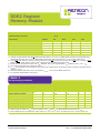
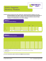
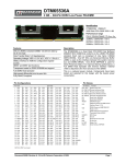
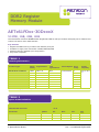
DDR2 Register
Memory Module
AETx61PDxx-30DxxxX
512MB, 1GB, 2GB, 4GB
This Data Sheet describes AENEON DDR2 Registered DIMM on 240-pin modules with parity bit for address and
control bus and its main characteristics.
Key features
•
•
•
•
Registered DDR2 memory modules with address parity bit
Available in single pack of densities 512MB/1GB/2GB/4GB
Standard Industry Standard pin configuration
Fully RoHS compliant
TABLE 1
Ordering Information
Product Type1)
Module Organization
Density
Rank
Module Speed No of
Organization
Comp
Module
Size(mm)
133.5 x 30 x
8.2
AET661PD00-30DB19X
512MB
64M x 72
1Rx8
AET761PD00-30DB19X
1GB
128M x 72
1Rx4
PC2-5300-555
18
9
AET761PD14-30DB29X
1GB
128M x 72
1Rx4
18
AET861PD00-30DB19X
2GB
256M x 72
2Rx4
36
AET861PD24-30DB29X
2GB
256M x 72
2Rx4
36
AET861PD14-30DC20X
2GB
256M x 72
1Rx4
18
AET961PD24-30DC20X
4GB
512M x 72
2Rx4
36
AET961PD00-30DB10X
4GB
512M x 72
2Rx4
18 DDP
1) Full Product Type / Sales Description
TABLE 2
Speed Grade Definition
Speed Grade
PC2
–5300
CAS-RCD-RP latencies
Parameter
Clock Period
@ CL = 3
@ CL = 4
@ CL = 5
AENEON™ Data Sheet
A Qimonda AG Brand
5–5–5
Symbol
Min.
Max.
Unit
Note
tCK
tCK
tCK
5
8
ns
1)2)3)4)
3.75
8
ns
1)2)3)4)
3
8
ns
1)2)3)4)
1
Revision 1.10, 2008-05
Doc. # 01282008-5Q5R-K6FR
DDR2 Register
Memory Module
Speed Grade
PC2
–5300
CAS-RCD-RP latencies
5–5–5
Parameter
Symbol
Min.
Max.
Unit
Note
Row Active Time
tRAS
tRAS
tRC
tRC
tRCD
tRP
45
70k
ns
1)2)3)4)5)6)
40
70k
ns
1)2)3)4)5)7)
60
—
ns
1)2)3)4)
55
–
ns
1)2)3)4)
15
—
ns
1)2)3)4)
15
—
ns
1)2)3)4)
Row Active Time
Row Cycle Time
Row Cycle Time
RAS-CAS-Delay
Row Precharge Time
1) Timings are guaranteed with CK/CK differential Slew Rate of 2.0 V/ns. For DQS signals timings are guaranteed with a
differential Slew Rate of 2.0 V/ns in differential strobe mode and a Slew Rate of 1 V/ns in single ended mode.
2) The CK/CK input reference level (for timing reference to CK/CK) is the point at which CK and CK cross. The DQS / DQS,
RDQS / RDQS, input reference level is the crosspoint when in differential strobe mode.
3) Inputs are not recognized as valid until VREF stabilizes. During the period before VREF stabilizes, CKE = 0.2 x VDDQ
4) The output timing reference voltage level is VTT.
5) tRAS.MAX is calculated from the maximum amount of time a DDR2 device can operate without a refresh command which is
equal to 9 x tREFI.
6) Products released after 2007-08-01 can support tRAS.MIN = 40 ns for all DDR2 speed sort.
7) For products released after 2007-08-01.
TABLE 3
DC Operating Conditions
Parameter
Device Supply Voltage
Output Supply Voltage
Input Reference Voltage
SPD Supply Voltage
DC Input Logic High
DC Input Logic Low
Symbol
VDD
VDDQ
VREF
VDDSPD
VIH(DC)
VIL (DC)
IL
Values
Unit
Note
Min.
Typ.
Max.
1.7
1.8
1.9
V
1.7
1.8
1.9
V
1)
0.49 × VDDQ
0.5 × VDDQ
0.51 × VDDQ
V
2)
1.7
—
3.6
V
VREF + 0.125
—
V
– 0.30
—
VDDQ + 0.3
VREF – 0.125
V
3)
In / Output Leakage Current
–5
—
5
μA
1) Under all conditions, VDDQ must be less than or equal to VDD
2) Peak to peak AC noise on VREF may not exceed ± 2% VREF (DC).VREF is also expected to track noise in VDDQ.
3) Input voltage for any connector pin under test of 0 V ≤ VIN ≤ VDDQ + 0.3 V; all other pins at 0 V. Current is per pin
AENEON™ Data Sheet
A Qimonda AG Brand
2
Revision 1.10, 2008-05
Doc. # 01282008-5Q5R-K6FR
DDR2 Register
Memory Module
Attention:Stresses greater than those listed under “Absolute Maximum Ratings” may cause
permanent damage to the device. This is a stress rating only and functional operation of
the device at these or any other conditions above those indicated in the operational
sections of this specification is not implied. Exposure to absolute maximum rating
conditions for extended periods may affect reliability.
TABLE 4
Absolute Maximum Ratings
Symbol
VDD
VDDQ
VDDL
VIN, VOUT
Parameter
Rating
Unit
Note
1)
Min.
Max.
Voltage on VDD pin relative to VSS
–1.0
+2.3
V
Voltage on VDDQ pin relative to VSS
–0.5
+2.3
V
Voltage on VDDL pin relative to VSS
–0.5
+2.3
V
Voltage on any pin relative to VSS
–0.5
+2.3
V
1) When VDD and VDDQ and VDDL are less than 500 mV; VREF may be equal to or less than 300 mV.
TABLE 5
Environmental Requirements
Parameter
Symbol
Values
Unit
Note
Min.
Max.
–
–
°C
1)
0
+55
°C
2)
0
+65
°C
Storage Temperature
TOPR
TOPR
TOPR
TSTG
– 50
+100
°C
3)
Barometric Pressure (operating & storage)
PBar
+69
+105
kPa
4)
Operating Humidity (relative)
HOPR
HSTG
10
90
%
5
95
%
Operating temperature (ambient)
Operating temperature (ambient)
Operating temperature (ambient)
Storage Humidity (without condensation)
1) The application designer must meet the case temperature specifications for individual module components.
2) The component maximum case temperature (Tcase) shall not exceed the value specified in the DDR2 DRAM component
specification.
3) Storage Temperature is the case surface temperature on the center/top side of the DRAM.
4) Up to 3000 m.
For more information, please contact your AENEON representative
AENEON™ Data Sheet
A Qimonda AG Brand
3
Revision 1.10, 2008-05
Doc. # 01282008-5Q5R-K6FR