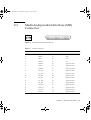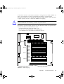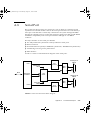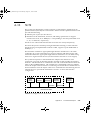
1
LW2Sys_Ref.book Page 1 Wednesday, August 19, 1998 2:29 PM
Netra t 1120/1125
System Reference Manual
Sun Microsystems, Inc.
901 San Antonio Road
Palo Alto, CA 94303-4900 USA
650 960-1300
Fax 650 969-9131
Part No. 805-6805-10
Revision A, August 1998
LW2Sys_Ref.book Page ii Wednesday, August 19, 1998 2:29 PM
Copyright 1998 Sun Microsystems Computer Company • 901 San Antonio Road • Palo Alto • California 94303 • U.S.A. 415-960-1300 •
Fax 415 969-9131. All rights reserved.
This product or document is protected by copyright and distributed under licenses restricting its use, copying, distribution, and decompilation.
No part of this product or document may be reproduced in any form by any means without prior written authorization of Sun and its licensors,
if any.
Portions of this product may be derived from the UNIX® system, licensed from Novell, Inc., and from the Berkeley 4.3 BSD system, licensed
from the University of California. UNIX is a registered trademark in the United States and in other countries and is exclusively licensed by X/
Open Company Ltd. Third-party software, including font technology in this product, is protected by copyright and licensed from Sun’s
suppliers. RESTRICTED RIGHTS: Use, duplication, or disclosure by the U.S. Government is subject to restrictions of FAR 52.227-14(g)(2)(6/87)
and FAR 52.227-19(6/87), or DFAR 252.227-7015(b)(6/95) and DFAR 227.7202-3(a).
Sun, Sun Microsystems, the Sun logo, Solaris, Netra and the Netra logo are trademarks or registered trademarks of Sun Microsystems, Inc. in
the United States and in other countries. All SPARC trademarks are used under license and are trademarks or registered trademarks of SPARC
International, Inc. in the United States and in other countries. Products bearing SPARC trademarks are based upon an architecture developed by
Sun Microsystems, Inc.
The OPEN LOOK® and Sun™ Graphical User Interfaces were developed by Sun Microsystems, Inc. for its users and licensees. Sun
acknowledges the pioneering efforts of Xerox Corporation in researching and developing the concept of visual or graphical user interfaces for
the computer industry. Sun holds a nonexclusive license from Xerox to the Xerox Graphical User Interface, which license also covers Sun’s
licensees who implement OPEN LOOK GUIs and otherwise comply with Sun’s written license agreements.
THIS PUBLICATION IS PROVIDED “AS IS” WITHOUT WARRANTY OF ANY KIND, EITHER EXPRESS OR IMPLIED, INCLUDING, BUT
NOT LIMITED TO, THE IMPLIED WARRANTIES OF MERCHANTABILITY, FITNESS FOR A PARTICULAR PURPOSE, OR NONINFRINGEMENT.
Copyright 1998 Sun Microsystems Computer Company • 901 San Antonio Road •Palo Alto • California 94303 U.S.A. • 415-960-1300 •
Fax 415 969-9131. Tous droits réservés.
Ce produit ou document est protégé par un copyright et distribué avec des licences qui en restreignent l’utilisation, la copie et la décompilation.
Aucune partie de ce produit ou de sa documentation associée ne peut être reproduite sous aucune forme, par quelque moyen que ce soit, sans
l’autorisation préalable et écrite de Sun et de ses bailleurs de licence, s’il y en a.
Des parties de ce produit pourront être derivées du système UNIX® licencié par Novell, Inc. et du système Berkeley 4.3 BSD licencié par
l’Université de Californie. UNIX est une marque enregistrée aux Etats-Unis et dans d’autres pays, et licenciée exclusivement par X/Open
Company Ltd. Le logiciel détenu par des tiers, et qui comprend la technologie relative aux polices de caractères, est protégé par un copyright et
licencié par des fournisseurs de Sun.
Sun, Sun Microsystems, le logo Sun, Solaris, Netra et le logo Netra sont des marques déposées ou enregistrées de Sun Microsystems, Inc. aux
Etats-Unis et dans d’autres pays. Toutes les marques SPARC, utilisées sous licence, sont des marques déposées ou enregistrées de SPARC
International, Inc. aux Etats-Unis et dans d’autres pays. Les produits portant les marques SPARC sont basés sur une architecture développée par
Sun Microsystems, Inc.
Les utilisateurs d’interfaces graphiques OPEN LOOK® et Sun™ ont été développés de Sun Microsystems, Inc. pour ses utilisateurs et licenciés.
Sun reconnaît les efforts de pionniers de Xerox Corporation pour la recherche et le développement du concept des interfaces d’utilisation
visuelle ou graphique pour l’industrie de l’informatique. Sun détient une licence non exclusive de Xerox sur l’interface d’utilisation graphique,
cette licence couvrant aussi les licenciés de Sun qui mettent en place les utilisateurs d’interfaces graphiques OPEN LOOK et qui en outre se
conforment aux licences écrites de Sun.
CETTE PUBLICATION EST FOURNIE "EN L’ETAT" SANS GARANTIE D’AUCUNE SORTE, NI EXPRESSE NI IMPLICITE, Y COMPRIS, ET
SANS QUE CETTE LISTE NE SOIT LIMITATIVE, DES GARANTIES CONCERNANT LA VALEUR MARCHANDE, L’APTITUDE DES
PRODUITS A REPONDRE A UNE UTILISATION PARTICULIERE OU LE FAIT QU’ILS NE SOIENT PAS CONTREFAISANTS DE PRODUITS
DE TIERS.
Please
Recycle
LW2Sys_Ref.book Page iii Wednesday, August 19, 1998 2:29 PM
Contents
Figures
1.
2.
vii
Tables
ix
Preface
xi
Product Overview
1-1
1.1
System Features
1.2
To Power On the System
1-5
1.3
To Power Off the System
1-6
1.4
To Attach the Wrist Strap
1-7
1.5
To Remove the Top Access Cover
1-10
1.6
To Replace the Top Access Cover
1-12
1-2
Back Panel Connectors
2-1
2.1
Connector Layout
2-1
2.2
Serial Connectors
2-2
2.3
Media Independent Interface (MII) Connector
2.4
2.3.1
Cable-Type Connectivity
2.3.2
External Cable Length
2-4
2-4
Twisted-Pair Ethernet (TPE) Connector
2.4.1
2-3
TPE Cable-Type Connectivity
2-5
2-5
Contents
iii
LW2Sys_Ref.book Page iv Wednesday, August 19, 1998 2:29 PM
2.5
SCSI Connector
2-6
2.5.1
SCSI Implementation
2.5.2
SCSI Cabling and Configuration
2-8
2.5.2.1 SCSI Cabling Procedure
2-8
2-7
2.5.2.2 SCSI-2 (Fast Wide SCSI) External Devices
2.6
Alarms Port
2.6.1
2.7
3.
4.
5.
2-10
Alarm Output Description
Parallel Interface
2-11
Twisted-Pair Ethernet Link Test
3-1
3.1
Overview
3.2
Technical Discussion
3.3
Troubleshooting
3.4
Moves and Changes
3.5
To Check or Disable the Link Test
3.6
To Enable the Link Test
Modem Setup
3-1
3-4
3-4
3-5
3-6
4-1
4.1
To Set Up the Modem
4.2
Serial Port Speed Change
4.3
Recommendations
4-1
5.1
To Identify Jumpers
5.2
Flash PROM Jumpers
5.3
Serial Port Jumpers
A. Functional Description
A.2 UPA
5-1
5-2
5-3
5-3
A-1
A-1
A-3
A.3 PCI Bus
A.3.1
4-2
4-2
Main Logic Board Jumpers
A.1 System
2-10
A-4
U2P ASIC
A-4
iv Netra t 1120/1125 System Reference Manual • August 1998
3-5
2-9
LW2Sys_Ref.book Page v Wednesday, August 19, 1998 2:29 PM
A.3.2
Symbios 53C876 SCSI Controller
A.3.3
PCIO ASIC
A-5
A.4 UltraSPARC II Processor
A.5 Memory System
A.5.1
SIMM
A-5
A-6
A-9
A.5.1.1 Memory System Timing
A.6 Peripherals
A-5
A-10
A-12
A.6.1
Disk Drives
A.6.2
Optional CD-ROM Drive
A.6.3
Optional 2.5Gbyte, 4mm and 8mm Tape Drives
A-12
A-12
A.6.3.1 2.5Gbyte Tape Drive
A-13
A.6.3.2 4mm Tape Drive
A-13
A.6.3.3 8mm Tape Drive
A-13
A.7 Parallel Port
A-14
A.7.1
Parallel Port Cables
A.7.2
Electrical Characteristics
A.8 Serial Port
A-14
A-14
A-15
A.8.1
Serial Port Components
A.8.2
Serial Port Functions
A.8.3
EIA Levels
A-16
A-16
A-16
A.8.3.1 Synchronous Rates
A.8.3.2 Asynchronous Rates
A-17
A-17
A.8.3.3 Slew Rate and Cable Length
A.9 Ethernet
A-13
A-17
A-17
A.9.1
Automatic Negotiation
A.9.2
External Transceivers
A.9.3
External Cables
A.9.4
Connectors
A.9.5
MII Power
A.9.6
MII Port Timing
A-18
A-19
A-19
A-19
A-19
A-20
Contents
v
LW2Sys_Ref.book Page vi Wednesday, August 19, 1998 2:29 PM
A.10 Alarms Card
A-21
A.11 Ebus Connector
A.12 SCSI
A-22
A-23
A.12.1 Host Adapter
A-24
A.12.2 Supported Target Devices
A.12.3 External Cables
A-25
A.12.4 Internal SCSI Subassembly
A.12.5 SCSI ID Selection
A.13 ASICs
A-27
A-27
A.13.1 QSC
A-27
A.13.2 XB9+
A-28
A.13.3 PCIO
A-28
A.13.4 U2P A-28
A.13.5 RISC
A-29
A.13.6 SuperIO
A.14 Power Supply
A-29
A-30
A.14.1 Netra t 1120
A-30
A.14.2 Netra t 1125
A-31
Index
A-24
Index-1
vi Netra t 1120/1125 System Reference Manual • August 1998
A-25
LW2Sys_Ref.book Page vii Wednesday, August 19, 1998 2:29 PM
Figures
FIGURE 1-1
Netra t 1120 System Front View
1-3
FIGURE 1-2
Netra t 1125 System Front View
1-3
FIGURE 1-3
Netra t 1120 System Rear View 1-4
FIGURE 1-4
Netra t 1125 System Rear View 1-4
FIGURE 1-5
System Power-On (Front Panel) 1-5
FIGURE 1-6
System Power-Off (Front Panel) 1-7
FIGURE 1-7
Attaching the Wrist Strap to the Front of the Chassis 1-8
FIGURE 1-8
Attaching the Wrist Strap to the Rear of the Chassis 1-9
FIGURE 1-9
Removing the Top Access Cover 1-11
FIGURE 1-10
Replacing the Top Access Cover
FIGURE 2-1
Back Panel Connectors 2-1
FIGURE 2-2
DB-25 Serial Connectors 2-2
FIGURE 2-3
40-Pin Miniature-D MII Connector 2-3
FIGURE 2-4
RJ45 TPE Socket
FIGURE 2-5
68-Pin SCSI Connector 2-6
FIGURE 2-6
Connecting External Mass Storage Devices 2-9
FIGURE 2-7
Alarms Connector Configuration 2-10
FIGURE 2-8
Dry Contact Outputs 2-10
FIGURE 2-9
DB-25 Parallel Connector 2-11
1-13
2-5
Figures
vii
LW2Sys_Ref.book Page viii Wednesday, August 19, 1998 2:29 PM
viii
FIGURE 3-1
Hosts and Hub in a Local Area Network 3-2
FIGURE 3-2
Ensuring Host Hub Communication in a 10BASE-T Network 3-3
FIGURE 5-1
Jumper Locations on the Main Logic Board 5-1
FIGURE 5-2
To Identify Jumper Pins 5-2
FIGURE A-1
System Unit Functional Block Diagram A-2
FIGURE A-2
UPA Address and Data Buses Functional Block Diagram A-4
FIGURE A-3
Memory System Functional Block Diagram A-6
FIGURE A-4
SIMM Mapping A-7
FIGURE A-5
Memory Module Functional Block Diagram A-8
FIGURE A-6
120MHz (8.33ns) Timing – Two Reads to the Same Bank
FIGURE A-7
120MHz (8.33ns) Timing – Two Writes to the Same Bank A-10
FIGURE A-8
120MHz (8.33ns) Timing – Read/Write to Same Bank A-11
FIGURE A-9
120 MHz (8.33ns) Timing – Write/Read to Same Bank A-11
FIGURE A-10
120 MHz (8.33ns) Timing – Refresh Cycle A-11
FIGURE A-11
Serial Port Functional Block Diagram A-15
FIGURE A-12
MII Port Timing Model A-20
FIGURE A-13
Alarms Card Functional Block Diagram A-21
FIGURE A-14
Configuration for the SCSI Bus
FIGURE A-15
SCSI Sub-Assembly Block Diagram A-26
A-23
Netra t 1120/1125 System Reference Manual • August 1998
A-10
LW2Sys_Ref.book Page ix Wednesday, August 19, 1998 2:29 PM
Tables
TABLE 2-1
Serial Connector Pinouts, RS423/RS232
TABLE 2-2
Connector Pinouts
TABLE 2-3
MII External Cable Lengths
TABLE 2-5
TPE STP-5 Cable Lengths 2-5
TABLE 2-4
TPE Connector Pinouts 2-5
TABLE 2-6
68-Pin SCSI Connector Pinouts
TABLE 2-7
Determining SCSI Bus Length 2-8
TABLE 2-8
Alarms Connector Line Assignments
TABLE 2-9
Parallel Connector Pinouts
TABLE 5-1
User-Configurable Jumpers 5-2
TABLE 5-2
Flash PROM Jumper Settings 5-3
TABLE 5-3
Serial Port Jumper Settings
TABLE A-1
UPA Port Identification Assignments
TABLE A-2
DIMM Bank-to-U-Number Mapping A-9
TABLE A-3
IL = 0, DIMM Bank-to-Physical Address Mapping
TABLE A-4
Supported Disk Drives A-12
TABLE A-5
Ebus Connector Pinouts A-22
TABLE A-6
SCSI Devices Supported
TABLE A-7
DC Power Supply Output Voltages A-30
TABLE A-8
AC Power Supply Output Voltages A-31
2-2
2-3
2-4
2-6
2-10
2-11
5-3
A-3
A-9
A-24
Tables
ix
LW2Sys_Ref.book Page x Wednesday, August 19, 1998 2:29 PM
x
Netra t 1120/1125 System Reference Manual • August 1998
LW2Sys_Ref.book Page xi Wednesday, August 19, 1998 2:29 PM
Preface
The Netra t 1120/1125 System Reference Manual provides information on the
configuration of the subsystems in the Netra t 1120 (order code N04) and Netra t
1125 (order code N03).
Note – This Guide does not apply to the version of Netra t 1120 supplied as order
code N02.
Note – All illustrations in this manual are of the Netra t 1125, except where the two
types of system differ, in which case examples of both are shown.
Who Should Use This Guide
This manual is intended to be read by OEM engineers, system designers and
application programmers who have to perform advanced tasks concerned with the
maintenance and configuration of the system.
How This Guide Is Organized
The guide is arranged as follows:
Chapter 1, “Product Overview”, describes the key features of the Netra t 1120/1125
system.
Preface
xi
LW2Sys_Ref.book Page xii Wednesday, August 19, 1998 2:29 PM
Chapter 2, “Back Panel Connectors”, provides information on the Netra t 1120/1125
system board and its components.
Chapter 3, “Twisted-Pair Ethernet Link Test”, describes how to connect your Netra t
1120/1125 system to a 10BASE-T Twisted-Pair Ethernet (TPE) network.
Chapter 4, “Modem Setup”, provides information on modem setup specifications.
Any modem compatible with CCITT V.24 can be connected to the Netra t 1120/1125
serial ports.
Chapter 5, “Main Logic Board Jumpers”, provides information about the main logic
board jumpers.
Appendix A, “Functional Description”, is a functional description of the Netra t
1120/1125 system.
Accompanying Documentation
■
Netra t 1120/1125 Compliance and Safety Manual (805-6806-10)
Note – It is important that you read the Netra t 1120/1125 Compliance and Safety
Manual before doing anything else.
■
■
■
Netra t 1120/1125 Installation and Basic Maintenance Guide (805-6803-10)
Netra t 1120/1125 Service Manual (805-6804-10)
Netra t 1120/1125 User’s Guide (805-6040-05)
xii Netra t 1120/1125 System Reference Manual • August 1998
LW2Sys_Ref.book Page xiii Wednesday, August 19, 1998 2:29 PM
Conventions used in this Guide
The following table shows the type changes and symbols used in this guide.
TABLE P-1
Typographic Conventions
Typeface or
Symbol
Meaning
Example
AaBbCc123
The names of commands, files, and
directories; on-screen computer
output
Edit your .login file.
Use ls -a to list all files.
system% You have mail.
AaBbCc123
What you type, as opposed to onscreen computer output
system% su
Password:
AaBbCc123
Command-line placeholder:
replace with a real name or value
To delete a file, type rm filename.
AaBbCc123
Book titles, new words or terms, or
words to be emphasized
Read Chapter 6 in User’s Guide.
These are called class options.
You must be root to do this.
%
UNIX C shell prompt
system%
$
UNIX Bourne and Korn shell
prompt
system$
#
super-user prompt, all shells
system#
Symbols
The following symbols mean:
Note – A note provides information which should be considered by the reader.
!
Caution – Cautions accompanied by this Attention icon carry information about
procedures or events which if not considered may cause damage to the data or
hardware of your system.
xiii
LW2Sys_Ref.book Page xiv Wednesday, August 19, 1998 2:29 PM
Caution – Cautions accompanied by this Hazard icon carry information about
procedures which must be followed to reduce the risk of electric shock and danger
to personal health. Follow all instructions carefully.
xiv
1125
Paragraphs accompanied by this 1125 icon apply only to Netra t 1125 systems.
1120
Paragraphs accompanied by this 1120 icon apply only to Netra t 1120 systems.
Netra t 1120/1125 System Reference Manual • August 1998
LW2Sys_Ref.book Page 1 Wednesday, August 19, 1998 2:29 PM
CHAPTER
1
Product Overview
The Netra t 1120/1125 system is a multi-processor device that uses the family of
UltraSPARC™ II processors. Housed within a rack-mounting enclosure, the
Netra t 1120/1125 provides the following:
■
■
■
■
■
■
One or two UltraSPARC II processors
Increased power and cooling for high performance processors
Extensive I/O expansion and a wide range of options
Modular internal design
High performance disk, system, memory and I/O subsystem
High-performance peripheral component interconnect (PCI) I/O expansion with
comparable options to existing SBus options.
The Netra t 1120 is a –48V/–60Vdc-powered system. The Netra t 1125 is powered by
a standard AC mains supply. There are no other differences between the systems.
FIGURE 1-1 and FIGURE 1-2 on page 1-3 and FIGURE 1-3 and FIGURE 1-4 on page 1-4
show the Netra t 1120/1125 system. The following sections provide a brief
description of the Netra t 1120/1125 I/O devices and a detailed overview of the
system’s features.
1-1
LW2Sys_Ref.book Page 2 Wednesday, August 19, 1998 2:29 PM
1.1
System Features
System components are housed in a rack-mounting enclosure. Overall enclosure
dimensions (width x depth x height) are 431.8mm x 496.1mm x 177mm (17.13in x
19.53in x 7in (4U)). System electronics are contained on a single printed circuit board
(motherboard). The motherboard contains the CPU module(s), memory, system
control application-specific integrated circuits (ASICs), and I/O ASICs.
The system unit has the following features:
■
Rack-mountable enclosure with power supply.
■
Support for up to two modular UltraSPARC II processor(s) with 1, 2 or 4 Mbyte
Ecache, at operating frequencies from 300MHz to 400MHz.
■
UPA coherent memory interconnect.
■
Use of SIMMs, with an interleaved memory system. Each pair of SIMM slots (four
rows of two pairs each) accepts 32, 64, or 128Mbyte SIMM modules. Populating
with two pairs of identical capacity SIMMs enables the memory controller to
interleave and overlap, providing optimal system performance. There are a total
of 16 SIMM slots.
■
Four PCI slots:
■
Three 33MHz, 64- or 32-bit, 5Vdc slots.
■
One 66MHz or 33MHz, 64- or 32-bit, 3.3Vdc slot.
Universal PCI cards can be used in any of the four PCI slots.
1-2
■
10/100Mbps Ethernet.
■
40Mb/s UltraSCSI (Fast-20).
■
Two DB-25 serial ports (synchronous and asynchronous protocols).
■
One parallel port.
Netra t 1120/1125 System Reference Manual • August 1998
LW2Sys_Ref.book Page 3 Wednesday, August 19, 1998 2:29 PM
FIGURE 1-2 and FIGURE 1-2 show the system unit front view. FIGURE 1-4 and FIGURE 1-4
shows the system unit rear view.
FIGURE 1-1
Netra t 1120 System Front View
1125
FIGURE 1-2
Netra t 1125 System Front View
Chapter 1
Product Overview
1-3
LW2Sys_Ref.book Page 4 Wednesday, August 19, 1998 2:29 PM
DC inputs A and B
B
A
Serial A TPE
and B
Parallel
FIGURE 1-3
MII
SCSI
Alarms
Netra t 1120 System Rear View
AC power inlet
B
A
Parallel
FIGURE 1-4
1-4
Serial A TPE
and B
MII
Netra t 1125 System Rear View
Netra t 1120/1125 System Reference Manual • August 1998
SCSI
Alarms
LW2Sys_Ref.book Page 5 Wednesday, August 19, 1998 2:29 PM
1.2
To Power On the System
1. Prior to powering on, inspect the supply connector(s) for correct polarity and
mechanical security.
1125
1120
2. Apply power to the system power inlet, or
activate the external circuit breakers for input A and input B.
3. Momentarily set the front panel ON/STBY system switch to the ON
and hold it until the system starts to power up.
position
1125
FIGURE 1-5
System Power-On (Front Panel)
Chapter 1
Product Overview
1-5
LW2Sys_Ref.book Page 6 Wednesday, August 19, 1998 2:29 PM
1.3
!
To Power Off the System
Caution – Prior to turning off system power, exit from the operating system. Failure
to do so may result in data loss.
1. Where necessary, notify the users that the system is going down.
2. Back up system files and data.
3. Halt the operating system.
4. Momentarily set the front panel ON/STBY system switch to the STBY
until the system powers down.
position
5. Verify that the Power LED is off.
6. Disconnect the input power connector(s) from the unit, or open the circuit
breaker(s) associated with the unit.
Caution –
1125
Regardless of the position of the ON/STBY switch, where an AC power cord
remains connected to the system, hazardous voltages are always present within the
power supply.
1120
Regardless of the position of the ON/STBY switch, where a DC power cord remains
connected to the system, DC voltage is always present within the power supply.
1-6
Netra t 1120/1125 System Reference Manual • August 1998
LW2Sys_Ref.book Page 7 Wednesday, August 19, 1998 2:29 PM
1125
FIGURE 1-6
1.4
System Power-Off (Front Panel)
To Attach the Wrist Strap
Caution – Wear an antistatic wrist strap and use an ESD-protected mat when
!
handling components. When servicing or removing system unit components, use a
wrist strap with a 10mm press stud connection and attach the wrist strap to the
press stud at the front or rear of the chassis. This should be performed before the top
cover is removed.
Chapter 1
Product Overview
1-7
LW2Sys_Ref.book Page 8 Wednesday, August 19, 1998 2:29 PM
FIGURE 1-7
1-8
Attaching the Wrist Strap to the Front of the Chassis
Netra t 1120/1125 System Reference Manual • August 1998
LW2Sys_Ref.book Page 9 Wednesday, August 19, 1998 2:29 PM
FIGURE 1-8
Attaching the Wrist Strap to the Rear of the Chassis
Chapter 1
Product Overview
1-9
LW2Sys_Ref.book Page 10 Wednesday, August 19, 1998 2:29 PM
1.5
To Remove the Top Access Cover
Note – This operation should be performed by qualified personnel only.
1. Power off the system.
See Section 1.3 “To Power Off the System” on page 1-6.
Caution – Wear an antistatic wrist strap and use an ESD-protected mat when
!
handling components. When servicing or removing system unit components, an ESD
Strap should be attached to the wrist, then to one of the connection points provided
on the system, and then the power connectors should be removed from the system
unit. Following this caution equalizes all electrical potentials with the system unit.
2. Disconnect the input power connector(s) from the rear of the unit or open the
associated circuit breaker(s), if fitted.
3. Attach the wrist strap.
See Section 1.4 “To Attach the Wrist Strap” on page 1-7.
4. Remove the rack fixing screws and withdraw the unit on its slides (if fitted). Refer
to FIGURE 1-9 on page 1-11.
To remove the top access cover, the unit may need to be completely removed from
the rack. If slides are fitted, disconnect the cables and release the slides. Place the
system on an approved work station/position.
5. Remove the two screws from the front of the top access cover and carefully store
them away from the system unit.
6. Place the system so that the extended tab of the top access cover is facing you. To
release the top cover, pull the tab towards you and lift the cover off.
1-10
Netra t 1120/1125 System Reference Manual • August 1998
LW2Sys_Ref.book Page 11 Wednesday, August 19, 1998 2:29 PM
Tab
Screws
1125
FIGURE 1-9
Removing the Top Access Cover
Chapter 1
Product Overview
1-11
LW2Sys_Ref.book Page 12 Wednesday, August 19, 1998 2:29 PM
1.6
To Replace the Top Access Cover
Caution – Wear an antistatic wrist strap and use an ESD-protected mat when
!
handling components. When servicing or removing system unit components, an ESD
Strap should be attached to the wrist, then to one of the connection points provided
on the system, and then the power connectors should be removed from the system
unit.Following this caution equalizes all electrical potentials with the system unit.
1. Attach the wrist strap.
See Section 1.4 “To Attach the Wrist Strap” on page 1-7.
2. Position the top access cover.
See FIGURE 1-10 on page 1-13.
3. Engage the top access cover. Push the top cover forwards until the lugs on the
sides have fully engaged in the slots.
4. Replace the two fixing screws.
1-12
Netra t 1120/1125 System Reference Manual • August 1998
LW2Sys_Ref.book Page 13 Wednesday, August 19, 1998 2:29 PM
1125
FIGURE 1-10
Replacing the Top Access Cover
Chapter 1
Product Overview
1-13
LW2Sys_Ref.book Page 14 Wednesday, August 19, 1998 2:29 PM
1-14
Netra t 1120/1125 System Reference Manual • August 1998
LW2Sys_Ref.book Page 1 Wednesday, August 19, 1998 2:29 PM
CHAPTER
2
Back Panel Connectors
2.1
Connector Layout
FIGURE 2-1 shows the locations of the Netra t 1120/1125 system back panel
connectors.
AC power inlet
B
A
Parallel
Serial A TPE
and B
FIGURE 2-1
Back Panel Connectors
MII
SCSI
Alarms
2-1
LW2Sys_Ref.book Page 2 Wednesday, August 19, 1998 2:29 PM
2.2
Serial Connectors
13
B
1
25
14
13
A
1
25
14
FIGURE 2-2
DB-25 Serial Connectors
TABLE 2-1
Serial Connector Pinouts, RS423/RS232
Pin
Function
I/O
Signal Description
1
none
none
Not connected
2
TxD
O
Transmit Data
3
RxD
I
Receive Data
4
RTS
O
Ready To Send
5
CTS
I
Clear To Send
6
DSR
I
Data Set Ready
7
Gnd
8
DCD
I
Data Carrier Detect
9–14
none
none
Not connected
15
TRxC
I
Transmit Clock
16
none
none
Not connected
17
RTxC
I
Receive Clock
18–19
none
none
Not connected
20
DTR
O
Data Terminal Ready
21-23
none
none
Not connected
24
TxC
O
Transmit Clock
25
none
none
Not connected
Signal Ground
Note: For information about serial port jumpers on the Netra t 1120/1125 system main logic board, see
Chapter 5 “Main Logic Board Jumpers”.
2-2
Netra t 1120/1125 System Reference Manual • August 1998
LW2Sys_Ref.book Page 3 Wednesday, August 19, 1998 2:29 PM
2.3
Media Independent Interface (MII)
Connector
20
1
40
21
FIGURE 2-3
40-Pin Miniature-D MII Connector
TABLE 2-2
Connector Pinouts
Pin
Function
Pin
Function
1
+5V
18
COL
2
MDIO
19
CRS
3
MDC
20
+5V
4
RXD<3>
21
+5V
5
RXD<2>
22
Signal Ground
6
RXD<1>
23
Signal Ground
7
RXD<0>
24
Signal Ground
8
RX_DV
25
Signal Ground
9
RX_CLK
26
Signal Ground
10
RX_ER
27
Signal Ground
11
TX_ER
28
Signal Ground
12
TX_CLK
29
Signal Ground
13
TX_EN
30
Signal Ground
14
TXD<0>
31
Signal Ground
15
TXD<1>
32
Signal Ground
16
TXD<2>
33
Signal Ground
17
TXD<3>
34
Signal Ground
Chapter 2
Back Panel Connectors
2-3
LW2Sys_Ref.book Page 4 Wednesday, August 19, 1998 2:29 PM
TABLE 2-2
2.3.1
Connector Pinouts (Continued)
Pin
Function
Pin
Function
35
Ground
38
Signal Ground
36
Ground
39
Signal Ground
37
Ground
40
+5V
Cable-Type Connectivity
The following types of Ethernet cable can be connected to the 40-pin MII connector:
■
■
2.3.2
Fiber (connected to an external transceiver)
Shielded twisted-pair (STP).
External Cable Length
TABLE 2-3
2-4
MII External Cable Lengths
Cable Type
Application(s)
Max Length
(Metric)
Max Length
(Imperial)
40-conductor (20 signal-ground twistedpair) shielded (STP)
All external MII
0.5m
20in
Shielded twisted- pair category 5 (STP-5,
“data grade”)
10BASE-T
1000m
3282ft
Shielded twisted- pair category 5 (STP-5,
“data grade”)
100BASE-T
100m
327ft
Netra t 1120/1125 System Reference Manual • August 1998
LW2Sys_Ref.book Page 5 Wednesday, August 19, 1998 2:29 PM
2.4
Twisted-Pair Ethernet (TPE) Connector
1
2.4.1
FIGURE 2-4
RJ45 TPE Socket
TABLE 2-4
TPE Connector Pinouts
8
Pin
Description
Pin
Description
1
Transmit Data +
5
Common Mode Termination
2
Transmit Data –
6
Receive Data –
3
Receive Data +
7
Common Mode Termination
4
Common Mode Termination
8
Common Mode Termination
TPE Cable-Type Connectivity
The following types of twisted-pair Ethernet cable can be connected to the
8-pin TPE connector:
■
■
For 10BASE-T applications, shielded twisted-pair (STP) cable:
■
Category 3 (STP-3, “voice grade”)
■
Category 4 (STP-4)
■
Category 5 (STP-5, “data grade”)
For 100BASE-T applications, shielded twisted-pair category 5 (STP-5, “data
grade”) cable.
TABLE 2-5
TPE STP-5 Cable Lengths
Cable Type
Application(s)
Max Length
(Metric)
Max Length
(Imperial)
Shielded twisted pair category 5 (STP-5, “data
grade”)
10BASE-T
1000m
3282ft
Shielded twisted pair category 5 (STP-5, “data
grade”)
100BASE-T
100m
327ft
Chapter 2
Back Panel Connectors
2-5
LW2Sys_Ref.book Page 6 Wednesday, August 19, 1998 2:29 PM
2.5
SCSI Connector
34
68
2-6
FIGURE 2-5
68-Pin SCSI Connector
TABLE 2-6
68-Pin SCSI Connector Pinouts
1
35
Pin
Signal Name
Pin
Signal Name
1
Ground
21
Ground
2
Ground
22
Ground
3
Ground
23
Ground
4
Ground
24
Ground
5
Ground
25
Ground
6
Ground
26
Ground
7
Ground
27
Ground
8
Ground
28
Ground
9
Ground
29
Ground
10
Ground
30
Ground
11
Ground
31
Ground
12
Ground
32
Ground
13
Ground
33
Ground
14
Ground
34
Ground
15
Ground
35
–DB<12>
16
Ground
36
–DB<13>
17
TERMPWR
37
–DB<14>
18
TERMPWR
38
–DB<15>
19
Not connected
39
–PAR<1>
20
Ground
40
–DB<0>
41
–DB<1>
55
–ATN
Netra t 1120/1125 System Reference Manual • August 1998
LW2Sys_Ref.book Page 7 Wednesday, August 19, 1998 2:29 PM
TABLE 2-6
68-Pin SCSI Connector Pinouts (Continued)
Pin
Signal Name
Pin
Signal Name
42
–DB<2>
56
Ground
43
–DB<3>
57
–BSY
44
–DB<4>
58
–ACK
45
–DB<5>
59
–RST
46
–DB<6>
60
–MSG
47
–DB<7>
61
–SEL
48
–PAR<0>
62
–CD
49
Ground
63
–REQ
50
TERM.DIS
64
–IO
51
TERMPWR
65
–DB<8>
52
TERMPWR
66
–DB<9>
53
Reserved
67
–DB<10>
54
Ground
68
–DB<11>
Note – All signals shown in
2.5.1
TABLE 2-6 on page 2-6 are active low.
SCSI Implementation
■
SCSI-3 Fast-20 (UltraSCSI) parallel interface
■
16-bit SCSI bus
■
40Mbps data transfer rate
■
Support for 16 SCSI addresses:
■
Target 0 to 6 and 8 to F for devices
■
Target 7 reserved for SCSI host adapter on main logic board
■
Support for up to four internal SCSI devices (including the host adapter):
■
SCSI disk drive target 0 (lower drive slot)
■
SCSI disk drive target 1 (upper drive slot)
■
SCSI CD-ROM drive target 6 or SCSI tape drive target 5
■
Support for external 8-bit and 16-bit SCSI devices via 68-pin SCSI connector.
Chapter 2
Back Panel Connectors
2-7
LW2Sys_Ref.book Page 8 Wednesday, August 19, 1998 2:29 PM
2.5.2
SCSI Cabling and Configuration
The SCSI-3 Fast-20 (UltraSCSI) specification requires that the external SCSI bus
length be limited to 3m (10ft) for less than five devices (internal and external), and
1.5m (5ft) for five to eight devices. When SCSI-3 and SCSI-2 devices are connected to
the Netra t 1120/1125 system SCSI bus, the system enables each device to operate at
its respective data transfer rate. The last external SCSI device in a daisy-chain must
be terminated internally (active termination) or with an external terminator
according to Forced-Perfect Termination (FPT) technology.
2.5.2.1
SCSI Cabling Procedure
1. Count the number of SCSI devices on the system SCSI bus. Be sure to count the
host adapter as a SCSI device.
2. Determine the total SCSI bus length.
TABLE 2-7
Determining SCSI Bus Length
SCSI Implementation
Bus Width
DataTransfer
Rate, Mb/s
Number of
Devices
SCSI
Bus Length
SCSI-2, Fast
8 bits
10
1–8
6.0m
SCSI-2, Fast/Wide
16 bits
20
1–8
6.0m
SCSI-3 Parallel Interface, Fast-20 Wide
(UltraSCSI) (WideUltra)
16 bits
40
1–4
3.0m
SCSI-3 Parallel Interface, Fast-20 Wide
(UltraSCSI) (WideUltra)
16 bits
40
5–8*
1.5m
* The maximum number of single-ended/differential SCSI devices is 16.
3. Verify the cable type used to connect external SCSI devices. You must use Fast-20
SCSI cable(s).
Ensure that the total SCSI cable length does not exceed the permissible total SCSI
bus length.
2-8
Netra t 1120/1125 System Reference Manual • August 1998
LW2Sys_Ref.book Page 9 Wednesday, August 19, 1998 2:29 PM
2.5.2.2
SCSI-2 (Fast Wide SCSI) External Devices
If you connect SCSI-2 (Fast Wide SCSI, 20Mb data transfer rate) external devices to a
Netra t 1120/1125 system, follow these cabling and configuration guidelines (as
shown in FIGURE 2-6) to ensure proper device addressing and operation:
■
■
■
If all external mass storage devices use 68-pin connectors, connect all non-Sun
devices to the Netra t 1120/1125 system first and follow them with Sun devices.
Sun devices use auto-termination.
If external mass storage devices consist of 68-pin Sun devices and 50-pin devices,
connect the Sun 68-pin devices to the Netra t 1120/1125 system first and terminate
the daisy chain with the 50-pin device and its terminator.
The total SCSI bus length for all external SCSI devices is 6.0m (19.7ft).
1125
1125
Non-Sun device
Sun device
Sun device
Non-Sun device
Sun device
50-pin device
Adaptor cable
FIGURE 2-6
Terminator
Connecting External Mass Storage Devices
Chapter 2
Back Panel Connectors
2-9
LW2Sys_Ref.book Page 10 Wednesday, August 19, 1998 2:29 PM
2.6
Alarms Port
The alarms connector is located on the alarms card. This connector is a male DB-15
and TABLE 2-8 lists each connector line assignment.
8
9
2.6.1
1
15
FIGURE 2-7
Alarms Connector Configuration
TABLE 2-8
Alarms Connector Line Assignments
Pin
Signal Name
Pin
Signal Name
1
RESET+
9
ALARM1 COM
2
RESET–
10
ALARM1 NC
3
Not connected
11
ALARM2 NO
4
Not connected
12
ALARM2 COM
5
ALARM3 COM
13
ALARM2 NC
6
ALARM3 NO
14
Not connected
7
ALARM3 NC
15
Not connected
8
ALARM1 NO
Alarm Output Description
NC
COM
NC
COM
NO
Alarm reset
FIGURE 2-8
NO
Alarm set
Dry Contact Outputs
The reset signal requirement is a pulse of 250±50ms duration applied to pin 1. The
pulse should be between +4Vdc and +12Vdc with respect to pin 2.
2-10
Netra t 1120/1125 System Reference Manual • August 1998
LW2Sys_Ref.book Page 11 Wednesday, August 19, 1998 2:29 PM
2.7
Parallel Interface
13
1
25
14
FIGURE 2-9
DB-25 Parallel Connector
TABLE 2-9
Parallel Connector Pinouts
Pin
Description
Pin
Description
1
Data_Strobe_L
14
AFXN_L
2
Data0
15
ERROR_L
3
Data1
16
RESET_L
4
Data2
17
IN_L
5
Data3
18
Ground
6
Data4
19
Ground
7
Data5
20
Ground
8
Data6
21
Ground
9
Data7
22
Ground
10
ACK_L
23
Ground
11
BUSY
24
Ground
12
PERROR
25
Ground
13
SELECT_L
Chapter 2
Back Panel Connectors
2-11
LW2Sys_Ref.book Page 12 Wednesday, August 19, 1998 2:29 PM
2-12
Netra t 1120/1125 System Reference Manual • August 1998
LW2Sys_Ref.book Page 1 Wednesday, August 19, 1998 2:29 PM
CHAPTER
3
Twisted-Pair Ethernet Link Test
Read this chapter if you are connecting your Netra t 1120/1125 system to a twistedpair Ethernet (TPE) network. This chapter contains important information for
configuring your system to communicate correctly over a TPE network. If you have
no experience with TPE networks, ask your system or network administrator to
perform the procedures in this chapter.
Note – In 100BASE-T networks, the link test function must be enabled at both the
host and the hub. If your host is connected to a 100BASE-T network, you must not
disable the host link test function.
3.1
Overview
■
■
■
The twisted-pair Ethernet link integrity test is a function defined by the IEEE
802.3 10BASE-T specification.
For a networked workstation (host) to communicate with a network hub, the link
test state (enabled or disabled) must be the same on the host and hub. The link
test must be enabled for 100BASE-T.
If either the host or hub does not share the link test enabled/disabled state of the
other, they cannot communicate effectively with each other.
FIGURE 3-1 on page 3-2 gives an example of a star configuration Local Area Network
(LAN), showing the relationship of hosts to a hub.
FIGURE 3-2 on page 3-3 shows the importance of ensuring that the host and hub link
test settings match in a 10BASE-T network.
3-1
LW2Sys_Ref.book Page 2 Wednesday, August 19, 1998 2:29 PM
Host
Host
Host
Hub
Host
100m (327ft)
Host
1125
Netra t 1120/1125 Host
FIGURE 3-1
3-2
Hosts and Hub in a Local Area Network
Netra t 1120/1125 System Reference Manual • August 1998
LW2Sys_Ref.book Page 3 Wednesday, August 19, 1998 2:29 PM
Link Test
Enabled
(Default)
1
Two-way communication
Netra t 1120/1125
Link Test
Enabled
(Default)
1
Netra t 1120/1125
Netra t 1120/1125 may boot
successfully, but with “lost
carrier” or “no carrier” error
messages.
Netra t 1120/1125 may boot
successfully, but other hosts
in the network cannot
communicate with the
Netra t 1120/1125.
Two-way communication
Link Test
Disabled
0
Netra t 1120/1125
Netra t 1120/1125
FIGURE 3-2
Link Test
Enabled
1
Netra t 1120/1125
Netra t 1120/1125
Link Test
Disabled
(Reset)
0
Link Test
Disabled
0
Netra t 1120/1125
Netra t 1120/1125
Link Test
Disabled
(Reset)
0
Link Test
Enabled
1
Ensuring Host Hub Communication in a 10BASE-T Network
Chapter 3
Twisted-Pair Ethernet Link Test
3-3
LW2Sys_Ref.book Page 4 Wednesday, August 19, 1998 2:29 PM
3.2
Technical Discussion
The twisted-pair Ethernet link integrity test determines the state of the twisted-pair
cable link between the host and the hub in a network. Both the host and hub
regularly transmit a link test pulse. When either the host or hub has not received a
link test pulse within a certain amount of time (50 to 150ms), it makes the transition
from the link-pass state to the link-fail state and remains in the link-fail state until it
once again receives regular link test pulses.
The link integrity test is specific to twisted-pair Ethernet and is not applicable to the
other physical layer implementations of IEEE 802.3 such as 10BASE5 (”thicknet”) or
10BASE2 (“thinnet”).
The link test function at the host or hub is either enabled (link test enabled or 1) or
disabled (link test disabled or 0). The IEEE 802.3 10BASE-T specification requires
that the link test be enabled at both the host and the hub.
Although link test disabled does not conform to the specification, it is often
encountered in real-world 10BASE-T network installations. Some hubs from various
vendors can exhibit any of the following:
3.3
■
Link test is “hardwired” enabled—link test is always enabled.
■
Link test is “hardwired” disabled—link test is always disabled.
■
Link test is configurable—the network administrator may enable or disable link
test.
Troubleshooting
If you have connected a Netra t 1120/1125 host to a hub using twisted-pair Ethernet
cable and observe either “no carrier” messages or failure to communicate effectively
with another host in the same network, look first at the hub. If it supports
configurable link test, make sure “link test enabled” is configured. This is usually
done by setting a hardware switch.
If the hub does not support configurable link test, refer to the hub manufacturer’s
documentation. Check to see if your hub is hardwired for link test disabled. If it is,
you must follow the procedure in Section 3.5 “To Check or Disable the Link Test” on
page 3-5 to disable the link test at your Netra t 1120/1125 host.
3-4
Netra t 1120/1125 System Reference Manual • August 1998
LW2Sys_Ref.book Page 5 Wednesday, August 19, 1998 2:29 PM
3.4
Moves and Changes
If the Netra t 1120/1125 host is physically moved to another network location or if
the hub is reconfigured, remember to refer back to FIGURE 3-2 on page 3-3. Unless the
new network relationship between the host and the hub is functional (that is, 1-1
link test enabled-link test enabled or 0-0 link test disabled-link test disabled), there
will be no full, regular two-way communication between the host and the hub.
3.5
To Check or Disable the Link Test
To check the link test state of a Netra t 1120/1125 host:
1. If you do not see the ok prompt, send a Break command.
2. At the ok prompt, type:
ok printenv tpe-link-test?
tpe-link-test?
true
ok
true
The output shows the current link test state (true, or enabled), followed by the
default state (true, or enabled).
To disable the host’s link test function:
3. Type the following commands:
ok setenv tpe-link-test? false
tpe-link-test? =
false
ok reset-all
4. Boot the host and verify that the transceiver cable problem messages do not
appear by typing either boot net or boot disk and pressing Return.
Chapter 3
Twisted-Pair Ethernet Link Test
3-5
LW2Sys_Ref.book Page 6 Wednesday, August 19, 1998 2:29 PM
3.6
To Enable the Link Test
1. If you do not see the ok prompt, send a Break command.
2. At the ok prompt, type:
ok printenv tpe-link-test?
tpe-link-test?
false
ok
true
The above screen shows the current link test state (false, or disabled), followed by
the default state (true, or enabled).
3. To enable the host’s link test function, type the following commands:
ok setenv tpe-link-test? true
tpe-link-test? =
true
ok reset-all
4. Boot the host and verify that the transceiver cable problem messages do not
appear by typing either boot net or boot disk and pressing Return.
3-6
Netra t 1120/1125 System Reference Manual • August 1998
LW2Sys_Ref.book Page 1 Wednesday, August 19, 1998 2:29 PM
CHAPTER
4
Modem Setup
Any modem compatible with CCITT V.24 can be connected to the Netra t 1120/1125
serial ports. Modems can be set up to function in one of three ways:
■
■
■
4.1
Dial out only
Dial in only
Bidirectional calls.
To Set Up the Modem
To set up your modem:
1. Become root and type admintool.
% su
Password:
# admintool
2. Click on Serial Port Manager.
3. Select Port a or Port b for your modem connection.
4. Click on Edit.
The Serial Port Manager: Modify Service window is displayed.
5. Choose the Expert level of detail.
6. From the Use Template menu, choose one of the following:
a. Modem – Dial-Out only
b. Modem – Dial-In only
4-1
LW2Sys_Ref.book Page 2 Wednesday, August 19, 1998 2:29 PM
c. Modem – Bidirectional
7. Click on Apply.
8. Set your modem auto-answer switch to one of the following:
■
■
■
4.2
Off – Dial-Out Only
On – Dial-In Only
On – Bidirectional
Serial Port Speed Change
To change the speed of a serial port, you must edit the /etc/remote file as follows:
1. Become super user, and type cd /etc.
% su
Password:
# cd /etc
2. Type vi remote.
3. Type tip speed device-name.
Typical speeds are 9600, 19200 to 38400 bps.
The device name is the serial port name, for example,
/dev/tty[a,b] or /dev/term/[a,b].
4. Press <Esc> and type :wq to save your file change(s) and to exit from the vi text
editor.
4.3
Recommendations
For a modem-to-host (system) connection, use an RS423/RS232 straight-through
cable with DB-25 male connectors at both ends.
4-2
Netra t 1120/1125 System Reference Manual • August 1998
LW2Sys_Ref.book Page 1 Wednesday, August 19, 1998 2:29 PM
CHAPTER
5
Main Logic Board Jumpers
The jumper settings given in this chapter refer to the etchings on the main logic
board. The jumpers are labeled with the letter “J” followed by a four-digit number
(see FIGURE 5-1).
SIMM
sockets
J3001
J2604
Jumpers
J2804 J2605 J2703
FIGURE 5-1
Jumper Locations on the Main Logic Board
5-1
LW2Sys_Ref.book Page 2 Wednesday, August 19, 1998 2:29 PM
5.1
To Identify Jumpers
Jumpers are marked on the main logic board with part numbers. For example, the
serial port jumpers are marked J2604 and J2605. Jumper pins are located
immediately adjacent to the part number. Pin 1 is marked with an asterisk in the
position shown in FIGURE 5-2.
J X X X X
Part number
Pins
Asterisk = Pin 1
*
5-2
FIGURE 5-2
To Identify Jumper Pins
TABLE 5-1
User-Configurable Jumpers
Jumper
Functionality
J2703
Flash PROM Write Protect/Write Enable
J2605
J2604
Serial Ports B and A RS423 and RS232
J2804
Flash PROM Hi-Lo Booting
Netra t 1120/1125 System Reference Manual • August 1998
LW2Sys_Ref.book Page 3 Wednesday, August 19, 1998 2:29 PM
5.2
Flash PROM Jumpers
The Netra t 1120/1125 system uses flash PROMs. Flash PROMs enable:
■
Reprogramming of specific code blocks.
■
Remote reprogramming of the PROM chip by a system administrator over a local
area network.
The default shunt setting of J2703 is on pins 1 and 2. This prevents the flash PROM
chip from being reprogrammed. Placing the shunt on pins 2 and 3 enables
reprogramming of the flash PROM chip (see TABLE 5-2).
Note – After reprogramming your system flash PROM, make sure you return the
flash PROM Write Protect/Enable jumper (J2703) to the Write Protect position to
increase system security.
5.3
TABLE 5-2
Flash PROM Jumper Settings
Jumper
Pins 1 + 2 Select
Pins 2 + 3 Select
Default Jumper
on Pins
J2703
Write Protect
Write Enable
1+2
FLASH PROM
PROG ENABLE
J2804
High Half
Booting
Normal Booting
2+3
XOR LOGIC SET
Signal Controlled
Serial Port Jumpers
The serial port jumpers on the main logic board enable you to configure the two
DB-25 serial ports on the system unit back panel for either RS423 or RS232 signal
levels. RS423 levels are the default standard for North American users. RS232 levels
are required for telecommunication in nations of the European Community (see
TABLE 5-3).
TABLE 5-3
Serial Port Jumper Settings
Jumper
Pins 1 + 2 Select
Pins 2 + 3 Select
Default Jumper on Pins
Signal Controlled
J2604
RS232
RS423
2+3
RS232/RS423 SEL
J2605
RS232
RS423
2+3
RS232/RS423 SEL
Chapter 5
Main Logic Board Jumpers
5-3
LW2Sys_Ref.book Page 4 Wednesday, August 19, 1998 2:29 PM
5-4
Netra t 1120/1125 System Reference Manual • August 1998
LW2Sys_Ref.book Page 1 Wednesday, August 19, 1998 2:29 PM
APPENDIX
A
Functional Description
This Appendix contains a functional description for the Netra t 1120/1125 system.
A.1
System
See FIGURE A-1. The system is an UltraSPARC port architecture (UPA) based
machine that uses peripheral component interconnect (PCI) as the I/O expansion
bus. The CPU modules and U2P ASIC (UPA-to-PCI bridge) communicate with each
other using the UPA protocol. The CPU modules and the U2P ASIC are UPA masterslave devices. The QSC ASIC routes UPA requests packets through the UPA address
bus and controls the flow of data using the XB9+ ASIC.
A-1
LW2Sys_Ref.book Page 2 Wednesday, August 19, 1998 2:29 PM
UPA_AD2
Memory address/control
QSC
ASIC
UPA_AD0
UPA_AD1
Memory
U2P
ASIC
CPU
module
0
CPU
module
1
Control
UPA_DATA1
UPA_DATA0
144
144
XB9+
ASIC
Memory data
576
UPA_DATA2
72
66MHz/64-bit PCI bus
Clock control
External SCSI bus
PCI
slot 2
PCI
slot 3
PCI 66
slot 1
PCIO
ASIC
EBus2
8
XCVR
SuperIO
ASIC
Alarms
module
10/100
Ethernet
Parallel
port
Alarms
NVRAM/
TOD
Serial
ports
PCI
slot 4
FIGURE A-1
A-2
Internal SCSI bus
Symbios
controller
33MHz/64-bit PCI bus
RISC
ASIC
System Unit Functional Block Diagram
Netra t 1120/1125 System Reference Manual • August 1998
Serial ports
1Mbyte
flash
PROM
LW2Sys_Ref.book Page 3 Wednesday, August 19, 1998 2:29 PM
A.2
UPA
The UltraSPARC port architecture (UPA) provides a packet-based interconnection
between the UPA clients: CPU modules and U2P ASIC. Electrical interconnection is
provided through three address buses and three data buses.
The three address buses are:
■
■
■
UPA address bus 0 (UPA_AD0)
UPA address bus 1 (UPA_AD1)
UPA address bus 2 (UPA_AD2)
The three data buses are:
■
■
■
UPA data bus 0 (UPA_DATA0)
UPA data bus 1 (UPA_DATA1)
UPA data bus 2 (UPA_DATA2)
Refer to FIGURE A-1.
UPA_AD0, UPA_AD1 and UPA_AD2 are full 36-bit bidirectional buses that connect
the QSC ASIC to the CPU modules and the U2P ASIC. UPA_DATA0 and
UPA_DATA are bidirectional 144-bit data buses (128 bits of data and 16 bits of ECC)
that connect the CPU modules to the XB9+ ASIC. UPA_DATA2 is a bidirectional 72bit data bus (64 bits of data and eight bits of ECC) that connects the U2P ASIC to the
XB9+ ASIC.
TABLE A-1 lists UPA port identification assignments. FIGURE A-2 illustrates how the
UPA address and data buses are connected between the UPA and the UPA clients.
TABLE A-1
UPA Port Identification Assignments
UPA Slot Number
UPA Port ID <4:0>
CPU module slot 0
0x0
CPU module slot 1
01
U2P ASIC
0x1f
Appendix A
Functional Description
A-3
LW2Sys_Ref.book Page 4 Wednesday, August 19, 1998 2:29 PM
UPA_AD0
UPA_ADDRBUS0
<35:0>
CPU
module
0
UPA_DATA0
P Bus
UPA_AD1
QSC
ASIC
UPA_AD2
FIGURE A-2
A.3
CPU
module
1
U2P
ASIC
UPA_DATA1
XB9+
ASIC
UPA_DATA3
I Bus
UPA Address and Data Buses Functional Block Diagram
PCI Bus
The peripheral component interconnect (PCI) bus is a high-performance 32- or 64-bit
bus with multiplexed address and data lines. The PCI bus provides electrical
interconnect between highly integrated peripheral controller components, peripheral
add-on devices, and the processor/memory system.
There are two PCI buses (FIGURE A-1). The first bus is a one-slot, 3.3Vdc, 64-bit or
32-bit, 66MHz or 33MHz bus. The second bus is a three-slot, 5.0Vcd, 64-bit or 32-bit,
33MHz bus. Both buses are controlled by the UPA-to-PCI bridge (U2P) ASIC. There
are also two on-board controllers, the Symbios 53C876 SCSI controller and the PCI to
Ebus/Ethernet controller (PCIO) ASIC, on the 33MHz PCI bus.
A.3.1
U2P ASIC
The UPA-to-PCI bridge (U2P) ASIC controls the PCI buses. It forms the bridge from
the UPA bus to the PCI buses. For a brief description of the U2P ASIC, see
Section A.13.4 “U2P” on page A-28.
A-4
Netra t 1120/1125 System Reference Manual • August 1998
LW2Sys_Ref.book Page 5 Wednesday, August 19, 1998 2:29 PM
A.3.2
Symbios 53C876 SCSI Controller
The Symbios 53C876 dual channel SCSI controller provides electrical connection
between the system board and separate internal and external SCSI buses. The
controller also provides the SCSI bus control.
A.3.3
PCIO ASIC
The PCI-to-Ebus/Ethernet controller (PCIO) ASIC bridges the PCI bus to the Ebus,
enabling communication between the PCI bus and all miscellaneous I/O functions
as well as the connection to slower on-board functions. The PCIO ASIC also embeds
the Ethernet controller. For a brief description of the PCIO ASIC, see Section A.13.3
“PCIO” on page A-28.
A.4
UltraSPARC II Processor
The UltraSPARC II processor is a high-performance, highly-integrated super-scalar
processor implementing the SPARC-V9 64-bit RISC architecture. The UltraSPARC II
processor is capable of sustaining the execution of up to four instructions per cycle
even in the presence of conditional branches and cache misses. This sustained
performance is supported by a decoupled prefetch and dispatch unit with instruction
buffer. The UltraSPARC II processor module provides 1, 2 or 4Mbyte Ecache, with
system operating frequencies from 300MHz.
UltraSPARC II processor characteristics and associated features include:
■
■
■
■
■
■
■
■
■
■
■
■
■
■
SPARC-V9 architecture compliance
Binary compatibility with all SPARC application code:
Multi-processing support
Snooping or directory-based protocol support
Four-way superscalar design with nine execution units
Four integer execution units
Three floating-point execution units
64-bit address pointers
16Kb non-blocking data cache
16Kb instruction cache
Single cycle branch following
Power management
Software prefetch instruction support
Multiple outstanding requests.
Appendix A
Functional Description
A-5
LW2Sys_Ref.book Page 6 Wednesday, August 19, 1998 2:29 PM
A.5
Memory System
The memory system (FIGURE A-3) consists of three components: the QSC ASIC, the
XB9+ ASIC and the DRAM SIMMs. The QSC ASIC generates memory addresses and
control signals to the SIMMs. The QSC ASIC also coordinates the data transfers
among the SIMMs through the 144-bit-wide processor data bus and the 72-bit-wide
I/O data bus (see FIGURE A-1 on page A-2). 16, 32, 64 and 128Mbyte SIMMs are
supported by the memory module. When all SIMM slots are populated with
128Mbyte SIMMs, maximum memory capacity is 2Gbytes.
MEM_ADDR
MEM_RASA2_L
QSC
MEM_RASA0_L
MEM_CASR2_L
MEM_CASR0_L
MEM_WRR2_L
Memory
interface
MEM_WRR0_L
MEM_A_SEL
MEM_B_SEL
MEM_A_RD
MEM_B_RD
MEM_DAT<575..000>
MEM_A_WR
XB9+
MEM_B_WR
UPA_DATA0<163..000>
UPA_DATA1<163..000>
UPA_DATA2<63..00>
FIGURE A-3
A-6
Memory System Functional Block Diagram
Netra t 1120/1125 System Reference Manual • August 1998
Memory
SIMMs
LW2Sys_Ref.book Page 7 Wednesday, August 19, 1998 2:29 PM
As shown in FIGURE A-5, the memory module is arranged in four banks. SIMMs are
always accessed four at a time. Consequently, the memory system must be
populated in groups of four (quad) and individual SIMMs within a quad should be
of equal capacity. FIGURE A-3 illustrates SIMM row mapping.
!
Caution – Failure to populate a SIMM quad with SIMMs of equal capacity will
result in inefficient use of memory resource or system failure.
The memory system normally operates in a non-interleave mode. To operate in the
interleave mode, three conditions must exist:
■
■
■
The interleave bit in the QSC ASIC is set.
Any bank containing SIMMs is fully populated.
All SIMMs in the same bank have identical capacity.
J2703
U1004
U1003
Bank 3
U1002
U1001
U0904
U0903
Bank 2
U0902
U0901
U0804
U0803
Bank 1
U0802
U0801
U0704
Bank 0
U0703
U0702
U0701
FIGURE A-4
SIMM Mapping
Appendix A
Functional Description
A-7
LW2Sys_Ref.book Page 8 Wednesday, August 19, 1998 2:29 PM
Bank 0
Bank 1
U0701
MEM_ADR_A
U0801
MEM_ADR_A
U0702
U0802
U0703
WE_A_L
U0704
RAS0_L
U0803
WE_A_L
U0804
RAS1_L
MEM_DAT
CAS0_L
CAS0_L
MEM_DAT
MEM_DAT
Bank 2
Bank 3
U0901
MEM_ADR_B
U0902
U1001
MEM_ADR_B
U0903
WE_B_L
A
(Above)
U1003
WE_B_L
RAS2_L
RAS3_L
CAS2_L
CAS2_L
MEM_DAT
FIGURE A-5
A-8
U0904
MEM_DAT
Memory Module Functional Block Diagram
Netra t 1120/1125 System Reference Manual • August 1998
U1002
U1004
A
(Below)
LW2Sys_Ref.book Page 9 Wednesday, August 19, 1998 2:29 PM
A.5.1
SIMM
The SIMM is a 60ns, fast-page-mode-style SIMM. Three SIMM densities are
supported in the system unit: 32Mbyte, 64Mbyte and 128Mbyte. The minimum
memory capacity is 128Mbyte (four 32Mbyte SIMMs). The maximum memory
capacity is 2Gb (16 128Mbyte SIMMs).
A block of data (64 bytes) always comes from one quad of SIMMs. An error code,
containing the address of where a failure occurred as well as the associated
syndrome, is logged when an ECC error occurs.
There are a total of four SIMM quads in the system. TABLE A-2 matches SIMM quads
to U numbers. TABLE A-3 lists physical address maps to SIMM quads.
TABLE A-2
DIMM Bank
DIMM Bank-to-U-Number Mapping
U Number
U0701 thru U0704
0
U0801 thru U0804
1
U0901 thru U0904
2
U1001 thru U1004
3
TABLE A-3
DIMM Bank
IL = 0, DIMM Bank-to-Physical Address Mapping
PA[30:28]
0000
0
0001
0010
1
0011
1000
2
1001
1010
3
1011
Appendix A
Functional Description
A-9
LW2Sys_Ref.book Page 10 Wednesday, August 19, 1998 2:29 PM
A.5.1.1
Memory System Timing
The QSC ASIC generates the memory addresses and control signals to the memory
system. The UPA clock is the clock source for the QSC ASIC and operates at a
120MHz frequency. FIGURE A-6 through to FIGURE A-10 show the memory timing at
the 120MHz UPA frequency.
0
Clock
Address
1
2
3
4
Row
5
6
7
8
9 10 11 12 13 14 15 16 17 18 19 20 21 22 23
Column
Row
Column
RAS
CAS
MDATA
Data
WE
FIGURE A-6
0
Clock
Address
1
120MHz (8.33ns) Timing – Two Reads to the Same Bank
2
Row
3
4
5
6
7
8
9 10 11 12 13 14 15 16 17 18 19 20 21 22 23
Column
Row
Column
RAS
CAS
MDATA
Data
WE
FIGURE A-7
A-10
120MHz (8.33ns) Timing – Two Writes to the Same Bank
Netra t 1120/1125 System Reference Manual • August 1998
Data
LW2Sys_Ref.book Page 11 Wednesday, August 19, 1998 2:29 PM
0
1
Clock
Address
2
3
4
5
Row
6
7
8
9 10 11 12 13 14 15 16 17 18 19 20 21 22 23
Column
Row
Column
RAS
CAS
MDATA
Data
Data
WE
FIGURE A-8
0
1
Clock
Address
120MHz (8.33ns) Timing – Read/Write to Same Bank
2
3
4
5
Row
6
7
8
9 10 11 12 13 14 15 16 17 18 19 20 21 22 23
Column
Row
Column
RAS
CAS
MDATA
Data
Dat
WE
FIGURE A-9
0
1
120 MHz (8.33ns) Timing – Write/Read to Same Bank
2
3
4
5
6
7
8
9 10 11 12 13 14 15 16 17 18 19 20 21 22 23
Clock
RAS
CAS
WE
FIGURE A-10
120 MHz (8.33ns) Timing – Refresh Cycle
Appendix A
Functional Description
A-11
LW2Sys_Ref.book Page 12 Wednesday, August 19, 1998 2:29 PM
A.6
Peripherals
The system unit supports up to two fixed disk drives. An optional CD-ROM drive,
2.5Gbyte, 4mm or 8mm tape drive are also supported.
A.6.1
Disk Drives
The system unit supports three SCSI disk drive capacities: 4.2, 9 and 18Gbyte.
The 4.2Gbyte disk drive is of 1in form factor; the 9Gbyte disk is of 1in or 1.6in form
factor, and the 18Gbyte disk drive is of 1.6in form factor. All disk drives have a
single connector configuration.
A drive bracket is used to mount the drive. TABLE A-4 lists the supported disk drives.
■
■
■
The 4.2Gb Disk Drive Specifications, part number 802-7744, provides installation
instructions, power requirements and performance data for the 4.2Gbyte disk drive.
The 9Gb Disk Drive Specifications, part number 802-7745, provides installation
instructions, power requirements and performance data for the 9Gbyte disk drive.
The 18Gb Disk Drive Specifications, part number 805-3936, provides installation
instructions, power requirements and performance data for the 18Gbyte disk drive.
TABLE A-4
A.6.2
Supported Disk Drives
Form Factor Dimension
Disk Drive Capacity
Wide
RPM
Seek Time
1.00in (25.4mm)
4.2Gbyte
Yes
7200
9.5ms
1.00in (2.54mm) or
1.63in (41.3mm)
9Gbyte
Yes
7200
9.5ms
1.63in (41.3mm)
18Gbyte
Yes
7200
9.5ms
Optional CD-ROM Drive
The CD-ROM drive is a standard device with multimedia features. This includes
multi-session capability and fast access (12x) for image and video data. The
CD-ROM drive dimensions are 149.5mm (5.94in) x 196mm (7.78in) x 43mm (1.71in)
and the drive slot is a standard 1.6-in (40.64mm) bay that uses industry standard
bezels.
A-12
Netra t 1120/1125 System Reference Manual • August 1998
LW2Sys_Ref.book Page 13 Wednesday, August 19, 1998 2:29 PM
The CD-ROM drive supports an approximate data transfer rate of 600Kb/s and an
access time of 350ms (maximum). The SunCD 12X Installation and User’s Guide,
document part number 805-0940, provides cleaning, jumper setting and operation
instructions for the CD-ROM drive.
An optional 32x CD-ROM drive is also supported.
A.6.3
Optional 2.5Gbyte, 4mm and 8mm Tape Drives
The system unit supports the optional 2.5Gbyte, 4mm or 8mm tape drives.
A.6.3.1
2.5Gbyte Tape Drive
The 2.5Gbyte tape drive is a 1/4in tape drive equipped with an intelligent controller
and an embedded SCSI-type interface. The 2.5-Gbyte QIC Tape Drive Specifications, part
number 802-3615, provides cleaning, jumper setting and tape cartridge instructions for
the 2.5Gbyte tape drive.
A.6.3.2
4mm Tape Drive
The 4mm tape drive is equipped with a single-ended SCSI controller and a
1Mbyte on-drive buffer. The DDS-2 Tape Drive Specifications, part number 802-5324,
provides cleaning, jumper setting and tape cartridge instructions for the 4mm DDS-2
tape drive. The DDS-3 Tape Drive Specifications, part number 802-7791, provides
cleaning, jumper setting and tape cartridge instructions for the 4mm DDS-3 tape drive.
A.6.3.3
8mm Tape Drive
The 8mm tape drive is an enhanced 8mm digital helical-scan cartridge tape
subsystem. It is packaged in the industry standard 5.25-inch half-height form factor.
The 8-mm Tape Drive Specifications, part number 802-5775, provides cleaning, jumper
setting and tape cartridge instructions for the 8mm tape drive.
Appendix A
Functional Description
A-13
LW2Sys_Ref.book Page 14 Wednesday, August 19, 1998 2:29 PM
A.7
Parallel Port
The parallel port is supported by an IEEE 1284-compatible parallel port controller
located on the SuperIO ASIC. The parallel port controller is an industry standard
controller that achieves a 2-megabits per second (Mbps) data transfer rate. The
parallel port controller interface supports the ECP protocol as well as the following:
■
■
■
A.7.1
Centronics – Provides a widely accepted parallel port interface.
Compatibility – Provides an asynchronous, byte-wide forward (host to
peripheral) channel with data and status lines used according to their original
definitions.
Nibble mode – Provides an asynchronous, reverse (peripheral-to-host) channel,
under control of the host. Data bytes are transmitted as two sequential, four-bit
nibbles using four peripheral-to-host status lines.
Parallel Port Cables
The parallel port cable is IEEE1284 compliant and consists of 18 pairs of signal wires
that are double shielded with braid and foil. The maximum length of the parallel
port cable is 2m.
A.7.2
Electrical Characteristics
Drivers operate at a nominal 5Vdc transistor-transistor logic (TTL) levels. The
maximum open circuit voltage is 5.5Vdc and the minimum is –0.5Vdc. A logic
high-level signal is at least 2.4Vdc at a source current of 0.32mA and a logic
low-level signal is no more than 0.4Vdc at a sink current of 14mA.
Receivers also operate at nominal –5Vdc TTL levels and can withstand peak voltage
transients between –2Vdc and 7Vdc without damage or improper operation. The
high-level threshold is less than or equal to 2.0Vdc and the low-level threshold is at
least 0.8Vdc. Sink current is less than or equal to 0.32mA at 2.0Vdc and source
current is less than or equal to 12mA at 0.8Vdc.
A-14
Netra t 1120/1125 System Reference Manual • August 1998
LW2Sys_Ref.book Page 15 Wednesday, August 19, 1998 2:29 PM
A.8
Serial Port
The system unit incorporates two serial ports, each of which is synchronous and
asynchronous with full modem controls. All serial port functions are controlled by a
serial port controller that is electrically connected to the system through the EBus.
Line drivers and line receivers control the serial port signal levels and provide RS232
and RS423 compatibility. Each serial port interfaces through its own DB-25
connector.
The major features of each serial port include:
■
Two fully-functional synchronous and asynchronous serial ports
■
DB-25 connectors
■
Increased baud rate speed (to 384Kbaud synchronous, 460.8Kbaud asynchronous)
■
Variable edge rate for greater performance
■
EBus interface.
FIGURE A-11 shows a functional block diagram of the serial ports.
Serial port A
DB-25
Line
receiver
Port A
RS232/423
select
Ebus
Serial port
controller
EMI
filter
Line
driver
Serial port B
DB-25
EMI
filter
Slew rate
select
Port B
FIGURE A-11
Line
receiver
Serial Port Functional Block Diagram
Appendix A
Functional Description
A-15
LW2Sys_Ref.book Page 16 Wednesday, August 19, 1998 2:29 PM
A.8.1
Serial Port Components
Serial port components include a serial port controller, line drivers and the line
receivers.
The serial port controller contains 64-byte buffers on both the input and output. This
enables the serial port to require less CPU bandwidth. Interrupts are generated when
the buffer reaches 32 bytes or half full. The serial port controller contains its own
crystal oscillator that supports rates of up to 921.6Kbaud.
The line drivers and line receivers are compatible with both RS232 and RS423. Two
system board jumpers are used to set the line drivers and line receivers to either
RS232 or RS423 protocols. The line driver slew rate is also programmable. For baud
rates over 100K, the slew rate is set to 10Vdc/s. For baud rates under 100K, the slew
rate is set to 5Vdc/s.
A.8.2
Serial Port Functions
The serial port provides a variety of functions. Modem connection to the serial port
allows access to the Internet. An ASCII text window is accessible through the serial
port on non-graphic systems. The additional speed of the serial port can be used to
execute communications with a CSU/DSU for a partial T1 line to the Internet at
384Kbaud.
A.8.3
EIA Levels
Each serial port supports both RS232 and RS423 protocols. RS232 signaling levels are
between –3Vdc and –15Vdc and +3Vdc and +15Vdc. A binary 1 (0012) is anything
greater than +3Vdc and a binary 0 (0002) is anything less than –3Vdc. The signal is
undefined in the transition area between –3Vdc and +3Vdc. The line driver switches
at –10Vdc and +10Vdc with a maximum of –12Vdc and +12Vdc in RS232 mode.
RS423 is similar except that signaling levels are between –4Vdc and
–6Vdc and +4Vdc and +6Vdc. The line driver switches at –5.3Vdc and +5.3Vdc with
a maximum of –6Vdc and +6Vdc. Switching from RS232 to RS423 protocol is
accomplished by changing jumpers J2604 and J2605. Jumper positions 1 and 2 are for
RS232 and jumper positions 2 and 3 are for RS423 (see Section 5.3 “Serial Port
Jumpers” on page 5-3).
The preferred signaling protocol is RS423. The higher voltages of RS232 make it
difficult to switch at the higher baud rates. The maximum rate for RS232 is
approximately 64Kbaud while the maximum rate for RS423 is 460.8 Kbaud. The
system default is set to RS232.
A-16
Netra t 1120/1125 System Reference Manual • August 1998
LW2Sys_Ref.book Page 17 Wednesday, August 19, 1998 2:29 PM
A.8.3.1
Synchronous Rates
The serial synchronous ports operate at any rate from 50Kbaud to 256Kbaud when
the clock is generated from the serial port controller. When the clock is generated
from an external source, the synchronous ports operate at up to 384Kbaud. Clock
generation is accurate within 1 percent for any rate that is generated between
50Kbaud and 256Kbaud.
A.8.3.2
Asynchronous Rates
The serial asynchronous ports support 20 baud rates that are all exact divisors of the
crystal frequency (with exception of 110, which is off by less than 1 percent). Baud
rates include 50, 75, 110, 200, 300, 600, 1200, 1800, 2400, 4800, 9600, 19200, 38400,
57600, 76800, 115200, 153600, 230400, 307200 and 460800.
A.8.3.3
Slew Rate and Cable Length
The maximum cable length is 30m. The slew rate changes depending on the speed.
For speeds less than 100Kbaud, the slew rate is set at 5Vdc/ms. For rates greater
than 100Kbaud, the slew rate is increased to 10Vdc/ms. This allows maximum
performance for the greater baud rates and better signal quality at the lesser baud
rates.
A.9
Ethernet
The system unit supports 10Mbps, 10BASE-T, twisted-pair Ethernet and 100Mbps,
100BASE-X, media independent interface (MII) Ethernet with the use of a single
magnetics module. Twisted-pair Ethernet is provided through an 8-pin RJ45
connector. MII Ethernet is provided through a 40-pin MII connector. The MII port
allows connection to any cable medium, including shielded twisted-pair (STP), and
fiber optic accompanied by the appropriate external transceiver. The system
automatically senses an external transceiver, thus disabling an on-board transceiver.
The Ethernet circuitry design is based on two National Semiconductor ICs: the
DP83840 (PHY) IC and the DP83223 (Twister) IC.
The PHY chip integrates a 100BASE-T physical coding sub-layer (PCS) and a
complete 10BASE-T module in a single chip. It provides a standard MII to
communicate between the physical signaling and the medium access control layers
for both 100BASE-X and 10BASE-T operations. The PHY IC interfaces to the
100Mbps physical-medium-dependent transceiver Twister IC.
Appendix A
Functional Description
A-17
LW2Sys_Ref.book Page 18 Wednesday, August 19, 1998 2:29 PM
The 100BASE-X portion of the PHY IC consists of the following functional blocks:
■
Transmitter
■
Receiver
■
Clock generation module
■
Clock recovery module.
The 10BASE-T section of the PHY IC consists of the 10Mbps transceiver module with
filters.
The 100BASE-T transceiver is included in a separate Twister IC and features
adaptive equalization, baseline wander correction and transition time control on the
output signals.
The 100BASE-X and 10BASE-T sections share the following functional
characteristics:
■
PCS control
■
MII registers
■
IEEE 1149.1 controller (JTAG compliance)
■
IEEE 802.3u auto negotiation.
The following sections provide brief descriptions of the following:
A.9.1
■
Automatic negotiation
■
External transceivers
■
External cables
■
Connectors
■
MII power
■
MII port timing.
Automatic Negotiation
Automatic negotiation controls the cable when a connection is established to a
network device. It detects the various modes that exist in the linked partner and
advertises its own abilities to configure automatically the highest performance mode
of inter-operation, namely, 10BASE-T, 100BASE-TX, or 100BASE-T4 in half- and fullduplex modes.
The Ethernet port supports automatic negotiation. At power up, an on-board
transceiver advertises 100BASE-TX in half-duplex mode, which is configured by the
automatic negotiation to the highest common denominator based on the linked
partner.
A-18
Netra t 1120/1125 System Reference Manual • August 1998
LW2Sys_Ref.book Page 19 Wednesday, August 19, 1998 2:29 PM
A.9.2
External Transceivers
The following external transceivers are connected through the MII port:
A.9.3
■
6211 Micro 100BASE-FX FastEthernet transceiver
■
CT4-1030 100BASE-T4 transceiver
■
CFX-107X 100BASE-FX transceiver
■
XF467A MII-to-AUI transceiver.
External Cables
The MII port supports a 0.5m, 40-conductor, 20 signal-ground, STP cable. The singleended impedance of the cable is 68Ω (±10%). The propagation delay for each
twisted-pair, measured from the MII connector to the PHY, does not exceed 2.5ns.
The RJ45 Ethernet port supports a Category 5 UTP cable for the 100BASE-T, and a
Category 3, 4, or 5 UTP cable for the 10BASE-T operation.
Note – The maximum cable segment lengths for the 100BASE-TX and 10BASE-TX
are 100m and 1000m, respectively.
A.9.4
Connectors
A 40-pin connector is used for the MII connector. A standard 8-pin RJ45 connector
with a shield is used for the AUI connector.
A.9.5
MII Power
A regulated 5Vdc ( 5%)voltage is supplied to the PHY IC over the load range from
0 to 750mA. A 2A overcurrent protection circuit is provided by a polymer-based
resettable fuse to the MII supply voltage.
MII-to-AUI connection to a 10Mbps medium attachment unit requires a
supplemental power source to meet the AUI power supply requirements. The
MII-AUI converter provides the necessary supplemental power.
Appendix A
Functional Description
A-19
LW2Sys_Ref.book Page 20 Wednesday, August 19, 1998 2:29 PM
A.9.6
MII Port Timing
MII port timing encompasses two configurations involving the use of either an onboard transceiver or external transceivers. For either transceiver configuration, the
MII port timing is the same because MII operates with a 40ns cycle time.
FIGURE A-12 illustrates MII being used to interconnect both integrated circuits and
circuit assemblies. This enables separate signal transmission paths to exist between
the reconciliation sublayer, (embedded in the PCIO ASIC), and a local PHY IC, and
between the reconciliation sublayer and a remote PHY IC. The unidirectional paths
between the reconciliation sublayer and the local PHY IC are composed of sections
A1, B1, C1 and D1. The unidirectional paths between the reconciliation sublayer and
the remote PHY IC are composed of sections A2, B2, C2 and D2.
B2
A2
A1
B1
Reconciliation
sublayer
(PCIO ASIC)
D1
D2
FIGURE A-12
A-20
PHY
(remote)
PHY
(local)
MII Port Timing Model
Netra t 1120/1125 System Reference Manual • August 1998
C1
C2
LW2Sys_Ref.book Page 21 Wednesday, August 19, 1998 2:29 PM
A.10
Alarms Card
Alarm 1
LED
ALARM 2
OptoIsolater
SYSTEM
LED
External
Reset
Validation
ALARM 3
FCode
PROM
SYSTEM_RESET
Watchdog
Reset
Ebus
ALARM 1
Alarm 2
LED
FIGURE A-13
Alarms Card Functional Block Diagram
Appendix A
Functional Description
A-21
LW2Sys_Ref.book Page 22 Wednesday, August 19, 1998 2:29 PM
A.11
Ebus Connector
The motherboard connector is an AMP Connector Assembly, Dual Position, 0.050
Series, Standard Edge. Amp Part No. 650090-7. TABLE A-5 lists the Ebus Connector
pin-outs.
A-22
TABLE A-5
Ebus Connector Pinouts
Pin
Signal
Pin
Signal
1
Gnd
24
VCC
2
Gnd
25
PROM-CS/
3
N/A
26
RESET/
4
N/A
27
AUD-CS/
5
Spare
28
N/A
6
Gnd
29
Gnd
7
Gnd
30
WR/
8
N/A
31
D6
9
+12V
32
RD/
10
–12V
33
D4
11
+12V
34
D7
12
AUDIO_PRESENT
35
D2
13
LA8
36
D5
14
Gnd
37
D0
15
A6
38
D3
16
A7
39
Gnd
17
Gnd
40
D1
18
A5
41
CDAK/
19
A4
42
Gnd
20
A3
43
PDAK/
21
A2
44
CDRQ
22
A1
45
PDWN/
23
A0
46
PDRQ
Netra t 1120/1125 System Reference Manual • August 1998
LW2Sys_Ref.book Page 23 Wednesday, August 19, 1998 2:29 PM
A.12
SCSI
The system unit implements a small computer system interface (SCSI)-3 Fast-20
parallel interface (Fast-20) bus. The Fast-20 is based on SCSI-3 parallel interface and
provides the following:
■
Efficient peer-to-peer I/O bus devices
■
Definition of the mechanical, electrical, and timing specification to support
transfer rates of 20, 40, or 80Mbyte/s corresponding to the data path width of an
8-, 16-, or 32-bit bus, respectively.
Fast-20 is also called wide SCSI and the two names are used synonymously.
The SCSI subsystem is based upon single-ended Fast-20 using a 16-bit-wide bus.
Fast-20, having an implemented 16-bit bus width, supports a peak bandwidth of
40 Mbyte/s.
The maximum cumulative signal path length between terminators is 3m when
connecting up to four external devices (one host initiator and three targets). The
maximum cumulative signal path length between terminators is 1.5m when using
from five to eight external devices (one host initiator and four to seven targets).
The system incorporates a dual-channel host adapter. One channel is used
exclusively to provide an internal SCSI bus, and the second provides the external
SCSI bus. The internal bus is terminated at one end on the motherboard and at the
other on the CD-ROM adapter. The external bus is terminated at the host adapter
and at the 68-pin external connector. Connecting an external device disables the onboard terminators near the 68-pin connector to extend the bus and allowing the last
external device to provide the termination. FIGURE A-14 shows the SCSI bus
configuration.
CD-ROM
drive
(8-bit)
Disk 1
(Fast-20)
Disk 0
(Fast-20)
Host
adapter
(Fast-20)
SCSI bus
External
devices
(Fast-20)
SCSI bus
Internal to chassis
FIGURE A-14
Configuration for the SCSI Bus
Appendix A
Functional Description
A-23
LW2Sys_Ref.book Page 24 Wednesday, August 19, 1998 2:29 PM
A.12.1
Host Adapter
The host adapter is a dual-channel Symbios 53C876 PCI-SCSI I/O processor IC. The
host adapter and all target devices comply with the Fast-20 single-ended drivers and
receivers characteristics. The electrical characteristics of the output buffers include:
■
VOL (output low) equals 0 to 0.5Vdc with Iol at 48mA (signal asserted)
■
VOH (output high) equals 2.5 to 3.7Vdc (signal negated)
■
trise (rising slew rate) equals 520mV /ns maximum
(0.7 to 2.3Vdc)
■
tfall (falling slew rate) equals 520mV/ns maximum (2.3 to 0.7Vdc).
The Fast-20 electrical characteristics for the host adapter and target device include:
A.12.2
■
VIL (input low) equals 1.0Vdc maximum (signal true)
■
VIH (input high) equals 1.9Vdc minimum (signal false)
■
IIL (input low current) equals ±20µA at Vi equals 0.5Vdc
■
IIH (input high current) equals ±20µA at Vi equals 2.7Vdc
■
Minimum input hysteresis equals 0.3Vdc
Supported Target Devices
The CD-ROM drive is a narrow device. A unipack with one drive or a six-pack,
accommodating six drives, can be used as external devices. TABLE A-6 lists the target
devices supported by the SCSI subsystem.
TABLE A-6
A-24
SCSI Devices Supported
Target Device
Comment
Internal disks
Up to two 3.5in x 1.6in disks (2.1, 4.2 or 9.1Gbyte). All internal
disks are Fast-20-compliant.
Internal CD-ROM drive
Optional 644Mbyte SunCD 12x or 32x speed; photo CD
compatible. Headphone jack with volume control. CD-ROM
drive is a narrow SCSI device.
Internal tape drive
Optional 4Gbyte DDS2 4mm, supporting narrow SCSI;
optional 20Gbyte 8mm, supporting wide SCSI.
External SPARCstorage
UniPack
Disk 2.1 or 4.2Gbyte, Fast-20 compliant.
External SPARCstorage
SixPack
Disk 2.1 or 4.2Gbyte, Fast-20 compliant.
Netra t 1120/1125 System Reference Manual • August 1998
LW2Sys_Ref.book Page 25 Wednesday, August 19, 1998 2:29 PM
A.12.3
External Cables
External Fast–20 compliant SCSI cables are an extension of the existing shielded
cables but have a impedance of 90Ω (±6Ω). Fast–20 requires that the total SCSI bus
length be limited to 3m for less than five devices and 1.5m for five to eight devices.
A.12.4
Internal SCSI Subassembly
The internal SCSI subassembly consists of two cable assemblies and two SCSI cards.
The SCSI subassembly is attached to the motherboard using an insulation
displacement connector (IDC) receptacle attached to an 80-conductor cable. The IDC
receptacle mates with a right angle plug mounted on the motherboard in close
proximity to the test edge connector.
The 80-conductor cable attaches on the other end to the SCSI backplane card with
another IDC connector. The SCSI backplane card incorporates two SCA-2 connectors
for mounting the hard drives and a four-circuit power connector to supply 5Vdc and
12Vdc power to the hard drives.
A 68-conductor cable exits the SCSI backplane card, carrying 27 SCSI signals and the
Termpower to the internal CD-ROM drive (or tape drive). The QCD card houses the
CD-ROM drive connector and three SCSI bus terminators. The Termpower is routed
through the SCSI subassembly to connect to the terminators on the QCD card in
support of the multi-host configuration. FIGURE A-15 shows the internal SCSI
subassembly.
Appendix A
Functional Description
A-25
LW2Sys_Ref.book Page 26 Wednesday, August 19, 1998 2:29 PM
SCSI bus
Test edge connector
SCSI bus
IDC receptacle connector
SCA connectors
SCSI
controller
68-pin external
SCSI connector
Motherboard
80-conductor cable
Drive power
SCSI backplane
IDC connectors
68-pin cable
DAT drive board
50-pin connector
68-pin cable
IDC connector
CD-ROM board
CD-ROM drive connector
SCA-2 connector
SCSI bus terminator
FIGURE A-15
A-26
SCSI Sub-Assembly Block Diagram
Netra t 1120/1125 System Reference Manual • August 1998
LW2Sys_Ref.book Page 27 Wednesday, August 19, 1998 2:29 PM
A.12.5
SCSI ID Selection
The motherboard host adapter is assigned the SCSI identification of 7. The two
internal drives attached to the SCA-2 connectors have a SCSI identification of 0 and
1, while the CD-ROM has an identification of 6 and the tape drive has an
identification of 5.
A.13
ASICs
The system unit achieves a high level of integration through application-specific
integrated circuits (ASICs). All ASICs are 1149.1 (JTAG) compliant. The ASICs are:
■
QSC
■
XB9+
■
PCI-to Ebus/Ethernet controller (PCIO)
■
UPA-to-PCI bridge (U2P)
■
Reset, interrupt, scan and clock (RISC).
Also included in this section is a brief discussions of the SuperIO component.
A.13.1
QSC
The QSC ASIC provides system control. It controls the UPA interconnect between
the major system unit components and main memory. The QSC ASIC provides the
following:
■
■
■
■
■
■
■
■
■
■
Interconnect packet receive
Memory arbiter
Non-cached arbiter
Memory controller
Snoop interface
Coherence controller
S_register dispatcher
Internet packet send
Datapatch scheduler
EBus interface.
Appendix A
Functional Description
A-27
LW2Sys_Ref.book Page 28 Wednesday, August 19, 1998 2:29 PM
A.13.2
XB9+
The XB9+ ASIC is a buffered memory crossbar device that acts as the bridge between
the six system unit buses. The six system unit buses include two processor buses, a
memory data bus and two I/O buses. The XB9+ ASIC provides the following:
Note – Referred data formats are as follows: a byte is 8 bits, a halfword is 16 bits, a
word is 32 bits, and a doubleword is 64 bits.
A.13.3
■
Six-port crossbar
■
Decoupled memory port; loading and unloading of memory data can take place
in parallel with other operations
■
Burst transfers operate on a doubleword of data per slice
■
A total of eight two-entry first-in-first-out (FIFO) devices for read data storage
■
Power-up safe buses (tristated).
PCIO
The PCI-to-Ebus2/Ethernet controller (PCIO) ASIC performs dual roles: PCI bus-toEbus2 bridging and Ethernet control. The PCIO ASIC provides the electrical
connection between the PCI bus and all other I/O functions. In addition, the PCIO
ASIC also contains an embedded Ethernet controller to manage Ethernet
transactions and provides the electrical connection to slower on-board functions,
such as the Flash PROM and the alarms module.
A.13.4
U2P
The UPA-to-PCI bridge (U2P) ASIC provides an I/O connection between the UPA
bus and the two PCI buses. The U2P ASIC features include:
■
Full master and slave port connection to the high-speed UPA interconnect. The
UPA is a split address/data packet-switched bus that has a potential data
throughput rate greater than 1Gbyte/s. UPA data is ECC protected.
■
Two physically separate PCI bus segments with full master and slave support:
■
■
A-28
66MHz PCI bus segment (PCI bus A): 3.3Vdc signalling, 64-bit data bus,
compatible with the PCI 66MHz extensions, support for up to four master
devices (at 33MHz only)
33MHz PCI bus segment (PCI bus B): 5.0Vdc signaling, 64-bit data bus,
support for up to six master devices
Netra t 1120/1125 System Reference Manual • August 1998
LW2Sys_Ref.book Page 29 Wednesday, August 19, 1998 2:29 PM
A.13.5
■
Two separate 16-entry streaming caches, one for each bus segment, for
accelerating some kinds of PCI DVMA activity. Single IOMMU with 16-entry TLB
for mapping DVMA addresses for both bus (IOMMU used to translate 32- or
64-bit PCI addresses into 41-bit UPA addresses).
■
A mono-vector dispatch unit for delivering interrupt requests to the CPU module,
including support for PCI interrupts from up to six slots, as well as interrupts
from on-board I/O devices.
RISC
The reset, interrupt, scan, and clock (RISC) ASIC implements those four functions.
Generation and stretching of the reset pulse is performed in this ASIC. Interrupt
logic concentrates 42 different interrupt sources into a 6-bit code that communicates
with the U2P ASIC. It also integrates a JTAG controller.
The RISC ASIC features include:
A.13.6
■
Determination of system clock frequency
■
Control of reset generation
■
Provision of JTAG
■
Performance of PCI bus and miscellaneous interrupt concentration for U2P
■
Control of flash PROM programming, frequency margining and lab console
operation
■
33MHz operation
■
160-pin MQFP package
■
3.3Vdc and 5Vdc supply voltage.
SuperIO
The SuperIO is a commercial off-the-shelf component that contains two serial port
controllers.
Appendix A
Functional Description
A-29
LW2Sys_Ref.book Page 30 Wednesday, August 19, 1998 2:29 PM
A.14
Power Supply
A.14.1
Netra t 1120
The system unit uses a power supply that operates in the voltage range of –40 to
–75Vdc. The maximum input current is 15A and the inrush current is limited to 60
peak amps.
The power supply output voltages are listed in TABLE A-7. The power supply
continues to regulate all outputs for approximately 13ms after DC input power is
removed.
TABLE A-7
DC Power Supply Output Voltages
Output
Voltage (Vdc)
Max Current (A)
Regulation Band
1
3.3
50.0
3.23 to 3.43
2
5.0
35.0
4.85 to 5.25
3
12.0
6.0
11.65 to 12.6
4
–12.0
1.0
–12.6 to –11.4
5
2.5 to 3.5
28.0
±2%
Note – The combined power of output 1 and output 2 is less than 280W.
A-30
Netra t 1120/1125 System Reference Manual • August 1998
LW2Sys_Ref.book Page 31 Wednesday, August 19, 1998 2:29 PM
A.14.2
Netra t 1125
The power supply output voltages are listed in TABLE A-8. The power supply
continues to regulate all outputs for approximately 13ms after AC input power is
removed.
TABLE A-8
AC Power Supply Output Voltages
Output
Voltage (Vdc)
Max Current (A)
Regulation Band
1
3.3
50.0
3.23 to 3.43
2
5.0
35.0
4.85 to 5.25
3
12.0
6.0
11.65 to 12.6
4
–12.0
1.0
–12.6 to –11.4
5
2.5 to 3.5
28.0
±2%
Note – The combined power of output 1 and output 2 is less than 280W.
Appendix A
Functional Description
A-31
LW2Sys_Ref.book Page 32 Wednesday, August 19, 1998 2:29 PM
A-32
Netra t 1120/1125 System Reference Manual • August 1998
LW2Sys_Ref.book Page 1 Wednesday, August 19, 1998 2:29 PM
Index
NUMERICS
10BASE-T, 3-1
2.5Gbyte tape drive, A-13
4mm tape drive, A-13
8mm tape drive, A-13
A
address bus, A-4
alarms card, A-21
connector, 2-10
functional block diagram, A-21
alarms port, 2-10
antistatic precautions, 1-10
ASICs
PCIO, A-28
QSC, A-6, A-28
RISC, A-29
SuperIO, A-29
U2P, A-28
XB9+, A-6, A-28
asynchronous rates, A-17
automatic negotiation, A-18
MII, 2-4
serial port, A-17
slew rate, A-17
STP-5, 2-5
cables
external lengths, 2-4
MII, 2-4
SCSI, 2-8
CD-ROM drive, A-12
circuit breaker
activating, 1-5
external, 1-5
clock control, A-29
connectivity
TPE, 2-5
connectors
alarms card, 2-10
Ebus, A-22
layout, 2-1
MII, 2-3
parallel, 2-11
SCSI, 2-6
serial, 2-2
TPE, 2-5
CPU module timing, A-10, A-11
B
back panel layout, 2-1
C
cable lengths
D
data flow regulation, A-28
disk drive
capacity, A-12
supported, A-12
DRAM SIMM, See SIMM
Index-1
LW2Sys_Ref.book Page 2 Wednesday, August 19, 1998 2:29 PM
E
L
Ebus
connector, A-22
pinouts, A-22
EIA levels, A-16
Ethernet, 3-1, A-17
10BASE-T twisted-pair, 3-1
automatic negotiation, A-18
cable connectivity, 2-4
connectors, A-19
control, A-28
external cables, A-19
external transceivers, A-19
MII port timing, A-20
MII power, A-19
TPE connectivity, 2-5
TPE connector, 2-5
troubleshooting, 3-4
twisted-pair link integrity test, 3-4
external cable
lengths, 2-5
external cables, A-19
external transceivers, A-19
link test
description, 3-4
enable, 3-6
performing, 3-5
M
main logic board jumpers, 5-1
Media Independent Interface, See MII
memory
functional block diagram, A-6
module, A-8
system timing, A-10
memory system, A-6
MII
connector, 2-3
port timing, A-20
port timing model, A-20
power, A-19
modem
cable, 4-2
setup, 4-1
switch settings, 4-2
F
flash PROM
control, A-29
jumpers, 5-3
I
IEEE 10BASE-T specification, 3-1
interrupt logic, A-29
J
JTAG controller, A-29
jumpers, 5-1
flash PROM, 5-3
identifying, 5-2
serial port, 5-3
settings, 5-1
user-configurable, 5-2
Index-2
O
ON/STBY switch, 1-5, 1-6
operating system halt, 1-6
P
parallel port, A-14
cables, A-14
connector, 2-11
electrical characteristics, A-14
pin configuration, 2-11
PCI bus, A-4
PCIO ASIC, A-5, A-28
peripherals, A-12
CD-ROM drive, A-12
tape drive
2.5Gbyte, A-13
4mm, A-13
8mm, A-13
pinouts
Netra t 1120/1125 System Reference Manual • August 1998
LW2Sys_Ref.book Page 3 Wednesday, August 19, 1998 2:29 PM
alarms card connector, 2-10
Ebus connector, A-22
MII connector, 2-3
parallel connector, 2-11
SCSI connector, 2-6
serial connector, 2-2
TPE connector, 2-5
Power LED, 1-6
power supply
output voltages, A-30, A-31
power-off, 1-6
power-on, 1-5
Q
QSC ASIC, A-6, A-28
R
request flow regulation, A-28
reset pulse generation, A-29
RISC ASIC, A-29
functional block diagram, A-15
functions, A-16
jumpers, 5-3
slew rate, A-17
speed change, 4-2
synchronous rates, A-17
SIMM, A-6
bank-to-U-number mapping, A-9
configuration, A-9
mapping, A-9
physical address mapping
IL = 0, A-9
SuperIO ASIC, A-29
synchronous rates, A-17
system
back panel, 2-1
clock control, A-29
controller uniprocessor, A-6, A-28
description, A-1
features, 1-2
front view, 1-3
functional block diagram, A-2
power-off, 1-6
power-on, 1-5
rear view, 1-4
S
SCSI, A-23
cabling, 2-8
cabling procedure, 2-8
configuration, 2-8
connector, 2-6
controller, A-5
external cables, A-25
host adapter, A-24
implementation, 2-7
internal sub-assembly, A-25
SCSI-2 devices, 2-9
sub-assembly, A-25
sub-assembly functional block diagram, A-26
supported target devices, A-24
serial port, A-15
asynchronous rates, A-17
cable length, A-17
components, A-16
connectors, 2-2
controller, A-29
EIA levels, A-16
T
tape drive
2.5Gbyte, A-13
4mm, A-13
8mm, A-13
10BASE-T, 3-1
testing
Ethernet twisted-pair, 3-4
timing
CPU module, A-10, A-11
memory system, A-10
top cover
removing, 1-10
replacing, 1-12
TPE connector, 2-5
troubleshooting
Ethernet, 3-4
Twisted-Pair Ethernet, See TPE
Index-3
LW2Sys_Ref.book Page 4 Wednesday, August 19, 1998 2:29 PM
U
U2P ASIC, A-4, A-28
UltraSPARC II processor, A-5
UltraSPARC Port Architecture, See UPA
UPA, A-3
address bus functional block diagram, A-4
addressing, A-3
client resets, A-28
data bus, A-4
data bus functional block diagram, A-4
port identification assignments, A-3
W
wrist strap attachment, 1-7
X
XB9+ ASIC, A-6, A-28
Index-4
Netra t 1120/1125 System Reference Manual • August 1998