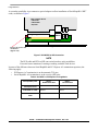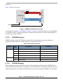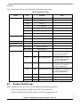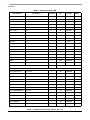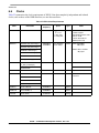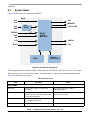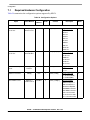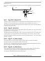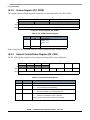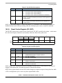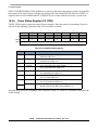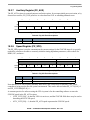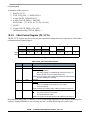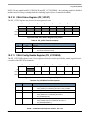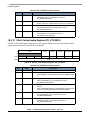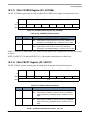
1
Freescale Semiconductor
Design Workbook
Document Number: HPCNUG
Rev. 1.04, 7/2007
HPCN — an MPC8641D Development
Platform
by
1
Gary Milliorn
DSD System Design and Architecture
Freescale Semiconductor, Inc.
Austin, TX
Overview
HPCN is a high-performance computing, evaluation and
development platform supporting the MPC8641D dual-core
processor built on Power Architecture technology, as well as
the MPC8641 single-core version.
HPCN’s official designation is “HPCN”, and may be ordered
using part numbers “PCEVALHPCN-8641D” (prototypes)
or “MCEVALHPCN-8641D”.
HPCN is optimized to support the high-bandwidth memory
ports for each processor core, as well as the two PCI-Express
ports, one dedicated for graphics or other slot-based card,
and the other dedicated for Linux I/O with the ULI
south-bridge.
HPCN is designed to the micro-ATX form-factor standard,
allowing it to be used in 1U or 2U rack-mount chassis’, as
well as in a standard ATX/Micro-ATX chassis.
© Freescale Semiconductor, Inc., 2007. All rights reserved.
Contents
1. Overview . . . . . . . . . . . . . . . . . . . . . . . . . . . . . . . . . . . 1
2. Features . . . . . . . . . . . . . . . . . . . . . . . . . . . . . . . . . . . . 2
3. Block Diagram . . . . . . . . . . . . . . . . . . . . . . . . . . . . . . 4
4. Evaluation Support . . . . . . . . . . . . . . . . . . . . . . . . . . . 5
5. Usage Scenarios . . . . . . . . . . . . . . . . . . . . . . . . . . . . . 6
6. Architecture . . . . . . . . . . . . . . . . . . . . . . . . . . . . . . . 11
7. Configuration . . . . . . . . . . . . . . . . . . . . . . . . . . . . . . 65
8. Debug Support . . . . . . . . . . . . . . . . . . . . . . . . . . . . . 70
9. PCB Development Issues . . . . . . . . . . . . . . . . . . . . . 70
10. Programming Model . . . . . . . . . . . . . . . . . . . . . . . . 103
App A.- References . . . . . . . . . . . . . . . . . . . . . . . . . . . . . 120
App B.- Lead-Free/RoHS Issues . . . . . . . . . . . . . . . . . . . 121
App C.- Frequently Asked Questions . . . . . . . . . . . . . . . 122
Features
2
Features
The features of the HPCN evaluation/development board are as follows:
• Processor
— MPC8641 (single-core) or MPC8641D (dual-core) at speeds of 1.0 GHz to 1.5 GHz
— 32 bit superscalar e600 core
— 1MiB + 32KiB internal ECC-protected cache
— Four integrated ethernet controllers
– Supports 10/100/1000-base T ports
— Dual DDR-2 Interfaces
– Up to 8.5GB/s performance with 533MHz DDR2
– Up to 16GiB per controller (32GiB total)
– Standard 240-pin unbuffered DDR-2 sockets
– 2T timing
— PCI Express
– PCI Express 1.0a compatible
– Supports x1, x4 and x8 link widths
– 2.5 Gbaud, 2.0 GHz data rate per lane
– Channel 1: 1X/4X to ULI south-bridge
– Channel 2: 1X/4X/8X connecting to a standard PCIExpress Slot
— Local Bus
– 8MiB Flash (8-bits wide)
– PromJet flash emulator support option
— I2C Ports
– Dual ports, one for boot initialization and the other for DDR SPD EEPROM, etc.
• South Bridge
— ULI 1575
— IDE Controller
– Parallel ATA
– Serial ATA 2 (RAID-1 Support)
— USB Interface
– UHCI/EHCI USB 2.0 Interface
– Two ports on stacked USB header
– Two ports on PCB header (mates with standard PC chassis connectors)
— PCI Bridge
– Two slots, 5V tolerant
HPCN — an MPC8641D Development Platform, Rev. 1.04
2
Freescale Semiconductor
Features
•
•
•
— Other
– LPC (socketed) boot flash
– Realtime Clock
– NVRAM: 256 bytes
System Logic
— Manages system reset sequencing
— Manages system bus and PCI clock speed selections
— Controls system and monitoring
— Implements registers for system control and monitoring
Clocks
— System clock
– Switch settable to one of eight common settings in the interval 100MHz-200MHz.
– Software settable in 1MHz increments from 100-200MHz.
Power Supplies
— Dedicated unified VCORE for MPC8641 V1.0
— VTT/VREF for DDR
— General I/O power
HPCN — an MPC8641D Development Platform, Rev. 1.04
Freescale Semiconductor
3
Block Diagram
3
Block Diagram
Figure 1 shows the overall architecture of the HPCN system:
PEx 8X Slot
VCore Power
PEx 4X
Pe 8X
Vt POWER
Vt POWER
SD2
DDR2 DIMM
DDR2 DIMM
DDR2 DIMM
DDR2 DIMM
ATX I/O
MPC8641D
SER
Flash
PromJet
CF
Actel
Pixis
RJ45
PEx 4X
Clocks
RJ45
Vitesse
Quad
PHY
SD1
RJ45
MP Tap
RJ45
AUD
PCI
PCI
ULI
M1575
2
USB
USB
PCI 2.3
Misc
TSECs
Panel I/O
PCIExp
LocalBus
SIO
Interrupt
LPC
DDR-II
SATA
Power
IDE
Audio
2
PS/2
Figure 1. HPCN Block Diagram
HPCN — an MPC8641D Development Platform, Rev. 1.04
4
Freescale Semiconductor
Evaluation Support
4
Evaluation Support
HPCN is intended to evaluate as many features of the MPC8641 as are reasonable within a limited amount
of board space and cost limitations..
Table 1. HPCN Evaluation Summary
MPC8641D
Feature
SerDes 1
SerDes 2
System
PCI Express
Direct
Connects to ULI southbridge via PEX/4X connection.
Testable by functional code.
Traffic monitoring via Tek/Agilent passive mid-point probing.
PCI Express
Lane-Reversed
Connects to PCIExpress4X slots positioned in-line with PCIExpress
Port1.
Allows off-board connection via custom PCB or cable.
PCI Express
Connects to PCIExpress 1X/4X/8X slot.
Testable via PCIExpress card (graphics) or CatalystTM PCIExpress
control/monitoring card.
SerialRIO
Connects to secondary SRIO 1X/4X device using custom cable that
attaches to PCIExpress slot.
NOTE: series capacitors are on transmit pins per PEX standard.
Memory Controller DDR-1
Ethernet
Local Bus
Evaluation Support/Methods
Not supported.
DDR-2
Independant VIO supplies (1.8V or 1.9V).
Independant VTT supplies.
Debugging uses Tek/NextWave analyzer breakout cards.
No special MECC/Debug tap.
VTT
Resistor dividers allow setting different VTT thresholds.
Each DIMM can use VTT VREF or disconnect and use resistor
dividers for custom threshold use/analysis.
All
Supports RMII or RGMII modes.
Uses VSC8244 QuadPHY
Port 1-2
Connects to RJ45 dual connectors for rear-panel access.
Port 2-3
Connects to RJ45 dual connectors.
Flash
2 banks of 32-bit, 16MB flash
Option for PromJet access.
Pixis
Internal registers implementing:
Board ID
VDD control
Frequency reset.
Self-reset reset
Compact Flash
Interface and connector.
GPCM/SDRAM
Not supported (no CPM, no compelling application).
HPCN — an MPC8641D Development Platform, Rev. 1.04
Freescale Semiconductor
5
Usage Scenarios
Table 1. HPCN Evaluation Summary
MPC8641D
Feature
I2C
System
Evaluation Support/Methods
Bus 1
Boot initialization code
Bus 2
DDR Bus 1 DIMM modules SPD EEPROMs
DDR Bus 2 DIMM modules SPD EEPROMs
Voltage Monitoring
System EEPROM
PEX/PCI Slots (as “SMBus”)
SYSCLK
Digitally settable clock generator.
Switch-selectable coarse settings.
Software-selectable fine settings.
REFCLK
SERDES reference clocks to SERDES’s on MPC8641, ULI and slots.
RTCCLK
Reference clock.
DMA
DMA(0:3)
REQ/ACK/DONEa
Test points.
IRQs
IRQ*(0:11)
EVENT switch asserts IRQ* but can drive SRESET0, and/or
SRESET1 via software setting.
Clocking
IRQ_OUT
SRESET*(0:1)
VCore Power
VDD
VID switch settable
Pixis software-monitored/controlled voltages
7-bit encoded voltage
5
Usage Scenarios
HPCN is expected to be used in many different test and evaluation scenarios. This section discusses
aspects of each potential use; i.e. “how would I use HPCN to do ___”?
5.1
Normal Use
For general hardware and/or software development and evaluation purposes, HPCN can be used just like
an ordinary desktop computer. In the absence of special hardware or software configuration, HPCN
operates identically to a development/evaluation system such as “Sandpoint” or a member the HPC family
HPCN — an MPC8641D Development Platform, Rev. 1.04
6
Freescale Semiconductor
Usage Scenarios
(HPC1, “Freeserve” and HPC2, “Taiga”). Figure 2 shows an example of HPCN system in a desktop
configuration:
Figure 2. HPCN Desktop Configuration
The PIXIS is used to provide startup configuration information for DINK, UBOOT or Linux and other
advanced features are used or may be ignored.
Note that the third and fourth Ethernet ports are only accessible when a custom ATX I/O panel is used; if
the third and fourth ports are not used, the connector can be depopulated and a standard ATX I/O panel
may be used.
5.2
Rackmount Server Use
For use in a rackmount chassis, HPCN requires the following modifications:
• low-profile heatsink
• non-socketed board
• right-angle flex PCI-Express cable (optional)
Otherwise, it is similar to the desktop case.
Figure 3 shows an example of HPCN system as a rackmount server; in particular, how the flex cable is
used to connect the PCI rear-chassis escape area to the PEX slot located at “slot 2”:
PCI I/O AREA
ATX I/O AREA
Normally, there is a slot here
and a vertical riser card installs
in it.
But this is the “first” slot, so a
flex cable is used.
Figure 3. HPCN Rackmount Configuration
HPCN — an MPC8641D Development Platform, Rev. 1.04
Freescale Semiconductor
7
Usage Scenarios
Figure 4 shows the PCI-Express cable used when HPCN is used in a rackmount 1U chassis.
Figure 4. PCI Express Flex Cable
Note that the heat sink changes between ATX and rackmount usage.
5.3
Embedded Use
For general embedded hardware and/or software development and evaluation purposes, HPCN can be used
just like an ordinary desktop computer. The core voltage and PLL settings might be adjusted to allow the
heatsink to be replaced or even removed. Perpiherals and embedded storage can be inserted in the CF slot.
As before, the PIXIS is used to provide startup configuration information for DINK, UBOOT or Linux and
other advanced features are used or ignored.
5.4
SERDES Evaluation
HPCN is designed as a PCIExpress-based platform; however, the MPC8641 SERDES’ support several
other options which may be evaluated, albeit some more easily than others.
5.4.1
Individual PCI Express Evaluation
The SERDES2 interface is wired to a PCIExpress 8X slot, while SERDES1 is connected to the ULI
M1575. Software can exercise these ports by generating traffic to respective devices (in the case of
SERDES2, generally a video card).
5.4.2
Dual PCI Express Evaluation
For applications desiring full access to both PCI Express ports, HPCN supports this using the
“lane-reversal” feature of PCIExpress to get access to 50% of the bandwidth of the SERDES 1 port. A
custom dual-port PCIExpress card must be developed to use this facility (that is, it is not inherently part
of HPCN’s feature set).
HPCN — an MPC8641D Development Platform, Rev. 1.04
8
Freescale Semiconductor
Usage Scenarios
Figure 6 shows how HPCN systems could be used to evaluate PCI Express.
Device to
Test
PEX x4
PEX x8
MPC8641
Figure 5. HPCN PCI Express Evaluation
5.4.3
Serial RIO Evaluation
The Serial RapidIO 1X/4X protocol is available on SERDES port 1, which is connected to a portion of
PCIExpress x16 slot. Although HPCN is constructed (and terminated -- see below) as a PCI Express
connection, reliable SRIO communication is possible over a high-quality connector and cable.
Figure 6 shows how HPCN systems could be used to evaluate Serial RapidIO.
8641
8641
Figure 6. HPCN Serial RapidIO Configuration 1 - Two HPCN boards
HPCN — an MPC8641D Development Platform, Rev. 1.04
Freescale Semiconductor
9
Usage Scenarios
A secondary possibility is to construct a special adapter to allow installation of Serial RapidIO “HIP”
cards, as shown in Figure 7.
HMZD
PWR
Right-Angle PCI Slot
PWR
HIP-compliant Board
“CDS 8540”
“CDS 8548E”
“Elysium”
PEX 16X SLOT
Argo Navis Motherboard
PCI slot for power and
mechanical
support only.
Figure 7. HPCN PEX-to-HIP Conversion
NOTE
The PEX cable and PEX-to-HIP conversion board are only possibilites;
Freescale has no intention of creating or making available such devices.
In terms of the difference between Serial RapidIO and PCI Express AC termination capacitors, the
following apply:
• PCIExpress: AC termination is on the transmit (TX) pins
• Serial RapidIO: AC termination is at the receiver (RX) pins.
Table 2. SerialRIO vs. PCIExpress vs. ArgoNavis
Interoperability with:
HPCN No RX Termination
HPCN TX Termination
PCI Express Card
Matches
Matches
CTSPQ38E via Cable
Matches
Matches
HPCN in PEX mode via
Cable
Matches
Matches
HPCN — an MPC8641D Development Platform, Rev. 1.04
10
Freescale Semiconductor
Architecture
Table 2. SerialRIO vs. PCIExpress vs. ArgoNavis
HPCN No RX Termination
Interoperability with:
HPCN in Serial RapidIO
mode via Cable
Serial RapidIO Card
6
HPCN TX Termination
OK, but AC term is at the
“wrong” side
OK, but AC term is at the
“wrong” side
AC termination would be
required on the adapter
card, and would effectively
be at the midpoint.
Depending on trace lengths
on HIP cards (which tend to
be small and short) this is
Double-terminated: May
work fine, or may require
replacing either boards AC
termination caps with
0-ohm resistors (depends
on eye quality).
Architecture
The HPCN architecture is primarily determined by the Freescale Semiconductor MPC8641 processor built
on Power Architecture technology, and by the need to provide typical OS-dependant resources (disk,
ethernet, etc.).
6.1
Processor
HPCN supports these Freescale Semiconductor processors:
• MPC8641 single-core processor, all speeds
• MPC8641D dual-core processor, all speeds
Table 3 lists the major pin groupings of the MPC8641D.
Table 3. MPC8641 Summary
Signal Group
Pin Count
Details
DDR-II Memory 1
147
Section 6.1.1
DDR-II Memory 2
147
Section 6.1.1
MII Interface/Clock
3
Section 6.1.2
Gbit MAC 1
25
Section 6.1.2
Gbit MAC 2
25
Section 6.1.2
Gbit MAC 3
25
Section 6.1.2
Gbit MAC 4
25
Section 6.1.2
SERDES 1
48
Section 6.1.3.2
SERDES 2
48
Section 6.1.3.1
SERDES Extra
2
Section 6.1.3.3
Local Bus
67
Section 6.1.4
DMA
6
Section 6.1.11
MPIC
18
Section 6.1.7
HPCN — an MPC8641D Development Platform, Rev. 1.04
Freescale Semiconductor
11
Architecture
Table 3. MPC8641 Summary
Signal Group
Pin Count
Details
System Control
8
Section 6.1.11
DUART
8
Section 6.1.5
I2C
4
Section 6.1.8
TOTAL
Debug
15
Section 6.1.11
Power Mgmt
1
Section 6.1.11
Clock
2
Section 6.1.11
Test
4
Section 6.1.11
JTAG/COP
5
Section 6.1.11
Thermal
2
Section 6.1.11
637
With the exceptions of a few signals such as SMI and COP signal for the second core, the differences
between the MPC8641 single-core and the MPC8641D dual-core processors are not visible at the pin level.
Consequently, throughout this document the term “MPC8641” refers to either the MPC8641 or the
MPC8641D, unless otherwise specifically noted.
6.1.1
DDR
The MPC8641 controls two independant DDR-II interfaces, either of which may support one or two
DDR-II DIMM modules, supporting up to 8 GiB of PC3200 DDR-II SDRAM. Each memory interface
includes all the necessary termination and termination power and is routed so as to achieve maximum
performance on the memory bus.
The DDR components are placed and routed so as to achieve 2T timing with unbuffered DIMMs at
533MHz or faster. 1T timing may be possible if the second slot is unoccupied.
HPCN — an MPC8641D Development Platform, Rev. 1.04
12
Freescale Semiconductor
Architecture
The general DDR SDRAM architecture is shown in Figure 8.
DIMM #1
MDQS[8:0]/MDQS[8:0]
MDM[8:0]
MDQ[63:0]
MECC[7:0]
MCK[0:2]
MCK[0:2]
MCK[3:5]
MCK[3:5]
MVREF
A[14:0]
BA[1:0]
S[1:0]
A[14:0]
BA[1:0]
DQS/DQS
DM[8:0]
DQ[63:0]
DQS/DQS
DM[8:0]
DQ[63:0]
CB[7:0]
CB[7:0]
CK[0:1]
CK[0:1]#
CK[0:1]
CK[0:1]#
MEM_RST
I2C_SDA
I2C_SCK
RAS
CAS
WE
CKE[1:0]
RAS
CAS
WE
CKE[1:0]
S[1:0]
comp cap
MRAS
MCAS
MWE
MCKE[1:0]
MCS[1:0]
MCS[2:3]
MA[14:0]
MBA[1:0]
DIMM #2
VTT Termination
MPC8641
RESET#
RESET#
SDA
SCL
SDA
SCL
VREF
VREF
VTT
MVREF
VDDIO
SIO
TPS51116
Sx
(power down modes)
Figure 8. HPCN Memory Architecture
The connections are all standard. Note that this connection is only for DDR2; DDR-1 has a different
termination scheme so designs need to select one interface or the other.
Note also that HPCN does not directly support the use of the MECC pins to access internal debug
information. Historical experience with the “Elysium” and “CDS” platforms revealed that the special
ECC-to-Mictor tap was rarely, if ever, used. HPCN does not provide the special multiplexer and thus has
a simpler routing and signal integrity status. On the other hand, HPCN does not interfere with this path, so
access to debug information on the MECC pins is possible with the use of a NextWave (or equivalent)
DDR logic analyzer connector and the use of non-ECC DDR modules.
Differential clocks for the two memory modules are supplied by the MPC8641; these signals are not
parallel terminated, unlike the single-ended memory signals.
HPCN — an MPC8641D Development Platform, Rev. 1.04
Freescale Semiconductor
13
Architecture
The TPS5116 supplies the following interface voltages:
• VDD_IO
up to 10A at 1.8V (default)
• VDDQ
up to 3A
• MVREF
up to 10mA
The VDD_IO level defaults to 1.8V, but may be changed with feedback resistors to provide any voltage
between 1.5 and 2.0V.
DDR-II memory port signals and connections are summarized in Table 4.
Table 4. DDR-II Memory Connections
Pin
Count
Signal Names
Compensation
Termination
Connections
64
MDQ[0:63]
-
-
MPC8641, DIMM 1, DIMM 2
8
MECC[0:7]
-
-
MPC8641, DIMM 1, DIMM 2
9
MDM[0:8]
-
-
MPC8641, DIMM 1, DIMM 2
18
MDQS[0:8](p,n)
-
-
MPC8641, DIMM 1, DIMM 2
3
MBA[0:2]
22pF
47 Ω
MPC8641, DIMM 1, DIMM 2, VTT
16
MA[0:15]
22pF
47 Ω
MPC8641, DIMM 1, DIMM 2, VTT
1
MWE*
22pF
47 Ω
MPC8641, DIMM 1, DIMM 2, VTT
1
MRAS*
22pF
47 Ω
MPC8641, DIMM 1, DIMM 2, VTT
1
MCAS*
22pF
47 Ω
MPC8641, DIMM 1, DIMM 2, VTT
2
MCS*[0:1]
22pF
47 Ω
MPC8641, DIMM 1, VTT
2
MCS*[2:3]
22pF
47 Ω
MPC8641, DIMM 2, VTT
4
MCKE[0:3]
22pF
47 Ω
MPC8641, DIMM 1, DIMM 2, VTT
6
MCK_0[0:2](p,n)
-
-
MPC8641, DIMM 1
6
MCK_0[3:5](p,n)
-
-
MPC8641, DIMM 2
4
MODT[0:3]
-
47 Ω
MPC8641, DIMM 1, DIMM 2, VTT
HPCN — an MPC8641D Development Platform, Rev. 1.04
14
Freescale Semiconductor
Architecture
6.1.1.1
Compatible DDR-2 Modules
The DDR interface of HPCN and the MPC8641 should work with any JEDEC-compliant 240-pin DDR-2
DIMM module, provided that the devices are 64Mib to 4Gib in size, and that the devices are x8, x16 or
x32 bits in width. Table 5 shows several DIMM modules which are believed compatible; those which have
been tested and confirmed are noted as such.
Table 5. Typical DDR-2 Modules
Mfg.
Part Number
Micron
MT16HTF6464AY-40EB2
Size
Speed
512 MiB
DDR2-533
Data Rate
Notes
Verified?
Pending
MT16HTF6464AY-53EB2
Pending
More to come...
6.1.2
Ethernet
The MPC8641 supports four 10/100/1000baseT Ethernet ports. On HPCN, a quad-port PHY is used to
provide access to all these devices. Since the ATX chassis generally does not provide easy access to four
RJ45 ports in the ATX “IO gasket” area on the back, the ports are at the locations shown in Table 6.
Table 6. Ethernet Port Locations
Port
PHY
Address
1
0
Bottom of “normal” RJ45 stack
Quasi-standard rack-mount server location.
2
1
Bottom of “extra” RJ45 stack
Non-standard
3
2
Top of “normal” RJ45 stack
Quasi-standard rack-mount server location.
4
3
Top of “extra” RJ45 stack
Non-standard
Location
Description
Note that the ports are interleaved; the MPC8641 has two high-speed internal pathways to the internal
MPX bus. Ethernet ports 1&2 share one path, while 3&4 share the other. Thus, for most applications
needing only two or fewer ethernet ports, the maximum bandwidth can be allocated to both ports.
HPCN uses the Vitesse VSC8244 quad-PHY, which provides a direct connection to the 4 GMACs and the
MI interface. The remaining connections are essentially clocks and resets. Signals are summarized in
Table 7.
Table 7. Ethernet Port Connections
Category
Pin
Count
Ethernet MI
2
EC_MDC, EC_MDI
MPC8641, VSC8244
GbE Clocking
1
EC_GTX_CLK125
MPC8641, PIXIS
Signal Names
Connections
HPCN — an MPC8641D Development Platform, Rev. 1.04
Freescale Semiconductor
15
Architecture
Table 7. Ethernet Port Connections
Category
Pin
Count
ETSECx
12
TSECx_TXD(3:0), TSECx_TX_EN,
TSECx_TX_CLK, TSECx_RXD(3:0),
TSECx_RX_DV, TSECx_RX_CLK
MPC8641, VSC8244
13
TSECx_TXD(7:4), TSECx_TX_ER,
TSECx_GTX_CLK, TSECx_CRS, TSECx_COL,
TSECx_RXD(7:4), TSECx_RX_ER
n/c (unless config pin)
Signal Names
Connections
The PHY addresses are 0 to 3, for GMAC/Ethernet ports 0 to 3, respectively.
GMAC #1
0
GMAC #2
1
GMAC #3
2
GMAC #4
3
VSC8244
MPC8641D
MI
125MHz
Figure 9. Ethernet Architecture
Refer to the Vitesse website for programming information for the PHY.
6.1.3
SERDES Ports
The MPC8641 contains two high-speed SERDES ports. HPCN uses these ports strictly for PCIExpress
connections; evaluation of other high-speed SERDES protocols is possible but limited by the following
restrictions:
•
•
•
transmit signals are AC coupled at the transmitter pins
SERDES 1 is fixedly connected to the ULI as a PEX 4X connection; the other 4X connections are
available on a PEX 4X slot colinear with the SERDES PEX 8X slot.
Evaluation of any other SERDES 1 protocol is only supported on the PEX(4:7)(p,n) signals.
All signals are connected using PCIExpress routing topology and spacing rules (see Section 9.6.34), and
includes a AC coupling capacitor at the transmit pins.
HPCN — an MPC8641D Development Platform, Rev. 1.04
16
Freescale Semiconductor
Architecture
6.1.3.1
SERDES 1
The SERDES 1 port is configured for PCIExpress mode. The low-order 4 lanes [PEX1_TX(0:3)(p,n) and
PEX1_RX(0:3)(p,n)] are connected to the ULI 1575 south bridge device, which provides many resources
for running Linux and providing remote test access. Since this is not a slot-based connection, a mid-point
probe is provided for connecting a logic/protocol analyzer.
In order to support evaluation of non-ULI based traffic and/or other protocols, HPCN uses the PCIExpress
“lane reversal” feature of the SERDES to re-route traffic to the unused half of the SERDES 1
[PEX1_TX(4:7)(p,n) and PEX1_RX(4:7)(p,n)]. In this mode, the ULI is ignored and PCIExpress traffic is
re-routed to a PCIExpress connector.
It is important to note that none of the signals are switched or rerouted in any way; this preserves the
highest signal quality for best performance. Only the lanes used for PCIExpress traffic are re-directed.
Mid-point tap
Figure 10 shows an overview.
TX >
MPC8641
Lane Revers
option
PEX1 TX(0:3)(p,n)
ULI
PEX1 RX(0:3)(p,n)
RX <
PEX1 TX(4:7)(p,n)
R
T
PEX1 RX(4:7)(p,n)
PEX/4X Slot
Figure 10. SERDES 1/PCIExpress 4X Overview
6.1.3.2
SERDES 2
The SERDES 2 port is typically configured as a PCIExpress port, and is connected to a PCI Express 16X
slot on the HPCN motherboard. The SERDES port only supports up to 8X protocol width; however, a 16X
connector is used to allow standard PEX video cards to be used (possibly at a reduced width).
It is expected that the primary test mechanism of the SERDES 2 port will be as a PEX/8X connection using
standard graphics cards (ATI, NVidia) or PCIExpress test boards (Catalyst).
HPCN — an MPC8641D Development Platform, Rev. 1.04
Freescale Semiconductor
17
Architecture
Figure 11 shows an overview.
PEX2_TX(0:7)(p,n)
TX >
MPC8641
RX <
PEX2_RX(0:7)(p,n)
PEX 16X SLOT
AC Term
CLK
Figure 11. SERDES 2/PCIExpress 8X Overview
As mentioned in Section 5.4, “SERDES Evaluation,” on page 8, the differential pairs are AC-terminated
in accordance with PCI Express requirements. Evaluation of other protocols, such as Serial RapidIO, is
possible as previously described.
6.1.3.3
SERDES Summary
SERDES signals not used for PCIExpress connections are connected to test points or pullups (as
appropriate) and are otherwise unused. Signals are summarized in Table 8.
Table 8. SerDes Port Connections
Category
Pin
Count
SERDES1
8
SD1_RX[0:3](p,n)
MPC8641, ULI M1575
8
SD1_RX[4:7](p,n)
MPC8641, PEX-4X slot (reversed)
8
SD1_TX[0:3](p,n)
MPC8641, ULI M1575
8
SD1_TX[4:7](p,n)
MPC8641, PEX-4X slot (reversed)
16
SD2_RX[0:7](p,n)
MPC8641, PEX-16X slot (lane reversed)
16
SD2_TX[0:7](p,n)
MPC8641, PEX-16X slot (lane reversed)
SERDES2
6.1.3.4
Signal Names
Connections
SERDES Bridging
HPCN supports an optional, and entirely custom, mode whereby the unused portion of SERDES #1 is
routed to a PCIExpress x4 connector. Using lane reversal, PCIEx traffic can be placed on this slot. The slot
is physically placed so as to align with the PCIExpress x8 connector attached to SERDES #2. This allows
HPCN — an MPC8641D Development Platform, Rev. 1.04
18
Freescale Semiconductor
Architecture
the development of custom/customer-specific boards that evaluation SERDES throughput through the
MPC8641. Figure 12 shows an overview.
T
R
T
MPC8641
R
Bridge Card
PEX/8X Slot
ULI
T
R
PEX/4X Slot
Figure 12. SERDES Bridging Overview
NOTE: Again, there is no board developed, or anticipated being developed, by Freescale Semiconductor
that uses this mode.
6.1.4
Local Bus
The local bus of the MPC8641 is used to provide access to boot code stored in flash devices and access to
general purpose peripherals. For HPCN the primary purpose of the local bus is access to bootable flash
images (or storage for Linux flash filesystems) and to system configuration/control (via the PIXIS).
In terms of architectural design, the local bus of the MPC8641 is very similar to that of the PQ3 family –
it requires a latch and a buffer/multiplexer to recreate independant address and data buses. A popular
device for doing this is the TI SN74ALVCH32973KR latch/multiplexer/buffer.
Note that this device has bus hold on the inputs -- use caution and avoid allowing passive connections to
be interfered with -- particularly those used for reset configuration sampling.
HPCN — an MPC8641D Development Platform, Rev. 1.04
Freescale Semiconductor
19
Architecture
Figure 13 shows an overview.
Virtual
Bank
LAD
LALE
LBCTL
LA
Latch/Buf
MPC8641
LSYNC
LD
Flash1
PromJet
CF+
LBGPL
LBCS
LBOE
LBWE
LBCLK
LBREADY
PIXIS
Figure 13. Local Bus Overview
The “Virtual Bank” block in Figure 13 above is simply an “XOR” gate on the upper address of the flash.
If the switch is open, the flash behaves normally. If the switch is closed, the MSB of the flash address is
HPCN — an MPC8641D Development Platform, Rev. 1.04
20
Freescale Semiconductor
Architecture
toggled; this has the effect of swapping the upper and lower halves of the flash. User’s may store two
different boot images and select which one to use. Figure 14 shows an overview.
FLASH
FFFFF
XOR
MSB not inverted
80000
7FFFF
A(n:0)
0
FLASH
7FFFF
XOR
0
FFFFF
A(n:0)
MSB inverted
80000
Figure 14. Flash Virtual Bank Overview
Note that the addresses issued by the processor do not change; they are just routed to different parts of the
flash. Note also that the addresses used to program the flash using the standard CFI-sequences are well
below 0xFFFF and so this does not affect programming algorithms.
Local Bus connections are summarized in Table 9.
Table 9. Local Bus Device Summary
Device
LB Chip
Select
Width
Flash 1
LCS0
16
64Mib flash
Configured and enabled by default when local flash
boot selected (see Section 7).
PromJet
Header
LCS0
or
LCS1
16
Emutec PJ-8M-85
(8Mib) or PJ-16M-85
(16MiB) with option
BWS
PIXIS can re-route LCS0 or LCS1 to the PROMJET
under switch control.
Compact
Flash
LCS2
16
CF Flash Socket
Attached Devices
Notes
HPCN — an MPC8641D Development Platform, Rev. 1.04
Freescale Semiconductor
21
Architecture
Table 9. Local Bus Device Summary
Device
LB Chip
Select
Width
PIXIS
LCS3
8
none
LCS(4:7)
n/a
Attached Devices
Notes
PIXIS registers
unused
Local bus signals are summarized in Table 10.
Table 10. Local Bus Connections
Category
Local Bus
(67 total)
Pin
Count
Signal Names
Connections
32
LAD[0:31]
MPC8641, SN74ALVC32973, Mictors
4
LDP[0:3]
Mictors
5
LA[27:31]
Mictors
8
LCS[0:7]
MPC8641, PIXIS, Mictors
4
LWE[0:3]/LSDDQM[0:3]/LBS[0:3]
MPC8641, PIXIS, Flash, Mictors
1
LBCTL
MPC8641, Mictors
1
LALE
MPC8641, Mictors
1
LGPL0/LSDA10
Mictors
1
LGPL1/LSDWE
MPC8641, PIXIS, CF, Mictors
1
LGPL2/LOE/LSDRAS
MPC8641, PIXIS, Flash, CF, Mictors
1
LGPL3/LSDCAS
Mictors
1
LGPL4/LGTA/LUPWAIT/LPBSE
MPC8641, PIXIS, CF, Mictors
1
LGPL5
Mictors
1
LCKE
Mictors
3
LCLK[0:2]
MPC8641, PIXIS, Mictors
1
LSYNC_IN
MPC8641
1
LSYNC_OUT
MPC8641
Mictor logic analyzer headers are provided for local bus (boot code) debugging.
6.1.5
Serial Ports
HPCN connects both serial ports to serial level transceivers. Port 1 is connected to a DB9 female
connectors in the ATX I/O gasket area, and RTS/CTS flow control is supported on this connector.
The UART programming model is a standard PC16550-compatible register set. Baud rate calculations for
the divisor latch registers (DLL and DML) is typically done by by reading the PIXIS SYSCLK register to
HPCN — an MPC8641D Development Platform, Rev. 1.04
22
Freescale Semiconductor
Architecture
determine the MPC8641 reference clock input (nominally 166.66MHz) frequency. The baud rate divisors
can then be calculated using the formula described in the User’s Manual.
Serial port signals are summarized in Table 11.
Table 11. Serial Port Connections
Category
Pin
Count
Serial 1
4
UART_SOUT1, UART1_SIN1, UART_RTS1,
UART_CTS1
MPC8641, LT1331 RS232 transceiver.
Serial 2
4
UART_SOUT2, UART_SIN2
MPC8641, LT1331 RS232 transceiver.
UART_RTS2, UART_CTS2
unused
Signal Names
Connections
Note that Serial Port 2 is normally inaccessible, as there is no 9-pin serial port connector attached. Instead,
the RX and TX signals, along with a ground, are connected to a three-pin BERG header. If the extra serial
port is needed, a custom cable may be easily created to get access to the Port 2 data, albeit without
RTS/CTS flow control. Freescale Semiconductor does not make or supply this cable.
Figure 15 shows construction details for this cable.
J1
5
3 2 1
9-pin DB male” plug
rear view
DE9M (sometimes
called “DB9M”)
TXD
pin 1
pin 2
GND
pin 3
RXD
“Berg” receptacle
(0.1” spacing)
Figure 15. Serial Port 2 Cable Details
HPCN — an MPC8641D Development Platform, Rev. 1.04
Freescale Semiconductor
23
Architecture
6.1.6
Power
The power requirements of the MPC8641 are estimated at this time; based on the MPC8540 and
MPC7447A precedents, estimated power requirements are summarized in Table 12.
Table 12. MPC8641 Power Requirements
Voltage
Range
Tol.
VDD_CORE0
VDD_CORE1
0.9V
1.0V
1.1V
± 50 mV
± 50 mV
± 50 mV
PLL Filter
AVDD_CORE0
AVDD_CORE1
0.9V
1.0V
1.1V
± 50 mV
± 50 mV
± 50 mV
Platform
(internal buses)
VDD_PLAT
AVDD_PLAT
1.0V
1.1V
1.2V
± 50 mV
± 50 mV
± 50 mV
SERDES
SVDD
XVDD
1.0V
1.1V
1.2V
± 50 mV
± 50 mV
± 50 mV
DDR2 Bus
D1_GVDD
D2_GVDD
1.8V
2.5V
± 90 mV
± 125 mV
500 mW * 2
Ethernet
LVDD
TVDD
2.5V
3.3V
± 125 mV
± 165 mV
50mW * 4
50mW * 4
Local Bus
OVDD
2.5V
3.3V
2.0 W
Other
HVDD
2.5V
100 mW
Power Source
Symbol
Core Power
@1.8GHz
IMAX
PMAX
Supplied By
TBD
17.0W-25.0W * 2
33.1W * 2
7.0 W
0.77 W * 2
Some sources say ±5%,
which is actually
[email protected]
Note that this is the power for the MPC8641 only, it does not include external devices, memory, etc.
Since these are estimates, and because alpha silicon tends to be ‘hot’ the VDD rail needs to have excess
capacity of approximately 20%.
Because of the high current transients present on the VDD_COREx power pins, careful attention should
be paid to properly bypass these power pins, and to provide a good connection between the BGA pads and
the power and ground planes. In particular, the SMD capacitors should have pads directly attached to the
via ring (or within it, if the PCB costs are not prohibitive).
HPCN — an MPC8641D Development Platform, Rev. 1.04
24
Freescale Semiconductor
Architecture
Figure 16 shows the dispersion of VDD_CORE0 and VDD_CORE1 (merged). Note that this is an view
from the bottom of the board, of the center of the 32x32 BGA array.
L
M
N
P
R
T
U
11
12
13
14
15
16
VDD_COREx
GROUND
Figure 16. MPC8641 VDD_COREx and Ground Pattern
HPCN — an MPC8641D Development Platform, Rev. 1.04
Freescale Semiconductor
25
Architecture
Building on Figure 16, Figure 17 shows the vias attached of VDD_CORE(0:1) and GROUND expanding
radially outward from the center of the die.
VDD_COREx PAD
Trace to VIA
GROUND PAD
Trace to VIA
Figure 17. MPC8641 VDD_COREx and Ground VIA escape
Once the power and grounds have been escaped, the 0402SMD caps can be placed such that the capacitor
pads attach directly to the power vias on the side. Figure 18 shows the attachment of 0402 caps.
HPCN — an MPC8641D Development Platform, Rev. 1.04
26
Freescale Semiconductor
Architecture
Again: this is a view through the bottom of the board; in a CAD tool the view would be rotated around the
X and Y axes. The caps and vias are visible on the bottom, but the BGA pads are not. Thus, generally, the
capacitors are centered over the BGA pads.
C
C
C
C
C
C
C
C
C
C
C
C
C
C
C
C
C
C
C
C
C
C
C
C
C
C
C
C
C
C
C
C
C
C
C
C
C
C
C
C
C
C
C
C
C
C
C
C
C
C
Figure 18. MPC8641 VDD_COREx and Ground SMD 0402 Capacitor Placement
This pattern provides an adjacent bypass capacitors for all except one VDD_VCORE pad, and three
grounds. It requires 50 capacitors.
HPCN — an MPC8641D Development Platform, Rev. 1.04
Freescale Semiconductor
27
Architecture
In addition to bypass placement, the wholesale delivery of power to the VDD pins must be considered in
the presence of the vias used for the BGA attachment. Simulation results show that with 1 oz copper power
planes in the presence of the documented BGA escape pattern, 6 A per quadrant may be used.
6A
6A
6A
per quadrant
NOTE: The arrowed lines are not traces,
they are current flows on the underlying plane.
6A
Figure 19. MPC8641 VDD_COREx Planar Current Delivery by Quadrant
With current requirements at 40-50A, the power delivery system between the VDD supply and the
MPC8641 will need at three power planes or an equivalent amount of area fills on signal planes.
6.1.6.1
Core Power
HPCN uses the SemTech SC458 two-phase switching power controller. This device can produce at least
55A over the range of interest for the MPC8641: 0.9V to 1.3V (with additional margin above and below).
The voltage encoding, called VID(6:0), is seven bits and encodes 12.5 mV steps.
Table 13. SC458 VID(6:0) Encoding
VID(6:0)
VCORE Voltage
VID(6:0)
VCORE Voltage
0000000
1.5000
0011011
1.1625
0000001
1.4875
0011100
1.1500
0000010
1.4750
0011101
1.1375
0000011
1.4625
0011110
1.1250
0000100
1.4500
0011111
1.1125
0000101
1.4375
0100000
1.1100
HPCN — an MPC8641D Development Platform, Rev. 1.04
28
Freescale Semiconductor
Architecture
Table 13. SC458 VID(6:0) Encoding
6.1.7
0000110
1.4250
0100001
1.0875
0000111
1.4125
0100010
1.0750
0001000
1.4000
0100011
1.0625
0001001
1.3875
0100100
1.0500
0001010
1.3750
0100101
1.0375
0001011
1.3625
0100110
1.0250
0001100
1.3500
0100111
1.0125
0001101
1.3375
0101000
1.0000
0001110
1.3250
0101001
0.9875
0001111
1.3125
0101010
0.9750
0010000
1.3000
0101011
0.9625
0010001
1.2875
0101100
0.9500
0010010
1.2750
0101101
0.9375
0010011
1.2625
0101110
0.9250
0010100
1.2500
0101111
0.9125
0010101
1.2375
0110000
0.9000
0010110
1.2250
0110001
0.8875
0010111
1.2125
0110010
0.8750
0011000
1.2000
0110011
0.8625
0011001
1.1875
0110100
0.8500
0011010
1.1750
0110101
0.8375
Interrupts
HPCN contains numerous interrupt connections. From the standpoint of the MPC8641 the various
interrupting devices attached are as shown in Table 14.
Table 14. Interrupt Connections
Category
Pin
Count
MCP
2
SMI
2
Signal Names
Connections
MCP0*
pullup (unused)
MCP1*
pullup (unused)
SMI0*
M1575 nSMI
SIO SMI (SMB_ALERT#)
PIXIS SMI*
SMI1*
pullup (unused)
HPCN — an MPC8641D Development Platform, Rev. 1.04
Freescale Semiconductor
29
Architecture
Table 14. Interrupt Connections
Category
Pin
Count
IRQ
12
Signal Names
IRQ0*
Connections
Reserved; used to internally to map legacy
INT(A:D)# interrupts for PCIExpress interrupt
(four per port).
IRQ1*
IRQ2*
(NOTE: Interrupts can be shared, so it is certainly
possible to add interrupt sources to these pins.
With MSI interrupts fewer external interrupts are
needed, that’s all.)
IRQ3*
IRQ4*
IRQ5*
IRQ6*
IRQ7*
1
IRQ8*
PIXIS PIX_INT*
IRQ9*
M1575 INTR
IRQ10*
VSC8244 PHY INT*
IRQ11*
unused
IRQ_OUT*
All interrupts sources are level-sensitive, active-low with the exception of the M1575 INTR pin, which is
an 8259-compatible PIC controller output and as such is edge-triggered and active-high.
6.1.8
I2C
The MPC8641 has two separate I2C/SMB buses. Bus 1 is dedicated to a single I2C-based EEPROM which
contains boot initialization code. Bus 2 is dedicated to the SDRAM I2C-based SPD/EEPROMs (for proper
memory initialization), the slots and SIO (as the SMBus protocol). The I2C/SMB bus signals are
summarized in Table 15.
Table 15. I2C Bus Connections
Category
Pin
Count
I2C1
2
I2C1_SDA, I2C1_SCL
MPC8641, Boot EEPROM
I2C2
2
I2C2_SDA, I2C2_SCL
MPC8641, DDR1 Socket 1, DDR1 Socket 2, ,
DDR2 Socket 1, DDR2 Socket 2, PCI Express
Slots (as SMBus).
Signal Names
Connections
HPCN — an MPC8641D Development Platform, Rev. 1.04
30
Freescale Semiconductor
Architecture
I2C/SMB bus device addresses are summarized in Table 16.
Table 16. I2C Bus Device Map
Bus
I2C/SMB Address
Device
1
0x50 or 0x51
2
0x51
DDR1 Socket 1
2
0x52
DDR1 Socket 2
2
0x53
DDR2 Socket 1
2
0x54
DDR2 Socket 2
2
0x56
DINK ENV storage/general purpose
2
0x57
SYSTEM ID EEPROM (write protected)
2
0x5A
SIO LPC
2
0x6E
I2C9FG108 (SERDES clock generator)
2
(programmable)
4KiB EEPROM (reset initialization)
ULI M1753 SMB interface
Note: These are “DINK”-style addresses, which ignore the LSB of the transmitted address (the read/write bit).
The I2C bus 1 is also attached to a bi-directional buffer and connector, to allow attachment of remote
I2C-capable host processor boards such as the Elysium, Unity and CDS boards, using an appropriate cable.
A configuration switch selects address 0x50 or 0x51, to allow co-existing with any I2C-based devices
residing on the programmer system (typically a CDS or MPC8245-based DINK system).
6.1.9
Temperature
The MPC8641 V2.0 has two pins connected to a thermal body diode on the die, allowing direct
temperature measurement. These pins are connected to the LPC47M192 SIO logic, which contains
standard PC-compatible hardware monitoring logic, including a thermal measurement port. This device
allows direct reading of the temperature of the die and is accurate to ±TBD °C.
Thermal management signals are summarized in Table 17.
Table 17. Thermal Management Connections
Category
Pin
Count
Thermal
2
6.1.10
Signal Names
TEMP_ANODE, TEMP_CATHODE
Connections
MPC8641, LPC47M192
Mechanical Clearance
The MPC8641 LGA package size is 33mm^2, and there are 1023 pins in the package (a 32x32 array). In
addition to providing a socketable board, addition considerations are required to accomodate the heatsink
both for socketed systems and non-socketed systems.
HPCN — an MPC8641D Development Platform, Rev. 1.04
Freescale Semiconductor
31
Architecture
The expected thermal dissipation requirements are 70W max, 40W typical.
To use a socket requires 6 custom mounting holes surrounding the processor (see Section 9) and for a
package as large as the MPC8641 also requires a custom contact (“backing”) plate on the reverse of the
board. Since the central section of the processor is where high-frequency bypass capacitors are placed, a
custom channel is required on this backing plate.
The socket footprint is shown in Figure 20.
Figure 20. BGA Socket Dimensions
In total there are eight hole: 6 mounting holes and two guide pins.
HPCN — an MPC8641D Development Platform, Rev. 1.04
32
Freescale Semiconductor
Architecture
In addition, the BGA socket has a rectangular clasp which extends beyond the top of the socket over the
surrounding PCB. The clasp can be installed horizontally or vertically, so the clearance under the clasp can
be limited to only one axis, if necessary. The socket clearance is shown in Figure 21.
SOCKET
CPU
SOCKET
LATCH
CPU
LATCH
2.7 [68.58]
CPU
0.39 [10.00]
Figure 21. BGA Socket Overhang Clearance
HPCN — an MPC8641D Development Platform, Rev. 1.04
Freescale Semiconductor
33
Architecture
To minimize impact to the PCB routing area, the socket and the heatsink share mounting holes. The
combined socket/heatsink clearance requirements are shown in Figure 22.
Figure 22. BGA Socket+HeatSinkg Clearance
HPCN — an MPC8641D Development Platform, Rev. 1.04
34
Freescale Semiconductor
Architecture
The bottom of the PCB should have the clearances shown in Figure 23 to allow for the installation of a
backing support plate.
8mm
8.5mm
8mm
8.5mm
7.63mm
305 mm
7.63mm
2mm
8.5mm
C
C
C
C
C
C
C
C
C
C
C
C
C
C
C
C
C
C
C
C
C
C
C
C
C
C
C
C
C
C
C
C
C
C
C
2mm
8mm
C
C
8mm
C
C
C
C
C
C
C
C
C
C
C
C
C
8.5mm
Placement area for OVDD, XVDD, SVDD, GVDD (non VDD) capacitors
Figure 23. MPC8641 PCB Bottom Clearance for Socket Plate
In descriptive terms, the central 16 mm2 area centered under the processor has the VDD capacitor
placement, and the backing plate needs to be milled out in this area. At 2mm strip down the X and Y axes
allow relatively close placement of the other bypass capacitors.
NOTE: For PCB layouts not using a socket with a backing plate, the non-VDD bypass capacitors should
be moved directly to the corresponding power pin.
HPCN — an MPC8641D Development Platform, Rev. 1.04
Freescale Semiconductor
35
Architecture
6.1.11
Other
The remaining MPC8641 signals are summarized in Table 18.
Table 18. Miscellaneous MPC8641 Connections
Category
Pin
Count
Clock
3
Signal Names
Connections
SYSCLK
ICS525 clock synthesizer
RTC
ICS525 clock base frequency
CLK_OUT
Test point w/adjacent ground.
DMA
6
DMA_DREQ[0:1]
DMA_DACK[0:1]
DMA_DDONE[0:1]
Test points.
STATUS
2
ASLEEP
To PIXIS for monitoring.
Buffered LED monitor
READY
TRIG_OUT
To PIXIS for monitoring.
To test point.
HRESET
From PIXIS reset controller (thence from
COP, PowerGood, Port92, etc.)
HRESET_REQ
To PIXIS
SRESET_0
To PIXIS
SRESET_1
To PIXIS
CKSTP_IN*
COP Header
CKSTP_OUT*
COP Header
TRIG_IN
To PIXIS
MSRCID[0:1][0:4]
Debug P6880 Header
MDVAL0, MDVAL1
Debug P6880 Header
TEST_MODE(0:3)
Pullups
TEST_SEL
Pullups
TCK
COP Header
TDI
COP Header
TDO
COP Header
TMS
COP Header
TRST
PIXIS
System
Control
Debug
Test
JTAG
4
15
4
5
Note that the DMA[2:3] pins are not supported as DMA, they are used in the alternate function
configuration (LCS[4:7] and IRQ[8:11]).
HPCN — an MPC8641D Development Platform, Rev. 1.04
36
Freescale Semiconductor
Architecture
6.2
South Bridge
HPCN uses the ULI M1575 ”Super South Bridge” to provide access to standard Linux I/O devices,
including:
• USB 2.0
• SATA 2 (“serial IDE”)
• PATA (“classic IDE”)
• PCI slots (non-PCIExpress graphics, customer-specific
• LPC boot flash (optional)
• Real-time clock/BBRAM
Figure 24 shows an overview of the ULI M1575.
PMU
PEX
Link
LPC
SATA2
SWITCH
HD
Audio
PATA
PCI
Bridge
PCI
Bus
AC97
Audio
USB
ENET
1 EHCI
3 OHCI
10/100bT
Figure 24. ULI M1575 Overview
There are several other features of the M1575, such as a 10/100baseT ethernet MAC, that are not
supported. By and large, the ULI M1575 supplies all the IO channels needed for full Linux, QNX or other
OS desktop support.
The M1575 is in a 628-Ball (31mmx31mm) BGA package, and requires several clock and power sources
as detailed in Section 6.5, “System Power"” and Section 6.6, “Clocks"”. It is pin-compatible with the ULI
M1575 which may also be used.
HPCN — an MPC8641D Development Platform, Rev. 1.04
Freescale Semiconductor
37
Architecture
6.2.1
ULI SATA Controller
M1575
The ULI M1575 supports a high-speed serial ATA (“SATA”) connections. The SATA controller supports
four ports at a 1.5 Gib/s and 3.0 Gib/s data rates, for SATA I and SATA II modes, respectively. AHCI
features are also supported. Figure 25 shows the overall connections of the SATA bus.
SATA #1
SATA
SATA #2
SATA
SATA #3
SATA
SATA #4
SATA
Figure 25. SATA Architecture
6.2.2
ULI PATA Controller
The ULI M1575 supports four conventional parallel ATA (“PATA”), or classic IDE” connections. HPCN
supports only the primary channel due to board space/routing restriction. The interface supports 2-channel
Ultra DMA-33/66/100/133 IDE bus master operations.
PIDE
SIDE
header
M1575
Figure 26 shows the overall connections of the PATA connections.
Figure 26. PATA Architecture
6.2.3
ULI USB Controller
The ULI M1575 contains one EHCI (USB 2.0) and three OHCI (USB 1.1) controllers. The controllers
support all three speed definitions: HS (480Mbits/sec), FS (12Mbits/sec) and LS (1.5Mbits/sec). Though
HPCN — an MPC8641D Development Platform, Rev. 1.04
38
Freescale Semiconductor
Architecture
M1575
eight USB ports are supported, HPCN supports only four due to I/O and board space limitations. Figure 27
shows the overall connections of the USB ports.
USB #1
USB #2
USB #3
USB #4
USB #5
USB #6
USB #7
USB #8
MIC2077
USB Power
header_2x5
Figure 27. USB Architecture
As shown, USB ports 0 and 1 connect to the stacked USB+RJ45 Ethernet connector, while ports 2 and 3
connect to a 2x5 header. This header is compatible with the pinout of most ATX/microATX chassis
front-panel USB cable attachments.
6.2.4
ULI PCI Controller
The ULI M1575 provides a conventional 33MHz, 5V PCI interface for communication with legacy PCI
boards, and most importantly (for test purposes) provides a channel for remote control of the HPCN using
the “DataBlizzard” PCI bridge card. The “DataBlizzard” can control many features of the board remotely
via PCI configuration cycles.
The PCI bus is connected only to two PCI slots and to the PIXIS system controller. This allows the use of
a PCI card for graphics, test target memory (generally, a video card frame buffer) or other need while still
maintaining access through the DataBlizzard.
The ULI provides all clocks and arbitration signals. Figure 28 shows the bus organization.
VCC 3.3V
REQ/GNT
buffer
PIXIS
SLOT #2
PCICLK
SLOT #1
M1575
PCI
Figure 28. PCI Bus Architecture
HPCN — an MPC8641D Development Platform, Rev. 1.04
Freescale Semiconductor
39
Architecture
Note that the M1575 drives signals to 3.3V levels, and bus pullups are 3.3V; it is tolerant to 5V signalling
levels. The PCI slots are 5V and the PCI IO pins are connected to 5V.
Table 19 summarizes the PCI bus arbitration and interrupt connections.
Table 19. HPCN PCI Bus Information
Device
Vendor
Device
IDSEL
Arbiter
Port
Clock
Port
PCI Interrupt Mapping
Notes
INTA#
INTB#
INTC#
INTD#
ULI
0x10B9
0x5249
AD16
Device is the PCIBridge,
there are other devices
(see spec).
Slot 1
varies
AD17
0
0
0
1
2
3
Left-most slot
Slot 2
varies
AD18
1
1
1
2
3
0
Right-most slot
PIXIS
0x1957
0x3002
AD19
2
0
1
SIO
3
LPCFlash
4
6.2.5
PIXIS cannot bus master
These devices are on the
LPC bus, which requires a
PCI clock but little else.
ULI LPC Interface
The ULI M1575 supports a standard LPC (Low Pin Count) flash interface and HPCN uses this interface
to support non-local-bus flash booting and to communicate with the SuperIO. The alternate boot vector
address of 0xFFFF_0100 is supported by the MPC8641, and is accepted by the ULI immediately out of
reset; if the MPC8641 is configured to boot from PCIExpress SERDES1, the ULI will supply boot code.
The LPC flash device supports up to 4 Mib of boot code, which is sufficient to contain a DINK. This
default HPCN configuration is to supply DINK in the LPC flash, and reserve the local-bus flash for
high-speed customer applications. The LPC flash is socketed to support the use of LPC emulators and
external programming.
6.2.6
ULI Interrupts
The ULI M1575 collects interrupts from a variety of internal resources, and combines them with the
external interrupts (for PCI, those listed in Table 19). Interrupts are generated as PCIExpress MSI
interrupts, or legacy INTA:D# messages.
HPCN — an MPC8641D Development Platform, Rev. 1.04
40
Freescale Semiconductor
Architecture
6.2.7
ULI Audio
M1575
The ULI AC97 audio controller logic is connected to an AC97 codec, and then to a standard combined
AC97 audio line in/mic in/line out mini jack. Figure 29 shows the overall connections of the audio portion.
LINE IN
AC97
AC97
CODEC
MIC IN
LINE OUT
CD AUDIO
Figure 29. Audio Architecture
In addition to the standard ATX I/O audio connectors, there is a single “CD AUDIO” internal connector.
This could be used for CD audio, though analog capture is mostly unused on modern systems. It can be
useful for TV capture card audio outputs, however.
6.2.8
ULI Power/Power Control
Other than standby real-time clock/NVRAM battery power, all ULI power supplies are supplied by the
ATX power supply or other sources derived from it. VCC_HOT_1.8V is constantly provided to power the
APM/ACPI section.
6.2.9
ULI Other
The ULI M1575 has several useful features which are supported. These include:
• RTC
• NVRAM - 256 bytes
6.2.10
ULI Unsupported Interfaces
The 10/100baseT ethernet, floppy and other interfaces are not supported.
6.3
SuperIO
HPCN contains a SuperIO, the SMSC LPC47M192. The SIO is used to provide temperature monitoring
for the processor as well as the PCB, and hardware monitoring (voltage, fan speed, etc.). The SIO also
provides PS/2-type keyboard and mouse interfacing for legacy software, and numerous GPIO pins to
control miscellaneous features.
HPCN — an MPC8641D Development Platform, Rev. 1.04
Freescale Semiconductor
41
Architecture
Table 19 summarizes the PCI bus arbitration and interrupt connections.
Table 20. SIO Support Table
Feature
Voltage Monitoring
Temperature Monitoring
Pins
Definition
12_IN_VID4
VCC_12V_BULK
5V_IN
VCC_5
3.3V_IN
VCC_3.3
2.5V_IN
VCC_DDRA_IO
1.8V_IN
VCC_1.8
1.5V_IN
VCC_SERDES
Vccp_IN
VCC_PLAT
D0
MPC8641 Thermal Diode
D1
Chassis Thermal Diode Header
KCLK, KDAT
DIN6 stack (bottom)
MCLK, MDAT
DIN6 stack (top)
Notes
Thermal Alert
Fan Tachometer
PS/2
GPIO
6.4
GP10
OUT
M1_DDR_IOPWR_S3
Force DDR1 power to S3 state if 0.
If 1 or if not set to output mode,
no-change to DDR1 power.
GP11
OUT
M1_DDR_IOPWR_S5
Force DDR1 power to S5 state.
If 1 or if not set to output mode,
no-change to DDR1 power.
GP12
OUT
M2_DDR_IOPWR_S3
Force DDR2 power to S3 state.
If 1 or if not set to output mode,
no-change to DDR1 power.
GP13
OUT
M2_DDR_IOPWR_S5
Force DDR2 power to S5 state.
If 1 or if not set to output mode,
no-change to DDR1 power.
GP15
IN
S1_PRSNT*
Slot 1 occupied if low.
GP16
IN
S2_PRSNT*
Slot 2 occupied if low.
LED_GP60
OUT
SIO_LED
Direct drive of an LED.
System Control Logic
HPCN contains a FPGA, the “Pixis”, which implements the following functions:
• Reset sequencing/timing combined with COP/JTAG connections.
• Map/re-map MPC8641 local bus chip selects to flash, compact flash, etc.
HPCN — an MPC8641D Development Platform, Rev. 1.04
42
Freescale Semiconductor
Architecture
•
•
Provide internal registers to monitor and control:
— Processor VCORE setting.
— Device Reset
— System bus speed monitoring/selection
Miscellaneous system logic
— COP reset merging
— CF+ Sideband signals
— DMA trigger/monitor regs.
The FPGA is powered from standby power supplies and an independant clock. This ameliorates issues
with IO cells transitioning, and possibly accidentally (mis)controlling, the rest of the board during power
up of the FPGA. It does, however, raise a few different side-effects:
• IO and output cells must insure they do not drive any unpowered devices.
• there are two asynchronous clock domains; signals which cross this barrier must be
metastable-hardened (or have no relevant AC timing, such as the case of reset signals, etc.)
HPCN — an MPC8641D Development Platform, Rev. 1.04
Freescale Semiconductor
43
Architecture
The PIXIS is implemented in an Actel APA150 in a 256-pad micro-BGA. Figure 30 shows the overall
PIXIS architecture.
COP
IO
COP
POWER_GOOD
(various)
RESET SW.
RESET
SEQ
CPU
REG
RESET
RESETS
CONFIG
DRIVE
VELA
LBUS
REG
FILE
CONFIG
PCI
LOCAL
BUS
CONFIG
PCI
TARGET
LBIO
Hot clock domain PCI clock domain
Figure 30. PIXIS Overview
The principal portions of PIXIS are:
COP
RESETSEQ
REGRESETS
Handles merging COP header resets with on-board resets in a transparent manner.
Collects various reset/power-good signals and starts the global reset sequencer.
Drives resets from the sequencer, from register-based software control, or from
VELA.
REGFILE
LOCALBUS
CONFIG
VELA
A dual-ported register file containing several sorts of registers.
Interface between processor and REGFILE
Monitors and/or sets selected configuration signals
VELA is a simple machine to monitor requested changes in board configuration
and when detected, perform a power-on-reset / re-configuration of the target
system.
HPCN — an MPC8641D Development Platform, Rev. 1.04
44
Freescale Semiconductor
Architecture
Table 21 shows the pinout of PIXIS and the signal definitions.
Table 21. Pinout Listing for PIXIS
Signal Names
Pin Numbers
Pin Count
I/O
I/O Cell
Notes
POWER MONITORING AND SEQUENCING
PWRGD
A8
1
I
IB33U
PS_VCORE_PG
A9
1
I
IB33U
PS_PLATFORM_PG
A10
1
I
IB33U
PS_1.2V_PG
A11
1
I
IB33U
PS_SERDES_PG
A12
1
I
IB33U
PS_ULI_1.8V_PG
A13
1
I
IB33U
M1_DDR_IOPWRGD
A14
1
I
IB33U
M2_DDR_IOPWRGD
A15
1
I
IB33U
PS_CORE_EN
D8
1
O
OB33U
PS_PLATFORM_EN
D9
1
O
IOB33LNU
PS_1.2V_EN
D11
1
O
IOB33LNU
PS_SERDES_EN
D12
1
O
IOB33LNU
PS_ULI_1.8V_EN
D13
1
O
IOB33LNU
SB_OFFPWR_S4_S5*
D14
1
I
IB33U
SB_OFFPWR_S3*
C6
1
I
IB33U
SB_PWG
C8
1
O
OB33U
PWRSWX*
C16
1
O
IOB33LNU
PWRSW*
D5
1
I
IB33U
PS_ON*
D6
1
O
IOB33LNU
SubTotal
19
CLOCKING
HOTCLK
H14
1
I
GL33US
PCICLK_SB
J12
1
O
IOB33U
SYS_REFCLK
J14
1
O
IOB33U
SYSCLK_R(4:0)
P10, P9, P8, P7, P6
5
O
OB33U
SYSCLK_S(2:0)
P16, P12, P11
3
O
OB33U
SYSCLK_V(2:0)
T6, T5, J5, J4, H12, H5, G14, G13
8
O
OB33U
SubTotal
19
RESETS and INTERRUPTS
HOT_RST*
H1
1
I
GL33US
COP_HRST*
B5
1
I
IB33U
HPCN — an MPC8641D Development Platform, Rev. 1.04
Freescale Semiconductor
45
Architecture
Table 21. Pinout Listing for PIXIS
Signal Names
Pin Numbers
Pin Count
I/O
I/O Cell
COP_SRST*
B6
1
I
IB33U
COP_TRST*
B7
1
I
IB33U
HRESET_REQ*
B8
1
I
IB33U
EVENT*
B9
1
O
OB33LH
CPU_HRST*
B10
1
O
OB33LH
CPU_TRST*
B11
1
O
OB33LH
SRESET_(0:1)*
B12, B13
1
O
OB33LH
CFGDRV*
B15
1
O
OB33LH
SB_CPURST*
B16
1
I
IB33U
SB_INIT*
C5
1
I
IB33U
RSMRST*
C6
1
O
OB33LH
PME*
1
O
OB33LH
SMI*
1
O
OB33LH
PHYRST*
1
O
OB33LH
LB_RST*
1
O
OB33LH
GEN_RST*
1
O
OB33LH
IRQ8*
R5
1
O/D
IOB33HN
DATABLIZZARD_INTD*
T4
1
I
IB33U
SubTotal
Notes
7
20
CONFIGURATION CONTROL/SENSE
CFG_REFCLK(2:0)
A3, A4, A5
3
I/O
IOB33HN
CFG_FLASHMAP
A6
1
I/O
IOB33HN
CFG_FLASHBANK
A7
1
I/O
IOB33HN
CFG_BOOTSEQ(0:1)
D15, D16
2
I/O
IOB33HN
CFG_VID(6:0)
E5, E8, E9, E12, E13, E14, E15
7
I/O
IOB33HN
CFG_PLATVDD
E16
1
I/O
IOB33HN
CFG_BOOTLOC(0:3)
F13, F14, F15, F16
4
I/O
IOB33HN
CFG_HOSTMODE(0:1)
K13, K14
2
I/O
IOB33HN
CFG_PIXISOPT(0:1)
K15, K16
2
I/O
IOB33HN
CFG_MPXPLL(0:3)
L13, L14, L15, L16
4
I/O
IOB33HN
CFG_COREPLL(0:4)
M5, M8, M9, M12, M13
5
I/O
IOB33HN
CFG_PORTDIV
A2
1
I/O
IOB33HN
CFG_SYSCLK
M14, M15, M16
3
I/O
IOB33HN
HPCN — an MPC8641D Development Platform, Rev. 1.04
46
Freescale Semiconductor
Architecture
Table 21. Pinout Listing for PIXIS
Signal Names
Pin Numbers
Pin Count
SubTotal
I/O
I/O Cell
Notes
36
LOCALBUS INTERFACE
LB_A(26:31)
R13, R12, R11, R10, R9, R8
6
I
IB33U
6
LB_D(0:7)
T7, T8, T9, T10, T11, T12, T13, T14
8
I/O
IOB33HN
5
LB_CS(0:3)*
N11, N12, N13, N15
4
I
IB33U
LB_WE*(0)
N5
1
I
IB33U
LB_GPL(2,4) (OE*, RDY) N6, N16
2
I
IB33U
LBCLK1
P5
1
I
IB33U
FCS*
N7
1
O
OB33LH
PJCS*
N8
1
O
OB33LH
CF_RDYBSY*
R6
1
I
IB33U
CF_CD*
R7
1
I
IB33U
SubTotal
26
MISCELLANEOUS
ASLEEP
B1
1
I
IB33U
PIXIS_DEBUG(0:1)
G15, G16
2
O
OB33LH
PASS_LED*
N9
1
O
OB33LH
FAIL_LED*
N10
1
O
OB33LH
SubTotal
Total
4
5
125
of 184
NOTES:
4. Routed to Mictor debug header for internal debug purposes.
5. LB_D(0) is the MSB and LB_D(7) is the LSB; all other LB_D signals are ignored for 8-bit transfers.
6. LB_A(31) is the LSB of the address for 8-bit transfers.
7. This special signal serves as a DUT reset input for remote-system control
6.4.1
6.4.1.1
Subsections
COP
Handles merging COP header resets with on-board resets in a transparent manner. It is critical that the COP
HRST* input resets the entire system EXCEPT for the COP JTAG controller (i.e. TRST* must not be
asserted). With COP not attached, it is critical that reset does assert TRST*. The COP core manages these
modal operation.
6.4.1.2
RESETSEQ
Collects various reset/power-good signals and starts the global reset sequencer.
HPCN — an MPC8641D Development Platform, Rev. 1.04
Freescale Semiconductor
47
Architecture
Figure 31 shows the overall reset process flow (vastly simplified).
Upon powerup, reset internals but don’t do
much since power is not present at the rest
of the system. Most I/Os are tristated.
HOT_RST = 0
IDLE
HOT_RST = 1
Internal
Reset
Wait for PWRGD from the main PSU. This
means the ULI or VELA toggled the PWRSW
signal and the system is powering up.
...reset internals
...tristate outputs
PWRGD = 0
PWAIT
PWRGD = 1
Main power is active, enable tri-stated outputs,
which have been set to appropriate levels
during power sequencing (“0” or “Z”).
Wait for subordinate PSUs to complete powerup.
PWRGD from the main PSU. This
Drive
Un-tristate outputs
Start Power Sequencer
PWAIT2
PWRGDxxx
PS_VCORE_PG = 1
PS_PLATFORM_PG = 1
...
Power is active, wait for clocks to stabilize. There
are no PLL_LOCK flags, so wait an appropriate
amount of time.
CWAIT
Power is stable. Release reset signals in an
orderly fashion.
DONE
CFGDRV = 0
HRESET = 0
...
ASLEEP = 0
RUN
Power fail, due to switch or to VELA.
Restart sequence.
PWRGD = 0
Figure 31. PIXIS Reset Overview
HPCN — an MPC8641D Development Platform, Rev. 1.04
48
Freescale Semiconductor
Architecture
Note that ASLEEP indicates the processors(s) have exited the reset state. It does not cause a reset, as the
processor can sleep for any number of reasons after hard reset has completed.
Note also that during power-down ALL I/O and output drivers must be tristated. After power up, drivers
MAY be driven. Normal operation and/or use of the VELA engine may cause some I/Os to be tristated.
6.4.1.3
REGRESETS
Copies reset signals from the sequencer, but also allows register-based software to individually asserted
reset tot the local bus, memory, and/or compact flash interfaces.
6.4.1.4
REGFILE
A dual-ported register file containing several sorts of registers.
Note that REGFILE must be able to accept (or arbitrate for) concurrent writes to the same register, though
this is not a statistically likely occurrance.
6.4.1.5
LOCALBUS
Interface between processor and REGFILE (and indirect access to LEGACYIO and CFIO. Since access
to the internal registers may be blocked, asynchronous (not ready) signalling is used.
6.4.1.6
CONFIG
Monitors and/or sets selected configuration signals.
In some instances, CONFIG maps switch settings into direct configuration outputs, while in others (such
as SYSCLK) it maps a 3-position switch into a 16-bit register initialization pattern, which is subsequently
used to initialize the clock generator.
6.4.1.7
VELA
VELA is a simple microsequencer used to monitor sequence in requested changes in board configuration
upon a signal (generally a register write from PCI). When detected, bits in a register allow performing a
power-off/power-on cycle and/or re-configuration of the target system.
1. If PX_VCTL[ GO ] = ‘1’ then STEP 2 else STEP 1
2. Wait 1 us
Wait for LB/PCI to quiesce.
3. Assert HRESET
4. Wait 200 us
5. If PX_VCFGEN0[ VID ] = ‘1’ then STEP 6 else STEP 8
Change the voltage?
6. Drive PX_VCORE0 => VID(6:0) pins.
PS_VCORE_PG drops
7. Wait 1 us
Wait for PS_VCORE_PG to be
set
8. If PX_VCFGEN0[ SCLK ] = ‘1’ then STEP 9 else STEP 11 Change SYSCLK?
9. Drive PX_VCLKH+L => SYSCLK_S+R+V pins
HPCN — an MPC8641D Development Platform, Rev. 1.04
Freescale Semiconductor
49
Architecture
10. Wait 200 us
Wait for SYSCLK
11. If PX_VCFGEN0[ MPLL ] = ‘1’ then STEP 12 else STEP 13 Change MPX PLL?
12. Drive PX_VSPEED1[MPXPLL] => MPXPLL pins
13. If PX_VCFGEN0[ CPLL ] = ‘1’ then STEP 14 else STEP 15 Change Core PLL?
14. Drive PX_VSPEED0[COREPLL] => COREPLL pins
15. If PX_VCFGEN0[ REFCLK ] = ‘1’ then STEP 16 else STEP 18Change RefClk?
16. Drive PX_VSPEED0[REFCLKSEL] => REFCLKSEL pins
17. Wait 200 us
Wait for SYSCLK
18. If PX_VCFGEN1[ BOOTLOC ] = ‘1’ then STEP 19 else STEP 20Change BootLoc?
19. Drive PX_BOOT[BOOTLOC] => BOOTLOC pins
20. If PX_VCFGEN1[ BOOTSEQ ] = ‘1’ then STEP 21 else STEP 22Change BootSeq?
21. Drive PX_BOOT[BOOTSEQ] => BOOTSEQ pins
22. If PX_VCFGEN1[ FLASH ] = ‘1’ then STEP 23 else STEP 25 Change FlashMap/FlashBank?
23. Drive PX_BOOT[FMAP] => FLASHMAP pin
24. Drive PX_BOOT[FBANK] => FLASHBANK pin
25. If PX_VCFGEN1[ HOST ] = ‘1’ then STEP 26 else STEP 27 Change Host/Agent mode?
26. Drive PX_VSPEED1[HOST] => HOSTMODE pin
27. If PX_VCFGEN1[ PIXIS ] = ‘1’ then STEP 28 else STEP 29 Change Host/Agent mode?
28. Drive PX_VSPEED1[PIXIS] => PIXIS pin
29. Release HRESET
30. If PX_VCTL[ GO ] = ‘1’ then STEP 30 else STEP 1
Wait for sync. release
6.4.2
Power
Power for PIXIS is derived from the VCC_HOT_3.3 and VCC_HOT_2.5V rails.
6.4.3
Register Summary
PIXIS contains several registers as detailed in Table 22; for further details, see Section 10.2, “PIXIS
Registers,” on page 104”.
Table 22. PIXIS Register Map
Base Address
Offset
Register
Name
Access
Reset
0x00
System ID register
PX_ID
R
16 (0x10)
0x01
System version register
PX_VER
R
0x00
0x02
Pixis version register
PV_PVER
R
0x00
0x03
General control/status register
PX_CSR
R/W
0x00
0x04
Reset control register
PX_RST
R/W
0x00
0x05
Power status register
PX_PWR
R
varies
0x06
Auxiliary register
PX_AUX
R/W
0x00
HPCN — an MPC8641D Development Platform, Rev. 1.04
50
Freescale Semiconductor
Architecture
Table 22. PIXIS Register Map
Base Address
Offset
0x07
Name
Access
Reset
Speed register
PX_SPD
R
0x00
reserved
reserved
reserved
undefined
0x10
VELA Control Register
PX_VCTL
R/W
0x00
0x11
VELA Status Register
PX_VSTAT
R
0x00
0x12
VELA Configuration Enable Register 0
PX_VCFGEN0
R/W
0x00
0x13
VELA Configuration Enable Register 1
PX_VCFGEN1
R/W
0x00
0x14
VCORE0 Register
PX_VCORE0
0x15
reserved
reserved
0x16
VBOOT Register
0x17
0x08-0x0F
R/W
reserved
undefined
PX_VBOOT
R/W
0x00
VSPEED0 Register
PX_VSPEED0
R/W
0x00
0x18
VSPEED1 Register
PX_VSPEED1
R/W
0x00
0x19
VCLKH Register
PX_VCLKH
R/W
varies
0x1A
VCLKL Register
PX_VCLKL
R/W
varies
0x1B
VWATCH Register
PX_WATCH
R/W
0x7F
reserved
reserved
reserved
undefined
0x1C-0x3F
6.5
Register
System Power
The 12V, 5V and 3.3V power requirements are met by the attached ATX-12V compatible power supply
unit (PSU). 5V and 3.3V is connected to individual power planes in the HPCN PCB stackup. The 12V
power from the standard ATX header treated as separate from the ATX-12V power, which supplies a large
amount of current and is referred to as “VCC_12V_BULK”. The latter is used solely for the VCORE
power supply rail, while the former is used for miscellaneous purposes such as fan power and PCI slots.
Note that to support PIXIS standby operation and to support video cards or other high-power-dissipation
cards in the PCIExpress slot, the PSU should support the following minimum specification:
• minimum 450W overall
• supports one PCIE 12V connector
• PCIE 12V support a minimum of 150W
• mimumum 5V 2A standby current
HPCN — an MPC8641D Development Platform, Rev. 1.04
Freescale Semiconductor
51
Architecture
All other power sources are derived from the ATX PSU. Figure 33 shows the principal clock connections
(DDR and miscellaneous clocks are not shown).
+12V_BULK
ATX PSU
EN
GD
EN
PWRON
PWRGD
+3.3VHOT
+5VSTB
SPS
LDO
PIXIS
+2.5VHOT
SC458
VCORE
GD
SPS
1.8V
EN
GD
SPS
1.2V
EN
GD
SPS
VSERDES
+1.8VHOT
+5V
LDO
ULI
+3.3V
+12V
+12V_BULK
Figure 32. HPCN Power Architecture
HPCN — an MPC8641D Development Platform, Rev. 1.04
52
Freescale Semiconductor
Table 23 summarizes these power requirements..
Table 23. HPCN Power Requirements
Power Rails
Parent
Destination
Output
Capacity
Sub-Power
Output
Capacity
Device
IMAX, mA
Total
Load
Notes
STANDBY POWER
+5V_HOT
VCC_3.3V_HOT
2A
10 W
3A
9.9W
VCC_3.3V_HOT
3.3V ± 5%
VCC_2.5V_HOT
2.5V ± 5%
VCC_1.8V_HOT
1.8V ± 5%
3A
9.9 W
1A
2.5 W
1A
1.8 W
PIXIS IO
450 mA
PEX Slot 1
375 mA
PEX Slot 2
0 mA
PCI Slot 1
375 mA
PCI Slot 2
375 mA
33 MHZ Osc.
75 mA
Actel Program Header
50 mA
2972 mA
9.8 W
Spec limit; very
unlikely in 99.9% of
cases.
HOT 2.5V supply
1032 mA
80% conv. efficiency
HOT 1.8V supply
240 mA
80% conv. efficiency
PIXIS VCORE
Maximum:
2972 mA
9.8 W
850 mA
860 mA
2.2 W
PIXIS PLL
10 mA
Actel Program Header
--- mA
ULI PM/ACPI
200 mA
Maximum:
FULL POWER
Part of VCORE
200 mA
0.4 W
1272 mA
4.2 W
80% conv. efficiency
Table 23. HPCN Power Requirements
Power Rails
Parent
+12V
Destination
Output
Capacity
13 A
156 W
Sub-Power
VCC_12
12V ± 5%
Output
Capacity
13 A
156 W
Device
FAN Power 1, 2
PEX Slots (2x)
PCI Slots (2x)
+12V_BULK
-12V
+5V
17 A
204 W
A
W
52 A
260 W
VDD_CORE[0:1]
0.9-1.3V ± 50 mV
VCC_12N
-12V ± 5%
VCC_5
5V ± 5%
55 A
66 W
A
W
52 A
260 W
SC458 FETs
PCI Slots (2x)
SC458 Controller
IMAX, mA
6A
6.5 A
13.5 A
162 W
?
1A
Maximum:
13.5 A
162 W
6.3 A
76 W
6.3 A
Maximum:
6.3 A
76 W
200 mA
200 mA
2.4 W
Maximum:
13.5 A
162 W
15 mA
38.3 A
192 W
TPS54310 SPS (3X)
3.3 A
74CBTD16211 (2x)
5 mA
PCI Slot (2x)
10 A
MIC2077-2BM
2.1 A
TPS51116 (2x)
7.4 A
VDD_DDRx_IO FETs (2x)
8.2 A
PS/2 (2)
Notes
Total
Load
1A
Maximum:
38.3 A
192 W
Assumes 85% eff.
85% eff.
Table 23. HPCN Power Requirements
Power Rails
Parent
+3.3V
Destination
Output
Capacity
28A
92 W
Sub-Power
VCC_3.3
3.3V ± 5%
Output
Capacity
28A
92 W
Device
ICS525
IMAX, mA
20 mA
TPS54910 SPS
2.5 A
MPC94551 (2x)
78 mA
ICS9FG108
250 mA
74LVC16244 (2x)
100 mA
MPC8641D OVDD
1A
VSC8244 VCC3.3V
397 mA
VSC8244 VMAC
152 mA
74ALVCH32973 (2x)
100 mA
Flash: AM29LV641MH
EmuTech PromJet
17.1 A
56 W
85% eff.
incl. drivers
est.
incl. drivers
60 mA
300 mA
CFlash Card
45 mA
M1575 PCI
72 mA
M1575 SATA
126 mA
M1575 USB
23 mA
M1575 Other
5 mA
ALC650 PWR
88 mA
PEX Slot (2x)
6A
PCI Slots (2x)
7.6 A
SIO: LPC47M192
20 mA
Flash: SST49LF016C
60 mA
LEDs (20x)
Notes
Total
Load
400 mA
optional
typical
Table 23. HPCN Power Requirements
Power Rails
Parent
Output
Capacity
Destination
Sub-Power
Output
Capacity
Device
IMAX, mA
Maximum:
VCC_DDRx_IO
10 A
Notes
Total
Load
17.1 A
56 W
MPC8641 DDR (2x)
DIMM IO (2x) (2x)
DIMM Power (2x) (2x)
VTTx (2x)
VCC_1.8V
VCC_PLAT
VCC_SERDES
VCC_1.2V
3A
DIMM-dependant
Termination Array (2x)
ULI CORE
550
ULI PEX
487
ULI SATA
176
MPC8641 VDD_PLAT
6.6 A
MPC8641 AVDD
100 mA
MPC8641 SVDD
700 mA
MPC8641 XVDD
700 mA
VSC8244 1.2
957 mA
ULI VDD_CPU
0.5 mA
est.
over est.
Architecture
Table 23 summarizes these power requirements.
Table 24. HPCN Power Sequencing Requirements
Power Rail
Sequence
Notes
Parent
Child
0
1
2
3
4
♦
+5V_HOT
VCC_3.3V_HOT
♦
VCC_2.5V_HOT
♦
VCC_1.8V_HOT
♦
Essentially simultaneous.
+12V
♦
No sequencing.
+12V _BULK
♦
No sequencing.
♦
VCORE
0.9-1.3V
♦
+5V
No sequencing.
VDD_PLAT
♦
VDD_1.2
♦
VCC_SERDES
♦
VCC_1.8
♦
VCC_DDRA_IO
♦
VTT_A
♦
VCC_DDRB_IO
♦
VTT_B
♦
+3.3V
OVDD
♦
No sequencing.
♦
OVDD=VCC_3.3
HPCN — an MPC8641D Development Platform, Rev. 1.04
Freescale Semiconductor
57
Architecture
6.6
Clocks
Table 25 summarizes the clock requirements of HPCN. Note that completely independant and isolated
clocks, such as those of the DDR interfaces, are not discussed here..
Table 25. HPCN Clock Requirements
Clock
Destination
Clock
Frequency
Specs
Type
Notes
SYSCLK
MPC8641 SYSCLK
33-200 MHz
tR <= 1ns
tF <= 1ns
<= 60% duty
<= 150 ps jitter
LVTTL
40.00 nominal
closed loop jitter
bandwidth should be <500
kHz at -20 dB.
156.25 desireable for
SRIO (internal clk)
REFCLK
MPC8641 SD1_REFCLK(p,n)
100.00 MHz
125.00 MHz
jitter: 80-100 ps
skew: 330 ps
LVDS
PEX: 100.00 MHz
100 ps jitter
MPC8641 SD2_REFCLK(p,n)
SRIO: 100 or 125 MHz
80 ps jitter
PEXSLOT1 REFCLK(p,n)
PEXSLOT2 REFCLK(p,n)
MIDBUS TAP
ULI PE_REFCLK(p,n)
GTXCLK
MPC8641
EC_GTX_CLK125(0:1)
125.000 MHz
>47-53% duty
LVTTL
VSC8244 XTAL
PCICLK
M1575
33.333 MHz
>47-53% duty
LVTTL
replicated to slots, PIXIS
BCLK
M1575 CLK14M
14.318 MHz
none
LVTTL
Traditional ISA clock
reference.
SIO CLOCKI
MPC8641 RTCCLK
ALC650 AUD_CLK
USBCLK
M1575 USBCLK
48.000 MHz
LVTTL
SATACLK
M1575 X25M(1:2)
25.000 MHz
LVTTL
CLKCLK
M1575 X32KI
32.768 kHz
analog
HPCN — an MPC8641D Development Platform, Rev. 1.04
58
Freescale Semiconductor
Architecture
Figure 33 shows the principal clock connections (DDR and miscellaneous clocks are not shown).
XOSC
XOSC
config
REF33MHz
MPC94551
MPC94551
ICS525
VSC8244
125MHz
14.318MHz
14.318MHz
125MHz
100-200MHz
config
SYSCLK
2
GTXCLK
I2C config
ICS9FG108
REFCLK
REF=100-250 MHz
MPC8641
PEX 1
tap
PEX Slot 2
PEX Slot 1
14.318MHz
REFCLK
CLK14M
RTC
REF33MHz
ULI M1575
RTC
PCICLKI
SIO
PCICLKO
PCI Slot 2
PCI Slot 1
33MHz
33MHz
XOSC
33MHz
“hot”
PIXIS
Figure 33. HPCN Clock Architecture
HPCN — an MPC8641D Development Platform, Rev. 1.04
Freescale Semiconductor
59
Architecture
6.6.1
SYSCLK
Almost all timing within the MPC8641 is derived from the SYSCLK pin. On HPCN this pin is controlled
by the ICS ICS525-02 frequency synthesizer. This devices has numerous configuration inputs (18 to be
precise), which would be unwieldy if HPCN required the user to correctly set 18 DIP switches. Instead,
PIXIS remaps 3 switches representing the most “popular” choices and drives the ICS525-02 accordingly.
Test software has more direct control over the ICS525-02 through PIXIS, such that many different values
may configured for SYSCLK.
Table 26 summarizes the switch-selectable clock generation possibilities, which are based upon a 33.000
MHz clock input.
Table 26. ICS525-02 Frequency Options
SYSCLK_SE
L
SYSCLK
(PIXIS V1.0)
SYSCLK
(PIXIS V1.1)
Error
ICS Settings
S(2:0) + R(6:0) + V(8:0)
000
33.0 MHz
33.0 MHz
0 ppm
100 + 000 0100 + 0 0000 0111
001
66.0 MHz
0 ppm
001 + 000 0100 + 0 0000 0100
0 ppm
001 + 001 1111 + 0 0010 0000
0 ppm
001 + 001 1111 + 0 0100 1011
0 ppm
001 + 001 1111 + 0 0010 1010
0 ppm
001 + 001 1111 + 0 0101 1100
0 ppm
001 + 000 0100 + 0 0000 0100
0 ppm
001 + 000 1001 + 0 0001 1101
0 ppm
001 + 001 1111 + 0 0100 1011
0 ppm
110 + 001 1111 + 0 0011 1011
0 ppm
001 + 001 1111 + 0 0101 1100
0 ppm
110 + 001 1111 + 0 0100 1011
0 ppm
110 + 001 1111 + 0 0011 1011
0 ppm
110 + 001 1111 + 0 0101 1100
0 ppm
110 + 001 1111 + 0 0100 1011
40.0 MHz
010
83.0 MHz
50.0 MHz
011
100.0 MHz
66.0 MHz
100
111.0 MHz
83.0 MHz
101
134.0 MHz
100.0 MHz
110
166.0 MHz
134.0 MHz
111
200.0 MHz
166.0 MHz
Notes
3
3
3
1
2
2
NOTES
1. Default configuration.
2. Trivially over spec.
3. Not supported.
Note that R(6), R(5) and V(8) are always ‘0’ for the frequencies of most interest. To conserve FPGA pins,
those pins are pulled down to ground.
HPCN — an MPC8641D Development Platform, Rev. 1.04
60
Freescale Semiconductor
Architecture
6.6.2
REFCLK
REFCLK is the clock used by PCIExpress and/or Serial RapidIO devices. It is a differential clock and is
routed to each PEX or SRIO target. These frequencies are generated by the ICS9FG108.
Switches are used to set the REFCLK frequency, though they can be overridden by the PIXIS and also via
I2C accesses.
Table 27 summarizes the clock frequencies which the ICS9FG108 can generate.
Table 27. ICS9FG108 Frequency Options
REFCLK_SEL
REFCLK
000
100.000 MHz
001
125.000 MHz
010
133.333 MHz
011
166.000 MHz
100
200.000 MHz
101
266.000 MHz
110
333.000 MHz
111
400.000 MHz
Notes
1
NOTES
1. Nominal default.
HPCN — an MPC8641D Development Platform, Rev. 1.04
Freescale Semiconductor
61
Architecture
6.7
System Reset
Figure 34 shows the reset connections of HPCN.
PIXIS
HOT
CLK
HOT
PWR
PWRGD
PHY
MEMORY
HOT
RESET
LOCAL BUS
5
RESET
STATE
MACHINE
PWR
SW
COP
MP8641
ULI
M1575
LB/PCI
REGISTERS
VELA
Figure 34. HPCN Reset Architecture
All reset operations are conducted within various portions of the PIXIS; refer to Section 6.4.1.2 for details.
Due to the many reset resources and outputs, reset generation is a little more complicated than normal.
Table 28 summarizes reset terms.
Table 28. Reset Terms
Term
Description
Notes
INPUT TERMS
HOT_RST*
Low until VCC_HOT_3.3 is stable, high
thereafter.
Only toggles when power supply is
removed/unplugged.
PWRGD
Low until ATX power supply is stable, or while
system reset is asserted (motherboard switch
or chassis-cabled switch)
Asserted after PWRON* asserted by ULI, or by
manual user intervention.
PWRGD_xxx
Low until other supplies are stable, during
power-sequencing controls.
COP_HRST*
Asserted under COP control.
Must never cause CPU_TRST* to be asserted.
HPCN — an MPC8641D Development Platform, Rev. 1.04
62
Freescale Semiconductor
Architecture
Table 28. Reset Terms
Term
Description
Notes
COP_TRST*
Asserted under COP control. Drives
CPU_TRST*.
SB_INIT*/SB_CPURST*
Asserted by ULI for s/w initiated reset.
(seem to be the same)
DATABLIZZARD_INTD#
Asserted by DataBlizzard to initiate system
recovery.
Can be masked in s/w.
VELA “GO”
Assered by s/w (local or remote). Triggers
configuration-controlled startup.
RESET_REQ*
Asserted by CPU(s) to start self-reset.
Short duration -- needs stretching.
CPU_HRST*
Restarts MPC8641 cores.
Cannot directly cause CPU_TRST*
CPU_TRST*
Resets MPC8641 JTAG controller.
Must be asserted by others when COP is not
attached.
Must not be asserted by others when COP is
attached.
PHY_RST*
Soft-reset of PHY.
LB_RST*
Resets flash and compact-flash devices.
MEM_RST*
Resets DIMMs on all controllers.
GEN_RST*
Hard-reset of PHY and other devices.
CFG_DRV*
Asserted one clock beyond CPU_HRST* to
insure adequate configuration sampling.
OUTPUT TERMS
Some of the important guidelines for creating the reset controller are:
• PWRGD from the ATX power supply is also the general system reset
• COP_TRST* must be asserted during normal, non-COP startup.
• COP_TRST* must not be asserted if COP asserts COP_HRST*
• COP_HRST* must reset the target system as well as the processor HRESET* inputs.
• HRESET_REQ* is only 2-3 clock cycles and requires pulse stretching.
• DATABLIZZARD_INTD# must serve as a reset by default to insure catastrophic recovery is
possible.
• For shmoo/test tracking, one register (PX_AUX) must be reset by all reset sources EXCEPT
COP_HRST and WDOG_RST.
HPCN — an MPC8641D Development Platform, Rev. 1.04
Freescale Semiconductor
63
Figure 34 shows the reset connections of HPCN.
PIXIS
HOTRST
PHY_RST
LB_RST
MEM_RST
GEN_RST
PS_xxx_EN
PIXIS REGS
HOTRST
PWRGD(SYSRST)
ULI_RST
DATABLIZ_INTD#
reg_rstall
wdog_rst
+
RRST
GO
GO
RESET
SEQ
+
PWRGD_xxx
XRST
PWRGD_xxx
MPC8641
RST
COP_HRST
COP_HRST
rreq_rst
HRST
CPU_HRST
TRST
+
COP_TRST
CPU_TRST
HRST_REQ
lower_case = internal signal
UPPER CASE = external signal
No polarity information is shown
Figure 35. HPCN Reset Hierarchy
From Figure 35, the following can be inferred:
Configuration
•
•
•
•
•
•
•
•
7
PIXIS registers are reset by every reset input except PWRGD_xxx (which are slowly sequenced)
and GO (which is an output controlled by VELA, in turn controlled by PIXIS registers).
Most PIXIS registers are reset by either RRST or XRST, except one, PX_AUX, which is reset
ONLY by RRST (it is unaffected by COP_HRST and wdog_rst).
If the watchdog timer expires, all internal settings (including VELA-controlled configuration) are
reset.
If the COP COP_HRST signal is asserted, all internal settings (including VELA-controlled
configuration) are reset.
Transitions on the subordinate power supplies (VDD_PLAT, etc.) do NOT cause registers to be
reset.
The reset sequencer is triggered upon “GO”, “COP_HRESET”, or “RST”. The sequencer performs
identically, except that when triggered by COP_HRST” it does NOT assert CPU_TRST; in all
other cases, it does.
The reset sequencer controls CPU_HRST; it must run for the COP_HRST signal to be passed
through.
Conversely, CPU_TRST is wire-OR’ed with the sequencer, so COP has control of CPU_TRST
directly (essentially).
Configuration
There are three categories of configuration options:
• those options which require software-configuration to support evaluation,
• those options which are expected to be easily and often changed by the end-user/developer, and
• those which should rarely or never be changed.
The first two options are implemented with “DIP switches” and/or software-settable options, while the
latter set are usually implemented by resistors which must be added or removed by competent technicians.
For those signals configured using switches, the configuration logic is as shown in Figure 36.
MPC8641
OVDD
PIXIS
CFGDRV
CFGEN
CFGOUT
cfg_pin
CFGIN
where needed
where needed
Figure 36. Configuration Logic
HPCN — an MPC8641D Development Platform, Rev. 1.04
Freescale Semiconductor
65
Configuration
7.1
Required Hardware Configuration
Table 29 summarizes the configuration options supported by HPCN.
Table 29. Configuration Options
Option
Select Method
Assert
Method
Width
4
Controls
Description
Notes
PROCESSOR CONFIGURATION
SYSCLK:MPXBus
clock ratio
SW2[1:4] +
PIXIS L13-L16
CFGDRV
e600 Core:MPXBus
clock ratio
SW1[1:5] +
PIXIS M5-M13
CFGDRV
5
LDP[0:3], LA[27]
cfg_core_pll[0:4]
01000 2:1
01100 2.5:1
10000 3:1
11100 3.5:1
10100 4:1
01110 4.5:1
SW5[4] +
PIXIS A2
CFGDRV
1
TSEC1_TXD1
cfg_platform_freq
0 - 1:1
1 - 2:1
4
Address Translation
SW5[6]
static
1
TSEC3_TXD[3]
core1_trans_enbl
0 - disabled (ASMP)
1 - enabled (SMP)
2
Boot ROM Location
SW2[5:8] +
PIXIS F13-F16
CFGDRV
4
TSEC2_TXD[0:3]
cfg_rom_loc[0:3]
MPXBus/Ocean Speed
Ratio
LA[28:31]
cfg_sys_pll[0:3]
0000 16:1
0010 2:1
0011 3:1
0100 4:1
0101 5:1
0110 6:1
1000 8:1
1001 9:1
1010 10:1
1100 12:1
0000 PCI Express 1
0001 PCI Express 2
0010 Serial RapidIO
0100 DDR Controller 1
0101 DDR Controller 2
1101 Local bus 8-bit
1110 Local bus 16-bit
1111 Local Bus 32-bit
HPCN — an MPC8641D Development Platform, Rev. 1.04
66
Freescale Semiconductor
Configuration
Table 29. Configuration Options
Assert
Method
Width
SW4[1:2] +
PIXIS K13-K14
CFGDRV
2
SW4[5:8]
CFGDRV
4
TSEC4_TXD[0:3]
cfg_io_ports[0:3]
0011 - SerDes1 = PEX
SerDes2 = PEX
0101 - SerDes1 = PEX
SerDes2 =
3GSRio
0110 - SerDes1 = PEX
SerDes2 =
2GSRio
0111 - SerDes1 = PEX
SerDes2 =
1GSRio
CPU Boot
Configuration
SW6[1] +
PIXIS D16-D16
CFGDRV
2
LWE0
cfg_cpu_boot
0 - Core 0 is in holdoff
1 - Core 0 boots
Boot Sequencer
Configuration
SW4[3:4] +
PIXIS C15-C16
CFGDRV
2
LGPL3+LGPL5
cfg_boot_seq[0:1]
01 - Normal I2C seq.
10 - Extended I2C seq.
11 - Boot seq.
disabled.
DDR SDRAM Type
RES
static
2
TSEC2_TXD[4],
TSEC2_TX_ER
cfg_dram_type
01 - DDR 1
11 - DDR 2
2
DDR Driver Impedence
Compensation
RES
static
TSEC3_TXER
cfg_dram_ocd
0 - auto cal.
1 - manual cal.
2
TSEC1 Width
RES
static
1
TSEC1_TXD[5]
2
TSEC2 Width
RES
static
1
TSEC2_TXD[5]
cfg_tsecN_reduce
0 - RMII/RGMII
1 - MII/GMII
TSEC3 Width
RES
static
1
TSEC3_TXD[5]
2
TSEC4 Width
RES
static
1
TSEC4_TXD[5]
2
Option
Host/Agent
Configuration
I/O Port Selection
Select Method
Controls
LWE[2:3]
Description
Notes
cfg_host_agt[0:1]
00 - PEXn = endpoint.
SRIOn = agent
01 - PEX1 = root
PEX 2 = endpoint
SRIOn = host
10 - PEX1 = endpoint
PEX2 = root
SRIOn = agent
11 - PEXn = root
SRIOn = host
2
HPCN — an MPC8641D Development Platform, Rev. 1.04
Freescale Semiconductor
67
Configuration
Table 29. Configuration Options
Select Method
Assert
Method
Width
TSEC1 Mode
RES
static
2
TSEC1_TXD[6:7]
TSEC2 Mode
RES
static
2
TSEC2_TXD[6:7]
TSEC3 Mode
RES
static
2
TSEC3_TXD[6:7]
2
TSEC4 Mode
RES
static
2
TSEC4_TXD[6:7]
2
RapidIO Device ID
RES
static
3
TSEC1_TXD[2:4]
cfg_dev_id[5:7]
2
RapidIO System Size
RES
static
1
LCS[5]
cfg_rio_sys_size
0 - Large system size
1 - Small System Size
2
Memory Debug
Configuration
SW6[7]
CFGDRV
1
MSRCID0[0]
cfg_mem_debug
0 - MSRCID/MDVAL
show LB info.
1 - MSRCID/MDVAL
show DDR info.
DDR Debug
Configuration
SW6[8]
CFGDRV
1
MSRCID0[1]
cfg_ddr_debug
0 - Debug info on the
ECC pins.
1 - No debug info on
ECC pins.
General-Purpose POR
Configuration
SW5[7]
none
1
LAD[30]
cfg_gpporcr[29]
0 - TBD
1 - TBD
LAD[31]
cfg_gpporcr[30]
0 - TBD
1 - TBD
Option
SW5[8]
Controls
Description
cfg_tsecN_prtcl[0:1]
01 - R/MII
10 - R/GMII
Notes
2
2
3
OTHER CONFIGURATION
Processor VID
Encoding
Platform Voltage Select
SYSCLK Speed
SW3[1:7] +
PIXIS E5-E15
static
7
SC458 VID(6:0)
VID(6:0)
001_1000 - 1.2000 V
001_1100 - 1.1500 V
010_1000 - 1.0000 V
010_1100 - 0.9500 V
SW3[8] +
PIXIS E16
static
1
TPS54310 RSET
VDD_PLAT
0 - 1.10V
1 - 1.05V
SW1[6:8] +
PIXIS
G13-G14, H6,
H12, J4, J6, ,
P6-P16, T6, T8
mapped
and driven
3->16
PIXIS, then ICS525
CFG_SYSCLK(0:2)
mapped to
SYSCLK_R/V/S
1
HPCN — an MPC8641D Development Platform, Rev. 1.04
68
Freescale Semiconductor
Configuration
Table 29. Configuration Options
Assert
Method
Width
SW6[3:5] +
PIXIS A3-A5
CFGDRV
3
Flash/PromJet
Mapping
SW5[1]
PIXIS A6
static
1
FLASHSEL
0 - Boot from PromJet
1 - Boot from Flash
Flash Banking
SW5[2] +
PIXIS A7
static
1
FLASHBANK
0 - Swap banks.
1 - Normal.
SW6[6]
static
1
SW5[5] +
PIXIS K15
static
1
SW8[1]
static
1
ACZ_SYNC
ACZ_SYNC
01-
SW8[2]
1
ACB_SYNC
ACB_SYNC
01-
SW8[3]
1
ACZ_SDOUT
ACZ_SDOUT
01-
SW8[4]
1
ACB_SDOUT
ACB_SDOUT
01-
SW8[5]
1
ACZ_RST
ACZ_RST*
01-
SW8[6]
1
AC_PWR
AC_PWR
01-
Option
REFCLK (SERDES)
Speed
CPU Serial EEPROM
Address
PIXIS Options
ULI Options
Select Method
Controls
CFG_REFCLKSEL
I2C bus 0 EEPROM
address LSB.
Description
Notes
CFG_REFCLKSEL
see Table 27
SERROM_ADDR
0 - Address = 0x50
1 - Address = 0x51
PIXOPT0
0 - M1575 is in
EndPoint mode
1 - M1575 is in
SouthBridge mode.
-reserved-
SW8[7]
static
1
-n/a-
-n/a-
Config/ID EEPROM
Write-Protect
SW8[8]
static
1
CFG_WP
CFG_IDWP
0 - Writing permitted.
1 - Writing disabled.
5
HPCN — an MPC8641D Development Platform, Rev. 1.04
Freescale Semiconductor
69
Debug Support
NOTES
1. To save pins, the SYSCLK switches are reduced to only three inputs, but are mapped to 16 outputs. This means that
switch-configured speeds are limited to 8 pre-selected “popular” values. Fine grained (~1MHz) tuning of the output requires
external software setting, or modification of the FPGA image.
2. Switch is only implemented on PCB version V1.03 or V1.02 with errata fixes; for earlier boards, a resistor must be installed or
removed - consult the schematic.
3. LAD(0:28,31) are undriven, so values read should be considered random.
4. Must be 0 for V1.0 silicon (PD4); must be 0 for V2.0 silicon running at 400 MHz or less, otherwise it must be 1.
5. Only implements EndPoint/SouthBridge mode for V1.02 or later.
8
Debug Support
For debug purposes, Table 30 summarizes the debug support options for various HPCN subsystems.
Table 30. HPCN Debug Options
9
9.1
Subsystem
Debug Support Method
SERDES 1
Mid-point TAP (PEX or SRIO)
SERDES 2
PEX connector (whether PEX or SRIO)
Catalyst card for PEX
DDR-2
NextWave DDR-2 “interposer”
Flow
P6880 “banjo” logic analyzer trace
Local Bus
Mictor headers
Notes
Must use non-ECC DDR
PCB Development Issues
Material
The PCB shall be constructed using non-lead processing in compliance with RoHS standards.
The PCB shall be immersion-gold plated or OSP protected. HASL is not allowed.
9.2
Dimensions
The PCB dimensions (9.6” square) and mounting holes are based on the Micro-ATX standard V1.2.
9.3
Pad Stack
For the MPC8641:
• .010 drill
• .020 pad
• .028 antipad/plane clearance.
This is for 4mil trace routing between pads (dual track).
For all other components traditional (though lead-free) padstacks may be used.
HPCN — an MPC8641D Development Platform, Rev. 1.04
70
Freescale Semiconductor
PCB Development Issues
9.4
Stackup
Suggested stackup is shown in Figure 37
Layer
SIGNAL1
Weight
Impedance
1.5 oz
55 Ω uni / 100 Ω diff
5mil
GROUND1
1.0 oz
5mil
0.5 oz
SIGNAL3
PREG
SIGNAL4
0.5 oz
5mil
POWER1
1.0 oz
VCC_3.3V, DDR_IO_A, VTT_A
1.0 oz
All other power (heavily split)
PREG
POWER2
5mil
1.0 oz
GROUND2
CORE
5mil
Buried Capacitance Layer
1.0 oz
POWER3
VCC_5V, DDR_IO_B, VTT_B
5mil
SIGNAL6
0.5 oz
PREG
SIGNAL7
0.5 oz
5mil
GROUND3
1.0 oz
5mil
SIGNAL2
1.5 oz
55 Ω uni / 100 Ω diff
Total: 12 layers (6 signal, 6 power)
Total: 0.095” thick
Figure 37. PCB Stackup
9.5
Components
All components shall be lead-free; any exceptions need to be listed in Appendix B. All SMT components
are 0402, unless otherwise noted.
Components are as noted in the bill of material (BOM), except for these “non-components” (custom)
gemoetries:
• “mtg” is an ATX chassis mounting hole, connected to ground.
HPCN — an MPC8641D Development Platform, Rev. 1.04
Freescale Semiconductor
71
PCB Development Issues
•
•
•
9.6
9.6.1
“tp_pth” is a test point implemented as a plated-through hole.
“tp_pth” should be smaller than on FS1/FS2 (size TBD).
All other test points are “25 mil” pads, or circular 0.1”.
“splice” is a pair of “tp_pth” test points with 0.1” separation and 25mils of trace between the pads.
“pcb_trace” is a PCB-implemented resistors of specified width and length, creating a low-ohm
resistor.
NOTE: on HPCN, “pcb_trace” is only ever used to provide an isolated ground attachment, so all
“pcb_trace” resistors have 0 ohm parameters, and can be implemented with a ground tie.
Placement
General Rules
Resistors, ceramic capacitors (no tantalums or lytics) and ferrites should be placed on the bottom of the
board.
ICs should be placed on the top, with the following exceptions:
• single-gate ICs
• any IC in a SO8 or smaller that dissipates <10mW
• FET-gate buffers
In general, nothing over ~0.15” should be on the back.
Keep fiducials 200 mils away from all card edges.
Bulk and high-frequency bypass capacitors are shown on the power supply pins of each device on the
schematic page; these caps must be located very near the power pin.
No tall components may exist in the area on the top of the board, such that it might interfere with installing
a long the PCI or PCI-Express card. Components smaller than 0.3” are acceptable.
ICT Probe Rules
• 28-30 mil for standard test point.
• 20-28 mil for smaller test point (less accurate, greater cost on ICT fixture).
• No test points for ICT can be less than 20 mil.
9.6.2
MPC8641
To accomodate sockets and thermal control modules (Marlow, etc.) the clearances mentioned in
Section 6.1.10 must be followed.
HPCN — an MPC8641D Development Platform, Rev. 1.04
72
Freescale Semiconductor
PCB Development Issues
9.6.3
Suggested Placement
Placement is based upon the following escape pattern for the MPC8641
TOP VIEW
A1
DDR 1
DDR 2
VCORE
Debug
Misc.
ETSEC
1:4
Local
Bus
SERDES 2
SERDES 1
lane 0
lane 1
...
lane 6
lane 7
Figure 38. MPC8641 Escape Flow
There are several other power/ground pins other than the central VDD (VCORE) pins; these are scattered
throughout the pin array and are not shown.
HPCN — an MPC8641D Development Platform, Rev. 1.04
Freescale Semiconductor
73
PCB Development Issues
which produces the escape flow shown in Figure 39..
SER 2
RJ45
RJ45
SER 1
PS2
USB
SXCVR
A12V
AC97
Enet
QPHY
COP
UPWR
S2
DDR2 TERM
DDR2 DIMM #2
DDR2 DIMM #1
MidBus
S1
D2
DDR2 TERM
DDR1 DIMM #2
DDR1 DIMM #1
D1
PEx 4X
CLKs
ATXPWR
PEx 16X Slot 1
PCI32 Slot 2
PCI32 Slot 3
banjo
VCORE PHY
VDD
MPC8641D
LEDs
I/O AREA
AUD
ULI
CONFIG
CPLD
SWITCHES
BAT
LB
SWITCHES
Flash
CHASSIS
HEADERS
PromJet
CFlash
Latches
SATA
Mictor
SATA
Mictor
SATA
Mictor
SATA
SIO
LPC
PATA
Figure 39. MPC8641 Escape Guide
Note that everything flows well except for SERDES2 to the PCIExpress slot. In that case, the signals are
“crossed over” due to the lane orientation (lane 0 starts at the top of the PEX slot, while on the MPC8641
SERDES pins, lane 7 is at the “top” (see Figure 38) with this orientation and pairing. To simplify routing,
SERDES2 is connected using lane reversal.
Note also that the DDR1 and DDR2 ports are intermingled. This is inevitable, but the solution is to route
DDR1 on the top layers of the PCB and DDR2 on the bottom layers. With intervening ground planes,
crosstalk is minimized.
HPCN — an MPC8641D Development Platform, Rev. 1.04
74
Freescale Semiconductor
PCB Development Issues
“Top” 9.6”
6.25”
SER 2
RJ45
RJ45
SER 1
USB
ATXPWR
banjo
VCORE
VDD
PEx 16X Slot 1
PCI32 Slot 2
PCI32 Slot 3
DDR2 TERM
DDR2 DIMM #2
DDR2 DIMM #1
DDR2 TERM
DDR1 DIMM #2
DDR1 DIMM #1
MidBus
PEx 4X
CLKs
UPWR
COP
A12V
Enet
QPHY
MPC8641D
LEDs
PS2
SXCVR
AC97
9.6”
I/O AREA
AUD
ULI
CONFIG
CPLD
SWITCHES
BAT
SWITCHES
“Left”
Flash
CHASSIS
HEADERS
PromJet
CFlash
Latches
SATA
Mictor
SATA
Mictor
SATA
Mictor
SATA
SIO
LPC
PATA
“Right”
“Bottom”
=MicroATX mtg Hole
= Socket/HeatSink Mount
<=0.5 sq in
Figure 40. Placement and Layout Guide
Note that relative to standard ATX/microATX placement, the “slot 1” area is omitted to add additional
routing space.
HPCN — an MPC8641D Development Platform, Rev. 1.04
Freescale Semiconductor
75
PCB Development Issues
To work with existing ATX “I/O shield” hardware, connector placement must follow the alignment shown
in Figure 41.
ATX
MOUNTING
HOLE
“A”
PCB
EDGE
Reused for
ETSEC Ports
0.25”
0.5cm
1.9cm
2.8cm
3.6cm
TBDcm
TBDcm
Figure 41. ATX Rear-Panel Escape “Gasket”
Note that the second serial/VGA opening is re-used for a second double-RJ45 stack. This requires a custom
gasket, so there are no critical restrictions on placeing that component.
9.6.4
Routing
Routing is constrained by a combination of electrical classes and differential pair notations.
Nets should accomodate ICT with testpoints on the bottom where no other pads are accessible (e.g. BGA
via pads), where space permits.
All BGA pads should be open on the bottom layer.
All BGA devices should have silkscreen pin number labelling on the bottom layer (grid).
9.6.5
Electrical Classes
HPCN — an MPC8641D Development Platform, Rev. 1.04
76
Freescale Semiconductor
This table shows the electrical classes as noted on the schematic page nets. These properties are green, but on black-and-white PDFs can be
detected either by their smaller typeface, or by the fact that they are not placed at the end of the net as net names are.
Electrical Class
Width
(mils)
Trace Type
Differential Pair
Separation
(mils)
Separation
DiffPair-to-DiffPai
r
(mils)
Separation
to other
(mils)
Match
(mils)
Other
1CM_MAX
any
any
n/a
n/a
any
n/a
0 vias
2CM_MAX
any
any
n/a
n/a
any
n/a
1 via
5MM_MAX
any
any
n/a
n/a
any
n/a
0 vias
DIFF_SERDES
with
SD2_RX_[0:7]
SD2_TX_[0:7]
SD2_TXAC_[0:7]
100 Ω +/- 15%
differential
stripline/
microstrip
4 (stripline)
5
(microstrip)
7
20
30
(low-speed
signals)
50
(high-speed
signals)
5
Outer layers only
No stubs
45 degree corners optional
2 vias max.
<=11000 mils
DIFF_SATA
with
SATA_x_RX_(P,N)
SATA_x_TX_(P,N)
100 Ω +/- 15%
differential
stripline/
microstrip
5 (stripline)
4
(microstrip)
7 (stripline)
7 (microstrip)
20
20
10 mils
Layer 1/2 only
No stubs
round corners optional
Max length = 4000 mil.
2 vias max.
DIFF_USB
with
USB[0:3]
USB[0:3]O
90 Ω +/- 15%
differential
stripline/
microstrip
7.5
(microstrip)
4 (stripline)
7.5 (microstrip)
5 (stripline)
20
20
(low-speed
signals)
50
(high-speed
signals)
<= 150
(in a pair)
USB[0:3]: pre-choke
USB[0:3]O : post-choke
Over ground plane.
2 vias max.
Max length = 17000 mil.
TSEC[1:4]
50 Ω
strip
5
5
25 mm
Route over unbroken
ground plane.
TX and RX paths may be
independantly matched.
No stubs for
pullup/pulldown option
resistors
2 vias max; matching other
traces
Electrical Class
Width
(mils)
Trace Type
Differential Pair
Separation
(mils)
Separation
DiffPair-to-DiffPai
r
(mils)
Separation
to other
(mils)
Match
(mils)
Other
PHY[0:4]_[0:4]
+
DIFF_PHY
100 Ω
differential
6&6
12
10 mils
LBUS
50 Ω
4-5
n/a
0.1”
LBUS_LATCH
50 Ω
4-5
n/a
0.1”
POWER_TRACE
any
>= 50 mil
any
none
Power connections to
multiple
components.
2 vias max; must use heavy
barrel via
DDR_CMD
50 Ω
5
12-15
(11.5 between
DIMMs)
20
20-25
+200 mil
over
DDR_CLK
MA, MBA, MRAS, MCAS,
MWE
2 vias max.
DDR_CTL
50 Ω
5
12-15
(11.5 between
DIMMs)
20-25
20-25
+200 mil
over
DDR_CLK
MCS, MCKE, MODT
2 vias max.
DL(0:8)
[DDR_DATA]
50 Ω
5 (sing.)
5+5 (diff)
12-15
(11.5 between
DIMMs)
20
Data: 20-25
DQS: 25
±50 mils
to DQS
±0.5in of
DDR_CLK
bytelane
to
bytelane
Individual data byte lanes
DQ+DP (9 bits) and
accompanying data strobe
(DQSp, DQSn,
quasi-differential) and the
data mask (DQM). All
routed on inner layers.
2 vias max.
DDR_CLK
40 Ω trace
70 Ω diff.
8
10 mil
20
20
±10 mils
CLK to
CLK*
±25 mils
to other
CLKs
Same matched length as
DDR_CTL.
in combination with
differential pair MCK/MCKT
4 vias max (includes ser
term)
PCI
55 Ω +/- 10%
5
7
none
Max length = 8000 mils.
Layer 1/2 only
No stubs
2 vias max; matching other
traces
Electrical Class
Width
(mils)
Trace Type
Differential Pair
Separation
(mils)
Separation
DiffPair-to-DiffPai
r
(mils)
Separation
to other
(mils)
Match
(mils)
Other
PCICLK
any
4-5
10 mil
0.1”
PHYCLK
any
4-5
10 mil
0.1”
SHORT
any
4-10
any
<= 1cm
Same as 1CM_MAX
0 vias
SHORT_POWER
any
>= 50 mil
any
none
Same as POWER_TRACE,
but <= 1 cm.
0 vias
IDE
any
4
(microstrip)
5 (stripline)
500 mils
Max length = 10000 mils.
7 (microstrip)
7 (stripline)
PCB Development Issues
9.6.6
Power Nets
Power Net Name
Description
Restrictions
VCC_HOT_5
Powers 3.3, 2.5 and 1.8V HOT supplies.
Heavy trace with 2A capacity, or localized area fill.
VCC_12
Slot and Fan power
Heavy trace with 1A capacity. Used by slots and fans
so probably should be routed around the periphery of
the PCB.
VCC_HOT_3.3
FPGA I/O
Heavy trace/fill between PSU and Actel; 25 mil traces
to all other users.
VCC_HOT_2.2
FPGA core
Heavy trace/fill between PSU and Actel; 25 mil traces
to all other users.
VCC_HOT_1.8
ULI
Heavy trace.
VCC_5V
Main power
Shared power plane w/3.3V
VCC_3.3V
Main 3.3V power
Shared power plane w/5V
VCORE
MPC8641 core power.
Requires 60A path between PSU endpoint and
VCORE vias. Requires 3 planes/fills - see
Section 6.1.6 for details.
VCC_PLAT
MPC8641 IP power
Area fill on inner power plane. Second priority after
VCORE.
VCC_1.2
VSC8244 core power,
Area fill
VCC_SERDES
MPC8641 XVDD/SVDD pins.
Area fill
VCC_1.8V
ULI, AC codec, etc.
Area fill
VCC_DDRA_IO
I/O power for DDR interface #1 (“A”)
Area fill on plane TBD
VCC_DDRB_IO
I/O power for DDR interface #2 (“B”)
Area fill on plane TBD
FANPWR
Power for fansinks
25 mil trace
1. Specific Rules
The following table and rules describe the layout and routing rules particular to each section of the design.
Table 31. Schematic Plat
Sheet
Description
Routing Commentary Link
1
Cover
n/a
2
Information
n/a
3
Block Diagram
n/a
4
Placement/Stackup
n/a
5
Power Entry
Section 9.6.7, “Page 5 - Chassis Interface,” on page 82
6
Hot Power
Section 9.6.8, “Page 6 - Hot Power Supplies,” on page 83
HPCN — an MPC8641D Development Platform, Rev. 1.04
80
Freescale Semiconductor
PCB Development Issues
Table 31. Schematic Plat
Sheet
Description
Routing Commentary Link
7
VCORE Power Supply
Section 9.6.9, “Page 7/8 - VDD(VCore) Power Supply,” on page 84
8
VCORE cont’d.
Section 9.6.9, “Page 7/8 - VDD(VCore) Power Supply,” on page 84
9
1.1V (Platform Power)
Section 9.6.10, “Page 9 - 2.5V Power,” on page 88
10
1.2V (PHY, etc.)
Section 9.6.11, “Page 10/11 - General Power,” on page 89
11
1.2V (SERDES), 1.8V
Section 9.6.11, “Page 10/11 - General Power,” on page 89
12
System Clock
Section 9.6.12, “Page 12 - System Clocks,” on page 90
13
Ref Clocks
Section 9.6.13, “Page 13 - Reference Clocks,” on page 90
14
Pixis
Section 9.6.14, “Page 14/15 - PIXIS FPGA - Actel APA150,” on page 91
15
Pixis
Section 9.6.14, “Page 14/15 - PIXIS FPGA - Actel APA150,” on page 91
16
PCI Isolation Buffer
Section 9.6.15, “Page 16 - PCI Buffers,” on page 91
17
Configuration
Section 9.6.16, “Page 17 - Configuration Switches,” on page 91
18
COP/Debug Interface
Section 9.6.17, “Page 18 - Configuration Driver/Debug"
19
MPC8641 Control
Section 9.6.18, “Page 19 - Processor System Interface"
20
MPC8641 Power #1
Section 9.6.19, “Page 20:21 - Processor Power Interface"
21
MPC8641 Power #2
Section 9.6.19, “Page 20:21 - Processor Power Interface"
22
MPC8641 DDR #1
Section 9.6.20, “Page 22/26 - Memory Interface"
23
DDR1 DIMM 1
Section 9.6.21, “Page 23/24/26/27 - DDR Modules"
24
DDR1 DIMM 2
Section 9.6.21, “Page 23/24/26/27 - DDR Modules"
25
DDR1 VTT
Section 9.6.22, “Page 25/29 - DDR2 Termination"
26
MPC8641 DDR #2
Section 9.6.20, “Page 22/26 - Memory Interface"
27
DDR2 DIMM 1
Section 9.6.21, “Page 23/24/26/27 - DDR Modules"
28
DDR2 DIMM 2
Section 9.6.21, “Page 23/24/26/27 - DDR Modules"
29
DDR2 VTT
Section 9.6.22, “Page 25/29 - DDR2 Termination"
30
MPC8641 Quad ENET
Section 9.6.23, “Page 30 - Ethernet Interface"
31
Ethernet Quad PHY MAC
Section 9.6.24, “Page 31 - Ethernet PHY"
32
VSC8244 Quad PHY Power/Sys
Section 9.6.25, “Page 32 - Ethernet PHY"
33
VSC8244 Quad PHY Ports
Section 9.6.26, “Page 33 - Ethernet PHY"
34
Ethernet MAG + Conns
Section 9.6.27, “Page 34/35 - Ethernet PHY"
35
Ethernet MAG + Conns
Section 9.6.27, “Page 34/35 - Ethernet PHY"
36
Serial 1 + 2
Section 9.6.28, “Page 36 - Serial Ports"
37
MPC8641 Local Bus I/F
Section 9.6.29, “Page 37 - LocalBus Interface"
HPCN — an MPC8641D Development Platform, Rev. 1.04
Freescale Semiconductor
81
PCB Development Issues
Table 31. Schematic Plat
Sheet
Description
Routing Commentary Link
38
Flash + PromJet
Section 9.6.30, “Page 38 - LocalBus Devices"
39
CF Interface
Section 9.6.31, “Page 39 - CompactFlash"
40
I2C Bus Devices
Section 9.6.32, “Page 40 - I2C Devices"
41
Local Bus Debug
Section 9.6.33, “Page 41 - LocalBus Debug"
42
MPC8641 PEX #2
Section 9.6.34, “Page 42 - SERDES Port #2"
43
PEX Slot #1
Section 9.6.35, “Page 43 - PCI Express Slot"
44
MPC8641 PEX #1
Section 9.6.36, “Page 44 - SERDES #1"
45
PEX Alternate Slot #2 + midbus tap
Section 9.6.37, “Page 45 - PCI Express Slot"
46
ULI PEX Interface
Section 9.6.38, “Page 46:49 - ULI M1575"
47
ULI PCI+RTC+LPC+MISC
Section 9.6.38, “Page 46:49 - ULI M1575"
48
ULI USB+APIC
Section 9.6.38, “Page 46:49 - ULI M1575"
49
ULI SATA+IDE
Section 9.6.38, “Page 46:49 - ULI M1575"
50
ULI Audio
Section 9.6.39, “Page 50 - Audio Codec"
51
PCI Slots 1 and 2
Section 9.6.40, “Page 51 - PCI Slots"
52
USB Connectors/Headers
Section 9.6.41, “Page 52 - USB"
53
IDE + Audio Connectors
Section 9.6.42, “Page 53 - Audio/IDE"
54
SIO
Section 9.6.43, “Page 54 - SIO"
55
LPC Flash
Section 9.6.44, “Page 55 - LPC Flash"
56
LEDs
Section 9.6.45, “Page 56 - LED Monitors"
57
Global Bypass, Mounting, Etc.
Section 9.6.46, “Page 57 - General"
9.6.7
Page 5 - Chassis Interface
The 20-pin ATX power header should be located somewhere along the right side of the board.
The 4-pin ATX power header should be located relatively near the FETs of the VCORE power supply
(page 7/8).
The electrolytic capacitors should be near the 20 pin ATX power connector, but not so near the locking tab
that a human hand cannot easily remove or install it.
The three switches should be in the lower left and clearly labelled. The chassis switch headers should be
nearby but not so close to the switches that they interfere or are a hazard (i.e. poking Berg headers into
bare fingers).
The two three-pin fan headers should be located within 4 inches of the CPU.
The signal VCC_HOT_5 does not need to be a split plane; a fat/wide trace (>= 0.2” will suffice).
HPCN — an MPC8641D Development Platform, Rev. 1.04
82
Freescale Semiconductor
PCB Development Issues
9.6.8
Page 6 - Hot Power Supplies
VCC_HOT_3.3 is derived from the external ATX-supplied 5VSTBY power; it in turn powers the
VCC_HOT_2.5 and VCC_HOT_1.8 standby powers.
All these power should be area fills in a tight area; it is unlikely they can be planes or split with existing
planes. The principal users of these power are the Actel (95%) and ULI (<=5%). Consequently, all these
power should be placed near the Actel APA150. If the ULI is not easily attached, it may be connected via
a 25 mil trace.
For the TI TPS54310, the part has a metal slug on the bottom. The geometry must have a area fill with 6
heavy/thermal vias in the slug, with an additional 4 slightly further out.
Courtesy Texas Instruments, Inc.
Figure 42. TPS54310 Suggested Layout
The VIN pins should be connected together on the printed circuit board (PCB) and bypassed with a low
ESR ceramic bypass capacitors (C138-C140). Care should be taken to minimize the loop area formed by
HPCN — an MPC8641D Development Platform, Rev. 1.04
Freescale Semiconductor
83
PCB Development Issues
the bypass capacitor connections, the VIN pins, and the TPS54X10 ground pins. The optimum placement
is closest to the VIN pins and the PGND pins. Refer to the datasheet for PowerPAD dimensions.
The TPS54310 has two internal grounds (analog and power). Separate analog and power ground traces are
recommended. There should be an area of ground one the top layer directly under the IC, with an exposed
area for connection to the PowerPAD. Use vias to connect this ground area to any internal ground planes.
Use additional vias at the ground side of the input (C138-C140) and output filter capacitors (C152) as well.
The AGND and PGND pins should be tied to the PCB ground by connecting them to the ground area under
the device as shown. The only components that should tie directly to the power ground plane are the input
capacitors, the output capacitors, the input voltage decoupling capacitor, and the PGND pins of the
TPS54310.
Use a separate wide trace for the analog ground signal path. This analog ground should be used for the
voltage set point divider (R67+R68), timing resistor RT, slow start capacitor and bias capacitor grounds.
Connect this trace directly to AGND (pin 1).
The PH pins should be tied together and routed to the output inductor. Since the PH connection is the
switching node, inductor should be located very close to the PH pins and the area of the PCB conductor
minimized to prevent excessive capacitive coupling.
Connect the boot capacitor between the phase node and the BOOT pin as shown. Keep the boot capacitor
close to the IC and minimize the conductor trace lengths.
Connect the output filter capacitor(s) as shown between the VOUT trace and PGND. It is important to keep
the loop formed by the PH pins, Lout, Cout and PGND as small as practical.
Place the compensation components from the VOUT trace to the VSENSE and COMP pins. Do not place
these components too close to the PH trace. Do to the size of the IC package and the device pinout, they
will have to be routed somewhat close, but maintain as much separation as possible while still keeping the
layout compact.
Connect the bias capacitor from the VBIAS pin to analog ground using the isolated analog ground trace.
The slow-start capacitor and/or RT resistor should connect to this trace as well.
For the two LDO’s (TPS72525 and TPS72518) the DDPAK devices require 1cm^sq area fill per device,
assuming 1oz copper on the top layer. Each area fill should have 0.3mm vias spaced 1.5 mm apart as a
array, each attached to inner ground layers. See the TPS725xx datasheet (same for both parts) for a
diagram.
9.6.9
Page 7/8 - VDD(VCore) Power Supply
Due to the large amount of power needed for the MPC8641, very careful attention is needed to design a
PDS that delivers up to 60A reliably.
In addition, as ArgoNavis is planning a 12-layer PCB, some internal signal layers only have a power plane
for an adjacent return path. Ground returns will cause noise at the discontinuity.
• critical routes cannot route across plane splits
• the DDR path is more congested than TSEC or PEX
• each power plane can contribute 6A per quadrant (see Section 9.6.19).
HPCN — an MPC8641D Development Platform, Rev. 1.04
84
Freescale Semiconductor
PCB Development Issues
•
inner plane fills should not interfere with DDR routing.
Given the above, it is critical that immediately as a part of placement, the plane splits need to be created.
All routing that crosses these splits needs to be carefully weighted. One plane fill strategy is shown below:
3.3V FILL
P1+P2
VCORE OUTPUT
VCORE FILL
MPC8641D
Signals crossing plane fills need to
completely avoid it, or if non-critical,
place ground return path capacitors.
GVDD FILL
AREA FILL ON
P1+P2+S3+S2
Total = 14*3 quads * 6A = 72A
SIGNAL 3
Specific Recommendations courtesy of Semtech:
The SC458 IC is laid out with PCB layout in mind. The top and bottom sides of the IC have the driver
supplies and gate drive pins for phase one and phase two, respectively as well as a few logic signals. The
VID lines and reference lines (VREF, HYS, and CLSET) are on the left side of the IC. The current and
voltage feedback lines, DAC, and SS pins are on the right. Because all of the control feedback lines for the
SC458 are fully differential, it is less layout sensitive than prior ICs; however, all high frequency, high
current switch-mode power circuits need to be laid out correctly.
Component Placement:
A. Schematic flow represents component placement flow.
B. “Balance” Phase 1 power chain components (top half of page 8) with Phase 2 power chain components
(bottom half of page 8) with respect to placement, trace-width, and routing as best as possible. Place the
bulk caps first ( etc.), then, lay out the rest of the powerchain components back to SC458 IC placement.
Place and route the power input capacitors (C4, C6, C7, etc.) to minimize the loop area from these
capacitors through the top and bottom FETs to GND. The bulk output capacitors (C10, C12, C14, etc.)
should be placed near the CPU power pins.
C. These small-signal components need to be as close to the SC458 IC as possible (In order of priority):
HPCN — an MPC8641D Development Platform, Rev. 1.04
Freescale Semiconductor
85
PCB Development Issues
1. Compensation components - those between the ISH and ERROUT pins and ground.
2. Droop FB components - those components spanning DRP+ and DRP- pins.
3. Functional capacitors (DAC cap, bypass, etc) - C19, C21, C23, C25, etc.
4. Combi-sense™ and inductive sense capacitors and resistors, and common-mode filters -C28, C29, C8,
C9, (no caps on CS(1:2)(P:N)?), R11, R12, R13, R16. Place near the FETs and inductor. Due to differential
routing requirements (see below), the components on page 6 will actually need to be placed near the
components on 7 to maintain differential routing.
5. R17-R18-R19-R20 should be placed as an array essentially as depicted on the schematics, as though it
were a resistor network.
6. HYS and CLSET pin components must be kept less than 0.25 inches away from all switching signals
and at the SC458.
7. Combi-sense divider resistors - R14, TH1, R39, R15, TH2, R42 The NTC thermistor in series with R14
and R15 are placed in a place heated by the power chain components.
8. AGND/GND connection resistor. Keep away from noisy GNDs.
9. VPN coupling components - the VPNx-to-DRNx path (R35+C27) and (R36+C26).
10. FET drive components - (R41, C31, CR4) and (R42, C30, CR2). Please place drive and VPN
components so that sensitive control and feedback traces do not route near them.
II. Trace Routing Rules:
The following traces are differential pairs. If the layout does not flow as a differential pair, then the
placement instructions above were wrong or were not followed. Please doublecheck. The differential pairs
are:
• VCORE_SENSE(p,n)
• DRP(P,N)
• CS1(P,N)
• CS2(P,N)
A. All feedback pairs must be routed as sensitive differential pairs. Route together with minimum spacing
in the same (quiet) layer. Be especially careful with the DRP+ and DRP- traces. Layers can be changed if
both signals change layers as close as possible to the same place. Use Kelvin connections to all current
HPCN — an MPC8641D Development Platform, Rev. 1.04
86
Freescale Semiconductor
PCB Development Issues
sense points (Combi-sense and inductor sense) per following figure. Match the path lengths as much as
possible.
L1
Connection to R12
Connection to R12
Connection to R16
Connection to R11
Output Plane
L2
Courtesy Semtech, Inc.
Figure 43. SC458 Kelvin Connection
Notice in the above diagram that R12/R11 are sensing the output of the inductors as they attach to the
plane, and are
B. Keep the signal traces of the DRP+, DRP-, ERROUT, HYS, CLSET, ISH, DAC, and SS nodes as short
as possible. Noise pickup on these pins can adversely affect the performance of the converter.
C. Separate the analog signals (noted above) from the noisy driver signals (BG1, BG2, DRN1, DRN2,
TG1, TG2, VPN1, VPN2, BST1, and BST2) and other noisy signals by at least 250 mils. Where this is
impossible, use a ground trace and/or ground plane between the analog and driver signals to minimize
coupling.
D. Minimize the loop areas of the driver signals to avoid radiated noise.
III. Trace Width Considerations:
A. In general, maximize the amount of copper area, especially for nodes with little AC noise. This
improves the efficiency of the circuit and provides critical heat sinking.
B. The DRN1/DRN2 and nets between the inductors and the current sense resistors carry half the load
current each and need to be copper pours as large as physically possible. The minimum width of the pour
for a 20C rise with 1oz. copper on an external plane is 550 mils. Twice the width is required if half ounce
copper or an internal plane is used. These nets can be reinforced on internal planes if required.
C. Route VOUT in at least two power planes. Because the SC458 has differential voltage feedback, DC
regulation is not affected by the copper resistance of VOUT, but efficiency is improved if the resistance is
HPCN — an MPC8641D Development Platform, Rev. 1.04
Freescale Semiconductor
87
PCB Development Issues
low. In the case of using VOUT copper for droop, the minimum requirement is 10% of the load line
requirement (0.21m. as of this revision). Use at least twenty 14-mil vias to the internal plane and spread
them out to avoid current crowding. Place VOUT and GND vias near the decoupling capacitors and near
each other to minimize inductance.
D. For the following signals, the MLP_7x7-44 package limits the connection width to approximately 12
mils. Connect at 12 mils, and then increase the width as soon as possible to the required width.
1. The BG1, BG2, DRN1, DRN2, TG1, and TG2 traces need to be at least 100 mils wide. For long runs
(>400 mils), use a 20:1 width to length ratio for the BG1 and BG2 traces. For long runs (>800 mils), use
a 40:1 width to length ratio for the path from BSTx to TGx, through the top FET and back through the
DRNx trace.
2. The traces from the PGND1, PGND2, V5_1, V5_2, AGND, VCCA, BST1, and BST2 pins need to be
20 mils minimum. Connections to the associated components to these pins need to be 20 mils also.
IV. Grounding Considerations (Tie all grounds together at the output capacitors):
A. GND is the VOUT power ground at the processor IC. This is the system Ground plane.
B. PGND carries the high-speed high-current (up to 4A peak) gate drive return currents. Connect the
SC458 PAD connection to the system GND plane using one large or multiple small vias in the PAD.
C. AGND is the SC458 and support circuit small signal ground point. An AGND island around the SC458
support components AGND connections and tie to the system GND plane in a quiet (avoiding noisy areas,
such as those around FETs and inductors) location near the SC458. The voltage between GND and AGND
must be kept to less than 300mV.
V. Insure that Net name AGND is unique to the SC458 portion of the system design and not tied to other
nets (i.e., audio system analog grounds) on the system.
VI. Update and verify signal names to the SC458 for proper connection to associated system net names.
9.6.10
Page 9 - 2.5V Power
The TPS54910 is similar to the TPS54310 as used on pages 6+10+11, but it supplies more current. The
rules for page 6 apply, except as follows:
• It may be located elsewhere; it are not primarily needed by the Actel.
• Different reference designators apply.
• The area fill for the PowerPAD is larger. More vias are required, and the total area fill should be 3
x 3 sq. in.
See the following diagram for details:
HPCN — an MPC8641D Development Platform, Rev. 1.04
88
Freescale Semiconductor
PCB Development Issues
.
U50
C801 R681
C758
C790-C796
L13
C802-C803
U50
Courtesy Texas Instruments, Inc.
Figure 44. TPS54910 Suggested Layout
Note: Reference designators sometimes change. If the components shown above are not on page 9 of the
schematic, notify the author.
9.6.11
Page 10/11 - General Power
The layout rules for these components are the same as that for the VCC_HOT_3.3V, as shown in
Section 9.6.8, “Page 6 - Hot Power Supplies,” on page 83, except:
• They may be located elsewhere; they are not primarily needed by the Actel.
• Different reference designators apply.
HPCN — an MPC8641D Development Platform, Rev. 1.04
Freescale Semiconductor
89
PCB Development Issues
9.6.12
Page 12 - System Clocks
For the PHYCLKs on the upper portion of the page, the resistors in the power paths should attach to the
3.3V plane with a heavy, non-relieved vias. The output of the resistors should be short and have a have ~25
mil width to the corresponding power pins.
The series resistor on the net UTPCLK should be near the oscillator, and the series resistors on the outputs
of the MPC94551EF should be within 1CM of the driver pin. Otherwise, the components may be located
wherever convenient.
The 125MHZ PHY clocks are not skew controlled and can be routed as needed.
The ICS525 drives only the MPC8641 so should be presumably placed nearby. It does have SMA
connector clearance requirements so it may be more effective to place further away.
The SMA connectors are placed in-line with the clock traces, such that neither the SYS_REFCLK nor the
SYSCLK traces will have any stubs when the resistors “in front” of the SMA are removed. In essence, the
SMA and the preceeding resistors should be placed and locked into a group.
The SMA connectors should not be within 2cm of any large components (connectors, electrolytic caps,
etc.) so fingers can tighten the ferrule.
The 51 ohm termination resistor on SYS_REFCLK should be placed near the ICS525.
The output series termination may be up to 2CM away, but preferably closer.
The resistor in the power path of the ICS525 should attach to the 3.3V plane with a heavy, non-relieved
vias. The output of the resistor should be short and have a have ~25 mil width to the corresponding power
pins.
The latch is relatively slowly updated, so it can be placed as needed. Placing it near the ICS525 is fine and
should minimize routing.
9.6.13
Page 13 - Reference Clocks
The 3.3V power for the ICS9FG108 is split into three portions both to minimize crosstalk and to minimize
I-R losses. All three resistors attached to the VDDx or VDDA pins attach to the 3.3V plane with a heavy,
non-relieved vias. The output of the resistors should be short and have a have ~25 mil width to the
corresponding power pins.
The SMD oscillator can be placed where convenient. It needs a good connection to power and a short series
termination. The series resistor also serves as a SMA insertion option, so the SMA needs to be near this
resistor as well.
The 51 ohm termination resistor on RCLK should be placed near the ICS9FG108.
The outputs of the clock generator are all differential pairs, and must be routed to 6/6 (100ohm) differential
topology rules. Interestingly, as this is just a reference clock for the PCIExpress PLL, the PEX reference
clock lengths do not need to be length-matched to other PEX clocks (they obviously need to be matched
to their differential partner).
The pulldowns on the clock outputs should be located near the series termination resistors, with
minimal-to-none stub length.
HPCN — an MPC8641D Development Platform, Rev. 1.04
90
Freescale Semiconductor
PCB Development Issues
The BCLK output of the ICS9FG108 is just a reference and does not have special length rules.
The series resistors on the outputs of the MPC94551EF should be within 1CM of the driver pin.
9.6.14
Page 14/15 - PIXIS FPGA - Actel APA150
The programming header needs to be <= 10 cm from the device.
The programming header traces should be matched to ~0.5” trace lengths. They should not be adjacent to
clock traces.
The AVDD filter should be short, probably on the bottom of the board.
The FPGA should have open vias on the bottom of the PCB, and s/s identifying the pins should be added
to the bottom.
The bypass capacitors on the programming header should be near the header itself, and with short traces.
Bypass capacitors should be placed such that the VCC_HOT_3.3, VCC_HOT_2.5 and GND connections
are through vias, and the vias have a bypass capacitor placed immediately adjacent to the via ring.
The 33MHz oscillator is used only for the FPGA and can be placed where convenient.
The series termination resistor on SYS_REFCLK needs to be near the FPGA.
The IDSEL resistor needs to be near pin N1 of the FPGA.
9.6.15
Page 16 - PCI Buffers
The PCI buffers isolate the 5V PCI signals from the 3V FPGA. They should most likely be located right
at or underneath the FPGA. An alternate placement would be near the pins of a 5V device such as the ULI
M1575 or a PCI connector.
9.6.16
Page 17 - Configuration Switches
All seven DIP switches should be located in the same area of the board. All should have the same pin-one
orientation, where “up” is towards the top of the board, and corresponds with pin 1 of the switch being on
the lower left-hand side.
All the resistors should be nearby; on the bottom is OK.
HPCN — an MPC8641D Development Platform, Rev. 1.04
Freescale Semiconductor
91
PCB Development Issues
There are too many signals to label each switch individually, so I would prefer the following for both
placement and silk-screen labelling
SW6
SW5
9.6.17
12345678
12345678
ULI
ON
HST SQ IOPRT
ON
CTS
SP
CTS
SW4
12345678
BT REF E DBG
ON
CTS
FLSH PX OPT
ON
CTS
12345678
VID
ON
BOOT
CTS
SW7
12345678
MPX
ON
SW3
CLK
CTS
SW2
SW1
CORE
ON
12345678
CTS
12345678
Page 18 - Configuration Driver/Debug
The two LVC16244 buffers drive configuration signals onto sampled pins of the MPC8641 during reset;
they should be placed near the processor to minimize the stubs caused.
For those configuration signals that are high-speed routes (such as TSECx_TXDx), 330 ohm resistors are
present. These should be placed to eliminate any stub effects.
to 16244 driver
R=330
MPC8641 TSEC4_TXD[0]
to VSC8244 PHY
The “banjo” header should be placed in a conveniently open area. Keep placement such that traces will be
<5”.
The COP header should be placed within 5” of the CPU, and no high-speed/noisy traces should be adjacent
to the TCK/TMS/TDI/TDI pins.
9.6.18
Page 19 - Processor System Interface
The zero ohm resistors in the TEMP_* signals should be adjacent and parallel. They are not differential,
but should receive differential routing (Kelvin routing, really, but differential rules are sufficient).
HPCN — an MPC8641D Development Platform, Rev. 1.04
92
Freescale Semiconductor
PCB Development Issues
The CLKOUT test point should be placed on the top of the board at least 2 inches away, so that it is
probe-able with a heat sink installed. The ground test point should be placed 0.1” adjacent to the CLKOUT
test point.
The AC termination on SYSCLK should be placed within 1cm of the SYSCLK BGA pad.
9.6.19
Page 20:21 - Processor Power Interface
The AVDD filters for the VCORE supplies should be short and near the pin, with no additional vias (other
than the BGA escape via) on the traces.
The ferrite beads filtering some supplies should be heavily connected to the source trace, and all
connections thereafter must be area fills or very heavy traces. Multiple power vias should be used to
transition between components and planes/area fills.
The VCORE layout is described in the VCORE supply section.
The placement of the high-frequency bypass capacitors is described in Section 6.1.6, “Power".
9.6.20
Page 22/26 - Memory Interface
The M1_MVREF/M2_MVREF traces should be 15 mils and have at least 15 mils separation from any
trace.
For DDR, most signals are daisy-chained using the following placement and topology:
MPC8641D
DIMM
RS=0Ω
VTT
DIMM
RT=47Ω
DDR_SIG
CT=0.1uF
GND
CC=22pF
1cm
2-5”
0.5”
0.4-0.5”
0.2”
Not all signals have RS, CC or RT. Whether present or not, the trace lengths still need to be matched.
Length matching is defined as the length of the trace from the MPC8641 to the first DIMM. The path from
DIMM to DIMM should be a constant by virtue of placement, and trace lengths from DIMM to the
terminiation plane are irrelevant (assuming the termination is after the last DIMM, as suggested).
Currently, only the clock outputs have series resistors. Routing is length-matched such that the lengths of
the clock traces on both sides of the resistors matches the overall length of the other signals. Alternately,
if the 1CM_MAX series termination is followed, then DDR clock traces must be 1 cm less than all other.
The series terminations on the clocks should be short and relatively near the CPU.
Clocks are routed as differential pairs using the DIFF_CLK class electrical rules. Unlike most DDR
signals, clocks are point-to-point only.
HPCN — an MPC8641D Development Platform, Rev. 1.04
Freescale Semiconductor
93
PCB Development Issues
M1_MDQS(8:0) and M1_MDQS_B(8:0) are the quasi-differential DQS strobes for the DDR #1 interface;
M2_MDQS(8:0) and M2_MDQS_B(8:0) are similar for the DDR #2 interface. The most important
criterion for routing DQS is that the lengths of the positive and negative traces must have equal lengths.
9.6.21
Page 23/24/26/27 - DDR Modules
Modules are placed such that DIMM1 (page 23) is closest and in order, left-to-right, such that DIMM4
(page 27) is furthest.
For all modules:
• the clock capacitors should be placed immediately at the DIMM socket pins
• the MVREF bypass capacitor should be placed immediately at the DIMM socket pins
• the VDD/VDDQ bypass capacitor should be placed one per pin
• the power pins should terminate in the VCC_DDRA_IO area fill (there are separate, overlapping
planes for the overlapping DDR interfaces).
9.6.22
Page 25/29 - DDR2 Termination
In general, compared to DDR termination requirements, DDR2 termination requires are somewhat less
exacting, thanks to the on-DIMM termination. VTT power for the two independant DDR systems (VTT_A
and VTT_B, respectively) are supplied by the TI TPS51116. Termination resistors need to be placed
behind the
• The TPS51116 has a thermal relief pad on the bottom (“PowerPAD”) which must be attached to a
top-layer area fill. The minimum area is 6.5 mm by 3.4 mm with eight vias (0.33mm) to the ground
plane. This fill is not attached to ground.
• The trace from the LL to the MOSFETs and the high-voltage side of the inducto, should be as short
and wide (top layer) as possible. The capacitor from this line to VBST should be placed on the trace
so there is no inteference with area filling.
• All sensitive analog traces such as VDDQSNS, VTTSNS and CS should routed away from
high-voltage switching nodes such as LL, DRVL or DRVH nodes to avoid coupling.
• VLDOIN should be connected to VDDQ output (inductor output) with short and wide trace.
• The output capacitors on the VTT pin (VTT_A or VTT_B planes) should be placed close to the pin
with short and wide connection in order to avoid additional ESR and/or ESL of the trace.
• VTTSNS should be connected to the positive VTT_A/VTT_B plane using the 0-ohm resistor such
that VTTSNS monitors the VTT plane at its most distant point (end of the area fill, generally).
• The output capacitor for VTT_A/VTT_B should be near the the sense point (R497, etc.).
• Minimize any additional ESR and/or ESL of ground trace between GND pins and the output
capacitors.
• Negative node of VTT output capacitor(s) and VTTREF capacitor should be tied together by
avoiding common impedance to the high current path of the VTT source/sink current.
• Connect GND to negative nodes of VTT capacitor(s), VTTREF capacitor and VDDQ capacitor(s)
with care to avoid additional ESR and/or ESL. GND and PGND (power ground) should be
connected together at a single point.
HPCN — an MPC8641D Development Platform, Rev. 1.04
94
Freescale Semiconductor
PCB Development Issues
•
•
•
•
•
•
Connect CS_GND (RGE) to source of rectifying MOSFET using Kevin connection. Avoid
common trace for high-current paths such as the MOSFET to the output capacitors or the PGND
to the MOSFET trace. In case of using external current sense resistor, apply the same care and
connect it to the positive side (ground side) of the resistor.
PGND is the return path for rectifying MOSFET gate drive. Use 0.65 mm (25mil) or wider trace.
Connect to source of rectifying MOSFET with shortest possible path.
Place the V5FILT filter capacitor (RGE) close to the TPS51116, within 12 mm (0.5 inches) if
possible.
The trace from the CS pin should avoid high-voltage switching nodes such as those for LL, VBST,
DRVH, DRVL or PGOOD.
In order to effectively remove heat from the package, prepare thermal land and solder to the
package’s thermal pad. Wide trace of the component-side copper, connected to this thermal land,
helps heat spreading.
Numerous vias with a 0.33-mm diameter connected from the thermal land to the
internal/solder-side ground plane(s) should be used to help dissipation. Do NOT connect PGND to
this thermal land underneath the package.
9.6.23
Page 30 - Ethernet Interface
The series resistors on the ETSECx_TXD[0:7] and ETSECx_TX_EN pins need to be located within 1cm
of the source pin as shown. NOTE: these resistors can be eliminated if the PHY is <2 inches from the CPU.
This is considered unlikely for this design.
The “TSEC[1:4]”-class nets are not differential, but are high-speed and should be carefully routed with
matched lengths. (as described in table X above). There are 12 traces in each group, and each group may
be independently matched without respect to the other. The match length rules are slightly complicated by
the series resistors added to some but not all of the bus signals. For those traces, the match length must
encompaass the series resistor as shown:
TSEC1
LEN=x
R
MPC8641D
LEN=y
LEN=0402
1CM_MAX
LEN=1cm
to VSC8244
where x = y+4mils+1cm
The EMI snubbing R+C set for the clock inputs need to be within 1CM of their corresponding pins.
HPCN — an MPC8641D Development Platform, Rev. 1.04
Freescale Semiconductor
95
PCB Development Issues
The pulldown resistors are for option selection. They should be placed such that minimal interference with
the trace is accomplished. The preferred routing is S->L->T or S->L->L->T, where the MPC8641 is the
Source, the option resistors are the Loads, and the VSC8244 is the Termination.
S
from CPU
L
T
to VSC8244
L
signal flows through pad.
Those signals not having an option resistor are routed point-to-point (S->L).
Some of these option resistors are to power/ground, while others are to the configuration drive. In all cases,
the resistors need to be located near the driver pin as shown on this page.
RGMII routing requires the insertion of a 2 ns delay into the TX_CLK and RX_CLK paths. Rather than
complicate layout, the RGMII-ID option of the VSC8244 is used to insert this delay (for both the PHY and
the MPC8641).
9.6.24
Page 31 - Ethernet PHY
Since the VSC8244 has internal impedance compensation, there are no other requirements other than those
previously mentioned.
9.6.25
Page 32 - Ethernet PHY
The bypass capacitors should be placed approximately one per pin, with the pads adjacent to the BGA
power vias with no invervening traces (as described above in the CPU bypass placement).
At least 10 ceramic caps should be placed in the inner ring, on the bottom of the PCB: 5 for VDD12_x pins
and 5 for VDDDIG_x pins.
The REF_REXT and REF_FILT R/C traces should be short and well-isolated from noisy traces or
crossover.
The component “pcb_trace” is a PCB trace resistor. In this case it is a 0 ohm resistors and is used to force
the grounds for the REXT/FILT traces to be attached at a single point. No particular resistance value is
needed.
The multiple power pins will probably require a split plane under the part. No high-speed traces should
route over these splits. Depending on connections to the power supply (whether through the ferrites or
more distant) the split planes can be reallocated to signal layers as an area fill.
Several of the power connections are through ferrite beads; all connections into and exiting these ferrites
need to be planes or heavy traces. “Power vias” should be used on those connections.
Avoid splitting the ground plane at any point under the chip.
HPCN — an MPC8641D Development Platform, Rev. 1.04
96
Freescale Semiconductor
PCB Development Issues
The VSC8244 uses the ground pads to dissipate thermal energy, and so requires a lattice of ground
connections on the inner central BGA fiel, as shown here:
These vias must not have thermal reliefs, despite the soldering/rework issues that causes.
9.6.26
Page 33 - Ethernet PHY
The MDIx_Py pins denote separate ports (“x”) and pairs (“y”). Each set is a differential pair and should
be routed to 50-ohm trace (100-ohm differential) impedance. The trace widths and separation may vary but
There is no special matching requirements between any of the pairs (recall that these are ultimately twisted
pairs) but avoid excessive differences.
The differential termination resistors on the MDIxxx pins (shown on the next two pages) must be as close
as possible to the PHY pins. The MDI traces flow through the 49.9 ohm resistor pad with no disruption of
HPCN — an MPC8641D Development Platform, Rev. 1.04
Freescale Semiconductor
97
PCB Development Issues
the trace flow or length. The other side of the resistors are tied and capacitively coupled to ground on the
bottom.
PHY
MDIx(p,n)
R
R
top
bottom
diff_pair
9.6.27
Page 34/35 - Ethernet PHY
The page 34 connector should be placed to align with the stacked ethernet opening of the ATX I/O area.
The page 35 connector should be placed to align with the custom positioning noted in Figure 41.
The capacitors on the center taps of the magnetic interfaces should be short, and placed near the connector
(bottom side of the board is OK).
9.6.28
Page 36 - Serial Ports
The DB9 serial ports should be placed to align with the ATX I/O area openings. The “berg” header should
be nearby but has no critical placement.
The topmost driver/port pair on the page is “SER1” and goes on the right side of the ATX opening when
viewed from above (i.e. near the USB stack). The other opening is video or serial #2, and is not used.
The LT1331 serial driver should be placed near the connector; the output swing of +/- 10V is noisier than
the input 3.3V swing.
9.6.29
Page 37 - LocalBus Interface
The local bus latch can be located farther from the CPU bus as this is a relatively slow interface.
The series termination resistors should be within 2 cm of the CPU.
The LSYNC OUT->IN path should be approximately equal to the maximum of the length of the LAD bus.
However, as there is no SDRAM on this system it is not critical.
9.6.30
Page 38 - LocalBus Devices
The two flash memories shown are population options; only one will be installed. The BGA63 device
could ideally be placed with the space of the TSSOP48 package, but this is not required.
The single-gate XOR should be placed near the flash memory.
HPCN — an MPC8641D Development Platform, Rev. 1.04
98
Freescale Semiconductor
PCB Development Issues
The PromJet header should have 0.4” of clearance around it in all directions of any components over 0.5cm
of height (i.e. R’s and C’s are fine).
The PromJet power is through a 5 ohm resistors; this path needs to be short and heavy (~25 mils).
9.6.31
Page 39 - CompactFlash
The CompactFlash socket is the vertical type (the symbol label is slightly wrong) and so should not take
up too much board space. It can be placed anywhere convenient.
There are no ATX chassis height restrictions because it is not expected to be used in a desktop environment
-- only when open-chassis in the lab.
9.6.32
Page 40 - I2C Devices
These devices may be placed anywhere convenient.
The connector should be along the edge of the board; preferably grouped with all the other chassis/option
headers.
9.6.33
Page 41 - LocalBus Debug
The three Mictor debug headers, being on the local bus, are not placement critical and are part of the slower
localbus layout flow.
Each mictor has a corresponding label (ADDR, DATA, STAT) which must be on the silkscreen and at least
0.3cm high.
9.6.34
Page 42 - SERDES Port #2
The connections to AVDD must be short. One of the ceramic capacitors need to be attached to the AVDD
and AVSS pad vias with little or no trace length. The rest of the traces need to be short.
The IMPCAL resistors need to be short and away from noisy traces.
The SD2_RX_ bus is comprised of P and N buses, representing 8 differential pairs. Each P+N pair should
be matched to each other member of the RX bus (irrespective of the TX bus length) using the routing
electrical class characteristics.
The SD2_TX_ bus is comprised of P and N buses, representing 8 differential pairs. Each P+N pair should
be matched to each other member of the TX bus (irrespective of the RX bus length) using the routing
electrical class characteristics.
For the TX bus, the AC termination capacitors must be placed within the TX path at exactly the same point.
The electrical classes SD2_TXAC and SD2_TX control the length matching before and after the AC
blocking capacitors.
The REFCLK differential pairs are described before.
PCIExpress supports lane reversal and bit polarity inversion. For testing purposes we would prefer that
this NOT be done; however, if routing is severely compromised we can discuss this.
HPCN — an MPC8641D Development Platform, Rev. 1.04
Freescale Semiconductor
99
PCB Development Issues
9.6.35
Page 43 - PCI Express Slot
The PCI Express slot is positioned in the ATX/microATX slot 2 position (i.e., moved left to make more
space).
Routing rules for the clock (REFCLK_SLOT1_[p,n]) are already governed by the clock routing page.
Routing rules for the data (SD2_[R,T]X_[p,n]) are already described on the previous section.
9.6.36
Page 44 - SERDES #1
Exactly the same as SERDES #1 in Section 9.6.34.
9.6.37
Page 45 - PCI Express Slot
The PCI Express slot is positioned in the same line as the 16X slot. There is no particular spacing required
between the two -- whatever works best will become the new “standard” for any future respins.
Routing rules for the clock (REFCLK_SLOT2_[p,n]) are already governed by the clock routing page.
The midbus probe is placed halfway between the MPC8641 (source), and the ULI+Slot (destinations -each device sees only half of the bus). It is important that the PCI Express bus flows through the contact
pads, with no vias for attachment or other disturbance of the differential
Refer to the Tektronix document “Probe Design Guide V1.12” (or later) for keepout rules.
Routing rules for the clock (REFCLK_SLOT2_[p,n]) are already governed by the clock routing page.
HPCN — an MPC8641D Development Platform, Rev. 1.04
100
Freescale Semiconductor
PCB Development Issues
9.6.38
Page 46:49 - ULI M1575
Refer to the ULI M1575 Design Guide Layout document for further details.
In addition, the 32kHz crystal must be routed with width 5mil, spacing 5mil, and trace length <800mil.
9.6.39
Page 50 - Audio Codec
The digital audio signals between the M1575 and the ALC650 CODEC should be routed as 5mil trace/5mil
spacing. The maximum distance between M1575 and ALC650 would be 10”. Trace impedance should be
Z0 = 60 Ω.
Traces from ALC650 codec to the the audio jack should be routed as 7mil width/7mil space with the
exception of ACZ_SDIN and ACZ_SDOUT signals which should be routed as 5mil/5mil.
All traces should be routed on the same layer where applicable. All power traces should be at least 20
mil/20mil. Ground traces are 30mil/30mil when applicable.
A special island of at least 600mils by 690mils thickness should be carved out for AVCC_SYS audio
power. Decoupling caps should be placed close to the edge of the island. Furthermore, audio analog ground
(AGND) should be cut out to be at least 1.3”x1” area. AGND and DGND should be adjoined ONLY at one
point by a ferrite bead placed close or underneath ALC650 CODEC.
9.6.40
Page 51 - PCI Slots
The PCI Slot at the top of the page has special connections to accomodate the DataBlizzard card, and so
should be located on the left-most side of the board (maximum clearance for processor-specific test
equipment).
The other slot is immediately to the right of the one above (0.8” standard PCI spacing).
9.6.41
Page 52 - USB
The USB connector stack is placed in the standard PC motherboard USB gasket spacing.
The USB chassis header is with the other chassis headers on the lower left side of the board.
As the USB ports are on diametrically opposite sides of the board, the power supply should arguably be
near the USB connectors (primary usage) with longer traces to the 2x5 header. Midway between the two
is a viable alternative.
In all cases, the USB power traces need to be sufficient to carry 500mA.
The filtering transformers should be located near the USB connectors.
The connection between electrical ground and chassis ground for the USB connector needs to be short and
low impedance.
Each USB differential pair is indepentantly routed relative to other pairs.
HPCN — an MPC8641D Development Platform, Rev. 1.04
Freescale Semiconductor
101
PCB Development Issues
9.6.42
Page 53 - Audio/IDE
The audio jack should be located in the ‘standard’ PC ATX vertical audio stack space, as shown in the ATX
Gasket diagram.
The parallel IDE connector should be located near the bottom of the board.
9.6.43
Page 54 - SIO
The PS2 keyboard/mouse stack is located in the ‘standard’ ATX position.
9.6.44
Page 55 - LPC Flash
The LPC flash device is socketed with a PLCC32 socket.
9.6.45
Page 56 - LED Monitors
The LED monitors should be positioned in an open visible part of the board.
9.6.46
VCORE
Dx
VPLAT
Dx
1.2V
VSERDES
Dx
Dx
1.8V
Dx
PATA
Dx
M2_VTT
Dx
SATA
M1_VTT
Dx
Dx
SIO
3.3V
Dx
Dx
SUS
Dx
HOT_1.8V
Dx
ASLEEP
Dx
HOT_2.5V
Dx
PASS
Dx
HOT_3.3V
Dx
Dx
HOT_5V
Dx
FAIL
The 11 power supply monitors should be located left-to-right as a set, with visible legend silk-screen text
adjacent. Resistors can be placed on the bottom to insure legibility.
Page 57 - General
Place one tantalum in each corner of the board, about 2cm or so (not critical).
Place the array of 16 bypass caps to overlay a grid, about every 5cm or so. Placement is lowest priority
over all else (but these can be on the bottom of the board).
The placement of the mounting holes is governed by the ATX/microATX standard. The holes are generally
0.156” diameter with a 0.15” annular ring. Clearance around the holes is required for installation.
HPCN — an MPC8641D Development Platform, Rev. 1.04
102
Freescale Semiconductor
Programming Model
The four ground test loops should be placed in each quadrant of the board. Placement is not critical, but
should not be near any open power pads (i.e. ferrites or tantalum pads) since a scope alligator typically is
loosely connected here.
9.7
Silkscreen Text
In addition to any specific s/s defined in section Section 1., there are additional silkscreen elements
required:
• Specific silkscreen text noted with the LEGEND property
(pushbutton switches, DIP switches, LEDs, etc).
• Freescale Semiconductor Logo
(Logo available in several formats from
http://www.freescale.com/webapp/sps/site/overview.jsp?nodeId=0917906111)
• Board Identification:
“Argo Navis/HPCN”
• Board Revision
“V1.0”
• Serial Number Block
0.7cm x 1.5cm block
• Serial Port labels
SER 1 on the right, SER2 on the left
• RJ45 Port labels
“Port 1/3” for rightmost RJ45 stack, “Port 2/4” for left-most RJ45 stack.
10 Programming Model
10.1
Address Map
Table 32 shows a typical map of the HPCN. Since all chip-selects are programmable, almost all devices
may be located with relative impunity, so this map is subject to great changes..
Table 32. Address Map
Start Address
End Address
SIZE
BAT
LAW
LCS
Register
0_0000_0000
0_7FFF_FFFF
2G
1
1
-
DDR memory
0_8000_0000
0_9FFF_FFFF
512M
3
2
-
PEX 1: Memory in ULI M1575
0_A000_0000
0_AFFF_FFFF
256M
4
3
-
PEX 2: Memory in PEX Slot
0_B000_0000
0_E1FF_FFFF
838M
0_E200_0000
0_E2FF_FFFF
16M
0
4
-
PEX 1: IO space in ULI M1575
0_E300_0000
0_E3FF_FFFF
16M
0
5
-
PEX 2: IO space in PEX slot
0_E400_0000
0_EFFF_FFFF
201M
0_F000_0000
0_F0FF_FFFF
1M
0_F100_0000
0_F7FF_FFFF
117M
reserved
reserved
0
8
-
PEX 2: LPC Flash space
reserved
HPCN — an MPC8641D Development Platform, Rev. 1.04
Freescale Semiconductor
103
Programming Model
Table 32. Address Map
Start Address
End Address
SIZE
0_F800_0000
0_F80F_FFFF
1M
0_F810_0000
0_F81F_FFFF
1M
0_F820_0000
0_F82F_FFFF
1M
BAT
LAW
LCS
Register
-
-
CCSRBAR space (internal MPC8641 registers)
0
0
3
PIXIS register space
0
0
2
CompactFlash socket
0_F830_0000
0_FDFF_FFFF
97M
0_FE00_0000
0_FEFF_FFFF
16M
0
6
1
PromJet (or flash)
0_FF00_0000
0_FFFF_FFFF
16M
0
6
0
Flash (or PromJet)
1_0000_0000
F_FFFF_FFFF
<64G
10.2
reserved
reserved
PIXIS Registers
The PIXIS device contains several software-accessible registers which are accessed from the base address
programmed for LCS3 (see Section 6.1.4). Table 33 shows the register map of the PIXIS device.
Table 33. PIXIS Register Map
Base Address
Offset
Register
Name
Access
Reset
0x00
System ID register
PX_ID
R
16 (0x10)
0x01
System version register
PX_VER
R
0x00
0x02
Pixis version register
PV_PVER
R
0x20
0x03
General control/status register
PX_CSR
R/W
0x00
0x04
Reset control register
PX_RST
R/W
0x00
0x05
Power status register
PX_PWR
R
varies
0x06
Auxiliary register
PX_AUX
R/W
0x00
0x07
Speed register
PX_SPD
R
0x00
0x08-0x0F
reserved
undefined
0x10
VELA Control Register
PX_VCTL
R/W
0x00
0x11
VELA Status Register
PX_VSTAT
R
0x00
0x12
VELA Configuration Enable Register 0
PX_VCFGEN0
R/W
0x00
0x13
VELA Configuration Enable Register 1
PX_VCFGEN1
R/W
0x00
0x14
VCORE0 Register
PX_VCORE0
R/W
0x00
0x15
reserved
reserved
undefined
0x16
VBOOT Register
PX_VBOOT
R/W
0x00
0x17
VSPEED0 Register
PX_VSPEED0
R/W
0x00
0x18
VSPEED1 Register
PX_VSPEED1
R/W
0x00
0x19
VCLKH Register
PX_VCLKH
R/W
0x00
0x1A
VCLKL Register
PX_VCLKL
R/W
varies
0x1B
VWATCH Register
PX_WATCH
0x1C-0x3F
reserved
reserved
reserved
reserved
reserved
R/W
0x7F
reserved
undefined
The corresponding header file definitions are in Section 10.3.
HPCN — an MPC8641D Development Platform, Rev. 1.04
104
Freescale Semiconductor
Programming Model
10.2.1
ID Register (PX_ID)
The ID register contains a unique classification number; this ID number is used by DINK/eDINK and other
software to identify board types. This number is guaranteed not to change for any ArgoNavis PCB or
FPGA revision.
0
1
2
3
R
4
5
6
7
ID
W
Reset
16 (0x10)
Offset
0x00
Figure 45. ID Register (PX_ID)
Table 34. PX_ID Field Descriptions
10.2.2
Bits
Name
0-7
ID
Description
Board identification
Version Register (PX_VER)
The version register contains the major and minor revision information of the HPCN board.
0
1
R
2
3
4
VER
5
6
7
REV
W
Reset
0x13
Offset
0x01
Figure 46. Version Register (PX_VER)
Table 35. PX_VER Field Descriptions
Bits
Name
Description
0-3
VER
Version Number:
%0001 : V1.x
%0010 : V2.x
etc.
4-7
REV
Revision Number (starts with 0)
Note that HPCN PCBs V1.0 and V1.0a are hardware and software compatible, so the PX_VER register is
0x10 for both.
HPCN — an MPC8641D Development Platform, Rev. 1.04
Freescale Semiconductor
105
Programming Model
10.2.3
Version Register (PX_PVER)
The version register contains the major and minor revision information of the Pixis FPGA.
0
1
R
2
3
4
5
VER
6
7
REV
W
Reset
0x20
Offset
0x02
Figure 47. Version Register (PX_PVER)
Table 36. PX_PVER Field Descriptions
Bits
Name
Description
0-3
VER
Version Number:
%0001 : V1.x
%0010 : V2.x
etc.
4-7
REV
Revision Number (starts with 0)
Refer to the Pixis FPGA release notes for a list of changes between various revisions.
10.2.4
General Control/Status Register (PX_CSR)
The PX_CSR register contains various control and status fields, as described below.
R
0
1
2
3
4
-rsv-
ASLEEP
CF_CD
PIXOPT0
0
0
0
0
5
EVES
6
7
PASS
FAIL
0
0
W
Reset
Offset
0
0
0x03
Figure 48. General Control/Status Register (PX_CSR)
Table 37. PX_CSR Field Descriptions
Bits
Name
Description
0
-rsvd-
1
ASLEEP
If 0:
If 1:
The processor(s) are running.
The processor(s) are idled/waiting.
2
CF_CD
If 0:
If 1:
A card is installed in the CompactFlash slot.
No card is installed in the CompactFlash slot.
3
PIXOPT0
-reserved-
If 0:
ULI M1575 “endpoint” mode is selected.
If 1:
ULI M1575 “southbridge” mode is selected.
NOTE: This bit is only present in PIXIS V2.0 or greater.
HPCN — an MPC8641D Development Platform, Rev. 1.04
106
Freescale Semiconductor
Programming Model
Table 37. PX_CSR Field Descriptions
Bits
Name
Description
4-5
EVES
If 00:
If 01:
If 10:
If 11:
6
PASS
If set, the external LED labelled “PASS” is turned off. By default, the LED
is inactive, so software must actively clear this bit on the completion of a
successful self-test.
7
FAIL
If set, the external LED labelled “FAIL” is turned off. By default, the LED is
active, so software must actively clear this bit on the completion of a
successful self-test.
The EVENT* switch asserts IRQ8* (debugger switch).
The EVENT* switch asserts SRESET0*.
The EVENT* switch asserts SRESET1*.
The EVENT* switch asserts both SRESET0* and SRESET1*.
NOTE: Do not enable both PX_CSR[LOCK] and PX_VCTL[WDEN] - the watchdog then cannot be
disabled and the board will keep resetting when the watchdog expires (since it cannot be disabled).
10.2.5
Reset Control Register (PX_RST)
The PX_RST register may be used to assert system resets. PX_RST is usually only written -- reads return
the value in the register, and do not (necessarily) reflect the value of the system reset.
R
0
1
2
3
4
5
6
7
ALL
-rsv-
-rsv-
-rsv-
DBMASK
PHY
LB
GEN
1
0
0
0
1
1
1
1
W
Reset
Offset
0x04
Figure 49. Reset Control Register (PX_RST)
Table 38. PX_RST Field Descriptions
Bits
Name
0
ALL
Description
If set to 0, a full system reset is initiated.
1-3
-rsvd-
4
DBMASK
-reservedIf 0:
If 1:
DATABLIZZARD_INTD# is just an interrupt.
DATABLIZZARD_INTD# is a system reset term.
5
PHY
If 0:
If 1:
PHY_RST* is asserted.
PHY_RST* is deasserted
6
LB
If 0:
If 1:
LB_RST* is asserted.
LB_RST* is deasserted
7
GEN
If 0:
If 1:
GEN_RST* is asserted.
GEN_RST* is deasserted
NOTE: the PX_RST register bits are not self-resetting. PX_RST[ALL] is reset only as a side-effect of
trigging a full system reset. The other bits must be cleared with software.
NOTE: these register-based resets are OR’d with existing reset sequencer outputs. Setting these bits while
a VELA configuration cycle is active may have unpredictable results.
HPCN — an MPC8641D Development Platform, Rev. 1.04
Freescale Semiconductor
107
Programming Model
NOTE: DATABLIZZARD_INTD# defaults to a reset term; this insures that remote systems can generally
take control of an erratic system. In deployed systems where the standard INTD# function of SLOT1 is
required, this bit can be disabled and PX_CSR[LOCK] set to insure cards do not cause a system reset.
10.2.6
Power Status Register (PX_PWR)
The PX_PWR registers reports the status of power supplies. Since the system is not running if power is
not active, this reporting is primarily only of use to remote accessors..
R
0
1
2
3
4
5
6
7
PWRGD
V0_PG
-rsv-
PLATPG
SDPG
V1P2PG
V1P8PG
DDRPG
X
X
1
X
X
X
X
X
W
Reset
Offset
0x05
Figure 50. Power Status Register (PX_PWR)
Table 39. PX_PWR Field Descriptions
Bits
Name
Description
0
PWRGD
0:
1:
ATX power supply is off
ATX power supply is on.
1
V0_PG
0:
1:
VCORE0 power supply off/fault
VCORE0 power supply is on.
2
-rsvd-
3
PLATPG
0:
1:
VCC_PLATFORM power supply off/fault
VCC_PLATFORM power supply is on.
4
SDPG
0:
1:
VCC_SERDES power supply off/fault
VCC_SERDES power supply is on.
5
V1P2PG
0:
1:
VCC_1.2 power supply off/fault
VCC_1.2 power supply is on.
6
V1P8PG
0:
1:
VCC_ULI_1.8V power supply off/fault
VCC_ULI_1.8V power supply is on.
7
DDRPG
0:
1:
Either M1_DDR and M2_DDR power supply off/fault
Both M1_DDR and M2_DDR power supplies are on.
-reserved-
Note that DDR power-good reporting is the composite of both; s/w cannot see if both have failed (but one
is bad enough).
HPCN — an MPC8641D Development Platform, Rev. 1.04
108
Freescale Semiconductor
Programming Model
10.2.7
Auxiliary Register (PX_AUX)
The PX_AUX register is a general-purpose read/write register. It reset upon initial power activation, or by
chassis reset sources; PX_AUX preserves its value between COP- or watchdog-initiated resets.
0
1
2
3
R
4
5
6
7
0
0
0
0
USER
W
Reset
0
0
0
0
Offset
0x06
Figure 51. Power Status Register (PX_AUX)
Table 40. PX_AUX Field Descriptions
10.2.8
Bits
Name
0-7
USER
Description
User defined.
Speed Register (PX_SPD)
The PX_SPD register is used to communicate the current settings for the SYSCLK input. It is typically
needed for software to be able to accurately initialize timing-dependant parameters, such as those for
DDR2, I2C, and more..
0
1
R
2
3
4
5
-rsvd-
6
7
SYSCLK
W
Reset
0
0
0
Offset
0
0
X
X
X
0x07
Figure 52. Power Status Register (PX_SPD)
Table 41. PX_SPD Field Descriptions
Bits
Name
0-4
-rsvd-
5-7
SYSCLK
Description
-reservedReflects switch settings as described in Table 26.
Note that the SYSCLK frequency normally indicated by this switch may be different, if the VELA
controller is being used to alter the system environment. This can be detected when PX_VCTL[GO] = 1
and PX_VCFGEN0[SCLK] = 1.
A common practice for software using the VELA system is for the controlling software to store the
SYSCLK speed in the PX_AUX register:
• If PX_VCTL[GO] = 0, then the VELA is not in use, and the SYSCLK field above may be used to
determing the SYSCLK speed.
• if PX_VCTL[GO] = 1, then the PX_AUX speed represents the SYSCLK speed.
HPCN — an MPC8641D Development Platform, Rev. 1.04
Freescale Semiconductor
109
Programming Model
A summary of this process is:
1. Read PX_VCTL
2. If PX_VCTL[GO] = 1 THEN GOTO 6
3. Assign SW=PX_SPD[SYSCLK]
4. Assign SYSCLK_FREQ = Table[SW]
Where Table = [ 33, 40, 50, 66, 83, 100, 134, 166 ]
5. GOTO 7
6. Assign SYSCLK_FREQ = PX_AUX
7. (Initialization using SYSCLK_FREQ...)
10.2.9
VELA Control Register (PX_VCTL)
The PX_VCTL register may be used to start and control the configuration reset sequencer as well as other
configuration/test-related features..
R
0
1
2
3
4
5
6
7
-rsvd-
-rsvd-
-rsvd-
-rsvd-
WDEN
-rsvd-
PWROFF
GO
0
0
0
0
0
0
0
0
W
Reset
Offset
0x10
Figure 53. PIXIS VELA Configuration Register (PX_VCTL)
Table 42. PX_VCTL Field Descriptions
Bits
Name
Description
0-3
-rsvd-
-reserved-
4
WDEN
Watchdog Enable
0:
Watchdog disabled.
1:
Watchdog enabled. If not disabled with 2^29 clock cycles (> 5
minutes at 30ns clock), the system will be reset.
NOTE: This is not a highly-secure watchdog; software can reset this bit at
any time, disabling the watchdog.
5
-rsvd-
-reserved-
6
PWROFF
Power Off
0:
Power is controlled as normal (by ULI or by switch).
1:
Power is forced off.
NOTE: Hardware must restore power; software cannot force power on.
7
GO
Go
0:
The VELA sequencer remains idle.
1:
The VELA sequencer starts.
NOTE: The sequencer halts after running until software resets GO to 0.
Note that the default value of PWROFF is zero, so that normal operations do not interfere with the power
switches. Setting PWROFF to one overrides any user- or APM-initiated power switch event.
HPCN — an MPC8641D Development Platform, Rev. 1.04
110
Freescale Semiconductor
Programming Model
NOTE: Do not enable both PX_CSR[LOCK] and PX_VCTL[WDEN] - the watchdog cannot be disabled
and the board will keep resetting when the watchdog expires (since it cannot be disabled).
10.2.10 VELA Status Register (PX_VSTAT)
The PX_VSTAT register may be used to assert general resets.
R
0
1
2
3
4
5
6
7
-rsvd-
-rsvd-
-rsvd-
-rsvd-
-rsvd-
-rsvd-
-rsvd-
BUSY
0
0
0
0
0
0
0
0
W
Reset
Offset
0x11
Figure 54. PIXIS VELA Status Register (PX_VSTAT)
Table 43. PX_VSTAT Field Descriptions
Bits
Name
Description
0-6
-rsvd-
-reserved-
7
BUSY
0:
1:
The VELA sequencer is idle.
The VELA sequencer is busy.
10.2.11 VELA Config Enable Register (PX_VCFGEN0)
The PX_VCFGEN0 register is one of two registers which are used to specifically enable register-based
overrides of the HPCN environment.
R
0
1
2
3
4
5
6
7
VCORE0
-rsvd-
VPLAT
CPLL
MPLL
SCLK
REFCLK
PDIV
0
0
0
0
0
0
0
0
W
Reset
Offset
0x12
Figure 55. General Control/Status Register (PX_VCFGEN0)
Table 44. PX_VCFGEN0 Field Descriptions
Bits
Name
Description
0
VCORE0
1
-rsvd-
-reserved-
2
VPLAT
0:
1:
CFG_VDDPLAT is controlled by the switches.
CFG_VDDPLAT is controlled by the value in
PX_VCORE0[VPLAT].
3
CPLL
0:
1:
CFG_COREPLL(0:4) is controlled by the switches.
CFG_COREPLL(0:4) is controlled by the value in
PX_SPEED0[COREPLL].
0:
1:
CFG_VID(6:0) is controlled by the switches.
CFG_VID(6:0) is controlled by the value in PX_VCORE0.
HPCN — an MPC8641D Development Platform, Rev. 1.04
Freescale Semiconductor
111
Programming Model
Table 44. PX_VCFGEN0 Field Descriptions
Bits
Name
Description
4
MPLL
0:
1:
CFG_MPXPLL(0:3) is controlled by the switches.
CFG_MPXPLL(0:3) is controlled by the value in
PX_VSPEED1[PX_MPX].
5
SCLK
0:
1:
SYSCLK_(S/R/V) are controlled by the switch-based presets.
SYSCLK_(S/R/V) is controlled by the values in PX_VCLK(H/L).
6
REFCLK
0:
1:
CFG_REFCLKSEL(2:0) is controlled by the switches.
CFG_REFCLKSEL(2:0) is controlled by the value in
PX_VSPEED0[ REFCLK ].
7
PDIV
0:
1:
CFG_PORTDIV is controlled by the switches.
CFG_PORTDIV is controlled by the value in
PX_VSPEED1[PX_PORTDIV].
10.2.12 VELA Config Enable Register (PX_VCFGEN1)
The PX_VCFGEN0 register is the other of two registers which are used to specifically enable
register-based overrides of the HPCN environment.
0
R
1
2
-rsvd-
3
4
5
PIXIS
HOST
FLASH
0
0
0
6
7
BOOTSEQ BOOTLOC
W
Reset
0
0
0
Offset
0
0
0x13
Figure 56. General Control/Status Register (PX_VCFGEN1)
Table 45. PX_VCFGEN1 Field Descriptions
Bits
Name
Description
0-2
-rsvd-
-reserved-
3
PIXIS
0:
1:
CFG_PIXIS(0:1) is controlled by the switches.
CFG_PIXIS(0:1) is controlled by the value in PX_SPEED1[ PIXIS
].
4
HOST
0:
1:
CFG_HOSTMODE(0:1) is controlled by the switches.
CFG_HOSTMODE(0:1) is controlled by the value in
PX_SPEED1[ HOSTMODE ].
5
FLASH
0:
CFG_FLASHBANK and CFG_FLASHMAP are controlled by the
switches.
CFG_FLASHBANK and CFG_FLASHMAP are controlled by the
values in PX_VBOOT[FBANK] and PX_VBOOT[FMAP].
1:
6
BOOTSEQ
0:
1:
CFG_BOOTSEQ(0:1) is controlled by the switches.
CFG_BOOTSEQ(0:1) is controlled by the value in
PX_VBOOT[BOOTSEQ].
7
BOOTLOC
0:
1:
CFG_BOOTLOC(0:3) is controlled by the switches.
CFG_BOOTLOC(0:3) is controlled by the value in
PX_VBOOT[BOOTLOC].
HPCN — an MPC8641D Development Platform, Rev. 1.04
112
Freescale Semiconductor
Programming Model
10.2.13 VELA VCORE0 Register (PX_VCORE0)
The PX_VCORE0 register may be used to control the VCORE power supply to the processor core 0.
0
R
1
2
3
4
VPLAT
5
6
7
X
X
X
VID
W
Reset
X
X
X
X
Offset
X
0x14
Figure 57. VCORE0 Control Register (PX_VCORE0)
Table 46. PX_VCORE0 Field Descriptions
Bits
Name
Description
0
VPLAT
Read: returns the current values on the CFG_VDDPLAT bus.
Write: values written to VPLAT are driven on the CFG_VDDPLAT bus,
provided PX_VCFGEN0[VPLAT]=1; otherwise, it has no effect.
1-7
VID
Read: returns the current values on the CFG_VID(6:0) bus.
Write: values written to VID are driven on the CFG_VID(6:0) bus,
provided PX_VCFGEN0[VCORE0]=1; otherwise, it has no effect.
NOTE: VID(6:0) is a “little-endian” bus, so the bits may appear to be swapped; however, they are correct
as shown.
NOTE: For HPCN V1.0 and/or MPC8641 V1.0, this register controls power to both cores.
10.2.14 VELA VBOOT Register (PX_VBOOT)
The PX_VBOOT register controls general settings used for startup code location selection..
R
0
1
2
FMAP
FBANK
X
X
3
4
5
BOOTSEQ
6
7
X
X
BOOTLOC
W
Reset
Offset
X
X
X
X
0x16
Figure 58. VBOOT Control Register (PX_VBOOT)
Table 47. PX_VBOOT Field Descriptions
Bits
Name
Description
1
FMAP
Read: returns the current values on the CFG_FLASHMAP signal.
Write: values written to FBANK are driven on the CFG_FLASHMAP
signal, provided PX_VCFGEN[FLASH]=1; otherwise, it has no
effect.
1
FBANK
Read: returns the current values on the CFG_FLASHBANK signal.
Write: values written to FBANK are driven on the CFG_FLASHBANK
signal, provided PX_VCFGEN[FLASH]=1; otherwise, it has no
effect.
HPCN — an MPC8641D Development Platform, Rev. 1.04
Freescale Semiconductor
113
Programming Model
Table 47. PX_VBOOT Field Descriptions
Bits
Name
Description
2-3
BOOTSEQ
Read: returns the current values on the CFG_BOOTSEQ(0:1) signals.
Write: values written to BOOTSEQ are driven on the CFG_BOOTLOC
bus, provided PX_VCFGEN[BOOTLOC]=1; otherwise, it has no
effect.
4-7
BOOTLOC
Read: returns the current values on the CFG_BOOTLOC(0:3) signals.
Write: values written to BOOTLOC are driven on the CFG_BOOTLOC
bus, provided PX_VCFGEN[BOOTLOC]=1; otherwise, it has no
effect.
10.2.15 VELA VSPEED Register 0 (PX_VSPEED0)
The PX_VSPEED0 register controls some of the general speed/clock settings used for startup..
0
1
R
3
4
REFCLKSEL
2:0)
W
Reset
2
X
X
5
6
7
X
X
COREPLL
(0:4)
X
X
Offset
X
X
0x17
Figure 59. VELA VSPEED Register 0 (PX_VSPEED0)
Table 48. PX_VSPEED0 Field Descriptions
Bits
Name
Description
0-2
REFCLKSEL
Read: returns the current values on the CFG_REFCLKSEL(2:0) bus.
Write: values written to REFCLKSEL are driven on the
CFG_REFCLKSEL(2:0) bus, provided
PX_VCFGEN0[REFCLK]=1; otherwise, it has no effect.
3-7
COREPLL
Read: returns the current values on the CFG_COREPLL(0:4) bus.
Write: values written to COREPLL are driven on the
CFG_COREPLL(0:4) bus, provided PX_VCFGEN0[CPLL]=1;
otherwise, it has no effect.
10.2.16 VELA VSPEED Register 1 (PX_VSPEED1)
The PX_VSPEED1 register controls some of the general speed/clock settings used for startup..
R
0
1
-rsvd-
PORTDIV
0
X
2
3
4
5
HOSTMODE
6
7
X
X
MPXPLL
W
Reset
Offset
X
X
X
X
0x18
Figure 60. VELA VSPEED Register 1 (PX_VSPEED1)
HPCN — an MPC8641D Development Platform, Rev. 1.04
114
Freescale Semiconductor
Programming Model
Table 49. PX_VSPEED1 Field Descriptions
Bits
Name
Description
0
-rsvd-
1
PORTDIV
2-3
HOSTMODE
Read: returns the current values on the CFG_HOSTMODE(0:1) bus.
Write: values written to HOSTMODE are driven on the
CFG_HOSTMODE(0:1) bus, provided PX_VCFGEN1[HOST]=1;
otherwise, it has no effect.
4-7
MPXPLL
Read: returns the current values on the CFG_MPXPLL(0:3) bus.
Write: values written to COREPLL are driven on the CFG_MPXPLL(0:3)
bus, provided PX_VCFGEN0[MPLL]=1; otherwise, it has no
effect.
-reservedRead: returns the current values on the CFG_PORTDIV signal.
Write: values written to PORTDIV are driven on the CFG_PORTDIV
signal, provided PX_VCFGEN0[PDIV]=1; otherwise, it has no
effect.
10.2.17 VELA VCLKH Register (PX_VCLKH)
The PX_VCLKH register controls the upper 16 bits of the ICS525 system clock generator..
0
1
R
3
4
S
(2:0)
W
Reset
2
X
X
Offset
5
6
7
X
X
R
(4:0)
X
X
X
X
0x19
Figure 61. VELA VCLKH Register (PX_VCLKH)
Table 50. PX_VCLKH Field Descriptions
Bits
Name
Description
0-2
S
Read: returns the current values driven on the SYSCLK_S(2:0) bus.
Write: values written to S are driven on the SYSCLK_S(2:0) bus if
PX_VCFGEN0[SCLK]=1; otherwise, the encoded value of
CFG_SYSCLK(0:2) drives SYSCLK_S(2:0) (see Section 6.6.1).
3-7
R
Read: returns the current values driven on the SYSCLK_R(4:0) bus.
Write: values written to R are driven on the SYSCLK_R(4:0) bus if
PX_VCFGEN0[SCLK]=1; otherwise, the encoded value of
CFG_SYSCLK(0:2) drives SYSCLK_R(4:0) (see Section 6.6.1).
NOTE: CFG_SYSCLK(0:2) are used to preset 16 bits of data for the ICS525 in the S, R and V fields.
HPCN — an MPC8641D Development Platform, Rev. 1.04
Freescale Semiconductor
115
Programming Model
10.2.18 VELA VCLKL Register (PX_VCLKL)
The PX_VCLKL register controls the upper 16 bits of the ICS525 system clock generator..
0
1
2
3
R
4
5
6
7
X
X
X
X
V
W
Reset
X
X
X
X
Offset
0x1A
Figure 62. VELA VCLKL Register (PX_VCLKL)
Table 51. PX_VCLKL Field Descriptions
Bits
Name
Description
0-7
V
Read: returns the current values driven on the SYSCLK_V(7:0) bus.
Write: values written to R are driven on the SYSCLK_V(7:0) bus if
PX_VCFGEN0[SCLK]=1; otherwise, the encoded value of
CFG_SYSCLK(0:2) drives SYSCLK_V(7:0) (see Section 6.6.1).
NOTE: See the restrictions noted for PX_VCLKH.
10.2.19 VELA Watchdog Register (PX_VWATCH)
The PX_VWATCH register controls the duration of the watchdog facility.
0
1
2
3
R
4
5
6
7
1
1
1
1
WTIME
W
Reset
0
1
1
Offset
1
0x1B
Figure 63. VELA Watchdog Register (PX_VWATCH)
Table 52. PX_VWATCH Field Descriptions
Bits
Name
Description
0-7
V
Read: returns the current watchdog setting.
Write: sets new watchdog timer value. PX_VCTL[WDEN] must be zero
(watchdog disabled) before new values are written.
The PX_VWATCH register value represents the 8 most-significant bits of the 34 bit watchdog timer. Any new value
should be written before the PX_VCTL[WDEN] bit is set to one, and the value must be written after every reset of
this register (it resets just like any other general register).
The unprogrammable lower 26 bits of the internal watchdog timer are always set to one. The watchdog runs off the
33MHz PIXIS clock, so the minimum watchdog timer interval is:
26 bits * 30ns interval = 2.01326592 seconds.
Therefore the PX_VWATCH register represents multiples of this base value, with the value zero indicating only the
lower 26 bits are used. The formula is:
HPCN — an MPC8641D Development Platform, Rev. 1.04
116
Freescale Semiconductor
Programming Model
(PX_VWATCH +1) *2.01326592 sec.
Some examples are:
Table 53. Watchdog Timer Values
10.3
PX_WATCH Value
Watchdog Timer
(minutes)
11111111
8.59
01111111
4.29
00111111
2.15
00011111
1.07
00001111
32.1
00000111
16.1
00000011
8.05
00000001
4.03
00000000
2.01
Header File
// ArgoNavis include file
#ifndef ARGONAVIS_H
#define ARGONAVIS_H
#define PIXIS_BASE
0xFD810000
// Registers
#define PX_ID
(PIXIS_BASE + 0x00)
#define PX_VER
(PIXIS_BASE + 0x01)
#define PV_PVER
(PIXIS_BASE + 0x02)
#define PX_CSR
(PIXIS_BASE + 0x03)
#define PX_RST
(PIXIS_BASE + 0x04)
#define PX_PWR
(PIXIS_BASE + 0x05)
#define PX_AUX
(PIXIS_BASE + 0x06)
#define PX_SPD
(PIXIS_BASE + 0x07)
#define PX_VCTL
(PIXIS_BASE + 0x10)
#define PX_VSTAT
(PIXIS_BASE + 0x11)
#define PX_VCFGEN0
(PIXIS_BASE + 0x12)
#define PX_VCFGEN1
(PIXIS_BASE + 0x13)
HPCN — an MPC8641D Development Platform, Rev. 1.04
Freescale Semiconductor
117
Programming Model
#define PX_VCORE0
(PIXIS_BASE + 0x14)
#define PX_VBOOT
(PIXIS_BASE + 0x16)
#define PX_VSPEED0
(PIXIS_BASE + 0x17)
#define PX_VSPEED1
(PIXIS_BASE + 0x18)
#define PX_VCLKH
(PIXIS_BASE + 0x19)
#define PX_VCLKL
(PIXIS_BASE + 0x1A)
#define PX_VWATCH
(PIXIS_BASE + 0x1B)
#define PX_VCTL_WDEN
0x08
#define PX_VCTL_GO
0x01
// Define functions to read and write byte registers.
// Could be replaced by asm or other functions.
#define PXR(r)
read_byte(r)
#define PXW(r,b)
write_byte(r,w)
// Register bit read/write controls
#define PX_GET_ID
( PXR(PX_ID)
& 0xFF)
#define PX_GET_VER_MAJOR
((PXR(PX_VER) >> 4 & 0x0F)
#define PX_GET_VER_MINOR
( PXR(PX_VER)
#define PX_GET_PVER_MAJOR
((PXR(PX_PVER) >> 4 & 0x0F)
#define PX_GET_PVER_MINOR
( PXR(PX_PVER)
& 0x0F)
& 0x0F)
// Set watchdog timer and enable it.
#define PX_SET_WATCHDOG(secs) \
{ PXW(PX_VWATCH,((secs)/2); \
PXW(PXR(PX_VCTL)|PX_VCTL_WDEN);\}
#endif /* ARGONAVIS_H */
HPCN — an MPC8641D Development Platform, Rev. 1.04
118
Freescale Semiconductor
Programming Model
10.4
System ID EEPROM
The “system ID” EEPROM, located at I2C address 0x57, is provided on many Freescale development
platforms. In addition to storing board identification data, it also serves as storage for Ethernet MAC
address numbers. During startup, software needs to read this device to associate one MAC address for each
port that will be used.
The System ID EEPROM format is as follows:
Table 54. System ID EEPROM Format
End
Name
Definition
0x0000
0x0003
NXID
0x0004
0x000F
SERIAL
Null-terminated arbitrary string.
0x0010
0x0014
ERRATA
Null-terminated arbitrary string.
0x0015
0x001A
TIME
0x001B
0x003F
-
0x0040
-
MAC_QTY
UBYTE: Number of valid numbers in the MAC table.
0x0041
-
MAC_FLG
UBYTE: Flags.
0x0042
0x0047
MAC_01
UBYTE[6]: MAC address for PHY #0
0x0048
0x004D
MAC_02
UBYTE[6]: MAC address for PHY #1
0x004E
0x0053
MAC_03
UBYTE[6]: MAC address for PHY #2
0x0054
0x0059
MAC_04
UBYTE[6]: MAC address for PHY #3
0x005A
0x005F
MAC_05
UBYTE[6]: MAC address for PHY #4
0x0060
0x0065
MAC_06
UBYTE[6]: MAC address for PHY #5
0x0066
0x006B
MAC_07
UBYTE[6]: MAC address for PHY #6
0x006C
0x0071
MAC_08
UBYTE[6]: MAC address for PHY #7
0x0072
0x00FF
-
4-character string set to “NXID” for revision control.
Date and time
reserved
-
HPCN — an MPC8641D Development Platform, Rev. 1.04
Freescale Semiconductor
119
Programming Model
Appendix A - References
Table 55. Useful References
Topic
Reference
Compact Flash
Uses the interface hardware/software arrangement as described in AN2647,
http://www.freescale.com/files/32bit/doc/app_note/AN2647.pdf
PromJet
“PromJet” modules are flash memory emulators available from Emutec (www.emutec.com).
HPCN uses the 16-bit wide devices (size is user-dependant). The “low-voltage” option for use
on the 3.3V local bus.
SC458
www.semtech.com
or send email to “RBalasubramaniam”
at the location “Semtech.com” if not on the website.
HPCN — an MPC8641D Development Platform, Rev. 1.04
120
Freescale Semiconductor
Programming Model
Appendix B - Lead-Free/RoHS Issues
All components are chosen from lead-free selections, where possible. The following are exceptions:
Table 56. Lead-Free/RoHS Exceptions
Component
Vertical Compact Flash
header
Solution
This connector is not populated as it is apparently not (easily) available in a lead-free version.
Customers wishing to use the CF port will need to obtain a CF header (leaded or unleaded) and
install it themselves.
HPCN — an MPC8641D Development Platform, Rev. 1.04
Freescale Semiconductor
121
Programming Model
Appendix C - Frequently Asked Questions
Q1. Where did the names “Argo Navis”, “Pixis” and “Vela” come from?
A1. They were inspired by the name “Gemini”. The Gemini twins of ancient legend, Castor and Pollux,
sailed on the Argo Navis along with Jason and the Argonauts (from whence the name). From
“http://www.pa.msu.edu/people/horvatin/Astronomy_Facts/obsolete_pages/argo_navis.htm”, written by
Shane Horvatin:
Argo Navis, the ship Argo: This is a large and ancient constellation of the southern skies. The
constellation of Argo Navis represents the ship that Jason and the Argonauts used during their
search for the Golden Fleece. Argo Navis is no longer recognized as one constellation, it has been
broken down into three separate components: Carina, the keel; Puppis, the ship's deck; and Vela,
the sail. These are now the official constellations recognized by astronomer. Along with these
three, the modern constellation of Pyxis, the compass was added near the ship. Pyxis is composed
of stars that was formed the constellation of Mallus, the ship's mast. The stars that comprise the
parts of Argo Navis are found low on the southern horizon, so most of the ship is not visible to
observers in the northern sections of the United States.
Q2. So that’s “Pyxis” then, you spelled it wrong.
A2. That’s not a question.
Q3. What/where can I get a PCIExpress card that plugs into both slots?
A3. The extra connection is decidedly non-standard, so it is up to end-users to develop these cards
themselves.
HPCN — an MPC8641D Development Platform, Rev. 1.04
122
Freescale Semiconductor
Programming Model
THIS PAGE INTENTIONALLY LEFT BLANK
HPCN — an MPC8641D Development Platform, Rev. 1.04
Freescale Semiconductor
123
How to Reach Us:
Home Page:
www.freescale.com
Web Support:
http://www.freescale.com/support
USA/Europe or Locations Not Listed:
Freescale Semiconductor, Inc.
Technical Information Center, EL516
2100 East Elliot Road
Tempe, Arizona 85284
+1-800-521-6274 or
+1-480-768-2130
www.freescale.com/support
Europe, Middle East, and Africa:
Freescale Halbleiter Deutschland GmbH
Technical Information Center
Schatzbogen 7
81829 Muenchen, Germany
+44 1296 380 456 (English)
+46 8 52200080 (English)
+49 89 92103 559 (German)
+33 1 69 35 48 48 (French)
www.freescale.com/support
Information in this document is provided solely to enable system and software
implementers to use Freescale Semiconductor products. There are no express or
implied copyright licenses granted hereunder to design or fabricate any integrated
circuits or integrated circuits based on the information in this document.
Freescale Semiconductor reserves the right to make changes without further notice to
any products herein. Freescale Semiconductor makes no warranty, representation or
guarantee regarding the suitability of its products for any particular purpose, nor does
Freescale Semiconductor assume any liability arising out of the application or use of
any product or circuit, and specifically disclaims any and all liability, including without
limitation consequential or incidental damages. “Typical” parameters which may be
provided in Freescale Semiconductor data sheets and/or specifications can and do
vary in different applications and actual performance may vary over time. All operating
parameters, including “Typicals” must be validated for each customer application by
customer’s technical experts. Freescale Semiconductor does not convey any license
Japan:
Freescale Semiconductor Japan Ltd.
Headquarters
ARCO Tower 15F
1-8-1, Shimo-Meguro, Meguro-ku
Tokyo 153-0064
Japan
0120 191014 or
+81 3 5437 9125
[email protected]
under its patent rights nor the rights of others. Freescale Semiconductor products are
Asia/Pacific:
Freescale Semiconductor Hong Kong Ltd.
Technical Information Center
2 Dai King Street
Tai Po Industrial Estate
Tai Po, N.T., Hong Kong
+800 2666 8080
[email protected]
claims, costs, damages, and expenses, and reasonable attorney fees arising out of,
For Literature Requests Only:
Freescale Semiconductor
Literature Distribution Center
P.O. Box 5405
Denver, Colorado 80217
+1-800 441-2447 or
+1-303-675-2140
Fax: +1-303-675-2150
LDCForFreescaleSemiconductor
@hibbertgroup.com
Document Number: HPCNUG
Rev. 1.04
7/2007
not designed, intended, or authorized for use as components in systems intended for
surgical implant into the body, or other applications intended to support or sustain life,
or for any other application in which the failure of the Freescale Semiconductor product
could create a situation where personal injury or death may occur. Should Buyer
purchase or use Freescale Semiconductor products for any such unintended or
unauthorized application, Buyer shall indemnify and hold Freescale Semiconductor
and its officers, employees, subsidiaries, affiliates, and distributors harmless against all
directly or indirectly, any claim of personal injury or death associated with such
unintended or unauthorized use, even if such claim alleges that Freescale
Semiconductor was negligent regarding the design or manufacture of the part.
Freescale™ and the Freescale logo are trademarks of Freescale Semiconductor, Inc.
The Power Architecture and Power.org word marks and the Power and Power.org logos
and related marks are trademarks and service marks licensed by Power.org. The
PowerPC name is a trademark of IBM Corp. and is used under license. IEEE nnn,
nnn,nnn, and nnn are registered trademarks of the Institute of Electrical and
Electronics Engineers, Inc. (IEEE). This product is not endorsed or approved by the
IEEE. All other product or service names are the property of their respective owners.
© Freescale Semiconductor, Inc., 2007. All rights reserved.