1
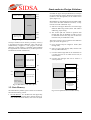
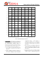
SIDSA
Chapter 4
On-Chip Subsystems Interface
FIPSOC
User’s Manual
SIDSA
Semiconductor Design Solutions
On-Chip Subsystems Interface
Overview
The Field Programmable System On Chip (FIPSOC)
constitutes a new concept in system integration. It
provides the user with the possibility of integrating a
microprocessor core along with programmable digital
and analog cells within the same integrated circuit.
This chip can be considered as a large granularity
FPGA with a FPAA (Field Programmable Analog
Array) and a built-in microprocessor core that does not
only act as a general purpose processing element, but
also configures the programmable cells and their
interconnections. Therefore, there is a strong
interaction between hardware and software as long as
signal values and configuration data within the
programmable cells are accessible from microprocessor
programs.
This chapter describes the communication interface
between the built-in 8051 and the programmable
blocks integrated on the FIPSOC chip. The mP8051
has two functions: firstly, it configures each of the onchip subsystems; secondly, after the programmable
blocks are configured, it is used as general purpose
microprocessor. Thus, the interface circuitry among the
different blocks has been optimized.
Both configuration and data exchange is made through
the memory map of the built-in 8051 core. This
enhanced memory organization keeps, by default, the
map distribution of the original 8051. New registers
included in the SFR area of the 8051 have been added
for system and memory organization control purposes.
Manipulating these registers, the memory organization
of the processor may dynamically change.
With accurate programming, the mP8051 is able to
configure and control the programmable blocks
through its internal and external memory and SFR
areas.
The Regular Configuration Memory of the
Programmable Logic Block has a double function:
Chapter 4. On-Chip Subsystems Interface
firstly, it is used as a buffer memory for the
configuration registers of the DMC (new configuration
is not updated until a transfer command is sent);
secondly, it can be used as general purpose on-chip
memory, so no external memory is needed.
1. 8051 Memory Organization
The memory map of the on-chip mP8051 keeps, by
default, the memory organization of the original 8051.
That is, it has a separate address space for Program
Memory and Data Memory, distributed in the
following four addresses spaces:
•
•
•
•
Up to 64 Kbytes of Program Memory,
Up to 64 Kbytes of external Data Memory,
256 bytes of internal Data Memory,
128 bytes of Special Function Registers area.
On the FIPSOC chip, two memory areas have been
added, overlapped with the original memory areas,
with the purpose of accessing to the different
configuration memories and control registers of the onchip peripherals of the 8051. These locations, whose
mapping is configured by Special Function Registers,
are mapped in the following two spaces:
• 64 bytes of internal data memory, called buffer
access area,
• Up to 16 Kbytes memory mapped on the lower
external Data Memory (depending on device)
1.1. Program Memory
The Program Memory of the on-chip mP8051 consists
of an internal and an external space (see figure 1.1).
512 bytes of Program Memory resides on-chip
(dedicated to the FIPSOC’s Boot Program). The
program memory can be externally expanded up to 64
Kbytes. The internal memory may be disabled; in that
case, the 8051 fetches all instructions from the external
program memory.
2
SIDSA
Auxiliary Memory
External
$FFFF
$FF00
$FEFF
Semiconductor Design Solutions
of RAM, the upper 128 bytes RAM area, 128 bytes
of special function register (SFR) area and 64 bytes
(located in $30 through $6F) of the buffer access
space (figure 1.2).
Both SFR area–upper RAM and lower RAM–buffer
access share the same addresses locations, so they
must be accessed in different ways:
External
a) SFR area and upper RAM are accessed trough
different addressing modes (direct and indirect
addressing, respectively)
Internal ROM
(Boot Program)
$0200
$01FF
External
$0000
Fig. 1.1: Program Memory Address Space
256 bytes random access memory (auxiliary memory)
is provided in the upper addresses space and may be
simultaneously mapped in both program and data
memories. If this memory is enabled, location $FF00
through $FFFF are fetched from it (see Microprocessor
Document for further information).
$FF
Special Function
Register Area
Upper 128 bytes
Internal RAM
(direct addresing)
(indirect addresing)
b) The scratch pad area located in positions $30
through $6F may be disabled in order to access
to the buffer access area (only one of these two
memories may be enabled at a time)
The lower 128 bytes are grouped in four addresses
space (as shown in figure 1.3):
a) Four General Purpose Registers banks ($00
through $1F),
b) Next 16 bytes ($20 through $2F) contains 128
directly addressable bits,
c) Location $30 through $6F can be used either as
a scratch pad area or as buffer access area (as
shown below)
d) Location $70 through $7F can be used as a
scratch pad area.
Scratch Pad Area
$80
$7F
$70
$6F
$7F
$6F
Buffer Access Area
Scratch Pad Area
Buffer Access
$30
Lower 128 bytes
Internal RAM
$30
Bit-addressable Area
Both direct and
indirect addressing
$00
Fig. 1.2: Data Memory / SFR Address Spaces
1.2. Data Memory
The Data Memory address space consists of an internal
and external memory portion.
$2F
$20
$1F
4 Banks for
General Purpose
Registers
$00
Fig. 1.3: Lower portion of the Internal Data Memory
• Internal Memory: It is divided into four physically
separated blocks (original 8051 internal memory is
only divided into three blocks): the lower 128 bytes
Chapter 4. On-Chip Subsystems Interface
3
SIDSA
F8
F0
Semiconductor Design Solutions
ROWL
ROWH
COLL
COLH
RG1
RG2
RGTX
outCOMP
(00)
(00)
(00)
(00)
(00)
(00)
(00)
(0X)
B*
CKCONF
CKCNTL
CKCNTH
CKDMC2
CKDMC1
CKANA
CK8051
(00)
(60)
(00)
(00)
(00)
(00)
(00)
(6F)
DBG2L
DBG2H
DBG3L
DBG3H
DBG4L
DBG4H
DBG5L
DBG5H
(00)
(00)
(00)
(00)
(00)
(00)
(00)
(00)
E0
ACC*
ANAST
DBGCNF
DBGMSK
DBG0L
DBG0H
DBG1L
DBG1H
(00)
(0X)
(00)
(00)
(00)
(00)
(00)
(00)
D8
DANA1
DANA2
DANA3
DANA4
DANA5
DANA6
DANA7
DANA8
(XX)
(XX)
(XX)
(XX)
(XX)
(XX)
(XX)
(XX)
E8
D0
PSW*
FF
F7
EF
E7
DF
D7
(00)
C8
C0
B8
B0
A8
A0
CF
EIMR0
EIMR1
SGNI0
SGNI1
IRS
IRSCKDB
(00)
(00)
(00)
(00)
(XX)
(00xxxxxx)
C7
IP*
VHW4L
VHW4H
VANAL
VANAH
(xxx00000)
(00)
(00)
(00)
(00)
PRTD*
VDBGL
VDBGH
VHW3L
VHW3H
(FF)
(00)
(00)
(00)
(00)
IE*
VCLKL
VCLKH
VHW2L
VHW2H
(0xx00000)
(00)
(00)
(00)
(00)
PRTC*
VPLLL
VPLLH
VHW1L
VHW1H
(FF)
(00)
(00)
(00)
(00)
98
SCON*
SBUF
WDOG
RG3
I2CREG
BTREG
DDRGP
CMBUF
(00)
(XX)
(00)
(02***)
(**)
(**)
(FF)
(XX)
90
PRTB*
BF
B7
AF
A7
9F
97
(FF)
88
80
TCON*
TMOD
TL0
TL1
TH0
TH1
(00)
(00)
(00)
(00)
(00)
(00)
PRTA*
SP
DPL
DPH
PCON
(FF)
(07)
(00)
(00)
(0xxx0000)
* bit addressable
(Reset values of the SFRs)
** Reset value depends on general port values
8F
87
SFRs in grey only in FIPSOCs
*** It depends on FIPSOCs version
Table 1.1: Special Function Registers map (SFR)
• External Memory: There can be up to 64 Kbytes of
external data memory. Its addresses can be either 2
or 1 byte wide (using the 16 bit data pointer or an 8bit
general-purpose
register).
Refer
to
Microprocessor Document for detailed descriptions.
configuration memory. If this memory is
enabled, lower 16 Kbytes (12, 6 or 4 Kbytes) of
the external memory area are not available
(some bits of a special register will select the
active area).
The external data memory address space is divided
into four different areas (as shown in figure 1.4):
c) Next 256 bytes for hardware probing and
writing of the output of the DMCs. Only one of
these two memories may be enabled ata a time
(that is, the 256 hardware memory or external
data memory)
a) Up to 64 Kbytes of external data memory area
(this memory is represented in four regions in
figure 1.4)
b) Lower 16 Kbytes (12 Kbytes, 6 Kbytes or
4Kbytes, depending on device version) can also
be used for mapping on-chip subsystems
Chapter 4. On-Chip Subsystems Interface
d) Upper 256 bytes may be internally mapped
through the auxiliary memory. Note that if the
auxiliary memory is enabled both upper 256
4
SIDSA
locations of data and program memories
coincide.
Semiconductor Design Solutions
been reserved for system configuration and generalpurpose control.
1.3. General Purpose Registers
The subsystems and the memory used for configuration
are listed below:
The lower 32 positions of the internal RAM are
grouped into four banks of 8 registers. Only one of the
banks may be enabled at a time (two bits of PSW
register are used to select the active bank). For indirect
addressing, two of them are used as pointer or index
registers.
a) The programmable blocks (CAB and PL block) are
configured (and accessed) using special function
registers and data memory (both internal and
external) of the 8051 memory organization. Thus,
the configuration and data transfer of these blocks
is made through positions located in both internal
and external memories.
Auxiliary Memory
Data (Region 4)
$FF00-$FFFF
$FEFF
External Data Memory
(Region 3)
$1900*
HW Probing Area
Data (Region 2)
$1800-$18FF*
$17FF*
PL Block
Configuration Memory
Area
External Data Memory
(Region 1)
$0000
* Locations given for 12x8 PL size device
Fig. 1.4: External Data Memory Space
1.4. Special Function Registers (SFR)
The SFR area is located in the upper 128 bytes of the
internal memory. It has two important functions:
Firstly, all CPU registers reside in this area (excepting
PC and GPR banks). Secondly, a number of registers
(not included in the SFR area of the original 8051)
constitute the interface between the mP8051 and all the
on-chip subsystems.
SFR, which are located in addresses which are multiple
of eight, are both byte- and bit-addressable. All SFR
can be accessed by direct addressing only (see Table
1.1).
Note that not all of the addresses are occupied.
Unoccupied addresses are not implemented on the chip
(and the may be used in future). Read access to these
addresses will return random data; write accesses will
be ignored.
2. Subsystems Interface
The configuration and control of the subsystems that
are included in the FIPSOC chip are realized through
accesses to locations of the different memories of the
mP8051. Some memory locations of the SFR area have
Chapter 4. On-Chip Subsystems Interface
• Programmable Logic Block: Either internal or
external memory locations may be used to
configure, control and transfer data. In particular,
both configuration memory and hardware outputs
of the DMC are mapped in both internal (buffer
access) and external; LUT memory data in DMCs
can be accessed through internal memory only.
• Configurable Analog Block (CAB): The
configuration of the block is made through the
buffer access area only; Data transfer is made
using memory locations of the SFR area.
b) Other subsystems are configured and controlled
with special function registers only. These blocks,
not described here, are the Clock Generation Block
(CGB),
Interrupt
Service
Block,
Serial
Communication Block, Debugger Block, Watchdog
Block and other 8051 peripherals systems (Parallel
& Serial I/O, Timers, etc.)
2.1. External Memory
Locations $0000 through $17FF of the external
memory are used to map the configuration memory of
the PL block. Next 256 bytes are used to probe
hardware outputs of the DMCs. Table 2.1. shows the
external memory distribution for different FIPSOC
models.
All these memory areas may be independently and
simultaneously mapped. External memory can always
be disabled. When a particular memory block is
disabled, its memory space becomes automatically
available for external use (out of the chip through the
external bus).
For example, the following memory usage can be
configured:
ü both auxiliary memory and hardware probing
registers area may be mapped, leaving the lower
16 Kbytes as the original external data memory.
ü the whole 64K of the external data memory may
be mapped
ü Region 1, 2 and 4 of the original external data
memory have been disabled in order to access to
5
SIDSA
PL Configuration Memory, HW Probing Area and
Auxiliary Memory, respectively
Setting or clearing the values of the corresponding bits
in the system control registers (see later in the
document), the configuration of the memory can be
changed. This re-configuration can be made
dynamically; that is, non-reset between different
configurations are needed.
2.2. Buffer Access
The Data Buffer Area is located in $30 through $6F of
the internal data memory of the 8051. By default, this
portion of memory is not mapped, and the original
memory organization is obtained (see figure 1.3).
When buffer access area is enabled (first scratch pad
area is disabled because only one of them may be
active at a time), memories and registers from several
different blocks throughout the FIPSOC chip can be
accessed, depending on the access mode (these modes
will be described in detail later in the document):
• PL Block Regular Configuration Memory:
Locations $30 to $4F map buffer context #0 ($50
to $6F for buffer context #1). A write operation on
any of these locations writes data to all the DMCs
selected with the row and column mask registers
(mapped in the SFR area). A read operation should
only be done with one DMC selected, otherwise
the internal priority control circuit would select
only the one with the bigger column and mask
number. Configuration memory for the IO cells
and CAB-DMCs routing resources can also be
selected setting the corresponding bits included in
the row and column mask registers.
• PL Block LUT data memory: Locations $38 to
$3F map nibbles 0 to 7 of the Low Tile of the
DMC selected with the mask registers. Locations
$40 to $47 map the nibbles 0 to 7 of the High Tile
of the DMC selected to the mask registers. In both
cases, the lowest nibble is always used. Locations
$48 to $4F map nibbles 0 to 7 of both tiles, using
the four most significant bits of each location for
the nibble corresponding to the High tile and the
four least significant bits for the Low Tile. Several
DMCs can be selected for multiple write
operations, while only one for reading (the priority
circuit works like in the Regular Configuration
Memory mode). Locations $30 to $37 and $50 to
$6F are unused.
• PL Block Hardware Probing memory: This access
mode is intended to provide a fast way to probe
hardware signals in real time, both sequential and
combinational. Only the outputs of a Chip Quarter
are mapped, so the appropriate Chip Quarter must
be selected first with the Mapping Control
Registers (mapped in the SFR area)
Chapter 4. On-Chip Subsystems Interface
Semiconductor Design Solutions
• PL Block Hardware Writing mode: This access
mode is intended to provide a fast way to write in
the flip-flops of the sequential part of the DMCs in
real time. Only the DMCs of a Chip Quarter are
mapped, so the appropriate Chip Quarter must be
selected first with the Mapping Control
• CAB Configuration memory: CAB Configuration
is done by writing in non-buffered conventional
RAM memory. No multicontext operation is
allowed for the CAB. In this mode, the buffer
directly maps the whole CAB configuration
memory for read and write access. No context
transfer command is needed like for buffered
multicontext configuration memory (DMCs and
IOs).
Note that the regular configuration memory registers
and the hardware probing and flip-flop writing memory
locations may be also mapped in the external memory.
These access modes are independently configured and
may be used at the same time. These memory
locations cannot be reached from any program
running from the programmable logic configuration
memory (due to timing scheduling conflict)
The data in the Regular Configuration can be used
either for general purpose data or for configuring the
Programmable Logic Block. Data is stored in the
memory cells until a transfer command is sent (see PL
Block Document for further information).
2.3. Extended SFR map
The new special function registers added to the original
SFR map of the 8051 are dedicated to control,
configure and data transfer purpose. Only 18 of them
are related to the programmable blocks interface and
the system mapping control. In particular, SFR may be
grouped as follows:
• System Mapping Control Registers: These registers
are used by FIPSOC for memory organization
control and buffer access modes. They include:
a) Row and Column mask (two 16-bit registers
-ROW and COL- and one nibble of general control
register -RG2[7:4]-),
b) General Control registers (three locations, RG1,
RG2 and RG3),
c) Transfer command (one register, RGTX).
• Analog Control Registers: Ten registers are used
for (digital) data transmission with the CAB. Input
registers for the DACs are written here and output
registers from the ADCs and comparators are read
(DANA1 through DANA8 for DACs/ADCs
operations and outCOMP for comparators reading).
Control commands for this block are also issued
writing to one of these registers (ANAST).
6
SIDSA
The new SFR map is completed with control registers
of the on-chip subsystems (described in their
corresponding documents).
Port 3 [5:0]
INT1
Port 2 [3:0]
Ext. Timers 0. 1
HW 1-4 INTs.
INT0
ports of 8 bits). Due to the fact that FIPSOC integrates
some external peripherals on-chip, not all the 4 ports
are accessible from the external system. In particular,
port 2 and port 3 of the 8051 have been used for
internal communication purposes (see figure 2.1)
• Port 2 is utilized by the system for accesses to
external memories.
ü Only output direction is available (normally
used as high byte address),
ü Input direction of Port 2 has been dedicated for
the communication between the PL block and
the 8051 (PL→ 8051 direction),
• Port 3 has been reserved for internal use only
(except data memory strobes and RX / TX of the
serial interface).
ü Output of bits 0 to 5 are dedicated for the
communication with the PL block (8051→ PL
direction),
ü Output 0 enables the TX lines of the serial
interface
ü Bits 2 and 3 (inputs) are reserved to interrupt
signals,
ü Bits 4 and 5 (inputs) are reserved for external
timer purpose, and come from the PL block.
PL BLOCK
Interrupts.
Extension.
Block
Semiconductor Design Solutions
8051
Fig. 2.1: Fast access bus interface
(see Microprocessor Document for further information)
2.4. Port Access
The original 8051 has 32 bi-directional and
individually addressable I/O lines (grouped into four
8x8
12x8
16x12
16x16
$0000 to $0FFF
$0000 to $17FF
$0000 to $2FFF
$0000 to $3FFF
Regular Configuration Memory
$1000 to $10FF
$1800 to $18FF
$3000 to $30FF
$4000 to $40FF
Hardware Probing Registers
$FF00 to $FFFF
$FF00 to $FFFF
$FF00 to $FFFF
$FF00 to $FFFF Auxiliary Memory
Table 2.1: External memory distribution for different FIPSOC models
3. System Mapping Control
SFR
FIPSOC uses some Special Function Registers (SFR)
of the internal memory map of the mP8051 for the
memory configuration (used for programmable blocks
interfaces) and general system control. These registers
are described below:
Column Mask Register (h00 after Reset)
Address
$FB,$FA
Name
COL
COLL
Byte
COLH
$FB
$FA
Description
Column Mask Register
Column Mask Register Low
Byte
Column Mask Register High
Byte
Row Mask Register (h00 after Reset)
Address
$F9,$F8
Name
ROW
ROWL
ROWH
Byte
$F8
$F9
Description
Row Mask Register
Row Mask Register Low Byte
Row Mask Register High Byte
Chapter 4. On-Chip Subsystems Interface
7
SIDSA
8051 Port 3.
Address
Name
PORTD
NRD
System Control Register 2 (h00 after Reset)
Description
8051 Port 3
PORTD.7
NRD for external memory. Must
not be cleared
NWR
PORTD.6
NWR for external memory.
Must not be cleared
PRTD5..2
5 thru 2
General Purpose
TXD
PRTD.1
(Output) Serial port TX
ETXD
PRTD.0
If cleared (=0), TX serial port is
enabled.
RX
PRTD.0
(Input) Serial Port RX
Note: Different registers are used for both read and write accesses.
While writing, b11 - - - - 10 must be fixed to keep communications
though the serial port.
$B0
Semiconductor Design Solutions
Bit
Address
$FD
Name
RG2
EPM
WPM
NPM
SPM
HOA1
Bit
RG2.7
RG2.6
RG2.5
RG2.4
RG2.3
HOA0
RG2.2
AME
RG2.1
EDMF
RG2.0
System Control Register 1 (h00 after Reset)
Address
$FC
Name
RG1
CQDB1
CQDB0
AMI
RG1.7
RG1.6
RG1.5
LMI
RG1.4
HOI
Bit
RG1.3
HOE
RG1.2
CMI
RG1.1
CME
RG1.0
Description
FIPSOCs Control Register 1
Chip Quarter Data Buffer bit 1.
Chip Quarter Data Buffer bit 0
Analog Configuration memory
mapped as Int. Mem. If 1,
configuration
memory
is
mapped in the Data Buffer
locations of the Internal Memory
($30-$6F)
LUT Data Memory mapped as
Internal Mem. If 1, LUT Data
memory is mapped in the Data
Buffer locations of the Internal
Memory ($30-$6F)
Hardware Outputs mapped as
Internal Memory. If 1, hardware
outputs are mapped in the Data
Buffer locations of the Internal
Memory
($30-$6F).
Use
CQDB1 and CQDB0 to select
the appropriate Quarter.
Hardware Outputs mapped as
External Memory
Configuration Memory mapped
as Internal Memory. If 1,
configuration
memory
is
mapped in the Data Buffer
locations of the Internal Memory
($30-$6F)
Configuration Memory mapped
as External Memory.
System Control Register 3 (h02 after Reset, 12x8
device)
Address
$9B
Name
RG3
Bit
INTM
RG3.7
RG3.6
RG3.5
RG3.4
RG3.3
RG3.2
CM1
RG3.1
CM0
RG3.0
Description
FIPSOCs Control Register 3
Description
FIPSOCs Control Register 2
East Pads Mask bit.
West Pads Mask bit
North Pads Mask bit
South Pads Mask bit.
Hardware Outputs Access Mode
1.
Hardware Outputs Access Mode
0.
Auxiliary Memory Enable. If this
bit is set, the Aux. memory
(256x8bits) is mapped at
locations $FF00-$FFFF of both
external data and program
memories.
External Data Memory Function.
If 1, external data memory is
mapped in program memory
locations. If this bit is set and
CME = 1, the configuration
memory of the Programmable
Logic is used both for data and
program memories .
Transfer Command Register (h2F after Reset)
Address
$FE
Name
RGTX
PLTB
Bit
RGTX.7
CTXSB
RGTX.6
FCB
RGTX.5
FAB
RGTX.4
Description
Transfer Register
Programmable Logic Transfer
bit. Writing to RGTX with this
bit set produce a context transfer
(set by RGTX.6) of the
configuration in the DMCs
Context Select Bit. If this bit is
set when writing to RGTX with
PLTB = 1, context 1 is
transferred to the configuration
memory of the selected DMCs.
If this bit is 0, context 0 is
transferred.
Freezing Command Bit. A
writing to RGTX with this bit set
produce an start/stop action in
the state machine of the clock
generation block.
Freezing Action Bit. If this bit is
set when writing to RGTX with
FCB = 1, clocks stops by SW
after CKCNT. If 0, clocks
restarts.
RGTX.3
RGTX.2
RGTX.1
RGTX.0
Interrupt mode. If 1, extended
interrupt vectors mode is
entered, if 0, basic 8051
interrupt mode is selected
External Memory Compatible
map bit 1
External Memory Compatible
map bit 0
Chapter 4. On-Chip Subsystems Interface
8
SIDSA
4. PROGRAMMABLE
BLOCKS & uC INTERFACE
Configuration memories and outputs of the
programmable blocks (PL and CAB) may be accessed
through internal and external memory locations.
4.1. PL Subsystem Interface
Regular Configuration Memory: This memory may be
mapped either through internal memory (data buffer
access) or external memory. If a buffer access is done,
row and column mask registers are needed, with the
purpose of selecting the desired DMC(s), IO cell(s) or
IIC (Internal Interface Cell) routing resources cell(s).
Location $30 through $6F of the internal memory map
will be used. If the external memory is used, each
position of the Regular Configuration Memory of every
DMC has its correspondence with one location on the
external memory map.
4.1.1. Regular Configuration Memory
Regular Configuration Memory is used to configure the
DMC. For this purpose, two different memory contexts
have been included in the chip. A Transfer Command
is needed for the configuration change. RGTX[7:6] is
used: writing to this register with bit 7 set, data stored
in the selected context of the Regular Configuration
Memory will be transferred to the corresponding
registers (context #0 is selected if bit 6 is cleared;
otherwise, context #1 is selected). See PL Block
Document for further information.
4.1.1.1. Buffer Access
Data buffer area is enabled by setting RG1[0] (SFR
$FC). Write and read operations affect to the
selected DMCs marked by the column and row
mask registers (ROW and COL registers), and to the
IO and IIC cells routing resources cells selected by
RG2[7:4] bits (east, west, north, south IO mask
nibble), as shown in figure 4.1.
The buffer access area is organized in 2 blocks:
ü $30 to $4F: 32 bytes map context #0 of the
selected DMC,
ü $50 to $6F: 32 bytes map context #1 of the
selected DMC
A write operation on any of these locations writes
data to all the DMCs (and IO and CAD-DMC cells)
selected with the row and column mask registers
and IO mask nibble.
A read operation should only be done with one
DMC (or cell) selected; otherwise, the internal
priority control would select only the one with the
bigger column and row mask number (including IO
mask bits as depicted in figure 4.1), or the first
row/column if no one is selected.
Chapter 4. On-Chip Subsystems Interface
Semiconductor Design Solutions
The following accesses are not valid:
ü write access with column register and west and
east bits cleared (write is inhibit),
ü write access with row register and north and
south bits cleared (write is inhibit),
ü read and write operations to physically nonexist DMC or cell; in this case, write operations
will be inhibit and read operations will return
random data.
4.1.1.2. External Memory Access
The Regular Configuration Memory is enabled
when RG1[1]=1. The addresses space is divided
into two areas: the lower half portion maps all the
registers of context #0 and the upper locations map
the configuration registers of context #1.
In both portions, the address decoding is done as
follows:
ü The 5 least significant bits address the 32
configuration registers of the corresponding
context of the DMC,
ü Every 32 locations the selected DMC is
changed. The selection of the DMC is arranged,
firstly, from east to west and, secondly, from
south to north,
ü The upper half maps context #1 with the same
organization as the first portion.
The size and organization of the Regular
Configuration Memory depend on the selected
device model. Tables 4.1 shows the memory
organization for the 8x12 models.
By default, the memory organization version
mirrors the physical PL block model integrated in
the device. However, different device models have
been designed to have a compatible memory map.
In fact, the logical memory organization and the
physical implemented memory access have been
separated. In this way, each FIPSOC model can be
configured to have a memory organization equal to
that of any other model. For example, the user can
configure the 12x8 PL device to have the same
memory map than the 16x16 model. This is a
convenient way to develop an application using a
big prototyping device (the 16x16 model) and
produce it using a smaller device (12x8) with no
changes at all. Table 4.2. shows the selection of the
memory organization.
In the same way as data buffer access, a write and
read access to a non-exist DMC has no sense.
IO cells and IICs routing resources cells cannot be
accessed through external memory as only internal
data buffer access is allowed.
9
SIDSA
Semiconductor Design Solutions
COLH
7
Selected cell by the
priority control circuitry
High Priority
IO North bit mask
8x12 model cells
Selected cell
ROWH
7
ROWL
0
7
Low Priority
0
COLL
7
0
Bit
set
IO South bit mask
0
IO East bit mask
IO West bit mask
High Priority
Low Priority
Fig. 4.1: Data buffer access
Memory location
$17C0 - $17FF
...
DMC selected
RCOL[15:0] RROW[15:0]
h0080
h0080
...
...
Description
(row 7, context 1)
(column 11)
$0C00 - $0C3F
$0BC0 - $0BFF
...
h0001
h0080
...
h0001
h0080
...
(row 0, context 1)
(row 7, context 0)
(column 11)
$0200 - $023F
$01C0 - $01FF
...
$0040 - $007F
$0000 - $003F
h0001
h0080
...
h0002
h0001
h0002
h0001
...
h0001
h0001
(row 1, context 0)
(row 0, context 0)
Table 4.2: 12x8 model Configuration Memory Organization
RG2[5:4]
Memory
Organization
00
01
10
11
16x16 model
16x12 model
12x8 model
8x8 model
Table 4.3: Logical Configuration Memory Organization selection
Chapter 4. On-Chip Subsystems Interface
4.1.2. LUT Data Memory
This memory may only be mapped through the internal
data buffer (setting RG1[4] bit). Read and write
operations affect the selected DMC (using row and
column mask register) like in the Regular
Configuration Memory mode. Locations $38 to $3F
map nibbles 0 to 7 of the Low Tile of the DMC(s)
selected. Location $40 to $47 map the nibbles 0 to 7 of
the High Tile of the DMC(s) selected. In both cases,
the lowest nibble of the byte is used either in read or
write access.
Location $48 to $4F map nibbles 0 to 7 of both Tiles,
using the four most significant bits of each location for
the nibble corresponding to the High Tile and the four
least significant bits for the Low Tile. Locations $30 to
$37 and $50 to $6F are not used.
Restrictions and priority features enumerated in the
Configuration Memory section are also valid here.
IO cell and IICs routing resources cells have only
configuration memory. Any write or read access with a
IO mask bit set has no sense. Write operations will be
inhibit and a read access will return random data.
10
SIDSA
4.1.3. Hardware Memory Area
This area may be accessed either through internal or
external memory. Due to the fact that read and write
accesses affect different signals, two modes are
provided:
• Hardware writing mode: This mode is intended to
provide a fast way to write in the flip-flops of the
sequential part of the DMC in real time,
• Hardware Probing mode: This mode is intended to
provided a fast way to probe hardware signals in
real time, both sequential and combinational.
Four different accesses are allowed for both write and
read operations (selected by RG2[3:2]). Table 4.6 lists
these sub-modes.
RG2[3:2]
Hardware Writing
Hardware Probing
00
01
10
11
Single DMC context #0
Single DMC context #1
Horizontal 8-bit access
Vertical 8-bit access
Single DMC access
(both contexts)
Horizontal 8-bit access
Vertical 8-bit access
Table 4.6: Accesses allowed for both write and read operations
4.1.3.1. Data buffer Access
This access is enabled when RG1[2]=1. In both
write and read modes only the DMCs of a Chip
Quarter are mapped. RG1[7:6] are used for Chip
Quarter selection (see tables 4.7 and figure 4.2).
Semiconductor Design Solutions
RG2[7:6]
Quarter Selection
(horizontal access)
Quarter Selection
(vertical access )
00
01
10
11
South-East Quarter (Q0)
South-West Quarter (Q1)
North-East Quarter (Q2)
North-West Quarter (Q3)
South-East Quarter (Q0)
North-East Quarter (Q1)
South-West Quarter (Q2)
North-West Quarter (Q3)
Table 4.7: Logical Configuration Memory Organization selection
The different modes and sub-modes accesses
allowed are described below:
a)
Hardware Probing modes (read operations):
Sequential and combinational outputs are
obtained. Different sub-modes bring as different
organizations (see Table 4.9).
ü Single
DMC
access
(RG[3:2]=0X):
Locations $30 to $6F map the outputs of the
DMCs, one byte each DMC. The most
significant nibble corresponds with the
sequential output and the least one corresponds
with the combinational output.
ü Horizontal 8-bit access (RG[3:2]=10):
Locations $30 to $4F (lower half) map the
combinational outputs, two horizontally
adjacent DMCs in each byte; locations $50 to
$6F (upper half) map the sequential outputs,
two horizontally adjacent DMCs in each byte.
ü Vertical 8-bit access (RG[3:2]=11): The
lower half portion maps the combinational
outputs, two vertically adjacent DMCs in each
byte; Locations of the upper half maps the
sequential outputs, two vertically adjacent
DMCs in each byte.
Table 4.9 and figure 4.3 show how simultaneous
access to DMC pairs is performed.
Chip Quarter distribution for 8x8 model
(only first quarter is occupied)
Chip Quarter distribution for 12x8 model
(first and partially second quarter are occupied)
b) Hardware Writing modes (write operations):
Flip-flops of the sequential part of the DMCs
are written. Different accesses are allowed (see
Table 4.9):
ü Single
DMC
context
#0
access
(RG[3:2]=00): Each locations of the $30 to $6F
area writes in context #0 of the flip-flops of one
DMC. The least significant nibble of the
locations is used in the operation.
Chip Quarter distribution for 16x12 model
(third and fourth quarter are partially empty)
Chip Quarter distribution for 16x16 model
(all quarters are occupied -no gaps exist)
Fig. 4.2: Chip Quarter distribution for the different models
ü Single
DMC
context
#1
access
(RG[3:2]=01): Each locations of the $30 to $6F
area writes in context #0 of the flip-flops of one
DMC. The least significant nibble of the
locations is used in the operation.
ü Horizontal 8-bit access (RG[3:2]=10):
Locations $30 to $4F write in context #0 of the
flip-flops, two horizontally adjacent DMCs in
each byte; locations $50 to $6F write in context
Chapter 4. On-Chip Subsystems Interface
11
SIDSA
#1 of the flip-flops, two horizontally adjacent
DMCs in each byte.
ü Vertical 8-bit access (RG[3:2]=11):
Locations $30 to $4F write in context #0 of the
flip-flops, two vertically adjacent DMCs in each
byte; locations $50 to $6F write in context #1 of
the flip-flops, two vertically adjacent DMCs in
each byte.
Semiconductor Design Solutions
ü Vertical 8-bit access (RG[3:2]=11): The
lower half portion maps the combinational
outputs, two vertically adjacent DMCs in each
byte; Locations of the upper half maps the
sequential outputs, two vertically adjacent
DMCs in each byte.
b) Hardware Writing modes (write operations):
Flip-flops of the sequential part of the DMCs is
written. Different acceses are allowed (see
Table 4.9):
ü Single
DMC
context
#0
access
(RG[3:2]=00): Each locations of the $00 to $FF
area writes in context #0 of the flip-flops of one
DMC. The least significant nibble of the
locations is used in the operation.
ü Single
DMC
context
#1
access
(RG[3:2]=01): Each locations of the $00 to $FF
area writes in context #0 of the flip-flops of one
DMC. The least significant nibble of the
locations is used in the operation.
Figure 4.3: Hardware Memory accesses mode
Only one DMC may be selected; column and row
mask registers (and IO mask nibble) are ignored in
Hardware memory modes.
Read and write operations to physically non-exist
DMCs or cells have no sense; in this case, write
operations will be inhibit and read operations will
return random data.
4.1.3.2. External Memory
If RG1[3] is set, Hardware Memory is enabled. The
area is located in the next 256 bytes after the
Regular Configuration Memory locations (see table
3.1). All the DMC are mapped through the relative
locations $00 to $FF. As in data buffer access,
different modes and sub-modes are allowed:
a) Hardware Probing modes (read operations):
Sequential and combinational outputs are
obtained. Differentes sub-modes bring as
different organizations (see Table 4.9).
ü Single
DMC
access
(RG[3:2]=0X):
Locations $00 to $FF map the outputs of the
DMCs, one byte each DMC. The most
significant nibble corresponds with the
sequential output and the least one corresponds
with the combinational output.
ü Horizontal 8-bit access (RG[3:2]=10):
Locations $00 to $7F (lower half) map the
combinational outputs, two horizontally
adjacent DMCs in each byte; locations $80 to
$FF (upper half) map the sequential outputs,
two horizontally adjacent DMCs in each byte.
Chapter 4. On-Chip Subsystems Interface
ü Horizontal 8-bit access (RG[3:2]=10):
Locations $00 to $7F write in context #0 of the
flip-flops, two horizontally adjacent DMCs in
each byte; locations $80 to $FF write in context
#1 of the flip-flops, two horizontally adjacent
DMCs in each byte.
ü Vertical 8-bit access (RG[3:2]=11):
Locations $00 to $7F write in context #0 of the
flip-flops, two vertically adjacent DMCs in each
byte; locations $80 to $FF write in context #1 of
the flip-flops, two vertically adjacent DMCs in
each byte.
Read and write operations to physically non-exist
DMC or cell have no sense; in this case, write
operations will be inhibit and read operations will
return random data. Note that in all the FIPSOC
models, 256 bytes are dedicated to map the
Hardware Memory. Gaps exist in non-16x16
models.
4.2. CAB Subsystem Interface
CAB uses both data buffer and SFR maps for
configure, control and data transfer.
4.2.1. Buffer Access
CAB Configuration Memory may only be mapped
through the internal data buffer (if RG1[5] = 1).
Configuration is done by writing in non-buffered
conventional RAM memory. No multicontext is
provided. Locations $30 to $6F constitute the whole
CAB configuration memory.
Not all of the addresses are used. Unoccupied
locations are reserved for future use.
12
SIDSA
Semiconductor Design Solutions
4.2.2. Data transfer (through SFR area)
Data transfer and fast control (such as the start
command and the end of conversion signals) are
mapped in the SFR area.
Locations $D8 through $DF, $E1 and $FF are used
(as shown in Table 4.8).
SFR
Register Name
Access mode
$D8 to $DB
$DC to $DF
$E1
DANA1 to DANA4
DANA5 to DANA8
ANAST (mPCONV[3:0])
ANAST (mPDONE[3:0])
outCOMP[3:0]
Read and write
Read Only
Read
Write
Read Only
$FF
Table 4.8: Logical Configuration Memory Organization selection
ü Input registers for ther DACs are written by
accessing to DANA1 to DANA4 SFRs.
ü Output registers from the ADCs may be
obtained by reading these four registers (DANA1 to
DANA4).
ü DANA5 to DANA8 are read only registers and
they are used in 4 input-multiplexed 10-bits ADC
mode (see CAB document for detailed description).
ü Outputs of the comparators section may be read
by accessing to the least significant nibble of the
read only OutCOMP SFR.
ü ANAST registers has different functions:
Writing on its bits, the corresponding ADC channel
starts conversion. With a read access to the register,
the end-of-conversion status is obtained. Only the
least significant nibble is used.
See CAB Document for further information
Locations
Internal
External*
Q0, $30
$00
Q0, $31
$01
Q0, $32
$02
Q0, $33
$03
Q0, $34
$08
Hardware Probing Mode
Horizontal 8-bit **
Vertical 8-bit ***
(1,0) & (0,0), comb
(0,1) & (0,0), comb
(3,0) & (2,0), comb
(0,3) & (0,2), comb
(5,0) & (4,0), comb
(0,5) & (0,4), comb
(7,0) & (5,0), comb
(0,7) & (0,6), comb
(1,1) & (0,1), comb
(1,1) & (1,0), comb
Hardware writing Mode
Horizontal 8-bit **
Vertical 8-bit ***
(1,0)&(0,0), context #0 (0,1)&(0,0) context #0
(3,0) & (2,0), ctx #0
(0,3) & (0,2), ctx #0
(5,0) & (4,0), ctx #0
(0,5) & (0,4), ctx #0
(7,0) & (5,0), ctx #0
(0,7) & (0,6), ctx #0
(1,1) & (0,1), ctx #0
(1,1) & (1,0), ctx #0
Q0, $4F
Q0, $50
$3B
$80
(7,7) & (6,7), comb
(1,0) & (0,0), seq
(7,7) & (7,6), comb
(0,1) & (0,0), seq
(7,7) & (6,7), ctx #0
(1,0) & (0,0), ctx #1
(7,7) & (7,6), ctx #0
(0,1) & (0,0), ctx #1
Q0, $6F
Q1, $30
$BB
$04
(7,7) & (6,7), seq
(9,0) & (8,0), comb
(7,7) & (7,6), seq
(1,8) & (0,8), comb
(7,7) & (6,7), ctx #1
(9,0) & (8,0), ctx #0
(7,7) & (7,6), ctx #1
(1,8) & (0,8), ctx #0
Q1, $4F
Q1, $50
$3F
$84
(15,7) & (14,7), comb
(9,0) & (8,0), seq
(7,15) & (6,15), comb
(1,8) & (0,8), seq
(15,7) & (14,7), ctx #0
(9,0) & (8,0), ctx #1
(7,15) & (6,15), ctx #0
(1,8) & (0,8), ctx #1
Q1, $6F
Q2, $30
$BF
$40
(15,7) & (14,7), seq
(1,8) & (0,8), comb
(7,15) & (6,15), seq
(9,0) & (8,0), comb
(15,7) & (14,7), ctx #1
(1,8) & (0,8), ctx #0
(7,15) & (6,15), ctx #0
(9,0) & (8,0), ctx #0
Q2, $4F
Q2, $50
$7B
$C0
(7,15) & (6,15), comb
(1,8) & (0,8), seq
(15,7) & (14,7), comb
(9,0) & (8,0), seq
(7,15) & (6,15), ctx #0
(1,8) & (0,8), ctx #1
(15,7) & (14,7), ctx #0
(9,0) & (8,0), ctx #1
Q2, $6F
Q3, $30
$FB
$44
(7,15) & (6,15), seq
(9,8)&(8,8), comb
(15,7) & (14,7), seq
(9,8)&(8,8), comb
(7,15) & (6,15), ctx #1
(9,8)&(8,8), ctx #0
(15,7) & (14,7), ctx #1
(9,8)&(8,8), ctx #0
Q3, $4F
Q3, $50
$7F
$C4
(15,15)&(14,15) comb
(9,0)&(8,15), seq
(15,15)&(14,15) comb
(9,0)&(8,15), seq
(15,15)&(14,15) ctx #0
(9,0)&(8,15), ctx #1
(15,15)&(14,15) ctx #0
(9,0)&(8,15), ctx #1
Q3, $6F
$FF
(15,15)&(14,15), seq
(15,15)&(14,15), seq
(15,15)&(14,15) ctx #1 (15,15)&(14,15), ctx #1
* Memory Locations are relative (absolute values depend on map organization version)
** DMCs are arranged to, first, from East to West and, secondly, from South to North of die size (8x8 for each Quarter in
internal access and 16x16 for external access)
*** DMCs are arranged to, first, from South to North and, secondly, from East to West of die size (8x8 for each Quarter in
internal access and 16x16 for external access)
Table 4.9: DMC association in vertical and horizontal accesses
Chapter 4. On-Chip Subsystems Interface
13