1
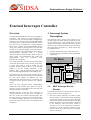
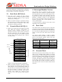
SIDSA
Chapter 6
External Interrupts Controller
FIPSOC
User’s Manual
SIDSA
Semiconductor Design Solutions
External Interrupts Controller
The control logic for each external interrupt input is
duplicated so the same interrupt sources are available
for each input. Masks are different for each
duplicated input and in fact this is a convenient way
to specify relative priorities between two interrupt
sources.
There are nine interrupt sources, independently
masked for each interrupt input. Each one may be
inverted, so both low and high levels and rising and
falling transitions are allowed.
Multiple interrupt vectors are also supported. In
normal operation, the interrupt vector is unique for
each one of the two external interrupt inputs. The
External Interrupt Controller (EIC block) provides
an enhanced multiple interrupt vector mode which
selects the interrupt vector from a user-defined table
of registers.
Chapter 6. External Interrupts Controller
Programmable Hardware Interrupts 1 - 4
End of Conversion
PLL stabilization
Clock
Generation
Block
Serial
Comm.
Block
Stop Interrupt
EIC
Block
Program Code Bus
Program Address Bus
PL Block
External Data Bus
External Data Address Bus
• Interrupts generated by the on-chip subsystems,
• Custom interrupts generated in the Programmable
Logic Block
Comm. Interrupt
This chapter describes the interrupt controller added
to the external interrupts service circuitry of the builtin 8051. This block is used to extend the two
available external interrupt sources in the standard
mP8051 to all the on-chip subsystems of the
FIPSOC. Thus, a full interrupt service interface has
been customized and integrated in the FIPSOC chip.
The interrupts service system of the on-chip core of
the 8051 keeps the same interrupt requesting system
of the original 8051, even though there has been
integrated an external interrupt controller to expand
the limit of two external interrupt sources allowed by
the original 8051 (see figure 1.1). These sources may
be grouped into two:
SW BreakPoint Interrupt
The Field Programmable System On Chip (FIPSOC)
constitutes a new concept in system integration. It
provides the user with the possibility of integrating a
microprocessor core along with programmable digital
and analog cells within the same integrated circuit.
This chip can be considered as a large granularity
FPGA with a FPAA (Field Programmable Analog
Array) and a built-in microprocessor core that does
not only act as a general purpose processing element,
but also configures the programmable cells and their
interconnections. Therefore, there is a strong
interaction between hardware and software as long as
signal values and configuration data within the
programmable
cells
are
accessible
from
microprocessor programs.
1. Interrupt System
Description
CAB
Overview
INT0 INT1
8051
Debugging
Block
Fig. 1.1: Block Diagram of the Interrupt System
1.1.
8051 Interrupt Service
Routine
The mP8051 provides five interrupt sources with two
priority levels (as shown in figure 1.2):
ü The 8051 external interrupts can each be either
level-activated or transition-activated, depending
on bits IT0 and IT1 in register TCON. The flags
that actually generate these interrupts are bits IE0
and IE1 of TCON. The interrupt flag is cleared a)
by the hardware, when the service routine is
vectored to, only if the interrupt was transitionactivated; b) by the external requesting source
(which controls the request flag), if the interrupt
was level-activated.
2
SIDSA
ü Timer0 and Timer1 interrupts are generated by
bits TF0 and TF1, which are set by the rollover in
their respective timer/counter registers. The
interrupt flag is cleared by the on-chip hardware
when the service routine is vectored to.
Semiconductor Design Solutions
The interrupt sources are described in table 1.1. Note
that one of the sources can only interrupt thshare the
same interrupt
IE0
IT1
IE1
TF0
RI
TI
Fig. 1.2: mP8051 Interrupt Sources
All the bits that generate interrupts can be set or
cleared by software, with the same result as though it
had been set or cleared by hardware.
Each of these interrupt sources may be individually
enabled or disabled. The 8051 also provides a global
disable bit which disables all interrupts at once.
Each interrupt source can also be individually
programmed to one of two priority levels by setting
or clearing a bit on the register located in $B8 of the
SFR map. A lower-priority interrupt can itself be
interrupted by a higher-priority interrupt, but no t by
a lower-priority interrupt. If request of the same
priority level are received simultaneously, an internal
polling sequence determines which request is
serviced (see Microprocessor Document for further
information)
1.2.
HW1/COM
CKint
HW2
DBGint
HW3
HW4
CABint
Table 1.1: Interrupt Sources
TF0
INT1
PLL stabilization (highest priority)
Programmable Hardware interrupt #1 /
Serial Communication Block Interrupt
Clock Generation Block: clock stop
Programmable Hardware interrupt #2
Software breakpoints
Programmable Hardware interrupt #3
Programmable Hardware interrupt #5
End of Conversion of the ADCs
External Interrupts
Controller
Each interrupt signal is connected to the internal
channels of the External Interrupt Controller Block.
The output of these channels is connected to the
external interrupt inputs (INT0 and INT1) of the
mP8051.
All the signals may be independently inverted and
masked in each channel. A priority circuitry is
provided to solve simultaneous request conflicts
between different sources. Figure 1.3 schematically
shows the block diagram of the External Interrupt
Controller.
EIMR0[6]
Priority within level
IT0
Priority within level
ü The Serial Port Interrupt is generated by the
logical OR of RI and TI. Neither of these flags is
cleared by hardware when the service routine is
vectored to.
INT0
Description
Source
PLLint
SGN 0
COM INT
EIMR 0
Channel # 0
TSR 0
PLL INT
HW1
INT 0
CK INT
HW2
ISR
DBG INT
HW3
INT 1
HW4
ANA INT
TSR 1
Channel # 1
SGN 1
EIMR 1
Fig. 1.3: Block Diagram of the EIC Block
An interrupt controller block to complement the
interrupt system of the built-in 8051 has been
inergrated. This controller expands to nine the
number of interrupt sources connected to the interrupt
system. Therefor, different subsystems would be able
to request a hardware interrupt in the microprocessor
.
Both channels of the EIC Block are independently
controlled (they have separate registers): mask and
polarity registers are duplicated. Only the Interrupt
Status Register is not available on each channel, since
this register is the logical OR of the Temporal Status
Register (TSR0 and TSR1) of the channels (as
depicted from figure 1.3).
The 8051 core can be externally interrupted by one of
the nine new interrupt sources through any of the
external interrupt inputs; that is, hardware for both
interrupt inputs has been duplicated to provide higher
flexibility.
Signal HW1 in channel #0 has a double function: if
its corresponding bit in the mask register is set, the
Programmable Hardware Interrupt 1 is selected:
otherwise, Serial Communication Block Interrupt is
selected.
Chapter 6. External Interrupts Controller
3
SIDSA
Finally, an enhanced mode is provided from the
External Interrupt Controller Block. This mode
supports multiple interrupt vectors for the 8051
external interrupt sources. That is, only one interrupt
vector each external interrupt input is provided by the
on-circuitry when the interrupt routine is called. If the
enhanced mode is disabled, the programmer would
have to identify which of the nine new sources has
caused the interrupt. This mode is called normal or
basic mode.
In the enhanced mode, a user-definable vector table is
provided (located in the SFR map of the 8051), and
no action from the programmer is needed, since the
interface selects the corresponding vector. This
operation is totally transparent to the mP8051 as long
as the register is multiplexed via hardware. The
corresponding flag in the Interrupt Status Register is
also cleared when the service routine is vectored to,
only if the interrupt was transition-activated.
Semiconductor Design Solutions
System Control Register 3 (h02 after Reset,
12x8 device)
Address
$9B
Name
RG3
Bit
INTM
RG3.7
RG3.6
RG3.5
RG3.4
RG3.3
RG3.2
CM1
RG3.1
CM0
RG3.0
Address
$A7,$A6
Name
VHW1
Byte
$A6
$A7
VHW1L
VHW1H
The Global Interrupt system of the FIPSOC is
controlled using registers located in the SFR map.
These registers can be divided into three groups:
ü Original 8051 registers used to control the on-core
interrupt system of the 8051 (see Microprocessor
Document),
ü Interrupt related Registers included in the
different subsystems of the FIPSOC. These
registers are explained in their corresponding
Documents
(Configurable
Analog
Block
Document, Software Debugging Block Document,
Clock Generation Block Document, and PL Block
Document).
The SFR used to control the External Interrupt
Controller Block are described below:
Address
$A5,$A4
Name
VPLL
Byte
$A4
VPLLL
$A5
VPLLH
Description
PLL
Interrupt
Vector.
Pseudovector used when
extended interrupt mode is
enabled (INTM = 1),
external
interrupt
and
PLLint are enabled and an
Interrupt
from
PLL
happens.
PLL Interrupt Vector Low
Byte
PLL Interrupt Vector High
Byte
Chapter 6. External Interrupts Controller
Description
HW Interrupt Vector 1
Pseudovector
used
when
extended interrupt mode is
enabled (INTM = 1), external
interrupt is enabled and
a) HW1int are enabled and an
Interrupt from the PLblock
happens; or
is
disabled,
b) HW1int
BOOTint is enabled and an
the communication system
produce
HW1 Interrupt Vector Low Byte
HW1 Interrupt Vector High Byte
Clock Interrupt Vector (h0000 after Reset)
Address
$AD,$AC
Name
VCLK
Byte
$AC
$AD
VCLKL
VCLKH
Description
CLK
Interrupt
Vector.
Pseudovector
used
when
extended interrupt mode is
enabled (INTM = 1), external
interrupt and CLKint are
enabled and clocks are frozen,
either
by
software
or
hardware
CLK Interrupt Vector Low Byte
CLK Interrupt Vector High Byte
Programmable Hardware vector 2 (h0000 after
Reset)
Address
$AF,$AE
PLL Interrupt Vector (h0000 after Reset)
Interrupt mode. If 1, extended
interrupt vectors mode is
entered, if 0, basic 8051interrupt mode is selected
External Memory Compatible
map bit 1
External Memory Compatible
map bit 0
Programmable Hardware vector 1 (h0000 after
Reset)
2. EIC Block Registers
ü EIC Registers used to control this block. The
registers are: two mask and two polarity registers
(one pair for each channel) used to control each
interrupt source signal, and the Interrupt Status
Register from which information is obtained.
Description
System Control Register 3
Name
VHW2
Byte
$AE
$AF
VHW2L
VHW2H
Description
HW2
Interrupt
Vector.
Pseudovector
used
when
extended interrupt mode is
enabled (INTM = 1), external
interrupt and HW2int are
enabled and an Interrupt from
the PLblock happens through
HW2INT input.
HW2 Interrupt Vector Low Byte
HW2 Interrupt Vector High Byte
4
SIDSA
SW Breakpoints Interrupt Vector (h0000 after Reset)
Address
$B5,$B4
Name
VDBG
$B4
$B5
Byte
VDBGL
VDBGH
Description
DEBUG Interrupt Vector.
Pseudovector
used
when
extended interrupt mode is
enabled (INTM = 1), external
interrupt and DBGint are
enabled and a memory
location is debbuged (a
breakpoint is reached).
DBG Interrupt Vector Low Byte
DBG Interrupt Vector High Byte
Semiconductor Design Solutions
Extended Interrupt Mask Register 0 (h00 after Reset)
Address
$C0
Name
EIMR0
EIMR0.7
EIMR0.6
EIMR0.5
Programmable Hardware vector 3 (h0000 after
Reset)
Address
$B7,$B6
Name
VHW3
$B6
$B7
Byte
VHW3L
VHW3H
Description
HW3
Interrupt
Vector.
Pseudovector
used
when
extended interrupt mode is
enabled (INTM = 1), external
interrupt and HW3int are
enabled and an Interrupt from
the Plblock happens through
HW3INT input.
HW3 Interrupt Vector Low Byte
HW3 Interrupt Vector High Byte
Programmable Hardware vector 4 (h0000 after
Reset)
Address
$BD,$BC
Name
VHW4
$BC
$BD
Byte
VHW4L
VHW4H
EIMR0.4
EIMR0.3
EIMR0.2
EIMR0.1
EIMR0.0
$BF,$BE
Name
VANA
Byte
Address
$C1
Name
EIMR1
Description
HW4
Interrupt
Vector.
Pseudovector
used
when
extended interrupt mode is
enabled, external interrupt
and HW4int are enabled and
an Interrupt from the PLblock
happens through HW4INT
input.
HW4 Interrupt Vector Low Byte
HW4 Interrupt Vector High Byte
$BE
VANAL
$BF
VANAH
Description
Analog
Interrupt
Vector.
Pseudovector
used
when
extended interrupt mode is
enabled (INTM = 1), external
interrupt and analog inerrupt
enabled
and
an
A-D
conversion is finished.
Analog Interrupt Vector Low
Byte
Analog Interrupt Vector High
Byte
Description
Extended Interrupt Mask
Register
for
External
Interrupt 0. A 0 means that
the corresponding source is
masked.
Enable or Disable PLL interrupt
through IX0
HW1 / COM interrupt through
External Int 0 (if 1, HW1 is
selected)
Enable or Disable CLK interrupt
through External Int 0
Enable or Disable HW2 interrupt
through External Int 0
Enable or Disable DBG interrupt
through External Int 0
Enable or Disable HW3 interrupt
through External Int 0
Enable or Disable HW4 interrupt
through External Int 0
Enable or Disable ANA interrupt
through External Int 0
Extended Interrupt Mask Register 1 (h00 after Reset)
Bit
EIMR1.7
EIMR1.6
EIMR1.5
EIMR1.4
EIMR1.3
End of Conversion Interrupt Vector (h0000 after
Reset)
Address
Bit
EIMR1.2
EIMR1.1
EIMR1.0
Description
Extended Interrupt Mask
Register
for
External
Interrupt 1. A 0 means that
the corresponding source is
masked
Enable or Disable PLL interrupt
through External Int 1
Enable or Disable HW1 interrupt
through External Int 1
Enable or Disable CLK interrupt
through External Int 1
Enable or Disable HW2 interrupt
through External Int 1
Enable or Disable DBG interrupt
through External Int 1
Enable or Disable HW3 interrupt
through External Int 1
Enable or Disable HW4 interrupt
through External Int 1
Enable or Disable ANA interrupt
through External Int 1
Polarity Register 0 (h00 after Reset)
Address
$C2
Name
SGNI0
Byte
Description
Inverting extended external
Interrupts through Ext. Int. 0
For each bit of this register, if
1, inverts the corresponding
interrupt input (high level or
rising edge interrupts).
Polarity Register 1 (h00 after Reset)
Address
$C3
Chapter 6. External Interrupts Controller
Name
SGNI1
Byte
Description
Inverting extended external
Interrupts through Ext. Int. 1
For each bit of this register, if
1, inverts the corresponding
interrupt input (high level or
rising edge interrupts).
5
SIDSA
Extended Interrupt Status Register (h00 after Reset)
Address
$C4
Name
IRS
IPLL
IHW1
ICLK
IHW2
IHW3
IDBG
IHW4
IANA
Bit
ISR.7
ISR.6
ISR.5
ISR.4
ISR.3
ISR.2
ISR.1
ISR.0
Description
Extended Interrupt Status
Register. Each bit is set by
HW when the corresponding
interrupt occurs, and also
cleared by HW when IRS is
read (see later in the text).
PLL Interrupt flag.
HW1 Interrupt flag
Clock Stop Interrupt flag
HW2 Interrupt flag
HW3 Interrupt flag
SW Breakpoints Interrupt flag
HW4 Interrupt flag
Analog Interrupt flag
3. Programming the EIC Block
This section will describe how the external interrupts
INT0 and INT1 of the 8051 core may be
programmed. There are not big differences between
programming the original interrupt system and the
EIC-8051 system of the FIPSOC.
Each of the interrupt sources can be individually
enabled or disabled by setting or clearing the
corresponding bit:
ü IE Register (SFR $A8), enables or disables the
five original interrupt sources of the 8051 (INT0,
INT1, TF0, TF1 and RI+TI), by setting or clearing
its corresponding bit, respectively.
ü Extended interrupt sources can be enabled or
disabled writing on the corresponding bit of
EIMR0 and EIMR1 masks registers (SFR $C0
and SFR $C1). Not that bits IE[0] and IE[2] are
used as a global disable for both channel #0
(INT0) and channel #1 (INT1), respectively.
ü There is an special bit in EIMR0 (EIMR0[6]),
used as a selecting bit instead of a masking bit. If
this bit is set, Programmable Hardware Interrupt 1
is selected; otherwise, Serial Communication
Block Interrupt is enabled.
ü IE register contains a global disable bit, IE[7],
which disables all interrupts at once.
Semiconductor Design Solutions
(that is, PLL interrupt, Hardware sources, etc.) of
the corresponding channel in the EIC Block.
ü A low priority interrupt can itself be interrupted
by a high-priority interrupt.
ü A high priority interrupt cannot be interrupted by
any other interrupt source. Even more, no
interrupt source can be interrupted by any other
source within level
ü If two requests of the same priority level are
received simultaneously, an internal polling
sequence determines which request is serviced
(see figure 1.2. and Table 1.1)
External Interrupt sources in the on-chip 8051 can
only interrupt if a low level or a 1-to-0 transition is
entered (depending on the configuration of bits IT0
and IT1 of TCON –SFR $88-). Two new registers
have been added to the SFR map of the 8051 core of
the FIPSOC to configure the polarity of the incoming
interrupt signal. Each interrupt input of both channels
of the External Interrupt Controller Block can be
individually inverted clearing the corresponding bit
of SGNI0 and SGNI1 (SFR $C2 and SFR $C3).
Table 3.1 shows this configuration.
SGNI0 [i]
SGNI1 [i]
IT0 (TCON[0])
IT1 (TCON[1])
Interrupt
0
1
0
1
0
0
1
1
High level
Low level
0-to-1 transition
1-to-0 transition
Table 3.1: Interrupt triggering condition
When an interrupt is produced, the ISR register set
the corresponding bit. If the conditions are right for
it, the IE.x flag of SFR $88 will be set during the
polling cycle.
ü If IT.x = 1, external interrupt x is edge triggered;
in this mode, if successive samples of the INTx
input show a high in one cycle and a low in the
next cycle, interrupt request flag IE.x in TCON
register is set. Flag bit IE.x then requests the
interrupt.
ü Note that each subsystem interrupt signal may be
programmed to be connected to both channels.
Due to this flexibility, it is strongly recommended
not to enable the same interrupt source in both
channels.
ü If
various
external
sources
interrupt
simultaneously, the EIC block will register them.
Each time one of the request interrupts is
acknowledged the EIC block sets the
corresponding IE.x flag, until all of the interrupts
arrived were serviced (see figure 3.1).
Each of the original interrupt sources can also be
individually programmed to one of two priority levels
(low and high) by setting or clearing a bit in IP
register (SFR $B8):
ü Besides the EIC Interrupt Status Registers, also
status registers from other blocks must be
correctly reinitialized if the interrupt system is to
be used. Programmers would handle carefully.
ü Note that the priority of the external interrupts
sources of the 8051 (INT0 and INT1) is
propagated to the non-masked extended inputs
The 8051 of the FIPSOC is provided with two
different operating modes. Bit 2 of the RG3 (SFR
$9B) selects the active mode: normal or basic mode
Chapter 6. External Interrupts Controller
6
SIDSA
Semiconductor Design Solutions
is selected if RG3[2]=0; extended mode is entered by
setting this bit. This modes affects how the interrupt
service routine is vectored to. In particular:
3.1.
Basic Mode (RG3[2]=0)
a) Only one vector register for each channel
(external inputs) is provided. Programmer would
decode by software which of the external
subsystem has interrupted.
b) When an external interrupt is generated, the flag
that generated it is cleared by the hardware when
the service routine is vectored to only if the
interrupt was transition-activated.
3.2.
a) Eight vector registers have been added to the SFR
map. When the processor acknowledges an
interrupt request, hardware LCALL to the
appropriate servicing routine will be executed on
the next instruction. The start address of the
routine which is going to be vectored to depends
on the source of the interrupt and it will be
internally chosen.
Addresses execution
....
$XX14
$XX15
$XX18
DBG INT
$XX20 → LCALL $0003
$0003: LJMP (VANA)
The interrupt flags are sampled at S5P2 of every
machine cycle. The samples are polled during the
following machine cycle. If one of the flags was in a
set condition at S5P2 of the preceding cycle, the
polling cycle will find it and the interrupt system will
generate a hardware LCALL to the appropriate
service routine. The address field of the instruction is
hardware generated and its value depends on the
source of the interrupt.
As mentioned before, a different vector table is used
depending on the selected mode.
4.1.
Extended Mode (RG3[2]=1)
ANAINT
4. Interrupt Routine Vectors
The routines of the five interrupt sources of the 8051
occupy the lowest locations of the Program Memory.
Execution proceeds from the location determined by
the vector until the RETI instruction is encountered.
Table 4.1. shows the vector table used in the basic
mode.
The Internal ROM includes a LJMP to $FFXX
instructions in each vector address. These instructions
point to the auxiliary memory where users may
define their interrupt routine.
Interrupt
request flag
Interrupt Source
IE0
TF0
IE1
TF1
RI+TI
External Interrupt 0
Timer 0 overflow
External Interrupt 0
Timer 1 overflow
Serial Channel
....
HW1 INT
RETI
$XX20
....
RETI
Interrupts
arrived
$XX21
Execution time
$XX23 → LCALL $0003
$0003: LJMP (VDBG)
....
Input vector
address
$0003 ?
$000B?
$0013?
$001B?
$0023?
$FF03
$FF0B
$FF13
$FF1B
$FF23
Table 4.1: Interrupt vectors table
Polling sequence selection
$XX21 → LCALL $0003
$0003: LJMP (VHW1)
Basic Mode
RETI
$XX23
$XX26
....
Figure 3.1: Interrupt registering in the extended mode
4.2.
Extended Mode
Same table as the basic mode interrupt vector table is
used in the extended mode. When an external
interrupt flag is set and the hardware LCALL jumps
to the routine address ($0004 and $0013 for flags IE0
and IE1, respectively), a HW-LJMP instruction is
executed. The address field of the instruction depends
on the source of the interrupt (see figure3.1). Values
from the SFR map are used, as shown in Table 4.2.
Note that the same vectors are used in both external
interrupts.
b) When an external interrupt is generated, the flag
that generated it and the flag bit in the Temporal
Status Register of the corresponding channel of
the EIC block are cleared by the hardware when
the service routine is vectored to (only if the
interrupt was transition-activated),. Note that the
clearing action updates the Temporal Status
Registers, not to the Interrupt Status Register
(ISR).
Chapter 6. External Interrupts Controller
7
SIDSA
Interrupt request
flag of ISR
Interrupt Source
Input vector
address
IPLL
PLL stabilization
(VPLL)
IHW1
Programmable HW 1
(VHW1)
ICLK
Clock stop
(VCLK)
IHW2
Programmable HW 2
(VHW2)
IDBG
SW Breakpoints
(VDBG)
IHW3
Programmable HW 3
(VHW3)
IHW4
Programmable HW 4
(VHW4)
IANA
End of Conversion
(VANA)
(REG) → value stored in REG regsiter
Table 4.2: Extended Interrupt vectors table
The first LCALL instruction is done to locations of
the Program Memory. Different routines may be
accessed depending on the portion of the program
memory enabled. That is, three different destination
routines can be called: on-chip ROM, external
program memory and Regular Configuration
memory mapped in the program memory.
The on-chip ROM has stored another LJMP
instructions in all the routines. New pseudovectors
are used (see table 4.3.). Note that if the Auxiliary
Memory is enabled, a user-definable vector table is
obtained. These vectors can be dynamically modified
because Auxiliary Memory can be mapped in both
program and data memories.
Interrupt
request flag
Input vector
address
LJMP address
IE0*
TF0
IE1*
TF1
RI+TI
$0003
$000B
$0013
$001B
$0023
$FF03
$FF0B
$FF13
$FF1B
$FF23
Semiconductor Design Solutions
If the interrupt system is working on the extended
mode, only one routine location is possible (there
exists a dedicated hardware to execute the LJMP
using SFR vectors).
See Microprocessor
information.
Document
for
further
5. Step-by-step Execution
The 8051 interrupt system allows step-by-step
execution with very little software overhead. Once an
interrupt routine has been entered, it cannot be reentered until at least one instruction of the interrupted
program is executed.
One way to use this feature for step-by-step operation
is setting one of the two external interrupts to be
level-activated, and a continuous active level (high or
low level depending on the SGNx bit) in its input.
The continuous active level is set by manipulating the
SFR $E2. If bit 7 in this register is set to 1, a high
level in the DBG interrupt source is set. The levelactivated configuration is set with IT0 = 0.
See Software Debugging Document for further
information.
Table 4.3: On-chip ROM Interrupt Table.
Chapter 6. External Interrupts Controller
8