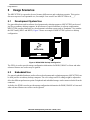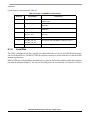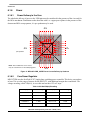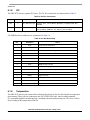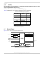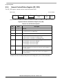
1
Freescale Semiconductor
Document Number: MPC8572DSUG
Rev. 1, 01/2009
MPC8572 Development System
User’s Guide
by
1
Networking and Multimedia Group
Freescale Semiconductor, Inc.
Austin, TX
Overview
MPC8572DS is a high-performance computing, evaluation
and development platform supporting the MPC8572
processor built on Power Architecture technology.
MPC8572DS is optimized to support two high-bandwidth
memory ports for the processor core, as well as the three
PCI-express ports, two of which are dedicated for graphics
or other slot-based cards, and the third dedicated for Linux
I/O with the ULI south-bridge.
MPC8572DS is designed for standard ATX form-factor,
allowing it to be used in a standard ATX chassis. The system
is lead-free and RoHS-compliant.
2
Features
The features of the MPC8572DS evaluation/development
board are as follows:
• MPC8572 Processor
— See full feature list from the device reference
manual
— PCI Express (SerDes1)
– x4 connections to PCIe slot2
© Freescale Semiconductor, Inc., 2009. All rights reserved.
1.
2.
3.
4.
5.
6.
7.
8.
9.
10.
A.
B.
Contents
Overview . . . . . . . . . . . . . . . . . . . . . . . . . . . . . . . . . . . 1
Features . . . . . . . . . . . . . . . . . . . . . . . . . . . . . . . . . . . . 1
Block Diagram . . . . . . . . . . . . . . . . . . . . . . . . . . . . . . 3
Evaluation Support . . . . . . . . . . . . . . . . . . . . . . . . . . . 4
Usage Scenarios . . . . . . . . . . . . . . . . . . . . . . . . . . . . . 6
Architecture . . . . . . . . . . . . . . . . . . . . . . . . . . . . . . . . 7
Configuration . . . . . . . . . . . . . . . . . . . . . . . . . . . . . . 45
Debug Support . . . . . . . . . . . . . . . . . . . . . . . . . . . . . 54
Programming Model . . . . . . . . . . . . . . . . . . . . . . . . . 54
Revision History . . . . . . . . . . . . . . . . . . . . . . . . . . . . 71
References . . . . . . . . . . . . . . . . . . . . . . . . . . . . . . . . . 72
Lead-Free/RoHS Issues . . . . . . . . . . . . . . . . . . . . . . 72
Features
•
•
•
•
— PCI Express (SerDes2)
– x2 connections to PCIe slot1
— PCI Express (SerDes3)
– x2 connectivity to ULI M1575 South bridge
— SGMII Support
– x4 connectivity to SGMII PHY plug-in card.
— Trusted Platform Modules using I2C and ULI LPC
South Bridge
— NVIDIA/ULI M1575
— IDE Controller
– Parallel ATA
– Serial ATA 2 (RAID-1 Support)
— USB Interface
– UHCI/EHCI USB 2.0 Interface
– Two ports on stacked USB header
– Two ports on PCB header (mates with standard PC chassis connectors)
— PCI
– Two 5-V, 33-MHz slots.
— Other
– LPC (socketed) boot flash
– Real-time Clock
– NVRAM: 256-byte
System Logic
— Manages system reset sequencing
— Manages system bus and PCI clock speed selections
— Controls system and monitoring
— Implements registers for system control and monitoring
Clocks
— System and DDR clocks
– Switch selectable to one of eight common settings in the interval.
– Default = 66MHz Sysclk.
– Software selectable via FPGA in 1MHz increments.
Power Supplies
— VCORE supplied by a programmable switcher.
— VTT/VREF for DDR
— General I/O power
MPC8572 Development System User’s Guide, Rev. 1
2
Freescale Semiconductor
Block Diagram
3
Block Diagram
Figure 1 shows the overall architecture of the MPC8572DS system
SGMII
PCIe Slot 1
PCIe Slot 2
VTT Power
PEX1 x4
DDR-2 DIMM
PEX2 x2
DDR-2
SGMII x4
VTT Power
NOR Flash
NAND Flash
DDR-2 DIMM
MPC8572
FSRAM
DDR-2
ATX I/O
Panel I/O
PromJet
SER
Local Bus
Actel
Pixis
RJ45
TSECs
Interrupt
Clocks
RJ45
Vitesse
PHY
RJ45
RJ45
PEX3 x2
Audio
PCI
PCI
32-bit Bus
Panel I/O
ULI M1575
AUD
2
USB
USB
KB
Panel I/O
IDE
LPC
SIO
2
PS/2
SATA
TPM
Note: TPM is no longer supported.
Figure 1. MPC8572DS Block Diagram
MPC8572 Development System User’s Guide, Rev. 1
Freescale Semiconductor
3
Evaluation Support
4
Evaluation Support
MPC8572DS is intended to evaluate as many features of the MPC8572 as are reasonable within a limited
amount of board space and cost limitations.
Table 1. MPC8572DS Evaluation Summary
MPC8572 Feature
System
Evaluation Support/Methods
SerDes 1
PCI Express
Connects to PCIExpress slot via PEX/4X connection.
Testable via PCIExpress card (graphics) or CatalystTM PCIExpress
control/monitoring card.
Traffic monitoring via Tek/Agilent passive mid-point probing.
SerDes 2
PCI Express
Connects to PCIExpress slot via PEX/2X connection.
Testable via PCIExpress card (graphics) or CatalystTM PCIExpress
control/monitoring card.
Traffic monitoring via Tek/Agilent passive mid-point probing.
SerDes 3
PCI Express
Connects to ULI south bridge via PEX/2X connection.
Testable by functional code.
Traffic monitoring via Tek/Agilent passive mid-point probing.
SGMII
SGMII
Connects to SGMII riser slot via x4 lane connection.
Memory Controller DDR3
Ethernet
Local Bus
Not supported.
DDR2 (2 channels)
Independent VIO supplies (1.8V).
Independent VTT supplies.
Debugging uses Tek/NextWave analyzer breakout cards.
No special MECC/Debug tap.
VTT
Resistor dividers allow setting different VTT thresholds.
Each DIMM can use VTT VREF or disconnect and use resistor dividers for custom
threshold use/analysis.
All
Supports RGMII modes.
Uses VSC8244 QuadPHY (for software compatibility). Four ports attached.
Port 1, 2, 3, 4
Connects to two RJ45 dual connectors for rear-panel access.
NOR Flash
1 bank of 16-bit, 128MB NORflash
Option for PromJet access.
Pixis
Internal registers implementing:
Board ID
VDD control
Frequency reset.
Self-reset reset
NAND Flash
4 GB.
FSRAM
UPM operated 512K x 36 bit NOBL.
MPC8572 Development System User’s Guide, Rev. 1
4
Freescale Semiconductor
Evaluation Support
Table 1. MPC8572DS Evaluation Summary (continued)
MPC8572 Feature
I2C
System
Evaluation Support/Methods
Bus 1
Boot initialization code
Voltage Monitoring
SERDES CLOCK 1
AT97SC3203S Trusted Platform Module
Bus 2
DDR Bus 1 and 2 DIMM modules SPD EEPROMs
System (MAC address storage, serial number, etc.)
Board EEPROM
PEX/PCI Slots (as “SMBus”)
Serial
UART ports 0-1
UART: Supports 2-wire and 4-wire modes for two serial ports muxed to one serial
connector.
Clocking
DDRCLK
Digitally settable clock generator.
Switch-selectable coarse settings.
Software-selectable fine settings.
SYSCLK
Digitally settable clock generator.
Switch-selectable coarse settings.
Software-selectable fine settings.
REFCLK
SERDES reference clocks to SERDES’s on MPC8572, ULI and slots.
RTCCLK
Reference clock.
DMA
DMA(0:3)
REQ/ACK/Done
Test points.
IRQs
IRQ*(0:11)
EVENT switch asserts IRQ* but can drive SRESET via software setting.
IRQ_OUT
SRESET*
VCore Power
VDD
VID switch settable
Pixis software-monitored/controlled voltages
7-bit encoded voltage
MPC8572 Development System User’s Guide, Rev. 1
Freescale Semiconductor
5
Usage Scenarios
5
Usage Scenarios
The MPC8572DS is expected to be used in many different test and evaluation scenarios. This section
discusses aspects of each potential use; for example “how would I use MPC8572DS to do ___?”
5.1
Development System Use
For general hardware and/or software development and evaluation purposes, MPC8572DS can be used
just like an ordinary desktop computer. In the absence of special hardware or software configuration,
MPC8572DS operates identically to a development/evaluation system such as “Sandpoint” or a member
the HPC family (HPC1 and HPC2). Figure 2 shows an example of MPC8572DS system in a desktop
configuration.
MPC8572DS
Figure 2. MPC8572DS Desktop Configuration
The FPGA is used to provide startup configuration information for DINK, UBOOT or Linux and other
advanced features are used or may be ignored.
5.2
Embedded Use
For general embedded hardware and/or software development and evaluation purposes, MPC8572DS can
be used just like an ordinary desktop computer. The core voltage and PLL settings might be adjusted to
allow the different performance points. Peripherals and embedded storage can be connected to the PromJet
connector.
As before, the PIXIS is used to provide startup configuration information for DINK, UBOOT or Linux and
other advanced features are used or can be ignored.
MPC8572 Development System User’s Guide, Rev. 1
6
Freescale Semiconductor
Architecture
6
Architecture
The MPC8572DS architecture is primarily determined by the Freescale Semiconductor MPC8572 Power
processor, and by the need to provide typical OS-dependant resources (disk, ethernet, etc.).
6.1
Processor
MPC8572DS supports these Freescale Semiconductor processors:
• mpc8572 processor, all speeds
Table 2 lists the major pin groupings of the MPC8572.
Table 2. MPC8572 Summary
Signal Group
Pin Count
Details
DDR2 Memory 1
147
Section 6.1.1
DDR2 Memory 2
147
Section 6.1.1
MII Interface/Clock
3
Section 6.1.2
Gbit MAC 1
25
Section 6.1.2
Gbit MAC 2
25
Section 6.1.2
Gbit MAC 3
25
Section 6.1.2
Gbit MAC 4
25
Section 6.1.2
SERDES 1
48
Section 6.1.3.1
SERDES 2
24
Section 6.1.3.3
SERDES Extra
2
Section 6.1.3.2
Local Bus
67
Section 6.1.4
DMA
6
Section 6.1.11
MPIC
18
Section 6.1.7
System Control
8
Section 6.1.11
DUART
8
Section 6.1.5
I2C
4
Section 6.1.8
Debug
15
Section 6.1.11
Power Mgmt
1
Section 6.1.11
Clock
2
Section 6.1.11
Test
4
Section 6.1.11
JTAG/COP
5
Section 6.1.11
Thermal
2
Section 6.1.11
TOTAL
637
MPC8572 Development System User’s Guide, Rev. 1
Freescale Semiconductor
7
Architecture
6.1.1
DDR
The MPC8572 contains two memory controller capable of supporting DDR1 and DDR2 devices.
MPC8572DS supports DDR2 only, using industry-standard JEDEC DDR2 DIMM modules. The memory
interface includes all the necessary termination and I/O power and is routed so as to achieve maximum
performance on the memory bus.
The general DDR SDRAM architecture is shown in Figure 3.
MPC8572
MA[14:0]
MBA[1:0]
A[14:0]
BA[1:0]
MDQS[8:0]/MDQS[8:0]
MDM[8:0]
MDQ[63:0]
DQS/DQS
DM[8:0]
DQ[63:0]
CB[7:0]
MECC[7:0]
MCK[0:2]
MCK[0:2]
CK[0:2]
CK[0:2]#
MEM_RST
VTT Termination Plane
RAS
CAS
WE
CKE[1:0]
S[1:0]
comp cap
MRAS
MCAS
MWE
MCKE[1:0]
MCS[1:0]
DIMM #1 & #2
RESET#
I2C_SDA
I2C_SCK
SDA
GVDD
MVREF
VDD
SCL
VREF
DDR2 Power
VTT
Figure 3. MPC8572DS Memory Architecture
Note also that MPC8572DS does not directly support the use of the MECC pins to access internal debug
information, as MPC8572DS does not provide the special multiplexer and thus has a simpler routing and
signal integrity status. On the other hand, MPC8572DS does not interfere with this path, so access to debug
information on the MECC pins is possible with the use of a NextWave (or equivalent) DDR logic analyzer
connector and the use of non-ECC DDR modules.
Differential clocks for the memory module are supplied by the MPC8572; these signals are not parallel
terminated, unlike the single-ended memory signals.
32-bit DDR2 interface mode is supported; from the viewpoint of the MPC8572DS board, the unused lower
MDQ/MDS/MDM signals are simply inactive.
MPC8572 Development System User’s Guide, Rev. 1
8
Freescale Semiconductor
Architecture
The DDR2 power supply the following interface voltages:
• VDDQ & VDD_IOup to 18A
• MVREFup to 10mA
DDR2 memory port signals and connections are summarized in Table 3.
Table 3. DDR2 Memory Connections (Per Controller)
Pin
Count
Signal Names
Compensation
Termination
Connections
64
MDQ[0:63]
—
—
MPC8572, DIMM
8
MECC[0:7]
—
—
MPC8572, DIMM
9
MDM[0:8]
—
—
MPC8572, DIMM
18
MDQS[0:8](p,n)
—
—
MPC8572, DIMM
3
MBA[0:2]
22pF
47 Ω
MPC8572, DIMM, VTT
16
MA[0:15]
22pF
47 Ω
MPC8572, DIMM, VTT
1
MWE*
22pF
47 Ω
MPC8572, DIMM, VTT
1
MRAS*
22pF
47 Ω
MPC8572, DIMM, VTT
1
MCAS*
22pF
47 Ω
MPC8572, DIMM, VTT
2
MCS*[0:1]
22pF
47 Ω
MPC8572, DIMM, VTT
2
MCS*[2:3]
—
—
2
MCKE[0:1]
22pF
47 Ω
2
MCKE[2:3]
—
—
Not used
6
MCK_0[0:2](p,n)
—
—
MPC8572, DIMM
6
MCK_0[3:5](p,n)
—
—
Not used
2
MODT[0:1]
22pF
47 Ω
2
MODT[2:3]
—
—
6.1.1.1
Not used
MPC8572, DIMM, VTT
MPC8572, DIMM, VTT
Not used
Compatible DDR2 Modules
The DDR interface of MPC8572DS and the MPC8572 should work with any JEDEC-compliant 240-pin
DDR2 DIMM module, provided that the devices are 64Mib to 4Gib in size, and that the devices are x8,
x16 or x32 bits in width. Table 4 shows several DIMM modules which are believed compatible; those
which have been tested and confirmed are noted as such.
Table 4. Typical DDR2 Modules
Mfg.
Micron
Part Number
MT9HTF6472AY-800
Size
512 MB
Speed
DDR2-800
Data Rate
Notes
—
—
Verified?
Pending
MPC8572 Development System User’s Guide, Rev. 1
Freescale Semiconductor
9
Architecture
6.1.2
Ethernet
The MPC8572 supports four 10/100/1000Base-T Ethernet ports. On MPC8572DS, the VSC8244 PHY is
used to provide access to these four ports. Both Ethernet ports come out the rear ATX I/O panel as shown
in Table 5.
Table 5. Ethernet Port Locations
mpc8572
TSEC #
ATX Port
$
PHY
Address
1
1
0
Bottom of “normal” RJ45 stack
Quasi-standard rack-mount server location.
2
2
1
Bottom of “extra” RJ45 stack
Non-standard
3
3
2
Top of “normal” RJ45 stack
Quasi-standard rack-mount server location.
4
4
3
Top of “extra” RJ45 stack
Non-standard
Location
Description
MPC8572DS uses the Vitesse VSC8244 quad-PHY, which provides a direct connection to the four
GMACs and the RGMII interface. The remaining connections are essentially clocks and resets. Signals
are summarized in Table 6.
Table 6. Ethernet Port Connections
Category
Pin
Count
Ethernet MI
2
EC_MDC, EC_MDIO
MPC8572, VSC8244
GbE Clocking
1
EC_GTX_CLK125
MPC8572, VSC8244
ETSECx
12
TSECx_TXD(3:0), TSECx_TX_EN,
TSECx_TX_CLK, TSECx_RXD(3:0),
TSECx_RX_DV, TSECx_RX_CLK
MPC8572, VSC8244
—
13
TSECx_TXD(7:4), TSECx_TX_ER,
TSECx_GTX_CLK, TSECx_CRS, TSECx_COL,
TSECx_RXD(7:4), TSECx_RX_ER
n/c (unless config pin)
Signal Names
Connections
The PHY addresses are 0 to 3, for GMAC/Ethernet ports 0 to 3, respectively.
MPC8572 Development System User’s Guide, Rev. 1
10
Freescale Semiconductor
Architecture
MPC8641D
VSC8244
MI
GMAC 1
0
GMAC 2
1
GMAC 3
2
GMAC 4
3
125 MHz
Figure 4. Ethernet Architecture
Refer to the Vitesse website for programming information for the PHY.
6.1.3
SERDES Ports
The MPC8572 contains two high-speed SERDES ports. MPC8572DS uses these ports for 3 PCIExpress
(x4 slot, x2 slot, and x2 ULI South bridge) and 4 SGMII channels to the optional SGMII slot.
All signals are connected using PCIExpress routing topology and spacing rules, and includes a AC
coupling capacitor at the transmit pins.
SerDes signals not used for connections are connected to test points or pull-ups (as appropriate) and are
otherwise unused. Signals are summarized in Table 7.
Table 7. SerDes Port Connections
Category
Controller
Pin
Count
SerDes 1
PEX 1
8
SD1_RX[0:3](p,n)
MPC8572, slot 2 (PCIe x4)
PEX1
8
SD1_TX[0:3](p,n)
MPC8572, slot 2 (PCIe x4)
PEX 2
4
SD1_RX[4:5](p,n)
MPC8572, slot 1 (PCIe x2)
PEX 2
4
SD1_TX[4:5](p,n)
MPC8572, slot 1 (PCIe x2)
PEX 3
4
SD1_RX[6:7](p,n)
MPC8572, ULI M1575 (PCIe x2)
PEX 3
4
SD1_TX[6:7](p,n)
MPC8572, ULI M1575 (PCIe x2)
SGMII 1
8
SD2_RX[0:3](p,n)
MPC8572, SGMII slot (SGMII x4)
SGMII 1
8
SD2_TX[0:3](p,n)
MPC8572, SGMII slot (SGMII x4)
SerDes 2
Signal Names
Connections
MPC8572 Development System User’s Guide, Rev. 1
Freescale Semiconductor
11
Architecture
6.1.3.1
SerDes 1: PCI Express x4 to Slot 2, x2 to Slot 1
The SerDes 1 block provides two PCI Express slots, each connected to a PCI Express x16 slot on the
MPC8572DS motherboard. Each SerDes port supports only up to a x4 or x2 protocol width respectively,
but an x16 connector is used to allow the use of standard PCI Express video cards (possibly at a reduced
width). The primary test mechanism of the SerDes 1 port is expected to be a PCI Express x4 connection
using standard graphics cards (ATI, NVidia) or PCI Express test boards (Catalyst). Figure 5 shows an
overview.
AC Term
MPC8572
SD1_TX[0:3](p,n)
TX
PEX1
Slot 2
SD1_RX[0:3](p,n)
RX
AC Term
TX
Mid-Bus
Probe
SD1_TX[4:5](p,n)
SD1_RX[4:5](p,n)
RX
PEX2
Slot 1
PEXCLKs
Figure 5. PCI Express x4 and x2 Slot Connections Overview
Signals are summarized in Table 8.
Table 8. PCI Express x4 and x2 Slot Connections
Pin Count
Signal Names
Connections
8
SD1_RX[0:3](p,n)
MPC8572
PCI Express Slot 2
8
SD1_TX[0:3](p,n)
MPC8572
PCI Express Slot 2
2
SD1_RX[4:5](p,n)
MPC8572
PCI Express Slot 1
2
SD1_TX[4:5](p,n)
MPC8572
PCI Express Slot 1
2
SD1_REFCLK(p,n)
MPC8572
ICS9FG108 Clock generator
2
SD1_PLL_TPA
SD1_PLL_TPD
MPC8572
Test point
2
SD1_TXCLK(p,n)
MPC8572, not used, testpoints
2
SD1_IMP_CAL_TX
SD1_IMP_CAL_RX
Connected to 100 and 200 Ohm calibration resistors.
1
AGND_SRDS
Tied directly to ground.
MPC8572 Development System User’s Guide, Rev. 1
12
Freescale Semiconductor
Architecture
6.1.3.2
SerDes 1: PCI Express x2 to ULI South Bridge
The MPC8572 SerDes 1 block provides a PCI Express x2 that is connected to the ULI M1575 South
Bridge device that provides many resources for running Linux. Because this is not a slot-based connection,
a mid-point bus probe is provided for connecting a PCIe analyzer. Figure 6 shows an overview.
AC Term
MPC8572
SD1_TX[6:7](p,n)
TX
Mid-Bus
Probe
RX
RX
ULI
AC Term
SD1_RX[6:7](p,n)
TX
REFCLK_SD1(p,n)
REFCLK_MIDBUS(p,n)
REFCLK_M1575(p,n)
Figure 6. PCI Express x2 to South Bridge Overview
Connections are summarized in Table 9.
Table 9. PCI Express x2 to South Bridge Connections
Pin Count
6.1.3.3
Signal Names
Connections
4
SD1_RX[6:7](p,n)
MPC8572
ULI M1575
4
SD1_TX[6:7](p,n)
MPC8572
ULI M1575
SerDes 2: SGMII x4
The MPC8572 SerDes2 block also provides a x4 SGMII interface. On the MPC8572DS, these lanes are
connected to a dedicated SGMII slot, and a special SGMII-GbE plug-in card is designed for test and
evaluation. Figure 7 shows an overview.
AC Term
MPC8572
TX
SD2_TX[0:3](p,n)
RX
SGMII
Slot
RX
SD2_RX[0:3](p,n)
TX
REFCLK_SD2(p,n)
Figure 7. SGMII x2 Overview
MPC8572 Development System User’s Guide, Rev. 1
Freescale Semiconductor
13
Architecture
Connections are summarized in Table 10.
Table 10. Serdes 2 x4 SGMII Port Connections
Pin Count
6.1.4
Signal Names
Connections
2
SD2_REFCLK(p,n)
MPC8572
ICS841 Clock
8
SD2_RX[0:3](p,n)
MPC8572
SGMII Slot
8
SD2_TX[0:3](p,n)
MPC8572
SGMII Slot
2
SD2_PLL_TPA
SD2_PLL_TPD
MPC8572
Test point
2
SD2_TXCLK(p,n)
unused, testpoints
2
SD2_IMP_CAL_TX
SD2_IMP_CAL_RX
Connected to 100 and 200 Ohm calibration resistors.
1
AGND_SRDS2
Tied directly to ground.
Local Bus
The eLBC (embedded Local Bus Controller) is a split architecture, a fast side for NoBl SRAM and slow
side for flash and FPGA. For MPC8572DS, the local bus connects to various flash devices and the PIXIS
internal register space.
MPC8572DS uses external address demultiplexers to generate the local bus address, rather than using the
provided de multiplexed address. To keep overall routing and costs to a minimum, 16-bit devices are used.
MPC8572 Development System User’s Guide, Rev. 1
14
Freescale Semiconductor
Architecture
Figure 8 shows an overview
MPC8572
LAD
LALE
Latch/
Buffer
FastLA
Buffer
LA
NOR Flash
S29GL01GP11FFI010
LBCTL
SRAM
CY7C1370D
NAND Flash
K9NBG08U5M-P
LBCLK
LSYNC
PromJet
LBCS
LBWE
LBGPL
LBCLK
NORCS0
NORCS1
NANDCS1
JETCS1
FOE
PIXIS FPGA
cfg_lbmap[0:1]
Figure 8. Local Bus Overview
Local Bus connections are summarized in Table 11.
Table 11. Local Bus Chip Select Mapping
Flash
Selection
(cfg_lbmap)
NOR
Flash
PromJet
NAND Flash
PIXIS
SRAM
CFG_FLASHBANK
Description
00
LCS0
LCS1
LCS[2,4:6]
LCS3
LCS7
0
Normal; boot from NOR flash
01
LCS1
LCS0
LCS[2,4:6]
0
Boot from PromJet (code
injection)
10
LCS2
LCS1
LCS[0,4:6]
0
Normal; boot from NAND
flash
11
LCS0
LCS1
LCS[2,4:6]
1
Swap flash halves; boot from
NOR flash but with MSB of
address toggled.
MPC8572 Development System User’s Guide, Rev. 1
Freescale Semiconductor
15
Architecture
The “address toggle” feature mentioned in Table 11 is implemented as an XOR gate in-line with the most
significant address of the flash, as shown in Figure 9.
MPC8572
NORFlash
A[30:6]
A
A[0:24]
A5
A25
PIXIS
CFG_FLASHBANK
Figure 9. Flash Address Toggle
When CFG_FLASHBANK is ‘0’, A25 is not altered and so the flash behaves as normal. When
CFG_FLASHBANK is ‘1’ (which occurs when LB_MAP=”00”), A25 is toggled such that data in the high
half of the flash appears at the bottom, and vice-versa. Note that CFI flash programming algorithms do not
use higher address bits, so such algorithms are not affected.
Local bus signals are summarized in Table 12.
Table 12. Local Bus Connections
Pin
Count
Signal Names
Connections
32
LAD[0:31]
NORFlash: LAD[0:15] to D[15:0]
NANDFlash: LAD[0:7] to D[7:0]
PIXIS: LAD[0:7] to D[7:0]
8
LCS*[0:7]
See Table 11.
1
LWE[0]*_LFWE_LBS*[0]
NANDFlash: LFWE to WE*
NORFlash: LWE0* to WE
MRAM: LWE0* to WE*
3
LWE[1:3]*_LBS*[1:3]
unused
1
LBCTL
—
1
LALE
—
1
LGPL0/LFCLE
NANDFlash: LFCLE to CLE
1
LGPL1/LFALE
NANDFlash: LFCLE to ALE
1
LGPL2/LOE/LFRE
NANDFlash: LFRE to RD_B
1
LGPL3/LSDCAS
unused
MPC8572 Development System User’s Guide, Rev. 1
16
Freescale Semiconductor
Architecture
Table 12. Local Bus Connections (continued)
Pin
Count
6.1.5
Signal Names
Connections
1
LGPL4/LUPWAIT/LGTA
NANDFlash: LFCLE to R/B_B
1
LGPL5
unused
3
LCLK[0:2]
unused
Serial Ports
MPC8572DS muxes the two serial ports (UART0 and UART1) to a DB9 female connector located in the
ATX I/O gasket area, and RTS/CTS flow control is supported on this connector. The user may select which
serial port is connected to the DB9 via header J9. In normal operation, UART0 is selected (jumper
un-installed on board).
Note that newer versions of the MPC8572DS assembly revision X5 (revision D PCB) or later do not mux
the two serial ports but added a header (J100) to allow full utilization of UART1 via a custom cable.
UART0 is always available on the DB9 connector and UART1 is always available at J100 with a custom
cable. J9 is no longer able to mux the two ports. The custom cable is not provided, but may easily be
fabricated if two serial ports are desired. For most applications and debug, one serial port is sufficient.
Figure 10 shows construction details for this cable.
The UART programming model is a standard PC16550-compatible register set. Baud rate calculations for
the divisor latch registers (DLL and DML) is typically done by reading the PIXIS SYSCLK register to
determine the MPC8572 reference clock input frequency. The baud rate divisors can then be calculated
using the formula described in the User’s Manual.
J100
5
3
2 1
9-pin DB male” plug
rear view
DE9M (sometimes
called “DB9M”)
TXD
pin 1
pin 2
GND
pin 3
RXD
“Berg” receptacle
(0.1” spacing)
Figure 10. Serial Port 2 Cable Details
MPC8572 Development System User’s Guide, Rev. 1
Freescale Semiconductor
17
Architecture
6.1.6
6.1.6.1
Power
Power Delivery to the Core
The wholesale delivery of power to the VDD pins must be considered in the presence of the vias used for
the BGA attachment. Simulation results show that with 1 oz. copper power planes in the presence of the
documented BGA escape pattern, 6 A per quadrant may be used.
6A
6A
6A
per quadrant
Note: The arrowed lines are not traces,
they are current flows on the underlying plane.
6A
Figure 11. MPC8572 VDD_CORE Planar Current Delivery by Quadrant
6.1.6.2
Core Power Regulator
MPC8572DS uses the SemTech SC457 single-phase switching power controller. This device can produce
at least 35A over the range of interest for the MPC8572, with additional margin above and below. The
voltage encoding, called VID(6:0), is seven bits and encodes 12.5 mV steps.
Table 13. SC458 VID(6:0) Encoding
VID(6:0)
VCORE Voltage
VID(6:0)
VCORE Voltage
0000000
1.5000
0011011
1.1625
0000001
1.4875
0011100
1.1500
0000010
1.4750
0011101
1.1375
0000011
1.4625
0011110
1.1250
0000100
1.4500
0011111
1.1125
MPC8572 Development System User’s Guide, Rev. 1
18
Freescale Semiconductor
Architecture
Table 13. SC458 VID(6:0) Encoding (continued)
6.1.7
VID(6:0)
VCORE Voltage
VID(6:0)
VCORE Voltage
0000101
1.4375
0100000
1.1100
0000110
1.4250
0100001
1.0875
0000111
1.4125
0100010
1.0750
0001000
1.4000
0100011
1.0625
0001001
1.3875
0100100
1.0500
0001010
1.3750
0100101
1.0375
0001011
1.3625
0100110
1.0250
0001100
1.3500
0100111
1.0125
0001101
1.3375
0101000
1.0000
0001110
1.3250
0101001
0.9875
0001111
1.3125
0101010
0.9750
0010000
1.3000
0101011
0.9625
0010001
1.2875
0101100
0.9500
0010010
1.2750
0101101
0.9375
0010011
1.2625
0101110
0.9250
0010100
1.2500
0101111
0.9125
0010101
1.2375
0110000
0.9000
0010110
1.2250
0110001
0.8875
0010111
1.2125
0110010
0.8750
0011000
1.2000
0110011
0.8625
0011001
1.1875
0110100
0.8500
0011010
1.1750
0110101
0.8375
Interrupts
MPC8572DS contains numerous external interrupt connections. Secondly, whenever the PCI Express
controller is in root complex mode and it receives an inbound INTx asserted or negated message
transaction, it asserts or negates an equivalent internal INTx signal to the PIC.
The internal INTx signals from the PCI Express controller are logically combined with the interrupt
request (IRQn) signals so that they share the same OpenPIC external interrupt controlled by the associated
EIVPRn and EIDRn registers.
If PCI Express INTx signalling is used, then the PIC must be configured so that external interrupts are
active-low (EIVPRn[P] = 0) and level-sensitive (EIVPRn[S] = 1), as the OpenPIC interrupt is now shared
between multiple entities. If an interrupt occurs, the interrupt service routine must poll both the external
MPC8572 Development System User’s Guide, Rev. 1
Freescale Semiconductor
19
Architecture
sources connected to the IRQn input and the PCI Express INTx sources to determine from which path the
external interrupt came.
Table 14. Interrupt Connections
Category
Pin
Count
MCP
2
MCP0/1*
pullup (unused)
IRQ
12
IRQ0*
unused
PCI Express 1—INTA
IRQ1*
PCI Slot 1—INTD
PCI Slot 2—INTC
PCI Express 1—INTB
IRQ2*
PCI Slot 1—INTA
PCI Slot 2—INTD
PCI Express 1—INTC
IRQ3*
PCI Slot 1—INTB
PCI Slot 2—INTA
PCI Express 1—INTD
IRQ4*
PCI Slot 1—INTC
PCI Slot 2—INTB
PCI Express 2- INTA
IRQ5*
unused
PCI Express 2- INTB
IRQ6*
SGMII slot
PCI Express 2- INTC
IRQ7*
SGMII slot
PCI Express 2- INTD
IRQ8*
PIXIS FPGA
PCI Express 3- INTA
IRQ9*
ULI M1575 Bridge
PCI Express 3- INTB
IRQ10*
VSC8244 PHY INT*
PCI Express 3- INTC
IRQ11*
unused
PCI Express 3- INTD
IRQ_OUT*
unused. Can be routed back to IRQ0 or IRQ2 if resistors
are populated.
1
Signal Names
External Connections
Internally Mapped
to OpenPIC
—
—
MPC8572 Development System User’s Guide, Rev. 1
20
Freescale Semiconductor
Architecture
Figure 12 shows a conceptual diagram of the MPC8572DS system interrupt scheme.
FPGA
Vitesse PHY
IO_R5
SMI
MDINIT_0 MDINIT_1 MDINIT_2 MDINIT_3
VCC_3.3
R5
C11
P18
N16
N17
N18
U37
ULI South Bridge
Note:
Active High
AG28
INTR
PCI_SLOT 1&2
ULI PIRQ A-D
PEX1 INTA-D
SGMII
PEX2 INTA-D
PEX3 INTA-D
nPIDEIRQ
nSIDEIRQ
NMI
LPC_SERIRQ
nSMI
IRQ11
IRQ10
IRQ9
IRQ8
IRQ7
IRQ5
IRQ6
IRQ_OUT
MCP1
VCC_3.3
MCP0
IRQ4
IRQ3
IRQ2
IRQ1
IRQ0
AC2
MPC8572
nPIRQA
nPIRQB
nPIRQC
nPIRQD
nPIRQE
nPIRQF
nPIRQG
nPIRQH
D5
D6
C1
E3
D2
E2
E5
E6
1
2
3
4
0
1
2
3
AG21
NC
NC
8572
IRQ[1:4]
VCC_3.3
J47
31
IDE
Primary
AG21
SIO
30
LPC_SERIRQ
50
nIO_SMI_GP27
NC
TP TP
8572
IRQ[6:7]
SGMII
Riser
IRQ6
IRQ7
8572 PEX1 x4 Slot #2 – IRQ[0:3]
(Tied Internally)
82
84
8572
IRQ[1:4]
IRQ3
IRQ4
IRQ1
IRQ2
A6
B7
A7
B8
J20
J21
ULI PCBus
Slot 2
ULI PCBus
Slot 1
INTA
INTB
INTC
INTD
8572
IRQ[1:4]
IRQ2
IRQ3
IRQ4
IRQ1
A6
B7
A7
B8
INTA
INTB
INTC
INTD
8572 PEX2 x2 Slot #1 – IRQ[4:7]
(Tied Internally)
Figure 12. MPC8572DS Concept of System Interrupts
MPC8572 Development System User’s Guide, Rev. 1
Freescale Semiconductor
21
Architecture
6.1.8
I2C
The MPC8572 has two separate I2C buses. The I2C bus connections are summarized in Table 15.
Table 15. I2C Bus Connections
Category Pin Count
1
Signal Names
Connections
I2C1
2
I2C1_SDA, I2C1_SCL MPC8572, TPM 1, Current Monitor (MCP3021), ics9fg108, FPGA, Boot
EEPROM
I2C2
2
I2C2_SDA, I2C2_SCL MPC8572, ICS841, DIMM Sockets, 2 Board specific EEPROMs, PCI Express
Slots (as SMBus), SGMII slot, ULI, SIO, PCI slots (as SMBus).
Note: TPM is no longer supported.
I2C/SMB bus device addresses are summarized in Table 16.
Table 16. I2C Bus Device Map
Bus
I2C Address
1
0x55
1
52 write 52 read
1
0x6E
1
Device
Current Monitor (MCP3021),
Trusted Platform Module (TPM)
I2C9FG108 (SERDES clock generator)
Not currently implemented. Actel FPGA
1
0x50 or 0x51
4KiB EEPROM (reset initialization)
2
0x6E
ICS841
2
0x51
DIMM Channel 1 Socket
2
0x52
DIMM Channel 2 Socket
2
0x56
DINK ENV storage/general purpose 256x8 eeprom
2
0x57
SYSTEM ID EEPROM (write protected) 256x8 eeprom
2
SMBus
PCIexpress slots
2
SMBus
Legacy PCI slots
2
0x50
SGMII slot
2
0x5A
SIO LPC
2
(programmable)
ULI M1753 SMB interface
Note: These are “DINK”-style addresses, which ignore the LSB of the transmitted address (the read/write bit).
6.1.9
Temperature
The MPC8572 has two pins connected to a thermal body diode on the die, allowing direct temperature
measurement. These pins are connected to the LPC47M192 SIO logic, which contains standard
PC-compatible hardware monitoring logic, including a thermal measurement port. This device allows
direct reading of the temperature of the die.
MPC8572 Development System User’s Guide, Rev. 1
22
Freescale Semiconductor
Architecture
Thermal management signals are summarized in Table 17.
Table 17. Thermal Management Connections
Category
Pin
Count
Thermal
2
Signal Names
TEMP_ANODE, TEMP_CATHODE
6.1.10
Mechanical Clearance
6.1.11
Other
Connections
MPC8572, LPC47M192
The remaining MPC8572 signals are summarized in Table 18.
Table 18. Miscellaneous MPC8572 Connections
Category
Pin Count
Clock
4
Signal Names
Connections
SYSCLK/DDRCLK
ICS307 clock synthesizer
RTC
ICS9F108->MPC94551 -> RTC pin
CLK_OUT
Test point w/adjacent ground.
DMA
10
DMA1_DREQ[0:1]*
DMA1_DACK[0:1]*
DMA1_DDONE[0:1]*
DMA2_DREQ[0]*
DMA2_DREQ[2]*
DMA2_DACK[0]*
DMA2_DDONE[0]*
Test points.
STATUS
3
ASLEEP
To PIXIS for monitoring.
Buffered LED monitor
READY P1
Buffered LED monitor
READY P2/TRIG_OUT
Debug P6880 Header
Buffered LED monitor
HRESET
From PIXIS reset controller (hence from COP, Power Good, etc.)
HRESET_REQ
To PIXIS, test point
SRESET
From PIXIS
CKSTP_IN[0:1]*
COP Header, test point
CKSTP_OUT[0:1]*
COP Header, test point
TRIG_IN
Debug P6880 Header
MSRCID[0:4]
Debug P6880 Header
MDVAL
Debug P6880 Header
TEST_SEL
Pull-ups
System Control
Debug
Test
4
16
4
MPC8572 Development System User’s Guide, Rev. 1
Freescale Semiconductor
23
Architecture
Table 18. Miscellaneous MPC8572 Connections (continued)
Category
Pin Count
JTAG
5
General
Purpose Out
Test
6.2
Signal Names
Connections
TCK
COP Header
TDI
COP Header
TDO
COP Header
TMS
COP Header
TRST
PIXIS
8
GPINOUT[0:7]
test points and Put-downs
4
TEST_SEL
Pull-ups
South Bridge
MPC8572DS uses the ULI M1575”Super South Bridge” to provide access to standard Linux I/O devices,
including:
• USB 2.0
• SATA 2 (“serial IDE”)
• PATA (“classic IDE”)
• PCI slots (non-PCIExpress graphics, customer-specific
• LPC flash (optional)
• Real-time clock/BBRAM
Figure 13 shows an overview of the ULI M1575
ULI M1575
PEX Link
PMU
LPC
SATA 2
Switch
PCI Bridge
PCI Bus
HD Audio
AC97 Audio
PATA
USB
1 EHCI
3 OHCI
Ethernet
10/100 baseT
Figure 13. ULI M1575 Overview
There are several other features of the ULI M1575, such as a 10/100baseT ethernet MAC, that are not
supported. By at large, the ULI M1575 supplies all the IO channels needed for full Linux, QNX or other
OS desktop support.
MPC8572 Development System User’s Guide, Rev. 1
24
Freescale Semiconductor
Architecture
The ULI M1575 is in a 628-Ball (31mmx31mm) BGA package, and requires several clock and power
sources as detailed in Section 6.5, “System Power,” and Section 6.6, “Clocks.” It is pin-compatible with
the ULI M1575 which may also be used.
6.2.1
ULI SATA Controller
The ULI M1575 supports a high-speed serial ATA (“SATA”) connections. The SATA controller supports
four ports at a 1.5 Gbit/s and 3.0 Gbit/s data rates, for SATA I and SATA II modes, respectively. AHCI
features are also supported. Figure 14 shows the overall connections of the SATA bus.
ULI M1575
SATA 1
SATA
SATA 2
SATA
SATA 3
SATA
SATA 4
SATA
Figure 14. SATA Architecture
6.2.2
ULI PATA Controller
The ULI M1575 supports four conventional parallel ATA (“PATA”), or classic IDE” connections.
MPC8572DS supports only the primary channel due to board space/routing restriction. The interface
supports 2-channel Ultra DMA-33/66/100/133 IDE bus master operations.
Figure 15 shows the overall connections of the PATA connections.
ULI M1575
PIDE
SIDE
Header
NC
Figure 15. PATA Architecture
6.2.3
ULI USB Controller
The ULI M1575 contains one EHCI (USB 2.0) and three OHCI (USB 1.1) controllers. The controllers
support all three speed definitions: HS (480Mbits/sec), FS (12Mbits/sec) and LS (1.5Mbits/sec). Though
MPC8572 Development System User’s Guide, Rev. 1
Freescale Semiconductor
25
Architecture
eight USB ports are supported, MPC8572DS supports only four due to I/O and board space limitations.
Figure 16 shows the overall connections of the USB ports.
ULI M1575
USB 0
MIC2077
USB 1
USB 2
USB 3
USB 4
USB 5
USB 6
USB Power
NC
USB 7
Header_2x5
Figure 16. USB Architecture
As shown, USB ports 0 and 1 connect to the stacked USB+RJ45 Ethernet connector, while ports 2 and 3
connect to a 2 ¥ 5 header. This header is compatible with the pinout of most ATX/microATX chassis
front-panel USB cable attachments.
6.2.4
ULI LPC Interface
The ULI M1575 supports a standard LPC (Low Pin Count) flash interface and MPC8572DS uses this
interface to access flash and to communicate with the SuperIO.
6.2.5
ULI Interrupts
The ULI M1575 collects interrupts from a variety of internal resources, and combines them with the
external interrupts (for PCI, those listed in Table 19). Interrupts are generated as PCIExpress MSI
interrupts, or legacy INTA:D# messages.
MPC8572 Development System User’s Guide, Rev. 1
26
Freescale Semiconductor
Architecture
6.2.6
ULI Audio
The ULI AC97 audio controller logic is connected to an AC97 codec, and then to a standard combined
AC97 audio line in/mic in/line out mini jack. Figure 17 shows the overall connections of the audio portion.
M1575
LINE IN
AC97
AC97
CODEC
MIC IN
LINE OUT
CD AUDIO
Figure 17. Audio Architecture
In addition to the standard ATX I/O audio connectors, there is a single “CD AUDIO” internal connector.
This could be used for CD audio, though analog capture is mostly unused on modern systems. It can be
useful for TV capture card audio outputs, however.
6.2.7
ULI Power/Power Control
Other than standby real-time clock/NVRAM battery power, all ULI power supplies are supplied by the
ATX power supply or other sources derived from it. VCC_HOT_1.8V is constantly provided to power the
APM/ACPI section.
6.2.8
ULI Other
The ULI M1575 has several useful features which are supported. These include:
• RTC
• NVRAM—256 bytes
6.2.9
ULI Unsupported Interfaces
The 10/100baseT ethernet, floppy and other interfaces are not supported.
6.3
SuperIO
MPC8572DS contains a SuperIO, the SMSC LPC47M192. The SIO is used to provide temperature
monitoring for the processor as well as the PCB, and hardware monitoring (voltage, fan speed, etc.). The
SIO also provides PS/2-type keyboard and mouse interfacing for legacy software, and numerous GPIO
pins to control miscellaneous features.
MPC8572 Development System User’s Guide, Rev. 1
Freescale Semiconductor
27
Architecture
Table 19 summarizes the SIO connections.
Table 19. SIO Support Table
Feature
Pins
Definition
Notes
12_IN_VID4
VCC_12V_BULK
—
5V_IN
VCC_5
—
3.3V_IN
VCC_3.3
—
2.5V_IN
VCC_DDRA_IO
—
1.8V_IN
VCC_1.8
—
1.5V_IN
VCC_XVDD (SERDES)
—
Vccp_IN
VCC_HOT_3.3
—
D0n, D0p
MPC8572 Thermal Diode
—
D1n, D1p
Tied to ground
—
Thermal Alert
—
—
—
Fan Tachometer
—
—
—
KCLK, KDAT
DIN6 stack (bottom)
—
MCLK, MDAT
DIN6 stack (top)
—
Voltage Monitoring
Temperature Monitoring
PS/2
GPIOs
6.4
GP14
IN
SGMII_PRESENT*
SGMII card occupied if low.
GP15
IN
S1_PRSNT*
Slot 1 occupied if low.
GP16
IN
S2_PRSNT*
Slot 2 occupied if low.
LED_GP60
OUT
SIO_LED
Direct drive of an LED.
System Control Logic
MPC8572DS contains a FPGA, the “Pixis”, which implements the following functions:
• Reset sequencing/timing combined with COP/JTAG connections.
• Map/re-map MPC8572 local bus chip selects to flash, compact flash, etc.
• Provide internal registers to monitor and control:
— Processor VCORE setting.
— Device Reset
— System bus speed monitoring/selection
• Miscellaneous system logic
— COP reset merging
— CF+ Sideband signals
— DMA trigger/monitor regs.
The FPGA is powered from standby power supplies and an independent clock. This ameliorates issues
with IO cells transition, and possibly accidentally (mis)controlling, the rest of the board during power up
of the FPGA. It does, however, raise a few different side-effects:
MPC8572 Development System User’s Guide, Rev. 1
28
Freescale Semiconductor
Architecture
•
•
IO and output cells must insure they do not drive any unpowered devices.
there are two asynchronous clock domains; signals which cross this barrier must be
metastable-hardened (or have no relevant AC timing, such as the case of reset signals, etc.)
The PIXIS is implemented in an Actel APA150 in a 256-pad micro-BGA. Figure 18 shows the overall
PIXIS architecture.
POWER_GOOD
(Various)
RESETSW
CPU
COP
IO
COP
RESETSEQ
RESETS
REGRESETS
CONFIG
Drive
VELA
LBUS
REGFILE
LOCALBUS
CONFIG
PCI TARGET
CONFIG
PCI
LBIO
Hot Clock Domain
PCI Clock Domain
Figure 18. PIXIS Overview
The principal portions of PIXIS are as follows:
COP
Handles merging COP header resets with on-board resets in a transparent manner.
RESETSEQ
Collects various reset/power-good signals and starts the global reset sequencer.
REGRESETS
Drives resets from the sequencer, from register-based software control, or from
VELA.
REGFILE
A dual-ported register file containing several sorts of registers.
LOCALBUS
Interface between processor and REGFILE
CONFIG
Monitors and/or sets selected configuration signals
PCI TARGET
Target-only interface between remote PCI devices and the REGFILE.
VELA
VELA is a simple machine to monitor requested changes in board configuration
and when detected, perform a power-on-reset / re-configuration of the target
system.
MPC8572 Development System User’s Guide, Rev. 1
Freescale Semiconductor
29
Architecture
6.4.1
6.4.1.1
Subsections
COP
Handles merging COP header resets with on-board resets in a transparent manner. It is critical that the COP
HRST* input resets the entire system EXCEPT for the COP JTAG controller (i.e. TRST* must not be
asserted). With COP not attached, it is critical that reset does assert TRST*. The COP core manages these
modal operation.
6.4.1.2
RESETSEQ
Collects various reset/power-good signals and starts the global reset sequencer.
MPC8572 Development System User’s Guide, Rev. 1
30
Freescale Semiconductor
Architecture
Figure 19 shows the overall reset process flow (vastly simplified).
Upon powerup, reset internals but don’t do
much since power is not present at the rest
of the system. Most I/Os are tristated.
HOT_RST = 0
IDLE
HOT_RST = 1
...reset internals
...tristate outputs
Internal
Reset
Wait for PWRGD from the main PSU. This
means the ULI or VELA toggled the PWRSW
signal and the system is powering up.
PWRGD = 0
PWAIT
PWRGD = 1
Main power is active, enable tri-stated outputs,
which have been set to appropriate levels
during power sequencing (“0” or “Z”).
Wait for subordinate PSUs to complete powerup.
PWRGD from the main PSU. This
Un-tristate outputs
Start Power Sequencer
Drive
PWAIT2
PWRGDxxx
PS_VCORE_PG = 1
PS_PLATFORM_PG = 1
...
Power is active, wait for clocks to stabilize. There
are no PLL_LOCK flags, so wait an appropriate
amount of time.
Power is stable. Release reset signals in an
orderly fashion.
CWAIT
CFGDRV = 0
HRESET = 0
...
DONE
ASLEEP = 0
RUN
Power fail, due to switch or to VELA.
Restart sequence.
PWRGD = 0
Figure 19. PIXIS Reset Overview
MPC8572 Development System User’s Guide, Rev. 1
Freescale Semiconductor
31
Architecture
Note that ASLEEP indicates the processors(s) have exited the reset state. It does not cause a reset, as the
processor can sleep for any number of reasons after hard reset has completed.
Note also that during power-down ALL I/O and output drivers must be tri-stated. After power up, drivers
MAY be driven. Normal operation and/or use of the VELA engine may cause some I/Os to be tri-stated.
6.4.1.3
REGRESETS
Copies reset signals from the sequencer, but also allows register-based software to individually asserted
reset tot the local bus, memory, and/or compact flash interfaces.
6.4.1.4
REGFILE
A dual-ported register file containing several sorts of registers.
Note that REGFILE must be able to accept (or arbitrate for) concurrent writes to the same register, though
this is not a statistically likely occurrence.
6.4.1.5
LOCALBUS
Interface between processor and REGFILE (and indirect access to LEGACYIO and CFIO. Since access
to the internal registers may be blocked, asynchronous (not ready) signalling is used.
6.4.1.6
CONFIG
Monitors and/or sets selected configuration signals.
In some instances, CONFIG maps switch settings into direct configuration outputs, while in others (such
as SYSCLK) it maps a 3-position switch into a 16-bit register initialization pattern, which is subsequently
used to initialize the clock generator.
6.4.1.7
PCI TARGET
Target-only interface between remote PCI devices (generally Data Blizzard) and the REGFILE.
The PCI vendor ID is 0x1957 (Freescale) and the device ID is 0x3002.
6.4.1.8
VELA
VELA is a simple micro sequencer used to monitor sequence in requested changes in board configuration
upon a signal (generally a register write from PCI). When detected, bits in a register allow performing a
power-off/power-on cycle and/or re-configuration of the target system.
1. If PX_VCTL[ GO ] = ‘1’ then STEP 2 else STEP 1
2. Wait 1 usWait for LB/PCI to quiesce.
3. Assert HRESET
4. Wait 200 us
5. If PX_VCFGEN0[ VID ] = ‘1’ then STEP 6 else STEP 8Change the voltage?
MPC8572 Development System User’s Guide, Rev. 1
32
Freescale Semiconductor
Architecture
6. Drive PX_VCORE0 => VID(6:0) pins.PS_VCORE_PG drops
7. Wait 1 usWait for PS_VCORE_PG to be set
8. If PX_VCFGEN0[ CLK ] = ‘1’ then STEP 9 else STEP 11Change SYSCLK and/or DDRCLK?
9. Drive PX_VCLKH+L => SYSCLK_S+R+V pins
10. Wait 200 usWait for SYSCLK
11. If PX_VCFGEN0[ MPLL ] = ‘1’ then STEP 12 else STEP 13Change MPX PLL?
12. Drive PX_VSPEED1[MPXPLL] => MPXPLL pins
13. If PX_VCFGEN0[ CPLL ] = ‘1’ then STEP 14 else STEP 15Change Core PLL?
14. Drive PX_VSPEED0[COREPLL] => COREPLL pins
15. If PX_VCFGEN0[ REFCLK ] = ‘1’ then STEP 16 else STEP 18Change RefClk?
16. Drive PX_VSPEED0[REFCLKSEL] => REFCLKSEL pins
17. Wait 200 usWait for SYSCLK
18. If PX_VCFGEN1[ BOOTLOC ] = ‘1’ then STEP 19 else STEP 20Change BootLoc?
19. Drive PX_BOOT[BOOTLOC] => BOOTLOC pins
20. If PX_VCFGEN1[ BOOTSEQ ] = ‘1’ then STEP 21 else STEP 22Change BootSeq?
21. Drive PX_BOOT[BOOTSEQ] => BOOTSEQ pins
22. If PX_VCFGEN1[ FLASH ] = ‘1’ then STEP 23 else STEP 25Change FlashMap/FlashBank?
23. Drive PX_BOOT[FMAP] => FLASHMAP pin
24. Drive PX_BOOT[FBANK] => FLASHBANK pin
25. If PX_VCFGEN1[ HOST ] = ‘1’ then STEP 26 else STEP 27Change Host/Agent mode?
26. Drive PX_VSPEED1[HOST] => HOSTMODE pin
27. If PX_VCFGEN1[ PIXIS ] = ‘1’ then STEP 28 else STEP 29Change Host/Agent mode?
28. Drive PX_VSPEED1[PIXIS] => PIXIS pin
29. Release HRESET
30. If PX_VCTL[ GO ] = ‘1’ then STEP 30 else STEP 1Wait for sync. release
6.4.2
Power
Power for PIXIS is derived from the VCC_HOT_3.3 and VCC_HOT_2.5V rails.
6.4.3
Register Summary
PIXIS contains several registers as detailed in Table 30; for further details, see Section 9.2, “PIXIS
Registers.”
6.5
System Power
The 12 V, 5 V, and 3.3 V power requirements are met by the attached ATX-12V compatible power supply
unit (PSU). 5 V and 3.3 V is connected to individual power planes in the MPC8572DS PCB stackup. The
12V power from the standard ATX header treated as separate from the ATX-12-V power, which supplies
MPC8572 Development System User’s Guide, Rev. 1
Freescale Semiconductor
33
Architecture
a large amount of current and is referred to as “VCC_12V_BULK”. The latter is used solely for the
VCORE power supply rail, while the former is used for miscellaneous purposes such as fan power and PCI
slots.
Note that to support PIXIS standby operation and to support video cards or other high-power-dissipation
cards in the PCIExpress slot, the PSU should support the following minimum specification:
• minimum 450 W overall
• supports one PCIE 12 V connector
• PCIE 12 V support a minimum of 150 W
• minimum 5 V 2 A standby current
All other power sources are derived from the ATX PSU. Figure 20 shows the principal power connections.
+12V_BULK
ATX PSU
EN
GD
PWRON
PWRGD
SC457
EN
SPS
1.8V
GD
SPS
1.2V
EN
GD
SPS
2.5V
GD
+5VSTB
SPS
LDO
+5V
VCORE/
PLAT/SERDES
LDO
+3.3V_HOT
PIXIS
EN
+2.5V_HOT
+1.8V_HOT
ULI
+3.3V
+12V
+12V_BULK
Figure 20. MPC8572DS Power Architecture
MPC8572 Development System User’s Guide, Rev. 1
34
Freescale Semiconductor
Architecture
Table 20 summarizes these power requirements.
Table 20. MPC8572DS Power Requirements
Power Rails
Parent
Destination
Output
Capacity
Sub-Power
Output
Capacity
Notes
Device
IMAX, mA
Total Load
STANDBY POWER
+5V_HOT
VCC_3.3V_HOT
2 A VCC_3.3V_HO
10 W T
3.3 V ± 5%
3 A VCC_2.5V_HO
9.9 W T
2.5 V ± 5%
3 A PIXIS IO
9.9 W
PEX Slot 1
375 mA
PEX Slot 2
375 mA
PCI Slot 1
375 mA
PCI Slot 2
375 mA
2972 mA
9.8 W
—
Spec
limit; very
unlikely in
99.9% of
cases.
33 MHz Osc.
75 mA
—
Actel Program Header
50 mA
—
HOT 2.5V supply
1032 mA
80%
conv.
efficiency
HOT 1.8V supply
240 mA
80%
conv.
efficiency
1 A PIXIS VCORE
2.5 W
PIXIS PLL
Actel Program Header
VCC_1.8V_HO
T
1.8 V ± 5%
450 mA
1 A ULI PM/ACPI
1.8 W
Maximum:
2972 mA
9.8 W
—
850 mA
860 mA
2.2 W
—
10 mA
--- mA
200 mA
Maximum:
—
Part of
VCORE
200 mA
0.4 W
—
1272 mA 80%
4.2 W conv.
efficiency
FULL POWER
+12 V
13 A VCC_12
156 W 12 V ± 5%
13 A FAN Power 1, 2
156 W
PEX Slots (2x)
PCI Slots (2x)
6A
6.5 A
1A
Maximum:
+12V_BULK
17 A VDD_CORE
204 W 1.0 V
35 A SC457 FETs
35 W
13.5 A
162 W
30 A
30 W
—
—
—
13.5 A
162 W
—
35 A Assumes
85% eff.
MPC8572 Development System User’s Guide, Rev. 1
Freescale Semiconductor
35
Architecture
Table 20. MPC8572DS Power Requirements (continued)
Power Rails
Parent
–12 V
+5 V
Destination
Output
Capacity
Sub-Power
A VCC_12N
W –12V ± 5%
52 A VCC_5
260 W 5V ± 5%
Notes
Output
Capacity
Device
A PCI Slots (2x)
W
52 A SC457 Controller
260 W
TPS54310 SPS (3X)
IMAX, mA
Total Load
Maximum:
13 A
13 W
—
200 mA
200 mA
2.4 W
—
Maximum:
13.5 A
162 W
—
15 mA
38.3 A
192 W
—
3.3 A
85% eff.
74CBTD16211 (2x)
5 mA
—
PCI Slot (2x)
10 A
—
MIC2077-2BM
2.1 A
—
TPS51116 (2x)
7.4 A
—
VDD_DDRx_IO FETs
(2x)
8.2 A
—
1A
—
PS/2 (2)
Maximum:
38.3 A
192 W
—
MPC8572 Development System User’s Guide, Rev. 1
36
Freescale Semiconductor
Architecture
Table 20. MPC8572DS Power Requirements (continued)
Power Rails
Parent
Destination
Output
Capacity
+3.3 V
Sub-Power
Output
Capacity
28A VCC_3.3
92 W 3.3 V ± 5%
Notes
Device
IMAX, mA
28A ICS307
92 W
TPS54910 SPS
20 mA
MPC94551 (2x)
78 mA
—
ICS9FG108
250 mA
—
74LVC16244 (2x)
100 mA
2.5 A
MPC8572D OVDD
1A
—
—
—
—
—
—
VTTx (2x)
—
—
VCC_1.8V
est.
152 mA
—
74ALVCH32973 (2x)
100 mA
incl.
drivers
60 mA
—
300 mA
optional
72 mA
—
M1575 SATA
126 mA
—
M1575 USB
23 mA
—
M1575 Other
5 mA
—
ALC650 PWR
88 mA
—
SGMII Slot
3A
—
PEX Slot (2x)
6A
—
PCI Slots (2x)
7.6 A
—
SIO: LPC47M192
20 mA
—
Flash: SST49LF016C
60 mA
—
400 mA
—
Maximum:
—
incl.
drivers
VSC8244 VMAC
LEDs (20x)
—
85% eff.
—
M1575 PCI
VCC_DDRx_IO 10 A
—
397 mA
EmuTech PromJet
—
17.1 A
56 W
VSC8244 VCC3.3V
Flash: AM29LV641MH
—
Total Load
20.1 A
66.3 W
MPC8572 DDR
—
—
—
—
DIMM IO
—
—
—
—
DIMM Power
—
—
DIMM-de
pendant
Termination Array
—
—
—
550
—
—
3A
—
ULI CORE
MPC8572 Development System User’s Guide, Rev. 1
Freescale Semiconductor
37
Architecture
Table 20. MPC8572DS Power Requirements (continued)
Power Rails
Destination
Parent
Output
Capacity
Sub-Power
Output
Capacity
—
—
—
—
—
—
—
—
—
—
Notes
IMAX, mA
Total Load
ULI PEX
487
—
—
—
ULI SATA
176
—
—
—
—
MPC8572 AVDD
100 mA
—
over est.
—
VCC_SERDES
—
MPC8572 SVDD
700 mA
—
—
—
—
—
—
MPC8572 XVDD
700 mA
—
—
—
—
—
VSC8244 1.2
957 mA
—
—
—
—
—
ULI VDD_CPU
0.5 mA
—
—
VCC_1.2 V
Device
Table 21 summarizes these power sequencing requirements.
Table 21. MPC8572DS Power Sequencing Requirements
Power Rail
Sequence
Notes
Parent
Child
0
1
2
3
4
®
—
—
—
—
VCC_3.3V_HOT
®
—
—
—
—
VCC_2.5V_HOT
®
—
—
—
—
VCC_1.8V_HOT
®
—
—
—
—
+12 V
—
®
—
—
—
No sequencing.
+12V _BULK
—
®
—
—
—
No sequencing.
VCORE
—
—
—
®
—
Nominal 1.0V
VCC_XVDD
—
—
—
®
—
Filtered Vcore & separated plane.
VCC_SVDD
—
—
—
®
—
Filtered Vcore & separated plane.
—
®
—
—
—
No sequencing.
VDD_1.2
—
—
®
—
—
—
VCC_SERDES
—
—
®
—
—
—
VCC_1.8
—
—
®
—
—
—
VCC_DDRA_IO
—
—
—
—
®
—
VTT_A
—
—
—
—
®
—
—
®
—
—
—
No sequencing.
OVDD
—
®
—
—
—
OVDD=VCC_3.3
VDD_ENET_IO
—
®
—
—
—
2.5V generated via TPS72525 device
+5V_HOT
+5 V
+3.3 V
Essentially simultaneous.
MPC8572 Development System User’s Guide, Rev. 1
38
Freescale Semiconductor
Architecture
6.6
Clocks
Table 22 summarizes the clock requirements of MPC8572DS. Note that completely independent and
isolated clocks, such as those of the DDR interfaces, are not discussed here.
Table 22. MPC8572DS Clock Requirements
Clock
Destination
Clock
Frequency
Specs
Type
Notes
SYSCLK/
DDRCLK
MPC8572 SYSCLK/DDRCLK
33–200 MHz
tR <= 1ns
tF <= 1ns
<= 60% duty
<= 150 ps jitter
LVTTL
40.00 nominal
closed loop jitter bandwidth
should be <500 kHz at -20
dB.
REFCLK
ICS9F108
MPC8572 SD1_REFCLK(p,n)
100.00 MHz
125.00 MHz
jitter: 80-100 ps
skew: 330 ps
LVDS
PEX: 100.00 MHz
100 ps jitter
100.00 MHz
125.00 MHz
jitter: 80-100 ps
skew: 330 ps
LVDS
PEX: 100.00 MHz
100 ps jitter
125.000 MHz
>47-53% duty
LVTTL
PEXSLOT1 REFCLK(p,n)
PEXSLOT2 REFCLK(p,n)
MIDBUS TAPS 3 & 4
REFCLK
ICS841
MPC8572 SD2_REFCLK(p,n)
ULI PE_REFCLK(p,n)
MIDBUS TAPS 1& 2
GTXCLK
MPC8572
EC_GTX_CLK125(0:1)
VSC8244 XTAL
—
—
PCICLK
M1575
33.333 MHz
>47-53% duty
LVTTL
BCLK
M1575 CLK14M
14.318 MHz
none
LVTTL
SIO CLOCKI
—
Traditional ISA clock
reference.
MPC8572 RTCCLK
ALC650 AUD_CLK
USBCLK
M1575 USBCLK
48.000 MHz
—
LVTTL
—
SATACLK
M1575 X25M(1:2)
25.000 MHz
—
LVTTL
—
CLKCLK
M1575 X32KI
32.768 kHz
—
analog
—
MPC8572 Development System User’s Guide, Rev. 1
Freescale Semiconductor
39
Architecture
Figure 21 shows the principal clock connections (DDR and miscellaneous clocks are not shown).
CONFIG
REF33MHz
XOSC
125MHz
MPC94551
XOSC
ICS307 x 2
MPC94551
14.318MHz
VSC8244
66Mhz (default)
14.318MHz
CONFIG
125MHz
SYSCLK/DDRCLK
GTXCLK
2
I 2C CONFIG
MPC8572
ICS9FG108
REF=100-250MHz
REFCLK
RTC
14.318MHz
PEX
Slot 1
PEX
Slot 2
REFCLK
TAP
CLK14M
REF33MHz
ULI
M1575
33MHz
PCI
Slot 2
RTC
PCICLKI
PCICLKO
PCI
Slot 1
SIO
33MHz
PIXIS
33MHz
XOSC
‘HOT’
Figure 21. MPC8572DS Clock Architecture
6.6.1
SYSCLK
Much of the timing within the MPC8572 is derived from the SYSCLK pin. On MPC8572DS this pin is
controlled by the IDT ICS307-02 frequency synthesizer. This device is serially configured by PIXIS as
part of the reset/power-up sequence. It is possible to set the SYSCLK speed to 1-MHz increments using
remote access; however, in most circumstances, PIXIS uses a value determined from three switches
located on the motherboard.
Table 23 summarizes the switch-selectable clock generation possibilities, which are based upon a
33.333 MHz clock input. The “Control Word” field is the data sent to the ICS307 upon startup or when
commanded to by the VELA controller. This value can be calculated from the ICS307 data sheet examples,
or using the convenient on-line calculator IDT provides. In the cases below, whenever different values are
calculated for frequency accuracy vs. lowest-jitter, the lowest-jitter parameter was chosen.
Table 23. ICS307 SYSCLK Frequency Options
cfg_sysclk(0:2)
Selected SYSCLK
Actual SYSCLK
Error
ICS Control Word
Notes
000
33.333 MHz
33.3330 MHz
0 ppm
0x200381
—
001
40.000 MHz
39.9996 MHz
10 ppm
0x200501
—
MPC8572 Development System User’s Guide, Rev. 1
40
Freescale Semiconductor
Architecture
Table 23. ICS307 SYSCLK Frequency Options (continued)
cfg_sysclk(0:2)
Selected SYSCLK
Actual SYSCLK
Error
ICS Control Word
Notes
010
50.000 MHz
49.9995 MHz
10 ppm
0x220501
—
011
66.666 MHz
66.666 MHz
0 ppm
0x270501
1
100
83.333 MHz
83.3325 MHz
6 ppm
0x230381
—
101
100.000 MHz
99.999 MHz
10 ppm
0x230501
—
110
133.333 MHz
133.332 MHz
7.5 ppm
0x210201
—
111
166.666 MHz
166.665 MHz
6 ppm
0x210381
—
Notes:
1. Default configuration.
6.6.2
DDRCLK
Some of the timing within the MPC8572 is derived from the DDRCLK pin. On MPC8572DS this pin is
controlled by the IDT ICS307-02 frequency synthesizer. This device is serially configured by PIXIS as
part of the reset/power-up sequence. It is possible to set the DDRCLK speed to 1-MHz increments using
remote access; however, in most circumstances, PIXIS uses a value determined from three switches
located on the motherboard.
Table 24 summarizes the switch-selectable clock generation possibilities, which are based upon a
33.333 MHz clock input. The “Control Word” field is the data sent to the ICS307 upon startup or when
commanded to by the VELA controller. This value can be calculated from the ICS307 data sheet examples,
or using the convenient on-line calculator IDT provides. In the cases below, whenever different values are
calculated for frequency accuracy vs. lowest-jitter, the lowest-jitter parameter was chosen.
Table 24. ICS307 DDRCLK Frequency Options
cfg_ddrclk(0:2)
Selected DDRCLK
Actual DDRCLK
Error
ICS Control Word
Notes
000
33.333 MHz
33.3330 MHz
0 ppm
0x200381
—
001
40.000 MHz
39.9996 MHz
10 ppm
0x200501
—
010
50.000 MHz
49.9995 MHz
10 ppm
0x220501
—
011
66.666 MHz
66.666 MHz
0 ppm
0x270501
1
100
83.333 MHz
83.3325 MHz
6 ppm
0x230381
—
101
100.000 MHz
99.999 MHz
10 ppm
0x230501
—
110
133.333 MHz
133.332 MHz
7.5 ppm
0x210201
—
111
166.666 MHz
166.665 MHz
6 ppm
0x210381
—
Notes:
1. Default configuration.
MPC8572 Development System User’s Guide, Rev. 1
Freescale Semiconductor
41
Architecture
6.6.3
REFCLK
REFCLK is the clock used by PCIExpress. It is a differential clock and is routed to each PEX target. These
frequencies are generated by the ICS9FG108.
Switches or I2C accesses are used to set the REFCLK frequency.
Table 25 summarizes the clock frequencies which the ICS9FG108 can generate.
Table 25. ICS9FG108 Frequency Options
REFCLK_SEL(2:0)
REFCLK
Notes
000
100.000 MHz
1
001
125.000 MHz
—
010
133.333 MHz
—
011
166.000 MHz
—
100
200.000 MHz
—
101
266.000 MHz
—
110
333.000 MHz
—
111
400.000 MHz
—
Notes:
1. Nominal default PEX frequency.
6.7
System Reset
Figure 22 shows the reset connections of MPC8572DS.
PIXIS
HOT_CLK
PHY
Memory
HOT_PWR
PWRGD
HOT
Reset
Local Bus
Reset
State
Machine
5
PWRSW
COP
MPC8572
M1575
ULI
VELA
LB/PCI
Registers
Figure 22. MPC8572DS Reset Architecture
MPC8572 Development System User’s Guide, Rev. 1
42
Freescale Semiconductor
Architecture
All reset operations are conducted within various portions of the PIXIS; refer to Section 6.4.1.2,
“RESETSEQ,” for details. Due to the many reset resources and outputs, reset generation is a little more
complicated than normal. Table 26 summarizes reset terms.
.
Table 26. Reset Terms
Term
Description
Notes
INPUT TERMS
HOT_RST*
Low until VCC_HOT_3.3 is stable, high
thereafter.
Only toggles when power supply is
removed/unplugged.
PWRGD
Asserted after PWRON* asserted by ULI, or by
Low until ATX power supply is stable, or while
system reset is asserted (motherboard switch or manual user intervention.
chassis-cabled switch)
PWRGD_xxx
Low until other supplies are stable, during
power-sequencing controls.
COP_HRST*
Asserted under COP control.
COP_TRST*
Asserted under COP control. Drives
CPU_TRST*.
—
Must never cause CPU_TRST* to be asserted.
—
SB_INIT*/SB_CPURST* Asserted by ULI for s/w initiated reset.
(seem to be the same)
DATABLIZZARD_INTD# Asserted by DataBlizzard to initiate system
recovery.
Can be masked in s/w.
VELA “GO”
Asserted by s/w (local or remote). Triggers
configuration-controlled startup.
Most of the PIXIS registers will retain their values.
RESET_REQ*
Asserted by CPU(s) to start self-reset.
Short duration -- needs stretching.
CPU_HRST*
Restarts MPC8572 cores.
Cannot directly cause CPU_TRST*. CPU_TRST* is
pulsed by either PIXIS reset controller or COP
TRST.
CPU_TRST*
Resets MPC8572 JTAG controller.
Must be asserted by others when COP is not
attached.
Must not be asserted by others when COP is
attached.
PHY_RST*
Soft-reset of PHY.
—
LB_RST*
Resets flash and compact-flash devices.
—
MEM_RST*
Resets DIMMs on all controllers.
—
GEN_RST*
Hard-reset of PHY and other devices.
—
CFG_DRV*
Asserted one clock beyond CPU_HRST* to
insure adequate configuration sampling.
—
OUTPUT TERMS
Some of the important guidelines for creating the reset controller are as follows:
• PWRGD from the ATX power supply is also the general system reset
• COP_TRST* must be asserted during normal, non-COP startup.
• COP_TRST* must not be asserted if COP asserts COP_HRST*
MPC8572 Development System User’s Guide, Rev. 1
Freescale Semiconductor
43
Architecture
•
•
•
•
COP_HRST* must reset the target system as well as the processor HRESET* inputs.
HRESET_REQ* is only 2–3 clock cycles and requires pulse stretching.
DATABLIZZARD_INTD# must serve as a reset by default to insure catastrophic recovery is
possible.
For shmoo/test tracking, one register (PX_AUX) must be reset by all reset sources EXCEPT
COP_HRST and WDOG_RST.
Figure 22 shows the reset connections of MPC8572DS.
Reset
Sequencer
PIXIS
HOT_RST
PHY_RST
LB_RST
PIXIS
Registers
MEM_RST
HOT_RST
PWRGD(SYSRST)
GEN_RST
RRST
PS_xxx_EN
GO
+
GO
ULI_RST
DATABLIZ_INTD#
reg_rstall
XRST
+
PWRGD_xxx
MPC544
wdog_rst
PWRGD_xxx
RST
CPU_HRST
HRST COP_HRST
TRST
CPU_TRST
COP_HRST
rreq_rst
+
COP_TRST
HRST_REQ
lower case = Internal Signal.
UPPER CASE = External Signal.
No polarity information is shown.
Figure 23. MPC8572DS Reset Hierarchy
From Figure 22, the following can be inferred:
• PIXIS registers are reset by every reset input except PWRGD_xxx (which are slowly sequenced)
and GO (which is an output controlled by VELA, in turn controlled by PIXIS registers).
• Most PIXIS registers are reset by either RRST or XRST, except one, PX_AUX, which is reset
ONLY by RRST (it is unaffected by COP_HRST and wdog_rst).
• If the watchdog timer expires, all internal settings (including VELA-controlled configuration) are
reset.
• If the COP COP_HRST signal is asserted, all internal settings (including VELA-controlled
configuration) are reset.
• Transitions on the subordinate power supplies (VDD_PLAT, etc.) do NOT cause registers to be
reset.
MPC8572 Development System User’s Guide, Rev. 1
44
Freescale Semiconductor
Configuration
•
•
•
7
The reset sequencer is triggered upon “GO”, “COP_HRESET”, or “RST”. The sequencer performs
identically, except that when triggered by COP_HRST” it does NOT assert CPU_TRST; in all
other cases, it does.
The reset sequencer controls CPU_HRST; it must run for the COP_HRST signal to be passed
through.
Conversely, CPU_TRST is wire-OR’ed with the sequencer, so COP has control of CPU_TRST
directly (essentially).
Configuration
There are three categories of configuration options, as follows:
• those options which require software-configuration to support evaluation,
• those options which are expected to be easily and often changed by the end-user/developer, and
• those which should rarely or never be changed.
The first two options are implemented with “DIP switches” and/or software-settable options, while the
latter set are usually implemented by resistors which must be added or removed by competent technicians.
For those signals configured using switches, the configuration logic is as shown in Figure 24.
MPC8572
OVDD
CFGDRV
PIXIS
CFGEN
CFGOUT
cfg_pin
CFGIN
where needed
where needed
Figure 24. Configuration Logic
MPC8572 Development System User’s Guide, Rev. 1
Freescale Semiconductor
45
Configuration
7.1
Required Hardware Configuration
Table 27 summarizes the configuration options supported by MPC8572DS.
Table 27. Configuration Options
Option
Select
Method
Assert
Width
Method
Controls
Description
Notes
SWITCHAB1E CONFIGURATION
Extra Switches
SW1[1:2]
—
2
REFCLK
(SERDES) Speed
SW1[3:5]
or
I2C
CFGDR
V
3
CFG_REFCLKSEL CFG_REFCLKSEL
(2:0)
see Table 25
—
REFCLK (Spread
enable)
SW1[6]
CFGDR
V
1
CFG_REFCLK_SP CFG_REFCLK_SPREAD
READ
0 Spread spectrum disabled
1 Spread spectrum clocking enabled
—
Configuration via
Local Bus AD(0:1)
SW1[7:8]
CFGDR
V
2
CFG_LADOPT(0:1) General-Purpose POR Configuration via
Local Bus AD(0:1)
3
Processor VID
Encoding
SW2[1:7]
or
FPGA
registers
static
7
SC457 VID(6:0)
VID(6:0)
0101000 1.0 V Nominal setting
—
Extra Switches
SW2[8]
—
1
Not Used
—
SW3[1:3]
or
FPGA
registers
CFGDR
V
2
cfg_sys_pll[0:2]
000 4 : 1
001 5 : 1
010 6 : 1
011 8 : 1
100 10 : 1
101 12 : 1
110 ReservedPLL Bypass—Functional Mode
111 ReservedPLL Bypass—Burn-In Mode
—
SW3[4]
—
1
Not Used
—
System (platform)
Clock PLL ratio
Extra Switches
—
—
LA[29:31]
—
Not Used
—
MPC8572 Development System User’s Guide, Rev. 1
46
Freescale Semiconductor
Configuration
Table 27. Configuration Options (continued)
Select
Method
Assert
Width
Method
Boot ROM Location
SW3[5:8]
or
FPGA
registers
CFGDR
V
4
TSEC1_TXD[6:4],T cfg_rom_loc[0:3]
SEC1_TX_ER
0000 PCI Express 1
0001 PCI Express 2
0010 Serial RapidIO
0011 Reserved Hyper Transport
0100 DDR controller 1
0101 DDR controller 2
0110 DDR Interleaved
0111 PCI Express 3
1000 Local bus FCM--8-bit NAND Flash small
page
1001 Reserved
Local bus FCM--16-bit NAND Flash small
page
1010 Local bus FCM--8-bit NAND Flash large
page
1011 Reserved
Local bus FCM--16-bit NAND Flash large
page
1100 Reserved
1101 Local bus GPCM—8-bit ROM
1110 Local bus GPCM—16-bit ROM <<
1111 Local Bus GPCM—32-bit ROM
—
SGMII 1
Configuration
SW4[1]
or
FPGA
registers
CFGDR
V
1
LA[28]
0 eTSEC1 Ethernet interface operates in
SGMII mode and uses SGMII SerDes lane 0
pins.
1 eTSEC1 Ethernet interface operates in
standard parallel interface mode and uses the
TSEC1_* pins (default).
—
SGMII 2
Configuration
SW4[2]
or
FPGA
registers
CFGDR
V
1
LGPL1/LFALE
0 eTSEC2 Ethernet interface operates in
SGMII mode and uses SGMII SerDes lane 1
pins.
1 eTSEC2 Ethernet interface operates in
standard parallel interface mode and uses the
TSEC2_* pins (default).
—
SGMII 3
Configuration
SW4[3]
or
FPGA
registers
CFGDR
V
1
TSEC3_TXD[3]
0 eTSEC3 Ethernet interface operates in
SGMII mode and uses SGMII SerDes lane 2
pins.
1 eTSEC3 Ethernet interface operates in
standard parallel interface mode and uses the
TSEC3_* pins provided
the FEC is not
enabled. If the FEC is enabled, eTSEC3 is
powered down (default).
—
Option
Controls
Description
Notes
MPC8572 Development System User’s Guide, Rev. 1
Freescale Semiconductor
47
Configuration
Table 27. Configuration Options (continued)
Select
Method
Assert
Width
Method
SGMII 4
Configuration
SW4[4]
or
FPGA
registers
CFGDR
V
1
Debug to ECC
Configuration
SW4[5]
CFGDR
V
Serial EEPROM
Address select
SW4[6]
Memory Debug
Configuration
Host/Agent
Configuration
Option
Controls
Description
Notes
UART_SOUT[0]
0 eTSEC4 Ethernet interface operates in
SGMII mode and uses SGMII SerDes lane 3
pins.
1 eTSEC4 Ethernet interfaces operates in
standard parallel interface mode and uses the
TSEC4_* pins provided
the FEC is not
enabled. If the FEC is enabled, eTSEC4 is
powered down (default).
—
1
DMA2_DDONE[0]
Debug information is driven on the ECC pins
instead of normal ECC I/O. ECC signals from
memory devices
must be disconnected.
1 Debug information is not driven on ECC
pins. ECC pins function in their normal mode
(default).
—
static
1
CFG_SERROM_A
DDR
0 Address = 0x50
1 Address = 0x51 .
—
SW4[7,8]
CFGDR
V
2
DMA2_DACK[0],
DMA1_DDONE[0]
cfg_mem_debug[0:1]
00 Debug information from the local bus
controller (LBC) is driven on the MSRCID
and MDVAL signals
01 Reserved
10 Debug information from the DDR SDRAM
controller 1 is driven on the MSRCID and
MDVAL signals.
11 Debug information from the DDR SDRAM
controller 2 is driven on the MSRCID and
MDVAL signals (default).
—
SW5[1:3]
or
FPGA
registers
CFGDR
V
3
LWE[1:3]
cfg_host_agt[0:2]
000 an agent of a HyperTransport hoston
every interface.
001 an endpoint of a host on PCI Express
interface 1.
010 an endpoint of a host on PCI Express
interface 2 / Serial RapidIO.
011 an endpoint of a host on PCI Express
interface 3.
100 an endpoint/agent of hosts on PCI
Express interface 1 and PCI Express
interface 2 / Serial RapidIO.
101 an endpoint of hosts on PCI Express
interface 1 and PCI Express interface 3.
110 an endpoint/agent of hosts on PCI
Express interface 2 / Serial RapidIO and
PCI Express interface 3.
111 the host processor/root complex for all
interfaces. <<
—
MPC8572 Development System User’s Guide, Rev. 1
48
Freescale Semiconductor
Configuration
Table 27. Configuration Options (continued)
Select
Method
Assert
Width
Method
Boot Sequencer
Configuration
SW5[4:5]
or
FPGA
registers
CFGDR
V
2
DDR clock pll ratio
SW5[6:8]
or
FPGA
registers
CFGDR
V
3
SYSCLK Speed
SW6[1:3]
or
FPGA
registers
mapped 3->24 PIXIS, then ICS307 CFG_SYSCLK(0:2)Table 23
bit
and
mapped to SYSCLK
driven serial
000 :: SYSCLK= 33MHz
load
001 :: SYSCLK= 40MHz
010 :: SYSCLK= 50MHz
011 :: SYSCLK= 66MHz
100 :: SYSCLK= 83MHz
101 :: SYSCLK=100MHz
110 :: SYSCLK=134MHz
111 :: SYSCLK=166MHz
1
DDRCLK Speed
SW6[4:6]
or
FPGA
registers
mapped 3->24 PIXIS, then ICS307 CFG_DDRCLK(0:2)Table 24
-bit
and
mapped to SYSCLK
driven serial
000 :: DDRCLK= 33MHz
load
001 :: DDRCLK= 40MHz
010 :: DDRCLK= 50MHz
011 :: DDRCLK= 66MHz
100 :: DDRCLK= 83MHz
101 :: DDRCLK=100MHz
110 :: DDRCLK=134MHz
111 :: DDRCLK=166MHz
1
Extra Switches
SW6[7:8]
Option
—
2
Controls
Description
Notes
LGPL3, LGPL5
cfg_boot_seq[0:1]
00 Reserved
01 Normal I2C addressing mode is used.
Boot sequencer is enabled and loads
configuration information from a ROM on
the I2C interface. A valid ROM must be
present.
10 Extended I2C addressing mode is used.
Boot sequencer is enabled and loads
configuration information from a ROM on
the I2C1 interface. A valid ROM must be
present.
11 Boot sequencer is disabled. No I2C ROM
is accessed (default).
—
TSEC_1588_CLK_
OUT,
TSEC_1588_PULS
E_OUT1,
TSEC_1588_PULS
E_OUT2
cfg_ddr_pll[0:2]
000 Reserved3 : 1
001 Reserved4 : 1
010 6 : 1
011 8 : 1
100 10 : 1 <<
101 12 : 1
110 14 : 1
111 Synchronous mode
—
—
Not Used
—
MPC8572 Development System User’s Guide, Rev. 1
Freescale Semiconductor
49
Configuration
Table 27. Configuration Options (continued)
Option
ULI Options
Select
Method
SW7[1]
Assert
Width
Method
static
Controls
Description
Notes
1
ACZ_SYNC
ACZ_SYNC
0 24 MHz on TP49.
1 48 MHz on TP49.
—
SW7[2]
1
ACB_SYNC
ACB_SYNC
0 Thermtrip enabled
1 Thermtrip disabled
—
SW7[3]
1
ACZ_SDOUT
ACZ_SDOUT
0 AMD Mode
1 P4 Mode
—
SW7[4]
1
ACB_SDOUT
ACB_SDOUT
0 PATA freq = 125 MHz
1 PATA freq = 133 MHz
—
SW7[5]
1
Not Used
—
SW7[6]
1
SATA_GPO3
SATA_GPO3
0
1
—
SW7[7]
1
AC_PWR
AC_PWR
0 Battery power mode
1 AC power mode
—
—
SW7[8]
static
1
CFG_WP
CFG_IDWP
0 Writing permitted.
1 Writing disabled.
—
LED Function
SW8[1:2]
static
2
Status LED(1:8)
LED FUNCTION [0:1]
00 Bit by bit represents the contents of the
LED register. A "0" in the LED register
light status LED(1:8).
01 Status of Reset Controller and EP MODE
for ULI
10 Status of Reset Controller and EP MODE
for ULI
11 Status of Reset Controller and EP MODE
for ULI
—
Extra Switches
SW8[3:8]
—
6
Not Used
—
Local Bus Mapping
SW9[1:2]
or
FPGA
registers
static
2
CFG_LBMAP[0:1]
CFG_LBMAP[0:1]
00 Boot from NOR Normal Bank
01 Boot from Promjet
10 Boot from NAND
11 Boot from NOR Swapped Bank
—
Flash Write Protect
SW9[3]
static
1
CFG_FLASHWP
FLASHWP
0 Flash protected from writes
1 Flash can be written
—
Config/ID
EEPROM
Write-Protect
—
MPC8572 Development System User’s Guide, Rev. 1
50
Freescale Semiconductor
Configuration
Table 27. Configuration Options (continued)
Option
Select
Method
Assert
Width
Method
Controls
Description
Notes
CPU Boot Control
SW9[4:5]
or
FPGA
registers
static
2
CFG_CPU0_BOOT CFG_CPU[0:1]_BOOT
,
00 CPU boot holdoff mode for both cores.
CFG_CPU1_BOOT 01 e500 core 1 is allowed to boot
10 e500 core 0 is allowed to boot
11 Both e500 cores are allowed to boot
—
ULI Bridge Mode
SW9[6]
FPGA
register
read only
static
1
CFG_EPMODE
0 southbridge mode
1 endpoint mode
—
FPGA Optional
Switches
SW9[7:8]
or
FPGA
registers
read only
static
2
CFG_PIXIS
_OPT[0:1]
Unused
—
e500 Core 0 Pll
Clock Ratio
SW10[1:3]
or
FPGA
registers
CFGDR
V
3
LBCTL, LALE,
LGPL2/LOE/LFRE
CFG_CORE0_PLL[0:2]
000 4 : 1
001 9 : 2 (4.5:1)
010 1 : 1
011 3 : 2 (1.5 : 1)
100 2 : 1
101 5 : 2 (2.5:1)
110 3 : 1
111 7 : 2 (3.5 : 1)
—
Extra Switches
SW10[4:5]
static
2
—
Not Used
—
e500 Core 1 Pll
Clock Ratio
SW10[6:8]
or
FPGA
registers
CFGDR
V
3
CFG_CORE1_PLL[0:2]
000 4 : 1
001 9 : 2 (4.5:1)
010 1 : 1
011 3 : 2 (1.5 : 1)
100 2 : 1
101 5 : 2 (2.5:1)
110 3 : 1
111 7 : 2 (3.5 : 1)
—
LWE[0]/LBS[0]/LF
WE,
UART_SOUT[1],
READY_P1
MPC8572 Development System User’s Guide, Rev. 1
Freescale Semiconductor
51
Configuration
Table 27. Configuration Options (continued)
Select
Method
Assert
Width
Method
I/O Port Selection
SW6[6:8]
CFGDR
V
3
CPU Boot
Configuration
SW10[4]
or
FPGA
registers
CFGDR
V
1
Option
Controls
Description
Notes
TSEC3_TXD[6:4]
cfg_io_ports[0:2]
000 All three PCI Express ports powered
down. SGMII ports powered down
001 All three PCI Express ports powered
down. SGMII ports active
010 PCI Express port 1 active. PCI Express
ports 2 and 3 powered down. SGMII ports
powered down
011 PCI Express port 1 active. PCI Express
ports 2 and 3 powered down. SGMII ports
active
100 PCI Express ports 1 and 2 active. PCI
Express port 3 powered down. SGMII ports
powered down
101 PCI Express ports 1 and 2 active. PCI
Express port 3 powered down. SGMII ports
active
110 All three PCI Express ports active. SGMII
ports powered down
111 All three PCI Express ports active. SGMII
ports active
PCI Express 1:
RX lane[0:3] -> SD_RX[0:3],
TX lane[0:3] -> SD_TX[0:3]
PCI Express 2:
RX lane[0:3] -> SD_RX[4:7],
TX lane[0:3] -> SD_TX[4:7]
PCI Express 3:
RX lane[0] -> SD2_RX[0],
TX lane[0] -> SD2_TX[0],
SGMII:
RX lane[0:1] -> SD2_RX[2:3]
TX lane[0:1] -> SD2_TX[2:3]
—
LA27
cfg_cpu_boot
0 CPU boot holdoff mode. The e500 core is
prevented from booting until configured by an
external master.
1 The e500 core is allowed to boot without
waiting for configuration by an external
master (default).
—
PRE-CONFIGURED SETTINGS (Other than default value by on-chip pullup resistor)
DDR PLL
FEEDBACK
on-chip
pull-up
resistor.
static
1
EC5_MDC
Dram Type
pull down
resistor
static
1
TSEC2_TXD[1]
Reserved. CFG_DDR_PLL_FDBK_SEL
Set to DDR2. CFG_DRAM_TYPE
3
3
MPC8572 Development System User’s Guide, Rev. 1
52
Freescale Semiconductor
Configuration
Table 27. Configuration Options (continued)
Option
Select
Method
Assert
Width
Method
Controls
Description
Notes
FEC Configuration
on-chip
pull-up
resistors
static
1
DMA1_DDONE_B[
1]
FEC is disabled.
3
IO Port
Configuration
Pull
Up/Down
resistors
static
4
TSEC1_TXD[3:1],
TSEC2_TX_ER
cfg_io_ports[0:3]
Pull up/down resistor = 0111
PCI Express 1 (x4), PCI Express 2 (x2), PCI
Express 3 (x2)
100-MHz reference clock
PCI Express 1:
RX lane[0:3] -> SD1_RX[0:3]
TX lane[0:3] -> SD1_TX[0:3]
PCI Express 2:
RX lane[0:1] -> SD1_RX[4:5]
TX lane[0:1] -> SD1_TX[4:5]
PCI Express 3:
RX lane[0:1] -> SD1_RX[6:7]
TX lane[0:1] -> SD1_TX[6:7]
3
TSEC1 Reduced
Pull Down
resistor
static
1
EC1_MDC
Set to reduced mode. cfg_tsec_1_reduce
3
TSEC3 Reduced
Pull Down
resistor
static
1
TSEC3_TXD[2]
Set to reduced mode. cfg_tsec_3_reduce
3
Configure TSEC1
Protocol
Pull
Up/Down
resistors
static
2
TSEC1_TXD[0],
TSEC1_TXD[7]
cfg_tsec1_prtcl[0:1] = 10.
If not in SGMII mode via cfg_sgmii1, then
RGMII mode.
3
Configure TSEC2
Protocol
Pull
Up/Down
resistors
static
2
TSEC2_TXD[0],
TSEC2_TXD[7]
cfg_tsec2_prtcl[0:1] = 10.
If not in SGMII mode via cfg_sgmii2, then
RGMII mode.
3
Configure TSEC3
Protocol
Pull
Up/Down
resistors
static
2
TSEC3_TXD[0],
TSEC3_TXD[1]
cfg_tsec3_prtcl[0:1] = 10.
If not in SGMII mode via cfg_sgmii3, then
RGMII mode.
3
Configure TSEC4
Protocol
Pull
Up/Down
resistors
static
2
TSEC4_TXD[0],
TSEC4_TXD[1]
cfg_tsec4_prtcl[0:1] = 10.
If not in SGMII mode via cfg_sgmii4, then
RGMII mode.
3
Notes:
1. To save pins, the SYSCLK switches are reduced to only three inputs, but are mapped to 24 outputs. This means that
switch-configured speeds are limited to 8 pre-selected “popular” values. Fine grained (~1MHz) tuning of the output requires
external software setting, or modification of the FPGA image.
2. To change “RES” options, consult the schematic.
3. LAD(2:31) are undriven, so values read should be considered random.
MPC8572 Development System User’s Guide, Rev. 1
Freescale Semiconductor
53
Debug Support
8
Debug Support
For debug purposes, Table 28 summarizes the debug support options for various MPC8572DS
subsystems.
Table 28. MPC8572DS Debug Options
Subsystem
Mid-point TAP (PEX or SRIO)
—
SERDES 2
PEX connector (whether PEX or SRIO) Catalyst card for PEX
—
Flow
Local Bus
9.1
Notes
SERDES 1
DDR2
9
Debug Support Method
NextWave DDR2 “interposer”
Must use non-ECC DDR
P6880 “banjo” logic analyzer trace
—
Mictor headers
—
Programming Model
Address Map
Table 29 shows a typical map of the MPC8572DS for UBOOT. Since all chip-selects are programmable,
almost all devices may be located with impunity, so this map is subject to great changes.
Table 29. Address Map
Start Address
End Address
Size
Register
0_0000_0000
0_7FFF_FFFF
2 Gbytes
0_8000_0000
0_8FFF_FFFF
256 Mbytes
0_9000_0000
0_9FFF_FFFF
—
0_A000_0000
0_AFFF_FFFF
256 Mbytes
PEX 1: PEX Slot 2 x4
0_B000_0000
0_BFFF_FFFF
256 Mbytes
PEX 3: ULI South Bridge x2
0_C000_0000
0_DFFF_FFFF
—
0_E000_0000
0_E00F_FFFF
1 Mbyte
0_E100_0000
0_E1FF_FFFF
—
0_E200_0000
0_E27F_FFFF
8 Mbytes
PCI Express 1 IO range
0_E280_0000
0_E2FF_FFFF
8 Mbytes
PCI Express 2 IO range
0_E300_0000
0_E37F_FFFF
8 Mbytes
PCI Express 3 IO range
0_E380_0000
0_E3FF_FFFF
—
0_E400_0000
0_E400_3FFF
4 Kbytes
Cacheable TLB0
0_E800_0000
0_E80F_FFFF
1 Mbyte
PIXIS register space
0_F000_0000
0_F7FF_FFFF
128 Mbytes
Flash (2nd bank)
0_F800_0000
0_FFFF_FFFF
128 Mbytes
Flash (1st bank)
DDR memory
PEX 2: PEX Slot 1 x2
Reserved
Reserved
CCSRBAR space (internal MPC8572 registers)
Reserved
Reserved
MPC8572 Development System User’s Guide, Rev. 1
54
Freescale Semiconductor
Programming Model
9.2
PIXIS Registers
The PIXIS device contains several software-accessible registers which are accessed from the base address
programmed for LCS3 (see Section 6.1.4, “Local Bus”). Table 30 shows the register map of the PIXIS
device.
Table 30. PIXIS Register Map
Base Address
Offset
Register
Name
Access
Reset
0x00
System ID register
PX_ID
R
20 (0x14)
0x01
System version register
PX_VER
R
varies
0x02
Pixis version register
PV_PVER
R
varies
0x03
General control/status register
PX_CSR
R/W
varies
0x04
Reset control register
PX_RST
R/W
0x8F
0x05
Power status register
PX_PWR1
R
varies
0x06
Auxiliary 1 register
PX_AUX1
R/W
0x00
0x07
Speed register
PX_SPD
R
varies
0x08
Auxiliary 2 register
PX_AUX2
R/W
0x00
Reserved
Reserved
Reserved
undefined
0x10
VELA Control Register
PX_VCTL
R/W
0x00
0x11
VELA Status Register
PX_VSTAT
R
0x00
0x12
VELA Configuration Enable Register 0
PX_VCFGEN0
R/W
0x00
0x13
VELA Configuration Enable Register 1
PX_VCFGEN1
R/W
0x00
0x14
VCORE0 Register
PX_VCORE0
R/W
varies
0x15
Reserved
Reserved
Reserved
undefined
0x16
VBOOT Register
PX_VBOOT
R/W
varies
0x17
VSPEED0 Register
PX_VSPEED0
R/W
varies
0x18
VSPEED1 Register
PX_VSPEED1
R/W
varies
0x19
VSPEED2 Register
PX_VSPEED2
R/W
varies
Reserved
Reserved
Reserved
undefined
0x1C
VELA SYSCLK0 Register
PX_VSYSCLK0
R/W
varies
0x1D
VELA SYSCLK1 Register
PX_VSYSCLK1
R/W
varies
0x1E
VELA SYSCLK2 Register
PX_VSYSCLK2
R/W
varies
0x1F
VELA DDRCLK0 Register
PX_VDDRCLK0
R/W
varies
0x20
VELA DDRCLK1 Register
PX_VDDRCLK1
R/W
varies
0x21
VELA DDRCLK2 Register
PX_VDDRCLK2
R/W
varies
Reserved
Reserved
Reserved
undefined
0x09–0x0F
0x1A–0x1B
0x22-0x23
MPC8572 Development System User’s Guide, Rev. 1
Freescale Semiconductor
55
Programming Model
Table 30. PIXIS Register Map (continued)
Base Address
Offset
Register
Name
Access
Reset
0x24
WATCH Register
PX_WATCH
R/W
0x7F
0x25
LED Register
PX_LED
R/W
0x00
Reserved
Reserved
Reserved
undefined
0x26-0x3F
The corresponding header file definitions are in Section 9.3, “System ID EEPROM.”
9.2.1
ID Register (PX_ID)
The ID register contains a unique classification number; this ID number is used by DINK/eDINK and other
software to identify board types. This number does not change for any MPC8572DS revision.
Offset 0x00
Access: Read only
0
7
R
ID
W
Reset
20 (0x14)
Figure 25. ID Register (PX_ID)
Table 31. PX_ID Field Descriptions
9.2.2
Bits
Name
0–7
ID
Description
Board identification. For MPC8572DS ID = 20(0x14)
Version Register (PX_VER)
The version register contains the major and minor revision information of the MPC8572DS PCB. Used to
delineate software compatibility between different artwork spins. However, if PCB spin does not effect
functionality or important architectural changes that software needs, then this revision may not progress
until it is necessary. For example, if REV B of PCB is only adding tooling holes, thus no important function
change that software needs to process, then this register may remain indication of REV A until the next
PCB rev that needs software to be aware of functional changes.
Offset 0x01
Access: Read only
0
R
3
4
VER
7
REV
W
Reset
0xcurrent VER and current REV
Figure 26. Version Register (PX_VER)
MPC8572 Development System User’s Guide, Rev. 1
56
Freescale Semiconductor
Programming Model
Table 32. PX_VER Field Descriptions
9.2.3
Bits
Name
Description
0–3
VER
Version Number:
0x0 = Reserved
0x1 = Reserved
0x2 = PCB is Rev. A
0x3 = PCB is Rev. D
4–7
REV
Revision Number (starts with 0)—Currently
this field in not used.
Version Register (PX_PVER)
The version register contains the major and minor revision information of the Pixis FPGA.
Offset 0x02
Access: Read only
0
3
R
4
VER
7
REV
W
Reset
=current VER and current REV
Figure 27. Version Register (PX_PVER)
Table 33. PX_PVER Field Descriptions
•
•
•
•
Bits
Name
Description
0–3
VER
Version Number:
etc.
4–7
REV
Revision Number (starts with 0)
0.0 Initial design.
0.1 For REV A and B PCB. First working and shipped.
0.2 For REV A and B PCB. Added second Auxiliary Register at offset 0x8.
1.0 For REV D and Later PCB. Same as Rev 0.2 but allows software to know that second serial
port is available on REV D PCB and Higher.
MPC8572 Development System User’s Guide, Rev. 1
Freescale Semiconductor
57
Programming Model
9.2.4
General Control/Status Register (PX_CSR)
The PX_CSR register contains various control and status fields.
Offset 0x03
Access: Mixed
0
R
1
2
ASLEEP
—
3
4
5
6
7
PASS
FAIL
0
0
EPMODE
—
EVES
W
Reset
0
X
0
X
0
0
Figure 28. General Control/Status Register (PX_CSR)
Table 34. PX_CSR Field Descriptions
Bits
Name
Description
0
—
1
ASLEEP
2
—
3
EPMODE
4–5
EVES
If 00:The EVENT* switch asserts IRQ8* (debugger switch).
If 01:The EVENT* switch asserts SRESET*.
If 10:The EVENT* switch asserts UDE0*
If 11:The EVENT* switch asserts UDE1*.
6
PASS
If set, the external LED labelled “PASS” is turned off. By default, the LED
is inactive, so software must actively clear this bit on the completion of a
successful self-test.
7
FAIL
If set, the external LED labelled “FAIL” is turned off. By default, the LED is
active, so software must actively clear this bit on the completion of a
successful self-test.
Reserved
If 0:The processor(s) are running.
If 1:The processor(s) are idled/waiting.
Reserved
Reflects the settings of the CFG_EPMODE switch.
if 1} Then system is running ULI in Endpoint mode.
if 0} Then system is running ULI in Southbridge mode
Note: Do not enable both PX_CSR[LOCK] and PX_VCTL[WDEN]—the watchdog then cannot be
disabled and the board will keep resetting when the watchdog expires (since it cannot be disabled).
MPC8572 Development System User’s Guide, Rev. 1
58
Freescale Semiconductor
Programming Model
9.2.5
Reset Control Register (PX_RST)
The PX_RST register may be used to assert system resets. PX_RST is usually only written—reads return
the value in the register, and do not (necessarily) reflect the value of the system reset.
Offset 0x04
Access: Read/Write
0
1
3
4
5
6
7
DBMASK
PHY
LB
GEN
1
1
1
1
R
ALL
—
W
Reset
1
0
0
0
Figure 29. Reset Control Register (PX_RST)
Table 35. PX_RST Field Descriptions
Bits
Name
0
ALL
1–3
—
4
DBMASK
5
PHY
6
LB
7
GEN
Description
If set to 0, a full system reset is initiated.
Reserved
If 0:DATABLIZZARD_INTD# is just an interrupt.
If 1:DATABLIZZARD_INTD# is a system reset term.
If 0:PHY_RST* is asserted.
If 1:PHY_RST* is deasserted
If 0:LB_RST* is asserted.
If 1:LB_RST* is deasserted
If 0:GEN_RST* is asserted.
If 1:GEN_RST* is deasserted
Notes:
• Bits 1–3 are used to implement an errata related to PEX operation on the V1.0 mpc8572 silicon, and will not be needed
thereafter.
• The PX_RST register bits are not self-resetting. PX_RST[ALL] is reset only as a side-effect of triggering a full system reset.
The other bits must be cleared with software.
• These register-based resets are OR’d with existing reset sequencer outputs. Setting these bits while a VELA configuration
cycle is active may have unpredictable results.
• DATABLIZZARD_INTD# defaults to a reset term; this insures that remote systems can generally take control of an erratic
system. In deployed systems where the standard INTD# function of SLOT1 is required, this bit can be disabled and
PX_CSR[LOCK] set to insure cards do not cause a system reset.
• The PCI slot resets are controlled via ULI M1575. Initially, the on-board reset sequencer in PIXIS FPGA will control resets to
the PCI slots. However, additional software control may be available via the M1575.
MPC8572 Development System User’s Guide, Rev. 1
Freescale Semiconductor
59
Programming Model
9.2.6
Power Status Register (PX_PWR)
The PX_PWR registers reports the status of power supplies. Since the system is not running if power is
not active, this reporting is primarily only of use to remote accessories.
Offset 0x05
R
Access: Read only
0
1
PWRGD
V0_PG
2
3
4
5
6
7
SDPG
V1P2PG
V1P8PG
DDRPG
X
X
X
X
—
W
Reset
X
X
1
X
Figure 30. Power Status Register (PX_PWR)
Table 36. PX_PWR Field Descriptions
Bits
Name
Description
0
PWRGD
1
V0_PG
2–3
—
4
SDPG
5
V1P2PG
0:VCC_1.2 power supply off/fault
1:VCC_1.2 power supply is on.
6
V1P8PG
0:VCC_ULI_1.8V power supply off/fault
1:VCC_ULI_1.8V power supply is on.
7
DDRPG
0:Either M1_DDR power supply off/fault
1:Both M1_DDR power supplies is on.
0:ATX power supply is off
1:ATX power supply is on.
0:VCORE0 power supply off/fault
1:VCORE0 power supply is on.
Reserved
0:VCC_SERDES power supply off/fault
1:VCC_SERDES power supply is on.
Note: DDR power-good reporting is the composite of both; s/w cannot see if both have failed (but one is bad enough).
9.2.7
Auxiliary Register 1 (PX_AUX1)
The PX_AUX 1 register is a general-purpose read/write register. It reset upon initial power activation, or
by chassis reset sources; PX_AUX 1 preserves its value between COP- or watchdog-initiated resets.
Offset 0x06
Access: Read/Write
0
7
R
USER
W
Reset
All zeros
Figure 31. Power Status Register (PX_AUX1)
MPC8572 Development System User’s Guide, Rev. 1
60
Freescale Semiconductor
Programming Model
Table 37. PX_AUX1 Field Descriptions
9.2.8
Bits
Name
0–7
USER
Description
User defined.
Speed Register (PX_SPD)
The PX_SPD register is used to communicate the current settings for the SYSCLK input. It is typically
needed for software to be able to accurately initialize timing-dependant parameters, such as those for
DDR2, I2C, and more.
Offset 0x07
Access: Read/Write
0
1
2
4
5
7
R
—
DDRCLK
SYSCLK
W
Reset
0
0
X
X
X
X
X
X
Figure 32. Power Status Register (PX_SPD)
Table 38. PX_SPD Field Descriptions
9.2.9
Bits
Name
Description
0–1
—
2–4
DDRCLK
Reflects switch settings as described in Table 24.
5–7
SYSCLK
Reflects switch settings as described in Table 23.
Reserved
Auxiliary Register 2 (PX_AUX2)
The PX_AUX 2 register is a general-purpose read/write register. If reset upon initial power activation, or
by chassis reset sources; PX_AUX 2 preserves its value between COP- or watchdog-initiated resets.
Offset 0x08
Access: Read/Write
0
7
R
USER
W
Reset
All zeros
Figure 33. Power Status Register (PX_AUX2)
Table 39. PX_AUX2 Field Descriptions
Bits
Name
0–7
USER
Description
User defined.
MPC8572 Development System User’s Guide, Rev. 1
Freescale Semiconductor
61
Programming Model
9.2.10
VELA Control Register (PX_VCTL)
The PX_VCTL register may be used to start and control the configuration reset sequencer as well as other
configuration/test-related features.
Offset 0x10
Access: Read/Write
0
3
4
5
6
7
WDEN
—
PWROFF
GO
R
—
W
Reset
All zeros
Figure 34. PIXIS VELA Configuration Register (PX_VCTL)
Table 40. PX_VCTL Field Descriptions
Bits
Name
Description
0–3
—
4
WDEN
5
—
6
PWROFF
Power Off
0:Power is controlled as normal (by ULI or by switch).
1:Power is forced off.
Note: Hardware must restore power; software cannot force power on.
7
GO
Go
0:The VELA sequencer remains idle.
1:The VELA sequencer starts.
Note: The sequencer halts after running until software resets GO to 0.
Reserved
Watchdog Enable
0:Watchdog disabled.
1:Watchdog enabled. If not disabled with 2^29 clock cycles (> 5 minutes at 30ns clock), the
system will be reset.
Note: This is not a highly-secure watchdog; software can reset this bit at any time, disabling the
watchdog.
Reserved
Notes:
• The default value of PWROFF is zero, so that normal operations do not interfere with the power switches. Setting PWROFF
to one overrides any user- or APM-initiated power switch event.
• Do not enable both PX_CSR[LOCK] and PX_VCTL[WDEN]—the watchdog cannot be disabled and the board will keep
resetting when the watchdog expires (since it cannot be disabled).
MPC8572 Development System User’s Guide, Rev. 1
62
Freescale Semiconductor
Programming Model
9.2.11
VELA Status Register (PX_VSTAT)
The PX_VSTAT register may be used to assert general resets.
Offset 0x11
Access: Read only
0
6
R
7
BUSY
—
W
Reset
All zeros
Figure 35. PIXIS VELA Status Register (PX_VSTAT)
Table 41. PX_VSTAT Field Descriptions
9.2.12
Bits
Name
0–6
—
7
BUSY
Description
Reserved
0:The VELA sequencer is idle.
1:The VELA sequencer is busy.
VELA Config Enable Register (PX_VCFGEN0)
The PX_VCFGEN0 register is one of two registers which are used to specifically enable register-based
overrides of the MPC8572DS environment.
Offset 0x12
Access: Read/Write
0
1
2
3
4
5
6
7
CPLL
MPLL
CLK
—
DPLL
R
VCORE0
—
W
Reset
All zeros
Figure 36. General Control/Status Register (PX_VCFGEN0)
Table 42. PX_VCFGEN0 Field Descriptions
Bits
Name
Description
0
VCORE0
1–2
—
3
CPLL
0:CFG_CORE0_PLL(0:2) and CFG_CORE1_PLL(0:2) are controlled by the switches.
1:CFG_CORE0_PLL(0:2) and CFG_CORE1_PLL(0:2) are controlled by the value in
PX_VSPEED0[CORE0PLL] and PX_VSPEED0[CORE0PLL] respectively.
4
MPLL
0:CFG_MPXPLL(0:2) is controlled by the switches.
1:CFG_MPXPLL(0:2) is controlled by the value in PX_VSPEED1[PX_MPX].
0:CFG_VID(6:0) is controlled by the switches.
1:CFG_VID(6:0) is controlled by the value in PX_VCORE0.
Reserved
MPC8572 Development System User’s Guide, Rev. 1
Freescale Semiconductor
63
Programming Model
Table 42. PX_VCFGEN0 Field Descriptions (continued)
Bits
Name
5
CLK
6
—
7
DPLL
9.2.13
Description
0:SYSCLK and DDRCLK are controlled by the switch-based presets.
1:SYSCLK is controlled by the values in PX_VSYSCLK(0/1/2). DDRCLK is controlled by the
values in PX_VDDRCLK(0/1/2).
Reserved
0:CFG_DDRPLL(0:3) is controlled by the switches.
1:CFG_DDRPLL(0:3) is controlled by the value in PX_VSPEED1[DDRPLL].
VELA Config Enable Register (PX_VCFGEN1)
The PX_VCFGEN0 register is the other of two registers which are used to specifically enable
register-based overrides of the MPC8572DS environment.
Offset 0x13
Access: Read/Write
0
1
2
3
4
5
SGMII
PIXIS
HOST
FLASH
6
7
R
—
BOOTSEQ BOOTLOC
W
Reset
All zeros
Figure 37. General Control/Status Register (PX_VCFGEN1)
Table 43. PX_VCFGEN1 Field Descriptions
Bits
Name
Description
0–1
—
2
SGMII
0:CFG_SGMII(1/2/3/4) are controlled by the switches.
1:CFG_SGMII(1/2/3/4) are controlled by the value in PX_SPEED2[SGMII].
3
PIXIS
0:CFG_PIXIS(0:1) is controlled by the switches.
1:CFG_PIXIS(0:1) is controlled by the value in PX_SPEED1[PIXIS].
4
HOST
0:CFG_HOSTMODE(0:2) is controlled by the switches.
1:CFG_HOSTMODE(0:2) is controlled by the value in PX_SPEED1[HOSTMODE].
5
FLASH
0:CFG_LBMAP is controlled by the switches.
1:CFG_LBMAP is controlled by the values in PX_VBOOT[LBMAP].
6
BOOTSEQ
0:CFG_BOOTSEQ(0:1) is controlled by the switches.
1:CFG_BOOTSEQ(0:1) is controlled by the value in PX_VBOOT[BOOTSEQ].
7
BOOTLOC
0:CFG_BOOTLOC(0:3) is controlled by the switches.
1:CFG_BOOTLOC(0:3) is controlled by the value in PX_VBOOT[BOOTLOC].
Reserved
MPC8572 Development System User’s Guide, Rev. 1
64
Freescale Semiconductor
Programming Model
9.2.14
VELA VCORE0 Register (PX_VCORE0)
The PX_VCORE0 register may be used to control the VCORE power supply to the processor core 0.
Offset 0x14
Access: Read/Write
0
7
R
—
VID(6:0)
W
Reset
X
X
X
X
X
X
X
X
Figure 38. VCORE0 Control Register (PX_VCORE0)
Table 44. PX_VCORE0 Field Descriptions
Bits
Name
0
—
1–7
VID
Description
Reserved
Read:returns the current values on the CFG_VID(6:0) bus.
Write: values written to VID are driven on the CFG_VID(6:0) bus, provided
PX_VCFGEN0[VCORE0]=1; otherwise, it has no effect.
Note: VID(6:0) is a little-endian bus, so the bits may appear to be swapped; however, they are correct as shown.
See table Table 13 for encoded VID values for the SC457 regulator.
9.2.15
VELA VBOOT Register (PX_VBOOT)
The PX_VBOOT register controls general settings used for startup code location selection.
Offset 0x16
Access: Read/Write
0
1
2
3
4
7
R
LBMAP
BOOTSEQ
BOOTLOC
W
Reset
X
X
X
X
X
X
X
X
Figure 39. VBOOT Control Register (PX_VBOOT)
Table 45. PX_VBOOT Field Descriptions
Bits
Name
0–1
LBMAP
Description
Read:returns the current values on the CFG_LBMAP signal.
Write: values written to LBMAP are driven on the CFG_LBMAP signal, provided
PX_VCFGEN[FLASH]=1; otherwise, it has no effect.
MPC8572 Development System User’s Guide, Rev. 1
Freescale Semiconductor
65
Programming Model
Table 45. PX_VBOOT Field Descriptions (continued)
Bits
Name
2–3
BOOTSEQ
Read:returns the current values on the CFG_BOOTSEQ(0:1) signals.
Write: values written to BOOTSEQ are driven on the CFG_BOOTLOC bus, provided
PX_VCFGEN[BOOTLOC]=1; otherwise, it has no effect.
4–7
BOOTLOC
Read:returns the current values on the CFG_BOOTLOC(0:3) signals.
Write: values written to BOOTLOC are driven on the CFG_BOOTLOC bus, provided
PX_VCFGEN[BOOTLOC]=1; otherwise, it has no effect.
Note: BOOTLOC(3) is not needed by the MPC8572. Write as zero.
9.2.16
Description
VELA VSPEED Register 0 (PX_VSPEED0)
The PX_VSPEED0 register controls some of the general speed/clock settings used for startup.
Offset 0x17
Access: Read/Write
0
2
3
5
6
7
R
CORE0PLL
CORE1PLL
—
W
Reset
X
X
X
X
X
X
X
X
Figure 40. VELA VSPEED Register 0 (PX_VSPEED0)
Table 46. PX_VSPEED0 Field Descriptions
Bits
Name
Description
0–2
CORE0PLL
Read:returns the current values on the CFG_CORE0PLL(0:2) bus.
Write: values written to COREPLL are driven on the CFG_CORE0PLL(0:2) bus, provided
PX_VCFGEN0[CPLL]=1; otherwise, it has no effect.
Note: COREPLL(3:4) is not needed by the MPC8572. Write as zero.
3–5
CORE1PLL
Read:returns the current values on the CFG_CORE1PLL(0:2) bus.
Write: values written to COREPLL are driven on the CFG_CORE1PLL(0:2) bus, provided
PX_VCFGEN0[CPLL]=1; otherwise, it has no effect.
Note: COREPLL(3:4) is not needed by the MPC8572. Write as zero.
6–7
—
Reserved
MPC8572 Development System User’s Guide, Rev. 1
66
Freescale Semiconductor
Programming Model
9.2.17
VELA VSPEED Register 1 (PX_VSPEED1)
The PX_VSPEED1 register controls some of the general speed/clock settings used for startup.
Offset 0x18
Access: Read only
0
1
2
R
4
5
DDRPLL
7
MPXPLL
—
W
Reset
0
X
0
X
X
0
X
X
Figure 41. VELA VSPEED Register 1 (PX_VSPEED1)
Table 47. PX_VSPEED1 Field Descriptions
Bits
Name
0–1
—
2–4
DDRPLL
Read:returns the current values on the CFG_DDRPLL(0:2) bus.
Write: values written to DDRPLL are driven on the CFG_DDRPLL(0:2) bus, provided
PX_VCFGEN0[DPLL]=1; otherwise, it has no effect.
5–7
MPXPLL
Read:returns the current values on the CFG_MPXPLL(0:2) bus.
Write: values written to COREPLL are driven on the CFG_MPXPLL(0:2) bus, provided
PX_VCFGEN0[MPLL]=1; otherwise, it has no effect.
9.2.18
Description
Reserved
VELA VSPEED Register 2(PX_VSPEED2)
The PX_VSPEED2 register controls some of the high speed port configuration for the processor.
Offset 0x19
Access: Read only
0
R
1
2
3
HOSTMODE
4
5
6
7
SGMII1
SGMII2
SGMII3
SGMII4
X
X
X
X
—
W
Reset
X
X
X
0
Figure 42. VELA VSPEED Register 2(PX_VSPEED1)
Table 48. PX_VSPEED2 Field Descriptions
Bits
Name
0–2
HOSTMODE
3
—
4
SGMII1
Description
Read:returns the current values on the CFG_HOSTMODE(0:2) bus.
Write: values written to HOSTMODE are driven on the CFG_HOSTMODE(0:2) bus, provided
PX_VCFGEN1[HOST]=1; otherwise, it has no effect.
Reserved
Read:returns the current values on the CFG_SGMII1 signal.
Write: values written to SGMII1 are driven on the CFG_SGMII1 signal, provided
PX_VCFGEN1[SGMII]=1; otherwise, it has no effect.
MPC8572 Development System User’s Guide, Rev. 1
Freescale Semiconductor
67
Programming Model
Table 48. PX_VSPEED2 Field Descriptions (continued)
Bits
Name
5
SGMII2
Read:returns the current values on the CFG_SGMII2 signal.
Write: values written to SGMII2 are driven on the CFG_SGMII2 signal, provided
PX_VCFGEN1[SGMII]=1; otherwise, it has no effect.
6
SGMII3
Read:returns the current values on the CFG_SGMII3 signal.
Write: values written to SGMII3 are driven on the CFG_SGMII3 signal, provided
PX_VCFGEN1[SGMII]=1; otherwise, it has no effect.
7
SGMII4
Read:returns the current values on the CFG_SGMII4 signal.
Write: values written to SGMII4 are driven on the CFG_SGMII4 signal, provided
PX_VCFGEN1[SGMII]=1; otherwise, it has no effect.
9.2.19
Description
VELA SYSCLK[0:2] Registers (PX_VSYSCLK0/1/2)
The PX_VCLK[0:2] registers control the 24-bit configuration word of the ICS307 system clock generator.
Offset 0x1C (MSB)
0x1D (midbyte)
0x1E (LSB)
Access: Read/Write
0
7
R
WORD
W
Reset
X
X
X
X
X
X
X
X
Figure 43. VELA VCLK[0:2] Register (PX_VCLK0/1/2)
Table 49. PX_VSYSCLK[0:2] Field Descriptions
Bits
Name
0–7
WORD
Description
Read:returns the current programmed values.
Write: values written to WORD are driven into the ICS307 during reset sequencing if
PX_VCFGEN0[CLK]=1; otherwise, the encoded value of CFG_SYSCLK(0:2) is used.
Note: CFG_SYSCLK(0:2) are used to preset 24bits of data for the ICS307.
MPC8572 Development System User’s Guide, Rev. 1
68
Freescale Semiconductor
Programming Model
9.2.20
VELA DDRCLK[0:2] Registers (PX_VDDRCLK0/1/2)
The PX_VDDRCLK[0:2] registers control the 24-bit configuration word of the ICS307 system clock
generator.
Offset
Access: Read/Write
0x1F (MSB)
0x20 (midbyte)
0x21 (LSB)
0
7
R
WORD
W
Reset
X
X
X
X
X
X
X
X
Figure 44. VELA VDDRCLK[0:2] Register (PX_VDDRCLK0/1/2)
Table 50. PX_VDDRCLK[0:2] Field Descriptions
Bits
Name
Description
0–7
WORD
Read:returns the current programmed values.
Write: values written to WORD are driven into the ICS307 during reset sequencing if
PX_VCFGEN0[CLK]=1; otherwise, the encoded value of CFG_DDRCLK(0:2) is used.
Note: CFG_DDRCLK(0:2) are used to preset 24bits of data for the ICS307.
9.2.21
VELA Watchdog Register (PX_VWATCH)
The PX_VWATCH register controls the duration of the watchdog facility.
Offset 0x24
Access: Read/Write
0
7
R
WTIME
W
Reset
0
1
1
1
1
1
1
1
Figure 45. VELA Watchdog Register (PX_VWATCH)
Table 51. PX_VWATCH Field Descriptions
Bits
Name
0–7
V
Description
Read:returns the current watchdog setting.
Write: sets new watchdog timer value. PX_VCTL[WDEN] must be zero (watchdog disabled) before
new values are written.
The PX_VWATCH register value represents the 8 most-significant bits of the 34 bit watchdog timer. Any
new value should be written before the PX_VCTL[WDEN] bit is set to one, and the value must be written
after every reset of this register (it resets just like any other general register).
MPC8572 Development System User’s Guide, Rev. 1
Freescale Semiconductor
69
Programming Model
The unprogrammed lower 26 bits of the internal watchdog timer are always set to one. The watchdog runs
off the 33MHz PIXIS clock, so the minimum watchdog timer interval is:
26 bits * 30ns interval = 2.01326592 seconds.
Therefore the PX_VWATCH register represents multiples of this base value, with the value zero indicating
only the lower 26 bits are used. The formula is:
(PX_VWATCH +1) *2.01326592 sec.
Table 52 lists some examples.
Table 52. Watchdog Timer Values
9.2.22
PX_WATCH Value
Watchdog Timer
(minutes)
11111111
8.59
01111111
4.29
00111111
2.15
00011111
1.07
00001111
32.1
00000111
16.1
00000011
8.05
00000001
4.03
00000000
2.01
LED Register (PX_LED)
Controls the eight general purpose LEDs on the board.
Offset 0x25
Access: Read/Write
0
R
W
Reset
3
4
LEDS(1:4)
Green
7
LEDS(5:8)
Green
All zeros
Figure 46. LED Register (PX_LED)
Table 53. PX_LED Field Descriptions
Bits
Name
Description
0–7
LEDS
Read:returns the current values of this register. LED Function switches have no effect.
Write: values written to these bits drive the STAT_LED signals. A value=”1” lights the corresponding
LED and a “0” disables the LED when LED Function switches SW8[1:2] are set to 00. Otherwise,
the value of the LEDs report the status of the reset controller + EPMODE.
MPC8572 Development System User’s Guide, Rev. 1
70
Freescale Semiconductor
Revision History
9.3
System ID EEPROM
The “system ID” EEPROM, located at I2C address 0x57, is provided on many Freescale development
platforms. In addition to storing board identification data, it also serves as storage for Ethernet MAC
address numbers. During startup, software needs to read this device to associate one MAC address for each
port that will be used.
The System ID EEPROM format is as follows:
Table 54. System ID EEPROM Format
End
Name
Definition
0x0000
0x0003
NXID
0x0004
0x000F
SERIAL
Null-terminated arbitrary string.
0x0010
0x0014
ERRATA
Null-terminated arbitrary string.
0x0015
0x001A
TIME
0x001B
0x003F
—
0x0040
—
MAC_QTY
UBYTE: Number of valid numbers in the MAC table.
0x0041
—
MAC_FLG
UBYTE: Flags.
0x0042
0x0047
MAC_01
UBYTE[6]: MAC address for PHY #0
0x0048
0x004D
MAC_02
UBYTE[6]: MAC address for PHY #1
0x004E
0x0053
MAC_03
UBYTE[6]: MAC address for PHY #2
0x0054
0x0059
MAC_04
UBYTE[6]: MAC address for PHY #3
0x005A
0x005F
MAC_05
UBYTE[6]: MAC address for PHY #4
0x0060
0x0065
MAC_06
UBYTE[6]: MAC address for PHY #5
0x0066
0x006B
MAC_07
UBYTE[6]: MAC address for PHY #6
0x006C
0x0071
MAC_08
UBYTE[6]: MAC address for PHY #7
0x0072
0x00FF
—
4-character string set to “NXID” for revision control.
Date and time
Reserved
—
10 Revision History
Table 55 provides a revision history for this document.
Table 55. Document Revision History
Rev.
Number
Date
1
01/2009
•
•
•
•
0
10/2007
Initial release
Substantive Change(s)
In Figure 1, “MPC8572DS Block Diagram,” added note to TPM block.
In Section 6.1.1, “DDR,” modified second sentence of first paragraph.
In Table 15, “I2C Bus Connections,” added footnote.
In Section 6.2, “South Bridge,” changed “LPC boot flash (optional)” to “LPC flash
(optional).”
• Significantly modified Section 6.2.4, “ULI LPC Interface.”
MPC8572 Development System User’s Guide, Rev. 1
Freescale Semiconductor
71
Revision History
Appendix A References
Table A-1 lists useful references.
Table A-1. Useful References
Topic
Reference
PromJet
“PromJet” modules are flash memory emulators available from Emutec (www.emutec.com). MPC8572DS uses
the 16-bit wide devices (size is user-dependant). The “low-voltage” option for use on the 3.3-V local bus.
SC457
www.semtech.com
Appendix B Lead-Free/RoHS Issues
All components are chosen from lead-free selections, where possible. Table B-1 lists the exceptions.
Table B-1. Lead-Free/RoHS Exceptions
Component
Vertical Compact Flash
header
Solution
This connector is not populated as it is apparently not (easily) available in a lead-free version.
Customers wishing to use the CF port will need to obtain a CF header (leaded or unleaded) and
install it themselves.
MPC8572 Development System User’s Guide, Rev. 1
72
Freescale Semiconductor
Revision History
THIS PAGE INTENTIONALLY LEFT BLANK
MPC8572 Development System User’s Guide, Rev. 1
Freescale Semiconductor
73
How to Reach Us:
Home Page:
www.freescale.com
Web Support:
http://www.freescale.com/support
USA/Europe or Locations Not Listed:
Freescale Semiconductor, Inc.
Technical Information Center, EL516
2100 East Elliot Road
Tempe, Arizona 85284
1-800-521-6274 or
+1-480-768-2130
www.freescale.com/support
Europe, Middle East, and Africa:
Freescale Halbleiter Deutschland GmbH
Technical Information Center
Schatzbogen 7
81829 Muenchen, Germany
+44 1296 380 456 (English)
+46 8 52200080 (English)
+49 89 92103 559 (German)
+33 1 69 35 48 48 (French)
www.freescale.com/support
Information in this document is provided solely to enable system and software
implementers to use Freescale Semiconductor products. There are no express or
implied copyright licenses granted hereunder to design or fabricate any integrated
circuits or integrated circuits based on the information in this document.
Freescale Semiconductor reserves the right to make changes without further notice to
any products herein. Freescale Semiconductor makes no warranty, representation or
guarantee regarding the suitability of its products for any particular purpose, nor does
Freescale Semiconductor assume any liability arising out of the application or use of
any product or circuit, and specifically disclaims any and all liability, including without
limitation consequential or incidental damages. “Typical” parameters which may be
provided in Freescale Semiconductor data sheets and/or specifications can and do
vary in different applications and actual performance may vary over time. All operating
parameters, including “Typicals” must be validated for each customer application by
customer’s technical experts. Freescale Semiconductor does not convey any license
Japan:
Freescale Semiconductor Japan Ltd.
Headquarters
ARCO Tower 15F
1-8-1, Shimo-Meguro, Meguro-ku
Tokyo 153-0064
Japan
0120 191014 or
+81 3 5437 9125
[email protected]
under its patent rights nor the rights of others. Freescale Semiconductor products are
Asia/Pacific:
Freescale Semiconductor China Ltd.
Exchange Building 23F
No. 118 Jianguo Road
Chaoyang District
Beijing 100022
China
+86 10 5879 8000
[email protected]
claims, costs, damages, and expenses, and reasonable attorney fees arising out of,
For Literature Requests Only:
Freescale Semiconductor
Literature Distribution Center
P.O. Box 5405
Denver, Colorado 80217
1-800 441-2447 or
+1-303-675-2140
Fax: +1-303-675-2150
LDCForFreescaleSemiconductor
@hibbertgroup.com
Document Number: MPC8572DSUG
Rev. 1
01/2009
not designed, intended, or authorized for use as components in systems intended for
surgical implant into the body, or other applications intended to support or sustain life,
or for any other application in which the failure of the Freescale Semiconductor product
could create a situation where personal injury or death may occur. Should Buyer
purchase or use Freescale Semiconductor products for any such unintended or
unauthorized application, Buyer shall indemnify and hold Freescale Semiconductor
and its officers, employees, subsidiaries, affiliates, and distributors harmless against all
directly or indirectly, any claim of personal injury or death associated with such
unintended or unauthorized use, even if such claim alleges that Freescale
Semiconductor was negligent regarding the design or manufacture of the part.
Freescale™ and the Freescale logo are trademarks of Freescale Semiconductor, Inc.
The Power Architecture and Power.org word marks and the Power and Power.org logos
and related marks are trademarks and service marks licensed by Power.org. All other
product or service names are the property of their respective owners.
© Freescale Semiconductor, Inc., 2009. All rights reserved.