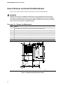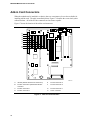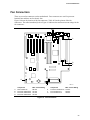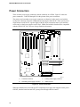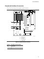
1
MS440GX Motherboard Product Guide Order Number: 713653-001 Revision History Revision Revision History Date -001 Initial release of the MS440GX Motherboard Product Guide. May 1998 Disclaimer Intel Corporation (Intel) makes no warranty of any kind with regard to this material, including, but not limited to, the implied warranties of merchantability and fitness for a particular purpose. Intel assumes no responsibility for any errors that may appear in this document. Intel makes no commitment to update nor to keep current the information contained in this document. No part of this document may be copied or reproduced in any form or by any means without prior written consent of Intel. An Intel product, when used in accordance with its associated documentation, is "Year 2000 Capable" when, upon installation, it accurately stores, displays, processes, provides, and/or receives date data from, into, and between the twentieth and twenty-first centuries, including leap year calculations, provided that all other technology used in combination with said product properly exchanges date data with it. Copies of documents which have an ordering number and are referenced in this document, or other Intel literature, may be obtained from: Intel Corporation P.O. Box 5937 Denver, CO 80217-9808 or call in North America 1-800-548-4725, Europe 44-0-1793-431-155, France 44-0-1793-421-777, Germany 44-0-1793-421-333, other Countries 708-296-9333. † Brands, names, or trademarks are the property of their respective owners. Copyright 1998, Intel Corporation. Contents Acronyms......................................................................................................................... 9 1 Motherboard Features Summary of Features..........................................................................................................12 Board Layout.......................................................................................................................13 Motherboard Part-Function Table........................................................................................14 Microprocessor....................................................................................................................15 Processor Packaging ..........................................................................................................15 Second Level Cache ...........................................................................................................15 Processor Options...............................................................................................................15 Form Factor.........................................................................................................................16 Chipset................................................................................................................................16 82443GX PCI/A.G.P. Controller (PAC) (H)..........................................................................17 Intel® 82371EB Xcelerator (PIIX4E) (Q) ..............................................................................18 Intel® 82093AA I/O Advanced Programmable Interrupt Controller (IOAPIC) .......................19 IDE Support.........................................................................................................................19 Real-Time Clock, CMOS RAM, and Battery ........................................................................20 Diskette Drive Controller......................................................................................................20 Accelerated Graphics Port (A.G.P.) Support .......................................................................21 Memory ...............................................................................................................................21 Input/Output (I/O) Controller (O)..........................................................................................22 82558 PCI LAN Controller (D) .............................................................................................23 EtherExpress™ PRO/100 WfM PCI LAN Subsystem ...........................................................23 Alert On LAN Component....................................................................................................24 Audio Subsystem ................................................................................................................24 Audio Drivers and Utilities ...................................................................................................25 Hardware Monitor Subsystem .............................................................................................25 Power Supply ......................................................................................................................26 Power Supply Considerations..............................................................................................26 Expansion ...........................................................................................................................27 Basic Input/Output System (BIOS) ......................................................................................27 BIOS Upgrades ...................................................................................................................27 BIOS Flash Memory Organization ..............................................................................28 Piezoelectric Speaker (N)....................................................................................................28 2 Installation and Removal Procedures Safety Considerations .........................................................................................................30 How to Install the DRM Fans and Processor Retention Mechanism....................................30 Materials Required......................................................................................................31 How to Install a Single Processor ........................................................................................37 How to Install a Second Processor......................................................................................38 How to Remove and Install the Motherboard.......................................................................40 How to Set Processor Speed ..............................................................................................41 Jumper Settings ..................................................................................................................42 iii MS440GX Motherboard Product Guide How to Remove a Processor...............................................................................................43 How to Upgrade a Processor ..............................................................................................44 How to Install the Termination Card ....................................................................................45 How to Remove the Termination Card ................................................................................46 How to Install Memory.........................................................................................................47 How to Remove Memory.....................................................................................................48 How to Replace the CR2032 Lithium Battery (M) ................................................................49 How to Clear Passwords .....................................................................................................51 3 Using the BIOS Setup Program Setup Program Modes ........................................................................................................54 Modes .................................................................................................................................54 Mode Control.......................................................................................................................54 Setup Program Menus ........................................................................................................55 Menu Functionality ..............................................................................................................56 Menu Function Keys............................................................................................................56 Maintenance Menu..............................................................................................................57 Main Menu ..........................................................................................................................57 Advanced Menu ..................................................................................................................58 Peripheral Configuration Submenu......................................................................................59 IDE Configuration Submenus ..............................................................................................60 Floppy Options Submenu ....................................................................................................61 DMI Event Logging Submenu..............................................................................................62 Video Configuration Submenu.............................................................................................62 Security Menu .....................................................................................................................63 Power Menu ........................................................................................................................63 Boot Menu...........................................................................................................................64 Boot Options .......................................................................................................................65 Hard Drive Submenu...........................................................................................................65 Removable Devices Submenu ............................................................................................66 Exit Menu ............................................................................................................................66 4 Using the BIOS Features How to Prepare for the Upgrade..........................................................................................68 Obtaining the BIOS Upgrade File ........................................................................................68 Recording the Current BIOS Settings..................................................................................68 Creating a Bootable Floppy Disk .........................................................................................69 Creating the BIOS Upgrade Floppy Disk .............................................................................69 Upgrading the BIOS ............................................................................................................70 Recovering the BIOS...........................................................................................................71 Changing the BIOS Language.............................................................................................72 Plug and Play: PCI Autoconfiguration.................................................................................72 ISA Plug and Play ...............................................................................................................73 ISA Legacy Devices ............................................................................................................73 PCI IDE Support..................................................................................................................73 Desktop Management Interface (DMI).................................................................................74 Advanced Power Management (APM) ................................................................................74 iv Contents Advanced Configuration and Power Interface (ACPI)..........................................................75 System States and Power States ...............................................................................75 Wake Up Devices and Events ....................................................................................76 Plug and Play .............................................................................................................76 BIOS Support .............................................................................................................76 Language Support...............................................................................................................76 OEM Logo or Scan Area .....................................................................................................76 USB Legacy Support...........................................................................................................77 BIOS Security Features.......................................................................................................77 Recovering BIOS Data ........................................................................................................78 5 Technical Reference Front Panel Connectors (L) .................................................................................................80 Speaker...............................................................................................................................81 Reset Switch .......................................................................................................................81 Power/Sleep LED ................................................................................................................82 Hard Drive Activity LED .......................................................................................................82 Infrared Port ........................................................................................................................82 Power Switch ......................................................................................................................82 Front Panel Pin Connector Mapping....................................................................................83 Back Panel Connectors (E) .................................................................................................84 Keyboard and Mouse Interface ...........................................................................................85 Universal Serial Bus (USB) .................................................................................................85 Parallel Port.........................................................................................................................86 Serial Ports..........................................................................................................................86 I/O Shield....................................................................................................................88 Midboard Connectors ..........................................................................................................89 Add-in Card Connectors ......................................................................................................90 Audio Connectors................................................................................................................91 CD-ROM Audio ...................................................................................................................92 Telephony ...........................................................................................................................92 Fan Connectors...................................................................................................................93 Thermal Considerations ......................................................................................................94 Power Connectors...............................................................................................................96 Peripheral Interface Connectors..........................................................................................99 Security and Hardware Management Connectors .............................................................100 Chassis Intrusion Connectors............................................................................................102 Wake on LAN Technology Connector ...............................................................................102 Wake on Modem ...............................................................................................................102 Memory Map .....................................................................................................................103 DMA Channels ..................................................................................................................103 I/O Map .............................................................................................................................104 PCI Configuration Space Map ...........................................................................................106 LAN Subsystem Software..................................................................................................107 Interrupts...........................................................................................................................107 PCI Interrupt Routing Map.................................................................................................108 Interrupt Routing Example.................................................................................................109 v MS440GX Motherboard Product Guide A Error Messages BIOS Beep Codes .............................................................................................................112 BIOS Error Messages .......................................................................................................113 Port 80h POST Codes.......................................................................................................115 B Regulatory and Integration Information Regulatory Compliance .....................................................................................................122 Product Certification Markings...........................................................................................122 Installation Precautions .....................................................................................................122 Installation Instructions......................................................................................................123 C Environmental Specifications and Reliability Information Environmental Specifications ............................................................................................126 Reliability Information ........................................................................................................126 D Specifications and Customer Support Online Support ..................................................................................................................128 Specifications ....................................................................................................................128 Figures 1. 2. 3. 3a. 3b. 3c. 3d. 3e. 3f. 3g. 3h. 3i. 4. 5. 6. 7. 8. 9. 10. 11. 12. 13. 14. 15. 16. 17. 18. 19. vi MS440GX Main Board Components...........................................................................13 MS440GX Custom ATX Form Factor .........................................................................16 Procedure Step 2: DRM Stand ...................................................................................31 Procedure Step 3: DRM Stand With Fans ..................................................................31 Procedure Step 5: Fan Positioning/Air Flow ...............................................................32 Procedure Step 6: DRM Base With Retention Clip .....................................................32 Procedure Step 7: Fans and Fan Header in Chassis..................................................33 Procedure Step 11a: Installing the DRM.....................................................................33 Procedure Step 13: CPU/Heat Sinks-DRM Tops ........................................................34 Procedure Step 14: DRM Tops, Clips, Holes..............................................................34 Procedure Step 16: Processors Installed in the DRM .................................................35 Procedure Step 17: Final DRM-Fan Assembly ...........................................................36 Installing a Single Processor ......................................................................................37 Installing a Second Processor ....................................................................................39 Motherboard Mounting Screw Holes...........................................................................40 Configuration Jumper Block........................................................................................42 Removing a Processor ...............................................................................................43 Installing the Termination Card ...................................................................................45 Removing the Termination Card .................................................................................46 Installing a DIMM........................................................................................................48 Replacing the Battery .................................................................................................50 Setup Program Menu Structure ..................................................................................55 Front Panel Connectors..............................................................................................80 Back Panel Connectors ..............................................................................................84 Back Panel I/O Shield Dimensions (ATX Chassis-Independent).................................88 Add-in Card Connectors .............................................................................................90 Audio Connectors .......................................................................................................91 Fan Connectors ..........................................................................................................93 Contents 20. 21. 22. 23. Thermally Sensitive Components ...............................................................................94 Power Connectors ......................................................................................................96 Peripheral Interface Connectors .................................................................................99 Security and Hardware Management Connectors ....................................................100 Tables 1. 2. 3. 4. 5. 6. 7. 8. 9. 10. 11. 12. 13. 14. 15. 16. 17. 18. 19. 20. 21. 22. 23. 24. 25. 26. 27. 28. 29. 30. 31. 32. 33. 34. 35. 36. 37. 38. 39. 40. Motherboard Part-Function Table ...............................................................................14 PCI/A.G.P. Controller Features ..................................................................................17 82371EB Xcelerator Features ....................................................................................18 DIMM Sizes Supported...............................................................................................21 I/O Controller Components .........................................................................................22 LAN Controller Functions............................................................................................23 Audio Subsystem Resources......................................................................................25 Power Usage..............................................................................................................26 DC Voltage Tolerances and Estimated Current Requirements (no PCI or A.G.P. shown) ...........................................................................................26 Flash Memory Organization........................................................................................28 BIOS Setup Configuration Jumper Settings................................................................43 Setup Program Modes................................................................................................54 Jumper Settings .........................................................................................................54 Setup Menu Bar .........................................................................................................56 Setup Function Keys ..................................................................................................56 Maintenance Menu .....................................................................................................57 Main Menu..................................................................................................................57 Advanced Menu..........................................................................................................58 Peripheral Configuration Submenu.............................................................................59 IDE Configuration Submenus .....................................................................................60 Floppy Options Submenu ...........................................................................................61 DMI Event Logging Submenu.....................................................................................62 Video Configuration Submenu ....................................................................................62 Security Menu ............................................................................................................63 Power Menu ...............................................................................................................63 Boot Menu ..................................................................................................................64 Hard Drive Submenu ..................................................................................................65 Removable Devices Submenu....................................................................................66 Exit Menu ...................................................................................................................66 Recommendations for Configuring an ATAPI Device..................................................73 Effects of Pressing the Power Switch .........................................................................75 Wake Up Devices and Events ....................................................................................76 Administrator and User Password Functions ..............................................................78 Front Panel I/O Connectors ........................................................................................81 Pin Connector Functionality........................................................................................83 PS/2 Keyboard/Mouse Connectors.............................................................................85 LAN Connector ...........................................................................................................86 Audio Line In Connector .............................................................................................86 Audio Line Out Connector ..........................................................................................87 Audio Mic In Connector ..............................................................................................87 vii MS440GX Motherboard Product Guide 41. 42. 43. 44. 45. 46. 47. 48. 49. 50. 51. 52. 53. 54. 55. 56. 57. 58. 59. 60. 61. 62. 63. 64. 65. 66. 67. 68. viii Connector Groups ......................................................................................................89 ATAPI-Style Telephony Connector(J1E1)...................................................................92 ATAPI CD Audio Connector (J2E1) ............................................................................92 External Speaker Connector (J12A1) .........................................................................92 MIDI/Joystick Connector (J2E2) .................................................................................92 Fan Connectors ..........................................................................................................94 Thermal Considerations for Components ...................................................................95 1x6 Power Connector .................................................................................................97 Primary and Secondary Power Supply Connectors (J10H1).......................................97 VRM Connector (J13J1) .............................................................................................98 SCSI LED Connector (J10A1) ....................................................................................99 Front and Rear Chassis Intrusion Connectors ..........................................................101 Wake on LAN Technology Connector (J11A2) .........................................................101 Wake-on-Modem Connector (J9A1) .........................................................................101 Memory Map ............................................................................................................103 DMA Channels .........................................................................................................103 I/O Map ....................................................................................................................104 PCI Configuration Space Map ..................................................................................106 Interrupts ..................................................................................................................107 PCI Device Classes..................................................................................................108 PCI Interrupt Routing Map ........................................................................................108 Beep Codes..............................................................................................................112 BIOS Error Messages...............................................................................................113 Port 80h Codes ........................................................................................................115 Safety Regulations ...................................................................................................122 EMC Regulations......................................................................................................122 Environmental Specifications....................................................................................126 Compliance with Specifications ................................................................................128 Acronyms Acro. Meaning Acro. Meaning Acro. Meaning Acro. Meaning ACPI Advanced configuration and power interface ECC Error checking and correcting IRQ Interrupt request POST Power-on self test ADPCM Adaptive differential pulse code modulation ECHS Extended cylinder head sector LAN Local area network SCI Special circumstance instructions A.G.P. Accelerated graphics port ECP Extended capabilities port LBA Logical block addressing S.E.C.C. Single edge contact cartridge APM Advanced power management EMC Electromagnetic compatibility LED Light emitting diode SIR Surface insulation resistance BIOS Basic input / output system EPP Enhanced parallel port MHz Megahertz SMI System management interrupt CMOS Complementary metal oxide semiconductor ESCD Extended system configuration data MIF Management information format SMM System management mode CPU Central processing unit ESD Electrostatic DISCHARGE MIDI Musical interface digital interface SMP Symmetric multiprocessing CSMA/CD Carrier sense multiple access with collision detection FIFO First in, first out MTBF Mean time between failures SRAM Static random access memory DIMM Dual inline memory module IDE Integrated dual channel enhanced NIC Network interface card UHCI Universal host controller interface DMA Direct memory access I/O Input / output OEM Original equipment manufacturer USB Universal serial bus DMI Desktop Management Interface IOAPIC Input Output Advanced Programmable Input Controller OS Operating System VID Voltage ID DRAM Dynamic random access memory IPL Initial program load PAC PCI A.G.P. controller VPD Vital product data DRM Dual retention mechanism ISA Industry standard architecture PCI Peripheral component interconnect WfM Wired for management 9 MS440GX Motherboard Product Guide 10 1 Motherboard Features The MS440GX is designed specifically for the DCC, MCAD, and EDA markets with a high performance workstation. This chapter describes the features of the MS440GX motherboard. The chapter covers the following topics: Topic Page Summary of Features 12 Board Layout 13 Motherboard Part-Function Table 14 Microprocessor 15 Processor Packaging 15 Second Level Cache 15 Processor Options 15 Form Factor 16 Chipset 16 PCI/A.G.P. Controller 17 82371EB Xcelerator 18 I/O Advanced Programmable Interrupt Controller 19 IDE Support 19 Real-Time Clock, CMOS SRAM, and Battery 20 Diskette Drive Controller 20 A.G.P. Support 21 Memory 21 I/O Controller 22 PCI LAN Controller 23 EtherExpress™ PRO/100 WfM PCI LAN Subsystem 23 Alert on LAN Component 24 Audio Subsystem 24 Audio Drivers and Utilities 25 Hardware Monitor Subsystem 25 Power Supply 26 Power Supply Considerations 26 Expansion 27 Basic Input/Output System (BIOS) 27 BIOS Upgrades 27 BIOS Flash Memory Organization 28 Piezoelectric Speaker 28 11 MS440GX Motherboard Product Guide Summary of Features The MS440GX motherboard features are summarized below. Form factor Custom ATX (12 inches by 13 inches) Processor(s) • Two Slot 2 connectors • Support for one or two Pentium® II Xeon™ processors • 100 MHz host bus speed • Up to 1 MB of L2 cache support on each processor Chipset Memory 82440GX, consisting of: • 82443GX PCI/A.G.P. controller (PAC) • 82371EB PCI ISA IDE Xcelerator (PIIX4E) • Four DIMM sockets • Support for up to 2 GB of 100 MHz SDRAM • Support for ECC DIMMs only (see Table 4 and associated text) I/O Control • National Semiconductor PC97307 I/O controller Peripheral Interfaces • Two serial ports • Two USB ports • One parallel port • Two IDE interfaces with Ultra DMA support • One diskette drive interface Video • One A.G.P. slot Audio • Crystal Semiconductor CS4235 audio codec • Crystal Semiconductor CS9236 wavetable synthesizer LAN • Intel® 82558 10/100 Mbps PCI LAN controller Hardware Monitor • Microprocessor system hardware monitor (Analog Devices ADM9240 or equivalent) • Wired for Management (WfM) compliant • Five PCI slots • One shared slot for either a PCI or an ISA add-in card • Intel® E28F004BXT80 4 Mbit flash memory • Support for SMBIOS, ACPI, APM, and Plug and Play Expansion Capabilities BIOS 12 Intel® Motherboard Features Board Layout The illustration below is a picture of the MS440GX integrated motherboard. The main board components are identified by alphabetical callouts. This board supports the Slot 2 processor (DS2P) family. It is a custom ATX form factor (12”x13”) board with an ATX I/O panel. A B C D E S F G R H Q P I J O N M K L OM08377 Figure 1. MS440GX Main Board Components 13 MS440GX Motherboard Product Guide Motherboard Part-Function Table This table identifies the motherboard components called out in Figure 1 and defines the functional purpose of each. Table 1. 14 Motherboard Part-Function Table Callout ID Part (Component) Function A Intel E28F004BXT80 4 Mbit Flash Memory Flash upgradable. Stores BIOS, Setup program, POST, APM, PCI auto configuration utility and Plug and Play code B Crystal Semiconductor CS4235 Audio Codec On board audio subsystem with integrated FM synthesizer C A.G.P. Connector High performance graphics connector with support for 133 MHz data transfer rates (AGP2x) D Intel 82558 PCI LAN Controller On board LAN controller with support for 10Base-T and 100Base-TX interfaces E Back Panel Connectors Keyboard, mouse, USB, parallel, serial, LAN and audio connectors F Slot 2 Connector for Boot Processor Connector for Pentium II Xeon processor G Slot 2 Connector for Application Processor Connector for Pentium II Xeon processor H Intel® 82443GX (PAC) AGPset provides bus-control signals, address paths and data paths for transfers between the processor’s host bus, PCI bus, the A.G.P. and main memory I DIMM Sockets Support for up to 2GB PC100 compliant SDRAM DIMMS J Diskette Drive Connector Supports one or two diskette drives K VRM Connector Plug-in Voltage Regulator Module for application processor L Front Panel Connectors Connectors for PC speaker, reset switch, power LED, HDD LED, infrared port and power switch M Battery Provides power to real-time clock and CMOS memory N Piezoelectric Speaker Provides BIOS beep codes O National Semiconductor PC97307 I/O Controller Provides serial and parallel ports, diskette drive, mouse, keyboard and IR interfaces P IDE Connectors Each connector supports two IDE devices Q 82371EB (PIIX4E) Provides USB and power management support in addition to EIDE and UDMA/33 data transfer rates R PCI Bus Add-in Board Connectors Support for 33 MHz PCI devices S ISA Bus Add-in Board Connector Support for ISA compatible add-in cards Motherboard Features Microprocessor The Intel® MS440GX motherboard supports one or two Pentium II Xeon 400 or 450 MHz processors, 100 MHz host bus speeds, and L2 caches up to 1MB in size. The processor’s VID pins automatically program the voltage regulator on the motherboard to the required processor voltage for the Boot (P0) Processor only. A plug-in VRM must be used when adding an Application (P1) Processor. If a plug-in VRM is not used, then the L2 cache will be disabled. Processor Packaging Each processor is packaged in a single edge contact cartridge (S.E.C.C.). The cartridge includes the processor core, second-level cache, thermal plate, and back cover. The processor connects to the motherboard through the Slot 2 connector, a 330-pin edge connector. When mounted in a Slot 2 connector, the processor is secured by a retention mechanism attached to the motherboard. Second Level Cache The second-level cache is located on the substrate of the S.E.C.C.. The ECC cache includes components totaling up to 1 MB in size. All onboard system memory is cacheable. Processor Options The following processor configuration options can be used: • A single 400 MHz processor installed in the boot processor slot (P0) and a terminator card installed in the application processor slot (P1). P0 is the Slot 2 connector closest to the middle of the board. See Figure 1 callouts F and G. • Dual 400 MHz processors. When using two processors, a voltage regulator module (VRM) must be installed. • A single 450 MHz processor installed in the boot processor slot (P0) and a terminator card installed in the application processor slot (P1). • Dual 450 MHz processors. When using two processors, a voltage regulator module (VRM) must be installed. See Figure 21, callout D for the location of the VRM connector. If you are installing two processors, then the following values must be identical for both: • L2 cache size • Operating voltages • Processor speed CAUTION If the processor operating voltages for either VCC core or VCC L2 do not match, then the computer will not boot. Use configure mode to set the processor speed if necessary. 15 MS440GX Motherboard Product Guide Form Factor The motherboard is designed to fit into a custom ATX form factor chassis. The illustration below shows the board mounting hole locations. The mounting holes closest to the Slot 2 connectors are used for mounting the processor retention mechanism to the board and chassis. 0.20 3.30 2.59 12.70 12.30 11.40 6.74 6.20 3.35 2.80 11.55 11.30 0.00 0.30 0.00 0.45 5.10 9.06 9.31 OM07109 Figure 2. MS440GX Custom ATX Form Factor Chipset The Intel® 440GX AGPset includes a Host-PCI bridge integrated with both an optimized DRAM controller and an Accelerated Graphics Port (A.G.P.) interface. The I/O subsystem of the 440GX is based on the PIIX4E which is a highly integrated PCI-ISA/IDE Accelerator Bridge. This chipset consists of the Intel 82443GX PCI/A.G.P. controller (PAC) and the Intel® 82371EB PCI/ISA IDE Xcelerator (PIIX4E) bridge chip. 16 Motherboard Features 82443GX PCI/A.G.P. Controller (PAC) (H) The Intel 82443GX PCI/A.G.P. Controller (PAC) provides the following functions: • Bus-control signals • Address paths • Data paths for transfers between the processor’s host bus, PCI bus, the A.G.P., and main memory. Table 2 lists the PAC features and the functionality each feature supports. Table 2. PCI/A.G.P. Controller Features Feature Functionality Processor Interface Control Support for processor host bus frequencies of 100 MHz only 32-bit addressing Desktop optimized GTL + compliant host bus interface Integrated DRAM Controller +3.3V only DIMM DRAM configurations Up to four double sided DIMMs 100 MHz PC100-compatible Synchronous DRAM DIMM serial presence detect via SMBus interface 2-, 4-, 8-, 16-, 32-, 64-, and 128-Mbit DRAM devices SDRAM 64-bit data interface with ECC support Symmetrical and asymmetrical DRAM addressing A.G.P. Interface Complies with the A.G.P. specification Rev. 1.0 Support for +3.3V A.G.P. 66/133 MHz devices Synchronous coupling to the host-bus frequency PCI Bus Interface Complies with the PCI specification Rev. 2.1 Asynchronous coupling to the host-bus frequency PCI parity generation support Data streaming support from PCI-to-DRAM Support for six PCI bus masters in addition to the host PCI-to-ISA I/O bridge Support for concurrent host, A.G.P., and PCI transactions to main memory Data Buffering DRAM write buffer with read-around-write capability Dedicated host-to-DRAM, PCI0-to-DRAM, and PCI1/A.G.P.-to-DRAM read buffers A.G.P. dedicated inbound/outbound FIFOs (AGP2X), used for temporary data storage Power Management Functions Support for system suspend/resume and power-on suspend Compliant with ACPI power management SMBus Support for Desktop Management Functions Support for System Management Mode (SMM) 17 MS440GX Motherboard Product Guide Intel® 82371EB Xcelerator (PIIX4E) (Q) The Intel® PIIX4E is a multifunction PCI device implementing the PCI-to-ISA bridge, PCI IDE functionality, Universal Serial Bus (USB) host/hub function, and enhanced power management. Table 3 lists the PIIX4E features and the functionality each feature supports. Table 3. 82371EB Xcelerator Features Feature Functionality Multifunction PCI-to-ISA Bridge Support for the PCI bus at 33 MHz Complies with the PCI specification Full ISA bus support USB Controller Two USB ports Support for legacy keyboard and mouse Support for UHCI Design Guide, revision 1.1, interface Integrated Dual Channel Enhanced IDE Interface Support for up to four IDE devices PIO Mode 4 transfers at up to 16 MB/sec Support for Ultra DMA/33 synchronous DMA mode transfers up to 33 MB/sec Bus master mode with an 8x32-bit buffer for bus master PCI IDE burst transfers Enhanced DMA Controller Two 8237-based DMA controllers Support for PCI DMA with three PC/PCI channels and distributed DMA protocols Fast type-F DMA for reduced PCI bus usage Interrupt Controller Based on 82C59 Support for 15 interrupts Programmable for edge/level sensitivity Power Management Logic Sleep/resume logic Support for Wake on Modem, Wake on LAN † technology, and Wake on PME Support for ACPI System wakes from ACPI sleep state with keyboard activity Real-Time Clock 256-byte battery backed CMOS RAM Includes date alarm 16-bit Counters/Timers Based on 82C54 18 Motherboard Features Intel® 82093AA I/O Advanced Programmable Interrupt Controller (IOAPIC) The Intel® 82093AA I/O Advanced Programmable Interrupt Controller (IOAPIC) provides interrupt management and incorporates both static and dynamic symmetric interrupt distribution across all processors in a multiprocessor system. The 82093AA IOAPIC features 24 interrupts as follows: • 13 ISA interrupts • Four PCI interrupts • One Interrupt/SMI# rerouting • Two motherboard interrupts • One interrupt used for INTR input • Three general purpose interrupts • SCI BIOS supported steering IDE Support The motherboard has two independent bus-mastering IDE interfaces. These interfaces support PIO Mode 3, PIO Mode 4, ATAPI devices (e.g., CD-ROM), and Ultra DMA synchronous-DMA mode transfers. The BIOS supports logical block addressing (LBA) and extended cylinder head sector (ECHS) translation modes. The BIOS automatically detects the IDE device transfer rate and translation mode. The motherboard supports LS-120 diskette technology through its IDE interfaces. LS-120 diskette technology enables users to store 120 MB of data on a single, 3.5-inch removable diskette. LS-120 technology is backward compatible (both read and write) with 1.44 MB and 720 KB DOSformatted diskettes and is supported by Windows† 95 and Windows NT† operating systems. The motherboard allows connection of an LS-120 compatible drive and a standard 3.5-inch diskette drive. If an LS-120 drive is connected to an IDE connector and configured as the A drive, and a standard 3.5-inch diskette drive is configured as a B drive, the standard diskette drive must be connected to the diskette drive cable's "A" connector (the connector at the end of the cable). The LS-120 drive can be configured as a boot device, if selected in the BIOS setup utility. 19 MS440GX Motherboard Product Guide Real-Time Clock, CMOS RAM, and Battery The real-time clock provides a time-of-day clock and a multicentury calendar with alarm features and century rollover. The clock is compatible with DS1287 and MC146818 components and it supports 256 bytes of battery-backed CMOS RAM in two banks that are reserved for BIOS use. The time, date, and CMOS values can be specified in the Setup program. The CMOS values can be returned to their defaults by using the Setup program. An external coin-cell battery powers the real-time clock and CMOS memory. When the computer is not plugged into a wall socket, then the battery has an estimated life of three years. When the computer is plugged in, then the 3 V standby current from the power supply extends the life of the battery. ✏ NOTE Power is supplied to the chassis intrusion circuit by the battery when no AC power is provided. Chassis intrusion will be detected when no AC power is available to the system. If the switch is activated when no AC power is provided, then the drain on the battery is approximately 200 mA. The clock is accurate to ± 13 minutes/year at 25 ºC with 5 V applied. Diskette Drive Controller The diskette drive controller is software compatible with the DP8473 and N82077 diskette drive controllers and supports both PC-AT† and PS/2† modes. In the Setup program, the diskette drive interface can be configured for the following diskette drive capacities and sizes: • 360 KB, 5.25-inch • 1.2 MB, 5.25-inch • 720 KB, 3.5-inch • 1.2 MB, 3.5-inch (driver required) • 1.25/1.44 MB, 3.5-inch 20 Motherboard Features Accelerated Graphics Port (A.G.P.) Support The Accelerated Graphics Port (A.G.P.) is a high-performance interconnect for graphic-intensive applications, such as 3D applications. A.G.P. is independent of the PCI bus. It is intended for exclusive use with graphical display devices. A.G.P. provides these performance features: • Pipelined-memory read and write operations that hide memory access latency • Demultiplexing of address and data on the bus for near 100 percent bus efficiency • AC timing for 133 MHz data transfer rates, allowing data throughput of 528 MB/sec An A.G.P. connector is provided on the motherboard to install A.G.P. add-in cards. Memory The motherboard has four dual inline memory module (DIMM) sockets. Minimum memory size is 32 MB; maximum memory size is 2 GB. The BIOS automatically detects memory type and size. The motherboard supports the following memory features: • PC100 compliant 168-pin DIMMs with gold-plated contacts • 3.3 V unbuffered or registered (not mixed) 100 MHz ECC SDRAM DIMMs only • Single or double sided DIMMs in the sizes listed in the Table 4. Table 4. DIMM Sizes Supported DIMM Size Configuration 16 MB 2 Mbit x 72 32 MB 4 Mbit x 72 64 MB 8 Mbit x 72 128 MB 16 Mbit x 72 256 MB 32 Mbit x 72 512 MB 128 Mbit x 72 Memory can be installed in any order in one, two, three or four sockets. Memory size can vary between sockets. Memory speed is 100 MHz only. 21 MS440GX Motherboard Product Guide Input/Output (I/O) Controller (O) The I/O controller handles the exchange of information between the processor and external devices like the mouse and keyboard or a printer that are connected to the computer. The National Semiconductor PC97307 I/O Controller is an ISA Plug and Play compatible multifunction I/O device with components and features listed in the table below. Table 5. I/O Controller Components Component Feature(s) Serial Ports Two 16450/16550A software compatible UARTs Internal send/receive 16-byte FIFO buffer Four internal 8-bit DMA options for the UART with SIR support (USI) Multimode Bidirectional Parallel Port Standard mode: IBM and Centronics compatible Enhanced parallel port (EPP) mode with BIOS and driver support High speed extended capabilities port (ECP) mode Diskette Drive Controller DP8473 and N82077 compatible 16-byte FIFO buffer PS/2 diagnostic-register support High performance digital data separator (DDS) PC-AT, PS/2, and 3 mode diskette drive mode support 8042A Compatible Keyboard and Mouse Controller Support for IrDA† and Consumer Infrared Compliant Infrared Interface By default, the I/O controller interfaces are automatically configured during boot up. The I/O controller can also be manually configured in the Setup program. 22 Motherboard Features 82558 PCI LAN Controller (D) The Intel 82558 LAN Controller provides the functions listed in Table 6 below. Table 6. LAN Controller Functions Function Includes: CSMA/CD Protocol Engine PCI bus interface (Rev 2.1 compliant) DMA engine for movement of commands, status, and network data across the PCI bus Integrated physical layer interface Complete functionality necessary for the 10Base-T and 100Base-TX interfaces When in 10 Mbit/sec mode, the interface drives the cable directly A complete set of MII management registers for control and status reporting 802.3µ Auto-Negotiation for automatically establishing the best operating mode when connected to other 10 Base-T or 100Base-TX devices Integrated power management features Support for ACPI Support for Wake on LAN technology Digitally controlled adaptive equalizations and transmission EtherExpress™ PRO/100 WfM PCI LAN Subsystem The Intel EtherExpress PRO/100 Wired for Management (WfM) PCI LAN subsystem is an Ethernet LAN interface that provides both 10Base-T and 100Base-TX connectivity. Features include: • • • • 32-bit direct bus mastering on the PCI bus Shared memory structure in the host memory that copies data directly to/from host memory 10Base-T and 100Base-TX capability using a single RJ-45 connector IEEE 802.3µ Auto-Negotiation for the fastest available connection 23 MS440GX Motherboard Product Guide Alert On LAN Component The Alert on LAN component is a companion device to the Intel 82558 LAN controller. Together, these devices provide a management interface between a remote management console (or management server) and a client system monitoring instrumentation. When an alert input is asserted, the Alert on LAN component transmits Ethernet † packets to the 82558 through an 8-bit dedicated data path. Examples of events that can trigger alert messages to a management server include: • Chassis intrusion • System BIOS hang (transmits POST code error) • LAN leash (transmits an alert that the LAN cable was disconnected) • Temperature out of specification • Fan failure For more information on the Alert on LAN component and its network management capabilities, contact your local Intel sales office. Audio Subsystem The optional onboard audio subsystem features the Crystal CS4235, an audio codec with an integrated FM synthesizer. The audio subsystem provides all the digital audio and analog mixing functions needed for recording and playing sound on personal computers. The audio subsystem contains the following features: • Stereo analog-to-digital and digital-to-analog converters • Analog mixing, anti-aliasing, and reconstruction filters • Line and microphone level inputs • ADPCM, A-law, or µlaw digital audio compression/decompression • Full digital control of all mixer and volume control functions • High-quality, 16-bit, MPC-II compliant onboard audio • Full duplex operation • AdLib†, Sound Blaster Pro† 2.0, Windows Sound System, and MPU-401 support • Full DOS games compatibility • MIDI/Game port support • OPL3 compatible FM synthesizer • BIOS Setup-based enable/disable The audio subsystem requires up to two DMA channels and one IRQ. Table 7 shows the IRQ, DMA channel, and base I/O address options. These options are automatically chosen by the Plug and Play interface, so there are no default settings. 24 Motherboard Features Table 7. Audio Subsystem Resources Resource Blaster† IRQ (Options) DMA Channel (Options) I/O Address (Options) Sound (DMA playback, DMA / IRQ shared with Windows Sound System capture) 5 best choice 7 9 best choice 11 0 best choice 3 210-21Fh 220-22Fh best choice 230-234h 240-24Fh 250-25Fh 260-26Fh Windows Sound System (DMA playback) 7 9 best choice 11 0 1 best choice 3 534-537h best choice 608-60Bh MPU-401 (IRQ shared with Sound Blaster) 5 best choice 7 9 best choice 11 300-301h 330-331h best choice 332-333h 334-335h MIDI 200-207h FM Synthesis 388-38Dh CS4235 Control FF0-FFFh Audio Drivers and Utilities Audio software and utilities are available from Intel’s World Wide Web site. Audio driver support is provided for the Microsoft Windows NT 4.0 and Microsoft Windows 98 operating systems. Hardware Monitor Subsystem The hardware monitor subsystem provides low-cost instrumentation capabilities. The features of the hardware monitor subsystem include: • Management Level 4 functionality • Analog Devices ADM 9240 or equivalent. Integrated temperature and voltage monitoring to detect levels above or below acceptable values (+12 V, -12 V, +5 V, +3.3 V, and +2.5 V). When suggested ratings for temperature, fan speed or voltage are exceeded, an interrupt is activated. Two fan speed sensors Access through the SMBus • Remote reset capabilities from a remote peer or server through LANDesk® 3.3 (or later) Client Manager and service layers • Headers for front and rear chassis intrusion connectors. 25 MS440GX Motherboard Product Guide Power Supply Table 9 lists the power specifications for a computer that contains a motherboard with two 400 MHz Pentium II Xeon processors, 128 MB SDRAM, a 3.5-inch diskette drive, an WD Caviar 3320 3.3 GB Ultra ATA hard drive, a Hitachi CPR 8330 IDE CD-ROM, and a Diamond Viper 330 A.G.P. graphics card. This information is provided only as a guide for calculating approximate power usage with additional resources added. Values for the Windows 98 desktop mode are measured at 1280x1024x256 colors and 70 Hz refresh rate. AC watts are measured with a typical 300 W supply, nominal input voltage and frequency, with true RMS wattmeter at the line input. Table 8. Power Usage Mode Watts (AC) Out of AC Wall Outlet Windows 98 desktop 60 watts Windows NT 4.0 desktop 92 watts Power Supply Considerations For typical configurations, the motherboard is designed to operate with at least a 300 W power supply. A higher-wattage power supply should be used for heavily-loaded configurations. The power supply must comply with the following recommendations: • The potential relation between 3.3 V DC and +5 V DC power rails • The current capability of the +5 VSB line • All timing parameters • Must meet UL SELV requirements and meet the 240VA energy limit Table 9. ✏ DC Voltage Tolerances and Estimated Current Requirements (no PCI or A.G.P. shown) DC Voltage Acceptable Tolerance Estimated current with a 400 Estimated current with a 450 MHz processor, 512 KB MHz processor, 512 KB cache, and 2 GB RAM cache, and 2 GB RAM +3.3 V ± 5% 20A 20A +5 V ± 5% 14A 16A +5 VSB (standby) ± 5% 0.72A 0.72A -5 V ± 10% 0.0A 0.0A +12 V ± 5% 2.8A 3.1A -12 V ± 10% 0.0A 0.0A NOTE Some heavily loaded configurations could require additional +3.3 V and +5 V power for peripherals. Use the auxiliary power supply connector for this purpose. 26 Motherboard Features Expansion The MS440GX motherboard has seven expansion slots for installing add-cards such as video or network cards that expand the capabilities of your computer. The expansion slots available are as follows: • Five PCI slots • One shared slot (for a PCI or ISA card) • One AGP 2X slot Basic Input/Output System (BIOS) The MS440GX motherboard uses an Intel/Phoenix BIOS which is stored in flash memory. The BIOS can be upgraded using a disk-based program. The contents of flash memory includes the following items: • BIOS • Setup Program • Power-on Self Test (POST) • Advanced Power Management (APM) • PCI Auto-configuration Utility • Windows 98-ready Plug and Play Code The MS440GX motherboard supports system BIOS shadowing, allowing the BIOS to execute from 64-bit onboard write-protected DRAM. During POST, the BIOS displays a message identifying the type of BIOS and the revision code. The initial production BIOS is identified as 4M4SG0X0.86E. BIOS Upgrades ✏ NOTE Please review the instructions distributed with the upgrade before attempting a BIOS upgrade. The BIOS can be upgraded from a diskette using the Intel Flash Memory Update utility that is available from Intel. This utility does BIOS upgrades as follows: • Updates the flash BIOS from a file on a disk • Updates the language section of the BIOS • Makes sure that the upgrade BIOS matches the target system to prevent accidentally installing a BIOS for a different type of system. BIOS upgrades and the update utility are available from Intel through the Intel World Wide Web site. Chapter 4 details the procedure for executing a BIOS upgrade. 27 MS440GX Motherboard Product Guide BIOS Flash Memory Organization The Intel E28F004BXT80 4-Mbit flash component is organized as 512 KB x 8 bits and is divided into areas as described in Table 10. The table shows the addresses in the ROM image in normal mode (the addresses change in BIOS Recovery Mode). Table 10. Flash Memory Organization Address (Hex) Size Description FFFFC000 - FFFFFFFF 16 KB Boot Block FFFFA000 - FFFFBFFF 8 KB Vital Product Data (VPD) Extended System Configuration Data (ESCD) (DMI configuration data / Plug and Play data) FFFF9000 - FFFF9FFF 4 KB Used by BIOS (e.g., for Event Logging) FFFF8000 - FFFF8FFF 4 KB OEM logo or Scan Flash Area FFF80000 - FFFF7FFF 480 KB Main BIOS Block Piezoelectric Speaker (N) The onboard piezoelectric speaker is enabled by a jumper on pins 1 and 2 of the front panel connector. The onboard speaker can be disabled by removing the jumper. An outboard speaker can be connected in its place by a jumper on pins 1 and 4. This speaker provides error beep code information during the POST in the event that the computer cannot use the video interface. The speaker is not connected to the audio subsystem and does not receive output from the audio subsystem. 28 2 Installation and Removal Procedures This chapter explains how to remove and install the MS440GX motherboard and its various component parts. The chapter covers the following topics: Topic or Procedure Page Safety Considerations 30 How to Install the Processor Retention Mechanism 30 How to Install a Single Processor 37 How to Install a Second Processor 38 How to Remove and Install the Motherboard 40 How to Set Processor Speed 41 Jumper Settings 42 How to Remove a Processor 43 How to Upgrade a Processor 44 How to Install the Termination Card 45 How to Remove the Termination Card 46 How to Install Memory 47 How to Remove Memory 48 How to Replace the Battery 49 How to Clear Passwords 51 29 MS440GX Motherboard Product Guide Safety Considerations CAUTION Before removing or installing the motherboard or any other system component, observe the following safety guidelines: See Appendix B: Regulatory & Integration Information for safety requirements and precautions. Always follow the steps in the procedure in the correct order (i.e., as written). Set up a log to record identification information about your computer. Wear an antistatic wrist wrap and place the motherboard on a conductive foam pad when working on it. WARNINGS The procedures in this section assume that you are familiar with the general terminology associated with personal computers and with the safety practices and regulatory compliance required for using and modifying electronic equipment including but not limited to the following: Turn off system AC power by unplugging the AC power cord from the wall outlet. Disconnect the computer from any telecommunications systems, networks, and modems attached before performing any of the procedures described in this section else personal injury or equipment damage can result. CAUTION Electrostatic discharge (ESD) can damage components. Therefore, protect against electrostatic discharge (ESD) by performing the procedures described in this section only at an ESD workstation or by wearing an antistatic wrist wrap and attaching it to a metal part of your computer’s chassis. How to Install the DRM Fans and Processor Retention Mechanism ✏ NOTES Dual Retention Mechanism (DRM) fans must be installed in the DRM end stands prior to installing the processor retention mechanism on the motherboard. The following procedure table combines the fan installation and processor retention mechanism installation procedures. 30 Installation and Removal Procedures Materials Required: • • • • • • • 2 40mm fans 2 DRM stands (see Figure 3) 4 Fan screws (P/N 656880-002) 2 DRM tops (see Figure 3f) 2 Processors (CPUs) with attached heatsinks (see Figure 3g) 2 Retention clips (see Figure 3c) 1 Small tie wrap Procedure To: Install DRM Fans and the Processor Retention Mechanism Step Action 1 Observe the safety precautions in Safety Considerations at the beginning of this chapter. 2 Obtain one of the DRM stands. OM08275 Figure 3. 3 Place the two Delta 40mm fans in the DRM stand pocket. Position the fans with air flow away from the DRM. Air flow OM08276 SIDE VIEW Figure 3a. Continued 31 MS440GX Motherboard Product Guide Procedure (continued) Step Action 4 Orient power cables to the upper left corner as illustrated in Step 3. 4a Run the power cables down the left side of the DRM base as illustrated in Step 3. 4b Tie wrap the cables leaving approximately 2 inches of cable hanging beyond the base. 5 Attach fans in the DRM stand with 2 fan screws placed in opposite corners. Position the fans with air flow away from the DRM. 40mm Fans (2) Stacked P1 Processor Heat Sink P0 Processor Air Flow Heat Sink DRM Top DIMM sockets OM08277 Figure 3b. IF more air flow is needed, then position 2 fans in the other DRM stand and secure them with air flow into (towards) the DRM. 6 Apply a retention clip to the tops of the DRM bases. Retention Clip Keypost E1 Keypost E2 OM08278 Figure 3c. Continued 32 Installation and Removal Procedures Procedure (continued) Step Action 7 Take the DRM base with 40mm fans attached and connect the two fans to the processor fan headers on the motherboard. 40mm Fan Headers 120mm Fan Header OM08279 Figure 3d. 8 Locate the Slot 2 processor connectors (A and B) and the four attachment screw holes (C1-C4) shown in Figure 3e. 9 Properly position the processor retention mechanisms (D1 and D2) relative to the Slot 2 connectors. 10 Fit the keyposts (Step 6 illustration, callouts E1 and E2) on the processor retention mechanisms into the holes in the motherboard base. When properly seated, the bases of the processor retention mechanism should fit flush with the motherboard. 11 Mount the DRM base to the motherboard with fan air flow pointing toward the back of the chassis. 11a Use four 6-32x1/2 or 5/8 inch screws (chassis dependent) to attach DRM bases to motherboard. Torque screws to 6 inch pounds. Retention Mechanism (D1) Retention Mechanism (D2 ) Keyposts (E1&E2) Processor Connecter (A) Screw Holes (C3/C4) Keyposts (E3&E4) Screw Holes (C1/C2) Processor Connecter (B) OM08280 Figure 3e. Continued 33 MS440GX Motherboard Product Guide Procedure (continued) Step Action 12 Assemble the other DRM base, mount it on the other side of the Slot 2 connectors with 1/2 or 5/8 inch screws (chassis dependent). 13 Obtain the CPU/Heat sinks and the DRM tops. DRM Top OM08281 Figure 3f. 14 Secure one of the DRM tops to the processor with the holes facing toward the DIMM sockets on the motherboard. ✏ NOTE The DRM tops snap into two recesses on the sides of the processor. Retention Clips Heatsinks Holes CPUs DIMM Slots OM08282 Figure 3g. Continued 34 Installation and Removal Procedures Procedure (continued) Step Action 15 Secure the other DRM top to the processor with the holes facing toward the DIMM slots. ✏ NOTE If using a Termination Card, then secure the DRM top to the card in the same manner. The DRM top is necessary to lock the Termination Card down and provide a way to remove it from the connector by pulling it up and out. 16 Install the two processors (CPUs) in the DRM with the heat sinks facing the DIMM slots. ✏ NOTE Check hole placement of the DRM top relative to the retainer clip holes before installation to ensure correct alignment. Use 4 ½ inch screws to secure tops to retainer clip. DRM Top Retention Clip DRM Top Retention Hole Heatsink Dual Retention Mechanism (DRM) D Processor (CPU) Connector DIMM Slots OM08285 Figure 3h. Continued 35 MS440GX Motherboard Product Guide Procedure (continued) Step Action 17 The final fan/CPU-heat sink/DRM assembly should appear as shown in the illustration below. CPU Heat sinks DRM top CPU DRM base DRM 40mm Fans OM08283 Figure 3i. 36 Installation and Removal Procedures How to Install a Single Processor Procedure To: Install a Single Processor Step Action 1 Observe the safety precautions in Safety Considerations at the beginning of this chapter. 2 Turn OFF the computer. 3 Disconnect the computer’s power cord and all external peripheral equipment. 4 Remove any peripherals that block access to the P0 processor’s Slot 2 connector. 5 Remove the antistatic packaging from the new processor. 6 Secure a DRM top (D) to the processor by snapping the clips (H1 and H2) into the holes on each side of the processor. 7 Orient the P0 processor (A) so that the heat sink (B) is closest to the DIMM sockets. 8 Slide the processor into the retention mechanism (E). C D H2 H1 A B E F E G DIMM Slots OM08284 Figure 4. 9 Press down firmly on the processor until it is seated in the P0 processor Slot 2 connector (G) and fasten with screws. 10 Lock down DRM top into retainer clips (F) on tops of DRM bases with 6-32x1/2 inch screws (C). 11 If there is no Termination Card in the P1 processor Slot 2 connector then install one using the procedure entitled “How to Install a Termination Card”. 12 Replace any peripheral equipment that was removed in Steps 3 and 4 above. 13 Set the processor speed using the procedure entitled “How to Set the Processor Speed”. 37 MS440GX Motherboard Product Guide How to Install a Second Processor ✏ NOTE It may be necessary to reload the operating system to realize optimum performance when upgrading from a single processor to a dual processor configuration. If installing two processors, then the following values must be identical for both processors: L2 cache size and type (ECC); Operating voltages; Bus and Core frequencies. The core stepping value may differ by one step (eg., C0 to C1). These values may be determined by checking the parameters of the s-spec number, a five character code (eg., SL28R) printed on the top edge of the S.E.C.C.. For information about s-spec parameters, refer to the Pentium II processor quick reference guide at the Intel developer’s web site. Procedure To: Install a Second Processor Step Action 1 Observe the safety precautions in Safety Considerations at the beginning of this chapter. 2 Turn OFF the computer. 3 Disconnect the computer’s power cord and all external peripheral equipment and remove any peripherals that block access to the P1 processor Slot 2 connector. 4 If there is a Termination Card installed in the P1 processor Slot 2 connector then remove it using the procedure entitled “How to Remove a Termination Card”. 5 Remove the antistatic packaging from the second processor. 6 Secure a DRM top (E) to the processor by snapping the clips (F) into the holes on each side of the processor. 7 Orient the P1 processor (A) so that the heat sink (B) faces the DIMM slots. Continued 38 Installation and Removal Procedures Procedure (continued) Step Action 8 Slide the processor into the processor retention mechanism (C). E F A B C D D OM08285 Figure 5. 9 Press down firmly on the processor until it is seated in the P1 Slot 2 connector (D) and fasten with screws. 10 Replace any peripheral equipment that was removed in Step 3 above. 11 Set the processor speed using the procedure entitled “How to Set the Processor Speed”. 39 MS440GX Motherboard Product Guide How to Remove and Install the Motherboard Refer to your chassis manual for detailed instructions on removal and installation. WARNING Motherboard removal or installation should be done only by qualified technical personnel. Disconnect the computer from its power source before performing the removal or installation procedures noted here and before opening the computer. Failure to observe these precautions may result in personal injury or equipment damage. Procedure To: Remove the Motherboard Step Action 1 Remove processor/heatsink/DRM assembly/Termination Card (if applicable) using procedures “How to Remove a Processor” and “How to Remove a Termination Card”. 2 Remove the four screws attaching the DRM bases to the chassis. 3 Disconnect fan cables from fan headers 4 Locate the motherboard mounting screw holes in Figure 6 below. 5 Remove the 11 motherboard mounting screws. 6 Carefully extract the board by its edges. 7 Place board component-side up on a grounded, static free surface. 0.20 3.30 2.59 12.70 12.30 11.40 6.74 6.20 3.35 2.80 11.55 11.30 0.00 0.30 0.00 0.45 5.10 9.06 9.31 OM07109 Figure 6. Motherboard Mounting Screw Holes 40 Installation and Removal Procedures How to Set Processor Speed CAUTION Selecting a processor speed greater than the rated speed of the installed processor(s) may damage the processor(s). Set processor speed after you have installed or upgraded the processor. The procedure that follows assumes that: • The computer is turned OFF • The cover has been removed • The configuration jumper block (J4J1) has the jumper set on pins 1-2 for normal mode Procedure To: Set Processor Speed Step Action 1 Observe the safety precautions in Safety Considerations at the beginning of this chapter. 2 Locate the configuration jumper block (see figure below). 3 Move the jumper to pins 2-3. 4 Replace the computer cover. 5 Turn ON the computer. 6 Allow the computer to boot up. 7 The computer starts the Setup Program. 8 Setup displays the Maintenance Menu. 9 Select the Processor Speed feature using the arrow keys. 10 Press the <ENTER> key. 11 Setup displays a pop-up screen with available processor speeds. 12 Select a speed using the arrow keys. (Choose 400 for a 400 MHz processor). CAUTION 13 Do not exceed the rated speed or damage to the processor may result. Press the <ENTER> key to confirm the speed. 14 The Maintenance Menu is re-displayed. 15 Press <F10> to save the current values then Exit Setup. 16 Turn OFF the computer. 17 Remove the computer cover. 18 Move the jumper back to pins 1-2 on the jumper block (J4J1) to restore normal operation. 19 Replace the cover. 20 Turn ON the computer. 21 Verify the processor speed in the startup information displayed by the BIOS. 41 MS440GX Motherboard Product Guide Jumper Settings CAUTION Do not move jumpers with the power ON. Always turn OFF the power and unplug the power cord from the computer before changing jumpers. ✏ NOTE There is no jumper setting for configuring the processor speed or bus frequency. The feature for configuring the processor speed is in the Setup program using configure mode. A 1 1 B OM07120 A LAN enable/disable jumper block B BIOS Setup configuration jumper block Figure 7. Configuration Jumper Block 42 Installation and Removal Procedures Table 11 describes the settings of the BIOS Setup configuration jumper block. Table 11. BIOS Setup Configuration Jumper Settings Mode Jumper Setting Description Normal 1-2 The BIOS uses current configuration information and passwords for booting. (Default) Configure 2-3 After the POST runs, Setup runs automatically. Recovery Off (jumper removed) The BIOS attempts to recover the BIOS from a diskette. The maintenance menu is displayed. A recovery diskette is required. How to Remove a Processor Procedure To: Remove a Processor Step Action 1 Observe the safety precautions in Safety Considerations at the beginning of this chapter. 2 Turn OFF the computer. 3 Disconnect the computer’s power cord and all external peripheral equipment. 4 Remove any peripherals that block access to the processor. 5 Remove the screws from the DRM top (B) 6 Remove the processor (C) from the Slot 2 connector (D) by pulling the processor vertically upward as shown by the arrows in the illustration below. ✏ NOTE Do not rock the processor (CPU) out of the DRM (E). B C E D OM08286 Figure 8. 7 Store the processor in an antistatic package. 43 MS440GX Motherboard Product Guide How to Upgrade a Processor ✏ NOTES If your motherboard has one microprocessor, then you can upgrade the computer by replacing this processor with a faster one or by installing an application processor. If your motherboard has two microprocessors, then you can upgrade by replacing these processors with two faster processors. If your operating system supports single processors only (such as Windows 95), then use the sequence of procedures listed under “Upgrading a Single Processor”. If your operating system supports dual-processing capability (such as Windows NT or UNIX†) and you will be running software programs that require additional processing power, then use the sequence of procedures listed under “Upgrading from Single to Dual Processors”. If your computer has two microprocessors and you want more processing power, then use the sequence of procedures listed under “Upgrading Dual Processors”. If you install only one processor on a motherboard, then it must go in the boot (P0) processor connector. In a single processor configuration, you must install a Termination Card in the empty application (P1) processor connector to ensure proper operation of the computer. Procedure Reference Table To Upgrade Use Procedures a Single Processor How to Remove a Processor How to Install a Single Processor How to Set Processor Speed from Single to Dual Processors How to Remove the Termination Card How to Install a Second Processor How to Set Processor Speed Dual Processors How to Remove a Processor How to Install a Single Processor How to Install a Second Processor How to Set Processor Speed 44 Installation and Removal Procedures How to Install the Termination Card Procedure To: Install the Termination Card Step Action 1 Observe the safety precautions in Safety Considerations at the beginning of this chapter. 2 Turn OFF the computer. 3 Disconnect the computer’s power cord and all external peripheral equipment. 4 Remove any peripherals that block access to the processor Slot 2 connector. 5 Remove the screws from the DRM top as shown in Figure 9 below. 6 Secure a DRM top (A) to the Termination Card (B) by snapping the clips (C) into the holes (or slots) in each side of the Card. 7 Slide the Termination Card (B) into the Retention Mechanism (D). 8 Ensure that the alignment notches (E1 and E2) in the Termination Card fits over the key in the P1 Processor Slot 2 connector (F) shown in the illustration below. A C B E1 F E2 E D OM08287 Figure 9. 9 Press down firmly on the Termination Card until it is seated in the P1 slot connector. ✏ NOTE A Termination Card will never be used in the P0 slot connector. Fasten the DRM cap into place with screws as shown in Figure 9 above. 45 MS440GX Motherboard Product Guide How to Remove the Termination Card Procedure To: Remove the Termination Card Step Action 1 Observe the safety precautions in Safety Considerations at the beginning of this chapter. 2 Turn OFF the computer. 3 Disconnect the computer’s power cord and all external peripheral equipment. 4 Remove any peripherals that block access to the processor Slot 2 connector. 5 Remove the two screws holding the DRM Top over the P1 slot Termination Card. 6 Using the DRM top (A) as a handle, lift the Termination Card (B) up and out of the processor Slot 2 connector (C) and the processor retention mechanism (D) as shown by the arrows in the illustration below. ✏ NOTE Do not rock the Termination Card out of the connector - pull vertically upward. A B C D OM08288 Figure 10. 46 Installation and Removal Procedures How to Install Memory ✏ NOTE You can install from 32 MB to 2 GB of 100 MHz SDRAM in the motherboard DIMM sockets. Memory can be installed in one, two, three or four sockets. DIMM size can vary between sockets. The MS440GX motherboard supports the following types of memory: • 168-pin 3.3V DIMMs with gold-plated contacts • Single or double-sided DIMMs (See Table 4) • 100 MHz SDRAM DIMM socket locations are shown in Figure 1/Callout I. Procedure To: Install DIMMs Step Action 1 Observe the safety precautions in Safety Considerations at the beginning of this chapter. 2 Disconnect the computer’s power cord and all external peripheral equipment. 3 Remove the computer cover and locate the DIMM sockets. 4 Holding the DIMM by its edges, remove it from its antistatic package. 5 Ensure that the clips at either end of the socket are pushed away from the socket. Continued 47 MS440GX Motherboard Product Guide Procedure (continued) Step Action 6 Position the DIMM above the socket and align the two small notches in the bottom edge of the DIMM with the keys in the socket. 1,2,3,4 OM08289 Figure 11. 7 Insert the bottom edge of the DIMM into the socket. 8 When the DIMM is seated, then press down on the top edge of the DIMM until the retaining clips at the ends of the socket snap into place. 9 Make sure that the clips are firmly in place. 10 Replace the computer cover. How to Remove Memory Procedure To: Remove DIMMs 48 Step Action 1 Observe the safety precautions in Safety Considerations at the beginning of this chapter. 2 Turn OFF the computer. 3 Disconnect the computer’s power cord and all external peripheral equipment. 4 Remove the computer cover and locate the DIMM sockets (See Figure 1/ Callout I). 5 Gently spread the retaining clips at each end of the socket. 6 The DIMM pops out of the socket. 7 Holding the DIMM by its edges, lift it away from the socket and store it in an antistatic package. Installation and Removal Procedures How to Replace the CR2032 Lithium Battery (M) When your computer is turned off, a lithium battery maintains the current time-of-day clock and the current values in CMOS RAM. The battery should last about seven years. When the battery begins to fail, it loses voltage; when the voltage drops below a certain level, the Setup program settings stored in CMOS RAM (for example, the date and time) might not be accurate. Replace the battery with an equivalent one. WARNING Danger of explosion if the battery is incorrectly replaced. Replace only with the same or equivalent type recommended by the equipment manufacturer. Discard used batteries according to manufacturer’s instructions. ATTENTION Il y a danger d’explosion s’il y a remplacement incorrect de la batterie. Remplacer uniquement avec une batterie du méme type ou d’un type recommandé par le constructeur. Mettre au rébut les batteries usagées conformément aux instructions du fabricant. ADVARSEL! Lithiumbatteri - Eksplosionsfare ved fejlagtig håndtering. Udskiftning må kun ske med batteri af samme fabrikat og type. Levér det brugte batteri tilbage til leverandøren. ADVARSEL Lithiumbatteri - Eksplosjonsfare. Ved utskifting benyttes kun batteri som anbefalt av apparatfabrikanten. Brukt batteri returneres apparatleverandøren. VARNING Explosionsfara vid felaktigt batteribyte. Använd samma batterityp eller en ekvivalent typ som rekommenderas av apparattillverkaren. Kassera använt batteri enligt fabrikantens instruktion. VAROITUS Paristo voi räjähtää, jos se on virheellisesti asennettu. Vaihda paristo ainoastaan laitevalmistajan suosittelemaan tyyppiin. Hävitä käjtetty paristo valmistajan ohjeiden mukaisesti. 49 MS440GX Motherboard Product Guide Procedure To: Replace the Battery Step Action 1 Observe the safety precautions in Safety Considerations at the beginning of this chapter. 2 Record CMOS settings. 3 Turn OFF the computer. 4 Disconnect the computer’s power cord and all external peripheral equipment. 5 Remove the computer cover. 6 Locate the battery on the motherboard (See Figure 1/ Callout M) . 7 Gently pry the battery free from its socket using a small flat bladed screwdriver. Note the orientation of the “+” on the battery B A C OM08290 Figure 12. 8 50 Install the new battery in the socket, orienting the “+” as shown in the illustration. 9 Replace the computer cover. 10 Update CMOS records with any changes. Installation and Removal Procedures How to Clear Passwords ✏ NOTE This procedure assumes that the motherboard is installed in the computer and the configuration jumper block (J4J1) has the jumper set on pins 1-2 for normal mode. Procedure To: Clear Passwords Step Action 1 Observe the safety precautions in Safety Considerations at the beginning of this chapter. 2 Turn OFF the computer. 3 Disconnect the computer’s power cord and all external peripheral equipment. 4 Remove the computer cover. 5 Locate the configuration jumper block (See Figure 11, Configuration Jumper Block). . 6 Move the jumper to pins 2-3. 7 Replace the cover and turn ON the computer. 8 Allow the computer to boot up. 9 The computer starts the Setup Program and the Maintenance Menu is displayed. 10 Use the arrow keys to select CLEAR PASSWORDS from the Maintenance Menu. 11 Press <ENTER> key. 12 Setup displays a pop-up screen requesting confirmation of clearing the password. 13 Select YES then Press <ENTER> key. 14 Setup displays the Maintenance Menu once again. 15 Press <F10> to save current values and EXIT Setup. 16 Turn OFF the computer. 17 Remove the computer cover. 18 On the Jumper Block (J4J1) move the jumper back to pins 1-2 to restore normal operation. 19 Replace the computer cover. 51 MS440GX Motherboard Product Guide 52 3 Using the BIOS Setup Program This chapter provides an overview of the BIOS Setup Program. This program enables you to change the BIOS settings of your computer. This chapter covers the following topics: Topic Page Setup Program Modes 54 Setup Program Menus 55 Menu Functionality 56 Menu Function Keys 56 Maintenance Menu 57 Main Menu 57 Advanced Menu 58 Peripheral Configuration Submenu 59 IDE Configuration Submenu 60 Floppy Options Submenu 61 DMI Event Logging Submenu 62 Video Configuration Submenu 62 Security Menu 63 Power Menu 63 Boot Menu 64 Boot Options 65 Hard Drive Submenu 65 Removable Devices Submenu 66 Exit Menu 66 53 MS440GX Motherboard Product Guide Setup Program Modes ✏ NOTE The Setup Program is used for viewing and changing the BIOS settings for your computer. It is recommended that you write down the current Setup settings for reference puproses. Then when you make changes to these settings, update your record accordingly. To access Setup, press the <F2> key after the Power-On Self Test (POST) memory test begins but before the operating system boot begins. Modes The Setup Program has three modes of operation as shown in Table 12. Table 12. Setup Program Modes Operational mode Is used for ... Normal Normal system operations. Configure Configuring the processor speed. Clearing passwords. Recovery Recovering the BIOS data. Mode Control The Setup Program’s operational mode is controlled by the setting of the configuration jumper block J4J1. The jumper is usually set to Normal mode at the factory. Table 13 shows the jumper settings for the different Setup modes. Table 13. Mode Jumper Settings Jumper Description Normal 1-2 BIOS uses current configuration and passwords for booting. Configure 2-3 After the POST runs, Setup starts and displays the Maintenance Menu. This menu displays options for setting the processor speed and clearing passwords. Recovery None BIOS recovers data from a recovery diskette. Refer to Section 4 for information on BIOS data recovery during an upgrade. 54 Using the BIOS Setup Program Setup Program Menus This diagram illustrates the Setup Program’s menu structure. SETUP Menu Menu Bar Maint. Main Advanced Security Power Boot Exit Exit Saving Changes Features Processor Speed Processor 0 Type Plug and Play O/S User Password Is Power Mgmt. QuickBoot Mode Clear all Passwords Processor 1 Type Reset Configuration Data Admin. Password Is Inactivity Timer Scan User Flash Area Processor Speed Numlock Set User Password Hard Drive After Power Failure Cache RAM Fan Monitoring Set Admin. Password VESA Video Power Down On LAN System Memory Power LED Type Clear User Password User Setup Access Memory Bank 0 Memory Bank 1 Fan Always On Unattended Start On Modem Ring Exit Discarding Changes Load Setup Defaults Load Custom Defaults Save Custom Defaults On PME Discard Changes First Boot Device Memory Bank 2 Second Boot Device Memory Bank 3 Third Boot Device Language Fourth Boot Device ECC Configuration Fifth Boot Device System Time System Date Hard Drive Peripheral Configuration Submenus Remov. Devices IDE Configuration Floppy Options DMI Event Logging Video Configuration OM08291 Figure 13. Setup Program Menu Structure 55 MS440GX Motherboard Product Guide Menu Functionality Table 14 explains the functionality associated with each Setup Program menu screen. Table 14. Setup Menu Bar Setup Menu Screen Functionality Maintenance Specifies the processor speed and clears the Setup passwords. This menu is only available in configure mode. Main Allocates resources for hardware components. Advanced Specifies advanced features available through the chipset. Security Specifies passwords and security features. Power Specifies power management features. Boot Specifies boot options and power supply controls. Exit Saves or discards changes to the Setup program options. Menu Function Keys Table 15 shows the function keys available for use with the Setup Program menu screens. Table 15. 56 Setup Function Keys Setup Key Description <F1> or <Alt-H> Brings up a help screen for the current item. <Esc> Exits the menu. <←> or <→> Selects a different menu screen. <↑> or <↓> Moves cursor up or down. <Home> or <End> Moves cursor to top or bottom of the window. <PgUp> or <PgDn> Moves cursor to top or bottom of the window. <F5> or <-> Selects the previous value for a field. <F6> or <+> or <Space> Selects the next value for a field. <F9> Load the default configuration values for the current menu. <F10> Save the current values and exit Setup. <Enter> Executes command or selects the submenu. <+> or <-> Toggles to next or previous submenu selection. Using the BIOS Setup Program Maintenance Menu Use this menu to set the processor speed and clear Setup passwords. Setup only displays this menu in configure mode. Table 16. Maintenance Menu Feature Options Description Processor Speed 300 MHz Specifies the processor speed in megahertz. 350 MHz 400 MHz 450 MHz 500 MHz Clear All Passwords No options Clears the user and administrator passwords. Main Menu This menu reports processor and memory information. Use the Main Menu to configure the system date, system time, floppy options, and IDE devices. Table 17. Main Menu Feature Options Description Processor 0 Type No options Displays processor type. Processor 1 Type No options Displays processor type. Processor Speed No options Displays processor speed. Cache RAM No options Displays size of second-level cache. System Memory No options Displays the total amount of RAM on the motherboard. Memory Bank 0,1,2,3 No options Specifies the size and type of DIMMs installed in each respective memory bank. Language English (US) Selects the language used by the BIOS. ECC Configuration None Specifies the ECC memory configuration. System Time Hour, minute, and second Specifies the current time. System Date Month, day, and year Specifies the current date. 57 MS440GX Motherboard Product Guide Advanced Menu Use this menu to set advanced features that are available through the chipset. Table 18. Advanced Menu Feature Options Description Plug & Play O/S No (default) Specifies if a Plug and Play operating system is being used. Yes No lets the BIOS configure all devices and steers SCI to INT20 of the IOAPIC. Yes lets the operating system configure Plug and Play devices and steers SCI to INT9 of the IOAPIC. Not required with a Plug and Play operating system. Reset Configuration Data No (default) Yes Numlock Auto (default) On Clears the BIOS configuration data on the next boot. Specifies the power on state of the Numlock feature on the numeric keypad of the keyboard. Off Fan Monitoring Fan 4 J8L1 Sets which fan headers are monitored. Fan 3 J8M1and J13A1 Fan 2 J2L1 and J14G1 Fan 1 J2K1 and J3J1 Power LED Type Single Color (default) Dual Color Set this option based on what type of LED is used for power LED on your chassis. A single color LED is typically Green or OFF. A dual color LED can be Green, Yellow or OFF. A single color LED will blink during SUSPEND, whereas a two-color LED will turn Yellow. Peripheral Configuration submenu No options IDE Configuration submenu No options Configures peripheral ports and devices. When selected, displays the Peripheral Configuration submenu. Reports type of connected IDE device. When selected, displays the Primary IDE Master submenu. 58 Floppy Options submenu No options When selected, displays the Floppy Options submenu. DMI Event Logging submenu No options Configures DMI Events Logging. Video Configuration submenu No options When selected, displays the DMI Events Logging submenu. Configures video features. When selected, displays the Video Configuration submenu. Using the BIOS Setup Program Peripheral Configuration Submenu Use this submenu to configure the computer peripherals. Table 19. Peripheral Configuration Submenu Feature Options Description Serial port A Disabled Configures serial port A. Enabled Auto assigns the first free COM port, normally COM1, the address 3F8h, and the interrupt IRQ4. Auto (default) An * (asterisk) displayed next to an address indicates a conflict with another device. Serial port B Disabled Configures serial port B. Enabled Auto assigns the first free COM port, normally COM2, the address 2F8h, and the interrupt IRQ3. Auto (default) An * (asterisk) displayed next to an address indicates a conflict with another device. If either serial port address is set, that address will not appear in the list of options for the other serial port. Mode Normal (default) Selects the mode for serial port B. IrDA ASK-IR Parallel port Disabled Configures the parallel port. Enabled Auto assigns LPT1 the address 378h and the interrupt IRQ7. Auto (default) An * (asterisk) displayed next to an address indicates a conflict with another device. Mode Output Only Selects the mode for the parallel port. Bi-directional Output Only operates in AT†-compatible mode. EPP Bi-directional operates in bidirectional PS/2compatible mode. ECP (default) EPP is Extended Parallel Port mode, a high-speed bidirectional mode. ECP is Enhanced Capabilities Port mode, a highspeed bidirectional mode. Audio Disabled Enables or disables the onboard audio subsystem. Enabled (default) LAN Disabled Enables or disables the LAN. Enabled (default) Embedded PXE Support Disabled Legacy USB Support Disabled (default) Enables or disables the embedded PXE support. Enabled (default) Enables support for legacy universal serial bus. Enabled 59 MS440GX Motherboard Product Guide IDE Configuration Submenus This submenu is for configuring IDE devices, including: • Primary IDE master • Primary IDE slave • Secondary IDE master • Secondary IDE slave Table 20. IDE Configuration Submenus Feature Options Description IDE Controller Disabled Configures the IDE Controller. Primary Both specifies that both the Primary and Secondary channels are used. Secondary Both (default) Hard Disk Pre-Delay Disabled (default) Specifies hard disk pre-delay time. 3 Seconds 6 Seconds 9 Seconds 12 Seconds 15 Seconds 21 Seconds 30 Seconds Type None ATAPI Removable CD-ROM IDE Removable Other ATAPI Specifies the IDE configuration mode for IDE devices. IDE Removable allows the cylinders, heads, and sectors fields to be changed. Auto automatically fills in the values for the cylinders, heads, and sectors fields. User Auto (default) Cylinders 1 to XXXX Specifies number of disk cylinders. Heads 1 to 16 Specifies number of disk heads. Sectors 1 to 64 Specifies number of disk sectors. Maximum Capacity No options Reports the maximum capacity for the hard disk. Value calculated from number of cylinders, heads, and sectors. Multi-Sector Transfers Disabled 2 Sectors 4 Sectors 8 Sectors Specifies number of sectors per block for transfers from the hard drive to memory. Check the hard drive’s specifications for optimum setting. 16 Sectors (default) Continued 60 Using the BIOS Setup Program Table 20. IDE Configuration Submenus (continued) Feature Options Description LBA Mode Control Disabled Enables or disables logical block addressing (LBA) in place of the Cylinders, Heads, and Sectors fields. Enabled (default) CAUTION Changing the LBA Mode Control after a hard drive has been formatted can corrupt data on the drive . Transfer Mode Standard Fast PIO 1 Specifies method for transferring data between the hard drive and system memory. Fast PIO 2 Fast PIO 3 Fast PIO 4 FPIO 3 / DMA 1 (default) Mastering FPIO 4 / DMA 2 Ultra DMA Disabled (default) Mode 0 Specifies the ultra DMA mode for the hard drive. Mode 1 Mode 2 Floppy Options Submenu This submenu is used to configure diskette drives. Table 21. Floppy Options Submenu Feature Options Description Floppy Disk Controller Disabled Configures the diskette drive controller. Enabled (default) Diskette A: Disabled 360 KB, 5¼″ Specifies the capacity and physical size of diskette drive A. 1.2 MB, 5¼″ 720 KB, 3½″ 1.44/1.25 MB, 3½″ (default) 2.88 MB, 3½″ Diskette B: Disabled (default) 360 KB, 5¼″ Specifies the capacity and physical size of diskette drive B. 1.2 MB, 5¼″ 720 KB, 3½″ 1.44/1.25 MB, 3½″ 2.88 MB, 3½″ Floppy Write Protect Disabled (default) Enabled Disables or enables write protect for the diskette drive(s). 61 MS440GX Motherboard Product Guide DMI Event Logging Submenu Use this submenu to configure the DMI event logging features. Table 22. DMI Event Logging Submenu Feature Options Description Event log capacity No options Indicates if there is space available in the event log. Event log validity No options Indicates if the contents of the event log are valid. View DMI event log No options Enables viewing of DMI event log. Clear all DMI event logs No (default) Clears the DMI Event Log after rebooting. Yes Event Logging Disabled Enables logging of DMI events. Enabled (default) ECC Event Logging Disabled Enables logging of ECC events. Enabled (default) Mark DMI events as read No options Marks all DMI events as read. Video Configuration Submenu Use this submenu to configure video features. Table 23. Video Configuration Submenu Feature Palette Snooping Options Disabled (default) Enabled 62 Description Controls the ability of a primary PCI graphics controller to share a common palette with an ISA add-in video card. Using the BIOS Setup Program Security Menu Use this menu to set passwords and security features. Table 24. Security Menu Feature User Password Is Administrator Password Is Options No options No options Set User Password Password can be up to seven alphanumeric characters. Set Administrative Password Password can be up to seven alphanumeric characters. Clear User Password No options User Setup Access Unattended Start None View Only (default) Limited Access Full Disabled (default) Enabled Description Reports if there is a user password set. Reports if there is an administrator password set. Specifies the user password. Specifies the administrator password. Pressing <Enter> clears the user password. Enables or disables user access to the Setup program. Enables the unattended start feature. When enabled, the computer boots, but the keyboard is locked. The user must enter a password to unlock the computer or boot from a diskette. Power Menu Use this menu to set power management features. Table 25. Power Menu Feature Power Management Inactivity Timer Hard Drive VESA† Video Power Down Fan Always On Options Disabled Enabled (default) Off (default) 1 Minute 5 Minutes 10 Minutes 20 Minutes 30 Minutes 60 Minutes 120 Minutes Disabled Enabled (default) Disabled Enabled (default) No (default) Yes Description Enables or disables the BIOS power management feature. Specifies the amount of time before the computer enters standby mode. Enables power management for hard disks during standby and suspend modes. Enables power management for video during standby and suspend modes. Select YES to force a fan to remain on when the system is in a power-managed state. 63 MS440GX Motherboard Product Guide Boot Menu Use this menu to specify the boot features and the boot sequence. Table 26. Boot Menu Feature Options Description QuickBoot Mode Disabled Enables the computer to boot without running certain POST tests. Enabled (default) Scan User Flash Area Disabled (default) Enabled After Power Failure Stay Off Last State (default) Power On Enables the BIOS to scan the flash memory for user binary files that are executed at boot time. Specifies how the computer responds following a power failure. Stay Off keeps power OFF until the power button is pressed. Last State restores previous power state before a power failure. Power On restores power without restoring previous power state. On LAN Stay Off Power On (default) On Modem Ring Stay Off (default) Power On On PME Stay Off (default) Power On Specifies how the computer responds to a LAN wakeup event when the power is OFF. Specifies how the computer responds to an incoming call on an installed modem when the power is off. Specifies how the computer responds to a PCI power management enable event when the power is OFF. First Boot Device Removable devices Second Boot Device Hard Drive Specifies the boot sequence from the available devices. To Specify Boot Sequence: Third Boot Device ATAPI CD-ROM Drive 1. Select the boot device with <↑> or <↓>. Fourth Boot Device Network boot 2. Fifth Boot Device LANDesk Service Agent Press <+> to move the device up the list or <-> to move the device down the list. 3. The operating system assigns a drive letter to each boot device in the order listed. 4. Changing the order of the devices changes the drive lettering. Hard Drive submenu No options Removable Devices submenu No options Lists available hard drives. When selected, displays the Hard Drive submenu. 64 Lists available removable devices. When selected, displays the Removable Devices submenu. Using the BIOS Setup Program Boot Options In the Setup program, the user can choose to boot from a diskette drive, hard drive, CD-ROM, or the network. The default setting is for the diskette drive to be the primary boot device and the hard drive to be the secondary boot device. Booting from CD-ROM is supported in compliance to the El Torito bootable CD-ROM format specification. Under the Boot menu in the Setup program, CD-ROM is listed as a boot device. Boot devices are defined in priority order. The network can be selected as a boot device. This selection allows booting from a network add-in card or on-board LAN with a remote boot ROM installed. The LANDesk Service Agent can be used to perform service boots if the network is equipped with a suitable LANDesk Configuration Manager server. Hard Drive Submenu Use this submenu to configure the boot sequence for hard drives. Table 27. Hard Drive Submenu Options Description Installed hard drive Specifies the boot sequence for the hard drives attached to the computer. To Specify Boot Sequence: Bootable ISA Cards 1. Select the boot device with <↑> or <↓>. 2. Press <+> to move the device up the list or <-> to move the device down the list. 3. The operating system assigns a drive letter to each device in the order listed. 4. Changing the order of the devices changes the drive lettering. 65 MS440GX Motherboard Product Guide Removable Devices Submenu Use this submenu to configure the boot sequence for removable devices. Table 28. Removable Devices Submenu Options Description Legacy Floppy Drives Specifies the boot sequence for the removable devices attached to the computer. To Specify Boot Sequence: 1. Select the boot device with <↑> or <↓>. 2. Press <+> to move the device up the list or <-> to move the device down the list. 3. The operating system assigns a drive letter to each device in the order listed. 4. Changing the order of the devices changes the drive lettering. Exit Menu Use this menu to exit the Setup Program, save changes, load defaults, and save defaults. Table 29. Exit Menu Feature Description Exit Saving Changes Exits and saves the changes in CMOS RAM. Exit Discarding Changes Exits without saving any changes made in Setup. Load Setup Defaults Loads the default values for all the Setup options. Load Custom Defaults Loads the custom defaults for Setup options. Save Custom Defaults Saves the current values as custom defaults. Normally, the BIOS reads the Setup values from flash memory. If this memory is corrupted, then the BIOS reads the custom defaults. If no custom defaults are set, then the BIOS reads the factory defaults. Discard Changes Discards changes without exiting Setup. The option values present when the computer was turned on are used. 66 4 Using the BIOS Features The MS440GX motherboard uses an Intel/Phoenix BIOS, which is stored in flash memory and can be upgraded using a disk-based program. The flash memory also contains the BIOS Setup Program (described in Chapter 3), Power-On Self Test (POST), Advanced Power Management (APM), the PCI auto-configuration utility, and Windows 98-ready Plug and Play code. This motherboard supports system BIOS shadowing, allowing the BIOS to execute from 64-bit onboard write-protected DRAM. The BIOS displays a message during POST identifying the type of BIOS and the revision code. The initial production BIOS is identified as 4M4SG0X0.86E. This chapter covers the following topics: Topic/Procedure Page How to Prepare for the Upgrade 68 Obtaining the BIOS Upgrade File 68 Recording the Current BIOS Settings 68 Creating a Bootable Floppy Disk 69 Creating the BIOS Upgrade Floppy Disk 69 Upgrading the BIOS 70 Recovering the BIOS 71 Changing the BIOS Language 72 Plug and Play: PCI Autoconfiguration 72 ISA Plug and Play 73 ISA Legacy Devices 73 PCI IDE Support 73 Desktop Management Interface (DMI) 74 Advanced Power Management (APM) 74 Advanced Configuration and Power Interface (ACPI) 75 Language Support 76 OEM Logo or Scan Area 76 USB Legacy Support 77 BIOS Security Features 77 Recovering the BIOS Data 78 67 MS440GX Motherboard Product Guide How to Prepare for the Upgrade Before attempting to upgrade the BIOS, prepare for the upgrade process as follows: • Obtain the BIOS upgrade file • Record the current BIOS settings • Create a bootable floppy disk • Create the BIOS upgrade floppy disk Obtaining the BIOS Upgrade File Use the BIOS upgrade file to upgrade to a new version of the BIOS. The BIOS upgrade file is a compressed self-extracting archive that contains all the files you need to upgrade the BIOS. The file contains the following elements: • New BIOS files • BIOS recovery files • Intel Flash Memory Update Utility You can obtain the BIOS upgrade file from the Intel World Wide Web site: http://www.intel.com. ✏ NOTE Please review the instructions distributed with the update utility before attempting a BIOS upgrade. The Intel Flash Memory Update Utility allows you to: • Upgrade the BIOS in flash memory. • Update the language section of the BIOS. Recording the Current BIOS Settings 1. Boot the computer and press <F2> when you see the message: Press <F2> Key if you want to run SETUP ✏ NOTE Do not skip step 2. You will need these settings to configure your computer at the end of the upgrade procedure. 2. Write down the current settings in the BIOS Setup program. 68 Using the BIOS Features Creating a Bootable Floppy Disk ✏ NOTE If your drive A is an LS-120 diskette drive, then you must use a 1.44-MB floppy diskette as the bootable BIOS upgrade floppy disk. The computer is unable to recover a BIOS from an LS-120 diskette. Procedure To: Create a Bootable Floppy Disk Step Action 1 Use a DOS or Windows 95 system to create the floppy disk. 2 Insert a floppy disk in floppy drive A. 3 or for a formatted floppy disk, type: sys a: 4 Press <Enter>. Creating the BIOS Upgrade Floppy Disk Obtain the BIOS upgrade and then use the procedure in the following table. Procedure To: Create the BIOS Upgrade Floppy Disk Step Action 1 Copy the BIOS upgrade file to a temporary directory on your hard disk. 2 From the C:\ prompt, change to the temporary directory. 3 To extract the file, type the name of the BIOS upgrade file, for example: 10006BI1.EXE 4 Press <Enter>. The extracted file contains the following files: LICENSE.TXT, BIOINSTR.TXT, BIOS.EXE 5 Read the LICENSE.TXT file, which contains the software license agreement and the BIOINSTR.TXT file, which contains the instructions for the BIOS upgrade. 6 Insert a bootable floppy disk into drive A. 7 To extract the BIOS.EXE file to the floppy disk, change to the temporary directory that holds the BIOS.EXE file and type: BIOS A: 8 Press <Enter>. 9 The floppy disk now holds the new BIOS files, the Intel Flash Update Utility, and the recovery files. 69 MS440GX Motherboard Product Guide Upgrading the BIOS Procedure To: Upgrade the BIOS Step Action 1 Boot the computer with the BIOS upgrade floppy disk in drive A. 2 The flash memory update utility screen appears. 3 Select Update Flash Memory From a File. 4 Select Update System BIOS. 5 Press <Enter>. 6 Use the arrow keys to select the correct .bio file. 7 Press <Enter>. 8 When the utility asks for confirmation to flash the new BIOS into memory. Then select Continue with Programming. 9 10 Press <Enter>. When the utility displays the message upgrade is complete. Then remove the floppy disk. 70 11 Press <Enter>. 12 As the computer boots, check the BIOS identifier (version number) to ensure that the upgrade was successful. 13 When you see the message Press <F2> Key if you want to run SETUP Then Press <F2> to enter the BIOS Setup Program. 14 For proper operation, load the BIOS Setup Program defaults by pressing <F9>. 15 Press <Enter> to accept the defaults. 16 Set the options in the BIOS Setup Program to the settings you wrote down before the BIOS upgrade. 17 Press <F10> to save the settings. 18 Press <Enter> to accept the settings. 19 Turn OFF the computer and reboot. Using the BIOS Features Recovering the BIOS Although unlikely, if an interruption should occur during a BIOS upgrade, the BIOS could be damaged. If a BIOS upgrade interruption does occur, then follow the procedure in the following table to recover the BIOS. This procedure uses recovery mode for the BIOS Setup Program. ✏ NOTE Because of the small amount of code available in the non-erasable boot block area, there is no video support. You will not see anything on the screen during this procedure. Monitor the procedure by listening to the speaker and looking at the floppy drive LED. Procedure To: Recover the BIOS Step 1 2 3 4 5 6 7 8 9 10 11 12 13 Action Turn OFF the computer. Disconnect the computer’s power cord and disconnect all external peripherals. Remove the computer cover and locate the configuration jumper block. Remove the jumper from the BIOS Setup configuration jumper block (J4J1) to set recovery mode for Setup. See page 42 for the location of the BIOS Setup configuration jumper block. Insert the bootable BIOS upgrade floppy disk into floppy drive A. Replace the computer cover, connect the power cord, turn ON the computer, and allow it to boot. The recovery process will take a few minutes. Listen to the speaker. Two beeps and the end of activity in drive A indicate successful BIOS recovery. A series of continuous beeps indicates failed BIOS recovery. If recovery fails, return to Step 1 and repeat process. If recovery is successful, turn off the computer and disconnect its power cord. Remove the computer cover and continue with the following steps. Replace the jumper back on to pins 1-2 on the BIOS Setup configuration jumper block (J4J1) to set normal mode for Setup. Leave the upgrade disk in drive A, replace the computer cover, and connect the computer’s power cord. Turn on the computer and continue with the BIOS upgrade procedure. 71 MS440GX Motherboard Product Guide Changing the BIOS Language You can use the BIOS upgrade utility to change the language the BIOS uses for messages and the Setup program. Use a bootable floppy disk containing the Intel Flash Memory Update Utility and language files (see “Upgrading the BIOS” on Page 70). Procedure To: Change the BIOS Language Step Action 1 Boot the computer with the bootable floppy disk in drive A. 2 The BIOS upgrade utility screen appears. 3 Select Update Flash Memory From a File. 4 Select Update Language Set. 5 Press <Enter>. 6 Select drive A and use the arrow keys to select the correct .lng file. 7 Press <Enter>. 8 When the utility asks for confirmation that you want to flash the new language into memory, select Continue with Programming. 9 Press <Enter>. 10 When the utility displays the message upgrade is complete, remove the floppy disk. 11 Press <Enter>. 12 The computer will reboot and the changes will take effect. Plug and Play: PCI Autoconfiguration The BIOS can be set to automatically configure PCI devices and Plug and Play devices. PCI devices may be onboard or add-in cards. Plug and Play devices are add-in cards built to meet the Plug and Play specification. Autoconfiguration lets a user insert or remove PCI or Plug and Play cards without having to configure the system. When a user turns on the system after adding a PCI or Plug and Play card, the BIOS can automatically configure interrupts, the I/O space, and other system resources. Any interrupts set to Available in Setup are considered to be available for use by the add-in card. PCI interrupts are distributed to available ISA interrupts that have not been assigned to an ISA card or to system resources. The assignment of PCI interrupts to ISA IRQs is dependent upon a number of factors including type and number of add-in cards, slot selection, and operating system. Any change to the hardware or system software configuration can cause a change to the interrupt configuration of existing devices. PCI devices can share an interrupt, but an ISA device cannot share an interrupt allocated to PCI or to another ISA device. Autoconfiguration information is stored in the extended system configuration data (ESCD) format. For information about the versions of PCI and Plug and Play supported by this BIOS, see Plug and Play Specification Version 1.0a, May 5, 1994, Compaq Computer Corp., Phoenix Technologies Ltd., Intel Corporation. 72 Using the BIOS Features ISA Plug and Play If Plug and Play operating system is selected in Setup, then the BIOS autoconfigures only ISA Plug and Play and PCI cards that are required for booting (IPL devices). If Plug & Play OS is not selected in Setup, then the BIOS autoconfigures all Plug and Play ISA and PCI cards. ✏ NOTE If Plug & Play OS is selected in Setup, then PCI or PnP add-in cards that are not required for booting will not be available unless they are initialized and assigned resources by the operating system or other program. ISA Legacy Devices ISA legacy devices are not autoconfigurable, therefore the resources for them must be reserved in the Setup program or with an ISA configuration utility. PCI IDE Support If Auto is selected as a primary or secondary IDE device in Setup, then the BIOS automatically sets up the two local-bus IDE connectors with independent I/O channel support. The IDE interface supports PIO Mode 3, PIO Mode 4, and Ultra DMA hard drives and recognizes any ATAPI devices, including CD-ROM drives, tape drives, and LS-120 diskette drives. The BIOS determines the capabilities of each drive and configures them so as to optimize capacity and performance. To take advantage of the high-capacity storage devices, hard drives are automatically configured for logical block addressing (LBA) and to PIO Mode 3, PIO Mode 4, or Ultra DMA depending on the capability of the drive. To override the autoconfiguration options, use the specific IDE device options in Setup. The ATAPI specification recommends that ATAPI devices be configured as shown in Table 32. Table 30. Recommendations for Configuring an ATAPI Device Primary Cable Configuration Drive 0 Normal, no ATAPI ATA Disk and CD-ROM for enhanced IDE systems ATA Legacy IDE system with only one cable ATA Enhanced IDE with CD-ROM and a tape or two CD-ROMs ATA Drive 1 Secondary Cable Drive 0 Drive 1 ATAPI ATAPI ATAPI ATAPI 73 MS440GX Motherboard Product Guide Desktop Management Interface (DMI) Desktop Management Interface (DMI) is an interface for managing computers in an enterprise environment. The main component of DMI is the management information format (MIF) database, which contains information about the computing system and its components such as system types, capabilities, operational status, and installation dates for system components. The MIF database defines the data and provides the method for accessing this information. The BIOS stores and reports the following DMI information: • BIOS data, such as the BIOS revision level • Fixed-system data, such as peripherals, serial numbers, and asset tags • Resource data, such as memory size, cache size, and processor speed • Dynamic data, such as event detection and error logging OEMs can use a utility that programs flash memory so the BIOS can report on system and chassis information. This utility is available through Intel sales offices. DMI does not work directly under non-Plug and Play operating systems (e.g., Windows NT 4.0). However, the BIOS supports a DMI table interface for such operating systems. Using this support, a DMI service-level application running on a non-Plug and Play OS can access the DMI BIOS information. Advanced Power Management (APM) The BIOS supports APM and standby mode. The energy saving standby mode can be initiated in the following ways: • Time-out period specified in Setup • From the operating system, such as the Suspend menu item in Windows 98 In standby mode, the motherboard reduces power consumption by using SMM capabilities, spinning down hard drives, and reducing power to or turning off VESA DPMS-compliant monitors. Power-management mode can be enabled or disabled in Setup. While in standby mode, the system retains the ability to respond to external interrupts and service requests, such as incoming faxes or network messages. Any keyboard or mouse activity brings the system out of standby mode and immediately restores power to the monitor. The BIOS enables APM by default; but the operating system must support an APM driver for the power-management features to work. Windows 98 supports the power management features upon detecting that APM is enabled in the BIOS. 74 Using the BIOS Features Advanced Configuration and Power Interface (ACPI) ACPI gives the operating system direct control over the power management and Plug and Play functions of a computer. ACPI requires an ACPI-aware operating system. ACPI features include: • Plug and Play (including bus and device enumeration) and APM functionality normally contained in the BIOS • Power management control of individual devices, add-in boards (some add-in boards may require an ACPI-aware driver), video displays, and hard disk drives • A Soft-off feature that enables the operating system to power off the computer • Support for multiple wake up events (see Table 32) • Support for a front panel power and sleep mode switch. Table 31 describes the system states based on how long the power switch is pressed, depending on how ACPI is configured with an ACPI-aware operating system Table 31. Effects of Pressing the Power Switch If the system is in this state… …and the power switch is pressed for …the system enters this state Off Less than four seconds Power on On Less than four seconds Soft off/Suspend On More than four seconds Fail safe power off Sleep Less than four seconds Wake up System States and Power States Under ACPI, the operating system directs all system and device power state transitions. The operating system puts devices in and out of low-power states based on user preferences and knowledge of how devices are being used by applications. Devices that are not being used can be turned off. The operating system uses information from applications and user settings to put the system as a whole into a low-power state. 75 MS440GX Motherboard Product Guide Wake Up Devices and Events The table below describes which devices or specific events can wake the computer from specific states. Sleeping states S4BIOS and S5 are the same for the wake up events. Table 32. Wake Up Devices and Events These devices/events can wake up the computer… …from this state Power switch S1, S4BIOS, S5 RTC alarm S1, S4BIOS, S5 LAN S1, S4BIOS, S5 Modem S1, S4BIOS, S5 IR command S1 USB S1 PS/2 keyboard S1 PS/2 mouse S1 Sleep button S1 Plug and Play In addition to power management, ACPI provides controls and information so that the operating system can facilitate Plug and Play device enumeration and configuration. ACPI is used only to enumerate and configure motherboard devices that do not have other hardware standards for enumeration and configuration. PCI devices on the motherboard, for example, are not enumerated by ACPI. BIOS Support The BIOS supports both APM and ACPI. If the board is used with an ACPI-aware operating, the BIOS provides ACPI support. Otherwise, it defaults to APM support. Language Support Five languages are available: American English, German, Italian, French, and Spanish. The default language is American English unless another language is programmed into the BIOS using the flash memory update utility. The BIOS includes extensions to support the Kanji character set and other non-ASCII character sets. Translations of other languages may become available at a later date. OEM Logo or Scan Area A 4 KB flash-memory user area at memory location FFFF8000h-FFFF8FFFh is for displaying a custom OEM logo during POST. A utility is available from Intel to assist with installing a logo into the flash memory. Contact Intel customer support for further information. 76 Using the BIOS Features USB Legacy Support USB legacy support enables USB keyboards and mice to be used even when no operating system USB drivers are in place. By default, USB legacy support is disabled and is only intended to be used in accessing BIOS Setup and installing an operating system that supports USB. This sequence describes how USB legacy support operates in the default (disabled) mode. 1. When you power up the computer, USB legacy support is disabled. 2. POST begins. 3. USB legacy support is temporarily enabled by the BIOS. This allows you to use a USB keyboard to enter the Setup program or the maintenance mode. 4. POST completes and disables USB legacy support (unless it was set to Enabled while in Setup). 5. The operating system loads. While the operating system is loading, USB keyboards and mice are not recognized. After the operating system loads the USB drivers, the USB devices are recognized. To install an operating system that supports USB, enable USB Legacy support in BIOS Setup and follow the operating system’s installation instructions. Once the operating system is installed and the USB drivers configured, USB legacy support is no longer used. USB Legacy Support can be left enabled in BIOS Setup if needed. ✏ NOTES If USB legacy support is enabled, then do not mix USB and PS/2 keyboards and mice. For example, do not use a PS/2 keyboard with a USB mouse, or a USB keyboard and a PS/2 mouse. Do not use USB devices with an operating system that does not support USB. USB legacy is not intended to support the use of USB devices in a non USB operating system. USB legacy support is for keyboards and mice only. Hubs and other USB devices are not supported. BIOS Security Features The BIOS includes security features that restrict access to the BIOS Setup program and who can boot the computer. An administrator password and a user password can be set for the Setup program and for booting the computer using options on the Security Menu (see Figure 13) with the following restrictions: Password Modes • If in Administrator Mode, then the administrator password gives unrestricted access to view and change all Setup options in the Setup Program. • If in User Mode, then the user password gives restricted access to view and change Setup options in the Setup Program. 77 MS440GX Motherboard Product Guide Password Sets • If only the administrator password is set, then press the <ENTER> key at the password prompt of the Setup Program to allow the user restricted access to Setup. • If both administrator and user passwords are set then users can enter either password to access Setup and privileges afforded are dependent upon which password is entered. • When the user password is set, then who can boot the computer is restricted and the password prompt will be displayed before the computer is booted. • If only the administrator password is set then the computer boots without asking for a password. • If both passwords are set then enter either password to boot the computer. Table 33 shows the effects of setting the administrator and user passwords. This table is for reference only and is not displayed on the screen. Table 33. Administrator and User Password Functions Administrator Mode User Mode Setup Options Password to Enter Setup Password During Boot Neither Can change all options * Can change all options * None None None Administrator only Can change all options Can change a Administrator limited number Password of options Administrator None User only N/A Can change all options User User Administrator and user set Can change all options Can change a Administrator limited number Password of options Enter Password Administrator or user Administrator or user Password Set Enter Password Clear User Password * If no password is set, then any user can change all Setup options. Recovering BIOS Data Some types of failure can destroy the BIOS. For example, the data can be lost if a power outage occurs while the BIOS is being updated in flash memory. The BIOS can be recovered from a diskette using the BIOS recovery mode To create a BIOS recovery diskette, a bootable diskette must be created and the recovery files copied to it. The recovery files are available from Intel. Contact Intel customer support for further information. ✏ NOTE If the computer is configured to boot from an LS-120 diskette), then the BIOS recovery diskette must be a standard 1.44 MB diskette, not a 120 MB diskette 78 5 Technical Reference This chapter describes the location, pinouts, and signals associated with the various types of connectors used in the MS440GX motherboard. This chapter covers the following topics: Topic/Procedure Page Front Panel Connectors Front Panel I/O Connectors Speaker Reset Switch Power/Sleep LED Hard Drive Activity LED Infrared Port Power Switch Front Panel Pin Connector Mapping Back Panel Connectors Keyboard and Mouse Interface Universal Serial Bus (USB) Parallel Port Serial Ports I/O Shield Midboard Connectors Add-in Card Connectors Audio Connectors CD-ROM Audio Telephony Fan Connectors Thermal Considerations Power Connectors Peripheral Interface Connectors Security and Hardware Management Connectors Chassis Intrusion connectors Wake on LAN Technology Connector Wake on Modem Memory Map DMA Channels I/O Map PCI Configuration Space Map LAN Subsystem Software Interrupts PCI Interrupt Routing Map Interrupt Routing Example 80 81 81 81 82 82 82 82 83 84 85 85 86 86 88 89 90 91 92 92 93 94 96 99 100 102 102 102 103 103 104 106 107 107 108 109 79 MS440GX Motherboard Product Guide Front Panel Connectors (L) The illustration below shows the location of the front panel connectors. Table 34 indicates the functional purpose of each connector identified in the illustration. 1 2 4 A 5 B 6 8 10 C 12 13 15 D 17 18 19 20 22 24 25 E 26 27 F OM07112 A Speaker D Hard disk drive activity LED B Reset switch E Infrared port C Power/sleep LED F Power switch Figure 14. Front Panel Connectors 80 Technical Reference Table 34. Front Panel I/O Connectors Call-out Connector/Function Pin Signal Name A SPEAKER/ 1 BUZZER_B1 Provides error beep code information during the 2 POST and is not connected to audio 3 subsystem. 4 BUZZER_A2 RESET SWITCH/ 5 FP_RESET# Resets the motherboard and initiates running the POST. 6 Ground NONE 7 Key POWER/SLEEP LED/ 8 GREEN/YELLOW_INV B C D E +5V Displays indicating if computer is ON or in sleep 9 mode. 10 Key NONE 11 Key HARD DISK DRIVE ACTIVITY LED/ 12 +5V Visually indicate if data is being read from or written to an IDE or SCSI hard drive. 13 DASDACTIVE# 14 Key 15 +5V NONE 16 Key INFRARED PORT/ 17 IRLS1 Can be configured to support an IrDA module enabling data files to be transferred to/from various portable devices. 18 IRTX 19 Ground 20 IRRX 21 Key 22 +5V NONE F Key YEL_BLNK# 23 Key 24 +5V 25 No Connect (N.C.) POWER ON SWITCH/ 26 Ground Enables system to be powered ON or OFF. 27 SWITCH Speaker Connect pins 1 and 2 to use the built-in speaker. Leave the jumper off pins 1 and 2 and connect the external speaker to J12A1 to use the external speaker. See page 91 for the location of the external speaker connector. Reset Switch Pins 5 and 6 can be connected to a momentary SPST type switch that is normally open. When the switch is closed, then the motherboard resets and runs the POST. 81 MS440GX Motherboard Product Guide Power/Sleep LED These pins can be connected to a multicolor LED that lights when the computer is powered on or in sleep mode. The possible states for this LED are: If state = OFF, then Power is OFF. If state = GREEN, then Power is ON. If state = YELLOW, then in Sleep Mode. Hard Drive Activity LED These pins can be connected to an LED to provide a visual indicator that data is being read from or written to an IDE or SCSI hard drive, as well as add-in cards that provide an activity signal. For the LED to function properly, the IDE drive must be connected to the onboard IDE controller. This LED will also show activity for devices connected the the hard drive LED header. Infrared Port Serial Port 2 can be configured to support an IrDA module connected to the front panel infrared connector. After the IrDA interface is configured, files can be transferred to or from portable devices such as laptop computers, PDAs, and printers using application software. Power Switch Pins 26 and 27 can be connected to a front panel power switch. Because of debounce circuitry on the motherboard, the switch must pull the SW_ON# pin to ground for at least 50 ms to signal the power supply to switch on or off. At least two seconds must pass before the power supply will recognize another on/off signal. ✏ NOTE When BIOS is active, the power switch is recognized immediately. When BIOS is not active (POST, system lock-up) then the power switch is only recognized if held in for four seconds. CAUTION If you need to turn off the computer during POST, then hold the power switch in for four seconds; otherwise the computer will not switch off. 82 Technical Reference Front Panel Pin Connector Mapping This table describes the operational effect(s) of connecting various devices such as switches and LED lights to the Front Panel pin connectors. Table 35. Pin Connector Functionality If pin numbers .... are connected to a .... Then the operational effect is .... 5,6 Momentary SPST type switch that is normally OPEN. To reset the motherboard and run the POST when the switch is closed. 8,9,10,11 Multicolor LED that lights when the computer is ON. To visually display one of three states: OR in Sleep Mode. Green = Power ON If using a single color LED, it will blink during suspend state. Yellow = Sleep LED To provide a visual indication of data being read from or written to an IDE or SCSI hard drive. 12,13,14,15 There are two SCSI LED headers (J10E1 and J10A1) on the board. If you connect a SCSI card’s LED cable to either of them and connect the Hard Drive Activity LED on the front panel, then the LED will work either when the IDE hard drive or the SCSI drive is operating. OFF = Power OFF AND show activity for devices connected to the hard drive LED header. ✏ NOTE IDE drive must be connected to the onboard IDE controller. When using a SCSI controller card with an activity signal, connect a cable from the card’s drive activity header to header J10E1 or J10A1. 17,18,19,20,21,22 IrDA module TO enable transfer of files to or from portable devices such as laptop computers, PDAs, and printers using applications software. 26,27 Front Panel power switch that pulls the SW_ON# pin to ground for at least 50 ms TO turn the computer’s power supply ON or OFF. ✏ NOTE At least 2 seconds must pass before the power supply will recognize another ON/OFF signal. CAUTION IF you need to turn OFF the computer during POST THEN hold the power switch IN for 4 seconds ELSE the computer will not switch OFF. 83 MS440GX Motherboard Product Guide Back Panel Connectors (E) The figure below shows location of the back panel connectors. A E I C B D F G H J K OM07122 A PS/2 Keyboard or Mouse G Serial Port B B PS/2 Keyboard or Mouse H LAN C USB Port 1 I Audio Line Input D USB Port 0 J Audio Line Output E Parallel Port K Microphone Input F Serial Port A Figure 15. Back Panel Connectors 84 Technical Reference Keyboard and Mouse Interface PS/2 keyboard and mouse connectors are located on the back panel (see Figure 15/Callouts A and B). The 5V lines to these connectors are protected with a PolySwitch† circuit that, like a selfhealing fuse, reestablishes the connection after an over-current condition is removed. ✏ NOTE The mouse and keyboard can be plugged into either of the PS/2 connectors. Power to the computer should be turned off before a keyboard or mouse is connected or disconnected. The keyboard controller contains the AMI Megakey keyboard and mouse controller code, provides the keyboard and mouse control functions, and supports password protection for power on/reset. A power on/reset password can be specified in Setup. The keyboard controller also supports the hot-key sequence <Ctrl><Alt><Del> for a software reset. This key sequence resets the computer’s software by jumping to the beginning of the BIOS code and running the Power-On Self Test (POST). Table 36. PS/2 Keyboard/Mouse Connectors Pin Signal Name 1 Data 2 No connect 3 Ground 4 +5 V (fused) 5 Clock 6 No connect Universal Serial Bus (USB) The motherboard has two USB ports. One USB peripheral can be connected to each port. For more than two USB devices, an external hub can be connected to either port. The motherboard fully supports the universal host controller interface (UHCI) and uses UHCI-compatible software drivers. ✏ NOTE Computer systems that have an unshielded cable attached to a USB port may not meet FCC Class B requirements, even if no device or a low-speed USB device is attached to the cable. Use shielded cable that meets the requirements for high-speed devices. 85 MS440GX Motherboard Product Guide Parallel Port The connector for the multimode bidirectional parallel port is a 25-pin D-Sub connector located on the back panel (see Figure 15/Callout E). In the Setup program, the parallel port can be configured for the following: • Compatible (standard mode) • Bidirectional (PS/2 compatible) • Extended Parallel Port (EPP) • Enhanced Capabilities Port (ECP) Refer to the MS440GX Motherboard Technical Product Specification for connector pinout information. Serial Ports The two 9-pin D-Sub serial port connectors on the back panel are compatible with 16450 and 16550A UARTs. Refer to the MS440GX Motherboard Technical Product Specification for connector pinout information. Table 37 shows the pinouts for the LAN Connector. Table 37. Pin Signal Name 1 TX+ 2 TX- 3 RX+ 4 No connect 5 No connect 6 RX- 7 No connect 8 No connect Table 38. 86 LAN Connector Audio Line In Connector Pin Signal Name Sleeve Ground Tip Audio Left In Ring Audio Right In Technical Reference Table 39. Audio Line Out Connector Pin Signal Name Sleeve Ground Tip Audio Left Out Ring Audio Right Out Table 40. Audio Mic In Connector Pin Signal Name Sleeve Ground Tip Mono In Ring Electret Bias Voltage 87 MS440GX Motherboard Product Guide I/O Shield Systems based on the MS440GX motherboard need the back panel I/O shield to pass EMI compliance verification. The back panel I/O shield must meet specific dimension and material requirements. Figure 16 shows the critical dimensions of a chassis-independent I/O shield. Additional design considerations for I/O shields relative to chassis requirements are described in the ATX form factor specification. 0.201 0.00 0.461 0.617 1.209 1.207 1.216 1.433 1.689 6.183 5.785 5.975 5.184 4.180 2.959 1.803 1.534 0.773 0.409 0.207 0.00 1.450 1.489 Note: Material = 0.010 ±.0.001 Stainless Steel, Alloy 301 Half Hard Outside(Rear) View of Shield OM07110 Figure 16. Back Panel I/O Shield Dimensions (ATX Chassis-Independent) 88 Technical Reference Midboard Connectors This section addresses the location and functionality associated with the Midboard family of motherboard connectors. The Midboard connectors are organized into the following functional groups. Table 41. Connector Groups Connector Family Functional Group(s) See Figure/Table No. Add-in Card Connectors ISA See MS440GX Technical Product Specification (Order No. 710790-001) PCI A.G.P. Audio Fans ATAPI-style Telephony 18/42 ATAPI CD Audio 18/43 External Speaker 18/44 MIDI/Joystick 18/45 Processor heatsink fans (4) See MS440GX Technical Product Specification (Order No. 710790-001) Front chassis fans (2) Rear chassis fans (1) Power Peripheral Interfaces 1x6 21/48 Primary and Secondary 21/49 VRM 21/50 Diskette See MS440GX Technical Product Specification (Order No. 710790-001) SCSI LED IDE Security and Hardware Management Front and Rear Intrude 23/52 Wake on LAN 23/53 Wake on Modem 23/54 89 MS440GX Motherboard Product Guide Add-in Card Connectors When the motherboard is installed in a chassis, there are a maximum of seven slots available for installing add-in cards. The table immediately below Figure 17 identifies the seven slots by their callout locations. All of the PCI bus connectors are bus master capable. Figure 17 shows the location of the add-in card connectors. A B C D E F G H OM07115 A ISA slot (shared with PCI bus connector 6) E PCI bus connector 3 B PCI bus connector 6 (shared with ISA bus connector F PCI bus connector 2 C PCI bus connector 5 G PCI bus connector 1 D PCI bus connector 4 H A.G.P. connector Figure 17. Add-in Card Connectors 90 Technical Reference Audio Connectors Figure 18 shows the locations of the audio connectors. Tables 42 through 45 list the pinouts of the audio connectors. A C B 1 1 4 4 1 2 16 15 1 D OM07118 A ATAPI CD-ROM B ATAPI-style telephony C MIDI/Joystick D External speaker Figure 18. Audio Connectors The audio connectors include the following: • Back panel connectors: Line In, Line Out, Mic In • CD-ROM audio (ATAPI) • Telephony (ATAPI-style) 91 MS440GX Motherboard Product Guide CD-ROM Audio A 1 x 4-pin ATAPI-style connector is available for connecting an internal CD-ROM drive to the audio mixer. Telephony A 1 x 4-pin ATAPI-style connector is available for connecting the monaural audio signals of an internal telephony device, such as a modem, to the audio subsystem. A monaural audio-in and audio-out signal interface is necessary for telephony applications such as speakerphones, modems, and answering machines. Table 42. Pin Signal Name 1 MONO_IN (from external device) 2 Ground 3 Ground 4 TEL_MICIN Table 43. ATAPI CD Audio Connector (J2E1) Pin Signal Name 1 Left CD In 2 Ground 3 Ground 4 Right CD In Table 44. External Speaker Connector (J12A1) Pin Signal Name 1 +5V 2 BUZZER_A Table 45. 92 ATAPI-Style Telephony Connector(J1E1) MIDI/Joystick Connector (J2E2) Pin Signal Name Pin Signal Name 1 +5 V (fused) 9 Ground 2 +5 V (fused) 10 JBCY 3 JAB1 11 JACY 4 JBB1 12 JBB2 5 JACX 13 JAB2 6 JBCX 14 MIDI-IN 7 No connect 15 +5 V (fused) 8 MIDI-OUT 16 MIDI-PRESENT GP# Technical Reference Fan Connectors There are seven fan connectors on the motherboard. Four connectors are used for processor heatsink fans and three are for chassis fans. Figure 19 shows the location of the fan connectors. Table 46 lists the pinouts of the fan connectors. The table immediately below Figure 19 indicates the maximum current ratings for the fan connectors. AB 1 1 1 C 1 1 D E G 1 1 OM07113 F A B C D Component Rear chassis fan Processor heatsink fan Processor heatsink fan Processor heatsink fan Max. Current Rating 600 mA 150 mA 150 mA 150 mA E F G Component Processor heatsink fan Front chassis fan 1 Front chassis fan 2 Max. Current Rating 150 mA 500 mA 300 mA Figure 19. Fan Connectors 93 MS440GX Motherboard Product Guide Table 46. Fan Connectors Pin Signal Name 1 TACH_OUT 2 +12 V 3 FAN_ENABLE Thermal Considerations Figure 20 shows the locations of the thermally-sensitive components. Table 47 lists the maximum component case temperatures for motherboard components that could be sensitive to thermal changes. Case temperatures could be affected by the operating temperature, current load, or operating frequency. Maximum case temperatures are important when considering proper airflow to cool the motherboard. A E B D C OM07121 A Slot 2 (Application Processor) D 82371EB PIIX4E B Slot 2 (Boot Processor) E 82443GX PAC C Battery Case Figure 20. Thermally Sensitive Components CAUTION o o An ambient temperature that exceeds the board’s maximum operating temperature by 5 C to 10 C might cause components to exceed their maximum case temperature. For information about the maximum operating temperature, see the environmental specifications in Appendix C. When determining system compliance, consideration should be given for maximum rated ambient temperatures. 94 Technical Reference CAUTION o The motherboard printed wiring substrate is rated for 105 C. Care should be taken to ensure the maximum temperature of any component does not exceed the aboard substrate rating. This limit should include a correction value for the maximum ambient operation temperature. Table 47. Thermal Considerations for Components Component Maximum Case Temperature Pentium II Xeon processor 75 C (thermal plate) Intel 82443GX (PAC) o o 105 C (thermal plate) o Intel 82371EB (PIIX4E) 85 C (thermal plate) Lithium Battery 70 C (case) PWB Substrate o Motherboard Location(s) (Fig. 1) F and G H Q M o 105 C 95 MS440GX Motherboard Product Guide Power Connectors There are three power supply connectors and one connector for a VRM. Figure 21 shows the power connectors. Tables 48 through 50 list the pinouts of the power connectors. The primary and secondary power supply connectors are identical; either may be used with the 6-pin power connector for system configurations requiring less than 300 W. If the system power requirements exceed 300 W, a power supply with two 20-pin connectors and a 6-pin connector can be used, or dual power supplies can be used. VRMs used with this board must be compatible with the VRM 8.3 DC-DC Converter Design Guidelines document. 10 20 A B 10 20 C 1 1 11 6 1 11 2 40 1 39 D OM07114 A 1x6 Power connector C Primary power supply connector B Secondary power supply connector D VRM connector Figure 21. Power Connectors When the motherboard is used with an ATX-compliant power supply that supports remote power ON/OFF, then the board can turn OFF system power through software control. 96 Technical Reference Table 48. 1x6 Power Connector Pin Signal Name 1 Ground 2 Ground 3 Ground 4 +3.3 V 5 +3.3 V 6 +5 V (Keyed) Table 49. Primary and Secondary Power Supply Connectors (J10H1) Pin Signal Name Pin Signal Name 1 +3.3 V 11 +3.3 V 2 +3.3 V 12 -12 V 3 Ground 13 Ground 4 +5 V 14 PWS_ON# (power supply remote on/off control) 5 Ground 15 Ground 6 +5 V 16 Ground 7 Ground 17 Ground 8 PWRGD (Power Good) 18 -5 V 9 +5 VSB 19 +5 V 10 +12 V 20 +5 V 97 MS440GX Motherboard Product Guide Table 50. 98 VRM Connector (J13J1) Pin Signal Name Pin Signal Name 1 5VIN 21 VSS 2 5VIN 22 VCC 3 5VIN 23 VCC 4 5VIN 24 VSS 5 5VIN 25 VSS 6 5VIN 26 VCC 7 12VIN 27 VCC 8 12VIN 28 VSS 9 12VIN 29 VSS 10 SENSE 30 VCC 11 No connect 31 VCC 12 OUTEN 32 VSS 13 VID0 33 VSS 14 VID1 34 VCC 15 VID2 35 VCC 16 VID3 36 VSS 17 VID4 37 VSS 18 PWRGOOD 38 VCC 19 VCC 39 VCC 20 VSS 40 VSS Technical Reference Peripheral Interface Connectors Figure 22 shows the location of the peripheral interface connectors. 1 2 D 39 40 1 2 39 40 C B 1 1 2 A 33 34 OM07116 A Diskette Drive B SCSI LED C Secondary IDE D Primary IDE Figure 22. Peripheral Interface Connectors Table 51. SCSI LED Connector (J10A1) Pin Signal Name 1 SCSI_LED# 2 Ground 99 MS440GX Motherboard Product Guide Security and Hardware Management Connectors Figure 23 shows the security and hardware management connectors. Tables 52 through 54 list the pinouts of the security and hardware management connectors. D 1 C 1 1 1 BA OM07117 A Rear Chassis Intrusion B Front Chassis Intrusion C Wake On LAN technology connector D Wake On Modem Figure 23. Security and Hardware Management Connectors 100 Technical Reference Table 52. Front and Rear Chassis Intrusion Connectors Pin Signal Name 1 TAMPER_DETECT# 2 Ground Table 53. Wake on LAN Technology Connector (J11A2) Pin Signal Name 1 AUX5 2 Ground 3 WOL_PIN3 Table 54. Pin Wake on Modem Connector (J9A1) Signal Name 1 Ground 2 MODEMRING # 101 MS440GX Motherboard Product Guide Chassis Intrusion Connectors If the chassis cover is removed, then a security feature of the hardware monitor subsystem detects the intrusion. This security feature uses mechanical switches on the chassis that are attached to the 1x2-pin chassis intrusion connectors. During normal computer operation, the mechanical switch is OPEN. If a chassis intrusion event occurs when the AC power is OFF, the system remembers the occurrence. Wake on LAN Technology Connector This connector supports the Wake on LAN technology feature. Attach this connector to a network interface card (NIC) that supports Wake on LAN technology. The NIC monitors network traffic. When the NIC detects a Magic Packet†, then it asserts a signal through the Wake on LAN technology connector to wake up the computer. This signal can wake up the computer only when the power cord is still plugged into the socket and the computer is turned OFF. Wake on LAN can be enabled through the BIOS Setup program. The 82558 LAN component on the motherboard also supports Wake on LAN. ✏ NOTE The computer’s power supply must provide sufficient +5 VSB current to the NIC. Without sufficient +5 VSB current, the Wake on LAN feature will not function and the motherboard may not boot. Check the NIC’s documentation for its +5 VSB current requirements. Wake on Modem This feature allows the computer to wake from Sleep mode when a call is received on a telephony device, such as a modem. The first incoming call will power up the motherboard, but a second call must be made to access the computer. 102 Technical Reference Memory Map Table 55. Memory Map Address Range (decimal) Address Range (hex) Size Description 1024 K - 2097152 K 100000 - 7FFFFFFF 2047 MB Extended memory (SDRAM) 928 K - 1024 K E8000 - FFFFF 96 KB System BIOS 800 K - 928 K C8000 - E7FFF 128 KB Available high DOS memory (open to ISA and PCI bus) 640 K - 800 K A0000 - C7FFF 160 KB Video memory and BIOS 639 K - 640 K 9FC00 - 9FFFF 1 KB Extended BIOS data (movable by memory manager software) 512 K - 639 K 80000 - 9FBFF 127 KB Extended conventional memory 0 K - 512 K 00000 - 7FFFF 512 KB Conventional memory DMA Channels Table 56. DMA Channels DMA Channel Number Data Width System Resource 0 8 or 16 bits Audio 1 8 or 16 bits Audio / parallel port 2 8 or 16 bits Diskette drive 3 8 or 16 bits Parallel port (for ECP)/audio 4 Reserved - cascade channel 5 16 bits Open 6 16 bits Open 7 16 bits Open 103 MS440GX Motherboard Product Guide I/O Map Table 57. I/O Map Address (hex) Size Description 0000 - 000F 16 bytes PIIX4 - DMA 1 0020 - 0021 2 bytes PIIX4 - interrupt controller 1 002E - 002F 2 bytes Super I/O controller configuration registers 0040 - 0043 4 bytes PIIX4 - Counter/Timer 1 0048 - 004B 4 bytes PIIX4- Counter/Timer 2 0060 1 byte Keyboard Controller Byte - Reset IRQ 0061 1 byte PIIX4 - NMI, Speaker Control 0064 1 byte Keyboard controller, CMD/STAT Byte 0070, bit 7 1 bit PIIX4 - enable NMI 0070, bits 6:0 7 bits PIIX4 - real time clock, address 0071 1 byte PIIX4 - real time clock, data 0078 1 byte Reserved - motherboard configuration 0079 1 byte Reserved - motherboard configuration 0080 - 008F 16 bytes PIIX4 - DMA page registers 00A0 - 00A1 2 bytes PIIX4 - interrupt controller 2 00B2 - 00B3 2 bytes APM control 00C0 - 00DE 31 bytes PIIX4 - DMA 2 00F0 1 byte Reset numeric error 0170 - 0177 8 bytes Secondary IDE channel 01F0 - 01F7 8 bytes Primary IDE channel 0200 - 0207 8 bytes Audio / game port 0220 - 022F 16 bytes Audio (Sound Blaster compatible) 0240 - 024F 16 bytes Audio (Sound Blaster compatible) 0278 - 027F 8 bytes LPT2 0290 - 0297 8 bytes Hardware monitor 02E8 - 02EF 8 bytes COM4/Video (8514A) 02F8 - 02FF 8 bytes COM2 0300 - 0301 2 bytes MPU-401 (MIDI) 0330 - 0331 2 bytes MPU-401 (MIDI) 0332 - 0333 2 bytes MPU-401 (MIDI) 0334 - 0335 2 bytes MPU-401 (MIDI) 0376 1 byte Secondary IDE channel command port 0377 1 byte Floppy channel 2 command 0377, bit 7 1 bit Floppy disk change, channel 2 0377, bits 6:0 7 bits Secondary IDE channel status port Continued 104 Technical Reference Table 57. I/O Map (continued) Address (hex) Size Description 0378 - 037F 8 bytes LPT1 0388- 038D 6 bytes AdLib (FM synthesizer) 03B4 - 03B5 2 bytes Video (VGA†) 03BA 1 byte Video (VGA) 03BC - 03BF 4 bytes LPT3 03C0 - 03CA 11 bytes Video (VGA) 03CC 1 byte Video (VGA) 03CE - 03CF 2 bytes Video (VGA) 03D4 - 03D5 2 bytes Video (VGA) 03DA 1 byte Video (VGA) 03E8 - 03EF 8 bytes COM3 03F0 - 03F5 6 bytes Floppy Channel 1 03F6 1 byte Primary IDE channel command port 03F7 (Write) 1 byte Floppy channel 1 command 03F7, bit 7 1 bit Floppy disk change channel 1 03F7, bits 6:0 7 bits Primary IDE channel status port 03F8 - 03FF 8 bytes COM1 04D0 - 04D1 2 bytes Edge/level triggered PIC 0530 - 0537 8 bytes Windows Sound System 0604 - 060B 8 bytes Windows Sound System LPTn + 400h 8 bytes ECP port, LPTn base address + 400h 0CF8 - 0CFB* 4 bytes PCI configuration address register 0CF9** 1 byte Turbo and reset control register 0CFC - 0CFF 4 bytes PCI configuration data register 0E80 - 0E87 8 bytes Windows Sound System 0F40- 0F47 8 bytes Windows Sound System 0FF0 - 0FF7 8 bytes CS4236B audio control FF00 - FF07 8 bytes IDE bus master register FFA0 - FFA7 8 bytes Primary bus master IDE registers FFA8 - FFAF 8 bytes Secondary bus master IDE registers 007C, bits 5:4 2 bits Chassis fan RPM sense selection * DWORD access only ** Byte access only 105 MS440GX Motherboard Product Guide PCI Configuration Space Map Table 58. PCI Configuration Space Map Bus Number (hex) Device Number (hex) Function Number (hex) Description 00 00 00 Intel 82443GX (PAC) 01 00 00 Intel 82443GX PCI-to-PCI Bridge (for A.G.P.) 00 0C 00 Intel 82371EB (PIIX4E) PCI/ISA Bridge 00 0C 01 Intel 82371EB (PIIX4E) IDE Bus Master 00 0C 02 Intel 82371EB (PIIX4E) USB 00 0C 03 Intel 82371EB (PIIX4E) Power Management 00 02 00 Intel 82558 PCI LAN Controller 00 0D 00* PCI expansion slot 1 00 0E 00* PCI expansion slot 2 00 0F 00* PCI expansion slot 3 00 10 00* PCI expansion slot 4 00 11 00* PCI expansion slot 5 00 12 00* PCI expansion slot 6 * Function numbers depend upon Add-in Card used. (Typical card = 00) 106 Technical Reference LAN Subsystem Software The EtherExpress PRO/100 WfM PCI LAN software provided includes setup/diagnostic software (SETUP.EXE), a readme file viewer (README.EXE) and drivers. The LAN software is available from Intel’s World Wide Web site. Interrupts Table 59. Interrupts IRQ System Resource NMI I/O channel check 0 Reserved, interval timer 1 Reserved, keyboard buffer full 2 Reserved, cascade interrupt from slave PIC 3 COM2* 4 COM1* 5 LPT2 (Plug and Play option) / audio / user available / shared 6 Diskette drive 7 LPT1* / shared 8 Real time clock 9 Windows Sound System* / shared 10 LAN / shared 11 User available / shared 12 Onboard mouse port (if present, else user available) 13 Reserved, math coprocessor 14 Primary IDE (if present, else user available) 15 Secondary IDE (if present, else user available) * Default, but can be changed to another IRQ 107 MS440GX Motherboard Product Guide PCI Interrupt Routing Map This section describes interrupt sharing and how the interrupt signals are connected between the PCI expansion slots and onboard PCI devices. The PCI specification states how interrupts can be shared between devices attached to the PCI bus. In most cases, the small amount of latency added by interrupt sharing does not affect the operation or throughput of the devices. Where maximum performance is needed from a device, a PCI device should not share an interrupt with other PCI devices. Use the following information to avoid sharing an interrupt with a PCI add-in card. Table 60 specifies the PCI device classifications identifying their interrupt group. Table 60. PCI Device Classes Device Classification Class Definition/Specification INTA By default, all add-in cards that require only one interrupt are in this category. For almost all cards that require more than one interrupt, the first interrupt on the card is also classified as INTA. INTB Generally, the second interrupt on add-in cards that require two or more interrupts is classified as INTB. (This is not an absolute requirement.) INTC Generally, a third interrupt on add in cards is classified as INTC. INTD Generally, a fourth interrupt on add in cards is classified as INTD. The PIIX4E PCI-to-ISA bridge has four programmable interrupt request (PIRQ) input signals. Any PCI interrupt source (either onboard or from a PCI add-in card) connects to one of these PIRQ signals. Because there are only four signals, some PCI interrupt sources are mechanically tied together on the motherboard and, therefore, share the same interrupt. Table 60 lists the PIRQ signals and shows how the signals are connected to the PCI expansion slots and to onboard PCI interrupt sources. Table 61. 108 PCI Interrupt Routing Map PIIX4E PIRQ Signal PCI Slot 1 PCI Slot 2: PCI Slot 3: PCI Slot 4: PCI Slot 5: PCI Slot 6: A.G.P. PIRQA INTA INTD INTC INTB INTA INTD INTA PIRQB INTB INTA INTD INTC INTB INTA INTB PIRQC INTC INTB INTA INTD INTC INTB PIRQD INTD INTC INTB INTA INTD INTC PCI LAN Power Management X X Technical Reference Interrupt Routing Example IF an add-in card in the second PCI slot has one interrupt (group INTA) THEN in this slot, an interrupt source from group INTA connects to the PIRQB signal WHICH is not connected to any onboard interrupt sources AND IF there are no other add-in cards THEN this card does not share its interrupt with any other devices. NOW plug a second add-in card WITH two interrupts (groups INTA and INTB) into the first PCI slot THEN INTA in the first slot is connected to signal PIRQA AND INTB in the second slot is connected to signal PIRQB RESULTING IN the second device on the two function add-in card in the first slot SHARING its interrupt with the single function card IN the second slot. ✏ NOTE The PIIX4E can connect each PIRQ line internally to one of the IRQ signals (3, 4, 5, 7, 9, 10, 11, 12, 14, or 15). Typically, a device that does not share a PIRQ line will have a unique interrupt. However, in certain interrupt-constrained situations, it is possible for two or more of the PIRQ lines to be connected to the same IRQ signal. In the presence of an SMP operating system, the IOAPIC is used instead of the PIIX4 to distribute interrupts. 109 MS440GX Motherboard Product Guide 110 A Error Messages This appendix describes system error messages and alarms which are triggered when operational errors are detected. This appendix covers the following topics: Topic/Procedure Page BIOS Beep Codes 112 BIOS Error Messages 113 Port 80h POST Codes 114 111 MS440GX Motherboard Product Guide BIOS Beep Codes Beep codes represent a terminal error. If the BIOS detects a terminal error condition, then the BIOS outputs an error beep code, halts the POST, and attempts to display a port 80h code on the POST card’s LED display. Table 62 displays the BIOS Beep Codes that can be generated and provides an explanation of each. Table 62. Beeps Beep Codes 80h Code 1 B4h One short beep before boot 1-2 98h Search for option ROMs 1-2-2-3 16h BIOS ROM checksum 1-3-1-1 20h Test DRAM refresh 1-3-1-3 22h Test keyboard controller 1-3-4-1 2Ch RAM failure on address line nnnn 1-3-4-3 2Eh RAM failure on data bits nnnn of low byte of memory bus 1-4-1-1 30h RAM failure on data bits nnnn of high byte of memory bus 2-1-2-3 46h Check ROM copyright notice 2-2-3-1 58h Test for unexpected interrupts nnnn = hexadecimal numbers 112 Description Error Messages BIOS Error Messages Table 63 lists the error messages generated by the system and explains the meaning of each message. Table 63. BIOS Error Messages Error Message Explanation Diskette drive A error or Diskette drive B error Drive A or B is present but fails the POST diskette tests. Extended RAM Failed at offset: nnnn Extended memory not working or not configured properly at offset nnnn. Failing Bits: nnnn The number nnnn is a map of the bits at the RAM address (System, Extended, or Shadow memory) that failed the memory test. Check that the drive is defined with the proper diskette type in Setup and that the diskette drive is installed correctly. Each 1 in the map indicates a failed bit. Fixed Disk 0 Failure or Fixed Disk 1 Failure or Fixed Disk Controller Failure Fixed disk is not working or not configured properly. Incorrect Drive A type - run SETUP Type of diskette drive for drive A not correctly identified in Setup. Incorrect Drive B type - run SETUP Type of diskette drive for drive B not correctly identified in Setup. Invalid NVRAM media type Problem with NVRAM (CMOS) access. Keyboard controller error The keyboard controller failed test. Check to see if fixed disk is installed properly. Run Setup be sure the fixed-disk type is correctly identified. Try replacing the keyboard. Keyboard error Keyboard not working. Keyboard error nn BIOS discovered a stuck key and displays the scan code nn for the stuck key. Keyboard locked - Unlock key Unlock the system to proceed. switch Monitor type does not match CMOS - Run SETUP Monitor type not correctly identified in Setup. Operating system not found Operating system cannot be located on either drive A or drive C. Parity Check 1 Parity error found in the system bus. Enter Setup and see if fixed disk and drive A are properly identified. BIOS attempts to locate the address and display it on the screen. If it cannot locate the address, it displays ????. Parity Check 2 Parity error found in the I/O bus. BIOS attempts to locate the address and display it on the screen. If it cannot locate the address, it displays ????. Press <F1> to resume, <F2> to Setup Displayed after any recoverable error message. Press <F1> to start the boot process or <F2> to enter Setup and change any settings. Continued 113 MS440GX Motherboard Product Guide Table 63. BIOS Error Messages (continued) Error Message Explanation Real time clock error Real-time clock fails BIOS test. May require motherboard repair. Shadow RAM Failed at offset: nnnn Shadow RAM failed at offset nnnn of the 64 KB block at which the error was detected. System battery is dead Replace and run SETUP The CMOS clock battery indicator shows the battery is dead. System cache error Cache disabled RAM cache failed the BIOS test. System CMOS checksum bad - run SETUP System CMOS RAM has been corrupted or modified incorrectly, perhaps by an application program that changes data stored in CMOS. Replace the battery and run Setup to reconfigure the system. BIOS disabled the cache. Run Setup and reconfigure the system either by getting the default values and/or making your own selections. System RAM Failed at offset: nnnn System RAM failed at offset nnnn of the 64 KB block at which the error was detected. System timer error The timer test failed. Requires repair of system motherboard. nnnn = hexadecimal numbers 114 Error Messages Port 80h POST Codes During the POST, the BIOS generates diagnostic progress codes (POST codes) to I/O port 80h. If the POST fails, then execution stops and the last POST code generated is left at port 80h. This code is useful for determining the point where an error occurred. Displaying the POST codes requires an add-in card (often called a POST card). The POST card can decode the port and display the contents on a medium such as a seven-segment display. These cards can be purchased from JDR Microdevices or other sources. The following table provides the POST codes that can be generated by the BIOS. Some codes are repeated in the table because that code applies to more than one operation. Table 64. Port 80h Codes Code Description of POST Operation 02h Verify real mode 03h Disable non-maskable interrupt (NMI) 04h Get processor type 06h Initialize system hardware 08h Initialize chipset with initial POST values 09h Set IN POST flag 0Ah Initialize CPU registers 0Bh Enable CPU cache 0Ch Initialize caches to initial POST values 0Eh Initialize I/O component 0Fh Initialize the local bus IDE 10h Initialize power management 11h Load alternate registers with initial POST valuesnew 12h Restore CPU control word during warm boot 13h Initialize PCI bus mastering devices 14h Initialize keyboard controller 16h BIOS ROM checksum 17h Initialize cache before memory autosize 18h 8254 timer initialization 1Ah 8237 DMA controller initialization 1Ch Reset programmable interrupt controller 20h Test DRAM refresh 22h Test keyboard controller 24h Set ES segment register to 4 GB 26h Enable A20 line 28h Autosize DRAM 29h Initialize POST memory manager Continued 115 MS440GX Motherboard Product Guide Table 64. Port 80h Codes (continued) Code Description of POST Operation Currently In Progress 2Ah Clear 512 KB base RAM 2Ch RAM failure on address line nnnn 2Eh RAM failure on data bits nnnn of low byte of memory bus 2Fh Enable cache before system BIOS shadow 30h RAM failure on data bits nnnn of high byte of memory bus 32h Test CPU bus-clock frequency 33h Initialize POST dispatch manager 34h Test CMOS RAM 35h Initialize alternate chipset registers 36h Warm start shut down 37h Reinitialize the chipset (MB only) 38h Shadow system BIOS ROM 39h Reinitialize the cache (MB only) 3Ah Autosize cache 3Ch Configure advanced chipset registers 3Dh Load alternate registers with CMOS valuesnew 40h Set Initial CPU speed new 42h Initialize interrupt vectors 44h Initialize BIOS interrupts 45h POST device initialization 46h Check ROM copyright notice 47h Initialize manager for PCI option ROMs 48h Check video configuration against CMOS RAM data 49h Initialize PCI bus and devices 4Ah Initialize all video adapters in system 4Bh Display QuietBoot screen 4Ch Shadow video BIOS ROM 4Eh Display BIOS copyright notice 50h Display CPU type and speed 51h Initialize EISA motherboard 52h Test keyboard 54h Set key click if enabled 56h Enable keyboard 58h Test for unexpected interrupts 59h Initialize POST display service 5Ah Display prompt "Press F2 to enter SETUP" 5Bh Disable CPU cache Continued 116 Error Messages Table 64. Code Port 80h Codes (continued) Description of POST Operation Currently In Progress 5Ch Test RAM between 512 and 640 KB 60h Test extended memory 62h Test extended memory address lines 64h Jump to UserPatch1 66h Configure advanced cache registers 67h Initialize multiprocessor APIC 68h Enable external and processor caches 69h Setup System Management Mode (SMM) area 6Ah Display external L2 cache size 6Ch Display shadow-area message 6Eh Display possible high address for UMB recovery 70h Display error messages 72h Check for configuration errors 74h Test real-time clock 76h Check for keyboard errors 7Ah Test for key lock on 7Ch Set up hardware interrupt vectors 7Eh Initialize coprocessor if present 80h Disable onboard Super I/O ports and IRQs 81h Late POST device initialization 82h Detect and install external RS232 ports 83h Configure non-MCD IDE controllers 84h Detect and install external parallel ports 85h Initialize PC-compatible PnP ISA devices 86h Re-initialize onboard I/O ports 87h Configure motherboard configurable devices 88h Initialize BIOS Data Area 89h Enable Non-Maskable Interrupts (NMIs) 8Ah Initialize extended BIOS data area 8Bh Test and initialize PS/2 mouse 8Ch Initialize diskette drive controller 8Fh Determine number of ATA drives 90h Initialize hard-disk controllers 91h Initialize local-bus hard-disk controllers 92h Jump to UserPatch2 93h Build MPTABLE for multiprocessor boards 94h Disable A20 address line 95h Install CD ROM for boot Continued 117 MS440GX Motherboard Product Guide Table 64. Port 80h Codes (continued) Code Description of POST Operation Currently In Progress 96h Clear huge ES segment register 97h Fix up multiprocessor table 98h Search for option ROMs 99h Check for SMART Drive 9Ah Shadow option ROMs 9Ch Set up power management 9Eh Enable hardware interrupts 9Fh Determine number of ATA and SCSI drives A0h Set time of day A2h Check key lock A4h Initialize typematic rate A8h Erase F2 prompt AAh Scan for F2 key stroke ACh Enter SETUP AEh Clear IN POST flag B0h Check for errors B2h POST done - prepare to boot operating system B4h One short beep before boot B5h Terminate QuietBoot B6h Check password (optional) B8h Clear global descriptor table B9h Clean up all graphics BAh Initialize DMI parameters BBh Initialize PnP Option ROMs BCh Clear parity checkers BDh Display MultiBoot menu BEh Clear screen (optional) BFh Check virus and backup reminders C0h Try to boot with INT 19 C1h Initialize POST Error Manager (PEM) C2h Initialize error logging C3h Initialize error display function C4h Initialize system error handler Continued 118 Error Messages Table 64. Port 80h Codes (continued) Code Description of POST Operation (The following are for boot block in flash memory) E0h Initialize the chipset E1h Initialize the bridge E2h Initialize the processor E3h Initialize system timer E4h Initialize system I/O E5h Check force recovery boot E6h Checksum BIOS ROM E7h Go to BIOS E8h Set huge segment E9h Initialize multiprocessor EAh Initialize OEM special code EBh Initialize PIC and DMA ECh Initialize memory type EDh Initialize memory size EEh Shadow boot block EFh System memory test F0h Initialize interrupt vectors F1h Initialize runtime clock F2h Initialize video F3h Initialize beeper F4h Initialize boot F5h Clear huge segment F6h Boot to mini-DOS F7h Boot to full DOS nnnn = hexadecimal numbers 119 MS440GX Motherboard Product Guide 120 B Regulatory and Integration Information This appendix contains: • Safety standards, electromagnetic compatibility regulations, and product certification markings for this motherboard • Instructions and precautions for integrators who are installing this motherboard in a chassis This appendix covers the following topics: Topic/Procedure Page Regulatory Compliance 122 Product Certification Markings 122 Installation Precautions 122 Installation Instructions 123 Ensure Electromagnetic Compatibility 123 Prevent Power Supply Overload 123 Place Battery Marking on the Computer 123 Use Only for Intended Applications 123 121 MS440GX Motherboard Product Guide Regulatory Compliance This motherboard complies with the following safety and electromagnetic compatibility (EMC) regulations when correctly installed in a compatible host system. Table 65. Safety Regulations Regulation Title UL 1950 - CSA 950-95, 3rd edition, Dated 07-28-95 The Standard for Safety of Information Technology Equipment including Electrical Business Equipment. (USA and Canada) IEC 950, 2nd edition, 1991 (with Amendments 1, 2, 3, and 4) The Standard for Safety of Information Technology Equipment including Electrical Business Equipment. (International) Table 66. EMC Regulations Regulation Title FCC Class A Title 47 of the Code of Federal Regulations, Parts 2 and 15, Subpart B, pertaining to unintentional radiators. (USA) Product Certification Markings This motherboard has the following product certification markings: • European CE Marking: Consists of a marking on the board and/or shipping container. • UL Recognition Mark: Consists of the UL File No. E186194 and a stylized backward UR on the component side of the board and the PB No. on the solder side of the board. Board material flammability is minimum 94V-1 or -0. • Canadian Compliance: Consists of a small c followed by a stylized backward UR on the component side of the board. Installation Precautions When you install and test the motherboard, observe all warnings and cautions in the installation instructions. To avoid injury, be careful of: • Sharp pins on connectors • Sharp pins on printed circuit assemblies • Rough edges and sharp corners on the chassis • Hot components (like processors, voltage regulators, and heat sinks) • Damage to wires that could cause a short circuit Observe all warnings and cautions that instruct you to refer computer servicing to qualified technical personnel. 122 Regulatory and Integration Information Installation Instructions CAUTION Follow these guidelines to meet safety and regulatory requirements when installing this board assembly. Read and adhere to all of these instructions and the instructions supplied with the host computer and associated modules. If the instructions for the host computer are inconsistent with these instructions or the instructions for associated modules, contact the supplier’s technical support to find out how you can ensure that your computer meets safety and regulatory requirements. If you do not follow these instructions and the instructions provided by host computer and module suppliers, you increase safety risk and the possibility of noncompliance with regional laws and regulations. Ensure Electromagnetic Compatibility (EMC) Integration of this motherboard is a regulated activity. The integrator is responsible to ensure the end product is tested in accordance with local and national requirements. Prevent Power Supply Overload When integrating this motherboard, care should be taken to ensure the power supply is not overloaded. Make sure that the calculated total load current of all modules within the computer is less than the output current rating of the power supply. Failure to ensure correct power supply loading could create an unsafe condition. If the load drawn by a module cannot be determined by the markings and instructions supplied with the module, then contact the module supplier’s technical support. Place Battery Marking on the Computer There is insufficient space on this motherboard to provide instructions for replacing and disposing of the battery. The following warning must be placed permanently and legibly on the host computer as near as possible to the battery or in the user instructions. WARNING Danger of explosion if battery is incorrectly replaced. Replace with only the same or equivalent type recommended by the manufacturer. Dispose of used batteries according to the manufacturer’s instructions. Use Only for Intended Applications This product was evaluated for use in computers that will be installed in offices, homes, schools, computer rooms, and similar locations. The suitability of this product for other applications, (such as medical, industrial, alarm systems, and test equipment) may require further evaluation. 123 MS440GX Motherboard Product Guide 124 C Environmental Specifications and Reliability Information This appendix contains: • Motherboard environmental requirements for safe operation and optimal performance. • Reliability information related to the Mean Time Between Failures (MTBF) measure for the MS440GX motherboard. This appendix covers the following topics: Topic/Procedure Page Environmental Specification Table 126 Reliability Information 126 125 MS440GX Motherboard Product Guide Environmental Specifications Table 67. Environmental Specifications Parameter Specification Temperature Nonoperating -40 °C to +70 °C Operating 0 °C to +55 °C Shock Unpackaged 50 G trapezoidal waveform Packaged Half sine 2 millisecond Velocity change of 170 inches/sec Product Weight Free Fall (inches) Velocity Change (inches/sec) <20 lbs 36 167 21-40 lbs 30 152 41-80 lbs 24 136 81-100 lbs 18 118 Vibration Unpackaged 5 Hz to 20 Hz : 0.01g² Hz sloping up to 0.02 g² Hz Packaged 10 Hz to 40 Hz : 0.015g² Hz (flat) 20 Hz to 500 Hz : 0.02g² Hz (flat) 40 Hz to 500 Hz : 0.015g² Hz sloping down to 0.00015 g² Hz Reliability Information The mean time between failures (MTBF) prediction is calculated using component and subassembly random failure rates. The calculation is based on the Bellcore Reliability Prediction Procedure, TR-NWT-000332, Issue 4, September 1991. The MTBF prediction can be used when estimating repair rates and spare parts requirements. MTBF data is calculated from predicted data @ 55 °C. The MTBF prediction for the MS440GX motherboard is 129,574 hours. 126 D Specifications and Customer Support This appendix identifies where to obtain about Intel boards and details the specifications that the MS440GX motherboard is in compliance with. This appendix covers the following topics: Topic/Procedure Page Online Support 128 Specifications 128 127 MS440GX Motherboard Product Guide Online Support Find information about Intel boards under “Product Info” or “Customer Support” at this World Wide Web site: http://www.intel.com/ Specifications The motherboard complies with the following specifications: Table 68. 128 Compliance with Specifications Specification Description Revision Level A.G.P. Accelerated Graphics Port Interface Specification Revision 1.0, July 1996, Intel Corporation. The specification is available through the Accelerated Graphics Implementers Forum at: http://www.agpforum.org/ APM Advanced Power Management BIOS interface specification Revision 1.2, February 1996, Intel Corporation, Microsoft Corporation ATA-3 Information Technology - AT Attachment-3 Interface X3T10/2008D Revision 6 ATA Anonymous FTP Site: fission.dt.wdc.com ATAPI ATA Packet Interface for CDROMs SFF-8020i Revision 2.5 (SFF) Fax Access: (408) 741-1600 ATX ATX form factor specification Revision 2.01, February 1997, Intel Corporation. The specification is available at: http://www.intel.com/ DIMMs Module outline, 100- and 168-pin DIMMs JEDEC Publication No. 95, MO-161, Rev. B, December 1996. This specification is available at: http://www.eia.org/jedec DMI Desktop Management Interface BIOS specification Version 2.0, October 16, 1995 American Megatrends Inc., Award Software International Inc., Dell Computer Corporation, Intel Corporation, Phoenix Technologies Ltd., SystemSoft Corporation El Torito Bootable CD-ROM format specification Version 1.0, January 25, 1995 Phoenix Technologies Ltd., IBM Corporation. The El Torito specification is available at: http://www.ptltd.com/techs/specs.html EPP Enhanced Parallel Port IEEE 1284 standard, Mode [1 or 2], v1.7 Multiprocessor systems Multiprocessor specification Version 1.4, May 1997, Intel Corporation PCI PCI Local Bus specification Revision 2.1, June 1, 1995, PCI Special Interest Group Plug and Play Plug and Play BIOS specification Version 1.0a, May 5, 1994, Compaq Computer Corporation, Phoenix Technologies Ltd., Intel Corporation USB Universal serial bus specification Revision 1.0, January 15, 1996, Compaq Computer Corporation, Digital Equipment Corporation, IBM PC Company, Intel Corporation, Microsoft Corporation, NEC, Northern Telecom