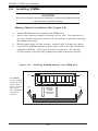
1
SUPER
SUPER P3TDDE
USER’S MANUAL
Revision 1.0c
®
The information in this User’s Manual has been carefully reviewed and is believed to be
accurate. The vendor assumes no responsibility for any inaccuracies that may be
contained in this document, makes no commitment to update or to keep current the
information in this manual, or to notify any person or organization of the updates. Please
Note: For the most up-to-date version of this manual, please see our
web site at < http://www.supermicro.com >.
SUPERMICRO COMPUTER reserves the right to make changes to the product described in
this manual at any time and without notice. This product, including software, if any, and
documentation may not, in whole or in part, be copied, photocopied, reproduced, translated
or reduced to any medium or machine without prior written consent.
IN NO EVENT WILL SUPERMICRO COMPUTER BE LIABLE FOR DIRECT, INDIRECT,
SPECIAL, INCIDENTAL, OR CONSEQUENTIAL DAMAGES ARISING FROM THE USE OR
INABILITY TO USE THIS PRODUCT OR DOCUMENTATION, EVEN IF ADVISED OF THE
POSSIBILITY OF SUCH DAMAGES. IN PARTICULAR, THE VENDOR SHALL NOT HAVE
LIABILITY FOR ANY HARDWARE, SOFTWARE, OR DATA STORED OR USED WITH THE
PRODUCT, INCLUDING THE COSTS OF REPAIRING, REPLACING, INTEGRATING,
INSTALLING OR RECOVERING SUCH HARDWARE, SOFTWARE, OR DATA.
Any disputes arising between manufacturer and customer shall be governed by the laws of
Santa Clara County in the State of California, USA. The State of California, County of
Santa Clara shall be the exclusive venue for the resolution of any such disputes.
Supermicro's total liability for all claims will not exceed the price paid for the hardware
product.
Unless you request and receive written permission from SUPER MICRO COMPUTER,
you may not copy any part of this document.
Information in this document is subject to change without notice. Other products and
companies referred to herein are trademarks or registered trademarks of their respective
companies or mark holders.
Copyright © 2003 by SUPER MICRO COMPUTER INC.
All rights reserved.
Printed in the United States of America
Preface
Preface
About This Manual
This manual is written for system integrators, PC technicians and
knowledgeable PC users. It provides information for the installation and use
of the SUPER P3TDDE motherboard. The SUPER P3TDDE supports dual
Intel ® 370-pin Pentium TM III FCPGA 500 MHz - 1.4 GHz processors with a
512K L2 cache at front side bus speeds of 133, 100 and 66 MHz. Please
refer to the support section of our web site (http://www.supermicro.com/
TechSupport.htm) for a complete listing of supported processors. FCPGA
Pentium III processors are housed in a 370-pin package.
Manual Organization
Chapter 1 includes a checklist of what should be included in your
mainboard box, describes the features, specifications and performance of
the SUPER P3TDDE mainboard and provides information on the chipset.
Chapter 2 begins with instructions on handling static-sensitive devices.
Read this chapter when installing the processors, SDRAM memory modules
and for mounting the mainboard in the chassis. Also refer to this chapter
for connecting floppy/hard disk drives, the IDE interfaces, the parallel and
serial ports and the twisted wires for the power supply, the reset button,
the keylock/power LED, the speaker and the keyboard.
If you encounter any problems, see Chapter 3, which describes troubleshooting procedures for the video, the memory and the setup configuration
stored in CMOS. For quick reference, a general FAQ (Frequently Asked
Questions) section is provided. Instructions are also included for contacting technical support. In addition, you can visit our web site at
www.supermicro.com/techsupport.htm for more detailed information.
Chapter 4 includes an introduction to BIOS and provides detailed information on running the CMOS Setup utility.
Chapter 5 provides information on the IDE RAID controller.
Appendix A lists BIOS POST messages.
Appendix B provides POST codes.
Appendix C details BIOS beep codes.
iii
SUPER P3TDDE User’s Manual
Table of Contents
About This Manual ...................................................................................................... iii
Manual Organization ................................................................................................... iii
Chapter 1: Introduction
1-1
Overview ............................................................................................................ 1-1
Checklist ....................................................................................................... 1-1
Contacting Supermicro ................................................................................ 1-2
SUPER P3TDDE Image ............................................................................ 1-3
SUPER P3TDDE Layout .......................................................................... 1-4
SUPER P3TDDE Quick Reference ........................................................... 1-5
VIA Apollo Chipset: System Block Diagram ........................................... 1-6
Motherboard Features ............................................................................... 1-7
1-2
Chipset Overview .............................................................................................. 1-9
1-3
Special Features ............................................................................................ 1-10
1-4
PC Health Monitoring .................................................................................... 1-10
1-5
ACPI/PC 99 Features ................................................................................... 1-12
1-6
Power Supply ................................................................................................. 1-13
1-7
Super I/O .......................................................................................................... 1-14
Chapter 2: Installation
2-1
Static-Sensitive Devices ................................................................................. 2-1
2-2
Processor Installation ..................................................................................... 2-2
2-3
Mounting the Motherboard in the Chassis .................................................... 2-3
2-4
Installing DIMMs .............................................................................................. 2-4
2-5
I/O Port/Front Control Panel Connector Locations ...................................... 2-5
2-6
Connecting Cables .......................................................................................... 2-7
Power Supply Connector .......................................................................... 2-7
6-Pin Power Connector .............................................................................. 2-7
Infrared Connector ....................................................................................... 2-8
PWR_ON Connector ................................................................................. 2-8
Reset Connector ......................................................................................... 2-8
Overheat LED Connector ............................................................................ 2-8
IDE RAID LED ........................................................................................... 2-9
NICLED ....................................................................................................... 2-9
IDE LED ....................................................................................................... 2-9
Power LED Connector ................................................................................ 2-9
iv
Table of Contents
PW_LED Connector .................................................................................... 2-9
RAID LED Connector ................................................................................ 2-10
Speaker Connector ................................................................................. 2-10
ATX PS/2 Keyboard/Mouse Ports ......................................................... 2-10
Universal Serial Bus ............................................................................... 2-10
Serial Ports ............................................................................................. 2-11
Wake-On-LAN (WOL) ............................................................................... 2-11
Wake-On-Ring (WOM) .............................................................................. 2-11
Fan Headers ............................................................................................ 2-11
2-7
Jumper Settings ............................................................................................. 2-12
Explanation of Jumpers .......................................................................... 2-12
Front Side Bus Speed ............................................................................ 2-12
CMOS Clear ............................................................................................ 2-13
Keyboard Wake-Up ................................................................................... 2-13
Watch Dog Enable .................................................................................... 2-13
LAN Enable/Disable .................................................................................. 2-14
Fan RPM Detection Select ...................................................................... 2-14
Onboard IDE RAID .................................................................................... 2-14
2-8
Parallel Port, Floppy/Hard Disk Drive and AGP Connections .................. 2-15
Parallel Port Connector .......................................................................... 2-15
Floppy Connector .................................................................................... 2-16
IDE Connectors ....................................................................................... 2-16
4x AGP Pro Slot ....................................................................................... 2-17
2-9
Installing Software Drivers ............................................................................ 2-18
Chapter 3: Troubleshooting
3-1
Troubleshooting Procedures ........................................................................... 3-1
Before Power On ....................................................................................... 3-1
No Power ................................................................................................... 3-1
No Video .................................................................................................... 3-1
Memory Errors ........................................................................................... 3-2
3-2
Technical Support Procedures ....................................................................... 3-2
3-3
Frequently Asked Questions .......................................................................... 3-3
3-4
Returning Merchandise for Service ................................................................ 3-5
v
SUPER P3TDDE User’s Manual
Chapter 4: BIOS
4-1
Introduction ....................................................................................................... 4-1
4-2
Running Setup .................................................................................................. 4-2
4-3
Main BIOS Setup .............................................................................................. 4-2
4-4
Advanced BIOS Setup .................................................................................... 4-6
4-5
PCI/PnPConfigurations ................................................................................... 4-16
4-6
Power Management ...................................................................................... 4-18
4-7
Boot-up Devices ............................................................................................ 4-21
4-8
Security Setup ............................................................................................... 4-23
4-9
Exit Setup ....................................................................................................... 4-25
Chapter 5: IDE RAID Controller
5-1
Introduction ....................................................................................................... 5-1
5-2
Installing Drivers .............................................................................................. 5-3
5-3
Frequently Asked Questions ....................................................................... 5-10
Appendices:
Appendix A: AwardBIOS POST Messages ......................................................... A - 1
Appendix B: AwardBIOS POST Codes ................................................................. B-1
Appendix C: AwardBIOS Error BeepCodes ......................................................... C-1
vi
Chapter 1: Introduction
1-1
Introduction
Chapter 1
Introduction
Overview
Checklist
Congratulations on purchasing your computer motherboard from an acknowledged leader in the industry. Supermicro boards are designed with
the utmost attention to detail to provide you with the highest standards in
quality and performance.
Please check that the following items have all been included with your
motherboard. If anything listed here is damaged or missing, contact your
retailer.
One (1) Supermicro Mainboard
Two (2) ATA66/100 ribbon cables for IDE devices
One (1) floppy ribbon cable
One (1) Supermicro CD or diskettes containing drivers and utilities
One (1) User's/BIOS Manual
1-1
SUPER P3TDDE User's Manual
Contacting Supermicro
Headquarters
Address:
Tel:
Fax:
E-mail:
Web site:
Super Micro Computer, Inc.
980 Rock Ave.
San Jose, CA 95131 U.S.A.
+1 (408) 503-8000
+1 (408) 503-8008
[email protected] (General Information)
[email protected] (Technical Support)
www.supermicro.com
Europe
Address:
Tel:
Fax:
E-mail:
Super Micro Computer B.V.
Het Sterrenbeeld 28, 5215 ML,
's-Hertogenbosch, The Netherlands
+31 (0) 73-6400390
+31 (0) 73-6416525
[email protected] (General Information)
[email protected] (Technical Support)
[email protected] (Customer Support)
Asia-Pacific
Address:
3F, #753 Chung-Cheng Road
Chung-Ho City, Taipei Hsien, Taiwan, R.O.C.
Tel:
+886-(2) 8228-1366
Fax:
+886-(2) 8221-2790
Web Site:
www.supermicro.com.tw
Email:
[email protected]
Technical Support:
Tel: 886-2-8228-1366, ext.132
1-2
Chapter 1: Introduction
Figure 1-1. SUPER P3TDDE Image
1-3
Introduction
SUPER P3TDDE
SUPER P3TDDE User's Manual
Figure 1-2. SUPER P3TDDE Layout
(not drawn to scale)
J12
10.7"
COM2
DIMM 3
DIMM 0
CPU2
VIA
Processor
DIMM 1
370 FCPGA/PPGA
DIMM 2
CLK
BUF1
6 PIN POWER
CHASSIS FAN1
CPU1 CHASSIS FAN
LED+
SPK1
CPU1
1
CPU2 FAN
J14
Parallel
Port
x
J13
COM1
CLK BUF2
Processor
JP9
PW LED RAIDLED SPEAKER
JP3
370 FCPGA/PPGA
USB1/2
JF1
1
1
BUTTON+ OH/IDE_R/NIC/IDE/PWR
24 PIN POWER
1
JP10
J2
JPWAKE
CPU1
Fan
KB/
MOUSE
J10
1
VT8633
1
J16
1
IDE2
IDE1
Clock
FLOPPY
LAN
JPL1
4x AGP PRO
11.6"
I2C
JP4
JP5
1
1
JP7
PCI 1
1
1
USB4
USB3
PCI 3
PCI 4
BIOS
FWH
VIA
VT8233
1
1
®
#1 #2
J17
PCI 5
ACR
IDE RAID
RAID
CNTLR
IDE RAID
WOL1 WOM1
BATTERY
1-4
1
IR
1
SUPER I/O
SUPER
CHASSIS FAN2
P3TDDE
1
CPU2 CHASSIS FAN
JL1
JP6
PCI 2
Chapter 1: Introduction
Jumpers
JBT1
JPWAKE
JPL1
JP4, JP5
JP6
JP7
JP10
J17
Description
CMOS Clear
Keyboard Wake-Up
LAN Enable/Disable
Front Side Bus Speed
Fan Detection Select
Fan Detection Select
Watch Dog Enable
Onboard IDE RAID
Connectors
COM1/COM2
CPU FAN1/2 CPU
CPU1/2 CHASSIS FAN
CPU CHASSIS FAN1/2
DIMM 0/1/2/3
D11, D12
IDE1, IDE2
JF1
JL1
JP1
JP8
JP9
J10
J12
J16
J18
J19
WOM1
WOL1
USB1/2, JUSB1 (USB3/4)
Default Setting
Pins 1-2 (Normal)
Pins 1-2 (Disabled)
Pins 1-2 (Enabled)
Both: Pins 1-2 (Auto)
Open (Overheat)
Closed (CPU Fans)
Open (Disabled)
Pins 2-3 (Disabled)
Description
COM1/COM2 Serial Port Connectors
Fan Headers
Overheat Fan Header
Chassis Fan Header
SDRAM Memory slots
IDE RAID Drive #1/2 Connectors
IDE Hard Disk Drive #1/2 Connectors
Front Control Panel Connector
Chassis Intrusion Header
Floppy Disk Drive Connector
I2C
PW_LED, RAID LED & Speaker
ATX 24-Pin Power Connector
PS/2 Keyboard/Mouse
Parallel Printer Port
Infrared Device Header
6-Pin Power Connector
Wake-On-Ring Header
Wake-on-LAN Header
Universal Serial Bus Ports
See Chapter 2 for details on the I/O ports, the Front Control Panel (JF1/2)
connectors and the jumper settings. Jumpers not indicated are for test purposes only.
1-5
Introduction
P3TDDE Quick Reference
SUPER P3TDDE User's Manual
Pentium III
FCPGA/PPGA
CPUs
133/100/66 MHz Host Bus
3D Graphics
Controller
GCLK
AGP Bus
VT8633
DDR Vlink
Host North
552BGA
Memory Bus
MCLK
266 MHz
Memory
Clock Buffer
HCLK/PCLK
Clock
Generator
SMBus
PCI Slots
PCI Bus
VT8233
Vlink
ATA 33/66/100
MII/LAN
6x USB
Power Plane & Peripheral Control
ACPI Events
LPC
LPC
Figure 1-3. VIA 266T Chipset:
System Block Diagram
1-6
Chapter 1: Introduction
CPU
• Dual Intel ® 370-pin Pentium TM III FCPGA 500 MHz - 1.4 GHz processors
with a 512K L2 cache (including low power Pentium TM III processors) at
133/100/66 MHz Front Side Bus speeds
Memory
• Four PC100/133 SDRAM DIMM sockets to support up to 4 GB SDRAM
Chipset
• VIA Apollo Pro 266T
Expansion Slots
•
One 4xAGP Pro
•
Five 32-bit PCI (33MHz)
•
One ACR
BIOS
• 2 Mb Award ® Flash ROM
• ACPI/APM Power Management
• PAC'99 color-coded I/O connectors
• One WOL (Wake-On-LAN) connector
• Internal control of Power-On Mode for recovery from AC power loss
PC Health Monitoring
• Seven onboard voltage monitors for CPU core, chipset voltage, +3.3V,
±5V and ±12V
• Four-fan status monitor with firmware/software on/off control
• Environmental temperature monitor and control
• CPU fan auto-off in sleep mode
• Power-up mode control for recovery from AC power loss
• System overheat LED and control
• System resource alert
• Hardware BIOS virus protection
• Auto-switching voltage regulator for the CPU cores
• Slow blinking LED for suspend state indicator
• BIOS support for USB keyboard
1-7
Introduction
Motherboard Features
SUPER P3TDDE User's Manual
ACPI/PC 98 Features
• Microsoft ® OnNow
• Real-time clock wake-up alarm
• Main switch override mechanism
•
External modem ring-on
Onboard I/O
• 2 IDE bus master interfaces support UDMA/100
• 1 floppy port interface (up to 2.88 MB)
• 2 Fast UART 16550A compatible serial ports
• 1 EPP (Enhanced Parallel Port)/ECP (Extended Capabilities Port)
• PS/2 mouse and PS/2 keyboard ports
• 1 infrared port
• 4 USB ports
• 2 IDE RAID connectors
Other
• Selectable CPU and chassis fan speed control (set in BIOS)
• Internal/external modem ring-on (WOM)
• Recovery from AC power loss control
• Wake-on-LAN (WOL)
• Multiple FSB clock frequency selections (set in BIOS)
CD Utilities
• BIOS flash upgrade utility (awdflash.exe)
• Drivers for the VIA Apollo Pro 266T chipset
Dimensions
• SUPER P3TDDE - ATX: 10.7" x 11.2" (271.78 mm x 284.48 mm)
1-8
Chapter 1: Introduction
Chipset Overview
The VIA Apollo Pro 266T chipset is a high performance, cost-effective and
energy-efficient chipset for the implementation of AGP/V-Link/PCI/LPC computer systems based on 64-bit, 370 Pentium III (66/100/133 MHz) processors.
VIA's Apollo Pro 266T chipset consists of two major components: the
VT8633 V-Link Memory Host System controller (North Bridge) and the
VT8233 V-Link Client PCI/LPC controller (South Bridge). The VT8633 Host
System Controller provides superior performance between the CPU, DIMMs,
AGP bus and V-Link inferface with pipelined, burst and concurrent operation. The VT8233 V-Link Client controller is a highly integrated PCI/LPC
controller. Its internal bus structure is based on a 66 MHz PCI bus that
provides a 2x bandwidth. The VT8233 integrated Clint V-Link controller,
which supports a 266 MB bandwidth between the Host/Client V-Link interface, provides a V-Link PCI and V-Link LPC controller. It supports five PCI
slots arbitration and decoding for all integrated functions and an LPC bus.
Memory Support and AGP Capability
The VT8633 supports up to 4 GB of SDRAM memory. The DRAM controller
supports both SDRAM and VCSDRAM (Virtual Channel SDRAM) in a flexible
mix/match manner. The SDRAM interface allows for zero wait state bursting between the DRAM and the data buffers at 66/100/133 MHz.
The VT8633 Controller also supports full AGP v.2.0 capability for maximum
bus utilization including 2x and 4x mode transfer, SBA (Side Band Addressing), Flush/Fence commands and pipelined grants. The VT8633 also provides flexible CPU/AGP/PCI remapping control, which supports major AGPbased 3D and DVD multimedia accelerators.
Recovery from AC Power Loss
The BIOS provides a setting that alllows you to determine how the system
will respond when AC power is lost and then restored to the system. You
can choose for the system to remain powered off (in which case you must
press the power switch to turn the system back on) or for it to return
automatically to a power-on state. See the Power Lost Control setting in
the BIOS chapter of this manual to change this setting. The default setting
is "Always OFF."
1-9
Introduction
1-2
SUPER P3TDDE User's Manual
1-3
Special Features
Advanced Communications Riser (ACR)
The ACR (Advanced Communications Riser) combines several existing communications buses with new and advanced communications buses to provide for low-cost, high-performance communications solutions. The ACR
Specification supports modem, audio, Local Area Network (LAN), and Digital
Subscriber Line (DSL). Pins are also reserved for future wireless bus
support. The ACR Specification enables riser-based broadband communications, networking peripheral and audio subsystem designs. ACR accomplishes this in an open-standards context.
1-4
PC Health Monitoring
This section describes the PC health monitoring features of the SUPER
P3TDDE motherboard.
Seven Onboard Voltage Monitors for the CPU Core, Chipset
Voltage, +3.3V, ± 5V and ± 12V
The onboard voltage monitor will scan these seven voltages continuously.
If a voltage becomes unstable, the monitor will give a warning or send an
error message to the screen. Users can adjust the voltage thresholds to
define the sensitivity of the voltage monitor.
Four-Fan Status Monitor with Firmware/Software On/Off Control
The PC health monitor can check the RPM status of the cooling fans. The
onboard 3-pin CPU and chassis fans are controlled by the power management functions. The thermal fan is controlled by the overheat detection
logic.
Environmental Temperature Control
The thermal control sensor monitors the CPU temperature in real time and
will activate the thermal control fan whenever the CPU temperature exceeds a user-defined threshold. The overheat circuitry runs independently
from the CPU. It can continue to monitor for overheat conditions even when
the CPU is in sleep mode. Once it detects that the CPU temperature is too
high, it will automatically turn on the thermal control fan to prevent any
1-10
Chapter 1: Introduction
CPU Fan Auto-Off in Sleep Mode
The CPU fan activates when the power is turned on. It can be turned off
when the CPU is in sleep mode. When in sleep mode, the CPU will not run
at full power, thereby generating less heat.
CPU Overheat LED and Control
This feature is available when the user enables the CPU overheat warning
function in the BIOS. This allows the user to define an overheat temperature. When this temperature is exceeded, both the overheat fan and the
warning LED are triggered.
System Resource Alert
This feature is available when used with Intel's LANDesk Client Manager
(optional). It is used to notify the user of certain system events. For
example, if the system is running low on virtual memory and there is insufficient hard drive space for saving the data, you can be alerted of the
potential problem.
Hardware BIOS Virus Protection
The system BIOS is protected by hardware so that no virus can infect the
BIOS area. The user can only change the BIOS content through the flash
utility provided by SUPERMICRO. This feature can prevent viruses from
infecting the BIOS area and destroying valuable data.
Auto-Switching Voltage Regulator for the CPU Core
The auto-switching voltage regulator for the CPU core can support up to
20A of current and auto-sense voltage IDs ranging from 1.3V to 3.5V. This
will allow the regulator to run cooler and thus make the system more stable.
1-11
Introduction
overheat damage to the CPU. The onboard chassis thermal circuitry can
monitor the overall system temperature and alert users when the chassis
temperature is too high.
SUPER P3TDDE User's Manual
1-5 ACPI/PC 99 Features
ACPI is an acronym for Advanced Configuration and Power Interface. The
ACPI specification defines a flexible and abstract hardware interface that
provides a standard way to integrate power management features throughout a PC system, including its hardware, operating system and application
software. This enables the system to turn on and off peripherals such as
CD-ROMs, network cards, hard disk drives and printers automatically. This
also includes consumer devices connected to the PC such as VCRs, TVs,
telephones and stereos.
In addition to enabling operating system-directed power management, ACPI
provides a generic system event mechanism for Plug and Play and an operating system-independent interface for configuration control. ACPI leverages the Plug and Play BIOS data structures while providing a processor
architecture-independent implementation that is compatible with both Windows 98, Windows NT and Windows 2000. You can check to see if ACPI
has been properly installed by looking for it in the Device Manager, which is
located in the Control Panel in Windows.
Microsoft OnNow
The OnNow design initiative is a comprehensive, system-wide approach to
system and device power control. OnNow is a term for a PC that is always
on but appears to be off and responds immediately to user or other requests.
Slow Blinking LED for Suspend-State Indicator
When the CPU goes into a suspend state, the chassis power LED will start
blinking to indicate that the CPU is in suspend mode. When the user presses
any key, the CPU will wake-up and the LED will automatically stop blinking
and remain on.
BIOS Support for USB Keyboard
If the USB keyboard is the only keyboard in the system, the keyboard will
function as a normal keyboard during system boot-up.
1-12
Chapter 1: Introduction
Although the PC may be perceived to be off when not in use, it is still
capable of responding to preset wake-up events. In the BIOS, the user can
set a timer to wake-up the system at a predetermined time.
Main Switch Override Mechanism
When an ATX power supply is used, the power button can function as a
system suspend button. When the user depresses the power button, the
system will enter a SoftOff state. The monitor will be suspended and the
hard drive(s) will spin down. Depressing the power button again will cause
the whole system to wake-up. During the SoftOff state, the ATX power
supply provides power to keep the required circuitry in the system alive. In
case the system malfunctions and you want to turn off the power, just
depress and hold the power button for 4 seconds. The power will turn off
and no main power will be provided to the motherboard.
External Modem Ring-On
Wake-up events can be triggered by a device such as the external modem
ringing when the system is in the SoftOff state. Note that external modem
ring-on can only be used with an ATX 2.01 (or above) compliant power
supply.
Wake-On-LAN (WOL)
Wake-On-LAN is defined as the ability of a management application to
power up a computer remotely that is powered off. Remote PC setup,
updates and asset tracking can occur after-hours and on weekends so that
daily LAN traffic is kept to a minimum and users are not interrupted. The
motherboards have a 3-pin header (WOL) to connect to the 3-pin header on
a Network Interface Card (NIC) that has WOL capability. Wake-On-LAN
must be enabled in BIOS. Note that Wake-On-Lan can only be used with an
ATX 2.01 (or above) compliant power supply.
1-6
Power Supply
As with all computer products, a stable power source is necessary for
proper and reliable operation. It is even more important for processors that
have high CPU clock rates.
1-13
Introduction
Real Time Clock Wake-Up Alarm
SUPER P3TDDE User's Manual
The SUPER P3TDDE accommodates ATX power supplies. Although most
power supplies generally meet the specifications required by the CPU, some
are inadequate.
It is strongly recommended that you use a high quality power supply that
meets ATX power supply Specification 2.02 or above. Additionally, in areas where noisy power transmission is present, you may choose to install
a line filter to shield the computer from noise. It is recommended that you
also install a power surge protector to help avoid problems caused by
power surges.
1-7
Super I/O
The functions of the disk drive adapter for the Super I/O chip include a
floppy disk drive controller that is compatible with industry standard 82077/
765, a data separator, write pre-compensation circuitry, decode logic, data
rate selection, a clock generator, drive interface control logic and interrupt
and DMA logic. The wide range of functions integrated onto the Super I/O
greatly reduces the number of components required for interfacing with
floppy disk drives. The Super I/O supports four 360 K, 720 K, 1.2 M, 1.44
M or 2.88 M disk drives and data transfer rates of 250 Kb/s, 500 Kb/s or 1
Mb/s. It also provides two high-speed, 16550 compatible serial communication ports (UARTs), one of which supports serial infrared communication.
Each UART includes a 16-byte send/receive FIFO, a programmable baud
rate generator, complete modem control capability and a processor interrupt
system. Both UARTs provide legacy speed with baud rate of up to 115.2
Kbps as well as an advanced speed with baud rates of 250 K, 500 K, or 1
Mb/s, which support higher speed modems.
At any given time, the Super I/O supports one of the followinga : PC-compatible printer port (SPP), Bi-directional Printer Port (BPP), Enhanced Parallel
Port (EPP) or Extended Capabilities Port (ECP).
The Super I/O provides functions that comply with ACPI (Advanced Configuration and Power Interface), which includes support of legacy and ACPI
power management through an SMI or SCI function pin. It also features
auto power management to reduce power consumption.
The IRQs, DMAs and I/O space resources of the Super I/O can flexibly
adjust to meet ISA PnP requirements, which suppport ACPI and APM (Advanced Power Management).
1-14
Chapter 2: Installation
Chapter 2
Installation
2-1 Static-Sensitive Devices
ElectroStatic Discharge (ESD) can damage electronic components. To prevent damage to your system board, it is important to handle it very carefully.
The following measures are generally sufficient to protect your equipment
from ESD.
Precautions
• Use a wrist strap designed to prevent electrostatic discharge that is
grounded to the computer chassis.
•
Touch a grounded metal computer object before removing the board from
the antistatic bag.
• Handle the board by its edges only; do not touch its components, peripheral chips, memory modules or gold contacts.
• When handling chips or modules, avoid touching their pins.
• Put the motherboard and peripherals back into their antistatic bags when
not in use.
• For grounding purposes, make sure your computer chassis provides excellent conductivity amongst the power supply, the case, the mounting
fasteners and the motherboard.
Unpacking
The motherboard is shipped in antistatic packaging to avoid static damage.
When unpacking the board, make sure the person handling it is static protected.
2-1
SUPER P3TDDE User’s Manual
2-2
Processor Installation
!
When handling the processor package, avoid placing
direct pressure on the label area of the fan.
The following pages cover the installation procedures. You should install
the processor in the motherboard first, then install the motherboard in the
chassis, then the memory and add-on cards, and finally the cables and
drivers. Following the installation procedures in the order they appear in
this chapter should eliminate the most common problems encountered when
building a system.
IMPORTANT: Always connect the power cord last, and always remove it before adding, removing or changing any hardware components.
Heat Sink
Follow the instructions that came with your processors and heat sinks to
attach heat sinks to the processors. Each of your heat sinks should have
a 3-pin fan connector, which should be connected to the CPU FAN header.
Make sure that good contact is made between the processors and the heat
sinks. Insufficient contact, incorrect types of heat sinks, fans, or thermal
compound used or improper amount of thermal compound applied on the
CPU die can cause a processor to overheat, which may crash the system.
Processor
You are now ready to install the processors. Your motherboard has two
370-pin, FCPGA type sockets, which support 370-pin Pentium III FCPGA (not
SEPP) 500 MHz - 1.4 GHz processors with a 512K L2 cache, including low
power Pentium III processors. Lift the lever on the FCPGA socket and install
with the notched corner of the processor oriented with pin 1. Fully seat the
processor into the socket and then close the lever. See Figure 2-1 for
views of the FCPGA 370-pin socket before and after processor installation.
2-2
Chapter 2: Installation
Pin 1
Lever
Notched
Corner
Processor
(installed)
Figure 2-1.
2-3
FCPGA Socket: Empty and with Processor Installed
(low power Pentium III shown)
Mounting the Motherboard in the Chassis
All motherboards have standard mounting holes to fit different types of
chassis. Chassis may include a variety of mounting fasteners made of
metal or plastic. Although a chassis may have both types, metal fasteners
are the most highly recommended because they ground the motherboard to
the chassis. For this reason, it is best to use as many metal fasteners as
possible.
2-3
SUPER P3TDDE User’s Manual
2-4
Installing DIMMs
CAUTION
Exercise extreme care when installing or removing DIMM modules
to prevent any possible damage.
Memory Module Installation (See Figure 2-2)
1.
Install SDRAM memory modules into DIMM slots.
2.
Insert each memory module vertically into its slot. Pay attention to
the two notches along the bottom of the module to prevent inserting
the DIMM incorrectly.
3.
Gently press down on the memory module until it snaps into place.
4.
Four PC133 SDRAM sockets support up to 4 GB of PC133 unbuffered,
registered SDRAM. ECC type memory is supported. PC133 and
PC100 memory are both fully supported at their respective speeds.
Figure 2-2.
Installing SDRAM Module into DIMM Slot
DIMM
Notch
To Install:
Insert module
vertically and
press down
until it snaps
into place.
Pay attention
to the two
notches.
Release
Tab
Note: Notch
should align
with the
receptive point
on the slot
2-4
Notch
Release
Tab
Chapter 2: Installation
Top View of DIMM Slot
Release Tab
Release Tab
To Remove:
Use your thumbs gently to push each release tab outward
to release the DIMM from the slot.
2-5
I/O Port/Front Control Panel Connector Locations
The I/O ports are color coded in conformance with the PC99 specification to
make setting up your system easier. See Figure 2-3 below for the colors
and locations of the various I/O ports.
Figure 2-3. I/O Port Locations and Definitions
Mouse
Parallel Port
(Lime)
(Burgandy)
Keyboard
(Purple)
USB Ports
COM1 Port
COM2 Port
LAN (Ethernet)
(Turquoise)
(Turquoise)
Port
2-5
SUPER P3TDDE User’s Manual
Front Control Panel
JF1 and JP9 contain header pins for various front control panel connectors. See Figure 2-4 for the pin definitions of the speaker, component/
function LEDs, power on and reset button headers.
Refer to Sections 2-6 and 2-7 for connector pin definitions and jumper
settings.
Figure 2-4.
Front Control Panel Connectors
16
Power
IDE
LED +
NIC
Speaker
IDE RAID
Over Heat
X
IDE
RAID
LED
Button +
Reset
Power
1
JF1
Power
LED
1
JP9
2-6
Chapter 2: Installation
2-6
Connecting Cables (see previous page for locations)
Power Supply Connector
The primary power supply connector on the P3TDDE meets the SSI
(Superset ATX) 24-pin specifications, however, it also supports an
ATX 20-pin connector. Thus, both
20-pin ATX and 24-pin SSI connectors can be installed on the
P3TDDE as long as the power supply connector is correctly oriented. (Make sure that pin 1 of
the PS connector is seated on pin
1 of the header of J10.) If a 24pin connector is used, please refer to Table 2-1a for pin definitions. (Also see Figure A below
for connector orientation). If a 20pin connector is used, please refer to Table 2-1b for pin definitions. (Also see Figure B below
for connector orientation.)
T able 2-1a
AT X Pow er Supply 24-pin Co nnector
Pin D efinitions (AT X POW ER)
Pin Number Definition Pin Number Definition
1
+3.3V
13
+3.3V
2
+3.3V
14
-12V
3
COM
15
C OM
4
+5V
16
PS_ON#
5
COM
17
C OM
6
+5V
18
C OM
7
COM
19
C OM
8
PW R_O K
20
R es(NC)
9
5VSB
21
+5V
10
+12V
22
+5V
11
+12V
23
+5V
12
+3.3V
24
C OM
T able 2-1b
AT X Power Supply 20-pin Connector Pin
Definitions
Pin #
11
12
13
14
15
16
17
18
19
20
Definition
+3.3V
-12V
COM
PS_ON
COM
COM
COM
-5V
+5V
+5V
Pin # Definition
1
+3.3V
2
+3.3V
3
COM
4
+5V
5
COM
6
+5V
7
COM
8
PW -OK
9
5VSB
10
+12V
T able 2-1c
PS Color Definitions
Color
Definition
Orange +3.3V
Black
Com
Red
5V
W hite
Power OK
Yellow
+12V
Purple
5V standby
Brown
-5V
(For reference only)
Pin 13
12345678901234567890123456789
12345678901234567890123456789
12345678901234567890123456789
12345678901234567890123456789
12345678901234567890123456789
12345678901234567890123456789
Pin 1
Pin 11
Pin
20
1234567890123456789012345
1234567890123456789012345
1234567890123456789012345
1234567890123456789012345
1234567890123456789012345
1234567890123456789012345
Pin 10
Pin 1
T able 2-2
6-Pin Power Connector
(J19)
6-Pin Power Connector
Pin #
Refer to Table 2-2 for pin definitions for the 6-Pin connector J19.
2-7
1
2
3
4
5
6
Definition
GND
GND
GND
+3.3V
+3.3V
+5V
SUPER P3TDDE User’s Manual
Infrared Connector
The header at J18 is for infrared
devices. See Table 2-3 for pin
definitions. See the Technical
Support section of our web page
for information on the infrared devices you can connect to the system.
PW_ON Connector
T able 2-3
Infrared Pin
Definitio ns (J18)
Pin
Number Definition
+5V
1
Key
2
IRRX
3
Ground
4
IRTX
5
T able 2-4
PW _ON Connector
Pin Definitions
(JF1)
The PW_ON connector is located
on pins 1 and 2 of JF1. Momentarily contacting both pins will
power on/off the system. The
user can also configure the power
on button to function as a suspend
button (see the Power Button
Mode setting in BIOS). To turn off
the power when set to suspend
mode, hold down the power button for at least 4 seconds. See
Table 2-4 for pin definitions.
Pin
Number Definition
PW _ON
1
2
Power
T able 2-5
Reset Connector
Pin Definitions
(JF1)
Reset Connector
The Reset connector is located on
pins 3 and 4 of JF1. This connector attaches to the hardware reset
switch on the computer case.
See Table 2-5 for pin definitions.
Pin
number Definition
3
Reset
4
Ground
T able 2-6
Overheat LED
Pin Definitions (JF1)
Overheat LED
Pin
Number
7
8
The Overheat connector is located
on pins 7 and 8 of JF1. It attaches
to an LED to to provide warning of
chassis overheating. See Table 26 for pin definitions.
2-8
Definition
LED +
LED -
Chapter 2: Installation
IDE RAID LED
The IDE RAID LED header is located on JF1. Attach the IDE RAID
hard drive LED cable to pins 9 and
10 of JF1. See Table 2-7 for pin
definitions.
NIC LED
The NIC (LAN) LED is located on
JF1. Attach the NIC LED cable to
pins 11 and 12 of JF1. See Table
2-8 for pin definitions.
T able 2-7
IDE RAID LED
Pin Definitions (JF1)
Pin
Number
9
10
Definition
LED +
LED -
T able 2-8
NIC (LED) Pin Definitions
(JF1)
Pin
Number
11
12
Definition
LED +
LED -
T able 2-9
IDE LED Pin Definitions
(JF1)
IDE LED
The IDE LED is located on JF1. Attach the IDE hard drive LED cable
to pins 13 and 14 of JF1. See
Table 2-9 for pin definitions.
Power LED
Pin
Number
13
14
Definition
LED +
LED -
T able 2-10
PW R LED
Pin Definitions (JF1)
The power LED connector is located on pins 15 to 16 of JF1. See
Table 2-10 for pin definitions. This
connection was designed for use
with Supermicro chassis.
Pin
Number
15
16
Definition
LED +
LED -
T able 2-11
PW _LED
Pin Definitions (JP9)
PW_LED Connector
The PW_LED connector is located
on pins 1 through 3 of JP9. See
Table 2-11 for pin definitions. This
connection was designed for use
with other chassis that require a
3-pin power LED connection.
2-9
Pin
Number D efinition
LED +
1
LED 2
3
LED -
SUPER P3TDDE User’s Manual
T able 2-12
RAID _LED
Pin Definitions (JP9)
RAID_LED Connector
The PW_LED connector is located
on pins 4 through 6 of JP9. See
Table 2-12 for pin definitions.
Pin
Number
4
5
6
Definition
LED +
LED LED -
Speaker Connector
Table 2-13
Speaker
Pin Definitions (JP9)
The speaker connector is located
on pins 7 through 11 of JF9. To
use the onboard speaker, leave
the jumper in place on pins 10-11
and connect the speaker cable to
pins 7-9. For an external speaker,
remove the jumper and connect
the speaker cable to pins 8-11.
See Table 2-13 for pin definitions.
Pin
Definition
Number
Spkr (+) Pull-Up
7
8
Spkr (+) Pull-Up
9
NC
Onboard Spkr (-)
10
Spkr (-) Signal
11
ATX PS/2 Keyboard and
PS/2 Mouse Ports
Table 2-14
PS/2 Keyboard
and Mouse Port
Pin Definitions
(J12)
The ATX PS/2 keyboard and the
PS/2 mouse are located on J12.
See Table 2-14 for pin definitions.
(The mouse port is above the keyboard port. See Figure 2-3 for locations.)
Pin
Number Definition
Data
1
NC
2
Ground
3
VCC
4
Clock
5
NC
6
Universal Serial Bus (USB)
Four Universal Serial Bus connectors are provided on the P3TDDE.
USB1 and USB2 are ports located
on the backplane and USB2 and
USB3 are headers located near
the IDE #1 connector. See Table
2-15 for pin definitions.
T able 2-15
Universal Serial Bus Pin Definitions
USB1
USB2
Pin
Number
Pin
Definition Number
1
2
3
4
+5V
P0P0+
Ground
USB3
Pin
Number
1
2
3
4
5
2-10
Definition
1
2
3
4
+5V
P0P0+
Ground
USB4
Pin
Definition Number
+5V
1
P02
P0+
3
Ground 4
Ground 5
Definition
+5V
P0P0+
Ground
Ground
Chapter 2: Installation
Serial Ports
Two serial ports (COM1 and
COM2) are provided on your
board. See Table 2-16 for the pin
definitions of connectors J13 and
J14). A 10-pin serial ribbon cable
is required if connecting a device
to a COM header.
Wake-On-LAN (WOL)
The Wake-On-LAN header is located on WOL1. Refer to Table 217 for pin definitions. You must
enable the LAN Wake-Up setting in
BIOS to use this function. (You
must also have a LAN card with a
Wake-on-LAN connector and cable
to use this feature.)
T able 2-16
Serial Port (COM) Pin
Definitions (J13, J14)
Pin Number
1
2
3
4
5
Definition Pin Number
6
DCD
7
Serial In
8
Serial Out
9
DTR
10
Ground
T able 2-17
W ake-On-LAN
Pin Definitions (W OL1)
Pin
Number
1
2
3
Definition
+5V Standby
Ground
W ake-up
T able 2-18
W ake-On-Ring Pin
Definitions (W OM1)
Wake-On-Ring (WOM1)
The Wake-On-Ring header is located on WOM1. Refer to Table 218 for pin definitions. You must
enable the Ring Wake-Up setting in
BIOS to use this function. (You
must also have a modem card with
a Wake-on-Ring connector and
cable to use this feature.) Both 2pin and 3-pin WOM headers are
provided.
Fan Headers*
Pin
Number
1
2
3
Pin
Number
1
2
Definition
+5V Standby
Ground
W ake-up
Definition
Ground
W ake-up
2-pin connector
T able 2-19
Fan Header
Pin Definitions
The six CPU and chassis fan
headers are designated CPU1/2
FAN, CPU1/2 CHASSIS FAN and
CHASSIS FAN 1/2. Refer to Table
2-19 for pin definitions.
Note: NC indicates "no connection".
2-11
Pin
Number
1
2
3
Definition
Ground (black)
+12V (red)
Tachometer
*Caution: These fan
headers use DC power
Definition
DSR
RTS
CTS
RI
NC
SUPER P3TDDE User’s Manual
2-7
Jumper Settings
Explanation of
Jumpers
Connector
Pins
To modify the operation of the
motherboard, jumpers can be used
to choose between optional settings. Jumpers create shorts between two pins to change the
function of the connector. Pin 1 is
identified with a square solder pad
on the printed circuit board. On a
2-pin jumper, "Closed" means the
jumper is over both pins (to
"close" the connection) and
"Open" means the jumper is either
off or on a single pin only. See
the motherboard layout pages for
3
2
1
3
2
1
Jumper
Cap
Setting
Pin 1-2 short
jumper locations.
Front Side Bus Speed
T able 2-20
Front Side Bus Sp eed Jumper Settings
(JP4, JP5)
The FSB speed is set with JP4
and JP5. Table 2-20 displays the
settings for these two jumpers.
The CPU speed can also be
changed by software control in
BIOS (see the CPU Speed setting).
The CPU Speed setting will also
show you the actual CPU speed
for each FSB speed option selected.
No te : If the system does not
reboot after changing the CPU
speed, 1) clear CMOS and reboot
(as described on the next page)
and then set the correct CPU
speed with the BIOS setting mentioned above.
2-12
JP4
JP5
FSB Speed
1-2
2-3
2-3
Open
1-2
2-3
Open
Open
Auto
66 MHz
100 MHz
133 MHz
Note: T he Auto setting allows the CPU
to set the speed.
Chapter 2: Installation
CMOS Clear
Refer to Table 2-21 for instructions on how to clear CMOS. Always remove the AC power cord
from the system before clearing
CMOS.
T able 2-21
CMOS Clear Jumper Settings
(JBT 1)
Jumper
Position
1-2
2-3
Definition
Normal
CMOS Clear
Position
1-2
Position
2-3
tem, remove the AC power cord, then
use JBAT1 to clear CMOS.
Normal
must completely shut down the sys-
CMOS Clear
Note: For an ATX power supply, you
Replace
JBAT1 back to the pin 1-2 position
before powering up the system
again.
Do not use the PW_ON con-
nector to clear CMOS.
Keyboard Wake-Up
The JPWAKE jumper (JP2) is used
together with the Keyboard WakeUp function in BIOS. Enable both
the jumper and the BIOS setting to
allow the system to be woken up
by depressing a key on the keyboard. See Table 2-22 for jumper
settings.
Table 2-22
Keyboard Wake-Up
Jumper Settings (JP2)
Jumper
Position
1-2
2-3
Definition
Disabled
Enabled
Note: Your power supply must meet ATX
specification 2.01 or higher and supply 720
mA of standby power to use this feature.
Watch Dog Enable
Watch Dog Enable
Jumper Settings (JP10)
This jumper is used to enable or disable the Watch Dog function. This
jumper is used together with the
Watch Dog enable function in BIOS.
Enable both the jumper and the
BIOS setting to use the Watch Dog
feature. See the table on the right
for pin definitions.
2-13
Jumper
Position
Open
Closed
Definition
Disabled
Enabled
SUPER P3TDDE User’s Manual
LAN Enable/Disable
Table 2-23
LAN Enable/Disable
Jumper Settings (JPL1)
JPL1 allows you to enable or disable the onboard LAN. See Table
2-23 for jumper settings.
Jumper
Position
1-2
2-3
Definition
Enabled
Disabled
Table 2-24a
Fan RPM Monitor Select
Jumper Settings (JP6)
Fan RPM Detection Select
Jumper
Position
Closed
*Open
JP6 and JP7 allow you to choose
which of two fans to monitor for
RPM speed. JP6 is for the Chassis
and Overheat fans and JP7 is for
the CPU and CPU Chassis fans.
See Table 2-24 for jumper settings.
Definition
Chassis fan
Overheat fan
*Default position
Table 2-24b
Fan RPM Monitor Select
Jumper Settings (JP7)
Jumper
Definition
Position
CPU 1/2 fan
*Closed
Open CPU chassis fan
*Default position
Onboard IDE RAID
J17 gives you the option of disabling/enabling the onboard IDE
RAID. See Table 2-25 for jumper
settings.
T able 2-25
Onboard IDE RAID Enable/Disable
(J17)
Jumper
Position
1-2
2-3
Definition
Enabled
Disabled
2-14
Position
2-3
Disabled
Enabled
Position
1-2
Chapter 2: Installation
2-8
Parallel Port, ACP, AGP and Floppy/Hard Disk Drive
Connections
Note the following when connecting the floppy and hard disk drive cables.
• The floppy disk drive cable has seven twisted wires.
• A red mark on a wire typically designates the location of pin 1.
• A single floppy disk drive ribbon cable has 34 wires and two connectors to
provide for two floppy disk drives. The connector with twisted wires always
connects to drive A, and the connector that does not have twisted wires
always connects to drive B.
• The 80-wire ATA66/100 IDE hard disk drive cable that came with your
system has two connectors to support two drives. This special cable
should be used to take advantage of the speed this new technology
offers. The blue connector connects to the onboard IDE connector interface and the other connector(s) to your hard drive(s). Consult the documentation that came with your disk drive for details on actual jumper
locations and settings for the hard disk drive.
Parallel Port Connector
The parallel port is located on J16.
See Table 2-26 for pin definitions.
T able 2-26
Parallel (Printer) Port Pin Definitions
(J16)
Pin Number
1
3
5
7
9
11
13
15
17
19
21
23
25
2-15
Function Pin Number Function
Strobe2
Auto FeedData Bit 0
4
ErrorData Bit 1
6
InitData Bit 2
8
SLCT INData Bit 3
10
GND
Data Bit 4
12
GND
Data Bit 5
14
GND
Data Bit 6
16
GND
Data Bit 7
18
GND
ACK
20
GND
BUSY
22
GND
PE
24
GND
SLCT
26
NC
SUPER P3TDDE User’s Manual
Floppy Connector
The floppy connector is located
on JP1. See Table 2-27 for pin
definitions.
T able 2-27
Floppy Connector Pin Definitions (JP1)
Pin Number
1
3
5
7
9
11
13
15
17
19
21
23
25
27
29
31
33
Function
GND
GND
Key
GND
GND
GND
GND
GND
GND
GND
GND
GND
GND
GND
GND
GND
GND
T able 2-28
IDE Connecto r Pin Definitions
(IDE#1, IDE#2)
Pin Number
1
3
5
7
9
11
13
15
17
19
21
23
25
27
29
31
33
35
37
39
Function
Reset IDE
Host Data 7
Host Data 6
Host Data 5
Host Data 4
Host Data 3
Host Data 2
Host Data 1
Host Data 0
GND
DRQ3
I/O W riteI/O ReadIOCHRDY
DACK3IRQ14
Addr 1
Addr 0
Chip Select 0
Activity
Pin Number
2
4
6
8
10
12
14
16
18
20
22
24
26
28
30
32
34
36
38
40
Function
GND
Host Data 8
Host Data 9
Host Data 10
Host Data 11
Host Data 12
Host Data 13
Host Data 14
Host Data 15
Key
GND
GND
GND
BALE
GND
IOCS16GND
Addr 2
Chip Select 1GND
2-16
Pin Number
Function
2
FDHDIN
4
Reserved
6
FDEDIN
8
Index10
M otor Enable
12
D rive Select B14
D rive Select A16
M otor Enable
18
DIR20
STEP22
W rite Data24
W rite Gate26
Track 0028
W rite Protect30
Read Data32
Side 1 Select34
Diskette
IDE Connectors
There are no jumpers to configure the onboard IDE interfaces
IDE1 and IDE2. Refer to Table
2-28 for pin definitions. You
must use the ATA100/66 cable
included with your system to
benefit from the ATA100/66
technology.
Chapter 2: Installation
4x AGP Pro Slot
The 4x AGP Pro slot is backward compatible with AGP and 4xAGP graphics
cards, which have fewer pins than AGP Pro cards. Because of this, care
must be taken when installing a graphics card into this slot, as doing so
incorrectly can damage your motherboard. For AGP Pro cards, you should
remove the orange sticker covering one end of the slot. For other cards,
leave this sticker in place and make sure your card does not plug into the
section it covers. A general rule of thumb is to make sure your card fills the
center section of pins first, then the end toward the edge of the motherboard if there are more. If the I/O shield of your card is flush with the edge
of the motherboard, the card should be inserted correctly.
AGP Pro Slot
Edge of motherboard
2-17
SUPER P3TDDE User’s Manual
2-9
Installing Software Drivers
After all the hardware has been installed you must install the software
drivers. The necessary drivers are all included on the Supermicro CD that
came packaged with your motherboard. After inserting this CD into your
CDROM drive, the display shown in Figure 2-5 should appear. (If this display does not appear, click on the My Computer icon and then on the icon
representing your CDROM drive. Finally, double click on the S "Setup" icon.)
Figure 2-5. Driver/Tool Installation Display Screen
Click the icons showing a hand writing on paper to view the readme files
for each item. Click the tabs to the right of these in order from top to
bottom to install each item one at a time. After installing each item, you
must reboot the system before moving on to the next item on the
list. The bottom icon with a CD on it allows you to view the entire contents
of the CD.
2-18
Chapter 3: Troubleshooting
Chapter 3
Troubleshooting
3-1
Troubleshooting Procedures
Use the following procedures to troubleshoot your system. If you have
followed all of the procedures below and still need assistance, refer to the
"Technical Support Procedures" and/or "Returning Merchandise for Service"
section(s) in this chapter. Note: Always disconnect the power cord
before adding, changing or installing any hardware components.
Before Power On
1. Make sure no short circuits exist between the motherboard and
chassis.
2. Disconnect all ribbon/wire cables from the motherboard, including those
for the keyboard and mouse.
3. Remove all add-on cards.
4. Install a CPU (making sure it is fully seated) and connect the chassis
speaker and the power LED to the motherboard. (Check all jumper
settings as well.)
No Power
1. Make sure no short circuits exist between the motherboard and the
chassis.
2. Verify that all jumpers are set to their default positions.
3. Check that the 115V/230V switch on the power supply is properly set.
4. Turn the power switch on and off to test the system.
5. The battery on your motherboard may be old. Check to verify that it
still supplies ~3VDC. If it does not, replace it with a new one.
No Video
1. If the power is on but you have no video, remove all the add-on cards
and cables.
2. Use the speaker to determine if any beep codes exist. Refer to
Appendix A for details on beep codes.
3-1
SUPER P3TDDE User’s Manual
NOTE
If you are a system integrator, VAR or OEM, a POST diagnostics card is recommended. For I/O port 80h codes, refer to
App. B.
Memory Errors
1. Make sure the DIMM modules are properly and fully installed for the
amount of memory desired.
2. Determine if different speeds of DIMMs have been installed and verify
that the BIOS setup is configured for the fastest speed of memory
used. It is recommended that all DIMMs in the system have the same
speed.
3. For DIMMs, make sure you are using PC133 or PC100 compliant
SDRAM.
4. Check for bad DIMM modules or slots by swapping modules between
slots and noting the results.
5. Make sure all memory modules are fully seated in their slots.
3-2
Technical Support Procedures
Before contacting Technical Support, please take the following steps. Also,
note that as a motherboard manufacturer, Supermicro does not sell directly
to end-users, so it is best to first check with your distributor or reseller for
troubleshooting services. They should know of any possible problem(s)
with the specific system configuration that was sold to you.
1. Please go through the ‘Troubleshooting Procedures’ and 'Frequently
Asked Question' (FAQ) sections in this chapter or see the FAQs on our
web site (http://www.supermicro.com/techsupport.htm) before contacting Technical Support.
2. BIOS upgrades can be downloaded from our web site at
http://www.supermicro.com/techsupport/download.htm.
Note: Not all BIOS can be flashed depending on the modifications to the boot block code.
3. If you still cannot resolve the problem, include the following information
when contacting Supermicro for technical support:
•Motherboard model and PCB revision number
3-2
Chapter 3: Troubleshooting
•BIOS release date/version (this can be seen on the initial display when
your system first boots up)
•System configuration
An example of a Technical Support form is on our web site at
< http://www.supermicro.com/techsupport/contact_support.htm >.
4. Distributors: For immediate assistance, please have your account number
ready when placing a call to our technical support department. We can
be reached by e-mail at < [email protected] > or by fax at
(408) 503-8019.
3-3
Frequently Asked Questions
Question: What are the various types of memory that the P3TDDE
motherboard can support?
Answer: The P3TDDE has four 168-pin DIMM slots that support up to 4 GB
of unbuffered 3.3V SDRAM. ECC memory is also supported. Please refer
to Chapter 2 for additional information.
Question: How do I update my BIOS?
Answer: It is recommended that you do not upgrade your BIOS if you are
not experiencing problems with your system. Updated BIOS files are located on our web site at < http://www.supermicro.com >. Please check our
BIOS warning message and the info on how to update your BIOS on our
web site. Also, check the current BIOS revision and make sure it is newer
than your BIOS before downloading. Select your motherboard model and
download the BIOS file to your computer. Unzip the BIOS update file and
you will find the readme.txt (flash instructions), the awdflash.exe (BIOS
flash utility) and the BIOS image (xxxx.bin) files. Copy these files onto a
bootable floppy and reboot your system. It is not necessary to set BIOS
boot block protection jumpers on the motherboard. At the DOS prompt,
enter the command "awdflash." Type in the BIOS file that you want to
update (xxxx.bin).
Question: After flashing the BIOS my system does not have video.
How can I correct this?
Answer: If the system does not have video after flashing your new BIOS,
it indicates that the flashing procedure failed. To remedy this, first clear
CMOS per the instructions in this manual and retry the BIOS flashing procedure. If you still do not have video, please use the following BIOS Recov-
3-3
SUPER P3TDDE User’s Manual
ery Procedure. First, make sure the JPWAKE jumper is disabled. Then,
turn your system off and place the floppy disk with the saved BIOS image
file (see above FAQ) in drive A. Press and hold <Alt> and <F2> at the same
time, then turn on the power with these keys pressed until your floppy drive
starts reading. Your screen will remain blank until the BIOS program is
done. If the system reboots correctly, then the recovery was successful.
The BIOS Recovery Procedure will not update the boot block in your
BIOS.
Question: What's in the CD that came with my motherboard?
Answer: The supplied compact disc has quite a few drivers and programs
that will greatly enhance your system. We recommend that you review the
CD and install the applications you need. Applications on the CD include VIA
Pro 266 chipset drivers for Windows plus security and audio drivers.
Question: Why can't I turn off the power using the momentary
power on/off switch?
Answer: The instant power off function is controlled in BIOS by the Power
Button Mode setting. When the On/Off feature is enabled, the motherboard
will have instant off capabilities as long as the BIOS has control of the
system. When the Standby or Suspend feature is enabled or when the
BIOS is not in control such as during memory count (the first screen that
appears when the system is turned on), the momentary On/Off switch must
be held for more than four seconds to shut down the system. This feature
is required to implement the ACPI features on the motherboard.
Table 3-1.
Shared IRQs
PCI 1 shares an IRQ with PCI5
PCI 2 shares an IRQ with the IDE RAID controller
PCI 3 shares an IRQ with the LAN controller
PCI 4 shares an IRQ with 4xAGP Pro
3-4
Chapter 3: Troubleshooting
Question: I installed my microphone correctly but I can't record any
sound. What should I do?
Answer: Go to <Start> <Programs> <Accessories> <Entertainment> and
then <Volume Control>. Under the Properties tab, scroll down the list of
devices in the menu and check the box beside "Microphone".
Question: How do I connect the ATA66/100 cable to my IDE
device(s)?
Answer: The 80-wire/40-pin ATA66/100 IDE cable that came with your
system has two connectors to support two drives. This special cable must
be used to take advantage of the speed the ATA66/100 technology offers.
Connect the blue connector to the onboard IDE header and the other
connector(s) to your hard drive(s). Consult the documentation that came
with your disk drive for details on actual jumper locations and settings.
3-4
Returning Merchandise for Service
A receipt or copy of your invoice marked with the date of purchase is
required before any warranty service will be rendered. You can obtain
service by calling your vendor for a Returned Merchandise Authorization
(RMA) number. When returning to the manufacturer, the RMA number
should be prominently displayed on the outside of the shipping carton, and
mailed prepaid or hand-carried. Shipping and handling charges will be applied for all orders that must be mailed when service is complete.
This warranty only covers normal consumer use and does not cover damages incurred in shipping or from failure due to the alternation, misuse,
abuse or improper maintenance of products.
During the warranty period, contact your distributor first for any product
problems.
3-5
SUPER P3TDDE User’s Manual
Notes
3-6
Chapter 4: BIOS/Setup
Chapter 4
BIOS
4-1
Introduction
This chapter describes the Award BIOS for the P3TDDE. The Award
ROM BIOS is stored in a Flash chip and can be easily upgraded using a
floppy disk-based program.
Note: Due to periodic changes to the BIOS, some settings may have been
added or deleted and might not yet be recorded in this manual. Refer to the
Manual
Download
area
of
the
Supermicro
web
site
(located at http://www.supermicro.com) for any changes to BIOS that may
not be reflected in this manual.
System BIOS
The BIOS is the Basic Input Output System used in all IBM® PC, XT™, AT® ,
and PS/2® compatible computers. The AwardBIOS Flash chip stores the
system parameters, such type of disk drives, video displays, etc. in the
CMOS. The CMOS memory requires very little electrical power. When the
computer is turned off, a back-up battery provides power to the BIOS Flash
chip, enabling it to retain system parameters. Each time the computer is
powered-on the computer is configured with the values stored in the BIOS
ROM by the system BIOS, which gains control at boot-up.
How To Change the Configuration Data
The CMOS information that determines the system parameters may be
changed by entering the BIOS Setup utility. This Setup utility can be accessed by pressing <Del> at the appropriate time during system boot, see
below.
Starting the Setup Utility
Normally, the only visible POST (Power On Self Test) routine is the memory
test. As the memory is being tested, press the <Delete> key to enter the
main menu of the BIOS Setup utility. From the main menu, you can access
the other setup screens, such as the Chipset and Power menus. Section 43 gives detailed descriptions of each parameter setting in the Setup utility.
4-1
SUPER P3TDDE User’s Manual
4-2
Running Setup
*Optimal default settings are in bold text unless otherwise noted.
The BIOS setup options described in this section are selected by choosing the appropriate text from the Main BIOS Setup screen. All displayed
text is described in this section, although the screen display is often all
you need to understand how to set the options (see on next page).
When you first power on the computer, the AwardBIOS™ is immediately
activated.
While the BIOS is in control, the Setup program can be activated in one of two
ways:
1. By pressing <Del> immediately after turning the system on, or
2. When the message shown below appears briefly at the bottom of the
screen during the POST (Power On Self-Test), press the <Del> key to
activate the Main Setup Menu:
Press DEL to enter SETUP
4-3
Main BIOS Setup
All Main Setup options are described in this section. The Main BIOS Setup
screeen is displayed below.
Use the Up/Down arrow keys or the <Tab> key to move among the different
settings in the above menu.
Press the <ESC> key to exit theCMOS Setup Menu and use the Left/Right
arrow keys to enter other categories of BIOS settings. The next section
describes in detail how to navigate through the menus.
4-2
Chapter 4: BIOS/Setup
Main BIOS Setup Menu
Main Setup Features
Date/Time
Set the system date and time. Key in the correct information in the fields
when the options of "Month, DD, YYYY" and "HH:MM:SS" appear in the
screen. Press the <Enter> key to save the data.
Drive A/Drive B
These options allow the user to set the type of floppy disk drive installed in
the system. The settings are: "None", "360K, 5.25in", "1.2M, 5.25in", "720K,
3.5in", "1.44M, 3.5in", "2.88M, 3.5in".
Swap Floppy Drive
These options allow the user to swap the names of floppy disk drives
installed in the system, should there be two floppy disk drives installed on
the main board. The settings are: "Disabled" and "Enabled." The default
setting is "Disabled".
IDE Primary Master/IDE Primary Slave/IDE Secondary Master/
IDE Secondary Slave
These options allow the user to set the parameters of the IDE Primary
Master/Slave and IDE Secondary Master/Slave slots. Hit <Enter> to activate
the following sub-menu screen for detailed options of these items. Set the
4-3
SUPER P3TDDE User’s Manual
correct configurations accordingly. The items included in the sub-menu are:
IDE HDD Auto-Detection
Press the <Enter> key to activate the "IDE HDD Auto-Detection" function to
automatically detect the parameters of the IDE hard disk drives installed in
the system, such as the sizes of the hard drives.
IDE Primary Master
This option allows the user to determine the manner in which the
AwardBIOS sets the settings for the IDE Primary Master Device. The
settings are "None", "Auto" and "Manual".
Access Mode
This item determines the location through which the AwardBIOS access
the IDE Primary Master Device. The settings are "CHS", "LBA", "Large" and
"Auto".
IDE Primary Master PIO / IDE Primary Slave PIO / IDE
Secondary Master PIO / IDE Secondary Slave PIO
This IDE PIO (Programmed Input/Output) field allows you to set a PIO mode
(0-4) for the IDE Primary device designated Mode 0 thorugh Mode 4. Each
increase in mode number indicates a corresponding increase in
performance. The settings are "Auto", "Mode 0", "Mode 1", "Mode 2",
"Mode3", "Mode 4" and "Auto".
4-4
Chapter 4: BIOS/Setup
IDE Primary Master UDMA / IDE Primary Slave UDMA /
IDE Secondary Master UDMA / IDE Secondary Slave UDMA
This option is available only when your IDE hard drive supports Ultra DMA/
33 and the operating environment also includes a DMA drive (Windows 95
OSR2 or a third-party IDE bus master driver). If your IDE hard drive and
your system software both support Ultra DMA/33, select "Auto" to enable
BIOS support. The settings are "Auto", and "Disabled".
Video
This option allows the user to select the setting for the default video device.
The settings are "EGA/VGA", "CGA 40", "CGA 80", and "MONO".
HaltOn
This option allows the user to select the situation in which you want the
BIOS to stop the POST process and notify you about the status of the
system. The settings are "All Errors", "No Errors", "All, but Keyboard",
"All, but Diskette" and "All, but Disk/Key".
Base Memory
This field displays the amount of conventional memory detected during bootup. This is normally set to "640K".
Extended Memory
This feature displays the amount of extended memory detected during bootup. This is normally set to "65535K".
Total Memory
This feature displays the amount of total memory available in the system.
This is normally set to "1024K".
4-5
SUPER P3TDDE User’s Manual
4-4
Advanced BIOS Setup
Choose the Advanced BIOS Setup from the Award BIOS Setup Utility main menu
with the <Left> and <Right> arrow keys. You should see the display shown
below. Select one of the items in the left frame of the screen to go to the sub
screen for that item. Advanced BIOS Setup options are displayed by highlighting
the option using the arrow keys. All Advanced BIOS Setup options are described
in this section.
4-4.1
Advanced BIOS Features
When the required item in the "Advanced BIOS Features" is highlighted,
press the <Enter> key to activate the selection, as shown below:
4-6
Chapter 4: BIOS/Setup
Auto Detect DIMM/PCI CLK
If enabled, this feature will allow the BIOS automatically to detect the status
of the DIMM/PCI clock. The settings are "Enabled" and "Disabled."
Init Display First
This option allows the user to determine which display device will first be
activated when the sytem boots up -- either a installed in the PCI slot or a
device intalled in the AGP slot. The settings are "PCI slot" and "AGP".
Quick Power-On Self Test
If enabled, this feature will speed up the process of POST (Power On Self
Test) after the computer is switched on. The settings are "Enabled" and
"Disabled". If "Disabled", the POST procedure will take place at its normal
speed.
Boot Up NumLock Status
This option enables the system to check the status of the NumLock key
during boot-up. The settings are "On" and "Off".
Gate A20 Option
This option allows the user to determine if the chipset or the keyboard
controller should have the control over Gate A20. The settings are "Normal"
or "Fast". If set to "Normal", a pin in the keyboard controller controls Gate
A20. If "Fast" is selected, the chipset will have the control over Gate A20.
Typematic Rate Setting
Key strokes repeat at a rate pre-determined by the keyboard controller. The
key stroke repeating rate is called the typematic rate. If "Enabled", this
option allows the user to set the "Typematic Rate" of the system. If
"Disabled", the user will not be allowed to set the "Typematic Rate." The
settings are "Enabled" and "Disabled". (When disabled, "Typematic Rate"
and "Typematic Delay" will not be displayed.)
4-7
SUPER P3TDDE User’s Manual
Typematic Rate (Chars/Sec)
If enabled, the option allows the user to set the number of times a key stroke
repeats itself in a second when the key is held down. The settings are "6",
"8", "10", "12", "15", "20", "24" and "30".
Typematic Delay
The option sets the delay time after a key is held down before it begins to
repeat the keystroke. The settings are "250", "500", "750" and "1000".
MPS Version Control for OS
This option sets the modes of the MPS Version Control for the operating
system. The settings are "1.4" and "1.1".
OS Select For DRAM > 64MB
The option allows the user to select the operating system that requires a
DRAM memory greater than 64 MB in order to function properly. The
settings are "OS2", and "Non OS2".
Power On after PWR Fail
This option allows the user to determine if the system's power will be
automatically turned "on" or remain "off" after power is restored after an
outtage. The settings are "On", "Off" and "Former Status".
4-4.2
Advanced Chipset Features
4-8
Chapter 4: BIOS/Setup
This section documents the functions that the AwardBIOS provides the user
in configuring the system based upon the special features offered by the
VIA Apollo 266 chipset. The VIA Apollo 266 chipset manages the operations
of major components of the board, such as the bus speed of the CPU,
access to the memory and the communication between the PCI slots and
the CPU. Normally, the default settings for the Advanced Chipset Features
listed in the section are pre-configured by the manufacturer for optimal
system performance. It is not recommended that the user alter the default
settings. This section is provided as an emergency measure for the user
to restore the functions of the system when the critical data stored in the
BIOS is lost.
When the desired item in "Advanced Chipset Features" is highlighted, press
the <Enter> key to access its settings.
Host & AGP Bridge Control
This section documents the AwardBIOS management of the bus links
between the host and bridge devices.
Memory Parity / ECC Check
Select "Enabled" only if the system DRAM contains parity to add a parity
check to the boot-up memory tests. The settings are "Enabled" and
Disabled".
4-9
SUPER P3TDDE User’s Manual
System BIOS Cacheable
If enabled, the system BIOS information stored in the BIOS ROM (Read Only
Memory) chip will be written and temporarily stored in the "cacheable"
section of the memory, so the CPU has faster access to the information.
The settings are "Enabled" or "Disabled".
Video BIOS Cacheable
If enabled, the Video BIOS information stored in the BIOS ROM (Read Only
Memory) chip will be written and temporarily stored in the "cacheable"
section of the memory for faster access. The settings are "Enabled" and
"Disabled".
Memory Hole
To improve the performance of the sytem, a certain section of the memory
will be reserved for the use of the devices installed in the PCI slots. This
section of memory must be mapped into the memory space below 16 MB.
The settings are "15M-16M" and "Disabled".
CPU to PCI Write Buffer
To improve the performance of the system, a certain section of the memory
will be designated as "Write Buffer" to temporarily store the data CPU writes
to PCI to provide faster access. This information can be exe.codes or
operational instructions for the system. The settings are "Enabled" and
"Disabled".
PCI Master 0 WS Write
If enabled, the transimission of PCI Master Write PCI Master Write signals
will have no delays. The settings are "Enabled" and "Disabled".
PCI Delayed Transition
If enabled, the PCI signal transition will be delayed. The settings are
"Enabled" and "Disabled".
4-10
Chapter 4: BIOS/Setup
On-Chip IDE Channel 10
If enabled, BIOS support of onchip IDE 10 will be activated. The settings
are "Enabled" and "Disabled".
OnChip IDE Channel 11
If enabled, BIOS support of onchip IDE 11 will be activated. The settings
are "Enabled" and "Disabled".
IDE Prefetch Mode
If enabled, the IDE Prefetch Mode function will be activated. The settings
are "Enabled" and "Disabled".
On-Chip AC97 Modem
If enabled, this option allows the user to activate the BIOS support of OnChip MC 97 Modem. The settings are "Disabled" and "Enabled".
On-Chip AC97 Modem
If enabled, this option allows the user to activate the BIOS support of OnChip MC 97 Modem. The settings are "Disabled" and "Enabled".
On-Chip LAN Controller
If enabled, this option allows the user to activate the BIOS support of OnChip LAN Controller. The settings are "Disabled" and "Enabled".
On-Chip USB Controller
If enabled, this option will allow the user to acctivate the BIOS support of
On-Chip USB Controllers. The settings are "All Disabled", "All Enabled",
"1&2 USB Ports", "2&3 USB Ports", "1 USB Port", "2 USB Port" and "3USB
port".
USB Keyboard Support
If enabled, this option allows the user to activate the BIOS support of the
On-Chip USB Keyboard Controller. The settings are: "Disabled" and
"Enabled".
4-11
SUPER P3TDDE User’s Manual
4-4.3
Integrated Peripherals
When the item "Integrated Peripherals" is highlighted, hit the <Enter> key to
activate the sub-menu screen. When the above menu appears, select the
items and press the <Enter> key to display the options.
Onboard FDC Controller
Select "Enabled" if your system has a floppy disk controller (FDC) installed
on the main board and you wish to use it. The settings are "Enabled" and
"Disabled".
Onboard Serial Port 1 / Port 2
This option allows the user to set the address and the corresponding IRQ
for the Serial Port1 and Serial Port 2. The settings are "Disabled" , "3F8/
IRQ4", "2F8/IRQ3", "3E8/IRQ4", "2E8/IRQ3" and "Auto ." The default setting
for Serial Port1 is "3F8/IRQ4" and the default for Port 2 is is "2F8/IRQ3".
UART Mode Select
This option allows the user to select the UART mode for BIOS. The settings
are "IrDA", "ASKIR" and "Normal".
RxD, TxD Active
This option allows the user to set the settings for the function of "RxD, TxD
Active." The settings are "Hi, Hi", "Hi, Lo", "Lo, Hi" and "Lo, Lo".
4-12
Chapter 4: BIOS/Setup
IR Transmission Delay
If "Enabled", the transmssion of IR (infrared) signals will be delayed. The settings
are "Enabled" and "Disabled".
UR2 Duplex Mode
This option sets the UR2 Duplex Mode. The settings are "Full" and "Half".
Use IR Pins
This item is used to change the Use IR Pins setting. The settings are "RxD2,
TxD2" and "IR-Rx2Tx2".
Onboard Parallel Port
This option allows the user to set the address and the corresponding IRQ
for the onboard parallel port. The settings are "Disabled", "378/IRQ7", "278/
IRQ5" and "3BC/IRQ7".
Parallel Port Mode
This option sets the mode for the onboard parallel port. The settings are
"SPP", "EPP", "ECP" and "ECP+EPP".
EPP Mode Select
This option allows the user to select the EPP mode. The settings are "EPP
1.9" and "EPP 1.7".
ECP Mode Use DMA
This option allows the user to select the ECP use DMA mode. The settings
are "1" and "3".
Watch Dog Feature
This option allows the user to enable or disable the Watch Dog Feature. The
settings are "Enabled" and "Disabled".
4-13
SUPER P3TDDE User’s Manual
4-4.4
Hardware Monitors
When the item "Hardware Monitors" is highlighted, press the <Enter> key to
activate the sub-menu.
CPU Warning Temperatures
This item allows the user to set the CPU temperature threshold. When the
CPU temperature reaches the threshold temperature set by the user, the
alarm will sound and a warning message will be displayed on the screen.
The settings are "Disabled", "60 0C/140 0F", "65 0 C/149 0F", "70 0 C/158 0 F", "75 0C/
167 0F", "80 0C/176 0F", "85C/185F" and 90C/194F".
4-14
Chapter 4: BIOS/Setup
4-4.5
Processor Features
When the item "Processor Features" is highlighted, press the <Enter> key to
activate the sub-menu as seen below.
CPU L1 & L2 Cache
Set this option to "Enabled" to activate the CPU L1 and L2 cache. The
settings are "Disabled" and "Enabled".
CPU L2 Cache ECC Check
Set this option to "Enabled" to activate ECC Checking to take place with the
CPU L2 Cache. The settings are "Disabled" and "Enabled".
4-15
SUPER P3TDDE User’s Manual
Processor Number Feature
Set this option to "Enabled" to enable the reporting of your computer
system's CPU ID numbers. The settings are "Enabled" and "Disabled".
CPU Clock Ratio
This option allows the user to set the CPU Clock Ratio. The settings are
"x3", "x3.5", "x4","x4.5", "x5", "x5.5","x6", "x6.5", "x7", "x7.5", "x8", "x8.5",
"x9", "x9.5", "x10", "x10.5", "x11", "x11.5", "x12", "x13", "x14", "x15" and
"16."
4-5
PnP/PCI Configurations
With the item "PnP/PCI" highlighted on the main menu bar, press the <Enter>
key to activate the following screen:
PCI Slot 1/5, 2, 3, and 4 IRQ Select
The IRQ for the various PCI slots can be configured manually. The settings
are "Auto", "3", "4", "5", "7", "9", "10", "11", "12", "14" and "15".
4-16
Chapter 4: BIOS/Setup
PNP OS Installed
Select "Yes" if you are using an operating system that supports Plug and
Play solutions. Select "No" if you need the BIOS to configure non-boot
devices.
Reset Configuration Data
If you have installed a new add-on device and it has caused conflicts in
system configuration that results in a system boot-up failure, then select
"Enabled" to reset "Extended System Configuration Data" (ESCD) for the
OS to reboot the system. The settings are "Enabled" and "Disabled".
Resources Controlled By
AwardBIOS can automatically configure all the boot devices and all Plug and
Play compatible devices. However, if this item is set to "Auto (ESCD)", the
user will not be able to set the IRQ DMA and memory address since the
Award BIOS will automatically assign the values to these fields. The
settings are "AUTO (ESCD)" and "Manual."
PCI/VGA Palette Snoop
For best system performance, this item has been preset to "Disabled" by
the manufacturer. The settings are "Enabled" and "Disabled".
Assign IRQ for VGA
If "Enabled", you allow AwardBIOS to assign an IRQ for the VGA devices.
The settings are "Enabled" and "Disabled".
Assign IRQ for USB
If "Enabled", you allow the AwardBIOS to assign IRQ for the USB devices.
The settings are "Enabled" and "Disabled".
4-17
SUPER P3TDDE User’s Manual
4-6
Power Management
When the Item "Power" is highlighted on the main menu bar, hit the <Enter>
key to activate the following screen:
ACPI Function
This item allows you to enable and disable the functions included in the
Advanced Configuration and Power Management software. The settings
are "Enabled" and "Disabled".
Power Management Option
This option sets the power saving level for the system, especially for HDD
Power Down, Doze Mode and Suspend Mode. The settings are "User
Define", "Min. Saving" and "Max. Saving".
Suspend Mode
This item sets the system suspend time-out mode. The settings are
"Disabled", "1 Min", "2 Min", "4 Min", "6 Min", "8 Min", "10 Min", "20 Min", "30
Min", "40 Min" and 1 Hr".
Wake-Up by PME
If "Enabled", the user is able to "wake up" the system by a Power
Management Event. The settings are "Enabled" and "Disabled".
4-18
Chapter 4: BIOS/Setup
Wake-Up by WOL/ WOM / RI
Select "Enabled" to allow BIOS to activate the Modem Ring Resume function.
The settings are "Enabled" and "Disabled".
HDD Spin Off Timeout
If "Enabled", this option will allow the AwardBIOS to power-down the
hard disk drive after a time delay to avoid losing data. The settings are
"Disabled", and "1 min" through "15 min" in one minute increments.
Video Off Option
This option sets the status of the video device and monitor when the system
is in the Suspend Mode. When set to "Always On", the video device and
the monitor will always be on when the system is in the suspend mode.
When the option is set to "Suspend-Off", the video device and the monitor
will be turned off when the system is in the suspend mode.
Video Off Method
This item determines the manner in which the monitor is turned off. The
settings are "Blank Screen", "V/H SYNC+Blank" and "DPMS". Select "V/H
SYNC+Blank" to turn off the vertical and horizontal synchronization ports
and the monitor. Select "Blank Screen" to turn off the video buffer and the
monitor. Select "DPMS" to initiate display power management signals.
Soft-off by PWR-BTTN
This item determines the system's "Soft-off" mode when the user presses
the power-button. The settings are "Instant-off" and "Delay 4 Sec".
Power On Function
This setting allows the user to determine the method by which the system
activates the power on function. The settings are "Password", "Hot Key",
"Mouse Left", "Mouse Right", "Any key", "BUTTON ONLY" and "Keyboard
98."
4-19
SUPER P3TDDE User’s Manual
KB Power On Password
This item allows the user to set the password to activate the power on
function through keyboard. Press the <Enter> key to enter the password.
Hot Key Power On
This option allows the user to set the hot key to activate the power on
function. The settings are "Ctrl F1", "Ctrl-F2", "Ctrl-F3", "Ctrl-F4", "Ctrl-F5",
"Ctrl-F6", "Ctrl-F7", "Ctrl-F8", "Ctrl-F9", "Ctrl-F10", "Ctrl-F11" and "Ctrl-F12".
RTC Alarm Resume
If "Enabled", this option will allow AwardBIOS to resume the RTC (Real Time
Clock) Alarm activities. The default settings are "Enabled" and "Disabled".
4-20
Chapter 4: BIOS/Setup
4-7
Boot-up Devices
When the Item "Boot" is highlighted on the main menu bar, press the <Enter>
key to activate the following screen:
AwardBIOS attempts to load the operating system from devices specified
by the users in a user-specified sequence.
First Boot Device
This item allows the user to select the first boot-up device. The settings
are "Floppy", "LS120", "HDD-0", "SCSI", "CDROM", "HDD-1", "HDD-2", "HDD3", "ZIP100", "USB-HDD", "USB-ZIP", "USB-CDROM", USB-HDD", "LAN" and
"Disabled".
Second Boot Device
This item allows the user to select the second boot-up device. The settings
are "Floppy", "LS120", "HDD-0", "SCSI", "CDROM", "HDD-1", "HDD-2", "HDD3", "ZIP100", "USB-HDD", "USB-ZIP", "USB-CDROM", USB-HDD", "LAN" and
"Disabled".
Third Boot Device
This item allows the user to select the third boot-up device. The settings
are "Floppy", "LS120", "HDD-0", "SCSI", "CDROM", "HDD-1", "HDD-2", "HDD3", "ZIP100", "USB-HDD", "USB-ZIP", "USB-CDROM", USB-HDD", "LAN" and
"Disabled".
4-21
SUPER P3TDDE User’s Manual
Boot Other Device
If enabled, this option enables the BIOS to load the OS from another device
rather than the ones that have been specified as the first, second and third
boot-up devices. The settings are "Enabled" and "Disabled".
Onboard LAN Boot ROM
This setting determines whether the boot ROM BIOS of the onboard LAN
chip is called. The settings are "Enabled" and "Disabled".
Virus Warning
This item allows the user to choose the Virus Warning feature for the IDE
Hard Drive Disk boot sector protection. If this function is enabled and
someone attempts to write data into this area, the BIOS will display a
warning message and an audible alarm will be activated. The settings are
"Enabled" and "Disabled."
Boot Up Floppy Seek
Set this option to "Enabled" to allow the BIOS to test floppy drives to
determine whether they have 40 tracks or 80 tracks. The settings are
"Enabled" and "Disabled."
4-22
Chapter 4: BIOS/Setup
4-8
Security Setup
When the Item "Security" is highlighted on the main menu bar, hit the <Enter>
key to activate the following screen:
Set Supervisor's Password
When the item "Set Supervisor Password" is highlighted on the above
screen, press the <Enter> key to activate the following screen. When
prompted, type in Supervisor's password in the dialogue box to set or to
change Supervisor's Password.
4-23
SUPER P3TDDE User’s Manual
Set User's Password
When the item "Set User's Password" is highlighted on the Security Main
Menu, press the <Enter> key to activate the following screen. When
prompted, type in User's password in the dialogue box to set or to change
the User's Password.
Security Option
When the item "Security Option" is highlighted on the Security Main Menu,
press the <Enter> key to activate the screen shown below.
This option allows the user to determine if the password is required every
time the system boots up or only when you enter the CMOS setup. The
settings are "System" and "Setup".
4-24
Chapter 4: BIOS/Setup
4-9
Exit Setup
Select "Exit" from the Main Menu bar and press the <Enter> key to activate
the following screen:
Save & Exit Setup
If you highlight the letter "Y" and press <Enter>, you will save any changes
you've made in the BIOS program (CMOS) before you exit. Your system
should then continue with the boot-up procedure. The options are "Y", and
"N".
Exit without Saving
If you highlight the letter "Y" and press <Enter>, any changes you've made
in the CMOS will not be saved when you exit the CMOS Setup. Your
system should then continue with the boot-up procedure.
Load Fail-Safe Defaults
Press the key "Y" to load the BIOS Fail-Safe default values for the most
stable system operation. The settings are "Yes" and "No".
Load Optimal Defaults
Press the key "Y" to load the default values for the optimal system
performance. The settings are "Yes" and "No".
4-25
SUPER P3TDDE User’s Manual
Notes
4-26
Chapter 5: FastTrak 100 RAID Controller
Chapter 5
IDE RAID Controller
5-1
Introduction to the FastTrak 100 RAID Controller
The P3TDDE contains a Promise Technology FastTrak100 RAID controller installed
onboard. Promise designed the FastTrak100 PDC20267 to provide a cost-effective,
high performance RAID controller that adds performance and/or reliability to PC
desktops and servers using Ultra ATA/100, Ultra ATA/66 or EIDE drives.
FastTrak100 supports striping (RAID 0), mirroring (RAID 1), striping/mirroring (RAID
0+1) or spanning (JBOD) operations. With striping, identical drives can read and write
data in parallel to increase performance. Mirroring increases read performance
through load balancing and elevator sorting while creating a complete backup of your
files. Striping with mirroring offers both high read/write performance and error
tolerance. Spanning uses the full capacity of all attached drives without requiring
identical drive sizes, but offers no other RAID functionality.
A FastTrak100 striped array can double the sustained data transfer rate of Ultra ATA/
66 drives. FastTrak100 fully supports Ultra ATA/100 specification of up to 100 MB/
sec per drive, depending upon individual drive specifications.
FastTrak100 also offers fault tolerant, data redundancy for entry-level network file
servers or simply for desktop PC users wanting to continually protect valuable data
on their PC. FastTrak100 offers RAID 1 mirroring (for two drives) and RAID 0+1
mirroring and striping (for four drives) to protect data. Should a drive that is part of
a mirrored array fail, FastTrak100 uses the mirrored drive (which contains identical
data) to assume all data handling. When a new replacement drive is later installed,
FastTrak100 rebuilds data to the new drive from the mirrored drive to restore fault
tolerance.
FastTrak100’s bootable BIOS supports individual drives larger than 8.4 GB. With
FAT32 and NTFS partitioning, the array can be addressed as one large single volume.
5-1
SUPER P3TDDE User's Manual
Keys Features and Benefits
The following information offers an overview of the major features of your new
Promise FastTrak100. It is divided into two areas: Advanced Hardware Design and
Compatibility.
Advanced Hardware Design
Features
Benefits
Supports data striping (RAID 0), mirroring
(RAID 1), and striping/mirroring combination
(RAID 0+1)
Supports Ultra DMA 5/4/3/2/1/0,
DMA 2/1/0
PCI Plug-n-Play, PCI Interrupt sharing and
coexists with mainboard IDE controllers
Supports concurrent dual IDE controller
operation
Supports IDE bus master operation
Utilizes FastBuildTM automenu from the
FastTrak100 onboard BIOS
Displays status and error checking messages
during bootup
Provides dramatic increase in drive
performance and/or fault tolerant options.
Offers performance customization and data
rebuilds from the BIOS menu.
Burst data transfer rates up to 100MB/sec from
Ultra ATA/100 drives to boost overall system
performance.
Easy to install; support four ATA drives on the
FastTrak100 while still supporting 4 devices on
motherboard ATA controller.
Drive workload is distributed in parallel
between members of the array.
Allows multiasking during disk transfers which
increase CPU efficiency. The CPU is free to
process tasks during IDE data transfers through
the PCI Bus to/from system memory.
Offers pre-set application specific settings
which can be optimized for Desktop, Server, or
A/V Editing. Has "Auto Setup" option for quick
and easy array builds.
Notifies user of possible errors and allows for
recovery of mirrored drive arrays directly from
FastBuildTM .
Employs the latest Promise PCI
Ultra ATA/100 ASIC technology.
Fully supports Ultra ATA/100 specifications
with 100 MB/sec timing and CRC errorchecking at high speeds.
Mirroring supports automatic background
rebuilds
Fault tolerance can be restored automatically
without rebooting
Compatibility
Features
Complies with PCI v2.1 Local Bus standard
Compliant with PCI IDE Bus Master standard.
PCI IDE Bus Master support for Windows
98/95, Windows NT 3.5x, 4.0
Tested compatiblity to coexist with Mainboards
that have integrated IDE controllers
Compatible with Ultra ATA/100, Ultra
ATA/66, Ultra ATA/33, EIDE and Fast ATA-2
drives supporting multi-word DMA
Features LBA and Extended Interrupt13 drive
translation in controller onboard BIOS
Benefits
Provides highest level of hardware
compatibility.
Provides 32-bit I/O, IDE Bus Master, and Ultra
ATA performance for optimal system
performance.
Improves system performance of new and
existing installations including mainboards with
Intel chipsets.
Works with newest and current IDE drive
specifications. Promise engineers experienced
with IDE devices perform verification testing
with major drive manufacturers and
development partners.
Breaks capacity barriers for support of drives
greater than 8.4GB in capacity. Offers flexible
storage options for space demanding
applications.
5-2
Chapter 5: FastTrak 100 RAID Controller
5-2
Installing Drivers
This section details the FastTrak100 driver installation when used with various
operating systems. The software includes the driver necessary to identify FastTrak100
to the operating system.
·
·
·
·
·
For Windows 2000, see below
For Microsoft Millennium, see page 5-5
For Windows 95/98, see page 5-6
For Windows 3.1/DOS, see page 5-8
For Windows 4.x, see page 5-10
Windows 2000
Installing Driver During New Windows 2000 Installation
1a. Floppy Install: Boot the computer with the Windows 2000 installation diskettes.
1b. Floppyless Install: Boot from floppy and type “WINNT”. After files have been
copied, the system will reboot. On the reboot, press <F6> after the message “Setup
is inspecting your computer’s hardware configuration...” appears.
1c. CD-ROM Install: Boot from the CD-ROM. Press <F6> after the message “Press
F6 if you need to install third party SCSI or RAID driver” appears.
2. When the “Windows 2000 Setup” window is generated, press “S” to Specify an
Additional Device(s)
3. Press “O” to select “Other” and press the “Enter” key.
4. Insert the Promise Technology® driver diskette into drive A: and press “Enter” key.
5. Choose “Win2000 Promise FastTrak100 Controller” from the list that appears on
screen, then press the “Enter” key.
6. The Windows 2000 Setup screen will appear again saying “Setup will load support
for the following mass storage devices:” The list will include “Win2000 Promise
FastTrak100 Controller”..
NOTE: If you need to specify any additional devices to be installed, do so at this time.
Once all devices are specified, continue to step 7.
7. From the Windows 2000 Setup screen, press the Enter key. Setup will now load
all device files and then continue the Windows 2000 installation.
5-3
SUPER P3TDDE User's Manual
Installing Driver in Existing Windows 2000 System
WARNING: If you will be moving the boot drive containing the
existing Windows 2000 operating system to a mirrored RAID 1
array on the FastTrak100 card, the FastTrak100 driver MUST
be loaded to the hard drive while it is still attached to your
existing hard drive controller. Do not attach this drive or any
other hard drive to the FastTrak100 controller card before
completing this step.
After installing the FastTrak100 card and rebooting your system, Windows 2000
setup will show a “New Hardware Found” dialog box. Under Windows 2000, the
“PCI RAID Controller” will be displayed.
1. In the dialog box, choose “Driver from disk provided by hardware manufacturer”
button.
2. In the A: drive, insert the FastTrak100 driver diskette.
3. Type “A:\WIN2000” in the text box. Press “Enter”.
4. Choose “Win2000 Promise FastTrak100 Controller” from the list that appears on
screen, then press the “Enter” key.
5. The Windows 2000 Setup screen will appear again saying “Setup will load support
for the following mass storage devices – Win2000 Promise FastTrak100 controller”.
The FastTrak100 driver will now be copied on to the system and entered into the
Windows 2000 driver database.
6. When the “System Settings Change” dialog box appears, remove the floppy diskette
and click on “Yes” to restart the system. Windows 2000 will then restart for the driver
installation to take effect.
7. Power off your system, then attach your hard drives to the FastTrak100 controller
card.
Confirming Windows 2000 Installation
1. From Windows 2000, open the Control Panel from “My Computer” followed by the
System icon.
2. Choose the “Hardware” tab, then click the “Device Manager” tab.
3. Click the “+” in front of “SCSI & RAID Controllers hardware type.” The driver
“Win2000 Promise FastTrak/FastTrak100 Controller” should appear.
5-4
Chapter 5: FastTrak 100 RAID Controller
Microsoft Millennium
Installing Drivers During Millennium Installation
The following details the installation of the FastTrak100 drivers while installing
Microsoft’s Millennium (with the FastTrak100 controller card already in place). If you
are installing the FastTrak100 drivers on a system with Millennium already installed,
see “Installing Drivers with Existing Millennium System.”
1. Install Microsoft Millennium fully.
2. After installation, go the “Start” menu and choose “Settings.”
3. From the “Settings” menu, choose “Control Panel.”
4. In the “Control Panel” window, double-click on the “System” icon.
5. In the “System” window, choose the “Device Manager” tab.
6. In the hierarchical display under “Other Devices” is a listing for “PCI RAID Controller.”
Choose it and then press the “Properties” button.
7. Choose the “Driver” tab in the “Properties” window, choose “Update Driver,” and
then press “Next.”
8. Choose “Search for a better driver than the one your device is using now
(recommended),” then press “Next.”
9. Choose “Specify Location,” and then type “A:\WINME” in the text box.
10. Insert the “FastTrak100 Driver” diskette into the A: drive.
11. Press the “Next” button. A message informing you that Windows Millennium has
found “Windows Millennium Promise FastTrak100 Controller” should appear.
12. Press “Next,” then “Finish,” then “Yes” when asked if you want to restart your
computer. Be sure to remove the diskette from drive A:.
Installing Drivers with Existing Millennium System
The following section details the installation of FastTrak100 drivers on a system that
has Millennium already installed and running. If you’re installing the Ultra100 drivers
on a system during an installation of Millennium, see “Installing Drivers During
Millennium Installation.”
1. After installing the FastTrak100 controller card and configuring the hard drives,
power up the system and boot.
2. The “Add New Hardware Wizard” will appear, informing you that it has found a “PCI
RAID Controller.”
3. Click on “Next,” and from the generated list box, choose “Search for a better driver
than the one your device is using now.”
4. Click on “Next,” and from the generated choices, choose “Specify a location.”
5. Insert the “FastTrak100 Driver” diskette in drive A:.
6. Type “A:\WINME” in the text box that appears.
5-5
SUPER P3TDDE User's Manual
7. Click on “Next.” A message informing you that Windows Millennium has found
“Windows Millennium Promise FastTrak100 Controller” should appear.
8. Click on “Next,” and then on “Finish.”
9. Choose “Yes” when asked if you want to restart your computer. Be sure to eject
the diskette from drive A:.
Confirming Driver Installation in Millennium
To confirm that the driver has been properly loaded in Millennium, perform the following
steps:
1. Choose “Settings” from the “Start” menu.
2. Choose “Control Panel,” and then double-click on the “System” icon.
3. Choose the “Device Manager” tab, and then click the “+” in front of “SCSI & RAID
controllers.” “Windows Millennium Promise FastTrak100 Controller” should appear.
Windows 95/98
Installing Drivers During Windows 95/98 Installation
The following three sections detail the installation of the FastTrak100 drivers while
installing Windows 95/98 (with the FastTrak100 controller card already in place). If
you are installing the FastTrak100 drivers on a system with Windows 95/98 already
installed, see “Installing Drivers with Existing Windows 95/98” on page 5-7.
Windows 98
1. After installing the FastTrak100 controller card and configuring the hard drive(s),
partition and format your hard drive(s), if necessary.
2. Install Windows 98 normally.
3. After installation, go the “Start” menu and choose “Settings.”
4. From the “Settings” menu, choose “Control Panel.”
5. In the “Control Panel” window, double-click on the “System” icon.
6. In the “System” window, choose the “Device Manager” tab.
7. In the hierarchical display under “Other Devices” is a listing for “PCI RAID Controller.”
Choose it and then press the “Properties” button.
8. Choose the “Driver” tab in the “Properties” window, choose “Update Driver,” and
then press “Next.”
9. Choose “Search for a better driver than the one your device is using now
(recommended),” then press “Next.”
10. Choose “Specify Location,” and then type “A:\WIN95-98” in the text box.
11. Insert the “FastTrak100 Driver” diskette into the A: drive.
12. Press the “Next” button. A message informing you that Windows 98 has found
“Win95-98 Promise FastTrak100 (tm) Controller” should appear.
5-6
Chapter 5: FastTrak 100 RAID Controller
13. Press “Next,” then “Finish,” then “Yes” when asked if you want to restart your
computer. Be sure to remove the diskette from drive A:.
Windows 95
1. After installing the FastTrak100 controller card and configuring the hard drives,
partition and format your hard drive(s), if necessary.
2. Install Windows 95 normally.
3. After installation, go to the “Start” menu and choose “Settings.”
4. From the “Settings” menu, choose “Control Panel.”
5. In the “Control Panel” window, double-click on the “System” icon.
6. In the “System” window, choose the “Device Manager”tab.
7. In the hierarchical display under “Other Devices” is a listing for “PCI Mass Storage
Controller.” Choose it and then press the “Properties” button.
8. Choose the “Driver” tab in the “Properties” window, and then press the “Update
Driver” button.
9. When asked if you want Windows to search for the driver, choose “Yes
(recommended).”
10. Insert the “FastTrak100 Driver” diskette into the A: drive, then press “Next.”
11. When Windows informs you that it was unable to find the drivers, press “Other
Locations…”
12. In the “Select Other Location” dialog box, type “A:\WIN95-98”.
13. Press the “Next” button. A message informing you that Windows 95 has found
“Win95-98 Promise FastTrak100 (tm) Controller” should appear.
14. Press “Finish.” (If Windows can’t find the “FastTrak100.MPD” file, type “A:\WIN9598” in the “Copy files from:” text box).
15. Choose “Yes” when asked if you wish to restart the system, and remove the
diskette.
Installing Drivers with Existing Windows 95/98
The following three sections detail the installation of FastTrak100 drivers on a system
that has Windows 95/98 already installed. If you’re installing the FastTrak100 drivers
on a system during a Windows 95/98 installation, see “Installing Drivers During
Windows 95/98 Installation” on Page 5-6.
Windows 98
1. After installing the FastTrak100 controller card and configuring the hard drives,
power up the system and boot Windows.
2. The “Add New Hardware Wizard” will appear, informing you that it has found a “PCI
RAID Controller.”
3. Check the “Search for the best driver for your device” box and click the Next button.
4. Check the “Specify a Location” box and click Next button.
5. Type “A:\WIN95-98” in the text box that appears.
5-7
SUPER P3TDDE User's Manual
6. Insert the “FastTrak100 Driver” diskette in drive A:.
7. Click on “Next.” The Add New Hardware wizard will say it has found “Win95-98
Promise FastTrak100 controller”.
8. Click on “Next,” and then on “Finish.”
9. Choose “Yes” when asked if you want to restart your computer. Be sure to eject
the diskette from drive A:.
Windows 95
1. After installing the Ultra100 controller card and configuring the hard drives, power
up the system and boot Windows.
2. The “Update Device Drive Wizard” will appear, informing you that it has found a “PCI
Mass Storage Controller.”
3. Insert the “FastTrak100 Driver” diskette in drive A:.
4. Type “A:\WIN95-98” in the text box, then click on “Next. Windows will inform you
that it has found the “Win95-98 Promise FastTrak100 controller”.
5. Click on “Finish,” and when prompted, insert the “FastTrak100 Driver” diskette and
click on “OK.”
6. If a message informing you that the file “FastTrak100.MPD” cannot be found, go to
the “Copy files from:” text box and type: “A:\WIN95-98”.
7. Choose “Yes” when asked whether you want to start your computer. Be sure to
remove the diskette from drive A
Confirming Driver Installation in Windows 98/95
To confirm that the driver has been properly loaded in Win 95/98, perform the following
steps:
1. Choose “Settings” from the “Start” menu.
2. Choose “Control Panel,” and then double-click on the “System” icon.
3. Choose the “Device Manager” tab, and then click the “+” in front of “SCSI & RAID
controllers. ” “Win95-98 Promise FastTrak100 controller” should appear.
DOS/Windows 3.1x
For first-time installation, follow the standard procedure of installing DOS on to your
hard disk (partition all hard drives with FDISK and format before performing the
following procedure):
1. Insert “Disk 1” of your DOS installation diskettes into drive A:.
2. Type “A:SETUP” at the “A:\” prompt.
3. Continue with normal DOS installation procedure, and refer to your DOS manual
for additional details.
NOTE: The FastTrak100 BIOS supports both DOS and Windows 3.1x without
software drivers.
5-8
Chapter 5: FastTrak 100 RAID Controller
Windows NT4
Installing Drivers During Windows NT 4.0 Installation
1. Start the system installation by booting from the Windows NT disk:
a) Floppy install: boot the system with the Windows NT installation diskettes.
b) Floppyless install: boot from floppy and type “WINNT /B”. After files have
been copied, the system will reboot. On the reboot, press the “F6” key when
the message “Setup is inspecting your computer’s hardware configuration…”
appears.
c) CD-ROM disk install: boot from the CD-ROM disk and press the “F6” key when
the message “Setup is inspecting your computer’s hardware configuration…”
appears.
2. When the “Windows NT Setup” window is generated, press “S” to Specify an
Additional Device(s).
3. Press “O” to select “Other” and press the “Enter” key.
4. Insert the Promise Technology® FastTrak100 driver diskette into drive A: and press
the “Enter” key.
5. Choose “Win NT Promise FastTrak100 (tm) Controller” from the list that appears on
screen, then press the “Enter” key.
6. The Windows NT Setup screen will appear again saying “Setup will load support
for the following mass storage devices:” The list will include “Win NT Promise
FastTrak100 (tm) controller”.
NOTE: If you need to specify any additional devices to be installed, do so at this time.
Once all devices are specified, continue to step 7.
7. From the Windows NT Setup screen, press the Enter key. Setup will now load all
device files and then continue the Windows NT installation.
8. After a successful installation, the “SCSI Adapter Setup” box will show that the
“Win NT Promise FastTrak100 (tm) Controller” driver has been installed.
Installing Driver with Existing Windows NT 4.0
WARNING: If you plan to move your boot drive to a mirrored RAID 1
FastTrak array, hard drives should NOT be connected to the FastTrak100
controller card before performing the following procedure. The FastTrak100
drivers must be loaded on the system hard drive (running under the existing
hard drive controller) before any hard drives are connected to the FastTrak100
controller card.
1. Choose “Settings” from the “Start” menu.
2. Choose “Control Panel” from the “Settings” menu.
3. Double-click on the “SCSI Adapters” icon, which generates the “SCSI Adapters”
dialog box.
4. Choose “Drivers,” and then press “Add.”
5-9
SUPER P3TDDE User's Manual
5. In the “Install Drivers” dialog box, press “Have Disk…”
6. When the “Install From Disk” appears, insert the “FastTrak100 Driver” diskette in
drive A:.
7. Type “A:\NT4” in the text box window, then choose “OK.”
8. When the “Install Driver” dialog box appears, select “Win NT Promise FastTrak100
Controller” and then press “OK.”
9. When the “Select SCSI Adapter Option” dialog box appears, press “Install.”
10. After a successful installation, the “SCSI Adapter Setup” box will show that the
“Win NT Promise FastTrak100 Controller” has been installed.
11. Power off your system.
12. If moving the boot drive to the FastTrak card, now attach the hard drives (see page
Error! Bookmark not defined. otherwise reboot.
Removing the Driver from Windows NT 4.x
1. From the “Start” Button choose “Control Panel” in “Setup” group.
2. In “Control Panel,” select “SCSI Adapter,” next choose “Drivers” label
3. Choose “Remove” button.
4. After successful removing, the “SCSI Adapter Setup” box will show that “Win NT
FastTrak100 RAID Controller” has been removed.
5-3
Frequently Asked Questions
This section lists frequently asked questions involving pre-installation, drive issues,
installation, and post-installation.
Pre-Installation
(Speed, Device Types, Capacity, Cabling)
Q:
What kind of hard drives can I use for a FastTrak100 array?
A:
You can use any IDE/EIDE hard drive(s) to create arrays on the FastTrak100.
You should use matching drives for multiple-drive arrays to maximize capacity usage
as well as performance. Ultra ATA/100 drives are recommended for highest
performance.
Q:
Will APM (Advanced Power Management) work with HDDs on the
FastTrak100?
A:
APM will not work with HDDs on the FastTrak100. This is because the system
sees the card as a SCSI card.
5-10
Chapter 5: FastTrak 100 RAID Controller
Q:
Can I use ATAPI devices on the FastTrak100 controller?
A:
No. There is no driver layer on the FastTrak100 controller which will support
ATAPI packet messages.
Q:
Will the FastTrak/100 work with a 37Mhz or 41Mhz PCI bus speed?
A:: The current PCI 2.1 specification is for a 33Mhz PCI bus speed. The FastTrak100
is designed around the specification. In most cases, a higher PCI bus speed will result
in a variety of different errors. While some people have been able to get these higher
speeds to work, since it is out of specification we cannot support it.
Q:
How can I change the resources that the FastTrak uses?
A:
The FastTrak100 is fully PnP. This means all the resources that it uses are given
to it by the PnP BIOS on the motherboard. The FastTrak100 does support IRQ sharing,
but this will not work unless ALL the concerned devices support the feature. If your
motherboard allows you to control the assignment of these resources, you may be
able to remedy the problem by “playing around” with them. You can also try resetting
the configuration data in your CMOS. This is usually an option in the PnP section of
your CMOS. Otherwise, the only way you might be able to affect these assignments
is to switch the PCI slot that the card is in.
Q:
How does the FastTrak100 RAID controller provide storage and/or
data protection with their arrays?
A:
FastTrak100 implements three different types of RAID levels as follows:
RAID 0 (stripe)
For capacity — The FastTrak100 array will be as big as the smallest HDD in the array
times however many HDDs are in the array. Any larger HDDs will simply be truncated.
The truncated space on the bigger HDDs will then be unusable.
For sustained data transfers — Using FastTrak100, a RAID 0 array consisting of
two HDDs will transfer at about twice the speed of the slowest HDD in the array. A
RAID 0 array consisting of four HDDs will transfer at about three times the speed of
the slowest HDD in the array.
RAID 1 (mirror)
For capacity — The FastTrak100 array will be as big as the smallest HDD in the array.
The larger HDD will simply be truncated. The truncated space on the bigger HDD will
then be unusable.
For sustained data transfers — The FastTrak100 array will write data at the rate
of the slowest HDD in the array. The FastTrak100 array will read data at twice the
rate of the slowest HDD in the array.
JBOD (spanning)
For capacity — The FastTrak100 array will combine the sizes of the HDDs in the array.
As soon as one HDD is filled to capacity, the next HDD will automatically be used.
For sustained data transfers — There is no performance increase with spanning
(reading or writing).
5-11
SUPER P3TDDE User's Manual
Drive Issues
Q:
Can I add a drive to a FastTrak66 RAID array via hot-swap and
dynamically adjust the array size/configuration?
A:
No. The FastTrak100 system does not support dynamically adjustable RAID
size/configurations.
Q:
Do the HDDs on the FastTrak100 have to be the same size?
A:
The HDDs that you use with the FastTrak100 do not have to be the same size.
If the sizes differ, the FastTrak100 will “adjust” the HDDs so that they are compatible.
Basically, it will truncate the bigger HDD so the sizes match. Any unused space that
results from this is unusable, so don’t use HDDs that differ too much. It’ll work, but
it’s a waste.
Q:
Can I take a set of drives which make up an array created on one
FastTrak100 server and move it to another FastTrak100 server?
A:
Yes. All FastTrak100 controllers read the arrays the same way. Once the drives
are all connected, you must restart the system for it to recognize the newly-inserted
array configuration.
Q:
Can I take a drive used in a FastTrak100 array and access it directly
with a different controller, such as the one integrated on the motherboard?
A:
Yes, but only under certain configurations. The following array configurations
will allow the drive(s) to be accessed individually on another controller: mirror (RAID
0), single drive striped (RAID 1), or single drive spanned (JBOD). Multiple drives striped
or spanned will not work. Also, the controller must address the drives as LBA, not
CHS.
Q:
If I have a problem with one of the drives on the FastTrak100, how can
I low level format it to correct the problem?
A:
Do NOT do this. Low-level formatting IDE drives is unnecessary and generally
does not correct problems which might be experienced during use. Errors such as
bad sectors or ECC/CRC failure are best remedied by completely replacing the drive.
For this reason, drives attached to the FastTrak100 controller should NOT be low level
formatted.
Q:
Do I have to install disk management software on my array in order
to access the full storage capacity of drives?
A:
No! Disk management software would only complicate things. The array should
be fully addressable by your O/S as it is. Remember that some operating systems have
varying limits on the sizes of partitions and logical drives that can be defined. Consult
your O/S documentation about partitioning larger drives.
5-12
Chapter 5: FastTrak 100 RAID Controller
Q:
What system BIOS CMOS settings do I use for the drives on the
FastTrak100 controller?
A:
None. The drives on the FastTrak100 controller are supported by the FastTrak100
BIOS and/or an O/S drivers, not by your system BIOS.
Q:
How do I partition/format my FastTrak100 RAID array?
A:
The FastTrak100 “fools” the system into thinking that it’s dealing with a single
HDD. Therefore, anything that you can do to a single HDD can also be done to a
FastTrak100 array. You can, and should, use the FDISK and FORMAT utilities to
partition/format the array. You can partition the array however you see fit. You can
format the array with whatever file system you wish.
Installation Issues
(Capacity, Booting)
Q:
Why are some drives recognized by the FastTrak100 Array Setup
utilities with only partial capacity?
A:
Some hard drive models are shipped with a jumper that reduces the addressable capacity of the drive to prevent problems with older systems which won’t
support larger drives. Consult the documentation accompanying the hard drive to set
the jumper appropriately in order to utilize the full capacity of the drive.
Q:
How can I change the system boot sequence in order to boot from
the FastTrak100 array?
A:
The boot sequence is controlled by the system BIOS. As far as the system BIOS
is concerned, the FastTrak100 controller and defined arrays are categorized as a
“SCSI” device (even though the BIOS will not attempt to access the FastTrak100 as
any type of SCSI device). This allows you to set the boot sequence in your BIOS CMOS
setup utility to boot from “SCSI” (an add-in controller like the FastTrak100) first, rather
than “IDE” (an IDE controller built onto the motherboard or one which effectively
replaces it). If there are multiple SCSI add-in controllers in the system, then the boot
sequence among them will be determined exclusively by their PCI slot priority. PCI slot
#1 will be first, slot #2 second, etc. Put the FastTrak100 controller in the PCI slot where
it will be accessed ahead of other SCSI controllers if you want to boot from the array.
Q:
How can I change the boot sequence between a PCI SCSI card and the
FastTrak100 RAID array?
A:
Since all PCI devices are all PnP, it is difficult to determine which device is
addressed first. Some newer motherboard BIOSes may use advanced options that
identify devices and allow you to select which device will be assigned resources first.
Otherwise you may have to physically switch the device cards on the PCI slots so
that the boot device is in the highest priority slot number (see previous question). If
5-13
SUPER P3TDDE User's Manual
you do not require the FastTrak100 BIOS to boot from an array and it is only to be used
through a driver under the O/S, one simpler solution would be to disable the
FastTrak100 BIOS so that it does not affect the boot sequence at all.
Post-Installation
(Memory Managers, FDISK)
Q:
Why does my system reboot after the QEMM driver loads from
CONFIG.SYS?
A:
The problem lies in the QEMM “Stealth” feature. This feature places the drive
information from the DOS System area into the upper reaches of RAM where
Windows resides. This causes the FastTrak100 to lose track of its drives when asked
to execute the next line in the CONFIG.SYS file. This forces the reboot that you see.
Disable QEMM’s stealth feature to correct this problem.
Q:
Why can’t I see the drives on the FastTrak100 under FDISK?
A:
The FastTrak100 controller is dedicated to RAID array management and does
not provide any means of addressing individual hard drives through the Int 13h
interface used by FDISK. In order to access drives on the FastTrak100 from MSDOS
at all, you must first create a RAID array.
5-14
Appendix A: POST Messages
Appendix A
AwardBIOS POST Messages
During the Power On Self-Test (POST), if the BIOS detects an error and correction
is needed, then, the BIOS will activate the alarm or display a message.
If a message is displayed, it will be accompanied by the following:
PRESS F1 TO CONTINUE, CTRL-ALT-ESC OR DEL TO ENTER SETUP
POST Beep Codes
Error Messages
One or more of the following messages may be displayed if the BIOS detects an error
during the POST routine. This list includes messages for both the ISA and the EISA
BIOS.
CMOS BATTERY HAS FAILED
CMOS battery is no longer functional. It should be replaced.
CMOS CHECKSUM ERROR
The CMOS checksum is incorrect. This can indicate that CMOS has become corrupt.
This error may have been caused by a weak battery. Check the battery and replace
if necessary.
A-1
APPENDIX A
Currently, there are several kinds of beep codes in the Award BIOS. For example,
a single long beep followed by two short beeps indicates that a video error has
occurred and that the BIOS cannot initialize the video screen to display any additional
information. A single long beep that sounds repeatedly indicates that an error has
occurred in Rambus error has occurred. Refer to Appendix C for a complete list of
beep codes.
SUPER P3TDDE User’s Manual
DISK BOOT FAILURE, INSERT SYSTEM DISK AND PRESS ENTER
No boot device was found. This could mean that either a boot drive was not detected
or the drive does not contain proper system boot files. Insert a system disk into Drive
A: and press <Enter>. If you assumed the system would boot from the hard drive,
make sure the controller is inserted correctly and all cables are properly attached.
Also be sure the disk is formatted as a boot device. Then reboot the system.
DISKETTE DRIVES OR TYPES MISMATCH ERROR - RUN SETUP
Type of diskette drive installed in the system is different from the CMOS definition. Run
Setup to reconfigure the drive type correctly.
DISPLAY SWITCH IS SET INCORRECTLY
Display switch on the motherboard can be set to either monochrome or color. This
indicates the switch is set to a different setting than indicated in Setup. Determine
which setting is correct, and then either turn off the system and change the jumper,
or enter Setup and change the VIDEO selection.
DISPLAY TYPE HAS CHANGED SINCE LAST BOOT
Since last powering off the system, the display adapter has been changed. You must
configure the system for the new display type.
ERROR ENCOUNTERED INITIALIZING HARD DRIVE
Hard drive cannot be initialized. Be sure the adapter is installed correctly and all cables
are correctly and firmly attached. Also be sure the correct hard drive type is selected
in Setup.
ERROR INITIALIZING HARD DISK CONTROLLER
Cannot initialize controller. Make sure the cord is correctly and firmly installed in the
bus. Be sure the correct hard drive type is selected in Setup. Also check to see if
any jumper needs to be set correctly on the hard drive.
FLOPPY DISK CNTRLR ERROR OR NO CNTRLR PRESENT
Cannot find or initialize the floppy drive controller. make sure the controller is installed
correctly and firmly. If there are no floppy drives installed, be sure the Diskette Drive
selection in Setup is set to NONE.
KEYBOARD ERROR OR NO KEYBOARD PRESENT
Cannot initialize the keyboard. Make sure the keyboard is attached correctly and no
keys are being pressed during the boot.
If you are purposely configuring the system without a keyboard, set the error halt
condition in Setup to HALT ON ALL, BUT KEYBOARD. This will cause the BIOS to
ignore the missing keyboard and continue the boot.
A-2
Appendix A: Award BIOS POST Messages
Memory Address Error at ...
Indicates a memory address error at a specific location. You can use this location
along with the memory map for your system to find and replace the bad memory chips.
Memory parity Error at ...
Indicates a memory parity error at a specific location. You can use this location along
with the memory map for your system to find and replace the bad memory chips.
Memory Verify Error at ...
Indicates an error verifying a value already written to memory. Use the location along
with your system’s memory map to locate the bad chip.
OFFENDING ADDRESS NOT FOUND
This message is used in conjunction with the I/O CHANNEL CHECK and RAM PARITY
ERROR messages when the segment that has caused the problem cannot be isolated.
OFFENDING SEGMENT:
This message is used in conjunction with the I/O CHANNEL CHECK and RAM PARITY
ERROR messages when the segment that has caused the problem has been isolated.
PRESS A KEY TO REBOOT
This will be displayed at the bottom screen when an error occurs that requires you
to reboot. Press any key and the system will reboot.
PRESS F1 TO DISABLE NMI, F2 TO REBOOT
When BIOS detects a Non-maskable Interrupt condition during boot, this will allow you
to disable the NMI and continue to boot, or you can reboot the system with the NMI
enabled.
RAM PARITY ERROR - CHECKING FOR SEGMENT ...
Indicates a parity error in Random Access Memory.
SYSTEM HALTED, (CTRL-ALT-DEL) TO REBOOT ...
Indicates the present boot attempt has been aborted and the system must be rebooted.
Press and hold down the CTRL and ALT keys and press DEL.
FLOPPY DISK(S) fail (80)
→
FLOPPY DISK(S) fail (40)
→
Floppy Type dismatch.
Hard Disk(s) fail (80)
→
HDD reset failed
Unable to reset floppy subsystem.
A-3
SUPER P3TDDE User’s Manual
Hard Disk(s) fail (40)
→
HDD controller diagnostics failed.
Hard Disk(s) fail (20)
→
HDD initialization error.
Hard Disk(s) fail (10)
→
Unable to recalibrate fixed disk.
Hard Disk(s) fail (08)
→
Sector Verify failed.
Keyboard is locked out - Unlock the key.
BIOS detect the keyboard is locked. P17 of keyboard controller is pulled low.
Keyboard error or no keyboard present.
Cannot initialize the keyboard. Make sure that the keyboard is attached correctly
and no keys are being pressed during the boot.
Manufacturing POST loop.
System will repeat POST procedure infinitely while the P15 of keyboard controller is
pull low. This is also used for M/B burn in test.
BIOS ROM checksum error - System halted.
The checksum of ROM address F0000H-FFFFFH is bad.
Memory test fail..
BIOS reports the memory test fail if the onboard memory is tested error.
A-4
Appendix B: AwardBIOS POST Codes
Appendix B
AwardBIOS POST Codes
This section lists the POST (Power On Self Testing) Codes for the Award BIOS.
POST (hex)
CFh
C0h
C1h
C3h
C5h
0h1
02h
03h
04h
05h
06h
07h
08h
09h
0Ah
0Bh
0Ch
0Dh
0Eh
Description
Test CMOS R/W functionality.
Early chipset initialization:
-Disable shadow RAM
-Disable L2 cache (socket 7 or below)
-Program basic chipset registers
Detect memory
-Auto-detection of DRAM size, type and ECC.
-Auto-detection of L2 cache (socket 7 or below)
Expand compressed BIOS code to DRAM
Call chipset hook to copy BIOS back to E000 & F000 shadow
RAM.
Expand the Xgroup codes locating in physical address 1000:0
Reserved
Initial Superio_Early_Init switch.
Reserved
1. Blank out screen
2. Clear CMOS error flag
Reserved
1. Clear 8042 interface
2. Initialize 8042 self-test
1. Test special keyboard controller for Winbond 977 series Super
I/O chips.
2. Enable keyboard interface.
Reserved
! Disable PS/2 mouse interface (optional).
! Auto detect ports for keyboard & mouse followed by a port & interface swap
(optional).
! Reset keyboard for Winbond 977 series Super I/O chips.
Reserved
Reserved
Reserved
Test F000h segment shadow to see whether it is R/W-able or not. If
test fails, keep beeping the speaker.
Debug LED Codes (hex codes displayed by onboard LEDs D16, D17, D18
POST Code
Hex Code
Description
C1h
001b
Memory Detection
05h
010b
BIOS Shadowing
07h
011b
KBC Initialization
0Eh
100b
Shadow RAM Test
14h
101b
Chipset Defaults Loaded
26h
110b
Clock Generator Configured
2Bh
111b
Video Initialization
52h
000b
Just Clear LEDs
B-1
SUPER P3TDDE User’s Manual
POST (hex)
0Fh
10h
11h
12h
13h
14h
15h
16h
17h
18h
19h
1Ah
1Bh
1Ch
1Dh
1Eh
1Fh
20h
21h
22h
23h
24h
25h
26h
27h
28h
29h
2Ah
2Bh
2Ch
Description
Reserved
Auto detect flash type to load appropriate flash R/W codes into the
run time area in F000 for ESCD & DMI support.
Reserved
Use walking 1’s algorithm to check out interface in CMOS
circuitry. Also set real-time clock power status, and then check for
override.
Reserved
Program chipset default values into chipset. Chipset default
values are MODBINable by OEM customers.
Reserved
Initial Early_Init_Onboard_Generator switch.
Reserved
Detect CPU information including brand, SMI type (Cyrix or
Intel) and CPU level (586 or 686).
Reserved
Reserved
Initial interrupts vector table. If no special specified, all H/W
interrupts are directed to SPURIOUS_INT_HDLR & S/W
interrupts to SPURIOUS_soft_HDLR.
Reserved
Initial EARLY_PM_INIT switch.
Reserved
Load keyboard matrix (notebook platform)
Reserved
HPM initialization (notebook platform)
Reserved
1. Check validity of RTC value:
e.g. a value of 5Ah is an invalid value for RTC minute.
2. Load CMOS settings into BIOS stack. If CMOS checksum fails, use default
value instead.
3. Prepare BIOS resource map for PCI & PnP use. If ESCD is valid, take into
consideration of the ESCD’s legacy information.
4. Onboard clock generator initialization. Disable respective clock resource to
empty PCI & DIMM slots.
5. Early PCI initialization:
-Enumerate PCI bus number
-Assign memory & I/O resource
-Search for a valid VGA device & VGA BIOS, and put it
into C000:0.
Reserved
Reserved
Reserved
Initialize INT 09 buffer
Reserved
! Program CPU internal MTRR (P6 & PII) for 0-640K memory address.
! Initialize the APIC for Pentium class CPU.
! Program early chipset according to CMOS setup. Example: onboard IDE
controller.
! Measure CPU speed.
! Invoke video BIOS.
Reserved
Reserved
Reserved
B-2
Appendix B: AwardBIOS POST Codes
POST (hex)
2Dh
2Eh
2Fh
30h
31h
32h
33h
34h
35h
36h
37h
38h
39h
3Ah
3Bh
3Ch
3Dh
3Eh
3Fh
40h
41h
42h
43h
44h
45h
46h
47h
48h
49h
4Ah
4Bh
4Ch
4Dh
4Eh
4Fh
50h
51h
52h
53h
54h
55h
56h
57h
Description
1. Initialize multi-language
2. Put information on screen display, including Award title, CPU type, CPU
speed ….
Reserved
Reserved
Reserved
Reserved
Reserved
Reset keyboard except Winbond 977 series Super I/O chips.
Reserved
Reserved
Reserved
Reserved
Reserved
Reserved
Reserved
Reserved
Test 8254
Reserved
Test 8259 interrupt mask bits for channel 1.
Reserved
Test 8259 interrupt mask bits for channel 2.
Reserved
Reserved
Test 8259 functionality.
Reserved
Reserved
Reserved
Initialize EISA slot
Reserved
1. Calculate total memory by testing the last double word of each 64K page.
2. Program writes allocation for AMD K5 CPU.
Reserved
Reserved
Reserved
Reserved
1. Program MTRR of M1 CPU
2. Initialize L2 cache for P6 class CPU & program CPU with proper cacheable
range.
3. Initialize the APIC for P6 class CPU.
4. On MP platform, adjust the cacheable range to smaller one in case the
cacheable ranges between each CPU are not identical.
Reserved
Initialize USB
Reserved
Test all memory (clear all extended memory to 0)
Reserved
Reserved
Display number of processors (multi-processor platform)
Reserved
1. Display PnP logo
2. Early ISA PnP initialization
-Assign CSN to every ISA PnP device.
B-3
SUPER P3TDDE User’s Manual
POST (hex)
58h
59h
5Ah
5Bh
5Ch
5Dh
5Eh
5Fh
60h
61h
62h
63h
64h
65h
66h
67h
68h
69h
6Ah
6Bh
6Ch
6Dh
6Eh
6Fh
70h
71h
72h
73h
74h
75h
76h
77h
78h
79h
7Ah
7Bh
7Ch
7Dh
7Eh
7Fh
Description
Reserved
Initialize the combined Trend Anti-Virus code.
Reserved
(Optional Feature)
Show message for entering AWDFLASH.EXE from FDD (optional)
Reserved
1. Initialize Init_Onboard_Super_IO switch.
2. Initialize Init_Onboard_AUDIO switch.
Reserved
Reserved
Okay to enter Setup utility; i.e. not until this POST stage can users
enter the CMOS setup utility.
Reserved
Reserved
Reserved
Reserved
Initialize PS/2 Mouse
Reserved
Prepare memory size information for function call:
INT 15h ax=E820h
Reserved
Turn on L2 cache
Reserved
Program chipset registers according to items described in Setup &
Auto-configuration table.
Reserved
1. Assign resources to all ISA PnP devices.
2. Auto assign ports to onboard COM ports if the corresponding item in Setup is
set to “AUTO”.
Reserved
1. Initialize floppy controller
2. Set up floppy related fields in 40:hardware.
Reserved
Reserved
Reserved
(Optional Feature)
Enter AWDFLASH.EXE if :
-AWDFLASH is found in floppy drive.
-ALT+F2 is pressed
Reserved
Detect & install all IDE devices: HDD, LS120, ZIP, CDROM…..
Reserved
Detect serial ports & parallel ports.
Reserved
Reserved
Detect & install co-processor
Reserved
Reserved
Reserved
Reserved
1. Switch back to text mode if full screen logo is supported.
-If errors occur, report errors & wait for keys
-If no errors occur or F1 key is pressed to continue:
#Clear EPA or customization logo.
B-4
Appendix B: AwardBIOS POST Codes
POST (hex)
80h
81h
82h
83h
84h
85h
86h
87h
88h
89h
90h
91h
92h
93h
94h
95h
96h
FFh
Description
Reserved
Reserved
1. Call chipset power management hook.
2. Recover the text font used by EPA logo (not for full screen logo)
3. If password is set, ask for password.
Save all data in stack back to CMOS
Initialize ISA PnP boot devices
1. USB final Initialization
2. NET PC: Build SYSID structure
3. Switch screen back to text mode
4. Set up ACPI table at top of memory.
5. Invoke ISA adapter ROMs
6. Assign IRQs to PCI devices
7. Initialize APM
8. Clear noise of IRQs.
Reserved
Reserved
Reserved
Reserved
Reserved
Reserved
Reserved
Read HDD boot sector information for Trend Anti-Virus code
1. Enable L2 cache
2. Program boot up speed
3. Chipset final initialization.
4. Power management final initialization
5. Clear screen & display summary table
6. Program K6 write allocation
7. Program P6 class write combining
1. Program daylight saving
2. Update keyboard LED & typematic rate
1. Build MP table
2. Build & update ESCD
3. Set CMOS century to 20h or 19h
4. Load CMOS time into DOS timer tick
5. Build MSIRQ routing table.
Boot attempt (INT 19h)
B-5
SUPER P3TDDE User’s Manual
Notes
B-6
Appendix C: AwardBIOS Beep Codes
Appendix C
AwardBIOS Error Beep Codes
This section lists the Award BIOS Error Beep Codes.
Beep Code
Error Message Description
1 short beep
2 short beeps
1 long + 1 short
1 long + 2 short
1 long + 3 short
1 long + 9 short
Long beeps
High beeps
System boot.
Incorrect CMOS setting.
DRAM error.
VGA error.
Keyboard error.
ROM error.
Memory module error.
Power error.
C-1
SUPER P3TDDE User’s Manual
Notes
C-2