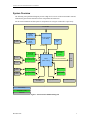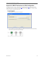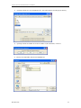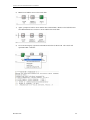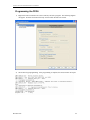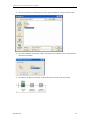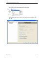
1
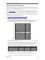
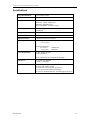
FreeForm/PCI-104
User Manual
Connect Tech, Inc.
42 Arrow Road
Guelph, Ontario
Canada, N1K 1S6
Tel: 519-836-1291
800-426-8979
Fax: 519-836-4878
Email: [email protected]
[email protected]
URL: http://www.connecttech.com
CTIM-00040 Revision 0.02 September 19, 2008
Connect Tech FreeForm/PCI-104 User Manual
Limited Lifetime Warranty
Connect Tech Inc. provides a Lifetime Warranty for all Connect Tech Inc. products. Should
this product, in Connect Tech Inc.'s opinion, fail to be in good working order during the
warranty period, Connect Tech Inc. will, at its option, repair or replace this product at no
charge, provided that the product has not been subjected to abuse, misuse, accident, disaster or
non Connect Tech Inc. authorized modification or repair.
You may obtain warranty service by delivering this product to an authorized Connect Tech
Inc. business partner or to Connect Tech Inc. along with proof of purchase. Product returned to
Connect Tech Inc. must be pre-authorized by Connect Tech Inc. with an RMA (Return
Material Authorization) number marked on the outside of the package and sent prepaid,
insured and packaged for safe shipment.
The Connect Tech Inc. Lifetime Warranty is defined as the serviceable life of the product. This
is defined as the period during which all components are available. Should the product prove to
be irreparable, Connect Tech Inc. reserves the right to substitute an equivalent product if
available or to retract Lifetime Warranty if no replacement is available.
The above warranty is the only warranty authorized by Connect Tech Inc. Under no
circumstances will Connect Tech Inc. be liable in any way for any damages, including any lost
profits, lost savings or other incidental or consequential damages arising out of the use of, or
inability to use such product.
Copyright Notice
The information contained in this document is subject to change without notice. Connect Tech
Inc. shall not be liable for errors contained herein or for incidental consequential damages in
connection with the furnishing, performance, or use of this material. This document contains
proprietary information that is protected by copyright. All rights are reserved. No part of this
document may be photocopied, reproduced, or translated to another language without the prior
written consent of Connect Tech, Inc.
Copyright © 2008 by Connect Tech, Inc.
Trademark Acknowledgment
Connect Tech, Inc. acknowledges all trademarks, registered trademarks and/or copyrights
referred to in this document as the property of their respective owners.
Not listing all possible trademarks or copyright acknowledgments does not constitute a lack of
acknowledgment to the rightful owners of the trademarks and copyrights mentioned in this
document.
Revision 0.02
2
Connect Tech FreeForm/PCI-104 User Manual
Customer Support Overview
If you experience difficulties after reading the manual and/or using the product, contact the
Connect Tech reseller from which you purchased the product. In most cases the reseller can
help you with product installation and difficulties.
In the event that the reseller is unable to resolve your problem, our highly qualified support
staff can assist you. Our support section is available 24 hours a day, seven days a week on our
website at:
www.connecttech.com/support/support.asp. See the contact information section below for
more information on how to contact us directly. Our technical support is always free.
Not listing all possible trademarks or copyright acknowledgments does not constitute a lack of
acknowledgment to the rightful owners of the trademarks and copyrights mentioned in this
document.
Contact Information
We offer three ways for you to contact us:
Telephone/Facsimile
Technical Support representatives are ready to answer your call Monday through Friday, from
8:30 a.m. to 5:00 p.m. Eastern Standard Time. Our numbers for calls are:
Telephone:
Telephone:
Facsimile:
800-426-8979 (North America only)
519-836-1291 (Live assistance available 8:30 a.m. to 5:00 p.m. EST, Monday to
Friday)
519-836-4878 (on-line 24 hours)
Email/Internet
You may contact us through the Internet. Our email and URL addresses are:
[email protected]
[email protected]
www.connecttech.com
Mail/Courier
You may contact us by letter and our mailing address for correspondence is:
Connect Tech, Inc.
42 Arrow Road
Guelph, Ontario
Canada N1K 1S6
Revision 0.02
3
Connect Tech FreeForm/PCI-104 User Manual
Table of Contents
Limited Lifetime Warranty......................................................................................................... 2
Copyright Notice ........................................................................................................................ 2
Trademark Acknowledgment ..................................................................................................... 2
Customer Support Overview ...................................................................................................... 3
Contact Information ........................................................................................................... 3
Table of Contents ....................................................................................................................... 4
List of Tables.............................................................................................................................. 5
List of Figures ............................................................................................................................ 5
Introduction ................................................................................................................................ 6
Product Features ................................................................................................................ 6
About this manual .............................................................................................................. 6
System Overview ....................................................................................................................... 7
Reference Design ....................................................................................................................... 9
Hardware Description............................................................................................................... 10
Jumpers and Switches ...................................................................................................... 10
Slot Selection (RSW1) ............................................................................................ 10
FPGA Configuration Settings (J1) .......................................................................... 10
Connector Pinouts............................................................................................................ 11
PCI-104 Header (P1) ............................................................................................... 11
JTAG Programming Header (P2)............................................................................ 11
SPI Flash Programming Header (P3) ...................................................................... 11
High-speed Serial (P4) ............................................................................................ 12
RS-485 Headers (P5, P6)......................................................................................... 13
GPIO Header (P7) ................................................................................................... 14
External Power Connector (P8)............................................................................... 15
Connector’s Mating Components and Cables.................................................................. 16
Hardware Installation ............................................................................................................... 17
Heat Sink Installation....................................................................................................... 17
Stand-alone Operation ..................................................................................................... 17
Software Installation................................................................................................................. 18
FPGA Development Environment ................................................................................... 18
PLX Software Development Kit (SDK) .......................................................................... 18
Reference Design & Application Examples .................................................................... 18
FPGA Configuration ................................................................................................................ 19
Power and Thermal Considerations.......................................................................................... 20
Reference Design FPGA power analysis ......................................................................... 20
Specifications ........................................................................................................................... 21
Appendix A: iMPACT Instructions for FPGA Configuration.................................................. 22
Launch Impact ................................................................................................................. 22
Programming the FPGA .................................................................................................. 25
Generating a PROM (MCS) File ..................................................................................... 26
Configuring the FPGA with the SPI Flash....................................................................... 29
Configuring the FPGA / SPI flash Association ....................................................... 29
Programming the Flash ........................................................................................... 31
Appendix B: Power calculations .............................................................................................. 33
Scenario 1: Heatsink attached, 250 LFM ................................................................ 33
Scenario 2: No Heatsink, 250 LFM......................................................................... 34
Scenario 3: No heatsink, 0 LFM.............................................................................. 35
Appendix C: Hardware Changes from Revision B................................................................... 36
Reference Design ............................................................................................................. 37
Hardware Description ...................................................................................................... 38
Connector Pinouts ................................................................................................... 38
Specifications................................................................................................................... 39
Revision 0.02
4
Connect Tech FreeForm/PCI-104 User Manual
List of Tables
Table 1: FreeForm/PCI-104 Components .................................................................................. 8
Table 2: Slot Selection (RSW1) ............................................................................................... 10
Table 3: FPGA Configuration Settings (J1) ............................................................................. 10
Table 4: JTAG Programming Header Pinout (P2).................................................................... 11
Table 5: SPI Flash Programming Header Pinout (P3) .............................................................. 11
Table 6: High-Speed serial Connector Pinout (P4) .................................................................. 12
Table 7: RS-485 Port 1 Pinout (P5).......................................................................................... 13
Table 8: RS-485 Port 2 Pinout (P6).......................................................................................... 13
Table 9: GPIO Header Pinout................................................................................................... 14
Table 10: External Power Connector Pinout (P8) .................................................................... 15
Table 11: Connector Mate Listing............................................................................................ 16
List of Figures
Figure 1: FreeForm/PCI-104 Block Diagram............................................................................. 7
Figure 2: FreeForm/PCI-104 Layout .......................................................................................... 8
Figure 3: External Power Connection....................................................................................... 15
Revision 0.02
5
Connect Tech FreeForm/PCI-104 User Manual
Introduction
Connect Tech’s FreeForm/PCI-104 features Xilinx’s Virtex-5 multi-platform FPGA offering users a
flexible, reconfigurable computing platform that also takes advantage of the high bandwidth capabilities
of the PCI bus while communicating with various I/O interfaces.
Product Features
o
o
o
o
o
o
o
o
o
o
o
o
o
o
o
PCI-104 form factor – 32-Bit/33MHz
Xilinx multi-platform Virtex-5 FPGA with 3 million logic gates
2MB Flash for FPGA configuration storage
8MB Flash for embedded code storage
Designed for embedded processing using MicroBlaze™
100MHz input clock
128MB DDR2-400 memory
2 x 10/100 Ethernet with modular jacks
2 x RS-485 serial interface
High-speed serial connector 4 x Rocket I/O (GTP) channels
64 single ended or 32 LVDS general purpose I/O
External 5V power connection for programming and development
JTAG test and programming chain
Industrial temperature range of -40°C to 85°C
Ships preconfigured with a reference design
About this manual
This manual will provide the user with the following information:
o
o
o
o
o
o
o
System overview
Introduction to the reference design
Description of jumpers, switches, and connector pinouts
Hardware installation instructions
Software installation instructions
FPGA configuration details
Specifications
Revision 0.02
6
Connect Tech FreeForm/PCI-104 User Manual
System Overview
The following conceptual block diagram provides a high level overview of the FreeForm/PCI-104 and
illustrates the general interconnection between components and connectors.
For the actual orientation and description of components refer to Figure 2 and Table 1 respectively.
PCI-104 Bus
EEPROM
(Config
Registers)
PCI Bus Interface
[PLX 9056]s
SPI Flash
(FPGA
Config.)
1x6
Header
100 Mhz
Osc.
Local Bus
SPI Flash
(Embedded
Code)
EEPROM
(Parameters)
RJ-45
Dual Ethernet PHY
FPGA
[Xilinx Virtex-5]
64 I/O, 32 LVDS Pairs
2x40
Header
RJ-45
2x5
Header
RS-485 Transceiver
DDR2 RAM
2x5
Header
RS-485 Transceiver
DDR2 RAM
JTAG Connector
1x7 Header
High Speed Serial
Ext Power Connector
Core Circuitry
Peripheral Circuitry
Connector
Figure 1: FreeForm/PCI-104 Block Diagram
Revision 0.02
7
Connect Tech FreeForm/PCI-104 User Manual
Figure 2: FreeForm/PCI-104 Layout
Table 1: FreeForm/PCI-104 Components
Connectors
P1
P2
P3
P4
P5, P6
P7
P8
P9
P10
Jumpers /Switches
RSW1
J1
Components
D1-D4
D5
U4
U5
U10
U11
U12, U13
U14
U15, U16
U17
O1,O2, O3
Revision 0.02
Description
PCI-104 connector
JTAG programming header
SPI flash programming header
High-speed serial connector
RS-485 header
GPIO header
External power header
RJ-45 A
RJ-45 B
Description
Slot selection
FPGA configuration settings
Description (not all on top side)
User LEDs
FPGA load complete LED
PLX PCI-local bus bridge
Virtex-5 FPGA
FPGA configuration flash
Embedded code flash
DDR2 memory
Parameter EEPROM
RS-485 transceiver
Dual 10/100 PHY
Oscillators
8
Connect Tech FreeForm/PCI-104 User Manual
Reference Design
The FreeForm/PCI-104 ships with a pre-installed reference design that is loaded into the FPGA’s
configuration flash. This reference design demonstrates how to interface the FreeForm/PCI-104
(Virtex-5 FPGA) with the PLX PCI 9056 PCI to Local Bus Bridge, as well as the various peripherals.
The PLX 9056 provides a generic local bus that is capable of operating at up to 66MHz (this design
forwards a 50MHz clock to the PLX). The PLX bridge has been set in the C-Mode of operation. The
reference logic operates as a local bus slave, as well as a local bus master.
The reference design contains examples demonstrating:
o
o
o
o
o
o
o
o
o
o
Loading of PLX 9056’s registers via the local bus
Local bus slave transfers
Local bus master transfers
GPIO control
Programming the SPI Flash
Interfacing to the built-in Virtex-5 TEMACs
RS-485 serial data transfers
Reading/writing to the serial EEPROM
Reading/writing to DDR2 memory
Interfacing to the Virtex-5 Rocket I/O transceivers
Most of the example VHDL modules demonstrate how to interface with the various peripherals through
a register set, which is accessible by the host system over the PCI bus. A set of software applications
has been created to show how the host system can communicate with each FPGA sub-module. In most
applications, the host system will not directly control these peripherals. In a custom application, these
modules can be easily modified to interconnect with each other through the FPGA fabric.
To obtain the source code, refer to Software Installation. For further details on the reference design,
refer to FreeForm/PCI-104 Reference Design Guide (CTIM-00042)
Revision 0.02
9
Connect Tech FreeForm/PCI-104 User Manual
Hardware Description
The following sections describe the function of all switches/jumpers and provide details on connector
pinouts.
Jumpers and Switches
Slot Selection (RSW1)
This rotary switch selects a slot position in the PCI-104 stack. When mounting on a PCI adapter
card, ensure slot one is selected.
Table 2: Slot Selection (RSW1)
Position
Slot
0,4
0
1,5
1
2,6
2
3,7
3
FPGA Configuration Settings (J1)
Jumper J1 is used to control FPGA configuration.
Table 3: FPGA Configuration Settings (J1)
Location
Function
FPGA waits for configuration over JTAG (using P2)
FPGA reads configuration from SPI flash
FPGA is tri-stated, flash is isolated from FPGA and
can be programmed directly
Revision 0.02
10
Connect Tech FreeForm/PCI-104 User Manual
Connector Pinouts
PCI-104 Header (P1)
Refer to PCI-104 specifications.
Note: P1 must be connected to a PCI-104 stack supplying both 3.3V and 5V.
JTAG Programming Header (P2)
Use P2 to configure the FPGA via JTAG. Refer to FPGA Configuration for more information.
Power pins are for voltage reference only; they do not provide power to the configuration
circuitry.
Note that the FPGA can always be programmed via JTAG, regardless of the J1 configuration
setting.
P2 JTAG
Header
Table 4: JTAG Programming Header Pinout (P2)
Pin
Signal
Direction
1
1
TRST
Input
2
TMS
Input
3
TDI
Input
4
TDO
Output
5
TCK
Input
6
GND
Reference
Top View
7
3.3V
Reference
SPI Flash Programming Header (P3)
P3 may be used to directly program the SPI flash, providing that J1 is set correctly to the tri-state
FPGA position. The power pins are for voltage reference only. They do not provide power to the
configuration circuitry.
Pin
1
2
3
4
5
6
Revision 0.02
Signal
SPI_CSN
SPI_MOSI
SPI_MISO
SPI_CLK
GND
3.3V
Direction
Input
Input
Output
Input
Reference
Reference
Flash
P3 SPI
Header
Table 5: SPI Flash Programming Header Pinout (P3)
1
Top View
11
Connect Tech FreeForm/PCI-104 User Manual
High-speed Serial (P4)
The high-speed serial connector carries four Rocket (GTP) I/O channels, each with a dedicated
transmit and receive differential pair. These channels are capable of operating up 3.125 Gbps,
depending on configuration. For more information on Rocket I/O capabilities, visit the Xilinx
website: http://www.xilinx.com/products/silicon_solutions/fpgas/virtex/virtex5/
Table 6: High-Speed serial Connector Pinout (P4)
Pin
Signal
Direction
Notes
1
MTGRXN0_112
Input
(b)
3
MTGRXP0_112
Input
(b)
2
MTGTXN0_112
Output
(b)
4
MTGTXP0_112
Output
(b)
5
HSS_USER_IO(0) Input/Output (a), (d)
7
HSS_USER_IO(1) Input/Output (a), (d)
6
HSS_USER_IO(2) Input/Output (a), (d)
8
HSS_USER_IO(3) Input/Output (a), (d)
9
MTGRXN1_112
Input
(b)
11
MTGRXP1_112
Input
(b)
10
MTGTXN1_112
Output
(b)
12
MTGTXP1_112
Output
(b)
13
3.3V
Power
(a)
15
3.3V
Power
(a)
14
3.3V
Power
(a)
16
3.3V
Power
(a)
17
MTGRXN0_114
Input
(c)
19
MTGRXP0_114
Input
(c)
18
MTGTXN0_114
Output
(c)
20
MTGTXP0_114
Output
(c)
21
3.3V
Power
(a)
23
3.3V
Power
(a)
22
3.3V
Power
(a)
24
3.3V
Power
(a)
25
MTGRXN1_114
Input
(c)
27
MTGRXP1_114
Input
(c)
26
MTGTXN1_114
Output
(c)
28
MTGTXP1_114
Output
(c)
Notes:
a) Pins have a different function from Revision B.
b) The Rocket I/O (GTP) are organized into tiles, where each tile has two transceivers and
shares a common PLL. In this design, tiles 112 and 114 are used.
c) Tile 112 has AC coupling capacitors on the TX pairs, validated at PCI Express data rates
(2.5 Gbps).
d) Tile 114 has AC coupling capacitors on both the RX and TX pairs, validated at SATA
data rates (1.5 Gbps).
e) HSS_USER_IO are flexible LVCMOS side-band signals.
WARNING
Revision 0.02
If connecting two FreeForm/PCI-104’s together using the Rocket I/O
interface in a cross-over fashion; care must be taken. Ensure that only
cables provided by Connect Tech are used. Cables ordered directly
from Samtec or a third party could result in damage to the cable and/or
the FreeForm/PCI-104 board itself.
12
Connect Tech FreeForm/PCI-104 User Manual
Top View
26 28
1 3
25 27
Speed
P4 High
Serial
2 4
RS-485 Headers (P5, P6)
Table 7: RS-485 Port 1 Pinout (P5)
Pin
1
2
3
4
5
6
7
8
9
10
Signal
RXD+1
Direction
Input
RXD-1
Input
TXD+1
Output
TXD-1
Output
GND
Power
1
10
P5
485 Port 0
Top View
Table 8: RS-485 Port 2 Pinout (P6)
Pin
1
2
3
4
5
6
7
8
9
10
Revision 0.02
Signal
RXD+2
Direction
Input
RXD-2
Input
TXD+2
Output
TXD-2
Output
GND
Power
10
P6
485 Port 1
1
Top View
13
Connect Tech FreeForm/PCI-104 User Manual
GPIO Header (P7)
When in differential mode, the GPIO header positive (P) and negative (N) signals are adjacent on
a standard ribbon cable. Note that the GPIO voltage level is set via hardware.
o
o
Pin
1
2
3
4
5
6
7
8
9
10
11
12
13
14
15
16
17
18
19
20
21
22
23
24
25
26
27
28
29
30
31
32
33
34
35
36
37
38
39
40
Revision 0.02
FCG001: L12 populated, enabling 2.5V I/O, including LVDS
FCG002: L13 populated, enabling 3.3V I/O
Signal
GPION(0)
GPIOP(0)
GPION(1)
GPIOP(1)
GPION(2)
GPIOP(2)
GPION(3)
GPIOP(3)
GND
GND
GPION(4)
GPIOP(4)
GPION(5)
GPIOP(5)
GPION(6)
GPIOP(6)
GPION(7)
GPIOP(7)
GND
GND
GPION(8)
GPIOP(8)
GPION(9)
GPIOP(9)
GPION(10)
GPIOP(10)
GPION(11)
GPIOP(11)
GND
GND
GPION(12)
GPIOP(12)
GPION(13)
GPIOP(13)
GPION(14)
GPIOP(14)
GPION(15)
GPIOP(15)
GND
GND
Table 9: GPIO Header Pinout
Direction
Pin
Signal
Input/Output
41
GPION(16)
Input/Output
42
GPIOP(16)
Input/Output
43
GPION(17)
Input/Output
44
GPIOP(17)
Input/Output
45
GPION(18)
Input/Output
46
GPIOP(18)
Input/Output
47
GPION(19)
Input/Output
48
GPIOP(19)
Power
49
GND
Power
50
GND
Input/Output
51
GPION(20)
Input/Output
52
GPIOP(20)
Input/Output
53
GPION(21)
Input/Output
54
GPIOP(21)
Input/Output
55
GPION(22)
Input/Output
56
GPIOP(22)
Input/Output
57
GPION(23)
Input/Output
58
GPIOP(23)
Power
59
GND
Power
60
GND
Input/Output
61
GPION(24)
Input/Output
62
GPIOP(24)
Input/Output
63
GPION(25)
Input/Output
64
GPIOP(25)
Input/Output
65
GPION(26)
Input/Output
66
GPIOP(26)
Input/Output
67
GPION(27)
Input/Output
68
GPIOP(27)
Power
69
GND
Power
70
GND
Input/Output
71
GPION(28)
Input/Output
72
GPIOP(28)
Input/Output
73
GPION(29)
Input/Output
74
GPIOP(29)
Input/Output
75
GPION(30)
Input/Output
76
GPIOP(30)
Input/Output
77
GPION(31)
Input/Output
78
GPIOP(31)
Power
79
GND
Power
80
GND
Direction
Input/Output
Input/Output
Input/Output
Input/Output
Input/Output
Input/Output
Input/Output
Input/Output
Power
Power
Input/Output
Input/Output
Input/Output
Input/Output
Input/Output
Input/Output
Input/Output
Input/Output
Power
Power
Input/Output
Input/Output
Input/Output
Input/Output
Input/Output
Input/Output
Input/Output
Input/Output
Power
Power
Input/Output
Input/Output
Input/Output
Input/Output
Input/Output
Input/Output
Input/Output
Input/Output
Power
Power
14
Connect Tech FreeForm/PCI-104 User Manual
Side View
External Power Connector (P8)
The external connector provides 5V to the power regulation circuitry.
The external power connector should only be used when the FreeForm/PCI-104 is being
programmed outside of a PCI/PCI-104 system.
Pin
Table 10: External Power Connector Pinout (P8)
Signal
Direction
1
2
3
5V
Power
GND
Power
4
VIO (connect to 5V)
Power
1
2
3
4
P8
Standalone
Power Input
It is recommended that a Connect Tech Inc. FreeForm/PCI-104 power supply is used for providing
external power. Orientation of the power supply connector is important. Ensure that the clip on
the cable aligns with the catch on P8, as shown below.
Figure 3: External Power Connection
Revision 0.02
15
Connect Tech FreeForm/PCI-104 User Manual
Connector’s Mating Components and Cables
The following table lists the manufacturer and part number for connectors on the FreeForm/PCI-104, as
well as potential mating components.
Table 11: Connector Mate Listing
Connector
P2
P3
P4
P5/P6
P7
Component on
FreeForm/PCI-104
Samtec
TSW-107-07-L-S
(0.100” pitch, 1x7)
Samtec
TSW-106-07-L-S
(0.100” pitch, 1x6)
Samtec
QSE-014-01-L-D-DP-A
(0.8mm pitch, 2x14,
arranged as 14 differentials
pairs)
Samtec
TSW-105-07-L-D
(0.100” pitch, 2x5)
Tyco
5-104069-3
(0.050”x0.100” pitch, 2x40)
Mating components
Mating cable assembly
Samtec
SSW-107-xx-G-S
(Socket, other options available)
Samtec
SSW-106-xx-G-S
(Socket, other options available)
Samtec
QTE-014-01-L-D-DP-A
(5mm mated height, other
heights available)
Connect Tech Inc.
CBG027
(JTAG programming cable)
Connect Tech Inc.
CBG027
(JTAG programming cable)
Connect Tech.
Please contact sales for more
information.
Samtec
SSW-105-xx-G-D
(Socket, other options available)
Tyco
3-111196-3
(ribbon cable mate)
Connect Tech Inc.
CAG104
(Header to DB9)
-
or
P8
Samtec
IPL1-102-01-S-D
(0.100” pitch, 2x2)
Tyco
8-487937-0
(discrete wire housing)
Tyco
1-487547-1
(crimps for housing)
Samtec
IPD1-02-D
(discrete wire housing)
Samtec
CC79L-2024-01-S
(crimps for housing)
Connect Tech Inc.
MSG037
(5V power supply, for
development purposes)
or
Samtec
MMSD-02-22-S-03-25-S
(pre-assembled housing and
wiring)
Note: CBG027 and MSG037 are available as part of development kit DEV002
For more details on mating components, visit:
o Samtec (http://www.samtec.com/)
o Tyco Electronics (http://www.tycoelectronics.com/)
Revision 0.02
16
Connect Tech FreeForm/PCI-104 User Manual
Hardware Installation
Before installing the FreeForm/PCI-104 into a PCI-104 stack, ensure the following:
o
o
Slot selection is properly set using the rotary switch RSW1.
FPGA configuration jumper J1 is set to read from flash.
Once installed in the system and power is applied, the LED D1 will illuminate to indicate that
FreeForm/PCI-104 is functioning.
Heat Sink Installation
Each FreeForm/PCI-104 ships with a FPGA heat sink (27 mm x 27 mm); to be installed by the user.
Simply peel of the sticker backing and press firmly onto the FPGA, using proper ESD precautions.
If the heat sink size is not suitable for your application, please contact Connect Tech Inc.
WARNING In many applications, including high speed memory operations, the
FPGA dissipates a significant amount of power. Failure to use any heat
sinking will result in the product warranty being voided.
Stand-alone Operation
Operating the FreeForm/PCI-104 outside of a PCI-104 stack or a PCI system for extended periods of
time is not recommended. The PCI to local bus bridge (PCI PLX 9056) requires the pull-up/pull-down
resistors provided on a system’s main board.
Configuring or programming the FreeForm/PCI-104 in stand-alone mode is acceptable, providing that it
is not left powered on in stand-alone state for an extended period of time.
WARNING The power supply MSG037 included with the development kit
DEV002 is intended for desktop programming only. It is not intended
or warranted to be used in any other situation.
Revision 0.02
17
Connect Tech FreeForm/PCI-104 User Manual
Software Installation
FPGA Development Environment
FreeForm/PCI-104 has been developed with Xilinx WebPACK 9.2, available free of charge at:
http://www.xilinx.com/ise/logic_design_prod/webpack.htm
PLX Software Development Kit (SDK)
PLX provides a software development kit (SDK) to aid in the creation of applications using the PLX
9056 bridge. The SDK provides a generic driver for Windows 2000/XP and Linux. A common API is
also included; which encapsulates functions like:
o
o
o
o
o
Configuration register read / write
Block read / block write to local address space (i.e. memory / registers in the FPGA)
Physical memory allocation, for bus mastering or DMA purposes
Interrupt handling
EEPROM read/write by address
The SDK is available for download from:
http://www.plxtech.com/products/sdk/
In order to download the SDK, you will need to register with PLX.
Reference Design & Application Examples
The FreeForm/PCI-104 ships with a CD containing:
o
o
o
Documentation and manuals
FPGA VHDL reference design
Software program examples
The reference design and example programs help users quickly develop custom hardware and software
applications. Refer to the CD for installation instructions.
The latest reference design is always available from:
http://devel.connecttech.com/
If a username and password have not already been provided, please contact Connect Tech Support via
email [email protected].
Revision 0.02
18
Connect Tech FreeForm/PCI-104 User Manual
FPGA Configuration
The Virtex-5 FPGA can be configured via two methods:
o
o
JTAG programming chain, using P2
SPI Flash, read on, power-up by FPGA
The configuration flash can be programmed (loaded) through three methods:
o
o
o
JTAG programming chain (through FPGA), using P2
Direct with cable, using P3
Indirect programming through FPGA, only possible after configuration is complete (refer
to reference design for more details)
To configure the FPGA via the JTAG / boundary scan programming chain, three items are required:
o
o
o
FPGA bitstream (*.bit), generated at end FPGA implementation using ISE
PLX 9056 boundary scan definition file (*.bdsl)
Ethernet PHY boundary scan definition file
To program the SPI flash, a hex file must be generated (*.mcs) then written to the flash. To generate
the hex file, the following is required:
o
o
o
o
FPGA Bitstream
Setting PROM file format to MCS (important since bits are swapped)
Setting SPI PROM density to 16M
Setting SPI Flash type to M25P16
For a complete procedure, refer to Appendix A.
Revision 0.02
19
Connect Tech FreeForm/PCI-104 User Manual
Power and Thermal Considerations
The FreeForm/PCI-104’s Virtex-5 FPGA is a versatile, flexible device, with many built-in features like
termination, PLLs, and high speed gigabit transceivers. The drawback of these on-chip features is that they
consume a lot of power and hence dissipate a lot of heat.
As a result Connect Tech, is recommending the installation of a heatsink, included with the product (see
section Heat Sink Installation). As well, the FPGA designer must perform power analysis on their design to
determine that they are not stressing the Virtex-5 component (i.e. exceeding the junction temperature).
Power analysis can be performed using the Xpower Analyzer (part of the ISE design suite) and the XPE
spreadsheets (Xilinx Power Estimator Spreadsheets).
http://www.xilinx.com/products/design_resources/power_central/
Reference Design FPGA power analysis
Power analysis was performed on the FCG001 when configured with the reference design. The Virtex5 XPE spreadsheet was used to determine an effective junction to ambient thermal resistance
(θJA_effective). The following parameters are entered into the spreadsheet to determine θJA_effective.
Device
Part
Package
Grade
Process
Speed Grade
Stepping
XC5VLX30T
FF665
Industrial
Typical
-1
Stepping - 1
Thermal Information
Ambient Temp (°C)
Airflow (LFM)
Heat Sink
Custom ΘSA (°C/W)
Board Selection
# of Board Layers
50
250
Custom
8 (*)
Small (4"x4")
12 to 15
(θSA is the surface to ambient temperature for a heatsink with dimensions 27 mm x 27 mm x 6.4 mm and 250 LFM airflow. The
θSA improves (decreases) with a taller heatsink. )
Three scenarios were developed and the XPE parameters Airflow and Custom ΘSA were varied. The
θJA_effective was entered into the Xpower Analyzer yielding a Juction Temperature @ 50 °C and a
maximum ambient temperature. The following table summarizes the scenarios and the results. For
complete details of the scenarios, see Appendix B.
Scenario
Heatsink attached, 250 LFM
No Heatsink, 250 LFM
No heatsink, 0 LFM
θJA_effective (°C/W)
4.9
6.4
9.7
Tambient_max
82.7
72.7
65.1
Tjunction at 50 °C
67.3
72.7
84.9
Calculation details:
Tjunction = Tambient + (PFPGA * θJA_effective) = 50°C + (3.53W * 4.9 °C /W) = 67.297°C
Tambient_max = Tjunction_max - (PFPGA * θJA_effective) = 100°C - (3.53W * 4.9 °C /W) = 82.7°C
Note Tjunction_absolute_max = 125°C is not used, since this is the absolute point of failure.
Revision 0.02
20
Connect Tech FreeForm/PCI-104 User Manual
Specifications
Programmable FPGA
Virtex-5 FPGA LX30T
Input Clock
100MHz
Memory / Flash
128MB DDR2-400
2MB Flash – FPGA configuration
8MB Flash – Embedded code
4K serial EEPROM – parameter storage
General Purpose User I/O 64 single ended I/O
32 LVDS I/O
Serial
2 x RS-485
Ethernet
2 x 10Base-T, 100Base-TX
High-speed serial
4 x Rocket I/O transceivers (GTP)
Operating Environment
Storage Temperature:
-65°C to 150°C
Operating Temperature:
0°C to 70°C
-40°C to 85°C
Power Requirements
(commercial)
(industrial)
+5V DC, in PCI-104 stack
+5V DC standalone
Current requirements are configuration dependant
Dimensions
PC/104-Plus 2.2 compliant
PCI-104 1.0 compliant
Connectors
Two RJ-45 modular jacks (Ethernet)
Two 2x5 0.100” headers (serial)
One 2x40 0.050 x 0.100” header (general I/O)
One 1x6 0.100” header (flash programming)
One 2x14 0.8 mm differential pair terminal (high speed serial)
Revision 0.02
21
Connect Tech FreeForm/PCI-104 User Manual
Appendix A: iMPACT Instructions for FPGA Configuration
To configure the FPGA via JTAG, connect the JTAG programming cable to P2 ensuring that all JTAG
signals align correctly. It is important to note that P2 also has the TRST signal on pin 1, which is not part
of Xilinx’s Parallel or USB programming cables.
Launch Impact
1) Open iMPACT, and select create a new project
2) Select configure devices using boundary scan. iMPACT will scan the JTAG chain, and identify
three devices. The first device will be the FPGA.
Revision 0.02
22
Connect Tech FreeForm/PCI-104 User Manual
3) A prompt will ask for a new configuration file. Select the bitstream from the project directory.
4) A prompt will ask for a BSDL file for device number 2 (PLX PCI9056). Click Yes.
5) Browse to the bsdl folder and select PCI9056BA.bsd
Revision 0.02
23
Connect Tech FreeForm/PCI-104 User Manual
6) iMPACT will add the device to the JTAG chain.
7) Again, a prompt will ask for device number three (National PHY). Browse to the bsdl folder and
select DP83849IVS.bsd. The device will be added to the JTAG chain.
8) To test stream integrity, right click on the FPGA and select Get Device ID. The console will
report IDCODE = 82a6e093
Revision 0.02
24
Connect Tech FreeForm/PCI-104 User Manual
Programming the FPGA
1) Right click on device number one (Virtex-5 FPGA), and select program. The following diagram
will appear. Note that verification will only work if an msk file has been created.
2) Select OK to begin programming. After programming is complete, the status window will report:
Revision 0.02
25
Connect Tech FreeForm/PCI-104 User Manual
Generating a PROM (MCS) File
1) Double click Prom File Formatter in the Flows window.
2) The “Prepare PROM Files” dialog will appear. Ensure that the following settings are selected:
3rd Party SPI PROM
MSC PROM File Format
3) Give the file a name, and click Next.
Revision 0.02
26
Connect Tech FreeForm/PCI-104 User Manual
4) Select the PROM density (16M) → click Next → click Finish.
5) A prompt will ask to add device to data stream 0. Click OK. Select the bitstream from the project
directory.
Revision 0.02
27
Connect Tech FreeForm/PCI-104 User Manual
6) Click “No” when asked if another device is to be added. Click “OK” to accept the setup.
7) Double Click “Generate File” from the “iMPACT” processes menu. The status will be reported in
the console.
// *** BATCH CMD : setMode -pff
// *** BATCH CMD : setSubmode -pffparallel
// *** BATCH CMD : setAttribute -configdevice -attr fillValue -value "FF"
// *** BATCH CMD : setAttribute -configdevice -attr swapBit -value "true"
// *** BATCH CMD : setAttribute -configdevice -attr fileFormat -value "mcs"
// *** BATCH CMD : setAttribute -configdevice -attr dir -value "UP"
// *** BATCH CMD : setAttribute -configdevice -attr path -value
"C:\Data\Projects\FreeFormPCI104\hardware\logic\init_plx_GPIO25\/"
// *** BATCH CMD : setAttribute -configdevice -attr name -value "init_plx_GPIO25.cs"
Total configuration bit size = 9371136 bits.
Total configuration byte size = 1171392 bytes.
// *** BATCH CMD : setCurrentDesign -version 0
// *** BATCH CMD : generate -spi
Swap bit can only be disabled in Hex file format only.
0x11dfc0 (1171392) bytes loaded up from 0x0
Using user-specified prom size of 2048K
Writing file
"C:\Data\Projects\FreeFormPCI104\hardware\logic\init_plx_GPIO25\//init_plx_GPIO25.mcs"
.
Writing file
"C:\Data\Projects\FreeFormPCI104\hardware\logic\init_plx_GPIO25\//init_plx_GPIO25.prm"
.
Revision 0.02
28
Connect Tech FreeForm/PCI-104 User Manual
Configuring the FPGA with the SPI Flash
In previous Xilinx FPGA configurations, the SPI flash required programming via 3rd party JTAG test
software or through in-system methods. The following features are new to ISE 9.1/9.2, and are only
available on select FPGAs, including the Virtex-5. Your FreeForm/PCI-104 card featuring the Xilinx
Virtex-5 FPGA includes a standard core to enable programming of BPI and SPI flashes over JTAG.
Configuring the FPGA / SPI flash Association
1) Select “Boundary Scan” from the “Flows” tab.
2) Right click on the FPGA and select “Add SPI Flash…”
Revision 0.02
29
Connect Tech FreeForm/PCI-104 User Manual
3) Browse to the directory containing the previously generated MCS file. Select and click “Open”.
4) The “FPGA SPI Flash Association” window will appear; select “M25P16” (this is the flash device
connected to the FPGA).
5) The flash will be added to the FPGA. Note that this flash is not part of the JTAG chain.
Revision 0.02
30
Connect Tech FreeForm/PCI-104 User Manual
Programming the Flash
1) Right click the previously associated flash device, and select program.
2) The programming dialog will appear. Select “Verify” and “Erase Before Programming”, then
click “OK.”
Revision 0.02
31
Connect Tech FreeForm/PCI-104 User Manual
3) Observe the results in the transcript window.
a. The SPI core is first download to the FPGA device
b. The IDCODE is checked and verified
c. Flash is erased
d. Flash is programmed
After completion of the flash programming, the FPGA will attempt to configure itself from the
flash. If the SPI flash setting is not selected with J1; this step will fail. This does not mean the
flash is not programmed, but rather the verification of the programmed contents has failed.
'1': SPI access core not detected. SPI access core will be downloaded to the
device to enable operations.
PROGRESS_START - Starting Operation.
'1': Downloading core...
done.
'1': Reading status register contents...
INFO:iMPACT:2219 - Status register values:
INFO:iMPACT - 0011 1111 1001 1110 0000 1010 1000 0000
INFO:iMPACT:2492 - '1': Completed downloading core to device.
INFO:iMPACT - '1': Checking done pin....done.
'1': Core downloaded successfully.
'1': IDCODE is '202015' (in hex).
'1': ID Check passed.
'1': IDCODE is '202015' (in hex).
'1': ID Check passed.
'1': Erasing Device.
'1': Programming Device.
'1': Reading device contents...
done.
'1': Verification completed.
INFO:iMPACT - '1': Checking done pin....done.
'1': Programmed successfully.
INFO:iMPACT - '1': Checking done pin....done.
'1': Programmed successfully.
PROGRESS_END - End Operation.
Elapsed time =
179 sec.
Revision 0.02
32
Connect Tech FreeForm/PCI-104 User Manual
Appendix B: Power calculations
Scenario 1: Heatsink attached, 250 LFM
Revision 0.02
33
Connect Tech FreeForm/PCI-104 User Manual
Scenario 2: No Heatsink, 250 LFM
Revision 0.02
34
Connect Tech FreeForm/PCI-104 User Manual
Scenario 3: No heatsink, 0 LFM
Revision 0.02
35
Connect Tech FreeForm/PCI-104 User Manual
Appendix C: Hardware Changes from Revision B
This appendix lists the changes between hardware revision B and hardware revision C.
The following is a summary of changes:
PCB requires only 5V over PCI-104; it previously required 3.3V and 5V
A dedicated local bus oscillator was added to generate 50Mhz. A clock is no longer forwarded
from FPGA to the PLX PCI 9056.
The DDR2 FPGA pinout has been changed to increase timing margins
The pinout of connector P4 (high-speed serial) has changed. The sideband signals have been
relocated and 3.3V has been added.
The orientation of connector P5 (RS-485 port 0) has rotated 180 degrees
The Location of P8 (external power connector) has changed. The 3.3V enable signal has also
been removed
Revision 0.02
36
Connect Tech FreeForm/PCI-104 User Manual
Reference Design
The top level reference design contains a generic parameter which will correctly configure the FPGA
for Revision B or Revision C. A separate constraint file UCF is created for Revision B and Revision C,
which need to be added to the ISE project manually.
Revision B
Local Clock Generation
Pin
Signal Name
Y21
lb_lclkfb
A20
lb_lclko_loop
B21
lb_lclko_plx
Revision C
Local clock generated in
FPGA and forwarded to PLX
bridge. Clock feedback to
FPGA via pin Y21.
Pin
Signal Name
Y21
lb_lclkfb
A20
Dedicated oscillator
generates local bus clock.
Clock is driven to FPGA on
pin Y21, which drives an
internal global clock net.
B21
DDR2 Pinout
Pin
Signal Name
Pin
Signal Name
Pin
Signal Name
Pin
AA9
ddr2_a<0>
AD21
ddr2_dq<0>
AA9
ddr2_a<0>
AC21
Signal Name
ddr2_dq<0>
Y8
ddr2_a<1>
AD15
ddr2_dq<1>
Y8
ddr2_a<1>
AD15
ddr2_dq<1>
AD8
ddr2_a<2>
AC21
ddr2_dq<2>
AD8
ddr2_a<2>
AC23
ddr2_dq<2>
Y7
ddr2_a<3>
AD14
ddr2_dq<3>
Y7
ddr2_a<3>
AE13
ddr2_dq<3>
AB9
ddr2_a<4>
AE13
ddr2_dq<4>
AB9
ddr2_a<4>
AD14
ddr2_dq<4>
W9
ddr2_a<5>
AE22
ddr2_dq<5>
W9
ddr2_a<5>
AE22
ddr2_dq<5>
ddr2_dq<6>
AC8
ddr2_a<6>
AD16
ddr2_dq<6>
AE8
ddr2_a<6>
AD16
AD6
ddr2_a<7>
AE17
ddr2_dq<7>
AD6
ddr2_a<7>
AD21
ddr2_dq<7>
AA8
ddr2_a<8>
AF10
ddr2_dq<8>
AA8
ddr2_a<8>
AF10
ddr2_dq<8>
V8
ddr2_a<9>
AE5
ddr2_dq<9>
V8
ddr2_a<9>
AE5
ddr2_dq<9>
AC7
ddr2_a<10>
AE12
ddr2_dq<10>
AC7
ddr2_a<10>
AE12
ddr2_dq<10>
AB7
ddr2_a<11>
AF3
ddr2_dq<11>
AB7
ddr2_a<11>
AF3
ddr2_dq<11>
AB6
ddr2_a<12>
AF4
ddr2_dq<12>
AB6
ddr2_a<12>
AF4
ddr2_dq<12>
AC9
ddr2_a<13>
AF12
ddr2_dq<13>
AD10
ddr2_a<13>
AF12
ddr2_dq<13>
AE7
ddr2_ba<0>
AF5
ddr2_dq<14>
AE7
ddr2_ba<0>
AF5
ddr2_dq<14>
AA5
ddr2_ba<1>
AF9
ddr2_dq<15>
AA5
ddr2_ba<1>
AF9
ddr2_dq<15>
V9
ddr2_ba<2>
AD24
ddr2_dq<16>
V9
ddr2_ba<2>
AC26
ddr2_dq<16>
AE8
ddr2_cas_n
AE25
ddr2_dq<17>
AC9
ddr2_cas_n
AE26
ddr2_dq<17>
AE11
ddr2_ck<0>
AC26
ddr2_dq<18>
AE11
ddr2_ck<0>
AC24
ddr2_dq<18>
AD11
ddr2_ck_n<0>
AC23
ddr2_dq<19>
AD11
ddr2_ck_n<0>
AD24
ddr2_dq<19>
AD18
ddr2_cke<0>
AB22
ddr2_dq<20>
AC8
ddr2_cke<0>
AE25
ddr2_dq<20>
AC22
ddr2_cs_n<0>
AC24
ddr2_dq<21>
W8
ddr2_cs_n<0>
AB22
ddr2_dq<21>
ddr2_dq<22>
AE16
ddr2_dm<0>
AE26
ddr2_dq<22>
AE16
ddr2_dm<0>
AD26
AE6
ddr2_dm<1>
AD26
ddr2_dq<23>
AE6
ddr2_dm<1>
AD25
ddr2_dq<23>
AD25
ddr2_dm<2>
AD23
ddr2_dq<24>
AE17
ddr2_dm<2>
AD23
Ddr2_dq<24>
AE18
ddr2_dm<3>
AE15
ddr2_dq<25>
AE18
ddr2_dm<3>
AE15
Ddr2_dq<25>
AD19
ddr2_dqs<0>
AF24
ddr2_dq<26>
AD19
ddr2_dqs<0>
AF25
ddr2_dq<26>
AF7
ddr2_dqs<1>
AF13
ddr2_dq<27>
AF7
ddr2_dqs<1>
AF13
ddr2_dq<27>
AF20
ddr2_dqs<2>
AF14
ddr2_dq<28>
AF20
ddr2_dqs<2>
AF14
ddr2_dq<28>
AF22
ddr2_dqs<3>
AF25
ddr2_dq<29>
AF22
ddr2_dqs<3>
AF24
ddr2_dq<29>
ddr2_dq<30>
AD20
ddr2_dqs_n<0>
AF15
ddr2_dq<30>
AD20
ddr2_dqs_n<0>
AF15
AF8
ddr2_dqs_n<1>
AF23
ddr2_dq<31>
AF8
ddr2_dqs_n<1>
AF23
ddr2_dq<31>
AE20
ddr2_dqs_n<2>
AD13
ddr2_odt<0>
AE20
ddr2_dqs_n<2>
AD9
ddr2_odt<0>
AE21
ddr2_dqs_n<3>
AA7
ddr2_ras_n
AE21
ddr2_dqs_n<3>
AA7
ddr2_ras_n
AB5
ddr2_we_n
AB5
ddr2_we_n
Revision 0.02
37
Connect Tech FreeForm/PCI-104 User Manual
Hardware Description
Connector Pinouts
High-speed Serial (P4)
The sideband LVCMOS signals (HSS) have been rearranged so that when two FreeForm units are
connected:
HSS_USER_IO(0) maps to HSS_USER_IO(2)
HSS_USER_IO(1) maps to HSS_USER_IO(3)
Also, 3.3V pins replace the GND pins; this is because the connector has embedded GND blades.
Revision B
Revision C
Pin
1
3
2
4
5
7
6
8
Signal
MTGRXN0_112
MTGRXP0_112
MTGTXN0_112
MTGTXP0_112
GND
GND
HSS_USER_IO(0)
HSS_USER_IO(1)
Pin
1
3
2
4
5
7
6
8
Signal
MTGRXN0_112
MTGRXP0_112
MTGTXN0_112
MTGTXP0_112
HSS_USER_IO(0)
HSS_USER_IO(1)
HSS_USER_IO(2)
HSS_USER_IO(3)
9
11
10
12
13
15
14
16
17
19
18
20
21
23
22
24
25
27
26
28
MTGRXN1_112
MTGRXP1_112
MTGTXN1_112
MTGTXP1_112
GND
GND
GND
GND
MTGRXN0_114
MTGRXP0_114
MTGTXN0_114
MTGTXP0_114
GND
GND
HSS_USER_IO(2)
HSS_USER_IO(3)
MTGRXN1_114
MTGRXP1_114
MTGTXN1_114
MTGTXP1_114
9
11
10
12
13
15
14
16
17
19
18
20
21
23
22
24
25
27
26
28
MTGRXN1_112
MTGRXP1_112
MTGTXN1_112
MTGTXP1_112
3.3V
3.3V
3.3V
3.3V
MTGRXN0_114
MTGRXP0_114
MTGTXN0_114
MTGTXP0_114
3.3V
3.3V
3.3V
3.3V
MTGRXN1_114
MTGRXP1_114
MTGTXN1_114
MTGTXP1_114
RS-485 Headers (P5)
The orientation of the connector has changed. The pinout remains the same.
Revision B
Revision C
10
1
1
P5
485 Port 0
Revision 0.02
10
P5
485 Port 0
38
Connect Tech FreeForm/PCI-104 User Manual
External Power Connector (P8)
The connector no longer enables 3.3V regulation – it is always enabled.
Revision B
Pin
Signal
Revision C
Pin
Signal
1
5V
1
2
3.3 enable (connect to 5V)
2
5V
3
GND
3
GND
4
VIO (connect to 5V)
4
VIO (connect to 5V)
Specifications
Revision B
Power Requirements +3.3V DC and +5V DC, in PCI-104 stack
+5V DC stand-alone
Revision C
+5V DC, in PCI-104 stack
+5V DC stand-alone
Current requirements are configuration
dependant.
Revision 0.02
39