1
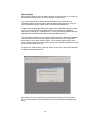
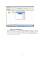
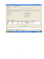
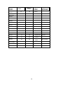
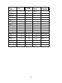
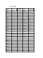
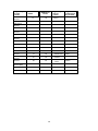
FuturePlus® Systems Corporation DDR2 DIMM HIGH SPEED PROBE FS2334 Users Manual For use with Agilent Technologies Logic Analyzers Revision 1.1 FuturePlus is a trademark of FuturePlus Systems Corporation Copyright 2006 FuturePlus Systems Corporation How to reach us.......................................................................................................................4 Product Warranty....................................................................................................................5 Limitation of warranty................................................................................................................... 5 Exclusive Remedies ....................................................................................................................................5 Assistance......................................................................................................................................... 5 Software License Agreement ..................................................................................................6 License Agreement.......................................................................................................................... 6 Use of the software.......................................................................................................................... 6 Copies and Adaptations.................................................................................................................. 6 Ownership ....................................................................................................................................... 6 Sublicensing and Distribution........................................................................................................ 6 Introduction.............................................................................................................................7 Definitions........................................................................................................................................ 7 Logic Analyzer Modules ..............................................................................................................................7 Logic Analyzer Machine ..............................................................................................................................7 FS2334 Probe Description......................................................................................................8 Probe Technical Feature Summary .............................................................................................. 8 Probe Components.......................................................................................................................... 8 Signal Assignments on Probe Pods................................................................................................ 9 Signal Threshold Voltage Settings................................................................................................. 9 Connecting the DDR2 Probe to the Logic Analyzer .................................................................... 9 Test Points ..................................................................................................................................... 10 Connecting to your Target System.............................................................................................. 11 Signal Isolation on the Probe ....................................................................................................... 11 Buffered signals on the probe ...................................................................................................... 11 Recommended Logic Analyzer Card Requirements and Configuration files......................... 12 Software Requirements .........................................................................................................14 Setting up the 169xx Analyzer ..................................................................................................... 14 169xx Licensing ............................................................................................................................. 14 Loading 169xx configuration files and General Purpose Probe Feature................................. 14 Offline Analysis ............................................................................................................................. 15 TimingZoom Analysis ...........................................................................................................17 Decoding DDR Commands .......................................................................................................... 17 Taking a Trace, Triggering, and Seeing Measurement Results ............................................... 17 State Analysis ........................................................................................................................18 2 Overview ........................................................................................................................................ 18 State Analysis Operation – Read and Writes above 667MT/s....................................................................18 State Analysis Operation – Read and Write at 667MT/s or slower ............................................................19 State Analysis Operation – Read or Write at 800MT/s ..............................................................................19 The process for setting sampling positions at speeds of 800MT/s: ........................................... 20 State analysis calibration procedure ...........................................................................................................21 Adjusting the sampling positions with controlled stimulus ...................................................... 24 State Display.................................................................................................................................. 26 DDR2 Protocol Checking and Performance Tool (FS1140) ..............................................27 FS1140 Installation and Licensing .............................................................................................. 27 Loading the FS1140 ...................................................................................................................... 27 Setting up the FS1140 DDR2 Tool............................................................................................... 28 Functional and Performance Analysis – NOTE: The Functional Performance portion of this software will NOT work with 2 FRAME configurations .......................................................... 29 Statistics......................................................................................................................................................29 Errors ..........................................................................................................................................................29 Export .........................................................................................................................................................30 Repetitive Run ............................................................................................................................................30 Timing Analysis ............................................................................................................................ 30 Export .........................................................................................................................................................30 Appendix................................................................................................................................32 FS2334 Signal to Logic Analyzer Connector and Channel Mapping ...................................... 32 3 How to reach us For Technical Support: FuturePlus Systems Corporation 36 Olde English Road Bedford NH 03110 TEL: 603-471-2734 FAX: 603-471-2738 On the web http://www.futureplus.com For Sales and Marketing Support: FuturePlus Systems Corporation TEL: 719-278-3540 FAX: 719-278-9586 On the web http://www.futureplus.com FuturePlus Systems has technical sales representatives in several major countries. For an up to date listing please see http://www.futureplus.com/contact.html. 4 Product Warranty Due to wide variety of possible customer target implementations, the FS2334 DDR2 DIMM probe has a 30 day acceptance period by the customer from the date of receipt. If the customer does not contact FuturePlus Systems within 30 days of the receipt of the product it will be said that the customer has accepted the product. If the customer is not satisfied with the FS2334 DDR2 DIMM probe they may return the FS2334 within 30 days for a refund. This FuturePlus Systems® product has a warranty against defects in material and workmanship for a period of 1 year from the date of shipment. During the warranty period, FuturePlus Systems will, at its option, either replace or repair products proven to be defective. For warranty service or repair, this product must be returned to the factory. For products returned to FuturePlus Systems for warranty service, the Buyer shall prepay shipping charges to FuturePlus Systems and FuturePlus Systems shall pay shipping charges to return the product to the Buyer. However, the Buyer shall pay all shipping charges, duties, and taxes for products returned to FuturePlus Systems from another country. FuturePlus Systems warrants that its software and hardware designated by FuturePlus Systems for use with an instrument will execute its programming instructions when properly installed on that instrument. FuturePlus Systems does not warrant that the operation of the hardware or software will be uninterrupted or error-free. Limitation of warranty The foregoing warranty shall not apply to defects resulting from improper or inadequate maintenance by the Buyer, Buyer-supplied software or interfacing, unauthorized modification or misuse, or improper site preparation or maintenance. NO OTHER WARRANTY IS EXPRESSED OR IMPLIED. FUTUREPLUS SYSTEMS SPECIFICALLY DISCLAIMS THE IMPLIED WARRANTIES OF MERCHANTABILITY AND FITNESS FOR A PARTICULAR PURPOSE. Exclusive Remedies THE REMEDIES PROVIDED HEREIN ARE BUYER’S SOLE AND EXCLUSIVE REMEDIES. FUTUREPLUS SYSTEMS SHALL NOT BE LIABLE FOR ANY DIRECT, INDIRECT, SPECIAL, INCIDENTAL, OR CONSEQUENTIAL DAMAGES, WHETHER BASED ON CONTRACT, TORT, OR ANY OTHER LEGAL THEORY. Assistance Product maintenance agreements and other customer assistance agreements are available for FuturePlus Systems products. For assistance, contact the factory. 5 Software License Agreement IMPORTANT - Please read this license agreement carefully before opening the media envelope. Rights in the software are offered only on the condition that the customer agrees to all terms and conditions of the license agreement. Opening the media envelope indicates your acceptance of these terms and conditions. If you do not agree to the licensing agreement, you may return the unopened package for a full refund. License Agreement In return for payment for this product, FuturePlus Systems grants the Customer a SINGLE user LICENSE in the software subject to the following: Use of the software Customer may use the software on any one Agilent mainframe logic analysis system. • Customer may make copies or adaptations of the software. • Customer may not reverse assemble or decompile the software. Copies and Adaptations • Are allowed for archival purpose only. • When copying for adaptation is an essential step in the use of the software with the logic analyzer and/or logic analysis mainframe so long as the copies and adaptations are used in no other manner. Customer has no right to copy software unless it acquires an appropriate license to reproduce from FuturePlus Systems. • Customer agrees that it does not have any title or ownership of the software, other than the physical media. Ownership • Customer acknowledges and agrees that the software is copyrighted and protected under the copyright laws. • Transfer of the right of ownership shall only be done with the consent of FuturePlus Systems. Sublicensing and Distribution Customer may not sublicensing the software or distribute copies of the software to the public in physical media or by electronic means or any other means without the prior written consent of FuturePlus Systems. 6 Introduction Thank you for purchasing the FuturePlus Systems FS2334 DDR2 DIMM Interposer Logic Analyzer Probe. We think you will find the FS2334, along with your Agilent Technologies Logic Analyzer, a valuable tool for helping to characterize and debug your DDR2-based systems. This Users Guide will provide the information you need to install, configure, and use the DDR2 Probe. If you have any questions about this Guide or use of this probe, please contact FuturePlus Systems Corporation. Definitions Logic Analyzer Modules "Module" - A set of logic analyzer cards that have been configured (via cables connecting the cards) to operate as a single logic analyzer whose total available channels is the sum of the channels on each card. A trigger within a module can be specified using all of the channels of that module. Each module may be further broken up into "Machines”. A single module may not extend beyond a single 5 card 16700 frame or 6 card 16900 frame. Logic Analyzer Machine "Machine" - A set of logic analyzer pods from a logic analyzer module grouped together to operate as a single state or timing analyzer. 7 FS2334 Probe Description The FS2334 DDR2 Probe allows you to perform timing analysis measurements on DDR2 DIMM busses. It also provides a Protocol Decoder with the capability of providing State analysis of both Read and Write activity is provided by using the dual sample mode feature available on the 169xx. The interposer design of this probe allows any DDR2 connection to be probed while it supports a DDR2 DIMM module. Probe Technical Feature Summary • • • • • Quick and easy connection between the DDR2 240 pin DIMM connector and Agilent Logic Analyzers. Interposer design does not consume a DDR2 slot. Complete and accurate state analysis up to 800MT/s. Available Protocol Checking capability (VBA license required) software. Uses Auto Sample Position Set-up (EyeFinder) and Auto Threshold Set-up to locate tight DDR2 data valid windows for optimal state data capture. Probe Components The following components have been shipped with your FS2334 DDR2 Probe: • FS2334 DDR2 DIMM Probe • Supplemental DC power supply. • This Users Guide and other information on CD-ROM. • CD-ROM with the following software install files: • FS1136 DDR2 Protocol decoder software and configuration files for 169xx analyzers or offline analysis of 800MT/s data traffic • FS1117 DDR2 Protocol Decoder software and configuration files for 169xx analyzers or offline analysis of data traffic <= 667MT/s. • FS1140 Protocol Checking software. • Software Entitlement Certificate for Windows based FS1136, FS1117 and FS1140 software. • Quick Start Sheet. 8 Signal Assignments on Probe Pods The overlap in the bit ranges (for DQxx) signals between pods occurs because the bits are assigned to pods in the order that they appear physically on the DDR2 DIMM connector, which is not strictly in logical bit order. This allows the Probe layout to better match stub lengths among all DQxx signals. See the Appendix for a detailed list of how Logic Analyzer Channels are mapped to signals and DDR2 pins. Signal Threshold Voltage Settings The standard voltage threshold for the logic analyzer pods is defined as 900mV. This is based on the SSTL2-1.8V signaling used by the DDR2 DIMM bus. The configuration files provided with this product set-up the threshold voltages for both the Data and Command pods to 900mV. Design differences between target platforms or overvoltage settings may require adjustment of the logic analyzers threshold for optimal signal capture. The use of Eye Scan can be very helpful in determining where to set these thresholds. NOTE: The optimal settings may need to be defined either through trial and error or by using Eye Scan. Accurate data capture is very dependent on optimizing these settings and changes of as little as 50mV may have a significant effect. Connecting the DDR2 Probe to the Logic Analyzer The FS2334 DDR2 Probe requires up to 7 logic analyzer cards depending on whether state (Read and Write - quadruple sampled), state (Read or Write - dual sampled), or timing measurements are desired. See Timing and State configuration information below. At this time the user may find it easier to connect the logic analyzer cables to the probe before inserting the probe into the target system. The FS2334 probe has fourteen 90 pin pod connections which mate directly to Agilent Logic analyzer cards. Adapter cables are not required. Once a configuration file is loaded refer to the General Purpose Probe feature in the Agilent 1690x Overview tab for cable connections. 9 FS2334 Frontside layout Header 3 Header 4 Header 5 Header 1 Header 6 Header 7 Header 8 1.25” Header 14 FS2334 Backside layout TP 5 Header 2 Header 13 Header 11 Header 10 Header 12 TP 1,2,3,7 Header 9 TP 6 TP 4 Test Points There are several test point on the board. The first set of test points are used to select which signals go to the Clk input and the D15 input of Header 2. The shipping configuration for the FS2334 is to have S0 wired to the Clk input, which is TP3 wired to TP2. This is done in the factory by soldering a short wire between the 2 test points. If CKE0 is to be used as a Clk input then TP7 is wired to TP2 and S0 is brought to the D15 input by wiring TP3 to TP1. DM2_DQS11 is not brought to the logic analyzer, but it can be probed at TP4 DQS5n is not brought to the logic analyzer, but it can be probed at TP5 DQS14n is not brought to the logic analyzer, but it can be probed at TP6 10 Connecting to your Target System To connect the probe to the DDR2 bus, select an available DDR2 slot. Remove the DDR2 DIMM module, if present. Install the DDR2 DIMM module into the 240 pin connector on the top of the FS2334 probe. Install the DDR2 probe/DIMM into the target system. Connect the supplemental power supply to the FS2334. Connect the FS2334 Headers directly to the logic analyzer pods per the configuration file requirements if not done prior to installing the probe. Refer to the General Purpose Probe. Signal Isolation on the Probe All signals sent to the logic analyzer from the FS2334 DDR2 probe are isolated from the DDR2 DIMM bus by a parallel RC network of 20K ohms and .3 pF. These resistors are placed in a manner to minimize stubs seen by the DIMM bus and to match lengths to the DIMM module so that Data bits and their Strobe/Mask bits are matched to within 20 ps. Buffered signals on the probe The DDR2 DIMM bus Control signals are buffered on the probe before they are connected to the DIMM. This includes the S0:1, CKE0:1, and ODT0:1 signals. 11 Recommended Logic Analyzer Card Requirements and Configuration files 169xx Analyzer Type Timing Analysis State Analysis 667MT/s or slower 16753/4/5/6, 16950 FS234_2 3 cards configured as one module, one timing machine FS234_5 4 cards configured as one logic analyzer state machine. Uses FS1117 FS234_2 3 cards configured as one module, one timing machine FS234_1 Read and Write analysis requires 7 cards across 2 frames configured as 2 logic analyzer state machines. Uses FS1136 800MT/s 16753/4/5/6, 16950 FS234_3 4 card configuration provides Write state analysis only Uses FS1136 FS234_4 4 card configuration provides Read state analysis only Uses FS1136 FS234_32_Lower(Upper) 4 card configuration provides Read and Write state analysis for only 32 bits of Data, either Lower or Upper Uses FS1136 12 Logic Analyzer card configurations – Note: These are all for unbuffered DIMM probing FS234_1 2 machine, 7 Card 800MT/s Read and Write configuration file Write – Command machine 4 cards in slots A – D (B = Master). Read machine 3 cards in slots A – C (B = master) FS234_32_Lower(Upper) 4 card 32 bit 800MT/s Data State analysis configuration 4 cards in slots A – D (B = Master) FS234_2 Timing analysis 3 card configuration 3 cards in slots A – C (B = Master) FS234_3 800MT/s Writes only 4 card configuration 4 cards in slots A – D (B = Master) FS234_3 800MT/s Reads only 4 card configuration 4 cards in slots A – D (B = Master) FS234_3 667MT/s Reads and Writes 4 card configuration 4 cards in slots A – D (B = Master) 13 Software Requirements Setting up the 169xx Analyzer A CD containing the 16900 software is included in the FS1136 package. The CD contains a setup file that will automatically install the configuration files and protocol decoder onto a PC containing the 16900 operating system or onto a 16900 analyzer itself. To install the software simply double click the .exe file on the CD containing the FS1136 and the FS1117 software. After accepting the license agreement the software should install within a couple of minutes. Duplicate the process for the FS1140 Protocol Checking software. 169xx Licensing Once the software has been successfully installed you must license the software. Please refer to the entitlement certificate for instructions on licensing each software product. Please note that you are licensing 3 products, both the FS1136 and FS1117 Protocol Decoders AND the FS1140 Protocol Checking software and all require separate license installation on your system. The software can only be installed on one machine. If you need to install the products on more than one machine you must contact the FuturePlus sales department to purchase additional licenses. Loading 169xx configuration files and General Purpose Probe Feature When the software has been licensed you are able to load a configuration file. You can access the configuration files by clicking on the folder that was placed on the desktop. When you click on the folder it should open up to display all the configuration files to choose from. If you put your mouse cursor on the name of the file a description will appear telling you what the setup consists of, once you choose the configuration file that is appropriate for your configuration, the 16900 operating system should execute. The protocol decoder automatically loads when the configuration file is loaded. If the decoder does not load, you may load it by selecting tools from the menu bar at the top of the screen and select the decoder from the list. Once you have loaded a configuration file on the 169xx machine you can find out how to attach the logic analyzer cables to the probe by going to the workspace and selecting Properties on the General Purpose Probe tool icon that appears before the logic analyzer icon. Once you click on the Properties box a new window will appear showing which analyzer pod attaches to which probe cable. 14 Offline Analysis Offline analysis allows a user to be able to analyze a trace offline at a PC so it frees up the analyzer for another person to use the analyzer to capture data. If you have already used the license that was included with your package on a 1680/90/900 analyzer and would like to have the offline analysis feature on a PC you may buy additional licenses, please contact FuturePlus sales department. In order to view decoded data offline, after installing the 1680/90/900 operating system on a PC, you must install the FuturePlus software. Please follow the installation instructions for “Setting up a 16900 analyzer”. Once the FuturePlus software has been installed and licensed follow these steps to import the data and view it. From the desktop, double click on the Agilent logic analyzer icon. When the application comes up there will be a series of questions, answer the first question asking which startup option to use, select Continue Offline. On the analyzer type question, select cancel. When the application comes all the way up you should have a blank screen with a menu bar and tool bar at the top. For data from a 16900 analyzer, open the .ala file using the File, Open menu selections and browse to the desired .ala file. After clicking “next” you must browse for the fast binary data file you want to import. Once you have located the file and clicked start import, the data should appear in the listing. 15 After the decoder has loaded, select Preferences from the overview screen and set the preferences to their correct value in order to decode the trace properly. The protocol decoders, FS1136 and FS1117, require 4 parameters to be entered by the user in order to decode valid states. To access the preferences on the 169xx select Prefs from the graphic representation of the protocol decoder in the overview window. The information required is generally available from the spec. sheet of the memory device being used or by querying the BIOS of the target system. a) Number of Chip Selects – This is either 1 or 2 based on the whether either S0 is being probed and incorporated into the IA or both S0 and S1. b) CAS Latency – Also defined as “CL”, or the delay from a valid Read command to when the Read data is strobed on the bus. c) Additive Latency – Defined by the chipset d) Burst Length – Usually fixed at 4, or 8. e) Additionally, the FS1136 has Preference selections for Data bit length and number of logic machines The input screen for this information is shown below 16 TimingZoom Analysis The TimingZoom feature of the 1690x logic analyzer allows for efficient timing analysis of all the signals on the DDR2 DIMM bus. Please refer to the “Setting up the 16900 Analyzer” section of this manual on the use of the general purpose probe feature to determine how to attach the logic analyzer to the probe. Load the logic analyzer configuration file for timing, FS234_2. It doesn't matter whether you select to load "Configs only" or "Configs and Data". You are now ready to start making measurements. For timing analysis operation above 600 MHz you need to use the ½ Channel Timing Mode, which provides bandwidth to 1.2GHz. This mode makes every other pod available to the user so 4 cards are required. These must be configured via the cables supplied with the cards as a single logic analyzer module. Refer to the appropriate Agilent Technologies manual for information on how to connect analyzer cards together to create multi-card modules. Please note that 6 of the ECC bits and their Data Strobe (DQS8) are contained on an extra Header (#14), which will require an additional logic analyzer card in order to probe. Decoding DDR Commands No Protocol Decoder is used for timing analysis. However, symbols are pre-defined for the DDR2 Command bus. These decode the RAS, CAS, and WE lines to display the DDR Command as “Read”, “Write”, etc., so you don’t have to refer to the DDR chip data sheet to see what command is being executed. These decoded values are displayed by setting the display base (in the listing window) or the label property (in the waveform window) to “Symbols”. The display base defaults to hexadecimal. Taking a Trace, Triggering, and Seeing Measurement Results Timing analysis is the simplest setup and there are no special factors involved in analyzer trigger setup, initiating a trace, and viewing results. For the Command bus you can use the pre-defined symbols to specify mnemonically the command you wish to trigger on. These are set up by default and are accessible in the trigger tab. The default waveform display also shows DDR Commands mnemonically. You may setup a trigger, initiate a measurement, and view results in the usual ways via the trigger tab, pressing the Run button, and opening the desired display window. 17 State Analysis Overview There are several choices for State mode analysis using the FS2334 DDR2 probe depending on the speed of the data bus being probed and the number of logic analyzer cards available to the user. At data speeds of up to 667MT/s the logic analyzer can be triggered on BOTH edges of the clock signal used for State analysis (state clock), at a data speed of 800MT/s ONLY the rising edge of the state clock can be used. Because the sampling point for a data signal is at a different position relative to the state clock edges during a Read data burst than during a Write data burst you need 2 sampling points established for each data signal, which allows the analyzer to sample a data signal twice at speeds up to 667MT/s. When you only have sampling on the rising edge of the state clock (800MT/s) you need to sample each data signal four times because you need to account for both the 2 data states per clock and both Reads and Writes. This is all done by the logic analyzer cards, which drives the cards requirements. If a user is willing to sample ONLY Read OR Write bursts at 800MT/s, then you reduce your sampling requirements by ½. FuturePlus has provided configuration files and a set-up procedure that anticipates these different scenarios and has described them in the following pages. Please note that these are for DIMMs without ECC because the addition of the DQ64-72 bits would force the user to add another card in all the configurations. These bits are available (refer to the Appendix) if the user wants to modify the existing configuration files and/or add an additional logic analysis card. State Analysis Operation – Read and Writes above 667MT/s State mode capture of Reads and Writes at data rates above 667MT/s requires quadruple sampling of the Data bits and is performed by using the rising edge of CK0. This requires 7 cards, which means that for every Data bit there are 4 labels (or sampling positions), Write Data rising and falling, and Read Data rising and falling. The analyzer sample position of each channel is set as described later in this manual. The DDR Command/Address bus is also sampled (along with the data bus) on the rising edge of CK0. The 7 cards are configured as 2 logic analyzer machines (Write/Command and Read) in 2 separate frames. CK signals are provided to both machines as well as MRASn and RASn, which are 2 copies of the same signal from each logic analyzer machine that can be used as a reference signal for intermodule skew adjustment. The configurations are set-up with 4 cards melded together in Frame # 1 in slots C, D (master), E and F. Frame #2 has 3 cards melded together in slots A, B (master) and C. The frames need to be connected through the Intermodule cable and share a network connection. More detailed information is available within the Help documentation on your Agilent Logic analysis frame under “Multiframe operation”. If you are using the special configurations for 32 bits of Read and Write Data decode only, then a 4 card configuration in one frame is all that is required. 18 State Analysis Operation – Read and Write at 667MT/s or slower State mode capture is performed by using both edges of CK0. This double probing of each signal is handled internally by the Agilent Logic Analyzer using the Dual Sample mode feature. State analysis within these parameters only requires dual sampling of the Data signals, which can be done with 4 cards in one frame. The four cards used for state analysis must be configured as one logic analyzer machine. You may also place the cards in slots other than described here, but must then adjust the pod connection tables and configuration file loading instructions accordingly. The configuration file is set up with the Master in slot D, expanders in C, E, and F. The analyzer sample position of the channel capturing data is set via a calibration procedure (described in this document) to the optimum value. The DDR Command/Address bus is also sampled (along with the Data bus) on both edges of CK0. This does not reduce triggering capability but does require additional care when setting up triggers because the command/address bus is not valid on the falling edge of CK0. The Auto Sample Position Set-up function can be a more accurate means to set the sampling position for each bit used in the State analysis, but this requires using known, continuous data patterns of exclusive Reads and then exclusive Writes. The logic analyzer’s TimingZoom traces can be used to set the sampling positions for the labels as described in the following sections. Note: The label names are different depending on whether you are doing Read and Write <= 667MT/s (FS1117) or doing Read or Write at 800 MT/s (FS1136). State Analysis Operation – Read or Write at 800MT/s This mode of State Analysis permits just the use of 4 cards and one logic analyzer frame. There are 2 different configuration files provided, on for Read only and one for Write only State analysis. These configuration files use the FS1136 Protocol Decoder and difference between the 2 is there pre-defined sampling positions are set for one type of data burst or the other. The State clock operates on only the rising edge of the clock and each data signal is sampled twice. Please note that the Protocol decoder listing will show invalid data for the type of burst that the sampling positions are not defined for. Setting the sampling positions is done in the same manner as for the 7 card, 800MT/s configuration, the only difference being fewer labels to set sampling positions for. 19 The process for setting sampling positions at speeds of 800MT/s: This procedure requires the probe user to capture TimingZoom traces and use the markers to determine the correct sampling positions. This is an iterative, trial and error procedure where adjustments to Data signal sampling positions may need to be adjusted several times before they provide correct State data capture on both Read and Writes. When operating at 800MT/s data speed and a Multi-Frame configuration. There are several things to consider: 1) There are 4 sets of State Data. These are: a. b. c. d. Write Data sampled on the rising edge of CK0 Write Data sampled on the falling edge of CK0 Read Data sampled on the rising edge of CK2 Read Data sampled on the falling edge of CK2 Data63-0_R Data63-0_F READdata63-0_R READdata63-0_F 2) Please note within each of these 4 groups of labels there are additional labels organized by data byte. This is because many platforms may display timing differences between byte groups and therefore require a slightly different sampling setting which the byte labels make easier to both measure and set. 3) At 400MHz clock speed the 16900 analyzer in this configuration will display both the State and TimingZoom version of the State Clock signal, (CommandClk) CK0 for the Write analyzer and CK2 for the Read analyzer, at ½ it’s actual frequency. For an .actual representation of the state clock use Write – Command:CK2_TZ 4) Because of the logic analyzer’s pod to pod skew of +/- 1.75ns, you want to take several timing offset measurements before setting a sampling value. 5) Both the Write and Read analyzers are clocked only on the rising edge of their State Clocks. 6) The Intermodule Skew should not need adjustment for State analysis. This can done if necessary by aligning the MRAS_TZ (Write analyzer) and RAS_TZ (Read analyzer) signals, but the user will have to reset it after every trace capture. 7) Sample positions for Command, Address and Control signals are already set to values that should allow proper State analysis. If adjustment is necessary they can be moved using either the TimingZoom measurement procedure described here, or by using Auto Sample positioning provided that Chip Select qualification is applied or the system is slowed down to a DDR clock rate of 333MHz and the logic analyzer is set to 300MHz State mode. 20 State analysis calibration procedure This process is in large part the same for both use in the 7 card Read and Write configuration at 800MT/s and for the 4 card configurations. Differences are noted. 1) Start a memory test program that creates a good mixture of reads and writes in a single TimingZoom trace. A trigger on a write may be required if the test program does not have a mix or reads and writes in close proximity. Note that in addition to looking for the DDR commands the #S0:1 and CKE0:1 signals are used to determine if the command is actually addressing a memory chip. The Write – Command:CK2_TZ signal is used to make sure the command is sampled on the rising edge of the DIMM clock (since that is when the DDR command bus is valid). 2) Bring up a waveform display and add the TimingZoom labels for the command clock, chip selects, and DQS0 (Write – Command:CK2_TZ, #S0_TZ, DQS80_TZ[0]) and the data bus labels for Writes (Data63-32_R/Fand Data31-0_R/F) in the waveform view. Scroll the waveforms to find the start of a Write burst. You will see this by finding where the DQS0 strobe becomes active. Note: The 4 card configurations have only 2 sets of Data labels. 3) Now the time delay from the closest rising edge of Write – Command:CK2_TZ prior to the center of the write data eyes can be measured. This will be the DATA_rising point. Place a marker on that edge of the Write – Command:CK2_TZ. Place the other marker in the center of the data valid region for the data label. You may find it easier to identify this point by locating the point on one of the DQS signals that is equal distances from the edges. Note the 103 ps delay between the markers as shown below. The 4 card config for 667MT/s will use delays measured from the nearest rising of falling edge of the state clock. 21 4) Repeat this procedure using the next rising edge of Write – Command:CK2_TZ and the corresponding data burst cycle (it will be right next to the burst cycle you just looked at). Measure the time difference from the rising edge of Write – Command:CK2_TZ to both the center of the data eyes associated with the rising edge of the Data strobe and then the falling edge of the Data strobe. 5) Repeat this procedure for several cycles of the burst. You may do this for other bursts as well if you wish to cover different types of data burst patterns and account for possible edge jitter sources. You may also find that the timing varies slightly from Data byte to Data byte. This can be due to differences in the DIMM layout and individual differences in the DRAMs on the DIMM. Compute the average of the times between the rising edge of Write – Command:CK2_TZ for each byte associated with the rising and separately for the falling labels. 6) Now it is time to use this delay information to set the logic analyzer sample position. From the “Sampling” tab of the “Write - Command” analyzer window click the ”Thresholds and Sampling Positions” button to bring up the sample positions for Write data labels. (The write data labels are shown below). 7) Set the sample position to be equal to the average time you computed in step 5. The easiest way to do this is to point to the blue vertical sample position bar with the mouse and press and hold the left mouse button while dragging the blue bars as far to the left side of the display as possible. This will cause all the blue bars for that 22 label to be set to the same value. Then you can drag the blue sample position bar back to the right to place it in the position you measured in step 5. The sample position is indicated on the scale at the top of the display as well as on the side under the “Sampling Position” column. The figure above shows the DATA31-0_R label sample position set to .110 ns and DATA31-0_F sample position set to 1.59 ns. This means that a 1.59ns average delay was measured to the center of the data eye associated with a falling data strobe edge for a Write data burst on the bus after a valid State Clock edge. 8) After making these adjustments to the Write Data Sampling positions, go back to step #1 and trigger on your known data pattern again. Check your Write - Command listing for the State data values across multiple Write bursts. They should be close to or equal to the known data written. There may be a pattern of bits that are incorrect and those bits will need further adjustment to their sample positions following the steps outlined above until you have the Write data sampling positions set to values that allow for proper data capture. This completes the procedure for the Write labels. Use the same procedure using Read bursts and the Read data labels. Write data eyes are centered on the edge of the strobes whereas reads straddle the DQS strobes. You should now be ready to take state traces and be confident you will capture bus traffic correctly. You may want to save the settings that you have either in the current configuration or in a new one. 23 Adjusting the sampling positions with controlled stimulus This is a special case requiring special stimulus of the DDR2 DIMM bus. This may involve the use of a special memory test card from Ultra-X that can create this special stimulus • The Auto Sample Position Setup and Auto Threshold functions of the Agilent logic analyzer are the most precise method of determining the data valid window for signals and then setting each logic analyzer sample position to that optimum value for state analysis. There are several basic concepts that should be understood first. In order to run Auto Sample Position Setup and Auto Threshold on the Data signals it is important that the target system is programmed to generate exclusively Write or Read traffic. This is the only way to get usable data windows to set the sampling positions of both the Read and Write Data labels on the logic analyzer. At these speeds even ½ a data strobe bit width of timing relationship shift between the strobe (clock) and the data bits will eliminate the window. • The Threshold setting for clocks and signals can have a significant effect on the size of the eyes. At speeds of 667MT/s or higher even a 50mV change in the threshold can make all the difference in the eye size as measured at the logic analyzer. The best way to determine this level is through trial and error, or through use of the Auto Threshold function. • The Command/Address/Control signals are all qualified by Chip Select (S0:1), and therefore one of these signals should be used as a clock qualifier when using Eyefinder to set sampling positions. However, 600MHz State speed on the Agilent logic analyzer does not provide clock qualification. You can set the sampling speed to 300MHz and slow the system DDR clock down to 333MHz (667MT/s) and run Eyefinder on the Command/Address/Control signals with the S0 clock qualification. Set the sampling speed and system DDR clock back afterwards. Alternatively, the use of a special memory test may provide a mode where there are continuous Chip Select qualified commands at 800MT/s 1. To setup the sampling positions for Address, Command and Control signals. This can be done using a Timing or State configuration as they use CK0 as the clock input for the logic analyzer. Make sure the Clock mode is Rising edge. Set the Sampling Options to 300MHz and select S0 as a Clock Qualifier – Low, (refer to section on secondary Clock inputs). Generate some bus traffic and run Auto Sample Position Setup and/or Auto Threshold as required to establish correct Threshold settings, valid eye openings, and sample positions for these signals. NOTE: You have to have the target system running at 667MT/s for this process. 2. For Data signal sample positions, initiate traffic on the target system that generates as much only Write bursts to the DIMM as possible. If there are Read bursts contained in this traffic the positions of the Data signal edges change relative Clock input and this will close the valid eye openings for all the Data signals. All Clock cycles that occur without Write Data transfers will also close down the eyes. Run Auto Sample Position Setup and/or Auto Threshold as required to establish correct Threshold settings, valid eye openings, and sample positions for these signals. Move the sample positions for the Data Strobes and all the Data labels (rising and falling) to the center of the valid windows for those labels as shown below. 3. Initiate traffic on the target system that generates only Read bursts to the DIMM. If there are Write bursts contained in this traffic the positions of the Data 24 signal edges change relative to the Data Strobes (clock input) and this will be close the valid eye openings for all the Data signals. Run Auto Sample Position Setup and/or Auto Threshold as required to establish correct Threshold settings, valid eye openings, and sample positions for these signals. Move the sample positions for all the Read_Data labels (rising and falling) to the center of the valid windows. 4. Once the Sampling positions have been correctly set for all labels in the configuration file, save the sample positions by saving the configuration file. 25 State Display The following figure shows a typical DDR2 screen display. Because the analyzer may sample data on both edges of the clock (FS1117) there are going to be some states that have no commands or data associated with them. The Protocol Decoder contains a filter that will allow post filtering of any states included Not Selected state, which is defined as a state that has no command or data associated with it. Symbols were created for the Command label. These symbols make searching for a particular command in a listing easier as well as setting up triggers. These decode the RAS, CAS, and WE lines to display the DDR Command as “Read”, “Write”, etc., so you don’t have to refer to the DDR chip data sheet to see what command is being executed. These decoded values are displayed by setting the display base (in the listing window) or the label property (in the waveform window) to “Symbols”. The display base defaults to hexadecimal. Filtering on the 169xx is configured by the user there are no predetermined filters in the 169xx decoder. To set up a filter in the 169xx environment select tools from the menu bar, then select filter/colorize. You can choose to filter before or after the decoder. If you filter before the decoder, use caution to not filter any labels needed by the decoder. If you filter after the decoder you can use the label “filter tags” created by the decoder, change hex to symbols and use symbols to remove any command that the user does not want to see. 26 DDR2 Protocol Checking and Performance Tool (FS1140) The FS1140 DDR2 Protocol Checking and Performance Tool is a separate VBA-based application that provides a detailed analysis of a 16900 format logic analyzer trace file, captured with an FS2334 DDR2 Interposer probe. The FS1140 is provided as a single user, node-locked license that requires separate licensing, and the Agilent system needs the Agilent VBA Runtime or Development license present as well. NOTE: The Functional Performance portion of this software will NOT work with 2 FRAME configurations The FS1140 provides 3 different types of analysis on the captured trace data. First, it provides a flag any where there is a violation of any of 6 different DDR2 protocol rules. These include: 1) Refresh with Active Banks 2) Write to a Bank that is not Active 3) Read from a Bank that is not Active – Not available on FS2334 probe 4) Mode Register Set with Active Banks 5) Bank not Precharged before being Activated 6) Data Burst interrupted by a Command Second, the FS1140 provides summary statistics of the transactions captured in the trace file. These measurements provide some indication of the performance of the DDR2 system during the trace capture and include % of Write and Read commands, % of Clock cycles with data activity, Third, the FS1140 software will provide measurements of the Data Window eye width on a bit by bit basis across all Timing Zoom data in the trace file; additionally it will identify those signals with the smallest eye width. FS1140 Installation and Licensing The FS1140.exe file is on the CD used to install the FS2334 configurations and Protocol Decoder in your Windows environment. It can be installed by simply double-clicking on the file. Please note that you are licensing 3 products, both the FS1136 and FS1117 Protocol Decoders AND the FS1140 Protocol Checking software and they require separate installation on your system. The software can only be installed on one machine. If you need to install the products on more than one machine you must contact the FuturePlus sales department to purchase additional licenses. Loading the FS1140 After one of the State listing configuration files has been loaded, go to the “Windows” selection on the Title bar from the Overview tab in the Logic Analyzer application. The application can be either on or off-line at this time. From the “Windows” drop-down, select “new VBAView” and from that list, select “DDR2 Checking and Performance”. Once that is selected, a new window will appear providing some choice as to where the DDR2 Diagnostic Window will attach to the DDR2 data. We recommend that the user select to attach it directly after the logic analyzer module, so that filtering effects from the Protocol Decoder do not impact the DDR2 Diagnostic Tool’s results. 27 Setting up the FS1140 DDR2 Tool The FS1140 DDR2 tool has to be set-up with the DDR2 bus parameters being used on the target system in order to insure proper decode of the captured logic analyzer trace file. Selecting the “Setup” button from the window provides a form for this information. There are 4 DDR2 DIMM bus parameters that have to be set in order for the FS1140 tool to work properly. These are the same as the Preferences described on page 21. 28 Functional and Performance Analysis – NOTE: The Functional Performance portion of this software will NOT work with 2 FRAME configurations This window tab provides the ability to initiate the analysis of a trace file in either on or off-line mode using the “Start Analysis” button. Additionally, when used in on-line mode it can capture a trace file using the “run” command or initiate repetitive runs and additive Tool analysis of each run. Statistics The performance analysis of the DDR2 DIMM bus over the entire captured trace file is displayed in the “Statistics” section. This shows information regarding the total number of clock cycles and Commands that are included in the analyzed trace file, as well as the total number of errors found. The error count is based on the errors selected in the Setup. Also, included in this display is information on the Read, Write and Data activity occurring during the captured trace file. Errors This section of the tool displays comprehensive information about the location and nature of each selected error found in the captured trace file. The user can scroll through the error listing and either select one error by left clicking on the error to set a “DDR” marker in the State and Waveform listings, or the user can select the “Place Markers on All” button which will place uniquely numbered markers (DDRx) on all identified errors. Please note: The errors listing is limited to a maximum of 1,000 errors. Placing markers on all with a large number of errors in the listing can take several minutes to complete, The error markers allow the users to switch between the Tool, State, and Waveform information easily during the analysis of the activity related to an error. 29 Export This function takes the data captured and exports it in .csv format to a location the user selects. Repetitive Run This function allows the user to set-up the tool to trigger the logic analyzer a predefined number of times and capture data incrementally on each run. Please note this function does not work in Off Line mode. Timing Analysis This window tab provides an analysis of each Data bit’s window during every data burst across an entire TimingZoom trace. The user can set a threshold criteria in this window and then select whether the data windows to be identified should be equal to, greater than or equal to, or less than or equal to that value. All Data bits during any burst captured in a TZ trace will be listed in the Timing Analysis window. Additionally, the tool provides some overall statistics on what was measured in the TZ trace that was analyzed. This includes the number of Read and Write strobes analyzed, the % of data strobes with data transitions occurring; as well as, the maximum, minimum and average Data Bit widths across ALL bits during ALL bursts in the TZ trace. Export This function takes the data captured and exports it in .csv format to a location the user selects. 30 31 Appendix FS2334 Signal to Logic Analyzer Connector and Channel Mapping The following table shows how the FS2334 DDR2 Probe connects DDR2 DIMM signals to the logic analyzer pods and channels. Header 1 - Command Logic Analyzer channel number SAMTEC Pin number SAMTEC Pin number Logic Analyzer channel number Ground 1 2 Ground 3 4 NC NC 5 6 NC Ground 7 8 D0 20K ohm to Ground 9 10 Ground Ground 11 12 D1 20K ohm to Ground 13 14 Ground Ground 15 16 D2 20K ohm to Ground 17 18 Ground Ground 19 20 D3 20K ohm to Ground 21 22 Ground Ground 23 24 D4 20K ohm to Ground 25 26 Ground Ground 27 28 D5 20K ohm to Ground 29 30 Ground Ground 31 32 D6 20K ohm to Ground 33 34 Ground Ground 35 36 D7 20K ohm to Ground 37 38 Ground Ground 39 40 D8 20K ohm to Ground 41 42 Ground Ground 43 44 D9 20K ohm to Ground 45 46 Ground Ground 47 48 D10 Signal name/Logical Signal Name Ground 32 CKE1 CKE0 A15 A14 A16 NC2 A12 A9 A11 A7 A8 Logic Analyzer channel number SAMTEC Pin number SAMTEC Pin number Logic Analyzer channel number 20K ohm to Ground 49 50 Ground Ground 51 52 D11 20K ohm to Ground 53 54 Ground Ground 55 56 D12 20K ohm to Ground 57 58 Ground Ground 59 60 D13 20K ohm to Ground 61 62 Ground Ground 63 64 D14 20K ohm to Ground 65 66 Ground Ground 67 68 D15 20K ohm to Ground 69 70 Ground Ground 71 72 NC NC 73 74 Ground Ground 75 76 NC Ground 77 78 Ground Ground 79 80 DP16P/ CLK 20K ohm to Ground 81 82 Ground Ground 83 84 DP16N/ CLKN 25K ohm to Ground (PID) 85 86 Ground Ground 87 88 NC NC 89 90 Ground 33 Signal name/Logical Signal Name A5 A6 A4 A3 A1 CK0 CK0N Header 2 - Command Logic Analyzer channel number SAMTEC Pin number SAMTEC Pin number Logic Analyzer channel number Ground 1 2 Ground 3 4 NC NC 5 6 NC Ground 7 8 D0 20K ohm to Ground 9 10 Ground Ground 11 12 D1 20K ohm to Ground 13 14 Ground Ground 15 16 D2 20K ohm to Ground 17 18 Ground Ground 19 20 D3 20K ohm to Ground 21 22 Ground Ground 23 24 D4 20K ohm to Ground 25 26 Ground Ground 27 28 D5 20K ohm to Ground 29 30 Ground Ground 31 32 D6 20K ohm to Ground 33 34 Ground Ground 35 36 D7 20K ohm to Ground 37 38 Ground Ground 39 40 D8 20K ohm to Ground 41 42 Ground Ground 43 44 D9 20K ohm to Ground 45 46 Ground Ground 47 48 D10 20K ohm to Ground 49 50 Ground Ground 51 52 D11 20K ohm to Ground 53 54 Ground Ground 55 56 D12 20K ohm to Ground 57 58 Ground Signal name/Logical Signal Name Ground 34 ODT1 No connection A13 NC4 S1 ODT0 CAS MRAS WE BA1 BA0 A0 A10 Logic Analyzer channel number SAMTEC Pin number SAMTEC Pin number Logic Analyzer channel number Ground 59 60 D13 20K ohm to Ground 61 62 Ground Ground 63 64 D14 20K ohm to Ground 65 66 Ground Ground 67 68 D15 20K ohm to Ground 69 70 Ground Ground 71 72 NC NC 73 74 Ground Ground 75 76 NC Ground 77 78 Ground Ground 79 80 DP16P/ CLK 20K ohm to Ground 81 82 Ground Ground 83 84 DP16N/ CLKN 25K ohm to Ground (PID) 85 86 Ground Ground 87 88 NC NC 89 90 Ground 35 Signal name/Logical Signal Name NC3 A2 See TP matrix See TP matrix Header 3 - Write Logic Analyzer channel number SAMTEC Pin number SAMTEC Pin number Logic Analyzer channel number Ground 1 2 Ground 3 4 NC NC 5 6 NC Ground 7 8 D0 20K ohm to Ground 9 10 Ground Ground 11 12 D1 20K ohm to Ground 13 14 Ground Ground 15 16 D2 20K ohm to Ground 17 18 Ground Ground 19 20 D3 20K ohm to Ground 21 22 Ground Ground 23 24 D4 20K ohm to Ground 25 26 Ground Ground 27 28 D5 20K ohm to Ground 29 30 Ground Ground 31 32 D6 20K ohm to Ground 33 34 Ground Ground 35 36 D7 20K ohm to Ground 37 38 Ground Ground 39 40 D8 20K ohm to Ground 41 42 Ground Ground 43 44 D9 20K ohm to Ground 45 46 Ground Ground 47 48 D10 20K ohm to Ground 49 50 Ground Ground 51 52 D11 20K ohm to Ground 53 54 Ground Ground 55 56 D12 20K ohm to Ground 57 58 Ground Signal name/Logical Signal Name Ground 36 DQ4 DQ0 DQ5 DQ1 DM0 DQS0n DQS0 DQ6 DQ2 DQ7 DQ3 DQ12 DQ8 Logic Analyzer channel number SAMTEC Pin number SAMTEC Pin number Logic Analyzer channel number Ground 59 60 D13 20K ohm to Ground 61 62 Ground Ground 63 64 D14 20K ohm to Ground 65 66 Ground Ground 67 68 D15 20K ohm to Ground 69 70 Ground Ground 71 72 NC NC 73 74 Ground Ground 75 76 NC Ground 77 78 Ground Ground 79 80 DP16P/ CLK 20K ohm to Ground 81 82 Ground Ground 83 84 DP16N/ CLKN 25K ohm to Ground (PID) 85 86 Ground Ground 87 88 NC NC 89 90 Ground 37 Signal name/Logical Signal Name DQ13 DQ9 DM1 DQS1 NC Header 4 - Write Logic Analyzer channel number SAMTEC Pin number SAMTEC Pin number Logic Analyzer channel number Ground 1 2 Ground 3 4 NC NC 5 6 NC Ground 7 8 D0 20K ohm to Ground 9 10 Ground Ground 11 12 D1 20K ohm to Ground 13 14 Ground Ground 15 16 D2 20K ohm to Ground 17 18 Ground Ground 19 20 D3 20K ohm to Ground 21 22 Ground Ground 23 24 D4 20K ohm to Ground 25 26 Ground Ground 27 28 D5 20K ohm to Ground 29 30 Ground Ground 31 32 D6 20K ohm to Ground 33 34 Ground Ground 35 36 D7 20K ohm to Ground 37 38 Ground Ground 39 40 D8 20K ohm to Ground 41 42 Ground Ground 43 44 D9 20K ohm to Ground 45 46 Ground Ground 47 48 D10 20K ohm to Ground 49 50 Ground Ground 51 52 D11 20K ohm to Ground 53 54 Ground Ground 55 56 D12 20K ohm to Ground 57 58 Ground Signal name/Logical Signal Name Ground 38 CK1 CK1n RESETn DQ14 DQ10 DQ15 DQ11 DQ20 DQ16 DQ21 DQ17 DQS2n DQS2 Logic Analyzer channel number SAMTEC Pin number SAMTEC Pin number Logic Analyzer channel number Ground 59 60 D13 20K ohm to Ground 61 62 Ground Ground 63 64 D14 20K ohm to Ground 65 66 Ground Ground 67 68 D15 20K ohm to Ground 69 70 Ground Ground 71 72 NC NC 73 74 Ground Ground 75 76 NC Ground 77 78 Ground Ground 79 80 DP16P/ CLK 20K ohm to Ground 81 82 Ground Ground 83 84 DP16N/ CLKN 25K ohm to Ground (PID) 85 86 Ground Ground 87 88 NC NC 89 90 Ground 39 Signal name/Logical Signal Name DQ22 DQ18 DQ23 No connection Header 5 - Write Logic Analyzer channel number SAMTEC Pin number SAMTEC Pin number Logic Analyzer channel number Ground 1 2 Ground 3 4 NC NC 5 6 NC Ground 7 8 D0 20K ohm to Ground 9 10 Ground Ground 11 12 D1 20K ohm to Ground 13 14 Ground Ground 15 16 D2 20K ohm to Ground 17 18 Ground Ground 19 20 D3 20K ohm to Ground 21 22 Ground Ground 23 24 D4 20K ohm to Ground 25 26 Ground Ground 27 28 D5 20K ohm to Ground 29 30 Ground Ground 31 32 D6 20K ohm to Ground 33 34 Ground Ground 35 36 D7 20K ohm to Ground 37 38 Ground Ground 39 40 D8 20K ohm to Ground 41 42 Ground Ground 43 44 D9 20K ohm to Ground 45 46 Ground Ground 47 48 D10 20K ohm to Ground 49 50 Ground Ground 51 52 D11 20K ohm to Ground 53 54 Ground Ground 55 56 D12 20K ohm to Ground 57 58 Ground Signal name/Logical Signal Name Ground 40 DQ19 DQ28 DQ24 DQ29 DQ25 DM3 DQS3n DQS3 DQ30 DQ26 DQ31 DQS7 CB4 Logic Analyzer channel number SAMTEC Pin number SAMTEC Pin number Logic Analyzer channel number Ground 59 60 D13 20K ohm to Ground 61 62 Ground Ground 63 64 D14 20K ohm to Ground 65 66 Ground Ground 67 68 D15 20K ohm to Ground 69 70 Ground Ground 71 72 NC NC 73 74 Ground Ground 75 76 NC Ground 77 78 Ground Ground 79 80 DP16P/ CLK 20K ohm to Ground 81 82 Ground Ground 83 84 DP16N/ CLKN 25K ohm to Ground (PID) 85 86 Ground Ground 87 88 NC NC 89 90 Ground 41 Signal name/Logical Signal Name CB0 CB5 DM8 No connection Header 14 – ECC bits only this header is not in any config file Logic Analyzer channel number SAMTEC Pin number SAMTEC Pin number Logic Analyzer channel number Ground 1 2 Ground 3 4 NC NC 5 6 NC Ground 7 8 D0 20K ohm to Ground 9 10 Ground Ground 11 12 D1 20K ohm to Ground 13 14 Ground Ground 15 16 D2 20K ohm to Ground 17 18 Ground Ground 19 20 D3 20K ohm to Ground 21 22 Ground Ground 23 24 D4 20K ohm to Ground 25 26 Ground Ground 27 28 D5 20K ohm to Ground 29 30 Ground Ground 31 32 D6 20K ohm to Ground 33 34 Ground Ground 35 36 D7 20K ohm to Ground 37 38 Ground Ground 39 40 D8 20K ohm to Ground 41 42 Ground Ground 43 44 D9 20K ohm to Ground 45 46 Ground Ground 47 48 D10 20K ohm to Ground 49 50 Ground Ground 51 52 D11 20K ohm to Ground 53 54 Ground Ground 55 56 D12 Signal name/Logical Signal Name Ground 42 CB1 DQS8n DQS8 CB6 CB2 CB7 CB3 Ground No connection No connection No connection No connection No connection Logic Analyzer channel number 20K ohm to Ground SAMTEC Pin number 57 SAMTEC Pin number Logic Analyzer channel number 58 Ground Ground 59 60 D13 20K ohm to Ground 61 62 Ground Ground 63 64 D14 20K ohm to Ground 65 66 Ground Ground 67 68 D15 20K ohm to Ground 69 70 Ground Ground 71 72 NC NC 73 74 Ground Ground 75 76 NC Ground 77 78 Ground Ground 79 80 DP16P/ CLK 20K ohm to Ground 81 82 Ground Ground 83 84 DP16N/ CLKN 25K ohm to Ground (PID) 85 86 Ground Ground 87 88 NC NC 89 90 Ground 43 Signal name/Logical Signal Name No connection No connection No connection Ground No connection Header 6 – Write Logic Analyzer channel number SAMTEC Pin number SAMTEC Pin number Logic Analyzer channel number Ground 1 2 Ground 3 4 NC NC 5 6 NC Ground 7 8 D0 20K ohm to Ground 9 10 Ground Ground 11 12 D1 20K ohm to Ground 13 14 Ground Ground 15 16 D2 20K ohm to Ground 17 18 Ground Ground 19 20 D3 20K ohm to Ground 21 22 Ground Ground 23 24 D4 20K ohm to Ground 25 26 Ground Ground 27 28 D5 20K ohm to Ground 29 30 Ground Ground 31 32 D6 20K ohm to Ground 33 34 Ground Ground 35 36 D7 20K ohm to Ground 37 38 Ground Ground 39 40 D8 20K ohm to Ground 41 42 Ground Ground 43 44 D9 20K ohm to Ground 45 46 Ground Ground 47 48 D10 20K ohm to Ground 49 50 Ground Ground 51 52 D11 20K ohm to Ground 53 54 Ground Ground 55 56 D12 Signal name/Logical Signal Name Ground 44 DQ36 DQ32 DQ37 DQ33 DM4_DQS13 DQS4n DQS4 DQ38 DQ34 DQ39 DQ35 DQ44 DQ40 Logic Analyzer channel number 20K ohm to Ground SAMTEC Pin number 57 SAMTEC Pin number Logic Analyzer channel number 58 Ground Ground 59 60 D13 20K ohm to Ground 61 62 Ground Ground 63 64 D14 20K ohm to Ground 65 66 Ground Ground 67 68 D15 20K ohm to Ground 69 70 Ground Ground 71 72 NC NC 73 74 Ground Ground 75 76 NC Ground 77 78 Ground Ground 79 80 DP16P/ CLK 20K ohm to Ground 81 82 Ground Ground 83 84 DP16N/ CLKN 25K ohm to Ground (PID) 85 86 Ground Ground 87 88 NC NC 89 90 Ground 45 Signal name/Logical Signal Name DQ45 DQ41 DM5_DQS14 No connection Ground Header 7 -Write Logic Analyzer channel number SAMTEC Pin number SAMTEC Pin number Logic Analyzer channel number Ground 1 2 Ground 3 4 NC NC 5 6 NC Ground 7 8 D0 20K ohm to Ground 9 10 Ground Ground 11 12 D1 20K ohm to Ground 13 14 Ground Ground 15 16 D2 20K ohm to Ground 17 18 Ground Ground 19 20 D3 20K ohm to Ground 21 22 Ground Ground 23 24 D4 20K ohm to Ground 25 26 Ground Ground 27 28 D5 20K ohm to Ground 29 30 Ground Ground 31 32 D6 20K ohm to Ground 33 34 Ground Ground 35 36 D7 20K ohm to Ground 37 38 Ground Ground 39 40 D8 20K ohm to Ground 41 42 Ground Ground 43 44 D9 20K ohm to Ground 45 46 Ground Ground 47 48 D10 20K ohm to Ground 49 50 Ground Ground 51 52 D11 20K ohm to Ground 53 54 Ground Ground 55 56 D12 Signal name/Logical Signal Name Ground 46 DQS5 DQ46 DQ42 DQ47 DQ43 DQ52 DQ48 DQ53 DQ49 DM6_DQS15 DQS6n DQS6 DQ54 Logic Analyzer channel number 20K ohm to Ground SAMTEC Pin number 57 SAMTEC Pin number Logic Analyzer channel number 58 Ground Ground 59 60 D13 20K ohm to Ground 61 62 Ground Ground 63 64 D14 20K ohm to Ground 65 66 Ground Ground 67 68 D15 20K ohm to Ground 69 70 Ground Ground 71 72 NC NC 73 74 Ground Ground 75 76 NC Ground 77 78 Ground Ground 79 80 DP16P/ CLK 20K ohm to Ground 81 82 Ground Ground 83 84 DP16N/ CLKN 25K ohm to Ground (PID) 85 86 Ground Ground 87 88 NC NC 89 90 Ground 47 Signal name/Logical Signal Name DQ50 DQ55 DQ51 CK2a CK2na Header 8 - Write Logic Analyzer channel number SAMTEC Pin number SAMTEC Pin number Logic Analyzer channel number Ground 1 2 Ground 3 4 NC NC 5 6 NC Ground 7 8 D0 20K ohm to Ground 9 10 Ground Ground 11 12 D1 20K ohm to Ground 13 14 Ground Ground 15 16 D2 20K ohm to Ground 17 18 Ground Ground 19 20 D3 20K ohm to Ground 21 22 Ground Ground 23 24 D4 20K ohm to Ground 25 26 Ground Ground 27 28 D5 20K ohm to Ground 29 30 Ground Ground 31 32 D6 20K ohm to Ground 33 34 Ground Ground 35 36 D7 20K ohm to Ground 37 38 Ground Ground 39 40 D8 20K ohm to Ground 41 42 Ground Ground 43 44 D9 20K ohm to Ground 45 46 Ground Ground 47 48 D10 20K ohm to Ground 49 50 Ground Ground 51 52 D11 20K ohm to Ground 53 54 Ground Ground 55 56 D12 Signal name/Logical Signal Name Ground 48 DQ60 DQ56 DQ51 DQ57 DM7_DQS16 DQS7n DQS7 DQ62 DQ58 DQ63 DQ59 SA2 SA0 Logic Analyzer channel number 20K ohm to Ground SAMTEC Pin number 57 SAMTEC Pin number Logic Analyzer channel number 58 Ground Ground 59 60 D13 20K ohm to Ground 61 62 Ground Ground 63 64 D14 20K ohm to Ground 65 66 Ground Ground 67 68 D15 20K ohm to Ground 69 70 Ground Ground 71 72 NC NC 73 74 Ground Ground 75 76 NC Ground 77 78 Ground Ground 79 80 DP16P/ CLK 20K ohm to Ground 81 82 Ground Ground 83 84 DP16N/ CLKN 25K ohm to Ground (PID) 85 86 Ground Ground 87 88 NC NC 89 90 Ground 49 Signal name/Logical Signal Name SDA SA1 SCL No connection Ground Header 12 – Read – Duplicates - only data signals Logic Analyzer channel number SAMTEC Pin number SAMTEC Pin number Logic Analyzer channel number Ground 1 2 Ground 3 4 NC NC 5 6 NC Ground 7 8 D0 20K ohm to Ground 9 10 Ground Ground 11 12 D1 20K ohm to Ground 13 14 Ground Ground 15 16 D2 20K ohm to Ground 17 18 Ground Ground 19 20 D3 20K ohm to Ground 21 22 Ground Ground 23 24 D4 20K ohm to Ground 25 26 Ground Ground 27 28 D5 20K ohm to Ground 29 30 Ground Ground 31 32 D6 20K ohm to Ground 33 34 Ground Ground 35 36 D7 20K ohm to Ground 37 38 Ground Ground 39 40 D8 20K ohm to Ground 41 42 Ground Ground 43 44 D9 20K ohm to Ground 45 46 Ground Ground 47 48 D10 20K ohm to Ground 49 50 Ground Ground 51 52 D11 20K ohm to Ground 53 54 Ground Ground 55 56 D12 20K ohm to Ground 57 58 Ground Signal name/Logical Signal Name Ground 50 DQ4 DQ0 DQ5 DQ1 No connection No connection No connection DQ6 DQ2 DQ7 DQ3 DQ12 DQ8 Logic Analyzer channel number SAMTEC Pin number SAMTEC Pin number Logic Analyzer channel number Ground 59 60 D13 20K ohm to Ground 61 62 Ground Ground 63 64 D14 20K ohm to Ground 65 66 Ground Ground 67 68 D15 20K ohm to Ground 69 70 Ground Ground 71 72 NC NC 73 74 Ground Ground 75 76 NC Ground 77 78 Ground Ground 79 80 DP16P/ CLK 20K ohm to Ground 81 82 Ground Ground 83 84 DP16N/ CLKN 25K ohm to Ground (PID) 85 86 Ground Ground 87 88 NC NC 89 90 Ground 51 Signal name/Logical Signal Name DQ13 DQ9 No connection DQS1 No connection Header 10 - Read Duplicates - only data signals Logic Analyzer channel number SAMTEC Pin number SAMTEC Pin number Logic Analyzer channel number Ground 1 2 Ground 3 4 NC NC 5 6 NC Ground 7 8 D0 20K ohm to Ground 9 10 Ground Ground 11 12 D1 20K ohm to Ground 13 14 Ground Ground 15 16 D2 20K ohm to Ground 17 18 Ground Ground 19 20 D3 20K ohm to Ground 21 22 Ground Ground 23 24 D4 20K ohm to Ground 25 26 Ground Ground 27 28 D5 20K ohm to Ground 29 30 Ground Ground 31 32 D6 20K ohm to Ground 33 34 Ground Ground 35 36 D7 20K ohm to Ground 37 38 Ground Ground 39 40 D8 20K ohm to Ground 41 42 Ground Ground 43 44 D9 20K ohm to Ground 45 46 Ground Ground 47 48 D10 20K ohm to Ground 49 50 Ground Ground 51 52 D11 20K ohm to Ground 53 54 Ground Ground 55 56 D12 20K ohm to Ground 57 58 Ground Signal name/Logical Signal Name Ground 52 No connection No connection No connection DQ14 DQ10 DQ15 DQ11 DQ20 DQ16 DQ21 DQ17 No connection No connection Logic Analyzer channel number SAMTEC Pin number SAMTEC Pin number Logic Analyzer channel number Ground 59 60 D13 20K ohm to Ground 61 62 Ground Ground 63 64 D14 20K ohm to Ground 65 66 Ground Ground 67 68 D15 20K ohm to Ground 69 70 Ground Ground 71 72 NC NC 73 74 Ground Ground 75 76 NC Ground 77 78 Ground Ground 79 80 DP16P/ CLK 20K ohm to Ground 81 82 Ground Ground 83 84 DP16N/ CLKN 25K ohm to Ground (PID) 85 86 Ground Ground 87 88 NC NC 89 90 Ground 53 Signal name/Logical Signal Name DQ22 DQ18 DQ25 CB7 Ground Header 11 – Read Duplicates - only data signals Logic Analyzer channel number SAMTEC Pin number SAMTEC Pin number Logic Analyzer channel number Ground 1 2 Ground 3 4 NC NC 5 6 NC Ground 7 8 D0 20K ohm to Ground 9 10 Ground Ground 11 12 D1 20K ohm to Ground 13 14 Ground Ground 15 16 D2 20K ohm to Ground 17 18 Ground Ground 19 20 D3 20K ohm to Ground 21 22 Ground Ground 23 24 D4 20K ohm to Ground 25 26 Ground Ground 27 28 D5 20K ohm to Ground 29 30 Ground Ground 31 32 D6 20K ohm to Ground 33 34 Ground Ground 35 36 D7 20K ohm to Ground 37 38 Ground Ground 39 40 D8 20K ohm to Ground 41 42 Ground Ground 43 44 D9 20K ohm to Ground 45 46 Ground Ground 47 48 D10 20K ohm to Ground 49 50 Ground Ground 51 52 D11 20K ohm to Ground 53 54 Ground Ground 55 56 D12 20K ohm to Ground 57 58 Ground Signal name/Logical Signal Name Ground 54 DQ19 DQ28 DQ24 DQ29 DQ25 CB3 CB6 CB2 DQ30 DQ26 DQ31 DQ27 CB4 Logic Analyzer channel number SAMTEC Pin number SAMTEC Pin number Logic Analyzer channel number Ground 59 60 D13 20K ohm to Ground 61 62 Ground Ground 63 64 D14 20K ohm to Ground 65 66 Ground Ground 67 68 D15 20K ohm to Ground 69 70 Ground Ground 71 72 NC NC 73 74 Ground Ground 75 76 NC Ground 77 78 Ground Ground 79 80 DP16P/ CLK 20K ohm to Ground 81 82 Ground Ground 83 84 DP16N/ CLKN 25K ohm to Ground (PID) 85 86 Ground Ground 87 88 NC NC 89 90 Ground 55 Signal name/Logical Signal Name CB0 CB5 CB1 RAS Ground Header 9 – Read Duplicates - only data signals Logic Analyzer channel number SAMTEC Pin number SAMTEC Pin number Logic Analyzer channel number Ground 1 2 Ground 3 4 NC NC 5 6 NC Ground 7 8 D0 20K ohm to Ground 9 10 Ground Ground 11 12 D1 20K ohm to Ground 13 14 Ground Ground 15 16 D2 20K ohm to Ground 17 18 Ground Ground 19 20 D3 20K ohm to Ground 21 22 Ground Ground 23 24 D4 20K ohm to Ground 25 26 Ground Ground 27 28 D5 20K ohm to Ground 29 30 Ground Ground 31 32 D6 20K ohm to Ground 33 34 Ground Ground 35 36 D7 20K ohm to Ground 37 38 Ground Ground 39 40 D8 20K ohm to Ground 41 42 Ground Ground 43 44 D9 20K ohm to Ground 45 46 Ground Ground 47 48 D10 20K ohm to Ground 49 50 Ground Ground 51 52 D11 20K ohm to Ground 53 54 Ground Ground 55 56 D12 20K ohm to Ground 57 58 Ground Signal name/Logical Signal Name Ground 56 DQ36 DQ32 DQ37 DQ33 DQ43 DQ47 No connection DQ38 DQ34 DQ39 DQ35 DQ44 DQ40 Logic Analyzer channel number SAMTEC Pin number SAMTEC Pin number Logic Analyzer channel number Ground 59 60 D13 20K ohm to Ground 61 62 Ground Ground 63 64 D14 20K ohm to Ground 65 66 Ground Ground 67 68 D15 20K ohm to Ground 69 70 Ground Ground 71 72 NC NC 73 74 Ground Ground 75 76 NC Ground 77 78 Ground Ground 79 80 DP16P/ CLK 20K ohm to Ground 81 82 Ground Ground 83 84 DP16N/ CLKN 25K ohm to Ground (PID) 85 86 Ground Ground 87 88 NC NC 89 90 Ground 57 Signal name/Logical Signal Name DQ45 DQ41 DQ42 CK2 CK2n Header 13 – Read Duplicates - only data signals Logic Analyzer channel number SAMTEC Pin number SAMTEC Pin number Logic Analyzer channel number Ground 1 2 Ground 3 4 NC NC 5 6 NC Ground 7 8 D0 20K ohm to Ground 9 10 Ground Ground 11 12 D1 20K ohm to Ground 13 14 Ground Ground 15 16 D2 20K ohm to Ground 17 18 Ground Ground 19 20 D3 20K ohm to Ground 21 22 Ground Ground 23 24 D4 20K ohm to Ground 25 26 Ground Ground 27 28 D5 20K ohm to Ground 29 30 Ground Ground 31 32 D6 20K ohm to Ground 33 34 Ground Ground 35 36 D7 20K ohm to Ground 37 38 Ground Ground 39 40 D8 20K ohm to Ground 41 42 Ground Ground 43 44 D9 20K ohm to Ground 45 46 Ground Ground 47 48 D10 20K ohm to Ground 49 50 Ground Ground 51 52 D11 20K ohm to Ground 53 54 Ground Ground 55 56 D12 20K ohm to Ground 57 58 Ground Signal name/Logical Signal Name Ground 58 DQ59 DQ46 DQ63 DQ58 DQ62 DQ52 DQ48 DQ53 DQ49 DQ57 DQ61 DQ56 DQ54 Logic Analyzer channel number SAMTEC Pin number SAMTEC Pin number Logic Analyzer channel number Ground 59 60 D13 20K ohm to Ground 61 62 Ground Ground 63 64 D14 20K ohm to Ground 65 66 Ground Ground 67 68 D15 20K ohm to Ground 69 70 Ground Ground 71 72 NC NC 73 74 Ground Ground 75 76 NC Ground 77 78 Ground Ground 79 80 DP16P/ CLK 20K ohm to Ground 81 82 Ground Ground 83 84 DP16N/ CLKN 25K ohm to Ground (PID) 85 86 Ground Ground 87 88 NC NC 89 90 Ground 59 Signal name/Logical Signal Name DQ50 DQ55 DQ51 DQ60 Ground