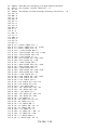
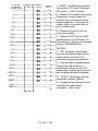
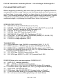
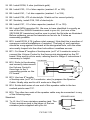
1
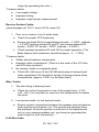
2 METER AMATEUR PLL
SYNTHESIZED FM
TRANSCEIVER 140 - 180MHz
Ramsey Electronics Model No.
FX-146
•
Synthesized - no crystals to buy !
•
Perky 5 watt RF output
•
Dual conversion sensitive receiver with crystal and ceramic IF filters
•
PACKET ready ! Dedicated packet interface connector on back!
•
12 Channels, expandable to as many as you want - programmed with
diodes !
•
Easy 4 evening assembly - need only a voltmeter and another rig for
testing
•
Fantastic manual teaches as you build, rig is assembled in bite-sized
sections that are tested as you build - your kit will work first time !
•
Rig operates over 20 MHz of band, great for snooping out of band !
•
Be proud to say...The rig here is a home-brew!
Published in Three Sections:
•
•
•
FX-series General Reference Information
•
Fold-out Schematic Diagram
•
Fold-out Multi-color Parts Layout
Plus:
Kit Assembly Phase I: Circuit Stages A through F
Kit Assembly Phase II: Circuit Stages G through TX
FX-146
•1
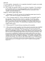
A DEDICATION
The Ramsey FX-series FM Transceiver Kits are writing a truly NEW chapter
in the annals of the ham radio story. Growing numbers of today's radio
amateurs ARE willing to build, understand, adjust and maintain modern VHF
gear capable of digital frequency programming and data communication as
well as FM voice. How do we know? We know it because, during 1991,
thousands of hams worldwide built and are using our pioneering FTR-146 for
two meters. The FX Transceiver design was developed in immediate
response to those builders' suggestions, wish lists and inquiries. This
publication is dedicated with deep thanks to all those FTR-146 builders!
FX-146 VHF FM Transceiver Reference and Kit Assembly Manual
Ramsey Publication No. M146FX
First Printing: December, 1991
Copyright 1991,1994 by Ramsey Electronics, Inc. All Rights Reserved.
Revision number 2.0
Published by Ramsey Electronics, Inc. Printed in the United States of
America
RAMSEY ELECTRONICS, INC.
Amateur Radio and Hobby Kits Dept.
793 Canning Parkway Victor, New York 14564
(716) 924-4560 Fax: 924-4555
FX 146 • 2
TABLE OF CONTENTS:
The Ramsey FX-146 Tranceiver Manual is organized into three sections:
General Reference Information, Kit Assembly Phase 1, and Kit Assembly
Phase 2.
FX-146 GENERAL REFERENCE INFORMATION
Notice Regarding FX-146 Frequency Coverage ................................4
FX-146 Technical Specifications ........................................................5
Introduction to Transceiver Kit Assembly ...........................................6
A Message to Ham Radio Beginners .................................................8
DC Power Supply Considerations ......................................................9
Enclosure and Hardware Considerations .........................................10
Ramsey CFX Transceiver Enclosure Kit ..........................................12
Guide to PC-board I/O Connections.................................................14
Microphone & Speaker Information ..................................................16
A Few Antenna Considerations ........................................................16
VHF Packet Data Operation .............................................................17
FX-series Transceiver Block Diagram ..............................................18
FX-146 Circuit Overview...................................................................19
Quick-Reference Programming Guide .............................................28
FX-146 Programming Worksheet .....................................................30
Using Computer BASIC as a Programming Aid ...............................32
How to Activate an Auxiliary (non-Standard) Offset .........................35
Programming "Minus" Offsets...........................................................36
FX-146 Programming Summary.......................................................38
Basics of Externally-Controlled Frequency Switching ......................38
FX-series GLOSSARY of Terms ......................................................40
Troubleshooting Guide .....................................................................46
Note on Replacement Parts..............................................................48
FX-146 Master Component Index ....................................................49
RAMSEY ELECTRONICS FX Kit Warranty Terms ..........................62
KIT ASSEMBLY: PHASE 1
Assembly and Explanation of Circuit Stages A through F
(including Kit Parts List, kit-building tips and preliminary receiver & VCO
test) ............................................................................................63 - 98
KIT ASSEMBLY: PHASE 2
Assembly and Explanation of Circuit Stages G through TX (includes all
Frequency Programming directions plus alignment and transmitter tuneup.)
................................................................................................ 99 - 137
Optional Helical Filter Installation ...................................................138
Technicians Notes ..........................................................................139
FX-146
•3
IMPORTANT NOTICE
The Ramsey FX-146 VHF FM Transceiver is capable of
TRANSMITTING as well as receiving on any frequency in the
range of 140 to 180 MHz, making it suitable for a wide range of
VHF communications requirements. Operation of the Transmit
function of this equipment requires an appropriate license
issued by the Federal Communications Commission (FCC) for
the class of operation intended. The FCC issued TECHNICIAN
CLASS license or higher is required for operation in the
Amateur 2 METER band (144 to 148 MHz). Proper licensing is
required for MARS or CAP operations. Amateur licensees are
required by the FCC to maintain strict control over their
equipment to prevent unlicensed operation either in the
amateur band or outside it. FCC regulations ENFORCE severe
penalties for unlicensed operation of radio transmitting
equipment and for interference with other communications
services, whether malicious or accidental. Ramsey Electronics,
Inc. sells the FX-146 transceiver solely for correctly-licensed
operation. It is the sole responsibility of builders and operators
of this RF electronics device, capable of emissions controlled
by FCC Rules, to understand and comply with those rules.
FX 146 • 4
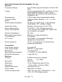
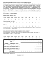
SPECIFICATIONS FOR THE RAMSEY FX-146
General:
Frequency Range:
Any 20 MHz segment between 140 and 180
MHz
Tuning:
Diode-programmable PLL synthesis 12 front
panel selected frequency pairs, easily
expandable by switches, microprocessors,
computers, etc.
Programming:
5 KHz steps with programmable offsets
Transmit Offset:
Programmable: Simplex, +1.2, -1.2, Aux
Mode:
NBFM
Packet (Data) Operation:
All rates incl. 9600 baud . 5-pin DIN jack
(TXD, RXD, PTT, +12VDC, GND)
Packet RX Audio:
Speaker, discriminator or true FSK
Power Requirement:
13.6V DC +/-10% (Negative ground)
Power Consumption:
1.0 A Transmit (for 5 watts RF output) 200
ma. (Receive, no signal)
Antenna Impedance:
50 ohms
Microphone Impedance:
600 ohms or high impedance
T-R switching:
PIN diodes
PTT circuit:
Solid State (for standard ICOM-type
speaker/mic connection)
Semiconductors:
10 IC's, 16 transistors, 24 diodes (plus
programming diodes)
Transmitter:
Final Power Output:
4-6 watts RF
Final Output Stage:
MRF237 or equivalent
Modulation:
True direct FM
Max frequency deviation:
+/- 25 KHz, +/- 5KHz NBFM
Modulation distortion:
Less than 5%
Receiver:
Circuitry:
Double-conversion superhet
First IF:
21.4 MHz
Second IF:
455 KHz
Sensitivity:
12 db. SINAD less than 0.35 uv
Selectivity:
7 KHz (-6db.), 15 KHz (-60db.)
Squelch sensitivity:
Less than 0.25 uv
Audio output:
More than 2.0 watts
Circuit access points:
COR, PL tone input, FSK demod. +12V,
+8V, +5V, PLL programming.
FX-146
•5
INTRODUCTION
to FX-series VHF Transceiver Kit Assembly
For the 1990's, Ramsey Electronics has adopted a "Learn As You Build"
philosophy for ALL our electronics kits. We feel that licensed ham operators
should know about the equipment they use, and also should have the desire
to understand how their gear works. Additionally, it has been our corporate
response to all those urgings by public officials that both students and their
parents need to become sharper in science and math. This "Learn as You
Build" approach to electronics hobby kits is now evident in all Ramsey
Electronics build-it-yourself kits from our under-$5 student kits up to this
synthesized VHF transceiver suitable for ham radio and public service
applications alike.
We think that "learning (and UNDERSTANDING) as we build" is especially
essential in a more sophisticated project such as the Ramsey FX-series VHF
transceivers. In fact, we are so convinced of this basic need that this kit
instruction manual departs from the traditional scheme of separating
assembly directions from a "theory of operation."
The FX-series of Ramsey VHF/UHF Transceivers puts today's FM 2-way
radio technology back in YOUR hands at a budget price. Our idea of
"budget" looks far beyond the modest purchase price to our goal that you
can maintain your FX- unit in good operating readiness with no need for
expensive shop service. On the other hand, we also have made the
transceiver design as abuse-proof and rugged as possible. "Alignment,"
traditionally an intimidating many steps process is very easy, quick and foolproof in this circuit design.
Instead of separate stage-by-stage assembly directions plus separate theory
information, these FX- instruction booklets highlight your transceiver's
operational theory, often a single component at a time, with actual
construction steps provided as follow-up after each explanation. The
assembly sequences are easy to find in the following pages. You indeed
have the freedom to solder first and read all about it later. We hope, though,
that you'll take it easy, learning as you build, and then enjoy the reliability of
your Ramsey FX Transceiver for a long time to come.
The "style" of our kit-building directions presumes that you are peeking at
our multi-color parts layout sheet while seeing that the very same parts
outlines are imprinted on the component side of your FX- PC-board. Our
smaller kits do not justify any need for on-board imprinting (silkscreening).
Therefore, such kits provide more detailed published explanations for
identifying correct locations for inserting and soldering parts.
You'll install EVERY FX- part perfectly by using our simple step-by-step kit
building process. And you'll know the WHY of most assembly steps, if not all
of them. Before you start, THINK about what you'll create from those bags of
FX 146 • 6
parts as a finished product! For a minimal investment of your time as well as
your well-earned money, you will have a VHF FM voice-data transceiver that
you will truly own. Real "owning" ultimately means knowing how to maintain
and understand something that we have, in contrast to merely possessing a
thing because you spent the bucks to do so. You'll have the flexibility of 12
channels chosen by YOU with the easy ability to change or expand. You'll
have both FM voice and high-speed data capability. When you're ready, you
can experiment with many different enhancements, concentrating on those
truly useful to you. If there's ever a problem, you won't think twice about
digging in and fixing it. Whenever you decide you could use still another
VHF/UHF FM/data transceiver at a budget price, you'll know with confidence
that an FX-series kit is the right way to go.
What's faster: turning your FX- Transceiver to any one of 12 possible
channels programmed by you, or trying to remember again exactly how to
use the memory pre-sets of your HT, or your HF rig, or the VCR, or the
microwave?
Let's learn about and build up a FX- VHF FM Transceiver!
FX-146
•7
A MESSAGE TO HAM RADIO BEGINNERS:
If you have just earned your Novice or Technician license, or are studying for
either of them right now, we'd like to say a special Thank You for choosing
this Ramsey VHF/UHF transceiver as part of your ham radio beginnings. We
have tried to make this instruction manual as clear as possible. However,
there are some VHF radio "basics" covered by the FCC question pools for all
ham license study guides that we must presume that you have studied and
understood.
Here is a simple guide to selected Technician Class questions to help with
any review you wish to make before building:
FCC Subelement 3AA (Selected Rules): 4.2 11-1.1 12.5 15.2
FCC Subelement 3AB (Operating Procedures): 2-1.1 2-1.2 2-1.3 2-1.4
2-1.5 2-2.1 2-2.2 2-3.1 3.2 6-3.1
FCC Subelement 3AC (Propagation): It's up to you to understand the
characteristic differences among HF
(shortwave), VHF and UHF
communications.
FCC Subelement 3AD (Amateur Radio Practice): All of this is fundamental
know-how for hams. In working on this
project, be especially familiar with: 1-1.1 11.2 1-1.3 7.1 9.1 through 9.5 (dummy
loads)
FCC Subelement 3AE (Electrical Principles) 3AF (Circuit Components)
Please know ALL of this.
FCC Subelement 3AG (Practical Circuits): 4.21
FCC Subelement 3AH (Signals and Emissions): 1.1 2-1.1 2-4.1 2-6.2
2-7.1 4.1 6-1.2 7-1.1 7-2.1 7-2.2
FCC Subelement 3AI (Antennas and Transmission Lines): You will want
to know all of this, if you don't want to take
all your savings from building your own
transceiver and spend it on a commerciallybuilt antenna. Very good VHF antennas are
easy and inexpensive to build yourself!
FX 146 • 8
DC POWER SUPPLY CONSIDERATIONS :
Your Ramsey FM Transceiver is designed to operate from any stable DC
voltage source in the 12 to 15 volt range, from typical car, boat or plane 12V
systems to a wide variety of battery packs or AC-powered DC sources. In a
pinch, you can get on the air for quite a while with 8 to 10 ordinary "D" cells!
Our lab tests show only a .93 amp current draw for 5 watts of RF output. We
have just a few points of advice and caution:
1. Your DC supply should be able to provide a minimum of 1.0 amperes in
continuous service.
2. Any battery setup capable of supplying 12-15VDC will serve quite well.
3. Use of wall plug power supplies is NOT recommended. Obviously,
12VAC output is not suitable. Most DC output units do not have
adequate voltage regulation.
4. Turn your transceiver OFF before re-starting the vehicle in which it has
been installed.
5. Replace F1 only with a 1 amp fuse.
6. If you power your transceiver from the +12V accessory voltage available
from other equipment, be sure that source is rated for the 1 amp
required.
7. Your transceiver circuit includes noise suppression at the DC input and
additional filtering at the VCO, primarily to prevent ignition/alternator
noise from being introduced into the FM modulation. If you hear ignition
noise in the receiver, the vehicle has a serious general problem. Check
your transmitted signal on another receiver before mobile operation.
Radio Shack sells a variety of noise-suppression capacitors and
chokes. The ultimate solution, which has been tested, is to run the
transceiver from a smaller accessory battery.
If you plan to build a power supply for fixed-station use, there are numerous
construction articles in ham and electronics hobby publications. A
convenient new book featuring easy-to-find components and clear
explanations is Building Power Supplies (Radio Shack 276-5025.)
FX-146
•9
ENCLOSURE & HARDWARE CONSIDERATIONS:
The companion CFX case and knob kit is sold as a separate option ONLY
as an accommodation to those radio hams who have their own ideas or
resources for the "finishing touches."
However, a proper case for your FX-series is much more than a "finishing
touch," since the controls and jacks are panel mounted and proper RF
shielding is required.
The CFX case measures 9-3/4"L X 6"W X 1.5"H. 9" x 6" dimensions are
minimum for accommodating the PC board. The height may vary if you wish
to include an internal speaker, accessory PC boards, additional front panel
controls or indicators, etc. If you are new at all this and do not already own a
suitable enclosure plus that collection of hardware and knobs that every ham
seems to accumulate, here is what you need to know if you are hesitant to
purchase the CFX case kit:
A.
"Blank" electronics enclosures have become among the most
expensive hardware in the industry, especially if you are buying just one
unit. This is because they are sold mainly to engineers and designers
for prototyping. A blank metal enclosure even slightly comparable to the
CFX case kit will run $30 to $80 or more. Even a plain aluminum
chassis box/cover will be around $15.00.
B. If you think there's any chance you someday may wish to sell or trade
your transceiver, you should be aware that units mounted in odd boxes
may have even less value than the bare circuit board with
documentation alone.
C. Many distributors have a minimum mail order of $25.00.
D. Your best chance for finding an inexpensive alternative case is to have
access to a lot of ham friends who tend to "collect stuff," or to browse
the catalogs or showrooms of electronic surplus dealers. You just might
find a gorgeous new box originally intended for somebody's ingenious
Ultra Modem, external disk drive or other dream gadget from two years
ago.
Are we trying to discourage you? No, not really! We know you can see that
there are good reasons to consider calling Ramsey Electronics and getting
your CFX case on its way while you work on the PC-board and PLL
Programming. However, we do not want you to feel "stuck" with our
recommended CFX enclosure, so we have worked up a detailed shopping
list for getting what you will need to make as attractive a finished unit as
possible with a single trip to the neighborhood Radio Shack store.
FX 146 • 10
Quantity
RS Part No.
Description
1992 Price ($)
1
270-272/74
Deluxe Project Enclosure 8.79 or 10.79
1 set
274-section
Pkg. of 3 or 4 knobs
2.00-3.00
1 set
270-201
Rub-on project labels
2.99
2 sets
276-195
PC-board standoffs/
2.38
This $16 to $18 (plus tax) in basic hardware also presumes availability of all
needed drill bits and/or a reamer or punches of sufficient size to make the
needed access holes for the rear panel jacks. You'll also want to figure on
spray paint as well as a clear finish to protect the panel labels. Tools and
supplies, if not on hand, could cost much more than the CFX enclosure kit
itself.
In addition, this style of case will have to be utilized upside-down and also
length wise rather than as designed. This means that the top (black)
becomes the foundation for mounting the PC board with the standoffs as
well as securing the SO-239 antenna connector assembly. You may wish to
repaint the white bottom which now becomes the top. And, to use the project
labels (black lettering), you'll probably wish to repaint both pieces.
This adaptation of standard Radio Shack hardware is adequate for indoor or
occasional use but not recommended for mobile operation. We are happy to
provide this suggested alternative to the rugged case, knob and hardware kit
custom designed for the FX-series transceivers. The choice is yours!
FX-146
• 11
THE RAMSEY CFX TRANSCEIVER ENCLOSURE KIT:
The CFX Kit is very obviously a fair value and solid investment for the long
term performance and worth of your transceiver. As we have mentioned, we
make it "optional" ONLY because some of our ham customers have
specialized applications requiring only the basic PC board kit. We try
whenever we can to accommodate that important do-it-yourself spirit of ham
radio.
ENCLOSURE KIT PARTS LIST
Please check the boxes after the components have been identified, and it is
also handy at this time to “sort” the like components into groups or bins (an
egg carton does nicely) to avoid using the wrong component during
assembly.
1
1
1
1
2
5
5
8
8
1
2
4
Steel bottom shell with 5 threaded PC board standoff posts
Steel top shell
Front control panel
Rear panel with access holes to PC mounted jacks
Steel side rails
PC board standoff spacers
#4 nuts to secure PC board on standoffs
#4 screws to mount front and rear panels
#6 screws for securing top and bottom to side rails
large knob for Channel Selection Switch
smaller knobs for Volume and Squelch controls
self-adhesive rubber feet
CFX CASE ASSEMBLY PROCEDURE:
The purpose of these hardware parts is largely self-evident. We offer the
following suggestions for your convenience and to minimize wear and tear
on your factory-fresh CFX enclosure.
1. Since the bottom shell might be used for several "test fittings" during
transceiver assembly, install the rubber feet right away to protect its
finish.
2. Obviously, the PC board cannot be secured permanently to the
bottom section until after installation of L9, R32 and L10 AFTER
Alignment and before Transmitter tuneup.
3. Install the strain-relief grommet supplied with the transceiver kit in its
rear panel hole. Pass the black ground wire through this grommet. The
red, fused wire will have to be unsoldered from S1 and then carefully
FX 146 • 12
resoldered after passing through the grommet. Snap in the locking
section of the relief grommet only AFTER both the red and black wires
are in place.
4. Remove the two screws from the SO-239 antenna connector, gently
bend the lugs as needed to match the rear panel holes, then secure the
jack and lugs to the rear panel.
5. Since the top shell will not be needed until you're ready to go on the
air, keep it wrapped in protective material until you're really ready to use
it.
6. The side rails may be installed to the bottom section at any time. To
prevent loss of the screws for the top, keep them loosely threaded in the
side rails.
7. There is no point in securing the front panel controls and jacks to the
panel permanently until AFTER wiring the Channel Selection switch.
Note the locking hole for the switch in the front panel which mates the
tab on the front of the switch.
8. Use care and a well chosen pair of pliers to secure the microphone
and speaker jacks to the front panel, so as not to scratch the panel.
9. Bend the leads of the TX LED so that their tension presses the front
of the bulb against its front panel hole.
10. Whenever you find it necessary to remove the top shell, "store" the
screws back into their holes in the side rails.
11. If you decide to install a ribbon cable in the diode matrix for external
programming control, route the cable (folded at a right angle) on the
synthesizer and receiver side of the board so that it exits the case
between the rear panel and top cover, right above the DC power cord.
Do NOT route any such cable across the VCO and transmitter side.
12. After the PC board is secured to the case bottom and front/rear
panels, it is a good idea to neaten up the wires to the controls and
jacks, bundling them at two or three points with tie wraps or cord.
FX-146
• 13
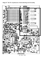
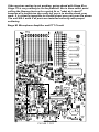
GUIDE TO PC BOARD I/O CONNECTIONS:
In addition to primary interconnections required for jacks and controls, etc.,
your FX-series Transceiver PC board provides additional access to
operating voltages and circuit features to make later customizing as neat
and easy as possible. All these points are plainly marked on the board itself
and highlighted on the facing page, with a few other components for
FX 146 • 14
1. PRIMARY CONNECTIONS:
PWR (near L20): +12-15 volts DC from S1.
GROUND: - DC from battery or power supply.
SPEAKER: both connections near C37
MIKE: both connections (IN & GND) near notched end of U1.
SQUELCH: two connections marked CW and W near C18
VOLUME: three connections marked IN, OUT, GND.
ANTENNA: Center of SO-239 connected at "RF OUT" near C71.
CHANNEL SWITCH: Row of holes numbered 1 through 12. The switch
wiper (moving contact) is wired to +5V near "1."
EXT AUDIO: must be jumpered per options to enable pin 4 of J1.
2. TEST POINTS:
+12V, +8V, +5V, +8R, +8T permit checking for presence of those voltages.
+8R = Receive mode. +8T = Transmit.
TP1: For checking of VCO control voltage during alignment.
TP2: For checking VCO frequency with counter.
TP3: For checking U3 prescaler output with counter.
R103: +7VDC at top lead shows locked PLL. 0 volts = problem.
3. OPTIONS:
+12V, GND, +8V, +5V, +8T, +8R: provide supply voltage for accessories or
modifications designed by you. +5V is available both near L1 and near
C102. +8T and, +8R are near Q13, Q14.
Jumper Options for Packet Operation: SPKR to EXT AUDIO: Speaker level
audio for packet (J1). DISC to EXT AUDIO: FM discriminator output for
packet.
COR: "Carrier Operated Relay" output from U1.
PL: Input point for audio tones (DTMF, CTCSS, etc.)
Binary Programming Holes: The row of holes alongside the Binary
Programming labels permits installation of ribbon cable for external
programming devices designed by the innovative amateur radio community.
switches or interfaces, or a row of internal DIP switches.
FX-146
• 15
MICROPHONE & SPEAKER INFORMATION
The FX transceivers with the hardware supplied are designed to accept
standard ICOM or ICOM-compatible speaker-mikes such as MFJ-284. The
most conveniently available such unit is Radio Shack No.19-310.
Be aware that the receiver audio amplifier is capable of supplying a husky 2
watts or more of audio power and will drive full-size communications
speakers to excellent volume levels.
The PTT switching circuit can be activated simply by introducing a
resistance (e.g. 10K) from the microphone input to ground. This resistance is
enough to trigger the PTT circuit without interfering with the microphone
audio input.
Consider these factors in selecting microphone, speaker and/or speakermike for FM voice operation. If your microphone and speaker preferences
differ radically from the use of a speaker/mike, and you do not wish to alter
the front panel, remember that you also have very easy access to mike and
speaker lines via J1, the packet connector.
A FEW ANTENNA CONSIDERATIONS
The idea of building your own transceiver is to save money and enjoy your
hobby. Effective VHF and UHF antennas are easy and inexpensive to build,
whether for fixed or mobile use. There are plenty of off-the-shelf antennas to
buy, but don't hesitate to "roll your own."
If you are a newcomer to ham radio, you'll discover many strong opinions
about the "best" antenna to use. A home-built ground plane vertical or even
a dipole can provide very satisfying results. Whether you need a gain factor
or directivity in your antenna depends on your operating goals. Regardless
of the style of antenna, it really pays to give serious attention to electricallysolid, weatherproof connections of the coaxial cable to the antenna
elements. A simple antenna in good condition will outperform a fancy one
that's been neglected.
Popular ham magazines and ARRL publications provide plenty of antenna
building ideas. MFJ Enterprises offers good value in simple ready-to-use
antennas for 2 Meters.
FX 146 • 16
VHF PACKET DATA OPERATION
Your FM transceiver was planned and designed to accommodate easy and
reliable VHF packet radio operation.
The J1 Packet I/O port can be quickly connected to many modern TNC's and
the Ramsey P-IBM or P64 Packet Modems with Radio Shack's shielded DIN
cable (42-2151). Otherwise, your first step is to prepare a reliable 5conductor cable with a 5-pin DIN plug (RS 274-003) at one end, and the
correct connector needed by your packet TNC at the other end. If you
salvage a "ready made" 5-pin DIN cable from something like a discarded
computer joystick, be sure that there are indeed 5 wires, or at least the ones
that are required by your TNC!
Consult your Packet TNC or Packet Modem documentation for ALL details
on hookup and operation. Pin 4 of J1 offers a choice of amplified and
squelched (speaker level) audio output or low-level (discriminator) output.
This choice is set up by the jumper wire positions clearly visible on the PC
board.
Packet RX Audio Jumper: Some TNC's require low-level audio from the
discriminator output of the FM detector, while others will accept speaker
output. Either is available in the FX transceivers. Simply install a jumper in
the appropriate location near VR1, to connect "EXT AUDIO" to either
"SPKR" for speaker audio or "DATA" for discriminator audio. Use scrap
resistor wire to make the jumper. You also can choose to wire these three
points to a miniature SPDT switch which you can mount on the rear panel
near the packet connector. OR, use a PC mount switch in the jumper area
itself.
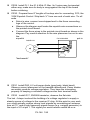
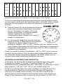
Use this space to diagram your TNC cable connection:
DRAW YOUR TNC
FX-146
• 17
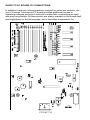
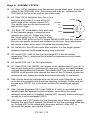
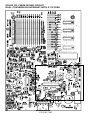
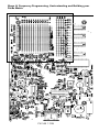
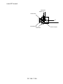
RAMSEY FX-SERIES FM TRANSCEIVER
(With emphasis on the PLL and VCO)
MC13135
FX 146 • 18
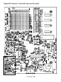
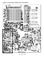
FX-146 CIRCUIT OVERVIEW
The FX-146 VHF FM Transceiver circuit theory is explained in progressive
stages and in some detail as part of our "Learn As You Build" approach to
electronic kits. Builders are encouraged to study and learn about a stage or
section, build it and then test it before going to the next stage. The circuit
explanations are necessarily written for people with all levels of experience,
starting with and FAVORING beginners.
Following is a straight and "minimally chatty" synopsis or overview of FXseries technical information provided in the building stages. However, we'll
still follow the same stage-by-stage designations of the building process.
A: DC Power Input
Much of the circuitry operates on the regulated 8 volts supplied by voltage
regulator VR1. "+8R" or "+8T" are points where the regulated 8V output is
switched for Receive or Transmit by the PTT circuitry (Q12, U4c, U4d, Q13,
Q14).
The Receiver IC (U1) and the digital frequency synthesis circuit are powered
by +5 volts regulated by VR2. The op amps used in the circuit (U4 and U5)
operate from this single supply through the use of voltage divider networks
at the respective IC's. The full 12-15 volt input is supplied to the transmitter
RF output section and to the audio amplifier (U2).
Components L20 and C42 provide ignition noise filtering. The 5-pin DIN
Packet I/O Jack (J1) has pinouts corresponding to current conventions for
TNC's. Receiver audio to pin 4 may be taken from the amplified speaker
output, or from the FM discriminator output or from the true FSK data output
of U1. Selection is by a jumper wire on the PC-board.
B: Receiver Audio Amplifier
The LM380 is a self-contained general purpose audio amplifier capable of
over 2 watts audio output with a voltage gain of 50. Audio from from the FM
discriminator (U1) is fed through C7 through the 10K volume control (R7) to
pin 2, the amplifier input. The amplified output at pin 8 is available through
C34 to both the speaker jack and pin 4 of the Packet I/O Jack. C41 in series
with R108 across this amplified output are good practice recommended to
prevent self-oscillation of the IC. Pin 1 is bypassed to ground through C48 in
normal operation.
If pin 1 is grounded directly, the internal bias of the LM380 is upset, and the
amplifier is silenced. Q6 is a simple switch. When 8 volts is applied through
R107 and D22 to the base of Q6, the transistor collector grounds pin 1 of
U2, thus silencing the receiver during transmit. The COR output of U1 (pin
16) also mutes the amplifier.
FX-146
• 19
FX 146 • 20
Stage CR: Integrated FM Receiver
The MC13135 is a complete FM narrowband receiver from antenna input
(pin 22) to audio output (pin 17). The low voltage dual conversion design
results in low power drain, excellent sensitivity and good image rejection in
narrowband voice and data link applications. The FX146 implementation of
this IC yields increased image rejection by using a 21.4 MHz first IF rather
than the traditional 10.7 MHz.A precision 2-pole crystal filter (FL1) is used for
the 21.4 MHz first IF.
Our design injects the PLL controlled VCO output through C35 to pin 1
rather than using U1's internal local oscillator circuit. The VCO input to pin 1
is mixed with the RF input from the antenna circuitry.
The first mixer amplifies the signal and converts this RF input to 21.4 MHz.
This IF signal is applied to the second internal mixer via pin 18, where the
2nd IF frequency of 455 KHz is achieved by mixing with the 21.855 MHz
oscillator. The oscillator circuit is internal to U1; the crystal is Y1, 21.855
MHz.
The 455 KHz second IF output (pin 7) requires filtering. We used a precision
ceramic 455 KHz filter with 6 poles for a 2nd IF filtering scheme designed to
solve the adjacent- frequency swamping effect experienced with many
handhelds costing much more.
The receiver has good "hysteresis" characteristics, the ability to hold the
squelch open once it has been broken by a marginal signal, even if the
signal becomes weaker. The squelch is activated by signal strength, not by
noise.
R13 permits squelch adjustment. Finally, the carrier detect circuitry affords
the same COR ("Carrier Operated Relay") action as needed in any repeater,
which is why the output of pin 16 is also available on the PC board,
designated "COR."
Stage DR:
Antenna Input and RF Preamplifier: At Antenna jack J3, C71, L12 and C72
form a LOW pass filter, The filtered signals are coupled through C47 to be
amplified by Q3, NE021, favored for its high gain and low noise (15 db gain,
1 db noise).
Front-end components C30, L5, C28, L2, C31, L6 form a BANDPASS filter,
which sets both upper and lower limits on the RF passing from Q3 to Q2 for
further amplification and coupling via C17 to U1, pin 22.
The PIN diodes, D2, D6 and D7, perform all RF T-R functions. PIN diodes
can pass RF energy either way when turned on by DC voltage and also
block RF from the other direction when not powered by DC. During Receive,
D6 is "on" and permits RF to flow from the antenna through C47 to the
amplifier stage just discussed. Because any DC device needs a ground
FX-146
• 21
connection as well as +DC, D6 is grounded through RF choke L17, which
prevents the antenna RF from being shorted to ground.
During Transmit, D7 passes RF from the transmitter to the antenna, and L17
again prevents loss of RF to ground. During transmit, D6 is blocking
transmitter RF from the receiver circuit. For maximum protection of the more
delicate receiver circuit, D2 is turned on during transmit to ground any stray
RF.
Stage E-F The FX Transceiver VCO
The VCO (Voltage Controlled Oscillator) provides basic frequency control for
both transmit and receive modes. It is essential to understand its function in
the transceiver circuit. Q7 is the oscillator transistor. L7, D3 and D23 are key
VCO components.
After the VCO is assembled on the PC board, the interested builder is given
the option of experimenting with it in receive mode before working on the
PLL synthesizer. This is done by applying a variable DC control voltage
through a pot to TP1. Otherwise, TP1 is available for checking VCO control
voltage during initial alignment. TP2 permits checking VCO frequency output
with a frequency counter. TP3 permits checking the output of the TD6128
Ã64/65 dual modulus prescaler (U3)
The control voltage for the D3 and D23 varactor diodes is supplied through
R47 and R25 by the output of U5:A in the PLL synthesizer circuit.
There must be a 21.4 MHz difference between the receive and transmit
frequencies of the VCO. This swing cannot be accomplished by PLL
programming alone. The VCO must be able to stay "in range" with the
synthesizer. D3 and D23 work in series during transmit, which reduces their
capacitance per the standard formula. For example, if a given control voltage
runs both diodes at 5 pf, the actual capacitance is 2.5 pf. In receive, the +8R
through D1 causes D3 to be shunted by C39, which causes D23 alone to
control the VCO L-C circuit, introducing twice as much capacitance and
thereby lowering the frequency.
Q5 is a common base buffer which affords good isolation, low input
impedance and broadband characteristics. The buffered output from Q5 is
fed into U3, TD6128, a dual modulus Ã64/65 prescaler, the output of which
is fed to the A and N counters in U6. The output is further buffered and
amplified by Q16, the VCO buffer which couples through C35 for receive,
and Q10 through C56 for transmit.
The VCO is is frequency modulated by microphone amplifier U4. D5 and
R31 perform an interesting function. Remember that the VCO control voltage
has a range of about 1.0 volts DC (low frequency) to 7.0 volts (high
frequency). Therefore, more modulation voltage is needed at the higher
frequencies. As the VCO control voltage increases, D5 turns on and places
R31 in parallel with R33, reducing the resistance in the line to half and
FX 146 • 22
thereby increasing available modulation voltage.
The VCO requires a very pure source of well-filtered DC, free of AC hum,
alternator whine or other disturbance. R19 and the 47 uf C40 form a basic
low pass filter. Transistor Q4 serves as an electronic capacitance multiplier.
The actual effect of the filter is that the beta of Q4 multiplies the 47 uf for a
virtual capacitance effect of a much larger device.
Stage G: The FX- Transceiver Synthesizer PLL
The MC145152 IC incorporates the equivalent of 8000 individual transistors
and contains the following circuits:
• A crystal reference oscillator governed by Y2, 10.24 MHz.
• A counter or "frequency divider" circuit set externally to divide the
crystal oscillator output by 2048, for a Reference Frequency output
of 5 KHz.
• A second counter or frequency divider that divides the frequency
from the Prescaler (U3) by the externally programmed number that
we call "N".
• A third frequency divider ("A") also used for programming
• Control logic circuitry which permit the "N" and "A" counters to
work together for channel programming.
• The Phase Detector (or "phase corrector") which compares the 5
KHz Reference Frequency with the "intended" 5 KHz output of the
N-divider and sends correcting pulses to the VCO to keep the
output of the N-divider right at 5 KHz.
• A "lock detect signal" circuit. The reference oscillator is internal to
U6, governed by Y2.
The precision of the 10.240 MHz reference oscillator can be adjusted by
trimmer C81. The R divider feeds 5 KHz to the phase detector section of U6
(10240 KHz divided by 2048).
The output of the TD6128 Ã64/65 prescaler U3 is AC coupled via C57 to pin
1. U3 is a dual modulus prescaler, controlled by pin 9 of U6. The prescaled
output of the VCO is fed to the A and N counters. The "N" number
programmed on the diode matrix is predetermined to divide this frequency
down to 5 KHz for phase comparison with the 5 KHz output of the crystal
controlled reference divider. Maximum "N" is 65,535, achieved by switching
on all 16 parallel inputs.
Unlike simpler PLL IC's, U6's phase detector has TWO outputs at pins 7
and 8. These outputs go through very simple low pass filters (R44-C68, R53C91) to cut back the 5 KHz whine sound of U6 at work. Op amp U5:A sums
together the phase detector outputs and the output of U5:A is passed
through a network of 2.2 uf electrolytic capacitors (C67,70,90,92) to smooth
out the phase detector pulses to clean DC for controlling the VCO.
FX-146
• 23
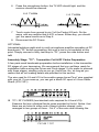
FREQ.
N=
BINARY PROGRAMMING VALUES
144.000
28,800
0111
0000
1000
0000
148.000
29,600
0111
0011
1010
0000
R48 and C85 form yet another low pass filter to ensure that any 5 KHz
"whine" will not get into the VCO. Because the DC charge developed in C85
(.1 uf) would slow down the PLL during major frequency swings, such as just
going from transmit to receive, D8 and D10 are set up back-to-back across
voltage dropping R48. Whenever there is a major frequency shift (which
means a significant VCO control
voltage change), one way
or the other, one diode or the
other
is switched on to
146520 (KHz)
short out R48 and discharge
C85.
This
lets the PLL
5 (KHz)
relock instantly; C85 recharges
and the diodes become
no factor in the circuit.
The lock detect output (pin 28) gives a strong series of pulses when the PLL
is unlocked. When the PLL is locked, only a tiny sawtooth wave appears at
pin 28. The "lock detect" voltage is watched by U5:B. If "unlock" pulses
appear, they are integrated through R90 and C96 as a fairly clean DC
voltage charge built up in C96. If this charge causes U5B to swing low, bias
is removed from Transmit Buffer Q10, preventing transmitter damage and
unwanted emissions.
Stage H: The Diode Matrix and PLL Synthesizer Programming
There are two diode-matrix programming areas on the PC board. The
obviously larger area is for frequency channel programming. The second
space is for offset programming added in by U7-U10.
The 19 100K resistors at the frequency programming matrix and the 14
100K resistors at the offset matrix are "pulldown resistors," to ensure
positive logic switching action of U6.
Q15 and its associated switching diodes ensure that the desired offset is
switched in during transmit, that offset programming does not interfere when
simplex is desired and that the offsets do not interfere with receiver
operation and that receiver programming (21.4 MHz lower) does not
interfere with transmit operation.
A variety of techniques are possible for binary programming of U6's 16
paralel inputs. We focus on the diode programming approach with some
brief suggestions on externally-controlled switching. It is very intentional on
our part to leave innovative programming schemes up to FX transceiver
users, because there's no single best way to do it for everybody.
FX 146 • 24
There are several methods for quickly finding the required binary code for a
particular frequency and its "N" number:
1. Descending Subtraction (see Programming Worksheet)
2. Printed reference lists (see Popular 2 Meter Frequency Pairs)
3. Computer programs (see our sample BASIC program)
We recommend strongly that you fully understand how to make the
calculation yourself, because that is your ONLY means for checking the
accuracy of printed information, computer programs or the operation of
experimental programming circuits. Even though there are 16 matrix
positions to program, there are some shortcuts to make the job easier for
normal ham band operation. Consider the upper and lower band edges.
Notice the values of the highest 6 positions are the same throughout the
band. We still must program in those six positions but we only need to
calculate for the remaining 10 (512 through 1) to program any 2 Meter band
frequency desired. The simplex calling frequency of 146.52MHz is the
demonstration and alignment standard for the FX-146 model.
"N" is quite easy to determine:
"N" for 146.520 MHz =
= 29,304
The placement of diodes in the Programmable Offset Matrix follows the
same binary number principles as used for frequency programming. This
matrix is connected to the 16 programming inputs of U6 through the four 4
bit binary adders (U7-U10). Fewer programming positions are provided on
the board simply because there is no practical use for extremely large or
very tiny offsets. The 1 bit to 8K range provides plenty of flexibility for nonstandard channel spacing.
U7 through U10 are called "4 bit" binary adders because they each can
handle four binary addition operations. For each bit, there are A and B inputs
and one S (sum) output. Examine the schematic diagram closely, and you
will see that all the frequency programming lines are connected to "A" inputs
and all offset lines go to "B" inputs. Notice further that the binary positions of
both matrixes correspond to each other exactly: the 8K offset position goes
to B1 of U7 and the 8K frequency programming position goes to A1. Their
sum appears at S1 (pin 1) and goes to U6. And so forth for all the other
binary programming positions.
The programming for receive mode and standard repeater offsets is
silkscreened on the PC board itself. Assembly Stage H explains the theory
behind these positions. The +RPT "N" numbers are calculated in the same
way as for the Frequency Programming matrix. -RPT, RECV and other
"minus" offsets are calculated by straightforward "2's Complement" binary
addition. See Stage H for examples.
FX-146
• 25
Stage M: Microphone Amplifier and PTT Circuit
U4 is a LM324 quad op amp: two are used as a conventional microphone
gain amplifier, and the other two are used in the PTT (push to talk) circuit.
Capacitor C83 couples microphone audio to U4A and isolates the audio
(AC) from the PTT circuitry (DC). U4 is powered by a single +8V supply
through the use of a voltage divider network (R59, R40). The gain of the
amplifier is established by the ratio of R56 to R58. A passive low pass filter
is formed by R51 and C89. The B section of U4 and its associated
components form an active low pass audio filter. The output of U4B is fed
through C62 to modulate the VCO control voltage as explained in Stage E-F.
Trimmer R46 adjusts modulation level.
The purpose of Q11 is to shunt the microphone circuit straight to ground
during receive, so that it cannot possibly disturb the VCO. An accessory
modulation input is provided at PC-board point "PL" for direct injection of
DTMF or CTCSS tones, etc. The PTT circuit is designed to accommodate
the popular ICOM compatible speaker-mikes. Notice that a single line at J4
serves both audio and PTT functions. One shielded wire into the microphone
handles THREE functions. First, we need to supply audio output from the
microphone element to the amplifer. Secondly, we need some kind of PTT
switching connection. Third, the electret microphone itself needs a small
amount of voltage to operate its internal FET source follower transistor.
Here's how we do it with one mike line. Pushing the button simply connects
the microphone element to the line. About 2 volts through R60 and R57
operate the microphone element which sends audio through C83 to U4A.
PNP transistor Q12 senses the tiny current draw of the microphone element
and switches the 8 volts at the emitter through to the collector. To state it
very simply, the output of U4 turns off PNP Q13 which had been supplying 8
volts to all "+8R" points of the circuit. And the output of U4C switches on
PNP Q14 to supply all "+8T" points. Zener diodes D11 and D12 assure
positive action, that Q13 and Q14 are fully on or fully off when the op amp
outputs swing. Releasing the mike button instantly reverses the status of
Q12, Q13 and Q14 to return to receive mode. R70 limits the current drawn
by "TX" indicator D17 to a safe level.
The PTT circuit may also be activated at pin 3 of the Packet I/O jack. A
direct short to ground is not necessary. The author noted very positive PTT
action with resistance as high as 100K from pin 3 to ground.
Stage TX: Transmitter Buffer, Driver and Final
The transmitter section, Q10, Q9 and Q8, is conventional VHF RF circuitry
that has proven quite reliable in Ramsey FM transceivers. Just a few circuit
notes are in order.
Transistor Q10, the transmit buffer, amplifies the VCO output from C56 to
about 10 milliwatts, quite sufficient for checking modulation and PLL
FX 146 • 26
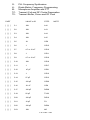
Using the FX-series FM Transceiver Quick Reference Programming
Guide:
In addition to "pencil & paper math" calculation directions and also a handy
computer BASIC program for programming the FX- series Transceiver for
any frequency and transmit offset within its specified range, we provide this
guide for binary programming of a variety of popular Repeater frequency
pairs as well as some other frequencies of general interest. All binary
programming data for 512 through 1 presumes prior diode programming of
higher level binary inputs which remain constant for the 2 Meter amateur
radio band:
You'll notice definite patterns
32K
16K
8K
4K
2K
1K
in the standard repeater
frequency assignments and
0
1
1
1
0
0
their binary equivalents. Look
at these patterns up and
down the programming input rows as well as across for any given frequency.
If your application could use more than the 12 channels easily programmed
for front panel switching, perhaps these patterns will give you some good
ideas for additional channel switching convenience.
FX-146
• 27
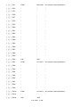
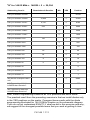
FX-146 Quick Program Reference
Standard 2 Meter band repeater pairs and selected frequencies
Program as follows:
1. Install diodes at 16K, 8K, 4K and NO diodes at 32K, 2K ,1K positions.
2. PLUS install diodes at 512 through 1 positions as needed per this Quick
Reference Chart.
3. For repeater channels, add the proper repeater TX offset diode.
Simplex channels: add the 'SIMP' diode.
4. A '1' means to install a diode, '0' means NO diode.
Freq
Offset
N
512
256
128
64
32
16
8
4
2
1
145.11
-
29,022
0
1
0
1
0
1
1
1
1
0
145.13
-
29,026
0
1
0
1
1
0
0
0
1
0
145.15
-
29,030
0
1
0
1
1
0
0
1
1
0
145.17
-
29,034
0
1
0
1
1
0
1
0
1
0
145.19
-
29,038
0
1
0
1
1
0
1
1
1
0
145.21
-
29,042
0
1
0
1
1
1
0
0
1
0
145.23
-
29,046
0
1
0
1
1
1
0
1
1
0
145.25
-
29,050
0
1
0
1
1
1
1
0
1
0
145.27
-
29,054
0
1
0
1
1
1
1
1
1
0
145.29
-
29,058
0
1
1
0
0
0
0
0
1
0
145.31
-
29,062
0
1
1
0
0
0
0
1
1
0
145.33
-
29,066
0
1
1
0
0
0
1
0
1
0
145.35
-
29,070
0
1
1
0
0
0
1
1
1
0
145.37
-
29,074
0
1
1
0
0
1
0
0
1
0
145.39
-
29,078
0
1
1
0
0
1
0
1
1
0
145.41
-
29,082
0
1
1
0
0
1
1
0
1
0
145.43
-
29,086
0
1
1
0
0
1
1
1
1
0
145.45
-
29,090
0
1
1
0
1
0
0
0
1
0
145.47
-
29,094
0
1
1
0
0
1
1
0
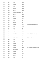
FX 1146 •0 28
145.49
-
29,098
0
1
1
0
1
0
1
0
1
0
146.61
-
29,322
1
0
1
0
0
0
1
0
1
0
146.64
-
29,328
1
0
1
0
0
1
0
0
0
0
146.67
-
29,334
1
0
1
0
0
1
0
1
1
0
146.70
-
29,340
1
0
1
0
0
1
1
1
0
0
146.73
-
1
0
1
0
1
0
0
0
1
0
146.76
-
29,352
1
0
1
0
1
0
1
0
0
0
146.79
-
29,358
1
0
1
0
1
0
1
1
1
0
146.82
-
29,364
1
0
1
0
1
1
0
1
0
0
146.85
-
29,370
1
0
1
0
1
1
1
0
1
0
146.88
-
29,376
1
0
1
1
0
0
0
0
0
0
146.91
-
29,382
1
0
1
1
0
0
0
1
1
0
146.94
-
29,388
1
0
1
1
0
0
1
1
0
0
146.97
-
29,394
1
0
1
1
0
1
0
0
1
0
147.00
+
29,400
1
0
1
1
0
1
1
0
0
0
147.03
+
29,406
1
0
1
1
0
1
1
1
1
0
147.06
+
29,412
1
0
1
1
1
0
0
1
0
0
147.09
+
29,418
1
0
1
1
1
0
1
0
1
0
147.12
+
29,424
1
0
1
1
1
1
0
0
0
0
147.15
+
29,430
1
0
1
1
1
1
0
1
1
0
147.18
+
29,436
1
0
1
1
1
1
1
1
0
0
147.21
+
29,442
1
1
0
0
0
0
0
0
1
0
147.24
+
29,448
1
1
0
0
0
0
1
0
0
0
147.27
+
29,454
1
1
0
0
0
0
1
1
1
0
147.30
+
29,460
1
1
0
0
0
1
0
1
0
0
147.33
+
29,466
1
1
0
0
0
1
1
0
1
0
147.36
+
29,472
1
1
0
0
1
0
0
0
0
0
147.39
+
29,478
FX-146
1
1
• 290
0
1
0
0
1
1
0
29,346
N = Frequency (KHz) ÷ 5
Freq = Receive frequency/Repeater output
145.01
S
29,002
0
1
0
1
0
0
1
0
1
0
145.03
S
29,006
0
1
0
1
0
0
1
1
1
0
145.05
S
29,010
0
1
0
1
0
1
0
0
1
0
145.07
S
29,014
0
1
0
1
0
1
0
1
1
0
145.09
S
29,018
0
1
0
1
0
1
1
0
1
0
145.01
-
29,002
1
0
1
0
0
0
1
1
0
1
145.03
-
29,006
1
0
1
0
0
1
0
1
1
1
145.05
-
29,010
1
0
1
0
0
1
1
0
1
1
145.07
-
29,014
1
0
1
0
1
1
0
0
0
1
145.09
+
29,018
1
0
1
1
0
1
0
1
1
1
145.05
+
29,010
1
0
1
1
1
0
1
0
1
1
145.07
+
29,014
1
1
0
0
0
0
0
0
0
1
145.09
+
29,018
1
1
0
0
1
0
0
1
1
1
KHz
Some common PACKET frequencies:
NASA STS Orbiters and USSR MIR transmit on:
and may also listen on various frequencies for which an auxiliary offset can
145.55
-
29,110
0
1
1
0
1
1
0
1
1
0
0
0
1
1
1
1
0
0
0
be programmed on your FX-146.
146.52
S
29,304
1
National Simplex frequency:
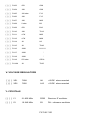
RAMSEY FX-series Programming Worksheet
To convert N from decimal to binary, simply TRY to subtract EACH of the 16
binary values from N, always in descending order, always starting with
32768 and always ending with 1. This process will always yield 16 YES or
NO answers, which will give you exact diode installation instructions.
N = Freq in KHz divided by 5 KHz (or, Freq in MHz divided by .005)
FX 146 • 30
Let's try doing an example. We want to receive 146.520 MHz:
Subtracting from N:
Remainders & Doodles
NO
YES
Position
Can you subtract 32768?
32768
Can you subtract 16384?
16384
Can you subtract 8192?
8192
Can you subtract 4096?
4096
Can you subtract 2048?
2048
Can you subtract 1024?
1024
Can you subtract 512?
512
Can you subtract 256?
256
Can you subtract 128?
128
Can you subtract 64?
64
Can you subtract 32?
32
Can you subtract 16?
16
Can you subtract 8?
8
Can you subtract 4?
4
Can you subtract 2?
2
Can you subtract 1?
1
Will this be a Simplex channel?
SIMP
Will Transmit be 600 KHz
LOWER than Receive?
- RPT
Will Transmit be 600 KHz
HIGHER than Receive?
+ RPT
N = 146520 ÷ 5 = 29,304 Now, convert to binary...
Install diodes in YES positions only.
See FX-series instruction book, Section H, for ham band shortcuts for 32K
through 1K programming positions. If an auxiliary split is needed or if you are
not licensed to transmit in a band portion, do not install diodes in SIMP,
FX-146
• 31
+RPT or -RPT positions.
Using Computer BASIC as a Diode Matrix Programming Aid
The purpose of the following BASIC program is to be as CLEAR AND
GENERIC as possible with no concern for programming efficiency or
sophistication. Those who enjoy and understand programming in Basic can
dress it up to suit themselves. Or, they can write a program that satisfies
their own standards. A major purpose of the deliberate simplicity is that the
routine should run on virtually any computer using any version of Basic. If
you follow the program flow, you'll see that it carries out in order the very
same steps you would follow by hand in converting decimal to binary using
the FX Programming Worksheet. You can use this same program for
calculating nonstandard Transmitter Offsets.
Program Notes:
1. Install diodes ONLY in rows where "1" is indicated.
2. If you prefer, "0's" can also be generated through the use of appropriate
IF . . . THEN . . . ELSE lines.
3. The "!" after 32768 is generated automatically by the computer, whether
you type it in or not.
4. Be VERY accurate in typing "<" and ">" or "=>" because they are critical
to correct placement of 1's.
5. The CLEAR instruction after screen printing is important; if it is omitted,
AA, BB, CC, etc., will not be reset for checking the next frequency.
6. Innovative computer programs to enhance enjoyment of the FX
transceivers are encouraged; send them to your favorite ham or computer
magazine, newsletter or BBS.
7. LPRINT or equivalent Basic statements can be used to produce
hard-copy printouts of frequency information you need.
8. IMPORTANT: Before soldering ANY diodes in your FX-transceiver
programming matrix per this program, CHECK AND VERIFY that your
program is giving CORRECT results! COMPARE it to the samples in this
book.
NOTICE:
Although this program has been tested on many Microsoft BASIC
releases, including GW Basic, it is printed here solely as a convenience
and is not integral to the Ramsey FX-146 operation. If you have trouble
running the program, please get help from a local computer friend and
not from the Ramsey factory - we're radio guys, not computer hackers!
Sample BASIC Program Listing
FX 146 • 32
50
52
55
60
101
102
103
104
105
106
107
108
109
110
111
112
113
114
115
116
200
205
206
210
215
216
220
225
226
230
235
236
240
245
246
250
255
256
260
265
266
270
275
276
280
285
286
290
295
296
300
305
306
310
315
316
320
325
PRINT “Enter Receiver Frequency as 6 digits with NO decimal!”
INPUT “For example: 146520. Enter here: “; F
N = F/5
PRINT “The FX146 or FX220 N number for binary conversion is “; N
AA = 0
BB = 0
CC = 0
DD = 0
EE = 0
FF = 0
GG = 0
HH = 0
II = 0
JJ = 0
KK = 0
LL = 0
MM = 0
NN = 0
OO = 0
PP = 0
IF N => 32768! THEN AA = 1
IF N > 32768! THEN NA = N - 32768!
IF N < 32768! THEN NA = N
IF NA => 16384 THEN BB = 1
IF NA > 16384 THEN NB = NA - 16384
IF NA < 16384 THEN NB = NA
IF NB => 8192 THEN CC = 1
IF NB > 8192 THEN NC = NB - 8192
IF NB < 8192 THEN NC = NB
IF NC => 4096 THEN DD = 1
IF NC > 4096 THEN ND = NC - 4096
IF NC < 4096 THEN ND = NC
IF ND => 2048 THEN EE = 1
IF ND > 2048 THEN NE = ND - 2048
IF ND < 2048 THEN NE = ND
IF NE => 1024 THEN FF = 1
IF NE > 1024 THEN NF = NE - 1024
IF NE < 1024 THEN NF = NE
IF NF => 512 THEN GG = 1
IF NF > 512 THEN NG = NF - 512
IF NF < 512 THEN NG = NF
IF NG => 256 THEN HH = 1
IF NG > 256 THEN NH = NG - 256
IF NG < 256 THEN NH = NG
IF NH => 128 THEN II = 1
IF NH > 128 THEN NI = NH - 128
IF NH < 128 THEN NI = NH
IF NI => 64 THEN JJ = 1
IF NI > 64 THEN NJ = NI - 64
IF NI < 64 THEN NJ = NI
IF NJ => 32 THEN KK = 1
IF NJ > 32 THEN NK = NJ - 32
IF NJ < 32 THEN NK = NJ
IF NK => 16 THEN LL =1
IF NK > 16 THEN NL = NK - 16
IF NK < 16 THEN NL = NK
IF NL => 8 THEN MM = 1
IF NL > 8 THEN NM = NL - 8
FX-146
• 33
326
330
335
336
340
345
346
347
400
405
410
415
420
425
430
435
440
445
450
455
460
465
470
475
IF NL < 8 THEN NM = NL
IF NM => 4 THEN NN = 1
IF NM > 4 THEN NX = NM - 4
IF NM < 4 THEN NX = NM
IF NX > 2 THEN OO = 1
IF NN = 2 THEN OO = 1
IF NX = 3 THEN PP = 1
IF NX = 1 THEN PP = 1
PRINT “32768 - “; AA
PRINT “16384 - ”; BB
PRINT “ 8192 - “; CC
PRINT “ 4096 - “; DD
PRINT “ 2048 - “; EE
PRINT “ 1024 - “; FF
PRINT “ 512 - “; GG
PRINT “ 256 - “; HH
PRINT “ 128 - “; II
PRINT “
64 - “; JJ
PRINT “
32 - “; KK
PRINT “
16 - “; LL
PRINT “
8 - “; MM
PRINT “
4 - “; NN
PRINT “
2 - “; OO
PRINT “
1 - “; PP
480
481
482
485
505
510
520
PRINT “The Binary Equivalent of N can also look like this: “
PRINT “_______________________________________ “
PRINT USING “##”; AA, BB, CC, DD, EE, FF, GG, HH, II, JJ, KK, LL, MM, NN, OO, PP
PRINT
CLEAR.
GOTO 50
END
Here’s an example of the screen display for the program as written, showing
the results for an entry of “146865” and ready for the next frequency to be
entered as 6 digits:
For example: 146.52 MHz. = 146520. Enter here >>> ? 146865
The FX146 or FX220 N number for binary conversion is: 29373
32768 - 0
16384 - 1
8192 - 1
4096 - 1
2048 - 0
1024 - 0
512 - 1
256 - 0
128 - 1
64 - 0
32 - 1
16 - 1
8 - 1
4 - 1
2 - 0
1 - 1
>> The Binary Equivalent of N looks like this:
———————————————————-
FX 146 • 34
0 1 1 1 0 0 1 0 1 0 1 1 1 1 0 1
>>> Enter Next Frequency for Programming:
Enter Receiver Frequency as 6 digits with NO decimal!
For example: 146.52 MHz. = 146520. Enter here >>> ?
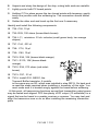
HOW TO ACTIVATE AN AUXILIARY OFFSET:
1. Install NO diode in SIMP, -RPT or +RPT for the channel that gets a nonstandard offset.
2. Program the AUX matrix row for the desired offset, following our
published instructions.
3. Connect the channel row to the AUX matrix row by installing a diode as
shown below. The cathode end is soldered to the diode programming
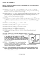
bridge. In this example, Channel 3 uses the auxiliary offset:
4. You can connect as many of the channel rows as you wish in this
manner, but remember that each would follow the same non-standard
split you have programmed. Only one such split can be programmed in
the AUX matrix row. It may be changed as needed. If more than one
non-standard split is needed, you can either give up a standard split or
devise your own way of switching in what you need.
1
DIODE JUMPER FOR CHANNEL 3
PER MARKINGS ON PC BOARD
2
3
4
5
6
7
8
9
10 11 12
SIMP
-RPT
+RPT
32 K
16 K
FRONT EDGE OF PC BOARD
+TX (+RPT) OFFSETS
+TX offsets are programmed exactly like the Frequency Programming
matrix. For example, for a +600 KHz offset:
N= 600 KHz ÷ 5 KHz = 120
FX-146
• 35
PROGRAMMING THE 'MINUS' OFFSETS
We showed the Plus offsets first to prepare you for the Minus offsets. The
offsets are entered into the FX synthesizer through the binary adders, U710. Notice that we said adders and not subtractors; in binary there is 'no
such animal' as a subtractor. We must use the technique known as 'two's
complement addition' which actually performs a subtraction process! This
may sound complicated, but it really isn't. We simply find 'N' as usual, take
its 'two's complement' and program the result into the offset matrix. We'll
show you three detailed examples.
Don't be alarmed. If all you need is the standard 2 Meter band offsets, just
install the diodes in the offset matrix as clearly illustrated on your PC board.
Understanding the following information is essential ONLY for those who
need to program non-standard Minus or AUX offsets.
First we need to understand some rules for binary addition:
1) 0+0=0
2) 1+0=1
3) 1+1=0 and CARRY 1
(Carrying is done from right to left)
EXAMPLE 1: -600 KHz TX Offset
As for the +600 KHz offset, N= 600 ÷ 5 KHz = 120. However, this is the last
of Decimal numbers in this work. We'll have to work with Binary numbers
now. In brief, we set up the complement, or exact inverse of N in binary, and
then add 1. This will give us our two's complement that is needed for
programming into our offset matrix.
Binary code for N=120
8192 4096 2048 1024
0
0
0
0
512
256
128
64
32
16
8
0
0
0
1
1
1
1
Now, just INVERT all of the above 'bits':
1
1
1
1
1
1
1
0
0
0
0
1
1
1
1
1
0
0
0
1
Then, ADD 1:
1
1
This is our two's complement value which we program into our offset matrix.
You'll see these diodes in the position for -600 KHz TX offset.
Even though it appears that we are adding a huge N number to the original
transmitter frequency, the binary adders will follow the rules of binary
addition and provide the proper programming information to the PLL
synthesizer.
FX 146 • 36
EXAMPLE 2: RECEIVER OSCILLATOR FREQUENCY
We know from previous circuit discussion that the PLL synthesizer must run
21.4 MHz lower when in receive mode. Two things must be done to do this;
first, we switch out varactor diode D3 to allow the VCO L-C circuitry to tune
21.4 MHz lower, and secondly, program in a 'minus' 21.4 MHz offset to the
synthesizer. This offset is permanently programmed into the matrix because
the 21.4 MHz 1st IF is integral to the FX receiver design. Look closely at the
Receive offset diode row and see why the diodes are installed the way they
are.
N = 21400 ÷ 5 KHz = 4,280
Binary code for N=4,280
8192 4096 2048 1024
0
1
0
0
512
256
128
64
32
16
8
0
0
1
0
1
1
1
Now, invert all the bits:
1
0
1
1
1
1
0
1
0
0
0
0
1
1
1
1
0
1
0
0
1
Add 1:
1
You'll see this is the number programmed into the Receive offset matrix line
for a minus 21.4 MHz offset.
EXAMPLE 3. TWO'S COMPLEMENT WITH CARRY
For illustration purposes, we'll pick an odd-ball offset such as 640 KHz. In
this case, N = 640 ÷ 5 KHz = 128.
8192 4096 2048 1024
0
0
0
0
512
256
128
64
32
16
8
0
0
1
0
0
0
0
Invert all bits:
1
1
1
1
1
1
0
1
1
1
Add 1:
+
1
Sum at '8' bit position, carry 1
1
0
1
0
0
1
0
0
0
Sum at '16' bit position, carry 1
Sum at '32' bit position, carry 1
1
Sum at '64' bit position, carry 1
1
0
0
0
0
Sum at '128', no carry needed
1
0
0
0
0
1
0
0
0
0
Final result:
1
1
Binary code for N=128
FX-146
• 37
1
1
1
1
FX-146 PROGRAMMING SUMMARY
Programming your FX-146 is really quite simple; all it takes is a clear mind, a
scratch pad and a calculator. In closing, let's find the proper N value for a
common NOAA weather channel, 162.55 MHz.
First, find N: 162550 ÷ 5 = 32,510 Then, convert to binary:
Can we subtract 32,768?
NO
Can we subtract 16,384?
YES
32,510 - 16,384 = 16,126
Can we subtract 8,192?
YES
16,126 - 8,192 = 7,934
Can we subtract 4,096?
YES
7,934 - 4,096 = 3,838
Can we subtract 2,048?
YES
3,838 - 2,048 = 1,790
Can we subtract 1,024?
YES
1,790 - 1,024 = 766
Can we subtract 512?
YES
766 - 512 = 254
Can we subtract 256?
NO
Can we subtract 128?
YES
254 - 128 = 126
Can we subtract 64?
YES
126 - 64 = 62
Can we subtract 32?
YES
62 - 32 = 30
Can we subtract 16?
YES
30 - 16 = 14
Can we subtract 8?
YES
14 - 8 = 6
Can we subtract 4?
YES
6-4=2
Can we subtract 2?
YES
2-2=0
Can we subtract 1?
NO
We're done! Install diodes in all YES positions, and no diodes elsewhere.
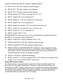
BASICS OF EXTERNALLY CONTROLLED FX-TRANSCEIVER
FREQUENCY SWITCHING
The 12 front panel switched channels, with never a need for a crystal will
cover most applications generously. Yet many of us will want to figure out
ways for easy frequency-programming of still more channels, especially if we
do a lot of cross-country travel. Rather than endorse or illustrate any
particular scheme, of which there are dozens if not hundreds, we provide
here the most basic schematic information needed to set up any kind of
auxiliary switching correctly. The principles and requirements remain the
same whether you use DIP switches, toggle or slide switches, electronic
latching or go all out to build the mother of all diode matrixes. Make sure
whatever you build resembles electrically the diagram on the page 39.
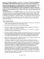
Some DO's and DON'Ts of FX-Transceiver Add-Ons:
1. DO study and understand the basic switching diagram.
2. DO let your ingenuity run wild to come up with the neatest, most costeffective scheme.
3. Please DON'T ask our technicians to talk you through your own idea.
FX 146 • 38
FX-XCVR
RIBBON CABLE 1N914/
PC BOARD
1N4148
CONNECTION
SWITCH:
SPST
1
2
4. DON'T run switching cables
across the VCO and Transmit
RF side of the PC board.
5. Please DO submit successful
frequency control ideas as
articles for your favorite ham
radio magazine. Your pay as
author may cover the cost of
your transceiver!
4
8
16
32
6. Please DO mail or fax us
your good ideas.
64
7. Please DON'T try out ANY
modifications of the basic FXTransceiver unless you already
have it WORKING fine.
128
256
512
NOTES:
1K
1. DIP switches with diodes
can be installed on/above the
diode matrix itself for E-Z
internal programing changes.
2K
4K
8K
2. Any auxiliary programming
device can be wired to a
switched position on the FXtransceiver matrix as well as to
the auxiliary points illustrated.
16 K
32 K
+ RPT
- RPT
3. "SPDT" switching may be
devised to select offsets.
SIMP
4. Programming Shortcuts are
possible for ham-band
operation. (See text).
+ 5V
GND
FX-146
• 39
FX-SERIES TRANSCEIVER GLOSSARY
The following is a deliberately INFORMAL collection of:
•
Technical terms useful to know in understanding your FX- transceiver
design.
•
Acronyms (phrases expressed by first letters of words: example: PLL
= Phased Locked Loop)
• Selected Electronics Industry "jargon"
Any of these words or expressions might be used in this instruction manual
or in conversation related to your FX- transceiver, either with other hams or
with Ramsey technicians. These descriptions or notes for a very few terms
certainly are not an "electronics dictionary," but the author/compiler hopes
that they might enhance your grasp of the concepts and language that he
has seen as useful in building and using this transceiver. For more detail,
PLEASE study the introductory part of each Assembly Stage.
ADDER = Anybody who can add can be called an "adder." If we delegate
such work to electronic devices, the most fundamental digital operation after
being in a binary high or low (on or off) state is to be able to find the sum of
such states from two or more sources. The BINARY ADDER performs this
function. See also: BINARY.
AFSK = "Audio Frequency Shift Keying." [SEE: "FSK"] In short, this is a
very popular form of data transmission.
AXIAL-LEAD = Wires stretch out from two opposite ends of a part instead of
from one end, i.e. along the "axis" of the body. For example: L20.
BA- = Manufacturer's PREFIX for PIN-type diodes.
BASIC = "Basic." We're talking about the one computer programming
procedure that should make sense to ALL computer owners. If any further
explanation is needed, visit a library or computer dealer.
BB- = Manufacturer's PREFIX for VARACTOR diodes.
BINARY = the number system based on the two values of 0 and 1. Here are
all the tables that we need to memorize:
0+0=0
0+1=1
1 + 1 = 0 and carry 1 to next
position.
BOARD = Generally refers to "PC board" or "printed circuit board."
BUFFER = An electronic circuit stage, a sort of "referee" that tells its input
and output not to mess with each other.Think about such a task! It may also
provide amplified output of the incoming signal.
CASCADE, cascading = combining two or more identical circuit elements or
components for improved effectiveness.
CARRIER = Transmitted RF signal that is NOT "modulated." It is heard as a
steady tone on BFO-equipped receivers or as a powerful silence (i.e. over
riding all background noise or hiss) on FM receivers.
FX 146 • 40
CCW = see CW below.
COR = "Carrier Operated Relay," a switching circuit activated by the
detection of a carrier signal in a receiving circuit.
"CW" = TWO common meanings in electronics: "Continuous Wave" for the
communicating of Morse code signals, or "Clockwise" to designate a point
on a variable control. "CCW" therefore means "counterclockwise."
DECIMAL = in computer or programming context, "decimal" refers to
counting by tens, our traditional way, in contrast to your computer's binary
(counting by 1's and 0's), or the hexadecimal system (counting by 16's.) See
"N" and BINARY.
DIP = "Dual Inline Package," referring to IC's and their sockets or any other
component ("DIP Switch," etc.). The "line" refers to rows of PC-board or
perfboard holes that are 0.1" apart. "Dual" means two rows. Therefore "SIP"
would mean a SINGLE row device.
DISCRIMINATOR = FM terminology for "detector." See: FM.
DUAL-MODULUS = as in dual-modulus prescaler or divider: a circuit which
divides a frequency by two different ratios depending on pin selection, for
example: 64 or 65. (See: PRE- SCALE)
FILTER-ACTIVE
FILTER-CERAMIC
FILTER-CRYSTAL
Filters are used in DC, Audio and RF
FILTER-HI-PASS
circuits. Understanding them is essential
FILTER-LOW-PASS
electronics know-how. The Radio Amateurs’
FILTER-BANDPASS
Handbook covers the subject of filters very
FILTER-PASSIVE
well.
FM ("Frequency Modulation") = Changing the transmitter frequency in exact
pace with speech or sound variations.
FREQUENCY SYNTHESIS = To "synthesize" anything is to create an
imitation or simulation from something else. The "basic" ways for generating
useful RF frequencies are a crystal oscillator or the L-C oscillator where the
frequency is determined by coil (L) and capacitor (C). However we can
process the output of an L-C oscillator through digital circuitry to simulate
many different, precise crystal-like frequencies, using only one crystal as a
reference standard. See also PLL, PHASE DETECTOR, VCO.
FSK = "Frequency Shift Keying." TRUE FSK actually moves the RF
frequency (transmitted and received) from one pre-determined point to
another, in contrast to "AFSK" (Audio Frequency Shift Keying") where the
transmitted signal remains steady and all shifting is done by audio tones.
GROUND-PLANE = ALL sections of a PC-board which are mechanically or
electrically connected to DC and RF ground. In the Ramsey FX design,
almost ALL of the top or upper side (component side) of the board is a
groundplane. The term is also used in antenna design: if your 2M or 1.25M
antenna has a vertical radiating element, plus four (or more) horizontal
FX-146
• 41
elements connected to RF ground, the horizontal elements are called a
"groundplane."
HIGH = In solid-state circuitry, to say a given device pin or circuit point is at a
"logic high" is to say that it shows a + DC supply voltage at that point.
Switching to the opposite state (LOW) or back again for some specific
purpose is a fundamental capability of the circuit.
HOUSE-NUMBER = A manufacturer's part number different from the
industry-standard description of a part. Example: LB3303HK (L1)
HYSTERESIS = the ability of an FM squelch circuit to remain open after
being broken by a weak signal which fluctuates further.
INPUT, INVERTING = see "Op Amp"
INPUT, NON-INVERTING = see "Op Amp"
I/O = acronym meaning "Input and Output" port or connection.
JUMPER = Short, plain wire, soldered to interconnect points in a circuit not
otherwise connected by board traces or other wiring.
KEY, "to key" = to turn on a transmitter's carrier signal momentarily, whether
by a telegraphy code key (the root of this very common radio jargon) or by a
push-to-talk switch.
L-C = A tuned circuit made of inductor (L) and capacitor (C).
LIMITER = The portion of an FM receiver circuit which chops off noise and
AM (amplitude modulation). It processes the IF signal so that only FM will be
detected.
LOCAL OSCILLATOR (LO) = An oscillator in a superhet receiver whose
output is mixed with another signal such as antenna input. See SUPERHET.
LOCK = The condition in a phased-locked-loop (PLL) in which all sections
are working together as intended and designed.
LOOP-FILTER = (See PLL). The output of a PLL phase detector is in the
form of pulses. The frequency of those pulses depends on the reference
frequency. The loop filter smooths out these pulses into a clean DC control
voltage for the VCO. (See: VCO)
LOW = A logic level at or near zero volts. (See HIGH).
MATRIX = A methodical criss-crossing of many connections.
MC- = Prefix for parts made by Motorola, Inc.
MIXER = A circuit section which gets two or more inputs and delivers a
single output. The output is equal to the sum of the input frequencies and
also to the difference between them.
MODULATION = See also: CW, FM. "Modulation" is simply the process of
imposing variations on a steady RF signal from an audio source such as
voice, music or data (see: AFSK).
MUTE = to turn off, to render silent. (See also SQUELCH)
N = can be any number to solve in a classroom problem, but "N" is THE
FX 146 • 42
magic number (decimal) to understand in FX binary frequency programming.
N = the frequency in KHz divided by 5 KHz.
NBFM = "Narrow-Band FM." NE- = prefix to transistors or IC's made by
Signetics, Inc.
OFFSET = The distance in KHz or MHz of the transmitted signal from the
primary or received signal. The "TX Offset" may be higher or lower,
depending on the repeater setup or other application.
OP-AMP = "Operational Amplifier," a high performance linear amplifier with
an Inverting input, a Non-inverting Input and one Output.
ORIENT, orientation = Yes, the Orient is Marco Polo's Far East where they
build many FM radios and where we buy many common parts. When we
ask you to "orient" a kit part one way or the other, we're just asking you to
get it RIGHT -- per all the "orientation" illustrations that we provide.
PACKET = Rapid transmission of intelligible computer generated data in
groups or bursts of a fixed length called "packets."
PHASE DETECTOR = In a frequency synthesizer, the phase detector
compares the signal from a reference oscillator to the signal from a
programmable counter and sends a corrected control voltage to the L-C
section of a VCO. Thus, it can be considered a phase "corrector." See also:
VCO, PLL, VARACTOR.
PLATED-THROUGH = Refers to a style of PC board manufacturing in which
traces on both sides of the board are interconnected by a coating of solder
around the inside of each hole.
POLARITY = Refers to the "+" and "-" sides of batteries, power supplies,
power cables, electrolytic capacitors, etc.
PLL = "Phase-Locked Loop," a frequency generator circuit in which an
oscillator output is analyzed by counters and a phase detector which
controls and corrects the voltage supplied to varactor diode(s) which
determine oscillator frequency.
POT = jargon for "potentiometer", a variable resistor, either a panel control
or a "mini" device on a PC-board.
PRESCALE, Prescaler = a circuit or device which divides an incoming
frequency down to a lower frequency so that it can be handled more easily
by later digital counting circuitry or devices.
PTT = "push to talk", referring to all switches and circuitry involved in turning
a transmitter on and off from a switch usually built into a microphone. This
switch may also be a relay or transistor in a packet TNC, etc.
PUFF = No, not the magic dragon. It's an easier way to say "picofarads" in
the Ramsey warehouse and other high tech temples.
QUADRATURE = Refers to the Phase Angle (90 degrees) considered by
the FM discriminator or detector.
REFERENCE FREQUENCY = a precise, known frequency, usually crystalFX-146
• 43
controlled, compared with another frequency, as is done in a PLL circuit.
See PHASE DETECTOR, PLL.
RSSI = "Received Signal Strength Indicator," a function of the MC13135 IC
and comparable circuits which permits MEASURING of the relative strength
of a received signal. A few microamps of variation can be interpreted as DB
(decibels) of signal strength.
RX = Abbreviation for receive, receiver, receiving. [See: TX]
SPEAKER-MIKE = speaker and microphone functions contained in the
same physical housing, as in the design of simple home intercoms. For ham
operators, this means that both speaker and microphone are in a
microphone casing with separate plugs from a common cord. Since such
accessories can use ANY style of plug for either mic or speaker function,
Ramsey Electronics has adopted the popular ICOM-compatible standard for
the FX transceivers.
SHIELD = The outer braid of audio or RF coaxial cable, or the aluminum
case enclosing a coil or transformer.The metal case of a transceiver also
performs an important RF shielding function.The shield blocks or protects a
coil from the effect of nearby objects that would change its inductance. The
shielding on cable prevents the inner wire from radiating (RF) or from picking
up stray radiation such as AC hum.
SQUELCH = means literally, to subdue utterly or crushingly! In radio
communication, usually VHF and UHF, squelch is the circuitry needed to
subdue (mute) the background noise until a detected signal "breaks" the
squelch.
SUPERHET = A receiver design that converts the incoming desired
frequency to a lower Intermediate Frequency (IF) where most of the gain
and bandpass characteristics reside.
TOROID = A style of making coils or inductors where the insulated wire is
threaded ("wound") around a metallic form shaped like a doughnut. This
style of coil making generally eliminates any need for additional shielding
which may be needed to make the coil's inductance immune to the presence
of other nearby components or objects with metallic content.
TRIMMER = either a capacitor or resistor, miniature and variable, intended
to permit exact, final adjustment of circuit values.
TX = Abbreviation for transmit, transmitter, transmitting.
T-R = Abbreviation for "Transmit-Receive Switching", which can be
accomplished by manual switches, relays or solid-state devices such as the
PIN diodes used in the FX transceivers.
UNLOCK, unlocked = refers to the condition in a PLL (phased locked loop)
where one or more elements of the loop become defective or incorrect,
preventing the phase detector from supplying the correct control voltage to
the oscillator for the intended frequency of operation.
VARACTOR = a diode whose capacitance can be varied in step by the
FX 146 • 44
amount of DC voltage applied to it. The higher the voltage, the lower the
capacitance. See also VCO.
VCO = "Voltage Controlled Oscillator," an oscillator whose frequency is
varied by DC voltage applied to varactor diodes, which change capacitance
in step with the voltage level.
ZENER DIODE = a diode designed to have a very specific reverse
breakdown voltage. This property makes the Zener diode ideal for simple
voltage regulators or precise voltage drop elements.
FX-146
• 45
FX- TROUBLESHOOTING GUIDE
The FX- transceiver is designed to W-O-R-K with a minimum of adjustment
or alignment. By imprinting the location and correct orientation of each
component on the PC-board itself in addition to publishing detailed assembly
steps, we have virtually guaranteed the successful operation of your
transceiver from the moment you turn on the switch.
A detailed guide to servicing a transceiver requiring so few internal
adjustments is virtually pointless to compile. (It would be like writing a
troubleshooting guide to a jigsaw puzzle: "Make sure all puzzle parts are in
the right place, and it will be a nice, complete puzzle. That's it!")
The best assurance of trouble-free operation is to build, understand and test
your transceiver in the stage-by-stage sequence presented in this book. If
you chose to install all parts first and then test, and then encountered
difficulty, we recommend that you compare your assembly work to the stageby-stage steps: USE the double-check spaces.
We simply MUST accept that any malfunction is caused by:
• incorrect part selection
• incorrect part orientation (diode or capacitor polarity, transistors,
IC's etc.)
• soldering error (missing connection, solder bridge)
• omitted part
• part damaged during assembly
• part defective in manufacturing (extremely rare)
• part damaged by incorrect installation of other part(s)
• part breakdown after extended operation
• defective external device or cable connected to the transceiver
circuit board.
The above possibilities may seem vague, but they cover what can go wrong
in any multi-stage electronic device. For this reason, it is important for you to
LEARN the FX circuit design in as much detail as possible, which is why
both the schematic and assembly instructions are presented stage by stage.
Troubleshooting is a process that considers EVERYTHING possible,
ESPECIALLY including every external device connected to the unit:
• power supply
• ALL cables and connectors
• microphone, speaker
• antenna AND
• ALL cables and connectors!
If you are at all hazy about the binary programming of the "N" number,
FX 146 • 46
despite the detail of our explanations, be sure you set one channel up for
146.52 MHz Simplex before you pursue troubleshooting. It is very important
to have a clear understanding of how to program the frequency synthesizer
and offset matrixes of your transceiver.
It's fairly easy to double-check "obvious" details such as IC orientation, diode
polarity, electrolytic capacitor polarity, and those other construction
essentials that we stress repeatedly. SOME of the more subtle assembly
errors which take very careful checking to find include the following:
Any use of 2N3904 where VHF 2SC2498 is required
Use of NPN where PNP is required: Q12,Q13,Q14
Mistaken use of .01 or .001 disc capacitors where a small picofarad
value is specified.
Major error in selecting resistors with similar color codes, like 100 ohm
(brown-black-brown) used for 100K (brown-black-yellow), or vice-versa.
Reversal of the 8V and 5V voltage regulators
L16, L14 or L13 touching the top groundplane.
A single IC pin or IC socket pin bent under the plastic body of the device.
Simple operational tests are discussed at the end of most of the assembly
stages. Use these as a guide for tracing the circuit. If you make the effort to
understand each of the small sections of the big picture, you should have no
trouble in identifying the source of your problem.
If tracing and repairing complex circuits is new to you, we urge you to retrace
your assembly steps thoroughly. Take the extra time to really understand
circuit functions that might have been hazy during the excitement of
construction. Use basic LOGIC to narrow down the problem to a specific
stage.
If you ask a more experienced ham friend to look at your unit, it is up to you
to be able to recognize whether this person has the know-how and proper
equipment and tools to be of real help to you. Most hams really WANT to be
helpful, but good intentions are no substitute for competence. (If your friend
drags out the trusty soldering gun and big, rusty alligator clips, suggest a
fishing trip or antenna-fixing party instead!)
The best favor any friend can do for your kit project is to review the
correctness of part choices.
Factory Service is, of course, available at prevailing shop rates. The hams at
Ramsey enjoy providing kits to hams and hobbyists in addition to our Test
and Measurement Division work, and we're sure that you understand that
our company is not a ham club, and that our professional technicians aren't
FX-146
• 47
NOTE ON REPLACEMENT PARTS:
If you lose or damage parts during assembly or testing, you may, of course,
order any needed replacement parts by writing or faxing the Ramsey
Electronics, Inc. factory. Some of the more common parts may also be
picked up at Radio Shack or other local parts distributors. Use EXACT
values when replacing parts. Following is a GENERAL guide to obtaining
parts for your transceiver as quickly as possible:
A Radio Shack or local electronic parts distributor:
Resistors, electrolytic capacitors, disc capacitors, common NPN or
PNP transistors, Zener diodes, switching diodes, voltage regulator
(5V), hookup wire, LED, controls, antenna connector, replacement
1-amp fuses.
B Order from RAMSEY ELECTRONICS:
Most RF and VHF transistors, coils, crystals, PIN diodes, varactor
diodes, trimmers, filters and most IC chips.
C U1 and U6 are Motorola devices
These parts might be in stock at service shops featuring Motorola
equipment. There are acceptable "standard replacements" for some
of the semiconductors used in the transceiver. "SK" and "ECG"
standard replacements are stocked by local electronics parts
distributors or may be ordered through a Radio Shack store. The
following chart should help you make the most cost-effective choice
if replacement semiconductors are needed:
Part ID
Type
Recommended source
RE=Ramsey,
RS=Radio Shack
Q1, etc.
2N3904
RS 276-1617
Q12,13,14
PNP 228256
RS276-1604 or 2N3906
Q2, etc.
2SC2498
ECG10, SK9139, 2N5179, or RE
Q3
NE02137
MRF901 or RE
Q9
2N3866
ECG311, SK3195 or RE
Q8
SD1127
MRF237, ECG341, SK9617 or RE
Signal diodes
1N4148
1N914, RS276-1620 (pack of 50)
D3,D23
BB405
RE
D2,D7
BA482
ECG553 or RE
D6
BA389
RE
D18
1N4002
RS276-1102, 1N4003
FX 146 • 48
D11,D12
6.2 V Zener
RS276-561
VR1
7808
ECG964, SK3630 or RE
VR2
7805
RS276-1770
U1
MC13135
RE or Motorola
U2
LM380
ECG740A, SK3328 or RE
U3
MC12017
RE or Motorola
U4
LM324
RS276-1711
U5
LM358
ECG928, SK3691 or RE
U6
MC145152
RE or Motorola
FX-146 MASTER COMPONENT INDEX
The following pages were prepared to serve these purposes:
1. A general cross-reference for circuit study and servicing;
2.
Additional help for parts sorting and identification;
3. An accommodation for experienced builders who prefer to work out their
own assembly sequences. (If you have ANY questions or doubt about a
part, refer to the specified assembly steps and the schematic diagram.)
Key to Component Index format:
A. Part designator number (e.g., C1, Q12, Y2, etc.)
B. Experienced builders always double-check!
C. Part value or manufacturer identification
D. Assembly step number (which also identifies general circuit stage per the
schematic.)
E. Component function note (or space for your own note.)
Key to assembly step letter-number codes:
The letter code indicates the circuit stage(s) in the step-by-step assembly
instructions. The numeral designates the specific step. If you have any
question whatsoever about a particular part, please consult its assembly step.
A:
DC Power input
B:
Receiver audio amplifier
CR: Receiver FM detector and squelch
DR: Antenna input, T-R switching, filters, RF preamplifiers
EF: VCO (Voltage Controlled Oscillator)
FX-146
• 49
G:
H:
M:
TC:
TX:
PART
PLL Frequency Synthesizer
Diode Matrix, Frequency Programming
Microphone Amplifier and PTT
Transmit Coil and RF Choke Preparation
Transmit Buffer, Driver and RF Final
VALUE or ID
STEP
[ ] [ ]
C1
.001
A16
[ ] [ ]
C2
.001
A13
[ ] [ ]
C3
.001
A14
[ ] [ ]
C4
.001
A15
[ ] [ ]
C5
.01
CR9
[ ] [ ]
C6
.1
CR15
[ ] [ ]
C7
4.7 or 10 uF
CR16
[ ] [ ]
C8
.1
CR11
[ ] [ ]
C9
4.7 or 10 uF
CR10
[ ] [ ]
C10
.001
CR19
[ ] [ ]
C11
.1
CR17
[ ] [ ]
C12
47 pF
CR21
[ ] [ ]
C13
.1
CR12
[ ] [ ]
C14
27 pF
CR13
[ ] [ ]
C15
120 pF
CR20
[ ] [ ]
C16
.01 uF
CR8
[ ] [ ]
C17
100 pF
DR28
[ ] [ ]
C19
56 pF
TX38
[ ] [ ]
C20
100 pF
DR16
[ ] [ ]
C21
10 pF
F8
[ ] [ ]
C22
100 pF
DR24
[ ] [ ]
C23
.001
M5
FX 146 • 50
NOTE:
[ ] [ ]
C24
.001
M16
[ ] [ ]
C25
100 pF
DR6
[ ] [ ]
C26
.01
CR14
[ ] [ ]
C27
8.2 pf
DR8
[ ] [ ]
C28
47 pf
DR19
[ ] [ ]
C29
330 uF electrolytic
B7
[ ] [ ]
C30
47 pf
DR17
[ ] [ ]
C31
47 pf
DR22
[ ] [ ]
C32
100 pf
F13
[ ] [ ]
C33
.01
B4
[ ] [ ]
C34
470 uF
B6
[ ] [ ]
C35
100 pf
F18
[ ] [ ]
C36
.01
E12
[ ] [ ]
C37
.01
B8
[ ] [ ]
C38
.001
F11
[ ] [ ]
C39
.001
E14
[ ] [ ]
C40
47 uF elec.
E13a
[ ] [ ]
C41
.1
B5
[ ] [ ]
C42
1500 uf elec.
A5
[ ] [ ]
C43
.001
E2
[ ] [ ]
C44
.001
TX8
[ ] [ ]
C45
100 pf
F1
[ ] [ ]
C46
100 pf
F9
[ ] [ ]
C47
100 pf
DR4
[ ] [ ]
C48
4.7 or 10 uf
B2
[ ] [ ]
C49
100 pf
F1
[ ] [ ]
C50
100 pf
F10
[ ] [ ]
C51
22 pf
[ ] [ ]
C52
.001
FX-146
• E4
51
F3
Couples VCO output to U1
VCO +DC filter with Q4
DC input filtering
RF coupling: antenna to RX
[ ] [ ]
C53
.01
D10
[ ] [ ]
C54
56 pf
E3
[ ] [ ]
C55
.01
TX30
[ ] [ ]
C56
10 pf
TX5
[ ] [ ]
C57
.001
F12
[ ] [ ]
C58
.1 uf
TX26
[ ] [ ]
C59
.001
TX27
[ ] [ ]
C60
220 uf elec.
TX25
[ ] [ ]
C61
.001
TX17
[ ] [ ]
C62
.001
M37
[ ] [ ]
C63
.01
TX43
[ ] [ ]
C64
.001
TX33
[ ] [ ]
C65
.1 uf
A17
[ ] [ ]
C66
3.9 pf
TX18
[ ] [ ]
C67
2.2 uf elec.
G11
[ ] [ ]
C68
.01
G23
[ ] [ ]
C69
.01
G22
[ ] [ ]
C70
2.2 uf elec.
G10
PLL loop filter network
[ ] [ ]
C71
39 pf
TX37
Low pass filter board
[ ] [ ]
C72
39 pf
TX39
Low pass filter board
[ ] [ ]
C73
18 pf
TX29
[ ] [ ]
C74
35 pf trimmer
TX31
TX driver output tuning
[ ] [ ]
C75
100 pf SMT chip
TX3
See base of Q8
[ ] [ ]
C76
15 pf
TX9
[ ] [ ]
C77
.001
M4
[ ] [ ]
C78
22 pf
TX20
[ ] [ ]
C79
3.9 pf
TX19
[ ] [ ]
C80
39 pf
FX 146 • 52
[ ] [ ]
C81
35 pf trimmer
G7
Low pass filter board
PLL loop filter network
G5
PLL ref freq adjust (see Y2)
[ ] [ ]
C82
10 pf
TX10
[ ] [ ]
C83
.001
M2
[ ] [ ]
C84
35 pf trimmer
TX32
TX final output tuning
[ ] [ ]
C85
.1 uf
G38
PLL loop filter
[ ] [ ]
C86
.001
M1
[ ] [ ]
C87
39 pf
G4
[ ] [ ]
C88
.001
M3
[ ] [ ]
C89
.001
M15
[ ] [ ]
C90
2.2 uf elec.
G13
[ ] [ ]
C91
.01
G24
[ ] [ ]
C92
2.2 uf elec.
G14
[ ] [ ]
C93
4.7 or 10 uf elec.
M14
[ ] [ ]
C94
3.9pf
F19
[ ] [ ]
C95
4.7 or 10 uf elec.
A6
[ ] [ ]
C96
4.7 or 10 uf elec.
G12
[ ] [ ]
C97
.01
TX14
[ ] [ ]
C98
.01
G25
[ ] [ ]
C99
.01
E17
[ ] [ ]
C100
4.7 or 10 uf elec.
A11
[ ] [ ]
C101
4.7 or 10 uf elec.
CR24
[ ] [ ]
C104
8.2 pf
DR23
PLL loop filter
PLL loop filter
D: DIODES (All Types)
[ ] [ ]
D1
1N914 or 1N4148
E15
Shunts D3 with C39 in receive
[ ] [ ]
D2
BA482 PIN
M34a
Grounds RX RF input in transmit
[ ] [ ]
D3
BB505 varactor
E11
VCO L-C circuit with D23
[ ] [ ]
D4
1N914 or 1N4148
DR9
Turns on D6 during receive
[ ] [ ]
D5
1N914 or 1N4148
M38
Switches in R31 at high VCO freq
[ ] [ ]
D6
BA479 PIN
DR1
See T-R switch theory
FX-146
• 53
[ ] [ ] D7
BA482 PIN
M34b
See T-R switch theory
[ ] [ ] D8
1N914 or 1N4148
G34
works with D10,C85: see PLL theory
[ ] [ ] D9
1N914 or 1N4148
A18
[ ] [ ] D10
1N914 or 1N4148
G35
see D8
[ ] [ ] D11
1N914 or 1N4148
M31
assures positive switching by U4D
[ ] [ ] D12
1N914 or 1N4148
M32
"
[ ] [ ] D13
1N914 or 1N4148
H8a
disables -RPT during receive
[ ] [ ] D14
1N914 or 1N4148
H8b
turns on Q15 during receive
[ ] [ ] D15
1N914 or 1N4148
H7
disables +RPT during receive
[ ] [ ] D16
1N914 or 1N4148
H9
turns off offsets during Simplex
[ ] [ ] D17
LED
M42
transmit indicator
[ ] [ ] D18
1N4002
A7
[ ] [ ] D19
1N914 or 1N4148
H6
[ ] [ ] D20
6.2 volt Zener diode
CR32
[ ] [ ] D21
not used
[ ] [ ] D22
1N914 or 1N4148
M36
[ ] [ ] D23
BB505 varactor
E10
[ ] [ ] D24
1N914 or 1N4148
G36
[ ] [ ] D26
1N914 or 1N4148
TX36
[ ] [ ] D25-DX
1N914 or 1N4148
Stage H
"
"
U4C
disables AUX offset for receive
VCO L-C tuning
Synthesizer Programming
FL: FILTERS
[ ] [ ] FL1
21.4 MHz. crystal
CR30
Receiver 1st IF
[ ] [ ] FL2
455 KHz. ceramic
CR18
Receiver 2nd IF
J: JACKS
[ ] [ ] J1
5-pin DIN
A12
Packet I/O
[ ] [ ] J2
miniature 3.5mm.
B15
Speaker connection
[ ] [ ] J3
SO-239
TX45
Antenna
[ ] [ ] J4
subminiature 2.5mm.
M43
Microphone
FX 146 • 54
L: INDUCTORS (Coils, Transformers, Chokes):
[ ] [ ] L1
455 KHz
LB53303HK
CR23
FM quadrature adjust
[ ] [ ] L2
.015 uH
DR20
Q2 input bandpass filter
[ ] [ ] L3
not used
[ ] [ ] L4
not used
[ ] [ ] L5
.015 uH
DR18
[ ] [ ] L6
.015 uH
DR21
[ ] [ ] L7
variable coil
E1
[ ] [ ] L8
2.2 uH
TX34
[ ] [ ] L9
VK200 RF choke
TX49
Install AFTER alignment!
[ ] [ ] L10
.04 uH
TX47
Install AFTER alignment!
[ ] [ ] L11
.33 uH, mini
TX7
[ ] [ ] L12
2.5 T
TX40
[ ] [ ] L13
1.5T, 5/16" dia.
TX28
[ ] [ ] L14
.015 uH
TX24
[ ] [ ] L15
2.5T, 5/16" dia.
TX21
[ ] [ ] L16
2.5T, 5/16" dia.
TX16
[ ] [ ] L17
2.2 uH
DR2
[ ] [ ] L18
.33 uH axial
TX22
[ ] [ ] L19
VK200 RF choke
TX15
See stage "TC" for winding
[ ] [ ] L20
500 uH choke
A4
Ignition hash filter
[ ] [ ] L21
.33 uH mini
F17
[ ] [ ] L22
2.5T
TX41
[ ] [ ] T1
6T/2T toroid
CR34
VCO tank circuit with D3,D23
VCO injection to U1
Q: TRANSISTORS (All Types):
[ ] [ ] Q2
2SC2498 NPN RF
DR27
Receiver RF preamp #2
[ ] [ ] Q3
NE021 NPN RF
DR12
Receiver RF preamp #1
[ ] [ ] Q4
2N3904 NPN
E19
VCO DC input filter
FX-146
• 55
[ ] [ ] Q5
2SC2498 NPN RF
F8
VCO common base buffer
[ ] [ ] Q6
2N3904 NPN
B9
Carrier detect switch
[ ] [ ] Q7
2SC2498 NPN RF
E9
VCO
[ ] [ ] Q8
SD1127 or MRF237
TX2
Transmit final amplifier
[ ] [ ] Q9
2N3866 NPN RF
TX1
Transmit driver
[ ] [ ] Q10
NE021
TX14
Transmit buffer
[ ] [ ] Q11
2N3904
M18
Grounds mic amp in receive
[ ] [ ] Q12
PNP 2N3906
(228256)
M20
PTT switching
[ ] [ ] Q13
PNP 2N3906
(228256)
M21
+8R PTT output
[ ] [ ] Q14
PNP 2N3906
(228256)
M22
+8T PTT output
[ ] [ ] Q15
2N3904
H10
Offset matrix switching
[ ] [ ] Q16
2SC2498
F15
VCO buffer
[ ] [ ] Q17
2N3904
CR33
Voltage regulator
R: RESISTORS (Fixed, Trimmers, and Panel-Mounted)
[ ] [ ] R1
220K
CR29
[ ] [ ] R2
1K
CR27
[ ] [ ] R4
68K
CR4
[ ] [ ] R5
10K
CR3
[ ] [ ] R6
3.3K
CR25
Sets hysteresis for U1
[ ] [ ] R7
100K pot w/switch
A2,B12
Volume
[ ] [ ] R8
47 ohm
CR26
[ ] [ ] R9
270
CR6
[ ] [ ] R10
470
DR26
[ ] [ ] R11
47K
CR2
[ ] [ ] R12
100
DR15
[ ] [ ] R13
100K pot
CR31
[ ] [ ] R14
47K
DR25
[ ] [ ] R15
1K
E16
Squelch control
FX 146 • 56
[ ] [ ] R16
47K
DR13
[ ] [ ] R17
470 ohm
DR14
[ ] [ ] R18
270 ohm
E7
[ ] [ ] R19
10K
E13b
[ ] [ ] R20
270
F5
[ ] [ ] R21
470
M33
[ ] [ ] R22
10K
E6
[ ] [ ] R23
100 ohm
F6
[ ] [ ] R24
10K
CR5
[ ] [ ] R25
47K
E18
[ ] [ ] R26
51 ohm
F3
[ ] [ ] R27
47K
F4
[ ] [ ] R28
470 ohm
DR5
[ ] [ ] R29
100 ohm
TX6
[ ] [ ] R30
51 ohm
E5
[ ] [ ] R31
47K
M39
[ ] [ ] R32
82 (1/2W)
TX48
[ ] [ ] R33
47K
M40
[ ] [ ] R34
270 ohm
TX13
[ ] [ ] R35
100K
E20
[ ] [ ] R36
10K
TX11
[ ] [ ] R37
100K
M13
[ ] [ ] R38
10K
G6
[ ] [ ] R39
47K
M30
[ ] [ ] R40
100K
M26
[ ] [ ] R41
not used
[ ] [ ] R42
2.2K
A20
FX-146
• 57
[ ] [ ] R43
10K
G26
[ ] [ ] R44
22K
G20
[ ] [ ] R45
82 ohm 1/2W
TX23
[ ] [ ] R46
10K trimpot
M19
[ ] [ ] R47
10K
G31
[ ] [ ] R48
10K
G33
[ ] [ ] R49
10K
M9b
[ ] [ ] R50
10K
M9a
[ ] [ ] R51
47K
M10
[ ] [ ] R52
10K
G27
[ ] [ ] R53
22K
G21
[ ] [ ] R54
200 or 220 (1/2W)
DR3
[ ] [ ] R55
10K
G19
[ ] [ ] R56
47K
M11
[ ] [ ] R57
2.2K
M6
[ ] [ ] R58
270 ohm
M8
[ ] [ ] R59
100K
M7
[ ] [ ] R60
10K
M23
[ ] [ ] R61
2.2K
M12
[ ] [ ] R62
10K
M24
[ ] [ ] R63
470 ohm
M27
[ ] [ ] R64
470 ohm
M28
[ ] [ ] R65
1K
H4
[ ] [ ] R66
47K
E8
[ ] [ ] R67
10K
H5
[ ] [ ] R68
1K
H1
[ ] [ ] R69
1K
H2
[ ] [ ] R70
1K
M41
FX 146 • 58
[ ] [ ] R71
100K
H22-H40
U6 counter input pulldowns
[ ] [ ] R72
"
"
"
[ ] [ ] R73
"
"
"
[ ] [ ] R74
“
“
“
[ ] [ ] R77
"
"
"
[ ] [ ] R78
"
"
"
[ ] [ ] R79
"
"
"
[ ] [ ] R80
"
"
"
[ ] [ ] R81
"
"
"
[ ] [ ] R82
"
"
"
[ ] [ ] R83
"
"
"
[ ] [ ] R84
"
"
"
[ ] [ ] R85
"
"
"
[ ] [ ] R86
"
"
"
[ ] [ ] R87
"
"
"
[ ] [ ] R88
"
"
"
[ ] [ ] R89
"
"
"
[ ] [ ] R90
10K
G30
[ ] [ ] R91
100K
H11-H21
U6 counter input pulldowns
[ ] [ ] R92
"
"
"
[ ] [ ] R93
"
"
"
[ ] [ ] R94
"
"
"
[ ] [ ] R95
"
"
"
[ ] [ ] R96
"
"
"
[ ] [ ] R97
"
"
"
[ ] [ ] R98
"
"
"
[ ] [ ] R99
"
"
"
[ ] [ ] R100
100K
H11-H21
U6 counter input pulldowns
[ ] [ ] R101
"
"
"
[ ] [ ] R102
10K
G32
FX-146
• 59
[ ] [ ] R103
47K
G28
[ ] [ ] R104
10K
G29
[ ] [ ] R105
100 ohm
F16
[ ] [ ] R106
10K
F15
[ ] [ ] R107
10K
M35
[ ] [ ] R108
2 ohm
B3
[ ] [ ] R109
47K
B10
[ ] [ ] R110
10K
TX12
[ ] [ ] R111
4.7K
M25
[ ] [ ] R112
4.7K
M29
[ ] [ ] R114
1K
H3
[ ] [ ] R115
1K
TX42
[ ] [ ] R116
100K
H11-21
[ ] [ ] R117
100K
“
[ ] [ ] R118
100K
“
[ ] [ ] R119
270 ohm
CR36
[ ] [ ] R119A
1K
TX35
V: VOLTAGE REGULATORS
[ ] [ ] VR1
7808
A9
+8VDC where needed
[ ] [ ] VR2
7805
A10
+5VDC where needed
[ ] [ ] Y1
21.855 MHz
CR23
Receiver IF oscillator
[ ] [ ] Y2
10.240 MHz
G3
PLL reference oscillator
Y: CRYSTALS
FX 146 • 60
S: SWITCHES
TP: TEST POINTS
[ ] [ ] S1
on R7 (volume)
A2
DC on-off
[ ] [ ] S2
12 position
"H"
Frequency selection
[ ] [ ] TP1
F20
VCO control voltage
[ ] [ ] TP2
F20
VCO output frequency
[ ] [ ] TP3
F20
U3 prescaler output
U: INTEGRATED CIRCUITS
[ ] [ ] U1
MC13135
CR1
FM dual-conversion receiver
[ ] [ ] U2
LM380
B1
Receiver audio amplifier
[ ] [ ] U3
MC12017
F21
Dual- modulus 64/65 prescaler
[ ] [ ] U4
LM324
M17
Quad op amp: mic and PTT
[ ] [ ] U5
LM358
G9
Dual op amp: see PLL theory
[ ] [ ] U6
MC145152
G2
PLL Frequency Synthesizer
[ ] [ ] U7
74HC283
G15
4-bit high speed binary Adder
[ ] [ ] U8
74HC283
G16
"
"
[ ] [ ] U9
74HC283
G17
"
"
[ ] [ ] U10
74HC283
G18
"
"
FX-146
• 61
The RAMSEY FX Transceiver Kit WARRANTY
Please read carefully BEFORE calling or writing in about your Kit. Most problems can be
solved WITHOUT contacting the Factory!
Notice that this is not a "fine print" warranty. We want you to understand your rights and ours
too! All Ramsey kits will work if assembled properly. The very fact that your kit includes this
manual is your assurance that a team of knowledgeable people have field-tested several
"copies" of this kit straight from the Ramsey inventory. If you need help, please read through the
manual carefully: all information required to properly build and test your kit is contained within its
pages! In particular, the FX Transceiver has been documented exhaustively.
1. DEFECTIVE PARTS: It's always easiest to blame a part for a problem in your kit. Before you conclude that
a part may be bad, thoroughly check your work. Today's semiconductors and passive components have
reached incredibly high reliability levels, and it's sad to say that our human construction skills have not. Very
rarely, a sour component might slip through. All our kit parts carry the Ramsey Electronics Warranty that they
are free from defects for a full (90) days from the date of purchase. Defective parts will be replaced at our
expense. If you suspect a part to be defective, please mail it to our factory for testing and replacement.
Please send only the defective part(s), NOT the entire kit. The part(s) MUST be returned to us in suitable
condition for testing. Please be aware that testing can usually determine if the part was truely defective or
damaged by assembly or usage. Don't be afraid to tell us that you "blew it". We're all human: in most cases,
replacement parts are very reasonably priced.
2. MISSING PARTS: Ramsey Electronics project kits are packed with pride in the U.S.A. If you believe we
packed an incorrect part or omitted a part clearly indicated in your assembly manual as supplied with the
basic kit by Ramsey, please write us with information on the part you need and proof of the kit purchase.
Before assuming a part value is incorrect, check the parts list carefully to see if it is a critical value such as a
specific coil or IC, or whether a range of values is suitable (such as 100 to 500 ufd.). Often, common sense
will solve a mysterious missing part problem. If you are missing five 10K ohm resistors and find five extra 1K
resistors, a simple VOM check will likely confirm that the "1K" resistors are actually the "missing" 10K units.
("Hmmm, I guess the red band really does look orange!")
3. FACTORY REPAIR OF ASSEMBLED KITS: To qualify for Ramsey Electronics factory repair, kits MUST:
1.
NOT be assembled with acid core solder or flux.
2.
NOT be modified in any manner.
3.
BE returned in fully assembled form, not partially assembled.
4.
BE accompained by payment of the proper repair fee. No repair will be begun until we
have received the MINIMUM repair fee of $49.00, or authorization to charge it to your
credit card account.
INCLUDE a description of the problem and legible return address. Do not send a separate letter: include all
correspondence with the unit. Please do not include your own hardware such as non-Ramsey cabinets,
knobs, cables, external battery packs, and the like. Ramsey Electronics reserves the right to refuse to repair
ANY item in which we find excessive problems or damage due to construction methods. To assist customers
in such situations, Ramsey Electronics, Inc. reserves the right to solve their needs on a case-by-case basis
without creating policy or precedent.
Please understand that our technicians are not volunteers and that set-up, testing, diagnosis, repair and
paper work can easily take over two hours of paid employee time on even a simple problem. Understand
too, that aligment is part of the kit building process and is not covered by this Warranty. Of course, it
we find that a part was defective in original manufacture, there will be no charge to repair your kit (But please
realize that our technicians know the difference between a defective part and parts burned out or damaged
through improper use or assembly.)
4. REFUNDS: You are given ten (10) days to examine our products. If you are not satisfied, you may return
your unassembled kit with all parts and instructions and proof of purchase to the factory for a full refund. The
returned package should be packed securely. Insurance is recommended. Please do not cause needless
delays, read all information carefully.
RAMSEY ELECTRONICS, INC. 793 Canning Parkway, Victor, New York 14564
Telephone 716-924-4560 Fax 716-924-4555
FX 146 • 62
KIT ASSEMBLY PHASE 1:
Stage A: DC Power Regulation & Distribution
Plus Packet Data I/O Connector
Stage B: Receiver Audio Amplifier
Stage CR: Integrated Circuit FM Receiver
Stage DR: Receiver, Tuned RF Input and Preamp
Stage E-F: Transceiver VCO with Buffer Stages
Each set of Assembly Instructions is introduced by an explanation of how
that part of the circuit works and what it is for. LEARN as you build!
ALSO INCLUDED IN THIS SECTION:
Master Kit Parts List
Important Information About Kit Parts and the Printed Circuit Board.
TOOLS AND EQUIPMENT REQUIRED FOR CONSTRUCTION, PLL
SYNTHESIZER ALIGNMENT, & TRANSMITTER ADJUSTMENT
Medium-heat (25 to 50 watt) soldering pencil with clean, tinned
tip
Damp sponge to keep soldering tip clean
Thin diameter ROSIN core solder
Diagonal cutters or wire nippers
Wire strippers
Small pair of pliers
Small screwdriver
Ruler
Tweezers (to install SMT C75)
Non-metallic alignment tool
Digital Voltmeter (DVM)
50-ohm Dummy Load (5-10 watt rating)
VHF RF power output meter
ALIGNMENT: A feature of the FX design is that Synthesizer Alignment can
be accomplished by listening carefully to a transmitted signal of known
accuracy. To adjust trimmer capacitor C81 "by the numbers," use your
Ramsey Frequency Counter or a digitally accurate VHF receiver with BFO.
FX-146
• 63
FX-146 Transceiver Assembly Phase 1: Circuit stages A through E-F
FX-146 MASTER PARTS LIST
Before beginning assembly, take some time to check and organize these kit
components in such a way that you can find them easily and not lose any or
confuse them. Leave parts supplied on tape strips in the strips until you need
them. The following headings also provide logical sorting categories. Popular
methods for organizing parts include egg cartons, muffin tins, corrugated
cardboard edges, or pressing the leads into a block of styrofoam.
INTEGRATED CIRCUITS
1 MC13135 24-pin DIP FM Receiver IC (U1)
1 LM380 14-pin DIP Audio Amplifier IC (U2) [Do NOT use socket]
1 12017 8-pin DIP divide-by 64/65 Prescaler (U3)
1 LM324 14-pin DIP Quad Op-amp IC (U4)
1 LM358 8-pin DIP Dual Op-amp IC (U5)
1 MC145152 28-pin DIP PLL Synthesizer IC (U6)
4 74HC283 16-pin high speed 4-bit Binary Adder (U7,U8,U9,U10)
1 7808 8V voltage regulator [VR1]
1 7805 5V voltage regulator [VR2]
TRANSISTORS:
5 NPN transistor, type 2N3904 or equivalent (Q4,6,11,15,17)
3 PNP transistor, 2N3906-type [marked 228256] (Q12,13,14)
2 NPN VHF type NE02137 (Q3,10) [flat disc type marked '021']
4 NPN VHF type 2SC2498 or 2570 (Q2,7,5,16)(Sort these carefully
from the 5 type 2N3904 for Q1, etc.)
1 RF NPN type 2N3866 (transmit driver, Q9)
1 RF NPN type MRF237 or SD1127 (transmit final, Q8)
DIODES (Note color code descriptions CAREFULLY!):
1 LED (D17, transmit indicator)
100+ 1N914 or 1N4148 switching diode
(D1,4,5,8,9,10,11,12,13,14,15,16,19,22,24,26,plus PLL matrix)
2 Varactor diode, type BB505 (D3, D23) [orange labeled BB505]
1 PIN diode, type BA479 (D6)
2 PIN diode, type BA482 (D2, D7) [orange body, red band]
1 1N4002 rectifier diode (D18) [largest black body, gold band]
1 6.2 volt zener diode (D20) [gray body with black band]
FX 146 • 64
CRYSTALS:
1 10.240 MHz, has 2 leads (Y2, PLL reference frequency)
1 21.855 MHz, has 2 leads (Y1, receiver IF oscillator)
1 21.4 MHz crystal filter, has 3 leads (FL1, 1st IF filter)
INDUCTORS:
1 455 KHz shielded inductor, marked LB53303HK (L1)
1 Shielded variable coil, marked 8488 5-5 (L7)
4 .015 uH, 1.5 turns, .125" diameter (L2,5,6,14)
1 .04 uH, 4 turns, red color, (L10)
1 500 uH noise suppression choke, large with black shrink tubing over
the body (L20)
2 .33 uh., upright-style green molded mini-inductor: markings include 2
orange stripes (L11,L21)
1 .33 uh., axial leads, wirewound with orange-orange-silver bands (L18)
2 2.2 uh. axial leads, molded inductor, marked with two red, one gold
bands (L8,L17)
1 tinned wire to make: 1.5 turn, .375" diameter, hand-wound (L13)
4 tinned wire to make: 2.5 turn, .375" diameter, hand-wound
(L12,15,16,22)
2 small size tinned wire and cores to make: RF chokes, hand-wound on
ferrite cores (L9,L19)
SPECIALIZED COMPONENTS:
1 Ramsey FX-series main and low pass filter printed circuit boards
2 ferrite cores (for making L9,L19)
1 455 KHz ceramic filter, molded cube, 3 pins. (FL2)
1 100 pf SMT chip capacitor (C75)
INTERNAL ALIGNMENT COMPONENTS:
1 10K trimmer potentiometers, marked 103 (R46)
3 35 pf trimmer capacitors (C74,C81,C84)
FIXED-VALUE CAPACITORS (RF-critical picofarad values):
3 3.9 pf (C66,C79,C94)
2 8.2 pf (C27,104)
3 10 pf (C21,C56,C82)
1 15 pf (C76)
1 18 pf (C73)
2 22 pf (C51,C78)
1 27 pf (C14)
4 39 pf (C71,C72,C80,C87)
FX-146
• 65
4 47 pf (C12,28,30,C31)
2 56 pf (C19,54)
10 100 pf (may be marked 100 or 101)
(C17,20,22,25,32,35,45,46,47,50)
ADDITIONAL DISC CAPACITORS:
22 .001 uf (may be marked .001, 102 or 1nf)
(C1,2,3,4,10,23,24,38,39,43,44,52,57,59,61,62,64,77,83,86,88,89)
16 .01uf (may be marked .01, 103 or 10 nf)
(C5,15,16,26,33,36,37,53,55,63,68,69,91,97,98,99)
8 .1 uf (may be marked .1 or 104) (C6,8,11,13,41,58,65,85)
ELECTROLYTIC (Polarized) CAPACITORS:
4 2.2 uf electrolytic (C67,70,90,92)
8 4.7 to 10 uf electrolytic (C7,9,48,93,95,96,100,101)
1 47 uf electrolytic (C40)
1 220 uf electrolytic (C60)
1 330 uf electrolytic (C29)
1 470 uf electrolytic (C34)
1 1500 uf electrolytic (C42)
FIXED RESISTORS:
1 2 ohms [red-black-gold] (R108)
1 47 ohms [yellow-violet-black] (R8)
2 51 ohms [green-brown-black] (R26,30)
2 82 ohms, 1/2 watt, larger size, [gray-red-black] (R32,45)
4 100 ohms [brown-black-brown] (R12,23,29,105)
1 220 ohms, 1/2 watt [red-red-brown] (R54){This resistor may range
from 200 to 240 ohms.}
6 270 ohms [red-violet-brown] (R9,18,20,34,58,119)
6 470 ohms [yellow-violet-brown] (R10,17,21,28,63,64)
9 1K ohms [brown-black-red] (R2,15,65,68,69,70,114,115,119a)
3 2.2K ohms [red-red-red] (R42,57,61)
1 3.3K ohms [orange-orange-red] (R6)
2 4.7K ohms [yellow-violet-red] (R111,112)
22 10K ohms [brown-black-orange] (R5,19,22,24,
36,38,43,47,48,49,50,52,55,60,62,67,90,102,104,106,107,110)
2 22K ohms [red-red-orange] (R44,53)
13 47K ohms [yellow-violet-orange]
(R11,14,16,25,27,31,33,39,51,56,66,103,109)
1 68K ohms [blue-gray-orange] (R4)
37 100K ohms [brown-black-yellow] (R35,37,40,59,71-89,91101,116,117,118)
1 220K ohms [red-red-yellow] (R1)
FX 146 • 66
CONTROLS, HARDWARE AND MISC.:
1 volume control potentiometer with switch (may be any value from 10K
to 100K) (R7,S1)
1 10K squelch control potentiometer (R13)
1 12-position rotary switch (S2)
1 3.5 mm. Jack, miniature (J2, speaker)
1 2.5 mm. Jack, subminiature (J4, microphone)
1 5-pin female DIN PC-mount connector (J1, packet)
1 SO-239 coaxial RF connector (J3)
3 sets of: 4-40 screw and nut (to mount J3 and VR1)
1 28 pin DIP IC socket (for U6)
1 DC power cord with inline fuseholder and 1A fuse
1 1/2" panel-mount strain relief for DC power cord
1 length of No. 20 bus wire (to make diode matrix bridges)
1 length of No. 24 bus wire (to make L9 and L19)
1 hookup wire, as needed (may include 1,2, or 3 conductors)
3 wire cable ties
1 5/16"x18 bolt (to wind coils on for perfect spacing)
1 document packet, including this manual
REQUIRED, NOT SUPPLIED WITH KIT:
Thin-diameter rosin-core solder
Correct tools for all phases of assembly (see text)
Microphone and speaker per specifications in text (J2,J4 and PTT circuit
are designed for ICOM-type mike)
Fused, 13.5 VDC power supply or battery
50-ohm dummy load
50-ohm 2-meter antenna with PL259 or adapter
OPTIONAL, RECOMMENDED:
Ramsey FXC Transceiver Case and Knob Kit
Ramsey speaker mike SM-7
IMPORTANT:
For proper RF shielding and secure mounting of controls, connectors, and
the PC board, immediate consideration must be given to the transceiver
enclosure as an integral part of the assembly process. The FXC matching
case set is the quality, custom designed finishing touch for your transceiver.
FX-146
• 67
VERY IMPORTANT PC BOARD ASSEMBLY INFORMATION FOR A-L-L
OUR BUILDERS!
1. Your FX- transceiver PC board is double-clad with plated- through holes.
What this means in practice is that it is VERY important to select and
install correct part values the FIRST time around. This type of board
makes "desoldering" much more difficult and risky because the solder
adheres inside the hole and flows to the component side of the board as
well. It is VERY tricky to remove a part without damaging it. If too much
de-soldering heat or component "pulling" is used, there is also the
serious risk of damaging small PC board traces. Be careful and
methodical in assembly!!!
2. Do not, under any circumstances, install L9, R32 or L10 until instructed
to do so in Assembly Stage "TX." This applies even if you are following
your own assembly sequences. This procedure will prevent damage to
Q9 and Q8 during the initial test and alignment procedure.
3. Do not attempt to "re-engineer" our transistor orientation illustrations.
Simply point flat sides or tabs as illustrated.
4. After installing all parts, you will see a few empty holes in the circuit
traces on the top or component side of the board. These plated-through
holes are placed intentionally to connect with traces on the solder side.
The hole IS the connection! However, if these holes nag at you, simply
fill them in with a touch of solder -- AFTER verifying that all parts have
been placed and installed correctly.
5. Additional "empty" holes are marked on the PC board to allow for easy
connection of accessories or modifications as you begin to customize
your transceiver. See "GUIDE TO FX- CIRCUIT ACCESS POINTS."
6. The purpose of check boxes “ ” in the assembly steps is to make it
easy to check the accuracy of your work at the end of each step.
7. Almost all resistors are mounted in vertical (upright) position. You can
see that the wire leads for resistors come in several styles. If a resistor's
pre-trimmed lead is ever too short for upright installation, simply solder a
scrap wire nipped from another resistor to extend its length.
8. Some of the resistors and miniature inductors used in this project require
upright or vertical installation. It is important to follow the orientation
illustrated for vertically installed parts. Always put the body of the part in
the hole with the circle!
9.
Whenever you have a choice, install parts with stamped markings so
that you can still see the markings later. This will help greatly with any
possible troubleshooting needed.
10. PARTS SORTING: In a kit of this size and complexity, there is no single
best way to sort and organize the 300+ individual components used. We
FX 146 • 68
at the factory have tried to help by grouping similar or related parts in
individual sealed bags. Sorting organizers popular among kit builders
include empty egg cartons, muffin tins, small box tops, or the corrugated
edges of box cartons. Since the assembly of this kit is presented in
distinct stages, some builders may prefer to group their parts by stage
before beginning assembly.
11. HELPFUL HINT: Many of the parts are supplied on tape strips cut from
bulk reels. Leave them taped, which keeps them nicely sorted for you. It
is NOT necessary to pull the entire lengths of both leads from the tape.
Simply nip the leads right at the edge of the tape, and you'll have plenty
of length to work with.
12. The .01 disc capacitors may be marked in any of the following ways: .01,
103 or 10n (nanofarads)
13. Similarly, .001 ufd. discs may be marked: .001, 102 or 1n(nanofarads)
14. The several .1 uf units required should be clearly recognizable and
often will have a rectangular rather than disc shape. Their markings
may be .1 or 104.
15. Small Picofarad values are clearly stamped on capacitor bodies. 100 pf.
units may be marked 100 or 101.
16. We tried to make it clear in both lists and assembly steps that some
components can have a RANGE of acceptable values, even though a
single value is indicated on the schematic, the control document for this
project. A rule of thumb is that a value within 10% of the stated value will
be fine: 2 or 2.2 pf, 4.7 or 5 pf, 200 or 220 ohm and so forth. 10 uf
electrolytics may be 4.7 to 10 uf. Remember that there's a reason for the
"tolerance" codes for all parts. Unless we scream in bold print that
something must be exact down to the last micro-henry, ohm or partial
picofarad, PLEASE assume the 10% rule in sorting through your kit
parts!
17. Manufacturer stamping patterns can vary, and we sometimes need to
use simple logic and deduction to identify parts, particularly the
extremely common ones. For example: if your kit includes 3 identical
transistors with no apparent body marking at all, you may presume them
to be the 3 PNP transistors described as 2N3906, 228256 or equivalent.
18. Check your manual or kit package for any insert page advising that a
part identification or physical description has changed. We cannot
control how manufacturers may vary their product codes or colors of
plastic.
19. Observe correct POLARITY when installing all diodes and electrolytic
capacitors!
20. Please review No. 1 above!
FX-146
• 69
21. Use the extra spaces provided throughout this manual to write down the
details of any changes or revisions noted on additional sheets that may
be supplied with your kit.
22. You will be installing various wires for switches, controls and jacks very
early in the assembly procedure. This is contrary to normal building or
manufacturing practice but will permit progressive testing of completed
stages. Follow the suggestion at the end of Stage CR for tying down
these wires for protection and your convenience during further assembly
work.
23. Examine your FX- circuit board. Notice that the side with silkscreened
parts outlines is covered almost completely by tinned copper or "foil."
This is called a groundplane. This side is the Top or COMPONENT
SIDE of the board. All parts (except SMT C75) will be mounted on this
side. The other side has most of the printed circuit traces and is called
the Bottom or CIRCUIT SIDE.
ABOUT THE WIRE SUPPLIED WITH YOUR KIT:
Your kit parts include lengths of wire for making all needed connections from
the PC board to the controls and jacks. Because there is nothing critical in
the functions of these wires, the color and style of wire lengths actually
packed in your kit may vary. You may receive lengths of 2 or 3 conductor
wire (such as speaker cable or ribbon cable) or a supply of simple single
conductor hookup wire. Use the heavier gauge wire for the power supply
connections in the following steps, saving the lighter gauge wire for jacks
and controls. The bare wire is used for constructing the diode matrix for
frequency programming and for making a few coils and RF chokes. The
piece of thin, enameled "magnet" wire is to be wound on the small "toroid"
coil in Assembly Stage "CR."
"TINNING" is the process of heating the stripped end of a wire and LIGHTLY
flowing solder so that all strands are bonded together. This practice, while
not essential, generally makes for easier soldering and physically stronger
connections.BROKEN WIRES are the primary cause of malfunctions in ham
equipment and computers! Please follow our instructions in Stage CR
(PAGE 27) for securing completed cables to the PC board temporarily so
the connections will not get damaged during further assembly.
IMPORTANT NOTE REGARDING FLEXING WIRES: In Stages A, B, CR,
and M, you will install numerous wires from the PC board for panel controls
and jacks. Repeated flipping of the board during assembly can damage
these wires and also become very annoying during kit assembly. PLEASE
tie the wires down as noted on page 27, using one of the cable ties provided.
Take your time, learn about what you're doing and ENJOY your FM
Transceiver project!
FX 146 • 70
STAGE A: DC POWER INPUT REGULATION & DISTRIBUTION and
PACKET RADIO I/O CONNECTOR (J1)
The "power supply" for your FX- transceiver is, basically, any "12-volt"
battery or well designed power supply operating from 120VAC or other
source. In theory, all "12V" sources should provide pure DC voltage to your
FX- transceiver DC input. In fact, there are many variations and
imperfections in common "12VDC" sources, ranging from weak batteries,
poorly filtered AC powered supplies, vehicle ignition noise, or just badly
made power supplies.
Stage "A" of your FX- Transceiver is designed to help your radio survive
quite a wide variety of imperfections. It's not a "power supply" in itself, but it
comes close, because it performs all the essential functions expected from a
good solid-state DC source. Just add 12-15VDC from a battery, vehicle or
bench supply.
Much of the circuitry operates on the regulated 8 volts supplied by voltage
regulator VR1. If you have already looked around the schematic diagram
and also seen "+8R" or "+8T", these are points where the regulated 8V
output is switched for Receive or Transmit by the PTT (push to talk) circuitry
(Q12, U4c, U4d, Q13, Q14) which we'll discuss in more detail when it's time
to build it in Stage M.
The Receiver IC (U1) and the digital frequency synthesis circuit is powered
by +5 volts regulated by VR2. The op amps used in the circuit (U4 and U5)
operate from this single supply through the use of voltage divider networks
at the respective IC's. The full 12-15 volt input is supplied to the transmitter
RF output section and to the receiver audio amplifier (U2).
The large 1500 uf capacitor (C42) and inductor L20 are installed at the DC
input to filter out ignition noise, etc. Fuse F1 is contained in the power cord
and the DC power switch is integral to the volume control. The DC negative
(black) wire is soldered directly to the PC board ground plane.
The Packet Connector
The Packet I/O Jack (J1) is not a "stage" or section of your transceiver in
itself. It is simply a convenient "port," to use computer terminology, which
gives a packet TNC (terminal node controller) convenient access to the
microphone and receiver audio circuits. We'll install J1 and its associated
bypass capacitors at the beginning -- because now is as good a time as any,
and it gets some parts on your PC board quickly and easily! Also, having J1
in place will give a little extra protection to other parts when you are working
on the solder-side of the board.
FX-146
• 71
STAGE A: DC POWER INPUT REGULATION & DISTRIBUTION and
PACKET RADIO I/O CONNECTOR (J1)
FX 146 • 72
Stage A: ASSEMBLY STEPS
A1. Strip 1/8" of insulation from the heavier-gauge black wire, insert and
solder in the GROUND hole. This connection may be soldered on the
TOP side of the board as well as the solder side.
A2. Strip 1/8" of insulation from the in-line
fuse wire and solder it to one of the S1
switch lugs of the volume control (R7).
The switch lugs are the two outermost
lugs of the 5 lugs.
FUSE
VOLUME
IN
OUT
A3. Strip 1/8" of insulation from each end
GND
of the heaviest gauge 1 conductor wire
remaining in your kit. Solder one end to
PWR
the other switch lug on R7 and the other
end to the PWR point on the PC board. MAKE SURE that ALL strands of
this wire are neatly inserted and soldered in the hole. Any stray strand
will cause a direct short when it touches the ground plane.
A4. Install L20, the 500 uH noise filter inductor. It is the large cylinder
shaped component with wires coming from each end.
A5. Install C42, 1500 uf, the first (and largest!) of the electrolytic
capacitors. The (+) side must be oriented as imprinted on your board,
toward L20.
A6. Install C95, a 4.7 to 10 uf electrolytic.
A7. Select D18, the 1N4002, the largest of the diodes used in your kit. It
has a black body with a gold band on one end. Notice the band towards
one end designating the cathode. This diode MUST be installed with its
ANODE in the ground hole nearest the back of the PC board. Solder the
anode end now, letting the diode body stand vertically on the board.
A8b. Gently bend the cathode wire into its hole, pull it through so that it
is as short as possible with the diode standing vertically. Solder and trim
excess wire. NOTE: this is the basic method for installing all upright
parts.
A9a. Voltage Regulator VR1 (type 7808 for 8 volts) is mounted with its
metallic back flat against the ground plane, secured by the small
machine screw and nut supplied. Identify VR1 correctly without mixing it
up with its 5-volt counterpart (VR2).
A9b. Insert the 3 VR1 leads into the triangular set of holes while gently
bending the body back towards the board so that the mounting holes line
up. Secure VR1 to the board with the screw and nut. After VR1 is
mounted flat, solder and nip the 3 leads.
FX-146
• 73
A10. Study the PC board, locate the triangular set of 3 holes for VR2
(type 7805), and insert VR2 so that the flat metal tab side is toward the
center of the board. Press VR2 in as far as it will go, solder and trim.
A11. Near VR2, install C100, a 4.7 or 10 uf electrolytic, oriented for
correct polarity.
Stage A PROGRESS TEST:
The power input circuitry is completed and can be tested before proceeding.
Perform the test as follows:
1. Make sure a 1 amp fuse is installed in the fuse holder.
2. Connect the fused (+) and black (-) wires to a 12-volt battery or
power supply (12-15 volts DC).
Connect the black (-) lead of a DC voltmeter or VOM to the ground
plane of the PC board.
Study the PC board and locate the three points marked +12V, +8V and
+5V. (These connections are provided for convenience in later
modifying or experimenting.)
With the power switch turned on, you should get meter readings of
+12V, +8V, and +5V respectively. (If your meter probe does not have a
fine enough point to make solid contact inside the holes at these 3
points, simply study the multi-color PC board illustration and look for
+12, +8 and +5 volts DC on PC board traces that lead to the 3 voltage
points.)
After you are satisfied that the power input circuitry is working correctly,
disconnect the 12 volt source.
WIRING THE PACKET I/O CONNECTION:
A12. Press J1, the Packet I/O DIN connector into position. Before
soldering, make sure that the bottom of the jack is perfectly flat against
the board. It is best to solder only the middle pin first, check for
straightness, and then solder the other 4 or 6 points. (DIN jack styles
may vary; your jack may have simply the 5 connector pins, or 2 extra
pins for mechanical stability. Either style fits your PC board.) Directions
for installing hardware or unusual parts often require extra written detail.
You've just been through a lot of that in this stage.
The following steps are more typical of how many upcoming installation
directions will be given:
FX 146 • 74
A13. Install C2, .001 uf disc capacitor. It may be marked .001 or 1 nf or
102. (102 means a one, a zero and two zeros which equals: 1000 pf.
1000 pf is the same as .001 uf. This notation (102) is similar to the
resistor color code to indicate resistance values.
A14. Install C3, .001 uf.
A15. Install C4, .001 uf.
A16. Install C1, .001 uf (Don't confuse with C65).
A17. Install C65, .1 uf. It may be marked .1 or 104. (As above, 104
means a one, a zero and four zeros = 100,000 pf which is the same
as .1 uf) (On the schematic, C65 is located near J4 and U4 and couples
packet audio to the microphone input line.)
A18a. Select D9, one of the many 1N914 or 1N4148 switching diodes
used in the circuit. Don't confuse these diodes with the smaller PIN and
varactor diodes used in later stages. Notice the dark band at one end
designating the cathode and notice how the cathode end is imprinted
right on the PC board.
A19. Install D9 paying attention to the orientation of the banded end.
A20. Install R42, 2.2K (red-red-red). This is an "upright" installation like
D18, previously installed.
Almost all resistors will be installed this way. Like C65, R42 and D9 are
shown near J4 on the schematic and complete the External PTT connection
between U4 and J1.
No testing of the Packet components is required, but make sure all parts
values are correct and that D9 is oriented correctly.
FX-146
• 75
Stage B: Receiver Audio Amplifier
The secret to the fine performance of the LM380 audio amplifier lies in
careful selection and physical positioning of the several external components
required to complete its circuit. The LM380 is a self contained general
purpose audio amplifier capable of over 2 watts audio output with a voltage
gain of 50. Audio from the FM discriminator (U1) is fed through C7 through
the 10K volume control (R7) to pin 2, the amplifier input. The amplified
output at pin 8 is available through C34 to both the speaker jack and pin 4 of
the Packet I/O Jack. Capacitor C41 in series with R108 across this amplified
output are recommended good practice to prevent self-oscillation of the
amplifier IC.
Pin 1 is bypassed to ground through C48 in normal operation. If pin 1 is
grounded directly, the internal bias of the LM380 is upset, and the amplifier
is silenced. We are able to put this characteristic to practical use, using Q6
as a simple switch. When 8 volts is applied through R107 and D22 to the
base of Q6, the transistor collector grounds pin 1 of U2, thus silencing the
receiver during transmit. The COR output of U1 (pin 16) also mutes the
amplifier, a feature which we'll discuss in the context of Stage CR.
LM380 Audio Amplifier IC
FX 146 • 76
Stage B: Receiver Audio Amplifier and Speaker Connection
Stage B: AUDIO AMPLIFIER CIRCUIT ASSEMBLY:
Some of the Stage "A" steps required more detailed explanation than simply
inserting and soldering parts. As we move along, there will be more and
more short "one liners"! The following steps will complete a working audio
amplifier ready to power up and test.
B1. Install U2, the LM380 IC. Be sure to orient the dotted or banded end
as illustrated. (The use of a DIP socket for U2 is NOT recommended,
even if you use sockets for the other IC's. Notice that most of U2's pins
are soldered to the PC board ground plane. This provides heat sinking
to the IC chip for proper heat dissipation.)
B2. Install C48, 4.7 or 10 uf electrolytic, observe correct polarity.
FX-146
• 77
B3. Install R108, 2 ohm (red-black-gold).
B4. Install C33, .01 uf disc capcitor (marked .01 or 103).
B5. Install C41, .1 uf disc capacitor (marked .1 or 104).
B6. Install C34, 470 uf electrolytic. Watch out for correct polarity.
B7. Similarly, install C29, 330 uf electrolytic.
B8. Install C37, .01 uf disc capacitor (marked .01 or 103).
B9. Install NPN transistor Q6. Be sure to have identified it correctly as
one of the five 2N3904 transistors used in your kit, (not one of the
2SC2498 RF transistors) and be sure to orient the flat side as illustrated.
Before soldering, press the transistor as far into its 3 holes as
reasonably possible.
B10. Install R109, 47K (yellow-violet-orange). Note that this is another of
numerous vertical installations of resistors. The body of such resistors
should be snug against the board at the designated hole, with the other
wire neatly looped into the other hole without needless excess.
B11. Cut three 8" lengths of hookup wire (or 8" of 3 conductor wire) to
connect the Volume Control to the three points designated on the PC
board. Strip and tin all six ends, referring back to Stage A instructions if
necessary or helpful.
FX PCBOARD
B12. Refer to the drawing
and correctly interconnect
the Volume Control's
three lugs to the 3
connecting points on the
PC board.
FUSE
IN
OUT
GND
PWR
B13. Use two 8" lengths
of hookup wire (or 8" of 2 conductor wire) to prepare the Speaker
Cable. Neatly strip and tin all 4 ends as in Step B11.
B14. Solder both wires of one end of this speaker cable to the two
marked points near C37.
B15. The other two ends of the speaker cable may be connected in any
of the following ways:
SPEAKER JACK
Standard:
OU
To J2, the 3.5 mm miniature speaker jack. The
3.5mm miniature jack is the larger of the two
miniature jacks supplied with your kit.
GND
FX 146 • 78
Optional:
To a test speaker, temporarily or to a speaker intended for regular use inside
or along with your FX- Transceiver.
B16. Solder the speaker cable to your choice of speaker. Give attention
to the polarity marks on most bare speakers as well as enclosed units.
The wire from the point marked SPKR should be connected to the
speaker terminal marked (+).
Stage B: AUDIO AMPLIFIER TEST:
1. Reconnect 12 volts DC as done for testing the power input circuit in
stage A. (We assume speaker hookup per B15.)
2. Turn on power switch S1. All you should hear is one gentle "pop" in
the speaker. There should be no hiss or whistle. Touch the center
terminal of the volume control, and you should hear a moderate AC
hum. If you wish, connect a test oscillator or line-level audio source to
the input line to the control. You should hear a generous level of good
quality audio sound.
3. Disconnect DC Power before proceeding with assembly.
4. The volume control, speaker and other wired connections are installed
quite early in the assembly sequence so that tests can be performed
periodically during assembly. The disadvantage to this approach is that
there is considerable wear and strain on the various wire connections as
the PC board is repeatedly flipped back and forth during assembly. This
is a serious consideration because most radio malfunctions are due to
broken wires and not component failure. For this reason, such wiring is
usually done at the final stage of assembly. To minimize damage to the
controls and wiring, use a wire ty-rap, plastic bag tie or a scrap piece of
hook-up wire to hold down this group of wires temporarily. A convenient
point to loop your tie through is one of the PC board mounting holes
near U10.
FX-146
• 79
STAGE CR: FM RECEIVER CIRCUIT
DUAL CONVERSION SUPERHET WITH IF FILTERS
FX 146 • 80
Stage CR: Integrated FM RECEIVER (with Squelch Control)
This step is named "CR" so that the assembly step numbers do not
resemble designator numbers for capacitors.
To fully appreciate the marvel of U1, the MC13135 FM Receiver IC, one
would need to study the schematic diagram of any FM receiver more than
15-20 years old, including fully "solid-state" models. The MC13135 IC is truly
a "Receiver-on-a-Chip." The cluster of parts to assemble and understand
around U1 is minimal in comparison to what was previously required for a
quality FM receiver circuit
For years, Ramsey Electronics has employed a similar IC, the MC3359 as
the heart of our popular FM receivers for the 10, 6, 2 and 1.25 Meter bands.
We adopted the MC13135 IC for the FX-series because of its features
especially suited for state-of-the-art FM voice and digital communications
requirements.
The MC13135 is a complete FM narrowband receiver from antenna input
(pin 22) to audio preamp output (pin 17). The low voltage dual conversion
design results in low power drain, excellent sensitivity and good image
rejection in narrowband voice and data link applications. The FX146
implementation of this IC yields increased image rejection by using a 21.4
MHz first IF rather than the traditional 10.7 MHz. A precision 2-pole crystal
filter (FL1) is used for the 21.4 MHz first IF.
The receiver IC is so complete that it includes an internal local oscillator
requiring only a crystal across pins 5 and 6 to establish the basic operating
frequency. Our design injects the output of the transceiver's PLL-controlled
VCO through C35.T
As an option, a helical resonator module can be installed in the front end RF
amplifier area for excellent receiver performance in high RF environments.
The first mixer amplifies the signal and converts this RF input to 21.4 MHz.
The second internal mixer is where the 2nd IF frequency of 455 KHz is
achieved by mixing with the 21.855 MHz oscillator. The oscillator circuit is
internal to U1; the crystal is Y1, 21.855 MHz.
The 455 KHz second IF output (pin 7) requires filtering to provide good
adjacent channel rejection. A high performance 6 pole ceramic filter is used.
Filters such as this are used in virtually all FM radio transceivers. Let's
summarize the basic "double-conversion" principle for receivers, using the
national 2 Meter band simplex channel, 146.52 MHz as our working
example:
1. An antenna could be connected directly to pin 22 of U1, and our receiveron-a-chip would indeed work. The antenna would bring in our theoretical test
signal of 146.52 MHz as well as every other signal in the radio spectrum.
Since that's a bit much to expect the receiver to handle, we will build up that
network of filters, tuned circuits and RF preamplifiers that constitutes Stage
FX-146
• 81
"DR" of this project. The purpose of the "DR" circuitry is to filter out or at
least diminish other signals while boosting signals in the 146 MHz region.
2. The First IF converts the incoming 146.52 MHz signal down to 21.4 MHz.
In order to do this job, the IC's 1st IF Mixer needs ANOTHER frequency
source to mix with the signal presented by the antenna through the filters
and preamps of Stage DR. This other signal must be VERY precise since
the mixer output is fed into a very sharp crystal filter at 21.40 MHz.
Specifically, the 1st IF mixer seeks a second signal that is 146.52 - 21.40 =
125.12 MHz.
3. Supplying the needed 125.12 MHz "local-oscillator" input signal is the job
of the tuneable or programmable oscillator section of any receiver, whether
AM-FM-SSB, HF or VHF, etc. In this case, take it on faith that the VCO
(Stage F), controlled by the PLL Frequency Synthesizer (Stage H) will
deliver the precise 125.12 MHz local oscillator signal needed by U1's 1st IF
Mixer. The VCO signal is applied to pin 1.
4. No matter what we tuned in, the 1st IF Mixer section of U1 delivers the
incoming signal at 21.4 MHz to the next section of U1. This next section
wants to do yet ANOTHER frequency conversion! Which is where we get
the ideas of "dual-conversion" and "2nd IF." This time, though, no more
"variable" input is expected from beyond the FM IC's basic functions. Crystal
Y1, 21.855 MHz, completes another internal oscillator. Its output is mixed
with the steady 21.4 MHz signal from the 1st IF Mixer, and we can start to
see the whole
picture:
146.52 - 125.12 = 21.400 MHz
21.855 - 21.400 = 455 KHz
5. The 146.52 MHz signal at the antenna has gone through quite a sorting
and converting process. It now appears to additional sections of U1 as a 455
KHz signal that needs "demodulating," a way of saying: detecting, analyzing,
decoding, or just making something intelligent out of it all. The MC13135
employs a conventional quadrature detector. Inductor L1 is the quadrature
coil, requiring a simple one-time adjustment.
The exact process of "detecting" intelligible FM voice or data from the 455
KHz 2nd IF is the job of the remaining sections of the MC13135 IC. Because
there's much more of this transceiver circuit to discuss and understand,
please study other sources if you are not clear on concepts such as Limiter,
FM Discriminator, Quadrature, phase shift, and so forth. As long as you just
see the general flow of how a 146.52 MHz. VHF FM signal can become
intelligible audio input to the U2 speaker amplifier (Stage "B"), we're doing
fine for now.
FX 146 • 82
ADDITIONAL RECEIVER IC FUNCTIONS AND FEATURES
In addition to audio output at pin 17, a separate high speed data output (up
to 35000 baud) is available and may be linked directly to a packet TNC or
other data controller using the jumper wire pad provided on the PC board.
The MC13135 is capable of detecting true FSK (frequency shift keying) in
addition to AFSK.
The receiver has good "hysteresis" characteristics, the ability to hold the
squelch open once it has been broken by a marginal signal, even if the
signal becomes weaker. The IC also has carrier detect circuitry which is put
to good use in the transceiver design by providing very effective squelch
action. The squelch is activated by signal strength, not by noise. When no
carrier is detected, the voltage at pin 16 is high, which causes Q6 to mute
the audio amplifier U2 as explained in Stage B.
When a carrier is detected, the voltage at pin 16 drops low, turning off Q6.
Resistor R13 permits squelch adjustment.
Finally, the carrier detect circuitry affords the same COR ("Carrier Operated
Relay") action as needed in any repeater, which is why the output is also
available on the PC board, designated "COR." It is up to creative users to
determine their own practical implementations for this feature.
Stage CR ASSEMBLY PROCEDURE:
CR1. Install U1, the MC13135 24-pin DIP FM Receiver IC. Make sure
all 24 pins are visible through the holes before soldering and be very
sure that the notched end is oriented as illustrated.
Install the following resistors:
CR2. Install R11, 47K ohm (yellow-violet-orange).
CR3. Install R5, 10K ohm (brown-black-orange).
CR4. Install R4, 68K ohm (blue-gray-orange).
CR5. Install R24, 10K ohm (brown-black-orange).
CR6. Install R119, 270 ohm (red-violet-brown).
CR7. Take a moment now to double check your work. Touch up any less
than perfect solder connections.
Install the following capacitors:
CR8. Install C16, .01 uf disc capacitor (marked .01 or 103).
CR9. Install C5, .01 uf disc capacitor (marked .01 or 103).
CR10. Install C9, 4.7 or 10 uf electrolytic, observe correct polarity.
FX-146
• 83
CR11. Install C8, .1 uf disc capacitor (marked .1 or 104).
CR12. Install C13, .1 uf disc capacitor (marked .1 or 104).
CR13. Install C14, 27 pf disc capacitor (marked 27).
CR14. Install C26, .01 uf disc capacitor (marked .01 or 103).
CR15. Install C6, .1 uf disc capacitor (marked .1 or 104).
CR16. Install C7, 4.7 or 10 uf electrolytic. Watch polarity (or U1's audio
won't reach U2!) The polarity doesn't always show up on the silkscreen
so consult the pictorial for proper orientation.
CR17. Install C13, .1 uf disc capacitor (marked .1 or 104).
CR18. Select and install FL2, the rectangular plastic block with 3 thin
pins. It fits only one way. This is the 6 pole, ceramic 455 KHz IF filter
network. Verify that filter FL2 is properly seated and soldered. So far,
most disc capacitors installed have been from your endless supply of .01
and .001 capacitors. If you have not done so already, now would be a
good time to sort and organize all your "picofarad" capacitors, ranging in
value from 2 to 100 pf. Correct selection of these values will be essential
throughout the RF stages of your transceiver.
CR19. Install C10, .001 uf. (marked .001 or 102).
CR20. Install C15, .01 uf (marked .01 or 103).
CR21. Install C12, 47 pf (marked 47).
CR22. Select and install Y1, the 21.855 MHz. crystal. It must be snug
on the board before soldering. [Be sure not to confuse Y1 with Y2, the
10.240 MHz. crystal which will set the Reference Frequency for the PLL
Synthesizer, or with FL1, which has 3 wires.]
CR23. Install L1, the 455 KHz shielded coil marked LB53303HK. Make
sure it is seated squarely on the board before soldering. Solder all pins.
CR24. Install C101, 4.7 or 10 uf electrolytic, observe polarity.
Install these following resistors:
CR25. Install R6, 3.3K ohm (orange-orange-red).
CR26. Install R8, 47 ohm (yellow-violet-black).
CR27. Install R2, 1K ohm (brown-black-red).
CR28. Install R1, 220K ohm (red-red-yellow)
FX 146 • 84
CR29. Install FL1, the 21.4 MHz IF filter. Its 3 wires may be inserted
either way; make sure its body is snug against the top of the board
before soldering.
CR30. Prepare three 8" lengths of hookup wire for connecting R13, the
100K Squelch Control. Strip back ¼" from one end of each wire. Tin all
ends.
• Select a wire, connect one stripped end to the three connecting
lugs of the control.
• Observe the diagram and locate the squelch wire connections on
the printed circuit board.
• Connect the three wires to the printed circuit board as shown in the
diagram. Pay careful attention to the wire placement as not to wire
the
FX PCBOARD
squelch
pot in
SQUELCH
R6
C16
FL1
“backwards”.
CR31 Install D20, 6.2 volt zener diode (gray body, black band).
Observe correct placement of the banded cathode end. Zener diodes
are widely used as voltage regulators. They have the interesting
property of keeping a constant voltage across their terminal leads.
CR32 Install Q17, 2N3904 transistor, observe the flat side.
The last 4 steps involved the building of a voltage regulator to supply a
steady source of voltage to the receiver IC chip. At this point in your work,
you could actually receive strong local signals by connecting an antenna
wire at C17 and a high frequency signal source (e.g. a signal generator) to
the input of U1 at pin 1. The signal you would receive would be on a
FX-146
• 85
frequency of the signal generator frequency plus 21.4 MHz. Because we
have not yet constructed any of the input circuitry (Stage DR), you would
also hear any signal on the signal generator frequency minus 21.4 MHz.
FX 146 • 86
FX SERIES TRANSCEIVER Simplified Receiver Block Diagram
ANTENNA
LOW
PASS
FILTER
HIGH
PASS
FILTER
Q3
RECEIVE
PRE-AMP
BAND
PASS
FILTER
21.4 MHz
FILTER,
AMPLIFIER
21.885 MHz
LOCAL
OSCILLATOR
SECOND
IF
MIXER
LIMITER
6 POLE
455 KHz
FILTER
FM
DISCRIMINATOR
Q2
RECEIVE
PRE-AMP
FIRST
IF
MIXER
PLL CONTROLLED
VCO
PROGRAMMED
21.4 MHz
LOWER THAN
DESIRED
RECEIVE SIGNAL
Q6
RECEIVER
MUTING
AUDIO
AMPLIFIER
SPEAKER
FX-146
• 87
Stage DR: Receiver Tuned RF Input and Preamp
FX 146 • 88
Stage DR: Antenna Input and RF Preamplifier
The operation of the FM receiver IC was discussed in Stage CR. The
purpose of the following circuitry is to minimize the strength of unwanted
signals and to boost signals in the 140 - 160 MHz range before they reach
the 1st mixer input of U1 (pin 22). In addition, the circuit includes PIN diodes
for proper T-R (transmit-receive) switching.
Let's follow the signal path briefly from the antenna jack, remembering that
the antenna is "picking up" thousands of signals from all over the radio
spectrum. Capacitor C71,19,72 and L12,22 form a low pass filter,
suppressing unwanted signals that are higher than the desired receiving
range. The filtered signals are coupled through C47 to Q3, a low noise
preamp stage and then on to a band pass filter network consisting of
C30,31,28,104 and L2,5,6. For use in very high RF environments, an
optional helical filter may be installed in place of this band pass filter.
Helical filters provide excellent filtering characteristics, although at a cost typically $20 to $25. We leave this option open to you!
The RF present now strongly favors signals that are in the desired frequency
range of interest. This RF is amplified again by Q2 and then applied to U1,
the main receiver IC chip. The RF from the antenna input to U1 now can be
said to be restricted to the desired tuning range of the transceiver. Unwanted
signals have been doubly rejected, and the desirable signals have been
doubly amplified.
Take a look at PIN diodes D2, D6 and D7. These tiny diodes are amazing
devices which have made relays and so forth all but obsolete for T-R
switching purposes. To put it simply, a PIN diode can pass RF energy either
way when it is turned on by DC voltage and also block RF from the other
direction when it is not powered by DC. Just picture RF passing with the
anode "arrow" and picture the cathode band as a barrier.
The symbols "+8R" and "8T" mean that voltage is present at such a point
during Receive or Transmit only, not both at the same time.
During Receive, D6 is "on" and permits RF to flow from the antenna through
C47 to the filter and amplifier stages just discussed. Because any DC device
needs a ground connection as well as +DC, D6 is grounded through RF
choke L17, which prevents the antenna RF from being shorted to ground.
During Transmit, D7 passes RF from the transmitter to the antenna, and L17
again prevents loss of RF to ground.
During transmit, D6 is blocking transmitter RF from the receiver circuit.
For maximum protection of the more delicate receiver circuitry, D2 is
turned on during transmit to short any stray RF directly to ground.
FX-146
• 89
STAGE DR ASSEMBLY:
Be very attentive to capacitor values (in picofarads) and to coil descriptions
throughout this section.
DR1. Correctly identify and install PIN diode D6. It is the only BA479
used in the circuit, and its number is stamped plainly on the diode body.
Be sure to orient the cathode end correctly!
DR2. Install L17, 2.2 uH in upright position with the inductor's body in the
designated hole. This is a molded inductor, resembling a resistor but is
larger. Look for 2 red bands on its body.
DR3. Because it must dissipate slightly more power, resistor R54 is
larger than most of the resistors used in this circuit. Its value may be 200
or 220 ohms (red-black-brown, or red-red-brown). Install R54 in upright
style.
DR4. Install C47, 100 pf (marked 100 or 101).
DR5. Install R28, 470 ohms (yellow-violet-brown).
DR6. Install C25, 100 pf (marked 100 or 101).
DR7. Install C27, 8.2 pf disc (marked 8.2).
DR8. Install D4, type 1N914 or 1N4148. Orient the cathode band
correctly.
DR9. Install C53, .01 uf disc capacitor (marked .01 or 103).
DR10. If you think that transistor Q3, type NE021,
is tiny, wait until you install C75, the SMT
(Surface Mount Technology) or "chip" capacitor
at Q8, the Transmit Final Amp! Study the drawing
and Q3 itself before removing the device from its
protective paper.
DR11. The longest of the three leads is the
collector, which points to R12, as pictured.
Remove Q3 from its adhesive paper, bend all three leads down 90
degrees, and insert as illustrated.
DR12. After making sure that the body of Q3 is snugly against the PC
board and correctly oriented as shown above, solder and trim all three
wires. That's all there is to it!
FX 146 • 90
Install the following resistors, each in upright position:
DR13: R16, 47K ohm (yellow-violet-orange).
DR14: R17, 470 ohm (yellow-violet-brown).
DR15: R12, 100 ohm (brown-black-brown).
DR16. Install C20, 100 pf. (marked 100 or 101).
DR17. Install C30, 47 pf (marked 47).
DR18. Install L5, .015 uH, a small 2 turn wire coil.
DR19. Install C28, 47 pf (marked 47).
DR20. Install L2, another .015 uH small 2 turn wire coil.
DR21. Install L6, yet another 2 turn .015 uH coil.
DR22. Install C31, 47 pf (marked 47).
DR23. Install C104, 8.2 pf.
INTERMISSION: Notice how our work is methodically creeping toward all
the FM IC circuitry you did in Stage CR ?
DR24. Install C22, 100 pf (marked 100 or 101).
DR25. Install R14, 47K ohm (yellow-violet-orange).
DR26. Install R10, 470 ohm (yellow-violet-brown).
DR27a. Select a 2SC2498 NPN RF transistor. This is the first of such
transistors used in this circuit, they are marked with 'C2498' on the flat
side. Again, do not confuse these with the more common 2N3904 (or
similar) transistors such as already installed.
DR27b. Install Q2, 2SC2498 transistor.
DR28. Install C17, 100 pf (marked 100 or 101), and all your work in this
stage is now connected to the RF input of U1.
Stage DR Progress Note:
No other testing is required at this point other than to double-check the
accuracy of your parts installations. However, experienced builders will
recognize that VHF signals could now be received very well by connecting
an antenna and tuning a signal generator coupled to U1 provided that the TR circuitry is operational. A more useful preliminary receiver test will be
conducted after we complete the VCO stage.
FX-146
• 91
Stages E - F: Transceiver VCO (Voltage Controlled Oscillator) and
Buffer Stages
FX 146 • 92
Stage E-F: The FX Transceiver VCO
The VCO (Voltage Controlled Oscillator) provides basic frequency control for
both transmit and receive modes. It is essential to understand its function in
the transceiver circuit. Q7 is the oscillator transistor and the key VCO
components are L7, D3 and D23.
Think of the VCO for now as just a simple 'VFO' type RF oscillator whose
output frequency can be changed by adjusting the slug in L7. Notice that
there are no capacitors, either fixed or variable, to form a 'tuned-circuit' with
L7. Instead, varactor diodes D3 and D23 perform this function. (A varactor
diode changes capacitance in step with the amount of voltage applied
across it.) If the output of this simple oscillator reached U1 through C35, you
would certainly be able to receive any signals on a frequency determined by
that oscillator frequency plus or minus 21.4 MHz, the Receiver 1st IF.
Similarly, if the oscillator output could reach Q9 and Q8 in the transmit
section, or even the transmit buffer, Q10, some sort signal could be put on
the air.
After the VCO is assembled on the PC board, the interested builder has the
option of experimenting with it in receive mode before proceeding. The VCO
must be capable of considerable frequency range. To receive a signal at 140
MHz, the VCO must tune to 140 MHz minus 21.4 MHz or 118.60 MHz. To
transmit at 160 MHz, it must tune to 160 MHz. This indicates a tuning range
of over 40 MHz!
For now, consider Q5 and Q16 to be buffer stages for oscillator Q7 and that
transistor Q4 does some nifty voltage filtering that we'll explain later on.
What we have so far is a master oscillator for the transceiver that can be
tuned by varying the voltage applied to the varactor diodes. All we really
need now is some precision way of controlling the voltage applied to those
varactor diodes so that we can put that oscillator on any VHF channel we
want with 5 KHz precision. And this control obviously must be extremely
stable, since a change of only a few picofarads can tune through many MHz
of VHF spectrum. We know we can get stability by using a crystal oscillator,
but that would not allow us to operate on a multitude of channels without
changing crystals for each channel. How can we get such precision
performance from small tuning diodes, a very ordinary shielded coil, and a
transistor with its supporting capacitors and resistors?
We guess already that the answer must lie in the functions of the Frequency
Synthesizer IC. However, the key to grasping what this IC really does lies in
understanding TWO concepts: frequency synthesis and the "Phase Locked
Loop" or PLL. The more of a handle that you can get on these two
interconnected ideas, the less mysterious will be your FX transceiver as well
most other modern radio gear - from ham transceivers to car stereos to
cellular phones. The VCO is an integral part of the phase locked loop. You
can read ahead about PLL and synthesis in the next section, or you can
proceed with building and testing the VCO alone.
FX-146
• 93
VCO CIRCUIT SUMMARY:
The control voltage for the D3 and D23 varactor diodes is supplied through
R47 and R25 by the output of U5:A in the PLL synthesizer circuit.
We know already that there must be a 21.4 MHz difference between the
receive and transmit frequencies of the VCO. This swing cannot be
accomplished by PLL programming alone. The VCO must be able to stay "in
range" with the synthesizer. D3 and D23 work in series during transmit,
which reduces their total capacitance to one-half (per the standard formula
for capacitors in series). For example, if a given control voltage runs both
diodes at 5 pf, the actual capacitance is 2.5 pf. In receive, the +8R through
D1 causes D3 to be shunted by C39, which causes D23 alone to control the
VCO L-C circuit, introducing twice as much capacitance and thereby
lowering the frequency.
Transistor Q5 is a common base buffer which affords good isolation, low
input impedance and broadband characteristics. The output from Q7 is fed
into U3, 12017, a Ã64/65 prescaler which divides down the VHF signal to a
lower frequency which the PLL chip can process. The output is further
buffered and amplified by Q16, the VCO buffer which feeds U1 through C35
for receive, and Q10 through C56 for transmit.
Another important role of the VCO is that it is the stage that is modulated by
microphone amplifier U4, which is discussed in Stage M. Notice that the
microphone amplifier output is coupled through C62 directly to the voltage
control line for the varactor diodes. Therefore, any voltage variation imposed
on that line will vary the VCO frequency in step with that variation. If the
frequency is varied in step with speech patterns or other audio signals such
as tone shifts, we are generating 'frequency modulation', hence 'FM'.
D5 and R31 perform an interesting function. Remember that the VCO control
voltage has a range of about 1.0 volts DC (low frequency) to 7.0 volts (high
frequency). Therefore, more modulation voltage is needed at higher VCO
frequencies. As the VCO control voltage increases, D5 turns on and places
R31 in parallel with R33, reducing the resistance in the line to half and
thereby increasing available modulation voltage.
Finally, it should make sense that the VCO should have a very pure source
of well-filtered DC, completely free of AC hum, alternator whine or other
disturbance. R19 and 47 uf C40 form a basic low pass filter. Transistor Q4
serves as an electronic capacitance multiplier. The actual effect of the filter
is that the beta of Q4 multiplies the 47 uf to the equivalent of installing a
huge 4000-5000 uf capacitor in the VCO area.
FX 146 • 94
Stage E: BASIC VCO ASSEMBLY
In this Stage, we will assemble the basic VCO (Voltage Controlled Oscillator)
circuit. Understanding the function of this stage is especially important for
knowing how the FX transceiver works.
E1. Select and install shielded coil L7, stamped 84885-5. It fits in two
different ways, and either way will work. Be VERY sure BEFORE
soldering that this coil is seated snugly on the PC board.
E2. Install C43, .001 uf (marked .001 or 102).
E3. Install C54, 56 pf disc capacitor (marked 56).
E4. Install C51, 22 pf disc capacitor (marked 22).
E5. Install R30, 51 ohm (green-brown-black).
E6. Install R22, 10K ohm (brown-black-orange).
E7. Install R18, 270 ohm (red-violet-brown).
E8. Install R66, 47K ohm (yellow-violet-orange).
E9. Install Q7, NPN type 2SC2498. Before soldering be sure to identify
Q7 correctly and to insert it with its flat side as shown in the parts
diagram.
E10. Install varactor diode D23, type BB505. It has a black body with a
white band. Be certain of correct diode identification and orientation of
cathode (WHITE band) end.
E11. Similarly, install D3, also type BB505. Watch that polarity!
E12. Install C36, .01 uf disc capacitor (marked .01 or 103).
E13a. Install C40, 47 uf electrolytic. Be sure to orient polarity as shown.
E13b. Install R19, 10K ohm (brown-black-orange).
E14. Install C39, .001 uf. disc capacitor (marked .001 or 102).
E15. Install D1, type 1N914 or 1N4148.
E16. Install R15, upright, 1K ohm (brown-black-red).
E17. Install C99, .01 uf disc capacitor (marked .01 or 103).
E18. Install R25, upright, 47K ohm (yellow-violet-orange).
E19. Install Q4, NPN type 2N3904. Be sure to orient flat side as
illustrated.
FX-146
• 95
E20. Install R35, upright, 100K ohm (brown-black-yellow). R35 is
between positions for D5 and C62.
Steps E1-E20 are presented as a group primarily as a help in visualizing the
location of the VCO on the PC board. You have built up the VCO itself and
the capacitance multiplier voltage filter provided by C40, Q4, etc. After
double-checking the accuracy of your work, proceed with installing the VCO
related components in Stage F.
Stage F: VCO Buffers, PLL Synthesizer, ÷65/64 Prescaler
Install the following group of parts for Q5:
F1. C45, 100 pf disc capacitor (marked 100 or 101).
F2. C52, .001 uf disc capacitor (marked .001 or 102).
F3. R26, 51 ohms, (green-brown-black).
F4. R27, 47K, upright (yellow-violet-orange).
F5. R20, 270 ohm, upright (red-violet-brown).
F6. R23, 100 ohm, upright (brown-black-brown).
F7. Install Q5, NPN type 2SC2498. Be sure to select the correct
transistor type and to orient the flat side as pictured.
Install these capacitors associated with U3:
F8. C21, 10 pf disc capacitor (marked 10).
F9. C46, 100 pf disc capacitor (marked 100 or 101).
F10. C50, 100 pf disc capacitor (marked 100 or 101).
F11. C38, .001 uf (marked .001 or 102).
F12. C57, .001 uf (marked .001 or 102).
F13. Install C32, 100 pf disc capacitor (marked 100 or 101).
F14. Install Q16, NPN type 2SC2498. Be sure to select the correct
transistor type and to orient the flat side as pictured.
F15. Install R106, 10K ohm (brown-black-orange).
F16. Install R105, 100 ohm (brown-black-brown).
F17. Install L21 near R105. This .33 uH. molded inductor is quite small,
green body with 2 orange stripes. Before soldering, make sure there is
no excess wire length above the board.
FX 146 • 96
F18. Install C35, 100 pf disc capacitor (marked 100 or 101). C35 couples
the VCO buffer to the receiver IC.
F19. Install C94, a 3.9 pf disc capacitor (marked 3.9).
F20. Solder 1/4" lengths of bare wire (trimmed from resistors or
capacitors) in the two test point holes marked TP2 and TP3. Study the
following optional test procedure before installing a similar test point at
TP1.
F21: TEMPORARY RECEIVER PTT/T-R CONNECTION
OMIT this step if you prefer to install ALL transceiver parts before any testing
or use of the Receiver alone. If you wish to conduct further tests or put the
receiver to work, it is necessary to solder a 5" length of hookup wire from
the hole marked "+8R" (near Q13, R112) to the hole marked "+8V" near
C29. In lieu of the switching done by the PTT circuit (Stage M), this
temporary jumper applies +8V to all +8R points on the board. (You also
have, of course, the option of wiring the microphone input and PTT circuitry
before testing the receiver.)
Even if you do not perform the following test, be aware that there is one
more step following this discussion (F22) - please don't forget to do it.
OPTIONAL VCO RECEIVER TEST OR INSTRUCTIONAL
DEMONSTRATION
At this point in building your transceiver, the VCO is functional but is lacking
any control voltage to varactor diodes D3 and D23 that would permit tuning.
Supplying this precision controlled voltage is, of course, the function of the
PLL Frequency Synthesizer that will be constructed next. However, for those
who would benefit from such a test or demonstration, it IS fairly easy at this
point to set up temporary manual or "analog" tuning with an ordinary
potentiometer.
Notice on the schematic diagram that the control voltage to the tuning diodes
comes from U5A through R47 and R25. Notice that a Test Point (TP1) is
conveniently located at R25. The purpose of TP1 is to permit measurement
of the precision voltage to the varactor diodes generated by the frequency
synthesizer's phase detector. Since no such voltage is yet reaching TP1, we
can put it there ourselves! If we connect a potentiometer as illustrated below,
the wire soldered to TP1 can be trimmed down later to serve as the intended
test point. The potentiometer will vary the voltage to D3 and D23, thereby
varying the VCO frequency and tuning your receiver.
FX-146
• 97
VCO AND RECEIVER TEST PROCEDURE:
1. Make sure work area is tidied up and that the PC board has been
checked for stray scraps of wire, etc.
2. Use your own hookup wire and potentiometer to connect to TP1, +8V
and GND as illustrated.
3. Turn power switch OFF and squelch fully counter clockwise.
4. Connect 12V DC, speaker and antenna (2' of wire will do).
5. With power on and volume at a low level, s-l-o-w-l-y turn the
temporary tuning potentiometer. See if you can hear a local repeater,
nearby transmitter or business band transmissions. Perhaps the easiest
signal to hear is the local NOAA weather transmitter located around
162.5 MHz. Because the control is sweeping through FORTY MHz of
spectrum, actually tuning in a station will be VERY touchy.
The demonstration can be more interesting and useful if a digital voltmeter is
added to monitor the voltage changes at TP1, and a Ramsey Frequency
Counter is connected to TP2 or the top of R113. REMEMBER that the
indicated VCO frequency is 21.400 MHz LOWER than any signal you
happen to tune in. Observe how much frequency change there is per .1 volt
or less of voltage change. Stay on a given frequency for a minute or so and
notice how the indicated frequency drifts slightly either up or down. This
observation helps us appreciate the precision control that will be offered by
the PLL circuit. Finally, notice that the higher the voltage applied, the lower
the varactor diode's capacitance which means the higher the VCO
frequency.
If you do have a meter and counter connected, an initial setting of the slug in
L7 can be made now. Adjust the voltage for 4.0 volts and tune L7 to
approximately 138 MHz. (Note: final tuning of L7 will be even easier after the
PLL circuitry is completed). When you are finished with this optional
test,disconnect DC voltage. Then, cut the wire to TP1, leaving 1/4" soldered
in place to serve as a permanent test point. If you do not wish to conduct this
test, simply double-check the accuracy of your work in this stage and
proceed to the Frequency Synthesizer section.
F22. Install U3, IC type 12017. Do not use a socket for U3, just be sure
to orient the notched end as shown on the board.
FX 146 • 98
RAMSEY FX-146 VHF FM TRANSCEIVER
KIT ASSEMBLY PHASE 2:
•
Stage G: Understanding and Building the PLL Frequency
Synthesizer
•
Stage H: Building and Programming the Diode Matrixes
•
Stage M: Microphone Amplifier and PTT Circuit
•
Stage "TC": Preparing Transmitter Coils, RF Chokes
•
Stage "TO": Other Transmitter Stage Preparation
•
Stage TX: Transmitter Buffer, Driver and Final
Each set of Assembly Instructions is introduced by an explanation of how
that part of the circuit works and what it is for. LEARN as you build!
ALSO INCLUDED IN THIS SECTION:
• Detailed Explanation of PLL Frequency Synthesis
• How to Program the Synthesizer
• EASY PLL Alignment Directions
Study the REFERENCE SECTION for additional help and tips on Frequency
Programming.
FX-146
• 99
Stage G: The PLL Synthesizer: Understanding and Assembly
FX 146 • 100
Stage G: The FX- Transceiver PLL Synthesizer
A reassuring feature of the FX Transceiver is that if you build it correctly and
make just a few adjustments, it will work fine whether you understand how it
works or not. For most amateurs and beginners, the functions of the PLL
Frequency Synthesizer and VCO will present the greatest challenge to
understanding. In fact, these stages, which are at the heart of the
transceiver's design, are not easy to explain in everyday terms, because
some level of engineering training or serious amateur curiosity is definitely
required to catch on to the many concepts and principles involved. In short,
don't feel bad if the functions of U5 through U10 seem somewhat mysterious
to you at first.
The author's suggestion is that you study the FX transceiver's more complex
sections simply for the fun and satisfaction of it, catching on to a little bit here
or a new concept there as you go along. You'll get some insights from our
published circuit descriptions, and you'll pick up more from studying other
publications such as the ARRL HANDBOOK, discussing the circuit with
friends with engineering backgrounds, or doing whatever helps you best
catch on to new ideas and concepts.
The VCO, integral to the PLL, was discussed and tested in the preceding
assembly stage.
What we have so far is a master oscillator for the transceiver that can be
tuned by varying the voltage applied to the varactor diodes. All we really
need now is a super reliable way of controlling the voltage applied to those
varactor diodes so that we can put that oscillator on any VHF channel we
want with 5 KHz precision. And this control obviously must be extremely
stable, since a change of only a few picofarads can tune through many MHz
of VHF spectrum. How can we get such precision performance from small
tuning diodes, a very ordinary shielded coil, and a transistor with its
supporting capacitors and resistors?
We assume already that the answer must lie in the functions of the
Frequency Synthesizer IC. However, the key to grasping what this IC really
does lies in grasping TWO concepts: frequency synthesis and the "Phase
Locked Loop" or PLL. The more of a handle that you can get on these two
interconnected ideas, the less mysterious will be your FX transceiver as well
most other modern radio gear from ham transceivers to car stereos to
cellular phones. To begin, let's over simplify as much as we can.
UNDERSTANDING THE PLL:
In the following block diagram, the notion of "Loop" is seen in the simple fact
that the VCO output is routed right back into the VCO itself via the other
circuit sections. Try to imagine the unending and rapid circle of activity in
which the VCO output is repeatedly affecting its own oscillating frequency,
self-adjusting many times per second. Hence, an un-ending circle or loop.
FX-146
• 101
Inserted into this circle is the frequency synthesizer (U6 with U3), which
compares the output of the VCO with the output of its own 10.24 MHz.
Reference Oscillator (see Y2) and also with the frequency programming
which you have set up. After making these comparisons, it gives an
instruction to the VCO in the form of a precision voltage applied to the
varactor diodes, and the cycle repeats itself at lightning speed.
Try dividing 10240 KHz by 2048 on your calculator. If you get an answer of 5
(KHz) you are correct and perhaps on your way to seeing how the FX
transceiver can be programmed in 5 KHz steps! If you are curious about U3,
its job is to divide the VCO's VHF output down so that U6 need only analyze
("count") 1/64 of it in order to send voltage adjustments back to the VCO.
This prescaling keeps the input frequency to U6within specifications.
"Will the circle stay unbroken?" asks an old folksong. If the PLL's circle of
activity is broken by incorrect phasing, the loop is said to be "unlocked." If all
is going well, the loop is locked. The loop is UN-locked only when the phase
detector gets so unhappy that what is being fed into its two inputs is so far
"out of whack" that it cannot make corrections. If the loop is unlocked, no
useful control voltage reaches the VCO. If the VCO operates at all, it will be
at a wrong or unknown frequency.
The phase "detector" can also be called a phase "corrector." It does more
than just detect or look at the two incoming 5 KHz signals. It sends
correcting pulses to the VCO to keep it in phase with the 5 KHz output of the
crystal reference oscillator.
A good word for understanding "phase" is synchronization or "sync." The
process of tuning a musical instrument is a good illustration of sync or
phase. When two guitar strings are very close but not exactly on the same
note, there is a discernible third sound, a sort of rumble that disappears as
FX 146 • 102
soon as both strings are exactly on the same frequency. By tuning the one
string to the exact pitch of the other, you have corrected the phasing of the
two independent frequency sources. Pilots of multi-engine planes (or boats)
make slight RPM adjustments to get all engines in phase. If you have two
audio oscillators handy, listen carefully as you adjust both to EXACTLY the
same frequency. Another analogy is the process of tuning a BFO equipped
receiver to a perfect null or "zero beat." If you are exactly on frequency, you
hear nothing, even though the BFO and incoming signal are both fully
present. In a PLL, we want the "beat note" to be a perfect zero or constant
direct current (DC), and this DC controls the VCO.
What breaks the circle? What UN-locks the loop, the PLL? Let's think and
make a list of possibilities:
• VCO will not tune in proper frequency range
• Bad Reference Oscillator (IC, crystal, component?)
• Invalid "N" number?
• A physical break in the loop?
Caused by (what else?):
• Bad solder connections
• Incorrect components
• Defective components (rare)
• Incorrect programming
The preceding is about as untechnical as we know how to get in giving a hint
of how the PLL Frequency Synthesizer portion of your transceiver functions.
The Glossary of Terms in this book might give some additional help, but
there's really no substitute for just exploring the knowhow of modern
communications technology by whatever learning method works best for
you.
Now, let's take another look at the whole circuit in a more formal way.
The PLL Frequency Synthesizer IC:
• The MC145152 IC incorporates the equivalent of 8000 individual
transistors and contains the following circuits:
• A crystal reference oscillator governed by Y2, 10.24 MHz.
• A counter or "frequency divider" circuit set externally to divide the
crystal oscillator output by 2048, for a Reference Frequency output
of 5 KHz.
• A second counter or frequency divider that divides the frequency
from the Prescaler (U3) by the externally programmed number that
we call "N".
• A third frequency divider ("A") also used for programming
• Control logic circuitry which permit the "N" and "A" counters to
FX-146
• 103
•
•
work together for channel programming.
The Phase Detector (or "phase corrector") which compares the 5
KHz Reference Frequency with the "intended" 5 KHz output of the
divide by N counter and sends correcting pulses to the VCO to
keep the output of the N divider right at 5 KHz.
A "lock detect signal" circuit.
An easy illustration of how simple assembly error causes an unlocked or
mistuned PLL can be seen in the fact that theReference Frequency "R"
counter is externally programmable by grounding various combinations of
pins 4,5,6, permitting 8 possible divider values.
Let's say that pin 6 of the IC or socket is bent and does not make contact.
This would cause the "R" divider to divide by 1160 rather than 2048, for a
Reference Frequency of 8.8276 KHz rather than 5 KHz! Thus, the VCO
output would become a multiple of 8.8276 KHz. If "N" is programmed as
29,304 for 146.52 MHz Simplex, the single bent IC pin would cause the
output frequency to be 29,304 X 8.8276 KHz, which is 258.684 MHz!
Because the VCO cannot tune this high, the loop becomes unlocked.
In addition to looking over the following block diagram of the internal circuits
of U6, it is worthwhile to study the block diagram and the schematic of the
whole FX- transceiver circuit. The more you work to understand it, the more
confident you'll become in using, maintaining, programming and customizing
your FM transceiver.
FX- TRANSCEIVER PLL OVERVIEW:
The reference oscillator is internal to U6, governed by Y2. The precision of
the 10.240 MHz reference oscillator can be adjusted by trimmer C81. The R
divider feeds 5 KHz to the phase detector section of U6 (10.240 divided by
2048).
The output of the 12017 ÷64/65 prescaler U3 is AC coupled via C57 to pin
1. IC U3 is a "dual-modulus" prescaler, controlled by pin 9 of U6. The prescaled output of the VCO is fed to the A and N counters. The "N" number
programmed on the diode matrix is pre-determined to divide this frequency
down to 5 KHz for phase comparison with the 5 KHz output of the crystal
controlled reference divider.
The minimum "N" number is 1. The maximum can be stated in a variety of
ways, some more exact than others. We could just say "64K less 1" or 2 to
an n-th power less one. We could say the maximum is what you get when
you install diodes in all 16 positions of the parallel programming matrix. We
could express it as "2 x 32768 - 1" or just say that it is 65,535!
The details of N divider programming will be covered in the next section.
We'll even see that the roles of the offset matrix and the binary adders (U7U10) are clear, brief and simple to explain.
FX 146 • 104
Unlike simpler PLL IC's, U6's phase detector has TWO outputs at pins 7 and
8. These outputs go through very simple low pass filters (R44-C68, R53C91) to cut back the 5 KHz whine sound of U6 at work. Op amp U5:A sums
together the phase detector outputs and the output of U5:A is passed
through a network of 2.2 uf electrolytic capacitors (C67,70,90,92) to smooth
out the phase detector pulses to clean DC for controlling the VCO.
FX-146
• 105
R48 and C85 form yet another low pass filter to ensure that any 5 KHz
"whine" will not get into the VCO. Because the DC charge developed in C85
(.1 uf) would slow down the PLL during major frequency swings, such as just
going from transmit to receive, D8 and D10 are set up back-to-back across
voltage dropping R48.
Whenever there is a major frequency shift (which means a significant VCO
control voltage change), one way or the other, one diode or the other is
switched on to short out R48 and discharge C85. This lets the PLL re-lock
instantly; C85 recharges and the diodes become no factor in the circuit. The
"lock detect" output (pin 28) of this Motorola PLL IC is a fine feature that
could be used many different ways in this circuit. We could have set it up to
tell an LED just to alert you that you are "UL" (unlucky, unlocked??) Instead,
we decided to protect your investment in the transmitter RF section of your
transceiver and keep our FCC smiling. The lock detector gives a strong
series of pulses when the PLL is unlocked. When the PLL is locked, only a
tiny sawtooth wave appears at pin 28. The "lock detect" voltage is watched
by U5:B. If "unlock" pulses appear, they are integrated through R90 and C96
as a fairly clean DC voltage charge built up in C96. If this charge causes
U5B to swing low, bias is removed from Transmit Buffer Q10. No damage is
done, and no offending signals can be emitted.
We've toured "The Loop." Now, let's build it and enjoy what it can do!
STAGE G: PLL SYNTHESIZER CIRCUIT ASSEMBLY
Since our most immediate goal is a functioning, programmable receiver, it is
useful to know that the receiver portion could work fine WITHOUT the four
binary adder IC's (U7-U10) or the secondary diode programming matrix. In
practice, this proposition need NOT be pursued, because it would require 16
wire jumpers to connect the A inputs of the adders to the summing outputs.
Also, the programming formula would involve addition of the receiver IF
frequency. For example, to receive 146.52 MHz., we would have to
determine N as (146520 - 21400) ÷ 5. Consequently, we can see that it will
actually EASIER to install the 4 IC's, install diodes in the RECEIVE line of
the second matrix and proceed to find "N" simply by dividing our desired
frequency by 5 KHz.
CONSTRUCTION PROCEDURE NOTE:
The suggested order of assembly for the PLL Frequency Synthesizer portion
of your transceiver is exactly that: a suggestion. This stage involves some
repetitive work that may seem extra easy, but it also can become easier to
make mistakes: skipping connections, causing solder bridges, etc. Some
builders may prefer to push ahead and do all of the repetitive soldering as a
single operation, while others do better work with frequent breaks in the
phases that involve repetition of steps. The suggested order of assembly is
for the benefit of the latter group. If you wish to proceed differently, feel free
to do so. Just be sure to check off the respective assembly steps as you
FX 146 • 106
finish or review your work.
G1a. Insert the 28-pin DIP socket for U6 into its PC board position and
slightly bend the 4 outermost pins to hold it in place.
G1b. Examine the solder side and verify that ALL 28 pins are extended
into their respective holes.
G1c. Press the socket squarely onto the board, solder the 4 corner pins,
check for proper seating, then solder remaining pins.
G2. Install U6, MC145152, checking that all pins are fully seated.
G3. Install oscillator crystal Y2, 10.240 MHz. Be sure it is firmly seated
on the board, then solder.
G4. Install C87, 39 pf.
G5. Install C80, 39 pf.
G6. Install R38, 10K (brown-black-orange).
G7. Identify C81, a 35 pf. trimmer capacitor. (Trimmer caps have 2
prongs; trimmer pots have 3.) Press it in place flat on the PC board.
G8. Solder C81's two connections.
G9. Identify and install U5, the LM358 dual op amp IC. Be certain to
orient the notched end as pictured on the PC board.
OBSERVE CORRECT POLARITY FOR THESE CAPACITORS:
Due to size constraints, the silkscreened "+" markings for these electrolytic
capacitors may not be apparent on the circuit board. Be sure to check the
parts diagram for proper orientation in placement.
G10. Install C70, 2.2 uf. electrolytic.
G11. Install C67, 2.2 uf. electrolytic.
G12. Install C96, 4.7 or 10 uf. electrolytic.
G13. Install C90, 2.2 uf. electrolytic.
G14. Install C92, 2.2 uf. electrolytic.
G15a. Insert U7, type 74HC283 IC with its notched end correctly
oriented. Solder the 4 outermost pins.
G16a. Insert and solder U8 as in step G15a.
G17a. Insert and solder U9 as in step G15a.
FX-146
• 107
G18a. Insert and solder U10 as in step G15a.
Soldering the remaining pins for U7, U8, U9 and U10 may be done either as
a single operation or at any other pace preferred by you to ensure careful
work (no missed pins, no solder bridges). As you complete the soldering of
each IC, mark its respective assembly step:
G15b. 14 pins soldered on U7.
G16b. 14 pins soldered on U8.
G17b. 14 pins soldered on U9.
G18b. 14 pins soldered on U10.
Install the following resistors and capacitors:
G19: R55, upright, 10K (brown-black-orange).
G20: R44, upright, 22K (red-red-orange).
G21: R53, upright, 22K (red-red-orange).
G22: C69, .01 uf (marked .01 or 103).
G23: C68, .01 uf.
G24. C91, .01 uf.
G25. C98, .01 uf.
G26: R43, upright, 10K (brown-black-orange).
G27: R52, also 10K.
G28: R103, upright, 47K (yellow-violet-orange).
G29: R104, upright, 10K.
G30: R90, upright, 10K.
G31: R47, upright, 10K.
G32: R102, upright 10K.
G33: R48, upright, 10K.
G34. Install C85, .1 uf (marked .1 or 104).
G35. Install diode D8 type 1N914 or 1N4148. Orient the banded
cathode end correctly.
FX 146 • 108
Stage H: Frequency Programming, Understanding and Building your
Diode Matrix
FX-146
• 109
Stage H: FREQUENCY PROGRAMMING:
Understanding and Building the Diode Matrix
The labeling of the 16 parallel programming inputs of U6 should have a
familiar ring to anyone with at least some understanding of computer
principles, which should include all of us by now. Even though our desired
"N" number is a five-digit decimal number, it is programmed as a "16 bit"
BINARY number.
Binary numbers can be as big as you like, but we get there by counting on a
base of two, either 1 or 0, yes or no, on or off. This is, of course, the
foundation for all digital circuitry.
The programming inputs of your FX transceiver synthesizer can be set for
any frequency in its range, using the correct "N" number, by means of the
diode programming provided with your kit, or with simple switches, or by
digital switching circuitry, or by a dedicated microprocessor circuit, or by a
control circuit controlled by the same computer you use for packet, etc.
We will cover only the diode programming approach with some brief
suggestions on externally controlled switching. It is very intentional on our
part to leave innovative programming schemes up to FX transceiver users,
because there's no single best way to do it for everybody. Our job was to
break the price barrier on a practical, state-of-the-art VHF transceiver and
make it highly useful for most operating patterns.
You have easy front-panel selection of ANY 12 frequency pairs and never
need to buy a crystal. Nor should you ever need factory service. THAT is
what this transceiver is all about!
There are several methods for quickly finding the required binary code for a
particular frequency and its "N" number:
1. Descending Subtraction (see Programming Worksheet)
2. Printed reference lists (see Popular 2 Meter Band Pairs)
3. Computer programs (see our sample BASIC program)
We recommend strongly that you fully understand how to make the
"attempted descending subtraction" calculation yourself, because that is
your ONLY means for checking the accuracy of printed information,
computer programs or the operation of experimental programming circuits.
Let's walk through the programming of 146.52 MHz, which is the national
Simplex Calling Frequency and is also the demonstration and alignment
standard for the FX-146 model. You'll see exactly what we mean by
"descending attempted subtraction." Also, this is how the model BASIC
program for diode programming included in this book is structured.
FX 146 • 110
"N" for 146.52 MHz = 146520 ÷ 5 = 29,304
Subtracting from N:
Remainders & Doodles
Can you subtract 32768?
NO
YES
Position
32768
Can you subtract 16384?
12,920
16384
Can you subtract 8192?
4,728
8192
Can you subtract 4096?
632
4096
Can you subtract 2048?
2048
Can you subtract 1024?
1024
Can you subtract 512?
120
512
Can you subtract 256?
256
Can you subtract 128?
128
Can you subtract 64?
56
64
Can you subtract 32?
24
32
Can you subtract 16?
8
16
Can you subtract 8?
0
8
Can you subtract 4?
4
Can you subtract 2?
2
Can you subtract 1?
1
Will this be a Simplex channel?
SIMP
Will Transmit be 600 KHz
LOWER than Receive?
- RPT
Will Transmit be 600 KHz
HIGHER than Receive?
+ RPT
Now, install Programming Diodes at all YES positions and we're done!
The practical result from the preceding exercise is that we install diodes only
in the YES positions on the matrix. Compare these results with the diode
programming illustrated for 146.52 MHz Simplex on the schematic diagram.
If you do not yet understand EXACTLY what we did in this exercise and why,
we suggest in the strongest possible terms that you work at getting it clear
FX-146
• 111
before doing any further work on your transceiver.
Freq
N=
32
K
16
K
8K
4K
2K
1K
512
256
128
64
32
16
8
4
2
1
144.00
28,800
0
1
1
1
0
0
0
0
1
0
0
0
0
0
0
0
148.00
29,600
0
1
1
1
0
0
1
1
1
0
1
0
0
0
0
0
146.52
29,304
0
1
1
1
0
0
1
0
0
1
1
1
1
0
0
0
FX 146 • 112
Even though there are 16 matrix positions to program, there are some
shortcuts to make your job easier for normal ham band operation. Let's look
at the upper and lower band edges for the 2 Meter band:
Notice that the values of the highest 6 positions are the same throughout the
band. We still must program in those six positions but we only need to
calculate for the remaining 10 (512 through 1).
Let's look again at the programming of 146.52 MHz Simplex, where N =
29,304. First, we see that the 16K, 8K and 4K positions are always
programmed with a diode and that the 32K, 2K and 1K positions never have
a diode installed. Let's put that fact to practical use:
1. We will always install diodes in the 16K, 8K and 4K positions.
This gives us an 'initial' N value of: 16,384 + 8,192 + 4,096 =
28,672
2. This number can be used to START programming ANY
frequency within the Amateur 2 Meter Band. We need only add
additional diodes in the 512 through 1 positions for the various
channels within the band.
3. We determine these additional diodes by the same "Descending
Attempted Subtraction," that we used above for studying the
programming of 146.52 MHz Simplex, a process which you can
do in your head, with scratchpaper, or on the FX146
Programming Worksheet.
Let's do an example:
1. We're already familiar with the right answer for 146.52 simplex,
let's use it again. N = 146520 ÷ 5 = 29,304
2. Since we have already installed diodes in the 16K, 8K and 4K
positions, our 'initial' N is 28,672. The N we need is 29,304.
3. We now figure the difference between the N needed and the
'initial' N: 29,304 - 28,672 = 632
4. Now, using the "Attempted Subtraction" technique, find the
remaining binary value to be programmed.
FX-146
• 113
THE RX/TX OFFSET PROGRAMMING MATRIX
Diode placement in this matrix follows the same binary number principles as
used for frequency programming. This matrix is connected to the 16
programming inputs of U6 through the four binary adders (U7-U10).
Fewer programming positions are provided on the board simply because
there is no practical use for extremely large or very tiny frequency offsets.
The 1 to 8K range provides plenty of flexibility for non-standard channel
spacing.
U7 through U10 are called "4 bit" binary adders because they each can
handle four binary addition operations. For each bit, there are A and B inputs
and one S (sum) output. Examine the schematic diagram closely, and you
will see that all the frequency programming lines are connected to "A" inputs
and all offset lines go to "B" inputs. Notice further that the binary positions of
both matrixes correspond to each other exactly: the 8K offset position goes
to B1 of U7 and the 8K frequency programming position goes to A1. Their
sum appears at S1 (pin 1) and goes to U6. And so forth for all the other
binary positions of both matrix areas.
We made it very easy for you to set up the required receiver frequency and
standard 600 KHz transmit offsets. Simply insert diodes correctly in the
holes marked by circles, solder, and you're in business. Here's a
reproduced image of the PC Board's matrix area. See how the standard
offset positions are outlined with circles.
However, it's worthwhile to understand why the diodes are in those
positions. Let's work backwards, starting with the actual diode positions and
discover why they are put there.
Starting with the easiest, add up the values for the 2 diodes used in the
+RPT line:
8 + 16 +32 +64 = 120
120 X 5 KHz = 600 KHz, which is added by U10 and U9 to the frequency
programmed on the main matrix. To say it precisely: 120 is added in binary
form to the binary form of the N number.
FX 146 • 114
Easy enough! Whenever you want a transmit offset that is higher than the
receiver or repeater output frequency, simply find the the N number for the
offset and program it on the offset matrix.
Here's one more example. Let's say we want a + 1 MHz offset.
1 MHz = 1000 KHz. 1000 ÷ 5 = 200 = N
Converting to binary: (Obviously 200 is less than all values from 8K through
256, meaning that we need no diodes in those positions.)
Can we subtract 128 from 200? YES (Therefore diode at 128)
200 - 128 = 72
Can we subtract 64 from 72?
YES (Therefore diode at 64)
72 - 64 = 8
Can we subtract 32 from 8?
NO
(Therefore NO diode at 32)
Can we subtract 16 from 8?
NO
(Therefore NO diode at 16)
Can we subtract 8 from 8?
YES (Therefore diode at 8)
This +1 MHz TX offset is set up easily by diodes at 128, 64 and 8!
Programming of Minus offsets is covered in the Reference section of your
manual.
ADDITIONAL CIRCUIT NOTES:
The 19 100K resistors at the frequency programming matrix and the 14
100K resistors at the offset matrix are called "pull down resistors" and are
required to ensure positive logic switching action of U6.
Transistor Q15 and its associated switching diodes ensure that the desired
offset is switched in during transmit, that offset programming does not
interfere when simplex is desired and that the offsets do not interfere with
receiver operation . . . and that receiver programming (21.4 MHz lower) does
not interfere with transmit operation. Obviously, these simple parts must be
installed correctly, or major PLL problems would result.
Stage H: PROGRAMMING MATRIX ASSEMBLY
There are two diode matrix programming areas on your PC board. The
obviously larger area is for frequency channel programming. The second
space is for offset programming added in by U7-U10.
Correct assembly of the following section permits Q15 to switch off all three
transmit offset programming lines while receiving, allowing only the RECV
programming to be in effect. Be certain to orient the diodes correctly.
Install the following resistors:
H1: R68, 1K (brown-black-red).
FX-146
• 115
H2: R69, 1K (brown-black-red).
H3: R114, 1K (brown-black-red).
H4: R65, 1K (brown-black-red).
H5: R67, 10K (brown-black-orange).
Install the following diodes, be sure to orient the cathode banded end
correctly. (Diodes are type 1N914/1N4148):
H6: D19
H7: D15
H8a: D13
H8b: D14
H9: D16
H10. Install NPN transistor Q15, type 2N3904. Watch correct orientation
of the flat side.
Notice that a total of 33 identical 100K resistors (brown-black- yellow) are to
be installed in two rows for the two diode matrix areas of your transceiver. If
the 100K resistors provided in your kit have pre-shaped and trimmed wire
leads, simply press them into place and solder both ends. If the 100K
resistors are supplied in the more usual style of a taped strip, all you need to
do is work out your own mass-production procedure to get the resistors in
place as illustrated. There is no right, better or best way other than the need
for clean soldering practice.
R118
H11-21(a). Install the 14 100K resistors (brown-black-yellow) required
for R91-R101 and R116-118. Plan careful soldering procedure and
install the parts.
H22-40(a). Install the 19 100K resistors (brown-black-yellow) required
for R71-R89. Once again plan careful soldering procedure and install the
parts.
FX 146 • 116
H41. Form one diode matrix "bridge" for the RECV row of holes. Using
the heavier gauge bare wire in your kit, shape, insert and solder this wire
bridge as illustrated.
H42a. Select seven (7) diodes from the master supply of 1N914 or
1N4148 switching diodes provided with this transceiver kit.
H42b. Set the PC board across two small boxes, blocks, cups or any
objects which provide a couple inches of clearance between the bottom
(solder side) and your work surface.
H42c. Stand the CATHODE (dark band) ends of the seven diodes down
into these positions (only) on the RECV row of the smaller matrix:
[ ] 8 [ ] 64 [ ] 256 [ ] 512 [ ] 1K [ ] 2K [ ] 8K+
H42d. Join, solder and trim the 7 RECV diodes so that all seven anode
wires are neatly connected to the RECV bus wire "bridge" installed in
Step H41.
H42e. Solder all 7 RECV line diode cathodes on the solder-side of the
PC board. Trim excess wires.
We have reached the mountain-top in building the RECEIVE section of your
transceiver as well as many sections or stages needed for transceiving.
Double-check your work as needed.
FX-146
• 117
Frequency Programming and Channel Switch Preparation
Before completing the transmit functions of this VHF FM transceiver, we
should now verify that the PLL Frequency Synthesizer gives performance as
desired and as designed. Regardless of whether you pursued the VCO/
receiving tests proposed as optional in the previous section, it is now time to
put your completed receiver section through its paces.
In order to do this, one or more receiving frequencies must be programmed
on the primary matrix. If you already have a firm plan for how you wish to
program some or all of the channel positions, you can proceed with making
the frequency programming lines that you are sure about. If you have little
or no sure idea of how you want to set up the channel selector switch, you
can build up a simple switching system that will let you try any frequency of
your choice.
H43. If you are unsure of what frequencies to program, we suggest the
following to get started:
• Channel 1: 146.52 MHz Simplex (national calling frequency)
• Channel 2: One additional simplex frequency such as 146.55 MHz
• Channel 3: Main repeater of your local radio club
• Channel 4: One additional repeater in your area
• Channel 11: A popular packet frequency such as 145.01 MHz
• Channel 12: Your local NOAA weather station.
Add more channels as you become more familiar with 2 Meter band
operation in your area. You can change or delete any of these frequencies
whenever you wish.
H44a. Construct at least two diode bridges for frequency programming
as illustrated.
H44b. Install 2 or more diode bridges in the channel rows of your choice.
H45. Install programming diodes for two or more channels per the
following guide or per your own calculations or our Quick-Reference
Chart:
'X' indicates the installation of a diode in that position. Each one of these
channels also requires a diode installed at the 'Simplex' position. Before
installing diodes, please be sure that you understand the principles of binary
FX 146 • 118
Freq
(MHz)
32K
16K
8K
4K
2K
1K
512
256
128
64
32
16
8
4
2
1
146.52
162.55
145.01
programming explained in detail in the first pages of this Section.
In lieu of constructing diode bridges and wiring the channel selector switch,
you may elect to build your own switching system, using DIP, slide or toggle
switches. Do such projects only after your transceiver is finished and
working.
Channel Switch S2 may be installed at whatever
point in the procedure that is most convenient
for you. Its purpose is to apply +5V to the
desired diode bridge. Connect the desired
channel positions on the switch to
corresponding matrix channel rows using 2"
lengths of hookup wire.
For all channels installed at this point that you
intend for actual 2 Meter band communication,
remember to install a diode in the correct
position for Simplex, +RPT or -RPT. Install in only one position for any
given channel. Remember that the Receiver Frequency corresponds to
a repeater's output and that you are using +RPT or -RPT to match the
repeater's input frequency.
There is no need for diodes in the Simplex, +RPT or -RPT on any channel
intended only for listening. Also, be aware that omitting these diodes does
not completely disable transmitting capability. Be VERY careful and use
common sense when monitoring outside the ham band.
RECEIVER ADJUSTMENT AND OPERATION
At this point, we assume that all preceding assembly steps have been
completed for stages "A" through "H" and that Stages "M" and "TX"
associated with the transmitter have NOT been done. A jumper wire is still in
place between "+8R" and "+8V." All IC's are installed except U4.
NOTE: If you already have done parts installation in stages M and TX, it
would be better to finish that work and follow the test and alignment
instructions provided in those sections. You can still test and use the
receiver section without damaging the transmit section if the directions in
Stage TX are followed exactly. In particular, do not install L10, R32, L9 or
FX-146
• 119
C60 until instructed to do so.
Adjustment Procedure:
1. Check PC board carefully for missed connections, wire trimmings or
untrimmed wires bent down, etc.
2. Connect speaker and DC supply voltage.
3. Obtain or make a non-metallic alignment blade capable of adjusting L7
and C81.
4. Set frequency to the channel you selected for 146.52 MHz Simplex.
5. Turn on the unit and verify normal operation of squelch and volume
controls.
6. Connect an accurate voltmeter to TP1 and adjust L7 for 1.27 volts (1.25
to 1.30 is OK for right now.) In our final alignment in Stage TX, we will
touch up this adjustment for 1.60 volts in TRANSMIT mode at 146.52
MHz.
7. If you have a frequency counter and know how to use it, connect it to
TP2 and adjust C81 for 125.120 MHz. This presumes you have
programmed correctly for 146.52 (146.52 - 21.40 MHz 1st IF = 125.12
MHz). If the frequency is too low and cannot be adjusted any higher, clip
out C80, 39 pf. If you do not have a fine Ramsey frequency counter
(you didn't think we'd mention another brand, did you?) but have
completed Step 6 successfully, you can still verify receiver operation
quite easily. Proceed as follows:
8. Connect your voltmeter to pin 5 of U5. Pin 5 is a corner pin near R104.
You should get a reading of at least 4 volts, this indicates that the PLL is
indeed locked. If there is less than 3.5 volts or no voltage at this point,
the loop is not locked and an assembly error is very likely.
9. If the PLL is locked per step 8 above, it's time to listen to a signal. Since
we have no antenna connected, we'll have to listen to a known signal
from a friend or nearby hand-held. If desired, a connection can be made
to the wire sticking up from the PC board near C71 (that wire will later be
connected to the antenna jack). You may then connect up to a signal
generator or antenna. Adjust the quadrature coil, L1, for the best
sounding audio signal.
10. Disconnect the DC power source before further assembly.
That's about all there is to it. The receiver either works or it does'nt. There is
very little "tinkering" that can be done. If it does not work at this stage, it
would be wise to "double check" and retrace your steps.
HINT: trace your work "backwards," beginning with your most recent steps.
Make sure you thoroughly understand the PLL frequency programming and
have installed the program diodes correctly.
FX 146 • 120
If the receiver section is not working, going ahead with Stage M or
Stage TX is very unlikely to fix the problem. Nor is there much point
calling the Ramsey factory for a quick fix or "what do I check?"
because all a technician can really tell you is to double-check your
work. It is virtually imposible to trouble-shoot your unit over the phone.
The unit WILL work if all parts are installed correctly with proper
soldering
Stage M: Microphone Amplifier and PTT Circuit
FX-146
• 121
Stage M: Microphone Amplifier and PTT Circuit
If you have studied all preceding circuit explanations, you have a good idea
of what the Microphone and PTT circuitry is supposed to accomplish.
Understanding our design clearly and assembling it correctly will save many
headaches and will ensure reliable FX transceiver operation.
U4 is a "quad op amp" which means 4 operational amplifiers in one DIP
package. Two are used as a conventional microphone gain amplifier, and
the other two are used in the PTT (push to talk) circuit.
Capacitor C83 couples microphone audio to U4A and isolates the audio
(AC) from the PTT circuitry (DC). Op amps are designed to run from both a
positive and a negative voltage source. U4 is powered by a single +8V
supply through the use of a voltage divider network (R59, R40). The gain of
the amplifier is established by the ratio of R56 to R58. A passive low pass
filter is formed by R51 and C89. The B section of U4 and its associated
components form an active low pass audio filter. The output of U4B is fed
through C62 to modulate the VCO control voltage as explained in Stage E-F.
Trimmer R46 permits adjustment of modulation level.
The purpose of Q11 is to shunt the microphone circuit straight to ground
during receive, so that it cannot possibly disturb the VCO. An accessory
modulation input is provided at PC-board point "PL" for direct injection of
DTMF or CTCSS tones, etc.
The PTT circuit is designed to accommodate the popular ICOM- compatible
speaker-mikes. Notice that a single line at J4 serves both audio and PTT
functions. The one shielded wire into the microphone takes care of not two
but three functions which could involve three conductors and a more
complex jack.
Three functions? First, we need to supply audio output from the microphone
element to the amplifer. Next, we need some kind of PTT switching
connection. Third, the electret microphone itself needs a small amount of
voltage to operate its internal FET source follower transistor.
Here's how we do it with one mike line. Pushing the button simply connects
the microphone element to the line. About 2 volts through R60 and R57
operate the microphone element which sends audio through C83 to U4A.
PNP transistor Q12 senses the tiny current draw of the microphone element
and switches the 8 volts at the emitter through to the collector. To state it
very simply, the output of U4 turns off PNP Q13 which had been supplying 8
volts to all "+8R" points of the circuit. And the output of U4C switches on
PNP Q14 to supply all "+8T" points.
Diodes D11 and D12 assure positive action, that Q13 and Q14 are fully on
or fully off when the op amp outputs swing. Releasing the mike button
instantly reverses the status of Q12, Q13 and Q14 to return to receive mode.
R70 limits the current drawn by D17 to a safe level. This LED usefully
FX 146 • 122
assures that the otherwise-silent PTT circuitry is indeed functioning and
obviously has nothing to do with the RF output of the transmitter.
The PTT circuit may also be activated at pin 3 of the Packet I/O jack. A
direct short to ground is not necessary. The author noted very positive PTT
action with resistance as high as 100K from pin 3 to ground. This is a highly
reliable and efficient PTT system provided that careful attention is given to
correct selection and installation of all parts: resistor values, PNP transistors,
zener diode orientation, U4 installation, correct wiring of microphone jack.
Stage M: ASSEMBLY PROCEDURE:
Install the following parts:
M1: C86, .001 uf (marked 102 or .001 or 1nf).
M2: C83, .001 uf.
M3: C88: .001 uf.
M4: C77, .001 uf.
M5: C23, .001 uf.
M6: R57, 2.2K (red-red-red).
M7: R59, 100K (brown-black-yellow).
M8: R58, 270 ohms (red-violet-brown).
M9a: R50, 10K (brown-black-orange).
M9b: R49, 10K (brown-black-orange).
M10: R51, 47K (yellow-violet-orange).
M11: R56: 47K (yellow-violet-orange).
M12: R61: 2.2K (red-red-red).
M13: R37: 100K (brown-black-yellow).
M14: C93: 4.7 or 10 uf. (Watch polarity!)
M15: C89: .001 uf.
M16: C24: .001 uf.
M17. Install U4, a 14 pin DIP IC, type LM324, which contains all 4 op
amp sections of this circuit. Orient the notched end as shown on the
board. If you elect to provide a DIP socket, use the same care as if
soldering the IC itself.
FX-146
• 123
M18. Install Q11, NPN transistor type 2N3904. Be sure to orient flat side
as shown.
M19. Identify and install R46, the yellow color modulation control
trimmer potentiometer. It differs from trimmer capacitors by having three
terminals. Simply place it in position and solder all three points.
NOTE: The remaining three transistors used in this section are PNP types,
2N3906 or similar, marked 228256. It is essential to use the correct
transistor type for Q12, Q13, Q14.
M20. Install Q12, PNP transistor type 228256. Orient flat side as shown.
M21. Similarly, install Q13, PNP type 228256.
M22. Install Q14, PNP type 228256.
Install the following additional parts:
M23: R60, near Q12, 10K (brown-black-orange).
M24: R62, also 10K (brown-black-orange).
M25: R111, near Q13, 4.7K (yellow-violet-red).
M26: R40, 100K (brown-black-yellow).
M27: R63, 470 ohms (yellow-violet-brown).
M28: R64, also 470 ohms (yellow-violet-brown).
M29: R112, 4.7K (yellow-violet-red).
M30: R39, near Q11, 47K (yellow-violet-orange).
M31: Install diode D11, 1N914/1N4148.Orient the banded end as
shown.
M32: Similarly, install diode D12, another 1N914/1N4148.
IMPORTANT: The following parts are located in areas of the PC board that
already have been assembled. If the ham in you pursued an assembly
sequence different from these step-by-step directions, you may already have
soldered in these parts. If so, no harm is done. Be certain now, though, that
the following are installed:
M33: R21, 470 ohms (yellow-violet-brown).
M34a: PIN diode D2, type BA482, near R21. BA482 PIN diodes have
an orange body, with a red cathode band. (D2 grounds the receiver
input during transmit.)
M34b: PIN diode D7, also type BA482, which passes RF to the antenna
FX 146 • 124
during transmit.
M35: R107, near Y1, 10K (brown-black-orange).
M36: D22, near VR1, type 1N914 or 1N4148. Orient the banded end
correctly. (+8T through R107 and D22 turns on Q6 to mute the audio
amp IC during transmit).
M37: C62, near R113, .001 uf.
M38: Diode D5, near R35, type 1N914 or 1N4148.
M39: R31, near D5, 47K (yellow-violet-orange).
M40: R33, also 47K (yellow-violet-orange).
M41: R70, near diode matrix, 1K (brown-black-red).
M42: Install the LED transmit indicator, D17, correctly identify the anode
side lead which is the longer of the two. Install the LED with full lead
length extending above board so that the LED can be positioned in the
front panel hole.
M43a. Referring back to Section A if needed, prepare two 11" wires ( or
11" of 2 conductor wire) and solder one end of each to IN and GND
(MIC) between C86 and U1.
M43b. Study microphone jack J4 and the above drawing. Solder the
other two wire ends to the jack lugs as shown.
STAGE M PROGRESS TEST
1. Check the PC board for wire scraps, untrimmed leads, etc.
2. Connect an ICOM compatible speaker-microphone to the Mic jack.
3. Connect DC power, antenna and speaker.
4. Turn the power switch 'ON' and verify that receiver still works
properly.
5. Select a steady signal or turn the squelch control so that the
FX-146
• 125
background noise is audible.
FX 146 • 126
6. Press the microphone button: the TX LED should light, and the
receiver should be silenced.
2.5 TURN
1.5 TURN
7. Touch a wire from ground to pin 3 of the Packet I/O jack. Do the
same with any resistor that is 47K or lower. Either way, you should
get the same results as in Step 6.
8. Disconnect the DC Power.
OPTIONAL:
Interested builders might wish to verify microphone amplifier operation at PC
board point "PL" before proceeding, but such a test is not essential at this
point. Simply connect a utility test amp to "PL", press the mike button and
talk!
Assembly Stage "TC": Transmitter Coil & RF Choke Preparation
A few parts need handmade preparation before installation in the transmitter
RF stages of your transceiver. We recommend that you get them ready for
installation before wiring the Driver and Final stages. If you prefer to proceed
with those stages, winding coils as you go, that's fine, too, as long as you
realize that all coil making details are provided in this section.
The wire used for L9 and L19 is the smaller gauge tinned "bus" wire supplied
with your kit. If you mess up, you can get a whole 50' spool of it from Radio
Shack (278-1341).
TC1: RF CHOKES (two identical units required for L9 and L19):
Examine the two cylindrical ferrite cores provided in the kit. Notice that
there are six holes at either end of these cylinder shaped units,
arranged in two groups of three. Cut 6" of bus wire and following the
FX-146
• 127
Stage TX: Transmitter, Buffer and Final Amplifier
FX 146 • 128
Stage TX: Transmitter Buffer, Driver and Final
The transmitter section, Q10, Q9 and Q8, is conventional VHF RF circuitry
that has proven quite reliable in Ramsey transceivers. Just a few circuit
notes are in order.
Transistor Q10, the transmit Buffer, amplifies the VCO output from C56 to
about 10 milliwatts, quite sufficient for checking modulation and PLL
alignment in transmit mode as soon as this stage is built. Operating bias is
supplied by the PLL lock detect voltage from U5B through R110. If the PLL
unlocks, Q10 does not operate, preventing the radiation of out-of-band
signals.
The 2N3866 Driver, Q9, amplifies the output of Q10 to drive Q8 to its full
rated output. Q8, the popular MRF237 or its equivalent, has physical
characteristics that the builder should understand. Many RF transistors of
this style have the Collector lead common to the case. Through
sophisticated insulating technology, the Emitter lead is common to the case.
There is significantly better gain because there is no emitter lead length to
speak of. This relatively small transistor package can handle large power
dissipation IF the case is properly soldered to the groundplane of the PC
board as detailed in the assembly instructions.The transistor is fully intended
by the manufacturer to be heat-sunk in this manner: don't worry about
soldering heat damaging the device.
An unusual part is C75, a SMT "chip capacitor". It is installed on the solder
side of the board, and its leadless design is what allows Q9 to deliver such
exceptional gain.
DO NOT install any transmitter parts without at least reading over the
assembly details first and the reasons for the sequence that we have
recommended. The PIN T-R diodes D7, D6 and D2 are discussed in section
DR. In brief review, D7 passes RF to J3 during transmit while D2 and D6
protect the receiver RF input. The antenna input is designed for a 50 ohm
resonant antenna. C84 and C74 are tuned for maximum RF output (3 to 5
watts). These adjustments are part of final transmitter alignment.
Maximum RF output depends critically on following the coil winding
instructions EXACTLY in Stage "TC".
Stage TX: TRANSMITTER SECTION ASSEMBLY:
Install the components in the order recommended and DO NOT under any
circumstances connect DC power to the unit unless instructed to do so at a
particular point. The following assembly steps presume that Stage "TC" (RF
coil and choke preparation) was done. Refer to "TC" if you have any
question on these parts, which also may be built up as you proceed.
FX-146
• 129
IMPORTANT:
DO NOT install any parts near Q8 until after Q8 has been installed in accord
with the explicit directions in Step TX2. If you fail to observe this caution, it
will be virtually impossible to perform the installation of Q8 correctly.
DO NOT INSTALL L9, R32 or L10 UNTIL AFTER ALIGNMENT HAS BEEN
COMPLETED.
C75 is a SMT (surface-mount-technology) "chip" capacitor and is the only
part installed on the SOLDER SIDE (bottom) of the board.
TX1. Install Q9, RF NPN type 2N3866. Let it rest flush on the round
bare area of the board. The holes match the pins, so the tab will point
exactly as illustrated.
TX2a. RF Final transistor Q8 (MRF237 or SD1127) is also installed
completely flush on the board, with the tab oriented toward L9. The
case of Q8 is common to the emitter. Be sure the case stays completely
flat against the top ground plane when soldering the 3 points.
READ CAREFULLY: The following procedure lets the top groundplane serve
as the heatsink for the RF final output transistor. Do not be hesitant in
making a smooth solder bond between Q8's case and the board. An ordinary
soldering pencil tip applied to both the case and the groundplane at the
same time will NOT damage Q8. On the other hand, the lack of a good
heatsink bond WILL destroy Q8 when transmitting. This procedure is
INTENDED by the manufacturer.
TX2b. Now, using only your regular soldering pen and NOT a soldering
"gun," solder the rim of Q8 directly to the top ground plane, starting at
the square tab. Use enough solder for thorough bonding.
TX3
A. Prepare the following tools for installing SMT chip capacitor C75:
• Tweezers
• Magnifier (if needed)
• Low wattage, clean soldering tip.
Location of C75
C75
FX 146 • 130
B. Unpack and study the design of the chip, noting both ends are metallic.
C. Lightly pre-tin both PC board points.
D. Holding C75 in place across the two tinned points with tweezers, gently
touch one junction with the soldering tip. The connection should solder
easily.
E. Solder the other end and touch up the first one if necessary.
Identify and install the following components:
TX4: C56, 10 pf.
TX5: R29, 100 ohms (brown-black-brown).
TX6. L11, miniature .33 uh. inductor (small green body, two orange
stripes)
TX7. C44, .001 uf.
TX8: C76, 15 pf.
TX9: C82, 10 pf.
TX10: R36, 10K (brown-black-orange).
TX11: R110, 10K (brown-blackorange).
TX12: R34, 270 ohms (red-violetbrown).
TX13: C97, .01 uf.
TX14: Install Q10, NE021, the
Transmit Buffer transistor. It installs
in the same way as Q3, which was installed in step DR19. Go back and
re-read the steps required when installing a transistor of this style. You
must make sure it is seated snugly against the board before soldering.
At this point, all transceiving functions except final transmitter output power
may be tested and aligned. Q10 has plenty of RF output (10 milliwatts) for a
signal that can be heard in a nearby receiver or scanner. You may test and
align the transceiver now or do so after installing the remaining transmitter
parts.
FX-146
• 131
However, DO NOT INSTALL L9, R32 or L10 UNTIL AFTER ALIGNMENT
HAS BEEN COMPLETED. Whether you test now or later depends on
how anxious you are to see (and hear) the results of all your hard work.
If you are still awaiting your ham license, you can test the FM
modulation of buffer stage Q10 and also enjoy your receiver fully. Be
aware, however, that the buffer stage, even with no antenna connected
to it, has a transmitting range of about 100 feet, even through walls and
obstacles.
TRANSCEIVER PLL ALIGNMENT (May also be done before Step TX35)
Our goal in this test is to verify speech amplifier operation (U4), actual FM
modulation of a low-level RF signal (Q10), and correct operation of the PLL
Frequency Synthesizer in Transmit mode. If an antenna is connected for this
test, it will affect receiver operation only. The "antenna" for the 10 milliwatt
output consists of of the lead lengths and circuit-board traces associated
with C76 and C82.
TEST PROCEDURE:
1. Make sure work area is cleaned up and that the PC board is checked for
wire scraps lodged between connections, etc.
2. Set transceiver frequency to 146.52 MHz Simplex.
3. Obtain or make a non-metallic alignment blade capable of turning the
slug in L7 and also turning trimmer C81.
4. Connect speaker, microphone, antenna and 12-15 volts DC. (Antenna
will serve receive function only.)
5. Connect a digital voltmeter (DVM) of known accuracy to TP1 (red + lead
to the test point, and black lead to ground). Set the meter to the lowest
DC range that will handle up to 7 or 8 volts. A digital voltmeter is used
for this procedure because it has the required high input impedance.
6.
With the transceiver power turned on, press the microphone button and
adjust L7 for a reading of 1.6 VDC at TP1.
7. A precision adjustment of C81 requires either a frequency counter
connected to TP2 or a digitally accurate VHF receiver tuned to 146.52
MHz. With the microphone keyed (button pressed), C81 is adjusted for
exactly 146.52 MHz on your Ramsey frequency counter or a zero-beat
146.52 MHz signal on a digitally accurate monitoring receiver. If you
cannot tune C81 low enough, install C80, 39 pf (this places more
capacity across C81). An adequate initial adjustment of C81 can be
made by listening to your signal on any VHF FM receiver and carefully
adjusting C81 for the clearest-sounding signal. Or: adjust C81 for the
best reception of a transmitted signal of known accuracy. This might be
all that you'll ever need to do, but it is recommended that you make the
precise adjustment when possible.
FX 146 • 132
8. While speaking in the microphone, adjust modulation level (R46) for the
best sounding speech. "Best" is not necessarily the maximum: see the
following note. NOTE: R46 adjusts the FM deviation of the transmitted
frequency. Deviation is carrier frequency swing in step with voice
modulation. If you "over-deviate," your signal will not be stronger.
Instead, the speech will become distorted and "splash" over to adjacent
channels. Deviation is a very important adjustment: "best sounding
speech" will usually result in the proper 5KHz deviation used on VHF
FM.
9. Disconnect power and proceed with completing the transmitter section
(Steps TX15, etc.)
IMPORTANT: If you do not achieve the test results discussed above, there
is no point in doing more work on the transmitter section until the problem is
solved. If you are not able to transmit at least within the same room and
receive on any desired frequency, finishing the transmitter is not going to fix
the problem.
CONTINUE TRANSMITTER ASSEMBLY:
TX15. Install RF choke L19 (prepared in Stage TC). Notice that the
holes are diagonal from each other. If the choke was wound correctly,
L19 will line up nicely as illustrated.
TX16. Coil L16 was also prepared in Stage TC. Insertion may stretch the
windings very slightly. Gently press L16 in as close to he top of the
board as possible, leaving about 1/8" clearance. The coil windings must
not, of course, touch the solder plane.
TX17. Install C61, .001 uf.
TX18. Install C66, 3.9 pf.
TX19, Install C79, also 3.9 pf.
TX20. Install C78, 22 pf.
TX21. Referring to step TX16 and Stage TC as needed, install L15, the
other 5/16" 2.5 turn coil.
TX22. Install L18, a .33 uh inductor with axial leads. (L18 looks like a
resistor body with wire wrapped around it and is marked by 2 orange
dots.)
TX23. Install R45, 82 ohm (gray-red-black), R45 is larger than the other
resistors in your kit, it is a 1/2 Watt size resistor.
TX24. Install L14, .015 uh, small pre-wound 1/8" 1.5 turn coil.
TX25. Install C60, 220 uf electrolytic, observe polarity.
FX-146
• 133
TX26: C58, the last .1 uf capacitor.
TX27: C59, .001 uf.
TX28: L13, 1.5 turn hand-wound coil. Review "TC" and TX16.
TX29 C73, 18 pf.
TX30: C55, .01 uf.
TX31: C74, 35 pf trimmer.
TX32: C84, 35 pf trimmer.
TX33: C64, .001 uf.
TX34: L8, 2.2 uH molded inductor (2 red, 1 gold and 1 black stripe).
At this point, every single main PC board component has been installed
except for L10, R32 and L9, which apply power to the RF output transistors
(driver Q9, final Q8). DO NOT INSTALL these parts until instructed to do so
during the Transmitter Completion and Tuneup procedure.
Stage TX: FINAL PROGRESS CHECK:
1. Double check component selection for Steps TX.
2. Use bright light and magnifier to go over entire board to check for
missed connections or solder bridges. If you suspect a solder bridge,
simple review the X-ray illustrations to see whether the points in
question are indeed tied together.
3. Carefully check entire board for:
A. Loose bits of wire lodged among connections or components on
either side of board.
B. Excess wire lengths which may not have been nipped and are now
bent flat, probably against another connection.
BUILDING THE LOW PASS FILTER PC BOARD:
The assembly of the low pass filter PC board is quite different from the way in
which you have assembled the main FX transceiver board. Component parts
are mounted on the circuit trace/solder side of the board! The reason for this is
that the board mounts against the output connector - and it would be very
difficult to solder the connector center pin after the board is mounted to it.
You'll see why as you finish building your rig.
When installing parts, insert the component on to the PC board from the
solder side, the leads will extend out through the bare side of the board with
no traces. The part is then soldered on the solder side and the leads trimmed
away flush on the other side. When soldering the disc caps, be sure that their
leads are properly soldered, sometimes the body insulating material will coat
FX 146 • 134
the lead preventing a good solder connection, you may wish to slightly
scrape away this coating on some parts.
TX35. Install R119a, 1K (brown-black-red).
TX36. Install D26, 1N914/1N4148 diode, observe correct placement of
the cathode band.
TX37. Install C71, 39 pf.
TX38. Install C19, 56 pf.
TX39. Install C72, 39 pf.
TX40. Install L12, the 2 1/2 turn coil prepared in stage TC. Insertion will
require you to spread the windings slightly to fit the holes. When
mounting these coils, do not allow the wire spirals to contact the PC
board ground plane area under them. The coil must sit slightly above the
board and not short against it.
TX41. Install L22, another 2 1/2 turn previously wound. Again, be sure
you don't allow the coil to short against the ground area.
TX42. Fabricate R115. Locate a 1K resistor (brown-black-red). Cut one
Test point loo
Resistor
PC Board
lead to a length of 1/4" and bend it into a small loop as shown. Carefully
hold it straight while soldering it to the board. This loop will provide a
handy point to attach a meter
probe.
TX43. Install C63. Locate a .01
uf capacitor, bend out its leads
away from the body and insert
one lead into the PC board and
solder. Its other lead will
connect to the main PC board
later.
TX44. Locate two scrap component leads at least 1/2" long. Solder
each lead to the PC board as shown. These leads will also attach to the
FX-146
• 135
main PC board.
#4-40 nuts
Spacer nut
#4-40 Screw
102
C7
SO-239 Female
Case Panel
FX 146 • 136
Ground Jumper
This completes the assembly of the low pass filter PC board. Inspect the
board to be sure all leads on the bare side of the board are trimmed neatly
and that the coils do not short against the PC board ground plane.
TX45. Exactly when to install the SO-239 antenna RF connector is left to
your discretion. If you are using your own case, you must now "wing it"
on your own, observing the way we are mounting the connector to our
case. If you are using the Ramsey CFX case set, mount the SO-239 to
the rear panel as part of this assembly operation. Use the two screws
and four nuts supplied and consult the illustration as needed. The flange
of the connector sits on the outside of the rear panel. Mount the
connector with one set of nuts, then mount the low pass filter PC board
using the other two nuts. Solder the connector center pin to the board.
TX46. Line up the two ground wires and C63, the .01 uf coupling
capacitor, on the low pass filter board with the mating holes on the main
FX PC board. Allow the low pass board to stand about 1/8" above the
main FX board and at a neat right angle. Solder the leads to the main
FX board, be careful so as to not loosen the solder joints on the little
board from too much heat when soldering - if you do, just retouch the
solder joints again, it's no big deal!
TRANSMITTER COMPLETION AND TUNEUP
Do not proceed with the following until all of the previous steps have been
completed successfully. You now have a somewhat fragile assembly, the
rear panel being held to the main PC board with only three wires, please be
careful during the next few steps.
TX47. Install L10, an orange wire coil that appears to have 5 turns when
viewed from the top.
TX48. Install R32, the remaining 1/2-watt 82 ohm resistor. (Larger body:
gray-red-black).
TX49. Install RF choke L9, reviewing Section "TC" and Step TX15, if
necessary.
TX50. Connect the following to your transceiver:
• 50-ohm dummy load
• VHF RF wattmeter or voltmeter connected to R115, the stand up
resistor test point on the low pass filter board.
• DC 12 volts power
TX51. Press (key) the transmit button and alternately adjust C84 and
C74 with a non-metallic alignment tool for maximum RF output indicated
on the meter. If you are using a voltmeter connected to the resistor test
point, you will typically see about 12 to 15 volts when connected to a
FX-146
• 137
good 50 ohm load. Keep these key-down tests as brief as possible.
TX52. If you are observing at least 4 watts of RF output, transmitter
tuneup is completed. Spread coils L13 and L16 on the main board and
L12 and L22 on the low pass board for maximum RF output. These coils
are purposefully wound with a little too much inductance, so that they
can be easily "peaked" by some spreading. This is probably one of the
most important steps to get the most RF out of your rig.
TX53. Adjust Modulation control R46 by listening on another receiver or
scanner and simply adjust for best sounding audio. See Test Procedure,
Step 8, regarding FM Deviation.
Remember that indicated RF output also depends on the accuracy of the
wattmeter and correct DC supply voltage. Our lab measurements
consistently show 4 to 5 watts or better. If your application demands
significantly more RF output, your FX-146 transceiver will drive the
Ramsey PA-146 booster amp (factory assembled with receiver pre-amp)
to its maximum rated outputs in the 35 to 40 watt range.
TX54. Replace the dummy load with a well designed 2 Meter antenna
and start enjoying the FM transceiver that you built yourself!
IMPORTANT:
It is your responsibility to know what band privileges are granted by
your Amateur Radio License and how to program the frequency
synthesizer correctly within the 144.00 to 148.00 MHz operating range
of the 2 Meter Amateur Band. A proper license is required for
transmitting in this band. Other FCC licensing is required for operation
of this equipment on frequencies outside the Amateur Band. It is illegal
for licensed amateurs or other persons to transmit on frequencies for
which they are not properly licensed.
RAMSEY
ELECTRONICS, INC.
FX 146 • 138
FX-146 TECHNICIAN’S NOTES
Throughout production of the “FX” series transceivers, the technicians here
at Ramsey have been speaking with customers, making repairs,
experimenting, and compiling notes on the FX-146. These notes, and the
circuit overview and theory of operation sections of your FX-146 manual,
provide extensive information on the inner workings of the FX-146. Should a
nasty gremlin jump into your trusty new FX-146, this information will help
lead your foray into troubleshooting.
Several voltages and testpoints are given throughout this guide. Keep in
mind that, due to differences in test equipment, power supply voltage, etc.,
your readings may vary slightly. Any voltage within 20% or so should be
considered ok. It may also be difficult to lead you to a specific component or
fault right off.
Now clear off that workbench, lock the doors, put up the “do not disturb”
sign, and let’s get started!
Preliminary Checks: (Many times these first few checks will solve the
problem.)
1. Proper DC voltages. (+13.8VDC, +8V, +5V, +8T, +8R)
2. Solder connections. All joints should be clean, shiny, and solid. (You
won’t need a magnifying glass. If a connection is suspect, reflow the
solder.) Also, check for stray solder shorts or bridges.
3. Easy to confuse items. Now let’s see, was that a 10K ohm resistor
or 1K ohm? Some of those color bands look quite similar to tired
eyes. Let another pair of eyes check your work.
4. Component lead length. VERY IMPORTANT! Make sure all
component leads are as short as possible. In other words, pull the
leads through the board until the component body rests on the
board. The hand wound coils of buss wire should not touch the
board! (One exception - obviously)
5. Make sure only one channel is activated at a time. A diode installed
backwards in another channel can turn on two channels at once!
Your voltmeter should indicate voltage on only one bus wire at a
time. This is true for the offsets too.
6. Reread those sections of the manual where you feel the possible
fault could be. A thorough understanding of each circuit just may
FX-146
• 139
help after all.
VCO & PLL Faults:
(manual pages ref. 21-24, assm.35-36, 43-48, 52-57)
1. PLL not locking. (L7 will not set correct voltage @ TP1)
a. Check for proper programming inputs to U6 (pins 10-25). If
VOLTAGES ON U6 @ 146.52 MHZ IN RECEIVE/TRANSMIT
pin ~ VDC
pin ~ VDC
pin ~ VDC
pin ~ VDC
20 ~ 0/0
16 ~ 0/0
12 ~ 5/0
24 ~ 0/5
19 ~ 5/5
15 ~ 0/0
11 ~ 5/5
22 ~ 0/0
18 ~ 5/5
14 ~ 0/5
10 ~ 0/5
21 ~ 0/0
17 ~ 0/5
13 ~ 5/0
25 ~ 0/5
23 ~ 0/0
incorrect, fault lies between diode matrix and inputs to U6.
b. Check VCO for proper range of operation. Follow the test on page
assm. 39-40 of your manual. (You will need to remove R47 for
this test) The VCO should tune smoothly from approx. 120 Mhz
to 180 Mhz as seen on TP2. If not, check area of Q7. TP3 should
indicate approx. 1/64 of the frequency at TP2. If not, check area of
U3.
*Common faults:
• Solder shorts between traces.
• Diodes installed in reverse.
• Excess lead length on VCO components
• Improper frequency readings. Try probing on other components,
(Q7, Q16, R113) for a better reading.
2. VCO Frequency Incorrect.
a. If frequency is incorrect on one channel only, recheck diode
programming for that channel.
b. A few channels are off by the same amount. Check for similar
diode programming on these channels to find your faulty area.
(ex. Let’s say our faulty channels are all off by 10 Khz, and they
all use the # 2 diode programming position. Hmmm, if we refer
FX 146 • 140
back to the manual, isn’t our “n” number for 10 Khz right about 2?
c.
Some coincidence! Now we can guess that our fault is between
the # 2 position trace and the input to U6.)
d. Some channels are off frequency by different amounts. (Refer to
preliminary check # 5)
*Common faults:
• Improper diode programming.
• Solder shorts between traces. (There’s a lot of traces between U6
and the diode matrix!)
Transmit Section Faults:
(manual pages ref. 26, assm. 72)
1. No power output.
a. Check for proper VCO frequency.
b. Check +8T and +12V to the`transmit Buffer, Driver, and Final
stages.
c.
Ensure D7 is forward biased. (approx. 7.2 VDC at junction of L17
& R54)
d. Double check all components in transmit section for proper value
and placement.
e. Check for heat on Q9 and Q8. (If they’re warm, chances are
they’re working)
*Common faults:
• Coils touching the board.
• Solder shorts between components.
• Solder short on Q8 base to ground.
2. Low Output Power. (We see 4-6 watts normally. If your figures are
within 20%, consider this ok.)
a. Ensure DC input to the transceiver is a full 13.8 VDC. (If your lead
wires are too long, they could be dropping excess voltage.) Check
for proper voltage on the board, not at the power supply.
b. Ensure +8T is a full 8VDC. (This is the supply voltage for the
transmit Buffer.)
c.
Try adjusting the coils slightly, and then retuning for maximum
power output. (L12, L13, L15, L16, and L22 are purposely
designed to have extra inductance so you can peak the power
FX-146
• 141
output by spreading the coils.)
*Common faults:
• Low supply voltage.
• Improper tuning.
• Improper output power measurement.
Receive Section Faults:
(manual pages ref. 20-21, assm 22-24, assm 30)
1. Poor or no receive. Lots of audio hash.
a. Check for proper VCO frequency.
b. Ensure pin diode D6 is forward biased (anode ~ 2.7VDC, cathode
~ 2.0 VDC) and pin diodes D2 and D7 are reverse biased (D2
anode ~ 0VDC, D7 anode ~ 0VDC, cathode ~ 2.0VDC).
c.
Check preamp transistors Q2 and Q3 for proper operation. (The
Base lead on both transistors should be appox. .6 - .7 VDC)
*Common faults:
• Solder shorts between components.
• Improper value components. (There’s a few each of the 470 ohm
and 47K ohm resistors!)
2. No receive. Audio is completely quiet.
a. Check Q6. (Q6 turns off the LM-380 audio amp in transmit and
when squelched.) Q6 should be turned off during receive when
unsquelched. (approx. 0 VDC on the Base lead.)
Misc. Faults:
1. The darn thing is blowing fuses.
a. Check for a short to ground on one of the supply lines. (+12V,
+8V, +5V) You may have to remove a few components to isolate
the short.
2. Low receive audio, or low transmit audio.
a. Ensure correct connections between the speaker and microphone
jacks and the circuit board. (ex. The ground and speaker wires
are switched. Since the ground is common for the speaker and
mic on your average speaker-mic, you have just grounded the
audio output of your transceiver.)
If All Else Fails:
FX 146 • 142
FX-146
• 143
FX 146 • 144
FX-146
• 145