1
Errata
Title & Document Type: 4352B VOC/PLL Signal Analyzer Service Manual
Manual Part Number: 04352-90141
Revision Date: June 2000
HP References in this Manual
This manual may contain references to HP or Hewlett-Packard. Please note that
Hewlett-Packard's former test and measurement, semiconductor products and chemical
analysis businesses are now part of Agilent Technologies. We have made no changes to
this manual copy. The HP XXXX referred to in this document is now the Agilent XXXX.
For example, model number HP8648A is now model number Agilent 8648A.
About this Manual
We’ve added this manual to the Agilent website in an effort to help you support your
product. This manual provides the best information we could find. It may be incomplete
or contain dated information, and the scan quality may not be ideal. If we find a better
copy in the future, we will add it to the Agilent website.
Support for Your Product
Agilent no longer sells or supports this product. You will find any other available product
information on the Agilent Test & Measurement website:
www.tm.agilent.com
Search for the model number of this product, and the resulting product page will guide
you to any available information. Our service centers may be able to perform calibration
if no repair parts are needed, but no other support from Agilent is available
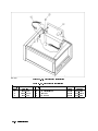
Agilent 4352B VCO/PLL Signal Analyzer
Service Manual
SERIAL NUMBERS
This manual applies directly to instruments with
serial number prex JP1KE00196 or above.
For additional important information about serial numbers,
read \Serial Number" in Appendix A of this Manual.
Agilent Part No. 04352-90141
Printed in JAPAN June 2000
Second Edition
Notice
The information contained in this document is subject to change without notice.
This document contains proprietary information that is protected by copyright. All rights are
reserved. No part of this document may be photocopied, reproduced, or translated to another
language without the prior written consent of the Agilent Technologies .
Agilent Technologies Japan, Ltd.
Component Test PGU-Kobe
1-3-2, Murotani, Nishi-ku, Kobe-shi,
Hyogo, 651-2241 Japan
R is a U.S. registered trademark of Microsoft Corporation.
MS-DOS
c Copyright Agilent Technologies Japan, LTD. 1997, 2000
Printing History
December 1997 : : : : : : : : : : : : : : : : : : : : : : : : : : : : : : : : : : : : : : First Edition (part number: 04352-90141)
June 2000 : : : : : : : : : : : : : : : : : : : : : : : : : : : : : : : : : : : : : : : : : Second Edition (part number: 04352-90141)
iii
Safety Summary
The following general safety precautions must be observed during all phases of operation,
service, and repair of this instrument. Failure to comply with these precautions or with specic
WARNINGS elsewhere in this manual may impair the protection provided by the equipment.
In addition, it violates safety standards of design, manufacture, and intended use of the
instrument.
The Agilent Technologies assumes no liability for the customer's failure to comply with these
requirements.
Note
The 4352B complies with INSTALLATION CATEGORY II and POLLUTION
DEGREE 2 in IEC1010-1. The 4352B is an INDOOR USE product.
Ground The Instrument
To avoid electric shock hazard, the instrument chassis and cabinet must be connected to a
safety earth ground using the supplied power cable with earth blade.
DO NOT Operate In An Explosive Atmosphere
Do not operate the instrument in the presence of ammable gasses or fumes. Operation of any
electrical instrument in such an environment constitutes a safety hazard.
Keep Away From Live Circuits
Operating personnel must not remove instrument covers. Component replacement and internal
adjustments must be made by qualied maintenance personnel. Do not replace components
with the power cable connected. Under certain conditions, dangerous voltages may exist even
with the power cable removed. To avoid injuries, always disconnect power and discharge
circuits before touching them.
DO NOT Service Or Adjust Alone
Do not attempt internal service or adjustment unless another person, capable of rendering rst
aid and resuscitation, is present.
DO NOT Substitute Parts Or Modify Instrument
Because of the danger of introducing additional hazards, do not install substitute parts or
perform unauthorized modications to the instrument. Return the instrument to a Agilent
Technologies Sales and Service Oce for service and repair to ensure the safety features are
maintained.
Dangerous Procedure Warnings
Warnings, such as the example below, precede potentially dangerous procedures throughout
this manual. Instructions contained in the warnings must be followed.
Warning
iv
Dangerous voltages, capable of causing death, are present in this
instrument. Use extreme caution when handling, testing, and adjusting
this instrument.
Typeface Conventions
Bold
Italics
Computer
4HARDKEYS5
NNNNNNNNNNNNNNNNNNNNNNNNNN
SOFTKEYS
Boldface type is used when a term is dened. For example: icons are
symbols.
Italic type is used for emphasis and for titles of manuals and other
publications.
Italic type is also used for keyboard entries when a name or a variable
must be typed in place of the words in italics. For example: copy
lename means to type the word copy, to type a space, and then to
type the name of a le such as file1.
Computer font is used for on-screen prompts and messages.
Labeled keys on the instrument front panel are enclosed in 4 5.
Softkeys located to the right of the CRT are enclosed in .
NNNNN
v
Certication
Agilent Technologies certies that this product met its published specications at the time
of shipment from the factory. Agilent Technologies further certies that its calibration
measurements are traceable to the United States National Institute of Standards and
Technology, to the extent allowed by the Institution's calibration facility, or to the calibration
facilities of other International Standards Organization members.
Warranty
This Agilent Technologies instrument product is warranted against defects in material and
workmanship for a period of one year from the date of shipment, except that in the case of
certain components listed in Instrument Specications of this manual, the warranty shall be
for the specied period. During the warranty period, Agilent Technologies will, at its option,
either repair or replace products that prove to be defective.
For warranty service or repair, this product must be returned to a service facility designated by
Agilent Technologies. Buyer shall prepay shipping charges to Agilent Technologies and Agilent
Technologies shall pay shipping charges to return the product to Buyer. However, Buyer shall
pay all shipping charges, duties, and taxes for products returned to Agilent Technologies from
another country.
Agilent Technologies warrants that its software and rmware designated by Agilent
Technologies for use with an instrument will execute its programming instruction when
properly installed on that instrument. Agilent Technologies does not warrant that the operation
of the instrument, or software, or rmware will be uninterrupted or error free.
Limitation Of Warranty
The foregoing warranty shall not apply to defects resulting from improper or inadequate
maintenance by Buyer, Buyer-supplied software or interfacing, unauthorized modication or
misuse, operation outside of the environmental specications for the product, or improper site
preparation or maintenance.
No other warranty is expressed or implied. Agilent Technologies specically disclaims the
implied warranties of merchantability and tness for a particular purpose.
vi
Exclusive Remedies
The remedies provided herein are buyer's sole and exclusive remedies. Agilent Technologies
shall not be liable for any direct, indirect, special, incidental, or consequential damages,
whether based on contract, tort, or any other legal theory.
Assistance
Product maintenance agreements and other customer assistance agreements are available for
Agilent Technologies products.
For any assistance, contact your nearest Agilent Technologies Sales and Service Oce.
Addresses are provided at the back of this manual.
vii
Safety Symbols
General denitions of safety symbols used on equipment or in manuals are listed below.
Instruction manual symbol: the product is marked with this symbol when it is
necessary for the user to refer to the instruction manual.
Alternating current.
Direct current.
On (Supply).
O (Supply).
This Warning sign denotes a hazard. It calls attention to a procedure, practice,
condition or the like, which, if not correctly performed or adhered to, could
result in injury or death to personnel.
This Caution sign denotes a hazard. It calls attention to a procedure, practice,
condition or the like, which, if not correctly performed or adhered to, could
result in damage to or destruction of part or all of the product.
This Note sign denotes important information. It calls attention to a
procedure, practice, condition or the like, which is essential to highlight.
viii
Document Guide
Please utilize the following manuals when using the analyzer:
Function Reference
Explains the operations commonly used for measurement and illustrates all functions
accessed from the front panel keys and softkeys. It also provides information on options
and accessories available, specications, system performance, and conceptual
information about the analyzer's features.
GPIB Programming Manual
Explains the basic programming methods used when remotely controlling the analyzer
with GPIB. Also, contains information on the usage of all GPIB commands, the status
report mechanism, and the data transmission format.
Manual Supplement for HP Instrument BASIC User's Handbook
Describes how HP Instrument BASIC works with the analyzer.
HP Instrument BASIC User's Handbook
Explains the usage of HP Instrument BASIC including general programming examples
and hints. Also, explains all HP Instrument BASIC commands. This manual consists of
the following three parts: \HP Instrument BASIC Programming Technique," \HP
Instrument BASIC Interface Technique," and \HP Instrument BASIC Language
Reference."
Service Manual
Explains how to do performance tests, and to adjust, troubleshoot, and repair the
instrument.
ix
Contents
1. General Information
INTRODUCTION . . . . . . . . . . . . .
ORGANIZATION OF SERVICE MANUAL . .
ANALYZERS COVERED BY THIS MANUAL
TABLE OF SERVICE TEST EQUIPMENT . .
.
.
.
.
.
.
.
.
.
.
.
.
.
.
.
.
.
.
.
.
.
.
.
.
.
.
.
.
.
.
.
.
.
.
.
.
.
.
.
.
.
.
.
.
.
.
.
.
.
.
.
.
.
.
.
.
.
.
.
.
.
.
.
.
.
.
.
.
1-1
1-1
1-3
1-4
INTRODUCTION . . . . . . . . . . . . . . . . . . . . . . . .
GENERAL INFORMATION . . . . . . . . . . . . . . . . . . .
Warm Up Time . . . . . . . . . . . . . . . . . . . . . . .
Ambient Conditions . . . . . . . . . . . . . . . . . . . . .
Calibration Cycle . . . . . . . . . . . . . . . . . . . . . .
Performance Test Record . . . . . . . . . . . . . . . . . . .
Recommended Test Equipment . . . . . . . . . . . . . . . .
FREQUENCY MEASUREMENT TEST . . . . . . . . . . . . . .
Description . . . . . . . . . . . . . . . . . . . . . . . . .
Specication . . . . . . . . . . . . . . . . . . . . . . . . .
Test Equipment . . . . . . . . . . . . . . . . . . . . . . .
Procedure . . . . . . . . . . . . . . . . . . . . . . . . . .
RF POWER MEASUREMENT ACCURACY TEST . . . . . . . . .
Description . . . . . . . . . . . . . . . . . . . . . . . . .
Specication . . . . . . . . . . . . . . . . . . . . . . . . .
Test Equipment . . . . . . . . . . . . . . . . . . . . . . .
Procedure . . . . . . . . . . . . . . . . . . . . . . . . . .
C/N RATIO MEASUREMENT PHASE NOISE TEST . . . . . . . .
Description . . . . . . . . . . . . . . . . . . . . . . . . .
Specication . . . . . . . . . . . . . . . . . . . . . . . . .
Test Equipment . . . . . . . . . . . . . . . . . . . . . . .
Procedure . . . . . . . . . . . . . . . . . . . . . . . . . .
C/N MEASUREMENT FLATNESS ACCURACY TEST . . . . . . .
Description . . . . . . . . . . . . . . . . . . . . . . . . .
Specication . . . . . . . . . . . . . . . . . . . . . . . . .
Test Equipment . . . . . . . . . . . . . . . . . . . . . . .
Procedure . . . . . . . . . . . . . . . . . . . . . . . . . .
C/N RATIO MEASUREMENT LINEARITY ACCURACY TEST . . . .
Description . . . . . . . . . . . . . . . . . . . . . . . . .
Specication . . . . . . . . . . . . . . . . . . . . . . . . .
Test Equipment . . . . . . . . . . . . . . . . . . . . . . .
Procedure . . . . . . . . . . . . . . . . . . . . . . . . . .
FM DEVIATION TEST . . . . . . . . . . . . . . . . . . . . .
Description . . . . . . . . . . . . . . . . . . . . . . . . .
Specication . . . . . . . . . . . . . . . . . . . . . . . . .
Test Equipment . . . . . . . . . . . . . . . . . . . . . . .
Procedure . . . . . . . . . . . . . . . . . . . . . . . . . .
SPECTRUM MEASUREMENT RELATIVE LEVEL ACCURACY TEST
Description . . . . . . . . . . . . . . . . . . . . . . . . .
.
.
.
.
.
.
.
.
.
.
.
.
.
.
.
.
.
.
.
.
.
.
.
.
.
.
.
.
.
.
.
.
.
.
.
.
.
.
.
.
.
.
.
.
.
.
.
.
.
.
.
.
.
.
.
.
.
.
.
.
.
.
.
.
.
.
.
.
.
.
.
.
.
.
.
.
.
.
.
.
.
.
.
.
.
.
.
.
.
.
.
.
.
.
.
.
.
.
.
.
.
.
.
.
.
.
.
.
.
.
.
.
.
.
.
.
.
.
.
.
.
.
.
.
.
.
.
.
.
.
.
.
.
.
.
.
.
.
.
.
.
.
.
.
.
.
.
.
.
.
.
.
.
.
.
.
.
.
.
.
.
.
.
.
.
.
.
.
.
.
.
.
.
.
.
.
.
.
.
.
.
.
.
.
.
.
.
.
.
.
.
.
.
.
.
.
.
.
.
.
.
.
.
.
.
.
.
.
.
.
.
.
.
.
.
.
.
.
.
.
.
.
.
.
.
.
.
.
.
.
.
.
.
.
.
.
.
.
.
.
.
.
.
.
.
.
.
.
.
.
.
.
.
.
.
.
.
.
.
.
.
.
.
.
.
.
.
.
.
.
.
.
.
2-1
2-1
2-1
2-1
2-1
2-1
2-2
2-3
2-3
2-3
2-3
2-3
2-5
2-5
2-5
2-5
2-5
2-11
2-11
2-11
2-11
2-11
2-13
2-13
2-13
2-13
2-13
2-16
2-16
2-16
2-16
2-16
2-19
2-19
2-19
2-19
2-19
2-25
2-25
2. Performance Tests
.
.
.
.
Contents-1
Specication . . . . . . . . . . . . . . . . . . . . .
Test Equipment . . . . . . . . . . . . . . . . . . .
Procedure . . . . . . . . . . . . . . . . . . . . . .
FREQUENCY TRANSIENT FREQUENCY ACCURACY TEST
Description . . . . . . . . . . . . . . . . . . . . .
Specication . . . . . . . . . . . . . . . . . . . . .
Test Equipment . . . . . . . . . . . . . . . . . . .
Procedure . . . . . . . . . . . . . . . . . . . . . .
DC POWER VOLTAGE ACCURACY TEST . . . . . . . . .
Description . . . . . . . . . . . . . . . . . . . . .
Specication . . . . . . . . . . . . . . . . . . . . .
Test Equipment . . . . . . . . . . . . . . . . . . .
Procedure . . . . . . . . . . . . . . . . . . . . . .
DC CONTROL VOLTAGE ACCURACY TEST . . . . . . .
Description . . . . . . . . . . . . . . . . . . . . .
Specication . . . . . . . . . . . . . . . . . . . . .
Test Equipment . . . . . . . . . . . . . . . . . . .
Procedure . . . . . . . . . . . . . . . . . . . . . .
MOD OUT LEVEL ACCURACY TEST . . . . . . . . . .
Description . . . . . . . . . . . . . . . . . . . . .
Specication . . . . . . . . . . . . . . . . . . . . .
Test Equipment . . . . . . . . . . . . . . . . . . .
Procedure . . . . . . . . . . . . . . . . . . . . . .
DC POWER CURRENT MEASUREMENT ACCURACY TEST
Description . . . . . . . . . . . . . . . . . . . . .
Specication . . . . . . . . . . . . . . . . . . . . .
Test Equipment . . . . . . . . . . . . . . . . . . .
Procedure . . . . . . . . . . . . . . . . . . . . . .
PERFORMANCE TEST RECORD . . . . . . . . . . . .
Frequency Measurement Test . . . . . . . . . . . . .
Power Measurement Accuracy Test . . . . . . . . . .
C/N Phase Noise Test . . . . . . . . . . . . . . . . .
C/N Measurement Accuracy Test (Flatness) . . . . . .
C/N Measurement Accuracy Test (Linearity) . . . . . .
FM Deviation Test . . . . . . . . . . . . . . . . . .
Spectrum Measurement Relative Level Accuracy Test .
Frequency Transient Frequency Accuracy Test . . . . .
DC POWER Voltage Test . . . . . . . . . . . . . . .
DC CONTROL Voltage Test . . . . . . . . . . . . . .
MOD OUT Voltage Test . . . . . . . . . . . . . . . .
DC POWER Current Test . . . . . . . . . . . . . . .
3. Adjustments and Correction Constants
Introduction . . . . . . . . . . . . . . . . . . .
Safety Considerations . . . . . . . . . . . . . .
Required Equipment . . . . . . . . . . . . . . .
Adjustment Program . . . . . . . . . . . . . .
Warm-up for Adjustments and Correction Constants
Instrument Cover Removal . . . . . . . . . . . .
Order Of Adjustments and Correction Constants . .
Preparation for Using the Adjustment Program . .
REFERENCE FREQUENCY ADJUSTMENT . . . .
Required Equipment . . . . . . . . . . . . . .
Procedure . . . . . . . . . . . . . . . . . . .
THIRD MIXER FEEDTHROUGH ADJUSTMENT . .
Contents-2
.
.
.
.
.
.
.
.
.
.
.
.
.
.
.
.
.
.
.
.
.
.
.
.
.
.
.
.
.
.
.
.
.
.
.
.
.
.
.
.
.
.
.
.
.
.
.
.
.
.
.
.
.
.
.
.
.
.
.
.
.
.
.
.
.
.
.
.
.
.
.
.
.
.
.
.
.
.
.
.
.
.
.
.
.
.
.
.
.
.
.
.
.
.
.
.
.
.
.
.
.
.
.
.
.
.
.
.
.
.
.
.
.
.
.
.
.
.
.
.
.
.
.
.
.
.
.
.
.
.
.
.
.
.
.
.
.
.
.
.
.
.
.
.
.
.
.
.
.
.
.
.
.
.
.
.
.
.
.
.
.
.
.
.
.
.
.
.
.
.
.
.
.
.
.
.
.
.
.
.
.
.
.
.
.
.
.
.
.
.
.
.
.
.
.
.
.
.
.
.
.
.
.
.
.
.
.
.
.
.
.
.
.
.
.
.
.
.
.
.
.
.
.
.
.
.
.
.
.
.
.
.
.
.
.
.
.
.
.
.
.
.
.
.
.
.
.
.
.
.
.
.
.
.
.
.
.
.
.
.
.
.
.
.
.
.
.
.
.
.
.
.
.
.
.
.
.
.
.
.
.
.
.
.
.
.
.
.
.
.
.
.
.
.
.
.
.
.
.
.
.
.
.
.
.
.
.
.
.
.
.
.
.
.
.
.
.
.
.
.
.
.
.
.
.
.
.
.
.
.
.
.
.
.
.
.
.
.
.
.
.
.
.
.
.
.
.
.
.
.
.
.
.
.
.
.
.
.
.
.
.
.
.
.
.
.
.
.
.
.
.
.
.
.
.
.
.
.
.
.
.
.
.
.
.
.
.
.
.
.
.
.
.
.
.
.
.
.
.
.
.
.
.
.
.
.
.
.
.
.
.
.
.
.
.
.
.
.
.
.
.
.
.
.
.
.
.
.
.
.
.
.
.
.
.
.
.
.
.
.
.
.
.
.
.
.
.
.
.
.
.
.
.
.
.
.
.
.
.
.
.
.
.
.
.
.
.
.
.
.
.
.
.
.
.
.
.
.
.
.
.
.
.
.
.
.
.
2-25
2-25
2-25
2-28
2-28
2-28
2-28
2-28
2-30
2-30
2-30
2-30
2-30
2-32
2-32
2-32
2-32
2-32
2-34
2-34
2-34
2-34
2-34
2-36
2-36
2-36
2-36
2-36
2-38
2-38
2-38
2-38
2-39
2-39
2-39
2-40
2-40
2-40
2-41
2-41
2-41
.
.
.
.
.
.
.
.
.
.
.
.
.
.
.
.
.
.
.
.
.
.
.
.
.
.
.
.
.
.
.
.
.
.
.
.
.
.
.
.
.
.
.
.
.
.
.
.
.
.
.
.
.
.
.
.
.
.
.
.
.
.
.
.
.
.
.
.
.
.
.
.
.
.
.
.
.
.
.
.
.
.
.
.
.
.
.
.
.
.
.
.
.
.
.
.
.
.
.
.
.
.
.
.
.
.
.
.
.
.
.
.
.
.
.
.
.
.
.
.
.
.
.
.
.
.
.
.
.
.
.
.
3-1
3-1
3-2
3-2
3-3
3-3
3-3
3-4
3-8
3-8
3-8
3-10
Required Equipment . . . . . . . . . . . . . . . . . . . . . . .
Procedure . . . . . . . . . . . . . . . . . . . . . . . . . . . .
THIRD IF AMP GAIN ADJUSTMENT . . . . . . . . . . . . . . . .
Required Equipment . . . . . . . . . . . . . . . . . . . . . . .
Procedure . . . . . . . . . . . . . . . . . . . . . . . . . . . .
EEPROM WRITE-ID AND INITIAL CORRECTION CONSTANTS . . . .
Required Equipment . . . . . . . . . . . . . . . . . . . . . . .
Procedure . . . . . . . . . . . . . . . . . . . . . . . . . . . .
CRYSTAL FILTER FREQUENCY RESPONSE CORRECTION CONSTANTS
Required Equipment . . . . . . . . . . . . . . . . . . . . . . .
Procedure . . . . . . . . . . . . . . . . . . . . . . . . . . . .
FV CONVERTER CORRECTION CONSTANTS . . . . . . . . . . . .
Required Equipment . . . . . . . . . . . . . . . . . . . . . . .
Procedure . . . . . . . . . . . . . . . . . . . . . . . . . . . .
DC POWER VOLTAGE CORRECTION CONSTANTS . . . . . . . . . .
Test Equipment . . . . . . . . . . . . . . . . . . . . . . . . .
Procedure . . . . . . . . . . . . . . . . . . . . . . . . . . . .
DC CONTROL VOLTAGE CORRECTION CONSTANTS . . . . . . . . .
Required Equipment . . . . . . . . . . . . . . . . . . . . . . .
Procedure . . . . . . . . . . . . . . . . . . . . . . . . . . . .
MOD OUT LEVEL CORRECTION CONSTANTS . . . . . . . . . . . .
Required Equipment . . . . . . . . . . . . . . . . . . . . . . .
Procedure . . . . . . . . . . . . . . . . . . . . . . . . . . . .
DC POWER CURRENT CORRECTION CONSTANTS . . . . . . . . . .
Test Equipment . . . . . . . . . . . . . . . . . . . . . . . . .
Procedure . . . . . . . . . . . . . . . . . . . . . . . . . . . .
RF POWER LINEARITY CORRECTION CONSTANTS . . . . . . . . .
Required Equipment . . . . . . . . . . . . . . . . . . . . . . .
Procedure . . . . . . . . . . . . . . . . . . . . . . . . . . . .
RF POWER FLATNESS CORRECTION CONSTANTS . . . . . . . . . .
Required Equipment . . . . . . . . . . . . . . . . . . . . . . .
Procedure . . . . . . . . . . . . . . . . . . . . . . . . . . . .
SPECTRUM MEASUREMENT CORRECTION CONSTANTS . . . . . . .
Required Equipment . . . . . . . . . . . . . . . . . . . . . . .
Procedure . . . . . . . . . . . . . . . . . . . . . . . . . . . .
4. Overall Troubleshooting
INTRODUCTION . . . . . . . . . . . . . . . . . . .
TROUBLESHOOTING SUMMARY . . . . . . . . . . .
START HERE . . . . . . . . . . . . . . . . . . . .
INSPECT THE POWER ON SEQUENCE . . . . . . . .
Check the Fan . . . . . . . . . . . . . . . . . . .
Check the Front Panel LED . . . . . . . . . . . .
Check Error Message . . . . . . . . . . . . . . . .
OPERATOR'S CHECK . . . . . . . . . . . . . . . .
Test Equipment . . . . . . . . . . . . . . . . . .
Procedure to check the source group . . . . . . . .
Procedures to check the receiver group . . . . . . .
PERFORMANCE TESTS FAILURE TROUBLESHOOTING
Perform Adjustments and Correction Constants . . .
TROUBLESHOOTING GPIB SYSTEM . . . . . . . . .
Check the GPIB system with the signal generator . .
Check the External Controller . . . . . . . . . . .
.
.
.
.
.
.
.
.
.
.
.
.
.
.
.
.
.
.
.
.
.
.
.
.
.
.
.
.
.
.
.
.
.
.
.
.
.
.
.
.
.
.
.
.
.
.
.
.
.
.
.
.
.
.
.
.
.
.
.
.
.
.
.
.
.
.
.
.
.
.
.
.
.
.
.
.
.
.
.
.
.
.
.
.
.
.
.
.
.
.
.
.
.
.
.
.
.
.
.
.
.
.
.
.
.
.
.
.
.
.
.
.
.
.
.
.
.
.
.
.
.
.
.
.
.
.
.
.
.
.
.
.
.
.
.
.
.
.
.
.
.
.
.
.
.
.
.
.
.
.
.
.
.
.
.
.
.
.
.
.
.
.
.
.
.
.
.
.
.
.
.
.
.
.
.
.
.
.
.
.
.
.
.
.
.
.
.
.
.
.
.
.
.
.
.
.
.
.
.
.
.
.
.
.
.
.
.
.
.
.
.
.
.
.
.
.
.
.
.
.
.
.
.
.
.
.
.
.
.
.
.
.
.
.
.
.
.
.
.
.
.
.
.
.
.
.
.
.
.
.
.
.
.
.
.
.
.
.
.
.
.
.
.
.
.
.
.
.
.
.
.
.
.
.
.
.
.
.
.
.
.
.
.
.
.
.
.
3-10
3-10
3-11
3-11
3-11
3-13
3-13
3-13
3-14
3-14
3-14
3-15
3-15
3-15
3-16
3-16
3-16
3-17
3-17
3-17
3-18
3-18
3-18
3-19
3-19
3-19
3-20
3-20
3-20
3-22
3-22
3-22
3-23
3-23
3-23
.
.
.
.
.
.
.
.
.
.
.
.
.
.
.
.
.
.
.
.
.
.
.
.
.
.
.
.
.
.
.
.
.
.
.
.
.
.
.
.
.
.
.
.
.
.
.
.
.
.
.
.
.
.
.
.
.
.
.
.
.
.
.
.
.
.
.
.
.
.
.
.
.
.
.
.
.
.
.
.
4-1
4-1
4-3
4-4
4-4
4-4
4-4
4-5
4-5
4-5
4-6
4-9
4-9
4-10
4-10
4-11
Contents-3
5. Power Supply Troubleshooting
INTRODUCTION . . . . . . . . . . . . . . . . . . . . . . .
START HERE . . . . . . . . . . . . . . . . . . . . . . . .
1. Check Error Messages . . . . . . . . . . . . . . . . . .
2. Check the Fan is Rotating . . . . . . . . . . . . . . . .
3. Check the A50 SHUTDOWN LED . . . . . . . . . . . . .
A50 Shutdown LED . . . . . . . . . . . . . . . . . . .
4. Check the A1 +5 VD LED . . . . . . . . . . . . . . . .
Measure the A1 +5 VD Voltage . . . . . . . . . . . . . .
5. Check the A2 Seven LEDs . . . . . . . . . . . . . . . .
6. Run the Internal Test 4: A2 POST REGULATOR . . . . . .
Internal Test 4: A2 POST REGULATOR . . . . . . . . . .
FIND OUT WHY THE FAN IS NOT ROTATING . . . . . . . . .
1. Check the Line Voltage, Selector Switch Setting, and Fuse .
2. Check the A50 SHUTDOWN LED . . . . . . . . . . . . .
FIND OUT WHY THE A50 SHUTDOWN LED IS OFF . . . . . .
1. Disconnect the Cable from the A50J3 . . . . . . . . . .
2. Disconnect the Cable from the A1J10 . . . . . . . . . .
3. Remove Assemblies . . . . . . . . . . . . . . . . . . .
FIND OUT WHY THE A1 +5 VD LED IS NOT ON STEADILY . .
1. Check the A40 Pre-Regulator . . . . . . . . . . . . . .
2. Check the A50 DC-DC Converter . . . . . . . . . . . . .
3. Disconnect Cables on the A1 CPU . . . . . . . . . . . .
4. Remove Assemblies . . . . . . . . . . . . . . . . . . .
TROUBLESHOOT THE FAN AND THE A50 DC-DC CONVERTER
1. Troubleshoot the Fan . . . . . . . . . . . . . . . . . .
2. Troubleshoot the A50 DC-DC Converter . . . . . . . . .
TROUBLESHOOT A2 POST-REGULATOR . . . . . . . . . . .
1. Measure A2 Post Regulator Output Voltages . . . . . . . .
.
.
.
.
.
.
.
.
.
.
.
.
.
.
.
.
.
.
.
.
.
.
.
.
.
.
.
.
.
.
.
.
.
.
.
.
.
.
.
.
.
.
.
.
.
.
.
.
.
.
.
.
.
.
.
.
.
.
.
.
.
.
.
.
.
.
.
.
.
.
.
.
.
.
.
.
.
.
.
.
.
.
.
.
.
.
.
.
.
.
.
.
.
.
.
.
.
.
.
.
.
.
.
.
.
.
.
.
.
.
.
.
.
.
.
.
.
.
.
.
.
.
.
.
.
.
.
.
.
.
.
.
.
.
.
.
.
.
.
.
.
.
.
.
.
.
.
.
.
.
.
.
.
.
.
.
.
.
.
.
.
.
.
.
.
.
.
.
.
.
.
.
.
.
.
.
.
.
.
.
.
.
.
.
.
.
.
.
.
.
.
.
.
.
.
.
.
.
.
.
.
.
.
.
.
.
.
.
.
.
.
.
.
.
.
.
.
.
.
.
.
.
.
.
5-1
5-2
5-2
5-2
5-2
5-3
5-4
5-4
5-4
5-5
5-6
5-7
5-7
5-7
5-8
5-8
5-8
5-8
5-9
5-9
5-9
5-10
5-10
5-12
5-12
5-13
5-15
5-15
INTRODUCTION . . . . . . . . . . . . . . . . . . . . . . . .
A1 CPU Replacement . . . . . . . . . . . . . . . . . . . . .
FIRMWARE INSTALLATION . . . . . . . . . . . . . . . . . .
Ordering the Firmware Diskette . . . . . . . . . . . . . . .
START HERE . . . . . . . . . . . . . . . . . . . . . . . . .
1. Check the Power On Sequence . . . . . . . . . . . . . . .
Check the A1 Eight LEDs . . . . . . . . . . . . . . . . .
Check Error Messages . . . . . . . . . . . . . . . . . . .
2. Check the A1 CPU . . . . . . . . . . . . . . . . . . . .
3. Check the A1 DRAM and Flash Memory . . . . . . . . . .
4. Check the A1 Volatile Memory . . . . . . . . . . . . . . .
5. Check the A30 Front Keyboard . . . . . . . . . . . . . .
6. Check the A53 FDD . . . . . . . . . . . . . . . . . . . .
7. Check the A32 I-BASIC Interface and the mini-DIN Keyboard
8. Check the A17 24 bit I/O Port . . . . . . . . . . . . . . .
TROUBLESHOOT THE A51 GSP and A52 LCD . . . . . . . . . .
1. Run the Internal Test 3: A51 GSP . . . . . . . . . . . . .
2. Check the A52 LCD(Liquid Crystal Display) . . . . . . . . .
.
.
.
.
.
.
.
.
.
.
.
.
.
.
.
.
.
.
.
.
.
.
.
.
.
.
.
.
.
.
.
.
.
.
.
.
.
.
.
.
.
.
.
.
.
.
.
.
.
.
.
.
.
.
.
.
.
.
.
.
.
.
.
.
.
.
.
.
.
.
.
.
.
.
.
.
.
.
.
.
.
.
.
.
.
.
.
.
.
.
.
.
.
.
.
.
.
.
.
.
.
.
.
.
.
.
.
.
.
.
.
.
.
.
.
.
.
.
.
.
.
.
.
.
.
.
6-1
6-3
6-4
6-4
6-5
6-5
6-5
6-6
6-6
6-7
6-8
6-8
6-8
6-9
6-9
6-10
6-10
6-10
6. Digital Control Troubleshooting
Contents-4
7. Source Group Troubleshooting
INTRODUCTION . . . . . . . . . . . . . . . .
SOURCE GROUP TROUBLESHOOTING SUMMARY
START HERE . . . . . . . . . . . . . . . . .
1. Check A6's A/D Converter . . . . . . . . .
2. Check Option 001 DC CONTROL Outputs . .
3. Bypass A70 . . . . . . . . . . . . . . . .
4. Check DC POWER/DC CONTROL Outputs . .
5. Check A3/A13 Source . . . . . . . . . . .
6. Check MOD OUT signal . . . . . . . . . .
7. Check REF OSC on A6 . . . . . . . . . .
.
.
.
.
.
.
.
.
.
.
.
.
.
.
.
.
.
.
.
.
.
.
.
.
.
.
.
.
.
.
.
.
.
.
.
.
.
.
.
.
.
.
.
.
.
.
.
.
.
.
.
.
.
.
.
.
.
.
.
.
.
.
.
.
.
.
.
.
.
.
.
.
.
.
.
.
.
.
.
.
.
.
.
.
.
.
.
.
.
.
.
.
.
.
.
.
.
.
.
.
.
.
.
.
.
.
.
.
.
.
.
.
.
.
.
.
.
.
.
.
.
.
.
.
.
.
.
.
.
.
.
.
.
.
.
.
.
.
.
.
.
.
.
.
.
.
.
.
.
.
7-1
7-2
7-4
7-4
7-4
7-5
7-5
7-7
7-8
7-8
INTRODUCTION . . . . . . . . . . . . . . . . . . . . . . . . . . . . .
RECEIVER GROUP TROUBLESHOOTING SUMMARY . . . . . . . . . . . .
START HERE . . . . . . . . . . . . . . . . . . . . . . . . . . . . . .
1. Check the Rear Panel Output signals (40MHz Output/INT REF OUTPUT)
2. Check A6 Spectrum Analyzer . . . . . . . . . . . . . . . . . . . .
3. Check A5 2nd PLL . . . . . . . . . . . . . . . . . . . . . . . . .
4. Check Measurement Functions . . . . . . . . . . . . . . . . . . . .
5. Check A11 Thermometer . . . . . . . . . . . . . . . . . . . . . .
6. Check the outputs from A10 1st Mixer . . . . . . . . . . . . . . . .
7. Check the Residual FM . . . . . . . . . . . . . . . . . . . . . . .
8. Check the Frequency Transient measurement . . . . . . . . . . . . .
.
.
.
.
.
.
.
.
.
.
.
.
.
.
.
.
.
.
.
.
.
.
8-1
8-2
8-4
8-4
8-4
8-7
8-9
8-10
8-10
8-12
8-13
.
.
.
.
.
.
.
.
.
.
.
.
.
.
.
.
.
.
.
.
.
.
.
.
.
.
.
.
.
.
.
.
.
.
.
.
.
.
.
.
.
.
.
.
.
.
.
.
.
.
.
.
9-1
9-3
9-3
9-3
9-3
9-4
9-5
9-5
9-6
9-6
9-6
9-6
9-7
9-8
9-8
9-8
9-8
9-8
9-9
9-9
9-9
9-9
9-9
9-9
9-9
9-10
8. Receiver Group Troubleshooting
9. Service Key Menus
INTRODUCTION . . . . . . . . . . . . . . . . . .
SERVICE MENU . . . . . . . . . . . . . . . . . .
TESTS . . . . . . . . . . . . . . . . . . . . .
SERVICE INSTRUMENT . . . . . . . . . . . . . .
SERVICE MODES (:DIAG:SERV:MODE {OFF|ON|0|1})
FIRMWARE REVISION (:DIAG:FREV?) . . . . . . .
TESTS MENU . . . . . . . . . . . . . . . . . . .
EXECUTE TEST (:DIAG:TEST:EXEC) . . . . . . . .
INTERNAL TESTS (:DIAG:TEST 0) . . . . . . . .
EXTERNAL TESTS (:DIAG:TEST 11) . . . . . . . .
DISPLAY TESTS (:DIAG:TEST 21) . . . . . . . .
Test Status . . . . . . . . . . . . . . . . . . .
Diagnostic Tests . . . . . . . . . . . . . . . . .
Test Descriptions . . . . . . . . . . . . . . . . .
INTERNAL TESTS . . . . . . . . . . . . . . .
0: ALL INT . . . . . . . . . . . . . . . . . .
1: A1 CPU . . . . . . . . . . . . . . . . . .
2: A1 VOLATILE MEMORY . . . . . . . . . . .
3: A51 GSP . . . . . . . . . . . . . . . . . .
4: A2 POST REGULATOR . . . . . . . . . . .
5 through 10: N/A . . . . . . . . . . . . . . .
EXTERNAL TESTS . . . . . . . . . . . . . . .
11: FRONT PANEL DIAG. . . . . . . . . . . .
12: DSK DR FAULT ISOL'N . . . . . . . . . . .
13: 24 BIT I/O PORT . . . . . . . . . . . . . .
14 through 20: N/A . . . . . . . . . . . . . .
NNNNNNNNNNNNNNNNN
NNNNNNNNNNNNNNNNNNNNNNNNNNNNNNNNNNNNNNNNNNNNNNNNNNNNNNNN
NNNNNNNNNNNNNNNNNNNNNNNNNNNNNNNNNNNNNNNNN
NNNNNNNNNNNNNNNNNNNNNNNNNNNNNNNNNNNNNNNNNNNNNNNNNNNNN
NNNNNNNNNNNNNNNNNNNNNNNNNNNNNNNNNNNNNN
NNNNNNNNNNNNNNNNNNNNNNNNNNNNNNNNNNNNNNNNNNNN
NNNNNNNNNNNNNNNNNNNNNNNNNNNNNNNNNNNNNNNNNNNN
NNNNNNNNNNNNNNNNNNNNNNNNNNNNNNNNNNNNNNNNN
NNNNNNNNNNNNNNNNNNNNNNNNNNNNNNNNNNNNNNNNNNNN
NNNNNNNNNNNNNNNNNNNNNNNNNNNNNNNNNNNNNNNNNNNN
.
.
.
.
.
.
.
.
.
.
.
.
.
.
.
.
.
.
.
.
.
.
.
.
.
.
.
.
.
.
.
.
.
.
.
.
.
.
.
.
.
.
.
.
.
.
.
.
.
.
.
.
.
.
.
.
.
.
.
.
.
.
.
.
.
.
.
.
.
.
.
.
.
.
.
.
.
.
.
.
.
.
.
.
.
.
.
.
.
.
.
.
.
.
.
.
.
.
.
.
.
.
.
.
.
.
.
.
.
.
.
.
.
.
.
.
.
.
.
.
.
.
.
.
.
.
.
.
.
.
.
.
.
.
.
.
.
.
.
.
.
.
.
.
.
.
.
.
.
.
.
.
.
.
.
.
.
.
.
.
.
.
.
.
.
.
.
.
.
.
.
.
.
.
.
.
.
.
.
.
.
.
.
.
.
.
.
.
.
.
.
.
.
.
.
.
.
.
.
.
.
.
.
.
.
.
.
.
.
.
.
.
.
.
.
.
.
.
.
.
.
.
.
.
.
.
.
.
.
.
.
.
.
.
.
.
.
.
.
.
.
.
.
.
.
.
.
.
.
.
.
.
.
.
.
.
.
.
.
.
.
.
.
.
.
.
.
.
.
.
.
.
.
.
.
.
.
.
.
.
.
.
.
.
.
.
Contents-5
DISPLAY TESTS . . .
21: TEST PATTERN 1
22: TEST PATTERN 2
23: TEST PATTERN 3
24: TEST PATTERN 4
25: TEST PATTERN 5
SERVICE MODES MENU .
BUS MEAS [ON] . . . .
MISC MENU . . . . . .
. . . . . . . . . . . . . . . . .
. . . . . . . . . . . . . . . . .
. . . . . . . . . . . . . . . . .
. . . . . . . . . . . . . . . . .
. . . . . . . . . . . . . . . . .
. . . . . . . . . . . . . . . . .
. . . . . . . . . . . . . . . . .
. . . . . . . . . . . . . . . . .
. . . . . . . . . . . . . . . . .
CORRECTION CONSTANTS . . . . . . . . . . . . . . . . .
A2/A8 . . . . . . . . . . . . . . . . . . . . . . . . .
A3 . . . . . . . . . . . . . . . . . . . . . . . . . . .
A5 . . . . . . . . . . . . . . . . . . . . . . . . . . .
A6 . . . . . . . . . . . . . . . . . . . . . . . . . . .
A70 . . . . . . . . . . . . . . . . . . . . . . . . . .
Service Modes . . . . . . . . . . . . . . . . . . . . . .
BUS MEASUREMENT MENU . . . . . . . . . . . . . . . .
BUS MEAS ON off (:DIAG:SERV:BUS:STAT {ON|OFF|1|0} )
DC BUS [FAN PWR] (:DIAG:SERV:BUS:DC <numeric>) . .
FREQ BUS [OFF] (:DIAG:SERV:BUS:FREQ <numeric>) . .
WAIT COUNT (:DIAG:SERV:BUS:WAIT<numeric>) . . . . .
Bus Measurement . . . . . . . . . . . . . . . . . . . .
Bus Measurement Procedure . . . . . . . . . . . . . . .
Bus Measurement Values . . . . . . . . . . . . . . . . .
DC Bus Node Descriptions . . . . . . . . . . . . . . . .
0: NONE . . . . . . . . . . . . . . . . . . . . . . .
1: [A2] +5 V (AUX) (2.025 U) . . . . . . . . . . . . .
2: [A2] 015 V (01.92 U) . . . . . . . . . . . . . . . .
3: [A2] 012.6 V (02.124 U) . . . . . . . . . . . . . . .
4: [A2] 05 V (02.025 U) . . . . . . . . . . . . . . . .
5: [A2] +5 V (2.025 U) . . . . . . . . . . . . . . . . .
6: [A2] +5.3 V (2.1465 U) . . . . . . . . . . . . . . .
7: [A2] +8.5 V (1.8955 U) . . . . . . . . . . . . . . .
8: [A2] +15 V (AUX) (1.92 U) . . . . . . . . . . . . .
9: [A2] +15 V (1.92 U) . . . . . . . . . . . . . . . . .
10: [A2] +22 V (2.002 U) . . . . . . . . . . . . . . . .
11: [A2] FAN POWER . . . . . . . . . . . . . . . . .
12: [A2] +65 V (2.0605 U) . . . . . . . . . . . . . . .
13 through 19: Not Assigned . . . . . . . . . . . . . .
20: [A3] +20VB . . . . . . . . . . . . . . . . . . . .
21: [A3] 05VB . . . . . . . . . . . . . . . . . . . .
22: [A3] +25VC . . . . . . . . . . . . . . . . . . . .
23: [A3] -5VC . . . . . . . . . . . . . . . . . . . . .
24: [A3] DC POWER . . . . . . . . . . . . . . . . . .
25: [A3] DC CONTROL . . . . . . . . . . . . . . . . .
26 through 29: Not Assigned . . . . . . . . . . . . . .
30: [A5] VCO VTUNE . . . . . . . . . . . . . . . . .
31: [A5] 2ND IF DC OFFSET . . . . . . . . . . . . . .
32 through 39: Not Assigned . . . . . . . . . . . . . .
40: [A6] AD VREF . . . . . . . . . . . . . . . . . . .
41: [A6] REF LOOP VTUNE . . . . . . . . . . . . . .
NNNNNNNNNNNNNNNNNNNNNNNNNNNNNNNNNNNNNNNNN
NNNNNNNNNNNNNNNNNNNNNNNNNNNNNNNNNNNNNNNNN
NNNNNNNNNNNNNNNNNNNNNNNNNNNNN
NNNNNNNNNNNNNNNNNNNNNNNNNNNNNNNNNNNNNNNNNNNNNNNNNNNNNNNNNNNNNN
NNNNNNNNNNNNNNNNN
NNNNNNNN
NNNNNNNN
NNNNNNNN
NNNNNNNNNNN
NNNNNNNNNNNNNNNNNNNNNNNNNNNNNNNNNNNNNNNNNNNNNNN
NNNNNNNNNNNNNNNNNNNNNNNNNNNNNNNNNNNNNNNNNNNNNNNNNN
NNNNNNNNNNNNNNNNNNNNNNNNNNNNNNNNNNNNNNNNNNNN
NNNNNNNNNNNNNNNNNNNNNNNNNNNNNNNN
Contents-6
.
.
.
.
.
.
.
.
.
.
.
.
.
.
.
.
.
.
.
.
.
.
.
.
.
.
.
.
.
.
.
.
.
.
.
.
.
.
.
.
.
.
.
.
.
.
.
.
.
.
.
.
.
.
.
.
.
.
.
.
.
.
.
.
.
.
.
.
.
.
.
.
.
.
.
.
.
.
.
.
.
.
.
.
.
.
.
.
.
.
.
.
.
.
.
.
.
.
.
.
.
.
.
.
.
.
.
.
.
.
.
.
.
.
.
.
.
.
.
.
.
.
.
.
.
.
.
.
.
.
.
.
.
.
.
.
.
.
.
.
.
.
.
.
.
.
.
.
.
.
.
.
.
.
.
.
.
.
.
.
.
.
.
.
.
.
.
.
.
.
.
.
.
.
.
.
.
.
.
.
.
.
.
.
.
.
.
.
.
.
.
.
.
.
.
.
.
.
.
.
.
.
.
.
.
.
.
.
.
.
.
.
.
.
.
.
.
.
.
.
.
.
.
.
.
.
.
.
.
.
.
.
.
.
.
.
.
.
.
.
.
.
.
.
.
.
.
.
.
.
.
.
.
.
.
.
.
.
.
.
.
.
.
.
.
.
.
.
.
.
.
.
.
.
.
.
.
.
.
.
.
.
.
.
.
.
.
.
.
.
.
.
.
.
.
.
.
.
.
.
.
.
.
.
.
.
.
.
.
.
.
.
.
.
.
.
.
.
.
.
.
.
.
.
.
.
.
.
.
.
.
.
.
.
.
.
.
.
.
.
.
.
.
.
.
.
.
.
.
.
.
.
.
.
.
.
.
.
.
.
.
.
.
.
.
.
.
.
.
.
.
.
.
.
.
.
.
.
.
.
.
.
.
.
.
.
.
.
.
.
.
.
.
.
.
.
.
.
.
.
.
.
.
.
.
.
.
.
.
.
.
.
.
.
.
.
.
.
.
.
.
.
.
.
.
.
.
.
.
.
.
.
.
.
.
.
.
.
.
.
.
.
.
.
.
.
.
.
.
.
.
.
.
.
.
.
.
.
.
9-10
9-10
9-10
9-10
9-10
9-10
9-11
9-11
9-11
9-11
9-12
9-12
9-12
9-12
9-12
9-12
9-13
9-13
9-13
9-14
9-14
9-14
9-14
9-15
9-15
9-15
9-15
9-15
9-15
9-15
9-15
9-15
9-15
9-16
9-16
9-16
9-16
9-16
9-16
9-16
9-16
9-16
9-16
9-16
9-17
9-17
9-17
9-17
9-17
9-17
9-17
42: [A6] FIXED PLL VTUNE . .
43: [A6] FN LOOP VTUNE . . .
44: [A6] PEAK DETECTOR . . .
45: [A6] GND . . . . . . . . .
46 through 49: Not Assigned . .
50: [A6] SA PATH . . . . . . .
51: [A6] MONITOR PATH . . . .
Frequency Bus Node Descriptions .
0: OFF . . . . . . . . . . . .
1: [A5] 2nd LOCAL . . . . . .
2: [A5] FREQ COUNTER . . . .
3: [A5] FV CONVERTER . . . .
4 through 9: Not Assigned . . .
10: [A6] SAMPLE HOLD . . . .
11: [A6] FM FREQ . . . . . . .
12: [A6] REF LOOP . . . . . .
13: [A6] FIXED PLL . . . . . .
14: [A6] FN LOOP . . . . . . .
CORRECTION CONSTANTS MENU .
XTAL FILT ON off . . . . . . .
FV ON off . . . . . . . . . . .
DCPOW VOLT CC ON off . . . . .
DCPOW CURR CC ON off . . . . .
DCCTL VOLT ON off . . . . . .
MOD OUT ON off . . . . . . . .
POW LIN ON off . . . . . . . .
POW TEMP ON off . . . . . . .
POW FRESP ON off . . . . . . .
NOISE ATTN ON off . . . . . .
SPEC WIDE ON off . . . . . . .
SPEC NARR ON off . . . . . . .
A2/A8 CONTROL MENU . . . . . .
RF ATTEN: . . . . . . . . . . .
POW FAIL LOCATION . . . . . .
A3/A13 CONTROL MENU . . . . .
DAC MENU . . . . . . . . . . .
RANGE MENU . . . . . . . . . .
OUTPUT SELECT . . . . . . . . .
STATUS . . . . . . . . . . . . .
A5 CONTROL MENU . . . . . . . .
2nd PLL . . . . . . . . . . . .
FREQ COUNTER . . . . . . . . .
FV CONVERTER . . . . . . . . .
IF . . . . . . . . . . . . . . .
STATUS . . . . . . . . . . . . .
INTERNAL STATUS . . . . . . .
A6 CONTROL MENU . . . . . . . .
NNNNNNNNNNNNNNNNNNNNNNNNNNNNNNNNNNNNNNNNNNNNNNNNNN
NNNNNNNNNNNNNNNNNNNNNNNNNNNNN
NNNNNNNNNNNNNNNNNNNNNNNNNNNNNNNNNNNNNNNNNNNNNNNNNNNNNNNNNNNNNN
NNNNNNNNNNNNNNNNNNNNNNNNNNNNNNNNNNNNNNNNNNNNNNNNNNNNNNNNNNNNNN
NNNNNNNNNNNNNNNNNNNNNNNNNNNNNNNNNNNNNNNNNNNNNNNNNNNNN
NNNNNNNNNNNNNNNNNNNNNNNNNNNNNNNNNNNNNNNNNNNN
NNNNNNNNNNNNNNNNNNNNNNNNNNNNNNNNNNNNNNNNNNNN
NNNNNNNNNNNNNNNNNNNNNNNNNNNNNNNNNNNNNNNNNNNNNNN
NNNNNNNNNNNNNNNNNNNNNNNNNNNNNNNNNNNNNNNNNNNNNNNNNN
NNNNNNNNNNNNNNNNNNNNNNNNNNNNNNNNNNNNNNNNNNNNNNNNNNNNN
NNNNNNNNNNNNNNNNNNNNNNNNNNNNNNNNNNNNNNNNNNNNNNNNNN
NNNNNNNNNNNNNNNNNNNNNNNNNNNNNNNNNNNNNNNNNNNNNNNNNN
NNNNNNNNNNNNNNNNNNNNNNNNNNNNN
NNNNNNNNNNNNNNNNNNNNNNNNNNNNNNNNNNNNNNNNNNNNNNNNNNNNN
NNNNNNNNNNNNNNNNNNNNNNNNNN
NNNNNNNNNNNNNNNNNNNNNNNNNNNNNNNN
NNNNNNNNNNNNNNNNNNNNNNNNNNNNNNNNNNNNNNNNN
NNNNNNNNNNNNNNNNNNNN
NNNNNNNNNNNNNNNNNNNNNNN
NNNNNNNNNNNNNNNNNNNNNNNNNNNNNNNNNNNNNN
NNNNNNNNNNNNNNNNNNNNNNNNNNNNNNNNNNNNNN
NNNNNNNN
NNNNNNNNNNNNNNNNNNNN
NNNNNNNNNNNNNNNNNNNNNNNNNNNNNNNNNNNNNNNNNNNNNNN
.
.
.
.
.
.
.
.
.
.
.
.
.
.
.
.
.
.
.
.
.
.
.
.
.
.
.
.
.
.
.
.
.
.
.
.
.
.
.
.
.
.
.
.
.
.
.
.
.
.
.
.
.
.
.
.
.
.
.
.
.
.
.
.
.
.
.
.
.
.
.
.
.
.
.
.
.
.
.
.
.
.
.
.
.
.
.
.
.
.
.
.
.
.
.
.
.
.
.
.
.
.
.
.
.
.
.
.
.
.
.
.
.
.
.
.
.
.
.
.
.
.
.
.
.
.
.
.
.
.
.
.
.
.
.
.
.
.
.
.
.
.
.
.
.
.
.
.
.
.
.
.
.
.
.
.
.
.
.
.
.
.
.
.
.
.
.
.
.
.
.
.
.
.
.
.
.
.
.
.
.
.
.
.
.
.
.
.
.
.
.
.
.
.
.
.
.
.
.
.
.
.
.
.
.
.
.
.
.
.
.
.
.
.
.
.
.
.
.
.
.
.
.
.
.
.
.
.
.
.
.
.
.
.
.
.
.
.
.
.
.
.
.
.
.
.
.
.
.
.
.
.
.
.
.
.
.
.
.
.
.
.
.
.
.
.
.
.
.
.
.
.
.
.
.
.
.
.
.
.
.
.
.
.
.
.
.
.
.
.
.
.
.
.
.
.
.
.
.
.
.
.
.
.
.
.
.
.
.
.
.
.
.
.
.
.
.
.
.
.
.
.
.
.
.
.
.
.
.
.
.
.
.
.
.
.
.
.
.
.
.
.
.
.
.
.
.
.
.
.
.
.
.
.
.
.
.
.
.
.
.
.
.
.
.
.
.
.
.
.
.
.
.
.
.
.
.
.
.
.
.
.
.
.
.
.
.
.
.
.
.
.
.
.
.
.
.
.
.
.
.
.
.
.
.
.
.
.
.
.
.
.
.
.
.
.
.
.
.
.
.
.
.
.
.
.
.
.
.
.
.
.
.
.
.
.
.
.
.
.
.
.
.
.
.
.
.
.
.
.
.
.
.
.
.
.
.
.
.
.
.
.
.
.
.
.
.
.
.
.
.
.
.
.
.
.
.
.
.
.
.
.
.
.
.
.
.
.
.
.
.
.
.
.
.
.
.
.
.
.
.
.
.
.
.
.
.
.
.
.
.
.
.
.
.
.
.
.
.
.
.
.
.
.
.
.
.
.
.
.
.
.
.
.
.
.
.
.
.
.
.
.
.
.
.
.
.
.
.
.
.
.
.
.
.
.
.
.
.
.
.
.
.
.
.
.
.
.
.
.
.
.
.
.
.
.
.
.
.
.
.
.
.
.
.
.
.
.
.
.
.
.
.
.
.
.
.
.
.
.
.
.
.
.
.
.
.
.
.
.
.
.
.
.
.
.
.
.
.
.
.
.
.
.
.
.
.
.
.
.
.
.
.
.
.
.
.
.
.
.
.
.
.
.
.
.
.
.
.
.
.
.
.
.
.
.
.
.
.
.
.
.
.
.
.
.
.
.
.
.
.
.
.
.
.
.
.
.
.
.
.
.
.
.
.
.
.
.
.
.
.
.
.
.
.
.
.
.
.
.
.
.
.
.
.
.
.
.
.
.
.
.
.
.
.
.
.
.
.
.
.
.
.
.
.
.
.
.
.
.
.
.
.
.
.
.
.
.
.
.
.
.
.
.
.
.
.
.
.
.
.
.
.
.
.
.
.
.
.
.
.
.
.
.
.
.
.
.
.
.
.
.
.
.
.
.
.
.
.
.
.
.
.
.
.
.
.
.
.
.
.
.
.
.
.
.
.
.
.
.
.
.
.
.
.
.
.
.
.
.
.
.
.
.
.
.
.
.
.
.
.
.
.
.
.
.
.
.
.
.
.
.
.
.
.
.
.
.
.
.
.
.
.
.
.
.
.
.
.
.
.
.
.
.
.
.
.
.
.
.
.
.
.
.
.
.
.
.
.
.
.
.
.
.
.
.
.
.
.
.
.
.
.
.
.
.
.
.
.
.
.
.
.
.
.
.
.
.
.
.
.
.
.
.
.
.
.
.
.
.
.
.
.
.
.
.
.
.
.
.
.
.
.
.
.
.
.
.
.
.
.
.
.
.
.
.
.
.
.
.
.
.
.
.
.
.
.
.
.
.
.
.
.
.
.
.
.
.
.
.
.
.
.
.
.
.
.
.
.
.
.
.
.
.
.
.
.
.
.
.
.
.
.
.
.
.
.
9-17
9-17
9-17
9-17
9-17
9-18
9-18
9-18
9-18
9-18
9-18
9-18
9-18
9-18
9-18
9-18
9-18
9-18
9-19
9-19
9-19
9-20
9-20
9-20
9-20
9-20
9-20
9-20
9-20
9-20
9-21
9-22
9-22
9-22
9-23
9-23
9-24
9-24
9-24
9-25
9-25
9-26
9-26
9-26
9-26
9-26
9-27
Contents-7
ATTEN/AMP . . . .
IF GAIN . . . . .
INPUT SELECT . .
PLL . . . . . . .
FV CALOUT on OFF
FM OUT on OFF . .
STATUS . . . . . .
.
.
.
.
.
.
.
.
.
.
.
.
.
.
.
.
.
.
.
.
.
.
.
.
.
.
.
.
.
.
.
.
.
.
.
.
.
.
.
.
.
.
.
.
.
.
.
.
.
.
.
.
.
.
.
.
.
.
.
.
.
.
.
.
.
.
.
.
.
.
.
.
.
.
.
.
.
.
.
.
.
.
.
.
.
.
.
.
.
.
.
.
.
.
.
.
.
.
.
.
.
.
.
.
.
.
.
.
.
.
.
.
.
.
.
.
.
.
.
.
.
.
.
.
.
.
.
.
.
.
.
.
.
.
.
.
.
.
.
.
.
.
.
.
.
.
.
.
.
.
.
.
.
.
.
.
.
.
.
.
.
.
.
.
.
.
.
.
.
.
.
.
.
.
.
.
.
.
.
.
.
.
.
.
.
.
.
.
.
.
.
.
.
.
.
.
.
.
.
.
.
.
.
.
.
.
.
.
.
.
.
.
.
.
.
.
.
.
.
.
.
.
.
.
.
.
.
.
.
.
.
.
.
.
.
.
.
.
.
.
.
.
.
.
.
.
.
.
.
.
.
.
.
.
.
.
.
.
.
.
.
.
.
.
.
.
.
.
.
.
.
.
.
.
.
.
.
.
.
.
.
.
.
.
.
.
.
.
.
.
.
.
.
.
.
.
.
.
.
.
.
.
.
.
.
.
.
.
.
.
.
.
.
.
.
.
.
.
.
.
.
.
.
.
9-27
9-28
9-28
9-28
9-28
9-28
9-28
9-29
9-29
9-29
9-30
9-30
OVERALL OPERATION AND FUNCTIONAL GROUPS .
POWER SUPPLY OPERATION . . . . . . . . . . . .
Line Power Module . . . . . . . . . . . . . . .
A40 Preregulator . . . . . . . . . . . . . . . .
A50 DC-DC Converter . . . . . . . . . . . . . .
Switching Regulator 1 . . . . . . . . . . . . .
Switching Regulator 2 . . . . . . . . . . . . .
Regulated +5V Digital Supply (+5 VD) . . . . .
A50 Shutdown LED . . . . . . . . . . . . . .
A2 Post-Regulator . . . . . . . . . . . . . . . .
Shutdown Circuit . . . . . . . . . . . . . . .
Seven Status LEDs . . . . . . . . . . . . . . .
A8 RF Attenuator Drive Circuit . . . . . . . . .
DIGITAL CONTROL OPERATION . . . . . . . . . .
A1 CPU . . . . . . . . . . . . . . . . . . . . .
A17 24 Bit I/O Port . . . . . . . . . . . . . . .
A30 Front-Panel Keyboard . . . . . . . . . . . .
A31 I/O Connector . . . . . . . . . . . . . . . .
A32 I-BASIC Interface . . . . . . . . . . . . . .
A51 GSP . . . . . . . . . . . . . . . . . . . .
A54 Inverter . . . . . . . . . . . . . . . . . .
A52 LCD (Liquid Crystal Display) . . . . . . . . .
A53 FDD . . . . . . . . . . . . . . . . . . . .
SOURCE THEORY . . . . . . . . . . . . . . . . .
RECEIVER THEORY . . . . . . . . . . . . . . . .
A5 Second PLL . . . . . . . . . . . . . . . . .
A6 Spectrum Analyzer . . . . . . . . . . . . . .
A7 Power Divider . . . . . . . . . . . . . . . .
A8 RF Attenuator . . . . . . . . . . . . . . . .
A9 Peak Detector . . . . . . . . . . . . . . . .
A10 First Mixer . . . . . . . . . . . . . . . . .
A11 Thermometer . . . . . . . . . . . . . . . .
A part of A3/A13, A60 . . . . . . . . . . . . . .
.
.
.
.
.
.
.
.
.
.
.
.
.
.
.
.
.
.
.
.
.
.
.
.
.
.
.
.
.
.
.
.
.
.
.
.
.
.
.
.
.
.
.
.
.
.
.
.
.
.
.
.
.
.
.
.
.
.
.
.
.
.
.
.
.
.
.
.
.
.
.
.
.
.
.
.
.
.
.
.
.
.
.
.
.
.
.
.
.
.
.
.
.
.
.
.
.
.
.
.
.
.
.
.
.
.
.
.
.
.
.
.
.
.
.
.
.
.
.
.
.
.
.
.
.
.
.
.
.
.
.
.
.
.
.
.
.
.
.
.
.
.
.
.
.
.
.
.
.
.
.
.
.
.
.
.
.
.
.
.
.
.
.
.
.
.
.
.
.
.
.
.
.
.
.
.
.
.
.
.
.
.
.
.
.
.
.
.
.
.
.
.
.
.
.
.
.
.
.
.
.
.
.
.
.
.
.
.
.
.
.
.
.
.
.
.
.
.
.
.
.
.
.
.
.
.
.
.
.
.
.
.
.
.
.
.
.
.
.
.
.
.
.
.
.
.
.
.
.
.
.
.
.
.
.
.
.
.
.
.
.
.
.
.
.
.
.
.
.
.
.
.
.
.
.
.
.
.
.
.
.
.
.
.
.
.
.
.
.
.
.
.
.
.
.
.
.
.
.
.
.
.
.
.
.
.
.
.
.
.
.
.
.
.
.
.
.
.
.
.
.
.
.
.
.
.
.
.
.
.
.
.
.
.
.
.
.
.
.
.
.
.
.
.
.
.
.
.
.
.
.
.
.
.
.
.
.
.
.
.
.
.
.
.
.
.
.
.
.
.
.
.
.
.
.
.
.
.
.
.
.
.
.
.
.
.
.
.
.
.
.
.
.
.
.
.
.
.
.
.
.
.
.
.
.
.
.
.
.
.
.
.
.
.
.
.
.
.
.
.
.
.
.
.
.
.
.
.
.
10-1
10-2
10-4
10-4
10-4
10-4
10-4
10-4
10-4
10-5
10-5
10-5
10-6
10-7
10-9
10-9
10-9
10-9
10-10
10-10
10-10
10-10
10-10
10-11
10-12
10-13
10-13
10-13
10-13
10-13
10-13
10-14
10-14
NNNNNNNNNNNNNNNNNNNNNNNNNNNNN
NNNNNNNNNNNNNNNNNNNNNNN
NNNNNNNNNNNNNNNNNNNNNNNNNNNNNNNNNNNNNN
NNNNNNNNNNN
NNNNNNNNNNNNNNNNNNNNNNNNNNNNNNNNNNNNNNNNNNNNNNNNNN
NNNNNNNNNNNNNNNNNNNNNNNNNNNNNNNNNNNNNNNNN
NNNNNNNNNNNNNNNNNNNN
BOOTLOADER MENU
SYSTEM UPDATE . .
SYSTEM BACKUP . .
PREVIEW DISK . .
REBOOT . . . . . .
NNNNNNNNNNNNNNNNNNNNNNNNNNNNNNNNNNNNNNNNN
NNNNNNNNNNNNNNNNNNNNNNNNNNNNNNNNNNNNNNNNN
NNNNNNNNNNNNNNNNNNNNNNNNNNNNNNNNNNNNNN
NNNNNNNNNNNNNNNNNNNN
10. Theory of Operation
Contents-8
.
.
.
.
.
.
.
.
.
.
.
.
11. Replaceable Parts
Introduction . . . . . . .
Ordering Information . .
Direct Mail Order System
Replaceable Parts List . .
.
.
.
.
.
.
.
.
.
.
.
.
.
.
.
.
.
.
.
.
.
.
.
.
.
.
.
.
.
.
.
.
.
.
.
.
.
.
.
.
.
.
.
.
.
.
.
.
.
.
.
.
.
.
.
.
.
.
.
.
.
.
.
.
.
.
.
.
.
.
.
.
.
.
.
.
.
.
.
.
.
.
.
.
.
.
.
.
.
.
.
.
.
.
.
.
.
.
.
.
.
.
.
.
11-1
11-1
11-1
11-2
INTRODUCTION . . . . . . . . . . . . . . . . . . . . . . . . . . . . . . .
POST REPAIR PROCEDURES . . . . . . . . . . . . . . . . . . . . . . . . .
12-1
12-1
12. Post Repair Procedures
A. Manual Changes
Introduction . .
Manual Changes
Change 1 . . .
Serial Number .
.
.
.
.
.
.
.
.
.
.
.
.
.
.
.
.
.
.
.
.
.
.
.
.
.
.
.
.
.
.
.
.
.
.
.
.
.
.
.
.
.
.
.
.
.
.
.
.
.
.
.
.
.
.
.
.
.
.
.
.
.
.
.
.
.
.
.
.
.
.
.
.
.
.
.
.
.
.
.
.
.
.
.
.
.
.
.
.
.
.
.
.
.
.
.
.
.
.
.
.
.
.
.
.
.
.
.
.
.
.
.
.
.
.
.
.
.
.
.
.
.
.
.
.
A-1
A-1
A-2
A-5
.
.
.
.
.
.
.
.
.
.
.
.
.
.
.
.
.
.
.
.
.
.
.
.
.
.
.
.
.
.
.
.
.
.
.
.
.
.
.
.
.
.
.
.
.
.
.
.
.
.
.
.
.
.
.
.
.
.
.
.
.
.
.
.
.
.
.
.
.
.
.
.
.
.
.
.
.
.
.
.
.
.
.
.
.
.
.
.
.
.
.
.
.
.
.
.
.
.
.
.
.
.
.
.
.
.
.
.
.
.
.
.
.
.
.
.
B-1
B-1
B-2
B-2
B. Power Requirement
Replacing Fuse
Fuse Selection . .
Power Requirements
Power Cable . . .
Messages
Error Messages in Alphabetical Order . . . . . . . . . . . . . . . . . . . .Messages-2
.
Error Messages in Numerical Order . . . . . . . . . . . . . . . . . . . . Messages-15
. .
Index
Contents-9
Figures
1-1.
2-1.
2-2.
2-3.
2-4.
2-5.
2-6.
2-7.
2-8.
2-9.
2-10.
2-11.
2-12.
2-13.
2-14.
2-15.
2-16.
2-17.
2-18.
2-19.
2-20.
3-1.
3-2.
3-3.
3-4.
3-5.
3-6.
3-7.
3-8.
3-9.
3-10.
3-11.
3-12.
3-13.
3-14.
3-15.
3-16.
3-17.
3-18.
3-19.
3-20.
3-21.
3-22.
4-1.
4-2.
4-3.
Serial Number Plate . . . . . . . . . . . . . . . . . . . .
Frequency Measurement Test Setup . . . . . . . . . . . . .
Power Splitter Tracking Error Measurement Setup 1 . . . . .
Power Splitter Tracking Error Measurement Setup 2 . . . . .
RF Power Measurement Accuracy Test Setup 1 . . . . . . .
RF Power Measurement Accuracy Test Setup 2 . . . . . . .
C/N Measurement Phase Noise Test Setup . . . . . . . . . .
C/N Ratio Measurement Accuracy (Flatness) Test Setup . . . .
C/N Ratio Measurement Accuracy (Linearity) Test Setup . . .
FM Deviation Accuracy Test Setup 1 . . . . . . . . . . . .
FM Deviation Accuracy Test Setup 2 . . . . . . . . . . . .
FM Deviation Accuracy Test Setup 3 . . . . . . . . . . . .
FM Deviation Accuracy Test Setup 4 . . . . . . . . . . . .
FM Deviation Accuracy Test Setup 5 . . . . . . . . . . . .
FM Deviation Accuracy Test Setup 6 . . . . . . . . . . . .
Relative Level Accuracy Test Setup . . . . . . . . . . . . .
Frequency Transient Frequency Accuracy Setup . . . . . . .
DC Power Voltage Accuracy Test Setup . . . . . . . . . . .
DC Control Voltage Accuracy Test Setup . . . . . . . . . . .
MOD OUT Voltage Test Setup . . . . . . . . . . . . . . . .
DC Power Current Test Setup . . . . . . . . . . . . . . . .
Updating Correction Constants Setup . . . . . . . . . . . .
4352B Adjustment Program Basic Menu . . . . . . . . . . .
Setup Menu . . . . . . . . . . . . . . . . . . . . . . . .
List Box Menu . . . . . . . . . . . . . . . . . . . . . . .
Reference Frequency Adjustment Setup . . . . . . . . . . .
Reference Frequency Adjustment Location . . . . . . . . .
Third Mixer Feedthrough Adjustment Location . . . . . . . .
Third IF AMP GAIN Adjustment Setup . . . . . . . . . . .
Third IF AMP GAIN Adjustment Location . . . . . . . . . .
Crystal Filter Frequency Response Correction Constants Setup
F-V Converter Correction Constants Setup . . . . . . . . .
DC Power Voltage Correction Constants Setup . . . . . . . .
DC Control Voltage Correction Constants Setup . . . . . . .
MOD OUT Level Correction Constants Setup . . . . . . . . .
DC Power Current Correction Constants Setup . . . . . . . .
RF Power Linearity Correction Constants Setup 1 . . . . . .
RF Power Linearity Correction Constants Setup 2 . . . . . .
RF Power Flatness Correction Constants Setup . . . . . . .
Spectrum Measurement Correction Constants Setup . . . . .
Power Splitter Tracking Error Measurement Setup 1 . . . . .
Power Splitter Tracking Error Measurement Setup 2 . . . . .
Absolute Amplitude Measurement Accuracy Test Setup . . .
Troubleshooting Organization . . . . . . . . . . . . . . . .
Source Group Check Setup . . . . . . . . . . . . . . . . .
Receiver Group Check Setup . . . . . . . . . . . . . . . .
Contents-10
.
.
.
.
.
.
.
.
.
.
.
.
.
.
.
.
.
.
.
.
.
.
.
.
.
.
.
.
.
.
.
.
.
.
.
.
.
.
.
.
.
.
.
.
.
.
.
.
.
.
.
.
.
.
.
.
.
.
.
.
.
.
.
.
.
.
.
.
.
.
.
.
.
.
.
.
.
.
.
.
.
.
.
.
.
.
.
.
.
.
.
.
.
.
.
.
.
.
.
.
.
.
.
.
.
.
.
.
.
.
.
.
.
.
.
.
.
.
.
.
.
.
.
.
.
.
.
.
.
.
.
.
.
.
.
.
.
.
.
.
.
.
.
.
.
.
.
.
.
.
.
.
.
.
.
.
.
.
.
.
.
.
.
.
.
.
.
.
.
.
.
.
.
.
.
.
.
.
.
.
.
.
.
.
.
.
.
.
.
.
.
.
.
.
.
.
.
.
.
.
.
.
.
.
.
.
.
.
.
.
.
.
.
.
.
.
.
.
.
.
.
.
.
.
.
.
.
.
.
.
.
.
.
.
.
.
.
.
.
.
.
.
.
.
.
.
.
.
.
.
.
.
.
.
.
.
.
.
.
.
.
.
.
.
.
.
.
.
.
.
.
.
.
.
.
.
.
.
.
.
.
.
.
.
.
.
.
.
.
.
.
.
.
.
.
.
.
.
.
.
.
.
.
.
.
.
.
.
.
.
.
.
.
.
.
.
.
.
.
.
.
.
.
.
.
.
.
.
.
.
.
.
.
.
.
.
.
.
.
.
.
.
.
.
.
.
.
.
.
.
.
.
.
.
.
.
.
.
.
.
.
.
.
.
.
.
.
.
1-3
2-3
2-6
2-7
2-8
2-9
2-11
2-14
2-17
2-19
2-21
2-22
2-22
2-23
2-24
2-26
2-28
2-30
2-32
2-34
2-36
3-4
3-5
3-6
3-7
3-8
3-9
3-10
3-11
3-12
3-14
3-15
3-16
3-17
3-18
3-19
3-20
3-21
3-22
3-24
3-25
3-26
3-27
4-2
4-5
4-7
5-1.
5-2.
5-3.
5-4.
5-5.
5-6.
5-7.
5-8.
5-9.
5-10.
5-11.
5-12.
5-13.
6-1.
6-2.
6-3.
6-4.
6-5.
6-6.
7-1.
7-2.
7-3.
7-4.
7-5.
8-1.
8-2.
8-3.
8-4.
8-5.
8-6.
8-7.
8-8.
8-9.
9-1.
9-2.
9-3.
9-4.
9-5.
9-6.
9-7.
9-8.
9-9.
9-10.
9-11.
9-12.
9-13.
10-1.
10-2.
10-3.
10-4.
10-5.
11-1.
11-2.
11-3.
11-4.
A50 SHUTDOWN LED Location . . . . . . . . . . . . .
A1 +5 VD LED Location . . . . . . . . . . . . . . . .
A2 Eight LED Locations . . . . . . . . . . . . . . . .
Displayed Test Result . . . . . . . . . . . . . . . . .
Removing Line Fuse . . . . . . . . . . . . . . . . . .
A40J1 Output Voltage . . . . . . . . . . . . . . . . .
A1 CPU Connector Locations . . . . . . . . . . . . . .
Fan Troubleshooting Setup . . . . . . . . . . . . . . .
A50 DC-DC Converter Troubleshooting Setup . . . . . .
A2 Output Voltage Measurement Setup . . . . . . . . .
Power Supply Block Diagram 1 . . . . . . . . . . . . .
Power Supply Block Diagram 2 . . . . . . . . . . . . .
Power Supply Block Diagram 3 . . . . . . . . . . . . .
Digital Control Group Simplied Block Diagram . . . . .
A1 EEPROM Location . . . . . . . . . . . . . . . . .
Firmware Revision Label . . . . . . . . . . . . . . . .
A1 Eight LEDs' Pattern . . . . . . . . . . . . . . . .
Bootloader Display . . . . . . . . . . . . . . . . . . .
A17 24 bit I/O Port Test Setup . . . . . . . . . . . . .
Source Group Block Diagram . . . . . . . . . . . . . .
Source Group Troubleshooting Flow . . . . . . . . . .
Option 001 DC CONTROL Output Test Setup . . . . . . .
DC POWER Output Test Setup . . . . . . . . . . . . .
MOD OUT Signal Test Setup . . . . . . . . . . . . . .
Receiver Group Block Diagram . . . . . . . . . . . . .
Receiver Group Troubleshooting Flow . . . . . . . . . .
40MHz Output/INT REF OUTPUT Signals Test Setup . . .
A6 Peak Detector Test Setup . . . . . . . . . . . . . .
Measurement Functions Test Setup . . . . . . . . . . .
A10 Output Test Setup 1 . . . . . . . . . . . . . . . .
A10 Output Test Setup 2 . . . . . . . . . . . . . . . .
FM Deviation Residual FM Test Setup . . . . . . . . . .
Frequency Transient Measurement Test Setup . . . . . .
Service Key Menus . . . . . . . . . . . . . . . . . . .
Service Menu . . . . . . . . . . . . . . . . . . . . .
Tests Menu . . . . . . . . . . . . . . . . . . . . . .
Test Status on the Display . . . . . . . . . . . . . . .
Sample Program Using :DIAG:TEST:RES? . . . . . . . .
Service Modes Menu . . . . . . . . . . . . . . . . . .
Bus Measurement Menu . . . . . . . . . . . . . . . .
Correction Constants Menu . . . . . . . . . . . . . . .
A2/A8 Control Menu . . . . . . . . . . . . . . . . . .
A3/A13 Control Menu . . . . . . . . . . . . . . . . .
A5 Control Menu . . . . . . . . . . . . . . . . . . .
A6 Control Menu . . . . . . . . . . . . . . . . . . .
Bootloader Menu . . . . . . . . . . . . . . . . . . .
Power Supply Functional Group, Simplied Block Diagram
A2 Eight Status LED . . . . . . . . . . . . . . . . . .
Digital Control Group Simplied Block Diagram . . . . .
Source Group Simplied Block Diagram . . . . . . . . .
Receiver Group Simplied Block Diagram . . . . . . . .
Top View . . . . . . . . . . . . . . . . . . . . . . .
Bottom View . . . . . . . . . . . . . . . . . . . . .
Front Assembly Parts 1 . . . . . . . . . . . . . . . . .
Front Assembly Parts 2 . . . . . . . . . . . . . . . . .
.
.
.
.
.
.
.
.
.
.
.
.
.
.
.
.
.
.
.
.
.
.
.
.
.
.
.
.
.
.
.
.
.
.
.
.
.
.
.
.
.
.
.
.
.
.
.
.
.
.
.
.
.
.
.
.
.
.
.
.
.
.
.
.
.
.
.
.
.
.
.
.
.
.
.
.
.
.
.
.
.
.
.
.
.
.
.
.
.
.
.
.
.
.
.
.
.
.
.
.
.
.
.
.
.
.
.
.
.
.
.
.
.
.
.
.
.
.
.
.
.
.
.
.
.
.
.
.
.
.
.
.
.
.
.
.
.
.
.
.
.
.
.
.
.
.
.
.
.
.
.
.
.
.
.
.
.
.
.
.
.
.
.
.
.
.
.
.
.
.
.
.
.
.
.
.
.
.
.
.
.
.
.
.
.
.
.
.
.
.
.
.
.
.
.
.
.
.
.
.
.
.
.
.
.
.
.
.
.
.
.
.
.
.
.
.
.
.
.
.
.
.
.
.
.
.
.
.
.
.
.
.
.
.
.
.
.
.
.
.
.
.
.
.
.
.
.
.
.
.
.
.
.
.
.
.
.
.
.
.
.
.
.
.
.
.
.
.
.
.
.
.
.
.
.
.
.
.
.
.
.
.
.
.
.
.
.
.
.
.
.
.
.
.
.
.
.
.
.
.
.
.
.
.
.
.
.
.
.
.
.
.
.
.
.
.
.
.
.
.
.
.
.
.
.
.
.
.
.
.
.
.
.
.
.
.
.
.
.
.
.
.
.
.
.
.
.
.
.
.
.
.
.
.
.
.
.
.
.
.
.
.
.
.
.
.
.
.
.
.
.
.
.
.
.
.
.
.
.
.
.
.
.
.
.
.
.
.
.
.
.
.
.
.
.
.
.
.
.
.
.
.
.
.
.
.
.
.
.
.
.
.
.
.
.
.
.
.
.
.
.
.
.
.
.
.
.
.
.
.
.
.
.
.
.
.
.
.
.
.
.
.
.
.
.
.
.
.
.
.
.
.
.
.
.
.
.
.
.
.
.
.
.
.
.
.
.
.
.
.
.
.
.
.
.
.
.
.
.
.
.
.
.
.
.
.
.
.
.
.
.
.
.
.
.
.
5-3
.
5-4
.
5-5
.
5-5
.
5-7
.
5-9
. 5-10
. 5-12
. 5-13
. 5-15
. 5-17
. 5-18
. 5-19
.
6-2
.
6-3
.
6-4
.
6-5
.
6-7
.
6-9
.
7-2
.
7-3
.
7-4
.
7-6
.
7-8
.
8-2
.
8-3
.
8-4
.
8-6
.
8-9
. 8-11
. 8-11
. 8-13
. 8-14
.
9-1
.
9-3
.
9-5
.
9-6
.
9-7
. 9-11
. 9-13
. 9-19
. 9-22
. 9-23
. 9-25
. 9-27
. 9-29
. 10-3
. 10-6
. 10-8
. 10-11
. 10-12
. 11-4
. 11-5
. 11-6
. 11-7
Contents-11
11-5.
11-6.
11-7.
11-8.
11-9.
11-10.
11-11.
11-12.
11-13.
11-14.
11-15.
11-16.
11-17.
11-18.
11-19.
11-20.
11-21.
11-22.
11-23.
11-24.
11-25.
11-26.
11-27.
11-28.
11-29.
11-30.
11-31.
11-32.
11-33.
11-34.
11-35.
11-36.
11-37.
11-38.
11-39.
11-40.
11-41.
11-42.
11-43.
11-44.
11-45.
11-46.
11-47.
A-1.
A-2.
A-3.
A-4.
B-1.
Front Assembly Parts 3 . . . . . .
Front Assembly Parts 4 . . . . . .
Front Assembly Parts 5 . . . . . .
Front Assembly Parts 6 . . . . . .
Front Assembly Parts 7 . . . . . .
Front Assembly Parts 8 . . . . . .
Front Assembly Parts 9 . . . . . .
Rear Assembly Parts 1 . . . . . .
Rear Assembly Parts 2 . . . . . .
Rear Assembly Parts 3 . . . . . .
Rear Assembly Parts 4 . . . . . .
Rear Assembly Parts 5 . . . . . .
Rear Assembly Parts 6 . . . . . .
Rear Assembly Parts 7 . . . . . .
1st Mixer Board -1 . . . . . . . .
1st Mixer Board -2 . . . . . . . .
Power Switch ASSY . . . . . . .
Chassis/Frames -1 . . . . . . . .
Chassis/Frames -2 . . . . . . . .
1st Mixer Installation . . . . . .
FDD Assembly . . . . . . . . . .
Motherboard Installation . . . . .
CPU Board Installation . . . . . .
Saddle Edge . . . . . . . . . . .
Preregulator Installation . . . . .
DC-DC Converter Installation . . .
Front Panel Installation . . . . .
Troidal Core . . . . . . . . . . .
Front Bezel . . . . . . . . . . .
Rear Panel Installation . . . . . .
Covers . . . . . . . . . . . . .
DC/FM Source Board ASSY . . . .
DC/FM Source Board Installation .
GSP Board Installation . . . . . .
Post-Regulator Installation . . . .
Receiver Board and Spe Ana Board
Cables . . . . . . . . . . . . .
Output Filter ASSY . . . . . . .
DC Oset (Option 001) . . . . . .
24 Bit I/O Board . . . . . . . . .
Top Shield Plate . . . . . . . . .
BNC-BNC Adapter . . . . . . . .
Top Covers/Foot . . . . . . . . .
Front Assembly Parts 5 . . . . . .
Front Assembly Parts 6 . . . . . .
Front Assembly Parts 7 . . . . . .
Serial Number Plate . . . . . . .
Power Cable Supplied . . . . . .
Contents-12
.
.
.
.
.
.
.
.
.
.
.
.
.
.
.
.
.
.
.
.
.
.
.
.
.
.
.
.
.
.
.
.
.
.
.
.
.
.
.
.
.
.
.
.
.
.
.
.
.
.
.
.
.
.
.
.
.
.
.
.
.
.
.
.
.
.
.
.
.
.
.
.
.
.
.
.
.
.
.
.
.
.
.
.
.
.
.
.
.
.
.
.
.
.
.
.
.
.
.
.
.
.
.
.
.
.
.
.
.
.
.
.
.
.
.
.
.
.
.
.
.
.
.
.
.
.
.
.
.
.
.
.
.
.
.
.
.
.
.
.
.
.
.
.
.
.
.
.
.
.
.
.
.
.
.
.
.
.
.
.
.
.
.
.
.
.
.
.
.
.
.
.
.
.
.
.
.
.
.
.
.
.
.
.
.
.
.
.
.
.
.
.
.
.
.
.
.
.
.
.
.
.
.
.
.
.
.
.
.
.
.
.
.
.
.
.
.
.
.
.
.
.
.
.
.
.
.
.
.
.
.
.
.
.
.
.
.
.
.
.
.
.
.
.
.
.
.
.
.
.
.
.
.
.
.
.
.
.
.
.
.
.
.
.
.
.
.
.
.
.
.
.
.
.
.
.
.
.
.
.
.
.
.
.
.
.
.
.
.
.
.
.
.
.
.
.
.
.
.
.
.
.
.
.
.
.
.
.
.
.
.
.
.
.
.
.
.
.
.
.
.
.
.
.
.
.
.
.
.
.
.
.
.
.
.
.
.
.
.
.
.
.
.
.
.
.
.
.
.
.
.
.
.
.
.
.
.
.
.
.
.
.
.
.
.
.
.
.
.
.
.
.
.
.
.
.
.
.
.
.
.
.
.
.
.
.
.
.
.
.
.
.
.
.
.
.
.
.
.
.
.
.
.
.
.
.
.
.
.
.
.
.
.
.
.
.
.
.
.
.
.
.
.
.
.
.
.
.
.
.
.
.
.
.
.
.
.
.
.
.
.
.
.
.
.
.
.
.
.
.
.
.
.
.
.
.
.
.
.
.
.
.
.
.
.
.
.
.
.
.
.
.
.
.
.
.
.
.
.
.
.
.
.
.
.
.
.
.
.
.
.
.
.
.
.
.
.
.
.
.
.
.
.
.
.
.
.
.
.
.
.
.
.
.
.
.
.
.
.
.
.
.
.
.
.
.
.
.
.
.
.
.
.
.
.
.
.
.
.
.
.
.
.
.
.
.
.
.
.
.
.
.
.
.
.
.
.
.
.
.
.
.
.
.
.
.
.
.
.
.
.
.
.
.
.
.
.
.
.
.
.
.
.
.
.
.
.
.
.
.
.
.
.
.
.
.
.
.
.
.
.
.
.
.
.
.
.
.
.
.
.
.
.
.
.
.
.
.
.
.
.
.
.
.
.
.
.
.
.
.
.
.
.
.
.
.
.
.
.
.
.
.
.
.
.
.
.
.
.
.
.
.
.
.
.
.
.
.
.
.
.
.
.
.
.
.
.
.
.
.
.
.
.
.
.
.
.
.
.
.
.
.
.
.
.
.
.
.
.
.
.
.
.
.
.
.
.
.
.
.
.
.
.
.
.
.
.
.
.
.
.
.
.
.
.
.
.
.
.
.
.
.
.
.
.
.
.
.
.
.
.
.
.
.
.
.
.
.
.
.
.
.
.
.
.
.
.
.
.
.
.
.
.
.
.
.
.
.
.
.
.
.
.
.
.
.
.
.
.
.
.
.
.
.
.
.
.
.
.
.
.
.
.
.
.
.
.
.
.
.
.
.
.
.
.
.
.
.
.
.
.
.
.
.
.
.
.
.
.
.
.
.
.
.
.
.
.
.
.
.
.
.
.
.
.
.
.
.
.
.
.
.
.
.
.
.
.
.
.
.
.
.
.
.
.
.
.
.
.
.
.
.
.
.
.
.
.
.
.
.
.
.
.
.
.
.
.
.
.
.
.
.
.
.
.
.
.
.
.
.
.
.
.
.
.
.
.
.
.
.
.
.
.
.
.
.
.
.
.
.
.
.
.
.
.
.
.
.
.
.
.
.
.
.
.
.
.
.
.
.
.
.
.
.
.
.
.
.
.
.
.
.
.
.
.
.
.
.
.
.
.
.
.
.
.
.
.
.
.
.
.
.
.
.
.
.
.
.
.
.
.
.
.
.
.
.
.
.
.
.
.
.
.
.
.
.
.
.
.
.
.
.
.
.
.
.
.
.
.
.
.
.
.
.
.
.
.
.
.
.
.
.
.
.
.
.
.
.
11-8
11-9
11-10
11-11
11-12
11-13
11-14
11-15
11-16
11-17
11-18
11-19
11-20
11-21
11-22
11-23
11-24
11-25
11-26
11-27
11-28
11-29
11-30
11-31
11-32
11-33
11-34
11-35
11-36
11-37
11-38
11-39
11-40
11-41
11-42
11-43
11-44
11-45
11-46
11-47
11-48
11-49
11-50
A-2
A-3
A-4
A-5
B-3
Tables
1-1.
4-1.
4-2.
4-3.
5-1.
5-2.
9-1.
11-1.
11-2.
11-3.
11-4.
11-5.
11-6.
11-7.
11-8.
11-9.
11-10.
11-11.
11-12.
11-13.
11-14.
11-15.
11-16.
11-17.
11-18.
11-19.
11-20.
11-21.
11-22.
11-23.
11-24.
11-25.
11-26.
11-27.
11-28.
11-29.
11-30.
11-31.
11-32.
11-33.
11-34.
11-35.
11-36.
11-37.
11-38.
11-39.
Recommended Test Equipment . . . . . . . . . . .
Recommended Adjustments and Correction Constants
Default GPIB Addresses . . . . . . . . . . . . . .
SG Type . . . . . . . . . . . . . . . . . . . . . .
A50 Power Supplies . . . . . . . . . . . . . . . .
Power Supplies on A2 Post-Regulator . . . . . . . .
Test Status Terms . . . . . . . . . . . . . . . . .
Manufacturers Code List . . . . . . . . . . . . . .
List of Abbreviations . . . . . . . . . . . . . . . .
Top View . . . . . . . . . . . . . . . . . . . . .
Bottom View . . . . . . . . . . . . . . . . . . .
Front Assembly Parts 1 . . . . . . . . . . . . . . .
Front Assembly Parts 2 . . . . . . . . . . . . . . .
Front Assembly Parts 3 . . . . . . . . . . . . . . .
Front Assembly Parts 4 . . . . . . . . . . . . . . .
Front Assembly Parts 5 . . . . . . . . . . . . . . .
Front Assembly Parts 6 . . . . . . . . . . . . . . .
Front Assembly Parts 7 . . . . . . . . . . . . . . .
Front Assembly Parts 8 . . . . . . . . . . . . . . .
Front Assembly Parts 9 . . . . . . . . . . . . . . .
Rear Assembly Parts 1 . . . . . . . . . . . . . . .
Rear Assembly Parts 2 . . . . . . . . . . . . . . .
Rear Assembly Parts 3 . . . . . . . . . . . . . . .
Rear Assembly Parts 4 . . . . . . . . . . . . . . .
Rear Assembly Parts 5 . . . . . . . . . . . . . . .
Rear Assembly Parts 6 . . . . . . . . . . . . . . .
Rear Assembly Parts 7 . . . . . . . . . . . . . . .
1st Mixer Board -1 . . . . . . . . . . . . . . . . .
1st Mixer Board -2 . . . . . . . . . . . . . . . . .
Power Switch ASSY . . . . . . . . . . . . . . . .
Chassis/Frames -1 . . . . . . . . . . . . . . . . .
Chassis/Frames -2 . . . . . . . . . . . . . . . . .
1st Mixer Installation . . . . . . . . . . . . . . .
FDD Assembly . . . . . . . . . . . . . . . . . . .
Motherboard Installation . . . . . . . . . . . . . .
CPU Board Installation . . . . . . . . . . . . . . .
Saddle Edge . . . . . . . . . . . . . . . . . . . .
Preregulator Installation . . . . . . . . . . . . . .
DC-DC Converter Installation . . . . . . . . . . . .
Front Panel Installation . . . . . . . . . . . . . .
Troidal Core . . . . . . . . . . . . . . . . . . . .
Front Bezel . . . . . . . . . . . . . . . . . . . .
Rear Panel Installation . . . . . . . . . . . . . . .
Covers . . . . . . . . . . . . . . . . . . . . . .
DC/FM Source Board ASSY . . . . . . . . . . . . .
DC/FM Source Board Installation . . . . . . . . . .
.
.
.
.
.
.
.
.
.
.
.
.
.
.
.
.
.
.
.
.
.
.
.
.
.
.
.
.
.
.
.
.
.
.
.
.
.
.
.
.
.
.
.
.
.
.
.
.
.
.
.
.
.
.
.
.
.
.
.
.
.
.
.
.
.
.
.
.
.
.
.
.
.
.
.
.
.
.
.
.
.
.
.
.
.
.
.
.
.
.
.
.
.
.
.
.
.
.
.
.
.
.
.
.
.
.
.
.
.
.
.
.
.
.
.
.
.
.
.
.
.
.
.
.
.
.
.
.
.
.
.
.
.
.
.
.
.
.
.
.
.
.
.
.
.
.
.
.
.
.
.
.
.
.
.
.
.
.
.
.
.
.
.
.
.
.
.
.
.
.
.
.
.
.
.
.
.
.
.
.
.
.
.
.
.
.
.
.
.
.
.
.
.
.
.
.
.
.
.
.
.
.
.
.
.
.
.
.
.
.
.
.
.
.
.
.
.
.
.
.
.
.
.
.
.
.
.
.
.
.
.
.
.
.
.
.
.
.
.
.
.
.
.
.
.
.
.
.
.
.
.
.
.
.
.
.
.
.
.
.
.
.
.
.
.
.
.
.
.
.
.
.
.
.
.
.
.
.
.
.
.
.
.
.
.
.
.
.
.
.
.
.
.
.
.
.
.
.
.
.
.
.
.
.
.
.
.
.
.
.
.
.
.
.
.
.
.
.
.
.
.
.
.
.
.
.
.
.
.
.
.
.
.
.
.
.
.
.
.
.
.
.
.
.
.
.
.
.
.
.
.
.
.
.
.
.
.
.
.
.
.
.
.
.
.
.
.
.
.
.
.
.
.
.
.
.
.
.
.
.
.
.
.
.
.
.
.
.
.
.
.
.
.
.
.
.
.
.
.
.
.
.
.
.
.
.
.
.
.
.
.
.
.
.
.
.
.
.
.
.
.
.
.
.
.
.
.
.
.
.
.
.
.
.
.
.
.
.
.
.
.
.
.
.
.
.
.
.
.
.
.
.
.
.
.
.
.
.
.
.
.
.
.
.
.
.
.
.
.
.
.
.
.
.
.
.
.
.
.
.
.
.
.
.
.
.
.
.
.
.
.
.
.
.
.
.
.
.
.
.
.
.
.
.
.
.
.
.
.
.
.
.
.
.
.
.
.
.
.
.
.
.
.
.
.
.
.
.
.
.
.
.
.
.
.
.
.
.
.
.
.
.
.
.
.
.
.
.
.
.
.
.
1-4
4-9
4-10
4-10
5-14
5-16
9-7
11-2
11-3
11-4
11-5
11-6
11-7
11-8
11-9
11-10
11-11
11-12
11-13
11-14
11-15
11-16
11-17
11-18
11-19
11-20
11-21
11-22
11-23
11-24
11-25
11-26
11-27
11-28
11-29
11-30
11-31
11-32
11-33
11-34
11-35
11-36
11-37
11-38
11-39
11-40
Contents-13
11-40.
11-41.
11-42.
11-43.
11-44.
11-45.
11-46.
11-47.
11-48.
11-49.
12-1.
A-1.
A-2.
A-3.
A-4.
A-5.
B-1.
GSP Board Installation . . . . . . .
Post-Regulator Installation . . . . .
Receiver Board and Spe Ana Board .
Cables . . . . . . . . . . . . . .
Output Filter ASSY . . . . . . . .
DC Oset (Option 001) . . . . . . .
24 Bit I/O Board . . . . . . . . . .
Top Shield Plate . . . . . . . . . .
BNC-BNC Adapter . . . . . . . . .
Top Covers/Foot . . . . . . . . . .
Post Repair Procedures . . . . . . .
Manual Changes by Serial Number .
Manual Changes by Firmware Version
Front Assembly Parts 5 . . . . . . .
Front Assembly Parts 6 . . . . . . .
Front Assembly Parts 7 . . . . . . .
Fuse Selection . . . . . . . . . . .
Contents-14
.
.
.
.
.
.
.
.
.
.
.
.
.
.
.
.
.
.
.
.
.
.
.
.
.
.
.
.
.
.
.
.
.
.
.
.
.
.
.
.
.
.
.
.
.
.
.
.
.
.
.
.
.
.
.
.
.
.
.
.
.
.
.
.
.
.
.
.
.
.
.
.
.
.
.
.
.
.
.
.
.
.
.
.
.
.
.
.
.
.
.
.
.
.
.
.
.
.
.
.
.
.
.
.
.
.
.
.
.
.
.
.
.
.
.
.
.
.
.
.
.
.
.
.
.
.
.
.
.
.
.
.
.
.
.
.
.
.
.
.
.
.
.
.
.
.
.
.
.
.
.
.
.
.
.
.
.
.
.
.
.
.
.
.
.
.
.
.
.
.
.
.
.
.
.
.
.
.
.
.
.
.
.
.
.
.
.
.
.
.
.
.
.
.
.
.
.
.
.
.
.
.
.
.
.
.
.
.
.
.
.
.
.
.
.
.
.
.
.
.
.
.
.
.
.
.
.
.
.
.
.
.
.
.
.
.
.
.
.
.
.
.
.
.
.
.
.
.
.
.
.
.
.
.
.
.
.
.
.
.
.
.
.
.
.
.
.
.
.
.
.
.
.
.
.
.
.
.
.
.
.
.
.
.
.
.
.
.
.
.
.
.
.
.
.
.
.
.
.
.
.
.
.
.
.
.
.
.
.
.
.
.
.
.
.
.
.
.
.
.
.
.
.
.
.
.
.
.
.
.
.
.
.
.
.
.
.
.
.
.
11-41
11-42
11-43
11-44
11-45
11-46
11-47
11-48
11-49
11-50
12-2
A-1
A-1
A-2
A-3
A-4
B-1
1
General Information
INTRODUCTION
This Service Manual is a guide to servicing the 4352B VCO/PLL Signal Analyzer. The Service
Manual provides information about performance testing, adjusting, troubleshooting, and
repairing the 4352B.
ORGANIZATION OF SERVICE MANUAL
This manual consists of the major chapters listed below. The chapters are divided by tabs. This
section describes the names of the tabs and the content of each chapter.
Performance Tests provides procedures for performance testing the 4352B.
Adjustments and Correction Constants provides procedures for adjusting the analyzer after
repair or replacement of an assembly. Some of the adjustments update correction constants
stored into the EEPROM on the A1 CPU. The correction constants are updated by using the
adjustment program.
Note
The next ve chapters are the core troubleshooting chapters.
Overall Troubleshooting outlines the 4352B troubleshooting, and provides troubleshooting
procedures to isolate the faulty functional group. Faulty assembly isolation procedures for
each functional group follow this chapter.
Power Supply Troubleshooting
Digital Control Troubleshooting
Source Group Troubleshooting
Receiver Group Troubleshooting
Note
The following chapters are, for the most part, reference material.
Service Key Menus documents the functions of the menus accessed from 4System5,
SERVICE MENU . These menus let the operator test, verify, adjust, control, and troubleshoot
NNNNNNNNNNNNNNNNNNNNNNNNNNNNNNNNNNNNNN
the analyzer. GPIB service mnemonics are included.
Theory of Operation explains the overall operation of the analyzer, the division into
functional groups, and the operation of each functional group.
General Information
1-1
Replaceable Parts provides part numbers and illustrations of the replaceable assemblies and
miscellaneous chassis parts, together with ordering information. It also can be used as the
replacement procedure reference.
Post-Repair Procedures contains the table of related service procedures. It is a table of
adjustments and verication procedures to be performed after repair or replacement of each
assembly.
Appendices contains manual change information (required to make this manual compatible
with earlier shipment congurations of the analyzer), and power requirements.
Messages contains the service related error message list.
1-2
General Information
ANALYZERS COVERED BY THIS MANUAL
Agilent Technologies uses a two-part, ten-character serial number that is stamped on the serial
number plate (see Figure 1-1) attached to the rear panel. The rst ve digits and letters are the
serial prex and the last ve digits are the sux. The rst two letters identify the country
where the instrument was manufactured. The same prex is used for all identical instruments.
The prex changes only when a change is made to the instrument. However, the sux is
assigned sequentially and is unique to each instrument. The contents of this manual apply to
instruments with the serial number prexes listed under SERIAL NUMBERS on the title page.
Figure 1-1. Serial Number Plate
An instrument manufactured after the printing date of this manual may have a serial number
prex that is not listed on the title page. This unlisted serial number prex indicates that
the instrument is dierent from those described in this manual. The manual for an unlisted
instrument may be accompanied by a yellow Manual Changes supplement or have a dierent
manual part number. The Manual Changes supplement contains \change information" that
explains how to adapt the manual to newer instruments.
In additions to change information, the supplement may contain information for correcting
errors (Errata) in the manual. To keep this manual as current and accurate as possible,
Agilent Technologies recommends that you periodically request the latest Manual Changes
supplement. The supplement for this manual is identied by this manual's printing date and
is available from Agilent Technologies. If the serial prex or number of an instrument is lower
than that on the title page of this manual, see Appendix A, Manual Changes.
For information concerning serial number prexes not listed on the title page or in the Manual
Changes supplement, contact the nearest Agilent Technologies oce.
General Information
1-3
TABLE OF SERVICE TEST EQUIPMENT
The rst part of Table 1-1 lists all of the equipment required to verify, adjust, and troubleshoot
the analyzer and perform the operator's check. The table also notes the use and critical
specications of each item, and the recommended models. Equipment other than the
recommended models may be substituted if the equipment meets or exceeds the critical
specications.
In addition to test equipment listed in Table 1-1, the following tools are also required:
Torx screwdriver, T15
Pozidriv screwdriver, pt size #1 (small)
Pozidriv screwdriver, pt size #2 (medium)
IC extractor
Open-end wrench, 1/4 inch
Open-end wrench, 5/16 inch
Hex socket, 7/32 inch (5.5 mm)
Flat edge screwdriver
Table 1-1. Recommended Test Equipment
Equipment
Critical Specications
Qty
Recommended
Model/Agilent Part
Number
Use1
Computer
CPU: 80486, 33 MHz or faster, RAM: 16MB, OS: HP Vectra Series with HP
E2120C, 82335B/82340A
Windows 3.1, HP VEE, GPIB Card
1
A
Program
4352B Adjustment Program
PN 04352-18010
1
A
Signal Generator
Freq.Range 10 MHz to 2 GHz
8664A #004 or 8642B
1
A, P
Signal Generator
Freq.Range 10 MHz to 3 GHz
8664A #004 or 8665B #004
1
A, P
Network Analyzer
Freq.Range to 3 GHz
8753D
1
A, P
Function Generator
Freq.Range: 80 kHz, Level: -20 dBm
3325B
1
A
Frequency Counter
Freq.Range: 10 MHz to 3 GHz
5343A Opt.001, 5334B
1
P, A, T
Power Meter
No Substitute
436A Opt.022, 437B, or
438A
2
P, A, T
Power Sensor
Frequency Range: 10 MHz to 3 GHz, Power:+5 8482A
dBm to -20 dBm, Freqnecy: 10 MHz to 3 GHz
2
P, A, T
DVM
No Substitute
3458A
1
P, A, T
AM/FM Test Source
No Substitute
11715A
1
A, T
Power Amplier
Gain: 35 dB, Flatness:61 dB
R & K A3000-2H-R
1
P, A, T
Power Divider
No Substitute
11636A
1
P
10 dB Fixed Attenuator
50
, N(m)-N(f)
8491A Opt.010, H60
1
P
Step Attenuator
Attenuation Range: 0 dB to 70 dB, Step: 10 dB, 8496A/G Opt.001 and H60
VSWR: 1.02
1
P
2
P: Performance Tests, A: Adjustments and Correction Constants, T: Troubleshooting
2 Calibration values at 10 MHz, 1 GHz are required.
3 11713A is required when using a programmable step attenuator 8496G.
1
1-4
General Information
3
Table 1-1. Recommended Test Equipment (continued)
Equipment
Critical Specications
Recommended
Model/Agilent Part
Number
Qty
Use1
50
Termination
Type-N (m), 50
909C Opt.012 or part of
85032B1
P
Power Splitter
Frequency Range: 100 kHz to 3 GHz, Output
Tracking: 0.15dB
11667A
1
P, A, T
Oscilloscope
Bandwidth:
54111D
1
T
Oscilloscope Probe
Impedance: 1M
10431A
1
T
Spectrum Analyzer
Frequency Range:
8568B
1
T
Cables, Adapters
Type N Cable, 50
11500B or Part of 11851B
3
P, A, T
BNC Cable, 61 cm, 50
PN 8120-1839
2
P, A, T
BNC Cable, 122 cm, 50
PN 8120-1840
2
P, A, T
N(m)-N(m) Adapter, 50
PN 1250-1475
2
P, A, T
N(f)-SMA(m) Adapter, 50
PN 1250-1562
2
P, A
BNC Tee Adapter
PN 1250-0781
2
P, A
N(m)-BNC(f) Adapter, 50
PN 1250-1476
2
P, A, T
SMB(m)-BNC(f) Adapter, 50
PN 1250-1237
1
T
RF Cable assembly
PN 04352-61616
1
T
940
Resistor BOX
PN 04352-65002
1
T
300
Resistor BOX
PN 04352-65001
1
P, A, T
BNC(f)-Dual Banana Adapter
PN 1251-2277
1
P, A, T
GPIB Cable
10833A/B/C
4
P, A, T
I/O Port Test Kit
PN 87510-65002
1
T
1
100 MHz
> 80 MHz
The 85032B includes a type-N(m) 50 termination.
General Information
1-5
2
Performance Tests
INTRODUCTION
This chapter provides information on the 4352B VCO/PLL Signal Analyzer performance tests
information. These performance tests are used to verify that the 4352B performance meets its
specications.
General information about the performance tests is provided rst. Then, step by step
procedures for each test are provided.
Each test procedure consists of the following parts:
Description:
describes the test procedure.
Test Equipment:
describes test equipment required in the test.
Procedure:
describes the test procedure step by step.
GENERAL INFORMATION
This section provides general information about the performance tests.
Warm Up Time
Allow the 4352B to warm up for at least 30 minutes before you execute any of the
performance tests.
Ambient Conditions
Perform all performance tests within ambient conditions of 23 6 5 C, 70%RH.
Calibration Cycle
The 4352B requires periodic performance verication to remain in calibration. The frequency
of performance verication depends on the operating and environmental conditions under
which the 4352B is used. Verify the 4352B's performance at least every two years using the
performance tests given in this chapter.
Performance Test Record
The Performance Test Record lists all test points, acceptable test limits, test result entry
columns, and measurement uncertainties. The measurement uncertainty shows how accurately
the 4352B's specications are measured and depends on the test equipment used. The listed
measurement uncertainties are valid only when the recommended test equipment is used.
The Performance Test Record is provided at the end of this chapter. Use the record as a master
and make extra copies for performance testing.
Performance Tests
2-1
Recommended Test Equipment
Table 1-1 lists the equipment required for performance testing the 4352B. Other equipment
may be substituted if the equipment meets or exceeds the critical specications given in Table
1-1.
2-2
Performance Tests
FREQUENCY MEASUREMENT TEST
Description
This test measures the output frequency from the external signal generator, and veries the
frequency measurement accuracy over its entire frequency measurement range.
Specication
Frequency Range : : : : : : : : : : : : : : : : : : : : : : : : : : : : : : : : : : : : : : : : : : : : : : : : : : : : : : : : : : : : : 10 MHz to 3 GHz
Resolution
When @1kHz Selected as resolution : : : : : : : : : : : : : : : : : : : : : : : : : : : : : : : : : : : : : : : : : : : : : : : : : : : : 1 kHz
Accuracy : : : : : : : : : : : : : : : : : : : 6(time base accuracy of the external signal source used + 1 kHz)
Test Equipment
Signal Generator (SG#2) : : : : : : : : : : : : : : : : : : : : : : : : : : : : : : : : : : : : : : : : : : : : : : : : : : : : : : : : : : : : 8664A/8665B
Network Analyzer : : : : : : : : : : : : : : : : : : : : : : : : : : : : : : : : : : : : : : : : : : : : : : : : : : : : : : : : : : : : : : : : : : : : : : : : : 8753D
N(m)-N(m) cable, 61 cm, 2 ea. : : : : : : : : : : : : : : : : : : : : : : : : : : : : : : : : : : : : : : : : 11500B or part of 11851B
BNC cable; 122 cm, 2 ea. : : : : : : : : : : : : : : : : : : : : : : : : : : : : : : : : : : : : : : : : : : : : : : : : : : : : : : : : : PN 8120-1840
GPIB Cable : : : : : : : : : : : : : : : : : : : : : : : : : : : : : : : : : : : : : : : : : : : : : : : : : : : : : : : : : : : : : : : : : : : : : : : : PN 8120-3445
Procedure
1. Connect the test equipment as shown in Figure 2-1.
Note
Figure 2-1. Frequency Measurement Test Setup
Connect the signal generator's 10 MHz frequency reference output to the
4352B EXT REF Input on the rear panel as shown in Figure 2-1. With this
conguration, both the signal generator and the 4352B are phase locked to the
same reference frequency to obtain a stable measurement.
Performance Tests
2-3
Note
In this test, the 4352B uses the signal generator (SG#2) as the rst local
oscillator. The 4352B automatically controls SG#2 via GPIB by performing the
following procedures.
a. Connect the GPIB cable between the 4352B and the signal generator.
b. Press 4Local5, SYSTEM CONTROLLER . Then press SET ADDRESSES ,
ADDRESS: SG and the entry keys to set the GPIB address of the signal
generator (SG#2). (The factory default setting of the signal generator
address is 19.)
c. Press 4RF/LO5, SG TYPE , 415, 4x15 to set the signal generator type to the
8664A.
d. Press 4Preset5 to initialize the 4352B. Conrm that the SG#2's GPIB remote
indicator is lit.
NNNNNNNNNNNNNNNNNNNNNNNNNNNNNNNNNNNNNNNNNNNNNNNNNNNNN
NNNNNNNNNNNNNNNNNNNNNNNNNNNNNNNNNNNNNNNNN
NNNNNNNNNNNNNNNNNNNNNNNNNNNNNNNNNNN
NNNNNNNNNNNNNNNNNNNNNNN
2. Press 4Meas5, INST TYPE , INST TYPE: VCO TESTER to set the instrument type to the Tester
Mode.
3. Set the measurement controls as follows:
a. Press 4Preset5, 4Meas5, and FREQUENCY to set the measurement item to Frequency.
b. Press 4Sense Range5, FREQ RES: 1kHz to set the frequency resolution to 1 kHz.
NNNNNNNNNNNNNNNNNNNNNNNNNNNNN
NNNNNNNNNNNNNNNNNNNNNNNNNNNNNNNNNNNNNNNNNNNNNNNNNNNNNNNNNNNNNNNNN
NNNNNNNNNNNNNNNNNNNNNNNNNNNNN
NNNNNNNNNNNNNNNNNNNNNNNNNNNNNNNNNNNNNNNNNNNN
4. Set the network analyzer's output to 10 MHz, 0 dBm.
5. Read the 4352B measurement result. Subtract the network analyzer setting value from the
4352B reading, and record the calculated value in the performance test record.
6. Change the network analyzer's output to the frequencies listed below. Repeat step 5 for
each of these settings:
100 MHz
1 GHz
3 GHz
2-4
Performance Tests
RF POWER MEASUREMENT ACCURACY TEST
Description
This tests measures the output level of the signal generator with/without the power amplier,
and veries the RF power measurement accuracy.
Specication
Frequency Range : : : : : : : : : : : : : : : : : : : : : : : : : : : : : : : : : : : : : : : : : : : : : : : : : : : : : : : : : : : : : : 10 MHz to 3 GHz
Input Level : : : : : : : : : : : : : : : : : : : : : : : : : : : : : : : : : : : : : : : : : : : : : : : : : : : : : : : : : : : : : : : 010 dBm to +20 dBm
Resolution : : : : : : : : : : : : : : : : : : : : : : : : : : : : : : : : : : : : : : : : : : : : : : : : : : : : : : : : : : : : : : : : : : : : : : : : : : : : : : : 0.01 dB
Accuracy
@2GHz, 15dBm, Peak Voltage Response, 23610 C : : : : : : : : : : : : : : : : : : : : : : : : : : : : : : : : : 60.6dB
@Other than the above, Peak Voltage Response, 23610 C : : : : : : : : : : : : : : : : : : : : : : : : : : : : 61.0dB
@Peak Voltage Response, 0 to 40 C : : : : : : : : : : : : : : : : : : : : : : : : : : : : : : : : : : : : : : : : : : : : : : : : : : : : 62.0dB
Test Equipment
Signal Generator (SG#2) : : : : : : : : : : : : : : : : : : : : : : : : : : : : : : : : : : : : : : : : : : : : : : : : : : : : : : : : : : : 8664A/8665B
Power Amplier (35 dB) : : : : : : : : : : : : : : : : : : : : : : : : : : : : : : : : : : : : : : : : : : : : : : : : : : : : : R & K A3000-2H-R
Power Meter, 2 ea. : : : : : : : : : : : : : : : : : : : : : : : : : : : : : : : : : : : : : : : : : : : : : : : : : : : : : : : : : : : : : : : : : : : : : : : : : 436A
Power Sensor, 2 ea. : : : : : : : : : : : : : : : : : : : : : : : : : : : : : : : : : : : : : : : : : : : : : : : : : : : : : : : : : : : : : : : : : : : : : : : 8482A
Power Splitter : : : : : : : : : : : : : : : : : : : : : : : : : : : : : : : : : : : : : : : : : : : : : : : : : : : : : : : : : : : : : : : : : : : : : : : : : : : : 11667A
10 dB Fixed Attenuator : : : : : : : : : : : : : : : : : : : : : : : : : : : : : : : : : : : : : : : : : : : : : : : : : : : : 8491A Opt.010, H60
50 Termination, type-N(m) : : : : : : : : : : : : : : : : : : : : : : : : : : : : : : : : : : : 909C Opt.012 or part of 85032B
N(m)-N(m) adapter, 50
: : : : : : : : : : : : : : : : : : : : : : : : : : : : : : : : : : : : : : : : : : : : : : : : : : : : : : : : : : : PN 1250-1475
N(f)-SMA(m) adapter, 2 ea. : : : : : : : : : : : : : : : : : : : : : : : : : : : : : : : : : : : : : : : : : : : : : : : : : : : : : : : PN 1250-1562
N(m)-N(m) cable, 61 cm, 2 ea. : : : : : : : : : : : : : : : : : : : : : : : : : : : : : : : : : : : : : : : : 11500B or part of 11851B
BNC cable, 122 cm : : : : : : : : : : : : : : : : : : : : : : : : : : : : : : : : : : : : : : : : : : : : : : : : : : : : : : : : : : : : : : : : PN 8120-1840
Procedure
1. Connect the power sensor #A to the power meter #A. Calibrate the power meter #A with
the power sensor #A. Set the power meter #A's display unit to dBm. Connect the power
sensor #B to the power meter #B. Calibrate the power meter #B with the power sensor #B.
Set the power meter #B's display unit to dBm.
2. Obtain the tracking error data of the power splitter in accordance with the following
procedures.
a. Connect the test equipment as shown in Figure 2-2.
Performance Tests
2-5
Figure 2-2. Power Splitter Tracking Error Measurement Setup 1
b. Set the signal generator output level to 6 dBm.
c. Set the output frequency of the signal generator in accordance with the following table,
and record each power meter value at each frequency as PMA1(XXX) and PMB1(XXX)
(where, XXX is the SG's setting frequency).
SG Frequency
10 MHz
50 MHz
100 MHz
500 MHz
1 GHz
1.5 GHz
2 GHz
2.5 GHz
3 GHz
Power Meter #A
Value as:
PMA1(10M)
PMA1(50M)
PMA1(100M)
PMA1(500M)
PMA1(1G)
PMA1(1.5G)
PMA1(2G)
PMA1(2.5G)
PMA1(3G)
Power Meter #B
Value as:
PMB1(10M)
PMB1(50M)
PMB1(100M)
PMB1(500M)
PMB1(1G)
PMB1(1.5G)
PMB1(2G)
PMB1(2.5G)
PMB1(3G)
d. Reverse the power sensor with 10 dB attenuator connections on the Power Splitter as
shown in Figure 2-3.
2-6
Performance Tests
Figure 2-3. Power Splitter Tracking Error Measurement Setup 2
e. Repeat the step c except for the recording name. Use PMA2(XXX), PMB2(XXX) instead
of PMA1(XXX), PMB1(XXX), respectively.
f. Calculate the following formula. Note each calculated value as Track(XXX).
Track(XXX)=[fPMA1(XXX) - PMB1(XXX)g - fPMA2(XXX) - PMB2(XXX)g] / 2
3. Remove the 50
termination, and connect the power splitter to the 4352B RF IN connector
with a N(m)-N(m) adapter as shown in Figure 2-4.
Performance Tests
2-7
Note
Figure 2-4. RF Power Measurement Accuracy Test Setup 1
Connect the signal generator's 10 MHz frequency reference output to the
4352B EXT REF Input on the rear panel as shown in Figure 2-4. With this
conguration, both the signal generators and the 4352B are phased locked to
the same reference frequency to obtain a stable measurement.
4. Press 4Preset5 to initialize the 4352B.
5. Press 4Meas5, INST TYPE , INST TYPE: VCO TESTER to set the instrument type to Tester
Mode.
6. Press MEAS: RF POWER to set the measurement item to RF Power.
NNNNNNNNNNNNNNNNNNNNNNNNNNNNN
NNNNNNNNNNNNNNNNNNNNNNNNNNNNNNNNNNNNNNNNNNNNNNNNNNNNNNNNNNNNNNNNN
NNNNNNNNNNNNNNNNNNNNNNNNNNNNNNNNNNNNNNNNNNNN
7. Set the signal generator output frequency to 10 MHz, and turn the signal generator output
ON.
8. Adjust the signal generator output level around 6 dBm until the power meter reading is -10
dBm 60.1 dB.
9. Read the 4352B measurement result, and calculate the following formula:
Test Result (dB) = 4352B reading - (Power Meter reading - Track(10M))
Record the calculated test result on the Performance Test Record.
2-8
Performance Tests
10. Set the signal generator output frequency in accordance with the following frequencies,
and repeat step 8 and step 9.
10 MHz
50 MHz
100 MHz
500 MHz
1 GHz
1.5 GHz
2 GHz
2.5 GHz
3 GHz
11. Set the signal generator output frequency to 50 MHz, and adjust the signal generator
output level to around -4 dBm until the power meter reading is -20 dBm 6 0.1 dB.
12. Read the 4352B measurement result, and calculate the following formula:
Test Result (dB) = 4352B - (Power Meter reading - Track(50M))
Record the calculated test result on the Performance Test Record.
13. Turn the signal generator output OFF, and connect the test equipment as shown in
Figure 2-5.
Figure 2-5. RF Power Measurement Accuracy Test Setup 2
14. Set the signal generator output level to -22 dBm, 50 MHz, and turn the signal generator
output ON. Adjust the signal generator output level until the power meter reading is 0 dBm
60.1 dB.
15. Read the 4352B measurement result, and calculate the following formula:
Performance Tests
2-9
Test Result (dB) = 4352B reading - (Power Meter reading - Track(50M))
Record the calculated test result on the Performance Test Record.
16. Turn the signal generator output OFF, and set the signal generator output level to -12 dBm,
50 MHz. Then turn the signal generator output ON.
17. Adjust the signal generator output level until the power meter reading is 10dBm 60.1 dB.
18. Read the 4352B measurement result, and calculate the following formula:
Test Result (dB) = 4352B reading - (Power Meter reading - Track(50M))
Record the calculated test result on the Performance Test Record.
Caution
2-10
To prevent damage of the 4352B from an accidentially large signal level input,
turn the power amplier o immediately after this test is completed.
Performance Tests
C/N RATIO MEASUREMENT PHASE NOISE TEST
Description
This test veries the accuracy of the Carrier/Noise ratio measurement in Tester Mode. This test
uses the 10 MHz internal reference frequency on the rear panel as the carrier frequency.
Specication
Phase Noise
@1 kHz Oset : : : : : : : : : : : : : : : : : : : : : : : : : : : : : : : : : : : : : : : : : : : : : : : : : : : : : : : : : : : : : : : : : : : : : : 100 dBc/Hz
@10 kHz Oset : : : : : : : : : : : : : : : : : : : : : : : : : : : : : : : : : : : : : : : : : : : : : : : : : : : : : : : : : : : : : : : : : : : : : 130 dBc/Hz
@100 kHz Oset : : : : : : : : : : : : : : : : : : : : : : : : : : : : : : : : : : : : : : : : : : : : : : : : : : : : : : : : : : : : : : : : : : : : 140 dBc/Hz
Test Equipment
BNC cable, 122 cm, 2 ea. : : : : : : : : : : : : : : : : : : : : : : : : : : : : : : : : : : : : : : : : : : : : : : : : : : : : : : : : : PN 8120-1840
BNC(f)-N(m) adapter, 2 ea. : : : : : : : : : : : : : : : : : : : : : : : : : : : : : : : : : : : : : : : : : : : : : : : : : : : : : : : : PN 1250-1476
Procedure
1. Connect the test equipment as shown in Figure 2-6.
Figure 2-6. C/N Measurement Phase Noise Test Setup
2. Press 4Preset5 to initialize the 4352B.
3. Press 4Meas5, INST TYPE , INST:TYPE VCO TESTER to set the instrument type to the Tester
Mode.
4. Press 4Meas5, CARRIER/NOISE to set the measurement item to Carrier/Noise ratio.
NNNNNNNNNNNNNNNNNNNNNNNNNNNNN
NNNNNNNNNNNNNNNNNNNNNNNNNNNNNNNNNNNNNNNNNNNNNNNNNNNNNNNNNNNNNN
NNNNNNNNNNNNNNNNNNNNNNNNNNNNNNNNNNNNNNNNN
5. Press 4Bw/Avg5, AVERAGING on OFF to turn the averaging function (AVG=16) ON.
NNNNNNNNNNNNNNNNNNNNNNNNNNNNNNNNNNNNNNNNNNNNNNNNNN
Performance Tests
2-11
6. Press 4Bw/Avg5, OFFSET FREQ , and the entry keys to set the oset frequency in accordance
with the following list, and record each measurement result on the Performance Test
Record.
1 kHz
10 kHz
100 kHz
NNNNNNNNNNNNNNNNNNNNNNNNNNNNNNNNNNN
2-12
Performance Tests
C/N MEASUREMENT FLATNESS ACCURACY TEST
Description
This test veries the atness of the Carrier/Noise ratio measurement in Tester Mode. The mixed
signal generated by two signal generators is used as the signal under test (One signal generator
is used to make a carrier signal, and the other is used to make a noise signal).
Specication
C/N Measurement Accuracyy
@1 kHz to 1 MHz oset : : : : : : : : : : : : : : : : : : : : : : : : : : : : : : : : : : : : : : : : : : : : : : : : : : : : : : : : : : : : : : : : : : 62dB
@1 MHz to 10 MHz oset : : : : : : : : : : : : : : : : : : : : : : : : : : : : : : : : : : : : : : : : : : : : : : : : : : : : : : : : : : : : : : : : 64dB
y(Note that if NOISE
FFFFFFFFFFFFFFFFFFFFFFFFFFFFFFFFFFFFFFFFFFFFFFFF
PLL auto WIDE (CNPLL WIDE ) is selected, this accuracy is valid at an oset
frequency above 5 kHz.)
Test Equipment
Signal Generator for LO (SG#1) : : : : : : : : : : : : : : : : : : : : : : : : : : : : : : : : : : : : : : : : : : : : : : : : : : : : 8664A/8642B
Signal Generator (SG#2) : : : : : : : : : : : : : : : : : : : : : : : : : : : : : : : : : : : : : : : : : : : : : : : : : : : : : : : : : : : 8664A/8665B
Network Analyzer : : : : : : : : : : : : : : : : : : : : : : : : : : : : : : : : : : : : : : : : : : : : : : : : : : : : : : : : : : : : : : : : : : : : : : : : : 8753D
Power Meter : : : : : : : : : : : : : : : : : : : : : : : : : : : : : : : : : : : : : : : : : : : : : : : : : : : : : : : : : : : : : : : : : : : : : : : : : : : : : : : : 436A
Power Sensor : : : : : : : : : : : : : : : : : : : : : : : : : : : : : : : : : : : : : : : : : : : : : : : : : : : : : : : : : : : : : : : : : : : : : : : : : : : : : : 8482A
Power Divider : : : : : : : : : : : : : : : : : : : : : : : : : : : : : : : : : : : : : : : : : : : : : : : : : : : : : : : : : : : : : : : : : : : : : : : : : : : : 11636A
10 dB Fixed Attenuator, 2 ea. : : : : : : : : : : : : : : : : : : : : : : : : : : : : : : : : : : : : : : : : : : : : : 8491A Opt.010, H60
Power Splitter : : : : : : : : : : : : : : : : : : : : : : : : : : : : : : : : : : : : : : : : : : : : : : : : : : : : : : : : : : : : : : : : : : : : : : : : : : : : 11667A
Step Attenuator : : : : : : : : : : : : : : : : : : : : : : : : : : : : : : : : : : : : : : : : : : : : : : : : : : : : : : : : : : : : : : : 8496A/G Opt.H60
N(m)-N(m) adapter, 50
, 2 ea. : : : : : : : : : : : : : : : : : : : : : : : : : : : : : : : : : : : : : : : : : : : : : : : : : : : : PN 1250-1475
N(m)-N(m) cable, 61 cm, 3 ea. : : : : : : : : : : : : : : : : : : : : : : : : : : : : : : : : : : : : : : : : 11500B or part of 11851B
BNC cable, 122 cm, 3 ea. : : : : : : : : : : : : : : : : : : : : : : : : : : : : : : : : : : : : : : : : : : : : : : : : : : : : : : : : : PN 8120-1840
GPIB Cable : : : : : : : : : : : : : : : : : : : : : : : : : : : : : : : : : : : : : : : : : : : : : : : : : : : : : : : : : : : : : : : : : : : : : : : : PN 8120-3445
1: Calibration values for attenuation setting of 40 dB at 10 MHz, 1 GHz are required.
2: 11713A is required when using a programmable step attenuator 8496G.
Procedure
1. Connect the power sensor to the power meter. Calibrate the power meter with the power
sensor. Set the display unit to dBm.
2. Connect the test equipment as shown in Figure 2-7.
Performance Tests
2-13
Note
Note
Figure 2-7. C/N Ratio Measurement Accuracy (Flatness) Test Setup
Connect the signal generator's 10 MHz frequency reference output to the
4352B EXT REF Input on the rear panel as shown in Figure 2-8. With this
conguration, both the signal generators and the 4352B are phase locked to the
same reference frequency to obtain a stable measurement.
In this test, the 4352B uses the signal generator (SG#1) as the rst local
oscillator. The 4352B automatically controls SG#1 via GPIB by performing the
following procedures.
a. Connect the GPIB cable between the 4352B and the signal generator.
b. Press 4Local5, SYSTEM CONTROLLER . Then press SET ADDRESSES ,
ADDRESS: SG and the entry keys to set the GPIB address of the signal
generator (SG#1). (The factory default setting of the signal generator
address is 19.)
c. Press 4RF/LO5, SG TYPE , 415, 4x15 to set the signal generator type to the
8664A.
d. Press 4Preset5 to initialize the 4352B. Conrm that the SG#1's GPIB remote
indicator is lit.
NNNNNNNNNNNNNNNNNNNNNNNNNNNNNNNNNNNNNNNNNNNNNNNNNNNNN
NNNNNNNNNNNNNNNNNNNNNNNNNNNNNNNNNNNNNNNNN
NNNNNNNNNNNNNNNNNNNNNNNNNNNNNNNNNNN
NNNNNNNNNNNNNNNNNNNNNNN
3. Press 4Preset5 to initialize the 4352B.
4. Press 4Meas5, INST TYPE , INST TYPE: VCO TESTER to set the instrument type to Tester
Mode.
5. Press 4Meas5, CARRIER/NOISE to set the measurement item to Carrier/Noise ratio.
NNNNNNNNNNNNNNNNNNNNNNNNNNNNN
NNNNNNNNNNNNNNNNNNNNNNNNNNNNNNNNNNNNNNNNNNNNNNNNNNNNNNNNNNNNNNNNN
NNNNNNNNNNNNNNNNNNNNNNNNNNNNNNNNNNNNNNNNN
2-14
Performance Tests
6. Set the 4352B Measurement Controls as follows:
Control Settings
RF ATTEN = 0 dB
AVERAGING: ON (AVG=16)
C/N APERTURE: MANUAL
Keystrokes
4Sense
Range5
, RF ATTEN , 405, 4x15
NNNNNNNNNNNNNNNNNNNNNNNNNN
, AVERAGING on OFF
4System5, SERVICE MENU , SERVICE MODES , MISC MENU ,
4Bw/Avg5
NNNNNNNNNNNNNNNNNNNNNNNNNNNNNNNNNNNNNNNNNNNNNNNNNN
NNNNNNNNNNNNNNNNNNNNNNNNNNNNNNNNNNNNNN
NNNNNNNNNNNNNNNNNNNNNNNNNNNNNNNNNNNNNNNNN
NNNNNNNNNNNNNNNNNNNNNNNNNNNNN
NNNNNNNNNNNNNNNNNNNNNNNNNNNNNNNNNNNNNNNNNNNNNNNNNNNNN
C/N APER AUTO man
7.
8.
9.
10.
11.
12.
13.
14.
15.
16.
17.
18.
Set SG#2's output frequency to 10 MHz as the carrier signal.
Set SG#3's output frequency to 9 MHz as the noise signal.
Turn the SG#2 signal output ON, and turn the SG#3 signal output OFF.
Adjust the output amplitude of SG#2 until the power meter reading is -10 dBm 60.1 dB.
Then record the power meter reading as PM carrier(10M).
Turn the SG#2 signal output OFF, and turn the SG#3 signal output to ON.
Set the step attenuator to 0 dB.
Adjust the output amplitude of SG#3 until the power meter reading is -10 dBm 60.1 dB.
Then record the power meter reading as PM noise (9M).
Set the step attenuator to 40 dB.
Turn both SG#2 and SG#3 signal outputs ON.
Press 4Bw/Avg5, OFFSET FREQ , 415, 4M/5 to set the oset frequency of the 4352B
Carrier/Noise ratio measurement to 1 MHz.
Read the 4352B measurement result, and calculate the following formula:
Test Result(dB) = 4352B reading - (PM carrier(10M) - PM noise(9M) + 40 dB Cal.Value of
Step Att.)
Record the test result on the Performance Test Record.
Change the signal generator's (SG#2/SG#3) output frequencies, and the 4352B oset
frequency in accordance with the following table. Repeat step 7 through step 17 for each
setting.
NNNNNNNNNNNNNNNNNNNNNNNNNNNNNNNNNNN
SG#2 Freq.
(Carrier)
10 MHz
10 MHz
10 MHz
10 MHz
1 GHz
1 GHz
1 GHz
1 GHz
1 GHz
1 GHz
SG#3 Freq. (Noise)
9 MHz
9.999 MHz
10.001 MHz
11 MHz
0.99 GHz
0.999 GHz
0.999999 GHz
1.000001 GHz
1.001 GHz
1.01 GHz
4352B
Oset Freq.
1 MHz
1 kHz
1 kHz
1 MHz
10 MHz
1 MHz
1 kHz
1 kHz
1 MHz
10 MHz
Performance Tests
2-15
C/N RATIO MEASUREMENT LINEARITY ACCURACY TEST
Description
This test veries the linearity of the Carrier/Noise ratio measurement in Tester Mode. The
mixed signal generated by two signal generators is used as the signal under test (One signal
generator is used to make a carrier signal, and the other is used to make a noise signal).
Specication
C/N Measurement Accuracyy
@1 kHz to 1 MHz oset : : : : : : : : : : : : : : : : : : : : : : : : : : : : : : : : : : : : : : : : : : : : : : : : : : : : : : : : : : : : : : : : : : 62dB
@1 MHz to 10 MHz oset : : : : : : : : : : : : : : : : : : : : : : : : : : : : : : : : : : : : : : : : : : : : : : : : : : : : : : : : : : : : : : : : 64dB
y(Note that if NOISE
FFFFFFFFFFFFFFFFFFFFFFFFFFFFFFFFFFFFFFFFFFFFFFFF
PLL auto WIDE (CNPLL WIDE) is selected, this accuracy is valid at oset
frequency above 5 kHz.)
Test Equipment
Signal Generator for LO (SG#1) : : : : : : : : : : : : : : : : : : : : : : : : : : : : : : : : : : : : : : : : : : : : : : : : : : : : : 8664A/8642B
Signal Generator (SG#2) : : : : : : : : : : : : : : : : : : : : : : : : : : : : : : : : : : : : : : : : : : : : : : : : : : : : : : : : : : : 8664A/8665B
Network Analyzer : : : : : : : : : : : : : : : : : : : : : : : : : : : : : : : : : : : : : : : : : : : : : : : : : : : : : : : : : : : : : : : : : : : : : : : : : 8753D
Power Meter : : : : : : : : : : : : : : : : : : : : : : : : : : : : : : : : : : : : : : : : : : : : : : : : : : : : : : : : : : : : : : : : : : : : : : : : : : : : : : : : 436A
Power Sensor : : : : : : : : : : : : : : : : : : : : : : : : : : : : : : : : : : : : : : : : : : : : : : : : : : : : : : : : : : : : : : : : : : : : : : : : : : : : : : 8482A
Power Divider : : : : : : : : : : : : : : : : : : : : : : : : : : : : : : : : : : : : : : : : : : : : : : : : : : : : : : : : : : : : : : : : : : : : : : : : : : : : 11636A
10 dB Fixed Attenuator, 2 ea. : : : : : : : : : : : : : : : : : : : : : : : : : : : : : : : : : : : : : : : : : : : : : 8491A Opt.010, H60
Power Splitter : : : : : : : : : : : : : : : : : : : : : : : : : : : : : : : : : : : : : : : : : : : : : : : : : : : : : : : : : : : : : : : : : : : : : : : : : : : : 11667A
Step Attenuator : : : : : : : : : : : : : : : : : : : : : : : : : : : : : : : : : : : : : : : : : : : : : : : : : : : : : : : : : : : : : : : 8496A/G Opt.H60
N(m)-N(m) adapter, 50
, 2 ea. : : : : : : : : : : : : : : : : : : : : : : : : : : : : : : : : : : : : : : : : : : : : : : : : : : : : PN 1250-1475
N(m)-N(m) cable, 61 cm, 3 ea. : : : : : : : : : : : : : : : : : : : : : : : : : : : : : : : : : : : : : : : : 11500B or part of 11851B
BNC cable, 122 cm, 3 ea. : : : : : : : : : : : : : : : : : : : : : : : : : : : : : : : : : : : : : : : : : : : : : : : : : : : : : : : : : PN 8120-1840
GPIB Cable : : : : : : : : : : : : : : : : : : : : : : : : : : : : : : : : : : : : : : : : : : : : : : : : : : : : : : : : : : : : : : : : : : : : : : : : PN 8120-3445
1: Calibration values for attenuation settings of 10 dB through 70 dB at 1 GHz are required.
2: 11713A is required when using a programmable step attenuator 8496G.
Procedure
1. Connect the power sensor to the power meter. Calibrate the power meter with the power
sensor. Set the display unit to dBm.
2. Connect the test equipment as shown in Figure 2-8.
2-16
Performance Tests
Note
Note
Figure 2-8. C/N Ratio Measurement Accuracy (Linearity) Test Setup
Connect the signal generator's 10 MHz frequency reference output to the
4352B EXT REF Input on the rear panel as shown in Figure 2-8. With this
conguration, both the signal generators and the 4352B are phase locked to the
same reference frequency to obtain a stable measurement.
In this test, the 4352B uses the signal generator (SG#1) as the rst local
oscillator. The 4352B automatically controls SG#1 via GPIB by performing the
following procedures.
a. Connect the GPIB cable between the 4352B and the signal generator.
b. Press 4Local5, SYSTEM CONTROLLER . Then press SET ADDRESSES ,
ADDRESS: SG and the entry keys to set the GPIB address of the signal
generator (SG#1). (The factory default setting of the signal generator
address is 19.)
c. Press 4RF/LO5, SG TYPE , 415, 4x15 to set the signal generator type to the
8664A.
d. Press 4Preset5 to initialize the 4352B. Conrm that the SG#1's GPIB remote
indicator is lit.
NNNNNNNNNNNNNNNNNNNNNNNNNNNNNNNNNNNNNNNNNNNNNNNNNNNNN
NNNNNNNNNNNNNNNNNNNNNNNNNNNNNNNNNNNNNNNNN
NNNNNNNNNNNNNNNNNNNNNNNNNNNNNNNNNNN
NNNNNNNNNNNNNNNNNNNNNNN
3. Press 4Preset5 to initialize the 4352B.
4. Press 4Meas5, INST TYPE , INST TYPE: VCO TESTER to set the instrument type to Tester
Mode.
5. Press 4Meas5, CARRIER/NOISE to set the measurement item to Carrier/Noise ratio.
NNNNNNNNNNNNNNNNNNNNNNNNNNNNN
NNNNNNNNNNNNNNNNNNNNNNNNNNNNNNNNNNNNNNNNNNNNNNNNNNNNNNNNNNNNNNNNN
NNNNNNNNNNNNNNNNNNNNNNNNNNNNNNNNNNNNNNNNN
Performance Tests
2-17
6. Set the 4352B Measurement Controls as follows:
Control Settings
RF ATTEN = 0 dB
AVERAGING: ON (AVG=16)
NOISE ATTEN = 30 dB
C/N APERTURE: MANUAL
7.
8.
9.
10.
11.
12.
13.
14.
15.
16.
17.
2-18
Keystrokes
4Sense
Range5
, RF ATTEN , 405, 4x15
NNNNNNNNNNNNNNNNNNNNNNNNNN
, AVERAGING on OFF
4Sense Range5, NOISE ATTEN , 435, 405, 4x15
4System5, SERVICE MENU , MISC MENU , C/N APER AUTO man
4Bw/Avg5
NNNNNNNNNNNNNNNNNNNNNNNNNNNNNNNNNNNNNNNNNNNNNNNNNN
NNNNNNNNNNNNNNNNNNNNNNNNNNNNNNNNNNN
NNNNNNNNNNNNNNNNNNNNNNNNNNNNNNNNNNNNNN
NNNNNNNNNNNNNNNNNNNNNNNNNNNNN
NNNNNNNNNNNNNNNNNNNNNNNNNNNNNNNNNNNNNNNNNNNNNNNNNNNNN
Set SG#2's output frequency to 1.0001 GHz as the carrier signal.
Set SG#3's output frequency to 1.0000 GHz as the noise signal.
Turn the SG#2 signal output ON, and turn the SG#3 signal output OFF.
Adjust the output amplitude of SG#2 until the power meter reading is -10 dBm 60.1 dB.
Then record the power meter reading as PM carrier.
Turn the SG#2 signal output OFF, and turn the SG#3 signal output to ON.
Set the step attenuator to 0 dB.
Adjust the output amplitude of SG#3 until the power meter reading is - 20 dBm 60.1 dB.
Then record the power meter reading as PM noise (0dB).
Turn both SG#2 and SG#3 signal outputs ON.
Press 4Bw/Avg5, OFFSET FREQ , 415, 405, 405, 4k/m5 to set the oset frequency of the 4352B
Carrier/Noise ratio measurement to 100 kHz.
Read the 4352B measurement result, and calculate the following formula:
Test Result(dB) = 4352B reading - (PM carrier - PM noise(0dB))
Record the test result on the Performance Test Record.
Change the step attenuator setting and the 4352B Noise Attenuator setting in accordance
with the following list. Calculate the following formula, and record each test result on the
Performance Test Record.
Test Result(dB) = 4352B reading - (PM carrier - PM noise(each attenuator) + Calibrated
Value of Step Attenuator)
NNNNNNNNNNNNNNNNNNNNNNNNNNNNNNNNNNN
Performance Tests
Attenuator
Setting
4352B NOISE
ATTEN Setting
C/N ratio
10 dB
20 dB
30 dB
40 dB
50 dB
60 dB
70 dB
20 dB
10 dB
0 dB
0 dB
0 dB
0 dB
0 dB
20 dB
30 dB
40 dB
50 dB
60 dB
70 dB
80 dB
FM DEVIATION TEST
Description
This test veries the accuracy of the FM deviation measurement. This test uses the FM signal
from function generator with an AM/FM Test Source.
Specication
Measurement Range : : : : : : : : : : : : : : : : : : : : : : : : : : : : : : : : : : : : : : : : : : : : : : : : : : : : : : : : : : : : : : : 0 to 200 kHz
Deviation Resolution : : : : : : : : : : : : : : : : : : : : : : : : : : : : : : : : : : : : : : : : : : : : : : : : : : : : : : : : : : : : : : : : : : : 4 digits
Deviation Accuracy
@1kHz FM, 2kHz range, 23610 C : : : : : : : : : : : : : : : : : : : (62% of reading + 0.5% of meas.range)
@1kHz FM, 2kHz range, 0 to 40 C : : : : : : : : : : : : : : : : : : (68% of reading + 2.0% of meas.range)
@1kHz FM, 20, 200 kHz range, 23610 C : : : : : : : : : : : : (62% of reading + 0.1% of meas.range)
@1kHz FM, 20, 200 kHz range, 0 to 40 C : : : : : : : : : : : (68% of reading + 0.4% of meas.range)
Test Equipment
Signal Generator for LO (SG#1) : : : : : : : : : : : : : : : : : : : : : : : : : : : : : : : : : : : : : : : : : : : : : : : : : : : : : 8664A/8642B
Function Generator : : : : : : : : : : : : : : : : : : : : : : : : : : : : : : : : : : : : : : : : : : : : : : : : : : : : : : : : : : : : : : : : : : : : : : : 3325A
AM/FM Test Source : : : : : : : : : : : : : : : : : : : : : : : : : : : : : : : : : : : : : : : : : : : : : : : : : : : : : : : : : : : : : : : : : : : : : : 11715A
N(m)-N(m) cable, 61 cm. : : : : : : : : : : : : : : : : : : : : : : : : : : : : : : : : : : : : : : : : : : : : : 11500B or part of 11851B
BNC cable; 122 cm, 5 ea. : : : : : : : : : : : : : : : : : : : : : : : : : : : : : : : : : : : : : : : : : : : : : : : : : : : : : : : : : PN 8120-1840
N(m)-BNC(f) adapter. : : : : : : : : : : : : : : : : : : : : : : : : : : : : : : : : : : : : : : : : : : : : : : : : : : : : : : : : : : : : : PN 1250-1476
GPIB Cable : : : : : : : : : : : : : : : : : : : : : : : : : : : : : : : : : : : : : : : : : : : : : : : : : : : : : : : : : : : : : : : : : : : : : : : : PN 8120-3445
Procedure
1. Connect the test equipment as shown in Figure 2-9.
Figure 2-9. FM Deviation Accuracy Test Setup 1
Performance Tests
2-19
Note
Connect the signal generator's 10 MHz frequency reference output to both the
4352B EXT REF Input on the rear panel and the function generator EXT REF
Input on the rear panel as shown in Figure 2-8. With this conguration, the
signal generator, the function generator, and the 4352B are phase locked to the
same reference frequency to obtain a stable measurement.
Note
In this test, the 4352B uses the signal generator as the rst local oscillator. The
4352B automatically controls the signal generator via GPIB by performing the
following procedures.
a. Connect the GPIB cable between the 4352B and the signal generator.
b. Press 4Local5, SYSTEM CONTROLLER . Then press SET ADDRESSES ,
ADDRESS: SG and the entry keys to set the GPIB address of the signal
generator. (The factory default setting of the signal generator address is 19.)
c. Press 4RF/LO5, SG TYPE , 415, 4x15 to set the signal generator type to the
8664A.
d. Press 4Preset5 to initialize the 4352B. Conrm that the signal generator's GPIB
remote indicator is lit.
NNNNNNNNNNNNNNNNNNNNNNNNNNNNNNNNNNNNNNNNNNNNNNNNNNNNN
NNNNNNNNNNNNNNNNNNNNNNNNNNNNNNNNNNNNNNNNN
NNNNNNNNNNNNNNNNNNNNNNNNNNNNNNNNNNN
NNNNNNNNNNNNNNNNNNNNNNN
2.
3.
4.
5.
Set the Test Mode of AM/FM Test Source to FM.
Set the function generator's output to 1 kHz.
Press 4Preset5 to initialize the 4352B.
Press 4Meas5, INST TYPE , INST TYPE: VCO TESTER to set the instrument type to Tester
Mode.
6. Press 4Meas5, FREQUENCY to set the measurement item to Frequency.
NNNNNNNNNNNNNNNNNNNNNNNNNNNNN
NNNNNNNNNNNNNNNNNNNNNNNNNNNNNNNNNNNNNNNNNNNNNNNNNNNNNNNNNNNNNNNNN
NNNNNNNNNNNNNNNNNNNNNNNNNNNNN
7. Adjust the AM/FM Test Source's CARRIER FREQUENCY TUNE knob until the 4352B
reading is 400 MHz 60.1 MHz. Keep this knob position until this test is completed.
8. Press 4Meas5, FM DEVIATION to set the measurement item to FM deviation.
NNNNNNNNNNNNNNNNNNNNNNNNNNNNNNNNNNNNNN
9. Perform the following steps to check the 200 kHz range of the FM deviation measurement.
a. Press 4Sense Range5, FM DEV RANGE , FM DEV RNG 200 kHz to set the FM deviation range
to 200 kHz.
b. Adjust the function generator's amplitude (around 0 dBm) until the 4352B reading is
within the range of 199 kHzrms to 200 kHzrms , and note the 4352B reading as FM REF.
c. Connect the test equipment as shown in Figure 2-10.
NNNNNNNNNNNNNNNNNNNNNNNNNNNNNNNNNNNNNN
2-20
Performance Tests
NNNNNNNNNNNNNNNNNNNNNNNNNNNNNNNNNNNNNNNNNNNNNNNNNNNNNNNN
Figure 2-10. FM Deviation Accuracy Test Setup 2
d. Conrm that the 4352B reading is approximately 50 kHzrms , and note the 4352B reading
as FM TEST.
e. Calculate the following formula, and record the 200 kHz range test result on the
Performance Test Record.
Test Result (%REL) = FM TEST / FM REF * 100
10. Perform the following steps to check the 20 kHz range of the FM deviation measurement.
a. Remove the BNC cable from FM output on the AM/FM Test Source, and connect it to the
FM OUTPUT on the AM/FM Test Source as shown in Figure 2-11.
Performance Tests
2-21
Figure 2-11. FM Deviation Accuracy Test Setup 3
b. Press 4Sense Range5, FM DEV RANGE , FM DEV RNG 200 kHz to set the FM deviation range
to 200 kHz.
c. Adjust the function generator's amplitude (around -8 dBm) until the 4352B reading is 80
kHzrms 61 kHzrms , and note the 4352B reading as FM REF.
d. Remove the BNC cable from the FM/4 output on the AM/FM Test Source, and connect it
to the FM OUTPUT on the AM/FM Test Source as shown in Figure 2-12.
NNNNNNNNNNNNNNNNNNNNNNNNNNNNNNNNNNNNNN
NNNNNNNNNNNNNNNNNNNNNNNNNNNNNNNNNNNNNNNNNNNNNNNNNNNNNNNN
Figure 2-12. FM Deviation Accuracy Test Setup 4
e. Press 4Sense Range5, FM DEV RANGE , 20 kHz to set the FM deviation range to 20 kHz.
NNNNNNNNNNNNNNNNNNNNNNNNNNNNNNNNNNNNNN
2-22
Performance Tests
NNNNNNNNNNNNNNNNNNNN
f. Conrm that the 4352B reading is approximately 20 kHzrms , and note the 4352B reading
as FM TEST.
g. Calculate the following formula, and record the 20 kHz range test result on the
Performance Test Record.
Test Result (%REL) = FM TEST / FM REF * 100
11. Perform the following steps to check the 2 kHz range of the FM deviation measurement.
a. Remove the BNC cable from FM output on the AM/FM Test Source, and connect it to the
FM OUTPUT on the AM/FM Test Source as shown in Figure 2-13.
Figure 2-13. FM Deviation Accuracy Test Setup 5
b. Press 4Sense Range5, FM DEV RANGE , 20 kHz to set the FM deviation range to 20 kHz.
c. Adjust the function generator's amplitude (around -28 dBm) until the 4352B reading is 8
kHzrms 60.1 kHzrms , and note the 4352B reading as FM REF.
d. Connect the test equipment as shown in Figure 2-14.
NNNNNNNNNNNNNNNNNNNNNNNNNNNNNNNNNNNNNN
NNNNNNNNNNNNNNNNNNNN
Performance Tests
2-23
Figure 2-14. FM Deviation Accuracy Test Setup 6
e. Press 4Sense Range5, FM DEV RANGE , 2 kHz to set the FM deviation range to 2 kHz.
f. Conrm that the 4352B reading is approximately 2 kHzrms, and note the 4352B reading
as FM TEST.
g. Calculate the following formula, and record the 2 kHz range test result on the
Performance Test Record.
Test Result (%REL) = FM TEST / FM REF * 100
NNNNNNNNNNNNNNNNNNNNNNNNNNNNNNNNNNNNNN
2-24
Performance Tests
NNNNNNNNNNNNNNNNN
SPECTRUM MEASUREMENT RELATIVE LEVEL ACCURACY
TEST
Description
This test veries the relative level accuracy of the spectrum measurement in Analyzer mode.
The mixed signal generated by two signal generators is used as the signal under test.
Specication
Relative Level Accuracy
Ratio of -10 dBm to -60 dBm during one sweep, attenuation=0 dB
: : : : : : : : : : : : : : : : : : : : : : : : : : : : : : : : : : : : : : : : : : : : : : : : : : : : : : : : : : : : : : : : : : : : : : : : : : : : : : : : : : : : : : : : : 61.5dB
Test Equipment
Signal Generator for LO (SG#1) : : : : : : : : : : : : : : : : : : : : : : : : : : : : : : : : : : : : : : : : : : : : : : : : : : : : 8664A/8642B
Signal Generator (SG#2) : : : : : : : : : : : : : : : : : : : : : : : : : : : : : : : : : : : : : : : : : : : : : : : : : : : : : : : : : : : 8664A/8665B
Network Analyzer : : : : : : : : : : : : : : : : : : : : : : : : : : : : : : : : : : : : : : : : : : : : : : : : : : : : : : : : : : : : : : : : : : : : : : : : : 8753D
Power Meter : : : : : : : : : : : : : : : : : : : : : : : : : : : : : : : : : : : : : : : : : : : : : : : : : : : : : : : : : : : : : : : : : : : : : : : : : : : : : : : : 436A
Power Sensor : : : : : : : : : : : : : : : : : : : : : : : : : : : : : : : : : : : : : : : : : : : : : : : : : : : : : : : : : : : : : : : : : : : : : : : : : : : : : : 8482A
Power Divider : : : : : : : : : : : : : : : : : : : : : : : : : : : : : : : : : : : : : : : : : : : : : : : : : : : : : : : : : : : : : : : : : : : : : : : : : : : : 11636A
10 dB Fixed Attenuator, 2 ea. : : : : : : : : : : : : : : : : : : : : : : : : : : : : : : : : : : : : : : : : : : : : : : : : : : : 8491A Opt.H60
Power Splitter : : : : : : : : : : : : : : : : : : : : : : : : : : : : : : : : : : : : : : : : : : : : : : : : : : : : : : : : : : : : : : : : : : : : : : : : : : : : 11667A
Step Attenuator : : : : : : : : : : : : : : : : : : : : : : : : : : : : : : : : : : : : : : : : : : : : : : : : : : : : : : : : : : : : : : : 8496A/G Opt.H60
N(m)-N(m) adapter, 50
, 2 ea. : : : : : : : : : : : : : : : : : : : : : : : : : : : : : : : : : : : : : : : : : : : : : : : : : : : : PN 1250-1475
N(m)-N(m) cable, 61 cm, 3 ea. : : : : : : : : : : : : : : : : : : : : : : : : : : : : : : : : : : : : : : : : 11500B or part of 11851B
BNC cable; 122 cm, 3 ea. : : : : : : : : : : : : : : : : : : : : : : : : : : : : : : : : : : : : : : : : : : : : : : : : : : : : : : : : : PN 8120-1840
GPIB Cable : : : : : : : : : : : : : : : : : : : : : : : : : : : : : : : : : : : : : : : : : : : : : : : : : : : : : : : : : : : : : : : : : : : : : : : : PN 8120-3445
1: Calibration value for attenuation setting of 50 dB at 1 GHz is required.
Procedure
1. Connect the power sensor to the power meter. Calibrate the power meter with the power
sensor. Set the display unit to dBm.
2. Connect the test equipment as shown in Figure 2-15.
Performance Tests
2-25
Figure 2-15. Relative Level Accuracy Test Setup
Note
Connect the signal generator's 10 MHz frequency reference output to the
4352B EXT REF Input on the rear panel as shown in Figure 2-8. With this
conguration, both the signal generators and the 4352B are phase locked to the
same reference frequency to obtain a stable measurement.
Note
In this test, the 4352B uses the signal generator (SG#1) as the rst local
oscillator. The 4352B automatically controls SG#1 via GPIB by performing the
following procedures.
a. Connect the GPIB cable between the 4352B and the signal generator.
b. Press 4Local5, SYSTEM CONTROLLER . Then press SET ADDRESSES ,
ADDRESS: SG and the entry keys to set the GPIB address of the signal
generator (SG#1). (The factory default setting of the signal generator
address is 19.)
c. Press 4RF/LO5, SG TYPE , 415, 4x15 to set the signal generator type to the
8664A.
d. Press 4Preset5 to initialize the 4352B. Conrm that the SG#1's GPIB remote
indicator is lit.
NNNNNNNNNNNNNNNNNNNNNNNNNNNNNNNNNNNNNNNNNNNNNNNNNNNNN
NNNNNNNNNNNNNNNNNNNNNNNNNNNNNNNNNNNNNNNNN
NNNNNNNNNNNNNNNNNNNNNNNNNNNNNNNNNNN
NNNNNNNNNNNNNNNNNNNNNNN
3. Press 4Preset5 to initialize the 4352B.
4. Press 4Meas5, INST TYPE , VCO ANALY to set the instrument type to Analyzer mode.
NNNNNNNNNNNNNNNNNNNNNNNNNNNNN
NNNNNNNNNNNNNNNNNNNNNNNNNNNNN
5. Press 4Meas5, SPECTRUM to set the measurement item to Spectrum.
NNNNNNNNNNNNNNNNNNNNNNNNNN
2-26
Performance Tests
6. Set the 4352B Measurement Controls as follows:
Control Settings
RF ATTEN = 0 dB
CENTER = 1 GHz
SPAN = 10 MHz
RES BW = 1 kHz
7.
8.
9.
10.
11.
12.
13.
14.
15.
16.
Keystrokes
, RF ATTEN , 405, 4x15
4Menu5, SWEEP , CENTER , 415, 4G/n5
SPAN , 415, 405, 4M/5
4Bw/Avg5, RES BW , 415, 4k/m5
4Sense
Range5
NNNNNNNNNNNNNNNNNNNNNNNNNN
NNNNNNNNNNNNNNNNN
NNNNNNNNNNNNNNNNNNNN
NNNNNNNNNNNNNN
NNNNNNNNNNNNNNNNNNNN
Set the signal generator (SG#2) output to 1 GHz, 12 dBm.
Set the signal generator (SG#3) output to 0.999 GHz, 12 dBm.
Turn the SG#2 signal output ON, and turn the SG#3 signal output OFF.
Record the power meter reading as PM1.
Turn the SG#1 signal output OFF, and turn the SG#2 signal output ON.
Set the step attenuator to 0 dB.
Record the power meter reading as PM2.
Turn both SG#2 and SG#3 signal outputs ON.
Set the step attenuator to 50 dB.
Press 4Trigger5, SINGLE to make a measurement. Wait until a sweep is completed.
NNNNNNNNNNNNNNNNNNNN
17. Press 4Menu5, MKR SEARCH , MAX to move the marker to the SG#2 frequncy point. Note the
4352B reading as SA1. Press SEARCH: PEAK , NEXT PEAK to move the marker to the SG#3
frequency point. Note the 4352B reading as SA2.
18. Calculate the following formula:
Test Result(dB) = (SA1 - SA2) - (PM1 - PM2 - Cal.value of Step attenuator(50 dB @ 1GHz))
Record the test result on the Performance Test Record.
19. Set the SG#3 output frequency in accordance with the following list, and repeat steps 16
through 18.
0.998 GHz
0.997 GHz
0.996 GHz
0.995 GHz
1.001 GHz
1.002 GHz
1.003 GHz
1.004 GHz
1.005 GHz
NNNNNNNNNNNNNNNNNNNNNNNNNNNNNNNN
NNNNNNNNNNN
NNNNNNNNNNNNNNNNNNNNNNNNNNNNNNNNNNNNNN
NNNNNNNNNNNNNNNNNNNNNNNNNNNNN
Performance Tests
2-27
FREQUENCY TRANSIENT FREQUENCY ACCURACY TEST
Description
This test veries the frequency accuracy of the Frequency Transient measurement in Analyzer
mode.
Specication
Frequency Accuracy
Measurement Range = RF MAX 0 RF MIN
When Measurement range > 30MHz,
: : : : : : : : : : : : : : : : : : : : : : : 6([Integer of fRF MAX [MHz]/192 + 1g ] 2 192 2 0.1% + 0.2 ) [MHz]
When Measurement range 30MHz,
When RF MAX 40MHz : : : : : : : : : 6(measurement range 2 0.1% + time base accuracy of
external signal source used)
When RF MAX < 40MHz : : 6(30kHz + time base accuracy of external signal source used)
Test Equipment
Signal Generator (SG#1) : : : : : : : : : : : : : : : : : : : : : : : : : : : : : : : : : : : : : : : : : : : : : : : : : : : : : : : : : : : 8664A/8642B
Signal Generator (SG#2) : : : : : : : : : : : : : : : : : : : : : : : : : : : : : : : : : : : : : : : : : : : : : : : : : : : : : : : : : : : 8664A/8665B
N(m)-N(m) cable, 61 cm, 2 ea. : : : : : : : : : : : : : : : : : : : : : : : : : : : : : : : : : : : : : : : : 11500B or part of 11851B
BNC cable, 122 cm, 2 ea. : : : : : : : : : : : : : : : : : : : : : : : : : : : : : : : : : : : : : : : : : : : : : : : : : : : : : : : : : PN 8120-1840
GPIB Cable : : : : : : : : : : : : : : : : : : : : : : : : : : : : : : : : : : : : : : : : : : : : : : : : : : : : : : : : : : : : : : : : : : : : : : : : PN 8120-3445
Procedure
1. Connect the test equipment as shown in Figure 2-16.
Figure 2-16. Frequency Transient Frequency Accuracy Setup
2-28
Performance Tests
2. Press 4Preset5 to initialize the 4352B.
3. Press 4Meas5, INST TYPE , VCO ANALY to set the instrument type to Analyzer mode.
NNNNNNNNNNNNNNNNNNNNNNNNNNNNN
NNNNNNNNNNNNNNNNNNNNNNNNNNNNN
4. Press 4Meas5, RF TRANSIENT to set the measurement item to Frequency Transient.
NNNNNNNNNNNNNNNNNNNNNNNNNNNNNNNNNNNNNN
5. Set the output level from the signal generator (SG#2) to 0 dBm.
6. Set the signal generator (SG#2) output frequency to 880 MHz.
7. Press 4Sense Range5, RF MAX FREQ , 495, 465, 405, 4M/5 to set the maximum frequency for RF
transient measurement to 960 MHz.
8. Press 4Sense Range5, RF MIN FREQ , 435, 425, 405, 4M/5 to set the minimum frequency for RF
transient measurement to 320 MHz.
9. Press 4Trigger5, SINGLE to make one sweep measurement.
NNNNNNNNNNNNNNNNNNNNNNNNNNNNNNNNNNN
NNNNNNNNNNNNNNNNNNNNNNNNNNNNNNNNNNN
NNNNNNNNNNNNNNNNNNNN
10. Press 4Menu5, MKR SEARCH , MAX to move the marker to the maximum frequency point on
the trace. Record the 4352B marker reading on the Performance Test Record.
11. Press MIN to move the marker to the minimum frequency point on the trace. Record the
4352B marker reading on the Performance Test Record.
12. Set the output frequency of the signal generator (SG#2) and the maximum/minimum
frequency for RF transient measurement in accordance with the following table. (Refer
to the above setting procedures as reference.) Record the 4352B marker reading (each
maximum/minimum frequency point) on the Performance Test Record.
NNNNNNNNNNNNNNNNNNNNNNNNNNNNNNNN
NNNNNNNNNNN
NNNNNNNNNNN
SG#2 Output
880 MHz
880 MHz
25 MHz
RF TRANS
MAX FREQ
884 MHz
880.3 MHz
30 MHz
RF TRANS MIN
FREQ
854 MHz
878.3 MHz
10 MHz
Performance Tests
2-29
DC POWER VOLTAGE ACCURACY TEST
Description
This test veries the accuracy of the DC POWER output voltage. This test uses a multimeter to
measure the actual DC POWER voltage.
Specication
DC Power Voltage
Voltage Range : : : : : : : : : : : : : : : : : : : : : : : : : : 0 to +15.5 V (50 mA max.), variable in 1 mV steps
Setting Accuracy
@23610 C : : : : : : : : : : : : : : : : : : : : : : : : : : : : : : : : : : : : : : : : : : : : : : : : : : : : : : : : : : : : : : : : : : 6(0.2% + 2 mV)
@0 to 40 C : : : : : : : : : : : : : : : : : : : : : : : : : : : : : : : : : : : : : : : : : : : : : : : : : : : : : : : : : : : : : : : : : 6(0.6% + 6 mV)
Test Equipment
Multimeter : : : : : : : : : : : : : : : : : : : : : : : : : : : : : : : : : : : : : : : : : : : : : : : : : : : : : : : : : : : : : : : : : : : : : : : : : : : : : : : : 3458A
BNC Cable, 61 cm : : : : : : : : : : : : : : : : : : : : : : : : : : : : : : : : : : : : : : : : : : : : : : : : : : : : : : : : : : : : : : : : : PN 8120-1839
Dual Banana-BNC(f) adapter : : : : : : : : : : : : : : : : : : : : : : : : : : : : : : : : : : : : : : : : : : : : : : : : : : : : : : PN 1251-2277
Procedure
1. Connect the test equipment as shown in Figure 2-17.
Figure 2-17. DC Power Voltage Accuracy Test Setup
2. Set the multimeter to the DCV measurement mode.
3. Press 4Preset5 to initialize the 4352B.
4. Press 4DC Power5, POWER VOLTAGE , 405, 4x15 to set the DC POWER to 0 V.
NNNNNNNNNNNNNNNNNNNNNNNNNNNNNNNNNNNNNNNNN
2-30
Performance Tests
5. Press OUTPUT on OFF to output the DC POWER voltage.
NNNNNNNNNNNNNNNNNNNNNNNNNNNNNNNNNNNNNNNNN
6. Record the multimeter reading on the Performance Test Record.
7. Press 4DC Power5, POWER VOLTAGE , and the entry keys to set the DC POWER voltage in
accordance with the following list. Subtract each DC Power voltage setting value from each
multimeter reading, and record the calculated value on the Performance Test Record.
1.0 V
2.5 V
5.0 V
7.5 V
10.0 V
12.5 V
15.0 V
15.5 V
NNNNNNNNNNNNNNNNNNNNNNNNNNNNNNNNNNNNNNNNN
Performance Tests
2-31
DC CONTROL VOLTAGE ACCURACY TEST
Description
This test veries the accuracy of the DC CONTROL output voltage. This test uses a multimeter
to measure the actual DC CONTROL voltage.
Specication
Voltage Range : : : : : : : : : : : : : : : : : : : : : : : : : : : : : : : 0 to 20 V (20 mA max.), variable in 100 V steps
with option 001 : : : : : : : : : : : : : : : : : : : : : : : : : 015 to 35 V (20 mA max.), variable in 100 V steps
Setting Accuracy
@23610 C
015 V to 00.0001 V : : : : : : : : : : : : : : : : : : : : : : : : : : : : : : : : : : : 6f(setting + 15 V)20.1 % + 5 mVg
0 V to 20 V : : : : : : : : : : : : : : : : : : : : : : : : : : : : : : : : : : : : : : : : : : : : : : : : : : : : : : : 6(setting20.1 % + 2 mV)
20.0001 V to 35 V : : : : : : : : : : : : : : : : : : : : : : : : : : : : : : : : : : : : 6f(setting 0 15 V)20.1 % + 5 mV)g
Test Equipment
Multimeter : : : : : : : : : : : : : : : : : : : : : : : : : : : : : : : : : : : : : : : : : : : : : : : : : : : : : : : : : : : : : : : : : : : : : : : : : : : : : : : : 3458A
BNC Cable, 61 cm : : : : : : : : : : : : : : : : : : : : : : : : : : : : : : : : : : : : : : : : : : : : : : : : : : : : : : : : : : : : : : : : : PN 8120-1839
Dual Banana-BNC(f) adapter : : : : : : : : : : : : : : : : : : : : : : : : : : : : : : : : : : : : : : : : : : : : : : : : : : : : : : PN 1251-2277
Procedure
1. Connect the test equipment as shown in Figure 2-18.
Figure 2-18. DC Control Voltage Accuracy Test Setup
2. Set the multimeter to the DCV measurement mode.
3. Press 4Preset5 to initialize the 4352B.
2-32
Performance Tests
4. Press 4DC Control5, CTRL VOLTAGE , 405, 4x15 to set the DC CONTROL to 0 V.
NNNNNNNNNNNNNNNNNNNNNNNNNNNNNNNNNNNNNN
5. Press OUTPUT on OFF to output the DC CONTROL voltage.
NNNNNNNNNNNNNNNNNNNNNNNNNNNNNNNNNNNNNNNNN
6. Record the multimeter reading on the Performance Test Record.
7. Press 4DC Control5, CTRL VOLTAGE , and the entry keys to set the DC CONTROL voltage in
accordance with the following list. Subtract each DC CONTROL voltage setting value from
each multimeter reading, and record the calculated value on the Performance Test Record.
015 V (opt.001 only)
01 V (opt.001 only)
1.0 V
1.2 V
5.0 V
10.0 V
15.0 V
20.0 V
21 V (opt.001 only)
35 V (opt.001 only)
NNNNNNNNNNNNNNNNNNNNNNNNNNNNNNNNNNNNNN
Performance Tests
2-33
MOD OUT LEVEL ACCURACY TEST
Description
This test veries the accuracy of the MOD OUT output level. This test uses a multimeter to
measure the actual MOD OUT level.
Specication
Frequency : : : : : : : : : : : : : : : : : : : : : : : : : : : : : : : : : : : : : : : : : : : : : : : : : : : : : : : : : : : : : : : : : : : : : : : : : 1 kHz (Fixed)
Level
@ OPEN load : : : : : : : : : : : : : : : : : : : : : : : : : : : : : : : : : : : : : : : : : : : 0 to 1 Vrms , variable in 1 mVrms steps
Setting Accuracy
@ OPEN load, 23610 C : : : : : : : : : : : : : : : : : : : : : : : : : : : : : : : : : : : : : : : : : : : : : : : : : : : : : 6(0.5%+1 mVrms)
@ OPEN load, 0 to 40 C : : : : : : : : : : : : : : : : : : : : : : : : : : : : : : : : : : : : : : : : : : : : : : : : : : : : 6(1.5%+3 mVrms)
Test Equipment
Multimeter : : : : : : : : : : : : : : : : : : : : : : : : : : : : : : : : : : : : : : : : : : : : : : : : : : : : : : : : : : : : : : : : : : : : : : : : : : : : : : : : 3458A
BNC Cable, 61 cm : : : : : : : : : : : : : : : : : : : : : : : : : : : : : : : : : : : : : : : : : : : : : : : : : : : : : : : : : : : : : : : : : PN 8120-1839
Dual Banana-BNC(f) adapter : : : : : : : : : : : : : : : : : : : : : : : : : : : : : : : : : : : : : : : : : : : : : : : : : : : : : : PN 1251-2277
Procedure
1. Change the cable connection as shown in Figure 2-19.
Figure 2-19. MOD OUT Voltage Test Setup
2. Set the multimeter to Synchronously Sub-sample AC voltage measurement mode (ACV,
SETACV SYNC).
3. Press 4Preset5 to initialize the 4352B.
2-34
Performance Tests
4. Press 4Mod5, MOD AMPLITUDE , 405, 4x15 to set the MOD OUT level to 0 Vrms.
NNNNNNNNNNNNNNNNNNNNNNNNNNNNNNNNNNNNNNNNN
5. Press MOD OUT on OFF to output the MOD OUT level.
NNNNNNNNNNNNNNNNNNNNNNNNNNNNNNNNNNNNNNNNNNNN
6. Record the multimeter reading on the Performance Test Record.
7. Press 4Mod5, MOD AMPLITUDE , and the entry keys to set the MOD OUT level in accordance
with the following list. Subtract each MOD OUT setting value from each multimeter reading,
and record the calculated value on the Performance Test Record.
0.005 Vrms
0.25 Vrms
0.5 Vrms
0.75 Vrms
1.0 Vrms
NNNNNNNNNNNNNNNNNNNNNNNNNNNNNNNNNNNNNNNNN
Performance Tests
2-35
DC POWER CURRENT MEASUREMENT ACCURACY TEST
Description
This test veries the accuracy of the DC POWER current measurement function. This test uses
a 300 resistor box to dene the DC POWER current.
Specication
Current Range : : : : : : : : : : : : : : : : : : : : : : : : : : : : : : : : : : : : : : : : : : : : : : : : : : : : : : : : : : : : : : : : : : : : : : : 0 to 50 mA
Accuracy
@23610 C : : : : : : : : : : : : : : : : : : : : : : : : : : : : : : : : : : : : : : : : : : : : : : : : : : : : : : 6(0.2% of reading + 100 A)
@0 to 40 C : : : : : : : : : : : : : : : : : : : : : : : : : : : : : : : : : : : : : : : : : : : : : : : : : : : : : 6(0.8% of reading + 400 A)
Resolution : : : : : : : : : : : : : : : : : : : : : : : : : : : : : : : : : : : : : : : : : : : : : : : : : : : : : : : : : : : : : : : : : : : : : : : : : : : : : : : : : 10A
Test Equipment
Multimeter : : : : : : : : : : : : : : : : : : : : : : : : : : : : : : : : : : : : : : : : : : : : : : : : : : : : : : : : : : : : : : : : : : : : : : : : : : : : : : : : 3458A
BNC Cable, 61 cm, 2 ea. : : : : : : : : : : : : : : : : : : : : : : : : : : : : : : : : : : : : : : : : : : : : : : : : : : : : : : : : : : PN 8120-1839
Dual Banana-BNC(f) adapter : : : : : : : : : : : : : : : : : : : : : : : : : : : : : : : : : : : : : : : : : : : : : : : : : : : : : : PN 1251-2277
300 Resistor Box : : : : : : : : : : : : : : : : : : : : : : : : : : : : : : : : : : : : : : : : : : : : : : : : : : : : : : : : : : : : : : PN 04352-65001
Procedure
1. Connect the equipment as shown in Figure 2-20.
Figure 2-20. DC Power Current Test Setup
2. Set the multimeter to the DCI measurement mode.
3. Press 4Preset5 to initialize the 4352B.
2-36
Performance Tests
4. Press 4Meas5, INST TYPE , INST TYPE: VCO TESTER to set the instrument type to Tester
Mode.
5. Press DC POWER CURRENT to set the measurement item to DC Power Current.
NNNNNNNNNNNNNNNNNNNNNNNNNNNNN
NNNNNNNNNNNNNNNNNNNNNNNNNNNNNNNNNNNNNNNNNNNNNNNNNNNNNNNNNNNNNNNNN
NNNNNNNNNNNNNNNNNNNNNNNNNNNNNNNNNNNNNNNNNNNNNNNNNN
6. Press 4DC Power5, POWER VOLTAGE , 405, 4x15 to set the DC POWER voltage to 0 V.
NNNNNNNNNNNNNNNNNNNNNNNNNNNNNNNNNNNNNNNNN
7. Press OUTPUT on OFF to output the DC POWER voltage.
NNNNNNNNNNNNNNNNNNNNNNNNNNNNNNNNNNNNNNNNN
8. Record the multimeter reading on the Performance Test Record.
9. Press 4DC Power5, POWER VOLTAGE , and the entry keys to set the DC POWER voltage in
accordance with the following table. Subtract each DC POWER CURRENT measurement
value from each multimeter reading, and record the calculated value on the Performance
Test Record.
NNNNNNNNNNNNNNNNNNNNNNNNNNNNNNNNNNNNNNNNN
DC POWER
setting voltage
0.3 V
3V
6V
9V
12 V
15 V
DC POWER
Current through
300 R-Box
1 mA
10 mA
20 mA
30 mA
40 mA
50 mA
Performance Tests
2-37
PERFORMANCE TEST RECORD
Agilent Technologies 4352B VCO/PLL Signal Analyzer
Serial Number
Test Date
Tested by
C
%RH
Temperature
Humidity
Frequency Measurement Test
Input
Frequency
10 MHz
100 MHz
1 GHz
3 GHz
Test Limit
61 kHz
61 kHz
61 kHz
61 kHz
Test Result
kHz
kHz
kHz
kHz
Power Measurement Accuracy Test
Frequency
Input Level
Test Limit
10 MHz
50 MHz
100 MHz
500 MHz
1 GHz
1.5 GHz
2 GHz
2.5 GHz
3 GHz
50 MHz
50 MHz
50 MHz
0 dBm
0 dBm
0 dBm
0 dBm
0 dBm
0 dBm
0 dBm
0 dBm
0 dBm
010 dBm
10 dBm
20 dBm
60.6 dB
60.6 dB
60.6 dB
60.6 dB
60.6 dB
60.6 dB
60.6 dB
61 dB
61 dB
60.6 dB
60.6 dB
61 dB
Test Result
Measurement
Uncertainty
60.18 dB
60.18 dB
60.19 dB
60.19 dB
60.18 dB
60.18 dB
60.19 dB
60.22 dB
60.22 dB
60.19 dB
60.18 dB
60.22 dB
dB
dB
dB
dB
dB
dB
dB
dB
dB
dB
dB
dB
C/N Phase Noise Test
Oset Frequency
1 kHz
10 kHz
100 kHz
2-38
Performance Tests
Test Limit
>100 dBc
>130 dBc
>140 dBc
Test Result
dBc
dBc
dBc
C/N Measurement Accuracy Test (Flatness)
Carrier
Frequency
Oset
Frequency
10 MHz
01 MHz
01 kHz
+1 kHz
+1 MHz
010 MHz
01 MHz
01 kHz
+1 kHz
+1 MHz
+10 MHz
1 GHz
Test Limit
Test Result
62.0 dB
62.0 dB
62.0 dB
62.0 dB
64.0 dB
62.0 dB
62.0 dB
62.0 dB
62.0 dB
64.0 dB
Measurement
Uncertainty
dB
dB
dB
dB
dB
dB
dB
dB
dB
dB
60.04 dB
60.04 dB
60.04 dB
60.04 dB
60.04 dB
60.04 dB
60.04 dB
60.04 dB
60.04 dB
60.04 dB
C/N Measurement Accuracy Test (Linearity)
C/N
Test Limit
10 dB
20 dB
30 dB
40 dB
50 dB
60 dB
70 dB
80 dB
62.0 dB
62.0 dB
62.0 dB
62.0 dB
62.0 dB
62.0 dB
62.0 dB
62.0 dB
Test Result
dB
dB
dB
dB
dB
dB
dB
dB
Measurement
Uncertainty
60.08 dB
60.08 dB
60.08 dB
60.08 dB
60.08 dB
60.09 dB
60.15 dB
60.43 dB
FM Deviation Test
Range
200 kHz
20 kHz
2 kHz
Min Limit
24.4%REL
24.475%REL
24.375%REL
Test Result
Max Limit
% 25.6%REL
% 25.525%REL
% 25.625%REL
Performance Tests
2-39
Spectrum Measurement Relative Level Accuracy Test
Frequency
@-10 dBm
Frequency
@-70 dBm
1 GHz
1 GHz
1 GHz
1 GHz
1 GHz
1 GHz
1 GHz
1 GHz
1 GHz
1 GHz
0.999 GHz
0.998 GHz
0.997 GHz
0.996 GHz
0.995 GHz
1.001 GHz
1.002 GHz
1.003 GHz
1.004 GHz
1.005 GHz
Test Limit
Test Result
6 1.5 dB
6 1.5 dB
6 1.5 dB
6 1.5 dB
6 1.5 dB
6 1.5 dB
6 1.5 dB
6 1.5 dB
6 1.5 dB
6 1.5 dB
Measurement
Uncertainty
60.15 dB
60.15 dB
60.15 dB
60.15 dB
60.15 dB
60.15 dB
60.15 dB
60.15 dB
60.15 dB
60.15 dB
dB
dB
dB
dB
dB
dB
dB
dB
dB
dB
Frequency Transient Frequency Accuracy Test
MIN FREQ MAX FREQ
320 MHz
320 MHz
854 MHz
854 MHz
878.3 MHz
878.3 MHz
10 MHz
10 MHz
960 MHz
960 MHz
884 MHz
884 MHz
880.3 MHz
880.3 MHz
30 MHz
30 MHz
RF
Test Limit
880 MHz
880 MHz
880 MHz
880 MHz
880 MHz
880 MHz
25 MHz
25 MHz
61.16 MHz
61.16 MHz
630 kHz
630 kHz
62 kHz
62 kHz
6 30kHz
6 30kHz
Test Result
MHz
MHz
kHz
kHz
kHz
kHz
kHz
kHz
Max.
Min.
Max.
Min.
Max.
Min.
Max.
Min.
Measurement
Uncertainty
DC POWER Voltage Test
DC POWER
Voltage
0V
1V
2.5 V
5V
7.5 V
10.0 V
12.5 V
15 V
15.5 V
2-40
Performance Tests
Test Limit
62.0 mV
64.0 mV
67.0 mV
612.0 mV
617.0 mV
622.0 mV
627.0 mV
632.0 mV
633.0 mV
Test Result
mV
mV
mV
mV
mV
mV
mV
mV
mV
Measurement
Uncertainty
60.001 mV
60.014 mV
60.033 mV
60.063 mV
60.093 mV
60.124 mV
60.318 mV
60.367 mV
60.377 mV
330 Hz
330 Hz
330 Hz
330 Hz
330 Hz
330 Hz
9.4 Hz
9.4 Hz
DC CONTROL Voltage Test
DC CONTROL
Voltage
Test Limit
015 V
01 V
0V
1.2 V
5V
10 V
15 V
20 V
21 V
35 V
65.0 mV
619.0 mV
62.0 mV
63.2 mV
67.0 mV
612.0 mV
617.0 mV
622.0 mV
611.0 mV
625.0 mV
Test Result
Measurement
Uncertainty
60.367 mV (Opt.001 only)
60.014 mV (Opt.001 only)
60.001 mV
60.017 mV
60.063 mV
60.124 mV
60.367 mV
60.466 mV
60.485 mV (Opt.001 only)
60.763 mV (Opt.001 only)
mV
mV
mV
mV
mV
mV
mV
mV
mV
mV
MOD OUT Voltage Test
MOD OUT
Voltage
0V
0.005 V
0.25 V
0.5 V
0.75 V
1V
Test Limit
61.00 mV
61.03 mV
62.25 mV
63.50 mV
64.75 mV
66.00 mV
Test Result
Measurement
Uncertainty
mV
mV
mV
mV
mV
mV
60.004 mV
60.003 mV
60.068 mV
60.112 mV
60.156 mV
60.200 mV
DC POWER Current Test
DC POWER
Current
0 mA
1 mA
10 mA
20 mA
30 mA
40 mA
50 mA
Test Limit
6100 A
6102 A
6120 A
6140 A
6160 A
6180 A
6200 A
Test Result
Measurement
Uncertainty
A
A
A
A
A
A
A
60.07 nA
60.049 A
60.490 A
62.3 A
63.1 A
63.8 A
64.6 A
Performance Tests
2-41
3
Adjustments and Correction Constants
Introduction
This chapter describes the Adjustments and Correction Constants procedures required to ensure
that the 4352B VCO/PLL Signal Analyzer is within its specications. These adjustments should
be performed along with periodic maintenance to keep the analyzer in optimum operating
condition. The recommended calibration period is 24 months. If proper performance cannot
be achieved after the Adjustments and Correction Constants procedures are performed, see
Chapter 4.
Note
The correction constants are empirically derived data that are stored in
memory and then recalled to rene the analyzer's measurement and to dene
its operation.
Safety Considerations
This manual contains NOTEs, CAUTIONs, and WARNINGs that must be followed to ensure the
safety of the operator and to keep the instrument in a safe and serviceable condition. The
adjustments must be performed by qualied service personnel.
Warning
Any interruption of the protective ground conductor (inside or outside the
analyzer) or disconnection of the protective ground terminal can make the
instrument dangerous. Intentional interruption of the protective ground
system for any reason is prohibited.
The removal or opening of covers for adjustment, or removal of parts other than those that are
accessible by hand will expose circuits containing dangerous voltage levels.
Remember that the capacitors in the analyzer can remain charged for several minutes, even
through you have turned the analyzer OFF and unplugged it.
Warning
The adjustments described in this chapter are performed with power
applied and the protective covers removed. Dangerous voltage levels exist
at many points and can result in serious personal injury or death if you
come into contact with them.
Adjustments and Correction Constants
3-1
Required Equipment
Table 1-1 lists the equipment required to perform the Adjustments and the Correction Constants
procedures described in this chapter. Use only calibrated test equipment when adjusting the
analyzer. If the recommended test equipment is not available, equipment whose specications
are equal to, or surpasses those of the recommended test equipment may be used.
Adjustment Program
The adjustment program must be used to adjust the 4352B and to update the correction
constants of the 4352B. The adjustment program is provided on one disk. The disk's
Agilent part number is 04352-18010 . The le contained on the diskette is ADJ4352B.EXE,
self-extracting le.
Note
To prevent accidental deletion or destruction of the program, make working
copies of the furnished master diskette. Use the working copies for daily use.
Keep the master diskette in a safe place and use it only for making working
copies.
The following equipment is required when using the adjustment program.
HP E2120C HP VEE for Windows
82335B / 82340A GPIB Card
Personal Computer: HP Vectra series
Microprocessor
80486, 66 MHz or faster
RAM
Minimum: 16 MB (megabytes)
Recommended: 20 MB
Mass Storage A 3.5-inch (1.44 MHB) oppy disk drive, and a hard disk drive with at least
15 MB of free disk space.
Display system
Ultra VGA (1024-by-768)
Operating System
MS-DOS Version 5.0 or later
Microsoft Windows NT
3-2
Adjustments and Correction Constants
Warm-up for Adjustments and Correction Constants
Warm-up the analyzer for at least 30 minute before performing any of the following
Adjustments and Correction Constants procedures to ensure proper results and correct
instrument operation.
Instrument Cover Removal
To gain access to the adjustment components, be careful when removing the top cover and the
side covers.
Order Of Adjustments and Correction Constants
When performing more than one Adjustments or Correction Constants procedure, perform them
in the order they appear in this chapter. The procedures are presented in the following order:
Reference Frequency Adjustment
Third Mixer Feedthrough Adjustment
Third IF Amp Gain Adjustment
EEPROM Write-ID and Initial Correction Constants
Crystal Filter Frequency Response Correction Constants
FV Converter Correction Constants
DC Power Voltage Correction Constants
DC Control Voltage Correction Constants
MOD OUT Level Correction Constants
DC Power Current Correction Constants
RF Power Linearity Correction Constants
RF Power Flatness Correction Constants
Spectrum Measurement Correction Constants
Adjustments and Correction Constants
3-3
Preparation for Using the Adjustment Program
Correction Constants are updated using the following procedure:
1. Connect the equipment as shown in Figure 3-1
Note
Figure 3-1. Updating Correction Constants Setup
Press 4Local5, ADDRESSABLE ONLY to set the 4352B to the addressable only
mode.
NNNNNNNNNNNNNNNNNNNNNNNNNNNNNNNNNNNNNNNNNNNNNNNNNN
2.
3.
4.
5.
6.
Run Microsoft Windows.
Make the directory c:nvee4352b in your c: drive using the File Manager.
Put the adjustment program disk in the a: drive (3.5 inch FDD).
Copy a:adj4352b.exe to c:nvee4352bnadj4352b.exe.
From the Windows Program Manager, pull down the File menu and click on Run. The RUN
dialog box will be displayed.
7. Type the following: c:nvee4352bnadj4352b.exe in the command line text box. Click on OK.
All les and directories will be automatically extracted.
8. Run HP VEE software by double-clicking its icon.
9. Click on File and select OPEN. Type \c:nvee4352bn4352b.vee". Then click on OK. The
4352B adjustment program will load. Wait until the 4352B adjustment program basic menu
as shown in Figure 3-2 is displayed.
3-4
Adjustments and Correction Constants
Figure 3-2. 4352B Adjustment Program Basic Menu
10. Click on START. GPIB Address menu will be displayed. Choose the model number of your
test equipment. Set the GPIB address and time for time out for each item. Then Click on
OK.
11. The Setup Menu will be displayed as shown in Figure 3-3. Click on OK. If you want to save
to a dierent drive or directory, change the drive letter and path (default is c:nvee4352b),
and click on OK.
Adjustments and Correction Constants
3-5
Figure 3-3. Setup Menu
12. The Calibration Factor Entry Menu for an 8482A will be displayed. Edit the reference
calibration factor and the calibration factor to match your power sensor. Then click on OK.
13. The Serial Number Entry Menu will be displayed. Enter the serial number, and click on If
OK, Push here! .
14. The list Box Menu will be displayed as shown in Figure 3-4. Choose the adjustment items
using the mouse. Click on OK to start the adjustment procedures. If you click on Select All,
you can easily activate all adjustment items. These selected adjustments are performed in
the listed order.
3-6
Adjustments and Correction Constants
Figure 3-4. List Box Menu
Adjustments and Correction Constants
3-7
REFERENCE FREQUENCY ADJUSTMENT
The purpose of this procedure is to adjust the 40 MHz reference oscillator frequency.
Required Equipment
Frequency Counter : : : : : : : : : : : : : : : : : : : : : : : : : : : : : : : : : : : : : : : : : : : : : : : : : : : : : : : : : : : : : : : : : : : : : : : : 5334B
BNC cable, 122 cm : : : : : : : : : : : : : : : : : : : : : : : : : : : : : : : : : : : : : : : : : : : : : : : : : : : : : : : : : : : : : : : : PN 8120-1840
Procedure
1. Run the HP VEE adjustment program and display the list box menu.
2. Click on ADJ FREQ to choose the Reference Frequency Adjustment in the list box menu.
Then click on OK.
3. Follow the adjustment program instructions to adjust the reference frequency. Figure 3-5
shows the equipment setup for this adjustment, and Figure 3-6 shows the adjustment
location.
Figure 3-5. Reference Frequency Adjustment Setup
3-8
Adjustments and Correction Constants
Figure 3-6. Reference Frequency Adjustment Location
Adjustments and Correction Constants
3-9
THIRD MIXER FEEDTHROUGH ADJUSTMENT
The purpose of this procedure is to minimize the leakage of the 3rd mixer.
Required Equipment
None
Procedure
1. Run the HP VEE adjustment program and display the list box menu.
2. Click on ADJ 3MixFdThru to choose the Third Mixer Feedthough Adjustment in the list box
menu. Then click on OK.
3. Follow the adjustment program instructions to adjust the third mixer feedthough. Figure 3-7
shows the adjustment location.
Figure 3-7. Third Mixer Feedthrough Adjustment Location
3-10
Adjustments and Correction Constants
THIRD IF AMP GAIN ADJUSTMENT
The purpose of this procedure is to maximize the dynamic range of the 3rd IF Amplier gain.
Required Equipment
Function Generator : : : : : : : : : : : : : : : : : : : : : : : : : : : : : : : : : : : : : : : : : : : : : : : : : : : : : : : : : : : : : : : : : : : : : : : 3325B
BNC cable, 122 cm, 2 ea. : : : : : : : : : : : : : : : : : : : : : : : : : : : : : : : : : : : : : : : : : : : : : : : : : : : : : : : : : PN 8120-1840
Procedure
1. Run the HP VEE adjustment program and display the list box menu.
2. Click on ADJ GAIN to choose the Third IF Amp Gain Adjustment in the list box menu. Then
click on OK.
3. Follow the adjustment program instructions to adjust the reference frequency. Figure 3-8
shows the equipment setup for this adjustment, and Figure 3-9 shows the adjustment
location.
4. After this adjustment, connect the BNC-BNC adapter between the 2nd IF Input and Output
connectors on the 4352B rear panel.
Figure 3-8. Third IF AMP GAIN Adjustment Setup
Adjustments and Correction Constants
3-11
Figure 3-9. Third IF AMP GAIN Adjustment Location
3-12
Adjustments and Correction Constants
EEPROM WRITE-ID AND INITIAL CORRECTION CONSTANTS
The purpose of this procedure is to write the ID and initial correction constants data into
EEPROM when replacing a defective A1 CPU or EEPROM with new one.
Required Equipment
None
Procedure
1. Run the HP VEE adjustment program and display the list box menu.
2. Click on WRITE ID and CC INIT to choose the WRITE-ID and Initial Correction Constants in
the list box menu. Then click on OK.
3. Follow the adjustment program instructions to write the data into EEPROM.
Adjustments and Correction Constants
3-13
CRYSTAL FILTER FREQUENCY RESPONSE CORRECTION
CONSTANTS
The purpose of this procedure is to obtain the correction constants that correct the crystal lter
frequency response.
Required Equipment
Function Generator : : : : : : : : : : : : : : : : : : : : : : : : : : : : : : : : : : : : : : : : : : : : : : : : : : : : : : : : : : : : : : : : : : : : : : : 3325A
BNC cable, 122 cm, 2 ea. : : : : : : : : : : : : : : : : : : : : : : : : : : : : : : : : : : : : : : : : : : : : : : : : : : : : : : : : : PN 8120-1840
Procedure
1. Run the HP VEE adjustment program and display the list box menu.
2. Click on CC XTAL to choose the Crystal Filter Frequency Response Correction Constants in
the list box menu. Then click on OK.
3. Follow the adjustment program instructions to update the correction constants. Figure 3-10
shows the equipment setup for these correction constants.
4. After this adjustment, connect the BNC-BNC adapter between the 2nd IF Input and Output
connectors on the 4352B rear panel.
Figure 3-10. Crystal Filter Frequency Response Correction Constants Setup
3-14
Adjustments and Correction Constants
FV CONVERTER CORRECTION CONSTANTS
The purpose of this procedure is to obtain the correction constants that correct the F-V
Converter for FM Deviation and RF Transient measurements.
Required Equipment
Signal Generator (LO SG#1) : : : : : : : : : : : : : : : : : : : : : : : : : : : : : : : : : : : : : : : : : : : : : : : : 8664A/8665B/8753D
Signal Generator (RF SG#2) : : : : : : : : : : : : : : : : : : : : : : : : : : : : : : : : : : : : : : : : : : : : : : : : : : : : : : : : 8664A/8665B
N(m)-N(m) cable, 61 cm, 2 ea. : : : : : : : : : : : : : : : : : : : : : : : : : : : : : : : : : : : : : : : : 11500B or part of 11851B
BNC cable; 61 cm, 2 ea. : : : : : : : : : : : : : : : : : : : : : : : : : : : : : : : : : : : : : : : : : : : : : : : : : : : : : : : : : : PN 8120-1839
Procedure
1. Run the HP VEE adjustment program and display the list box menu.
2. Click on CC FVCNV to choose the Crystal FV Converter Correction Constants in the list box
menu. Then click on OK.
3. Follow the adjustment program instructions to update the correction constants. Figure 3-11
shows the equipment setup for these correction constants.
Figure 3-11. F-V Converter Correction Constants Setup
Adjustments and Correction Constants
3-15
DC POWER VOLTAGE CORRECTION CONSTANTS
The purpose of this procedure is to obtain the correction constants that correct the DC POWER
output voltage.
Test Equipment
Multimeter : : : : : : : : : : : : : : : : : : : : : : : : : : : : : : : : : : : : : : : : : : : : : : : : : : : : : : : : : : : : : : : : : : : : : : : : : : : : : : : : 3458A
BNC cable, 61 cm : : : : : : : : : : : : : : : : : : : : : : : : : : : : : : : : : : : : : : : : : : : : : : : : : : : : : : : : : : : : : : : : : : PN 8120-1839
BNC(f)-Dual Banana adapter : : : : : : : : : : : : : : : : : : : : : : : : : : : : : : : : : : : : : : : : : : : : : : : : : : : : : : PN 1251-2277
Procedure
1. Run the HP VEE adjustment program and display the list box menu.
2. Click on CC DCP V to choose the DC Power Voltage Correction Constants in the list box
menu. Then click on OK.
3. Follow the adjustment program instructions to update the correction constants. Figure 3-12
shows the equipment setup for these correction constants.
Figure 3-12. DC Power Voltage Correction Constants Setup
3-16
Adjustments and Correction Constants
DC CONTROL VOLTAGE CORRECTION CONSTANTS
The purpose of this procedure is to obtain the correction constants that correct the DC
CONTROL output voltage.
Required Equipment
Multimeter : : : : : : : : : : : : : : : : : : : : : : : : : : : : : : : : : : : : : : : : : : : : : : : : : : : : : : : : : : : : : : : : : : : : : : : : : : : : : : : : 3458A
BNC Cable, 61 cm : : : : : : : : : : : : : : : : : : : : : : : : : : : : : : : : : : : : : : : : : : : : : : : : : : : : : : : : : : : : : : : : : PN 8120-1839
Dual Banana-BNC(f) adapter : : : : : : : : : : : : : : : : : : : : : : : : : : : : : : : : : : : : : : : : : : : : : : : : : : : : : : PN 1251-2277
Procedure
1. Run the HP VEE adjustment program and display the list box menu.
2. Click on CC DCC V to choose the DC Control Voltage Correction Constants in the list box
menu. Then click on OK.
3. Follow the adjustment program instructions to update the correction constants. Figure 3-13
shows the equipment setup for these correction constants.
Figure 3-13. DC Control Voltage Correction Constants Setup
Adjustments and Correction Constants
3-17
MOD OUT LEVEL CORRECTION CONSTANTS
The purpose of this procedure is to obtain the correction constants that correct the MD OUT
voltage.
Required Equipment
Multimeter : : : : : : : : : : : : : : : : : : : : : : : : : : : : : : : : : : : : : : : : : : : : : : : : : : : : : : : : : : : : : : : : : : : : : : : : : : : : : : : : 3458A
BNC Cable, 61 cm : : : : : : : : : : : : : : : : : : : : : : : : : : : : : : : : : : : : : : : : : : : : : : : : : : : : : : : : : : : : : : : : : PN 8120-1839
Dual Banana-BNC(f) adapter : : : : : : : : : : : : : : : : : : : : : : : : : : : : : : : : : : : : : : : : : : : : : : : : : : : : : : PN 1251-2277
Procedure
1. Run the HP VEE adjustment program and display the list box menu.
2. Click on CC MOD to choose the MOD OUT level Correction Constants in the list box menu.
Then click on OK.
3. Follow the adjustment program instructions to update the correction constants. Figure 3-14
shows the equipment setup for these correction constants.
Figure 3-14. MOD OUT Level Correction Constants Setup
3-18
Adjustments and Correction Constants
DC POWER CURRENT CORRECTION CONSTANTS
The purpose of this procedure is to obtain the correction constants that correct the DC POWER
current measurement.
Test Equipment
Multimeter : : : : : : : : : : : : : : : : : : : : : : : : : : : : : : : : : : : : : : : : : : : : : : : : : : : : : : : : : : : : : : : : : : : : : : : : : : : : : : : : 3458A
BNC Cable, 61 cm : : : : : : : : : : : : : : : : : : : : : : : : : : : : : : : : : : : : : : : : : : : : : : : : : : : : : : : : : : : : : : : : : PN 8120-1839
300 ohm R-Box : : : : : : : : : : : : : : : : : : : : : : : : : : : : : : : : : : : : : : : : : : : : : : : : : : : : : : : : : : : : : : : : : : PN 04352-65001
Dual Banana-BNC(f) adapter : : : : : : : : : : : : : : : : : : : : : : : : : : : : : : : : : : : : : : : : : : : : : : : : : : : : : : PN 1251-2277
Procedure
1. Run the HP VEE adjustment program and display the list box menu.
2. Click on CC DCP I to choose the DC Power Current Correction Constants in the list box
menu. Then click on OK.
3. Follow the adjustment program instructions to update the correction constants. Figure 3-15
shows the equipment setup for these correction constants.
Figure 3-15. DC Power Current Correction Constants Setup
Adjustments and Correction Constants
3-19
RF POWER LINEARITY CORRECTION CONSTANTS
The purpose of this procedure is to obtain the correction constants that correct the linearity of
RF POWER measurement.
Required Equipment
Signal Generator (LO SG#1) : : : : : : : : : : : : : : : : : : : : : : : : : : : : : : : : : : : : : : : : : : : : : : : : 8664A/8665B/8753D
Signal Generator (RF SG#2) : : : : : : : : : : : : : : : : : : : : : : : : : : : : : : : : : : : : : : : : : : : : : : : : : : : : : : : : 8664A/8665B
Power Meter : : : : : : : : : : : : : : : : : : : : : : : : : : : : : : : : : : : : : : : : : : : : : : : : : : : : : : : : : : : : : : : : : : : : : : : : : : : : : : : : 436A
Power Sensor : : : : : : : : : : : : : : : : : : : : : : : : : : : : : : : : : : : : : : : : : : : : : : : : : : : : : : : : : : : : : : : : : : : : : : : : : : : : : : 8482A
Power Amplier (35 dB) : : : : : : : : : : : : : : : : : : : : : : : : : : : : : : : : : : : : : : : : : : : : : : : : : : : : : A & K A3000-2H-R
Power Splitter : : : : : : : : : : : : : : : : : : : : : : : : : : : : : : : : : : : : : : : : : : : : : : : : : : : : : : : : : : : : : : : : : : : : : : : : : : : : 11667A
N(m)-N(m) adapter, 50
: : : : : : : : : : : : : : : : : : : : : : : : : : : : : : : : : : : : : : : : : : : : : : : : : : : : : : : : : : : PN 1250-1475
N(m)-SMA(m) adapter, 2 ea. : : : : : : : : : : : : : : : : : : : : : : : : : : : : : : : : : : : : : : : : : : : : : : : : : : : : : : PN 1250-1636
N(m)-N(m) Cable, 61 cm, 2 ea. : : : : : : : : : : : : : : : : : : : : : : : : : : : : : : : : : : : : : : : 11500B or part of 11851B
BNC Cable, 122 cm : : : : : : : : : : : : : : : : : : : : : : : : : : : : : : : : : : : : : : : : : : : : : : : : : : : : : : : : : : : : : : : : PN 8120-1840
Procedure
1. Run the HP VEE adjustment program and display the list box menu.
Note
Before performing this procedure, calibrate the power meter with the power
sensor.
2. Click on CC POW L to choose the RF Power Linearity Correction Constants in the list box
menu. Then Click on OK.
3. Follow the adjustment program instructions to update the correction constants. Figure 3-16
and Figure 3-17 show the equipment setup for these correction constants.
Figure 3-16. RF Power Linearity Correction Constants Setup 1
3-20
Adjustments and Correction Constants
Caution
Figure 3-17. RF Power Linearity Correction Constants Setup 2
To prevent any damage to the 4352B from large input levels, turn the power
amplier o immediately performing this procedure.
Adjustments and Correction Constants
3-21
RF POWER FLATNESS CORRECTION CONSTANTS
The purpose of this procedure is to obtain the correction constants that correct the atness of
RF POWER measurement.
Required Equipment
Signal Generator (LO SG#1) : : : : : : : : : : : : : : : : : : : : : : : : : : : : : : : : : : : : : : : : : : : : : : : : 8664A/8665B/8753D
Signal Generator (RF SG#2) : : : : : : : : : : : : : : : : : : : : : : : : : : : : : : : : : : : : : : : : : : : : : : : : : : : : : : : : 8664A/8665B
Power Meter : : : : : : : : : : : : : : : : : : : : : : : : : : : : : : : : : : : : : : : : : : : : : : : : : : : : : : : : : : : : : : : : : : : : : : : : : : : : : : : : 436A
Power Sensor : : : : : : : : : : : : : : : : : : : : : : : : : : : : : : : : : : : : : : : : : : : : : : : : : : : : : : : : : : : : : : : : : : : : : : : : : : : : : : 8482A
Power Splitter : : : : : : : : : : : : : : : : : : : : : : : : : : : : : : : : : : : : : : : : : : : : : : : : : : : : : : : : : : : : : : : : : : : : : : : : : : : : 11667A
N(m)-N(m) adapter, 50
: : : : : : : : : : : : : : : : : : : : : : : : : : : : : : : : : : : : : : : : : : : : : : : : : : : : : : : : : : : PN 1250-1475
N(m)-N(m) cable, 61 cm : : : : : : : : : : : : : : : : : : : : : : : : : : : : : : : : : : : : : : : : : : : : : : : 11500B or part of 11851B
BNC cable, 122 cm, 2 ea. : : : : : : : : : : : : : : : : : : : : : : : : : : : : : : : : : : : : : : : : : : : : : : : : : : : : : : : : : PN 8120-1840
Procedure
1. Run the HP VEE adjustment program and display the list box menu.
Note
Before performing this procedure, calibrate the power meter with the power
sensor.
2. Click on CC POW F to choose the RF Power Flatness Correction Constants in the list box
menu. Then click on OK.
3. Follow the adjustment program instructions to update the correction constants. Figure 3-18
shows the equipment setup for these correction constants.
Figure 3-18. RF Power Flatness Correction Constants Setup
3-22
Adjustments and Correction Constants
SPECTRUM MEASUREMENT CORRECTION CONSTANTS
The purpose of this procedure is to obtain the correction constants that correct the absolute
level of the spectrum measurement.
Required Equipment
Signal Generator (RF,SG#1) : : : : : : : : : : : : : : : : : : : : : : : : : : : : : : : : : : : : : : : : : : : : : : : : : 8664A/8665B/8753D
Signal Generator (Lo,SG#2) : : : : : : : : : : : : : : : : : : : : : : : : : : : : : : : : : : : : : : : : : : : : : : : : : : : : : : : : 8664A/8665B
Power Meter, 2 ea. : : : : : : : : : : : : : : : : : : : : : : : : : : : : : : : : : : : : : : : : : : : : : : : : : : : : : : : : : : : : : : : : : : : : : : : : : 436A
Power Sensor, 2 ea. : : : : : : : : : : : : : : : : : : : : : : : : : : : : : : : : : : : : : : : : : : : : : : : : : : : : : : : : : : : : : : : : : : : : : : : 8482A
Power Splitter : : : : : : : : : : : : : : : : : : : : : : : : : : : : : : : : : : : : : : : : : : : : : : : : : : : : : : : : : : : : : : : : : : : : : : : : : : : : 11667A
10 dB Fixed Attenuator : : : : : : : : : : : : : : : : : : : : : : : : : : : : : : : : : : : : : : : : : : : : : : : : : : : : 8491A Opt.010, H60
N(m)-N(m) adapter, 50
: : : : : : : : : : : : : : : : : : : : : : : : : : : : : : : : : : : : : : : : : : : : : : : : : : : : : : : : : : : PN 1250-1475
N(m)-N(m) cable, 61 cm, 2 ea. : : : : : : : : : : : : : : : : : : : : : : : : : : : : : : : : : : : : : : : : 11500B or part of 11851B
BNC cable, 122 cm, 2 ea. : : : : : : : : : : : : : : : : : : : : : : : : : : : : : : : : : : : : : : : : : : : : : : : : : : : : : : : : : PN 8120-1840
GPIB Cable : : : : : : : : : : : : : : : : : : : : : : : : : : : : : : : : : : : : : : : : : : : : : : : : : : : : : : : : : : : : : : : : : : : : : : : : PN 8120-3445
Procedure
1. Run the HP VEE adjustment program and display the list box menu.
Note
Before performing this procedure, calibrate the power meter with the power
sensor.
2. Click on CC SA to choose the Spectrum Measurement Correction Constants in the list box
menu. Then click on OK.
3. Follow the adjustment program instructions to update the correction constants. Figure 3-19
shows the equipment setup for these correction constants.
Adjustments and Correction Constants
3-23
Figure 3-19. Spectrum Measurement Correction Constants Setup
4. After updating these correction constants, perform the following procedures to verify the
the absolute amplitude accuracy of the spectrum measurement.
Note
The following verication is performed without the adjustment program.
5. Connect the power sensor #A to the power meter #A. Calibrate the power meter #A for
the power sensor #A. Set the power meter #A's display unit of the power meter to dBm.
Connect the power sensor #B to the power meter #B. Calibrate the power meter #B for the
power sensor #B. Set the power meter #B's display unit of the power meter to dBm.
6. Obtain the tracking error data of the power splitter in according with the following
procedure.
a. Connect the test equipment as shown in Figure 3-20.
3-24
Adjustments and Correction Constants
Figure 3-20. Power Splitter Tracking Error Measurement Setup 1
b. Set the signal generator output level to 6 dBm.
c. Set the output frequency of the signal generator in accordance with the following table,
and record each power meter value at each frequency as PMA1(XXX) and PMB1(XXX)
(where, XXX is the SG's setting frequency).
SG Frequency
10 MHz
80 MHz
800 MHz
3 GHz
Power Meter #A
Value as:
PMA1(10M)
PMA1(80M)
PMA1(800M)
PMA1(3G)
Power Meter #B
Value as:
PMB1(10M)
PMB1(80M)
PMB1(800M)
PMB1(3G)
d. Reverse the power splitter connection as shown in Figure 3-21.
Adjustments and Correction Constants
3-25
Figure 3-21. Power Splitter Tracking Error Measurement Setup 2
e. Repeat the step c except for the name recorded. Use PMA2(XXX), PMB2(XXX) instead
of PMA1(XXX), PMB1(XXX), respectively.
f. Calculate the following formula. Note each calculated value as Track(XXX).
Tack(XXX)=[fPMA1(XXX) - PMB1(XXX)g - fPMA2(XXX) - PMB2(XXX)g] / 2
7. Connect the test equipment as shown in Figure 3-22.
3-26
Adjustments and Correction Constants
Note
Note
Figure 3-22. Absolute Amplitude Measurement Accuracy Test Setup
Connect the signal generator's 10 MHz frequency reference output to the
4352B EXT REF Input on the rear panel as shown in Figure 3-22. With this
conguration, both the signal generators and the 4352B are phased locked to
the same reference frequency to obtain a stable measurement.
In this test, the 4352B uses the signal generator (LO,SG#2) as the rst local
oscillator. The 4352B automatically controls SG#2 via GPIB by performing the
following procedures.
a. Connect the GPIB cable between the 4352B and the signal generator.
b. Press 4Local5, SYSTEM CONTROLLER . Then press SET ADDRESSES ,
ADDRESS: SG and the entry keys to set the GPIB address of the signal
generator (LO,SG#2). (The factory default setting of the signal generator
address is 19.)
c. Press 4RF/LO5, SG TYPE , 415, 4x15 to set the signal generator type to the
8664A.
d. Press 4Preset5 to initialize the 4352B. Conrm that the SG#2's GPIB remote
indicator is lit.
NNNNNNNNNNNNNNNNNNNNNNNNNNNNNNNNNNNNNNNNNNNNNNNNNNNNN
NNNNNNNNNNNNNNNNNNNNNNNNNNNNNNNNNNNNNNNNN
NNNNNNNNNNNNNNNNNNNNNNNNNNNNNNNNNNN
NNNNNNNNNNNNNNNNNNNNNNN
8. Press 4Preset5 to initialize the 4352B.
9. Press 4Meas5, INST TYPE , VCO ANALY to set the instrument type to Analyzer mode.
NNNNNNNNNNNNNNNNNNNNNNNNNNNNN
NNNNNNNNNNNNNNNNNNNNNNNNNNNNN
Adjustments and Correction Constants
3-27
10. Set the 4352B controls as follows:
Control Settings
Meas.mode: Spectrum
RF ATTEN = 0 dB
SPAN = 10 kHz
RBW = 1 kHz
AVERAGING: ON (AVG=16)
Keystrokes
4Meas5, SPECTRUM
4Sense Range5, RF ATTEN , 405, 4x15
4Menu5, SWEEP , SPAN , 415, 405, 4k/m5
4Bw/Avg5, RES BW , 415, 4k/m5
4Bw/Avg5, AVERAGING on OFF
NNNNNNNNNNNNNNNNNNNNNNNNNN
NNNNNNNNNNNNNNNNNNNNNNNNNN
NNNNNNNNNNNNNNNNN
NNNNNNNNNNNNNN
NNNNNNNNNNNNNNNNNNNN
NNNNNNNNNNNNNNNNNNNNNNNNNNNNNNNNNNNNNNNNNNNNNNNNNN
11. Set the signal generator (Lo,SG#2) output level to 1 dBm.
12. Set the signal generator (Lo,SG#2) output frequency to 10 MHz.
13. Press 4Menu5, SWEEP , CENTER , 415, 405, 4.5, 405, 405, 455, 4M/5 to set the center frequency to
10.005 MHz.
14. Press 4Menu5, MARKER , 4Menu5, MKR SEARCH , MAX , and note the 4352B amplitude reading at
10 MHz input signal.
15. Subtract the 4352B reading and the power splitter tracking error with the power meter
reading as in following formula:
Test Result = 4352B reading - Power Meter reading + Track(XXX)
Conrm that the test result is within the range of 62 dB.
16. Set the signal generator and the 4352B center frequency in accordance with the following
list. Repeat step 9 through step 11. Conrm that each test result is within the range of 62
dB.
80 MHz
800 MHz
2.999995 GHz
NNNNNNNNNNNNNNNNN
NNNNNNNNNNNNNNNNNNNN
3-28
NNNNNNNNNNNNNNNNNNNN
NNNNNNNNNNNNNNNNNNNNNNNNNNNNNNNN
Adjustments and Correction Constants
NNNNNNNNNNN
4
Overall Troubleshooting
INTRODUCTION
This chapter describes overall troubleshooting summary and provides a procedure to determine
whether the analyzer is faulty, or not. The procedure is performed rst in the troubleshooting
section of this manual.
TROUBLESHOOTING SUMMARY
The troubleshooting strategy of this manual is based on a verication (rather than symptomatic)
approach. This chapter's rst step is to verify the operation of the analyzer alone, independent
of the signal generator or system peripherals. Peripherals are devices like computers,
disk drives, and plotters, for instance, which typically use an GPIB connection and a line
connection. This chapter also suggests remedies for system problems external to the analyzer.
This chapter identies one or more faulty groups in the analyzer's four functional groups. Then
refers the technician to the appropriate chapter. The four functional groups are power supply,
digital control, source, and receiver. Descriptions of these groups are provided in the Theory of
Operation chapter.
Figure 4-1 diagrams the troubleshooting organization.
Post-Repair Procedures is the last chapter of this manual. Post-Repair Procedures is organized
by assembly and notes what adjustment to perform and how to verify proper instrument
operation following the replacement of an assembly.
Overall Troubleshooting
4-1
Figure 4-1. Troubleshooting Organization
4-2
Overall Troubleshooting
START HERE
A system failure can be caused by a problem in the analyzer and its accessories or external to
the analyzer (in a peripheral or in programming). To verify the operation of the analyzer alone,
perform the following procedure.
1. Disconnect everything from the analyzer: GPIB cable, and RF cables, etc.
2. Perform the INSPECT THE POWER ON SEQUENCE in this chapter.
3. Perform the OPERATOR's CHECK in this chapter.
4. Perform the PERFORMANCE TEST FAILURE TROUBLESHOOTING in this chapter.
5. Perform the TROUBLESHOOTING GPIB SYSTEM in this chapter.
Overall Troubleshooting
4-3
INSPECT THE POWER ON SEQUENCE
Check the Fan
Turn the analyzer power on. Inspect the fan on the rear panel.
The fan should be rotating and audible.
If case of unexpected results, check AC line power to the analyzer. Check the fuse (rating listed
on the rear panel). Check the line voltage setting. For setting the line voltage, see the Power
Requirements in Appendix B.
If the problem persists, continue with the Power Supply Troubleshooting chapter.
Check the Front Panel LED
Turn on the analyzer and watch for the following events in this order:
1. Beep is sounding.
2. The beep stops.
3. Within a minute, LCD should come up bright.
4. \Internal test in progress" is shown for several seconds.
If case of unexpected results, continue with Digital Control Troubleshooting chapter.
Check Error Message
Turn the analyzer power on. Inspect the LCD. No error message should be displayed.
If one of the error message or status annotation listed below appears on the LCD, follow the
instructions described below.
If one of the following error messages is displayed, troubleshoot the power supply group in
Chapter 5.
POWER FAILED ON --POWER FAILED ON PostRegHot
If one of the following error messages or the status annotation (SVC) is displayed,
troubleshoot the digital control group in Chapter 6.
EEPROM CHECK SUM ERROR
DUAL PORT SRAM R/W ERROR
CPU DRAM R/W ERROR
Note
POWER ON TEST FAILED indicates the power on self-test failed.
These error messages indicate that one of power-on self tests failed. If an other error message
appears, refer to the appendix Error Messages .
4-4
Overall Troubleshooting
OPERATOR'S CHECK
The Operator's Check veries that the analyzer is functioning properly. This is an excellent test
to begin troubleshooting measurement problems.
When you want to test the individual analyzer specications, perform the performance tests in
accordance with the Chapter 2 in this manual.
Test Equipment
Digital Multimeter : : : : : : : : : : : : : : : : : : : : : : : : : : : : : : : : : : : : : : : : : : : : : : : : : : : : : : : : : : : : : : : : : : : : : : : : : 3458A
Dual Banana-BNC(m) Cable : : : : : : : : : : : : : : : : : : : : : : : : : : : : : : : : : : : : : : : : : : : : : : : : : : : : : : : PN 1251-2277
BNC(m)-BNC(m) Cable, 61 cm : : : : : : : : : : : : : : : : : : : : : : : : : : : : : : : : : : : : : : : : : : : : : : : : : : : : : PN 8120-1839
BNC(m)-BNC(m) Cable, 122 cm, 2 ea. : : : : : : : : : : : : : : : : : : : : : : : : : : : : : : : : : : : : : : : : : : : : : : PN 8120-1840
BNC(f)-N(m) Adapter, 2 ea. : : : : : : : : : : : : : : : : : : : : : : : : : : : : : : : : : : : : : : : : : : : : : : : : : : : : : : : PN 1250-1477
Procedure to check the source group
1. Connect the equipment as shown in Figure 4-2.
Figure 4-2. Source Group Check Setup
2.
3.
4.
5.
Turn the analyzer power on.
Set the multimeter to the DCV measurement mode.
Press 4Preset5 to initialize the analyzer.
Press 4DC Power5, POWER VOLTAGE , 415, 455, 4.5, 455, 4x15 to set the DC POWER voltage to 15.5
V. Press OUTPUT on OFF to activate the dc output.
NNNNNNNNNNNNNNNNNNNNNNNNNNNNNNNNNNNNNNNNN
NNNNNNNNNNNNNNNNNNNNNNNNNNNNNNNNNNNNNNNNN
6. Conrm that the multimeter reading value is 15.5 V633 mV. If it fails, go to the Source
Group Troubleshooting Chapter.
7. Press OUTPUT ON off to turn the dc output o.
NNNNNNNNNNNNNNNNNNNNNNNNNNNNNNNNNNNNNNNNN
Overall Troubleshooting
4-5
8. Remove the BNC cable from the DC POWER connector, and connect the BNC cable to the
DC CONTROL connector.
9. Press 4DC Control5, CTRL VOLTAGE , 425, 405, 4x15 to set the DC CONTROL voltage to 20 V. Press
OUTPUT on OFF to activate the dc output.
NNNNNNNNNNNNNNNNNNNNNNNNNNNNNNNNNNNNNN
NNNNNNNNNNNNNNNNNNNNNNNNNNNNNNNNNNNNNNNNN
10. Conrm that the multimeter reading value is 20 V622 mV. If it fails, go to the Source
Group Troubleshooting Chapter.
11. If the unit is equiped with the Option 001, perform the step 12 through 17. If the unit is
not, skip the steps.
12. Press 4DC Control5, MIN CTRL VOLTAGE , 4-5, 415, 455, 4x15 to set the minimum DC CONTROL
voltage to 015 V.
13. Press MAX CTRL VOLTAGE , 435, 455, 4x15 to set the maximum DC CONTROL voltage to 35 V.
NNNNNNNNNNNNNNNNNNNNNNNNNNNNNNNNNNNNNNNNNNNNNNNNNN
NNNNNNNNNNNNNNNNNNNNNNNNNNNNNNNNNNNNNNNNNNNNNNNNNN
14. Press CTRL VOLTAGE , 4-5, 415, 455, 4x15 to set the DC CONTROL voltage to 015 V. Press
OUTPUT on OFF to activate the dc output.
NNNNNNNNNNNNNNNNNNNNNNNNNNNNNNNNNNNNNN
NNNNNNNNNNNNNNNNNNNNNNNNNNNNNNNNNNNNNNNNN
15. Conrm that the multimeter reading value is 015 V 6 5 mV. If it fails, go to the Source
Group Troubleshooting Chapter.
16. Press CTRL VOLTAGE , 435, 455, 4x15 to set the DC CONTROL voltage to 35 V. Press
OUTPUT on OFF to activate the dc output.
NNNNNNNNNNNNNNNNNNNNNNNNNNNNNNNNNNNNNN
NNNNNNNNNNNNNNNNNNNNNNNNNNNNNNNNNNNNNNNNN
17. Conrm that the multimeter reading value is 35 V 6 25 mV. If if fails, go to the Source
Group Troubleshootin Chapter.
18. Press OUTPUT ON off to turn the dc output o.
NNNNNNNNNNNNNNNNNNNNNNNNNNNNNNNNNNNNNNNNN
19. Remove the BNC cable from the DC CONTROL connector, and connect the BNC cable to
the MOD OUT connector.
20. Set the multimeter to the Synchronously Sub-sample AC voltage measurement mode (ACV,
SETACV SYNC).
21. Press 4Mod5, MOD AMPLITUDE , 415, 4x15 to set the modulation amplitude to 1 Vrms. Press
MOD OUT on OFF to activate the modulation output.
NNNNNNNNNNNNNNNNNNNNNNNNNNNNNNNNNNNNNNNNN
NNNNNNNNNNNNNNNNNNNNNNNNNNNNNNNNNNNNNNNNNNNN
22. Conrm that the multimeter reading value is 1 V66 mV @1 kHz. If it fails, go to the Source
Group Troubleshooting Chapter.
Procedures to check the receiver group
Perform the following steps to check the receiver group. If one or more test fail, note the test
results, and go to the Receiver Group Troubleshooting chapter.
1. Connect the equipment as shown in Figure 4-3.
4-6
Overall Troubleshooting
Figure 4-3. Receiver Group Check Setup
2. Check RF POWER measurement.
a. Press 4Preset5, 4Meas5, INST TYPE , INST TYPE: VCO TESTER , MEAS: RF POWER .
NNNNNNNNNNNNNNNNNNNNNNNNNNNNN
NNNNNNNNNNNNNNNNNNNNNNNNNNNNNNNNNNNNNNNNNNNNNNNNNNNNNNNNNNNNNNNNN
NNNNNNNNNNNNNNNNNNNNNNNNNNNNNNNNNNNNNNNNNNNN
b. Conrm the reading value is within 2.5 dBm 6 1 dB. Record the result (pass or fail) as
RESULT(RF).
3. Check FREQUENCY measurement.
a. Press 4Meas5, FREQUENCY . 4Sense Range5, FREQ RES: 64 kHz .
NNNNNNNNNNNNNNNNNNNNNNNNNNNNN
NNNNNNNNNNNNNNNNNNNNNNNNNNNNNNNNNNNNNNNNNNNNNNNNNN
b. Conrm the reading value is within 10 MHz 6 100 kHz. Record the result (pass or fail) as
RESULT(FREQ).
4. Check FM Deviation measurement.
a. Press 4Meas5, FM DEVIATION , 4Sense Range5, FM DEV RANGE , FM DEV RNG: 2kHz , 4Bw/Avg5,
FM DETECTION , HP FILTER: 300 Hz , LP FILTER: 3 kHz .
NNNNNNNNNNNNNNNNNNNNNNNNNNNNNNNNNNNNNN
NNNNNNNNNNNNNNNNNNNNNNNNNNNNNNNNNNNNNN
NNNNNNNNNNNNNNNNNNNNNNNNNNNNNNNNNNNNNNNNNNNNNNNNNNNNN
NNNNNNNNNNNNNNNNNNNNNNNNNNNNNNNNNNNNNN
NNNNNNNNNNNNNNNNNNNNNNNNNNNNNNNNNNNNNNNNNNNNNNNNNN
NNNNNNNNNNNNNNNNNNNNNNNNNNNNNNNNNNNNNNNNNNNNNNNNNN
b. Conrm the reading value is equal to, or less than 3 Hzrms . Record the result (pass or fail)
as RESULT(FM).
5. Check Carrier/Noise ratio measurement.
a. Press 4Meas5, CARRIER/NOISE , 4Bw/Avg5, OFFSET FREQ , 415, 4k/m5.
NNNNNNNNNNNNNNNNNNNNNNNNNNNNNNNNNNNNNNNNN
NNNNNNNNNNNNNNNNNNNNNNNNNNNNNNNNNNN
b. Conrm the reading value is equal to, or greater than 100 dBc. Record the result (pass or
fail) as RESULT(CN(1k)).
c. Press OFFSET FREQ , 415, 405, 4k/m5.
NNNNNNNNNNNNNNNNNNNNNNNNNNNNNNNNNNN
d. Conrm the reading value is equal to, or greater than 130 dBc. Record the result (pass or
fail) as RESULT(CN(10k)).
e. Press OFFSET FREQ , 415, 405, 405, 4k/m5.
NNNNNNNNNNNNNNNNNNNNNNNNNNNNNNNNNNN
Overall Troubleshooting
4-7
f. Conrm the reading value is equal to, or greater than 140 dBc. Record the result (pass or
fail) as RESULT(CN(100k)).
g. If one or more tests fail, note all test results, and go to the Receiver Group
Troubleshooting Chapter.
6. Check the FM Deviation Calibration.
a. Press 4Trigger5, TRIGGER: HOLD to hold the measurement.
NNNNNNNNNNNNNNNNNNNNNNNNNNNNNNNNNNNNNNNNN
b. Press 4Meas5, FM DEVIATION , 4Menu5, FM DEV CAL , EXECUTE DEV CAL to perform the FM
Deviation Calibration.
If FM DEV CAL FACTOR : XXXXXXX (X: numeric) is displayed, there is no trouble found.
If CAUTION: Invalid Dev Cal is displayed, go to the Receiver Group Troubleshooting
chapter.
NNNNNNNNNNNNNNNNNNNNNNNNNNNNNNNNNNNNNN
4-8
Overall Troubleshooting
NNNNNNNNNNNNNNNNNNNNNNNNNNNNNNNN
NNNNNNNNNNNNNNNNNNNNNNNNNNNNNNNNNNNNNNNNNNNNNNN
PERFORMANCE TESTS FAILURE TROUBLESHOOTING
Perform the following procedure sequentially when any performance tests fail.
Perform Adjustments and Correction Constants
Table 4-1 gives the recommended adjustments and correction constants when a performance
test fails. If a performance test fails, you should perform the corresponding adjustments or
correction constants function as shown in Table 4-1.
Table 4-1. Recommended Adjustments and Correction Constants
Failed Performance Tests
Frequency Measurement
RF Power Measurement
C/N Measurement Phase Noise
C/N Measurement Accuracy (Flatness)
C/N Measurement Accuracy (Linearity)
FM Deviation Test
Spectrum Measurement Relative Level
Accuracy
Frequency Transient Frequency Accuracy
DC Power Voltage
DC Control Voltage
MOD OUT Voltage
DC Power Current
Adjustments
Correction Constants (CC)
None
RF Power Linearity CC, RF Power Flatness CC
Crystal Filter Frequency Response CC
Crystal Filter Frequency Response CC
Crystal Filter Frequency Response CC
Crystal Filter Frequency Response CC
FV Converter CC
Crystal Filter Frequency Response CC
Spectrum Measurement CC
None
DC Power Voltage CC
DC Control Voltage CC
MOD OUT Level CC
DC Power Current CC
Overall Troubleshooting
4-9
TROUBLESHOOTING GPIB SYSTEM
Check the analyzer's GPIB functions with a known working passive peripheral (like a printer)
or the recommended signal generator.
Check the GPIB system with the signal generator
The 4352B is normally used with the following recommended signal generator as the 4352S
VCO/PLL Signal Test System. The signal generator is controlled by the 4352B via GPIB cable
automatically. Perform the following procedures to check the GPIB system with the signal
generator.
8664A with Option 004
8644B with Option 002
8657B
8648B
8648C
1. Connect the signal generator using a good GPIB cable to the analyzer.
2. Turn the analyzer power on.
3. Press 4Local5, SYSTEM CONTROLLER . Then press SET ADDRESSES and press ADDRESS: SG to
see the signal generator addresses recognized by the analyzer. The factory default address
is:
NNNNNNNNNNNNNNNNNNNNNNNNNNNNNNNNNNNNNNNNN
NNNNNNNNNNNNNNNNNNNNNNNNNNNNNNNNNNNNNNNNNNNNNNNNNNNNN
NNNNNNNNNNNNNNNNNNNNNNNNNNNNNNNNNNN
Table 4-2. Default GPIB Addresses
DEVICE
GPIB ADDRESS
Signal Generator
19
4. Set the GPIB address of the signal generator to the address that the analyzer recognizes, if
required. Refer to the manual of the peripheral to read or change its address.
5. Press 4RF/LO5, set Lo Control auto Man to AUTO, and press SG TYPE , entry keys to set
the signal generator type according to the following list.
NNNNNNNNNNNNNNNNNNNNNNN
NNNNNNNNNNNNNNNNNNNNNNNNNNNNNNNNNNNNNNNNNNNNNNNNNNNNNNNNNNN
Table 4-3. SG Type
Signal Generator SG Type
8664A
8644B
8657B
8648B
8648C
1
1
2
3
3
6. Turn the signal generator power on.
7. Press 4Preset5 of the 4352B. Then conrm the signal generator's GPIB remote indicator is lit.
If it passes, the GPIB function is working in the analyzer.
If it fails, suspect GPIB problems in the analyzer. Continue with the Digital Control
Troubleshooting chapter.
4-10
Overall Troubleshooting
Check the External Controller
If unexpected operations appear when controlling the analyzer with an external controller,
perform the following checks to verify the problem is not within the controller.
Compatibility, must be HP 9000 series 200/300, see the controller and the BASIC system
manuals.
GPIB interface hardware must be installed in the controller, see the controller and the BASIC
system manuals.
I/O and GPIB binaries loaded, see the BASIC system manuals.
Select code, see the BASIC system manuals.
GPIB cables, see the BASIC system manuals.
Programming syntax, see the BASIC system manuals.
If the analyzer is operating in an unexpected manner after these checks are veried, continue
with Digital Control Troubleshooting chapter.
Overall Troubleshooting
4-11
5
Power Supply Troubleshooting
INTRODUCTION
Use this procedure only if you have read Troubleshooting, and you believe the problem is in
the power supply. The procedure is designed to let you identify the bad assembly within the
power supply functional group in the shortest possible time.
The power supply functional group consists of:
A40 Pre-Regulator
A50 DC-DC Converter
A2 Post-Regulator
Fan Assembly
All assemblies, however, are related to the power supply functional group because power is
supplied to each assembly. For more information about the signal paths and specic connector
pin numbers, see Figure 5-11, Figure 5-12, and Figure 5-13 at the end of this chapter.
If an assembly is replaced, see Post Repair Procedures in this manual. It tells what additional
tests or adjustments need to be done after replacing any assembly.
Power Supply Troubleshooting
5-1
START HERE
1. Check Error Messages
Turn the analyzer power on. If one of error messages listed below appears on the display,
follow the instruction of the displayed error message. If no error message is displayed,
continue with the next Check the Fan is Rotating.
Error Messages
POWER FAILED ON - - -
Instruction
One or some of A2 power supplies, +15 V, +8.5V, +5.3 V,
+5 V, -5 V, -15 V are displayed in - - - of the message. The
displayed power supplies are shut down due to the trouble
on the A2 post-regulator. Continue with the Check the A2
Seven LEDs in this START HERE.
POWER FAILED ON PostRegHot This indicates A2 power supplies, +15 V, +8.5 V, +5.3 V,
+5 V, -5 V, -15 V, are shut down due to too hot heat sink
on A2 post-regulator. Cool down the analyzer for about 30
minutes. Then turn the analyzer power on. If this message is
still displayed, replace A2 post-regulator.
These messages are associated with the power supplies functional group. These messages
indicate the A2 protective shutdown circuit is shutting down some of A2 power supplies to
protect them from over current, over voltage, under voltage, and too hot conditions. For more
information about the A2 shutdown circuit, see the Figure 5-12 Power Supply Block Diagram 2.
Note
These messages are displayed only after the power on sequence. In the power
on sequence, the analyzer checks the shutdown status of the A2 power
supplies, +15 V, +5 V, -5 V, -15 V. If a power supply is shut down, the analyzer
displays an error message and stops its operation. Once the analyzer stops the
operation, any front key operations are disabled. The only way to reset the
analyzer is turning the analyzer power o.
2. Check the Fan is Rotating
Look at the fan on the rear panel. Check the fan is rotating.
If the fan is not rotating, continue with the FIND OUT WHY THE FAN IS NOT ROTATING in
this chapter.
If the fan is rotating, continue with the next Check the A50 SHUTDOWN LED.
3. Check the A50 SHUTDOWN LED
There is a LED, SHUTDOWN LED, on the A50 DC-DC Converter. Perform the following
procedure to check it. The SHUTDOWN LED is described in the next A50 Shutdown LED .
a. Turn the analyzer power o.
b. Remove the analyzer's top cover and shield plate.
c. Turn the analyzer power on.
d. Look at the A50 SHUTDOWN LED. The LED is normally on. The SHUTDOWN LED location
on A50 DC-DC Converter is shown in Figure 5-1.
5-2
Power Supply Troubleshooting
If the A50 SHUTDOWN LED is o, check the cable connection between A50J2 and A2J4.
If the connection is good, continue with the FIND OUT WHY THE A50 SHUTDOWN LED
IS OFF in this chapter.
If the A50 SHUTDOWN LED is on, continue with the Check the A1 +5 VD LED in this
procedure.
Figure 5-1. A50 SHUTDOWN LED Location
A50 Shutdown LED
The A50 SHUTDOWN LED turning o indicates some of A50 power supply is shut down by the
A50 shutdown circuitry.
There are two FAN conditions, rotating and not rotating when the SHUTDOWN LED turns
o. When the fan is rotating, the shutdown circuit is probably activated by the over current
condition on the power lines in the A50 DC-DC Convereter or the A2 Post Regulator. In this
condition, though the A50 power supplies, +5 VD, +18 V, +7.8 V, -7.8 V, and -18 V are shut
down, the Fan Power +24 V is still supplied to the fan. When the fan is not rotating, the
shutdown circuit is probably activated by the FAN LOCK signal missing.
For more information about the A50 shutdown circuit operation, see the Figure 5-11 Power
Supply Block Diagram 1.
Note
Once the A50 shutdown circuit is activated, the only way to reset the circuit is
turning the analyzer power o. Wait a minute after turning the analyzer o.
Then turn it on.
Power Supply Troubleshooting
5-3
4. Check the A1 +5 VD LED
a. Remove the analyzer's bottom cover.
b. Turn the analyzer power on.
c. Look at the +5 VD LED. The +5 VD LED location on A1 CPU is shown in Figure 5-2. The
LED is normally on.
If the +5 VD LED is o, continue with the FIND OUT WHY THE A1 +5 VD LED IS NOT
ON STEADILY in this chapter.
If the +5 VD LED is on, the +5 VD power supply is veried with 95% condence level.
Continue with the Check A2 Seven LEDs in this procedure. If you want to conrm the last
5% uncertainty, perform steps in the next Measure the A1 +5 VD Voltage.
Figure 5-2. A1 +5 VD LED Location
Measure the A1 +5 VD Voltage
Measure the DC voltage on a test point A1TP8 (+5 VD) using a voltmeter. Check the voltmeter
reading is within 4.59 V to 5.61 V.
If the voltmeter reading is out of the limits, continue with the FIND OUT WHY THE A1 LED
IS NOT ON STEADILY.
If the voltmeter reading is within the limits, continue with the next step.
5. Check the A2 Seven LEDs
a. Remove the analyzer's top cover and shield.
b. Turn the analyzer power on.
c. Look at the A2 Seven LEDs. The A2 Seven LED locations are shown in Figure 5-3. Check
the LEDs are correctly on.
If two or more LEDs are o, continue with the TROUBLESHOOT A2 POST-REGULATOR in
this chapter.
If the LEDs are correctly on, continue with the next Run the Internal Test 4: A2 POST
REGULATOR.
5-4
Power Supply Troubleshooting
Figure 5-3. A2 Eight LED Locations
6. Run the Internal Test 4: A2 POST REGULATOR
The internal test 4: A2 POST REGULATOR veries the A2 post-regulator. Perform the following
procedure to check the A2 post-regulator. The internal test 4 is described in the next Internal
Test 4: A2 POST REGULATOR.
Press 4System5, SERVICE MENU , TESTS , 445, 4x15, EXECUTE TEST to execute the internal test
4: A2 POST REGULATOR. After the test completed, the test result is displayed as shown in
Figure 5-4.
NNNNNNNNNNNNNNNNNNNNNNNNNNNNNNNNNNNNNN
NNNNNNNNNNNNNNNNN
NNNNNNNNNNNNNNNNNNNNNNNNNNNNNNNNNNNNNN
Figure 5-4. Displayed Test Result
If \PASS" is displayed, the power supply function group are working properly with a 95%
condence level. To conrm the last 5% uncertainty of the A2 power supplies, measure the
all A2 power supply voltages. See the Measure A2 Post Regulator Output Voltages at the end
of this chapter.
If \FAIL" is displayed, perform the following steps.
a. Press RETURN , SERVICE MODES , BUS MEAS [ON] , DC BUS . Then the abbreviated faulty
power supply is displayed on the LCD.
NNNNNNNNNNNNNNNNNNNN
NNNNNNNNNNNNNNNNNNNNNNNNNNNNNNNNNNNNNNNNN
NNNNNNNNNNNNNNNNNNNNNNNNNNNNNNNNNNNNNNNNN
NNNNNNNNNNNNNNNNNNNN
Power Supply Troubleshooting
5-5
b. Continue with the TROUBLESHOOT A2 POST-REGULATOR in this chapter. In particular,
check the faulty power supply.
Internal Test 4: A2 POST REGULATOR
The internal test 4: A2 POST REGULATOR is a built-in diagnostics test. The test checks all A2
power supply voltages within the limits using the DC BUS and the A/D converter on the A6
receiver IF. If a power supply failure is found, the analyzer stops the test process and displays
the test result as shown in Figure 5-4. For more information about the internal test and the DC
BUS, see the Service Key Menu chapter in this manual.
5-6
Power Supply Troubleshooting
FIND OUT WHY THE FAN IS NOT ROTATING
If the fan is not rotating, the problem may be in the A40 pre-regulator, the A50 DC-DC
Converter, the A2 post-regulator, or the fan.
1. Check the Line Voltage, Selector Switch Setting, and Fuse
Check the main power line cord, line fuse, and actual line voltage to see that they are all
correct. Figure 5-5 shows how to remove the line fuse, using a small at-bladed screwdriver to
pry o the fuse holder. For more information about the line cord and line fuse, see the Power
Requirements in Appendix B.
Figure 5-5. Removing Line Fuse
2. Check the A50 SHUTDOWN LED
When the fan stops, the A50 SHUTDOWN LED is o. See the Figure 5-11 Power Supply Block
Diagram 1. The fan generates a FAN LOCK signal. The signal is fed into the FAN LOCK SENSE
circuit in the A50 DC-DC converter. If the FAN stops, the FAN LOCK signal is missing. Then
the FAN LOCK SENSE circuit activates the A50 shutdown circuitry, resulting the SHUTDOWN
LED turned o.
Perform the following procedure to check the A50 SHUTDOWN LED on.
a. Remove the analyzer's top cover and shield plate.
b. Make sure the A2 post-regulator is rmly seated and the cables are connected properly.
c. Turn the analyzer power on.
d. Look at the A50 SHUTDOWN LED. The LED location is shown in Figure 5-1.
If the SHUTDOWN LED is on, replace the A50 DC-DC Converter.
If the SHUTDOWN LED is o, check the cable connection between A50J2 and A2J4. If
the connection is good, continue with the TROUBLESHOOT THE FAN AND THE A50
DC-DC CONVERTER in this chapter.
Power Supply Troubleshooting
5-7
FIND OUT WHY THE A50 SHUTDOWN LED IS OFF
Use this procedure when the fan is rotating.
If the fan is rotating, the A50 SHUTDOWN LED turning o indicates the A50 shutdown circuit
is protecting the +5 VD power supply from the over voltage condition. The +5 VD power line
may be shorted with one of power lines higher than +5 V. The problem may be in the A50
DC-DC Converter, the A2 post-regulator, and any of assemblies obtaining the power from +5
VD supply and the higher power supplies.
1. Disconnect the Cable from the A50J3
Turn the analyzer power o. Disconnect the cable from the A50J3. Turn the analyzer power
on.
If the A50 SHUTDOWN LED is still o, replace the A50 DC-DC Converter.
If the A50 SHUTDOWN LED goes on, the A50 DC-DC Converter is veried. Turn the
analyzer power o and reconnect the cable to the A50J3. Continue with the next Disconnect
the Cable from the A1J10.
2. Disconnect the Cable from the A1J10
Turn the analyzer power o. Disconnect the cable from A1J10. Turn the analyzer power on.
If the A50 SHUTDOWN LED is still o, replace the A1 CPU.
If the A50 SHUTDOWN LED goes on, the A1 CPU is veried. Turn the analyzer power o
and reconnect the cable to the A1J10. Continue with the next Remove Assemblies.
3. Remove Assemblies
a. Turn the analyzer power o.
b. Remove the assemblies, A3, A5, A6, A13, A17, A60 and A70. Don't remove the A2
post-regulator.
c. Turn the analyzer power on.
If the A50 SHUTDOWN LED is still o, the A2 post-regulator is probably faulty.
Replace the A2 post-regulator. If the SHUTDOWN LED is still o after replacing the A2
post-regulator, inspect the A20 motherboard for soldering bridges and shorted traces on
the FAN POWER and the FAN LOCK signal paths.
If the A50 SHUTDOWN LED goes on, the A2 post-regulator and the A20 motherboard are
veried. Continue with the next step.
d. Reinstall each assembly one at a time. Turn the analyzer power on after each is installed.
The assembly that causes the A50 SHUTDOWN LED to go on is the most probable faulty
assembly. Replace the assembly.
5-8
Power Supply Troubleshooting
FIND OUT WHY THE A1 +5 VD LED IS NOT ON STEADILY
If the +5 VD LED is not on steadily, the +5 VD line voltage is missing or is not enough to
power the analyzer. The problem may be in the A40 pre-regulator, the A50 DC-DC Converter,
the A1 CPU, and any of assemblies obtaining the power from +5 VD supply.
1. Check the A40 Pre-Regulator
a.
b.
c.
d.
Turn the analyzer power o.
Disconnect a cable form the A50J1. The A50J1 location is shown in Figure 5-6.
Turn the analyzer power on.
Check the voltage between the pin 1 and pin 6(GND) of the cable within +22.0 V to +27.0
V using a voltmeter with a small probe.
If the voltmeter reading is out of the limits, replace the A40 pre-regulator.
If the voltmeter reading is within the limits, the A40 pre-regulator is veried. Turn the
analyzer power o and reconnect the cable to the A50J1. Then continue with the next
Check the A50 DC-DC Converter section.
Figure 5-6. A40J1 Output Voltage
2. Check the A50 DC-DC Converter
a.
b.
c.
d.
Turn the analyzer power o.
Disconnect a cable form the A50J3. The A50J3 location is shown in Figure 5-6.
Turn the analyzer power on.
Check the voltage between the A50J3 pin 1 and pin 6(GND) within +4.59 V to +5.61 V
using a voltmeter with a small probe.
If the voltmeter reading is out of the limits, replace the A50 DC-DC Converter.
If the voltmeter reading is within the limits, the A50 DC-DC Converter is veried. Turn
the analyzer power o and reconnect the cable to the A50J3. Then continue with the
next Disconnect Cables on the A1 CPU section.
Power Supply Troubleshooting
5-9
3. Disconnect Cables on the A1 CPU
a. Turn the analyzer power o.
b. Disconnect cables from the A1 CPU's connectors, J10, J11, J12, J13, J14, J16, and J17.
Don't disconnect the A1J15. The connector locations are shown in Figure 5-7
Figure 5-7. A1 CPU Connector Locations
c. Turn the analyzer power on. Look at the A1 +5 VD LED.
If the LED is still o, the A1 CPU is probably faulty. Replace the A1 CPU.
If the LED goes on, the A1 CPU is veried. Continue with the next step.
d. Turn the analyzer power o. Reconnect the cable to the A1J10. Turn the analyzer power
on. Look at the A1 +5 VD LED.
If the +5 VD LED goes o, the problem may be in the analog assemblies. Continue with
the next Remove Assemblies.
If the + 5 VD LED is still on, continue with the next step.
e. Reconnect one of the disconnected cables to its connector at a time. Turn the analyzer
power on after each cable is connected. The assembly related with the cable turning the +5
VD LED o is probably faulty. Replace the assembly.
4. Remove Assemblies
a. Turn the analyzer power o. Remove the assemblies, A3, A5, A6, A13, A17, A60 and A70.
Do not remove the A2 post-regulator.
b. Turn the analyzer power on. Look at the A1 +5 VD LED.
If the LED is still o, replace the A2 post-regulator. If the +5 VD LED is still o after
replacing the A2 post-regulator, inspect the A20 motherboard.
If the LED goes on, the A2 post-regulator and the A20 motherboard are veried. Continue
with the next step.
5-10
Power Supply Troubleshooting
c. Reinstall one of the removed assemblies at a time. Turn the analyzer power on after each
is installed. The assembly that turns the A1 +5 VD LED on is the most probable faulty
assembly. Replace the assembly.
Power Supply Troubleshooting
5-11
TROUBLESHOOT THE FAN AND THE A50 DC-DC CONVERTER
Perform the following procedure to troubleshoot the fan and the A50 DC-DC Converter.
1. Troubleshoot the Fan
a.
b.
c.
d.
Turn the analyzer power o.
Disassemble the rear panel.
Remove the fan power cable from the Motherboard A20J18.
Connect a DC power supply, a 10 k
resistance, and a oscilloscope to the fan power cable
using appropriate wires as shown in Figure 5-8.
Figure 5-8. Fan Troubleshooting Setup
e. Turn the DC power supply on. Adjust the output voltage to +24 V.
f. Check the fan is rotating. Check the FAN LOCK signal is as shown in Figure 5-8.
If the fan is not rotating or the FAN LOCK signal is unexpected, replace the fan.
If these are good, the fan is veried.
g. Reconnect the fan power cable to the Motherboard A20J18.
5-12
Power Supply Troubleshooting
2. Troubleshoot the A50 DC-DC Converter
Figure 5-9. A50 DC-DC Converter Troubleshooting Setup
a. Turn the analyzer power o.
b. Disconnect cables from the A50J2 and A50J3. The connector locations are shown in
Figure 5-9
c. Connect the pulse generator to the A50J2 as shown in Figure 5-9. The pulse generator
is used to feed the substitute of the FAN LOCK signal to the A50 DC-DC converter. This
purposes not to shut down the A50 DC-DC converter.
d. Turn the pulse generator power on. Set the controls as follows:
Wave Form
Square
Frequency
Approximately 30 Hz
Amplitude
+7.8 V
e. Connect a resister (appoximately 680ohms, 125mW) between the A50J2 pin 5 (+7.8 V) and
pin 4(GND) as shown in Figure 5-9.
f. Turn the analyzer power on.
g. Measure all power supply voltages on A50J2 and A50J3 using a voltmeter with a small
probe. See the Table 5-1 for power lines, connector pins, and limits.
Power Supply Troubleshooting
5-13
Table 5-1. A50 Power Supplies
Supply
Connector Pin
GND Connector Pin
+5 VD A50J3 Pin 1, 2, and 3 A50J3 Pin 4, 5, and 6
A50J2 Pin 3 and 4
-18 V
A50J2 Pin 1
A50J2 Pin 3 and 4
+18 V
A50J2 Pin 2
A50J2 Pin 3 and 4
+7.8 V
A50J2 Pin 5
-7.8 V
A50J2 Pin 6
A50J2 Pin 3 and 4
A50J2 Pin 10
+24 V
A50J2 Pin 8
Range
+4.6 V to +5.7 V
-14.0 V to -27.0 V
14.0 V to 27.0 V
7.0 V to 9.0 V
-6.0 V to -12.0 V
22.0 V to 27.0 V
If any of the power supply voltages are out of the limits, replace the A50 DC-DC
Converter.
If all A50 power supply voltages are good, the A50 pre-regulator is veried.
5-14
Power Supply Troubleshooting
TROUBLESHOOT A2 POST-REGULATOR
Use this procedure when the fan is rotating and the A50 SHUTDOWN LED turns on.
If one or some of the A2 eight LEDs are not on steadily, the corresponding A2 power supply
voltages, +8.5 V, +15 V, +5 V, +5 V(AUX), +5.3 V, -15 V, -5 V are missing or are not enough to
power the analyzer. The problem may be in the A40 pre-regulator, the A50 DC-DC Converter,
the A2 post-regulator, and any of assemblies obtaining the A2 post-regulator.
1. Measure A2 Post Regulator Output Voltages
Use this procedure to measure all A2 post-regulator voltages. If all A2 output voltages are
within the limits, the A2 post-regulator is veried with 100% condence.
This procedure put out the A2 post-regulator from the analyzer and measure the voltages on
the A2J3 pins. A pulse generator is used to feed the substitute of the FAN LOCK signal to the
A2 post regulator. This purposes not to shut down the A50 DC-DC converter.
a. Turn the analyzer power o.
b. Remove the cable from A2J4.
c. Remove A2 post-regulator from the analyzer.
d. Reconnect the cable between the A2J4 and the A50J2 as shown in Figure 5-10.
Figure 5-10. A2 Output Voltage Measurement Setup
e. Connect the pulse generator to the A2J4 as shown in Figure 5-10.
f. Turn the DC Power Supply on. Adjust the output voltage to +5.0 V.
Power Supply Troubleshooting
5-15
g. Turn the pulse generator power on. Set the controls as follows:
Wave Form
Square
Frequency
Approximately 30 Hz
Amplitude
+7.8 V
h. Turn the analyzer power on.
i. Measure the A2 output voltages at the A2J3 pins using a voltmeter with a small probe. See
Figure 5-10 and Table 5-2 for the power supplies, A2J3, and the limits.
Table 5-2. Power Supplies on A2 Post-Regulator
Supply
Connector Pin
+22 V
J3 Pin 8
J3 Pin 4
+15 V(AUX)
+15 V
J3 Pin 31
+8.5 V
J3 Pin 25A
+5.3 V J3 Pin 25B 25C
+5 V
J3 Pin 29 30
-5 V
J3 Pin 28
-12 V
J3 Pin 5
-15 V
J3 Pin 27
FAN POWER J3 Pin 9B, 9C
GND
Range
19.8 V to 24.2 V
13.5 V to 16.5 V
13.5 V to 16.5 V
7.65 V to 9.35 V
4.77 V to 5.83 V
4.5 V to 5.5 V
-4.5 V to -5.5 V
-10.8 V to -13.2 V
-13.5 V to -16.5 V
19.2 V to 28.8 V
J3 Pin 1, 32
If any of the line voltages are out of the limits, replace the A2 post-regulator.
If all line voltages are within the limits, the A2 post-regulator is veried.
5-16
Power Supply Troubleshooting
Figure 5-11. Power Supply Block Diagram 1
Power Supply Troubleshooting
5-17
Figure 5-12. Power Supply Block Diagram 2
5-18
Power Supply Troubleshooting
Figure 5-13. Power Supply Block Diagram 3
Power Supply Troubleshooting
5-19
6
Digital Control Troubleshooting
INTRODUCTION
Use this procedure only if you have followed the procedures in the Troubleshooting chapter
and believe the problem to be in the digital control group. This procedure is designed to let
you identify the bad assembly within the digital control group in the shortest possible time.
Whenever an assembly is replaced in this procedure, refer to the Table of Related Service
Procedures in the Post-Repair Procedures chapter of this manual.
Figure 6-1 shows the digital control group in simplied block diagram form. The following
assemblies make up the digital control group:
A1 CPU
A17 24 Bit I/O Port
A30 Front Keyboard
A31 I/O Connector
A32 I-BASIC Interface
A51 GSP
A52 LCD display
A53 FDD
Digital Control Troubleshooting
6-1
Figure 6-1. Digital Control Group Simplied Block Diagram
6-2
Digital Control Troubleshooting
A1 CPU Replacement
When you replave a faulty A1 CPU with a new one, remove the EEPROM from the faulty A1
and mount the EEPROM on the replacement A1.
In the EEPROM, the correction constants data is stored after performing the Adjustment and
Correction Constants procedures described in the chapter 2. The data may be valid for the new
A1 CPU.
Figure 6-2. A1 EEPROM Location
Digital Control Troubleshooting
6-3
FIRMWARE INSTALLATION
No rmware is installed in new A1 CPU assembly. When you replace a faulty A1 CPU with a
new one, perform the following steps to install the rmware into the A1 CPU.
Ordering the Firmware Diskette
A rmware diskette (3.5 inch) that contains the analyzer's rmware is required for the
rmware installation. If you do not have a Firmware Installation Kit, you must order one. For
ordering information, contact your nearest Agilent Technologies service center and provide the
revision of the analyzer's rmware. The part number of the Firmware Installation Kit depends
on the rmware revision. The rmware revision of the analyzer is indicated on the revision
label attached on the rear panel as shown in Figure 6-3.
Figure 6-3. Firmware Revision Label
6-4
Digital Control Troubleshooting
START HERE
1. Check the Power On Sequence
See the INSPECT THE POWER ON SEQUENCE in the chapter 4 for checking the Power On
Sequence.
Check the A1 Eight LEDs
There are eight LEDs on the A1 CPU. These LEDs should be in the pattern shown in Figure 6-4
at the end of the power on sequence. Perform the following procedure to check the A1 eight
LEDs.
a. Turn the analyzer turn o.
b. Remove the bottom cover of the analyzer.
c. Turn the analyzer power on.
d. Look at the A1 eight LEDs. Some of the LEDs light during the power on sequence. At the
end of the power on sequence, the LEDs should stay in the pattern shown in Figure 6-4. If
the LEDs stay in the other pattern, the A1 CPU is probably faulty. Replace the A1 CPU.
Figure 6-4. A1 Eight LEDs' Pattern
Digital Control Troubleshooting
6-5
Check Error Messages
Turn the analyzer power on. Check that no error message appears on the LCD.
If no error message is displayed, continue with the Check A1 DRAM and Flash Memory in
this START HERE section.
If one of error messages listed below is displayed, follow the instruction described below. For
any other message, see the Error Messages in the Messages Chapter.
Error Messages
EEPROM CHECK SUM ERROR
Svc (Status Annotation)
CPU DRAM R/W ERROR
DUAL PORT SRAM R/W ERROR
Note
Instruction
This indicates that the correction constants stored in the
EEPROM on the A1 CPU are invalid or the EEPROM is
faulty. Rewrite all correction constants into the EEPROM
using the adjustment program. For the detailed procedure,
see the Adjustments and Correction Constants chapter in
this manual. If the rewriting is not successfully performed,
replace the EEPROM and then rewrite the correction
constants into the new EEPROM.
This indicates that the correction constants stored in the
EEPROM on the A1 CPU are invalid or the EEPROM is faulty.
See the instructions in the EEPROM CHECK SUM ERROR message,
above.
This indicates that the A1 DRAM Read/Write test failed on
the power-on self test sequence. Replace the A1 CPU.
This indicates that the power-on self test for DSP's dual port
SRAM on the A1 CPU failed. Replace the A1 CPU.
CAUTION: Insufficient RF Level is displayed when turning with the analyzer
power on. This is caused by no RF signal input on RF IN connector of the
4352B. After the signal is input to the RF IN connector, this message will
disappear.
2. Check the A1 CPU
a. Turn the analyzer power on.
b. Press 4System5, SERVICE MENU , TESTS , 415, 4x15, EXECUTE TEST to run the internal test 1: A1
CPU.
If no error message is displayed, the A1 CPU is probably good. Continue with the next
step, Check the A1 DRAM and Flask Memory .
If one of the error messages listed below is displayed, the A1 CPU is faulty. Replace the
A1 CPU.
NNNNNNNNNNNNNNNNNNNNNNNNNNNNNNNNNNNNNN
NNNNNNNNNNNNNNNNN
FLASH MEMORY CHECK SUM ERROR
EEPROM CHECK SUM ERROR
F-BUS TIMER CHIP TEST FAILED
KEY CHIP TEST FAILED
GPIB CHIP TEST FAILED
RTC CHIP TEST FAILED
mini-DIN CHIP TEST FAILED
DSP CHIP TEST FAILED
BACKUP SRAM CHECK SUM ERROR
FDC CHIP TEST FAILED
6-6
Digital Control Troubleshooting
NNNNNNNNNNNNNNNNNNNNNNNNNNNNNNNNNNNNNN
3. Check the A1 DRAM and Flash Memory
The A1 DRAM and ash memory are tested in sequence to access the bootloader menu. For the
bootloader menu, see the Service Key Menus chapter.
Perform the following procedure to verify the A1 DRAM and ash memory.
a. Turn the analyzer power o.
b. Push the two keys 4DC Control5 and 4Preset5. While keeping the two keys pushed down, turn
the analyzer power on.
c. Wait for the display shown in Figure 6-5 to appear on the LCD.
d. Check that no error message displayed on the LCD.
If no error message is displayed, the A1 DRAM and ash memories are veried. Continue
with the next step, Check the A1 Volatile Memory .
If an error message is displayed or the display shown in Figure 6-5 does not appear, the A1
CPU is probably faulty. Replace the A1 CPU.
Figure 6-5. Bootloader Display
Digital Control Troubleshooting
6-7
4. Check the A1 Volatile Memory
a. Turn the analyzer power on.
b. Press 4System5, SERVICE MENU , TESTS , 425, 4x15, EXECUTE TEST to run the internal test 2: A1
VOLATILE MEMORY.
c. Check that no error message displayed. At the end of this test, the analyzer returns the
control settings to their default values (power on reset). If the test fails, the analyzer
displays an error message for a few seconds before setting the defaults.
If no error message is displayed, the A1 volatile memories are veried. Continue with the
next step, Check the A30 Front Keyboard.
If one of the error messages listed below is displayed, the A1 CPU is faulty. Replace the
A1 CPU.
NNNNNNNNNNNNNNNNNNNNNNNNNNNNNNNNNNNNNN
NNNNNNNNNNNNNNNNNNNNNNNNNNNNNNNNNNNNNN
NNNNNNNNNNNNNNNNN
CPU INTERNAL SRAM R/W ERROR
DSP SRAM R/W ERROR
DUAL PORT SRAM R/W ERROR
CPU BACKUP SRAM R/W ERROR
5. Check the A30 Front Keyboard
The A30 front keyboard can be checked using the external test 11: FRONT PANEL DIAG.
a. Press 4Preset5, 4System5, SERVICE MENU , TESTS , 415, 415, 4x15, EXECUTE TEST to run the
external test 17.
b. Press all of the front panel keys. The pressed abbreviated key name should be displayed as
a key is pressed. You can check every key on the A30 Keyboard except for 4Preset5. (If you
want to exit this test, press 4Preset5.)
If one or more keys seems to be defective, replace the A30 front keyboard.
If all keys seem to be good, the A30 front keyboard is veried. Continue with the next
step, Check the A53 FDD.
NNNNNNNNNNNNNNNNNNNNNNNNNNNNNNNNNNNNNN
NNNNNNNNNNNNNNNNN
NNNNNNNNNNNNNNNNNNNNNNNNNNNNNNNNNNNNNN
6. Check the A53 FDD
The A53 FDD (Flexible Disk Drive) can be checked using the external test 12: DISK DR FALUT
ISOL'N.
a. Press 4Preset5, 4System5, SERVICE MENU , TESTS , 415, 425, 4x15, EXECUTE TEST to run the
external test 12.
b. As the analyzer instructs, insert a exible disk into FDD. Use a formatted but blank exible
disk, otherwise the data on the disk will be overwritten by this test. Then press CONT .
NNNNNNNNNNNNNNNNNNNNNNNNNNNNNNNNNNNNNN
NNNNNNNNNNNNNNNNN
NNNNNNNNNNNNNNNNNNNNNNNNNNNNNNNNNNNNNN
NNNNNNNNNNNNNN
c. Check the test result, PASS or FAIL, that is displayed at the end of the test.
If this test fails, replace the A53 FDD.
6-8
Digital Control Troubleshooting
7. Check the A32 I-BASIC Interface and the mini-DIN Keyboard
Perform this procedure to verify the A32 I-BASIC interface assembly on the rear panel. The
mini-DIN external keyboard is connected to the A32 I-BASIC I/O connector, and is used to
develop programs.
If the mini-DIN keyboard of the I-Basic is not working, perform the following procedure to
verify the mini-DIN keyboard.
Press 4Preset5, 4System5, SERVICE MENU , TESTS , 415, 4x15, EXECUTE TEST to run the internal test
1: A1 CPU.
If the internal test 1 passes, the mini-DIN driver circuit on the A1 CPU is probably working.
Inspect the cables between the mini-DIN keyboard and the A1 CPU through the A32 I-BASIC
interface. If the cable is good, replace the mini-DIN keyboard.
If the internal test 1 fails, replace the A1 CPU.
NNNNNNNNNNNNNNNNNNNNNNNNNNNNNNNNNNNNNN
NNNNNNNNNNNNNNNNN
NNNNNNNNNNNNNNNNNNNNNNNNNNNNNNNNNNNNNN
8. Check the A17 24 bit I/O Port
Perform this procedure to verify the A17 24 bit I/O port by using the I/O Port Test Kit (PN
87510-65002).
1. Turn the analyzer o.
2. Connect the I/O Simulator to the 24 bit I/O Port on the analyzer's rear panel as shown in
Figure 6-6.
Figure 6-6. A17 24 bit I/O Port Test Setup
3. Turn the analyzer power on.
4. Press 4System5, SERVICE MENU , TESTS , 415, 435, 4x15 to select the 13: 24 BIT I/O PORT test.
NNNNNNNNNNNNNNNNNNNNNNNNNNNNNNNNNNNNNN
NNNNNNNNNNNNNNNNN
5. Press EXECUTE TEST CONT to perform this test.
NNNNNNNNNNNNNNNNNNNNNNNNNNNNNNNNNNNNNN NNNNNNNNNNNNNN
If it fails, replace the A17 24 bit I/O port.
If it passes, continue with the next step.
Digital Control Troubleshooting
6-9
TROUBLESHOOT THE A51 GSP and A52 LCD
Use this procedure when the LCD not acceptable, not bright or not focused.
1. Run the Internal Test 3: A51 GSP
The A51 GSP can be checked using the internal test 3: A51 GSP. If the test fails, a few beeps
will sound at the end of test. Then the analyzer returns the control settings to the power-on
default setting values.
a. Press 4Preset5, 4System5, SERVICE MENU , TESTS , 435, 4x15, EXECUTE TEST to run the internal
test 3.
b. Check the beeps at the end of the test.
If no beep sound, the A51 GSP is probably working. Continue with the next step, Check
NNNNNNNNNNNNNNNNNNNNNNNNNNNNNNNNNNNNNN
NNNNNNNNNNNNNNNNN
NNNNNNNNNNNNNNNNNNNNNNNNNNNNNNNNNNNNNN
the Two LEDs on A51 GSP.
If the beep sounds, the A51 GSP chip is faulty. Replace the A51 GSP.
If two beeps sound, the A51 GSP's DRAM is faulty. Replace the A51 GSP.
If three beeps sound and the LED blinks three times, the A51 GSP's VRAM is faulty.
Replace the A51 GSP.
2. Check the A52 LCD(Liquid Crystal Display)
The A52 LCD can be tested using the internal test 21 to 25.
a. Press 4PRESET5, 4SYSTEM5, SERVICE MENU , TESTS , 425, 415, 4x15, EXECUTE TEST CONTINUE to
run the internal test 21, and run the other tests with the same manner.
b. If any defects on the LCD, replace the LCD.
c. If no correct patterns are displayed, check the A54 Inverter.
NNNNNNNNNNNNNNNNNNNNNNNNNNNNNNNNNNNNNN
6-10
Digital Control Troubleshooting
NNNNNNNNNNNNNNNNN
NNNNNNNNNNNNNNNNNNNNNNNNNNNNNNNNNNNNNN NNNNNNNNNNNNNNNNNNNNNNNNNN
7
Source Group Troubleshooting
INTRODUCTION
Use these procedures only if you have read the Overall Troubleshooting chapter and you
believe the problem is in the source group.
This procedure is designed to let you identify a bad assembly within the source group in
the shortest possible time. Whenever an assembly is replaced in this procedure, refer to the
Post-Repair Procedures chapter.
Figure 7-1 shows a simplied block diagram of the source group. The source group consists of
the following assemblies:
A3/A13 Source
A60 DC Source LPF
A part of A6 Spectrum Analyzer
A70 DC Oset (Opt. 001 only)
Note
Allow the analyzer to warm up for at least 30 minutes before you perform any
procedure in this chapter.
Note
A3 is only an extender board which connects the A13 Source to the A20
Motherboard. Since the A3 is considered to be part of A13, the combination of
the assembly numbers \A3/A13" is used.
Source Group Troubleshooting
7-1
SOURCE GROUP TROUBLESHOOTING SUMMARY
This overview summarizes the sequence of checks included in this chapter.
The source group troubleshooting ow is shown in Figure 7-2.
Figure 7-1. Source Group Block Diagram
7-2
Source Group Troubleshooting
Figure 7-2. Source Group Troubleshooting Flow
Source Group Troubleshooting
7-3
START HERE
1. Check A6's A/D Converter
First, the A6's A/D Converter is veried because the internal tests use the A/D Converter to
check voltages at DC bus nodes for the source group.
Perform the following steps to troubleshoot the source group.
1. Press 4Preset5, 4System5, SERVICE MENU , SERVICE MODES , BUS MEAS [OFF] , DC BUS [OFF] ,
445, 405, 4x15 to select DC BUS to 40: AD VREF.
2. Press BUS MEAS on OFF to activate DC BUS function.
NNNNNNNNNNNNNNNNNNNNNNNNNNNNNNNNNNNNNN
NNNNNNNNNNNNNNNNNNNNNNNNNNNNNNNNNNNNNNNNN
NNNNNNNNNNNNNNNNNNNNNNNNNNNNNNNNNNNNNNNNNNNN
NNNNNNNNNNNNNNNNNNNNNNNNNNNNNNNNNNNNNN
NNNNNNNNNNNNNNNNNNNNNNNNNNNNNNNNNNNNNNNNNNNNNNN
3. Conrm that the reading value is within the range from 190 mU to 210 mU.
If the test fails, replace the A6 spectrum analyzer assembly.
if the test passes, continue with the next step.
2. Check Option 001 DC CONTROL Outputs
If the unit is equiped with the Option 001(Expand DC Control Voltage), perform the following
steps to conrm the Option 001 DC CONTROL Outputs. If the unit is not equiped the Option
001, go to the Check DC POWER/DC CONTROL Outputs.
1. Connect the multimeter as shown in Figure 7-3.
Figure 7-3. Option 001 DC CONTROL Output Test Setup
2. Set the multimeter to the DCV measurement mode.
3. Press 4Preset5, 4DC CONTROL5, MIN CTRL VOLTAGE , 4-5, 415, 455, 4x15 to set the minimum DC
CONTROL voltage to -15 V.
NNNNNNNNNNNNNNNNNNNNNNNNNNNNNNNNNNNNNNNNNNNNNNNNNN
7-4
Source Group Troubleshooting
4. Press CTRL VOLTAGE , 4-5, 415, 455, 4x15 to set the DC CONTROL voltage to -15 V. Press
OUTPUT on OFF to output the DC CONTROL source.
NNNNNNNNNNNNNNNNNNNNNNNNNNNNNNNNNNNNNN
NNNNNNNNNNNNNNNNNNNNNNNNNNNNNNNNNNNNNNNNN
5. Conrm that the multimater reading value is -15 V65 mV
6. Press MAX CTRL VOLTAGE , 435, 455, 4x15 to set the maximum DC CONTROL voltage to 35 V.
NNNNNNNNNNNNNNNNNNNNNNNNNNNNNNNNNNNNNNNNNNNNNNNNNN
7. Press CTRL VOLTAGE , 435, 455, 4x15 to set the DC CONTROL voltage to 35 V. Press
OUTPUT on OFF to output the DC CONTROL source.
NNNNNNNNNNNNNNNNNNNNNNNNNNNNNNNNNNNNNN
NNNNNNNNNNNNNNNNNNNNNNNNNNNNNNNNNNNNNNNNN
8. Conrm that the multimater reading value is 35 V625 mV
If it fails, go to the Bypass A70.
If it passes, go to the Check DC POWER/DC CONTROL Outputs.
3. Bypass A70
If the unit is equiped with the Option 001 and failed the Check Option 001 DC CONTROL
Outputs, perform the following steps. The DC CONTROL Expantion capability is eliminated
because A70 DC Oset Assembly is bypassed.
1. Turn o the 4352B.
2. Remove the top cover and the top shield plate from the 4352B.
3. Unplug the \K" RF cable from the A60 Output Filter Assembly and another \K" RF cable
from A13 DC FM Source Assembly. See Figure 11-35, 11-36 and 11-42 to identify the cables
and assemblies.
4. Connect a RF cable Agilent P/N 04352-61616 between the \K" connector of A60 and the \K"
connector of A13.
5. Go to the Check DC POWER/DC CONTROL Outputs.
4. Check DC POWER/DC CONTROL Outputs
Perform the following steps to conrm the DC POWER/DC CONTROL Outputs.
1. Connect the multimeter as shown in Figure 7-4.
Source Group Troubleshooting
7-5
Figure 7-4. DC POWER Output Test Setup
2. Set the multimeter to the DCV measurement mode.
3. Press 4Preset5, 4DC Power5, POWER VOLTAGE , 415, 455, 4.5, 455, 4x15 to set the DC POWER voltage to
15.5 V. Press OUTPUT off ON to output the DC POWER source.
NNNNNNNNNNNNNNNNNNNNNNNNNNNNNNNNNNNNNNNNN
NNNNNNNNNNNNNNNNNNNNNNNNNNNNNNNNNNNNNNNNN
4. Conrm that the multimeter reading value is 15.5 V 6 33 mV.
If it fails, go to the Check A3/A13 Source.
If it passes, continue with the next step.
5. Press OUTPUT ON off to turn the DC POWER output o.
NNNNNNNNNNNNNNNNNNNNNNNNNNNNNNNNNNNNNNNNN
6. Remove the BNC connector from the DC POWER connector, and connect the BNC cable to
the DC CONTROL connector.
7. Press 4DC Control5, CTRL VOLTAGE , 425, 405, 4x15 to set the DC CONTROL voltage to 20 V. Press
OUTPUT on OFF to output the DC CONTROL source.
NNNNNNNNNNNNNNNNNNNNNNNNNNNNNNNNNNNNNN
NNNNNNNNNNNNNNNNNNNNNNNNNNNNNNNNNNNNNNNNN
8. Conrm that the multimeter reading value is 20 V622 mV.
If it fails with eliminating A70 DC Oset(Opt.001 only), A70 was veried. Reinstall the
A70 and go to the Check A3/A13 Source.
If it passes with eliminating A70 DC Oset(Opt.001 only), replace A70. If it passes and not
equiped with the option 001, go to the Check MOD OUT Signal.
7-6
Source Group Troubleshooting
5. Check A3/A13 Source
Perform the following steps to conrm the A3/A13 Source by using the DC BUS function.
1. Make an OPEN condition at both DC POWER and DC CONTROL connectors.
2. Perform the following steps to check the DC-DC Converter on the A13.
a. Press 4Preset5, 4System5, SERVICE MENU , SERVICE MODES , BUS MEAS [OFF] ,
DC BUS [OFF] , 425, 405, 4x15, BUS MEAS on OFF . Conrm that the marker reading value
on the upper right corner is 2.0 U 6 0.2 U. Record the result (pass or fail) as RESULT(20).
b. Press 425, 415, 4x15. Conrm that the marker reading value is -0.5 U 6 0.05 U. Record the
result (pass or fail) as RESULT(21).
c. Press 425, 425, 4x15. Conrm that the marker reading value is +2.5 U 6 0.2 U. Record the
result (pass or fail) as RESULT(22).
d. Press 425, 435, 4x15. Conrm that the marker reading value is -0.5 U 6 0.05 U. Record the
result (pass or fail) as RESULT(23).
3. Perform the following steps to check the DC power function via DC BUS.
a. Press 4Preset5, 4System5, SERVICE MENU , SERVICE MODES , CORRECTION CONSTANTS ,
DCPOW VOLT ON off so as not to activate the DC POWER Output Correction Constants.
NNNNNNNNNNNNNNNNNNNNNNNNNNNNNNNNNNNNNN
NNNNNNNNNNNNNNNNNNNNNNNNNNNNNNNNNNNNNNNNN
NNNNNNNNNNNNNNNNNNNNNNNNNNNNNNNNNNNNNNNNNNNN
NNNNNNNNNNNNNNNNNNNNNNNNNNNNNNNNNNNNNNNNNNNNNNN
NNNNNNNNNNNNNNNNNNNNNNNNNNNNNNNNNNNNNN
NNNNNNNNNNNNNNNNNNNNNNNNNNNNNNNNNNNNNN
NNNNNNNNNNNNNNNNNNNNNNNNNNNNNNNNNNNNNNNNN
NNNNNNNNNNNNNNNNNNNNNNNNNNNNNNNNNNNNNNNNNNNNNNNNNNNNNNNNNNNNNN
NNNNNNNNNNNNNNNNNNNNNNNNNNNNNNNNNNNNNNNNNNNNNNNNNNNNN
b. Press 4System5, SERVICE MENU , SERVICE MODES , BUS MEAS [OFF] , DC BUS [OFF] , 425,
445, 4x15, BUS MEAS on OFF to select the 24: [A3] DC POWER.
NNNNNNNNNNNNNNNNNNNNNNNNNNNNNNNNNNNNNN
NNNNNNNNNNNNNNNNNNNNNNNNNNNNNNNNNNNNNNNNN
NNNNNNNNNNNNNNNNNNNNNNNNNNNNNNNNNNNNNNNNNNNN
NNNNNNNNNNNNNNNNNNNNNNNNNNNNNNNNNNNNNN
NNNNNNNNNNNNNNNNNNNNNNNNNNNNNNNNNNNNNNNNNNNNNNN
c. Press 4DC Power5, POWER VOLTAGE , 405, 4x15, OUTPUT on OFF . Conrm that the marker
reading value on the upper right corner is 0 U 6 0.01 U. Record the result (pass or fail) as
RESULT(24(0)).
d. Press POWER VOLTAGE , 415, 455, 4x15. Conrm that the marker reading value is 1.5 U 6 0.1
U. Record the result (pass or fail) as RESULT(24(15)).
4. Perform the following steps to check the DC control function via DC BUS.
a. Press 4Preset5, 4System5, SERVICE MENU , SERVICE MODES , CORRECTION CONSTANTS ,
DCCTL VOLT ON off so as not to activate the DC CONTROL output voltage Correction
Constants.
b. Press 4System5, SERVICE MENU , SERVICE MODES , BUS MEAS [OFF] , DC BUS [OFF] , 425,
455, 4x15, BUS MEAS on OFF to select the 25: [A3] DC CONTROL.
NNNNNNNNNNNNNNNNNNNNNNNNNNNNNNNNNNNNNNNNN
NNNNNNNNNNNNNNNNNNNNNNNNNNNNNNNNNNNNNNNNN
NNNNNNNNNNNNNNNNNNNNNNNNNNNNNNNNNNNNNNNNN
NNNNNNNNNNNNNNNNNNNNNNNNNNNNNNNNNNNNNN
NNNNNNNNNNNNNNNNNNNNNNNNNNNNNNNNNNNNNNNNN
NNNNNNNNNNNNNNNNNNNNNNNNNNNNNNNNNNNNNNNNNNNNNNNNNNNNNNNNNNNNNN
NNNNNNNNNNNNNNNNNNNNNNNNNNNNNNNNNNNNNNNNNNNNNNNNNNNNN
NNNNNNNNNNNNNNNNNNNNNNNNNNNNNNNNNNNNNN
NNNNNNNNNNNNNNNNNNNNNNNNNNNNNNNNNNNNNNNNN
NNNNNNNNNNNNNNNNNNNNNNNNNNNNNNNNNNNNNNNNNNNN
NNNNNNNNNNNNNNNNNNNNNNNNNNNNNNNNNNNNNN
NNNNNNNNNNNNNNNNNNNNNNNNNNNNNNNNNNNNNNNNNNNNNNN
c. Press 4DC Control5, CTRL VOLTAGE , 405, 4x15, OUTPUT ON off . Conrm that the marker
reading value on the upper right corner is 0 U 6 0.01 U. Record the result (pass or fail) as
RESULT(25(0)).
d. Press CTRL VOLTAGE , 425, 405, 4x15. Conrm that the marker reading value is 2.0 U 6 0.1
U. Record the result (pass or fail) as RESULT(25(20)).
5. Decide which assembly is faulty according to the following guideline.
If all results (RESULT(20) through RESULT (25(20))) are \PASS", replace the A60 DC
Source LPF assembly.
If one or more results are \FAIL", replace the A13 source assembly.
NNNNNNNNNNNNNNNNNNNNNNNNNNNNNNNNNNNNNN
NNNNNNNNNNNNNNNNNNNNNNNNNNNNNNNNNNNNNNNNN
NNNNNNNNNNNNNNNNNNNNNNNNNNNNNNNNNNNNNN
Source Group Troubleshooting
7-7
6. Check MOD OUT signal
Perform the following steps to conrm the MOD OUT signal.
1. Connect the multimeter as shown in Figure 7-5.
Figure 7-5. MOD OUT Signal Test Setup
2. Set the multimeter to the Synchronously Sub-sample AC voltage measurement mode (ACV,
SETACV SYNC).
3. Press 4Preset5, 4Mod5, MOD AMPLITUDE , 415, 4x15 to set the modulation amplitude to 1 Vrms.
Press MOD OUT off ON to output the modulation signal.
NNNNNNNNNNNNNNNNNNNNNNNNNNNNNNNNNNNNNNNNN
NNNNNNNNNNNNNNNNNNNNNNNNNNNNNNNNNNNNNNNNNNNN
4. Conrm that the multimeter reading value is 1 Vrms66 mVrms @1 kHz.
If it fails, go to the Check REF OSC on A6.
If it passes, there is no trouble found in the source group.
7. Check REF OSC on A6
Perform the following steps to conrm the REF OSC on A6 which derives MOD OUT signal by
using the DC BUS function.
1. Press 4System5, SERVICE MENU , SERVICE MODES , BUS MEAS [OFF] , DC BUS [OFF] , 445,
415, 4x15, BUS MEAS on OFF to select 41: [A6] REF LOOP VTUNE. Conrm that the marker
reading value is 1.1 U 6 0.5 U.
If it fails, replace the A6 spectrum analyzer assembly.
If it passes, replace the A13 source assembly.
NNNNNNNNNNNNNNNNNNNNNNNNNNNNNNNNNNNNNN
NNNNNNNNNNNNNNNNNNNNNNNNNNNNNNNNNNNNNNNNNNNNNNN
7-8
Source Group Troubleshooting
NNNNNNNNNNNNNNNNNNNNNNNNNNNNNNNNNNNNNNNNN
NNNNNNNNNNNNNNNNNNNNNNNNNNNNNNNNNNNNNNNNNNNN
NNNNNNNNNNNNNNNNNNNNNNNNNNNNNNNNNNNNNN
8
Receiver Group Troubleshooting
INTRODUCTION
Use these procedures only if you have read the Overall Troubleshooting chapter, and you
believe the problem is in the receiver group.
These procedures are designed to let you identify the bad assembly within the receiver group
in the shortest possible time. Whenever an assembly is replaced in this procedure, refer to Post
Repair Procedures chapter in this manual.
The procedures isolate the faulty assembly by using the 4352B service functions. Therefore,
before performing these procedures, verify the source group. See the Overall Troubleshooting
chapter.
Figure 8-1 shows a simplied block diagram of the receiver group. The receiver group consists
of the following assemblies:
A5 Second PLL
A6 Spectrum Analyzer
A7 Power Divider
A8 RF Attenuator
A9 Peak Detector
A10 First Mixer
A11 Thermometer
A part of A3/A13/A60
Note
Make sure all of the assemblies listed above are rmly seated before performing
the procedures in this chapter.
Allow the analyzer to warm up for at least 30 minutes before you perform any
procedure in this chapter.
Receiver Group Troubleshooting
8-1
Figure 8-1. Receiver Group Block Diagram
RECEIVER GROUP TROUBLESHOOTING SUMMARY
This overview summarizes the sequence of checks included in this chapter.
The receiver group troubleshooting ow is shown in Figure 8-2.
8-2
Receiver Group Troubleshooting
Figure 8-2. Receiver Group Troubleshooting Flow
Receiver Group Troubleshooting
8-3
START HERE
1. Check the Rear Panel Output signals (40MHz Output/INT REF OUTPUT)
Perform the following steps to check the 40 MHz Output/INT REF OUTPUT reference signals
generated from the REF OSC on the A6 spectrum analyzer.
1. Connect the spectrum analyzer to the 40 MHz Output connector using BNC cable as shown
in Figure 8-3.
Figure 8-3. 40MHz Output/INT REF OUTPUT Signals Test Setup
2. Conrm that the output spectrum is 40 MHz @ 11 dBm 61dB.
If it fails, replace the A6 spectrum analyzer assembly.
If it passes, continue with the next step.
3. Change the connection from the 40 MHz Output connector to the INT REF Output connector.
4. Conrm that the output spectrum is 10 MHz @2.5 dBm 6 1dB. If it fails, replace the A6
spectrum analyzer assembly.
If it fails, replace the A6 spectrum analyzer assembly.
If it passes, continue with the next step.
2. Check A6 Spectrum Analyzer
Perform the following steps to check the A6 spectrum analyzer by DC BUS/FREQ BUS
functions.
1. Press 4Preset5, 4System5, SERVICE MENU , SERVICE MODES , BUS MEAS [OFF] , DC BUS [OFF] ,
445, 405, 4x15, BUS MEAS on OFF to set the DC BUS to 40 [A6] AD VREF.
NNNNNNNNNNNNNNNNNNNNNNNNNNNNNNNNNNNNNN
NNNNNNNNNNNNNNNNNNNNNNNNNNNNNNNNNNNNNNNNN
NNNNNNNNNNNNNNNNNNNNNNNNNNNNNNNNNNNNNNNNNNNN
NNNNNNNNNNNNNNNNNNNNNNNNNNNNNNNNNNNNNN
NNNNNNNNNNNNNNNNNNNNNNNNNNNNNNNNNNNNNNNNNNNNNNN
2. Conrm that the marker reading value at the upper right corner is 0.2 U 6 0.01 U.
If it fails, replace the A6 spectrum analyzer assembly.
8-4
Receiver Group Troubleshooting
3.
4.
5.
6.
7.
8.
If it passes, continue with the next step.
Press 445, 415, 4x15 to set the DC BUS to 41 [A6] REF LOOP VTUNE.
Conrm that the marker reading value at the upper right corner is 1.1 U 6 0.05 U.
If it fails, replace the A6 spectrum analyzer assembly.
If it passes, continue with the next step.
Press 445, 425, 4x15 to set the DC BUS to 42 [A6] FIXED PLL VTUNE.
Conrm that the marker reading value at the upper right corner is within the range of 0.4
U to 1.5 U.
If it fails, replace the A6 spectrum analyzer assembly.
If it passes, continue with the next step.
Press 445, 455, 4x15 to set the DC BUS to 45 [A6] GND.
Conrm that the marker reading value at the upper right corner is within the range of -2.5
mU to +2.5 mU.
If it fails, replace the A6 spectrum analyzer assembly.
If it passes, continue with the next step.
Press 445, 435, 4x15 to set the DC BUS to 43 [A6] FN LOOP VTUNE.
9.
10. Press RETURN , A6 , PLL , AUTO CTRL ON off to set AUTO CONTROL to OFF.
NNNNNNNNNNNNNNNNNNNN
NNNNNNNN
NNNNNNNNNNN
NNNNNNNNNNNNNNNNNNNNNNNNNNNNNNNNNNNNNNNNNNNNNNNNNN
11. Press SPOT FREQ , 405, 4x15 to set the spot frequency to 0 Hz.
NNNNNNNNNNNNNNNNNNNNNNNNNNNNN
12. Conrm that the marker reading value at the upper right corner is 6 0.2 U.
If it fails, replace the A6 spectrum analyzer assembly.
If it passes, continue with the next step.
13. Press SPOT FREQ , 415, 405, 4M/5 to set the spot frequency to 10 MHz.
NNNNNNNNNNNNNNNNNNNNNNNNNNNNN
14. Conrm that the marker reading value at the upper right corner is within the range of 1.55
U to 1.93 U.
If it fails, replace the A6 spectrum analyzer assembly.
If it passes, continue with the next step.
15. Remove the BNC-BNC Adapter from the 2ND IF Input/2ND IF Output connectors located
on the rear panel.
16. Connect the BNC Cable between the 2ND IF Input connector on the rear panel and the
MOD OUT connector on the front panel as shown in Figure 8-4.
Receiver Group Troubleshooting
8-5
Figure 8-4. A6 Peak Detector Test Setup
17. Press 4Preset5, 4System5, SERVICE MENU , SERVICE MODES , BUS MEAS [OFF] , DC BUS [OFF] ,
445, 445, 4x15, BUS MEAS on OFF to set the DC BUS to 44 [A6] PEAK DETECTOR.
NNNNNNNNNNNNNNNNNNNNNNNNNNNNNNNNNNNNNN
NNNNNNNNNNNNNNNNNNNNNNNNNNNNNNNNNNNNNNNNN
NNNNNNNNNNNNNNNNNNNNNNNNNNNNNNNNNNNNNNNNNNNN
NNNNNNNNNNNNNNNNNNNNNNNNNNNNNNNNNNNNNN
NNNNNNNNNNNNNNNNNNNNNNNNNNNNNNNNNNNNNNNNNNNNNNN
18. Press 4Mod5, MOD AMPLITUDE , 445, 445, 4k/m5 to set the MOD OUT amplitude to 44 mVrms .
Press MOD OUT on OFF to output the MOD OUT signal.
NNNNNNNNNNNNNNNNNNNNNNNNNNNNNNNNNNNNNNNNN
NNNNNNNNNNNNNNNNNNNNNNNNNNNNNNNNNNNNNNNNNNNN
19. Press 4System5, SERVICE MENU , SERVICE MODES , A6 , ATTEN/AMP , ATTEN: 0 dB .
NNNNNNNNNNNNNNNNNNNNNNNNNNNNNNNNNNNNNN
NNNNNNNNNNNNNNNNNNNNNNNNNNNNNNNNNNNNNNNNN
NNNNNNNN
NNNNNNNNNNNNNNNNNNNNNNNNNNNNN
NNNNNNNNNNNNNNNNNNNNNNNNNNNNNNNNNNN
20. Conrm that the marker reading value at the upper right corner is within the range of 45
mU to 65 mU.
If it fails, replace the A6 spectrum analyzer assembly.
If it passes, continue with the next step.
Note
Remove the BNC cable from the 2nd IF Input connector, and reconnect the
BNC(m)-BNC(m) Adapter between the 2nd IF Input and the 2nd IF Output
connectors on the rear panel.
21. Press 4Preset5, 4System5, SERVICE MENU , SERVICE MODES , BUS MEAS [OFF] ,
FREQ BUS [OFF] , 415, 405, 4x15, BUS MEAS on OFF to set the FREQ BUS to 10 [A6] SAMPLE
HOLD.
22. Conrm that the marker reading value is within the range of 79 mU to 81 mU.
If it fails, replace the A6 spectrum analyzer assembly.
If it passes, continue with the next step.
23. Press 415, 415, 4x15 to set the FREQ BUS to 11 [A6] FM FREQ.
24. Conrm that the marker reading value is within the range of 0.99 mU to 1.01 mU.
If it fails, replace the A6 spectrum analyzer assembly.
If it passes, continue with the next step.
NNNNNNNNNNNNNNNNNNNNNNNNNNNNNNNNNNNNNN
NNNNNNNNNNNNNNNNNNNNNNNNNNNNNNNNNNNNNNNNNNNN
8-6
Receiver Group Troubleshooting
NNNNNNNNNNNNNNNNNNNNNNNNNNNNNNNNNNNNNNNNN
NNNNNNNNNNNNNNNNNNNNNNNNNNNNNNNNNNNNNNNNNNNNNNN
NNNNNNNNNNNNNNNNNNNNNNNNNNNNNNNNNNNNNNNNNNNN
25. Press 415, 425, 4x15 to set the FREQ BUS to 12 [A6] REF LOOP.
26. Conrm that the marker reading value is within the range of 39.6 mU to 40.4 mU.
If it fails, replace the A6 spectrum analyzer assembly.
If it passes, continue with the next step.
27. Press 415, 435, 4x15 to set the FREQ BUS to 13 [A6] FIXED PLL.
28. Conrm that the marker reading value is within the range of 198 mU to 202 mU.
If it fails, replace the A6 spectrum analyzer assembly.
If it passes, continue with the next step.
29. Press 415, 445, 4x15 to set the FREQ BUS to 14 [A6] FN LOOP.
30. Conrm that the marker reading value is within the range of 2.475 U to 2.525 U.
If it fails, replace the A6 spectrum analyzer assembly.
If it passes, continue with the next step.
3. Check A5 2nd PLL
Perform the following steps to check the A5 2nd PLL by DC BUS/FREQ BUS functions.
1. Press 4Preset5, 4System5, SERVICE MENU , SERVICE MODES , BUS MEAS [OFF] ,
FREQ BUS [OFF] , 415, 4x15, BUS MEAS on OFF to set the FREQ BUS to 1 [A5] 2nd LOCAL.
NNNNNNNNNNNNNNNNNNNNNNNNNNNNNNNNNNNNNN
NNNNNNNNNNNNNNNNNNNNNNNNNNNNNNNNNNNNNNNNN
NNNNNNNNNNNNNNNNNNNNNNNNNNNNNNNNNNNNNNNNNNNN
NNNNNNNNNNNNNNNNNNNNNNNNNNNNNNNNNNNNNNNNNNNNNNN
NNNNNNNNNNNNNNNNNNNNNNNNNNNNNNNNNNNNNNNNNNNN
2. Press RETURN , A5 , 2nd PLL , PLL MODE: SINGLE , PLL BW: WIDE , PLL REF: FIXed ,
MORE . Conrm that the PLL OFST setting is OFF ( PLL OFST on OFF ).
NNNNNNNNNNNNNNNNNNNN
NNNNNNNN
NNNNNNNNNNNNNNNNNNNNNNN
NNNNNNNNNNNNNNNNNNNNNNNNNNNNNNNNNNNNNNNNNNNNNNNNNN
NNNNNNNNNNNNNNNNNNNNNNNNNNNNNNNNNNNNNN
NNNNNNNNNNNNNNNNNNNNNNNNNNNNNNNNNNNNNNNNNNNN
NNNNNNNNNNNNNNNNNNNNNNNNNNNNNNNNNNNNNNNNNNNNNNN
NNNNNNNNNNNNNN
3. Press 2nd PLL DIVIDER , 435, 485, 4x15.
NNNNNNNNNNNNNNNNNNNNNNNNNNNNNNNNNNNNNNNNNNNNNNN
4. Conrm that the marker reading value at the upper right corner is 1.1875 U 6 0.0001 U.
If it fails, replace the A5 2nd PLL assembly.
If it passes, continue with the next step.
5. Press 2nd PLL DIVIDER , 465, 425, 4x15.
NNNNNNNNNNNNNNNNNNNNNNNNNNNNNNNNNNNNNNNNNNNNNNN
6. Conrm that the marker reading value at the upper right corner is 1.9375 U 6 0.0001 U.
If it fails, replace the A5 2nd PLL assembly.
If it passes, continue with the next step.
7. Press PLL OFST on OFF to set PLL OFST to ON.
NNNNNNNNNNNNNNNNNNNNNNNNNNNNNNNNNNNNNNNNNNNNNNN
8. Press 2nd PLL DIVIDER , 445, 485, 4x15.
NNNNNNNNNNNNNNNNNNNNNNNNNNNNNNNNNNNNNNNNNNNNNNN
9. Conrm that the marker reading value at the upper right corner is 1.5050 U 6 0.0001 U.
If it fails, replace the A5 2nd PLL assembly.
If it passes, continue with the next step.
10. Press 4Preset5, 4System5, SERVICE MENU , SERVICE MODES , BUS MEAS [OFF] ,
FREQ BUS [OFF] , 425, 4x15, BUS MEAS on OFF to set the FREQ BUS to 2 [A5] FREQ
COUNTER.
11. Press RETURN , A5 , FREQ COUNTER . Conrm that the frequency counter input (FREQ
CNTR INPUT:) is FV CAL.
12. Press RETURN , RETURN , A6 , FV CALOUT on OFF to set FV CALOUT to ON.
NNNNNNNNNNNNNNNNNNNNNNNNNNNNNNNNNNNNNN
NNNNNNNNNNNNNNNNNNNNNNNNNNNNNNNNNNNNNNNNNNNN
NNNNNNNNNNNNNNNNNNNNNNNNNNNNNNNNNNNNNNNNN
NNNNNNNNNNNNNNNNNNNNNNNNNNNNNNNNNNNNNNNNNNNN
NNNNNNNNNNNNNNNNNNNNNNNNNNNNNNNNNNNNNNNNNNNNNNN
NNNNNNNNNNNNNNNNNNNN
NNNNNNNN
NNNNNNNNNNNNNNNNNNNNNNNNNNNNNNNNNNNNNN
NNNNNNNNNNNNNNNNNNNN
NNNNNNNNNNNNNNNNNNNN
NNNNNNNN
NNNNNNNNNNNNNNNNNNNNNNNNNNNNNNNNNNNNNNNNNNNNNNNNNN
Receiver Group Troubleshooting
8-7
13. Press PLL , AUTO CTRL ON off to set AUTO CTRL to OFF.
NNNNNNNNNNN
NNNNNNNNNNNNNNNNNNNNNNNNNNNNNNNNNNNNNNNNNNNNNNNNNN
14. Press SPOT FREQ , 425, 4.5, 455, 485, 4M/5 to set the spot frequency to 2.58 MHz.
NNNNNNNNNNNNNNNNNNNNNNNNNNNNN
15. Conrm that the marker reading value at the upper right corner is 1.5000 U 6 0.0001 U.
If it fails, replace the A5 2nd PLL assembly.
If it passes, continue with the next step.
16. Press 4Preset5, 4System5, SERVICE MENU , SERVICE MODES , BUS [OFF] , FREQ BUS [OFF] , 435,
4x15, BUS MEAS on OFF to set the FREQ BUS to 3 [A5] FV CONVERTER.
NNNNNNNNNNNNNNNNNNNNNNNNNNNNNNNNNNNNNN
NNNNNNNNNNNNNNNNNNNNNNNNNNNNNNNNNNNNNNNNN
NNNNNNNNNNNNNNNNNNNNNNNNNNNNN
NNNNNNNNNNNNNNNNNNNNNNNNNNNNNNNNNNNNNNNNNNNN
NNNNNNNNNNNNNNNNNNNNNNNNNNNNNNNNNNNNNNNNNNNNNNN
17. Press RETURN , A5 , FREQ CONVERTER . Conrm that the frequency counter input (FREQ
CNVTR INPUT:) is FV CAL, and the FV DIV MOD is set to OFF.
18. Press FV DIVIDER , 415, 425, 4x15 to set the FV DIVIDER to 12.
NNNNNNNNNNNNNNNNNNNN
NNNNNNNN
NNNNNNNNNNNNNNNNNNNNNNNNNNNNNNNNNNNNNNNNNNNN
NNNNNNNNNNNNNNNNNNNNNNNNNNNNNNNN
19. Press FV RANGE , FV RANGE: 1MHz to set the FV RANGE to 1MHz.
NNNNNNNNNNNNNNNNNNNNNNNNNN
NNNNNNNNNNNNNNNNNNNNNNNNNNNNNNNNNNNNNNNNNNNN
20. Press RETURN , RETURN , RETURN , A6 , FV CALOUT on OFF to set the FV CALOUT to ON.
NNNNNNNNNNNNNNNNNNNN
NNNNNNNNNNNNNNNNNNNN
NNNNNNNNNNNNNNNNNNNN
NNNNNNNN
NNNNNNNNNNNNNNNNNNNNNNNNNNNNNNNNNNNNNNNNNNNNNNNNNN
21. Press PLL , AUTO CNTRL ON off to set the AUTO CONTROL to OFF.
NNNNNNNNNNN
NNNNNNNNNNNNNNNNNNNNNNNNNNNNNNNNNNNNNNNNNNNNNNNNNNNNN
22. Press SPOT FREQ , 425, 4.5, 455, 485, 4M/5 to set the spot frequency to 2.58 MHz.
NNNNNNNNNNNNNNNNNNNNNNNNNNNNN
23. Conrm that the marker reading value at the upper right corner is 2.000 U 6 0.0001 U.
If it fails, replace the A5 2nd PLL assembly.
If it passes, continue with the next step.
24. Press 4Preset5, 4System5, SERVICE MENU , SERVICE MODES , BUS MEAS [OFF] , DC BUS [OFF] ,
435, 405, 4x15, BUS MEAS on OFF to set the DC BUS to 30 [A5] VCO VTUNE.
NNNNNNNNNNNNNNNNNNNNNNNNNNNNNNNNNNNNNN
NNNNNNNNNNNNNNNNNNNNNNNNNNNNNNNNNNNNNNNNN
NNNNNNNNNNNNNNNNNNNNNNNNNNNNNNNNNNNNNNNNNNNN
NNNNNNNNNNNNNNNNNNNNNNNNNNNNNNNNNNNNNN
NNNNNNNNNNNNNNNNNNNNNNNNNNNNNNNNNNNNNNNNNNNNNNN
25. Press RETURN , A5 , 2nd PLL . Set the control settings as follows:
NNNNNNNNNNNNNNNNNNNN
NNNNNNNN
NNNNNNNNNNNNNNNNNNNNNNN
PLL MODE is set to SINGLE.
PLL BW is set to WIDE.
PLL REF is set to FIXed.
26. Press MORE . Conrm that the PLL OFST is set to OFF.
NNNNNNNNNNNNNN
27. Press 2nd PLL DIVIDER , 435, 485, 4x15 to set the 2nd PLL DIVIDER to 38.
NNNNNNNNNNNNNNNNNNNNNNNNNNNNNNNNNNNNNNNNNNNNNNN
28. Conrm that the marker reading value at the upper right corner is -1.5 U 6 0.3 U.
If it fails, replace the A5 2nd PLL assembly.
If it passes, continue with the next step.
29. Press 465, 425, 4x15 to set the 2nd PLL DIVIDER to 62.
30. Conrm that the marker reading value at the upper right corner is +1.7 U 6 0.3 U.
If it fails, replace the A5 2nd PLL assembly.
If it passes, continue with the next step.
8-8
Receiver Group Troubleshooting
4. Check Measurement Functions
Perform the following steps to check the receiver group's measurement functions by using
the 40MHz Output/INT REF OUTPUT signals, and especially to conrm that the A7 power
divider/A9 peak detector is working properly.
Note
This is the same procedure as described in OPERATOR'S CHECK. If you have
already done the OPERATOR'S CHECK, go to the step 6 of this procedure.
1. Connect the two BNC Cables as shown in Figure 8-5.
Figure 8-5. Measurement Functions Test Setup
2. Check RF POWER measurement.
a. Press 4Preset5, 4Meas5, INST TYPE , INST TYPE: VCO TESTER , MEAS: RF POWER .
NNNNNNNNNNNNNNNNNNNNNNNNNNNNN
NNNNNNNNNNNNNNNNNNNNNNNNNNNNNNNNNNNNNNNNNNNNNNNNNNNNNNNNNNNNNNNNN
NNNNNNNNNNNNNNNNNNNNNNNNNNNNNNNNNNNNNNNNNNNN
b. Conrm that the reading value is within 2.5 dBm 6 1 dB. Record the result (pass or fail)
as RESULT(RF).
3. Check FREQUENCY measurement.
a. Press 4Meas5, FREQUENCY . 4Sense Range5, FREQ RES: 64 kHz .
NNNNNNNNNNNNNNNNNNNNNNNNNNNNN
NNNNNNNNNNNNNNNNNNNNNNNNNNNNNNNNNNNNNNNNNNNNNNNNNN
b. Conrm that the reading value is within 10 MHz 6 100 kHz. Record the result (pass or
fail) as RESULT(FREQ).
4. Check FM Deviation measurement.
a. Press 4Meas5, FM DEVIATION , 4Sense Range5, FM DEV RANGE , FM DEV RNG: 2kHz , 4Bw/Avg5,
FM DETECTION , HP FILTER: 300 Hz , LP FILTER: 3 kHz .
NNNNNNNNNNNNNNNNNNNNNNNNNNNNNNNNNNNNNN
NNNNNNNNNNNNNNNNNNNNNNNNNNNNNNNNNNNNNN
NNNNNNNNNNNNNNNNNNNNNNNNNNNNNNNNNNNNNNNNNNNNNNNNNNNNN
NNNNNNNNNNNNNNNNNNNNNNNNNNNNNNNNNNNNNN
NNNNNNNNNNNNNNNNNNNNNNNNNNNNNNNNNNNNNNNNNNNNNNNNNN
NNNNNNNNNNNNNNNNNNNNNNNNNNNNNNNNNNNNNNNNNNNNNNNNNN
b. Conrm that the reading value is equal to, or less than 3 Hzrms. Record the result (pass
or fail) as RESULT(FM).
Receiver Group Troubleshooting
8-9
5. Check C/N ratio measurement.
a. Press 4Meas5, CARRIER/NOISE , 4Bw/Avg5, OFFSET FREQ , 415, 4k/m5.
NNNNNNNNNNNNNNNNNNNNNNNNNNNNNNNNNNN
NNNNNNNNNNNNNNNNNNNNNNNNNNNNNNNNNNNNNNNNN
b. Conrm that the reading value is equal to, or greater than 100 dBc. Record the result
(pass or fail) as RESULT(CN(1k)).
c. Press OFFSET FREQ , 415, 405, 4k/m5.
NNNNNNNNNNNNNNNNNNNNNNNNNNNNNNNNNNN
d. Conrm that the reading value is equal to, or greater than 130 dBc. Record the result
(pass or fail) as RESULT(CN(10k)).
e. Press OFFSET FREQ , 415, 405, 405, 4k/m5.
NNNNNNNNNNNNNNNNNNNNNNNNNNNNNNNNNNN
f. Conrm that the reading value is equal to, or greater than 140 dBc. Record the result
(pass or fail) as RESULT(CN(100k)).
6. Decide which assembly is faulty according to the following guideline.
If all results (RESULT(RF)) through RESULT(CN(100k)) are \FAIL", replace the A7 power
divider assembly.
If only RESULT(RF) is \FAIL", replace the A9 peak detector assembly.
Otherwise, continue with the next step.
5. Check A11 Thermometer
Perform the following steps to check that the A11 thermometer by using the DC BUS function.
1. Press 4Preset5, 4System5, SERVICE MENU , SERVICE MODES , BUS MEAS [OFF] , DC BUS [OFF] ,
455, 415, 4x15, BUS MEAS [off ON] , RETURN , A3 , OUTPUT SELECT , TEMP .
NNNNNNNNNNNNNNNNNNNNNNNNNNNNNNNNNNNNNN
NNNNNNNNNNNNNNNNNNNNNNNNNNNNNNNNNNNNNNNNNNNNNNNNNNNNN
NNNNNNNNNNNNNNNNNNNNNNNNNNNNNNNNNNNNNNNNN
NNNNNNNNNNNNNNNNNNNN
NNNNNNNN
NNNNNNNNNNNNNNNNNNNNNNNNNNNNNNNNNNNNNNNNNNNN
NNNNNNNNNNNNNNNNNNNNNNNNNNNNNNNNNNNNNNNNN
NNNNNNNNNNNNNNNNNNNNNNNNNNNNNNNNNNNNNN
NNNNNNNNNNNNNN
2. Multiply the marker reading value by 100. Conrm that the multiplied value is within the
range of -5 to +60.
If it fails, replace A11 thermometer.
If it passes, continue with the next step.
6. Check the outputs from A10 1st Mixer
Perform the following steps to measure the output signals from the A10 1st Mixer by using the
spectrum analyzer, and to conrm that the A8 RF attenuator/A10 1st Mixer is working properly.
1. Turn the 4352B power o.
2. Connect two BNC Cables with two N(m)-BNC(f) adapters as shown in Figure 8-6.
8-10
Receiver Group Troubleshooting
Figure 8-6. A10 Output Test Setup 1
3. Remove the top cover, and the shield plate.
4. Remove the \J" labeled cable connected to the A5. Connect the BNC cable with the
SMB(m)-BNC(f) adapter between the \J" cable and the spectrum analyzer as shown in
Figure 8-7.
Figure 8-7. A10 Output Test Setup 2
5. Set the spectrum analyzer as follows:
CENTER
30 MHz
Receiver Group Troubleshooting
8-11
SPAN
100 kHz
RBW
1 kHz
REF LEVEL
0 dBm
6. Turn the 4352B power on.
7. Set the RF attenuator according to the following table by pressing 4Sense Range5, RF ATTEN ,
and entry keys, and record each 30 MHz peak value of each RF attenuator setting of the
spectrum analyzer as LEVEL(0) through LEVEL(25).
NNNNNNNNNNNNNNNNNNNNNNNNNN
RF ATTEN
Record peak value @ 30MHz as:
0 dB
LEVEL(0)
5 dB
LEVEL(5)
10 dB
LEVEL(10)
15 dB
LEVEL(15)
20 dB
LEVEL(20)
25 dB
LEVEL(25)
8. Calculate the following formula, and conrm that each calculated value is within the range
of the limits.
Formula
Limits
LEVEL(0)
-12 dBm LEVEL(0) -2 dBm
LEVEL(5) - LEVEL(0) + 5 = A
-1.5 dB A 1.5 dB
LEVEL(10) - LEVEL(0) + 10 = B
-1.5 dB B 1.5 dB
LEVEL(15) - LEVEL(0) + 15 = C
-1.5 dB C 1.5 dB
LEVEL(20) - LEVEL(0) + 20 = D
-1.5 dB D 1.5 dB
LEVEL(25) - LEVEL(0) + 25 = E
-1.5 dB E 1.5 dB
9. Turn the 4352B power o.
10. Disconnect the cable from the connector \J", and reconnect the cable \J".
11. Decide which assembly is faulty according to the following guideline.
If all tests pass, continue with the next step.
If all fail, replace the A10 1st Mixer assembly.
If only LEVEL(0) fails, replace the A10 1st Mixer assembly.
Otherwise, replace the A8 RF attenuator assembly.
7. Check the Residual FM
Perform the following steps to checks that the residual FM is within the limit.
1. Connect the test equipment as shown in Figure 8-8.
8-12
Receiver Group Troubleshooting
Figure 8-8. FM Deviation Residual FM Test Setup
2. Press 4Preset5 to initialize the 4352B.
3. Press 4Meas5, INST TYPE , INST TYPE: VCO TESTER , FM DEVATION to set the measurement
item to FM Deviation in Tester mode.
4. Press 4Sense Range5, FM DEV RANGE , 2kHz to set the FM Deviation range to 2 kHz.
NNNNNNNNNNNNNNNNNNNNNNNNNNNNN
NNNNNNNNNNNNNNNNNNNNNNNNNNNNNNNNNNNNNNNNNNNNNNNNNNNNNNNNNNNNNNNNN
NNNNNNNNNNNNNNNNNNNNNNNNNNNNNNNNNNNNNN
NNNNNNNNNNNNNNNNNNNNNNNNNNNNNNNNNNN
NNNNNNNNNNNNNN
5. Press 4Bw/Avg5, FM DETECTION , 300 Hz , LP FILTER: 3kHz to set the lter bandwidth to
the range between 300 Hz and 3 kHz.
6. Conrm that the 4352B reading is within the range of 0 Hzrms to 3 Hzrms.
If it fails, replace the A6 spectrum analyzer assembly.
If it passes, continue with the next step.
NNNNNNNNNNNNNNNNNNNNNNNNNNNNNNNNNNNNNN
NNNNNNNNNNNNNNNNNNNN
NNNNNNNNNNNNNNNNNNNNNNNNNNNNNNNNNNNNNNNNNNNNNNN
8. Check the Frequency Transient measurement
Perform the following steps to check the functions for RF Transient measurement, and to
isolate which is probably faulty: the A5 2nd PLL assembly or the A6 spectrum analyzer
assembly.
1. Connect two BNC Cables with two N(m)-BNC(f) adapters as shown in Figure 8-9.
Receiver Group Troubleshooting
8-13
Figure 8-9. Frequency Transient Measurement Test Setup
2. Press 4Preset5, 4Meas5, INST TYPE , VCO ANALY , RF TRANSIENT to set the measurement
function to FREQUENCY TRANSIENT.
3. Press 4Sense Range5, RF TRANS MAX FREQ , 435, 405, 4M/5, RF TRANS MIN FREQ , 415, 405, 4M/5,
4Menu5, MARKER .
NNNNNNNNNNNNNNNNNNNNNNNNNNNNN
NNNNNNNNNNNNNNNNNNNNNNNNNNNNN
NNNNNNNNNNNNNNNNNNNNNNNNNNNNNNNNNNNNNNNNNNNNNNNNNNNNN
NNNNNNNNNNNNNNNNNNNNNNNNNNNNNNNNNNNNNN
NNNNNNNNNNNNNNNNNNNNNNNNNNNNNNNNNNNNNNNNNNNNNNNNNNNNN
NNNNNNNNNNNNNNNNNNNN
4. Conrm that the reading value is 10 MHz 6 30 kHz.
If it fails, replace the A5 2nd PLL assembly.
If it passes, replace the A6 spectrum analyzer assembly.
8-14
Receiver Group Troubleshooting
9
Service Key Menus
INTRODUCTION
The service key menus are used to test, verify, adjust, and troubleshoot the analyzer. They are
also used to install and update the rmware in the analyzer.
The service key menus consist of several menus that are accessed through the service menu
and the Bootloader menu as shown in Figure 9-1. The service menu is displayed by pressing
4System5, SERVICE MENU . The Bootloader menu is displayed by turning the analyzer power on
while pressing 4DC Control5 and 4Preset5.
NNNNNNNNNNNNNNNNNNNNNNNNNNNNNNNNNNNNNN
Figure 9-1. Service Key Menus
The service key menus allow you to perform the following functions:
Select and execute a built-in diagnostic test. The analyzer has 22 built-in diagnostic tests. For
detailed information, see the Tests Menu in this chapter.
Service Key Menus
9-1
Control and monitor various circuits for troubleshooting. For detailed information, see the
Service Modes Menu in this chapter.
Display the rmware revision. See the Service Menu .
Install and update the rmware in the analyzer. For detailed information, see the Bootloader
Menu in this chapter.
When applicable, the GPIB mnemonic is written in parentheses following the softkey using the
following symbol conventions:
fg
A necessary appendage
<numeric> A necessary numerical appendage
j
A delimiter for applicable appendages. For example,
fOFFjONj0j1jg means OFF, ON, 0, or 1.
For more information about the GPIB commands, see the 4352B GPIB Command Reference.
9-2
Service Key Menus
SERVICE MENU
Figure 9-2 shows the service menu. This menu is used to display the tests menu, the service
modes menu, and the rmware revision information. To display the service menu, press
4System5, SERVICE MENU . Each softkey in the service menu is described below.
NNNNNNNNNNNNNNNNNNNNNNNNNNNNNNNNNNNNNN
Figure 9-2. Service Menu
TESTS
WWWWWWWWWWWWWWWWWWWWWW
Displays the tests menu. For more information about the tests menu, see the Tests Menu later
in this chapter.
SERVICE INSTRUMENT
WWWWWWWWWWWWWWWWWWWWWWWWWWWWWWWWWWWWWWWWWWWWWWWWWWWWWWWWWWWWWWWWWWWWWWWWW
Only for use by factory personnel.
SERVICE MODES (:DIAG:SERV:MODE {OFF|ON|0|1})
WWWWWWWWWWWWWWWWWWWWWWWWWWWWWWWWWWWWWWWWWWWWWWWWWWWWWW
Activates the service modes and displays the service modes menu. For more information about
the service modes menu, see the Service Modes Menu later in this chapter.
Service Key Menus
9-3
FIRMWARE REVISION (:DIAG:FREV?)
WWWWWWWWWWWWWWWWWWWWWWWWWWWWWWWWWWWWWWWWWWWWWWWWWWWWWWWWWWWWWWWWWWWWW
Displays the current rmware revision information. The number and implementation date
appear in the active entry area of the display as shown below.
d
4352B REVN.NN MON DD YEAR HH:MM:SS
where N.NN:
MON DD YEAR
HH:MM:SS
9-4
Service Key Menus
Revision Number
Implementation Date (Month Day Year)
Implementation Time (Hour:Minute:Second)
a
TESTS MENU
Figure 9-3 shows the tests menu. The tests menu is used to select and execute one of the
22 built-in diagnostic tests. More information about the diagnostic tests is provided in the
Diagnostic Tests later in this section. To display the tests menu, press 4System5, SERVICE MENU ,
and TESTS .
When entering the tests menu, internal test 0: ALL INT is selected as the default test. The test
number, name, and status abbreviation is displayed in the active entry area of the display. For
the test status, see Figure 9-4.
The diagnostic tests are numbered from 0 to 35. To select a test, enter the desired test number
using the numeric keypad, 4*5, 4+5, RPG knob or GPIB command (:DIAG:TEST<numeric>).
Each softkey in the tests menu is described below.
NNNNNNNNNNNNNNNNNNNNNNNNNNNNNNNNNNNNNN
NNNNNNNNNNNNNNNNN
Figure 9-3. Tests Menu
EXECUTE TEST (:DIAG:TEST:EXEC)
WWWWWWWWWWWWWWWWWWWWWWWWWWWWWWWWWWWWWWWWWWWWWWWWWW
Runs the selected test. When the executed test requires user interaction, CONT
(:DIAG:TEST:CONT) and the instruction appear on the display. Follow the displayed instruction
and press CONT to continue the test.
NNNNNNNNNNNNNN
NNNNNNNNNNNNNN
Service Key Menus
9-5
INTERNAL TESTS (:DIAG:TEST 0)
WWWWWWWWWWWWWWWWWWWWWWWWWWWWWWWWWWWWWWWWWWWWWWWWWWWWWWWWW
Selects the rst internal test 0: ALL INT.
EXTERNAL TESTS (:DIAG:TEST 11)
WWWWWWWWWWWWWWWWWWWWWWWWWWWWWWWWWWWWWWWWWWWWWWWWWWWWWWWWW
Selects the rst external test 11: FRONT PANEL DIAG.
DISPLAY TESTS (:DIAG:TEST 21)
WWWWWWWWWWWWWWWWWWWWWWWWWWWWWWWWWWWWWWWWWWWWWWWWWWWWWW
Selects the rst display test 21: TEST PATTERN 1.
Note
After executing a test by pressing EXECUTE TEST , an annotation (Svc) is
displayed to indicate which tests are executing and that the analyzer settings
are changed to the test settings. To return the analyzer to normal operation,
cycle the analyzer power (o then on), or press 4Preset5.
Note
While any test is being executed, do not change any analyzer setting using the
front-panel keys, the GPIB, or the I-BASIC program. If the setting is changed
during test execution, the test result and the analyzer operation will be
unreliable.
NNNNNNNNNNNNNNNNNNNNNNNNNNNNNNNNNNNNNN
Test Status
When selecting a test, the test status abbreviation is displayed as shown in Figure 9-4.
Figure 9-4. Test Status on the Display
To see the test status of the desired test, enter the desired test number using the numeric
keypad, 4*5, 4+5, or RPG knob. Also, the three GPIB commands listed below are available to get
the test status using GPIB.
:DIAG:TEST:RES? <numeric> returns the test status. The <numeric> species the test
number and is an integer from 0 to 35.
9-6
Service Key Menus
executes internal test 0: ALL INT and returns the test result.
:DIAG:INIT:RES?
returns the power on self-test result.
A sample program using the command :DIAG:TEST:RES? is shown in Figure 9-5. This program
displays the test status of internal test 1. See the 4352B GPIB Programming Guide for more
information.
*TST?
d
10
20
30
40
50
60
70
!
ASSIGN @Hp4352 TO 717 ! When iBASIC is used, replace "717" to "800."
!
OUTPUT @Hp4352;"DIAG:TEST:RES? 1"
ENTER @Hp4352;Test_status$
PRINT Test_status$
!
Figure 9-5. Sample Program Using :DIAG:TEST:RES?
Table 9-1 shows the test status abbreviation, its denition, and the GPIB test status code.
Table 9-1. Test Status Terms
Status Abbreviation Denition GPIB Code
PASS
FAIL
-IP-NDDONE
Pass
\PASS"
Fail
\FAIL"
In progress \BUSY"
Not done \NDON"
Done
\DONE"
The test status is stored in nonvolatile memory (battery backup memory). If the power to the
nonvolatile memory is lost, the analyzer will set all test status abbreviations to \-ND-" (not
done). If a test is aborted by pressing any key during its execution, the test status is undened.
Diagnostic Tests
The analyzer has 22 built-in diagnostic tests. These tests are used to test, verify, adjust, and
troubleshoot the analyzer.
The 22 built-in diagnostic tests are divided by function into three categories: internal tests,
external tests, and display tests. Each group is described below. Descriptions of the tests
in each category are given in the Test Descriptions section. To access the rst test in each
category, the category softkey is available in the tests menu.
The 4352B performs the power on self-test when the analyzer is turned on.
Service Key Menus
9-7
a
The power on self-test consists of A1 CPU DRAM write/read test, Dual Port SRAM write/read
test, and the internal test 4: [A2] POST REGULATOR. If the test fails, a \POWER ON TEST
FAILED" message is displayed at the end of the power on sequence.
Internal Tests
These tests are completely internally and are self-evaluating. They do
not require external connections or user interaction. The analyzer has
4 internal tests.
External Tests
These are additional self-evaluating tests. However, these tests require
some user interaction (such as key entries). The analyzer has 3
external tests.
Display Tests
These tests are used to check for proper operation of the display
circuits. The analyzer has 5 display tests.
Test Descriptions
This section describes all 12 diagnostic tests.
NNNNNNNNNNNNNNNNNNNNNNNNNNNNNNNNNNNNNNNNNNNNNNNN
INTERNAL TESTS
This group of tests run without external connections or operator interaction. All return a
\PASS" or \FAIL" indication on the display. Except as noted, all are run during the power on
self-test and when 4Preset5 pressed.
0: ALL INT
Runs only when selected. It consists of internal tests (1, 4). If any of these tests fail, this test
displays the \FAIL" status indication. Use the RPG knob to scroll through the tests to see
which test failed. If all pass, the test displays the \PASS" status indication. Each test in the
subset retains its own test status.
1: A1 CPU
Veries the following circuit blocks on the A1 CPU:
Flash Memory Check Sum
Digital Signal Processor (DSP)
System Timer
Real Time Clock
Front Key Controller
Flexible Disk Drive Controller
GPIB Controller
mini-DIN Chip
EEPROM
2: A1 VOLATILE MEMORY
Runs only when selected. It veries the A1 volatile memories:
CPU internal SRAM
DSP SRAM
Dual Port SRAM
Backup SRAM
At the end of the test, the analyzer is set to the power-on default state because the data in
the tested memories has been destroyed. During this test, a test pattern is written into the
memories and then the pattern is read back and checked.
9-8
Service Key Menus
If the test fails, the test displays an error message for a few seconds and then sets the analyzer
to the default state. The error message indicates the faulty memory location.
3: A51 GSP
Runs only when selected. It veries the following circuit blocks on the A51 GSP:
GSP Chip
DRAM
VRAM
At the end of this test, the analyzer is set to the power-on default state because the data in
the tested memories has been destroyed. During this test, a test pattern is written into the
memories and then the pattern is read back and checked.
If the test fails, the analyzer beeps. It then sets the analyzer to the default state. If the GSP
chip is faulty, a beep sounds. If the DRAM is faulty, two beeps sound. If the VRAM is faulty,
three beeps sound.
4: A2 POST REGULATOR
Veries all A2 post regulator output voltages:
+5 V(AUX), +15 V(AUX)
015 V, 012.6 V, 05 V, +5 V, +5.3 V, +8.5 V, +15 V,
+22 V, FAN POWER, GND
This test measures the A2 output voltages at DC bus nodes 1 through 12. It checks that each
measured value is within limits.
5 through 10: N/A
These numbers are not assigned for tests.
NNNNNNNNNNNNNNNNNNNNNNNNNNNNNNNNNNNNNNNNNNNNNNNN
EXTERNAL TESTS
This group of tests requires either external equipment and connections or operator interaction
to run. These tests are used in the Troubleshooting chapter.
11: FRONT PANEL DIAG.
Checks the RPG and all front panel keys on the A30 keyboard. The abbreviated name is
displayed by pressing one of the keys or by rotating the RPG.
12: DSK DR FAULT ISOL'N
Checks the FDD (Flexible Disk Drive). A formatted, blank disk is required. When this test is
started, a bit pattern is written to the exible disk. The pattern is then read back and checked.
This write pattern check is repeated from the low to high addresses.
Note
After this test is performed, the data stored on the oppy disk is lost.
13: 24 BIT I/O PORT
Checks the 24 bit I/O Port function on the rear panel. This test requires I/O Port Test Kit (PN
87510-65002). For a more detailed procedure, refer to the Digital Control Troubleshooting.
Service Key Menus
9-9
14 through 20: N/A
Does not assign the tests.
NNNNNNNNNNNNNNNNNNNNNNNNNNNNNNNNNNNNNNNNNNNNN
DISPLAY TESTS
These tests are test patterns that are used to inspect the LCD display. Test patterns are
executed by entering the test number (21 through 25), then pressing EXECUTE TEST ,
CONTINUE . The test pattern is displayed and the softkey labels are blanked. To exit the test
pattern and return to the softkey labels, press softkey 8 (on the bottom). The following is a
description of the test patterns.
NNNNNNNNNNNNNNNNNNNNNNNNNNNNNNNNNNNNNN
NNNNNNNNNNNNNNNNNNNNNNNNNN
Note
Do NOT press any keys except softkey 8 (on the bottom) while the test pattern
is being executed. If you do, you CANNOT quit the test pattern (that is, you
can quit the test pattern only when the analyzer is turned OFF).
21: TEST PATTERN 1
All Black. This pattern is used to verify the color purity of the LCD Display.
22: TEST PATTERN 2
All White. This pattern is used to verify the light output and to check the color purity of the
LCD display.
23: TEST PATTERN 3
All Red. This pattern has the same use as TEST PATTERN 2.
24: TEST PATTERN 4
All Green. This pattern has the same use as TEST PATTERN 2.
25: TEST PATTERN 5
All Blue. This pattern has the same use as TEST PATTERN 2.
9-10
Service Key Menus
SERVICE MODES MENU
Figure 9-6 shows the service modes menu. The service modes menu leads to one of the
menus used to control the analyzer service modes. For the analyzer's service modes, see
the Service Modes . To display the service modes menu, press 4System5, SERVICE MENU , and
SERVICE MODES . Each softkey in the service modes menu is described below.
NNNNNNNNNNNNNNNNNNNNNNNNNNNNNNNNNNNNNN
NNNNNNNNNNNNNNNNNNNNNNNNNNNNNNNNNNNNNNNNN
Figure 9-6. Service Modes Menu
BUS MEAS [ON]
WWWWWWWWWWWWWWWWWWWWWWWWWWWWWWWWWWWWWWWWWWWWWWWWWWWWWW
Displays the Bus Measurement Menu. See the Bus Measurement Menu in this chapter.
MISC MENU
WWWWWWWWWWWWWWWWWWWWWWWWWWWWWWWWWWWWWW
Displays the Miscellaneous Menu. See the Miscellaneous Menu in this chapter.
CORRECTION CONSTANTS
WWWWWWWWWWWWWWWWWWWWWWWWWWWWWWWWWWWWWWWWWWWWWWWWWWWWWWWWWWWWWWWWWWWWWWWWWWWWWWWWW
Displays the Correction Constant Menu. See the Correction Constant Menu in this chapter.
Service Key Menus
9-11
A2/A8
WWWWWWWWWWWWWWWWWWWWWW
Displays the A2/A8 Menu. See the A2/A8 Menu in this chapter.
A3
WWWWWWWWWW
Displays the A3/A13 Menu. See the A3/A13 Menu in this chapter.
A5
WWWWWWWWWW
Displays the A5 Menu. See the A5 Menu in this chapter.
A6
WWWWWWWWWW
Displays the A6 Menu. See the A6 Menu in this chapter.
A70
WWWWWWWWWWWWWW
Displays the A70 Menu. This menu is factory use only.
Service Modes
The analyzer has various service modes. These service modes are powerful tools to test, verify,
and troubleshoot the analyzer. The service modes are divided by function into the ve groups
listed below:
Bus Measurement
measures and displays the signal voltage or frequency at
the selected bus node of the analyzer. This service mode
allows you to check the circuit operation by monitoring
the circuit signal without accessing the inside of the
analyzer.
Correction Constants On/O allows you to turn one (or more) of the corrections
on/o.
A2/A8
allows you to control the internal circuit settings in the
A8 input attenuator, and to see the power fail status on
the A2 post regulator.
A3/A13
allows you to control the internal circuit settings in the
A3/A13 source.
A5
allows you to control the internal circuit settings in the
A5 second PLL.
A6
allows you to control the internal circuit settings in the
A6 spectrum analyzer.
A70
allows you to control the internal circuit settings in the
A70 .
Note
9-12
After pressing SERVICE MODES , an annotation (Svc) is displayed to indicate
that the service modes are activated. The settings made in the service modes
are kept until the analyzer is turned o or 4Preset5 is pressed.
Service Key Menus
NNNNNNNNNNNNNNNNNNNNNNNNNNNNNNNNNNNNNNNNN
BUS MEASUREMENT MENU
Figure 9-7 shows the bus measurement menu. This menu is used to control the bus
measurements. For more information about the bus measurements, see the Bus Measurement.
For the bus measurement procedure, see the Bus Measurement Procedure .
To display the bus measurement menu, press 4System5, SERVICE MENU , SERVICE MODES , and
BUS MEAS [ ] . Each softkey in the bus measurement menu is described below.
NNNNNNNNNNNNNNNNNNNNNNNNNNNNNNNNNNNNNN
NNNNNNNNNNNNNNNNNNNNNNNNNNNNNNNNNNNNNNNNN
NNNNNNNNNNNNNNNNNNNNNNNNNNNNNNNNNNNNNN
Figure 9-7. Bus Measurement Menu
BUS MEAS ON off (:DIAG:SERV:BUS:STAT {ON|OFF|1|0})
WWWWWWWWWWWWWWWWWWWWWWWWWWWWWWWWWWWWWWWWWWWWWWWWWWWWWWWWWWWWW
Toggles the bus measurement on and o. After pressing this softkey, the menu changes to
BUS MEAS on OFF and the measured value of the bus measurement is displayed.
NNNNNNNNNNNNNNNNNNNNNNNNNNNNNNNNNNNNNNNNNNNNNNN
DC BUS [FAN PWR] (:DIAG:SERV:BUS:DC <numeric>)
WWWWWWWWWWWWWWWWWWWWWWWWWWWWWWWWWWWWWWWWWWWWWWWWWWWWWWWWWWWWWWWWW
Allows you to select one of the DC bus nodes. The DC bus nodes are numbered from 0 to 51.
To select the desired DC bus node, press this softkey and then enter the node number by using
the numeric keypad, 4*5, 4+5, or RPG knob. The node number and name are displayed in the
active entry area of the display and the node abbreviation is displayed in the brackets of the
menu.
Service Key Menus
9-13
FREQ BUS [OFF] (:DIAG:SERV:BUS:FREQ <numeric>)
WWWWWWWWWWWWWWWWWWWWWWWWWWWWWWWWWWWWWWWWWWWWWWWWWWWWWWWWW
Allows you to select one of the frequency bus nodes. The frequency bus nodes are numbered
from 0 to 14. To select the desired frequency bus node, press this softkey and then enter the
frequency node number by using the numeric keypad, 4*5, 4+5, or RPG knob. The node number
and name are displayed in the active entry area of the display and the node abbreviation is
displayed in the brackets of the menu.
WAIT COUNT (:DIAG:SERV:BUS:WAIT<numeric>)
WWWWWWWWWWWWWWWWWWWWWWWWWWWWWWWWWWWWWWWWWW
Sets the wait count to specify the wait time in the DC bus measurement. The wait count is an
integer from 1 to 32767. When the wait count is N, the analyzer waits N * 12.5 sec before
each DC bus measurement.
Bus Measurement
In this service mode, the analyzer measures and displays the signal voltage or frequency at the
selected bus node. This service mode allows you to check the circuit operation by monitoring
the circuit signal without accessing the inside of the analyzer.
The analyzer has 28 bus nodes for this service mode. Of these, 28 bus nodes are for DC voltage
measurement. These nodes are connected to the A/D converter in the A6 through the DC Bus.
The other 7 bus nodes are for frequency measurement. These nodes are connected to the
frequency bus timer in the A1 CPU through the frequency bus.
Each of the DC bus nodes and the frequency bus nodes is described in the DC Bus Nodes and
Frequency Bus Nodes in this section.
Bus Measurement Procedure
Use this procedure to perform the bus measurement.
1. Press 4Preset5 to initialize the analyzer.
2. Press 4System5, SERVICE MENU , SERVICE MODES , BUS MEAS to display the bus measurement
menu.
3. Select the desired bus node as follows:
If a DC bus measurement is desired, press DC BUS [OFF] . Then enter a node number
between 1 and 52.
If a frequency bus measurement is desired, press FREQ BUS [OFF] . Then enter a node
number between 1 and 14.
4. Press BUS MEAS on OFF to activate the bus measurement. The menu changes to
BUS MEAS ON off . The DC or frequency bus measurement value is displayed in the marker
value. See the Bus Measurement Values section.
5. Set the analyzer controls to the settings that you want to observe in the bus measurement.
6. Observe the bus measurement trace and marker value.
7. Press 4Preset5 to exit the bus measurement.
To change the bus node to another node, repeat the steps above.
The DC bus and the frequency bus can not be monitored simultaneously.
NNNNNNNNNNNNNNNNNNNNNNNNNNNNNNNNNNNNNN
NNNNNNNNNNNNNNNNNNNNNNNNNNNNNNNNNNNNNNNNN
NNNNNNNNNNNNNNNNNNNNNNNNNN
NNNNNNNNNNNNNNNNNNNNNNNNNNNNNNNNNNNNNN
NNNNNNNNNNNNNNNNNNNNNNNNNNNNNNNNNNNNNNNNNNNN
NNNNNNNNNNNNNNNNNNNNNNNNNNNNNNNNNNNNNNNNNNNNNNN
NNNNNNNNNNNNNNNNNNNNNNNNNNNNNNNNNNNNNNNNNNNNNNN
9-14
Service Key Menus
Bus Measurement Values
The bus measurement value is displayed with a unit \U".
The DC bus measurement's \1 U" is equivalent to \1 V". The displayed value in the DC
bus measurement does not corresponding to the measured voltage because the voltage
detected at the DC bus node is scaled appropriately and measured. The scaling factor
depends on each DC node. For example, the scaling factor at the DC bus node 1 of +5 V
(AUX) is approximately 0.405. Therefore, the displayed value is nominally 2.025 U (5 U x
0.405). A typical value for each DC bus node measurement is provided in the DC Bus Node
Descriptions.
The frequency bus measurement's \1 U" is equivalent to \1 MHz". For example, a measured
value of 1 kHz is displayed as 1 mU. A typical value for each frequency bus measurement is
provided in the Frequency Bus Node Descriptions.
DC Bus Node Descriptions
The following paragraphs describe the 26 DC bus nodes. They are listed in numerical order.
0: NONE
The DC bus is o. This is the default setting.
1: [A2] +5 V (AUX) (2.025 U)
This node is located on the A2 post-regulator and detects the voltage of the +5 V (AUX) power
supplied to the A2 post-regulator. The typical trace is at at approximately +2.025 U (610%).
2: [A2]
015 V (01.92 U)
This node is located on the A2 post-regulator and detects the voltage of the +5 V (AUX) power
supplied to the analog boards. The typical trace is at at approximately 01.92 U (610%).
3: [A2]
012.6 V (02.124 U)
This node is located on the A2 post-regulator and detects the voltage of the 012.6 V power
supplied to the probe power connectors on the front panel. The typical trace is at at
approximately 02.124 U (610%).
4: [A2]
05 V (02.025 U)
This node is located on the A2 post-regulator and detects the voltage of the 05 V power
supplied to the analog boards. The typical trace is at at approximately 02.025 U (610%).
5: [A2] +5 V (2.025 U)
This node is located on the A2 post-regulator and detects the voltage of the +5 V power
supplied to the analog boards. The typical trace is at at approximately +2.025 U (610%).
6: [A2] +5.3 V (2.1465 U)
This node is located on the A2 post-regulator and detects the voltage of the +5.3 V power
supplied to the A3/A13 source. The typical trace is at at approximately +2.1465 U (610%).
7: [A2] +8.5 V (1.8955 U)
This node is located on the A2 post-regulator and detects the voltage of the +8.5 V power
supplied to the A3/A13 source. The typical trace is at at approximately +1.8955 U (610%).
Service Key Menus
9-15
8: [A2] +15 V (AUX) (1.92 U)
This node is located on the A2 post-regulator and detects the voltage of the +15 V (AUX)
power supplied to the probe power connectors on the front panel. The typical trace is at at
approximately +1.8955 U (65%).
9: [A2] +15 V (1.92 U)
This node is located on the A2 post-regulator and detects the voltage of the +15 V power
supplied to the analog boards. The typical trace is at at approximately +1.92 U (610%).
10: [A2] +22 V (2.002 U)
This node is located on the A2 post-regulator and detects the voltage of the +22 V power
supplied to the S-parameter test set through the TEST SET-I/O INTERCONNECT connector on
the rear panel. The typical trace is at at approximately +2.002 U (610%).
11: [A2] FAN POWER
This node is located on the A2 post-regulator and detects the voltage of the FAN POWER
(nominal 24 V) supplied to the fan on the rear panel. The typical trace is at at approximately
+2.3 U (610%).
12: [A2] +65 V (2.0605 U)
(This node is not connected to the DC Bus.)
13 through 19: Not Assigned
These nodes are not assigned.
20: [A3] +20VB
This note is located on the A3/A13 source and detects the voltage of the +20 V supplied from
DC-DC Converter. The typical trace is at at approximately +2.0 U (610%).
21: [A3]
05VB
This node is located on the A3/A13 source and detects the voltage of the 05 V supplied from
DC-DC Converter. The typical trace is at at approximately -0.5 U (610%).
22: [A3] +25VC
This node is located on the A3/A13 source and detects the voltage of the +25 V supplied from
DC-DC Converter. The typical trace is at at approximately +2.5 U (610%).
23: [A3] -5VC
This node is located on the A3/A13 source and detects the voltage of the 05 V supplied from
DC-DC Converter. The typical trace is at at approximately -0.5 U (610%).
24: [A3] DC POWER
This node is located on the A3/A13 source and detects the output voltage of the DC POWER
supplied to the A60 source LPF. The typical trace is at, and the value is proportional to the
specied DC POWER voltage when the DC POWER voltage is output.
9-16
Service Key Menus
25: [A3] DC CONTROL
This node is located on the A3/A13 source and detects the output voltage of the DC CONTROL
supplied to the A60 source LPF. The typical trace is at, and the value is proportional to the
specied DC CONTROL voltage when the DC CONTROL voltage is output.
26 through 29: Not Assigned
These nodes are not assigned.
30: [A5] VCO VTUNE
This node is located on the A5 second PLL and detects the tuning voltage of the second PLL.
31: [A5] 2ND IF DC OFFSET
This node is located on the A5 second PLL and detects the voltage of the second IF DC oset.
The typical trace is at at 0 U 60.12 U.
32 through 39: Not Assigned
These nodes are not assigned.
40: [A6] AD VREF
This node is located on the A6 spectrum analyzer and detects the reference voltage of the A-D
converter. The typical trace is at at approximately +200 mU (610%).
41: [A6] REF LOOP VTUNE
This node is located on the A6 spectrum analyzer and detects the tuning voltage of the
reference oscillator. The typical trace is at at approximately +1.1 U (610%).
42: [A6] FIXED PLL VTUNE
This node is located on the A6 spectrum analyzer and detects the tuning voltage of the 4th
local oscillator (xed PLL). The typical trace is at at approximately +1.0 U (650%).
43: [A6] FN LOOP VTUNE
This node is located on the A6 spectrum analyzer and detects the tuning voltage of the
fractional N PLL.
44: [A6] PEAK DETECTOR
This node is located on the A6 spectrum analyzer and detects the input of the spectrum
analysis function.
45: [A6] GND
This node is located on the A6 spectrum analyzer. To observe this node, perform the steps in
the Bus Measurement Procedure . When this node is selected, the trace is typically at and
within 62.5 mU.
46 through 49: Not Assigned
These nodes are not assigned.
Service Key Menus
9-17
50: [A6] SA PATH
This is dierent from the above DC BUS nodes. This selects the SA Path instead of DC BUS
path as the input of A-D Converter. See the analog circuit block diagram.
51: [A6] MONITOR PATH
This is dierent from the above DC BUS nodes. This selects the MONITOR Path instead of DC
BUS path as the input of A-D Converter. See the analog circuit block diagram.
Frequency Bus Node Descriptions
The following paragraphs describe the 6 frequency bus nodes. They are listed in numerical
order.
0: OFF
The frequency bus is o. This is the default setting.
1: [A5] 2nd LOCAL
This node is located on A5 second PLL, and measures the loop back frequency of 2nd Local
Oscillator.
2: [A5] FREQ COUNTER
This node is located on A5 second PLL, and measures the frequency input to the frequency
counter. The displayed value is equal to F (MHz)/16 (F: F BUS frequency value).
3: [A5] FV CONVERTER
This node is located on A5 second PLL, and measures the frequency input to the FV converter.
4 through 9: Not Assigned
These notes are not assigned.
10: [A6] SAMPLE HOLD
This node is located in the A6 spectrum analyzer, and measures the frequency of the sampling
hold signal. The typical trace is at at approximately 80 mU (610%).
11: [A6] FM FREQ
This node is located on the A6 spectrum analyzer, and measures the 1 kHz FM frequency
derived from 4th LO OSC. The typical trace is at at approximately 1 mU (610%).
12: [A6] REF LOOP
This node is located on the A6 spectrum analyzer, and measures the loop back frequency of the
REF OSC. The typical trace is at at approximately 40 mU (610%).
13: [A6] FIXED PLL
This node is located on the A6 spectrum analyzer, and measures the loop back frequency of the
4th LO OSC (xed PLL). The typical trace is at at approximately 200 mU (610%).
14: [A6] FN LOOP
This node is located on the A6 spectrum analyzer, and measures the loop back frequency of the
Fractional N OSC. The typical trace is at at approximately 2.5 U (610%).
9-18
Service Key Menus
CORRECTION CONSTANTS MENU
Figure 9-8 shows the correction constants menu. This menu allows you to turn o one (or
more) of the corrections. When one (or more) corrections are turned o, the analyzer displays
the raw measured data. You can check the raw characteristics of the source and receiver
circuit. For the corrections, see the Correction Constants.
To display the menu, press 4System5, SERVICE MENU , SERVICE MODES , and
CORRECTION CONSTANTS . Each softkey in the correction constants menu is
described below.
NNNNNNNNNNNNNNNNNNNNNNNNNNNNNNNNNNNNNN
NNNNNNNNNNNNNNNNNNNNNNNNNNNNNNNNNNNNNNNNN
NNNNNNNNNNNNNNNNNNNNNNNNNNNNNNNNNNNNNNNNNNNNNNNNNNNNNNNNNNNNNN
Figure 9-8. Correction Constants Menu
XTAL FILT ON off
WWWWWWWWWWWWWWWWWWWWWWWWWWWWWWWWWWWWWWWWWWWWWWWWWWWWWWWWWWWWWWWWW
Toggles the crystal lter frequency response correction on and o. This correction constant
data is updated when performing Crystal Filter Frequency Response Correction Constants.
FV ON off
WWWWWWWWWWWWWWWWWWWWWWWWWWWWWWWWWWWWWW
Toggles the FV converter correction on and o. This correction constant data is updated when
performing FV Converter Correction Constants.
Service Key Menus
9-19
DCPOW VOLT CC ON off
WWWWWWWWWWWWWWWWWWWWWWWWWWWWWWWWWWWWWWWWWWWWWWWWWWWWWWWWWWWWWWWWWWWWWWWWWWWWWWWWW
Toggles the DC POWER output voltage correction on and o. This correction constant data is
updated when performing DC POWER Voltage Correction Constants.
DCPOW CURR CC ON off
WWWWWWWWWWWWWWWWWWWWWWWWWWWWWWWWWWWWWWWWWWWWWWWWWWWWWWWWWWWWWWWWWWWWWWWWWWWWWWWWW
Toggles the DC POWER current measurement correction on and o. This correction constant
data is updated when performing DC POWER Current Correction Constants.
DCCTL VOLT ON off
WWWWWWWWWWWWWWWWWWWWWWWWWWWWWWWWWWWWWWWWWWWWWWWWWWWWWWWWWWWWWWWWWWWWW
Toggles the DC CONTROL output voltage correction on and o. This correction constant data is
updated when performing DC CONTROL Voltage Correction Constants.
MOD OUT ON off
WWWWWWWWWWWWWWWWWWWWWWWWWWWWWWWWWWWWWWWWWWWWWWWWWWWWWWWWW
Toggles the MOD output signal correction on and o. This correction constant data is updated
when performing MOD OUT Level Correction Constants.
POW LIN ON off
WWWWWWWWWWWWWWWWWWWWWWWWWWWWWWWWWWWWWWWWWWWWWWWWWWWWWWWWW
Toggles the RF Power Linearity correction on and o. This correction constant data is updated
when performing RF Power Linearity Correction Constants.
POW TEMP ON off
WWWWWWWWWWWWWWWWWWWWWWWWWWWWWWWWWWWWWWWWWWWWWWWWWWWWWWWWWWWWW
Toggles the RF Power Temperature correction on and o. This correction constant data is
updated when performing RF Power Linearity Correction Constants.
POW FRESP ON off
WWWWWWWWWWWWWWWWWWWWWWWWWWWWWWWWWWWWWWWWWWWWWWWWWWWWWWWWWWWWWWWWW
Toggles the RF Power Frequency Response correction on and o. This correction constant data
is updated when performing RF Power Flatness Correction Constants.
NOISE ATTN ON off
WWWWWWWWWWWWWWWWWWWWWWWWWWWWWWWWWWWWWWWWWWWWWWWWWWWWWWWWWWWWWWWWWWWWW
Toggles the Noise Attenuators correction on and o. This correction data is xed and applicable
for all 4352Bs. Therefore, the correction constants update is not required. When you replace
a broken EEPROM with new one, this data is written by performing EEPROM Write-ID and
Initial Correction Constants.
SPEC WIDE ON off
WWWWWWWWWWWWWWWWWWWWWWWWWWWWWWWWWWWWWWWWWWWWWWWWWWWWWWWWWWWWWWWWW
Toggles the spectrum analyzer absolute level correction on and o. This correction constant
data is updated when performing Spectrum Measurement Correction Constants.
9-20
Service Key Menus
SPEC NARR ON off
WWWWWWWWWWWWWWWWWWWWWWWWWWWWWWWWWWWWWWWWWWWWWWWWWWWWWWWWWWWWWWWWW
Note
All corrections must be turned to on except when checking the analog circuits.
Note
The analyzer stores the above correction constants in the EEPROM on the
A1 CPU. It uses them to control the internal circuits and to achieve optimum
performance by compensating for errors due to circuit characteristics.
Service Key Menus
9-21
A2/A8 CONTROL MENU
Figure 9-9 shows the A2/A8 Control Menu hierarchy. To display the A2/A8 control menu, press
4System5, SERVICE MENU , SERVICE MODES , and A2/A8 . Each softkey of the A2/A8 control
menus is described below.
NNNNNNNNNNNNNNNNNNNNNNNNNNNNNNNNNNNNNN
NNNNNNNNNNNNNNNNNNNNNNNNNNNNNNNNNNNNNNNNN
NNNNNNNNNNNNNNNNN
Figure 9-9. A2/A8 Control Menu
RF ATTEN:
WWWWWWWWWWWWWWWWWWWWWWWWWWWWWWWWWWWWWW
Displays the control menu that allows you to control the A8 RF Attenuator setting. This is
equal to the control of RF ATTEN under 4Sense Range5 key. You can set one of these attenuation
values, 0 dB, 5 dB, 10 dB, 15 dB, 20 dB, and 25 dB by selecting the softkey.
NNNNNNNNNNNNNNNNNNNNNNNNNN
POW FAIL LOCATION
WWWWWWWWWWWWWWWWWWWWWWWWWWWWWWWWWWWWWWWWWWWWWWWWWWWWWWWWWWWWWWWWWWWWW
Displays the power fail location address on the A2 post regulator when you press this key. If
the displayed address is not \FFFF", the A2 post regulator is probably faulty. Troubleshoot the
power supply group by referring to the Power Supply Troubleshooting Chapter.
9-22
Service Key Menus
A3/A13 CONTROL MENU
Figure 9-10 shows the A3/A13 Source Control Menu hierarchy. To display the A3/A13 control
menu, press 4System5, SERVICE MENU , SERVICE MODES , and A3 . Each softkey of the A3/A13
control menus is described below.
NNNNNNNNNNNNNNNNNNNNNNNNNNNNNNNNNNNNNN
NNNNNNNNNNNNNNNNNNNNNNNNNNNNNNNNNNNNNNNNN
NNNNNNNN
Figure 9-10. A3/A13 Control Menu
DAC MENU
WWWWWWWWWWWWWWWWWWWWWWWWWWWWWWWWWW
Displays the control menu which allows you to control the DAC on the A3/A13 source for DC
POWER/DC CONTROL/MOD OUT. Each softkey in these control menus is described below.
sets the DAC value for DC POWER output level.
DC POW DAC
sets the DAC value to a coarse level setting for DC
DC CTRL DAC1
CONTROL output.
sets the DAC value to a ne level setting for DC
DC CTRL DAC2
CONTROL output.
toggles the low noise lter for DC CONTROL output on
LOW NOISE on OFF
and o.
OVLD MASK on OFF
sets the overload signal detection for DC POWER and DC
CONTROL.
MOD DAC
sets the DAC for MOD OUT output level.
toggles the MOD OUT signal output on and o.
MOD OUT on OFF
NNNNNNNNNNNNNNNNNNNNNNNNNNNNNNNN
NNNNNNNNNNNNNNNNNNNNNNNNNNNNNNNNNNNNNN
NNNNNNNNNNNNNNNNNNNNNNNNNNNNNNNNNNNNNN
NNNNNNNNNNNNNNNNNNNNNNNNNNNNNNNNNNNNNNNNNNNNNNNNNN
NNNNNNNNNNNNNNNNNNNNNNNNNNNNNNNNNNNNNNNNNNNNNNNNNN
NNNNNNNNNNNNNNNNNNNNNNN
NNNNNNNNNNNNNNNNNNNNNNNNNNNNNNNNNNNNNNNNNNNN
Service Key Menus
9-23
RANGE MENU
WWWWWWWWWWWWWWWWWWWWWWWWWWWWWWWWWWWWWWWWWW
Displays the control menu that allows you to control the switching frequency of the DC-DC
Converter on the A3/A13 ( DCDC F-RNG ), and to control the power range for RF POWER
measurement ( RF POW RNG ). This menu is for factory use only.
NNNNNNNNNNNNNNNNNNNNNNNNNNNNNNNN
NNNNNNNNNNNNNNNNNNNNNNNNNNNNNNNN
OUTPUT SELECT
WWWWWWWWWWWWWWWWWWWWWWWWWWWWWWWWWWWWWWWWWWWWWWWWWWWWWW
Displays the control menu that allows you to select one of the following six nodes which
outputs from the A3/A13 to the A6 spectrum analyzer.
RF POWER signal from A9
RF POW
Thermometer value from A11
TEMP
DC POWER Current
DCI POW
DC CONTROL Current
DCI CTRL
FV Converter output from A5
FV
MOD OUT signal
MOD OUT
NNNNNNNNNNNNNNNNNNNN
NNNNNNNNNNNNNN
NNNNNNNNNNNNNNNNNNNNNNN
NNNNNNNNNNNNNNNNNNNNNNNNNN
NNNNNNNN
NNNNNNNNNNNNNNNNNNNNNNN
STATUS
WWWWWWWWWWWWWWWWWWWWWWWWWW
Displays the DC POWER/DC CONTROL Overload address on the A3/A13 source when you
press this key. The displayed address is normally \FFFF" with nothing connections. If the
dierent value is displayed, troubleshoot the source group by referring to the Source Group
Troubleshooting Chapter.
9-24
Service Key Menus
A5 CONTROL MENU
Figure 9-11 shows the A5 Control Menu hierarchy. To display the A5 control menu, press
4System5, SERVICE MENU , SERVICE MODES , and A5 . Each softkey of the A5 control menus is
described below.
NNNNNNNNNNNNNNNNNNNNNNNNNNNNNNNNNNNNNN
NNNNNNNNNNNNNNNNNNNNNNNNNNNNNNNNNNNNNNNNN
NNNNNNNN
Figure 9-11. A5 Control Menu
2nd PLL
WWWWWWWWWWWWWWWWWWWWWWWWWWWWWW
Displays the 2nd PLL menus. Each softkey of the 2nd PLL menus is described below.
sets the 2nd PLL to single loop mode or double loop
2nd PLL:
mode.
PLL BW:
sets the 2nd PLL bandwidth to narrow mode or wide
mode.
PLL REF:
assign the xed signal or 1st IF signal as the reference
signals of 2nd PLL.
sets the 2nd PLL osets lock mode to on and o.
PLL OFST on OFF
sets the 2nd PLL unlock indicator to on and o.
UNLK MASK on OFF
shows the output frequency setting of 2nd PLL (2nd PLL
2nd PLL FREQUENCY
FREQUENCY = 500 kHz x 2nd PLL Divider Value).
sets the 2nd PLL divider (32 through 64).
2nd PLL DIVIDER
NNNNNNNNNNNNNNNNNNNNNNNNNN
NNNNNNNNNNNNNNNNNNNNNNN
NNNNNNNNNNNNNNNNNNNNNNNNNN
NNNNNNNNNNNNNNNNNNNNNNNNNNNNNNNNNNNNNNNNNNNNNNN
NNNNNNNNNNNNNNNNNNNNNNNNNNNNNNNNNNNNNNNNNNNNNNNNNN
NNNNNNNNNNNNNNNNNNNNNNNNNNNNNNNNNNNNNNNNNNNNNNNNNNNNN
NNNNNNNNNNNNNNNNNNNNNNNNNNNNNNNNNNNNNNNNNNNNNNN
Service Key Menus
9-25
FREQ COUNTER
WWWWWWWWWWWWWWWWWWWWWWWWWWWWWWWWWWWWWWWWWWWWWWWWWW
NNNNNNNNNNNNNNNNNNNNNNNNNNNNNNNNNNNNNNNNNNNNNNN
FREQ CNTR INPUT
sets the input of the frequency counter out of the RF
( RF ), 1st IF ( 1st IF ), 2nd IF ( 2nd IF ), FM Deviation
Calibration Signal ( FV CAL ).
shows the frequency counted value.
NNNNNNNN
NNNNNNNNNNNNNNNNNNNN
NNNNNNNNNNNNNNNNNNNN
NNNNNNNNNNNNNNNNNNNN
NNNNNNNNNNNNNNNNNNNNNNNNNNNNNNNNNNNNNNNNNNNNNNN
FREQUENCY VALUE
FV CONVERTER
WWWWWWWWWWWWWWWWWWWWWWWWWWWWWWWWWWWWWWWWWWWWWWWWWW
Displays the control menu that allows you to control FV converter related circuits.
selects one input signal out of four signals (RF signal from
FV CNVTR INPUT:
A10 ( RF ), 1st IF signal ( 1st IF ), 2nd IF signal ( 2nd IF ),
and FV CAL signal for FM DEV CAL function from A6
( FV CAL ).
sets the FV Divider value.
FV DIVIDER
sets the FV DIV MOD switch ON/OFF.
FV DIV MOD on OFF
FV RANGE
sets the FM Deviation Range to 2 kHz( 2kHz ), 20
kHz( 20kHz ), 200 kHz( 200kHz ), or 1 MHz( 1MHz ).
NNNNNNNNNNNNNNNNNNNNNNNNNNNNNNNNNNNNNNNNNNNNNNN
NNNNNNNN
NNNNNNNNNNNNNNNNNNNN
NNNNNNNNNNNNNNNNNNNN
NNNNNNNNNNNNNNNNNNNN
NNNNNNNNNNNNNNNNNNNNNNNNNNNNNNNN
NNNNNNNNNNNNNNNNNNNNNNNNNNNNNNNNNNNNNNNNNNNNNNNNNNNNN
NNNNNNNNNNNNNN
NNNNNNNNNNNNNNNNNNNNNNNNNN
NNNNNNNNNNNNNNNNN
NNNNNNNNNNNNNNNNNNNN
NNNNNNNNNNNNNN
IF
WWWWWWWWWW
Displays the 1st IF Range Selection Menu that allows you to set the 1st IF range to HIGH or
LOW.
STATUS
WWWWWWWWWWWWWWWWWWWWWWWWWW
Displays the phase lock status of the 2nd PLL. The displayed address is normally \FFF1". If a
dierent value is displayed, troubleshoot the receiver group by referring to the Receiver Group
Troubleshooting Chapter.
INTERNAL STATUS
WWWWWWWWWWWWWWWWWWWWWWWWWWWWWWWWWWWWWWWWWWWWWWWWWWWWWWWWWWWWW
Displays the status of the 2nd PLL, Frequency Counter, and FV Converter. The displayed
address depends on the 4352B settings.
9-26
Service Key Menus
A6 CONTROL MENU
Figure 9-12 shows the A6 Control Menu hierarchy. To display the A6 control menu, press
4System5, SERVICE MENU , SERVICE MODES , MORE , and A6 . Each softkey of the A6 control
menus is described below.
NNNNNNNNNNNNNNNNNNNNNNNNNNNNNNNNNNNNNN
NNNNNNNNNNNNNNNNNNNNNNNNNNNNNNNNNNNNNNNNN
NNNNNNNNNNNNNN
NNNNNNNN
Figure 9-12. A6 Control Menu
ATTEN/AMP
WWWWWWWWWWWWWWWWWWWWWWWWWWWWWWWWWWWWWW
Displays the control menu that allows you to select the input attenuator/special amplier of
the A6 spectrum analyzer Assembly. You can select one of the following attenuator/special
amplier (ATT: 0 dB, 10 dB, 20 dB, 30 dB, 40 dB, and AMP: 30 dB). The input attenuator is
equal to the attenuator of NOISE ATTEN under 4Sense Range5 when Phase Noise, Spectrum,
or C/N ratio measurement is performed. The special attenuator is used for testing the DC
POWER/DC CONTROL noise as in Troubleshooting Chapter.
NNNNNNNNNNNNNNNNNNNNNNNNNNNNNNNNNNN
Service Key Menus
9-27
IF GAIN
WWWWWWWWWWWWWWWWWWWWWWWWWWWWWW
Displays the control menu that allows you to control the 4th IF Gain Amplier of A6. You can
select one of three gains (0 dB, 10 dB, 20 dB).
INPUT SELECT
WWWWWWWWWWWWWWWWWWWWWWWWWWWWWWWWWWWWWWWWWWWWWWWWWW
Displays the control menu that allows you to select one of two signal paths (FM deviation
signal path from A3/A13 ( FM (A3) ) and Carrier/Noise signal path from A5 ( C/N ) for A6 input
( A6 INPUT ), and it also allows you to select one of three paths (SA path ( SA ), Monitor path
( MONITOR ), and DC BUS path ( DC BUS ) for the A-D Converter input ( A/D INPUT ).
NNNNNNNNNNN
NNNNNNNNNNNNNNNNNNNNNNN
NNNNNNNN
NNNNNNNNNNNNNNNNNNNNNNNNNN
NNNNNNNNNNNNNNNNNNNNNNNNNNNNN
NNNNNNNNNNNNNNNNNNNN
NNNNNNNNNNNNNNNNNNNNNNN
PLL
WWWWWWWWWWWWWW
Displays the control menu that allows you to control the PLL circuit on the A6. Each
softkey of the control menus is described below. However, SWEEP , STEP TRIG , RESET , and
INITIALIZE are for factory use only. These menus are not described.
NNNNNNNNNNNNNNNNN
NNNNNNNNNNNNNNNNNNNNNNNNNNNNN
NNNNNNNNNNNNNNNNN
NNNNNNNNNNNNNNNNNNNNNNNNNNNNNNNN
determines the 3rd Local frequency generated by FRAC N
OSC (3rd LO = SPORT FREQ + 21.42 MHz).
toggles the internal frequency sweep on and o, even if the
DC BUS node is tested.
Sets the timer value for the A-D Converter.
NNNNNNNNNNNNNNNNNNNNNNNNNNNNN
SPOT FREQ
NNNNNNNNNNNNNNNNNNNNNNNNNNNNNNNNNNNNNNNNNNNNNNNNNN
AUTO CTRL ON off
NNNNNNNNNNNNNNNNN
TIMER
FV CALOUT on OFF
WWWWWWWWWWWWWWWWWWWWWWWWWWWWWWWWWWWWWWWWWWWWWWWWWWWWWWWWWWWWWWWWW
Toggles the FV CAL signal output on and o.
FM OUT on OFF
WWWWWWWWWWWWWWWWWWWWWWWWWWWWWWWWWWWWWWWWWWWWWWWWWWWWWW
Toggles the FM signal output (40 kHz) on and o.
STATUS
WWWWWWWWWWWWWWWWWWWWWWWWWW
Displays the OP STATUS and UNLK STATUS keys.
NNNNNNNNNNNNNNNNNNNNNNNNNNNNN
NNNNNNNNNNNNNNNNNNNNNNNNNNNNNNNNNNN
When you press OP STATUS , the phase lock status of the FRAC N OSC or the input overload
status is displayed. The displayed address is normally \FFFF". If a dierent value is displayed,
troubleshoot the receiver group by referring to the Receiver Group Troubleshooting Chapter.
When you press UNLK STATUS , the phase lock status of the REF OSC and 4th LO OSC on the
A6 is displayed. The displayed address is normally \FFFF". If the dierent value is displayed,
troubleshoot the receiver group by referring to the Receiver Group Troubleshooting Chapter.
NNNNNNNNNNNNNNNNNNNNNNNNNNNNN
NNNNNNNNNNNNNNNNNNNNNNNNNNNNNNNNNNN
9-28
Service Key Menus
BOOTLOADER MENU
Figure 9-13 shows the Bootloader menus and the associated menus. To display the menu, turn
the analyzer on while pressing 4DC Control5 and 4Preset5. The Bootloader menu is used to install
the rmware into the analyzer using a rmware disk and the built-in FDD. Also, these menus
are used to make a system backup disk. Each softkey in the Bootloader menus is described
below.
Figure 9-13. Bootloader Menu
SYSTEM UPDATE
WWWWWWWWWWWWWWWWWWWWWWWWWWWWWWWWWWWWWWWWWWWWWWWWWWWWWW
Allows you to install and update the rmware in the analyzer. Before pressing this softkey,
insert the rmware disk into the FDD on the front panel. Then press this softkey to install the
rmware from the disk to the analyzer. The detailed procedure is provided in the Firmware
Installation in Post-Repair Procedures chapter.
After pressing this softkey, CONTINUE and CANCEL softkeys appear on the display. Press
CONTINUE to continue the rmware installation. Press CANCEL to cancel the rmware
installation.
NNNNNNNNNNNNNNNNNNNNNNNNNN
NNNNNNNNNNNNNNNNNNNNNNNNNN
NNNNNNNNNNNNNNNNNNNN
NNNNNNNNNNNNNNNNNNNN
SYSTEM BACKUP
WWWWWWWWWWWWWWWWWWWWWWWWWWWWWWWWWWWWWWWWWWWWWWWWWWWWWW
Displays the control menu that allows you to make a system backup disk in which the current
rmware is stored. The applicable disk is a 3.5 inch 1.44 MByte exible disk. The softkeys in
the control menu are described below.
FORMAT OPTION toggles format option on and o. When the format option is set to
on, the exible disk is formatted before storing the rmware. When
the format option is set to o, the disk is not formatted. The default
setting is on. The format option setting is displayed as shown below.
NNNNNNNNNNNNNNNNNNNNNNNNNNNNNNNNNNNNNNNNN
Service Key Menus
9-29
d
Note
Backup Options
Format Disk
Verify Data
a
: ON (or OFF)
: ON (or OFF)
This option is available on Bootloader revision 1.01 and above. Before
performing SYSTEM BACKUP, the exible disk must be initialized as LIF format
when the bootloader revision is 1.00.
NNNNNNNNNNNNNNNNNNNNNNNNNNNNNNNNNNNNNNNNN
VERIFY OPTION
NNNNNNNNNNNNNNNNNNNNNNNNNN
CONTINUE
NNNNNNNNNNNNNNNNNNNN
CANCEL
toggles verify option on and o. When the verify option is set to on,
the system stored in the exible disk is veried to be the same as the
current rmware in the analyzer. When the verify option is set to
o, the verication is not performed. The default setting is on. The
verify option setting is displayed as shown above.
continues making the system backup. Before pressing this softkey,
insert a disk into the FDD on the front panel.
stops making the system backup and returns to the Bootloader menu.
PREVIEW DISK
WWWWWWWWWWWWWWWWWWWWWWWWWWWWWWWWWWWWWWWWWWWWWWWWWW
Displays the revision information of the rmware stored in the rmware disk as shown below.
Before pressing this softkey, insert a rmware disk into the FDD on the front panel.
d
Update Disk Revision
4352B Format Disk REVN.NN : MON DD YEAR
where N.NN:
MON DD YEAR:
a
Revision Number
Implementation Date (Month Day Year)
REBOOT
WWWWWWWWWWWWWWWWWWWWWWWWWW
Reboots the analyzer. If the rmware is installed, the analyzer boots up using the new
rmware. After pressing the softkey, the analyzer performs the normal power on sequence.
9-30
Service Key Menus
10
Theory of Operation
The theory of operation begins with a general description of the operation of a VCO/PLL signal
analyzer. This description is followed by the detailed operating theory for the functional groups
of the analyzer.
Each functional group consists of several assemblies that combine to perform basic instrument
functions. These groups are the power supplies, the digital control, the source, and the
receiver. The operation of each group is described to the assembly level only. Detailed
component-level circuit theory is not provided in this manual.
Simplied block diagrams illustrate the operation of each functional group. The detailed analog
section block diagram is provided at the end of this chapter.
OVERALL OPERATION AND FUNCTIONAL GROUPS
The 4352B consists of four main functional groups: a power supply, a digital control, a source,
and a receiver. Each group consists of several major assemblies, and performs a distinct
function in the analyzer. However, all the groups are interrelated to some extent and aect
each other's performance.
Power Supply: The power supply functional group consists of the A40 preregulator, A50
DC-DC Converter and the A2 post-regulator. It supplies power to the other assemblies in the
analyzer.
Digital Control: The digital control group consists of the A1 CPU, the A17 24 bit I/O Port,
the A30 keyboard, the A31 I/O connector, the A32 Instrument BASIC interface, the A51 GSP
(Graphics System Processor), the A52 LCD, and the A53 FDD (Flexible Disk Drive). These
assemblies combine to provide digital control for the analyzer.
Source: The source group consists of the A3/A13 Source, the A60 DC Source, A70 DC Oset
(Opt. 001 only) and a part of A6 Spectrum Analyzer. The source supplies DC Control, DC
Power, and a 1 kHz Modulation Signal to the device under test.
Receiver: The receiver group consists of the A5 Second PLL, the A6 Spectrum Analyzer, the
A7 Power Divider, the A8 RF Attenuator, the A9 Peak Detector, the A10 First Mixer, the A11
Thermometer, and a part of A3/A13 Source/A60 (as an ammeter/multiplexer). The receiver
measures RF Inputs and processes them for display.
The following pages describe the operation of the functional groups.
Theory of Operation
10-1
POWER SUPPLY OPERATION
The power supply functional group consists of the following assemblies:
A40 Preregulator
A50 DC-DC Converter
A2 Post-Regulator
These two assemblies comprise a switching power supply that provides regulated DC voltages
to power all assemblies in the analyzer. See Figure 10-1.
The A40 preregulator steps down and recties the line voltage, and provides +24 V to the A50
DC-DC converter.
The A50 DC-DC converter contains two switching regulators, and provides the follwing six
power supply voltages.
+5 VD, +7.8 V, -7.8 V, +18 V, -18 V and +24 V
The +5 VD (+5 V digital supply) is fully regulated in A50 and is directly supplied to the A1
CPU. The other ve power supplies are preregulated in A50 and go to the A2 post-regulator for
nal regulation. A50 receives the FAN LOCK signal from the fan through the A20 motherboard
and the A2 post-regulator.
The A2 post-regulator lters and regulates the ve power supply voltages from A50. It
distributes the following eleven regulated voltages to individual assemblies throughout the
analyzer:
FAN POWER (+24 V), +22 V, +15 V, +15 V (AUX), +8.5, +5.3 V, +5 V, 05 V, 012.6 V, 015
V
10-2
Theory of Operation
Figure 10-1. Power Supply Functional Group, Simplied Block Diagram
Theory of Operation
10-3
Line Power Module
The line power module includes the main fuse. The main fuse, which protects the input side of
the preregulator from drawing too much line current, is also accessible at the rear panel. See
Power Requirements in appendix B for the fuse replacement and other power considerations.
A40 Preregulator
The A40 preregulator contains a rectier and a switching regulator, converts the line voltage to
+24 V and provides it to the A50 DC-DC converter.
A50 DC-DC Converter
The A50 DC-DC Converter consists of the two switching regulators (1 and 2). The DC-DC
convereter provides an LED (green) to indicate circuit status. See Figure 5-11 in chapter
5. The shutdown LED is turned o when the overcurrent protection circuit activates. The
circuit activates when an overcurrent is sensed on the +5 VD power line, when an overcurrent
is sensed on the four power supplies (618 V and 67.8 V), or when the FAN LOCK signal is
sensed. It shuts down the ve power supplies of the switching regulators (1 and 2). For A50 to
work properly, the +7.8 V must be loaded (approximately 680 ohms, more than 125mW). If it is
not, the other preregulated voltages in the A50 DC-DC converter will not be correct.
Switching Regulator 1
Switching regulator 1 converts the +24 V to the regulated +5 VD (digital supply). The +5 VD
goes directly to the A1 CPU.
Switching Regulator 2
Switching preregulator 2 converts the +24 V to four DC voltages, +7.8 V, 07.8 V, +18 V, 018
V. The voltages are routed to the A2 post-regulator for nal regulation.
Regulated +5V Digital Supply (+5 VD)
The +5VD power supply is fully regulated in the A50 DC-DC converter. It goes directly to the
A1 CPU and is supplied to all assemblies requiring a digital +5 V supply through A1, and the
A20 motherboard.
A50 Shutdown LED
The A50 shutdown LED is on during normal operation. It turns o when the A50 protective
circuits are activated and shut down some power lines. The shutdown LED turns o when one
of the following conditions is sensed:
Overcurrent on +5 VD Power Line.
Overcurrent on the four power supplies (618 V and 67.8 V)
Fan is not rotating (FAN LOCK signal is sensed).
The fan obtains its power +24 V from A40 preregulator through the A50 DC-DC converter and
the A2 post-regulator. When the power is missing, the FAN LOCK signal shuts the switching
regulators down and turns the A50 shutdown LED o.
10-4
Theory of Operation
A2 Post-Regulator
The A2 post-regulator consists of seven lters, nine regulators, and the drive circuits for the A8
input attenuator. See Figure 5-12 in chapter 5.
The A2 post-regulator distributes the following eleven power supply voltages to individual
assemblies throughout the analyzer. Each of the nine regulators receives the DC voltage
pre-regulated in A50 through a lter and converts it to one of the fully regulated constant DC
voltages listed below:
FAN POWER
is derived from the +24 V supply from A40. It powers the fan.
+22 V
is derived from the +24 V supply from A50. It goes to the A31 I/O
connector.
+15 V
is derived from the +18 V supply from A50. It powers analog assemblies.
+15 V (AUX)
is derived from the +18 V supply from A50. It goes to the A1 CPU through
A20 Motherboard.
+8.5 V
is derived from the +15 V supply regulated in the A2 post-regulator. It
powers the analog assemblies.
+5.3 V
is derived from the +7.8 V supply from A50. It powers the analog
assemblies.
+5 V
is derived from the +7.8 V supply from A50. It powers analog assemblies.
05 V
is derived from the 07.8 V supply from A50. It powers analog assemblies.
012.6 V
is derived from the 018 V supply from A50. It goes to the A1 CPU through
A20 Motherboard.
015 V
is derived from the 018 V supply from A50. It powers analog assemblies.
The A2 post-regulator is equipped with a protective shutdown circuit.
The A2 post-regulator provides two LED arrays, visible at the top edge of the A2 post-regulator.
Each LED array consists of four LEDs and indicates the status of the seven power supplies.
Shutdown Circuit
Four regulators for power supplies, +15 V, +5 V, 05 V, and 015 V are equipped with the
capability of sensing overcurrent, and overvoltage, undervoltage on their output lines. When a
regulator senses one of these conditions, it triggers the protective shutdown circuit. The circuit
is also triggered by an over temperature condition in A2.
The following power supplies are not shutdown:
FAN POWER, +22 V, 012.6 V, +15 V (AUX)
The shutdown circuit also provides the shutdown status to the A1 CPU. When the circuit
is activated, it triggers the A1 CPU. The A1 CPU checks the shutdown status on the A2
post-regulator and displays a warning message. Then the analyzer stops its operation. Once
the analyzer stops the operation, the front-panel keys are disabled. The only way to reset the
analyzer is to turn the analyzer power o then on.
Seven Status LEDs
The seven status LEDs on the A2 post-regulator are on during normal operation. They indicate
that the correct voltage is present in each supply. See Figure 10-2. If one (or more) of them is
o or ashing, there is a problem in the corresponding power supply.
Theory of Operation
10-5
Figure 10-2. A2 Eight Status LED
A8 RF Attenuator Drive Circuit
The A2 post-regulator has the drive circuit for the A8 RF attenuator. The circuit decodes the
control signal from the A1 CPU and generates the following TTL signals:
A8 input attenuator drive signals (5 dB ON/OFF, 10 dB ON/OFF, 15 dB ON/OFF, 20 dB
ON/OFF, 25 dB ON/OFF).
These signals are supplied to A8 through the A20 motherboard.
10-6
Theory of Operation
DIGITAL CONTROL OPERATION
The digital control functional group consists of the following assemblies:
A1 CPU
A17 24 bit I/O Port
A30 Front Keyboard
A31 I/O Connector
A32 I-BASIC Interface
A51 GSP
A52 LCD
A53 FDD (Flexible Disk Drive)
These assemblies combine to provide digital control for the analyzer. They provide math
processing functions, as well as communications between the analyzer and an external
controller and/or peripherals. Figure 10-3 is a simplied block diagram of the digital control
functional group.
Theory of Operation
10-7
Figure 10-3. Digital Control Group Simplied Block Diagram
10-8
Theory of Operation
A1 CPU
The A1 CPU consists of the following circuits and parts (See Figure 10-3):
CPU
central processing unit that controls the analyzer.
DSP
digital signal processor that is used for fast data processing.
Memory storages
consists of BOOT ROMs, Flash Memory, EEPROM, Backup SRAM,
DRAM, and Dual Port SRAM. The backup SRAM is powered
from a large capacitor that is charged when the analyzer is
turned on. Therefore, the SRAM keeps its data at least 72 hours
after the analyzer is turned o. The Dual Port SRAM is used for
communication between the CPU and DSP.
F-Bus Timer
is used in the frequency bus measurement that is a diagnostic
function of the analyzer. For a description of the frequency bus
measurement, see the Service Key Menus Chapter.
Analog Board Interface
interfaces between the CPU and analog assemblies.
24 bit I/O Control
controls the input/output from/to the 24 bit I/O port connector
on the A31 I/O connector from/to the A17 24 bit I/O Port.
Keyboard Controller
controls the A30 front-panel keyboard.
Audio Interface
controls the beeper on the A30 front-panel keyboard.
FDD Control
controls the A53 FDD.
GPIB Control
communicates with the external GPIB devices through the GPIB
connector on the A31 I/O connector.
mini-DIN Control
interfaces between the CPU and the external keyboard through
the mini-DIN connector on the A32 I-BASIC Interface.
I/O Control
controls external devices through the I/O PORT connector on
the A32 IBASIC interface. It also interfaces between the CPU
and the external inputs through the EXT PROG RUN/CONT
connector.
A17 24 Bit I/O Port
The A17 24 bit I/O port assembly interfaces the 4352B to an external handler, or the device
under test (PLL circuit) through the A31 I/O connector.
A30 Front-Panel Keyboard
The A30 front-panel keyboard assembly detects your inputs (key inputs and RPG inputs) from
the front panel of the analyzer, and transmits them to the keyboard controller on A1.
A31 I/O Connector
The A31 I/O connector is the board with two connectors: the GPIB connector and the 24 Bit
I/O connector. These connectors are connected to the GPIB controller on the A1 through the
A20 motherboard and the A17 24 bit I/O port assembly.
Theory of Operation
10-9
A32 I-BASIC Interface
The A32 I-BASIC Interface is the board with three connectors: the EXT PROG RUN/CONT
connector, the I/O Port connector, and the mini-DIN connector. These connectors are connected
to the I/O control and mini-DIN control circuit on A1 through the A20 motherboard.
A51 GSP
The A51 GSP (graphics system processor) provides an interface between the A1 CPU and the
A52 LCD. The A1 CPU converts the formatted data to GSP commands and writes them to the
A51 GSP. The A51 GSP processes the data to obtain the necessary signals and sends these
signals to the A52 LCD
The A51 GSP receives two power supply voltages: +5 VD, which is used for data processing
and converted to +3.3 V, and +15 V, which is passed on the A54 Inverter. The +3.3 V goes to
the A52 LCD.
A54 Inverter
The A54 Inverter is located in the LCD module on the front panel assembly. The A54 receives
+15 V from A1 CPU and provides a high voltage (800 to 1000 VAC) to the backlight of the LCD.
A52 LCD (Liquid Crystal Display)
The A52 LCD is a 8.4 TFT Color LCD, receives a high voltage (800 to 1000 VAC) from the A54
Inverter as backlight power and the digital horizontal and the vertical signals from the A51
GSP.
A53 FDD
The analyzer has a built-in, 3-1/2 inch FDD (Flexible Disk Drive) on the front panel. The high
density or 2 double density 3-1/2 inch exible disk is applicable. The A52 FDD reads and writes
data to and from the exible disk.
10-10
Theory of Operation
SOURCE THEORY
The 4352B generates the DC POWER voltage, the DC CONTROL voltage, and the MOD out
modulation signal (1 kHz) on the front panel. See Figure 10-4.
Figure 10-4. Source Group Simplied Block Diagram
The source group consists of the following assemblies:
A3/A13 Source
A60 DC Source LPF
A part of A6 Spectrum Analyzer as a reference oscillator
A70 DC Oset (Opt. 001 only)
Note
A3 is only an extender board which connects A13 Source to the A20
motherboard, and A3 appears to be a part of A13 as a connector. Therefore,
the combination of the assembly numbers \A3/A13" is used even if the analog
assembly is only A13.
A3/A13 Source consists of the DC POWER Source, the DC CONTROL Source, and the MOD
OUT Source. The DC POWER Source, which includes a 12-bit D/A converter, generates the dc
voltage from 0 V to 16 V with 1 mV resolution at the DC POWER connector through A60 DC
Source LPF. The DC CONTROL Source, which includes two D/A converters (16 bit DAC (ne
setting) and 12 bit DAC (coarse setting), generates the dc voltage from 0 V to 20 V with 0.1 mV
resolution to the DC CONTROL connector through A60 DC Source LPF. The MOD OUT Source
generates 1 kHz signal whose level can be set from 0 to 1 Vrms with 1 mVrms resolution.1 kHz
signal is derived from Reference Oscillator on A6, and is combined to 12-bit-DAC output in
order to determine the MOD OUT level.
Theory of Operation
10-11
RECEIVER THEORY
The 4352B receives the input signal from RF IN connector on the front panel, and
measures/analyzes the input signal according to the measurement item selected (RF POWER,
FREQUENCY, C/N RATIO, DC POWER CURRENT, PHASE NOISE, RF TRANSIENT, SPECTRUM,
and FM DEVIATION).
See Figure 10-5.
Figure 10-5. Receiver Group Simplied Block Diagram
The receiver group consists of the following assemblies:
A5 Second PLL
A6 Spectrum Analyzer
A7 Power Divider
A8 RF Attenuator
A9 Peak Detector
A10 First Mixer
A11 Thermometer
A part of A3/A13 Source as an ammeter/multiplexer
10-12
Theory of Operation
A5 Second PLL
The A5 Second PLL consists of the 2nd local oscillator, the frequency counter, and the FV
converter. The 2nd local oscillator generates the applicable signals to make the proper 2nd IF
signal. The frequency counter is used to measure the frequency. In case of 64 kHz resolution
selection, the frequency counter counts the signal, which is RF input signal/64. In case of 1
kHz resolution selection, the frequency counter counts the 1st IF signal. The FV converter
converts the frequency into the voltage, and is used to make the FM deviation or the frequency
transient measurement.
A6 Spectrum Analyzer
The A6 Spectrum Analyzer is used to make the spectrum measurement for C/N ratio, Phase
Noise, and Spectrum. The Reference Crystal Oscillator is included on the A6, and derives all of
the internal signals. The A-D Converter is also located on the A6, and is used for not only the
normal measurements (Spectrum, C/N Ratio, etc.), but also service functions (DC BUS, etc.).
A7 Power Divider
The A7 Power Divider is used to divide the RF input signal into two. One goes to the A10 1st
Mixer via A8 RF Attenuator. The other goes to the A9 Peak Detector.
A8 RF Attenuator
The A8 RF attenuator is a 5 dB step attenuator (0 dB to 25 dB). A8 is used to control the input
signal level to the rst mixer in the A10. The A8 setting can be controlled from the front panel
directly.
A9 Peak Detector
The A9 Peak Detector is used to detect the RF input power level for RF Power measurement.
The A9 is also used to check if there is the signal under test at the RF IN connector of the
4352B.
A10 First Mixer
The A10 First Mixer is to mix the RF input signal with the 1st local signal from the external
signal generator, and used outputs the 1st IF signal. When the automatic signal generator
control function is used, the 4352B controls the signal generator's settings (reset, output
frequency setting, output level setting, and output on/o) via GPIB to make the proper 1st IF
signal.
The 1st IF frequency depends on the RF input frequency. When the RF input frequency is 50 MHz, the 1st IF is within the range of 24 MHz62.5 MHz. When the RF input frequency is
< 50 MHz, the 1st IF is (31.5 MHz - RF input freq. (MHz) x 0.15) 6 RF input freq. x 0.05. To
generate the proper 1st IF, the 1st LO is set/re-set in accordance with the following (Note that
the frequency range between 550 MHz and 600 MHz is the hysteresis zone):
When RF input 550 MHz, 1st IF = RF input - 1st LO
When RF input < 600 MHz, 1st IF = 1st LO - RF input
Theory of Operation
10-13
A11 Thermometer
The A11 Thermometer is used to measure the temperature around the A9 Peak Detector, and to
compensate the RF power value of the A9 Peak Detector with the A11 Thermometer reading
value.
A part of A3/A13, A60
The A3/A13/A60 not only generates the DC POWER/DC VOLTAGE/MOD OUT outputs, but also
monitors the current of the DC POWER output. The A13 also contains a mutiplexer which
selects one of several nodes to the A6 Spectrum Analyzer in accordance with the measurement
item.
10-14
Theory of Operation
11
Replaceable Parts
Introduction
This chapter lists the analyzer's replaceable parts. How to order the parts is also described.
Ordering Information
To order a part listed in the replaceable parts table, quote the Agilent Technologies part number
(with a check digit), indicate the quantity required, and address the order to the nearest
Agilent Technologies oce. The check digit will ensure accurate and timely processing of the
order.
To order a part not listed in the replaceable parts table, include the instrument model number,
the description and function of the part, and the quantity of parts required. Address the order
to the nearest Agilent Technologies oce.
Direct Mail Order System
Within the USA, Agilent Technologies can supply parts through a direct mail order system.
Advantages of using this system are:
1. Direct ordering and shipment from the Agilent Technologies Parts Center in Mountain View,
California.
2. No maximum or minimum on any mail order (there is a minimum order amount for parts
ordered through a local Agilent Technologies oce when the orders require billing and
invoicing).
3. Prepaid transportation (there is a small handling charge for each order).
4. No invoices.
To provide these advantages, a check or money order must accompany each order.
Mail order forms and specic ordering information are available through your local Agilent
Technologies oce. Their addresses and phone numbers are located at the back of this manual.
Replaceable Parts
11-1
Replaceable Parts List
The Replaceable parts table lists the following information for each part.
1
2
3
4
5
6
Agilent Technologies part number.
Part number check digit (CD).
Part quantity as shown in the corresponding gure. There may or may not be more of
the same part located elsewhere in the instrument.
Part description, using abbreviations (see Table 11-2).
A typical manufacturer of the part in a ve-digit code (see Table 11-1).
The manufacturer's part number.
Table 11-1. Manufacturers Code List
Mfr #
00779
06369
06691
08747
09635
10572
12085
13160
28480
28520
73734
76381
78189
11-2
Name
Location
AMP INC
HARRISBURG PA US
JP
HIROSE ELECTRIC CO
SPRING VALLEY NY US
HOUSE OF METRICS LTD
TOKYO JP
KITAGAWA KOGYO
TAJIMI MUSEN
TOKYO JP
XICOR INC
MILPITAS CA
SCHLEGEL CORP
ROCHESTER NY US
MONTEBELLO CA US
TEAC OF AMERICA INC
AGILENT TECHNOLOGIES CO CORPORATE HQ PALO ALTO CA US
KENTWORTH NJ US
HEYCO MOLDED PRODUCTS
CHICAGO IL US
FEDERAL SCREW PRODUCTS CO
3M CO
ST PAUL MN US
ELGIN IL US
ILLINOIS TOOL WORKS INC SHAKEPROOF
Replaceable Parts
Zipcode
17111
10977
14692
90640
94304
07033
60618
55144
60126
Table 11-2. List of Abbreviations
A
A.F.C.
AMPL
B.F.O
BE CU
BH
BP
BRS
BWO
CCW
CER
CMO
COEF
COM
COMP
COMPL
CONN
CP
CRT
CW
DE PC
DR
ELECT
ENCAP
EXT
F
f
FH
FIL H
FXD
G
GE
GL
GRD
H
HEX
HG
HR
Hz
IF
IMPG
INCD
INCL
INS
INT
k
LH
LIN
LK WASH
LOG
LPF
m
M
MET FLM
MET OX
MFR
MINAT
MOM
MTG
MY
n
:
:
:
:
:
:
:
:
:
:
:
:
:
:
:
:
:
:
:
:
:
:
:
:
:
:
:
:
:
:
:
:
:
:
:
:
:
:
:
:
:
:
:
:
:
:
:
:
:
:
:
:
:
:
:
:
:
:
:
:
:
amperes
automatic frequency control
amplier
beat frequency oscillator
beryllium copper
binder head
bandpass
brass
backward wave oscillator
counter-clockwise
ceramic
cabinet mount only
coecient
common
composition
complete
connector
cadmium plate
cathode-ray tube
clockwise
deposited carbon
drive
electrolytic
encapsulated
external
farads
femto
at head
llister head
xed
giga
germanium
glass
ground(ed)
henries
hexagonal
mercury
hour(s)
hertz
intermediate freq.
impregnated
incandescent
include(s)
insulation(ed)
internal
kilo
left hand
linear taper
lock washer
logarithmic taper
low pass lter
milli
meg
metal lm
metallic oxide
manufacturer
miniature
momentary
mounting
\mylar"
nano
N/C
NE
NI PL
N/O
NPO
NPN
NRFR
NSR
OBD
OH
OX
P
PC
p
PH BRZ
PHL
PIV
PNP
P/O
POLY
PORC
POS
POT
PP
PT
PWV
RECT
RF
RH
RMO
RMS
RWV
S-B
SCR
SE
SECT
SEMICON
SI
SIL
SL
SPG
SPL
SST
SR
STL
TA
TD
TGL
THD
TI
TOL
TRIM
TWT
VAR
VDCW
W/
W
WIV
WW
W/O
:
:
:
:
:
:
:
:
:
:
:
:
:
:
:
:
:
:
:
:
:
:
:
:
:
:
:
:
:
:
:
:
:
:
:
:
:
:
:
:
:
:
:
:
:
:
:
:
:
:
:
:
:
:
:
:
:
:
:
:
:
normally closed
neon
nickel plate
normally open
negative positive zero (zero temperature coecient)
negative-positive-negative
not recommended for eld replacement
not separately replaceable
order by description
oval head
oxide
peak
printed circuit
pico
phosphor bronze
Philips
peak inverse voltage
positive-negative-positive
part of
polystyrene
porcelain
position(s)
potentiometer
peak to peak
point
peak working voltage
rectier
radio frequency
round head or right hand
rack mount only
root-mean square
reverse working voltage
slow-blow
screw
selenium
section(s)
semiconductor
silicon
silver
slide
spring
special
stainless steel
split ring
steel
tantalum
time delay
toggle
thread
titanium
tolerance
trimmer
traveling wave tube
micro
variable
dc working volts
with
watts
working inverse voltage
wirewound
without
Replaceable Parts
11-3
Figure 11-1. Top View
Table 11-3. Top View
Ref.
Desig.
A52
A51
A50
A2
A3
A13
A17
A5
A6
A60
A40
A70
A54
11-4
Agilent Part
Number
2090-0534
E4970-66552
E4970-66550
04396-66542
04352-66503
04352-66513
04351-66517
04352-66515
04352-66506
04352-66560
0950-3246
04352-66540
0950-2924
Replaceable Parts
C Qty.
D
8
9
7
4
5
7
0
9
8
4
7
0
6
1
1
1
1
1
1
1
1
1
1
1
1
1
Description
LCD
GSP Board
DC-DC Converter
Post Regulator
Connector Board
DC/FM Source Board
24 Bit I/O Board
Receiver Board
Spe. Ana. Section Board
Output Filter
Preregulator
DC Oset (Opt.001 only)
Inverter Board
Mfr
Code
Mfr Part
Number
28480 2090-0534
28480 E4970-66552
28480 E4970-66550
28480 04396-66542
28480 04352-66503
28480 04352-66513
28480 04351-66517
28480 04352-66515
28480 04352-66506
28480 04352-66560
28480 0950-3246
28480 04352-66540
28480 0950-2924
Figure 11-2. Bottom View
Ref.
Desig.
A1
A7
A8
A9
A10
A11
A20
A53
Agilent Part
Number
E4970-66501
11636B
0955-1008
8471E#004
0955-0971
04352-66516
04352-61621
04396-66520
0950-3208
Table 11-4. Bottom View
C Qty.
Description
D
8
1
5
8
9
0
8
8
1
1
1
1
1
1
1
1
1
1
CPU Board
Power Divider
Step ATT
Peak Detector
ATT
1st Mixer Board
Thermometer
Motherboard
FDD
Mfr
Code
Mfr Part
Number
28480 E4970-66501
28480
11636B
28480 0955-1008
28480 8471E#004
28480 0955-0971
28480 04352-66516
28480 04352-61621
28480 04396-66520
28480 0950-3208
Replaceable Parts
11-5
Figure 11-3. Front Assembly Parts 1
Table 11-5. Front Assembly Parts 1
Ref.
Desig.
1
2
3
4
5
11-6
Agilent Part
Number
04352-00222
1250-0252
5040-3325
5040-3324
2950-0035
Replaceable Parts
C Qty.
D
7
6
9
8
8
1
3
3
3
3
Description
Panel Sub
CONN-RF-BNC
Insulator BNC
Insulator BNC
NUT-HEX-DBL-CHAM
Mfr
Code
28480
28480
28480
28480
28480
Mfr Part
Number
04352-00222
1250-0252
5040-3325
5040-3324
2950-0035
Figure 11-4. Front Assembly Parts 2
Table 11-6. Front Assembly Parts 2
Ref.
Desig.
1
2
3
Agilent Part
Number
04351-61611
04351-61614
04351-61612
C Qty.
D
5
8
6
1
1
1
Description
RF CBL ASSY
RF CBL ASSY
RF CBL ASSY
Mfr
Code
28480
28480
28480
Mfr Part
Number
04351-61611
04351-61614
04351-61612
Replaceable Parts
11-7
Figure 11-5. Front Assembly Parts 3
Table 11-7. Front Assembly Parts 3
Ref.
Desig.
1
2
3
3
11-8
Agilent Part
Number
E4970-25001
04396-40071
3050-0891
0515-1550
Replaceable Parts
C Qty.
D
7
0
7
0
1
1
2
2
Description
Filter
Bezel Back
Washer M3
SCR M3-L 8 P-H
Mfr
Code
Mfr Part
Number
28480 E4970-25001
28480 04396-40071
28480 3050-0891
28480 0515-1550
Figure 11-6. Front Assembly Parts 4
Table 11-8. Front Assembly Parts 4
Ref.
Desig.
1
2
3
4
Agilent Part
Number
04286-40001
04352-25051
04352-66530
0515-1550
C Qty.
D
3
2
8
0
1
1
1
8
Description
Guide
Rubber Key
A30 Front Keyboard
SCR M3-L 8 P-H
Mfr
Code
28480
28480
28480
28480
Mfr Part
Number
04286-40001
04352-25051
04352-66530
0515-1550
Replaceable Parts
11-9
Figure 11-7. Front Assembly Parts 5
Table 11-9. Front Assembly Parts 5
Ref.
Desig.
1
2
3
4
5
6
11-10
Agilent Part
Number
E4970-04002
E4970-25002
0950-2924
0515-0977
04396-61709
0400-0010
Replaceable Parts
C Qty.
D
3
8
6
3
5
2
1
1
1
2
1
1
Description
Cover
Insulator
A54 Inverter Board
SCR-MACH M2X0.4
Cable Assy
Gromet
Mfr
Code
Mfr Part
Number
28480 E4970-04002
28480 E4970-25002
28480 0950-2924
28480 0515-0977
28480 04396-61709
28480 0400-0010
Figure 11-8. Front Assembly Parts 6
Table 11-10. Front Assembly Parts 6
Ref.
Desig.
1
2
Agilent Part
Number
2090-0574
04396-25071
C Qty.
D
7
8
1
1
Description
A52 LCD
Gasket
Mfr
Code
28480
28480
Mfr Part
Number
2090-0574
04396-25071
Replaceable Parts
11-11
Figure 11-9. Front Assembly Parts 7
Table 11-11. Front Assembly Parts 7
Ref.
Desig.
1
2
11-12
Agilent Part
Number
E4970-66539
0515-1550
Replaceable Parts
C Qty.
D
2
0
1
4
Description
LCD MINI-BD
SCR M3-L 8 P-H
Mfr
Code
Mfr Part
Number
28480 E4970-66539
28480 0515-1550
Figure 11-10. Front Assembly Parts 8
Table 11-12. Front Assembly Parts 8
Ref.
Desig.
1
2
Agilent Part
Number
0515-1550
E4970-61651
C Qty.
D
0
9
1
1
Description
SCR M3-L 8 P-H
FLAT CBL FFC
Mfr
Code
Mfr Part
Number
28480 0515-1550
28480 E4970-61651
Replaceable Parts
11-13
Figure 11-11. Front Assembly Parts 9
Table 11-13. Front Assembly Parts 9
Ref.
Desig.
1
11-14
Agilent Part
Number
0515-1550
Replaceable Parts
C Qty.
D
0
2
Description
SCR M3-L 8 P-H
Mfr
Code
28480
Mfr Part
Number
0515-1550
Figure 11-12. Rear Assembly Parts 1
Table 11-14. Rear Assembly Parts 1
Ref.
Desig.
1
2
3
4
5
Agilent Part
Number
1250-0252
2190-0102
2950-0035
5040-3325
5040-3324
C Qty.
D
6
8
8
9
8
6
4
6
2
2
Description
CONN-RF BNC
WSHR-LK INTL T
NUT-HEX-DBL-CHAM
Insulator BNC
Insulator BNC
Mfr
Code
28480
28480
28480
28480
28480
Mfr Part
Number
1250-0252
2190-0102
2950-0035
5040-3325
5040-3324
Replaceable Parts
11-15
Figure 11-13. Rear Assembly Parts 2
Table 11-15. Rear Assembly Parts 2
Ref.
Desig.
1
2
3
4
5
6
7
11-16
Agilent Part
Number
04396-61633
04396-61634
04352-61614
04351-61622
04352-61618
04396-61635
1400-1334
Replaceable Parts
C Qty.
D
4
5
9
8
3
6
6
1
1
1
1
1
1
1
Description
RF CBL ASSY
RF CBL ASSY
RF CBL ASSY
RF CBL ASSY
RF CBL ASSY
RF CBL ASSY
Clamp Cable
Mfr
Code
28480
28480
28480
28480
28480
28480
28480
Mfr Part
Number
04396-61633
04396-61634
04352-61614
04351-61622
04352-61618
04396-61635
1400-1334
Figure 11-14. Rear Assembly Parts 3
Table 11-16. Rear Assembly Parts 3
Ref.
Desig.
1
2
3
4
Agilent Part
Number
04396-61001
0515-1598
2190-0586
3050-0893
C Qty.
D
0
6
2
9
1
4
4
4
Description
Fan ASSY
SCR SKT-Head
WSHR-LK HLCL
WSHR-FL
Mfr
Code
28480
28480
28480
28480
Mfr Part
Number
04396-61001
0515-1598
2190-0586
3050-0893
Replaceable Parts
11-17
Figure 11-15. Rear Assembly Parts 4
Table 11-17. Rear Assembly Parts 4
Ref.
Desig.
1
2
3
4
5
11-18
Agilent Part
Number
E4970-66534
1251-7812
0380-0644
2190-0577
0515-1550
Replaceable Parts
C Qty.
D
7
0
4
1
0
1
4
2
2
2
Description
A31 Ext I/O Connector
Jackscrew
STDF-HEX-M/FEM
WSHR-LK HLCL
SCR M3-L 8 P-H
Mfr
Code
Mfr Part
Number
28480 E4970-66534
28480 1251-7812
28480 0380-0644
28480 2190-0577
28480 0515-1550
Figure 11-16. Rear Assembly Parts 5
Table 11-18. Rear Assembly Parts 5
Ref.
Desig.
1
2
3
4
5
Agilent Part
Number
E4970-66532
3050-1546
2190-0054
2950-0054
1251-7812
C Qty.
D
5
1
9
1
0
1
1
1
1
2
Description
A32 IBASIC I/F Board
Washer Flat NM
WSHR-LK INTL T
NUT-HEX-DBL-CHAM
Jackscrew
Mfr
Code
Mfr Part
Number
28480 E4970-66532
28480 3050-1546
28480 2190-0054
28480 2950-0054
28480 1251-7812
Replaceable Parts
11-19
Figure 11-17. Rear Assembly Parts 6
Table 11-19. Rear Assembly Parts 6
Ref.
Desig.
1
11-20
Agilent Part
Number
1252-6951
2110-0030
2110-1134
Replaceable Parts
C Qty.
D
8
3
0
1
1
1
Description
AC Inlet
Fuse 5A 250V
Fuse Drawer
Mfr
Code
28480
28480
28480
Mfr Part
Number
1252-6951
2110-0030
2110-1134
Figure 11-18. Rear Assembly Parts 7
Table 11-20. Rear Assembly Parts 7
Ref.
Desig.
1
2
3
4
Agilent Part
Number
E5100-61640
04396-61706
1400-0611
04396-61682
C Qty.
D
6
2
0
3
1
1
1
1
Description
Wire ASSY GND
Cable ASSY
Clamp-Cable
Wire ASSY
Mfr
Code
Mfr Part
Number
28480 E5100-61640
28480 04396-61706
28480 1400-0611
28480 04396-61682
Replaceable Parts
11-21
Figure 11-19. 1st Mixer Board -1
Ref.
Desig.
1
2
3
4
5
6
7
8
9
10
11-22
Agilent Part
Number
04352-66516
1250-2312
2190-0104
2950-0132
11636B
1250-1159
0955-1008
0515-1550
0955-0971
8471E#004
Replaceable Parts
Table 11-21. 1st Mixer Board -1
C Qty.
Description
D
4
3
0
6
1
4
5
0
9
8
1
1
1
1
1
2
1
4
1
1
A10 1st Mixer Board
ADPT-RF N-SMA
WSHR-LK INTL T
NUT-HEX-DUB-CHAM
A7 Power Divider
ADPTR-COAX STR
A8 Step ATT
SCR M3-L 8 P-H
ATT
A9 Peak Detector
Mfr
Code
28480
28480
28480
28480
28480
28480
28480
28480
28480
28480
Mfr Part
Number
04352-66516
1250-2312
2190-0104
2950-0132
11636B
1250-1159
0955-1008
0515-1550
0955-0971
8471E#004
Figure 11-20. 1st Mixer Board -2
Ref.
Desig.
1
2
Agilent Part
Number
04352-61622
04352-61623
Table 11-22. 1st Mixer Board -2
C Qty.
Description
D
9
0
1
1
Cable ASSY
Wire ASSY
Mfr
Code
28480
28480
Mfr Part
Number
04352-61622
04352-61623
Replaceable Parts
11-23
Figure 11-21. Power Switch ASSY
Ref.
Desig.
1
2
3
4
11-24
Agilent Part
Number
04396-61701
04396-01274
0515-0999
5041-0564
Replaceable Parts
Table 11-23. Power Switch ASSY
C Qty.
Description
D
7
3
9
4
1
1
2
1
Cable ASSY
Holder
M2.5X0.45 L=6 FL
KEY-Q-CORP WHT
Mfr
Code
28480
28480
28480
28480
Mfr Part
Number
04396-61701
04396-01274
0515-0999
5041-0564
Figure 11-22. Chassis/Frames -1
Ref.
Desig.
1
2
3
4
5
6
Agilent Part
Number
04396-60071
5021-5837
0515-1719
5022-1190
5021-5808
0515-1668
Table 11-24. Chassis/Frames -1
C Qty.
Description
D
2
2
3
4
7
1
1
2
8
1
1
8
Chassis ASSY
STRUT COR 497.8D
SCR M4X10
Front Frame221.5
RR-FR 221.5XFM
SCR-MTRC SPCLY
Mfr
Code
28480
28480
28480
28480
28480
28480
Mfr Part
Number
04396-60071
5021-5837
0515-1719
5022-1190
5021-5808
0515-1668
Replaceable Parts
11-25
Figure 11-23. Chassis/Frames -2
Ref.
Desig.
1
2
3
4
5
11-26
Agilent Part
Number
5021-5837
0515-1668
0515-2079
0515-1718
0515-0868
Replaceable Parts
Table 11-25. Chassis/Frames -2
C Qty.
Description
D
2
1
0
2
1
2
8
4
2
2
STRUT COR 497.8D
SCR-MTRC SPCLY
SCR M4X8
SCR M4X12
SCR M4X16
Mfr
Code
28480
28480
28480
28480
28480
Mfr Part
Number
5021-5837
0515-1668
0515-2079
0515-1718
0515-0868
Figure 11-24. 1st Mixer Installation
Ref.
Desig.
1
2
3
3
Agilent Part
Number
Table 11-26. 1st Mixer Installation
C Qty.
Description
D
see Figure 11-19
0515-1550
0
04352-61601 4
04352-61612 7
4
1
1
SCR M3-L 8 P-H
RF CBL ASSY SRGD
RF CBL ASSY
Mfr
Code
Mfr Part
Number
28480
28480
28480
0515-1550
04352-61601
04352-61612
Replaceable Parts
11-27
Figure 11-25. FDD Assembly
Table 11-27. FDD Assembly
Ref.
Desig.
1
2
3
4
5
6
11-28
Agilent Part
Number
04396-01275
04396-25004
0950-3208
04396-61651
04396-61672
0515-0914
Replaceable Parts
C Qty.
D
4
7
0
6
1
8
1
1
1
1
1
4
Description
Angle
Sponge
A53 FDD
Flat CBL ASSY
Wire ASSY
SCR-MACH M3X0.5
Mfr
Code
28480
28480
28480
28480
28480
28480
Mfr Part
Number
04396-01275
04396-25004
0950-3208
04396-61651
04396-61672
0515-0914
Figure 11-26. Motherboard Installation
Ref.
Desig.
1
2
3
5
6
7
Agilent Part
Number
04396-66520
04396-61661
0515-1550
04352-61613
04352-61621
04352-61615
Table 11-28. Motherboard Installation
C Qty.
Description
D
8
8
0
8
8
0
1
1
14
1
1
1
A20 Motherboard
CA-ASSY Flat 100
SCR M3-L 8 P-H
RF CBL ASSY
Wire ASSY
RF CBL ASSY
Mfr
Code
28480
28480
28480
28480
28480
28480
Mfr Part
Number
04396-66520
04396-61661
0515-1550
04352-61613
04352-61621
04352-61615
Replaceable Parts
11-29
Figure 11-27. CPU Board Installation
Ref.
Desig.
1
2
3
4
5
11-30
Agilent Part
Number
E4970-66501
04396-61661
04396-61671
04396-61662
0515-1550
Replaceable Parts
Table 11-29. CPU Board Installation
C Qty.
Description
D
5
8
0
9
0
1
1
1
1
13
A1 CPU Board
CA-ASSY Flat 100
Wire ASSY
CA-ASSY Flat 40
SCR M3-L 8 P-H
Mfr
Code
Mfr Part
Number
28480 E4970-66501
28480 04396-61661
28480 04396-61671
28480 04396-61662
28480 0515-1550
Figure 11-28. Saddle Edge
Table 11-30. Saddle Edge
Ref.
Desig.
1
2
Agilent Part
Number
1400-1048
1400-2198
C Qty.
D
9
2
3
3
Description
Saddle-Edge
Saddle-Edge
Mfr
Code
28480
28480
Mfr Part
Number
1400-1048
1400-2198
Replaceable Parts
11-31
Figure 11-29. Preregulator Installation
Table 11-31. Preregulator Installation
Ref.
Desig.
1
2
3
11-32
Agilent Part
Number
0950-3246
04396-61671
0515-1719
Replaceable Parts
C Qty.
D
7
0
3
1
1
3
Description
A40 Preregulator
Wire ASSY
SCR M4X10
Mfr
Code
28480
28480
28480
Mfr Part
Number
0950-3246
04396-61671
0515-1719
Figure 11-30. DC-DC Converter Installation
Ref.
Desig.
1
Table 11-32. DC-DC Converter Installation
Agilent Part C Qty.
Description
Number
D
E4970-66550
3
1
A50 DC-DC Converter
Mfr
Code
Mfr Part
Number
28480 E4970-66550
Replaceable Parts
11-33
Figure 11-31. Front Panel Installation
Ref.
Desig.
2
11-34
Agilent Part
Number
0515-0889
Replaceable Parts
Table 11-33. Front Panel Installation
C Qty.
Description
D
6
10 SCR-MACH M3.5X.6
Mfr
Code
28480
Mfr Part
Number
0515-0889
Figure 11-32. Troidal Core
Ref.
Desig.
1
Agilent Part
Number
1400-1334
Table 11-34. Troidal Core
C Qty.
Description
D
6
3
Clamp Cable
Mfr
Code
28480
Mfr Part
Number
1400-1334
Replaceable Parts
11-35
Figure 11-33. Front Bezel
Ref.
Desig.
1
2
3
4
5
6
7
11-36
Agilent Part
Number
04191-08000
04352-00221
04396-40051
04352-87121
5182-7522
5041-9173
5041-9176
Replaceable Parts
Table 11-35. Front Bezel
C Qty.
Description
D
0
6
6
7
6
9
2
1
1
1
1
1
2
1
Spring
Panel Front
Bezel
Label Front
RPG Knob
SIDE TRIM 221.5
Trim Strip
Mfr
Code
28480
28480
28480
28480
28480
28480
28480
Mfr Part
Number
04191-08000
04352-00221
04396-40051
04352-87121
5182-7522
5041-9173
5041-9176
Figure 11-34. Rear Panel Installation
Ref.
Desig.
2
3
4
5
Agilent Part
Number
1400-1391
1400-0611
0400-0276
04396-61662
Table 11-36. Rear Panel Installation
C Qty.
Description
D
5
0
2
9
2
1
1
1
Clamp Cable
Clamp-Cable
GROM RND
CA-ASSY FLAT 40
Mfr
Code
28480
28480
28480
28480
Mfr Part
Number
1400-1391
1400-0611
0400-0276
04396-61662
Replaceable Parts
11-37
Figure 11-35. Covers
Ref.
Desig.
1
2
3
4
5
6
7
8
11-38
Agilent Part
Number
5002-3989
5063-9210
5041-9186
5041-9187
0515-1132
5002-1088
1460-1345
5041-9167
Replaceable Parts
Table 11-37. Covers
C Qty.
Description
D
1
1
4
5
4
7
5
1
2
2
2
2
4
1
2
4
Cover Side REFE
Strap Handle
Strap Handle FRT
Strap Handle Rear
SCR-MACH M5X0.8
Cover Bottom
Wireform
Foot FL
Mfr
Code
28480
28480
28480
28480
28480
28480
28480
28480
Mfr Part
Number
5002-3989
5063-9210
5041-9186
5041-9187
0515-1132
5002-1088
1460-1345
5041-9167
Figure 11-36. DC/FM Source Board ASSY
Ref.
Desig.
1
2
3
Table 11-38. DC/FM Source Board ASSY
Description
Agilent Part C Qty.
Number
D
04352-66513
04352-66503
0515-1550
7
5
0
1
1
4
A13 DC/FM Source Board
A3 Connector Board
SCR M3-L 8 P-H
Mfr
Code
28480
28480
28480
Mfr Part
Number
04352-66513
04352-66503
0515-1550
Replaceable Parts
11-39
Figure 11-37. DC/FM Source Board Installation
Ref.
Desig.
1
11-40
Table 11-39. DC/FM Source Board Installation
Description
Mfr
Agilent Part C Qty.
Number
D
Code
0515-2079
Replaceable Parts
0
2
SCR M4X8
28480
Mfr Part
Number
0515-2079
Figure 11-38. GSP Board Installation
Ref.
Desig.
1
2
Agilent Part
Number
E4970-66552
04396-61707
Table 11-40. GSP Board Installation
C Qty.
Description
D
4
3
2
2
A51 GSP Board
Cable ASSY
Mfr
Code
Mfr Part
Number
28480 E4970-66552
28480 04396-61707
Replaceable Parts
11-41
Figure 11-39. Post-Regulator Installation
Table 11-41. Post-Regulator Installation
Ref.
Desig.
1
2
3
11-42
Agilent Part
Number
04396-66542
04396-61674
0515-1550
Replaceable Parts
C Qty.
D
6
3
0
1
1
3
Description
A2 Post Regulator
Wire ASSY
SCR M3-L 8 P-H
Mfr
Code
28480
28480
28480
Mfr Part
Number
04396-66542
04396-61674
0515-1550
Figure 11-40. Receiver Board and Spe Ana Board
Table 11-42. Receiver Board and Spe Ana Board
Ref.
Desig.
1
2
3
Agilent Part
Number
04352-66515
04352-66506
04396-61626
C Qty.
D
7
8
5
1
1
1
Description
A5 Receiver Board
A6 Spe. Ana. Section Board
RF CBL ASSY
Mfr
Code
28480
28480
28480
Mfr Part
Number
04352-66515
04352-66506
04396-61626
Replaceable Parts
11-43
Figure 11-41. Cables
Ref.
Desig.
1
2
11-44
Agilent Part
Number
04352-61611
04351-61618
Replaceable Parts
Table 11-43. Cables
C Qty.
Description
D
6
2
1
1
RF CBL ASSY
RF CBL ASSY
Mfr
Code
28480
28480
Mfr Part
Number
04352-61611
04351-61618
Figure 11-42. Output Filter ASSY
Table 11-44. Output Filter ASSY
Ref.
Desig.
1
2
3
4
5
Agilent Part
Number
04352-66560
04352-61616
04352-61617
0515-1550
1400-1391
C Qty.
D
4
1
2
0
5
1
1
1
1
3
Description
A60 Output Filter
Cable-RF
Cable-RF
SCR M3-L 8 P-H
Clamp Cable
Mfr
Code
28480
28480
28480
28480
28480
Mfr Part
Number
04352-66560
04352-61616
04352-61617
0515-1550
1400-1391
Replaceable Parts
11-45
Figure 11-43. DC Oset (Option 001)
Table 11-45. DC Oset (Option 001)
Ref.
Desig.
1
2
3
4
5
6
7
8
11-46
Agilent Part
Number
04352-66560
04352-61631
04352-61617
0515-1550
1400-1391
04352-66540
04352-61632
0515-2079
Replaceable Parts
C Qty.
D
4
0
2
0
5
0
1
0
1
1
1
1
3
1
1
2
Description
A60 Output Filter
RF FIEX COAX
Cable-RF
SCR M3-L 8 P-H
Clamp Cable
A70 DC Oset (Option 001 only)
RF FLEX COAX
SCR M4X8
Mfr
Code
28480
28480
28480
28480
28480
28480
28480
28480
Mfr Part
Number
04352-66560
04352-61631
04352-61617
0515-1550
1400-1391
04352-66540
04352-61632
0515-2079
Figure 11-44. 24 Bit I/O Board
Ref.
Desig.
1
2
Agilent Part
Number
04351-66517
0515-2079
Table 11-46. 24 Bit I/O Board
C Qty.
Description
D
0
0
1
2
A17 24 Bit I/O Board
SCR M4X8
Mfr
Code
28480
28480
Mfr Part
Number
04351-66517
0515-2079
Replaceable Parts
11-47
Figure 11-45. Top Shield Plate
Table 11-47. Top Shield Plate
Ref.
Desig.
1
2
3
11-48
Agilent Part
Number
04352-00621
0515-0914
0515-0913
Replaceable Parts
C Qty.
D
0
8
7
Description
1 Shield Top
15 SCR-MACH M3X0.5
4 SCR-MACH M4X0.7
Mfr
Code
28480
28480
28480
Mfr Part
Number
04352-00621
0515-0914
0515-0913
Figure 11-46. BNC-BNC Adapter
Table 11-48. BNC-BNC Adapter
Ref.
Desig.
1
Agilent Part
Number
1250-1859
C Qty.
D
1
1
Description
ADPTER-COAX
Mfr
Code
28480
Mfr Part
Number
1250-1859
Replaceable Parts
11-49
Figure 11-47. Top Covers/Foot
Table 11-49. Top Covers/Foot
Ref.
Desig.
1
2
3
11-50
Agilent Part
Number
5002-1047
5041-9188
0515-1232
Replaceable Parts
C Qty.
D
8
6
1
1
4
4
Description
Cover Top
Foot Rear
SCR-MACH M3.5
Mfr
Code
28480
28480
28480
Mfr Part
Number
5002-1047
5041-9188
0515-1232
12
Post Repair Procedures
INTRODUCTION
This chapter lists the procedures required to verify the analyzer operation after an assembly is
replaced with a new one.
POST REPAIR PROCEDURES
Table 12-1 Post Repair Procedures lists the required procedures that must be performed
after the replacement of an assembly or the EEPROM. These are the minimum recommended
procedures to ensure that the analyzer is working properly following the replacement.
When you replace an assembly or the EEPROM on the A1 CPU, perform the adjustments
and updating correction constants (CC) listed in Table 12-1. Then perform the operational
verications and performance verications listed in Table 12-1.
For the detailed procedure of the adjustments and updating correction constants, see the
Adjustments and Correction Constants Chapter. For detailed operational verication
procedures, see this manual's chapter specied in Table 12-1. For detailed performance
verication procedures, see the Performance Tests Chapter in this manual.
Post Repair Procedures
12-1
Table 12-1. Post Repair Procedures
Replaced
Assembly or Part
Adjustments
Correction Constants (CC)
A1 CPU
Firmware Installation1
A1 EEPROM
EEPROM Initialization
Display Background
Crystal Filter Frequency Response CC
FV Converter CC
DC Power Voltage CC
DC Control Voltage CC
MOD OUT Level CC
RF Power CC
Spectrum Measurement CC
A2 Postregulator
A50 DC-DC Converter
None
A5 2nd PLL
FV Converter CC
Spectrum Measurement CC
INSPECT THE POWER ON SEQUENCE
2
Internal Test 1: A1 CPU3
Internal Test 2: A1 VOLATILE MEMORY3
INSPECT THE POWER ON SEQUENCE
OPERATOR'S CHECK
2
2
Frequency Measurement
RF Power Measurement Accuracy
C/N Phase Noise
C/N Meas. Accuracy (Flatness)
C/N Meas. Accuracy (Linearity)
FM Deviation Test
DC Power Voltage
DC Control Voltage
MOD OUT Level Accuracy
DC Power Current
Spectrum Measurement Relative Level
Accuracy
Frequency Transient Frequency Accuracy
INSPECT THE POWER ON SEQUENCE
2
Internal Test 4: A2 POST REGULATOR4
See the Firmware Installation in this chapter.
See the Overall Troubleshooting chapter.
3 See the Digital Control Troubleshooting chapter.
4 See the Power Supply Troubleshooting chapter.
1
2
12-2
Verication
Post Repair Procedures
INSPECT THE POWER ON SEQUENCE
2
Frequency Measurement
C/N Phase Noise
C/N Meas.Accuracy (Flatness)
C/N Meas.Accuracy (Linearity)
FM Deviation
Spectrum Measurement Relative Level
Accuracy
Frequency Transient Frequency Accuracy
Table 12-1. Post Repair Procedures (continued)
Replaced
Assembly or Part
A6 Spectrum Analyzer
A7 Power Divider
Adjustments
Correction Constants (CC)
Internal Reference Frequency
Third Mixer Feedthough
Third IF Amp Gain
Crystal Filter Frequency Response CC
FV Converter CC
DC Power Current CC
RF Power CC
Spectrum Measurement CC
RF Power CC
Spectrum Measurement CC
A8 RF Attenuator
RF Power CC
Spectrum Measurement CC
A9 Peak Detector
RF Power CC
Spectrum Measurement CC
RF Power CC
Spectrum Measurement CC
A10 1st Mixer
A11 Thermometer
RF Power CC
Verication
INSPECT THE POWER ON SEQUENCE
1
Frequency Measurement
Power Measurement Accuracy
C/N Phase Noise
C/N Meas.Accuracy (Flatness)
C/N Meas.Accuracy (Linearity)
MOD OUT Voltage
DC Power Current
Spectrum Measurement Relative Level
Accuracy
Frequency Transient Frequency Accuracy
INSPECT THE POWER ON SEQUENCE
1
RF Power Measurement Accuracy
C/N Meas. Accuracy (Flatness)
INSPECT THE POWER ON SEQUENCE
1
RF Power Measurement Accuracy
C/N Meas. Accuracy (Flatness)
INSPECT THE POWER ON SEQUENCE
1
RF Power Measurement Accuracy
INSPECT THE POWER ON SEQUENCE
1
Frequency Measurement
RF Power Measurement Accuracy
C/N Meas. Accuracy (Flatness)
C/N Meas. Accuracy (Linearity)
INSPECT THE POWER ON SEQUENCE
1
RF Power Measurement Accuracy
A13 Source
1
FV Converter CC
DC Power Voltage CC
DC Power Current CC
DC Control Voltage CC
MOD OUT Level CC
RF Power CC
INSPECT THE POWER ON SEQUENCE
1
C/N Phase Noise
FM Deviation
DC Power Voltage
DC Control Voltage
MOD OUT voltage
DC Power Current
See the Overall Troubleshooting chapter.
Post Repair Procedures
12-3
Table 12-1. Post Repair Procedures (continued)
Adjustments
Correction Constants (CC)
Replaced
Assembly or Part
A17 24 Bit I/O Port
None
Verication
INSPECT THE POWER ON SEQUENCE
1
External Test 13: 24 BIT I/O PORT2
A20 Motherboard
None
INSPECT THE POWER ON SEQUENCE
OPERATOR'S CHECK
A30 Keyboard
None
1
1
INSPECT THE POWER ON SEQUENCE
1
External Test 11: FRONT PANEL DIAG.2
A31 I/O Connector
A32 I-BASIC Interface
None
None
INSPECT THE POWER ON SEQUENCE
INSPECT THE POWER ON SEQUENCE
1
1
Check the A32 I-BASIC Interface and
mini-DIN keyboard2
A40 Pre-Regulator
None
INSPECT THE POWER ON SEQUENCE
Internal Test 4: A2 POST REGULATOR
A51 GSP
Display Background
A52 LCD
Vertical Position and Focus (if needed)
Display Background
None
A53 FDD
INSPECT THE POWER ON SEQUENCE
Internal Test 3: GSP
1
3
1
2
INSPECT THE POWER ON SEQUENCE
INSPECT THE POWER ON SEQUENCE
1
1
External Test 12: DSK DR FAULTY ISOLN2
A60 DC Source LPF
None
INSPECT THE POWER ON SEQUENCE
DC Power Voltage
DC Control Voltage
DC Power Current
See the Overall Troubleshooting chapter.
See the Digital Control Troubleshooting chapter.
3 See the Power Supply Troubleshooting chapter.
1
2
12-4
Post Repair Procedures
1
A
Manual Changes
Introduction
This Appendix contains the information required to adapt this manual to earlier versions or
congurations of the 4352B than the current printing date of this manual. The information in
this manual applies directly to the 4352B VCO/PLL Signal Analyzer serial number prex listed
on the title page of this manual.
Manual Changes
To adapt this manual to your 4352B, refer to Table A-1 and Table A-2, and make all of the
manual changes listed opposite your instrument's serial number and rmware version.
Instruments manufactured after the printing of this manual may be dierent than those
documented in this manual. Later instrument versions will be documented in a manual
changes supplement that will accompany the manual shipped with that instrument. If your
instrument's serial number is not listed on the title page of this manual or in Table A-1, it may
be documented in a yellow MANUAL CHANGES supplement.
Turn on the line switch or execute the \*IDN?" command by GPIB to conrm the rmware
version. See GPIB Command Reference for information on the \*IDN?" command. For
additional information on serial number coverage, see chapter 1 of the Function Reference.
Table A-1. Manual Changes by Serial Number
Serial Prex or Number
JPIKE00195 or below
Make Manual Changes
Change 1
Table A-2. Manual Changes by Firmware Version
Version
Make Manual Changes
Manual Changes
A-1
Change 1
Change the Replaceable Parts as following.
Figure A-1. Front Assembly Parts 5
Table A-3. Front Assembly Parts 5
Ref.
Desig.
1
2
3
4
A-2
Agilent Part
Number
E4970-04002
E4970-25002
0950-2924
0515-0977
Manual Changes
C Qty.
D
3
8
6
3
1
1
1
2
Description
Cover
Insulator
A54 Inverter Board
SCR-MACH M2X0.4
Mfr
Code
Mfr Part
Number
28480 E4970-04002
28480 E4970-25002
28480 0950-2924
28480 0515-0977
Figure A-2. Front Assembly Parts 6
Table A-4. Front Assembly Parts 6
Ref.
Desig.
1
2
Agilent Part
Number
C Qty.
D
04396-25071
8
(Not Available) 7
1
1
Description
A52 LCD (See Service Note
4352B-1)
Gasket
Mfr
Code
Mfr Part
Number
28480
2090-0574
28480
04396-25071
Manual Changes
A-3
Figure A-3. Front Assembly Parts 7
Table A-5. Front Assembly Parts 7
Ref.
Desig.
1
2
3
A-4
Agilent Part
Number
E4970-61651
04396-61709
0515-1550
Manual Changes
C Qty.
D
4
5
0
1
1
4
Description
Flex PCBD ASSY
Cable ASSY
SCR M3-L 8 P-H
Mfr
Code
Mfr Part
Number
28480 E4970-61651
28480 04396-61709
28480 0515-1550
Serial Number
Agilent Technologies uses a two-part, ten-character serial number that is stamped on the serial
number plate (see Figure A-4) attached to the rear panel. The rst ve digits and the letter are
the serial prex and the last ve digits are the sux.
Figure A-4. Serial Number Plate
Manual Changes
A-5
B
Power Requirement
Replacing Fuse
Fuse Selection
Select proper fuse according to the Table B-1.
Table B-1. Fuse Selection
Fuse Rating/Type Fuse Part Number
5A 250Vac
UL/CSA type
Time Delay
2110-0030
For ordering the fuse,contact your nearest Agilent Technologies Sales and Service Oce.
Lever a small minus screwdriver to
dismount the fuse holder above the AC
line receptacle on the rear panel.
To check or replace the fuse, pull the fuse
holder and remove the fuse. To reinstall
the fuse, insert a fuse with the proper
rating into the fuse holder.
Power Requirement
B-1
Power Requirements
The 4352B requires the following power source:
Voltage : 90 to 132 Vac, 198 to 264 Vac
Frequency : 47 to 63 Hz
Power : 300 VA maximum
Power Cable
In accordance with international safety standards, this instrument is equipped with a
three-wire power cable. When connected to an appropriate ac power outlet, this cable grounds
the instrument frame.
The type of power cable shipped with each instrument depends on the country of destination.
Refer to Figure B-1 for the part numbers of the power cables available.
Warning
B-2
For protection from electrical shock, the power cable ground must not be
defeated.
The power plug must be plugged into an outlet that provides a protective
earth ground connection.
Power Requirement
Figure B-1. Power Cable Supplied
Power Requirement
B-3
Error Message
This section lists the error messages that are displayed on the 4352B display or transmitted
by the instrument over GPIB. Each error message is accompanied by an explanation, and
suggestions are provided to help in solving the problem. Where applicable, references are
provided to the related chapter of the appropriate manual.
When displayed, error messages are preceded with the word \CAUTION:." That part of the
error message has been omitted here for the sake or brevity. Some messages without the
\CAUTION:" are for information only, and do not indicate an error condition. The messages are
listed rst in alphabetical order because the displayed messages do not contain the message
number. The messages are then listed in numerical order to make them easier to nd if they
are read over the GPIB.
In addition to error messages, The 4352B's status is indicated by status notations in the left
margin of the display. Examples are 3, Cor, and P#. Sometimes these appear together with
error messages. A complete listing of status notations and their meanings is provided in
Chapter 2 in 4352B Function Reference.
Errors with a negative number are errors that occurred when the 4352B was being controlled
with GPIB commands over the GPIB.
Messages-1
Error Messages (Alphabetical Order)
Error Messages in Alphabetical Order
45
1st IF Out Of Range
The 4352B's 1st IF frequency is outside of the proper range.
Possible problems and the corrective action are shown below:
The frequency of the external signal generator is not correct.
The 4352B has not performed automatic control of the external signal generator via GPIB
( LO CONTROL MAN and/or ADDRESSABLE ONLY is selected). Verify the frequency of the
external signal generator.
The actual time required for the stabilization of the output frequency from the external
signal generator after changing the output frequency exceeds the specied wait time in
LOCAL SWTCH TIME .
Press 4RF/LO5, LOCAL SWTCH TIME , and the entry keys to increase the 4352B's wait time.
NNNNNNNNNNNNNNNNNNNNNNNNNNNNNNNNNNNNNNNNNNNN
NNNNNNNNNNNNNNNNNNNNNNNNNNNNNNNNNNNNNNNNNNNNNNNNNN
NNNNNNNNNNNNNNNNNNNNNNNNNNNNNNNNNNNNNNNNNNNNNNNNNN
NNNNNNNNNNNNNNNNNNNNNNNNNNNNNNNNNNNNNNNNNNNNNNNNNN
The DUT output frequency uctuated largely in a very short time (several hundred kHz in
several tens of ms)
Verify the DUT's frequency stability.
The automatic frequency control function was ON and the target frequency was 50 MHz or
less.
Set the acceptable frequency deviation to 4% or less of the target frequency.
81
2nd PLL Unlocked
The 4352B's internal 2nd PLL cannot be locked. If this message is displayed during a C/N ratio
measurement or a phase noise measurement, the following problems and the corrective action
are shown below.
The DUT's noise level is too large, or a large level spurious component exists in the
measurement range.
Verify the spectrum of the DUT's output signal.
The DUT's output signal is being modulated in frequency.
Press 4Mod5, MOD OUT on OFF to stop the frequency modulation.
NNNNNNNNNNNNNNNNNNNNNNNNNNNNNNNNNNNNNNNNNNNN
In the case of a DUT with an oscillation frequency of 100 MHz or less, a large harmonics
component is included in the output signal (eect of TTL output, etc.).
Insert a low-pass lter between the DUT's output terminal and the 4352B RF IN connector to
eliminate the harmonics component.
If this message is displayed any time other than during a C/N measurement, adjustment or
repair is necessary. Contact our service oce or the company from which you purchased the
4352B.
70
A/D Overload
The input level to the 4352B's internal A/D converter is too large.
Adjustment or repair is necessary. Contact our service oce or the company from which you
purchased the 4352B.
Messages-2
Error Messages (Alphabetical Order)
AFC Out Of Loop
48
The automatic frequency control function could not follow the uctuation in the measurement
condition, and did not converge on the target frequency.
Possible problems and the corrective action are shown below:
The tuning sensitivity is improperly set.
Press 4Menu5, AUTO FREQ CONTROL , SENSITIVITY , and the entry keys to specify a proper
tuning sensitivity (the unit is [Hz/V]).
The maximum value of the control voltage is too small.
Press 4Menu5, AUTO FREQ CONTROL , MAX CTRL VOLTAGE , and the entry keys to specify a
maximum value larger than the current setting. Be careful not to set a value that exceeds the
NNNNNNNNNNNNNNNNNNNNNNNNNNNNNNNNNNNNNNNNNNNNNNNNNNNNN
NNNNNNNNNNNNNNNNNNNNNNNNNNNNNNNNNNN
NNNNNNNNNNNNNNNNNNNNNNNNNNNNNNNNNNNNNNNNNNNNNNNNNNNNN
NNNNNNNNNNNNNNNNNNNNNNNNNNNNNNNNNNNNNNNNNNNNNNNNNN
DUT's maximum acceptable value.
The math/measurement repeat count is too low.
Press 4Menu5, AUTO FREQ CONTROL , MAX ITERATION , and the entry keys to specify a value
larger than the current setting.
An eect of the high value capacitor included with the DUT's power voltage (Vcc ) terminal.
Press 4Menu5, AUTO FREQ CONTROL , CTRL DELAY , and the entry keys to specify a value larger
than the current setting.
102
NNNNNNNNNNNNNNNNNNNNNNNNNNNNNNNNNNNNNNNNNNNNNNNNNNNNN
NNNNNNNNNNNNNNNNNNNNNNNNNNNNNNNNNNNNNNNNN
NNNNNNNNNNNNNNNNNNNNNNNNNNNNNNNNNNNNNNNNNNNNNNNNNNNNN
NNNNNNNNNNNNNNNNNNNNNNNNNNNNNNNN
ANALYZER TYPE MISMATCH
Indicates an invalid function was selected in the present measurement item. Change the
measurement item, or select a dierent function.
13
BACKUP DATA LOST
Data checksum error on the battery backup memory has occurred. Wait until the battery is
re-charged (approximately 10 minutes after turning the 4352B on).
0160
Block data error
The 4352B detected an invalid syntax in a block data element.
0168
Block data not allowed
A legal block data element was encountered but was not allowed by the 4352B at this point in
parsing.
51
Calibration Aborted
The FM deviation calibration in progress was aborted. This was probably caused by changing
the measurement parameters during the FM deviation calibration.
Perform the FM deviation calibration again.
100
CAN'T CHANGE- ANOTHER CONTROLLER ON BUS
The 4352B cannot assume the mode of system controller until the active controller is removed
from the bus or relinquishes the bus. See the 4352B GPIB Programming Manual.
144
CAN'T CHANGE NUMBER OF POINTS
The number of points in the spectrum measurement cannot be changed manually, except in
zero span.
Messages-3
Error Messages (Alphabetical Order)
132
CAN'T SAVE GRAPHICS WHEN COPY IN PROGRESS
If you attempt to save graphics when a print is in progress, this error message is displayed.
Wait until the print is completed, then save the graphics again.
0281
Cannot create program
Indicates that an attempt to create a program was unsuccessful. A reason for the failure might
include not enough memory.
54
Carrier Overload
The carrier level in a C/N ratio measurement or a phase noise measurement is too large.
The 4352B RF IN connector's input level is too large. Verify the input level to the 4352B RF IN
connector.
0140
Character data error
0148
Character data not allowed
This error, as well as errors 0141 through 0148, are generated when analyzing the syntax
of a character data element. This error message might be displayed if the 4352B detects an
unknown problem.
A legal character data element was encountered where prohibited by the 4352B.
0144
Character data too long
The character data element contains more than twelve characters (see IEEE 488.2, 7.7.1.4).
0100
Command error
This is a generic syntax error that the 4352B displays when it cannot detect more specic
errors. This code indicates only that a command error, as dened in IEEE 488.2, 11.5.1.1.4, has
occurred.
0110
Command header error
An error was detected in the header. This error message might be displayed if the 4352B
detects an unknown problem related to errors 0111 through 0119.
77
DC Control Current Overload
The current through the DC CONTROL connector is too large (20 mA or more).
Possible problems and the corrective action are shown below:
The DUT's control current is too large.
Verify that the DUT is correctly connected to the 4352B RF IN connector.
An eect of the high value capacitor connected to the DUT's power voltage (Vcc ) terminal.
This is a transient error. Press 4DC Control5, CTRL DELAY , and the entry keys to set a
suciently large value for elimination of this transient error.
NNNNNNNNNNNNNNNNNNNNNNNNNNNNNNNN
Messages-4
Error Messages (Alphabetical Order)
52
DC Output On Required in AFC
The automatic frequency control function was set on, however, the power or control voltage is
not being applied to the DUT.
Verify that the power/control voltages output is set to ON on the LCD display information (the
measurement setting parameter display or the status notations). If the power/control voltage
output is turned to OFF, press 4DC Power5 or 4DC Control5, and OUTPUT ON off .
NNNNNNNNNNNNNNNNNNNNNNNNNNNNNNNNNNNNNNNNN
76
DC Power Current Overload
The current through the DC POWER connector is too large (50 mA or more).
Possible problems and the corrective action are shown below:
The DUT's power current is too large.
Verify that the DUT is correctly connected to the 4352B.
An eect of the high value capacitor connected to the DUT's power voltage (Vcc ) terminal.
This is a transient error. Wait until the DC POWER voltage is stabilized, then perform the
measurement.
0230
Data corrupt or stale
Possibly invalid data. New reading started but not completed since last access.
0225
Data out of memory
The 4352B has insucient memory to perform the requested operation.
0222
Data out of range
A legal program data element was parsed but could not be executed because the interpreted
value was outside the legal range as dened by the 4352B (see IEEE 488.2, 11.5.1.1.5).
0231
Data questionable
Indicates that the measurement accuracy is suspect.
0104
Data type error
The parser recognized a data element that is not allowed. For example, numeric or string data
was expected but block data was encountered.
135
DUPLICATE FILE EXTENSION
The extension name entered is already used for other le types. Use a dierent extension
name.
0200
Execution error
This is the generic syntax error that the 4352B displays when it cannot detect more specic
errors. This code indicates only that an execution error as dened in IEEE 488.2, 11.5.1.1.5 has
occurred.
0123
Exponent too large
The magnitude of the exponent was larger than 32000 (see IEEE 488.2, 7.7.2.4.1).
Messages-5
Error Messages (Alphabetical Order)
44
F-V Input Overow
The input frequency to the 4352B's F-V converter is too high.
This message indicates that the DUT's frequency has uctuated widely in a very short time
(several hundred kHz in several tens of ms). Verify the DUT's output frequency stability.
0257
FILE NAME ERROR
Indicates that a legal program command or query could not be executed because the le name
on the device media was in error. For example, an attempt was made to copy to a duplicate le
name. The denition of what constitutes a le name error is device-specic.
53
FM Deviation Range Overload
The DUT's FM deviation is out of the measurement range.
Press 4Sense Range5, FM DEV RANGE , and select a measurement range larger than the current
setting. (FM deviations over 200 kHz cannot be measured.)
NNNNNNNNNNNNNNNNNNNNNNNNNNNNNNNNNNNNNN
43
F-V Input Underow
The input frequency to the 4352B's F-V converter is too low.
This message indicates that the DUT's frequency has uctuated widely in a very short time
(several hundred kHz in several tens of ms). Verify the DUT's output frequency stability.
0105
GET not allowed
A Group Execute Trigger (GET) was received within a program message (see IEEE 488.2, 7.7).
0240
Hardware error
Indicates that a legal program command or query could not be executed because of a hardware
problem in the 4352B. Denition of what constitutes a hardware problem is device-specic.
This error message might be displayed if the 4352B detects an unknown problem related to
errors 0241 through 0249.
0241
Hardware missing
A legal program command or query could not be executed because of missing 4352B hardware.
For example, an option was not installed.
0111
Header separator error
A character that is not a legal header separator was encountered while parsing the header. For
example, no white space followed the header, thus *SRE4 is an error.
0114
Header Sux out of range
The value of a numeric sux attached to a program mnemonic makes the header invalid.
0224
Illegal parameter value
Used where an exact value, from a list of possibilities, was expected.
Messages-6
Error Messages (Alphabetical Order)
0282
Illegal program name
The name used to reference a program was invalid. For example, redening an existing
program, deleting a nonexistent program, or in general, referencing a nonexistent program.
0283
Illegal variable name
An attempt was made to reference a nonexistent variable in a program.
0213
Init ignored
A request for a measurement initiation was ignored as another measurement was already in
progress.
159
INSUFFICIENT memory
If a lot of tasks are executed at the same time, memory might be insucient for a while.
(For example, if running an HP Instrument BASIC program, printing a screen, and sending or
receiving data array by GPIB are requested at the same time.) Wait until nishing some tasks
then execute the next task.
40
Insucient RF Level
The input level to the 4352B RF IN connector is too low (less than 020 dBm).
Verify that the DUT is correctly connected to the 4352B. Also, verify that the power/control
voltage output is turned ON on the LCD display information (the measurement setting
parameter display or the status notations). If it is OFF, press 4DC Power5 or 4DC Control5, and press
OUTPUT ON off .
This message is also displayed if a positive DC voltage component (TTL output, etc.) is included
in the DUT's output signal. In this case, insert a high-pass lter to suciently eliminate the
positive DC voltage component.
NNNNNNNNNNNNNNNNNNNNNNNNNNNNNNNNNNNNNNNNN
0161
Invalid block data
A block data element was expected, but was invalid for some reason (see IEEE 488.2, 7.7.6.2).
For example, an END message was received before the length was satised.
0141
Invalid character data
Either the character data element contains an invalid character or the particular element
received is not valid for the header.
0121
Invalid character in number
An invalid character for the data type being parsed was encountered. For example, an alpha
character in a decimal numeric or a \9" in octal data.
0101
Invalid character
A syntax element contains a character that is invalid for that type. For example, a header
containing an ampersand (SING&).
171
INVALID DATE
The date entered to set the real time clock is invalid. Re-enter the correct date.
Messages-7
Error Messages (Alphabetical Order)
50
Invalid Dev Cal
The correction coecient of the FM deviation calibration is not proper.
Adjustment or repair is necessary. Contact our service oce or the company from which you
purchased the 4352B.
130
INVALID FILE NAME
The le name for the RECALL, PURGE, or RE-SAVE function must have a \_D" or \_S"
extension for LIF format.
0103
Invalid separator
The parser was expecting a separator and encountered an illegal character (semicolon (;),
comma (,), etc.).
0151
Invalid string data
A string data element was expected, but was invalid for some reason (see IEEE 488.2, 7.7.5.2).
For example, an END message was received before the terminal quote character.
0131
Invalid sux
The sux does not follow the syntax described in IEEE 488.2, 7.7.3.2, or the sux is
inappropriate for the 4352B.
133
LIF-DOS COPY NOT ALLOWED
Indicates that you tried to copy a le between the dierently formatted disks.
For example, if you try to copy a le between the RAM disk and the exible disk when the
format of the RAM disk is dierent from the format of the exible disk, this message is
displayed.
0250
MASS STORAGE ERROR
Indicates that a mass storage error occurred. This error message might be displayed if the
4352B detects an unknown problem related to error 0257.
0311
Memory error
An error was detected in the 4352B's memory.
0109
Missing parameter
Fewer parameters were received than required for the header.
116
NO ACTIVE MARKER
Indicates that the Marker! function was executed when no marker is activated. Press 4Menu5
MARKER to activate a marker.
NNNNNNNNNNNNNNNNNNNN
111
NO DATA TRACE
Indicates that MKR ON [DATA] was pressed when no data trace is displayed.
NNNNNNNNNNNNNNNNNNNNNNNNNNNNNNNNNNNNNNNNN
Messages-8
Error Messages (Alphabetical Order)
137
NO DATA TRACE DISPLAYED
Indicates that SCALE FOR [DATA] was pressed when no data trace is displayed.
NNNNNNNNNNNNNNNNNNNNNNNNNNNNNNNNNNNNNNNNNNNNNNNNNN
118
NO FIXED DELTA MARKER
The xed 1marker was not turned on. Be sure to turn the xed 1marker on before using
FIXED 1MKR VALUE or FIXED 1MKR AUX VALUE .
NNNNNNNNNNNNNNNNNNNNNNNNNNNNNNNNNNNNNNNNNNNNNNNNNN
114
NNNNNNNNNNNNNNNNNNNNNNNNNNNNNNNNNNNNNNNNNNNNNNNNNNNNNNNNNNNNNN
NO MARKER DELTA - RANGE NOT SET
Indicates that MKR1!SEARCH RNG was selected when the 1marker is not turned on.
NNNNNNNNNNNNNNNNNNNNNNNNNNNNNNNNNNNNNNNNNNNNNNNNN
113
NO MARKER DELTA - SPAN NOT SET
Indicates that MKR1!SPAN was selected when the 1marker is not displayed.
NNNNNNNNNNNNNNNNNNNNNNNNNNNNNNN
112
NO MEMORY TRACE
Indicates that MKR ON [MEMORY] was selected when no memory trace is displayed.
NNNNNNNNNNNNNNNNNNNNNNNNNNNNNNNNNNNNNNNNNNNNNNN
138
NO MEMORY TRACE DISPLAYED
Indicates that SCALE FOR [MEMORY] was selected when no memory trace is displayed.
NNNNNNNNNNNNNNNNNNNNNNNNNNNNNNNNNNNNNNNNNNNNNNNNNNNNNNNN
131
NO STATE/DATA FILES ON DISK
There are no les with extensions (\_D" or \_S" for LIF format, or \.STA" or \.DTA" for DOS
format) on the exible disk.
134
NO STATE/DATA FILES ON MEMORY
There are no les with extensions (\_D" or \_S" for LIF format, or \.STA" or \.DTA" for DOS
format) in the RAM disk memory.
30
NO VALID MEMORY STORED
Indicates that you tried to display memory trace/data when there was no measurement data
stored in memory.
0
(No error)
The error queue is empty. Every error in the queue has been read (OUTPERRO? query) or the
queue was cleared by power-on or the 3CLS command.
55
Noise Overload
The noise level during a C/N ratio measurement or a phase noise measurement is too large.
This is caused by either the DUT's noise level being too large or by a supurious DUT component
being too large in the measurement range. Verify the spectrum of the DUT's output signal.
91
NOT ENOUGH DATA
The amount of data sent to the 4352B is less than that expected when the data transfer format
is binary.
Messages-9
Error Messages (Alphabetical Order)
0120
Numeric data error
0128
Numeric data not allowed
This error, as well as errors 0121 through 0129, are generated when parsing a data element
that appears to be numeric, including the nondecimal numeric types. This error message might
be displayed if the 4352B detects an unknown problem.
A legal numeric data element was received, but the 4352B does not accept it in this position
for a header.
75
POWER FAILED ON nnn
Serious error. Contact your nearest Agilent Technologies oce. One or more power supply
failed. where nnn is one of 05 V, 015 V, +5 V, +15 V, +65 V, and PostRegHot. It shows which
power line failed. When this error occurs, the system halts so an external controller cannot
read this error using GPIB.
22
PRINTER:not on, not connect, wrong address
Indicates that the printer did not respond when the 4352B tried to access the printer via GPIB.
Verify power to the printer, and check the GPIB connection between the 4352B and the printer.
Ensure that the printer address recognized by the 4352B matches the GPIB address set on the
printer itself.
0108
Parameter not allowed
More parameters were received than expected for the header. For example, the *SRE command
only accepts one parameter, so receiving *SRE 4,16 is not allowed.
0284
Program currently running
Certain operations dealing with programs may be illegal while the program is running. For
example, deleting a running program might not be possible.
0280
Program error
Indicates that a downloaded program-related execution error occurred. This error message
might be displayed if the 4352B detects an unknown problem related to errors 0281 through
0289.
0112
Program mnemonic too long
The header contains more than twelve characters (see IEEE 488.2, 7.6.1.4.1).
0286
Program runtime error
A program runtime error of the HP Instrument BASIC has occurred. To get more specic error
information, use the ERRM$ or ERRN command (HP Instrument BASIC).
0285
Program syntax error
Indicates that a syntax error appears in a downloaded program. The syntax used when parsing
the downloaded program is device-specic.
Messages-10
Error Messages (Alphabetical Order)
0350
Queue overow
A specic code entered into the queue instead of the code that caused the error. This code
indicates that there is no room in the queue and an error occurred but was not recorded.
0400
Query error
This is the generic query error that the 4352B displays when it cannot detect more specic
errors. This code indicates only that a query error as dened in IEEE 488.2, 11.5.1.1.7 and 6.3
has occurred.
0410
Query INTERRUPTED
A condition causing an interrupted query error occurred (see IEEE 488.2, 6.3.2.3). For
example, a query followed by DAB or GET before a response was completely sent.
0420
Query UNTERMINATED
A condition causing an unterminated query error occurred (see IEEE 488.2, 6.3.2.2). For
example, the 4352B was addressed to talk and an incomplete program message was receved by
the controller.
129
RECALL ERROR: INSTR STATE PRESET
A serious error, for example corrupted data, is detected on recalling a le, and this forced the
4352B to be PRESET.
49
RF Freq Out Of Range
The DUT's output frequency is not within the measurement range of the 4352B (10 MHz to 3
GHz).
Verify the DUT's output frequency.
58
RF Input Over Trans Max Freq
Indicates that the frequency transient measurement trace was probably inaccurate because the
input frequency to the 4352B was above the upper limit of the detection band.
Note, however, that \RF Input Under Trans Min Freq" (message No.: 57) may erroneously
appear even when the above problem is present, if the 4352B is operating in the heterodyne
mode and if the dierence between input signals from the device and the external signal
generator is larger than 40 MHz.
Verify that the DUT generates the proper signal, and sends it to the 4352B RF IN connector.
If the signal is generated, check its frequency. Press 4Sense Range5, MAX TRANS FREQ or
MIN TRANS FREQ , and the entry keys to change the detection bandwidth, if required.
NNNNNNNNNNNNNNNNNNNNNNNNNNNNNNNNNNNNNNNNNNNN
NNNNNNNNNNNNNNNNNNNNNNNNNNNNNNNNNNNNNNNNNNNN
57
RF Input Under Trans Min Freq
Indicates that the frequency transient measurement trace was probably inaccurate because the
input frequency to the 4352B was below the lower limit of the detection band.
Note, however, that \RF Input Under Trans Max Freq" (message No.: 58) may erroneously
appear even when the above problem is present, if the 4352B is operating in the heterodyne
mode and if the dierence between input signals from the device and the external signal
generator is larger than 40 MHz.
Messages-11
Error Messages (Alphabetical Order)
Verify that the DUT generates the proper signal, and inputs it to the 4352B RF IN connector.
If the signal is generated, check its frequency. Press 4Sense Range5, MAX TRANS FREQ or
MIN TRANS FREQ , and the entry keys to change the detection bandwidth, if required.
NNNNNNNNNNNNNNNNNNNNNNNNNNNNNNNNNNNNNNNNNNNN
NNNNNNNNNNNNNNNNNNNNNNNNNNNNNNNNNNNNNNNNNNNN
78
RF Level Overload
The input level to the 4352B RF IN connector is too high (+20 dBm or more).
Verify the input level to the 4352B RF IN connector. Also, this message is displayed if a
negative DC voltage component is included in the DUT's output signal during RF Power Level
measurement. In this case, insert a lter between the DUT's output terminal and the 4352B RF
IN connector to eliminate the DC voltage component.
Caution
128
Continuously applying excessive input to the 4352B will cause failures.
SAVE ERROR
A serious error occurred while a le was being saved.
For example, this is displayed when the disk surface is physically damaged.
27
SG:not on, not connect, wrong address
Indicates that the external signal generator did not respond when the 4352B tried to control
the external signal generator via GPIB.
Verify the external signal generator is turned ON, the GPIB cable connection is proper, the
GPIB address setting for the external signal generator is proper, etc.
0330
Self-test failed
The self test failed. Either contact our service oce, or see the Service Manual.
47
Set Noise ATT 10 dB More
Press 4Sense Range5, NOISE ATTN , and the entry keys to set a value 10 dB higher than the
current setting.
NNNNNNNNNNNNNNNNNNNNNNNNNNNNNNNN
41
Set RF ATT 5 dB Less
Press 4Sense Range5, RF ATTN , and the entry keys to set a value 5 dB lower than the current
setting.
NNNNNNNNNNNNNNNNNNNNNNN
42
Set RF ATT 5 dB More
Press 4Sense Range5, RF ATTN , and the entry keys to set a value 5 dB higher than the current
setting.
NNNNNNNNNNNNNNNNNNNNNNN
0221
Settings conict
A legal program data element was parsed but could not be executed due to the current device
state (See IEEE 488.2, 6.4.5.3, and 11.5.1.1.5.).
Messages-12
Error Messages (Alphabetical Order)
0150
String data error
0158
String data not allowed
This error, as well as errors 0151 and 0158, are generated when analyzing the syntax of a
string data element. This error message might be displayed if the 4352B detects an unknown
problem.
A string data element was encountered but was not allowed by the 4352B at this point in
parsing.
0130
Sux error
0138
Sux not allowed
This error, as well as errors 0131 through 0139, are generated when parsing a sux. This error
message might be displayed if the 4352B detects an unknown problem.
A sux was encountered after a numeric element that does not allow suxes.
0134
Sux too long
The sux contained more than 12 characters (see IEEE 488.2, 7.7.3.4).
0102
Syntax error
An unrecognized command or data type was encountered. For example, a string was received
when the 4352B was not expecting to receive a string.
0310
System error
Some error, termed \system error" by the 4352B, has occurred.
59
Target Freq Out Of Range
Indicates the 2nd or 3rd harmonic target frequency is not within the 4352B measurement range
(below 10 MHz or above 3 GHz) when 2xCARR ! CENTER or 3 x CARR ! CENTER is selected
in spectrum measurements.
NNNNNNNNNNNNNNNNNNNNNNNNNNNNNNNNNNNNNNNNNNNNNNNNN
NNNNNNNNNNNNNNNNNNNNNNNNNNNNNNNNNNNNNNNNNNNNNNNNNNNNNNN
At this time, the previous measurement conditions still remain [any of the sweep parameters
(start, stop, center, or span values) are not changed]. Check the DUT's output frequency.
90
TOO MUCH DATA
Either there is too much binary data to send to the 4352B when the data transfer format is
FORM 2, FORM 3 or FORM 5, or the amount of data is greater than the number of points.
82
Thermometer Out Of Range
The 4352B's internal thermometer reading is out of the proper range.
Adjustment or repair is necessary. Contact our service oce or the company from which you
purchased the 4352B.
Messages-13
Error Messages (Alphabetical Order)
0124
Too many digits
The mantissa of a decimal numeric data element contains more than 255 digits excluding
leading zeros (see IEEE 488.2, 7.7.2.4.1).
0223
Too much data
A legal program data element of block, expression, or string type was received that contained
more data than the 4352B could handle due to memory or related device-specic requirements.
0210
Trigger error
A trigger related error occurred. This error message might be displayed if the 4352B detects an
unknown problem related to errors 0211 through 0219.
0211
Trigger ignored
A GET, *TRG, or triggering signal was received and recognized by the 4352B but was ignored
because of the 4352B timing considerations. For example, the 4352B was not ready to respond.
0113
Undened header
The header is syntactically correct, but it is undened for the 4352B. For example, *XYZ is not
dened for the 4352B.
160
WRONG I/O PORT DIRECTION
The direction setting for the I/O port (input or output) is incorrect.
Verify that a signal from an external instrument is being sent to an input port, and a signal
from an output port is being sent to an external instrument.
79
X-tal PLL Unlocked (40 MHz)
The 4352B's internal PLL cannot be locked.
Verify the reference frequency input to the EXT REF input connector on the 4352B rear panel
is 10 MHz 6 100 Hz.
80
X-tal PLL Unlocked (85.6 MHz)
The 4352B's internal PLL cannot be locked.
Adjustment or repair is necessary. Contact our service oce or the company from which you
purchased the 4352B.
Messages-14
Error Messages (Numerical Order)
Error Messages in Numerical Order
Note
0
The positive number error messages are listed rst, and then negative number
error messages are listed.
(No error)
13
BACKUP DATA LOST
22
PRINTER:not on, not connect, wrong address
27
SG:not on, not connect, wrong address
30
NO VALID MEMORY STORED
40
Insucient RF Level
41
Set RF ATT 5 dB Less
42
Set RF ATT 5 dB More
43
F-V Input Underow
44
F-V Input Overow
45
1st IF Out Of Range
47
Set Noise ATT 10 dB More
48
AFC Out Of Loop
49
RF Freq Out Of Range
50
Invalid Dev Cal
51
Calibration Aborted
52
DC Output On Required in AFC
53
FM Deviation Range Overload
54
Carrier Overload
55
Noise Overload
Messages-15
Error Messages (Numerical Order)
57
RF Input Under Trans Min Freq
58
RF Input Over Trans Max Freq
59
Target Freq Out Of Range
70
A/D Overload
75
POWER FAILED ON nnn
76
DC Power Current Overload
77
DC Control Current Overload
78
RF Level Overload
79
X-tal PLL Unlocked (40 MHz)
80
X-tal PLL Unlocked (85.6 MHz)
81
2nd PLL Unlocked
82
Thermometer Out Of Range
90
TOO MUCH DATA
91
NOT ENOUGH DATA
100
CAN'T CHANGE- ANOTHER CONTROLLER ON BUS
102
ANALYZER TYPE MISMATCH
111
NO DATA TRACE
112
NO MEMORY TRACE
113
NO MARKER DELTA - SPAN NOT SET
114
NO MARKER DELTA - RANGE NOT SET
116
NO ACTIVE MARKER
118
NO FIXED DELTA MARKER
128
SAVE ERROR
129
RECALL ERROR: INSTR STATE PRESET
Messages-16
Error Messages (Numerical Order)
130
INVALID FILE NAME
131
NO STATE/DATA FILES ON DISK
132
CAN'T SAVE GRAPHICS WHEN COPY IN PROGRESS
133
LIF-DOS COPY NOT ALLOWED
134
NO STATE/DATA FILES ON MEMORY
135
DUPLICATE FILE EXTENSION
137
NO DATA TRACE DISPLAYED
138
NO MEMORY TRACE DISPLAYED
144
CAN'T CHANGE NUMBER OF POINTS
159
INSUFFICIENT memory
160
WRONG I/O PORT DIRECTION
171
INVALID DATE
230
FLOPPY DISK DRIVE FAILURE FOUND
0100
Command error
0101
Invalid character
0102
Syntax error
0103
Invalid separator
0104
Data type error
0105
GET not allowed
0108
Parameter not allowed
0109
Missing parameter
0110
Command header error
0111
Header separator error
0112
Program mnemonic too long
Messages-17
Error Messages (Numerical Order)
0113
Undened header
0114
Header Sux out of range
0120
Numeric data error
0121
Invalid character in number
0123
Exponent too large
0124
Too many digits
0128
Numeric data not allowed
0130
Sux error
0131
Invalid sux
0134
Sux too long
0138
Sux not allowed
0140
Character data error
0141
Invalid character data
0144
Character data too long
0148
Character data not allowed
0150
String data error
0151
Invalid string data
0158
String data not allowed
0160
Block data error
0161
Invalid block data
0168
Block data not allowed
0200
Execution error
0210
Trigger error
0211
Trigger ignored
Messages-18
Error Messages (Numerical Order)
0213
Init ignored
0220
Parameter error
0221
Settings conict
0222
Data out of range
0223
Too much data
0224
Illegal parameter value
0225
Data out of memory
0230
Data corrupt or stale
0231
Data questionable
0240
Hardware error
0241
Hardware missing
0250
MASS STORAGE ERROR
0257
FILE NAME ERROR
0280
Program error
0281
Cannot create program
0282
Illegal program name
0283
Illegal variable name
0284
Program currently running
0285
Program syntax error
0286
Program runtime error
0310
System error
0311
Memory error
0330
Self-test failed
0350
Queue overow
Messages-19
Error Messages (Numerical Order)
0400
Query error
0410
Query INTERRUPTED
0420
Query UNTERMINATED
Messages-20