1
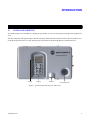
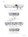
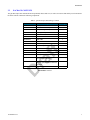
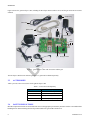
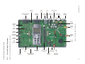
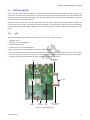
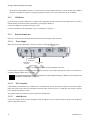
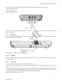
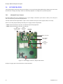
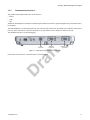
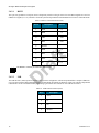
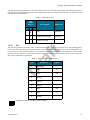
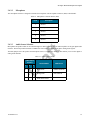
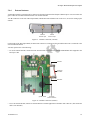
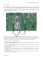
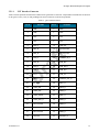
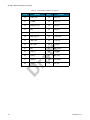
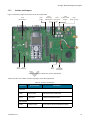
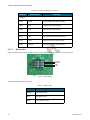
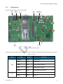
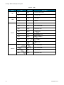
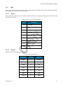
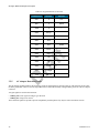
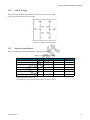
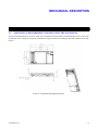
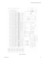
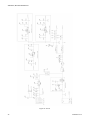
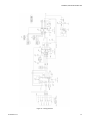
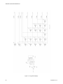
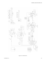
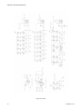
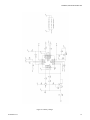
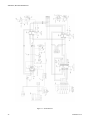
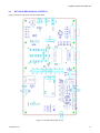
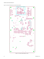
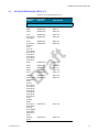
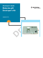
Developer's Guide
Motorola g20
Developer’s Kit
D
ra
ft
98-08901C67-O
REVISION HISTORY
Revision
ii
Date
Purpose
98-08901C67-O
g20 Developer’s Kit
CONTENTS
REVISION HISTORY ................................................................................................................................................................ii
PREFACE
1.1 SCOPE OF THIS MANUAL .................................................................................................................................................1
1.2 WHO SHOULD USE THIS MANUAL.................................................................................................................................1
1.3 DISCLAIMER ........................................................................................................................................................................1
1.4 SAFETY .................................................................................................................................................................................1
1.4.1 User Operation ............................................................................................................................................................1
1.4.2 Antenna Installation ....................................................................................................................................................2
1.5 APPLICABLE DOCUMENTS ..............................................................................................................................................2
1.6 TRADEMARKS .....................................................................................................................................................................2
1.7 TERMS AND ABBREVIATIONS ........................................................................................................................................3
1.8 HOW THIS MANUAL IS ORGANIZED..............................................................................................................................3
INTRODUCTION
2.1 GENERAL DESCRIPTION...................................................................................................................................................5
2.2 PACKAGE CONTENTS........................................................................................................................................................7
2.3 ACCESSORIES......................................................................................................................................................................8
2.4 SAFETY PRECAUTIONS.....................................................................................................................................................8
DEVELOPER BOARD AND INTERFACES DESCRIPTION
3.1 HOW THIS CHAPTER IS ORGANIZED .............................................................................................................................9
3.2 OVERVIEW ...........................................................................................................................................................................9
3.2.1 Developer Board Features...........................................................................................................................................9
3.2.2 Developer Board Components ..................................................................................................................................10
3.3 INITIAL SETUP...................................................................................................................................................................11
3.3.1 g20.............................................................................................................................................................................11
3.3.2 USB Driver................................................................................................................................................................12
3.3.3 External Connectors ..................................................................................................................................................12
© Motorola Inc., 2003
March 2003
98-08901C67-O
3.4 CONFIGURATION ............................................................................................................................................................. 14
3.4.1 Alternate Power Sources .......................................................................................................................................... 14
3.4.2 Communication Interfaces........................................................................................................................................ 17
3.4.3 Audio Interface ......................................................................................................................................................... 20
3.4.4 External Antenna ...................................................................................................................................................... 23
3.4.5 Ignition...................................................................................................................................................................... 24
3.4.6 Wakeup ..................................................................................................................................................................... 24
3.4.7 LEDs Logic and Control........................................................................................................................................... 24
3.4.8 SIM Card .................................................................................................................................................................. 24
3.4.9 Host........................................................................................................................................................................... 25
3.5 COMPONENTS AND SPECIFICATIONS ........................................................................................................................ 26
3.5.1 Connectors Description ............................................................................................................................................ 26
3.5.2 Switches and Jumpers............................................................................................................................................... 29
3.5.3 LED Indicators ......................................................................................................................................................... 31
3.5.4 MMI.......................................................................................................................................................................... 33
3.5.5 AC Adapter Detection Circuit .................................................................................................................................. 34
3.5.6 ADC Test Logic........................................................................................................................................................ 35
3.5.7 Electrical Specifications ........................................................................................................................................... 35
MECHANICAL DESCRIPTION
4.1 MECHANICAL REQUIREMENTS FOR MOUNTING THE G20 MODULE ................................................................. 37
SERVICE SUPPORT
5.1 CUSTOMER ASSISTANCE ............................................................................................................................................... 39
5.1.1 Motorola Workflow .................................................................................................................................................. 40
5.1.2 Service Centers ......................................................................................................................................................... 40
5.1.3 Ordering Accessories................................................................................................................................................ 41
SCHEMATICS, PLACEMENT AND PARTS LIST
6.1 SCHEMATICS..................................................................................................................................................................... 43
6.2 DEVELOPER BOARD PLACEMENT............................................................................................................................... 53
6.3 DEVELOPER BOARD PARTS LIST................................................................................................................................. 55
INDEX
iv
98-08901C67-O
LIST OF FIGURES
Figure 1. g20 Developer’s Kit (top view, with cover) ................................................................................................................. 5
Figure 2. g20 Developer’s Kit (front, with cover) ....................................................................................................................... 6
Figure 3. g20 Developer’s Kit (left side, with cover) .................................................................................................................. 6
Figure 4. g20 Developer’s Kit (rear, with cover)......................................................................................................................... 6
Figure 5. g20 Developer’s Kit (right side, with cover) ................................................................................................................ 6
Figure 6. g20 Developer’s Kit with Accessories and the g20...................................................................................................... 8
Figure 7. Developer Board Components.................................................................................................................................... 10
Figure 8. Connecting the g20 ..................................................................................................................................................... 11
Figure 9. Developer Board Power Switch and Adapter Connector ........................................................................................... 12
Figure 10. Audio Connectors ..................................................................................................................................................... 13
Figure 11. SIM Tray................................................................................................................................................................... 13
Figure 12. Power Supply Connectors, Jumpers and Switches ................................................................................................... 14
Figure 13. USB, RS232 and DIAG (SPI) Connectors ............................................................................................................... 17
Figure 14. Audio Connectors and Jumper.................................................................................................................................. 20
Figure 15. Antenna Connectors (external) ................................................................................................................................. 23
Figure 16. Antenna Connectors (internal).................................................................................................................................. 23
Figure 17. 70-pin Connectors..................................................................................................................................................... 25
Figure 18. Jumpers and Switches on Developer Board ............................................................................................................. 29
Figure 19. Dip Switches ............................................................................................................................................................. 30
Figure 20. LEDs on Developer Board........................................................................................................................................ 31
Figure 21. ADC Test Logic Design ........................................................................................................................................... 35
Figure 22. Mechanical Mounting Requirements........................................................................................................................ 37
Figure 23. Developer Board Top-Level Design......................................................................................................................... 44
Figure 24. Diagnostics................................................................................................................................................................ 45
Figure 25. Power ........................................................................................................................................................................ 46
Figure 26. Debug Interface......................................................................................................................................................... 47
Figure 27. Keypad and Display.................................................................................................................................................. 48
Figure 28. Audio Interface ......................................................................................................................................................... 49
Figure 29. LEDs ......................................................................................................................................................................... 50
Figure 30. Battery Charger......................................................................................................................................................... 51
Figure 31. Serial Interface .......................................................................................................................................................... 52
Figure 32. Developer Board Top Layout ................................................................................................................................... 53
Figure 33. Developer Board Bottom Layout.............................................................................................................................. 54
98-08901C67-O
v
LIST OF TABLES
Table 1. Terms and Abbreviations ............................................................................................................................................... 3
Table 2. g20 Developer’s Kit Package Contents.......................................................................................................................... 7
Table 3. Accessories Sold Separately .......................................................................................................................................... 8
Table 4. Power Adapter Connector Pinout (J230) ..................................................................................................................... 15
Table 5. Battery Connector Pinout (P600) ................................................................................................................................. 15
Table 6. Power Source Jumper (P202)....................................................................................................................................... 16
Table 7. Developer Board Power Jumper (P201) ...................................................................................................................... 16
Table 8. g20 Power Jumper (P201) ............................................................................................................................................ 16
Table 9. RS232-1 Connector Pinout (J350) ............................................................................................................................... 18
Table 10. USB Connector Pinout (J300).................................................................................................................................... 18
Table 11. USB Jumper (P300) ................................................................................................................................................... 19
Table 12. RS232-2 Connector Pinout (J500) ............................................................................................................................. 19
Table 13. Speaker Connector Pinout (J430)............................................................................................................................... 20
Table 14. Microphone Connector Pinout (J460) ........................................................................................................................ 21
Table 15. Audio Jumper (P420) ................................................................................................................................................. 21
Table 16. Headset Connector Pinout (J440)............................................................................................................................... 22
Table 17. Alert Transducer Pinout (LS400)............................................................................................................................... 22
Table 18. SIM Connector Pinout (J100) .................................................................................................................................... 24
Table 19. SIM Card Detect Logic Jumper (P110) ..................................................................................................................... 24
Table 20. Connectors.................................................................................................................................................................. 26
Table 21. g20 Connectors Pinout ............................................................................................................................................... 27
Table 22. Switches and Jumpers ................................................................................................................................................ 29
Table 23. Dip Switches .............................................................................................................................................................. 30
Table 24. LEDs .......................................................................................................................................................................... 31
Table 25. Display Connector Pinout (DS800) ........................................................................................................................... 33
Table 26. Keypad Functions....................................................................................................................................................... 33
Table 27. Electrical Specifications............................................................................................................................................. 35
Table 28. Developer Board Parts List ....................................................................................................................................... 55
vi
98-08901C67-O
1. PREFACE
1.1
SCOPE OF THIS MANUAL
This manual introduces the g20 Developer's Kit, and describes the technical details required by the data terminal equipment user
to successfully integrate the Motorola g20 cellular engine into an original equipment manufacturer (OEM) wireless host device.
With the help of this manual, the user can utilize the Developer's Kit to conduct a full series of test and evaluation procedures
on the g20, as well as perform application development.
We at Motorola want to make this guide as helpful as possible. Keep us informed of your comments and suggestions for
improvements.
You can reach us by email: GSM [email protected].
1.2
WHO SHOULD USE THIS MANUAL
This manual is intended for all members of the DTE OEM integration team who will use the g20 Developer’s Kit, including
representatives from hardware, software and RF engineering disciplines.
1.3
DISCLAIMER
This guide provides advice and guidelines to developers. Responsibility regarding how the information is used lies entirely with
the OEM. Statements indicating support provided by, or offered by, Motorola are subject to change at any time.
Motorola reserves the right to make any changes to this manual.
1.4
1.4.1
SAFETY
User Operation
Do not operate your telephone when a person is within eight inches (20 centimeters) of the antenna. A person or object within
eight inches (20 centimeters) of the antenna could impair call quality and may cause the phone to operate at a higher power level
than necessary, as well as expose that person to RF energy in excess of that established by the FCC RF Exposure Guidelines.
IMPORTANT: The telephone must be installed in a manner that provides a minimum separation distance of eight inches (20
centimeters) or more between the antenna and persons in order to satisfy FCC RF exposure requirements for mobile transmitting
devices.
IMPORTANT: To comply with the FCC RF exposure limits and to satisfy the categorical exclusion requirements for mobile
transmitters, the requirements described in the following section must be met.
98-08901C67-O
1
Preface
1.4.2
Antenna Installation
• A minimum separation distance of eight inches (20 centimeters) must be maintained between the antenna and all persons.
• The effective radiated power of the transmitter must be less than 3.0 Watts ERP (4.9 Watts or 36.9 dBm EIRP). This requires
that the combination of antenna gain and feed line loss not exceed 16 dBi.
1.5
APPLICABLE DOCUMENTS
g20 Cellular Engine Module Description: 9808901C66-O
g20 AT Commands: 9808901C68-O
1.6
TRADEMARKS
MOTOROLA and the Stylized M Logo are registered in the U.S. Patent and Trademark Office. All other product and service
names are the property of their respective owners.
© Motorola, Inc. 2003
2
98-08901C67-O
Preface
1.7
TERMS AND ABBREVIATIONS
This section provides definitions for terms and abbreviations used in this document.
Table 1. Terms and Abbreviations
Acronym/Term
1.8
Definition/Description
ADC
Analog to Digital Converter
CMOS
Complementary Metal Oxide Semiconductor
CODEC
Coder-Decoder
DTE
Data Terminal Equipment (such as terminals, PCs and so on)
EME
Electromagnetic Energy Exposure
ESD
Electro-Static Discharge
EVB
Evaluation Board
GPRS
General Packet Radio Service
GSM
Global System for Mobile Communications
IRQ
Interrupt Request
LED
Light-Emitting Diode
MIDI
Musical Instrument Digital Interface
MMCX
Mini Micro Coax
MMI
Man-Machine Interface
OEM
Original Equipment Manufacturer
PCM
Pulse Code Modulation
RF
Radio Frequency
SIM
Subscriber Identity Module
SPI
Serial Peripheral Interface
UART
Universal Asynchronous Receiver Transmitter
USB
Universal Serial Bus
UUT
Unit Under Test
HOW THIS MANUAL IS ORGANIZED
This manual contains the following chapters:
• Chapter 1 contains this preface.
• Chapter 2 introduces the g20 Developer’s Kit and provides important safety instructions.
• Chapter 3 describes the Developer Board and its components in detail, including connectors, jumpers, Dip switches and
LED indicators. It also includes a set of setup procedures for first-time use.
• Chapter 4 provides the mechanical requirements for mounting the g20 onto the Developer Board.
• Chapter 5 provides contact information for Motorola Service Support and Customer Assistance.
• Chapter 6 includes schematic diagrams of the g20 Developer’s Kit as well as a complete parts list.
98-08901C67-O
3
Preface
4
98-08901C67-O
2. INTRODUCTION
2.1
GENERAL DESCRIPTION
The g20 Developer’s Kit is intended for evaluating the g20 module, as well as for developing and testing software applications
for it.
The main component of the g20 Developer’s Kit is the Developer Board, which is mounted in a chassis. The kit includes a cover
for the Developer Board. The cover has openings on the top and side for the Developer Board’s external connectors.
Display
Keypad
SIM Tray
On-board Antenna
Figure 1. g20 Developer’s Kit (top view, with cover)
98-08901C67-O
5
Introduction
SIM Tray
g20 Power
Indicator LED
g20 Power On/Off
Pushbutton
Figure 2. g20 Developer’s Kit (front, with cover)
Speaker
Connector
Headset
Connector
Microphone
Connector
Figure 3. g20 Developer’s Kit (left side, with cover)
Power Adapter
Power
Connector
Indicator LED
Battery Connector
Power
On/Off Switch
USB
Connector
RS232-1
Connector
RS232-2 (SPI)
Connector
Figure 4. g20 Developer’s Kit (rear, with cover)
External
Antenna Input
Internal
Antenna Input
Figure 5. g20 Developer’s Kit (right side, with cover)
6
98-08901C67-O
Introduction
2.2
PACKAGE CONTENTS
The g20 Developer’s Kit includes the Developer Board, chassis and cover, as well as accessories that enable you to better utilize
the board. The kit contains the following components:
Table 2. g20 Developer’s Kit Package Contents
Part No.
Description
Quantity
FTN8121B
Developer Board
1
SPN4716B
Wall Mount Power Adapter
1
SYN7456A
European Plug for Adapter
1
SYN7455A
UK Plug for Adapter
1
8102316T02
Test SIM Card
1
SYN6962A
Mono Headset w/Detect
1
3087563V12
USB Cable
1
3087563V13
RS232 Cable
1
2987604U01
DC Power Input Mount — VCC
1
2987604U02
DC Power Input Mount — GND
1
0310907A03
M2/6mm Screw (for g20 fastening)
2
8509397T03
Antenna Stub
1
1587867V01
Developer Board Chassis
1
1587867V02
Developer Board Cover
1
3087568V01
RF cable between internal antenna
and external connectors
1
3087568V02
RF cable with MMCX connector
between g20 and external antenna
connector
1
Documentation and Software CD
1
Kit Number: F3030A
98-08901C67-O
7
Introduction
Figure 6 shows the g20 Developer’s Kit, including the Developer Board (without cover) and the g20 and some accessories
attached.
Adapter Plug
USB Cable
Battery
RS232 Cable
Speaker
Power Adapter
RF
Cables
g20
Developer Board
Headset
Microphone
Figure 6. g20 Developer’s Kit with Accessories and the g20
The Developer’s Kit does not include a g20 device. A g20 must be obtained separately.
2.3
ACCESSORIES
Table 3 provides a list of accessories for the g20 Developer’s Kit.
Table 3. Accessories Sold Separately
Part No.
0189727L01
2.4
Description
3.6V Lithium-Ion Battery
0187506V08
Host Interconnect Flex Cable
FSN5527A
Audio Speaker 8 Ω
SYN5708D
Audio Microphone (Passive)
SAFETY PRECAUTIONS
Most Developer Board circuits are not shielded. Be sure to take appropriate precautionary measures in order to avoid ESD while
handling the kit. ESD can damage the Developer Board and/or the g20 module attached to it.
8
98-08901C67-O
3. DEVELOPER BOARD AND
INTERFACES DESCRIPTION
3.1
HOW THIS CHAPTER IS ORGANIZED
This chapter contains the following sections:
• Overview provides an overview of the Developer Board.
• Initial Setup describes how to set up and prepare the Developer Board for first-time use.
• Configuration describes how to modify the default settings to control the operation of the Developer Board.
• Components and Specifications lists each connector, switch, jumper, Dip switch and LED and provides other details and
specifications for the Developer Board.
3.2
OVERVIEW
The g20 Developer Board is designed to support the hardware and software development and validation of the g20 GSM/GPRS
data module. The Developer Board provides a peripheral platform to operate the g20 as a standalone product, and to easily
access the g20’s 70-pin interface connector signals.
The Developer Board has the following functions:
• Serves as a mounting platform for the g20 module
• Supplies the g20 module with power
• Provides standard communication interfaces (USB and RS232) to the g20
3.2.1
Developer Board Features
The Developer Board provides the following features to facilitate software and hardware development:
• Easy access to the g20’s 70-pin interface connector signals, through a large header connector and an external host connector
• AC, battery and DC power supplies for board operation
• LED indicators for critical signals
• Display and keypad for phone operation
• USB and RS232 serial interfaces
• Secondary RS232 interface using the SPI bus (for g20 debugging)
• Digital audio interface
• Analog audio interface for speaker, alert transducer, microphone and headset
• SIM card connector
• Switches and jumpers for controlling board operation
98-08901C67-O
9
RS232-1
Connector
Power
Indicator LED
USB
Connector
DC Power
Connectors
Off
SPI and
RS232-2
LEDs
Figure 7 shows the Developer Board and its components:
Developer Board Components
On
Power
Adapter
Connector
Power Source
Jumper
Power Jumpers
Speaker
Connector
3.2.2
Battery
Connector
USB
LEDs
Dip
Switches
Developer Board and Interfaces Description
98-08901C67-O
Power On/Off
Switch
g20 UUT
Connector
Host
Connector
Microphone
Connector
SIM Card
Detect Logic
Jumper
Headset
Connector
Internal
Antenna
Input
External
Antenna
Input
Internal
Antenna
Alert
Transducer
MMI Keypad
& Display
GPIO
LEDs
Audio
Jumper
Entertainment Mute
Input Jumper
g20 Diagnostics
Connector
g20 Power
Indicator LED
SIM Card
Tray
g20 Power
Pushbutton
10
RS232-2 Debugger
Connector
Fuse
2.5A
Figure 7. Developer Board Components
USB
Jumper
RS232-1
LEDs
Developer Board and Interfaces Description
3.3
INITIAL SETUP
This section describes the initial procedure for setting up the g20 Developer Board for testing and evaluating of the g20. The
tasks in this section need to be performed only once, before the first time you use the g20 Developer’s Kit. After performing the
initial setup, you can modify the default settings or use different peripheral devices, as described in “Configuration” on page 14.
Perform the steps in this section in sequence.
Before starting, remove the cover of the Developer Board. The cover simply slides up off the board, and does not require the
removal of any screws or clips. After setting up the Developer Board, you can place the cover back on the Developer Board by
simply pushing it gently back into place. Make sure the cover is aligned properly with the external connectors on the side of the
board.
3.3.1
g20
The Developer Board works with all versions of the g20. There are four versions of the g20:
• European version
• European version with USB driver
• North American version
• North American version with USB driver
Connect the g20 to the Developer Board by performing the following steps:
• Place the g20 into the area on the Developer Board marked by a white rectangle, and push the g20 70-pin connector down
into the UUT 70-pin connector (P1). The two screw holes on the g20 should be aligned with the g20 spacers (M2 and M3).
• Fasten the g20 to the Developer Board using the two M2 screws provided with the kit.
Internal Antenna
Connector
g20
RF Cable
g20
Screws
MMCX
Connector
RF
Cable
External Antenna
Connector
Figure 8. Connecting the g20
98-08901C67-O
11
Developer Board and Interfaces Description
• An RF cable with an MMCX connector is connected to the external antenna connector. Connect the RF cable’s MMCX
connector to the MMCX connector of the g20 by pushing it in until it clicks. This connects the g20 to the antenna.
3.3.2
USB Driver
If you are using a g20 with a USB driver, you must set the USB jumper (P300), located next to the USB connector, in order to
indicate that the g20 and not the Developer Board is providing the USB driver.
Connect the USB jumper (P300) between pins 1 and 2.
For more information on the USB jumper, refer to “Configuration” on page 14.
3.3.3
External Connectors
Place the cover back on the Developer Board and connect the following external connectors.
3.3.3.1
Power Supply
Make sure the Developer Board power switch is off before connecting the power supply.
Developer Board
On/Off Switch
Power Adapter
Connector
Power Indicator
LED
Figure 9. Developer Board Power Switch and Adapter Connector
Connect the power adapter to the Developer Board adapter connector (J230), which is labeled Power on the cover of the Developer Board. Plug the adapter into a wall outlet.
The g20 Developer Board can also be powered by an external DC power supply or battery cell. These options are
described in “Configuration” on page 14.
Note
3.3.3.2
PC Connection
USB and RS232 serial interfaces are available for PC communications. If a PC connection is required, connect either a RS232
cable with a male D-type connector to the RS232-1 labeled UART1 connector (J350), or a USB cable with a B-type connector
to the USB labeled connector (J300).
The g20 Developer’s Kit includes the necessary RS232 and USB cables.
3.3.3.3
Audio Devices
Connect the headset, which includes a headphone and a microphone. You can instead connect the speaker and microphone,
which are optional accessories.
12
98-08901C67-O
Developer Board and Interfaces Description
The jacks for these devices are on the left side of the Developer Board and labeled on the board as follows:
• Headset: HEADSET (J440)
• Microphone: MIC (J460)
• Speaker: SPEAKER (J430)
Speaker
Connector
Headset
Connector
Microphone
Connector
Figure 10. Audio Connectors
You can use the speaker and microphone together or use each one by itself. You cannot use the headset while using either the
speaker or microphone.
3.3.3.4
SIM Card
Insert a SIM card into the SIM tray (J100) with the contacts down and the cut-off corner to the front and right. A diagram on the
cover indicates how to insert the SIM.
SIM Tray
Figure 11. SIM Tray
A test SIM card is provided with the g20 Developer’s Kit.
3.3.3.5
Antenna
Connect the additional RF cable from the EXT ANT connector to the INT ANT connector. This connects the g20 to the onboard internal antenna.
3.3.3.6
Power Up
You must turn on the Developer Board power and then turn on the g20.
• Turn on the Developer Board power by switching on the power switch (S200). The Developer Board power indicator LED
is lit.
• Turn on the g20 by pushing in the g20 on/off switch (S110), holding it in for about a second and then releasing it. You can
also turn on the g20 by pressing and holding the red function button on the keypad. (The red button also functions as the endcall button.) The g20 on/off LED is lit and the display above the keypad shows text.
The Developer Board is now ready for use.
98-08901C67-O
13
Developer Board and Interfaces Description
3.4
CONFIGURATION
After performing the initial setup in the previous chapter, you can use the Developer Board with the default setup. This section
describes how to change this setup in order to use different peripherals or to change the way the board operates.
3.4.1
Alternate Power Sources
Developer Board power can be supplied from an AC power adapter, external DC power source or battery. The same power
source is used for the g20 and the board peripherals.
You must connect the Developer Board to a power source, and then set the power source jumper (P202), if necessary.
There are two other jumpers that help control the power supply in the Developer Board:
• P201: Connects/disconnects the power from the Developer Board peripherals
• P200: Connects/disconnects the power from the g20
P201
(Developer Board
Power Jumper)
P200
(g20 Power
Jumper)
DC Power
Connectors
Battery Connector
Power Adapter
Connector
P202
(Power Source
Jumper)
Figure 12. Power Supply Connectors, Jumpers and Switches
Each power supply option is described in the sections that follow.
14
98-08901C67-O
Developer Board and Interfaces Description
3.4.1.1
AC Adapter Operation
When using an AC adapter, the adapter is connected to the power adapter connector (J230). The adapter supplies a constant 4.5
V, which is regulated to a nominal 4.1 V on the Developer Board.
Table 4. Power Adapter Connector Pinout (J230)
Pin #
3.4.1.2
Pin Name
1
GND
2
Detection circuit
3
VCC
DC Power Source Operation
You can use an external DC power supply by connecting it to the VCC (J201) and GND (J200) connectors.
The supplied DC input connectors must be attached to the Developer Board in order to use an external DC power source. Use
the red connector for VCC and the black one for GND. Connect the DC power source to these connectors using banana plugs,
alligator clips or wire.
The DC voltage applied through this connection should not exceed the recommended operational limits of 3 V to 4.2 V. In all
cases, the DC source input is protected from over voltage and reverse polarity, and includes a 2.5A protective fuse.
!
It is recommended to remove jumper P202 when using the DC power source. The DC power source should not be
used when other sources are connected.
Caution
3.4.1.3
Battery Operation
The Developer Board supports a battery power supply. The battery used must be a 3.6V lithium-ion cell, corresponding to
Motorola part number 0189727L01. The battery is an optional accessory.
When using a battery as the main power source, the AC adapter input operates as a battery charger, which connects to an
on-board battery charging circuit.
Table 5. Battery Connector Pinout (P600)
Pin #
98-08901C67-O
Pin Name
1
VCC
2
GND
15
Developer Board and Interfaces Description
3.4.1.4
Power Source Selection
The Developer Board AC adapter and battery power inputs include a selection jumper (P202) that diverts either the regulated
AC adapter power or the battery power to the board.
Table 6. Power Source Jumper (P202)
P202 Jumper
Position
1
2
•
•
•
Selected Mode
Power Source
3
•
Adapter
AC Adapter
Battery
LiIon Battery
Adapter and battery disconnected
DC power only
Jumpers are provided for disconnecting the power from the Developer Board and for disconnecting the power from the g20.
You may wish to remove the Developer Board power jumper and shut off the power to the board in order to diagnose a problem
that may be caused by the board. The g20 will continue to receive power.
You may also want to remove the g20 power jumper and then connect an amperometer to the jumper’s two pins to measure the
current through the g20.
Table 7. Developer Board Power Jumper (P201)
P201
Jumper
Position
1
2
•
•
Selected Mode
Developer Board connected to
power source
Developer Board disconnected
from power source
Table 8. g20 Power Jumper (P201)
P200
Jumper
Position
1
2
•
•
Selected Mode
g20 connected to power
source
g20 disconnected from power
source
16
98-08901C67-O
Developer Board and Interfaces Description
3.4.2
Communication Interfaces
The g20 Developer Board includes three serial interfaces:
• RS232
• USB
• SPI
The RS232 and USB ports are multiplexed within the g20, and therefore cannot be operated simultaneously. The default connection is RS232.
The USB and RS232 is not detected dynamically. The selected serial connection is determined by the USB cable connection at
power up. If the USB cable is connected (and the PC is on), then USB is selected. Otherwise, RS232 is selected.
The SPI RS232 interface is used for debugging.
USB
Connector
RS232-1
Connector
RS232-2 (SPI)
Connector
Figure 13. USB, RS232 and DIAG (SPI) Connectors
Each of these serial interfaces is described in the sections that follow.
98-08901C67-O
17
Developer Board and Interfaces Description
3.4.2.1
RS232
The 9-pin, D-type RS232-1 serial port (J350) is the primary interface to the g20 UUT. The UUT RS232 signals are active-low
CMOS-level signals (0-2.7 V), which are converted by the Developer Board to standard RS232 levels for PC communications.
Table 9. RS232-1 Connector Pinout (J350)
Pin #
Description
DTE I/O
1
DCD
In
2
RXD
In
3
TXD
Out
4
DTR
Out
5
Ground
6
DSR
In
7
RTS
Out
8
CTS
In
9
RI
In
The RS232-1 connector pin names are DTE-oriented.
Note
3.4.2.2
USB
The USB interface (J300) operates according to the g20 UUT configuration. The Developer Board has a complete USB transceiver circuit to support USB communications for g20 units that do not include a USB driver of their own. The Developer Board
USB interface can be overridden manually when using a g20 unit that does include its own USB driver interface.
Table 10. USB Connector Pinout (J300)
Pin #
18
Description
1
VCC
2
D-
3
D+
4
Ground
98-08901C67-O
Developer Board and Interfaces Description
The USB jumper (P300) located next to the USB connector selects between the Developer Board USB interface and the UUT
USB interface. By changing the jumper position, the USB_VBUS signal is diverted to the selected driver (in the g20 or on the
Developer Board) and operates it.
Table 11. USB Jumper (P300)
P300
Jumper
Position
1
2
Selected Mode
USB Source
3
• •
•
•
g20
g20 driver
EVB (Developer Board)
EVB driver
USB disconnected
3.4.2.3
SPI
The 9-pin D-type RS232-2 serial port (J500) is connected to the g20 internal SPI bus. This interface is used to debug applications. On the Developer Board, the g20 SPI interface is converted to standard RS232 signals for PC communications. The
conversion process uses the RS232 interface as a second slave on the internal g20 SPI bus, and communicates with it as such.
SPI read and write operations are performed normally, using the CS and IRQ signals provided by the conversion circuit. The
IRQ signal is connected to a g20 IRQ pin.
Table 12. RS232-2 Connector Pinout (J500)
Pin #
Description
DTE I/O
1
Unused
2
RXD
In
3
TXD
Out
4
Unused
5
Ground
6
Unused
7
RTS
Out
8
CTS
In
9
Unused
The RS232-2 connector pin names are DTE-oriented.
Note
98-08901C67-O
19
Developer Board and Interfaces Description
3.4.3
Audio Interface
The Developer Board includes analog and digital audio interfaces. The audio interface contains a hands-free speaker and microphone, a headset, and an alert transducer.
Speaker
Microphone
Headset
Alert Transducer
Audio Jumper
Figure 14. Audio Connectors and Jumper
3.4.3.1
Speaker
The differential speaker interface is designed as a hands-free speaker. The Developer Board uses an audio amplifier to amplify
the speaker audio output to desired levels. The speaker connector (J430) is labeled SPEAKER. The speaker output is 8 ohms
matched.
Table 13. Speaker Connector Pinout (J430)
Pin #
20
Description
1
Not connected
2
Speaker positive output
3
Speaker negative output
4
Not connected
98-08901C67-O
Developer Board and Interfaces Description
3.4.3.2
Microphone
The microphone interface is designed as a hands-free microphone. The microphone connector (J460) is labeled MIC.
Table 14. Microphone Connector Pinout (J460)
Pin #
3.4.3.3
Description
1
Ground
2
Microphone audio-in
3
Ground
4
Ground
5
Ground
Audio Source Selection
Microphone and speaker audio can be routed through two different sources: the g20 audio amplifiers or the g20 digital audio
interface. The Developer Board includes a CODEC that converts the g20 digital audio data to analog audio signals.
The P420 jumper selects the speaker and microphone source, as indicated in Table 15. This enables you to test the digital or
analog audio channels.
Table 15. Audio Jumper (P420)
P300 Jumper
Position
1
2
•
•
•
Selected Mode
USB Source
3
•
Digital audio
CODEC audio I/O
Analog audio
G20 audio I/O
Audio disconnected
98-08901C67-O
21
Developer Board and Interfaces Description
3.4.3.4
Headset
The headset interface is designed as a portable phone audio interface, and is similar to a phone headset interface. The headset
connector (J440) includes a speaker, microphone and a detection signal. The speaker and microphone signals are directly
connected to the g20 audio signals.
The purpose of the detection circuit is to switch the g20 headset audio paths on and off, whenever a headset connection is
detected. Headset detection is made whenever a headset plug is inserted into the jack. This action disables the g20 microphone
and speaker, and routes the audio signals to the headset.
Table 16. Headset Connector Pinout (J440)
Pin #
3.4.3.5
Description
1
Ground
2
Headset-detect switch
3
Speaker audio-out
4
Microphone audio-in
5
Ground
Alert Transducer
The Developer Board includes an on-board transducer, labeled ALERT, for alert audio sounds (LS400). The transducer is
connected directly to the g20 differential alert outputs. The alert transducer sounds the g20 MIDI signals.
Table 17. Alert Transducer Pinout (LS400)
Pin #
22
Description
1
Alert audio inverted output
2
Alert audio positive output
3
Alert audio inverted output
4
Alert audio inverted output
98-08901C67-O
Developer Board and Interfaces Description
3.4.4
External Antenna
An antenna (internal or external) must be connected to the Developer Board for adequate GSM reception. You can connect the
g20 to either the on-board internal antenna or to an external antenna.
Two RF connectors on the side of Developer Board, labeled INT ANT and EXT ANT on the cover, are used for setting up the
antenna.
External
Antenna Input
Internal
Antenna Input
Figure 15. Antenna Connectors (external)
On the inside of the Developer Board, the EXT ANT connector is connected to the g20 and the INT ANT is connected to the
on-board internal antenna.
You must perform one of the following:
• To use the internal antenna, connect the EXT ANT and INT ANT connectors with the additional RF cable supplied in the
Developer’s Kit.
INT ANT
Additional
RF Cable
EXT ANT
g20 RF Cable
On-board
Internal Antenna
Figure 16. Antenna Connectors (internal)
• To use an external antenna, connect an external antenna or antenna application to the EXT ANT connector. (The connection
cable is not included.)
98-08901C67-O
23
Developer Board and Interfaces Description
3.4.5
Ignition
The Developer Board contains an on/off Dip switch, labeled IGN, that is connected to the g20 UUT ignition circuit. You can
use this Dip switch to turn on and off the g20.
3.4.6
Wakeup
The Developer Board includes a wakeup Dip switch, labeled WAKEUP, that toggles the g20 WAKEUP_IN_N signal.
Generally, your application wakes up the g20. In cases where the application is not ready for integration, you can force wakeup
of the g20 by turning on this Dip switch.
3.4.7
LEDs Logic and Control
The Developer Board includes LED indicators for critical signals. A 3.0V regulator powers the LEDs.
A Dip switch enables you to turn off all the LEDs on the Developer Board, for example, to reduce power consumption. The
Developer Board power on/off LED and the g20 on/off LED are always active and cannot be disabled.
3.4.8
SIM Card
The SIM card connector (J100) is external to the UUT, but is connected directly to it, similar to an internal SIM. The UUT can
accept 1.8V and 3V SIM cards.
Table 18. SIM Connector Pinout (J100)
Pin
Description
1
Ground
2
Presence detect
3
Clock
4
Reset
5
VCC
6
Serial data I/O
7
VPP
8
Ground
Use the SIM card detect logic jumper (P110) to choose active-high or active-low detection configurations.
Table 19. SIM Card Detect Logic Jumper (P110)
P110 Jumper
Position
1
2
•
•
•
Selected Mode
3
Active-low
•
Active-high
Not active
24
98-08901C67-O
Developer Board and Interfaces Description
3.4.9
Host
An external application may communicate with the g20 through the host connector (J1) and control some or all of the g20's
functions. The host connector enables you to integrate the g20 into an application without installing the g20 inside the product.
The host connector operates in parallel with the developer board peripherals and enables an external application to share g20
resources with the developer board. You may select any g20 function to control externally, through the host connector, and allow
the developer board to control other functions.
70-pin
Host Connector
g20 70-pin
Diagnostics Connector
g20 70-pin
Connector
Figure 17. 70-pin Connectors
You can connect an external application to the g20 Developer Board using a host interconnect flex cable and connecting it to
the host connector (J1). Connect the other end of the cable to the external application. The cable is an optional accessory.
All pin numbers and functions of the host connector are identical to those of the g20 UUT (P1) and the g20 diagnostic connector
(P100). For more information on the pins of the host connector, refer to “UUT Interface Connector” on page 27.
The following are guidelines for using the host connector:
• When using an external SIM card through the host connector, the developer board SIM card jumper (P110) must be disconnected and the SIM card tray should be empty.
• When using any of the serial communication channels (USB, RS232, SPI) through the host connector, the developer board
serial connectors should not be used.
• When using the IGN or WAKEUP functions through the host connector, the functions should be switched off on the developer board Dip switches.
• When using the analog audio channels through the host connector, disconnect all audio devices from the developer board.
• When using the PCM digital audio through the host connector, it is recommended to place the audio selection jumper (P420)
to analog audio mode.
• When connecting an external application that provides the power to the g20 and the Developer Board, remove any other
power sources from the Developer Board.
98-08901C67-O
25
Developer Board and Interfaces Description
3.5
3.5.1
COMPONENTS AND SPECIFICATIONS
Connectors Description
All the Developer Board connectors are marked by their reference number and by a pin-1 indicator. Table 20 describes the available connectors on the Developer Board.
Table 20. Connectors
Reference
Connector
Description
Internal Connectors (not visible when cover is on)
P1
g20 UUT
g20 UUT (unit under test) connector
J1
Host
Emulates the g20 connector for host systems
P100
Diagnostics
Debug header connector (70-pin)
J201
VCC
Developer Board DC power supply
J200
GND
Developer Board common ground
External Connectors (visible when cover is on)
26
J300
USB
USB B-type connector
J350
RS232-1
Primary RS232 to PC
J500
RS232-2
Secondary RS232 for debugging (SPI)
J430
Speaker
Hands-free system speaker jack
J460
Microphone
Hands-free system microphone jack
J440
Headset
Headset jack
P600
Battery
Battery connector
J230
AC adapter/charger
Wall-mount adapter connector (CE bus
compatible)
J100
SIM card
SIM card socket with detection
P2
Antenna connector
SMA connector internal antenna
M1
RF Antenna
SMA connector for external antenna
98-08901C67-O
Developer Board and Interfaces Description
3.5.1.1
UUT Interface Connector
Table 21 lists the pin names and functions available for the g20 interface connectors. All pin numbers and functions are identical
for the g20 UUT (P1), host (J1) and g20 Diagnostic (P100) connectors on the Developer Board.
Table 21. g20 Connectors Pinout
Pin #
98-08901C67-O
Pin Name
Pin #
Pin Name
1
GND
2
GND
3
GND
4
GND
5
VCC
6
VCC
7
VCC
8
VCC
9
RTS_N
10
USB_DET
11
RXD_N
12
Not connected
13
DSR_N
14
Not connected
15
CTS_N
16
WAKEUP_IN_N
17
DCD_N
18
PCM_DIN
19
DTR_N
20
PCM_DOUT
21
TXD_N
22
PCM_CLK
23
RI_N
24
PCM_FS
25
RESET_N
26
WAKEUP_OUT_N
27
BL_SINK
28
KBC1_N
29
CHRG_DIS
30
KBC0_N
31
CHRG_SW
32
KBR0_N
33
CHRG_STATE
34
KBR1_N
35
CHRG_DET_N
36
KBR2_N
37
Not connected
38
KBR3_N
39
TX_EN_N
40
KBR4_N
41
Not connected
42
KBR5_N
43
VIB_OUT
44
SIM_RST_N
27
Developer Board and Interfaces Description
Table 21. g20 Connectors Pinout (Continued)
Pin #
28
Pin Name
Pin #
Pin Name
45
CHRG_TYP
46
SIM_CLK
47
THERM
48
SIM_VCC
49
GPRS_DET_N
50
SIM_PD
51
IGN
52
SIM_DIO
53
ON_OFF_N
54
LCD_CS
55
HDST_INT_N
56
LCD_DATA
57
HDST_MIC
58
LCD_CLK
59
MIC_GND
60
LCD_RS
61
MIC
62
SPI_IRQ_N
63
ALRT_N
64
SPI_DIN
65
ALRT_P
66
SPI_CLK
67
SPKR_N
68
SPI_DOUT
69
SPKR_P
70
SPI_CS
98-08901C67-O
Developer Board and Interfaces Description
3.5.2
Switches and Jumpers
Figure 18 shows the jumpers and switches on the Developer Board.
P300
(USB)
S100
(Dip Switches)
P201
(Developer
P200
Board Power) (g20 Power)
S200
(Power On/Off
P202
Switch)
(Power Source)
Host
Connector
P420
P130
(Audio) (EMUTE)
P110
(SIM)
S110
(g20 On/Off
Pushbutton)
Figure 18. Jumpers and Switches on Developer Board
Table 22 describes the available switches and jumpers on the Developer Board.
Table 22. Switches and Jumpers
Reference
Switch/Jumper
Description
Switches
S200
Board on/off
Developer Board on/off switch
S110
g20 on/off
g20 on/off pushbutton switch
Options switch
Four switches for Developer Board options
Dip Switches
S100
98-08901C67-O
29
Developer Board and Interfaces Description
Table 22. Switches and Jumpers (Continued)
Reference
Switch/Jumper
Description
Jumpers
3.5.2.1
P420
Audio
Analog/digital audio-selection jumper
P201
EVB
Peripheral power input jumper
P200
UUT
g20 UUT power input jumper
P202
Source
Power source selection jumper
P110
SIM
SIM card detect logic selection jumper
P300
USB
USB driver source selection jumper
P130
EMUTE
Entertainment mute connection point
Dip Switches
Figure 19 shows the Dip switches provided on the Developer Board, which are located on the S100 component.
Not Used
WAKEUP
IGN
LEDS
Figure 19. Dip Switches
The following Dip switches are provided:
Table 23. Dip Switches
Reference
30
Description
WAKEUP
g20 wakeup signal
IGN
g20 ignition circuit
LEDS
on/off switch for LEDs
98-08901C67-O
Developer Board and Interfaces Description
3.5.3
LED Indicators
Figure 20 shows the LEDs on the Developer Board.
SPI
LEDs
RS232-2
LEDs
USB
LEDs
RS232-1
Developer
Board Power
Host
Connector
GPIO
LEDs
g20 On-Off
Figure 20. LEDs on Developer Board
Table 24 describes the LED indicators on the Developer Board. Each LED is marked on the board by the function it represents.
Table 24. LEDs
Group
GPIO
LED
Reference
Description
WAKEUP
D704
Wake-up in/out
IGN
D702
Ignition input
GPRS
D710
GPRS coverage indication
SIM
D703
SIM card reset indication
EMUTE
D708
Entertainment mute indicator
UUT
D701
g20 on/off
PWR
D200
Power
Power
98-08901C67-O
31
Developer Board and Interfaces Description
Table 24. LEDs
Group
LED
Reference
Description
CS
D741
SPI chip-select output
IRQ
D744
SPI IRQ input
VCC
D760
USB VBUS
DATA
D761
USB D+
RXD
D722
DTE receive data
TXD
D721
DTE transmit data
RTS
D724
Request to send
CTS
D723
Clear to send
DTR
D725
Data terminal ready
DSR
D726
Data set ready
DCD
D727
Carrier detect
RI
D728
Ring indicator
RXD
D743
DTE receive data
TXD
D742
DTE transmit data
CTS
D744
Clear to send
RTS
D745
Request to send
SPI
USB
RS232-1
RS232-2
32
98-08901C67-O
Developer Board and Interfaces Description
3.5.4
MMI
The Developer Board includes a man-machine interface (MMI), complete with display and keypad. The signals from the display
and keypad are directly connected to the UUT interface.
3.5.4.1
Display
The grayscale display (DS800) is not a standalone component, and includes a complete assembly in which it is housed, along
with other necessary parts.
Table 25. Display Connector Pinout (DS800)
Pin #
3.5.4.2
Description
1
Chip select
2
Reset
3
Register select
4
Serial clock
5
Serial data
6
Supply
7
Supply
8
Ground
9
Vout
Keypad
Table 26 describes the Developer Board keypad layout.
Table 26. Keypad Functions
98-08901C67-O
Pad Reference
Function
Alternate
S803
1
Punctuation
S802
2
ABC
S820
3
DEF
S801
4
GHI
S805
5
JKL
S804
6
MNO
S806
7
PQRS
33
Developer Board and Interfaces Description
Table 26. Keypad Functions (Continued)
3.5.5
Pad Reference
Function
Alternate
S817
8
TUV
S811
9
WXYZ
S809
0
+
S810
Star (*)
S815
Pound (#)
S814
Send
S813
End
S819
Menu
S822
Right
S823
Left
S818
Up
S816
Down
S812
Soft Right
S808
Soft Left
On/Off
AC Adapter Detection Circuit
The g20 charger module includes a detection logic circuit for detecting charger presence and type. The detection circuit is internal to the g20 module. However, the Developer Board does contain the necessary routing from the g20 UUT to the AC adapter
connector.
Two g20 signals are used for this detection:
• CHRG_TYP: ADC signal for charger type detection
• CHRG_SW: Charger rate control
These detection signals are present to provide compatibility with the phone. They may be removed in future versions.
34
98-08901C67-O
Developer Board and Interfaces Description
3.5.6
ADC Test Logic
The g20 includes an additional internal 47kΩ pull-up resistor at each ADC input.
Figure 21 describes the ADC test logic design.
Figure 21. ADC Test Logic Design
3.5.7
Electrical Specifications
Table 27 describes the electrical specifications of the Developer Board.
Table 27. Electrical Specifications
Parameter
Units
Min
Typ
Max
DC power supply
V
3.0
3.6
4.2
Adapter power supply
V
4.4
4.6
12
Battery power supply
V
3.0
3.6
4.2
Off current*
uA
3.6
On current
mA
8.0
8.25
8.45
Active current, peripherals off
mA
12.3
12.4
---
Active current, peripherals on**
mA
12.6
---
---
42.6
* When using DC power supply only.
** Depends on the active peripherals (LEDs, UART, USB, and so on) in use.
98-08901C67-O
35
Developer Board and Interfaces Description
36
98-08901C67-O
4. MECHANICAL DESCRIPTION
4.1
MECHANICAL REQUIREMENTS FOR MOUNTING THE G20 MODULE
The size of the g20 module is 45.2 x 24.4 x 6 mm. Two 2.4-mmØ holes are provided to accommodate M2 screws or #1-64 UNC
2A machine screws. Torque to 2 inches per pound. Refer to Figure 22 below for mounting requirements (dimensions in millimeters):
Figure 22. Mechanical Mounting Requirements
98-08901C67-O
37
Mechanical Description
38
98-08901C67-O
5. SERVICE SUPPORT
5.1
CUSTOMER ASSISTANCE
This section provides contact information for any possible queries that may arise, such as the following:
• Have questions?
• Having trouble getting the Developer Board set up?
• Technical questions?
• Configuration questions/problems?
• Technical operating problems?
• Need documentation?
The GSM/CDMA Data Module Customer Support Center is ready to assist you on integration issues.
Use the following email address to contact customer assistance: [email protected]
The support services provided by Motorola are subject to the agreement between the customer and Motorola and
may be at an additional charge to the customer. Motorola will inform the customer in advance of any such charge.
Note
Every new call/problem report should be directed to the help desk email address noted above. It is recommended to report each
individual issue in a separate email. The following information is required when reporting a problem:
• Customer name and address
• Customer contact information for this request, including:
• Name
• Telephone
• Fax number
• Mobile number
• Email address
• Product name (for example, d10, d15, g18, Apollo, CP211, and so on)
• Software version of the unit (ATI3 command) or model number
• PCB version. This information is located on the PCB near the RF connector.
• Severity of the problem
• Problem description, including:
• Operator name
• Type of SIM card (for example, Test, Pre-paid, or 5v/3v/1.8v)
• Configuration of the setup (such as Developer Board, handset, host, connections, and so on)
• Detailed scenario from startup
• Log of all the commands and the responses, beginning from startup
98-08901C67-O
39
Service Support
• Answers to the following questions:
• Was the same scenario tested on the Developer Board and the PC to reproduce the problem?
• How many units do you have, and how many of them have this problem?
• How often does the problem recur?
In addition to the information requested above, send the following AT commands and the HyperTerminal log with the
responses:
AT+CMEE=2
// To get textual error message
AT+CPIN?
// To get SIM card status
AT+CREG?
// To see if the TXVR is registered to the network
AT+CSQ
// To get the signal strength (RX level)
AT+CGSN
// To read the IMEI number of the unit
AT+CRSM=176,1
// To read the Flex ID
ATI3
// To get the software version of the TXVR
AT\S
// To get the setting of basic AT commands
AT+CMER=0,0,1,1
// To get messages and indicators from the handset display to the DTE
5.1.1
Motorola Workflow
The help desk uses the following workflow when responding to new calls:
1.
Each new call is registered in the help desk data base.
2.
The help desk immediately notifies the customer with the help desk system record number for each issue.
3.
A champion is assigned to be responsible for the new call, from arrival to closing.
4.
During this time, the champion updates the help desk system with the progress of the resolution process.
5.
The champion is the contact to the customer and the engineering team, and coordinates activities that are required to solve
the problem.
5.1.2
Service Centers
Motorola Electronics Taiwan PCS
11F, No, 296, Sec. 4, Jen-Ai Road
Taipei, 106, Taiwan, R.O.C
Motorola GmbH
Am Sophienhof 10
D-24941 Flensburg
Germany
40
98-08901C67-O
Service Support
Motorola Communications ISRAEL Ltd.
Service Operation
Attention: Shukrun Ofer
3 Krementsky Street
Tel Aviv, Israel 67899
Telephone: (972) 3 5658829
JNB Electronics Pty Ltd.
347 Settlement Road, Thomastown
VIC 3074
Australia
Field service should be coordinated with the Service Manager in Motorola using the following email address:
[email protected]
5.1.3
Ordering Accessories
You can order the following accessories for the g20 Developer’s Kit:
0189727L01
3.6V Lithium-Ion Battery
0187506V08
Host Interconnect Flex Cable
FSN5527A
Audio Speaker 8 Ω
SYN5708D
Audio Microphone (Passive)
To place an order, contact your Motorola account manager. A list of Motorola account managers is available at
www.motorola.com/automotive/telematics/. Then, Click Products > Data Modules > Contact Us.
98-08901C67-O
41
Service Support
42
98-08901C67-O
6. SCHEMATICS, PLACEMENT AND
PARTS LIST
6.1
SCHEMATICS
This section presents the schematics for the g20 Developer Board.
98-08901C67-O
43
Schematics, Placement and Parts List
Figure 23. Developer Board Top-Level Design
44
98-08901C67-O
Schematics, Placement and Parts List
Figure 24. Diagnostics
98-08901C67-O
45
Schematics, Placement and Parts List
Figure 25. Power
46
98-08901C67-O
Schematics, Placement and Parts List
Figure 26. Debug Interface
98-08901C67-O
47
Schematics, Placement and Parts List
Figure 27. Keypad and Display
48
98-08901C67-O
Schematics, Placement and Parts List
Figure 28. Audio Interface
98-08901C67-O
49
Schematics, Placement and Parts List
Figure 29. LEDs
50
98-08901C67-O
Schematics, Placement and Parts List
Figure 30. Battery Charger
98-08901C67-O
51
Schematics, Placement and Parts List
Figure 31. Serial Interface
52
98-08901C67-O
Schematics, Placement and Parts List
6.2
DEVELOPER BOARD PLACEMENT
Figure 32 shows the top layout of the Developer Board:
Figure 32. Developer Board Top Layout
98-08901C67-O
53
Schematics, Placement and Parts List
Figure 33 shows the bottom layout of the Developer Board:
Figure 33. Developer Board Bottom Layout
54
98-08901C67-O
Schematics, Placement and Parts List
6.3
DEVELOPER BOARD PARTS LIST
Table 28. Developer Board Parts List
REFERENCE
SYMBOL
MOTOROLA
PART NO.
DESCRIPTION
Resistors
98-08901C67-O
R440
0662057A21
RES, 68
R600
0662057A22
RES, 75
R330
0662057A25
RES, 100
R773
0662057A28
RES, 130
R723, R725,
R745, R747
0662057A31
RES, 180
R703
0662057A35
RES, 270
R705, R707,
R709-10,
R713,
R717-18,
R727, R729,
R731, R733,
R735, R737,
R743, R749,
R751, R753,
R763, R764
0662057A36
RES, 300
R203
0662057A39
RES, 390
R603
0662057A47
RES, 820
R604
0662057A49
RES, 1K
R602
0662057A51
RES, 1.2K
R312
0662057A53
RES, 1.5K
R465-66
0662057A57
RES, 2.2K
R201-2, R702, 0662057A65
R704, R706,
R708,
R711-12,
R716, R722,
R724, R726,
R728, R730,
R732, R734,
R736, R742,
R744, R746,
R748, R750,
R752,
R760-61,
R800
RES, 4.7K
R179, R197,
0662057A73
R200, R303,
R414-16,
R441, R508-9,
R525, R601,
R607, R774,
R781
RES, 10K
R230-32,
R322
RES, 12K
0662057A75
55
Schematics, Placement and Parts List
Table 28. Developer Board Parts List (Continued)
56
REFERENCE
SYMBOL
MOTOROLA
PART NO.
DESCRIPTION
R411-12,
R418
0662057A80
RES, 20 K
R177-78,
0662057A89
R191-92,
R196, R198,
R317-18,
R320-21,
R353, R507,
R608-9, R780
RES, 47 K
R435
RES, 100 K
0662057A97
R1, R10-11,
0662057B47
R15-16, R107,
R116-144,
R146,
R148-49,
R151-53,
R155, R157,
R159, R170,
R172-76,
R181-190,
R300-302,
R350-352,
R400-402,
R407-410,
R413, R417,
R419,
R423-27,
R460,
R480-85,
R500-503,
R506,
R510-524,
R594-97,
R606,
R611-618,
R700, R720,
R740,
R770-771,
R801-805
RES, 0
R790
0662057C01
RES, 0
R430-31,
R433-34
0662057P20
RES, 20K
R221
0662057P95
RES, 100K
R234
0662057P96
RES, 130K
R211, R220,
R241
0662057P97
RES, 150K
R210, R240
0662057P99
RES, 200K
R233
0662057T17
RES, 301K
R310-11
0662057T43
RES, 33.2
R772
0662057W13
RES, 3.3
98-08901C67-O
Schematics, Placement and Parts List
Table 28. Developer Board Parts List (Continued)
REFERENCE
SYMBOL
MOTOROLA
PART NO.
DESCRIPTION
Fuses
F200
0904923K01
FUSE
F600
6586221J04
FUSE
J430
0909032K01
CONN_J
J460
0909399T09
CONN_J
J350, J500
0909672B03
CONN_J
P2
0909908P02
CONN_J
J1
0987547V01
CONN_J
J300
0987583U01
CONN_J
J440
0987837L02
CONN_J
J230
0989601K01
CONN_J
P600
2886290J07
CONN_P
P100
2886397J02
CONN_P
P1
2887548V01
CONN_P
J201
2987604U01
CONN_J
J200
2987604U02
CONN_J
P130
2880001R01
CONN_P
P120,
P200-201
2880001R02
CONN_P
P110, P202,
P300, P420
2880001R03
CONN_P
Connectors
Jumpers
Capacitors
98-08901C67-O
C1, C2, C3,
C4
2113740F01
CAP, 0.5p
C5
2113740F19
CAP, 4.7p
C207, C215,
C217, C234
2113740F25
CAP, 8.2p
C442, C444,
C447, C450,
C462,
C472-473
2113740F27
CAP, 10p
57
Schematics, Placement and Parts List
Table 28. Developer Board Parts List (Continued)
REFERENCE
SYMBOL
58
MOTOROLA
PART NO.
DESCRIPTION
C100,
2113740F39
C102-106,
C108-115,
C130, C137,
C143,
C147-151,
C153-160,
C171,
C191-192,
C211, C221,
C241, C312,
C401-404,
C416-418,
C421-428,
C436-439,
C443,
C445-446,
C448-449,
C451-2, C461,
C463-4,
C470-471,
C474-475,
C502-510,
C781,
C810-819
CAP, 33p
C125, C128,
C131, C134,
C208, C216,
C218, C231,
C511-12
2113740F41
CAP, 39p
C411-412,
C414
2113741F49
CAP, 10n
C101, C107,
C116-124,
C126-127,
C129,
C132-133,
C135-136,
C138-142,
C144-146,
C152, C465,
C600
2113743E20
CAP, 100n
C430-431,
C433-434
2113743K16
CAP, 220n
C361-364,
C521-524
2113743K17
CAP, 330n
C310, C313,
C466
2113928C04
CAP, 4.7u
C440-441
2113928C12
CAP, 10u
98-08901C67-O
Schematics, Placement and Parts List
Table 28. Developer Board Parts List (Continued)
REFERENCE
SYMBOL
MOTOROLA
PART NO.
DESCRIPTION
C170,
C172-173,
C180, C190,
C200, C233,
C300, C311,
C350, C360,
C400, C410,
C413, C415,
C420, C432,
C435, C453,
C460, C500,
C513, C520,
C700, C720,
C770-774,
C780,
C800-801
2113928P04
CAP, 1u
C230, C232
2311049A57
CAPP, 10u
C210, C212,
C220, C222,
C240, C242
2311049A72
CAPP, 10u
C201-206
2387572V01
CAPP, 1000u
Inductors
L440
2409154M42
SH400
2604044K01
IDCTR, 33n
Shields
SHIELD
Contacts
M1
3903920K01
CONTACT
S200
4008241G06
SWITCH_ET01
S110
4008242G05
SWITCH
J100
4009060S03
SWITCH_CONTACT_BLOCK
S100
4080564C02
Switches
SWITCH
Spacers
M2, M3, M4,
M5, M6, M7,
M8, M9
4302809C15
SPACER
LEDs
98-08901C67-O
D702-704,
D708, D710,
D721-8,
D741-746,
D760-761
4805729G44
BR1102W
D770-771
4870370A25
CL-260S-WA
D200, D701
4880304L02
LED_RED
59
Schematics, Placement and Parts List
Table 28. Developer Board Parts List (Continued)
REFERENCE
SYMBOL
MOTOROLA
PART NO.
DESCRIPTION
Transistors
Q701-704,
Q706, Q708,
Q710,
Q760-761
4809579E16
TN0200T
Q705, Q707,
Q711,
Q721-728,
Q741-746
4809579E18
TP0101T
Q200, Q780
4809807C31
IRF7220
Q350, Q720,
Q740, Q1000
4809939C05
UMC5NTL
Q110, Q300,
Q500, Q610,
Q620, U771
4813824A10
MMBT3904
Q201
4813824A17
MMBT3906
Q600
4813824B11
MMJT9435
Q190
4813824B13
MMJT9410T1
Diodes
VR200
4813831A14
SMB5918
D320
4813833C02
MMBD6100
VR100-105,
VR310
4886182U05
UMZ6.8EN
Integrated Circuits
60
U510
5102870C15
MAX3100EEE
U201, U220,
U240
5104187K10
MAX604ESA
U230
5104187K89
MIC29302BU
U370, U380,
U530
5105492X05
TC7SH32
U520
5108428S67
MAX3223EAP
U330
5109522E53
NC7SZ125
U360
5109781E76
MAX3238
U320
5109817F26
TC54VN2902E
U420
5113805B39
MC74HC4053
U410
5113811A56
MC145481
U300, U350,
U400, U500
5113837A07
MC74LCX244
U430
5186214J87
TPA6203A1GQVR
U600
5187970L09
LM3652
U310
5187970L15
ISP1104
U770
5187970L20
LM2795BLX
98-08901C67-O
Schematics, Placement and Parts List
Table 28. Developer Board Parts List (Continued)
REFERENCE
SYMBOL
MOTOROLA
PART NO.
DESCRIPTION
General
98-08901C67-O
M100
5987772L02
MOTOR
Y510
4884450T02
XTAL3_6864MHZ
LS400
5087951K01
SPKR
61
Schematics, Placement and Parts List
62
98-08901C67-O
7. INDEX
70-pin Connectors 9, 11, 25
A
Abbreviations 3
AC Adapter 16
Adapter Detection Circuit 34
Connector Pins 15
Electrical Specifications 35
Voltage 15, 35
Accessories 8, 41
Battery 15
Adapter Detection Circuit 34
ADC Test Logic 35
Alert Transducer 9, 20, 22
Antenna 2, 12, 13
External 23
Internal 23
Audio 9, 12, 20
Amplifier 20
Analog 21
Digital 21
Headset 12, 20, 22
Jumpers 21
Microphone 12, 20, 21
Schematic 49
Source Selection 21
Speaker 13, 20
B
Battery 12, 15, 16
Connector Pins 15
Electrical Specifications 35
Voltage 15, 35
Battery Charger 15
Schematic 51
98-08901C64-O
C
Communications 12, 17, 18
Schemtic 52
Serial Interface 52
Configuration 14
Connectors
Description 26
Customer Assistance 39
D
DC External Power. See External DC Power
Debug Interface
Schematic 47
Debugging
SPI 17
Developer Board 5
Board Number 7
Components 10
Configuration 14
Connectors Description 26
Electrical Specifications 35
ESD 8
External Connectors 12
Features 9
Initial Setup 11
Overview 9
Power Jumpers 16
Power LED 24
Power Up 13
Safety 8
Schematic 44, 53, 54
Diagnostics
Connector 25
Schematic 45
Dip Switches 30
Ignition 24
LEDs 24
Wakeup 24
63
Index
Display and Keypad 9, 33
Display Connector Pins 33
Keypad Connector Pins 33
Schematic 48
Display. See Display and Keypad
E
Electrical Specifications 35
External Connectors 12
External DC Power 12, 14, 15
Electrical Specifications 35
Voltage 15, 35
External Power Source
Jumpers 15
G
g20
Connecting 11
Connecting to Antenna 12
Mechanical Requirements 37
On/Off LED 24
Power Jumpers 14, 16
Power Switch 12
Versions 11
GND 15
GSM
Reception 23
H
Headset 12, 20, 22
Connector Pins 22
Host Connector 25
Flex Cable 25
I
Ignition 24
Initial Setup 11
IRQ Signals 19
J
Jumpers 9, 29
Audio 21
g20 Power 16
Power Source 14, 15, 16, 25
SIM Card 24
USB 12
64
K
Keypad. See Display and Keypad
Kit Number 7
L
LEDs 9, 31
Dip Switch 24
g20 On/Off 13
g20 on/off 24
Power 13, 24
Schematic 50
Voltage 24
M
Man-Machine Interface (MMI). See Keypad and Display
Mechanical Requirements 37
Microphone 12, 20
Connector Pins 21
MMCX Connector 12
O
OEM 1
Overview 5
P
Parts List 7, 55
Power Adapter 12
Power Supply 9, 12
AC Adapter 12, 14, 16, 34
Alternate Power Sources 14
Battery 12, 15, 16
Battery Charger 15, 34, 51
Developer Board Power Jumper 16
Electrical Specifications 35
External DC Power 12, 15
g20 Power Jumper 16
Jumpers 14, 15, 16, 25
Power Switch 24
Schematic 46, 51
VCC 15
Voltage 15
Power Switch 12
g20 12
Power Up 13
98-08901C64-O
Index
R
U
RF Cable 12, 13, 23
RS232 9, 12, 17, 18
Connector Pins 18
Voltage 18
RS232 Cable 41
USB 9, 12, 17, 18
Connector Pins 18
Driver 12
Jumpers 12, 19
USB Cable 41
UUT 11, 18, 24, 25
Connector Pins 27
S
Safety 1, 8
Schematics 43
Service Centers 40
SIM Card 9, 13, 24
Active-High 24
Active-Low 24
Connector Pins 24
Jumpers 24
Voltage 24
Spacers 11
Speaker 13, 20
Connector Pins 20
Output 20
SPI 9, 17, 19
Connector Pins 19
Support Center 39
Switches 9, 29
98-08901C64-O
V
VCC 15
Voltage
AC Adapter 15, 35
Battery 15, 35
External DC Power 15, 35
LEDs 24
RS232 18
SIM Card 24
W
Wakeup 24
65
Index
66
98-08901C64-O