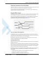
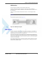
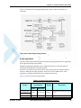
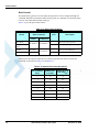
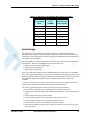
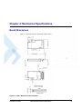
1
Technical Information Motorola G24-L and G24-LC Developer’s Guide Module Hardware Description NOVEMBER 15, 2008 6802984C05-D SPECIFICATIONS SUBJECT TO CHANGE WITHOUT NOTICE Notice While reasonable efforts have been made to assure the accuracy of this document, Motorola, Inc. assumes no liability resulting from any inaccuracies or omissions in this document, or from use of the information obtained herein. The information in this document has been carefully checked and is believed to be entirely reliable. However, no responsibility is assumed for inaccuracies or omissions. Motorola, Inc. reserves the right to make changes to any products described herein and reserves the right to revise this document and to make changes from time to time in content hereof with no obligation to notify any person of revisions or changes. Motorola, Inc. does not assume any liability arising out of the application or use of any product, software, or circuit described herein; neither does it convey license under its patent rights or the rights of others. It is possible that this publication may contain references to, or information about Motorola products (machines and programs), programming, or services that are not announced in your country. Such references or information must not be construed to mean that Motorola intends to announce such Motorola products, programming, or services in your country. Copyrights This instruction manual, and the Motorola products described in this instruction manual may be, include or describe copyrighted Motorola material, such as computer programs stored in semiconductor memories or other media. Laws in the United States and other countries preserve for Motorola and its licensors certain exclusive rights for copyrighted material, including the exclusive right to copy, reproduce in any form, distribute and make derivative works of the copyrighted material. Accordingly, any copyrighted material of Motorola and its licensors contained herein or in the Motorola products described in this instruction manual may not be copied, reproduced, distributed, merged or modified in any manner without the express written permission of Motorola. Furthermore, the purchase of Motorola products shall not be deemed to grant either directly or by implication, estoppel, or otherwise, any license under the copyrights, patents or patent applications of Motorola, as arises by operation of law in the sale of a product. Computer Software Copyrights The Motorola and 3rd Party supplied Software (SW) products described in this instruction manual may include copyrighted Motorola and other 3rd Party supplied computer programs stored in semiconductor memories or other media. Laws in the United States and other countries preserve for Motorola and other 3rd Party supplied SW certain exclusive rights for copyrighted computer programs, including the exclusive right to copy or reproduce in any form the copyrighted computer program. Accordingly, any copyrighted Motorola or other 3rd Party supplied SW computer programs contained in the Motorola products described in this instruction manual may not be copied (reverse engineered) or reproduced in any manner without the express written permission of Motorola or the 3rd Party SW supplier. Furthermore, the purchase of Motorola products shall not be deemed to grant either directly or by implication, estoppel, or otherwise, any license under the copyrights, patents or patent applications of Motorola or other 3rd Party supplied SW, except for the normal non-exclusive, royalty free license to use that arises by operation of law in the sale of a product. VENDOR COPYRIGHT Apache Software Foundation Copyright 2004-2005 All Rights Reserved Usage and Disclosure Restrictions License Agreements The software described in this document is the property of Motorola, Inc. and its licensors. It is furnished by express license agreement only and may be used only in accordance with the terms of such an agreement. Copyrighted Materials Software and documentation are copyrighted materials. Making unauthorized copies is prohibited by law. No part of the software or documentation may be reproduced, transmitted, transcribed, stored in a retrieval system, or translated into any language or computer language, in any form or by any means, without prior written permission of Motorola, Inc. High Risk Materials Components, units, or third-party products used in the product described herein are NOT fault-tolerant and are NOT designed, manufactured, or intended for use as on-line control equipment in the following hazardous environments requiring fail-safe controls: the operation of Nuclear Facilities, Aircraft Navigation or Aircraft Communication Systems, Air Traffic Control, Life Support, or Weapons Systems (High Risk Activities"). Motorola and its supplier(s) specifically disclaim any expressed or implied warranty of fitness for such High Risk Activities. Trademarks MOTOROLA and the Stylized M Logo are registered in the US Patent & Trademark Office. All other product or service names are the property of their respective owners. © Copyright 2007 Motorola, Inc. REV052604 Table of Contents Manual Scope . . . . . . . . . . . . . . . . . . . . . . . . . . . . . . . . . . . . . . . . . . . . . . . . . . . . . . . . . . . . . . . . . . . .ix Target Audience . . . . . . . . . . . . . . . . . . . . . . . . . . . . . . . . . . . . . . . . . . . . . . . . . . . . . . . . . . . . . . . . . .ix Manual Organization . . . . . . . . . . . . . . . . . . . . . . . . . . . . . . . . . . . . . . . . . . . . . . . . . . . . . . . . . . . . . . .ix Applicable Documents . . . . . . . . . . . . . . . . . . . . . . . . . . . . . . . . . . . . . . . . . . . . . . . . . . . . . . . . . . . . . x Regulatory Requirements . . . . . . . . . . . . . . . . . . . . . . . . . . . . . . . . . . . . . . . . . . . . . . . . . . . . . . . . . . . x Safety Statement and Requirements . . . . . . . . . . . . . . . . . . . . . . . . . . . . . . . . . . . . . . . . . . . . . . . . . . . x Antenna and Transmission Safety Precautions . . . . . . . . . . . . . . . . . . . . . . . . . . . . . . . . . . . . . . . . . . .xi Standards . . . . . . . . . . . . . . . . . . . . . . . . . . . . . . . . . . . . . . . . . . . . . . . . . . . . . . . . . . . . . . . . . . . . . . . xii Contact Us . . . . . . . . . . . . . . . . . . . . . . . . . . . . . . . . . . . . . . . . . . . . . . . . . . . . . . . . . . . . . . . . . . . . . . xii Text Conventions. . . . . . . . . . . . . . . . . . . . . . . . . . . . . . . . . . . . . . . . . . . . . . . . . . . . . . . . . . . . . . . . xiii Field Service . . . . . . . . . . . . . . . . . . . . . . . . . . . . . . . . . . . . . . . . . . . . . . . . . . . . . . . . . . . . . . . . . . . .xiv General Safety . . . . . . . . . . . . . . . . . . . . . . . . . . . . . . . . . . . . . . . . . . . . . . . . . . . . . . . . . . . . . . . . . . .xiv Caring for the Environment. . . . . . . . . . . . . . . . . . . . . . . . . . . . . . . . . . . . . . . . . . . . . . . . . . . . . . . . .xvi Limitation of Liability . . . . . . . . . . . . . . . . . . . . . . . . . . . . . . . . . . . . . . . . . . . . . . . . . . . . . . . . . . . . xvii Warranty Notification . . . . . . . . . . . . . . . . . . . . . . . . . . . . . . . . . . . . . . . . . . . . . . . . . . . . . . . . . . . xviii How to Get Warranty Service? . . . . . . . . . . . . . . . . . . . . . . . . . . . . . . . . . . . . . . . . . . . . . . . . . . . . xviii Claiming . . . . . . . . . . . . . . . . . . . . . . . . . . . . . . . . . . . . . . . . . . . . . . . . . . . . . . . . . . . . . . . . . . . . . . .xix Conditions . . . . . . . . . . . . . . . . . . . . . . . . . . . . . . . . . . . . . . . . . . . . . . . . . . . . . . . . . . . . . . . . . . . . . .xix What is Not Covered by the Warranty . . . . . . . . . . . . . . . . . . . . . . . . . . . . . . . . . . . . . . . . . . . . . . . . xx Installed Data. . . . . . . . . . . . . . . . . . . . . . . . . . . . . . . . . . . . . . . . . . . . . . . . . . . . . . . . . . . . . . . . . . . . xx Out of Warranty Repairs . . . . . . . . . . . . . . . . . . . . . . . . . . . . . . . . . . . . . . . . . . . . . . . . . . . . . . . . . . . xx Revision History . . . . . . . . . . . . . . . . . . . . . . . . . . . . . . . . . . . . . . . . . . . . . . . . . . . . . . . . . . . . . . . . .xxi Chapter 1: Introduction . . . . . . . . . . . . . . . . . . . . . . . . . . . . . . . . . . . . . . . . . . . . . . . . . . . . . . . . . . . . . 1 Product Specifications . . . . . . . . . . . . . . . . . . . . . . . . . . . . . . . . . . . . . . . . . . . . . . . . . . . . . . . . . . . . . . 2 Regulatory Approvals . . . . . . . . . . . . . . . . . . . . . . . . . . . . . . . . . . . . . . . . . . . . . . . . . . . . . . . . . . . . . . 5 European Union Directives Conformance Statement . . . . . . . . . . . . . . . . . . . . . . . . . . . . . . . . . . . 5 CFR 47 Part 15.19 specifies label requirements . . . . . . . . . . . . . . . . . . . . . . . . . . . . . . . . . . . . . . . 5 CFR 47 Part 15.21 Information to user . . . . . . . . . . . . . . . . . . . . . . . . . . . . . . . . . . . . . . . . . . . . . . 6 CFR 47 Part 15.105 Information to the user . . . . . . . . . . . . . . . . . . . . . . . . . . . . . . . . . . . . . . . . . . 6 Chapter 2: Hardware Interface Description . . . . . . . . . . . . . . . . . . . . . . . . . . . . . . . . . . . . . . . . . . . . . 7 Architecture Overview . . . . . . . . . . . . . . . . . . . . . . . . . . . . . . . . . . . . . . . . . . . . . . . . . . . . . . . . . . . . . 7 Digital Block . . . . . . . . . . . . . . . . . . . . . . . . . . . . . . . . . . . . . . . . . . . . . . . . . . . . . . . . . . . . . . . . . . 8 Analog Block . . . . . . . . . . . . . . . . . . . . . . . . . . . . . . . . . . . . . . . . . . . . . . . . . . . . . . . . . . . . . . . . . . 8 GSM Transceiver Block . . . . . . . . . . . . . . . . . . . . . . . . . . . . . . . . . . . . . . . . . . . . . . . . . . . . . . . . . 8 Operating Modes . . . . . . . . . . . . . . . . . . . . . . . . . . . . . . . . . . . . . . . . . . . . . . . . . . . . . . . . . . . . . . . . . . 9 Power Supply. . . . . . . . . . . . . . . . . . . . . . . . . . . . . . . . . . . . . . . . . . . . . . . . . . . . . . . . . . . . . . . . . . . . 10 Power Supply Design . . . . . . . . . . . . . . . . . . . . . . . . . . . . . . . . . . . . . . . . . . . . . . . . . . . . . . . . . . . 10 Power Consumption . . . . . . . . . . . . . . . . . . . . . . . . . . . . . . . . . . . . . . . . . . . . . . . . . . . . . . . . . . . . 11 Power On/Off Operation . . . . . . . . . . . . . . . . . . . . . . . . . . . . . . . . . . . . . . . . . . . . . . . . . . . . . . . . . . . 13 Turning the G24-L On . . . . . . . . . . . . . . . . . . . . . . . . . . . . . . . . . . . . . . . . . . . . . . . . . . . . . . . . . . 13 Turning the G24-L On Using ON_N . . . . . . . . . . . . . . . . . . . . . . . . . . . . . . . . . . . . . . . . . . . . . 13 Turning the G24-L On Using IGN . . . . . . . . . . . . . . . . . . . . . . . . . . . . . . . . . . . . . . . . . . . . . . . 14 November 15, 2008 G24-L Module Hardware Description i Table of Contents Turning the G24-L Off . . . . . . . . . . . . . . . . . . . . . . . . . . . . . . . . . . . . . . . . . . . . . . . . . . . . . . . . . . 15 Turning the G24-L Off Using ON_N . . . . . . . . . . . . . . . . . . . . . . . . . . . . . . . . . . . . . . . . . . . . . 15 Turning the G24-L Off Using IGN. . . . . . . . . . . . . . . . . . . . . . . . . . . . . . . . . . . . . . . . . . . . . . . 15 Turning the G24-L Off Using AT+MRST . . . . . . . . . . . . . . . . . . . . . . . . . . . . . . . . . . . . . . . . . 16 Power Loss shut down . . . . . . . . . . . . . . . . . . . . . . . . . . . . . . . . . . . . . . . . . . . . . . . . . . . . . . . . 16 Low Power Mode. . . . . . . . . . . . . . . . . . . . . . . . . . . . . . . . . . . . . . . . . . . . . . . . . . . . . . . . . . . . . . . . . 17 Activating Low Power Mode . . . . . . . . . . . . . . . . . . . . . . . . . . . . . . . . . . . . . . . . . . . . . . . . . . . . . 17 Serial Interface During Low Power Mode . . . . . . . . . . . . . . . . . . . . . . . . . . . . . . . . . . . . . . . . . . . 18 Terminating Low Power Mode . . . . . . . . . . . . . . . . . . . . . . . . . . . . . . . . . . . . . . . . . . . . . . . . . . . 18 Temporary Termination of Low Power Mode . . . . . . . . . . . . . . . . . . . . . . . . . . . . . . . . . . . . . . 19 Permanent termination of Low Power Mode . . . . . . . . . . . . . . . . . . . . . . . . . . . . . . . . . . . . . . . 20 Real Time Clock . . . . . . . . . . . . . . . . . . . . . . . . . . . . . . . . . . . . . . . . . . . . . . . . . . . . . . . . . . . . . . . . . 21 Serial Interfaces . . . . . . . . . . . . . . . . . . . . . . . . . . . . . . . . . . . . . . . . . . . . . . . . . . . . . . . . . . . . . . . . . . 22 UART . . . . . . . . . . . . . . . . . . . . . . . . . . . . . . . . . . . . . . . . . . . . . . . . . . . . . . . . . . . . . . . . . . . . . . . 22 USB Interface . . . . . . . . . . . . . . . . . . . . . . . . . . . . . . . . . . . . . . . . . . . . . . . . . . . . . . . . . . . . . . . . . 23 SIM Interface . . . . . . . . . . . . . . . . . . . . . . . . . . . . . . . . . . . . . . . . . . . . . . . . . . . . . . . . . . . . . . . . . . . . 23 SIM Connection . . . . . . . . . . . . . . . . . . . . . . . . . . . . . . . . . . . . . . . . . . . . . . . . . . . . . . . . . . . . . . . 24 SIM Design Guidelines . . . . . . . . . . . . . . . . . . . . . . . . . . . . . . . . . . . . . . . . . . . . . . . . . . . . . . . . . 24 Audio Interface . . . . . . . . . . . . . . . . . . . . . . . . . . . . . . . . . . . . . . . . . . . . . . . . . . . . . . . . . . . . . . . . . . 26 Handset Microphone Port . . . . . . . . . . . . . . . . . . . . . . . . . . . . . . . . . . . . . . . . . . . . . . . . . . . . . . . . 26 Headset Microphone Port . . . . . . . . . . . . . . . . . . . . . . . . . . . . . . . . . . . . . . . . . . . . . . . . . . . . . . . . 27 Speaker Port . . . . . . . . . . . . . . . . . . . . . . . . . . . . . . . . . . . . . . . . . . . . . . . . . . . . . . . . . . . . . . . . . . 28 Headset Detection . . . . . . . . . . . . . . . . . . . . . . . . . . . . . . . . . . . . . . . . . . . . . . . . . . . . . . . . . . . . . . 30 Alert Loudspeaker Port . . . . . . . . . . . . . . . . . . . . . . . . . . . . . . . . . . . . . . . . . . . . . . . . . . . . . . . . . 31 Digital Audio Interface . . . . . . . . . . . . . . . . . . . . . . . . . . . . . . . . . . . . . . . . . . . . . . . . . . . . . . . . . . 32 Operating Modes . . . . . . . . . . . . . . . . . . . . . . . . . . . . . . . . . . . . . . . . . . . . . . . . . . . . . . . . . . . . . . 33 Basic Mode . . . . . . . . . . . . . . . . . . . . . . . . . . . . . . . . . . . . . . . . . . . . . . . . . . . . . . . . . . . . . . . . . 33 Advanced Mode . . . . . . . . . . . . . . . . . . . . . . . . . . . . . . . . . . . . . . . . . . . . . . . . . . . . . . . . . . . . . 34 Audio Programming Interface . . . . . . . . . . . . . . . . . . . . . . . . . . . . . . . . . . . . . . . . . . . . . . . . . . . . 34 Audio Algorithms . . . . . . . . . . . . . . . . . . . . . . . . . . . . . . . . . . . . . . . . . . . . . . . . . . . . . . . . . . . . 35 Gain Control . . . . . . . . . . . . . . . . . . . . . . . . . . . . . . . . . . . . . . . . . . . . . . . . . . . . . . . . . . . . . . . . 36 Audio Design . . . . . . . . . . . . . . . . . . . . . . . . . . . . . . . . . . . . . . . . . . . . . . . . . . . . . . . . . . . . . . . . . 37 Analog Ground . . . . . . . . . . . . . . . . . . . . . . . . . . . . . . . . . . . . . . . . . . . . . . . . . . . . . . . . . . . . . . 38 A/D Interface . . . . . . . . . . . . . . . . . . . . . . . . . . . . . . . . . . . . . . . . . . . . . . . . . . . . . . . . . . . . . . . . . . . . 39 General Purpose A/D . . . . . . . . . . . . . . . . . . . . . . . . . . . . . . . . . . . . . . . . . . . . . . . . . . . . . . . . . . . 39 Power Supply A/D . . . . . . . . . . . . . . . . . . . . . . . . . . . . . . . . . . . . . . . . . . . . . . . . . . . . . . . . . . . . . 40 Battery Temperature A/D . . . . . . . . . . . . . . . . . . . . . . . . . . . . . . . . . . . . . . . . . . . . . . . . . . . . . . . . 40 Controls and Indicators Interface. . . . . . . . . . . . . . . . . . . . . . . . . . . . . . . . . . . . . . . . . . . . . . . . . . . . . 42 Reset . . . . . . . . . . . . . . . . . . . . . . . . . . . . . . . . . . . . . . . . . . . . . . . . . . . . . . . . . . . . . . . . . . . . . . . . 42 VREF Reference Regulator . . . . . . . . . . . . . . . . . . . . . . . . . . . . . . . . . . . . . . . . . . . . . . . . . . . . . . 42 Wakeup Out . . . . . . . . . . . . . . . . . . . . . . . . . . . . . . . . . . . . . . . . . . . . . . . . . . . . . . . . . . . . . . . . . . 43 Antenna Detection . . . . . . . . . . . . . . . . . . . . . . . . . . . . . . . . . . . . . . . . . . . . . . . . . . . . . . . . . . . . . 45 GPRS Detection . . . . . . . . . . . . . . . . . . . . . . . . . . . . . . . . . . . . . . . . . . . . . . . . . . . . . . . . . . . . . . . 45 Transmission Indicator . . . . . . . . . . . . . . . . . . . . . . . . . . . . . . . . . . . . . . . . . . . . . . . . . . . . . . . . . . 45 General Purpose I/O . . . . . . . . . . . . . . . . . . . . . . . . . . . . . . . . . . . . . . . . . . . . . . . . . . . . . . . . . . . . 45 Antenna Interface. . . . . . . . . . . . . . . . . . . . . . . . . . . . . . . . . . . . . . . . . . . . . . . . . . . . . . . . . . . . . . . . . 46 Battery Charger Interface. . . . . . . . . . . . . . . . . . . . . . . . . . . . . . . . . . . . . . . . . . . . . . . . . . . . . . . . . . . 47 General . . . . . . . . . . . . . . . . . . . . . . . . . . . . . . . . . . . . . . . . . . . . . . . . . . . . . . . . . . . . . . . . . . . . . . 47 Battery Connectivity . . . . . . . . . . . . . . . . . . . . . . . . . . . . . . . . . . . . . . . . . . . . . . . . . . . . . . . . . . . . 47 Charger Connectivity . . . . . . . . . . . . . . . . . . . . . . . . . . . . . . . . . . . . . . . . . . . . . . . . . . . . . . . . . . . 47 ii G24-L Module Hardware Description November 15, 2008 Table of Contents Battery Charging Process . . . . . . . . . . . . . . . . . . . . . . . . . . . . . . . . . . . . . . . . . . . . . . . . . . . . . . . . 49 Under Voltage . . . . . . . . . . . . . . . . . . . . . . . . . . . . . . . . . . . . . . . . . . . . . . . . . . . . . . . . . . . . . . 49 Pre-Charging . . . . . . . . . . . . . . . . . . . . . . . . . . . . . . . . . . . . . . . . . . . . . . . . . . . . . . . . . . . . . . . 49 Charging (Continuos Current) . . . . . . . . . . . . . . . . . . . . . . . . . . . . . . . . . . . . . . . . . . . . . . . . . . 49 Monitoring (Full) . . . . . . . . . . . . . . . . . . . . . . . . . . . . . . . . . . . . . . . . . . . . . . . . . . . . . . . . . . . . 50 Protection and Safety . . . . . . . . . . . . . . . . . . . . . . . . . . . . . . . . . . . . . . . . . . . . . . . . . . . . . . . . . . . 51 Chapter 3: Electrical and Environmental Specifications . . . . . . . . . . . . . . . . . . . . . . . . . . . . . . . . . 53 Absolute Maximum Ratings . . . . . . . . . . . . . . . . . . . . . . . . . . . . . . . . . . . . . . . . . . . . . . . . . . . . . . . . 53 Environmental Specifications . . . . . . . . . . . . . . . . . . . . . . . . . . . . . . . . . . . . . . . . . . . . . . . . . . . . . . . 54 Application Interface Specifications . . . . . . . . . . . . . . . . . . . . . . . . . . . . . . . . . . . . . . . . . . . . . . . . . . 54 Chapter 4: Mechanical Specifications . . . . . . . . . . . . . . . . . . . . . . . . . . . . . . . . . . . . . . . . . . . . . . . . 61 Board Dimensions . . . . . . . . . . . . . . . . . . . . . . . . . . . . . . . . . . . . . . . . . . . . . . . . . . . . . . . . . . . . . . . . 61 Interface Connector Specifications . . . . . . . . . . . . . . . . . . . . . . . . . . . . . . . . . . . . . . . . . . . . . . . . . . . 62 Mating Connector . . . . . . . . . . . . . . . . . . . . . . . . . . . . . . . . . . . . . . . . . . . . . . . . . . . . . . . . . . . . . 63 RF Connector Specifications . . . . . . . . . . . . . . . . . . . . . . . . . . . . . . . . . . . . . . . . . . . . . . . . . . . . . . . . 64 Mating Connector . . . . . . . . . . . . . . . . . . . . . . . . . . . . . . . . . . . . . . . . . . . . . . . . . . . . . . . . . . . . . 64 G24-L Mounting . . . . . . . . . . . . . . . . . . . . . . . . . . . . . . . . . . . . . . . . . . . . . . . . . . . . . . . . . . . . . . . . . 66 Chapter 5: Service and Testing. . . . . . . . . . . . . . . . . . . . . . . . . . . . . . . . . . . . . . . . . . . . . . . . . . . . . . 67 Service . . . . . . . . . . . . . . . . . . . . . . . . . . . . . . . . . . . . . . . . . . . . . . . . . . . . . . . . . . . . . . . . . . . . . . . . . 67 Who to Contact? . . . . . . . . . . . . . . . . . . . . . . . . . . . . . . . . . . . . . . . . . . . . . . . . . . . . . . . . . . . . . . 67 Required Query Information . . . . . . . . . . . . . . . . . . . . . . . . . . . . . . . . . . . . . . . . . . . . . . . . . . . . . 67 Motorola Workflow . . . . . . . . . . . . . . . . . . . . . . . . . . . . . . . . . . . . . . . . . . . . . . . . . . . . . . . . . . . . 68 Service Centers . . . . . . . . . . . . . . . . . . . . . . . . . . . . . . . . . . . . . . . . . . . . . . . . . . . . . . . . . . . . . . . 69 Testing a Standalone Unit . . . . . . . . . . . . . . . . . . . . . . . . . . . . . . . . . . . . . . . . . . . . . . . . . . . . . . . . . . 70 Test Setup . . . . . . . . . . . . . . . . . . . . . . . . . . . . . . . . . . . . . . . . . . . . . . . . . . . . . . . . . . . . . . . . . . . . 70 Test Procedure . . . . . . . . . . . . . . . . . . . . . . . . . . . . . . . . . . . . . . . . . . . . . . . . . . . . . . . . . . . . . . . . 72 Acronyms and Abbreviations Index November 15, 2008 G24-L Module Hardware Description iii List of Figures 2-1 2-2 2-3 2-4 2-5 2-6 2-7 2-8 2-9 2-10 2-11 2-12 2-13 2-14 2-15 2-16 2-17 2-18 2-19 2-20 2-21 2-22 2-23 2-24 2-25 2-26 2-27 G24-L Block Diagram . . . . . . . . . . . . . . . . . . . . . . . . . . . . . . . . . . . . . . . . . . . . . . . . . . . . . . . . 7 Transmission Power Drops. . . . . . . . . . . . . . . . . . . . . . . . . . . . . . . . . . . . . . . . . . . . . . . . . . . . 10 ON_N Power On Timing . . . . . . . . . . . . . . . . . . . . . . . . . . . . . . . . . . . . . . . . . . . . . . . . . . . . . 14 IGN Power On Timing . . . . . . . . . . . . . . . . . . . . . . . . . . . . . . . . . . . . . . . . . . . . . . . . . . . . . . . 14 ON_N Power Off Timing . . . . . . . . . . . . . . . . . . . . . . . . . . . . . . . . . . . . . . . . . . . . . . . . . . . . . 15 IGN Power Off Timing. . . . . . . . . . . . . . . . . . . . . . . . . . . . . . . . . . . . . . . . . . . . . . . . . . . . . . . 16 ATS24 Operation . . . . . . . . . . . . . . . . . . . . . . . . . . . . . . . . . . . . . . . . . . . . . . . . . . . . . . . . . . . 17 CTS Signal During Sleep Mode . . . . . . . . . . . . . . . . . . . . . . . . . . . . . . . . . . . . . . . . . . . . . . . . 18 WKUPI_N Signal Operation . . . . . . . . . . . . . . . . . . . . . . . . . . . . . . . . . . . . . . . . . . . . . . . . . . 19 Serial Interface Data . . . . . . . . . . . . . . . . . . . . . . . . . . . . . . . . . . . . . . . . . . . . . . . . . . . . . . . . . 20 UART Interface Signals . . . . . . . . . . . . . . . . . . . . . . . . . . . . . . . . . . . . . . . . . . . . . . . . . . . . . . 22 USB Interface Signals. . . . . . . . . . . . . . . . . . . . . . . . . . . . . . . . . . . . . . . . . . . . . . . . . . . . . . . . 23 G24-L SIM Interface . . . . . . . . . . . . . . . . . . . . . . . . . . . . . . . . . . . . . . . . . . . . . . . . . . . . . . . . 24 Audio Interface Topology. . . . . . . . . . . . . . . . . . . . . . . . . . . . . . . . . . . . . . . . . . . . . . . . . . . . . 26 Handset Microphone Circuit. . . . . . . . . . . . . . . . . . . . . . . . . . . . . . . . . . . . . . . . . . . . . . . . . . . 27 Headset Microphone Circuit. . . . . . . . . . . . . . . . . . . . . . . . . . . . . . . . . . . . . . . . . . . . . . . . . . . 28 Differential Speaker Circuit . . . . . . . . . . . . . . . . . . . . . . . . . . . . . . . . . . . . . . . . . . . . . . . . . . . 29 Single-ended Speaker Circuit . . . . . . . . . . . . . . . . . . . . . . . . . . . . . . . . . . . . . . . . . . . . . . . . . . 29 Differential Loudspeaker Circuit . . . . . . . . . . . . . . . . . . . . . . . . . . . . . . . . . . . . . . . . . . . . . . . 31 SIngle-ended Loudspeaker Circuit . . . . . . . . . . . . . . . . . . . . . . . . . . . . . . . . . . . . . . . . . . . . . . 31 Voiceband Mode PCM Bus Coding Format. . . . . . . . . . . . . . . . . . . . . . . . . . . . . . . . . . . . . . . 33 Audio Programming Interface . . . . . . . . . . . . . . . . . . . . . . . . . . . . . . . . . . . . . . . . . . . . . . . . . 35 VREF Power-up Timing. . . . . . . . . . . . . . . . . . . . . . . . . . . . . . . . . . . . . . . . . . . . . . . . . . . . . . 43 WKUPO_N Operation . . . . . . . . . . . . . . . . . . . . . . . . . . . . . . . . . . . . . . . . . . . . . . . . . . . . . . . 44 TXEN_N Operation . . . . . . . . . . . . . . . . . . . . . . . . . . . . . . . . . . . . . . . . . . . . . . . . . . . . . . . . . 45 Battery and Charger Interface Connectivity . . . . . . . . . . . . . . . . . . . . . . . . . . . . . . . . . . . . . . . 48 Battery Charging Process . . . . . . . . . . . . . . . . . . . . . . . . . . . . . . . . . . . . . . . . . . . . . . . . . . . . . 50 4-1 4-2 4-3 4-4 4-5 4-6 G24-L Mechanical Characteristics . . . . . . . . . . . . . . . . . . . . . . . . . . . . . . . . . . . . . . . . . . . . . . G24-L Interface Connector. . . . . . . . . . . . . . . . . . . . . . . . . . . . . . . . . . . . . . . . . . . . . . . . . . . . Mating Connector Dimensions . . . . . . . . . . . . . . . . . . . . . . . . . . . . . . . . . . . . . . . . . . . . . . . . . MMCX Connector Dimensions . . . . . . . . . . . . . . . . . . . . . . . . . . . . . . . . . . . . . . . . . . . . . . . . Optional MMCX Cable Assembly . . . . . . . . . . . . . . . . . . . . . . . . . . . . . . . . . . . . . . . . . . . . . . G24-L Mounting Area . . . . . . . . . . . . . . . . . . . . . . . . . . . . . . . . . . . . . . . . . . . . . . . . . . . . . . . 5-1 Test Setup . . . . . . . . . . . . . . . . . . . . . . . . . . . . . . . . . . . . . . . . . . . . . . . . . . . . . . . . . . . . . . . . . 71 November 15, 2008 G24-L Module Hardware Description 61 62 63 64 65 66 v List of Tables 1-1 Product Specifications . . . . . . . . . . . . . . . . . . . . . . . . . . . . . . . . . . . . . . . . . . . . . . . . . . . . . . . . 2 2-1 2-2 2-3 2-4 2-5 2-6 2-7 2-8 2-9 2-10 2-11 2-12 2-13 2-14 2-15 2-16 2-17 2-18 2-19 2-20 2-21 2-22 2-23 2-24 2-25 3-1 3-2 3-3 G24-L Operating Modes. . . . . . . . . . . . . . . . . . . . . . . . . . . . . . . . . . . . . . . . . . . . . . . . . . . . . . . 9 Power Supply Signals . . . . . . . . . . . . . . . . . . . . . . . . . . . . . . . . . . . . . . . . . . . . . . . . . . . . . . . . 10 Recommended Power Supply Filtering . . . . . . . . . . . . . . . . . . . . . . . . . . . . . . . . . . . . . . . . . . 11 G24-L Current Ratings . . . . . . . . . . . . . . . . . . . . . . . . . . . . . . . . . . . . . . . . . . . . . . . . . . . . . . . 11 SIM Interface Signals . . . . . . . . . . . . . . . . . . . . . . . . . . . . . . . . . . . . . . . . . . . . . . . . . . . . . . . . 24 Handset Microphone Port Specifications . . . . . . . . . . . . . . . . . . . . . . . . . . . . . . . . . . . . . . . . . 27 Headset Microphone Port Specifications . . . . . . . . . . . . . . . . . . . . . . . . . . . . . . . . . . . . . . . . . 28 Speaker Port Specifications . . . . . . . . . . . . . . . . . . . . . . . . . . . . . . . . . . . . . . . . . . . . . . . . . . . 30 Alert Port Specifications. . . . . . . . . . . . . . . . . . . . . . . . . . . . . . . . . . . . . . . . . . . . . . . . . . . . . . 32 Basic Mode Audio Paths . . . . . . . . . . . . . . . . . . . . . . . . . . . . . . . . . . . . . . . . . . . . . . . . . . . . . 33 Advanced Mode Commands. . . . . . . . . . . . . . . . . . . . . . . . . . . . . . . . . . . . . . . . . . . . . . . . . . . 34 Speech Processing Features . . . . . . . . . . . . . . . . . . . . . . . . . . . . . . . . . . . . . . . . . . . . . . . . . . . 35 Gain Control Features. . . . . . . . . . . . . . . . . . . . . . . . . . . . . . . . . . . . . . . . . . . . . . . . . . . . . . . . 36 Speaker Port Gains for Speech . . . . . . . . . . . . . . . . . . . . . . . . . . . . . . . . . . . . . . . . . . . . . . . . . 36 Microphone and Headset Microphone Port Gains . . . . . . . . . . . . . . . . . . . . . . . . . . . . . . . . . . 37 A/D Signals. . . . . . . . . . . . . . . . . . . . . . . . . . . . . . . . . . . . . . . . . . . . . . . . . . . . . . . . . . . . . . . . 39 GPAD Specifications . . . . . . . . . . . . . . . . . . . . . . . . . . . . . . . . . . . . . . . . . . . . . . . . . . . . . . . . 40 Supply A/D Specifications . . . . . . . . . . . . . . . . . . . . . . . . . . . . . . . . . . . . . . . . . . . . . . . . . . . . 40 Temperature A/D Specifications . . . . . . . . . . . . . . . . . . . . . . . . . . . . . . . . . . . . . . . . . . . . . . . 41 Controls and Indicators. . . . . . . . . . . . . . . . . . . . . . . . . . . . . . . . . . . . . . . . . . . . . . . . . . . . . . . 42 VREF Specifications . . . . . . . . . . . . . . . . . . . . . . . . . . . . . . . . . . . . . . . . . . . . . . . . . . . . . . . . 43 Antenna Interface Specifications . . . . . . . . . . . . . . . . . . . . . . . . . . . . . . . . . . . . . . . . . . . . . . . 46 Battery and Charger Interface Signals . . . . . . . . . . . . . . . . . . . . . . . . . . . . . . . . . . . . . . . . . . . 48 Charger Supply Specifications . . . . . . . . . . . . . . . . . . . . . . . . . . . . . . . . . . . . . . . . . . . . . . . . . 49 Recommended Accessories for G24-LC . . . . . . . . . . . . . . . . . . . . . . . . . . . . . . . . . . . . . . . . . 51 Maximum Ratings . . . . . . . . . . . . . . . . . . . . . . . . . . . . . . . . . . . . . . . . . . . . . . . . . . . . . . . . . . 53 Environmental Ratings . . . . . . . . . . . . . . . . . . . . . . . . . . . . . . . . . . . . . . . . . . . . . . . . . . . . . . . 54 Interface Specifications . . . . . . . . . . . . . . . . . . . . . . . . . . . . . . . . . . . . . . . . . . . . . . . . . . . . . . 55 4-1 4-2 4-3 G24-L interface connector options . . . . . . . . . . . . . . . . . . . . . . . . . . . . . . . . . . . . . . . . . . . . . . 62 Interface Connector Specifications. . . . . . . . . . . . . . . . . . . . . . . . . . . . . . . . . . . . . . . . . . . . . . 62 RF Connector Specifications . . . . . . . . . . . . . . . . . . . . . . . . . . . . . . . . . . . . . . . . . . . . . . . . . . 64 November 15, 2008 G24-L Module Hardware Description vii Preface Note: All references to G24-L also apply to G24-LC, except where otherwise noted. Manual Scope This manual provides the electrical, mechanical and environmental requirements for properly integrating the G24-L module in a host application. This manual gives a complete set of hardware features and functions that may be provided by G24-L. The availability of any feature or function, which is described in this manual, depends on the hardware revision and software version of a specific G24-L model, and also the capabilities of the host application which must provide a user interface and control the module via AT commands. The parameters and values provided in this manual are defined under typical conditions. These values may vary when subject to different conditions, such as SW version, network status, application settings and environmental conditions. Target Audience This manual is intended for all members of the integration team who are responsible for integrating the G24-L module into the host OEM device, including representatives from hardware, software and RF engineering disciplines. Manual Organization This manual contains the following chapters: • Chapter 1 —introduces the G24-L unit and provides important safety instructions. • Chapter 2 —provides a detailed hardware description of the blocks and components comprising the G24-L. • Chapter 3 —describes the pin assignments for G24-L connectors. • Chapter 4 —describes G24-L mechanical specifications and requirements. • Chapter 5 —provides contact information for Motorola Service Support and Customer Assistance. November 15, 2008 G24-L Module Hardware Description ix Applicable Documents Applicable Documents • G24-L Developer's Kit - 6802984C10 • G24-L AT Commands - 6802983C95 Regulatory Requirements The G24-L module is compliant with applicable FCC, IC and European R&TTE requirements. The integrated system incorporating the G24-L module may be subject to further regulations and standards. Motorola strongly recommends that the system integrator seeks professional advice regarding the regulations and standards that apply to their product. The Federal Communications Commission (FCC) requires application for certification of digital devices in accordance with CFR Title 47, Part 2 and Part 15. This includes Electromagnetic Energy Exposure (EME) testing. As the G24-L modem is not a standalone transceiver but is an integrated module, the G24-L cannot be tested by itself for EME certification. It is, however, the integrator’s responsibility to have the completed device tested for EME certification. The module is compliant to European R&TTE directive requirements; however the complete system (host plus G24 module) may be subject to R&TTE or other directives (for instance the EMC directive 2004/108/EC). Motorola strongly recommends that the system integrator seek professional advice regarding the applicable standards and directives, and most efficient route to demonstrating compliance, and required product markings. The G24-L module is compliant to FCC, IC and R&TTE requirements allowing use within Europe and North America. Use in other regions may require regional "type approvals" which the manufacturer of the final product integration or reseller will be responsible for procuring. Many regional type approvals are based upon compliance to FCC, R&TTE, ETSI and other standards that the G24-L is compliant with. It is strongly recommended that professional advice be sought before placing the finished integrated product on the market to establish local approval and marking requirements. Safety Statement and Requirements Certain safety precautions must be observed during all phases of the operation, usage, service or repair of any cellular terminal or mobile incorporating the G24-L module. The integrator is advised to consider the following general cautions in the context of their integrated system incorporating the G24-L module, and to provide the end user with the applicable warnings and advice of safe operation of the equipment. Failure to comply with these precautions violates safety standards of design, manufacture and intended use of the product. Motorola assumes no liability for customer failure to comply with these precautions. • The G24-L must be operated at the voltages described in the technical documentation • The G24-L must not be mechanically nor electrically changed. Use of connectors should follow the guidance of the technical documentation • The G24-L is designed to meet the EMC requirements of EN301 489-1 and EN301 489-7 for R&TTE devices using GSM • When integrating the G24-L into a system, Motorola recommends testing the system to EN301 489-1 and EN301 489-7 for R&TTE devices using GSM • The G24-LC meets the safety requirements of EN60950 x G24-L Module Hardware Description November 15, 2008 Preface • Systems using the G24-L are subject to mandatory EMC testing under directive 2004/108/EC (see item 3 above). Other directives, such as the LVD directive 2006/95/EC, may also apply to a system using the G24-L module • The integrated product incorporating the G24-L moduel must be evaluated for SAR under intended use conditions, and suitable text and SAR values be provided to the end user • No wireless device can guarantee operation at all times due to network or interference conditions, A user should never rely on a wireless device as the sole means of making emergency calls • The G24-L module complies with all applicable standards and directives, this does not guarantee that the product it is integrated into complies, expert advice should be sought to identify the applicable regulations and show compliance Suitable warning statements regarding the use of RF energy in the integrated host system should be given in the end user documentation. Antenna and Transmission Safety Precautions User Operation The G24-L module is normally supplied without an antenna, and is compliant with SAR requirements provided the following conditions are observed. Do not operate your unit when a person is within 8 inches (20 centimeters) of the antenna. A person or object within 8 inches (20 centimeters) of the antenna could impair call quality and may cause the phone to operate at a higher power level than necessary. Important: The unit must be installed in a manner that provides a minimum separation distance of 20 cm or more between the antenna and persons and must not be co-located or operate in conjunction with any other antenna or transmitter to satisfy FCC RF exposure requirements for mobile transmitting devices. Important: To comply with the FCC RF exposure limits and satisfy the categorical exclusion requirements for mobile transmitters, the requirements described in the following section, “Antenna Installation” , must be met. Antenna Installation • The antenna installation must provide a minimum separation distance of 20 cm from users and nearby persons and must not be co-located or operating in conjunction with any other antenna or transmitter. • The combined cable loss and antenna gain must not exceed +6.8 dBi (850 band). The combined cable loss and antenna gain must not exceed +2.2 dBi and total system output must not exceed 2.0W EIRP in the PCS (1900) band in order to comply with the EIRP limit of 24.232 (b). OEM installers must be provided with antenna installation instruction and transmitter operating conditions for satisfying RF exposure compliance. • For system integrations requiring higher antenna gain, or position closer than 20cm from the body, SAR compliance testing of the completed product will be required. It is strongly recommended that the system integrator seeks the advice of a suitably accredited test laboratory to develop a test plan and carry out necessary testing. November 15, 2008 G24-L Module Hardware Description xi Standards Standards Electromagnetic Compatibility: Principles and Applications by David A Weston, published by Marcel Dekker, Inc., 270 Madison Avenue, New York, NY 10016 USA. GSM 07.07 - prETS 300 916, Digital cellular telecommunication system (Phase 2+); AT command set for GSM Mobile Equipment (ME), Version 5.2.0 or higher, Reference RE/SMG-040707QR1. GSM 07.05, Digital cellular telecommunication system (Phase 2+); Use of Data Terminal Equipment - Data Circuit terminating; Equipment (DTE-DCE) interface for Short Message Service (SMS) and Cell Broadcast Service (CBS), Version 5.3.0, August, 1997, Reference TS/SMG-040705QR2. GSM 03.40, Digital cellular telecommunication system (Phase 2+); Technical realization of the Short Message Service (SMS) Point-to-Point (PP), Version 5.3.0, July 1996, Reference TS/SMG-040340QR2. GSM 04.11 Digital cellular telecommunication system (Phase 2+); Point-to-Point (PP) Short Message Service (SMS) support on mobile radio interface, Version 5.1.0, March 1996, Reference TS/SMG-030411QR. GSM 03.38, Digital cellular telecommunication system (Phase 2+); Alphabets and language-specific information, Version 5.3.0, July 1996, Reference TS/SMG-040338QR2. GSM 51.010-1, Digital cellular telecommunication system (Phase 2+); Mobile Station (MS) Conformance specification; Part 1: Conformance specification (3GPP TS 51.010-1 version 7.0.1 Release 7). GSM Specifications are orderable from Global Engineering Documents, 15 Inverness Way East, Englewood, Colorado 80112-5704 USA 303-792-2181 800-624-3974. ETSI Standard PCS - 11.10-1. GSM 02.30 Supplementary services. GSM 03.90 USSD stage 2. GSM 11.14 SIM toolkit. ITU-T V.25ter GSM Data Adapter for Motorola Handsets, AT command reference, Rev 2, June 9 1997. ETSI standard SMG31. GSM 05.02. ETSI 07.60. ETSI 0.7.07 Ver. 7.5.0. Contact Us We at Motorola want to make this guide as helpful as possible. Keep us informed of your comments and suggestions for improvements. For general contact, technical support, report documentation errors and to order manuals, use this email address: [email protected] Motorola appreciates feedback from the users of our information. xii G24-L Module Hardware Description November 15, 2008 Preface Text Conventions The following special paragraphs are used in this guide to point out information that must be read. This information may be set-off from the surrounding text, but is always preceded by a bold title in capital letters: Note Note: Presents additional, helpful, noncritical information that you can use. Warning Warning: Presents information to warn you of a potentially hazardous situation in which there is a possibility of personal injury. Important Important: Presents information to help you avoid an undesirable situation or provides additional information to help you understand a topic or concept. Caution Caution: November 15, 2008 Presents information to identify a situation in which damage to software, stored data, or equipment could occur, thus avoiding the damage. G24-L Module Hardware Description xiii Field Service Field Service For Field Service requests, use this email address: [email protected] General Safety Remember!. . . safety depends on you! The following general safety precautions must be observed during all phases of operation, service, and repair of the equipment described in this manual. Failure to comply with these precautions or with specific warnings elsewhere in this manual violates safety standards of design, manufacture, and intended use of the equipment. Motorola, Inc. assumes no liability for the customer’s failure to comply with these requirements. The safety precautions listed below represent warnings of certain dangers of which we are aware. You, as the user of this product, should follow these warnings and all other safety precautions necessary for the safe operation of the equipment in your operating environment. Ground the instrument Only suitably qualified individuals should work on the product and host system. Consideration should be given to the safest grounding arrangement for the host application. Do not operate in an explosive atmosphere Do not operate the equipment in the presence of flammable gases or fumes. Operation of any electrical equipment in such an environment constitutes a definite safety hazard. Do not service or adjust alone Do not attempt internal service or adjustment unless another person, capable of rendering first aid is present. There are no user serviceable parts inside the G24-L module. Keep away from live circuits Operating personnel must: • not remove equipment covers. Only Factory Authorized Service Personnel or other qualified maintenance personnel may remove equipment covers for internal subassembly, or component replacement, or any internal adjustment • not replace components with power cable connected. Under certain conditions, dangerous voltages may exist even with the power cable removed • always disconnect power and discharge circuits before touching them xiv G24-L Module Hardware Description November 15, 2008 Preface Do not substitute parts or modify equipment Because of the danger of introducing additional hazards, do not install substitute parts or perform any unauthorized modification of equipment. Contact Motorola Warranty and Repair for service and repair to ensure that safety features are maintained. Batteries Batteries can cause property damage and/or bodily injury such as burns if a conductive material such as jewelry, keys, or beaded chains touch exposed terminals. The conductive material may complete an electrical circuit (short circuit) and become quite hot. Exercise care in handling any charged battery, particularly when placing it inside a pocket, purse, or other container with metal objects. Use only Motorola original batteries and chargers. Your battery may contain symbols, defined as follows: Symbol Definition Important safety information will follow. Your battery or phone should not be disposed of in a fire. Your battery or phone may require recycling in accordance with local laws. Contact your local regulatory authorities for more information. Your battery or phone should not be thrown in the trash. Your phone contains an internal lithium ion battery. Li Ion BATT Dangerous procedure warnings Warnings, such as the example below, precede potentially dangerous procedures throughout this manual. Instructions contained in the warnings must be followed. You should also employ all other safety precautions that you deem necessary for the operation of the equipment in your operating environment. Warning example: Warning: November 15, 2008 Dangerous voltages, capable of causing death, are present in this equipment. Use extreme caution when handling, testing, and adjusting. G24-L Module Hardware Description xv Caring for the Environment Caring for the Environment The following information is provided to enable regulatory compliance with the European Union (EU) Directive 2002/96/EC Waste Electrical and Electronic Equipment (WEEE) when using Motorola equipment in EU countries. The finished host application should be marked with the crossed out "wheelie bin" mark at least 7mm high if it is within the scope of the WEEE directive. Motorola recommends that the system integrator seeks expert guidance as to the applicable directives for the finished product. Disposal of Motorola equipment in EU countries Please do not dispose of Motorola G24-L in landfill sites. In the EU, Motorola in conjunction with a recycling partner will ensure that G24-L is collected and recycled according to the requirements of EU environmental law. Note that the system integrator will be liable for recovery and disposal of the integrated system. Please contact the Customer Network Resolution Center (CNRC) for assistance. The 24 hour telephone numbers are listed at http://mynetworksupport.motorola.com Select Customer Network Resolution Center contact information. Alternatively if you do not have access to CNRC or the internet, contact the Local Motorola Office. Disposal of Motorola equipment in non-EU countries In non-EU countries, dispose of Motorola equipment in accordance with national and regional regulations. RoHS Compliance The G24-L/LC product meets the European Union directive for RoHS compliance. The RoHS compliance is subject to a declaration of conformity that may be viewed upon request. xvi G24-L Module Hardware Description November 15, 2008 Preface CMM Compliance The disclosure table and symbols below are provided in accordance with Section 5 & 6 of the People's Republic of China's "Electronic Industry Marking Standard for Control of Pollution Caused by Electronic Information Products". The disclosure table and symbols shown below cover the electronic information product (EIP) supplied. ᳝↦᳝ᆇ⠽䋼ܗ㋴ 䚼ӊৡ⿄ 䪙˄Pb˅ ∲˄Hg˅ 䬝˄Cd˅ ݁Ӌ䫀 ⒈㘨㣃 ⒈Ѡ㣃䝮 Cr6+) ˄PBB˅ ˄PBDE˅ R˖㸼⼎䆹᳝↦᳝ᆇ⠽䋼䆹䚼ӊ᠔᳝ഛ䋼ᴤ᭭Ёⱘ䞣ഛSJ/T 11363-2006 ᷛޚ㾘ᅮⱘ䰤䞣㽕∖ҹϟDŽ ×˖㸼⼎䆹᳝↦᳝ᆇ⠽䋼㟇ᇥ䆹䚼ӊⱘᶤϔഛ䋼ᴤ᭭Ёⱘ䞣䍙ߎSJ/T 11363-2006 ᷛޚ㾘ᅮⱘ䰤䞣㽕∖DŽ Cellular Phone x o o o o o Battery x o o o o o Accessories x o o o o o The two symbols shown below indicate the product is recyclable and the number denotes the Environmental Friendly Use Period for the EIP indicated above it. Transceiver Module & Accessories Except Battery Battery Limitation of Liability The Products are not designed, intended, or authorized for use as components in systems intended for surgical implant into the body; in other applications intended to support or sustain life; for the planning, construction, maintenance, operation or use of any nuclear facility; for the flight, navigation, communication of aircraft or ground support equipment; or in any other application in which the failure of the Product could create a situation where personal injury or death may occur. If CUSTOMER should use any Product or provide any Product to a third party for any such use, CUSTOMER hereby agrees that MOTOROLA is not liable, in whole or in part, for any claims or damages arising from such use, and further agrees to indemnify and hold MOTOROLA harmless from any claim, loss, cost or damage arising from such use. EXCEPT AS SPECIFICALLY STATED ABOVE, THE PRODUCTS ARE PROVIDED "AS IS" AND MOTOROLA MAKES NO OTHER WARRANTIES EXPRESS, IMPLIED, STATUTORY, OR OTHERWISE REGARDING THE PRODUCTS. MOTOROLA SPECIFICALLY DISCLAIMS ANY IMPLIED WARRANTIES OF MERCHANTABILITY AND FITNESS FOR A PARTICULAR PURPOSE, OR ARISING FROM A COURSE OF DEALING OR USAGE OF TRADE. Under no circumstances shall MOTOROLA be liable to CUSTOMER or any other party for any costs, lost revenue or profits or for any other special, incidental or consequential damages, even if November 15, 2008 G24-L Module Hardware Description xvii Warranty Notification MOTOROLA has been informed of such potential loss or damage. And in no event shall MOTOROLA's liability to CUSTOMER for damages of any nature exceed the total purchase price CUSTOMER paid for the Product at issue in the dispute, except direct damages resulting from patent and/or copyright infringement, which shall be governed by the "INDEMNITY" Section of this Agreement. The preceding states MOTOROLA's entire liability for MOTOROLA's breach or failure to perform under any provision of this Agreement. Warranty Notification Motorola guarantees to you, the original purchaser, the OEM module and accessories which you have purchased from an authorized Motorola dealer (the "Products"), to be in conformance with the applicable Motorola specifications current at the time of manufacture for a term of [1] year from date of purchase of the Product(s) (Warranty Term). You must inform Motorola of the lack of conformity to the applicable specifications of any of the Products within a period of two (2) months from the date on which you detect a defect in material, workmanship or lack of conformity and in any event within a term not to exceed the Warranty Term, and must immediately submit the Product for service to Motorola's Authorized Repair or Service Center. Motorola shall not be bound by Product related statements not directly made by Motorola nor any warranty obligations applicable to the seller. A list of the Motorola Call Center numbers is enclosed with this Product. During the Warranty term, Motorola will, at its discretion and without extra charge, as your exclusive remedy, repair or replace your Product which does not comply with this warranty; or failing this, to reimburse the price of the Product but reduced to take into account the use you have had of the Product since it was delivered. This warranty will expire at the end of the Warranty Term. This is the complete and exclusive warranty for a Motorola OEM module and accessories and in lieu of all other warranties, terms and conditions, whether express or implied. Where you purchase the product other than as a consumer, Motorola disclaims all other warranties, terms and conditions express or implied, such as fitness for purpose and satisfactory quality. In no event shall Motorola be liable for damages nor loss of data in excess of the purchase price nor for any incidental special or consequential damages* arising out of the use or inability to use the Product, to the full extent such may be disclaimed by law. This Warranty does not affect any statutory rights that you may have if you are a consumer, such as a warranty of satisfactory quality and fit for the purpose for which products of the same type are normally used under normal use and service, nor any rights against the seller of the Products arising from your purchase and sales contract. (*)including without limitation loss of use, loss of time, loss of data, inconvenience, commercial loss, lost profits or savings. How to Get Warranty Service? In most cases the authorized Motorola dealer which sold and/or installed your Motorola OEM module and original accessories will honor a warranty claim and/or provide warranty service. Alternatively, for further information on how to get warranty service please contact either the xviii G24-L Module Hardware Description November 15, 2008 Preface customer service department of your service provider or Motorola's service centers, listed in Chapter 5. Claiming In order to claim the warranty service you must return the OEM module and/or accessories in question to Motorola's Authorized Repair or Service Center in the original configuration and packaging as supplied by Motorola. Please avoid leaving any supplementary items like SIM cards. The Product should also be accompanied by a label with your name, address, and telephone number; name of operator and a description of the problem. In order to be eligible to receive warranty service, you must present your receipt of purchase or a comparable substitute proof of purchase bearing the date of purchase. The phone should also clearly display the original compatible electronic serial number (IMEI) and mechanic serial number [MSN]. Such information is contained with the Product. You must ensure that all and any repairs or servicing is handled at all times by a Motorola Authorized Service Center in accordance with the Motorola Service requirements In some cases, you may be requested to provide additional information concerning the maintenance of the Products by Motorola Authorized Service Centers only, therefore it is important to keep a record of any previous repairs, and make them available if questions arise concerning maintenance. Conditions This warranty will not apply if the type or serial numbers on the Product has been altered, deleted, duplicated, removed, or made illegible. Motorola reserves the right to refuse free-of-charge warranty service if the requested documentation can not be presented or if the information is incomplete, illegible or incompatible with the factory records. Repair, at Motorola's option, may include reflashing of software, the replacement of parts or boards with functionally equivalent, reconditioned or new parts or boards. Replaced parts, accessories, batteries, or boards are warranted for the balance of the original warranty time period. The Warranty Term will not be extended. All original accessories, batteries, parts, and OEM module equipment that have been replaced shall become the property of Motorola. Motorola does not warrant the installation, maintenance or service of the products, accessories, batteries or parts. Motorola will not be responsible in any way for problems or damage caused by any ancillary equipment not furnished by Motorola which is attached to or used in connection with the Products, or for operation of Motorola equipment with any ancillary equipment and all such equipment is expressly excluded from this warranty. When the Product is used in conjunction with ancillary or peripheral equipment not supplied by Motorola, Motorola does not warrant the operation of the Product/peripheral combination and Motorola will not honor any warranty claim where the Product is used in such a combination and it is determined by Motorola that there is no fault with the Product. Motorola specifically disclaims any responsibility for any damage, whether or not to Motorola equipment, caused in any way by the use of the OEM module, accessories, software applications and peripherals (specific examples include, but are not limited to: batteries, chargers, adapters, and power supplies) when such accessories, software applications and peripherals are not manufactured and supplied by Motorola. November 15, 2008 G24-L Module Hardware Description xix What is Not Covered by the Warranty What is Not Covered by the Warranty This warranty is not valid if the defects are due to damage, misuse, tampering, neglect or lack of care and in case of alterations or repair carried out by unauthorized persons. The following are examples of defects or damage not covered by this product warranty 1. Defects or damage resulting from use of the Product in other than its normal and customary manner. 2. Defects or damage from misuse, access to incompatible sources, accident or neglect. 3. Defects or damage from improper testing, operation, maintenance, installation, adjustment, unauthorized software applications or any alteration or modification of any kind. 4. Breakage or damage to antennas unless caused directly by defects in material or workmanship. 5. Products disassembled or repaired other than by Motorola in such a manner as to adversely affect performance or prevent adequate inspection and testing to verify any warranty claim. 6. Defects or damage due to range, coverage, availability, grade of service, or operation of the cellular system by the cellular operator. 7. Defects or damage due to moist, liquid or spills of food. 8. Control unit coil cords in the Product that are stretched or have the modular tab broken. 9. All plastic surfaces and all other externally exposed parts that are scratched or damaged due to customer normal use. Depending on operating conditions and your usage habits, wear and tear might take place of components including mechanical problems related to Product housing, paint, assembly, sub-assemblies, displays and keyboards and any accessories which are not part of the Product's in-box configuration. The rectification of faults generated through wear and tear and the use of consumable items like batteries beyond their Optimum Performance Time as indicated in the product manual is considered to be your responsibility and therefore Motorola will not provide the free Warranty repair service for these items Installed Data Please make and retain a note of all data you have inserted into your Product for example names, addresses, phone numbers, user and access codes, notes etc. before submitting your Product for a Warranty service as such data may be deleted or erased as part of the repair or service process. Please note if you have downloaded material onto your product, these may be deleted or erased as part of the repair process or testing process. Motorola shall not be responsible for such matters. The repair or testing process should not affect any such material that was installed by Motorola on your Product as a standard feature. Out of Warranty Repairs If you request Motorola to repair your Product any time after the Warranty term or where this warranty does not apply due to the nature of the defect or fault, then Motorola may in its discretion carry out such repairs subject to you paying Motorola its fees for such a repair or it may refer you to an authorized third party to carry out such repairs. xx G24-L Module Hardware Description November 15, 2008 Preface Revision History Manual Number 6802984C05-D Manual Title G24-L Module Hardware Description Version Information The following table lists the manual version, date of version, and remarks about the version. Revision History Version Date Issue A September 25, 2007 B January 15, 2008 Remarks Initial Release New sub-paragraph “Power Supply A/D” , under “A/D Interface” . Updated values in the following tables: 2-4, 2-6, 2-7, 2-8, 2-9 and 2-25. C April 15, 2008 Updated values in the following tables: 2-4 and 3-3. D November 15, 2008 Updated SIM Design Guidelines paragraph. November 15, 2008 G24-L Module Hardware Description xxi Revision History xxii G24-L Module Hardware Description November 15, 2008 Chapter 1: Introduction The G24-L is the newest member of Motorola's embedded cellular modules family. Designed with quad band GSM capabilities, which supports all four GSM bands 850/900/1800/1900 MHz, and with GPRS multislot class 10, G24-L can operate on any GSM/GPRS network to provide voice and data communications. The G24-L is similar to a condensed cellular phone core, which can be integrated into any system or product that needs to transfer voice or data information over a cellular network. Thus, it significantly enhances the system's capabilities, transforming it from a standalone, isolated product to a powerful high-performance system with global communications capabilities. The G24-L is designed as a complete GSM communications solution with all the controls, interfaces and features to support a broad range of applications: • A powerful audio interface. • • • • A large set of indicators and control signals. Several advanced power-saving modes. A variety of serial communications solutions. An optional battery charging interface for battery powered applications. All these features and interfaces are easily controlled and configured using a versatile AT command interface that provides full control over the G24-L operation. The G24-L control and indication interface extends its capabilities beyond GSM communications. This includes an A/D and GPIO interface, and a regulated output voltage for supplying external circuits. With these interfaces, the G24-L can operate and control external applications and receive feedback from external environment and circuits. The G24-L interface design, using a single 70 pin board-to-board connector, through which all application interfaces are managed, facilitates fast and easy integration. It significantly shortens the development process, and minimizes the product's time to market. The G24-L is extremely compact in size with a slim mechanical design, which makes it space saving on the application board and easily fitted into any board design. The advanced power supply management significantly reduces power consumption to a necessary minimum and prolongs battery life. November 15, 2008 G24-L Module Hardware Description 1 Product Specifications Product Specifications Important: For safety regulations and requirements, see “Regulatory Requirements” on page x, “Safety Statement and Requirements” on page x and “Antenna and Transmission Safety Precautions” on page xi in “Preface” . Note: Motorola reserves the right to change the specifications without prior notice. Table 1-1: Product Specifications Product Features Operating systems: GSM 850/GSM 900 DCS 1800/PCS 1900 Physical Characteristics 2 Dimensions: 45.2 x 24.4 x 6.5 mm Mounting: Two Ø2.4 mm holes Weight: 9 grams G24-L Module Hardware Description November 15, 2008 Table 1-1: Product Specifications (Cont.) Environmental Operational temperature: -20°C to +75°C Storage temperature: -40°C to +85°C Performance Operating voltage: 3.3 - 4.2 V Current consumption: 2.5 mA @ DRX9 (Sleep mode) Maximum Tx output power: GSM 850/GSM 900: Power class 4 (33 + 2 dBm) DCS 1800/PCS 1900: Power class 1 (30 + 2 dBm) Interfaces Connectors: Single 70-pin, board-to-board RF MMCX SIM Card: External SIM connectivity 3.0 V/1.8 V Serial Ports: UART: BR from 300 bps to 115200 bps Auto BR USB: USB full-speed device specifications, Rev. 1.1 Data Features GPRS: Multi-slot class 10 (4 Rx/2 Tx/5 Sum) Max Downlink BR 85.6 kbps Coding scheme CS1-CS4 CSD: Max BR 14.4 kbps SMS: MO/MT Text and PDU modes Cell broadcast Voice Features Telephony Digital audio Differential analog audio lines EFR/HR/FR/AMR Vocoders DTMF support Audio control: November 15, 2008 Echo suppression, noise suppression, side tone and gain control G24-L Module Hardware Description 3 Product Specifications Table 1-1: Product Specifications (Cont.) GSM Supplementary Service USSD Phase II Call forwarding Call hold, waiting and multiparty Call diverting Missed-call indicator AOC Call barring Character Set UTF8 UCS2 ASCII GSM 8859-1 Control/Status Indicators GSM/GPRS coverage Wakeup TX enable Reset Antenna Detect AT Command Set GSM 07.05 GSM 07.07 Motorola proprietary AT commands Accessories Firmware data loader Data logger Developer Kit 4 G24-L Module Hardware Description November 15, 2008 Regulatory Approvals The G24-L module has been tested and approved under the standards and regulations listed below: • FCC - part 15, 22, 24 • • • • R&TTE - LVD 2006/95/EC, standards: EN301 489-1 & 7, EN60950 GCF 3.27.1 NAPRD 3.14.0 IC European Union Directives Conformance Statement Hereby, Motorola declares that this product is in compliance with • The essential requirements and other relevant provisions of Directive 1999/5/EC • All other relevant EU Directives IMEI: 350034/40/394721/9 0168 Type: G24-L Product Approval Number The above gives an example of a typical Product Approval Number. You can view your product's Declaration of Conformity (DoC) to Directive 1999/5/EC (the R&TTE Directive) at www.motorola.com/rtte - to find your DoC, enter the product Approval Number from your product's label in the "Search" bar on the Web site. Important: The following paragraphs must be addressed by the integrator to ensure their host is in compliance to the G24-L FCC grant and/or the FCC grant of the host device. CFR 47 Part 15.19 specifies label requirements The following text may be on the product, user's manual, or container. This device complies with Part 15 of the FCC Rules. Operation is subject to the following two conditions: (1) this device may not cause harmful interference, and (2) this device must accept any interference received, including interference that may cause undesired operation. November 15, 2008 G24-L Module Hardware Description 5 Regulatory Approvals CFR 47 Part 15.21 Information to user The user's manual or instruction manual for an intentional or unintentional radiator shall caution the user that changes or modifications not expressly approved by the party responsible for compliance could void the user's authority to operate the equipment. In cases where the manual is provided only in a form other than paper, such as on a computer disk or over the Internet, the information required by this section may be included in the manual in that alternative form, provided the user can reasonably be expected to have the capability to access information in that form. CFR 47 Part 15.105 Information to the user (b) For a Class B digital device or peripheral, the instructions furnished the user shall include the following or similar statement, placed in a prominent location in the text of the manual: Note: This equipment has been tested and found to comply with the limits for a Class B digital device, pursuant to Part 15 of the FCC Rules. These limits are designed to provide reasonable protection against harmful interference in a residential installation. This equipment generates, uses and can radiate radio frequency energy and, if not installed and used in accordance with the instructions, may cause harmful interference to radio communications. However, there is no guarantee that interference will not occur in a particular installation. If this equipment does cause harmful interference to radio or television reception, which can be determined by turning the equipment off and on, the user is encouraged to try to correct the interference by one or more of the following measures: - Reorient or relocate the receiving antenna. - Increase the separation between the equipment and receiver. - Connect the equipment into an outlet on a circuit different from that to which the receiver is connected. - Consult the dealer or an experienced radio/TV technician for help. 6 G24-L Module Hardware Description November 15, 2008 Chapter 2: Hardware Interface Description The following paragraphs describe in details the hardware requirements for properly interfacing and operating the G24-L module. Architecture Overview Figure 2-1 below illustrates the primary functional components of the G24-L. Figure 2-1: G24-L Block Diagram November 15, 2008 G24-L Module Hardware Description 7 Architecture Overview The G24-L consists of the following blocks: Digital Block • Micro-controller Unit (MCU) for system and user code execution. • Digital Signal Processor (DSP) for voice and data processing. • Serial communications interfaces. • USB driver interface • UART • SIM card • Digital audio (PCM) bus interface. • General purpose IO signals. Analog Block • Power Management IC (PMIC). • Internal regulators • 1 external regulator for customer use • Analog audio interface management. • Speaker, microphone • Alert speaker • Headset • Real Time Clock (RTC) subsystem. GSM Transceiver Block • RF power amplifier. • 3 gain stages for the low GSM band and high GSM band • 850/900/1800/1900 MHz • RF receiver is integrated in the MCU and processed by the DSP. • Signal processing IC for transmit and receive GSM data processing. • FEM - Front End Module. • Includes a harmonic filter and antenna switch • Filter - Quad-band SAW filter that selects the required receive band. 8 G24-L Module Hardware Description November 15, 2008 Chapter 2: Hardware Interface Description Operating Modes G24-L incorporates several operating modes. Each operating mode is different in the active features and interfaces. Table 2-1 summarizes the general characteristics of the G24-L operating modes and provides general guidelines for operation. Table 2-1: G24-L Operating Modes Mode Description Features Not Powered VCC supply is disconnected. The G24-L is Off. Any signals connected to the interface connector must be set low or tri-state. RTC Mode Valid VCC supply. RESET_N signal is enabled (low). The G24-L Interfaces are Off. Only the internal RTC timer is operating. Any signals connected to the interface connector must be set low or tri-stated. Idle Mode RESET_N signal is disabled (high). CTS_N and DSR_N signals are enabled (low). The G24-L is fully active, registered to the GSM network and ready to communicate. This is the default power-up mode. Sleep Mode RESET_N signal is high. CTS_N signal is disabled. The G24-L is in low power mode. The application interfaces are disabled, but, G24-L continues to monitor the GSM network. CSD call or GPRS data RESET_N signal is high. TXEN_N signal is toggling. A GSM voice or data call is in progress.When the call terminates, G24-L returns to the last operating state (Idle or Sleep). November 15, 2008 G24-L Module Hardware Description 9 Power Supply Power Supply The G24-L power supply must be a single external DC voltage source of 3.3V to 4.2V. The power supply must be able to sustain the voltage level during a GSM transmit burst current surge, which may reach 2.0A. The G24-L interface connector has 8 contacts for the main power supply, as described in Table 2-2. All these contacts must be used for proper operation. Table 2-2: Power Supply Signals Pin # Signal Name 1-4 GND 5-8 VCC Description Main ground connection for G24-L module. DC supply input for G24-L module. VIN = 3.3 V to 4.2 V IRMS = 550 mA during multislot transmission IMAX = 2 A during transmit bursts Power Supply Design Special care must be taken when designing the power supply of the G24-L. The single external DC power source indirectly supplies all the digital and analog interfaces, but also directly supplies the RF power amplifier (PA). Therefore, any degradation in the power supply performance, due to losses, noises or transients, will directly affect the G24-L performance. The burst-mode operation of the GSM transmission and reception, draws instantaneous current surges from the power supply, which causes temporary voltage drops of the power supply level. The transmission bursts consume the most instantaneous current, and therefore cause the largest voltage drop. If the voltage drops are not minimized, the frequent voltage fluctuations may degrade the G24-L performance. Figure 2-2 illustrates the power supply behavior during GSM transmission. Figure 2-2: Transmission Power Drops 10 G24-L Module Hardware Description November 15, 2008 Chapter 2: Hardware Interface Description It is recommended that the voltage drops during a transmit burst will not exceed 300mV, measured on the G24-L interface connector. In any case, the G24-L supply input must not drop below the minimum operating level during a transmit burst. Dropping below the minimum operating voltage may degrade the module performance. To minimize the losses and transients on the power supply lines, it is recommended to follow these guidelines: • Use a 1000 uF, or greater, low ESR capacitor on the G24-L supply inputs. The capacitor should be located as near to the G24-L interface connector as possible. • Use low impedance power source, cabling and board routing. • Use cabling and routing as short as possible. • Filter the G24-L supply lines using filtering capacitors, as described in Table 2-3. Table 2-3: Recommended Power Supply Filtering Capacitor Usage Description 1000 uF GSM Transmit current serge Minimizes power supply losses during transmit bursts. Use maximum possible value. 10 nF, 100 nF Digital switching noise Filters digital logic noises from clocks and data sources. 8.2 pF, 10 pF 1800/1900 MHz GSM bands Filters transmission EMI. 33 pF, 39 pF 850/900 MHz GSM bands Filters transmission EMI. Power Consumption Table 2-4 specifies typical G24-L current consumption ratings in various operating modes. The current ratings refer to the overall G24-L current consumption over the VCC supply. Table 2-4: G24-L Current Ratings Parameter Description Conditions IOFF RTC mode IIDLE Idle mode Registered ISLEEP Low power mode DRx IGSM-RMS Average current GSM voice 1 TX slot 1 Rx slot November 15, 2008 Min Typ Max Unit 50 µA 20 mA 2 9 3.3 2.0 mA 850/900 (PCL 5) 1800/1900 (PCL 0) 300 230 mA G24-L Module Hardware Description 11 Power Supply Table 2-4: G24-L Current Ratings (Cont.) Parameter 12 Description Conditions Min Typ Max Unit IGPRS-RMS Average current GPRS Class 10 2 TX slot 3 Rx slot 850/900 (PCL 5) 1800/1900 (PCL 0) 500 420 mA IGSM-MAX Maximum TX current burst 850/900 (PCL 5) 1800/1900 (PCL 0) 2000 1500 mA G24-L Module Hardware Description November 15, 2008 Chapter 2: Hardware Interface Description Power On/Off Operation The G24-L power on and off process includes two primary phases, which are indicated at the interface connector by the hardware output signals RESET_N and CTS_N. The RESET_N signal indicates whether G24-L is powered on or off. When this signal is enabled (low), G24-L is powered-off. When it is disabled (high), G24-L is powered-on. The CTS_N signal indicates the serial communications interface (UART) status. When this signal is high, the G24-L serial interface is disabled. When it is low, the serial interface is enabled, and G24-L is ready to communicate. Important: Do not operate the G24-L out of its electrical or environmental limits. Refer to the specifications chapter for details of these limits. Important: The G24-LC model with battery charger will not turn-on unless all the battery terminals are connected as required, and the battery voltage is above the minimum operating level. Refer to “Battery Charger Interface” on page 47 for more information. Turning the G24-L On When the G24-L power supply is stable above the minimum operating level and G24-L is powered off, only the internal RTC timer is active. When G24-L is turned on, by any of the methods described below, it will first perform an automatic internal system-test, during which basic functions are verified. The system-test duration is typically 800 milliseconds. When the system-test has completed G24-L resumes normal operation. During the internal system-test process G24-L may toggle several interface signals, which are visible to the application. These signals do not represent any valid state or data, and should be ignored by the customer application until the system-test has completed. Turning the G24-L On Using ON_N The ON_N input signal is set high, to VCC level, by an internal pull-up resistor whenever a power supply is applied to G24-L. Therefore, it is recommended to operate this signal using an open collector/drain circuit connection. Asserting the ON_N signal low for a minimum of 500 milliseconds (0.5 seconds) and a maximum of 1.5 seconds will cause the G24-L to turn-on. November 15, 2008 G24-L Module Hardware Description 13 Power On/Off Operation Figure 2-3 illustrates the power-on process using the ON_N signal. Figure 2-3: ON_N Power On Timing Turning the G24-L On Using IGN To turn on G24-L, the IGN signal must be asserted high. The IGN signal must remain high for the duration of the G24-L operation. G24-L powers down when the IGN signal is returned to its low state. Figure 2-4 illustrates the power-on process using the IGN signal. Figure 2-4: IGN Power On Timing Important: 14 The Ignition signal functionality is disabled in the G24-LC charger model. This signal is used for external charger supply application and doesn't function as specified herein. Refer to “Battery Charger Interface” on page 47 for more information. G24-L Module Hardware Description November 15, 2008 Chapter 2: Hardware Interface Description Turning the G24-L Off There are several ways to turn the G24-L off: • Asserting the ON_N signal low for a minimum of 2 seconds. • Setting the IGN signal low. • AT command. Turning the G24-L Off Using ON_N Asserting the ON_N signal low for a minimum of 2 seconds will turn G24-L off. This will initiate a normal power-off process, which includes disabling of all applications interfaces (UART, SIM card, audio, etc.) and closing the network connection. Figure 2-5 illustrates the power-off timings when using the ON_N signal. Figure 2-5: ON_N Power Off Timing Turning the G24-L Off Using IGN The IGN signal may be used to power off G24-L only if it was also used to power it on. When the IGN signal is set low, G24-L will turn off. This will initiate a normal power-off process, which includes disabling of all applications interfaces (UART, SIM card, audio, etc.) and closing the network connection. The IGN signal will not power off G24-L before 30 seconds have elapsed since G24-L was powered-on. This delay mechanism is implemented to protect G24-L from unexpected transients on the IGN line during power up, particularly when applying vehicle cranking waveforms. November 15, 2008 G24-L Module Hardware Description 15 Power On/Off Operation Figure 2-6 illustrates the power-off timings when using the IGN signal. Figure 2-6: IGN Power Off Timing Turning the G24-L Off Using AT+MRST The AT+MRST command initiates a G24-L system reset operation, which powers off the G24-L. This command emulates the ON_N signal operation for power off. Power Loss shut down A low power shut down occurs when G24-L senses the external power supply is below the minimal operating limit. The module will respond by powering down automatically without notice. This form of power-down is not recommended for regular use since the unexpected power loss may result in loss of data. 16 G24-L Module Hardware Description November 15, 2008 Chapter 2: Hardware Interface Description Low Power Mode The G24-L incorporates an optional low power mode, called Sleep Mode, in which it operates in minimum functionality, and therefore draws significantly less current. During low power mode the G24-L network connection is not lost. G24-L continues to monitor the GSM network constantly for any incoming calls or data. During low power mode, all of the G24-L interface signals are inactive and are kept in their previous state, prior to activating low power mode. To save power, all the G24-L internal clocks and circuits are shut down, and therefore serial communications is limited. Activating Low Power Mode By default, the G24-L powers on in Idle mode. In this mode the G24-L interfaces and features are functional and the module is fully active. Low power mode is activated by the ATS24 command. The value set by this command determines the inactive state duration required by G24-L, in seconds, after which G24-L will enter sleep mode. For example: ATS24 = 1 activates low power mode after 1 second of inactivity. ATS24 = 5 activates low power mode after 5 seconds of inactivity. ATS24 = 0 disables low power mode (default). Figure 2-7 illustrates the ATS24 command operation. Figure 2-7: ATS24 Operation Important: November 15, 2008 G24-L will not enter low power mode in any case when there is data present on the serial interface or incoming from the GSM network or an internal system task is running. Only when processing of any external or internal system task has completed, and G24-L is inactive for the duration of ATS24, it will enter low power mode. G24-L Module Hardware Description 17 Low Power Mode Important: G24-L will not enter low power mode when USB is operating. Connecting USB to the G24-L will disable the low power mode operation. Serial Interface During Low Power Mode During low power mode the G24-L serial interfaces are disabled. This is indicated by the CTS signal high state. The G24-L wakes up periodically from low power mode to page the GSM network for any incoming calls or data. After this short paging is completed, G24-L returns to low power mode. During this short awake period, the serial interfaces are enabled and communications with the module is possible. The CTS_N signal is alternately enabled and disabled synchronously with the network paging cycle. CTS_N is enabled whenever G24-L awakes to page the network. This indicates the G24-L serial interfaces are active (see Figure 2-8). Figure 2-8: CTS Signal During Sleep Mode The periodical enabling and disabling of the CTS_N signal during low power mode can be controlled by the AT+MSCTS command. Setting AT+MSCTS=1 permanently disables the serial interface during low power mode, even during a network page by G24-L. The CTS_N signal is disabled, and therefore the serial interfaces are blocked. Terminating Low Power Mode Terminating the low power mode, or wake-up, is defined as the transition of the G24-L operating state from Sleep mode to Idle mode. There are several ways to wake-up G24-L from low power mode as described below. Important: 18 During power saving mode the G24-L internal clocks and circuits are disabled, in order to minimize power consumption. When terminating the power saving mode, and switching to Idle mode, G24-L requires a minimal delay time to reactivate and stabilize its internal circuits before it can respond to application data. This delay is typically of 10 milliseconds, and is also indicated by the CTS_N signal inactive (high) state. The delay guarantees that data on the serial interface is not lost or misinterpreted. G24-L Module Hardware Description November 15, 2008 Chapter 2: Hardware Interface Description Temporary Termination of Low Power Mode Temporary termination of low power mode occurs when G24-L switches from Sleep mode to Idle mode for a defined period, and then returns automatically to Sleep mode. Low power mode may be terminated temporarily by several sources, some of which are user initiated and others are initiated by the system. Using the WKUPI_N signal The WKUPI_N signal is an active low input, that is set high by default. By asserting this signal low the application can wake-up G24-L from low power mode and switch to Idle mode. G24-L will remain in Idle mode, awake and fully active, as long as WKUPI_N signal remains low. When this signal is disabled and set high again, G24-L will return to Sleep mode automatically, according to the ATS24 settings (see Figure 2-9). Figure 2-9: WKUPI_N Signal Operation The WKUPI_N signal is the recommended method to temporarily wake-up G24-L from low power mode. It provides the application full control of the G24-L operating mode and guarantees that data on the serial interface will not be lost or misinterpreted. The WKUPI_N signal must be used to wake up G24-L from low power mode if the serial interface has been disabled by the AT+MSCTS command. Incoming Network Data During low power mode, G24-L continues monitoring the GSM network for any incoming data, message or voice calls. When G24-L receives an indication from the network that an incoming voice call, message or data is available, it automatically wakes up from low power mode to alert the application. When G24-L has completed to process all the tasks related to the incoming data, it will automatically return to low power mode according to the ATS24 settings. Depending on the type of network indication and the application settings, G24-L may operate in several methods, which are configurable by AT commands, to alert the application of the incoming data: • Enable the WKUPO_N signal to wake-up the application from low power. • Send data to the application over the serial interface. • Enable the serial interface's Ring Indicator (RI_N) signal. November 15, 2008 G24-L Module Hardware Description 19 Low Power Mode Data on the Serial interface While G24-L is temporarily awake in Idle mode, data may be transmitted on the serial interface. In case data is being transmitted in any direction, G24-L will not return to low power mode. This is regardless of the original wake-up reason or source. G24-L will remain awake while data is transferred. Only when the serial interface transfer is completed and the data has been processed, G24-L will return to low power mode automatically, according to the ATS24 settings (see Figure 2-10). Figure 2-10: Serial Interface Data Permanent termination of Low Power Mode The G24-L low power mode is enabled and disabled by the ATS24 command. To permanently terminate the G24-L low power mode, the ATS24 = 0 command must be used. Setting ATS24 = 0 disables the currently active low power mode and switches G24-L to Idle mode. G24-L will not return to low power mode until an ATS24 > 0 commands is set again. This command can be sent only when the serial interface is active. In case the serial interface is disabled, it must first be activated before sending this command. To reactivate the serial interface, a temporary termination of the low power mode is required, as described in “Temporary Termination of Low Power Mode” on page 19. Following the temporary low power mode termination, the serial interface will activate and the ATS24 = 0 command can be received by G24-L. 20 G24-L Module Hardware Description November 15, 2008 Chapter 2: Hardware Interface Description Real Time Clock G24-L incorporates a Real Time Clock (RTC) mechanism that performs many internal functions, one of which is keeping time. The RTC subsystem is embedded in the PMIC and operates in all of the G24-L operating modes (Off, Idle, Sleep), as long as power is supplied above the minimum operating level. The G24-L time and date can be set using the following methods: • Automatically retrieved from the GSM network. In case G24-L is operated in a GSM network that supports automatic time zone updating, it will update the RTC with the local time and date upon connection to the network. The RTC will continue to keep the time from that point. • Using the AT+CCLK command. Setting the time and date manually by this AT commands overrides the automatic network update. Once the time and date are manually updated, the RTC timer will keep the time and date synchronized regardless of the G24-L operating state. When the power supply is disconnected from G24-L, the RTC timer will reset and the current time and date will be lost. On the next G24-L power-up the time and date will need to be set again automatically or manually. November 15, 2008 G24-L Module Hardware Description 21 Serial Interfaces Serial Interfaces G24-L includes two completely independent serial communications interfaces, which may be used by the application for several purposes. UART The G24-L UART is a standard 8-signal bus. The UART is used for all the communications with G24-L - AT commands interface, GPRS data and CSD data, programming and software upgrades. The UART signals are active low CMOS level signals. For standard RS232 communications with a PC, an external transceiver is required. G24-L is defined as a DCE device, and the user application is defined as the DTE device. These definitions apply for the UART signals naming conventions, and the direction of data flow, as described in Figure 2-11. Figure 2-11: UART Interface Signals The G24-L primary UART supports baud rates 300, 600, 1200, 2400, 4800, 9600, 19200, 38400, 57600 and 115200 bps. Auto baud rate detection is supported for baud rates up to 115200 bps. All flow control handshakes are supported: hardware, software, or none. Parity bit and Stop bit definitions are also supported. The UART default port configuration is 8 data bits, 1 stop bit and no parity, with hardware flow control and auto baud rate detect enabled. Important: 22 The G24-L UART will not send data over the serial interface in case the DTR_N and/or RTS_N input signals are disabled (set high). Therefore, regardless of the handshake method, it is still required to enable these signals for proper operation, by asserting them low. G24-L Module Hardware Description November 15, 2008 Chapter 2: Hardware Interface Description USB Interface G24-L incorporates a standard Universal Serial Bus (USB) interface. The G24-L USB electrical interface and protocol conform to the USB 1.1 full-speed specifications. G24-L is defined as a USB device on the USB bus and does not support hub or host functionality. USB may be used for standard communications with G24-L, as done through the UART interface. Important: When USB is active, G24's low power mode cannot be operated. The USB interface signals are shown in Figure 2-12. Figure 2-12: USB Interface Signals SIM Interface The G24-L incorporates a SIM interface, which conforms to the GSM 11.11 and GSM 11.12 standards, that are based on the ISO/IEC 7816 standard. These standards define the electrical, signaling and protocol specifications of a GSM SIM card. G24-L does not incorporate an on-board SIM card tray for SIM placement. The SIM must be located on the user application board, external to the G24-L. The G24-L SIM interface includes all the necessary signals, which are routed to the interface connector, for a direct and complete connection to an external SIM. G24-L supports dynamic detection of the SIM card, through a dedicated SIM detection signal. G24-L will detect a SIM card insertion or removal upon power up or during operation by the transitions on the SIM_PD_N signal. November 15, 2008 G24-L Module Hardware Description 23 SIM Interface SIM Connection Figure 2-13 illustrates a typical SIM interface connection to G24-L. This connection type is implemented on the G24-L Developer Board, using an FCI SIM tray, PN 7111S1615A05. Figure 2-13: G24-L SIM Interface Table 2-5 details the SIM interface signals. Table 2-5: SIM Interface Signals Pin # Signal Name Description 48 SIM_VCC 2.85V/1.80V Supply to the SIM 44 SIM_RST_N Active low SIM reset signal 52 SIM_DIO Serial input and output data 46 SIM_CLK Serial 3.25 MHz clock 50 SIM_PD_N Active low SIM card presence detection SIM Design Guidelines The SIM interface and signals design is important for proper operation of G24-L and the SIM card. Below are several design guidelines that must be followed to achieve a robust and stable design that meets the required standards and regulations. • Two 100nF low ESR capacitors must be placed, in parallel, on the SIM_VCC signal line. The capacitors should be located as near as possible to the SIM card tray contacts. The capacitors value may slightly change depending on the application design. • A 56Ω series resistor must be placed on the SIM_DIO signal line. The resistor value may slightly change depending on the application design. 24 G24-L Module Hardware Description November 15, 2008 Chapter 2: Hardware Interface Description • A 100Ω series resistor must be placed on the SIM_CLK signal line. • • • • • • • November 15, 2008 The resistor value may slightly change depending on the application design. It is recommended to design component placeholders (unpopulated) for capacitors on the SIM_RST and SIM_DIO signal lines. The SIM card tray should be located, and its signals should be routed, away from any possible EMI sources, such as the RF and digital switching signals. The SIM interface signals length should not exceed 100mm between the G24-L interface connector and the SIM tray. The SIM clock and data signals (SIM_CLK and SIM_DIO) should be routed separately on the application board, and preferably isolated by a surrounding ground plane. In case that transient suppressors (zener diodes, etc.) are used by the application on the SIM card signals, individual package components (not arrays) with low capacitance should be used. The G24-L interface does not support SIM programming through the VPP signal. This signal should not be connected to G24-L. Using the SIM detection signal (SIM_PD_N) is mandatory in case that the SIM card is accessible to the user, and may be removed during G24-L operation. To avoid damage to the SIM or G24-L, the SIM interface signals must be deactivated before the SIM card is mechanically removed from the SIM tray contacts. Therefore, the SIM_PD_N detection signal must be disabled before the SIM is removed from the tray. G24-L Module Hardware Description 25 Audio Interface Audio Interface The G24-L audio interface supports several audio devices and operating modes. The audio interface's operating modes, active devices, amplification levels and speech processing algorithms are fully controlled by the host application, through advanced programming options and a versatile AT commands set. The G24-L supports the following audio devices: • Two single-ended and biased mono analog microphone inputs for use in a variety of modes. • Two differential mono analog speaker outputs for use in a variety of modes. • A digital serial interface using PCM coding. Figure 2-14 shows the audio interface topology. Figure 2-14: Audio Interface Topology Handset Microphone Port The handset microphone port is the G24-L power-up default active audio input for voice calls. It is located on pin 61 at the G24-L interface connector, named MIC. It is designed as a single-ended input and should be referenced to the G24-L analog ground. The microphone input includes all the necessary circuitry to support a direct connection to an external microphone device. It incorporates an internal bias voltage of 2.0V through a 2.0kΩ resistor, and has an impedance of 1kΩ. 26 G24-L Module Hardware Description November 15, 2008 Chapter 2: Hardware Interface Description Figure 2-15 shows the microphone circuit and Table 2-6 gives the microphone specifications. Figure 2-15: Handset Microphone Circuit Important: The microphone circuit design depends on the type of microphone device. A series capacitor is required in case a passive microphone is used, or the application provides a separate bias voltage to an active microphone circuit.The internal G24-L biasing circuit may also be used with an active microphone, which corresponds to the microphone port specifications. Table 2-6: Handset Microphone Port Specifications Parameter Conditions Min Typ Max Unit 2.0 Vpp 31 dB Input Voltage No load Gain Programmable by +MMICG AC Input Impedance Freq=1Khz 1 kΩ Bias voltage RBIAS = 2.0 kΩ IBIAS < 1 mA 2.0 V 0 Bias Current 1 mA Headset Microphone Port The headset microphone port is designed for use with, but not limited to, a headset audio device. It is located at pin 57 on the G24-L interface connector, named HDST_MIC. It is designed as a single-ended input and should be referenced to the G24-L analog ground. The microphone input includes all the necessary circuitry to support a direct connection to a headset microphone device. It incorporates an internal bias voltage of 2.0V through a 2.0kΩ resistor, and has an impedance of 1kΩ. November 15, 2008 G24-L Module Hardware Description 27 Audio Interface Figure 2-16 shows the microphone circuit and Table 2-7 gives the microphone specifications. Figure 2-16: Headset Microphone Circuit Important: The headset microphone circuit design depends on the type of microphone device. A series capacitor is required in case a passive microphone is used, or the application provides a separate bias voltage to an active microphone circuit. The internal G24-L biasing circuit may also be used with an active microphone, which corresponds to the headset microphone port specifications. Table 2-7: Headset Microphone Port Specifications Parameter Conditions Min Typ Max Unit 2.0 Vpp 31 dB Input Voltage No load Gain Programmable by +MMICG AC Input Impedance Freq=1Khz 1 kΩ Bias voltage RBIAS = 2.0 kΩ IBIAS < 1 mA 2.0 V 0 Bias Current 1 mA Speaker Port The analog speaker port is the G24-L power-up default active output for voice calls and DTMF tones. It is located at pins 67 and 69 on the G24-L interface connector, named SPKR_N and SPKR_P respectively. It is designed as a differential output with 32Ω impedance, but may also be used as a single-ended output referenced to the G24-L analog ground. The speaker output is used for both the handset and the headset audio paths. 28 G24-L Module Hardware Description November 15, 2008 Chapter 2: Hardware Interface Description Figure 2-17 shows a differential speaker circuit, Figure 2-18 shows a single-ended speaker circuit and Table 2-8 gives the speaker specifications. Figure 2-17: Differential Speaker Circuit Important: For safety regulations it is important to place series resistors on the speaker output lines, as illustrated in Figure 2-17. The resistors value should be R = 0Ω at the design stage, but may be changed to a different value during audio safety testing, in case speaker level limitation is required. Figure 2-18: Single-ended Speaker Circuit November 15, 2008 G24-L Module Hardware Description 29 Audio Interface Important: When implementing a single ended speaker design, it is required to place a series capacitor and resistor on the speaker output line, as illustrated in Figure 2-18. The capacitor should be of low tolerance with values of C = 10-22 uF. The resistor value depends on the speaker application: - For a handset device, the resistor value should be R = 0Ω at the design stage, but may be changed to a different value during audio safety testing, in case speaker level limitation is required. - For a headset device, safety regulations require the resistors value to be R > 2RLΩ, where RL is the speaker impedance (e.g. 32Ω). For example, when using a 32Ω speaker the series resistance would be R > 64Ω. Table 2-8: Speaker Port Specifications Parameter Conditions Output Voltage No load Gain Programmable by +CLVL Min Typ 0 Max Unit 2.5 Vpp 21 dB AC Output Impedance 32 Ω DC Voltage 1.4 V THD 32 Ω load 200 Hz - 20 kHz 0.1 % Headset Detection The G24-L operates by default in the basic audio mode with the handset audio path, for DTMF tones and speech, and the alert loudspeaker device, for rings and alert tones, active. The headset path is an alternate audio path in basic mode. It is designed for, but not limited to, a personal hands-free audio device, a headset, using the headset microphone input device and the speaker output device. When this path is selected, the alert loudspeaker is disabled, and all the audio sounds are passed through to the headset path. The HDST_INT_N signal is used to switch between handset and headset audio paths in basic audio mode. This signal is set high by default at power up. Asserting the HDST_INT_N signal low enables the headset audio path and disables the handset and alert paths. Setting this signal high will disable the headset path and enable the handset and alert audio paths. The G24-L supports dynamic switching between the handset and headset audio paths, during operation and call handling. Important: 30 The HDST_INT_N signal does not operate in advanced audio mode. This signal's functionality is overridden by the AT+MAPATH command settings. G24-L Module Hardware Description November 15, 2008 Chapter 2: Hardware Interface Description Alert Loudspeaker Port The alert loudspeaker is the default G24-L power-up ringer. It is used for, but not limited to, sounding the G24-L alerts, melodies, and rings. It is located at pins 63 and 65 on the G24-L interface connector, named ALRT_N and ALRT_P respectively. It is designed with an internal amplifier supplied directly from VCC, which supplies 0.5W to the audio device. It may also be used as a single-ended output referenced to the G24-L analog ground. Figure 2-19 shows the alert loudspeaker circuit and Table 2-9 gives the loudspeaker specifications. Figure 2-19: Differential Loudspeaker Circuit Important: For safety regulations it is important to place series resistors on the alert output lines, as illustrated in Figure 2-19. The resistors value should be R = 0Ω at the design stage, but may be changed to a different value during audio safety testing, in case that alert level limitation is required. Figure 2-20: SIngle-ended Loudspeaker Circuit November 15, 2008 G24-L Module Hardware Description 31 Audio Interface Important: When implementing a single ended loudspeaker design, it is required to place a series capacitor and resistor on the alert output line, as illustrated in Figure 2-20. The capacitor should be of low tolerance with values of C = 10-22 uF. The resistor value should be R = 0Ω at the design stage, but may be changed to a different value during audio safety testing, in case that alert level limitation is required. Table 2-9: Alert Port Specifications Parameter Conditions Output Voltage No load Gain Programmable by +CRSL Min Typ 0 Max Unit 3.0 Vpp 21 dB AC Output Impedance 8 Ω DC Voltage VCC/ 2 V THD 8 Ω load 5 % Digital Audio Interface The G24-L digital audio interface is a serial Pulse Code Modulation (PCM) bus, which uses linear 2's compliment coding. G24-L is the PCM bus master, supplying the clock and sync signals to the application. The G24-L digital interface is a 4 signal PCM bus, which includes a bit clock output signal for the bus timing, a frame sync output signal for audio sampling timing, and serial data input and output signals. The PCM bus signal's configuration is: • PCM_CLK - 520 kHz serial clock • PCM_FS - 8 kHz bit-wide frame-sync • PCM_DOUT - 13-bit linear audio data output • PCM_DIN - 13-bit linear audio data input The analog audio is sampled at an 8 kHz rate and converted to linear 13-bit serial PCM audio data. The serial data is transferred on the PCM bus in 16-bit word format, which includes 13 sampled data bits, and 3 added zero value bits. The 16-bit serial data is transferred in both directions after each sync signal's falling edge. The sync signal pulse duration is one clock period, after which the serial data is transferred in both directions for 16 consecutive clock periods. Following the 16-bit data transfer, the serial input and output data signals inactivate until the next sync pulse, which occurs every 125 µS (8 kHz). It is recommended the serial data signals will be High-Z during the inactive period. 32 G24-L Module Hardware Description November 15, 2008 Chapter 2: Hardware Interface Description Important: In digital audio mode the input and output gains cannot be controlled by AT commands. Figure 2-21 illustrates the PCM bus format of the voiceband audio configuration. Figure 2-21: Voiceband Mode PCM Bus Coding Format Operating Modes The G24-L audio interface includes 2 modes of operation. Each operating mode defines the audio input and output devices to be used for each audio sound type and their programmable settings. Basic Mode Basic audio mode is the G24-L default power-up audio configuration. Several audio paths are available in this mode, and their settings can be programmed through the AT command set. Table 2-10 describes the available audio paths in Basic mode. Table 2-10: Basic Mode Audio Paths Audio Path Input Signal Description Handset MIC SPKR_N, SPKR_P Default audio path for speech and DTMF tones. Headset HDST_MIC SPKR_N, SPKR_P Alternate path for headset device. Enable by setting HDST_INT_N interface signal low. ALRT_N, ALRT_P Default alert and ringer loudspeaker output device. PCM_DOUT Enable digital path by AT+MADIGITAL=1 Alert Digital November 15, 2008 Output Signal PCM_DIN G24-L Module Hardware Description 33 Audio Interface Advanced Mode Advanced audio mode utilizes G24's unique set of AT commands for advanced audio programming. The expanded AT command set enables to define a specific audio path and setting, which are not part of the default configuration, for each type of audio sound (speech, DTMF tones, rings and alerts). Unlike basic audio mode, which provides predefined audio paths, the advanced audio mode provides full control over the G24-L audio interface and its parameters, and differentiates between each type of audio sound. Table 2-11 describes the advanced mode audio programming features. These features are only a part of the complete advanced audio AT command set. Table 2-11: Advanced Mode Commands Command Description AT+MAPATH Sets the input device for voice, and the output devices for voice, DTMF tones, rings and alerts. AT+MAFEAT Enables and disables the speech processing algorithms - Echo suppression, noise suppression and sidetone. AT+MAVOL Sets the gain (amplification) level of the selected analog output device. AT+MMICG Sets the gain (amplification) level of the selected analog input device. AT+MADIGITAL Switches between analog and digital audio paths. Audio Programming Interface The G24-L incorporates a unique audio programming interface, through AT commands, which controls the following audio features: • Audio Path - Defines the input and output devices for speech, DTMF tones, rings and alerts. • Audio Gain - Defines the amplification (gain) level for input and output audio devices. • Audio Algorithm - Defines the speech processing features for voice calls. 34 G24-L Module Hardware Description November 15, 2008 Chapter 2: Hardware Interface Description Figure 2-22 describes the audio programming interface options, which are defined by AT commands. Figure 2-22: Audio Programming Interface Audio Algorithms The G24-L audio interface features advanced speech processing algorithms for echo suppression, noise suppression and side-tone feedback Enabling or disabling the algorithms can be configured separately for each audio path and operating mode through the AT command interface. The G24-L also supports full rate (FR), half rate (HR), enhanced full rate (EFR) and adaptive multi-rate (AMR) speech coding algorithms, which are used by the GSM network. These algorithms are configured and operated by the GSM network provider. Table 2-12 gives the speech processing features. Table 2-12: Speech Processing Features Feature AT Command Basic Default Setting Advanced Echo Suppression Noise Suppression Sidetone November 15, 2008 Description ATS96 AT+MAFEAT Disabled Controls the echo and noise suppression. ATS94 AT+MAFEAT Enabled Controls the sidetone. G24-L Module Hardware Description 35 Audio Interface Gain Control The amplification (gain) level for each input and output device can be configured through AT commands. Both basic and advanced audio modes provide AT commands to set the desired gain levels for each audio path and audio sound type. Table 2-13 gives the gain control features. Table 2-13: Gain Control Features Device Default Gain Gain Command Basic Advanced AT+MMICG AT+MMICG Microphone Headset Microphone Speaker Alert Speaker AT+CLVL AT+MAVOL AT+CRSL Description 3 Sets input speech gain level. 3 Sets input speech gain level. 4 Sets voice and DTMF gain. 4 Sets rings and alerts gain. Gain levels for the input and output devices, which correspond to the values set by the AT commands, are described in Table 2-14 and Table 2-15. Table 2-14: Speaker Port Gains for Speech 36 AT Command Value 0dBm0 Gain Level (dB) 0dBm0 Output Level (mVRMS) 0 -36 12 1 -33 17.5 2 -30 25 3 -27 34.5 4 -24 50 5 -21 70 6 -18 100 7 -15 140 G24-L Module Hardware Description November 15, 2008 Chapter 2: Hardware Interface Description . Table 2-15: Microphone and Headset Microphone Port Gains AT Command Value 0dBm0 Input Level (mVRMS) Maximum Input Level (mVRMS) 0 87 350 ... ... ... 3 63 250 ... ... ... 16 15 55 ... ... ... 31 4 11 Audio Design The audio quality delivered by G24-L is highly affected by the application audio design, particularly when using the analog audio interface. Therefore, special care must be taken when designing the G24-L audio interface. Improper design and implementation of the audio interface will result in poor audio quality. Poor audio quality is a result of electrical interferences, or noises, from circuits surrounding the audio interface. There are several possible sources for the audio noise: • Transients and losses on the power supply • EMI from antenna radiations • Digital logic switching noise Most of the audio noise originates from the GSM transmit burst current surges (217 Hz TDMA buzz), which appear on the main power supply lines and antenna, but also indirectly penetrate the internal application's supplies and signals. The noises are transferred into the G24's audio circuits through the microphone input signals and then are amplified by the G24's internal audio amplifiers. To minimize the audio noise and improve the audio performance the microphone and speaker signals must be designed with sufficient protection from surrounding noises. The following guidelines should be followed to achieve best audio performance: • Reference the microphone input circuits to the G24-L AGND interface signal. • If using single-ended audio outputs, they should be referenced to the G24-L AGND interface signal. • Keep the audio circuits away from the antenna. • • • • November 15, 2008 Use RF filtering capacitors on the audio signals, as described in Table 2-3. The audio signals should not be routed adjacent to digital signals. Isolate the audio signals by a surrounding ground plane or shields. Filter internal supplies and signals that may indirectly affect the audio circuits, from noises and voltage drops. G24-L Module Hardware Description 37 Audio Interface Analog Ground The G24-L interface incorporates a dedicated analog ground contact, AGND pin 59, which is internally connected to the G24's ground. The AGND signal is intended to provide a separate ground connection for the application's external audio devices and circuits. This signal provides an isolated ground connection directly from G24-L, which is separated from the noisy digital ground of the application. It is recommended to connect this signal to analog audio devices and circuits used by the application. Using a separate analog ground minimizes audio noises and improves the audio circuit's immunity from external interferences. 38 G24-L Module Hardware Description November 15, 2008 Chapter 2: Hardware Interface Description A/D Interface The G24-L includes 4 Analog to Digital Converter (ADC) signals with 8-bit resolution, for environmental and electrical measurements. The ADC signals measure an analog DC voltage level on their inputs which is converted to a 8-bit digital value for further processing by G24-L or the user application. The A/D signals operation and reporting mechanism is defined by the AT+MMAD command. Each A/D can be defined to provide several reports: • A single measurement. A single A/D measurement will take place and will be reported upon activation of the AT command. • An automatic periodical measurement. The A/D measures its input signal at a rate that is defined by the user application. Every measurement will generate an unsolicited message over the serial interface. • An automatic periodical measurement with predefined limits. The A/D measures its input signal at a rate that is defined by the user. The user also defines upper and/or lower limits for the A/D measurements. Each measurement is compared to these limits, and an unsolicited message is generated only if these limits are exceeded. Important: In case the defined periodical measurement rate is equal to, or shorter than, the defined sleep mode delay settings (ATS24), G24-L will not enter low power mode. Table 2-16 below, lists the internal and external A/D signals provided by G24-L. Table 2-16: A/D Signals ADC Name Description Pin # ADC # Min Max Unit VCC Power Supply A/D - 5 3.0 4.5 V ADC3 GPAD 3 47 3 0 2.66 V ADC2 GPAD 2 43 2 0 2.66 V ADC1 GPAD 1 37 1 0 2.66 V General Purpose A/D The G24-L provides 3 general purpose A/D (GPAD) signals for customer application use. Each A/D signal can monitor a separate external voltage and report its measured level independently to the application, through the AT command interface. The GPAD signals measure a DC voltage level of 0 - 2.66 V, which is converted internally to a 8-bit digital value. The user application can monitor the A/D voltage level through the AT+MMAD command, which returns the measured DC level in Volts times 100. For example, a measured analog DC level of 1.75 Volts will be presented as 175 by the MMAD command. November 15, 2008 G24-L Module Hardware Description 39 A/D Interface Important: In the G24-LC Charger Model configuration, the ADC3 signal is allocated to a battery temperature measurement sensor and is not intended for general use. Table 2-17 gives the GPAD specifications. Table 2-17: GPAD Specifications Parameter Conditions Maximum Input Voltage Operating range Measurement Voltage ADC range Min Max Unit -0.1 2.75 V 0 2.66 V Resolution Typ 10 mV Power Supply A/D The main power supply (VCC) is constantly monitored internally by the G24-L through a dedicated A/D signal, which is not accessible on the interface connector. The measured VCC level can be read and monitored through the AT+MMAD command, which returns the measured VCC level in Volts times 100. For example, a measured supply level of 3.65 Volts will be presented as 365 by the MMAD command. Important: During GSM transmissions the power supply may suffer voltage drops. This can cause frequent and wide changes in the power supply A/D measurements. This should be taken into account when reading and operating the G24-L power supply A/D. Table 2-18: Supply A/D Specifications Parameter Sampling Range Conditions Operating range Min Typ 3.0 Resolution 10 Max Unit 4.5 V mV Battery Temperature A/D In the G24-LC Battery Charging Model the ADC3 signal is allocated specifically to the battery temperature measurement, which is required during the charging process. 40 G24-L Module Hardware Description November 15, 2008 Chapter 2: Hardware Interface Description This function is described in detail in “Battery Charger Interface” on page 47. Table 2-19: Temperature A/D Specifications Parameter Temperature Range Conditions Operating range Min Typ 0 Tolerance Resolution November 15, 2008 G24-L Module Hardware Description 5 Max Unit +45 °C 5 % °C 41 Controls and Indicators Interface Controls and Indicators Interface The G24-L incorporates several interface signals for controlling and monitoring the module's operation. The following paragraphs describes these signals and their operation. Table 2-20 gives a description of the controls and indicators signals. Table 2-20: Controls and Indicators Connector Pin Signal Name Description 25 RESET_N G24-L system reset output indicator. When high, G24-L is operating. 27 VREF 2.80V regulated output. Supplies external circuits up to 150mA. 26 WKUPO_N Host application wake-up signal indicator. 41 ANT_DET Antenna physical connection detect indicator. 49 GPRS/GSM Network status indicator. 39 TXEN_N Transmission burst indication. 28, 30, 32, 34, 36, 38, 40, 42 GPIO 1-8 General purpose IO signals for customer use. Reset The RESET_N output signal indicates the G24's operating status. This signal is set high after power up, when G24-L is operating. It is set low when G24-L is powered off. When the RESET_N signal is low, the G24-L interface signals are disabled and do not represent any valid data or state. Furthermore, any input signals connected to the G24-L interface must be disabled (tri-state) or set low when RESET_N is low. Important: During SW programming, the RESET_N signal state is not valid and may be set low or toggled by the module. VREF Reference Regulator The G24-L incorporates a regulated voltage output, VREF. The regulator provides a 2.8V output for use by the customer application. This regulator can source up to 150 mA of current to power any external digital circuits. 42 G24-L Module Hardware Description November 15, 2008 Chapter 2: Hardware Interface Description Important: The VREF regulator is powered from the G24's main power supply, and therefore any current sourced through this regulator originates from the G24-L VCC supply. The overall VCC current consumed by G24-L is directly affected by the VREF operation. The G24-L current consumption rises with respect to the current sourced through VREF. Figure 2-23 shows the VREF power-up timing. Figure 2-23: VREF Power-up Timing Table 2-21 gives the VREF specifications. Table 2-21: VREF Specifications Parameter VOUT Conditions IOUT < 150 mA Min Typ Max Unit -1% 2.8 +1% V 150 mA IOUT Load regulation 12 Line regulation PSRR mV 0.2 20 Hz - 20 kHz 65 %/V dB Wakeup Out Some applications incorporate their own power saving mode, in which they operate with minimal functionality, including disabling of interfaces and serial communications. The wakeup-out (WKUPO_N) signal is an active low output, which is designed to support a low power mode feature in the host application. This signal is used by G24-L to indicate that it requires to communicate with the host application through the serial interface, due to an incoming call or data, or an unsolicited event. Applications that incorporate a low power mode should use November 15, 2008 G24-L Module Hardware Description 43 Controls and Indicators Interface this signal as an indication to switch from low power mode to normal operation, and activate the serial interface. The wakeup-out mechanism, using the WKUPO_N signal, is controlled by 2 AT commands (see Figure 2-24): • ATS102 - Defines the delay time in milliseconds that G24-L will wait, after asserting the WKUPO_N signal low, before sending data on the serial interface. This delay is required to allow the application enough time to reactivate from low power mode and switch to normal mode. If ATS102=0, which is the default value, the WKUPO_N signal and mechanism is disabled. In case the serial interface incorporates hardware flow control signals, the data will be sent according to their state, after the ATS102 delay time has expired. • ATS100 - Defines the application minimal wakeup duration, in seconds, for a single wakeup event. This time definition is required to avoid frequent unnecessary wakeup events and consequent ATS102 delays. The application may return to low power mode after the serial interface has been inactive for the duration set by ATS100. This duration is measured from the last data sent or received on the serial interface. Figure 2-24: WKUPO_N Operation The following guidelines apply to the wakeup-out mechanism: • G24-L will set the WKUPO_N signal low to indicate that in has data to send through the serial interface. • G24-L will start sending the data to the application after the delay defined by ATS102. • The WKUPO_N signal will remain low while data is being sent to the host application. • The host application should keep its serial interface active, and not switch to low power mode, while the WKUPO_N signal is low. • G24-L will set the WKUPO_N signal high when it has completed sending the data. • The application serial interface must stay active, and not switch to low power mode, for the duration set by ATS100, after WKUPO_N is set high. • G24-L will not set the WKUPO_N signal low if it needs to send additional data during the ATS100 delay time. • The application may switch to low power mode after the WKUPO_N signal is set high and the serial interface has been inactive for the duration set by ATS100. 44 G24-L Module Hardware Description November 15, 2008 Chapter 2: Hardware Interface Description Antenna Detection The G24-L incorporates an internal antenna detection circuit, which senses the physical connection and removal of an antenna or antenna circuit on the G24-L antenna connector. The antenna detection state is reported to the application through the ANT_DET output signal, and may also be queried by the ATS97 command. The detection circuit senses DC resistance to ground on the G24-L antenna connector. A DC resistance below 100kohm (+10%) is defined as a valid antenna connection, and the ANT_DET output signal is set high. GPRS Detection The GPRS output signal indicates the network GPRS connection status. When G24-L is connected to a GPRS network, this signal is enabled. When G24-L is not connected to the GPRS network this signal is disabled. Transmission Indicator The TXEN_N output signal indicates when G24-L is transmitting over the GSM network. This signal follows the G24-L GSM transmit bursts. This signal is set low during transmission burst, and set high when no transmission is in progress. Figure 2-25 shows the TXEN_N operation. Figure 2-25: TXEN_N Operation General Purpose I/O The G24-L incorporates 8 general purpose IO signals for the user application. Each GPIO signal may be configured and controlled by AT command. These signals may be used to control or set external application circuits, or to receive indications from the external application. November 15, 2008 G24-L Module Hardware Description 45 Antenna Interface Antenna Interface The G24-L antenna connector is the RF interface to the GSM network. The antenna interface is terminated by an MMCX connector type, which is 50Ω impedance matched at the relevant GSM frequencies. The antenna or antenna application must be installed properly to achieve best performance. Table 2-22 gives the antenna interface specifications. Table 2-22: Antenna Interface Specifications Parameter GSM 850 GSM 900 DCS 1800 PCS 1900 46 Conditions Specifications TX 824 - 849 MHz RX 869 - 893 MHz TX 880 - 915 MHz RX 925 - 960 MHz TX 1710 - 1785 MHz RX 1805 - 1880 MHz TX 1850 - 1910 MHz RX 1930 - 1990 MHz Gain 0 dBi (unity) gain or greater Impedance 50Ω VSWR Less than: 2.5:1 G24-L Module Hardware Description November 15, 2008 Chapter 2: Hardware Interface Description Battery Charger Interface General G24-LC incorporates a charging circuit to support battery operated applications. The battery charger interface includes all the necessary circuitry and signals to facilitate operation and charging of a single cell 3.7V Lithium-Ion battery pack, including safety and temperature controls. The battery charger interface is designed for a direct and seamless connection to the battery pack and external charger. The G24-LC battery charger interface is managed and controlled automatically by the internal G24-LC charging management application. The management application is responsible for executing the battery charging algorithm and controlling the battery charging process without external user intervention. Battery Connectivity The battery is connected to the G24-LC module through the 70-pin interface connector in the same manner as when using any external DC regulated supply. The battery positive (+) and negative (-) supply contacts are connected to the module's VCC and GND contacts, respectively, and the battery internal thermistor is connected to the module's ADC3 contact. The battery pack is required to include an internal thermistor for temperature control, Murata PN NTH5G10P39A103J08TH, or equivalent. The module will not operate in case the ADC3 signal is not connected to a valid thermistor. Important: In the G24-LC model, the ADC3 signal is used specifically for the battery thermistor measurement, and is not used for general purpose. ADC3 provides a current source for the thermistor load measurement during charging operation. ADC3 must be used with a battery thermistor for proper operation. Charger Connectivity The external charger is connected to the G24-LC module through the 70-pin interface connector. The charger provides the necessary external current source to charge the battery when required. The charger must provide a stable DC voltage and current at the specified levels. The charger positive (+) supply contact is connected to the module's VBUS and IGN contacts. VBUS and IGN are connected internally in the module charging circuit. The charger negative (-) contact is connected to the module's GND contacts. Important: November 15, 2008 In the G24-LC model, the Ignition (IGN) signal is used for the external charger supply together with VBUS, and is not used for turning-on the module. Both VBUS and IGN must be connected to the external charger for proper operation. G24-L Module Hardware Description 47 Battery Charger Interface The battery and charger interface signals are described in the table below: Table 2-23: Battery and Charger Interface Signals Pin # Signal Name Description 1-4 GND Module Ground Connect to battery BATT(-) contact. 5-8 VCC Module Supply Connect to battery BATT(+) contact. 10 VBUS 51 IGN External charger input VBUS and IGN signals are connected internally in the G24-LC. 47 ADC3 Battery temperature measurement. Connect to thermistor at battery THERM contact. The battery charger connectivity is depicted in Figure 2-26. Figure 2-26: Battery and Charger Interface Connectivity 48 G24-L Module Hardware Description November 15, 2008 Chapter 2: Hardware Interface Description The following table describes the battery charger specifications. Table 2-24: Charger Supply Specifications Parameter Conditions Supply Voltage Supply Current Maximum Pre-Charge Operating Temperature Battery Thermistor Min Typ Max Unit 4.5 5.0 5.25 V 500 150 mA 45 °C 0 Battery Charging Process The battery charging process is managed automatically by the G24-LC, as described below. The charging process is enabled when an external 5V DC supply is connected to the G24-LC interface, at the VBUS and IGN contacts, while a valid battery is used and properly connected. Depending on the battery capacity conditions, the charging process will commence in one of the following states. Under Voltage Under Voltage state is defined as battery voltage below the module's minimum operating level. At this stage, the module can't be turned-on. The battery must be charged until it reaches the minimum operating voltage level. The charger supplies a constant current of 150 mA into the battery until the module can be turned-on. Pre-Charging Pre-Charge is defined as a low current charging state, when the battery voltage level is over the minimum operating level, but still considered low. At this stage the module can be turned-on and operated. The charger supplies a constant current of 150 mA into the battery, until a stable voltage level of 3.6V is reached. Charging (Continuos Current) In this stage the battery capacity is at a sufficient level to allow safe and steady operation of the module and the charging process. The charging is performed in 3 stages, from maximum current down to low current, until the battery reaches its maximum capacity. Each stage provides a different charging current continuously to the battery, based on the battery level. November 15, 2008 G24-L Module Hardware Description 49 Battery Charger Interface Monitoring (Full) When the battery is fully charged and reaches above 4.20V, the charging process is stopped. The battery charging circuit is deactivates the charging path and current from the external charger is not required. At this stage the battery voltage is monitored continuously by the G24-LC as it discharges. While the battery discharges, charging may be performed in a discontinuous mode, in which the charging circuit activates and deactivates periodically, providing low current, as required to keep the battery fully charged. In case the battery voltage drops below the monitoring state level, the charging process will switch back to the charging state and provide the required current. Figure 2-27 below depicts the charging process. CC State 4.20V Charging 1st Stage 3.60V nd Pre-Charge 2 Stage 3.30V Under Voltage t rd 3 Stage Full stage Full Current (500mA) 250mA 150mA 120mA 25mA Figure 2-27: Battery Charging Process 50 G24-L Module Hardware Description November 15, 2008 Chapter 2: Hardware Interface Description Protection and Safety The G24-LC battery Charger Interface is designed and tested according to the EN60950 safety regulation together with the recommended accessories, which are described in the table below. Table 2-25: Recommended Accessories for G24-LC Accessory Description Manufacturer Part Number Battery 3.7V Li-Ion 850mAh Motorola SNN5804A Charger 5V, 550mA Motorola SPN5189A Charger 5V, 850mA Motorola SPN5202C In addition, the charging circuit incorporates protective elements that will halt the charging process in case an error is detected. If any of the following faults occur, the charging process will be stopped until the fault condition is corrected: • Battery voltage limits exceeded • Charger Supply voltage limits exceeded • Charger Supply current limits exceeded • Battery temperature limits exceeded November 15, 2008 G24-L Module Hardware Description 51 Battery Charger Interface 52 G24-L Module Hardware Description November 15, 2008 Chapter 3: Electrical and Environmental Specifications Absolute Maximum Ratings Table 3-1 gives the maximum electrical characteristics of the G24-L interface signals. Caution: Exceeding the values may result in permanent damage to the module. Table 3-1: Maximum Ratings Parameter Conditions VCC Supply November 15, 2008 Min Max Unit 0 4.5 V Digital Input Signals (Except for IGN, VBUS, USB_DP, USB_DN) G24-L powered on 0 3 V Analog Input Signals (Audio, A/D interfaces) G24-L powered on 0 2.75 V All Input Signals (Except for IGN, VBUS, USB_DP, USB_DN) G24-L powered off 0 0.2 V IGN signal 0 16 V VBUS signal 0 5.5 V USB_DP, USB_DN 0 5 V G24-L Module Hardware Description 53 Environmental Specifications Environmental Specifications Table 3-2 gives the environmental operating conditions of the G24-L module. Caution: Exceeding the values may result in permanent damage to the module. Table 3-2: Environmental Ratings Parameter Min Max Unit Standard Operating Temperature -20 +75 °C Storage Temperature -40 +85 °C ESD Conditions At antenna connector Air Contact At interface connector KV ± 15 ±6 ±1 Application Interface Specifications Table 3-3 summarizes the DC electrical specifications of the application interface connector signals. 54 Important: Interface signals that are not used by the customer application must be left unconnected. G24-L incorporates the necessary internal circuitry to keep unconnected signal in their default state. Do not connect any components to, or apply any voltage on, signals that are not used by the application. Important: Signals that are defined as "Do Not Use", or DNU, must remain externally unconnected in any case. These signals are reserved for future use. G24-L Module Hardware Description November 15, 2008 Chapter 3: Electrical and Environmental Specifications Table 3-3: Interface Specifications Level Signal Name Pin # Active Internal H/L PU/PD Parameter Conditions Description I/O Min Typ Max Units 3.3 3.6 4.2 V 2 A 65 µA 2.8 +1% V 2.8 3.0 V 0 0.4 Power: 1 2 GND Ground 3 4 VIN 5 6 VCC 7 DC power supply I IMAX VCC = 3.6 V IOFF 8 Control: 27 VREF Reference regulator output O 16 WKUPI_N G24-L wakeup input I WKUPO_ N Host wakeup output O RESET_N Reset signal output O 26 25 VOUT L 100K PU L L IOUT< 150 mA -1% 2 VIH VIL VOH VOL IOUT < 4 mA VOH VOL IOUT < 4 mA 2.6 0 2.6 ON_N On/Off switch I L 100K PU VIH VIL 0.7 VCC 51 IGN Ignition input H 15K PD VIH VIL 2.0 39 41 49 TXEN_N ANT_DET GPRS Transmit indicator O Antenna presence indicator O GPRS coverage indicator O November 15, 2008 L H L 100K PU VOH VOL IOUT < 2.2 uA VOH VOL IOUT < 4 mA VOH VOL IOUT < 4 mA 2.6 VCC G24-L Module Hardware Description V 16 V 0.1 2.8 V 0.3 2.8 0 V 0.4 2.8 0 2.6 V 0.3 VCC 0 2.6 V 0.3 2.8 0 53 I 2.8 V 0.3 55 Application Interface Specifications Table 3-3: Interface Specifications (Cont.) Level Pin # Signal Name Active Internal H/L PU/PD Parameter Conditions Description I/O Min Typ Max Units 2.0 2.8 3.0 0 0.3 UART: 21 TXD_N UART1 TXD I L 11 RXD_N UART1 RXD O L 9 RTS_N UART1 RTS I L 15 CTS_N UART1 CTS O L 19 DTR_N UART1 DTR I L 13 DSR_N UART1 DSR O L 17 DCD_N UART1 DCD O L 23 RI_N UART1 RI O L USB_VBUS USB bus power I H 100K PU VIH 100K PU 100K PU VIL VOH IOUT < 4 mA 2.6 VOL V 2.8 0 0.3 5.0 5.25 USB: 10 VIH 4.5 V VIL 12 14 USB_DP USB_DN USB bus serial data I/O USB bus serial data I/O SIM presence detect I H VIH VIL L 3.0 NOTE 1 VOH VOL 3.0 VIH VIL 2.0 VOH 2.7 1.65 0 0.2 3.3 3.6 0 0.8 V 3.3 0 0.3 SIM Card: 50 SIM_PD_N L 48 SIM_VCC SIM supply O H 44 SIM_RST_ N SIM reset O L 52 SIM_DIO SIM serial data I/O H 46 SIM_CLK SIM clock O H 56 100K PU VOH NOTE 2 5.1K PU VOL G24-L Module Hardware Description 2.8 3.0 0 0.3 2.85 1.8 2.95 1.95 SIM_ VCC 0 V V V 0.4 November 15, 2008 Chapter 3: Electrical and Environmental Specifications Table 3-3: Interface Specifications (Cont.) Level Pin # Signal Name Active Internal H/L PU/PD Parameter Conditions Description I/O Min Typ Max Units 2.0 2.8 3.0 0 0.3 Digital Audio: 18 PCM_ DIN Digital audio receive I H 20 PCM_ DOUT Digital audio transmit O H VIL 22 PCM_CLK Digital audio clock O H VOH 24 PCM_FS Digital audio frame sync. O H VOL November 15, 2008 100K PU VIH IOUT < 4 mA G24-L Module Hardware Description 2.6 V 2.8 0 0.3 57 Application Interface Specifications Table 3-3: Interface Specifications (Cont.) Level Pin # Signal Name Active Internal H/L PU/PD Parameter Conditions Description I/O Min Typ Max Units 2.4 2.8 3.0 0 0.15 GPIO: 28 GPIO1 General purpose I/O I/O 22K PU 30 GPIO2 General purpose I/O I/O 22K PU 32 GPIO3 General purpose I/O I/O 22K PU 34 GPIO4 General purpose I/O I/O 22K PU 36 GPIO5 General purpose I/O I/O 22K PU 38 GPIO6 General purpose I/O I/O 22K PU VIH VIL V 2.0 VOH IOUT < 150 uA 2.8 0 0.3 VOL 40 GPIO7 General purpose I/O I/O 22K PU 42 GPIO8 General purpose I/O I/O 22K PU 67 SPKR_N Speaker inverted Hands free O RL 69 SPKR_P Speaker Hands free O VACPP 63 ALRT_N Alert speaker inverted O RL 65 ALRT_P Alert speaker O VACPP 61 MIC Microphone input I RIN Audio: 32 2.75 Single ended, no load 8 Single ended, no load AGND Audio ground 57 HDST_ MIC Headset microphone input I 10K Headset detect interrupt I 55 58 HDST_ INT_N 10K L 100K PU VIH VIL G24-L Module Hardware Description 2.0 V Ω 2.5 VPP V Ω 2.5 RIN V Ω 2.75 VACPP 59 Ω 2.8 3.0 0 0.3 V V November 15, 2008 Chapter 3: Electrical and Environmental Specifications Table 3-3: Interface Specifications (Cont.) Level Pin # Signal Name Active Internal H/L PU/PD Parameter Conditions Description I/O Min Typ Max Units A/D: 37 ADC1 General purpose A/D I VIN Maximum Input Level 0 2.75 V 43 ADC2 General purpose A/D I VIN-ACTIVE Active sampling range 0 2.66 V 47 ADC3/ Thermistor General purpose A/D/ Battery Temperature I IADC 3 mV Not Used: 29 Do Not Use 31 Do Not Use 33 Do Not Use 35 Do Not Use 45 Do Not Use 54 Do Not Use 60 Do Not Use 56 Do Not Use 58 Do Not Use 70 Do Not Use 62 Do Not Use 64 Do Not Use 68 Do Not Use 66 Do Not Use Note 1:Per USB Specifications Rev 1.1. Note 2:Per ISO 7816-3 IC specifications. November 15, 2008 G24-L Module Hardware Description 59 Application Interface Specifications 60 G24-L Module Hardware Description November 15, 2008 Chapter 4: Mechanical Specifications Board Dimensions Figure 4-1 describes the G24-L mechanical characteristics. Figure 4-1: G24-L Mechanical Characteristics November 15, 2008 G24-L Module Hardware Description 61 Interface Connector Specifications Interface Connector Specifications The G24-L uses a single 70-pin, 0.5 mm pitch, board to board connector for the application interface, which is available in 2 stacking height versions, as described in Table 4-1. Table 4-1: G24-L interface connector options G24-L Connector Mating Connector Molex 53748-0708 Molex 52991-0708 Stacking Height 3.0 mm Figure 4-2 shows the G24-L interface connector. Figure 4-2: G24-L Interface Connector Table 4-2 describes the G24-L interface connector characteristics. Table 4-2: Interface Connector Specifications 62 Parameter 53748 (3.0 mm) Contacts 70 Rows 2 Pitch 0.5 mm Maximum Current 500 mA Maximum Voltage 50 V Contact Resistance 50 mΩ maximum Insulation Resistance 100 MΩ minimum Durability 30 mating cycles maximum Stacking Height 3.0 mm Mates with Molex 52991-0708 G24-L Module Hardware Description November 15, 2008 Chapter 4: Mechanical Specifications Mating Connector The mating connector incorporate the same electrical and mechanical characteristics as the corresponding G24-L interface connector, which is described in Table 4-2. Figure 4-3 provides a reference drawing of the mating connector mechanical dimensions. Figure 4-3: Mating Connector Dimensions For more information on the G24-L mating connector, please refer to the Molex web site at http://www.molex.com. November 15, 2008 G24-L Module Hardware Description 63 RF Connector Specifications RF Connector Specifications The G24-L uses a standard MMCX receptacle connector for the radio interface. The connector is manufactured by Amphenol, PN MMCX6251S5. Figure 4-4 shows the MMCX connector dimensions. Figure 4-4: MMCX Connector Dimensions Table 4-3 describes the G24-L RF connector characteristics. Table 4-3: RF Connector Specifications Parameter Specifications Rated Voltage 335 VRMS Impedance 50 Ω Contact Resistance 5 mΩ center contact 2.5 mΩ outer contact Insulation Resistance 1000 MΩ Insertion Force 3.4 lbs maximum Withdrawal Force 4.5 lbs maximum Contact Retaention Force 4 lbs maximum Durability 500 mated cycles maximum Mating Connector The RF mating connector should be a standard MMCX plug connector or cable assembly, which corresponds to the G24-L MMCX connector specifications. Any standard MMCX connector or application from different manufacturers may be mated with G24-L. 64 G24-L Module Hardware Description November 15, 2008 Chapter 4: Mechanical Specifications Such a cable assembly example is the Huber-Suhner PN 11_MMCX-50-1-2/111_OH, which is illustrated in Figure 4-5. Figure 4-5: Optional MMCX Cable Assembly November 15, 2008 G24-L Module Hardware Description 65 G24-L Mounting G24-L Mounting The G24-L incorporates 2 mechanical holes for installing the module onto the application board. The holes are 2.4 millimeters in diameter, which accommodates several types of mechanical elements. Several mechanical approaches may be applied to mount and fasten G24-L to the application board. Using M2 screws with suitable washers to mount the module onto spacers, a bracket or chassis is a recommended design. Special attention must be paid to the area surrounding the G24-L mounting holes. A grounding pad of 4.4 milimeters in diameter surrounds these holes. The diameter and area of this pad must not be exceeded by any mechanical or electrical element. Several electrical components, which are not shielded, are located near the holes. These components must not be in contact with the mounting elements or with other parts of the application board, and care must be taken to avoid any damage. Figure 4-6 depicts the G24-L mounting area. Figure 4-6: G24-L Mounting Area The holes are used for mechanical mounting of G24-L to the application board but also for grounding support. Using conductive elements to install G24-L significantly improves the overall grounding of the module and therefore improves the G24-L performance and stability. It is required to use screws or other mechanical elements to fasten G24-L to the application board, but it is highly recommended to use conductive elements to improve the module's performance. 66 G24-L Module Hardware Description November 15, 2008 Chapter 5: Service and Testing Service This section provides contact information for any possible queries that may arise, for example: • Have questions? • • • • • Having trouble getting the Developer Board set up? Technical questions? Configuration questions/problems? Technical operating problems? Need documentation? Who to Contact? The GSM/CDMA Data Module Customer Support Center is ready to assist you on integration issues. Direct Customer. Use this following email address to contact customer assistance: [email protected] Note: The support services provided by Motorola are subject to the agreement between the customer and Motorola and may be at an additional charge to the customer. Motorola will inform the customer in advance of any such charge. Indirect Customer. Send requests to your distributor and not to Motorola help desk. Required Query Information Every new call/problem report, directly from a Direct Customer or from a distributor, should be directed to the help desk email address noted above in “Who to Contact?” . It is recommended to report each individual issue in a separate email. The following information is required when reporting a problem: • Customer name and address • Customer contact information for this request, including: – Name – Telephone – Fax number – Mobile number – Email address • Product name (G24) November 15, 2008 G24-L Module Hardware Description 67 Service • • • • Software version of the unit (ATI8 command) or model number PCB version (located on the PCB near the RF connector) Severity of the problem Problem description, including: – Operator name – Type of SIM card (for example, Test, Pre-paid, or 5v/3v/1.8v) – Setup Configuration (such as Developer Board, handset, host, connections, and so on) – Detailed scenario from startup – Log of all the commands and the responses, beginning from startup • Answers to the following questions: – Was the same scenario tested on the Developer Board and the PC to reproduce the problem? – How many units do you have, and how many of them have this problem? – How often does the problem recur? In addition to the information requested above, send the following AT commands and the HyperTerminal log with the responses: • AT+CMEE=2 // to get textual error message • • • • • • • AT+CPIN? // to get SIM card status AT+CREG? // to see if the TXVR is registered to the network AT+CSQ // to get the signal strength (RX level) AT+CGSN // to read the IMEI number of the unit ATI3 // to get the software version of the TXVR AT\S // to get the setting of basic AT commands AT+CMER=0,0,1,1 // to get messages and indicators from the handset display to the DTE Motorola Workflow The help desk uses the following workflow when responding to new calls: 1. Each new call is registered in the help desk data base. 2. The help desk immediately notifies the customer with the help desk system record number for each issue. 3. A champion is assigned to be responsible for the new call, from arrival to closing. 4. During this time, the champion updates the help desk system with the progress of the resolution process. 5. The champion is the contact to the customer and the engineering team, and coordinates activities that are required to solve the problem. 68 G24-L Module Hardware Description November 15, 2008 Chapter 5: Service and Testing Service Centers Motorola Electronics Taiwan PCS 11F, No, 296, Sec. 4, Jen-Ai Road Taipei, 106, Taiwan, R.O.C Motorola GmbH Am Sophienhof 10 D-24941 Flensburg Germany Motorola Communications ISRAEL Ltd. Service Operation Attention: Shukrun Ofer 3 Krementski Street Tel Aviv, Israel 67899 Telephone: (972) 3 5658829 JNB Electronics Pty Ltd. 347 Settlement Road, Thomastown VIC 3074 Australia Flextronics Transportation group leader Zalaegerszeg Industrial Park 1 PCC Building 1 PCC Posta u. 63 H-8900 Zalaegerszeg Hungary BGH do Brasil Comunicações e Serviços Ltda. Al Ceci, 534 - Galpão 3 Barueri - SP - Brazil Tel: 54 11 4309 2046 FeiHongDaLi Telecommunications Technology Co.Ltd.,TianjinSHi B-6F JuFu Yuan Building XinKai Road, Hedong District, Tianjin 300011 China Field service should be coordinated with the Service Manager in Motorola using the following email address: [email protected] November 15, 2008 G24-L Module Hardware Description 69 Testing a Standalone Unit Testing a Standalone Unit This section describes how to perform a G24-L functionality test, whose purpose is to: • Introduce the user to the G24-L • Explain how to work with the G24-L unit • Describe how to evaluate basic G24-L features The test setup provides a wide platform through which a G24-L unit can be evaluated. The specific test procedure described below covers only a few of the G24-L’s many features. Using this setup, you can perform several additional tests on the G24-L. The test is performed using two modems, one of which is the G24-L. The modems communicate with each other through a single computer, which also controls their operation. The test requires knowledge about the operation of the G24-L Developer’s Kit, terminal applications and AT commands. Refer to relevant documentation for assistance. To perform the test, you need the following: • A G24-L OEM cellular engine unit • A G24-L Developer's Kit • A desktop or laptop computer, which includes: – A free serial communications port (RS232) – A connected and active line modem (internal or external) – A terminal application (such as HyperTerminal) Test Setup To Setup the G24-L Test Follow this procedure (Figure 5-1) to set up your equipment before performing the test: 1. Verify that the computer you intend to use for the test is equipped with a working line modem You can use a second G24-L unit instead of the line modem. When doing so, you must repeat the setup procedure that follows for the additional G24-L. 2. Set up the G24-L and the Developer Board as described in “Initial Setup” in “Chapter 2: Developer Board and Interfaces Description” in the “G24-L Developer’s Kit” (Motorola part no. 6802984C10) 3. Verify that the G24-L has adequate reception from the local GSM network 4. Connect the Developer Board’s RS232 port to the computer’s serial port 5. Open a terminal application window (such as HyperTerminal) and configure it to operate with the serial port occupied by the G24-L 70 G24-L Module Hardware Description November 15, 2008 Chapter 5: Service and Testing 6. Open a second terminal window and configure it to operate with the serial port occupied by the line modem Computer To telephone line wall outlet Line Modem (internal or external) Serial Port Serial Port Serial Cable Developer Board with G24-L unit RS232 Port Figure 5-1: Test Setup November 15, 2008 G24-L Module Hardware Description 71 Testing a Standalone Unit Test Procedure To Perform the G24-L Test Follow the procedure below to perform the G24-L test: 1. Verify that the line modem is functioning and communicating with the computer by entering the AT command at in the modem’s terminal window This common AT command prompts a properly working modem to reply OK. 2. Verify that the G24-L is functioning and communicating with the computer by performing the following AT commands in the G24-L terminal window: • ati7 —prompts G24-L identification The G24-L will reply G24-L OEM Module. • ati8 —prompts the G24-L software version 3. Make a CSD call from the G24-L to the line modem or the reverse using the atd and ata commands in the appropriate window 4. Verify that a connection between the two modems is established 5. Select any file to transfer between the two modems The file can be any existing file, or a new file created specifically for the test. 6. Send the file either from the G24-L, or to the G24-L, through the terminal application using the terminal application’s send/receive file options 7. When the file transfer is complete, use the ath command in any of the terminal windows to terminate the call This step completes the test. You can now continue to perform additional tests using the same setup, or change the setup as required. 72 G24-L Module Hardware Description November 15, 2008 Acronyms and Abbreviations Abbreviation Full Name A A AMR Adaptive Multi Rate A AOC Advice of Charge B BR Baud Rate B bps Bits Per Second C CSD Circuit Switched Data C CTS Clear to Send D DCD Data Carrier Detect D DCE Data Communication Equipment (such as modems) D DCS Digital Cellular System (GSM in the 1800MHz band) D DOC Department of Communications (Canada) D DRX Discontinuos Reception D DSP Digital Signal Processor D DSR Data Set Ready D DTE Data Terminal Equipment (such as terminals, PCs and so on) D DTMF Dual Tone MultiFrequency D DTR Data Terminal Ready D DTX Discontinuos Transmission E EFR Enhanced Full Rate E EGPRS Enhanced General Packet Radio Service E EGSM Extended Global System for Mobile Communications E EIRP Effective Isotropic Radiated Power B C D E November 15, 2008 G24-L Module Hrdware Description Acr & Abbr-1 Abbreviation Full Name E EMC Electromagnetic Compatibility E EOTD Enhanced Observed Time Difference E EPOS Electronic Point of Sale E ERP Effective Radiated Power E ESD Electrostatic Discharge E ETSI European Telecommunication Standards Institute F FCC Federal Communications Commission (U.S.) F FR Full Rate F FTA Full Type Approval G GCF GSM Certification Forum G GPIO General Purpose Input/Output G GPRS General Packet Radio Service G GSM Global System for Mobile Communications H HR Half Rate F G H I I IC Integrated Circuit L L LNA Low-noise Amplifier M MMCX Miniature Micro Coax M MO Mobile Originated M MT Mobile Terminated O OEM Original Equipment Manufacturer P PCB Printed Circuit Board P PCL Power Class Level P PCM Pulse Code Modulation P PCS Personal Communication System (also known as GSM 1900) P PD Pull Down P PDA Personal Data Assistant M O P Acr & Abbr-2 G24-L Module Hrdware Description November 15, 2008 Acronyms and Abbreviations Abbreviation Full Name P PDU Packet Data Unit P PLL Phase-locked Loop P PTCRB PCS-1900 Type Certification Review Board (GSM North America) P PU Pull Up R R&TTE Radio and Telecommunications Terminal Equipment R RMS Root Mean Square R RI Ring Indicator R RTS Request To Send S SAR Specific Absorption Rate S SIM Subscriber Identity Module S SMS Short Message Service S SPI Serial Peripheral Interface T TDMA Time Division Multiple Access R S T November 15, 2008 G24-L Module Hrdware Description Acr & Abbr-3 Abbreviation Full Name U U UART Universal Asynchronous Receiver Transmitter U USB Universal Serial Bus U USSD Unstructured Supplementary Services Data V VCC Voltage Common Collector V VSWR Voltage Standing Wave Ratio V Acr & Abbr-4 G24-L Module Hrdware Description November 15, 2008 Index A Antenna Installation, xi Approvals Regulatory, 5 B Block Diagram Description, 7 E Environmental Specifications, 3 G G24-L Abbreviations, 2 Antenna Installation, xi Block Diagram Description, 7 Product Specifications, 2 Regulatory Approvals, 5 Safety Precautions, xi Standards, xii Terms and Abbreviations, 2 Testing, 70 User Operation, xi P Physical Specifications, 2 Precautions, xi Product Specifications, 3 R Regulatory Approvals, 5 S Safety Precautions, xi Specifications, 2 Environmental, 3 Physical, 2 Standards, xii Support Center, 67 T Terms, 2 Testing, 70 Test Procedure, 72 Test Setup, 70 U User Operation, xi O Organization of Manual, xxi November 15, 2008 G24-L Module Hardware Description Index-1 Index Index-2 U-U G24-L Module Hardware Description November 15, 2008 MOTOROLA and the Stylized M Logo are registered in the US Patent & Trademark Office. All other product or service names are the property of their respective owners. ©Copyright 2007 Motorola, Inc. Java™Technology and/or J2ME™: Java and all other Java–based marks are trademarks or registered trademarks of Sun Microsystems, Inc. in the U.S. and other countries. UNIX® : UNIX is a registered trademark of The Open Group in the United States and other countries. @6802984C05@ 6802984C05-D