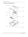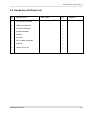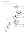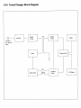
1
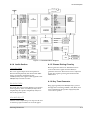
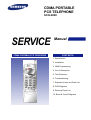
CDMA PORTABLE
PCS TELEPHONE
SCH-2000
SERVICE
CDMA PORTABLE PCS TELEPHONE
Manual
CONTENTS
1. Specification
2. Installation
3. NAM Programming
4. Circuit Description
5. Test Procedure
6. Troubleshooting
7. Exploded Views and Parts List
8. PCB Diagrams
9. Electrical Parts List
10. Block & Circuit Diagrams
Samsung Electronics Co.,Ltd.
GH68-60692A
Printed in Korea.
1. Specification
1-1 General
Frequency Range
Transmitter
Receiver
: 1850 ° ≠1910 MHz
: 1930 ° ≠1990 MHz
Channel Bandwidth
: 1.23 MHz
Channel Spacing
: 50 KHz
Number of Channels
: 1200
Duplex Separation
: 80 MHz
Type of Emission
: G7 W
Input/Output Impedance
: 50 ohms
Intermediate Frequency
Transmitter
Receiver
: 130.38 MHz
: 210.38 MHz
Local Frequency
Transmitter
Receiver
: 1st (FTX-130.38), 2nd (260.76 MHz)
: 1st (FRX-210.38), 2nd (420.76 MHz)
TCXO Frequency
: 19.68 MHz
Frequency Stability
: (FRX - 80 MHz) °æ 150 Hz
Operating Temperature
: -30 °… ° ≠+60 °…
Supply Voltage
: +3.6 V
Current Consumption (Average)
Standby
Talk
: 180 mA (Non-slot mode)
: 480 mA (at +10 dBm)
Size and Weight
Including Standard Battery
Including Extended Battery
: 121.9(H)°ø50.8(W)°ø20.3(D), 138.9 g
: 121.9(H)°ø50.8(W)°ø25.4(D), 158.7 g
Samsung Electronics
1-1
Specification
1-2 Transmitter
Waveform Quality
: 0.944 or more
Open Loop Power Control Range
-25 dBm
-65 dBm
-104dBm
: -60.5 dBm ° ≠-41.5 dBm
: -20.5 dBm ° ≠-1.5 dBm
: +15.0 dBm ° ≠+30.0 dBm
Minimum Tx Power Control
: -50 dBm below
Closed Loop Power Control Range
: °æ24 dB
Maximum RF Output Power
: 200 mW (+23 dBm)
Occupied Bandwidth
: 1.23 MHz
Conducted Spurious Emissions @1.25MHz
: -42 dBc/30KHz
1-3 Receiver
Rx Sensitivity and Dynamic Range
(Rate Set 1)
: -104 dBm, FER=0.5% or less
: -25 dBm, FER=0.5% or less
Conducted Spurious Emission
1930 ° ≠1990 MHz
1850 ° ≠1910 MHz
All Other Frequencies
: <-81 dBm
: <-61 dBm
: <-47 dBm
Single Tone Desensitization
Rx power=-101 dBm
Tone power=-30 dBm
Tone offset from carrier=°æ1.25 MHz
: lower than 1%
Intermodulation Spurious Response Attenuation : lower than 1%
Rx power=-101 dBm
Tone power 1=-43 dBm
Tone power 2=-43 dBm
Tone 1 offset from carrier=°æ1.25 MHz
Tone 2 offset from carrier=°æ2.05 MHz
1-2
Samsung Electronics
2. Installation
2-1 Installing a Battery Pack
1.
2.
To attach the battery pack after charging, align
it with the phone about 1cm (1/2") away from
its place so that the two arrows on the phone
are seen, the battery charge contacts pointing
downwards.
3.
To remove the battery pack, release it by
pressing the button on the rear of the phone.
4.
Slide the battery pack downwards about 1cm
(1/2") and lift it away from the phone.
Slide the battery pack upwards until it clicks
firmly into position. The phone is now ready
to be turned on.
Press this button to release
the battery pack
2-2 For Desk Top Use
1.
Choose a proper location to install the charger
for desk top use.
2.
Plug the power cord of the charger into an
appropriate wall socket. When the power cord
is connected correctly, the lamps turn on
briefly.
3.
To charge the battery pack, insert the battery
pack into the rear slot of the charger. The lamp
marked BAT on the front panel of the charger
lights up red.
4.
If you do not wish to use the phone while
charging the battery, insert the phone with the
battery pack attached into the front slot of the
charger. The lamp marked PHONE on the
front panel of the charger lights up red.
Figure 2-1 Charging The Phone and Battery
Samsung Electronics
2-1
Installation
2-3 For Mobile Mount
2-3-1 Antenna
2-3-2 Cradle
1.
Choose a proper location to install the
antenna.
¶UThe center of the roof top provides the best
performance.
¶UThe edge of the rear trunk also provides a
good performance. However, the antenna
should be higher than the roof of the car.
¶UIn case of on-glass antenna, you should
align the antenna base with the round plate
to connect the cables correctly.
1.
Choose a location where it is easy to reach and
does not interfere with the driver's safe
operation of the car.
2.
Separate the two halves of the clamshell by
removing the two large slotted screws. See the
figure 2-2.
3.
Drill holes and mount the lower half of the
clamshell by using the screws.
2.
Mount the antenna vertically, connect the
antenna cable.
4.
Place the cradle onto the remaining half of the
clamshell and assemble them by using the
screws.
3.
Tighten the antenna nut fully.
5.
Reassemble the two halves of the clamshell
together. Adjust the mounting angle and
tighten the two slotted screws.
Figure 2-2 Cradle Installation
2-2
Samsung Electronics
Installation
2-3-3 Hands-Free Box
2-3-4 Hands-Free Microphone
1.
Drill holes in a proper location for the handsfree box, attach the mounting bracket by using
the screws. See the figure 2-3.
1.
2.
Install the hands-free box into the bracket.
It is recommended to install the microphone
where it is 30-45 cm (12-18") away from the
driver. Choose the location where is least
susceptible to interference caused by external
noise sources, ie, adjacent windows, radio
speakers, etc. Normal place is the sun visor.
2.
Once the microphone has been correctly
positioned, connect the microphone wire to
the MIC jack on the hands-free box.
Figure 2-3 Hands-Free Box Installation
Samsung Electronics
2-3
Installation
2-3-5 Cables
1.
Connect the cradle and the hands-free box
with the data cable. See the figure 2-4.
2.
Connect the antenna cable to the RF jack of the
cradle.
3.
Connect one end of the power cable to the
battery or ignition terminal. Connect the red
wire to the battery (+) terminal, black wire to
the vehicle chassis. Then connect the battery (-)
terminal to the vehicle chassis.
4.
Connect the other end of the power cable to
the PWR jack of the hands-free box.
Notes:
¶UIt is recommended to connect the power cable
directly to the battery to avoid power noise.
¶UMake sure the connection between the battery terminal and the vehicle chassis is made
correctly.
¶UMake sure the fuse having a proper capacity is
used on the power cable.
¶UMake sure the cables do not pass over any sharp
metal edge that may damage it.
Figure 2-4 Cable Connections
2-4
Samsung Electronics
3. NAM Programming
NAM features can be programmed as follows:
Notes:
-If you enter the NAM program mode, each item shows the currently stored data. Go to the next item by
pressing OK.
-You can modify the data by entering a new data.
-If you enter a wrong digit, press CLR to delete the last digit. Press and hold CLR to delete all digits.
-To scroll items backwards or forwards, press the VOLUME button on the left side of the phone.
3-1 General Setup
LCD Display
Key in
Function
MENU, 5, 0
-selects NAM programming
Enter Lock
??????
6-digit code
-Enter random 6-digit code (MSL)
SVC Menu°Ë°È
1:PCS Phone#
2:General
2
-choose 'GENERAL.'
Volume °„
-Electronic Serial Number of the phone is displayed
Volume °„
-Common Air Interface version is displayed
VOC13K/8K
SO_VOICE_13K
°Ëor°È
OK
-Select vocoder service option
-stores it
SCM
Volume °„
-Station Class Mark displays the power class,
transmission, slotted class, dual mode.
ESN
B0000000
CAI version
1
00001010
Lock
Code
0000
Slot Mode
No
4-digit code
OK
Lock code, current status is displayed
-to change, enter new code.
-stores it.
°Ëor°È
OK
Slot mode. 'Yes' indicates the slot mode.
-changes the status.
-stores it.
0-7
OK
Slot mode index. The higher, the longer sleeping time.
-to change, enter new one.
-stores it.
Slot Index
2
Samsung Electronics
3-1
NAM Programming
3-2 Setting Up NAM
LCD Display
Key in
Function
SVC Menu°Ë°È
1:PCS Phone #
2:General
Volume °„
-NAM Programming Menu is displayed
SVC Menu°Ë°È
3:NAM
3
-choose 'Setup NAM'
IMSI_MCC
310
number
OK
IMSI Mobile Country Code, current code is displayed.
-to change, enter new one.
-stores it.
00
number
OK
IMSI Mobile Network Code, current code is displayed.
-to change, enter new one.
-stores it.
IMSI_MNC
class number
OK
CDMA Access Over load Class, current status is displayed.
-to change, enter new one.
-stores it.
CDMA HomeSID
Yes
°Ëor°È
OK
CDMA Home system ID, current status is displayed.
-changes the status.
-stores it.
CDMA
fSID
Yes
°Ëor°È
OK
CDMA foreign SID, current status is displayed.
-changes the status.
-stores it.
CDMA
fNID
Yes
°Ëor°È
OK
CDMA foreign NID, current status is displayed.
-changes the system.
-stores it.
4120
number
OK
first SID written in the list, current status is displayed.
-to change, enter new one.
-stores it.
65535
number
OK
first NID written in the list, current status is displayed.
-to change, enter new one.
-stores it.
CDMA ACCOLC
0
SID
NID
3-2
Samsung Electronics
4. Circuit Description
4-1 Logic Section
4-1-1 Power Supply
With the battery installed on the phone and by
pressing the PWR key, the VBATT and ON_SW
signals will be connected. This will turn on
Q109(2SC4081) and make gate port Low. VBAT
will be supplied to input if DC/DC converter,
controlled by Q115, makes 3.6V for Idle and Talk
Mode, and 3.4V for Sleep Mode.
The VBAT applied to ON_SW turns on
Q110(DTC144) and will result in the signal
ON_SW_SENSE to change state from HIGH to
LOW. The MSM recognizes this signal and sends
out PS_HOLD(logical HIGH) to turn on Q109 even
after the PWR key is released.
The power from U108 is used in the digital part of
MSM and BBA. The power from U111 is used in
the analog part of BBA.
4-1-2 Logic Part
The Logic part consists of internal CPU of MSM,
RAM, ROM and EEPROM. The MSM receives
TCXO/4 and CHIPX8 clock signals from the BBA
and controls the phone. The major components are
as follows:
¶UCPU
¶UFROM
: INTEL 80186 core
: U111,U114 (MBM29LV800T)-8MBIT
FLASH ROM
¶USRAM
: U112(KM68FS2000I)-2MBIT STATIC
RAM
¶UEEPROM : U107(24LC128I)-128KBIT SERIAL
EEPROM
CPU
INTEL 80186 CMOS type 16-bit microprocessor is
used and CPU controls all the circuitry. For the
CPU clock, 27MHz is used.
Samsung Electronics
FLASH ROM (U111, U114)
One 8MBIT FROM(U111) is used to store the
terminal's program. Using the down-loading
program, the program can be changes even after
the terminal is fully assembled. The other is used
to store program for Voice memo, Voice dialing
and so on.
SRAM (U112)
One 2MBIT is used to store the internal flag
information, call processing data, and time data.
EEPROM (U107)
One 128KBIT is used to store ESN, NAM, power
level, volume level, and telephone number.
KEY-PAD
For key recognition, key matrix is setup using
SCAN0-6 of STROBE signals and KEY0-2 of input
ports of MSM. Six LEDs and backlight circuitry are
included in the keypad for easy operation in the
dark and it senses the six LEDs and backlight flip
ON/OFF through reed switch.
EARPIECE
This is a phone that can make a call and receive a
call by earpiece.
LCD MODULE
LCD module contains a controller which will
display the information onto the LCD by 8-bit data
from the MSM. It also consists a DC-DC converter
to supply negative voltage for fine view angle and
LCD reflector to improve the display efficiency.
4-1
Circuit Description
4-1-3 Base Band
MOBILE SYSTEM MODEM (MSM)
The MSM equipped with the INTEL 80186 CPU
core is an important component of the CDMA
cellular phone. The MSM comes in a 176 pins
TQFP package. The interface block diagram is
shown on Figure 4-1.
MICROPROCESSOR INTERFACE
The interface circuitry consists of reset address bus
(A0-A19), data bus (AD0-AD15), and memory
controls (DT-R,HWR/,LWR/,RAM_CS/,
ROM_CS).
ADC Interface
ADC_CLK (pin3), ADC_ENABLE (pin1) and
ADC_DATA (pin2) are required to control the
internal ADC in the BBA.
Data Port Interface
Includes the UART. Also, supports Diagnostic
Monitor (DM) and HP equipment Interface.
CODEC Interface
INPUT CLOCK
°§CPU clock : 27 MHz
°§TXCO/4 (pin34) : 4.92 MHz. This clock signal
from the BBA is the reference clock for the MSM
except in CDMA mode.
°§CHIPX8 : 9.8304 MHz. The reference clock used
during the CDMA mode.
BBA INTERFACE
CDMA,Data Interface
°§TX_IQDATA0~7 (pin24-32) : TX data bus used
during both CDMA.
°§C_RX_IDATA0-3 (pins16-20) and
C_RX_QDATA0-3(pins 12-15) : RX data bus
used during CDMA mode.
The MSM outputs 2.048MHz PCM_CLK (pin19)
and 8KHz CODEC_SYNC (pin16,20) to the
CODEC (U102). The voice PCM data from the
MSM (U101)PCM_DIN (pin135) is compressed
into 8KHz by QCELP algorithm in the CDMA
mode.
RF Interface
TX : TX_AGC_ADJ (pin35) port is used to control
the TX power level and PA_ON (pin44) signal is
used to control the power amplifier.
RX : AGC_REF (pin36) port is used to control the
RX gain and TRK_LO_ADJ (pin45) is used to
compensate the TCXO clock.
General Purpose I/O Register Pins
Input/output ports to control external devices.
Clock
°§TX_CLK(pin 22), TX_CLK/(pin23) : Analog to
Digital Converter(ADC) reference clock used in
TX mode.
°§CHIPX8 : ADC reference clock used in CDMA
RX mode.
4-2
Power Down Control
When the IDLE/signal turns LOW, only the TX
sections will be disabled. If both the IDLE/ and
SLEEP/ changed to LOW, all the pins except for
the TXCO are disabled.
Samsung Electronics
Circuit Description
Figure 4-1 Baseband Block Diagram
4-1-4 Audio Section
TX AUDIO PATH
The voice signal output from microphone is
filtered and amplified by the internal OP-AMP
and is converted to PCM data by the
CODEC(U102). This signal is then applied to the
MSM(U101)'s internal vocoder.
RX AUDIO PATH
The PCM data out from the MSM is converted to
audio signal by ADC of CODEC(U102),is then
amplified by the speaker amplifier(U105) to be
sent to the speaker unit.
4-1-5 Buzzer Driving Circuitry
Buzzer generates alert tone. When the buzzer
receives the timer signal from the MSM, it
generates alert tone. The buzzer level is adjusted
by the alert signal's period generated from the
MSM timer.
4-1-6 Key Tone Generator
Ring signal (pin49) from MSM(U101) is passed
through LPF consisting of R220, C222, R219, and
C221, amplified at the speaker amp(U105) and
come out to speaker.
VOLUME ADJUST
Volume can be adjusted up to 8 steps for the user
to obtain a proper loudness of received signal.
Samsung Electronics
4-3
Circuit Description
4-2 Receiver Section
LOW NOISE AMPLIFIER (LNA)
BUFFER
The low noise amplifier featuring 1.6dB Noise
Figure and 19dB gain amplifies a weak signal
received from the base station to obtain the
optimum signal level.
Buffer (Q311) amplifies signal to be applied to the
local input of the down converter (U302) when a
phase is locked between U304 and U305.
DOWN CONVERTER (MIXER)
First local signal is applied to this down converter.
The down converter transfers the signal amplified
at the LNA into 210.38 MHz IF signal. 210.38MHz
IF signal is made by subtracting 1960°æ30MHz RF
signal from 1750°æ30MHz first local signal. The
LNA is Q303 and down converter is U302.
RF IF AUTOMATIC GAIN CONTROLLER
(AGC) AMP
210.38 MHz IF signal is applied to IF AGC
amp,the AGC output level is applied to BBA (Base
Band Asic). The AGC amp (U303) keeps the signal
at a constant level by controlling the gain.
Dynamic range is 90dB, up gain +45dB, and down
gain -45dB.
RF BAND PASS FILTER (BPF)
The RF BPF(F302) accepts only a specific
frequency (1960°æ30MHz) from the signal
received from the mobile station. The band width
is 60MHz.
IF SAW BAND PASS FILTER FOR CDMA
IF SAW BPF (F303) is used for CDMA system
having 1.23 MHz wide band and °æ630kHz band
width. The filter also eliminates the image product
generated at the mixer.
4-4
VOLTAGE CONTROLLED OSCILLATOR
The VCO (U305) generates the signal having
1750MHz center frequency and °æ30MHz
deviation with the voltage control. PLL IC(U304)
controls this signal.
PHASE LOCKED LOOP (PLL)
Input reference frequency is generated at
VCTCXO (U306) and the signal is generated at
VCO. PLL compares the two signals and generate
the desired signal with a pre-programmed counter
which controls voltage.
VOLTAGE CONTROLLED TEMPERATURE
COMPENSATED CRYSTAL OSCILLATOR
It provides 19.68MHz reference frequency to PLL
(U304) and BBA (U401). A correct frequency
tuning is made by the voltage control.
DUPLEXER
Duplexer (F301) controls to transmit through the
antenna only the signals within acceptable Tx
frequency range (1880°æ30MHz) and to receive
through the antenna only the signals within
acceptable Rx frequency range (1960°æ30MHz). It
also matches LNA(Q303) input in receiving part
and PA output in transmitter part with the
antenna.
Samsung Electronics
Circuit Description
4-3 Transmitter Section
POWER AMP MODULE
POWER SUPPLY SWITCHING
Power Amp Module (U407) amplifies signal to be
sent out to the base station through the antenna.
Power supply switching (Q412) turns on TX
POWER when the phone is in traffic mode and
supplies power to the circuits.
DRIVER AMP
The driver amp (Q413) allows the signal input to
the Power Amp Module (U407) to be within a
specified level.
UP CONVERTER (MIXER)
The up-converter (U405) receives the first local
signal to generate 1880°æ30MHz from the signal
controlled by TX AGC amp (U404). 1880°æ30MHz
signal comes out from the mixer output by adding
130MHz IF signal to 1750°æ30MHz first local
signal. The driver amp's reference number is Q413
and up converter's reference number is U405.
ISOLATOR
Isolator (I401) is used to reduce a reflected signal
to protect the power amp MMIC from being
damaged.
POWER SUPPLY REGULATOR
The power supply regulator (U413,U414) supply a
regulated power to each part of transmitter.
U413 supplies 3.6V to Tx driver (Q413) and Power
Amp Module (U407). U414 supplies 3.3V to the
others.
IF AUTOMATIC GAIN CONTROLLER AMP
The signal out to BBA (Base Band Asic) should be
a constant level. The TX IF AGC amp (U404)
controls power to keep the signal at a constant
level. Dynamic range is 85 dB, up gain +40dB, and
down gain -45dB.
ANTENNA
ANT1 allows signals to send to receive from the
base station.
RF BAND PASS FILTER (BPF)
The RF BPF (F402) accept only a specific frequency
(1880°æ30MHz) to send it out to power amp
MMIC. The band width is 60MHz.
Samsung Electronics
4-5
Circuit Description
4-4 Hands-Free Kit
Hands-free board is largely composed of car
adapter circuit and Hands-free circuit.
4-4-1 Car Adapter Circuit
POWER SUPPLY
Input power switching circuit : This circuit (Q902,
Q903) is power switching control circuit. It supply
power for hands-free kit.
8V regulator (U806) : This circuit supplied power
for audio amplifier (+8V).
Voltage detection circuit : Charging circuit is
designed to stop charging when the charging
circuit is decrease.
The voltage of battery is entered to A/D converter
located in U701 #4. (B/VTG)
Temperature detection circuit : The temperature
of battery is measured by missing NTC thermistor.
NTC thermistor has a characteristics of Log-scale.
It can obtain a linear characteristics by the parallel
connection of resistors.
4-4-2 Hands-free Circuit
POWER SUPPLY (U808)
Vcc regulator (U807) : This circuit regulate Vcc
(+5V).
U808 regulated -5V.
CHARGER CIRCUIT
TX PATH
This circuit charges battery pack by detecting the
temperature of battery, the slope of temperature,
the slope of the voltage of battery, charging time,
etc.
During charging time turns on red LED. Charging
is completed, turn on green LED.
The audio signal from external Mic(J701) flows
into U802 #11. U802 include amplifier and Control
circuit for hands-free operating. U801A amplified
input signal. Output signal transmit to HHP.
Battery Type Capacity
Charge Time
Standard
1000mAH
about 3h °æ
30M
OA ~ 900mA
Extended
1600mAH
about 5h °æ
30M
OA ~ 900mA
4-6
Charge Current
RX PATH
Input audio signal canceled noise by difference
amplifier (U801c). U802 process hands-free action.
The RX audio signal is input (U805). The speaker
drive amp (U804) amplify the Rx audio signal and
the output of U804 is go out of speaker.
Samsung Electronics
Circuit Description
4-5 Desk-Top Rapid Charger
4-5-1 Description
This specification describes requirements of
DTC55 desktop charger. DTC55 is designed as
desk-top rapid charger for Li-ion battery for
SAMSUNG PCS Cellular phone SCH2000.
This charger include AC/DC adapter circuitry in
its own board. This characteristic offers operating
with direct indoor AC input without additional
AC/DC adapter unit.
Integrated AC/DC adapter circuitry adopts
switching mode power supply to keep lightness of
whole charger.
And it has two battery slot, the front one is
intended for cellular phone with battery and rear
one is for another battery only. Two bi-color LED
include charging status of each battery slot.
Charging current is automatically controlled by
programmed microprocessor inside of charger, to
proper to each type of battery.
4-5-2 Electrical Characteristic
AC IN PUT
¶UAC input voltage : 110/220Vac
¶UAC input voltage : 85Vac ~ 264Vac
¶UAC input frequency : 60Hz
¶UAC input ON/OFF cycle : MIN 5 sec
OUT PUT
¶UBattery Charging Method : CC-CV mode
¶UBattery Charging Current Range under CC
mode
-Front slot : 800mA °æ
70mA
-Rear slot :
400mA °æ
50mA
¶UBattery Charging Voltage Range under CC
mode
-Front slot voltage setting (V/F : 5.1K)
4.1 °æ
0.05 VDC with 110Vac input and 180mA
load current.
- CV mode 4.05V ~ 4.15V
- Voltage range (4.05V ~ 4.15V), is to be tested
with 180mA ~ 600mA load range for Front slot.
- Rear slot voltage (V/F : 5.1K)
- CV mode 4.0V ~ 4.15V at 150mA load
¶URipple & Noise
- Ripple & Noise Lim it : 60mVp_p MAX
- Test Condition
- Front : At output contact with 20MHz
bandwidth using resistive load 650mA and
nominal input.
¶UEfficiency
- 55% MIN
- Efficiency is to be tested with 650mA and
150mA resisted load and 110Vac input.
Samsung Electronics
4-7
Circuit Description
LED INDICATION
BURN -IN
¶UAC plug in : red and green orange at 0.5 sec
intervals
¶USlot Identification
- Front slot : LED “ PHONE”
- Rear slot : LED "BATT”
¶UAll power supply shall be subjected to the burn in process
- Temperature : 35 °∆
C °æ
5 °∆
C
- Load condition : 600mA and 150mA
- Input Voltage : nominal 110Vac
¶UCharging Status
- Constant Red : Rapid charging
- Constant Green : Rapid charging is terminated.
- Constant Orange : Under or Over Temperature
- Flashing Orange
*If charging is started with any battery of open
cell, equivalent LED should be flashing
Orange.
*If a battery of open cell is loaded on rear slot
whole front slot is charging, the other good
battery.
LED for front slot - Constant RED
LED fro rear slot - flashing Orange
*If a battery of open cell is loaded on front slot
while rear slot charging, the other good
battery.
LED for front slot - flashing Orange
LED for rear slot - constant RED
- Off : battery unloaded
4-5-3 General Characteristics
TEMPERATURE
¶UCharging Temperature Range : 0 to 45 °∆
C
¶UStorage Temperature Range : -20 to 85 °∆
C
SAFETY REQUIREMENTS
¶USafety Approval
- Approval No. : UL and CUL, FCC Class B
- Approval No. should be appeared in label
design.
PRIMARY - SECONDARY ISOLATION
¶UWithstanding Voltage : 3K Vdc for 1 sec
¶UCut-off Current : 10mA
4-8
4-5-4 Schematic Description
BATTERY RECOGNITION CIRCUIT : HIC
¶UBattery identity detection determined to voltage
through R4, R6, R11, R12.
¶UBattery internal between C/F and GND.
CURRENT DETECTION CIRCUIT : R5, R6,
R11, R12, HIC
¶UBattery charging current is changed voltage
detection.
¶UThis voltage inputted u-COM to 16 times
amplified through HIC.
VOLTAGE DETECTION CIRCUIT : HIC
u-COM A/D through HIC pin 12, 13 detected
voltage.
BATTERY TEMPERATURE DETECTION
CIRCUIT : HIC, TH1
Battery temperature detection determined
temperature by use of thermistor resistor variation
of TH1 by HIC.
CURRENT LIMIT CIRCUIT : HIC
When soft-change, current detection circuit limited
current flow to battery, reference voltage more
than detected current, detected current and HIC
internal reference voltage.
Samsung Electronics
Circuit Description
4-6 Cigarette Lighter Adapter
4-6-1 Description
This specification describes requirements of
CHG55 cigarette lighter adapter. CHG55 is
designed as an charger for Li-ion battery for
SAMSUNG PCS Phone SCH-2000.
4-6-2 Electrical Characteristic
¶UInput Voltage : 11~ 30V DC (Normal voltage :
13.7V DC)
¶UOutput Voltage : 4.1 °æ
0.02V DC9 (Maximum)
¶UOutput Current :
- Output Current : 0 ~ 740 mA
- Current limited in this unit should be kept 740
°æ
40mA
¶URipple Noise : 0.1 Vp_p (under 600mA load)
¶UFuse Capacity : 250V, 2A
¶UCharging time :
- Standard battery : 4 hours °æ
30 minutes
- Extended battery : 5 hours °æ
30 minutes
4-6-3 Function
PROTECTION CIRCUIT
Protection Circuit is the circuit against the
electrical stress which is occurred at unexpected
condition of the source power of CLA unit such as
reserve voltage or over current.
DETECTION OF MOBILE PHONE
If mobile phone is connected to CLA, the CLA
lamp is on to display whether CLA is operating or
not.
AUTO POWER ON
When a phone is connected to CLA, the power of
the phone will be on automatically.
DUAL LED
This CLA has dual LED.
Green : When battery is fully charged. (over 80%)
Red : When CLA is on charging battery.
4-6-4 Schematic Description
POWER SUPPLY
This circuit supplies HHP & battery with power
received from Cigar Lighter jack of automobile.
POWER CIRCUIT OF CHARGE FOR HHP
POWER & BATTERY
This Switching Regulator produces needed power
for charging HHP power & battery, supplied U1,
D1, D2, C1, C2, L1, R11 from Cigar Lighter jack of
automobile.
CONFIRMING CIRCUIT OF EXISTING
BATTERY OR NOT
U3A reads separated voltage between resistance
battery C/F and R20, controls no. 5 pin of U1
through reference voltage and comparator then
decides to produce Vcc or not.
CHARGE CURRENT CONTROL CIRCUIT
U2A, U4, Q1 and side circuit detects R4's flowing
current, control no. 5 pin of u1 then charge current
and charge voltage.
Samsung Electronics
4-9
Circuit Description
LED ACTIVATING CIRCUIT
LED activating circuit compares to voltage
difference between R4 source and D4 PROP,
controls Q3, Q4 through U2B comparator for Q6
and side circuit, then activates LED.
AUTO POWER ON CIRCUIT
Q7, Q8 and side circuit makes power on the circuit
allowed Vcc power to no. 9 HHP pin (power on)
by turned on Q7, following up the producing Vcc.
CONNECTION OF CLC, CURL, AND CABLE
PIN NO.(CLA)
DESCRIPTION
PIN NO.(PHONE)
#1
HP-PWR
#2
V-BAT
#3
V/F
N.C
#4
C/F
3
#5
GND
4-10
9
14/15/16
2/4/6
Samsung Electronics
Circuit Description
4-7 Travel Charger
4-7-1 Description
- This specification describes requirements of TC55
travel charger. TC55 is designed as a wall-mount
type rapid charger for Li-ion battery (1CELL) for
SAMSUNG PCS phone SCH-2000.
- This charger includes AC/DC adapter circuitry
in its own board. This characteristic offers
operating with direct indoor AC input without
additional AC/DC adapter unit. And it is
connected by DC power cord to a phone with
battery.
- Integrated AC/DC adapter circuity adopts
switching mode power supply to keep lightness
of whole charger.
- Own bi-color LED indicates charging status of
battery.
- Charge current is automatically controlled by
programmed microprocessor inside of charger.
SAFETY REQUIREMENTS
Primary-Secondary Isolation
- Withstanding Voltage : 3000Vac min for 1 second
- Cut-put current : 10mA
- Isolation Resistance : 8 Mohm
LED INDICATION
AC PLUG IN : yellow for 1 second
Charging status
- Red : Charging
- Green : Charging termination
- OFF : Battery unloaded
- Yellow blinking : Error mode
- Yellow : Under or over temperature
ENVIRONMENTAL SPECIFICATION
Unit Operating Temperature Range : 1 to 45 °∆
C
4-7-2 Electrical Characteristic
AC INPUT
- AC input voltage : 110/220 Vac
- AC input voltage range : 85Vac ~ 264 Vac
- AC input frequency : 60Hz
- Ac input power : 10W
OUTPUT
- Battery Charging Voltage : 4.1/4.2 V
- Battery Charging Voltage Range under C-V
mode : 4.1/4.2 (-0.2/+0.1V)
- Battery Charging Current : 0 to 700 mA
- Battery Charging Current Range under C-C
mode : 700mA °æ
70 mA
- Efficiency : 55% min
- Ripple & Noise : 60mVp_p max (test condition :
At output contact with 20MHz bandwidth using
resistive load 650mA)
Samsung Electronics
Storage Temperature : -20 to 85 °∆
C
4-7-3 Schematic Description
MICOM CONTROLLER : U4
¶UU4 is include u-COM to controlled whole
charging system and include following internal
circuit.
- General input / output
- A/D converter
- Reset delay circuit (power on delay)
- Timer
¶UIt is carried following functions
- Battery recognition
- Charging termination condition detection
- Output short detection and output protection
- Temperature detection
4-11
Circuit Description
BATTERY RECOGNITION CIRCUIT : U4
¶UBattery identity detection determined to voltage
detection
¶UBattery internal between ID & GND
CURRENT DETECTION CIRCUIT : R14, R15,
R16, U4
¶UBattery charging current is changed voltage
through R14, R15, R16
¶UThis voltage inputted u-COM to 16times
amplified through U4
VOLTAGE DETECTION CIRCUIT : U4
¶Uu-COM A/D through U4 pin 15 detected
voltage
BATTERY TEMPERATURE DETECTION
CIRCUIT : U4
¶UBattery temperature detection determined
temperature by use of thermistor resistor
variation of battery by U4
CURRENT LIMIT CIRCUIT : U4
¶UWhen soft-change, current detection circuit
limited current flow to battery, reference voltage
more than detected current, detected current
and U4 internal reference voltage.
4-12
Samsung Electronics
5. Test Procedure
5-1 List of Equipment
¶UDC Power Supply
¶UTest Jig
¶UTest Cable
¶UCDMA Mobile Station Test Set
¶USpectrum Analyzer (include CDMA test mode)
HP8924C, HP83236B, CMD-80, etc
HP8596E
5-2 Configuration of Test
5-2-1 Hand Set
5-2-2 Hand-Free
Samsung Electronics
5-1
Test Procedure
5-3 Test Procedure
5-3-1 Change to Test Mode
1. To change the phone from Normal Mode to test
Mode, You should enter the following keys.
"47*869#1235"
2. The command° ∞
0 1"(Suspend) is entered to start
test.
3. To finish the Test Mode, You should enter the
command "0 2".
5-3-2 Channel Selection and Tx Power
Output level Control
1. You should change the phone from Normal
Mode to Test mode
2. The command° ∞
0 1"(Suspend) is entered to start
test.
5-2
3. You should enter the following keys.
" 0 9, 0 5 2 5, #, 0 7, 3 4, 7 1, 4 7 5, #"
¶UIf you enter the command "0 9", You can select
the channel
ex) 0 9 X X X X (means channel number)
¶UThe command "0 7°±means Carrier On (Carrier
Off :° ∞
0 8°±)
¶UIf you enter the command "3 4", You can
spread the carrier.
¶UIf you enter the command "7 1", You can
control the power output level. Following
under-bar means AGC code. And you can
control the power output level using Volume
Up/Down Keys.
ex) 7 1 X X X
4. After enter the command "7 4" and control the
Tx Power Output Level to be 0.0dBm using
Volume Up/Down keys, press "STO" key to
store Data in EEPROM.
Samsung Electronics
Test Procedure
5-4 Test Command Table
Command No.
(OP, AB, RB)
Test Command
01(1F, 0, 0)
02(3F, 0, 0)
03(FD, 0, 0)
04(1D, 0, 1)
05(1C, 1, 0)
06(1E, 0, 0)
07(81, 0, 0)
08(82, 0, 0)
09(83, 4, 0)
10(84, 1, 0)
11(85, 0, 0)
12(86, 0, 0)
13(87, 0, 0)
14(88, 0, 0)
16(8F, 0, 0)
17(90, 0, 0)
22(91,96,96)
23(95, 3, 4)
24(9F, 7, 8)
25(92, 0, 0)
26(93, 0, 0)
27(96, 0, 0)
28(97, 0, 0)
29(9A, 0, 0)
30(9D,15, 0)
32(A0, 1, 0)
33(A1, 0, 0)
34(A2, 0, 0)
35(A3, 0, 0)
36(A4, 0, 0)
42(AA, 1, 0)
43(AB, 0, 0)
44(B0, 0, 0)
45(B1, 0, 0)
46(B2, 0, 0)
47(B3, 0, 0)
48(B4, 0, 4)
50(B6, 4, 0)
57(BC, 0, 0)
58(BD, 0, 0)
59(BE, 0, 0)
67(C6, 3, 6)
T_SUSPEND_I
T_RESTART_I
T_SAVE_VAL_I
T_GET_MODE_I
T_SET_MODE_I
T_WRITE_NV_I
T_CARRIERON_I
T_CARRIEROFF_I
T_LOADSYN_I
T_PWRLEVEL_I
T_RXMUTE_I
T_RXUNMUTE_I
T_TXMUTE_I
T_TXUNMUTE_I
T_STON_I
T_STOFF_I
T_SNDNAM_I
T_SNDVERSION_I
T_SNDESN_I
T_BACKLIGHT_ON_I
T_BACKLIGHT_OFF_I
T_LAMP_ON_I
T_LAMP_OFF_I
T_REBUILD_I
T_PLINE_I
T_SATON_I
T_SATOFF_I
T_CDATA_I
T_VOLUME_UP_I
T_VOLUME_DOWN_I
T_DTMFON_I
T_DTMFOFF_I
T_COMPANDORON_I
T_COMPANDOROFF_I
T_VIBRATOR_ON_I
T_VIBRATOR_OFF_I
T_BATT_TYPE_I
T_H_LIST_I
T_MIC_ON_I
T_MIC_OFF_I
T_ALLPATH_I
T_READ_BATT_I
Samsung Electronics
Description
Terminate the normal mode, enter to the test mode.
Terminate the test mode, enter to the normal mode.
Save value in EEPROM. (Only for Auto test)
Get mode. (CDMA or FM)
Set mode to CDMA or FM. (Only for Auto test)
Write an EEPROM item. (one of the NV items)
Turn the carrier on.
Turn the carrier off.
Set the synthesizer to the channel specified by ch_ data.
Set the RF power attenuation to the specified value.
Mute the receive-audio signal.
Unmute the receive-audio signal.
Mute the transmit-audio signal.
Unmute the transmit-audio signal.
Turn on ST.
Turn off ST.
Display and send NAM information.
Display and return S/W version.
Display and return ESN.
Turn on the backlight.
Turn off the backlight.
Turn on the LAMP.
Turn off the LAMP.
Rebuild EEPROM.
Display and return production date.
Turn on SAT.
Turn off SAT.
Continuously send TX control data.
Increase value of the last command. (Only for autotest)
Decrease value of the last command. (Only for autotest)
Activate dtmf generator with keycode.
Deactivate DTMF generator.
Turn on compandor.
Turn off compandor.
activate a vibrator
inactivate a vibrator
Battery Type
History Channel.
Mic path on.
Mic path off.
Set RX Path, TX Path Unmute to Earpiece.
Reads Low-Battery in the standby, talk.
5-3
Test Procedure
Command No.
(OP, AB, RB)
Signal. Name
Description
68(C8, 0, 3)
T_VBATT1_I
Set the low battery position in the standby.
69(C9, 0, 3)
T_VBATT2_I
Set the low battery position in the talking.
70(CA, 3, 0)
T_WRITE_BATT_I
Write low battery level value to NVM.
71(D1, 3, 0)
T_CDMA_TXADJ_I
Change PDM TX AGC in CDMA.
72(D2, 3, 0)
T_FM_TXADJ_I
Change PDM TX AGC in FM.
73(D3, 1, 0)
T_SET_PA_R_I
Set PA R1, R0 in CDMA.
74(D4, 3, 0)
T_TXADJ_0DBM_I
Set TX AGC ADJ for 0dBm power.
75(D5, 0, 3)
T_READ_RSSI_I
Read a RSSI.
76(D6, 3, 0)
T_WRITE_RSSI_I
Writes RSSI.
77(D7, 0, 3)
T_READ_TEMP_I
Read Temp.
79(D9, 1, 0)
T_BUZZER_ON_I
Buzzer On at DTMF 0 key.
80(DA, 0, 0)
T_BUZZER_OFF_I
Buzzer off.
81(E3, 0, 0)
T_VOC_PCMLPON_I
Play a PCM LOOP BACK.
82(E4, 0, 0)
T_VOC_PCMLPOFF_I
Play off a PCM LOOP BACK.
84(E6, 3, 0)
T_CD_MAX_LIMIT_I
CDMA MAX limit.
85(E7, 0, 0)
T_SPEAKER_ON_I
Turn on the speaker path.
86(E8, 0, 0)
T_SPEAKER_OFF_I
Turn off the speaker path.
87(E9, 0, 0)
T_FM_LOOP-TEST_I
Play a PCM FM loopback.
88(EA, 3, 0)
T_TRK_ADK_I
TRK LOCAL ADJUST.
89(EB, 3, 0)
T_CD_TRK_ADJ_I
CDMA TRK LOCAL ADJUST.
90(F0, 3, 0)
T_CDMA_LOW_CH_HIPWR_I
Setting the volume for LOW CH highpwr. (+18dBm)
91(F1, 3, 0)
T_CDMA_LOWMID_CH_HIPWR_I
Setting the volume for LOWMID CH highpwr. (+18dBm)
92(F2, 3, 0)
T_CDMA_MIDDLE_CH_HIPWR_I
Setting the volume for MIDDLE CH highpwr. (+18dBm)
93(F3, 3, 0)
T_CDMA_LOW_CH_LOPWR_I
Setting the volume for LOW CH lowpwr. (-41dBm)
94(F4, 3, 0)
T_CDMA_LOWMID_CH_LOPWR_I
Setting the volume for LOWMID CH lowpwr. (-41dBm)
95(F5, 3, 0)
T_CDMA_MIDDLE_CH_LOPWR_I
Setting the volume for MIDDLE CH lowpwr. (-41dBm)
96(F6, 3, 0)
T_CDMA_HIGHMID_CH_LOPWR_I Setting the volume for HIGHMID CH lowpwr. (-41dBm)
97(F7, 3, 0)
T_CDMA_HIGH_CH_LOPWR_I
Setting the volume for HIGH CH lowpwr. (-41dBm)
98(F8, 3, 0)
T_CDMA_HIGHMID_CH_HIPWR_I
Setting the volume for HIGHMID CH highpwr. (+18dBm)
99(F9, 3, 0)
T_CDMA_HIGH_CH_HIPWR_I
Setting the volume for HIGH CH highpwr. (+18dBm)
¶S
OP: Operation Command Number
AB: Input Argument Byte Number
RB: Return Byte Number
5-4
Samsung Electronics
6. Troubleshooting
6-1 Logic Section
6-1-1 No Power
Samsung Electronics
6-1
Troubleshooting
6-1-2 Abnormal Initial Operation (Normal +3.3 voltage source)
6-2
Samsung Electronics
Troubleshooting
6-1-3 Abnormal Backlight Operation
Samsung Electronics
6-3
Troubleshooting
6-1-4 Abnormal Key Data Input
6-4
Samsung Electronics
Troubleshooting
6-1-5 Abnormal Keytone
Samsung Electronics
6-5
Troubleshooting
6-1-6 Abnormal Alert Tone
6-6
Samsung Electronics
Troubleshooting
6-2 Transmitter Section
Samsung Electronics
6-7
Troubleshooting
6-3 Receiver Section
6-8
Samsung Electronics
Troubleshooting
6-4 Hands-Free Kit
6-4-1 Abnormal Battery Charging
A (STD): 0.5V °¬ V at U701 pin 7 < 1.5V
B (EXT): 1.6V °¬ V at U701 pin 7 < 2.4V
Samsung Electronics
6-9
Troubleshooting
6-4-2 No Power
6-10
Samsung Electronics
Troubleshooting
6-4-3 Hands-Free RX Path
Samsung Electronics
6-11
Troubleshooting
6-4-4 Hands-Free TX Path
6-12
Samsung Electronics
Troubleshooting
6-5 Desk-Top Rapid Charger
Samsung Electronics
6-13
Troubleshooting
6-6 Cigarette Lighter Adapter
6-6-1 LED-ON Fault
6-14
Samsung Electronics
Troubleshooting
6-6-2 Charge Fault
Samsung Electronics
6-15
Troubleshooting
6-7 Travel Charger
6-16
Samsung Electronics
7. Exploded View and its Parts List
7-1
Main Set Exploded View
7-2
Main Set Parts List
7-3
Hands-Free Kit Exploded View
7-4
Hands-Free Kit Parts List
7-5
Hands-Free Kit Cradle Exploded View
7-6
Hands-Free Kit Cradle Parts List
7-7
Desk-Top Rapid Charger Exploded View
7-8
Desk-Top Rapid Charger Parts List
7-9
Cigarette Lighter Adapter
7-10 Travel Charger
7-11 Main Set Packing Layout
7-12 Main Set Packing Parts List
7-13 Hands-Free Kit Packing Layout
7-14 Hands-Free Kit Packing Parts List
Samsung Electronics
7-1
Exploded View and its Parts List
7-1 Main Set Exploded View
7-2
Samsung Electronics
Exploded View and its Parts List
7-2 Main Set Parts List
NO
1
2
3
4
5
6
7
8
9
10
11
12
13
14
15
16
17
18
19
20
21
22
23
24
25
26
27
28
29
30
31
32
33
34
35
36
37
38
39
40
41
42
43
44
45
DESCRIPTION
TAPE WINDOW-BOHO
WINDOW-LCD
TAPE-WINDOW
CAP-LED
FRONT-COVER
FLIP COVER
MAGNETIC
LABEL (R)-FLIP
SHIELD STRIP (A)
SHIELD STRIP (B)
BUZZER-COVER
SPEAKER-COVER
KNOB-VOLUME
HINGE-HOUSING
SHAFT-HINGE
CAM-HINGE
SPRING-HINGE
HOUSING-CAP
HOLDER BUZZER
SPEAKER-TAPE
KEY PBA ASSY
HOLDER MIC
SHIELD COVER
MAIN PCB
COVER-CONNECTOR
MEMORY PCB
STRIP FINGER
SHIELD STRIP (D)
SHIELD STRIP (F)
SHIELD STRIP (C)
SHIELD STRIP
REAR COVER
TAPTITE
VIBRATOR
EARPHONE COVER
ANT-BUSHING
ANTENNA
SPRING LOCKER
LOCKER-MAIN
SCREW
LABEL (R) BAR CODE
LABEL MAIN
BAR CODE ESN
STD. BATT. PACK
EXT. BATT. PACK
Samsung Electronics
SEC. CODE
GH72-10001A
GH72-20008A
GH74-10650A
GH72-41424A
GH72-41426A
GH72-41427A
937 312008AA
GH68-31044A
GH71-10639A
GH71-10640A
GH72-10503A
GH72-10528A
GH73-40670A
GH72-41293A
GH72-41554A
GH72-41055A
GH70-10608A
GH72-41056A
GH73-40666A
GH74-10571A
GH59-10075A
GH73-40667A
GH72-41423A
GH41-10626A
GH73-40636A
GH41-10627A
GH71-10551A
GH71-10643A
GH71-10673A
GH71-10641A
GH71-10644A
GH72-41425A
6003-000366
GH31-10003A
GH72-41493A
GH71-40003A
GH42-10520A
GH70-10516A
GH72-41492A
6001-001046
GH68-30963A
GH68-31069A
GH68-30936A
GH43-10111A
GH43-10112A
Q'TY
REMARK
1
1
1
1
1
1
1
1
6
5
1
1
1
1
2
2
2
2
1
1
1
1
1
1
1
1
1
1
5
3
1
1
1
1
1
1
1
1
1
4
1
1
1
1
1
7-3
Exploded View and its Parts List
7-3 Hands-Free Kit Exploded View
7-4
Samsung Electronics
Exploded View and its Parts List
7-4 Hands-Free Kit Parts List
NO
DESCRIPTION
SEC. CODE
Q'TY
1
H/F UPPER HOUSING
1
2
LABEL (R)-LOGO H/F
1
3
H/F FELT-SPEAKER
1
4
AUDIO-SPEAKER
1
5
SCREW
4
6
H/F PBA
1
7
H/F LOWER HOUSING
1
8
SCREW
4
9
LABEL (R)-ID H/F
1
Samsung Electronics
REMARK
7-5
Exploded View and its Parts List
7-5 Hands-Free Kit Cradle Exploded View
7-6
Samsung Electronics
Exploded View and its Parts List
7-6 Hands-Free Kit Cradle Parts List
NO
DESCRIPTION
SEC. CODE
Q'TY
1
UPPER HOUSING-C/D
1
2
SOCKET PLATE-C/D
1
3
LOCKER-C/D
2
4
TORSION SPRING-C/D
2
5
EJECTOR SPRING-C/D
2
6
FRAME-C/D
1
7
SCREW, TAPTITE, B, BH, M2.6, L6
4
8
CLADLE-PBA
1
9
SCREW, TAPTITE, BH, M2.6, L6
2
10
SCREW, TAPTITE, BH, M2, L6
4
11
HOLDER-C/D
1
12
CURL CORD
1
13
SCREW, MACHINE, BH, M3, L8
1
14
LABEL (R)-ID C/D
1
15
CRADLE DATA CABLE
1
16
LOWER HOUSING-C/D
1
Samsung Electronics
REMARK
7-7
Exploded View and its Parts List
7-7 Desk-Top Rapid Charger Exploded View
7-8
Samsung Electronics
Exploded View and its Parts List
7-8 Desk-Top Rapid Charger Parts List
NO
DESCRIPTION
1
LABEL-LOGO DTC
1
2
CASE TOP
1
3
TAPPING SCREW
4
4
HOOK PLATE (L)
1
5
HOOK PLATE (R)
1
6
HOUSING BATT
1
7
TAPPING SCREW
1
8
MAIN PBA
3
9
TAPPING SCREW
1
10
AC POWER CORD ASSY
2
11
CASE BOTTOM
1
12
FOOT RUBBER
1
13
TAPPING SCREW
4
14
LABEL-DTC
4
Samsung Electronics
SEC. CODE
Q'TY
REMARK
7-9
Exploded View and its Parts List
7-9 Cigarette Lighter Adapter
CIGARETTE LIGHTER ADAPTER ASS'Y :
GH44-40071A
7-10
Samsung Electronics
Exploded View and its Parts List
7-10 Travel Charger
TRAVEL CHARGER ASS'Y : GH44-40070A
Samsung Electronics
7-11
Exploded View and its Parts List
7-11 Main Set Packing Layout
7-12
Samsung Electronics
Exploded View and its Parts List
7-12 Main Set Packing Parts List
NO
DESCRIPTION
SEC. CODE
1
GIFT BOX MAIN
GH69-11132A
1
2
CUSHION CASE-MAIN
GH69-20664A
1
3
DESK TOP CHARGER
GH44-40069A
1
4
STD BATT. PACK
GH43-10111A
1
5
MAIN SET
6
HAND STRAP
Samsung Electronics
Q'TY
REMARK
1
GH72-41051A
1
7-13
Exploded View and its Parts List
7-13 Hands-Free Kit Packing Layout
7-14
Samsung Electronics
Exploded View and its Parts List
7-14 Hands-Free Kit Packing Parts List
NO
DESCRIPTION
SEC. CODE
Q'TY
1
PWR-CABLE
1
2
H/F MIC ASS'Y
1
3
H/F BOX
1
4
MTG BRACKET-H/F
1
5
SUA INSTALL SCREW
1
6
CLAM SHELL MOUNT
1
7
MANUAL
1
8
CRADLE
1
9
CUSHION CASE-H/K
1
10
GIFT BOX-H/F
1
Samsung Electronics
REMARK
7-15
Exploded View and its Parts List
7-16
Samsung Electronics
9. Electrical Parts List
9-1 Handset
NO
DESCRIPTION
SEC. CODE
REMARK
- Capacitors C101
CERAMIC,CHIP,47nF
2203-001432
C102
CERAMIC,CHIP,33nF
2203-001416
C104
CERAMIC,CHIP,100nF
2203-000189
C105
CERAMIC,CHIP,1nF
2203-000438
C106
TANTALIUM,CHIP,1uF
2404-000151
C107,C108
CERAMIC,CHIP,470pF
2203-000941
C109
TANTALIUM,CHIP,100uF
2404-000112
C110
TANTALIUM,CHIP,10uF
2404-001020
C111
CERAMIC,CHIP,1nF
2203-000438
C112
TANTALIUM,CHIP,330uF
2404-001027
C114,C115
TANTALIUM,CHIP,1uF
2404-000151
C117
TANTALIUM,CHIP,10uF
2404-001020
C118-C121
CERAMIC,CHIP,8.2nF
2203-001210
C126-C128
TANTALIUM,CHIP,2.2uF
2404-000167
C135
CERAMIC,CHIP,10nF
2203-000254
C138,C139
CERAMIC,CHIP,5pF
2203-001437
C148
CERAMIC,CHIP,10nF
2203-000254
C149
CERAMIC,CHIP,100nF
2203-000189
C150
CERAMIC,CHIP,10nF
2203-000254
C151
CERAMIC,CHIP,100nF
2203-000189
C152
CERAMIC,CHIP,10nF
2203-000254
C153
CERAMIC,CHIP,100nF
2203-000189
C154
CERAMIC,CHIP,10nF
2203-000254
C155
CERAMIC,CHIP,100nF
2203-000189
C156
CERAMIC,CHIP,10nF
2203-000254
C157
CERAMIC,CHIP,100nF
2203-000189
C158
CERAMIC,CHIP,10nF
2203-000254
C159
CERAMIC,CHIP,100nF
2203-000189
C160
CERAMIC,CHIP,10nF
2203-000254
C161
CERAMIC,CHIP,100nF
2203-000189
C162
CERAMIC,CHIP,10nF
2203-000254
C163
CERAMIC,CHIP,100nF
2203-000189
C164
CERAMIC,CHIP,100pF
2203-000234
C165
CERAMIC,CHIP,470pF
2203-000941
Samsung Electronics
9-1
Electrical Parts List
NO
DESCRIPTION
SEC. CODE
C166-C168
CERAMIC,CHIP,100pF
2203-000234
C169
CERAMIC,CHIP,100pF
2203-000189
C171-C176
CERAMIC,CHIP,100nF
2203-000189
C201,C202
TANTALIUM,CHIP,1uF
2404-000151
C203,C204
CERAMIC,CHIP,680pF
2203-001124
C205,C206
CERAMIC,CHIP,100nF
2203-000189
C207
CERAMIC,CHIP,18nF
2203-000415
C209
TANTALIUM,CHIP,1uF
2404-000151
C211
CERAMIC,CHIP,5.6nF
2203-001033
C212
CERAMIC,CHIP,10nF
2203-000254
C213
CERAMIC,CHIP,100nF
2203-000189
C214
CERAMIC,CHIP,1.2nF
2203-002687
C215
CERAMIC,CHIP,2.2nF
2203-000439
C216
TANTALIUM,CHIP,2.2uF
2404-000167
C217
CERAMIC,CHIP,100nF
2203-000189
C218
TANTALIUM,CHIP,33uF
2404-000309
C219
CERAMIC,CHIP,100nF
2203-000189
C221
CERAMIC,CHIP,22nF
2203-000604
C222
CERAMIC,CHIP,100nF
2203-000189
C229
CERAMIC,CHIP,15pF
2203-000386
C302
CERAMIC,CHIP,6pF
2203-001178
C303
CERAMIC,CHIP,15pF
2203-000386
C304
CERAMIC,CHIP,1pF
2203-000469
C305
CERAMIC,CHIP,2.7nF
2203-000530
C308
CERAMIC,CHIP,1nF
2203-000438
C309
CERAMIC,CHIP,10nF
2203-000254
C315
CERAMIC,CHIP,47pF
2203-000995
C316
CERAMIC,CHIP,10nF
2203-000254
C317
CERAMIC,CHIP,100nF
2203-000189
C318
CERAMIC,CHIP,10nF
2203-000254
C319
CERAMIC,CHIP,100pF
2203-000234
C320
CERAMIC,CHIP,2.7nF
2203-000530
C321
TANTALIUM,CHIP,4.7uF
2404-000232
C322,C323
CERAMIC,CHIP,1nF
2203-000438
C324
CERAMIC,CHIP,100nF
2203-000189
C325
CERAMIC,CHIP,2.7nF
2203-000530
C326
CERAMIC,CHIP,47nF
2203-001432
C327
CERAMIC,CHIP,1nF
2203-000438
9-2
REMARK
Samsung Electronics
Electrical Parts List
NO
DESCRIPTION
SEC. CODE
C328
CERAMIC,CHIP,22pF
2203-000628
C329
CERAMIC,CHIP,100nF
2203-000189
C331
CERAMIC,CHIP,5pF
2203-001437
C332
CERAMIC,CHIP,100nF
2203-000189
C334
CERAMIC,CHIP,10nF
2203-000254
C335,C336
TANTALIUM,CHIP,10uF
2404-001020
C337,C338
CERAMIC,CHIP,10nF
2203-000254
C339
CERAMIC,CHIP,100nF
2203-000189
C340-C342
CERAMIC,CHIP,100pF
2203-000234
C343
CERAMIC,CHIP,10nF
2203-000254
C344
CERAMIC,CHIP,100pF
2203-000234
C345
CERAMIC,CHIP,10pF
2203-000278
C346
CERAMIC,CHIP,1nF
2203-000438
C347
CERAMIC,CHIP,100pF
2203-000234
C348
TANTALIUM,CHIP,1.5uF
2404-000274
C349
CERAMIC,CHIP,100nF
2203-000189
C350
CERAMIC,CHIP,2.2nF
2203-000439
C351
TANTALIUM,CHIP,10uF
2404-001020
C352
CERAMIC,CHIP,100pF
2203-000234
C353
TANTALIUM,CHIP,1.5uF
2404-000274
C354
CERAMIC,CHIP,100nF
2203-000189
C355
CERAMIC,CHIP,2.2nF
2203-000439
C356
CERAMIC,CHIP,2.7nF
2203-000530
C357
CERAMIC,CHIP,10nF
2203-000254
C358
CERAMIC,CHIP,100nF
2203-000189
C359
CERAMIC,CHIP,33pF
2203-000812
C360
TANTALIUM,CHIP,10uF
2404-001020
C361
CERAMIC,CHIP,15pF
2203-000386
C362
CERAMIC,CHIP,10pF
2203-000278
C363
CERAMIC,CHIP,10nF
2203-000254
C364
CERAMIC,CHIP,1pF
2203-000466
C365
CERAMIC,CHIP,1nF
2203-000438
C367
CERAMIC,CHIP,5pF
2203-001437
C401,C402
CERAMIC,CHIP,100pF
2203-000234
C403
CERAMIC,CHIP,6pF
2203-001178
C404
CERAMIC,CHIP,47nF
2203-001432
C405
CERAMIC,CHIP,1nF
2203-000438
C406
TANTALIUM,CHIP,2.2uF
2404-000167
Samsung Electronics
REMARK
9-3
Electrical Parts List
NO
DESCRIPTION
SEC. CODE
C420
CERAMIC,CHIP,10pF
2203-000278
C421,C422
CERAMIC,CHIP,33pF
2203-000812
C423
CERAMIC,CHIP,3pF
2203-000870
C438
CERAMIC,CHIP,10nF
2203-000254
C439
CERAMIC,CHIP,1nF
2203-000438
C440
CERAMIC,CHIP,1.5pF
2203-001385
C441
CERAMIC,CHIP,1nF
2203-000438
C442
CERAMIC,CHIP,10nF
2203-000254
C443
CERAMIC,CHIP,100pF
2203-000234
C445
CERAMIC,CHIP,1nF
2203-000438
C446
CERAMIC,CHIP,10nF
2203-000254
C447
CERAMIC,CHIP,100nF
2203-000189
C448
CERAMIC,CHIP,1nF
2203-000438
C451
CERAMIC,CHIP,1nF
2203-000438
C452
CERAMIC,CHIP,10nF
2203-000254
C453
CERAMIC,CHIP,47nF
2203-001432
C457
CERAMIC,CHIP,1nF
2203-000438
C463
TANTALIUM,CHIP,1uF
2404-000151
C464
CERAMIC,CHIP,1nF
2204-000151
C466
CERAMIC,CHIP,15pF
2203-000386
C467
CERAMIC,CHIP,1.5pF
2203-001385
C468
CERAMIC,CHIP,10nF
2203-000254
C469
CERAMIC,CHIP,15pF
2203-000386
C470
CERAMIC,CHIP,1nF
2203-000438
C471
CERAMIC,CHIP,100pF
2203-000234
C472
CERAMIC,CHIP,100nF
2203-000189
C473
CERAMIC,CHIP,15pF
2203-000386
C474
CERAMIC,CHIP,10nF
2203-000254
C475
TANTALIUM,CHIP,4.7uF
2404-000232
C476
CERAMIC,CHIP,220pF
2203-000585
C477
CERAMIC,CHIP,1nF
2203-000438
C480
CERAMIC,CHIP,100nF
2203-000189
C481
CERAMIC,CHIP,100pF
2203-000234
C491
CERAMIC,CHIP,1pF
2203-000466
C493
CERAMIC,CHIP,100pF
2203-000234
C499,C500
CERAMIC,CHIP,10nF
2203-000254
C501
TANTALIUM,CHIP,10uF
2404-001020
C503
CERAMIC,CHIP,100nF
2203-000189
9-4
REMARK
Samsung Electronics
Electrical Parts List
NO
DESCRIPTION
SEC. CODE
C504
TANTALIUM,CHIP,10uF
2404-001020
C505
CERAMIC,CHIP,100pF
2203-000234
C506
CERAMIC,CHIP,10nF
2203-000254
C507,C508
CERAMIC,CHIP,100nF
2203-000189
C509
CERAMIC,CHIP,100pF
2203-000234
C510
CERAMIC,CHIP,10nF
2203-000254
C511
CERAMIC,CHIP,1nF
2203-000438
C512,C513
CERAMIC,CHIP,10nF
2203-000254
C514
CERAMIC,CHIP,1nF
2203-000438
C515
TANTALIUM,CHIP,10uF
2404-001020
C516
CERAMIC,CHIP,10nF
2203-000254
C517
CERAMIC,CHIP,1nF
2203-000438
C518
CERAMIC,CHIP,10nF
2203-000254
C519
CERAMIC,CHIP,1nF
2203-000438
C520
CERAMIC,CHIP,10nF
2203-000254
C521
CERAMIC,CHIP,1nF
2203-000438
C522
CERAMIC,CHIP,10nF
2203-000254
C523
CERAMIC,CHIP,1nF
2203-000438
C524
CERAMIC,CHIP,10nF
2203-000254
C525
CERAMIC,CHIP,1nF
2203-000438
C526
CERAMIC,CHIP,47nF
2203-001432
C527
CERAMIC,CHIP,100pF
2203-000234
C531
CERAMIC,CHIP,10pF
2203-000278
C532
CERAMIC,CHIP,220pF
2203-000585
C533
CERAMIC,CHIP,100nF
2203-000189
C534
TANTALIUM,CHIP,4.7uF
2404-000232
C535,C536
CERAMIC,CHIP,1nF
2203-000438
C544
CERAMIC,CHIP,100nF
2203-000189
C551
CERAMIC,CHIP,10nF
2203-000254
Samsung Electronics
REMARK
9-5
Electrical Parts List
NO
DESCRIPTION
SEC. CODE
REMARK
Diods
D101,D102
DIODE,TVS,SMS05C
0406-001051
D103,D104
DIODE,ARRAY,DAN202U
0407-000115
D110
DIODE,SCHOTTKY,RB160L-40
0404-000115
D401-D403
DIODE,VARACTOR,1SV229
0404-000107
D406
DIODE,VARACTOR,1SV229
0404-000107
D407
DIODE,ARRAY,DAN202U
0407-000115
Filters
F301
FILTER,DUPLEXER,1960MHz
2909-001065
F302
FILTER,SAW,1960MHz
2904-001021
F303
FILTER,SAW,210.38MHz
2904-001071
F304
FILTER,SAW,1G7475
2904-001107
F401
FILTER,SAW,130,38MHz
2904-001082
F402,F403
FILTER,SAW,1880MHz
2904-001020
Connectors
J101
CONNECTOR,SOCKET
3710-001117
J102
CONNECTOR,HEADER,BOX
3711-003939
J103
CONNECTOR,SOCKET
3710-001105
J104
JACK,AC POWER,SOCKET
3722-001172
J301
CONNECTOR,SOCKET
3710-001302
9-6
Samsung Electronics
Electrical Parts List
NO
DESCRIPTION
SEC. CODE
REMARK
Coils
L101
INDUCTOR,SMD,22uH
2703-001429
L302
INDUCTOR,SMD,6.8nH
2703-001207
L303
INDUCTOR,SMD,100nH
2703-001172
L307,L308
INDUCTOR,SMD,100nH
2703-001172
L309.L310
INDUCTOR,SMD,150nH
2703-001222
L310
INDUCTOR,SMD,2.7uH
2703-000301
L312
INDUCTOR,SMD,18nH
2703-001189
L313,L314
INDUCTOR,SMD,5.6nH
2703-001284
L315
INDUCTOR,SMD,2.2nH
2703-001205
L316
INDUCTOR,SMD,39nH
2703-001285
L317
INDUCTOR,SMD,33nH
2703-001174
L318
INDUCTOR,SMD,39nH
2703-001285
L401
INDUCTOR,SMD,27nH
2703-000304
L405
INDUCTOR,SMD,15nH
2703-000302
L407
INDUCTOR,SMD
2703-001206
L412
INDUCTOR,SMD,1.8uH
2703-000310
L421
INDUCTOR,SMD,750nH
2703-000237
L422
INDUCTOR,SMD,2.2nH
2703-001205
L423
INDUCTOR,SMD,180nH
2703-000143
L424
INDUCTOR,SMD,3.3nH
2703-001258
L425
INDUCTOR,SMD,2.7nH
2703-001290
L434-L436
INDUCTOR,SMD,47nH
2703-001259
Samsung Electronics
9-7
Electrical Parts List
NO
DESCRIPTION
SEC. CODE
REMARK
Transistors
Q101
TR,DIGITAL,RN2104
0504-000172
Q102
TR,DIGITAL,RN1102
0504-000167
Q103
TR,SMALL SIGNAL.MMBT2222A
0501-000457
Q104
TR,DIGITAL,RN2104
0504-000172
Q106
TR,DIGITAL,RN1104
0504-000168
Q107
TR,SMALL SIGNAL.MMBT2907A
0501-000462
Q109
TR,SMALL SIGNAL.2SC4081
0501-000218
Q110
TR,DIGITAL,RN1104
0504-000168
Q111
TR,SMALL SIGNAL.2SC4081
0501-000218
Q112
TR,SMALL SIGNAL.MMBT2222A
0501-000457
Q115
TR,DIGITAL,RN2104
0504-000172
Q303
TR,SMALL SIGNAL.BFP405
0501-002037
Q310,Q311
TR,SMALL SIGNAL.AT-32011
0501-002060
Q404
TR,SMALL SIGNAL.AT-32011
0501-002060
Q406
TR,SMALL SIGNAL.MMBT2907A
0501-000462
Q407
TR,SMALL SIGNAL.2SC4081
0501-000218
Q408
TR,SMALL SIGNAL.2SA1576
0501-000162
Q409
TR,DIGITAL,RN2104
0504-000172
Q412
TR,DIGITAL,RN1102
0504-000167
Q413
TR,SMALL SIGNAL.AT-32011
0501-002060
9-8
Samsung Electronics
Electrical Parts List
NO
DESCRIPTION
SEC. CODE
REMARK
Resistors
R101
CHIP,470ohm,5%
2007-000932
R102
CHIP,47Kohm,5%
2007-000157
R103
CHIP,10Kohm,5%
2007-000148
R104
CHIP,0ohm,5%
2007-000171
R105
CHIP,47Kohm,5%
2007-000157
R106
CHIP,470ohm,5%
2007-000932
R107,R108
CHIP,22Kohm,5%
2007-000153
R111
CHIP,10Kohm,5%
2007-000148
R113
CHIP,120ohm,5%
2007-001305
R114,R115
CHIP,470ohm,5%
2007-000932
R117
CHIP,6.8Kohm,5%
2007-000146
R118
CHIP,6.8Kohm,5%
2007-007313
R119
CHIP,0ohm,5%
2007-000171
R120
CHIP,3.3Kohm,5%
2007-001325
R121,R122
CHIP,100Kohm,5%
2007-000162
R123
CHIP,220Kohm,5%
2007-007334
R124
CHIP,100Kohm,5%
2007-000162
R125
CHIP,2.2Kohm,5%
2007-000141
R129
CHIP,100Kohm,5%
2007-000162
R130
CHIP,270Kohm,5%
2007-000636
R131
CHIP,75Kohm,5%
2007-007488
R132
CHIP,10Kohm,5%
2007-000148
R134
CHIP,4.7Kohm,5%
2007-000143
R135-R138
CHIP,20Kohm,5%
2007-000152
R143
CHIP,22Kohm,5%
2007-000153
R144
CHIP,1Kohm,5%
2007-000140
R145
CHIP,3.3Kohm,5%
2007-001325
R149
CHIP,62Kohm,5%
2007-003023
R163
CHIP,100Kohm,5%
2007-000162
R179,R180
CHIP,100ohm,5%
2007-000138
R181
CHIP,1Mohm,5%
2007-000170
R182
CHIP,4.7Kohm,5%
2007-000143
R185
CHIP,0ohm,5%
2007-000171
R186
CHIP,220Kohm,5%
2007-000566
R191
CHIP,39Kohm,5%
2007-000831
R192
CHIP,1Kohm,5%
2007-000140
Samsung Electronics
9-9
Electrical Parts List
NO
DESCRIPTION
SEC. CODE
R193
CHIP,22Kohm,5%
2007-000153
R194,R195
CHIP,100ohm,5%
2007-000138
R196
CHIP,100ohm,5%
2007-000138
R197
CHIP,22Kohm,5%
2007-000153
R198,R199
CHIP,100ohm,5%
2007-000138
R201
CHIP,10Kohm,5%
2007-000148
R203
CHIP,68Kohm,5%
2007-000160
R204
CHIP,1Kohm,5%
2007-000140
R205
CHIP,4.7Kohm,5%
2007-000143
R206
CHIP,47Kohm,5%
2007-000157
R207
CHIP,30Kohm,5%
2007-000156
R208
CHIP,1Kohm,5%
2007-000140
R209
CHIP,30Kohm,5%
2007-000156
R210
CHIP,10Kohm,5%
2007-000148
R211
CHIP,56Kohm,5%
2007-000159
R212
CHIP,43Kohm,5%
2007-007101
R213
CHIP,91Kohm,5%
2007-001244
R214
CHIP,3.9Kohm,5%
2007-007001
R215
CHIP,4.7Kohm,5%
2007-000143
R216
CHIP,1Kohm,5%
2007-000140
R217
CHIP,150Kohm,5%
2007-000164
R218
CHIP,39Kohm,5%
2007-000831
R219
CHIP,4.7Kohm,5%
2007-000143
R220
CHIP,1.2Kohm,5%
2007-001319
R221,R222
CHIP,10Kohm,5%
2007-000148
R224
CHIP,15Kohm,5%
2007-000151
R225
CHIP,1Kohm,5%
2007-000140
R226
CHIP,120Kohm,5%
2007-000163
R227
CHIP,0ohm,5%
2007-000171
R228
CHIP,6.8Kohm,5%
2007-000146
R229
CHIP,8.2Kohm,5%
2007-000147
R301
CHIP,20Kohm,5%
2007-000152
R302
CHIP,10ohm,5%
2007-000172
R304
CHIP,0ohm,5%
2007-000171
R305
CHIP,4.7ohm,5%
2007-001284
R306,R307
CHIP,0ohm,5%
2007-000171
R308,R309
CHIP,3.9Kohm,5%
2007-007001
R310
CHIP,1.5Kohm,5%
2007-000242
9-10
REMARK
Samsung Electronics
Electrical Parts List
NO
DESCRIPTION
SEC. CODE
R311
CHIP,10ohm,5%
2007-000172
R312
CHIP,100ohm,5%
2007-000138
R313
CHIP,15ohm,5%
2007-002965
R314
CHIP,68ohm,5%
2007-001301
R315
CHIP,3.9Kohm,5%
2007-007001
R316
CHIP,33ohm,5%
2007-001292
R317
CHIP,1Kohm,5%
2007-000140
R318
CHIP,100ohm,5%
2007-000138
R319
CHIP,1.2Kohm,5%
2007-001319
R321
CHIP,15ohm,5%
2007-002965
R322
CHIP,30ohm,5%
2007-001291
R323
CHIP,10ohm,5%
2007-000148
R330
CHIP,27Kohm,5%
2007-000155
R333
CHIP,27Kohm,5%
2007-000155
R401
CHIP,10Kohm,5%
2007-000148
R402
CHIP,1.8Kohm,5%
2007-001320
R403-R405
CHIP,10Kohm,5%
2007-000148
R406
CHIP,39Kohm,5%
2007-000831
R411
CHIP,10ohm,5%
2007-000172
R412,R413
CHIP,10Kohm,5%
2007-000148
R421
CHIP,10Kohm,5%
2007-000148
R422
CHIP,100ohm,5%
2007-000138
R426
CHIP,1Kohm,5%
2007-000140
R431
CHIP,2.4ohm,5%
2007-007200
R433
CHIP,470ohm,5%
2007-000932
R434,R435
CHIP,0ohm,5%
2007-000171
R440
CHIP,1.5Kohm,5%
2007-007528
R441
CHIP,10ohm,5%
2007-000172
R443
CHIP,22Kohm,5%
2007-000153
R444
CHIP,4.7Kohm,5%
2007-000143
R445
CHIP,12Kohm,5%
2007-000149
R446
CHIP,1Kohm,5%
2007-000140
R450
CHIP,4.7Kohm,5%
2007-000143
R451
CHIP,0ohm,5%
2007-000171
R452
CHIP,12Kohm,5%
2007-000149
R454
CHIP,10Kohm,5%
2007-000148
Samsung Electronics
REMARK
9-11
Electrical Parts List
NO
DESCRIPTION
SEC. CODE
R455
CHIP,4.7Kohm,5%
2007-000143
R456
CHIP,12Kohm,5%
2007-000149
R458
CHIP,27Kohm,5%
2007-000155
R459
CHIP,15Kohm,5%
2007-000151
R480
CHIP,0ohm,5%
2007-000171
R481
CHIP,100ohm,5%
2007-000138
R482
CHIP,56Kohm,5%
2007-000159
R484
CHIP,10Kohm,5%
2007-000148
R485
CHIP,100ohm,5%
2007-000138
R486
CHIP,10Kohm,5%
2007-000148
R488
CHIP,10Kohm,1%
2007-007142
R489
CHIP,11.3Kohm,1%
2007-007491
R491
CHIP,1.2Kohm,5%
2007-001319
R503
CHIP,1.2Kohm,5%
2007-001319
REMARK
IC’s
U101
IC,DATA COMM./GEN,Q5270
1205-001196
U102
IC,ASP,TLV320AC361PT
1204-001106
U103
IC,TTL,4W53
0803-003010
U105
IC,AUDIO AMP,8602
1201-000103
U106
IC,VOLTAGECOMP,75W393
1202-000192
U107
IC,EEPROM,24C128
1103-001062
U108
IC,VOLTAGE REGURATOR,7333
1203-001335
U109
IC,VOLTAGE REGURATOR,1120
1203-001468
U110
IC,ANALOG SWITCH,TC4S66FET85
1001-000133
U113
IC,DC-DC CONVERTER,1204
1203-001402
U117
IC,CMOS LOGIC,7S04
0801-002192
U303
IC,AGC AMP,CXA3221N-T4
1201-001257
U304
IC,PLL/SYNTHESISER,LMX2331LT
1209-001064
U307
IC,VOLTAGE REGURATOR,1120
1203-001468
U401
IC,DATA COMM./GEN,Q5312I
1205-001203
U404
IC,AGC AMP,3222
1201-001261
U405
IC,MIXER,MRFIC1813
1205-001267
U407
IC,POWER AMP,23107
1201-001305
U410
IC,OP AMP,7101
1201-001006
U414
IC,VOLTAGE REGURATOR,1120
1203-001468
U415
IC,ANALOG MULTIPLEX,BU4051BC
1001-001019
9-12
Samsung Electronics
Electrical Parts List
NO
DESCRIPTION
SEC. CODE
REMARK
Miscellaneous
D105
LED,CHIP,RED
0601-000355
I401
FREQ-ISOLATOR,800M~20GHz
4709-001127
TH401
THEMISTOR-NTC,10Kohm
1401-001040
U302
FREQ-MIXER,210.38MHz
4709-001103
U305
OSCILLATOR-VCO,1720~1780MHz
2806-001159
U306
OSCILLATOR-VCTCXO,19.68MHz
2809-001205
U413
FET-SILICON,SI9933ADY-T1
0505-001170
T301
RF POWER SPLITTER,2WAY
4709-001119
X1
RESONATOR,CERAMIC,27MHz
2802-001048
Samsung Electronics
9-13
Electrical Parts List
9-2 Hands-Free Kit
NO
DESCRIPTION
SEC. CODE
REMARK
Capacitors
C701
CERAMIC-CAP,0.1uF
C703,C704
CERAMIC-CAP,22pF
C712
ELEC-CAP,1000uF,25V
C715
CERAMIC-CAP,1000pF
C716
CERAMIC-CAP,0.1uF
C721
ELEC-CAP,1000uF,16V
C777
CHIP TANTAL 10uF,10V
C801,C802
CERAMIC-CAP,0.1uF
C803
CHIP TANTAL 4.7uF,16V
C804
ELEC-CAP,1000uF,16V
C805,C806
ELEC-CAP,47uF,16V
C807,C808
CERAMIC-CAP,0.1uF
C809
CERAMIC-CAP,330pF
C810
CERAMIC-CAP,0.1uF
C811
CERAMIC-CAP,0.22uF
C812,C813
CERAMIC-CAP,0.1uF
C821
CERAMIC-CAP,0.1uF
C824
CERAMIC-CAP,0.1uF
C825
CERAMIC-CAP,4700pF
C826
CERAMIC-CAP,0.1uF
C828
CHIP TANTAL 2.2uF,6.3V
C829,C830
CHIP TANTAL 0.47uF,16V
C831
CHIP TANTAL 2.2uF,6.3V
C832
CERAMIC-CAP,0.1uF
C833
CERAMIC-CAP,330pF
C834
CERAMIC-CAP,0.1uF
C836
CERAMIC-CAP,0.1uF
C840
ELEC-CAP,470uF,16V
C842
CERAMIC-CAP,470pF
C843,C844
ELEC-CAP,100uF,16V
9-14
Samsung Electronics
Electrical Parts List
NO
DESCRIPTION
C845
CERAMIC-CAP,0.1uF
C846
ELEC-CAP,470uF,16V
C847
ELEC-CAP,100uF,16V
C851
CERAMIC-CAP,0.1uF
C858
CERAMIC-CAP,0.1uF
C861
CHIP TANTAL 10uF,10V
C862
CERAMIC-CAP,0.1uF
C863,C864
CHIP TANTAL 10uF,10V
C872
CERAMIC-CAP,0.1uF
C888
CERAMIC-CAP,0.1uF
C900,C901
CERAMIC-CAP,0.1uF
C902
CHIP TANTAL 2.2uF,10V
C903
ELEC-CAP,10uF,25V
C910
SOLID TANTALIUM CAP 10uF,35V
SEC. CODE
REMARK
Resistors
R701
CHIP, 10Kohm,5%
R702
CHIP, 120Kohm,5%
R703
CHIP, 22Kohm,5%
R704
CHIP, 10Kohm,5%
R705
CHIP, 22Kohm,5%
R706
CHIP, 100Kohm,5%
R707
CHIP, 680ohm,5%
R708,R709
CHIP, 10Kohm,5%
R710,R711
CHIP, 4.7Kohm,5%
R712
CHIP, 1Kohm,5%
R713
CHIP, 4.7Kohm,1%
R714
CHIP, 1Kohm,5%
R715
CHIP, 51Kohm,5%
R716
CHIP, 22Kohm,5%
R717
CHIP, 24Kohm,5%
R721
CHIP, 4.7Kohm,5%
R723
CHIP, 4.7Kohm,5%
R751
CHIP, 10Kohm,5%
Samsung Electronics
9-15
Electrical Parts List
NO
DESCRIPTION
R752
CHIP, 2.2Kohm,5%
R756
METAL OXIDE, 1ohm, 1W
R757
CHIP, 4.3Kohm,5%
R758
CHIP, 3.3Kohm,5%
R759
METAL OXIDE, 0.5ohm,2%
R760
CHIP, 2.2Kohm,5%
R763
CHIP, 330Kohm,5%
R764
CHIP, 39Kohm,5%
R765,R766
CHIP, 10Kohm,5%
R768
CHIP, 24Kohm,5%
R776
CHIP, 24Kohm,5%
R777
CHIP, 56Kohm,5%
R778
CHIP, 0ohm,5%
R801,R802
CHIP, 100Kohm,5%
R803
CHIP, 4.7Kohm,5%
R804
CHIP, 5Kohm,5%
R805
CHIP, 43Kohm,5%
R806
CHIP, 120Kohm,5%
R807
CHIP, 10Kohm,5%
R808,R809
CHIP, 100Kohm,5%
R810
CHIP, 4.7Kohm,5%
R811
CHIP, 150Kohm,5%
R812
CHIP, 2.2Kohm,5%
R813
CHIP, 1Kohm,5%
R814
CHIP, 2.2Kohm,5%
R816
CHIP, 1Kohm,5%
R817-R819
CHIP, 100Kohm,5%
R820
CHIP, 82Kohm,5%
R821
CHIP, 100Kohm,5%
R822
CHIP, 82Kohm,5%
R824
CHIP, 100Kohm,5%
R825
CHIP, 24Kohm,5%
R826,R827
CHIP, 5.1Kohm,5%
R828
CHIP, 5.1Kohm,5%
R829
CHIP, 100Kohm,5%
R830
CHIP, 560Kohm,5%
9-16
SEC. CODE
REMARK
Samsung Electronics
Electrical Parts List
NO
DESCRIPTION
R832
CHIP, 10Kohm,5%
R835
CHIP, 10Kohm,5%
R836
CHIP, 2.2Kohm,5%
R837
CHIP, 15Kohm,5%
R841
CHIP, 330Kohm,5%
R842
CHIP, 180Kohm,5%
R843
CHIP, 120Kohm,5%
R844
CHIP, 82Kohm,5%
R845
CHIP, 56Kohm,5%
R846
CHIP, 33Kohm,5%
R848
CHIP, 5.1Kohm,5%
R849
CHIP, 100Kohm,5%
R851
CHIP, 680ohm,5%
R852
CHIP, 330ohm,5%
R854
CHIP, 510ohm,5%
R855
CHIP, 100Kohm,5%
R861
CHIP, 150Kohm,5%
R862
CHIP, 1Mohm,5%
R863
CHIP, 3.3Kohm,5%
R864
CHIP, 100Kohm,5%
R865
CHIP, 2.2Kohm,5%
R871
CHIP, 0ohm,5%
R872
CHIP, 680ohm,5%
R874,R875
CHIP, 270ohm,5%
R887
CHIP, 0ohm,5%
R888
CHIP, 560Kohm,5%
R889
CHIP, 100Kohm,5%
R900
CHIP, 100Kohm,5%
R901
CHIP, 1Mohm,5%
R902
CHIP, 10Kohm,5%
R903
CHIP, 100Kohm,5%
R904-R906
CHIP, 10Kohm,5%
R907
CHIP, 4.7Kohm,5%
R908
CHIP, 100Kohm,5%
R909
CHIP, 15Kohm,5%
Samsung Electronics
SEC. CODE
REMARK
9-17
Electrical Parts List
NO
DESCRIPTION
SEC. CODE
REMARK
Diodes
D701
DIODE,CHIP,SDS7000
D705
DIODE,RECTIFIER,1N4004RL
D711
DIODE,IN5818RL
D712
DIODE,CHIP,SDS2838
D713
DIODE,IN5818RL
D714
DIODE,CHIP,SDS2838
D715
DIODE,IN5818RL
D719
DIODE,ZENER,MMBZ5234BLT1
D804
DIODE,ZENER,MMBZ5234BLT1
D861
DIODE,CHIP,SDS7000
D900
DIODE,CHIP,SDS2838
Capacitors
Q701-Q704
TR,KSR1104/NPN,20
Q708
TR,KSR1104/NPN,20
Q711
TR,KSR1104/NPN,20
Q712
TR,MMBT2907A
Q713,Q714
TR,KSR1104/NPN,20
Q801
TR,KSB1151-Y
Q802,Q803
TR,KSR1104/NPN,20
Q804
TR,KSB1151-Y
Q871,Q872
TR, KSR1104
Q900-Q902
TR,KSR1104/NPN,20
Q903
TR, IRF9540
Q904
TR, CHIP, KSR2104
Q905
TR,KSR1104/NPN,20
9-18
Samsung Electronics
Electrical Parts List
NO
DESCRIPTION
SEC. CODE
REMARK
IC’s
U701
MPU,PIC16C73A
U705
O.P AMP(8P),KA358D
U707
IC, REGURATOR, LM2575T-ADJ
U801
O.P AMP(14P),KA2902D/T
U802
IC,SPEAK PHONE,MC34118DW
U803
IC,ANALOG S/W,MC14053BDR2
U804
AMP SPEAKER, KA2206
U805
IC,ANALOG S/W,MC14051BDR2
U806
VOLTAGE REGURATOR,KA7808
U807
IC,REGURATOR,KA78L05
U808
IC,FIXED REGURATOR,ICL7660SCBA-T
U871
PHOTO DIODE, SG215
Miscellaneous
JP871
GILS-15P-S2L2-EF
JP872
GILS-12P-S2L2-EF
JP873
CONNECTOR,ESQ-103-44-T
J701
CONNECTOR,RP13A-13PB
J703
CONNECTOR,RP13A-20PB
J704
GILS-2P-S2L2-EF
J705
MIC JACK, HSJ1045-01-010
X701
CRYSTAL,X-TAL,UNIT/4MHz
VZR701
VARISTOR,SVS330D-10B
VR701
V-CHIP RES, 10K
L702
CHOKE COIL RF-600/600uH
L704
CHOKE COIL RF-600/600uH
Samsung Electronics
9-19
Electrical Parts List
9-3 Desk-Top Rapid Charger
NO
DESCRIPTION
SEC. CODE
REMARK
- Capacitors C1,C2
CAP-EL, 400V,10uF,85’C
C3
MYLAR CAP,0.0015uF
C4
CHIP-CAP,0.22uF,1206
C5
CAP-EL, 16V,47uF,85’C
C6
CHIP-CAP,0.1uF,0805
C7
CHIP-CAP,470pF,500V,1KV
C8,C9
CAP-EL, 16V,330uF,105’C
C10
CER-CAP,102K,0805,1KV
C11,C12
CAP-EL, 16V,330uF,105’C
C13
CE-CAP,250VAC,222-Y1
C15
CHIP-CAP,0.1uF,0805
C17
CHIP-CAP,0.1uF,1206
C19
CAP-EL, 16V,330uF,105’C
C22,C23
CHIP-CAP,0.1uF,0805
C24
CAP-EL, 16V,47uF,85’C
C25
CHIP-CAP,0.1uF,0805
C26,C27
CAP-EL, 16V,330uF,105’C
C28
CHIP-CAP,0.1uF,1206
C29
CHIP-CAP,0.1uF,0805
C30
CHIP-CAP,0.1uF,1206
Resistors
R1
CHIP,6.2ohm,MCR18
R3
CHIP,20Kohm,MCR18
R5,R6
CHIP,1ohm,MCR18
R7
CHIP,10Kohm,MCR10
R8
CHIP,68ohm,MCR18
R11,R12
RESISTOR,1/4W,1ohm
R13
CHIP,1.5Kohm,MCR18
R14
CHIP,2.2Kohm,MCR10
R15
RESISTOR,1/4W,4.7Mohm
R17
CHIP,470ohm,MCR18
R19
CHIP,470ohm,MCR18
VR1
SEMI-FIXED RES,1Kohm,20%
9-20
Samsung Electronics
Electrical Parts List
NO
DESCRIPTION
SEC. CODE
REMARK
Inductors
L1,L2
CHOKE ASS’Y,DR6.5,0.5-17.5TS
L3
CHOKE ASS’Y,13PHI,82Ts,0.4M/M
L4,L5
INDUCTOR,DR5X11,S6H,530TS
Transistors
Q1-Q3
TR,SOT-89
Diodes
D1
T.V.S DIODE,600W200V,5%,SOD-57
D2
DIODE UF,1KV,1A
D3
DIODE SW,75V,225MA,D0-35
D4
DIODE SCHOTKY,3A,40V,D0-201AD
D5
DIODE SCHOTKY,1A,60V
D6-D8
DIODE SCHOTKY,1A,40V,D0-41
DZ1
DIODE ZENER,4.7V
BD1
DIODE BRIG,1000V,1A,BD TYPE
IC’s
IC1
IC PWM P/S 220VAC,3PIN
IC3
IC V.REF,36V 100MA 1%
IC7
IC OPTO 32V,50mA,4PIN
55V,60MA,4PIN,GB
HIC
IC HYBRID,AH1511B
U10
MICOM IC,PIN16C72,28PIN SOP
Miscellaneous
LED1,2
LED,RECT(RED/GREEN)
TH1
THERMISTOR,10Kohm,25’C
PTF1
DTC55 TRANS,MAIN TRANS ASS’Y
F1
MICRO FUSE,250VAC 1A/TR5-T,TUV
MOV1
VARISTOR,300V,3KV ‘VDE’
M.O.V,300V,PHI 12
Samsung Electronics
9-21
Electrical Parts List
9-4 Cigarette Lighter Adapter
NO
DESCRIPTION
SEC. CODE
REMARK
Capacitors
C1
ELEC-CAP,100uF,35V
C2
ELEC-CAP,330uF,16V
C3
CHIP-CAP,0.01uF
C4
ELEC-CAP,330uF,16V
C5
CERAMIC-CAP,0.22uF
C6
CERAMIC-CAP,0.1uF
C7
ELEC-CAP,10uF,16V
C9
CERAMIC-CAP,0.1uF
Resistors
R1
CHIP,470ohm
R2
CHIP,11Kohm
R3
CARBON FILM,680ohm,1/4W
R4
METAL OXIDE,0.5ohm,1/2W
R5
CHIP,2.2Kohm
R6
CHIP,5.6Kohm
R7
CHIP,9.1Kohm
R11,R12
CHIP,100Kohm
R13
CHIP,4.7Kohm
R14
CHIP,3.3Mohm
R15
CHIP,2.2Kohm
R16
CHIP,430ohm
R18-R20
CHIP,4.7Kohm
R21
CHIP,2.2Kohm
R22
CHIP,100Kohm
R23
CHIP,1Kohm
VR1
V-RESI,1Kohm
9-22
Samsung Electronics
Electrical Parts List
NO
DESCRIPTION
SEC. CODE
REMARK
Diods
D1
DIODE,P6KE36A
D2
DIODE,1N5819
D3
CHIP-DIODE,KSD184
D4
DIODE,1N5819
D5
CHIP-DIODE,KSD184
U4
DIODE,TL431
Inductors
L1
CHOKE COIL,
Transistors
Q1
CHIP-TR,KTA1504
Q3
TR,KSR1104,NPN
Q4
CHIP-TR,KSR2104
Q5
TR,KSR1104,NPN
Q6
CHIP-TR,KTA1504
Q7
TR,KSR1104,NPN
Q8
CHIP-TR,KSR2104
IC’s
U1
ADJUST REGURATOR I.C, LM257T-ADJ
U2
O.P AMP, KA393D
U3
O.P AMP, KA358D
Miscellaneous
J1
5PIN CONNECTOR,GIL-S-5P
F1
FUSE,250V/2A
LED
LED(DUAL),SM3511
Samsung Electronics
9-23
Electrical Parts List
9-5 Travel Charger
NO
DESCRIPTION
SEC. CODE
REMARK
Resistors
R1
CHIP,1206,10Kohm
R2
CHIP,MRC18,6.2ohm
R4,R5
SURGE,0.5W,4.7Mohm
R14-R16
CHIP,MRC18,0ohm
R17
CHIP,0805,47ohm
R57
CHIP,MRC10,1.5Kohm
R58
CHIP,MRC10,2.2Kohm
R59
CHIP,MRC10,1Kohm
R66,R67
CHIP,MRC18,510ohm
JP1,2,3
CHIP,MRC18,0ohm
JP4,5
CHIP,MRC10,0ohm
Capacitors
C1,C2
CAP-ELEC,400V,10uF,85’C
C3
CE-CAP,1KV,22pF
C4
CAP-ELEC,16V,47uF,85’C
C5
CHIP-CAP,1206,0.22uF
C6
MY-CAP,100V,0.0015uF
C8
CE-CAP,250VAC,472-Y1
C20
CAP-ELEC,16V,47uF,85’C
C21
CAP-ELEC,10V,1000uF,105’C
C22
CAP-ELEC,16V,330uF,105’C
C23
CHIP-CAP,0805,330pF
C24
CAP-ELEC,16V,47uF,85’C
C25-C29
CHIP-CAP,0805,1uF
Diodes
D1-D4
DIODE,REC,1000V,1A
D5
DIODE,TVS,600W,160V,SOD57
D6
DIODE,UF,1KV,1A
D7
DIODE,SW,75V,200mA,LL-34
D20
DIODE,SW,75V,200mA,LL-34
D21
DIODE,SCHOTKY,60V,5A
D24
DIODE,ZENER,4.3V,0.5W
9-24
Samsung Electronics
Electrical Parts List
NO
DESCRIPTION
SEC. CODE
REMARK
Transistors
Q7
S.S.TR,30V,-2A,TO-92
IC’s
U1
IC,PWM P/S,DIP-8
U2
IC,OPTO,32V,50mA,4PIN
U3
IC,HYBRID,AH1504F
U4
IC,V.REF,36V,100MA 1%
IC,MICOM,PIC16C711,18PIN,SOP
LED’s
LED
LED, RED/GREEN
Inductors
L1,L2
INDUCTORS,S6H,530TS
L20
CHOKE ASS’Y,1.2uH,DR4
Miscellaneous
MOV1
VARISTOR,30V,3KA,’VDE’
M.O.V,300V,PHI 12
VR1
REMI-FIXED RES,1Kohm 20%
TH
THERMISTOR,10Kohm 25’C
F1
MICRO FUSE,250VAC,1.0A/TR5-T,TUV
SK2
CONN.HEADER,4PIN(5267-04A)
Samsung Electronics
9-25