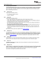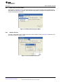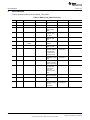
1
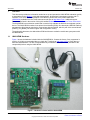
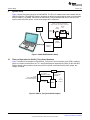
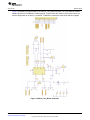
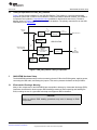
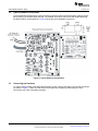
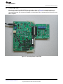
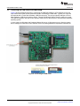
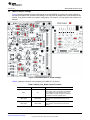
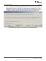
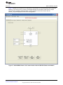
User's Guide
SBOU074A – January 2009 – Revised February 2010
INA219 Evaluation Module
This user’s guide describes the characteristics, operation, and use of the INA219 evaluation module
(EVM). It covers all pertinent areas involved to properly use this EVM board. This document includes the
physical printed circuit board layout, schematic diagrams, and circuit descriptions.
1
2
3
4
5
Contents
Overview ..................................................................................................................... 2
System Setup ................................................................................................................ 4
INA219EVM Hardware Setup ............................................................................................. 7
INA219 Software Overview .............................................................................................. 14
Bill of Materials ............................................................................................................. 20
List of Figures
1
Hardware Included with the INA219EVM ................................................................................ 2
2
INA219EVM Hardware Setup ............................................................................................. 4
3
INA219_Test_Board Block Diagram ...................................................................................... 4
4
INA219_Test_Board Schematic ........................................................................................... 5
5
USB_DIG_Platform Theory of Operation ................................................................................ 7
6
Typical Hardware Connections ............................................................................................ 8
7
Connecting Power to the EVM ............................................................................................ 9
8
Connecting the USB Cable............................................................................................... 10
9
INA219EVM Default Jumper Settings
10
INA219EVM Software—Functioning Properly ......................................................................... 15
11
INA219EVM Software—No Communication with the USB DIG Platform .......................................... 16
12
INA219EVM Software—No Communication with the USB DIG Platform and INA219 ........................... 17
13
EVM Controls Drop-Down Menu ........................................................................................ 19
14
Current Software Revision
1
Signal Definition of J1 (25-Pin Male DSUB) on INA219_Test_Board ................................................ 6
2
INA219_Test_Board Jumper Functions ................................................................................ 11
3
USB DIG Platform Jumper Settings..................................................................................... 12
4
Power-Supply Jumper Configuration #1 ................................................................................ 13
5
Power-Supply Jumper Configuration #2 ................................................................................ 13
6
INA219_Test_Board Parts List
..................................................................................
...............................................................................................
11
19
List of Tables
..........................................................................................
20
Microsoft, Windows are registered trademarks of Microsoft Corporation.
I2C is a trademark of NXP Semiconductors.
All other trademarks are the property of their respective owners.
SBOU074A – January 2009 – Revised February 2010
Submit Documentation Feedback
Copyright © 2009–2010, Texas Instruments Incorporated
INA219 Evaluation Module
1
Overview
1
www.ti.com
Overview
This document provides the information needed to set up and operate the INA219EVM evaluation module,
a test platform for the INA219, a high-side measurement, bi-directional current/power monitor with I2C
interface. For a more detailed description of the INA219, please refer to the product data sheet
(SBOS448A) available from the Texas Instruments web site at http://www.ti.com. Additional support
documents are listed in the section of this guide entitled Related Documentation from Texas Instruments .
The INA219EVM is an evaluation module that is used to fully evaluate the INA219 current/power monitor
device. The INA219EVM consists of two printed circuit boards (PCBs). One board (the USB DIG Platform)
generates the digital signals required to communicate with the INA219, which is part of the second board
(INA219_Test_Board), as well as support and configuration circuitry.
Throughout this document, the abbreviation EVM and the term evaluation module are synonymous with
the INA219EVM.
1.1
INA219EVM Hardware
Figure 1 shows the hardware included with the INA219EVM kit. Contact the factory if any component is
missing. It is highly recommended that you check the TI web site at http://www.ti.com to verify that you
have the latest software. It is also recommended that you watch the QuickStart Video (included on the
compact disk) before using the INA219EVM.
Figure 1. Hardware Included with the INA219EVM
2
INA219 Evaluation Module
SBOU074A – January 2009 – Revised February 2010
Submit Documentation Feedback
Copyright © 2009–2010, Texas Instruments Incorporated
Overview
www.ti.com
The complete kit includes the following items:
• INA219 test PCB
• USB DIG platform PCB
• USB cable
• +6V power supply
• CD-ROM containing this user's guide, product software, and a demonstration video
1.2
Related Documentation from Texas Instruments
The following document provides information regarding Texas Instruments integrated circuits used in the
assembly of the INA219EVM. This user's guide is available from the TI web site under literature number
SBOU074. Any letter appended to the literature number corresponds to the document revision that is
current at the time of the writing of this document. Newer revisions may be available from the TI web site
at http://www.ti.com/, or call the Texas Instruments Literature Response Center at (800) 477-8924 or the
Product Information Center at (972) 644-5580. When ordering, identify the document by both title and
literature number.
1.3
Document
Literature Number
INA219 Product Data Sheet
SBOS448A
USB DIG Platform Users Guide
SBOU058
Information About Cautions and Warnings
This document contains caution statements.
CAUTION
This is an example of a caution statement. A caution statement describes a
situation that could potentially damage your software or equipment.
The information in a caution or a warning is provided for your protection. Please read each caution
carefully.
SBOU074A – January 2009 – Revised February 2010
Submit Documentation Feedback
Copyright © 2009–2010, Texas Instruments Incorporated
INA219 Evaluation Module
3
System Setup
2
www.ti.com
System Setup
Figure 2 shows the system setup for the INA219EVM. The PC runs software that communicates with the
USB DIG Platform. The USB DIG Platform generates the analog and digital signals used to communicate
with the INA219_Test_Board. Connectors on the INA219_Test_Board allow the user to connect to the
system under test whose power, current, and voltage will be monitored.
System on which we will measure
Shunt Current, Bus Voltage, and Power
System
Load
Shunt
Resistor
EVM
Power
System
Power
INA219
Test Board
USB DIG
Platform
Figure 2. INA219EVM Hardware Setup
2.1
Theory of Operation for INA219_Test_Board Hardware
Figure 3 presents a block diagram of the INA219_Test_Board. The functionality of this PCB is relatively
simple. It provides connections to the I2C™ and general-purpose input/outputs (GPIO) on the USB DIG
Platform board. It also provides connection points for external connections of the shunt voltage, bus
voltage, and GND.
VDUT Supply
Switched 5.0V Power
25-Pin
Male DSUB Signals
From USB DIG Platform
Connection to
Shunt Voltage
and GND
2
IC
Address
Jumpers
2
IC
Interface
INA219
Figure 3. INA219_Test_Board Block Diagram
4
INA219 Evaluation Module
SBOU074A – January 2009 – Revised February 2010
Submit Documentation Feedback
Copyright © 2009–2010, Texas Instruments Incorporated
System Setup
www.ti.com
Figure 4 illustrates the system setup for the INA219_Test_Board schematic. D1 is an LED that indicates
whether the INA219 Test Board is receiving power. Jumpers allow the selection of the power source as
well as configuration of A0 and A1. Connector T4 allows the connection of the shunt and bus voltages.
Figure 4. INA219_Test_Board Schematic
SBOU074A – January 2009 – Revised February 2010
Submit Documentation Feedback
Copyright © 2009–2010, Texas Instruments Incorporated
INA219 Evaluation Module
5
System Setup
2.2
www.ti.com
Signal Definitions of J1 (25-Pin Male DSUB)
Table 1 lists the different signals connected to J1 on the INA219_Test_Board. This table also identifies
signals connected to pins on J1 that are not used on the INA219_Test_Board.
Table 1. Signal Definition of J1 (25-Pin Male DSUB) on INA219_Test_Board
6
J1 Pin
Signal
INA219 Pin
1
NC
No connection
2
NC
No connection
3
NC
No connection
4
NC
No connection
5
NC
No connection
6
NC
No connection
7
NC
No connection
8
NC
No connection
9
I2C_SCK
No connection
10
I2C_SDA2
No connection
11
NC
No connection
12
I2C_SCK_ISO
I2C clock signal (SCL) channel 1; can be
disconnected using a switch
13
I2C_SDA_ISO
I2C data signal (SDA) channel 1; can be
disconnected using a switch
14
NC
No connection
15
NC
No connection
16
NC
No connection
17
VDUT
Switched 3V or 5V power. Note that when power is
switched off, the digital I/O is also switched off.
18
VCC
No connection
19
NC
No connection
20
NC
No connection
21
GND
Common or ground connection for power
22
SPI_SCK
No connection
23
SPI_CS1
No connection
24
SPI_DOUT
No connection
25
SPI_DIN1
No connection
INA219 Evaluation Module
SBOU074A – January 2009 – Revised February 2010
Submit Documentation Feedback
Copyright © 2009–2010, Texas Instruments Incorporated
INA219EVM Hardware Setup
www.ti.com
2.3
Theory of Operation For USB_DIG_Platform
Figure 5 shows the block diagram for the USB DIG Platform. This platform is a general-purpose data
acquisition system that is used on several different Texas Instruments evaluation modules. The details of
its operation are included in a separate document (available for download at www.ti.com). The block
diagram shown in Figure 5 gives a brief overview of the platform. The primary control device on the USB
DIG Platform is the TUSB3210.
External
Power
Adjustable
Regulator
VCC
(2.7V to
5.5V)
3.3V
Regulator
USB Connection
from Computer
TUSB3210
8052 mC
with USB Interface
and UART
Reset Button
and Power-On
Reset
VDUT
(2.7V to 5.5V)
Switched Power
USB DIG EVM
VS mC
3.3V
VUSB
5V
Power
Switching
2
Buffers and
Latches
IC
SPI
Control Bits
Measure Bits
8Kx8-Byte
EEPROM
Figure 5. USB_DIG_Platform Theory of Operation
3
INA219EVM Hardware Setup
The INA219EVM hardware setup involves connecting the two PCBs of the EVM together, applying power,
connecting the USB cable, and setting the jumpers. This section presents the details of this procedure.
3.1
Electrostatic Discharge Warning
Many of the components on the INA219EVM are susceptible to damage by electrostatic discharge (ESD).
Customers are advised to observe proper ESD handling precautions when unpacking and handling the
EVM, including the use of a grounded wrist strap at an approved ESD workstation.
CAUTION
Failure to observe ESD handling procedures may result in damage to EVM
components.
SBOU074A – January 2009 – Revised February 2010
Submit Documentation Feedback
Copyright © 2009–2010, Texas Instruments Incorporated
INA219 Evaluation Module
7
INA219EVM Hardware Setup
3.2
www.ti.com
Typical Hardware Connections
The INA219EVM hardware setup involves connecting the two PCBs of the EVM together, applying power,
and connecting an external shunt and load. The external connections may be the real-world system that
the INA219 will be incorporated into. Figure 6 shows the typical hardware connections.
Figure 6. Typical Hardware Connections
3.3
Connecting the Hardware
To connect the two PCBs of the INA219EVM together, gently push on both sides of the D-SUB connectors
(as shown in Figure 7). Make sure that the two connectors are completely pushed together; loose
connections may cause intermittent operation.
8
INA219 Evaluation Module
SBOU074A – January 2009 – Revised February 2010
Submit Documentation Feedback
Copyright © 2009–2010, Texas Instruments Incorporated
INA219EVM Hardware Setup
www.ti.com
3.4
Connecting Power
After the two parts of the INA219 EVM are connected, as shown in Figure 7, connect the power to the
EVM. Always connect power before connecting the USB cable. If you connect the USB cable before
connecting the power, the computer will attempt to communicate with an unpowered device that will not be
able to respond.
Figure 7. Connecting Power to the EVM
SBOU074A – January 2009 – Revised February 2010
Submit Documentation Feedback
Copyright © 2009–2010, Texas Instruments Incorporated
INA219 Evaluation Module
9
INA219EVM Hardware Setup
3.5
www.ti.com
Connecting the USB Cable to the INA219EVM
Figure 8 shows the typical response to connecting the USB DIG platform to a PC USB port for the first
time. Note that the EVM must be powered on before connecting the USB cable. Typically, the computer
will respond with a Found New Hardware, USB Device pop-up. The pop-up typically changes to Found
New Hardware, USB Human Interface Device. This pop-up indicates that the device is ready to be used.
The USB DIG platform uses the Human Interface Device Drivers that are part of the Microsoft® Windows®
operating system.
In some cases, the Windows Add Hardware Wizard will pop up. If this prompt occurs, allow the system
device manager to install the Human Interface Drivers by clicking Yes when requested to install drivers.
Figure 8. Connecting the USB Cable
10
INA219 Evaluation Module
SBOU074A – January 2009 – Revised February 2010
Submit Documentation Feedback
Copyright © 2009–2010, Texas Instruments Incorporated
INA219EVM Hardware Setup
www.ti.com
3.6
INA219 Jumper Settings
Figure 9 shows the default jumpers configuration for the INA219EVM. In general, the jumper settings of
the USB DIG Platform will not need to be changed. You may want to change some of the jumpers on the
INA219_Test_Board to match your specific configuration. For instance, you may wish to set a specific I2C
address.
Figure 9. INA219EVM Default Jumper Settings
Table 2 explains the function of the jumpers on the INA219_Test_Board.
Table 2. INA219_Test_Board Jumper Functions
Jumper
Default
Purpose
JMP1
VDUT
This jumper determines the source for the INA219
power supply. In the Vdut position, the USB DIG
board supplies the power to the INA219. In the
Vs_Ext position, an external supply connected to
the INA219 T3 terminal supplies power.
JMP2, JMP3
JMP2 (GND)
A0 address input selection. This jumper determines
which signal is connected to the A0 pin of the
INA219.
JMP4, JMP5
JMP4 (GND)
A1 address input selection. This jumper determines
which signal is connected to the A1 pin of the
INA219.
SBOU074A – January 2009 – Revised February 2010
Submit Documentation Feedback
Copyright © 2009–2010, Texas Instruments Incorporated
INA219 Evaluation Module
11
INA219EVM Hardware Setup
www.ti.com
Table 3 indicates the function and default position of the USB-DIG-Platform jumpers. For most
applications, the default jumper position should be used. Table 4 and Table 5 describe the options for the
power-supply configuration. For example, the logic power supply can be changed from the default of 5V to
3V. A separate document (SBOU058) gives details regarding the operation and design of the USB DIG
platform.
Table 3. USB DIG Platform Jumper Settings
Jumper
Default
Purpose
JUMP1
EXT
This jumper selects external power or bus power. External
power is applied on J5 or T3 (9VDC). Bus power is 5V from the
USB. External power is typically used because the USB power is
noisy.
JUMP2
EXT
Same as JUMP1.
JUMP3
EE ON
JUMP4, JUMP5
L, L
This jumper sets the address for the USB board. The only
reason to change from the default setting is if multiple boards
are being used.
JUMP9
5V
This selects the voltage of the device under test supply (VDUT =
5V or 3V). This jumper is typically the only jumper that is
changed for most applications.
JUMP10
WP ON
This write-protects the firmware EEPROM.
JUMP11
WP ON
This write-protects the calibration EEPROM.
JUMP13
Reg
JUMP14
9V
JUMP17
BUS
This jumper determines where the TUSB3210 will load the USB
DIG Platform firmware upon power-up or reset. The EE Off
position is used for development for development or firmware
updates.
Uses the regulator output to generate the VDUT supply. The USB
can be used as the VDUT supply.
Uses the external power (9V as apposed to the bus)
While in the BUS position, VDUT operation is normal. While in the
VRAW position, the VDUT supply is connected to an external
source. This flexibility allows for any value of VDUT between 3V
and 5V.
CAUTION
When JUMP17 is in the
VRAW position, adjusting
the VDUT voltage beyond
the 3V to 5V range will
damage the EVM.
JUMP18
12
INA219 Evaluation Module
VDUT
Connects the pull-up on the GPIO to the VDUT supply or the VCC
supply.
SBOU074A – January 2009 – Revised February 2010
Submit Documentation Feedback
Copyright © 2009–2010, Texas Instruments Incorporated
INA219EVM Hardware Setup
www.ti.com
Table 4. Power-Supply Jumper Configuration #1
Mode
Jumper
Comment
External Power—5V
(default jumper settings)
JUMP17 = BUS (not used)
JUMP13 = REG
JUMP14 = 9V
JUMP1 = EXT
JUMP2 = EXT
JUMP6 = 5V
JUMP7 = REF
In this mode, all power is supplied to the EVM via J5 or T3. The external
supply must be between 5.8V and 10.4V for proper operation. All digital
I/Os are regulated to 5V using U19 (REG101).
External Power—3V
(typical jumper settings)
JUMP17 = BUS (not used)
JUMP13 = REG
JUMP14 = 9V
JUMP1 = EXT
JUMP2 = EXT
JUMP6 = 3V
JUMP7 = REF
In this mode, all power is supplied to the EVM via J5 or T3. The external
supply must be between 5.8V and 10.4V for proper operation. All digital
I/Os are regulated to 3V using U19 (REG101).
External Power—Variable
Supply
JUMP17 = Vraw
JUMP13 = BUS
JUMP14 = 9V (not used)
JUMP1 = EXT
JUMP2 = EXT
JUMP6 = 5V (not used)
JUMP7 = REG (ratiometric
mode)
In this mode, all the digital I/Os are referenced to the supply that is
attached to either J5 or T3.
CAUTION
It is absolutely critical that the
supply voltage does not
exceed 5.5V in this mode.
The supply is directly applied to devices with 5.5V absolute maximum
ratings. This mode of operation is useful when a device supply other
then 3.0V or 5.0V is required.
Table 5. Power-Supply Jumper Configuration #2
Mode
Jumper
Comment
Bus Power—5V
JUMP17 = BUS
JUMP13 = BUS
JUMP14 = 9V (not used)
JUMP1 = BUS
JUMP2 = BUS
JUMP6 = 5V (not used)
JUMP7 = REG (ratiometric
mode, 5V supply)
In this mode, the USB bus completely powers the EVM. The USB bus is
regulated by the master (computer) to be 5V. This mode relies upon
external regulation. This mode is recommended only when an external
9V supply is not available. If an external 9V supply is available, use
either External Power 5V mode or External Power 3V mode.
Bus Power—3V
JUMP17 = BUS (not used)
JUMP13 = REG
JUMP14 = BUS
JUMP1 = BUS
JUMP2 = BUS
JUMP6 = 3V
JUMP7 = REG (ratiometric
mode, 5V supply)
In this mode, the USB bus completely powers the EVM. The regulator
(U19, REG101) is used to generate a 3V supply for all digital I/O.
SBOU074A – January 2009 – Revised February 2010
Submit Documentation Feedback
Copyright © 2009–2010, Texas Instruments Incorporated
INA219 Evaluation Module
13
INA219 Software Overview
3.7
www.ti.com
Connecting External Power to the INA219EVM
The INA219 power supply (VS) operates over the range of 3V to 5.5V (see the INA219 product data
sheet). The default jumper position provides 5V to the INA219 from the USB-DIG-Platform. The power
from the USB-DIG-Platform can be changed to 3V using JUMP9.
Another option is to connect power to the INA219 power supply (VS) using an external power supply. In
this case, connect power to the T3 terminal block and set JMP1 to the Vs_EXT positon. The INA219
power supply (VS) operates over the range of 3V to 5.5V, so be careful to not exceed this range.
3.8
Connecting External Signals to the INA219EVM
The INA219 shunt and bus voltages are applied via terminal block T4. The T4 terminal block is a direct
connection to VIN+ and VIN– of the INA219. The bus voltage is monitored on VIN– (26V max). The shunt
voltage is the difference between VIN– and VIN+ (320mV max). Refer to the INA219 data sheet for more
details
4
INA219 Software Overview
This section discusses how to install and use the INA219 software.
4.1
Operating Systems for INA219 Software
The INA219EVM software has been tested on the Microsoft Windows XP operating system (OS) with
United States and European regional settings. The software should also function on other Windows
operating systems.
14
INA219 Evaluation Module
SBOU074A – January 2009 – Revised February 2010
Submit Documentation Feedback
Copyright © 2009–2010, Texas Instruments Incorporated
INA219 Software Overview
www.ti.com
4.2
INA219EVM Software Install
Follow these steps to install the INA219EVM software:
Step 1. Software can be downloaded from the INA219EVM web page, or from the disk included with
the INA219EVM, which contains a folder called Install_software/.
Step 2. Find the file called setup.exe. Double-click the file to start the installation process.
Step 3. Follow the on-screen prompts to install the software.
Step 4. To remove the application, use the Windows Control Panel utility, Add/Remove Software.
The INA219 Quick-Start Video (included with the kit) gives more detail regarding the initialization of the
software.
4.3
Starting the INA219EVM Software
The INA219 software can be operated through the Windows Start menu. From Start, select All Programs;
then select the INA219EVM program. Figure 10 shows how the software should appear if the EVM is
functioning properly.
Figure 10. INA219EVM Software—Functioning Properly
SBOU074A – January 2009 – Revised February 2010
Submit Documentation Feedback
Copyright © 2009–2010, Texas Instruments Incorporated
INA219 Evaluation Module
15
INA219 Software Overview
www.ti.com
Figure 11 shows an error that pops up if the computer cannot communicate with the EVM. If you receive
this error, first check to see that the USB cable is properly connected. This error can also occur if you
connect the USB cable before the USB DIG Platform 9V power source. A second possible reason for this
problem is that there may be a problem with your computer USB Human Interface Device Driver. Make
sure that when you plug the in the USB cable, the computer recognizes the device. If the sound is on, you
will hear the distinctive sound that you expect when a USB device is properly connected to the PC.
Figure 11. INA219EVM Software—No Communication with the USB DIG Platform
16
INA219 Evaluation Module
SBOU074A – January 2009 – Revised February 2010
Submit Documentation Feedback
Copyright © 2009–2010, Texas Instruments Incorporated
INA219 Software Overview
www.ti.com
Figure 12 shows an error that occurs if the INA219_Test_Board is not communicating with the USB DIG
Platform. If you see this error, check the connectors between the two boards; make sure the 25-pin
connectors are completely pushed together. Another possible cause of this issue it that the
INA219_Test_Board jumpers are set in the wrong position.
Figure 12. INA219EVM Software—No Communication with the USB DIG Platform and INA219
SBOU074A – January 2009 – Revised February 2010
Submit Documentation Feedback
Copyright © 2009–2010, Texas Instruments Incorporated
INA219 Evaluation Module
17
INA219 Software Overview
4.4
www.ti.com
Using the INA219 Software
The INA219EVM software has six different tabs that allow you to access different features of the INA219.
The first four tabs are designed so that you can completely configure the device by stepping through the
tabs in order. Each of the tabs is intended to have an intuitive graphical interface that helps you gain a
better understanding of the device.
4.4.1
Overview Tab
This tab has the following controls:
• Turn the power supply on and off
• Set the I2C address
4.4.2
Config Tab
This tab has the following controls:
• Shunt voltage attenuator range (smallest range: 40mV; largest range: 320mV)
• Shunt voltage configuration: resolution and number of averages. Note that increasing the number of
averages decreases the noise but slows down the conversion rate.
• Bus voltage attenuator range (16V and 32V): Note that the maximum bus voltage for the INA219 is
26V. Thus, the 32V range cannot be fully used.
• Bus voltage configuration: Resolution and number of averages. Note that increasing the number of
averages decreases noise but slows down the conversion rate.
• A/D converter mode: This control determines how the converters work. The most commonly used
modes are Shunt and Bus continuous conversion mode. This mode causes both converters to run
continuously.
More details on these options are explained in the product data sheet.
4.4.3
Calibrate Tab
The calibration tab allows users to enter some information regarding the INA219 configuration in a given
application. This information is used to compute the Full-Scale Cal Register. The Full-Scale Cal Register
converts the shunt voltage to a current value. The detailed mathematics behind this calibration feature is
given in the INA219 data sheet. Also, this feature is explained in a step-by-step manner in the video.
4.4.4
Scaling Tab
This tab allows you to see how the mathematical operations work in the INA219. Specifically, this tab
shows how the current and power values are computed using the full-scale calibration register.
4.4.5
Graph Tab
The graph tab will display bus voltage, shunt current, and power versus time when the software is in
continuous convert mode.
4.4.6
Registers Tab
This tab allows you to read and edit all the registers in the INA219. All the previous tabs affect the register
listing. For example, changing the A/D configuration on Tab 2 will affect Register 0 in the register list. It is
also true that changing register 0 updates the A/D configuration on Tab 2. Thus, the graphical
representation and register representation affect each other.
18
INA219 Evaluation Module
SBOU074A – January 2009 – Revised February 2010
Submit Documentation Feedback
Copyright © 2009–2010, Texas Instruments Incorporated
INA219 Software Overview
www.ti.com
4.4.7
EVM Controls Pull-Down Menu
The INA219 Configuration (that is, the register settings) can be saved or loaded using the EVM Controls
drop-down menu, as Figure 13 shows. The file that the configuration is saved into is a simple text file and
can be viewed with any text editor.
Figure 13. EVM Controls Drop-Down Menu
4.4.8
Software Revision
The Help...About feature can be used to check the current software revision, as Figure 14 illustrates. This
document is based on revision 1.0.35.
Figure 14. Current Software Revision
SBOU074A – January 2009 – Revised February 2010
Submit Documentation Feedback
Copyright © 2009–2010, Texas Instruments Incorporated
INA219 Evaluation Module
19
Bill of Materials
5
www.ti.com
Bill of Materials
Table 6 shows the parts list for the INA219_Test_Board.
Table 6. INA219_Test_Board Parts List
20
No.
Quantity
Value
Ref Des
1
1
4.02k
R5
Description
Vendor
Part Number
Resistor, 4.02k,
603
ROHM
MCR03EZPFX4021
2
2
10k
R3, R4
Resistor, 10k, 603
Yageo Corporation
RC0603FR-0710KL
3
2
0ohm
R1, R2
RES 0.0 OHM
1/8W 5% 0805
SMD
Panasonic - ECG
ERJ-6GEY0R00V
4
1
10uF
C3
Capacitor,
Tantalum, 10uF,
16V, 6032
Kemet
T491C106M016AT
5
1
0.1uF
C2
CAP .10UF 25V
CERAMIC Y5V
0603
Kemet
C0603C104M3VACTU
6
0
Optional/Not
Installed
C1
0603-1206
Capacitor
—
—
7
1
LED
D1
Diode, LED, Ultra
Bright Diff, 603
Panasonic
LNJ208R8ARA
8
1
DSUB25M
J1
CONN D-SUB
PLUG R/A 25POS
30GOLD (With
Threaded Inserts
and Board locks)
AMP/Tyco
Electronics
5747842-4
9
3
N/A
N/A
SHUNT LP
W/HANDLE 2 POS
30AU
AMP/Tyco
Electronics
881545-2
10
5
JUMP3 cut to size
JMP1-JMP5
CONN HEADER
32POS .100" SGL
GOLD (4 per Strip)
Samtec
TSW-132-07-G-S
11
5
standoff
none
Standoffs, Hex ,
4-40 Threaded,
0.500" length,
0.250" OD,
Aluminum Iridite
Finish
Keystone
2203
12
5
screw
none
SCREW MACHINE
PHIL 4-40X1/4 SS
Building Fasteners
PMSSS 440 0025 PH
13
10
Test Point
N/A
5018 SMD Test
Point
Keystone
5018
14
4
2 pin connector
T1 T2 T3 T4
On-Shore
Technology Inc
ED300/2
INA219 Evaluation Module
2-Position Terminal
Strip, Cage Clamp,
45º, 15A,
Dove-tailed
SBOU074A – January 2009 – Revised February 2010
Submit Documentation Feedback
Copyright © 2009–2010, Texas Instruments Incorporated
Revision History
www.ti.com
Revision History
Changes from Original (January, 2009) to A Revision ................................................................................................... Page
•
•
•
•
Revised Table 3 .........................................................................................................................
Added Table 4 and Table 5 ............................................................................................................
Added Section 3.7 ......................................................................................................................
Added Section 3.8 ......................................................................................................................
12
13
14
14
NOTE: Page numbers for previous revisions may differ from page numbers in the current version.
SBOU074A – January 2009 – Revised February 2010
Submit Documentation Feedback
Copyright © 2009–2010, Texas Instruments Incorporated
Revision History
21
Evaluation Board/Kit Important Notice
Texas Instruments (TI) provides the enclosed product(s) under the following conditions:
This evaluation board/kit is intended for use for ENGINEERING DEVELOPMENT, DEMONSTRATION, OR EVALUATION
PURPOSES ONLY and is not considered by TI to be a finished end-product fit for general consumer use. Persons handling the
product(s) must have electronics training and observe good engineering practice standards. As such, the goods being provided are
not intended to be complete in terms of required design-, marketing-, and/or manufacturing-related protective considerations,
including product safety and environmental measures typically found in end products that incorporate such semiconductor
components or circuit boards. This evaluation board/kit does not fall within the scope of the European Union directives regarding
electromagnetic compatibility, restricted substances (RoHS), recycling (WEEE), FCC, CE or UL, and therefore may not meet the
technical requirements of these directives or other related directives.
Should this evaluation board/kit not meet the specifications indicated in the User’s Guide, the board/kit may be returned within 30
days from the date of delivery for a full refund. THE FOREGOING WARRANTY IS THE EXCLUSIVE WARRANTY MADE BY
SELLER TO BUYER AND IS IN LIEU OF ALL OTHER WARRANTIES, EXPRESSED, IMPLIED, OR STATUTORY, INCLUDING
ANY WARRANTY OF MERCHANTABILITY OR FITNESS FOR ANY PARTICULAR PURPOSE.
The user assumes all responsibility and liability for proper and safe handling of the goods. Further, the user indemnifies TI from all
claims arising from the handling or use of the goods. Due to the open construction of the product, it is the user’s responsibility to
take any and all appropriate precautions with regard to electrostatic discharge.
EXCEPT TO THE EXTENT OF THE INDEMNITY SET FORTH ABOVE, NEITHER PARTY SHALL BE LIABLE TO THE OTHER
FOR ANY INDIRECT, SPECIAL, INCIDENTAL, OR CONSEQUENTIAL DAMAGES.
TI currently deals with a variety of customers for products, and therefore our arrangement with the user is not exclusive.
TI assumes no liability for applications assistance, customer product design, software performance, or infringement of
patents or services described herein.
Please read the User’s Guide and, specifically, the Warnings and Restrictions notice in the User’s Guide prior to handling the
product. This notice contains important safety information about temperatures and voltages. For additional information on TI’s
environmental and/or safety programs, please contact the TI application engineer or visit www.ti.com/esh.
No license is granted under any patent right or other intellectual property right of TI covering or relating to any machine, process, or
combination in which such TI products or services might be or are used.
FCC Warning
This evaluation board/kit is intended for use for ENGINEERING DEVELOPMENT, DEMONSTRATION, OR EVALUATION
PURPOSES ONLY and is not considered by TI to be a finished end-product fit for general consumer use. It generates, uses, and
can radiate radio frequency energy and has not been tested for compliance with the limits of computing devices pursuant to part 15
of FCC rules, which are designed to provide reasonable protection against radio frequency interference. Operation of this
equipment in other environments may cause interference with radio communications, in which case the user at his own expense
will be required to take whatever measures may be required to correct this interference.
EVM Warnings and Restrictions
It is important to operate this EVM within the input voltage range of 5.7V to 9V and the output voltage range of 0V to 5V.
Exceeding the specified input range may cause unexpected operation and/or irreversible damage to the EVM. If there are
questions concerning the input range, please contact a TI field representative prior to connecting the input power.
Applying loads outside of the specified output range may result in unintended operation and/or possible permanent damage to the
EVM. Please consult the EVM User's Guide prior to connecting any load to the EVM output. If there is uncertainty as to the load
specification, please contact a TI field representative.
During normal operation, some circuit components may have case temperatures greater than +25°C. The EVM is designed to
operate properly with certain components above +25°C as long as the input and output ranges are maintained. These components
include but are not limited to linear regulators, switching transistors, pass transistors, and current sense resistors. These types of
devices can be identified using the EVM schematic located in the EVM User's Guide. When placing measurement probes near
these devices during operation, please be aware that these devices may be very warm to the touch.
Mailing Address: Texas Instruments, Post Office Box 655303, Dallas, Texas 75265
Copyright © 2010, Texas Instruments Incorporated
IMPORTANT NOTICE
Texas Instruments Incorporated and its subsidiaries (TI) reserve the right to make corrections, modifications, enhancements, improvements,
and other changes to its products and services at any time and to discontinue any product or service without notice. Customers should
obtain the latest relevant information before placing orders and should verify that such information is current and complete. All products are
sold subject to TI’s terms and conditions of sale supplied at the time of order acknowledgment.
TI warrants performance of its hardware products to the specifications applicable at the time of sale in accordance with TI’s standard
warranty. Testing and other quality control techniques are used to the extent TI deems necessary to support this warranty. Except where
mandated by government requirements, testing of all parameters of each product is not necessarily performed.
TI assumes no liability for applications assistance or customer product design. Customers are responsible for their products and
applications using TI components. To minimize the risks associated with customer products and applications, customers should provide
adequate design and operating safeguards.
TI does not warrant or represent that any license, either express or implied, is granted under any TI patent right, copyright, mask work right,
or other TI intellectual property right relating to any combination, machine, or process in which TI products or services are used. Information
published by TI regarding third-party products or services does not constitute a license from TI to use such products or services or a
warranty or endorsement thereof. Use of such information may require a license from a third party under the patents or other intellectual
property of the third party, or a license from TI under the patents or other intellectual property of TI.
Reproduction of TI information in TI data books or data sheets is permissible only if reproduction is without alteration and is accompanied
by all associated warranties, conditions, limitations, and notices. Reproduction of this information with alteration is an unfair and deceptive
business practice. TI is not responsible or liable for such altered documentation. Information of third parties may be subject to additional
restrictions.
Resale of TI products or services with statements different from or beyond the parameters stated by TI for that product or service voids all
express and any implied warranties for the associated TI product or service and is an unfair and deceptive business practice. TI is not
responsible or liable for any such statements.
TI products are not authorized for use in safety-critical applications (such as life support) where a failure of the TI product would reasonably
be expected to cause severe personal injury or death, unless officers of the parties have executed an agreement specifically governing
such use. Buyers represent that they have all necessary expertise in the safety and regulatory ramifications of their applications, and
acknowledge and agree that they are solely responsible for all legal, regulatory and safety-related requirements concerning their products
and any use of TI products in such safety-critical applications, notwithstanding any applications-related information or support that may be
provided by TI. Further, Buyers must fully indemnify TI and its representatives against any damages arising out of the use of TI products in
such safety-critical applications.
TI products are neither designed nor intended for use in military/aerospace applications or environments unless the TI products are
specifically designated by TI as military-grade or "enhanced plastic." Only products designated by TI as military-grade meet military
specifications. Buyers acknowledge and agree that any such use of TI products which TI has not designated as military-grade is solely at
the Buyer's risk, and that they are solely responsible for compliance with all legal and regulatory requirements in connection with such use.
TI products are neither designed nor intended for use in automotive applications or environments unless the specific TI products are
designated by TI as compliant with ISO/TS 16949 requirements. Buyers acknowledge and agree that, if they use any non-designated
products in automotive applications, TI will not be responsible for any failure to meet such requirements.
Following are URLs where you can obtain information on other Texas Instruments products and application solutions:
Products
Applications
Amplifiers
amplifier.ti.com
Audio
www.ti.com/audio
Data Converters
dataconverter.ti.com
Automotive
www.ti.com/automotive
DLP® Products
www.dlp.com
Communications and
Telecom
www.ti.com/communications
DSP
dsp.ti.com
Computers and
Peripherals
www.ti.com/computers
Clocks and Timers
www.ti.com/clocks
Consumer Electronics
www.ti.com/consumer-apps
Interface
interface.ti.com
Energy
www.ti.com/energy
Logic
logic.ti.com
Industrial
www.ti.com/industrial
Power Mgmt
power.ti.com
Medical
www.ti.com/medical
Microcontrollers
microcontroller.ti.com
Security
www.ti.com/security
RFID
www.ti-rfid.com
Space, Avionics &
Defense
www.ti.com/space-avionics-defense
RF/IF and ZigBee® Solutions www.ti.com/lprf
Video and Imaging
www.ti.com/video
Wireless
www.ti.com/wireless-apps
Mailing Address: Texas Instruments, Post Office Box 655303, Dallas, Texas 75265
Copyright © 2010, Texas Instruments Incorporated