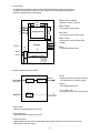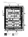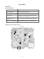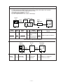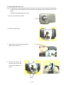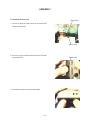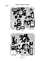
1
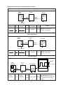
(without price)
QV-30 (B) (KX-724B)
(For NTSC)
APR. 1996
R
CONTENTS
SPECIFICATIONS ......................................................................................... 1
BLOCK DIAGRAM ........................................................................................ 2
CIRCUIT OPERATIONS ................................................................................ 3
COLOR ADJUSTMENT ............................................................................... 13
ADJUSTMENT ............................................................................................. 15
TROUBLESHOOTING ................................................................................. 18
DISASSEMBLY ........................................................................................... 19
ASSEMBLY ................................................................................................. 21
PRINTED CIRCUIT BOARDS ..................................................................... 23
EXPLODED VIEW ....................................................................................... 25
PARTS LIST ................................................................................................ 26
SCHEMATIC DIAGRAMS ........................................................................... 35
WAVEFORMS.............................................................................................. 39
SPECIFICATIONS
Item
Specification
1. Recording System
Digital (JPEG based)/Field recording
2. Video Signal System
NTSC
3. Recording Medium
Built-in 16-Mbit flash memory
4. Number of pages
96
5. Delete Functions
Single page; All pages (with page protect feature)
6. Imaging Device
1/5-inch CCD (Total Number of Pixels: 250,000)
7. Lens
2 focal points with macro position: F2.8 f=4.0 mm/f=9.0 mm
8. Aperture
F2.8/F8 manual switching
9. Focal Length
f=4.0 mm F2.8/NORMAL
: 50 cm ~ y
f=4.0 mm F2.8/MACRO
: 10 cm ~ 13 cm
f=4.0 mm F8/NORMAL
: 24 cm ~ y;
f=4.0 mm F8/MACRO
: 8 cm ~ 19 cm
f=9.0 mm F2.8/NORMAL
: 250 cm ~ y
f=9.0 mm F2.8/MACRO
: 50 cm ~ 65 cm
f=9.0 mm F8/NORMAL
: 120 cm ~ y;
f=9.0 mm F8/MACRO
: 40 cm ~ 95 cm
10. Light Metering
TTL center point by photographic element
11. Exposure Metering
Aperture priority AE
12. Exposure Range
EV +5 to 18
13. Exposure Adjustment
-2 EV to +2 EV
14. Shutter System
Electronic
15. Shutter Speed
1/8 to 1/4000 second
16. White Balance
Automatic
17. Self-timer
10-second
18. Monitor
61,380-pixel 2.5-inch TFT low-glare color LCD
19. Terminals
DIGITAL; VIDEO OUT; DC IN 6 V
20. Power Supply
Batteries (AA-size Alkaline batteries × 4)/AC Adaptor
21. Battery Life
Approximately 120 minutes (Playback mode)
22. Dimensions
72 (H) × 162 (W) × 49 (D) mm/
2.8" (H) × 6.4" (W) × 1.9" (D)
23. Weight
Approximately 240 g / 8.5 oz (excluding batteries)
24. Accessories
Wirst strap; soft case; special video cable;
Alkaline batteries (LR6 × 4); cleaning cloth
—1—
BLOCK DIAGRAM
1 Camera PCB 2 Digital PCB
Gate Array
HG51B167FB
CCD
3 Linear PCB
V RAM
HM53812BJ8
IC300
IR3P90Y
LCD
IC400
MSM6770GS
Flash
Memory
TC5816FT-1
5 VIDEO OUT (Video I/O)
(KM29N16000T)
D RAM
HM514B00
ALJ8
CPU
CPU
HD6477034F16
HD6437034F16
6 DIGITAL (Serial I/O)
Power Supply
Circuit
DC IN (6V)
AC adaptor
Battery x 4
Key
Key PCB
1 Camera Unit: It is used to provide color information.
2 Digital PCB: It controls the CCD, compressed data, stores image in memory.
3 Linear PCB: It generates the tricolor and controls the LCD display.
4 LCD: 61,380-pixel 1.8-inch Thin Film Transistor low-glare color LCD.
5 VIDEO OUT(Video I/O): Use this terminal when connecting to the VIDEO IN terminal of
a TV, video tape deck, video printer, or other similar device.
6 DIGITAL (SERIAL I/O): Use this terminal when connecting to a personal computer.
—2—
CIRCUIT OPERATIONS
CAMERA UNIT (CAMERA PCB)
The camera unit is composed a lens, color filter, CCD (IC802), driver (IC800) and signal
processor (IC802). It produces voltages R, B, and G, for the colors red, blue, and green
when light from a scene is focused on the surface. These voltage values vary according
to the intensity of the respective color being scanned.
The camera unit must be replaced with whole unit when it is defective, because the precise
adjustment is required when the individual parts are replaced, and can be done only at our
factory.
Camera PCB
1 Lens
3 IC802 (CCD)
Ye,Cy,Gr
color signal
CCD IN
2 Color
Filter
Digital PCB
Data Bus
4 IC801
D0 ~ D7
8bit A/D
Converter
Sample Hold,
AGC
D RAM
PHI1~PHI4
PHS1~PHS4
IC800
Driver
VI1~ VI4
VS1 ~ VS4
Timing
Generator
MCK,
HRS2,
FTTRG,
STTRG,
CCODE,
ENDFLG
CPU
11 Lens
Lens
Concentrates
lightlight
rays
to atopoint.
Concentrates
rays
a point.
22 Color
Colorfilter
filter
TheThe
striped
color
filter
in front
of the
CCD
detector
is used
to provide
color
information.
striped
color
filter
in front
of the
CCD
detector
is used
to provide
color
information.
It has
three
colors,
yellow,
green
and
cyan.
It has three colors, yellow, green and cyan.
Array
of color
filter
andand
signal
processing
(IC801)
for for
camera
areare
extremely
close
relationship.
Array
of color
filter
signal
processing
(IC801)
camera
extremely
close
relationship.
1
2
3
~ 506 507 508
Ye G Cy
Ye G Cy
Ye G Cy
Ye G Cy
Ye G Cy
Ye G Cy
Red
Ye=Red+Green
Mg=Blue+Red
Ye
Mg
White
Ye G Cy
Ye G Cy
Green
Ye G Cy
Cy
Blue
Ye G Cy
Cy=Blue+Green
Three Primary colors
Array of color filter
—3—
3 CCD (IC802)
A charge-coupled device in which charges are introduced when light from a scene is
focused on the surface of the device. The image points are accessed sequentially to
produce a television-type output signal.
Effective picture element:
249,936 = 508 (H) x 492 (V)
532(H)
508(H)
PHIS1~PHIS4:
Clock pulse for the storage.
Image pickup
PHI1~PHI4:
Clock pulse for the image pickup.
19
18
17
16
PHIH1~PHIH2:
Clock pulse for the horizontal shift
register.
PHIR:
CCD analog signal output.
Horizontal shift
register (CCD)
PHIH1
12 13
PHIH2
VOG
Output
VGG
Amp.
Vout 9
PHIS4
PHIS1
PHIS2
PHIS3
Storage
PHIR 7
VDD 8
500(V)
492(V)
PHI4
3
PHI3
4
5 PHI2
PHI1
6
14
15
4 Camera Signal Processor (IC801)
From CCD
Sample Hold,
AGC
8bit A/D
Converter
D0~D7
D0~D7:
Digital signal of the luminance and the
color difference B-Y and R-Y signal.
CCD IN:
CCD analog signal input.
to CCD
Timing
Generator
VI1~VI4/VS1~VS4:
Clock pulse for the CCD control signal.
From/to CPU
Sample Hold
Selects a desired signal from the CCD.
Timing Genarator
Generates the clock pulse for the CCD.
8-bit AD converter
Analog signal from the CCD is converted into 8-bit digital signal of the luminance and the color
difference B-Y and R-Y signal. .
—4—
DIGITAL PCB
Camera PCB
IC802
CCD
2 IC700
IC801
Gate Array
3 IC701
IC800
Processor
Control
Timing
V RAM
Control
Driver
1M
V RAM
Encoder
4 IC602
16M Flash Memory
Data
Compressor
Amp.
D/A
VIDEO OUTPUT
(Video I/O)
DIGITAL PCB
1 IC600
Microprocessor
ROM
DMAC
5 IC601
+5V +18V -10V
RAM
4M D RAM
CPU
Linear
PCB
IC300
Chroma
Circuit
TFT LCD
BSC
6
Power Supply
I/O Port
SCI, Timmer
IC400
Display
Control
DC in +6V
Key Input
Battery
Digital PCB is composed Microprocessor (IC600), D RAM (IC601), Flash Memory (IC602),
Gate Array (IC700), and V RAM (IC701).
Microprocessor controls the CCD, D RAM, Flash Memory and key operation. Gate array
compresses data for the color and the luminance from the CCD to increase the number of
memory, and up to 96 images can be stored in flash memory. The color and the luminance
data are mixed in the gate array to make the video signal.
As to spare parts for digital PCB, Casio supplies PCB ass'y and the individual parts.
—5—
DIGITAL (Serial I/O)
1
CPU (IC600)
the CCD, D RAM, Flash memory and key operation.
1Controls
CPU (IC600)
Controls the CCD, D RAM, Flash memory and key operation.
PA15 ~ PA0
CS3 ~ CS0, A21 ~ A16
Port A
Address
RAM1
PROM/MASKROM1
Address
Reset,
MD2 ~
MD0,
EXTAL,
XTAL
CK
Direct memory
access
controller
CPU
Interrupt
controller
User break
controller
Direct state controller
Serial communication
interface (x2channel)
16-bit integrated
timer pulse unit
A/D
Timer
converter
Port C
Port B
PC7 ~ PC0
Address bus 24-bit
PB0 ~ PB15
Address bus 24-bit
High-order 8-bit
Low-order 8-bit
—6—
Data/Address
Programmable timing
pattern controller
Data bus 16-bit
A15 ~ A0
AD15 ~ AD0
CPU PIN FUNCTION
Pin No. Terminal Name IN/OUT
Function
1
PB14
OUT Timing pattern output.
2
PB15
Not used.
3
VSS
IN
Ground terminal.
4 - 11
AD0 - AD7
IN/OUT Address bus.
12
VSS
IN
Ground terminal.
13 - 14
AD8 - AD9
Not used.
15
VCC
IN
Power source.
16 - 21
AD10 - AD15
Not used.
22
VSS
IN
Ground terminal.
23 - 30
A0 - A7
OUT Address bus.
31
VSS
IN
Ground terminal.
32 - 33
A8, A9
OUT Address bus.
34 - 39
A10 - A15
Not used.
40
VSS
IN
Ground terminal.
41, 42
A16, A17
Not used.
43
VCC
IN
Power source.
44 - 47
A18 - A21
Not used.
48 - 50
CS0 - CS2
Not used.
51
CASL
OUT CAS(Column Address Strobe) signal for D RAM.
52
VSS
IN
Ground terminal.
53
PAO
Not used.
54
RAS
OUT RAS(Row Address Strobe) signal for D RAM.
55
CS6
OUT Chip select signal.
56
WAIT
Not used.
57
WR
OUT Write enable signal for outer memory (low-order 8-bit).
58
PA5
OUT Write enable signal for outer memory (high-order 8-bit).
59
RD
OUT Read enable signal for outer memory.
60
PA7
Not used.
61
VSS
IN
Ground terminal.
62
PA8
IN
Bus request signal.
63
PA9
OUT Interrupt request signal.
64 - 66
PA10 - PA12
Not used.
67
DREQ0
IN
Interrupt request signal.
68
IRQ2
IN
Interrupt request signal.
69
PA15
IN
Interrupt request signal.
70
VCC
IN
Power source.
71
CK
OUT System clock pulse.
72
VSS
IN
Ground terminal.
73
EXTAL
IN
Clock pulse input.
74
XTAL
Not used.
75 - 77 VCC, NMI, VPP
IN
Power source.
78
WDTOVF
Not used.
79
RES
IN
Reset signal input.
80
MD0
IN
Ground terminal.
81
MD1
IN
Connected to VCC3.
82
MD2
IN
Connected to ground.
83, 84
VCC
IN
Power source.
—7—
Pin No. Terminal Name
85, 86
AVCC, AVREF
87 - 89
PC0 - PC2
90
PC3
91
AVSS
92 - 95
PC4 - PC7
96
VSS
97, 98
PB0, PB1
99
VCC
100 - 105
PB2 - PB7
106
VSS
107
RXDO
108
TXDO
109, 110
PB10, PB11
111
PB12
112
PB13
IN/OUT
IN
IN
IN
IN
IN
IN/OUT
IN
IN/OUT
IN
IN
OUT
IN/OUT
-
Function
Connected to VCC3.
Key input terminal.
Low battery detection terminal.
Ground terminal.
Not used.
Power source.
Port B.
Power source.
Port B.
Ground terminal.
Data input terminal from a personal computer.
Data output terminal to a personal computer.
Port B.
Not used.
Not used.
2 Gate Array (IC700)
Control
Timing
V RAM
Control
V RAM
Encoder
Data
Compressor
D/A
Data Compressor
The color difference and the luminance data is compressed about 1/7 to increase the
numer of images in memory. Up to 96 images can be stored.
Y (luminance siganal) data
Cb (color difference signal B-Y) data
Cr (color difference signal R-Y) data
: 480 x 224 byte
: 160 x 112 byte
: 160 x 112 byte
Total: 143,360 byte
21,120 byte
1/7
21,120 byte
Encoder
The color and the luminance data are mixed internally to make the video signal, and
send it to the linear PCB and the video out terminal.
—8—
3 V RAM
3It V
is RAM
used for encoder function.
It is used for encoder function.
4 Flash Memory
4 Flash Memory
Up to 96 images can be stored in memory. Flash memory does not require electrical power
Up to 96 images can be stored in memory. Flash memory does not require electrical power to store
todata,
storeso
data,
so image
is retained
in memory
even you
when
you
turn camera
off.
image
data isdata
retained
in memory
even when
turn
camera
power power
off.
If Ifbatteries
go
dead,
simply
load
a
set
of
new
batteries
or
connect
the
AC
adaptor
and
you
batteries go dead, simply load a set of new batteries or connect the AC adaptor and you will be able
will
able
to view
camera memory.
to be
view
images
in images
camera in
memory.
Memory Map
Header
record
Image data
Max; 96 images
Color
Information
5 D RAM
There is area of work space that the microprocessor uses for storing temporary data , the
5 D RAM
intermediate results of calculations, and all sorts of pieces of information that the system
There is area of work space that the microprocessor uses folr storing temporary data, the intermediate
needs to remember.
results of calculations, and all sorts of pieces of information that the system needs to remember.
6 Power Supply
6 Power supply
Terminal
VCC3-0
VCC3-1
VCC3-2
VCC6
VEE3
Voltage
4.75 ~ 5.15 (V)
4.70 ~ 5.15 (V)
4.60 ~ 5.15 (V)
17.80 ~ 18.20 (V)
-9.6 ~ -10.6 (V)
Purpose
Logic circuit
Video output
Digital I/O
CCD
CCD
KEY PCB
Block Diagram
BUTTON
CPU
RESISTOR
KEY 0
87 pin
KEY 1
VCC3-1
88 pin
KEY 2
89 pin
Key Matrix
VOLTAGE
VCC3-1
VCC3-1
VCC3-1
VCC3-1
VCC3-1
VCC3-1
VCC3-1
VCC3-1
BUTTON
Shutter
[+]
MODE
DISP
ZOOM
SELF
[-]
DEL
RESISTOR KEY MATRIX
R900(1.8K)
KEY0
R901(15K)
KEY0
R902(1.8K)
KEY1
R903(4.7K)
KEY1
R904(10K)
KEY1
R905(27K)
KEY1
R906(1.8K)
KEY2
R907(15K)
KEY2
—9—
CPU
87pin
87pin
88pin
88pin
88pin
88pin
89pin
89pin
LINEAR PCB
IC300 generates the tricolor (red, green and blue) from the video signal, and IC400 controls
the TFT-LCD display.
Power Supply
G-OUT
B-OUT
36
AGC.FIL
34
APL
35 32
CLAMP
COLOR
DCDET
R-OUT
19 20
TIME-CONST
21 22 16 11 17 14 13 23
SYNC-IN
SYNC-SEP
15
Purpose
Logic circuit
Display
Display
Display
AGC OUT
PICTURE
18
TRAP
H.F.OUT
IC300
Voltage
4.3 ~ 4.7 (V)
9.5 ~ 11.0 (V)
-7.0 ~ -8.0 (V)
-16.5 ~ -17.9 (V)
SYNC-OUT
Terminal
VCC2
VCC4
VEE2
VEE4
42
Vref
SYNC SEP
BGP GEN
AGC DET
H filter
Trap
D.L
BPF
APC
INV
41
INV
44
γ2
45
γ1
γ corrector
γ corrector
Picture
quality
ADJ.
ACC DET
γcorrector
Killer
46
SWP GEN
VCO
Demodulation
L
P
F
Matrix
Contrast
INT/EXT
SW
R Gain
B Gain
RGB.
40 INV
39
FRP
Clamp
Bright
TINT
31
GND
VCC2
VEE
2
5 4 3 1 48
— 10 —
47
43
30
COM.OUT
33
BRIGHT
29
B-SUB-CONT
6
R-SUB-CONT
7
COM DRIV
EXT-R
EXT-G
EXT-B
SW
25
VCC1
VEE VCC1 GND VCC2 VEE
YEE
24
Killer.F
26
VCO
Color control
TINT
APC.F
27
AGC AMP
INV
ACC
ACC.F
9
CLAMP
RGB.
38 AMP
CONT
VIDEO
10
F ADJ
12
28
COM.
AMP
AFT
UHF
KCB
KDB
AVB
M1~M7
MBUI
HDB
SRT
CLR
OE
GPCK
GSRT
GRES
IC400
U/V
Key control
VCO
51
VCO
ADJ
AFT
control
48
5.9MHz
47
OSC
SYF
Control
PD
CKB
Analog
control
Mode control
Horizontal
control
PHO
Mode
set
POCL
CK2
LOE0
PD
18
50
Clock
SW
CK2 Initial
1/2
Tuning program
control
35
VMUTEB
VTUCK
Tuning Up/Down
counter
Channel
bar control
PL1, PL2, PL3
PDM D/A
56
Amplitude
control
MCLK
TAB/COG
SW
SELFRB
TSI1
TSI2
TSI3
TSI4
TSI5
TSI6
54
55
8
9
10
11
Test
39 AFTO
46 VREF
45 U1
44 VH1
43 VL1
41 OUT
SYNC
judgment
Vertical
control
Test
circuit
SD
VD
SYNC
VSync SEP.
Mute
24
VDB
36
FRP
2
28
38
HCNT
AMUTEB
CSYNC
— 11 —
SYNC
DET.
HSync
32
33
34 SW
VBAR
UBAR
30
29
TUPCM
VLB
TFT-LCD
Gate
pulse
Vy
Frame period
Selective period
Gate electrode
Source electrode
t1
Y1
Y1
T1
T3
T2
Tn
T4
Picture
element A
GND
Y2
Y2
Y3
Y3
Va
X1
Vb
Ym
t1 t2
t3
X1
X2
X3
X4
TFT array substrate
Picture
element
A
Xn
Common substrate
Common
electrode
V COM
Each picture element electrode is controlled by a transistor. To the gate electrodes, the
gate pulse is applied timesharing. VCOM voltage is applied to the common electrodes.
The above figure shows the operation of TFT-LCD. If the gate pulse is not applied to
the gate electrodes, the transistors do not operate even when the potential difference
is given between the common electrodes and source electrodes, and no effect is given
to the liquid crystal. If the gate pulse is applied to Y1, the transistorT1 is in operation
during a priod of t1, and voltage of source electrode of Va is applied to the LCD layer
of picture element A, then electric charges are stored in the picture element of A. After
the period of t1, T1 is turned off, and voltage in the LCD layer of A is held until next
gate pulse comes, but it drops little by little through off leak resistance of TFT and leak
resistance of LCD itself.
BACK LIGHT
The camera unit is equipped with a fluorescent light source to provide the back lighting
for its LCD. The normal service life of the backlight is approximately six years, when the
camera is used for about two hours a day.
The backlight is consumption items, so even under guarantee replace it under charge
basis.
— 12 —
COLOR ADJUSTMENT
Each of this model has a color information in its flash memory due to the CCD camera has a color characteristic.
The color information is loaded in the flash memory when the color adjustment is done after assembling of this
model in our factory. A brand-new flash memory and digital PCB ass’y stocked in our spare parts center do
not have the color information, so the color adjustment should be done after the following situation.
• Replacing the digital PCB ass’y with the brand-new one
• Replacing the flash memory with the brand-new one
And it also should be done, after the following situation due to change of the color characteristic.
• Replacing the camera unit
The following items are required for the color adjustment.
• PC
•
•
•
•
IBM PC/AT or compatible
RS-232C serial port
4 MB RAM minimum (8 MB recommended)
Microsoft MS-DOS Ver. 3.1 or later
QV-30 support utility disk
Color adjustment utility: ADJ724.EXE
(ADJ724.EXE will be run on MS-DOS)
Light box
Handy 5000 (Code No.: 1904 5301)
Color filter
LBA 3 (Code No.: 1904 5302)
Cable and adapter for LK-1 connection kit
Notes: • The support utility disk for QV-30 does not work for QV-30.
• Use an AC adapter for the power source of the QV-30 to avoid the failure of the adjustment.
• QV-30 support utility disk is supplied from CASIO. Please contact to Technical Dept., Overseas
Service Div.
• The light source and color filter are available in our spare parts center. Please order to our spare parts
div.
Preparation for the color adjustment
1. Copy the ADJ724.EXE file from the support utility disk to the hard disk in the PC.
2. Connect QV-30 to the RS-232C serial port (COM1) of PC with the cable for LK-1.
COM1
QV-30
QV-10A
IBM-PC
— 13 —
Execution of the color adjustment
1. Set the aperture switch to F8 position, and turn on QV-30.
F2.8
MACRO
F8
NORMAL
2. Put the color filter on the light source, and turn on the light box.
Color filter: LBA 3
Light box: Handy 5000
3. Put the QV-30 with its lens toward the light source.
PC
QV-30
4. Execute “ADJ724.EXE” on MS-DOS.
Type “ADJ724” and press Enter.
The message “WAIT” appears on the monitor of QV-30.
Some parameters appear on the screen of your computer, then the color adjustment will be finished.
— 14 —
ADJUSTMENT
LINEAR PCB
Items to Be Adjusted
Item
Measuring Instrument
VCC2 voltage setting
Voltmeter, Regulated power supply
VBL voltage setting
Voltmeter, Regulated power supply
Vcom adjustment
Patern generator, Oscilloscope, Regulated power supply,
Photo sensor amp., Band pass filter
Free-running Frequency
adjustment
Pattern generator, Oscilloscope, Regulated power supply
Bright and Contrast adjustment
Pattern generator, Oscilloscope, Regulated power supply
Adjustment and Test Point Locations
Top View
CP302
VR303
CP410
VR300
VR302
CP412
CP108
VR100
VR101
CP111
VR400
VR304
— 15 —
Equipment Connection / Adjustment Procedure
VCC2 Voltage Setting
Regulated
power
supply
QV-30
QV-10
Set
Input
DC Jack
Voltmeter
Output
CP108
5.0 ± 0.05 V
Input
Input
Connection Point
Input
Signal
Adjust
Output
Connection
VR100
Voltmeter
Output
Point
Result
Adjust for 4.50 ± 0.02 V
CP108 reading on voltmeter.
VBL Voltage Setting
Regulated
power
supply
QV-30
QV-10
Set
Input
DC Jack
Voltmeter
Output
CP111
5.0 ± 0.05 V
VR101
Voltmeter
Adjust for 5.0 ± 0.05 V
CP111 reading on voltmeter.
Vcom Adjustment
0 ± 0.25 [V]
Pattern
generator
QV-30
QV-10
Set
Input
CP101
Pattern
generator
Color bar
CP101 45.75 MHz
Oscilloscope
6.0 ± 0.1 [V]
Output
CP410
VR303
VR302
Oscilloscope
— 16 —
Adjust VR303 so that squarewave to read 6.0 ± 0.1 V.
CP410 Adjust VR302 so that high level
of the square-wave is at 0.0 ±
0.25 V.
Vcom Adjustment
1)
2)
3)
4)
5)
While pressing the MODE and the shutter button, slide to the right to turn on power.
Press the self-timer and the DEL button at a time.
Press [+] or [–] to select the BLACK.
Press the shutter button.
Place a photo diode on the middle of the display.
QV-30
Set
Photo sensor amp.
Photo
diode
60Hz
Band-pass
filter
ON
OFF
Input
Input
Connection Point
Input
Signal
Oscilloscope
H
M
L
Adjust
Output
Connection
Output
Point
Photo sensor
amp.
VR302
Band pass filter
Oscilloscope
Result
Adjust for ripple at minimum.
Free-running Frequency Adjustment
QV-10
QV-30
Set
Pattern
generator
Input
CP101
Pattern
generator
Color bar
CP101 45.75 MHz
VR400
Frequency
Counter
Output
CP302
Frequency
Counter
— 17 —
CP302
Adjust for a reading of
15.734 ± 0.1 KHz.
Bright and Contrast Adjustment
Pattern
generator
QV-10
QV-30
Set
CP303
Input
CP101
Input
Input
Connection Point
Pattern
generator
CP412
CP410
Input
Signal
Color bar
CP101 45.75 MHz
VCC2
Oscilloscope
10 K
A
B
Output
Trigger
Adjust
VR304
VR300
Output
Connection
Output
Point
Result
Adjust VR304 until A in the above
diagram equals 3.5 ± 0.1 V.
Oscilloscope CP412
Adjust VR300 until B in the above
diagram equals 3.1 ± 0.1 V.
TROUBLESHOOTING
No Display
1. Check the slide switch on the key PCB.
2. Check the fuse (FU500) on the digital PCB.
3. Check the fuse (FU100) on the linear PCB.
4. Check the jack (JK500) on the digital PCB.
5. Check the flat cable between the digital and linear PCBs.
6. Check the back light.
7. Check the LCD.
No Display at Record Mode
1. Check the camera unit.
Defect of the Camera Unit
The camera unit must be replaced with whole unit when it is defective, because the precise adjustment is
required when the individual parts of the camera unit are replaced, and it can be done only at our factory.
(Except for replacing the outer case of the camera unit)
— 18 —
DISASSEMBLY
To disassemble the main unit
1. Rotate the camera unit then remove the two screws
on the side of the unit.
2. Remove the two screws on the bottom of the unit and
the battery cover. Then remove the upper case at
the bottom of the unit.
3. Then remove the upper case at the top of the unit.
Hook
4. Be careful not to lose the switch knob.
Switch knob
— 19 —
To disassemble the camera unit
Note: The camera unit must be replaced with whole unit when it is defective, because the precise adjustment
is required when the individual parts of the camera unit are replaced, and it can be done only at our
factory.
(Except for the replacing the outer case.)
1. Be sure to turn the lever to "TELE".
Lever
2. Remove the two screws.
Cover
3. Remove the cover of the camera unit at the
opposite side of the lever.
4. Unhook and remove the
lens and CCD unit from the
outer case as shown in the
picture.
Hook
— 20 —
ASSEMBLY
To assemble the main unit
Slide switch
1. Be sure to align the slide switch on the linear PCB
with the switch knob.
Switch knob
2. Be sure to align the slide switch on the key PCB with
the switch knob.
3. Push hard the upper case with both hands.
— 21 —
Switch knob
To assemble the main unit
1. Be sure to turn the lever to "TELE".
2. Be sure to align the lever of the outer case with the
knob of the lens.
Knob
Lever
3. Confirm if the lens is switched by the lever.
Lens
Lever
4. Be sure to align the switch knobs of the cover with
the switches.
Switch knob
— 22 —
Switch
PRINTED CIRCUIT BOARDS
R301
C327
C300
R301
+
Q401
R110
R320
R121
R111
R420
IC100
R423
R410
L100
L104
FU100
R142
R140
C402
VR400
C405
D105
+ C153
T150
C141
R409 R408
+ C100
R426
Q400
R422
R411
R412
C404
R401
C408
C150
R141
+ C401
R400
+ C101
+ C144
C409
VR101
C414
L401
R425
VR100
R112
R328
C333
R321
R424
R421
D103
C125
T100
C303
R318
CN150
CN100
VR304
R310
R309
R429
C411 R100
R402
C410
R428
R427
IC400
R407
C407
R115
C329
Bottom View
— 23 —
C412
Q102
L402
CN400
R413
IC101
R414
L400
C140
SW100
C325
C326
L301
C319
C323
C313
C314
C324 C334
+ C328
R325
R324
C331 R322
+
R405
R113
C113
IC150
R314
C320 +
R406
R114
C142
Q101
R150
C151
Q150
C330
R315
R403
R326
R404
C110
C111
C315
C406
+
R327
C128
C129
D106
C332
C112
Q100
R323
C126
D104
C127
+ C305
C302
L103
R312
R311
C306
R304 C304
C143
C152
R307
C308
R302
+
R305
C335
R303
C413
C124
L102
C122
+
R308
Top View
R120
D101
+
IC300
C322 +
+
C123
R300
R316
R319
C121
C307 +
C318
D102
R313
C317
C120
+
VR300
VR303
VR302 R317
C321
C312 L300
R306
C311 C310
VR301
H300
C309
C316
LINEAR
R716
C716
C701
IC700
L279
+
C618
L713
— 24 —
C710 R611
C709 C606
L714
R650 R651
Bottom View
IC600
C708 R613
C706 C603
+ C721
L712 L701 R618
C600
IC701
H700
R606
C660
IC602
L631
L640
R620
R715 C615
L619
C620
L618
L617
R619
C654
C653
C712
R655
L732
R605
R612
L711 L710
L702
L703
L704
+
C612
R513
C609
+
R610
D603
R617
D506
C611
C524
L705
C541
D602
R654
L706
JK600
L500
JK700
L643
C651
Q500
L507
C652
L601 R615
+
R616
L740
R614
+ C546
L602
L734
L707
C719
R652 Q702
R653
R711
+
C664
R714
L708
C518
IC504
R515
IC506
Q503
C520
+
C663
C602
L709
C718
C544
L639
R713
L632
CN600
C717
Q611
L600
L735
+ C545
L633
IC703
C650
C730 +
R622
C617
C702
IC507
C521
+
L621
Q501
C715
L501
C619
R707
C714
C511
R607
C713
IC702
L540
D600 R708
R709 Q701
Q514
IC505
R514
Q513
R512
CN602
C731
L641
C720
R706
C513
IC604
IC601
L624
R702
L603
L604
L605
L606
C621
L620
C623
Q512
+
Q700 C707
L610
L609
L608
L607
L615
L616
L611
L612
C622
C517
R644
R703
R705
R506
L717
L700
C519
IC502
Q510
L613
EM2
CN603
C531
C549
JK500
FU500
C548
C613
C722 +
C703
Q502
L718
F700
R704
C507 D500
IC503
D505
R505
L719
C512
R507 R508
C525
L720
Q511
R502
L721
C506
C523
EM1
C601
L725
L614
C655
C656
R509
R516
R621
L724
R510
L715
L730
D503
C514
R501 R500
L722
C505 C501
R750
+
C630
L504
R601
RM600
R511
L716
L726
R600
R602
C607
C661
L502
IC500
C503
R503
C662
L723
D502
L503
VR500
R504
L505
C515
C504
C700
D501
L731
L506
C508
C705 R701 R700 C704
DIGITAL
CN601
C543
C540
T500
+
R517
+ C542
Q610
RM601
C658
C659
C657
Top View
D601
R647
Q612
IC603
L650
R624
EXPLODED VIEW
25-1
1
26
2
25-2
3
26
25-3
5
6
26
4
7
25-4
27
28
8
25
25-5
27
25-6
28
9
27
27
23-1
10
24
27
23
20
21
22
19
18
17
27
14
27
16
27
15
11
27
13
27
11-1
12
— 25 —
PARTS LIST
LINEAR PCB ASS'Y
Item
CN400
D101
D102
D103
D104
D105
D106
FU100
IC100
IC101
IC150
IC300
IC400
Q100
Q101
Q102
Q150
Q400
Q401
SW100
T100
T150
Code No.
Parts Name
Specification
Connector
3502 1410 Connector
Diodes
7101 1194 Chip diode
2390 1379 Schottky diode
2390 1379 Schottky diode
7101 1194 Chip diode
2390 1379 Schottky diode
2360 2359 Chip zener diode
Fuse
3122 2772 IC protector
ICs
2114 3150 IC
2114 3150 IC
2105 3990 IC
2114 3633 Linear IC
2011 8337 LSI
Transistors
2253 0308 Chip transistor
2253 0308 Chip transistor
7911 0126 Digital transistor
2253 0700 Chip transistor
2251 0189 Chip transistor
2251 0189 Chip transistor
Switch
3412 1106 Slide switch
Converter and Transformaer
3065 0483 DC-DC converter
3012 1477 Inverter transformer
Notes:
Q – Quantity used per unit
R – Rank
— 26 —
Q R
52745-2090
1 C
MA111-(TX)
MA729-(TX)
MA729-(TX)
MA111-(TX)
MA729-(TX)
MA8180-L(TX)
1
1
1
1
1
1
ICP-S0.7TN
1 B
MB3776APNF-EF
MB3776APNF-EF
TC7S02F-TE85L
IR3P90Y-1
MSM6770GS-VK-675-F
1
1
1
1
1
C
C
C
C
C
2SD1119-R(TX)
2SD1119-R(TX)
DTC144EUAT106
2SK1485-T1
2SB1218A-R(TX)
2SB1218A-R(TX)
1
1
1
1
1
1
B
B
B
B
B
B
SSSS212-12
1 C
TTV6DD360M01
ETJ09K20AM
1 B
1 B
C
C
C
C
C
C
DIGITAL PCB ASS'Y
Item
D500
D501
D502
D503
D505
D506
D600
D601
D602
D603
FU500
IC500
IC502
IC503
IC504
IC505
IC506
IC507
IC600
IC601
IC602
IC603
IC604
IC700
IC701
IC702
IC703
JK500
JK600
JK700
Q500
Q501
Q502
Q503
Q510
Q511
Q512
Q513
Q514
Q610
Q611
Q612
Q700
Q701
Q702
T500
Code No.
Parts Name
Specification
Diodes
2390 2268 Chip diode
2360 1876 Chip zener diode
2390 1379 Schottky diode
7101 1194 Chip diode
2390 2261 Chip diode
2390 1421 Chip schottky diode
7101 1194 Chip diode
2390 1379 Schottky diode
2390 1470 Chip diode
2390 1379 Schottky diode
Fuse
3632 0651 IC protector
ICs
2114 3654 IC
2105 3969 IC
2105 3689 MOS-IC
2105 3976 IC
2105 1407 CMOS-IC
2105 3269 L-MOS
2105 3983 IC
2012 3535 LSI
2011 9436 LSI
2012 2317 LSI
2105 1414 CMOS-IC
2105 4214 LSI
2011 9457 LSI
2011 9464 LSI
2105 5663 IC
2114 2093 Linear IC
Jacks
3501 8281 Jack
3501 6538 Jack
3501 5439 Jack
Transistors
2253 0308 Chip transistor
2253 0308 Chip transistor
2251 0847 Chip transistor
2251 0189 Chip transistor
7911 0126 Digital transistor
7911 0126 Digital transistor
7911 0126 Digital transistor
7911 0126 Digital transistor
7911 0126 Digital transistor
2259 2205 Digital transistor
7911 0126 Digital transistor
2254 0448 Chip FET
2253 0133 Chip transistor
2251 0189 Chip transistor
2253 0133 Chip transistor
DC-DC converter
3701 0693 DC-DC converter
Notes:
Q – Quantity used per unit
R – Rank
— 27 —
Q R
MA727-(TX)
MA8100-M(TX)
MA729-(TX)
MA111-(TX)
MA720-(TX)
MA738-(TX)
MA111-(TX)
MA729-(TX)
MA143A-(TX)
MA729-(TX)
1
1
1
1
1
1
1
1
1
1
C
C
C
C
C
C
C
C
C
C
F1206A1R00FW-TP
1 A
MB3800PNF-G-BND-EF
RH5RH503B-T1
RN5RG50AA-TR
RN5RL25AA-TR
TC7S00F-TE85L
TC7W74F-TE12L
RN5VL32AA-TR
HD6437034F16-SK10F
HM514800ALJ8
KM29N16000T
TC7S04F-TE85L
RN5VL38AA-TR
HG51B167FB
HM538123BJ8
TC7S66F(TE85L)
MM1031XMR
1
1
1
1
1
1
1
1
1
1
1
1
1
1
1
1
HEC0811-010010
HSJ1169-012010
HSJ1456-01-210
1 C
1 C
1 C
2SD1119-R(TX)
2SD1119-R(TX)
2SB1386-T100R
2SB1218A-R(TX)
DTC144EUAT106
DTC144EUAT106
DTC144EUAT106
DTC144EUAT106
DTC144EUAT106
DTA114EUAT106
DTC144EUAT106
2SK1580-T1
2SD1819A-R(TX)
2SB1218A-R(TX)
2SD1819A-R(TX)
1
1
1
1
1
1
1
1
1
1
1
1
1
1
1
CEE98-05
1 B
C
C
C
C
C
C
C
C
C
C
C
C
C
C
C
C
B
B
B
B
B
B
B
B
B
B
B
B
B
B
B
KEY PCB ASS'Y
Item
Code No.
SW900
SW901
SW902
SW903
SW904
SW905
SW906
SW907
SW908
Switches
3412 1421
3412 0882
3412 0882
3412 0882
3412 0882
3412 0882
3412 0882
3412 0882
3412 0882
Notes:
Parts Name
Specification
Slide switch
Switch
Switch
Switch
Switch
Switch
Switch
Switch
Switch
ESD165227
SKHUPD-T
SKHUPD-T
SKHUPD-T
SKHUPD-T
SKHUPD-T
SKHUPD-T
SKHUPD-T
SKHUPD-T
Q – Quantity used per unit
R – Rank
— 28 —
Q R
1
1
1
1
1
1
1
1
1
A
C
C
C
C
C
C
C
C
MAIN COMPONENT
Item
Code No.
Parts Name
1
2
3
4
5
6
7
8
9
10
11
11-1
12
13
14
15
16
17
18
19
20
21
22
23
23-1
24
25
25-1
25-2
25-3
25-4
25-5
25-6
26
27
28
6611 0670
6611 0680
6611 0440
6611 0470
6611 1090
6603 8924
6611 0690
2725 1183
6611 0700
6611 0384
6611 0383
6609 7340
6611 0375
6611 0410
6611 0420
6611 0460
6609 7440
6611 0790
6611 0810
6611 0800
6611 0820
6611 0430
6610 2540
6611 0387
3412 1421
6611 1050
6611 0374
6611 0510
6611 0500
6611 0530
6611 0520
6611 0550
6611 0540
5860 9009
5860 1477
5112 0868
Upper case K724AAA
R-P knob K724AAA
Power switch knob K724AAA
Battery label K724AAA
Rating plate K724BAA
C knob A-K310
Tape for LCD K724AAA
LCD
Spacer for LCD K724AAA
BL block
Linear PCB ass'y
Flat cable A-K720
Battery cover ass'y
Battery holder K724AAA
Blinder K724AAA
Plate K724AAA
Badge A-K720
Lower case K724AAA
Shutter button K724AAA
DEL button K724AAA
MENU button K724AAA
Connector cover K724AAA
Cover label B-K720
Key PCB ass'y
Slide switch
Digital PCB ass'y
Camera unit
Protector K724AAA
Camera case A-K724AAA
T-W knob K724AAA
Camera case B-K724AAA
Iris knob K724AAA
Focus knob K724AAA
Screw
Screw
Screw
Notes:
Specification
C140275-1
C340701-1
C340700-1
C441180-1
C441158-2
K3741D-1
C441068-1
COD25T2002RB
C441069-1
C340812*1
C240604*1
K411997-1
C340811*1
C340693-1
C340695-1
C441170-1
K440063-1
C140276-1
C340698-1
C340697-1
C340699-1
C340696-1
K440064-2
C340813*1
ESD165227
C240603*2
C240573*1
C441074-1
C240523-1
C340715-1
C240524-1
C340713-1
C340714-1
PT3 1.7X4.5 Bk
BT3 1.7X3.5 Bk
BT3 1.7X5 Bk
Q – Quantity used per unit
R – Rank
— 29 —
Q R
1
1
1
1
1
1
1
1
1
1
1
1
1
1
1
1
1
1
1
1
1
1
1
1
1
1
1
1
1
1
1
1
1
4
16
2
X
X
X
X
X
X
X
B
X
B
B
B
C
X
X
X
X
X
X
X
X
X
X
C
A
B
B
X
X
X
X
X
X
X
X
X
ACCESSORY
Item
29
30
31
32
Code No.
Parts Name
Specification
5860 8085 Wrist strap
6608 9210 Cleaning cloth A-K613
1014 8773 Video cable
1014 8857 Soft case
Q R
ST3-340A
K412004-1
C-K723-FC
SC-724
1
1
1
1
Notes: Q – Quantity used per unit
R – Rank
31
30
29
32
— 30 —
X
X
X
X
The following electrical parts will be not supplied from CASIO. (For QV-30B)
C100
C101
C110
C111
C112
C113
C120
C121
C122
C123
C124
C125
C126
C127
C128
C129
C140
C141
C142
C143
C144
C150
C151
C152
C153
C300
C301
C302
C303
C304
C305
C306
C307
C308
C309
C310
C311
C312
C313
C314
C315
C316
C317
C318
C319
C320
C321
C322
C323
C324
C325
C326
C327
C328
C329
C330
C331
C332
C333
10SL10M
10SL47M
GR39W5R103K50PT
GR39Y5V104Z25PT
GR39W5R332K50PT
GR39CH471J50PT
EMK316F225Z-T
6SL15M
GR39W5R103K50PT
6SL47M
GR39W5R103K50PT
10SL47M
GR39W5R103K50PT
TMK316F105Z-T
TMK316F105Z-T
ECST1DY335R
GR39Y5V104Z25PT
GR39Y5V104Z25PT
GR39W5R152K50PT
GR39W5R103K50PT
16SL15M
C2012JB2A332KT
GR39Y5V104Z25PT
EMK212BJ224K-T
10SL47M
GR39Y5V103Z50PT
GR39Y5V103Z50PT
GR39Y5V103Z50PT
GR39Y5V103Z50PT
GR39Y5V103Z50PT
ECST0JY156R
GR39Y5V104Z25PT
ECST1CX106R
GR39Y5V103Z50PT
TESVSP1A105M8R
GR39CH560J50PT
GR39W5R562K50PT
GR39W5R153K25PT
TESVSP1A105M8R
GR39CH151J50PT
GR39Y5V103Z50PT
GR39Y5V473Z50PT
GR39Y5V103Z50PT
GR39CH150J50PT
GR39Y5V103Z50PT
TESVSP1C474M8R
GR39Y5V103Z50PT
ECST1CY335R
ECST1CX156R
GR39Y5V103Z50PT
GR39Y5V103Z50PT
ECST0JY156R
GR39Y5V103Z50PT
GR39Y5V103Z50PT
GR39Y5V103Z50PT
GR39Y5V103Z50PT
GR39Y5V103Z50PT
GR39Y5V103Z50PT
GR39Y5V103Z50PT
C334
C335
C401
C402
C404
C405
C406
C408
C409
C410
C411
C412
C413
C414
C501
C503
C504
C505
C506
C507
C508
C511
C512
C513
C514
C515
C517
C518
C519
C520
C521
C523
C524
C525
C531
C540
C541
C542
C543
C544
C545
C546
C548
C549
C600
C601
C602
C603
C606
C607
C609
C611
C612
C613
C615
C617
C618
C619
C620
EMK212F105Z-T
ECST1CX156R
ECST0JY156R
GR39Y5V103Z50PT
EMK212BJ224K-T
GR39W5R562K50PT
EMK212F105Z-T
GR39Y5V103Z50PT
EMK212F105Z-T
GR39Y5V103Z50PT
GR39Y5V103Z50PT
GR39Y5V104Z25PT
GR39Y5V104Z25PT
EMK212BJ224K-T
EMK107BJ104K-T
10N1HB152K-T1
GR39Y5V104Z25PT
GR39Y5V104Z25PT
GR39Y5V104Z25PT
C2012JF1C225Z-TP
GR39Y5V104Z25PT
GR39W5R103K50PT
GR39Y5V104Z25PT
GR39Y5V104Z25PT
GR39Y5V104Z25PT
GR39Y5V104Z25PT
GR39Y5V104Z25PT
GR39Y5V104Z25PT
GR39Y5V104Z25PT
GR39Y5V104Z25PT
GR39Y5V104Z25PT
LMK212BJ105K-T
10N1HCH120J-T1
GR39CH101J50PT
ECST1AY106R
16CV220GX
25CV100GX
16CV220GX
16CV220GX
6SL47M
6.3CV220GX
6.3CV220GX
16CV220GX
10SL47M
GR39Y5V104Z25PT
GR39Y5V104Z25PT
GR39Y5V104Z25PT
GR39Y5V104Z25PT
GR39Y5V104Z25PT
GR39Y5V104Z25PT
GR39Y5V104Z25PT
C2012JF1C225Z-TP
C2012JF1C225Z-TP
C2012JF1C225Z-TP
GR39CH101J50PT
GR39Y5V104Z25PT
C2012JF1C225Z-TP
GR39CH220J50PT
10N1HCH330J-T1
— 31 —
C621
C622
C623
C630
C650
C651
C652
C653
C654
C655
C656
C657
C658
C659
C660
C661
C662
C663
C664
C700
C701
C702
C703
C704
C705
C706
C707
C708
C709
C710
C712
C713
C714
C715
C716
C717
C718
C719
C720
C721
C722
C730
C731
CB900
CB901
D900
D901
D902
D903
EM1
EM2
F700
H300
H700
L100
L102
L103
L104
L300
10N1HCH330J-T1
10N1HCH330J-T1
10N1HCH330J-T1
ECST0JY156R
GR39Y5V104Z25PT
GR39CH220J50PT
GR39W5R471K50PT
10N1HCH470J-T1
10N1HCH470J-T1
10N1HCH470J-T1
10N1HCH470J-T1
10N1HCH470J-T1
10N1HCH470J-T1
10N1HCH470J-T1
10N1HCH470J-T1
GR39CH220J50PT
GR39CH220J50PT
GR39CH220J50PT
GR39CH220J50PT
GR39Y5V104Z25PT
GR39Y5V104Z25PT
GR39Y5V104Z25PT
GR39Y5V104Z25PT
10N1HCH330J-T1
10N1HCH270J-T1
GR39Y5V104Z25PT
GR39Y5V104Z25PT
GR39Y5V104Z25PT
GR39W5R102K50PT
GR39Y5V104Z25PT
GR39Y5V104Z25PT
GR39Y5V104Z25PT
TMK212B104K-T
GR39Y5V104Z25PT
GR39CH101J50PT
10N1HCH330J-T1
10N1HCH330J-T1
10N1HCH330J-T1
ECST0JY156R
ECST0JY156R
ECST0JY156R
6.3CV220GX
6.3CV220GX
GR39Y5V104Z25PT
GR39Y5V104Z25PT
MA143A-(TX)
MA143A-(TX)
MA143A-(TX)
MA142WK-(TX)
EXC-CET271UV
EXC-CET470UV
MXF3535L5R00T011
HC-49/U-S-A
HC-49/U-S-C
CD43-220MC-T
NLC322522-101K-TP
BK1608HS601-T
NLC322522-470K-TP
LK1608-330K-TP
The following electrical parts will be not supplied from CASIO. (For QV-30B)
L301
L400
L401
L402
L500
L501
L502
L503
L504
L505
L506
L507
L540
L600
L601
L602
L603
L604
L605
L606
L607
L608
L609
L610
L611
L612
L613
L614
L615
L616
L617
L618
L619
L620
L621
L622
L624
L631
L632
L633
L639
L640
L641
L643
L650
L700
L701
L702
L703
L704
L705
L706
L707
L708
L709
L710
L711
L712
L713
BK1608HS601-T
BK1608HS601-T
BK1608HS601-T
BK1608HS601-T
CD43-100MC-T
CD43-220MC-T
NLC322522-100K-TP
NLC322522-470K-TP
BK2125HM601-T
BK1608HM601-T
BK1608HM601-T
CD43-100MC-T
ACM4532-801-2P-TP
BK1608HM601-T
BK1608HM601-T
BK1608HM601-T
ERJ-3GEYJ270V
ERJ-3GEYJ270V
ERJ-3GEYJ270V
ERJ-3GEYJ270V
ERJ-3GEYJ270V
ERJ-3GEYJ270V
ERJ-3GEYJ270V
ERJ-3GEYJ270V
ERJ-3GEYJ270V
ERJ-3GEYJ270V
ERJ-3GEYJ270V
ERJ-3GEYJ270V
ERJ-3GEYJ270V
ERJ-3GEYJ270V
ERJ-3GEYJ270V
ERJ-3GEYJ270V
ERJ-3GEYJ270V
ERJ-3GEYJ270V
BK1608HS121-T
ERJ-3GEYJ470V
BK1608HM601-T
BK1608HM601-T
ERJ-3GEYJ470V
BK1608HM601-T
ERJ-3GEYJ470V
ERJ-3GEYJ470V
BK1608HM601-T
ACM4532-102-3P-TP
BK1608HM601-T
MLF3216E100K-TP
BK2125HM601-T
BK1608HM601-T
BK1608HM601-T
BK1608HM601-T
BK1608HM601-T
ERJ-3GEYJ470V
ERJ-3GEYJ470V
ERJ-3GEYJ470V
ERJ-3GEYJ470V
ERJ-3GEYJ470V
ERJ-3GEYJ470V
ERJ-3GEYJ470V
ERJ-3GEYJ470V
L714
L715
L716
L717
L718
L719
L720
L721
L722
L723
L724
L725
L726
L729
L730
L731
L732
L734
L735
L740
R100
R110
R111
R112
R113
R114
R115
R120
R121
R140
R141
R142
R150
R300
R301
R302
R303
R304
R305
R306
R307
R308
R309
R310
R311
R312
R313
R314
R315
R316
R317
R318
R319
R320
R321
R322
R323
R324
R325
ERJ-3GEYJ470V
ERJ-3GEYJ470V
ERJ-3GEYJ470V
ERJ-3GEYJ470V
ERJ-3GEYJ470V
ERJ-3GEYJ470V
ERJ-3GEYJ470V
ERJ-3GEYJ470V
ERJ-3GEYJ470V
BK1608HM601-T
BK1608HM601-T
BK1608HM601-T
BK1608HM601-T
BK1608HS121-T
BK1608HS601-T
BK1608HM601-T
BK1608HM601-T
BK1608HS121-T
BK1608HS121-T
ACM3225-102-2P-TP
ERJ-3GEYJ102V
ERJ-3GEYF683V
ERJ-3GEYF622V
ERJ-3GEYJ102V
ERJ-3GEYF153V
ERJ-3GEYJ391V
ERJ-3GEYJ391V
ERJ-14YJ331U
ERJ-3GEYJ333V
ERJ-3GEYJ102V
ERJ-3GEYF913V
ERJ-3GEYF362V
ERJ-3GEYJ155V
ERJ-3GEYJ473V
ERJ-3GEYJ473V
ERJ-3GEYJ105V
ERJ-3GEYF563V
ERJ-3GEYF513V
ERJ-3GEYF332V
ERJ-3GEYJ105V
ERJ-3GEYJ271V
ERJ-3GEYJ102V
ERJ-3GEYF333V
ERJ-3GEYF563V
ERJ-3GEYF513V
ERJ-3GEYJ333V
ERJ-3GEYJ563V
ERJ-3GEYJ562V
ERJ-3GEYJ822V
ERJ-3GEYJ223V
ERJ-3GEYJ223V
ERJ-3GEYJ103V
ERJ-3GEYJ472V
ERJ-3GEYJ393V
ERJ-3GEYJ223V
ERJ-3GEYF683V
ERJ-3GEYF473V
ERJ-3GEYF563V
ERJ-3GEYF823V
— 32 —
R326
R327
R328
R400
R401
R402
R403
R404
R405
R406
R407
R408
R409
R410
R411
R412
R413
R414
R420
R421
R422
R423
R424
R425
R426
R427
R428
R429
R500
R501
R502
R503
R504
R505
R506
R507
R508
R509
R510
R511
R512
R513
R514
R515
R516
R517
R600
R601
R602
R605
R606
R607
R610
R611
R612
R613
R614
R615
R616
ERJ-3GEYF473V
ERJ-3GEYF623V
ERJ-3GEYJ102V
ERJ-3GEYJ474V
ERJ-3GEYJ472V
ERJ-3GEYJ101V
ERJ-3GEYJ472V
ERJ-3GEYJ472V
ERJ-3GEYJ472V
ERJ-3GEYJ102V
ERJ-3GEYJ472V
ERJ-3GEYJ392V
ERJ-3GEYJ183V
ERJ-3GEYJ682V
ERJ-3GEYF224V
ERJ-3GEYF224V
ERJ-3GEYJ102V
ERJ-3GEYJ102V
ERJ-3GEYF363V
ERJ-3GEYF473V
ERJ-3GEYF333V
ERJ-3GEYF103V
ERJ-3GEYJ104V
ERJ-3GEYJ104V
ERJ-3GEYJ623V
ERJ-3GEYJ101V
ERJ-3GEYJ470V
ERJ-3GEYJ101V
ERJ-3GEYF333V
ERJ-3GEYF821V
ERJ-3GEYJ391V
ERJ-3GEYJ182V
ERJ-14YJ101U
ERJ-3GEYJ473V
ERJ-6GEYJ331V
ERJ-3GEYJ103V
ERJ-3GEYJ272V
ERJ-3GEYJ473V
ERJ-3GEYJ473V
ERJ-3GEYJ102V
ERJ-3GEYJ473V
ERJ-3GEYJ473V
ERJ-3GEYJ473V
ERJ-3GEYJ473V
ERJ-3GEYJ223V
ERJ-3GEYJ103V
ERJ-3GEYJ123V
ERJ-3GEYJ123V
ERJ-3GEYJ123V
ERJ-3GEYF223V
ERJ-3GEYF473V
ERJ-3GEYJ223V
ERJ-3GEYJ473V
ERJ-3GEYJ473V
ERJ-3GEYJ102V
ERJ-3GEYJ222V
ERJ-3GEYJ222V
ERJ-3GEYJ471V
ERJ-3GEYJ472V
The following electrical parts will be not supplied from CASIO. (For QV-30B)
R617
R618
R619
R620
R621
R624
R644
R647
R650
R651
R652
R653
R654
R655
R700
R701
R702
R703
R704
R705
R706
R707
R708
R709
R711
R713
R714
R715
R716
R750
R900
R901
R902
R903
R904
R905
R906
R907
R908
R909
R910
RM600
RM601
VR100
VR101
VR300
VR301
VR302
VR303
VR304
VR400
VR500
ERJ-3GEYJ472V
ERJ-3GEYJ222V
ERJ-3GEYJ103V
ERJ-3GEYJ103V
ERJ-3GEYJ103V
ERJ-3GEYJ104V
ERJ-3GEYJ473V
ERJ-3GEYJ101V
ERJ-3GEYJ270V
ERJ-3GEYJ270V
ERJ-3GEYJ104V
ERJ-3GEYJ104V
ERJ-3GEYJ104V
ERJ-3GEYJ104V
ERJ-3GEYJ105V
ERJ-3GEYJ181V
ERJ-3GEYJ681V
ERJ-3GEYJ102V
ERJ-3GEYJ122V
ERJ-3GEYJ153V
ERJ-3GEYJ153V
ERJ-3GEYJ561V
ERJ-3GEYJ102V
ERJ-3GEYJ102V
ERJ-3GEYJ472V
ERJ-3GEYJ473V
ERJ-3GEYJ680V
ERJ-3GEYJ103V
ERJ-3GEYJ470V
ERJ-3GEYJ470V
ERJ-3GEYJ182V
ERJ-3GEYJ153V
ERJ-3GEYJ182V
ERJ-3GEYJ472V
ERJ-3GEYJ103V
ERJ-3GEYJ273V
ERJ-3GEYJ182V
ERJ-3GEYJ153V
ERJ-3GEYJ102V
ERJ-3GEYJ102V
ERJ-3GEYJ102V
MNR14E0AJ104
MNR14E0AJ104
EVM-1XSX50B53
EVM-1XSX50B13
EVM-1XSX50B24
EVM-1XSX50B24
EVM-1XSX50B14
EVM-1XSX50B54
H0614D-10KB
EVM-1XSX50B14
EVM-1XSX50B32
— 33 —
SCHEMATIC DIAGRAM
LINEAR
8
9
Chroma IC
Display Controller
10
7
6
To LCD
5
2
To Digital PCB
1
To Back Light
Power Supply for LCD
4
3
Power Supply for Back Light
— 35 —
11 12
To Camera Unit
Flash Memory
D RAM
To Key PCB
Gate Array
13
14
Power Supply Circuit
— 36 —
Digital Out
Video Out
To Linear PCB
CPU
To Camera Unit
V RAM
DC in
DIGITAL
Battery
To Digital PCB
KEY
— 37 —
6.4 µsec
6 µsec
6.4 µsec
2 Q100 collector
3 IC101 pin 5
6 µsec
4.8 V
6.8 V
1.0 V
1 IC100 pin 5
10.1 V
0.8 V
0.7 V
WAVEFORMS
63.5 µsec
63.5 µsec
5 IC300 pin 10
6 IC300 pin 21
4.4 V
4.0 V
4.4 V
4 Q101 collector
63.5 µsec
63.5 µsec
125 µsec
7 IC300 pin 20
9 IC300 pins 32, 34, 36
10 V
6.0 V
0.8 V
8 IC300 pin 39
4.8 µsec
125 µsec
44 V
22 V
A IC500 pin 5 (Switch to the
B T500 pin 1 (Switch to the
REC position.)
REC position.)
0 IC300 pin 30
4.4 µsec
4.8 µsec
4.8 µsec
C T500 pin 5 (Switch to the
D T500 pin 8 (Switch to the
REC position.)
REC position.)
— 39 —
MA0500361A