1
ZT 8808A/8809A
V20 Single Board Computers
OPERATING MANUAL
FOR
ZT 8808A/8809A REVISION A
ZT 88CT08A/88CT09A REVISION A
May 1, 1993
1050 Southwood Drive
San Luis Obispo, CA 93401 USA
FAX (805) 541-5088
Telephone (805) 541-0488
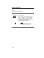
ZIATECH WARRANTY
Ziatech Hardware: Within two years of shipping date, Ziatech will
repair or replace products which prove to be defective in materials
and/or workmanship, provided they are promptly returned to Ziatech
at customer’s expense and have not been repaired, altered, or
damaged by non-Ziatech personnel. Service after warranty is
available at a predesignated service charge. Batteries are not covered
by this warranty. No other warranty is expressed or implied.
Ziatech Software: Within 90 days of shipping date, Ziatech will
replace software (PROM or diskette) should it prove defective.
Products not manufactured by Ziatech: Limited to the warranty
provided by the original manufacturer.
Notice: Contact Ziatech for a Return Materials Authorization (RMA)
number before returning any product to Ziatech for repair.
Life Support Policy: Ziatech products are not authorized for use as
critical components in life support devices or systems without the
express written approval of the president of Ziatech Corporation. As
used herein:
1.
Life support devices or systems are devices or systems that
support or sustain life and whose failure to perform, when
properly used in accordance with instructions for use provided in
the labeling, can be reasonably expected to result in a significant
injury to the user.
2.
A critical component is any component of a life support device
or system whose failure to perform can be reasonably expected
to cause the failure of the life support device or system or to
affect its safety or effectiveness.
1993 Ziatech Corporation
IBM PC, PC/AT, and PC/XT are registered trademarks of International Business Machines, Inc.
MS-DOS is a registered trademark of Microsoft Corp.
CUSTOMER SUPPORT
If you have a technical question, please call Ziatech’s
Customer Support Service at one of the following numbers.
Corporate Headquarters: (805) 541-0488
(805) 541-5088 (FAX)
You can also use a modem to leave a message on the 24-hour
Ziatech Bulletin Board Service (BBS) by calling
(805) 541-8218. The BBS will provide you with current
Ziatech product revision and upgrade information.
PREFACE
The ZT 8808A and ZT 8809A are single board computers designed
primarily for DOS applications on the STD bus. The combination of
the 8088-compatible V20 microprocessor with RAM, EPROM, serial
ports, a printer port, timers, and a real-time clock makes a hardwarecompatible PC viable for compact industrial applications.
This manual describes the operation and use of the ZT 8808A/8809A.
The only difference between the ZT 8808A and ZT 8809A is the
processor clock speed; the ZT 8808A runs at 5 MHz and the
ZT 8809A runs at 8 MHz. The ZT 88CT08A and ZT 88CT09A are
extended temperature CMOS versions of the ZT 8808A and
ZT 8809A.
Except where otherwise specifically stated, all references in this
manual to the ZT 8809A also apply to the ZT 8808A and
ZT 88CT08A/88CT09A.
The following organizational outline describes the focus of each
chapter. Section headings enclosed in boxes indicate the locations of
labeled tabs, provided for quick access to the appropriate information.
Chapter 1, "Introduction,"is an overview of the ZT 8809A. It
includes a product definition, a listing of product features, a functional
block diagram, and a brief description of each block. If you are
evaluating the ZT 8809A to determine whether it fits your needs, this
chapter is especially useful to you.
Chapter 2, "Getting Started,"summarizes the information you need
to get your ZT 8809A up and running. Refer to the remaining
chapters in this manual for further explanation of the material covered
here.
Chapter 3, "Theory Of Operation," presents a detailed description
of ZT 8809A system level operation. Some of the topics discussed
include microprocessor performance compared to the IBM PC,
Preface
STD bus compatibility, serial communications, interrupts, direct
memory access, power-fail protection, and battery backup.
Chapter 4, "Application Examples," provides specific examples of
the ZT 8809A in operation, including code to implement these
applications. The examples demonstrate the use of interrupts, timers,
and the real-time clock.
Chapter 5, "Memory and I/O Capability," focuses on the memory
and input/output organization of the V20 microprocessor relative to
the ZT 8809A.
Chapter 6, "CPU Description (V20)," describes the basic
components of the V20 microprocessor, its enhancements over 8088
architecture, its ability to operate in both native mode and 8080
emulation mode, its operation with DMA, and the wait state
generator.
Chapter 7, "Numeric Data Processor (8087)," explains the
installation and operation of the optional 8087 Numeric Data
Processor for numerically intensive applications.
Chapter 8, "Serial Communications (16C452)," describes the two
RS-232-C serial ports on the ZT 8809A, serial port signals, and
register addresses.
Chapter 9, "Centronics Printer Interface," details the Centronics
printer port interface.
Chapter 10, "Real-Time Clock (DS 1215)," explains the
organization of the real-time clock, including method of access and
register organization.
Preface
Chapter 11, "Counter/Timers (8254)," describes the main
components of the three programmable 16-bit counter/timers
implemented in an Intel 8254 chip on the ZT 8809A. This chapter
describes the method used to program the counter/timers and their use
by STD DOS and STD ROM.
Chapter 12, "Interrupt Controller (8259A)," describes the features
and operation of the Intel 8259A Programmable Interrupt Controller
(PIC).
Chapter 13, "ZT 88CT08A/88CT09A CMOS Boards," describes
the functional, electrical, and environmental characteristics of the
CMOS versions of the ZT 8808A and ZT 8809A that differ from the
non-CMOS versions.
Appendix A, "Jumper Configurations," describes the ZT 8809A
jumper selectable options in detail.
Appendix B, "Specifications," contains the electrical, mechanical,
and environmental specifications for the ZT 8809A. It also contains
STD-80 bus timing diagrams, cable drawings, and tables showing
connector pin assignments.
Appendix C, "Customer Support," offers technical assistance for
ZT 8809A users. A revision history, and warranty and service
information are also included.
CONTENTS
I.
INTRODUCTION
Chapter 1. INTRODUCTION
1-1
OVERVIEW . . . . . . . . . . . . . . . . . . . . . . . . . . . . . . . . . . . . . . . . . . . . . . . . . . . . . 1-1
ZT 88CT08A and ZT 88CT09A . . . . . . . . . . . . . . . . . . . . . . . . . . . . . . . . 1-3
FEATURES OF THE ZT 8809A . . . . . . . . . . . . . . . . . . . . . . . . . . . . . . . . . . . 1-4
FUNCTIONAL BLOCKS . . . . . . . . . . . . . . . . . . . . . . . . . . . . . . . . . . . . . . . . . 1-6
V20 (uPD70108) Processor . . . . . . . . . . . . . . . . . . . . . . . . . . . . . . . . . . . . 1-6
Memory and I/O Addressing . . . . . . . . . . . . . . . . . . . . . . . . . . . . . . . . . . . 1-6
Wait-State Generator . . . . . . . . . . . . . . . . . . . . . . . . . . . . . . . . . . . . . . . . . . 1-7
Direct Memory Access (DMA) . . . . . . . . . . . . . . . . . . . . . . . . . . . . . . . . 1-7
Optional Battery Backup . . . . . . . . . . . . . . . . . . . . . . . . . . . . . . . . . . . . . . 1-7
AC/DC Power-Fail Detection . . . . . . . . . . . . . . . . . . . . . . . . . . . . . . . . . . 1-8
Real-Time Clock . . . . . . . . . . . . . . . . . . . . . . . . . . . . . . . . . . . . . . . . . . . . . 1-9
Serial Communications . . . . . . . . . . . . . . . . . . . . . . . . . . . . . . . . . . . . . . . 1-9
Counter/Timers . . . . . . . . . . . . . . . . . . . . . . . . . . . . . . . . . . . . . . . . . . . . . 1-10
Interrupts . . . . . . . . . . . . . . . . . . . . . . . . . . . . . . . . . . . . . . . . . . . . . . . . . . . 1-11
Centronics Printer/General Purpose I/O Port . . . . . . . . . . . . . . . . . . . . 1-12
Optional Numeric Data Coprocessor (8087) . . . . . . . . . . . . . . . . . . . . 1-12
Clock Slowdown & Halt Restart (CMOS boards only) . . . . . . . . . . . 1-13
II.
GETTING STARTED
Chapter 2. GETTING STARTED
OVERVIEW . . . . . . . . . . . . . . . . . . . . . . . . . . . . . . . . . . . . . . . . . . . . . . . . . . . . .
UNPACKING . . . . . . . . . . . . . . . . . . . . . . . . . . . . . . . . . . . . . . . . . . . . . . . . . . . .
WHAT’S IN THE BOX? . . . . . . . . . . . . . . . . . . . . . . . . . . . . . . . . . . . . . . . . . .
SYSTEM REQUIREMENTS . . . . . . . . . . . . . . . . . . . . . . . . . . . . . . . . . . . . . .
2-1
2-2
2-2
2-3
2-4
Contents
Physical Requirements . . . . . . . . . . . . . . . . . . . . . . . . . . . . . . . . . . . . . . . . 2-4
Power Requirements . . . . . . . . . . . . . . . . . . . . . . . . . . . . . . . . . . . . . . . . . . 2-4
Environmental Requirements . . . . . . . . . . . . . . . . . . . . . . . . . . . . . . . . . . 2-6
INSTALLING THE ZT 8809A . . . . . . . . . . . . . . . . . . . . . . . . . . . . . . . . . . . . 2-7
Configuring the ZT 8809A for STD ROM . . . . . . . . . . . . . . . . . . . . . . . 2-9
Configuring the ZT 8809A for STD DOS . . . . . . . . . . . . . . . . . . . . . . 2-13
MEMORY ADDRESSING . . . . . . . . . . . . . . . . . . . . . . . . . . . . . . . . . . . . . . . 2-19
I/O ADDRESSING . . . . . . . . . . . . . . . . . . . . . . . . . . . . . . . . . . . . . . . . . . . . . . 2-22
UPGRADING FROM ZT 8806/8807 SYSTEMS . . . . . . . . . . . . . . . . . . . 2-24
III. USER’S REFERENCE
Chapter 3. THEORY OF OPERATION
3-1
OVERVIEW . . . . . . . . . . . . . . . . . . . . . . . . . . . . . . . . . . . . . . . . . . . . . . . . . . . . . 3-2
RELATIVE MICROPROCESSOR PERFORMANCE . . . . . . . . . . . . . . . . 3-3
STD BUS COMPATIBILITY . . . . . . . . . . . . . . . . . . . . . . . . . . . . . . . . . . . . . . 3-4
MEMORY AND I/O . . . . . . . . . . . . . . . . . . . . . . . . . . . . . . . . . . . . . . . . . . . . . . 3-4
SERIAL COMMUNICATIONS . . . . . . . . . . . . . . . . . . . . . . . . . . . . . . . . . . . . 3-4
Serial Port 1 (COM1) . . . . . . . . . . . . . . . . . . . . . . . . . . . . . . . . . . . . . . . . . 3-5
Serial Port 2 (COM2) . . . . . . . . . . . . . . . . . . . . . . . . . . . . . . . . . . . . . . . . . 3-6
INTERRUPTS . . . . . . . . . . . . . . . . . . . . . . . . . . . . . . . . . . . . . . . . . . . . . . . . . . . 3-8
Interrupt Request Assignments . . . . . . . . . . . . . . . . . . . . . . . . . . . . . . . . . 3-8
Polled Interrupts on the STD Bus . . . . . . . . . . . . . . . . . . . . . . . . . . . . . . 3-10
STD Bus Vectored Interrupts . . . . . . . . . . . . . . . . . . . . . . . . . . . . . . . . . 3-12
STD Bus Cascaded Interrupts . . . . . . . . . . . . . . . . . . . . . . . . . . . . . . . . . 3-13
Non-Maskable Interrupts . . . . . . . . . . . . . . . . . . . . . . . . . . . . . . . . . . . . . 3-14
DIRECT MEMORY ACCESS (DMA) . . . . . . . . . . . . . . . . . . . . . . . . . . . . 3-15
Advantages of DMA . . . . . . . . . . . . . . . . . . . . . . . . . . . . . . . . . . . . . . . . . 3-15
DMA Operation . . . . . . . . . . . . . . . . . . . . . . . . . . . . . . . . . . . . . . . . . . . . . 3-16
POWER-FAIL PROTECTION . . . . . . . . . . . . . . . . . . . . . . . . . . . . . . . . . . . 3-18
DC Power-Fail . . . . . . . . . . . . . . . . . . . . . . . . . . . . . . . . . . . . . . . . . . . . . . 3-18
AC Power-Fail . . . . . . . . . . . . . . . . . . . . . . . . . . . . . . . . . . . . . . . . . . . . . . 3-19
System Battery Fail . . . . . . . . . . . . . . . . . . . . . . . . . . . . . . . . . . . . . . . . . . 3-22
BATTERY . . . . . . . . . . . . . . . . . . . . . . . . . . . . . . . . . . . . . . . . . . . . . . . . . . . . . 3-23
STATUS INDICATOR (LED) . . . . . . . . . . . . . . . . . . . . . . . . . . . . . . . . . . . . 3-25
RESET . . . . . . . . . . . . . . . . . . . . . . . . . . . . . . . . . . . . . . . . . . . . . . . . . . . . . . . . . 3-26
CMOS VERSIONS OF THE ZT 8808A/8809A . . . . . . . . . . . . . . . . . . . . . 3-27
Added Features . . . . . . . . . . . . . . . . . . . . . . . . . . . . . . . . . . . . . . . . . . . . . 3-27
Functional Differences . . . . . . . . . . . . . . . . . . . . . . . . . . . . . . . . . . . . . . . 3-29
Contents
Chapter 4. APPLICATION EXAMPLES
4-1
OVERVIEW . . . . . . . . . . . . . . . . . . . . . . . . . . . . . . . . . . . . . . . . . . . . . . . . . . . . . 4-2
EXAMPLE 1-A: USING SIMPLE INTERRUPTS . . . . . . . . . . . . . . . . . . . 4-3
Objectives . . . . . . . . . . . . . . . . . . . . . . . . . . . . . . . . . . . . . . . . . . . . . . . . . . . 4-3
System Configuration . . . . . . . . . . . . . . . . . . . . . . . . . . . . . . . . . . . . . . . . . 4-3
Software Outline . . . . . . . . . . . . . . . . . . . . . . . . . . . . . . . . . . . . . . . . . . . . . 4-4
Program Code . . . . . . . . . . . . . . . . . . . . . . . . . . . . . . . . . . . . . . . . . . . . . . . . 4-6
EXAMPLE 1-B: HANDLING SLAVE INTERRUPTS . . . . . . . . . . . . . . 4-13
Objectives . . . . . . . . . . . . . . . . . . . . . . . . . . . . . . . . . . . . . . . . . . . . . . . . . . 4-13
System Configuration . . . . . . . . . . . . . . . . . . . . . . . . . . . . . . . . . . . . . . . . 4-14
Software Outline . . . . . . . . . . . . . . . . . . . . . . . . . . . . . . . . . . . . . . . . . . . . 4-14
Program Code . . . . . . . . . . . . . . . . . . . . . . . . . . . . . . . . . . . . . . . . . . . . . . 4-17
EXAMPLE 2: POWER-FAIL/WATCHDOG TIMER . . . . . . . . . . . . . . . . 4-28
Objectives . . . . . . . . . . . . . . . . . . . . . . . . . . . . . . . . . . . . . . . . . . . . . . . . . . 4-28
System Level Issues . . . . . . . . . . . . . . . . . . . . . . . . . . . . . . . . . . . . . . . . . 4-28
System Requirements . . . . . . . . . . . . . . . . . . . . . . . . . . . . . . . . . . . . . . . . 4-29
Software Outline . . . . . . . . . . . . . . . . . . . . . . . . . . . . . . . . . . . . . . . . . . . . 4-31
Flowcharts For AC Power-Fail & Watchdog Interrupts . . . . . . . . . . 4-34
EXAMPLE 3: REAL-TIME CLOCK DRIVERS . . . . . . . . . . . . . . . . . . . . 4-40
Objectives . . . . . . . . . . . . . . . . . . . . . . . . . . . . . . . . . . . . . . . . . . . . . . . . . . 4-40
System Configuration . . . . . . . . . . . . . . . . . . . . . . . . . . . . . . . . . . . . . . . . 4-40
Software Outline . . . . . . . . . . . . . . . . . . . . . . . . . . . . . . . . . . . . . . . . . . . . 4-40
Chapter 5. MEMORY AND I/O CAPABILITY
5-1
OVERVIEW . . . . . . . . . . . . . . . . . . . . . . . . . . . . . . . . . . . . . . . . . . . . . . . . . . . . . 5-1
MEMORY ADDRESSING . . . . . . . . . . . . . . . . . . . . . . . . . . . . . . . . . . . . . . . . 5-2
Memory Expansion (MEMEX) . . . . . . . . . . . . . . . . . . . . . . . . . . . . . . . . 5-2
On-Board Memory Capacity . . . . . . . . . . . . . . . . . . . . . . . . . . . . . . . . . . . 5-2
Write Protection . . . . . . . . . . . . . . . . . . . . . . . . . . . . . . . . . . . . . . . . . . . . . . 5-3
MEMORY MAPS . . . . . . . . . . . . . . . . . . . . . . . . . . . . . . . . . . . . . . . . . . . . . . . . 5-4
BATTERY BACKUP . . . . . . . . . . . . . . . . . . . . . . . . . . . . . . . . . . . . . . . . . . . . 5-10
MEMORY DEVICE LOCATIONS . . . . . . . . . . . . . . . . . . . . . . . . . . . . . . . . 5-11
Sockets 3D1 and 5D1 . . . . . . . . . . . . . . . . . . . . . . . . . . . . . . . . . . . . . . . . 5-12
Sockets 7D1 and 9D1 . . . . . . . . . . . . . . . . . . . . . . . . . . . . . . . . . . . . . . . . 5-13
DEVICE ACCESS TIMES . . . . . . . . . . . . . . . . . . . . . . . . . . . . . . . . . . . . . . . 5-14
INPUT/OUTPUT ADDRESSING . . . . . . . . . . . . . . . . . . . . . . . . . . . . . . . . . 5-15
Chapter 6. CPU DESCRIPTION (V20)
V20 OVERVIEW . . . . . . . . . . . . . . . . . . . . . . . . . . . . . . . . . . . . . . . . . . . . . . . .
Segment Registers . . . . . . . . . . . . . . . . . . . . . . . . . . . . . . . . . . . . . . . . . . . .
Program Counter (PC) [IP] . . . . . . . . . . . . . . . . . . . . . . . . . . . . . . . . . . . .
6-1
6-2
6-3
6-5
Contents
Prefetch Pointer (PFP) . . . . . . . . . . . . . . . . . . . . . . . . . . . . . . . . . . . . . . . . 6-6
General Purpose Registers . . . . . . . . . . . . . . . . . . . . . . . . . . . . . . . . . . . . . 6-6
Pointers and Index Registers . . . . . . . . . . . . . . . . . . . . . . . . . . . . . . . . . . . 6-7
Program Status Word (PSW) [FL] . . . . . . . . . . . . . . . . . . . . . . . . . . . . . . 6-8
V20 ARCHITECTURAL ENHANCEMENTS . . . . . . . . . . . . . . . . . . . . . . . 6-9
Dual Data Bus . . . . . . . . . . . . . . . . . . . . . . . . . . . . . . . . . . . . . . . . . . . . . . . 6-9
Effective Address Generator . . . . . . . . . . . . . . . . . . . . . . . . . . . . . . . . . . . 6-9
16/32-Bit Temporary Shift Registers (TA,TB) . . . . . . . . . . . . . . . . . . 6-10
Loop Counter (LC) . . . . . . . . . . . . . . . . . . . . . . . . . . . . . . . . . . . . . . . . . . 6-10
Program Counter (PC) and Prefetch Pointer (PFP) . . . . . . . . . . . . . . 6-10
Enhanced and Unique Instructions . . . . . . . . . . . . . . . . . . . . . . . . . . . . . 6-11
MODE OPERATIONS - 8080 EMULATION MODE . . . . . . . . . . . . . . . 6-12
Break for Emulation (BRKEM) . . . . . . . . . . . . . . . . . . . . . . . . . . . . . . . 6-14
Return From Emulation (RETEM) . . . . . . . . . . . . . . . . . . . . . . . . . . . . 6-14
Call Native Routine (CALLN) . . . . . . . . . . . . . . . . . . . . . . . . . . . . . . . . 6-15
Return from Interrupt (RETI) . . . . . . . . . . . . . . . . . . . . . . . . . . . . . . . . . 6-15
Register Use in Emulation Mode . . . . . . . . . . . . . . . . . . . . . . . . . . . . . . 6-16
DMA SUPPORT . . . . . . . . . . . . . . . . . . . . . . . . . . . . . . . . . . . . . . . . . . . . . . . . 6-18
RESET STATE . . . . . . . . . . . . . . . . . . . . . . . . . . . . . . . . . . . . . . . . . . . . . . . . . 6-20
WAIT-STATE GENERATOR . . . . . . . . . . . . . . . . . . . . . . . . . . . . . . . . . . . . . 6-21
Chapter 7. NUMERIC DATA PROCESSOR (8087)
7-1
OVERVIEW . . . . . . . . . . . . . . . . . . . . . . . . . . . . . . . . . . . . . . . . . . . . . . . . . . . . . 7-1
zSBC 337 PIGGYBACK PROCESSOR . . . . . . . . . . . . . . . . . . . . . . . . . . . . 7-3
INSTALLING THE zSBC 337 . . . . . . . . . . . . . . . . . . . . . . . . . . . . . . . . . . . . . 7-4
COPROCESSOR INTERFACE . . . . . . . . . . . . . . . . . . . . . . . . . . . . . . . . . . . . 7-7
MEMORY ADDRESSING . . . . . . . . . . . . . . . . . . . . . . . . . . . . . . . . . . . . . . . . 7-8
INTERRUPT/NUMERIC ERRORS . . . . . . . . . . . . . . . . . . . . . . . . . . . . . . . . 7-9
REFERENCES . . . . . . . . . . . . . . . . . . . . . . . . . . . . . . . . . . . . . . . . . . . . . . . . . 7-13
Chapter 8. SERIAL COMMUNICATIONS (16C452)
8-1
OVERVIEW . . . . . . . . . . . . . . . . . . . . . . . . . . . . . . . . . . . . . . . . . . . . . . . . . . . . . 8-2
SERIAL COMMUNICATIONS PROTOCOL . . . . . . . . . . . . . . . . . . . . . . . 8-3
SERIAL INTERFACE (RS-232-C/422/485) . . . . . . . . . . . . . . . . . . . . . . . . . 8-8
RS-232-C vs. RS-422/485 . . . . . . . . . . . . . . . . . . . . . . . . . . . . . . . . . . . . 8-10
Signal Definitions . . . . . . . . . . . . . . . . . . . . . . . . . . . . . . . . . . . . . . . . . . . 8-11
SERIAL REGISTERS . . . . . . . . . . . . . . . . . . . . . . . . . . . . . . . . . . . . . . . . . . . 8-16
Transmit and Receive Buffer Registers . . . . . . . . . . . . . . . . . . . . . . . . 8-20
Scratchpad Register . . . . . . . . . . . . . . . . . . . . . . . . . . . . . . . . . . . . . . . . . 8-20
Line Control Register . . . . . . . . . . . . . . . . . . . . . . . . . . . . . . . . . . . . . . . . 8-21
Baud Rate Generator . . . . . . . . . . . . . . . . . . . . . . . . . . . . . . . . . . . . . . . . . 8-24
Contents
Line Status Register . . . . . . . . . . . . . . . . . . . . . . . . . . . . . . . . . . . . . . . . .
Interrupt ID Register . . . . . . . . . . . . . . . . . . . . . . . . . . . . . . . . . . . . . . . . .
Interrupt Enable Register . . . . . . . . . . . . . . . . . . . . . . . . . . . . . . . . . . . . .
Modem Control Register . . . . . . . . . . . . . . . . . . . . . . . . . . . . . . . . . . . . .
Modem Status Register . . . . . . . . . . . . . . . . . . . . . . . . . . . . . . . . . . . . . .
8-26
8-28
8-30
8-31
8-33
Chapter 9. CENTRONICS PRINTER INTERFACE
9-1
OVERVIEW . . . . . . . . . . . . . . . . . . . . . . . . . . . . . . . . . . . . . . . . . . . . . . . . . . . . . 9-1
PRINTER PORT OUTPUT CHARACTERISTICS . . . . . . . . . . . . . . . . . . . 9-3
USING THE PRINTER PORT . . . . . . . . . . . . . . . . . . . . . . . . . . . . . . . . . . . . . 9-4
REGISTER DEFINITIONS/ADDRESSES . . . . . . . . . . . . . . . . . . . . . . . . . . 9-5
Data Port . . . . . . . . . . . . . . . . . . . . . . . . . . . . . . . . . . . . . . . . . . . . . . . . . . . . 9-6
Status Port . . . . . . . . . . . . . . . . . . . . . . . . . . . . . . . . . . . . . . . . . . . . . . . . . . . 9-7
Control Port . . . . . . . . . . . . . . . . . . . . . . . . . . . . . . . . . . . . . . . . . . . . . . . . . 9-8
DISABLING SHARING OF PRINTER PORT SIGNALS . . . . . . . . . . . 9-12
OPTIONAL PRINTER CABLE PINOUT . . . . . . . . . . . . . . . . . . . . . . . . . . 9-14
PRINTER PORT RESET STATE . . . . . . . . . . . . . . . . . . . . . . . . . . . . . . . . . 9-15
Chapter 10. REAL-TIME CLOCK (DS 1215)
OVERVIEW . . . . . . . . . . . . . . . . . . . . . . . . . . . . . . . . . . . . . . . . . . . . . . . . . . . .
OPERATION . . . . . . . . . . . . . . . . . . . . . . . . . . . . . . . . . . . . . . . . . . . . . . . . . . .
TIMECHIP COMPARISON REGISTER DEFINITION . . . . . . . . . . . . .
TIMEKEEPER REGISTER INFORMATION . . . . . . . . . . . . . . . . . . . . . .
TIMECHIP REGISTER DEFINITION . . . . . . . . . . . . . . . . . . . . . . . . . . . .
AM/PM 12/24-Hour Mode . . . . . . . . . . . . . . . . . . . . . . . . . . . . . . . . . . .
Oscillator and Reset Bits . . . . . . . . . . . . . . . . . . . . . . . . . . . . . . . . . . . . .
Zero Bits . . . . . . . . . . . . . . . . . . . . . . . . . . . . . . . . . . . . . . . . . . . . . . . . . . .
10-1
10-1
10-3
10-5
10-6
10-7
10-8
10-8
10-8
Chapter 11. COUNTER/TIMERS (8254)
11-1
OVERVIEW . . . . . . . . . . . . . . . . . . . . . . . . . . . . . . . . . . . . . . . . . . . . . . . . . . . . 11-2
BLOCK DIAGRAM . . . . . . . . . . . . . . . . . . . . . . . . . . . . . . . . . . . . . . . . . . . . . 11-3
COUNTER/TIMER ARCHITECTURE . . . . . . . . . . . . . . . . . . . . . . . . . . . . 11-4
OPERATION . . . . . . . . . . . . . . . . . . . . . . . . . . . . . . . . . . . . . . . . . . . . . . . . . . . 11-6
Reset State . . . . . . . . . . . . . . . . . . . . . . . . . . . . . . . . . . . . . . . . . . . . . . . . . 11-6
Programming . . . . . . . . . . . . . . . . . . . . . . . . . . . . . . . . . . . . . . . . . . . . . . . 11-6
Read Operations . . . . . . . . . . . . . . . . . . . . . . . . . . . . . . . . . . . . . . . . . . . . . 11-8
Mode Definitions . . . . . . . . . . . . . . . . . . . . . . . . . . . . . . . . . . . . . . . . . . . 11-16
Operation Common to All Modes . . . . . . . . . . . . . . . . . . . . . . . . . . . . 11-23
Counter Use by STD DOS and STD ROM . . . . . . . . . . . . . . . . . . . . 11-25
Contents
Chapter 12. INTERRUPT CONTROLLER (8259A)
12-1
OVERVIEW . . . . . . . . . . . . . . . . . . . . . . . . . . . . . . . . . . . . . . . . . . . . . . . . . . . . 12-3
I/O PORT ADDRESSES . . . . . . . . . . . . . . . . . . . . . . . . . . . . . . . . . . . . . . . . . 12-3
OPERATION OVERVIEW . . . . . . . . . . . . . . . . . . . . . . . . . . . . . . . . . . . . . . . 12-4
FUNCTIONAL DESCRIPTION . . . . . . . . . . . . . . . . . . . . . . . . . . . . . . . . . . 12-7
Interrupt Request Register (IRR) . . . . . . . . . . . . . . . . . . . . . . . . . . . . . . 12-8
Interrupt Mask Register (IMR) . . . . . . . . . . . . . . . . . . . . . . . . . . . . . . . . 12-8
Priority Resolver (PR) . . . . . . . . . . . . . . . . . . . . . . . . . . . . . . . . . . . . . . . 12-9
Interrupt In-Service Register (ISR) . . . . . . . . . . . . . . . . . . . . . . . . . . . . 12-9
Control Logic . . . . . . . . . . . . . . . . . . . . . . . . . . . . . . . . . . . . . . . . . . . . . . . 12-9
Read/Write Control Logic . . . . . . . . . . . . . . . . . . . . . . . . . . . . . . . . . . . 12-10
Initialization and Operation Registers . . . . . . . . . . . . . . . . . . . . . . . . . 12-10
Cascade Buffer/Comparator . . . . . . . . . . . . . . . . . . . . . . . . . . . . . . . . . 12-10
PROGRAMMABLE REGISTERS . . . . . . . . . . . . . . . . . . . . . . . . . . . . . . . 12-11
Initialization Control Words (ICW1-4) . . . . . . . . . . . . . . . . . . . . . . . . 12-12
Operation Control Words (OCW1-3) . . . . . . . . . . . . . . . . . . . . . . . . . 12-16
8259A I/O PORT ADDRESSES . . . . . . . . . . . . . . . . . . . . . . . . . . . . . . . . . 12-21
INTERRUPT ASSIGNMENTS ON THE ZT 8809A . . . . . . . . . . . . . . . 12-22
OPERATION OF THE INTERRUPT CONTROLLER . . . . . . . . . . . . . 12-24
Priorities . . . . . . . . . . . . . . . . . . . . . . . . . . . . . . . . . . . . . . . . . . . . . . . . . . 12-24
Interrupt Triggering . . . . . . . . . . . . . . . . . . . . . . . . . . . . . . . . . . . . . . . . 12-27
Interrupt Status . . . . . . . . . . . . . . . . . . . . . . . . . . . . . . . . . . . . . . . . . . . . 12-29
EOI COMMANDS . . . . . . . . . . . . . . . . . . . . . . . . . . . . . . . . . . . . . . . . . . . . . 12-31
Nonspecific EOI Commands . . . . . . . . . . . . . . . . . . . . . . . . . . . . . . . . 12-31
Specific EOI Commands . . . . . . . . . . . . . . . . . . . . . . . . . . . . . . . . . . . . 12-32
Automatic EOI Mode . . . . . . . . . . . . . . . . . . . . . . . . . . . . . . . . . . . . . . . 12-32
RESET . . . . . . . . . . . . . . . . . . . . . . . . . . . . . . . . . . . . . . . . . . . . . . . . . . . . . . . . 12-34
Chapter 13. ZT 88CT08A/88CT09A CMOS BOARDS
OVERVIEW . . . . . . . . . . . . . . . . . . . . . . . . . . . . . . . . . . . . . . . . . . . . . . . . . . . .
FUNCTIONAL DIFFERENCES . . . . . . . . . . . . . . . . . . . . . . . . . . . . . . . . . .
Logic Family (CT vs. C) . . . . . . . . . . . . . . . . . . . . . . . . . . . . . . . . . . . . .
Use of 80C88 Processor . . . . . . . . . . . . . . . . . . . . . . . . . . . . . . . . . . . . . .
Addition of Optional 8087(-2) . . . . . . . . . . . . . . . . . . . . . . . . . . . . . . . .
Clock Slowdown Mode . . . . . . . . . . . . . . . . . . . . . . . . . . . . . . . . . . . . . .
Halt With Restart Via Interrupt . . . . . . . . . . . . . . . . . . . . . . . . . . . . . . . .
ELECTRICAL/ENVIRONMENTAL DIFFERENCES . . . . . . . . . . . . . .
Increased Temperature Range . . . . . . . . . . . . . . . . . . . . . . . . . . . . . . . . .
Reduced Power Consumption . . . . . . . . . . . . . . . . . . . . . . . . . . . . . . . . .
Bus Loading . . . . . . . . . . . . . . . . . . . . . . . . . . . . . . . . . . . . . . . . . . . . . . . .
13-1
13-1
13-2
13-2
13-3
13-4
13-4
13-6
13-8
13-8
13-8
13-9
Contents
IV. APPENDICES
Appendix A. JUMPER CONFIGURATIONS
A-1
OVERVIEW . . . . . . . . . . . . . . . . . . . . . . . . . . . . . . . . . . . . . . . . . . . . . . . . . . . . A-1
JUMPER DESCRIPTIONS . . . . . . . . . . . . . . . . . . . . . . . . . . . . . . . . . . . . . . . A-3
Appendix B. SPECIFICATIONS
B-1
OVERVIEW . . . . . . . . . . . . . . . . . . . . . . . . . . . . . . . . . . . . . . . . . . . . . . . . . . . . B-1
ELECTRICAL AND ENVIRONMENTAL . . . . . . . . . . . . . . . . . . . . . . . . . B-2
Absolute Maximum Ratings . . . . . . . . . . . . . . . . . . . . . . . . . . . . . . . . . . . B-2
DC Operating Characteristics . . . . . . . . . . . . . . . . . . . . . . . . . . . . . . . . . . B-2
Battery Backup Characteristics . . . . . . . . . . . . . . . . . . . . . . . . . . . . . . . . B-3
STD Bus Loading Characteristics . . . . . . . . . . . . . . . . . . . . . . . . . . . . . . B-3
MECHANICAL . . . . . . . . . . . . . . . . . . . . . . . . . . . . . . . . . . . . . . . . . . . . . . . . . B-6
CONNECTORS . . . . . . . . . . . . . . . . . . . . . . . . . . . . . . . . . . . . . . . . . . . . . . . . . B-9
CABLES . . . . . . . . . . . . . . . . . . . . . . . . . . . . . . . . . . . . . . . . . . . . . . . . . . . . . . . B-20
TIMING . . . . . . . . . . . . . . . . . . . . . . . . . . . . . . . . . . . . . . . . . . . . . . . . . . . . . . . B-23
Appendix C. CUSTOMER SUPPORT
C-1
OVERVIEW . . . . . . . . . . . . . . . . . . . . . . . . . . . . . . . . . . . . . . . . . . . . . . . . . . . . C-1
TROUBLESHOOTING . . . . . . . . . . . . . . . . . . . . . . . . . . . . . . . . . . . . . . . . . . C-2
Powering Up STD ROM . . . . . . . . . . . . . . . . . . . . . . . . . . . . . . . . . . . . . . C-2
Powering Up STD DOS . . . . . . . . . . . . . . . . . . . . . . . . . . . . . . . . . . . . . . C-4
ZT 8808A/8809A REVISION HISTORY . . . . . . . . . . . . . . . . . . . . . . . . . . . C-8
Revision 0 - Original Release of Board, 12/17/91 . . . . . . . . . . . . . . . . C-8
Revision A - 8/19/92 . . . . . . . . . . . . . . . . . . . . . . . . . . . . . . . . . . . . . . . . . C-8
ZT 88CT08A/88CT09A REVISION HISTORY . . . . . . . . . . . . . . . . . . . . . C-8
RELIABILITY . . . . . . . . . . . . . . . . . . . . . . . . . . . . . . . . . . . . . . . . . . . . . . . . . . C-9
WARRANTY . . . . . . . . . . . . . . . . . . . . . . . . . . . . . . . . . . . . . . . . . . . . . . . . . . C-10
TECHNICAL ASSISTANCE . . . . . . . . . . . . . . . . . . . . . . . . . . . . . . . . . . . . C-11
RETURNING FOR SERVICE . . . . . . . . . . . . . . . . . . . . . . . . . . . . . . . . . . . C-12
TABLES
Table 3–1
Table 3–2
Table 5–1
Table 5–2
Table 5–3
Table 6–1
Table 6–2
Table 6–3
Table 7–1
Table 8–1
Table 8–2
Table 8–3
Table 8–4
Table 8–5
Table 9–1
Table 9–2
Table 9–3
Table 9–4
Table 9–5
Table 11–1
Table 11–2
Table 11–3
Table 12–1
Table A–1
Table A–2
Table B–1
Table B–2
Table B–3
Table B–4
Table B–5
Table B–6
Table B–7
Table B–8
Processor Speed Comparison. . . . . . . . . . . . . . . . . . . . . . . . . . 3-3
Serial Communications Standards. . . . . . . . . . . . . . . . . . . . . 3-7
Memory Configurations, 3D1/5D1/BRAM. . . . . . . . . . . . 5-12
Memory Configurations, 7D1/9D1. . . . . . . . . . . . . . . . . . . . 5-13
Device Access Times. . . . . . . . . . . . . . . . . . . . . . . . . . . . . . . 5-14
Segment Registers. . . . . . . . . . . . . . . . . . . . . . . . . . . . . . . . . . . 6-4
8080 Emulation Register Use. . . . . . . . . . . . . . . . . . . . . . . . 6-16
Memory Access Times. . . . . . . . . . . . . . . . . . . . . . . . . . . . . . 6-21
Queue-Status Line Functions. . . . . . . . . . . . . . . . . . . . . . . . . . 7-7
16C452 Reset State. . . . . . . . . . . . . . . . . . . . . . . . . . . . . . . . . 8-14
ZT 8809A I/O Port Assignments. . . . . . . . . . . . . . . . . . . . . 8-17
16C452 Addressable Registers Summary. . . . . . . . . . . . . . 8-18
Baud Rate Table. . . . . . . . . . . . . . . . . . . . . . . . . . . . . . . . . . . . 8-25
16C452 Interrupt Control Functions. . . . . . . . . . . . . . . . . . . 8-28
16C452 Printer Port Output Characteristics. . . . . . . . . . . . . 9-3
Parallel Port Register Definitions. . . . . . . . . . . . . . . . . . . . . . 9-5
Parallel Port Register Addresses. . . . . . . . . . . . . . . . . . . . . . . 9-5
Shared Printer Signals. . . . . . . . . . . . . . . . . . . . . . . . . . . . . . . 9-13
ZT 90039 Cable Pinout. . . . . . . . . . . . . . . . . . . . . . . . . . . . . . 9-14
Read-Back Command Example. . . . . . . . . . . . . . . . . . . . . 11-15
Gate Pin Operations Summary. . . . . . . . . . . . . . . . . . . . . . 11-22
Minimum and Maximum Initial Counts. . . . . . . . . . . . . . 11-24
PIC Registers. . . . . . . . . . . . . . . . . . . . . . . . . . . . . . . . . . . . . 12-11
Jumper Descriptions. . . . . . . . . . . . . . . . . . . . . . . . . . . . . . . . . A-3
Memory Addressing, W55-W59. . . . . . . . . . . . . . . . . . . . . A-42
STD Bus Signal Loading, P Connector. . . . . . . . . . . . . . . . . B-4
STD Bus Signal Loading, E Connector. . . . . . . . . . . . . . . . . B-5
Mechanical Specifications. . . . . . . . . . . . . . . . . . . . . . . . . . . . B-7
J1 Pin Assignments (RS-232-C). . . . . . . . . . . . . . . . . . . . . . B-13
J2 Pin Assignments (RS-232-C). . . . . . . . . . . . . . . . . . . . . . B-14
J2 Pin Assignments (RS-422/485). . . . . . . . . . . . . . . . . . . . B-15
J3 Pin Assignments. . . . . . . . . . . . . . . . . . . . . . . . . . . . . . . . . B-16
J4 Pin Assignments. . . . . . . . . . . . . . . . . . . . . . . . . . . . . . . . . B-17
Tables
Table B–9
Table B–10
Table B–11
J5 Pin Assignments. . . . . . . . . . . . . . . . . . . . . . . . . . . . . . . . . B-17
J6 Pin Assignments. . . . . . . . . . . . . . . . . . . . . . . . . . . . . . . . . B-18
J7 Pin Assignments. . . . . . . . . . . . . . . . . . . . . . . . . . . . . . . . . B-19
ILLUSTRATIONS
Figure 1–1
Figure 2–1
Figure 2–2
Figure 2–3
Figure 2–4
Figure 2–5
Figure 3–1
Figure 3–2
Figure 3–3
Figure 3–4
Figure 3–5
Figure 3–6
Figure 5–1
Figure 5–2
Figure 5–3
Figure 5–4
Figure 5–5
Figure 5–6
Figure 5–7
Figure 5–8
Figure 6–1
Figure 6–2
Figure 6–3
Figure 7–1
Figure 8–1
Figure 8–2
Figure 8–3
Figure 9–1
Figure 10–1
Figure 10–2
Figure 10–3
Figure 11–1
Figure 11–2
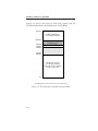
ZT 8809A Functional Block Diagram. . . . . . . . . . . . . . . . . . 1-5
Non-DOS Factory Default Jumper Configuration. . . . . . . . 2-8
ZT 8809A Configured For STD DOS. . . . . . . . . . . . . . . . . 2-14
STD DOS Factory Default Memory Map. . . . . . . . . . . . . . 2-20
STD ROM Factory Default Memory Map. . . . . . . . . . . . . 2-21
I/O Map, STD DOS / STD ROM Systems. . . . . . . . . . . . . 2-23
PIC Interrupt Input Requests. . . . . . . . . . . . . . . . . . . . . . . . . . 3-9
Polled Interrupt Structure. . . . . . . . . . . . . . . . . . . . . . . . . . . . 3-11
Small Scale Vectored Structure. . . . . . . . . . . . . . . . . . . . . . . 3-12
Large Scale Vectored Structure. . . . . . . . . . . . . . . . . . . . . . . 3-13
DMA With STD Bus Controller. . . . . . . . . . . . . . . . . . . . . . 3-17
AC Transformer Connection. . . . . . . . . . . . . . . . . . . . . . . . . 3-19
STD DOS Factory Default Memory Map. . . . . . . . . . . . . . . 5-4
STD DOS Factory Default Jumper Configuration. . . . . . . . 5-5
STD DOS Map with 640K On-Board RAM. . . . . . . . . . . . . 5-6
STD DOS With 640K RAM Jumper Configuration. . . . . . 5-7
Non-DOS Factory Default Memory Map. . . . . . . . . . . . . . . 5-8
Non-DOS Factory Default Jumper Configuration. . . . . . . . 5-9
Memory Chip Locations. . . . . . . . . . . . . . . . . . . . . . . . . . . . . 5-11
ZT 8809A I/O Map. . . . . . . . . . . . . . . . . . . . . . . . . . . . . . . . . 5-16
Program Status Word. . . . . . . . . . . . . . . . . . . . . . . . . . . . . . . . . 6-8
V20 Modes. . . . . . . . . . . . . . . . . . . . . . . . . . . . . . . . . . . . . . . . 6-13
DMA With STD Bus Controller. . . . . . . . . . . . . . . . . . . . . . 6-19
zSBC 337 Piggyback Processor Installation. . . . . . . . . . . . . 7-6
Establishing Serial Communications. . . . . . . . . . . . . . . . . . . 8-5
Loopback of RTS/CTS, DTR/DSR. . . . . . . . . . . . . . . . . . . . . 8-7
16C452 Serial Port Block Diagram. . . . . . . . . . . . . . . . . . . . 8-9
Printer Interface Block Diagram. . . . . . . . . . . . . . . . . . . . . . . 9-2
Real-Time Clock Block Diagram. . . . . . . . . . . . . . . . . . . . . 10-2
Timechip Comparison Register. . . . . . . . . . . . . . . . . . . . . . . 10-5
Timechip Register. . . . . . . . . . . . . . . . . . . . . . . . . . . . . . . . . . 10-7
Intel 8254 Timers Block Diagram. . . . . . . . . . . . . . . . . . . . 11-3
Internal Block Diagram of a Counter. . . . . . . . . . . . . . . . . . 11-4
Illustrations
Figure 11–3
Figure 11–4
Figure 11–5
Figure 11–6
Figure 12–1
Figure 12–2
Figure 12–3
Figure 12–4
Figure 12–5
Figure A–1
Figure A–2
Figure A–3
Figure A–4
Figure A–5
Figure A–6
Figure A–7
Figure A–8
Figure A–9
Figure A–10
Figure A–11
Figure A–12
Figure A–13
Figure A–14
Figure A–15
Figure A–16
Figure B–1
Figure B–2
Figure B–3
Figure B–4
Figure B–5
Figure B–6
Figure B–7
Figure B–8
Figure B–9
Figure B–10
Figure B–11
Figure B–12
Figure B–13
Figure B–14
Control Word Format. . . . . . . . . . . . . . . . . . . . . . . . . . . . . . . 11-7
Counter Latch Command Format. . . . . . . . . . . . . . . . . . . . . 11-9
Counter Status Format. . . . . . . . . . . . . . . . . . . . . . . . . . . . . 11-12
Null Count Operation. . . . . . . . . . . . . . . . . . . . . . . . . . . . . . 11-13
V20 Interrupt Vector Table. . . . . . . . . . . . . . . . . . . . . . . . . . 12-5
8259A Block Diagram. . . . . . . . . . . . . . . . . . . . . . . . . . . . . . 12-7
8259A ICW Formats. . . . . . . . . . . . . . . . . . . . . . . . . . . . . . . 12-13
8259A Operation Control Word Formats. . . . . . . . . . . . . 12-17
8259A Interrupts. . . . . . . . . . . . . . . . . . . . . . . . . . . . . . . . . . 12-23
W1 - W12 Jumper Block. . . . . . . . . . . . . . . . . . . . . . . . . . . . . A-2
W13 - W32 Jumper Block. . . . . . . . . . . . . . . . . . . . . . . . . . . A-11
COM2 Configured as RS-232-C DCE. . . . . . . . . . . . . . . . A-18
COM2 Configured as RS-232-C DTE. . . . . . . . . . . . . . . . A-19
COM2 Configured as RS-422 DCE. . . . . . . . . . . . . . . . . . A-20
COM2 Configured for RS-485 Operation. . . . . . . . . . . . . A-21
COM1 Configured for DTE Operation. . . . . . . . . . . . . . . . A-23
COM1 Configured for DCE Operation. . . . . . . . . . . . . . . A-24
W33-W36, W38-W46, W68 Jumper Blocks. . . . . . . . . . . A-26
Socket 3D1 Configuration. . . . . . . . . . . . . . . . . . . . . . . . . . . A-31
W37, W47-50, W66-W67 Jumper Blocks. . . . . . . . . . . . . A-34
W51 - W59 Jumper Block. . . . . . . . . . . . . . . . . . . . . . . . . . . A-37
W60 - W65 Jumper Block. . . . . . . . . . . . . . . . . . . . . . . . . . A-46
ZT 8809A User Configuration. . . . . . . . . . . . . . . . . . . . . . . A-54
Non-DOS Factory Default Jumper Configuration. . . . . . A-55
ZT 8809A Configured for STD DOS. . . . . . . . . . . . . . . . . A-56
Board Dimensions Without zSBC 337. . . . . . . . . . . . . . . . . B-7
Board Dimensions With zSBC 337. . . . . . . . . . . . . . . . . . . . B-8
P/E Connector Pinout. . . . . . . . . . . . . . . . . . . . . . . . . . . . . . . B-11
ZT 8809A Connector Locations. . . . . . . . . . . . . . . . . . . . . . B-12
ZT 90014 Cable Drawing. . . . . . . . . . . . . . . . . . . . . . . . . . . B-20
ZT 90027 Cable Drawing. . . . . . . . . . . . . . . . . . . . . . . . . . . B-21
ZT 90039 Cable Drawing. . . . . . . . . . . . . . . . . . . . . . . . . . . B-22
ZT 8809A CLOCK* Timing. . . . . . . . . . . . . . . . . . . . . . . . . B-23
ZT 8809A Status Timing. . . . . . . . . . . . . . . . . . . . . . . . . . . . B-24
ZT 8809A Read Timing. . . . . . . . . . . . . . . . . . . . . . . . . . . . . B-25
ZT 8809A Write Timing. . . . . . . . . . . . . . . . . . . . . . . . . . . . B-26
ZT 8809A Wait Request Timing. . . . . . . . . . . . . . . . . . . . . B-27
ZT 8809A Bus Exchange Timing. . . . . . . . . . . . . . . . . . . . B-28
ZT 8809A Interrupt Timing. . . . . . . . . . . . . . . . . . . . . . . . . B-29
Chapter 1
INTRODUCTION
Contents
Page
OVERVIEW . . . . . . . . . . . . . . . . . . . . . . . . . . . . . . . . . . . . . . . . . . . . . . . . . . . . . 1-1
ZT 88CT08A and ZT 88CT09A . . . . . . . . . . . . . . . . . . . . . . . . . . . . . . . . 1-3
FEATURES OF THE ZT 8809A . . . . . . . . . . . . . . . . . . . . . . . . . . . . . . . . . . . 1-4
FUNCTIONAL BLOCKS . . . . . . . . . . . . . . . . . . . . . . . . . . . . . . . . . . . . . . . . . 1-6
V20 (uPD70108) Processor . . . . . . . . . . . . . . . . . . . . . . . . . . . . . . . . . . . . 1-6
Memory and I/O Addressing . . . . . . . . . . . . . . . . . . . . . . . . . . . . . . . . . . . 1-6
Wait-State Generator . . . . . . . . . . . . . . . . . . . . . . . . . . . . . . . . . . . . . . . . . . 1-7
Direct Memory Access (DMA) . . . . . . . . . . . . . . . . . . . . . . . . . . . . . . . . 1-7
Optional Battery Backup . . . . . . . . . . . . . . . . . . . . . . . . . . . . . . . . . . . . . . 1-7
AC/DC Power-Fail Detection . . . . . . . . . . . . . . . . . . . . . . . . . . . . . . . . . . 1-8
Real-Time Clock . . . . . . . . . . . . . . . . . . . . . . . . . . . . . . . . . . . . . . . . . . . . . 1-9
Serial Communications . . . . . . . . . . . . . . . . . . . . . . . . . . . . . . . . . . . . . . . 1-9
Counter/Timers . . . . . . . . . . . . . . . . . . . . . . . . . . . . . . . . . . . . . . . . . . . . . 1-10
Interrupts . . . . . . . . . . . . . . . . . . . . . . . . . . . . . . . . . . . . . . . . . . . . . . . . . . . 1-11
Centronics Printer/General Purpose I/O Port . . . . . . . . . . . . . . . . . . . . 1-12
Optional Numeric Data Coprocessor (8087) . . . . . . . . . . . . . . . . . . . . 1-12
Clock Slowdown & Halt Restart (CMOS boards only) . . . . . . . . . . . 1-13
OVERVIEW
The 5 MHz ZT 8808A and 8 MHz ZT 8809A are 16-bit single board
computers (SBCs) designed with DOS applications on the STD bus in
mind. The high level of integration allows for a complete STD DOS
system on one board. All peripherals are located at the same I/O
addresses as on the IBM PC, allowing for a greater degree of
software compatibility.
1-1
Introduction
A performance increase over 8088-based STD CPU boards is
achieved in part by the use of the NEC V20 microprocessor. This is
an 8088 compatible processor with a superset of the 8088 instruction
set. The V20 is a CMOS device with a standby mode, which results in
lower power consumption.
The ZT 8808A/8809A and 88CT08A/88CT09A boards also provide
an increase in memory capacity over the earlier non-"A" versions
(ZT 8808/8809 and 88CT08/88CT09). The "A" versions allow up to
640 bytes of static RAM directly on the processor board, thus
eliminating the need to use an additional memory board. Increased
memory capacity is accomplished by adding support for a 512 Kbyte
RAM device in socket 7D1 and placing a 128 Kbyte RAM in
socket 3D1 (this configuration assumes no EPROM in socket 3D1). If
you have been using an additional memory board (ZT 8824,
ZT 8820B, ZT 8825, or other) to achieve 640 Kbytes of system RAM,
you may be able to eliminate that memory board from your system by
putting more system RAM on the "A" version processor board.
However, systems with large RAM and PROM disks on the ZT 8825
will probably still require the ZT 8825.
Peripherals on the ZT 8808A and ZT 8809A include three
counter/timers, an interrupt controller, a real-time clock, two
RS-232-C serial ports (one of which may be configured to be
RS-485), a Centronics printer interface or general purpose parallel I/O
port, and four 32-pin memory sockets. The memory sockets may
include one EPROM, two RAM, and one additional RAM or EPROM
(the last socket is configurable). An additional 32 Kbytes of on-board
RAM and a general purpose LED indicator are also provided.
1-2
Introduction
All RAM and the real-time clock may be optionally battery-backed by
a 1 Amp-hour lithium battery. DC power failure detection is provided
to switch to the battery backup mode during +5 VDC failure. AC
power failure detection is possible with the use of an optional AC/DC
converter. Detection of AC power failure provides time for the
processor to save critical data in battery-backed RAM before
impending +5 VDC failure.
ZT 88CT08A and ZT 88CT09A
The ZT 88CT08A and ZT 88CT09A are CMOS versions of the
ZT 8808A and ZT 8809A, respectively. They are designed for
extended temperature and low power applications. All references in
this manual to the ZT 8808A and ZT 8809A are also appropriate for
the ZT 88CT08A and ZT 88CT09A. Refer to Chapter 13 for
information pertaining specifically to the ZT 88CT08A and
ZT 88CT09A. Features provided with the CMOS version boards in
addition to the standard ZT 8808A/8809A include slow-down and
sleep modes.
Software support is provided by Ziatech’s STD DOS option and by
the STD ROM option. STD DOS includes the MS-DOS operating
system for the ZT 8809A. STD ROM provides software debugging
capabilities when used in conjunction with an IBM PC. The STD
ROM option is useful for applications where no operating system is
required for the target system. Contact Ziatech for further information
on these development systems.
1-3
Introduction
FEATURES OF THE ZT 8809A
•
•
•
•
STD-80 and STD 32 bus compatible
Optional CMOS versions available
8088/8086 code compatible
Four 32-pin memory sockets, configurable for
–
–
•
•
•
•
•
•
•
•
•
•
•
•
•
•
•
•
•
•
•
1-4
1 EPROM and 3 RAMs or
2 EPROMs and 2 RAMs
Acceptable RAM sizes are 32 Kbytes to 512 Kbytes
Acceptable EPROM sizes 16 Kbytes through 256 Kbytes
One 32 Kbyte static RAM
Real-time clock (DS 1215)
Optional battery backup for all RAM and real-time clock
AC/DC power-fail protection
Latching frontplane connectors
Optional Numeric Data Processor (8087) via zSBC 337
Wait-state generator
Interrupt Controller (8259A-2)
Two RS-232-C serial channels (VL 16C452), one RS-422/485
selectable
Three Counter/Timers (8254)
Centronics printer interface or general purpose parallel I/O port
(VL 16C452)
Optional STD DOS operating system software
Optional STD ROM development/debug software
Optional cables for Centronics printer interface and serial ports
Fully tested while cycling temperature from ambient to +55˚
Celsius to guarantee reliability (to +80˚ Celsius for
ZT 88CT08A/88CT09A)
Slow-down and sleep modes provided with the
ZT 88CT08A/88CT09A
Two-year warranty on all boards
Introduction
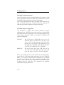
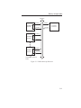
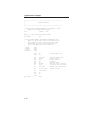
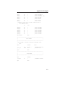
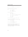
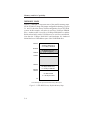
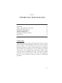
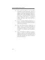
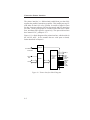
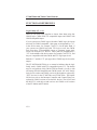
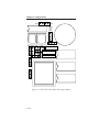
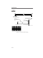
ZT 8809A
Optional
Battery
Backup
3
Counter/
Timers
RS-232-C
Serial
Interrupt
Controller
RS-232-C/
RS-422/485
Serial
32K RAM
(Optional
Battery
Backup)
V20
CPU
Clock
Slowdown
and
Halt/
Restart
AC/DC
PowerFail
Centronics
Printer
I/O
Real-time
Clock
256K RAM & 256K ROM
or
384K RAM & 128K ROM
(RAM Optionally
Battery-backed)
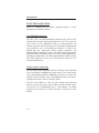
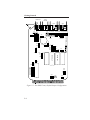
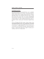
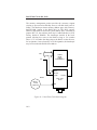
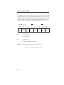
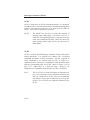
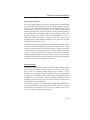
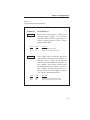
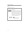
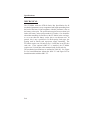
Figure 1–1. ZT 8809A Functional Block Diagram.
1-5
Introduction
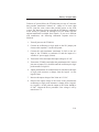
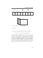
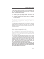
FUNCTIONAL BLOCKS
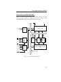
Figure 1-1 illustrates the ZT 8809A’s functional blocks. A brief
description of each block follows.
V20 (uPD70108) Processor
The NEC V20 is an 8088-compatible microprocessor with a 16-bit
internal data bus and an 8-bit external data bus. The V20 executes all
code written for the 8088/8086 family of microprocessors and
includes a superset of their instruction set. Performance enhancements
are provided by way of such architectural features as a dual 16-bit
internal data bus, high-speed effective address generation, and
additional hidden temporary registers. The added instructions include
shift and rotate by immediate value, move string, stack manipulations,
and 8080 emulation mode. The 8080 emulation mode enables existing
8-bit 8080 software to run on new 16-bit hardware with few or no
software modifications.
Memory and I/O Addressing
The ZT 8809A comes populated with one 32 Kbyte static RAM and
four 32-pin JEDEC compatible byte-wide sockets. Two of the sockets
accept 16K through 256 Kbyte EPROMs; the other two accept 32K
through 512 Kbyte RAMs. One of the EPROM sockets can also be
configured to accept a 32K or 128 Kbyte RAM.
The full 20-bit address is used for both on-board and off-board
memory accesses, giving the system 1 Mbyte of direct address space.
I/O accesses are accomplished with a 16-bit address, providing
64 Kbytes of I/O space for 16-bit I/O boards or 256 bytes for 8-bit
boards.
1-6
Introduction
Wait-State Generator
To accommodate I/O and memory boards needing more time for
access, the ZT 8809A contains a one wait-state generator. If enabled,
it inserts one wait-state (clock cycle) within the normal four-clock bus
cycle to increase it to five clocks. This gives memory and I/O boards
additional time between address valid time and the end of the bus
cycle to complete an access.
Direct Memory Access (DMA)
External DMA controllers are supported by the ZT 8809A via the
BUSRQ* (pin 42) and BUSAK* (pin 41) STD bus control signals. A
request for the bus is made to the ZT 8809A via BUSRQ* pin 42, and
the ZT 8809A responds with BUSAK* once the microprocessor has
signaled its release of the bus. When the DMA transfer is complete,
the DMA device releases BUSRQ* and the ZT 8809A then responds
by releasing BUSAK*. DMA is supported on the ZT 8809A for all
on-board EPROM and RAM, with the exception of the 32 Kbyte
static RAM.
Optional Battery Backup
All RAM and the real-time clock may be selectively battery-backed
with a 3.9 V, 1 Amp-hour lithium battery, which is shipped as a
standard option with the ZT 8809A STD DOS systems. When DC
power falls below 4.75 V, the battery power is switched in and
remains until power is again at that level. At the same time, the
DCPWRDWN* STD bus signal (pin 6) is driven active (low) to warn
other boards in the system of low DC voltage.
1-7
Introduction
Jumpers are provided to select whether the following three groups of
devices, either individually or as a whole, are to be battery-backed:
•
Real-time clock and 32 Kbyte RAM
•
Two RAM sockets
•
ROM/RAM socket when RAM is present
This conserves battery power exclusively for those devices that
require backup.
AC/DC Power-Fail Detection
DC power-fail detection senses when DC voltage drops below 4.75 V.
This signals the board to switch into battery backup mode, as
described above. AC power-fail detection is also available for early
warning of impending low DC voltage, to give the processor time to
store critical data while DC voltage is still above 4.75 V.
An optional 24 V transformer is available from Ziatech (ZT 90020) to
monitor the same AC source supplying the STD bus card cage, and
may be attached to the ZT 8809A via the frontplane. Upon detection
of AC voltage falling below 90 VAC, a non-maskable interrupt
(NMIRQ*) is sent to the CPU to prepare for the power down.
Approximately 2 ms after a DC power failure, the battery is switched
in and simultaneously the DCPWRDWN* STD bus signal (pin 6) is
driven active low.
1-8
Introduction
Real-Time Clock
The real-time clock on the ZT 8809A is a Dallas Semiconductor
DS 1215. It keeps track of hundredths of seconds, seconds, minutes,
hours, days, date of the month, months, and years. The clock
automatically corrects for leap years, and adjusts for months with
fewer than 31 days. It may be battery-backed by the optional battery.
The real-time clock shares its address space with the 32 Kbyte static
RAM. To communicate with the DS 1215, a 64-bit signature must be
written to the device, which then switches out the 32 Kbyte static
RAM and switches in the timekeeper function.
Serial Communications
The
ZT 8809A
contains
two
asynchronous
RS-232-C
communications channels, one of which is selectable for RS-422/485.
Both use the same type of UART chip (16C450 equivalent), which is
functionally equivalent to the serial communications channels found
in the IBM family of personal computers or their compatibles.
Each channel has a programmable baud rate generator, loopback
diagnostic capability, maskable interrupt generation, and jumper
selectable DCE or DTE configuration. The two channels become the
COM1 and COM2 serial ports in an STD DOS system. All drivers for
both the RS-232-C and RS-422/485 are on board the ZT 8809A.
COM2 may be disabled to allow an external board, such as a modem
board, to provide COM1.
1-9
Introduction
Counter/Timers
The ZT 8809A has three independent 16-bit counter/timers, each of
which can be used as a timer or event counter. The clock frequency
driving each of these timers is a 1.19318 MHz oscillator. For timers 1
and 2, the clock input may be jumpered to receive the frontplane
connector J4 signal, which may be an external frequency or event
input.
The six programmable counter/timer modes are as follows:
1.
Interrupt on end of count
2.
Frequency divider
3.
Square wave generator
4.
Software triggered strobe
5.
Retriggerable hardware triggered strobe
6.
Retriggerable one-shot
Each timer output may be jumper-selected to drive one of the
interrupt controller inputs, and is also available at connector J4. The
"gate" or enable input to each timer is pulled up active by a 10 kΩ
resistor and may be controlled by a source on frontplane connector J4.
1-10
Introduction
Interrupts
The programmable interrupt controller (PIC) on the ZT 8809A is an
Intel 8259A-2 or equivalent. It has eight interrupt inputs that can be
prioritized in software. Its output drives the CPU interrupt input. All
PIC interrupt inputs may be jumper selected between various onboard sources and the five frontplane and three backplane sources.
Factory default assigns the STD DOS compatible interrupt selections
as described by jumper descriptions W2-11 in Appendix A.
The interrupt structure follows Revision 2.3 and later of the STD-80
Series Bus Specification, which allows for the RESERVED and
CNTRL* STD bus pins 37 and 50, respectively, to be interrupt
sources as well as INTRQ* pin 44. These signals are now referred to
as INTRQ1*, INTRQ2*, and INTRQ*, respectively. This provides
for more backplane interrupts and may eliminate frontplane cabling
for added interrupts.
Also supported is the 8088 STD bus protocol for PIC cascading,
allowing for 8259A interrupt controller expansion. The PIC may
handle up to 50 prioritized interrupts by combining six off-board
sources, each of which may support eight interrupt inputs via a
separate "slave" interrupt controller, plus two direct on-board sources.
1-11
Introduction
Centronics Printer/General Purpose I/O Port
A Centronics printer interface is included on the ZT 8809A. It may
drive a Centronics-compatible printer directly. The printer interface
can also be used for general purpose I/O. It consists of eight I/O lines
for data, four open collector I/O lines for control, and five input lines
for status. The open collector lines have internal 2.5 kΩ pullups to
Vcc.
One of the status lines, ACK, activates the interrupt request LPT1
from the printer interface to the interrupt controller. An enable bit for
this interrupt is within the printer interface chip, the VL 16C452.
(This chip also contains the two 16C450 equivalent serial ports.) All
lines have corresponding register bits within the 16C452.
Optional Numeric Data Coprocessor (8087)
An Intel 8087 or equivalent Numeric Data Coprocessor is available
for the ZT 8809A. It adds performance by contributing arithmetic,
trigonometric, exponential, and logarithmic instructions to the
standard 8088/8086 instruction set.
The 8087 may be mounted on the ZT 8809A with the aid of Ziatech’s
zSBC 337 module. This module mounts onto the microprocessor
socket and accepts both the microprocessor and 8087. This
configuration requires two slots in a standard STD bus card cage
unless mounted in the end slot.
1-12
Introduction
Clock Slowdown & Halt Restart (CMOS boards only)
For power conservation, the ZT 88CT08A and ZT 88CT09A contain
two features to slow down or stop processor execution programmatically. These are the clock slowdown and halt with interrupt
restart features, provided by a special Harris Semiconductor 82C85
clock chip that replaces the 82C84A normally shipped on the
ZT 8809A board.
Clock slowdown divides the existing clock frequency by 256,
allowing a selection between 5 MHz and 19.5 kHz for the
ZT 88CT08A, and between 8 MHz and 31.25 kHz for the
ZT 88CT09A. Writing to a bit at the printer port allows programmatic
control of the slowdown feature. If the printer requires this bit for
proper control (most do not), a jumper selection is also provided to
allow hardware selection of this feature.
Interrupt restart allows the processor to stop processing via a software
halt instruction and remain dormant until a time interval has passed or
until the processor is needed by an external device. This conserves the
ZT 88CT08A/88CT09A power until processing is actually needed. To
use this feature, the software programs the on-board 8259A interrupt
controller to enable the proper interrupt level. This interrupt may be
from the on-board timers with their independent oscillator or from an
external source. The program then halts the microprocessor with the
HLT instruction until the interrupt arrives to restart it.
1-13
Chapter 2
GETTING STARTED
Contents
Page
OVERVIEW . . . . . . . . . . . . . . . . . . . . . . . . . . . . . . . . . . . . . . . . . . . . . . . . . . . . . 2-2
UNPACKING . . . . . . . . . . . . . . . . . . . . . . . . . . . . . . . . . . . . . . . . . . . . . . . . . . . . 2-2
WHAT’S IN THE BOX? . . . . . . . . . . . . . . . . . . . . . . . . . . . . . . . . . . . . . . . . . . 2-3
SYSTEM REQUIREMENTS . . . . . . . . . . . . . . . . . . . . . . . . . . . . . . . . . . . . . . 2-4
Physical Requirements . . . . . . . . . . . . . . . . . . . . . . . . . . . . . . . . . . . . . . . . 2-4
Power Requirements . . . . . . . . . . . . . . . . . . . . . . . . . . . . . . . . . . . . . . . . . . 2-4
Environmental Requirements . . . . . . . . . . . . . . . . . . . . . . . . . . . . . . . . . . 2-6
INSTALLING THE ZT 8809A . . . . . . . . . . . . . . . . . . . . . . . . . . . . . . . . . . . . 2-7
Configuring the ZT 8809A for STD ROM . . . . . . . . . . . . . . . . . . . . . . . 2-9
STD ROM Memory Requirements . . . . . . . . . . . . . . . . . . . . . . . . . 2-9
STD ROM Cable Requirements . . . . . . . . . . . . . . . . . . . . . . . . . . . 2-10
STD ROM Jumper Configuration . . . . . . . . . . . . . . . . . . . . . . . . . 2-10
Powering Up STD ROM . . . . . . . . . . . . . . . . . . . . . . . . . . . . . . . . . 2-11
Configuring the ZT 8809A for STD DOS . . . . . . . . . . . . . . . . . . . . . . 2-13
STD DOS Memory Requirements . . . . . . . . . . . . . . . . . . . . . . . . . 2-15
STD DOS Cable Requirements . . . . . . . . . . . . . . . . . . . . . . . . . . . 2-16
STD DOS Jumper Configuration . . . . . . . . . . . . . . . . . . . . . . . . . . 2-16
Powering Up STD DOS . . . . . . . . . . . . . . . . . . . . . . . . . . . . . . . . . . 2-17
MEMORY ADDRESSING . . . . . . . . . . . . . . . . . . . . . . . . . . . . . . . . . . . . . . . 2-19
I/O ADDRESSING . . . . . . . . . . . . . . . . . . . . . . . . . . . . . . . . . . . . . . . . . . . . . . 2-22
UPGRADING FROM ZT 8806/8807 SYSTEMS . . . . . . . . . . . . . . . . . . . 2-24
2-1
Getting Started
OVERVIEW
This chapter includes all the information you need to properly install
the ZT 8809A into an STD bus card cage. You should read this
chapter and Chapter 3, "Theory of Operation," before you attempt to
use the board. Remember, unless specifically stated otherwise, all
references to the ZT 8809A also pertain to the ZT 8808A,
ZT 88CT08A, and ZT 88CT09A.
UNPACKING
Please check the shipping carton for damage. If the shipping carton
and contents are damaged, notify the carrier and Ziatech for an
insurance settlement. Retain the shipping carton and packing material
for inspection by the carrier. Do not return any product to Ziatech
without a Return Material Authorization (RMA) number. Appendix D
explains the procedure for obtaining an RMA number from Ziatech.
2-2
Getting Started
WHAT’S IN THE BOX?
The items listed below are included in a standard ZT 8809A order.
The list does not include options such as system level software or
cabling. Refer to the packing list for a complete list of items shipped.
When ordering specific system level software options with the
ZT 8809A, refer to the software manual for a list of the items that
should be included.
•
ZT 8808A or ZT 8809A Single Board NEC V20 Computer or
ZT 88CT08A or ZT 88CT09A Single Board 80C88 Computer.
•
ZT 8808A/8809A Operating Manual (in binder)
•
Anti-static packing material
Attach the sticker packaged with the manual to the spine of the binder.
Be sure to save the anti-static packing material for use in storing or
shipping the ZT 8809A.
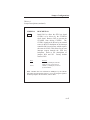
WARNING!
Like all equipment utilizing MOS devices, the ZT 8809A must
be protected from static discharge. This is especially true for
the ZT 88CT08A and ZT 88CT09A, which contain all CMOS
logic and are therefore very sensitive to static discharge.
Never remove or install any of the socketed parts except at a
static-free workstation.
2-3
Getting Started
SYSTEM REQUIREMENTS
Physical Requirements
The ZT 8809A is designed to be used in an STD bus system. It is
therefore physically and electrically compatible with the STD-80 bus
standard. It should normally be mounted in one slot of an STD bus
card cage. If the zSBC 337 module containing the 8087 Numeric Data
Processor is mounted on the board, it occupies two slots of the card
cage unless the end slot is used. Refer to the board outline in
Appendix B for board dimensions with and without the zSBC 337
module attached.
Power Requirements
Power requirements for the ZT 8808A and ZT 8809A are +5 VDC at
1.6 A maximum, 0.8 A typical. For serial communications, the
requirements are +12 VDC at 24 mA maximum and -12 VDC at
24 mA maximum. For proper operation of the ZT 8809A, +12 V and
-12 V must be supplied even though the serial ports may not be in use.
WARNING!
If you are using an emulator in place of the microprocessor
on the ZT 8809A, the emulator should be powered down or
disconnected before the CPU is powered down.
2-4
Getting Started
Important Note: The ZT 8809A CPU uses an 82C84A or
82C84B as the clock generator. The following special
considerations should be observed regarding the +5 VDC
power supply:
•
The +5 VDC power supply should never have a rise
time faster than 1 V per millisecond.
•
Use switcher-type power supplies if possible because
their turn-on times are generally slower than linear
power supplies.
If the above recommendations are not observed, the
82C84A/B may cause erratic behavior or the system may fail
to operate upon power-up (this problem is characterized by
the 82C84’s oscillator starting up at the third overtone of the
crystal installed). Ziatech’s power supplies are switcher
designs and do not induce oscillator instabilities. For further
information, refer to Intel’s Microsystems Components
Handbook, 1985, Volume I, page 3-238, under "Oscillator."
2-5
Getting Started
Environmental Requirements
The ambient temperature must be maintained at 0˚ to +65˚ Celsius for
proper operation and to avoid possible damage to the ZT 8809A (the
ZT 88CT08A and ZT 88CT09A allow for a lower power requirement
and wider temperature range, detailed in Chapter 13). Relative
humidity should be less than 95% at 40˚ C, non-condensing.
Important Note: It is critical to the ZT 8809A RS-232-C
serial interface that Auxiliary Ground (AUXGND) on the
STD bus be connected at the backplane to the +5 V ground
reference (GND). Ziatech backplanes are shipped in this
configuration, and the ZT 8809A provides Jumper W63 for
this purpose. Jumper W63 is installed at the factory prior to
shipment.
Vertical mounting is recommended in convective cooling systems not
using a fan. Horizontal mounting is not recommended unless forced
air cooling is provided at a rate of 30 cubic feet per minute passing
over the surface of the board.
2-6
Getting Started
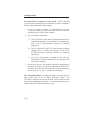
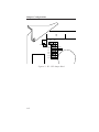
INSTALLING THE ZT 8809A
The fastest way to begin using the ZT 8809A is with the addition of
development software available from Ziatech. The STD ROM
development system allows you to download application software
developed on an IBM PC (or equivalent) through a serial port onto the
ZT 8809A. In addition to download and upload capabilities, STD
ROM uses Borland’s Turbo Debugger, which provides a wide
variety of commands for debugging software. When the code is ready
to be placed into EPROM, the locater program included with the STD
ROM system is used to format the file into an Intel hexadecimal
format acceptable to most EPROM programmers. This STD ROM
system is used primarily for applications written in assembly language
and ROM-able high-level languages.
STD DOS for the ZT 8809A is intended for designers who wish to
develop an application using a high-level language or for those
systems requiring a resident operating system (to support disk
subsystems, for example). STD DOS is an MS-DOS operating
system that resides on the ZT 8809A and is able to run most PC
software. In addition to high-level language support, STD DOS
includes an extensive base of easily integrated software such as:
•
Support for EGA and VGA graphics (ZT 8844 and ZT 8980)
•
Fixed and floppy disks (ZT 8850 and ZT 8950 series)
•
RAM and EPROM disks (ZT 8825 and on-board ZT 8809A)
•
Centronics printer interface (on-board ZT 8809A)
•
IEEE 488 support (ZT 8847 and ZT 8848)
•
Serial (ZT 8840, ZT 8841, and on-board ZT 8809A)
•
Real-time clock (on-board ZT 8809A)
2-7
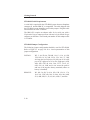
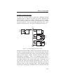
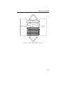
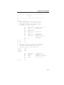
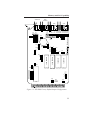
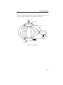
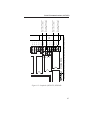
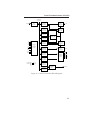
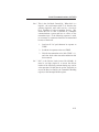
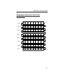
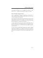
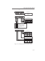
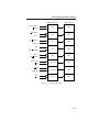
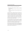
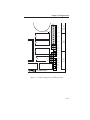
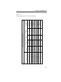
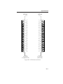
Getting Started
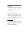
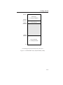
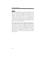
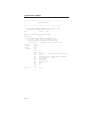
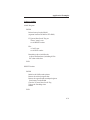
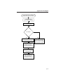
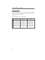
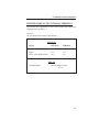
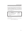
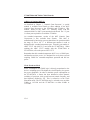
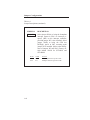
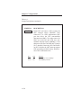
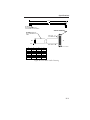
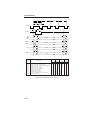
TIMER
COUNTER
W12
W29
W30
W31
W32
LPT
A B W36
A B
W33
W35
W34
A
B
B
A
W38
W39
W67
W40
W43
W44
W45
32K SRAM
B
A
STD ROM
W49
W68
A B
W48
W47
B
A
A B
W46
A B
W37
ZT8809A REV. A
W16
W17
W18
W19
W20
W21
W22
COM1
A
W4
W5
W6
W7
W8
W9
W10
W11
W1
W14
W3
A
W15
B
W2
A
B W13
COM2
W23
W24
W25
W26
W27
W28
INTERRUPTS
W66
B
W64
W65
W51
W52
W53
W54
W55
W56
W57
W58
W59
A
A B
W50
W60
W62
W63
W61
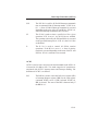
Figure 2–1. Non-DOS Factory Default Jumper Configuration.
2-8
Getting Started
Configuring the ZT 8809A for STD ROM
The STD ROM development system is available as an option to the
ZT 8809A for software development. If STD ROM is ordered along
with the ZT 8809A, the board is preconfigured and tested at the
factory prior to shipment. If the system has been altered or the
ZT 8809A rejumpered and the system does not function properly,
refer to the following instructions and to Figure 2-1 for configuring
your ZT 8809A.
STD ROM Memory Requirements
The STD ROM debug monitor is shipped in a 64 Kbyte EPROM.
Install this EPROM into the 32-pin socket at location 5D1, right
justified, with the board oriented component side up, goldfingers to
the left (see Figure 2-1).
STD ROM requires 2 Kbytes of memory, from address 0 through
7FFh, for program use. The 32 Kbyte static RAM shipped with the
STD ROM system should be sufficient for both debug and application
program memory. Install this RAM into socket location 7D1, right
justified.
If more application program RAM memory is required, another
32 Kbyte static RAM may be installed similarly into socket 9D1.
2-9
Getting Started
STD ROM Cable Requirements
A serial link is required for the STD ROM system between frontplane
connector J1 and the IBM PC or compatible. The cable shipped with
the STD ROM system should be used for this purpose. Plug this cable
into connector J1 of the ZT 8809A.
The IBM AT requires an adapter cable for its serial port with a
25-pin male D-type connector on one side and a 9-pin female D-type
connector on the other. The Ziatech part number for this adapter cable
is ZT 90026.
STD ROM Jumper Configuration
The following jumper configuration should be used for STD ROM.
Refer to Figure 2-1 on page 2-8 for a visual representation of this
jumper configuration.
INSTALL:
W2, 3, 4A, 5B, 6A, 7B-10B, 11A, 12, 13A, 14, 15B,
17B, 18B, 19, 20, 21B, 22-34, 35A, 36A, 37, 38B,
44A (top post) to left post of 40, left post of 41 to left
post of 42, right post of 42 to 43A (right post), 43B,
44B, 45B, 47B, 48, 49A, 50A, 52-57, 59-61, 63,
64B, 65A, 66, 68B, and a wire across the positive
and one of the negative battery terminals (where no
battery is installed).
REMOVE:
W1, 4B, 5A, 6B, 7A-10A, 11B, 13B, 15A, 16, 17A,
18A, 21A, 35B, 36B, 38A, 39, 44A, 45A, 46A, 46B,
47A, 49B, 50B, 51, 58, 62, 64A, 65B, 67, and 68A.
2-10
Getting Started
Note: This configures sockets 3D1 and 5D1 for 64 Kbyte ROMs and
sockets 7D1 and 9D1 for 128 Kbyte RAMs. Memory mapping
information may be found in the jumper configuration tables for W55W59 in Appendix A.
Powering Up STD ROM
Once the EPROM, RAM, jumpers, and cable are correctly
configured, install the ZT 8809A into the STD bus card cage. Be sure
to attach the D-type connector end of the cable to the appropriate IBM
PC or compatible.
•
Follow these steps to power on the system with a PC or
compatible.
1.
Turn on the PC and wait for the DOS prompt.
2.
Turn on the STD system.
3.
Insert the disk containing the STD ROM/Borland’s Turbo
Debugger in drive A.
4.
Type A:td -r and press the carriage return key.
5.
Borland’s Turbo Debugger should come up, communicating across the VTI link with your STD system.
2-11
Getting Started
•
2-12
Some things to check if the system is not working:
1.
Two ZT 8809A frontplane connectors accept the ZT 90014
serial cable. STD ROM works only in serial port 1 at J1.
2.
If a PC is used that has more than one 25-pin male
connector, be sure the serial cable is plugged into COM1.
3.
Check to see the EPROM and RAM chips are installed in
the proper sockets. EPROM should be installed in socket
5D1. RAM should be installed in socket 7D1.
4.
Check pin 1 orientation of the installed EPROM and
RAM(s). Pin 1 should be to the left, with the board
oriented component side up, goldfingers to the left. If a
chip has a smaller number of pins than its associated
socket, it should be right-justified in the socket.
5.
Re-verify the jumpers, particularly those associated with
the socket and memory configurations (W40-W45, W49,
and W55-W59).
Getting Started
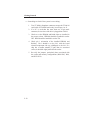
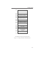
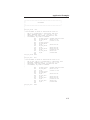
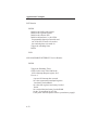
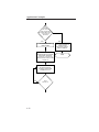
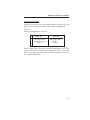
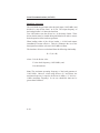
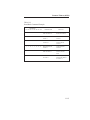
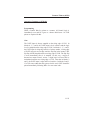
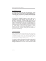
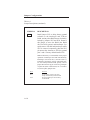
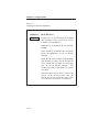
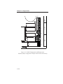
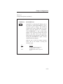
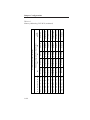
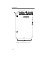
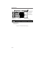
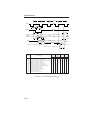
Configuring the ZT 8809A for STD DOS
STD DOS is an optional MS-DOS operating system available for the
ZT 8809A V20 processor board. If the ZT 8809A and STD DOS are
ordered together, Ziatech configures the ZT 8809A properly prior to
shipment and tests it as a system. If the ZT 8809A and STD DOS are
ordered separately, or the ZT 8809A was altered in any way after
shipment, instructions for installing and booting STD DOS on the
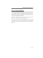
ZT 8809A are in the STD DOS System Manual. Refer to Figure 2-2
on page 2-14 for a visual representation of the correct STD DOS
jumper configuration.
2-13
Getting Started
TIMER
COUNTER
W12
W29
W30
W31
W32
LPT
A B W36
A B
W33
W35
W34
A
B
B
A
W38
W39
W67
W40
W43
W44
W45
W66
W68
128K RAM
128K RAM
B
A
256K EPROM
W49
128K EPROM
W47
B
A
A B
W48
W37
A B
W46
A B
B
W64
W65
W51
W52
W53
W54
W55
W56
W57
W58
W59
A B
W50
A
W60
W62
W63
W61
Figure 2–2. ZT 8809A Configured For STD DOS.
2-14
ZT8809A REV. A
W16
W17
W18
W19
W20
W21
W22
COM1
A
W4
W5
W6
W7
W8
W9
W10
W11
W1
W14
W3
A
W15
B
W2
A
B W13
COM2
W23
W24
W25
W26
W27
W28
INTERRUPTS
Getting Started
STD DOS Memory Requirements
The STD DOS/BIOS software is shipped in one EPROM for
installation onto the ZT 8809A at socket location 5D1 (see Figure
2-2). Install the EPROM only at a static-free workstation. Orient
pin 1 properly, to the lower left with the board oriented component
side up, goldfingers to the left.
STD DOS requires at least 128 Kbytes of static RAM, although the
STD DOS system is shipped with 256 Kbytes. The two 128 Kbyte
static RAMs occupy socket locations 7D1 and 9D1, occupying the
memory address range from 0 through 3FFFFh. Again be sure to
orient pin 1 consistently with the EPROM’s pin 1.
STD DOS requires battery-backed RAM for system configuration
variables; a 32 Kbyte static RAM supplies BRAM on the ZT 8809A.
This RAM is mapped at addresses D8000 through DFFFFh. A
1 Amp-hour lithium battery is shipped with the STD DOS system to
back the 32 Kbyte RAM and optionally all RAM on board. It should
be securely placed into the battery socket and held fast with doublesided tape underneath.
2-15
Getting Started
STD DOS Cable Requirements
If the STD DOS system is not a Stand Alone (SA) system, a serial
link is required between the ZT 8809A and a terminal or PC. Refer to
the STD DOS System Manual for cabling requirements.
The ZT 90039 optional printer cable is available from Ziatech for use
with a Centronics printer port. Install this cable into connector J6,
with the keying notch oriented to the inside of the board.
STD DOS Jumper Configuration
The ZT 8809A as shipped from Ziatech should be properly
configured for an STD DOS system if the board was ordered with the
STD DOS option. The following is a list of jumpers assigned at the
factory prior to shipment. Figure 2-2 on page 2-14 illustrates this
jumper configuration.
INSTALL:
W2, 3, 4A, 5B, 6A, 7B-9B, 10B, 11A, 12, 13A, 14,
15B, 17B, 18B, 19, 20, 21B, 22, 23-28, 29-34, 35A,
36A, 37, 38B, 39, 44A (top post) to left post of 40,
left post of 41 to left post of 42, right post of 42 to
43A (right post), 43B, 44B, 45B, 47B, 48, 49B, 50A,
52-55, 59-61, 63, 64B, 65A, 66, 67, and 68B.
REMOVE:
W1, 4B, 5A, 6B, 7A-9A, 10A, 11B, 13B, 15A, 16,
17A, 18A, 21A, 35B, 36B, 38A, 45A, 46A, 46B,
47A, 49A, 50B, 51, 56-58, 62, 64A, 65B, and 68A.
Note: This configures sockets 7D1 and 9D1 for 128 Kbyte RAMs,
socket 3D1 for a 128 Kbyte ROM, and socket 5D1 for a 256 Kbyte
ROM. If a 640 Kbyte on-board RAM configuration is purchased,
W56 will be removed and W67 will be installed (if a 256 Kbyte ROM
device is used in socket 5D1). W68A must be installed to use a
512 Kbyte device in socket 7D1. See Appendix A for additional
information on jumpers W55-W59.
2-16
Getting Started
Powering Up STD DOS
Be sure the ZT 8809A is seated securely into the card cage and the
power switch is off. Plug the card cage into your power source. Refer
to the following instructions appropriate to your configuration (PCAssisted with a host computer, PC-Assisted with a terminal or video
board, or Automation Engine).
PC-Assisted with a host computer - An IBM PC or compatible is
used to communicate with the ZT 8809A STD DOS system.
1.
Connect the STD DOS system’s serial cable from the proper
connector on the ZT 8809A to COM1 on the IBM or compatible
PC.
2.
Install the Host Development Software diskette into drive A: of
your IBM or compatible PC.
3.
Type A:VSC and press Return. The screen will indicate VSC is
installed.
4.
Press the ALT SPACE key combination to switch to the STD
DOS system screen. The screen will be clear on the STD DOS
system side.
5.
Power on the STD DOS system.
6.
You should see numbers incrementing in the upper left corner of
the display, indicating the RAM test is executing. The system
configuration then appears, followed by the ZT E:> or ZT P:>
prompt.
If you need further assistance, refer to your STD DOS System
Manual.
2-17
Getting Started
PC-Assisted with a terminal or video board - The PC-Assisted
system can also communicate with a terminal via COM2, or through a
Ziatech video board with keyboard support.
1.
If you are using a terminal for communication with the
ZT 8809A STD DOS system, connect the system’s serial cable
from the proper serial port to the terminal.
2.
If you are using a video board:
3.
a)
The ZT 8844 EGA video board is shipped configured for a
monochrome monitor. If your monitor is not monochrome,
refer to the ZT 8844 hardware manual for jumpering
information.
b)
The ZT 8980 and ZT 8842 VGA video boards are shipped
configured for an analog color monitor. Refer to the
ZT 8980 Hardware Operating Manual for jumpering
information.
c)
Be sure the video board is installed into the card cage
along with the ZT 8809A and the cables to the display and
keyboard are attached.
Power on the system. You should see numbers incrementing in
the upper left corner of the display, indicating the RAM test is
executing. This should be followed by the system configuration
list and a ZT E:> or ZT P:> prompt on your display.
The Automation Engine is available for OEM system designers or
high volume users of the ZT 8809A STD DOS system. The
ZT 8809A is shipped with a license for DOS, and is used for systems
with completed application software. It is assumed here that you are
familiar with the ZT 8809A STD DOS system.
2-18
Getting Started
MEMORY ADDRESSING
Figures 2-3 and 2-4 on pages 2-20 and 2-21 show the memory
addresses occupied by the ZT 8809A, for both STD DOS and
STD ROM. See also Appendix A for the tables describing the
memory configuration jumpers W55-W59.
Access to on-board memory and the backplane is through the full
8088 20-bit memory address, allowing for 1 Mbyte of memory in the
system. On-board memory consists of one 32 Kbyte static RAM and
four 32-pin byte-wide sockets. Two of these sockets accept from 32K
to 256 Kbyte EPROMs. The other two accept either 128K or
512 Kbyte RAMs. One of the EPROM sockets may also be configured for static RAM. All RAM may be battery-backed.
Memory access times required are 380 ns for a ZT 8808A and 210 ns
for a ZT 8809A. If DMA to or from on-board memory is used, chip
access times remain the same. If one wait state is inserted, add one
clock cycle to these speeds (access times then become 550 ns for a
ZT 8808A and 325 ns for a ZT 8809A).
Memory access times for ZT 8808A/8809A boards are as follows.
Revision A
ZT 8808A
380 ns or less (any access)
ZT 8809A
210 ns or less (any access)
Because a relatively fast speed is required for EPROM on the
ZT 8809A, be sure to verify the access times for the devices used on
your ZT 8809A if the board is jumpered for no wait states. Adding
one wait state improves your device access time by 125 ns, thereby
allowing use of the slower parts.
2-19
Getting Started
FFFFFh
256 Kbyte ROM Drive
w/ 256 Kbyte EPROM
DFFFFh
D8000h
32 Kbyte RAM Drive
and Timekeeper
C0000h
5FFFFh
40000h
3FFFFh
128 Kbyte ROM Drive
w/ 128 Kbyte EPROM
On-Board RAM
w/ 128 Kbyte RAMs
0h
Note: Shaded portion represents off-board memory address space.
Figure 2–3. STD DOS Factory Default Memory Map.
2-20
Getting Started
FFFFFh
128 Kbytes
w/ 64 Kbyte EPROM
E0000h
DFFFFh
D8000h
D7FFFh
32 Kbyte RAM Drive
and Timekeeper
40000h
3FFFFh
On-board RAM
w/ 128 Kbyte RAMs
0h
Note: Shaded portion represents off-board memory address space.
Figure 2–4. STD ROM Factory Default Memory Map.
2-21
Getting Started
I/O ADDRESSING
Figure 2-5 on page 2-23 shows the I/O addresses occupied by the
ZT 8809A, for both STD DOS and STD ROM systems.
I/O accesses are made via the full 16-bit I/O address, allowing for
64 Kbytes of I/O addresses. Eight-bit I/O boards are also compatible
with the ZT 8809A, provided the equivalent 8-bit addresses occupied
by the on-board devices are avoided. For example, the interrupt
controller at 0020 - 0027h prevents an off-board device from occupying any XX20 - XX27h I/O address, where X is a don’t care. Refer to
the timing diagrams in Appendix B for off-board I/O access times.
2-22
Getting Started
FFFFh
0400h
03FFh
Serial Port 1 (COM 1)
03F8h
03F7h
0380h
037Fh
Printer Port 1 (LPT 1)
0378h
0377h
0300h
02FFh
02F8h
02F7h
Serial Port 2 (COM 2)
0048h
0047h
0040h
003Fh
0028h
0027h
0020h
001Fh
8254 Timers
8259A Interrupt
Controller
0000h
Note: Shaded portion represents off-board I/O address space.
Figure 2–5. I/O Map, STD DOS / STD ROM Systems.
2-23
Getting Started
UPGRADING FROM ZT 8806/8807 SYSTEMS
If you are upgrading your existing STD DOS system from
ZT 8806/8807 boards to the ZT 8809A DOS systems, you should be
aware of the enhancements introduced with the ZT 8809A DOS that
may affect compatibility with existing systems.
This section explains how the memory map and interrupt usage differ
between the ZT 8809A systems and the ZT 8806 and ZT 8816
Revision A STD DOS systems.
The ZT 8809A DOS memory map is designed for maximum
compatibility with the IBM PC hardware environment to ensure
portability of code. The full 64 Kbytes of DOS system memory is
now available. This made it necessary to move the ZT 8844 video and
ZT 8980 network BIOS extensions from address range 9C000h
through 93FFFh to address range C0000h through C3FFFh. The
PROM disk that resided in this area may now be configured for
address range 80000h through 9FFFFh, or disabled completely.
The STD-80 Series Bus Specification Revision 2.3 allows two
additional bus lines to be optionally used for backplane interrupts.
One signal, previously designated RESERVED*, is now referred to as
INTRQ1*. The other signal, CNTRL*, retains its original name. The
ZT 8809A DOS systems use the INTRQ1* line for keyboard
interrupts, leaving CNTRL* and INTRQ* backplane lines available
for the user. Therefore, frontplane cabling for multiple interrupt
support is not required.
2-24
Getting Started
These changes affect the ZT 8844 EGA keyboard controller to the
extent that the Revision A board is not compatible with the ZT 8809A
DOS system. A modified version designated ZT 8844-III Rev. A, or
ZT 8844 Rev. B or later, should be ordered with ZT 8809A DOS
systems.
If you are upgrading an existing system, contact Ziatech for upgrade
charges and for a Return Material Authorization (RMA) number
before returning the board. Note the upgraded ZT 8844-III Rev. A is
not compatible with the older ZT 8806 DOS systems.
If you require any additional information, please contact Ziatech’s
Technical Support.
2-25
Chapter 3
THEORY OF OPERATION
Contents
Page
OVERVIEW . . . . . . . . . . . . . . . . . . . . . . . . . . . . . . . . . . . . . . . . . . . . . . . . . . . . . 3-2
RELATIVE MICROPROCESSOR PERFORMANCE . . . . . . . . . . . . . . . . 3-3
STD BUS COMPATIBILITY . . . . . . . . . . . . . . . . . . . . . . . . . . . . . . . . . . . . . . 3-4
MEMORY AND I/O . . . . . . . . . . . . . . . . . . . . . . . . . . . . . . . . . . . . . . . . . . . . . . 3-4
SERIAL COMMUNICATIONS . . . . . . . . . . . . . . . . . . . . . . . . . . . . . . . . . . . . 3-4
Serial Port 1 (COM1) . . . . . . . . . . . . . . . . . . . . . . . . . . . . . . . . . . . . . . . . . 3-5
Serial Port 2 (COM2) . . . . . . . . . . . . . . . . . . . . . . . . . . . . . . . . . . . . . . . . . 3-6
INTERRUPTS . . . . . . . . . . . . . . . . . . . . . . . . . . . . . . . . . . . . . . . . . . . . . . . . . . . 3-8
Interrupt Request Assignments . . . . . . . . . . . . . . . . . . . . . . . . . . . . . . . . . 3-8
Polled Interrupts on the STD Bus . . . . . . . . . . . . . . . . . . . . . . . . . . . . . . 3-10
STD Bus Vectored Interrupts . . . . . . . . . . . . . . . . . . . . . . . . . . . . . . . . . 3-12
STD Bus Cascaded Interrupts . . . . . . . . . . . . . . . . . . . . . . . . . . . . . . . . . 3-13
Non-Maskable Interrupts . . . . . . . . . . . . . . . . . . . . . . . . . . . . . . . . . . . . . 3-14
DIRECT MEMORY ACCESS (DMA) . . . . . . . . . . . . . . . . . . . . . . . . . . . . 3-15
Advantages of DMA . . . . . . . . . . . . . . . . . . . . . . . . . . . . . . . . . . . . . . . . . 3-15
DMA Operation . . . . . . . . . . . . . . . . . . . . . . . . . . . . . . . . . . . . . . . . . . . . . 3-16
POWER-FAIL PROTECTION . . . . . . . . . . . . . . . . . . . . . . . . . . . . . . . . . . . 3-18
DC Power-Fail . . . . . . . . . . . . . . . . . . . . . . . . . . . . . . . . . . . . . . . . . . . . . . 3-18
AC Power-Fail . . . . . . . . . . . . . . . . . . . . . . . . . . . . . . . . . . . . . . . . . . . . . . 3-19
System Battery Fail . . . . . . . . . . . . . . . . . . . . . . . . . . . . . . . . . . . . . . . . . . 3-22
BATTERY . . . . . . . . . . . . . . . . . . . . . . . . . . . . . . . . . . . . . . . . . . . . . . . . . . . . . 3-23
STATUS INDICATOR (LED) . . . . . . . . . . . . . . . . . . . . . . . . . . . . . . . . . . . . 3-25
RESET . . . . . . . . . . . . . . . . . . . . . . . . . . . . . . . . . . . . . . . . . . . . . . . . . . . . . . . . . 3-26
CMOS VERSIONS OF THE ZT 8808A/8809A . . . . . . . . . . . . . . . . . . . . . 3-27
Added Features . . . . . . . . . . . . . . . . . . . . . . . . . . . . . . . . . . . . . . . . . . . . . 3-27
Functional Differences . . . . . . . . . . . . . . . . . . . . . . . . . . . . . . . . . . . . . . . 3-29
3-1
Theory of Operation
OVERVIEW
This chapter describes the following system level issues:
•
Processor performance compared to the IBM PC/XT
•
STD bus compatibility
•
Serial communications using RS-232-C or RS-422/485
•
Expanding the ZT 8809A interrupt structure
•
Direct Memory Access (DMA) support and benefits
•
Methods of battery backup with DC and AC power-fail
detection
•
Battery life
•
Status indicator access (LED)
•
CMOS versions available for extended temperature and low
power
•
Processor reset
3-2
Theory of Operation
RELATIVE MICROPROCESSOR PERFORMANCE
Norton’s System Information version 4.50 was used to measure the
ZT 8808A and ZT 8809A processor performance relative to that of
the IBM PC. The test compared several processing tasks; the test
results are presented in Table 3-1.
Table 3-1
Processor Speed Comparison.
Test
Computing Index (CI)
Disk Index (DI)
Performance Index (PI)
Average Test Score
Relative to 4.77 MHz PC
ZT 8808A
ZT 8809A
2.0
1.8
1.9
3.3
2.6
3.0
3-3
Theory of Operation
STD BUS COMPATIBILITY
The ZT 8809A is fully compatible with Revision 2.3 of the STD-80
Series Bus Specification. This revision of the bus specification
includes definition of two new backplane interrupt request signals,
INTRQ1* and INTRQ2*, which replace the signals RESERVED and
CNTRL*, respectively. (An asterisk indicates an active low signal.)
Prior to ZT 8808 Revision 2.3, only one backplane interrupt request
INTRQ* existed, requiring frontplane cabling or sharing of the
interrupt if more than one backplane interrupt was in the system. STD
DOS uses INTRQ1* for the keyboard interrupt request from the
ZT 8844 Enhanced Graphics Adapter (EGA) card. See the discussion
of the interrupt system later in this chapter for details on these
interrupts.
The ZT 8809A also complies with the STD 32 Bus Specification,
class SA8 with no dynamic IOEXP support.
MEMORY AND I/O
Refer to Chapter 5, "Memory and I/O Capability," for a discussion of
the ZT 8809A’s memory allocation and I/O address space.
SERIAL COMMUNICATIONS
The ZT 8809A includes two asynchronous RS-232-C serial ports, one
of which is configurable for RS-422/485 use. Both serial ports are
implemented in one chip, the VL 16C452, which contains two
16C452 compatible serial ports. This section discusses system level
issues for serial communication. Refer to Chapter 8 for operation and
programming of these serial ports and to Appendix A for the proper
jumper configurations.
3-4
Theory of Operation
Serial Port 1 (COM1)
The programming architecture of both serial ports 1 and 2 is the same
as for the popular WD 8250. The baud rate generator is integral to the
serial controller, configurable for a range of baud rates up to
56 Kbaud. All of the RS-232-C signals (TXD, RXD, CTS, RTS,
DSR, and DTR) are implemented with RS-232-C drivers and
receivers and are controlled by the registers within the serial port chip.
In addition, RLSD and RI are implemented with RS-232-C receivers,
which are also controllable by registers available within the serial port
chip. This makes the serial port interface IBM-compatible.
Jumpers W23 through W28 control the orientation of this serial port
for Data Terminal Equipment (DTE) and Data Communication
Equipment (DCE). The factory ships this serial port configured as
DTE for STD DOS systems to perform COM1 operations, and as
DCE for STD ROM Development Systems to attach to an IBM PC or
compatible COM1 port. You can use optional cables ZT 90014 or
ZT 90027 to connect this serial port from the J1 frontplane connector
to another piece of RS-232-C compatible equipment.
You can use the ZT 90014 cable as a transition from J1 to a female
25-pin D-type connector, which then plugs into a male 25-pin D-type
connector such as is mounted on the IBM PC and compatibles. The
ZT 90027 cable contains a male 25-pin D-type connector, which
allows connection to a female 25-pin D-type connector on an external
device.
One difference exists between this serial port and a standard 8250
serial port: two general purpose I/O bits labeled OUT1 and OUT2
available on an 8250 are not available on the 16C452. Instead, one of
the bits in the Control register that would normally control the OUT2
signal now controls the interrupt enable for that serial port. The
OUT1 bit is a no connect. This is equivalent to the IBM PC
implementation of OUT1 and OUT2 and provides for complete IBM
PC compatibility. Refer to Chapter 8 for further details.
3-5
Theory of Operation
Serial Port 2 (COM2)
Serial ports 1 and 2 are identical in features and programming with
respect to RS-232-C communication, with one exception. You can
disable serial port 2 by removing jumper W66. This is useful for
systems adding a modem card at the same I/O address as on the
ZT 8809A. After removal of jumper W66, the ZT 8809A no longer
reserves the I/O addresses 2F8 - 2FFh for the on-board serial port, and
allows STD bus devices to reside here.
To connect serial port 2 to an external device, insert optional cables
ZT 90014 or ZT 90027 into frontplane connector J2. Each type of
cable then connects to the IBM PC or compatible as previously
described for COM1.
In addition, RS-422/485 compatible drivers and receivers allow serial
port 2 to communicate as an RS-422 or RS-485 device. Refer to
Appendix A, which describes jumpers W14-W19, W21, W22, and
W29-W32. You may also refer to Appendix A for the description of
W13, and to Chapter 9 regarding shared signals at the printer port if
requiring software control of the RS-485 driver enable. The various
serial communications protocols are discussed here to help solve any
questions regarding protocol selection.
Four Electronic Industries Association (EIA) standards are used for
most serial communications. The major differences between the four
standards are shown in Table 3-2. The RS-232-C standard is designed
for low data transfer rates between a single transmitter and a single
receiver over short distances. The RS-423-A standard increases the
number of receivers and the transmission length but because of a
single-ended implementation, still has low data transfer rates. The
RS-422-A standard implements a differential transmission medium to
support all the features of RS-423-A and a much higher transfer rate,
and is supported by the ZT 8809A. The RS-485 standard, supported
by the ZT 8809A, is similar to RS-422-A with the added ability to
handle multiple drivers and many more receivers.
3-6
Theory of Operation
Table 3-2
Serial Communications Standards.
Parameter
RS-232-C
RS-423-A
RS-422-A
RS-485
Operation
Single-ended
Single-ended
Differential
Differential
Number Of
Drivers/Receivers
1/1
1/10
1/10
32/32
Maximum Cable
Length (Ft.)
50
4000
4000
4000
20K
100K
10M
10M
Maximum Data Rate †
(Bits per second)
† The ZT 8809A maximum data rate is limited to 56 Kbaud by the UART
A terminated twisted pair should be used to protect the integrity of the
RS-485 signals. A typical twisted pair has a characteristic impedance
in the range of 100 to 130 Ω, adequate for data transfer rates of up to
10 MHz. The RS-485 balanced inputs can be terminated by installing
resistors at locations R17 and R19, which are adjacent to connector
J6. The resistors should be 0.25 watt or greater and have a resistance
value equal to the characteristic impedance of the twisted pair.
3-7
Theory of Operation
INTERRUPTS
The ZT 8809A supports both maskable and non-maskable interrupts.
This section discusses system level issues related to these interrupts.
Refer to Chapter 12 for more information on the operation and
programming of the maskable interrupt controller.
Interrupt Request Assignments
The 8259A Programmable Interrupt Controller (PIC) on board the
ZT 8809A has eight interrupt input requests, each with two
possibilities for an interrupt source. Figure 3-1 shows these
possibilities, which are assigned via jumper selections W2 through
W11. This figure indicates the factory default assignments with a
dagger symbol (†).
Three of these interrupt assignments are critical for STD DOS: the
counter/timer 0 for the Systick Timer and the two serial port interrupt
requests at levels 3 and 4. In addition, if the ZT 8844 EGA board is
placed in the system, then the keyboard interrupt at level 1 is also
critical. Do not reassign these interrupt selections. Notice that
although level 7 may receive the line printer interrupt request, STD
DOS does not communicate with the line printer via interrupts.
Therefore, level 7 may be reassigned unless an application program
requires it.
3-8
Theory of Operation
Jumper Selections
Interrupt Level
W5
IR0
W4
IR1
W6
IR2
W7
IR3
W8
IR4
W2,W9
IR5
W3,W10
IR6
8087 Interrupt
† Timer 0
† INTRQ1*
FP1/
† INTRQ*
Timer 2
FP3/
† COM2*
Timer 1
† COM1*
Power Fail/
†FP5/
INTRQ2*
† FP6/
LPT1
† FP7/
W11
IR7
Figure 3–1. PIC Interrupt Input Requests.
3-9
Theory of Operation
Polled Interrupts on the STD Bus
The PIC can be programmed to supply a unique vector for each of
these interrupt inputs. This means only one STD bus interrupt per
request can be uniquely defined as shown in Figure 3-2. Since STD
DOS expects the use of INTRQ1* and INTRQ2* for particular I/O
devices, this leaves only the INTRQ* signal for all remaining I/O
devices in the system. These devices may share this INTRQ* signal,
in which case the application program must poll each possible source
to determine which generated the interrupt. Such a procedure is fine
for most applications providing each interrupt source can be polled. A
software priority can be established by polling sources in a specific
order.
In general, sharing interrupts requires the use of level-triggered
interrupt sources. In this way, if one interrupt exists and another
arrives, the level remains active even when the first request has been
removed. The level will continue to activate the request at the
interrupt controller. Conversely, if edge-triggered interrupts are used,
activation of the interrupt request by one device essentially masks the
edge created by the second device, and the interrupt is not seen by the
interrupt controller even though the active logic level remains.
The 8259A PIC is programmable for either all level-triggered or all
edge-triggered interrupts. Use of counter/timer 0 for the system clock
tick requires that the PIC be programmed for edge-triggered
interrupts, as is standard for DOS systems. Sharing of INTRQ*
among two or more devices is still possible by monitoring the level of
INTRQ* at the printer port bit ERROR, bit 3 at I/O address 0379h. If
this bit remains a logical 1 after the first interrupt source has been
reset, an interrupt must remain active in the system and the polling
sequence should be restarted.
3-10
Theory of Operation
STD BUS
INTERRUPT
SOURCE 1
INTRQ*
ISP
INTRQ*
INTAK*
INTAK*
ZT 8808A/
ZT 8809A
INTERRUPT
SOURCE 2
ISP
INTRQ*
INTAK*
INTERRUPT
SOURCE N
ISP
INTRQ*
INTAK*
INTERRUPT STATUS
PORT
Figure 3–2. Polled Interrupt Structure.
3-11
Theory of Operation
STD Bus Vectored Interrupts
For more demanding applications, it may be necessary to support each
STD bus interrupt source with a unique vector, as illustrated in Figure
3-3. In this configuration, up to six STD bus interrupting devices can
provide a unique vector for more efficient servicing than is possible
by polling. This number may be decreased if STD DOS is present on
the ZT 8809A.
STD BUS
INTRQ*
INTERRUPT
SOURCE 1
INTAK*
INTRQ*
INTAK*
ZT 8808A/
ZT 8809A
INTRQ*
INTAK*
INTERRUPT
SOURCE 2
INTRQ*
INTAK*
INTERRUPT
SOURCE 6
Figure 3–3. Small Scale Vectored Structure.
3-12
Theory of Operation
STD Bus Cascaded Interrupts
To allow for a greater number of interrupts, additional interrupt
controllers may be added to the STD bus system, allowing each
interrupt source to generate a unique vector for its service routine.
The ZT 8809A supports the STD-80 implementation of cascaded
interrupt controllers, useful for demanding applications with a large
number of interrupt sources. The system is illustrated in Figure 3-4.
STD BUS
UP TO
EIGHT
INTERRUPTS
0
1
INTRQ*
INTAK*
INTRQ*
INTAK*
INTERRUPT
SOURCE
1-8
ZT 8808A/
ZT 8809A
7
INTRQ*
INTAK*
INTRQ*
INTAK*
0
INTERRUPT 1
SOURCE
9-16
7
0
INTERRUPT 1
SOURCE
41-48
7
UP TO
EIGHT
INTERRUPTS
UP TO
EIGHT
INTERRUPTS
Figure 3–4. Large Scale Vectored Structure.
Backplane interrupt INTRQ* and any of the frontplane interrupts may
be used to cascade interrupt controllers. The interrupt output from the
"slave" interrupt controller in the system is tied to the interrupt request
input on the ZT 8809A "master" interrupt controller, and the PIC
programmed accordingly. Then if an interrupt request from a
cascaded interrupt controller is to be serviced, the ZT 8809A drives a
3-bit address known as the cascade address onto A8 through A10 of
the STD bus during the interrupt acknowledge cycle. This 3-bit
address selects one of the cascaded interrupt controllers to provide an
interrupt vector for the requesting input. This interrupt scheme
supports up to 48 interrupts, in addition to the two on board, each with
3-13
Theory of Operation
a unique vector. If STD DOS is installed, this number decreases
depending upon the number of devices in the system.
Non-Maskable Interrupts
In addition to the eight interrupt inputs at the interrupt controller, the
ZT 8809A supports three sources of interrupt referred to as "nonmaskable" interrupts (NMI). This type of interrupt has higher priority
over any of the maskable interrupts from the interrupt controller and is
not software maskable. Two of these sources may be disabled by
jumpers on board.
The three sources of interrupt are:
1.
STD bus NMIRQ*
2.
AC Power-Fail
3.
8087 Numeric Data Processor interrupt
These sources are logically ORed together and routed to the CPU. AC
power-fail non-maskable interrupt request is disabled by removal of
jumper W1. This source of interrupt should be enabled only if the
optional AC converter is attached to connector J5, which allows
detection of AC power to the STD bus system power supply. The
8087 Numeric Data Processor interrupt request is disabled by
removing W51 and installing W52. This interrupt request should be
enabled only if the zSBC 337 option for mounting the 8087 to the
ZT 8809A is attached.
3-14
Theory of Operation
DIRECT MEMORY ACCESS (DMA)
The ZT 8809A supports Direct Memory Access (DMA) transfers
between local memory and STD bus system memory or I/O under the
supervision of an STD bus DMA controller. The following discussion
covers system level issues of DMA transfers: the advantages and the
operation of an STD bus DMA controller with respect to the CPU.
Advantages of DMA
The use of DMA can greatly increase performance in a system in
which block transfers of memory or I/O data are often performed. For
example, if a disk subsystem is present on the STD bus, large data
transfers from the disk controller to system memory, and vice versa,
often take place. The use of DMA can allow these transfers without
requiring CPU time, thus improving system throughput.
Data transfer is normally supervised by the CPU. In a memory to I/O
transfer, the CPU must first fetch the memory read instruction from
program memory, read the data from memory, temporarily store the
data, fetch the I/O instruction from program memory, and then write
the data to I/O. This process becomes very time-consuming when
moving large blocks of data, as is required for disk I/O.
The DMA controller improves the speed of this sequence by
eliminating the need to fetch memory and I/O instructions from
program memory, and the need to temporarily store the data being
transferred. A DMA controller contains source and destination
address counters that eliminate the need to fetch program instructions;
data transfers are performed sequentially under the supervision of the
controller. A single cycle transfer enables data from the source onto
the bus and to its destination without temporary storage.
3-15
Theory of Operation
DMA Operation
Figure 3-5 shows the interface between the ZT 8809A and an STD
bus DMA controller. The signals shown are required for proper
operation of devices on the STD bus during DMA cycles.
The DMA cycle is initiated when the controller asserts the bus request
signal BUSRQ* on the STD bus. The ZT 8809A responds to this
request by waiting for the CPU to finish the current instruction, then
acknowledges the release of the bus by asserting the bus acknowledge
signal BUSAK*. Simultaneously, the ZT 8809A turns the address
buffers inward to allow access to on-board memory by the DMA
controller. The controller is then free to transfer data between an STD
bus board and the ZT 8809A or between two STD bus boards.
The STD bus DMA controller must meet timings for read and write
cycles as defined by the STD-80 Series Bus Specification. Refer to
the timings in Appendix B for the ZT 8809A read and write cycles, as
well as timings for the transfer of bus control during DMA cycles.
For further details on transfer of STD bus control for DMA, refer to
Chapter 5, "Memory and I/O Capability."
3-16
Theory of Operation
A0-A19
D0-D7
STD BUS I/O OR
MEMORY WITH DMA
BUSRQ*
ZT 8808A/
ZT 8809A
BUSAK*
RD*
WR*
MEMRQ*
MCSYNC*
Figure 3–5. DMA With STD Bus Controller.
3-17
Theory of Operation
POWER-FAIL PROTECTION
The ZT 8809A supports both DC and AC power-fail protection.
Advantages of each, as well as operation of both types of power-fail
protection, are described in this section.
DC Power-Fail
The factory default setting enables the ZT 8809A to detect 5 VDC
and assert a System Reset if power falls below 4.75 VDC. If the
optional 3.9 V battery is installed, battery voltage switches in to
protect those circuits selected by jumpers for battery backup. The
real- time clock and 32 Kbyte static RAM are always protected if the
battery is installed. Jumpers allow additional battery backup of the
RAM sockets and the configurable RAM/EPROM socket (when
configured for RAM).
DC power-fail protection provides the advantages of system integrity
and battery backup. System integrity is improved because the system
is not allowed to operate if DC voltage is less than 4.75 V. System
Reset is held active both on power rising and power falling so the
processor will not try to function when power is invalid and thereby
possibly corrupt valid data in battery-backed devices. DC power-fail
detection is important for battery backup so battery power may be
switched in at the proper time as DC fails.
A problem with using only DC power-fail detection is that if the
processor is in the middle of a write to battery-backed or non-batterybacked RAM at the time of power-fail, invalid data could be written
to the correct RAM or even to the wrong RAM. Thus even the
battery-backed RAM could be corrupted if the processor is writing as
power fails. For more complete system integrity, AC power-fail
detection has been provided as an option to the ZT 8809A.
3-18
Theory of Operation
AC Power-Fail
J5
ZT 90020 WALL TRANSFORMER
All the logic required to detect AC power failure is present on the
ZT 8809A except the AC converter. This converter is available from
Ziatech as part number ZT 90071. One end of the converter plugs into
the same AC source as the power supply to monitor AC to the STD
system. The other end of the converter must be attached to connector
J5 on the ZT 8809A, located at the frontplane near the extractor (see
Figure 3-6).
Figure 3–6. AC Transformer Connection.
3-19
Theory of Operation
The advantage of AC power-fail detection is that it provides early
warning of impending DC power failure. When jumper W1 is
installed, a non-maskable interrupt (NMI) is sent to the processor
when AC power below 95 VAC is detected. Alternatively, a maskable
interrupt on level 5 (IR5) may indicate the AC power failure when
jumper W1 is removed and W9A is installed. However, this indicator
may not be seen if a higher priority interrupt is being serviced or
interrupts are disabled.
Proper response to the interrupt depends on the application running,
but in general the response should be to save important system
parameters in battery-backed memory and then place the processor in
an idle or read-only loop. This guarantees the processor will not be
writing at the time of DC power failure, and thus fully protects the
system. STD DOS assumes the application will supply the
appropriate non-maskable or maskable interrupt service routine for
power-fail.
If more than one source of non-maskable interrupt is in the system, it
is important to poll the system to determine the proper source. By
installing both W1 and W9A, and masking the interrupt level 5 at the
interrupt controller, only the non-maskable interrupt occurs; the fact
that it occurs is latched at the interrupt controller. The non-maskable
interrupt service routine then reads the interrupt request register (IRR)
at the interrupt controller to determine whether the interrupt was for
power-fail and responds properly. This requires that the interrupt
controller be reinitialized after each system reset in order to reset the
masked power-fail interrupt, but this is a standard requirement upon
power-up of any STD bus system using interrupts. Refer to Chapter 4,
"Application Examples," for a complete example of power-fail
detection with proper system startup after power-fail NMI.
3-20
Theory of Operation
To detect AC power failure, the ZT 8809A may use any AC converter
that provides transformer isolated AC voltage of no more than
30 VAC from the same source that provides power to the STD
system. The detection circuitry on board the ZT 8809A is calibrated
at the factory to generate an interrupt at 95 VAC RMS with the
optional transformer available from Ziatech. If you use a different
wall transformer, the following calibration sequence must be
followed.
1.
Turn off power to the ZT 8809A.
2.
Connect an oscilloscope or logic probe to the W1 jumper post
closest to the capacitor C1 at the card ejector.
3.
Connect the wall transformer (maximum 30 VAC) to the AC
input of the ZT 8809A at connector J5 and the output of a
variable AC power supply (Variac).
4.
Turn on the Variac and adjust the output voltage to 95 VAC.
5.
Turn on the ZT 8809A and adjust the potentiometer R1, located
just next to jumper W1, clockwise until the oscilloscope or logic
probe measures a logical 1.
6.
Adjust potentiometer R1 counterclockwise until the oscilloscope
or logic probe measures a change from the logical 1 to the
logical 0 state.
7.
Increase the output voltage of the Variac to 115 VAC.
8.
Decrease the output voltage of the Variac to the point that the
oscilloscope or logic probe measures a change from a logical 1
to a logical 0. At this point the output of the Variac should be
95 VAC. Repeat the above procedure if the voltage is off by
more than ±2 V.
3-21
Theory of Operation
System Battery Fail
For systems whose power is generated entirely from a large battery,
the AC power-fail detection circuit may be useful to generate an early
warning of battery failure. This warning should take place before the
system battery voltage to the ZT 8809A falls below 4.75 V, at which
time the system would reset.
The values of R1 and R2 must be changed so the input voltage to the
power monitor chip, the DS 1231-35, is above 2.5 V when power is
good. The following equation may be used to assign the resistor
values:
VSense =
R1 + R2
x 2.15 V
R1
where VSense =
battery voltage minimum allowed (4.8 V) minus
the diode drop (0.7 V) of CR1 or CR2
Example:
R1 is a variable 10 kΩ resistor. If we assume it
is set to a nominal 5 kΩ, and the diode CR1 is
replaced by a wire, then for VSense of 4.8 V, R2
becomes > 6.16 kΩ. Choose 6.19 kΩ, the closest
standard value.
The battery may then be monitored at pin 1 of connector J5, leaving
pin 2 open. A non-maskable interrupt is generated upon detection of
low system voltage, at which time the interrupt service routine
indicates low battery and goes into an idle loop. Refer to Chapter 4,
"Application Examples," for an example using this feature.
3-22
Theory of Operation
BATTERY
The ZT 8809A contains a socket for an optional 1 Amp-hour 3.9 V
lithium battery. As described above, the real-time clock and 32 Kbyte
static RAM are protected by the battery if jumper W12 is installed.
Jumpers allow the RAM sockets and the configurable RAM/EPROM
socket (when configured for RAM) also to be battery-backed. Jumper
W35B battery backs the RAM sockets and W38A battery backs the
RAM/EPROM socket.
Battery life depends on the current requirement per device powered
by the battery. Battery life is calculated for both typical and worstcase situations in the following equations, assuming the STD bus
system is powered for 8 hours a day. These equations show how
battery life decreases with a greater current load. This illustrates how
important it is to battery back only critical devices in the system.
Keep in mind that the following minimum battery life times are seen
only at the highest temperatures (65˚ C).
1.
Real-time clock and 32 Kbyte static RAM
a)
Typical Data Retention Time:
Total Current Drain = Clock + RAM + Buffer
= 1 uA + 1 uA + 8.0 uA
= 10 uA
Battery Life = 1 AHr x 1 Day
x 1
------(24-8)Hr 10 uA
= 6250 Days (17 years)
Note: The typical 10-year shelf life of the battery would
limit this figure.
3-23
Theory of Operation
b)
Minimum Data Retention Time:
Total Current Drain = Clock + RAM + Buffer
= 1 uA + 50 uA + 80 uA
= 111 uA
Battery Life =
1 AHr
x
1 Day x 1
------(24-8)Hr 111 uA
= 563 Days (1.5 years)
2.
Real-time clock, 32 Kbyte static RAM, one 128 Kbyte static
RAM (monolithic part assumed)
a)
Typical Data Retention Time:
Total Current Drain = Clock + RAM + Buffer + 128 Kbyte RAM
= 1 uA + 1 uA + 8 uA + 1 uA
= 11 uA
Battery Life =
1 AHr
x
1 Day x 1
------(24-8)Hr 11 uA
= 5896 Days (16.1 years)
Note: Again, the typical shelf life is 10 years, which would
become the limit here.
b)
Minimum Data Retention Time:
Total Current Drain = Clock + RAM + Buffer + 128 Kbyte RAM
= 1 uA + 50 uA + 80 uA + 50 uA
= 181 uA
Battery Life =
1 AHr
x
1 Day x 1
------(24-8)Hr 181 uA
= 345 Days (.95 years)
3-24
Theory of Operation
STATUS INDICATOR (LED)
The ZT 8809A includes an LED near the extractor for general
purpose use. It is turned on by writing a logical 1 to bit 1 of the
printer port Control register at I/O address 037Ah, and is turned off by
writing a logical 0 to bit 1 of the same address. This bit controls the
printer port signal Autofeed (AFD), which is one of four signals at the
printer interface shared between ZT 8809A uses and printer uses.
Refer to Chapter 9, "Centronics Printer Interface," for a description of
this and other shared printer port signals.
AFD also controls write-protection to the 32 Kbyte static RAM on
board, provided jumper W17 is installed. The write signal to this
RAM is gated by the inversion of AFD. If jumper W17 is not
installed, the RAM may be written to regardless of the sense of AFD,
and the LED remains off. Refer to Appendix A for a complete
description of jumper W17.
If AFD is set to a logical 1, which turns on the LED, the 32 Kbyte
static RAM cannot be written. Therefore, setting the AFD bit to 1
protects valuable data in RAM from erroneous writes. STD DOS uses
this feature to protect the on-board RAM drive, which contains
valuable system configuration variables. Notice that upon power-up
or warm boot of an STD DOS system, the LED is turned on. STD
ROM development software does not access this bit, and the LED is
left in the reset state, which is off.
3-25
Theory of Operation
RESET
The ZT 8809A is equipped with a System Reset circuit that asserts the
STD bus SYSRESET* signal at any time DC voltage is less than
4.75 V. It also drives the SYSRESET* signal during the time a
pushbutton switch drives the PBRESET* STD bus signal to the
ZT 8809A. The pushbutton switch is first debounced on the
ZT 8809A before causing a system reset. The pushbutton must
remain depressed a minimum of 0.5 microseconds for the debounce
circuit to detect it properly. This limitation remains true for an opencollector logic gate driving PBRESET*, with the additional restriction
that the gate must be able to sink 0.2 mA.
During a reset, the CPU, the two serial ports, and the printer port are
reset to initial states (these states are detailed in the descriptions of
each of these devices later in this manual). No other devices are
affected by the system reset. The SYSRESET* signal is driven to a
logical low for a minimum of 200 milliseconds (and typically
500 milliseconds) on power-up after the power supply reaches 4.75 V.
On power-up, also, the STD bus DCPWRDWN* signal (pin 5) is
monotonically driven to a logical 0 until power is at 4.75 V. If power
falls below 4.75 V, DCPWRDWN* is again driven to a logical 0.
This signal may be used by external boards protecting their RAM
during power-fail.
3-26
Theory of Operation
CMOS VERSIONS OF THE ZT 8808A/8809A
The ZT 8808A and ZT 8809A processor boards are also available in
CMOS versions, ZT 88CT08A and ZT 88CT09A, respectively. These
versions provide lower power and extended temperature operation.
Like the ZT 8808A and ZT 8809A, the ZT 88CT08A and
ZT 88CT09A differ only in their processor clock speeds; they are 5
and 8 MHz, respectively. System level differences between CMOS
versions and non-CMOS versions are discussed briefly here and in
further detail in Chapter 13. ZT 88CT09A refers to both the
ZT 88CT08A and ZT 88CT09A in the following description except
where explicitly stated otherwise.
Added Features
The ZT 88CT08A and the ZT 88CT09A extend the operating
temperature range to between -40˚ and +85˚ Celsius. All on-board
logic is CMOS and utilizes an advanced speed TTL compatible
CMOS logic family (ACT) to allow support of both CMOS and nonCMOS STD bus boards. This is an advantage over strictly CMOS
logic (HC or AC), which must receive only CMOS logic levels on its
inputs and is therefore restricted to operation with CMOS boards only.
The ZT 88CT09A does not have this restriction and is named as such
to distinguish both CMOS and TTL compatibility. Notice the
schematic in the back of this manual references 74ACT family parts;
these are replaced by 74ALS family parts for the ZT 8808A and
ZT 8809A.
In addition to these environmental and electrical advantages, the
ZT 88CT09A contains two added features to support very low power
applications. They are Clock Slowdown and Halt with Interrupt
Restart.
3-27
Theory of Operation
Clock Slowdown
Power consumption for CMOS logic is directly proportional to the
switching speed of the device. The higher the clock frequency, the
greater the power dissipation. In order to minimize the power
consumption on the ZT 88CT09A boards, the Clock Slowdown
feature has been included to allow dynamic switching of the processor
clock speed between the normal frequency and that frequency divided
by 256.
The ZT 88CT08A may be selected to run at either 5 MHz or
19.5 kHz, and the ZT 88CT09A at either 8 MHz or 31.25 kHz.
Selection is done at printer port bit 3 of the Control Port register at
I/O address 037Ah. Writing to this bit controls the Select In (SLIN*)
signal, which then controls the clock speed; a logical 0 selects the
slowed clock frequency and a logical 1 selects the normal frequency,
provided jumper W46B is installed.
Note: SLIN* is also used to map in the lower half of a 256K
EPROM. If W67 is installed and W68 is in the "A" position (for
512K SRAM devices), writing a logical 1 to bit 3 of the Control Port
register will also enable read cycles to the lower half of the EPROM
in socket 5D1.
SLIN* is one of four shared printer port signals described in further
detail in Chapter 9, "Centronics Printer Interface."
Slowing down the processor clock is useful for power-critical
applications where full-speed processing is not always a requirement.
For example, a situation may exist in which processing occurs only
during certain time intervals. The software is able to slow down the
clock for non-critical processing times, and yet continue to process in
order to monitor non-critical events such as checking time of day.
3-28
Theory of Operation
Halt with Interrupt Restart
To further decrease power consumption from the Clock Slowdown
mode described above, the processor clock may be halted during
times processing is not needed, and restarted by an interrupt. This
interrupt may be from an external source, such as an event requiring
service from the processor, or from one of the on-board timers. Since
the three 16-bit timers on board are driven by an independent
oscillator, the timers continue to run at their full 1.19 MHz frequency
and are not affected by a stopped processor clock. Alternatively, the
timer clock inputs could count external events and interrupt the
processor upon reaching a predetermined count. Any counters not
initialized remain idle and do not affect power consumption.
The mechanism used to stop and restart the processor clock is a part
of the 82C85 clock chip supplied on the ZT 88CT08A and
ZT 88CT09A boards only. This chip monitors the status lines from
the CPU. When a processor halt status is seen on those status lines,
the 82C85 halts its clock output. This in turn stops the processor.
When an interrupt is seen out of the 82C59A Programmable Interrupt
Controller on board, the 82C85 then restarts the clock.
Functional Differences
The following should be kept in mind regarding power consumption.
The CMOS logic is rated for a typical and a maximum power
consumption (see Appendix B). Notice that maximum power
consumption is generally seen at the higher operating temperatures.
This temperature variance affects battery life as well: the lower the
temperature, the longer the battery life. The minimum battery life
detailed previously in this chapter is generally seen at +65˚ Celsius. If
operating this board at +85˚ C, this value should generally hold since
all I.C. specifications cover up to +85˚ C.
3-29
Chapter 4
APPLICATION EXAMPLES
Contents
Page
OVERVIEW . . . . . . . . . . . . . . . . . . . . . . . . . . . . . . . . . . . . . . . . . . . . . . . . . . . . . 4-2
EXAMPLE 1-A: USING SIMPLE INTERRUPTS . . . . . . . . . . . . . . . . . . . 4-3
Objectives . . . . . . . . . . . . . . . . . . . . . . . . . . . . . . . . . . . . . . . . . . . . . . . . . . . 4-3
System Configuration . . . . . . . . . . . . . . . . . . . . . . . . . . . . . . . . . . . . . . . . . 4-3
Software Outline . . . . . . . . . . . . . . . . . . . . . . . . . . . . . . . . . . . . . . . . . . . . . 4-4
Program Code . . . . . . . . . . . . . . . . . . . . . . . . . . . . . . . . . . . . . . . . . . . . . . . . 4-6
EXAMPLE 1-B: HANDLING SLAVE INTERRUPTS . . . . . . . . . . . . . . 4-13
Objectives . . . . . . . . . . . . . . . . . . . . . . . . . . . . . . . . . . . . . . . . . . . . . . . . . . 4-13
System Configuration . . . . . . . . . . . . . . . . . . . . . . . . . . . . . . . . . . . . . . . . 4-14
Software Outline . . . . . . . . . . . . . . . . . . . . . . . . . . . . . . . . . . . . . . . . . . . . 4-14
Program Code . . . . . . . . . . . . . . . . . . . . . . . . . . . . . . . . . . . . . . . . . . . . . . 4-17
EXAMPLE 2: POWER-FAIL/WATCHDOG TIMER . . . . . . . . . . . . . . . . 4-28
Objectives . . . . . . . . . . . . . . . . . . . . . . . . . . . . . . . . . . . . . . . . . . . . . . . . . . 4-28
System Level Issues . . . . . . . . . . . . . . . . . . . . . . . . . . . . . . . . . . . . . . . . . 4-28
System Requirements . . . . . . . . . . . . . . . . . . . . . . . . . . . . . . . . . . . . . . . . 4-29
Software Outline . . . . . . . . . . . . . . . . . . . . . . . . . . . . . . . . . . . . . . . . . . . . 4-31
Flowcharts For AC Power-Fail & Watchdog Interrupts . . . . . . . . . . 4-34
EXAMPLE 3: REAL-TIME CLOCK DRIVERS . . . . . . . . . . . . . . . . . . . . 4-40
Objectives . . . . . . . . . . . . . . . . . . . . . . . . . . . . . . . . . . . . . . . . . . . . . . . . . . 4-40
System Configuration . . . . . . . . . . . . . . . . . . . . . . . . . . . . . . . . . . . . . . . . 4-40
Software Outline . . . . . . . . . . . . . . . . . . . . . . . . . . . . . . . . . . . . . . . . . . . . 4-40
4-1
Application Examples
OVERVIEW
The following examples show simple uses of some of the more
complex devices on the ZT 8809A board. Each example is described
first by an outline of the objectives, followed by the software in
outline form.
The first example is divided into two parts: the first part shows the
use of the programmable interrupt controller and the minimum steps
required to handle one interrupt from the on-board timer; the second
part shows the use of the ZT 8809A with an external interrupt
controller on the ZT 8840 Quad UART board used as a slave to the
ZT 8809A interrupt controller.
The second example uses one of the counter/timers as a watchdog
timer, which is generally done to ensure that the board is operating
properly and is not lost. The third example shows how to use the realtime clock when STD DOS is not present on the board to manage it.
4-2
Application Examples
EXAMPLE 1-A: USING SIMPLE INTERRUPTS
Objectives
•
Write a software routine that initializes the 8259A Interrupt
Controller on board.
•
Initialize the pointer to the interrupt service routine for the
interrupt used.
•
Provide the framework for an interrupt service routine. The
example shown strobes the LED after a certain timeout interrupt
provided by the timer 2.
System Configuration
The only assumption made by this example is that the ZT 8809A be
present in an STD DOS system, with all of the factory default jumper
assignments intact except that jumper W6A should be moved to W6B.
Be sure to restore this jumper to the original position, should this
example be tried, to ensure future system compatibility.
4-3
Application Examples
Software Outline
INITPIC Routine
BEGIN
Initialize the Interrupt Controller
Send ICW1 - Edge triggered, Single, ICW4 needed
Send ICW2 - Vector addresses 8 - 15
Send ICW3 - No slave interrupt controllers
Send ICW4 - SFNM, Buffered Master, Normal EOI,
8088
Send OCW1 - Unmask all interrupts for STD DOS use
END
Initialization of the Interrupt Vector
BEGIN
Initialize low memory with a pointer to the interrupt service
routine (ISR)
Write offset of ISR to lower word
Write code segment to next higher word
(This sequence would repeat for more than one ISR)
END
4-4
Application Examples
LED_STROBE routine
BEGIN
Check state of LED
Set it to the opposite state
Send End of Interrupt (EOI) byte to PIC
Return from ISR
END
INIT_TMR2 Routine
BEGIN
Send Control byte - set for Mode 2 as a Rate Generator
Send low byte of count
Send high byte of count
END
MAIN Program
BEGIN
Initialize the segment registers and stack
Initialize the interrupt vector for the ISR
Call INIT_PIC
Call INIT_TMR2
Enable processor interrupts (already enabled if running
on an STD DOS system)
Go into an idle wait loop, which allows the interrupts
to take care of strobing the LED
END
4-5
Application Examples
Program Code
;
;**********************************************************
;*
*
;*
PROGRAMMING ABSTRACT
*
;*
*
;**********************************************************
;
;
SHAWN SHURICK
;
6/30/88
;
ZIATECH CORP.
;
SAN LUIS OBISPO, CA
;
; THIS PROGRAMMING EXAMPLE IS FOR THE ZT 8809A CPU BOARD.
;
IT IS INTENDED TO DEMONSTRATE THE USE OF THE 8259A
;
INTERRUPT CONTROLLER TOGETHER WITH A COUNTER/TIMER.
;
INITIALIZATION OF THE 8259A AND THE INTERRUPT VECTOR
;
IS SHOWN, ALONG WITH INITIALIZATION OF THE COUNTER/
;
TIMER 2. THE FRAMEWORK OF AN INTERRUPT SERVICE ROUTINE
;
IS ALSO IMPORTANT AND DEMONSTRATES THE USE OF THE END
;
OF INTERRUPT (EOI).
;
;***********************************************************
;*
*
;*
JUMPER CHANGES
*
;*
*
;***********************************************************
;
; THE ZT 8809A IS SHIPPED WITH THE JUMPERS ASSIGNED CORRECTLY
;
FOR THIS EXAMPLE EXCEPT THE FOLLOWING:
;
;
MOVE W6A TO W6B - SELECTS TIMER 2 INSTEAD OF
;
STD BUS INTRQ* TO DRIVE IR2
4-6
Application Examples
;
;***********************************************************
;*
*
;*
SYSTEM EQUATES
*
;*
*
;***********************************************************
;
;
* ZT 8809A 8259A REGISTER EQUATES BY PORT ADDRESS *
;
;
REG A ICW,OCW2,OCW3,IRR,ISR,IL
PORT_A_8809A
EQU
0020H
; PORT_A
ICW1_8809A
EQU
00010001B
; EDGE, CASCADE
OCW2_8809A
EQU
01100010B
; SPECIFIC EOI FOR IR2
;
;
REG B ICW2,3,4,OCW1,IMR
PORT_B_8809A
EQU
0021H
; PORT B
ICW2_8809A
EQU
00001000B
; TYPES 8-15D
ICW3_8809A
EQU
00000000B
; NO SLAVES
ICW4_8809A
EQU
00011101B
; 8088, NORM EOI, BUF MASTER
OCW1_8809A
EQU
00000000B
; ENABLE ALL INTERRUPTS FOR
; STD DOS USE
;
;
* ZT 8809A 8254 REGISTER EQUATES BY PORT ADDRESS *
;
CNTRL_WORD
EQU
0043H
; TIMERS’ CONTROL WORD
TIMER0
EQU
0040H
; COUNTER/TIMER 0 DATA
TIMER1
EQU
0041H
; COUNTER/TIMER 1 DATA
TIMER2
EQU
0042H
; COUNTER/TIMER 2 DATA
TMR2_MODE2
EQU
10110100B
; SET TIMER 2 TO MODE 2
;
;
* ZT 8809A PRINTER PORT REGISTER EQUATES BY PORT ADDRESS *
;
PRTR_DATA
EQU
0378H
; PRINTER DATA PORT
PRTR_STAT
EQU
0379H
; PRINTER STATUS PORT
PRTR_CTRL
EQU
037AH
; PRINTER CONTROL PORT
4-7
Application Examples
;
;***********************************************************
;*
*
;*
MACRO DEFINITIONS
*
;*
*
;***********************************************************
;
GET
MACRO
SRC
MOV
DX,SRC
;; GET I/O PORT
IN
AL,DX
;; INPUT DATA
ENDM
;
PUT
MACRO
DST
MOV
DX,DST
;; GET I/O PORT
OUT
DX,AL
;; OUTPUT DATA
ENDM
;
;***********************************************************
;*
*
;*
INTERRUPT POINTERS SEGMENT
*
;*
*
;***********************************************************
;
; INTERRUPT POINTER TABLE LOCATED AT 0H
;
INT_POINTERS
SEGMENT
ORG
0
;
TYPE_0
DD
?
; DIV BY ZERO, NOT USED
TYPE_1
DD
?
; SINGLE STEP, "
TYPE_2
DD
?
; NON-MASKABLE INT
TYPE_3
DD
?
; BREAKPOINT, NOT USED
TYPE_4
DD
?
; OVERFLOW,
"
;
; INTERRUPT POINTER TABLE IS LOCATED JUST ABOVE THE FIRST EIGHT
;
INTERRUPT TYPES.
;
ORG
8*4
;
TYPE_8
DD
?
; 8259A IR0-TIMER 0
TYPE_9
DD
?
; 8259A IR1-KEYBD
TYPE_10
DD
?
; 8259A IR2-TIMER2 (W6B)
TYPE_11
DD
?
; 8259A IR3-COM2
TYPE_12
DD
?
; 8259A IR4-COM1
TYPE_13
DD
?
; 8259A IR5-FP5
TYPE_14
DD
?
; 8259A IR6-FP6
TYPE_15
DD
?
; 8259A IR7-FP7
;
INT_POINTERS
ENDS
;
4-8
Application Examples
;***********************************************************
;*
*
;*
STACK SEGMENT
*
;*
*
;***********************************************************
;
; STACK SEGMENT IS LOCATED IN RAM FOR AN ARBITRARY STACK
;
SIZE.
;
STACK
SEGMENT
STACK
;
DW
20 DUP (?)
; UNINITIALIZED STACK
STACK_TOP
LABEL
WORD
; OFFSET OF TOS
;
STACK
ENDS
;
;***********************************************************
;*
*
;*
DATA SEGMENT
*
;*
*
;***********************************************************
;
DATA
SEGMENT
;
;
NO DATA IS USED IN THIS PROGRAM, BUT WOULD RESIDE HERE
;
DATA
ENDS
;
4-9
Application Examples
;***********************************************************
;*
*
;*
INTERRUPT HANDLERS
*
;*
*
;***********************************************************
;
; ONLY ONE SERIAL INTERRUPT HANDLER IS ILLUSTRATED. OTHER
;
HANDLERS CAN BE ADDED HERE AS NEEDED.
;
CODE
SEGMENT
PARA
;
ASSUME CS:CODE,SS:STACK,DS:DATA,ES:NOTHING
;
LED_STROBE
PROC
;
; THIS PROCEDURE HANDLES THE INTERRUPT GENERATED BY THE
;
TIMER 2 ON THE ZT 8809A. FIRST THE PRINTER PORT BIT
;
THAT CONTROLS THE LED IS READ AND EXTRACTED, THEN
;
INVERTED AND OR’D BACK INTO THE BYTE READ. THE
;
BYTE IS THEN REWRITTEN TO THE PRINTER PORT.
;
; INPUTS:
NONE
; OUTPUTS:
NONE
; CALLS:
NONE
; DESTROYS:
NONE
;
PUSH
AX
; SAVE REGISTERS USED
PUSH
DX
LED_STROBE
;
4-10
GET
MOV
AND
NOT
AND
AND
OR
PUT
PRTR_CTRL
AH,AL
AH,2
AH
AH,2
AL,0FDH
AL,AH
PRTR_CTRL
;
;
;
;
;
;
;
;
MOV
PUT
AL,OCW2_8809A
PORT_A_8809A
; SEND EOI FOR IR2
POP
POP
IRET
DX
AX
ENDP
READ THE CONTROL BYTE
SAVE IT INTO AH
EXTRACT THE BIT
INVERT IT
ZERO ALL OTHERS
ZERO THE BIT IN CTRL BYTE
OR NEW ONE BACK INTO THE AL
REPLACE INTO CONTROL BYTE
Application Examples
;***********************************************************
;*
*
;*
PROCEDURES
*
;*
*
;***********************************************************
;
;
INIT_PIC
PROC ;
; THIS PROCEDURE IS CALLED TO INITIALIZE THE 8259A PIC.
;
THE PIC IS INITIALIZED TO: SINGLE MODE, EDGE TRIG;
GERED, INTERRUPT TYPES 8 - 15 D FOR IRQS 0-7 RE;
SPECTIVELY, 8088 MODE, NORMAL (NON-SPECIFIC) END;
OF-INTERRUPT, IRQ LINES 0-7 ENABLED.
;
MOV
DX,PORT_A_8809A ; ADDRESS THE FIRST BYTE
MOV
AL,ICW1_8809A
; WRITE 1ST ICW
OUT
DX,AL
; OUTPUT 1ST ICW
MOV
DX,PORT_B_8809A
MOV
AL,ICW2_8809A
OUT
DX,AL
; WRITE 2ND ICW
MOV
AL,ICW3_8809A
OUT
DX,AL
; WRITE 3RD ICW
MOV
AL,ICW4_8809A
; WRITE 4TH ICW
OUT
DX,AL
; OUTPUT 4TH ICW
MOV
AL,OCW1_8809A
; WRITE OCW1 (ASSUMES
; STD DOS USE)
OUT
DX,AL
; OUTPUT MASK
RET
INIT_PIC
ENDP
;
;
INIT_TMR2
PROC
;
; THIS PROCEDURE IS CALLED TO INITIALIZE THE COUNTER/TIMER 2
;
IN THE 8254. ONLY TIMER 2 WILL BE USED AS A RATE
;
GENERATOR, IDENTICAL TO THE WAY STD DOS USES IT.
;
THE INTERRUPT WILL OCCUR ONCE EVERY 55 MSEC.
;
; INPUTS:
NONE
; OUTPUTS:
NONE
; CALLS:
NONE
; DESTROYS:
;
MOV
AX,TMR2_MODE2
; INITIALIZE TIMER 2
PUT
CNTRL_WORD
; FOR MODE 2
MOV
AL,0
; FREQUENCY = MINIMUM
PUT
TIMER2
; SEND LEAST SIG BYTE FIRST
PUT
TIMER2
; SEND MOST SIG BYTE
RET
;
INIT_TMR2
ENDP
;
4-11
Application Examples
;***********************************************************
;*
*
;*
TEST CODE
*
;*
*
;***********************************************************
;
; INITIALIZE SEGMENT REGISTER AND STACK POINTER.
;
START:
MOV
AX,SEG DATA
MOV
DS,AX
MOV
AX,SEG STACK
MOV
SS,AX
MOV
SP,OFFSET STACK_TOP
;
; INITIALIZE INTERRUPT VECTORS (TYPE 10 ONLY IS USED).
;
PUSH
DS
MOV
AX,0
MOV
DS,AX
MOV
DI,OFFSET TYPE_10
MOV
CX,1
; 1 VECTOR TO BE INITIALIZED
VECT:
MOV
WORD PTR [DI],OFFSET LED_STROBE
ADD
DI,2
MOV
[DI],CS
ADD
DI,2
LOOP
VECT
POP
DS
;
; INITIALIZE THE COUNTER/TIMER 2 FOR THE RATE GENERATOR
;
TO ALLOW IT TO GENERATE INTERRUPTS.
;
CALL
INIT_TMR2
;
; INITIALIZE ZT 8809A 8259A INTERRUPTS.
;
CALL
INIT_PIC
;
; AT THIS POINT, ALL THAT IS NEEDED IS TO WAIT FOR THE
;
INTERRUPTS TO OCCUR.
;
STI
; ENABLE PROCESSOR INTERRUPTS
LOOP1:
JMP
LOOP1
;
;
CODE
ENDS
END
START
4-12
Application Examples
EXAMPLE 1-B: HANDLING SLAVE INTERRUPTS
Objectives
•
Write a software routine that initializes the 8259A Interrupt
Controller on-board to act as a master to receive interrupts from
both a slave interrupt controller and on-board devices.
•
Write a software routine that initializes the 8259A Interrupt
Controller on the ZT 8840 Quad UART board to act as a slave
interrupt controller.
•
Write a software routine that initializes the pointer to the
interrupt service routine for the slave interrupt used.
•
Write a software routine that initializes the serial port on the
ZT 8840 Quad Serial port card for a simple serial output. This
routine can be used to initialize any 8250 compatible serial port.
It is initialized for no interrupts enabled, to be enabled later in
the program.
•
Provide the framework for an interrupt service routine. The
example shown responds to an interrupt generated by the serial
port on the ZT 8840, which is initiated by the 8250 interrupting
on character transmitted.
•
In the main program, check that the interrupt is received, and
strobe the LED to tell the user the program was successful. End
the program.
4-13
Application Examples
System Configuration
The following example assumes that a ZT 8809A and a ZT 8840 are
present in the STD bus card cage. All jumpers are assigned in the
factory default configuration except the following:
1.
ZT 8809A - No jumper changes required.
2.
ZT 8840 - Remove jumpers W1 - W3 to assign the board to I/O
address E0h.
Software Outline
INIT_PIC_8809A Routine
BEGIN
Initialize the 8809A Interrupt Controller
Send ICW1 - Edge triggered, Cascade, ICW4 needed
Send ICW2 - Vector addresses 8 - 15
Send ICW3 - Slave interrupt controller on IR2
Send ICW4 - SFNM, Buffered Master, Normal EOI, 8088
Send OCW1 - Unmask all interrupts
END
INIT_PIC_8840 Routine
BEGIN
4-14
Application Examples
Initialize the 8840 Interrupt Controller
Send ICW1 - Edge triggered, Cascade, ICW4 needed
Send ICW2 - Vector addresses 248 - 255 D
Send ICW3 - Slave interrupt controller ID #2
Send ICW4 - SFNM, Buffered Slave, Normal EOI, 8088
Send OCW1 - Unmask interrupt IR0
END
INIT_VECT Routine
BEGIN
Initialize low memory with a pointer to the interrupt
service routine (ISR)
Write offset of ISR to lower word
Write code segment to next higher word
(This sequence would repeat for more than one ISR)
END
INIT_UART Routine
BEGIN
Initialize the 8250 on the ZT 8840 for the following:
8-bit data
9600 baud
No parity
No interrupts enabled
END
4-15
Application Examples
SERIAL_8250 Routine
BEGIN
Indicate to the main program that the interrupt was
received
Disable further serial interrupts
(no more are desired in this program)
Send EOI to the ZT 8809A
Send EOI to the ZT 8840 Interrupt Controller
Return from Interrupt
END
MAIN Program
BEGIN
Initialize the segment registers and stack
Use the routine to initialize the vector(s)
Call INIT_UART
Call INIT_PIC_8809A
Call INIT_PIC-8840
Enable the interrupt inside the UART for transmit
buffer empty
Enable processor interrupts (STD DOS already has
them enabled)
Send a byte, which should be shifted out and prompt
an interrupt from the UART
Wait for the byte to be sent, then check to see that
the interrupt was seen, indicating that the transmit
buffer is ready for another byte
Strobe the LED if the interrupt was seen
END
4-16
Application Examples
Program Code
;
;**********************************************************
;*
*
;*
PROGRAMMING ABSTRACT
*
;*
*
;**********************************************************
;
;
SHAWN SHURICK
;
6/30/88
;
ZIATECH CORP.
;
SAN LUIS OBISPO, CA
;
; THIS PROGRAMMING EXAMPLE IS FOR THE ZT 8809A CPU BOARD.
;
IT IS INTENDED TO DEMONSTRATE THE USE OF THE 8259A
;
INTERRUPT CONTROLLER TOGETHER WITH A COUNTER/TIMER.
;
INITIALIZATION OF THE 8259A AND THE INTERRUPT VECTOR
;
IS SHOWN, ALONG WITH INITIALIZATION OF THE COUNTER/
;
TIMER 2. THE FRAMEWORK OF AN INTERRUPT SERVICE ROUTINE
;
IS ALSO IMPORTANT, AND DEMONSTRATES THE USE OF THE END
;
OF INTERRUPT (EOI).
;
;***********************************************************
;*
*
;*
SYSTEM CONFIGURATION
*
;*
*
;***********************************************************
;
; THE SYSTEM IS ASSUMED TO CONTAIN ONE ZT 8808A OR ZT 8809A,
;
WITH STD DOS SOFTWARE INSTALLED. IN ADDITION, A
;
ZT 8840 IS INSTALLED AT I/O ADDRESS E0H CONFIGURED AS
;
A SLAVE INTERRUPT CONTROLLER. BE SURE NO OTHER CARDS
;
THAT USE THE BACKPLANE INTERRUPT REQUEST TO THE ZT 8809A
;
(STD BUS SIGNAL INTRQ*) ARE INSTALLED IN THE SYSTEM,
;
SUCH AS THE ZT 8890 NETWORK CARD.
;
;***********************************************************
;*
*
;*
JUMPER CHANGES
*
;*
*
;***********************************************************
;
; THE ZT 8809A IS SHIPPED WITH THE JUMPERS ASSIGNED CORRECTLY
;
FOR THIS EXAMPLE. THE ZT 8840 REQUIRES THE REMOVAL OF
;
JUMPERS W1-3, TO PLACE THE BOARD AT E0H.
4-17
Application Examples
;
;***********************************************************
;*
*
;*
SYSTEM EQUATES
*
;*
*
;***********************************************************
;
;
;
EQU
0
; SET TO 0 FOR STD DOS SYSTEM
;
;
* ZT 8809A 8259A REGISTER EQUATES BY PORT ADDRESS *
;
;
REG A ICW,OCW2,OCW3,IRR,ISR,IL
PORT_A_8809A
EQU
0020H
; PORT A
ICW1_8809A
EQU
00010001B
; EDGE, CASCADE, ICW4 NEEDED
OCW2_8809A
EQU
01100010B
; SPECIFIC EOI FOR IR2
;
;
REG B ICW2,3,4,OCW1,IMR
PORT_B_8809A
EQU
0021H
; PORT B
ICW2_8809A
EQU
00001000B
; TYPES 8-15D
ICW3_8809A
EQU
00000100B
; SLAVE ON IR2
ICW4_8809A
EQU
00011101B
; 8088, NORM EOI, BUF MASTER
OCW1_8809A
EQU
00000000B
; ENABLE ALL INTERRUPTS FOR
; STD DOS
;
;
* ZT 8840 8259A REGISTER EQUATES BY PORT ADDRESS *
;
;
REG A ICW,OCW2,OCW3,IRR,ISR,IL
PORT_A_8840
EQU
0E7H
; PORT A
ICW1_8840
EQU
00010001B
; EDGE, CASCADE, ICW4 NEEDED
OCW2_8840
EQU
01100000B
; SPECIFIC EOI FOR IR0
;
;
REG B ICW2,3,4,OCW1,IMR
PORT_B_8840
EQU
0EFH
; PORT B
ICW2_8840
EQU
11111000B
; TYPES 248-255D
ICW3_8840
EQU
00000010B
; SLAVE ID #2
ICW4_8840
EQU
00011001B
; 8088, NORM EOI, BUF SLAVE
OCW1_8840
EQU
11111110B
; ENABLE IR0 ONLY
;
;
* ZT 8809A PRINTER PORT REGISTER EQUATES BY PORT ADDRESS *
;
PRTR_DATA
EQU
0378H
; PRINTER DATA PORT
PRTR_STAT
EQU
0379H
; PRINTER STATUS PORT
PRTR_CTRL
EQU
037AH
; PRINTER CONTROL PORT
;
;
* ZT 8840 UART REGISTER EQUATES BY PORT ADDRESS *
;
BASE
EQU
00E0H
; FACTORY DEFAULT
UART1
EQU
BASE+00H
; UART 1 ADDRESS
;
;
* ZT 8840 8250 REGISTER EQUATES BY PORT ADDRESS *
;
;
REG #0 RECV./TRANS REG (R/W)
PORT_REC50
EQU
000H
; RECV REGISTER
PORT_XMT50
EQU
000H
; TRANS. REGISTER
PORT_DLALB
EQU
000H
; IF DLAB=1, LSB DIV.
;
4-18
Application Examples
;
PORT_INTEN
PORT_DLAMB
ERBI
EIRBI
EIRBO
ELSI
EDSSI
;
;
PORT_INSTAT
INTPND
RVLNS
RECDA
TXHRE
MODST
;
;
PORT_LINEC
WL5
WL6
WL7
WL8
STB
PEN
EPS
SBK
DLAB
;
BD111
BD301
BD122
BD242
BD362
BD482
BD962
BD193
;
;
PORT_MODC
DTR
RTS
OUT2
DIAG
;
;
PORT_LINST
DR
ORE
PE
FE
BKI
THRE
TSRE
;
REG #1 INTERRUPT ENABLE REG (W)
EQU
001H
; INTERRUPT EN.
EQU
001H
; IF DLAB=1, MSB DIV.
EQU
01H
; EN INTR ON RECV
EQU
01H
; EN INTR ON RECV
EQU
02H
; EN INTR ON XMT
EQU
04H
; EN LINE STATUS
EQU
08H
; EN MODEM STATUS
REG # 2 INTERRUPT STATUS REG (R)
EQU
002H
; INTERRUPT STATUS
EQU
0FEH
; INTERRUPT PENDING
EQU
06H
; RECV LINE INTR
EQU
04H
; RECV DATA AVAIL
EQU
02H
; XMTR. HOLD EMPTY
EQU
00H
; MODEM STATUS INTR
REG # 3
EQU
EQU
EQU
EQU
EQU
EQU
EQU
EQU
EQU
EQU
DIVISOR
EQU
EQU
EQU
EQU
EQU
EQU
EQU
EQU
LINE CONTROL REG (R/W)
003H
; LINE CONTROL REG
00H
; 5 BIT WORD
01H
; 6 BIT WORD
02H
; 7 BIT WORD
03H
; 8 BIT WORD
04H
; 2 STOP BITS
10H
; PARITY ENABLE
20H
; STICK PARITY
40H
; SET BREAK
80H
; DIV LATCH ACCESS
LATCH VALUES (REG#3, DLAB=1)
1047
; 110 BAUD COUNT
384
; 300 BAUD COUNT
96
; 1200 BAUD COUNT
48
; 2400 BAUD COUNT
32
; 3600 BAUD COUNT
24
; 4800 BAUD COUNT
12
; 9600 BAUD COUNT
6
; 19.2K BAUD COUNT
REG #4 MODEM CONTROL REG (W)
EQU
004H
; MODEM CONTROL
EQU
01H
; DATA TRML READY
EQU
02H
; REQ TO SEND
EQU
08H
; ENABLE INTERRUPT
EQU
10H
; DIAGNOSTIC MODE
REG #5 LINE STATUS REG (R)
EQU
005H
; LINE STATUS
EQU
01H
; DATA READY
EQU
02H
; OVERRUN ERROR
EQU
04H
; PARITY ERROR
EQU
80H
; FRAMING ERROR
EQU
10H
; BREAK INTR
EQU
20H
; XMTR HOLD EMPTY
EQU
40H
; XMTR SHIFT EMPTY
4-19
Application Examples
;
REG #6 MODEM STATUS REG (R)
PORT_MODS
EQU
006H
; MODEM STATUS
DCTS
EQU
01H
; DELTA CTS
DDSR
EQU
02H
; DELTA DSR
TERI
EQU
04H
; TRAIL RING IND.
DSLSD
EQU
08H
; DELTA RECV SIG.
CTS
EQU
10H
; CLEAR TO SEND
DSR
EQU
20H
; DATA SET READY
RI
EQU
40H
; RING INDICATOR
RLSD
EQU
80H
; RECV LINE DECT.
;
;
;***********************************************************
;*
*
;*
MACRO DEFINITIONS
*
;*
*
;***********************************************************
;
GET
MACRO
SRC
MOV
DX,SRC
;; GET I/O PORT
IN
AL,DX
;; INPUT DATA
ENDM
;
PUT
MACRO
DST
MOV
DX,DST
;; GET I/O PORT
OUT
DX,AL
;; OUTPUT DATA
ENDM
;
;***********************************************************
;*
*
;*
INTERRUPT POINTERS SEGMENT
*
;*
*
;***********************************************************
;
; INTERRUPT POINTER TABLE LOCATED AT 0H
;
INT_POINTERS
SEGMENT
ORG
0
;
TYPE_0
DD
?
; DIV BY ZERO, NOT USED
TYPE_1
DD
?
; SINGLE STEP, "
TYPE_2
DD
?
; NON-MASKABLE INT
TYPE_3
DD
?
; BREAKPOINT, NOT USED
TYPE_4
DD
?
; OVERFLOW,
"
;
; INTERRUPT POINTER TABLE IS LOCATED JUST ABOVE THE FIRST EIGHT
;
INTERRUPT TYPES.
;
ORG
8*4
;
4-20
Application Examples
TYPE_8
DD
?
; 8259A IR0-TIMER 0
TYPE_9
DD
?
; 8259A IR1-KEYBD
TYPE_10
DD
?
; 8259A IR2-TIMER2 (W6B)
TYPE_11
DD
?
; 8259A IR3-COM2
TYPE_12
DD
?
; 8259A IR4-COM1
TYPE_13
DD
?
; 8259A IR5-FP5
TYPE_14
DD
?
; 8259A IR6-FP6
TYPE_15
DD
?
; 8259A IR7-FP7
;
; INTERRUPT POINTER TABLE IS LOCATED AT THE TOP END OF
;
256D INTERRUPT TYPES.
;
ORG
248*4
;
TYPE_248
DD
?
; 8259A IR0-UART 1
TYPE_249
DD
?
; 8259A IR1-UART 2
TYPE_250
DD
?
; 8259A IR2-UART 3
TYPE_251
DD
?
; 8259A IR3-UART 4
TYPE_252
DD
?
; 8259A IR4-AVAIL
TYPE_253
DD
?
; 8259A IR5-AVAIL
TYPE_254
DD
?
; 8259A IR6-AVAIL
TYPE_255
DD
?
; 8259A IR7-AVAIL
;
INT_POINTERS
ENDS
;
;***********************************************************
;*
*
;*
STACK SEGMENT
*
;*
*
;***********************************************************
;
; STACK SEGMENT IS LOCATED IN RAM FOR AN ARBITRARY STACK
;
SIZE.
;
STACK
SEGMENT
STACK
;
DW
20 DUP (?)
; UNINITIALIZED STACK
STACK_TOP
LABEL
WORD
; OFFSET OF TOS
;
STACK
ENDS
;
;***********************************************************
;*
*
;*
DATA SEGMENT
*
;*
*
;***********************************************************
;
DATA
SEGMENT
;
INT_FLAG
DB
?
; INTERRUPT OCCURRED
;
DATA
ENDS
;
4-21
Application Examples
;***********************************************************
;*
*
;*
INTERRUPT HANDLERS
*
;*
*
;***********************************************************
;
; ONLY ONE SERIAL INTERRUPT HANDLER IS ILLUSTRATED. OTHER
;
HANDLERS CAN BE ADDED HERE AS NEEDED.
;
CODE
SEGMENT
PARA
;
ASSUME CS:CODE,SS:STACK,DS:DATA,ES:NOTHING
;
SERIAL_8250
PROC
; THIS PROCEDURE HANDLES INTERRUPTS GENERATED BY THE
;
8259A PIC ON THE ZT 8840. THE INT_FLAG LOCATION
;
WILL RECORD THAT THE INTERRUPT WAS RECEIVED WITH
;
A ZERO VALUE. IT IS ASSUMED THE FLAG IS INITIALLY 0FFH.
;
; INPUTS:
NONE
; OUTPUTS:
INT_FLAG - 0H
; CALLS:
NONE
; DESTROYS:
NONE
;
PUSH
AX
PUSH
DX
MOV
INT_FLAG,0
; RECORD THAT THE INT WAS RECV’D
MOV
AL,0
PUT
UART1+PORT_INTEN ; DISABLE FURTHER INTERRUPTS
MOV
AL,OCW2_8809A
; SEND EOI’S
PUT
PORT_A_8809A
MOV
AL,OCW2_8840
MOV
DX,PORT_A_8840
OUT
DX,AL
POP
DX
POP
AX
IRET
SERIAL_8250
ENDP
;
4-22
Application Examples
;***********************************************************
;*
*
;*
PROCEDURES
*
;*
*
;***********************************************************
;
;
INIT_PIC_8809A
PROC
;
; THIS PROCEDURE IS CALLED TO INITIALIZE THE 8259A PIC.
;
THE PIC IS INITIALIZED TO: SINGLE MODE, EDGE TRIG;
GERED, INTERRUPT TYPES 8 - 15 D FOR IRQS 0-7 RE;
SPECTIVELY, 8088 MODE, NORMAL (NON-SPECIFIC) END;
OF-INTERRUPT, IRQ LINES 0-7 ENABLED.
MOV
DX,PORT_A_8809A ; ADDRESS THE FIRST BYTE
MOV
AL,ICW1_8809A
; WRITE 1ST ICW
OUT
DX,AL
; OUTPUT 1ST ICW
MOV
DX,PORT_B_8809A
MOV
AL,ICW2_8809A
OUT
DX,AL
; WRITE 2ND ICW
MOV
AL,ICW3_8809A
OUT
DX,AL
; WRITE 3RD ICW
MOV
AL,ICW4_8809A
; WRITE 4TH ICW
OUT
DX,AL
; OUTPUT 4TH ICW
MOV
AL,OCW1_8809A
; WRITE OCW1
OUT
DX,AL
; OUTPUT MASK
RET
INIT_PIC_8809A ENDP
;
INIT_PIC_8840
PROC
;
; THIS PROCEDURE IS CALLED TO INITIALIZE THE 8259A PIC ON
;
THE ZT 8840. THE PIC IS INITIALIZED TO: SINGLE MODE, EDGE
;
TRIGGERED, INTERRUPT TYPES 8 - 15 D FOR IRQS 0-7 RE;
SPECTIVELY, 8088 MODE, NORMAL (NON-SPECIFIC) END;
OF-INTERRUPT, IRQ LINES 0-7 ENABLED.
;
MOV
DX,PORT_A_8840 ; ADDRESS THE FIRST BYTE
MOV
AL,ICW1_8840
; WRITE 1ST ICW
OUT
DX,AL
; OUTPUT 1ST ICW
MOV
DX,PORT_B_8840
MOV
AL,ICW2_8840
OUT
DX,AL
; WRITE 2ND ICW
MOV
AL,ICW3_8840
OUT
DX,AL
; WRITE 3RD ICW
MOV
AL,ICW4_8840
; WRITE 4TH ICW
OUT
DX,AL
; OUTPUT 4TH ICW
MOV
AL,OCW1_8840
; WRITE OCW1
OUT
DX,AL
; OUTPUT MASK
RET
INIT_PIC_8840
ENDP
;
4-23
Application Examples
;
LED_STROBE
PROC
;
; THIS PROCEDURE STROBES THE LED ON THE ZT 8809A,
;
THEREBY INDICATING TO THE USER THE INTERRUPT EXPECTED WAS RECEIVED.
;
FIRST THE PRINTER PORT BIT
;
THAT CONTROLS THE LED IS READ AND EXTRACTED, THEN
;
INVERTED AND OR’D BACK INTO THE BYTE READ. THE
;
BYTE IS THEN REWRITTEN TO THE PRINTER PORT. THIS TAKES
;
PLACE TWICE, SO THE LED IS PULSED EITHER ON OR OFF.
;
; INPUTS:
NONE
; OUTPUTS:
NONE
; CALLS:
NONE
; DESTROYS:
NONE
;
PUSH
AX
; SAVE REGISTERS USED
PUSH
BX
PUSH
CX
PUSH
DX
MOV
DO_TWICE:
GET
MOV
AND
NOT
AND
AND
OR
PUT
BL,2
; GO THRU TWICE
PRTR_CTRL
AH,AL
AH,2
AH
AH,2
AL,0FDH
AL,AH
PRTR_CTRL
;
;
;
;
;
;
;
;
XOR
CX,CX
; ZERO CX
LOOP
WAITLP
; WAIT A PERIOD OF TIME
DEC
BL
; CHECK TO SEE IF GONE THRU
; TWICE
JNZ
DO_TWICE
POP
POP
POP
POP
RET
DX
CX
BX
AX
READ THE CONTROL BYTE
SAVE IT INTO AH
EXTRACT THE BIT
INVERT IT
ZERO ALL OTHERS
ZERO THE BIT IN CTRL BYTE
OR NEW ONE BACK INTO THE AL
REPLACE INTO CONTROL BYTE
WAITLP:
LED_STROBE
;
4-24
ENDP
Application Examples
INIT_UART
PROC
;
; THIS PROCEDURE IS CALLED TO INITIALIZE A UART. THE FOL;
LOWING PARAMETERS ARE INITIALIZED:
;
;
8-BIT CHARACTER LENGTH
;
1-START/STOP BIT
;
9600-BAUD
;
NO PARITY
;
NO INTERRUPTS
;
; INPUTS:
UART - BASE ADDRESS OF UART TO BE INIT
; OUTPUTS:
NONE
; CALLS:
NONE
; DESTROYS:
AX,DX,F/FS
;
MOV
AL,WL8+DLAB
; 8-BIT, DLAB
PUT
UART1+PORT_LINEC ; OUTPUT LINE CONTROL
MOV
DX,UART1
; GET UART
ADD
DX,PORT_DLALB
MOV
AX,BD962
; 9600 BAUD
OUT
DX,AX
; WRITE LSB & MSB
GET
UART1+PORT_LINEC ; RESET DLAB
AND
AL,7FH
; ISOLATE INIT CODE
OUT
DX,AL
; WRITE LINE CONTROL
MOV
AL,0
; DISABLE ALL INTERRUPTS
; INITIALLY
PUT
UART1+PORT_INTEN ; IN THE INTERRUPT ENABLE REG
RET
INIT_UART
ENDP
;
4-25
Application Examples
;***********************************************************
;*
*
;*
TEST CODE
*
;*
*
;***********************************************************
;
; INITIALIZE SEGMENT REGISTER AND STACK POINTER.
;
START:
MOV
AX,SEG DATA
MOV
DS,AX
MOV
AX,SEG STACK
MOV
SS,AX
MOV
SP,OFFSET STACK_TOP
;
; INITIALIZE INTERRUPT VECTORS
;
PUSH
DS
MOV
AX,0
MOV
DS,AX
MOV
DI,OFFSET TYPE_248
MOV
CX,1
; 1 VECTOR TO BE INITIALIZED
VECT:
MOV
WORD PTR [DI],OFFSET SERIAL_8250
ADD
DI,2
MOV
[DI],CS
ADD
DI,2
LOOP
VECT
POP
DS
;
; INITIALIZE THE VARIABLE TO INDICATE NO INTERRUPT AT PRESENT
;
MOV
INT_FLAG,0FFH
;
; INITIALIZE THE SERIAL PORT 0 AND THE 8259A INTERRUPT CONTROLLER
; ON THE ZT 8840 QUAD UART BOARD.
;
CALL
INIT_UART
CALL
INIT_PIC_8840
;
; INITIALIZE ZT 8809A 8259A INTERRUPT CONTROLLER.
;
CALL
INIT_PIC_8809A
;
;
;
;
;
;
;
AT THIS POINT, ALL THAT IS NEEDED IS TO ENABLE THE INTERRUPTS
AT THE UART AND THE PROCESSOR, AND TO GENERATE AN
INTERRUPT. AS SOON AS THE INTERRUPT IS ENABLED AT THE UART,
THERE WILL BE AN INTERRUPT REQUEST TO THE 8259A. UPON RECEIPT
OF THE INTERRUPT, THE PROGRAM WILL CAUSE THE LED TO STROBE ON
AND OFF ONE TIME, AND TERMINATE.
4-26
Application Examples
;
MOV
PUT
STI
MOV
WAIT_RDY:
IN
AND
JZ
AL,EIRBO
; ENABLE DATA TRANSMIT
; INTERRUPT
UART1+PORT_INTEN ; AT THE UART INTERRUPT
; ENABLE REG
; ENABLE INTERRUPTS
DX,UART1+PORT_LINST ; GET CONSOLE STATUS
AL,DX
AL,THRE
WAIT_RDY
; INPUT THE STATUS
; CHECK IT FOR TXMIT BUF EMPTY
; WAIT IF NOT EMPTY
;
MOV
PUT
AL,0AAH
; PLACE A BYTE IN THE OUTREG
UART1+PORT_XMT50
;
AGAIN:
XOR
WAIT_LP:
LOOP
CMP
JNE
CALL
;
CODE
CX,CX
; ZERO THE CX REG (MAX COUNT)
WAIT_LP
INT_FLAG,0
AGAIN
LED_STROBE
;
;
;
;
MOV
INT
AX,4C00H
21H
; RETURN TO STD DOS
; USING INT 21H, FUNCTION 4C
ENDS
END
START
WAIT FOR THE INTERRUPT
CHECK TO SEE IT WAS RECEIVED
WAIT MORE IF NOT
STROBE LED IF SO
4-27
Application Examples
EXAMPLE 2: POWER-FAIL/WATCHDOG TIMER
Objectives
•
Write routines for system initialization and system restart after
power-fail.
•
Write a routine that handles the non-maskable interrupt that may
be caused by power-fail.
•
Write a routine that handles the maskable interrupt from the
watchdog timer timeout.
•
Determine in the main program whether system restart or system
initialization is in process. Call the appropriate routine and
execute it.
System Level Issues
As discussed in Chapter 3, "Theory of Operation," AC power-fail
protection makes use of the non-maskable interrupt to indicate that
AC power is failing and DC power will soon follow. As shown in the
following example, the AC power detection inputs to the board may
also be used to detect DC power failure, as is the case with a system
powered solely by a large battery.
Adjusting the DC input voltage level is accomplished on the
ZT 8809A by changing the resistor divider network R1 and R2 so that
the input voltage to the power monitor chip, the DS 1231-35, is above
2.5 V when power is good. An equation for adjusting these values is
given on page 4-29. Refer to the discussion in Chapter 3 for further
detail.
4-28
Application Examples
System Requirements
The following example assumes a ZT 8809A configured with the
factory default jumper assignments, with the following exceptions.
1.
2.
If detecting AC power failure:
•
wire-wrap jumper W1 as if installed, and continue the wire
to attach to W46B
•
if a ZT 8844 EGA video board is installed in the system,
be sure to disable AutoSwitch by removing W5 and SW5
(since AutoSwitch takes over the NMI vector)
If detecting system battery failure (not the on-board battery):
•
change the resistor divider network R1 and R2 according
to the equation
VSense =
R1 + R2
x 2.15 V
R1
where: VSense = battery voltage minimum allowed
Note: R1 is a variable 10 kΩ resistor, so use a nominal
value of 5 kΩ (variable from 0 to 10 kΩ)
4-29
Application Examples
The following application example is written with both methods of
power-fail detection in mind. The flowchart indicates that two
different paths may be taken depending on whether the cause is an
external battery failure or an AC power failure.
If an external battery failure is being detected, it is assumed that the
non-maskable interrupt remains until the battery is replaced, so the
code goes into an idle loop awaiting battery change. System restart
occurs with a new power-up.
If an AC power failure is being detected, a non-maskable interrupt
may occur, followed by the AC power being restored to a good level
without DC power going below 4.75 V. Therefore, the system may
not be reset every time. To monitor when the non-maskable interrupt
goes away in this situation, you may wire-wrap the power-fail NMI
request at W1 to one of the unused printer port signals (SLCT, BUSY,
PE) on pins 20, 16, and 18 of connector J6. If the input is a logical 1,
the NMI request remains active.
The following example also illustrates the use of one of the 8254
counter/timers as a watchdog timer. A watchdog timer is used to
indicate that the system’s software has gotten lost and the system
should be restarted. Under normal operation, the timer is programmed
(by the system software) to periodically trigger the watchdog circuit
to prevent an "alarm" interrupt from being generated.
4-30
Application Examples
Software Outline
MAIN Program
BEGIN
Point to battery-backed RAM
(segment location DC00h for STD DOS)
If "System Data Saved" flag set
Then a "warm" start
so call RESET routine
Else
A "cold" start
so call INIT routine
Remaining code to initialize the
software and hardware (including 8259A
PIC) that resides here
END
RESET Routine
BEGIN
Initialize the NMI routine pointer
Restore the critical program data
Restore the segment and scratchpad registers
from battery-backed RAM
Clear the "System Data Saved" flag
Trigger the watchdog timer
Return
END
4-31
Application Examples
INIT Routine
BEGIN
Initialize the NMI routine pointer
Initialize the segment registers
Initialize the software data
Initialize the hardware, ie. the 8259A
Programmable Interrupt Controller and
one of the 8254 Timers to be used as
the watchdog timer (use mode 4)
Trigger the watchdog timer
Return
END
NON-MASKABLE INTERRUPT Service Routine
BEGIN
Trigger the Watchdog Timer
Check for the cause of the NMI at the
8259A Interrupt Request register, bit 5
If set to 1,
A power-fail interrupt has occurred
Save the segment and scratchpad registers
into battery-backed RAM
Save the stack registers into battery-backed
RAM
Save critical data into battery-backed RAM
Set the "System Data Saved" flag
Is the power-fail interrupt due to low system battery supply?
4-32
Application Examples
If yes, halt the system, awaiting system battery
replacement (for systems powered by battery only)
If no, read SLIN* (bit 3) at the Printer Port
Control register at address 037Ah.
If set to 1, continue to read the bit and check.
Power-fail condition persists.
If set to 0, power-fail has resulted in a brownout
condition, and the system did not need to stop
(Vcc remained above 4.75 V). Call the RESET
routine.
Return from interrupt
If set to a 0, the NMI was the result of the 8087
mounted on the ZT 8809A, or from an NMI request
from the backplane. Resolve this according to the
system needs. Return from interrupt.
END
4-33
Application Examples
Flowcharts For AC Power-Fail & Watchdog Interrupts
MAIN PROGRAM
START
SET ES = BATTERY BACKED RAM
(DC00h IS STD DOS DEFAULT)
SYSTEM DATA
SAVED FLAG
SET?
YES
MUST BE A WARM
START. CALL
RESET ROUTINE
NORMAL MAIN PROGRAM
PROCEDES HERE WITH
REMAINING APPLICATION
SPECIFIC INITIALIZATION
END
4-34
NO
MUST BE A COLD
START. CALL
INIT ROUTINE
Application Examples
RESET ROUTINE
START
INITIALIZE THE NMI
INTERRUPT POINTER
RESTORE CRITICAL
PROGRAM DATA
RESTORE PROGRAM
SEGMENT REGISTERS
TRIGGER THE
WATCHDOG TIMER
CLEAR THE SYSTEM
DATA SAVED FLAG
RETURN
4-35
Application Examples
INIT ROUTINE
START
INITIALIZE THE NMI
INTERRUPT POINTER
INITIALIZE THE
SEGMENT REGISTERS
INITIALIZE THE
SOFTWARE DATA
INITIALIZE THE WATCHDOG TIMER USING ONE
8254 16-BIT TIMER SET
TO MODE 4
INITIALIZE THE
INTERRUPT CONTROLLER
MASKING THE POWER
FAIL INTERRUPT LEVEL 5
TRIGGER THE
WATCHDOG TIMER
RETURN
4-36
Application Examples
NON-MASKABLE INTERRUPT
SERVICE ROUTINE START
TRIGGER THE
WATCHDOG TIMER
READ INTERRUPT REQUEST REGISTER BIT 5
IS IT SET?
YES
POWER FAIL NMI
SO DO THE FOLLOWING
NO
OTHER NMI SO CHECK
FOR SOURCES ELSEWHERE IN THE SYSTEM
AND HANDLE THEM
SAVE REGISTERS, IE,
SEGMENT, AX, BX, CX,
DX, SI, DI, BP, SP, IN
BATTERY BACKED RAM
SAVE CRITICAL PROGRAM DATA IN BATTERY
BACKED RAM
SET SYSTEM DATA
SAVED FLAG IN BATTERY
BACKED RAM, IE A
PATTERN LIKE AA556996h
4-37
Application Examples
IS
POWER
FAIL CIRCUIT
USED TO DETECT
LOW BATTERY SUPPLY
VOLTAGE TO
SYSTEM?
NO
AC POWER FAIL
DETECTED
SET SLIN BIT AT
PRINTER PORT CONTROL
REGISTER ADDRESS
037Ah TO 1 TO ALLOW
READ (OPEN COLLECTOR
OUTPUT)
READ SLIN BIT
AT PRINTER PORT
CONTROL REGISTER
ADDRESS 037Ah
YES
4-38
IS IT
SET TO 1?
YES
HALT PROCESSOR TO
AWAIT MAIN
BATTERY SUPPLY
REPLACEMENT
END
Application Examples
NO
THE POWER FAIL
CONDITION IS ENDED
IT MUST HAVE BEEN A
BROWNOUT SITUATION
WITH NO HARDWARE
RESET
REINITIALIZE THE INTERRUPT CONTROLLER TO
CLEAR IRR
CALL RESET ROUTINE
RETURN FROM
INTERRUPT
END
4-39
Application Examples
EXAMPLE 3: REAL-TIME CLOCK DRIVERS
Objectives
•
Write the read and write routines which can initialize the time
and read it back.
•
Write the real-time clock access routine, which is required
before reading or writing the clock.
System Configuration
The ZT 8809A must be configured for the factory default jumper
assignments for this example. It is assumed that STD DOS is not
installed, since the clock is handled by STD DOS.
Software Outline
INIT_CLK Routine
BEGIN
Perform one read from the real-time clock to reset the
signature comparator
Send the 64-byte string to the real-time clock
END
READ_CLK Routine
BEGIN
Read 64 bytes from the real-time clock
Massage the data into separate bytes
4-40
Application Examples
END
WRIT_CLK Routine
BEGIN
Write 64 bytes of data into the real-time clock
Read the real-time clock once to reset the comparison
register to be sure it is no longer accessible
END
MAIN Routine
BEGIN
Call INIT_CLK to be able to access the real-time clock
Call WRIT_CLK to write the initial time to the clock
(or)
Call INIT_CLK to be able to access the real-time clock
Call READ_CLK to read the clock and parse the data
END
4-41
Chapter 5
MEMORY AND I/O CAPABILITY
Contents
Page
OVERVIEW . . . . . . . . . . . . . . . . . . . . . . . . . . . . . . . . . . . . . . . . . . . . . . . . . . . . . 5-1
MEMORY ADDRESSING . . . . . . . . . . . . . . . . . . . . . . . . . . . . . . . . . . . . . . . . 5-2
Memory Expansion (MEMEX) . . . . . . . . . . . . . . . . . . . . . . . . . . . . . . . . 5-2
On-Board Memory Capacity . . . . . . . . . . . . . . . . . . . . . . . . . . . . . . . . . . . 5-2
Write Protection . . . . . . . . . . . . . . . . . . . . . . . . . . . . . . . . . . . . . . . . . . . . . . 5-3
MEMORY MAPS . . . . . . . . . . . . . . . . . . . . . . . . . . . . . . . . . . . . . . . . . . . . . . . . 5-4
BATTERY BACKUP . . . . . . . . . . . . . . . . . . . . . . . . . . . . . . . . . . . . . . . . . . . . 5-10
MEMORY DEVICE LOCATIONS . . . . . . . . . . . . . . . . . . . . . . . . . . . . . . . . 5-11
Sockets 3D1 and 5D1 . . . . . . . . . . . . . . . . . . . . . . . . . . . . . . . . . . . . . . . . 5-12
Sockets 7D1 and 9D1 . . . . . . . . . . . . . . . . . . . . . . . . . . . . . . . . . . . . . . . . 5-13
DEVICE ACCESS TIMES . . . . . . . . . . . . . . . . . . . . . . . . . . . . . . . . . . . . . . . 5-14
INPUT/OUTPUT ADDRESSING . . . . . . . . . . . . . . . . . . . . . . . . . . . . . . . . . 5-15
OVERVIEW
This chapter describes the memory and I/O capabilities of the
ZT 8809A processor board. Both capacity and addressability are
detailed, along with representative memory and I/O system maps for
various applications such as the STD DOS and STD ROM
development systems.
5-1
Memory and I/O Capability
MEMORY ADDRESSING
The ZT 8809A processor board is capable of addressing up to
1 Mbyte of memory, both on-board and to the STD bus. This is the
maximum memory addressing capability of the V20 and 8088
microprocessors. The upper four bits of the 20-bit memory address
are multiplexed onto the STD bus data lines during address time. The
remaining 16 address bits, along with memory request (MEMRQ*),
are driven onto the 16 STD bus address lines during this time. Refer
to the timing diagrams in Appendix B for timing details.
Memory Expansion (MEMEX)
The Memory Expansion (MEMEX) signal is defined in the STD-80
Series Bus Specification for use with 16-bit memory cards. The
ZT 8809A can tie this signal to Vcc or ground via jumper W60. It
does not drive this signal dynamically. Therefore, 16-bit memory
cards may not be used. Factory default ties MEMEX to ground.
On-Board Memory Capacity
Memory capacity is determined by four 32-pin JEDEC compatible
sockets. One socket is reserved for EPROMs ranging in size from
16 Kbytes through 256 Kbytes. Two other sockets are reserved for
static RAM devices ranging in size from 32 Kbytes to 512 Kbytes.
The fourth socket is configurable for RAM or EPROM. Refer to the
description of jumpers W55-59 and W67-68 in Appendix A for all of
the configurations.
5-2
Memory and I/O Capability
Also included on-board is a 32 Kbyte static RAM, referred to as the
H: drive in STD DOS systems prior to BIOS Version 3.0 and the R:
drive for BIOS versions of 3.0 and later. This RAM is located in the
address space just below the EPROM on board. The memory address
of this RAM varies with the EPROM sizes selected by jumpers
W57-59.
Write Protection
A special feature is provided to protect the on-board static RAM from
being over-written by errant applications code. This is especially
important for STD DOS systems, where critical system configuration
variables are stored in the on-board 32 Kbyte RAM drive. STD DOS
controls the write protection of this RAM. For non-STD DOS
applications, bit 1 of the register at 037Ah in the printer port controls
a gate for the write signal to the RAM. This bit is not usually needed
by most printers, and is therefore dedicated to this function. Refer to
Chapter 9, "Centronics Printer Port," for details on the printer port bit
definitions. After power-up, the RAM is free to be written to; when a
logical 1 is written to the printer port bit, the RAM becomes writeprotected. Reading this RAM is always possible.
5-3
Memory and I/O Capability
MEMORY MAPS
Figures 5-1 through 5-6 represent some of the possible memory maps
for the ZT 8809A, along with jumper configuration drawings. Figures
5-1 and 5-2 show the factory default configuration for an STD DOS
system. In this example, one socket is used for a 256 Kbyte EPROM
drive. Another socket is used for a 128 Kbyte EPROM drive, and the
RAM sockets hold a total of 256 Kbytes to be used for system RAM.
Note that the 32 Kbyte RAM drive and timekeeper are shadowed
behind the lower 128K address space of the 256K ROM drive.
FFFFFh
256 Kbyte ROM Drive
w/ 256 Kbyte EPROM
DFFFFh
D8000h
32 Kbyte RAM Drive
and Timekeeper
C0000h
5FFFFh
40000h
3FFFFh
128 Kbyte ROM Drive
w/ 128 Kbyte EPROM
On-Board RAM
w/ 128 Kbyte RAMs
0h
Note: Shaded portion represents off-board memory address space.
Figure 5–1. STD DOS Factory Default Memory Map.
5-4
Memory and I/O Capability
TIMER
COUNTER
LPT
A B W36
A B
W33
W35
W34
A
B
B
A
W38
W39
W67
W40
W43
W44
W45
128K RAM
128K RAM
256K EPROM
W66
B
A
128K EPROM
W49
W68
A B
W48
W47
B
A
A B
W46
A B
W37
ZT8809A REV. A
W17
W18
W19
W20
W21
W22
W16
W12
W29
W30
W31
W32
W1
COM1
A
W4
W5
W6
W7
W8
W9
W10
W11
W14
W3
A
W15
B
W2
A
B W13
COM2
W23
W24
W25
W26
W27
W28
INTERRUPTS
B
W64
W65
W51
W52
W53
W54
W55
W56
W57
W58
W59
A
A B
W50
W60
W62
W63
W61
Figure 5–2. STD DOS Factory Default Jumper Configuration.
5-5
Memory and I/O Capability
Figures 5-3 and 5-4 also show an STD DOS system, with one
256 Kbyte EPROM drive and 640 Kbytes of system RAM.
FFFFFh
256 Kbyte ROM Drive
w/ 256 Kbyte EPROM
DFFFFh
D8000h
C0000h
BFFFFh
32 Kbyte RAM Drive
and Timekeeper
A0000h
9FFFFh
640 Kbytes on-board
w/ a 128 Kbyte RAM in
socket 3D1 and a 512 Kbyte
RAM in socket 7D1
0h
Note: Shaded portion represents off-board memory address space.
Figure 5–3. STD DOS Map with 640K On-Board RAM.
5-6
Memory and I/O Capability
TIMER
COUNTER
W12
W29
W30
W31
W32
LPT
A B W36
A B
W33
W35
W34
A
B
B
A
W38
W39
W67
W40
W43
W44
W45
Not Installed
512K RAM
256K EPROM
W66
B
A
128K RAM
W49
W68
A B
W48
W47
B
A
A B
W46
A B
W37
ZT8809A REV. A
W17
W18
W19
W20
W21
W22
W16
COM1
A
W4
W5
W6
W7
W8
W9
W10
W11
W1
W14
W3
A
W15
B
W2
A
B W13
COM2
W23
W24
W25
W26
W27
W28
INTERRUPTS
B
W64
W65
W51
W52
W53
W54
W55
W56
W57
W58
W59
A
A B
W50
W60
W62
W63
W61
Figure 5–4. STD DOS With 640K RAM Jumper Configuration.
5-7
Memory and I/O Capability
Figures 5-5 and 5-6 show the factory default configuration for nonDOS systems. Two of the sockets are configured to accept 64 Kbyte
EPROMs, one for the STD ROM software and the other for a user
EPROM. The other two sockets are configured for two 128 Kbyte
RAMs for a total of 256 Kbytes of user RAM. This memory
configuration might be used for an STD ROM system.
FFFFFh
128 Kbytes
w/ 64 Kbyte EPROM
E0000h
DFFFFh
D8000h
D7FFFh
32 Kbyte RAM Drive
and Timekeeper
40000h
3FFFFh
On-board RAM
w/ 128 Kbyte RAMs
0h
Note: Shaded portion represents off-board memory address space.
Figure 5–5. Non-DOS Factory Default Memory Map.
5-8
Memory and I/O Capability
TIMER
COUNTER
W12
W29
W30
W31
W32
LPT
A B W36
A B
W33
W35
W34
A
B
B
A
W38
W39
W67
W40
W43
W44
W45
32K SRAM
B
A
STD ROM
W49
W68
A B
W48
W47
B
A
A B
W46
A B
W37
ZT8809A REV. A
W17
W18
W19
W20
W21
W22
W16
COM1
A
W4
W5
W6
W7
W8
W9
W10
W11
W1
W14
W3
A
W15
B
W2
A
B W13
COM2
W23
W24
W25
W26
W27
W28
INTERRUPTS
W66
B
W64
W65
W51
W52
W53
W54
W55
W56
W57
W58
W59
A
A B
W50
W60
W62
W63
W61
Figure 5–6. Non-DOS Factory Default Jumper Configuration.
5-9
Memory and I/O Capability
BATTERY BACKUP
All on-board RAM may be battery-backed by a 3.9 V, 1 Amp-hour
lithium battery installed on the ZT 8809A. The 32 Kbyte RAM drive
and the real-time clock are always battery-backed if the battery is
loaded and jumper W12 is installed (the factory default for ZT 8809A
STD DOS systems). The two RAM sockets (7D1, 9D1) may select
battery backup with jumper W35; the selectable RAM/EPROM
socket (3D1) may select battery backup with jumper W38. The choice
of battery backup of a subset, rather than all of RAM memory, is
designed to conserve battery power and therefore lengthen battery
life.
Note for ZT 8809A STD DOS systems: Battery backup of the
selectable RAM/EPROM socket (3D1) is advantageous when loaded
with RAM because this socket is mapped into the top end of the
system memory (see jumper descriptions for W57-59 on page A-41).
As noted above, a DOS RAM drive may occupy the top end of
system memory and is therefore in this RAM. Thus this RAM drive
becomes a battery-backed RAM disk, capable of storing up to
100 Kbytes in files for a 128 Kbyte RAM.
5-10
Memory and I/O Capability
MEMORY DEVICE LOCATIONS
Figure 5-7 shows the physical locations of the RAM and EPROM
sockets on the ZT 8809A. Location 5D1 is the EPROM socket,
locations 7D1 and 9D1 are the RAM sockets, and 3D1 is the
RAM/EPROM selectable socket.
3D1
RAM/EPROM
SELECTABLE
SOCKET
5D1
EPROM
SOCKET
7D1
RAM
SOCKET
9D1
RAM
SOCKET
Figure 5–7. Memory Chip Locations.
5-11
Memory and I/O Capability
Sockets 3D1 and 5D1
Sockets 3D1 and 5D1 as well as the battery-backed RAM are
controlled primarily by jumpers W57-59. The eight possible memory
configurations are shown in Table 5-1.
Table 5-1
Memory Configurations, 3D1/5D1/BRAM.
1
2
3
4
5
6
7
8
Socket 3D1
Socket 5D1
BRAM
Disabled
F0000-F7FFF (32K)
E0000-EFFFF (64K)
C0000-DFFFF (128K)
80000-BFFFF (256K)
80000-9FFFF (128K)
40000-5FFFF (128K)
Disabled
Disabled
F8000-FFFFF (32K)
F0000-FFFFF (64K)
E0000-FFFFF (128K)
C0000-FFFFF (256K)
E0000-FFFFF (128K)
E0000-FFFFF (128K)
Disabled
F0000-F7FFF (32K)
E8000-EFFFF (32K)
D8000-DFFFF (32K)
B8000-BFFFF (32K)
78000-7FFFF (32K)
D8000-DFFFF (32K)
D8000-DFFFF (32K)
Disabled
5-12
Memory and I/O Capability
Sockets 7D1 and 9D1
Sockets 7D1 and 9D1 are controlled primarily by jumpers W55 and
W56. Table 5-2 shows the three possible memory configurations.
Table 5-2
Memory Configurations, 7D1/9D1.
Socket 7D1
1
2
3
00000-1FFFF (128K)
00000-7FFFF (512K)
Disabled
Socket 9D1
20000-3FFFF (128K)
Disabled
Disabled
Note: Jumpers W67 and W68 affect the addressing of all of the
sockets when W55 is installed and, concurrently, W56 is removed.
Refer to the jumper descriptions for W55-W59 on pages A-41 to A-44
for complete information.
5-13
Memory and I/O Capability
DEVICE ACCESS TIMES
Table 5-3 shows the maximum chip select access times allowed by the
ZT 8808A and ZT 8809A for on-board RAM and EPROM devices.
Each device should be selected with a chip select access time less than
this maximum.
Table 5-3
Device Access Times.
Board
ZT 8808A
ZT 8809A
5-14
Maximum Access Time
380 ns
210 ns
Memory and I/O Capability
INPUT/OUTPUT ADDRESSING
The I/O addressability of the ZT 8809A is 64 Kbytes, equal to that of
the V20 and 8088 series microprocessors. All 16 STD bus address
lines are driven during I/O read or write cycles. The upper eight
address lines remain at zero during 8-bit I/O instructions. All devices
on-board are accessed with 16 bits of address. During on-board
accesses, all address lines along with I/O Request (IORQ*) are driven
to the backplane. For details on the timing of I/O bus cycles, refer to
the timing diagrams in Appendix B.
The I/O devices on board include the two serial ports, the Centronics
compatible printer port, the three 16-bit counter/timers, and the
programmable interrupt controller. The real-time clock is a memory
mapped device sharing a memory address with the 32 Kbyte static
RAM on board. Refer to the description of the real-time clock in
Chapter 10 for further details on this shared memory address.
Figure 5-8 represents an I/O map for both STD DOS and non-DOS
systems. The I/O addresses do not vary like the memory
configurations. In the figure, all shaded areas represent free I/O space
for off-board use. If using STD DOS, refer to the STD DOS system
manual for recommendations as to where new I/O boards may be
added in the I/O address space to avoid conflict with other DOS
devices in the system.
Special consideration must be made when placing I/O boards that
decode less than the full 16 bits of I/O address into the ZT 8809A
STD system. For example, if an I/O board decodes only 8 bits, then
all of the upper 8 bits of the I/O address are "don’t cares" to this
board. It is important not to map this board into the same address
space occupied by the lower 8 bits of any device on-board or in the
system backplane.
5-15
Memory and I/O Capability
I/O Expansion (IOEXP) provides an additional address line for STD
bus I/O boards, and may be jumpered to Vcc or ground via jumper
W61. It is not dynamically driven by the ZT 8809A. Factory default
ties IOEXP to ground.
FFFFh
0400h
03FFh
Serial Port 1 (COM 1)
03F8h
03F7h
0380h
037Fh
Printer Port 1 (LPT 1)
0378h
0377h
0300h
02FFh
02F8h
02F7h
Serial Port 2 (COM 2)
0048h
0047h
0040h
003Fh
0028h
0027h
0020h
001Fh
8254 Timers
8259A Interrupt
Controller
0000h
Note: Shaded portion represents off-board I/O address space.
Figure 5–8. ZT 8809A I/O Map.
5-16
Chapter 6
CPU DESCRIPTION (V20)
Contents
Page
V20 OVERVIEW . . . . . . . . . . . . . . . . . . . . . . . . . . . . . . . . . . . . . . . . . . . . . . . . 6-2
Segment Registers . . . . . . . . . . . . . . . . . . . . . . . . . . . . . . . . . . . . . . . . . . . . 6-3
Program Counter (PC) [IP] . . . . . . . . . . . . . . . . . . . . . . . . . . . . . . . . . . . . 6-5
Prefetch Pointer (PFP) . . . . . . . . . . . . . . . . . . . . . . . . . . . . . . . . . . . . . . . . 6-6
General Purpose Registers . . . . . . . . . . . . . . . . . . . . . . . . . . . . . . . . . . . . . 6-6
Pointers and Index Registers . . . . . . . . . . . . . . . . . . . . . . . . . . . . . . . . . . . 6-7
Program Status Word (PSW) [FL] . . . . . . . . . . . . . . . . . . . . . . . . . . . . . . 6-8
V20 ARCHITECTURAL ENHANCEMENTS . . . . . . . . . . . . . . . . . . . . . . . 6-9
Dual Data Bus . . . . . . . . . . . . . . . . . . . . . . . . . . . . . . . . . . . . . . . . . . . . . . . 6-9
Effective Address Generator . . . . . . . . . . . . . . . . . . . . . . . . . . . . . . . . . . . 6-9
16/32-Bit Temporary Shift Registers (TA,TB) . . . . . . . . . . . . . . . . . . 6-10
Loop Counter (LC) . . . . . . . . . . . . . . . . . . . . . . . . . . . . . . . . . . . . . . . . . . 6-10
Program Counter (PC) and Prefetch Pointer (PFP) . . . . . . . . . . . . . . 6-10
Enhanced and Unique Instructions . . . . . . . . . . . . . . . . . . . . . . . . . . . . . 6-11
MODE OPERATIONS - 8080 EMULATION MODE . . . . . . . . . . . . . . . 6-12
Break for Emulation (BRKEM) . . . . . . . . . . . . . . . . . . . . . . . . . . . . . . . 6-14
Return From Emulation (RETEM) . . . . . . . . . . . . . . . . . . . . . . . . . . . . 6-14
Call Native Routine (CALLN) . . . . . . . . . . . . . . . . . . . . . . . . . . . . . . . . 6-15
Return from Interrupt (RETI) . . . . . . . . . . . . . . . . . . . . . . . . . . . . . . . . . 6-15
Register Use in Emulation Mode . . . . . . . . . . . . . . . . . . . . . . . . . . . . . . 6-16
DMA SUPPORT . . . . . . . . . . . . . . . . . . . . . . . . . . . . . . . . . . . . . . . . . . . . . . . . 6-18
RESET STATE . . . . . . . . . . . . . . . . . . . . . . . . . . . . . . . . . . . . . . . . . . . . . . . . . 6-20
WAIT-STATE GENERATOR . . . . . . . . . . . . . . . . . . . . . . . . . . . . . . . . . . . . . 6-21
6-1
CPU Description
V20 OVERVIEW
The microprocessor on board the ZT 8809A is an NEC V20, which is
an 8088 compatible microprocessor with a 16-bit internal and 8-bit
external data bus. The V20 executes all code written for the
8088/8086 family of microprocessors and includes a superset of their
instruction set. Mnemonics and execution times differ from those of
the 8088/8086 family. Overall program execution will be faster in
most cases.
Performance enhancements provided by the V20 are due to such
architectural features as a dual 16-bit internal data bus, high-speed
effective address generation, high-speed multiplication/division algorithms, and additional hidden temporary registers. The more powerful
instruction set of the V20 includes bit processing, packed BCD operations, move string, stack manipulation, and 8080 emulation mode.
The V20 supports both byte (8-bit) and word (16-bit) data types. Any
16-bit memory data fetch or write cycle is automatically performed as
two 8-bit transfers, where the least significant byte of the word is
stored in the lower address location and the most significant byte in
the next higher address location.
The V20 consists of two main functional blocks: the Bus Control Unit
(BCU) and the Execution Unit (EXU). The EXU is responsible for
the execution of all instructions, for providing data and addresses to
the BCU, and for manipulating the general registers and the flag
register. The EXU is largely isolated from the "outside world."
The BCU is comprised of the segment and communications registers,
the instruction pointer, and the instruction object code queue, as well
as an adder dedicated to the addition of the segment and offset values
for the creation of the 20-bit memory addresses. The BCU’s
responsibilities include execution of all external bus cycles,
transferring data to and from the EXU on the Arithmetic Logic Unit
(ALU) data bus, and loading or prefetching instructions into the
queue, where they are subsequently fetched by the EXU.
6-2
CPU Description
Each unit contains several registers important to the programmer. In
the following description of these registers, the designator in brackets
is the name of that register used by those who are familiar with the
8088 series of microprocessors. If no bracketed name is shown, no
8088 equivalent exists for this V20 register.
Segment Registers
The V20 can directly address up to one megabyte of memory in
segments of 64 Kbytes or less. The starting address of a segment is
specified in a segment register. The four segment registers are as
follows:
PS [CS] - Program Segment Register
SS [SS] - Stack Segment Register
DS0 [DS] - Data Segment Register 0
DS1 [ES] - Data Segment Register 1
Note: Register name in brackets is the 8088 series microprocessor designator.
6-3
CPU Description
All memory addresses are specified by a segment and an offset. The
16-bit segment is shifted four binary digits to the left and added to the
16-bit offset to create the full 20-bit memory address. Table 6-1
shows the conventions established for the 8088 series microprocessors
in using the available segment and offset registers for various types of
memory accesses.
The program always resides in a program segment pointed to by the
PS [CS] register. The Prefetch Pointer (PFP) [IP] always contains the
offset within the program segment. The base of the program stack is
always referenced by the stack segment register (SS), and the top of
the stack is always referenced by the stack pointer register (SP). The
stack always grows "down" in 8088/8086 memory organization.
Stack variables are usually referenced by the base pointer (BP)
register, which uses the SS for its segment register.
Table 6-1
Segment Registers.
MEMORY
REFERENCE
DEFAULT
SEGMENT
ALTERNATE
SEGMENT
OFFSET
Instruction Fetch
PS[CS]
NONE
PFP[IP]
Stack Operation
SS[SS]
NONE
SP[SP]
Variable (except
following)
DS0[DS]
PS[CS], DS1[ES],
SS[SS]
Effective
Address
String Source
DS0[DS]
PS[CS], DS1[ES],
SS[SS]
IX[SI]
String Destination
DS1[ES]
NONE
IY[DI]
BP[BP] Used As Base
Register
SS[SS]
PS[CS], DS0[DS],
DS1[ES]
Effective
Address
BW[BX] Used As Base
Register
DS0[DS]
PS[CS], DS1[ES],
SS[SS]
Effective
Address
6-4
CPU Description
Program variables generally reside in the data segment, referenced by
the data segment 0 register (DS0) [DS]. The offset of each variable
within the data segment is referenced by a result known as an
effective address. The effective address is calculated from any
combination of the displacement, base, and index registers. This
provides for a large number of addressing modes.
Strings are a special case of data references. The segment register
used to point to the source string is the DS0 [DS] register; its offset
into the source data segment is pointed to by the IX [SI] register. The
segment register used to point to the destination string is the DS1 [ES]
register. Its offset into the destination data segment is pointed to by
the IY [DI] register.
Program Counter (PC) [IP]
The program counter is a 16-bit binary counter. It contains the
segment offset address of the next instruction that the Execution Unit
(EXU) is to execute. Each time the microprogram fetches an
instruction from the instruction queue, the PC [IP] is also
incremented. A new value is loaded into the PC [IP] each time one of
the following instruction types executes: branch, call, return, or break
instruction. At this time, the contents of the PC [IP] are the same as
the Prefetch Pointer (PFP).
6-5
CPU Description
Prefetch Pointer (PFP)
This is a 16-bit binary counter. It contains the segment offset used to
calculate a program memory address. The Bus Control Unit (BCU)
uses this address to prefetch the next byte for the instruction queue.
The contents of the PFP are an offset from the Program Segment
(PS)[CS] register.
The PFP is incremented each time the BCU prefetches an instruction
from the program memory. A new location is loaded into the PFP
each time one of the following instruction types executes: branch,
call, return, or break. At this time, the contents of the PFP are the
same as the PC. The PFP is not directly accessible to the programmer.
General Purpose Registers
There are four 16-bit general purpose registers, each of which can be
used as 8-bit registers by referencing their high or low byte names.
All of the registers are intended for use as temporary data storage, and
their typical uses are listed here:
AW [AX] - Word multiplication or division, word I/O, data
conversion
AL [AL] - Byte multiplication or division, byte I/O, Binary
Coded Decimal rotation, data conversion or
translation (low byte of AW)
AH [AH] - Byte multiplication or division (high byte of AW)
BW [BX] - Data translation (byte references are BL and BH)
CW [CX] - Loop control branch, repeat prefix (byte references
are CL and CH)
CL [CL] - Shift, rotate, or BCD operations
DW [DX] - Word multiplication or division, indirect I/O addressing instructions (byte references are DL and DH)
6-6
CPU Description
Pointers and Index Registers
These 16-bit registers serve as base pointers and index registers when
accessing the memory using the based addressing, indexed
addressing, or based indexed addressing modes. They can also be
used for data transfer and for arithmetic and logical operations in the
same manner as the general purpose registers.
The base pointers are known as the BP and SP [BP and SP]. These
are primarily used to reference the stack. The SP is generally used to
point to the top of stack, and the BP to variables within the stack. This
is usually done when passing parameters on the stack within a
program.
The index registers are primarily used for string manipulations. The
two index registers, IX [SI] and IY [DI], are used to point to strings
within the source and destination segments, the DS0 [DS] and DS1
[ES], respectively. The index registers are adjusted automatically
during string transfers.
6-7
CPU Description
Program Status Word (PSW) [FL]
The program status word is a 16-bit register containing status and
control flag information important to CPU and program operation.
There are six status flags and four control flags whose bits are defined
in Figure 6-1. Notice that some of the bits are not defined, but are
reserved for future processor designs.
The status flags provide information about the result of the previous
arithmetic or logical processor operation. The status flags are set to
logical 1 or reset to logical 0 by the EXU based on the result of the
previous operation. These flags are generally tested by conditional
jump and branch instructions to affect program execution.
The control flags are used by the programmer to direct CPU
operation. They are set to logical 1 or reset to logical 0 by specific
processor instructions. The interrupt enable (IE) [IF] and break
(BRK) [TF] flags are automatically reset upon entering an interrupt
service routine. Refer to a V20 or an 8088 Assembly Programmer’s
Reference manual for descriptions of the instructions and how they
affect each of the control and status flags.
STATUS FLAGS:
CARRY
PARITY
AUXILIARY CARRY
ZERO
SIGN
OVERFLOW
15
STATUS
WORD:
14
13
12
11 10
9
8
7
6
V DIR IE BRK S
Z
(OF) (DF) (IF) (TF) (SF) (ZF)
MD
5
4
3
AC
(AF)
2
P
(PF)
1
0
CY
(CF)
CONTROL FLAGS:
BREAK
INTERRUPT ENABLE
DIRECTION
MODE
RESERVED
Figure 6–1. Program Status Word.
6-8
CPU Description
V20 ARCHITECTURAL ENHANCEMENTS
This section focuses on the architectural enhancements that the V20
provides which improve its speed over that of the 8088 microprocessor. These improvements include:
•
Dual data bus in EXU
•
Effective address generator
•
16/32-bit temporary registers/shifters (TA, TB)
•
16-bit loop counter (LC)
•
Program Counter (PC) and Prefetch Pointer (PFP)
Dual Data Bus
A dual data bus has been adopted for the V20 EXU in order to reduce
the number of processing steps for instruction execution. The two
data buses are both 16 bits wide, improving the addition/subtraction
and logical and comparison operations by approximately 30 percent
over single-bus architectures.
Effective Address Generator
A circuit has been included for direct hardware calculation of
effective addresses for accessing memory. Calculating an effective
address by the microprogramming method normally requires 5 to 12
clock cycles. This circuit requires only two clock cycles for addresses
to be generated for any addressing mode, thus improving processing
speed several times.
6-9
CPU Description
16/32-Bit Temporary Shift Registers (TA,TB)
Two 16-bit shift registers have been added for use by multiplication
and division instructions, and for shift and rotate functions for
temporary storage. These registers have decreased the execution time
of multiplication and division instructions by a factor of four over the
microprogramming method. If TA and TB are cascaded, they may be
used as a 32-bit register useful for multiplication and division. These
registers are not accessible to the programmer.
Loop Counter (LC)
The loop counter is designed for use by two instruction types that
must count a number of times before completing. These instructions
are primitive block transfers controlled by a repeat prefix instruction,
and multiple bit shift or rotate. Use of the loop counter improves
processor performance; for example, a multiple bit rotation of a
register is two times faster.
Program Counter (PC) and Prefetch Pointer (PFP)
The V20 uses both a program counter and a prefetch pointer for
program instruction addressing. The program counter addresses the
program memory location of the next instruction to be executed, and
the prefetch pointer addresses the program memory location to be
read into the instruction queue. Both of these are hardware functions,
saving several clocks in the execution of branch, call, return, and
break instructions over microprocessors with only one instruction
pointer.
6-10
CPU Description
Enhanced and Unique Instructions
The V20 implements all of the 8088/8086 instructions. It also has a
list of enhanced instructions as well as instructions unique to the V20.
The enhanced instructions include:
•
stack manipulation
•
shift by immediate value
•
move string instructions
The unique instructions include:
•
packed BCD
•
bit field manipulation
•
repeat until carry flag clears or sets
•
mode operations
•
additional floating point processor call instructions
Only the mode operation instructions are discussed here. For a
complete listing and description of these instructions, refer to the NEC
Microcomputer Products Data Book, Volume 2 of 2, 1987.
6-11
CPU Description
MODE OPERATIONS - 8080 EMULATION MODE
Designs based on 8080 and 8085 microprocessors have two major
limitations: not enough performance and lack of development tools.
Upgrading an 8-bit design to a higher performance microprocessor
requires time to convert the software. The V20 solves these problems
by supporting two modes of operation: emulation and native.
When the CPU is in native mode, it executes the 8088/8086 family of
instructions along with the V20 enhanced and unique instructions.
When in emulation mode, the CPU emulates the 8080
microprocessor. All future software development is done in native
mode to take advantage of the V20 instruction set and the larger
number of software development tools available.
The V20 processor powers up in native mode (the normal mode of
operation). The mode flag in the PSW [FL] register, bit 15, indicates
operation in the native mode when set to 1 and emulation mode when
set to 0. This bit is set and reset, both directly and indirectly, by
executing the mode manipulation instructions.
Two of these instructions are provided to switch operation from the
native mode to the emulation mode and back: Break for Emulation
(BRKEM) and Return From Emulation (RETEM). The other two
instructions are used to switch from the emulation mode to the native
mode and back: Call Native Routine (CALLN) and Return From
Interrupt (RETI). The system automatically returns from the 8080
emulation mode to the native mode when the RESET signal is
present, or when an external interrupt is present. The type of interrupt
may be maskable or non-maskable; interrupts are described more
fully in Chapter 12, "Interrupt Controller."
6-12
CPU Description
Figure 6-2 illustrates the possible modes of operation for the V20
processor and the methods used to transfer between them.
HOLD REQ / HOLD ACK
Native Mode
8088/86 Enhanced and
Unique Instruction Set
RESET, NMI or INT and IE
HALT
RETEM
BRKEM
RETI
INT and ID
Idle at 10% Power
CALLN
INT or
NMI
RESET
HLT
8080 Emulation
Standby
Mode
HOLD REQ / HOLD ACK
8080 MODE
Figure 6–2. V20 Modes.
6-13
CPU Description
Break for Emulation (BRKEM)
This is the basic instruction used to start the 8080 emulation mode.
This instruction operates identically to the software interrupt
instruction BRK [INT], except it resets the mode flag MD to 0 in the
PSW [FL]. The PSW, PS, and PC [FL, CS, and IP] registers are
pushed onto the stack. The MD flag is then reset, and the interrupt
vector specified by the immediate operand in this instruction is loaded
into the PS and PC [CS and IP]. This effectively performs a jump to
an interrupt service routine written in 8080 code.
It is prohibited to nest BRKEM instructions. In other words, the
routine must finish with a return from emulation before another
emulation call may be made using BRKEM. If an interrupt occurs
during the emulation mode, the V20 is forced back to native mode
and native mode is used for this interrupt service routine (ISR). A call
to emulation mode may not take place within this ISR.
Return From Emulation (RETEM)
When in 8080 emulation mode, RETEM may be used to return to
native mode. The V20 restores the PSW, PS, and PC [FL, CS, and IP]
registers from the stack as it would when returning from an interrupt
service routine. At the same time, the contents of the MD flag are
restored to a logical 1 since the flag register (PSW) is popped from
the stack.
6-14
CPU Description
Call Native Routine (CALLN)
The CALLN instruction makes it possible to call native mode
subroutines when in emulation mode. The processing steps taken by
this instruction are similar in 8080 code to those taken by the BRK
[INT] instruction in 8088/8086 code. The 8-bit immediate operand of
this instruction specifies an interrupt vector type, which is then
multiplied (shifted left 2 bits) by four to create an address. This
address holds the program code segment (PS) and offset (PC) of the
native mode subroutine.
The contents of the PSW, PS, and PC [IF, CS, and IP] are pushed onto
the stack, saving the MD bit in the PSW on the stack as 0. Then the
MD bit is set to a logical 1 in the PSW [FL], and the contents of the
PS and PC [CS and IP] are loaded with the new segment and offset
address of the native mode subroutine.
Return from Interrupt (RETI)
This is a general purpose instruction used to return from a native
mode interrupt service routine entered by the BRK [INT] instruction
or by an external interrupt. This instruction is also used to return from
a native mode subroutine entered by the CALLN instruction.
Restoration of the PSW, PS, and PC [IF, CS, and IP] from the top of
the stack is done exactly the same as the native mode execution. The
restored PSW determines the mode in which the processor will
execute. If returning to the emulation mode, as from a routine called
by CALLN, then the MD is a logical 1, signifying emulation mode.
6-15
CPU Description
Register Use in Emulation Mode
Register names for the 8080 processor differ from those of the V20.
The V20 registers must therefore consistently take the place of
corresponding 8080 registers during emulation mode. These register
uses are defined in Table 6-2.
Table 6-2
8080 Emulation Register Use.
6-16
8080
V20
REGISTERS:
A
B
C
D
E
H
L
SP
PC
AL
CH
CL
DH
DL
BH
BL
BP
PC
FLAGS:
C
Z
S
P
AC
CY
Z
S
P
AC
CPU Description
Keep in mind that the use of independent stack pointers in emulation
mode allows independent stack areas to be secured for each mode,
which keeps the stack of one of the modes from being destroyed by an
erroneous stack operation in the other mode.
The SP, IX, IY, and AH registers and the four segment registers PS,
SS, DS0, and DS1 used in the native mode are not affected by
operations in 8080 emulation mode.
In the 8080 emulation mode, the segment register for instructions is
determined by the PS [CS] register and the segment register for data
is determined by the DS0 [DS] register. The DS0 should be set by the
programmer immediately before the 8080 emulation mode is entered.
6-17
CPU Description
DMA SUPPORT
The STD-80 Series Bus Specification defines two signals used by
processor boards and DMA devices to exchange control of the STD
bus for DMA transfers. These two signals are Bus Request
(BUSRQ*) and Bus Acknowledge (BUSAK*), pins 42 and 41 on the
STD bus, respectively. Use of DMA increases data transfer speeds
from one device to another, frees the processor for other tasks while
the transfer takes place, and may significantly increase system
throughput.
The ZT 8809A supports DMA accesses via the BUSRQ* and
BUSAK* STD bus signals under the supervision of an external
device’s DMA controller. When the DMA controller asserts
BUSRQ*, the ZT 8809A bus arbiter pulses the Request/Acknowledge
(RQ/AK) [RQ/GT] signal to the V20, indicating that the V20 should
relinquish the processor bus. After completing its current instruction,
the V20 pulses RQ/AK back to the ZT 8809A bus arbiter, which
asserts BUSAK* to the STD bus.
At the same time, the ZT 8809A turns its address and data buffers to
point inward to allow the DMA device to access the ZT 8809A
memory and tri-states its control signals at the STD bus. The DMA
device is then free to transfer data independent of the V20 between
STD bus boards or between an STD bus board and the ZT 8809A
memory. All ZT 8809A memory is accessible to DMA devices except
the 32 Kbyte static RAM. The DMA controller must meet the 5 and
8 MHz timings of the STD-80 Series Bus Specification. Refer to
Appendix B for details on the bus control exchange timing during the
start and end of a DMA transfer cycle.
6-18
CPU Description
Figure 6-3 illustrates the signals required for a transfer between an
STD bus DMA controller and the ZT 8809A.
A0-A19
D0-D7
STD BUS I/O OR
MEMORY WITH DMA
BUSRQ*
ZT 8808A/
ZT 8809A
BUSAK*
RD*
WR*
MEMRQ*
MCSYNC*
Figure 6–3. DMA With STD Bus Controller.
6-19
CPU Description
RESET STATE
The ZT 8809A contains on-board power-fail detection logic that
detects DC, and optionally AC, power failure. This topic is covered
more fully in Chapter 13. The DC power failure mechanism is used to
detect a valid Vcc level and assert reset to the STD system for
approximately 600 milliseconds after that time. Reset to the system is
sent on the STD bus via the SYSRESET* signal, pin 47.
After power-up, reset may be asserted to the ZT 8809A via pushbutton reset (PBRESET*), which is pin 48 on the STD bus.
Debouncing circuitry on board allows for any pushbutton switch or
logic level to drive PBRESET* low. The driver of PBRESET* must
meet the following requirements:
•
open collector if a logic gate
•
remain active low for a minimum of 1.0 milliseconds
After a power-up or pushbutton reset, the microprocessor will first
access memory location FFFF0h. This is the location of the on-board
EPROM at socket 5D1. The processor then executes the instruction at
that address, and the remainder of the program may reside anywhere
in existing EPROM or RAM memory.
The reset state of all of the on-board devices is detailed under each
device’s description in the following chapters.
6-20
CPU Description
WAIT-STATE GENERATOR
The ZT 8809A contains a one wait-state generator for use with slower
memory and I/O boards, to allow for an increase in the memory and
I/O access time. The V20 processor extends the four-clock memory
and I/O cycles to five clocks when one wait state is requested at its
READY input. Proper selection of jumper W36 chooses between zero
(W36A) and one (W36B) wait state.
More wait states may be inserted by the particular board needing extra
time by assertion of the WAITRQ* STD bus signal, which in turn
causes the READY line to be driven low (inactive). Use of the
external board’s wait request, which should occur only when that
board is selected, yields optimum system performance. In this way,
only a subset of I/O or memory cycles is extended rather than all of
them, as is the case when an on-board wait state is selected. Refer to
the timing diagrams in Appendix B for details on the wait request
timing.
Table 6-3 shows the memory speed requirements for the ZT 8808A
and ZT 8809A at 5 and 8 MHz speeds with zero and one wait state.
Table 6-3
Memory Access Times.
Wait State
Memory Access Times
(Time for Address to Data)
ZT 8808A ZT 8809A
Zero Wait States
380 ns
210 ns
One Wait State
580 ns
335 ns
6-21
Chapter 7
NUMERIC DATA PROCESSOR (8087)
Contents
Page
OVERVIEW . . . . . . . . . . . . . . . . . . . . . . . . . . . . . . . . . . . . . . . . . . . . . . . . . . . . . 7-1
ZSBC 337 PIGGYBACK PROCESSOR . . . . . . . . . . . . . . . . . . . . . . . . . . . . 7-3
INSTALLING THE ZSBC 337 . . . . . . . . . . . . . . . . . . . . . . . . . . . . . . . . . . . . 7-4
COPROCESSOR INTERFACE . . . . . . . . . . . . . . . . . . . . . . . . . . . . . . . . . . . . 7-7
MEMORY ADDRESSING . . . . . . . . . . . . . . . . . . . . . . . . . . . . . . . . . . . . . . . . 7-8
INTERRUPT/NUMERIC ERRORS . . . . . . . . . . . . . . . . . . . . . . . . . . . . . . . . 7-9
REFERENCES . . . . . . . . . . . . . . . . . . . . . . . . . . . . . . . . . . . . . . . . . . . . . . . . . 7-13
OVERVIEW
Technological advances in large-scale integrated circuits now permit a
complete floating point mathematics subsystem to reside on a single
silicon substrate. The 8087 Numeric Data Processor (NDP) is
designed to function as a tightly coupled coprocessor in conjunction
with the 8088 series microprocessor. The ZT 8808A and ZT 8809A
each feature a V20 microprocessor that operates in MAX mode,
which also allows the addition of the 8087. The 8 MHz ZT 8809A
requires the use of the faster 8087-2. This option, when installed on
the CPU, rivals mainframe machines in terms of mathematical
capabilities.
7-1
Numeric Data Processor (8087)
The 8087 offers numeric data formats and arithmetic operations that
conform to the IEEE Microprocessor Floating Point Standard. All the
proposed IEEE floating point algorithms, exception detection and
handling, infinity arithmetic, and rounding controls are implemented.
The 8087 typically offers a hundredfold improvement in throughput
over calculations done entirely in software routines executed by the
V20. The chip also offers square root, modulus, tangent, arctangent,
logarithm, exponential, scale power, and extract power register
operations. Memory or register operations also include compare, add,
subtract, subtract reversed, multiply, divide, and divide reversed.
These operations are executed by the 8087 in a multiprocessing
environment where both the V20 and 8087 processors execute from a
single instruction stream. Both processors operate in unison by
monitoring the same instruction stream and executing selected
instructions from it. For example, while the V20 deals with memory
segmentation, calculating the addresses of operands in memory, the
8087 can go off and perform complex arithmetic and logic operations
that would otherwise have to be computed by the V20 software
subroutines.
The 8087 monitors the instruction stream as it appears on the local
bus that is shared with the V20. When one of a particular set of
escape instructions appears, the 8087 automatically recognizes it as its
own. If the escape instruction references memory, the V20 CPU
calculates the memory address for the initial operand and puts that on
the bus to perform a "dummy read." The 8087 latches this address,
reads the operand requested by the CPU (which the CPU ignores),
and begins to execute the required numerical operation. This leaves
the microprocessor free to process nonnumeric commands. The 8087
takes control of the bus only when necessary, to load and store
operands. The exact procedure is explained in "Coprocessor
Interface" on page 7-7.
7-2
Numeric Data Processor (8087)
zSBC 337 PIGGYBACK PROCESSOR
The large number of memory sockets on the ZT 8809A necessitates
the use of Ziatech’s zSBC piggyback processor option if the 8087 is
desired. This 2" x 2" card serves to extend board space by housing the
V20 microprocessor chip and the 8087 coprocessor chip beside one
another.
The base of the zSBC 337 has a 40-pin dual inline socket that
provides elevation from the ZT 8809A. The zSBC 337 module then
plugs into the location normally occupied by the V20 on the
ZT 8809A. This double socket configuration provides the extended
clearance required by the height constraints of the chips residing just
below the piggyback board. The piggyback board hovers partially
above the configurable RAM/EPROM memory socket, which is not
necessarily used for STD DOS and STD ROM. The zSBC 337
therefore should not physically interfere with typical uses of the
ZT 8809A memory sockets. With an 8087 module installed, the
ZT 8809A occupies two 1/2" spacing card slots.
For example, if a 128 Kbyte RAM is to be inserted into the
configurable RAM/EPROM socket at location 3D1 to expand
ZT 8809A memory, a second socket may be needed between the
zSBC 337 module and the ZT 8809A processor socket. This is due to
the height of some hybrid 128 Kbyte RAM modules. Ziatech
recommends use of an Augat 40-pin collet socket, part number
540-AG19D.
If you have purchased the zSBC 337 as a user, the following
procedure will assist you with its installation on the ZT 8809A.
7-3
Numeric Data Processor (8087)
WARNING!
The following procedure must be done at a static-free
workstation to avoid damage to the V20 or 8087 components.
INSTALLING THE zSBC 337
1.
Carefully remove the V20 microprocessor chip from the
ZT 8809A while in a static-free workstation. Immediately install
the V20 to the assigned location on the zSBC 337 piggyback
board.
2.
Remove jumper W54 on the ZT 8809A to enable the 8087.
3.
Be sure the additional spacer socket provided by Ziatech is
mounted to the socket pins behind the V20 chip on the
zSBC 337 module.
4.
Apply the 40-pin dual inline socket on the base of the zSBC 337
to the vacated V20 socket on the ZT 8809A. Note also that one
Ziatech-supplied pin, connecting to the zSBC 337 P2-1 (MINT),
is used to bridge the gap created by the extra socket. The
connection from P2-1 may selectively drive interrupt request 0
(IR0) or non-maskable interrupt (NMI) to the processor via J7,
pin 2, whereas P2-2 is not connected to the ZT 8809A CPU.
This pin may be left open. Refer to the descriptions of jumpers
W5 and W51 in Appendix A for proper routing of the 8087
interrupt.
7-4
Numeric Data Processor (8087)
5.
For added mechanical support of the zSBC 337 module, an
optional spacer may be added between the module and the
ZT 8809A board. This spacer aligns vertically between a tooling
hole in the corner of the module and a mounting hole on the
ZT 8809A. These holes accept a #3 screw or smaller to be
inserted through the spacer.
Suggested part numbers include:
a)
Spacer - 7/16" or 9/16" spacer x .187 outer diameter
Bivar #9908-562
(9/16" for use with hybrid RAM in socket 3D1)
Bivar #9908-437
(7/16" for all other uses)
Richco #R908-9 (9/16")
Richco #R908-7 (7/16")
b)
Screw - 256 x 5/8" or 3/4" pan-head machine screw
Micro-Plastics #010256 P 062 (5/8")
or #010256 P 075 (3/4")
Note: These are nylon screws; use a nylon washer if a
metal screw or nut is used.
c)
Nut - 256 x 1/4"
Micro-Plastics #0400256HN
d)
Washer - 1/4" diameter, nylon
Micro-Plastics #16FW002032
7-5
Numeric Data Processor (8087)
6.
Refer to Figure 7-1 for an illustration of the zSBC 337
installation.
Note: If you install a hybrid version of the 128 Kbyte RAM in
socket 3D1 (the memory socket under the zSBC 337 module),
an extra spacer socket may be required. Ziatech recommends the
40-pin collet socket made by Augat, part number 540-AG19D.
This configuration also requires insertion of an extra spacer pin
between the zSBC 337 P2-2 and the ZT 8809A J7 pin 2.
Figure 7–1. zSBC 337 Piggyback Processor Installation.
7-6
Numeric Data Processor (8087)
COPROCESSOR INTERFACE
Communication between the 8087 and the V20 occurs over the
request/grant, queue-status, and busy lines. The 8087 uses the
request/grant line to obtain control of the local bus for data transfers.
The request/grant sequence is as follows:
1.
A pulse, one clock wide, is passed to the CPU to indicate a local
bus request by the 8087.
2.
The 8087 waits for the grant pulse. When received, the 8087
initiates a bus transfer in the following clock cycle.
3.
The 8087 generates a release pulse to the CPU one clock cycle
after the completion of the last 8087 bus cycle.
The V20 queue-status lines QS0 and QS1 synchronize the fetching
and decoding of instructions by two devices. Table 7-1 below shows
the cycles indicated by the encoding of QS1 and QS0.
Table 7-1
Queue-Status Line Functions.
FUNCTION
No Operation
First OP Code Byte from Queue
Empty the Queue
Subsequent Byte from Queue
QS1
QS0
0
0
1
1
0
1
0
1
7-7
Numeric Data Processor (8087)
The 8087’s busy signal informs the V20 that the 8087 is executing an
instruction. It is connected to the V20 POLL/[8088 TEST] pin to
provide synchronization via the V20 WAIT instruction in the case
where the V20 must wait for an 8087 result before the V20 continues
with subsequent instructions.
MEMORY ADDRESSING
The 8087 has seven different memory operand formats. Six of them
are longer than one 16-bit word. All are an even number of bytes in
length and are addressed by the host at the lowest address word.
When the V20 executes a memory reference escape instruction,
intended to cause a read operation by the 8087, the V20 always reads
the low-order word of any 8087 memory operand. The 8087 saves the
address and data read. To read any subsequent words of the operand,
the 8087 must become a local bus master by requesting the bus from
the V20. This transfer of local bus control occurs in a manner similar
to the bus control exchange method used by DMA devices. DMA
transfer requests for bus control take a higher priority than 8087
requests for bus control. Upon gaining control of the local bus, the
8087 increments the 20-bit physical address that it had saved to
address the remaining words of the operand.
When the escape instruction is intended to cause a write operation by
the 8087, the 8087 saves the address but ignores the data read.
Eventually, it gains control of the local bus, then performs successive
write and increment address operations writing the entire data value.
7-8
Numeric Data Processor (8087)
INTERRUPT/NUMERIC ERRORS
Two courses of action are possible when a numeric error occurs: The
NDP can handle the error itself, allowing numeric program execution
to continue undisturbed; or host software can manage it. In order to
have the 8087 handle a numeric error, set its associated mask bit in
the NDP control word. Each numeric error may be individually
masked.
The NDP has a default fixup action defined for all possible numeric
errors when they are masked. The default actions were carefully
selected for their generality and safety. For example, the default fixup
for the precision error is to round the result using the rounding rules
currently in effect. If the invalid error is masked, the NDP generates a
special value called indefinite as the result of any invalid operation.
Any arithmetic operation with an indefinite operand always generates
an indefinite result. In this manner, the result of the original invalid
operation propagates throughout the program wherever it is used.
When a questionable operation, such as multiplying an unnormal
value by a normal value, occurs, the NDP signals this occurrence by
generating an unnormal result.
The required response by host software to a numeric error depends on
the application. The needs of each application must be understood
when deciding how to treat numeric errors. There are three basic
approaches to a numeric error:
1.
No response required. Let the NDP perform the default fixup.
2.
Stop everything, severe fault detected in system requiring immediate action.
3.
Interrupt only lower priority operations.
7-9
Numeric Data Processor (8087)
Some very simple applications may mask all of the numeric errors. In
this simple case, the 8087 interrupt request (INT) signal may be left
unconnected since the 8087 never asserts this signal. If any numeric
errors are detected during the course of executing the program, the
NDP generates a safe result. It is sufficient to test the final result of
the calculation to see if it is valid. Special values like not-a-number
(NAN), infinity, indefinite, denormals, and unnormals indicate the
type and severity of earlier invalid or questionable operations.
For dedicated applications, programs should not generate or use any
invalid operands. Furthermore, all numbers should be in range. An
operand or result outside this range indicates a severe fault in the
system. This situation may arise due to invalid input values, program
error, or hardware faults. An immediate action is required since the
integrity of the program and hardware is in question. In this case, the
interrupt (INT) signal can be used to interrupt the program currently
running. Such an interrupt would be of high priority. The interrupt
handler responsible for numeric errors might perform system integrity
tests and then restart the system at a known safe state. The handler
would not normally return to the point of error.
Five categories cover most uses of the 8087 interrupt in fixed priority
interrupt systems. For each category, an interrupt configuration is
suggested based on the goals mentioned above. All five
configurations hide the 8087 from all interrupt handlers that do not
use the 8087. Only those interrupt handlers that use the 8087 are
required to perform any special 8087 related interrupt control
activities.
The five categories and their interrupt configurations are summarized
on the following pages.
7-10
Numeric Data Processor (8087)
No 8087 interrupts
All errors on the 8087 are always masked. Numeric interrupts are not
possible. Leave the 8087 INT signal unconnected.
Single interrupt system
The 8087 is the only interrupt in the system. Connect the 8087 INT
signal directly to the interrupt request 0 (IR0) at the 8259A
Programmable Interrupt Controller (PIC) via jumper W5A.
Alternatively, tie the INT signal to the Non-Maskable Interrupt (NMI)
request via jumper W51. Note that STD DOS uses IR0 for the Timer
0 interrupt; therefore, the 8087 may not drive IR0 in ZT 8809A STD
DOS systems.
High priority 8087 interrupt
The 8087 interrupt is a stop everything event. Choose a high priority
interrupt input to the PIC that terminates all numerics related activity.
This is a special case since the interrupt handler may never return to
the point of interruption (that is, reset the system and restart rather
than attempt to continue operation). IR0 is the highest level interrupt
available at the 8259A PIC, although NMI takes higher priority over
the maskable interrupts such as IR0.
Low priority 8087 interrupt
Numeric exceptions or numeric programming errors are expected. All
interrupt handlers should use the 8087 only with all errors masked.
This is to prevent the possibility of an 8087 interrupt service routine
being interrupted by a higher priority service routine, which may try
to use the 8087 and cause another error interrupt. This prevents proper
handling of the first error-caused interrupt.
7-11
Numeric Data Processor (8087)
Use the lowest priority interrupt input to the interrupt controller for
the 8087, which is IR7 at the PIC. This requires wire-wrapping the
8087 INT to IR7. Refer to Chapter 12 for further information
regarding the interrupt controller. The 8087 interrupt handler should
allow further interrupts by higher priority events. The interrupt
controller’s priority system automatically prevents the 8087 from
disturbing other interrupts without adding extra code to those other
interrupt routines.
Multiple 8087 interrupts
The previous case holds, except interrupt handlers may also generate
numeric interrupts. Connect the 8087 INT signal to multiple interrupt
inputs. One input would still be the lowest priority input, as in case 4.
Interrupt handlers that may generate a numeric interrupt require
another 8087 INT connection to the next highest priority interrupt.
Normally the higher priority numeric interrupt inputs would be
masked and the low priority numeric interrupt enabled. The higher
priority interrupt input would be unmasked only when servicing an
interrupt that requires 8087 exception handling.
Note: For the physical interrupt configuration for your system, refer
to the section on jumper configurations in Appendix A and to the
discussion of the interrupt controller in Chapter 12. For more
information on the 8087 exception handling, refer to the 8087
Numerics Supplement by Intel.
7-12
Numeric Data Processor (8087)
REFERENCES
–
Cooner, Jerome, "An Implementation Guide to a Proposed
Standard for Floating Point," Computer, Institute of Electrical
and Electronic Engineers, Jan. 1980.
–
Palmer, John, & Wymore, Charles, "Making Mainframe
Mathematics Accessible to MicroComputers," Electronics, 8
May 1982. (or AR-135 from Intel Corporation)
–
Rash, Bill, "Getting Started with the Numeric Data Processor,"
Intel Corporation.
–
The 8087 User’s Manual Numerics Supplement,
Corporation.
–
Microsystem Components Handbook, Vol. I, Intel Corporation.
Intel
7-13
Chapter 8
SERIAL COMMUNICATIONS (16C452)
Contents
Page
OVERVIEW . . . . . . . . . . . . . . . . . . . . . . . . . . . . . . . . . . . . . . . . . . . . . . . . . . . . . 8-2
SERIAL COMMUNICATIONS PROTOCOL . . . . . . . . . . . . . . . . . . . . . . . 8-3
SERIAL INTERFACE (RS-232-C/422/485) . . . . . . . . . . . . . . . . . . . . . . . . . 8-8
RS-232-C vs. RS-422/485 . . . . . . . . . . . . . . . . . . . . . . . . . . . . . . . . . . . . 8-10
Signal Definitions . . . . . . . . . . . . . . . . . . . . . . . . . . . . . . . . . . . . . . . . . . . 8-11
Clear-To-Send Inputs (CTS0*, CTS1*) . . . . . . . . . . . . . . . . . . . . 8-11
Data-Set-Ready (DSR0*, DSR1*) . . . . . . . . . . . . . . . . . . . . . . . . . 8-11
Data-Terminal-Ready (DTR0*, DTR1*) . . . . . . . . . . . . . . . . . . . 8-12
Serial Channel Interrupt Outputs (INT0, INT1) . . . . . . . . . . . . . 8-12
Ring Indicator Inputs (RI0*, RI1*) . . . . . . . . . . . . . . . . . . . . . . . . 8-13
Receive Line Signal Detect (RLSD0*, RLSD1*) . . . . . . . . . . . . 8-13
Reset Control (RESET*) . . . . . . . . . . . . . . . . . . . . . . . . . . . . . . . . . 8-14
Request-To-Send (RTS0*, RTS1*) . . . . . . . . . . . . . . . . . . . . . . . . 8-15
Serial Data Inputs (SIN0, SIN1) . . . . . . . . . . . . . . . . . . . . . . . . . . . 8-15
Serial Data Outputs (SOUT0, SOUT1) . . . . . . . . . . . . . . . . . . . . . 8-15
SERIAL REGISTERS . . . . . . . . . . . . . . . . . . . . . . . . . . . . . . . . . . . . . . . . . . . 8-16
Transmit and Receive Buffer Registers . . . . . . . . . . . . . . . . . . . . . . . . 8-20
Scratchpad Register . . . . . . . . . . . . . . . . . . . . . . . . . . . . . . . . . . . . . . . . . 8-20
Line Control Register . . . . . . . . . . . . . . . . . . . . . . . . . . . . . . . . . . . . . . . . 8-21
Baud Rate Generator . . . . . . . . . . . . . . . . . . . . . . . . . . . . . . . . . . . . . . . . . 8-24
Line Status Register . . . . . . . . . . . . . . . . . . . . . . . . . . . . . . . . . . . . . . . . . 8-26
Interrupt ID Register . . . . . . . . . . . . . . . . . . . . . . . . . . . . . . . . . . . . . . . . . 8-28
Interrupt Enable Register . . . . . . . . . . . . . . . . . . . . . . . . . . . . . . . . . . . . . 8-30
Modem Control Register . . . . . . . . . . . . . . . . . . . . . . . . . . . . . . . . . . . . . 8-31
Modem Status Register . . . . . . . . . . . . . . . . . . . . . . . . . . . . . . . . . . . . . . 8-33
8-1
Serial Communications (16C452)
OVERVIEW
This chapter describes the two 16C450-equivalent serial ports
available on the ZT 8809A. They are referred to as COM1 and COM2
in STD DOS systems and ports 1 and 2 in non-DOS systems. These
two serial ports are contained within the VL 16C452 Communications
Element from VLSI Technologies.
The first section of this chapter details an overview of the software
communications priority scheme, with a basic outline of the protocol
between two serial devices. The second section details the serial port
signals, and the third section contains the register addresses and
definitions.
8-2
Serial Communications (16C452)
SERIAL COMMUNICATIONS PROTOCOL
The following paragraphs describe the functioning of a serial data link
between the ZT 8809A and a terminal or other computer. The
ZT 8809A is shipped configured as Data Communications Equipment
(DCE) for both serial ports 1 and 2. DCE is usually a device such as a
modem that would talk to a computer like a PC through the PC’s
COM1 port.
One general principle for DCE and DTE: if one piece of equipment is
configured in one sense (DCE, for example), the equipment with
which it is communicating must be configured in the opposite sense
(DTE, for example). The ZT 8809A employs a cable that converts the
frontplane serial signals to a female 25-pin D-type connector as
defined in the EIA Standard RS-232-C, Section 3.1, formally defining
the ZT 8809A as DCE. Both serial ports are jumper configurable for
DTE or DCE; refer to Appendix A for these jumper assignments.
The protocol shown in Figure 8-1 on page 8-5 could be used to link
the ZT 8809A as Data Communications Equipment (DCE) to a host
computer (DTE). Only the Request-To-Send (RTS) and Clear-ToSend (CTS) handshake lines are used, although both RTS/CTS and
Data-Set-Ready (DSR) and Data-Terminal-Ready (DTR) are
provided.
Both the transmit loop and the receive loop test for the CTS signal
and assert the RTS signal, but in opposite order from each other. In
the receive loop, CTS is set as a result of the other device asserting
RTS, indicating that the other device wants to transmit. Notice that
RTS and CTS are crossed at the interface. The ZT 8809A can monitor
the CTS signal via the Modem Status register, bit 4. The software
should loop until CTS is set. Refer to Table 8-3 on page 8-18 for a
definition of all the serial port registers.
8-3
Serial Communications (16C452)
In the transmit loop, CTS is tested until set, indicating that the other
device is ready to receive data. CTS occurs when the transmitter-to-be
sends RTS, asking the receiver-to-be to prepare to receive. The
transmit loop starts by asserting RTS, telling the other device to
prepare to receive. The other device signals it is okay to transmit by
asserting CTS. The RTS line on the ZT 8809A is asserted by writing
to the Modem Control register, setting bit 1.
When transmitting data, the system software must be sure the
transmitter output buffer is empty (the previous data, if any, having
been sent to the receiver). This is accomplished on the ZT 8809A by
reading the Transmitter Holding Register Empty status found in the
Line Status register, bit 5. When receiving data, the software must be
sure the receiver buffer is full but not overrun. In the ZT 8809A this is
accomplished by reading the Data Ready status found in the Line
Status register, bit 0.
8-4
Serial Communications (16C452)
Data Communications Equipmnent
(DCE)
ZT 8808A/8809A COM 2
POWER-UP
Do I xmit?†
no
Data Terminal Equipment
(DTE)
OTHER
POWER-UP
yes
Assert RST
Is CTS set?
yes
Do I xmit?†
no
Assert RST
Is CTS set?
no
Assert RTS
Is CTS set?
Recv byte
Xmit byte
no
no
no
Assert RTS
Is CTS set?
Recv byte
Xmit byte
no
no
Last byte?
Last byte?
De-assert RTS
Last byte?
Last byte?
De-assert RTS
TXD
RXD
TXD
RXD
RTS
CTS
ZT 8808A/8809A J2
GND
RTS
CTS
USER
GND
†A communications priority scheme must be provided at this junction to prevent both devices
from transmitting at the same instant. The system designer must assign either the DCE or the
DTE to transmit only after having received a message indicating it is okay to transmit.
Figure 8–1. Establishing Serial Communications.
Both the transmit and the receive loop test for the last byte by
specifying a data string length and/or an End-Of-String (EOS)
character in the software. When the data transfer is complete, the RTS
line is deasserted. When the ZT 8809A was receiving data, this action
told the DTE it was no longer "clear to send" data. When the
ZT 8809A was transmitting, it told the DTE that the ZT 8809A was
no longer "requesting to send" data. The software should loop back
and repeat the process again.
8-5
Serial Communications (16C452)
The ZT 8809A COM1 and COM2 are shipped configured as DCE.
However, if the opposite configuration is desired for either of these
ports, see Appendix A for the required jumper configurations.
If you prefer to use only a "three-wire" serial interface (that is, TXD,
RXD, and ground), the ZT 8809A can be used without the RTS and
CTS lines. Both serial devices appear to be always ready to transmit
and receive.
System software is more complicated this way because both serial
devices have to keep a sharp lookout for transmitter and receiver
buffer activity. This is best accomplished on the ZT 8809A by using
interrupts. Details on the different aspects of interrupt usage are
discussed later in the serial interrupt register sections of this chapter.
Functionally, whenever an incoming data stream fills the receiver
buffer, an interrupt should be generated, telling the CPU to hurry up
and read the receiver buffer for incoming data. The transmit process is
less critical, but we recommend that the processor be interrupted
when the transmitter buffer is ready to be loaded again by the CPU;
that is, when the previous transmission is complete.
If the software for handling the serial control lines has already been
designed and you want to implement the three-wire serial link, the
ZT 8809A can be jumpered to loop RTS back to CTS, and DTR to
DSR. This is done by wire-wrapping these signals to each other in the
area provided (see Figure 8-2).
8-6
J1
Note: dotted lines represent loopback of these signals at the external device.
ZT 8809A REV A
W28
W27
W26
W25
W24
W22
W21
W20
W32
B
A
W19
W18
W23
B
A
W17
W31
W30
W29
B
A
Wire wrap to loop back
DTR to DSR on COM1.
Wire wrap to loop back
RTS to CTS on COM1.
Wire wrap to loop back
DTR to DSR on COM2.
Wire wrap to loop back
RTS to CTS on COM2.
Serial Communications (16C452)
Figure 8–2. Loopback of RTS/CTS, DTR/DSR.
8-7
Serial Communications (16C452)
SERIAL INTERFACE (RS-232-C/422/485)
The ZT 8809A provides two high-speed RS-232-C serial ports. These
use the same programming architecture and pin definitions as the
popular 8250 from Western Digital. The serial ports are contained
within the 16C452 Communications Element.
Serial port 1 (COM1) is dedicated for RS-232-C operation, whereas
serial port 2 (COM2) is jumper selectable between RS-232-C or
RS-422/485 operation. Serial port 2 (COM2) may also be disabled
entirely with jumper W66, for use with an external card such as a
modem card mapped into the system as COM2. Refer to Appendix A
for a description of these jumpers.
Figure 8-3 shows the block diagram of a 16C452 serial port. This
device performs serial-to-parallel conversion on data characters
received from a peripheral device or a modem and parallel-to-serial
conversion on data characters received from the STD CPU.
The STD CPU can read the complete status of the serial interface at
any time. Status information reported includes the type and condition
of the transfer operation being performed, as well as any error
conditions.
Each serial port features an on-board baud rate generator capable of
operating anywhere in the 50 to 56 Kbaud range. The baud rate is
controlled by software and is usually determined by the initialization
routine. The baud rate generator is capable of dividing the timing
reference clock (1.84 MHz) input by 1 to 65,536, to produce a 16x
clock for driving the internal transmitter logic. This 16x clock also
drives the receiver logic.
The serial interface also includes Clear-To-Send (CTS), Request-ToSend (RTS), Data-Set-Ready (DSR), Data-Terminal-Ready (DTR),
and modem-control capability.
8-8
Serial Communications (16C452)
INTERNAL
DATA BUS
D7-D0
DATA
BUS
BUFFER
RECEIVER
BUFFER
REGISTER
RECEIVER
SHIFT
REGISTER
LINE
CONTROL
REGISTER
RECEIVER
TIMING &
CONTROL
SIN
DIVISOR
LATCH (LS)
DIVISOR
LATCH (MS)
A0
A1
A2
CS0
CS1
CS2
SELECT
&
CONTROL
LOGIC
AIOR
BAUD
GENERATOR
LINE
STATUS
REGISTER
TRANSMITTER
TIMING &
CONTROL
TRANSMITTER
HOLDING
REGISTER
TRANSMITTER
SHIFT
REGISTER
SOUT
IOWC
MODEM
CONTROL
REGISTER
CLK
MODEM
CONTROL
LOGIC
MODEM
STATUS
REGISTER
POWER
SUPPLY
+5V
GND
RTS
CTS
DTR
DSR
RSLD
R1
INTERRUPT
ENABLE
REGISTER
INTERRUPT
CONTROL
LOGIC
INTRPT
INTERRUPT
ID
REGISTER
Figure 8–3. 16C452 Serial Port Block Diagram.
8-9
Serial Communications (16C452)
The ZT 8809A provides fully buffered RS-232-C serial data and
control lines via two connectors, supplying the ±12 V swing needed to
meet RS-232-C driver requirements. In addition, RS-422/485 drivers
are on board, available for use at COM2. Refer to Appendix A for the
proper jumper selections. The RS-232-C buffers meet the RS-232-C
standard for signal conditioning for the recommended 50-foot cables.
Longer cables are permissible provided the resulting load capacitance
does not exceed 2500 picofarads. The ZT 8809A also implements the
capacitive signal conditioning as required by the RS-232-C standard.
Refer to the table on page 3-7 for an overview of the different serial
communications standards.
RS-232-C vs. RS-422/485
Serial port 2 is configurable for either RS-232-C or RS-422-A/
RS-485 operation. Both types of serial drivers and receivers are on
board. Use jumpers W14-W19, W21-W22, and W29-W32 to select
between the two types.
As shown in the table on page 3-7, RS-232-C is a single-ended serial
communications protocol that allows one driver and one receiver on
each line, with a maximum of 50 feet separation and a maximum
speed of 20K bits per second. RS-422-A was defined to increase the
distance of separation and the maximum bit rate. It allows for a
maximum separation of 4000 feet and a maximum bit rate of 10
megabits per second. Differential drivers and receivers accomplish
this increase in distance and speed and also allow for an increase in
the number of serial receivers to 10.
RS-485 is similar to RS-422-A, with the additional capability for 32
drivers and/or receivers. The ZT 8809A uses the same serial drivers
for both RS-422 and RS-485 applications. For RS-485, the use of
multiple drivers requires control of the drivers’ output enable; the
printer port signal INIT may be used for this control. Refer to the
description of jumper W13 in Appendix A, and to Chapter 9
regarding the printer port.
8-10
Serial Communications (16C452)
Signal Definitions
The following is a description of each of the 16C452 signal inputs and
outputs in the signal name. The 0 (zero) refers to serial port 1
(COM1) and the 1 (one) to serial port 2 (COM2).
Clear-To-Send Inputs (CTS0*, CTS1*)
The logical state of each CTS* pin is reflected in the CTS bit of the
Modem Status register (MSR), bit 4. A change of state in the CTS*
pin since the previous reading of the associated MSR in each serial
port causes the setting of the DCTS bit in the respective MSR, bit 0.
When CTS* is active (low), the modem is indicating that data on the
associated serial output (SOUT) can be transmitted.
Data-Set-Ready (DSR0*, DSR1*)
The logical state of the DSR* pins is reflected in the MSR, bit 5, of
the associated serial port. The DDSR bit, which is bit 1 in the MSR,
indicates whether the associated DSR* pin has changed state since the
previous reading of the MSR. When a DSR* pin is active (low), its
modem is indicating that it is ready to exchange data with the
associated UART.
8-11
Serial Communications (16C452)
Data-Terminal-Ready (DTR0*, DTR1*)
Each DTR* pin can be set active (low) by writing a logical 1 to the
DTR bit in the Modem Control register (MCR), bit 0, of its associated
UART. This signal is cleared (high) by writing a logical 0 to the DTR
bit in the MCR or whenever a reset occurs. When active, the DTR*
pin indicates that its UART is ready to receive data.
Serial Channel Interrupt Outputs (INT0, INT1)
Each serial channel interrupt goes active (high) when one of the
following interrupt sources has an active condition and is enabled by
the Interrupt Enable register (IER) of its associated channel: Receiver
Error flag, Received Data Available, Transmitter Holding Register
Empty (THRE), and Modem Status. The interrupt is reset low upon
appropriate service or a reset operation.
Factory default assigns INT0 to Interrupt Request level 4 (IR4) and
INT1 to Interrupt Request level 3 (IR3) at the 8259A Programmable
Interrupt Controller on board. These correspond to COM1 and COM2
in an STD DOS system, respectively, identical to the interrupt levels
in an IBM PC or equivalent.
8-12
Serial Communications (16C452)
Ring Indicator Inputs (RI0*, RI1*)
When active (low), RI* indicates that a telephone ringing signal has
been received by the modem or data set. The RI* signal is a modem
control input whose condition is tested by reading the RI*, bit 6, of
the associated UART’s MSR. The MSR output bit TERI, bit 2,
indicates whether the RI* input has changed from high to low since
the previous reading of the same MSR. If the interrupt is enabled
(indicated by the Interrupt Enable register bit 3 being set to 1), and
RI* changes from high to low, an interrupt is generated for that
UART.
Receive Line Signal Detect (RLSD0*, RLSD1*)
When active (low), RLSD* (sometimes referred to as Data Carrier
Detect, or DCD) indicates that the data carrier has been detected by
the modem or data set. RLSD* is a modem input whose condition can
be tested by reading the RLSD bit of the Modem Status register
(MSR), bit 7. The DRLSD bit of the MSR, bit 3, indicates whether
the RLSD input has changed since the previous reading of the MSR.
RLSD* has no effect on the receiver. If the RLSD* changes state with
the modem status interrupt enabled, an interrupt is generated.
8-13
Serial Communications (16C452)
Reset Control (RESET*)
The ZT 8809A contains power-up and pushbutton reset circuitry that
drives the RESET* input signal at the serial ports. The reset forces
the serial ports into an idle mode in which all serial data activities are
suspended. The Modem Control register (MCR) and its associated
outputs are cleared. The Line Status register (LSR) is cleared except
for the THRE and TEMT bits, which are set. All functions of the
device remain in an idle state until programmed to resume serial data
activities. Table 8-1 illustrates the effect of reset on the serial ports.
Table 8-1
16C452 Reset State.
Register/Signal
Reset Control
Reset
Interrupt Enable Register
Reset
All bits low (0-3 forced
and 4-7 permanent)
Interrupt Identification
Register
Reset
Bit 0 is high, bits 1 & 2 low
bits 3-7 permanently low
Line Control Register
Reset
All bits low
Modem Control Register
Reset
All bits low
Line Status Register
Reset
All bits low, except bits
5 and 6 are high
Modem Status Register
Reset
Bits 0-3 low,
bits 4-7 input signal
SOUT
Reset
High
Intrpt (RCVR Errs)
Read LSR, Reset
Low
Intrpt (RCVR Data Ready)
Read RBR, Reset
Low
Intrpt (THRE)
Read IIR,
Write THR, Reset
Low
Intrpt (Modem Status
Changes)
Read MSR, Reset
Low
-Out2
Reset
High
-RTS
Reset
High
-DTR
Reset
High
-Out1
Reset
High
8-14
Serial Communications (16C452)
Request-To-Send (RTS0*, RTS1*)
The RTS* pin is set active (low) by writing a logical 1 to bit 1 of the
associated UART’s Modem Control register. Both RTS* pins are
disabled (set high) by reset. The RTS* signal on each UART is used
to enable the modem. When active, an RTS* pin indicates that its
UART has data ready to transmit. In half-duplex operations, RTS* is
used to control the direction of the line.
Serial Data Inputs (SIN0, SIN1)
The serial data inputs move information from the communication line
or modem to the UART receiver circuits. A mark (1) is high; a space
(0) is low. Data on serial data inputs is disabled when operating in the
loopback mode.
Serial Data Outputs (SOUT0, SOUT1)
These lines are the serial data outputs from the UARTs’ transmitter
circuitry. A mark (1) is a logical 1 (high); a space (0) is a logical 0
(low). Each SOUT is held in the mark condition when the transmitter
is disabled, when RESET* is active (low), when the Transmitter
register is empty, or when in the loopback mode.
8-15
Serial Communications (16C452)
SERIAL REGISTERS
This section describes the individual UART registers.
You may access or control any of the serial registers summarized in
Table 8-3 on page 8-18. The registers are used to control the serial
ports’ operation and to transmit or receive data. There is a complete
set of these registers for each UART.
The base I/O address of each UART is 03F8h for serial port 1
(COM1) and 02F8h for serial port 2 (COM2). The offset of each
register from the base is shown in Table 8-3 on pages 8-18 and 8-19
and in the "I/O Port Assignments" table on page 8-17.
Note that the state of the Divisor Latch Access Bit (DLAB), which is
the most significant bit of the Line Control register, affects the
selection of certain UART registers. (See page 8-23 for a full
description.) DLAB is reset low when the ZT 8809A is reset or
powered up; the DLAB must be set high by the system software to
access the baud rate generator divisor latches, and reset low again to
access the remaining UART registers.
8-16
Serial Communications (16C452)
Table 8-2
ZT 8809A I/O Port Assignments.
I/O Port
Base +
I/O Address
I/O Read Register
I/O Write Register
0
1
2
3
4
5
6
7
3F8h
3F9h
3FAh
3FBh
3FCh
3FDh
3FEh
3FFh
Data Buffer Ch1
Intr. Enable Ch1
Intr. Indent. Ch1
Line Control Ch1
Modem Cntrl. Ch1
Line Status Ch1
Modem Status Ch1
---
Data Buffer Ch1
Intr. Enable Ch1
--Line Control Ch1
Modem Cntrl. Ch1
Line Status Ch1
-----
0
1
2
3
4
5
6
7
2F8h
2F9h
2FAh
2FBh
2FCh
2FDh
2FEh
2FFh
Data Buffer Ch2
Intr. Enable Ch2
Intr. Ident. Ch2
Line Control Ch2
Modem Cntrl. Ch2
Line Status Ch2
Modem Status Ch2
---
Data Buffer Ch2
Intr. Enable Ch2
--Line Control Ch2
Modem Cntrl. Ch2
Line Status Ch2
-----
Note: Serial port 1 base is 3F8h, serial port 2 base is 2F8h.
8-17
Serial Communications (16C452)
Table 8-3
16C452 Addressable Registers Summary.
Register Address
0 DLAB = 0
0 DLAB = 0
1 DLAB = 0
2
3
Bit
Interrupt IdenNo. Receive Buffer Transmit Buffer Interrupt Enable tify Register Line Control
Register
(Read Only)
(Write Only)
Register
(Read Only)
RBR
THR
IER
IIR
LCR
0
Data Bit 0*
Data Bit 0
Enable Receive
Buffer Full
Interrupt (MSI)
"0" if
Interrupt
Pending
Word Length
Select Bit 0
(WLS0)
1
Data Bit 1
Data Bit 1
Enable Transmit
Buffer Empty
Interrupt (RSI)
Interupt ID
Bit (0)
Word Length
Select Bit 1
(WLS1)
2
Data Bit 2
Data Bit 2
Enable Receive
Status Interrupt
(TBI)
Interrupt ID
Bit (1)
Number
of Stop
Bits (STB)
3
Data Bit 3
Data Bit 3
Enable Modem
Status Interrupt
(RBI)
0
Parity Enable
(PEN)
4
Data Bit 4
Data Bit 4
0
0
Even Parity
Select (EPS)
5
Data Bit 5
Data Bit 5
0
0
Stick Parity
6
Data Bit 6
Data Bit 6
0
0
Set Break
7
Data Bit 7
Data Bit 7
0
0
Divisor Latch
Access Bit
(DLAB)
*Bit 0 is the least significant bit. It is the first bit serially transmitted or received.
8-18
Serial Communications (16C452)
Table 8-3
16C452 Addressable Registers Summary (continued).
Register Address
4
5
6
Modem
Control
Register
Line Status
Register
Modem
Status
Register
MCR
LSR
MSR
SCR
DLL
DLM
0
Data
Terminal
Ready
(DTR)
Data Ready
(DR)
Delta Clear
to Send
(DCTS)
SCR0
D0
D8
1
Request to
Send
(RTS)
Overrun
Error (OE)
Delta Data
Set Ready
(DDSR)
SCR1
D1
D9
2
OUT1
(Not
available
externally)
Parity
Error (PE)
Trailing Edge
Ring
Indicator
(TERI)
SCR2
D2
D10
3
OUT2
(Interrupt
output
enable)
Framing
Error (FE)
Delta Data
Carrier
Detect
(DDCD)
SCR3
D3
D11
4
Loop
Break
Interrupt
(BI)
Clear to
Send (CTS)
SCR4
D4
D12
5
0
Transmit
Holding
Register
(THRE)
Data Set
Ready (DSR)
SCR5
D5
D13
6
0
Transmit
Empty
(TEMT)
Ring
Indicator
(RI)
SCR6
D6
D14
7
0
0
Data Carrier
Detect
(DCD)
SCR7
D7
D15
Bit
No.
7
0 DLAB = 1 1 DLAB = 1
Divisor
Divisor
Scratchpad
Register Latch (LSB) Latch (MSB)
8-19
Serial Communications (16C452)
Transmit and Receive Buffer Registers
The Transmitter Buffer register and Receiver Buffer register are data
registers holding from five to eight bits of data. If less than eight data
bits are transmitted, data is right justified to the LSB. Bit 0 of a data
word is always the first serial data bit received and transmitted.
The 16C452 data registers are double-buffered so that read and write
operations can be performed at the same time the UART is
performing the parallel-to-serial and serial-to-parallel conversion.
Scratchpad Register
The Scratchpad register (SCR) is an 8-bit Read/Write register that has
no effect on either serial channel. It is intended to be used by the
programmer to hold data temporarily.
8-20
Serial Communications (16C452)
Line Control Register
(2FBh, 3FBh; R/W)
Use the Line Control register (LCR) to specify the format of the
asynchronous data communications exchange. In addition to
controlling the format, you may retrieve the contents of the Line
Control register for inspection. This feature simplifies system
programming and eliminates the need for storing line characteristics
in system memory. Contents of the LCR are included in Table 8-3 on
page 8-18 and are described below.
Bits 0 and 1 These two bits specify the number of bits in each
transmitted or received serial character. The encoding
of bits 0 and 1 is as follows:
Bit 1
Bit 0
Word Length
0
0
1
1
0
1
0
1
5 bits
6 bits
7 bits
8 bits
8-21
Serial Communications (16C452)
Bit 2 Bit 2 specifies the number of stop bits in the
transmitted or received serial character. If bit 2 is a
logical 0, one stop bit is generated or checked in the
transmit or receive data, respectively. If bit 2 is a
logical 1 when a 5-bit word length is selected via
bits 0 and 1, 11⁄2 stop bits are generated or checked. If
bit 2 is a logical 1 when either a 6-, 7-, or 8-bit word
length is selected, two stop bits are generated or
checked. The receiver checks for two stop bits if
programmed.
Bit 3 This bit is the Parity Enable bit. When bit 3 is a
logical 1, a parity bit is generated (transmit data) or
checked (receive data) between the last data word bit
and stop bit of the serial data.
Bit 4 This is the Even Parity Select bit. When bit 3 is a
logical 1 and bit 4 is a logical 0, an odd number of
logical 1s is transmitted or checked in the data word
bits and parity bit. When bit 3 is a logical 1 and bit 4
is a logical 1, an even number of bits is transmitted or
checked.
Bit 5 Bit 5 is the Stick Parity bit. When bit 3 is a logical 1
and bit 5 is a logical 1, the parity bit is transmitted
and then detected by the receiver in the opposite state
indicated by bit 4. This allows you to force parity to a
known state and allows the receiver to check the
parity bit in a known state.
8-22
Serial Communications (16C452)
Bit 6 This is the Set Break Control bit. When bit 6 is a
logical 1, the serial output (SOUT) is forced to the
spacing (logical 0) state until reset by a low-level
bit 6, regardless of other transmitter activity. This
allows the CPU to alert a terminal in a computer
communications system and has no effect on the
transmitter logic. If the following sequence is used,
no erroneous or extraneous characters are transmitted
because of the break.
1.
Load an all "0s" pad character in response to
THRE.
2.
Set Break in response to the next THRE.
3.
Wait for the transmitter to be idle (TEMT = 1),
and clear break when normal transmission has
been restored.
Bit 7 Bit 7 is the Divisor Latch Access Bit (DLAB). It
must be set high (logical 1) to access the divisor
latches of the baud rate generator during any read or
write operation. DLAB must be set low (logical 0) to
access the Receiver Buffer, the Transmitter Holding
register, or the Interrupt Enable register.
8-23
Serial Communications (16C452)
Baud Rate Generator
The serial baud rate generator takes the clock input (1.8432 MHz) and
divides it by any divisor from 1 to 65,536. The output frequency of
the baud generator is 16 times the baud rate.
Two 8-bit latches store the divisor in a 16-bit binary format. These
divisor latches must be loaded during initialization in order to ensure
desired operation of the baud rate generator.
When loading either of the divisor latches, a 16-bit baud counter
immediately becomes effective. Table 8-4 illustrates the use of the
baud generator with the on-board 1.8432 MHz oscillator.
The baud rate divisor was calculated from the following relationship:
D = F/(16 x B)
where: D is the divisor value
F is the clock frequency (1.8432 MHz), and
B is the baud rate.
Note: The maximum operating frequency of the baud generator is
1.8432 MHz. However, when using divisors of 5 and below, the
maximum frequency is equal to the divisor in MHz (a "1" divisor =
1 MHz maximum frequency). In no case should the data rate be
greater than 56 Kbaud.
8-24
Serial Communications (16C452)
Table 8-4
Baud Rate Table.
Baud Rates Using 1.8432 MHz Clock (F)
Baud Rate
(B)
Divisor
(D)
50
75
110
134.5
150
300
600
1200
1800
2000
2400
3600
4800
7200
9600
19200
38400
56000
2304
1536
1047
857
768
384
192
96
64
58
48
32
24
16
12
6
3
2
% Error
0.026
0.058
.69
2.86
8-25
Serial Communications (16C452)
Line Status Register
(2FDh, 3FDh; R/W)
This 8-bit register provides status information to the CPU concerning
the data transfer. Reading the Line Status register (LSR) clears bits 1
through 4 (OE, PE, FE, and BI). The contents of the LSR are
included in Table 8-3 on pages 8-18 and 8-19, and a description
follows.
Bit 0 This bit is the receiver Data Ready (DR) indicator.
Bit 0 is set to logical 1 whenever a complete
incoming character has been received and transferred
into the Receiver Buffer register. Bit 0 may be reset
to logical 0 either by the CPU reading the data in the
Receiver Buffer register or by writing a logical 0 into
the LSR from the CPU.
Bit 1 This bit is the Overrun Error (OE) indicator. It
indicates that data in the Receiver Buffer register was
not read by the CPU before the next character was
transferred into the Receiver Buffer register, thereby
destroying the previous character. The OE indicator
is reset whenever the CPU reads the contents of the
LSR.
Bit 2 This bit is the Parity Error (PE) indicator. Bit 2
indicates that the received data character does not
have the correct even or odd parity, as selected by the
Even Parity Select bit. The PE bit is set to logical 1
upon detection of a parity error and is reset to
logical 0 whenever the CPU reads the contents of the
LSR.
Bit 3 This bit is the Framing Error (FE) indicator. Bit 3
indicates that the received character did not have a
valid stop bit. Bit 3 is set to logical 1 whenever the
stop bit following the last data bit or parity bit is
detected as a zero bit (spacing level).
8-26
Serial Communications (16C452)
Bit 4 This bit is the Break Interrupt (BI) indicator. Bit 4 is
set to logical 1 whenever the received data input is
held in the spacing (Logic 0) state for longer than a
full word transmission time (that is, the total time of
start bit + data bits + parity + stop bits).
Note:
Bits 1 through 4 of the LSR are the error conditions
that produce a Receiver Line Status interrupt
whenever any of the corresponding conditions are
detected.
Bit 5 This bit is the Transmitter Holding Register Empty
(THRE) indicator. Bit 5 indicates that the 16C452 is
ready to accept a new character for transmission. In
addition, this bit causes the 16C452 to issue an
interrupt to the CPU when the THRE Interrupt
Enable is set high. The THRE bit is set to logical 1
when a character is transferred from the Transmitter
Holding register into the Transmitter Shift register.
The bit is reset to logical 0 concurrently with the
loading of the Transmitter Holding register by the
CPU.
Bit 6 This bit is the Transmitter Shift Register Empty
(TEMT) indicator. Bit 6 is set to logical 1 whenever
the Transmitter Shift register is idle. It is reset to
logical 0 upon a data transfer from the Transmitter
Holding register to the Transmitter Shift register and
remains low until the character is transferred out of
SOUT. Bit 6 is a read-only bit.
Bit 7 This bit is permanently set to logical 0.
8-27
Serial Communications (16C452)
Interrupt ID Register
(2FAh, 3FAh; R)
The Interrupt Identification register (IIR) stores an identification code
or "ID" of pending interrupts. In order to provide minimum software
overhead during data character transfers, the serial hardware
prioritizes interrupts into four levels: Receiver Line Status (priority
1), Received Data Ready (priority 2), Transmitter Holding Register
Empty (priority 3), and Modem Status (priority 4). Refer to Table 8-5
below.
Table 8-5
16C452 Interrupt Control Functions.
Interrupt Identification
Register
Interrupt
Flag
Interrupt
Source
None
None
Highest
Receiver
Line Status
Overrun Error or
Parity Error or
Framing Error or
Break Interrupt
0
Second
Received
Data Available
Receiver
Data Available
0
Third
Transmitter
Transmitter
Holding Register Holding Register
Empty
Empty
Fourth
Modem
Status
Bit 2
Bit 1
Bit 0
0
0
1
1
1
0
1
0
0
1
0
8-28
0
Interrupt Set and Reset Functions
0
Priority
Level
Interrupt
Reset Control
Reading the
Line Status Register
Reading The
Receiver Buffer
Register
Reading the IIR
Register (if source
of interrupt) or
Writing into the
Transmitter
Holding Register
Clear to Send or
Data Set Ready or Reading the
Ring Indicator or Modem Status
Received Line
Register
Signal Detect
Serial Communications (16C452)
Information stored in the IIR indicates that a prioritized interrupt is
pending. The source of the interrupt is also indicated. The IIR, when
addressed during chip-select time, freezes the highest priority
interrupt pending, and no other interrupts are acknowledged until the
particular interrupt is serviced by the CPU. The contents of the IIR
are indicated in Table 8-3 on pages 8-18 and 8-19 and are described
below.
Bit 0 This bit can be used in either a hardwired prioritized
or a polled environment to indicate whether an
interrupt is pending. When bit 0 is a logical 0, an
interrupt is pending and the IIR contents may be used
as a pointer to the appropriate interrupt service
routine. When bit 0 is a logical 1, no interrupt is
pending and polling (if used) continues.
Bits 1 and 2 These two bits of the IIR are used to identify the
highest priority interrupt pending, as indicated in
Table 8-5, "16C452 Interrupt Control Functions."
Bits 3 - 7 These five bits of the IIR are always logical 0.
8-29
Serial Communications (16C452)
Interrupt Enable Register
(2F9h, 3F9h; R/W)
The Interrupt Enable register (IER) enables the four interrupt sources
of the serial interface to separately activate the on-board interrupt
hardware. It is possible to totally disable the interrupt system by
resetting bits 0-3 of the IER. Similarly, by setting the appropriate bits
of this register to logical 1, selected interrupts can be enabled. Keep in
mind that the Modem Control register (MCR) bit 3, the interrupt
output enable bit, must be set for interrupts to occur.
Disabling the interrupt system inhibits the Interrupt Identification
register (IIR) and the active (high) INTRPT output from the chip. All
other system functions operate in their normal manner, including the
setting of the Line Status and Modem Status registers. Contents of the
IER are included in Table 8-3 on pages 8-18 and 8-19 and are
described below.
Bit 0 This bit enables the Received Data Available
Interrupt when set to logical 1.
Bit 1 This bit enables the Transmitter Holding Register
Empty Interrupt when set to logical 1.
Bit 2 This bit enables the Receiver Line Status Interrupt
when set to logical 1.
Bit 3 This bit enables the Modem Status Interrupt when set
to logical 1.
Bits 4 - 7 These four bits are always logical 0.
8-30
Serial Communications (16C452)
Modem Control Register
(2FCh, 3FCh; R/W)
The Modem Control register (MCR) controls the interface with the
modem or data set (or a peripheral device emulating a modem). The
contents of the MCR are included in Table 8-3 on pages 8-18 and
8-19 and are described below. The RTS* and DTR* outputs are
directly controlled by their control bits in this register. A high written
to these bits asserts the signal active (low) at the output.
Bit 0 This bit controls the Data-Terminal-Ready (DTR*)
output. Setting this bit to 1 asserts the DTR* output
active (low). By resetting this bit to 0, the DTR* output
is set inactive (high).
Bit 1 This bit controls the Request-To-Send (RTS*) output.
When bit 1 is set to logical 1, the RTS* output is set
active (low). When bit 1 is reset to logical 0, the RTS*
output is set inactive (high).
Bit 2 This bit would normally control the Output 1 (OUT1)
signal, which is an auxiliary user-designated output. The
VL 16C452 implementation of the 16C452 serial port
OUT1 is not connected to an output pin.
Bit 3 This bit normally controls the Output 2 (OUT2) signal
on a 16C450, which is an auxiliary user-designated
output. In this implementation of the 16C452, this signal
controls the output enable to the buffered interrupt
request from the associated interrupt controller. Writing
a 1 to this bit enables the interrupt output, and writing a 0
three-states it. This is implemented identically to the
IBM PC/XT serial port, making these serial ports fully
IBM compatible. We recommend that this bit be set to 1
prior to enabling the associated interrupt input at the
8259 Interrupt Controller on board.
8-31
Serial Communications (16C452)
Bit 4 This bit provides a loopback feature for diagnostic
testing of the 16C452. When bit 4 is set to logical 1, the
following occurs: the transmitter Serial Output (SOUT)
is set to the marking (logical 1) state, the receiver Serial
Input (SIN) is disconnected, the output of the
Transmitter Shift register is "looped back" into the
Receiver Shift register input, the four Modem Control
inputs (CTS, DSR*, RLSD*, and RI*) are disconnected,
and the four Modem Control outputs (DTR*, RTS*,
OUT1, and OUT2) are internally connected to the four
Modem Control inputs. The Modem Control outputs
DTR* and RTS* are set to their inactive state (high).
In the diagnostic mode, data that is transmitted is
immediately received. This feature allows the processor
to verify the transmit-data and receive-data paths of the
16C452. In the diagnostic mode, the receiver and
transmitter interrupts are fully operational. The Modem
Control Interrupts are also operational, but the interrupts’
sources are now the lower four bits of the MCR instead
of the four Modem Control inputs. The interrupts are
still controlled by the Interrupt Enable register.
The 16C452 interrupt system can be tested by writing
into the lower six bits of the Line Status register and the
lower four bits of the Modem Status register. Setting any
of these bits to logical 1 generates the appropriate
interrupt (if enabled). The resetting of these interrupts is
the same as in normal 16C452 operation. To return to
normal operation, the register must be reprogrammed for
normal 16C452 operation and then bit 4 must be reset to
logical 0.
Bits 5 - 7 These bits are permanently set to logical 0.
8-32
Serial Communications (16C452)
Modem Status Register
(2FEh, 3FEh; R)
The Modem Status register (MSR) provides the current state of the
control lines from the modem (or peripheral device) to the CPU. In
addition to this current-state information, four bits of the MSR
provide change information.
These bits are set to logical 1 whenever a control input from the
modem changes state. They are reset to logical 0 whenever the CPU
reads the MSR. The contents of the MSR are included in Table 8-3 on
pages 8-18 and 8-19 and are described below.
Bit 0 This bit is the Delta Clear-To-Send (DCTS) indicator.
Bit 0 indicates that the CTS input to the chip has
changed state since the last time it was read by the
CPU.
Bit 1 This bit is the Delta Data-Set-Ready (DDSR)
indicator. Bit 1 indicates that the DSR input to the
chip has changed state since the last time it was read
by the CPU.
Bit 2 This bit is the Trailing Edge-of-Ring Indicator
(TERI) detector. Bit 2 indicates the RI* input to the
chip has changed from an On (logical 1) to an Off
(logical 0) since the last time it was read by the CPU.
Bit 3 This bit is the Delta Received Line Signal Detector
(DRLSD) indicator. Bit 3 indicates that the RLSD
input to the chip has changed state since the last time
it was read by the CPU.
Bit 4 This bit is the complement of the Clear-To-Send
(CTS*) input. When set, it indicates that the modem
is ready to receive data from the Serial Channels
Transmitter Output (SOUT). If bit 4 of the MCR is
set (loopback mode), this bit is equivalent to RTS* in
the MCR.
8-33
Serial Communications (16C452)
Bit 5 This bit is the complement of the Data-Set-Ready
(DSR*) input. When set, this bit indicates that the
modem is ready to provide received data to the serial
channel receiver circuitry. When DSR* is active
(low), this bit is set to 1. If the channel is in the
loopback mode, this bit is equivalent to DTR in the
MCR.
Bit 6 This bit is the complement of the Ring Indicator
(RI*) input. If the channel is in the loopback mode,
this bit doesn’t reflect any MCR bit status.
Bit 7 This bit is the complement of the Received Line
Signal Detect (RLSD*) input. If the channel is in the
loopback mode, this bit is equivalent to OUT2 of the
MCR.
The modem status inputs (-RI, -RLSD, -DSR, and -CTS) reflect or
are activated by any change of status. Reading the MSR clears these
indications but has no effect on the status bits. The status bits reflect
the state of the input pins, regardless of the mask control signals. If a
DCTS, DDSR, TERI, or DRLSD is true, and a state change occurs
during a read operation (-DISTR), the state change is not indicated in
the MSR. If DCTS, DDSR, TERI, or DRLSD is false, and a state
change occurs during a read operation, the state change is indicated
after the read operation.
For LSR and MSR, the setting of status bits is inhibited during status
register read -DISTR operations. If a status condition is generated
during a read -DISTR operation, the status bit is not set until the
trailing edge of the read -DISTR.
If a status bit is set during a read -DISTR operation, and the same
status condition occurs, that status bit is cleared at the trailing edge of
the read -DISTR instead of being set again.
8-34
Chapter 9
CENTRONICS PRINTER INTERFACE
Contents
Page
OVERVIEW . . . . . . . . . . . . . . . . . . . . . . . . . . . . . . . . . . . . . . . . . . . . . . . . . . . . . 9-1
PRINTER PORT OUTPUT CHARACTERISTICS . . . . . . . . . . . . . . . . . . . 9-3
USING THE PRINTER PORT . . . . . . . . . . . . . . . . . . . . . . . . . . . . . . . . . . . . . 9-4
REGISTER DEFINITIONS/ADDRESSES . . . . . . . . . . . . . . . . . . . . . . . . . . 9-5
Data Port . . . . . . . . . . . . . . . . . . . . . . . . . . . . . . . . . . . . . . . . . . . . . . . . . . . . 9-6
Status Port . . . . . . . . . . . . . . . . . . . . . . . . . . . . . . . . . . . . . . . . . . . . . . . . . . . 9-7
Control Port . . . . . . . . . . . . . . . . . . . . . . . . . . . . . . . . . . . . . . . . . . . . . . . . . 9-8
Interrupt Capability . . . . . . . . . . . . . . . . . . . . . . . . . . . . . . . . . . . . . . . 9-9
Shared Signals . . . . . . . . . . . . . . . . . . . . . . . . . . . . . . . . . . . . . . . . . . 9-10
DISABLING SHARING OF PRINTER PORT SIGNALS . . . . . . . . . . . 9-12
OPTIONAL PRINTER CABLE PINOUT . . . . . . . . . . . . . . . . . . . . . . . . . . 9-14
PRINTER PORT RESET STATE . . . . . . . . . . . . . . . . . . . . . . . . . . . . . . . . . 9-15
OVERVIEW
This chapter provides a descsription of the Centronics printer
interface, instructions for using the printer port, register definitions
and addresses, and information on dedicating the shared printer port
signals to printer use only. It also includes the pinout for the optional
ZT 90039 printer port cable and a summary of the effect of system
reset on the printer port.
9-1
Centronics Printer Interface
The printer interface is a bidirectional parallel data port that fully
supports the parallel Centronics type printer. This parallel port may be
used either for basic I/O or for a printer. It consists of eight I/O lines
for data, four open-collector I/O lines for control, and five input lines
for status. These signal groups are available at the Data Port, Control
Port, and Status Port registers, respectively. The open-collector lines
have internal 2.5 kΩ pullups to +5 V.
Figure 9-1 is a block diagram of the printer interface, which resides in
the 16C452 ASIC. It also contains the two serial ports on board,
further described in Chapter 8.
Jumper
ZT 8808A/8809A
Functions
PD0-7
LPT1
INT
Buffer
Centronics
Printer
Port
(LPT1)
INIT
AFD
STROBE
CPU
2.2K
+
470
Figure 9–1. Printer Interface Block Diagram.
9-2
SLIN
ERROR
SLCT
BUSY
PE
ACK
LPTOE
Centronics Printer Interface
PRINTER PORT OUTPUT CHARACTERISTICS
The current drive capabilities of the 16C452 printer port signals are
tabulated below in Table 9-1.
Table 9-1
16C452 Printer Port Output Characteristics.
OUTPUTS
Signal
IOL (mA)
IOH (mA)
PD0-7
INIT*,AFD*,STB*,SLIN*
12.0
10.0
-2.0
-0.2
INPUTS
All input signals
Input Leakage Current
10 µA
9-3
Centronics Printer Interface
USING THE PRINTER PORT
Physical access to the printer port may be gained through connector
J6, a 20-pin header located behind connectors J2 and J3 at the
frontplane. An optional cable, the ZT 90039, is available from Ziatech
for transition from this 20-pin header to a 25-pin D-type connector
similar to that used by IBM for their printer cable. Connection to a
printer may be made by attaching the ZT 90039 to the IBM cable,
which then connects to the printer.
There are two methods by which STD DOS allows printing. The first
is used in the DOS command line in order to print a file or the
contents of the display. Typing PRINT <filename> sends a file to the
printer. To print the contents of the display, you must first write the
display contents to a file, then print that file. STD DOS does not
support the Print Screen utility that prints the display contents from a
keystroke on the keyboard.
The second method of printing is from within an application. For
details on this and the Print command, refer to your STD DOS system
manual and the IBM DOS Reference Manual.
If STD DOS is installed on the ZT 8809A, most of the printer port
signals are free for use by applications programs for general purpose
TTL I/O signals as long as no DOS print commands are executed by
the program. Direct access to this port from the program is available
at the appropriate addresses defined in the following sections of this
chapter.
If STD DOS is not installed, the port remains free for use by an
application’s code. The STD ROM Development System does not
initialize or use this port.
Three of the signals (SLIN*, INIT*, and AFD*) in the printer’s
Control Port register and one signal (ERR*) in the Status Port register
are used by STD DOS for alternate uses. These alternate uses may be
disabled by jumpers W37, W39, W46, W62, and W67 described in
Appendix A. If you are using STD DOS and the printer port, refer to
the discussions on pages 9-7 and 9-8 regarding the Control Port
register and the Status Port register.
9-4
Centronics Printer Interface
REGISTER DEFINITIONS/ADDRESSES
Printer Port registers are accessed at I/O addresses 0378h through
037Ah, with 037Bh unused. I/O addresses 037Ch through 037Fh
redundantly map addresses 0378h to 037Bh, respectively. Tables 9-2
and 9-3 show register definitions and corresponding addresses.
Table 9-2
Parallel Port Register Definitions.
REGISTER
REGISTER BITS
Data Port
(R/W)
PD7
PD6
PD5
PD4
PD3
PD2
PD1
PD0
Status Port
(R only)
BUSY ACK
PE
SLCT
ERROR
1
1
1
1
IRQ
ENB
SLIN
INIT
AUTO
FD
STB
Control Port
(R/W)
1
1
Table 9-3
Parallel Port Register Addresses.
Register
Address
Data Port (R/W)
Status Port (R only)
Control Port (R/W)
0378h
0379h
037Ah
9-5
Centronics Printer Interface
Data Port
The Data Port register is an 8-bit bidirectional register with an output
control signal LPTOE* at connector J6, pin 10. When LPTOE* is
active (low), the Data Port is an output port; when LPTOE* is
inactive (high), the Data Port is an input port. There is a 470 Ω
pulldown resistor on LPTOE* to bring it low when it is not driven at
connector J6, making it an output port. The optional ZT 90039 cable
for the printer ties LPTOE* to ground so that it may remain
configured as an output port.
When the Data Port is configured as an input port, the data read in
reflects the data on the signals PD0-7 connected to the J6 data pins. If
any signals on the J6 data pins are left open, the data read in from the
port reflects the data written previously to the output data register.
9-6
Centronics Printer Interface
Status Port
The Status Port register has five read-only status bits:
1.
Busy (BUSY)
2.
Acknowledge (ACK*)
3.
Paper Error (PE)
4.
Printer Selected (SLCT)
5.
Error (ERROR*)
None of these bits in the Status Port register are inverted from
connector J6, with the exception of the BUSY signal. This is not
immediately obvious from the signal names, of which ACK* and
ERROR* show an active low state. The asterisk ("*") after the signal
names represents the active logical state at the printer interface rather
than inversion in the printer port. If not used by STD DOS as a printer
port, these status bits may be used for general purpose inputs. One
exception exists with the ERROR* signal.
The ERROR* signal is used by STD DOS to monitor the Interrupt
Request (INTRQ*) signal from the backplane. If the INTRQ* line is
still active after one source of interrupt has been serviced, then
another must be pending. This allows for the edge-triggered
backplane interrupt to be shared by two or more sources. To
understand more about interrupts, refer to Chapter 12, "Interrupt
Controller (8259A)."
It follows that the ERROR* signal is required for DOS usage only if
sharing backplane interrupts. It is best to leave this signal available to
STD DOS for future system expansion. Since most printers do not
require use of this signal, STD DOS assumes it may use ERROR*.
However, if a printer in use does require this signal, then changes
must be made as described in "Disabling Sharing of Printer Port
Signals" on page 9-12.
9-7
Centronics Printer Interface
Control Port
The Control Port register has four input/output signals:
1.
Select In (SLIN*)
2.
Initialize (INIT*)
3.
Autofeed (AFD*)
4.
Strobe (STB*)
The Control Port register also contains an interrupt request enable bit,
IRQ ENB, which is an internal control signal. All I/O signals are
inverted at the frontplane except INIT*. This means that for all
Control Port signals except INIT* and IRQ ENB, writing a logical 1
to the register drives a logical 0 to the frontplane connector J6. All
four signals are also open-collector, so that a 1 must be written to the
Control register bit corresponding to the particular signal(s) being
used for input. Remember that an asterisk after the signal name
represents the signal’s active state at the printer interface.
9-8
Centronics Printer Interface
Interrupt Capability
Set IRQ ENB to logical 1 to enable the interrupt from the printer port.
Set IRQ ENB to 0 to disable the interrupt from the printer port. The
interrupt is generated when the ACK* signal goes inactive (high) and
is a result of the rising edge of ACK*. Therefore, if ACK* remains
high, no further interrupts are generated. For STD DOS use, the IRQ
ENB bit is set to 0, since STD DOS does not use the printer port
interrupt. If using the printer port for general purpose I/O, keep IRQ
ENB disabled unless the ACK* signal is to be used as an interrupt
request input. Be sure also to disable the interrupt request (IR7) at the
8259A Interrupt Controller if jumper W11A is installed so that the
interrupt will not be seen. This should be done even if IRQ ENB is
disabled. STD DOS takes care of disabling the interrupt IR7 in
ZT 8809A DOS systems.
9-9
Centronics Printer Interface
Shared Signals
Four printer port signals on the ZT 8809A (INIT*, AFD*, ERR*, and
SLIN*) are shared by various logic functions.
Initialize (INIT*) is used to control the RS-485 drivers and is needed
for this control function only if multiple drivers are present on the
RS-485 bus. If the ZT 8809A is to be a receiver or transmitter only,
the RS-485 drivers may be disabled or enabled via hardware jumpers.
In this case, INIT control is not needed and W13B is removed. This is
the factory default configuration. Refer to Chapter 8 for further detail
on the serial ports.
Autofeed (AFD*) is used to control the write-protection feature on the
battery-backed RAM drive. This feature is controlled by STD DOS
only and is useful for protecting the RAM drive from being
overwritten by errant applications software. The RAM drive usually
contains important system parameters pertinent to STD DOS. STD
DOS enables the write signal to the RAM drive only when it needs to
update information or add files. If an application is running, the drive
remains protected. For non-DOS users, this battery-backed RAM
powers up unprotected, free for read and write access, and remains so
unless the AFD* signal is set to 1 with jumper W37 installed.
Error (ERR*) is used to drive IR2 of the programmable interrupt
controller (PIC) or the interrupt input directly into the processor. The
routing of this interrupt depends upon the configuration of jumpers
W6, W39, and W50. Refer to Appendix A for detailed jumper
descriptions.
9-10
Centronics Printer Interface
Select In (SLIN*) is used for SLOW/FAST control, to allow the
software to dynamically control the processor clock frequency to
conserve power in low-power CMOS applications. Processor clock
speed is switchable between 19.5 kHz and 5 MHz for the
ZT 88CT08A and 31.25 kHz and 8 MHz for the ZT 88CT09A,
provided W46B is installed. If SLIN* is needed for the printer, the
processor speed may then be controlled by jumpers W46A and B.
SLIN* is also used to map in the lower 128K memory space of 256K
EPROMs placed in socket 5D1. This means that systems requiring
the use of SLIN* as a printer port signal may not efficiently use a
256K EPROM in socket 5D1.
Whenever possible, it is preferable to leave signals INIT*, AFD*,
ERR*, and SLIN* available for STD DOS use unless the printer
requires them. As all four are treated as a group, STD DOS assumes
they are all available or all not available, according to information
described in the SYSTEM.CFG file. Most printers do not use these
signals. See the following discussion.
9-11
Centronics Printer Interface
DISABLING SHARING OF PRINTER PORT
SIGNALS
This section describes how to dedicate the shared printer port signals
to printer use only. All four shared signals (INIT*, AFD*, ERR*, and
SLIN*) are treated as a group by STD DOS, so if only one is needed
by the printer, all four are still made available. If you are not using
STD DOS, each signal may be individually selected for I/O or printer
purposes by jumper selections as described in Appendix A. The
relevant jumpers are W13, W37, W39, W46, and W67.
If you are using STD DOS,
1.
First edit the SYSTEM.CFG file on the RAM drive, which is a
battery-backed RAM disk designed to hold system configuration
variables and batch files. Refer to the STD DOS system manual
for further information on the contents of this file.
To edit this file, type:
P:\SETUP <CR>
Modify the "Shared Printer Port" option to "NO" and select
"YES" for the "Update System Configuration" option. Press F10
and YES to update your system.
2.
9-12
Next, power down the system and remove jumpers W13B, 37,
39, 46B, and W67 if installed. This disconnects all printer port
signals from any logic other than the actual printer port drivers
and receivers, freeing them for use by the printer. STD DOS
then drives the INIT signal on power-up active (high) for the
proper time, and then inactive (low).
Centronics Printer Interface
3.
Finally, modify the ZT 90039 printer cable. If you are using
STD DOS, all four signals (AFD*, ERROR*, INIT*, and
SLIN*) must be soldered to pins 14 through 17 in the 25-pin
D-type connector. You may also order an alternative cable, the
ZT 90074. It connects all four signals within the D-type
connector’s backshell.
If you are using a non-STD DOS system, a subset of these four
signals may be soldered, depending on the jumper selections
made for W37, W39, W13, and W46, respectively.
To prepare for soldering, first remove the shrink tubing at the
ends of the wires, which may be found inside the connector’s
backshell. Refer to Table 9-4 for appropriate signal routing,
keeping in mind that pin 1 of the ribbon cable is indicated by the
stripe on the outermost edge.
Table 9-4
Shared Printer Signals.
Signal Name
Mnemonic
AFD*
ERROR*
INIT*
SLIN*
Ribbon Cable
Pin No.
25-pin D-type
Connector Pin No.
2
4
6
8
14
15
16
17
9-13
Centronics Printer Interface
OPTIONAL PRINTER CABLE PINOUT
Table 9-5 below defines the pinout for the ZT 90039 printer port
cable, including the frontplane connector J6 pin definitions and the
corresponding pin on the ZT 90039 25-pin D-type connector, which is
identical to the IBM 25-pin D-type connector pinout.
Note: An alternative cable, the ZT 90074, should be used if the
shared signals are needed by the printer. The pinout is identical except
all signals are connected.
Table 9-5
ZT 90039 Cable Pinout.
Signal Name
Mnemonic
Strobe
Autofeed
Parallel Data 0
Error
Parallel Data 1
Initialize
Parallel Data 2
Select In
Parallel Data 3
Printer OE
Parallel Data 4
Ground
Parallel Data 5
Ground
Parallel Data 6
Busy
Parallel Data 7
Paper Empty
Acknowledge
Prtr Selected
STB*
AFD*
PD0
ERROR*
PD1
INIT*
PD2
SLIN*
PD3
LPTOE*
PD4
GND
PD5
GND
PD6
BUSY
PD7
PE
ACK*
SLCT
Connector J6
Pin #
1
2
3
4
5
6
7
8
9
10
11
12
13
14
15
16
17
18
19
20
25-Pin Connector
Pin #
1
14(B)
2
15(B)
3
16(B)
4
17(B)
5
18(A)
6
19(A)
7
20 - 25(A)
8
11
9
12
10
13
Notes:
(A)
(B)
9-14
The ZT 90039 cable ties together pins 18-25 of the 25-pin D-type connector, which is
common with ground on the ZT 8809A.
Pins 14-17 of the 25-pin D connector are open to make these signals available for
ZT 8809A uses. The wires leading to those pins are insulated and remain within the D
connector backshell.
Centronics Printer Interface
PRINTER PORT RESET STATE
The system reset signal does not affect the printer port inside the
VL 16C452. Following a power-up or pushbutton reset, the Data and
Control Ports initially assume a random state. The Status Port is an
input port and always reflects the state at the input pins, including at
power-on time.
9-15
Chapter 10
REAL-TIME CLOCK (DS 1215)
Contents
OVERVIEW . . . . . . . . . . . . . . . . . . . . . . . . . . . . . . . . . . . . . . . . . . . . . . . . . . . .
OPERATION . . . . . . . . . . . . . . . . . . . . . . . . . . . . . . . . . . . . . . . . . . . . . . . . . . .
TIMECHIP COMPARISON REGISTER DEFINITION . . . . . . . . . . . . .
TIMEKEEPER REGISTER INFORMATION . . . . . . . . . . . . . . . . . . . . . .
TIMECHIP REGISTER DEFINITION . . . . . . . . . . . . . . . . . . . . . . . . . . . .
AM/PM 12/24-Hour Mode . . . . . . . . . . . . . . . . . . . . . . . . . . . . . . . . . . .
Oscillator and Reset Bits . . . . . . . . . . . . . . . . . . . . . . . . . . . . . . . . . . . . .
Zero Bits . . . . . . . . . . . . . . . . . . . . . . . . . . . . . . . . . . . . . . . . . . . . . . . . . . .
Page
10-1
10-3
10-5
10-6
10-7
10-8
10-8
10-8
OVERVIEW
The real-time clock is a combination of CMOS timekeeper and
memory controller, providing protection to a memory device when
power is not within acceptable limits. The device is a Dallas
Semiconductor DS 1215 that may be battery-backed with an optional
battery mounted on the ZT 8809A. This battery backs up the RAM on
board and maintains the timekeeping operation. A functional diagram
of the timekeeper is shown in Figure 10-1 on page 10-2.
The timekeeper provides hundredths of seconds, seconds, minutes,
hours, day, date, month, and year information. The last date of the
month is automatically adjusted for months with less than 31 days,
including correction for a leap year every four years. The watch
operates in one of two formats: a 12-hour mode with an AM/PM
indicator or a 24-hour mode.
10-1
Real-Time Clock (DS 1215)
The memory management portion provides the necessary support
circuitry to prevent an invalid chip access to a RAM when power is
failing. The timekeeper shares memory address space with a batterybacked RAM, known as the RAM drive in STD DOS systems.
Wherever this RAM is located in system address space, according to
jumpers W57-59, the real-time clock may be addressed there as well.
Factory default is D8000h. The timekeeper remains in the background, allowing free access to the RAM as long as Vcc remains
above 4.5 V. It watches the data going to the RAM, on data bit zero,
for its signature. Once selected by its 64-bit signature, the timekeeper
may be accessed at the RAM’s base address.
CPU
CS
CMOS
RAM
32Kx8
RAM DRIVE
DIN
DOUT
CSIN
Buffer
Battery
1 A-Hr
(Optional)
CSOUT
Real-Time
Clock
Bat
32768 Hz
Figure 10–1. Real-Time Clock Block Diagram.
10-2
Real-Time Clock (DS 1215)
OPERATION
To access the real-time clock in an STD DOS system, use the DOS
functions "Time" and "Date" when at the DOS command line, or use
interrupt 1Ah function 2 to get to the real-time clock when running an
application program. STD DOS keeps a software clock for its own
time and date, which saves time in accessing the real-time clock on
board. The actual real-time clock is accessed only during time or date
changes to the clock from the command line or through the BIOS
function 2 call. DOS updates the software clock on intervals set by
Timer 0, its System Tick. See Chapter 11 for further details on the
Timer 0 System Tick. The following detailed description of the
timekeeper pertains to direct access of the real-time clock by nonSTD DOS systems.
Communication with the timekeeper is established by pattern
recognition of a serial bit stream of 64 bits. The processor must first
perform a read at the base address of the associated RAM to reset the
pattern comparison circuit of the timekeeper. This RAM base address
is determined by the settings of jumpers W57-59 (as described in
Appendix A) and is the address at which the timekeeper is always
accessed.
10-3
Real-Time Clock (DS 1215)
Next, the 64-bit signature must be sent to the timekeeper by executing
64 consecutive write cycles containing the proper data on data bit 0,
the least significant bit of the data bus. The proper data is illustrated
in Figure 10-2 and is listed here in hex values: C5, 3A, A3, 5C, C5,
3A, A3, 5C. All accesses prior to recognition of the 64-bit pattern are
directed to the RAM. After recognition is established, the next 64
read or write cycles either extract or update data in the real-time
clock. The associated RAM memory is not selected during this time.
A few comments about the pattern recognition cycles are needed here.
When the first write cycle is executed, it is compared to bit 1 of the
64-bit comparison register. If a match is found, the pointer increments
to the next location of the comparison register and awaits the next
write cycle. If a match is not found, the pointer does not advance and
all subsequent write cycles are ignored. If a read cycle to this address
occurs at any time during the pattern recognition, the present sequence
is aborted and the comparison register pointer is reset. Pattern
recognition continues for a total of 64 write cycles to this address as
described above. Cycles to other locations outside the memory block
occupied by the associated RAM and timekeeper can be interleaved
with cycles to the timekeeper without interrupting the pattern
recognition sequence or data transfer sequence to the timekeeper.
10-4
Real-Time Clock (DS 1215)
TIMECHIP COMPARISON REGISTER
DEFINITION
7
6
5
4
Byte 0
1
1
0
0
Byte 1
0
0
1
Byte 2
1
0
Byte 3
0
Byte 4
3
2
1
0
1
0
1
C5
1
1
0
1
0
3A
1
0
0
0
1
1
A3
1
0
1
1
1
0
0
5C
1
1
0
0
0
1
0
1
C5
Byte 5
0
0
1
1
1
0
1
0
3A
Byte 6
1
0
1
0
0
0
1
1
A3
Byte 7
0
1
0
1
1
1
0
0
5C
0
Figure 10–2. Timechip Comparison Register.
10-5
Real-Time Clock (DS 1215)
TIMEKEEPER REGISTER INFORMATION
Timekeeper information is contained in eight registers of 8 bits each
that are sequentially accessed one bit at a time after the 64-bit pattern
recognition sequence is completed. When updating the timekeeper
registers, each must be handled in groups of eight bits. Writing and
reading individual bits within a register could produce erroneous
results. These read/write registers are defined in Figure 10-3.
Reading or writing these registers is always accomplished by stepping
through all eight registers, starting with bit 0 of register 0 and ending
with bit 7 of register 7. All data in these registers is in BCD format,
with the exception of the upper four bits of register 3. When in 12hour mode, bit 5 of register 3 becomes an AM/PM indicator.
10-6
Real-Time Clock (DS 1215)
TIMECHIP REGISTER DEFINITION
Register
5
6
7
4
3
0.1 SEC
0
2
1
0.01 SEC
0
10 SEC
0
3
12/24
0
0
10
A/P
HR
0
0
0
0SC
RST
0
0
0
0
10 DATE
01-31
DATE
0
0
0
10
MONTH
01-12
MONTH
0
7
7
01-07
DAY
7
6
01-12
00-23
HOUR
7
5
00-59
MINUTES
10 MIN
7
0
00-59
0
7
4
00-99
SECONDS
7
2
Range (BCD)
0
7
1
0
10 YEAR
YEAR
00-99
Figure 10–3. Timechip Register.
10-7
Real-Time Clock (DS 1215)
AM/PM 12/24-Hour Mode
The timekeeper is able to return data in a 12- or 24-hour mode,
selected by bit 7 of register 3. When high, the 12-hour mode is
selected; when low, the 24-hour mode is selected. In the 12-hour
mode, bit 5 of register 3 becomes the AM/PM indicator; in the
24-hour mode, this bit becomes the second BCD bit, indicating tenths
of hours.
Oscillator and Reset Bits
Reset and oscillator functions are controlled by bits 4 and 5 of register
4, the day register. The reset pin on the timekeeper chip is pulled up
to Vcc, so the reset bit should be set to 1, indicating that the reset
function is ignored on the chip. Reset’s purpose is to abort data
transfer without changing data in the timekeeper registers; it is not
used. (If this bit is set to 0, reset still has no effect.)
To enable the oscillator circuit, write a 0 to register 4, bit 5. This
enables the clock to begin to run. Writing a 1 to register 4, bit 5,
disables the oscillator. This is useful to conserve battery power when
the ZT 8809A will be in storage or unused for a time. The ZT 8809A
STD DOS systems are shipped with the oscillator bit enabled.
Zero Bits
Registers 1 through 6 contain one or more bits that always read
logical 0. When writing to these locations, either a logical 1 or a
logical 0 is acceptable.
10-8
Chapter 11
COUNTER/TIMERS (8254)
Contents
Page
OVERVIEW . . . . . . . . . . . . . . . . . . . . . . . . . . . . . . . . . . . . . . . . . . . . . . . . . . . . 11-2
BLOCK DIAGRAM . . . . . . . . . . . . . . . . . . . . . . . . . . . . . . . . . . . . . . . . . . . . . 11-3
COUNTER/TIMER ARCHITECTURE . . . . . . . . . . . . . . . . . . . . . . . . . . . . 11-4
OPERATION . . . . . . . . . . . . . . . . . . . . . . . . . . . . . . . . . . . . . . . . . . . . . . . . . . . 11-6
Reset State . . . . . . . . . . . . . . . . . . . . . . . . . . . . . . . . . . . . . . . . . . . . . . . . . 11-6
Programming . . . . . . . . . . . . . . . . . . . . . . . . . . . . . . . . . . . . . . . . . . . . . . . 11-6
Read Operations . . . . . . . . . . . . . . . . . . . . . . . . . . . . . . . . . . . . . . . . . . . . . 11-8
Simple Read . . . . . . . . . . . . . . . . . . . . . . . . . . . . . . . . . . . . . . . . . . . . 11-8
Counter Latch Command . . . . . . . . . . . . . . . . . . . . . . . . . . . . . . . . . 11-8
Read-Back Command . . . . . . . . . . . . . . . . . . . . . . . . . . . . . . . . . . . 11-11
Mode Definitions . . . . . . . . . . . . . . . . . . . . . . . . . . . . . . . . . . . . . . . . . . . 11-16
Mode 0: Interrupt on Terminal Count . . . . . . . . . . . . . . . . . . . . . 11-16
Mode 1: Hardware Retriggerable One-Shot . . . . . . . . . . . . . . . 11-17
Mode 2: Rate Generator . . . . . . . . . . . . . . . . . . . . . . . . . . . . . . . . . 11-18
Mode 3: Square Wave Mode . . . . . . . . . . . . . . . . . . . . . . . . . . . . . 11-19
Mode 4: Software Triggered Strobe . . . . . . . . . . . . . . . . . . . . . . 11-20
Mode 5: Hardware Triggered Strobe . . . . . . . . . . . . . . . . . . . . . . 11-21
Operation Common to All Modes . . . . . . . . . . . . . . . . . . . . . . . . . . . . 11-23
Programming . . . . . . . . . . . . . . . . . . . . . . . . . . . . . . . . . . . . . . . . . . 11-23
Gate . . . . . . . . . . . . . . . . . . . . . . . . . . . . . . . . . . . . . . . . . . . . . . . . . . 11-23
Counter . . . . . . . . . . . . . . . . . . . . . . . . . . . . . . . . . . . . . . . . . . . . . . . 11-24
Counter Use by STD DOS and STD ROM . . . . . . . . . . . . . . . . . . . . 11-25
11-1
Counter/Timers (8254)
OVERVIEW
Three programmable 16-bit counter/timers on the ZT 8809A are
implemented in an Intel 8254 chip. These timers can handle inputs
from DC to 8 MHz, and are useful for generation of accurate time
delays under software control.
This chapter describes the main components of the counter/timers, the
method used to program them, and their use by STD DOS and the
STD ROM Development System.
In general, these counter/timers are used in place of a software timing
loop or for event tracking. When used for a timing loop, the
programmer configures a timer for the proper time delay, and some
time later an interrupt from the timer signifies that this time delay has
passed. When used for an event counter, the programmer initializes
the counter with a desired value. After the counter has counted down
to zero, an interrupt occurs indicating that the proper number of
events has passed.
Some of the other counter/timer functions include:
–
Real-time clock
–
Digital one-shot
–
Programmable rate generator
–
Square wave generator
–
Binary rate multiplier
–
Complex waveform generator
–
Complex motor controller
11-2
Counter/Timers (8254)
BLOCK DIAGRAM
Figure 11-1 illustrates the block diagram of the 8254. The data bus
buffer is a three-state, bidirectional, 8-bit buffer that interfaces to the
internal data bus on the ZT 8809A. The Read/Write Logic and the
Control Word register generate control signals for the counter/timers,
and address lines A0 and A1 control access to the three counter/timers
and the Control Word register.
As shown in the I/O map on page 5-16, the 8254 is addressed at
0040h through 0047h. Only four I/O addresses are actually needed by
the 8254, and these are redundantly mapped on the ZT 8809A in the
ranges 0040h - 0043h and 0044h - 0047h.
D7 - D0
8
CLK 0
DATA
BUS
BUFFER
COUNTER
0
GATE 0
RD
WR
A0
A1
READ/
WRITE
LOGIC
INTERNAL BUS
OUT 0
CLK 1
COUNTER
1
GATE 1
OUT 1
CS
CONTROL
WORD
REGISTER
CLK 2
COUNTER
2
GATE 2
OUT 2
Figure 11–1. Intel 8254 Timers Block Diagram.
11-3
Counter/Timers (8254)
COUNTER/TIMER ARCHITECTURE
Each counter is fully independent and may operate in a unique mode.
Only one counter/timer is described since the three counters are
identical in operation. Figure 11-2 shows the internal block diagram
of the counter/timer. Although the Control Word register is not a part
of the counter/timer itself, its contents determine how the counter
operates and it is therefore illustrated in the figure.
INTERNAL BUS
CONTROL
WORD
REGISTER
STATUS
LATCH
CR M
CR L
STATUS
REGISTER
CE
CONTROL
LOGIC
OL M
OL L
CLKn OUTn
GATEn
Figure 11–2. Internal Block Diagram of a Counter.
11-4
Counter/Timers (8254)
The Status register shown in Figure 11-2, when latched, contains the
current contents of the Control Word register and status of the output
and null count flag. See the description of the Read-Back command
on page 11-11.
The OLM and OLL are two 8-bit latches. OL represents "Output
Latch" and M and L refer to the high and low bytes of the count,
respectively. These latches contain the count presently attained in the
Counting Element (CE). However, if the Counter Latch command is
sent to the 8254, then the OL high and low contain the count latched
by that command until read by the CPU. The CE can never be read,
but the OL latches reflect the value in the CE.
Similarly, there are two 8-bit registers called CRM and CRL. CR
represents "Count Register" and M and L again refer to the high and
low bytes, respectively. When a new count is written to the counter, it
is first stored in the CR high and low bytes one byte at a time and
later transferred to the CE as a 16-bit word. The CRM and CRL are
cleared when the counter is programmed.
The CLK, GATE, and OUT signals represent the clock input, enable
input, and timer output, respectively. On the ZT 8809A, the CLK
input on counter 0 is always 1.19318 MHz, equal to the IBM PC/XT
frequency of 4.77 MHz divided by four. This frequency is supplied by
an on-board oscillator that is independent of the microprocessor
speed. Counters 1 and 2 CLK inputs are selectable between the
1.19318 MHz oscillator and an input tied to the frontplane connector
J3.
The GATE inputs of all three timers are pulled up to the active (high)
state and are also routed to the connector J3 for off-board control. All
counter OUT signals are routed both to the 8259A interrupt controller
and to the connector J3. For details on the possible interrupt request
levels for these timers, refer to Chapter 12.
11-5
Counter/Timers (8254)
OPERATION
Reset State
After power-up, the state of the 8254 is undefined. The mode, count
value, and output of all counter/timers are undefined. How each
counter operates is determined when it is programmed; each must be
programmed before it can be used. Unused counters need not be
programmed.
The 8254 does not receive a reset signal; if a board reset occurs due to
power-fail or a pushbutton reset, the timers continue to function as
programmed.
Programming
The three counter/timers are programmed by writing a Control Word
followed by an initial count. The Control Word is written to the
Control Word register at I/O address 0043h. This specifies the counter
being addressed, the mode programmed, whether or not reading or
writing will next take place, and whether or not BCD counting is
desired. Figure 11-3 illustrates the encoding of the Control Word
format.
After the Control Word has been written, the initial count may be
sent. This count must be written following the format specified in the
Control Word. The options are shown in Figure 11-3.
Since each Control Word specifies the counter to which it applies, no
special instruction sequence is required. Any programming sequence
that follows the conventions in Figure 11-3 is acceptable. A new
initial count may be written to a counter at any time without affecting
the counter’s programmed mode. Counting is affected as described
later in this chapter under "Mode Definitions" (see page 11-16). The
new count must follow the programmed count format.
11-6
Counter/Timers (8254)
If a counter is programmed to read or write two-byte counts, the
following precaution applies: a program must not transfer control
between writing the first and second byte to another routine that also
writes into the same counter. If this happens, the counter will be
loaded with an incorrect count.
I/O Address = 43h
RD = 1
WR = 0
D7
D6
D5
D4
D3
D2
D1
D0
SC1
SC0
RW1
RW0
M2
M1
M0
BCD
SC --- Select Counter:
M --- MODE:
M2
M1
SC1
SC0
0
0
Select Counter 0
0
0
0
Mode 0
0
1
Select Counter 1
0
0
1
Mode 1
1
0
Select Counter 2
X
1
0
Mode 2
1
1
Read-Back Command
(See Read Operations)
X
1
1
Mode 3
1
0
0
Mode 4
1
0
1
Mode 5
M0
RW --- Read/Write:
RW1
RW0
0
0
0
1
1
0
1
1
BCD:
Counter Latch Command (See Read )t
(Operations)
Read/Write least significant byte only
Read/Write most significant byte only
Read/Write least significant byte first,
then most significant byte
0
1
Binary Counter 16-bits
Binary Coded Decimal (BCD) Counter
(4 Decades)
Note: Don’t care bits (X) should be 0 to ensure compatibility with future products
Figure 11–3. Control Word Format.
11-7
Counter/Timers (8254)
Read Operations
It is possible to read the value of a counter without disturbing the
count in progress. Three possible methods for reading the counters in
the 8254 are a simple read operation, the Counter Latch command,
and the Read-Back command.
Simple Read
The first method is to perform a simple read operation. We
recommend that the counter CLK input first be inhibited by using the
GATE input or by external logic if the clock input comes from the
frontplane connector J3. Otherwise, the count may be in the process
of changing when it is read, giving an undefined result. To read the
counters 0, 1, or 2, access them at I/O port addresses 0040h, 0041h, or
0042h, respectively.
Keep in mind that if the Control Word indicates a read of two bytes,
then two separate byte I/O inputs must be performed at the
appropriate I/O address. These are not required to be read one right
after the other, but may be interleaved with other I/O operations,
including those to other counters.
Counter Latch Command
The second method uses the Counter Latch command. Like a Control
Word, this command is written to the Control Word register, which is
selected at address 0043h. Bits 4 and 5 distinguish the Latch
command from a simple read or write Control Word. Counter Latch
commands do not affect the programmed mode of the counter in any
way. Refer to Figure 11-4 for details on the Control Word format.
11-8
Counter/Timers (8254)
I/O Address = 43h
RD = 1
WR = 0
D7
D6
D5
D4
D3
D2
D1
D0
SC1
SC0
0
0
X
X
X
X
SC1, SC0 - specify counter to be latched
SC1
0
0
1
1
SC0
0
1
0
1
Counter
0
1
2
Read-Back Command
D5, D4 - 00 designates Counter Latch Command
X - don't care
Note: Don't care bits (X) should be 0 to ensure future compatibility
Figure 11–4. Counter Latch Command Format.
The selected counter’s output latch (OL) latches the count at the time
the Counter Latch command is received. This count is held in the
latch until it is read by the CPU or until the counter is reprogrammed.
The count is then unlatched automatically and the OL returns to
"following" the counting element (CE). This allows reading the
contents of the counters dynamically without affecting counting in
progress. Multiple Counter Latch commands may be used to latch
more than one counter. Each latched OL holds the count until read.
11-9
Counter/Timers (8254)
If a counter is latched and then some time later latched again before
the count is read, the second Counter Latch command is ignored. The
count read will be the count at the time the first Counter Latch
command was issued.
Like the first method of reading the counter, the Counter Latch
command requires that the count be read according to the
programmed format. If the counter is programmed for two byte
counts, two bytes must be read (though not necessarily one right after
the other).
Another feature of the 8254 is that reads and writes of the same
counter may be interleaved; for example, if the counter is programmed for two byte counts, the following sequence is valid:
1.
Read least significant byte
2.
Write new least significant byte
3.
Read most significant byte
4.
Write new most significant byte
If a counter is programmed to read or write two-byte counts, the
following precaution applies: a program must not transfer control
between reading the first and second byte to another routine that also
reads from that same counter. If this happens, an incorrect count will
be read.
11-10
Counter/Timers (8254)
Read-Back Command
The third method of reading the 8254 is through use of the Read-Back
command. This command allows you to check the count value,
programmed mode, and current state of the OUT pin and Null Count
flag of the selected counters. The Read-Back command is selected by
writing to the Control Word register and has the format shown in
Figure 11-3 on page 11-7.
The Read-Back command may be used to latch multiple counter
output latches (OL) by setting the COUNT* bit D5 to zero and
selecting the desired counter(s) by setting the appropriate bits D1
through D3 to 1. This single command is functionally equivalent to
several Counter Latch commands, one for each counter latched. Each
counter’s latched count is held until it is read (or until the counter is
reprogrammed).
The counter is automatically unlatched when read, but other counters
remain latched until they are read. If multiple count Read-Back
commands are issued to the same counter without reading the count,
all but the first are ignored; the count that will be read is the count at
the time the first Read-Back command was issued.
The Read-Back command may also be used to latch status
information of selected counter(s) by setting STATUS* bit D4 = 0.
STATUS* must be latched to be read; status of a counter is accessed
by a read from that counter.
11-11
Counter/Timers (8254)
The counter status format is shown in Figure 11-5. Bits D5 through
D0 contain the counter’s programmed mode exactly as written in the
last Mode Control Word. OUTPUT via D7 contains the current state
of the OUT pin. This allows you to monitor the counter’s output via
software, possibly eliminating some hardware from a system.
I/O Address = 43h
D7
Output
D7
D6
Null
Count
WR = 1
RD = 0
D5
D4
D3
D2
D1
D0
RW1
RW0
M2
M1
M0
BCD
1 = OUT Pin is 1
0 = OUT Pin is 0
D6
1 = Null Count
0 = Count available for reading
D5-D0
Counter programmed mode (see Figure 11-3)
Figure 11–5. Counter Status Format.
11-12
Counter/Timers (8254)
NULL COUNT bit D6 indicates when the last count written to the
Count register (CR) has been loaded into the Counting Element (CE).
The exact time this happens depends on the mode of the counter and
is described in "Mode Definitions" on page 11-16, but until the count
is loaded into the Counting Element (CE) it can’t be read from the
counter. If the count is latched or read before this time, the count
value will not reflect the new count just written. The operation of Null
Count is shown in Figure 11-6.
This Action
A. Write to the Control Word register;1
B. Write to the Count register (CR); 2
C. New Count is loaded into CE
(CR > CE);
Causes
Null Count = 1
Null Count = 1
Null Count = 0
Notes:
1. Only the counter specified by the Control Word has its Null Count set to 1. Null Count bits of
other counters are unaffected.
2. If the counter is programmed for two-byte counts (least significant byte, then most significant
byte), Null Count goes to 1 when the second byte is written.
Figure 11–6. Null Count Operation.
11-13
Counter/Timers (8254)
If multiple status latch operations of the counter(s) are performed
without reading the status, all but the first are ignored; the status that
is read is the status of the counter at the time the first status ReadBack command was issued.
Both count and status of the selected counter(s) may be latched
simultaneously by setting both COUNT* and STATUS* bits D5 and
D4 equal to 0. This is functionally the same as issuing two separate
Read-Back commands at once, and the above discussions also apply
here. Specifically, if multiple count and/or status Read-Back
commands are issued to the same counter(s) without any intervening
reads, all but the first are ignored. This is illustrated in Table 11-1.
If both count and status of a counter are latched, the first read
operation of that counter returns latched status, regardless of which
was latched first. The next one or two reads (depending on whether
the counter is programmed for one or two type counts) return latched
count.
11-14
Counter/Timers (8254)
Table 11-1
Read-Back Command Example.
COMMAND
D7 D6 D5 D4 D3 D2 D1 D0
DESCRIPTION
RESULTS
1
1
0
0
0
0
1
0
Read back count and
status of counter 0
Count and status
latched for counter 0
1
1
1
0
0
1
0
0
Read back status of
counter 1
Status latched for
counter 1
1
1
1
0
1
1
0
0
Read back status of
counters 2,1
Status latched for
counter 2 but not
counter 1
1
1
0
1
1
0
0
0
Read back count of
counter 2
Count latched for
counter 2
1
1
0
0
0
1
0
0
Read back count and
status of counter 1
Count latched for
counter 1, but not
status
1
1
1
0
0
0
1
0
Read back status
of counter 1
Command ignored,
status already latched
for counter 1
11-15
Counter/Timers (8254)
Mode Definitions
The following modes are defined for use in describing the operation
of the 8254.
CLK Pulse:
A rising edge, then a falling edge, in that order, of
a counter’s CLK input.
Trigger:
A rising edge of a counter’s GATE input.
Counter Loading: The transfer of a count from the CR to the CE
(refer to Chapter 12, "Functional Description,"
page 12-7).
Timing diagrams for these modes are included in the Intel
Microprocessor and Peripheral Handbook, Volume II, 1988, pages
2-35 through 2-40.
Mode 0: Interrupt on Terminal Count
Mode 0 is typically used for event counting. After the Control Word
is written, OUT is initially low and remains low until the counter
reaches zero. OUT then goes high and remains high until a new count
or a new Mode 0 Control Word is written into the counter.
GATE = 1 enables counting
GATE = 0 disables counting
(GATE has no effect on OUT)
After the Control Word and initial count are written to a counter, the
initial count is loaded on the next CLK pulse. This CLK pulse does
not decrement the count, so for an initial count of N, OUT does not go
high until N + 1 CLK pulses after the initial count is written.
11-16
Counter/Timers (8254)
If a new count is written to the counter, it will be loaded on the next
CLK pulse and counting continues from the new count. If a two-byte
count is written, the following happens:
1.
Writing the first byte disables counting. OUT is set low
immediately (no clock pulse required).
2.
Writing the second byte allows the new count to be loaded on
the next CLK pulse.
This allows the counting sequence to be synchronized by software.
Again, OUT does not go high until N + 1 CLK pulses after the new
count of N is written.
If an initial count is written while GATE = 0, it will still be loaded on
the next clock pulse. When GATE goes high, OUT goes high N
pulses later. No clock pulse is needed to load the counter because this
has already been done.
Mode 1: Hardware Retriggerable One-Shot
OUT is initially high. OUT goes low on the CLK pulse following a
trigger to begin the one-shot pulse and remains low until the counter
reaches zero. OUT then goes high and remains high until the CLK
pulse after the next trigger.
After writing the Control Word and initial count, the counter is armed.
A trigger results in loading the counter and setting OUT low on the
next CLK pulse, thus starting the one-shot pulse. An initial count of N
results in a one-shot pulse N CLK cycles in duration. The one-shot is
retriggerable, hence OUT remains low for N CLK pulses after any
trigger. The one-shot pulse can be repeated without rewriting the
same count into the counter. GATE has no effect on OUT.
If a new count is written to the counter during a one-shot pulse, the
current one-shot is not affected unless the counter is retriggered. In
that case, the counter is loaded with the new count and the one-shot
pulse continues until the new count expires.
11-17
Counter/Timers (8254)
Mode 2: Rate Generator
This mode functions like a divide-by-N counter. It is typically used to
generate a real-time clock interrupt. OUT is initially high. When the
initial count has decremented to 1, OUT goes low for one CLK pulse.
OUT then goes high again, the counter reloads the initial count, and
the process is repeated. Mode 2 is periodic: the same sequence is
repeated indefinitely. For an initial count of N, the sequence repeats
every N CLK cycles.
GATE = 1 enables counting
GATE = 0 disables counting
If GATE goes low during an output pulse, OUT is set high
immediately. A trigger reloads the counter with the initial count on
the next CLK pulse. OUT goes low N CLK pulses after the trigger.
Thus the GATE input can be used to synchronize the counter.
After writing a Control Word and initial count, the counter will be
loaded on the next CLK pulse. OUT goes low N CLK pulses after the
initial count is written. This allows the counter to be synchronized by
software also.
Writing a new count while counting does not affect the current
counting sequence. If a trigger is received after writing a new count
but before the end of the current period, the counter will be loaded
with the new count on the next CLK pulse and counting continues
from the new count. Otherwise, the new count is loaded at the end of
the current counting cycle. In Mode 2, a count of 1 is illegal.
11-18
Counter/Timers (8254)
Mode 3: Square Wave Mode
Mode 3 is typically used for baud rate generation. Mode 3 is similar
to Mode 2 except for the duty cycle of OUT. OUT is initially high.
When half the initial count has expired, OUT goes low for the
remainder of the count. Mode 3 is periodic; the sequence above is
repeated indefinitely. An initial count of N results in a square wave
with a period of N CLK cycles.
GATE = 1 enables counting
GATE = 0 disables counting
If GATE goes low while OUT is low, OUT is set high immediately:
no CLK pulse is required. A trigger reloads the counter with the
initial count on the next CLK pulse. Thus the GATE input can be
used to synchronize the counter.
After writing a Control Word and initial count, the counter is loaded
on the next CLK pulse. This allows the counter to be synchronized by
software.
Writing a new count while counting does not affect the current
counting sequence. If a trigger is received after writing a new count
but before the end of the current half-cycle of the square wave, the
counter will be loaded with the new count on the next CLK pulse and
counting continues from the new count. Otherwise, the new count is
loaded at the end of the current half-cycle.
Mode 3 is implemented as follows:
Even counts:
OUT is initially high. The initial count is loaded
on one CLK pulse and then is decremented by two
on succeeding CLK pulses. When the count
expires, OUT changes value and the counter is
reloaded with the initial count. The above process
is repeated indefinitely.
11-19
Counter/Timers (8254)
Odd counts:
OUT is initially high. The initial count minus one
(an even number) is loaded on one CLK pulse and
then is decremented by two on succeeding CLK
pulses. One CLK pulse after the count expires,
OUT goes low and the counter is reloaded with
the initial count minus one. Succeeding CLK
pulses decrement the count by two. When the
count expires, OUT goes high again and the
counter is reloaded with the initial count minus
one. The above process is repeated indefinitely.
So for odd counts, OUT is high for (N = 1)/2
counts and low for (N - 1)/2 counts.
Mode 4: Software Triggered Strobe
OUT is initially high. When the initial count expires, OUT goes low
for one CLK pulse and then goes high again. The counting sequence
is "triggered" by writing the initial count.
GATE = 1 enables counting
GATE = 0 disables counting
(GATE has no effect on OUT)
After writing a Control Word and initial count, the counter is loaded
on the next CLK pulse. This CLK pulse does not decrement the
count, so for an initial count of N, OUT does not strobe low until
N + 1 CLK pulses after the initial count is written.
If a new count is written during counting, it is loaded on the next CLK
pulse and counting continues from the new count. If a two-byte count
is written, the following happens:
1.
Writing the first byte has no effect on counting.
2.
Writing the second byte allows the new count to be loaded on
the next CLK pulse.
11-20
Counter/Timers (8254)
This allows the sequence to be "retriggered" by software. OUT
strobes low N + 1 CLK pulses after the new count of N is written.
Mode 5: Hardware Triggered Strobe
OUT is initially high. Counting is triggered by a rising edge of
GATE. When the initial count has expired, OUT goes low for one
CLK pulse and then goes high again.
After writing the Control Word and initial count, the counter is not
loaded until the CLK pulse after a trigger. This CLK pulse does not
decrement the count. So for an initial count of N, OUT does not
strobe low until N + 1 CLK pulses after a trigger.
A trigger results in the counter being loaded with the initial count on
the next CLK pulse. The counting sequence is retriggerable. OUT
does not strobe low for N + 1 CLK pulses after any trigger. GATE has
no effect on OUT.
If a new count is written during counting, the current counting
sequence is not affected. If a trigger occurs after the new count is
written but before the current count expires, the counter is loaded with
the new count on the next CLK pulse and counting continues from
there.
11-21
Counter/Timers (8254)
Table 11-2
Gate Pin Operations Summary.
Signal
Status
Modes
Low
or Going
Low
0
Rising
High
Disables
Counting
——
Enables
Counting
1
——
1. Initiates
Counting
2. Resets Output
after Next
Clock
——
2
1. Disables
Counting
2. Sets Output
Immediately
High
Initiates
Counting
Enables
Counting
Initiates
Counting
Enables
Counting
3
1. Disables
Counting
2. Sets Output
Immediately
High
4
Disables
Counting
——
Enables
Counting
5
——
Initiates
Counting
——
11-22
Counter/Timers (8254)
Operation Common to All Modes
Programming
When a Control Word is written to a counter, all Control Logic is
immediately reset and OUT goes to a known initial state. No CLK
pulses are required for this.
Gate
The GATE input is always sampled on the rising edge of CLK. In
Modes 0, 2, 3, and 4, the GATE input is level sensitive and the logic
level is sampled on the rising edge of CLK. In Modes 1, 2, 3, and 5,
the GATE input is rising-edge sensitive. In these modes, a rising edge
of GATE (trigger) sets an edge sensitive flip-flop in the counter. This
flip-flop is then sampled on the next rising edge of CLK. The flip-flop
is reset immediately after it is sampled. In this way, a trigger is
detected no matter when it occurs—a high logic level need not be
maintained until the next rising edge of CLK. Note that in Modes 2
and 3, the GATE input is edge and level sensitive. In Modes 2 and 3,
if a CLK source other than the system clock is used, GATE should be
pulsed immediately following WR* of a new count value.
11-23
Counter/Timers (8254)
Counter
New counts are loaded and counters are decremented on the falling
edge of CLK.
The largest possible initial count is 0. This is equivalent to 216 for
binary counting and 104 for BCD counting.
The counter does not stop when it reaches zero. In Modes 0, 1, 4, and
5, the counter "wraps around" to the highest count (either FFFF hex
for binary counting or 9999 for BCD counting) and continues
counting. Modes 2 and 3 are periodic. The counter reloads itself with
the initial count and continues counting from there.
Table 11-3
Minimum and Maximum Initial Counts.
Mode
Minimum
Count
Maximum
Count
0
1
2
3
4
5
1
1
2
2
1
1
0
0
0
0
0
0
Note: 0 is equivalent to 216 for binary counting and 104 for BCD
counting.
11-24
Counter/Timers (8254)
Counter Use by STD DOS and STD ROM
The use of these counters by STD DOS is limited to the use of
counter/timer 0 as the DOS Timer 0 for its System Tick. This counter
is programmed into Mode 2 as a rate generator for a periodic
frequency of 18.2 ticks per second. The interrupt from this timer
generates a request on level 0 (IR0) at the 8259A Interrupt Controller
on board at this frequency. STD DOS maintains its software real-time
clock with this System Tick.
Counter 0 is dedicated for STD DOS use and should not be altered in
any way by user programs. The remaining counters 1 and 2 are free
for application use and may be selected to drive interrupt request
levels 4 and 2 (IR4 and IR2) at the 8259A, respectively. Since IR4 is
used by DOS for COM1, we recommend that you use counter 2, or
wire-wrap the interrupt to a level not used by STD DOS. Refer to
Chapter 12 for further information regarding the 8259A Interrupt
Controller.
The STD ROM Development System does not use the counter/timers
and leaves them uninitialized. They remain free for user programs.
11-25
Chapter 12
INTERRUPT CONTROLLER (8259A)
Contents
Page
OVERVIEW . . . . . . . . . . . . . . . . . . . . . . . . . . . . . . . . . . . . . . . . . . . . . . . . . . . . 12-3
I/O PORT ADDRESSES . . . . . . . . . . . . . . . . . . . . . . . . . . . . . . . . . . . . . . . . . 12-3
OPERATION OVERVIEW . . . . . . . . . . . . . . . . . . . . . . . . . . . . . . . . . . . . . . . 12-4
FUNCTIONAL DESCRIPTION . . . . . . . . . . . . . . . . . . . . . . . . . . . . . . . . . . 12-7
Interrupt Request Register (IRR) . . . . . . . . . . . . . . . . . . . . . . . . . . . . . . 12-8
Interrupt Mask Register (IMR) . . . . . . . . . . . . . . . . . . . . . . . . . . . . . . . . 12-8
Priority Resolver (PR) . . . . . . . . . . . . . . . . . . . . . . . . . . . . . . . . . . . . . . . 12-9
Interrupt In-Service Register (ISR) . . . . . . . . . . . . . . . . . . . . . . . . . . . . 12-9
Control Logic . . . . . . . . . . . . . . . . . . . . . . . . . . . . . . . . . . . . . . . . . . . . . . . 12-9
Read/Write Control Logic . . . . . . . . . . . . . . . . . . . . . . . . . . . . . . . . . . . 12-10
Initialization and Operation Registers . . . . . . . . . . . . . . . . . . . . . . . . . 12-10
Cascade Buffer/Comparator . . . . . . . . . . . . . . . . . . . . . . . . . . . . . . . . . 12-10
PROGRAMMABLE REGISTERS . . . . . . . . . . . . . . . . . . . . . . . . . . . . . . . 12-11
Initialization Control Words (ICW1-4) . . . . . . . . . . . . . . . . . . . . . . . . 12-12
ICW1 . . . . . . . . . . . . . . . . . . . . . . . . . . . . . . . . . . . . . . . . . . . . . . . . . 12-12
ICW2 . . . . . . . . . . . . . . . . . . . . . . . . . . . . . . . . . . . . . . . . . . . . . . . . . 12-14
ICW3 . . . . . . . . . . . . . . . . . . . . . . . . . . . . . . . . . . . . . . . . . . . . . . . . . 12-14
ICW4 . . . . . . . . . . . . . . . . . . . . . . . . . . . . . . . . . . . . . . . . . . . . . . . . . 12-15
ICW Summary . . . . . . . . . . . . . . . . . . . . . . . . . . . . . . . . . . . . . . . . . 12-16
Operation Control Words (OCW1-3) . . . . . . . . . . . . . . . . . . . . . . . . . 12-16
OCW1 . . . . . . . . . . . . . . . . . . . . . . . . . . . . . . . . . . . . . . . . . . . . . . . . 12-18
OCW2 . . . . . . . . . . . . . . . . . . . . . . . . . . . . . . . . . . . . . . . . . . . . . . . . 12-18
OCW3 . . . . . . . . . . . . . . . . . . . . . . . . . . . . . . . . . . . . . . . . . . . . . . . . 12-19
8259A I/O PORT ADDRESSES . . . . . . . . . . . . . . . . . . . . . . . . . . . . . . . . . 12-21
INTERRUPT ASSIGNMENTS ON THE ZT 8809A . . . . . . . . . . . . . . . 12-22
OPERATION OF THE INTERRUPT CONTROLLER . . . . . . . . . . . . . 12-24
Priorities . . . . . . . . . . . . . . . . . . . . . . . . . . . . . . . . . . . . . . . . . . . . . . . . . . 12-24
Fully Nested Mode . . . . . . . . . . . . . . . . . . . . . . . . . . . . . . . . . . . . . 12-24
12-1
Special Fully Nested Mode . . . . . . . . . . . . . . . . . . . . . . . . . . . . . .
Automatic Rotating Mode . . . . . . . . . . . . . . . . . . . . . . . . . . . . . . .
Specific Rotating Mode . . . . . . . . . . . . . . . . . . . . . . . . . . . . . . . . .
Special Mask Mode . . . . . . . . . . . . . . . . . . . . . . . . . . . . . . . . . . . .
Poll Mode . . . . . . . . . . . . . . . . . . . . . . . . . . . . . . . . . . . . . . . . . . . . .
Interrupt Triggering . . . . . . . . . . . . . . . . . . . . . . . . . . . . . . . . . . . . . . . .
Level-Triggered Mode . . . . . . . . . . . . . . . . . . . . . . . . . . . . . . . . . .
Edge-Triggered Mode . . . . . . . . . . . . . . . . . . . . . . . . . . . . . . . . . .
Interrupt Status . . . . . . . . . . . . . . . . . . . . . . . . . . . . . . . . . . . . . . . . . . . .
EOI COMMANDS . . . . . . . . . . . . . . . . . . . . . . . . . . . . . . . . . . . . . . . . . . . . .
Nonspecific EOI Commands . . . . . . . . . . . . . . . . . . . . . . . . . . . . . . . .
Specific EOI Commands . . . . . . . . . . . . . . . . . . . . . . . . . . . . . . . . . . . .
Automatic EOI Mode . . . . . . . . . . . . . . . . . . . . . . . . . . . . . . . . . . . . . . .
When To Use Automatic EOI Mode . . . . . . . . . . . . . . . . . . . . . .
RESET . . . . . . . . . . . . . . . . . . . . . . . . . . . . . . . . . . . . . . . . . . . . . . . . . . . . . . . .
12-2
12-25
12-26
12-26
12-26
12-27
12-27
12-28
12-29
12-29
12-31
12-31
12-32
12-32
12-33
12-34
Interrupt Controller (8259A)
OVERVIEW
The Programmable Interrupt Controller (PIC) is an Intel 8259A
device (or equivalent). It is capable of monitoring eight interrupt
inputs with programmable priority. When peripherals request service,
the PIC interrupts the CPU with a pointer to a service routine for the
highest priority device. This pointer is often called a "vector."
Interrupt management of this type is needed for an efficient interface
between the CPU and supporting peripheral devices, such as serial
controllers and counter/timers. The major features of the PIC are as
follows:
•
Eight individually maskable interrupts
•
Extended operation for additional interrupts
•
Level- or edge-triggered interrupts
•
Fixed and rotating prioritization
•
Status for polled operation
•
Equivalent to the PIC used in IBM PCs and compatibles
•
I/O addresses equivalent to IBM PCs and compatibles
I/O PORT ADDRESSES
I/O port addresses used by the 8259A are 0020h - 0021h. Use of these
addresses is described beginning on page 12-21. The PIC actually
occupies addresses 0020h - 0027h, mapping it redundantly every two
I/O addresses in this range.
12-3
Interrupt Controller (8259A)
OPERATION OVERVIEW
The basic functions of the PIC are to resolve the priority of interrupt
requests, issue a single interrupt request to the V20 based on that
priority, and send the V20 a vector address pointing to the interrupt
service routine for the proper device.
When an interrupt request is enabled in the PIC and interrupts are
enabled at the CPU, the occurrence of an interrupt prompts the CPU
to enter its interrupt acknowledge cycle. The flag register (FL) is
pushed onto the stack, as in a PUSHF instruction, and the IF flag is
cleared, disabling interrupts. The contents of both the code segment
(CS) and instruction pointer (IP) registers are then also pushed onto
the stack. Thus, the stack retains pre-interrupt flag status and preinterrupt program location, which are used to return from the service
routine. The V20 then issues the first of two INTA* pulses that signal
the 8259A that the V20 has honored its interrupt request.
The 8259A is now ready to vector program execution to the
corresponding service routine. This is done during the sequence of the
two INTA* pulses issued by the V20. Unlike operation with the
8080A or 8085A, the 8259A does not place a CALL instruction and
the starting address of the service routine on the data bus. Instead, the
first INTA* pulse is used only to signal the 8259A of the honored
request. The second INTA* pulse causes the 8259A to place a single
interrupt vector byte onto the data bus. Not used as a direct address,
this interrupt vector byte pertains to one of 256 interrupt "types"
supported by the V20 memory. Program execution is vectored to the
corresponding service routine by the contents of a specified interrupt
type.
12-4
Interrupt Controller (8259A)
All 256 interrupt types are located in absolute memory locations 0
through 3FFh, which make up the V20’s interrupt vector table (see
Figure 12-1). Each type in the interrupt vector table requires 4 bytes
of memory and stores a code segment address and an instruction
pointer address. Locations 0 through 3FFh should be reserved for the
interrupt vector table alone. Furthermore, memory locations 00
through 7Fh (types 0-31) are reserved for use by Intel Corporation for
Intel hardware and software products. To maintain compatibility with
present and future Intel products, do not use these locations.
INTERRUPT TYPE 255
INTERRUPT TYPE 254
3FFh
3FCh
3FBh
3F8h
.
.
.
INTERRUPT TYPE 2
INTERRUPT TYPE 1
INTERRUPT TYPE 0
Bh
8h
7h
4h
3h
0h
Figure 12–1. V20 Interrupt Vector Table.
12-5
Interrupt Controller (8259A)
When the V20 receives an interrupt vector byte from the 8259A, it
multiplies its value by four to acquire the address of the interrupt type.
For example, if the interrupt vector byte specifies a type of 128 (80h),
the vectored address in V20 memory is 4 x 80h, which equals 200h.
Program execution is then vectored to the service routine whose
address is specified by the code segment and the instruction pointer
values within type 128 located at 200h.
When entering an interrupt service routine, those registers that are
used by the main program and the service routine should be saved.
The best way to do this is to push each register used onto the stack
immediately. The service routine can then pop each register off the
stack in the reverse order when it is completed.
Once the service routine is completed, the main program may be reentered by using an IRET (Interrupt Return) instruction. The IRET
instruction pops the pre-interrupt instruction pointer, code segment,
and flags off the stack. Thus, the main program resumes where it was
interrupted with the same flag status regardless of changes in the
service routine. Note especially that this includes the state of the IF
flag. Thus, interrupts are re-enabled automatically when returning
from the service routine.
In addition to external interrupt generation from the INTR pin, the
V20 is also able to invoke interrupts by software. Three interrupt
instructions are provided: INT, INT (Type 3), and INTO. INT is a
two-byte instruction; the second byte selects the interrupt type. INT
(Type 3) is a one-byte instruction that selects interrupt Type 3. INTO
is a conditional one-byte interrupt instruction that selects interrupt
Type 4 if the OF flag (trap on overflow) is set. Like the hardware
interrupts, all of the software interrupts vector program execution.
For further details on interrupt controller operation, see the subsection
entitled "Operation of the Interrupt Controller" on page 12-24.
12-6
Interrupt Controller (8259A)
FUNCTIONAL DESCRIPTION
Figure 12-2 shows a block diagram of the 8259A. The PIC is divided
into eight major blocks for explanation purposes. Each of these
functional blocks is described in the following sections.
INT
INTA
DATA
BUS
BUFFER
RD
WR
READ/
WRITE
CONTROL
LOGIC
AO
CONTROL LOGIC
INTERNAL BUS
D7-D0
INSERVICE
REGISTER
(ISR)
PRIORITY
RESOLVER
(PR)
INTERRUPT
REQUEST
REGISTER
(IRR)
CS
CAS 0
CAS 1
CONTROL
WORD
REGISTER
INTERRUPT MASK REGISTER
(IMR)
CAS 2
SP/EN
INTERNAL BUS
Figure 12–2. 8259A Block Diagram.
12-7
Interrupt Controller (8259A)
Interrupt Request Register (IRR)
All interrupt requests are input to the Interrupt Request register (IRR).
The 8-bit IRR maintains a bit position for each interrupt input. A
requesting interrupt sets the bit position to logical 1. The bit is
automatically reset during the interrupt acknowledge cycle. The
application program can read the IRR to determine the status of the
requesting interrupts.
The PIC has eight interrupt inputs, IR0 through IR7. Figure 12-5 on
page 12-23 illustrates the interrupt options available on the
ZT 8809A. Each interrupt source is available at a wirewrap pin, and
one of each pair of wirewrap pins is jumper selected to drive the
interrupt at the PIC. Refer to Appendix A to reassign these jumpers.
Pay particular attention to those jumper selections required by STD
DOS.
Interrupt Mask Register (IMR)
All interrupt requests are seen by the Interrupt Request register. The
Interrupt Mask register (IMR) is used as a filter to these interrupt
requests, selectively disabling them from being serviced. The IMR is
an 8-bit register with one bit for each interrupt input. Setting a bit to
logical 1 prevents the respective interrupt request from being transferred from the Interrupt Request register to the interrupt In-Service
register (ISR).
12-8
Interrupt Controller (8259A)
Priority Resolver (PR)
All interrupt requests are latched into the IRR. Those not masked by
the IMR are input to the Priority Resolver (PR) to determine which is
to be serviced. The interrupt request with the highest priority is
transferred from the IRR to the ISR during the interrupt acknowledge
cycle.
The PIC includes several programmable operating modes that define
the rules by which the PR determines the highest priority interrupt
request. These modes range from all inputs having equal priority to
rotating the priorities each time an interrupt is serviced.
Interrupt In-Service Register (ISR)
The 8-bit interrupt In-Service register (ISR) maintains a bit position
for each interrupt request that is currently being serviced. More than
one bit can be set if an interrupt is currently under service and a
second interrupt request is acknowledged. The 8-bit ISR is read to
determine the status of the interrupts currently being serviced. A
logical 1 in a bit position means the interrupt is currently being
serviced.
Control Logic
This functional block directs the operation of the other PIC blocks
based on the programmed mode of operation. The Control Logic also
interfaces with the CPU for interrupt request and acknowledge
signals. An interrupt request is generated to the CPU if a PIC has the
correct priority and is not masked. If the CPU interrupts have been
enabled with the "set interrupt" command, the CPU will respond with
an interrupt acknowledge.
12-9
Interrupt Controller (8259A)
Read/Write Control Logic
The Read/Write Control Logic controls command and data transfer
between the PIC and the CPU. This functional block selects a PIC
register and determines the direction of data travel based on the
address and I/O control inputs.
Initialization and Operation Registers
Several registers in the PIC store programmed information regarding
the handling of interrupts. The initialization registers store the four
Initialization Control Words (ICWs), which must be written to the
PIC in the order of ICW1 through ICW4 before CPU interrupts are
enabled. Once initialized, the operation of the PIC is controlled by the
Operation Control Words (OCWs). The OCWs control the interrupts
to be masked, the End-of-Interrupt (EOI) indication, interrupt priority
rotation, and the reading of certain PIC registers. ICW1 through
ICW4 are described more fully beginning on page 12-12. Description
of the OCWs begins on page 12-16.
Cascade Buffer/Comparator
The 8259A Programmable Interrupt Controller can be cascaded with
other 8259A PICs to increase the number of interrupt inputs from 8
up to 43. Briefly, cascading involves connecting the interrupt output
from external 8259A PICs in the STD system to interrupt inputs on
the ZT 8809A PIC.
Each of these external "slave" PICs
communicates to the ZT 8809A "master" PIC via a 3-bit cascade
address. This cascade address is driven by the master and indicates
which slave (if any) should provide the vector address for the proper
interrupt service routine. These cascade address bits are driven over
the STD bus backplane signals A8-10 during interrupt acknowledge
time. The cascade buffer/comparator logic inside each 8259A is used
to cascade interrupt controllers in this manner.
12-10
Interrupt Controller (8259A)
PROGRAMMABLE REGISTERS
The PIC is initialized with the Initialization Control Words 1 through
4 (ICW1-4). This must take place before enabling CPU interrupts,
since the 8259A does not receive a power-up reset pulse and is in an
undetermined state until initialized. Operation of the PIC is then
controlled with Operation Control Words 1 through 3 (OCW1-3),
which handle operation and read or write access to various registers
within the PIC.
All registers within the PIC are addressed at I/O addresses 0020h and
0021h. As may be expected, a specific sequence of read and write
operations is needed to pass multiple bytes through two I/O addresses.
The following subsections describe these registers and the methods
used to access them. Table 12-1 summarizes the register addresses
and where each is described within this chapter. Refer to the figures
on pages 12-13 and 12-17 for the format of each Control Word.
Table 12-1
PIC Registers.
Address
Register
Operation
Pages
Described
0020h
0020h
0021h
0021h
IRR, ISR, IL†
ICW1, OCW2, OCW3
IMR
ICW2 - ICW4, OCW1
Read
Write
Read
Write
12-8, 12-9
12-12, 12-18
12-8
12-14, 12-18
†When the PIC is programmed for poll mode (bit 2 = "1" in OCW3), this address can
be used to read the binary status of the highest priority Interrupt Level (IL) requesting
service.
12-11
Interrupt Controller (8259A)
Initialization Control Words (ICW1-4)
Initialization of the PIC consists of writing from three to four bytes, or
Initialization Control Words (ICWs), to the PIC in the proper order.
The format of these ICWs is shown on page 12-13. The sequence in
which these words are programmed is in order of their names, ICW1
through ICW4. ICW1, ICW2, and ICW4 are always required; ICW3
is not always programmed, depending upon the information supplied
in ICW1 and ICW2.
ICW1
The first Initialization Control Word (ICW1), required in all modes of
operation, is located at I/O address 20h. ICW1 consists of the
following:
a)
Bits 0 and 4 are both logical 1s and identify the word as ICW1
for an 8088 CPU operation.
b)
Bit 1 denotes whether or not the PIC is employed in a multiple
PIC configuration. In other words, code bit 1 = logical 1 if no
slave PIC is interfaced to the master PIC via the STD bus.
c)
Bits 2, 5, 6, and 7 are "don’t care" and are normally coded as
logical 0s.
d)
Bit 3 establishes whether the interrupts are requested by a lowto-high transition input at the interrupt controller and is referred
to as "edge-triggered mode." This applies to all input requests
handled by the PIC. In other words, if bit 3 = 0, a low-to-high
transition is required to request an interrupt on any of the eight
levels handled by the PIC.
12-12
Interrupt Controller (8259A)
ICW1
D7
D6
D5
D4
D3
D2
D1
D0
0
0
0
1
LTIM
0
S
1
I/O ADDRESS = 20h
1 - SINGLE
0 - NOT SINGLE
1 - LEVEL TRIGGERED INPUT
0 - EDGE TRIGGERED INPUT
ICW2
D7
D6
D5
D4
D3
D2
D1
D0
A15
A14
A13
A12
A11
0
0
0
I/O ADDRESS = 21h
SET BY 8259A
ACCORDING TO INTERRUPT
LEVEL
MOST SIGNIFICANT
BITS OF VECTORING BYTE
ICW3 (Master Device)
D7
D6
D5
D4
D3
D2
D1
D0
S7
S6
S5
S4
S3
S2
S1
S0
I/O ADDRESS = 21h
1 - IR INPUT HAS A SLAVE
0 - IR INPUT DOES NOT HAVE A
SLAVE
ICW3 (Slave Device)
D7
D6
D5
D4
D3
D2
D1
D0
0
0
0
0
0
ID2
ID1
ID0
I/O ADDRESS = 21h
SLAVE ID(1)
0
0
0
0
1
1
0
0
2
0
1
0
3
1
1
0
4
0
0
1
5
1
0
1
6
0
1
1
7
1
1
1
ICW4
D7
D6
D5
0
0
0
D4
FNM
D3
D2
1
1
D1
D0
AEOI
1
I/O ADDRESS = 21h
1 - AUTO EOI
0 - NORMAL EOI
1 - FULLY NESTED MODE
0 - NOT FULLY NESTED MODE
NOTE 1: SLAVE ID IS EQUAL TO THE CORRESPONDING MASTER IR INPUT.
NOTE 2: X INDICATES "DON'T CARE."
Figure 12–3. 8259A ICW Formats.
12-13
Interrupt Controller (8259A)
ICW2
The second Initialization Control Word (ICW2), also required in all
modes of operation, is located at I/O address 21h. It consists of the
following:
a)
For programming as a master PIC with slaves on all inputs,
write 00h in ICW2. Although in this case ICW2 conveys no
information, it is required to prepare the master PIC for either
ICW3 or ICW4 (or both) to follow.
b)
For programming as a master with slaves on some inputs, write
ICW2 to establish the base vector address table in memory. Bits
D0-D7 specify the interrupt type desired (0-255) and must be
defined as a multiple of 8, for the eight interrupts in the PIC.
Hence D0-D2 are always 0 for ICW2. The memory address of
the vector table is obtained by multiplying the type by 4. For
example, to use the last eight vector types (248-255), program
bits D3-D7 with 11111B. The three least significant bits of the
vector determine which unique vector in the range 248-255 is
selected and are set by the PIC.
ICW3
The third Initialization Control Word (ICW3) is required only if
bit 1 = 0 in ICW1, denoting that multiple PICs are used; that is, one or
more PICs are slaves to the on-board master PIC. It is located at I/O
address 21h. The S0-S7 bits correspond to the IR0-IR7 bits of the
master PIC. For example, if a slave PIC is connected to the master
PIC IR3 input, code bit 3 = 1.
12-14
Interrupt Controller (8259A)
ICW4
The fourth Initialization Control Word (ICW4), required for all modes
of operation, is located at I/O address 21h. It consists of the
following:
a)
Bits 0 and 3 are both logical 1s to identify the word as ICW4 for
an 8088 CPU and to denote that the hardware is configured for
buffered operation. These bits must both be set to 1 for proper
operation of the PIC on the ZT 8809A.
b)
Bit 1 programs the End-Of-Interrupt (EOI) function. Code bit 1
= logical 1 if an EOI is to be automatically executed (hardware)
as the interrupt service routine is entered. Code bit 1 = logical 0
if an EOI command is to be generated by software before
returning from the service routine.
c)
Bit 2 is set to 1, which specifies that the 8259A on the
ZT 8809A is a master PIC. This bit must be set to 1 since the
PIC on the ZT 8809A must be the master in the system.
d)
Bit 4 programs the nested or fully-nested mode. A logical 1 in
bit 4 selects special fully-nested mode.
12-15
Interrupt Controller (8259A)
ICW Summary
In summary, three or four ICWs are required to initialize the master
and each slave PIC. Specifically:
•
Master PIC - No Slaves: ICW1, ICW2, ICW4
•
Master PIC - With Slave(s): ICW1, ICW2, ICW3, ICW4
•
Each Slave PIC: ICW1, ICW2, ICW3, ICW4
To initialize the PICs (master and slave), proceed as follows:
1.
Disable system interrupts by executing a CLI (Clear Interrupt
Flag) instruction.
2.
Initialize the master PIC by writing ICWs in the following
sequence:
a)
Write ICW1 and ICW2.
b)
If slave PICs are used, write ICW3 and ICW4. If no slave
PICs are used, omit ICW3 and write ICW4 only.
3.
Initialize each slave PIC by writing ICWs in the following
sequence: ICW1, ICW2, ICW3, and ICW4.
4.
Enable system interrupts by executing an STI (Set Interrupt
Flag) instruction.
Operation Control Words (OCW1-3)
After initialization, master and slave PICs can be programmed at any
time for various operating modes. Operation Control Word (OCW)
formats are shown in Figure 12-4.
Three OCWs are available for programming various modes and
commands. Unlike ICWs, OCWs need not be in sequential order.
Rather, they are issued by the processor as needed within a program.
12-16
Interrupt Controller (8259A)
OCW1
D7
D6
D5
D4
D3
D2
D1
D0
M7
M6
M5
M4
M3
M2
M1
M0
I/O ADDRESS = 21h
INTERRUPT MASK
1 = MASK SET
0 = MASK RESET
OCW2
D7
D6
D5
D4
D3
D2
D1
D0
R
SL
EOI
0
0
L2
L1
L0
I/O ADDRESS = 20h
BCD LEVEL TO BE RESET
OR PUT INTO LOWEST PRIORITY
0 1 2
3
4 5 6 7
0 1 0
1
0 1 0 1
0 0 1
1
0 0 1 1
0 0 0
0
1 1 1 1
0
0
1
1
0
1
1
0
0
1
0
0
0
1
1
1
1
1
1
0
0
1
0
0
Non-specific EOI
Specific EOI
Rotate on Non-Specific EOI Command
Rotate in Automatic EOI Mode (Set)
Rotate in Automatic EOI Mode (Clear)
*Rotate on Specific EOI Command
*Set Priority Command
No operation
OCW3
D7
D6
D5
0 ESMM SMM
D4
D3
D2
D1
D0
0
1
P
RR
RIS
I/O ADDRESS = 20h
READ IN-SERVICE REGISTER
0
0
1
0
NO ACTION
0
1
1
1
READ
IRR
ON NEXT
RD PULSE
READ
ISR
ON NEXT
RD PULSE
POLLING
A HIGH ENABLES THE NEXT RD PULSE
TO READ THE BCD CODE OF THE HIGHEST LEVEL REQUESTING INTERRUPT
0
0
1
0
NO ACTION
0
1
RESET
SPECIAL
MASK
1
1
SET
SPECIAL
MASK
Figure 12–4. 8259A Operation Control Word Formats.
12-17
Interrupt Controller (8259A)
OCW1
OCW1 is used solely for 8259A masking operations. It is located at
I/O address 21h. It provides a direct link to the IMR (Interrupt Mask
register). The processor can write to or read from the IMR via
OCW1. The OCW1 bit definition is as follows:
M0-M7
The M0-M7 bits are used to control the masking of
interrupt request (IR) inputs. If an M bit is set to 1, it
masks the corresponding IR input. A logical 0 clears the
mask, thus enabling the IR input. These bits convey the
same meaning when being read by the processor for
status update.
OCW2
OCW2 is used for End-Of-Interrupt, automatic rotation, and specific
rotation operations. It is located at I/O address 20h. Associated
commands and modes of these operations, with the exception of
AEOI initialization, are selected using the bits of OCW2 in a
combined fashion. Selection of a command or mode should be made
with the corresponding table for OCW2, shown in Figure 12-4 on
page 12-17, rather than on a bit-by-bit basis. However, for
completeness of explanation, bit definition of OCW2 is as follows:
L0-L2
12-18
The L0-L2 bits are used to designate an interrupt level
(0-7) to be acted upon for the operation selected by the
EOI, SL, and R bits of OCW2. The level designated is
used either to reset a specific ISR bit or to set a specific
priority. The L0-L2 bits are enabled or disabled by the
SL bit.
Interrupt Controller (8259A)
EOI
The EOI bit is used for all End-Of-Interrupt commands
(not an automatic End-Of-Interrupt mode). If EOI is set
to 1, a form of End-Of-Interrupt command is executed
depending on the state of the SL and R bits. If EOI is 0,
an End-Of-Interrupt command is not executed.
SL
The SL bit is used to select a specific level for a given
operation. If SL is set to 1, the L0-L2 bits are enabled.
The operation selected by the EOI and R bits is executed
on the specified interrupt level. If SL is 0, the L0-L2 bits
are disabled.
R
The R bit is used to control all 8259A rotation
operations. If the R bit is set to 1, a form of priority
rotation is executed depending on the state of the SL and
EOI bits. If R is 0, rotation is not executed.
OCW3
OCW3 is used to issue various modes and commands to the 8259A. It
is located at I/O address 20h. Two main categories of operation are
associated with OCW3: interrupt status and interrupt masking. Bit
definition of OCW3 is as follows:
RIS
The RIS bit is used to select the In-Service register (ISR)
or Interrupt Request register (IRR) for the read register
command. If RIS is set to 1, ISR is selected. If RIS is 0,
IRR is selected. The state of the RIS is honored only if
the RR bit is 1.
12-19
Interrupt Controller (8259A)
RR
The RR bit is used to execute the read register
command. If RR is set to 1, the read register command
is issued and the state of RIS determines the register to
be read. If RR is 0, the read register command is not
issued.
P
The P bit is used to issue the poll command. If P is set to
1, the poll command is issued. If it is 0, the poll
command is not issued. The poll command overrides a
read register command if they are set simultaneously.
SMM
The SMM bit is used to set the special mask mode. If
SMM is set to 1, the special mask mode is selected. If it
is 0, it is not selected. The state of the SMM bit is
honored only if it is enabled by the ESMM bit.
ESMM
The ESMM bit is used to enable or disable the effect of
the SMM bit. If ESMM is set to 1, SMM is enabled. If
ESMM is 0, SMM is disabled. This bit is useful to
prevent interference of mode and command selections in
OCW3.
12-20
Interrupt Controller (8259A)
8259A I/O PORT ADDRESSES
The 8259A programmable interrupt controller on the ZT 8809A uses
I/O port addresses 20h or 21h. I/O address 20h is used to write ICW1,
OCW2, and OCW3 and to read IRR, ISR, and the interrupt level (IL)
(when the PIC is programmed for poll mode). I/O address 21h is used
to write ICW2-ICW4 and to read IMR.
Slave PICs, if employed, are accessed via the STD bus, and their I/O
addresses are determined by the board manufacturer.
Three OCWs are available for programming various modes and
commands. Unlike ICWs, the OCWs need not be in any sequential
order. Rather, they are issued by the processor as needed within a
program.
12-21
Interrupt Controller (8259A)
INTERRUPT ASSIGNMENTS ON THE ZT 8809A
The PIC has eight interrupt inputs, IR0 through IR7. Figure 12-5
illustrates the interrupt options available on the ZT 8809A. Each
interrupt source is available at a wirewrap pin, and one of each pair of
wirewrap pins is jumper selected to drive the interrupt at the PIC. In
the figure, interrupt sources preceded by bullets are interrupts required
by STD DOS; do not change these if you use STD DOS on the
ZT 8809A. Refer to Appendix A for a description of jumpers W2W11.
If a particular interrupt source is desired to drive a particular interrupt
request level, you may wire-wrap it to that source if a simple jumper
selection is not available. Be sure to pay attention to the active level
of the source and whether STD DOS requires the use of that interrupt
level. If active low, that signal must be inverted before being routed to
the interrupt controller. Figure 12-5 illustrates the active levels of all
interrupts and where these sources are inverted, if necessary. An
asterisk after the signal name indicates active low. Factory default
assignments are indicated by a dagger (†). In summary, the interrupts
driven from the counter/timers and the serial and printer ports are
active high; all sources from the backplane and frontplane are active
low.
Note: Low true signals followed by an asterisk (*) are inverted onboard before they drive the appropriate interrupt request input (IRx).
12-22
Interrupt Controller (8259A)
Jumper Selections
8087 Interrupt
A
Timer 0
B
INTRQ1*
A
FP1*
B
INTRQ*
A
Timer 2
B
FP3*
A
COM2*
B
Timer 1
A
COM1*
B
Power Fail*
FP5*
A
FP6*
A
INTRQ2*
B
LPT1
FP7*
A
B
B
Interrupt Level
W5
IRO
W4
IR1
W6
IR2
W7
IR3
W8
IR4
W2, W9
IR5
W3, W10
IR6
W11
IR7
Figure 12–5. 8259A Interrupts.
12-23
Interrupt Controller (8259A)
OPERATION OF THE INTERRUPT CONTROLLER
Interrupt operation of the 8259A falls under three categories:
priorities, triggering, and status. Each category uses various modes
and commands, as discussed below. Additional information can be
found in Intel’s 8259A data sheet and application note AP-59.
Priorities
The 8259A can be programmed to operate in one of the following
modes:
•
Fully Nested Mode
•
Special Fully Nested Mode
•
Automatic Rotating Mode
•
Specific Rotating Mode
•
Special Mask Mode
•
Poll Mode
Fully Nested Mode
In this mode, PIC input signals are assigned a priority from 0 through
7. Interrupt IR0 has the highest priority and IR7 has the lowest
priority. This is the normal operation mode of the PIC unless
specifically programmed otherwise.
When an interrupt is acknowledged, the highest priority request is
available to the CPU. Lower priority interrupts are inhibited; higher
priority interrupts are able to generate an interrupt that will be
acknowledged if the 8088 has enabled its own interrupt. The End-OfInterrupt (EOI) command from the CPU is required to reset the PIC
for the next interrupt.
12-24
Interrupt Controller (8259A)
Special Fully Nested Mode
This mode is used only when one or more PICs are cascaded to the
ZT 8809A master PIC. In the cascade mode, if a slave receives a
higher priority interrupt request than one that is in service, it will not
be recognized by the master. This is because the master’s ISR bit is
set to ignore all requests of equal or lower priority. Thus, in this case,
the higher priority slave interrupt will not be serviced until after the
master’s ISR bit is reset by an EOI command. This is most likely
after the completion of the lower priority routine.
For a true fully nested structure within a slave 8259A, the special
fully nested mode should be used. The special fully nested mode is
programmed in the master only at initialization time. In this mode, the
master ignores interrupt requests of lower priority than the set ISR bit
and responds to all requests of equal or higher priority. Thus, if a
slave receives a request with higher priority than the one in service, it
recognizes the request, and the master PIC initiates another interrupt
to the 8088. To receive this higher priority interrupt, the interrupt
service routine must be sure that interrupts are enabled within the
routine.
When exiting the interrupt service routine, the software must check to
determine if another interrupt is pending in the slave before issuing an
EOI command to the master. This is done by resetting the appropriate
slave ISR bit with an EOI to the slave and then reading the slave’s
ISR. If the ISR contains all zeros, there are no other interrupts from
the slave in service, and an EOI command can be sent to the master. If
the ISR does not contain all zeros, an EOI command should not be
sent to the master.
12-25
Interrupt Controller (8259A)
Automatic Rotating Mode
In this mode, the interrupt priority rotates. Once an interrupt on a
given input is serviced, that interrupt assumes the lowest priority.
Thus, if a number of simultaneous interrupts occur, the priority rotates
among the interrupts in numerical order. For example, if interrupts
IR4 and IR6 request service simultaneously, IR4 receives the highest
priority. After service, the priority level rotates so that IR4 has the
lowest priority and IR5 assumes the highest priority. In the worst
case, seven other interrupts are serviced before IR4 again has the
highest priority. Of course, if IR4 is the only request, it is serviced
promptly. The priority shifts when the PIC receives an End-ofInterrupt (EOI) command.
Specific Rotating Mode
In this mode, the software can change interrupt priority by specifying
the lowest priority, which automatically sets the highest priority. For
example, if IR5 is assigned the lowest priority, IR6 assumes the
highest priority. In specific rotating mode, the priority can be rotated
by writing a Specific Rotate at EOI (SEOI) command to the PIC. This
command contains the BCD code of the interrupt being serviced; that
interrupt is reset as the lowest priority. In addition, the lowest priority
interrupt can be fixed at any time by writing a Command Word to the
appropriate PIC.
Special Mask Mode
One or more of the eight interrupt request inputs can be individually
masked during the PIC initialization or at any subsequent time. If an
interrupt is masked while being serviced, lower priority interrupts are
inhibited. You can enable lower priority interrupts in two ways:
1.
Write an End-Of-Interrupt (EOI) command.
2.
Set the special mask mode.
12-26
Interrupt Controller (8259A)
The special mask mode is useful when one or more interrupts are
masked. If for any reason an input is masked while it is being
serviced, the lower priority interrupts are disabled. However, it is
possible to enable the lower priority interrupt with the special mask
mode. In this mode, the lower priority lines are enabled until the
special mask mode is reset. Higher priorities are not affected.
Poll Mode
In this mode, the CPU internal Interrupt Enable flip-flop is clear
(interrupts disabled) and a software subroutine is used to initiate a poll
command. In the poll mode, the addressed PIC treats an I/O Read
Control as an interrupt acknowledge, sets its In-Service flip-flop if
there is a pending interrupt request, and reads the priority level. This
mode is useful if there is a common service routine for several
devices.
In poll mode, the word enabled onto the data bus during RD* is:
D7
D6
D5
D4
D3
D2
D1
D0
A
—
—
—
—
W2
W1
W0
where W0-W2 are binary code of the highest priority level requesting
service, and A is equal to a "1" if there is an interrupt.
Interrupt Triggering
Two ways of sensing an active interrupt request are a level sensitive
input or an edge sensitive input. The 8259A gives you the capability
for either method with the edge-triggered mode and the leveltriggered mode. Selection of one of these interrupt triggering methods
is done during the programmed initialization of the 8259A.
12-27
Interrupt Controller (8259A)
Level-Triggered Mode
When in the level-triggered mode, the 8259A recognizes any active
(high) level on an IR input as an interrupt request. If the IR input
remains active after an EOI command has been issued (resetting its
ISR bit), another interrupt is generated. This occurs if the processor
INT pin is enabled. Unless repetitious interrupt generation is desired,
the IR input must be brought to an inactive state before an EOI
command is issued in its service routine.
Note that the request on the IR input must remain until after the
falling edge of the first INTA* pulse. If on any IR input the request
goes inactive before the first INTA* pulse, the 8259A responds as if
IR7 were active. In any design in which this may occur, the IR7
default feature can be used as a safeguard. You may accomplish this
by using the IR7 routine as a "clean-up routine" that might recheck
the 8259A status or merely return program execution to its preinterrupt location.
Depending upon the particular design and application, the leveltriggered mode for the operation is selected by the EOI, SL, and R
bits of OCW2. The level-triggered mode has a number of uses. For
example, it provides for repetitious interrupt generation. This is useful
if a service routine needs to be continually executed until the interrupt
request goes inactive.
Note: Caution should be taken when using the automatic EOI mode
and the level-triggered mode together. In the automatic EOI mode, an
EOI is automatically performed at the end of the interrupt
acknowledge sequence. If the processor enables interrupts while an IR
input is still high, an interrupt will occur immediately. To avoid this,
interrupts should be kept disabled until the end of the service routine
or until the IR input returns low.
12-28
Interrupt Controller (8259A)
Edge-Triggered Mode
In the edge-triggered mode, the 8259A recognizes only interrupts that
are generated by an inactive (low) to active (high) transition on an IR
input. The edge-triggered mode incorporates an edge-lockout method
of operation. After the rising edge of an interrupt request and
acknowledgment of the request, the positive level of the IR input does
not generate further interrupts on this level. You need not worry about
quickly removing the request after acknowledgment for fear of
generating further interrupts, as might be the case in the leveltriggered mode. Before another interrupt can be generated, IR input
must return to the inactive state.
Because of its edge-lockout operation, the edge-triggered mode is best
used when repetitious interrupt generation is not desired. It is also
useful in systems in which the interrupt request is a pulse (this should
be in the form of a negative pulse to the 8259A). Another advantage
is that it can be used with the automatic EOI mode without the
cautions needed in the level-triggered mode. In most cases, the edgetriggered mode simplifies operation since the duration of the interrupt
request at a positive level is not usually a factor.
Interrupt Status
You can interrogate the status of the 8259A through software control.
This allows the internal interrupt registers to be read, which may
prove useful for interrupt control during service routines. It also
provides for a modified status poll method of device monitoring by
using the poll command, which makes status of internal IR inputs
available to you via software control. The poll command offers an
alternative to the interrupt vector method, especially for those cases
requiring more than 64 interrupts.
The contents of each 8-bit interrupt register (IRR, ISR, and IMR) can
be read to update the present status of the 8259A. This is a versatile
tool in the decision-making process of a service routine since it gives
you more control over interrupt operations.
12-29
Interrupt Controller (8259A)
A brief review of the registers’ general descriptions follows.
•
IRR (Interrupt Request Register): Specifies all interrupts
requesting service.
•
ISR (In-Service Register): Specifies all interrupt levels being
serviced.
•
IMR (Interrupt Mask Register): Specifies all interrupt levels that
are masked.
To read the contents of the IRR or ISR, you must first issue the
appropriate read register command (read IRR or read ISR) to the
8259A. Then, by applying an RD* pulse to the 8259A (an input
instruction), the contents of the desired register can be acquired. You
need not issue a read register command every time the IRR or ISR is
to be read. Once the 8259A receives a read register command, it
"remembers" which register has been selected. Thus, all that is
necessary to read the contents of the same register more than once is
the RD* pulse and the correct addressing (A0=0). Upon initialization,
the selection of registers defaults to the IRR.
Some caution should be taken when using the read register command
in a system that supports several levels of interrupts. If the higher
priority routine causes an interrupt between the read register
command and the actual input of the register contents, there is no
guarantee the same register will be selected when it returns. Thus, it is
best in such cases to disable interrupts during the operation.
Reading the contents of the IMR is different from reading the IRR or
ISR. A read register command is not necessary when reading the IMR
because the IMR can be addressed directly for both reading and
writing. Thus all that the 8259A requires for reading the IMR is an
RD* pulse and the correct addressing (A0 = 1).
12-30
Interrupt Controller (8259A)
EOI COMMANDS
Upon completion of an interrupt service routine, the 8259A needs to
be notified so its ISR can be updated. This is done to keep track of
interrupt levels being serviced and their relative priorities. Three
different End-Of-Interrupt (EOI) formats are available. These are the
nonspecific EOI command, the specific EOI command, and the
automatic EOI mode. Which EOI you select depends upon the
interrupt operations you wish to perform.
Nonspecific EOI Commands
A nonspecific EOI command sent from the microprocessor informs
the 8259A that a service routine has been completed without
specifying its exact interrupt level. The 8259A automatically determines the interrupt level and resets the correct bit in the ISR.
To take advantage of the nonspecific EOI, the 8259A must be in a
mode of operation in which it can predetermine in-service routine
levels. For this reason the nonspecific EOI command should be used
only when the most recent level acknowledged and serviced is always
the highest priority level. When the 8259A receives a nonspecific EOI
command, it simply resets the highest priority ISR bit, thus
confirming to the 8259A that the highest priority routine of those in
service is finished.
The main advantage of using the nonspecific EOI command is that IR
level specification is not necessary as it is in the specific EOI
command. However, special consideration should be given when
deciding to use the nonspecific EOI. Two program conditions in
which it is best not to use the nonspecific EOI are as follows:
•
Using the set priority command within an interrupt service
routine
•
Using a special mask mode
12-31
Interrupt Controller (8259A)
Specific EOI Commands
A specific EOI command sent from the microprocessor lets the
8259A know when a service routine of a particular interrupt level is
completed. Unlike a nonspecific EOI command, which automatically
resets the highest priority ISR bit, a specific EOI command specifies
an exact ISR bit to be reset. One of the eight IR levels of the 8259A
can be specified in the command.
The specific EOI command is needed to reset the ISR bit of a
completed service routine whenever the 8259A is not able to
determine it automatically. An example of this situation might be if
the priorities of the interrupt levels were changed during an interrupt
routine ("Specific Rotation"). In this case, if any other routines were
in service at the same time, a nonspecific EOI might reset the wrong
ISR bit. Thus the specific EOI command is the best choice in this case
or, for that matter, at any time in which confusion of interrupt
priorities may exist. The specific EOI command can be used in all
conditions of 8259A operation, including those that prohibit nonspecific EOI command usage.
Automatic EOI Mode
When programmed in the automatic EOI mode, the microprocessor
no longer needs to issue a command to notify the 8259A that it has
completed an interrupt routine. The 8259A accomplishes this by
automatically performing a nonspecific EOI at the trailing edge of the
last INTA* pulse (second pulse in 8088 systems).
The obvious advantage of the automatic EOI mode over the other EOI
method is that no command has to be issued. In general, this
simplifies programming and lowers code requirements within
interrupt routines.
12-32
Interrupt Controller (8259A)
Special consideration should be given, however, when deciding to use
the automatic EOI mode because it disturbs the fully-nested mode. In
the automatic EOI mode the ISR bit of a routine in service is reset
immediately after it is acknowledged, thus leaving no designation in
the ISR that a service routine is being executed. If any interrupt
request occurs during this time (and if interrupts are enabled), it will
be serviced regardless of its priority, low or high. The problem of
"over nesting" may also occur in this situation. "Over nesting" occurs
when an IR input keeps interrupting its own routine, resulting in
unnecessary stack pushes that could fill the stack in a worst case
condition. This is usually not a desired form of operation!
When To Use Automatic EOI Mode
As with the other EOIs, selection of the automatic EOI mode is
dependent upon the application. If interrupts are controlled at a
predetermined rate (thus preventing the problems mentioned above),
the automatic EOI mode works properly just the way it is. However,
if interrupts happen sporadically at an indeterminate rate, the
automatic EOI mode should be used only under the following
guideline.
When using the automatic EOI mode with an indeterminate interrupt
rate, the microprocessor should keep its interrupt request input
disabled during execution of service routines.
By disabling the CPU’s interrupt request input during interrupt service
routines, higher priority interrupt levels will be serviced only after the
completion of a routine in service. This guideline restores the fullynested structure in regard to the IRR. However, this also means that a
routine in service cannot be interrupted.
12-33
Interrupt Controller (8259A)
RESET
The 8259A does not receive a reset signal upon power-up or when
pushbutton reset is applied to the ZT 8809A. The part powers up in an
undefined state and may drive the interrupt request to the processor.
You MUST initialize the 8259A prior to enabling processor interrupts
via software.
12-34
Chapter 13
ZT 88CT08A/88CT09A CMOS BOARDS
Contents
OVERVIEW . . . . . . . . . . . . . . . . . . . . . . . . . . . . . . . . . . . . . . . . . . . . . . . . . . . .
FUNCTIONAL DIFFERENCES . . . . . . . . . . . . . . . . . . . . . . . . . . . . . . . . . .
Logic Family (CT vs. C) . . . . . . . . . . . . . . . . . . . . . . . . . . . . . . . . . . . . .
Use of 80C88 Processor . . . . . . . . . . . . . . . . . . . . . . . . . . . . . . . . . . . . . .
Addition of Optional 8087(-2) . . . . . . . . . . . . . . . . . . . . . . . . . . . . . . . .
Clock Slowdown Mode . . . . . . . . . . . . . . . . . . . . . . . . . . . . . . . . . . . . . .
Halt With Restart Via Interrupt . . . . . . . . . . . . . . . . . . . . . . . . . . . . . . . .
ELECTRICAL/ENVIRONMENTAL DIFFERENCES . . . . . . . . . . . . . .
Increased Temperature Range . . . . . . . . . . . . . . . . . . . . . . . . . . . . . . . . .
Reduced Power Consumption . . . . . . . . . . . . . . . . . . . . . . . . . . . . . . . . .
Bus Loading . . . . . . . . . . . . . . . . . . . . . . . . . . . . . . . . . . . . . . . . . . . . . . . .
Page
13-1
13-2
13-2
13-3
13-4
13-4
13-6
13-8
13-8
13-8
13-9
OVERVIEW
The ZT 8808A and ZT 8809A processor boards are also available in
CMOS versions, the ZT 88CT08A and ZT 88CT09A, respectively.
The CMOS versions provide lower power and extended temperature
operation. Like the ZT 8808A and ZT 8809A, the ZT 88CT08A and
ZT 88CT09A differ only in their processor clock speeds, which are 5
and 8 MHz, respectively. This chapter describes the functional,
electrical, and environmental differences between the CMOS versions
and the non-CMOS versions. References in this chapter to the
ZT 88CT09A also apply to the ZT 88CT08A unless otherwise noted.
13-1
ZT 88CT08A/88CT09A CMOS Boards
FUNCTIONAL DIFFERENCES
Logic Family (CT vs. C)
There are two main logic families to choose from when using fast
CMOS logic: CMOS with TTL-compatible inputs and CMOS with
CMOS-compatible inputs.
If your system uses CMOS logic with other CMOS logic, the inputs
need only be CMOS-compatible. Such parts are designated by a "C"
in the device name; for example, 74AC573. On the other hand, if
your system uses CMOS logic with TTL logic as well, the CMOS
logic must have TTL-compatible inputs to guarantee proper logic
levels seen from the TTL devices. These parts are designated by a
"CT" in the middle of the device name (for example, 74ACT573), and
they are compatible with both CMOS and TTL logic input levels.
Both the "C" and the "CT" part types drive CMOS logic levels on the
output.
The ZT 88CT08A/88CT09A are so named to indicate that the logic
family used is CMOS with TTL-compatible inputs (CT). The boards
may be used with any fully CMOS STD bus boards, as well as with
all existing STD-80 compatible non-CMOS boards. All "ALS" family
logic devices on the non-CMOS version of this board are replaced by
"ACT" devices for the ZT 88CT08A and ZT 88CT09A. The bipolar
LSI devices such as the Interrupt Controller and Counter/Timers are
replaced by CMOS versions, as are the PAL devices. The 16C452 and
the RS-232-C serial drivers and receivers are CMOS on all versions
of the ZT 8808A and ZT 8809A.
13-2
ZT 88CT08A/88CT09A CMOS Boards
Use of 80C88 Processor
The ZT 88CT09A uses an 80C88 microprocessor instead of the V20
used on non-CMOS versions. The 80C88 allows for a slower clock
speed, even a halted clock, for extremely low power operation.
Although the V20 is CMOS and also has a low power standby mode,
it does not allow for a clock speed slower than 2 MHz. The slowdown
and stopped clock modes are available on the ZT 88CT09A and are
described beginning on page 13-4.
Performance of the 80C88 processor is identical to that of the 8088
microprocessor. The 80C88 also contains bus hold circuitry that pulls
the data and address buses internal to the ZT 88CT09A to a valid
logic state if no driving source is present. A useful example of this is
during DMA accesses on the STD bus when the CPU is asked to
three-state its address and data buses to allow another bus master to
drive the bus.
Since the CPU is fully buffered from the STD bus, these buffers
actually three-state their outputs at DMA time, and their inputs
require a valid logic level. This logic level is required to avoid large
current consumption characteristic of CMOS parts when the inputs
are not at a valid high or low logic level. Instead of going to a threestate level at DMA time, the CPU maintains the last logic level driven
unless another driving source is present. This provides the valid logic
level to the inputs of the STD bus buffers and thus conserves power.
If your system requires the use of the V20 processor, the 80C88 may
be replaced by the V20. However, this requires the addition of a
9 x 22 kΩ SIP pullup resistor on the data and address buses internal to
the ZT 88CT09A. Holes are provided on the printed circuit board for
this purpose at SIP location 8. Contact Ziatech for further information
regarding addition of these resistors.
13-3
ZT 88CT08A/88CT09A CMOS Boards
Addition of Optional 8087(-2)
As described in Chapter 7, "Numeric Data Processor," a special
module is available from Ziatech to allow addition of the 8087
Numeric Data Processor to the ZT 8808A and ZT 8809A. This
module, known as the zSBC 337, normally comes with the
commercial 8087 or 8087-2 part mounted on the board. The "-2" part
is a faster part required for use with the ZT 8809A.
An extended temperature version of the 8087 Numeric Data
Coprocessor is also available from Ziatech. This 8087 is
manufactured by Intel using a process that allows for operation within
the range of -40 to +85˚ C. A different part number is used to
distinguish this extended temperature part. Ziatech’s part number is
zSBC 337CT (the 8087-2 is used with the ZT 88CT09A). When
ordering the zSBC 337CT module with the ZT 88CT08A or
ZT 88CT09A, refer to the part as OPT 337CT.
Remember that this extended temperature 8087 is not a CMOS part,
and therefore not low power. It is designed for use by those systems
requiring CMOS for extended temperature operation and not low
power.
Clock Slowdown Mode
Power consumption for CMOS logic is directly proportional to the
device’s switching speed. The higher the clock frequency, the greater
the power dissipation. In order to minimize power consumption on
the ZT 88CT09A, a feature has been included to allow dynamic
switching of processor clock speed between normal frequency and
that frequency divided by 256. This is referred to as the Clock
Slowdown mode. The ZT 88CT08A may be selected to run at either
5 MHz or 19.5 kHz and the ZT 88CT09A at either 8 MHz or
31.25 kHz.
13-4
ZT 88CT08A/88CT09A CMOS Boards
Slowing down the processor clock is useful for power-critical
applications that don’t always require full speed processing. For
example, a situation may exist in which processing occurs only during
certain time intervals. The software can slow down the clock for noncritical processing times, yet continue to process in order to monitor
non-critical events such as checking time of day.
This feature is provided by the 82C85 clock chip supplied on the
ZT 88CT08A and ZT 88CT09A boards. An input to this chip
determines the speed of the clock it supplies to the CPU. You can
alter the processor clock speed either in software through a printer
port output or in hardware through jumper W46. The printer port bit
Select In (SLIN*) controls the speed of the processor clock only if
jumper W46B is installed; SLIN* is at address 037Ah, bit 3.
Definition of this bit is as follows:
SLIN* = 0
SLIN* = 1
Full Processor Speed (5 or 8 MHz)
Processor Speed Divided by 256 (19.5 or 31.25 kHz)
Note: SLIN* is also used to enable the lower 128K of a 256K
EPROM installed in socket 5D1. Refer to Chapter 9, "Centronics
Printer Interface."
If you use Ziatech printer cable ZT 90039 or equivalent to interface to
the printer, this bit is free to control processor speed even if a printer
is being used. This is because the signal is one of four used for onboard resources and is not driven to the printer. Refer to Chapter 9,
"Centronics Printer Interface," for further details on shared printer
port signals.
13-5
ZT 88CT08A/88CT09A CMOS Boards
If the processor must operate at slow processor speed 100% of the
time, hardware jumper W46A may select this, leaving the SLIN* bit
free for printer use. The board is shipped from the factory with both
W46A and W46B removed, selecting full processor speed and leaving
SLIN* free for printer use.
You may not use this feature with STD DOS, which is a timedependent application. The Systick Timer will continue to interrupt
DOS each 55 milliseconds; the processor, running at an extremely
slow speed, would consequently spend almost all its processing time
servicing this interrupt. This is only one reason why STD DOS does
not allow this feature. We recommend that you not use this feature
with STD DOS on the ZT 88CT08A and ZT 88CT09A.
Halt With Restart Via Interrupt
To further decrease power consumption from the Clock Slowdown
mode described above, you may halt the processor clock during times
processing is not needed and restart it by an interrupt. This interrupt
may be from an external source, such as an event requiring service
from the processor, or from one of the on-board timers. Since the
three 16-bit timers from the 8254 are driven by an independent
oscillator, the timers continue to run at their full 1.19 MHz frequency
and are not affected by a stopped processor clock. Alternatively, the
timer clock inputs could count external events and interrupt the
processor upon reaching a predetermined count. Any counters not
initialized remain idle and do not affect power consumption.
13-6
ZT 88CT08A/88CT09A CMOS Boards
The mechanism used to stop and restart the processor clock is part of
the 82C85 clock chip, which is supplied only on the ZT 88CT08A
and ZT 88CT09A boards. This chip monitors the status lines from the
CPU. When a processor halt status is seen on those status lines, the
82C85 halts its clock output. This in turn stops the processor. When
an interrupt is seen out of the 82C59A Programmable Interrupt
Controller on board, the 82C85 then restarts the clock. To the
programmer, the order of events is as follows:
1.
Initialize the Programmable Interrupt Controller (8259A).
2.
Initialize the pointer to the Interrupt Service Routine.
3.
Be sure the event to restart the processor is initialized.
4.
Enable processor interrupts.
5.
Execute a processor halt instruction.
The latency between the time the interrupt occurs and the time the
processor clock restarts is approximately 80 clock cycles. Add to this
the time required for jumping to the interrupt service routine, which is
about 15 clock cycles. This translates to about 19 milliseconds for a
ZT 88CT08A and to about 11.8 milliseconds for a ZT 88CT09A.
This feature is limited to the ZT 88CT08A and ZT 88CT09A boards,
since it is provided by the 82C85 chip. It is necessary only in a system
where power conservation is of greatest importance and is therefore
limited to the CMOS boards only.
13-7
ZT 88CT08A/88CT09A CMOS Boards
ELECTRICAL/ENVIRONMENTAL DIFFERENCES
Increased Temperature Range
The ZT 8808A and ZT 8809A boards are rated for operation in
ambient temperatures of 0 to +65˚ C in <95% humidity (noncondensing).
The CMOS parts on the ZT 88CT08A and
ZT 88CT09A increase this range to -40 to +85˚ C in <95% humidity
(non-condensing).
Reduced Power Consumption
The CMOS logic used on the ZT 88CT08A and ZT 88CT09A greatly
reduces power consumption. Since power consumption in CMOS
devices is directly related to switching speed and load capacitance,
power is specified for the ZT 88CT08A and ZT 88CT09A uniquely.
Capacitive load is also identified for these power ratings. If using a
Ziatech supplied card cage and power supply, 100 pF capacitors are
mounted at both ends of the card cage, one per signal line. This is the
minimum load presented to the ZT 88CT08A and ZT 88CT09A.
Power consumption is reduced to 500 mA maximum for the
ZT 88CT08A and 600 mA for the ZT 88CT09A. This is calculated
with no RAM or EPROM in the four on-board memory sockets and a
50 pF load on the STD bus. Typical power consumption on the
ZT 88CT08A measured 195 mA with one 64 Kbyte EPROM and one
128 Kbyte RAM and a 100 pF load on the STD bus.
13-8
ZT 88CT08A/88CT09A CMOS Boards
If you take advantage of the Clock Slowdown feature, typical power
consumption is reduced to 132 mA with one 64 Kbyte EPROM and
one 128 Kbyte RAM and a 100 pF load on the STD bus. This shows a
power reduction of approximately 30 percent.
To further reduce power, use the halt with interrupt restart method
(see page 3-29). During the time the processor is halted, power consumption measures 115 mA with the same memory configuration and
capacitive load. This provides a power reduction of roughly
40 percent from the typical value.
Bus Loading
Since power consumption and delay times for CMOS logic are
directly proportional to load capacitance, it is important to pay
particular attention to bus loading. The ZT 88CT08A and
ZT 88CT09A are designed for a bus capacitance of 300 pF. If the
STD bus system presents a greater load than this to the processor
board, you should slightly modify the timings shown in Appendix A
to compensate for this.
13-9
Appendix A
JUMPER CONFIGURATIONS
Contents
Page
OVERVIEW . . . . . . . . . . . . . . . . . . . . . . . . . . . . . . . . . . . . . . . . . . . . . . . . . . . . A-1
JUMPER DESCRIPTIONS . . . . . . . . . . . . . . . . . . . . . . . . . . . . . . . . . . . . . . . A-3
OVERVIEW
This appendix contains detailed descriptions of the ZT 8809A jumper
selectable options. The jumper descriptions outline the use of the
ZT 8809A jumpers in numerical order. Jumper block illustrations are
placed near relevant jumper descriptions to help you locate jumper
positions on the board. Figure A-14 on page A-54 is provided for
documenting your custom jumper configuration. See Figure 2-1 (page
2-8) for the STD ROM jumper configuration and Figure A-16 (page
A-56) for the STD DOS jumper configuration.
Special symbols used in the jumper descriptions are defined as
follows:
•
A dagger (†) indicates a factory default jumper position.
•
Double daggers (††) indicate special considerations for STD
ROM systems.
•
A signal name followed by an asterisk (*) indicates an active
low signal.
•
A signal name not followed by an asterisk (*) indicates an active
high signal.
A-1
J5
J4
Jumper Configurations
W1
W2
W4
W5
W6
W7
W8
W9
W10
W11
W3
A
B
A
B
A
B
A
B
A
B
A
B
A
B
A
B
W12
Figure A–1. W1 - W12 Jumper Block.
A-2
Jumper Configurations
JUMPER DESCRIPTIONS
Table A-1
Jumper Descriptions.
JUMPER #
DESCRIPTION
W1
Install this jumper when using the AC
Power-Fail Detect option. This option
requires use of the ZT 90071 24 VAC
Transformer plugged into connector J5. The
ZT 8809A power-fail circuitry is then able to
detect AC power failure and generate a nonmaskable interrupt to the processor for early
warning of impending DC power failure.
Factory default removes this jumper.
W1
Function
IN
Enable AC Power-Fail Detect
NMI request (PNMI*)
Disable AC Power-Fail Detect
NMI request
OUT †
A-3
Jumper Configurations
Table A-1
Jumper Descriptions (continued).
JUMPER #
DESCRIPTION
W2
Jumper W2 ties the power-fail non-maskable
interrupt request (PNMI*) or the frontplane
interrupt request 5 (FP5*) to the interrupt
request 5 (IR5) on the interrupt controller,
depending upon the state of jumper W9.
Factory default installs this jumper.
W2
Function
IN †
OUT
PNMI* or FP5* may drive IR5
Alternate source may drive IR5
W3
Jumper W3 ties the STD bus pin INTRQ2*
(previously CNTRL*) or frontplane interrupt
request 6 (FP6*) to the interrupt request 6
(IR6) on the interrupt controller. The state of
jumper W10 decides between these two
possibilities. Factory default installs this
jumper.
W3
Function
IN †
INTRQ2* (previously CNTRL*)
or FP6* may drive IR6
Alternate source may drive IR6
OUT
A-4
Jumper Configurations
Table A-1
Jumper Descriptions (continued).
JUMPER #
DESCRIPTION
W4(A,B)
Installing W4A ties the STD bus pin
INTRQ1* (previously RESERVED) to the
interrupt request 1 (IR1) on the interrupt
controller, as opposed to installing W4B,
which ties the frontplane interrupt request 1
(FP1*) to IR1. Factory default installs W4A
for STD DOS and STD ROM systems.
W4A
W4B
Function
IN †
OUT
OUT
IN
INTRQ1* (previously RESERVED)
STD bus signal drives IR1
FP1* frontplane signal drives IR1
W5(A,B)
Install W5A when using the 8087 plug-in
module (zSBC 337) to bring the 8087 interrupt request to interrupt request 0 (IR0) on
the interrupt controller. Install W5B for STD
DOS systems to bring the output of timer 0
to IR0 on the interrupt controller. Factory
default installs W5B.
W5A
W5B
Function
IN
OUT
OUT
IN †
8087 interrupt request drives IR0
Timer 0 output drives IR0
A-5
Jumper Configurations
Table A-1
Jumper Descriptions (continued).
JUMPER #
DESCRIPTION
W6(A,B)
Jumper W6A brings the STD bus interrupt
request (INTRQ*), inverted once, to the
interrupt request 2 (IR2) on the interrupt
controller. Jumper W6B brings the output of
timer 2 to IR2. Factory default installs W6A.
W6A
W6B
Function
IN †
OUT
OUT
IN
INTRQ* STD bus signal drives IR2
Timer 2 output drives IR2
W7(A,B)
A-6
Install W7A to bring frontplane interrupt
request 3 (FP3*), inverted once, to the
interrupt request 3 (IR3) on the interrupt
controller. Install W7B to bring serial port 2
(COM2) interrupt request to IR3. Factory
default installs W7B.
W7A
W7B
Function
IN
OUT
OUT
IN †
FP3* frontplane signal drives IR3
Serial port 2 (COM2) drives IR3
Jumper Configurations
Table A-1
Jumper Descriptions (continued).
JUMPER #
DESCRIPTION
W8(A,B)
Install W8A to bring timer 1 output to the
interrupt request 4 (IR4) on the interrupt
controller. Install W8B to bring serial port 1
(COM1) interrupt request to IR4. Factory
default installs W8B.
W8A
W8B
Function
IN
OUT
OUT
IN †
Timer 1 output drives IR4
Serial port 1 (COM1) drives IR4
W9(A,B)
Select jumper W9A to bring the power-fail
non-maskable interrupt request (PNMI*) to
interrupt request 5 (IR5) on the interrupt
controller, provided jumpers W1 and W2 are
also installed. Select jumper W9B to bring
the frontplane interrupt request 5 (FP5*) to
IR5, assuming again that jumper W2 is installed. (Refer to the description of jumper
W2.) Factory default installs W9B.
W9A
W9B
Function
IN
OUT
OUT
IN †
PNMI* power-fail NMI drives IR5
FP5* frontplane interrupt drives IR5
A-7
Jumper Configurations
Table A-1
Jumper Descriptions (continued).
JUMPER #
DESCRIPTION
W10(A,B)
Select jumper W10A to bring the frontplane
interrupt request 6 (FP6*) to interrupt request 6 (IR6) on the interrupt controller,
provided jumper W3 is also installed. Select
jumper W10B to bring the STD bus
INTRQ2* pin 50 to IR6, assuming again
jumper W3 is installed. (Refer to the descriptions of jumpers W3 and W62.) Factory default installs W10B for STD DOS and
STD ROM.
A-8
W10A
W10B
Function
IN
OUT
OUT
IN †
FP6* frontplane interrupt drives IR6
INTRQ2* STD bus signal drives IR6
Jumper Configurations
Table A-1
Jumper Descriptions (continued).
JUMPER #
DESCRIPTION
W11(A,B)
Install jumper W11A to bring frontplane
interrupt request 7 (FP7*) to interrupt request 7 (IR7) on the 8259A interrupt controller. Install jumper W11B to bring the
printer interrupt request (LPT1) to IR7.
Factory default installs W11A.
W11A
W11B
Function
IN †
OUT
OUT
IN
FP7* frontplane interrupt drives IR7
LPT1 printer interrupt drives IR7
A-9
Jumper Configurations
Table A-1
Jumper Descriptions (continued).
JUMPER #
DESCRIPTION
W12
Install jumper W12 to bring battery ground
reference to the timekeeper and 32 Kbyte
RAM, and any other RAM chosen for battery
backup by jumpers W35 and W38. Remove
this jumper to erase the RAM (the RAM
drive for DOS systems) and timekeeper. For
rapid erasure of RAM and timekeeper while
W12 is removed, temporarily short the W12
pin nearest the extractor to STD bus ground
pins 3 and 4. Factory default installs W12.
Note: If the battery is not installed, ensure proper
operation of timekeeper and 32K static RAM by
installing a wire across the (+) and one of the (-)
terminals of the battery sockets, and install W12.
To clear battery-backed RAM, quickly remove
jumper W12 and tie top pin of W12 to ground pin
of pack 1B (8254 counter/timer) for a second or
two, then replace jumper W12.
W12
Function
IN †
Tie the battery output to the timekeeper and all battery-backed RAM
Erase the timekeeper and all batterybacked RAM
OUT
A-10
Jumper Configurations
J6
A
W13
B
J3
TIMER
LPT
COUNTER
W14
A
W15
B
W16
A
B
W17
A
B
W18
J2
COM2
W19
W20
A
W29
B
W21
W22
W30
W31
W23
W32
W24
J1
COM1
W25
W26
W27
W28
ZT 8809A REV. A
Figure A–2. W13 - W32 Jumper Block.
A-11
Jumper Configurations
Table A-1
Jumper Descriptions (continued).
JUMPER #
DESCRIPTION
W13(A,B)
Jumpers W13 A and B control the enabling
and disabling of the RS-422/485 drivers
available on serial channel 2.
Install W13A to disable the drivers unconditionally.
Remove both W13A and W13B to enable the
drivers unconditionally, as for an RS-422
interface.
Install W13B to allow control of the enabling
and disabling of these drivers through the
INIT control line available on the printer
port, as for an RS-485 interface. This
assumes this printer port signal is not going
to be used.
Note: STD DOS assumes INIT is used for this
purpose, so the ZT 90039 printer cable disconnects J6 pin 6 (INIT) from the printer, which
is acceptable for most printers (see Chapter 9).
A-12
Jumper Configurations
Table A-1
Jumper Descriptions (continued).
JUMPER #
DESCRIPTION
W13(cont.)
Refer to the descriptions of jumpers W16-18
and W21 if attempting to use the RS-422/485
drivers to avoid interference by the RS-232C drivers and receivers. Factory default
installs jumper W13A. Refer to Chapter 9 for
further details on the printer interface and
Chapter 8 for further details on the serial
ports.
W13A
W13B
Function
IN †
OUT
OUT
IN
OUT
OUT
Disable RS-422/485 drivers
Control RS-422/485 drivers via printer
port INIT
Enable RS-422/485 drivers
A-13
Jumper Configurations
Table A-1
Jumper Descriptions (continued).
JUMPER #
DESCRIPTION
W14
Jumper W14 controls enabling and disabling
of RS-422/485 receivers available on serial
channel 2. Install W14 to disable the
receivers and remove it to enable the
receivers. Refer to the table on page A-17 if
attempting to use the RS-422/485 receivers
to avoid interference by RS-232-C drivers
and receivers. Factory default installs W14.
W14
Function
IN †
OUT
Disable RS-422/485 receivers at COM2
Enable RS-422/485 receivers at COM2
Note: Disable RS-232-C drivers/receivers if using RS-422/485.
A-14
Jumper Configurations
Table A-1
Jumper Descriptions (continued).
JUMPER #
DESCRIPTION
W15(A,B)
Install W15A to bring connector J2 pin 13 to
the input of the RS-422/485 receiver at serial
data in (SIN1) on serial port 2. Install W15B
to ground pin 13 of J2 for use of the
RS-232-C drivers and receivers on serial
port 2. Factory default installs W15B. Refer
to page A-17 for complete serial jumper
assignments.
W15A
W15B
Function
IN
OUT
OUT
IN †
RS-485 operation, serial port 2 (connector J2)
RS-232 operation, serial port 2 (connector J2)
W16
Install W16 to provide ground for the
RS-422/485 interface at serial port 2 via J2
pin 8. Remove W16 to remove ground from
J2 pin 8 when using the RS-232-C drivers
and receivers on serial port 2. Refer to the
table on page A-17 for complete jumper
selections for COM2. Factory default removes W16.
W16
Function
IN
OUT †
RS-485 operation, serial port 2 (connector J2)
RS-232 operation, serial port 2 (connector J2)
A-15
Jumper Configurations
Table A-1
Jumper Descriptions (continued).
JUMPER #
DESCRIPTION
W17(A,B)
Install W17A to bring J2 pin 1 to the
RS-422/485 driver from serial port 2 serial
data out (SOUT1). Install W17B to ground
J2 pin 1 to provide shell ground to the
RS-232-C interface. Remove both W17A
and W17B to leave J2 pin 1 open. Factory
default installs W17B.
W17A
W17B
Function
IN
OUT
OUT
IN †
OUT
OUT
RS-485 operation, serial port 2
(connector J2)
RS-232 operation, serial port 2
(connector J2)
No connection to J2 pin 1
W20
A-16
Install W20 to select an asynchronous wait
request input. Remove W20 to select a synchronous wait request input. Factory default
installs this jumper.
W20
Function
IN †
OUT
Asynchronous wait request
Synchronous wait request
Jumper Configurations
Table A-1
Jumper Descriptions (continued).
JUMPER #
DESCRIPTION
W14-W19,
The following table shows jumper
assignments for use of serial port 2 (COM2)
as either an RS-232-C port in DCE or DTE
mode or as an RS-422/485 port. Factory
default is DCE mode, with the RS-422/485
drivers and receivers disabled.
W21-W22,
W29-W32
Be sure to read the description of W13 if
using the RS-422/485 drivers and the description of W66 to enable COM2.
Figures A-3 through A-6 illustrate jumper
configurations for the COM2 options listed
below; also see W13 and W66 descriptions.
RS-232-C DCE †
(IN)
(OUT)
RS-232-C DTE
(IN)
(OUT)
RS-422/485
(IN)
(OUT)
W14
W15B
-W17B
W18B
W19
W21B
W22
W29
W30
W31
W32
W14
W15B
-W17B
W18B-W19
(CROSS)
W21B-W22
(CROSS)
W29
W30-W31
(CROSS)
W32
-W15A
W16
W17A
W18A
-W21A
------
-W15A
W16
W17A
W18A
-W21A
------
-W15A
W16
W17A
W18A
-W21A
------
W14
W15B
-W17B
W18B
W19
W21B
W22
W29
W30
W31
W32
A-17
Jumper Configurations
J6
W13
J3
TIMER
COUNTER
LPT
W14
W15
W16
J2
COM2
W17
W18
W19
W20
W21
W29
W22
W30
W31
W23
W32
W24
W25
J1
COM1
W26
W27
W28
ZT 8809A REV. A
Figure A–3. COM2 Configured as RS-232-C DCE.
(Jumpers W13-W19, W21-W22, W29-W32 relevant only)
A-18
Jumper Configurations
J6
W13
J3
TIMER
LPT
COUNTER
W14
W15
W16
J2
COM2
W17
A
B
W18
W19
W20
A
W29
B
W21
W22
W30
W31
W23
W32
W24
W25
J1
COM1
W26
W27
W28
ZT 8809A REV. A
Figure A–4. COM2 Configured as RS-232-C DTE.
(Jumpers W13-W19, W21-W22, W29-W32 relevant only)
A-19
Jumper Configurations
J6
A
W13
B
J3
TIMER
COUNTER
LPT
W14
W15
B
W16
B
W17
B
W18
J2
COM2
W19
W20
B
W29
W21
W22
W30
W31
W23
W32
W24
J1
COM1
W25
W26
W27
W28
ZT 8809A REV. A
Figure A–5. COM2 Configured as RS-422 DCE.
(Jumpers W13-W19, W21-W22, W29-W32 relevant only)
A-20
Jumper Configurations
J6
A
W13
B
LPT
J3
TIMER
COUNTER
W14
W15
B
W16
B
W17
B
W18
J2
COM2
W19
W20
B
W29
W21
W22
W30
W31
W23
W32
W24
W25
J1
COM1
W26
W27
W28
ZT 8809A REV. A
Note: Select W13B and refer to Chapter 9 if controlling the RS-485 driver output enables
dynamically (in software via printer port signal INIT).
Figure A–6. COM2 Configured for RS-485 Operation.
(Jumpers W13-W19, W21-W22, W29-W32 relevant only)
A-21
Jumper Configurations
Table A-1
Jumper Descriptions (continued).
JUMPER #
DESCRIPTION
W23-W28
(DCE †,DTE)
These jumpers allow reconfiguration of the
RS-232-C serial port 1 at J1 for DCE or
DTE. Install W23 through W28 to configure the port as DCE. To configure the port
for DTE, the three jumper pairs W23-24,
W25-26, and W27-28 must be crossed over
as shown in Figure A-7. Factory default
ships serial port 1 as DCE in order to allow
communication with COM1 on the IBM
PC (see Figure A-8).
W23-W28
Function
IN †
CROSSED
Serial port 1 as DCE (see Figure 8)
Serial port 1 as DTE (see Figure 7)
W33
A-22
Install W33 to bring the 1.19318 MHz clock
to the timer 1 clock input and to J3 pin 3.
Remove W33 to disconnect this clock,
requiring an external source on J3 pin 4 to
clock the timer. This external source must be
present to prevent an open circuit on the
clock input. Factory default installs this
jumper. The location of W33 is shown in
Figure A-9 on page A-26.
W33
Function
IN †
OUT
Timer 1 clock input is 1.19318 MHz
Timer 1 clock input is from J3 pin 4
Jumper Configurations
J6
A
W13
B
J3
TIMER
COUNTER
LPT
W14
W15
B
W16
B
W17
B
W18
J2
COM2
W19
W20
B
W29
W21
W22
W30
W31
W23
W32
W24
J1
COM1
W25
W26
W27
W28
ZT 8809A REV. A
Figure A–7. COM1 Configured for DTE Operation.
A-23
Jumper Configurations
J6
A
W13
B
J3
TIMER
COUNTER
LPT
W14
W15
B
W16
B
W17
B
W18
J2
COM2
W19
W20
B
W29
W21
W22
W30
W31
W23
W32
W24
J1
COM1
W25
W26
W27
W28
ZT 8809A REV. A
Figure A–8. COM1 Configured for DCE Operation.
(Default jumper configuration. Jumpers W23-W28 relevant only)
A-24
Jumper Configurations
Table A-1
Jumper Descriptions (continued).
JUMPER #
DESCRIPTION
W34
Install W34 to bring the 1.19318 MHz clock to
the timer 2 clock input and to J3 pin 8. Remove
W34 to disconnect this clock. This requires an
external source on J3 pin 8 to clock the timer and
is necessary to prevent an open circuit on the
clock input. Factory default installs this jumper.
W34
Function
IN †
OUT
Timer 2 clock input is 1.19318 MHz
Timer 2 clock input is from J3 pin 8
Select W35B to battery back the two RAM sockets at locations 7D1 and 9D1 with the optional
battery installed (also install W12 if using the
battery). Select W35A to back up only the
32 Kbyte static RAM at location 7D2 on the
ZT 8809A. If no battery is installed, select
W35A, the factory default.
W35(A,B)
W35A
35B
Function
IN †
OUT
OUT
IN
Battery back the 32 Kbyte RAM and
timekeeper only
Battery back the above plus sockets
7D1 and 9D1
Note: If no battery is installed, select W35A.
A-25
Jumper Configurations
W34
W33
W35
A
B
A
W45 W44
W40
W38
B
W36
A
B
B
W42 W41
A
A
B
B
A
W43
W39
A
B
W46
A
B
W68
Figure A–9. W33-W36, W38-W46, W68 Jumper Blocks.
A-26
Jumper Configurations
Table A-1
Jumper Descriptions (continued).
JUMPER #
DESCRIPTION
W36(A,B)
Select W36B to insert one wait state on all CPU
cycles. Select W36A to omit any wait states
generated by the ZT 8809A. This still allows for
off-board wait requests. Factory default installs
W36A.
W36A
36B
Function
IN †
OUT
OUT
IN
No wait states inserted
Insert one wait state
Install jumper W37 to allow the printer port
signal Autofeed* (AFD*) to control the LED and
the write-protect enable on the 32 Kbyte RAM at
location 7D2. Remove it if using this printer port
signal, leaving the RAM write enabled and the
LED off. AFD* is used by the STD DOS printer
driver to control write protection so the
ZT 90039 printer cable does not drive this signal
to the printer. Factory default installs this jumper
for STD DOS and STD ROM systems. See
Chapter 9 for details on printer interface. Figure
A-11 on page A-34 shows the location of W37.
W37
W37
Function
IN †
LED and write protect of 32 Kbyte
RAM controlled by AFD*
LED is off, write protect of 32 Kbyte
RAM disabled
OUT
A-27
Jumper Configurations
Table A-1
Jumper Descriptions (continued).
JUMPER #
DESCRIPTION
W38(A,B)
Install jumper W38A to battery back the
RAM 3/EPROM 0 socket at 3D1. This is
possible only when a CMOS static RAM is
installed in the socket. Install jumper W38B
to tie pin 16 of that socket directly to ground.
Factory default installs W38B.
Note: Since the RAM in 3D1 is a possible location for a RAM drive in a 640 Kbyte system,
jumper W38A allows independent battery backup
of a RAM drive. The drive can be up to
112 Kbytes for a 128 Kbyte battery-backed
RAM, allowing for software overhead.
A-28
W38A
W38B
Function
IN
OUT
OUT
IN †
Battery back the RAM in socket 3D1
No battery backup of RAM/EPROM
in 3D1
Jumper Configurations
Table A-1
Jumper Descriptions (continued).
JUMPER #
DESCRIPTION
W39
This jumper controls the use of the printer
port signal ERROR*. Removing W39 allows
for the use of ERROR* by the printer. Installing W39 allows the STD bus interrupt
request signal (INTRQ*), inverted once, to
be read as a status bit at the printer port
signal ERROR*.
This assumes that
ERROR* is not being used at the printer.
STD DOS uses ERROR* for reading
INTRQ*, so the ZT 90039 printer cable does
not drive this signal to the printer. Factory
default installs W39 for STD DOS use and
removes it for STD ROM systems. Refer to
Chapter 9 regarding the printer interface for
further detail.
W39
Function
IN †
INTRQ* STD bus pin read through
printer ERROR* input
ERROR* used at the printer
OUT ††
A-29
Jumper Configurations
Table A-1
Jumper Descriptions (continued).
JUMPER #
W40-W42,
W43 (A,B)
Assign these jumpers to configure socket
3D1 for the proper chip type installed. Refer
to Figure A-10 on page A-31. The memory
address space allocated for this socket is
assigned according to jumper assignments
W55-W59.
Factory default assigns a
128 Kbyte EPROM for an STD DOS
EPROM drive to socket 3D1. For STD
ROM systems, factory default assigns a
64 Kbyte EPROM to socket 3D1. Socket
3D1 loaded at the factory is not a standard
option.
W40-W43
Function
See Fig. A-10
†STD DOS–Configure socket 3D1 for
128 Kbyte EPROM drive
††STD ROM–Configure socket 3D1 for
64 Kbyte EPROM drive
See Fig. A-10
A-30
DESCRIPTION
Jumper Configurations
JUMPER PIN
ASSIGNMENTS
16K byte EPROM
W40
W45AW44A W41
A
B W39
W41
W45BW44B W42
W39
B
A
W43
32K byte EPROM
64K BYTE EPROM or
128K byte EPROM
W44A-W40
W41-W42
W41-W42
W43B
256 byte EPROM
W40
W42-W43A
128K byte RAM
or 32K byte RAM
W44A-W40
W41
W41-W42
W43B
W42-W43A
W42
W43
NOTE: Dotted lines represent wire wraps. Only jumpers W40-W43 and
W44 affect socket 3D1. Shaded areas should remain jumpered as
appropriate for your application.
Figure A–10. Socket 3D1 Configuration.
A-31
Jumper Configurations
Table A-1
Jumper Descriptions (continued).
JUMPER #
DESCRIPTION
W44-45(A,B),
These three jumpers select the chip size
to be used in the EPROM socket 5D1.
The memory address space occupied by
the EPROM is determined by the jumper
assignments W57-W59, which must also
be selected for proper operation. Socket
3D1 occupies the lower half (if
containing EPROM) and socket 5D1 occupies the upper half of the on-board
EPROM address space. The following
table shows the jumper assignments according to chip size.
W49(A,B)
CHIP SIZE
16 Kbyte
32 Kbyte
†† 64 Kbyte
128 Kbyte
†256 Kbyte
A-32
JUMPER IN
W44A, W45A, W49A
W44A, W45B, W49A
W44B, W45B, W49A
W44B, W45B, W49A
W44B, W45B, W49B
JUMPER OUT
W44B, W45B, W49B
W44B, W45A, W49B
W44A, W45A, W49B
W44A, W45A, W49B
W44A, W45A, W49A
Jumper Configurations
Table A-1
Jumper Descriptions (continued).
JUMPER #
DESCRIPTION
W46(A,B)
Installing W46B allows the printer port
signal Select In* (SLIN*) to control the
speed of operation of the processor via the
Slow/Fast (SLO/F) input to the 82C85 on
ZT 88CT08A and ZT 88CT09A boards only.
ZT 8808A and ZT 8809A boards contain
82C84A parts that do not receive this signal,
and altering the SLIN* bit on these boards
does nothing. Installing W46A disconnects
the SLIN* signal from the 82C85 SLO/F
input, and instead brings the SLO/F input
low to select slow operation of the CPU.
This frees the SLIN* bit for use by the
printer. Removing W46A and B ties the
SLO/F input high to select fast (or normal
speed) operation of the CPU, and frees the
SLIN* bit for use by the printer. Factory default removes both W46A and B.
W46A
W46B
Function
OUT
IN
IN
OUT
OUT†
OUT†
Control SLO/F with printer SLIN*
signal (ZT 88CT08A/09A only)
Printer SLIN* signal free for printer use;
slow mode selected if ZT 88CT08A/09A
Printer SLIN* signal free for printer use;
fast mode selected if ZT 88CT08A/09A
A-33
Jumper Configurations
C
J7
W50
A
B
W66
W37
W47
A
A
B
B
W49
W48
Figure A–11. W37, W47-50, W66-W67 Jumper Blocks.
A-34
W67
Jumper Configurations
Table A-1
Jumper Descriptions (continued).
JUMPER #
DESCRIPTION
W47(A,B),
These jumpers control the interrupt scheme.
Install jumper W47B to use the on-board
8259A as a single or master interrupt
controller, allowing the ZT 8809A to drive
the cascade address lines (CAS0-2) over
STD bus address lines A8-A10, respectively.
Install W48 to bring the interrupt acknowledge line (INTA*) to the 8259A to allow it
to supply the vectors to the microprocessor if
a slave is not the interrupting device. Install
W47A to allow an off-board interrupt controller to be the master to other off-board
slave 8259A interrupt controllers, thereby not
allowing the on-board interrupt controller to
supply the vectors to the microprocessor.
This also requires W48 to be removed. Factory default installs W48 and W47B.
W48
W47A
W47B
W48
Function
IN
OUT
OUT
IN †
OUT
IN †
OUT
IN
OUT
Off-board 8259A is master
On-board 8259A is single or
master
On-board 8259A is polled
A-35
Jumper Configurations
Table A-1
Jumper Descriptions (continued).
JUMPER #
DESCRIPTION
W50(A,B)
Install jumper W50A to bring the interrupt
output (INT) from the on-board 8259A to the
CPU interrupt input (INT). Install W50B to
bring the STD bus interrupt request
(INTRQ*), inverted once, directly to the
CPU INT input. This disconnects the onboard 8259A INT. Do this when using an
off-board master 8259A with or without
slaves. Factory default installs W50A.
A-36
W50A
W50B
Function
IN †
OUT
OUT
IN
8259A drives CPU interrupt input
INTRQ* STD bus signal drives CPU
interrupt input, bypassing the 8259A
W48
B
W49
B
A
J7
W50
W66
A
B
A
W47
Jumper Configurations
W51
W52
W53
W54
W55
W56
W57
W58
W59
Figure A–12. W51 - W59 Jumper Block.
A-37
Jumper Configurations
Table A-1
Jumper Descriptions (continued).
JUMPER #
DESCRIPTION
W51,W52
Install W51 and remove W52 to bring the
8087 interrupt output (NDPINT) from
connector J7 to a PAL implemented "OR"
gate that drives the CPU non-maskable
interrupt input (NMI). Two other sources for
NMI are power-fail and STD bus nonmaskable interrupt request (NMIRQ*). Note
that power-fail causes an NMI only if jumper
W1 is installed. Removing W51 and installing W52 disables the 8087 interrupt request
from generating an NMI. Factory default removes W51 and installs W52.
A-38
W51
W52
Function
IN
OUT†
OUT
IN †
8087 interrupt causes NMIRQ*
8087 NMIRQ* disabled
Jumper Configurations
Table A-1
Jumper Descriptions (continued).
JUMPER #
DESCRIPTION
W53
Install W53 to enable the ZT 8809A to drive
the STD bus signal DCPWRDWN*, pin 6,
when DC power is failing. The ZT 8809A
can detect DC power failure and AC power
failure with the optional AC transformer.
The DCPWRDWN* is sent to allow other
boards in the system to protect their static
RAM at the same time as the processor.
Removing W53 prevents the ZT 8809A from
driving the DCPWRDWN* signal. Factory
default installs this jumper.
Note: Be sure to remove this jumper if another
board, such as the ZT 8882, is driving this
backplane signal.
W53
Function
IN †
AC power-fail detect logic drives
DCPWRDWN* on STD bus
DCPWRDWN* STD bus signal not
driven
OUT
A-39
Jumper Configurations
Table A-1
Jumper Descriptions (continued).
JUMPER #
DESCRIPTION
W54
Remove W54 when installing the optional
zSBC 337 module for use of an 8087 Numeric Data Processor with the ZT 8809A.
Install W54 when this module is not to be
used. Factory default installs W54.
A-40
W54
Function
IN †
OUT
No zSBC 337 module with 8087 present
Installing zSBC 337 module with 8087
Jumper Configurations
Table A-1
Jumper Descriptions (continued).
JUMPER #
DESCRIPTION
W55-W59
These jumpers control the memory map for
sockets 3D1, 5D1, 7D1, and 9D1. They also
affect the location of the 32K battery-backed
RAM (BRAM). The "Memory Addressing"
table on the following three pages clearly
describes the memory map for each jumper
combination. An "X" indicates that the
jumper may be in or out. Factory defaults for
STD DOS and STD ROM are shown below.
JUMPER IN
STD DOS
STD ROM
W55, W59
W55-W57, W59
JUMPER OUT
W56, W57, W58
W58
Notes:
1.
W68A must be installed for 512K RAM devices. Use the "B"
position for 128K and smaller devices.
2.
W67 must be installed for 256K EPROMs installed in location 5D1
when the board is configured for a 512K RAM. This allows SLIN*
(bit 3 of the WCR register of the printer port) to enable the lower
128K of the 256K EPROM. The "Memory Addressing" table on the
following three pages shows how the memory map is affected by
SLIN*. W55, W56, and W67 must be IN, OUT, IN respectively for
SLIN* to have any effect on the memory map.
3.
32K and 64K devices may be used, but will be redundantly mapped
within the memory space shown in the table.
A-41
A-42
In
In
In
In
In
In
In
In
In
In
In
In
In
In
Out In
Out Out
Out
Out
Disabled
Disabled
40000-5FFFF E0000-FFFFF
Out 80000-9FFFF E0000-FFFFF
0-1FFFF
0-1FFFF
0-1FFFF
In
Out
In
80000-BFFFF C0000-FFFFF 0-1FFFF
0-1FFFF
In
E0000-EFFFF F0000-FFFFF
0-1FFFF
Out
In
Out F0000-F7FFF F8000-FFFFF
0-1FFFF
7D1
Out Out C0000-DFFFF E0000-FFFFF 0-1FFFF
Out
In
D/A
5D1
D8000-DFFFF
Disabled
20000-3FFFF
D8000-DFFFF
78000-7FFFF
B8000-BFFFF
D8000-DFFFF
E8000-EFFFF
F0000-F7FFF
32 K
BRAM
20000-3FFFF
20000-3FFFF
20000-3FFFF
20000-3FFFF
20000-3FFFF
20000-3FFFF
20000-3FFFF
9D1
Memory Configuration For Each Socket
In
In
In
In
D/A
In
In
In
In
3D1
W55 W56 W57 W58 W59
Memory Addressing
Jumper Configurations
Table A-2
Memory Addressing, W55-W59.
W55 W56 W57 W58 W59
In Out In
In
In
W67 In & SLIN Low >>
In Out In
In Out
W67 In & SLIN Low >>
In Out In Out In
W67 In & SLIN Low >>
In Out In Out Out
W67 In & SLIN Low >>
In Out Out In
In
W67 In & SLIN Low >>
In Out Out In Out
W67 In & SLIN Low >>
In Out Out Out In
W67 In & SLIN Low >>
In Out Out Out Out
W67 In & SLIN Low >>
3D1
Disabled
80000-9FFFF
F0000-F7FFF
80000-9FFFF
E0000-EFFFF
80000-9FFFF
C0000-DFFFF
80000-9FFFF
80000-BFFFF
"
80000-9FFFF
"
40000-5FFFF
4-5F & 8-9F
Disabled
80000-9FFFF
5D1
Disabled
C0000-FFFFF
F8000-FFFFF
C0000-FFFFF
F0000-FFFFF
C0000-FFFFF
E0000-FFFFF
C0000-FFFFF
C0000-FFFFF
"
E0000-FFFFF
C0000-FFFFF
E0000-FFFFF
C0000-FFFFF
Disabled
C0000-FFFFF
7D1
0-7FFFF
"
0-7FFFF
"
0-7FFFF
"
0-7FFFF
"
0-7FFFF
"
0-7FFFF
"
0-1FFFF
"
Disabled
0-7FFFF
9D1
Disabled
"
Disabled
"
Disabled
"
Disabled
"
Disabled
"
Disabled
"
20000-3FFFF
"
Disabled
"
Memory Configuration For Each Socket
Memory Addressing (continued)
F0000-F7FFF
Disabled
E8000-EFFFF
Disabled
D8000-DFFFF
Disabled
B8000-BFFFF
Disabled
Disabled
"
D8000-DFFFF
Disabled
D8000-DFFFF
Disabled
Disabled
B8000-BFFFF
32 K
BRAM
Jumper Configurations
Table A-2
Memory Addressing, W55-W59 (continued).
A-43
A-44
Out Out Out
Out
Out
Out Out
Out Out
In
E0000-FFFFF
Disabled
Disabled
Disabled
Disabled
Disabled
Disabled
Disabled
Disabled
Out 80000-9FFFF E0000-FFFFF
Disabled
In
B8000-BFFFF
Disabled
Disabled
D8000-DFFFF
D8000-DFFFF
78000-7FFFF
D8000-DFFFF
Disabled
Disabled
Disabled
E8000-EFFFF
F0000-F7FFF
Reserved
32 K
BRAM
Disabled
Disabled
80000-BFFFF C0000-FFFFF Disabled
E0000-EFFFF F0000-FFFFF
Out
In
In
Out
Out
Disabled
In
Out
Out
Disabled
Reserved
Resv'd
Out F0000-F7FFF F8000-FFFFF Disabled
Disabled
Reserved
Out
Out
Out
In
In
Reserved
Out Out C0000-DFFFF E0000-FFFFF Disabled
Out
Out
In
In
X
9D1
7D1
In
Out
Out
In
X
5D1
Memory Configuration For Each Socket
Out
Out
Out
X
3D1
In
In
Out
W55 W56 W57 W58 W59
Memory Addressing (continued)
Jumper Configurations
Table A-2
Memory Addressing, W55-W59 (continued).
Jumper Configurations
Table A-1
Jumper Descriptions (continued).
JUMPER #
DESCRIPTION
W60
Install W60 to ground the STD bus signal
MEMEX. Remove W60 to pull MEMEX up
through a 2.2 kΩ resistor to +5 V. Factory
default installs W60.
W60
Function
IN †
OUT
MEMEX tied to Logic Ground
MEMEX tied to Vcc
W61
Install W61 to ground the STD bus signal
IOEXP. Remove W61 to pull IOEXP up
through a 2.2 kΩ resistor to +5 V. Factory
default installs W61.
W61
Function
IN †
OUT
IOEXP tied to Logic Ground
IOEXP tied to Vcc
A-45
Jumper Configurations
W61
W60
W62
W63
W64
A
B
A
B
W65
Figure A–13. W60 - W65 Jumper Block.
A-46
Jumper Configurations
Table A-1
Jumper Descriptions (continued).
JUMPER #
DESCRIPTION
W62
Install W62 to allow the STD bus signal
CNTRL* to be driven by the ZT 8809A
clock signal. Remove W62 to prevent the
ZT 8809A from driving CNTRL*. The
CNTRL* signal can be driven by an external
source in the STD backplane to the interrupt
controller IR6 via an inverter, which requires
the removal of W62. This allows for an extra
interrupt request through the STD bus
backplane. Refer to the descriptions of
jumpers W10 and W3. Factory default
removes W62.
W62
Function
IN
CNTRL* (or INTRQ2*) STD bus
signal driven by on-board clock
CNTRL* (or INTRQ2*) not driven
by the ZT 8809A
OUT †
Note: CNTRL* has been redefined as INTRQ2* by the STD-80
Series Bus Specification Revision 2.3. If you are using the signal as
an interrupt input to the ZT 8809A, remove W62.
A-47
Jumper Configurations
Table A-1
Jumper Descriptions (continued).
JUMPER #
DESCRIPTION
W63
Install W63 to connect the STD bus auxiliary
ground (AUXGND) signal to the STD bus
logic ground (GND). These two grounds
must be attached for proper operation of the
RS-232-C drivers and receivers. Ziatechsupplied card cage and power supply
assemblies already connect AUXGND with
GND in the backplane; therefore, installation
of W63 is not necessary. Remove W63 to
disconnect AUXGND from GND on the
ZT 8809A. Factory default installs W63.
A-48
W63
Function
IN †
OUT
Connect logic ground to AUXGND
Separate logic ground from AUXGND
Jumper Configurations
Table A-1
Jumper Descriptions (continued).
JUMPER #
DESCRIPTION
W64(A,B)
Install W64A to drive the STD bus write
signal (WR*) during memory cycles with the
8288 Memory Write control (MWTC*).
Install W64B to drive WR* with the 8288
Advanced Memory Write control (AMWC*).
The AMWC* signal starts one clock earlier
with respect to MWTC* in the four clock
CPU cycle. Factory default installs W64B.
W64A
W64B
Function
IN
OUT
OUT
IN †
Select normal write pulse for memory cycles
Select advanced write pulse for memory cycles
A-49
Jumper Configurations
Table A-1
Jumper Descriptions (continued).
JUMPER #
DESCRIPTION
W65(A,B)
Install W65B to drive the STD bus write
signal (WR*) during I/O cycles with the
8288 I/O Write control (IOWC*). Install
W65A to drive WR* with the 8288 Advanced I/O Write control (AIOWC*). The
AIOWC* signal starts one clock earlier with
respect to IOWC* in the four clock CPU
cycle. Factory default installs W65A.
A-50
W65A
W65B
Function
IN †
OUT
OUT
IN
Select advanced write pulse for I/O cycles
Select normal write pulse for I/O cycles
Jumper Configurations
Table A-1
Jumper Descriptions (continued).
JUMPER #
DESCRIPTION
W66
Removing jumper W66 allows an off-board
serial port to be mapped into the system at
the COM2 I/O port address. This is useful,
for example, when a separate serial card such
as the ZT 8841 is to be used for COM2.
Factory default installs W66. The location of
W66 is shown in Figure A-11 on page A-34.
W66
Function
IN †
OUT
Enable serial port 2 (COM2) on board
Disable serial port 2 (COM2) on board,
allowing external boards to supply COM2
A-51
Jumper Configurations
Table A-1
Jumper Descriptions (continued).
JUMPER #
DESCRIPTION
W67
Installing jumper W67 connects the parallel
port signal SLIN* to the memory decoder.
This allows 256K EPROMs to be used in
socket 5D1 in conjunction with 640K of
system RAM. Writing a "1" to bit 3 of the
Line Printer Control Register allows access
to the lower 128K of a 256K EPROM placed
in socket 5D1. Jumpers W55 and W56 must
also be selected correctly for a 256K device.
Refer to the "Memory Addressing" table for
jumpers W55-59 on pages A-42 to A-44.
Factory default installs W67. The location of
W67 is shown in Figure A-11 on page A-34.
W67
IN †
OUT
A-52
Function
Enables software control/access to the lower half
of 256K EPROMs in socket 5D1 when the board
is configured with 640K of system RAM
Disables access to the lower half of 256K
EPROMs in socket 5D1 when the board is
configured with 640K of system RAM
Jumper Configurations
Table A-1
Jumper Descriptions (continued).
JUMPER #
DESCRIPTION
W68(A,B)
Memory size selection jumper for socket
7D1. The "B" position connects Vcc to
socket 7D1 pin 30 for 128K and smaller
RAM devices. The "A" position connects
address line "LA17" to socket 7D1 pin 30 for
512K RAM devices. Factory default installs
W68B. The location of W68 is shown in
Figure A-9 on page A-26.
W68A
W68B
Function
IN
OUT
OUT
IN†
Selects 512K devices for socket 7D1
Selects 128K and smaller devices for socket 7D1
A-53
Jumper Configurations
TIMER
COUNTER
W12
W23
W24
W25
W26
W27
W28
W16
W17
W18
W19
W20
W21
W22
COM1
W29
W30
W31
W32
A
W4
W5
W6
W7
W8
W9
W10
W11
W1
W14
W3
A
W15
B
W2
A
B W13
COM2
LPT
A B W36
A B
W33
W35
W34
A
B
B
A
W38
W39
W67
W40
W43
W44
W45
W47
B
A
W49
A B
W68
W48
W37
A B
W46
A B
B
A
W66
B
W64
W65
W51
W52
W53
W54
W55
W56
W57
W58
W59
A B
W50
A
W60
W62
W61
Figure A–14. ZT 8809A User Configuration.
A-54
W63
ZT8809A REV. A
INTERRUPTS
Jumper Configurations
TIMER
COUNTER
W17
W18
W19
W20
W21
W22
W16
COM1
W12
W29
W30
W31
W32
ZT8809A REV. A
A
W4
W5
W6
W7
W8
W9
W10
W11
W1
W14
W3
A
W15
B
W2
A
B W13
COM2
W23
W24
W25
W26
W27
W28
INTERRUPTS
LPT
A B W36
A B
W33
W35
W34
A
B
B
A
W38
W39
W67
W40
W43
W44
W45
B
A
32K SRAM
W49
W68
A B
STD ROM
W47
B
A
W48
A B
W37
A B
W46
W66
B
W64
W65
W51
W52
W53
W54
W55
W56
W57
W58
W59
A
A B
W50
W60
W62
W63
W61
Figure A–15. Non-DOS Factory Default Jumper Configuration.
A-55
Jumper Configurations
TIMER
COUNTER
LPT
A B W36
A B
W33
W35
W34
A
B
B
A
W38
W39
W67
W40
W43
W44
W45
W66
W68
128K RAM
128K RAM
B
A
256K EPROM
W49
128K EPROM
W47
B
A
A B
W48
W37
A B
W46
A B
B
A B
W51
W52
W53
W54
W55
W56
W57
W58
W59
A
W64
W65
W50
W60
W62
W63
W61
Figure A–16. ZT 8809A Configured for STD DOS.
A-56
ZT8809A REV. A
W17
W18
W19
W20
W21
W22
W16
W12
W29
W30
W31
W32
W1
COM1
A
W4
W5
W6
W7
W8
W9
W10
W11
W14
W3
A
W15
B
W2
A
B W13
COM2
W23
W24
W25
W26
W27
W28
INTERRUPTS
Appendix B
SPECIFICATIONS
Contents
Page
OVERVIEW . . . . . . . . . . . . . . . . . . . . . . . . . . . . . . . . . . . . . . . . . . . . . . . . . . . . B-1
ELECTRICAL AND ENVIRONMENTAL . . . . . . . . . . . . . . . . . . . . . . . . . B-2
Absolute Maximum Ratings . . . . . . . . . . . . . . . . . . . . . . . . . . . . . . . . . . . B-2
DC Operating Characteristics . . . . . . . . . . . . . . . . . . . . . . . . . . . . . . . . . . B-2
Battery Backup Characteristics . . . . . . . . . . . . . . . . . . . . . . . . . . . . . . . . B-3
STD Bus Loading Characteristics . . . . . . . . . . . . . . . . . . . . . . . . . . . . . . B-3
MECHANICAL . . . . . . . . . . . . . . . . . . . . . . . . . . . . . . . . . . . . . . . . . . . . . . . . . B-6
CONNECTORS . . . . . . . . . . . . . . . . . . . . . . . . . . . . . . . . . . . . . . . . . . . . . . . . . B-9
CABLES . . . . . . . . . . . . . . . . . . . . . . . . . . . . . . . . . . . . . . . . . . . . . . . . . . . . . . . B-20
TIMING . . . . . . . . . . . . . . . . . . . . . . . . . . . . . . . . . . . . . . . . . . . . . . . . . . . . . . . B-23
OVERVIEW
This appendix contains the electrical, mechanical, and environmental
specifications for the ZT 8809A, and STD-8088 bus timing diagrams.
It also contains cable drawings and tables showing connector pin
assignments.
B-1
Specifications
ELECTRICAL AND ENVIRONMENTAL
The ZT 8809A meets the electrical and environmental parameters of
the STD-80 Series Bus Specification. These parameters are outlined
below.
Absolute Maximum Ratings
ZT 8808A/8809A
Supply Voltage, Vcc . . . . . . . . . . . . . . . . . . . . . . . . . . . . . . . 0 to 7 V
Supply Voltage, AUX +V . . . . . . . . . . . . . . . . . . . . . . . . 0 to 13 V
Supply Voltage, AUX -V . . . . . . . . . . . . . . . . . . . . . . . . 0 to -13 V
Operating Temperature . . . . . . . . . . . . . . . . . . 0˚ to +65˚ Celsius
Storage Temperature . . . . . . . . . . . . . . . . . . . -40˚ to +85˚ Celsius
ZT 88CT08A/88CT09A
Supply Voltage, Vcc . . . . . . . . . . . . . . . . . . . . . . . . . . . . . . . 0 to 7 V
Supply Voltage, AUX +V . . . . . . . . . . . . . . . . . . . . . . . . 0 to 15 V
Supply Voltage, AUX -V . . . . . . . . . . . . . . . . . . . . . . . . 0 to -15 V
Operating Temperature . . . . . . . . . . . . . . . . -40˚ to +85˚ Celsius
Storage Temperature . . . . . . . . . . . . . . . . . . . -40˚ to +85˚ Celsius
DC Operating Characteristics
Supply Voltage, Vcc . . . . . . . . . . . . . . . . . . . . . . . . . . . . . . . . . 4.75 to 5.25 V
Supply Voltage, AUX +V . . . . . . . . . . . . . . . . . . . . . . . . . . . 11.4 to 12.6 V
Supply Voltage, AUX -V . . . . . . . . . . . . . . . . . . . . . . . . . . -11.4 to -12.6 V
Supply Current, Vcc for ZT 8808A/8809A . . . . 0.8 A typ, 1.6 A max
Supply Current, Vcc for ZT 88CT08A . . . . . . . . . . . . . . . . . . . 0.5 A max
Supply Current, Vcc for ZT 88CT09A . . . . . . . . . . . . . . . . . . 0.54 A max
Supply Current, AUX +V . . . . . . . . . . . . . . . . . . 15 mA typ, 25 mA max
Supply Current, AUX -V . . . . . . . . . . . . . . . . . . . 15 mA typ, 25 mA max
Less than 95% relative humidity at 40˚ C, non-condensing
B-2
Specifications
Battery Backup Characteristics
(Vcc < 4.75 V)
32 Kbyte Static RAM Data Retention and Real-Time Clock
Operation: 1.5 years min., 10 years typ.
Adding 128 Kbyte Static RAM: 1.0 years min., 10 years typ.
STD Bus Loading Characteristics
The unit load is a convenient method for specifying the input and
output drive capability of STD bus cards. In the STD bus systems,
one unit load is equal to one LSTTL load as follows:
•
Maximum high-level input current: 20 µA
•
Maximum low-level input current: -400 µA
The STD bus unit load reflects input current requirements at worst
case conditions over the recommended supply voltage and ambient
temperature ranges. An output rated at 60 unit loads can drive 60 STD
bus cards having input ratings of one unit load. Tables B-1 and B-2 on
pages B-4 and B-5 include load values for the STD-80 and STD 32
connections, respectively.
B-3
Specifications
Table B-1
STD Bus Signal Loading, P Connector.
PIN (COMPONENT SIDE)
OUTPUT DRIVE
INPUT LOAD
MNEMONIC
PIN (CIRCUIT SIDE)
OUTPUT DRIVE
INPUT LOAD
MNEMONIC
+5 VDC
GND
DCPDN*
D7/A13
D6/A22
D5/A21
D4/A20
60
[1]
[1]
[1]
[1]
P2 P1
P4 P3
P6 P5
+5 VDC
GND
VBAT
D3/A19
D2/A18
D1/A17
D0/A16
59
59
59
59
1
1
1
1
1
1
1
1
P23
P25
P27
P29
59
59
59
59
1
1
1
1
A3
A2
A1
A0
P32
P34
P36
P38
P31
P33
P35
P37
59 1
59 1
60 26
NC 26
WR*
IORQ*
IOEXP
INTRQ1*
P40
P42
P44
P46
P39
P41
P43
P45
59 1
NC 1
NC 1
NC 26
STATUS 1*
BUSAK* [2]
INTAK*
WAITRQ*
1
1
1
1
59 P8 P7 59
59 P10 P9 59
59 P12 P11 59
59 P14 P13 59
A15
A14
A13
A12
1
1
1
1
59
59
59
59
P16
P18
P20
P22
P15
P17
P19
P21
A11
A10
A9
A8
1
1
1
1
59
59
59
59
P24
P26
P28
P30
RD*
MEMRQ*
BHE
ALE*
1
1
26
1
59
59
60
59
STATUS 0*
BUSRQ*
INTRQ*
NMIRQ*
1
26
26
26
59
NC
NC
NC
PBRESET*
INTRQ2* (CNTRL*)
PCI [4]
40 NC P48 P47 59 1
26 59 P50 P49 59 1
NC NC P52 P51 NC NC
AUX GND
AUX-V
P54 P53
P56 P55
Notes: NC indicates no connection
[1] High order address bits multiplexed over data bus
[2] PCI connected to PCO
B-4
[1]
[1]
[1]
[1]
A7
A6
A5
A4
SYSRESET* [3]
CLOCK* [3]
PCO [4]
AUX GND
AUX+V
Specifications
Table B-2
STD Bus Signal Loading, E Connector.
PIN (CIRCUIT SIDE)
OUTPUT DRIVE
INPUT LOAD
MNEMONIC
PIN (COMPONENT SIDE)
OUTPUT DRIVE
INPUT LOAD
MNEMONIC
E2
E4
E6
E8
E1
E3
E5
E7
E10
E12
E14
E16
E9
E11
E13
E15
E18
E20
E22
E24
E17
E19
E21
E23
E26
E28
E30
E32
E25
E27
E29
E31
D13
D12
D11
D10
E34
E36
E38
E40
E33
E35
E37
E39
D9
D8
MASTER16*
AENx*
E42
E44
E46
E48
E41
E43
E45
E47
BE3*
BE2*
GND
W-R
E50
E52
E54
E56
E49
E51
E53
E55
BE1*
BE0*
MEM16*
M-IO
E58
E60
E62
E64
E57
E59
E61
E63
DMAIOW*
IO16*
CMD*
EX16*
E66
E68
E70
E72
E65
E67
E69
E71
EXRDY
INTRQ3*
MAKx*
SLBURST*
E74
E76
E78
E80
E73
E75
E77
E79
XA27*
XA26*
XA25*
XA24*
LOCK*
XA23
XA22
XA21
XA20
RSVD
+5 VDC
DREQx*
GND
D31
D30
D29
D28
GND
D15
D14
PRE
PRE
PRE
PRE
DMAIOR*
EX8*
START*
EX32*
T-C
+5 VDC
MREQx*
MSBURST*
PRE
XA31*
XA30*
XA29*
XA28*
GND
XA19
XA18
XA17
PRE
PRE
XA16
NOWS*
+5 VDC
DAKx*
GND
D27
D26
D25
D24
D23
D22
D21
PRE
PRE
D20
GND
D19
D18
D17
D16
GND
IRQx
REQ indicates required connection.
PRE indicates preferred.
B-5
Specifications
MECHANICAL
The ZT 8809A meets the STD-80 Series Bus Specification for all
mechanical parameters except component lead length protruding from
the back of the board. Non-compliance with this parameter is due to
the battery socket pins. The specification requires no more than 0.04
inches; the battery socket pins protrude 0.125 inches. Care should be
taken when mounting a board next to the ZT 8809A in the card cage,
so as to not short the battery socket pins to an adjacent card. In
general, this is not a problem in 5/8-inch spacing card cages, the
spacing used in Ziatech card cage/power supply assemblies. The
ZT 8809A requires one 5/8-inch or two 1/2-inch slots in an STD bus
card rack. If the optional zSBC 337 is installed, the ZT 8809A
requires two 5/8-inch slots unless mounted in the far left end slot.
The mechanical specifications are outlined in Table B-3. See Figure
B-1 for board dimensions without the zSBC 337 and Figure B-2 for
board dimensions with the zSBC 337.
B-6
Specifications
Table B-3
Mechanical Specifications.
Board Length . . . . . . . . . . . . . . . . . . . . . . . . 16.5 cm (6.500 ±0.025 in)
Board Width . . . . . . . . . . . . . . . . . . 11.4 cm (4.500 +0.005, -0.025 in)
Board Thickness . . . . . . . . . . . . 1.575 mm (0.062 +0.007, -0.003 in)
Board Weight . . . . . . . . . . . . . . . . . . . . . . . . . . . . . . 283.5 g (10 oz) max.
Component Height - Top - w/ battery,
w/o 128 Kbyte Hybrid RAMs . . . . . . . . 12.7 mm (0.50 in) max.
Component Height - Top
w/ 128 Kbyte Hybrid RAMs . . . . . . . . . 15.2 mm (0.60 in) max.
Component Height - Top
w/ 8087 (zSBC 337) . . . . . . . . . . . . . . . 20.8 mm (0.82 in) max.
Component Height - Bottom . . . . . . . . . 3.175 mm (0.125 in) max.
6.50
0.100 FROM EDGE, NO
COMPONENT PLACEMENT
2 PL
2 X 0.400
0.015 X 45 o
CHAM. 2 PL
.25
.25
COMPONENT SIDE
4.055 3.610
4.50
0.015 X 45 o BEVEL
BOTH EDGES
0.06 R MAX 2 PL
0.15 X 45 o CHAM 3 PL
.445
.062
TOLERANCES .XXX =
.XX =
+-.003 INCHES
+-.007
+-.01 INCHES
Figure B–1. Board Dimensions Without zSBC 337.
B-7
Specifications
.525
2.16
.12
.455
2.05
4.500
3.610
.40
6.500
All dimensions in inches.
V20
C2
8087
.210
C1
zSBC 337
.230
Spacer Socket
CPU BOARD
Sockets
for V20
Figure B–2. Board Dimensions With zSBC 337.
B-8
.690
Specifications
CONNECTORS
The ZT 8809A has nine connectors to interface to the I/O cables, the
STD bus, the STD 32 bus, and application-specific devices. The
board has four right angle frontplane connectors (J1 through J4) and
two vertical mount frontplane connectors (J5 and J6). A vertical
mount, two-pin socket connector (J7) is used for 8087 operation. The
connectors are described below. Their locations are shown in
Figures B-3 (page B-11) and B-4 (page B-12).
P:
The P connector is a 56-pin (dual 28-pin) printed circuit
board edge connector with fingers on 0.125 inch
centers.
The mating connector is a Viking
3VH28/1CNK5 or equivalent for the solder tail, or a
Viking 3VH28/1CND5 or equivalent for a three-level
wire wrap. The pin assignments are shown in Table B-1
on page B-4.
E:
The E connector extends the P connector to interface
the ZT 8809A to the STD 32 bus. It combines with the
P connector to make a 114-pin (dual 57-pin) card-edge
connector with fingers on 0.062 inch centers. The
mating connector is a Viking S3VT68/5DP12 or
equivalent for the solder tail, or a Viking
S3VT68/5DE12 for the card extender version. The pin
assignments are shown in Table B-2on page B-5.
J1 and J2:
Connectors J1 and J2 are latching 14-pin (dual 7-pin)
male transition connectors with 0.1 inch lead spacing.
These are used for the two serial ports 1 and 2,
respectively. The mating connector is a T&B Ansley
#622-1401M or equivalent. The pin assignments for J1
and J2 are shown in Tables B-4 through B-6, beginning
on page B-13.
B-9
Specifications
J3 and J4:
Connectors J3 and J4 are latching 10-pin (dual 5-pin)
male transition connectors with 0.1 inch lead spacing.
J3 is used for the counter/timer inputs and outputs, and
J4 is used for the frontplane interrupt inputs. The
mating connector is a T&B Ansley #622-1001M or
equivalent. The pin assignments are shown in Tables
B-7 (page B-16) and B-8 (page B-17).
J5:
Connector J5 is a two-pin vertical header used to
connect to an AC wall transformer or other AC source
for power-fail detection. See page 3-19 for more
information. The pin assignments are shown in
Table B-9 on page B-17.
J6:
Connector J6 is a 20-pin (dual 10-pin) vertical header
used to connect to the on-board printer port. See
Chapter 9 for more information. The pin assignments
are shown in Table B-10 on page B-18.
J7:
Connector J7 is a two-pin socket connector used for
8087 operation. See Chapter 7 for more information.
The pin assignments are shown in Table B-11 on
page B-19.
B-10
Specifications
STD 32
STD 32
E13
E14
E15
E16
E17
E18
E19
E20
E21
E22
E23
E24
E25
E26
E27
E28
E29
E30
E31
E32
E33
E34
E35
E36
E37
E38
E39
E40
E41
E42
E43
E44
E45
E46
E47
E48
E49
E50
E51
E52
E53
E54
E55
E56
E57
E58
E59
E60
E61
E62
E63
E64
E65
E66
E67
E68
P01
P02
P03
P04
P05
P07
P06
P08
P09
P10
P11
P12
P13
P14
P15
P16
P17
P18
P19
P20
P21
P22
P23
P24
P25
P26
P27
P28
P29
P30
P31
P32
P33
P34
P35
P36
P37
P38
P39
P40
P41
P42
P43
P44
P45
P46
P47
P48
P49
P50
P51
P52
P53
P54
P55
P56
E69
P Connector
(Component Side)
E70
E Connector
(Solder Side)
Figure B–3. P/E Connector Pinout.
B-11
Specifications
TIMER
COUNTER
INTERRUPTS
Pin 1
J3
J4
COM1
J2
J1
Pin 1
J6
LPT
J7
P1
Figure B–4. ZT 8809A Connector Locations.
B-12
ZT8809A REV A
W1
J5
COM2
Specifications
Table B-4
J1 Pin Assignments (RS-232-C).
Signal
TXD
RXD
RTS
CTS
DSR
DTR
RI
DCD
GND
NC
Pin Number
DTE†
DCE††
3
5
7
9
11
14
12
10
1,13
2,4,6,8
5
3
9
7
14
11
12
10
1,13
2,4,6,8
Description
Transmit Data
Receive Data
Request to Send
Clear to Send
Data Set Ready
Data Terminal Ready
Ring Indicator
Data Carrier Detect
Ground
No Connection
† See Figure A-7 (page A-23) for configuration of jumpers W23-W28.
†† See Figure A-8 (page A-24) for configuration of jumpers W23-W28 (factory default).
B-13
Specifications
Table B-5
J2 Pin Assignments (RS-232-C).
Signal
TXD
RXD
RTS
CTS
DSR
DTR
RI
DCD
GND
NC
Pin Number
DTE†
DCE††
3
5
7
9
11
14
12
10
1,13
2,4,6,8
5
3
9
7
14
11
12
10
1,13
2,4,6,8
Description
Transmit Data
Receive Data
Request to Send
Clear to Send
Data Set Ready
Data Terminal Ready
Ring Indicator
Data Carrier Detect
Ground
No Connection
† See Figure A-4 (page A-19) for jumper assignments/configuration.
†† See Figure A-3 (page A-18) for jumper assignments/configuration (factory default).
B-14
Specifications
Table B-6
J2 Pin Assignments (RS-422/485).
Signal
Pin Number†
SDA
SDB
RDA
RDB
RSA
RSB
CSA
CSB
GND
NC
1
2
14
13
3
4
12
11
7,8
5,6,9,10
Description
Send Data (negative)
Send Data (positive)
Receive Data (negative)
Receive Data (positive)
Request to Send (negative)
Request to Send (positive)
Clear to Send (negative)
Clear to Send (positive)
Ground
No Connection
† Reverse cable for DCE/DTE selection
B-15
Specifications
Table B-7
J3 Pin Assignments.
Signal
Pin Number
OUT0*
GAT0
CLK1*
GAT1
OUT1*
CLK2*
GAT2
OUT2*
GND*
1
2
4
5
6
8
9
10
3,7
B-16
Description
Counter/Timer 0 Output
Counter/Timer 0 Gate
Counter/Timer 1 Clock In
Counter/Timer 1 Gate
Counter/Timer 1 Output
Counter/Timer 2 Clock In
Counter/Timer 2 Gate
Counter/Timer 2 Output
Ground
Specifications
Table B-8
J4 Pin Assignments.
Signal
Pin Number
FP1
FP3
FP5
FP6
FP7
2
4
6
8
10
Description
Frontplane Interrupt Level 1
Frontplane Interrupt Level 3
Frontplane Interrupt Level 5
Frontplane Interrupt Level 6
Frontplane Interrupt Level 7
Table B-9
J5 Pin Assignments.
Signal
Pin Number
AC0
AC1
1
2
Description
One Side of AC Input Voltage
Other Side of AC Input Voltage
B-17
Specifications
Table B-10
J6 Pin Assignments.
Signal
Pin
Number
PD0
3
PD1
5
PD2
7
PD3
9
PD4
11
PD5
13
PD6
15
PD7
17
ACK*
19
STB*
1
AFD*
2
ERROR*
4
INIT*
6
SLIN*
8
LPTOE*
10
BUSY
16
PE
18
SLCT
20
GND
12,14
B-18
IBM
Equivalent
Pin #
2
3
4
5
6
7
8
9
10
1
14
15
16
17
18
11
12
13
19-25
Description
Parallel Data Bit 0
Parallel Data Bit 1
Parallel Data Bit 2
Parallel Data Bit 3
Parallel Data Bit 4
Parallel Data Bit 5
Parallel Data Bit 6
Parallel Data Bit 7
Acknowlege
Strobe
Autofeed
Printer Error
Initialize Printer
Select In
Line Printer Output Enable
Printer Busy
Paper Empty
Printer Selected
Ground
Specifications
Table B-11
J7 Pin Assignments.
Signal
Pin Number
NDPINT
1
NC
2
Description
Numeric Data Processor
Interrupt
No Connect
B-19
Specifications
CABLES
40"+1"
TB ANSLEY
622-1430 FEMALE .025" SQ.
14 PIN CONNECTOR POLARIZED
TB ANSLEY 622-25S FEMALE
25 PIN "D" CONNECTOR
TB ANSLEY
171-25 25 CONDUCTOR
28 GA. STRANDED FLAT
CABLE
TRIM 15-25
AT CONNECTOR
BLUE WIRE
PIN 1
PIN 1
P1
J1
P1
J1
1
1
8
17
2
3
4
14
2
15
3
16
4
9
10
11
12
13
14
5
18
6
19
5
6
7
7
20
Figure B–5. ZT 90014 Cable Drawing.
B-20
Specifications
40"+1"
TB ANSLEY
622-1430 FEMALE .025" SQ.
14 PIN CONNECTOR POLARIZED
TB ANSLEY 622-25P MALE
25 PIN "D" CONNECTOR
TB ANSLEY
171-25 25 CONDUCTOR
28 GA. STRANDED FLAT
CABLE
TRIM 15-25
AT CONNECTOR
P1
J1
PIN 1
BLUE WIRE
PIN 1
P1
J1
P1
J1
17
5
18
6
19
7
20
1
1
8
2
3
4
14
2
15
3
16
4
9
10
11
12
13
14
5
6
7
Figure B–6. ZT 90027 Cable Drawing.
B-21
Specifications
36+1/2"
Pin 1
Pin 1 Stripe
CON-00052 and CON-00098
Circuit Assembly CA-25DSS-3
and Tex-Techs FCH 25A,
respectively (screws, if any,
removed from backshell)
Female 25 Pin D-Type
Connector with solder pot
leads and metalized backshell
CON-00090 TB Ansley
622-2041
TB Ansley 171-20
.025" square 20 pin polarized
connector with strain relief
20 conductor 28 guage
stranded flat cable
Hex Standoffs
4-40 (2 places)
Pin Assignment Chart
Wire No.
25 Pin D Pin No
1
1
2
14**
3
2
4
5
15** 3
6
16**
7
4
8
17**
9
10 11 12 13 14 15
* 7 24-25
* 8
* 6 21-23
5 18-20
Note: *Pins 18-25 are tied in common
**Pins 14-17 are not soldered, but left
at a length equal to the soldered wires,
and encased in 1/4" length of 1/8"
diameter shrink tubing.
Figure B–7. ZT 90039 Cable Drawing.
B-22
16
11
17
9
18
12
19
10
20
13
Specifications
TIMING
The ZT 8809A timing parameters shown in the following pages are
based on the STD bus CLOCK* signal. The CLOCK* signal has rise
and fall times of less than 10 ns as illustrated below.
tW1
tW2
SYMBOL
PARAMETER
tW3
8808A
8809A
88CT08A
88CT09A
MIN MAX MIN MAX MIN MAX MIN MAX
tW1
tW2
tW3
8088 CLOCK* period
8088 CLOCK* high width
8088 CLOCK* low width
200
118
69
125
69
44
200
118
69
125
69
44
Figure B–8. ZT 8809A CLOCK* Timing.
B-23
Specifications
T1
tW1
tW7
tW2
tW8
T2
T3 /TW
T4
tW3
tW9
CLOCK*
tD2
tD1
tW4
MCSYNC*
tD3
A0-A15
IOEXP
MEMEX
tH4
VALID
tH1
tD4
STATUS 0*
VALID
STATUS 1*
tH2
tD5
IORQ*
VALID
tD6
tH3
MEMRQ*
SYMBOL
VALID
PARAMETER
8808A
8809A
88CT08A
88CT09A
MIN MAX MIN MAX MIN MAX MIN MAX
tD1
tD2
tD3
tD4
tD5
tD6
tH1
tH2
tH3
tH4
tW4
Delay from CLOCK * to MCSYNC* low
Delay from CLOCK* to MCSYNC* high
Delay from CLOCK* to Address 0-15, MEMEX, IOEXP
Delay from CLOCK* to STATUS
Delay from CLOCK* to IORQ*
Delay from CLOCK* to MEMRQ*
STATUS* hold after CLOCK*
IORQ* hold after CLOCK*
MEMRQ* hold after CLOCK*
Address 0-15, MEMEX, IOEXP, hold after CLOCK*
MCSYNC* pulse width
1
7
68
68
68
73
85
71
25
118
68
105
59
1
7
46
25
68
43
80
34
43
43
43
48
60
Figure B–9. ZT 8809A Status Timing.
B-24
0
3
57
57
57
69
79
81
26
125
67
67
54
0
3
32
32
32
44
74
56
26
75
42
42
29
Specifications
T1
T2
T3 /TW
T4
CLOCK*
tD2
tD1
tW4
MCSYNC*
tD3
tD7
tH4
A0-A15
IOEXP
MEMEX
tS1
tD9
tD8
tH8
DATA
tD10
tH9
tS2
A16-A19
VALID
VALID
tD12
tD11
RD*
tW5
SYMBOL
PARAMETER
ZT 8808A ZT 8809A ZT 88CT08A ZT 88CT09A
MIN MAX MIN MAX MIN MAX MIN MAX
tD1
tD2
tD3
tD7
tD8
tD9
tD10
tD11
tD12
tH4
tH8
tH9
tS1
tS2
tW4
tW5
Delay from CLOCK * to MCSYNC* low
Delay from CLOCK* to MCSYNC* high
Delay from CLOCK* to Address 0-15
Delay from Address 0-15, MEMEX, IOEXP to data valid
Delay from Address 16-19 to data valid
Delay from CLOCK* to to Address 16-19
Delay from CLOCK* to RD* low
Delay from CLOCK* to RD* high
Delay from RD* to Data valid
Address 0-15, MEMEX, IOEXP hold after CLOCK*
Address 16-19 hold after MCSYNC*
RD* Data hold after CLOCK*
Address 16-19 setup to MCSYNC*
Data setup to CLOCK*
MCSYNC* pulse width
RD* pulse width
1
7
429
440
1
2
2
315
73
55
7
15
37
85
400
71
25
118
118
43
43
1
7
264
275
1
2
2
175
48
30
7
15
27
60
250
46
25
68
68
43
43
0
3
436
422
0
0
0
297
0
51
7
15
46
79
394
81
26
125
119
50
50
0
3
271
257
0
0
0
157
0
26
7
15
36
74
244
56
26
75
75
50
50
All times given in nanoseconds
Figure B–10. ZT 8809A Read Timing.
B-25
Specifications
T1
T2
T3 /TW
T4
CLOCK*
tD2
tD1
tW4
MCSYNC*
tD3
tH4
A0-A15
IOEXP
MEMEX
VALID
tH8
tS1
tD9
tD13
A16-A19
VALID
DATA
tH10
VALID
tD14
tW6
tD15
WR*
tH11
SYMBOL
PARAMETER
ZT 8808A ZT 8809A ZT 88CT08A ZT 88CT09A
MIN MAX MIN MAX MIN MAX MIN MAX
tD1
tD2
tD3
tD9
tD13
tD14
tD15
tH4
tH8
tH10
tH11
tS1
tW4
tW6
Delay from CLOCK * to MCSYNC* low
Delay from CLOCK* to MCSYNC* high
Delay from CLOCK* to Address 0-15, MEMEX, IOEXP
Delay from CLOCK* to Address 16-19
Delay from CLOCK* to Data Valid
Delay from CLOCK* to Advanced WR* low
Delay from CLOCK* to Advanced WR* high
Address 0-15, MEMEX, IOEXP hold after CLOCK*
Address 16-19 hold after MCSYNC*
WR* Data hold after CLOCK*
Data hold after Advanced WR* high
Address 16-19 setup to MCSYNC*
MCSYNC* pulse width
ADVANCED WR* pulse width
1
7
1
7
8
73
55
11
92
15
85
404
71
25
118
118
118
53
57
1
7
1
7
8
48
30
11
43
15
60
254
46
25
68
68
68
53
57
All times given in nanoseconds
Figure B–11. ZT 8809A Write Timing.
B-26
0
3
0
0
0
0
51
6
90
15
29
394
81
26
125
119
125
64
58
0
3
0
0
0
0
26
6
41
15
74
244
56
26
75
75
75
64
58
Specifications
T1
T2
T3
TW
T4
CLOCK*
tD2
tD1
tW4
MCSYNC*
tH14
tS4
tH14
WAITRQ* (2)
tS5
tS4
tH14
WAITRQ* (2)
tS7
SYMBOL
tH14
tS5
A0-A19
PARAMETER
ZT 8808A ZT8809A ZT 88CT08A ZT 88CT09A
MIN MAX MIN MAX MIN MAX MIN MAX
tD1
tD2
tH14
tS4
tS5
tS7
tW4
Delay from CLOCK* to MCSYNC* low
Delay from CLOCK* to MCSYNC high
WAITRQ* hold after CLOCK*
WAITRQ* low setup to CLOCK*
WAITRQ* high setup to CLOCK*
Address 0-19 setup to WAITRQ* (end of T 2 )
MCSYNC* pulse width
1
6
0
45
45
249
85
69
22
1
6
0
45
45
149
60
42
22
0
3
0
50
50
236
79
75
31
0
3
0
50
50
136
74
50
31
All times given in nanoseconds
Figure B–12. ZT 8809A Wait Request Timing.
B-27
Specifications
CLOCK*
(1)
BUSRQ*
tD22
tD21
BUSAK*
tD23
DBUS
D0-D7
tD24
DMA USE
CPU USE
CPU USE
tD25
A0-A15
tD26
DMA USE
CPU USE
CPU USE
tD27
(2)
CONTROL
SYMBOL
tD28
DMA USE
CPU USE
PARAMETER
CPU USE
ZT 8808A ZT 8809A ZT 88CT08A ZT 88CT09A
MIN MAX MIN MAX MIN MAX MIN MAX
tD21
tD22
tH23
tD24
tD25
tD26
tD27
tD28
Delay from CLOCK* to BUSAK* low
Delay from CLOCK* to BUSAK* high
Delay from BUSAK* to Data Bus 3-State
Delay from BUSAK* to Data Bus driven
Delay from BUSAK* to Address Bus 3-State
Delay from BUSAK* to Address Bus driven
Delay from BUSAK* to Control Bus 3-State
Delay from BUSAK* to Control /bus driven
12
0
40
178
11
12
0
0
All times given in nanoseconds
Figure B–13. ZT 8809A Bus Exchange Timing.
B-28
60
81
9
44
0
8
11
0
14
0
59
0
2
11
60
178
9
44
38
38
2
14
0
134
86
161
0
40
81
11
8
0
Specifications
T1
T2
T3
T4
T1
T2
T3
T4
CLOCK*
MCSYNC*
tD19
tD18
tD18
tD19
INTAK*
tD9
(2)
DATA
BUS
tD9
tD20
tS3
tD20
D0-D3
UNDETERMINED
D0-D3
UNDETERMINED
tH13
POINTER
IN
tD36
tH17
(3)
A0-A15
VALID CASCADE #
tD37
tD39
FLOAT
(3)
A0-A15
tD38
tH18
(4)
A0-A15
SYMBOL
VALID CASCADE #
PARAMETER
ZT 8808A ZT 8809A ZT 88CT08A ZT88CT09A
MIN MAX MIN MAX MIN MAX MIN MAX
tD9
tD18
tD19
tD20
tD36
tD37
tD38
tD39
tH13
tH17
tH18
tS3
Delay from CLOCK* to Address 16-19
Delay from CLOCK * to INTAK* low
Delay from CLOCK* to INTAK* high
Delay from CLOCK* to Data Bus 3-State
Delay from INTAK* to Cascade from CPU
Delay from INTAK* to A0-A15 3-State
Delay from INTAK* to Cascade from PIC
Delay from INTAK* to A0-A15 driven
Interrupt vector hold from CLOCK*
Cascade hold after INTAK* low
Cascade hold after INTAK* high
Interrupt vector setup to CLOCK*
1
4
4
118
43
43
35
379
55
1
4
4
68
43
43
35
379
55
0
0
0
55
6
2
6
55
6
7
6
61
6
7
0
37
27
46
119
50
44
35
386
61
0
0
0
75
50
44
35
386
61
61
6
7
0
20
20
36
All times given in nanoseconds
Figure B–14. ZT 8809A Interrupt Timing.
B-29
Appendix C
CUSTOMER SUPPORT
Contents
Page
OVERVIEW . . . . . . . . . . . . . . . . . . . . . . . . . . . . . . . . . . . . . . . . . . . . . . . . . . . . C-1
TROUBLESHOOTING . . . . . . . . . . . . . . . . . . . . . . . . . . . . . . . . . . . . . . . . . . C-2
Powering Up STD ROM . . . . . . . . . . . . . . . . . . . . . . . . . . . . . . . . . . . . . . C-2
Powering Up STD DOS . . . . . . . . . . . . . . . . . . . . . . . . . . . . . . . . . . . . . . C-4
ZT 8808A/8809A REVISION HISTORY . . . . . . . . . . . . . . . . . . . . . . . . . . . C-8
Revision 0 - Original Release of Board, 12/17/91 . . . . . . . . . . . . . . . . C-8
Revision A - 8/19/92 . . . . . . . . . . . . . . . . . . . . . . . . . . . . . . . . . . . . . . . . . C-8
ZT 88CT08A/88CT09A REVISION HISTORY . . . . . . . . . . . . . . . . . . . . . C-8
RELIABILITY . . . . . . . . . . . . . . . . . . . . . . . . . . . . . . . . . . . . . . . . . . . . . . . . . . C-9
WARRANTY . . . . . . . . . . . . . . . . . . . . . . . . . . . . . . . . . . . . . . . . . . . . . . . . . . C-10
TECHNICAL ASSISTANCE . . . . . . . . . . . . . . . . . . . . . . . . . . . . . . . . . . . . C-11
RETURNING FOR SERVICE . . . . . . . . . . . . . . . . . . . . . . . . . . . . . . . . . . . C-12
OVERVIEW
This appendix offers technical assistance for ZT 8809A users. It also
includes the ZT 8809A revision history, a discussion of reliability
considerations, the Ziatech warranty, and information about returning
products for service.
C-1
Customer Support
TROUBLESHOOTING
Powering Up STD ROM
If you are having difficulty powering up under STD ROM, be sure the
EPROM, RAM, jumpers, and cable are correctly configured. Check
that the ZT 8809A is installed securely in the STD bus card cage. Be
sure you have attached the D-type connector end of the cable to the
appropriate IBM PC or compatible, or to a terminal.
•
C-2
Follow these steps to power on the system with a PC or
compatible.
1.
Turn on the PC and wait for the DOS prompt.
2.
Turn on the STD system.
3.
Insert the disk containing the STD ROM/Borland’s Turbo
Debugger in drive A.
4.
Type A:td -r and press the carriage return key.
5.
Borland’s Turbo Debugger should come up,
communicating across the VTI link with your STD system.
Customer Support
•
Some things to check if the system is not working:
1.
Two ZT 8809A frontplane connectors accept the ZT 90014
serial cable. STD ROM works only in serial port 1 at J1.
2.
If a PC is used that has more than one 25-pin male
connector, be sure the serial cable is plugged into COM1.
3.
Check to see the EPROM and RAM chips are installed in
the proper sockets. EPROM should be installed in socket
5D1. RAM should be installed in socket 7D1.
4.
Check pin 1 orientation of the installed EPROM and
RAM(s). Pin 1 should be to the left, with the board
oriented component side up, goldfingers to the left. If a
chip has a smaller number of pins than its associated
socket, it should be right-justified in the socket.
5.
Re-verify the jumpers, particularly those associated with
the socket and memory configurations (W40-W45, W49,
and W55-W59).
C-3
Customer Support
Powering Up STD DOS
Be sure the ZT 8809A is seated securely into the card cage and the
power switch is off. Plug the card cage into a 120 VAC source. Refer
to the following instructions appropriate for your configuration
(PC-Assisted with a host computer, PC-Assisted with a terminal or
video board, or Automation Engine).
•
PC-Assisted with a host computer - An IBM PC or compatible
is used to communicate with the ZT 8809A STD DOS system.
1.
Connect the STD DOS system’s serial cable from the
proper serial port connector on the ZT 8809A to COM1 on
the IBM or compatible PC.
2.
Install the Host Development Software diskette into drive
A of your IBM or compatible PC.
3.
Type A:VSC and press Return. The screen will indicate that
VSC is installed.
4.
Press the ALT-SPACE key combination to switch to the
STD DOS system screen. The screen will be clear on the
DOS system side.
5.
Power on the STD DOS system.
6.
You should see numbers incrementing in the upper left
corner of the display, indicating the RAM test is executing.
The system configuration will then appear, followed by the
ZT E:> or ZT P:> prompt.
For further assistance, refer to your STD DOS System Manual.
C-4
Customer Support
•
PC-Assisted with a terminal or video board - The PCAssisted system can also communicate with a terminal via
COM2 or through a Ziatech EGA video board with keyboard
support.
1.
If you are using a terminal for communication with the
ZT 8809A STD DOS system, connect the system’s serial
cable from the proper ZT 8809A serial port to the terminal.
2.
If you are using a video board:
3.
a)
The ZT 8844 EGA video board is shipped configured
for a monochrome monitor. If your monitor is not
monochrome, refer to the ZT 8844 Hardware
Operating Manual for jumpering information.
b)
The ZT 8980 VGA video board is shipped configured
for an analog color monitor. Refer to the ZT 8980
Hardware Operating Manual for jumpering
information.
c)
Be sure the video board is installed into the card cage
along with the ZT 8809A and the cables are attached
to the display and keyboard.
Power on the system. You should see numbers incrementing in the upper left corner of the display, indicating
the RAM test is executing. This should be followed by the
system configuration list and a ZT E:> or ZT P:> prompt
on your display.
C-5
Customer Support
•
The Automation Engine is available for OEM system
designers or high volume users of the ZT 8809A STD DOS
system. The ZT 8809A is shipped with a license for DOS, and it
is used for systems with completed application software. It is
assumed here that the user is familiar with the ZT 8809A STD
DOS system.
•
Some things to look for if the system didn’t boot:
1.
C-6
The LED near the extractor should have lit (this is set by
DOS). If it lit but the RAM test did not start, the most
likely problem is the serial communications between the
STD system and the host computer.
a)
Check that the serial cable is connected from the
proper serial port on the ZT 8809A to COM1 on the
PC, or to the terminal. Refer to your STD DOS
System Manual for further information.
b)
If the ZT 8809A is tied to a PC, be sure the proper
25-pin D male connector on the PC is being used and
that it is connected to COM1.
c)
Be sure the COM port on the ZT 8809A is jumpered
properly. Check the jumper configuration as
explained in Appendix A.
d)
Check the serial cable for open connections.
Customer Support
2.
3.
If the system completes the RAM test, but does not
continue, check the following:
a)
Check the assignment of jumpers W57-W59, as
explained in Appendix A.
b)
Be sure W12 (located next to the battery) is installed
to allow DOS access to the RAM drive that contains
the configuration variables.
c)
Check the placement of the STD DOS EPROM in
socket 5D1 and the 256 Kbytes of RAM in sockets
7D1 and 9D1.
If the system previously booted but no longer does,
chances are the 32K RAM drive was destroyed. To clear it,
remove jumper W12 and short the side of W12 nearest to
the extractor to STD bus pins 3 or 4 at the edge connector
of the board. Replace jumper W12 and turn on the STD
system. The RAM drive should now be empty.
C-7
Customer Support
ZT 8808A/8809A REVISION HISTORY
The ZT 8808A/8809A has undergone several revisions, some of
which affect the functioning of the board from a user perspective. All
of the functional changes for each revision are detailed in this section.
Revision 0 - Original Release of Board, 12/17/91
The original artwork showed a revision level 0. The board contained
wires to correct the item listed below. No boards were shipped
without this correction:
–
Improper layout of W68. A cuttable trace on the solder side of
5D1 is used to select 512K or 128K devices for socket 7D1.
Revision A - 8/19/92
This revision correctly places a jumper (W68) to select 128K or 512K
devices for socket 7D1.
ZT 88CT08A/88CT09A REVISION HISTORY
The revision history for ZT 88CT08A/88CT09A boards is identical to
that shown above for non-CMOS versions.
C-8
Customer Support
RELIABILITY
Ziatech has taken extra care in the design of the ZT 8809A to ensure
reliability. The four major ways in which reliability is achieved are:
1.
The product was designed in top-down fashion, utilizing the
latest in hardware and software design techniques, so that
unwanted side effects and unclean interactions between parts of
the system are eliminated.
2.
The advanced low-power Schottky TTL parts used in the
ZT 8809A are high-reliability parts available from several
manufacturers. The 74ALS series has been shown to be one of
the most reliable logic families on the market.
3.
Each ZT 8809A has an identification number and Ziatech
maintains a lifetime data base on each one and on the parts used.
Any negative trends in reliability are spotted and Ziatech’s
suppliers are informed and/or changed.
C-9
Customer Support
WARRANTY
Ziatech Hardware: Within two years of shipping date, Ziatech will
repair or replace products which prove to be defective in materials
and/or workmanship, provided they are promptly returned to Ziatech
at customer’s expense and have not been repaired, altered, or
damaged by non-Ziatech personnel. Service after warranty is
available at a predesignated service charge. Batteries are not covered
by this warranty. No other warranty is expressed or implied.
Ziatech Software: Within 90 days of shipping date, Ziatech will
replace software (PROM or diskette) should it prove defective.
Products not manufactured by Ziatech: Limited to the warranty
provided by the original manufacturer.
Notice: Contact Ziatech for a Return Materials Authorization (RMA)
number before returning any product to Ziatech for repair.
Life Support Policy: Ziatech products are not authorized for use as
critical components in life support devices or systems without the
express written approval of the president of Ziatech Corporation. As
used herein:
1.
Life support devices or systems are devices or systems that
support or sustain life and whose failure to perform, when
properly used in accordance with instructions for use provided in
the labeling, can be reasonably expected to result in a significant
injury to the user.
2.
A critical component is any component of a life support device
or system whose failure to perform can be reasonably expected
to cause the failure of the life support device or system or to
affect its safety or effectiveness.
C-10
Customer Support
TECHNICAL ASSISTANCE
You can reach Ziatech’s Customer Support Service at one of the
following numbers.
Corporate Headquarters: (805) 541-0488
(805) 541-5088 (FAX)
You can also use your modem to leave a message on the 24-hour
Ziatech Bulletin Board Service (BBS) by calling (805) 541-8218. The
BBS will provide you with current Ziatech product revision and
upgrade information.
C-11
Customer Support
RETURNING FOR SERVICE
Before returning any of Ziatech’s products, you must obtain a
Returned Material Authorization (RMA) number by calling (805)
541-0488. We will need the following information to expedite the
return of your board:
1.
Your company name and address for invoice
2.
Shipping address and phone number
3.
Product I.D. number
4.
If possible, the name of technically qualified individual at your
company familiar with the mode of failure on the board
If the unit is out of warranty, service is available at a predesignated
service charge. Contact Ziatech for pricing and please supply a
purchase order number for invoicing the repair.
Pack the ZT 8809A in anti-static material and ship in a sturdy
cardboard box with enough packing material to adequately cushion it.
Mark the RMA number clearly on the outside of the box before
returning.
C-12
INDEX
-Aaccess times . . . . . . . . . . . . . . . . . . . . . . . . . . . . . . . . . . . . . . . . . . . . . . . . . . . 5-14
AC converter . . . . . . . . . . . . . . . . . . . . . . . . . . . . . . . . . . . . . . . . . . . . . . . . . . 3-19
calibration sequence . . . . . . . . . . . . . . . . . . . . . . . . . . . . . . . . . . . . . . . . . 3-20
ACK . . . . . . . . . . . . . . . . . . . . . . . . . . . . . . . . . . . . . . . . . . . . . . . . . . . . . . . . . . 1-12
AC power-fail . . . . . . . . . . . . . . . . . . . . . . . . . . . . . . . . . . . . . . . . . . . . 3-19, 4-34
application examples . . . . . . . . . . . . . . . . . . . . . . . . . . . . . . . . . . . . . . . . . . . . 4-1
handling slave interrupts . . . . . . . . . . . . . . . . . . . . . . . . . . . . . . . . . . . . . 4-13
power-fail/watchdog timer . . . . . . . . . . . . . . . . . . . . . . . . . . . . . . . . . . . 4-28
real-time clock . . . . . . . . . . . . . . . . . . . . . . . . . . . . . . . . . . . . . . . . . . . . . . 4-40
using simple interrupts . . . . . . . . . . . . . . . . . . . . . . . . . . . . . . . . . . . . . . . . 4-3
architectural enhancements of the V20 . . . . . . . . . . . . . . . . . . . . . . . . . . . 6-9
automatic EOI mode . . . . . . . . . . . . . . . . . . . . . . . . . . . . . . . . . . . . . . . . . . 12-32
automatic rotating mode . . . . . . . . . . . . . . . . . . . . . . . . . . . . . . . . . . . . . . 12-26
automation engine . . . . . . . . . . . . . . . . . . . . . . . . . . . . . . . . . . . . . . . . 2-18, C-6
-Bbase pointers . . . . . . . . . . . . . . . . . . . . . . . . . . . . . . . . . . . . . . . . . . . . . . . . . . . . 6-7
battery backup . . . . . . . . . . . . . . . . . . . . . . . . . . . . . 1-3, 1-7, 2-15, 3-23, 5-10
battery generated system power-fail . . . . . . . . . . . . . . . . . . . . . . . . . . . . 3-22
battery life . . . . . . . . . . . . . . . . . . . . . . . . . . . . . . . . . . . . . . . . . . . . . . . . . . . . . 3-23
baud rate generator . . . . . . . . . . . . . . . . . . . . . . . . . . . . . . . . . . . . . . . . . . . . . 8-24
baud rate table . . . . . . . . . . . . . . . . . . . . . . . . . . . . . . . . . . . . . . . . . . . . . . . . . 8-25
16/32-bit temporary shift registers (TA,TB) . . . . . . . . . . . . . . . . . . . . . 6-10
block diagram
16C452 serial port . . . . . . . . . . . . . . . . . . . . . . . . . . . . . . . . . . . . . . . . . . . . 8-9
interrupt controller . . . . . . . . . . . . . . . . . . . . . . . . . . . . . . . . . . . . . . . . . . 12-7
i
Index
ZT 8809A . . . . . . . . . . . . . . . . . . . . . . . . . . . . . . . . . . . . . . . . . . . . . . . . . . . . 1-5
board dimensions . . . . . . . . . . . . . . . . . . . . . . . . . . . . . . . . . . . . . . . . . . . . . . . B-7
Borland . . . . . . . . . . . . . . . . . . . . . . . . . . . . . . . . . . . . . . . . . . . . . . . . . . . . 2-7, C-2
break for emulation (BRKEM) . . . . . . . . . . . . . . . . . . . . . . . . . . . . . . . . . 6-14
break interrupt (BI) indicator . . . . . . . . . . . . . . . . . . . . . . . . . . . . . . . . . . . 8-27
BUSAK* . . . . . . . . . . . . . . . . . . . . . . . . . . . . . . . . . . . . . . . . . . . . 1-7, 3-16, 6-18
bus control unit (BCU) . . . . . . . . . . . . . . . . . . . . . . . . . . . . . . . . . . . . . . . . . . 6-2
BUSRQ* . . . . . . . . . . . . . . . . . . . . . . . . . . . . . . . . . . . . . . . . . . . . 1-7, 3-16, 6-18
-Ccables
ZT 90039 printer cable . . . . . . . . . . . . . . . . . . . . . . . . . . 2-16, 9-14, B-22
ZT 90014 serial cable . . . . . . . . . . . . . . . . . . . . . . . . 2-12, 3-5, B-20, C-3
ZT 90027 serial cable . . . . . . . . . . . . . . . . . . . . . . . . . . . . . . . . . . 3-5, B-21
call native routine (CALLN) . . . . . . . . . . . . . . . . . . . . . . . . . . . . . . . . . . . 6-15
cascade buffer/comparator . . . . . . . . . . . . . . . . . . . . . . . . . . . . . . . . . . . . 12-10
cascaded interrupts . . . . . . . . . . . . . . . . . . . . . . . . . . . . . . . . . . . . . . . . . . . . . 3-13
Centronics printer interface . . . . . . . . . . . . . . . . . . . . . 1-12, 2-16, 5-15, 9-1
block diagram . . . . . . . . . . . . . . . . . . . . . . . . . . . . . . . . . . . . . . . . . . . . . . . . 9-2
control port interrupt capability . . . . . . . . . . . . . . . . . . . . . . . . . . . . . . . 9-9
control port register . . . . . . . . . . . . . . . . . . . . . . . . . . . . . . . . . . . . . . . . . . . 9-8
control port shared signals . . . . . . . . . . . . . . . . . . . . . . . . . . . . . . . . . . . 9-10
data port register . . . . . . . . . . . . . . . . . . . . . . . . . . . . . . . . . . . . . . . . . . . . . 9-6
disabling sharing of signals . . . . . . . . . . . . . . . . . . . . . . . . . . . . . . . . . . 9-12
optional printer cable pinout . . . . . . . . . . . . . . . . . . . . . . . . . . . . . . . . . 9-14
register definitions/addresses . . . . . . . . . . . . . . . . . . . . . . . . . . . . . . . . . . 9-5
shared printer signals . . . . . . . . . . . . . . . . . . . . . . . . . . . . . . . . . . . . . . . . 9-13
status port register . . . . . . . . . . . . . . . . . . . . . . . . . . . . . . . . . . . . . . . . . . . . 9-7
using the printer port . . . . . . . . . . . . . . . . . . . . . . . . . . . . . . . . . . . . . . . . . 9-4
clear to send (CTS*) . . . . . . . . . . . . . . . . . . . . . . . . . . . . . . . . . . . . . 8-11, 8-33
clock slowdown . . . . . . . . . . . . . . . . . . . . . . . . . . . . . . . . . . . . . . . . . . 1-13, 3-28
CMOS versions . . . . . . . . . . . . . . . . . . . . . . . . . . . . . . . . . 1-3, 2-3, 3-27, 13-1
added features . . . . . . . . . . . . . . . . . . . . . . . . . . . . . . . . . . . . . . . . . . . . . . . 3-27
addition of optional 8087(-2) . . . . . . . . . . . . . . . . . . . . . . . . . . . . . . . . 13-4
clock slowdown mode . . . . . . . . . . . . . . . . . . . . . . . . . . . . . . . . . . . . . . . 13-4
80C88 processor . . . . . . . . . . . . . . . . . . . . . . . . . . . . . . . . . . . . . . . . . . . . 13-3
ii
Index
electrical/environmental differences . . . . . . . . . . . . . . . . . . . . . . . . . . 13-8
functional differences . . . . . . . . . . . . . . . . . . . . . . . . . . . . . . . . . . 3-29, 13-2
halt with restart via interrupt . . . . . . . . . . . . . . . . . . . . . . . . . . . . . . . . . 13-6
logic family . . . . . . . . . . . . . . . . . . . . . . . . . . . . . . . . . . . . . . . . . . . . . . . . . 13-2
CNTRL* . . . . . . . . . . . . . . . . . . . . . . . . . . . . . . . . . . . . . . . . . . . . . . . . . . . . . . 1-11
COM1 . . . . . . . . . . . . . . . . . . . . . . . . . . . . . . . . . . . . . . . . . 1-9, 2-16, 3-5, A-50
configured for DCE operation . . . . . . . . . . . . . . . . . . . . . . . . . . . . . . . A-24
configured for DTE operation . . . . . . . . . . . . . . . . . . . . . . . . . . . . . . . A-23
COM2 . . . . . . . . . . . . . . . . . . . . . . . . . . . . . . . . . . . . . . . . . . . . . . . . 1-9, 2-16, 3-6
configured as RS-232-C DCE . . . . . . . . . . . . . . . . . . . . . . . . . . . . . . . A-18
configured as RS-232-C DTE . . . . . . . . . . . . . . . . . . . . . . . . . . . . . . . A-19
configured as RS-422 DCE . . . . . . . . . . . . . . . . . . . . . . . . . . . . . . . . . A-20
communications element (VL 16C452) . . . . . . . . . . . . . . . . . . . . . . . . . . 8-2
block diagram . . . . . . . . . . . . . . . . . . . . . . . . . . . . . . . . . . . . . . . . . . . . . . . . 8-9
compatibility with IBM PC . . . . . . . . . . . . . . . . . . . . . . . . . . . . . . . . . 1-1, 1-9
configuring the ZT 8809A . . . . . . . . . . . . . . . . . . . . . . . . . . . . . . . . . . . . . . A-1
for STD DOS . . . . . . . . . . . . . . . . . . . . . . . . . . . . . . . . . . . . . . . . . . . . . . . 2-13
for STD ROM . . . . . . . . . . . . . . . . . . . . . . . . . . . . . . . . . . . . . . . . . . . . . . . . 2-9
connectors . . . . . . . . . . . . . . . . . . . . . . . . . . . . . . . . . . . . . . . . . . . . . . . . . . . . . . B-9
control flags . . . . . . . . . . . . . . . . . . . . . . . . . . . . . . . . . . . . . . . . . . . . . . . . . . . . 6-8
Control Logic . . . . . . . . . . . . . . . . . . . . . . . . . . . . . . . . . . . . . . . . . . . . . . . . . . 12-9
cooling systems . . . . . . . . . . . . . . . . . . . . . . . . . . . . . . . . . . . . . . . . . . . . . . . . . 2-6
coprocessor interface . . . . . . . . . . . . . . . . . . . . . . . . . . . . . . . . . . . . . . . . . . . . 7-7
counters
program counter . . . . . . . . . . . . . . . . . . . . . . . . . . . . . . . . . . . . . . . . . . . . . 6-10
counter status format . . . . . . . . . . . . . . . . . . . . . . . . . . . . . . . . . . . . . . . . . . 11-12
counter/timers . . . . . . . . . . . . . . . . . . . . . . . . . . . . . . . . . . 1-10, 3-8, 5-15, 11-1
architecture . . . . . . . . . . . . . . . . . . . . . . . . . . . . . . . . . . . . . . . . . . . . . . . . . 11-4
block diagram . . . . . . . . . . . . . . . . . . . . . . . . . . . . . . . . . . . . . . . . . . . . . . . 11-3
counter latch command . . . . . . . . . . . . . . . . . . . . . . . . . . . . . . . . . . . . . . 11-8
counter use by STD DOS and STD ROM . . . . . . . . . . . . . . . . . . . 11-25
mode definitions . . . . . . . . . . . . . . . . . . . . . . . . . . . . . . . . . . . . . . . . . . . 11-16
operation common to all modes . . . . . . . . . . . . . . . . . . . . . . . . . . . . . 11-23
programming . . . . . . . . . . . . . . . . . . . . . . . . . . . . . . . . . . . . . . . . . . . . . . . . 11-6
readback command . . . . . . . . . . . . . . . . . . . . . . . . . . . . . . . . . . . . . . . . . 11-11
read operations . . . . . . . . . . . . . . . . . . . . . . . . . . . . . . . . . . . . . . . . . . . . . . 11-8
reset state . . . . . . . . . . . . . . . . . . . . . . . . . . . . . . . . . . . . . . . . . . . . . . . . . . . 11-6
iii
Index
simple read . . . . . . . . . . . . . . . . . . . . . . . . . . . . . . . . . . . . . . . . . . . . . . . . . . 11-8
CPU description . . . . . . . . . . . . . . . . . . . . . . . . . . . . . . . . . . . . . . . . . . . . . . . . 6-1
creating EPROMS . . . . . . . . . . . . . . . . . . . . . . . . . . . . . . . . . . . . . . . . . . . . . . 2-7
customer support . . . . . . . . . . . . . . . . . . . . . . . . . . . . . . . . . . . . . . . . . . . . . . . C-1
-Ddata communication equipment (DCE) . . . . . . . . . . . . . . . . 1-9, 3-5, A-20
data ready (DR) indicator . . . . . . . . . . . . . . . . . . . . . . . . . . . . . . . . . . . . . . 8-26
data set ready (DSR*) . . . . . . . . . . . . . . . . . . . . . . . . . . . . . . . . . . . . 8-11, 8-34
data terminal equipment (DTE) . . . . . . . . . . . . . . . . . . . . . . . . . . . . . 1-9, 3-5
data terminal ready (DTR*) . . . . . . . . . . . . . . . . . . . . . . . . . . . . . . . 8-12, 8-31
DCPWRDWN* . . . . . . . . . . . . . . . . . . . . . . . . . . . . . . . . . . . . . . . . . . . 1-7, 3-26
debugging monitor . . . . . . . . . . . . . . . . . . . . . . . . . . . . . . . . . . . . . . . . . . 2-7, 2-9
delta clear to send (DCTS) indicator . . . . . . . . . . . . . . . . . . . . . . . . . . . . 8-33
delta data set ready (DDSR) . . . . . . . . . . . . . . . . . . . . . . . . . . . . . . . . . . . . 8-33
delta received line signal detector (DRLSD) . . . . . . . . . . . . . . . . . . . . 8-33
device access times . . . . . . . . . . . . . . . . . . . . . . . . . . . . . . . . . . . . . . . . . . . . 5-14
diagnostic testing (16C452) . . . . . . . . . . . . . . . . . . . . . . . . . . . . . . . . . . . . 8-32
direct memory access (DMA) . . . . . . . . . . . . . . . . . . . . . . . . . 1-7, 3-15, 7-8
advantages . . . . . . . . . . . . . . . . . . . . . . . . . . . . . . . . . . . . . . . . . . . . . . . . . . 3-15
DMA support . . . . . . . . . . . . . . . . . . . . . . . . . . . . . . . . . . . . . . . . . . . . . . . 6-18
operation . . . . . . . . . . . . . . . . . . . . . . . . . . . . . . . . . . . . . . . . . . . . . . . . . . . . 3-16
divisor latch access bit (DLAB) . . . . . . . . . . . . . . . . . . . . . . . . . . . . . . . . 8-16
dual data bus . . . . . . . . . . . . . . . . . . . . . . . . . . . . . . . . . . . . . . . . . . . . . . . . . . . . 6-9
-Eedge-triggered mode . . . . . . . . . . . . . . . . . . . . . . . . . . . . . . . . . . . . . . . . . . 12-29
effective address generator . . . . . . . . . . . . . . . . . . . . . . . . . . . . . . . . . . . . . . 6-9
EIA serial communications standards . . . . . . . . . . . . . . . . . . . . . . . . . . . . 3-6
electrical and environmental specifications . . . . . . . . . . . . 2-6, 13-8, B-2
emulation mode . . . . . . . . . . . . . . . . . . . . . . . . . . . . . . . . . . . . . . . . . . . . . . . . 6-12
break for emulation (BRKEM) . . . . . . . . . . . . . . . . . . . . . . . . . . . . . . . 6-14
call native routine (CALLN) . . . . . . . . . . . . . . . . . . . . . . . . . . . . . . . . . 6-15
register use in emulation mode . . . . . . . . . . . . . . . . . . . . . . . . . . . . . . . 6-16
return from emulation (RETEM) . . . . . . . . . . . . . . . . . . . . . . . . . . . . . 6-14
iv
Index
End-of-Interrupt (EOI) commands . . . . . . . . . . . . . . . . . . . . . . . . . . . . . 12-31
automatic EOI mode . . . . . . . . . . . . . . . . . . . . . . . . . . . . . . . . . . . . . . . 12-32
nonspecific EOI commands . . . . . . . . . . . . . . . . . . . . . . . . . . . . . . . . 12-31
specific EOI commands . . . . . . . . . . . . . . . . . . . . . . . . . . . . . . . . . . . . 12-32
when to use automatic EOI mode . . . . . . . . . . . . . . . . . . . . . . . . . . . 12-33
enhanced and unique instructions . . . . . . . . . . . . . . . . . . . . . . . . . . . . . . . 6-11
enhancements of the V20 . . . . . . . . . . . . . . . . . . . . . . . . . . . . . . . . . . . . . . . . 6-9
environmental requirements . . . . . . . . . . . . . . . . . . . . . . . . . . . . . . . . . . . . . B-2
ZT 88CT08A/88CT09A . . . . . . . . . . . . . . . . . . . . . . . . . . . 2-6, 13-8, B-2
establishing serial communications . . . . . . . . . . . . . . . . . . . . . . . . . . . . . . 8-5
execution unit (EXU) . . . . . . . . . . . . . . . . . . . . . . . . . . . . . . . . . . . . . . . . . . . 6-2
-Ffeatures of the ZT 8809A . . . . . . . . . . . . . . . . . . . . . . . . . . . . . . . . . . . . . . . . 1-4
flags
control flags . . . . . . . . . . . . . . . . . . . . . . . . . . . . . . . . . . . . . . . . . . . . . . . . . . 6-8
status flags . . . . . . . . . . . . . . . . . . . . . . . . . . . . . . . . . . . . . . . . . . . . . . . . . . . 6-8
flowcharts for AC power-fail & watchdog interrupts . . . . . . . . . . . . 4-34
framing error (FE) indicator . . . . . . . . . . . . . . . . . . . . . . . . . . . . . . . . . . . . 8-26
fully nested mode . . . . . . . . . . . . . . . . . . . . . . . . . . . . . . . . . . . . . . . . . . . . . 12-24
functional blocks (ZT 8809A) . . . . . . . . . . . . . . . . . . . . . . . . . . . . . . . . . . . 1-6
-Ggetting started . . . . . . . . . . . . . . . . . . . . . . . . . . . . . . . . . . . . . . . . . . . . . . . . . . . 2-1
-Hhalt restart . . . . . . . . . . . . . . . . . . . . . . . . . . . . . . . . . . . . . . . . . . . . . . . . . . . . . 1-13
halt with interrupt restart . . . . . . . . . . . . . . . . . . . . . . . . . . . . . . . . . . . . . . . 3-29
hardware retriggerable one-shot . . . . . . . . . . . . . . . . . . . . . . . . . . . . . . . 11-17
hardware triggered mode . . . . . . . . . . . . . . . . . . . . . . . . . . . . . . . . . . . . . . 11-21
v
Index
-IIBM-LPT . . . . . . . . . . . . . . . . . . . . . . . . . . . . . . . . . . . . . . . . . . . . . . . . . . . . . . 2-16
IBM PC compatibility . . . . . . . . . . . . . . . . . . . . . . . . . . . . . . . . . . . . . . 1-1, 1-9
IBM PC performance compared to ZT 8809A . . . . . . . . . . . . . . . . . . . . 3-3
index registers . . . . . . . . . . . . . . . . . . . . . . . . . . . . . . . . . . . . . . . . . . . . . . . . . . 6-7
initialization and operation registers . . . . . . . . . . . . . . . . . . . . . . . . . . . 12-10
initialization control words (ICW1-4) . . . . . . . . . . . . . . . . . . . . . . . . . . 12-12
input/output addressing . . . . . . . . . . . . . . . . . . . . . . . . . . . . . . . . . . . . . . . . . 5-15
installing the ZT 8809A . . . . . . . . . . . . . . . . . . . . . . . . . . . . . . . . . . . . . . . . . 2-7
interrupt controller (8259A) . . . . . . . . . . . . . . . . . . . . . . . . . . . . . . . . . . . . 12-2
block diagram . . . . . . . . . . . . . . . . . . . . . . . . . . . . . . . . . . . . . . . . . . . . . . . 12-7
cascade buffer/comparator . . . . . . . . . . . . . . . . . . . . . . . . . . . . . . . . . . 12-10
Control Logic . . . . . . . . . . . . . . . . . . . . . . . . . . . . . . . . . . . . . . . . . . . . . . . 12-9
EOI commands . . . . . . . . . . . . . . . . . . . . . . . . . . . . . . . . . . . . . . . . . . . . 12-31
functional description . . . . . . . . . . . . . . . . . . . . . . . . . . . . . . . . . . . . . . . 12-7
initialization and operation registers . . . . . . . . . . . . . . . . . . . . . . . . 12-10
initialization control words (ICW1-4) . . . . . . . . . . . . . . . . . . . . . . . 12-12
interrupt assignments . . . . . . . . . . . . . . . . . . . . . . . . . . . . . . . . . . . . . . . 12-22
interrupt in-service register (ISR) . . . . . . . . . . . . . . . . . . . . . . . . . . . . 12-9
interrupt mask register (IMR) . . . . . . . . . . . . . . . . . . . . . . . . . . . . . . . . 12-8
interrupt request register (IRR) . . . . . . . . . . . . . . . . . . . . . . . . . . . . . . 12-8
I/O port addresses . . . . . . . . . . . . . . . . . . . . . . . . . . . . . . . . . . . . . . . . . . . 12-3
I/O port addresses and interrupts . . . . . . . . . . . . . . . . . . . . . . . . . . . . 12-21
operation . . . . . . . . . . . . . . . . . . . . . . . . . . . . . . . . . . . . . . . . . . . . . . . . . . 12-24
operation control words (OCWs) . . . . . . . . . . . . . . . . . . . . . . . . . . . 12-16
operation overview . . . . . . . . . . . . . . . . . . . . . . . . . . . . . . . . . . . . . . . . . . 12-4
priority resolver (PR) . . . . . . . . . . . . . . . . . . . . . . . . . . . . . . . . . . . . . . . . 12-9
programmable registers . . . . . . . . . . . . . . . . . . . . . . . . . . . . . . . . . . . . . 12-11
read/write control logic . . . . . . . . . . . . . . . . . . . . . . . . . . . . . . . . . . . . . 12-10
RESET . . . . . . . . . . . . . . . . . . . . . . . . . . . . . . . . . . . . . . . . . . . . . . . . . . . . 12-34
V20 interrupt vector table . . . . . . . . . . . . . . . . . . . . . . . . . . . . . . . . . . . . 12-5
interrupt enable register (IER) . . . . . . . . . . . . . . . . . . . . . . . . . . . . . . . . . . 8-30
interrupt ID register (IIR) . . . . . . . . . . . . . . . . . . . . . . . . . . . . . . . . . . . . . . 8-28
interrupt in-service register (ISR) . . . . . . . . . . . . . . . . . . . . . . . . . . . . . . . 12-9
interrupt mask register (IMR) . . . . . . . . . . . . . . . . . . . . . . . . . . . . . . . . . . 12-8
vi
Index
interrupt on terminal count . . . . . . . . . . . . . . . . . . . . . . . . . . . . . . . . . . . . 11-16
interrupt request register (IRR) . . . . . . . . . . . . . . . . . . . . . . . . . . . . . . . . . 12-8
interrupt restart . . . . . . . . . . . . . . . . . . . . . . . . . . . . . . . . . . . . . . . . . . . . . . . . 1-13
interrupts . . . . . . . . . . . . . . . . . . . . . . . . . . . . . . . . . . . . . . . . . . . . . . . . . . 1-11, 3-8
8087 . . . . . . . . . . . . . . . . . . . . . . . . . . . . . . . . . . . . . . . . . . . . . . . . . . . . . . . . 7-11
application example . . . . . . . . . . . . . . . . . . . . . . . . . . . . . . . . . . . . . . . . . . 4-3
input requests . . . . . . . . . . . . . . . . . . . . . . . . . . . . . . . . . . . . . . . . . . . . . . . . 3-8
status . . . . . . . . . . . . . . . . . . . . . . . . . . . . . . . . . . . . . . . . . . . . . . . . . . . . . . 12-29
triggering . . . . . . . . . . . . . . . . . . . . . . . . . . . . . . . . . . . . . . . . . . . . . . . . . . 12-27
INTRQ* . . . . . . . . . . . . . . . . . . . . . . . . . . . . . . . . . . . . . . . 1-11, 3-4, 3-10, 3-13
I/O
addressing . . . . . . . . . . . . . . . . . . . . . . . . . . . . . . . . . . . . . . . . . . . . . . . . . . 2-22
map, STD DOS / STD ROM . . . . . . . . . . . . . . . . . . . . . . . . . . . . . . . . 2-23
port addresses and interrupts (8259A) . . . . . . . . . . . . . . . . . . . . . . . 12-21
port assignments . . . . . . . . . . . . . . . . . . . . . . . . . . . . . . . . . . . . . . . . . . . . 8-17
I/O addressing . . . . . . . . . . . . . . . . . . . . . . . . . . . . . . . . . . . . . . . . . . . . . . . . . . 1-6
IOEXP . . . . . . . . . . . . . . . . . . . . . . . . . . . . . . . . . . . . . . . . . . . . . . . . . . . . . . . . 5-16
IORQ* . . . . . . . . . . . . . . . . . . . . . . . . . . . . . . . . . . . . . . . . . . . . . . . . . . . . . . . . 5-15
-JJ1 . . . . . . . . . . . . . . . . . . . . . . . . . . . . . . . . . . . . . . . . . . . . . . . . . . . . . . . . . . . . . . B-9
J2 . . . . . . . . . . . . . . . . . . . . . . . . . . . . . . . . . . . . . . . . . . . . . . . . . . . . . . . . . . . . . . B-9
J3 . . . . . . . . . . . . . . . . . . . . . . . . . . . . . . . . . . . . . . . . . . . . . . . . . . . . . . . . . . . . . . B-9
jumper configurations
non-DOS factory default . . . . . . . . . . . . . . . . . . . . . . . . . . . . . . . 5-9, A-55
STD DOS factory default . . . . . . . . . . . . . . . . . . . . . . . . . . . . . . . 5-5, A-56
STD DOS with 640K RAM . . . . . . . . . . . . . . . . . . . . . . . . . . . . . . . . . . 5-7
jumper descriptions . . . . . . . . . . . . . . . . . . . . . . . . . . . . . . . . . . . . . . . . . . . . . A-1
-Llevel-triggered interrupts . . . . . . . . . . . . . . . . . . . . . . . . . . . . . . . . . . . . . . . 3-10
level-triggered mode . . . . . . . . . . . . . . . . . . . . . . . . . . . . . . . . . . . . . . . . . . 12-28
line control register (LCR) . . . . . . . . . . . . . . . . . . . . . . . . . . . . . . . . . . . . . 8-21
line status register (LSR) . . . . . . . . . . . . . . . . . . . . . . . . . . . . . . . . . . . . . . . 8-26
vii
Index
LOCATE . . . . . . . . . . . . . . . . . . . . . . . . . . . . . . . . . . . . . . . . . . . . . . . . . . . . . . . 2-7
loop counter (LC) . . . . . . . . . . . . . . . . . . . . . . . . . . . . . . . . . . . . . . . . . . . . . . 6-10
-MMEMEX . . . . . . . . . . . . . . . . . . . . . . . . . . . . . . . . . . . . . . . . . . . . . . . . . . . . . . . 5-2
memory
access times . . . . . . . . . . . . . . . . . . . . . . . . . . . . . . . . . . . . . . . . . . . . . . . . . 6-21
addressing . . . . . . . . . . . . . . . . . . . . . . . . . . . . . . . . . . . . . . . . . 2-19, 5-2, 7-8
20-bit addressing . . . . . . . . . . . . . . . . . . . . . . . . . . . . . . . . . . . . . . . . . . . . . 7-8
capacity on-board . . . . . . . . . . . . . . . . . . . . . . . . . . . . . . . . . . . . . . . . . . . . 5-2
chip locations . . . . . . . . . . . . . . . . . . . . . . . . . . . . . . . . . . . . . . . . . . . . . . . 5-11
device locations . . . . . . . . . . . . . . . . . . . . . . . . . . . . . . . . . . . . . . . . . . . . . 5-11
I/O capability . . . . . . . . . . . . . . . . . . . . . . . . . . . . . . . . . . . . . . . . . . . . . . . . . 5-1
memory and I/O addressing . . . . . . . . . . . . . . . . . . . . . . . . . . . . . . . . . . . . . 1-6
memory map
STD DOS systems . . . . . . . . . . . . . . . . . . . . . . . . . . . . . . . . . 2-20, 5-4, 5-6
STD ROM systems . . . . . . . . . . . . . . . . . . . . . . . . . . . . . . . . . . . . . 2-21, 5-8
MEMRQ* . . . . . . . . . . . . . . . . . . . . . . . . . . . . . . . . . . . . . . . . . . . . . . . . . . . . . . 5-2
modem control register (MCR) . . . . . . . . . . . . . . . . . . . . . . . . . . . . . . . . . 8-30
modem status interrupt . . . . . . . . . . . . . . . . . . . . . . . . . . . . . . . . . . . . . . . . . 8-30
modem status register (MSR) . . . . . . . . . . . . . . . . . . . . . . . . . . . . . . . . . . . 8-33
mode operations - 8080 emulation mode . . . . . . . . . . . . . . . . . . . . . . . . 6-12
mounting the ZT 8809A . . . . . . . . . . . . . . . . . . . . . . . . . . . . . . . . . . . . . . . . . 2-6
-NNMIRQ* . . . . . . . . . . . . . . . . . . . . . . . . . . . . . . . . . . . . . . . . . . . . . . . . . . 1-8, 3-14
non-DOS factory default jumper config. . . . . . . . . . . . . . . . . . . . 5-9, A-55
non-maskable interrupt (NMI) . . . . . . . . . . . . . . . . . . . . . . 3-14, 3-20, 7-11
nonspecific EOI commands . . . . . . . . . . . . . . . . . . . . . . . . . . . . . . . . . . . 12-31
null count operation (counter/timers) . . . . . . . . . . . . . . . . . . . . . . . . . . 11-13
numeric data processor (NDP) . . . . . . . . . . . . . . . . . . . . . . . . . . . . . . . . . . . 7-1
errors . . . . . . . . . . . . . . . . . . . . . . . . . . . . . . . . . . . . . . . . . . . . . . . . . . . . . . . . 7-9
interrupt . . . . . . . . . . . . . . . . . . . . . . . . . . . . . . . . . . . . . . . . . . . . . . . . . . . . 3-14
other references . . . . . . . . . . . . . . . . . . . . . . . . . . . . . . . . . . . . . . . . . . . . . 7-13
with zSBC 337 . . . . . . . . . . . . . . . . . . . . . . . . . . . . . . . . . . . . . . . . . 1-12, 2-4
viii
Index
-Ooperation control words (OCWs) . . . . . . . . . . . . . . . . . . . . . . . . . . . . . . 12-16
operation of the interrupt controller . . . . . . . . . . . . . . . . . . . . . . . . . . . . 12-24
automatic rotating mode . . . . . . . . . . . . . . . . . . . . . . . . . . . . . . . . . . . . 12-26
edge-triggered mode . . . . . . . . . . . . . . . . . . . . . . . . . . . . . . . . . . . . . . . 12-29
fully nested mode . . . . . . . . . . . . . . . . . . . . . . . . . . . . . . . . . . . . . . . . . . 12-24
interrupt status . . . . . . . . . . . . . . . . . . . . . . . . . . . . . . . . . . . . . . . . . . . . . 12-29
interrupt triggering . . . . . . . . . . . . . . . . . . . . . . . . . . . . . . . . . . . . . . . . . 12-27
level-triggered mode . . . . . . . . . . . . . . . . . . . . . . . . . . . . . . . . . . . . . . . 12-28
poll mode . . . . . . . . . . . . . . . . . . . . . . . . . . . . . . . . . . . . . . . . . . . . . . . . . . 12-27
priorities . . . . . . . . . . . . . . . . . . . . . . . . . . . . . . . . . . . . . . . . . . . . . . . . . . . 12-24
special fully nested mode . . . . . . . . . . . . . . . . . . . . . . . . . . . . . . . . . . . 12-25
special mask mode . . . . . . . . . . . . . . . . . . . . . . . . . . . . . . . . . . . . . . . . . 12-26
specific rotating mode . . . . . . . . . . . . . . . . . . . . . . . . . . . . . . . . . . . . . . 12-26
output 1 (OUT1) . . . . . . . . . . . . . . . . . . . . . . . . . . . . . . . . . . . . . . . . . . 3-5, 8-31
output 2 (OUT2) . . . . . . . . . . . . . . . . . . . . . . . . . . . . . . . . . . . . . . . . . . 3-5, 8-31
overrun error (OE) indicator . . . . . . . . . . . . . . . . . . . . . . . . . . . . . . . . . . . . 8-26
-Pparity error (PE) indicator . . . . . . . . . . . . . . . . . . . . . . . . . . . . . . . . . . . . . . 8-26
PBRESET* . . . . . . . . . . . . . . . . . . . . . . . . . . . . . . . . . . . . . . . . . . . . . . 3-26, 6-20
peripherals . . . . . . . . . . . . . . . . . . . . . . . . . . . . . . . . . . . . . . . . . . . . . . . . . . . . . . 1-2
piggyback processor . . . . . . . . . . . . . . . . . . . . . . . . . . . . . . . . . . . . . . . . . . . . . 7-3
pin assignments . . . . . . . . . . . . . . . . . . . . . . . . . . . . . . . . . . . . . . . . . . . . . . . B-13
pointers . . . . . . . . . . . . . . . . . . . . . . . . . . . . . . . . . . . . . . . . . . . . . . . . . . . . . . . . . 6-7
prefetch pointer . . . . . . . . . . . . . . . . . . . . . . . . . . . . . . . . . . . . . . . . . . . . . 6-10
polled interrupts on the STD bus . . . . . . . . . . . . . . . . . . . . . . . . . . . . . . . 3-10
poll mode . . . . . . . . . . . . . . . . . . . . . . . . . . . . . . . . . . . . . . . . . . . . . . . . . . . . 12-27
power consumption . . . . . . . . . . . . . . . . . . . . . . . . . . . . . . . . . . . . . . . . 1-2, 1-13
power-fail . . . . . . . . . . . . . . . . . . . . . . . . . . . . . . . . . . . . 3-18, 4-28, 4-34, 6-20
detection . . . . . . . . . . . . . . . . . . . . . . . . . . . . . . . . . . . . . . . . . . . . . . . . . . . . . 1-8
interrupt request . . . . . . . . . . . . . . . . . . . . . . . . . . . . . . . . . . . . . . . . . . . . . 3-14
protection . . . . . . . . . . . . . . . . . . . . . . . . . . . . . . . . . . . . . . . . . . . . . . . . . . . 3-18
prefetch pointer (PFP) . . . . . . . . . . . . . . . . . . . . . . . . . . . . . . . . . . . . . . . . . . . 6-6
ix
Index
printer interface (see Centronics printer interface) . . . . . . . . . . . . . . . . 9-1
priority resolver (PR) . . . . . . . . . . . . . . . . . . . . . . . . . . . . . . . . . . . . . . . . . . 12-9
processor performance compared to IBM PC . . . . . . . . . . . . . . . . . . . . . 3-3
program counter and prefetch pointer (PC and PFP) . . . . . . . . . . . . . 6-10
program counter (PC) [IP] . . . . . . . . . . . . . . . . . . . . . . . . . . . . . . . . . . . . . . . 6-5
programmable interrupt controller (PIC) . . . . . . . . 1-11, 3-8, 5-15, 7-11
programmable interrupt controller (see interrupt controller) . . . . . . 12-2
programmable registers (interrupt controller) . . . . . . . . . . . . . . . . . . 12-11
programming
counter/timers . . . . . . . . . . . . . . . . . . . . . . . . . . . . . . . . . . . . . . . . . . . . . . . 11-6
interrupt controller . . . . . . . . . . . . . . . . . . . . . . . . . . . . . . . . . . . . . . . . . 12-31
program status word (PSW) [FL] . . . . . . . . . . . . . . . . . . . . . . . . . . . . . . . . 6-8
-Rrate generator . . . . . . . . . . . . . . . . . . . . . . . . . . . . . . . . . . . . . . . . . . . . . . . . . 11-18
read-back command (counter/timers) . . . . . . . . . . . . . . . . . . . . . . . . . . 11-11
example . . . . . . . . . . . . . . . . . . . . . . . . . . . . . . . . . . . . . . . . . . . . . . . . . . . 11-15
read operations for counter/timers . . . . . . . . . . . . . . . . . . . . . . . . . . . . . . 11-8
read/write control logic . . . . . . . . . . . . . . . . . . . . . . . . . . . . . . . . . . . . . . . 12-10
READY . . . . . . . . . . . . . . . . . . . . . . . . . . . . . . . . . . . . . . . . . . . . . . . . . . . . . . . 6-21
real-time clock . . . . . . . . . . . . . . . . . . . . . . . . . . . . . . . . . . . . . . . . . . . . 1-9, 10-1
application example . . . . . . . . . . . . . . . . . . . . . . . . . . . . . . . . . . . . . . . . . 4-40
block diagram . . . . . . . . . . . . . . . . . . . . . . . . . . . . . . . . . . . . . . . . . . . . . . . 10-2
operation . . . . . . . . . . . . . . . . . . . . . . . . . . . . . . . . . . . . . . . . . . . . . . . . . . . . 10-3
timechip comparison register . . . . . . . . . . . . . . . . . . . . . . . . . . . . . . . . 10-5
timechip register . . . . . . . . . . . . . . . . . . . . . . . . . . . . . . . . . . . . . . . . . . . . 10-7
timekeeper register . . . . . . . . . . . . . . . . . . . . . . . . . . . . . . . . . . . . . . . . . . 10-6
received data available interrupt . . . . . . . . . . . . . . . . . . . . . . . . . . . . . . . . 8-30
receive line signal detect (RLSD*) . . . . . . . . . . . . . . . . . . . . . . . . 8-13, 8-34
receiver line status interrupt . . . . . . . . . . . . . . . . . . . . . . . . . . . . . . . . . . . . 8-30
registers
16/32-bit temporary shift registers . . . . . . . . . . . . . . . . . . . . . . . . . . . 6-10
general purpose registers . . . . . . . . . . . . . . . . . . . . . . . . . . . . . . . . . . . . . . 6-6
index registers . . . . . . . . . . . . . . . . . . . . . . . . . . . . . . . . . . . . . . . . . . . . . . . . 6-7
register use in emulation mode . . . . . . . . . . . . . . . . . . . . . . . . . . . . . . . 6-16
segment registers . . . . . . . . . . . . . . . . . . . . . . . . . . . . . . . . . . . . . . . . . . . . . 6-3
x
Index
summary (16C452) . . . . . . . . . . . . . . . . . . . . . . . . . . . . . . . . . . . . . . . . . . 8-18
reliability . . . . . . . . . . . . . . . . . . . . . . . . . . . . . . . . . . . . . . . . . . . . . . . . . . . . . . . C-9
request to send (RTS*) . . . . . . . . . . . . . . . . . . . . . . . . . . . . . . . . . . . 8-15, 8-31
RESERVED . . . . . . . . . . . . . . . . . . . . . . . . . . . . . . . . . . . . . . . . . . . . . . . . . . . 1-11
RESET . . . . . . . . . . . . . . . . . . . . . . . . . . . . . . . . . . . . . . . . . . . 3-26, 6-20, 12-34
reset state
16C452 . . . . . . . . . . . . . . . . . . . . . . . . . . . . . . . . . . . . . . . . . . . . . . . . . . . . . 8-14
counter/timer . . . . . . . . . . . . . . . . . . . . . . . . . . . . . . . . . . . . . . . . . . . . . . . . 11-6
return for service . . . . . . . . . . . . . . . . . . . . . . . . . . . . . . . . . . . . . . . . . . . . . . C-12
return from emulation (RETEM) . . . . . . . . . . . . . . . . . . . . . . . . . . . . . . . 6-14
return from interrupt (RETI) . . . . . . . . . . . . . . . . . . . . . . . . . . . . . . . . . . . . 6-15
ring indicator (RI*) . . . . . . . . . . . . . . . . . . . . . . . . . . . . . . . . . . . . . . . . . . . . 8-34
inputs . . . . . . . . . . . . . . . . . . . . . . . . . . . . . . . . . . . . . . . . . . . . . . . . . . . . . . . 8-13
RMA . . . . . . . . . . . . . . . . . . . . . . . . . . . . . . . . . . . . . . . . . . . . . . . . . . . . . . . . . C-12
RS-232-C serial interface . . . . . . . . . . . . . . . . . . . . . . . . . . . . . . . . . . . . . . . . 8-8
RS-232-C vs RS-422/485 operation . . . . . . . . . . . . . . . . . . . . . . . . . . . . 8-10
-Sscratchpad register . . . . . . . . . . . . . . . . . . . . . . . . . . . . . . . . . . . . . . . . . . . . . 8-20
segment registers . . . . . . . . . . . . . . . . . . . . . . . . . . . . . . . . . . . . . . . . . . . . . . . . 6-3
serial channel interrupt outputs (INT) . . . . . . . . . . . . . . . . . . . . . . . . . . . 8-12
serial communications . . . . . . . . . . . . 1-9, 2-4, 2-6, 2-16, 3-4, 3-26, A-50
EIA standards . . . . . . . . . . . . . . . . . . . . . . . . . . . . . . . . . . . . . . . . . . . . . . . . 3-6
protocol . . . . . . . . . . . . . . . . . . . . . . . . . . . . . . . . . . . . . . . . . . . . . . . . . . . . . . 8-3
serial data inputs (SIN) . . . . . . . . . . . . . . . . . . . . . . . . . . . . . . . . . . . . . . . . . 8-15
serial interface . . . . . . . . . . . . . . . . . . . . . . . . . . . . . . . . . . . . . . . . . . . . . . . . . . 8-8
serial port signal definitions . . . . . . . . . . . . . . . . . . . . . . . . . . . . . . . . . . . . 8-11
clear to send inputs (CTS*) . . . . . . . . . . . . . . . . . . . . . . . . . . . . . . . . . . 8-11
data set ready (DSR*) . . . . . . . . . . . . . . . . . . . . . . . . . . . . . . . . . . . . . . . 8-11
data terminal ready (DTR*) . . . . . . . . . . . . . . . . . . . . . . . . . . . . . . . . . . 8-12
receive line signal detect (RLSD*) . . . . . . . . . . . . . . . . . . . . . . . . . . . 8-13
request to send (RTS*) . . . . . . . . . . . . . . . . . . . . . . . . . . . . . . . . . . . . . . 8-15
reset control (RESET*) . . . . . . . . . . . . . . . . . . . . . . . . . . . . . . . . . . . . . . 8-14
ring indicator inputs (RI*) . . . . . . . . . . . . . . . . . . . . . . . . . . . . . . . . . . . 8-13
serial channel interrupt outputs (INT) . . . . . . . . . . . . . . . . . . . . . . . . 8-12
serial data inputs (SIN) . . . . . . . . . . . . . . . . . . . . . . . . . . . . . . . . . . . . . . 8-15
xi
Index
serial data outputs (SOUT) . . . . . . . . . . . . . . . . . . . . . . . . . . . . . . . . . . 8-15
serial registers . . . . . . . . . . . . . . . . . . . . . . . . . . . . . . . . . . . . . . . . . . . . . . . . . 8-16
baud rate generator . . . . . . . . . . . . . . . . . . . . . . . . . . . . . . . . . . . . . . . . . . 8-24
divisor latch access bit (DLAB) . . . . . . . . . . . . . . . . . . . . . . . . . . . . . . 8-16
internal ID register (IIR) . . . . . . . . . . . . . . . . . . . . . . . . . . . . . . . . . . . . . 8-28
line control register (LCR) . . . . . . . . . . . . . . . . . . . . . . . . . . . . . . . . . . . 8-21
line status register (LSR) . . . . . . . . . . . . . . . . . . . . . . . . . . . . . . . . . . . . 8-26
scratchpad register (SCR) . . . . . . . . . . . . . . . . . . . . . . . . . . . . . . . . . . . . 8-20
transmit and receive buffer registers . . . . . . . . . . . . . . . . . . . . . . . . . . 8-20
service information . . . . . . . . . . . . . . . . . . . . . . . . . . . . . . . . . . . . . . . . . . . . C-12
socket 3D1 . . . . . . . . . . . . . . . . . . . . . . . . . . . . . . . . . . . . . . . . . . . . . . . . . . . . A-28
configuration . . . . . . . . . . . . . . . . . . . . . . . . . . . . . . . . . . . . . . . . . . . . . . . A-31
software support
STD DOS . . . . . . . . . . . . . . . . . . . . . . . . . . . . . . . . . . . . . . . . . . . . . . . . . . . . 1-3
STD ROM . . . . . . . . . . . . . . . . . . . . . . . . . . . . . . . . . . . . . . . . . . . . . . . . . . . 1-3
software triggered strobe . . . . . . . . . . . . . . . . . . . . . . . . . . . . . . . . . . . . . . 11-20
special fully nested mode . . . . . . . . . . . . . . . . . . . . . . . . . . . . . . . . . . . . . 12-25
special mask mode . . . . . . . . . . . . . . . . . . . . . . . . . . . . . . . . . . . . . . . . . . . . 12-26
specifications
absolute maximum ratings . . . . . . . . . . . . . . . . . . . . . . . . . . . . . . . . . . . . B-2
battery backup characteristics . . . . . . . . . . . . . . . . . . . . . . . . . . . . . . . . . B-3
DC operating characteristics . . . . . . . . . . . . . . . . . . . . . . . . . . . . . . . . . . B-2
electrical and environmental . . . . . . . . . . . . . . . . . . . . . . . . 2-6, 13-8, B-2
mechanical . . . . . . . . . . . . . . . . . . . . . . . . . . . . . . . . . . . . . . . . . . . . . . . . . . B-6
specific EOI commands . . . . . . . . . . . . . . . . . . . . . . . . . . . . . . . . . . . . . . . 12-32
specific rotating mode . . . . . . . . . . . . . . . . . . . . . . . . . . . . . . . . . . . . . . . . 12-26
speed comparison, ZT 8809A and IBM PC . . . . . . . . . . . . . . . . . . . . . . . 3-3
square wave mode . . . . . . . . . . . . . . . . . . . . . . . . . . . . . . . . . . . . . . . . . . . . 11-19
standby mode . . . . . . . . . . . . . . . . . . . . . . . . . . . . . . . . . . . . . . . . . . . . . . . . . . . 1-2
status flags . . . . . . . . . . . . . . . . . . . . . . . . . . . . . . . . . . . . . . . . . . . . . . . . . . . . . . 6-8
status indicator (LED) . . . . . . . . . . . . . . . . . . . . . . . . . . . . . . . . . . . . . . . . . . 3-25
STD bus
cascaded interrupts . . . . . . . . . . . . . . . . . . . . . . . . . . . . . . . . . . . . . . . . . . 3-13
compatibility . . . . . . . . . . . . . . . . . . . . . . . . . . . . . . . . . . . . . . . . . . . 1-11, 3-4
polled interrupts . . . . . . . . . . . . . . . . . . . . . . . . . . . . . . . . . . . . . . . . . . . . . 3-10
vectored interrupts . . . . . . . . . . . . . . . . . . . . . . . . . . . . . . . . . . . . . . . . . . 3-12
ZT 8809A interface . . . . . . . . . . . . . . . . . . . . . . . . . . . . . . . . . . . . . . . . . . B-3
xii
Index
STD DOS . . . . . . . . . . . . . . . . . . . . . . . . . . . . . . . . . . . . . . . . . 2-7, 3-4, 3-8, 5-3
cable requirements . . . . . . . . . . . . . . . . . . . . . . . . . . . . . . . . . . . . . . . . . . 2-16
configuring the ZT 8809A . . . . . . . . . . . . . . . . . . . . . . . . . . . . . . . . . . . 2-13
default jumper configuration . . . . . . . . . . . . . . . . . . . . . . . . . . . . 2-14, 5-5
default memory map . . . . . . . . . . . . . . . . . . . . . . . . . . . . . . . . . . . . 2-20, 5-4
jumper configuration . . . . . . . . . . . . . . . . . . . . . . . . . . . . . . . . . . . . . . . . A-56
640K RAM jumper configuration . . . . . . . . . . . . . . . . . . . . . . . . . . . . . 5-7
memory map with 640K on-board RAM . . . . . . . . . . . . . . . . . . . . . . 5-6
memory requirements . . . . . . . . . . . . . . . . . . . . . . . . . . . . . . . . . . . . . . . 2-15
powering up . . . . . . . . . . . . . . . . . . . . . . . . . . . . . . . . . . . . . . . . . . . . . . . . . 2-17
upgrading ZT 8806/8807 systems . . . . . . . . . . . . . . . . . . . . . . . . . . . . 2-24
use of counters . . . . . . . . . . . . . . . . . . . . . . . . . . . . . . . . . . . . . . . . . . . . . 11-25
STD ROM
cable requirements . . . . . . . . . . . . . . . . . . . . . . . . . . . . . . . . . . . . . . . . . . 2-10
configuring the ZT 8809A . . . . . . . . . . . . . . . . . . . . . . . . . . . . . . . . . . . . 2-9
default memory map . . . . . . . . . . . . . . . . . . . . . . . . . . . . . . . . . . . . 2-21, 5-8
development system . . . . . . . . . . . . . . . . . . . . . . . . . . . . . . . . . . . . . . . . . . 2-7
jumper configuration . . . . . . . . . . . . . . . . . . . . . . . . . . . . . 2-10, 5-9, A-55
memory requirements . . . . . . . . . . . . . . . . . . . . . . . . . . . . . . . . . . . . . . . . 2-9
powering up . . . . . . . . . . . . . . . . . . . . . . . . . . . . . . . . . . . . . . . . . . . . . . . . . 2-11
use of counters . . . . . . . . . . . . . . . . . . . . . . . . . . . . . . . . . . . . . . . . . . . . . 11-25
SYSRESET* . . . . . . . . . . . . . . . . . . . . . . . . . . . . . . . . . . . . . . . . . . . . 3-26, 6-20
system battery fail . . . . . . . . . . . . . . . . . . . . . . . . . . . . . . . . . . . . . . . . . . . . . 3-22
system requirements . . . . . . . . . . . . . . . . . . . . . . . . . . . . . . . . . . . . . . . . . . . . . 2-4
environmental requirements . . . . . . . . . . . . . . . . . . . . . . . . . . . . . . . . . . . 2-6
physical requirements . . . . . . . . . . . . . . . . . . . . . . . . . . . . . . . . . . . . . . . . . 2-4
power requirements . . . . . . . . . . . . . . . . . . . . . . . . . . . . . . . . . . . . . . . . . . . 2-4
systick timer . . . . . . . . . . . . . . . . . . . . . . . . . . . . . . . . . . . . . . . . . . . . . . . . . . . . 3-8
-Ttechnical assistance . . . . . . . . . . . . . . . . . . . . . . . . . . . . . . . . . . . . . . . . . . . . C-11
theory of operation . . . . . . . . . . . . . . . . . . . . . . . . . . . . . . . . . . . . . . . . . . . . . . 3-1
timechip comparison register . . . . . . . . . . . . . . . . . . . . . . . . . . . . . . . . . . . 10-5
timechip register . . . . . . . . . . . . . . . . . . . . . . . . . . . . . . . . . . . . . . . . . . . . . . . 10-7
AM/PM 12/24 hour mode . . . . . . . . . . . . . . . . . . . . . . . . . . . . . . . . . . . 10-8
oscillator and reset bits . . . . . . . . . . . . . . . . . . . . . . . . . . . . . . . . . . . . . . 10-8
xiii
Index
zero bits . . . . . . . . . . . . . . . . . . . . . . . . . . . . . . . . . . . . . . . . . . . . . . . . . . . . 10-8
timekeeper register . . . . . . . . . . . . . . . . . . . . . . . . . . . . . . . . . . . . . . . . . . . . . 10-6
timing diagrams . . . . . . . . . . . . . . . . . . . . . . . . . . . . . . . . . . . . . . . . . . . . . . . B-23
trailing edge of ring indicator (TERI) . . . . . . . . . . . . . . . . . . . . . . . . . . . 8-33
transformer calibration sequence . . . . . . . . . . . . . . . . . . . . . . . . . . . . . . . . 3-20
transformer, 24 V . . . . . . . . . . . . . . . . . . . . . . . . . . . . . . . . . . . . . . . . . . . . . . . 1-8
transmit and receive buffer registers . . . . . . . . . . . . . . . . . . . . . . . . . . . . 8-20
transmitter holding register empty (THRE)
indicator . . . . . . . . . . . . . . . . . . . . . . . . . . . . . . . . . . . . . . . . . . . . . . . . . . . . 8-27
interrupt . . . . . . . . . . . . . . . . . . . . . . . . . . . . . . . . . . . . . . . . . . . . . . . . . . . . 8-30
transmitter shift register empty (TEMT) indicator . . . . . . . . . . . . . . . 8-27
troubleshooting
STD DOS . . . . . . . . . . . . . . . . . . . . . . . . . . . . . . . . . . . . . . . . . . . . . . . . . . . C-4
STD ROM . . . . . . . . . . . . . . . . . . . . . . . . . . . . . . . . . . . . . . . . . . . . . . . . . . . C-2
Turbo Debugger . . . . . . . . . . . . . . . . . . . . . . . . . . . . . . . . . . . . . . . . . . . . 2-7, C-2
-UUART . . . . . . . . . . . . . . . . . . . . . . . . . . . . . . . . . . . . . . . . . . . . . . . . . . . . 1-9, 4-13
unpacking . . . . . . . . . . . . . . . . . . . . . . . . . . . . . . . . . . . . . . . . . . . . . . . . . . . . . . . 2-2
-Vvectored interrupts . . . . . . . . . . . . . . . . . . . . . . . . . . . . . . . . . . . . . . . . . . . . . 3-12
V20 processor . . . . . . . . . . . . . . . . . . . . . . . . . . . . . . . . . . . . . . . . . . . . . . 1-2, 1-6
architectural enhancements . . . . . . . . . . . . . . . . . . . . . . . . . . . . . . . . . . . 6-9
description . . . . . . . . . . . . . . . . . . . . . . . . . . . . . . . . . . . . . . . . . . . . . . . . . . . 6-1
-WWAITRQ* . . . . . . . . . . . . . . . . . . . . . . . . . . . . . . . . . . . . . . . . . . . . . . . . . . . . . 6-21
wait-state generator . . . . . . . . . . . . . . . . . . . . . . . . . . . . . . . . . . . . . . . . 1-7, 6-21
warranty . . . . . . . . . . . . . . . . . . . . . . . . . . . . . . . . . . . . . . . . . . . . . . . . . . . . . . C-10
watchdog timer . . . . . . . . . . . . . . . . . . . . . . . . . . . . . . . . . . . . . . . . . . . . . . . . 4-28
interrupts . . . . . . . . . . . . . . . . . . . . . . . . . . . . . . . . . . . . . . . . . . . . . . . . . . . 4-34
Western Digital 8250 serial interface . . . . . . . . . . . . . . . . . . . . . . . . . . . . . 8-8
xiv
Index
what’s in the box . . . . . . . . . . . . . . . . . . . . . . . . . . . . . . . . . . . . . . . . . . . . . . . . 2-3
write protection . . . . . . . . . . . . . . . . . . . . . . . . . . . . . . . . . . . . . . . . . . . . . . . . . 5-3
-ZzSBC 337 . . . . . . . . . . . . . . . . . . . . . . . . . . . . . . . . . . . . . . . . . . . . . . . . . 1-12, 7-3
installation . . . . . . . . . . . . . . . . . . . . . . . . . . . . . . . . . . . . . . . . . . . . . . . . . . . 7-4
ZT 90020 AC converter . . . . . . . . . . . . . . . . . . . . . . . . . . . . . . . . . . . . . . . . . 1-8
ZT 90071 AC converter . . . . . . . . . . . . . . . . . . . . . . . . . . . . . . . . . . . . . . . . 3-19
ZT 8844 EGA card . . . . . . . . . . . . . . . . . . . . 2-7, 2-18, 3-4, 3-8, 4-29, C-5
BIOS extensions . . . . . . . . . . . . . . . . . . . . . . . . . . . . . . . . . . . . . . . . . . . . 2-24
ZT 90039 printer cable . . . . . . . . . . . . . . . . . . . . . . . . . . . . . . . . . . . 2-16, 9-14
drawing . . . . . . . . . . . . . . . . . . . . . . . . . . . . . . . . . . . . . . . . . . . . . . . . . . . . B-22
ZT 90014 serial cable . . . . . . . . . . . . . . . . . . . . . . . . . . . . . . . . . 2-12, 3-5, C-3
drawing . . . . . . . . . . . . . . . . . . . . . . . . . . . . . . . . . . . . . . . . . . . . . . . . . . . . B-20
ZT 90027 serial cable . . . . . . . . . . . . . . . . . . . . . . . . . . . . . . . . . . . . . . . . . . . 3-5
drawing . . . . . . . . . . . . . . . . . . . . . . . . . . . . . . . . . . . . . . . . . . . . . . . . . . . . B-21
ZT 8840 serial interface . . . . . . . . . . . . . . . . . . . . . . . . . . . . . . . . . . . . . . . . 4-13
ZT 8806/8807 STD DOS system upgrading . . . . . . . . . . . . . . . . . . . . . 2-24
ZT 8842 VGA card . . . . . . . . . . . . . . . . . . . . . . . . . . . . . . . . . . . . . . . . . . . . 2-18
ZT 8980 VGA card . . . . . . . . . . . . . . . . . . . . . . . . . . . . . . . . . . . 2-7, 2-18, C-5
BIOS extensions . . . . . . . . . . . . . . . . . . . . . . . . . . . . . . . . . . . . . . . . . . . . 2-24
xv