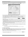
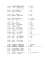
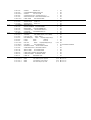
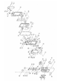
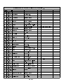
1
ALAN HP 106 SERVICE MANUAL HP106 Service Manual ALAN HP106 Portable VHF Transceiver Service Manual Copyright 2003 by CTE International Italy; all rights reserved Page 1 of 12 HP106 Service Manual Contents 1 TECHNICAL SPECIFICATIONS......................................................................................................................3 1.1 1.2 2 CIRCUIT DESCRIPTION .................................................................................................................................4 2.1 2.2 2.3 2.4 2.5 2.6 2.7 3 Test methods.................................................................................................................................................................3 Specifications table .......................................................................................................................................................3 General information.......................................................................................................................................................4 Microprocessor/control ..................................................................................................................................................4 VCO / Synthesizer (PLL) ...............................................................................................................................................4 2.3.a Temperature-Compensated Crystal Oscillator (TCXO) ..................................................................................................... 4 2.3.b Voltage-Controlled Oscillators ........................................................................................................................................... 4 2.3.c Synthesizer ........................................................................................................................................................................... 5 2.3.d Loop Filter ........................................................................................................................................................................... 5 Transmitter ....................................................................................................................................................................5 2.4.a RF Power Amplifier ............................................................................................................................................................. 5 2.4.b Antenna Switching ............................................................................................................................................................... 5 2.4.c Power control....................................................................................................................................................................... 6 2.4.d Transmitter Audio Circuits .................................................................................................................................................. 6 2.4.e Audio Processing ................................................................................................................................................................. 6 Receiver ........................................................................................................................................................................6 2.5.a Receiver Front End .............................................................................................................................................................. 6 2.5.b Local Oscillator (LO) .......................................................................................................................................................... 6 2.5.c Mixer .................................................................................................................................................................................... 6 2.5.d FM Detector and Squelch .................................................................................................................................................... 6 2.5.e Receiver Audio Circuit......................................................................................................................................................... 7 Signalling.......................................................................................................................................................................7 2.6.a General................................................................................................................................................................................. 7 2.6.b CTCSS Tone Encoder / Digital Code Squelch (DCS) Encoder .......................................................................................... 7 2.6.c Selective call ........................................................................................................................................................................ 7 2.6.d Scrambler ............................................................................................................................................................................. 7 Battery ...........................................................................................................................................................................7 ADJUSTMENTS ..............................................................................................................................................9 3.1 3.2 3.3 3.4 3.5 3.6 General..........................................................................................................................................................................9 Synthesizer/Transmitter VCO Check ............................................................................................................................9 3.2.a Frequency Adjustment ......................................................................................................................................................... 9 Transmitter Alignment ...................................................................................................................................................9 3.3.a Power Adjustment ................................................................................................................................................................ 9 3.3.b Modulation Adjustment........................................................................................................................................................ 9 3.3.c CTCSS/DCS adjustment..................................................................................................................................................... 10 3.3.d Selcal adjustment ............................................................................................................................................................... 10 Receiver Alignment .....................................................................................................................................................10 Figure 1 - Equipment Test set-up................................................................................................................................11 Figure 2 - Test adaptor................................................................................................................................................12 Page 2 of 12 HP106 Service Manual 1 TECHNICAL SPECIFICATIONS 1.1 Test methods ETS 300-086 IEC 529 IP54 and MIL STD 810 C/D/E 1.2 Specifications table Characteristic Frequency Operating Band Number of Programmable Channels Channel Spacing Frequency Steps Rated Power Supply Battery Capacity General Units Value/Measurements conditions MHz from 148 to 174 MHz 26 16 KHz 12.5 / 20 / 25 KHz 5 / 6.25 Vcc 7.5 mAh Ni-MH 1.300 Duty Cycle hours Antenna Impedance Speaker Impedance Frequency Stability Operating Temperature Range Output Power (±1 dB) Spurious Emissions 5% on TX at the maximum power 5% on RX at 60 % of the maximum rated A.F. power 90% on RX with closed squelch in power save mode Ohm 50 Ohm 8 ppm ±2.5 °C from –30 to +60 Transmitter W 1/5 from 9 KHz to 1 GHz µW from 1 to 4 GHz Modulation System Modulation Audio Distortion Maximum Deviation Adjacent Channel Power Attenuation Configuration Sensitivity (at 12 dB SINAD) Squelch Sensitivity (SINAD) Selectivity (Adjacent Channel) Spurious Response Rejection Intermodulation Hum & Noise Suppression Audio Output (1 KHz at 5% T.H.D.) Size (Battery Pack Included) Weight (Battery Pack Included) Battery Accessories Connector / Programming Moisture & Dust Resistance 8 < 0,25 <1 F3E (FM) KHz ± 2,5 / 5 5 % or less KHz ± 2.5 / 5 dB < -60 / -70 Receiver Double Conversion Superetherodyne < 0.35 µV dB 10 dB At least -65 / -75 dB > 70 dB > 65 dB < -45 / < -40 mW 400 Mechanical Specifications mm 130 x 42 x 60 g 355 Back slide battery 2.5 and 3.5 mm standard monophonic jacks According to the IEC529 and IP54 regulations Page 3 of 12 HP106 Service Manual 2 CIRCUIT DESCRIPTION 2.1 General information The HP-106 has three printed circuit boards. Circuitry is divided in the following sections: Microprocessor/Control VCO/Synthesizer Transmitter Receiver Signalling Battery Refer to the Block Diagram and the Schematics. 2.2 Microprocessor/control The microprocessor IQ9 is constantly operating when the radio is turned ON. It is continuously monitoring the keyboard, the PTT line and other internal inputs such as the squelch detect, etc. When a change occurs, the microprocessor makes the appropriate response. The microprocessor is used for control. The Radio emits a beep on channel change and the synthesizer is loaded with the correct frequency information. The microprocessor runs off a 8 MHz oscillator which is composed of IX1, IC30, IC31 and IR48. When the radio is first turned on, the microprocessor reads the radio status from the EEPROM IQ8. The microprocessor determines the receive frequency codes, then loads the synthesizer via its pins 42 (PLL LE), 46 (PLL CLK) and 43 (PLL DATA). The microprocessor is fitted with an internal program flash memory as well, therefore functions can be customised, if necessary, upon specific request from the customer. 2.3 VCO / Synthesizer (PLL) This section consists of the Temperature-Compensated Crystal Oscillator (TCXO), Voltage Controlled Oscillator(VCO), Synthesizer and the Loop Filter. 2.3.a Temperature-Compensated Crystal Oscillator (TCXO) The reference oscillator (X401) is a temperature compensated crystal- oscillator, RV402 is used to adjust the oscillator on frequency (14.4 MHz) at room temperature (22 ℃). The reference oscillator is held within the specified ±2.5 PPM from -30 to +60℃. 2.3.b Voltage-Controlled Oscillators Only one of the VCOs runs at a time, which is controlled by Q420 and IQ9. When the PTT is pressed, IQ9 pin 34 goes low (approx. 0V) disabling the receive VCO by the Q420 and biases on Q419 to enable the transmitter VCO. The receive VCO consists of C482-C485, CV401, L426-L428, and Q422-Q424. This VCO oscillates at 45.1 MHz above the programmed receive frequency. The VCO’s oscillating frequency is tuned by the varactors Q423 and Q424. The tuning voltage is supplied from the output of the Loop Filter. The output of the VCO is AC coupled (C475 and R558, C530, C505) to the synthesizer and the output buffer Q414 respectively. The transmitter VCO consists of C487, C489-C491, CV402, L424, L425, L429 and Q416-Q418. This VCO oscillates on the programmed transmit frequency. The VCO’s oscillating frequency is tuned by the varactors Q417 and Q418. The tuning voltage is supplied from the output of the Loop Filter. The output of the VCO is AC coupled (C486) to the synthesizer input buffer Q428 and the output buffer Q415 respectively. The transmit voltage controlled oscillator is directly frequency-modulated and operates on the carrier frequency. In the receive mode, the transmit VCO is disabled and the receive VCO is enabled, producing the receive local oscillator signal at a frequency 45.1 MHz below the incoming receive frequency. Page 4 of 12 HP106 Service Manual The synthesizer is tuned in 5.00 KHz or 6.25 KHz step. 2.3.c Synthesizer The frequency synthesizer is a large scale monolithic synthesizer integrated circuit Q429. The synthesizer IC contains a dual modular prescaler, programmable divide-by-N counter, prescaler control (swallow) counter, reference oscillator, reference divider, phase detector, charge pump and lock detector. Also, included in Q429 are shift registers and control circuits for frequency controls and general device control. RF output from the active VCO is AC coupled to the synthesizer Q429 prescaler input at Pin 8. The divide-by-N counter chain in Q429, consisting of the dual-modulus prescaler, swallow counter and programmable counter, divides the VCO signal down to a frequency very close to 5.00 KHz or 6.25 KHz which is applied to the phase detector. The phase comparator compares the edges of this of this signal with that of the 5.00 KHz or 6.25 KHz reference signal from the reference divider and drives the external charge pump (Q425 and Q426). The synthesizer unlock detector circuit prevents the operation of the transmitter, when the phase lock loop (PLL) is unlocked. The following discussion assumes the unit has been placed in the transmit mode. Q429 lock detector Pin 7 goes high when the PLL is locked. This high level is applied to Pin 21 of the microprocessor IQ9. A software timing routing brings the RX/TX line low (Pin 29 of IQ9), feeding this signal through the switch/buffer IQ15. With the RX/TX line low, Q223A is cut off and Q223B is biases on passing +5VTX to Q431B, it biases on Q430 to pass switched TX B+ to the transmitter amplifier string which enables transmission. When the PLL become unlocked, the lock detector at Q429 Pin7 will begin pulsing low. A RC circuit converts pulsing low to a low level for the microprocessor. The microprocessor then changes the RX/TX line to a high, thus signalling the other transistor switches to drive Q430 into cutoff which disable transmission. Therefore, the transmitter remains disabled while the loop remains out of lock. 2.3.d Loop Filter The Loop Filter, a passive lead-lag filter consisting of R461-R464 and C493-C495, integrates the charge pump output to produce the DC turning voltage for the VCO. One parasitic pole, consisting of R461/C493 and RF chokes L428/L429, prevent modulation of the VCOs by the 5.00 KHz or 6.25 KHz reference energy remaining at the output of the loop filter. Direct FM is obtained for modulating frequencies outside the PLL bandwidth by applying the CTCSS/DCS signals and the pre-emphasized, limited microphone audio to the VCO modulation circuit. The modulation circuit consists of R452, Q421 and C487. 2.4 2.4.a Transmitter RF Power Amplifier After the PTT is pressed, the +5VTX line switches to approximately 5V. Q419 is turned on enabling transmit VCO. The VCO buffer, pre-driver, driver and power amplifier are biased on by Q430, which is biased on by the +5VTX line switching to 5V. RF output from the transmit VCO(Q416) is applied to the VCO output buffer Q415. Output from Q415 feeds the pre-driver amplifier Q413. The output signal from Q413 feeds the driver amplifier Q412, whose output from the driver stage feeds the final RF power amplifier Q407 to produce the rated output power of 2 watts. The output of the final is applied to a low-pass filter(C451, C452 and L413) and then to the transmit/receive switch Q402. RF power is then fed to the antenna via the output low-pass filter consisting of C401,C403, C405-C408, L401, and L402. 2.4.b Antenna Switching Switching of the antenna between the transmitter and the receiver is accomplished by the antenna transmit/receive switch consisting of diodes Q401 and Q402 in conjunction with C410 and R402. In the transmit mode, switched TX B+ is applied through R420 and RF choke L414,hard forward biasing the two diodes on. Q402 thus permits the flow of RF power from output of the low-pass filter fed by the output amplifier to the output lowpass filter. Q401 shorts the receiver input to C410, which is AC coupled to ground. L403, C409, C410 and R402 then function as a lumped constant quarter-wave transmission line, thus presenting a high impedance to the RF output path, effectively isolating the receiver input and transmitter output sections. Page 5 of 12 HP106 2.4.c Service Manual Power control Output power is controlled via the dual Op-Amp (Q408) , which is used as a differential amplifier and comparator. Current is sensed by the voltage drop across R421 and R422. This voltage is compared to the one set by the 2watt Adjustment RV401. The power output is then reduced or increased by varying the Q410's output voltage applied to the power amplifier Q407's pin 2. 2.4.d Transmitter Audio Circuits The transmitter audio circuits consist of the audio processing circuits, the CTCSS circuits and the DCS circuits. 2.4.e Audio Processing Transmit speed audio is providing by either the internal electric microphone N101 or the external microphone. The microphone audio is applied to MIC MUTE SW Q235, and Lo-pass filter Q214A, Q214B. The audio is pre emphasized by 6dB per octave by C236 and R284, and then signal amplification. The gain is such that when a signal greater than 20 dB. Limiting the peak-to-peak output. Under these conditions, the MOD. ADJ. Pot RV201 configured as a four-pole active low-pass filter. The resulting signal is then limited when respect to side band splatter, and has an 18 dB per octave roll-off above 3 KHz. The audio is then applied through the 25 KHz/12.5 KHz channel spacing SW Q215 to transmit VCO. By varying the voltage on the varactor diode Q921 at an audio rate. The resonant frequency of VCO is varied. The result is an oscillator output that is frequency -modulated at the audio frequency. 2.5 2.5.a Receiver Receiver Front End In the receive mode, the RF signal enters thorough the antenna, then through the low-pass filter C401, C403, C405-C409 and L401-L403. The diodes Q401 and Q402 are biased off so that the output of the low-pass filter is coupled (C411) to the first band-pass filter C412-C415, C417-C420, L404-L407 and to the Front End RF overload protection diode pair Q403. The signal from the band-pass filter is applied to the input of the RF amplifier Q404. The output of the RF amplifier feeds the input to three more stages of band-pass filters consisting of C424-C431, and L408-L410. The output from the band-pass filter is applied to the mixer’s Q405/L411. 2.5.b Local Oscillator (LO) The Receive VCO (C482-C485, CV401, L426-L427, Q422-Q424 and R453-R454) provides the LO signal. The VCO is running at 45.1 MHz above the desired receive frequency and is applied to output Buffer Q415/Q414. The output of the buffer through the low-pass filter C433-C435, L432-L433 and applied to the mixer Q405/L411/L412. 2.5.c Mixer The mixer is a DBM type (L411,Q405,L412). The mixer LO frequency is 45.1 MHz below the desired receiver frequency. When the receiver frequency is present, the mixer output will be a 45.1MHz signal. The mixer output is peaked for 45.1MHz at L434, C437 and R413, and the signal is filtered by crystal filter F401A and F401B and amplified by Q406 before being applied to the input of the IF IC IC6. Inside IC6, the 45.1MHz IF signal becomes the input to a second mixer with a LO frequency of 44.645 MHz set by X201. The 455 KHz ceramic filter F201 or F202 filters the second mixer’s output which is the second IF signal. The mixer’s output is then fed to the internal limiting amplifier and then on to the FM decoder. 2.5.d FM Detector and Squelch The FM detector output is used for squelch, decoding tones and audio output. The setting of the squelch adjustment potentiometer RV204 (for 25 KHz channel spacing) and RV205 (for 12.5 KHz channel spacing) sets the input to the squelch amplifier. The squelch amplifier is internal to IC6 and its output is fed to an internal rectifier and squelch detector. Page 6 of 12 HP106 Service Manual The output on IC6 Pin 14 signals the microprocessor IQ9 with a low level (~0V) to unmute the radio. The audio is unmuted by the microprocessor IQ9 Pin 27 switching to a high value (~5V on SQL MUTE) thus biasing on Q206. The audio is then routed to the audio amplifier Q221 via the volume control S201. 2.5.e Receiver Audio Circuit The detector’s audio output also is fed to the tone(CTCSS and DCS) low-pass filter Q212C. Then the output of the low-pass filter is routed to the second stage filter Q212B. The output of Q210B is applied to the squaring circuit Q212A and finally to the microprocessor IQ9 Pin 60 for decoding. Another branching of the detector output feeds the audio high-pass filter Q208 via Q212D. The output of the audio high-pass filter feeds the Volume Control S201(VOL). From the wiper arm on the Volume Control, the audio is routed to Pin 2, the input to the audio power amplifier Q221. The output of the audio power amplifier is routed through the earphone jack J401 to the internal speaker E101. 2.6 2.6.a Signalling General The microprocessor is fitted with a ADC/DAC converter built-in, so it provides generating and decoding the tones for selective calls, CTCSS and DCS. It can do that without using any other external ICs, but only by means of some transistors. The deviation of the selective call can be adjusted by the trimmer IRV1. The microprocessor manages the analogue switches for the scrambler as well, which is base-band-inversion type. 2.6.b CTCSS Tone Encoder / Digital Code Squelch (DCS) Encoder CTCSS signals and DCS signals are synthesized by microprocessor IQ9 and appear as pulse waveform on I/O line at Pin 39. This I/O line is a pseudo-sine wave for CTCSS or a DCS pseudo-waveform and is applied to the transistor IQ5 which makes the signals closer to the theoretic CTCSS/DCS signals. The waveform is then smoothed by low pass filters Q213B to produce an acceptable sine wave output. The CTCSS tone signal is adjust to the proper level by RV202. The DCS signal is adjust to the proper balance by RV203. The signal is then applied to the audio processing circuit at R305 and to the TCXO circuit at X401. 2.6.c Selective call Similarly to CTCSS/DCS, selcal signals are also generated and decoded by the microprocessor IQ9. The selcal decode input is the pin 59 (ADC_SELCALL), whilst the TX tones are generated at pin 37 (SELCALL_PWM), then fed to the transistor IQ4 and associated circuitry which provides to amplify and smooth the tones in order to make them suitable for the modulator. IRV1 adjusts the level (deviation) of the tones. 2.6.d Scrambler It’s a classic “baseband inversion” scrambler which inverts the audio baseband (300-30000 Hz). The audio baseband AFTX_IN is mixed with a fixed tone (1300 Hz) SCRMBLR_CLK generated by the microprocessor IQ9. The mixer’s output AFTX_OUT is a scrambled baseband which sounds garbled (not understandable) by normal receivers. However, if the receiver is equipped with the same kind of scrambler which is properly set on the same fixed tone, the received scrambled baseband is fed in the RX mixer which provides a complementary process obtaining a clear (understandable) baseband at its output. If fact if the scrambled transmission is received by the party’s HPx06 (with scrambled activated), the scrambled baseband AFRX is fed to the scrambler unit and mixed with the same tone generated by the microprocessor. The output of the mixer AFRX_OUT is a normal (unscrambled) baseband and can be clearly heard. As you can see, the over stated fixed audio tone acts as a encoding/decoding key, so it must be the same both at the TX and RX parties. As already stated, the standard version of HPx06 is fitted with a 1300 Hz encoding/decoding key, however a different tone can be required. 2.7 Battery The battery connects to the contact pins(CN201 and CN202) on the bottom end of the Radio. The positive terminal of the battery connects to the ON/OFF Volume Control switch (S201) and the negative terminal connects to chassis ground. Low battery sense R101/R102, voltage regulator Q222 and transmit power module Q407. Page 7 of 12 HP106 Service Manual The battery voltage status is monitored by the microprocessor IQ9 Pin 61 which senses the battery voltage through the BATT+SW line by means of IR51/IR49. When the battery voltage is approximately 5.8V, the microprocessor considers the battery discharged and switches off the circuits of the radio. When the Radio is on a channel with no tone programmed, the BATTERY SAVER Mode is enabled when programmed. In the BATTERY SAVER mode, the microprocessor IQ9 generates a square wave signal at Pin 48 which is applied to the inverter IQ10:6. The signal’s duty cycle varies according to what the POWER SAVE TIMER is set. When the microprocessor IQ9 Pin 48 goes high (approx. 5 V) Q226 (receiver module) is biased off, Q225 is biased on, Q224A is cut off, and Q223A is cut off, thus turning the supply off to IC6. Page 8 of 12 HP106 Service Manual 3 ADJUSTMENTS 3.1 General For proper alignment, the unit should be programmed with the following channel and frequency information Channel number CH 1 CH 2 CH 3 CH 4 CH 5 Receive Frequency (MHz) 174.050 163.050 163.050 163.050 163.050 Transmit Frequency (MHz) 174.025 163.025 163.050 163.050 163.025 RX/TX Tone Code NO TONE NO TONE 100Hz TONE 627 DCS CODE NO TONE Channel Spacing (KHz) 25 25 25 25 12.5 Make connections to the Unit per Figure 1 (Equipment Test Set-up) below and Figure 2 (Test Adapter). For the location of the components called out in these procedures, refer to RF Board and SUB Board. 3.2 Synthesizer/Transmitter VCO Check NOTE: VCO check must be accomplished before proceeding with the Transmitter and/or Receiver Alignment. 1) Connect the voltmeter to TP6. 2) Place the unit on channel 1 (174.050MHz. RX; 174.025MHz, TX). 3) Tune CV401 in Receive mode for 4.90V ± 0.05V at TP6. 4) Push the PTT switch (TX) and tune CV402 for 4.30V ± 0.05V at TP6. 3.2.a Frequency Adjustment 1) Connect the Radio in accordance with Figure 1. 2) Place the unit on channel 1 (174.050MHz, RX; 174.025MHz, TX). 3) Operate the transmitter and adjust RV402 for a Frequency Counter reading within ± 50Hz of the programmed transmit frequency. 3.3 Transmitter Alignment NOTE: In order to obtain proper transmission output power, connect the Radio to the power supply with a cable that is rated to withstand a current of 2 amperes or greater. 3.3.a Power Adjustment 1) Connect the Radio in accordance with Figure 1. 2) Place the radio on the channel 2 (163.050MHz, RX; 163.025MHz. TX). 3) Place the unit in HIGH POWER mode. 4) Turn RV401 and RV405 fully clockwise. 5) Operate the transmitter, using TA-S1, to make sure that the maximum RF output power reading on the wattmeter is 5.5 W or greater. 6) Adjust RV401 (HI PWR ADJ) for a reading of 5.0 W ±0.1 W. Check to make sure that the transmit current is within 1000 1400 mA after the adjustment has been made. 7) Place the unit in the LOW POWER mode. 8) Adjust RV405 (LO PWR ADJ) for a reading of 1.0 W ±0.1 W. Check to make sure that the transmit current is within 500 700 mA after the adjustment has been made. 3.3.b Modulation Adjustment 1) Connect the Radio in accordance with Figure 1. 2) Place the Radio on channel 2 (163.050MHz, RX; 163.025MHz, TX). 3) Apply a 1 KHz tone signal to Test Adapter's AF Input (Figure 2), which is the microphone impedance matching network. 4) Plug the Test Adapter into the external speaker/microphone jack. Page 9 of 12 HP106 Service Manual 5) Set the audio generator's output level at approximate 300mVrms at TPA of the Test adapter. 6) Operate the transmitter, using TA-S1, and adjust RV201(MOD.ADJ) for ±4.0 KHz deviation. 3.3.c CTCSS/DCS adjustment 7) To adjust CTCSS and DCS Deviation, perform step1 though 6 above. Then set the FM liner detector audio bandwidth of 0.25 Hz or less to15,000 Hz or more. Turn the de-emphasis function off. 8) Place the Radio on channel 4 (163.050MHz. TX; 627 DCS CODE). Set the audio generator output to 0V operate the transmitter, using TA-S1 and adjust the DCS balance control RV203 to U1-U2 is minimum on the Oscilloscope. 9) Place the Radio on channel 3 (163.050MHz, TX; 100Hz Tone). Operate the transmitter using TA-S1, and adjust RV202 to ±800Hz deviation on Modulation Analyzer. 3.3.d Selcal adjustment 10) Set up a selcall sequence which includes, at least, an hi-pitched tone and a tone length of 1 second minimum (in order to allow a convenient deviation check) 11) Send the selcal by keeping pressed the MON or FUNC keys and adjust RV1 in order to obtain the following minimum /maximum deviation according to the channel bandwidth: For 12.5 KHz channel bandwidth - min ±1.5 KHz / max ±2.5 KHz For 25 KHz channel bandwidth - min ±2.5 KHz / max ±3 KHz 3.4 Receiver Alignment 1) Connect the Radio in accordance with Figure 1. 2) Place the Radio on the channel 2 (163.050MHz, RX; 163.025MHz, TX). 3) Adjust the Squelch Control RV204 until the BUSY LED (Green) turns ON. 4) Apply the RF generator signal with 1 KHz tone at 3 KHz deviation so that the tone can be heard in the speaker. 5) Adjust the volume control for the rated audio. 6) Set the RF signal generator's level obtain a 9dB SINAD reading. 7) Adjust RV204 (Squelch control) counter clockwise slowly just until the BUSY LED goes out. 8) Adjust RV204 clockwise slowly just until the BUSY LED goes ON. 9) Place the radio on the channel 5 (163.050MHz, RX; 163.025MHz, TX). 10) Adjust the squelch control RV205 until the BUSY LED (Green) turns ON. 11) Apply the RF generator signal with 1 KHz tone at 1.5 KHz deviation so that the tone can be heard in the speaker. 12) Ad just the volume control for the rated audio. 13) Set the RF signal generator's level obtain 9dB SINAD reading. 14) Adjust RV205 counter clockwise slowly just the BUSY LED goes on. 15) Ad just RV205 clockwise slowly just until the BUSY LED goes on. Page 10 of 12 HP106 3.5 Service Manual Figure 1 - Equipment Test set-up Test Set-Up Legend 1) HP-105 2) 7.5VDC Supply (3 A) 3) 3 Amp DC Ammeter 4) AC Voltmeter 5) Distortion Meter 6) Test Adapter (Figure 2) 7) Audio Signal Generator (600 Ohm) 8) RF Signal Generator 9) Wattmeter - 10W 10) 30 dB Attenuator 11) UHF Frequency Counter 12) FM Linear Detector 13) Spectrum Analyzer 14) Digital Voltmeter 15) Oscilloscope Page 11 of 12 HP106 3.6 Service Manual Figure 2 - Test adaptor Page 12 of 12 HP406 Service Manual ALAN HP406 Portable VHF Transceiver Service Manual Copyright Ó 2003 by CTE International Italy; all rights reserved Page 1 of 12 HP406 Service Manual Contents 1 2 3 TECHNICAL SPECIFICATIONS .....................................................................................................................3 1.1 1.2 Test methods ............................................................................................................................................................3 Specifications table ...................................................................................................................................................3 2.1 2.2 2.3 General information...................................................................................................................................................4 Microprocessor/control ..............................................................................................................................................4 VCO / Synthesizer (PLL) ...........................................................................................................................................4 2.4 Transmitter................................................................................................................................................................5 2.5 Receiver....................................................................................................................................................................6 2.6 Signalling ..................................................................................................................................................................7 2.7 Battery.......................................................................................................................................................................8 3.1 3.2 General .....................................................................................................................................................................9 Synthesizer/Transmitter VCO Check.........................................................................................................................9 3.3 Transmitter Alignment ...............................................................................................................................................9 3.4 3.5 3.6 Receiver Alignment .................................................................................................................................................10 Figure 1 - Equipment Test set-up ............................................................................................................................11 Figure 2 - Test adaptor............................................................................................................................................12 CIRCUIT DESCRIPTION .................................................................................................................................4 2.3.a 2.3.b 2.3.c 2.3.d Temperature-Compensated Crystal Oscillator (TCXO) ..................................................................................................4 Voltage-Controlled Oscillators .......................................................................................................................................4 Synthesizer.......................................................................................................................................................................5 Loop Filter.......................................................................................................................................................................5 2.4.a 2.4.b 2.4.c 2.4.d 2.4.e RF Power Amplifier.........................................................................................................................................................5 Antenna Switching ...........................................................................................................................................................5 Power control ..................................................................................................................................................................6 Transmitter Audio Circuits ..............................................................................................................................................6 Audio Processing.............................................................................................................................................................6 2.5.a 2.5.b 2.5.c 2.5.d 2.5.e Receiver Front End..........................................................................................................................................................6 Local Oscillator (LO) ......................................................................................................................................................6 Mixer................................................................................................................................................................................6 FM Detector and Squelch................................................................................................................................................6 Receiver Audio Circuit ....................................................................................................................................................7 2.6.a 2.6.b 2.6.c 2.6.d General ............................................................................................................................................................................7 CTCSS Tone Encoder / Digital Code Squelch (DCS) Encoder .......................................................................................7 Selective call....................................................................................................................................................................7 Scrambler ........................................................................................................................................................................7 ADJUSTMENTS ..............................................................................................................................................9 3.2.a Frequency Adjustment .....................................................................................................................................................9 3.3.a 3.3.b 3.3.c 3.3.d Power Adjustment............................................................................................................................................................9 Modulation Adjustment ...................................................................................................................................................9 CTCSS/DCS adjustment ................................................................................................................................................10 Selcal adjustment...........................................................................................................................................................10 Page 2 of 12 HP406 Service Manual 1 TECHNICAL SPECIFICATIONS 1.1 Test methods § § ETS 300-086 IEC 529 IP54 and MIL STD 810 C/D/E 1.2 Specifications table Characteristic General Units Value/Measurements conditions Duty Cycle hours Frequency Operating Band Number of Programmable Channels Channel Spacing Frequency Steps Rated Power Supply Battery Capacity MHz MHz KHz KHz Vcc mAh from 440 to 470 30 16 12.5 / 20 / 25 5 / 6.25 7.5 Ni-MH 1.300 5% on TX at the maximum power 5% on RX at 60 % of the maximum rated A.F. power 90% on RX with closed squelch in power save mode Antenna Impedance Speaker Impedance Frequency Stability Operating Temperature Range Ohm Ohm ppm °C Output Power (±1 dB) Spurious Emissions W mW Modulation System Modulation Audio Distortion Maximum Deviation Adjacent Channel Power Attenuation KHz KHz dB Configuration Sensitivity (at 12 dB SINAD) Squelch Sensitivity (SINAD) Selectivity (Adjacent Channel) Spurious Response Rejection Intermodulation Hum & Noise Suppression Audio Output (1 KHz at 5% T.H.D.) Double Conversion Superetherodyne < 0.35 dB 10 dB At least -65 / -75 dB > 70 dB > 65 dB < -45 / < -40 mW 400 Size (Battery Pack Included) Weight (Battery Pack Included) Battery Accessories Connector / Programming Moisture & Dust Resistance 8 50 8 ±2.5 from –30 to +60 Transmitter 1/5 from 9 KHz to 1 GHz from 1 to 4 GHz F3E (FM) < 0,25 <1 ± 2,5 / 5 5 % or less ± 2.5 / 5 < -60 / -70 Receiver mV Mechanical Specifications mm g - 130 x 42 x 60 355 Back slide battery 2.5 and 3.5 mm standard monophonic jacks According to the IEC529 and IP54 regulations Page 3 of 12 HP406 Service Manual 2 CIRCUIT DESCRIPTION 2.1 General information The HP-406 has three printed circuit boards. Circuitry is divided in the following sections: § § § § § § Microprocessor/Control VCO/Synthesizer Transmitter Receiver Signalling Battery Refer to the Block Diagram and the Schematics. 2.2 Microprocessor/control The microprocessor IQ9 is constantly operating when the radio is turned ON. It is continuously monitoring the keyboard, the PTT line and other internal inputs such as the squelch detect, etc. When a change occurs, the microprocessor makes the appropriate response. The microprocessor is used for control. The Radio emits a beep on channel change and the synthesizer is loaded with the correct frequency information. The microprocessor runs off a 8 MHz oscillator which is composed of X1, C30, C31 and R48. When the radio is first turned on, the microprocessor reads the radio status from the EEPROM Q8. The microprocessor determines the receive frequency codes, then loads the synthesizer via its pins 42 (PLL LE), 46 (PLL CLK) and 43 (PLL DATA). The microprocessor is fitted with an internal program flash memory as well, therefore functions can be customised, if necessary, upon specific request from the customer. 2.3 VCO / Synthesizer (PLL) This section consists of the Temperature-Compensated Crystal Oscillator (TCXO), Voltage Controlled Oscillator(VCO), Synthesizer and the Loop Filter. 2.3.a Temperature-Compensated Crystal Oscillator (TCXO) The reference oscillator (X401) is a temperature compensated crystal- oscillator, RV402 is used to adjust the oscillator on frequency (14.4 MHz) at room temperature (22 ). The reference oscillator is held within the specified ±2.5 PPM from -30 to +60. 2.3.b Voltage-Controlled Oscillators Only one of the VCOs runs at a time, which is controlled by Q420 and Q17. When the PTT is pressed, Q17 pin 34 goes low (approx. 0V) disabling the receive VCO by the Q420 and biases on Q919 to enable the transmitter VCO. The receive VCO consists of C482-C485, CV901, L926-L928, and Q922-Q923. This VCO oscillates at 45.1 MHz above the programmed receive frequency. The VCO’s oscillating frequency is tuned by the varactors Q923 . The tuning voltage is supplied from the output of the Loop Filter. The output of the VCO is AC coupled (C475 and R558, C530, C505) to the synthesizer and the output buffer Q414 respectively. The transmitter VCO consists of C984, C980-C982, CV902, L924, L925, L929 and Q916-Q917. This VCO oscillates on the programmed transmit frequency. The VCO’s oscillating frequency is tuned by the varactors Q917 . The tuning voltage is supplied from the output of the Loop Filter. The output of the VCO is AC coupled (C486) to the synthesizer input buffer Q428 and the output buffer Q415 respectively. The transmit voltage controlled oscillator is directly frequency-modulated and operates on the carrier frequency. In the receive mode, the transmit VCO is disabled and the receive VCO is enabled, producing the receive local oscillator signal at a frequency 45.1 MHz below the incoming receive frequency. Page 4 of 12 HP406 Service Manual The synthesizer is tuned in 5.00 KHz or 6.25 KHz step. 2.3.c Synthesizer The frequency synthesizer is a large scale monolithic synthesizer integrated circuit Q429. The synthesizer IC contains a dual modular prescaler, programmable divide-by-N counter, prescaler control (swallow) counter, reference oscillator, reference divider, phase detector, charge pump and lock detector. Also, included in Q429 are shift registers and control circuits for frequency controls and general device control. RF output from the active VCO is AC coupled to the synthesizer Q429 prescaler input at Pin 8. The divide-by-N counter chain in Q429, consisting of the dual-modulus prescaler, swallow counter and programmable counter, divides the VCO signal down to a frequency very close to 5.00 KHz or 6.25 KHz which is applied to the phase detector. The phase comparator compares the edges of this of this signal with that of the 5.00 KHz or 6.25 KHz reference signal from the reference divider and drives the external charge pump (Q425 and Q426). The synthesizer unlock detector circuit prevents the operation of the transmitter, when the phase lock loop (PLL) is unlocked. The following discussion assumes the unit has been placed in the transmit mode. Q429 lock detector Pin 7 goes high when the PLL is locked. This high level is applied to Pin 21 of the microprocessor Q17. A software timing routing brings the RX/TX line low (Pin 29 of Q17), feeding this signal through the switch/buffer Q15. With the RX/TX line low, Q223A is cut off and Q223B is biases on passing +5VTX to Q431B, it biases on Q430 to pass switched TX B+ to the transmitter amplifier string which enables transmission. When the PLL become unlocked, the lock detector at Q429 Pin7 will begin pulsing low. A RC circuit converts pulsing low to a low level for the microprocessor. The microprocessor then changes the RX/TX line to a high, thus signalling the other transistor switches to drive Q430 into cutoff which disable transmission. Therefore, the transmitter remains disabled while the loop remains out of lock. 2.3.d Loop Filter The Loop Filter, a passive lead-lag filter consisting of R461-R464 and C493-C495, integrates the charge pump output to produce the DC turning voltage for the VCO. One parasitic pole, consisting of R461/C493 and RF chokes L928/L929, prevent modulation of the VCOs by the 5.00 KHz or 6.25 KHz reference energy remaining at the output of the loop filter. Direct FM is obtained for modulating frequencies outside the PLL bandwidth by applying the CTCSS/DCS signals and the pre-emphasized, limited microphone audio to the VCO modulation circuit. The modulation circuit consists of R952, Q921 and C987. 2.4 Transmitter 2.4.a RF Power Amplifier After the PTT is pressed, the +5VTX line switches to approximately 5V. Q919 is turned on enabling transmit VCO. The VCO buffer, pre-driver, driver and power amplifier are biased on by Q430, which is biased on by the +5VTX line switching to 5V. RF output from the transmit VCO(Q916) is applied to the VCO output buffer Q915. Output from Q415 feeds the pre-driver amplifier Q413. The output signal from Q413 feeds the driver amplifier Q412, whose output from the driver stage feeds the final RF power amplifier Q407 to produce the rated output power of 2 watts. The output of the final is applied to a low-pass filter(C451, C452 and L413) and then to the transmit/receive switch Q402. RF power is then fed to the antenna via the output low-pass filter consisting of C401,C402, C404-C405,C407-C408,L401, and L402. 2.4.b Antenna Switching Switching of the antenna between the transmitter and the receiver is accomplished by the antenna transmit/receive switch consisting of diodes Q401 and Q402 in conjunction with C410 and R402. In the transmit mode, switched TX B+ is applied through R420 and RF choke L414,hard forward biasing the two diodes on. Q402 thus permits the flow of RF power from output of the low-pass filter fed by the output amplifier to the output low-pass filter. Q401 shorts the receiver input to C410, which is AC coupled to ground. L403, C409, C410 and R402 then function as a lumped constant quarter-wave transmission line, thus presenting a high impedance to the RF output path, effectively isolating the receiver input and transmitter output sections. Page 5 of 12 HP406 2.4.c Service Manual Power control Output power is controlled via the dual Op-Amp (Q408) , which is used as a differential amplifier and comparator. Current is sensed by the voltage drop across R421A and R422. This voltage is compared to the one set by the 2watt Adjustment RV401. The power output is then reduced or increased by varying the Q410's output voltage applied to the power amplifier Q407's pin 2. 2.4.d Transmitter Audio Circuits The transmitter audio circuits consist of the audio processing circuits, the CTCSS circuits and the DCS circuits. 2.4.e Audio Processing Transmit speed audio is providing by either the internal electric microphone N101 or the external microphone. The microphone audio is applied to MIC MUTE SW Q235, and Lo-pass filter Q214A, Q214B. The audio is pre emphasized by 6dB per octave by C236 and R284, and then signal amplification. The gain is such that when a signal greater than 20 dB. Limiting the peak-to-peak output. Under these conditions, the MOD. ADJ. Pot RV201 configured as a four-pole active low-pass filter. The resulting signal is then limited when respect to side band splatter, and has an 18 dB per octave roll-off above 3 KHz. The audio is then applied through the 25 KHz/12.5 KHz channel spacing SW Q215 to transmit VCO. By varying the voltage on the varactor diode D921 at an audio rate. The resonant frequency of VCO is varied. The result is an oscillator output that is frequency -modulated at the audio frequency. 2.5 Receiver 2.5.a Receiver Front End In the receive mode, the RF signal enters thorough the antenna, then through the low-pass filter, C404-C409 and L401-L402. The diodes Q401 and Q402 are biased off so that the output of the low-pass filter is coupled (C411) to the first band-pass filter C811-C818, C822, L404-L407 and to the Front End RF overload protection diode pair D9. The signal from the band-pass filter is applied to the input of the RF amplifier Q804. The output of the RF amplifier feeds the input to three more stages of band-pass filters consisting of C826-C839, and L804-L808, L411. The output from the band-pass filter is applied to the mixer’s Q405/L411. 2.5.b Local Oscillator (LO) The Receive VCO (C989-C991, CV901, L926-L928, Q922, Q923, Q919 and R953) provides the LO signal. The VCO is running at 45.1 MHz above the desired receive frequency and is applied to output Buffer Q915/Q414. The output of the buffer through the low-pass filter C433-C435, L432-L433 and applied to the mixer Q405/L411/L412. 2.5.c Mixer The mixer is a DBM type (L411,Q405,L412). The mixer LO frequency is 45.1 MHz below the desired receiver frequency. When the receiver frequency is present, the mixer output will be a 45.1MHz signal. The mixer output is peaked for 45.1MHz at L434, C437 and R413, and the signal is filtered by crystal filter F401A and F401B and amplified by Q406 before being applied to the input of the IF IC IC6. Inside IC6, the 45.1MHz IF signal becomes the input to a second mixer with a LO frequency of 44.645 MHz set by X201. The 455 KHz ceramic filter F201 or F202 filters the second mixer’s output which is the second IF signal. The mixer’s output is then fed to the internal limiting amplifier and then on to the FM decoder. 2.5.d FM Detector and Squelch The FM detector output is used for squelch, decoding tones and audio output. The setting of the squelch adjustment potentiometer RV204 (for 25 KHz channel spacing) and RV205 (for 12.5 KHz channel spacing) sets the input to the squelch amplifier. The squelch amplifier is internal to IC6 and its output is fed to an internal rectifier and squelch detector. Page 6 of 12 HP406 Service Manual The output on IC6 Pin 14 signals the microprocessor Q17 with a low level (0V) to unmute the radio. The audio is unmuted by the microprocessor Q17 Pin 27 switching to a high value (5V on SQL MUTE) thus biasing on Q206. The audio is then routed to the audio amplifier Q221 via the volume control S201. 2.5.e Receiver Audio Circuit The detector’s audio output also is fed to the tone(CTCSS and DCS) low-pass filter Q212C. Then the output of the low-pass filter is routed to the second stage filter Q212B. The output of Q210B is applied to the squaring circuit Q212A and finally to the microprocessor Q17 Pin 60 for decoding. Another branching of the detector output feeds the audio high-pass filter Q208 via Q212D. The output of the audio high-pass filter feeds the Volume Control S201(VOL). From the wiper arm on the Volume Control, the audio is routed to Pin 2, the input to the audio power amplifier Q221. The output of the audio power amplifier is routed through the earphone jack J101 to the internal speaker E101. 2.6 Signalling 2.6.a General The microprocessor is fitted with a ADC/DAC converter built-in, so it provides generating and decoding the tones for selective calls, CTCSS and DCS. It can do that without using any other external ICs, but only by means of some transistors. The deviation of the selective call can be adjusted by the trimmer RV1. The microprocessor manages the analogue switches for the scrambler as well, which is base-band-inversion type. 2.6.b CTCSS Tone Encoder / Digital Code Squelch (DCS) Encoder CTCSS signals and DCS signals are synthesized by microprocessor Q17 and appear as pulse waveform on I/O line at Pin 39. This I/O line is a pseudo-sine wave for CTCSS or a DCS pseudo-waveform and is applied to the transistor IQ5 which makes the signals closer to the theoretic CTCSS/DCS signals. The waveform is then smoothed by low pass filters Q213B to produce an acceptable sine wave output. The CTCSS tone signal is adjust to the proper level by RV202. The DCS signal is adjust to the proper balance by RV203. The signal is then applied to the audio processing circuit at R305 and to the TCXO circuit at X401. 2.6.c Selective call Similarly to CTCSS/DCS, selcal signals are also generated and decoded by the microprocessor Q17. The selcal decode input is the pin 59 (ADC_SELCALL), whilst the TX tones are generated at pin 37 (SELCALL_PWM), then fed to the transistor Q4 and associated circuitry which provides to amplify and smooth the tones in order to make them suitable for the modulator. RV1 adjusts the level (deviation) of the tones. 2.6.d Scrambler It’s a classic “baseband inversion” scrambler which inverts the audio baseband (300-30000 Hz). The audio baseband AFTX_IN is mixed with a fixed tone (1300 Hz) SCRMBLR_CLK generated by the microprocessor Q17. The mixer’s output AFTX_OUT is a scrambled baseband which sounds garbled (not understandable) by normal receivers. However, if the receiver is equipped with the same kind of scrambler which is properly set on the same fixed tone, the received scrambled baseband is fed in the RX mixer which provides a complementary process obtaining a clear (understandable) baseband at its output. If fact if the scrambled transmission is received by the party’s HPx06 (with scrambled activated), the scrambled baseband AFRX is fed to the scrambler unit and mixed with the same tone generated by the microprocessor. The output of the mixer AFRX_OUT is a normal (unscrambled) baseband and can be clearly heard. As you can see, the over stated fixed audio tone acts as a encoding/decoding key, so it must be the same both at the TX and RX parties. As already stated, the standard version of HPx06 is fitted with a 1300 Hz encoding/decoding key, however a different tone can be required. Page 7 of 12 HP406 Service Manual 2.7 Battery The battery connects to the contact pins(CN201 and CN202) on the bottom end of the Radio. The positive terminal of the battery connects to the ON/OFF Volume Control switch (S201) and the negative terminal connects to chassis ground. Low battery sense R101/R102, voltage regulator Q222 and transmit power module Q407. The battery voltage status is monitored by the microprocessor Q17 Pin 61 which senses the battery voltage through the BATT+SW line by means of R51/R49. When the battery voltage is approximately 5.8V, the microprocessor considers the battery discharged and switches off the circuits of the radio. When the Radio is on a channel with no tone programmed, the BATTERY SAVER Mode is enabled when programmed. In the BATTERY SAVER mode, the microprocessor Q17 generates a square wave signal at Pin 48 which is applied to the inverter Q10-F. The signal’s duty cycle varies according to what the POWER SAVE TIMER is set. When the microprocessor Q17 Pin 48 goes high (approx. 5 V) Q226 (receiver module) is biased off, Q225 is biased on, Q224A is cut off, and Q223A is cut off, thus turning the supply off to IC6. Page 8 of 12 HP406 Service Manual 3 ADJUSTMENTS 3.1 General For proper alignment, the unit should be programmed with the following channel and frequency information Channel number CH 1 CH 2 CH 3 CH 4 CH 5 Receive Frequency (MHz) 469.950 455.050 455.050 455.050 455.050 Transmit Frequency (MHz) 469.975 455.075 455.075 455.075 455.075 RX/TX Tone Code NO TONE NO TONE 100Hz TONE 627 DCS CODE NO TONE Channel Spacing (KHz) 25 25 25 25 12.5 Make connections to the Unit per Figure 1 (Equipment Test Set-up) below and Figure 2 (Test Adapter). For the location of the components called out in these procedures, refer to RF Board and SUB Board. 3.2 Synthesizer/Transmitter VCO Check 2 NOTE: VCO check must be accomplished before proceeding with the Transmitter and/or Receiver Alignment. 1) Connect the voltmeter to TP6. 2) Place the unit on channel 1 (469.975MHz. RX; 469.950MHz, TX). 3) Tune CV401 in Receive mode for 4.50V ± 0.05V at TP6. 4) Push the PTT switch (TX) and tune CV402 for 4.50V ± 0.05V at TP6. 3.2.a Frequency Adjustment 1) Connect the Radio in accordance with Figure 1. 2) Place the unit on channel 1 (469.950MHz, RX; 469.975MHz, TX). 3) Operate the transmitter and adjust RV402 for a Frequency Counter reading within ± 50Hz of the programmed transmit frequency. 3.3 Transmitter Alignment 2 NOTE: In order to obtain proper transmission output power, connect the Radio to the power supply with a cable that is rated to withstand a current of 2 amperes or greater. 3.3.a Power Adjustment 3.3.b Modulation Adjustment 1) 2) 3) 4) 5) Connect the Radio in accordance with Figure 1. Place the radio on the channel 2 (455.050MHz, RX; 455.075MHz. TX). Place the unit in HIGH POWER mode. Turn RV401 and RV405 fully clockwise. Operate the transmitter, using TA-S1, to make sure that the maximum RF output power reading on the wattmeter is 5.5 W or greater. 6) Adjust RV401 (HI PWR ADJ) for a reading of 4.0 W ±0.2 W. Check to make sure that the transmit current is within 1000 1400 mA after the adjustment has been made. 7) Place the unit in the LOW POWER mode. 8) Adjust RV405 (LO PWR ADJ) for a reading of 1.0 W ±0.2 W. Check to make sure that the transmit current is within 500 700 mA after the adjustment has been made. 1) 2) 3) 4) Connect the Radio in accordance with Figure 1. Place the Radio on channel 2 (455.050MHz, RX; 455.075MHz, TX). Apply a 1 KHz tone signal to Test Adapter's AF Input (Figure 2), which is the microphone impedance matching network. Plug the Test Adapter into the external speaker/microphone jack. Page 9 of 12 HP406 Service Manual 5) Set the audio generator's output level at approximate 300mVrms at TPA of the Test adapter. 6) Operate the transmitter, using TA-S1, and adjust RV201(MOD.ADJ) for ±4.0 KHz deviation. 3.3.c CTCSS/DCS adjustment 3.3.d Selcal adjustment 7) To adjust CTCSS and DCS Deviation, perform step1 though 6 above. Then set the FM liner detector audio bandwidth of 0.25 Hz or less to15,000 Hz or more. Turn the de-emphasis function off. 8) Place the Radio on channel 4 (163.050MHz. TX; 627 DCS CODE). Set the audio generator output to 0V operate the transmitter, using TA-S1 and adjust the DCS balance control RV203 to U1-U2 is minimum on the Oscilloscope. 9) Place the Radio on channel 3 (163.050MHz, TX; 100Hz Tone). Operate the transmitter using TA-S1, and adjust RV202 to ±800Hz deviation on Modulation Analyzer. 10) Set up a selcall sequence which includes, at least, an hi-pitched tone and a tone length of 1 second minimum (in order to allow a convenient deviation check) 11) Send the selcal by keeping pressed the MON or FUNC keys and adjust RV1 in order to obtain the following minimum /maximum deviation according to the channel bandwidth: § For 12.5 KHz channel bandwidth - min ±1.5 KHz / max ±2.5 KHz § For 25 KHz channel bandwidth - min ±2.5 KHz / max ±3 KHz 3.4 Receiver Alignment 1) Connect the Radio in accordance with Figure 1. 2) Place the Radio on the channel 2 (455.050MHz, RX; 455.075MHz, TX). 3) Adjust the Squelch Control RV204 until the BUSY LED (Green) turns ON. 4) Apply the RF generator signal with 1 KHz tone at 3 KHz deviation so that the tone can be heard in the speaker. 5) Adjust the volume control for the rated audio. 6) Set the RF signal generator's level obtain a 9dB SINAD reading. 7) Adjust RV204 (Squelch control) counter clockwise slowly just until the BUSY LED goes out. 8) Adjust RV204 clockwise slowly just until the BUSY LED goes ON. 9) Place the radio on the channel 5 (163.050MHz, RX; 163.025MHz, TX). 10) Adjust the squelch control RV205 until the BUSY LED (Green) turns ON. 11) Apply the RF generator signal with 1 KHz tone at 1.5 KHz deviation so that the tone can be heard in the speaker. 12) Ad just the volume control for the rated audio. 13) Set the RF signal generator's level obtain 9dB SINAD reading. 14) Adjust RV205 counter clockwise slowly just the BUSY LED goes on. 15) Ad just RV205 clockwise slowly just until the BUSY LED goes on. Page 10 of 12 HP406 Service Manual 3.5 Figure 1 - Equipment Test set-up Test Set-Up Legend 1) HP-406 2) 7.5VDC Supply (3 A) 3) 3 Amp DC Ammeter 4) AC Voltmeter 5) Distortion Meter 6) Test Adapter (Figure 2) 7) Audio Signal Generator (600 Ohm) 8) RF Signal Generator 9) Wattmeter - 10W 10) 30 dB Attenuator 11) UHF Frequency Counter 12) FM Linear Detector 13) Spectrum Analyzer 14) Digital Voltmeter 15) Oscilloscope Page 11 of 12 HP406 Service Manual 3.6 Figure 2 - Test adaptor Page 12 of 12 ALAN HP 106 PCB LAYOUTS AND TEST POINTS HP106/HP406 Programmer software guide HP106/HP406 VHF/UHF Handheld Transceiver Programmer Software Guide Ver. 1.0 issued on June 15th 2003 Ver. 1.0 Page 1 HP106/HP406 Programmer software guide Copyright 2003 by CTE International Italy; all rights reserved. Microsoft, MS and Windows are registered trademarks of Microsoft Corporation. IBM is a registered trademark of International Business Machines Corporation. Screen shots reprinted by permission from Microsoft Corporation. Ver. 1.0 Page 2 HP106/HP406 Programmer software guide 1 ABOUT THIS MANUAL 1.1 Warning notes Every effort has been made to ensure that the information in this document is complete, accurate, and up-to-date. CTE International assumes no responsibility for the results of errors beyond its control. The manufacturer of this equipment also cannot guarantee that changes in software and equipment made by non authorized people and referred to in this guide will not affect the applicability of the information in it. Only authorized and qualified technicians should be allowed to follow the operation described into this manual. This manual has been written for use by CTE International dealers and distributors who are programming the HP106 handheld transceivers for customers. You should be familiar with conventional radio systems, radio system and radio network settings parameters as well as general PC operation. This programming guide is subject to change without notification. This booklet is referred to the current software version 1.08. If you own a later one please surf on www.cte.it or contact CTE International for the most recent updates by sending an email at [email protected]. 1.2 Conventions and Symbols in this Book 1.2.a Notes and warnings This symbol marks a ‘note’. Notes are hints or tips which offer additional information to help you. This symbol marks a ‘warning’. Warnings are special notices which you should read and follow carefully to avoid possible damage to your equipment, potential danger to yourself or others. 1.2.b Font format • Window names and screen buttons will be highlighted in bold • Important sentences and words are highlighted in Italic 1.2.c Screenshots All the screenshots are referred to Windows XP Ver. 1.0 Page 4 HP106/HP406 Programmer software guide CONTENTS 1 ABOUT THIS MANUAL ...................................................................................................................................4 1.1 1.2 2 INSTALLATION ...............................................................................................................................................5 2.1 2.2 2.3 2.4 3 Switching between Channel Data and Global Data windows ......................................................................................11 Structure of Global Data window .................................................................................................................................12 SELECTIVE CALL SETUP............................................................................................................................13 5.1 5.2 5.3 5.4 5.5 5.6 5.7 6 Running HPx06 programmer software ..........................................................................................................................7 Selecting the proper COM (serial) port..........................................................................................................................7 Checking the software version ......................................................................................................................................7 New or already stored data?..........................................................................................................................................7 Create a new programming filename ............................................................................................................................8 Basic parameters: TX/RX frequency, channel spacing, power monitor and group scanning........................................8 CTCSS/DCS Tx Rx Setup (CTCSS/DCS button) ........................................................................................................10 CHANNEL DATA AND GLOBAL DATA WINDOWS ....................................................................................11 4.1 4.2 5 Unpacking......................................................................................................................................................................5 System requirements.....................................................................................................................................................5 Installing programming Software ...................................................................................................................................5 Connecting to your computer ........................................................................................................................................6 PROGRAMMING .............................................................................................................................................7 3.1 3.2 3.3 3.4 3.5 3.6 3.7 4 Warning notes ...............................................................................................................................................................4 Conventions and Symbols in this Book .........................................................................................................................4 1.2.a Notes and warnings ..............................................................................................................................................................4 1.2.b Font format ...........................................................................................................................................................................4 1.2.c Screenshots ...........................................................................................................................................................................4 Defining Selcal RX parameters ...................................................................................................................................13 Defining Selcal TX parameters....................................................................................................................................14 Defining RX Standard and sequences ........................................................................................................................15 Defining Call1, Call2, Emergency default TX calls and Auto ID (ANI).........................................................................16 Monitor Key Behaviour ................................................................................................................................................16 Manual/Autoreset for selective calls ............................................................................................................................17 Overviewing a Channel Data Summary.......................................................................................................................17 CUSTOMIZATIONS.......................................................................................................................................19 6.1 6.2 6.3 6.4 Selcal database (Selcal definitions button)..................................................................................................................19 Scanning Configuration (Scan configuration button) ...................................................................................................20 Power-ON Selcal auto sending ...................................................................................................................................21 Transmission timeout / PTT lock (Tx Timeout / PTT Lock button) ..............................................................................21 6.4.a Setting the Transmission timeout .......................................................................................................................................21 6.4.b Setting the PTT lock............................................................................................................................................................22 6.5 Enabling/disabling the key and warn beeps (Key & Warn beeps button) ....................................................................23 6.6 Setting the acoustic signals (rings)..............................................................................................................................23 6.6.a Format of rings (acoustic signals) .....................................................................................................................................23 6.6.b Setting procedure ...............................................................................................................................................................23 6.7 Enabling/disabling the scrambler.................................................................................................................................24 6.8 Enabling/disabling the selective call audio monitor (Selcal monitor button)................................................................24 6.9 Emergency call setup ..................................................................................................................................................24 6.10 Power save function ....................................................................................................................................................25 7 FINAL OPERATIONS ....................................................................................................................................26 7.1 7.2 7.3 7.4 7.5 8 ADDITIONAL OPTIONS ................................................................................................................................28 8.1 9 Uploading programming data to the radio ...................................................................................................................26 Saving programming data ...........................................................................................................................................26 Restoring the default signal database .........................................................................................................................26 Viewing session history ...............................................................................................................................................27 Exit the programmer Software .....................................................................................................................................27 Modifying previously programmed parameters............................................................................................................28 8.1.a Open a programming data file in the PC...........................................................................................................................28 8.1.b Modifying data previously stored in a radio......................................................................................................................28 INDEX ............................................................................................................................................................29 Ver. 1.0 Page 3 HP106/HP406 Programmer software guide 2 INSTALLATION 2.1 Unpacking The following items are in the programmer’s package: (a) CD with the programming software (b) Programming operating instructions (this book!) (c) Connection cable (serial to transceiver’s service port) If something is missing please promptly advise your supplier. 2.2 System requirements To use the CTE Programming Software for HP106 you need the following hardware and software: (a) IBM-compatible personal computer with Pentium (I) processor or higher (basically depending on the operating system) (b) Operating system Windows 95 or higher. (c) Hard drive - at least 2MB of free disk space and CD drive (d) Random access memory (RAM) - basically depending on the O.S. (at least 32 MB; 64 MB recommended) 2.3 Installing programming Software Setting up your programming software is easy and fast, thanks to the Installing Wizard, a step-by-step installing program. Just please follow these steps. Steps can be slightly different according to the O.S. you are using 1) Start Windows, if it is not already running. 2) Insert the CD with the software in your drive. 3) Click the Start button, click Run: you will see the “Run” dialog box. 4) Type D:\setup.exe (where D: indicates your CD drive) or click the Browse button and use the “Browse” commands in order to select the said path and the executable (.exe) file. 5) Click OK and then follow the instructions which appear. 6) While installing, you will see a window asking you to read the software license agreement. Click YES button to accept them and continue installing. Should you want to use the software, you should accept the license agreement by clicking Yes button, otherwise, if you click No, the setup will be automatically interrupted. 7) Several windows will ask you to insert your user’s information, choose a destination location for the program and finally select the program folder. To accept the default information and go ahead with the next window click NEXT> button. 8) When installation is complete, the HPx06 programmer’s icon appears in Start – Programs – HPx06 folder If in the installing procedure you’ll get error messages, copy the software in a temporary directory on your hard disk (e.g. C:\temp), then retry installing the software from the hard disk instead from the CD Please see your computer’s operating instructions if you need help. Ver. 1.0 Page 5 HP106/HP406 Programmer software guide 2.4 Connecting to your computer This section explains how to connect the transceiver to your computer’s serial port. You will need to use the supplied serial cable (item C previously described in “Unpacking”). 1) Make sure that the transceiver is turned off. 2) Locate the connectors protection cover in the transceiver’s right side [A] 3) With a suitable screwdriver, unscrew the screw which locks the protection cover and remove it in order to access the connectors 4) Insert the end of the supplied serial cable provided with 2,5 mm stereo jack plug [B] in the 2,5 mm jack socket of the transceiver [C] A B C 5) Push gently the cable’s 2,5 mm stereo jack into the transceiver’s one until it is firmly in place. 6) Connect the other end of the serial cable to your computer’s serial port and make sure it’s firmly in place. Do not force the jack plug into the socket. If you need to remove the connector, pull it by grasping the connector itself (not the cable) Store the transceiver’s protection cover in a safe place. It must be replaced after the programming is completed Please see your computer’s operating instructions if you need help. Ver. 1.0 Page 6 HP106/HP406 Programmer software guide 3 PROGRAMMING 3.1 Running HPx06 programmer software 1) Make sure that the transceiver’s battery is properly charged and the radio is turned off 2) Keep the MON button pressed and switch the radio on by rotating clockwise the On-Off/Volume knob provided in its top panel. After the mechanical click, the status LED will steadily glow orange, showing that the radio is switched on in programming mode 3) Click the Start button, point to Programs and then to HPx06 folder. 4) Click HPx06 icon: the HPx06 programmer window will open (blank gray window) The figure shows the blank window under Windows XP 3.2 Selecting the proper COM (serial) port The serial port COM1 is automatically preset as default port. However, should you need to toggle between COM 1 and COM 2: 1) From the menu Options select Com Port: you will see the tick sign on Com 1. 2) Select Com 2: the tick will be moved on Com 2 and this port will be switched as default. 3.3 Checking the software version If you want to see the software version and other additional info, from the menu Help select About. The About window will open showing you the said data. 3.4 New or already stored data? Now that you have properly run the software, and connected the programming cable to your PC, you can choose either the first or the second following procedures depending if you want to create a new programming data set or you need to use a previously stored one: If you need to create a new programming data set (because you haven’t previously stored same/similar programming data in your PC or in a transceiver) please start from the following paragraph 3.5. If you want to use a data set previously stored in a transceiver (you will download the data from it) or in your PC (you will use a data file), because either of them contain same/similar programming data, we recommend to “jump” to the chapter 8.1, follow it, and then go back to the chapter 3.6 below described (i.e. skipping the next 3.5 paragraph). Ver. 1.0 Page 7 HP106/HP406 Programmer software guide 3.5 Create a new programming filename IMPORTANT! If this is the first time you are using the programming software, or it is the first time you are going to create a new file, you must restore the default signal database as explained in the par. 7.3 before going on with the following steps. 1) If you have just started the programmer software in your PC you will see a blank window. 2) From the menu File select New radio…, then click one of the New HPx06 Radio… (depending on the operating band of the radio to be programmed). 3) A new file creation will open. Type the database name you want to create (any name will do, anyway we recommend to type the customer’s name), then press the Save button: the Channel Data window will open. Important: we’ll always refer this window as “Channel Data window”. You will see in Chap 4 that this is one of the two main windows in this program (Channel data and Global Data). 3.6 Basic parameters: TX/RX frequency, channel spacing, power monitor and group scanning 1) Make sure that the Channel num dialog box is displaying the channel number you are going to setup (if it is the first channel you are programming, only 1 is available). If the channel number is not the one you want to program, press the select the needed one. You can also use the or respectively, to the first or to the last programmed channels Ver. 1.0 or buttons in order to buttons in order to quickly jump, Page 8 HP106/HP406 Programmer software guide 2) Go to the Rf Freqs (MHz/KHz) dialog box and select the TX frequency in MHz in the upper box TX by clicking its left drag down button, then click the hundreds MHz you require (e.g. 156 for 156 MHz) 3) Select now the decimal TX frequency in KHz by clicking the right drag down button, then point the decimal frequency you need (e.g. 800,00 will select 156,800.00 MHz) 4) Now that you have selected the whole TX frequency, you have three choices: If you are programming a simplex channel (same RX and TX frequency), click the Rx freq = Tx freq button: The RX frequency will be immediately set to the just programmed TX one If you are programming a duplex channel (RX frequency different than the TX one), go to RX box and set up the hundreds MHz and the decimal RX frequency performing the same operation described in steps 2) and 3) If you are programming a one way channel (only RX or only TX), tick either Only RX or Only TX checkboxes. The TX or the RX frequency will disappear accordingly You can’t check both the Only RX and Only TX checkboxes. If you don’t want to program a particular channel, just skip its programming as explained in the note in step 1). 5) To select the TX output power go to RF power level box and select either the Low or High radio button for that channel depending on your choice (in the example we have chosen Low). 6) Select the channel bandwidth (either 25 or 12.5 KHz) by clicking the Ch. spacing button until you’ll see your choice on it (the figure shows 12.5 KHz) 7) If you want to add the channel to the scan list, go to Scan/Priority channel box and tick the Add to Scan List checkbox. In this case, the Priority checkbox will be immediately available. Tick it if you want to designate the channel as priority one Obviously, you can designate only one priority channel. If you already did that with another channel, a message will warn you until you won’t remove the checkbox from the former priority channel If you don’t tick the priority checkbox in all the programmed channels, the user has the possibility to define the priority channel with the channel knob as described in the user’s manual 8) You have now programmed the basic channel specifications in the transceiver. However, depending on your customer’s requirements, you may need to program other channels and/or add CTCSS/DCS and/or Selective Call facilities and/or other options. You have three options: If you need to program the basic parameters of additional channels, go to step 9) (CTCSS/DCS, Selective Call and other options will be further added as we’ll describe). If you already have programmed the basic parameters of all the needed channels, but you still need to add the CTCSS/DCS and/or Selective Call facilities and/or other options, go to the appropriate paragraph/chapter: 3.7 for CTCSS/DCS and/or Chapters 4 & 5 (the whole chapters) for Selective call and/or chapters 4 & 6 (the whole chapters) for other options If you already have programmed the basic parameters of all the needed channels and you don’t need to add any CTCSS/DCS and/or Selective Call facilities and/or other options (i.e. you have complete the programming), go to chapter 7.1 in order to transfer the program to the unit. 9) If you need to add/modify/delete new channels, you have two convenient options: If you need to create a new channel which has completely different parameters, press Add and go back to step 1) If you need to program a new channel that only slightly differs between the current one, you can save time by pressing the Chann. Clone. You’ll create a new channel with the Ver. 1.0 Page 9 HP106/HP406 Programmer software guide same parameters. Just go back to the step(s) related to the parameter(s) you need to modify If you need to delete a channel (in case of total mistake), select it with the button.. The selected channels will be immediately deleted. 3.7 or buttons, then click the Delete CTCSS/DCS Tx Rx Setup (CTCSS/DCS button) As you may know CTCSS (continuous tone code squelch system) is a system which uses a sub audio frequency TX tone as an access “key” to work a repeater (encoder) or to unlock the party’s sub audio tone sensitive squelch. On the other side you may want to receive only signals provided with a proper sub audio tone, in this case you’ll select the decoder (tone squelch) features as well. DCS (Digital Coded Squelch) works in a similar way, but using a code instead of a fixed frequency. 1) Make sure you are programming the CTCSS/DCS in the right channel by checking the Channel num. box located in the upper left most position of the window. 2) Click on CTCSS/DCS button in the CTCSS setup area: the window Channel x Ctcss – Dcs selection will open 3) If you need to activate the CTCSS encoder click on the TX tone (Hz) drag down button and select the tone encoding frequency you need (e.g. 110.9 Hz) 4) If you need to activate the CTCSS decoder as well, click on the RX tone (Hz) drag down button and select the tone decoding frequency you need (e.g. 103.5 Hz) If in you need to set up the same RX and TX tone frequency, just click on the TX = Rx button: the RX tone will be copied from the TX tone 5) If you want to leave the radio in TX for 150 ms after each release of the PTT without transmitting the sub audio tone, tick the checkbox CTCSS tail. It is useful to avoid that the repeater to be used could make its tail noise heard by the receiving party at the end of each transmission. 6) If you need to activate the DCS codes repeat steps 3) and 4) in the DCS area with TX code and RX code drag down buttons. Should you have code compatibility problems with an existing radio network, you can try by activating the TX and/or the RX code inversion by ticking the TX Inv. and/or RX Inv. checkboxes. 7) Now, if you want to program CTCSS/DCS in the next or previously programmed channel, click respectively on either Next ch. or Previous ch. button: you will see the window’s name Channel x Ctcss – Dcs selection showing the selected channel. Go back to step 3). If you click either on Next ch or Previous ch. buttons, but you won’t obtain any effect, it means that there are no adjacent preprogrammed channels (higher or lower respectively). In this case click the OK button and check the programmed channels. 8) If you have finished to program CTCSS/DCS, click on the OK button: the CTCSS – Dcs selection window will close. Ver. 1.0 Page 10 HP106/HP406 Programmer software guide 4 CHANNEL DATA AND GLOBAL DATA WINDOWS IMPORTANT! Don’t skip this chapter, otherwise you will loose an important information to keep on programming 4.1 Switching between Channel Data and Global Data windows Starting from now, we’ll need to switch between Channel Data and Global data Windows. Global data window can be recalled at any time by clicking the Global Data button from the Channel Data window. Alternatively, you can switch back at any time to the Channel Data window by clicking the Channels data button from the Global data window (please see the diagram): Ver. 1.0 Page 11 HP106/HP406 Programmer software guide 4.2 Structure of Global Data window As you can see, Global Data window is divided into three areas: Set-Up, Set-Up 2 and Tables Set-Up Set-Up 2 Tables The Set-Up area allows you to adjust or enable/disable various radio’s parameters, such as the scan configuration, the TX timeout and PTT lock condition, set up the acoustic signals, switch the scrambler on/off and many other customizations. For further information please see the Chapter 6 The Set-Up 2 area is useful to set up additional parameters, such as the emergency call and the power save ones. For further information please see the paragraphs 6.9 and 6.10 The Tables area allows you to define the parameters for the Selective Calls and setup RX and TX tone sequences. For further information please see the Chapter 5 Moreover, there are two buttons at the window’s bottom: The Channels data button, which allows to quickly recall the Channel data window as described in the par. 4.1 The Channel Data Summary button, which allows to quickly see a channel data summary which includes the main parameters of all the programmed channels. For further information please see the par. 5.7 Ver. 1.0 Page 12 HP106/HP406 Programmer software guide 5 SELECTIVE CALL SETUP You can define two separate databases for selective calls: one is for TX and the other for RX. Each database can store up to 15 tone sequences, each of them can be programmed up to 20 tones. HP106 can be programmed in order to: RX - decode up to two RX sequences (Seq. I and Seq. II) per RF channel. TX - transmit up to four TX sequences per RF channel, to be set as Call1 and Call2, Emergency and ANI as you will see later on. The first two sequences are transmitted by keeping pressed, respectively, the MON or FUNC keys as stated in the user’s manual. Moreover, if both keys are kept pressed together, the emergency call is transmitted in the currently tuned channel or in a preset one For further details about setting Call1, Call2, Emergency and ANI calls please see the par. 5.4 5.1 Defining Selcal RX parameters 1) From the Channel Data window, press Global Data button: the Global Data window will open. 2) From the area Tables press RX tone sequences button: the Sequence receiving parameters window will open. 3) Go to Sequence Rx area and press the selected the sequence 1. or button to select the Rx sequence you need to setup. In the following example we 4) If you want to assign an alphanumeric name to the selected Rx sequence, just type the new name over the existing one RxSeq.x (in the example we renamed the sequence 1 as Main). 5) Now you have 20 decode events (from box 1 to box 20) available, in which of them you can define the decoded tone. Type the related numbers (or letters) in each box and then enable the identification ID of the required tones by checking the related checkbox. In the example we typed the format 3 4 0 1 1 F(pause tone) 3 4 0 6 5, however we enabled the ID of the first five tones only by ticking only the related check boxes. We’ll explain later the meaning of this operation. 6) If you like, you can add some additional capability to each event by checking the related boxes: ID means Identification. It is useful to recognize a selective call even if it doesn’t completely match with the programmed sequence. Please have a look to Partial Match at the next step. Grp is the group checkbox, which allow you to define the related tone as a group one. Obviously, GRP checkbox should be ticked only after the last ID digits, because there is no reason to define the first tones to be decoded as group ones. Ver. 1.0 Page 13 HP106/HP406 Programmer software guide 7) You have now other available options: if you check Partial Match you will enable to decode the sequence if it partially matches as well. In other words receiving just the tones with a tick in the ID checkbox are sufficient for a full decode operation. With the over stated example, you will accept any sequence beginning with 3 4 0 1 1. Enable transpond is checked by default. It enables the transpond function (emission of a sequence that will be defined later on) at the reception of the appropriate selective call. Remove the tick if you don’t need it. Enable ringer is checked by default. It will make the ringer sounding every time a selective call is properly decoded. Remove the tick if you don’t need it. You can set up different rings (acoustic signals) according to the decoded Selcall. For further detail please the par. 6.6 8) You can now: Keep on setting up new Rx sequences in this case go back to step 4). Enter the settings and close the Rx sequence set up. In this case click the OK button and go straight to the next paragraph Close the Rx sequence set up without entering all the settings (in case of big mistakes). In this case click the in the uppermost right corner) and start from the beginning of this paragraph. button (located If you composed a completely wrong sequence set up, you can also reset the screen by clicking the Data reset button: all the settings of the selected sequence will be canceled. 5.2 Defining Selcal TX parameters You can define 15 Tx sequences (up to 20 tones each) and rename them with alphanumeric labels. The setup of the Tx sequences is similar to the one described for the Rx ones. 1) From the Channel Data window, press Global Data button: the Global Data window will open. 2) From the Global Data window press the Tx tone sequences button: the Sequences transmitting parameters window will open. 3) Go to Sequence Tx area and press the or button to select the Tx sequence you need to setup. 4) If you want to assign an alphanumeric name to the selected Tx sequence go to the bottom box of the Sequence Tx area and type the new name over the TxSeq.x one (in the example we renamed the sequence 1 as Base call). 5) Select the TX selcall standard by clicking on the Selcal standard drag down button and clicking again on the standard you need (we choose CCIR in the example). If you like, you can select PERSONAL in order to later set a non-standard Selective call (we’ll describe how to set it up in the chapter 6.1). Ver. 1.0 Page 14 HP106/HP406 Programmer software guide 6) Now you have 20 events (from box 1 to box 20) in which you can define the tone sequence you need. Type the related numbers or letters related to the tones you want to send. In the example we typed the format 4 3 0 1 1 F(pause tone) 4 3 0 0 0 0 0. 7) If necessary you can adjust the Lead IN time. This allows to adjust the delay between the beginning of carrier and the beginning of the transmitted sequence in order to allow a proper operation in the other party’s decoders (for example some old decoders need more time to start decoding after receiving a carrier). In this case go to the Lead IN time area and type the time length you need. 8) Similarly, you might need to set the Lead OUT time. This allows to adjust the delay between the end of the transmitted sequence and the end of the carrier. In this case go to the Lead OUT time area and type the time length you need. Lead IN time and Lead OUT time are expressed in x 10 ms, so if you type 40 you will obtain 400 ms. 9) You can now: Keep on setting up new Tx sequences in this case go back to step 4). Enter the settings and close the Tx sequence set up. In this case click the OK button and go straight to the next paragraph Close the Tx sequence set up without entering all the settings (in case of big mistakes). In this case click the in the uppermost right corner) and start from the beginning of this paragraph. button (located If you composed a completely wrong sequence set up, you can also reset the screen by clicking the Data reset button: all the settings of the selected sequence will be canceled. 5.3 Defining RX Standard and sequences 1) Press the Channel Data button: you will go back to the Channel Data window. 2) Make sure to be on the right RF channel and, from the Channel Data window, click on RX sequences button: the Channel x Selcal window will open. 3) Be sure you are selecting parameters on the proper channel (shown in the heading of the window - Channel 6 in the example). If you want to set up another channel, in the Browse Channels area click Previous or Next buttons to select the appropriate channel. 4) Select the RX selcal standard you need to use for the selected channel by clicking on the drag down Standard and clicking again on the standard you need (we choose the CCIR in the example). 5) Select the received sequence(s) you may want to decode: in the Received sequences area click on either Seq. I and/or Seq. II drag down button (in the example we have chosen Main and Group respectively). 6) Now you have two choices: If you need to program RX standard and sequences for another channel go back to step 3). If you don’t need to program RX standard and sequences for other channels click the Ok button to enter the programmed data. Ver. 1.0 Page 15 HP106/HP406 Programmer software guide 5.4 Defining Call1, Call2, Emergency default TX calls and Auto ID (ANI) 1) Make sure to be on the right RF channel and, from the Channels Data window, click on TX sequences button: the Channel X Txed Selcal window will open. 2) Be sure you are selecting parameters on the proper channel (shown in the heading of the window - Channel 6 in the example). If you want to set up another channel click Previous or Next buttons to select the appropriate channel. 3) Select the TX Sequence you want to send when MON button (located over the PTT) is kept pressed by clicking the Call1 drag down button in the Default Tx sequences area and then click the appropriate sequence (in the example we have chosen Main). 4) Select the TX Sequence you want to send when FUNC button (located below the PTT) is kept pressed by clicking the Call2 drag down button in the Default Tx sequences area and then click the appropriate sequence (in the example we have chosen TxSeq2). To avoid confusion, MON and FUNC buttons act as Call1 and Call2 send buttons when kept pressed. If they are briefly pressed, their function is different. 5) Select the TX Sequence you want to send with Emergency button (by keeping pressed together MON and FUNC buttons) by clicking the Emergency drag down button in the Default Tx sequences area and then click the appropriate sequence (in the example we have chosen the sequence Warning). 6) You can now define one of the previously programmed sequences to be sent when a selcall is recognized. Click the drag down button in the Transpond area and then click the appropriate sequence (in the example we have chosen the sequence TxSeq2). You can also set the time which the radio has to wait before sending the transpond sequence just set if the channel is busy. Just go to the Wait before transpond on BUSY Channel drag down button and select the time you need which is available in 2.5 sec. steps 7) Select the condition in which you want the transceiver be sending the ANI by activating the related radio button in the Auto ID area: ANI disabled, ANI on Ptt press, ANI on Ptt release or Ptt ID for repeaters. 8) Unless you have left ANI disabled, the ANI sequence drag down button will be activated: click it and select the TX Sequence you want to use as ANI. ANI (Automatic Number Identification), is a tone sequence transmitted before or after normal voice transmissions in order to identify the radio in use. These last two steps allows you to set the condition in which the transceiver will automatically send it as well as the sequence to be transmitted. 9) Now you have two choices: If you need to program the said parameters for another channel go back to step 2). If you don’t need to program the said parameters for other channels press the OK button and go to the next paragraph. 5.5 Monitor Key Behaviour You can define the behaviour of the MON (monitor) key located in the left side of the transceiver (over the PTT) when briefly pressed. Normally, only Monitor key opens SQUELCH is available. However, depending on the previous settings you have made for Selcal and CTCSS/DCS in that channel, you will find different active options. For example, if you have activated CTCSS in the channel, the Monitor key opens CTCSS signalling checkbox will be available as well. If MON is briefly pressed a second time, it restores the previous monitor condition. 1) Be sure you are selecting parameters on the right channel, if not please select the right one by clicking on either the the Channel num. area in Channel Data window Ver. 1.0 or button in Page 16 HP106/HP406 Programmer software guide 2) From the Channel Data window – Monitor / Autoreset area - click the Monitor key behaviour button: the Monitor key behaviour window will open. 3) in the Monitor opens... area, tick the available ckeckbox(es) you need to activate (not available checkboxes will be shaded in gray). In the example we activated Monitor key opens SELCAL signalling. 4) Click the OK button to confirm or Cancel to leave this window without changing the settings. 5) Now you have two choices: If you need to program the monitor key behaviour for another channel, go back to step 1) If you don’t need to program the monitor key behaviour for other channels go to the next paragraph. 5.6 Manual/Autoreset for selective calls This option allows to define if the reset of the selective call should be made only manually (by the MON button) or automatically after a certain time. In this last option you can define the autoreset time. 1) Be sure you are selecting parameters on the right channel. If not, in Channel Data window - Channel num. area - please select the right one by clicking on either or button. 2) If you want the radio starting with monitor active (open squelch) every time is switched on and at every channel switching, in the Channel Data window – Monitor / Autoreset area – you can tick the checkbox Mon. opened by default in order to enable it, then go to step 5. Obviously, to manually reset the monitor (close the squelch) the users has top press briefly MON 3) Differently, if you need the automatic reset (i.e. you haven’t ticked the Mon. opened by default checkbox), click the Autoreset button: the Autoreset window will open. 4) Select the autoreset time you need by clicking the Autoreset drag down button and then click the needed time. You can select a time from 5 to 155 sec. in 5 sec steps or leave <disabled> if you need the manual reset only. In the example we have chosen an automatic reset time of 10 sec. If in step 2) you have previously ticked the checkbox Mon. opened by default, and in step 3) you have selected any time (i.e. not <disabled>), the Mon. opened by default checkbox will be automatically unavailable and the tick will be deleted The kind of reset action provided by the MON key depends by the settings described at chap. 5.5 5) Click the OK button to confirm or Cancel to leave this window without changing the settings. 6) Now you have two choices: If you need to program the autoreset for another channel go back to step 1). If you don’t need to program the autoreset for other channels go to the next paragraph. 5.7 Overviewing a Channel Data Summary This smart feature allows you to overview a channel data summary which includes the channel parameters (e.g. Rx/Tx frequency, channel spacing, sub audio tone/CTCSS etc.). You may decide to print this report as record for future references and/or steadily leave it on the screen during the programming operations in order to avoid mistakes. 1) From the Channel Data window click the Channel Data Summary button: the Radio Data Summary window will open and you will see the overview of the programmed channels. 2) You can decide to see the data in compact or in extended way. In this last case just expand the window as you do with the other software windows: go to the border, click on it with the mouse and extend the windows area in the direction you need by dragging it out. The over stated picture shows a slightly extended summary window. Ver. 1.0 Page 17 HP106/HP406 Programmer software guide 3) You have two options: if you want to use the summary as a programming monitor, click the Update button. It will remain on the screen providing an useful programming monitor. In fact, it can be manually updated every time you press the Update button or automatically after any programming operation you will make as described in par. 7.1. if you need to print the summary click the Print button. 4) To escape the Radio Data Summary window click the Exit button. Ver. 1.0 Page 18 HP106/HP406 Programmer software guide 6 CUSTOMIZATIONS In this section we’ll explain how to define personal (non-standard) Selcall parameters. Moreover you can define the availability of the basic controls to the end user and boost the customization in order to make the radio better matching with your needs. You can configure the scanning, set up some controls such as the transmission timeout, the PTT lock and enabling/disabling the key and warn beeps as well as setting the acoustic signals, enabling/disabling the scrambler and many others. 6.1 Selcal database (Selcal definitions button) If necessary, you can change some parameters of the standard Selcals. Moreover, if you don’t want to use the standard Selcal tone frequencies, you can totally define your own Selcal standard called PERSONAL. 1) From the Global Data window – Tables area - press the Selcal Definitions button: the Selcal database window will open. 2) By means of the or buttons of the Name area, select the Selcal standard you need to modify. You have two choices: if you need to completely define a new Selcal standard, select and go on with step 3) if you need to modify some allowed parameters of existing Selcal standards, just select it (e.g. CCIR) and go to step 7) 3) If necessary, in the Name box, type a new name over PERSONAL (e.g. FireCorp) 4) You can set the Minimum Tone Spacing. It’s the minimum frequency space between the various tones in order to avoid interferences between them if decoded by a old (and too wide) decoder. Go to Min. Tone spacing box and type 10 or 100 Hz. 5) Go directly to the proper Freq (Hz) box (from 0 to F) and type the new tone frequency or modify the preset ones. Ver. 1.0 Page 19 HP106/HP406 Programmer software guide 6) The Two-tone paging checkbox enables the said paging standard which is used in the U.S.A. This option is not normally supported in the standard HP106/406 versions and needs to be implemented upon specific request. For further information please contact your dealer. If you are sure that your radio supports it and you need to enable this option tick the Two-tone paging checkbox. The settings described till now are available only in the PERSONAL standard. 7) Now you can set the Maximum Rx gap length. It’s the maximum time in which the received selective call is assumed as over. Go to Rx gap len box and type the maximum accepted Rx gap length. Rx gap len parameter is expressed in x 10 ms, so if you type 20 you will obtain 200 ms. 8) If necessary, you can adjust now the tone length both for the first one and for other ones. Go to the TXed Tone length area and type the tone lengths you need respectively in the 1st and others boxes TXed Tone length parameters are expressed in x 10 ms, so if you type 20 you will obtain 200 ms. 9) Click on the OK button to close the database window and return to Global Data window. 6.2 Scanning Configuration (Scan configuration button) This button allows to define which condition the scan should stop in, as well as the scan speed, the priority scan speed and scan wait time. 1) From the Global Data window - Set-Up area - click the Scan configuration button: the Scan configuration window will open. 2) In the Scanning conditions area, you can define the condition in which the scan should stop: If you need the scanning should stop when a busy channel is detected (carrier presence) click the Busy channel radio button. If you need the scanning should stop when the proper CTCSS/DCS is detected, select the CTCSS/DCS radio button. If you need the scanning should stop when the proper Selcal is detected, select the Selcal radio button. 3) In the PTT Pressing while scan. area, you can define the channel in which the radio should transmit if PTT is pressed during scan: Select the Priority/First scan channel radio button if you need the transmission on the priority channel or the first scanned channel (the one which the user sets with the channel knob before starting the scan). The first or the second condition is selected depending if you have ticked the checkbox Priority described at step 7) in chap. 3.6) Select the Selected by channel knob radio button to allow the transmission on the channel currently selected by the channel knob. 4) In the Scanning timing area, you can define your preferred scan timings. Go to each box and type/select your preferred values: Scan speed time – It’s the time which the radio stays on each channel checking the condition defined at step 2) PRI scan speed time – It’s the time which the radio stays on the Priority channel, checking the condition defined at step 2) Scan resume time – defines the time to wait before automatically restart the scan when the radio is stopped on a channel and the condition defined at step 2) ceases Scan attack time – defines the maximum time which the radio can stay on a channel before automatically restart the scan even if the condition defined at step 2) is not ceased. If this timer is set to OFF, the radio stays on the channel all the time in which the said condition (which stopped the scan) is present PRI channel sampling time – It’s the time after that the radio switches on the priority channel (Dual watch) The over stated parameters are expressed, respectively, in x10, x20 and x50 ms. so if you type, for example 30 in the priority scan speed box, the time you will obtain will be: 30 x 20 = 600 ms. The scan attack timer is useful to avoid that the scan could uselessly stop too much on a channel (e.g. with long-timed noise or non modulated carriers). However ensure to set it with a sufficient time (or to OFF) in order to avoid the risk to loose the end of long messages due to an anticipated scan restart 5) Click the OK button to confirm or Cancel to exit without changing the previous settings. Ver. 1.0 Page 20 HP106/HP406 Programmer software guide 6.3 Power-ON Selcal auto sending You can define a selective call to be automatically transmitted every time the radio is switched on and which channel the radio should send it. 1) From the Global Data window - Set-Up area - click the Txed Selcal at Power-ON button: the Txed Selcal at Power-ON window will open. 2) Click the Txed Selcal channel drag down button and select the required channel. You can also select Selected by knob if you want to send the Selcal in the channel currently selected by the channel knob 3) Click the Txed selcal drag down button and select the required selcal you need to automatically send every time the radio is switched on. 4) Click the OK button to confirm or Cancel to exit without changing the previous settings If you don’t want to automatically send a selective call every time the radio is switched on, at step 3 leave Txed selcal on <none> 6.4 Transmission timeout / PTT lock (Tx Timeout / PTT Lock button) This window allows you to reduce the risks of accidental /excessive transmissions on the operating channel, even by non expert users: TX timeout - defines the maximum transmission time available for the end user for every message. If he/she continuously presses the PTT and reaches a certain preset time, the TX will be momentarily disabled and an error beep is emitted. The TX is automatically restored when the end user releases the PTT or, if needed, after a certain time with the PTT released (PTT resume time). PTT lock – locks the transmission if the channel shown some activities. You can configure this setting in order to lock the PTT in several activity conditions: just if a carrier is detected or if a correct/wrong CTCSS is detected. When the preset activity is detected, the TX will be momentarily disabled and an error beep is emitted. To access this settings, From the Global Data window - Set-Up area - click the Tx Timeout / PTT Lock button: the Tx timeout window will open. 6.4.a Setting the Transmission timeout 1) Click the Tx timeout drag down button and select the maximum transmission time available for the user. 2) Obviously, as soon as you will select a Tx timeout value different than disabled, you will also automatically activate the PTT resume drag down button. Leave it to disabled if you want to restore the transmission just after the PTT has been released or set the time which the user has to wait with the PTT released. Ver. 1.0 Page 21 HP106/HP406 Programmer software guide 6.4.b Setting the PTT lock 3) You have now three choices to lock the PTT in certain conditions: If you don’t want to lock the PTT, even when the channel is busy or the correct CTCSS tone is present, leave the NO PTT Lock radio button active. If you need the Tx inhibited when a carrier is detected (busy channels), use the PTT lock if CARRIER radio button. If you need the Tx inhibited when the correct CTCSS tone is detected, use the PTT lock if correct CTCSS radio button. If you need the Tx inhibited when a wrong CTCSS tone is detected, use the Lock on CTCSS wrong radio button. 4) Click the OK button to confirm or Cancel to exit without changing the previous settings. Ver. 1.0 Page 22 HP106/HP406 Programmer software guide 6.5 Enabling/disabling the key and warn beeps (Key & Warn beeps button) Normally, when you press any key or rotate the channel switch, you hear a short beep as a confirmation in the loudspeaker. Moreover, in case of mistakes or particular events, different beeps are emitted. If your customer requires a very silent use, you can disable the said acoustic signals as follows: From the Global Data window - Set-Up area - click the Key & Warn beeps button: you will toggle it OFF or ON depending on the times you press the button. We recommend, when possible, to leave the acoustic signals ON in order to improve the transceiver’s ease of use. 6.6 Setting the acoustic signals (rings) You can set up and configure the acoustic warning signals which the radio emits when a Selcall is received in order to obtain the audio effect you prefer. Independent settings are available for each kind of received Selcall, i.e. Primary (Seq I), Secondary (Seq II) or Group (Group call). Before doing that, have a look to the following paragraph in order to know how each ring is composed. 6.6.a Format of rings (acoustic signals) Each ring is composed by a preset number of bursts (from 1 to 255). Each burst is obtained by alternating two tones (Tone 1 and Tone 2) a preset number of times. Let’s call each alternation as trill. In other words, a ring is composed by a preset number of bursts which are composed by a preset number of trills which are composed by two tones. You can set not only the frequency and duration of each tone, but also the number of trill per burst, the number of bursts which make each ring, the pause between each burst and the cadency (repetition of each ring). The following diagram shows a ring made by 3 burst, each of them made by 3 trills Trill Tone 1 (white) Tone 2 (black) Burst Inter burst pause A good management of burst, trills etc. allow you to create a wide range of sounds in the rings which can imitate a lot of situations (e.g. alarm tones) or well known rings (e.g. your Country’s typical phone ring when a Selcall is received). This additionally improves the ease of use. 6.6.b Setting procedure 1) From the Global Data window - Set-Up area - click the Acoustic signals button: the Acoustic warning manager window opens. 2) Select the event which you want to change the acoustic signal using the related radio button in the Which call area: • Ver. 1.0 Primary (Seq I) – When primary selcal (with Sequence I) is properly received Page 23 HP106/HP406 Programmer software guide • Secondary (Seq II) – When secondary selcal (with Sequence II) is properly received • Group – When group selcal (with group sequence) is properly received 3) Press the TEST button in order to check the current ring for the selected event. Now you have three choices: If you need to change it, go on with the following step(s) If you want to check another ring, go back to the step 2) If you don’t want to change any ring, go to step 9) 4) If you need to continuously repeat the ring, go to the Cadency area, tick the Repeat ring every checkbox in order to make available the seconds (0-127) box (normally disabled), then type in it the time interval (in seconds) between each repeating 5) If you want to change the number of bursts to be emitted for each ring, go to the Number of burst area, then type the number of burst you need in the Number of burst (1-255) box, then type the number of trills (alternations of Tone 1 and Tone 2) per burst in the Number of trill per burst box 6) If you have selected more than one burst for each ring, you can set the pause time between each burst. Go to the Inter burst pause area and type the duration of the pause between each burst (1 to 255) in the Duration of burst pause box. This parameter is expressed in x 10 ms, so if you type 20 you will obtain 200 ms. 7) If you want to change the frequency and/or the duration of Tone 1 or Tone 2 which compose each burst, go to the Tones definition area, then type the frequency (from 300 to 3000 Hz) and duration (from 1 to 255) of each tone in the proper boxes The tone duration is expressed in x 10 ms, so if you type 20 you will obtain 200 ms 8) When finished, press the TEST button in order to check the new ring obtained. You have several choices: If you need to provide other modifications to the current ring, go back to step 4) If you need to change another ring, go back to step 2 If you want to exit without any modification (in case of big mistakes). Press X in the upper right corner of the Acoustic warning manager window 9) Exit by pressing OK 6.7 Enabling/disabling the scrambler You can enable/disable the possibility to activate the scrambler by the end user. To do that, from the Global Data window Set-Up area - click the Scrambler Enabled/Disabled button: the button itself shows the current setting. If the scrambler is enabled, the end user can activate or deactivate it by briefly pressing MON and FUNC keys together as explained in the user’s manual. 6.8 Enabling/disabling the selective call audio monitor (Selcal monitor button) Normally, when you send a selective call, you hear the related tones in the loudspeaker as an audio monitor. If your customer requires a silent use, you can disable this monitor as follows: From the Global Data window - Set-Up area - click the Selcal monitor button: you will toggle it OFF or ON depending on the times you press the button. We recommend, when possible, to leave the monitor ON in order to improve the transceiver’s ease of use. 6.9 Emergency call setup You can better define the radio behavior in emergency state, for example design a fixed emergency channel, how many calls must be transmitted, the pause between calls etc. 1) From the Global Data window - Set-Up 2 area - click the Emergency calls button: the Emergency calls setup window will open. 2) Use the Emergency channel drag down button to define the channel in which you want the emergency call should be sent. You can chose a fixed channel among one of the previously programmed ones, or leave the emergency selective call transmitted in the currently selected channel by selecting Current channel. Ver. 1.0 Page 24 HP106/HP406 Programmer software guide 3) Type the number of selective calls which must be transmitted in the Num. of txed calls box. 4) Type the time to allow free Tx after the selective call has been transmitted in the Tx enable time box. The time can be selected in multiple of 5 seconds, e.g. if you need to select 10 seconds type 2. 5) Type the pause time between each calls in the Pause between calls box. The time can be selected in multiple of 5 seconds, e.g. if you need to select 10 seconds type 2. 6) If you want to deactivate all the functions during the emergency cycle, tick the Dead radio during emergency cycle checkbox. 7) Click the OK button to confirm or Cancel to exit without changing the previous settings 6.10 Power save function HP106 is equipped with a power save function which switches off (sleep state) and on (work state) the radio’s receiver at regular times during stand by (no signals received). If a signal is received during work state, the power save cycle is interrupted and will be resumed again after a certain time in which the signal is terminated. You can set up this function in order to save the maximum energy without risking to loose calls, depending on the type of network and applications. 1) From the Global Data window - Set-Up 2 area - click the Power Save button: the Power save window will open. 2) Use the On time (radio works) drag down button to select the time (in ms.) in which the radio’s receiver is normally powered during stand by (squelch closed). 3) Use the Off time drag down button to select the time (in ms.) in which the radio’s receiver is not normally powered during stand by. 4) Use the Resume time (radio works) drag down button to select the time (in ms.) in which the radio’s receiver must be kept powered after a call has been received and terminated. 5) Click the OK button to confirm your settings. If you want to totally disable the power save function, leave all the settings to Off Ver. 1.0 Page 25 HP106/HP406 Programmer software guide 7 FINAL OPERATIONS 7.1 Uploading programming data to the radio Once you are sure to have properly programmed all the radio’s data (at least one TX/RX frequency with basic parameters) you can transfer the said data to its memory and terminate the programming. Do as follows: 1) From the menu Radio Programming select Program radio: the Radio Data Program window will open (or use the shortcut Ctrl+R) 2) Make sure the radio has been properly connected as described in par. 2.4. 3) Switch off the radio (if switched on), then keep the MON pressed and switch the radio on: the status LED should be steadily lit in orange color, showing that the radio is in programming mode. In this case you can release the MON key 4) Click the Program data button (or press Exit to escape the programming in case of mistakes): a writing sequence will start. 5) The program window will show the following simultaneous messages: PROGRAM WINDOW MESSAGES NOTES (blank) (idle state before clicking on Program data button) Performing data channel check First message after clicking on Program data button WHICH RADIO Radio type – HPx06 START_UPLOAD UPLOAD_SYS_RADIO_DATA UPLOAD_RX_SEQ_DEF #x UPLOAD_TX_SEQ_DEF #x UPLOAD_CHAN_DATA #x END UPLOAD These two messages are repeated for each RX channel (x is the number of the uploaded RX channel) These two messages are repeated for each TX channel (x is the number of the uploaded TX channel) These two messages are repeated for each programmed channel (x is the number of the uploaded TX channel) If the programming will fail an error message will be shown 6) Press the Exit button 7) Disconnect the programmer cable from the transceiver 8) Switch off and on the radio in order to exit the programming mode and restore its normal use 9) Check if all the parameters work properly 7.2 Saving programming data It’s recommended to save all the programmed data in the hard disk of your PC or diskette(s) in order to obtain a programming archive containing the data of all the radios you have programmed. This will be useful in case your customer would like to add new radios to the existing network or if you have to create new networks which have similar programming. 1) From the menu File select Save Radio as: the Save Radio database as window will open. 2) Type the file name in the appropriate box (file name usually). 3) Define the directory in which you want to store the file (default is C:\Programs\HPx06\usrDB), then press Save 7.3 Restoring the default signal database This option is basically useful in two conditions: Ver. 1.0 Page 26 HP106/HP406 Programmer software guide When a software upgrade has been performed. The Programmer software is in continuous development in order to add new features to the radio and make your programming operations easier. So if you have just upgraded your software by substituting the “.exe” main file with a new updated one, restoring the default signal database is mandatory. If you have set up your own signaling standard (i.e. PERSONAL selcal) or you have modified the default ones and you want to restore all of them to the default values. To restore the signal default database: 1) From the menu Options select Restore System DB. A window will open with the message “Restore the SYSTEM DB (Default Public Data, CTCSS Definition and Selcal Definition)?” 2) Press OK to restore the System DB. A window will confirm that the system DB has been restored successfully. In case of mistakes, you can press Cancel at step 2) in order to exit without restoring the System DB 7.4 Viewing session history If you want to see the history of the various programming sessions, from the menu Options select View session history. The Session log window will open showing the log of the various programming sessions as per the following example: You can scroll them using the vertical scrolling bar. 7.5 Exit the programmer Software From the menu File select Exit: the programmer software will close. Ver. 1.0 Page 27 HP106/HP406 Programmer software guide 8 ADDITIONAL OPTIONS 8.1 Modifying previously programmed parameters If you already have saved programming data in a transceiver unit or in a PC file and you need to “clone” them to other transceiver(s), or the said programming data are very close to a new programming data you have to set up, you can download previously stored programming data from a HPx06 transceiver or open a programming file previously stored in your PC as follows: 8.1.a Open a programming data file in the PC 1) Connect the programming cable to the radio and start the programmer software (as previously described in paragraphs 2.4 and 3.1). 2) From the menu File select Open Radio (ore use the button): the Select radio window will open. 3) Use the File type: drag down button to select either HP VHF radio (*.hpv) or HP UHF radio (*.hpu) depending if you are programming respectively a VHF or UHF radio of the HPx06 series. 4) In the Filename: box, type the name of the file containing the required programming data or browse it using the directory tree in folder box (programming files use the extension .hpv or .hpu and are usually placed in the directory C:\Programs\HPx06\usrDB). 5) As soon as you have selected the appropriate file name, click the OK button: the Channel Data window will open and will show the parameters previously programmed in the file. 8.1.b Modifying data previously stored in a radio 1) Create a new radio database as explained in the par. 3.5 2) From RadioProgramming menu select Retrieve radio data (or use the shortcut Ctrl+R): the Radio data retrieve dialog box will open 3) Make sure that the radio is properly connected to the PC and switched on in programming mode, then click on Retrieve data button (or press Exit in case of mistakes): a dialog box will ask you to type a PC file name for the data to be stored 4) In the Filename box type a file name (we recommend to use the customer’s name). 5) Click the Save button: the transceiver’s data will be copied into the file showing some messaging similar to the table stated in par. 7.1 (DOWNLOAD instead of UPLOAD). If the operation will be successful you will see the message End download 6) Click the Exit button: Channel Data window will open and will show the parameters previously programmed in the radio. Ver. 1.0 Page 28 HP106 Programmer software guide 9 INDEX C M Channel Data Summary ....................................... 17 Manual/Autoreset for selective calls ..................... 17 Channel Data window Monitor Key Behaviour ......................................... 16 Autoreset button .......................................................... 17 Channel bandwidth........................................................ 9 Channel Data Summary button ................................... 17 Channel num. ................................................................ 8 CTCSS/DCS Tx Rx Setup........................................... 10 Manual reset................................................................ 17 Monitor key behaviour button ...................................... 16 RX frequency................................................................. 9 selcal received sequencies II & II................................ 15 selective call setup ...................................................... 13 Switching to Global Data window ................................ 11 TX frequency ................................................................. 9 TX output power ............................................................ 9 Channels cloning ......................................................................... 10 creating new ones ......................................................... 9 deleting........................................................................ 10 N New or already stored data?................................... 7 P Power save function ............................................. 25 Programming modifying an already programmed unit........................28 modifying data already stored in a radio ......................28 running the software ......................................................7 using a previously stored PC file .................................28 R Restoring the default signal database .................. 26 Checking the software version................................ 7 Cloning channels .................................................. 10 Creating new channels ........................................... 9 CTCSS Tx/Rx frequency .......................................................... 10 D DCS S Saving programming data .................................... 26 Scan configuration PTT pressing while scan..............................................20 Scanning conditions.....................................................20 Scanning timing ...........................................................20 Scrambler enabling/disabling ........................................................24 Tx/Rx code .................................................................. 10 Deleting channels ................................................. 10 E Emergency call setup ........................................... 24 Exit the programmer Software .............................. 27 G Global Data window enabling/disabling the scrambler................................. 24 Key & Warn beeps button ........................................... 23 power-ON Selcal auto sending.................................... 21 PTT lock ...................................................................... 22 Scan Configuration button........................................... 20 Selcal monitor button................................................... 24 setting the acoustic signals ......................................... 23 switching to Channel Data window.............................. 11 Tx Timeout .................................................................. 21 Tx Timeout / PTT lock button ...................................... 21 Selcal Autoreset .....................................................................17 Default Call1 ................................................................16 Default Call2 ................................................................16 Default Emergency ......................................................16 received sequences I & II ............................................15 RX standard definition .................................................15 Selcal Rx sequence parameters entering sequence and ID............................................13 group definition ............................................................13 maximum Rx gap length ..............................................20 Minimum Tone Spacing ...............................................19 partial match ................................................................14 sequence rename ........................................................13 Selcal Tx sequence parameters enterning sequence .....................................................15 lead IN carrier time ......................................................15 sequence rename ........................................................14 sequence set up selection ...........................................14 tone lenght ...................................................................20 Set-Up I Installation connecting to your computer ......................................... 6 Package contents.......................................................... 5 System requirements .................................................... 5 Ver. 1.0 acoustic signals ...........................................................23 busy channel Tx lockout ..............................................22 correct CTCSS Tx lockout ...........................................22 emergency call setup...................................................24 enabling/disabling key and warn beeps .......................23 enabling/disabling the selective call audio monitor......24 power on ......................................................................21 power save ..................................................................25 PTT pressing while scan..............................................20 Page 29 HP106 Programmer software guide scanning condition ...................................................... 20 scanning timing (speed, priority, wait) ......................... 20 scanning with CTCSS/DCS......................................... 20 scanning with Selcal.................................................... 20 Tx PTT resume timer................................................... 21 Tx timeout timer........................................................... 21 wrong CTCSS Tx lockout ............................................ 22 T Transferring data to the radio ............................... 26 V Viewing session history ........................................ 27 Software installation................................................ 5 Ver. 1.0 Page 30 ALAN HP 106 ELECTRICAL DIAGRAMS ALAN HP 106 EXPLODED VIEW AND PART LIST HP-106/406 EXPLODED VIEW PART'S LIST. NO. PART NO. PART NAME DESCRIPTION Q'TY 1 719-896 Cov Front PC 1 2 795-920 Name Plate PC Clear T0.3 1 3 719-894 ABS 1 4 895-789 PTT Button Silicone Rubber 1 5 733-005A Holder PTT PC 1 6 853-223 Ring GND BSBM CR Plate 1 7 753-127 Spacer Ant Acetel CR-Plate 1 8 650-358 Nut Ant M8x0.75 BSBM CR-Plat 1 NSB97-H100-CI2 1 895-787 Gasket (Vol ) Silicone Rubber 1 895-788 Gasket Ch Silicone Rubber 1 11 907-023 Sheet Tapping PE T0.15 1 12 702-483 Top Panel ABS 1 13 881-672 Spring "D" Volum SK5 T0.2 1 BECU T0.2 1 9 10 10-1 Cov Spk/Mic 420-420-2 Ant 13-1 881-609A Spring Ch 14 826-450 Knob Vol ABS 1 14-1 826-449 Knob Ch ABS 1 15 895-793 Lens LED Silicone Rubber 1 16 907-020 FELT T0.3 1 40-8BB-24F 1 Felt (Speaker) 17 420-127-6 Speaker 18 600-814 Screw (PH) M2x5 Blk (H=T1.1) 2 19 632-006 Screw (BH) BLK T2.4 1 20 772-516 Shield can C SPTE TO.3 1 21 772-514 Shield can A SPTE TO.3 1 22 772-515 Shield can B SPTE TO.3 1 2 3 430-068 5A SW Rotary Code EC10SP16-31 1 24 772-517 Shield can D SPTE TO.3 1 25 611-391 M2.6x10 (+) BH Ni-Plat 2 26 650-357 Nut ( Volume) For Ch M7x0.75 BSBM Ni-plate 1 27 632-005 Tapping Screw (+) PH Ni-Plate T2x5 9 28 480-064-6 Potentiometer 10K MVR22 HX BR N13 1 29 420-8501 Jack HSJ1468-01-030 1 30 416-128-B Main PCB FR4 2/S 1 Screw 31 895-786 Bushing Mic Silicone Rubber 1 32 895-791 Gasket SP/MIC Jack Silicone Rubber 1 33 753-125 Terminal Gnd NSS To.2 1 34 853-225 Insulator Ant PC CR Plate 1 35 753-126 Terminal Ant NSS To.2 1 36 853-224 Connector Ant BSBM CR Plate 1 37 611-392 Screw M2.6x6 (+) BH SUS BLK 1 38 719-895 Cover Ant Flxer PC 1 Page 1 Remark 420-420-0 ( HP-405) For HP-405 only codice cte HP-106/406 EXPLODED VIEW PART'S LIST. NO. PART NO. 39 895-796 Gasket Poron T0.8 1 40 650-357 Nut ( Volume) M7x0.75 BSBM Ni-plate 1 41 895-836 Cushion ( Main Frame ) Poron T2.0 1 Polyester 44x 34.5 1 42 PART NAME 95A-872B Label Product DESCRIPTION Q'TY 43 895-785 Bushing Terminal Silicone Rubber 2 44 702-484 Frame Main AL Ni-Plate 1 45 895-790 Gasket Main Silicone Rubber 1 46 95A-820C Label Battery Polyester 39.5x 34.5 1 46-1 895-833 Gasket Battery Gore Tex T0.2 1 47 733-004 Battery Holder SUS T0.4 1 48 719-897 Cover Top ( Batt ) PC 1 49 753-124 Terminal Charger BSBM Gold Plate 5 50 406-825 A PCB Battery B FR4 1/1 1 51 420-516-5 Batterry Cell GP130AAM 6Sx 2 6 52 406-824 A PCB Battery A FR4 1/1 1 53 719-898 Cover Bottom ( Batt ) PC 1 54 826-451 Button Battery PC 1 55 753-128 PC 1 56 881-673 Spring ( Belt Clip ) Nico-Sus 1 57 665-126 "E" Ring SUS 1.5 1 58 753-129 Belt clip PC 1 59 853-226 Shaft ( Belt Clip ) BSBM Niplate 1 Hinge Page 2 Remark 95A-872C ( HP-405) codice cte HP-106 5WATT V2 PORTABLE RADIO BOM DD. Sep 26,2003 SEQ LEVEL PART-NO. NAME & DESCRIPTION 1 2 577-59A-NT ANTENNA ASS'Y 2 2 3 2 3 650-358 NUT(ANT) 3 660-A00-2 WASHER GROUND 3 660-985-A WASHER ANT 3 732-948 HOLDER (ANT MTG) 3 753-127 SPACER ANT 3 853-223-A RING GND 3 853-225 INSULATOR ANT 577-59B-A 7 2 8 2 M8X0.75 BSBM CR-PLAT 0.3T SPTE 0.3T SPTE BSBM &11 NI-PLATING ACETAL CR-PLATE 1 EA 2 EA 1 EA 1 EA 1 EA 2 EA BSBM CR PLATE 1 EA PC CR PLATE 1 EA BATTERY ASS'Y EA EA RB101 3 130-172-2Y CHIP CERAMIC 0.01UF GRM40 X7R103K 50V PT 1 EA CB101 3 130-187-7 AXIAL CERAMIC 0.001UF UP050B102MK 50V 1 EA CB999 3 243-159-0 DIODE SWITCHING 3 4A6-101-B P.C.B ASS'Y 4 406-824-A P.C.B BATT"A" 30 X10 X0.6 FR4 1/1 1 EA 4 406-825-A P.C.B BATT"B" 25 X10 X0.6 FR4 1/1 1 EA 3 420-516-5 BATTERY NI-MH GP130AAM6SXZ 3 719-897-A COVER TOP(BATT) 3 719-898-A COVER BOTTOM(BATT) PC 1 EA 3 733-004-A HOLDER BATTERY 1 EA 3 753-124-A TERMINAL CHARGE BSBM GOLD PLATE 5 EA 3 826-451-A BUTTON BATTERY PC 1 EA 3 895-833 GASKET BATTERY GORE TEX T0.2 1 EA 3 906-253 INSULATION PLATE 14X8XT1.0 FIBER 2 EA 3 906-560 INSULATOR 3 906-857 DOUBLE TAPE 3 907-043 577-59B-CA 1% 1 THERMISTOR DISK 577-59B-A1 10K 103AT-2 1 3 097-104-3 3 95A-820 6 2 Q'TY UT REFERENCE-NO DSA3A 55 X119 X0.6 FR4 1/1 PC SUS T0.4 12.7X10.3XT0.25 FIBER 1 EA D(QB101) 1 EA 1 EA BATT 1 EA 2 EA 1 EA DOUBLE TAPE(FOR BATT3M 26X10XT0.16 1 EA BATTERY ASS'Y 1 EA 1 EA 1 EA 1 EA 34X10XT0.16 3M LABEL BATTERY POLYESTER 39.5X34.5 BELT CLIP ASS'Y 3 665-126 E RING &1.5 3 753-128-A HINGE PC 3 753-129-A BELT CLIP 3 853-226 SHAFT(BELT CLIP) 3 881-673 SPRING(BELT CLIP) NICO-SUS 1 EA FRONT COVER ASS'Y 1 EA 577-59F-C SUS PC BSBM NI PLATE M2X5 BLK (H=T1.1) 1 EA 1 EA 1 EA 3 600-814 SCREW(PH) 3 611-392 (+)MACHINE SCREW(BH)M2.6X6 3 719-894-A COVER SPK/MIC 3 826-449-A KNOB CHANNEL ABS BLACK 1 EA 3 826-450-A KNOB VOLUME ABS 1 EA 3 881-609-A SPRING(CHANNEL) 3 881-672 SPRING"D"(VOLUME) SK5 T0.25 HEAT TREATING 3 895-266 RING(VOL) 3 895-787 GASKET VOLUME 3 895-788 GASKET CHANNEL 3 895-789-A PTT BUTTON 3 895-791 (+)BH SUS BLK ABS BECU T0.2 CR BLACK 2 EA 1 EA 1 EA 1 EA 1 EA 1 EA FOR HOLDER MIC SILICONE RUBBER 1 EA SILICONE RUBBER 1 EA 1 EA GASKET SP/MIC JACK SILICONE RUBBER 1 EA 3 895-793 LENS LED 1 EA 3 895-868 SPONGE 3 907-020 3 907-023 577-59F-C1 SILICONE RUBBER SILICONE RUBBER SPONGE &12 1 EA FELT(SPEAKER) FELT T0.3 1 EA SHEET TAPING PE T0.15 FRONT COVER ASS'Y 75-440BP 1 EA 1 EA 3 508-790-F PTT HOLDER ASS'Y 4 733-005-E HOLDER PTT 4 853-227 INSERT(PTT HOUSING) BSBM NI PLATE 2 EA 3 508-792-F FRONT COVER ASS'Y ALAN HP-106 1 EA PC PANTONE 433 1 EA 1 EA 11 2 12 2 4 719-896-E COVER FRONT 4 853-228 INSERT(FRONT COVER) BSBM NI PLATE PC PANTONE 202U 3 702-483-B PANEL TOP 3 795-920-D NAME PLATE ABS PANTONE 202U PC 41.8X9.8 T0.3 BLK 577-59M-BMA MAIN BOARD MANUAL AS 3 06K-027-3Z CHIP RESISTOR 0.27 1/ 8W 10% T 3216 3 221-728-8 POWER MODULE RF 3 263-469-6 CRYSTAL(UM-6S) 3 263-470-6 CRYSTAL 3 263-477-3 CRYSTAL 3 270-342-2Y FILTER CERAMIC 3 270-343-3Y FILTER CERAMIC 3 271-203-5 FILTER CRYSTAL 3 420-127-6Z SPEAKER 3 420-290-5Z CONDENSER MIC 3 420-850-1 JACK 3 421-311-6 HEADER 3 422-931-1 RA07M1317M(135~175MHZ)5W 44.645M -30 15PM 13.8P 4.194304M-25 30PM 16P 8MHZ -20 30PM 15PF C1-301 1 EA 2 EA 1 EA 1 EA 1 EA 1 EA R567 1 EA U407 1 EA X201 1 EA X101 1 EA IX202 LTM455HW 1 EA XF202 LTM455FW 1 EA XF201 1 EA XF401 45N12B5 (45.1MHZ) 8 OHM 2W 11/2INCH NR-040-B0X31 YCM 9745-P50-006 HSJ1468-01-030 53047-0210 1 EA E101 1 EA N101 1 EA J101 1 EA CN103 SPRING CONNECTOR GW201006 2 EA CN201.202 3 430-092-6 SW ROTARY 1 EA S108 3 436-057-5 SW TACT 3 450-458-9X VARIABLE RESISTOR 10KA:PK093VS-1 15F A10K 3 505-039 2P HOUSING ASS'Y EC10SP16-82A0 SKQYAB SH400502(WC-013) 577-59M-BSA MAIN BOARD SMD ASS'Y 1/16W 5% T 1608 3 EA S104.105.106 1 EA S201 1 EA 1 EA 8 EA R22.27.250.433.457.459.a4.Q18 3 05B-000-5Z CHIP RESISTOR 0 3 05B-100-2Z CHIP RESISTOR 10 3 05B-101-3Z CHIP RESISTOR 100 1/16W 5% T 1608 10 EA R48.61.66.72.73.249.455.465.491.51 3 05B-102-4Z CHIP RESISTOR 1K 19 EA R31.56.62.63.67.74.227,51,70, 3 05B-103-5Z CHIP RESISTOR 10K 1/16W 5% T 1608 40 EA R6.8.12.40.41.42.43.44.45.46 1/16W 5% T 1608 1/16W 5% T 1608 8 EA R20.54.58.60.213.255.414.475 4.321.417,60,2,74,96.500,65,6 47.49.50.53.59.71.150,2.202,6 ,26,9,30,8,46,59,69,84,92,99. 320,54,8.429,38,44,7,52,94.556 3 05B-104-6Z CHIP RESISTOR 100K 1/16W 5% T 1608 28 EA R1.2.3.10.11.13.14.16.17.18.19 .30.33.39.151.210,45,68.302, 3,7,57.434,5,58,78,99.RZ402 3 05B-105-7Z CHIP RESISTOR 1M 1/16W 5% T 1608 3 05B-121-1Z CHIP RESISTOR 120 1/16W 5% T 1608 1 EA R420 3 05B-122-2Z CHIP RESISTOR 1.2K 1/16W 5% T 1608 2 EA R461.477 3 05B-123-3Z CHIP RESISTOR 12K 1/16W 5% T 1608 3 EA R283.466.468 3 05B-124-4Z CHIP RESISTOR 120K 1/16W 5% T 1608 1 EA R305 3 05B-152-9Z CHIP RESISTOR 1.5K 1/16W 5% T 1608 2 EA R5.21 3 05B-153-0Z CHIP RESISTOR 15K 1/16W 5% T 1608 1 EA R291 3 05B-155-2Z CHIP RESISTOR 1.5M 1/16W 5% T 1608 1 EA R237 3 05B-164-0Z RESISTOR CHIP 160K 1 EA R233 3 05B-181-5Z CHIP RESISTOR 180 1/16W 5% T 1608 1 EA R453 3 05B-182-6Z CHIP RESISTOR 1.8K 1/16W 5% T 1608 1 EA R316 3 05B-183-7Z CHIP RESISTOR 18K 1/16W 5% T 1608 4 EA R368.441.467.469 3 05B-202-1Z CHIP RESISTOR 2K 4 EA R26.26A.28.239 3 05B-203-2Z CHIP RESISTOR 20K 1/16W 5% T 1608 9 EA R7.23.35.36.37.55.57.70.166 3 05B-220-7Z CHIP RESISTOR 22 3 05B-221-8Z CHIP RESISTOR 220 1/16W 5% T 1608 1/16W 5% T 1608 1/16W 5% T 1608 1/16W 5% T 1608 1 EA R430 2 EA R254.439 2 EA R130.443 EA R131.133.287.315.431.454.493.492 3 05B-222-9Z CHIP RESISTOR 2.2K 1/16W 5% T 1608 8 3 05B-223-0Z CHIP RESISTOR 22K 1/16W 5% T 1608 21 3 05B-224-1Z CHIP RESISTOR 220K 1/16W 5% T 1608 2 3 05B-229-6Z CHIP RESISTOR 2.2 1/16W 5% T 1608 3 EA R253.257.406 3 05B-272-4Z CHIP RESISTOR 2.7K 1/16W 5% T 1608 1 EA R290 3 05B-273-5Z CHIP RESISTOR 27K 1/16W 5% T 1608 1 EA R432 3 05B-302-8Z CHIP RESISTOR 3K 1 EA R29 3 05B-331-4Z CHIP RESISTOR 330 1/16W 5% T 1608 3 EA R118.119.407 3 05B-332-5Z CHIP RESISTOR 3.3K 1/16W 5% T 1608 6 EA R51.217.218.219.304.405 3 05B-334-7Z CHIP RESISTOR 330K 1/16W 5% T 1608 1 EA R310 EA R203-205.207-209.211,2,47,82 300.306.350.360-363.365.367.369.436 1/16W 5% T 1608 EA R353.450 3 05B-392-9Z CHIP RESISTOR 3.9K 1/16W 5% T 1608 1 EA R140 3 05B-434-4Z RESISTOR CHIP 430K 1 EA R235 3 05B-470-6Z CHIP RESISTOR 47 3 05B-471-7Z CHIP RESISTOR 3 05B-472-8Z 1/16W 5% T 1608 1/16W 5% T 1608 3 EA R201.402.480 470 1/16W 5% T 1608 4 EA R132.135.252.437 CHIP RESISTOR 4.7K 1/16W 5% T 1608 15 EA R215,43,4.330,41,52,66.440,2 3 05B-473-9Z CHIP RESISTOR 47K 1/16W 5% T 1608 10 EA R25.216.220.222.242.248.256 3 05B-474-0Z CHIP RESISTOR 470K 1/16W 5% T 1608 6 3 05B-560-4Z CHIP RESISTOR 56 1/16W 5% T 1608 1 EA R413 3 05B-562-6Z CHIP RESISTOR 5.6K 1/16W 5% T 1608 2 EA R236.301 3 05B-563-7Z CHIP RESISTOR 56K 1/16W 5% T 1608 2 EA R32.223 3 05B-622-7Z CHIP RESISTOR 6.2K 1/16W 5% T 1608 1 EA R232 3 05B-623-8Z CHIP RESISTOR 62K 1/16W 5% T 1608 1 EA R15 3 05B-681-0Z CHIP RESISTOR 680 1/16W 5% T 1608 3 EA R446.463.497 3 05B-682-1Z CHIP RESISTOR 6.8K 1/16W 5% T 1608 4 EA R9.260.289.403 3 05B-683-2Z CHIP RESISTOR 68K 1/16W 5% T 1608 3 EA R24.221.225 3 05B-684-3Z CHIP RESISTOR 680K 1/16W 5% T 1608 3 EA R142.294.449 3 05B-753-2Z CHIP RESISTOR 75K 1/16W 5% T 1608 2 EA R297.298 3 05B-821-0Z CHIP RESISTOR 820 1/16W 5% T 1608 2 EA R404.464 3 05B-822-1Z CHIP RESISTOR 8.2K 1/16W 5% T 1608 1 EA R234 3 05B-823-2Z CHIP RESISTOR 82K 1/16W 5% T 1608 2 EA R293.296 3 05B-913-0 CHIP RESISTOR 91K 1/16W 5% T 1608 8 EA R231.261.262.263.264.265.266.267 3 05C-913-0Z RESISTOR CHIP 91K 6 EA R423-428 3 06K-027-3Z CHIP RESISTOR 3 EA R307.421.422 3 130-A02-0Y CHIP CERAMIC 0.15UF GRM40 Y5V154Z 16V PT 1 EA C282 3 130-A48-4Y CHIP CERAMIC 0.0015UF GRM39 X7R152K 50V PT 1 EA C272 3 130-A49-5Y CHIP CERAMIC 0.0018UF GRM39 X7R182K 50V PT 2 3 130-A73-6Y CHIP CERAMIC 0.01UF GRM39 X7R103K 25V 19 EA C13.32.226,7,9.230-234.287,97 3 130-A75-8Y CHIP CERAMIC 0.001UF GRM39 X7R102K 50V PT 72 EA C101,8,12,18-20,36-8,56,65,73- 5,8,56,81,90,5 351.401.476 1/16W 1% T 1608 0.27 1/ 8W 10% T 3216 EA R224.258.285.288.416.A5 EA C20.279 310,6,8,20,30,1.53 76.201,4,7,20,39,40,2,4,8,50, 5,6,7,60,1,8,9,77,84,5,93,4,6. 321,4,7,33,4,5.408,11,23,32,41 ,54,7,60,6,7,8,71,4,6,8,9,82,7 ,92.506,21,2,3,6,8,9,31.600 3 130-A75-8Y CHIP CERAMIC 0.001UF GRM39 X7R102K 50V PT 18 EA C15.21.22.23.24.25.26.28.35.36 3 130-B09-9Y CHIP CERAMIC 0.1UF 19 EA C16.27.29.45.54.141.155.205.20 3 130-249-9 CHIP CERAMIC 0.0022UF GRM39 X7R222J 50V PT 1 EA C223 3 130-290-5Y CHIP CERAMIC 0.22UF GRM40 X7R224K 16V 5 EA C213.215.221.235.249 3 130-298-3Y CHIP CERAMIC 0.002UF GRM39 X7R202J 25V 2 EA C14.267 3 130-333-1Y CHIP CERAMIC 0.0039UF GRM39 X7R392K 50V PT 2 EA C10.274 3 130-340-7Y CHIP CERAMIC 0.0033UF GRM39 X7R332K 50V PT 6 EA C1.6.7.39.286.340 3 130-341-8Y CHIP CERAMIC 0.033UF GRM39 X7R333K 16V PT 1 EA C341 EA C12 .37.38.46.47.48.50.53.55 GRM39 X7R104K 16V AT 8,9,17,22,36,41,70.323,5.508.cz402 3 130-360-1Y CHIP CERAMIC 0.0036UF CL10 X7R362J 25V 1 3 130-432-7Y CHIP CERAMIC 0.0047UF GRM39 X7R472K 50V PT 1 EA C301 3 130-440-4Y CHIP CERAMIC 0.047UF GRM39 Y5V473Z 25V PT 4 EA C151.258.263.280 3 130-443-7 CHIP CERAMIC 0.47UF GRM40 Y5V474Z 16V PT 2 EA C455.458 3 130-515-9Y CHIP CERAMIC 0.5PF 1 EA C509 3 130-517-1Y CHIP CERAMIC 0.0056UF GRM39 X7R562K 50V PT 1 EA C246 3 130-529-2 CHIP CERAMIC 0.056UF GRM39 X7R563K 16V 1 EA C278 3 130-616-7 CHIP CERAMIC 0.0068UF GRM39 X7R682J 50V PT 1 EA C9 3 130-630-9Y CHIP CERAMIC 0.068UF GRM39 X7R683K 16V 1 EA C292 3 131-093-9Y CHIP CERAMIC 100PF 3 131-138-7Y CHIP CERAMIC 10PF 3 131-240-5Y CHIP CERAMIC 12PF 3 131-241-6Y CHIP CERAMIC 120PF 3 131-306-2Y CHIP CERAMIC 13PF 3 131-563-7Y CHIP CERAMIC 1.5PF GRM39 COG0R5C 50V PT GRM39 COG101J 50V PT 12 EA C33.51.52.216.252.253.264.428 GRM39 COG100C 50V 5 EA C469.475.489.530.532 GRM39 COG120J 50V PT 1 EA C412 453.456.480.539 GRM39 COG121J 50V PT 1 EA C273 GRM39 COG130J 50V PT 1 EA C402 GRM39 COG1R5C 50V PT 2 EA C477.486 3 131-564-8Y CHIP CERAMIC 15PF 3 131-610-7Y CHIP CERAMIC 160PF 3 131-834-2Y CHIP CERAMIC 18PF 3 132-024-2Y CHIP CERAMIC 2PF 3 132-025-3Y CHIP CERAMIC 3 132-259-8Y 3 132-260-8Y GRM39 COG150J 50V PT CL10 X7R161J 50V 4 EA C202.452.484.505 1 EA C18 EA C203.419.424 GRM39 COG180J 50V PT 3 GRM39 COG020C 50V PT 1 EA C481 20PF GRM39 COG200J 50V PT 2 EA C404.440 CHIP CERAMIC 22PF GRM39 COG220J 50V PT 4 EA C409.415.438.465 CHIP CERAMIC 220PF 3 132-410-7Y CHIP CERAMIC 24PF 3 132-734-0Y CHIP CERAMIC 27PF 3 132-735-1Y CHIP CERAMIC 270PF 3 133-102-4Y CHIP CERAMIC 3PF 3 133-103-5Y CHIP CERAMIC 3 133-349-1Y 3 133-616-2Y GRM39 COG221J 50V PT 4 EA C110.111.218.237 GRM39 COG240J 50V PT 1 EA C405 GRM39 COG270J 50V PT 2 EA C427.451 2 EA C210.211 GRM39 COG271J 50V PT GRM39 COG030C 50V PT 2 EA C406.436 30PF GRM39 COG300J 50V PT 2 EA C30.31 CHIP CERAMIC 33PF GRM39 COG330J 50V PT 4 EA C429.430.485.490 CHIP CERAMIC 36PF GRM39 COG360J 50V 1 EA C407 3 133-930-5Y CHIP CERAMIC 39PF GRM39 COG390J 50V PT 4 EA C224.421.422.491 3 133-936-1Y CHIP CERAMIC 390PF 2 EA C281.410 3 134-012-1Y CHIP CERAMIC 4PF 3 134-306-7Y CHIP CERAMIC 3 134-757-1Y 3 134-770-2Y GRM39 COG391J 50V PT GRM39 COG040C 50V PT 2 EA C417.472 43PF GRM39 COG430J 50V PT 1 EA C11 CHIP CERAMIC 47PF GRM39 COG470J 50V PT 4 EA C139.266.433.434 CHIP CERAMIC 470PF GRM39 X7R471K 50V PT 6 EA C426.459.461.462.463.501 3 135-021-4Y CHIP CERAMIC 5PF 3 135-632-6Y CHIP CERAMIC 56PF 3 136-014-3Y CHIP CERAMIC 6PF 3 136-839-2Y CHIP CERAMIC 68PF 3 138-232-3Y CHIP CERAMIC 82PF 3 138-233-4 CHIP CERAMIC 820PF 3 140-114-3Y CHIP TANTALUM 3 140-204-1 CHIP TANTALUM 0.22UF 3 141-036-1 CHIP TANTALUM 1UF 293D105X0016A2T16V 7 EA C2.34.243.265.288.290.525 3 141-059-2 CHIP TANTALUM 10UF 293D106X06R3A2T6.3V 2 EA C43.44 3 141-059-2Y CHIP TANTALUM 10UF 3 141-073-4 CHIP TANTALUM TSM0J 107CSSR (100/6.3 C TYPE) 3 142-215-1 CHIP TANTALUM 2.2UF 3 144-722-2Z CHIP TANTALUM 3 144-737-6Y CHIP TANTALUM 3 144-748-6 CHIP TANTAL 3 146-808-7Y CHIP TANTALUM 3 176-016-7 CHIP TRIMMER 3 200-057-4 TRANSISTOR 3 200-169-2 TR 3 200-237-0 TRANSISTOR UMC4N TR 3 200-238-1 TRANSISTOR DTC114EETL 14 3 200-239-2 TRANSISTOR DTA144EETL 2 EA Q19.410 3 200-240-2 TRANSISTOR DTA114EETL 2 EA Q241.434 3 200-241-3 TRANSISTOR DTC144EETL 3 EA Q225.411.437 3 200-248-0 TRANSISTOR DTA123YE 2 EA Q226.435 3 200-249-1 TRANSISTOR UMW1N (UMT5) 3 EA Q219.431.436 3 200-250-1 TRANSISTOR UMG2N (UMT5) 1 EA Q224 3 200-251-2 TRANSISTOR UMA9N (UMT5) 1 EA Q223 3 200-252-3 TRANSISTOR UMH6N (UMT6) 3 EA Q116.216.246 3 200-254-5 TRANSISTOR 2SC4215Y 1 EA Q406 3 200-255-6 TRANSISTOR 2SA1586GR 2 EA Q111.425 3 200-256-7 TRANSISTOR 2SC4116GR 5 EA Q2.4.5.426.427 GRM39 COG050C 50V PT 1 EA C470 GRM39 COG560J 50V PT 1 EA C414 GRM39 COG060D 50V PT 3 EA C403.435.483 GRM39 COG680J 50V PT 1 EA C413 GRM39 COG820J 50V PT 6 EA C3.8.420.425.431.437 GRM39 X7R821J 50V PT 1 EA C271 TCM1V104ASSR 35V 2 EA C493.494 1 EA C283 0.1UF 293D224X0035A2T35V TSM0J106ASSR 6.3V 11 EA C106.206.228.245.247.254.259 289.507.524.527 4.7UF 1 EA C276 293D475X0010A2T10V 4 EA C5.17.19.495 EA C150.160.225.275.322.496 TSM0J475ASSR 6.3V 6 TESVSP0J475M8R 6.3V 1 EA C500 TSM0J685ASSR 6.3V 1 EA C464 6.8UF 6PF EA C251 TESVA1A225M1-8R10V 4.7UF 4.7UF 1 TZV02Z060A100 MRF947 2SC3356-T1B(R25)(SOT-23) 2 EA CV401.402 3 EA Q413.414.415 1 EA Q404 1 EA Q420 EA Q7.12.13.14.15.112.202.205.215 .229.242.245.409.450 (EMT3) 3 200-257-8 FET P CHANNEL 2SJ144Y 3 200-258-9 TRANSISTOR 2SB798 3 200-259-0 FET P CHANNEL 3 200-260-0 FET 3 200-261-1 TRANSISTOR 2SA1362GR-TE85L 1 EA Q220 3 203-181-7Z TRANSISTOR PBR951 1 EA Q412 3 220-520-1 I.C IF DETECT TA31136FN 1 EA U201 2SJ243 (SOT-89) (SC-70) 2SK508-T1B K52 2 EA Q206.235 1 EA Q430 2 EA Q110.419 2 EA Q416,422 13 2 3 221-542-6 I.C DUAL OP AMP 3 EA U6.213.408 3 221-544-8 I.C LOW VOLT.PWR AMPNJM2070M-TE1/2(DMP8) NJM2904V-TE1/2(SSOP8) 1 EA U221 3 221-545-9 I.C SING.LEVEL SENS.NJM2072M-TE1/2(DMP8) 1 EA U240 3 221-546-0 I.C OP AMP NJM324V-TE1/2(SSOP14) 3 EA U1.208.212. 3 221-547-1 I.C OP AMP NJM2058V-TE1/2(SSOP14) 1 EA U214 3 221-555-8 I.C PLL MB15A02PFV1 (FPT-16P-M05) 1 EA U429 3 221-568-0 I.C 3 221-800-9 S-814A50AUC-BD0-T2 1 EA IC(U222) I.C HEX INVERTER MM74HCT04 1 EA U10 3 221-801-0 I.C E2PROM 1 EA U8 3 221-802-1 I.C LDO REGULATOR TPS77133 1 EA U11 3 221-803-2 I.C ANALOG MULTIDLEX74VHC4053 2 EA U3.16 3 221-847-2 I.C MICRO CONTROLLERMSP430F149IPM 1 EA U9 3 241-252-0 DIODE 1 EA D113 3 241-255-3 DIODE ZENER 3 242-031-2 DIODE VARICAP 3 242-044-4 3 242-045-5 3 243-089-0 24LC64 SOIC TYPE UDZTE-175.1B 1 EA D433 1SV239(TPH3) 1 EA D421 DIODE VARICAP HVU356 2 EA D417.418 DIODE VARICAP 1SV270 2 EA D423.424 DIODE SWITCHING CHIP1SS355 TE-17 3 EA D1.218.432 3 243-090-0 DIODE SI 3 EA D203.204.207 3 243-122-6 SCHOTTKY DIODE HSMS-2817 #L31 1 EA D405 3 243-154-5 DIODE SWITCHING 1SS356 TW11 (UMD2) 2 EA D401.505 3 243-155-6 DIODE 1SS362 1 EA D403 3 243-156-7 DIODE HVU131TRF 1 EA D402 3 245-049-4 DIODE RECTIFIER 2 EA D209.211 3 251-234-7 LED CHIP SML-020MLTT86 SMD 1 EA LED105 3 269-032-4 VCTCXO DSA751HA 14.4MHZ 1 EA X401 3 270-336-7 DISCRIMINATOR CERAM.CDS455C24 1 EA X(CD201) 3 300-259-1 TRANSFORMER 2 EA L411.412 3 311-306-8Z COIL CHIP 22NH CIH10T22NJNC 1 EA L432 3 311-377-2Z COIL CHIP 100NH CIH10TR10JNC 4 EA L416.420.421.422 3 311-797-8 COIL CHIP 2 EA L425.427 3 312-018-3 COIL AIR WOUND LE-017 2.5D 4T 0.5 2 EA L401.402 3 312-019-4 COIL AIR WOUND LE-019 2.5D 5T 0.5 1 EA L413 3 312-044-6 COIL CHIP 1 EA L433 3 312-046-8Z COIL CHIP 390NH 3 312-047-9Z COIL CHIP 1UH 3 312-052-3 COIL AIRWOUND 3 312-053-4Z COIL SPRING 3 312-055-6 COIL CHIP 2.2UH 3 312-056-7 COIL CHIP 4.7UH 3 312-057-8 COIL CHIP 150NH MLF1608DR15KT 3 312-058-9 COIL CHIP 470NH MLF1608DR47KT 1 EA L435 3 312-064-4 COIL CHIP 1 EA L415 3 312-070-9 COIL BEAD BLM21A121SPT 1 EA L430 3 312-073-2 COIL CHIP 1UF 1 EA L201 3 406-823-A P.C.B PTT 59.6 X10 X0.6 FR4 1/1 1 EA 3 416-152-A P.C.B MAIN 51 X120.6X1.0 FR42/S 1 EA 3 421-401-7 CONNECTOR WIRE TO BO1254SMB-20 1.25MM 1 EA ICN2 3 421-404-1 CONNECTOR 1 EA ICN1 3 480-064-6 POTENTIOMETERS 10K MVR22 HXBR N103 4 EA RV201.202.204.205 3 480-065-7 POTENTIOMETERS 47K MVR22 HXBR N473 3 EA RV203.401.405 3 480-066-8 POTENTIOMETERS 100K MVR22 HXBR N104 1 EA RV402 3 480-068-0 POTENTIOMETER 577-59M-FA UDZ 2.4B TE-17(UMD2) KDS120 1SR154-400 SMD-0314A 39NH LQN21A39NJ04 68NH LL1608-FH68NJ FCI2520-R39K FCI2520-1R0J E2-0.30-1.7-6TL E2-0.30-1.7-7TL EA L102 EA L414 1 EA L403 7 EA L404.405.406.407.408.409.410 MLF1608A2R2KT 2 EA L424.426 MLF1608A4R7KT 2 EA L428.429 1 EA L434 BLM21PG300SN1D LK1608 1R0K-T MMS-103-02-L-DV 1K 1 1 MVR22 HXBR N102 MAIN FRAME ASS'Y EA RV1 EA 3 611-393 (+)MACHINE SCREW(BH)M2.6X8 3 632-005 (+)TAPTITE SCREW(PH)T2X5 3 632-006 (+)TAPTITE SCREW(BH)T2X4 3 650-357 NUT(VOLUME) 3 702-484 FRAME MAIN 3 719-895-A COVER ANT FIXER PC 1 EA 3 771-500 COPPER PLATE COPPER(CUP) 15X15XT0.05 1 EA ATTACH SHIELD CAN for P/W 3 895-790 GASKET MAIN 1 EA M7X0.75 (+)BH NI-PLAT 1 1 (+)PH NI-PLAT 2 EA 9 EA (+)BH BLK 1 EA BSBM NI-PLAT 2 EA 1 EA AL NI-PLATE SILICONE RUBBER 14 2 17 2 18 2 19 2 3 895-796 GASKET 1 EA 3 895-836 CUSHION(MAIN FRAME) PORON T2.0 PORON T0.8 1 EA 3 895-925-A GASKET 1 EA 3 896-006 CUSHION(FOR LCD) 1 EA 3 907-029 INSULATION PLATE 1 EA 3 95B-129-A LABEL NAME PET T0.15+3M PORON 23X3.5 T0.1 INSULATION PAPER T0.15 POLYESTER 44X35 577-59M-FA1 MAIN FRAME ASS'Y 1 EA 1 EA 3 772-543 SHIELD CAN-E SPTE T0.3 1 EA 3 772-544 SHIELD CAN-F SPTE T0.3 1 EA EA MAIN PCB ASS'Y 1 3 895-785 577-59M-PA BUSHING TERMINAL SILICONE RUBBER 2 EA 3 895-786 BUSHING MIC 1 EA 3 895-794 CUSHION(X'TAL) 3 895-795 CUSHION-B 577-59P-A SILICONE RUBBER BLK CR SPONGE 5X5XT1.0 CR SPONGE 5X5XT1.0 PACKING ASS'Y EA EA 1 EA 1 EA 3 420-424-7 ANTENNA 3 91C-002 PAD (TRC-439) 3 91D-012 BOX INNER(UK) 3 91D-020 PAD"A" SW1E 399X381 1 EA 3 91D-021 PAD"B" SW1E 612X243 1 EA 3 91D-136-E BOX OUT DW1E 3 921-530-E POLYBAG P.E 150X300XT0.05 3 943-244-C WARRANTY CARD WOOD PAPER 350X92 1 EA 3 943-845 CARD CERTIFICATE ARTPAPER 120X210 1 EA 3 95A-767 SERIAL LABEL ART PAPER 45X10 1 EA 3 95A-768 SERIAL LABEL ART PAPER 45X20 1 EA 3 95B-102 LABEL RTTE COUNTRY ARTPAPER 90X15 1 EA 3 95B-130 LABEL BOX INNER 3 95B-131 LABEL CE 577-59W-A SXB-165MX BLACK (162-174MHZ) 1 3 SW1S 268X21 SW1S 230(W)X210(D)X102(H) 423(W)X308(D)X237(H) ARTPAPER 180X82 ARTPAPER 33X8 WIRE ASS'Y 3 427-023-6 WIRE 3 427-041-2 3 427-044-5 1 EA 1 EA 0,167 EA 2 EA FOR RADIO & MANUAL 1 EA 1 EA 1 EA 1007 AWG 24(11/0.16) RED 0,08 ME 0.5:0.5 WIRE 1007 AWG 26 (7/0.16) BLK 0,05 ME 0.5:0.5 WIRE 1007 AWG 26(7/0.16) ORG 0,16 ME 0.5:0.5 HP-106/406 EXPLODED VIEW PART'S LIST. NO. PART NO. PART NAME 1 719-896 Cov Front 2 795-920 Name Plate 3 719-894 Cov Spk/Mic 4 895-789 PTT Button 5 733-005A Holder PTT 6 853-223 Ring GND 7 753-127 Spacer Ant 8 650-358 Nut Ant 9 420-420-2 Ant 10 895-787 Gasket (Vol ) 10-1 895-788 Gasket Ch 11 907-023 Sheet Tapping 12 702-483 Top Panel 13 881-672 Spring "D" Volum 13-1 881-609A Spring Ch 14 826-450 Knob Vol 14-1 826-449 Knob Ch 15 895-793 Lens LED 16 907-020 Felt (Speaker) 17 420-127-6 Speaker 18 600-814 Screw 19 632-006 Screw 20 772-516 Shield can C 21 772-514 Shield can A 22 772-515 Shield can B 23 430-068 5A SW Rotary Code 24 772-517 Shield can D 25 611-391 Screw 26 650-357 Nut ( Volume) For Ch 27 632-005 Tapping Screw 28 480-064-6 Potentiometer 29 420-8501 Jack 30 416-128-B Main PCB 31 895-786 Bushing Mic 32 895-791 Gasket SP/MIC Jack 33 753-125 Terminal Gnd 34 853-225 Insulator Ant DESCRIPTION PC PC Clear T0.3 ABS Silicone Rubber PC BSBM CR Plate Acetel CR-Plate M8x0.75 BSBM CR-Plat NSB97-H100-CI2 Silicone Rubber Silicone Rubber PE T0.15 ABS SK5 T0.2 BECU T0.2 ABS ABS Silicone Rubber FELT T0.3 40-8BB-24F (PH) M2x5 Blk (H=T1.1) (BH) BLK T2.4 SPTE TO.3 SPTE TO.3 SPTE TO.3 EC10SP16-31 SPTE TO.3 M2.6x10 (+) BH Ni-Plat M7x0.75 BSBM Ni-plate (+) PH Ni-Plate T2x5 10K MVR22 HX BR N13 HSJ1468-01-030 FR4 2/S Silicone Rubber Silicone Rubber NSS To.2 PC CR Plate Page 1 Q'TY Remark 1 1 1 1 1 1 1 1 1 420-420-0 ( HP-405) 1 1 1 1 1 1 1 1 1 1 1 2 1 1 1 1 1 1 For HP-405 only 2 1 9 1 1 1 1 1 1 1 codice cte HP-106/406 EXPLODED VIEW PART'S LIST. NO. 35 36 37 38 39 40 41 42 43 44 45 46 46-1 47 48 49 50 51 52 53 54 55 56 57 58 59 PART NO. PART NAME 753-126 Terminal Ant 853-224 Connector Ant 611-392 Screw 719-895 Cover Ant Flxer 895-796 Gasket 650-357 Nut ( Volume) 895-836 Cushion ( Main Frame ) 95A-872B Label Product 895-785 Bushing Terminal 702-484 Frame Main 895-790 Gasket Main 95A-820C Label Battery 895-833 Gasket Battery 733-004 Battery Holder 719-897 Cover Top ( Batt ) 753-124 Terminal Charger 406-825 A PCB Battery B 420-516-5 Batterry Cell 406-824 A PCB Battery A 719-898 Cover Bottom ( Batt ) 826-451 Button Battery 753-128 Hinge 881-673 Spring ( Belt Clip ) 665-126 "E" Ring 753-129 Belt clip 853-226 Shaft ( Belt Clip ) DESCRIPTION NSS To.2 BSBM CR Plate M2.6x6 (+) BH SUS BLK PC Poron T0.8 M7x0.75 BSBM Ni-plate Poron T2.0 Polyester 44x 34.5 Silicone Rubber AL Ni-Plate Silicone Rubber Polyester 39.5x 34.5 Gore Tex T0.2 SUS T0.4 PC BSBM Gold Plate FR4 1/1 GP130AAM 6Sx 2 FR4 1/1 PC PC PC Nico-Sus SUS 1.5 PC BSBM Niplate Page 2 Q'TY Remark 1 1 1 1 1 1 1 1 95A-872C ( HP-405) 2 1 1 1 1 1 1 5 1 6 1 1 1 1 1 1 1 1 codice cte DEVELO DESIGN TECHNI S/W VE MODEL -----SEQ ------ 5 4 3 2 1 P M ENT : FINAL : FINAL Q U E : FINAL R S ION : UNDEFINED C O DE : 7766 - - --------------L E VEL PART-NO. - - --------------2 577-66A-NT 3 650-358 3 660-A00-2 3 660-985-A 3 732-948 3 753-127 3 853-223-A 3 853-225 2 577-66B-A 3 097-104-3 3 130-172-2Y 3 130-187-7 3 243-159-0 3 4A6-101-B 4 406-824-A 4 406-825-A 3 420-516-5 3 719-897-A 3 719-898-A 3 733-004-A 3 753-124-A 3 826-451-A 3 895-833 3 906-253 3 906-560 3 906-857 3 907-043 2 577-66B-A1 3 95A-820 2 577-66B-CA 3 665-126 3 753-128-A 3 753-129-A 3 853-226 3 881-673 2 577-66F-C 3 611-392 3 612-250 3 719-894-A 3 826-449-A 3 826-450-A 3 881-609-A ALAN HP-406 4W UHF W -------------------NAME & DESCRIPTION -------------------ANTENNA ASS’Y NUT(ANT) WASHER GROUND WASHER ANT HOLDER (ANT MTG) SPACER ANT RING GND INSULATOR ANT BATTERY ASS’Y THERMISTOR DISK CHIP CERAMIC AXIAL CERAMIC DIODE SWITCHING P.C.B ASS’Y P.C.B BATT"A" P.C.B BATT"B" BATTERY NI-MH COVER TOP(BATT) COVER BOTTOM(BATT) HOLDER BATTERY TERMINAL CHARGE BUTTON BATTERY GASKET BATTERY INSULATION PLATE INSULATOR DOUBLE TAPE DOUBLE TAPE(FOR BATT BATTERY ASS’Y LABEL BATTERY BELT CLIP ASS’Y E RING HINGE BELT CLIP SHAFT(BELT CLIP) SPRING(BELT CLIP) FRONT COVER ASS’Y (+)MACHINE SCREW(BH) (+)MACHINE SCREW(FH) COVER SPK/MIC KNOB CHANNEL KNOB VOLUME SPRING(CHANNEL) M2.6X6 (+)BH SUS BLK M2X4 (+)FH NI-PLAT ABS ABS BLACK ABS BECU T0.2 &1.5 SUS PC PC BSBM NI PLATE NICO-SUS POLYESTER 39.5X34.5 10K 103AT-2 1% 0.01UF GRM40 X7R103K 50V PT 0.001UF UP050B102MK 50V DSA3A 55 X119 X0.6 FR4 1/1 30 X10 X0.6 FR4 1/1 25 X10 X0.6 FR4 1/1 GP130AAM6SXZ PC PC SUS T0.4 BSBM GOLD PLATE PC GORE TEX T0.2 14X8XT1.0 FIBER 12.7X10.3XT0.25 FIBER 34X10XT0.16 3M 3M 26X10XT0.16 M8X0.75 BSBM CR-PLAT 0.3T SPTE 0.3T SPTE BSBM &11 NI-PLATING ACETAL CR-PLATE BSBM CR PLATE PC CR PLATE -------------------------------- IDE BAND -------------------------------- PARTS LIST =================== ------Q’TY ------1 2 1 1 1 2 1 1 1 1 1 1 1 1 1 1 1 1 1 1 5 1 1 2 2 1 1 1 1 1 1 1 1 1 1 1 1 2 1 1 1 1 --UT --EA EA EA EA EA EA EA EA EA EA EA EA EA EA EA EA EA EA EA EA EA EA EA EA EA EA EA EA EA EA EA EA EA EA EA EA EA EA EA EA EA EA -G -A B B B B B B B A B B B B B B B B B B B B B B B B B B A B A B B B B B A B B B B B B SUB SUB SUB SUB SUB SUB SUB SUB SUB SUB SUB FIN SUB SUB SUB SUB SUB SUB SUB SUB SUB SUB SUB SUB SUB SUB SUB SUB SUB SUB SUB SUB SUB SUB SUB SUB SUB ( ----KON ----- MC35 ----OPT ----- BATT RB101 CB101 CB999 D(QB101) ) 5/01/12 ------------------------------REFERENCE-NO ------------------------------- 10.45.01 --------ECO-DATE --------03/03/26 03/03/26 03/03/26 03/03/26 03/03/26 03/03/26 03/03/26 03/03/26 03/03/26 04/01/06 04/01/06 04/01/06 04/01/06 04/01/06 02/06/19 02/06/19 04/01/06 03/03/26 03/03/26 03/04/11 03/03/26 03/03/26 03/03/26 03/03/26 03/03/26 03/03/26 03/03/26 03/03/26 03/03/26 03/03/26 03/03/26 03/03/26 03/03/26 03/03/26 03/03/26 03/03/26 03/03/26 04/07/07 03/03/26 03/03/26 03/03/26 03/03/26 C CT04-0603 A CS-MYJUNG C CS-MYJUNG A CS-MYJUNG A CS-MYJUNG C CT03-0362 C AT02-KATHI C AT02-KATHI A CS-MYJUNG 4 1 -- ---------ECO-NO. -- ---------A CS-MYJUNG Rev.: 028 # RIR610B 2 2 2 6 7 8 05B-101-3Z 05B-102-4Z 05B-103-5Z 3 3 3 3 3 221-777-2 263-469-6 263-477-3 270-342-2Y 270-343-3Y 271-203-5 420-127-6Z 420-290-5Z 420-424-8 420-850-1 421-311-6 422-931-1 430-092-6 436-057-5 450-458-9X 505-039 577-66M-BSA 05B-000-5Z 05B-100-2Z 4 4 4 4 881-672 895-266 895-787 895-788 895-789-A 895-791 895-793 895-868 907-020 907-023 577-66F-C1 508-790-F 733-005-E 853-227 508-792-F 719-896-E 853-228 702-483-B 795-920-D 577-66M-BMA 05B-104-6Z 130-A01-7Y 130-A73-6Y 130-A75-8Y 3 3 3 3 3 3 3 3 3 3 3 3 3 3 3 3 3 3 3 3 3 3 3 3 3 3 3 3 3 3 3 3 3 3 CHIP RESISTOR CHIP RESISTOR CHIP RESISTOR POWER MODULE CRYSTAL(UM-6S) CRYSTAL FILTER CERAMIC FILTER CERAMIC FILTER CRYSTAL SPEAKER CONDENSER MIC ANTENNA JACK HEADER SPRING CONNECTOR SW ROTARY SW TACT VARIABLE RESISTOR 2P HOUSING ASS’Y MAIN BOARD SMD ASS’Y CHIP RESISTOR CHIP RESISTOR SPRING"D"(VOLUME) RING(VOL) GASKET VOLUME GASKET CHANNEL PTT BUTTON GASKET SP/MIC JACK LENS LED SPONGE FELT(SPEAKER) SHEET TAPING FRONT COVER ASS’Y PTT HOLDER ASS’Y HOLDER PTT INSERT(PTT HOUSING) FRONT COVER ASS’Y COVER FRONT INSERT(FRONT COVER) PANEL TOP NAME PLATE MAIN BOARD MAN. ASSY CHIP RESISTOR CHIP CERAMIC CHIP CERAMIC CHIP CERAMIC 1/16W 5% T 1608 10K 1/16W 5% T 1608 1K 100 1/16W 5% T 1608 0 1/16W 5% T 1608 10 1/16W 5% T 1608 RA07M4047M 44.645M -30 15PM 13.8P 8MHZ -20 30PM 15PF C1-301 LTM455HW LTM455FW 45N12B5 (45.1MHZ) 8 OHM 2W 11/2INCH NR-040-B0X31 YCM 9745-P50-006 SXD-450MX WHITE (440-470MHZ) HSJ1468-01-030 53047-0210 GW201006 EC10SP16-82A0 SKQYAB 10KA:PK093VS-1 15F A10K SH400502(WC-013) 100K 1/16W 5% T 1608 0.015UF GRM39 X7R153K 25V PT 0.01UF GRM39 X7R103K 25V 0.001UF GRM39 X7R102K 50V PT 75-440BP PC PANTONE 433 BSBM NI PLATE ALAN HP-106 PC PANTONE 202U BSBM NI PLATE ABS PANTONE 202U PC 41.8X9.8 T0.3 BLK SK5 T0.25 HEAT TREATING CR BLACK SILICONE RUBBER SILICONE RUBBER SILICONE RUBBER SILICONE RUBBER SILICONE RUBBER SPONGE &12 FELT T0.3 PE T0.15 EA EA EA EA EA EA EA EA EA EA EA EA EA EA EA EA EA EA EA EA EA EA EA EA EA EA EA EA EA EA EA EA EA EA EA EA EA EA EA EA EA EA EA 37 EA 18 EA 12 EA 1 1 1 1 1 1 1 1 1 1 1 2 1 3 1 1 1 4 10 1 1 1 1 1 1 1 1 1 1 1 1 1 2 1 1 2 1 1 1 1 1 1 16 SMD SMD SUB SUB SUB SUB SUB SUB SUB SUB SUB SUB SUB SUB SUB SUB SUB SUB SUB SUB SUB SMD SUB SUB SUB SUB SUB SUB SUB SUB SUB SUB SUB SUB SUB SUB SUB SUB SUB SUB B SMD B SMD B SMD B B B B B B B B B B B B B B B B A B B B B B B B B B B B B A B B B B B B B B A B B B B MC35 414,475 R48.61.66.72.73.249.402.462.46 5.491.510.955 R31.56.62.63.67.74.227,51,4. 321.417,61,74,96.500,65,6.960 R6.8.12.40.41.42.43.44.45.46. R65.68.250.433 R20.38.54.58.60.213.255.270. R567 C601 C602 C506,21,2,3,6,8,9,31.600,20.82 5.930,1,78,95,6 U(Q407) X201 X1 X(F202) X(F201) X(F401) E101 MIC1 A401 J101 CN103 CM201.202 S109 S104.105.106 S201 FOR HOLDER MIC CT04-1094 CT04-1094 CT04-1094 CT04-0544 AT02-PAT AT02-PAT CT04-0963 CT03-0822 CT03-0822 CT04-PAT CT04-PAT CT04-PAT CT04-PAT C CT04-0520 C CT04-1094 A CT04-0911 C CT04-PAT C CT04-0509 C CT04-PAT A C C C C CT04-PAT A A A A C C C A A C CS-MYJUNG 04/12/25 C CT04-1094 04/12/25 C CT04-1094 04/08/23 C CT04-0748 04/01/14 04/01/06 04/01/14 04/01/14 04/01/14 04/01/14 04/01/06 04/01/14 04/01/06 04/01/06 04/01/06 04/01/14 04/06/09 04/01/06 04/01/06 04/10/01 04/01/06 04/06/11 04/12/25 03/03/26 03/03/26 03/03/26 03/03/26 03/03/26 03/03/26 03/03/26 03/03/26 03/03/26 03/03/26 03/03/26 03/03/26 02/08/09 02/08/09 04/10/27 03/08/04 03/08/04 03/03/26 03/03/26 04/01/06 04/12/25 04/12/25 04/12/25 04/06/21 05B-104-6Z 05B-105-7Z 05B-121-1Z 05B-122-2Z 05B-123-3Z 05B-151-8Z 05B-152-9Z 05B-153-0Z 05B-155-2Z 05B-164-0Z 05B-182-6Z 05B-183-7Z 05B-202-1Z 05B-203-2Z 05B-220-7Z 05B-221-8Z 05B-222-9Z 05B-223-0Z 05B-224-1Z 05B-229-6Z 05B-272-4Z 05B-273-5Z 05B-302-8Z 05B-331-4Z 05B-332-5Z 05B-333-6Z 05B-334-7Z 05B-392-9Z 05B-434-4Z 05B-470-6Z 05B-471-7Z 05B-472-8Z 05B-473-9Z 05B-474-0Z 05B-560-4Z 05B-561-5Z 05B-562-6Z 05B-563-7Z 05B-622-7Z 05B-623-8Z 3 3 3 3 3 3 3 3 3 3 3 3 3 3 3 3 3 3 3 3 3 3 3 3 3 3 3 3 3 3 3 3 3 3 3 3 3 3 3 3 CHIP RESISTOR CHIP RESISTOR CHIP RESISTOR CHIP RESISTOR CHIP RESISTOR CHIP RESISTOR CHIP RESISTOR CHIP RESISTOR CHIP RESISTOR CHIP RESISTOR CHIP RESISTOR CHIP RESISTOR CHIP RESISTOR CHIP RESISTOR CHIP RESISTOR CHIP RESISTOR CHIP RESISTOR CHIP RESISTOR CHIP RESISTOR RESISTOR CHIP CHIP RESISTOR CHIP RESISTOR CHIP RESISTOR CHIP RESISTOR CHIP RESISTOR CHIP RESISTOR CHIP RESISTOR CHIP RESISTOR CHIP RESISTOR CHIP RESISTOR RESISTOR CHIP CHIP RESISTOR CHIP RESISTOR CHIP RESISTOR CHIP RESISTOR CHIP RESISTOR CHIP RESISTOR CHIP RESISTOR CHIP RESISTOR CHIP RESISTOR 470K 1/16W 5% T 1608 56 1/16W 5% T 1608 560 1/16W 5% T 1608 5.6K 1/16W 5% T 1608 56K 1/16W 5% T 1608 6.2K 1/16W 5% T 1608 62K 1/16W 5% T 1608 47K 1/16W 5% T 1608 4.7K 1/16W 5% T 1608 220K 1/16W 5% T 1608 2.2 1/16W 5% T 1608 2.7K 1/16W 5% T 1608 27K 1/16W 5% T 1608 3K 1/16W 5% T 1608 330 1/16W 5% T 1608 3.3K 1/16W 5% T 1608 33K 1/16W 5% T 1608 330K 1/16W 5% T 1608 3.9K 1/16W 5% T 1608 430K 1/16W 5% T 1608 47 1/16W 5% T 1608 470 1/16W 5% T 1608 1M 1/16W 5% T 1608 120 1/16W 5% T 1608 1.2K 1/16W 5% T 1608 12K 1/16W 5% T 1608 150 1/16W 5% T 1608 1.5K 1/16W 5% T 1608 15K 1/16W 5% T 1608 1.5M 1/16W 5% T 1608 160K 1/16W 5% T 1608 1.8K 1/16W 5% T 1608 18K 1/16W 5% T 1608 2K 1/16W 5% T 1608 20K 1/16W 5% T 1608 22 1/16W 5% T 1608 220 1/16W 5% T 1608 2.2K 1/16W 5% T 1608 22K 1/16W 5% T 1608 100K 1/16W 5% T 1608 EA EA EA EA EA EA EA EA EA EA EA EA EA EA EA EA EA EA EA EA EA EA EA EA EA EA EA EA EA EA 6 1 1 2 2 1 1 EA EA EA EA EA EA EA 9 EA 16 EA 3 1 1 3 1 2 5 1 1 3 1 1 8 1 1 1 2 1 2 3 1 1 1 5 4 7 4 2 4 19 27 EA SMD SMD SMD SMD SMD SMD SMD SMD SMD SMD SMD SMD SMD SMD SMD SMD SMD SMD SMD SMD SMD SMD SMD SMD SMD SMD SMD SMD SMD SMD B B B B B B B SMD SMD SMD SMD SMD SMD SMD B SMD B SMD B B B B B B B B B B B B B B B B B B B B B B B B B B B B B B B SMD 497 R219,43,4.330,41,52,66.440,2,5 ,90,2,5.805.948,81 R25.220.222.242.248.256.351.40 1,476 R224.269.285.288.383.416 R413 R807 R236.282 R32.223 R232 R15 47.49.50.53.59.71.150.152.202+ ,26,9,30,8,46,59,68,99.300,20, 54,8.429,38,94.556.947,52 R1.2.3.4.10.11.13.14.16.17.18. 19.30.33.39.151.245.302.303. + 357.434.435.478.499.958.2116. RZ402 R430 R420 R477 R283.403 R953 R5.21 R441.444.466 R237 R233 R316 R35.286.322.467.468 R26.26A.28.239 R7.23.36.55.57.70.166 R254.439.957.959 R130.443 R131.133.315.493 R203-209.211.212.247.306.350. 360.361.362.363.365.369.436 R305.353.950 R257 R290 R292.432.469 R29 R118.119 R51.217.218.304.464 R291 R310 R149.301.803 R235 R558 R132.135.201.252.431.437.463. C CT04-0748 C CT04-0748 C CT04-PAT C CT04-PAT C CT04-PAT A CT04-PAT C CT04-0748 C CT04-PAT C CT04-0748 C CT04-PAT C CT04-0909 C CT04-PAT C CT04-0748 A CT04-PAT C CT04-PAT C CT04-PAT C CT04-0509 04/12/25 04/01/06 04/08/23 04/01/06 04/01/14 04/01/06 04/01/14 C CT04-PAT C CT04-PAT A CT04-0748 C CT04-1094 04/01/14 C CT04-PAT 04/08/23 C CT04-0748 04/08/23 04/01/14 04/01/06 04/01/06 04/01/14 04/01/06 04/01/14 04/01/06 04/01/14 04/01/14 04/01/06 04/08/23 04/08/23 04/06/09 04/01/06 04/01/06 04/01/14 04/01/06 04/01/14 04/01/14 04/01/06 04/01/06 04/01/06 04/10/01 04/01/14 04/08/23 04/01/06 04/01/06 04/08/23 04/01/14 04/12/25 C CT04-1094 05B-681-0Z 05B-682-1Z 05B-683-2Z 05B-684-3Z 05B-753-2Z 05B-822-1Z 05B-823-2Z 05B-913-0 05C-624-1Z 05C-913-0Z 06B-007-9 06K-027-3Z 060-109-4Z 130-A44-0Y 130-A48-4Y 130-A49-5Y 130-A73-6Y 130-A75-8Y 130-B09-9Y 130-249-9 130-290-5Y 130-298-3Y 130-333-1Y 130-340-7Y 130-341-8Y 130-360-1Y 130-440-4Y 130-443-7 130-515-9Y 130-517-1Y 130-529-2 130-616-7 130-630-9Y 130-704-3Y 131-091-7Y 131-093-9Y 131-105-7Y 131-138-7Y 131-241-6Y 131-306-2Y 131-564-8Y 3 3 3 3 3 3 3 3 3 3 3 3 3 3 3 3 3 3 3 3 3 3 3 3 3 3 3 3 3 3 3 3 3 3 3 3 3 3 3 3 3 CHIP CERAMIC CHIP CERAMIC CHIP CERAMIC CHIP CERAMIC CHIP CERAMIC CHIP CERAMIC CHIP CERAMIC CHIP CERAMIC CHIP CERAMIC CHIP CERAMIC CHIP CERAMIC CHIP CERAMIC CHIP CERAMIC CHIP CERAMIC CHIP CERAMIC CHIP CERAMIC CHIP CERAMIC CHIP CERAMIC CHIP CERAMIC CHIP CERAMIC CHIP CERAMIC CHIP CERAMIC CHIP CERAMIC CHIP CERAMIC CHIP RESISTOR RESISTOR CHIP TCXO CHIP RESISTOR CHIP RESISTOR CHIP RESISTOR CHIP CERAMIC CHIP CERAMIC CHIP CERAMIC CHIP CERAMIC CHIP RESISTOR CHIP RESISTOR CHIP RESISTOR CHIP RESISTOR CHIP RESISTOR CHIP RESISTOR CHIP RESISTOR CHIP RESISTOR GRM39 X7R104K 16V AT 0.0022UF GRM39 X7R222J 50V PT 0.22UF GRM40 X7R224K 16V 0.002UF GRM39 X7R202J 25V 0.0039UF GRM39 X7R392K 50V PT 0.0033UF GRM39 X7R332K 50V PT 0.033UF GRM39 X7R333K 16V PT 0.0036UF CL10 X7R362J 25V 0.047UF GRM39 Y5V473Z 25V PT 0.47UF GRM40 Y5V474Z 16V PT 0.5PF GRM39 COG0R5C 50V PT 0.0056UF GRM39 X7R562K 50V PT 0.056UF GRM39 X7R563K 16V 0.0068UF GRM39 X7R682J 50V PT 0.068UF GRM39 X7R683K 16V 0.75PF GRM39 COG0R75C50V PT 1PF GRM39 COG010C 50V PT 100PF GRM39 COG101J 50V PT 11PF GRM39 COG110J 50V PT 10PF GRM39 COG100C 50V 120PF GRM39 COG121J 50V PT 13PF GRM39 COG130J 50V PT 15PF GRM39 COG150J 50V PT 0.1UF 0.001UF GRM39 X7R102K 50V PT 620K 1/16W 1% T 1608 91K 1/16W 1% T 1608 4.64K 1/10W 1% T 2012 0.27 1/ 8W 10% T 3216 1 1/10W 5% T 2012 0.015UF GRM40 X7R153K 50V PT 0.0015UF GRM39 X7R152K 50V PT 0.0018UF GRM39 X7R182K 50V PT 0.01UF GRM39 X7R103K 25V 680 1/16W 5% T 1608 6.8K 1/16W 5% T 1608 68K 1/16W 5% T 1608 680K 1/16W 5% T 1608 75K 1/16W 5% T 1608 8.2K 1/16W 5% T 1608 82K 1/16W 5% T 1608 91K 1/16W 5% T 1608 EA EA EA EA EA EA EA EA EA EA EA EA EA EA EA EA EA 2 5 1 2 6 2 1 4 2 1 1 1 1 1 1 2 8 2 4 2 1 4 EA EA EA EA EA EA EA EA EA EA EA EA EA EA EA EA EA EA EA EA EA EA 21 EA 72 EA 1 6 1 4 1 1 1 1 20 1 6 3 3 2 1 2 8 SMD SMD SMD SMD SMD SMD SMD SMD SMD SMD SMD SMD SMD SMD SMD SMD SMD B B B B B B B B B B B B B B B B B B B B B B SMD SMD SMD SMD SMD SMD SMD SMD SMD SMD SMD SMD SMD SMD SMD SMD SMD SMD SMD SMD SMD SMD B SMD B SMD B B B B B B B B B B B B B B B B B R210 R423-428 R215 R307.421.421A.422 R253 C282 C272 C20 C1.13.32.226,7,9.230-234.287, 97.310,6,8,20,30,1.503 C15.21,2,3,4,5,6,8,35,6,7,8.46 ,7,8.50,3,5.101,8,12,18-20,37+ ,38,65,73-76.201,4,7,20,39,40, 2,4,8,50,5,6,7,60,1,8,9,77,9, 84,5,94,6.321,4,6,7,33.408,11, 39,41,54,7,60,6,7,8,71,4,8 C16.27.29.45.54.141.155.156.20 5.208.209.217.222.236.241.270+ .301.323.325.508.CZ402 C223.267 C213.215.221.235.249 C14 C10.274 C3.6.7.39.286.340 C293.341 C12 C40.258.263.280 C455.458 C509 C246 C278 C9 C292 C987 C979.988 C33.51.252.253.264.453.456.539 C816.818 C433.465.829.838 C216.273 C407 C202.404.434.435 R946 R9.37.260.284.287.289 R24.221.225 R142.294.949 R297.298 R234 R94A.296 R231.261.262.263.264.265.266. 267 CT04-0599 CT04-PAT CT04-0599 CT04-PAT CT04-PAT CT04-1094 C CT04-0748 C CT04-0748 A C A C A C 04/08/23 04/01/06 04/01/14 04/01/14 04/08/23 04/01/14 04/01/14 04/08/23 04/01/06 04/08/23 04/01/06 04/01/06 04/01/14 04/08/23 04/08/23 04/01/06 04/08/23 04/08/23 04/08/23 04/08/23 04/01/14 04/08/23 CT04-PAT CT04-PAT CT04-0748 CT04-PAT CT04-PAT CT04-0748 C C C C A C CT04-0748 CT04-0748 CT04-0748 CT04-0748 CT04-PAT CT04-0748 A CT04-PAT C CT04-0748 A CT04-0748 C CT04-0748 A C C C A C C CT04-0748 04/12/25 C CT04-1094 04/08/23 C CT04-0748 04/07/05 04/01/14 04/07/05 04/01/14 04/01/14 04/12/25 04/01/06 04/08/23 04/08/23 04/01/06 04/08/23 C CT04-0748 04/01/14 C CT04-PAT 04/01/06 04/01/06 04/01/06 04/01/14 C CT04-PAT 04/01/06 131-575-8Y 131-604-1Y 131-610-7Y 131-834-2Y 132-024-2Y 132-025-3Y 132-258-7Y 132-259-8Y 132-260-8Y 132-410-7Y 132-417-4Y 132-734-0Y 133-102-4Y 133-103-5Y 133-349-1Y 133-930-5Y 133-936-1Y 134-012-1Y 134-306-7Y 134-757-1Y 134-770-2Y 135-021-4Y 135-631-5Y 136-014-3Y 136-838-1Y 137-013-7Y 138-011-0Y 138-232-3Y 138-233-4 139-005-0Y 140-114-3Y 140-114-3Z 141-036-1 141-059-2Y 141-073-4 142-215-1 144-722-2Z 144-737-6Y 146-808-7Y 176-016-7 200-057-4Z 200-237-0 200-238-1 200-239-2 200-240-2 200-241-3 200-248-0 3 3 3 3 3 3 3 3 3 3 3 3 3 3 3 3 3 3 3 3 3 3 3 3 3 3 3 3 3 3 3 3 3 3 3 3 3 3 3 3 3 3 3 3 3 3 3 TRANSISTOR TRANSISTOR TRANSISTOR TRANSISTOR CHIP TANTALUM CHIP TANTALUM CHIP TANTALUM CHIP TANTALUM CHIP TANTALUM CHIP TRIMMER TRANSISTOR TRANSISTOR TRANSISTOR CHIP CERAMIC CHIP CERAMIC CHIP CERAMIC CHIP CERAMIC CHIP CERAMIC CHIP CERAMIC CHIP CERAMIC CHIP CERAMIC CHIP TANTALUM CHIP TANTALUM CHIP TANTALUM CHIP TANTALUM CHIP CERAMIC CHIP CERAMIC CHIP CERAMIC CHIP CERAMIC CHIP CERAMIC CHIP CERAMIC CHIP CERAMIC CHIP CERAMIC CHIP CERAMIC CHIP CERAMIC CHIP CERAMIC CHIP CERAMIC CHIP CERAMIC CHIP CERAMIC CHIP CERAMIC CHIP CERAMIC CHIP CERAMIC CHIP CERAMIC CHIP CERAMIC CHIP CERAMIC CHIP CERAMIC CHIP CERAMIC GRM39 COG5R6C 50V PT GRM39 COG060D 50V PT GRM39 COG6R8D 50V PT GRM39 COG070D 50V PT GRM39 COG080D 50V PT GRM39 COG820J 50V PT GRM39 X7R821J 50V PT GRM39 COG090D 50V PT TCM1V104ASSR 35V 293D104X0035A2T35V 293D105X0016A2T16V TSM0J106ASSR 6.3V GRM39 COG151J 50V PT GRM39 COG160J 50V PT CL10 X7R161J 50V GRM39 COG180J 50V PT GRM39 COG020C 50V PT GRM39 COG200J 50V PT GRM39 COG2R2C 50V PT GRM39 COG220J 50V PT GRM39 COG221J 50V PT GRM39 COG240J 50V PT GRM39 COG2R4C 50V GRM39 COG270J 50V PT GRM39 COG030C 50V PT GRM39 COG300J 50V PT GRM39 COG330J 50V PT GRM39 COG390J 50V PT GRM39 COG391J 50V PT GRM39 COG040C 50V PT GRM39 COG430J 50V PT GRM39 COG470J 50V PT GRM39 X7R471K 50V PT GRM39 COG050C 50V PT DTA144EETL DTA114EETL DTC144EETL DTA123YE (EMT3) TSM0J 107CSSR (100/6.3 C TYPE) 2.2UF TESVA1A225M1-8R10V 4.7UF 293D475X0010A2T10V 4.7UF TSM0J475ASSR 6.3V 6.8UF TSM0J685ASSR 6.3V 6PF TZV02Z060A100 BFS520 UMC4N TR DTC114EETL 5.6PF 6PF 6.8PF 7PF 8PF 82PF 820PF 9PF 0.1UF 0.1UF 1UF 10UF 150PF 16PF 160PF 18PF 2PF 20PF 2.2PF 22PF 220PF 24PF 2.4PF 27PF 3PF 30PF 33PF 39PF 390PF 4PF 43PF 47PF 470PF 5PF 2 2 3 2 1 1 3 7 1 2 4 1 14 3 6 1 2 1 3 1 3 1 1 8 13 1 2 1 2 2 1 1 3 7 1 1 3 3 2 2 1 1 2 1 2 5 9 EA EA EA EA EA EA EA EA EA EA EA EA EA EA EA EA EA EA EA EA EA EA EA EA EA EA EA EA EA EA EA EA EA EA EA EA EA EA EA EA EA EA EA EA EA EA EA B B B B B B B B B B B B B B B B B B B B B B B B B B B B B B B B B B B B B B B B B B B B B B B SMD SMD SMD SMD SMD SMD SMD SMD SMD SMD SMD SMD SMD SMD SMD SMD SMD SMD SMD SMD SMD SMD SMD SMD SMD SMD SMD SMD SMD SMD SMD SMD SMD SMD SMD SMD SMD SMD SMD SMD SMD SMD SMD SMD SMD SMD SMD C824 C438.814 C18 C203.985 C532.992 C440 C982 C505.832.835 C110.111.210.211.218.237.432 C812 C827 C817.839.994 C475.826.983 C30.31 C410.822 C224 C281 C405.472 C11 C139.266 C459.461.462.463.998 C409.451.470.530.833.932.981. 989,99 C830.836.993 C436.813.831.837.980.991 C828 C834.984 C469 C4.8.437 C271 C811.815.823 C494 C96 C2.34.243.265.288.290.495.525 C43.44.106.206.228.245.247.254 .259.289.507.524.527 C251 C276 C5.17.19 C150.160.225.275.322.496.997 C464 CV901.902 Q413.414.804.915 Q420 Q7.12.13.14.15.112.202.205.215 .229.242.245.409.450 Q19.410 Q241.434 Q225.411.437 Q226.435 CT04-0748 CT04-PAT CT04-PAT CT04-PAT CT04-0748 CT04-PAT CT04-0748 CT04-PAT CT04-PAT C C A C C C CT04-0527 C CT04-PAT C CT04-PAT A CT04-PAT C CT04-PAT CT04-PAT CT04-0816 CT04-0748 CT04-0816 CT04-0748 CT04-PAT C C A C C C C CT04-PAT C CT04-PAT A CT04-PAT C CT04-0748 C C A C A CT04-0748 C CT04-0748 C CT04-0748 A CT04-PAT 04/01/14 C CT04-PAT 04/01/06 04/01/06 04/01/06 04/01/06 04/01/06 04/01/14 04/01/14 04/01/06 04/01/06 04/06/11 04/01/14 04/01/14 04/01/14 04/09/07 04/08/23 04/09/07 04/08/23 04/01/14 04/01/06 04/08/23 04/01/14 04/08/23 04/01/14 04/01/15 04/01/06 04/01/06 04/01/14 04/01/06 04/01/06 04/01/06 04/08/23 04/08/23 04/08/23 04/01/06 04/01/06 04/08/23 04/01/14 04/01/14 04/01/14 04/01/06 04/01/06 04/01/14 04/01/14 04/08/23 04/01/06 04/01/14 3 3 3 3 3 3 3 3 3 3 3 3 3 3 3 3 3 3 3 3 3 3 3 3 3 3 3 3 3 3 3 3 3 3 3 3 3 3 3 3 3 3 3 3 3 3 3 3 3 3 200-249-1 200-250-1 200-251-2 200-252-3 200-254-5 200-255-6 200-256-7 200-257-8 200-258-9 200-259-0 200-260-0 200-261-1 203-181-7Z 220-520-1 221-542-6 221-544-8 221-545-9 221-546-0 221-547-1 221-555-8 221-568-0 221-800-9 221-801-0 221-802-1 221-803-2 221-847-2 241-252-0 241-255-3 242-045-5 243-089-0 243-090-0 243-122-6 243-154-5 243-155-6 243-156-7 245-049-4 251-234-7 269-032-4 270-336-7 300-259-1 311-324-4Z 311-377-2Z 311-762-6 311-790-1 311-792-3 312-020-4 312-021-5 312-046-8Z 312-047-9Z 312-049-1 TRANSISTOR TRANSISTOR TRANSISTOR TRANSISTOR TRANSISTOR TRANSISTOR TRANSISTOR FET P CHANNEL TRANSISTOR FET P CHANNEL FET TRANSISTOR TRANSISTOR I.C IF DETECT I.C DUAL OP AMP I.C LOW VOLT.PWR AMP I.C SING.LEVEL SENS. I.C OP AMP I.C OP AMP I.C PLL I.C I.C HEX INVERTER I.C E2PROM I.C LDO REGULATOR I.C ANALOG MULTIDLEX I.C MICRO CONTROLLER DIODE DIODE ZENER DIODE VARICAP DIODE SWITCHING CHIP DIODE SI SCHOTTKY DIODE DIODE SWITCHING DIODE DIODE DIODE RECTIFIER LED CHIP VCTCXO DISCRIMINATOR CERAM. TRANSFORMER COIL CHIP COIL CHIP COIL CHIP COIL CHIP COIL CHIP COIL AIR WOUND COIL AIR WOUND COIL CHIP COIL CHIP COIL AIRWOUND UMW1N (UMT5) UMG2N (UMT5) UMA9N (UMT5) UMH6N (UMT6) 2SC4215Y 2SA1586GR 2SC4116GR 2SJ144Y 2SB798 (SOT-89) 2SJ243 (SC-70) 2SK508-T1B K52 2SA1362GR-TE85L PBR951 TA31136FN NJM2904V-TE1/2(SSOP8) NJM2070M-TE1/2(DMP8) NJM2072M-TE1/2(DMP8) NJM324V-TE1/2(SSOP14) NJM2058V-TE1/2(SSOP14) MB15A02PFV1 (FPT-16P-M05) S-814A50AUC-BD0-T2 MM74HCT04(MCT14) 24LC64 SOIC TYPE TPS77133 74VHC4053 MSP430F149IPM UDZTE-175.1B UDZ 2.4B TE-17(UMD2) 1SV270 1SS355 TE-17 KDS120 HSMS-2817 #L31 1SS356 TW11 (UMD2) 1SS362 HVU131TRF 1SR154-400 SML-020MLTT86 SMD DSA751HA 14.4MHZ CDS455C24 SMD-0314A 27NH CIH10T27NJNC 100NH CIH10TR10JNC 18NH LL1608-FH18NJ 18NH LQN21A18NK04 22NH LQN21A22NK04 LE-037 2.1D 3T 0.8 LE-005 2.5D 2T 0.5 390NH FCI2520-R39K 1UH FCI2520-1R0J E2-0.30-1.0-4TL 3 1 1 2 1 2 5 2 1 2 2 1 1 1 3 1 1 3 1 1 1 1 1 1 2 1 1 1 3 2 3 1 3 1 1 2 1 1 1 2 1 4 5 1 1 1 1 1 1 6 EA EA EA EA EA EA EA EA EA EA EA EA EA EA EA EA EA EA EA EA EA EA EA EA EA EA EA EA EA EA EA EA EA EA EA EA EA EA EA EA EA EA EA EA EA EA EA EA EA EA B B B B B B B B B B B B B B B B B B B B B B B B B B B B B B B B B B B B B B B B B B B B B B B B B B SMD SMD SMD SMD SMD SMD SMD SMD SMD SMD SMD SMD SMD SMD SMD SMD SMD SMD SMD SMD SMD SMD SMD SMD SMD SMD SMD SMD SMD SMD SMD SMD SMD SMD SMD SMD SMD SMD SMD SMD SMD SMD SMD SMD SMD SUB SUB SMD SMD SMD Q219.431.436 Q224 Q223 Q116.216 Q406 Q111.425 Q2.4.5.426.927 Q206.235 Q430 Q110.919 Q916.922 Q220 Q412 IC6 U(Q6.213.408) U(Q221) U(Q240) U(Q1.208.212) U(Q214) U(Q429) IC(Q222) IC(Q10) IC(Q8) IC(Q11) IC(Q3.16) IC(Q17) D(Q113) D(Q433) D(Q917.921.923) D(Q218).VD1 D(Q203.204.207) D(Q405) D(Q401.432.505) D(Q9) D(Q402) D(Q209.210) Q105 X401 X(CD201) L411.412 L421 L928.929.932.933 L416.420.432.433.922 L925 L927 L401 L413 L102 L414 L803.804.805.806.807.808 04/01/06 04/01/06 04/01/06 04/01/06 04/01/06 04/01/06 04/01/14 04/01/06 04/01/06 04/01/06 04/01/06 04/01/06 04/01/06 04/01/14 04/01/14 04/01/14 04/01/14 04/01/14 04/01/14 04/01/14 04/01/14 04/01/14 04/01/14 04/01/16 04/01/14 04/06/30 04/01/14 04/01/14 04/01/14 04/01/16 04/01/14 04/01/14 04/01/14 04/06/11 04/01/14 04/01/14 04/01/14 04/01/06 04/01/06 04/01/06 04/08/02 04/01/06 04/01/06 04/01/06 04/01/06 04/01/06 04/01/06 04/01/06 04/01/06 04/01/06 CT04-PAT CT04-PAT CT04-PAT CT04-PAT CT04-PAT CT04-PAT CT04-PAT CT04-PAT CT04-PAT CT04-PAT CT04-PAT CT04-PAT CT04-0581 CT04-PAT CT04-PAT CT04-PAT CT04-PAT CT04-PAT CT04-PAT CT04-PAT CT04-0520 CT04-PAT CT04-PAT CT04-PAT C CT04-0680 C C C C C C C C A A C A C C C C C C C C A C C C C CT04-PAT 2 2 2 2 9 10 11 12 3 3 3 3 3 3 3 3 3 3 3 3 3 3 3 3 3 3 3 3 3 3 3 3 3 3 3 3 3 3 3 3 3 3 3 3 3 3 3 3 3 3 3 312-050-1Z 312-051-2Z 312-055-6 312-057-8 312-058-9 312-064-4 312-070-9 312-073-2 312-248-4 401-914-A 416-163-B 421-401-7 421-404-1 480-064-6 480-065-7 480-066-8 480-068-0 577-66M-FA 611-393 632-005 632-006 650-357 702-484 719-895-A 895-790 895-796 895-836 895-925 896-006 907-029 577-66M-FA1 772-543 772-544 772-548 772-549 907-078 577-66M-PA 895-785 895-786 895-794 895-795 577-66P-A 518-149-A 4 665-130 4 896-357 4 925-067-E 91C-002 91D-012 91D-020 91D-021 COIL SPRING COIL SPRING COIL CHIP COIL CHIP COIL CHIP COIL CHIP COIL BEAD COIL CHIP COIL SPRING P.C.B SUB P.C.B MAIN CONNECTOR WIRE TO BO CONNECTOR POTENTIOMETERS POTENTIOMETERS POTENTIOMETERS POTENTIOMETER MAIN FRAME ASS’Y (+)MACHINE SCREW(BH) (+)TAPTITE SCREW(PH) (+)TAPTITE SCREW(BH) NUT(VOLUME) FRAME MAIN COVER ANT FIXER GASKET MAIN GASKET CUSHION(MAIN FRAME) GASKET CUSHION(FOR LCD) INSULATION PLATE MAIN FRAME ASS’Y SHIELD CAN-E SHIELD CAN-F SHIELD PLATE SHIELD BRACKET INSULATION PLATE MAIN PCB ASS’Y BUSHING TERMINAL BUSHING MIC CUSHION(X’TAL) CUSHION-B PACKING ASS’Y RUBBER GASKET ASS’Y ERING RUBBER GASKET POLYBAG PAD (TRC-439) BOX INNER(UK) PAD"A" PAD"B" HP-446 SUS T0.5 SILICONE RUBBER BLACK P.E 40X55 SW1S 268X21 SW1S 230(W)X210(D)X102(H) SW1E 399X381 SW1E 612X243 SILICONE RUBBER SILICONE RUBBER BLK CR SPONGE 5X5XT1.0 CR SPONGE 5X5XT1.0 SPTE T0.3 SPTE T0.3 CU PLATE T0.1 SPTE T0.3 INSULATION PAPER T0.15 M2.6X8 (+)BH NI-PLAT T2X5 (+)PH NI-PLAT T2X4 (+)BH BLK M7X0.75 BSBM NI-PLAT AL NI-PLATE PC SILICONE RUBBER PORON T0.8 PORON T2.0 PORON RUBBER PORON 23X3.5 T1.0 INSULATION PAPER T0.15 E2-0.30-1.7-4TL E2-0.30-1.0-3TL 2.2UH MLF1608A2R2KT 150NH MLF1608DR15KT 470NH MLF1608DR47KT BLM21PG300SN1D BLM21A121SPT 1UF LK1608 1R0K-T 2.7X0.8X2T:L 59.6 X10 X1.6 FR4 1/1 51 X120.6X1.6 FR4 2/S 1254SMB-20 1.25MM MMS-103-02-L-DV 10K MVR22 HXBR N103 47K MVR22 HXBR N473 100K MVR22 HXBR N104 1K MVR22 HXBR N102 1 2 2 1 1 1 1 1 1 1 1 1 1 4 2 2 1 1 2 9 1 2 1 1 1 1 1 1 1 1 1 1 1 1 2 1 1 2 1 1 3 1 1 1 1 1 1 1 1 1 EA EA EA EA EA EA EA EA EA EA EA EA EA EA EA EA EA EA EA EA EA EA EA EA EA EA EA EA EA EA EA EA EA EA EA EA EA EA EA EA EA EA EA EA EA EA EA EA EA EA B B B B B B B B B B B B B B B B B A B B B B B B B B B B B B A B B B B B A B B B B A B B B B B B B B SUB SUB SUB FIN FIN FIN FIN FIN SUB SUB SUB SUB SUB SUB SUB SUB SUB SUB SUB SUB SUB SUB SUB SUB SUB SUB SUB SUB SUB SMD SMD SMD SMD SMD SMD SMD SMD SUB SUB SMD SMD SMD SMD SMD SMD SMD MC35 CN1 CN2 RV201.202.204.205 RV401.405 RV203.402 RV1 L403 L801.802 L924.926 L434 L435 L415 L930 L201 L402 04/01/06 04/01/06 04/01/06 04/01/06 04/01/06 04/01/06 04/01/06 04/01/06 04/01/06 04/07/26 04/09/01 04/06/11 04/06/11 04/01/06 04/01/14 04/01/14 04/01/14 03/03/26 03/03/26 03/03/26 03/03/26 03/03/26 03/03/26 03/03/26 03/03/26 03/03/26 03/03/26 03/03/26 03/05/10 03/03/26 03/03/26 04/07/10 04/01/09 03/03/26 03/03/26 03/03/26 03/03/26 03/03/26 03/03/26 03/03/26 03/03/26 03/03/26 04/04/02 04/04/02 04/04/02 04/04/02 04/07/21 04/07/21 04/07/21 04/07/21 CT04-PAT CT04-PAT CT04-PAT CS-MYJUNG C C A A A A A A A A A A A CS-MYJUNG CT04-0317 CT04-0317 CT04-0317 CT04-0317 CT04-0639 CT04-0639 CT04-0639 CT04-0639 A CS-MYJUNG C CS-MYJUNG A CT04-0609 A CT04-PAT A CT03-0450 AT04-PAT CT04-0790 CT04-0520 CT04-0520 C C A A ------ 13 - 2 - 3 3 3 3 3 3 3 3 3 3 3 3 3 3 3 3 3 ---- 91D-136-E 921-530-E 937-802 943-244-C 943-862 943-863 95A-767 95A-768 95B-102 95B-131 95B-157-A 95B-205 95B-206 95B-207 577-66W-A 427-023-6 427-041-2 427-044-5 ------------ BOX OUT POLYBAG MANUAL OWNER’S WARRANTY CARD BOOKLET RTTE CARD CERTIFICATE SERIAL LABEL SERIAL LABEL LABEL RTTE COUNTRY LABEL CE LABEL EU-COUNTRY LABEL ALAN SPAIN LABEL NAME LABEL GIFT BOX WIRE ASS’Y WIRE WIRE WIRE -------------------1007 AWG 24(11/0.16) RED 1007 AWG 26 (7/0.16) BLK 1007 AWG 26(7/0.16) ORG -------------------------------* TOTAL RECORD = 334 DW1E 423(W)X308(D)X237(H) P.E 150X300XT0.05 MANUAL OWNER’S WOOD PAPER 350X92 WOODFREEPAPER 210X120 ARTPAPER 210X120 ART PAPER 45X10 ART PAPER 45X20 ARTPAPER 90X15 ARTPAPER 33X8 ARTPAPER 46X33 ARTPAPER 80X30 POLYESTER 34.5X44XT0.2 ARTPAPER 180X82 0,167 2 1 1 1 1 1 1 1 1 1 1 1 1 1 0,08 0,05 0,16 ------- EA EA EA EA EA EA EA EA EA EA EA EA EA EA EA ME ME ME --- B B B B B B B B B B B B B B A B B B -SUB SUB SUB ----- FIN FIN FIN FIN FIN FIN FIN FIN FIN FIN FIN FIN FIN FIN ----- 0.5:0.5 0.5:0.5 0.5:0.5 ------------------------------- 04/08/27 04/07/21 04/07/21 04/07/21 04/11/01 04/11/01 04/07/21 04/07/21 04/07/21 04/07/21 04/07/21 04/11/01 04/11/01 04/11/01 04/01/06 04/01/06 04/01/06 04/01/06 --------- CT04-0787 CT04-0639 CT04-0639 CT04-0639 CT04-0977 CT04-0977 CT04-0639 CT04-0639 CT04-0639 CT04-0639 CT04-0639 CT04-0976 CT04-0977 CT04-0977 -- ---------- A A A A A A A A A A A A A A