1
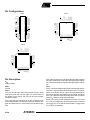
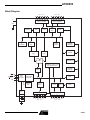
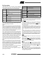
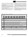
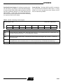
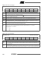
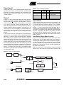
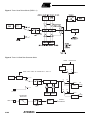
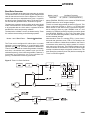
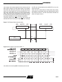
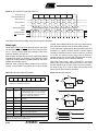
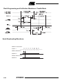
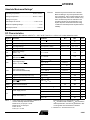
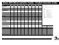
Atmel 8051 Microcontroller Family - Product Selection Guide
Device
89C1051
89C1051U
89C2051
89C4051
89C51
89C52
89C55
89S8252
89S53
1K
1K
2K
4K
4K
8K
20K
8K
12K
ON-CHIP MEMORY
Flash (Bytes)
EEPROM (Bytes)
0
0
0
0
0
0
0
2K
0
SRAM (Bytes)
64
64
128
128
128
256
256
256
256
In-System Programmable (ISP)
NO
NO
NO
NO
NO
NO
NO
YES
YES
15
15
YES
3
5
32
32
20
20
**Low voltage operation = 2.7-6.0V Operation
Key
SRAM
- Static RAM
ISP
- In-System Programmable
32
I/O
- Input/Output
- Analogue to Digital Convertor
HARDWARE FEATURES
I/O Pins
Max speed depends on Vcc voltage. Frequencies and Currents listed are for
Vcc= 5.0V & T=25c
NO
NO
NO
ADC
NO
NO
YES
YES
SPI
- Serial Peripheral Interface
YES
YES
YES
YES
PWM
- Pulse Width Modulation
NO
NO
YES
YES
PAR
- Parallel programming mode
3
3
3
3
FLASH
- Reprogrammable Code Memory
1
NO
NO
NO
NO
YES
YES
YES
YES
YES
YES
NO
NO
NO
NO
NO
YES
YES
6
6
6
8
8
9
9
NO
NO
NO
NO
NO
NO
NO
Enhanced LED I/O Drivers
YES
YES
YES
NO
SPI Port
NO
NO
NO
NO
NO
Full Duplex Serial UART
NO
YES
YES
YES
YES
Watchdog Timer
NO
NO
NO
NO
NO
Timer/Counters
1
2
2
2
2
Analogue Comparator
1
1
1
1
IDLE and Power Down modes
YES
YES
YES
Dual Data Pointer
NO
NO
Interrupt sources
3
6
NO
NO
NO
EEPROM - Parallel programming mode
MISCELLANEOUS
On-chip RC Oscillator
Max External Clock Frequency
24MHz
24MHz
24MHz
24MHz
24MHz
24MHz
24MHz
24MHz
24MHz
VCC Voltage Range (V)
2.7-6.0
2.7-6.0
2.7-6.0
2.7-6.0
4.0-6.0
4.0-6.0
4.0-6.0
4.0-6.0
4.0-6.0
Brown-out protection
NO
NO
NO
YES
NO
NO
NO
NO
NO
EQUINOX SUPPORT TOOLS
Farnell Order Code
Equinox Order Code
Micro-ISP Series III Programmer
NO
NO
NO
NO
NO
NO
NO
ISP only
ISP onlyNO
111-776
EQ-8051-ST1 (UK)
Micro-ISP Series IV Programmer
NO
NO
NO
NO
NO
NO
NO
ISP only
ISP only
302-2365
AVR-DV1 (UK)
Micro-ISP Series IV LV Programmer
NO
NO
NO
NO
NO
NO
NO
ISP only
ISP only
302-2298
UISP-S4
Micro-Pro Device Programmer
PAR
PAR
PAR
PAR
PAR
PAR
PAR
PAR
PAR
111-715
UISP-LV4
8051 Starter System
PAR
PAR
PAR
PAR
NO
NO
NO
ISP/PAR
ISP/PAR
111-806
MPW-PLUS (UK)
-
-
-
-
-
-
-
-
-
302-2328
BK-C51-1
EQ-89S-ST1
NO
NO
NO
NO
NO
NO
NO
ISP only
ISP only
302-2237
EQ-89S-ST1
PK51-2K
YES
YES
YES
NO
NO
NO
NO
NO
NO
121-058
PK51-2K
PK51-8K-UPG
YES
YES
YES
YES
YES
YES
NO
YES
NO
302-2262
PK51-8K-UPG
AllWriter Universal Programmer
NO
NO
NO
NO
YES
YES
YES
YES
NO
302-2225
SG-ALLWRITER
Equinox Guide to C & the 8051
For further information please contact Equinox Technologies UK Ltd on Tel: +44 (0) 1204 529000 Fax: +44 (0) 1204 535555 E-mail: [email protected]
Disclaimer: Whilst information is supplied in good faith, we are not liable for any errors or omissions. Please consult the relevant Atmel datasheet. E&OE
Atmel 8051 Microcontroller Family - Product Selection Guide
Continued....
Device
89C1051
89C1051U
89C2051
89C4051
89C51
89C52
89C55
89S8252
89S53
Farnell Order Code
Equinox Order Code
SS-89S-DIL40
NO
NO
NO
NO
NO
NO
NO
Fitted
NO
795-252
EQ-8051-ST1 (UK)
SS-89S-PLCC44
NO
NO
NO
NO
NO
NO
NO
Fitted
NO
795-264
AVR-DV1 (UK)
SS-89S-20P
NO
NO
NO
NO
NO
NO
NO
Fitted
NO
120-996
UISP-S4
EQUINOX SUPPORT TOOLS
AD-PLCC44-A
NO
NO
NO
NO
YES
YES
YES
YES
YES
701-040
AD-PLCC44-A
AD-SOIC20-A
YES
YES
YES
YES
NO
NO
NO
NO
NO
701-051
AD-SOIC20-A
20P3 (24PC)
701-063
123-893
701-087
120-911
-
-
-
-
-
20S (24SC)
701-075
120-900
-
120-923
-
-
-
-
-
40P6 (24PC)
-
-
-
-
700-988
701-014
302-2341
795-392
120-935
PACKAGE TYPES (Farnell Codes)
44J (24JC)
-
-
-
-
795-355
795-367
302-2353
795-409
120-947
44A (24JC)
-
-
-
-
-
-
-
-
-
For further information please contact Equinox Technologies UK Ltd on Tel: +44 (0) 1204 529000 Fax: +44 (0) 1204 535555 E-mail: [email protected]
Disclaimer: Whilst information is supplied in good faith, we are not liable for any errors or omissions. Please consult the relevant Atmel datasheet. E&OE
Features
• Compatible with MCS-51™ Products
• 12K Bytes of In-System Reprogrammable Downloadable Flash Memory
•
•
•
•
•
•
•
•
•
•
•
•
•
•
– SPI Serial Interface for Program Downloading
– Endurance: 1,000 Write/Erase Cycles
4.0V to 6V Operating Range
Fully Static Operation: 0 Hz to 24 MHz
Three-Level Program Memory Lock
256 x 8-bit Internal RAM
32 Programmable I/O Lines
Three 16-bit Timer/Counters
Nine Interrupt Sources
Programmable UART Serial Channel
SPI Serial Interface
Low Power Idle and Power Down Modes
Interrupt Recovery From Power Down
Programmable Watchdog Timer
Dual Data Pointer
Power Off Flag
Description
The AT89S53 is a low-power, high-performance CMOS 8-bit microcomputer with 12K
bytes of Downloadable Flash programmable and erasable read only memory. The
device is manufactured using Atmel’s high density nonvolatile memory technology
and is compatible with the industry standard 80C51 instruction set and pinout. The onchip Downloadable Flash allows the program memory to be reprogrammed in-system
through an SPI serial interface or by a conventional nonvolatile memory programmer.
By combining a versatile 8-bit CPU with Downloadable Flash on a monolithic chip, the
Atmel AT89S53 is a powerful microcomputer which provides a highly flexible and cost
effective solution to many embedded control applications.
The AT89S53 provides the following standard features: 12K bytes of Downloadable
Flash, 256 bytes of RAM, 32 I/O lines, programmable watchdog timer, two Data Pointers, three 16-bit timer/counters, a six-vector two-level interrupt architecture, a full
duplex serial port, on-chip oscillator, and clock circuitry. In addition, the AT89S53 is
designed with static logic for operation down to zero frequency and supports two software selectable power saving modes. The Idle Mode stops the CPU while allowing
the RAM, timer/counters, serial port, and interrupt system to continue functioning. The
Power Down Mode saves the RAM contents but freezes the oscillator, disabling all
other chip functions until the next interrupt or hardware reset.
The Downloadable Flash can be changed a single byte at a time and is accessible
through the SPI serial interface. Holding RESET active forces the SPI bus into a serial
programming interface and allows the program memory to be written to or read from
unless Lock Bit 2 has been activated.
8-Bit
Microcontroller
with 12K Bytes
Flash
AT89S53
0787B-B–12/97
4-217
Pin Configurations
PDIP
P1.4 (SS)
P1.3
P1.2
P1.1 (T2 EX)
P1.0 (T2)
NC
VCC
P0.0 (AD0)
P0.1 (AD1)
P0.2 (AD2)
P0.3 (AD3)
VCC
P0.0 (AD0)
P0.1 (AD1)
P0.2 (AD2)
P0.3 (AD3)
P0.4 (AD4)
P0.5 (AD5)
P0.6 (AD6)
P0.7 (AD7)
EA/VPP
ALE/PROG
PSEN
P2.7 (A15)
P2.6 (A14)
P2.5 (A13)
P2.4 (A12)
P2.3 (A11)
P2.2 (A10)
P2.1 (A9)
P2.0 (A8)
(MOSI) P1.5
(MISO) P1.6
(SCK) P1.7
RST
(RXD) P3.0
NC
(TXD) P3.1
(INT0) P3.2
(INT1) P3.3
(T0) P3.4
(T1) P3.5
6
5
4
3
2
1
44
43
42
41
40
40
39
38
37
36
35
34
33
32
31
30
29
28
27
26
25
24
23
22
21
7
8
9
10
11
12
13
14
15
16
17
39
38
37
36
35
34
33
32
31
30
29
18
19
20
21
22
23
24
25
26
27
28
1
2
3
4
5
6
7
8
9
10
11
12
13
14
15
16
17
18
19
20
P0.4 (AD4)
P0.5 (AD5)
P0.6 (AD6)
P0.7 (AD7)
EA/VPP
NC
ALE/PROG
PSEN
P2.7 (A15)
P2.6 (A14)
P2.5 (A13)
(WR) P3.6
(RD) P3.7
XTAL2
XTAL1
GND
NC
(A8) P2.0
(A9) P2.1
(A10) P2.2
(A11) P2.3
(A12) P2.4
(T2) P1.0
(T2 EX) P1.1
P1.2
P1.3
(SS) P1.4
(MOSI) P1.5
(MISO) P1.6
(SCK) P1.7
RST
(RXD) P3.0
(TXD) P3.1
(INT0) P3.2
(INT1) P3.3
(T0) P3.4
(T1) P3.5
(WR) P3.6
(RD) P3.7
XTAL2
XTAL1
GND
PLCC
44
43
42
41
40
39
38
37
36
35
34
P1.4 (SS)
P1.3
P1.2
P1.1 (T2 EX)
P1.0 (T2)
NC
VCC
P0.0 (AD0)
P0.1 (AD1)
P0.2 (AD2)
P0.3 (AD3)
TQFP
33
32
31
30
29
28
27
26
25
24
23
1
2
3
4
5
6
7
8
9
10
11
P0.4 (AD4)
P0.5 (AD5)
P0.6 (AD6)
P0.7 (AD7)
EA/VPP
NC
ALE/PROG
PSEN
P2.7 (A15)
P2.6 (A14)
P2.5 (A13)
(WR) P3.6
(RD) P3.7
XTAL2
XTAL1
GND
GND
(A8) P2.0
(A9) P2.1
(A10) P2.2
(A11) P2.3
(A12) P2.4
12
13
14
15
16
17
18
19
20
21
22
(MOSI) P1.5
(MISO) P1.6
(SCK) P1.7
RST
(RXD) P3.0
NC
(TXD) P3.1
(INT0) P3.2
(INT1) P3.3
(T0) P3.4
(T1) P3.5
Pin Description
Port 0 also receives the code bytes during Flash programming and outputs the code bytes during program verification. External pullups are required during program verification.
VCC
Supply voltage.
GND
Ground.
Port 0
Port 0 is an 8-bit open drain bidirectional I/O port. As an
output port, each pin can sink eight TTL inputs. When 1s
are written to port 0 pins, the pins can be used as highimpedance inputs.
Port 0 can also be configured to be the multiplexed loworder address/data bus during accesses to external program and data memory. In this mode, P0 has internal pullups.
4-218
AT89S53
Port 1
Port 1 is an 8-bit bidirectional I/O port with internal pullups.
The Port 1 output buffers can sink/source four TTL inputs.
When 1s are written to Port 1 pins, they are pulled high by
the internal pullups and can be used as inputs. As inputs,
Port 1 pins that are externally being pulled low will source
current (IIL) because of the internal pullups.
Some Port 1 pins provide additional functions. P1.0 and
P1.1 can be configured to be the timer/counter 2 external
count input (P1.0/T2) and the timer/counter 2 trigger input
(P1.1/T2EX), respectively.
AT89S53
Block Diagram
P0.0 - P0.7
P2.0 - P2.7
PORT 0 DRIVERS
PORT 2 DRIVERS
VCC
GND
RAM ADDR.
REGISTER
B
REGISTER
PORT 0
LATCH
RAM
PORT 2
LATCH
FLASH
PROGRAM
ADDRESS
REGISTER
STACK
POINTER
ACC
BUFFER
TMP2
TMP1
PC
INCREMENTER
ALU
INTERRUPT, SERIAL PORT,
AND TIMER BLOCKS
PROGRAM
COUNTER
PSW
PSEN
ALE/PROG
EA / VPP
TIMING
AND
CONTROL
INSTRUCTION
REGISTER
DPTR
RST
WATCH
DOG
PORT 3
LATCH
PORT 1
LATCH
SPI
PORT
PROGRAM
LOGIC
OSC
PORT 3 DRIVERS
P3.0 - P3.7
PORT 1 DRIVERS
P1.0 - P1.7
4-219
Pin Description
Furthermore, P1.4, P1.5, P1.6, and P1.7 can be configured
as the SPI slave port select, data input/output and shift
clock input/output pins as shown in the following table.
Port Pin
Alternate Functions
P1.0
T2 (external count input to Timer/Counter 2),
clock-out
Port Pin
Alternate Functions
P3.0
RXD (serial input port)
P3.1
TXD (serial output port)
P3.2
INT0 (external interrupt 0)
P3.3
INT1 (external interrupt 1)
P1.1
T2EX (Timer/Counter 2 capture/reload trigger
and direction control)
P3.4
T0 (timer 0 external input)
P3.5
T1 (timer 1 external input)
P1.4
SS (Slave port select input)
P3.6
WR (external data memory write strobe)
P1.5
MOSI (Master data output, slave data input pin
for SPI channel)
P3.7
RD (external data memory read strobe)
P1.6
MISO (Master data input, slave data output pin
for SPI channel)
P1.7
SCK (Master clock output, slave clock input pin
for SPI channel)
Port 1 also receives the low-order address bytes during
Flash programming and verification.
Port 2
Port 2 is an 8-bit bidirectional I/O port with internal pullups.
The Port 2 output buffers can sink/source four TTL inputs.
When 1s are written to Port 2 pins, they are pulled high by
the internal pullups and can be used as inputs. As inputs,
Port 2 pins that are externally being pulled low will source
current (IIL) because of the internal pullups.
Port 2 emits the high-order address byte during fetches
from external program memory and during accesses to
external data memory that use 16-bit addresses (MOVX @
DPTR). In this application, Port 2 uses strong internal pullups when emitting 1s. During accesses to external data
memory that use 8-bit addresses (MOVX @ RI), Port 2
emits the contents of the P2 Special Function Register.
Port 2 also receives the high-order address bits and some
control signals during Flash programming and verification.
Port 3
Port 3 is an 8 bit bidirectional I/O port with internal pullups.
The Port 3 output buffers can sink/source four TTL inputs.
When 1s are written to Port 3 pins, they are pulled high by
the internal pullups and can be used as inputs. As inputs,
Port 3 pins that are externally being pulled low will source
current (IIL) because of the pullups.
Port 3 also serves the functions of various special features
of the AT89S53, as shown in the following table.
Port 3 also receives some control signals for Flash programming and verification.
4-220
AT89S53
RST
Reset input. A high on this pin for two machine cycles while
the oscillator is running resets the device.
ALE/PROG
Address Latch Enable is an output pulse for latching the
low byte of the address during accesses to external memory. This pin is also the program pulse input (PROG) during
Flash programming.
In normal operation, ALE is emitted at a constant rate of 1/6
the oscillator frequency and may be used for external timing or clocking purposes. Note, however, that one ALE
pulse is skipped during each access to external data memory.
If desired, ALE operation can be disabled by setting bit 0 of
SFR location 8EH. With the bit set, ALE is active only during a MOVX or MOVC instruction. Otherwise, the pin is
weakly pulled high. Setting the ALE-disable bit has no
effect if the microcontroller is in external execution mode.
PSEN
Program Store Enable is the read strobe to external program memory.
When the AT89S53 is executing code from external program memory, PSEN is activated twice each machine
cycle, except that two PSEN activations are skipped during
each access to external data memory.
EA/VPP
External Access Enable. EA must be strapped to GND in
order to enable the device to fetch code from external program memory locations starting at 0000H up to FFFFH.
Note, however, that if lock bit 1 is programmed, EA will be
internally latched on reset.
EA should be strapped to VCC for internal program executions. This pin also receives the 12-volt programming
enable voltage (VPP) during Flash programming when 12volt programming is selected.
AT89S53
XTAL1
Input to the inverting oscillator amplifier and input to the
internal clock operating circuit.
XTAL2
Output from the inverting oscillator amplifier.
Special Function Registers
A map of the on-chip memory area called the Special Function Register (SFR) space is shown in Table 1.
Note that not all of the addresses are occupied, and unoccupied addresses may not be implemented on the chip.
Read accesses to these addresses will in general return
random data, and write accesses will have an indeterminate
effect.
Table 1. AT89S53 SFR Map and Reset Values
0F8H
0F0H
0FFH
B
00000000
0F7H
0E8H
0E0H
0EFH
ACC
00000000
0E7H
0D8H
0DFH
0D0H
PSW
00000000
0C8H
T2CON
00000000
T2MOD
XXXXXX00
RCAP2L
00000000
RCAP2H
00000000
TL2
00000000
SPCR
000001XX
0D7H
TH2
00000000
0CFH
0C0H
0C7H
0B8H
IP
XX000000
0BFH
0B0H
P3
11111111
0B7H
0A8H
IE
0X000000
0A0H
P2
11111111
98H
SCON
00000000
90H
P1
11111111
88H
TCON
00000000
TMOD
00000000
TL0
00000000
TL1
00000000
TH0
00000000
TH1
00000000
80H
P0
11111111
SP
00000111
DP0L
00000000
DP0H
00000000
DP1L
00000000
DP1H
00000000
SPSR
00XXXXXX
0AFH
0A7H
SBUF
XXXXXXXX
9FH
WCON
00000010
97H
8FH
SPDR
XXXXXXXX
PCON
0XXX0000
87H
4-221
User software should not write 1s to these unlisted locations, since they may be used in future products to invoke
new features. In that case, the reset or inactive values of the
new bits will always be 0.
Timer 2 Registers Control and status bits are contained in
registers T2CON (shown in Table 2) and T2MOD (shown in
Table 9) for Timer 2. The register pair (RCAP2H, RCAP2L)
are the Capture/Reload registers for Timer 2 in 16 bit capture mode or 16-bit auto-reload mode.
Watchdog Control Register The WCON register contains
control bits for the Watchdog Timer (shown in Table 3). The
DPS bit selects one of two DPTR registers available.
SPI Registers Control and status bits for the Serial Peripheral Interface are contained in registers SPCR (shown in
Table 4) and SPSR (shown in Table 5). The SPI data bits
are contained in the SPDR register. Writing the SPI data
register during serial data transfer sets the Write Collision
bit, WCOL, in the SPSR register. The SPDR is double buffered for writing and the values in SPDR are not changed by
Reset.
Interrupt Registers The global interrupt enable bit and the
individual interrupt enable bits are in the IE register. In addition, the individual interrupt enable bit for the SPI is in the
SPCR register. Two priorities can be set for each of the six
interrupt sources in the IP register.
Table 2. T2CON—Timer/Counter 2 Control Register
T2CON Address = 0C8H
Reset Value = 0000 0000B
Bit Addressable
Bit
TF2
EXF2
RCLK
TCLK
EXEN2
TR2
C/T2
CP/RL2
7
6
5
4
3
2
1
0
Symbol
Function
TF2
Timer 2 overflow flag set by a Timer 2 overflow and must be cleared by software. TF2 will not be set when either RCLK =
1 or TCLK = 1.
EXF2
Timer 2 external flag set when either a capture or reload is caused by a negative transition on T2EX and EXEN2 = 1.
When Timer 2 interrupt is enabled, EXF2 = 1 will cause the CPU to vector to the Timer 2 interrupt routine. EXF2 must be
cleared by software. EXF2 does not cause an interrupt in up/down counter mode (DCEN = 1).
RCLK
Receive clock enable. When set, causes the serial port to use Timer 2 overflow pulses for its receive clock in serial port
Modes 1 and 3. RCLK = 0 causes Timer 1 overflows to be used for the receive clock.
TCLK
Transmit clock enable. When set, causes the serial port to use Timer 2 overflow pulses for its transmit clock in serial port
Modes 1 and 3. TCLK = 0 causes Timer 1 overflows to be used for the transmit clock.
EXEN2
Timer 2 external enable. When set, allows a capture or reload to occur as a result of a negative transition on T2EX if
Timer 2 is not being used to clock the serial port. EXEN2 = 0 causes Timer 2 to ignore events at T2EX.
TR2
Start/Stop control for Timer 2. TR2 = 1 starts the timer.
C/T2
Timer or counter select for Timer 2. C/T2 = 0 for timer function. C/T2 = 1 for external event counter (falling edge triggered).
CP/RL2
Capture/Reload select. CP/RL2 = 1 causes captures to occur on negative transitions at T2EX if EXEN2 = 1. CP/RL2 = 0
causes automatic reloads to occur when Timer 2 overflows or negative transitions occur at T2EX when EXEN2 = 1. When
either RCLK or TCLK = 1, this bit is ignored and the timer is forced to auto-reload on Timer 2 overflow.
4-222
AT89S53
AT89S53
Dual Data Pointer Registers To facilitate accessing external data memory, two banks of 16 bit Data Pointer Registers are provided: DP0 at SFR address locations 82H-83H
and DP1 at 84H-85H. Bit DPS = 0 in SFR WCON selects
DP0 and DPS = 1 selects DP1. The user should always initalize the DPS bit to the appropriate value before accessing
the respective Data Pointer register.
Power Off Flag The Power Off Flag (POF) is located at
bit_4 (PCON.4) in the PCON SFR. POF is set to “1” during
power up. It can be set and reset under software control
and is not affected by RESET.
Table 3. WCON—Watchdog Control Register
WCON Address = 96H
Bit
Reset Value = 0000 0010B
PS2
PS1
PS0
reserved
reserved
DPS
WDTRST
WDTEN
7
6
5
4
3
2
1
0
Symbol
Function
PS2
PS1
PS0
Prescaler Bits for the Watchdog Timer. When all three bits are set to “0”, the watchdog timer has a nominal period of 16
ms. When all three bits are set to “1”, the nominal period is 2048 ms.
DPS
Data Pointer Register Select. DPS = 0 selects the first bank of Data Pointer Register, DP0, and DPS = 1 selects the
second bank, DP1
WDTRST
Watchdog Timer Reset. Each time this bit is set to “1” by user software, a pulse is generated to reset the watchdog timer.
The WDTRST bit is then automatically reset to “0” in the next instruction cycle. The WDTRST bit is Write-Only.
WDTEN
Watchdog Timer Enable Bit. WDTEN = 1 enables the watchdog timer and WDTEN = 0 disables the watchdog timer.
4-223
Table 4. SPCR—SPI Control Register
SPCR Address = D5H
Bit
Reset Value = 0000 01XXB
SPIE
SPE
DORD
MSTR
CPOL
CPHA
SPR1
SPR0
7
6
5
4
3
2
1
0
Symbol
Function
SPIE
SPI Interrupt Enable. This bit, in conjunction with the ES bit in the IE register, enables SPI interrupts: SPIE = 1 and ES
= 1 enable SPI interrupts. SPIE = 0 disables SPI interrupts.
SPE
SPI Enable. SPI = 1 enables the SPI channel and connects SS, MOSI, MISO and SCK to pins P1.4, P1.5, P1.6, and
P1.7. SPI = 0 disables the SPI channel.
DORD
Data Order. DORD = 1 selects LSB first data transmission. DORD = 0 selects MSB first data transmission.
MSTR
Master/Slave Select. MSTR = 1 selects Master SPI mode. MSTR = 0 selects Slave SPI mode.
CPOL
Clock Polarity. When CPOL = 1, SCK is high when idle. When CPOL = 0, SCK of the master device is low when not
transmitting. Please refer to figure on SPI Clock Phase and Polarity Control.
CPHA
Clock Phase. The CPHA bit together with the CPOL bit controls the clock and data relationship between master and
slave. Please refer to figure on SPI Clock Phase and Polarity Control.
SPR0
SPR1
SPI Clock Rate Select. These two bits control the SCK rate of the device configured as master. SPR1 and SPR0 have
no effect on the slave. The relationship between SCK and the oscillator frequency, FOSC., is as follows:
SPR1SPR0SCK = FOSC. divided by
0 0 4
0 1 16
1 0 64
1 1 128
Table 5. SPSR—SPI Status Register
SPSR Address = AAH
Bit
Reset Value = 00XX XXXXB
SPIF
WCOL
—
—
—
—
—
—
7
6
5
4
3
2
1
0
Symbol
Function
SPIF
SPI Interrupt Flag. When a serial transfer is complete, the SPIF bit is set and an interrupt is generated if SPIE = 1 and
ES = 1. The SPIF bit is cleared by reading the SPI status register with SPIF and WCOL bits set, and then accessing
the SPI data register.
WCOL
Write Collision Flag. The WCOL bit is set if the SPI data register is written during a data transfer. During data transfer,
the result of reading the SPDR register may be incorrect, and writing to it has no effect. The WCOL bit (and the SPIF
bit) are cleared by reading the SPI status register with SPIF and WCOL set, and then accessing the SPI data register.
4-224
AT89S53
AT89S53
Table Table 6. SPDR—SPI Data Register
SPDR Address = 86H
Bit
Reset Value = unchanged
SPD7
SPD6
SPD5
SPD4
SPD3
SPD2
SPD1
SPD0
7
6
5
4
3
2
1
0
Data Memory - RAM
Programmable Watchdog Timer
The AT89S53 implements 256 bytes of RAM. The upper
128 bytes of RAM occupy a parallel space to the Special
Function Registers. That means the upper 128 bytes have
the same addresses as the SFR space but are physically
separate from SFR space.
When an instruction accesses an internal location above
address 7FH, the address mode used in the instruction
specifies whether the CPU accesses the upper 128 bytes
of RAM or the SFR space. Instructions that use direct
addressing access SFR space.
For example, the following direct addressing instruction
accesses the SFR at location 0A0H (which is P2).
The programmable Watchdog Timer (WDT) operates from
an independent oscillator. The prescaler bits, PS0, PS1
and PS2 in SFR WCON are used to set the period of the
Watchdog Timer from 16 ms to 2048 ms. The available
timer periods are shown in the following table and the
actual timer periods (at VCC = 5V) are within ±30% of the
nominal.
The WDT is disabled by Power-on Reset and during Power
Down. It is enabled by setting the WDTEN bit in SFR
WCON (address = 96H). The WDT is reset by setting the
WDTRST bit in WCON. When the WDT times out without
being reset or disabled, an internal RST pulse is generated
to reset the CPU.
Table 7. Watchdog Timer Period Selection
MOV 0A0H, #data
Instructions that use indirect addressing access the upper
128 bytes of RAM. For example, the following indirect
addressing instruction, where R0 contains 0A0H, accesses
the data byte at address 0A0H, rather than P2 (whose
address is 0A0H).
MOV @R0, #data
Note that stack operations are examples of indirect
addressing, so the upper 128 bytes of data RAM are available as stack space.
WDT Prescaler Bits
Period (nominal)
PS2
PS1
PS0
0
0
0
16 ms
0
0
1
32 ms
0
1
0
64 ms
0
1
1
128 ms
1
0
0
256 ms
1
0
1
512 ms
1
1
0
1024 ms
1
1
1
2048 ms
4-225
Timer 0 and 1
Timer 0 and Timer 1 in the AT89S53 operate the same way
as Timer 0 and Timer 1 in the AT89C51, AT89C52 and
AT89C55. For further information, see the October 1995
Microcontroller Data Book, page 2-45, section titled,
“Timer/Counters.”
Table 8. Timer 2 Operating Modes
RCLK + TCLK
CP/RL2
TR2
0
0
1
16-bit Auto-Reload
0
1
1
16-bit Capture
1
X
1
Baud Rate Generator
X
X
0
(Off)
Timer 2
Timer 2 is a 16 bit Timer/Counter that can operate as either
a timer or an event counter. The type of operation is
selected by bit C/T2 in the SFR T2CON (shown in Table 2).
Timer 2 has three operating modes: capture, auto-reload
(up or down counting), and baud rate generator. The
modes are selected by bits in T2CON, as shown in Table 8.
Timer 2 consists of two 8-bit registers, TH2 and TL2. In the
Timer function, the TL2 register is incremented every
machine cycle. Since a machine cycle consists of 12 oscillator periods, the count rate is 1/12 of the oscillator frequency.
In the Counter function, the register is incremented in
response to a 1-to-0 transition at its corresponding external
input pin, T2. In this function, the external input is sampled
during S5P2 of every machine cycle. When the samples
show a high in one cycle and a low in the next cycle, the
count is incremented. The new count value appears in the
register during S3P1 of the cycle following the one in which
the transition was detected. Since two machine cycles (24
oscillator periods) are required to recognize a 1-to-0 transition, the maximum count rate is 1/24 of the oscillator frequency. To ensure that a given level is sampled at least
once before it changes, the level should be held for at least
one full machine cycle.
MODE
Capture Mode
In the capture mode, two options are selected by bit
EXEN2 in T2CON. If EXEN2 = 0, Timer 2 is a 16 bit timer
or counter which upon overflow sets bit TF2 in T2CON.
This bit can then be used to generate an interrupt. If
EXEN2 = 1, Timer 2 performs the same operation, but a lto-0 transition at external input T2EX also causes the current value in TH2 and TL2 to be captured into RCAP2H and
RCAP2L, respectively. In addition, the transition at T2EX
causes bit EXF2 in T2CON to be set. The EXF2 bit, like
TF2, can generate an interrupt. The capture mode is illustrated in Figure 1.
Auto-Reload (Up or Down Counter)
Timer 2 can be programmed to count up or down when
configured in its 16 bit auto-reload mode. This feature is
invoked by the DCEN (Down Counter Enable) bit located in
the SFR T2MOD (see Table 9). Upon reset, the DCEN bit
is set to 0 so that timer 2 will default to count up. When
DCEN is set, Timer 2 can count up or down, depending on
the value of the T2EX pin.
Figure 2 shows Timer 2 automatically counting up when
DCEN = 0. In this mode, two options are selected by bit
Figure 1. Timer 2 in Capture Mode
÷12
OSC
C/T2 = 0
TH2
TL2
OVERFLOW
CONTROL
C/T2 = 1
TF2
TR2
CAPTURE
T2 PIN
RCAP2H RCAP2L
TRANSITION
DETECTOR
TIMER 2
INTERRUPT
T2EX PIN
EXF2
CONTROL
EXEN2
4-226
AT89S53
AT89S53
EXEN2 in T2CON. If EXEN2 = 0, Timer 2 counts up to
0FFFFH and then sets the TF2 bit upon overflow. The overflow also causes the timer registers to be reloaded with the
16 bit value in RCAP2H and RCAP2L. The values in
RCAP2H and RCAP2L are preset by software. If EXEN2 =
1, a 16 bit reload can be triggered either by an overflow or
by a 1-to-0 transition at external input T2EX. This transition
also sets the EXF2 bit. Both the TF2 and EXF2 bits can
generate an interrupt if enabled.
Setting the DCEN bit enables Timer 2 to count up or down,
as shown in Figure 3. In this mode, the T2EX pin controls
the direction of the count. A logic 1 at T2EX makes Timer 2
count up. The timer will overflow at 0FFFFH and set the
TF2 bit. This overflow also causes the 16 bit value in
RCAP2H and RCAP2L to be reloaded into the timer registers, TH2 and TL2, respectively.
A logic 0 at T2EX makes Timer 2 count down. The timer
underflows when TH2 and TL2 equal the values stored in
RCAP2H and RCAP2L. The underflow sets the TF2 bit and
causes 0FFFFH to be reloaded into the timer registers.
The EXF2 bit toggles whenever Timer 2 overflows or
underflows and can be used as a 17th bit of resolution. In
this operating mode, EXF2 does not flag an interrupt.
Figure 2. Timer 2 in Auto Reload Mode (DCEN = 0)
Table 9. T2MOD—Timer 2 Mode Control Register
T2MOD Address = 0C9H
Reset Value = XXXX XX00B
Not Bit Addressable
Bit
—
—
—
—
—
—
T2OE
DCEN
7
6
5
4
3
2
1
0
Symbol
Function
—
Not implemented, reserved for future use.
T2OE
Timer 2 Output Enable bit.
DCEN
When set, this bit allows Timer 2 to be configured as an up/down counter.
4-227
Figure 3. Timer 2 Auto Reload Mode (DCEN = 1)
Figure 4. Timer 2 in Baud Rate Generator Mode
TIMER 1 OVERFLOW
÷2
"0"
"1"
NOTE: OSC. FREQ. IS DIVIDED BY 2, NOT 12
SMOD1
OSC
÷2
C/T2 = 0
"1"
TH2
"0"
TL2
RCLK
CONTROL
TR2
÷16
Rx
CLOCK
C/T2 = 1
"1"
"0"
T2 PIN
TCLK
RCAP2H RCAP2L
TRANSITION
DETECTOR
÷ 16
T2EX PIN
EXF2
CONTROL
EXEN2
4-228
AT89S53
TIMER 2
INTERRUPT
Tx
CLOCK
AT89S53
Baud Rate Generator
Timer 2 is selected as the baud rate generator by setting
TCLK and/or RCLK in T2CON (Table 2). Note that the baud
rates for transmit and receive can be different if Timer 2 is
used for the receiver or transmitter and Timer 1 is used for
the other function. Setting RCLK and/or TCLK puts Timer 2
into its baud rate generator mode, as shown in Figure 4.
The baud rate generator mode is similar to the auto-reload
mode, in that a rollover in TH2 causes the Timer 2 registers
to be reloaded with the 16 bit value in registers RCAP2H
and RCAP2L, which are preset by software.
The baud rates in Modes 1 and 3 are determined by Timer
2’s overflow rate according to the following equation.
Timer 2 Overflow Rate
Modes 1 and 3 Baud Rates = -----------------------------------------------------------16
The Timer can be configured for either timer or counter
operation. In most applications, it is configured for timer
operation (CP/T2 = 0). The timer operation is different for
Timer 2 when it is used as a baud rate generator. Normally,
as a timer, it increments every machine cycle (at 1/12 the
oscillator frequency). As a baud rate generator, however, it
increments every state time (at 1/2 the oscillator frequency). The baud rate formula is given below.
Modes 1 and 3
Oscillator Frequency
--------------------------------------- = ---------------------------------------------------------------------------------------------Baud Rate
32 × [ 65536 – ( RCAP2H,RCAP2L ) ]
where (RCAP2H, RCAP2L) is the content of RCAP2H and
RCAP2L taken as a 16 bit unsigned integer.
Timer 2 as a baud rate generator is shown in Figure 4. This
figure is valid only if RCLK or TCLK = 1 in T2CON. Note
that a rollover in TH2 does not set TF2 and will not generate an interrupt. Note too, that if EXEN2 is set, a 1-to-0
transition in T2EX will set EXF2 but will not cause a reload
from (RCAP2H, RCAP2L) to (TH2, TL2). Thus when Timer
2 is in use as a baud rate generator, T2EX can be used as
an extra external interrupt.
Note that when Timer 2 is running (TR2 = 1) as a timer in
the baud rate generator mode, TH2 or TL2 should not be
read from or written to. Under these conditions, the Timer is
incremented every state time, and the results of a read or
write may not be accurate. The RCAP2 registers may be
read but should not be written to, because a write might
overlap a reload and cause write and/or reload errors. The
timer should be turned off (clear TR2) before accessing the
Timer 2 or RCAP2 registers.
Figure 5. Timer 2 in Clock-Out Mode
4-229
Programmable Clock Out
UART
A 50% duty cycle clock can be programmed to come out on
P1.0, as shown in Figure 5. This pin, besides being a regular I/0 pin, has two alternate functions. It can be programmed to input the external clock for Timer/Counter 2 or
to output a 50% duty cycle clock ranging from 61 Hz to 4
MHz at a 16 MHz operating frequency.
To configure the Timer/Counter 2 as a clock generator, bit
C/T2 (T2CON.1) must be cleared and bit T2OE (T2MOD.1)
must be set. Bit TR2 (T2CON.2) starts and stops the timer.
The clock-out frequency depends on the oscillator frequency and the reload value of Timer 2 capture registers
(RCAP2H, RCAP2L), as shown in the following equation.
The UART in the AT89S53 operates the same way as the
UART in the AT89C51, AT89C52 and AT89C55. For further information, see the October 1995 Microcontroller
Data Book, page 2-49, section titled, “Serial Interface.”
Serial Peripheral Interface
The serial peripheral interface (SPI) allows high-speed synchronous data transfer between the AT89S53 and peripheral devices or between several AT89S53 devices. The
AT89S53 SPI features include the following:
• Full-Duplex, 3-Wire Synchronous Data Transfer
• Master or Slave Operation
• 1.5-MHz Bit Frequency (max.)
• LSB First or MSB First Data Transfer
• Four Programmable Bit Rates
• End of Transmission Interrupt Flag
• Write Collision Flag Protection
• Wakeup from Idle Mode (Slave Mode Only)
The interconnection between master and slave CPUs with
SPI is shown in the following figure. The SCK pin is the
Oscillator Frequency
Clock-Out Frequency = ------------------------------------------------------------------------------------------4 × [ 65536 – ( RCAP2H,RCAP2L ) ]
In the clock-out mode, Timer 2 rollovers will not generate
an interrupt. This behavior is similar to when Timer 2 is
used as a baud-rate generator. It is possible to use Timer 2
as a baud-rate generator and a clock generator simultaneously. Note, however, that the baud-rate and clock-out
frequencies cannot be determined independently from one
another since they both use RCAP2H and RCAP2L.
Figure 6. SPI Block Diagram
S
LSB
S
8/16-BIT SHIFT REGISTER
READ DATA BUFFER
DIVIDER
÷4÷16÷64÷128
CLOCK
SPI CLOCK (MASTER)
MOSI
P1.5
SCK
1.7
M
SPR0
SPI STATUS REGISTER
SPR0
SPR1
CPHA
CPOL
MSTR
SPI CONTROL REGISTER
8
8
SPI INTERRUPT INTERNAL
REQUEST
DATA BUS
AT89S53
DORD
SPE
8
SPIE
MSTR
SPE
WCOL
SPI CONTROL
DORD
SPE
SS
P1.4
MSTR
SPR1
S
CLOCK
LOGIC
SELECT
SPIF
PIN CONTROL LOGIC
MSB
4-230
MISO
P1.6
M
M
OSCILLATOR
AT89S53
the SPI port is deactivated and the MOSI/P1.5 pin can be
used as an input.
There are four combinations of SCK phase and polarity
with respect to serial data, which are determined by control
bits CPHA and CPOL. The SPI data transfer formats are
shown in Figures 8 and 9.
clock output in the master mode but is the clock input in the
slave mode. Writing to the SPI data register of the master
CPU starts the SPI clock generator, and the data written
shifts out of the MOSI pin and into the MOSI pin of the
slave CPU. After shifting one byte, the SPI clock generator
stops, setting the end of transmission flag (SPIF). If both
the SPI interrupt enable bit (SPIE) and the serial port interrupt enable bit (ES) are set, an interrupt is requested.
The Slave Select input, SS/P1.4, is set low to select an
individual SPI device as a slave. When SS/P1.4 is set high,
Figure 7. SPI Master-Slave Interconnection
MSB
MASTER
LSB
MISO MISO
8-BIT SHIFT REGISTER
MSB
SLAVE
LSB
8-BIT SHIFT REGISTER
MOSI MOSI
SPI
CLOCK GENERATOR
SCK
SS
SCK
SS
VCC
Figure 8. SPI transfer Format with CPHA = 0
*Not defined but normally MSB of character just received
4-231
Figure 9. SPI Transfer Format with CPHA = 1
SCK CYCLE #
(FOR REFERENCE)
1
2
3
4
5
6
7
8
SCK (CPOL=0)
SCK (CPOL=1)
MOSI
(FROM MASTER)
MISO
(FROM SLAVE)
*
MSB
6
5
4
3
2
1
MSB
6
5
4
3
2
1
LSB
LSB
SS (TO SLAVE)
*Not defined but normally LSB of previously transmitted character
Interrupts
The AT89S53 has a total of six interrupt vectors: two external interrupts (INT0 and INT1), three timer interrupts (Timers 0, 1, and 2), and the serial port interrupt. These interrupts are all shown in Figure 10.
Each of these interrupt sources can be individually enabled
or disabled by setting or clearing a bit in Special Function
Register IE. IE also contains a global disable bit, EA, which
disables all interrupts at once.
Note that Table 10 shows that bit position IE.6 is unimplemented. In the AT89C51, bit position IE.5 is also unimple-
mented. User software should not write 1s to these bit positions, since they may be used in future AT89 products.
Timer 2 interrupt is generated by the logical OR of bits TF2
and EXF2 in register T2CON. Neither of these flags is
cleared by hardware when the service routine is vectored
to. In fact, the service routine may have to determine
whether it was TF2 or EXF2 that generated the interrupt,
and that bit will have to be cleared in software.
The Timer 0 and Timer 1 flags, TF0 and TF1, are set at
S5P2 of the cycle in which the timers overflow. The values
are then polled by the circuitry in the next cycle. However,
the Timer 2 flag, TF2, is set at S2P2 and is polled in the
same cycle in which the timer overflows.
Table 10. Interrupt Enable (IE) Register
Figure 10. Interrupt Sources
(MSB)
EA
(LSB)
—
ET2
ES
ET1
EX1
ET0
EX0
Enable Bit = 1 enables the interrupt.
Enable Bit = 0 disables the interrupt.
Symbol
Position
Function
EA
IE.7
Disables all interrupts. If EA = 0, no interrupt
is acknowledged. If EA = 1, each interrupt
source is individually enabled or disabled by
setting or clearing its enable bit.
—
IE.6
Reserved.
ET2
IE.5
Timer 2 interrupt enable bit.
ES
IE.4
SPI and UART interrupt enable bit.
ET1
IE.3
Timer 1 interrupt enable bit.
EX1
IE.2
External interrupt 1 enable bit.
ET0
IE.1
Timer 0 interrupt enable bit.
EX0
IE.0
External interrupt 0 enable bit.
User software should never write 1s to unimplemented bits, because
they may be used in future AT89 products.
4-232
AT89S53
AT89S53
Figure 12. External Clock Drive Configuration
Figure 11. Oscillator Connections
Note: C1, C2 = 30 pF ± 10 pF for Crystals
= 40 pF ± 10 pF for Ceramic Resonators
Oscillator Characteristics
internal reset algorithm takes control. On-chip hardware
inhibits access to internal RAM in this event, but access to
the port pins is not inhibited. To eliminate the possibility of
an unexpected write to a port pin when idle mode is terminated by a reset, the instruction following the one that
invokes idle mode should not write to a port pin or to external memory.
XTAL1 and XTAL2 are the input and output, respectively,
of an inverting amplifier that can be configured for use as
an on-chip oscillator, as shown in Figure 11. Either a quartz
crystal or ceramic resonator may be used. To drive the
device from an external clock source, XTAL2 should be left
unconnected while XTAL1 is driven, as shown in Figure 12.
There are no requirements on the duty cycle of the external
clock signal, since the input to the internal clocking circuitry
is through a divide-by-two flip-flop, but minimum and maximum voltage high and low time specifications must be
observed.
Power Down Mode
In the power down mode, the oscillator is stopped and the
instruction that invokes power down is the last instruction
executed. The on-chip RAM and Special Function Registers retain their values until the power down mode is terminated. Exit from power down can be initiated either by a
hardware reset or by an enabled external interrupt. Reset
redefines the SFRs but does not change the on-chip RAM.
The reset should not be activated before VCC is restored to
its normal operating level and must be held active long
enough to allow the oscillator to restart and stabilize.
To exit power down via an interrupt, the external interrupt
must be enabled as level sensitive before entering power
down. The interrupt service routine starts at 16 ms (nominal) after the enabled interrupt pin is activated.
Idle Mode
In idle mode, the CPU puts itself to sleep while all the onchip peripherals remain active. The mode is invoked by
software. The content of the on-chip RAM and all the special functions registers remain unchanged during this
mode. The idle mode can be terminated by any enabled
interrupt or by a hardware reset.
Note that when idle mode is terminated by a hardware
reset, the device normally resumes program execution
from where it left off, up to two machine cycles before the
Status of External Pins During Idle and Power Down Modes
Mode
Program Memory
ALE
PSEN
PORT0
PORT1
PORT2
PORT3
Idle
Internal
1
1
Data
Data
Data
Data
Idle
External
1
1
Float
Data
Address
Data
Power Down
Internal
0
0
Data
Data
Data
Data
Power Down
External
0
0
Float
Data
Data
Data
4-233
Program Memory Lock Bits
The AT89S53 has three lock bits that can be left unprogrammed (U) or can be programmed (P) to obtain the additional features listed in the following table.
When lock bit 1 is programmed, the logic level at the EA pin
is sampled and latched during reset. If the device is powered up without a reset, the latch initializes to a random
value and holds that value until reset is activated. The
latched value of EA must agree with the current logic level
at that pin in order for the device to function properly.
Once programmed, the lock bits can only be unprogrammed with the Chip Erase operations in either the parallel or serial modes.
Lock Bit Protection Modes (1) (2)
Program Lock Bits
Protection Type
LB1
LB2
LB3
1
U
U
U
No internal memory lock feature.
2
P
U
U
MOVC instructions executed from external program memory are disabled from fetching code bytes
from internal memory. EA is sampled and latched on reset and further programming of the Flash
memory (parallel or serial mode) is disabled.
3
P
P
U
Same as Mode 2, but parallel or serial verify are also disabled.
4
P
P
P
Same as Mode 3, but external execution is also disabled.
Notes:
1. U = Unprogrammed
2. P = Programmed
Programming the Flash
Parallel Programming Algorithm
Atmel’s AT89S53 Flash Microcontroller offers 12K bytes of
in-system reprogrammable Flash Code memory.
The AT89S53 is normally shipped with the on-chip Flash
Code memory array in the erased state (i.e. contents =
FFH) and ready to be programmed. This device supports a
High-Voltage (12V) Parallel programming mode and a LowVoltage (5V) Serial programming mode. The serial programming mode provides a convenient way to download
the AT89S53 inside the user’s system. The parallel programming mode is compatible with conventional third party
Flash or EPROM programmers.
The Code memory array occupies one contiguous address
space from 0000H to 2FFFH.
The Code array on the AT89S53 is programmed byte-bybyte in either programming mode. An auto-erase cycle is
provided with the self-timed programming operation in the
serial programming mode. There is no need to perform the
Chip Erase operation to reprogram any memory location in
the serial programming mode unless any of the lock bits
have been programmed.
In the parallel programming mode, there is no auto-erase
cycle. To reprogram any non-blank byte, the user needs to
use the Chip Erase operation first to erase the entire Code
memory array.
To program and verify the AT89S53 in the parallel programming mode, the following sequence is recommended:
1. Power-up sequence:
Apply power between VCC and GND pins.
Set RST pin to “H”.
Apply a 3 MHz to 24 MHz clock to XTAL1 pin and wait
for at least 10 milliseconds.
2. Set PSEN pin to “L”
ALE pin to “H”
EA pin to “H” and all other pins to “H”.
3. Apply the appropriate combination of “H” or “L” logic
levels to pins P2.6, P2.7, P3.6, P3.7 to select one of the
programming operations shown in the Flash Programming Modes table.
4. Apply the desired byte address to pins P1.0 to P1.7
and P2.0 to P2.5.
Apply data to pins P0.0 to P0.7 for Write Code operation.
5. Raise EA/VPP to 12V to enable Flash programming,
erase or verification.
6. Pulse ALE/PROG once to program a byte in the Code
memory array, or the lock bits. The byte-write cycle is
self-timed and typically takes 1.5 ms.
7. To verify the byte just programmed, bring pin P2.7 to
“L” and read the programmed data at pins P0.0 to P0.7.
4-234
AT89S53
AT89S53
8. Repeat steps 3 through 7 changing the address and
data for the entire 12K-byte array or until the end of the
object file is reached.
9. Power-off sequence:
Set XTAL1 to “L”.
Set RST and EA pins to “L”.
Turn VCC power off.
The AT89S53 is shipped with the Serial Programming
Mode enabled.
Reading the Signature Bytes: The signature bytes are
read by the same procedure as a normal verification of
locations 030H and 031H, except that P3.6 and P3.7 must
be pulled to a logic low. The values returned are as follows:
(030H) = 1EH indicates manufactured by Atmel
(031H) = 53H indicates 89S53
DATA Polling
The AT89S53 features DATA Polling to indicate the end of a
write cycle. During a write cycle in the parallel or serial programming mode, an attempted read of the last byte written
will result in the complement of the written datum on P0.7
(parallel mode), and on the MSB of the serial output byte
on MISO (serial mode). Once the write cycle has been
completed, true data are valid on all outputs, and the next
cycle may begin. DATA Polling may begin any time after a
write cycle has been initiated.
Ready/Busy
The progress of byte programming in the parallel programming mode can also be monitored by the RDY/BSY output
signal. Pin P3.4 is pulled Low after ALE goes High during
programming to indicate BUSY. P3.4 is pulled High again
when programming is done to indicate READY.
Program Verify
If lock bits LB1 and LB2 have not been programmed, the
programmed Code can be read back via the address and
data lines for verification. The state of the lock bits can also
be verified directly in the parallel programming mode. In the
serial programming mode, the state of the lock bits can only
be verified indirectly by observing that the lock bit features
are enabled.
Chip Erase
In the parallel programming mode, chip erase is initiated by
using the proper combination of control signals and by
holding ALE/PROG low for 10 ms. The Code array is written with all “1”s in the Chip Erase operation.
In the serial programming mode, a chip erase operation is
initiated by issuing the Chip Erase instruction. In this mode,
chip erase is self-timed and takes about 16 ms.
During chip erase, a serial read from any address location
will return 00H at the data outputs.
Programming Interface
Every code byte in the Flash array can be written, and the
entire array can be erased, by using the appropriate combination of control signals. The write operation cycle is selftimed and once initiated, will automatically time itself to
completion.
All major programming vendors offer worldwide support for
the Atmel microcontroller series. Please contact your local
programming vendor for the appropriate software revision.
Serial Downloading
The Code memory array can be programmed using the
serial SPI bus while RST is pulled to VCC. The serial interface consists of pins SCK, MOSI (input) and MISO (output).
After RST is set high, the Programming Enable instruction
needs to be executed first before program/erase operations
can be executed.
An auto-erase cycle is built into the self-timed programming
operation (in the serial mode ONLY) and there is no need
to first execute the Chip Erase instruction unless any of the
lock bits have been programmed. The Chip Erase operation turns the content of every memory location in the Code
array into FFH.
The Code memory array has an address space of 0000H to
2FFFH.
Either an external system clock is supplied at pin XTAL1 or
a crystal needs to be connected across pins XTAL1 and
XTAL2. The maximum serial clock (SCK) frequency should
be less than 1/40 of the crystal frequency. With a 24 MHz
oscillator clock, the maximum SCK frequency is 600 kHz.
Serial Programming Fuse
A programmable fuse is available to disable Serial Programming if the user needs maximum system security. The
Serial Programming Fuse can only be programmed or
erased in the Parallel Programming Mode.
4-235
Serial Programming Algorithm
To program and verify the AT89S53 in the serial programming mode, the following sequence is recommended:
1. Power-up sequence:
Apply power between VCC and GND pins.
Set RST pin to “H”.
If a crystal is not connected across pins XTAL1 and
XTAL2, apply a 3 MHz to 24 MHz clock to XTAL1 pin
and wait for at least 10 milliseconds.
2. Enable serial programming by sending the Programming Enable serial instruction to pin MOSI/P1.5. The
frequency of the shift clock supplied at pin SCK/P1.7
needs to be less than the CPU clock at XTAL1 divided
by 40.
3. The Code array is programmed one byte at a time by
supplying the address and data together with the
appropriate Write instruction. The selected memory
location is first automatically erased before new data is
written. The write cycle is self-timed and typically takes
less than 2.5 ms at 5V.
4. Any memory location can be verified by using the Read
instruction which returns the content at the selected
address at serial output MISO/P1.6.
5. At the end of a programming session, RST can be set
low to commence normal operation.
Power-off sequence (if needed):
Set XTAL1 to “L” (if a crystal is not used).
Set RST to “L”.
Turn VCC power off.
Serial Programming Instruction
The Instruction Set for Serial Programming follows a 3-byte
protocol and is shown in the following table:
Instruction Set
Instruction
Input Format
Operation
Byte 3
Programming Enable
1010 1100
0101 0011
xxxx xxxx
Enable serial programming interface after RST goes high.
Chip Erase
1010 1100
xxxx x100
xxxx xxxx
Chip erase the 12K memory array.
xxxx xxxx
Read data from Code memory array at the selected address.
The 6 MSBs of the first byte are the high order address bits.
The low order address bits are in the second byte. Data are
available at pin MISO during the third byte.
data in
Write data to Code memory location at selected address. The
address bits are the 6 MSBs of the first byte together with the
second byte.
low addr
Write Code Memory
low addr
01
Write Lock Bits
Notes:
10
1010 1100
LB1
LB2
LB3
Read Code Memory
A12
A11
A10
A9
A8
A13
Byte 2
A12
A11
A10
A9
A8
A13
Byte 1
x x111
Write lock bits.
Set LB1, LB2 or LB3 = “0” to program lock bits.
1. DATA polling is used to indicate the end of a write cycle which typically takes less than 2.5 ms at 5V.
2. “x” = don’t care.
4-236
xxxx xxxx
AT89S53
AT89S53
Flash Parallel Programming Modes
P2.6
P2.7
P3.6
P3.7
Data I/O
P0.7:0
Address
P2.5:0 P1.7:0
12V
H
L
L
L
X
X
12V
L
H
H
H
DIN
ADDR
12V
L
L
H
H
DOUT
ADDR
12V
H
L
H
L
DIN
X
Bit - 1
P0.7 = 0
X
Bit - 2
P0.6 = 0
X
Bit - 3
P0.5 = 0
X
DOUT
X
Bit - 1
@P0.2
X
Bit - 2
@P0.1
X
Bit - 3
@P0.0
X
Mode
Serial Prog. Modes
RST
PSEN
ALE/PROG
EA/VPP
H
h (1)
h (1)
x
Chip Erase
H
L
Write (12K bytes) Memory
H
L
Read (12K bytes) Memory
H
L
Write Lock Bits:
H
L
Read Lock Bits:
H
L
(2)
H
H
Read Atmel Code
H
L
H
Read Device Code
H
L
H
Serial Prog. Enable
H
H
L
Read Serial Prog. Fuse
H
L
Notes:
(2)
L
Serial Prog. Disable
12V
(2)
H
H
H
L
L
12V
L
L
L
L
DOUT
30H
12V
L
L
L
L
DOUT
31H
12V
L
H
L
H
P0.0 = 0
X
12V
L
H
L
H
P0.0 = 1
X
12V
H
H
L
H
@P0.0
X
1. “h” = weakly pulled “High” internally.
2. Chip Erase and Serial Programming Fuse require a 10-ms PROG pulse. Chip Erase needs to be performed first before
reprogramming any byte with a content other than FFH.
3. P3.4 is pulled Low during programming to indicate RDY/BSY.
4. “X” = don’t care
4-237
Figure 14. Flash Serial Downloading
Figure 13. Programming the Flash Memory
+5V
+4.0V to 6.0V
AT89S53
A0 - A7
ADDR.
0000H/2FFFH
AT89S53
VCC
P1
VCC
PGM
DATA
P0
P2.0 - P2.5
A8 - A13
P2.6
SEE FLASH
PROGRAMMING
MODES TABLE
PROG
ALE
P2.7
P3.6
INSTRUCTION
INPUT
P1.5/MOSI
DATA OUTPUT
P1.6/MISO
CLOCK IN
P1.7/SCK
P3.7
XTAL2
VPP
EA
3-24 Mhz
3-24 Mhz
XTAL1
GND
VI H
RST
PSEN
+5V
AT89S53
ADDR.
0000H/2FFFH
A0 - A7
A8 - A13
SEE FLASH
PROGRAMMING
MODES TABLE
P1
VCC
P2.0 - P2.5
P0
P2.6
P2.7
PGM DATA
(USE 10K
PULLUPS)
ALE
VI H
XTAL2
EA
VPP
XTAL1
RST
VI H
P3.6
P3.7
3-24 Mhz
GND
XTAL1
GND
Figure 15. Verifying the Flash Memory
4-238
XTAL2
PSEN
AT89S53
RST
VI H
AT89S53
Flash Programming and Verification Characteristics - Parallel Mode
TA = 0°C to 70°C, VCC = 5.0V ± 10%
Symbol
Parameter
Min
Max
Units
VPP
Programming Enable Voltage
11.5
12.5
V
IPP
Programming Enable Current
1.0
mA
1/tCLCL
Oscillator Frequency
24
MHz
tAVGL
Address Setup to PROG Low
48tCLCL
tGHAX
Address Hold After PROG
48tCLCL
tDVGL
Data Setup to PROG Low
48tCLCL
tGHDX
Data Hold After PROG
48tCLCL
tEHSH
P2.7 (ENABLE) High to VPP
48tCLCL
tSHGL
VPP Setup to PROG Low
10
tGLGH
PROG Width
1
tAVQV
Address to Data Valid
48tCLCL
tELQV
ENABLE Low to Data Valid
48tCLCL
tEHQZ
Data Float After ENABLE
tGHBL
PROG High to BUSY Low
1.0
µs
tWC
Byte Write Cycle Time
2.0
ms
3
0
µs
110
µs
48tCLCL
4-239
Flash Programming and Verification Waveforms - Parallel Mode
Serial Downloading Waveforms
SERIAL CLOCK INPUT
SCK/P1.7
7
6
5
4
3
2
1
0
SERIAL DATA INPUT
MOSI/P1.5
MSB
LSB
MSB
LSB
SERIAL DATA OUTPUT
MISO/P1.6
4-240
AT89S53
AT89S53
Absolute Maximum Ratings*
Operating Temperature .................................. -55°C to +125°C
*NOTICE:
Storage Temperature ..................................... -65°C to +150°C
Voltage on Any Pin
with Respect to Ground .....................................-1.0V to +7.0V
Maximum Operating Voltage............................................. 6.6V
Stresses beyond those listed under “Absolute
Maximum Ratings” may cause permanent damage to the device. This is a stress rating only and
functional operation of the device at these or any
other conditions beyond those indicated in the
operational sections of this specification is not
implied. Exposure to absolute maximum rating
conditions for extended periods may affect device
reliability.
DC Output Current...................................................... 15.0 mA
DC Characteristics
The values shown in this table are valid for TA = -40°C to 85°C and VCC = 4.0V to 6.0V, unless otherwise noted.
Symbol
Parameter
Condition
Min
Max
Units
VIL
Input Low Voltage
(Except EA)
-0.5
0.2 VCC - 0.1
V
VIL1
Input Low Voltage (EA)
-0.5
0.2 VCC - 0.3
V
VIH
Input High Voltage
(Except XTAL1, RST)
0.2 VCC + 0.9
VCC + 0.5
V
VIH1
Input High Voltage
(XTAL1, RST)
0.7 VCC
VCC + 0.5
V
VOL
Output Low Voltage (1)
(Ports 1,2,3)
IOL = 1.6 mA
0.5
V
VOL1
Output Low Voltage (1)
(Port 0, ALE, PSEN)
IOL = 3.2 mA
0.5
V
VOH
Output High Voltage
(Ports 1,2,3, ALE, PSEN)
IOH = -60 µA, VCC = 5V ± 10%
2.4
V
IOH = -25 µA
0.75 VCC
V
IOH = -10 µA
0.9 VCC
V
2.4
V
IOH = -300 µA
0.75 VCC
V
IOH = -80 µA
0.9 VCC
V
IOH = -800 µA, VCC = 5V ± 10%
VOH1
Output High Voltage
(Port 0 in External Bus Mode)
IIL
Logical 0 Input Current (Ports 1,2,3)
VIN = 0.45V
-50
µA
ITL
Logical 1 to 0 Transition Current (Ports 1,2,3)
VIN = 2V, VCC = 5V ± 10%
-650
µA
ILI
Input Leakage Current
(Port 0, EA)
0.45 < VIN < VCC
±10
µA
RRST
Reset Pulldown Resistor
300
KΩ
CIO
Pin Capacitance
Test Freq. = 1 MHz, TA = 25°C
10
pF
Active Mode, 12 MHz
25
mA
Idle Mode, 12 MHz
6.5
mA
VCC = 6V
100
µA
VCC = 3V
40
µA
50
Power Supply Current
ICC
Power Down Mode (2)
Notes:
1. Under steady state (non-transient) conditions, IOL
must be externally limited as follows:
Maximum IOL per port pin: 10 mA
Maximum IOL per 8-bit port:
Port 0: 26 mA
Ports 1,2, 3: 15 mA
Maximum total IOL for all output pins: 71 mA
If IOL exceeds the test condition, VOL may exceed the
related specification. Pins are not guaranteed to sink
current greater than the listed test conditions.
2. Minimum VCC for Power Down is 2V.
4-241
AC Characteristics
Under operating conditions, load capacitance for Port 0, ALE/PROG, and PSEN = 100 pF; load capacitance for all other
outputs = 80 pF.
External Program and Data Memory Characteristics
12MHz Oscillator
Symbol
Parameter
1/tCLCL
Oscillator Frequency
tLHLL
ALE Pulse Width
127
2tCLCL - 40
ns
tAVLL
Address Valid to ALE Low
43
tCLCL - 13
ns
tLLAX
Address Hold After ALE Low
48
tCLCL - 20
ns
tLLIV
ALE Low to Valid Instruction In
tLLPL
ALE Low to PSEN Low
43
tCLCL - 13
ns
tPLPH
PSEN Pulse Width
205
3tCLCL - 20
ns
tPLIV
PSEN Low to Valid Instruction In
tPXIX
Input Instruction Hold After PSEN
tPXIZ
Input Instruction Float After PSEN
tPXAV
PSEN to Address Valid
tAVIV
Address to Valid Instruction In
312
5tCLCL - 55
ns
tPLAZ
PSEN Low to Address Float
10
10
ns
tRLRH
RD Pulse Width
400
6tCLCL - 100
ns
tWLWH
WR Pulse Width
400
6tCLCL - 100
ns
tRLDV
RD Low to Valid Data In
tRHDX
Data Hold After RD
tRHDZ
Data Float After RD
97
2tCLCL - 28
ns
tLLDV
ALE Low to Valid Data In
517
8tCLCL - 150
ns
tAVDV
Address to Valid Data In
585
9tCLCL - 165
ns
tLLWL
ALE Low to RD or WR Low
200
3tCLCL + 50
ns
tAVWL
Address to RD or WR Low
203
4tCLCL - 75
ns
tQVWX
Data Valid to WR Transition
23
tCLCL - 20
ns
tQVWH
Data Valid to WR High
433
7tCLCL - 120
ns
tWHQX
Data Hold After WR
33
tCLCL - 20
ns
tRLAZ
RD Low to Address Float
tWHLH
RD or WR High to ALE High
4-242
Min
AT89S53
Max
Variable Oscillator
Min
Max
Units
0
24
MHz
233
4tCLCL - 65
145
0
3tCLCL - 45
0
59
75
tCLCL - 8
0
5tCLCL - 90
3tCLCL - 50
0
43
123
tCLCL - 20
ns
ns
0
300
ns
ns
tCLCL - 10
252
ns
ns
ns
0
ns
tCLCL + 25
ns
AT89S53
External Program Memory Read Cycle
External Data Memory Read Cycle
4-243
External Data Memory Write Cycle
External Clock Drive Waveforms
External Clock Drive
Symbol
Parameter
VCC = 4.0V to 6.0V
1/tCLCL
Oscillator Frequency
tCLCL
Clock Period
tCHCX
Min
Max
Units
0
24
MHz
41.6
ns
High Time
15
ns
tCLCX
Low Time
15
ns
tCLCH
Rise Time
20
ns
tCHCL
Fall Time
20
ns
4-244
AT89S53
AT89S53
Serial Port Timing: Shift Register Mode Test Conditions
The values in this table are valid for VCC = 4.0V to 6V and Load Capacitance = 80 pF.
Symbol
Parameter
12 MHz Oscillator
Min
Max
Variable Oscillator
Min
Units
Max
tXLXL
Serial Port Clock Cycle Time
1.0
12tCLCL
µs
tQVXH
Output Data Setup to Clock Rising
Edge
700
10tCLCL - 133
ns
tXHQX
Output Data Hold After Clock Rising
Edge
50
2tCLCL - 117
ns
tXHDX
Input Data Hold After Clock Rising
Edge
0
0
ns
tXHDV
Clock Rising Edge to Input Data
Valid
700
10tCLCL - 133
ns
Shift Register Mode Timing Waveforms
AC Testing Input/Output Waveforms (1)
Float Waveforms (1)
Notes:
Notes:
1.
AC Inputs during testing are driven at V CC - 0.5V
for a logic 1 and 0.45V for a logic 0. Timing measurements are made at VIH min. for a logic 1 and VIL
max. for a logic 0.
1.
For timing purposes, a port pin is no longer floating
when a 100 mV change from load voltage occurs. A
port pin begins to float when a 100 mV change from
the loaded VOH/VOL level occurs.
4-245
Notes:
4-246
1.
XTAL1 tied to GND for ICC (power down)
2.
Lock bits programmed
AT89S53
AT89S53
Ordering Information
Speed
(MHz)
Power
Supply
Ordering Code
Package
16
4.0V to 6.0V
AT89S53-16AA
AT89S53-16JA
AT89S53-16PA
44A
44J
40P6
Automotive
(-40°C to 105°C)
24
4.0V to 6.0V
AT89S53-24AC
AT89S53-24JC
AT89S53-24PC
44A
44J
40P6
Commercial
(0°C to 70°C)
4.0V to 6.0V
AT89S53-24AI
AT89S53-24JI
AT89S53-24PI
44A
44J
40P6
Industrial
(-40°C to 85°C)
4.5V to 5.5V
AT89S53-33AC
AT89S53-33JC
AT89S53-33PC
44A
44J
40P6
Commercial
(0°C to 70°C)
33
Operation Range
= Preliminary Information
Package Type
44A
44 Lead, Thin Plastic Gull Wing Quad Flatpack (TQFP)
44J
44 Lead, Plastic J-Leaded Chip Carrier (PLCC)
40P6
40 Lead, 0.600" Wide, Plastic Dual Inline Package (PDIP)
4-247
4-248
AT89S53