1
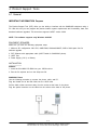
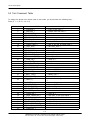
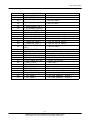
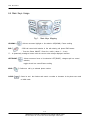
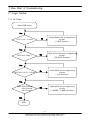
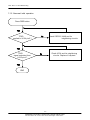
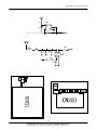
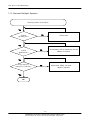
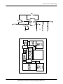
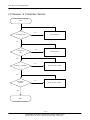
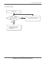
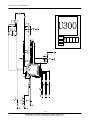
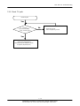
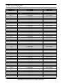
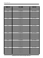
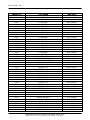
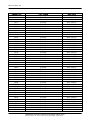
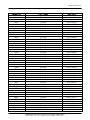
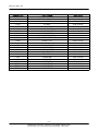
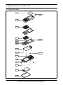
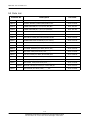
CDMA TELEPHONE
SCH-N500
CONTENTS
CDMA TELEPHONE
1.
General Introduction
2.
Specification
3.
Installation
4.
Product Support Tools
5.
Circuit Description
6.
Test Procedure
7.
Flow Chart of Troubleshooting
8.
Electrical Parts List
9.
Exploded Views and Parts List
10.
Block Diagram
11.
PCB Diagrams
ⓒ Samsung Electronics Co.,Ltd. Setember. 2005
This Service Manual is a property of Samsung Electronics Co.,Ltd.
Any unauthorized use of Manual can be punished under applicable
Printed in Korea.
International and/or domestic law.
Code No.: GH68-08423A
BASIC.
1. General Introduction
The SCH-N500 (Single Mode) phone functions as digital phone working in CDMA(Code Division Multiple
Access) mode.
The following standards and minimum performance standards shall be met or exceeded by each
subscriber unit.
Air Interface
The Subscriber Unit shall be Single band in compliance with TSB-74.
TIA/EIA IS-125 : Recommended Minimum Performance standards for Digital Cellular Wideband Spread
Spectrum Speech Service Option1.
TIA/EIA IS-126-A : Mobile Station Loop back Service Option standard.
TIA/EIA IS-95B : Mobile Station-Base Station Compatibility Standard for Dual-Mode Wideband Spread
Spectrum Cellular Systems;for the analog air interface.
CDMA Receiver/Transmitter Specifications and Requirements
The Subscriber Unit shall meet TIA/EIA IS-98C. The Subscriber Unit shall comply with Personal Station
Class III.
1-1
SAMSUNG Proprietary-Contents may change without notice
This Document can not be used without Samsung's authorization
General Introduction
1-2
SAMSUNG Proprietary-Contents may change without notice
This Document can not be used without Samsung's authorization
2. Specification
2-1 General
ITEM
CDMA
Tx Freq. range
824.64 ~ 848.87MHz
Rx Freq. range
869.64 ~ 893.37MHz
Channel Bandwidth
1.23MHz
Channel Spacing
30KHz
Number of Channel
20FA
Duplex Separation
45MHz
Type of Emission
1M25F9W
In/Output Impedance
50 Ohm
Tx Local Freq.
1649.28~1696.74MHz
Rx Local Freq
1739.28~1786.74MHz
TCXO freq.
19.2MHz
Freq. Stability
(FRX-45MHz)+/-300Hz
Operating Temperature
-30deg ~ +60deg
Supply Voltage
3.6V
Size and Weight
STD : 57.0 X 37.0 X 5.1mm
20g
800 mAh
2-1
SAMSUNG Proprietary-Contents may change without notice
This Document can not be used without Samsung's authorization
Specification
2-2 800MHz CDMA
GENERAL
Frequency Range
. Transmitter
: 824.64 ~ 848.87MHz
. Receiver
: 869.64 ~ 893.37MHz
Channel Bandwidth
: 1.23MHz
Channel Spacing
: 30kHz
Number of Channels
: 20FA
Duplex Separation
: 45 MHz
Type of Emission
: 1M25F9W
Input/Output Impedance
: 50 ohms
Local Frequency
. Transmitter
: 1649.28~1696.74MHz
. Receiver
: 1739.28~1786.7MHz
TCXO Frequency
: 19.2MHz
Frequency Stability
: (FRX-45MHz) ±300Hz
Operation Temperature
: -30°C ~ +60°C
Supply Voltage
: +3.6V
TRANSMITTER
Waveform Quality
: 0.944 or more
Open Loop Power Control Range
. -25dBm
: -57.5dBm ~ -38.5dBm
. -65dBm
: -17.5dBm ~ +1.5dBm
. -93.5dBm
: +10.5dBm ~ +29.5dBm
2-2
SAMSUNG Proprietary-Contents may change without notice
This Document can not be used without Samsung's authorization
Specification
Minimum Tx Power Control
: below -50dBm
Closed Loop Power Control Range
: ±24dB
Maximum RF Output Power
: 398mW(+24.5dBm)
Occupied Bandwidth
: 1.23MHz
Conducted Spurious Emission @885 KHz
: -42dBc/30kHz
@1.98 MHz
: -54dBc/30kHz
RECEIVER
Rx Sensitivity and Dynamic Range
: -104dBm, FER=0.5% or less
: -25dBm, FER=0.5% or less
Conducted Spurious Emission
. 869~894 MHz
: <-81dBm
. 824~849 MHz
: <-61dBm
All Other Frequencies
: <-47dBm
Single Tone Desensitization
: lower than 1 %
. Rx power level = -101dBm
. Tone power level = -30dBm
. Tone offset from carrier = ±900KHz
Intermodulation Spurious Response Attenuation
: lower than 1 %
. Tone 1 offset from carrier = ±900KHz
. Tone 2 offset from carrier = ±1.700MHz
- Test 1, 2
Rx power = -101dBm
Tone 1 power = -43dBm
Tone 2 power = -43dBm
- Test 3, 4
Rx power = -90dBm
Tone 1 power = -32dBm
Tone 2 power = -32dBm
- Test 5, 6
Rx power = -79dBm
Tone 1 power = -21dBm
Tone 2 power = -21dBm
2-3
SAMSUNG Proprietary-Contents may change without notice
This Document can not be used without Samsung's authorization
Specification
2-3 CDMA Debug Display Information
To select debug display mode : Select [Menu] +Press [5] +[*]+press [2] + [1] + [2] + [3] + [5] + [8] +
[0] + select [Debug Screen].
④ Pilot PN Code
①
②
③
⑥
⑤ RSSI-ECIO
CDMA Monitor
Sxxxxx Nxxxxx
④
Pxxx
⑥ -ECIO
SX
RSSI-ECIO
Wxx
⑦ Walsh Code
CxxxxR-xx SI0 T-xx
⑧
⑩
⑨
⑧ Channel Number
⑪
⑤
⑦
⑨ Protocol Revision
① SID : SXXXX
⑩ Slot Cycle Index
② NID : NXXXX
⑪ Call state : TX PDM Value
③ Call Processing State : SX
Idle, Sleep state :
1) S1 : Init State
Tx_Gain_ADJ Accumulator Value
2) S2 : Idle State
3) S3 : VC Init State
4) S4 : WFO State
5) S5 : WFA State
6) S6 : Call State
7) S7 : Release State
8) S8 : OVHD State
9) S9 : Originate State
10) SA : Page Res State
11) SB : ORD Res State
12) SC : Reg State
13) SD : MSG State
2-4
SAMSUNG Proprietary-Contents may change without notice
This Document can not be used without Samsung's authorization
3. Installation
Installing and Removing the Battery
To install, insert the battery into the opening on
To remove, make sure the power is off. Push the
the back of the phone making sure the plastic tabs battery release latch up completely. Pull and lift the
on the back are inserted into the matching slots in battery away from the phone.
the phone. Press down until the latchsnaps into
place.
3-1
SAMSUNG Proprietary-Contents may change without notice
This Document can not be used without Samsung's authorization
Installation
3-2
SAMSUNG Proprietary-Contents may change without notice
This Document can not be used without Samsung's authorization
4. Product Support Tools
4-1 General
IMPORTANT INFORMATION Purpose
The Product Support Tool (PST) offers you the ability to interface with the SAMSUNG telephone using a
PC. With this tool you can program the phones network system requirements and functionality, data, and
download software upgrades. This document supports UniPST version 2.686.
NOTE: This software supports only Windows 2000/XP.
EQUIPMENT REQUIRED
Make sure you have the following equipment setup:
1. Minimum PC configuration: 586 CPU, 64MB RAM, Windows2000/XP, 5MB of disk space free for
software upgrade.
2. PST Software with appropriate cable (UART Cable for SAMSUNG phone).
3. UART Port.
4. Power Supply (3.8 V) or Battery.
INSTALLATION
Software
1. Insert the SCH-N500 CD ROM into your CD-Rom drive.
2. Run the file explorer and run the Setup.exe file.
SAMSUNG Phone
Use the following procedure to connect the phone, cable, and PC .
Plug the female end of the DM Cable into the 16550 card.
Pull the black rubber connector away from the socket at the base of the phone.
Plug the special connector on the cable into the socket at the base of the phone.
4-1
SAMSUNG Proprietary-Contents may change without notice
This Document can not be used without Samsung's authorization
Product Support Tools
4-2 PST (Product Support Tool)
4-2-1 Getting Started
MAIN MENU SCREEN
1. Double Click on your "Samsung PST for PBTL (SE)"
2. Select SCH-N500
The Main Menu Screen shows the basic tasks that are available.
CAUTION: DO NOT attempt to program phone with a low battery.
PST SETUP
UniPst supports SAMSUNG portable telephone. You can select UART port.
4-2-2 Operation Procedure
Service Programming
setting correct com port.
Read Data from File
Click "Open mmc" icon to select the name of a file whose extension is "mmc". The values will be read
from the named file, and will initialize the parameter values seen on the Service programming screen
Read Data from Phone
Click Read from the Phone icon to upload the current programmable parameters of the phone. The
values are read from the phone, so the phone must have the power ON and be properly connected
to the PST.
NOTE: To actually view the data you need to go to the Edit Items screens.
Edit Items
Click this icon to edit Number Assignment Module (NAM) items or UI items.
1. General : Slot Cycle Index, Service Code
2. NAM1
3. NAM2
4-2
SAMSUNG Proprietary-Contents may change without notice
This Document can not be used without Samsung's authorization
Product Support Tools
Edit UI Items
1. System, Sound, And/Phone : Sound
Save Data to File
Click this icon to save the current parameters to a file. Once you enter a filename, Click <OK> button to
write all current parameters to that file. This way the same information can be downloaded into multiple
phones.
Write to Phone
Click this icon to write the selected parameter values to the phone. Writing the selected values to the
phone may take up to a minute. If there are dependencies in a field you can make all the changes in
the proper fields and download the information all together.
If you intend to use this write to Phone feature, it is recommended that you do a "Read Data from
Phone" first, and then make the changes, so that nothing gets inadvertently overwritten.
NOTE: DO NOT TOUCH THE PHONE WHILE WRITING IS IN PROGRESS.
Software Download and Upgrade Screen
1. Connect PC and SCH-N500 with UART cable
2. Run Universal PST.
3. Select DownLoad Mode tab.
4. Click Bin icon to load Image file.
5. When the downloading process is finished, the PST shows "Downloading completed!!" and the
SCH-N500 reboots automatically.
NOTE: DO NOT POWER OFF WHILE THE PHONE IS BEING DOWNLOADED!
4-3
SAMSUNG Proprietary-Contents may change without notice
This Document can not be used without Samsung's authorization
Product Support Tools
4-4
SAMSUNG Proprietary-Contents may change without notice
This Document can not be used without Samsung's authorization
5. Circuit Description
5-1 Logic Part
CPU(U100:MSM6000-208FBGA)
5-1-1 Power Supply
ARM 7TDMI microprocessor is used for the main
processing. The CPU controls all the circuitry. The
Press "END/ⓛ" key to turn on the phone and then
the V_BAT signal will be connected to ON_SW,
which turns on the inner regulator (MSMA_2.65V,
MSMP_2.85V) of U204 (RC5T623)
The
V_BAT
applied
to
ON_SW
from two clock inputs, TCXO (19.20MHz) and
XTAL (32.768KHz).
The clock of 32.768KHz is
used for sleep. This is equipped with the ARM
7TDMI CPU core, CDMA, DFM block, vocoder,
will
change
ON_SW_SENSE signal from HIGH to LOW. This
will allow MSM6000 (U100) to send out PS_HOLD
(logical HIGH) to turn on the inner regulator even
after the END/ⓛkey is released.
The regulated voltage (MSMP_2.85V) is used in
the digital part of MSM6000, Memory, and LCD.
The regulated voltage (MSMA_2.65V) is used in
analog part and MSMC_2.80V used in core part of
MSM6000.
MSM6000 derives all of its internal clock sources
The regulated voltage (RFTX_2.60V) is
used in the TX RF part. The regulated voltage
(RFRX_2.60V) is used in the Rx RF part.
The
general purpose interface, and other interfaces, and
is one of the most important components of the
CDMA cellular phone.
FROM and SRAM (U102:K5A3281CTM,MCP)
Memories are composed of 32Mbit FROM and
8Mbit SRAM. 32Mbit Flash ROM is used to store
the FONT data and terminal's program. Using
the down-loading program, the program can be
changed even after the terminal is fully assembled.
8Mbit SRAM is used to store the internal flag
information, call processing data, and timer data.
regulated voltage (MOTOR_3.0V) is used in motor
(PAVREF_2.90V) is KEYPAD
part. The regulated voltage
used in WS1101 (U447).
The regulated voltage
For key recognition, key matrix is setup using
(U209) LED_3.3V is used in LED.
SCAN(0:6) and KEYSENSE(0:2) of input port of
MSM6000.
5-1-2 Logic
circuitry
The
logic
part
consists
of
the
internal
CPU
are
12
backlight
included
in
LEDs
the
and
keypad
back-light
for
easy
operation in the dark.
(MSM6000) and the extra memory composed of
SRAM and FlashROM. The MSM6000 receives LCD MODULE
The LCD module is a 128 X 64 dots and 1 fixed
32.768KHz TCXO clock signal and controls the
which will
phone as a whole. The major components are as icon. The LCD contains a controller
display the information by 8-bit data from the MCU.
follows:
- CPU : ARM7TDMI CPU core,
It also contains a DC-DC converter for contrast
- FROM:U102(K5A3281CTM) 32Mbit Flash ROM, adjustment and LCD reflector to improve the
display efficiency. An internal back-light circuitry
MCP.
- SRAM:U102(K5A3281CTM) 8Mbit SRAM, MCP.
and EL back-light are used for easy operation in
the dark.
5-1
SAMSUNG Proprietary-Contents may change without notice
This Document can not be used without Samsung's authorization
Circuit Description
5-1-3 Baseband
RFT6122, RFR6122 AND MSM INTERFACE
MOBILE SYSTEM MODEM (MSM6000)
The MCU equipped with the ARM 7TDMI CPU A. CDMA Data Interface
core is an important component of the CDMA - TX_IP, TX_IM, TX_QP, TX_QM (U400 pins 29,
cellular phone. The MSM6000 comes in a 208-Ball 30 / 27, 28): Differential analog input for I and Q
component used during CDMA mode.
FBGA Package.
-RX_IP, RX_IM, RX_QP, RX_QM (U300 pins 28,
MICROPROCESSOR INTERFACE
The interface circuitry consists of reset circuit,
27 / 25, 26): RX analog baseband output for I and
address bus(A0-A22),data bus(D0-D15),and memory Q component used during CDMA mode
controls (LB, UB, WE, OE, CS|1S, CE|F, CS2S,
B. RF Interface
RY|BY)
- TX : TX_AGC_ADJ (U400 pin 21) port is used to
control the TX power, TX_ON (U100 pin B12)
CODEC
The MSM6000 (U100) integrates an audio voice
signal used to control RFT6122
band CODEC into the Mobile Station Modem. The - RX : SBI_DT, SBI_CK_SBI_ST (U300 pins 3, 4,
integrated CODEC contains all of the required 5) lines are used to control the RX gain and
conversion and amplification stages for the audio
TRK_LO_ADJ
(U100
pin
compensate the TCXO clock.
front end.
Clock
-Modem clock : 19.20MHz. This clock signal is
used for ARM 7TDMI
-Sleep clock : 32.768KHz. This clock signal is used
for sleep.
5-2
SAMSUNG Proprietary-Contents may change without notice
This Document can not be used without Samsung's authorization
D15)
is
used
to
Circuit Description
5-1-4 Audio Part
ALERT
TONE
AND
MELODY
DRIVING
CIRCUITRY
The
MSM6000
integrates
an
audio
voiceband
Codec into Mobile Station Modem. The integrated A speaker generates alert tone and melody. When
Codec contains all of the required conversion and the MSM (U100) receives the data, it generates
amplification stages for the audio front end. The alert tone and melody. Ringer signal generated in
Codec operates as a 13bit linear Codec with the MSM6000 is intended to drive a speaker.
transmit (TX) and receive (RX) filters designed to
meet
ITU-TG.712
requirement.
The
CODEC KEY TONE GENERATOR
contains the software controller amplifier for both
the receiving and transmitting sections. Also, the The CODEC data out from the MSM6000 is
vocoding schemes used will be IS-127 EVRC. The converted to DTMF signal by TONE generator of
EVRC vocoder is based in the MSM internally.
internal CODEC, is then amplified by the internal
audio amplifier to be sent to the speaker unit.
TX AUDIO PATH
The voice signal from the microphone is inputted
to the internal CODEC. The voice signal is then
amplified by the internal amplifier and is converted
to PCM data to be outputted to the MSM as 13bit
data. This data is then processed by the MSM
(U100)'s internal.
RX AUDIO PATH
The PCM data from the MSM (U100)'s internal is
inputted to the internal CODEC and the data will
be decoded by the internal DAC and audio levels
are adjusted by the amplifier. The final audio is
then sent to the audio receiver.
5-3
SAMSUNG Proprietary-Contents may change without notice
This Document can not be used without Samsung's authorization
Circuit Description
5-2 RF Part
5-2-2 Receiver (For CDMA (800MHz))
5-2-1 Transmitter (For CDMA (800MHz))
LOW NOISE AMPLIFIER (LNA)
ANTENNA
The low noise amplifier included in RFR6122
amplifies a weak signal received from the base
Antenna sends the signal to the base station and
station to obtain the optimum signal level.
receives the signal from the base station.
RF
DUPLEXER
BAND
PASS
FILTER
(RX
RF
SAW
FILTER)
The duplexer (F401) passes RF signal with the The RF BPF (F300) passes only specific frequency
frequency of 836.49 ± 12.5 MHz through power (881.49±12.5 MHz) signal.
amp output to antenna, and receives RF signal
with the frequency of 881.49 ± 12.5 MHz from
RX Automatic Gain Controller (AGC) AMP
antenna to LNA input.
POWER AMP
The power amplifier module (PAM, U447) amplifies
RX AGC amplifier within RFR6122 keeps its output
power at a constant level by controlling the gain
within the dynamic range of 90dB, maximum gain
45dB and minimum gain -45dB.
the power of the RF signal sent to the base
station through the antenna.
5-2-3 PLL Block
RF Band Pass Filter (Tx RF SAW Filter)
FREQUENCY SYNTHESIZER CIRCUIT
The RF BPF (F400) pass only specific frequency While both RX PLL block and TX PLL block are
(836.49 ± 12.5MHz) signal. This filter eliminates the
embedded in RFT6122, only the RX VCO block is
image products generated by the up-converter.
embedded in RFR6122. The input reference
TX Automatic Gain Control Amp
frequency is generated from VC-TCXO (OSC301),
and the RF local signal from VCO. PLL compares
The TX AGC amp within RFT6122 controls its gain the reference with the VCO output divided by
by adjusting the control voltage in order to deliver multiples preprogrammed in counters through SBI
the suitable power needed at the input stage of interface, and, if the difference is found, adjusts
Driver amp. Dynamic range is 90dB, and its control the DC voltage which controls the frequency of
voltage varies from 0.2V to 2.5V.
VCO output signal.
5-4
SAMSUNG Proprietary-Contents may change without notice
This Document can not be used without Samsung's authorization
Circuit Description
VC-TCXO
The VC-TCXO (OSC301) is used as a reference
source of the frequency synthesizer. It generates
19.20MHz reference frequency. It is a voltagecontrolled
temperature-compensated
crystal
oscillator with the frequency stability of 19.20MHz ±
2.0ppm over all useful temperature range. The
frequency is controlled by the voltage from the
MSM6000 considering the ambient temperature.
TEMPERATURE-TO-VOLTAGE CONVERTOR
The
temperature-to-voltage
convertor
(TH101)
detects the peripheral temperature. It is used to
compensate the variance in characteristics of an
active component due to the temperature difference.
5-5
SAMSUNG Proprietary-Contents may change without notice
This Document can not be used without Samsung's authorization
Circuit Description
5-3 Test Command Table
To change the phone from normal mode to test mode, you should enter the following keys. :
Press [4 7 * 6 8 # 1 3 5 8 0]
Command No
1
2
7
8
9
14
15
16
21
22
23
24
39
40
41
42
43
45
46
47
48
51
52
Command SW Name
T_SUSPEND_I
T_RESTART_I
T_CARRIERON_I
T_CARRIEROFF_I
T_LOADSYN_I
T_CDATA_I
T_CDTRK_ADJ_I
T_CDMA_TXADJ_I
T_TEST_SYS_I
T_SNDNAM_I
T_SNDVERSION_I
T_SNDESN_I
T_BACKLIGHT_ON_I
T_BACKLIGHT_OFF_I
T_LAMP_ON_I
T_LAMP_OFF_I
T_LCD_CONTRAST_I
T_VIBRATOR_ON_I
T_VIBRATOR_OFF_I
T_DTMFON_I
T_DTMFOFF_I
T_BATT_TYPE_I
T_READ_BATT_I
53
T_VBATT1_I
54
55
56
58
59
60
72
73
74
76
79
121
127
T_VBATT2_I
T_WRITE_BATT_I
T_THERM_READ_I
T_CLR_LIFETIME_I
T_CARRIER_I
T_CLEAR_ALL_I
T_HIGH_TXRAS_ADJ_I
T_TXRAS_ADJ_I
T_CH_FLATNESS_I
T_CDMA_PWR_LIMIT_I
T_CDMA_TEMPCOMP_I
T_CDMA_VGA_OFFSET_I
T_CDMA_BTF_I
/*
/*
/*
/*
/*
/*
/*
/*
/*
/*
/*
/*
/*
/*
/*
/*
/*
/*
/*
/*
/*
/*
/*
/*
Description
Enter to test menu */
Escape from test menu */
Turn on the carrier */
Turn off the carrier */
Load the synthesizer for locking */
Continuously send TX control data */
CDMA TRK local adjust */
Sets tx_agc_adj for cdma mode */
Set TEST_SYS */
Send NAM information */
Send software version */
Send ESN */
Backlight on */
Backlight off */
Lamp on */
Lamp off */
LCD contrast adjust */
Activate a vibrator */
Inactivate a vibrator */
Turn on DTMF */
Turn off DTMF */
Battery type */
Saved low battery value read */
Set the low battey position in the standby
*/
/*
/*
/*
/*
/*
/*
/*
/*
/*
/*
/*
/*
Set the low battey position in the talking */
Write a BATT */
Read a Thermister */
Clear Life Time */
Carrier selection */
Clear all */
High gain TX pwr RAS adjust */
Low gain TX pwr RAS adjust */
CDMA TX pwr ch. flatness */
CDMA TX pwr limit */
CDMA temp. compensation */
CDMA DVGA offset */
5-6
SAMSUNG Proprietary-Contents may change without notice
This Document can not be used without Samsung's authorization
Circuit Description
Command No
128
132
133
134
146
147
148
150
151
152
153
154
155
156
157
171
172
173
174
175
224
227
230
231
233
234
236
237
Command SW Name
T_CDMA_SET_IM2_I
T_TEST_SET_PA_RANGE_I
T_TEST_SET_LNA_RANGE_
I
T_TEST_SET_LNA_OFFSET
_I
T_READ_ADJUST_VAL_I
T_PA_WARMUP_DELAY_I
T_TX_WARMUP_DELAY_I
T_CDMA_LNA_RISE_I
T_CDMA_LNA_FALL_I
T_CDMA_LNA_2RISE_I
T_CDMA_LNA_2FALL_I
T_CDMA_LNA_3RISE_I
T_CDMA_LNA_3FALL_I
T_VCO_COARSE_TUNE_TA
BLE_I
T_RFR_BB_FILTER_I
T_FAC_RXRAS_ADJ_I
T_FAC_HIGH_TXRAS_ADJ_I
T_FAC_TXRAS_ADJ_I
T_FAC_CH_FLATNESS_I
T_FAC_TXRAS_ADJ_ALL_I
T_MRU2_TABLE_I
T_PLINE_I
T_SNDPINFO_I
T_READ_RSSI_I
T_VOC_PCMLPON_I
T_VOC_PCMLPOFF_I
T_GET_MODE_I
T_SET_MODE_I
Description
/* Set IM2 */
/*Set PA range*/
/*Set LNA range*/
/*Set LNA offset*/
/*LNA rise and fall setting*/
/* LNA rise and fall setting*/
/* LNA rise and fall setting*/
/* LNA rise and fall setting*/
/* LNA rise and fall setting*/
/* LNA rise and fall setting*/
/* Set VCO table */
/*
/*
/*
/*
/*
/*
/*
/*
/*
/*
/*
/*
/*
/*
RFR baseband filter */
Factory RX RAS */
High gain factory TX pwr RAS */
Low gain factory TX pwr RAS */
Factory TX pwr ch. flatness */
Factory TX pwr RAS */
MRU reset */
Product lile information */
Send product information 8 character */
Read a RSSI */
Turn on to play a PCM loop back */
Turn off to play a PCM loop back */
Get mode CDMA/FM autotest */
Set mode CDMA/FM autotest */
5-7
SAMSUNG Proprietary-Contents may change without notice
This Document can not be used without Samsung's authorization
Circuit Description
5-8
SAMSUNG Proprietary-Contents may change without notice
This Document can not be used without Samsung's authorization
6. Test Procedure
6-1 List of Equipment
● DC Power Supply
● Test Jig
● Test Cable
● CDMA Mobile Station Test Set HP8285A, HP8960, CMD-80, etc
● Spectrum Analyzer(include CDMA Test Mode) HP8596E
6-2 Configuration of Test
● CAUTION : The test jig and data cable has a voltage drop of 0.15V at Max power output,
you'd better set the DC power supply to 4.15V for normal test condition.
(Nominal voltage of battery is 4.0V at cellular phone)
6-1
SAMSUNG Proprietary-Contents may change without notice
This Document can not be used without Samsung's authorization
Test Procedure
6-3 TEST CABLE CONNECTIONS
6-3-1 TEST CABLE
6-3-2 TEST CABLE CONNECTIONS
1
KMS-510-D
2
RF CABLE (1.4dB Loss for CDMA,)
3
BNC CONNECTOR (RF)
4
PLUG CONNECT TO SCH-N500
5
DATA CABLE
6
Dsub 18PIN CONNECTOR (DATA)
6-2
SAMSUNG Proprietary-Contents may change without notice
This Document can not be used without Samsung's authorization
Test Procedure
6-3-3 Dsub 25 PIN CONNECTOR PIN DESCRIPTION (TEST CABLE 1, BACK SIDE)
Dsub CONN.
DATA DESCRIPTION
PIN NO.
V_BAT
5
DP_RX_DATA
8
DP_TX_DATA
9
HP_PWR
18
DC_VOLT
24,25
GROUND
3,23,17
6-3-4 CONVERSION TABLE OF FREQUENCY vs CHANNEL
T Y P E
CHANNEL
CONVERSION EQUATION
TX
FREQUENCY
1 ≤N≤779
990 ≤N≤1023
F=0.03 ×N + 825.00
F=0.03 × (N-1023) + 825.00
RX
FREQUENCY
990 ≤N≤1023
990 ≤N≤1023
F=0.03 ×N + 825.00
F=0.03 × (N-1023) + 870.00
REMARK
N ; CH NUMBER
F ; FREQUENCY
(CDMA)
6-3
SAMSUNG Proprietary-Contents may change without notice
This Document can not be used without Samsung's authorization
Test Procedure
6-4 Main Keys Usage
Fig 1. Main Keys Mapping
): Moves on-screen highlight or list selection UP(DOWN). Faster scrolling
UP/DOWN (
END
(
):
- END call control with behavior in line with existing cell phone END buttons
- Turns the Phone ON/OFF. Press for a while ( about 2 ~ 3 sec)
*** : A dynamically reassigned control with the current action always displayed onscreen.
): Moves on-screen focus or list selection LEFT(RIGHT), changes spin box control
LEFT/RIGHT(
selection,
toggles check box control.Faster scrolling
SEND
(
CLEAR
):
(
Performs a call by a selected phone number.
):
Cancel or end the function and cancel a number or character in the phone test mode
or NAM mode.
6-4
SAMSUNG Proprietary-Contents may change without notice
This Document can not be used without Samsung's authorization
Test Procedure
6-5 Test Procedure
6-5-1 Change the test mode
A. To change the phone's state from Normal Mode to Test Mode, You should press following keys.
" 4 7 * 6 8 # 1 3 5 8 0 "
B. To Enter suspend mode press "001"
C. Press "021" then You can set channel " 2xxxx "
Example : "2 0363"
Channel number
Mode : CDMA
and press the right soft key(Soft2 key) to save mode/channel value..
D. To finish the Test Mode, You should enter the command "002".
6-5-2 Channel selection and Tx power output level control
A. Enter to Test Mode [ 4 7 * 6 8 # 1 3 5 8 0 ]
B. "001" : Suspend.
C. "009" "0363" [ Push the right soft key ] : Set to '0363' channel.
D. "007" : Carrier On.(TX On)
E. "014" : Spread spectrum to 1.23MHz band width.
F. "016" " xxx " : Adjust RF power level. "xxx" means AGC level (000~ 511)
G. To finish the Test Mode, You should enter the command "002".
6-5
SAMSUNG Proprietary-Contents may change without notice
This Document can not be used without Samsung's authorization
Test Procedure
6-6 CDMA
TEST ITEMS
PROCEDURE
1. PREPARATION
Set test equipments up.
[ 4 7 * 6 8 # 1 3 5 8 0 ]: Enter the Test Mode
"001" : Suspend
If you select a wrong key, press " # ", then enter new command.
To exit the Test Mode at any time, just press [0 0 2].
2. FREQUENCY
ACCURACY
3. OCCUPIED CDMA
BANDWIDTH
4. LIMITATIONS ON
EMISSIONS
"001" : Suspend.
"009" "0363" 'right soft key(Soft2)' : Set channel to 363.
"007" : Carrier On.
"014" : Spread spectrum.
"016" ""280" ' right soft key(Soft2)' : Set AGC Code(xxx) to adjust RF
Output Power
.Measure the TX frequency : 836.49MHz±300Hz.
"001" : Suspend.
"009" "0363" 'right soft key(Soft2)' : Set channel to 363.
"007" : Carrier On.
"014" : Spread spectrum.
"016" ""280" ' right soft key(Soft2)' : Set AGC level.
Measure the bandwidth (spec: 1.23MHz).
"001" : Suspend.
"009" "0363" 'right soft key(Soft2)' : Set channel to 363.
"007" : Carrier On.
"014" : Spread spectrum.
"016" ""280" ' right soft key(Soft2)' : Set AGC level.
Measure the spurious at FC±885kHz, FC±1.98MHz, 2FC, 3FC, 1/2FC.
spec: FC±885kHz
below 42dBc/30kHz
FC±1.98MHz below 54dBc/30kHz
Outside Receive Band
43+10log (PY)
PY: Mean Output Power in watts
5. GATED POWER &
TIME
Set the service option 2.
Set the data rate Eighth (1200bps).
Registering: HHP → HP8924C.
Call
: HP8924C → HHP.
Measure the Gated Power & Time.
spec : Gated Power - at least 20dB
Gated Time
- Rising Time : below 6㎲
Falling Time : below 6㎲
Burst Time
: below 1.25㎳
6-6
SAMSUNG Proprietary-Contents may change without notice
This Document can not be used without Samsung's authorization
7. Flow Chart of Troubleshooting
7-1 Logic Section
7-1-1 No Power
Press PWR button
Yes
C240 + pin > 3.3volt?
C243
Check Battery and its neighboring
circuits
( V_BAT Problem )
No
Yes
Q203 Pin1 "High" ?
Check U100,U204 and its neighboring
circuits
( PS_HOLD Problem )
No
Yes
Q202 pin1,2,5,6 >=3.3volt?
Check Q202 and its neighboring
circuits
( V_IN Problem )
No
Yes
U204
U204 VO2
VO2=2.85volt
=2.85volt
VO3=2.65volt
&
VO1=2.8volt?
VO1=2.65volt
?
Check U204 and its neighboring
circuits
( V_MSMP / V_MSMA Problem )
No
Yes
END
7-1
SAMSUNG Proprietary-Contents may change without notice
This Document can not be used without Samsung's authorization
Flow Chart of Troubleshooting
7-2
SAMSUNG Proprietary-Contents may change without notice
This Document can not be used without Samsung's authorization
Flow Chart of Troubleshooting
7-3
SAMSUNG Proprietary-Contents may change without notice
This Document can not be used without Samsung's authorization
Flow Chart of Troubleshooting
7-1-2 Abnormal inital operation
Press PWR button
Yes
TCXO
applied to U104 pin2 ?
No
Check OSC301,U449 and its
neighboring circuits
Yes
TCXO
signal outputted from
U104 pin4 ?
Check U104 and its neighboring
circuits. Replace if required.
No
Yes
END
7-4
SAMSUNG Proprietary-Contents may change without notice
This Document can not be used without Samsung's authorization
Flow Chart of Troubleshooting
7-5
SAMSUNG Proprietary-Contents may change without notice
This Document can not be used without Samsung's authorization
Flow Chart of Troubleshooting
7-1-3 Abnormal Backlight Operation
Press any button on the phone
Yes
"H"level
@ U200 pin5 ?
No
Check U100
Yes
3.3Volt
@U200 pin4 ?
Check Battery and its neighboring circuits.
Replace if required.
No
Yes
Is the output of
U200 pin7 >=180 volt ?
No
Check U200, ZD201, EL sheet.
Replac if required.
Yes
END
7-6
SAMSUNG Proprietary-Contents may change without notice
This Document can not be used without Samsung's authorization
Flow Chart of Troubleshooting
7-7
SAMSUNG Proprietary-Contents may change without notice
This Document can not be used without Samsung's authorization
Flow Chart of Troubleshooting
7-1-4 Abnormal Key tone,voice / melody
Abnormal Key tone,voice / melody, ring tone
Yes
Is Key press
sensed?
No
No
Key tone,Voice
problem?
Replace Key
Dome sheet
or Check dust
Yes
Waveform
exist
@C151,C152
@C113,C114
?
No
Waveform
exist
@C153,C155
@C139,C142
?
Check U100
Check U100
Yes
Yes
Waveform
exist
@U105
pin2,6 ?
No
No
Waveform
exist
@U104
@U103
pinA2,C2
pin6,10 ??
Check U105 and its
neighboring circuits
No
Check U103
U450 and its
neighboring circuits
No
Check speaker
connection.
Replace if required
Yes
Yes
Normal
sound ?
Yes
END
7-8
SAMSUNG Proprietary-Contents may change without notice
This Document can not be used without Samsung's authorization
Flow Chart of Troubleshooting
7-9
SAMSUNG Proprietary-Contents may change without notice
This Document can not be used without Samsung's authorization
Flow Chart of Troubleshooting
7-2 Receiver & Transmitter Section
Start
No
Normal SVC OK?
Check RX path
Yes
No
Setup Call
OK?
Check TX path
Yes
No
Sensitivity <-104dBm ?
Check RX path in detail
Yes
Max Power
>22dBm?
No
Check TX path in detail
Yes
END
7-10
SAMSUNG Proprietary-Contents may change without notice
This Document can not be used without Samsung's authorization
Flow Chart of Troubleshooting
7-2-1 Check RX path
Check RX path
RF Local signal
(1739.28~1786.74MHz )
exist at C308
C337 ?
No
Check OSC301,CP_Rxleve at R317
and its neighboring circuits
Yes
Check Gain Characteristics
Duplexer(F401),LNA(U303),
RF SAW(F300)
7-11
SAMSUNG Proprietary-Contents may change without notice
This Document can not be used without Samsung's authorization
Flow Chart of Troubleshooting
7-12
SAMSUNG Proprietary-Contents may change without notice
This Document can not be used without Samsung's authorization
Flow Chart of Troubleshooting
7-2-2 Check TX path
Check TX path
Yes
TX signal
(824.64~848.37MHz)
exist at U400 pin23 ?
No
Check U400 pin12
and its neighboring circuits
Yes
Check Gain Characteristics
RFT6122(U400),RF SAW(F400),Power
Amp(U447),Duplexer(F401)
7-13
SAMSUNG Proprietary-Contents may change without notice
This Document can not be used without Samsung's authorization
Flow Chart of Troubleshooting
7-14
SAMSUNG Proprietary-Contents may change without notice
This Document can not be used without Samsung's authorization
8. Electrical Parts List
DESIGN LOC
C101
C102
C103
C104
C105
C106
C107
C108
C109
C110
C111
C112
C113
C114
C115
C116
C117
C118
C119
C120
C121
C122
C123
C124
C125
C126
C127
C128
C129
C130
C131
C132
C133
C134
C135
C136
C137
C138
C139
C140
C141
C142
C143
C144
C145
PART NAME
C-CER,CHIP
C-CER,CHIP
C-CER,CHIP
C-CER,CHIP
C-CER,CHIP
C-CER,CHIP
C-CER,CHIP
C-CER,CHIP
C-CER,CHIP
C-CER,CHIP
C-CER,CHIP
C-CER,CHIP
C-CER,CHIP
C-CER,CHIP
C-CER,CHIP
C-CER,CHIP
C-CER,CHIP
C-CER,CHIP
C-CER,CHIP
C-CER,CHIP
C-CER,CHIP
C-TA,CHIP
C-CER,CHIP
C-CER,CHIP
C-CER,CHIP
C-TA,CHIP
C-CER,CHIP
C-CER,CHIP
C-CER,CHIP
C-CER,CHIP
C-CER,CHIP
C-TA,CHIP
C-CER,CHIP
C-CER,CHIP
C-CER,CHIP
C-CER,CHIP
C-CER,CHIP
C-CER,CHIP
C-CER,CHIP
C-CER,CHIP
C-CER,CHIP
C-CER,CHIP
C-CER,CHIP
C-CER,CHIP
C-CER,CHIP
8-1
SAMSUNG Proprietary-Contents may change without notice
This Document can not be used without Samsung's authorization
SEC CODE
2203-005061
2203-005061
2203-005061
2203-005061
2203-005061
2203-005061
2203-005061
2203-005061
2203-005061
2203-005061
2203-005061
2203-005061
2203-000233
2203-000233
2203-000233
2203-005061
2203-005061
2203-001405
2203-001405
2203-001405
2203-001405
2404-001352
2203-005482
2203-006399
2203-005061
2404-001105
2203-005061
2203-005061
2203-005061
2203-005061
2203-006091
2404-001105
2203-000425
2203-006091
2203-000425
2203-005061
2203-005061
2203-006399
2203-006190
2203-000233
2203-000254
2203-006190
2203-005061
2203-006399
2203-000254
Electrical Parts List
DESIGN LOC
C146
C147
C148
C149
C150
C201
C202
C203
C204
C205
C206
C207
C208
C209
C210
C211
C212
C213
C214
C229
C231
C232
C233
C234
C235
C236
C237
C238
C239
C240
C241
C242
C243
C244
C245
C246
C247
C248
C249
C250
C257
C258
C259
C260
C261
PART NAME
C-CER,CHIP
C-CER,CHIP
C-CER,CHIP
C-CER,CHIP
C-CER,CHIP
C-CER,CHIP
C-CER,CHIP
C-CER,CHIP
C-CER,CHIP
C-CER,CHIP
C-CER,CHIP
C-CER,CHIP
C-CER,CHIP
C-CER,CHIP
C-CER,CHIP
C-CER,CHIP
C-CER,CHIP
C-CER,CHIP
C-CER,CHIP
C-CER,CHIP
C-CER,CHIP
C-CER,CHIP
C-CER,CHIP
C-CER,CHIP
C-CER,CHIP
C-CER,CHIP
C-CER,CHIP
C-CER,CHIP
C-CER,CHIP
C-CER,CHIP
C-CER,CHIP
C-CER,CHIP
C-CER,CHIP
C-TA,CHIP
C-CER,CHIP
C-CER,CHIP
C-CER,CHIP
C-CER,CHIP
C-CER,CHIP
C-CER,CHIP
C-TA,CHIP
C-CER,CHIP
C-TA,CHIP
C-CER,CHIP
C-CER,CHIP
8-2
SAMSUNG Proprietary-Contents may change without notice
This Document can not be used without Samsung's authorization
SEC CODE
2203-000254
2203-000254
2203-000254
2203-000254
2203-006626
2203-005061
2203-000138
2203-005061
2203-005061
2203-005061
2203-005061
2203-000995
2203-000995
2203-006399
2203-005482
2203-000885
2203-006399
2203-006399
2203-006399
2203-005061
2203-005061
2203-000233
2203-000995
2203-005061
2203-000438
2203-000438
2203-000438
2203-006201
2203-000254
2203-006201
2203-000138
2203-005061
2203-000438
2404-001268
2203-005061
2203-000254
2203-006324
2203-000438
2203-000940
2203-006399
2404-001268
2203-005061
2404-001105
2203-005061
2203-006201
Electrical Parts List
DESIGN LOC
C262
C263
C264
C265
C266
C268
C301
C302
C303
C304
C305
C306
C307
C308
C309
C310
C311
C312
C313
C314
C315
C317
C318
C319
C320
C321
C322
C323
C324
C325
C401
C402
C404
C405
C406
C407
C408
C409
C410
C411
C412
C413
C414
C415
C416
PART NAME
C-CER,CHIP
C-CER,CHIP
C-CER,CHIP
C-CER,CHIP
C-CER,CHIP
C-CER,CHIP
C-CER,CHIP
C-CER,CHIP
C-CER,CHIP
C-CER,CHIP
C-CER,CHIP
C-CER,CHIP
C-CER,CHIP
C-CER,CHIP
C-CER,CHIP
C-CER,CHIP
C-CER,CHIP
C-CER,CHIP
C-CER,CHIP
C-CER,CHIP
C-CER,CHIP
C-CER,CHIP
C-CER,CHIP
C-CER,CHIP
C-CER,CHIP
C-CER,CHIP
C-CER,CHIP
C-CER,CHIP
C-CER,CHIP
C-CER,CHIP
C-CER,CHIP
C-CER,CHIP
C-CER,CHIP
C-TA,CHIP
C-CER,CHIP
C-CER,CHIP
C-CER,CHIP
C-CER,CHIP
C-CER,CHIP
C-CER,CHIP
C-CER,CHIP
C-CER,CHIP
C-CER,CHIP
C-CER,CHIP
C-CER,CHIP
8-3
SAMSUNG Proprietary-Contents may change without notice
This Document can not be used without Samsung's authorization
SEC CODE
2203-006105
2203-006201
2203-006201
2203-006201
2203-006201
2203-006201
2203-005057
2203-005482
2203-005482
2203-000233
2203-005057
2203-000438
2203-000438
2203-000233
2203-000233
2203-005482
2203-006399
2203-000550
2203-005482
2203-006105
2203-000233
2203-000233
2203-000233
2203-005057
2203-005057
2203-000438
2203-006105
2203-000233
2203-005482
2203-000254
2203-000359
2203-000278
2203-000359
2404-001381
2203-000233
2203-006201
2203-000438
2203-002443
2203-000359
2203-000233
2203-005482
2203-000233
2203-001017
2203-000550
2203-000278
Electrical Parts List
DESIGN LOC
C418
C420
C421
C422
C423
C424
C425
C426
C427
C428
C429
C430
C431
C432
C433
C434
C435
C436
C437
C438
CN200
CN201
CN202
CN204
D100
D101
D200
D201
D202
D203
D204
D205
D206
F300
F400
F401
L101
L201
L202
L203
L204
L205
L301
L302
L303
PART NAME
C-CER,CHIP
C-CER,CHIP
C-CER,CHIP
C-CER,CHIP
C-CER,CHIP
C-CER,CHIP
C-CER,CHIP
C-CER,CHIP
C-CER,CHIP
C-CER,CHIP
C-CER,CHIP
C-CER,CHIP
C-CER,CHIP
C-CER,CHIP
C-CER,CHIP
C-CER,CHIP
C-CER,CHIP
C-CER,CHIP
C-CER,CHIP
C-CER,CHIP
CONNECTOR-INTERFACE
CONNECTOR-SOCKET
CONNECTOR-BATTERY
JACK-EAR PHONE
DIODE-TVS
DIODE-TVS
DIODE-SCHOTTKY
DIODE-ARRAY
DIODE-TVS
DIODE-TVS
DIODE-TVS
DIODE-TVS
DIODE-SWITCHING
FILTER-SAW
FILTER-SAW
DUPLEXER-SAW
INDUCTOR-SMD
INDUCTOR-SMD
INDUCTOR-SMD
BEAD-SMD
BEAD-SMD
BEAD-SMD
BEAD-SMD
BEAD-SMD
INDUCTOR-SMD
8-4
SAMSUNG Proprietary-Contents may change without notice
This Document can not be used without Samsung's authorization
SEC CODE
2203-000438
2203-005052
2203-002687
2203-002443
2203-000254
2203-000550
2203-000885
2203-005482
2203-005482
2203-005480
2203-000489
2203-000254
2203-005481
2203-000233
2203-006105
2203-006257
2203-001033
2203-000940
2203-005061
2203-000233
3710-001611
3710-001105
3711-005781
3722-002104
0406-001203
0406-001203
0404-001157
0407-001002
0406-001203
0406-001203
0406-001203
0406-001203
0401-001110
2904-001521
2904-001502
2909-001244
2703-001868
2703-002850
2703-001868
3301-001170
3301-001342
3301-001170
3301-001729
3301-001729
2703-001409
Electrical Parts List
DESIGN LOC
L304
L306
L307
L308
L309
L310
L311
L312
L313
L401
L402
L403
L404
L407
LED201
LED202
LED203
LED204
LED205
LED206
LED207
LED208
LED209
LED210
LED211
LED212
OSC101
OSC301
Q200
Q201
Q202
Q203
Q211
Q212
Q401
Q402
R101
R104
R106
R107
R108
R109
R110
R112
R113
PART NAME
INDUCTOR-SMD
INDUCTOR-SMD
BEAD-SMD
INDUCTOR-SMD
INDUCTOR-SMD
INDUCTOR-SMD
INDUCTOR-SMD
INDUCTOR-SMD
BEAD-SMD
INDUCTOR-SMD
BEAD-SMD
INDUCTOR-SMD
INDUCTOR-SMD
INDUCTOR-SMD
LED
LED
LED
LED
LED
LED
LED
LED
LED
LED
LED
LED
CRYSTAL-SMD
OSCILLATOR-VCTCXO
TR-DIGITAL
TR-DIGITAL
FET-SILICON
TR-DIGITAL
TR-SMALL SIGNAL
TR-DIGITAL
FET-SILICON
TR-DIGITAL
R-CHIP
R-CHIP
R-CHIP
R-CHIP
R-CHIP
R-CHIP
R-CHIP
R-CHIP
R-CHIP
8-5
SAMSUNG Proprietary-Contents may change without notice
This Document can not be used without Samsung's authorization
SEC CODE
2703-002313
2703-001786
3301-001729
2703-001737
2703-001868
2703-001990
2703-001868
2703-001737
3301-001729
2703-002204
3301-001120
2703-002155
2703-001938
2703-002155
0601-001094
0601-001094
0601-001094
0601-001094
0601-001094
0601-001094
0601-001094
0601-001094
0601-001094
0601-001094
0601-001094
0601-001094
2801-003747
2809-001280
0504-000168
0504-000168
0505-001165
0504-000168
0501-002039
0504-000168
0505-001165
0504-000168
2007-000171
2007-000148
2007-007309
2007-007137
2007-007139
2007-000162
2007-000141
2007-000141
2007-000162
Electrical Parts List
DESIGN LOC
R114
R115
R116
R117
R118
R119
R120
R121
R122
R123
R124
R125
R126
R127
R128
R130
R131
R132
R133
R134
R135
R136
R137
R138
R201
R202
R204
R205
R206
R207
R208
R209
R210
R211
R212
R213
R214
R215
R216
R217
R218
R221
R222
R223
R224
PART NAME
R-CHIP
R-CHIP
R-CHIP
R-CHIP
R-CHIP
R-CHIP
R-CHIP
R-CHIP
R-CHIP
R-CHIP
R-CHIP
R-CHIP
R-CHIP
R-CHIP
R-CHIP
R-CHIP
R-CHIP
R-CHIP
R-CHIP
R-CHIP
R-CHIP
R-CHIP
R-CHIP
R-CHIP
R-CHIP
R-CHIP
R-CHIP
R-CHIP
R-CHIP
R-CHIP
R-CHIP
R-CHIP
R-CHIP
R-CHIP
R-CHIP
R-CHIP
R-CHIP
R-CHIP
R-CHIP
R-CHIP
R-CHIP
R-CHIP
R-CHIP
R-CHIP
R-CHIP
8-6
SAMSUNG Proprietary-Contents may change without notice
This Document can not be used without Samsung's authorization
SEC CODE
2007-000162
2007-000172
2007-001339
2007-000171
2007-000148
2007-000172
2007-000169
2007-000148
2007-000141
2007-001339
2007-007312
2007-007529
2007-007312
2007-000140
2007-007107
2007-007312
2007-007312
2007-000138
2007-000162
2007-000775
2007-000775
2007-007313
2007-007313
2007-001308
2007-000171
2007-000171
2007-000157
2007-000690
2007-000162
2007-000163
2007-000138
2007-003004
2007-007009
2007-007009
2007-007009
2007-007009
2007-003004
2007-000138
2007-003004
2007-000138
2007-007310
2007-007697
2007-000165
2007-000141
2007-000162
Electrical Parts List
DESIGN LOC
R225
R226
R227
R228
R229
R230
R231
R232
R233
R234
R235
R236
R237
R238
R239
R240
R241
R246
R248
R249
R250
R301
R302
R303
R304
R305
R306
R307
R309
R310
R311
R312
R313
R401
R402
R403
R404
R405
R406
R407
R408
R409
R410
R411
RFSW401
PART NAME
R-CHIP
R-CHIP
R-CHIP
R-CHIP
R-CHIP
R-CHIP
R-CHIP
R-CHIP
R-CHIP
R-CHIP
R-CHIP
R-CHIP
R-CHIP
R-CHIP
R-CHIP
R-CHIP
R-CHIP
R-CHIP
R-CHIP
R-CHIP
R-CHIP
R-CHIP
R-CHIP
R-CHIP
R-CHIP
R-CHIP
R-CHIP
R-CHIP
R-CHIP
R-CHIP
R-CHIP
R-CHIP
R-CHIP
R-CHIP
R-CHIP
R-CHIP
R-CHIP
R-CHIP
R-CHIP
R-CHIP
R-CHIP
R-CHIP
R-CHIP
R-CHIP
CONNECTOR-COAXIAL
8-7
SAMSUNG Proprietary-Contents may change without notice
This Document can not be used without Samsung's authorization
SEC CODE
2007-000162
2007-001320
2007-000142
2007-000148
2007-003019
2007-000157
2007-000171
2007-000164
2007-000140
2007-000140
2007-000140
2007-000140
2007-000148
2007-000148
2007-000148
2007-000140
2007-000148
2007-008404
2007-007315
2007-003004
2007-003004
2007-001156
2007-000138
2007-001156
2007-001156
2007-001156
2007-002796
2007-000171
2007-008964
2007-003010
2007-000171
2007-000172
2007-000138
2007-000171
2007-000168
2007-007491
2007-000138
2007-000171
2007-000171
2007-000140
2007-000148
2007-000172
2007-001329
2007-007142
3705-001351
Electrical Parts List
DESIGN LOC
TH101
TH102
U100
U102
U103
U104
U105
U200
U203
U204
U206
U208
U209
U300
U400
U401
U402
V201
V202
V203
ZD201
ZD204
ZD205
PART NAME
THERMISTOR-NTC
THERMISTOR-NTC
IC-MODEM
IC-MCP
IC-AUDIO AMP
IC-CMOS LOGIC
IC-ANALOG MULTIPLEX
IC-EL DRIVER
IC-VOLTAGE COMP.
IC-POWER SUPERVISOR
DIODE-TVS
DIODE-TVS
IC-POSI.FIXED REG.
IC-RECEIVER
IC-TRANSMITTER
IC-POWER AMP
TR-ARRAY
VARISTOR
VARISTOR
VARISTOR
DIODE-ZENER
DIODE-ZENER
DIODE-ZENER
8-8
SAMSUNG Proprietary-Contents may change without notice
This Document can not be used without Samsung's authorization
SEC CODE
1404-001165
1404-001165
1205-002672
1109-001267
1201-002204
0801-000306
1001-001161
1003-001395
1202-001036
1203-003040
0406-001187
0406-001187
1203-003650
1205-002549
1205-002548
1201-002228
0506-001004
1405-001082
1405-001082
1405-001082
0403-001511
0403-001427
0403-001547
9. Exploded View and Parts list
9-1 Exploded Views
QMW01
QRF03
QFR01
QKP01
QME01
QSP01
QLC01
QMP01
QMI01
QSH01
QCR12
QMO01
QRF01
QRE01
QIF01
QCR20
QBA19
QBA00
9-1
SAMSUNG Proprietary-Contents may change without notice
This Document can not be used without Samsung's authorization
Exploded view and Part list
9-2 Parts List
Location No
Description
Sec Code
QBA00
PMO-BATT COVER;SCH-N500,PC,SIL,-,-,-
GH72-24170A
QBA19
BATTERY-800MAH,L/GRAY,ENG,M;BST3178L
GH43-01325A
QCR12
SCREW-MACHINE;PH,+,M1.4,L2.5,ZPC(BLK
6001-001530
QCR20
SCREW-MACHINE;BH,+,M1.7,L3.5,NYLOCK,
6001-001429
QIF01
PMO-IF COVER;SCH-N500,PC+URETHAN,WHT
GH72-24174A
QLC01
LCD-SCHN500 MODULE;WD-G1206W7-6WEOi,
GH07-00739A
QME01
UNIT-METAL DOME;SCH-N500,SSM5017P083
GH59-02239A
QMI01
MICROPHONE-ASSY-SCHN380;2,130~500uA,
GH30-00174A
QMO01
MOTOR DC-SCHN380 MOTOR;DMJBRK12BQ,SC
GH31-00150A
QMP01
PBA MAIN-SCHN500;SCH-N500,EU,INDA,PB
GH92-02271A
QMW01
PCT-MAIN WINDOW;SCH-N500,ACRYL,TRP,-
GH72-24175A
QRE01
MEC-REAR CASE;SCH-N500,TATA,-,-,-,-,
GH75-07755A
QRF01
RMO-RF COVER;SCH-N500,ELASTOMA,PI4.7
GH73-05218A
QSH01
MEC-SHIELD REAR;SCH-N500,TATA,-,-,-,
GH75-07757A
QSP01
SPEAKER;0.5W,8ohm,87dB,750Hz±15%
3001-001705
QFR01
MEC-FRONT CASE;SCH-N500,TATA,-,-,-,-
GH75-07754A
QRF03
PMO-EAR COVER;SCH-N500,PC+URETHAN,WH
GH72-24171A
QKP01
MEC-KEYPAD;SCH-N500,TATA,-,-,-,-,SIL
GH75-07756A
9-2
SAMSUNG Proprietary-Contents may change without notice
This Document can not be used without Samsung's authorization
Exploded view and Part list
Description
Sec Code
CARD-WARRANTY;INDA,TATA,ENGLISH,MOJO
6801-001471
BAG PE;LDPE,T0.05,W80,L180,TRP,-,-
6902-000634
CHARGER-SCHN380 TA;TAD137IBE,SCH-N38
GH44-00902A
LABEL(P)-WATER SOAK;COMM,NORGE,100G,
GH68-02026A
LABEL(R)-WARRANTY STICKER;COMM,-,-,-
GH68-03459A
MANUAL-QUICK GUIDE;SCH-N500,RELIANCE
GH68-07504A
MANUAL-QUICK GUIDE;SCH-N500,RELIANCE
GH68-07765A
LABEL(R)-MRP(TAT);SCH-N500,TAT,POLYE
GH68-08148A
LABEL(R)-MAIN(TAT);SCH-N500,TAT,POLY
GH68-08157A
CUSHION-CASE MAIN;SCH-N380,HIPS,T0.6
GH69-02737A
BOX(P)-SCHN500(TATA);SCH-N500,SC300+
GH69-03260A
ICT-SHIELD FRONT;SCH-N500,STS,-,0.3,
GH70-00723A
MPR-WINDOW BOHO VINYL(B);SCH-N356,ST
GH74-08753B
MPR-TAPE INSULATION;SCH-N380,3M,7X10
GH74-13584A
MPR-BOHO VINYL WIN (B);SCH-N345,STA
GH74-15116A
MPR-TAPE FPCB INSULATION;SCH-N500,3M
GH74-16900A
MPR-SPONGE SPK;SCH-N500,SRS,PI 11XT0
GH74-16901A
9-3
SAMSUNG Proprietary-Contents may change without notice
This Document can not be used without Samsung's authorization
Exploded view and Part list
9-3 Test Jig (GH80-10502C)
9-3-1 RF Test Cable
(GH39-00261A)
9-3-2 Test Cable
(GH39-00122A)
9-3-3 Serial Cable
9-3-4 Power Supply
Cable
9-3-5 DATA CABLE
(GH39-00221A)
9-3-6 TA
(GH44-00902A)
9-4
SAMSUNG Proprietary-Contents may change without notice
This Document can not be used without Samsung's authorization
10. Block Diagrams
10-1
SAMSUNG Proprietary-Contents may change without notice
This Document can not be used without Samsung's authorization
11. PCB Diagrams
11-1. Main PCB Top Diagram
11-1
SAMSUNG Proprietary-Contents may change without notice
This Document can not be used without Samsung's authorization
PCB Diagrams
11-2. Main PCB Bottom Diagram
11-2
SAMSUNG Proprietary-Contents may change without notice
This Document can not be used without Samsung's authorization