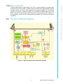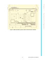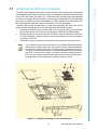
1
User Manual
MIC-3392 Rev.2
6U CompactPCI Intel Core 2 Duo
Processor Based Board with
Dual PCIe GbE/DDR2/SATA/PMC
Copyright
The documentation and the software included with this product are copyright 2008 by
Advantech Co., Ltd. All rights are reserved. Advantech Co., Ltd. reserves the right to
make improvements in the products described in this manual at any time without
notice. No part of this manual may be reproduced, copied, translated or transmitted
in any form or by any means without the prior written permission of Advantech Co.,
Ltd. Information provided in this manual is intended to be accurate and reliable. However, Advantech Co., Ltd. assumes no responsibility for its use, nor for any infringements of the rights of third parties, which may result from its use.
Acknowledgements
Intel and Pentium are trademarks of Intel Corporation.
Microsoft Windows and MS-DOS are registered trademarks of Microsoft Corp.
All other product names or trademarks are properties of their respective owners.
Product Warranty (2 years)
Advantech warrants to you, the original purchaser, that each of its products will be
free from defects in materials and workmanship for two years from the date of purchase.
This warranty does not apply to any products which have been repaired or altered by
persons other than repair personnel authorized by Advantech, or which have been
subject to misuse, abuse, accident or improper installation. Advantech assumes no
liability under the terms of this warranty as a consequence of such events.
Because of Advantech’s high quality-control standards and rigorous testing, most of
our customers never need to use our repair service. If an Advantech product is defective, it will be repaired or replaced at no charge during the warranty period. For outof-warranty repairs, you will be billed according to the cost of replacement materials,
service time and freight. Please consult your dealer for more details.
If you think you have a defective product, follow these steps:
1. Collect all the information about the problem encountered. (For example, CPU
speed, Advantech products used, other hardware and software used, etc.) Note
anything abnormal and list any onscreen messages you get when the problem
occurs.
2. Call your dealer and describe the problem. Please have your manual, product,
and any helpful information readily available.
3. If your product is diagnosed as defective, obtain an RMA (return merchandise
authorization) number from your dealer. This allows us to process your return
more quickly.
4. Carefully pack the defective product, a fully-completed Repair and Replacement
Order Card and a photocopy proof of purchase date (such as your sales receipt)
in a shippable container. A product returned without proof of the purchase date
is not eligible for warranty service.
5. Write the RMA number visibly on the outside of the package and ship it prepaid
to your dealer.
MIC-3392 Rev.2 User Manual
Part No. 2002339220
Edition 1
Printed in China
September 2008
ii
Declaration of Conformity
CE
This product has passed the CE test for environmental specifications when shielded
cables are used for external wiring. We recommend the use of shielded cables. This
kind of cable is available from Advantech. Please contact your local supplier for
ordering information.
FCC Class A
Note: This equipment has been tested and found to comply with the limits for a Class
A digital device, pursuant to part 15 of the FCC Rules. These limits are designed to
provide reasonable protection against harmful interference when the equipment is
operated in a commercial environment. This equipment generates, uses, and can
radiate radio frequency energy and, if not installed and used in accordance with the
instruction manual, may cause harmful interference to radio communications. Operation of this equipment in a residential area is likely to cause harmful interference in
which case the user will be required to correct the interference at his own expense.
FM
This equipment has passed the FM certification. According to the National Fire Protection Association, work sites are classified into different classes, divisions and
groups, based on hazard considerations. This equipment is compliant with the specifications of Class I, Division 2, Groups A, B, C and D indoor hazards.
Technical Support and Assistance
1.
2.
Visit the Advantech web site at www.advantech.com/support where you can find
the latest information about the product.
Contact your distributor, sales representative, or Advantech's customer service
center for technical support if you need additional assistance. Please have the
following information ready before you call:
– Product name and serial number
– Description of your peripheral attachments
– Description of your software (operating system, version, application software,
etc.)
– A complete description of the problem
– The exact wording of any error messages
iii
MIC-3392 Rev.2 User Manual
Warnings, Cautions and Notes
Warning! Warnings indicate conditions, which if not observed, can cause personal
injury!
Caution! Cautions are included to help you avoid damaging hardware or losing
data. e.g.
There is a danger of a new battery exploding if it is incorrectly installed.
Do not attempt to recharge, force open, or heat the battery. Replace the
battery only with the same or equivalent type recommended by the manufacturer. Discard used batteries according to the manufacturer's
instructions.
Note!
Notes provide optional additional information.
Document Feedback
To assist us in making improvements to this manual, we would welcome comments
and constructive criticism. Please send all such - in writing to: [email protected]
Packing List
MIC-3392 all-in-one single board computer x1
Utility and user manual (PDF file) CD-ROM disc x1
CPU Heat sink (Assembled) x1
Thermal pad for CPU x1
HDD tray (Assembled) x 1
North Bridge Heat sink including a thermal PAD for north bridge component
(Assembled) x 1
! Daughter board for SATA HDD (Assembled) x1 (Single PMC version only)
! PMC filler panel(s) (Assembled) x1 (Single PMC version) or x2 (Dual PMC version)
! Solder-side cover (Assembled) x1
! RJ45 to DB9 cable x1
! Several screws
! Warranty certificate document x1
! Safety Warnings: CE, FCC class A
If any of these items are missing or damaged, contact your distributor or sales representative immediately.
!
!
!
!
!
!
MIC-3392 Rev.2 User Manual
iv
Safety Instructions
1.
2.
3.
Read these safety instructions carefully.
Keep this User Manual for later reference.
Disconnect this equipment from any AC outlet before cleaning. Use a damp
cloth. Do not use liquid or spray detergents for cleaning.
4. For plug-in equipment, the power outlet socket must be located near the equipment and must be easily accessible.
5. Keep this equipment away from humidity.
6. Put this equipment on a reliable surface during installation. Dropping it or letting
it fall may cause damage.
7. The openings on the enclosure are for air convection. Protect the equipment
from overheating. DO NOT COVER THE OPENINGS.
8. Make sure the voltage of the power source is correct before connecting the
equipment to the power outlet.
9. Position the power cord so that people cannot step on it. Do not place anything
over the power cord.
10. All cautions and warnings on the equipment should be noted.
11. If the equipment is not used for a long time, disconnect it from the power source
to avoid damage by transient overvoltage.
12. Never pour any liquid into an opening. This may cause fire or electrical shock.
13. Never open the equipment. For safety reasons, the equipment should be
opened only by qualified service personnel.
14. If one of the following situations arises, get the equipment checked by service
personnel:
15. The power cord or plug is damaged.
16. Liquid has penetrated into the equipment.
17. The equipment has been exposed to moisture.
18. The equipment does not work well, or you cannot get it to work according to the
user's manual.
19. The equipment has been dropped and damaged.
20. The equipment has obvious signs of breakage.
21. DO NOT LEAVE THIS EQUIPMENT IN AN ENVIRONMENT WHERE THE
STORAGE TEMPERATURE MAY GO BELOW -20° C (-4° F) OR ABOVE 60° C
(140° F). THIS COULD DAMAGE THE EQUIPMENT. THE EQUIPMENT
SHOULD BE IN A CONTROLLED ENVIRONMENT.
22. CAUTION: DANGER OF EXPLOSION IF BATTERY IS INCORRECTLY
REPLACED. REPLACE ONLY WITH THE SAME OR EQUIVALENT TYPE
RECOMMENDED BY THE MANUFACTURER, DISCARD USED BATTERIES
ACCORDING TO THE MANUFACTURER'S INSTRUCTIONS.
23. The sound pressure level at the operator's position according to IEC 704-1:1982
is no more than 70 dB (A).
DISCLAIMER: This set of instructions is given according to IEC 704-1. Advantech
disclaims all responsibility for the accuracy of any statements contained herein.
v
MIC-3392 Rev.2 User Manual
Safety Precaution - Static Electricity
Follow these simple precautions to protect yourself from harm and the products from
damage.
! To avoid electrical shock, always disconnect the power from your PC chassis
before you work on it. Don't touch any components on the CPU card or other
cards while the PC is on.
! Take anti-static precautions before making any configuration changes. Electrostatic discharge events that occur when connecting a jumper or installing a card
or other device can severely damage sensitive electronic components.
MIC-3392 Rev.2 User Manual
vi
Contents
Chapter
1
Hardware Configuration......................1
1.1
Introduction ............................................................................................... 2
Table 1.1: MIC-3392 Variants...................................................... 2
Specifications ............................................................................................ 3
1.2.1 CompactPCI Bus Interface ........................................................... 3
1.2.2 CPU .............................................................................................. 3
1.2.3 Processor...................................................................................... 3
Table 1.2: Intel Processors.......................................................... 3
1.2.4 BIOS ............................................................................................. 3
1.2.5 Chipset.......................................................................................... 3
1.2.6 Memory ......................................................................................... 5
Table 1.3: SODIMM Types (Non-ECC) ....................................... 5
1.2.7 Ethernet ........................................................................................ 6
1.2.8 Storage interface........................................................................... 6
1.2.9 Serial ports.................................................................................... 6
1.2.10 USB port ....................................................................................... 6
1.2.11 LEDs ............................................................................................. 6
1.2.12 Watchdog timer............................................................................. 6
1.2.13 Optional Rear I/O Modules ........................................................... 6
1.2.14 Mechanical and Environmental Specifications.............................. 7
1.2.15 Compact Mechanical Design ........................................................ 7
1.2.16 CompactPCI Bridge ...................................................................... 7
1.2.17 I/O Connectivity............................................................................. 8
1.2.18 PMC (PCI Mezzanine Card) IEEE1386.1 Compliant .................... 8
1.2.19 Hardware Monitor ......................................................................... 8
1.2.20 Super IO........................................................................................ 8
1.2.21 RTC and Battery ........................................................................... 8
1.2.22 IPMI............................................................................................... 8
1.2.23 HPET and IO/APIC ....................................................................... 9
Functional Block Diagram ......................................................................... 9
Figure 1.1 MIC-3392 Rev.2 functional block diagram.................. 9
Jumpers and Switches ............................................................................ 10
Table 1.4: MIC-3392 jumper descriptions.................................. 10
Table 1.5: MIC-3392 switch descriptions................................... 10
1.4.1 Jumper Settings .......................................................................... 10
Table 1.6: JP2 VGA output settings .......................................... 10
Table 1.7: Backplane PCI-X / PCI settings................................ 10
1.4.2 Clear CMOS (JP1) ...................................................................... 10
Table 1.8: JP1 Clear CMOS ...................................................... 10
1.4.3 Switch Settings ........................................................................... 11
Table 1.9: SW5-1 LAN for BMC ................................................ 11
Table 1.10: SW5-2 SATA HDD channel setting (single PMC) .... 11
Table 1.11: SW5-2 SATA HDD channel setting (dual PMC) ....... 11
Table 1.12: SW5-3 & SW5-4: BMC, SIO & RTM COM2 selections
.................................................................................. 11
Table 1.13: SW6 IPMI programming setting................................ 12
Table 1.14: SW7 - Master/Drone mode setting ........................... 12
Table 1.15: SW1: BMC Reset Button & Platform Reset Button .. 12
Figure 1.2 MIC-3392 Rev.2 jumper, switch and connector locations .......................................................................... 13
Connector Definitions.............................................................................. 14
Table 1.16: MIC-3392 connector descriptions............................. 14
1.5.1 VGA Display Connector (VCN1 or rear I/O)................................ 15
1.5.2 Serial Ports (CN9 and Rear I/O) ................................................. 15
1.2
1.3
1.4
1.5
vii
MIC-3392 Rev.2 User Manual
1.8
1.9
1.5.3 USB Connector (CN11/12 and Rear I/O).................................... 15
1.5.4 CompactFlash Socket (CN10) .................................................... 15
1.5.5 SATA daughter board connector (CN4) (Single PMC only)........ 15
1.5.6 Ethernet Configuration (RJ1/RJ2 or Rear I/O RJ1) .................... 16
1.5.7 PMC Connector (J21/22/23 for PMC1, J11/12/13 for PMC2)..... 16
1.5.8 SW1 (System reset and BMC reset button)................................ 16
Safety Precautions.................................................................................. 16
Installing the CPU and Heatsink ............................................................. 17
Figure 1.3 Complete assembly of CPU and heat sink............... 17
1.7.1 CPU & Heatsink Installation Steps ............................................. 18
Battery Replacement .............................................................................. 19
Software Support .................................................................................... 19
2
AMI BIOS Setup................................. 21
2.1
Introduction ............................................................................................. 22
Figure 2.1 Setup program initial screen..................................... 22
Entering Setup ........................................................................................ 23
Figure 2.2 Press Del to run Setup ............................................. 23
Main Setup.............................................................................................. 24
Figure 2.3 Main setup screen .................................................... 24
2.3.1 System time/System date ........................................................... 24
Advanced BIOS Features Setup............................................................. 25
Figure 2.4 Advanced BIOS features setup screen .................... 25
2.4.1 CPU Configuration...................................................................... 26
Figure 2.5 CPU Configuration ................................................... 26
2.4.2 LAN & SMbus Configuration....................................................... 27
Figure 2.6 LAN & SMBus Configuration .................................... 27
Table 2.1: Select SMBus mode................................................. 27
2.4.3 IDE Configuration ....................................................................... 28
Figure 2.7 IDE Configuration ..................................................... 28
2.4.4 Floppy Configuration................................................................... 29
Figure 2.8 Floppy Configuration ................................................ 29
2.4.5 Super I/O Configuration .............................................................. 30
Figure 2.9 Super I/O Configuration............................................ 30
2.4.6 ACPI Setting ............................................................................... 31
Figure 2.10ACPI Setting............................................................. 31
2.4.7 Hardware Health Configuration .................................................. 31
Figure 2.11Hardware Health Configuration ................................ 31
2.4.8 Console Redirection Configuration ............................................. 32
Figure 2.12Configure Remote Access types and parameters.... 32
2.4.9 APM Configuration...................................................................... 33
Figure 2.13APM configuration .................................................... 33
PCI/PNP Setup ....................................................................................... 34
Figure 2.14PCI/PNP Setup......................................................... 34
2.5.1 Clear NVRAM ............................................................................. 34
2.5.2 Plug and Play O/S ...................................................................... 34
2.5.3 PCI Latency Timer ...................................................................... 34
Boot Setup .............................................................................................. 35
Figure 2.15Boot Setup................................................................ 35
2.6.1 Boot Settings Configuration ........................................................ 35
Figure 2.16Boot Settings Configuration...................................... 35
Security Setup......................................................................................... 36
Figure 2.17Password Configuration ........................................... 36
Advanced Chipset Settings..................................................................... 37
Figure 2.18Advanced Chipset Setting ........................................ 37
2.8.1 North Bridge Chipset Configuration ............................................ 37
Figure 2.19North Bridge Configuration....................................... 37
2.8.2 South Bridge Configuration......................................................... 38
1.6
1.7
Chapter
2.2
2.3
2.4
2.5
2.6
2.7
2.8
MIC-3392 Rev.2 User Manual
viii
2.9
Chapter
Figure 2.20South Bridge Configuration ...................................... 38
Exit Option............................................................................................... 39
Figure 2.21Exit Option ................................................................ 39
2.9.1 Save Changes and Exit .............................................................. 39
2.9.2 Discard Changes and Exit .......................................................... 39
2.9.3 Load Defaults.............................................................................. 39
3
IPMI .....................................................41
3.1
3.2
3.3
3.4
Introduction ............................................................................................. 42
Definitions ............................................................................................... 42
IPMI function list...................................................................................... 42
3.3.1 IPMI Device Global Commands.................................................. 43
Table 3.1: Supported IPMI commands ...................................... 43
3.3.2 BMC Device and Messaging Interfaces...................................... 43
Table 3.2: H8S12C bus connection to NIC SMBus ................... 43
Table 3.3: NIC Interrupt ............................................................. 43
Table 3.4: BMC Device and Messaging Commands................. 44
3.3.3 BMC Watchdog Timer Commands ............................................. 44
Table 3.5: BMC Watchdog Timer Commands........................... 44
3.3.4 Chassis Device Commands........................................................ 45
Table 3.6: Chassis Device commands ...................................... 45
3.3.5 Event Commands ....................................................................... 45
Table 3.7: Event commands...................................................... 45
3.3.6 PEF and Alerting Commands ..................................................... 45
Table 3.8: PEF and Alerting commands.................................... 45
3.3.7 SEL Device Commands.............................................................. 46
Table 3.9: SEL Device commands ............................................ 46
3.3.8 SDR Device Commands ............................................................. 46
Table 3.10: SDR Device commands ........................................... 46
3.3.9 FRU data..................................................................................... 46
Table 3.11: FRU Device commands............................................ 46
3.3.10 Sensors and Threshold configuration ......................................... 47
Table 3.12: Sensor List................................................................ 47
Table 3.13: Threshold values of sensors..................................... 48
Table 3.14: Sensor Device Commands....................................... 48
3.3.11 Serial over LAN........................................................................... 48
Table 3.15: LAN Device Commands ........................................... 48
3.3.12 Serial/Modem Device Commands .............................................. 49
Table 3.16: Serial/Modem Device Commands ............................ 49
BMC Reset.............................................................................................. 49
Appendix A
Pin Assignments ...............................51
A.1
J1 Connector........................................................................................... 52
Table A.1: J1 CompactPCI I/O................................................... 52
J2 Connector........................................................................................... 53
Table A.2: J2 CompactPCI I/O................................................... 53
J3 Connector........................................................................................... 54
Table A.3: J3 CompactPCI I/O (LPT, FDD, Parallel IDE, 2.16) . 54
J5 Connector........................................................................................... 55
Table A.4: J5 CompactPCI I/O (VGA, LAN, COM, USB, PS/2) . 55
Other Connectors.................................................................................... 55
Table A.5: VCN1 VGA Connector.............................................. 55
Table A.6: CN9 COM1 (RJ45) Connector.................................. 56
Table A.7: CN11 & CN12 USB port 1 & port 2........................... 56
Table A.8: CN10 CF socket ....................................................... 56
Table A.9: CN4 SATA daughter board connector...................... 56
Table A.10:RJ1 LAN1 Connector................................................ 57
A.2
A.3
A.4
A.5
ix
MIC-3392 Rev.2 User Manual
A.5.1
Table A.11:RJ1 LAN1 Indicator .................................................. 57
Table A.12:RJ2 LAN2 Indicator .................................................. 57
M/D, PWR & IDE/Hot-swap LEDs .............................................. 58
Appendix B
Programming the Watchdog Timer . 59
B.1
Watchdog Timer Programming Procedure ............................................. 60
Appendix C
CPLD .................................................. 61
C.1
C.2
Features.................................................................................................. 62
CPLD I/O Registers ................................................................................ 62
Table C.1: LPC I/O registers address ........................................ 62
C.2.1 Debug Message.......................................................................... 62
Table C.2: Debug_Code [7:0] (LPC I/O address: 80H).............. 62
C.2.2 Watchdog Register ..................................................................... 62
Table C.3: Watchdog [7:0] (LPC I/O address: 443H)................. 62
C.2.3 Watchdog Disable Register ........................................................ 63
Table C.4: Watchdog [7:0] (LPC I/O address: 444H)................. 63
Table C.5: Version [7:0] (LPC I/O address: 445H)..................... 63
C.2.4 Geography Address (GA) ........................................................... 63
Table C.6: GA [7:0] (LPC I/O address: 447H)............................ 63
MIC-3392 Rev.2 User Manual
x
Chapter
1
1
Hardware
Configuration
This chapter describes how to
configure MIC-3392 hardware.
1.1 Introduction
The MIC-3392 is a high performance, power efficient CompactPCI single-board computer based on the Intel Core 2 Duo and Core Duo microprocessors. The MIC-3392
delivers breakthrough energy-efficient performance for CompactPCI platforms. The
Intel Core 2 Duo provides enhanced energy-efficient performance to help equipment
manufacturers optimally balance processing capabilities within power and space constraints. The advanced smart cache of Core Duo dynamically allocates the shared L2
cache across cores and optimizes use of memory subsystem bandwidth to accelerate out-of-order execution. A prediction mechanism reduces the time in-flight instructions have to wait for data. The new pre-fetch algorithms move data from system
memory into fast L2 cache in advance of execution.
The Core Duo combines the benefits of two high-performance execution cores with
intelligent power management features to deliver significantly greater performance
per watt over previous Intel processors. The two execution cores share a high-performance, power-optimized 667 MHz front-side bus to access the same system memory. To save power, address and data buffers are turned off when there is no activity.
The MIC-3392 maximizes I/O throughput with PCI Express (PCIe) technology. It supports up to 4 GB of 667 MHz DDR2 memory provided by a combination of SO-DIMM
and soldered DRAM (6.4 GB/sec throughput). It supports a fast Serial-ATA interface
to an on-board hard drive or CompactFlash socket. The MIC-3392 is available in single or dual PMC variants with differing I/O combinations as listed in the table below.
Note!
The OS may report around 3GB of system memory when 4GB is
installed. Because the Intel 82945GME Graphics and Memory Controller Hub (GMCH) does not remap APIC or PCI Express memory space,
when system memory is populated with 4GB, some physical memory is
non-addressable and remains unusable by the system.
Table 1.1: MIC-3392 Variants
Features
'A' model Single PMC
'B' model Dual PMC
LAN
2
1
COM
1
1
PMC
1
2
USB
2
-
VGA
1
-
CPU
-
-
HDD socket
1
-
CF socket
1
1
SODIMM socket
1
1
MIC-3392 Rev.2 User Manual
2
1.2.1 CompactPCI Bus Interface
1.2.2 CPU
The MIC-3392 supports the latest Intel Core Duo/Solo and Intel Core 2 Duo processor family with clock frequencies up to 2.16 GHz and a Front-Side Bus (FSB) up to
667 MHz.
Intel Core Duo processors are validated with the Mobile Intel 945GME Express
chipset. This chipset provides greater flexibility for developers of embedded applications by offering improved graphics and increased I/O bandwidth over previous Intel
chipsets, as well as remote asset management capabilities, and improved storage
speed and reliability.
Currently supported processors are listed in the table below. The Intel Core Duo consists of two cores and up to 2 MB L2 cache shared by both cores. The Intel Core 2
Duo consists of two cores, up to 4 MB L2 cache shared by both cores.
1.2.3 Processor
Table 1.2: Intel Processors
Core
speed
Front-Side L2 cache
Bus speed
TDP
Package
Core Duo (T2500)
2.0 GHz
667 MHz
2 MB
31 W
FCPGA
LV Core Duo (L2400)
1.66 GHz
667 MHz
2 MB
15 W
FCBGA
Core 2 Duo (T7400)
2.16 GHz
667 MHz
4 MB
34 W
FCPGA
LV Core 2 Duo (L7400)
1.5 GHz
667 MHz
4 MB
17 W
FCBGA
Note!
Because power consumption and thermal restrictions vary between different CompactPCI systems, please double check these items before
installing a higher speed CPU not listed in the table above.
1.2.4 BIOS
An 8 Mbit Firmware Hub (FWH) contains a board-specific BIOS that is designed to
meet industrial and embedded system requirements.
1.2.5 Chipset
The Mobile Intel 945GME chipset provides excellent flexibility for developers of
embedded applications by offering improved graphics and increased I/O bandwidth
over previous Intel chipsets, as well as remote asset management capabilities and
3
MIC-3392 Rev.2 User Manual
Hardware Configuration
The MIC-3392 is compliant with PICMG 2.0 Rev. 3.0. It supports a 64-bit / 66 MHz
PCI bus for up to 8 compactPCI slots at 3.3 V or 5 V VIO. The MIC-3392 is hot-swap
compliant (PICMG 2.1) and conforms to the CompactPCI Packet Switching Backplane specification (PICMG 2.16) as well as the CompactPCI System Management
Specification (PICMG 2.9).
The board can be configured as a system master or a drone board. In drone mode it
only draws power from the CompactPCI backplane and is not active on the CompactPCI bus. However, PICMG 2.16 is still fully supported in this mode.
Chapter 1
1.2 Specifications
improved storage speed and reliability. Features include an integrated 32-bit 3D
graphics engine based on Intel Graphics Media Accelerator 950 (Intel GMA 950)
architecture.
The Mobile Intel 945GME chipset consists of the Intel 82945GME Graphics Memory
Controller Hub (GMCH) and Intel I/O Controller Hub 7-M (ICH7-M). It delivers outstanding system performance through high bandwidth interfaces such as PCI
Express, Serial ATA and Hi-Speed USB 2.0.
MIC-3392 Rev.2 User Manual
4
The MIC-3392 has up to 2 GB of onboard non-ECC DDR2 memory. In addition, an
SODIMM socket supports up to 2 GB of the following types of memory.
Table 1.3: SODIMM Types (Non-ECC)
Brand
Size
Memory
UG
512 MB DDR2 533
UG64T6400L8SU5AS
SEC 525 ZC05 K4T51083QC
EDE406CB (64x8)
Transcend 256 MB DDR2 533
119697-0060
SAMSUNG 52B K4T56083QFZCD5 BBE393BA (32x8)
512 MB DDR2 533
119833-0266
Infineon HYB18T512 800AF37
SVV39006 0526 (32x8)
1 GB
120048-0014
ELPIDA TWN E5108AE-5C-E
0517A9105 (64x8)
256 MB DDR2 533
NA
ELPIDA JAPAN E5116AB-5C-E
05020W108 (32x16)
512 MB DDR2 533
NA
ELPIDA JAPAN E5116AB-5C-E
(32x16)
1 GB
NA
ELPIDA TWN E5108AE-5C-E
0511009276 (64x8)
512 MB DDR2 533
NXBS64M64VJ-75
ELPIDA TWN E5108AE-5C-E
0525A9B1S (64x8)
1 GB
NXBS128M64VJ-75 ELPIDA TWN E5108AE-5C-E
0525A9B1S (64x8)
NEXS
Apacer
A-DATA
DDR2 533
DDR2 533
DDR2 533
256 MB DDR2 533
78.82054.420
ELPIDA JAPAN E5116AB-5C-E
05050WPWA (64x8)
512 MB DDR2 533
78.92051.421
ELPIDA JAPAN E5108AB-5C-E
04520WR5Q (64x8)
1 GB
78.02051.423
ELPIDA TWN E5108AE-5C-E
(64x8)
DDR2 533
256 MB DDR2 533
M20SS2F3G3410A1 SAMSUNG 52B K4T56083QFBOZ
GCD5 (32x8)
512 MB DDR2 533
M20EL2G3H3410A1 ELPIDA JAPAN E5108AB-5C-E
BOZ
(64x8)
1 GB
M20EL2G314430B1 ELPIDA TWN E5108AE-5C-E
BOZ
(64x8)
DDR2 533
Transcend 256 MB DDR2 667
(RoHS)
TS32MSQ64V6M
Infineon HYB18T512161BF-28
(32x16)
512 MB DDR2 667
TS64MSQ64V6J
SAMSUNG K4T51083QC ZCE6
(64x8)
1 GB
TS128MSQ64V6J
SAMSUNG K4T51083QC ZCE6
(64x8)
DDR2 667
Apacer
(RoHS)
512 MB DDR2 667
78.92G63.422
ELPIODA E5108AG-6E-E (64x8)
1 GB
78.02G63.423
ELPIODA E5108AGBG-6E-E
(64x8)
DSL
(RoHS)
256 MB DDR2 667
NA
ELPIDA E5116AF-6E-E (32x16)
512 MB DDR2 667
NA
ELPIDA E5108AGBG-6E-E (64x8)
1 GB
NA
ELPIDA E5108AGBG-6E-E (64x8)
512 MB DDR2 667
UG64T6400L8SU6AS
ELPIDA E5108AE-6E-E (32x16)
1 GB
UG12T6400L8SU6AP
ELPIDA E5108AG-6E-E (32x16)
UG
(RoHS)
DDR2 667
DDR2 667
DDR2 667
5
MIC-3392 Rev.2 User Manual
Hardware Configuration
Vendor PN
DSL
Speed
Chapter 1
1.2.6 Memory
1.2.7 Ethernet
The MIC-3392 uses two Intel 82573E LAN chips to provide 10/100/1000Base-T
Ethernet connectivity (LAN1 & LAN2) and one Intel 82562GT LAN chip to provide 10/
100Base-T Ethernet connectivity (LAN3) via rear I/O. Optional settings for the source
of each individual Gigabit Ethernet port can be selected in the BIOS menu. These are
mutually exclusive and can be any one of:
! Front I/O (RJ-45)
! Rear I/O (Rear Transition Module)
! PICMG 2.16
1.2.8 Storage interface
The MIC-3392 supports two SATA interfaces and one IDE channel. The SATA1 interface can be routed to an onboard 2.5" SATA hard disk drive or to the rear I/O module
via the J3 connector. The onboard SATA port is only available on the single PMC version of the MIC-3392. The SATA2 interface is connected to the rear I/O module via
the J5 connector and is reserved for user customized designs. Currently, Advantech's compatible RIO modules provide the SATA1 interface. The MIC-3392 also supports one IDE channel. The master is reserved for an onboard CompactFlash disk
drive (type 1). The slave is connected to a rear I/O module via the J3 connector.
1.2.9 Serial ports
One RJ-45 COM1 port (RS-232 interface) is provided on the front panel. A COM2
port is routed to a rear I/O module via the J5 connector.
1.2.10 USB port
Two USB 2.0/1.1 compliant ports with fuse protection are provided. Both ports are
routed to front panel connectors on the MIC-3392A (single-PMC board variant) and
to the rear I/O module via the J5 connector on both the single-PMC and dual-PMC
board variants.
1.2.11 LEDs
LEDs are provided on the front panel as follows:
! One bi-color LED (blue/yellow) indicates hot-swap status. Blue indicates that the
board may be safely removed from the system and yellow indicates HDD activity.
! One green LED provides power status and a further green LED indicates “Master or Drone” mode. Green indicates that the board is in “Master” mode and
when the LED is off the board is in “Drone” mode.
! One yellow LED indicates BMC heartbeat status.
1.2.12 Watchdog timer
An onboard watchdog timer provides system reset capabilities via software control.
The programmable time interval is from 1 to 255 seconds.
1.2.13 Optional Rear I/O Modules
A number of rear I/O modules are available with different I/O options:
! RIO-3310AE: 6U cPCI Rear I/O Module without SCSI
! RIO-3310S-A1E: 6U cPCI Rear I/O Module (Internal SCSI connectors)
! RIO-3310S-A2E: 6U cPCI Rear I/O Module (External SCSI connectors)
MIC-3392 Rev.2 User Manual
6
!
Operating temperature: 0 ~ 55° C (32 ~ 122° F)
Note!
!
!
!
!
Storage Temperature: -20 ~ 60° C (-4 ~ 140° F).
Humidity (Non-operating): 5 ~ 95% @ 60° C (non-condensing)
Power Consumption: (Intel Core 2 Duo and 2 GB memory)
+5 V @ 7.16 A; +3.3 V @ 3.17 A; +12 V @ 0.40 A
Board size: 233.35 x 160 mm (6U size), 1-slot (4 TE) wide
Weight: 0.8 kg (1.76 lb)
Shock: 20 G (operating); 50 G (non-operating)
Random vibration: 1.5 Grms (operating), 2.0 Grms (non-operating)
1.2.15 Compact Mechanical Design
The MIC-3392 has a specially designed CPU heat sink to enable fanless operation.
Forced air cooling in the chassis is needed for operational stability and reliability.
1.2.16 CompactPCI Bridge
The MIC-3392 uses a PLX PCI-6540 (Hint HB8) universal bridge as a gateway to an
intelligent subsystem. When configured as a system controller, the bridge acts as a
standard transparent PCI-X to PCI bridge. As a peripheral controller it allows the local
MIC-3392 processor to configure and control the onboard local subsystem independently from the CompactPCI bus host processor. The MIC-3392 local PCI subsystem
is presented to the CompactPCI bus host as a single CompactPCI device. Finally,
when the MIC-3392 is in drone mode, the PLX PCI-6540 is electrically isolated from
the CompactPCI bus. The MIC-3392 receives power from the backplane, supports
rear I/O and supports PICMG 2.16. Consult the PLX PCI-6540 (Hint HB8) datasheet
for more details. The PLX PCI-6540 PCI bridge provides the following features:
! PCI Interface
– Full compliance with the PCI Local Bus Specification, Revision 2.3
– Supports 3.3V or 5V tolerance I/O
– Transparent and non-transparent bridge function
– 64-bit, 33MHz-133MHz asynchronous operation
– Support for 8 Bus Masters
– Usable in CompactPCI system slot or peripheral slot
– 10-KB Buffer Architecture for PCI-X-to-PCI-X and PCI-X-to-PCI bridging and
speed conversion
– 1-KB downstream Posted Write buffer
– 1-KB upstream Poster Writer buffer
– 4-KB downstream Read Data buffer
– 4-KB upstream Read Data buffer
Consult the PLX PCI 6540 data book for detail.
7
MIC-3392 Rev.2 User Manual
Hardware Configuration
!
!
!
The operating temperature range of the MIC-3392 depends on the
installed processor and the airflow through the chassis.
Chapter 1
1.2.14 Mechanical and Environmental Specifications
1.2.17 I/O Connectivity
Front panel I/O is provided by two RJ-45 Gigabit Ethernet ports, one RJ-45 COM
port, two USB 2.0 ports, one VGA connector, and one PMC cutout. On the dual-PMC
version only one RJ-45 Gigabit Ethernet Port and one RJ-45 COM port are available
on the front panel due to the space taken by the second PMC cutout.
Onboard I/O consists of one IDE channel to a Compact Flash socket and additionally
on the single-PMC version of the MIC-3392, one SATA channel can be connected to
a 2.5" SATA HDD. Rear I/O connectivity is available via the following CompactPCI
connectors:
! J3: First SATA port, one IDE slave port, one floppy port, one printer port, and
two Gigabit Ethernet links to the backplane for PICMG 2.16.
! J5: Second SATA port, 10/100 LAN port, two USB ports (same ports as on the
front panel), one keyboard & mouse connector, two COM ports, a VGA port and
two Gigabit Ethernet LAN port for Rear I/O board.
The MIC-3392 provides two Gigabit Ethernet ports that can be routed to the front
panel, the rear transition module or the PICMG 2.16 packet switched backplane.
1.2.18 PMC (PCI Mezzanine Card) IEEE1386.1 Compliant
Additional I/O or co-processing functionality is supported by add-on PMC modules.
The MIC-3392 supports up to two PMC sites that are fully compliant with the
IEEE1386.1 PCI Mezzanine Card specification. PMC1 and PMC2 support a 64-bit /
66 MHz PCI bus interfac3 and 3.3 V VIO.
The two-layer front panel design complies with IEEE 1101.10. Connectors are firmly
screwed to the front panel, and a shielding gasket is attached to the panel edge. This
reduces emissions and increases protection from external interference.
1.2.19 Hardware Monitor
The MIC-3392 Super I/O (W83627DHG) is available to monitor critical hardware
parameters. It is connected to the Baseboard Management Controller (BMC) to monitor CPU temperature core voltage information.
1.2.20 Super IO
The MIC-3392 Super I/O device provides the following legacy PC devices:
! The serial port COM1 is connected to the rear I/O module or front panel
! The serial port COM2 is connected to the rear I/O module or BMC
! The parallel port is routed to the rear I/O module
! The FDD is routed to the rear I/O module
! The PS/2 keyboard and mouse is routed to the rear I/O module
1.2.21 RTC and Battery
The RTC module keeps the date and time. On the MIC-3392 the RTC circuitry is connected to a battery source (CR2032M1S8-LF, 3 V, 210 mAH).
1.2.22 IPMI
The MIC-3392 uses the Intelligent Platform Management Interface (IPMI) to monitor
the health of an entire system. A Renesas H8S/2167 microcontroller provides BMC
functionality to interface between system management software and platform hardware. The MIC-3392 implements fully-compliant IPMI 2.0 functionality and conforms
to the PICMG 2.9 R1.0 specification. The IPMI firmware is based on proven technology from Avocent. Full IPMI details are covered in Chapter 3.
MIC-3392 Rev.2 User Manual
8
The MIC-3392's built-in south bridge, the ICH7, provides features to support High
Precision Event Timer (HPET) registers and I/O Advanced Programmable Interrupt
Controller (APIC). The ICH7 timer registers are memory-mapped in a non-indexed
scheme. The choice of address range will be selected by configuration bits in the
HPET. The ICH7 incorporates an APIC that can be used in either a uni-processor or
multi-processor system, like the standard ISA-compatible PIC used in a uni-processor system.
Hardware Configuration
1.3 Functional Block Diagram
Figure 1.1 MIC-3392 Rev.2 functional block diagram
9
Chapter 1
1.2.23 HPET and IO/APIC
MIC-3392 Rev.2 User Manual
1.4 Jumpers and Switches
Table 1.4 and table 1.5 list the jumper and switch functions. Figure 1.2 illustrates the
jumper and switch locations. Read this section carefully before changing the jumper
and switch settings on your MIC-3392 board.
Table 1.4: MIC-3392 jumper descriptions
Number
Function
JP1
Clear CMOS
JP2
VGA Output Setting
JP3
Backplane PCIx / PCI setting
Table 1.5: MIC-3392 switch descriptions
Number
Function
SW5-1
LAN for BMC
SW5-2
SATA HDD channel Setting
SW5-3 & SW5-4
COM2 to console or BMC setting
SW6
IPMI programming / console setting
SW7
Master/Drone
1.4.1 Jumper Settings
Table 1.6: JP2 VGA output settings
Default
Front Panel
1-2
RTM
2-3
Table 1.7: Backplane PCI-X / PCI settings
Default
PCI-X
Open
PCI(reserved)
Closed
1.4.2 Clear CMOS (JP1)
This jumper is used to erase CMOS data and reset the system BIOS information. Follow the procedures below to clear the CMOS.
1. Turn off the system.
2. Close jumper JP1 (1-2) for about 3 seconds.
3. Set jumper JP1 as Normal.
4. Turn on the system. The BIOS is reset to its default setting.
Table 1.8: JP1 Clear CMOS
Default
Normal
MIC-3392 Rev.2 User Manual
open
10
Chapter 1
Table 1.8: JP1 Clear CMOS
Clear CMOS
closed
1.4.3 Switch Settings
Table 1.9: SW5-1 LAN for BMC
LAN2
on
LAN3 (reserved)
off
SW5-1 selects the LAN port that is used for Serial Over LAN (SoL) functionality. The
10/100 LAN3 port is routed to the rear I/O but is not currently implemented on standard Advantech Rear I/O modules.
Table 1.10: SW5-2 SATA HDD channel setting (single PMC)
Default
On board
on
RTM
off
Table 1.11: SW5-2 SATA HDD channel setting (dual PMC)
Default
RTM
off
SW5-2 selects the routing of SATA channel 0 to either the onboard HDD socket or
Rear IO module.
Table 1.12: SW5-3 & SW5-4: BMC, SIO & RTM COM2 selections
SW5-3
SW-5-4
BMC to RTM (Default)
On
On
SIO to RTM
On
Off
11
MIC-3392 Rev.2 User Manual
Hardware Configuration
Default
Table 1.12: SW5-3 & SW5-4: BMC, SIO & RTM COM2 selections
SIO to BMC
Off
Off
When COM2 is not used as a console interface, it is used to communicate BMC information via the onboard SIO COM2 or RTM COM2. SW5-3 and SW5-4 determine
whether COM2 is routed via SIO COM2 or RIO COM2. Three modes are available.
BMC to RTM COM2 is the default.
Table 1.13: SW6 IPMI programming setting
BMC firmware programmable
ON OFF ON OFF ON ON
Default
BMC to console
OFF ON OFF ON OFF OFF
When COM2 is connected to the BMC, the BMC firmware can be re-programmed by
setting switch 6 to “BMC firmware programmable” mode.
Table 1.14: SW7 - Master/Drone mode setting
Default
Master
ON ON
Drone
OFF OFF
The MIC-3392 default setting is Master.
Table 1.15: SW1: BMC Reset Button & Platform Reset Button
SW1-1
BMC Reset
SW1-2
Reset (Platform Reset)
MIC-3392 Rev.2 User Manual
12
Chapter 1
13
MIC-3392 Rev.2 User Manual
Hardware Configuration
Figure 1.2 MIC-3392 Rev.2 jumper, switch and connector locations
1.5 Connector Definitions
Onboard connectors link to external devices such as hard disk drives, keyboards or
floppy drives. Table 1.11 lists the function of each connector and Figure 1.2 illustrates
each connector location.
Table 1.16: MIC-3392 connector descriptions
Number
Function
VCN1
VGA Connector
CN9
COM1 (RJ45)
CN11
USB port 1
CN12
USB port 2
BH1
CMOS Battery
CN10
CompactFlash socket
CN4
SATA daughter board connector
RJ1
LAN1 Connector
RJ2
LAN2 Connector
J1/J2
Primary CompactPCI bus
J3/J5
Rear I/O transition
DDR2 Channel A
SODIMM socket
MIC-3392 Rev.2 User Manual
14
1.5.2 Serial Ports (CN9 and Rear I/O)
The MIC-3392 provides two serial ports. COM1 is available as an RS-232 interface
via an RJ-45 connector on the front panel (CN9). An RJ-45 to DB-9 adaptor cable is
provided in the MIC-3392 accessories to facilitate connectivity to external console or
modem devices. Both the COM1 and COM2 ports are connected to the RIO-3310
series of rear I/O boards. The BIOS Advanced Setup program covered in Chapter 2
provides a user interface for features such as enabling or disabling the ports and setting the port address. Many serial devices implement the RS-232 standard in different ways. If you are having problems with a serial device, be sure to check the pin
assignments for the connector. The IRQ and address range for both ports are fixed.
However, if you wish to disable the port or change these parameters later, you can do
this in the system BIOS setup.
1.5.3 USB Connector (CN11/12 and Rear I/O)
The MIC-3392 provides four Universal Serial Bus (USB) 2.0 channels. Two front
panel USB ports CN11 and CN12 are available on the single PMC variant of the MIC3392. Two USB channels are routed to rear I/O via the J5 connector. The USB interface provides complete plug and play, hot attach/detach for up to 127 external
devices. The MIC-3392 USB interface complies with USB specification rev. 2.0 and is
fuse protected (5 V @ 1.1 A). The USB interface can be disabled in the system BIOS
setup. The USB controller default is set to “Enabled”.
1.5.4 CompactFlash Socket (CN10)
The MIC-3392 features an on-board Compact Flash mass storage device connector.
When populated with a flash disk it appears to the user as an intelligent ATA (IDE)
disk drive with the same functionality and capabilities as a “rotating media” IDE hard
drive. The MIC-3392 BIOS includes an option to allow the board to boot from the
flash disk. The CompactFlash socket is connected to the IDE interface and 5 V
power. UltraDMA is supported and has been tested on a number of devices from different manufacturers. Please contact your local support office in the unlikely event
that you have any interoperability issues.
1.5.5 SATA daughter board connector (CN4) (Single PMC only)
The MIC-3392 provides two SATA interfaces: SATA1 channel via CN4 connects to
the onboard SATA HDD or via the J3 connector to a rear I/O board when selected by
switch SW5-2.
15
MIC-3392 Rev.2 User Manual
Hardware Configuration
The MIC-3392 incorporates the Intel 945GME Graphic Memory Controller Hub
(GMCH). The Intel Graphics Media Accelerator 950 (Intel GMA 950) graphics core is
an intelligent and responsive graphics engine built into the chipset. This integration
provides incredible visual quality, faster graphics performance and flexible display
options without the need for a separate graphics card. The Intel GMA 950 operates at
256-bit core speeds of up to 400 MHz. The GMA 950 graphics core supports a bandwidth of up to 10.6 GB/sec with up to 224 MB of DDR2 667 video memory. The maximum resolution is 2048 x 1536 at 75 Hz.
The VCN1 connector of MIC-3392 and the VCN1 connector of the corresponding
rear I/O board both provide DB-15 connectors for VGA monitors. The system monitor
display is routed to either the front panel or the rear I/O module depending on the
position of jumper JP2.
Chapter 1
1.5.1 VGA Display Connector (VCN1 or rear I/O)
1.5.6 Ethernet Configuration (RJ1/RJ2 or Rear I/O RJ1)
The MIC-3392 is equipped with two high performance, PCI-Express based, network
interface controllers which provide fully compliant IEEE 802.3u 10/100/1000Base-TX
Ethernet interfaces. Users can select front panel, rear I/O or PICMG 2.16 connectivity
via the BIOS. Users can choose the LAN1 and LAN2 either via the front panel RJ-45
connectors (RJ1 and RJ2) or the RJ-45 connector (RJ1) on the rear I/O module. The
medium type can be configured via software included on the accompanying utility
CD-ROM. Furthermore, the MIC-3392 supports the PICMG 2.16 Packet Switching
Backplane Specification via the J3 connector.
1.5.7 PMC Connector (J21/22/23 for PMC1, J11/12/13 for PMC2)
The MIC-3392 supports one or two PCI Mezzanine Cards (commonly known as
PMCs or PMC modules). PMC1 and PMC2 connect to a 64-bit / 66 MHz, 3.3 V PCI
bus. PMC2 is only available on the dual PMC version of the MIC-3392. Front panel
access is provided for the PMCs that require I/O connectivity.
1.5.8 SW1 (System reset and BMC reset button)
The MIC-3392 provides a system reset button located on the front panel. The system
reset button resets all payload and application-related circuitry. It does not reset the
system management (IPMI) related circuitry. A separate BMC reset button on the
front panel is provided for the BMC and related hardware.
1.6 Safety Precautions
Follow these simple precautions to protect yourself from harm and the products from
damage.
! To avoid electric shock, always disconnect the power from your CompactPCI
chassis before you work on it. Don't touch any components on the CPU board or
other boards while the CompactPCI chassis is powered.
! Disconnect power before making any configuration changes. The sudden rush
of power as you connect a jumper or install a board may damage sensitive electronic components.
! Always ground yourself to remove any static charge before you touch your CPU
board. Be particularly careful not to touch the chip connectors.
! Modern integrated electronic devices, especially CPUs and memory chips, are
extremely sensitive to static electric discharges and fields. Keep the board in its
antistatic packaging when it is not installed in the chassis, and place it on a
static dissipative mat when you are working with it. Wear a grounding wrist strap
for continuous protection.
MIC-3392 Rev.2 User Manual
16
Note!
If your product comes with a processor in a soldered µFCBGA package,
please add a different heat sink. You need to insert a heat pad between
the processor and the heat sink. The heat pad is provided in the accessory bag. The heat pad should be positioned between the heat sink and
the CPU. The heat pad is fragile, so please be careful during disassembly. If you are using a heat pad other than the one issued by Advantech,
be aware that it may not absorb a sufficient amount of heat.
Figure 1.3 Complete assembly of CPU and heat sink
17
MIC-3392 Rev.2 User Manual
Hardware Configuration
The MIC-3392 supports Intel Core Duo/Solo and Core 2 Duo processors. Advantech
has designed a heat sink to meet the critical environmental conditions and size limitations of the MIC-3392 (see figure 1.3). Advantech also provides larger heat sinks as
an option to support stricter operation environments. Application of such heat sinks
may lead to restrictions and/or unavailability of other features of the MIC3392. Contact an Advantech local sales office or distributor for more information.
The MIC-3392 should be fastened to a heat sink supporting the Intel Core 2 Duo.
When the user installs the CPU, the following steps should be followed:
1. Remove the screws from the solder side cover. During this step, the front panel
should also loosen. Be careful not to damage the SBC during disassembly.
2. Remove the last four screws from the heat sink, and then loosen the heat sink
for CPU installation. Apply the silicone heat sink compound, found in the accessory bag, to the CPU.
3. Follow the reverse procedure to replace the heat sink and solder side cover.
Chapter 1
1.7 Installing the CPU and Heatsink
1.7.1 CPU & Heatsink Installation Steps
The MIC-3392 contains electrostatically sensitive devices. Please discharge your
clothing before touching the assembly. Do not touch components or connector pins.
We recommend that you perform assembly at an anti-static workbench.
1. Check that the following components are close at hand:
– 1 x CPU
– Thermal paste
– 1 x Heatsink
– 4 x screws
– 4 x springs
2.
3.
Apply thermal paste to the top of the CPU die.
On the CPU interposer socket, turn the top screw in the “open” direction, to
ensure that it is in the unlocked position.
4.
Carefully orient the CPU to the interposer socket
5.
Turn the top screw to the “close” position to lock the processor in the socket.
Note!
6.
Match the corner of the interposer socket to the corner of the processor
with triangle mark.
Align the screw holes on the heatsink with the spacers on the PCB and seat the
heatsink on the processor.
MIC-3392 Rev.2 User Manual
18
Fasten the heatsink to the base plate.
Chapter 1
7.
The battery model number is CR2032M1S8-LF, a 3 V, 210 mAH battery. Replacement batteries may be purchased from Advantech.
When ordering the battery, please use the following part number:
1750129010 -- BATTERY 3V/210 mAh with WIRE ASS'YCR2032M1S8-LF
1.9 Software Support
Windows XP, Windows 2003 and Fedora Linux 5 have been fully tested on the MIC3392. Please contact your local sales representative for details on support for other
operating systems.
19
MIC-3392 Rev.2 User Manual
Hardware Configuration
1.8 Battery Replacement
MIC-3392 Rev.2 User Manual
20
Chapter
2
2
AMI BIOS Setup
This chapter describes how to
configure the AMI BIOS.
2.1 Introduction
The AMI BIOS has been customized and integrated into many industrial and embedded motherboards for over a decade. This section describes the BIOS which has
been specifically adapted to the MIC-3392. With the AMI BIOS Setup program, you
can modify BIOS settings and control the special features of the MIC-3392. The
Setup program uses a number of menus for making changes and turning the special
features on or off. This chapter describes the basic navigation of the MIC-3392 setup
screens.
Figure 2.1 Setup program initial screen
The BIOS ROM has a built-in Setup program that allows users to modify the basic
system configuration. This information is stored in battery-backed up CMOS so it
retains the Setup information when the power is turned off.
MIC-3392 Rev.2 User Manual
22
Turn on the computer and check for the “patch” code. If there is a number assigned to
the patch code, it means that BIOS supports your CPU. If there is no number
assigned to the patch code, please contact an Advantech application engineer to
obtain an up-to-date patch code file. This will ensure that your CPU's system status is
valid. After ensuring that you have a number assigned to the patch code, press
<DEL> and you will immediately be allowed to enter Setup.
Chapter 2
2.2 Entering Setup
AMI BIOS Setup
Figure 2.2 Press Del to run Setup
23
MIC-3392 Rev.2 User Manual
2.3 Main Setup
When you first enter the BIOS Setup Utility, you will enter the Main setup screen. You
can always return to the Main setup screen by selecting the Main tab. Two main
setup options are described in this section. The main BIOS setup screen is shown
below.
Figure 2.3 Main setup screen
The main BIOS setup menu screen has two main frames. The left frame displays all
the options that can be configured. “Grayed-out” options cannot be configured, whilst
options in blue can. The right frame displays the key legend. Above the key legend is
an area reserved for a text message. When an option is selected in the left frame, it is
highlighted in white. Often a text message will accompany it.
2.3.1 System time/System date
Use this option to change the system time and date. Highlight System Time or System Date using the <Arrow> keys. Enter new values through the keyboard. Press the
<Tab> key or the <Arrow> keys to move between fields. The date must be entered in
MM/DD/YY format. The time is entered in HH:MM:SS format.
MIC-3392 Rev.2 User Manual
24
Select the Advanced tab from the MIC-3392 setup screen to enter the Advanced
BIOS Setup screen. You can select any of the items in the left frame of the screen,
such as CPU Configuration, to go to the sub menu for that item. You can display an
Advanced BIOS Setup option by highlighting it using the <Arrow> keys. All Advanced
BIOS Setup options are described in this section. The Advanced BIOS Setup screen
is shown below. The sub menus are described on the following pages.
Chapter 2
2.4 Advanced BIOS Features Setup
AMI BIOS Setup
Figure 2.4 Advanced BIOS features setup screen
25
MIC-3392 Rev.2 User Manual
2.4.1 CPU Configuration
Figure 2.5 CPU Configuration
2.4.1.1 Max CPUID Value Limit
It is recommended that you leave this value at the default setting of Disabled.
Please note that this BIOS feature currently only allows the Intel Pentium 4 processor
with Hyper-Threading Technology to work with operating systems that do not support
extra CPUID information provided by the processor.
2.4.1.2 Core Multi-Processing
This item specifies the CPU to perform multi-processing. The default setting for this
item is set to “Enabled“.
2.4.1.3 CPU TM function
This item specifies the Thermal Monitor Feature. If set to “Enabled,” the BIOS
enables the CPU's built in automatic thermal throttling when the die temperature is
very near to the temperature limits of the processor. If set to “Disabled” the BIOS disables this feature and the MIC-3392 will shut off automatically if the CPU overheats.
The default setting is “Enabled”.
MIC-3392 Rev.2 User Manual
26
Chapter 2
2.4.2 LAN & SMbus Configuration
AMI BIOS Setup
Figure 2.6 LAN & SMBus Configuration
2.4.2.1 Select LAN1/LAN2 mode
The item allows you to choose where the LAN1 and LAN2 Gigabit Ethernet ports are
connected. There are 3 options: Front (Default), PICMG 2.16 and Rear I/O board.
2.4.2.2 Select SMBus mode
This setting indicates whether remote management is performed by IPMI-enabled
CMM such as the Advantech MIC-3927. The default setting is “BMC” which corresponds to IPMI-enabled CMM.
Table 2.1: Select SMBus mode
MIC-3927
Default
BMC
27
MIC-3392 Rev.2 User Manual
2.4.3 IDE Configuration
Figure 2.7 IDE Configuration
2.4.3.1 ATA/IDE Configuration
Three options are available: Disabled, Compatible or Enhanced. “Disabled” means
that all IDE resources are disabled. “Compatible” enables up to 2 IDE channels for
OSs requiring legacy IDE operation (default setting) and “Enhanced” enables all
SATA and PATA resources.
2.4.3.2 Legacy IDE Channels
Four options are available: SATA Only, Reserved, “SATA Pri, PATA Sec” or PATA
Only.
2.4.3.3 Primary and Secondary IDE Master and Slave
While entering setup, BIOS auto detects the presence of IDE devices. This displays
the status of auto detection of the four possible IDE devices.
MIC-3392 Rev.2 User Manual
28
Chapter 2
2.4.4 Floppy Configuration
AMI BIOS Setup
!
!
Figure 2.8 Floppy Configuration
Floppy A: Select the type of floppy drive connected to the system.
Floppy B: Select the type of floppy drive connected to the system.
29
MIC-3392 Rev.2 User Manual
2.4.5 Super I/O Configuration
!
!
!
!
Figure 2.9 Super I/O Configuration
Onboard Floppy Controller: Used to enable or disable the floppy controller
Serial Port1 Address: Used to select Serial Port1 base addresses
Serial Port2 Address: Used to select Serial Port2 base addresses
Parallel Port Address: Used to select Parallel Port base addresses
– Parallel Port Mode: Used to select Parallel Port mode
– Parallel Port IRQ: Used to select Parallel Port IRQ
MIC-3392 Rev.2 User Manual
30
Chapter 2
2.4.6 ACPI Setting
AMI BIOS Setup
Figure 2.10 ACPI Setting
The options for “ACPI Aware O/S” are “Yes” or “No” in order to enable or disable
ACPI support for the operating system. The default is “Yes”.
2.4.7 Hardware Health Configuration
Figure 2.11 Hardware Health Configuration
31
MIC-3392 Rev.2 User Manual
2.4.8 Console Redirection Configuration
Figure 2.12 Configure Remote Access types and parameters
2.4.8.1 Remote Access
You can disable or enable the BIOS remote access feature here. The optimal and
fail-safe default setting is “Enabled”.
2.4.8.2 Serial Port Number
Select the serial port you want to use for console redirection. You can set the value
for this option to either ICH COM1 or ICH COM2. The optimal and fail-safe default
setting is ICH COM1.
2.4.8.3 Serial Port Mode
Select the baud rate you want the serial port to use for console redirection. The optimal and fail-safe default setting is 115200 8, n, 1.
2.4.8.4 Flow Control
Select the flow control setting for the console re-direction - “None“, “Hardware“, and
“Software“. The default setting is “None“.
MIC-3392 Rev.2 User Manual
32
Chapter 2
2.4.9 APM Configuration
AMI BIOS Setup
Figure 2.13 APM configuration
APM allows the BIOS to control the system’s power management without the knowledge of the operating system. The default setting for “Power Management/APM” is
“Enabled”.
Note!
!
!
!
!
!
!
!
!
!
!
When both ACPI and APM modes are enabled at the same on the BIOS
setup, the former power management control will take precedence if the
OS supports ACPI mode.
Video Power Down Mode: Used to power down the video in “Suspend” mode.
Hard Disk Power Down Mode: Used to power down the hard disk drive in
“Suspend” mode.
Suspend Time Out: Allows the system to go into suspend in the specific time.
Throttle Slow Clock Ratio: Used to select the duty cycle of the CPU in throttle
mode. The default setting for this feature is “50%”.
Keyboard & PS/2 Mouse: Allows the system to monitor KBC Ports 60/6
Power Button Mode: Allows the system to go into on/off, or suspend when
power button is pressed. The default setting for this feature is “On/Off”.
Resume On Ring: Used to disable or enable RI to generate a wake up event.
Resume On LAN: Used to disable or enable LAN GPI to generate a wake up
event.
Resume On PME#: Used to disable or enable PME to generate awake event.
Resume On RTC Alarm: Used to disable or enable RTC to generate a wake
event.
33
MIC-3392 Rev.2 User Manual
2.5 PCI/PNP Setup
Select the PCI/PnP tab from the MIC-3392 setup screen to enter the Plug and Play
BIOS Setup screen. You can display a Plug and Play BIOS Setup option by highlighting it using the <Arrow> keys. All Plug and Play BIOS Setup options are described in
this section. The Plug and Play BIOS Setup screen is shown below.
Figure 2.14 PCI/PNP Setup
2.5.1 Clear NVRAM
Set this value to force the BIOS to clear the Non-Volatile Random Access Memory
(NVRAM). The optimal and fail-safe default setting is No.
2.5.2 Plug and Play O/S
Set this value to allow the system to modify the settings for Plug and Play operating
system support. The optimal and fail-safe default setting is No.
2.5.3 PCI Latency Timer
This option sets the latency of all PCI devices on the PCI bus. The optimal and failsafe default setting is 64.
MIC-3392 Rev.2 User Manual
34
Chapter 2
2.6 Boot Setup
AMI BIOS Setup
Figure 2.15 Boot Setup
2.6.1 Boot Settings Configuration
!
Figure 2.16 Boot Settings Configuration
Quick Boot: Allows the BIOS to skip certain tests while booting. This will
decrease the time needed to boot the system.
35
MIC-3392 Rev.2 User Manual
!
!
!
Boot From LAN1/2/3 Support: Used to set the system bootable from LAN1/2/
3. The default setting is on “Disabled“.
Wait For 'F1' If Error: Wait for the F1 key to be pressed if an error occurs.
Hit 'DEL' Message Display: Displays “Press DEL to run Setup” in POST.
2.7 Security Setup
Figure 2.17 Password Configuration
Select Security Setup from the MIC-3392 Setup main BIOS setup menu. All Security
Setup options, such as password protection and virus protection, are described in
this section. To access the sub menu for the following items, select the item and
press <Enter>:
! Change Supervisor Password
! Change User Password
! Clear User Password
MIC-3392 Rev.2 User Manual
36
Chapter 2
2.8 Advanced Chipset Settings
AMI BIOS Setup
Figure 2.18 Advanced Chipset Setting
2.8.1 North Bridge Chipset Configuration
Figure 2.19 North Bridge Configuration
37
MIC-3392 Rev.2 User Manual
!
!
!
!
!
!
!
!
!
!
DRAM Frequency: Available settings are “Auto” (default), “400MHz”,
“533MHz”, and “667MHz”.
Configure DRAM timing by SPD: Available settings are “Enable” (default) and
“Disabled”.
Memory Hole: Available settings are “Disabled” (default) and “15MB-16MB”.
Boots Graphic Adapter Priority: Select which graphics controller to use as the
primary boot device.
Internal Graphics Mode Select: Available settings are “Enabled, 8MB”
(default), “Enabled, 1MB”, and “Disabled”.
PEG Port: Available settings are “Auto” (default) and “Disabled”.
PEG Force x1: Available settings are “Disabled” (default) and “Enabled”.
Chipset Thermal Throttling: Allows the BIOS to enable or disable chipset
Thermal Throttling.
DT in SPD: The item specifies the GMCH to support the Delta Temperature
(DT) in SPD thermal management algorithm as specified by JEDEC. The
default setting is “Disabled”.
TS on DIMM: The item specifies the GMCH to support the Thermal Sensor (TS)
on DIMM thermal management functionality as specified by JEDEC. The default
setting is “Disabled”.
2.8.2 South Bridge Configuration
!
!
Figure 2.20 South Bridge Configuration
USB 2.0 Controller: Enabled, Disabled
Audio Controller: Auto, Azalia, AC'97 Audio and Modem, All Disabled
MIC-3392 Rev.2 User Manual
38
Chapter 2
2.9 Exit Option
AMI BIOS Setup
Figure 2.21 Exit Option
2.9.1 Save Changes and Exit
When you have completed the system configuration changes, follow these steps:
1. Select Exit Saving Changes from the Exit menu and press <Enter>. The following messages appear on the screen:
Save Configuration Changes and Exit Now?
[Ok] [Cancel]
2. Select Ok to save changes and exit.
2.9.2 Discard Changes and Exit
Follow these steps to quit Setup without making any permanent changes to the system configuration.
1. Select Exit Discarding Changes from the Exit menu and press <Enter>. The following messages appear on the screen:
Discard Changes and Exit Setup Now?
[Ok] [Cancel]
2. Select Ok to discard changes and exit. The following messages appear on the
screen:
Discard Changes
3. Select Discard Changes from the Exit menu and press <Enter>.
2.9.3 Load Defaults
This loads the safe defaults values for the MIC-3392 which allows optimum functionality and system performance, but may not work best for all computer applications.
Select Load Defaults from the Exit menu and press <Enter>.
39
MIC-3392 Rev.2 User Manual
MIC-3392 Rev.2 User Manual
40
Chapter
3
3
IPMI
This chapter describes IPMI configuration.
3.1 Introduction
The MIC-3392 fully supports the IPMI 2.0 interface and the PICMG 2.9 R1.0 specification. The Renesas H8S/2167 has been implemented as the IPMI controller / Baseboard Management Controller (BMC) to run firmware and collect information. The
MIC-3392 IPMI firmware is sourced from Avocent, a provider of proven and tested
IPMI implementations in a wide range of mission-critical applications. The BMC's key
features and functions are listed below.
! Compliant with IPMI specification, revision 2.0
! Compliant with PICMG 2.9 specification
! Environment monitoring (temperature and voltage)
! Power/Reset control via IPMI chassis command
! Complete SEL, SDR and FRU functionality
! FRU data capacity: 2 KB
! Provides 4 messaging interfaces
– One serial port
– One LPC interface
– One IPMB channel
– One LAN channel messaging via sideband NIC for out-of-band management
! 4 I2C buses (including IPMB and SMBus) and 2 optional others
! Firmware Hub flashing and updating over serial port
! 1 hardware monitor
! 1 interrupt input
! Sensors threshold configuration
! Complete IPMI watchdog functionality (reset, power down, power cycle)
! Platform even filtering (PEF) and alert policies
! External Event Generation
3.2 Definitions
!
!
!
!
BMC - (Baseboard Management Controller): This is the common abbreviation
for an IPMI Baseboard Management Controller.
IPMB - (Intelligent Platform Management Bus): A protocol defined for passing
IPMI messages over a public I2C bus.
IPMI - (Intelligent Platform Management Interface): A standardized system
management interface. Please refer to the IPMI Specification for more details.
IPMIv2.0: Specifically version 2.0 of IPMI
3.3 IPMI function list
The following standard IPMI commands are supported.
Note!
The Network function (NetFn) field identifies the functional class of the
message. The Network Function clusters IPMI commands into different
sets. Please refer to the IPMI specification of network function codes for
more information.
These command codes are compliant with the IPMI specification.
Mandatory and Optional commands are defined in the IPMI specification. For more details, please refer to the IPMI specification.
MIC-3392 Rev.2 User Manual
42
Table 3.1: Supported IPMI commands
IPMI Device Global Commands
Cmd
Mandatory /
Optional
Get Device Id
App
0x01
M
Cold Reset
App
0x02
O
Get Self Test Results
App
0x04
M
Manufacturing Test On
App
0x05
O
Set ACPI Power State
App
0x06
O
Get ACPI Power State
App
0x07
O
Get Device GUID
App
0x08
O
3.3.2 BMC Device and Messaging Interfaces
The BMC messaging interfaces comply with the Intelligent Platform Management
Interface Specification, Version 2.0. The MIC-3392 provides 4 messaging interface
channels.
! LPC/KCS channel: Connects the H8S/2167 to the system LPC bus. Firmware
sets 1 host interface over LPC:KCS for SMS.
! IPMB channel: Connects IPMB devices or connects to the H8S/2167's I2C_0
interface.
! Serial port: The H8S/2167 supports one serial port for out-of-band management (OOB) as well as one serial port for firmware flash update. Serial Port 0 is
selected for OOB serial port
! LAN channel: OOB management over LAN is accomplished by a sharing a NIC
(LAN2 or LAN3). This messaging interface channel connects the H8S/2167's
I2C interface to the NIC's SMBus interface.
Table 3.2: H8S12C bus connection to NIC SMBus
H8S/2167 Pin Name
I2C_1
I2C address
SCL1
0xC6
SDA1
Pin Number
System Connection
48
NIC SMBus clock
47
NIC SMBus data
Table 3.3: NIC Interrupt
H8S/2167 Pin Name
Pin Number
Usage
IRQ1#
130
SMALERT# for NIC SMBus
43
MIC-3392 Rev.2 User Manual
IPMI
NetFn
Chapter 3
3.3.1 IPMI Device Global Commands
Table 3.4: BMC Device and Messaging Commands
BMC Device and Messaging Commands
NetFn
Cmd
Mandatory /
Optional
Set BMC Global Enables
App
0x2e
M
Get BMC Global Enables
App
0x2f
M
Clear Message Flags
App
0x30
M
Get Message Flags
App
0x31
M
Enable Message Channel Receive
App
0x32
O
Get Message
App
0x33
M
Send Message
App
0x34
M
Read Event Message Buffer
App
0x35
O
Get System GUID
App
0x37
O
Get Channel Authentication Capabilities
App
0x38
O
Get Session Challenge
App
0x39
O
Activate Session
App
0x3a
O
Set Session Privilege Level
App
0x3b
O
Close Session
App
0x3c
O
Get Session Information
App
0x3d
O
Get AuthCode
App
0x3f
O
Set Channel Access
App
0x40
O
Get Channel Access
App
0x41
O
Get Channel Info
App
0x42
O
Set User Access
App
0x43
O
Get User Access
App
0x44
O
Set User Name
App
0x45
O
Get User Name
App
0x46
O
Set User Password
App
0x47
O
Master Write-Read
App
0x52
M
3.3.3 BMC Watchdog Timer Commands
Table 3.5: BMC Watchdog Timer Commands
BMC Watchdog Timer Commands
NetFn
Cmd
Mandatory /
Optional
Reset Watchdog Timer
App
0x22
M
Set Watchdog Timer
App
0x24
M
Get Watchdog Timer
App
0x25
M
MIC-3392 Rev.2 User Manual
44
Table 3.6: Chassis Device commands
Chassis Device Commands
NetFn
Cmd
Mandatory /
Optional
Chassis
0x00
M
Get Chassis Status
Chassis
0x01
M
Chassis Control
Chassis
0x02
M
Chassis Identify
Chassis
0x04
O
Set Chassis Capabilities
Chassis
0x05
O
Get System Restart Cause
Chassis
0x07
O
Set System Boot Options
Chassis
0x08
O
Get System Boot Options
Chassis
0x09
O
Set Front Panel Button Enables
Chassis
0x0a
O
Set Power Cycle Interval
Chassis
0x0b
O
NetFn
Cmd
Mandatory /
Optional
3.3.5 Event Commands
Table 3.7: Event commands
Event Commands
Set Event Receiver
S/E
0x00
M
Get Event Receiver
S/E
0x01
M
Platform Event
S/E
0x02
M
PEF and Alerting Commands
NetFn
Cmd
Mandatory /
Optional
Get PEF Capabilities
S/E
0x10
M
Arm PEF Postpone Timer
S/E
0x11
M
Set PEF Configuration Parameters
S/E
0x12
M
Get PEF Configuration Parameters
S/E
0x13
M
Set Last Processed Event ID
S/E
0x14
M
Get Last Processed Event ID
S/E
0x15
M
Alert Immediate
S/E
0x16
O
PET acknowledge
S/E
0x17
O
3.3.6 PEF and Alerting Commands
Table 3.8: PEF and Alerting commands
45
MIC-3392 Rev.2 User Manual
IPMI
Get Chassis Capabilities
Chapter 3
3.3.4 Chassis Device Commands
3.3.7 SEL Device Commands
Table 3.9: SEL Device commands
SEL Device Commands
NetFn
Cmd
Mandatory /
Optional
Get SEL Info
Storage
0x40
M
Reserve SEL
Storage
0x42
O
Get SEL Entry
Storage
0x43
M
Add SEL Entry
Storage
0x44
M
Clear SEL
Storage
0x47
M
Get SEL Time
Storage
0x48
M
Set SEL Time
Storage
0x49
M
SDR Device Commands
NetFn
Cmd
Mandatory /
Optional
Get SDR Repository Info
Storage
0x20
M
Reserve SDR Repository
Storage
0x22
M
Get SDR
Storage
0x23
M
Get SDR Repository Time
Storage
0x28
M
Set SDR Repository Time
Storage
0x29
M
Run Initialization Agent
Storage
0x2c
O
3.3.8 SDR Device Commands
Table 3.10: SDR Device commands
3.3.9 FRU data
The MIC-3392 supports the IPMI FRU function to store accessible multiple sets of
non-volatile Field Replaceable Unit (FRU) information in FRU EEPROM. The FRU
data includes information such as serial number, part number, model and asset tag.
FRU information is accessed using IPMI commands compliant to the IPMI 2.0 specification as below.
Table 3.11: FRU Device commands
FRU Device Commands
NetFn
Cmd
Mandatory /
Optional
Get FRU Inventory Area Info
Storage
0x10
M
Read FRU Inventory Data
Storage
0x11
M
Write FRU Inventory Data
Storage
0x12
M
MIC-3392 Rev.2 User Manual
46
Sensor data record (SDR) repository will be stored in BMC's flash memory and cannot be changed.
Note!
IPMI
UNC = Upper Non-Critical.
UC = Upper Critical
UNR = Upper Non-Recoverable
LNC = Lower Non-Critical
LC = Lower Critical
LNR = Lower Non-Recoverable
Table 3.12: Sensor List
Sensor Name
Sensor Sensor Reading
Logged
Number Type
Type Sensor Assertions
Logged
De-assertions
Power Unit
Status
50h
09h
6Fh
00h - Power Off
04h - AC Lost
00h - Power Off
Watchdog
51h
23h
6Fh
N/A
00h - Timer
Expired, status only
01h - Hard Reset
02h - Power Down
03h - Power Cycle
Power
Failure
52h
C0h
6Fh
00h - Power Failure 00h - Power Failure
SEL Full
64h
D0h
01h
09h - over 90% full N/A
0Bh - 100% full
W83627DHG
VcoreA
10h
02h
01h
LC, UC
LC, UC
W83627DHG
VcoreB
11h
02h
01h
LC, UC
LC, UC
W83627DHG
+3.3 V
12h
02h
01h
LC, UC
LC, UC
W83627DHG
+12 V
13h
02h
01h
LC, UC
LC, UC
W83627DHG
+1.8 V
14h
02h
01h
LC, UC
LC, UC
W83627DHG
+5 V
15h
02h
01h
LC, UC
LC, UC
W83627DHG
+3.3 VB
16h
02h
01h
LC, UC
LC, UC
System Temp
20h
01h
01h
LC, UC
LC, UC
CPU Temp
21h
01h
01h
LC, UC
LC, UC
07h - over 75% full
47
Chapter 3
3.3.10 Sensors and Threshold configuration
MIC-3392 Rev.2 User Manual
Note!
A chassis intruder sensor is not used on the MIC-3392 platform.
Power failure sensor type "C0h" indicates a power failure event.
Apart from the following list of sensors, other sensors should be reinitialized when the system is powered on or reset.
- VCC
- SEL Fullness
- System PWR monitor
- Watchdog
Table 3.13: Threshold values of sensors
Sensor Name
Sensor
Number
UNR
UC
Nominal
UNC Reading
LNC
LC
LNR
W83627DHG Vcore
0x10
N/A
1.44
N/A
N/A
0.8
N/A
1.2
W83627DHG +1.5 V
0x11
N/A
1.575 N/A
1.5
N/A
1.425 N/A
W83627DHG +3.3 V
0x12
N/A
3.63
N/A
3.3
N/A
2.97
N/A
W83627DHG +12 V
0x13
N/A
13.2
N/A
12
N/A
10.8
N/A
W83627DHG +1.8 V
0x14
N/A
1.98
N/A
1.8
N/A
1.62
N/A
W83627DHG +5 V
0x15
N/A
5.5
N/A
5
N/A
4.5
N/A
W83627DHG +3.3 VB
0x16
N/A
3.63
N/A
3.3
N/A
2.97
N/A
System Temp
0x20
55
50
N/A
35
N/A
N/A
N/A
CPU Temp
0x21
110
100
N/A
70
N/A
N/A
N/A
Table 3.14: Sensor Device Commands
Sensor Device Commands
NetFn
Cmd
Mandatory /
Optional
Set Sensor Hysteresis
S/E
0x24
O
Get Sensor Hysteresis
S/E
0x25
O
Set Sensor Threshold
S/E
0x26
O
Get Sensor Threshold
S/E
0x27
O
Set Sensor Event Enable
S/E
0x28
O
Get Sensor Event Enable
S/E
0x29
O
Re-arm Sensor Events
S/E
0x2a
O
Get Sensor Event Status
S/E
0x2b
O
Get Sensor Reading
S/E
0x2d
M
3.3.11 Serial over LAN
The MIC-3392 supports Serial over LAN (SOL). This can be used for implementing a
virtual remote serial terminal to enable user or remote software interaction with serial
interfaces for operating system and management services. SOL is implemented as a
payload type under the IPMI v2.0 “RMCP”+ protocol.
Table 3.15: LAN Device Commands
LAN Device Commands
MIC-3392 Rev.2 User Manual
NetFn
48
Cmd
Mandatory /
Optional
Set LAN Configuration Parameters
Transport
0x01
M
Get LAN Configuration Parameters
Transport
0x02
M
3.3.12 Serial/Modem Device Commands
Chapter 3
Table 3.15: LAN Device Commands
Table 3.16: Serial/Modem Device Commands
NetFn
Cmd
Mandatory /
Optional
Set Serial/Modem Configuration Parameters
Transport
0x10
M
Get Serial/Modem Configuration Parameters
Transport
0x11
M
Set Serial/Modem Mux
Transport
0x12
M
3.4 BMC Reset
The BMC can initiate a graceful shutdown of the MIC-3392 by issuing a short pulse
(~500 ms) on the power button signal to the ACPI controller when commanded
through its host, OOB, or IPMB channels as well as from a Graceful Shutdown Event
from the CMM or a Handle OPEN event. An ACPI compliant OS will then perform a
graceful shutdown and light the blue LED whereas a non-compliant OS will just shut
down.
Note!
The Network function (NetFn) field identifies the functional class of the
message. The Network Function clusters IPMI commands into different
sets. Please refer to the IPMI specification of network function codes for
more information.
These command codes are compliant with the IPMI specification.
Mandatory and Optional commands are defined in the IPMI specification. For more details, please refer to the IPMI specification.
49
MIC-3392 Rev.2 User Manual
IPMI
Serial/Modem Device Commands
MIC-3392 Rev.2 User Manual
50
Appendix
A
A
Pin Assignments
This appendix describes pin
assignments.
A.1 J1 Connector
Table A.1: J1 CompactPCI I/O
Row A
Row B
Row C
Row D
Row E
Row F
1
+5 V
-12 V
TRST# (NC)
+12 V
+5 V
GND
2
TCK (NC)
+5 V
TMS (NC)
TDO
TDI (NC)
GND
3
INTA#
INTB#
INTC#
+5 V
INTD#
GND
4
IPMB_PWR
HEALTHY#
V(I/O)
INTP
INTS
GND
5
NC
NC
PCI_RST#
GND
GNT0#
GND
6
REQ0#
PCI_PRESENT
+3.3 V
CLK0
AD31
GND
7
AD30
AD29
AD28
GND
AD27
GND
8
AD26
GND
V(I/O)
AD25
AD24
GND
9
C/BE3#
IDSEL
AD23
GND
AD22
GND
10
AD21
GND
+3.3 V
AD20
AD19
GND
11
AD18
AD17
AD16
GND
C/BE2#
GND
12
-
13
Key Area
GND
14
-
15
+3.3 V
16
DEVSEL#
PCIXCAP
V(I/O)
17
+3.3 V
IPMB_SCL
IPMB_SDA
18
SERR#
GND
+3.3 V
19
+3.3 V
AD15
AD14
20
AD12
GND
V(I/O)
AD11
AD10
GND
21
+3.3 V
AD9
AD8
M66EN
C/BE0#
GND
22
AD7
GND
+3.3 V
AD6
AD5
GND
23
+3.3 V
AD4
AD3
+5 V
AD2
GND
24
AD1
+5 V
V(I/O)
AD0
ACK64#
GND
25
+5 V
REQ64#
ENUM#
+3.3 V
+5 V
GND
Note!
NC:
#:
MIC-3392 Rev.2 User Manual
FRAME#
IRDY#
No Connect
Active Low
52
BD_SEL#
TRDY#
GND
STOP#
LOCK#
GND
GND
PERR#
GND
PAR
C/BE1#
GND
GND
AD13
GND
Table A.2: J2 CompactPCI I/O
Row A
Row B
Row C
Row D
Row E
Row F
1
CLK1
GND
REQ1#
GNT1#
REQ2#
GND
2
CLK2
CLK3
SYSEN#
GNT2#
REQ3#
GND
3
CLK4
GND
GNT3#
REQ4#
GNT4#
GND
4
V(I/O)
NC
C/BE7#
GND
C/BE6#
GND
5
C/BE5#
GND
V(I/O)
C/BE4#
PAR64
GND
6
AD63
AD62
AD61
GND
AD60
GND
7
AD59
GND
V(I/O)
AD58
AD57
GND
8
AD56
AD55
AD54
GND
AD53
GND
9
AD52
GND
V(I/O)
AD51
AD50
GND
10
AD49
AD48
AD47
GND
AD46
GND
11
AD45
GND
V(I/O)
AD44
AD43
GND
12
AD42
AD41
AD40
GND
AD39
GND
13
AD38
GND
V(I/O)
AD37
AD36
GND
14
AD35
AD34
AD33
GND
AD32
GND
15
NC
GND
FAL# (NC)
REQ5#
GNT5#
GND
16
NC
NC
DEG# (NC)
GND
NC
GND
17
NC
GND
PRST#
REQ6#
GNT6#
GND
18
NC
NC
NC
GND
NC
GND
19
NC
GND
SMB-SDA
SMB-SLL
SMBALERT#
GND
20
CLK5
NC
NC
GND
NC
GND
21
CLK6
GND
NC
NC
NC
GND
22
GA4
GA3
GA2
GA1
GA0
GND
Note!
NC:
#:
No Connect
Active Low
53
MIC-3392 Rev.2 User Manual
Appendix A Pin Assignments
A.2 J2 Connector
A.3 J3 Connector
Table A.3: J3 CompactPCI I/O (LPT, FDD, Parallel IDE, 2.16)
Row A
Row B
Row C
Row D
Row E
Row F
1
LPT_PD0
LPT_PD1
LPT_PD2
LPT_PD3
LPT_PD4
GND
2
LPT_PD5
LPT_PD6
LPT_PD7
LPT_BUSY
FDD_DRVEN1
GND
3
LPT_STB#
LPT_AFD#
FDD_DRVEN0 FDD_INDEX# FDD_DSKCHG# GND
4
LPT_ERR#
LPT_ACK#
FDD_RDATA# FDD_WP#
FDD_TRACK0# GND
5
LPT_PE
LPT_SLCT
FDD_STEP#
FDD_MTR0# FDD_WD#
GND
6
LPT_SLIN#
LPT_INIT#
FDD_WE#
FDD_HEAD# FDD_DSA#
GND
7
FDD_DIR#
PATA_ACK#
PATA_RST#
PDIORDY
PATA_CS#1
GND
8
IRQ15
PATA_DETECT PATA_DA0
PATA_DA1
PATA_DA2
GND
9
CF_LED#
RIO_CLOCK
PATA_IOW#
PATA_REQ
PATA_CS#3
GND
10 PATA_D15
PATA_D14
PATA_IOR#
PATA_D10
PATA_D11
GND
11 PATA_D5
PATA_D9
PATA_D13
PATA_D6
PATA_D8
GND
12 PATA_D1
PATA_D3
PATA_D12
PATA_D4
PATA_D7
GND
13 PATA_D0
PATA_D2
NC
NC
NC
GND
14 SATA_RX0N SATA_RX0P
NC
SATA_TX0N
SATA_TX0P
GND
15 2.16_B1+
2.16_B1-
GND
2.16_B3+
2.16_B3-
GND
16 2.16_B0+
2.16_B0-
GND
2.16_B2+
2.16_B2-
GND
17 2.16_A1+
2.16_A1-
GND
2.16_A3+
2.16_A3-
GND
18 2.16_A0+
2.16_A0-
GND
2.16_A2+
2.16_A2-
GND
19 NC
NC
NC
NC
NC
GND
Note!
NC:
#:
MIC-3392 Rev.2 User Manual
No Connect
Active Low
54
Table A.4: J5 CompactPCI I/O (VGA, LAN, COM, USB, PS/2)
Row A
Row B
Row C
Row D
Row E
Row F
1
GbE1_MD0+ GbE1_MD0- GND
GbE1_MD1+
GbE1_MD1-
GND
2
GbE1_MD2+ GbE1_MD2- GND
GbE1_MD3+
GbE1_MD3-
GND
3
GbE2_MD0+ GbE2_MD0- GND
GbE2_MD1+
GbE2_MD1-
GND
4
GbE2_MD2+ GbE2_MD2- GND
GbE2_MD3+
GbE2_MD3-
GND
5
GND
GND
GND
GND
GND
6
GbE1_100#
GbE1_LNK# GbE2_1000# GbE2_LNK#
+5 V
GND
7
GbE1_1000# NC
GbE2_100#
NC
+5 V
GND
8
NC
NC
COM2_TX
COM2_RTS
PS2_KBDAT
GND
9
NC
COM2_RX
COM2_DTR COM2_CTS
PS2_KBCLK
GND
10
COM2_DCD NC
COM2_RI
COM2_DSR
PS2_MSDAT
GND
11
COM1_RX
COM1_CTS
NC
NC
PS2_MSCLK
GND
12
COM1_TX
COM1_DSR NC
LAN3-ACT#
VGA_DAT
GND
13
COM1_RTS
COM1_DTR NC
LAN3-LNK#
VGA_CLK
GND
14
COM1_DCD COM1_RI
RIO-LED#
LAN3-SPD#
GND
GND
15
USB_OC3#
RIO Install
RIO-HW-SW GND
VGA_BLUE
GND
16
USB_OC2#
GNT7
GND
GND
GND
+3.3 V
VGA_VSYNC
17
GND
REQ7
NC
GND
VGA_GREEN
GND
18
USB_P2+
GND
GND
VGA_HSYNC
GND
GND
19
USB_P2-
GND
USB_P3+
GND
VGA_RED
GND
20
GND
GND
USB_P3-
GND
GND
GND
21
SATA_RX2N SATA_RX2P GND
SATA_TX2N
SATA_TX2P
GND
22
LAN3_RD+
LAN3_TD+
LAN3_TD-
GND
Note!
NC:
#:
LAN3_RD-
GND
No Connect
Active Low
A.5 Other Connectors
Table A.5: VCN1 VGA Connector
1
RED
9
+5 V
2
GREEN
10
GND
3
BLUE
11
NC
4
NC
12
DDC_DATA
5
GND
13
HSYNC
6
GND
14
VSYNC
7
GND
15
DDC_CLK
8
GND
55
MIC-3392 Rev.2 User Manual
Appendix A Pin Assignments
A.4 J5 Connector
Table A.6: CN9 COM1 (RJ45) Connector
1
DCD#
6
DSR#
2
SIN
7
RTS#
3
SOUT
8
CTS#
4
DTR#
5
GND
Table A.7: CN11 & CN12 USB port 1 & port 2
1
+5 V (fused)
1
+5 V (fused)
2
USBD0-
2
USBD1-
3
USBD0+
3
USBD1+
4
GND
4
GND
Table A.8: CN10 CF socket
1
GND
2
D3
3
D4
4
D5
5
D6
6
D7
7
CS1#
8
GND
9
GND
10
GND
11
GND
12
GND
13
+5 V (?)
14
GND
15
GND
16
GND
17
GND
18
A2
19
A1
20
A0
21
D0
22
D1
23
D2
24
NC
25
GND
26
GND
27
D11
28
D12
29
D13
30
D14
31
D15
32
CS3#
33
NC
34
IORD#
35
IOWR#
36
WE#
37
IRQ14
38
+5 V (?)
39
CSEL#
40
NC
41
RESET#
42
IORDY#
43
REQ#
44
REG#
45
DASP#
46
DET#
47
D8
48
D9
49
D10
50
GND
Table A.9: CN4 SATA daughter board connector
1
GND
2
GND
3
GND
4
SATA_TX0P
5
GND
6
SATA_TX0N
MIC-3392 Rev.2 User Manual
56
7
GND
8
GND
9
GND
10
SATA_RX0N
11
GND
12
SATA_RX0P
13
GND
14
GND
15
RSV (+3.3 V/+12 V)
16
+5 V
17
RSV (+3.3 V/+12 V)
18
+5 V
19
RSV (+3.3 V/+12 V)
20
+5 V
Table A.10: RJ1 LAN1 Connector
1
LANMDI_0+
5
LANMDI_2-
2
LANMDI_0-
6
LANMDI_1-
3
LANMDI_1+
7
LANMDI_3+
4
LANMDI_2+
8
LANMDI_3-
Table A.11: RJ1 LAN1 Indicator
Table A.12: RJ2 LAN2 Indicator
57
MIC-3392 Rev.2 User Manual
Appendix A Pin Assignments
Table A.9: CN4 SATA daughter board connector
A.5.1 M/D, PWR & IDE/Hot-swap LEDs
Name
Description
1
M/D (Green)
Indicates Master or Drone mode status
2
PWR (Green)
Indicates the power status
3
HDD / Hot-swap (Yellow/Blue) Indicates IDE activity when yellow, or that the board is
ready to be hot-swapped when blue.
4
BMC (Yellow)
MIC-3392 Rev.2 User Manual
Indicates BMC
58
Appendix
B
B
Programming the
Watchdog Timer
This appendix describes how to
program the watchdog timer.
B.1 Watchdog Timer Programming Procedure
To program the watchdog timer, you must execute a program that writes a value to I/
O port address 443/444 (hex) for Enable/Disable. This output value represents time
interval. The value range is from 01 (hex) to FF (hex), and the related time interval is
1 to 255 seconds.
Data
Time Interval
01
1 sec.
02
2 sec.
03
3 sec.
04
4 sec.
…
…
3F
63 sec.
After data entry, your program must refresh the watchdog timer by rewriting the I/O
port 443 and 043 (hex) while simultaneously setting it. When you want to disable the
watchdog timer, your program should read I/O port 043 (hex). The following example
shows how you might program the watchdog timer in BASIC:
10 REM Watchdog timer example program
20 OUT &H443, data REM Start and restart the watchdog
30 GOSUB 1000 REM Your application task #1,
40 OUT &H443, data REM Reset the timer
50 GOSUB 2000 REM Your application task #2,
60 OUT &H443, data REM Reset the timer
70 X=INP (&H444) REM, Disable the watchdog timer
80 END
1000 REM Subroutine #1, your application task
…
1070 RETURN
2000 REM Subroutine #2, your application task
…
2090 RETURN.
MIC-3392 Rev.2 User Manual
60
Appendix
C
C
CPLD
This appendix describes CPLD
configuration.
C.1 Features
!
!
!
!
!
!
Drone Mode
Hot-Swap: Hot insertion and removal control
CompactPCI Backplane: CompactPCI slot Addressing
LPC Bus: Provide LPC Bus access
Watchdog
Debug Message: Boot time POST message
C.2 CPLD I/O Registers
The Advantech MIC-3392 CPLD communicates with four main I/O spaces. The LPC
(low pin count) Unit is used to interconnect the Intel ICH7M LPC signals. The Debug
Port Unit is used to decode POST codes. The Hot-Swap Out-Of-Service LED Control
Unit is used to control the blue LED during Hot-Insert and Hot-Remove. The Drone
Mode Unit is used to disable the cPCI bridge. The other signals in the Miscellaneous
Unit are for interfacing with corresponding I/O interface signals.
Table C.1: LPC I/O registers address
LPC Address
I/O Type
Description
0x 80h
R
Debug Message
0x 443h
W
Watchdog Register (enable)
0x 444h
R
Watchdog Register (disable)
0x 445h
R
CPLD version
0x 447h
R
Geography Address (GA)
C.2.1 Debug Message
Table C.2: Debug_Code [7:0] (LPC I/O address: 80H)
Bits
Name
Default Valid
State
State
7~0
Debug
code
xxh
Read Only Function
0 ~ FFh Show debug code from Port 80h. Bit 7 (MSB) … 0
(LSB) is mapped to LED7…0
C.2.2 Watchdog Register
Table C.3: Watchdog [7:0] (LPC I/O address: 443H)
Bits
Name
Default Valid
State
State
7~0
Watchdog xxh
MIC-3392 Rev.2 User Manual
Write Only Function
1 ~ FFh Any non-zero value in I/O port 443h enables the
watchdog function. The watchdog reset time is 1 ~
255 seconds (1 second per step).
62
Table C.4: Watchdog [7:0] (LPC I/O address: 444H)
Bits
Name
Default Valid
State
State
7~0
Watchdog xxh
xxh
Read Only Function
Reading I/O port 444h will disable the watchdog. The
return value is meaningless.
Table C.5: Version [7:0] (LPC I/O address: 445H)
Bits
Name
Default Valid
State
State
Read Only Function
7~4
CPLD Ver- xxh
sion
(units)
xxh
Read I/O port 445h to get the CPLD version in BCD.
E.g, for v1.4, the return value is:
Bit 7 6 5 4
0001
3~0
CPLD Ver- xxh
sion
(tenths)
xxh
Read I/O port 445h to get the CPLD version in BCD.
E.g, for v1.4, the return value is:
Bit 4 3 2 1
0100
C.2.4 Geography Address (GA)
This read-only address shows the CPCI backplane slot position.
Table C.6: GA [7:0] (LPC I/O address: 447H)
Bits
Name
Default Valid
State
State
Read Only Function
7~5
Reserved X
X
Bit 7 … Bit 5 are always 111.
4
GA4
(MSB)
X
0/1
Bit 4 is connected to the J2.A22 pin.
3
GA3
X
0/1
Bit 3 is connected to the J2.B22 pin.
2
GA2
X
0/1
Bit 2 is connected to the J2.C22 pin.
1
GA1
X
0/1
Bit 1 is connected to the J2.D22 pin.
0
GA0
(LSB)
X
0/1
Bit 0 is connected to the J2.E22 pin.
63
MIC-3392 Rev.2 User Manual
Appendix C CPLD
C.2.3 Watchdog Disable Register
www.advantech.com
Please verify specifications before quoting. This guide is intended for reference
purposes only.
All product specifications are subject to change without notice.
No part of this publication may be reproduced in any form or by any means,
electronic, photocopying, recording or otherwise, without prior written permission of the publisher.
All brand and product names are trademarks or registered trademarks of their
respective companies.
© Advantech Co., Ltd. 2008