1
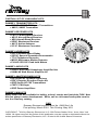
OPTICALLY ISOLATED
INTERFACE
Ramsey Electronics Model No. OM2
The OM2 provides 5000 volts of electrical isolation between the input and
output signals. Any input signal, AC or DC, greater than 1.5 volts can be
used to provide an output signal up to 40VDC at up to 150mA. The output
can follow an input signal with a frequency from 0Hz to 250KHz or it can
provide a constant level when an input signal is applied.
AC or DC input
40VDC @ 150mA output
0Hz to 250KHz operation
Output can either follow AC input or “latch” with signal input
Over 5000 volts optical isolation between input and output signals
Full custom configuration instructions included
OM2 1
PARTIAL LIST OF AVAILABLE KITS:
RAMSEY TRANSMITTER KITS
FM10C, FM25B FM Stereo Transmitters
AM1C, AM25 Transmitter
RAMSEY RECEIVER KITS
FR1C FM Broadcast Receiver
AR1C Aircraft Band Receiver
AR2 Aircraft Band Receiver
SR2C Shortwave Receiver
AA7C Active Antenna
SC1C Shortwave Converter
RAMSEY HOBBY KITS
SG7 Personal Speed Radar
SS70C Speech Scrambler/Descrambler
TT1CTelephone Recorder
MD3C Microwave Motion Detector
PH14C/15C/16C Peak hold Meters
RAMSEY AUDIO KITS
SHA1C and SHA2 Headphone Amplifier kits
UAM4 40 Watt Stereo Amplifier kit
RAMSEY AMATEUR RADIO KITS
HR Series HF All Mode Receivers
DDF1 Doppler Direction Finder Kit
QRP Series HF CW Transmitters
CW7C CW Keyer
QRP Power Amplifiers
RAMSEY MINI-KITS
Many other kits are available for hobby, school, scouts and just plain FUN! New
kits are always under development. Write, call or visit www.ramseykits.com for
our free Ramsey catalog.
OM2
Ramsey Electronics publication No. OM2 Rev1.0a
First printing: March 2010 This Printing: May 2011
COPYRIGHT 2010 by Ramsey Electronics, LLC. 590 Fishers Station Drive, Victor, New York
14564. All rights reserved. No portion of this publication may be copied or duplicated without the
written permission of Ramsey Electronics, LLC. Printed in the United States of America.
OM2 2
Ramsey Publication No. OM2:
Manual Price Only $5.00
INSTRUCTION MANUAL FOR
OPTICALLY ISOLATED
INTERFACE
TABLE OF CONTENTS
Introduction/Circuit Description ...................... 4
Parts Layout Diagram..................................... 7
“Learn-As-You-Build” Kit Assembly................ 8
Parts List......................................................... 9
Assembly Steps ............................................ 10
Schematic ................................................ 12-13
Input Signal Level Configuration .................. 14
Final Configuration Assembly Steps ............ 15
Configuring Your OM2.................................. 16
Conclusion .................................................... 21
Specifications ............................................... 22
Ramsey Kit Warranty ................................... 23
RAMSEY ELECTRONICS, LLC
590 Fishers Station Drive
Victor, New York 14564
Phone (585) 924-4560
Fax (585) 924-4555
www.ramseykits.com
OM2 3
Introduction
The OM2, Optically Isolated Interface, provides an optically isolated interface
between two devices. It can be used to interface nearly any AC or DC signal
to a logic level signal. It can also be used to operate a relay upon detection
of an input signal. The really great thing about the OM2 is the input and
output are totally isolated from each other. Virtually any voltage input level
above 1.5 volts can be used as long as long as the input current is limited to
a maximum of 60mA. The input can be a simple DC level or an AC signal
with a frequency up to 250KHz. (That’s 250,000 cycles per second for the
old pre-Hertz folks.) The input and output are isolated from each other to
5000 volts AC(rms) difference between the input and output connections.
The output can drive up to 150mA at up to 40VDC. It even provides active
low and high outputs when the input is activated.
Theory of Operation
The heart of the OM2 is an optical coupler. An optical coupler contains an
infrared LED and a photo transistor. When the LED is turned on it causes
the photo transistor to turn on. The coupler used in the OM2 actually has two
LED’s on the input. These LED’s are connected in parallel with each other in
opposite directions. This makes it able to operate using either a DC or AC
input. The DC polarity of the input doesn’t matter since one of the LED’s will
be turned on when an input signal is applied regardless of polarity. We’ll
take a look at the schematic now and go thru the entire circuit operation.
The Input Circuit
On the left side of the schematic you will see J1 which is the input
connection. The input signal is applied to J1’s two pins. Starting at pin 2 of
J1 you will see resistors R1, R2 and capacitor C2 connected in series with
each other. These components act to limit the current supplied to the LED’s
in OC1 pins 1 and 2. The LED’s in OC1 are just like any other LED in that
the forward current must be limited, in this case to a maximum of 60mA.
Why are there two resistors and a capacitor you ask. Well we tried to give
you lots of options to configure the OM2 to meet your requirements. The
values shown for R1 and R2 are such that you can use a standard 110VAC
or 220VAC signal to trigger the output. Since the original concept for the
OM2 was to sense presence or absence of power on an AC power line it
made sense to provide a simple way to select the input voltage by either
having both resistors in place for 220VAC or to remove R2, by installing
JMP1, to change to 110VAC. Notice they are both the same value and
220VAC is twice 110VAC so the current is changed by a factor of 2 by
adding or removing one of the resistors. The “Configuring Your OM2”section
of this manual explains how to set up the input of the OM2 for your
application+. But what’s C2 there for?
OM2 4
Under most conditions C2 is not required. If you have a DC input JMP2 MUST
be installed which removes C2. If you are using an AC voltage input you may
want to install C2 but for most applications JMP2 may be installed which
removes C2. See the “Configuring Your OM2” section of this manual for more
information about how to figure out resistor and capacitor values and if you
need C2 for your specific requirements.
The Output Circuit
Moving on, the output circuit consists of the transistor inside optical coupler
OC1, transistors Q1 and Q2, along with resistors R3, R4, R5, R6, capacitor C2
and diodes D1 and D2. When either of OC1’s LED’s is turned on it causes it’s
internal transistor to turn on. An external voltage, +V, is required for the output
circuitry to operate. This voltage is applied to the OM2 on J3 and J4 and may
be any voltage up to 40 volts DC depending on your application. Again the
“Configuring Your OM2” section of this manual provides more information
about this.
A little bit of transistor theory is provided here to help with understanding the
OM2 operation. The base connection of a transistor is used to control the
current flow between the emitter and collector. A very small amount of current
flowing in the emitter/base circuit can control a very large current flow in the
emitter/collector circuit. With no emitter/base current flowing, the current in the
emitter/collector circuit is essentially turned off. If current is allowed to flow
between the emitter and base then a larger current is allowed to flow in the
emitter/collector. The base current can control a proportional amount of
collector current based on the gain of the transistor. For our purposes we’ll
just say that the collector/emitter current is either on when base current flows
or off when there is no base current.
With no input signal applied to the OM2 the output transistor in OC1 is off
which places a high level on the base of Q1 thru R3. Transistors don’t like a
lot of current flowing from emitter to base so resistor R3 limits the current. This
allows current to flow in the emitter/base circuit and Q1 is turned on allowing
current to flow in the emitter/collector thru R4. When a signal is applied to the
OM2 input the OC1 transistor turns on. It’s collector, OC1 pin 4, is essentially
connected to it’s emitter, pin 3 connecting it to ground which stops the emitter/
base current in Q1 and Q1 turns off. All that to say when an input is applied to
the OM2 the optical coupler transistor is turned on and transistor Q1 is turned
off making it’s collector high. With no input the optical coupler transistor is
turned off and Q1 is turned on placing it’s collector at a low or ground level.
Now look at the connection between Q1’s collector and Q2’s base thru R6.
When Q1 is turned off current can flow in the emitter/base of Q2 thru R4 and
R6. This turns on Q2 in the same way Q1 is turned on when it’s emitter/base
current flows which in turn places Q2’s collector at a low level. Turning on Q1
OM2 5
turns off Q2 by stopping it’s emitter/base current placing Q2’s collector at a
high level.
What we have is the ability to provide both a high(active high), and a low
(active low), output signal when an input is applied to the OM2. The active
high output is connected to J2 pin 2 from the collector of Q1. Active low
output is provided on J1 pin 1 from the collector of Q2.
Now that we’ve explained the operation of the output transistors the only thing
left is what capacitor C2 does. For simple DC input levels there is no need to
have C2 in the circuit. It may even be desirable to remove it if fast acting input
signals are used. But if you need to monitor an AC input signal such as an AC
power line at 50/60Hz then C2 will be required. Without it the output will
change at the rate of the input signal frequency. C2’s value is such that a
50/60Hz input signal will produce a solid output signal fro an AC input signal.
For example when the input signal is power on an AC power line the output
will be held at it’s active state until power is removed. Input signals with a
frequency from 0Hz (DC) to 250KHz can be applied and will produce a
corresponding pulsed output if C2 is not installed. With C2 installed the output
will be a stead level according to the input signal.
Diodes D1 and D2 are placed across both the active high and active low
outputs to provide protection if an inductive load such as a relay is used. This
is necessary because when a current is passed thru an inductor, the coil of a
relay for example, a magnetic field is created around it. When the current is
removed the field collapses and a voltage is induced in the coil in the reverse
direction of the original applied voltage. This voltage can be many times the
original and is the opposite polarity. This is called counter EMF (Counter
Electromotive Force) and can damage the output transistors. The diodes are
connected so they do not conduct when normal voltage is applied but conduct
when the field collapses the diodes conduct and short out the counter EMF.
They are optional and can be left in place for most applications but can be
removed if they interfere with your application.
A load that draws up to 150mA at up to 40VDC can be connected between +V
and either or both the active high and active low outputs on J2. See the
“Connecting Your OM2” section for this manual for more information about
connecting you OM2 to input and output devices.
OM2 6
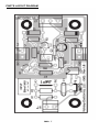
PARTS LAYOUT DIAGRAM
OM2 7
RAMSEY “LEARN-AS-YOU-BUILD” ASSEMBLY STRATEGY
Be sure to read through all of the steps, and check the boxes as you go to be
sure you didn't miss any important steps. Although you may be in a hurry to see
results, before you switch on the power check all wiring and capacitors for
proper orientation. Also check the board for any possible solder shorts, and/or
cold solder joints. All of these mistakes could have detrimental effects on your
kit - not to mention your ego!
Kit building tips:
Use a good soldering technique - let your soldering iron tip gently heat the
traces to which you are soldering, heating both wires and pads simultaneously.
Apply the solder on the iron and the pad when the pad is hot enough to melt the
solder. The finished joint should look like a drop of water on paper, somewhat
soaked in.
Mount all electrical parts on the top side of the board provided. The top side is
clearly marked with the word “TOP”, you can’t miss it. This is the side that has
little or no traces on it, but is covered with mostly copper. When parts are
installed, the part is placed flat to the board, and the leads are bent on the
backside of the board to prevent the part from falling out before soldering (1).
The part is then soldered securely to the board (2-4), and the remaining lead
length is then clipped off (5). Notice how the solder joint looks on close up,
clean and smooth with no holes or sharp points (6).
Warning: Use only rosin core solder or solder designed to be used with
electronic equipment. Use of acid core solder will void your warranty and
produce a board that will disintegrate in a short period of time.
OM2 8
PARTS LIST
Semiconductors
1 SFH620A optical isolator, (OC1)
2 2N3904 transistor, (Q1, Q2)
2 1N4002 diode, (D1, D2)
Resistors
2 1K resistor, (R6) [brown-black-red]
3 10K resistor, (R3, R4, R5) [brown-black-orange]
1 10 ohm resistor, (R8) brown-black-black]
Configuration Resistors
2 33K resistor, (R1, R2) [orange-orange-orange]
2 15K resistor, (R1, R2) [brown-green-orange]
1 39 ohm [orange-white-black]
1 82 ohm [gray-red-black]
1 220 ohm [red-red-brown]
1 470 ohm [yellow-violet-brown]
1 330 ohm [orange-orange-brown]
1 680 ohm [blue-gray-brown]
Capacitors
1 47uF, 16V (C2 optional, application specific)
0 Application specific, NONE INCLUDED (C1)
Connectors
3 2 pin screw terminals
1 3 pin screw terminals
1 2 pin header
1 Jumper block
Miscellaneous
1 Circuit board
OM2 9
ASSEMBLY STEPS
First we’ll install the components that are common to all configurations of your
OM2. Then the components that are configuration specific will be installed.
Make sure to save at least 2 of the resistor leads trimmed off the resistors for
use as jumpers later on.
1. Install OC1, optical isolator marked SFH620A. Make sure the small
dot near one corner on the device matches the dot printed on the board
outside the OC1 outline.
2. Install R3, 10K [brown-black-orange]
3. Install R4, 10K [brown-black-orange]
4. Install R5, 10K [brown-black-orange]
5. Install R6, 1K [brown-black-red]
6. Install R7, 1K [brown-black-red]
7. Install R8, 10 ohm [brown-black-black]
The white band on the component MUST match the white band on the circuit
board for D1 and D2.
8. Install D1, 1N4002 [1N4002]
9. Install D2, 1N4002 [1N4002]
The following terminals are installed so the openings on the housing are
facing the edge of the board.
10. Install J1, 2 position screw terminal
11. Install J3, 2 position screw terminal
12. Install J4, 2 position screw terminal
13. Install J2, 3 position screw terminal
OM2 10
Make sure the flat side on the component matches+ the printed pattern on the
board for Q 1 and Q2.
14. Install Q1, 2N3904 [2N3904].
15. Install Q2, 2N3904 [2N3904]
16. Install 2 pin header, JMP3 and jumper block
OK… now that we have the basic components installed it’s time to install the
application specific parts. The values indicated in the schematic for R1 and
R2 are for an input voltage of 110VAC. Unfortunately we cannot tell you
exactly what parts you need. You will need to refer to the “Configuring Your
OM2” section of this manual to determine the values for R1 and R2, if you
need C1 or not and if jumpers JP1 and JP2 are required for your application.
Also under consideration is whether or not you need to install C2, and if so
what value do you need. Everything you need to determine what is required is
covered in the “Configuring Your OM2” section. Once you have determined
what your application requires you can then install the following components
as required.
OM2 11
The table below lists suggested values for resistors R1 and R2 based on
some common input signals and we have included resistors for these values
in your OM2 kit. We’ve also provided some extra rows for entry of your own
custom configuration. Because C1 is probably not required for most applications no values have been provided. The value for C2 is again highly dependant on your application and a value has not been suggested. For many applications C2 is probably not required. We have provided a 47uF, 16 volt value
as suggested in the schematic. Make sure the voltage rating for C2 is at least
equal to the maximum voltage to be used for +V on the output.
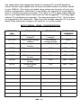
INPUT SIGNAL LEVEL CONFIGURATION
INPUT SIGNAL
110VAC
R1 VALUE
R2 VALUE
15K(brown-greenorange)
33K(orangeorange-orange)
N/A
JMP1, JMP2
5VDC
15K(brown-greenorange)
33K(orange-orangeorange)
39 (orange-whiteblack)
82(gray-red-black)
N/A
JMP1, JMP2
12VDC
220(red-red-brown)
N/A
JMP1, JMP2
24VDC
470(yellow-violetbrown)
330(orange-orangebrown)
680(blue-graybrown)
N/A
JMP1, JMP2
N/A
JMP1, JMP2
N/A
JMP1, JMP2
220VAC
3VDC
12VAC
24VAC
OM2 14
INSTALLED
JUMPERS
JMP2
JMP2
Final Configuration Assembly Steps
1. Install R1, value as determined above
2. Install R2 or jumper JMP1 as required.
3. Install C1 or JMP2 as required. Notice that there is no indication of
polarity for C1. If an electrolytic capacitor is used make sure to install it
so the “+” terminal is installed in the hole that is on the side electrically
nearest the positive connection of the input signal.
4. Install C2 as required. If the required capacitor is an electrolytic
type and has a polarity make sure it is installed with the “+” lead inserted into the hole next to the + printed on the circuit board. Notice
that the printed pattern has a small fat area on one side of the pattern.
This indicates the “-“ side of the capacitor.
5. Remember to remove jumper JMP3 if an active high output is required.
OM2 15
Configuring Your OM2
The OM2 is a versatile interface and can be configured to meet the
requirements of many applications. This section describes how to figure out
the necessary set-up and component values for your application. We’ll try to
give you the tools to work with and keep it simple but it is possible that we
may miss something you need to know since not all applications are created
equal.
Input Configuration
DC Input Calculations
The most complex set-up will involve the input circuit even though it looks like
it is very simple. Hang in there and we’ll get you thru it. The main thing to
keep in mind is that it is essential the input current be kept less than 60ma or
the input LED’s may be damaged. Ohm’s Law is the primary tool we’ll use
here. The following calculations assume C2 is bypassed (JMP2 installed) and
are for DC conditions only.
E=I*R
Where:
E = voltage in volts
I = current in amps
R = resistance in ohms
To calculate the circuit current and the resistance required the formulas are:
I=E/R
R=E/I
OK, so to calculate the value for R1 and R2 combined we need to figure out
the voltage that will be across R1 and R2 for the input you apply to turn on the
LED. For this we need to know not only the voltage you are applying but also
the voltage that will be across the LED when it is on. This is easy because the
manufacturer of the optical coupler tells us that there will be 1.25 volts across
the LED in the on state. That means that the voltage across R1 and R2 will
be your input voltage, we’ll call it Vin, minus 1.25 volts. The total resistance of
R1 and R2 in series is R1 + R2, we’ll call it Rt, so the formula for their total
resistance is:
Rt = (Vin – 1.25) / I
OM2 16
Even though the maximum current is 60mA (0.060 amps) it is a good idea to
stay a little lower than this so lets pick 50mA, (0.050 amps) and an input
voltage of 5 volts and see what happens.
Rt = (5 – 1.25) / 0.05 = 3.75 / 0.05 = 75 ohms
Now the problem is finding a resistor or resistors that add up to 75 ohms. In
this case we’re in luck because 75 ohms is a standard 5% resistor value, (that
was purely by accident by-the-way). All you need to do is install a 75 ohm
resistor in R1’s location and place a jumper at JMP1 position. If the
calculated value isn’t standard, check out values around it. Pick one close
and plug the value into the formula for current to see if it is less than 60mA.
You can also use two resistors that will add up to the calculated resistance
and install them in the R1 and R2 locations and leave JMP1 out. You can
probably use less current and your circuit will work fine. It’s a matter of
experimenting to see what works. The important thing this is to not exceed
60mA. In the real world the formulas give a starting point and then engineers
start to play.
AC Input Signal Calculations
Now what about an AC input voltage. Well it gets a little more complicated but
Ohm’s Law still applies. The problem with an AC voltage is it is constantly
changing voltage and possibly polarity at some frequency. To make it even
more interesting the AC voltage, we’ll call it a signal now, may be ‘riding on a
DC voltage. All of these factors come into play in the calculations. Don’t
panic it’s not that bad.
If a circuit contains only simple resistors things are straight forward. For this
discussion we’ll assume C1 is not in the circuit. The only concern is how the
AC voltage is specified. To keep it simple we’ll talk about a voltage that
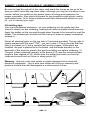
swings around a zero voltage point and is a simple sine wave. The figure
below shows what this voltage ‘looks’ like.
+170 volts
0 volts
-170 volts
OM2 17
The AC signal shown is what standard 120 volt house AC power ‘looks’ like.
The voltage of 120 volts is what is called RMS (Root Mean Squared) voltage.
Notice that the voltage goes up to a peak voltage of about 170 volts, goes
down to 0 and then goes to 170 volts in the opposite direction. The RMS
value is a complicated value determined with calculus and represents the
equivalent DC voltage of the peak voltage of 170 volts. In other words a DC
voltage of 120 volts would produce as much power as a 170 volt peak sine
wave voltage.
Now that you are totally confused all you need to know is that if 120VAC(rms)
is applied to the input of the OM2 the calculations need to use 170VDC as the
input voltage, Vin. To get the 170 volts simply multiply 120V(rms) times
1.414. So the formula is:
Vpeak = Vrms * 1.414
Or
Vpeak = 120 * 1.414 =~ 170 volts peak
To calculate the resistance required for a 120V(rms) input use the formula for
the DC signal described above as follows:
Rt = (Vin – 1.25) / I
Rt = (170 - 1.25) / 0.05 = 168.75 / .05 = 3375 ohms = 3.375Kohms
A standard resistor value that is very close to 3.375Kohms is 3.3Kohms. If we
use this value the current is calculated as:
I = (Vin - 1.25) / Rt = (170 - 1.25) / 3300 = 0.051A = 51mA
We are well below the maximum allowable current so this is a good choice
and is how the values shown in the schematic were determined.
If you decide to include C2 in the input circuit it gets more complex and since
you have determined you need C2 we are going to assume you know a good
deal about electronics and physics and provide a very basic explanation of
how to calculate a value for C2.
OM2 18
As described earlier a capacitor will block the flow of a DC current but will
appear to conduct and AC current. However it is not an absolute short circuit
to AC and actually changes its resistance with changes in the frequency of the
signal. In an AC circuit resistance is call impedance and can be plugged into
Ohm’s Law in place of the resistance values. To calculate the impedance of a
capacitor, we’ll call it ‘Zc’, of a capacitor the formula is:
Zc = 1 / {(2 * pi) * f * C}
Zc = 1 / 6.28 * f * C
Zc
f
C
pi
= Impedance of capacitor in ohms
= frequency of the AC signal in Hertz
= capacitance in Farads
= 3.14 (approx)
Notice that as the value of a capacitor or the signal frequency is increased the
impedance of the capacitor decreases. So then if the frequency is zero Hertz
the impedance of the capacitor is infinity since 1 divided by 0 is infinity. Hence
a capacitor blocks DC current since the frequency of a DC current is zero
Hertz.
To calculate the input resistance with an AC input signal with C2 in the circuit
all you need to do is add the impedance of the capacitor to the values of R1
and R2 and calculate the current. So the total resistance, Rt, becomes:
Rt = R1 + R2 + Zc
Insert the total resistance into the formula for current and you have:
I = (Vin - 1.25) / Rt = ( Vin – 1.25) / (R1 + R2 + Zc)
Output Configuration
The OM2 output is easily configured. The main considerations are the output
current, output voltage, and if the output needs to go low(active low) or high
(active high) when the input is activated by turning on an input LED. Start by
determining the output voltage level required. The outputs are capable of
supplying up to 150mA with a maximum voltage of 40 volts.
Now determine if you need an active high or active low output level. This will
be entirely dependant on your specific circuit requirements based on the type
of device you are connecting.
If an inductive load such as a relay is being used then diodes D1 and D2
MUST be installed. Otherwise they are optional. For most applications they
should not cause any problems. They may be removed if the load is not
OM2 19
inductive and they cause problems with any output devices.
The only other output consideration is if C2 is required. The basic function of
C2 is to fill in the gaps of an AC input signal and keep the output in it’s active
state during the time an AC signal is at a low level. The larger the value of C2
the bigger the gap can be and the output will not change. It does this by
charging to the peak voltage of the signal and keeping a high level on the
base of Q1, and therefore keeping Q1 turned on, for the short time the signal
is low. After the input signal is removed for more than a few input cycles, C2
will discharge and Q1 will turn off, changing the state of the output. This delay
can cause problems with very short input pulses and will delay the time it
takes for the output to respond to changes in the input. Because of this it may
be desirable to not install C2 unless the output is required to provide a solid
output for an AC input signal. For example if you are monitoring the AC line.
The value indicated in the schematic and supplied with your OM2 should work
for most AC input signals with a frequency from 50Hz or more. It is possible
you may need to change it’s value due to your circuit requirements.
If you enjoyed this Ramsey product, there are plenty more to choose from in
our catalog - visit our website at http://www.ramseyelectronics.com or call
today!
OM2 20
CONCLUSION
We sincerely hope that you will enjoy the use of this Ramsey product. As
always, we have tried to compose our manual in the easiest, most “user
friendly” format possible. As our customers, we value your opinions,
comments, and additions that you would like to see in future publications.
Please submit comments or ideas to:
Ramsey Electronics, LLC.
Attn. Hobby Kit Department
590 Fishers Station Drive
Victor, NY 14564
or email us at: [email protected]
And once again, thanks from the folks at Ramsey
OM2 21
OM2 SPECIFICATIONS
Input Requirements:
>=1.5 volts DC or >=1.5 volts peak AC
at 1mA to 60mA depending on application
Input to Output Isolation:
5000 volts maximum
Switching Rate:
DC to 250kHz
Output Configuration:
Active High DC or Active Low DC
Maximum Load:
40 VDC max @ 150mA max
Dimensions:
Board:
Mounting:
Weight:
1.5in (W) X 2.5in (L) X 0.875in (H)
31.1mm (W) X 63.5mm (L) X 22.2mm (H)
4 holes, 4/40 screw clearance on 1” x 2” pattern
4 holes on 25.4mm x 50.8mm pattern
0.7 Oz, 0.0198 Kg
OM2 22
THE RAMSEY KIT WARRANTY
1. GENERAL:
Notice that this is not a "fine print" warranty. We want you to understand your rights and ours too! All Ramsey kits will work if
assembled properly. The very fact that your kit includes this new manual is your assurance that prior to release of this kit, a
varied group of knowledgeable people have assembled this kit from scratch using this manual. During this process, changes
and additions are noted by each assembler and integrated into the final version of the manual…which you have! If you need
help, please read through your manual carefully, all information required to properly build and test your kit is contained within
the pages! However, customer satisfaction is our goal, so in the event that you do have a problem, please note the following:
2. DEFECTIVE PARTS:
It's always easy to blame a part for a problem in your kit. Before you conclude that a part may be bad, thoroughly check your
work. Today's semiconductors and passive components have reached incredibly high reliability levels, and it’s sad to say that
our human construction skills have not! But on rare occasions a sour component can slip through. All of our kit parts carry the
Ramsey Electronics Warranty that they are free from defects for a full ninety (90) days from the date of purchase. Defective
parts will be replaced promptly at our expense. If you suspect any part to be defective, please mail it to our factory for testing
and replacement. Please send only the defective part(s), not the entire kit. The part(s) MUST be returned to us in suitable
condition for testing. Please be aware that testing can usually determine if the part was truly defective or damaged by assembly
or usage. Don't be afraid of telling us that you “damaged it” or “burned it out”, we're all human and in most cases, replacement
parts are very reasonably priced. Remember, our goal for over three decades is to have a happy customer, and we’re here to
work WITH you, not AGAINST you!
3. MISSING PARTS:
Before assuming a part value is missing, check the parts listing carefully to see if it is a critical value such as a specific coil or
IC, or whether a RANGE of values is suitable for the component (such as a "100 to 500 uF capacitor"). Often times, common
sense will solve a mysterious missing part problem. If you're missing five 10K ohm resistors and received five extra 1K
resistors, you can pretty much be assured that the “1K ohm” resistors are actually the “missing” 10 K parts ("Hum-m-m, I guess
the orange band really does look red!") Ramsey Electronics project kits are packed with pride in the USA by our own staff
personnel. While separate QC checks are made on all product kits, we too are human, and once in a great while there is a
chance something can get through those checks! If you believe we packed an incorrect part or omitted a part clearly indicated
in your assembly manual for your Ramsey kit, please contact us with information on the part you need. Contact our Repair
Department via telephone, email or writing. Please have your invoice number and date of purchase handy.
4. REFUNDS:
All Ramsey products, kit or factory assembled units have an unconditional 10 day (from the date of purchase) return policy to
examine our products. If you are not satisfied for any reason, you may return your unassembled kit with all the parts and
instructions, or your factory assembled and tested product, together with your proof of purchase to the factory for a full refund
less shipping. The return package should be packed securely. Insurance and tracking is highly recommended. A reminder, this
applies to unassembled kits. They must be in the same new condition as received, not partially assembled! Assembled kits
cannot be returned for credit. No RMA’s are required; simply return to Ramsey Electronics LLC, Attn: Product Returns, 590
Fishers Station Drive, Victor, NY, 14564. If you have any questions, please contact us at 585-924-4560.
5. FACTORY REPAIR OF ASSEMBLED KITS:
Most of us at Ramsey are technically oriented and we do realize that things happen! Even following the best practices, with all
of the best intentions, there is that chance that your kit doesn’t work when you have completed it. Each manual goes into
detailed troubleshooting based on the specific kit to help you troubleshoot the problem. We have found that 95% of returned
kits involved wrongly installed components (wrong part or backwards polarity). This section of the warranty assumes you have
gone through all those steps, and have now reached the point that you need to send it back.
To qualify for factory repair of customer assembled kits, the following conditions apply:
1. Kits must not be assembled with acid solder flux
2. Kit boards or circuits must not be modified in any manner from the version received
3. Kits must be fully assembled, not partially assembled. Our warranty does not include “finishing” your kit!
4. Must include a full description of the problem encountered including the troubleshooting steps you have already done.
5. Must not include non-standard, non-Ramsey accessories, cases, enclosures, knobs, etc. or any batteries.
6. Must include the minimum repair fee of $25 USD in the form of check, money order or credit card authorization.
7. Ramsey Electronics, LLC reserves the right to refuse any repair due to excessive errors in construction methods.
8. If, due to customer construction methods, the repair is estimated to exceed the minimum flat rate, Ramsey Electronics,
LLC will contact the customer to discuss the repairs needed and to receive authorization and payment for repair prior
to repair.
9. In the unlikely case that a defective part is found to be the cause of the problem, the repairs will be made at no-charge
to the customer, and any payments received for repair will be returned or credited back to the customer.
10. Properly pack your kit, insure the package, and use a carrier that can be tracked. Ramsey Electronics, LLC is not
responsible for any loss or damage in shipment. Send the package together with your repair fee to the return address
below. No RMA is required.
6. FACTORY REPAIR FEES:
Please understand that our Tech Support Group personnel are not volunteers! They are a dedicated group of highly trained
technicians each configured with a very properly equipped test bench. Upon receipt of a repair, the setup, testing, diagnosis,
repair, paperwork, and repacking of your kit requires nearly an hour of their time regardless of the size or complexity of the kit!
The minimum repair fee represents ½ hour Tech Support time at $50/hour USD. We try to keep all kit repairs within the realm
of the $25 flat rate whenever possible…and trust us; we exceed that time spent on most kits received more often than not!
7. CONTACT INFORMATION AND RETURN ADDRESS:
Technical Questions
RAMSEY ELECTRONICS, LLC
Attn: Tech Support
590 Fishers Station Drive
OM2
Victor, NY 14564
585-924-4560; 585-924-4886 Fax
[email protected]
Product Repair & Returns
23
RAMSEY ELECTRONICS, LLC
Attn: Repairs
590 Fishers Station Drive
Victor, NY 14564
585-924-4560; 585-924-4886 Fax
[email protected]
Quick Reference
Introduction/Circuit Description .......................4
Parts Layout Diagram .....................................7
Parts List .........................................................9
Assembly Steps.............................................10
Schematic................................................ 12-13
Configuring Your OM2 ..................................16
Specifications ................................................22
REQUIRED TOOLS
Soldering Iron
Thin Rosin Core Solder
Needle Nose Pliers
Small Diagonal Cutters
ADDITIONAL SUGGESTED ITEMS
Helping Hands Holder for PC Board/
Parts
Desoldering Braid
TOTAL SOLDER POINTS
53
ESTIMATED ASSEMBLY
TIME
Beginner ............... 1.5 hrs
Intermediate ......... 1 hrs
Advanced ............. 0.5 hrs
RAMSEY ELECTRONICS, LLC
590 Fishers Station Drive
Victor, New York 14564
Phone
(585) 924-4560
Fax
(585) 924-4555
www.ramseykits.com
Ramsey Publication No. OM2
Assembly and Instruction manual
for:OM2
OM2 24