1
DOPPLER DIRECTION
FINDER
RADIO DIRECTION FINDER
KIT
Ramsey Electronics Model No.
DDF1
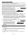
Get in on the fun of radio direction finding (RDF) with this super
kit ! The latest in affordable Doppler direction finding equipment
available in a complete kit form ..this one even includes the
receiving antenna. A must for the “fox hunter” at an unheard of
price!
Elegant and cost effective design thanks to WA2EBY ! Featured in
May / June 1999 QST Articles.
Solid state antenna switching for “rock solid” performance.
Convenient LED 22.5 degree bearing indicator.
Audio Level indicator for trouble free operation.
Adjustable damping rate, phase inversion, scan enable / disable.
Complete with home brew “mag mount” antennas and cable,
designed for quick set up and operation.
Utilizes latest high speed CMOS technology for signal conditioning
and audio processing!
Complete and informative instructions guide you to a kit that works
the first time, every time - enhances resale value, too !
DDF1 1
PARTIAL LIST OF AVAILABLE KITS:
RAMSEY TRANSMITTER KITS
· FM10A, FM25B, FM30, FM Stereo Transmitters
· FM100B, FM35 Professional FM Stereo Transmitters
· AM1, AM25 AM Broadcast Band
Transmitters
RAMSEY RECEIVER KITS
· FR1 FM Broadcast Receiver
· AR1 Aircraft Band Receiver
· SR2 Shortwave Receiver
· SC1 Shortwave Converter
RAMSEY HOBBY KITS
· LBC6K Laser Beam Communicator
· SG7 Personal Speed Radar
· SS70C Speech Scrambler/Descrambler
· TT1 Telephone Recorder
· LLS1 Laser Light Show
· MD3 Microwave Motion Detector
· LEDS1 LED Strobe Light
· BE66 Blinky Eyes Animated Display
· LTS1 Laser Trip Sensor
· ICI1C Infrared Switch Control Interface
RAMSEY AMATEUR RADIO KITS
· HR Series HF All Mode Receivers
· DDF1 Doppler Direction Finder Kit
· QRP Series HF CW Transmitters and QAMP Power Amplifiers
· CW7 CW Keyer
RAMSEY MINI-KITS
Many other kits are available for hobby, school, scouts and just plain FUN. New
kits are always under development. Write or call for our free Ramsey catalog.
DDF1 DOPPLER RADIO DIRECTION FINDER KIT INSTRUCTION MANUAL
Ramsey Electronics publication No. MDDF1 Revision 1.2c
This Printing: June 2011
COPYRIGHT 2006-2011 by Ramsey Electronics, LLC, 590 Fishers Station Drive, Victor, New
York 14564. All rights reserved. No portion of this publication may be copied or duplicated
without the written permission of Ramsey Electronics, LLC. Printed in the United States of
America.
DDF1 2
Ramsey Publication No. MDDF1
Price $5.00
INSTRUCTION MANUAL FOR
DOPPLER RADIO
DIRECTION FINDER
TABLE OF CONTENTS
Introduction to the DDF1 .............................................. 4
Theory Of Operation ...................................................... 4
Circuit Description......................................................... 7
Parts List ...................................................................... 11
Learn-as-you-build ....................................................... 13
DDF1 Assembly Steps ................................................ 14
Main Board Component Layout ................................... 17
Schematic Diagram ............................................... 18-19
Control & Indicator Assembly ...................................... 23
Antenna Schematic...................................................... 25
Antenna & Switcher Board Layout............................... 26
Antenna System Assembly .......................................... 27
Testing ......................................................................... 31
Operation ..................................................................... 34
Final Calibration ........................................................... 35
Final Case Up .............................................................. 36
Troubleshooting ........................................................... 36
Ramsey Warranty ........................................................ 39
RAMSEY ELECTRONICS, LLC
590 Fishers Station Drive
Victor, New York 14564
Phone (585) 924-4560
Fax (585) 924-4555
www.ramseykits.com
DDF1 3
INTRODUCTION
Radio direction finding is a fascinating hobby that has been becoming more
and more popular in today's portable world. More recently, Doppler “df-ing”
has become the rage, with a display that gives you a direct bearing on the location of the transmitter. Pretty neat trick considering you don’t need multiple
separate receivers at different locations to triangulate on the mystery transmitter.
DDF1 THEORY OF OPERATION
The classic example of the Doppler effect is that of a car approaching a stationary observer. The car's horn sounds higher in pitch (frequency) to an observer as the car approaches. The change in frequency occurs because the
motion of the car shortens the wavelength. The horn sounds lower in pitch
(frequency) to the observer as the car speeds away. This occurs because the
car is speeding away from the observer effectively increasing the wavelength. Fewer cycles per second, hence, lower-frequency sound. A similar
effect occurs when an antenna is moved toward or away from a transmitting
source. The signal received from an antenna moving toward the transmitting
source appears to be at a higher frequency than that of the actual transmission. The signal received from an antenna moving away from the source of
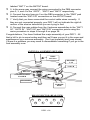
transmission appears to be lower in frequency than that of the actual transmission. Imagine a receiving antenna moving in a circular pattern as pictured in Figure 1A. Consider the antenna at position A, nearest the source of
transmission. The frequency of the received signal at point A equals that of
the transmitted signal because the antenna is not moving toward or away
from the source of transmission. The frequency of the received signal decreases as the antenna moves from point A to point B and from point B to
point C. Maximum frequency deviation occurs as the antenna passes
through point B. The frequency of the received signal at point C is the same
as that of the transmitted signal (no shift) because the antenna is not moving
toward or away from the source of transmission. As the antenna moves from
point C to point D and from point D back to point A, the frequency of the received signal increases. Maximum frequency deviation occurs again as the
antenna passes through point D. The Doppler frequency shift as a function
of antenna rotation is illustrated in Figure 1B.
dF= (rfc)/c
where:
dF =Peak change in frequency (Doppler shift in Hertz)
= Angular velocity of rotation in radians per second (2 x frequency of rotation)
r = Radius of antenna rotation (meters)
fc = Frequency of transmitted signal (Hertz)
DDF1 4
c = Speed of light
We can calculate how fast the antenna must rotate in order to produce a
given Doppler frequency shift with the following equation
fr = dF x 1879.8/R x fc
where
fr = The frequency of the received signal in megahertz
dF= The Doppler shift in Hertz
R = Radius of antenna rotation in inches
fc = Carrier frequency of the received signal in megahertz
As an example, let's calculate how fast the antenna must rotate in order to
produce a Doppler shift of 500 Hz at 146 MHz, assuming the antenna is turning in a circle with radius 13.39 inches.
R F S ig na l (fo )
F ig ure 1
D
R o ta tio n
C
A
B
(A )
+ f
fo
-f
(B )
DDF1 5
The frequency of rotation is:
fr = 500 x 1879.8/146 x 13.39
A rotation frequency of 480 Hz translates to 480 x 60 = 28,800 or almost
30,000 r/min, which pretty much rules out any ideas of mechanically rotating
the antenna! Fortunately, Terrence Rogers, WA4BVY, proposed a clever
method of electrically spinning the antenna that works very well. Roger's project, the DoppleScAnt, uses eight 1/4- vertical whips arranged in a circular
pattern. Only one antenna at a time is electrically selected. By controlling the
order in which the antennas are selected, the DoppleScAnt emulates a single 1/4 – whip antenna moving in a circle. A clever feature in Roger's design is the use of a digital audio filter to extract the Doppler tone from voice,
PL tones and noise.
The DDF1 design offers slightly improved audio filtering, 74HC-series logic
circuits capable of driving the LED display directly, a wideband VHF/UHF antenna switcher and the four 1/4- mag-mount antennas. Total project cost is
about one third the cost of purchasing a commercial RDF unit - and building
the project is a lot more educational.
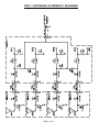
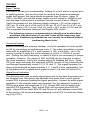
HOW IT WORKS
To understand the operation of the Doppler RDF circuit, see the block diagram of Figure 2. An 8 kHz clock oscillator drives a binary counter. The output of the counter performs three synchronized functions: "spin" the antenna,
drive the LED display and run the digital filter. The counter output drives a 1
of 4 multiplexer that spins the antennas by sequentially selecting (turning on)
one at a time in the order A,B,C,D,A, etc., at 500 times per second. The
counter output also drives a 1 of 6 multiplexer used to drive the LED display
in sync with the spinning antenna. The RF signal received from the spinning
antenna is connected to the antenna input of a VHF or UHF FM receiver.
The spinning antenna imposes a 500 Hz frequency deviation on a 146 MHz
received signal. A 146 MHz FM receiver connected to the spinning antenna's RF output demodulates the 500 Hz frequency deviation and sounds
like a 500 Hz tone with loudness set by the 500 Hz frequency deviation. The
receiver audio, including 500 Hz Doppler tone, is processed by a series of
audio filters. A high pass filter rejects PL tones and audio frequencies below
the 500 Hz Doppler tone. A low-pass filter rejects all audio frequencies
above the 500 Hz Doppler tone, and a very narrow bandwidth digital filter extracts only 500 HZ Doppler tone.
The output of the digital filter represents the actual Doppler frequency shift
shown in figure 1. - Zero crossings of the Doppler frequency shift pattern correspond to the antenna position located directly toward the source of transmission (position A) or directly opposite the source of transmission (position
C). The zero-crossing signal passes through an adjustable delay before it
DDF1 6
latches the direction indicating LED. The adjustable delay is used to calibrate
the LED direction indicator with the actual direction of the transmission.
FIGURE 2
WA2EBY Doppler DDF System
Figure 2 Block Diagram of the WA2EBY Doppler RDF System
Antenna
Switcher
1 of 4 Data
Selector
Ant
8 KHz Clock
LED Compass Display
1 of 16 Data
Selector
Binary Counter
Latch
High Pass
Filter
Low Pass
Filter
Digital Filter
Zero Crossing
Detector
Adjustable
Delay
AF Out
R 36
Calibrate
FM Receiver
External
Speaker
CIRCUIT DESCRIPTION
Take a look at the schematic of the WA2EBY Doppler RDF on page 18. The
heart of the system is an 8 kHz clock oscillator built around a 555 timer, U4,
configured as an astable multivibrator. C26, R27, and R28, R29 determine
the multivibrator's oscillation frequency. R27 and R28 are series connected
to allow fine tuning the oscillation frequency to 8 kHz. It is important that the
clock frequency be exactly 8 kHz; I recommend that it be adjusted to
+/-250 Hz of that frequency for reasons that I'll discuss shortly. The 8 kHz
output of U4 provides the clock for 4 bit binary counter U7. The 3 bit binary
coded decimal (BCD) output of U7 is used to operate three synchronized
functions.
DDF1 7
Three Synchronized Functions
The first function derived from binary counter U7 is antenna array spinning.
This is accomplished by using the two most significant bits of U7 to run 1 of 4
multiplexer U8. The selected output of U8 (active low) is inverted by buffer
U12. The buffered output of U12 (active high) supplies current sufficient to
turn on the antenna to which it is connected. (The details of how this is done
will be covered later.) Buffer outputs U12A, U12B, U12C and U12D are sequenced in order. The corresponding buffer selects antennas A,B,C,D,A,B,
etc. Driving multiplexer U8 with the two most significant bits of counter U7 divides the 8 kHz clock by four, so each antenna is turned on for 0.5 ms. One
complete spin of the antenna requires 0.5 ms x 4 = 2.0 ms, thus the frequency of rotation is 2 ms or 500 Hz. An FM receiver connected to the spinning antenna's RF output has a 500 Hz tone imposed on the received signal.
Sequencing the 16 LED display is the second synchronized function from binary counter U7. This is done by using the binary output of counter U7 to select 1 of 16 data outputs of U11. The selected output of U11 goes low, allowing current to flow from the +5 V supply through current limiting resistor R51,
green center LED D16, and direction indicating red LED's D17 through D32.
Each antenna remains turned on as the LED display sequences through four
direction indicating LED's, then switches to the next antenna. Each direction
indicating LED represents a heading change of 22.5 degrees.
The third synchronized function is operating the digital filter responsible for
extracting the Doppler tone. The 500 Hz Doppler tone present on the receiver audio output is connected to an external speaker and audio level adjust potentiometer R50. The signal is filtered by a two-pole Sallen Key high
pass filter built around op amp U1A. It filters out PL tones and audio frequencies below the 500 Hz Doppler tone. Next, a four-pole Sallen-Key low band
pass filter using U1B and U1C limits audio frequencies above the 500 Hz
Doppler tone. This signal is then applied to the input of a digital filter consisting of analog multiplexer U5, R18, R19 and C10 through C17. (Readers interested in the detailed operation and analysis of this fascinating digital filter
are encouraged to review QEX magazine for June 1999)
The Digital Filter
Using the three most significant bits of U7 to drive the digital filter divides the
8 kHz clock by the two, making the digital filter code rate 4 kHz. The center
frequency of the digital filter is determined solely by the clock frequency divided by the order of the filter. This is an 8th order filter, which makes the
center frequency of the filter 4 kHz/8 =500 Hz. This is the exact frequency at
which the antenna spins, hence, the same frequency of the Doppler tone
produced on the receiver audio connected to the spinning antenna. This is
truly an elegant feature of the Doppler RDF design. Using the same clock
oscillator to spin the antenna and clock the digital filter ensures the Doppler
tone produced by the spinning process is precisely the center frequency of
DDF1 8
the digital filter. Even if the clock oscillator frequency drifts, the Doppler tone
drifts accordingly, but the center frequency of the digital filter follows it precisely because the same clock runs it. Excessive drift in the 8 kHz clock
should be avoided, however, because the analog high and low pass filters
that precede the digital filter have fixed passband centers of 500 Hz. A drift
of +250 Hz on the 8 kHz clock corresponds to +62.5 Hz (250/4) drift in the
Doppler tone produced. This value is acceptable because of the relatively
low Q of the analog bandpass filter.
Digital filter Q is calculated by dividing the filter's center frequency by its
bandwidth (Q=f/BW) or 500 Hz/4 Hz=125. It's very difficult to realize such a
high Q filter with active or passive analog filters and even more difficult to
maintain a precise center frequency. The slightest change in temperature or
component tolerance would easily de-Q or detune such filters from the desired 500 Hz Doppler tone frequency. The digital filter makes the high Q possible and does so without the need for precision tolerance components. By
varying damping pot R19, the response time of the digital filter is changed.
This digital filter damping helps average rapid Doppler tone changes caused
by multipath reflected signals, noise or high audio peaks associated with
speech. A digitized representation of the Doppler tone is provided at the digital filter output. A two pole Sallen Key low pass filter built around U2B filters
out the digital steps in the waveform providing a near sinusoidal output corresponding to the Doppler shift illustrated in Figure 1B
The zero crossings of this signal are detected by U2C and indicate exactly
when the Doppler effect is zero. The output of U2C is used to trigger U6, a
555 timer configured as a monostable multivibrator. When U6 is triggered
it’s output, pin 3, goes high for the time determined by the setting of the
“CALIBRATE” control, R36. When U6’s output returns to a low U11’s output
is latched and the LED in the display corresponding to the direction of transmission is illuminated. Calibration of the actual direction of transmission and
the direction indicating display is accomplished by changing the delay between the Doppler tone zero crossing and the time U11 is latched. C23, R36
and R37 determine this delay by adjusting the time u6’s output is high after it
is triggered by U2C.
Low Signal Level and Audio Overload Indicators
Two useful modifications included in this design are the low signal level lockout and audio overload indicators. U2D continuously monitors the amplitude
of the Doppler tone at the input to the zero crossing detector. U2D’s output
goes low whenever the Doppler tone amplitude drops below 0.11 V peak.
This is done by referencing the negative input of U2D to 2.39 V, 0.11 V below the nominal 2.5 VDC reference level output of U2B by means of voltage
divider, R21 and R22. U2D's output remains high when the Doppler tone is
present and above 0.11 V peak. C9 discharges via D2 whenever U2D goes
low, causing U3's output (pin 7) to go high, turning on Q2 via R24 and illuminating low signal level LED, D4. D4 remains on until the Doppler tone returns
DDF1 9
with amplitude above 0.11 V peak and C9 recharges via R23. The LED display remains locked by disabling U11's strobe input whenever the Doppler
tone is too low for an accurate bearing. This is done by pulling pin 1 of U11
low via D5 when Q2 is turned on.
Audio overload indicator D3 tells you that audio clipping of the Doppler tone
is occurring. Clipping results if the signal level from the digital filter is too high
and can produce an erroneous bearing indication. The output of U1D goes
low whenever the output of the digital filter drops below 0.6 V as the amplitude of the Doppler tone approaches the 0V supply rail. C7 discharges via
D1 and causes the output of U3C to go high, turning on Q1 via R16 and illuminating audio overload LED D3. We elected not to lock the LED display on
audio overload; doing so, however, only requires connecting a diode between the collector of Q1 and pin 1 of U11, similar to the low level lock out
function.
Phase Correction
If the audio output of the Doppler RDF FM receiver is incorrectly phased, S3,
phase invert, can fix that. (If phasing is incorrect, LED direction indications
are 180 degrees opposite that of the actual signal source.) Moving S3 to the
opposite position corrects the problem by letting U2C sense the trailing edge.
This is particularly useful when switching between different receivers. S2 disables the 8 kHz clock to disable the antenna spinning. This helps when
you're trying to listen to the received signal. Presence of the Doppler tone in
the received audio makes it difficult to understand what is being said, especially with weak signals.
Power Supply
Power is delivered via on/off switch S1. D6 provides supply voltage reverse
polarity protection by limiting the reverse voltage to 0.7 V. U10 provides a
regulated 5 VDC to all digital ICs. C29 through C33 are bypass filters. U10's
5 VDC output is dropped 2.5 V by resistive divider R43 and R45. Noninverting voltage follower U3B buffers the 2.5 V source to provide a virtual
ground reference for all analog filters and the digital filter. Using a virtual
ground 2.5 V above circuit ground allows op amps to process analog signals
without the need of a negative power supply voltage. Analog voltages swing
from near 0 V to near +5 V with the virtual ground level right in the middle,
2.5 V.
DDF1 10
DDF1 PARTS LIST
Sort and “check off” the components in the boxes provided. It’s also helpful
to sort the parts into separate containers (egg cartons do nicely) to avoid
confusion while assembling the kit. Leave the IC’s on their foam holder until
ready for installation.
RESISTORS AND POTENTIOMETERS
2
2
4
1
7
1
2
1
19
2
1
3
1
2
47 ohm (yellow-violet-black) [R42,51]
330 ohm (orange-orange-brown) [R17,25]
470 ohm (yellow-violet-brown) [R46,47,48,49]
3.3K ohm (orange-orange-red) [R14]
10K ohm (brown-black-orange) [R13,16,22,24,27,37,39]
18K ohm (brown-gray-orange) [R28]
22K ohm (red-red-orange) [R8,32]
27K ohm (red-violet-orange) [R4]
33K ohm (orange-orange-orange)
[R1,2,3,5,6,7,9,10,11,12,20,26,30,31,34,35,38,43,45]]
68K ohm (blue-gray-orange) [R29,33]
100K ohm (brown-black-yellow) [R18]
220K ohm (red-red-yellow) [R15,21,23]
PC mount 10K linear potentiometer (103) [R50]
PC mount 500K linear potentiometer (504) [R19,36]
CAPACITORS AND INDUCTORS
11 .001 uF disc capacitors (labeled .001 or 102) [DDF1 board
C22,24,26][ANTINT-1 board C1,2,3,4,5,6,7,8]
1 .0047 uF disc capacitor (labeled .0047 or 472) [C23]
10 .01uF disc capacitors (labeled .01 or 103 or 10nF)
[C1,2,3,4,5,6,9,18,19,38
15 .1uF disc capacitors (labeled .1 or 104)
[C7,10,11,12,13,14,15,16,17,21,31,51,52,53,54]
1 .47 uF electrolytic capacitor (labeled .47) [C20]
3 1 uF electrolytic capacitor (labeled 1uF) [C8,25,32]
1 10 uF electrolytic capacitor (labeled 10uF) [C33]
2 100 uF electrolytic capacitors (labeled 100uF) [C29,30]
8 1.2 uH inductor (brown-red-gold) (ANTINT-1 board [L1,2,3,4],
ANTMTG-1 board, 1 ea.)
DDF1 11
SEMICONDUCTORS AND INTEGRATED CIRCUITS
11 1N4148 small signal diode (small glass case with banded end)
[DDF1 board D1,2,5 ANTINT-1 board D1,2,3,4 ANTMTG-1 board 1 ea.]
1 IN4000 type power diode (black epoxy package with cathode band)
[typically 4001 to 4007] [D6]
18 Mini red LED (light emitting diode)
[D3,4,17,18,19,20,21,22,23,24,25,26,27,28,29,30,31,32]
1 Mini green LED (light emitting diode) [D16]
2 NPN Transistors (Three leads marked 2N3904) [Q1,2]
1 7805 Voltage Regulator IC (marked 7805) [VR1]
1 74HC14 IC (14 pin DIP IC) [U12
1 74HC42 IC (16 pin DIP) [U8]
1 74HC161 IC (16 pin DIP IC) [U7]
1 74HC4051 IC (16 pin DIP IC) U5]
1 74HC4515 IC (24 pin DIP IC) [U11]
3 324 Op Amp IC (14 pin DIP marked 324) [U1,2,3]
2 555 Timer IC (8 pin DIP IC marked 555) [U4,6]
MISCELLANEOUS COMPONENTS
3 PC mount slide switch [S1,2,3]
1 PC mount 2.1mm jack [J3] (speaker audio input)
1 2.1mm plug (for speaker audio input)
1 2.1 mm PC mount power jack [J1]
1 2 pin header (silver pins set in plastic) [J4]
1 DB 9 PC mount connector [J2]
1 DB 9 male connector
1 Miniature 8 ohm speaker
5’ RG-174 mini coaxial cable
1 “Clamshell” abs plastic case with pre-punched panel set
1 Panel sticker set
8 #4-40 x 1/4“ pc board mounting screws
6 #4 x 3/8” self tapping screws (case assembly)
4 #4 Internal tooth washers
2 6-32 x 3/8” PPH black screws
2 6-32 1/4” hex nuts
4 M3 x 10mm FHP screws
4 M3 kepnuts (nuts with lock washer attached)
4 Telescoping whip antennas
5 Round plastic caps
5 Flexible self adhesive magnetic strips
DDF1 12
1 Main PC board (DDF-1)
1 Antenna switch board (ANTINT-1)
4 Antenna boards (ANTMTG-1)
REQUIRED ITEMS (But Not Supplied)
1 Length of RG58 cable for connecting between your radio and the
DDF1. (Not supplied due to unknown length required!)
1 Length of 5(or more) conductor control cable such as CAT5 LAN
cable (Not supplied due to unknown length required!)
Hot glue or silicone RTV sealer/adhesive
RAMSEY Learn-As-You-Build KIT ASSEMBLY
There are numerous solder connections on the DDF1 printed circuit board.
Therefore, PLEASE take us seriously when we say that good soldering is essential to the proper operation of your direction finder!
Use a 25-watt soldering pencil with a clean, sharp tip.
Use only rosin-core solder intended for electronics use.
Use bright lighting, a magnifying lamp or bench-style magnifier may
be helpful.
Do your work in stages, taking breaks to check your work. Carefully
brush away wire cuttings so they don't lodge between solder connections.
We have a two-fold "strategy" for the order of the following kit assembly
steps. First, we install parts in physical relationship to each other, so there's
minimal chance of inserting wires into wrong holes. Second, whenever possible, we install in an order that fits our "Learn-As-You Build" Kit building philosophy. This entails describing the circuit that you are building, instead of
just blindly installing components. We hope that this will not only make assembly of our kits easier, but help you to understand the circuit you’re constructing.
For each part, our word "install" always means these steps:
1. Pick the correct part value to start with.
2. Insert it into the correct PC board location.
3. Orient it correctly, follow the PC board drawing and the written
directions for all parts - especially when there's a right way and a
wrong way to solder it in. (Diode bands, electrolytic capacitor polar
ity, transistor shapes, dotted or notched ends of IC's, and so forth.)
4. Unless otherwise instructed, ALL components should be placed
snugly against the board.
5. Solder all connections unless directed otherwise. Use enough
heat and solder flow for clean, shiny, completed connections.
6 . Trim or “nip” the excess component lead wire after soldering.
Save some of the trimmed leads for later use.
DDF1 13
DDF1 DOPPLER DIRECTION FINDER ASSEMBLY STEPS
IMPORTANT!!
Although we know that you are anxious to complete the assembly of your direction finder kit, it will become necessary to assemble in a specific order to
accomplish the final components installation of your unit. Try to avoid the
urge to “jump ahead” installing components. We’ll be installing components
in blocks of the same type and/or value. Usually the component locations
will start in the upper left of the board and proceed in a left to right, top to
bottom order. Please also note that components will be mounted on BOTH
SIDES OF THE PRINTED CIRCUIT BOARD so be sure to read ALL instructions and follow them in order.
FRONT PANEL STICKER INSTALLATION
We need to place the front panel sticker on the case first so it will be dry by
the time you have finished the component assembly.
1. Locate the front sticker and top half of the case. This is the largest
one with the most holes in it.
2. Lightly spray the cover surface with some window cleaner like Windex™. Now remove the protective paper backing from the sticker and
apply it on the case. Since you used the window cleaner you can easily move the sticker around to align it with the holes in the case.
3. Gently smooth out the sticker with a soft cloth to remove any air
bubbles and set it aside to dry.
COMPONENT ASSEMBLY.
The following components will be installed on top of the board which is the
side with the most printing on it. Orient the board so “RAMSEY ELECTRONICS” and “DDF-1 REV1.2 KJW” is toward you.
Here we go!!!....First we’ll install the resistors. They may be installed in either direction and you should keep them tight to the board.
Locate seven(7) 10K ohm [brown-black-orange]
1. Install R24, 10K ohm.
2. Install R16, 10K ohm (brown-black-orange). There is a plated
through hole inside the silkscreen for R16 that is not the installation
hole. Be sure to install the resistor lead in the proper hole.
3. Install R13, 10K ohm.
4. Install R22, 10K ohm.
5. Install R39, 10K ohm.
DDF1 14
6. Install R37, 10K ohm.
7. Install R27, 10K ohm.
Locate nineteen(19) 33K resistors [orange-orange-orange]
8. Install R5, 33K ohm.
9. Install R11, 33K ohm.
10. Install R12, 33K ohm.
11. Install R6, 33K ohm.
12. Install R9, 33K ohm.
13. Install R10, 33K ohm.
14. Install R1, 33K ohm.
15. Install R3, 33K ohm.
16. Install R2, 33K ohm.
17. Install R7, 33K ohm.
18. Install R31 33K ohm.
19. Install R30, 33K ohm.
20. Install R20, 33K ohm.
21. Install R45, 33K ohm.
22. Install R43, 33K ohm.
23. Install R38, 33K ohm.
24 Install R34, 33K ohm.
25. Install R35, 33K ohm.
26. Install R26, 33K ohm.
Locate four(4) 470 ohm resistors [yellow-violet-brown]
27. Install R46, 470 ohm.
28 Install R49, 470 ohm.
29. Install R48, 470 ohm.
30. Install R47, 470 ohm.
Locate three(3) 220K ohm resistors [red-red-yellow]
31. Install R23, 220K ohm.
32. Install R15, 220K ohm.
33. Install R21, 220K ohm.
DDF1 15
Locate two(2) 47 ohm resistors [yellow-violet-black]
34. Install R51, 47 ohm.
35. Install R42, 47 ohm.
Locate two(2) 330 ohm resistors [orange-orange-brown]
36. Install R25, 330 ohm.
37. Install R17, 330 ohm.
Locate two(2) 22K ohm resistors [red-red-orange]
38. Install R8, 22K ohm.
39. Install R32, 22K ohm.
Locate two(2) 68K ohm resistors [blue-gray-orange]
40. Install R33, 68K ohm.
41. Install R29, 68K ohm.
Locate 0ne(1) 3.3K resistor [orange-orange-red]
42. Install R14, 3.3K ohm.
Locate one(1) 18K ohm resistor [brown-gray-orange]
43. Install R28, 18K ohm.
Locate one(1) 27K ohm resistor [red-violet-orange]
44. Install R4, 27K ohm.
Locate one(1) 100K ohm resistor [brown black-yellow]
45. Install R18, 100K ohm.
Next we’ll install the IC’s and diodes. Be careful and install each IC in the
correct orientation as indicated by the pattern on the board.
Locate the three(3) LM324 Op-amp IC’s, labeled LM324.
46. Install U3, LM324 op amp.
47. Install U1, LM324 op amp
48. Install U2, LM324 op amp.
Locate the 74HC4515 IC
49. Install U11, 74HC4515 IC.
Locate the 74HC161 IC
50. Install U7, 74HC161 IC.
Locate the 74HC14 IC
51. Install U12, the 74HC14 inverter IC.
DDF1 16
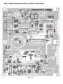
DDF-1 MAIN BOARD PARTS LAYOUT DIAGRAM
DDF1 17
Locate the two(2) 555 time IC’s
52. Install U6, 555 timer IC.
53. Install U4, 555 timer IC.
Locate the 74HC4051 IC
54. Install U5, 74HC4051 IC.
Locate the 74HC42 IC
55. Install U8, 74HC42 IC.
Locate the 7805 three lead voltage regulator
56. Install VR1, 7805 voltage regulator IC. Install as shown in the diagram by carefully pre-bending the component leads at right angles to
the IC. The component should fit flush to the printed circuit board. Solder all three leads.
Note that the following diodes have a band on one end of the case. It is important that the band be positioned so it matches the band of the pattern on
the board.
Locate the 1N4002 diode, (black epoxy case with a white polarity
“band”)
57. Install D6, 1N4002 diode.
Locate the three(3) 1N4148 diodes, (small glass component marked with
a polarity band)
58. Install D2, 1N4148 diode .
59. Install D1, 1N4148 diode.
60. Install D5, 1N4148 diode.
Next come some capacitors This bunch will be ceramic disc type capacitors
and they may be installed in any direction. Just remember to keep them
close to the board so they look like a pro assembled your DDF1.
Locate three(3) .001uF capacitors [marked 102]
61. Install C22, .001uF disc capacitor.
62. Install C24, .001uF disc capacitor.
63. Install C26, .001uF disc capacitor.
Locate ten(10) .01uF capacitors [marked 103]
64. Install C9, .01uF capacitor.
65. Install C5, .01uF capacitor.
66. Install C4, .01uF capacitor.
67. Install C6, .01uF capacitor.
DDF1 20
68. Install C2, .01uF capacitor.
69. Install C3, .01uF capacitor.
70. Install C1, .01uF capacitor.
71. Install C18, .01uF capacitor.
72. Install C19, .01uF capacitor.
73. Install C38, .01uF capacitor.
Locate fifteen(15) .1uF capacitors [marked 104]
74. Install C7, .1uF capacitor.
75. Install C51, .1uF capacitor.
76. Install C54, .1uF capacitor.
77 Install C53, .1uF capacitor.
78. Install C52, .1uF capacitor.
79. Install C21, .1uF capacitor.
80. Install C14, .1uF capacitor.
81. Install C17, .1uF capacitor.
82. Install C16, .1uF capacitor.
83. Install C15, .1uF capacitor.
84. Install C10, .1uf capacitor.
85. Install C12, .1uF capacitor.
86. Install C11, .1uF capacitor.
87. Install C13, .1uF capacitor.
88. Install C31, .1uF capacitor.
Locate one(1) .0047uF capacitors [marked .0047 or 472]
89. Install C23, .0047uF capacitor.
This batch of capacitors are called electrolytic capacitors. They are polarized with a (+) and (-) lead and must be installed in the correct orientation.
Ordinarily, only the negative side is marked on the capacitor body with a dark
band and the (-) sign clearly shown, while the PC board has a “+” printed
next to the pattern indicating the “+” lead. Be careful and install the capacitors with the negative lead in the opposite hole from where the “+”
is indicated on the board. Failure to do so may result in the capacitor actually EXPLODING and causing possible damage to you and/or the board.
In addition to the capacitance and polarity markings you will also find a voltage indication. Any value greater than 16 volts is good for our application.
The capacitors should fit snugly down on the PC board.
DDF1 21
Locate two(2) 100uF capacitors [100uF]
90. Install C30, 100uF electrolytic capacitor.
91. Install C29, 100uF. electrolytic capacitor.
Locate three(3) 1uF capacitors [1uF]
92. Install C8, 1uF electrolytic capacitor.
93. Install C25, 1uF electrolytic capacitor.
94. Install C32, 1uF electrolytic capacitor.
Locate one(1) 10uF capacitor [1uF]
95. Install C33, 10uF electrolytic capacitor.
Locate one(1) .47uF capacitors [.47uF]
Notice the pattern on the board for this capacitor, C20, is incorrect. Be careful and install the “-” or banded lead so it is toward R8 and the edge of the
board and the unmarked or “+” lead is toward the center of the board.
96. Install C20, .47 uF electrolytic capacitor.
Locate two(2) 2N3904 transistors [2N3904 or 3904]
97. Install Q2, 2N3904 transistor. The flat side must be placed as
shown on the PC board, facing R24. Mount it as close to the board as
possible without forcing it. Carefully solder all three leads.
98. Install Q1, 2N3904 transistor. Be sure to orient the flat side as
shown in the parts diagram and keep it close to the board as you did
with Q2.
Locate one(1) two pin speaker connector. This is a small connector
which looks like two wire leads inserted through a piece of plastic.
[Actually that’s exactly what it is :-) ]
99. Install speaker connector J4.
That’s all the components that are installed on this side of the main circuit
board. Take a few minutes to double check your work. Make sure all values
are correct and take special notice of the placement of the diodes, IC’s and
electrolytic capacitor orientation. It’s also a good idea to check your soldering
and make sure you didn’t slobber any solder, (say that three times fast),
across any connections. Remember that time spent here can save a lot of
time (and expense and frustration!) when the unit is initially turned on.
DDF1 22
CONTROL AND DIRECTION INDICATOR ASSEMBLY
In these assembly steps for the DDF1 main board, the components will be
mounted to the SOLDER SIDE of the circuit board. That’s the other side of
the board from the previous steps and with the least amount of printing on it.
Make sure the cover with the sticker you applied is dry and the sticker
is firmly attached before starting this part of the assembly.
100. Find the 3 DPDT slide switches. Looking at the bottom of the circuit
board locate the positions of S1, S2, and S3 switches. Insert a switch
into each location. It doesn’t matter how the switches are oriented, just
make sure each switch is flush to the circuit board. Check the placement of each switch by “test fitting” the circuit board into the upper half of
the case assembly and ensure it operates smoothly. Make any adjustments required so they operate smoothly and then solder them on the
other side of the board, (not to be confused with the other side of the
tracks).
101. Locate the 10K potentiometer, labeled 10K or 103, on the side of
the pot. Install this potentiometer in the R50 position. Once again make
sure that this control is mounted flush to the circuit board and solder into
place.
102. Locate the two(2) 500K, labeled 500K or 505, potentiometers and
install them in the same way in the locations for R19 and R36 in the
same manner as above.
Locate the 18 red and one green LED’s. Look closely at one of these LED’s
and notice one lead is shorter than the other. This lead is the cathode or
negative lead of the LED. Also notice that the plastic case has a flat area on
the same side as this lead. The longer of the two leads is the anode, or (+)
connection.
When installing these LED’s the SHORT LEAD/FLAT AREA must be inserted in the rectangular pad and the flat area must match the printed symbol on the board.
These are the direction heading and level indication LED’s and they should
be installed so they extend through top panel of the unit the same distance.
These LED’s are also inserted from the back side of the board matching the
printed symbols. The following steps will assure the correct installation and
height.
103. Insert, BUT DO NOT SOLDER, the 18 RED LED’s into the locations D3, 4, 17, 18, 19, 20, 21, 22, 23, 24, 25, 26, 27, 28, 29, 30, 31, 32.
104. Insert, BUT DO NOT SOLDER, the GREEN LED into location D16.
DDF1 23
105. Temporarily fit the circuit board into the case top, and carefully tip the
board and case over and allow the LED’s to fall into their respective holes
in the case.
106. With the 19 LED’s correctly oriented and set to the correct height,
solder into place while the circuit is in the case top. Be carefuf and don’t
touch the hot soldering iron to the case top. Doing so not only makes boo
-boos in the case but is also smelly.
107. Install J1, the 2.1mm DC input connector. Notice that this mounts on
the “component side of the circuit board and the solder leads push
through the circuit board to protrude through the solder “pads” for connection. Be sure to push it firmly onto the circuit board as the alignment of
this part is important in getting the case holes to line up with the part. Solder all three leads; don't be afraid to use enough heat to flow the entire
connection and fill the holes.
108. Identify and install J3, the miniature audio input jack. Gently “rock”
the component into place firmly onto the board before soldering.
109. In the same manner, identify and install J2, the DB 9 connector,
which will output the switching control voltage to the antenna switch. This
jack is a large plastic and metal connector with the board and cable connections at a right angle to each other. Be sure that the connector fits
firmly to the printed circuit board. Solder all connections as well as the two
large mounting tabs. The tabs will require a lot of heat to get the solder to
flow evenly. Don’t be afraid to get them really hot.
The main board assembly is complete! You are that much closer to a functioning Doppler DF system. Take a break...you have accomplished the biggest
“chunk” of the kit. We also recommend you check over your work so far and
make sure there are no missed or bridged(slobbered) solder connections and
that all components are installed properly and the correct values. The next
steps will assemble the antennas and switching system for the DDF1.
DDF1 24
DDF-1 ANTENNA SCHEMATIC DIAGRAM
DDF1 25
ANTMTG BOARD LAYOUT
ANTINT BOARD LAYOUT
DDF1 26
ANTENNA SYSTEM ASSEMBLY
Roll those sleeves back up; we’ll get to the antenna switcher and individual
antenna assemblies to complete the Doppler DF kit.
Have a look at the ANTINT-1 and ANTMTG-1 circuit boards. Note that these
circuit boards will be operating at RF frequencies and proper assembly techniques (i.e. short component lead lengths, coaxial cable connections, etc.)
will be critical on these boards. To minimize these impedance destroying
lead lengths, we have opted for a “surface
DIODE & INDCUCTOR
mount” procedure of the components. InFORMED
LEAD FORMING
LEAD
stead of the typical “thru hole assembly“ you
have completed on the main board, the components on boards will be soldered on the
SOLDER
same side of the circuit board. It is therefore
necessary to pre-form the component leads
PAD
and trim excess leads prior to the component
being installed. Take a look at the drawing showing how to form the leads for the inductors and diodes. Remember to keep
the body of all components tight to the board to minimize lead length.
1. Form and install the four(4) 1N4148 diodes D1, 2, 3, 4 into their respective positions on the circuit board. Use the shortest lead length possible. Note that these components are polarized. Install the banded end
as shown in the parts diagram. Don’t worry about too much heat from
your soldering iron, you will not damage the diodes.
2. In the same manner form and install four(4) 1.2uH (brown-red-gold)
inductors L1, 2, 3, and 4. Keep those lead
CAPACITOR LEAD
FORMED
lengths as short as possible.
FORMING
LEAD
3. Install eight(8) .001uF (marked 102),
C1-C8, disc capacitors on the board.
Install these so they lay flat on the
board keeping the leads as short as
possible!
102
SOLDER
PAD
WHIP ANTENNA AND ANTENNA MOUNTING BOARD INSTRUCTIONS
You will need to mount two components as well as an antenna whip to each
ANTMTG board
1. Install a 1N4148 diode on the ANTMTG circuit board in the same
manner in which you did on the switcher, keeping those leads as short
as possible.
2. Install the 1.2 uH inductor in the L1 position.
3. Repeat steps 1 & 2 for the remaining three(3) circuit board assemblies.
DDF1 27
COAXIAL CABLE PREPARATION AND ASSEMBLY
We’re getting very close to the end now! It is time to install the coaxial
“jumpers” that connect the antenna switcher board to the individual antenna
assemblies. To begin our preparation, locate the length of mini coax included
with your kit.
1. Cut four 13 inch pieces of cable to connect the switcher to each antenna assembly.
2. “Prep” each of the coaxial cables as shown in the diagram. Be careful
not to use too much heat when “tinning” the braid of the coax as this
could damage the center
insulating shield.
Tinned Braid
RG-174 Coax
3. Position a prepared
Center Conductor
coax on the board so the
center conductor is over
the “J1” pad and the
tinned braid does not
Center Insulation
touch the pad. Using
some of your longer trimmed component leads, insert one end into one
of the holes in the board on either side of the tinned braid of the coax
and carefully bend it over the coax and into the hole on the other side of
the coax.
4. Solder the coax center conductor to the circuit board. Make sure the
braid does not touch the center conductor connection.
5. Apply a little solder to the wire you formed over the braid. DO NOT
USE TOO MUCH HEAT WHEN ATTACHING THE BRAID, as this can
cause the center insulation of the cable to melt.
6. Form another wire over the insulated area of the coax and through the
holes on either side of the coax.
7. Be careful and don’t apply too much heat which can damage the
coax and cause a short to center conductor. Solder the two formed
wires to the top side of the board like you did the other components and
make sure there are no “bumps” on the back of the board since any solder or protruding lead will prevent the board from sitting flat on a surface.
8. Determine the length of cable you need to connect the ANTINT board
to your receiver.
9. Using the length determined above, cut your own coax cable cut to
length , such as type RG58, to the “TO RADIO” connection on the
ANTINT board as described in steps 2, 3 and 4 above.
FINAL ANTENNA AND ANTINT ASSEMBLY
DDF1 28
Locate the 4 antennas, 5 plastic caps, 4 lock washers, 4 M3 kepnuts, 4 M3
screws 4 antenna boards and 1 antenna switch board.. Refer to the following diagram and perform the following steps on each of the 4 antenna
mounting boards.
Final Antenna Board Assembly
Use the picture on Page 30 as a guide to construct the antenna.
1. Insert an M3 screw through the center hole from the back of the antenna board.
2. Place a #4 internal tooth wash over the screw.
3. Screw one of the M3 kep nuts, (that’s one of the nuts with a lock
washer attached to it), onto the screw so the lock washer is facing away
from the board and tighten it.
4. Remove the protective paper on a flexible magnet and attach the
magnet to the bottom of the antenna board. We suggest you not trim the
magnet since doing so will decrease the ability of the assembly to stay
put on a magnetic surface. (BIGGER IS BETTER (-: )
5. Screw a whip antenna onto the M3 screw.
6. Make a small notch to fit over the coax on the bottom edge of the
plastic cap. You can use a sharp hobby knife, side cutters or a hot tool
such as your soldering iron. Melting with iron will be smelly… use your
ingenuity here.
7. Slide a plastic cap down over the antenna and align the small cutout
you made over the coax. This is a tight fit but I’m sure you can do it.
8. Repeat the above steps for each of the other 3 antenna assemblies..
Final ANTINT Board Assembly
In order to install the control cable between the antenna ANTINT board and
the DDF1 controller you will need a cable with at least 5 conductors. A
length of CAT5 LAN cable or any other cable with at least 5 conductors is
acceptable. It is not necessary to have twisted pairs or shielding but a cable
that is fairly small in diameter and flexible is probably best. It is IMPORTANT that the connections between the DB9 connector and ANTINT board
be made in the correct sequence or your DDF1 will not function properly.
1. Determine the length of control cable you require and cut your cable
to this length.
2. If your cable has only 5 conductors you may skip to the next step
NOW. If you are using a cable with more than 5 conductors, identify and
isolate 5 matching conductors on each end of the cable.
3. Refer to the DB9 diagram on page 30 and solder one each of the 5
wires in the cable to pins 1, 2, 3, 4 and 5. It is important you know which
wire is connected to which pin so you can connected them to the
ANTINT board in the next steps.
4. Connect the wire connected to pin 1 of the DB9 connector to the pad
DDF1 29
labeled “ANT1” on the ANTINT board.
5. In the same way connect the wires connected to the DB9 connector
pins 2, 3, and 4 to the “ANT2”, “ANT3” and “ANT4” respectively.
6. Connect the wire from pin 5 on the DB9 connector to the “GND” pad
located near the “ANT4 IN” connection on the ANTINT board.
7. Verify that you have connected the control cable wires correctly. If
they are not connected properly your DDF1 will not indicate the right direction of the elusive transmitter you are trying to find.
8. Connect the coax cables from the 4 antenna assemblies to the “ANT1
IN”, “ANT2 IN”, “ANT3 IN” and “ANT4 IN” connection points using the
same procedure in steps 4 through 8 on page 28.
Congratulations, You have finished the major assembly of your DDF1. All
that is left to do is some testing and then we’ll have you put it in the case and
weatherproof your antenna assembly. Don’t get impatient and jump ahead.
If there is a problem you may need to disassemble something if you go to the
final assembly now.
ANTENNA ASSEMBLY DETAILS
WHIP
ATENNA
PLASTIC
CAP
NOTCH
KEPNUT
#4 INTER TOOTH
WASHER
M4 SCREW
FORMED
WIRE
DB9 CONNECTOR (REAR VIEW)
5
4
9
3
8
DDF1 30
2
7
1
6
TESTING
Basic Testing
It is wise to review your workmanship, looking for circuit shorts or opens prior
to applying power. Use an ohmmeter to measure the resistance between
power and ground; the value should be greater than 2k ohms. Apply 12
VDC to the RDF unit with the power supply current limited to 150mA to prevent damage in the event of a problem (normal current drain is 100mA).
Verify the presence of the following supply voltages: = 5V on the output of
VR1, pin 16 of U8, pin 8 of U4, pin 8 of U6, pin 16 of U7, pin 24 of U11, pin
16 of U5. Verify +2.5 V on pin 14 of U3, verify +12 V on pin 4 of U1 and U2.
This completes the basic testing of the Doppler RDF circuit.
The following tests are recommended to identify and troubleshoot
problems, but don't worry if you don't have all the necessary test
equipment. Satisfactory performance can usually be achieved without
performing these tests.
Functional testing
Before connecting the antenna switcher, verify the operation of clock oscillator U4 by connecting an oscilloscope to pin 3. The output should be a square
wave with an amplitude of 5 V and a period of 125 ms (8 kHz). Use a frequency counter to verify the clock frequency is 8 kHz +/- 250 Hz if you desire. Getting the clock frequency to exactly 8 kHz is not necessary for proper
operation, however, the values of R27 and R28 can be changed to adjust
the clock frequency. Verify that closing switch S2 disables the clock. Open
S2 (scan stop) and verify the operation of BCD counter U7 by connecting the
oscilloscope sequentially to pins 14,13,12, and 11. The signal frequency on
these outputs should be approximately 4, 2, 1 and 0.5 kHz, respectively. Verify the presence of a square wave signal on pins 2,4,6 and 8 of buffer U12.
Signal Level Indicators
The following test uses an audio signal generator to simulate the presence of
the Doppler tone. Disconnect the speaker from audio level control potentiometer R50 to prevent loading the signal generator. Connect an audio signal
generator to the receiver audio input terminal. Set the generator to apply a
500 Hz sine wave with amplitude 1V P-P. Rotate R50 until the audio overload LED D3 illuminates. Then, adjust R50 until low signal level LED D4
lights. Adjust R50 so that LEDs D3 and D4 are off, set calibrate control R36
to the center of its range and adjust damping control R19 for minimum damping (fully CCW).
DDF1 31
Direction Indicator
Adjust the frequency of the audio generator very slowly around 500 Hz while
observing the LED display. You should see the direction indicating LEDs
around the green center LED illuminating. The LED illumination should rotate clockwise when the frequency of the generator is set slightly lower than
the antenna rotation frequency. (Only one LED will be on when the frequency of the generator equals the antenna rotation frequency.) The display
should rotate counterclockwise. The audio generator must be capable of
very fine frequency adjustment in order to observe the transition. All LED’s in
the display may appear to be on if the signal generator frequency is just
10Hz different from that of the antenna rotation frequency determined by U4.
It is interesting to observe the sharpness of the digital filter on pin 1 of U2 on
the oscilloscope as the display makes the transition from counterclockwise.
You can see the simulated Doppler tone of the generator come out of the
noise, peak and return into the noise as the transition takes place.
Calibration Control
Verify the function of the calibrate control by adjusting the audio generator
equal to the antenna rotation frequency. At this point, only a single LED will
illuminate. Rotate the calibrate control through out its range and observe the
direction indicating LED "move" around the display. The range of movement
should be more than 360 degrees. The direction indicating LED may move
slightly if the generator frequency drifts. It is very difficult to keep the generator frequency synchronized exactly, but that's not necessary in this test.
Disconnect the signal generator and reconnect the speaker to the receiver
audio input terminal.
Antenna Switcher
Verifying proper operation of the antenna switcher sequencing circuit requires only a DC voltmeter. Connect the antenna switcher to the Doppler
RDF unit and position the four mag-mount antennas on a table.
Remove the whip antennas from all the mounting boards for this test
It is essential that the antennas be turned on in sequence to emulate an antenna spinning in a circular pattern for the Doppler RDF unit to operate correctly. A single antenna turned on out of sequence is enough to produce a
bogus RDF reading. It does not matter if the antenna spins clockwise or
counterclockwise.
Scan/stop switch S2 stops the antenna from spinning. Close and open S2
until the voltage on terminal J2 pin 1 reads +1.4V. Pins 2, 3 and 4 should all
read near 0V. Pin 1 is the antenna enable signal for antenna 1. Label the
corresponding mag-mount antenna on the table as antenna 1. Close and
open S2 until the voltage on terminal J2 pin 2 reads +1.4V. Pins 1,3, and 4
should all read near 0V. Pin 2 is the antenna enable signal for antenna 4
DDF1 32
and should be positioned to the right of antenna 1 as viewed from the center
of the antennas for a clockwise spin. Close and open S2 until the voltage on
terminal J2 pin 3 reads +1.4V. Pins 1,2, and 4 should all read near 0V. Pin 3
is the antenna enable signal for antenna 3 and should be positioned to the
right of antenna 2 as viewed from the center of the antennas. Close and
open S2 until the voltage on terminal J2 pin 4 reads +1.4V. Pins 1, 2, and 3
should all read near 0V. Pin 4 is the antenna enable signal for antenna 2
and should be positioned to the right of antenna 3 as viewed from the center
of the antennas.
RF Operation
Testing the RF operation of the antenna is quite simple. Place all four antenna mounting boards around the center of the car roof, placing each antenna at the corner of an 18.25 inch square pattern for operation on 146
MHz. Do not install any of the whip antennas yet. Connect the RF output of
the antenna switcher to your FM receiver or transceiver tuned to the frequency desired.
CAUTION: MAKE SURE YOU DISABLE TRANSMIT MODE IF YOU ARE
USING A TRANSCEIVER!
Apply power to the RDF unit and open S2 to stop the spinning process. Install a whip antenna on ONE of the antenna mounting boards. Using a low
power transmitter such as a portable handheld transceiver on low power,
walk a distance away from the antenna and transmit on the frequency your
receiver is tuned to. Only one antenna should provide a signal strength
reading similar to it being connected directly to the FM receiver. Remove the
whip from the selected antenna and touch it to each of the other three antennas. The received signal should be weak or nonexistent. Close and open
S2 until another antenna is selected and repeat the same test. Continue the
process until you have verified each antenna can be turned on while the
other three remain off.
DDF1 33
Operation
Checking performance of the RDF unit is best done in a large, empty area
away from tall buildings: a parking lot will do. Use caution at all times during
open road operation of the RDF unit. Use a minimum of two people for all
testing and operation of the RDF unit: one to operate the vehicle and the
other to operate the RDF unit. The magnets securing your antennas to the
roof of the car were designed for use at reduced speeds. If you intend to use
the DDF1 at highway speeds, you may want to get some stronger magnets.
The powerful magnets contained in computer hard drives are excellent for
this application and can often be found at flea markets or surplus store for as
little as $1.00 or less. The typical magnet found in an audio speaker would
also work well. As a safety measure, secure each mag-mount antenna with
20 pound fishing line when operating the vehicle at highway speeds.
Attach all four whip antennas to the mag-mount antenna bases placed about
the center of the car top. Connect the RF output of the antenna switcher to a
FM receiver transceiver tuned to the desired frequency.
CAUTION:
Make sure you disable transmit mode if you are using a transceiver!
It is best to use a smaller, handheld walkie talkie with your DDF1. The unit
connects easily to the antenna on your handheld and because they have
less output power, there is less chance of doing damage by accidentally
transmitting into your DDF1.
Adjust the receiver's audio to a comfortable level in the external speaker.
Apply 12 V to the RDF unit and “spin” the antenna by closing switch S2. As
soon as S2 is closed, you should hear a 500 Hz tone imposed on the receiver audio. Rotate audio level adjust control R50 so that low signal level
LED D4 and audio overload LED D3 are extinguished. Never trust directional indications if D3 and/or D4 are illuminated. The direction indicating
display should be relatively constant with a single LED lit, or one or two adjacent LEDs alternately illuminating. Adjust calibrate control R36 so that the
direction indicating LED is consistent with the general direction of the transmitter with respect to your location and the position of the car. Have the
driver slowly circle while you observe the display. You should see the direction indicating LEDS illuminate in the opposite direction as the car is turning
in a circle. The position changes relative to the changing direction of the car,
however, the direction indicated from the center of the circle the car is driving
should remain fixed. If the display turns in the same direction as the car, flip
phase invert switch S3 to the opposite position to correct the 180 degrees
phasing offset. This completes the rough calibration procedure.
DDF1 34
Final Calibration
A more accurate calibration can be achieved while the car is in motion. Position a volunteer with a transmitter in a safe spot on the side of a long, straight
and vacant roadway about 1/4 to 1/2 mile away. Have them transmit on low
power (up to 5W) while traveling towards them. The RDF operator should
calibrate the RDF display to indicate 0 degrees as straight ahead. The display should change to 180 degrees indicating the signal is coming from directly behind the car as the vehicle passes the transmitter. The moving calibration producer functions to average out false reflected signals caused by
multipath propagation. You may notice that the Doppler tone changes as the
car moves about. The Doppler tone will sound like a pure, undistorted 500
Hz sine wave in the absence of reflected or multipath interference. Direction
indications are most reliable under these conditions. When reflected or multipath signals are present the Doppler tone will sound raspy and distorted.
Those signal components may arrive from different directions causing false
bearing indications. The LED display tends to jump around randomly under
these conditions. Avoid taking bearing information when the Doppler tone
sounds raspy. You can minimize display jitter by slowing the response time
of the digital filter. This is accomplished by increasing damping control R19.
With a little time, you can master the art of Doppler RDFing.
The wide bandwidth antenna switcher can be used for DFing on other bands,
provided the proper antenna whip lengths and antenna spacing are used.
Arrange the antennas in a square pattern. Typical antenna lengths for common frequencies is shown in the table below. Whip lengths are measured
from the top surface of the mag-mount PC board base to the tip of the antennas.
You can determine the correct antenna length for other frequencies by interpolation of values from the table above. The Doppler DF’er will work on virtually any VHF/UHF frequency!
Frequency
Antenna length in
inches
146 MHz
18
223 MHz
13 1/2
446 MHz
7 7/8
DDF1 35
FINAL CASE UP
OK… Now that you’ve completed testing and setting up your DDF1 it’s time
to make it look pretty. This is the final phase of you trip.
CASE ASSEMBLY
1. Place the main circuit board in the top half of the case and secure it in
place using the 8 4-40x1/4 inch screws.
2. Notice that the bottom of the case has a bunch of holes drilled in it.
Find the speaker and mount it over the holes using the 2 black 6-32
screws and 6-32 nuts. Tighten the screws in place.
3. Plug the wire from the speaker into J4, the 2 pin connector near the
speaker input jack on the main board. It doesn’t matter which way it is
plugged in.
4. Place the top and bottom of the case together and use the six(6) 4-40
x 3/8 self tapping screws to secure them together.
FINAL ANTENNA SYSTEM ASSEMBLY
1. Make 6 small notches to fit over the cables on the bottom edge of the
plastic cap for the antenna switch board. You can use a sharp hobby
knife, side cutters or a hot tool such as your soldering iron. Melting with
an iron will be smelly… use your ingenuity here.
2. Use hot glue or silicone calking and apply a bead around the base of
the caps to attach the cap and seal the cable entry areas. You may also
want to seal around the whip antennas.
TROUBLESHOOTING INSTRUCTIONS
While we had hoped that it wouldn’t come to this, if you are having trouble
with your direction finder, here are a few suggestions.
Use a methodical, logical troubleshooting technique. Most problems can be
solved using common sense. A volt-ohm meter and a clear head are usually
all that are needed to correct any problem. Over 95% of problems with kits
returned for repair are due to misplaced parts and/or bad solder connections.
Working backwards through the assembly steps will often lead you to the
problem. We also suggest having someone else check over your work as it
is very common to miss an error several times and you will get even more
frustrated.
If you call our tech support for help please be sure to have the unit in front of
you and also have a multimeter available. If you have an oscilloscope available that might also be helpful. Please understand that due to the complexity of the DDF1 it may be difficult to troubleshoot over the phone but at lest it
will possible to get immediate real time information. If you decide to contact
us by email it will be even more difficult and time consuming because we will
need to ask questions and wait for answers numerous times.
DDF1 36
CONCLUSION
We sincerely hope that you enjoy the use of this Ramsey product. As always,
we have tried to compose our manual in the easiest, most “user friendly” format that is possible. As our customers, we value your opinions, comments,
and additions that you would like to see in future publications. Please submit
comments or ideas to:
Ramsey Electronics, LLC
Attn. Hobby Kit Department
590 Fishers Station Drive
Victor, NY 14564
And once again, thanks from the folks at Ramsey!
DDF1 37
NOTES
______________________________________________________________
______________________________________________________________
______________________________________________________________
______________________________________________________________
______________________________________________________________
______________________________________________________________
______________________________________________________________
______________________________________________________________
______________________________________________________________
______________________________________________________________
______________________________________________________________
______________________________________________________________
______________________________________________________________
______________________________________________________________
______________________________________________________________
______________________________________________________________
______________________________________________________________
______________________________________________________________
______________________________________________________________
______________________________________________________________
______________________________________________________________
______________________________________________________________
______________________________________________________________
______________________________________________________________
______________________________________________________________
______________________________________________________________
______________________________________________________________
______________________________________________________________
______________________________________________________________
DDF1 38
THE RAMSEY KIT WARRANTY
1. GENERAL:
Notice that this is not a "fine print" warranty. We want you to understand your rights and ours too! All Ramsey kits will work if
assembled properly. The very fact that your kit includes this new manual is your assurance that prior to release of this kit, a
varied group of knowledgeable people have assembled this kit from scratch using this manual. During this process, changes
and additions are noted by each assembler and integrated into the final version of the manual…which you have! If you need
help, please read through your manual carefully, all information required to properly build and test your kit is contained within
the pages! However, customer satisfaction is our goal, so in the event that you do have a problem, please note the following:
2. DEFECTIVE PARTS:
It's always easy to blame a part for a problem in your kit. Before you conclude that a part may be bad, thoroughly check your
work. Today's semiconductors and passive components have reached incredibly high reliability levels, and it’s sad to say that
our human construction skills have not! But on rare occasions a sour component can slip through. All of our kit parts carry the
Ramsey Electronics Warranty that they are free from defects for a full ninety (90) days from the date of purchase. Defective
parts will be replaced promptly at our expense. If you suspect any part to be defective, please mail it to our factory for testing
and replacement. Please send only the defective part(s), not the entire kit. The part(s) MUST be returned to us in suitable
condition for testing. Please be aware that testing can usually determine if the part was truly defective or damaged by assembly
or usage. Don't be afraid of telling us that you “damaged it” or “burned it out”, we're all human and in most cases, replacement
parts are very reasonably priced. Remember, our goal for over three decades is to have a happy customer, and we’re here to
work WITH you, not AGAINST you!
3. MISSING PARTS:
Before assuming a part value is missing, check the parts listing carefully to see if it is a critical value such as a specific coil or
IC, or whether a RANGE of values is suitable for the component (such as a "100 to 500 uF capacitor"). Often times, common
sense will solve a mysterious missing part problem. If you're missing five 10K ohm resistors and received five extra 1K
resistors, you can pretty much be assured that the “1K ohm” resistors are actually the “missing” 10 K parts ("Hum-m-m, I guess
the orange band really does look red!") Ramsey Electronics project kits are packed with pride in the USA by our own staff
personnel. While separate QC checks are made on all product kits, we too are human, and once in a great while there is a
chance something can get through those checks! If you believe we packed an incorrect part or omitted a part clearly indicated
in your assembly manual for your Ramsey kit, please contact us with information on the part you need. Contact our Repair
Department via telephone, email or writing. Please have your invoice number and date of purchase handy.
4. REFUNDS:
All Ramsey products, kit or factory assembled units have an unconditional 10 day (from the date of purchase) return policy to
examine our products. If you are not satisfied for any reason, you may return your unassembled kit with all the parts and
instructions, or your factory assembled and tested product, together with your proof of purchase to the factory for a full refund
less shipping. The return package should be packed securely. Insurance and tracking is highly recommended. A reminder, this
applies to unassembled kits. They must be in the same new condition as received, not partially assembled! Assembled kits
cannot be returned for credit. No RMA’s are required; simply return to Ramsey Electronics LLC, Attn: Product Returns, 590
Fishers Station Drive, Victor, NY, 14564. If you have any questions, please contact us at 585-924-4560.
5. FACTORY REPAIR OF ASSEMBLED KITS:
Most of us at Ramsey are technically oriented and we do realize that things happen! Even following the best practices, with all
of the best intentions, there is that chance that your kit doesn’t work when you have completed it. Each manual goes into
detailed troubleshooting based on the specific kit to help you troubleshoot the problem. We have found that 95% of returned
kits involved wrongly installed components (wrong part or backwards polarity). This section of the warranty assumes you have
gone through all those steps, and have now reached the point that you need to send it back.
To qualify for factory repair of customer assembled kits, the following conditions apply:
1. Kits must not be assembled with acid solder flux
2. Kit boards or circuits must not be modified in any manner from the version received
3. Kits must be fully assembled, not partially assembled. Our warranty does not include “finishing” your kit!
4. Must include a full description of the problem encountered including the troubleshooting steps you have already done.
5. Must not include non-standard, non-Ramsey accessories, cases, enclosures, knobs, etc. or any batteries.
6. Must include the minimum repair fee of $25 USD in the form of check, money order or credit card authorization.
7. Ramsey Electronics, LLC reserves the right to refuse any repair due to excessive errors in construction methods.
8. If, due to customer construction methods, the repair is estimated to exceed the minimum flat rate, Ramsey Electronics,
LLC will contact the customer to discuss the repairs needed and to receive authorization and payment for repair prior
to repair.
9. In the unlikely case that a defective part is found to be the cause of the problem, the repairs will be made at no-charge
to the customer, and any payments received for repair will be returned or credited back to the customer.
10. Properly pack your kit, insure the package, and use a carrier that can be tracked. Ramsey Electronics, LLC is not
responsible for any loss or damage in shipment. Send the package together with your repair fee to the return address
below. No RMA is required.
6. FACTORY REPAIR FEES:
Please understand that our Tech Support Group personnel are not volunteers! They are a dedicated group of highly trained
technicians each configured with a very properly equipped test bench. Upon receipt of a repair, the setup, testing, diagnosis,
repair, paperwork, and repacking of your kit requires nearly an hour of their time regardless of the size or complexity of the kit!
The minimum repair fee represents ½ hour Tech Support time at $50/hour USD. We try to keep all kit repairs within the realm
of the $25 flat rate whenever possible…and trust us; we exceed that time spent on most kits received more often than not!
7. CONTACT INFORMATION AND RETURN ADDRESS:
Technical Questions
RAMSEY ELECTRONICS, LLC
Attn: Tech Support
590 Fishers Station Drive
DDF1
Victor, NY 14564
585-924-4560; 585-924-4886 Fax
[email protected]
Product Repair & Returns
RAMSEY ELECTRONICS, LLC
Attn: Repairs
590 Fishers Station Drive
39
Victor, NY 14564
585-924-4560; 585-924-4886 Fax
[email protected]
ABREVIATED TABLE OF CONTENTS
Introduction to the DDF1 .................... 4
Theory Of Operation .......................... 4
Parts List ........................................... 11
DDF1 Assembly Steps ...................... 14
Component Layout ............................ 17
Schematic Diagram ........................... 18
Operation........................................... 34
Ramsey Warranty ............................. 39
REQUIRED TOOLS
Soldering Iron
Thin Rosin Core Solder
Needle Nose Pliers
Small Diagonal Cutters
ADDITIONAL SUGGESTED ITEMS
Helping Hands Holder for PC Board/Parts
Desoldering Braid
Price: $5.00
Ramsey Publication No. MDDF1
Instruction manual for:
RAMSEY MODEL NO. DDF1
DOPPLER RADIO DIRECTION FINDER
RAMSEY ELECTRONICS, LLC
590 Fishers Station Drive
Victor, New York 14564
Phone
(585) 924-4560
Fax
(585) 924-4555
www.ramseykits.com
DDF1 40