1
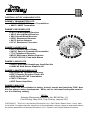
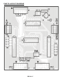
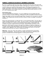
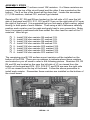
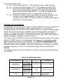
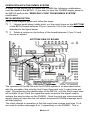
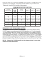
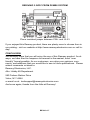
BINARY 16 to 4 LINE ENCODER 0 1 2 3 4 5 6 7 8 9 10 11 12 13 14 15 B E 1 6 4 1 2 4 8 Ramsey Electronics Model No. BE164 The BE164 is a one of 16 line input to 4 BCD (Binary-Coded-Decimal) output priority encoder. The output ay be configured as either active high or active low levels input and output and are 3.3/5 volt logic levels. Either an external data enable level may be selected or it may be set fro continuous data enable. A special configuration is provided to allow the B#16-4 to operate in conjunction with the Ramsey DVMS-BCD voice message recorder to allow direct access to up to 8 recorded messages. 3.3/5 volt logic level 16 line inputs to 4 line BCD active high/low output Highest input takes priority on output Internal/External data enable configurable Configuration option for operation with Ramsey DVMS-BCD message recorder BE164 1 PARTIAL LIST OF AVAILABLE KITS: RAMSEY TRANSMITTER KITS FM10C, FM25B FM Stereo Transmitters AM1C, AM25 Transmitter RAMSEY RECEIVER KITS FR1C FM Broadcast Receiver AR1C Aircraft Band Receiver AR2 Aircraft Band Receiver SR2C Shortwave Receiver AA7C Active Antenna SC1C Shortwave Converter RAMSEY HOBBY KITS SG7 Personal Speed Radar SS70C Speech Scrambler/Descrambler TT1CTelephone Recorder MD3C Microwave Motion Detector PH14C/15C/16C Peak hold Meters RAMSEY AUDIO KITS SHA1C and SHA2 Headphone Amplifier kits UAM4 40 Watt Stereo Amplifier kit RAMSEY AMATEUR RADIO KITS HR Series HF All Mode Receivers DDF1 Doppler Direction Finder Kit QRP Series HF CW Transmitters CW7C CW Keyer QRP Power Amplifiers RAMSEY MINI-KITS Many other kits are available for hobby, school, scouts and just plain FUN! New kits are always under development. Write, call or visit www.ramseykits.com for our free Ramsey catalog. BE164 Ramsey Electronics publication No. BE164 Rev 1.0 First Printing: May 2010, This Printing: January 2011 COPYRIGHT 2010-2011 by Ramsey Electronics, LLC. 590 Fishers Station Drive, Victor, New York 14564. All rights reserved. No portion of this publication may be copied or duplicated without the written permission of Ramsey Electronics, LLC. Printed in the United States of America. BE164 2 Ramsey Publication No. BE164: Manual Price Only $5.00 INSTRUCTION MANUAL FOR BINARY 16 to 4 LINE ENCODER TABLE OF CONTENTS Introduction/Circuit Description ...................... 4 “Learn-As-You-Build” Kit Assembly................ 8 Parts List......................................................... 9 Parts Layout Diagram..................................... 7 Schematic ..................................................... 10 Assembly Steps ............................................ 12 Setup ............................................................ 14 Operation with the DVMS8 ........................... 15 Conclusion .................................................... 17 Specifications ............................................... 18 Ramsey Kit Warranty ................................... 19 RAMSEY ELECTRONICS, LLC 590 Fishers Station Drive Victor, New York 14564 Phone (585) 924-4560 Fax (585) 924-4555 www.ramseykits.com BE164 3 Introduction The BE164 is a 16 to 4 line priority binary encoder. The output is 4 line binary with the highest input line taking priority. The binary output may be configured as either active high or active low. An active high data valid output is provided indicating when any of the 16 inputs and the input enable lines are at an active low level. The BE164 may also be configured to operate with the Ramsey Electronics DVMS8 Voice Messaging system to provide direct access to any of the 8 available recorded messages. Circuit Description The 16 input lines are divided between two 10 pin connectors, J1 and J2. Lines 1 to 8 are on J1 and 9 to 16 are on J2. A ground and common input enable are also provided on each connector. For the following operation description it will be assumed the input enable line, Pin 9 on both J1 and J2, is low (enabled) and jumper H2 installed in the “VALID” position. The enable line may be enabled from either an external signal applied to either J1 or J2, or by installing a jumper on the “ENA” jumper block, H3. Before we get into the more complex operation of the BE164 you will notice there are 18, 10K ohm resistors, R1 to R18, indicated in the schematic. All of these resistors are what are referred to as “pull-up” resistors. They are there to provide a high signal on all of the 16 input lines, input enable and active high option signal lines when no active low level is applied. Without these resistors the inputs would be in an unknown state if no signal were applied to the input. They also help reduce unwanted noise on the inputs. The input lines on J1 are applied to U1, a 74HC148 8 to 3 line priority encoder. U1’s output is 3 lines, pins 6, 7 and 9. U1 takes care of encoding which of the 8 inputs is low and sets the state of each output to a binary representation of the highest active input. In other words if input 1 is low and input 5 is also low the output will indicate input 5 instead of 1 is low or active. Another output on U1, pin 14, goes low whenever pin 5 and any input line are both low. This signal is used to indicate that a valid input is present. It is connected to U3A pin 1, a dual input NAND gate. We’ll talk about this signal later. For now just assume it is low. Whenever a low is applied to any input of a NAND gate it’s output is set to a high state. U3A pin 3 is therefore at a high level which is connected to J2 pin 2, the “DATA VALID” signal. The three binary output lines from U1 are connected to NAND gates U3B, BE164 4 U3C and U3D inputs. These gates essentially act as inverters since any input going low will cause the output to go high. The outputs of these gates are essentially the final binary output lines for 3 of the 4 binary outputs. More about the final outputs later. The reason a 2 input gate is used is because U2, another 74HC148, outputs are also used to determine the final binary output signals for input lines 8 to 15. U2 operates in the same way as U1 except it handles input lines 9 to 16. Notice that again U2 pin 14, which indicates an input is valid, is connected to the other input of U3A which is the NAND gate that controls the data valid output signal. So either U1 or U2 can control the data valid output signal. Pin 15 on U2 is connected to U1 pin 5. This signal is low whenever all the inputs, lines 9 to 16, are high and the enable pin, U2 pin 5, is low. Otherwise it is high. This works to our benefit because it disables the outputs of U1 whenever one of the top 8 inputs is activated. Pin 15 is also used as the high order output line, bit 3, of the final output since all 8 of these lines will activate bit 3 for the binary output. Notice that U2 pin 5 is the input enable for the BE164. Working thru the logic you will see that by enabling U2 pin 5 will enable the entire set of input lines, 1 to 16. Now for the final output magic. Notice that all of the output lines from U3B, U3C and U3D as well as U2 output pin 15 are each connected to the input of one of the XOR gates in U4, a 74HC86. So what is an XOR gate? First, an OR gate is just what it sounds like. Any input that goes high on an OR gate causes the output to go high. It doesn’t matter if one or all of the inputs is high, the output will be high. An XOR, short for exclusive OR, will only have a high output if one, and only one, input is high. This is neat because by making one input always low the output will follow the other input. But if one input is set to be always high the output will be the inverse of the other input. Notice that if the “ACTIVE HIGH” jumper, H2, is installed the outputs will not invert the signals applied from U3. But if it is removed one input is always high and the signals will be inverted. This is used to provide either and active high, jumperH2 installed, or active low, H2 not installed, binary output. The BE164 can operate on a supply voltage between 2VDC and 6VDC which may be supplied to either J3 or J4. Two connectors are provided to allow easy connection of multiple interface modules, or any other circuitry for that matter, together. Capacitors C1 and C2 are provided to keep any noise from getting into, or out of, the BE164 on the power supply lines. See “SETTING UP YOUR BE164” section of this manual for further information. Configuring the BE164 is covered in the “Setup and Testing” section of this manual. BE164 5 INPUT/OUTPUT FUNCTION OUTPUTS INPUTS LINE (=0) ENABLE DATA VALID BIT 3 (active hi) BIT 2 (active hi) BIT 1 (active hi) BIT 0 (active hi) 1 0 1 1 (0) 1 (0) 1 (0) 1 (0) 2 0 1 1 (0) 1 (0) 1 (0) 0 (1) 3 0 1 1 (0) 1 (0) 0 (1) 1 (0) 4 0 1 1 (0) 1 (0) 0 (1) 0 (1) 5 0 1 1 (0) 0 (1) 1 (0) 1 (0) 6 0 1 1 (0) 0 (1) 1 (0) 0 (1) 7 0 1 1 (0) 0 (1) 0 (1) 1 (0) 8 0 1 1 (0) 0 (1) 0 (1) 0 (1) 9 0 1 0 (1) 1 (0) 1 (0) 1 (0) 10 0 1 0 (1) 1 (0) 1 (0) 0 (1) 11 0 1 0 (1) 1 (0) 0 (1) 1 (0) 12 0 1 0 (1) 1 (0) 0 (1) 0 (1) 13 0 1 0 (1) 0 (1) 1 (0) 1 (0) 14 0 1 0 (1) 0 (1) 1 (0) 0 (1) 15 0 1 0 (1) 0 (1) 0 (1) 1 (0) 16 0 1 0 (1) 0 (1) 0 (1) 0 (1) x 1 0 1 (0) 1 (0) 1 (0) 1 (0) ALL=1 0 0 1 (0) 1 (0) 1 (0) 1 (0) MULTIPLE INPUTS FUNCTION EXAMPLES INPUTS OUTPUTS LINE (=0) DATA VALID DATA VALID BIT 3 (active hi) BIT 2 (active hi) BIT 1 (active hi) BIT 0 (activ e hi) 1,4,5 0 1 1 (0) 0 (1) 1 (0) 0 (1) 3,7,8,12 0 1 0 (1) 0 (1) 1 (0) 0 (1) 10,15 0 1 0 (1) 0 (1) 0 (1) 0 (1) BE164 6 PARTS LAYOUT DIAGRAM BE164 7 RAMSEY “LEARN-AS-YOU-BUILD” ASSEMBLY STRATEGY Be sure to read through all of the steps, and check the boxes as you go to be sure you didn't miss any important steps. Although you may be in a hurry to see results, before you switch on the power check all wiring and capacitors for proper orientation. Also check the board for any possible solder shorts, and/or cold solder joints. All of these mistakes could have detrimental effects on your kit - not to mention your ego! Kit building tips: Use a good soldering technique - let your soldering iron tip gently heat the traces to which you are soldering, heating both wires and pads simultaneously. Apply the solder on the iron and the pad when the pad is hot enough to melt the solder. The finished joint should look like a drop of water on paper, somewhat soaked in. Mount all electrical parts on the top side of the board provided. The top side is clearly marked with the word “TOP”, you can’t miss it. This is the side that has little or no traces on it, but is covered with mostly copper. When parts are installed, the part is placed flat to the board, and the leads are bent on the backside of the board to prevent the part from falling out before soldering (1). The part is then soldered securely to the board (2-4), and the remaining lead length is then clipped off (5). Notice how the solder joint looks on close up, clean and smooth with no holes or sharp points (6). Warning: Use only rosin core solder or solder designed to be used with electronic equipment. Use of acid core solder will void your warranty and produce a board that will disintegrate in a short period of time. BE164 8 PARTS LIST Resistors 1 17 10K ohm (brown-black-orange), R1 10K ohm 0805 surface mount (103) R2 –R18 Capacitors 1 1 100uF C1 (100uF, 35V) 0.1uF C2 (104) Connectors 3 2 2 10 pin dual row J1, J2, J5 2 pin H2, H3 2 screw terminal J3, J4 Semiconductors 2 74HC148 3 line priority encoder, U1, H2 1 74HC00 quad NAND gate, U3 1 74HC86 quad XOR gate, U4 Miscellaneous 2 jumper blocks 1 Printed circuit board BE164 9 ASSEMBLY STEPS First we’ll mount the 17 surface mount 10K resistors. 8 of these resistors are mounted on the top of the circuit board and the other 9 are mounted on the bottom. The 8 on top of the board will be done first. Locate the seventeen (17) 10K resistors, marked 103, and we’ll get started. Resistors R6, R7, R8 and R9 are located on the left side of U1 near the left side of the board and R10, R11, R12 and R13 are on the right side of U2 near the right of the board. It is suggested that you first apply a light coating, called tinning, to both pads of each resistor. Then using a set of tweezers carefully position each resistor over the pads and apply heat to one connection. Make sure it is properly positioned and then solder the other lead for each of the 17 resistors. Here we go. 1. 2. 3. 4. 5. 6. 7. 8. Install 10K ohm resistor R6 marked 103. Install 10K ohm resistor R7 marked 103. Install 10K ohm resistor R8 marked 103. Install 10K ohm resistor R9 marked 103. Install 10K ohm resistor R10 marked 103. Install 10K ohm resistor R11 marked 103. Install 10K ohm resistor R12 marked 103. Install 10K ohm resistor R13 marked 103. The remaining nine(9) 10K surface mount resistors will be installed on the bottom of the PCB. There are no makings to indicate where these resistors are located so you sill need to refer to the following picture. Resistors R2, R3 R4 and R5 are located on the near the left side of U1 as viewed from the bottom of the board and R14, R15, R16 R17 and R18 are near the right side of U2 as viewed from the top of the board. Follow the above procedure to install each resistor. Remember these resistors are installed on the bottom of the circuit board. . BE164 12 9. 10. 11. 12. 13. 14. 15. 16. 17. Install 10K ohm resistor R2 marked 103 Install10K ohm resistor R3 marked 103. Install 10K ohm resistor R4 marked 103. Install 10K ohm resistor R5 marked 103. Install 10K ohm resistor R14 marked 103. Install 10K ohm resistor R15 marked 103. Install 10K ohm resistor R16 marked 103. Install 10K ohm resistor R17 marked 103. Install 10K ohm resistor R18 marked 103. Next we’ll install the integrated circuits, (IC’s). Located the 4 IC’s, (2x74HC148, 1x74HC00, 1x74HC86). These will be installed on the top of the board. Notice that the marking on the board has a small half circle on one end and that the IC’s have the same type of marking or a small indented dot on one end. It is important that the IC be installed so it matches the marking on the board. It may be necessary to gently bend the leads inward on each side of the IC’s so they are at right angles with the plastic body in order to get them into the holes in the board. This is easily done by holding the IC so the leads on one side are flat against a flat surface and then pressing the body so the leads bend slightly inward. Do this for the leads on both sides of the IC. Make sure that all the leads go thru the board. When you install the IC it is a good idea to insert it into the board and slightly bend one lead on opposite corners on the bottom of the board so it will stay in place. Then make sure all leads are thru and it is properly oriented before soldering all the leads. 18. 19. 20. 21. Install U1, a 74HC148, marked 74HC148 Install U2, a 74HC148, marked 74HC148 Install U3, a 74HC00, marked 74HC00 Install U4, a 74HC86, marked 74HC86 Locate the three(3) 10 pin dual row connectors. 22. Install J1 23. Install J2 24. Install J5 Locate the two(2) 2 pin headers. 25. Install H2 26. Install H3+ Locate the two(2) 2 terminal screw connectors. 27. Install J3 28. Install J4 BE164 13 Just 3 more steps to go! 29. Locate and install R1, a 10K resistor, [brown, black orange] 30. Locate and install capacitor C2, a .1uF capacitor marked 104. 31. Locate and install capacitor C1, a 100uF electrolytic capacitor. Be careful and install this capacitor so the lead closest to the dark colored stripe marked with a “-“ or dash is installed in the board hole away from the “+” sign printed on the circuit. 32. Locate the 2 small 2 pin jumper blocks in your kit and place one on each of the jumper headers, H2 and H3. Refer to the “Setting Up Your BE164” section of this manual below for specific placement of these jumpers. SETTING UP YOUR BE164 As described in the Circuit Description section the BE164 can be configured to provide either an active high or active low data output. This option is configured using the “ACTIVE HIGH” jumper block. An active low data enable control line is provided and is available on pin 9 of both input connectors J1 and J2. You may also install a jumper block on the “ENA” option header to constantly enable the inputs. In all cases the active high “Data Valid” signal is always available on output connector J3 pin 2. If you are using the BE164 to control the DVMS8 message system then simply install the “ENA” jumper, H3, and perform the xxxxxxxx. An interface cable will be required to connect to the DVMS. The “BE164 CONFIGURATION” table below provides the cable connections required. The DB25INTF custom interface cable is also available. It’s your choice, make your own or buy ours. It is also necessary to use a 3.3VDC power supply when controlling the DBMS8. The following tables provide full details to assist in configuring and interfacing your BE164. BE164 CONFIGURATION CONFIGURATION ENA (H3) ACTIVE HIGH (H2) COMMENTS 16 to 4 Line Active High Output INPUT CONTROL-OPEN CONSTANTINSTALLED INSTALLED All outputs available 16 to 4 Line Active Low Output INPUT CONTROL-OPEN CONSTANTINSTALLED OPEN All outputs available INSTALLED Only bits 0,1,2 and data valid(play) outputs used DVMS8 INSTALLED BE164 14 OPERATION WITH THE DVMS8 SYSTEM In order to use the BE164 to control the DVMS8 the following modifications must be made to the BE164. If you want to have the DVMS8 supply power to the BE164 perform the “DERIVING 3.3VDC FROM DVMS8 SYSTEM” modification. BE164 MODIFICATION Refer to the diagram below and follow the steps 1. Using a small sharp hobby knife, cut the circuit trace on the BOTTOM of the BE164 board between U3 pin 3 and the VIA at the location indicated in the figure below. 2. Solder a jumper on the bottom of the board between U1 pin 14 and the via as shown. BOTTOM VIEW OF BOARD VIA CUT TRACE HERE JUMPER 14 U1 pin 14 3 U3 pin 3 The operation of the BE164 with the DVMS8 system is as described below with the exception that only the first 8 input lines and only 3 output lines are used. By performing this modification to the BE164, only the first 8 input lines will activate J5 pin 2 and the signal becomes an active low signal used to activate the play function on the DVMS8. Once the units are interconnected simply taking an input line low will select the desired DVMS8 message and it will start playing. The other change in operation is that the input lines reverse and lines 1 to 8 are used to access messages 8 to 1 respectively on the DVMS8. This is BE164 15 because of the way in which the DVMS8 inputs operate. The BE164 overall operation is not changed. Complete interface details are provided in the “Setting Up Your BE164” section of this manual. DVMS INPUT/OUTPUT FUNCTION 8 INPUT LINE (=0) 1 7 2 0 1 1 0 6 3 0 1 0 1 5 4 4 5 0 0 1 0 0 1 0 1 3 6 0 0 1 0 2 7 0 0 0 1 1 8 0 0 0 0 DVMS MESSAGE DATA VALID BIT 2 BIT 1 BIT 0 0 1 1 1 DERIVING 3.3VDC FROM DVMS8 SYSTEM For operation with the DVMS8 it is necessary to operate the BE164 from a 3.3VDC power source because the DVMS8 operates on 3.3 volts internally. You may either supply this voltage from a separate power supply or obtain it from the DVMS8. Pin 23 on J3, the DB25 connector, on the DVMS8 can be connected to a power source. An easy point to connect to the 3.3 volt supply on the DVMS8 is on the bottom of the circuit board at on the “+” lead of C26. Connect a short insulated jumper on the bottom of the DVMS8 board between this point and pin 23 on J3, the only spare pin. You can then connect a lead from the interface cable connector pin 23 to the “+” terminal of J3 or J4 on the BE164. Refer to the DVMS8 manual and the diagram below for more help locating to locate these points. BE164 16 DERIVING 3.3VDC FROM DVMS8 SYSTEM J3-23 C26 + Place insulated jumper between C26+ and J3-23 If you enjoyed this Ramsey product, there are plenty more to choose from in our catalog - visit our website at http://www.ramseyelectronics.com or call today! CONCLUSION We sincerely hope that you will enjoy the use of this Ramsey product. As always, we have tried to compose our manual in the easiest, most “user friendly” format possible. As our customers, we value your opinions, comments, and additions that you would like to see in future publications. Please submit comments or ideas to: Ramsey Electronics, LLC. Attn. Hobby Kit Department 590 Fishers Station Drive Victor, NY 14564 or email us at: [email protected] And once again, thanks from the folks at Ramsey! BE164 17 BE164SPECIFICATIONS Input Requirements: Power: Logic: 3.3VDC/5VDC 16 lines, 5V active low Output Configuration: 3.3V/5V logic active high, 1 of 16 lines Output: 3.3VDC/5VDC max @ 20mA max Dimensions: Board: Mounting: Weight: 2.5”(W) x 2.5” (L) 63.5mm (W) x 63.5mm (L) 6 holes, 4/40 screw clearance on 1” x 2” pattern 6 holes on 25.4mm x 50.8mm pattern 0.7 Oz, 0.0198 Kg BE164 18 THE RAMSEY KIT WARRANTY 1. GENERAL: Notice that this is not a "fine print" warranty. We want you to understand your rights and ours too! All Ramsey kits will work if assembled properly. The very fact that your kit includes this new manual is your assurance that prior to release of this kit, a varied group of knowledgeable people have assembled this kit from scratch using this manual. During this process, changes and additions are noted by each assembler and integrated into the final version of the manual…which you have! If you need help, please read through your manual carefully, all information required to properly build and test your kit is contained within the pages! However, customer satisfaction is our goal, so in the event that you do have a problem, please note the following: 2. DEFECTIVE PARTS: It's always easy to blame a part for a problem in your kit. Before you conclude that a part may be bad, thoroughly check your work. Today's semiconductors and passive components have reached incredibly high reliability levels, and it’s sad to say that our human construction skills have not! But on rare occasions a sour component can slip through. All of our kit parts carry the Ramsey Electronics Warranty that they are free from defects for a full ninety (90) days from the date of purchase. Defective parts will be replaced promptly at our expense. If you suspect any part to be defective, please mail it to our factory for testing and replacement. Please send only the defective part(s), not the entire kit. The part(s) MUST be returned to us in suitable condition for testing. Please be aware that testing can usually determine if the part was truly defective or damaged by assembly or usage. Don't be afraid of telling us that you “damaged it” or “burned it out”, we're all human and in most cases, replacement parts are very reasonably priced. Remember, our goal for over three decades is to have a happy customer, and we’re here to work WITH you, not AGAINST you! 3. MISSING PARTS: Before assuming a part value is missing, check the parts listing carefully to see if it is a critical value such as a specific coil or IC, or whether a RANGE of values is suitable for the component (such as a "100 to 500 uF capacitor"). Often times, common sense will solve a mysterious missing part problem. If you're missing five 10K ohm resistors and received five extra 1K resistors, you can pretty much be assured that the “1K ohm” resistors are actually the “missing” 10 K parts ("Hum-m-m, I guess the orange band really does look red!") Ramsey Electronics project kits are packed with pride in the USA by our own staff personnel. While separate QC checks are made on all product kits, we too are human, and once in a great while there is a chance something can get through those checks! If you believe we packed an incorrect part or omitted a part clearly indicated in your assembly manual for your Ramsey kit, please contact us with information on the part you need. Contact our Repair Department via telephone, email or writing. Please have your invoice number and date of purchase handy. 4. REFUNDS: All Ramsey products, kit or factory assembled units have an unconditional 10 day (from the date of purchase) return policy to examine our products. If you are not satisfied for any reason, you may return your unassembled kit with all the parts and instructions, or your factory assembled and tested product, together with your proof of purchase to the factory for a full refund less shipping. The return package should be packed securely. Insurance and tracking is highly recommended. A reminder, this applies to unassembled kits. They must be in the same new condition as received, not partially assembled! Assembled kits cannot be returned for credit. No RMA’s are required; simply return to Ramsey Electronics LLC, Attn: Product Returns, 590 Fishers Station Drive, Victor, NY, 14564. If you have any questions, please contact us at 585-924-4560. 5. FACTORY REPAIR OF ASSEMBLED KITS: Most of us at Ramsey are technically oriented and we do realize that things happen! Even following the best practices, with all of the best intentions, there is that chance that your kit doesn’t work when you have completed it. Each manual goes into detailed troubleshooting based on the specific kit to help you troubleshoot the problem. We have found that 95% of returned kits involved wrongly installed components (wrong part or backwards polarity). This section of the warranty assumes you have gone through all those steps, and have now reached the point that you need to send it back. To qualify for factory repair of customer assembled kits, the following conditions apply: 1. Kits must not be assembled with acid solder flux 2. Kit boards or circuits must not be modified in any manner from the version received 3. Kits must be fully assembled, not partially assembled. Our warranty does not include “finishing” your kit! 4. Must include a full description of the problem encountered including the troubleshooting steps you have already done. 5. Must not include non-standard, non-Ramsey accessories, cases, enclosures, knobs, etc. or any batteries. 6. Must include the minimum repair fee of $25 USD in the form of check, money order or credit card authorization. 7. Ramsey Electronics, LLC reserves the right to refuse any repair due to excessive errors in construction methods. 8. If, due to customer construction methods, the repair is estimated to exceed the minimum flat rate, Ramsey Electronics, LLC will contact the customer to discuss the repairs needed and to receive authorization and payment for repair prior to repair. 9. In the unlikely case that a defective part is found to be the cause of the problem, the repairs will be made at no-charge to the customer, and any payments received for repair will be returned or credited back to the customer. 10. Properly pack your kit, insure the package, and use a carrier that can be tracked. Ramsey Electronics, LLC is not responsible for any loss or damage in shipment. Send the package together with your repair fee to the return address below. No RMA is required. 6. FACTORY REPAIR FEES: Please understand that our Tech Support Group personnel are not volunteers! They are a dedicated group of highly trained technicians each configured with a very properly equipped test bench. Upon receipt of a repair, the setup, testing, diagnosis, repair, paperwork, and repacking of your kit requires nearly an hour of their time regardless of the size or complexity of the kit! The minimum repair fee represents ½ hour Tech Support time at $50/hour USD. We try to keep all kit repairs within the realm of the $25 flat rate whenever possible…and trust us; we exceed that time spent on most kits received more often than not! 7. CONTACT INFORMATION AND RETURN ADDRESS: Technical Questions RAMSEY ELECTRONICS, LLC Attn: Tech Support BE164 590 Fishers Station Drive Victor, NY 14564 585-924-4560; 585-924-4886 Fax [email protected] Product Repair & Returns 19 RAMSEY ELECTRONICS, LLC Attn: Repairs 590 Fishers Station Drive Victor, NY 14564 585-924-4560; 585-924-4886 Fax [email protected] Quick Reference Introduction/Circuit Description .......................4 Parts List .........................................................9 Parts Layout Diagram .....................................7 Schematic......................................................10 Assembly Steps.............................................12 Setup .............................................................14 Specifications ................................................18 ........................................................................... REQUIRED TOOLS Soldering Iron Thin Rosin Core Solder Needle Nose Pliers Small Diagonal Cutters ADDITIONAL SUGGESTED ITEMS Helping Hands Holder for PC Board/ Parts Desoldering Braid RAMSEY ELECTRONICS, LLC 590 Fishers Station Drive Victor, New York 14564 Phone (585) 924-4560 Fax (585) 924-4555 www.ramseykits.com Ramsey Publication No. BE164 Assembly and Instruction manual for: BINARY 16 to 4 LINE ENCODER BE164 20