1
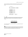
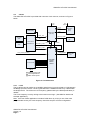
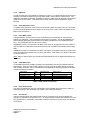
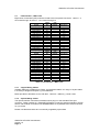
ADM-XRC-5T2-ADV
PCI Mezzanine Card
• JPEG2000 Video Compression
• Multi-Gigabit Serial I/O
User Guide
Version 1.0
ADM-XRC-5T2-ADV User Manual
Copyright © 2008 Alpha Data Parallel Systems Ltd. All rights reserved.
This publication is protected by Copyright Law, with all rights reserved. No
part of this publication may be reproduced, in any shape or form, without prior
written consent from Alpha Data Parallel Systems Limited
Alpha Data
4 West Silvermills Lane
Edinburgh EH3 5BD
UK
Alpha Data
2570 North First Street, Suite 440
San Jose, CA 95131
USA
Phone:
Fax:
Email:
Phone: (408) 467 5076
Fax:
(866) 820 9956
Email: [email protected]
+44 (0) 131 558 2600
+44 (0) 131 558 2700
[email protected]
EMI
This equipment generates, uses, and can radiate electromagnetic energy. It
may cause or be susceptible to electromagnetic interference if not installed
and used with adequate EMI protection for specific applications.
ADM-XRC-5T2-ADV User Manual
Version 1.0
ADM-XRC-5T2-ADV User Manual
Table of Contents
1.
2.
3.
4.
5.
Introduction ........................................................................................................................1
1.1.
Specifications ............................................................................................................1
Hardware Installation .........................................................................................................2
2.1.
Motherboard requirements........................................................................................2
2.2.
Handling instructions.................................................................................................2
2.3.
Installing the ADM-XRC-5T2-ADV onto a PMC motherboard ..................................2
2.4.
Installing the ADM-XRC-5T2-ADV if fitted to an ADC-PMC .....................................2
2.5.
Installing the ADM-XRC-5T2-ADV if fitted to an ADC-EMC .....................................2
Software Installation ..........................................................................................................2
Board Description ..............................................................................................................3
4.1.
Local Bus...................................................................................................................4
4.2.
Flash Memory............................................................................................................5
4.2.1.
Board Control Flash..........................................................................................5
4.2.2.
User FPGA Flash .............................................................................................5
4.3.
Health Monitoring ......................................................................................................5
4.4.
JTAG .........................................................................................................................6
4.5.
Clocks........................................................................................................................7
4.5.1.
LCLK.................................................................................................................7
4.5.2.
REFCLK ...........................................................................................................8
4.5.3.
PCIe Reference Clock......................................................................................8
4.5.4.
User MGT Clocks .............................................................................................8
4.5.5.
FCN MGT Clock ...............................................................................................8
4.5.6.
Rear (Pn4) Clocks ............................................................................................8
4.5.7.
PCI Clocks........................................................................................................8
4.6.
User FPGA ................................................................................................................9
4.6.1.
Configuration ....................................................................................................9
4.6.2.
I/O Bank Voltages...........................................................................................10
4.6.3.
Memory Interfaces..........................................................................................10
4.7.
FCN Interface – MGT Links ....................................................................................11
4.7.1.
Copper Mating Cables....................................................................................11
4.7.2.
Optical Mating Cables ....................................................................................11
4.7.3.
Example Gigabit I/O Applications...................................................................12
4.7.4.
Front Panel multi-gigabit I/O Control & Status Signals ..................................12
4.8.
Pn4 I/O ....................................................................................................................13
4.8.1.
Pn4 Signalling Voltage ...................................................................................13
4.9.
XMC Interface .........................................................................................................13
4.9.1.
Primary XMC Connector, P15 ........................................................................13
4.10. ADV212 Interface....................................................................................................14
4.10.1.
Signal Description...........................................................................................14
4.10.2.
JPEG Processor Interface Pin Locations .......................................................15
Design Examples .............................................................................................................16
5.1.
Revision History ......................................................................................................17
ADM-XRC-5T2-ADV User Manual
Version 1.0
ADM-XRC-5T2-ADV User Manual
Table of Tables
Table 1 Local Bus Interface Signal List .................................................................................... 4
Table 2 Voltage and Temperature Monitors............................................................................. 5
Table 3 MGT Clock Connections ............................................................................................. 8
Table 4 User FPGA I/O Bank Voltages .................................................................................. 10
Table 5 DDR Memory Bank Configuration ............................................................................. 10
Table 6 FCN Interface - MGT Links ....................................................................................... 11
Table 7 Board Control Signals ............................................................................................... 12
Table 8 Optical Module Control Signals .................................................................................. 12
Table 9 Pn4 to FPGA Assignments........................................................................................ 13
Table 10 Pn4 I/O Voltage Selection ....................................................................................... 13
Table 11 XMC P15 Connections ............................................................................................ 14
Table of Figures
Figure 1 ADM-XRC-5T2-ADV Block Diagram.......................................................................... 3
Figure 2 Local Bus Interface .................................................................................................... 4
Figure 3 JTAG Header ............................................................................................................. 6
Figure 4 Clock Structure........................................................................................................... 7
ADM-XRC-5T2-ADV User Manual
Version 1.0
ADM-XRC-5T2-ADV User Manual
1.
Introduction
The ADM-XRC-5T2-ADV is a high performance PCI Mezzanine Card (PMC) designed for
supporting development of applications using the Virtex-5 FF1738 Family of FPGA Devices.
•
Virtex5 LXT: LX110T, LX155T, LX220T or LX330T
•
Virtex 5 SXT: SX240T
•
Virtex 5 FXT: FX100T, FX130T, or FX200T
The card uses an FPGA PCI bridge developed by Alpha-Data supporting PCI-X and PCI. A
high-speed multiplexed address/data bus connects the bridge to the target (user) FPGA.
The card can also be fitted with a Primary XMC connector to provide high-speed serial links
to the user FPGA.
The board is an application specific version of the ADM-XRC-5T2 and features JPEG2000
video compression capabilities and multi-gigabit serial links using 2 FCN x4 Fibre Channel
connectors.
1.1.
Specifications
The ADM-XRC-5T2-ADV supports high performance PCI-X / PCI operation without the need
to integrate proprietary cores into the FPGA.
•
Physically conformant to VITA 42 XMC Standard
•
Physically conformant to IEEE P1386-2001 Common Mezzanine Card standard (with
XMC connector removed)
•
8-lane PCIe / Serial RapidIO connections to User FPGA (via XMC connector)
•
8 additional MGT links to User FPGA. (via front-panel) A cost-effective solution to
applications requiring high-speed data communications such as Infiniband TA, 10G
Ethernet, 4x Fibre Channel and others.
•
High performance PCI and DMA controllers
•
Local bus speeds of up to 80 MHz
•
Up to four independent banks of 64Mx32 DDRII SDRAM (1GB total)
•
Two banks of 2Mx18 DDRII SSRAM (8MB total)
•
User clock programmable between 31.25MHz and 625MHz
•
Stable low-jitter 200MHz clock for precision IO delays
•
User front panel gigabit serial I/O – 8 lanes in 2 FCN connectors
•
4 JPEG2000 codecs (Analog Devices ADV212) which can be operated individually or
in 2 tandem banks to provide compression /decompression of video data
•
User rear panel PMC connector with 32 free IO signals
•
Programmable I/O voltage rear interfaces
•
Supports 3.3V PCI or PCI-X at 64 bits
ADM-XRC-5T2-ADV User Manual
Version 1.0
Page 1
ADM-XRC-5T2-ADV User Manual
2.
Hardware Installation
This chapter explains how to install the ADM-XRC-5T2-ADV onto a PMC motherboard.
2.1.
Motherboard requirements
The ADM-XRC-5T2-ADV is a 3.3V only PCI device and is not compatible with systems that
use 5V PCI signalling levels.
The board must be installed in a PMC motherboard that supplies +5.0V and +3.3V power to
the PMC connectors. Ensure that the motherboard satisfies this requirement before powering
it up.
2.2.
Handling instructions
Observe SSD precautions when handling the cards to prevent damage to components by
electrostatic discharge.
Avoid flexing the board.
2.3.
Note:
Installing the ADM-XRC-5T2-ADV onto a PMC motherboard
This operation should not be performed while the PMC motherboard is powered up.
The ADM-XRC-5T2-ADV must be secured to the PMC motherboard using M2.5 screws in the
four holes provided. The PMC bezel through which the I/O connector protrudes should be
flush with the front panel of the PMC motherboard.
2.4.
Installing the ADM-XRC-5T2-ADV if fitted to an ADC-PMC
The ADM-XRC-5T2-ADV can be supplied for use in standard PC systems fitted to an ADCPMC carrier board. The ADC-PMC can support up to two PMC cards whilst maintaining host
PC PCI compatibility. If you are using a ADC-PMC refer to the supplied documentation for
information on jumper settings. All that is required for installation is a PCI slot that has enough
space to accommodate the full-length card. The ADC-PMC is compatible with 5V and 3V PCI
(32 and 64 bit) and PCI-X slots.
It should be noted that the ADC-PMC uses a standard bridge to provide a secondary PCI bus
for the ADM-XRC-5T2 and that some older BIOS code does not set up these devices
correctly. Please ensure you have the latest version of BIOS appropriate for your machine.
2.5.
Installing the ADM-XRC-5T2-ADV if fitted to an ADC-EMC
The ADM-XRC-5T2-ADV can be supplied for use in standard PC systems fitted to an ADCEMC carrier board. The ADC-EMC can support up to two PMC cards whilst maintaining host
PCI-Express compatibility. If you are using a ADC-EMC refer to the supplied documentation
for information on jumper settings. All that is required for installation is a PCIe slot that has
enough space to accommodate the full-length card
3.
Software Installation
Please refer to the SDK installation CD. The SDK contains drivers, examples for host control
and FPGA design and comprehensive help on application interfacing.
ADM-XRC-5T2-ADV User Manual
Version 1.0
Page 2
ADM-XRC-5T2-ADV User Manual
4.
Board Description
The ADM-XRC-5T2-ADV follows the architecture of the ADM-XRC series and decouples the
“target” FPGA from the PCI interface, allowing user applications to be designed with minimum
effort and without the complexity of PCI design.
A separate Bridge / Control FPGA interfaces to the PCI bus and provides a simple Local Bus
interface to the target FPGA. It also performs all of the board control functions including the
configuration of the target FPGA, programmable clock setup and the monitoring of on-board
voltage and temperature.
DDR2 SDRAM, SSRAM and serial flash memory connect to the target FPGA and are
supported by Xilinx or third party IP.
IO functionality is provided using multi-gigabit I/O connectors and Pn4 signals.
Bridge
Config
Config Flash
Memory
(32MB)
Secondary
Programmable
Clocks
Primary
Pn1
Pn2
Pn3
PCI-X /
PCI64/66
User FPGA
Bridge / Control FPGA
(Virtex4 LX25)
Local Bus (64 bit)
Serial Flash
(4MB)
Pn14
I/O
32 User Defined I/O (16 LVDS pairs)
Pn15
XMC
PCIe / Serial RapidIO (x8)
JTAG
System
Monitor
(LM87)
Virtex5
LX220T/LX330T
(FFG1738)
2x
ADV212
Front MGT
(x8)
Dual
Lane
Link
DDR-II
SSRAM
(4MB)
DDR-II
SSRAM
(4MB)
Power
Conversion
DDR-II
SDRAM
(256MB)
DDR-II
SDRAM
(256MB)
DDR-II
SDRAM
(256MB)
Figure 1 ADM-XRC-5T2-ADV Block Diagram
ADM-XRC-5T2-ADV User Manual
Version 1.0
Page 3
2x
ADV212
DDR-II
SDRAM
(256MB)
ADM-XRC-5T2-ADV User Manual
4.1.
Local Bus
The ADM-XRC-5T2-ADV implements a multi-master local bus between the bridge and the
target FPGA using a 32- or 64-bit multiplexed address and data path. The bridge design is
asynchronous and allows the local bus to be run faster or slower than the PCI bus clock to
suit the requirements of the user design.
Figure 2 Local Bus Interface
Signal
lad[63:0]
lbe_l[7:0]
lads_l
lblast_l
lbterm_l
lready_l
lwrite
ldreq_l[3:0]
ldack_l[3:0]
fhold
fholda
lreset_l
lclk
Type
bidir
bidir
bidir
bidir
bidir
bidir
bidir
unidir
unidir
unidir
unidir
unidir
unidir
Purpose
Address and data bus.
Byte qualifiers
Indicates address phase
Indicates last word
Indicates ready and requests new address phase
Indicates that target accepts or presents new data
Indicates a write transfer from master
DMA request from target to bridge
DMA acknowledge from bridge to target
Target bus request
Bridge bus acknowledge
Reset to target
Clock to synchronise bridge and target
Table 1 Local Bus Interface Signal List
ADM-XRC-5T2-ADV User Manual
Version 1.0
Page 4
ADM-XRC-5T2-ADV User Manual
4.2.
Flash Memory
The ADM-XRC-5T2-ADV is fitted with two separate Flash memories: one connected to the
Bridge / Control FPGA and the other to the User FPGA.
4.2.1. Board Control Flash
An Intel PC28F256P30 flash memory is used for storing a configuration bitstream for the User
FPGA. Once the Bridge / Control FPGA is configured, it checks for a valid bitstream in flash
and if present, automatically loads it into the User FPGA. This process can be inhibited by
setting a jumper on the JTAG connector. See the description of the “FBS” signal in Section
4.4 for further information.
Access to this flash device is only possible through control logic registers. The flash is not
directly mapped onto the local bus.
Programming, erasing and verification of the flash are supported by the ADM-XRC SDK and
driver. Utilities are provided to load bitstreams into the flash. These also verify the bitstream
is compatible with the target FPGA.
4.2.2. User FPGA Flash
An ST M25P32 flash memory with SPI interface is connected to the User FPGA for the
storage of application-specific information.
4.3.
Health Monitoring
The ADM-XRC-5T2-ADV has the ability to monitor temperature and voltage of key parts of
the board to maintain a check on the operation of the board. The monitoring is implemented
by a National Semiconductor LM87 and is supported by the board control logic connected
using I2C.
The Control Logic scans the LM87 when instructed by host software and stores the current
voltage and temperature measurements in a blockram. This allows the values to be read
without the need to communicate directly with the monitor.
The following supplies and temperatures, as shown in Table 2, are monitored.
Monitor
1.0V
1.2V
1.5V
1.8V
2.5V
3.3V
5.0V
Pn4_VCCIO
Temp1
Temp2
Purpose
User FPGA Core Supply
Bridge FPGA Core Supply
SRAM and ADV212 Core Supply
Memories, User FPGA Memory I/O,
Local Bus I/O
Config CPLD Core Supply
Source voltage for Front, Rear I/O
Board Input Supply
Board Input Supply
Either 2.5V or 3.3V Rear (Pn4) I/O Voltage
User FPGA die temperature
LM87 on die temperature for board/ambient
Table 2 Voltage and Temperature Monitors
ADM-XRC-5T2-ADV User Manual
Version 1.0
Page 5
ADM-XRC-5T2-ADV User Manual
The ‘sysmon’ application is provided upon request that permits the reading of the health
monitor. The typical output of the monitor is shown below, provided by the SYSMON
program.
*** SysMon ***
FPGA
Space Base Adr = 00900000
Control Space Base Adr = 00d00000
+1V0
+1V2
+1V8
+2V5
+3V3
+5V
Pn4
+1V5
Reading
Reading
Reading
Reading
Reading
Reading
Reading
Reading
=
=
=
=
=
=
=
=
1.01
1.21
1.81
2.51
3.32
5.04
3.31
1.51
SysMon Int Temp =
User FPGA Temp =
V
V
V
V
V
V
V
V
33 deg. C
26 deg. C
4.4.
JTAG
A JTAG header is provided to allow download of the FPGA using the Xilinx tools and serial
download cables. This also allows the use of ChipScope PRO ILA to debug an FPGA
design. It should be noted that four devices will be detected when the SCAN chain is
initialised.
TMS
TDI
TDO
TCK
FBS
GND
VCC
Figure 3 JTAG Header
The VCC supply provided on J5 to the JTAG cable is +3.3V and is protected by a poly fuse
with a rating of 350mA.
FBS
The FBS signal is an input to the control logic and provides control of the cold boot process.
By default with no link fitted, the control logic will load a bitstream from flash into the FPGA if
one is present. Shorting FBS to the adjacent GND pin will disable this process and can be
used to recover situations where rogue bitstreams have been stored in flash.
ADM-XRC-5T2-ADV User Manual
Version 1.0
Page 6
ADM-XRC-5T2-ADV User Manual
4.5.
Clocks
The ADM-XRC-5T2-ADV is provided with numerous clock sources, as shown in Figure 4
below:
PCI
Bus
PCI
RefClk
PCI-X
CLK
Bridge Config
(Coolrunner)
Bridge FPGA
(V4LX25)
PCI
CLK
Zero-delay
Buffer
(PLL)
XTAL_CLK
REFCLK_200M
25.0 MHz
XTAL
26.5625 MHz
XTAL
Ctl
Femto-clock
ICS843034-01
LCLK
200 MHz
Osc.
Local Bus
USERMGT_CLKB
USERMGT_CLKA
PCIe_RefClk (100 MHz)
FCN_MGTREF
156.25 MHz
Osc.
User FPGA
Virtex5
LX220T /
LX330T
Pn4 Connector
KEY
Global Clock Inputs
Clock Capable I/O
MGT Clock Inputs
Figure 4 Clock Structure
4.5.1. LCLK
The Local Bus can be used at up to 80 MHz and all timing is synchronised to LCLK between
the Bridge and User FPGAs. LCLK is generated from a 200MHz reference by a DCM within
the bridge FPGA. The minimum LCLK frequency (determined by the DCM specification) is
32MHz.
The LCLK frequency is set by writing to the board control logic. (See SDK for details and
example application).
Note: If the user FPGA application includes a DCM driven by LCLK (or one of the other
programmable clocks), the clock frequency should be set prior to FPGA configuration.
ADM-XRC-5T2-ADV User Manual
Version 1.0
Page 7
ADM-XRC-5T2-ADV User Manual
4.5.2. REFCLK
In order to make use of the IODELAY features of Virtex™-5, a stable low-jitter clock source is
required to provide the base timing for tap delay lines in each IOB in the User FPGA. The
ADM-XRC-5T2-ADV is fitted with a 200MHz LVPECL (LVDS optional) oscillator connected to
global clock resource pins. This reference clock can also be used for application logic if
required.
4.5.3. PCIe Reference Clock
A 100MHz PCIe reference clock input from the Primary XMC connector (Pn15) is connected
to one of the dedicated MGT clock inputs on the user FPGA. (See Table 3 for details of the
MGT clock connections.)
4.5.4. User MGT Clocks
A programmable, low-jitter clock source is provided by an ICS843034-01 “FemtoClocks”
frequency synthesiser. The synthesiser has two source crystals – one at 26.5625MHz (for
Fibre Channel applications) and another at 25.0MHz (suitable for PCIe, Gigabit Ethernet
etc.). The synthesiser also has two clock outputs.
”USERMGT_CLKA” is connected to an MGT clock input on the top-half of the user FPGA. It
may be used as an alternative to the PCIe reference for the MGTs connected to the Primary
XMC.
”USERMGT_CLKB” is connected to an MGT clock input on the bottom half of the user FPGA.
It may be used as the reference for the front user MGTs. (See Table 3 for details of the MGT
clock connections.)
Note: Either of these clocks can provide a programmable source for applications that do not
use MGTs.
4.5.5. FCN MGT Clock
A 156.25MHz precision oscillator is fitted on the ADM-XRC-5T2-ADV for Gigabit Serial I/O
applications. There are also 3 other options for clock inputs to the MGT tiles of the FPGA.
The oscillator frequency can be customised to suit applications requiring specific baud rates.
Contact the factory for details.
Clock Name
PCIE_REFCLK
USERMGT_CLKA
FCN_MGTREF
USERMGT_CLKB
GTP
No.
114
118
124
112
FPGA Pin (P/N)
Reference for:
AD4 / AD3
AK4 / AK3
C4 / C3
V4 / V3
Primary XMC (Pn15) MGTs
Primary XMC (Pn15) MGTs
Front (CN2) user MGTs
Front (CN2) user MGTs
Table 3 MGT Clock Connections
4.5.6. Rear (Pn4) Clocks
Four pairs of signals from Pn4 are connected to clock-capable inputs that can be used for
regional clocking of the remaining Pn4 signals. See Table 9 for details.
4.5.7. PCI Clocks
The PCI Interface within the bridge FPGA requires a regional clock input for 66MHz PCI
operation or a global clock input for PCI-X. To comply with the single-load requirement in the
PCI specification, a zero-delay clock buffer is used to route the PCI clock to the two different
clock inputs.
ADM-XRC-5T2-ADV User Manual
Version 1.0
Page 8
ADM-XRC-5T2-ADV User Manual
The clock buffer has a PLL with a minimum input frequency of 24MHz, potentially causing
problems in applications that use the PCI 33MHz mode with a slow clock. In this case, the
buffer can be bypassed to provide full PCI 33MHz compatibility.
4.6.
User FPGA
4.6.1. Configuration
The ADM-XRC-5T2-ADV performs configuration from the host at high speed using
SelectMAP. The FPGA may also be configured from flash or by JTAG via header J2.
Download from the host is the fastest way to configure the User FPGA with 8 bit SelectMAP
mode enabled. This permits an ideal configuration speed of up to 40MB/s.
The ADM-XRC-5T2-ADV can be configured to boot the User FPGA from flash on power-up if
a valid bit-stream is detected in the flash. Booting from flash will also configure the
programmable clocks.
ADM-XRC-5T2-ADV User Manual
Version 1.0
Page 9
ADM-XRC-5T2-ADV User Manual
4.6.2.
I/O Bank Voltages
Bank
0
1, 4, 5, 6
2
3
19, 21, 23, 25
27, 29, 31, 33
18
11, 13, 15, 17, 26
12, 20, 24
Voltage
3.3V
1.5V
3.3V
3.3V
1.8V
1.8V
2.5V or 3.3V
3.3V
1.8V
Description
Configuration I/F
DDRII SRAM
SelectMAP I/F, Serial Flash
Clocks
DDRII DRAM
DDRII DRAM (LX330T only)
Pn4 Interface
ADV212 Interface
Local Bus
Table 4 User FPGA I/O Bank Voltages
4.6.3. Memory Interfaces
The ADM-XRC-5T2-ADV has four independent banks of DDRII SDRAM when fitted with a
LX330T, SX240T or FX200T target FPGA. (Two banks with all smaller FPGAs) Each bank
consists of two memory devices in parallel to provide a 32 bit datapath. 1Gb Micron
MT47H64M16 devices are fitted as standard to provide 256MB per bank. The board will
support higher capacity devices when they become available.
The ADM-XRC-5T2-ADV has been designed for compatibility with Xilinx memory interface
cores.
Details of the signalling standards are given in the table below:
Name
DDR_ad[15:0],
DDR_ba[2:0],
DDR_rasn,
DDR_casn,
DDR_wen,
DDR_csn,
DDR_cke,
DDR_odt
DDR_ck0,
DDR_ckn0
DDR_dq[15:0]
DDR_dm[1:0]
DDR_dqs[1:0],
DDR_dqsn[1:0]
DDR_ck1,
DDR_ckn1
DDR_dq[31:16]
DDR_dm[3:2]
DDR_dqs[3:2],
DDR_dqsn[3:2]
Direction
Output
I/O Standard
SSTL18_I_DCI
Output
DIFF_SSTL18_II
BiDir
Output
BiDir
SSTL18_II
SSTL18_II_DCI
DIFF_SSTL18_II
Output
DIFF_SSTL18_II
BiDir
Output
BiDir
SSTL18_II
SSTL18_II_DCI
DIFF_SSTL18_II
Table 5 DDR Memory Bank Configuration
ADM-XRC-5T2-ADV User Manual
Version 1.0
Page 10
ADM-XRC-5T2-ADV User Manual
4.7.
FCN Interface – MGT Links
Eight lanes of user MGT (GTP) links are routed to the front panel connectors. Lanes 0 – 3
are routed through J5, lanes 4 - 7 are routed through J4.
Signal
FCN_TX0_P
FCN_TX0_N
FCN_RX0_P
FCN_RX0_N
FCN_TX1_P
FCN_TX1_N
FCN_RX1_P
FCN_RX1_N
FCN_TX2_P
FCN_TX2_N
FCN_RX2_P
FCN_RX2_N
FCN_TX3_P
FCN_TX3_N
FCN_RX3_P
FCN_RX3_N
Signal
FCN_TX4_P
FCN_TX4_N
FCN_RX4_P
FCN_RX4_N
FCN_TX5_P
FCN_TX5_N
FCN_RX5_P
FCN_RX5_N
FCN_TX6_P
FCN_TX6_N
FCN_RX6_P
FCN_RX6_N
FCN_TX7_P
FCN_TX7_N
FCN_RX7_P
FCN_RX7_N
FPGA
Pin
AA2
Y2
Y1
W1
T2
U2
U1
V1
R2
P2
P1
N1
K2
L2
L1
M1
FPGA
Pin
J2
H2
H1
G1
D2
E2
E1
F1
B1
B2
A2
A3
B6
B5
A5
A4
GTP
Number
112B
“
“
“
112A
“
“
“
116B
“
“
“
116A
“
“
“
GTP
Number
120B
“
“
“
120A
“
“
“
124B
“
“
“
124A
“
“
“
FCN J5 Pin
S16
S15
S1
S2
S14
S13
S3
S4
S12
S11
S5
S6
S10
S9
S7
S8
FCN J4 Pin
S16
S15
S1
S2
S14
S13
S3
S4
S12
S11
S5
S6
S10
S9
S7
S8
Table 6 FCN Interface - MGT Links
4.7.1. Copper Mating Cables
Suitable cables are available from Fujitsu “microGiGaCN Cable I/O” range of 8-pair cables
in a variety of lengths and styles e.g. FCD-ZZ00001.
Molex provide an alternative source with their ‘LaneLink’ cables e.g. 74526 -1002
4.7.2. Optical Mating Cables
The optical interface uses external modules which plug in to the standard FCN style
connector. These modules (e.g. EMCORE QTR3432) convert the electrical signals to optical
format. Inter-module connection uses MJ3MM12RPR-10-0 (available from Fiberconnections
Inc.) or similar
Please note that these items are not normally supplied by Alpha Data.
ADM-XRC-5T2-ADV User Manual
Version 1.0
Page 11
ADM-XRC-5T2-ADV User Manual
4.7.2.1. Important Notes on using Optical Modules
Optical modules provide a signal (‘sense_l’) indicating that they are present; however the
presence of optical modules cannot be distinguished from a copper connection by relying on
this signal alone.
Whilst the optical module supplies are disabled by default and protected by current limiting,
the method shown in the example code should always be used to ensure that supplies do not
drive into the short circuit presented when a copper cable is fitted.
Caution
This equipment uses Class 1 Laser devices; such devices are not considered to be
hazardous when used for their intended purpose. Use of controls, adjustments or
performance of procedures other than those specified herein may result in hazardous
laser light exposure.
4.7.3.
Example Gigabit I/O Applications
•
Dual Infiniband 4x ( 4 lanes at 2.5Gb/s over copper or optical fibre)
•
Dual 10Gb/s Ethernet CX4 ( 4 lanes at 3.125Gb/s over copper or optical fibre)
•
Dual 10Gb/s FibreChannel ( 4 lanes at 3.1875Gb/s over copper or optical fibre)
•
Dual 4 x OC-48 SONET
4.7.4.
Front Panel multi-gigabit I/O Control & Status Signals
Signal
BREFCK_ENA
B
STATUS_1
ATTEN_1
STATUS_2
ATTEN_2
Pin
Location
AC38
AC40
AM42
AC39
AM41
Description
-high to enable the 156.25MHz oscillator on the
board (pull-up on board)
-Infiniband STATUS led (yellow) connector 1
-Infiniband ATTEN led (green) connector 1
-Infiniband STATUS led (yellow) connector 2
-Infiniband ATTEN led (green) connector 2
Table 7 Board Control Signals
Signal
FCN Pin
G7
Connector 1 (J5)
FPGA Pin
AR5
Connector 2 (J4)
FPGA Pin
AM6
SENSE
FAULT
G6
AT6
AN5
ODIS
G2
AT7
AN6
PSUEN
G8 (3V3
Pwr)
-
AP7
AP6
AP5
AL7
OC_L
Description
low indicates that an opto module
has been fitted
low indicates that no data detected
on the opto Rx channel
low to disable Tx on any module
fitted on the channel
high to enable the opto power
supply
low indicates overcurrent on opto
supply
Table 8 Optical Module Control Signals
ADM-XRC-5T2-ADV User Manual
Version 1.0
Page 12
ADM-XRC-5T2-ADV User Manual
4.8.
Pn4 I/O
Up to 16 pairs of differential or 32 single-ended signals are available on Pn4 and are sourced
from Bank 18 of the User FPGA. All of the signal traces are routed as 100 Ohm differential
pairs and each pair is matched in length. The worst case difference in trace length between
any two pairs is 10mm. The pairs are distinguished by the signals names listed below and
follow the pattern +/-: 1/3, 2/4, 5/7, 6/8…
Signal
PN4_P1
PN4_N1
PN4_P3
PN4_N3
PN4_P5
PN4_N5
PN4_P7
PN4_N7
PN4_P9
PN4_N9
PN4_P11
PN4_N11
PN4_P13
PN4_N13
PN4_P15
PN4_N15
FPGA Pin
AF11
AF12
AF9
AF10
AF7
AE7
AC5 [CC]
AC6 [CC]
AG4 [CC]
AH4 [CC]
AH6
AH5
AB9
AB8
AB11
AC10
Pn4 Pin
1
3
5
7
9
11
13
15
17
19
21
23
25
27
29
31
Pn4 Pin
2
4
6
8
10 [CC]
12 [CC]
14 [CC]
16 [CC]
18
20
22
24
26
28
30
32
FPGA Pin
AE9
AE10
AD8
AE8
AF5
AF6
AB7
AB6
AD10
AD11
AC8
AC9
AL5
AK5
AJ7
AK7
Signal
PN4_P2
PN4_N2
PN4_P4
PN4_N4
PN4_P6
PN4_N6
PN4_P8
PN4_N8
PN4_P10
PN4_N10
PN4_P12
PN4_N12
PN4_P14
PN4_N14
PN4_P16
PN4_N16
Table 9 Pn4 to FPGA Assignments
In Table 9, pins marked [CC] are clock capable and may be used to access the regional
clocking resources in the FPGA.
Banks 18 is fitted with resistors to allow DCI terminations on Pn4 signals.
4.8.1. Pn4 Signalling Voltage
The signalling voltage on the Pn4 connector (and User FPGA Bank 18) is selectable by
switch SW2B.
Switch 2B
Open
Closed
Pn4 voltage
2.5V
3.3V
Table 10 Pn4 I/O Voltage Selection
It should be noted that the switch does not directly route power. The switch position is
monitored by the board control logic which, in turn, sets a power multiplexer to be either 2.5V
or 3.3V.
4.9.
XMC Interface
4.9.1. Primary XMC Connector, P15
The MGT (GTP) links connected between the user FPGA and the Primary XMC connector,
P15, are compatible with PCI Express and Serial RapidIO. Depending upon the carrier card,
they may also be used for user-specific applications.
ADM-XRC-5T2-ADV User Manual
Version 1.0
Page 13
ADM-XRC-5T2-ADV User Manual
Signal
PCIE_TX0_P
PCIE_TX0_N
PCIE_RX0_P
PCIE_RX0_N
PCIE_TX1_P
PCIE_TX1_N
PCIE_RX1_P
PCIE_RX1_N
PCIE_TX2_P
PCIE_TX2_N
PCIE_RX2_P
PCIE_RX2_N
PCIE_TX3_P
PCIE_TX3_N
PCIE_RX3_P
PCIE_RX3_N
PCIE_TX4_P
PCIE_TX4_N
PCIE_RX4_P
PCIE_RX4_N
PCIE_TX5_P
PCIE_TX5_N
PCIE_RX5_P
PCIE_RX5_N
PCIE_TX6_P
PCIE_TX6_N
PCIE_RX6_P
PCIE_RX6_N
PCIE_TX7_P
PCIE_TX7_N
PCIE_RX7_P
PCIE_RX7_N
FPGA Pin
AB2
AC2
AC1
AD1
AG2
AF2
AF1
AE1
AH2
AJ2
AJ1
AK1
AN2
AM2
AM1
AL1
AP2
AR2
AR1
AT1
AW2
AV2
AV1
AU1
BA1
BA2
BB2
BB3
BA6
BA5
BB5
BB4
GTP
Number
114A
“
“
“
114B
“
“
“
118A
“
“
“
118B
“
“
“
122A
“
“
“
122B
“
“
“
126A
“
“
“
126B
“
“
“
P15 Pin
A1
B1
A11
B11
D1
E1
D11
E11
A3
B3
A13
B13
D3
E3
D13
E13
A5
B5
A15
B15
D5
E5
D15
E15
A7
B7
A17
B17
D7
E7
D17
E17
Table 11 XMC P15 Connections
4.10.
ADV212 Interface
The ADV212 is a single-chip JPEG 2000 codec from Analog Devices. It is targeted for video and
high bandwidth image compression applications that can benefit from the enhanced quality and
features provided by the JPEG 2000 (J2K)—ISO/IEC15444-1 image compression standard. The
ADM-XRC-5T2-ADV features 4 ADV212 devices which can all operate independently or in 2 banks
of 2 for full frame capabilities.
4.10.1. Signal Description
See the ADV212 data sheet and associated literature for a full description of the operation of
these pins.
Signals common to each ADV212 bank
addr<1> to <3>
-ADV212 address bus
mclk
-ADV212 system clock
vclk
-ADV212 video data bus clock
hdat<0> to <31>
-ADV212 host data bus
field
-ADV212 field sync for video mode
hsync
-ADV212 horizontal sync for video mode
vsync
-ADV212 vertical sync for video mode
jpeg_reset_l
-asynchronous processor reset for ADV212’s
scomm5
-synchronisation signal for multi-chip operation
ADM-XRC-5T2-ADV User Manual
Version 1.0
Page 14
ADM-XRC-5T2-ADV User Manual
Individual signals to each ADV212 codec
ack_l
- ADV212 acknowledge signal
cs_l
- ADV212 chip select signal
dack_l<0> to <1> - ADV212 DMA acknowledge signals
dreq_l<0> to <1>
- ADV212 DMA request signals
irq_l
- ADV212 interrupt request signal
rd_l
- ADV212 read enable for host interface operation
we_l
- ADV212 write enable for host interface operation
vdat<0> to <11>
- ADV212 video data bus
scom4
- ADV212 LCODE Output in Encode Mode
4.10.2. JPEG Processor Interface Pin Locations
Bank Signals
adv_addr<0>
adv_addr<1>
adv_addr<2>
adv_addr<3>
adv_mclk
vclk
field
hsync
vsync
jpeg_reset_l
scomm5
adv_hdata<0>
adv_hdata<1>
adv_hdata<2>
adv_hdata<3>
adv_hdata<4>
adv_hdata<5>
adv_hdata<6>
adv_hdata<7>
adv_hdata<8>
adv_hdata<9>
adv_hdata<10>
adv_hdata<11>
adv_hdata<12>
adv_hdata<13>
adv_hdata<14>
adv_hdata<15>
adv_hdata<16>
adv_hdata<17>
adv_hdata<18>
adv_hdata<19>
adv_hdata<20>
adv_hdata<21>
adv_hdata<22>
adv_hdata<23>
adv_hdata<24>
adv_hdata<25>
adv_hdata<26>
adv_hdata<27>
adv_hdata<28>
adv_hdata<29>
adv_hdata<30>
adv_hdata<31>
ADM-XRC-5T2-ADV User Manual
Version 1.0
Page 15
Bank 1 (A & B)
W35
M41
AA34
Y34
T37
Y42
F41
E40
F40
L42
AF42
AA39
AA41
AA40
AA37
AL42
AD42
Y39
Y40
AB41
Y38
W40
AB42
W38
V39
AD38
Y37
U38
T41
AE40
P38
N41
W37
R39
L40
M42
M39
K38
L39
L41
M38
G39
K39
Bank 2 (C & D)
AJ38
AJ37
AH40
AH38
AJ42
AK8
AT5
AG12
AG9
AN41
AF37
AR40
AT40
AB34
AP40
AC34
AC35
AN40
AN39
AD35
AM39
AM38
AF39
AL41
AL39
AD36
AK38
AK37
AG37
AP42
AG38
AC41
AC36
AB38
AF40
AE38
AR42
AP38
AE39
AD40
AT42
AU42
AD37
ADM-XRC-5T2-ADV User Manual
Individual Codec
Signals
vdat<0>
vdat<1>
vdat<2>
vdat<3>
vdat<4>
vdat<5>
vdat<6>
vdat<7>
vdat<8>
vdat<9>
vdat<10>
vdat<11>
dack_l<0>
dack_l<1>
dreq_l<0>
dreq_l<1>
irq_l
scomm4
cs_l
rd_l
we_l
ack_l
5.
A
B
C
D
J40
K42
K40
J38
J42
J41
H39
H40
H41
G41
F42
G42
H38
F39
E39
G38
R38
AH41
Y35
R37
P37
N38
AA42
AB36
AB37
W36
AA35
AA36
V40
W42
W41
U41
U39
V41
T40
U42
T42
T39
N39
AB39
N40
P40
P41
R40
AV5
AU6
AV6
AR8
AR7
AN4
AN9
AL9
AM9
AG8
AH8
AP8
AM37
AE37
AN38
AL37
AR39
AU41
AV41
AU39
AV40
AT39
AM8
AM7
AN8
AL10
AL6
AJ8
AJ11
AH11
AH9
AH10
AJ10
AG11
AK42
AJ40
AK39
AT41
AP41
AF41
AG42
AD41
AE42
AG41
Design Examples
Example UCF, HDL files and Application software are available from Alpha Data for
purchasers of this card.
ADM-XRC-5T2-ADV User Manual
Version 1.0
Page 16
ADM-XRC-5T2-ADV User Manual
5.1.
Revision History
Date
Revision
Nature of Change
16-Dec-2008
1.0
Initial version
ADM-XRC-5T2-ADV User Manual
Version 1.0
Page 17