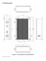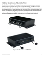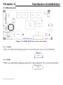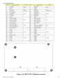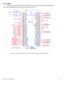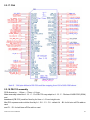
1
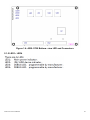
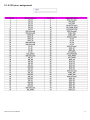
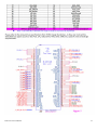
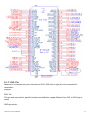
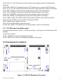
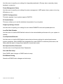
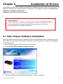
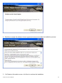
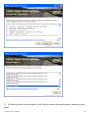
ACS-2701A IP67 Waterproof Box PC User Manual Release Date Revision Jun. 2011 V1.0 ®2011 Aplex Technology, Inc. All Rights Reserved. Published in Taiwan Aplex Technology, Inc. 15F-1, No.186, Jian Yi Road, Zhonghe District, New Taipei City 235, Taiwan Tel: 886-2-82262881 ACS-2701A User Manual Fax: 886-2-82262883 E-mail: [email protected] URL: www.aplex.com.tw 1 Warning!____________________________________ This equipment generates, uses and can radiate radio frequency energy and if not installed and used in accordance with the instructions manual, it may cause interference to radio communications. It has been tested and found to comply with the limits for a Class A computing device pursuant to FCC Rules, which are designed to provide reasonable protection against such interference when operated in a commercial environment. Operation of this equipment in a residential area is likely to cause interference in which case the user at his own expense will be required to take whatever measures may be required to correct the interference. Electric Shock Hazard – Do not operate the machine with its back cover removed. There are dangerous high voltages inside. Disclaimer This information in this document is subject to change without notice. In no event shall Aplex Technology Inc. be liable for damages of any kind, whether incidental or consequential, arising from either the use or misuse of information in this document or in any related materials. ACS-2701A User Manual 2 Table of Contents______________________ Warning!…………………………………………………………………………….……..….2 Disclaimer………………………………………………………………….…………………2 Chapter 1 1.1 1.2 1.3 1.4 Getting Started Features…....………………….………………………….…………..…...…4 Specifications………………………………………….………….……...…..4 Dimensions…………………………………...……………….…………......6 Brief Description……………………………………….…………………7 Chapter 2 Hardware Installation 2.1 Mainboard.....…...………………………………….…………………………8 2.2 Component Locations...…...………………………………….……………17 Chapter 3 Installations of BIOS 3.1 System Test and Initialization……………………………….……………26 3.2 Award BIOS Setup………………………………………………………….26 Chapter 4 Installations of Drivers 4.1 Intel Chipset Software Installation…………………….….….……………28 4.2 VGA Driver installation..........................................................................32 4.3 Intel PRO LAN Drivers installation.........................................................35 4.4 Realtek Audio Driver installation............................................................38 Figures Figure 1.1: Dimensions ……………………………………………………...6 Figure 1.2: Front View of ACS-2701A…………….……………………...7 Figure 1.3: ASB- S700 Top- view connectors………………..…………8 Figure 1.4: ASB- S700 Bottom- view LED and Connectors………………10 Figure 1.5: PB-703 Baseboard Overview…………………………………….17 Figure 1.6: PB-703 R1.10 Board overview………………………………...…23 ACS-2701A User Manual 3 Chapter 1_____________________________ 1.1 Features Intel Atom Z510 1.1 GHz CPU built-in, upgrade to Z530 1.6 GHz CPU Intel US15W chipset 1GB DDR2 400 MHz DRAM on board Support 1 x 2.5” SATA HDD 1 x Mini PCIe slot Fanless design IP67 Waterproof Long life backup battery 1.2 Specifications System CPU: Intel Atom Z510 1.1 GHz CPU built-in, upgrade to Z530 1.6 GHz CPU Chipset: Intel US15W chipset System Memory: 1GB DDR2 400 MHz DRAM on board Storage: 1 x 2.5” SATA HDD space 1 x CF slot (Internal) I/O Port: totally IP65 rating connector 1 x RJ45 LAN port 1 x DB15 port for RS-232 and RS-422/485 (Default RS-485) 1 x VGA port 1 x USB port 1 x DC 11~32V ACS-2701A User Manual 4 Mechanical Construction: Aluminum Dei casting chassis (Top Cover : heat sink design) Color: Black Dimensions: 223(W) x 62(D) x 147(H) mm Power Supply: DC 11~32V Input Environment Operating temperature: -20 ~ 60∘C Storage temperature: -20 ~ 70∘C Relative humidity: 10~90% @ 40∘C non-condensing Certificate CE/FCC Class A ACS-2701A User Manual 5 1.3 Dimensions Figure 1.1: Dimensions of the ACS-2701A ACS-2701A User Manual 6 1.4 Brief Description of the ACS-2701A The ACS-2701A is a Fanless IP67 Waterproof Solution and ultra-compact standalone embedded controller, powered by onboard Intel Atom Z510 1.1GHz, and supporting 1 x USB Port, 1 x DB 15 Port for RS-232 and RS-485, 1 x VGA Port , 1 x LAN Port and totally IP67 rating connectors. It is ideal for Industrial Automation & Outdoor Automation, etc. and running factory operations from small visual interface and maintenance applications to large control process applications. The ACS-2701A works very well along with any of our Display Monitor series. It absolutely can provide an easy way to perform control and field maintenance. It comes with a DC11~32V wide-ranging power input. Figure 1.2: Front View of ACS-2701A ACS-2701A User Manual 7 Chapter 2 Hardware Installation 2.1 Mainboard Figure 1.3: ASB- S700 Top- view connectors 2.1.1 JTAG1 2.1.2 TPM1 ACS-2701A User Manual 8 2.1.3 LVDS1 2.1.4 LVDS2 ACS-2701A User Manual 9 Figure 1.4: ASB- S700 Bottom- view LED and Connectors 2.1.5 LED1~ LED4 ACS-2701A User Manual 10 2.1.6 CN1 pins- assignment ACS-2701A User Manual 11 ACS-2701A User Manual 12 2.1.6.1 NC- Pin Means non- connected pin, part of the pins of CN1/ CN2 (left or right) are not connected for reservation Purpose 2.1.6.2 RSV- Pin This pin was reserved for specific function and definition maybe different from CN1 or CN3 (top or down) 2.1.6.3 GND ground pin 2.1.6.4 Power Supply Source Class There are four pins for power supply sources on CN1: 12V_S5, is defined for 12V standby power, connected Pin 1, 3, 5, 7, 9, 11 of total six pins, can secure transmission current up to 2.4 Amp. 3P3V_S5, is defined for 3.3V standby power, connected Pin 17, 19, 21, 23 of total four pins, can secure transmission current up to 1.6 Amp. 3P3V_S0, is defined for 3.3V system power source, connected Pin 44, 46, 48, 50, 52, 54 of total six pins, can secure transmission current up to 2.4Amp. 5V_S0, is defined for 5V system power source, connected Pin 22, 24, 26, 28, 29, 31, 33, 35 of total eight pins, can secure transmission current up to 3.2 Amp. 2.1.6.5 IDE bus signal Pin 37 and the odd pin- number in between #41 ~ # 97 are defined for IDE bus signals. 2.1.6.6 PCIE (PCI-Express) bus- signals ASB-S700 supports two PCI-E 1x bus. (1x lanes) Pin 4, 6 are defined for the PCIE1 differential negative as positive input signal, Pin16, 18 are defined for the PCIE1 differential negative as positive output signal, and Pin10, 12 are defined for the differential negative as the clockwise output signal. Pin 58, 60 are defined for the PCIE2 differential positive as negative output signal, Pin88, 90 are defined for the PCIE2 differential positive as negative input signals, Pin82, 84 are defined for the differential positive as counterclockwise output signal 2.1.6.7 SDIO bus signal Pin 68, 70, 72, 74, 78, 94, 96 are for the SDIO bus signals, can support 4 bit SDIO devices. Pin 32, 34, 64, 66 are reserved and malfunction. ACS-2701A User Manual 13 2.1.6.8 Other Signals Pin36, US15W's GPIO3 signal (the initial status is defined as the output); Pin38, US15W's GPIOSUS0 signal (the initial status is defined as the input); Pin40, PCIE_PME # signal, the external device wake-up signal (#, said active-low); Pin42, US15W's GPIO8 signal; (can be defined for LAN disable signal) Pin92, US15W the GPIO6 signal; Pin98, SCH_SLP3 # signal, control system power supply; Pin100, SIO_PSON # signal, SIO transferred switching ON/ OFF power supply signal. 2.1.7 CN2 pins- assignment (R1.30) ACS-2701A User Manual 14 2.1.7.1 NC- Pin Means non- connected pin, part of the pins of CN1/ CN2 (left or right) are not connected for reservation purpose. RSV- Pin This pin was reserved for specific function and definition maybe different from CN1 or CN3 (top or down) GND ground pin ACS-2701A User Manual 15 2.1.7.2 Power Supply Pin CN2, CN4 defined two kinds of power supply sources. VCC_RTC, is defined for the Real-Time-Clock power supply, ASB-S700 is equipped with a lithium battery (CR2032) also the onboard battery is also for the baseboard used. 5V_S5, is defined for 5V Standby power source, connected Pin63, 65, 67, 69, 71, 73 of total of six pins, can secure transmission current up to 2.4 Amp. 2.1.7.3 LPC Bus Signal Pin36, 48 and odd-number of pin 19 ~ 29 are defined for LPC Bus signals. 2.1.7.4 USB Bus Signal Pin77, 79, Pin56, 58, Pin62, 64, Pin68, 70, Pin74, 76, Pin80, 82, are defined set of differential pairs of negative as positive signals of USB. Pin83, 85, 87 are defined as over-current protection signal for relevant USB ports. 2.1.7.5 SMB Bus Signal Pin2, 4 are defined for the SMB Bus signals 2.1.7.6 SDVO Bus Signal The even-number of Pin8 ~ 52 are defined for SDVO Bus signals 2.1.7.7 HDA Bus Signal The even-number of Pin84 ~ 94 are defined for High Definition Audio Bus signals of Intel. 2.1.7.8 Clock Signals Pin7 is defined for 32.768 KHz clock signal, output from CPU board, core-module of mini-Express. Pin37 is defined for the 33MHz clock signal, output from CPU board, core-module of mini-Express. Pin41 is defined for the 48MHz clock signal, output from CPU board, core-module of mini-Express. 2.1.7.9 Other Signals Pin3, A20GATE, is defined for A20 GATE signal as issued by SIO. (Serial Input/ Output) Pin5, KB_RST #, is defined for Keyboard Reset as issued by SIO. (#, said active-low); Pin9, FP_RST #, is defined as forced Reset signal from external input; Pin11, RST_OUT1 #, CPU board, core-module send-out reset signal #1 to the adapted IO baseboard. Pin13, RST_OUT2 #, CPU board, core-module send-out reset signal #2 to the adapted IO baseboard. Pin15, IO_THRM #, IO baseboard send the system thermal- overheat signal to CPU board. Pin31, RSM_RST #, IO baseboard send system reboot ready signal to CPU board.; Pin33, CPU_CORE_SENSE, CPU core- power supply voltage detection; Pin42, multiplexed signal can be used for LPC_PME # and GPIO; Pin45, EN_3V_5V_S0 #, CPU board send the main power system signal to IO baseboard for operating ACS-2701A User Manual 16 Pin47, EN_3V_5V_S5, CPU board send an auxiliary power supply signal to IO baseboard for operating. Pin49, SMC_ONOFF #, IO baseboard send to CPU board to issue a system ON/ OFF signal; Pin51, 3V_5V_S5_OK, IO baseboard issued confirmed auxiliary power OK signal to CPU board; Pin53, SMC_LATCH #, CPU board sent disable system signal to the IO baseboard; Pin57, CPU_THERMDA, Defined the thermal diode positive signal to CPU board; Pin59, CPU_THERMDC, Defined the thermal diode negative signal to CPU board; Pin89, SIO_PWROK, IO baseboard send to the power OK signal to CPU board; Pin91, USB2_CLIENT_EN, USB2_CLIENT signal enable, but also can be defined as GPIO; Pin93, from the US15W access via CPLD out as defined GPIO; Pin95, Software Reset signal, active low; Pin97, AT Power Mode allows signal, active low; Pin100, SCH_SPKR, CPU board sent to the buzzer signal- sound to IO baseboard 2.1.7.10 LVDS panel backlight signal The main different functions of Rev: 1.20 version and Rev: 1.30 version is the CN2 added LVDS backlight control screen signals. Pin 96 L_BKLEN, is defined for Backlight start signal; Pin 98 L_BKLCTRL, is defined for backlight brightness control signal. 2.2 Component Locations Figure 1.5: PB-703 Baseboard Overview ACS-2701A User Manual 17 2.2.1 PWR1/PWR2 The power input of PCB was co-designed with PWR1or PWR2 for pre-selection。 PWR1 will use CJT brand like A3963WV-2P type connectors,PWR2 may use DINKLE brand like DT-126RP-02P type connectors。PWR1/PWR2 are different housing design but same pin defined: 2.2.2 USB4/5 2.2.3 JP3 JP3 is designed for auto-on switch jumper with 2xPin-header as pitch 2.0mm type. JP3 defaulted with closed jumper, system will be on when DC power input. If JP3is open jumper, system power-on will be controlled by firmware of ASB-S700. 2.2.4 BAT1 ACS-2701A User Manual 18 2.2.5 MPCIE1 [ mini- PCI express ] Mini PCI Express slot for full-/ half- size add-in card,initial designed for full-size mPCIe could be fixed on A1 and B1,optional designed for half-size mPCIe could be fixed on C1 and D1 2.2.6 JP1 2.2.7 JP4 2.2.8 IDE_CF1 ACS-2701A User Manual 19 2.2.9 INVERTER 2.2.10 JP2 2.2.11 SATA 2.2.12 SATA_P1 ACS-2701A User Manual 20 2.2.13 JP5 2.2.14 J1 Port ACS-2701A User Manual 21 2.2.15 J2 port ACS-2701A User Manual 22 Figure 1.6: PB-703 R1.10 Board overview ACS-2701A User Manual 23 2.2.16 CN3 ACS-2701A User Manual 24 2.2.17 CN4 2.2.18 PB-703 assembly PCB dimension:115mm × 70mm ×1.6mm Main assembly holes like A,B,C,D of PB-703 may adapt to A、B、C、Dholes of ASB-S700 (SOM) and baseboard (PB-703) could be fixed by 4x 6mm +/- 0.1mm height nuts Mini-PCI express card could be fixed by A1,B1,C1,D1:default A1,B1 for full-size mPCIe add-on card and C1,D1 for half-size mPCIe add-on card. ACS-2701A User Manual 25 Chapter 3 BIOS Setup 3.1 System Test and Initialization These routines test and initialize board hardware. If the routines encounter an error during the tests, you will either hear a few short beeps or see an error message on the screen. There are two kinds of errors: fatal and non-fatal. The system can usually continue the boot up sequence with non-fatal errors. Non-fatal error messages usually appear on the screen along with the following instructions: Press <F1> to RESUME Write down the message and press the F1 key to continue the boot up sequence. System configuration verification These routines check the current system configuration against the values stored in the CMOS memory. If they do not match, the program outputs an error message. You will then need to run the BIOS setup program to set the configuration information in memory. There are three situations in which you will need to change the CMOS settings: 1. You are starting your system for the first time 2. You have changed the hardware attached to your system 3. The CMOS memory has lost power and the configuration information has been erased. 3.2 Award BIOS Setup Awards BIOS ROM has a built-in Setup program that allows users to modify the basic system configuration. This type of information is stored in battery-backed CMOS RAM so that it retains the Setup information when the power is turned off. Entering Setup Power on the computer and press <Del> immediately. This will allow you to enter Setup. Standard CMOS Features Use this menu for basic system configuration. (Date, time, IDE, etc.) Advanced BIOS Features Use this menu to set the advanced features available on your system. Advanced Chipset Features Use this menu to change the values in the chipset registers and optimize your system performance. Integrated Peripherals ACS-2701A User Manual 26 Use this menu to specify your settings for integrated peripherals. (Primary slave, secondary slave, keyboard, mouse etc.) Power Management Setup Use this menu to specify your settings for power management. (HDD power down, power on by ring, KB wake up, etc.) PnP/PCI Configurations This entry appears if your system supports PnP/PCI. PC Health Status This menu allows you to set the shutdown temperature for your system. Frequency/Voltage Control Use this menu to specify your settings for auto detect DIMM/PCI clock and spread spectrum. Load Fail-Safe Defaults Use this menu to load the BIOS default values for the minimal/stable performance for your system to operate. Load Optimized Defaults Use this menu to load the BIOS default values that are factory settings for optimal performance system operations. While AWARD has designated the custom BIOS to maximize performance, the factory has the right to change these defaults to meet their needs. Set Supervisor/User Password Use this menu to set Supervisor/User Passwords. Save and Exit Setup Save CMOS value changes to CMOS and exit setup. Exit Without Saving Abandon all CMOS value changes and exit setup. ACS-2701A User Manual 27 Chapter 4 Installation of Drivers This chapter describes the installation procedures for software and drivers under the windows XP. The software and drivers are included with the motherboard. The contents include Intel chipset driver, VGA driver, LAN driver, Audio driver Installation instructions are given below. Important Note: After installing your Windows operating system (Windows 98SE/ME/2000/XP), you must install first the Intel Chipset Software Installation Utility before proceeding with the installation of drivers. 4.1 Intel Chipset Software Installation The Intel Chipset Drivers should be installed first before the software drivers to enable Plug & Play INF support for Intel chipset components. Follow the instructions below to complete the installation Under Windows XP 1. Insert the Aplex product CD that comes with the board. 2. Click “ Intel® Chipset software installation Utility “ 3. When the Welcome screen appears, please click “ Next “ to Continue. ACS-2701A User Manual 28 4. Click Yes to accept the software license agreement and proceed with the installation process. 5. On Readme Information screen, click Next to continue the installation. ACS-2701A User Manual 29 6. The Setup process is now complete. Click Finish to restart the computer and for changes to take effect. ACS-2701A User Manual 30 ACS-2701A User Manual 31 4.2 VGA Driver installation To install the VGA Driver follow the steps below to proceed with the installation. Step 1. Insert the Aplex product CD That comes with the board. Step 2. Click “ Intel® VGA Chipset “ Step 3. When the Welcome screen appears , click “Next” to continue. ACS-2701A User Manual 32 Step 4. Click YES to agree with the license agreement and continue the installation. ACS-2701A User Manual 33 Step 5. The Setup process is now complete. Click Finish to restart the computer as promoted and for changes to take effect. When the computer has restarted, the system will be able to find some devices. Restart your computer when prompted. ACS-2701A User Manual 34 4.3 Intel PRO LAN Drivers installation Follow the steps below to complete the installation of the Intel PRO LAN drivers. Step 1. Insert the Aplex product CD That comes with the board. Step 2. Click “Intel® Ethernet Driver“ Step 3. When the Welcome screen appears , click “Next” to continue. ACS-2701A User Manual 35 ACS-2701A User Manual 36 Step 4. Click “Finish” to restart the computer and for changes to take effect ACS-2701A User Manual 37 4.4 Realtek Audio Driver installation To install the Realtek codec Driver follow the steps below to proceed with the installation. Step 1. Insert the Aplex product CD That comes with the board. Step 2. Click “Realtek ‘ Codec Sound system “ Step 3. When the Welcome screen appears, click “Next” to continue. ACS-2701A User Manual 38 Step 4. Click “Finish” to restart the computer and for changes to take effect. ACS-2701A User Manual 39