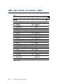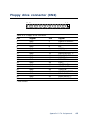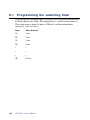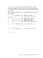
1
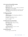
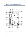
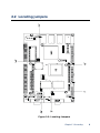
PCA-6740
ISA STPC Elite 133 Half-size CPU card
with CPU/32MB SDRAM/VGA/LCD/
LAN/DOC/CF/PC104
User’s Manual
Copyright notice
This document is copyrighted 2002, by Advantech Co., Ltd. All rights
are reserved. The original manufacturer reserves the right to make
improvements to the products described in this manual at any time
without notice.
No part of this manual may be reproduced, copied, translated or
transmitted in any form or by any means without the prior written
permission of the original manufacturer. Information provided in this
manual is intended to be accurate and reliable. However, the original
manufacturer assumes no responsibility for its use, nor for any
infringements upon the rights of third parties which may result from
its use.
Acknowledgments
Award is a trademark of Award Software International, Inc.
IBM, PC/AT, PS/2 and VGA are trademarks of International Business
Machines Corporation.
Intel and Pentium are trademarks of Intel Corporation.
Microsoft Windows® is a registered trademark of Microsoft Corp.
UMC is a trademark of United Microelectronics Corporation.
All other product names or trademarks are properties of their
respective owners.
For more information on this and other Advantech products please
visit our websites at: http://www.advantech.com
http://www.advantech.com/epc
For technical support and service for please visit our support website
at: http://www.advantech.com/support
This manual is for the PCA-6740 series half-size CPU card.
Part No. 2006674011
2nd Edition
Published in Taiwan
Apr., 2002
Packing list
Before installing your board, ensure that the following materials have
been received:
• 1 PCA-6740 Series all-in-one single board computer
• 1 Startup Manual (part no. 2006674000)
• 1 utility disk / CD including utilities and manual (in PDF format)
• 1 hard disk drive (IDE) interface cable (40-pin)
(part no. 1701400601)
• 1 keyboard / PS/2 mouse cable (part no. 1700060202)
• 1 COM port / parallel port cable (part no. 1701260303)
• 1 floppy disk drive interface cable 700 mm (28")
(part no. 1701340700)
• 1 Warranty Certificate
If any of these items are missing or damaged, contact your distributor
or sales representative immediately.
Optional devices
• IrdA adapter (part#: 968900042)
Contents
Chapter 1 General Information ............................................ 1
1.1 Introduction ....................................................................................... 2
1.2 Features ............................................................................................ 3
1.3 Specifications .................................................................................... 4
1.4 Board layout and dimensions ............................................................ 6
Chapter 2 Connecting Peripherals ..................................... 7
2.1 Connector locations (component side) ............................................ 8
2.2 Locating jumpers .............................................................................. 9
2.3 Jumpers and connectors ................................................................ 10
2.4 Setting jumpers .............................................................................. 12
2.5 Watchdog timer action (JP4) .......................................................... 15
2.6 Enhanced IDE connector (CN1) ...................................................... 16
2.7 FDD connector (CN2) ..................................................................... 17
2.8 Parallel port connector (CN3) ........................................................ 17
2.9 Flat panel display connector (CN4) ................................................ 18
2.10 ATX power button (CN6, pins 17,19) ........................................... 18
2.11 Reset switch (CN6, pins 9,11) ....................................................... 18
2.12 IR connector (CN6 pins 12,14,16,18,20) ..................................... 18
2.13 ATX Feature Connector (CN7) .................................................... 19
2.14 VGA display connector (CN9) ...................................................... 19
2.15 PC/104 connectors (CN10) .......................................................... 20
2.16 Ethernet connector (CN11) .......................................................... 20
2.17 Serial ports (CN13~15) ................................................................ 20
2.18 Internal keyboard connector (CN16) ........................................... 22
2.19 AT power connector (CN17) ......................................................... 22
2.20 Keyboard and PS/2 mouse connector (CN18) .............................. 22
2.21 ISA gold fingers (CN19) .............................................................. 22
Chapter 3 Award BIOS Setup ............................................. 23
3.1 System test and initialization .......................................................... 24
3.2 Award BIOS setup ....................................................................... 25
3.2.1 Entering setup ..................................................................... 25
3.2.2 Standard CMOS Features Setup ......................................... 26
3.2.3 Advanced BIOS Features Setup ......................................... 27
3.2.4 Advanced Chipset Features Setup ..................................... 28
3.2.5 Integrated Peripherals Setup ............................................... 29
3.2.6 Power Management Setup .................................................. 30
3.2.7 PnP/PCI Configurations Setup ............................................ 31
3.2.8 Set Password ....................................................................... 32
3.2.9 Save & Exit Setup ................................................................ 33
3.2.10 Exit without saving ............................................................ 34
Chapter 4 SVGA Setup ........................................................ 35
4.1
4.2
4.3
Introduction ................................................................................. 36
4.1.1 Chipset ................................................................................ 36
4.1.2 Display memory ................................................................... 36
Installation of SVGA driver ........................................................ 37
4.2.1 Installation for Windows 95 ................................................ 38
4.2.2 Installation for Windows 98 ................................................ 42
4.2.3 Installation for Windows NT ............................................... 48
Further information .................................................................... 53
Chapter 5 PCI Bus Ethernet Interface .............................. 55
5.1
5.2
5.3
Introduction ................................................................................. 56
Installation of Ethernet driver .................................................... 56
5.2.1 Installation for Windows 95 ................................................ 57
5.2.2 Installation for Windows 98 ................................................ 64
5.2.3 Installation for Windows NT ............................................... 72
Further information .................................................................... 76
Chapter 6 Floppy Disk Drive Installation .......................... 77
6.1
6.2
Installation for Windows 95 ...................................................... 78
Installation for Windows 98 ....................................................... 87
Appendix A Pin Assignments.............................................. 93
IDE hard drive connector (CN1) ............................................................ 94
Floppy drive connector (CN2) ................................................................ 95
Parallel port connector (CN3) ............................................................... 96
Flat panel display connector (CN4) ....................................................... 97
CN6- External speaker (pins 1,3,5,7) .................................................... 98
CN6- System reset switch conn (pins 9,11) .......................................... 98
CN6- Keyboard lock connector (pins 2,4) ............................................. 99
CN6- IR connector (pins 12,14,16,18,20) ............................................. 99
CN6- ATX power button (pins 17,19) .................................................. 100
ATX power standby connector (CN7) .................................................. 100
CN6- HDD LED connector (pins 13,15) .............................................. 101
LCD Inverter Power (CN8) .................................................................. 101
COM2 RS-232 connector (CN14) ....................................................... 102
COM1 RS-232 connector (CN15) ....................................................... 102
CRT Display Connector (CN9) ........................................................... 103
COM2 RS-422/485 connector (CN13) ............................................... 103
Internal keyboard connector (CN16) .................................................. 104
AT power connector (CN17) ................................................................ 105
Keyboard and mouse connnector (CN18) ............................................ 105
Appendix B System Assignments .....................................107
B.1
B.2
B.3
B.4
System I/O ports ....................................................................... 108
DMA channel assignments ....................................................... 109
Interrupt assignments .............................................................. 110
1st MB memory map ................................................................. 111
Appendix C LCD Services ................................................. 113
Appendix D Installing PC/104 Modules ............................ 115
Figures
Figure 1-1: PCA-6740 dimensions (component side) ....................................... 6
Figure 2-1: Board Layout: Connector Locations(component side) .................. 8
Figure 2-2: Locating Jumpers .......................................................................... 9
Figure 3-1: BIOS setup program initial screen ................................................ 25
Figure 3-2: Standard CMOS Features screen .................................................. 26
Figure 3-3: Advanced BIOS Features setup .................................................... 27
Figure 3-4: Advanced Chipset Features Setup ................................................ 28
Figure 3-5: Integrated Peripherals Setup ........................................................ 29
Figure 3-6: Power Management Setup ........................................................... 30
Figure 3-7: PnP/PCI Configurations ................................................................ 31
Figure 3-9: Save & Exit Setup ......................................................................... 33
Figure 3-8: Set Password Screen .................................................................... 33
Figure 3-10: Exit Setup Without Saving ......................................................... 34
Figure F-1: Board Dimensions (component side) ......................................... 124
Tables
Table 2-1: Jumpers ........................................................................................ 10
Table 2-2: Connectors .................................................................................... 11
Table 2-3: Serial port connections (COM1, COM2) ........................................ 21
Table 2-4: Serial port default settings ............................................................ 21
Table A-1: IDE hard drive connector .............................................................. 94
Table A-2: Floppy drive connector ................................................................. 95
Table A-3: Parallel port connector .................................................................. 96
Table A-4: Flat panel display connector ......................................................... 97
Table A-5a: External speaker connector ......................................................... 98
Table A-5b: Keyboard lock connector ............................................................ 98
Table A-5c: System reset switch connector ................................................... 99
Table A-5d: IR connector ............................................................................... 99
Table A-5e: HDD LED connector .................................................................. 100
Table A- 5f: ATX power button ..................................................................... 100
Table A-6: ATX power standby connector .................................................... 101
Table A-7: LCD Inverter connector ............................................................... 101
Table A-8: CRT display connector ................................................................ 102
Table A-9: COM2 RS-232/422/485 connector ............................................. 102
Table A-10: COM2 RS-232 connector .......................................................... 103
Table A-11: COM1 RS-232 connector .......................................................... 103
Table A-12: External keyboard connector .................................................... 104
Table A-13: AT power connector .................................................................. 105
Table A-14: Keyboard and mouse connector ............................................... 105
Table B-1: System I/O ports ......................................................................... 108
Table B-2: DMA channel assignments .......................................................... 109
Table B-3: Interrupt assignments ................................................................. 110
Table B-4: 1st MB memory map ................................................................... 111
Table D-1: PC/104 connectors (CN8) ........................................................... 118
CHAPTER
1
General Information
This chapter gives background information on the PCA-6740.
Sections include:
• Board specifications
• Board layout and dimensions
1.1
Introduction
The PCA-6740 is the ultimate cost-effective solution for limitedspace applications. It offers all the functions of an AT-compatible
industrial computer on a single board. The PCA-6740 comes with
an embedded high-performance STPC Elite 133 processor and
32MB SDRAM on board. For maximum performance, the PCA-6740
also supports one optional SODIMM socket that can accept up to
64 MB memory.
On-board features include an Ethernet interface, a socket for DOC®
2000, Enhanced IDE interface, one parallel port, two serial ports
(RS-232 and RS-232/422/485) with DB-9 connector as COM1, and a
mini-DIN PS/2 keyboard/mouse interface. An SVGA/LCD display
controller (LCD, and CRT displays) allows LCD screen resolutions
up to 1024 x 768 @ 64K colors and CRT resolutions up to 1280 x
1024 @ 256 colors.
The PCA-6740 complies with the "Green Function" standard and
supports three types of power saving features: Normal, Doze and
Sleep modes.
The display type configuration is done through software. A single
Flash chip holds the system BIOS and the VGA BIOS. This
minimizes the number of chips and eases configuration. You can
change the display BIOS simply by programming the Flash chip.
If you need any additional functions, the PCA-6740 has a PC/104
connector for future upgrades.
2
PCA-6740 User's Manual
1.2
Features
• On-board Low power STMicroelectronics STPC Elite 133
processor (fanless)
• On-board 32 MB SDRAM
• On-board VGA/LCD display controller and 18-bit LCD TFT
display
• 62-level watchdog timer, jumperless on-line setup supported
• Supports wake-up on LAN, ring-on by Modem
• SSD supports DiskOnChip® 2000
• Supports CMOS data backup functions
• PC/104 connector supports face-up installation
Chapter 1 General Information
3
1.3
Specifications
1.3.1 Standard SBC functions
• CPU: Embedded STMicroelectronics STPC Elite 133 MHz
processor (provides fanless operation)
• BIOS: 4 Mbit Flash BIOS,
-Supports Plug & Play, APM
-Supports Ethernet Boot ROM
-Supports boot from CD-ROM
-Supports boot from LS-120 ZIP™ Drive
-Optional Customer icon can be supplied
• Chipset: STPC Elite 133
• System memory: Onboard 32MB SDRAM,
and one optional SDRAM SODIMM max. 64MB socket
• PCI IDE interface: One Enhanced IDE interface. Supports 2 IDE
devices PIO mode 3,4 with bus mastering up to 14 MB/sec.
• Floppy disk drive interface: Supports up to two FDDs (360 KB/
1.2 MB/720 KB/1.44 MB/2.88 MB)
• Parallel port: One parallel port, supports EPP/ECP
• IR port: One 115 kbps IrDA compliant serial infrared
• Serial ports: 2 serial ports COM1: RS-232, COM2: RS-232/422/
485
• Watchdog timer: 62-level timer interval, setup by software or
jumperless selection, generates system reset or IRQ11.
4
PCA-6740 User's Manual
1.3.2 Local-bus flat panel/VGA interface
• Chipset: SMI LynxEM+ 712G
• Display memory: 2MB
• Display type: Simultaneous support for CRT and 18-bit TFT LCD
display (supports 3.3 V and 5 V LCD)
• Resolution: Non-interlaced CRT monitor resolution up to 1280 x
1024 @ 256 colors, Panel resolutions up to 1024 x 768 @ 64K
colors TFT panel
1.3.3 Ethernet interface
• Chipset: RTL 8139C
• Ethernet interface: PCI 10/100 Mbps Ethernet. IEEE 802.3 u
protocol compatible
• Connection: On-board RJ-45 connector
• I/O address switchless setting
• Built-in boot ROM
1.3.4 Mechanical and environmental
• Dimensions (L x W): 185 mm x 122 mm
• Power supply voltage: +5 V (4.75 ~ 5.25 V)
• Power consumption :
- Maximum: 5 V @ 2 A
Typical: +5 V @ 1.62 A
• Operating temperature: 0 ~ 60° C (32 ~ 140° F)
• Weight: 0.27 kg (0.59 lbs)
1.3.5 Solid state disk
• Provides support for one DOC® 2000.
Chapter 1 General Information
5
1.4
Board layout and dimensions
Figure 1-1: PCA-6740 dimensions (component side)
6
PCA-6740 User's Manual
CHAPTER
2
Connecting
Peripherals
This chapter tells how to connect
peripherals, switches and indicators to the
PCA-6740 board. You can access most of
the connectors from the top of the board
while it is installed in the chassis. If you
have a number of cards installed, or your
chassis is very tight, you may need to
partially remove the card to make all the
connections.
Chapter 2 Connecting
7
2.1 Connector locations (component side)
Figure 2-1: Board Layout: Connector Locations(component side)
8
PCA-6740 User's Manual
2.2 Locating jumpers
Figure 2-2: Locating Jumpers
Chapter 2 Connecting
9
2.3 Jumpers and connectors
Connectors on the board link it to external devices such as hard disk
drives, a keyboard or expansion bus connectors. In addition, the board
has a number of jumpers that allow you to configure your system to
suit your application.
The table below lists the function of each of the board jumpers and
connectors:
Table 2-1: Jumpers
10
Label
Function
J1
CMOS Charge & Discharge
J2
LAN Power select
JP1
LCD High Drive Signal Buffer Power
JP2
RS-232/RS-422/RS-485 select
JP3
DOC® 2000 Address select
JP4
Watchdog timer
PCA-6740 User's Manual
The following table lists the connectors on the PCA-6740.
Table 2-2: Connectors
Label
Function
CN1
IDE connector
CN2
FDD connector
CN3
Printer port connector
CN4
LCD 24-bit connector
CN5
Reserved
CN6
Multiple connector
CN7
ATX Power Standby connector
CN8
LCD inverter power
CN9
CRT connector
CN10
PC/104 connector
CN11
LAN connector
CN12
Reserved
CN13
COM2 connector (RS-422/RS-485)
CN14
COM2 connector (RS-232)
CN15
COM1 connector
CN16
Internal Keyboard connector
CN17
AT (Big 4P) power connector
CN18
PS2 Keyboard/Mouse connector
CN19
ISA Gold-Finger connector
CN 20
CompactFlash connector
Chapter 2 Connecting
11
2.4 Setting jumpers
2.4.1 Introduction
You may configure your card to match the needs of your application
by setting jumpers. A jumper is the simplest kind of electrical switch.
It consists of two metal pins and a small metal clip (often protected by
a plastic cover) that slides over the pins to connect them. To "close" a
jumper, you connect the pins with the clip. To "open” a jumper you
remove the clip. Sometimes a jumper will have three pins, labeled 1, 2,
and 3. In this case you would connect either pins 1 and 2 or 2 and 3.
1
Open
Closed
2
3
Closed 2-3
The jumper settings are schematically depicted in this manual as
follows:
3
1 1 22
Open
Closed
3
Closed 2-3
A pair of needle-nose pliers may be helpful when working with
jumpers.
If you have any doubts about the best hardware configuration for your
application, contact your local distributor or sales representative
before you make any changes.
Generally, you simply need a standard cable to make most connections.
12
PCA-6740 User's Manual
2.4.2 Settings details
J1: CMOS Charge & Discharge
Pin
Function
1-2
Discharge
2-3
Charge
3
2
1
3
Discharge
2
1
Charge
J2: LAN Power Select
Pin
Function
1-2
5 V Standby
2-3
VCC*
3
2
1
3
5 V Standby
2
1
VCC*
JP1: LCD High drive signal buffer power
Pin
Function
1-3, 2-4
+5 V*
3-5, 4-6
+3.3 V
+5 V*
+3.3 V
*Default Settings
Chapter 2 Connecting
13
JP2: RS-232/422/485 Select
Pin
Function
1-2 (CN10 connector)
COM2/RS-232*
3-4 (CN11 connector)
COM2/RS-422
5-6 (CN11 connector)
COM2/RS-485
2
1
4
6
2
3
5
1
RS-232*
4
6
2
3
5
1
RS-422
4
6
3
5
RS-485
JP3: DOC address select
Pin
Address at
1-2
D4000h
3-4
DC000h
1-2, 3-4
CC000h
1-2, 5-6
D0000h
3-4, 5-6
D8000h
2
1
4
6
2
3
5
1
D4000h
2
1
6
2
3
5
1
*Default Settings
14
PCA-6740 User's Manual
6
2
3
5
1
DC000h
4
D0000h
4
6
3
5
CC000h
4
6
3
5
D8000h
4
2.5 Watchdog timer action (JP4)
When the watchdog timer activates (CPU processing has come to a
halt), it can reset the system or generate an interrupt on IRQ11. This
can be set via JP4 as shown below:
JP4: Watchdog timer
Pin
Function
1-2
Reset*
2-3
IRQ11
1
2
Reset*
3
1
2
3
IRQ11
*Default Settings
Chapter 2 Connecting
15
The following sections tell how to make each connection. In most
cases, you will simply need to connect a standard cable. All of the
connector pin assignments are shown in Appendix A.
Warning! Always completely disconnect the power cord from
your chassis whenever you are working on it. Do not
make connections while the power is on. Sensitive
electronic components can be damaged by a
sudden rush of power. Only experienced electronics
personnel should open the PC chassis.
Caution!
Always ground yourself to remove any static charge
before touching the CPU card. Modern electronic
devices are very sensitive to static electric charges.
Use a grounding wrist strap at all times. Place all
electronic components on a static-dissipative
surface or in a static-shielded bag when they are not
in the chassis.
2.6 Enhanced IDE connector (CN1)
You can attach two IDE (Integrated Device Electronics) drives to the
PCA-6740 internal controller. The PCA-6740 CPU card has an EIDE
connector, CN1.
Wire number 1 on the cable is red or blue, and the other wires are gray.
Connect one end to connector CN1 on the CPU card. Make sure that
the red (or blue) wire corresponds to pin 1 on the connector. See
Figure 2-1, where pin 1 is indicated with a triangle and a solid square.
Unlike floppy drives, IDE hard drives can connect in either position on
the cable. If you install two drives, you will need to set one as the
master and one as the slave. You do this by setting the jumpers on the
drives. If you use just one drive, you should set it as the master. See
the documentation that came with your drive for more information.
Connect the first hard drive to the other end of the cable. Wire 1 on the
cable should also connect to pin 1 on the hard drive connector, which
should be labeled on the drive circuit board. Check the documentation
that came with the drive for more information. If you are using a
second drive, connect it to the remaining connector on the same cable.
16
PCA-6740 User's Manual
2.7 FDD connector (CN2)
You can attach up to two floppy disk drives to the PCA-6740's
onboard controller. You can use any combination of 5.25" (360 KB/
1.2 MB) and/or 3.5" (720 KB/1.44/2.88 MB) drives.
The card comes with a 34-pin daisy-chain drive connector cable. On
one end of the cable is a 34-pin flat-cable connector. On the other end
are two sets of floppy disk drive connectors. Each set consists of a 34pin flat-cable connector (usually used for 3.5" drives) and a printedcircuit-board connector (usually used for 5.25" drives). You can use
only one connector in each set. The set on the end (after the twist in
the cable) connects to the A: floppy. The set in the middle connects to
the B: floppy.
2.8 Parallel port connector (CN3)
The parallel port is designated as LPT1, and is normally used to
connect the CPU card to a printer. The PCA-6740 includes an onboard parallel port, accessed through a 26-pin flat-cable connector,
CN3. The card comes with an adapter cable which lets you use a
traditional DB-25 connector. The cable has a 26-pin connector on one
end and a DB-25 connector on the other, mounted on a retaining
bracket. The bracket installs at the end of an empty slot in your
chassis, giving you access to the connector.
To install the bracket, find an empty slot in your chassis. Unscrew the
plate that covers the end of the slot. Screw in the bracket in place of
the plate. Next, attach the flat-cable connector to CN3 on the CPU
card. Wire 1 of the cable is red or blue, and the other wires are gray.
Make sure that wire 1 corresponds to pin 1 of CN3. Pin 1 is on the
right side of CN3.
Chapter 2 Connecting
17
2.9 Flat panel display connector (CN4)
CN4 consists of a 44-pin, dual-in-line header.
The power supply (+12 V) for CN4 is dependant on the supply
connected to the board. Therefore make sure that CN17 is connected
to a +12 V power supply.
The PCA-6740 provides a bias control signal on CN4 which can be
used to control the LCD bias voltage. It is recommended that the LCD
bias voltage not be applied to the panel until the logic supply voltage
(+5 V or +3.3 V) and panel video signals are stable. Under normal
operation the control signal (ENAVEE) is active high. When the PCA6740 board's power is applied, the control signal is low until just after
the relevant flat panel signals are present.
2.10 ATX power button (CN6, pins 17,19)
The PCA-6740 provides an ATX power input connector. When
connected with the ATX power switch, the ATX power switch connector (CN6) enables power On/Off from the chassis.
2.11 Reset switch (CN6, pins 9,11)
If you install a reset switch, it should be a single pole switch rated at
10 mA, 5 V. Momentarily pressing the switch will activate a reset.
For reset switch pin assignments, please see Appendix A.
2.12 IR connector (CN6 pins 12,14,16,18,20)
This connector supports the optional wireless infrared transmitting and
receiving module. This module mounts on the system case. You must
configure the setting through BIOS setup.
18
PCA-6740 User's Manual
2.13 ATX Feature Connector (CN7)
When the PCA-6740 is used as a standalone card, the main power
connector (CN7) is used. If the PCA-6740 is used with a passive
backplane, the main power connector (CN7) should not be connected.
This is because the card will be powered from the backplane.
To ATX feature
connector (CN7)
ATX power supply source
P8
(P8) 6-pin in backplane
P9
(P9) 6-pin in backplane
20-pin female connector
Figure 2-4: ATX adaptor cable
The ATX adapter cable (optional) is used to connect the PCA-6740 to
the ATX power supply. The ATX adapter cable has different connectors at both ends. On one end is the ATX 20-pin (female type) which
connects to the (male) ATX power supply source. The other end has a
3-pin connector (female type) which connects to the ATX feature
connector (CN7) on the board itself. This end also has the 6-pin main
power connector (P8) and a 6-pin connector (P9) which is used when
the board is mounted on a passive backplane.
2.14 VGA display connector (CN9)
The PCA-6740 provides a VGA controller for a high resolution VGA
interface. The PCA-6740 CN9 is a DB-15 connector for VGA
monitor input. Pin assignments for the CRT display are detailed in
Appendix A.
Chapter 2 Connecting
19
2.15 PC/104 connectors (CN10)
The PCA-6740 is equipped with a 16-bit ISA signal PC/104 connector
for future expansion. See Appendix D for details.
2.16 Ethernet connector (CN11)
The PCA-6740 is equipped with a high performance 32-bit PCI-bus
Fast Ethernet interface which is fully compliant with IEEE 802.3u
10/100Base-T specifications. It is supported by all major network
operating systems.
The medium type can be configured via the rset8139.EXE program
included on the utility disk. (See Chapter 5 for detailed information.)
2.16.1 Network boot
The network boot feature is built into the BIOS. It can be enabled or
disabled in the chipset setup of the CMOS configuration. Refer to
"BIOS Setting" in Chapter 4 for more information.
2.17 Serial ports
(CN15: COM1; CN14: COM2/RS-232;
CN13: COM2/RS-422/485)
The PCA-6740 offers two serial ports: COM1 in RS-232 and COM2
(CN14: RS-232, CN13:RS-422/485). These ports let you connect to
serial devices (a mouse, printers, etc.) or a communication network.
You can select the address for each port (for example, 3F8H [COM1],
2F8H [COM2]) or disable each port. Use the BIOS Advanced Setup
program, which is covered in Chapter 4.
The card mounting bracket holds the serial port connector for the one
port. The parallel port and serial port adapter kit (supplied with the
card) holds the connector for the other port. This lets you connect and
disconnect cables after you install the card. The DB-9 connector on the
bottom of the bracket is the first RS-232 port, COM1. The DB-9
connector on the adapter kit is the second serial port, COM2.
20
PCA-6740 User's Manual
Table 2-3: Serial port connections (COM1, COM2)
Connector
Function
COM1,3*,4*
RS-232
COM2
RS-232/422/485
2.17.1 RS-232 connection (COM1:CN15)
Different devices implement the RS-232 standard in different ways. If
you are having problems with a serial device, be sure to check the pin
assignments for the connector.
2.17.2 RS-232/422/485 connection
(COM2: CN10: RS-232; CN11: RS-422/485)
COM2 is an RS-232/422/485 serial port. The specific port type is
determined by jumper settings (JP2), as detailed in Chapter 1.
The IRQ and address range for both ports are fixed. However, if you
wish to disable the port or change these parameters later, you can do
this in the system BIOS setup. The table below shows the settings for
the PCA-6740 series' board's ports:
Table 2-4: Serial port default settings
Port
Address
Interrupt
Default
COM1
3F8, 3E8
IRQ4
3F8
COM2
2F8, 2E8
IRQ3
2F8
Chapter 2 Connecting
21
2.18 Internal keyboard connector (CN16)
In addition to the PS/2 mouse/keyboard connector, an additional
external keyboard connector is provided.
For external keyboard pin assignments, see Appendix A.
2.19 AT power connector (CN17)
If you prefer not to acquire power through the PCA-6740 backplane
via the gold H-connectors, The big 4P power connector (CN17) also
provides power input connectors for +5 V, and +12 V.
2.20 Keyboard and PS/2 mouse connector (CN18)
The PCA-6740 board provides a keyboard connector. A 6-pin miniDIN connector (CN18) on the card mounting bracket supports singleboard computer applications. The card comes with an adapter to
convert from the 6-pin mini-DIN connector to a standard DIN connector and to a PS/2 mouse connector.
2.21 ISA gold fingers (CN19)
The 16-bit ISA gold fingers are used for connecting the PCA-6740
Series to an ISA passive backplane.
22
PCA-6740 User's Manual
CHAPTER
3
Award BIOS Setup
This chapter describes how to set BIOS
configuration data.
3.1
System test and initialization
These routines test and initialize board hardware. If the routines
encounter an error during the tests, you will either hear a few short
beeps or see an error message on the screen. There are two kinds
of errors: fatal and non-fatal. The system can usually continue the
boot up sequence with non-fatal errors. Non-fatal error messages
usually appear on the screen along with the following instructions:
press <F1> to RESUME
Write down the message and press the F1 key to continue the
bootup sequence.
3.1.1 System configuration verification
These routines check the current system configuration against the
values stored in the board’s CMOS memory. If they do not match,
the program outputs an error message. You will then need to run
the BIOS setup program to set the configuration information in
memory.
There are three situations in which you will need to change the
CMOS settings:
1. You are starting your system for the first time
2. You have changed the hardware attached to your system
3. The CMOS memory has lost power and the configuration
information has been erased.
The PCA-6740 CMOS memory has an integral lithium battery
backup. The battery backup should last ten years in normal service,
but when it finally runs down, you will need to replace the complete
unit.
24
PCA-6753 User's Manual
3.2
Award BIOS setup
Award’s BIOS ROM has a built-in Setup program that allows users
to modify the basic system configuration. This type of information
is stored in battery-backed CMOS RAM so that it retains the Setup
information when the power is turned off.
3.2.1 Entering setup
Power on the computer and press <Del> immediately. This will
allow you to enter Setup.
Figure 3-1: BIOS setup program initial screen
Chapter 3 Award BIOS Setup
25
3.2.2 Standard CMOS Features Setup
When you choose the Standard CMOS Features option from the
Initial Setup screen menu, the screen shown below is displayed.
This standard Setup Menu allows users to configure system
components such as date, time, hard disk drive, floppy drive and
display. Once a field is highlighted, on-line help information is
displayed in the left bottom of the Menu screen.
Figure 3-2: Standard CMOS Features screen
26
PCA-6753 User's Manual
3.2.3 Advanced BIOS Features Setup
By choosing the Advanced BIOS Features option from the Initial
Setup Screen menu, the screen below is displayed. This sample
screen contains the manufacturer’s default values for the
PCA-6740.
Figure 3-3: Advanced BIOS Features setup
Chapter 3 Award BIOS Setup
27
3.2.4 Advanced Chipset Features Setup
By choosing the Advanced Chipset Features Setup option from the
Initial Setup Screen menu, the screen below is displayed. This
sample screen contains the manufacturer’s default values for the
PCA-6740.
Figure 3-4: Advanced Chipset Features Setup
28
PCA-6753 User's Manual
3.2.5 Integrated Peripherals Setup
By choosing the Integrated Peripherals option from the Initial
Setup screen menu, the screen below is displayed. This sample
screen contains the manufacturer’s default values for the PCA6740. The PANEL TYPE by default supports a 18-bit 640 x 480 TFT
LCD panel display.
Figure 3-5: Integrated Peripherals Setup
Chapter 3 Award BIOS Setup
29
3.2.6 Power Management Setup
By choosing the Power Management Setup option from the Initial
Setup Screen menu, the screen below is displayed. This sample
screen contains the manufacturer’s default values for the PCA-6740.
Figure 3-6: Power Management Setup
30
PCA-6753 User's Manual
3.2.7 PnP/PCI Configurations Setup
By choosing the PnP/PCI Configurations option from the Initial
Setup Screen menu, the screen below is displayed. This sample
screen contains the manufacturer’s default values for the PCA6740.
Figure 3-7: PnP/PCI Configurations
Chapter 3 Award BIOS Setup
31
3.2.8 Set Password
To enable the password feature, you must first select either Setup
or System under the Security Option in the Advanced BIOS
Features Setup.
To change the password, choose the Set Password option from the
Initial Setup Screen menu and press <Enter>.
1. If the CMOS is bad or this option has never been used, a
default password is stored in the ROM. The screen will display
the following messages:
Enter Password:
Press <Enter>.
2. If the CMOS is good or this option has been used to change
the default password, the user is asked for the password stored
in the CMOS. The screen will display the following message:
Confirm Password:
Enter the current password and press <Enter>.
3. After pressing <Enter> (ROM password) or the current password (user-defined), you can change the password stored in
the CMOS. The password can be at most eight (8) characters
long.
32
PCA-6753 User's Manual
Figure 3-8: Set Password Screen
3.2.9 Save & Exit Setup
If you select this option and press <Enter>, the values entered in
the setup utilities will be recorded in the chipset’s CMOS memory.
The microprocessor will check this every time you turn your
system on and compare this to what it finds as it checks the
system. This record is required for the system to operate.
Figure 3-9: Save & Exit Setup
Chapter 3 Award BIOS Setup
33
3.2.10 Exit without saving
Selecting this option and pressing <Enter> lets you exit the Setup
program without recording any new values or changing old ones.
Figure 3-10: Exit Setup Without Saving
34
PCA-6753 User's Manual
CHAPTER
4
SVGA Setup
• Introduction
• Installation of SVGA driver for Windows 95/98/NT4.0
4.1
Introduction
The PCA-6740 has an on-board LCD/VGA interface. The specifications and features are described as follows:
4.1.1 Chipset
The PCM-6740 uses a SMI LynxEM+ 712G chipset for its SVGA
controller. It supports many popular 18-bit LCD displays and
conventional analog CRT monitors. The VGA BIOS supports LCD.
In addition, it also supports interlaced and non-interlaced analog
monitors (color and monochrome VGA) in high-resolution modes
while maintaining complete IBM VGA compatibility. Digital
monitors (i.e. MDA, CGA, and EGA) are NOT supported. Multiple
frequency (multisync) monitors are handled as if they were analog
monitors.
4.1.2 Display memory
With 2MB shared memory, the VGA controller can drive CRT
displays or color panel displays with resolutions up to 1280 x 1024
at 256 colors.
36
PCA-6740 User's Manual
4.2
Installation of SVGA driver
Complete the following steps to install the SVGA driver. Follow the
procedures in the flow chart that apply to the operating system that
you are using within your PCM-6740.
Important: The following windows illustrations are examples
only. You must follow the flow chart instructions
and pay attention to the instructions which then
appear on your screen.
Note 1:
The CD-ROM drive is designated as "D:" throughout this chapter.
Note 2:
<Enter> means pressing the “Enter” key on the
keyboard.
Note 3:
When you are using a CRT display, please make
sure that your flat panel resolution settings (in the
BIOS setup) are the same as your VGA resolution
settings (in Windows). Otherwise your display may
behave strangely.
Chapter 4 SVGA Setup
37
4.2.1 Installation for Windows 95
1. In the Windows 95 Main screen, click on "Start," select
"Settings," then "Control Panel." Double click the "Display"
icon.
38
PCA-6740 User's Manual
2. Select the "Settings" tab, then click the "Advanced Properties"
button.
Chapter 4 SVGA Setup
39
3. Click the "Change" button, then "Have Disk ..." to change the
default VGA driver.
4. Direct the path to the SMI VGA driver on the CD, and click
"OK."
40
PCA-6740 User's Manual
5. Select "Yes" to reboot the system.
Chapter 4 SVGA Setup
41
4.2.2 Installation for Windows 98
1. Insert the disk into the CD-ROM drive.
2. Click on the "Start" icon, then select "Settings," "Control
Panel," and double click on "Display."
42
PCA-6740 User's Manual
3. Select the "Settings" tab, then click "Advanced..."
Chapter 4 SVGA Setup
43
4. Click the "Adapter" tab, and then the "Change ..." button.
44
PCA-6740 User's Manual
5. Select "Display a list of all the drivers in a specific location..."
then click "Next."
Chapter 4 SVGA Setup
45
6. Click the "Have Disk ..." button
7. Direct the path to the SMI VGA driver in the CD and click "OK"
to install the driver.
46
PCA-6740 User's Manual
8. Reboot the system.
Chapter 4 SVGA Setup
47
4.2.3 Installation for Windows NT
1. Click the "Start" icon, select "Settings," then "Control
Panel,"and double click "Display."
48
PCA-6740 User's Manual
2. Click the "Settings" tab, then the "Display Type..." button.
Chapter 4 SVGA Setup
49
3. Click "Change..."
50
PCA-6740 User's Manual
4. Click the "Have Disk..." button.
Chapter 4 SVGA Setup
51
5. a. Insert the disk into the CD-ROM drive.
b. Type “D:\slotpc\6740\VGA\WINNT”
(where D: represents your CD-ROM drive) in the blank.
c. Press “OK”.
6. Press "Yes" to proceed.
52
PCA-6740 User's Manual
7. Press "Yes" to restart the system.
4.3
Further information
For further information about the PCI/SVGA installation in your
PCA-6740, including driver updates, troubleshooting guides and
FAQ lists, visit the following web resources:
SMI web site:
http://www.siliconmotion.com
Advantech web sites:
http://www.advantech.com
http://www.advantech.com.tw
Chapter 4 SVGA Setup
53
54
PCA-6740 User's Manual
CHAPTER
5
PCI Bus Ethernet
Interface
This chapter provides information on
Ethernet configuration.
• Introduction
• Installation of Ethernet driver for
Windows 95/98/NT
• Further information
5.1
Introduction
The PCA-6740 is equipped with a high performance 32-bit Ethernet
chipset which is fully compliant with IEEE 802.3 100 Mbps CSMA/
CD standards. It is supported by major network operating systems.
It is also both 100Base-T and 10Base-T compatible. The medium
type can be configured via the RSET8139.exe program included on
the utility disk.
The Ethernet port provides a standard RJ-45 jack on board. The
network boot feature can be utilized by incorporating the boot
ROM image files for the appropriate network operating system. The
boot ROM BIOS files are combined with system BIOS, which can
be enabled/disabled in the BIOS setup.
5.2
Installation of Ethernet driver
Before installing the Ethernet driver, note the procedures below.
You must know which operating system you are using in your
PCA-6740, and then refer to the corresponding installation flow
chart. Then just follow the steps described in the flow chart. You
will quickly and successfully complete the installation, even if you
are not familiar with instructions for MS-DOS or Windows.
Note:
56
The Windows illustrations in this chapter are
examples only. You must pay attention to and
follow the instructions which appear on your
screen.
PCA-6740 User's Manual
5.2.1 Installation for Windows 95
1. Click the "Start" icon, select "Settings," then "Control Panel,"
then "System."
Chapter 5 PCI Bus Ethernet Interface
57
2. Click "Device Manager" folder, then double click "PCI Ethernet
Controller."
58
PCA-6740 User's Manual
3. Select the "Driver" folder, then click "Update Driver ..."
Chapter 5 PCI Bus Ethernet Interface
59
4. Select "No, select driver from list," and click the "NEXT" button.
60
PCA-6740 User's Manual
5. Highlight "Network Adapters" then click the "NEXT" button.
Chapter 5 PCI Bus Ethernet Interface
61
6. Click "Have Disk ..." to update the LAN driver.
7. Direct the path to the LAN driver to install it.
62
PCA-6740 User's Manual
8. Insert "Windows 95 CD" and click "OK."
9. Reboot the system.
Chapter 5 PCI Bus Ethernet Interface
63
5.2.2 Installation for Windows 98
1. Click "Start," then "Settings," and "Control Panel." Double click
on the "System" icon.
64
PCA-6740 User's Manual
2. Click the "Device Manager" tab, then highlight "PCI Ethernet
Controller"
Chapter 5 PCI Bus Ethernet Interface
65
3. Click on "Properties," select the "Driver" tab, then "Update
Driver..."
66
PCA-6740 User's Manual
4. Select "Display a list of all the...." then hit "NEXT."
Chapter 5 PCI Bus Ethernet Interface
67
5. Select "Network adapters," and click the "NEXT" button.
68
PCA-6740 User's Manual
6. Click the "Have Disk..." button.
Chapter 5 PCI Bus Ethernet Interface
69
7. a. Insert the CD ROM.
b. Type “D:\LAN\WIN98_V3.94” (where D: represents your CDROM drive).
c. Click “OK”.
8. The system will now install the driver.
70
PCA-6740 User's Manual
9. Insert the Windows 98 CD in the CDROM drive.
10. Reboot the system.
Chapter 5 PCI Bus Ethernet Interface
71
5.2.3 Installation for Windows NT
1. a. Select “Start,” “Settings,” and “Control Panel.”
b. Double click “Network”.
72
PCA-6740 User's Manual
2. Click on "Select from list."
Chapter 5 PCI Bus Ethernet Interface
73
3. Click "Have Disk..."
4. Type in the path, then click "OK."
74
PCA-6740 User's Manual
5. Insert the Windows NT CD.
6. Reboot.
Chapter 5 PCI Bus Ethernet Interface
75
5.3
Further information
Realtek website: www.realtek.com
Advantech websites:www.advantech.com
www.advantech.com.tw
76
PCA-6740 User's Manual
CHAPTER
6
Floppy Disk Drive
Installation
This chapter provides information on
installation of a standard floppy drive for
Windows 95 and 98.
6.1
Installation for Windows 95
1. After BIOS POST, press “Shift+F5” to interrupt the system.
2. Execute the utility file, STM95fdc.bat, which is on the accompanying CD. This will create directory C:\STM95FDC on the C
drive and copy files into it.
3. Reboot the system and restart Windows 95.
4. Click the “Start” button, select “Settings,” then “Control
Panel,” and double click the “System” icon.
78
PCA-6740 User's Manual
5. In “System Properties,” click the “Device Manager” tab.
Chapter 6 Floppy Disk Drive Installation
79
6. Select the “Standard Floppy Disk Controller” listing, and
remove it. Do not reboot the system.
80
PCA-6740 User's Manual
7. Click “Start,” “Settings,” “Control Panel,” and “Add New
Hardware.”
Chapter 6 Floppy Disk Drive Installation
81
8. Click the “Yes (Recommended)” button. The system will detect
the new hardware.
82
PCA-6740 User's Manual
9. Highlight “Floppy Disk Controllers,” and click the “NEXT”
button.
Chapter 6 Floppy Disk Drive Installation
83
10. Click “Have Disk …”
11. Type in the path of the driver.
84
PCA-6740 User's Manual
12. Click “Finish” and reboot the system.
Chapter 6 Floppy Disk Drive Installation
85
13. In the “Device Manager,” remove any instance of “STMicroelectronics Floppy Disk Controller” that is marked with a red X.
Note : If the standard FDD is not updated as specified above,
the system might hang up during a FDD read/write
operation.
86
PCA-6740 User's Manual
6.2
Installation for Windows 98
1. Click “Start,” “Settings,” “Control Panel,” and then “System”
Chapter 6 Floppy Disk Drive Installation
87
2. In “System Properties,” click “Device Manager” and select the
“Standard Floppy Disk Controller” listing.
88
PCA-6740 User's Manual
3. Click “Properties,” and select “Driver.” Click “Update Driver …”
Chapter 6 Floppy Disk Drive Installation
89
4. Click “Display a list of all the drivers…,” and then “NEXT.”
90
PCA-6740 User's Manual
5. Click the “Have Disk …” button.
Chapter 6 Floppy Disk Drive Installation
91
6. Type in the path of the STM floppy controller, then hit "OK."
7. Reboot the system.
92
PCA-6740 User's Manual
APPENDIX
A
Pin Assignments
This appendix contains information of a
detailed or specialized nature. It includes:
•
•
•
•
•
•
•
IDE hard drive connector
Floppy drive connector
Parallel port connector
LCD connector
External speaker connector
Keyboard lock connector
System reset switch connector
• IR connector
• HDD LED connector
• ATX power button connector
• ATX power standby connector
• COM2 RS-232/422/485
serial port connector
•
•
•
•
•
•
CRT display connector
COM2 RS-232 connector
COM1 RS-232 connector
Internal keyboard connector
AT power connector
Keyboard and mouse connector
IDE hard drive connector (CN1)
Table A-1: IDE hard drive connector
Pin Signal
Pin Signal
1
3
5
7
9
11
13
15
17
19
21
23
25
27
29
31
33
35
37
2
4
6
8
10
12
14
16
18
20
22
24
26
28
30
32
34
36
38
39
IDE RESET*
DATA 7
DATA 6
DATA 5
DATA 4
DATA 3
DATA 2
DATA 1
DATA 0
SIGNAL GND
DRQ*
IO WRITE*
IO READ*
IO CHANNEL READY
ACK
IRQ14 (IDE IRQ)
ADDR 1
ADDR 0
HARD DISK
SELECT 0
IDE ACTIVE*
* low active
94
PCA-6740 User's Manual
40
GND
DATA 8
DATA 9
DATA 10
DATA 11
DATA 12
DATA 13
DATA 14
DATA 15
N/C
GND
GND
GND
N/C
GND
IOCS16*
N/C
ADDR 2
HARD DISK
SELECT 1
GND
Floppy drive connector (CN2)
33
31
3
1
34
32
4
2
Table A-2: Floppy drive connector
Pin
Signal
Pin
Signal
1
3
5
7
9
11
13
15
17
19
21
23
25
27
29
31
33
GND
GND
GND
GND
GND
GND
GND
GND
GND
GND
GND
GND
GND
GND
GND
GND
GND
2
4
6
8
10
12
14
16
18
20
22
24
26
28
30
32
34
DENSITY SELECT*
N/C
N/C
INDEX*
MOTOR 0*
DRIVE SELECT 1*
DRIVE SELECT 0*
MOTOR 1*
DIRECTION*
STEP*
WRITE DATA*
WRITE GATE*
TRACK 0*
WRITE PROTECT*
READ DATA*
HEAD SELECT*
DISK CHANGE*
* low active
Appendix A Pin Assignments
95
Parallel port connector (CN3)
25
23
3
1
26
24
4
2
Table A-3: Parallel port connector
Pin
Signal
1
2
3
4
5
6
7
8
9
10
11
12
13
14
15
16
17
18
19
20
21
22
23
24
25
26
STROBE*
AUTOFD*
D0
ERROR*
D1
INIT*
D2
SLCTINI*
D3
GND
D4
GND
D5
GND
D6
GND
D7
GND
ACK*
GND
BUSY
GND
PE
GND
SLCT
GND
* low active
96
PCA-6740 User's Manual
Flat panel display connector (CN4)
Table A-4: Flat panel display connector
Pin
Function
Pin
Function
1
3
5
7
9
11
13
15
17
19
21
23
25
27
29
31
33
35
37
39
41
43
+12 V
GND
VDD
ENAVEE
P0
P2
P4
P6
P8
P10
P12
P14
P16
P18
P20
P22
GND
SFK
DE (M)
GND
N/C
VSAFE (ENAVDD)
2
4
6
8
10
12
14
16
18
20
22
24
26
28
30
32
34
36
38
40
42
44
+12 V
GND
VDD
GND
P1
P3
P5
P7
P9
P11
P13
P15
P17
P19
P21
P23
GND
FLM
LP
ENABKL
N/C
N/C
Appendix A Pin Assignments
97
CN6- External speaker (pins 1,3,5,7)
External speaker
connector
Table A-5a: External speaker connector
Pin
Signal
1
3
5
7
+5V
N/C
Internal speaker input
External speaker signal
CN6- Keyboard lock connector (pins 2,4)
Keyboard Lock
Connector
Table A-5b: Keyboard lock connector
98
Pin
Signal
2
4
keyboard lock
GND
PCA-6740 User's Manual
CN6- System reset switch conn (pins 9,11)
Reset Connector
Table A-5c: System reset switch connector
Pin
Signal
9
11
MR_RESET
GND
CN6- IR connector (pins 12,14,16,18,20)
IR connector
Table A-5d: IR connector
Pin
Signal
12
14
16
18
20
+5 V
N/C
IR_RX
GND
IR_TX
Appendix A Pin Assignments
99
CN6- HDD LED connector (pins 13,15)
HDD LED Connector
Table A-5e: HDD LED connector
Pin
Signal
13
15
IDE LED +
IDE LED -
CN6- ATX power button (pins 17,19)
ATX power
button connector
Table A-5f: ATX power button
100
Pin
Signal
17
19
Power ON
GND
PCA-6740 User's Manual
ATX power standby connector (CN7)
1
2
3
Table A-6: ATX power standby connector
Pin
Signal
1
2
3
5 V SB
N/C
PS_ON
LCD Inverter Power (CN8)
5
4
3
2
1
Table A-7: LCD Inverter connector
Pin
Signal
1
2
3
4
5
12V
GND
Backlight On/Off Control
Backlight Control
5V
Appendix A Pin Assignments
101
CRT Display Connector (CN9)
5
1
6
11
10 6
15
Table A-8: CRT display connector
Pin
Signal
Pin
Signal
1
2
3
4
5
6
7
8
RED
GREEN
BLUE
N/C
GND
GND
GND
GND
9
10
11
12
13
14
15
N/C
GND
N/C
N/C
H-SYNC
V-SYNC
N/C
COM2 RS-422/485 connector (CN13)
1
3
5
7
2
4
6
8
9
10
Table A-9: COM2 RS-232/422/485 connector
102
Pin
RS-422 port
RS-485 port
1
2
3
4
5
6
7
8
9
10
TXDN/C
TXD+
N/C
RXD+
N/C
RXDN/C
GND
N/C
DATAN/C
DATA+
N/C
N/C
N/C
N/C
N/C
GND
N/C
PCA-6740 User's Manual
COM2 RS-232 connector (CN14)
1
3
5
7
2
4
6
8
9
10
Table A-10: COM2 RS-232 connector
Pin
RS-232 port
Pin
RS-232 port
1
2
3
4
5
DCD
DSR
RxD
RTS
TxD
6
7
8
9
10
CTS
DTR
RI
GND
N/C
COM1 RS-232 connector (CN15)
1 2
3 4
6
7 8 9
5
Table A-11: COM1 RS-232 connector
Pin
Signal
1
2
3
4
5
6
7
8
9
DCD
RXD
TXD
DTR
GND
DSR
RTS
CTS
RI
Appendix A Pin Assignments
103
Internal keyboard connector (CN16)
5
4
3
2
1
Table A-12: External keyboard connector
Pin
Signal
1
2
3
4
5
CLK
DATA
NC
GND
+5V
AT power connector (CN17)
1
2
3
4
Table A-13: AT power connector
104
Pin
Signal
1
2
3
4
+12 V
GND
GND
+5 V
PCA-6740 User's Manual
Keyboard and mouse connnector (CN18)
6
5
4
3
2
1
Table A-14: Keyboard and mouse connector
Pin
Signal
1
2
3
4
5
6
KB DATA
MS DATA
GND
VCC
KB CLOCK
MS CLOCK
Appendix A Pin Assignments
105
106
PCA-6740 User's Manual
APPENDIX
System
Assignments
• System I/O ports
• DMA channel assignments
• Interrupt assignments
• 1st MB memory map
B
B.1 System I/O ports
Table B-1: System I/O ports
Addr. range
(Hex)
Device
108
000-01F
DMA controller
020-021
Interrupt controller 1, master
022-023
Chipset address
040-05F
8254 timer
060-06F
8042 (keyboard controller)
070-07F
mask
Real-time clock, non-maskable interrupt (NMI)
080-09F
DMA page register,
0A0-0BF
Interrupt controller 2
0C0-0DF
DMA controller
0F0
Clear math co-processor
0F1
Reset math co-processor
0F8-0FF
Math co-processor
170- 178
2nd fixed disk for CompactFlash
1F0-1F8
1st fixed disk
200-207
Game I/O
278-27F
Reserved
2F8-2FF
Serial port 2
300-31F
Ethernet**
360-36F
Reserved
378-37F
Parallel printer port 1 (LPT2)
380-38F
SDLC, bisynchronous 2
3A0-3AF
Bisynchronous 1
3B0-3BF
Monochrome display and printer adapter (LPT1)
PCA-6740F User's Manual
3C0-3CF
Reserved
3D0-3DF
Color/graphics monitor adapter
3F0-3F7
Diskette controller
3F8-3FF
Serial port 1
443
Watchdog timer
** default setting
B.2 DMA channel assignments
Table B-2: DMA channel assignments
Channel
Function
0
Available
1
Available
2
Floppy disk (8-bit transfer)
3
Parallel**
4
Cascade for DMA controller 1
5
Available
6
Available
7
Available
** Parallel port DMA default setting: DMA 3
Parallel port DMA select: DMA 1.3
Appendix B System Assignments
109
B.3 Interrupt assignments
Table B-3: Interrupt assignments
Interrupt#
Interrupt source
NMI
Parity error detected
IRQ 0
Interval timer
IRQ 1
Keyboard
IRQ 2
Interrupt from controller 2 (cascade)
IRQ 8
Real-time clock
IRQ 9
Reserve
IRQ 10
Available
IRQ 11
Reserved for watchdog timer
IRQ 12
PS/2 mouse
IRQ 13
INT from co-processor
IRQ 14
Preliminary IDE
IRQ 15
Secondary IDE for CompactFlash
IRQ 3
Serial communication port 2
IRQ 4
Serial communication port 1
IRQ 5
Available
IRQ 6
Diskette controller (FDC)
IRQ 7
Parallel port 1 (print port)
USB and Ethernet IRQ is automatically set by the system
110
PCA-6740F User's Manual
B.4 1st MB memory map
Table B-4: 1st MB memory map
Addr. range (Hex) Device
F000h - FFFFh
System ROM
E000 - EFFF
Unused
CC00 - DFFF
available
C800 - CBFF
Ethernet ROM*
C000h - C7FFh
VGA BIOS
B800h - BFFFh
CGA/EGA/VGA text
B000h - B7FFh
Reserved for graphic mode usage
A000h - AFFFh
EGA/VGA graphics
0000h - 9FFFh
Base memory
* default setting
Appendix B System Assignments
111
112
PCA-6740F User's Manual
APPENDIX
C
LCD Services
This appendix contains information of a
detailed or specialized nature. It includes
information about 18-bit TFT LCD
interfaces.
C.1 LCD services
LCD screens are very popular on Advantech's CPU cards, biscuit
PCs and POS series products, such as the PCA-6135/6145/6153,
and PCA-6751/PCA-6751V. "Lighting" LCDs is virtually impossible
without technical expertise. Advantech provides LCD lighting and
integration services to assist our customers in setting up their
systems. Advantech's LCD lighting guide explains how to make
connections between LCD interfaces and LCD panels, as well as
how to control contrast, brightness, VEE source, LCD inverter and
all other factors that affect the successful installation of LCD
panels.
The following information details our LCD lighting services:
a) This policy is only valid for Advantech products that include
LCD support
b) The customer should send the following LCD components for
service:
•
DC-AC inverter and cable (i.e. connector with/without
wires)
and data sheet
•
LCD flat panel and cable (connector with/without wires)
and
complete data sheet
c) Advantech will normally charge the customer a deposit. The
deposit will be refunded when servicing exceeds a minimum
volume
d) The customer must sign the agreement and fax it to us prior to
sending the LCD package. Advantech reserves the right to
refuse service if the customer cannot provide the required
documents and auxiliary parts
e) Advantech will supply a BIOS file and connection cable to the
customer upon completing the service
f) A minimum of seven working days is required for completion of
service, starting from receipt of the LCD package by Advantech
For the 18-bit TFT display support list, please contact our customer
service department for more detailed information and service files.
See our web site at: http://www.advantech.com/support
114
PCA-6740 User's Manual
APPENDIX
D
Installing PC/104
Modules
This appendix gives instructions for
installing PC/104 modules.
D.1 Installing PC/104 modules
The PCA-6740F PC/104 connectors give you the flexibility to attach
PC/104 modules.
Installing these modules on the PCA-6740F is quick and simple. The
following steps show how to mount the PC/104 modules:
1. Remove the PCA-6740F from your system, paying particular
attention to the safety instructions already mentioned above.
2. Make any jumper or link changes required to the CPU card now.
Once the PC/104 module is mounted you may have difficulty in
accessing these.
3. Normal PC/104 modules have male connectors and mount
directly onto the main card. (Refer to the diagram on the
following page.)
4. Mount the PC/104 module onto the CPU card by pressing the
module firmly but carefully onto the mounting connectors.
5. Secure the PC/104 module onto the CPU card using the four
mounting spacers and screws.
116
PCA-6740 User's Manual
PC /104
M ou n tin g S u p p ort
Fem a le
PC A-6740
M ale
P C /10 4 m o d ule
Figure D-1: PC/104 module mounting diagram
8 .9
8 2.5
9 5 .9
9 0 .8
9 0.8
5 .1
5 .1
0
5 .1
0
8 5 .1
9 0 .2
Figure D-2: PC/104 module dimensions (mm) (±0.1)
Appendix D Installing PC/104 Modules
117
Table D-1: PC/104 connectors (CN8)
Pin
Number
Signal
Row A
Row B
Signal
Row C
Row D
0
1
2
3
4
5
6
7
8
9
10
11
12
13
14
15
16
17
18
19
20
21
22
23
24
25
26
27
28
29
30
31
32
—
IOCHCHK*
SD7
SD6
SD5
SD4
SD3
SD2
SD1
SD0
IOCHRDY
AEN
SA19
SA18
SA17
SA16
SA15
SA14
SA13
SA12
SA11
SA10
SA9
SA8
SA7
SA6
SA5
SA4
SA3
SA2
SA1
SA0
0V
—
0V
RESETDRV
+5 V
IRQ9
-5 V
DRQ2
-12 V
ENDXFR*
+12 V
N/C
SMEMW*
SMEMR*
IOW*
IOR*
DACK3*
DRQ3
DACK1*
DRQ1
REFRESH*
SYSCLK
IRQ7
IRQ6
IRQ5
IRQ4
IRQ3
DACK2*
TC
BALE
+5 V
OSC
0V
0V
0V
SBHE*
LA23
LA22
LA21
LA20
LA19
LA18
LA17
MEMR*
MEMW*
SD8
SD9
SD10
SD11
SD12
SD13
SD14
SD15
KEY
—
—
—
—
—
—
—
—
—
—
—
—
—
0V
MEMCS16*
IOCS16*
IRQ10
IRQ11
IRQ12
IRQ15
IRQ14
DACK0*
DRQ0
DACK5*
DRQ5
DACK6*
DRQ6
DACK7*
DRQ7
+5 V
MASTER*
0V
0V
—
—
—
—
—
—
—
—
—
—
—
—
—
* active low
118
PCA-6740 User's Manual
APPENDIX
E
Programming the
Watchdog Timer
The PCA-6740 is equipped with a watchdog timer that resets the CPU or generates
an interrupt if processing comes to a
standstill for any reason. This feature
ensures system reliability in industrial
standalone or unmanned environments.
E.1
Programming the watchdog timer
To program the watchdog timer, you must write a program which writes
I/O port address 443 (hex). The output data is a value of time interval.
The value range is from 01 (hex) to 3E (hex), and the related time
interval is 1 sec. to 62 sec.
120
Data
Time Interval
01
1 sec.
02
2 sec.
03
3 sec.
04
4 sec.
•
•
•
•
•
•
3E
62 sec.
PCA-6740 User's Manual
After data entry, your program must refresh the watchdog timer by
rewriting the I/O port 443 (hex) while simultaneously setting it. When
you want to disable the watchdog timer, your program should read I/O
port 443 (hex).
The following example shows how you might program the watchdog
timer in BASIC:
10
REM
Watchdog timer example program
20
OUT &H443, data REM
Start and restart the
watchdog
30
GOSUB 1000 REM
Your application task #1,
40
OUT &H443, data REM
Reset the timer
50
GOSUB 2000 REM
Your application task #2,
60
OUT &H443, data REM
Reset the timer
70
X=INP (&H443) REM, Disable the watchdog timer
80
END
1000
•
•
•
1070
2000
•
•
•
2090
REM
Subroutine #1, your application task
•
•
•
RETURN
REM
Subroutine #2, your application task
•
•
•
RETURN
Appendix E Programming the Watchdog Timer 121
122
PCA-6740 User's Manual
APPENDIX
Mechanical
Drawing
F
F.1
Component side
Figure F-1: Board Dimensions (component side)
124
PCA-6753 User's Manual