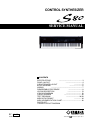
1
CONTROL SYNTHESIZER
SERVICE MANUAL
CONTENTS
SPECIFICATIONS
................................................... 3
PANEL LAYOUT
.................................... 4
CIRCUIT BOARD LAYOUT
................. 5
BLOCK DIAGRAM
............................ 6
WIRING
.................................................................... 7
DISASSEMBLY PROCEDURE
.............................. 8
LSI PIN DESCRIPTION
.............................. 13
IC BLOCK DIAGRAM
................................. 18
CIRCUIT BOARDS
...................................... 20
TEST PROGRAM
............................ 24/34
MIDI DATA FORMAT
............... 44
MIDI INPLEMENTATION CHART .......................................... 48
PARTS LIST
OVERALL CIRCUIT DIAGRAM
SY 011477
19991101-198000
HAMAMATSU, JAPAN
1.58K-9431
Printed in Japan ’99.11
S80
IMPOR TANT NOTICE
This manual has been provided for the use of authorized Yamaha Retailers and their service personnel. It has been assumed
that basic service procedures inherent to the industry, and more specifically Yamaha Products, are already known and understood by the users, and have therefore not been restated.
WARNING :
Failure to follow appropriate service and safety procedures when servicing this product may result in personal injury, destruction of expensive components and failure of the product to perform as specified. For
these reasons, we advise all Yamaha product owners that all service required should be performed by an
authorized Yamaha Retailer or the appointed service representative.
IMPORTANT :
This presentation or sale of this manual to any individual or firm does not constitute authorization certification, recognition of any applicable technical capabilities, or establish a principal-agent relationship of
any form.
The data provided is belived to be accurate and applicable to the unit(s) indicated on the cover. The research engineering, and
service departments of Yamaha are continually striving to improve Yamaha products. Modifications are, therefore, inevitable
and changes in specification are subject to change without notice or obligation to retrofit. Should any discrepancy appear to
exist, please contact the distributor’s Service Division.
WARNING :
Static discharges can destroy expensive components. Discharge any static electricity your body may have
accumulated by grounding yourself to the ground bus in the unit (heavy gauge black wires connect to
this bus.)
IMPORTANT :
Turn the unit OFF during disassembly and parts replacement. Recheck all work before you apply power
to the unit.
LITHIUM BA TTER Y HANDLING
This product uses a lithium battery for memory back-up.
WARNING :
Lithium batteries are dangerous because they can be exploded by improper handling. Observe the following precautions when handling or replacing lithium batteries.
Leave lithium battery replacement to qualified service personnel.
Always replace with batteries of the same type.
When installing on the PC board by soldering, solder using the connection terminals provided on the battery cells.
Never solder directly to the cells. Perform the soldering as quickly as possible.
Never reverse the battery polarities when installing.
Do not short the batteries.
Do not attempt to recharge these batteries.
Do not disasemble the batteries.
Never heat batteries or throw them into fire.
ADVARSEL!
Lithiumbatteri-Eksplosionsfare ved fejlagtig handtering. Udskiftning ma kun ske med batteri af samme fabrikat og type. lever det brugte
batteri tilbage til leverandren.
VARNING
Explosionsfara vid felaktigt batteribyte.
Anvand samma batterityp eller en ekvivalent typ som rekommenderas av apparattillverkaren.
Kassera anvant batteri enligt fabrikantens instruktion.
VAROITUS
Paristo voi rajahtaa, jos se on virheellisesti asennettu.
Vaihda paristo ainoastaan laitevalmistajan suosittelemaan tyyppiiin.
Havita kaytetty paristo valmistajan ohjeiden mukaisesti.
The following information complies with Dutch official Gazette 1995. 45; ESSENTIALS OF ORDER ON THE COLLECTION OF BATTERIES.
• Please refer to the diassembly procedure for the removal of Back-up Battery.
• Leest u voor het verwijderen van de backup batterij deze beschrijving.
WARNING: CHEMICAL CONTENT NOTICE!
The solder used in the production of this product contains LEAD. In addition, other electrical/electronic and/or plastic (Where
applicable) components may also contain traces of chemicals found by the California Health and Welfare Agency (and possibly
other entities) to cause cancer and/or birth defects or other reproductive harm.
DO NOT PLACE SOLDER, ELECTRICAL/ELECTRONIC OR PLASTIC COMPONENTS IN YOUR MOUTH FOR ANY REASON WHAT
SO EVER!
Avoid prolonged, unprotected contact between solder and your skin! When soldering, do not inhale solder fumes or expose
eyes to solder/flux vapor!
If you come in contact with solder or components located inside the enclosure of this product, wash your hands before handling
food.
WARNING
Components having special characteristics are marked
originally installed.
2
and must be replaced with parts having specification equal to those
S80
SPECIFICATIONS
KEYBOARD
Number of Keys
Touch
TONE GENERATION SYSTEM Tone Generators
Polyphony
VOICE
Number of Voice
88
Initial touch, After touch
AWM2, Modular Synthesis Plug-in System
64
Normal voices (256 Presets, 128 Internals [Users], 128 Externals [Memory Cards]),
Drum voices (8 presets, 2 Internals [Users], 2 Externals [Memory Cards]), Plug-in voices (64 x 2 Plug-in Boards [If installed])
Wave ROM
PERFORMANCE
EFFECT
Multi-Timbres
Number of Performance
128 Internals, 64 Externals
Master Keyboard Mode
4 Zones
Reverb
12
Chorus
23
Insertion
Master EQ
SEQUENCE PLAY
24 MByte
19 (16 Voice Parts, A/D Input Part, Plug-in 1/2 Parts)
Format
Number of Sequence Chains
ARPEGGIATOR
Number of Arpeggios
Card
File Type
Functions
CONTROLS
24 (Insertion 1), 92 (Insertion 2), 24 (Insertion for Plug-in Voices)
4
SMF Format 0 (Direct Play only), Sequence Chain (Load/Save)
100 Steps (100 Songs)
128
All Data, All Voice, Plug-in, Sequence Chain, SMF
Save, Load, Rename, Delete, Make Directory, Format
Volume Slider, 4 Control Sliders, Pitch, Modulation, Shift, Page, Knob A/B/C/1/2, Data, Effect Bypass, Master Keyboard, Exit,
Enter, Dec/No, Inc/Yes, 7 Mode Keys, Sequence Play, Sequence PLAY/STOP, 6 Memory Keys, Quick Access, 8 Bank Keys,
16 Program/Part Keys, Power, Card Slot, Gain, Host Select
CONNECTORS & TERMINALS
MIDI In, Out, Thru, To Host, Breath, Footswitch, Sustain, Foot Controller, Foot Volume, Individual Output 1, 2,
Output L/Mono R, Phones, A/D Input, AC Inlet, 2 Connectors for Plug-in Boards
DISPLAY
40 x 2 (Backlit)
INCLUDED ACCESSORIES
Owner’s Manual, Data List, CD-ROM, AC Power Cord
OPTIONAL ACCESSORIES
PLG150 Plug-in Boards Series, PLG100 Plug-in Boards Series, FC4/5 Footswitch, FC7 Foot Controller, BC3 Breath Controller
POWER CONSUMPTION
OUTPUT IMPEDANCE
DIMENSIONS
WEIGHT
16W
Output: +18.1 ±2dbm (10k ohms), Phones: +17.2 ±2dbm (33 ohms)
1329(W) x 371(D) x 157(H) mm
24.3 kg
3
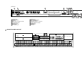
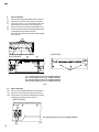
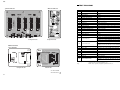
S80
PANEL LAYOUT
Front panel
1
GAIN ..... A/D INPUT
5
2
PHONES
L/MONO
R
OUTPUT
1
2
FOOT
FOOT
INDIVIDUAL OUTPUT VOLUME CONTROLLER SUSTAIN
FOOT
SWITCH
IN
BREATH
TO HOST
HOST SELECT
OUT
MIDI
11 10
6
THRU
3.3V CARD
18
12
AC INLET
PRE 2
INT
EXT
PLG1
PLG2
MODE
CONTROL SLIDER
EF
BYPASS
13
EXIT
MASTER
KEYBOARD
ENTER
DRUM
VOICE
UTILITY
PERFORM
CARD
DRUM
QUICK
ACCESS
STORE
SEQ
PLAY
A
B
C
D
E
F
G
H
A. PIANO
E. PIANO
ORGAN
GTR/BASS
STRINGS
BRASS
SYNTH
OTHER
1
2
3
4
5
6
7
8
9
10
11
12
13
14
15
16
ASSIGNABLE KNOB
SHIFT
PITCH
A
PAGE
B
C
1
2
DATA
MODULATION
DEC/NO INC/ YES
PART/ELEMENT
1
2
3
4
EDIT
COMPARE
7
JOB
PLAY/
STOP
14
8
15
16
3
1
2
3
4
5
6
7
8
9
10
4
PITCH bend wheel
MODULATION wheel
[VOLUME] Slider
Control Sliders
LCD (Liquid Crystal Display)
[DATA] knob
Knobs [A], [B], [C], [1] and [2]
[PAGE] knob
[SHIFT] key
[MASTER KEYBOARD] key
11
12
13
14
15
16
17
18
19
20
21
4
[EF BYPASS] key
[EXIT] key
[ENTER] key
[DEC/NO] key
[INC/YES] key
MODE keys
SEQ controls
MEMORY keys
[QUICK ACCESS] key
BANK [A] to [H] keys
PROGRAM/PART [1] to [16] keys
9
POWER
ON /
PRE1
VOLUME
19
17
21 20
OFF
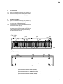
S80
Rear panel
1
2
3
4
5
6 7 8 9
3.3V CARD
POWER
ON
AC INLET
THRU
OFF
MIDI
OUT
IN
HOST SELECT
TO HOST
BREATH
FOOT
SWITCH
INDIVIDUAL OUTPUT
FOOT
FOOT
SUSTAIN CONTROLLER VOLUME
1
2
R
OUTPUT
L MONO PHONES
A D INPUT
GAIN
MIDI
Mac
PC-2 PC-1
10 11 12
1
2
3
4
5
6
7
8
POWER switch
AC INLET terminal
CARD slot
MIDI IN, OUT, and THRU connectors
HOST SELECT switch
TO HOST terminal
BREATH jack
FOOT SWITCH jack
9
10
11
12
13
14
15
16
13 14
15 16
SUSTAIN jack
FOOT CONTROLLER jack
FOOT VOLUME jack
INDIVIDUAL OUTPUT 1 and 2 jacks
OUTPUT L/MONO and R jack
PHONES jack
A/D INPUT jack
GAIN knob
CIRCUIT BOARD LAYOUT
SM
RV
PN
JK
Power supply assembly
LCD
DM
SV
PC
AE88L
(A-1
C2)
AEC
(C#2
C5)
AE88H
(C#5 C7)
5
S80
BLOCK DIAGRAM
PN
JK
IN
OUT
THRU
RV
PANEL SCANING
MN101C027YB
CLK8MHz
S
HOST
SELECT
TO HOST
Control
Slider
OPTION
SM
PLUG-IN
BOARD
Slot x 2
Smart Media
Load/Save
D
Panel LED 15
LCD
SV
IC1
Panel SW 52
MIDI
L
DISPLAY
LCD 40 2
LED BackLight
IC50
IC12
MIDI
I/F
DM
toHOST
I/F
IC22
RES
RV
RES
IC9
CPU
CONTROL
RES
1
DISPLAY
I/F
2
IC7
MPU SH2(28MHz)
SH7045
IC18,19
IC2
Knob 3
CPU
Knob 4
IC1
IC3
PROGRAM ROM
16Mbit
16bitDBUS
FLASH
OPTION
RES
I/F
mLAN
RES
RES
Knob 2
IC101
RESET
CONTROL
Battery
Back UP
I/F
Knob 1
CPU
CONTROL
RES
I/F
SIO4
CLK28MHz
Rotary Encoder
IC9
PLUG-IN
I/F
Smart
Media
I/F
IC4
PROGRAM ROM
16Mbit
16bitDBUS
FLASH
SRAM
1Mbit
8bitDBUS
IC5
SRAM
1Mbit
8bitDBUS
IC6
DRAM
4Mbit
16bitDBUS
Knob 5
IC10
PKS
CLK8MHz
JK
FOOT
VOLUME
SV
CPU
CONTROL
RES
MVR
IC13-16
CPU
CONTROL
RES
MULTI
PLEXER
+3.3V Power Supply
JK
IC61
FOOT
CONTROLLER
IC62
pD63200
SWP30B
Master
CLK33MHz
SUSTAIN
SWITCH
IC43
IC45
WAVE 8MByte
64Mbit X 4
16bit DBUS
DRAM
4Mbit
16bit DBUS
FOOT
SWITCH
IC60
14
DDE1
D/A
LINE
L/R
AMP
4570
IC38
BREATH
14
DDE1
WHEEL
11
D/A
INDV
1.2
6
15
7
AMP
4570
OUTPUT
L/MONO
IC2
1
7
1
3
OUTPUT R
5
IC65
pD63200
IC63
3
LPF
6
15
IC35
11
5
5
AMP
4570
HPAMP
3
7
AMP
4570
PHONES
1
LPF
3
IC3
7
1
INDIVIDUAL
OUTPUT 1
5
IC64
Pitch Bend
Modulation
INDIVIDUAL
OUTPUT 2
IC4
3
AE2 keyboard
IC44
IC46
WAVE 8MByte
32Mbit X 2
16bit DBUS
1
LPF
IC4
5
7
Keyboard
88 KEY
TYPE AE2
A/D INPUT
A/D
IC66
After
Touch
GAIN
MIC/LINE
POWER SW
PS
AC
Switching
Power SuppIy
+5D
+12A
-12A
INLET
AC
FG
6
28CA1-8813228
S80
WIRING
AE2 Keyboard Unit
After Touch
AE2
I/F
WHEEL
5P
8P
2P
CN1
CN2
Keyboard
After
Touch
Sensor
12P
16P
CN3
CN4
CN1
PN
CN2
5
4P
CN1
CN2
5P
6P
CN3
CN4
8P
5P
CN3
CN1
5P
23
3P
7P
8P
10P
3P
14P
CN9
CN8
CN7
CN6
CN5
CN4
CN1
2
26
17
14
6
26
2P
12
13
PLUG-IN 1
PLUG-IN 2
15P
15P
CN1
CN1
15
Location Connector Assembly
1
16
2
3
2
7
3
21
8
5
6
7
2
11
3
17
14
12
CORE
13
24
23
CN8
CN5
CN9
CN10
CN11
CN2
CN3
CN17
CN14
CN12
CN13
9P
5P
4P
3P
4P
12P
13P
7P
8P
14P
2P
16P
15P
12P
CN16
CN103
14P
CN102
CN15
6P
CN7
10P
CN6
15P
8
1
16
mLAN
27
26P
18
SM
22
Remarks
Parts List
Ref. No.
1
DM-PS
11P/L1450 OVERALL 370
2
MK2
12P
OVERALL 380
3
MK1
16P
OVERALL 390
4
KRD-KRD
15P/L600
OVERALL 450
5
WHEEL
5P/L300
WHEEL 80
6
KRD-KRD
10P/L650
CONTROLPANEL 110
7
KRD-KRD
6P/L400
CONTROLPANEL 120
OVERALL 400
8
KRD-KRD
9P/L450
11
AFTER
4P-8P/L1350 OVERALL 420
12
DM-LCD
14P/L300
13
DM-LCD
2P/L500
14
KRD-KRD
8P/L450
15
DM-PLUG IN1
14P-15P/L400
16
DM-PLUG IN2
15P-15P/L400
17
KRD-KRD
7P/L700
CONTROLPANEL 140
18
DM-mLAN
26P
OPTION
19
DM-MVR
4P/L450
CONTROLPANEL 150
20
DM-IND
5P/L500
OVERALL 470
21
DM-JK
4P/L350
OVERALL 480
22
DM-SM
26P/L430
CONTROLPANEL 181
23
JK-MVR
5P/L650
CONTROLPANEL 160
24
JK-PS
5P
OVERALL 370
25
JK-PN
5P/L800
CONTROLPANEL 170
26
KRD-KRD
3P/L300
CONTROLPANEL 180
27
PS-AC INLET
4P
POWER SUPPLY 40
28
PS-P.SW
3P/L100
POWER SUPPLY 30a
CONTROLPANEL 130
OVERALL 450
1 Connector Assembly (PS Core)
2 Connector Assembly (DMJK Core)
3 Connector Assembly (PLUG Core)
26P
26P
5P
CN3
26P
CN20
19
4P
INLET
CORE
1
(DM)
CN22
CN21
20
4
24
11P
21
CN18
CN1
CN1
25
CN1
1
CN19
9P
5P
CN6
CN7
4
CN4
CORE
20
8P
5P
CN2
15
15P
11P
CN2
CN1
5P
4P
6P
P.SW
CN4
JK
19
CN5
SV
5P
25
11
LCD
RV
PS
6P
CN5
28
7
S80
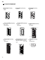
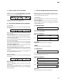
DISASSEMBLY PROCEDURE
1.
4.
4-1
4-2
Remove the six (6) screws marked [300] from the
bottom of the main unit and open the control panel
assembly by lifting it up. (Fig. 1)
〈BOTTOM VIEW〉
4-3
[300]
Power Supply Unit
Open the control panel assembly. (See procedure 1.)
Remove the two (2) screws marked [30] and the
five (5) screws marked [31]. (Fig. 3)
Remove the four (4) screws marked [22] from the
power assembly. (Fig. 3) Power supply unit can then
be removed.
[300]
5.
5-1
5-2
SM Circuit Board
Open the control panel assembly. (See procedure 1.)
Remove the two (2) screws marked [96]. The SM
circuit board can then be removed. (Fig. 4)
6.
6-1
6-2
SV Circuit Board
Open the control panel assembly. (See procedure 1.)
Remove the three (3) screws marked [130]. The PLG
angle can then be removed. (Fig. 4)
Remove the five (5) knobs marked [220] from the
panel surface. (Fig. 4)
Remove the six (6) screws marked [82]. The SV
circuit board can then be removed. (Fig. 3)
[300]: Bind Head Screw 5.0X20 MFZN2BL (VB857600)
Fig.1
2.
2-1
2-2
3.
3-1
3-2
3-3
PN Circuit Board
Open the control panel assembly. (See procedure 1.)
Remove the twelve (12) screws marked [42]. The
PN circuit board can then be removed. (Fig. 2)
6-3
6-4
RV Circuit Board
Open the control panel assembly. (See procedure 1.)
Remove the five (5) knobs marked [200] and the
two (2) knobs marked [210] from the panel surface.
Remove the ten (10) screws marked [96]. The RV
circuit board can then be removed. (Fig. 2)
8.
8-1
8-2
JK Circuit Board
Open the control panel assembly. (See procedure 1.)
Remove the nine (9) screws marked [81]. The JK
circuit board can then be removed. (Fig. 3)
[210] [200] [210]
[42]
[42]
PN
[42]
[42]:
Bind Head Tapping Screw-B 3.0X6 MFZN2BL (EP600230)
[96]:
Bind Head Tapping Screw-B 3.0X6 MFZN2BL (EP600230)
Fig.2
8
Display Assembly
Open the control panel assembly. (See procedure 1.)
Remove the PLG angle. (See procedure 6-2.)
Remove the four (4) screws marked [92]. The display
assembly can then be removed. (Fig. 3)
〈TOP VIEW〉
〈BOTTOM VIEW〉
[96]
7.
7-1
7-2
7-3
S80
〈BOTTOM VIEW1〉
[92]
[82]
Display assembly
〈TOP VIEW〉
[220]
〈BOTTOM VIEW2〉
Display assembly
[22]
SV
JK
PLG Angle
POWER SUPPLY
〈REAR VIEW〉
[81]
[130]
[96]
[31]
[30]
[31]
[22]: Bind Head Tapping Screw-B 3.0X6 MFZN2BL (EP600230)
[30]: Bind Head Tapping Screw-B 3.0X6 MFZN2BL (EP600230)
[82]:
[92]:
Bind Head Tapping Screw-B 3.0X6 MFZN2BL (EP600230)
Bind Head Tapping Screw-B 3.0X6 MFZN2BL (EP600230)
[31]: Bonding Tapping Screw-B 3.0X10 MFZN2BL (VQ049800)
[81]: Bonding Tapping Screw-B 3.0X10 MFZN2BL (VQ049800)
[96]: Bind Head Tapping Screw-B 3.0X6 MFZN2BL (EP600230)
[130]: Bind Head Tapping Screw-B 3.0X6 MFZN2BL (EP600230)
Fig.3
9
S80
9.
9-1
9-2
9-3
9-4
9-5
DM Circuit Board
Open the control panel assembly. (See procedure 1.)
Remove the JK circuit board. (See procedure 8.)
Remove the seven (7) screws marked [282]. The
DM shield cover can then be removed. (Fig. 4)
Remove the three (3) screws marked [63]. (Fig. 4)
Remove the two (2) screws marked [62] and the screw
marked [64] from the DM circuit board.
Be careful of the harness clamp, which is also installed
there. (Fig. 5)
[282]
〈BOTTOM VIEW〉
〈REAR VIEW〉
[62]
[64]
[63]
[62]:
[63]:
Bind Head Tapping Screw-B 3.0X6 MFZN2BL (EP600230)
Bonding Tapping Screw-B 3.0X10 MFZN2BL (VQ049800)
[64]: Bind Head Tapping Screw-B 3.0X8 MFZN2BL (EP600190)
[282]: Bind Head Tapping Screw-B 3.0X6 MFZN2BL (EP600230)
Fig.4
10.
10-1
10-2
10-3
Wheel Assembly
Open the control panel assembly. (See procedure 1.)
Remove the JK circuit board. (See procedure 8.)
Remove the four (4) screws marked [102]. The wheel
assembly can then be removed. (Fig. 5)
〈BOTTOM VIEW〉
[102]
[102]: Bind Head Tapping Screw-B 3.0X6 MFZN2BL (EP600230)
[102]
10
Fig.5
S80
11.
11-1
11-2
PC Circuit Board
Open the control panel assembly. (See procedure 1.)
Remove the two (2) screws marked [250]. The PC
circuit board can then be removed. (Fig. 6)
12.
12-1
12-2
Keyboard Assembly
Open the control panel assembly. (See procedure 1.)
Remove the four (4) screws marked [230] and the
four (4) screws marked [240]. (Fig. 6)
Loosen the two (2) screws marked [292], which are
secring the front rail. (Fig. 6)
Remove the seven (7) screws marked [300], which
are secring the front rail at the bottom of the main unit
to the keyboard assembly. The keyboard assembly
can then be removed. (Fig. 6)
12-3
12-4
〈TOP VIEW〉
[230]
[230]
[240]
[230]
[240]
[230]
[240]
[250]
PC
[240]
[292]
[292]
〈BOTTOM VIEW〉
[300]
[300]
[300]
[300]
[230]: Bind Head Screw 4.0X14 MFZN2Y (EG340210)
[240]: Bind Head Tapping Screw-1 3.5X12 MFZN2Y (EP030240)
[250]: Bind Head Screw-B 3.0X6 MFZN2BL (EG330360)
[292]: Bind Head Tapping Screw-1 3.5X12 MFZN2Y (EP030240)
[300]: Bind Head Screw 5.0X20 MFZN2BL (VB857600)
Fig.6
11
S80
13.
13-1
13-2
13-3
Keyboard Disassembly Procedure
Remove the circuit board marked [A], and then remove
the key spring marked [B]. (Fig. 7)
Press the part marked [D’] in the direction shown in
figure 9, then remove the key marked [D] and the
hammer assembly marked [C]. (Fig. 8, Fig. 9)
The black keys can be disassenbled by following
the same procedure.
[A]
[D']
[C]
[B]
[D]
Fig.7
14.
14-1
14-2
14-3
14-4
14-5
14-6
Fig.8
Fig.9
Keyboard Assembly Procedure
Insert the hammer assembly marked [C] in the frame
in the direction marked [1]. (Fig. 10)
Place the hammer assembly as shown in figures
10 and 11.
Place the white key in the order of [4] and [5]. (Fig. 12)
Place doun on the white key in the direction marked
[6] shown in figure 13.
Attach the key spring marked [B], and then place
the circuit board marked [A]. (Fig. 14)
The black keys can be disassenbled by following
the same procedure.
[1]
[2]
[3]
[C]
[2]
[5]
[D]
Fig.11
Fig.10
Fig.12
[A]
[B]
[6]
Fig.13
12
Fig.14
S80
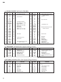
LSI PIN DESCRIPTION
HD64F7045F28 (XW419A00) CPU
PIN
NAME
I/O
FUNCTION
NO.
1
2
3
4
5
6
7
8
9
10
11
12
13
14
15
16
17
18
19
20
21
22
23
24
25
26
27
28
29
30
31
32
33
34
35
36
37
38
39
40
41
42
43
44
45
46
47
48
49
50
51
52
53
54
55
56
57
58
59
60
61
62
63
64
65
66
67
68
69
70
71
72
/WRHH
PE14
/WRHL
PA21
PE15
VSS6
A0
A1
A2
A3
A4
VCC12
A5
VSS14
A6
A7
A8
A9
A10
A11
A12
A13
A14
A15
A16
VCC26
A17
VSS28
PA20
PA19
PB2
PB3
PA18
PB4
VSS35
PB5
A18
A19
A20
VCC40
A21
VSS42
/RD
/WDTOVF
D31
D30
/WRH
WRL
/CS1
CS0
PA9
PA8
/CS3
/CS2
VSS55
D29
D28
D27
D26
D25
VSS61
D24
VCC63
D23
D22
D21
D20
D19
D18
D17
VSS71
D16
O
I/O
O
I
I/O
O
O
O
O
O
O
O
O
O
O
O
O
O
O
O
O
O
O
I
I
O
O
I
O
O
O
O
O
O
O
I/O
I/O
O
O
O
O
I
I
O
O
—
I/O
I/O
I/O
I/O
I/O
I/O
I/O
I/O
I/O
I/O
I/O
I/O
I/O
I/O
HH write
LCD data 6 input / output
MLAN insert detect
LCD data 7 input / output
Ground
Address bus
Power supply
Address bus
Ground
Address bus
Power supply
Address bus
Ground
Encoder 2A input
Encoder 2B input
Row address strobe
Column address strobe (low)
Host off line detect input
Column address strobe (high)
Ground
DRAM read/write
Address bus
Power supply
Address bus
Ground
Read
Not used
Data bus
High write
Low write
Chip Select 1
Chip Select 0
MLAN MIDI interrupt request
Interrupt request
Chip select 3
Chip select 2
Ground
Data bus
Ground
Data bus
Power supply
Data bus
Ground
Data bus
PIN
NO.
NAME
73
74
75
76
77
78
79
80
81
82
83
84
85
86
87
88
89
90
91
92
93
94
95
96
97
98
99
100
101
102
103
104
105
106
107
108
109
110
111
112
113
114
115
116
117
118
119
120
121
122
123
124
125
126
127
128
129
130
131
132
133
134
135
136
137
138
139
140
141
142
143
144
D15
D14
D13
D12
VCC77
D11
VSS79
D10
D9
D8
D7
D6
VCC85
D5
VSS87
D4
D3
D2
D1
D0
VSS93
XTAL
MD3
EXTAL
MD2
NMI
VCC99/FWP99
PA16
PA17
MD1
MD0
PLLVCC
PLLCAP
PLLVSS
PA15
/RES
TIOCOA
PE1
PE2
VCC112
PE3
PE4
PE5
PE6
VSS117
AN0
AN1
AN2
AN3
AN4
AN5
AVSS
AN6
AN7
AVREF
AVCC
VSS129
RXD0
TXD0
/IRQ0
RXD1
TXD1
VCC135
/IRQ1
PE7
PE8
PE9
PE10
VSS141
PE11
PE12
PE13
I/O
I/O
I/O
I/O
I/O
I/O
I/O
I/O
I/O
I/O
I/O
I/O
I/O
I/O
I/O
I/O
I/O
I
I
I
I
I
I
I
I
O
I
I
I
I
I
O
I
I
I
I
I
I
I
I
I
I
O
I
I
O
I
I
I/O
I/O
I/O
I/O
I/O
I/O
FUNCTION
Data bus
Power supply
Data bus
Ground
Data bus
Power supply
Data bus
Ground
Data bus
Ground
Crystal oscillator
Mode select
Crystal oscillator
Mode select
Non-maskable interrupt
Power supply
Encoder 1B input
Encoder 1A input
Mode select
Mode select
PLL power supply
PLL capacitor
PLL ground
CPU clock out
Reset
A/D jack insert detect interrupt request input
Smart MINS
Model detection
Power supply
Smart busy input
MLAN reset interrupt request input
1M clock out
Model detection
Ground
Analog input
Analog ground
Analog input
Analog reference voltage
Analog power supply
Ground
MIDI input
MIDI output
Plug in sireal interrupt request input
HOST input
HOST output
Power supply
MLAN MIDI interrupt input
Smart Vprt Input
LCD data 0 input / output
LCD data 1 input / output
LCD data 2 input / output
Ground
LCD data 3 input / output
LCD data 4 input / output
LCD data 5 input / output
13
S80
HD63B01Y0RCE0F (XM234A00) CPU (PKS)
PIN
NO.
1
2
3
4
5
6
7
8
9
10
11
12
13
14
15
16
17
18
19
20
21
22
23
24
25
26
27
28
29
30
31
32
NAME
/NMI
E
D#
D
C#
CL
PULL 1
PULL 2
LC.AE//FS
/REPEAT
/KOF-REQ
SW1
SW2
/IS
/OS
SW3
SW4
DOUT0
DOUT1
DOUT2
DOUT3
DOUT4
DOUT5
DOUT6
DOUT7
Vcc
Sf
M5/S13
M4/S12
M3/S10
M2/S9
M1/S8
I/O
I
O
O
O
O
O
I
I
I
I
I
I
I
I
I
O
O
O
O
O
O
O
O
O
I
I
I
I
I
FUNCTION
Non-maskable interrupt
Key scan drive
connected to ground
Auto repeat (L:on, H:off)
Key off request
Switch 1 (L: on, H: off)
Switch 2 (L: on, H: off)
Input strobe
Output strobe
Switch 3 (L: on, H: off)
Switch 4 (L: on, H: off)
Data output
Power supply (+5V)
Switch drive
Make contact of key receive/
Switch receive
PIN
NO.
33
34
35
36
37
38
39
40
41
42
43
44
45
46
47
48
49
50
51
52
53
54
55
56
57
58
59
60
61
62
63
64
NAME
M1/S8
M0/S7
Vss
F
F#
G
G#
A
A#
B
C
LC//AE
B6/S6
B5/S5
B4/S4
B3/S3
B2/S2
B1/S1
B0/S0
Se
Sd
Sc
Sb
Sa
E
Vss
XTAL
EXTAL
MP0
MP1
/RES
/STBY
I/O
I
I
O
O
O
O
O
O
O
O
I
I
I
I
I
I
I
I
O
O
O
O
O
I
I
I
I
I
FUNCTION
Make contact of key receive/
Switch receive
Ground
Key scan drive
connected to +5V
Break contact of key receive/
Switch receive
Switch drive
Not used
Ground
Not used
8 MHz clock
Mode program 0
Mode program 1
Initial clear
Stanby-mode signal
µ PD63200GS (XM145A00) DAC (Digital to Analog Converter)
PIN
NO.
1
2
3
4
5
6
7
8
NAME
4/8F
D. GND
16 BIT
D. VDD
A. GND
R. OUT
A. VDD
A. VDD
I/O
I
I
O
FUNCTION
4/8 Fs selection
Digital ground
16 bit/18 bit selection
Digital power supply
Analog ground
Channel R output
Analog power supply
PIN
NO.
9
10
11
12
13
14
15
16
NAME
R. REF
L. REF
L. OUT
A. GND
WDCK
RSI
SI/LSI
CLK
I/O
O
I
I
I
I
FUNCTION
Channel R voltage reference
Channel L voltage reference
Channel L output
Analog ground
Word clock
Channel R series input
Series input/Channel L series nput
Clock
JG710069 (XM326B00) DDE1 (DAC Dynamic Range Enhancer)
PIN
NO.
1
2
3
4
5
6
7
8
14
NAME
I/O
CLK
SYW
MIN 1
MIN 0
Vss
SEL 1
SEL 0
SUP
I
I
I
I
I
I
I
FUNCTION
Master clock
Sync signal
Signal input
Signal input
Ground
Mode select
Mode select
1 bit shift up input
PIN
NO.
9
10
11
12
13
14
15
16
NAME
I/O
SH 0
SH 1
LE
V DD
DACO 0
DACO 1
DCLK
ICN
O
O
O
O
O
O
I
FUNCTION
N.C.
N.C.
Latch enable for DAC
Power supply
Output (DAC)
Output (DAC)
Clock for DAC
Initial clear
S80
TC203C760HF-002 (XS725A00) SWP30B AWM Tone Generator coped with MEG) Standard Wave Processor
PIN
NO.
NAME
1
2
3
4
5
6
7
8
9
10
11
12
13
14
15
16
17
18
19
20
21
22
23
24
25
26
27
28
29
30
31
32
33
34
35
36
37
38
39
40
41
42
43
44
45
46
47
48
49
50
51
52
53
54
55
56
57
58
59
60
61
62
63
64
65
66
67
68
69
70
71
72
73
74
75
76
77
78
79
80
81
82
83
84
85
86
87
88
89
90
91
92
93
94
95
96
97
98
99
100
101
102
103
104
105
106
107
108
109
110
111
112
113
114
115
116
117
118
119
120
Vss
CA0
CA1
CA2
CA3
CA4
CA5
CA6
CA7
CA8
CA9
CA10
CA11
VSS
CD0
CD1
CD2
CD3
CD4
CD5
CD6
CD7
CD8
CD9
CD10
CD11
CD12
CD13
CD14
VDD
VSS
CD15
CSN
WRN
RDN
VDD
SYSH0
SYSH1
SYSH2
SYSH3
SYSH4
SYSH5
SYSH6
SYSH7
KONO0
KONO1
KONO2
KONO3
VSS
SYSL0
SYSL1
SYSL2
SYSL3
SYSL4
SYSL5
SYSL6
SYSL7
KONI0
KONI1
VDD
VSS
KONI2
KONI3
DAC0
DAC1
WCLK
MELO0
MELO1
MELO2
MELO3
MELO4
MELO5
MELO6
MELO7
VDD
ADLR
MELI0
MELI1
MELI2
MELI3
MELI4
MELI5
MELI6
MELI7
VSS
RCASN
RA8
RA7
RA6
VDD
VSS
RA5
RA4
RA3
RA2
RA1
RA0
RRASN
RWEN
VSS
RD7
RD6
RD5
RD4
RD3
RD2
RD1
RD0
VSS
RD17
RD16
RD15
RD14
RD13
RD12
RD11
RD10
RD9
RD8
VDD
I/O
FUNCTION
(Ground)
I
I
I
I
I
I
I
I
I
I
I
I
Address bus of internal register
(Ground)
I/O
I/O
I/O
I/O
I/O
I/O
I/O
I/O
I/O
I/O
I/O
I/O
I/O
I/O
I/O
Data bus of internal register
(Power supply)
(Ground)
I/O
I
I
I
Chip select
Write strobe
Read strobe
(Power supply)
O
O
O
O
O
O
O
O
O
O
O
O
NSYS/LNSYS upper 16 bits output
Key on data
(Ground)
I/O
I/O
I/O
I/O
I/O
I/O
I/O
I/O
I
I
I
I
I
O
O
O
O
O
O
O
O
O
O
O
NSYS input/LNSYS output lower 8 bits
Key on data input
(Power supply)
(Ground)
DAC output
DAC0/DAC1 word clock
MEL wave data output
(Power supply)
O
I
I
I
I
I
I
I
I
O
O
O
O
O
O
O
O
O
O
O
O
ADC word clock
MEL wave data input
(Ground)
DRAM column address strobe (RAS signal)
(Power supply)
(Ground)
DRAM address bus
DRAM row address strobe (RAS signal)
DARM write enable
(Ground)
I/O
I/O
I/O
I/O
I/O
I/O
I/O
I/O
(Ground)
I/O
I/O
I/O
I/O
I/O
I/O
I/O
I/O
I/O
I/O
DRAM data bus
(Power supply)
PIN
NO.
121
122
123
124
125
126
127
128
129
130
131
132
133
134
135
136
137
138
139
140
141
142
143
144
145
146
147
148
149
150
151
152
153
154
155
156
157
158
159
160
161
162
163
164
165
166
167
168
169
170
171
172
173
174
175
176
177
178
179
180
181
182
183
184
185
186
187
188
189
190
191
192
193
194
195
196
197
198
199
200
201
202
203
204
205
206
207
208
209
210
211
212
213
214
215
216
217
218
219
220
221
222
223
224
225
226
227
228
229
230
231
232
233
234
235
236
237
238
239
240
NAME
VSS
HMD0
HMD1
HMD2
HMD3
HMD4
HMD5
HMD6
HMD7
HMD8
HMD9
HMD10
HMD11
HMD12
HMD13
HMD14
HMD15
VSS
HMA0
HMA1
HMA2
HMA3
HMA4
HMA5
HMA6
HMA7
HMA8
HMA9
HMA10
VDD
VSS
HMA11
HMA12
HMA13
HMA14
HMA15
HMA16
HMA17
HMA18
HMA19
HMA20
HMA21
HMA22
HMA23
HMA24
VSS
MRASN
MCASN
MOEN
MWEN
VSS
LMD0
LMD1
LMD2
LMD3
LMD4
LMD5
LMD6
LMD7
VDD
VSS
LMD8
LMD9
LMD10
LMD11
LMD12
LMD13
LMD14
LMD15
VSS
LMA0
LMA1
LMA2
LMA3
LMA4
LMA5
LMA6
LMA7
LMA8
LMA9
LMA10
LMA11
VSS
LMA12
LMA13
LMA14
LMA15
LMA16
LMA17
VDD
VSS
LMA18
LMA19
LMA20
LMA21
LMA22
LMA23
LMA24
VSS
SYO
SYOD
QCLK
HCLK
CK256
SYSCLK
VDD
SYI
MCLKI
MCLKO
VDD
XIN
XOUT
VSS
ICN
CHIP2
SLAVE
TESTON
ACIN
DCTEST
VDD
I/O
FUNCTION
(Ground)
I/O
I/O
I/O
I/O
I/O
I/O
I/O
I/O
I/O
I/O
I/O
I/O
I/O
I/O
I/O
I/O
Wave memory data bus (Upper 16 bits)
(Ground)
O
O
O
O
O
O
O
O
O
O
O
(Power supply)
(Ground)
O
O
O
O
O
O
O
O
O
O
O
O
O
O
Wave memory address bus
(Ground)
O
O
O
O
I/O
I/O
I/O
I/O
I/O
I/O
I/O
I/O
RAS when DRAM(s) is connected to wave memory
CAS when DRAM(s) is connected to wave memory
Wave memory output enable
Wave memory write enable
(Ground)
Wave memory data bus (Lower 16 bits)
(Power supply)
(Ground)
I/O
I/O
I/O
I/O
I/O
I/O
I/O
I/O
(Ground)
O
O
O
O
O
O
O
O
O
O
O
O
(Ground)
O
O
O
O
O
O
Wave memory address bus (Lower data memory)
(Power supply)
(Ground)
O
O
O
O
O
O
O
O
O
O
O
O
O
I
I
O
I
O
I
I
I
I
I
I
(Ground)
Sync. signal for master clock
Sync. signal for HCLK/QCLK
1/12 master clock (64Fs)
1/6 master clock (128Fs)
1/3 master clock (256Fs)
1/2 master clock (384Fs)
(Power supply)
Sync. clock
Master clock input
Master clock output
(Power supply)
Crystal osc. input
Crystal osc. output
(Ground)
Initial clear
2 chips mode enable
Master/Slave select when 2 chips mode
Test pin
(Power supply)
15
S80
MN101C027YB (XS711200) CPU
PIN
NO.
1
2
3
4
5
6
7
8
9
10
11
12
13
14
15
16
17
18
19
20
21
22
23
24
25
26
27
28
29
30
31
32
NAME
I/O
S1
S2
S3
S4
S5
VREF+
VDD
OSC2
OSC1
VSS
XI
XO
MMOD
RD0
RXD
D0
D1
D2
D3
D4
/RST
D5
D6
D7
D8
D9
S6
S7
S8
S9
S10
S11
I
I
I
I
I
O
I
I
O
I
O
I
O
O
O
O
O
I
O
O
O
O
O
I
I
I
I
I
I
FUNCTION
Switch matrix data
Power supply (+5V, analog)
Power supply (+5V)
Crystal oscillator (8MHz)
Crystal oscillator (8MHz)
Ground
Not used
Not used
Memory mode select (Grounded)
Rotary encoder data
MIDI receive data
LED and switch drive data
Reset
LED and switch drive data
Switch matrix data
PIN
NO.
33
34
35
36
37
38
39
40
41
42
43
44
45
46
47
48
49
50
51
52
53
54
55
56
57
58
59
60
61
62
63
64
NAME
I/O
S12
S13
S14
TXD
S15
S16
S17
S18
L16
L17
L18
L19
L8
L9
L10
L11
L12
L13
L14
L15
L7
L6
L5
L4
L3
L2
L1
L0
VREF
AD0
AD1
S0
I
I
I
O
I
I
I
I
O
O
O
O
O
O
O
O
O
O
O
O
O
O
O
O
O
O
O
O
I
I
I
FUNCTION
Switch matrix data
MIDI transmit data
Switch matrix data
LED drive data
LED and switch drive data
Grounded
Analog input
Analog input
Switch matrix data
MBCG46183-129 (XV833A00) Gate Array
16
PIN
NO
NAME
I/O
1
2
3
4
5
6
7
8
9
10
11
12
13
14
15
16
17
18
19
20
21
22
23
24
D5
D6
D7
/IRQ0
/IRQ1
VSS
/IRQ2
/IRQ3
/RD
/WR
/CE
/ASTB
TESTSIO
RX0
TX0
RX1
TX1
VSS
VDD
RX2
TX2/BO2
RX30
TX30
RX31
I/O
I/O
I/O
I/O
I/O
I/O
I/O
I
I
I
I
I
I
O
I
O
I
O
I
O
I
FUNCTION
Data Bus
Interrupt Request Port 0
Interrupt Request Port 1
Ground
Interrupt Request Port 2
Interrupt Request Port 3
Read Signal Input
Write Signal Input
Chip Enable Input
Address Strobe (Not used: to ground)
Input with Pull-down Resistor (50k)
Receive Data 0
Transmit Data 0
Receive Data 1
Transmit Data 1
Ground
Power Supply
Receive Data 2
Transmit Data 2
Receive Data 30
Transmit Data 30
Receive Data 31
PIN
NO
NAME
I/O
25
26
27
28
29
30
31
32
33
34
35
36
37
38
39
40
41
42
43
44
45
46
47
48
TX31
RX32
TX32
RX33
TX33
/IC
VSS
XI
VSS
XO
A0
A1
A2
A3
A4
A5
CPUCLK
VSS
VDD
D0
D1
D2
D3
D4
O
I
O
I
I/O
I
I
I/O
I
I
I
I
I
I
I
I/O
I/O
I/O
I/O
I/O
FUNCTION
Transmit Data 31
Receive Data 32
Transmit Data 32
Receive Data 33
Transmit Data 33
Initial Clear
Ground
Quartz Crystal Input
Ground
Quartz Crystal Output
Address Bus
CPU Clock
Ground
Power Supply
Data Bus
S80
PCM1800 (XU770A00) A/D Converter
PIN
NAME
I/O
FUNCTION
NO.
1
2
3
4
5
6
7
8
9
10
11
12
VINL
VREF1
REFCOM
VREF2
VINR
RSTB
BYPAS
FMT0
FMT1
MODE0
MODE1
FSYNC
I
I
I
I
I
I
I
I
I/O
Analog input (L ch.)
Reference 1 decoupling cap.
Reference decoupling common
Reference 2 decoupling cap.
Analog input (R ch.)
Reset input active “L”
LCF bypass control
Audio data format 0
Audio data format 1
Master/Slave mode selection 0
Master/Slave mode selection 1
Frame sync. input/output
PIN
NO.
NAME
I/O
13
14
15
16
17
18
19
20
21
22
23
24
LRCK
BCK
DOUT
SYSCK
DGND
VDD
CINNR
CINPR
CINNL
CINPL
VCC
AGND
I/O
I/O
O
I
-
FUNCTION
Sampling clock input/output
Bit clock input/output
Audio data output
System clock input
Digital ground
Power supply +5V
Anti-aliasing filter cap. (-) R ch.
Anti-aliasing filter cap. (+) R ch.
Anti-aliasing filter cap. (-) L ch.
Anti-aliasing filter cap. (+) L ch.
Analog power supply
Analog ground
17
S80
IC BLOCK DIAGRAM
TC74VHC00F(XT229A00)
IC73
MAND
1A
14
1
2
13
4B
1Y
3
12
4A
4
11
1A
1
14
VDD
1Y
2
13
6A
2A
3
12
6Y
2Y
4
11
5A
VDD
1B
2A
TC74VH04F (XM332A00)
Inverter
4Y
3A
2B
5
10
2Y
6
9
8
1
16
G
1A
2
A
7
8
4A
4Y
TC74VHC157FF(XN966A00)
IC103
Multiplexer
Vcc
G
15
2G
1
14
VCC
2
13
4B
1Y
3
12
4A
2A
4
11
4Y
2B
5
10
3B
2Y
6
9
3A
GND
7
8
3Y
TC74VHC244F(XN969A00)
IC51
Bus Buffer
1G
1
16
Vcc
1G
1
20
VDD (Vcc)
1A
2
15
2G
1A1
2
19
2G
1B
3
B
A
14
2A
1B
3
14
2A
2Y4
3
18
1Y1
4
Y0
B
13
2B
1Y0
4
13
2B
1A2
4
17
2A4
1Y1
5
Y1
Y0
12
2Y0
1Y1
5
12
2Y0
2Y3
5
16
1Y2
Y1
11
6
11
2Y1
1A3
6
15
2A3
10
2Y2
2Y2
7
14
1Y3
9
2Y3
1A4
8
13
2A2
2Y1
9
12
1Y4
(GND) Vss
10
11
2A1
6
1Y3
7
GND
8
Y2
Y3
Y2
Y3
10
2Y2
1Y3
7
9
2Y3
GND
8
D1R
1
20
VCC
A1
2
19
G
A2
3
18
B1
TC74VHC273F(XN971A00)IC52
SN74HC273NSR(XH223A00)
IC27, IC28
D-FF
CLEAR
1
1Q
2
1D
3
B3
2D
4
B4
2Q
5
14
B5
3Q
6
13
B6
3D
7
12
B7
4D
8
B8
4Q
9
GND
10
A3
4
17
B2
A4
5
16
A5
6
15
A6
7
A7
8
A8
9
10
1Y2
2Y1
TC74VHC245F(XT487A00)
IC11
Trabsceiver
18
9
1A
1B
1Y0
1Y2
GND
6
3Y
TC74LVC139FPEL(XS048A00)
IC26, IC42
Demultiplexer
1G
5Y
3A
Vss
7
10
3B
3Y
Vss
5
TC74VH32F(XN963A00)
IC29, IC55
OR
11
Q
CL
D CK
Q
CL
CK D
D CK
CL
CK D
CL
Q
Q
Q
CL
D CK
D CK
CL
Q
Q
CL
CK D
CK D
CL
Q
20
VCC
19
8Q
18
8D
17
7D
16
7Q
15
6Q
14
6D
13
5D
12
5Q
11
CLOCK
TC7S66FF(XR682A00)
IC30
Analog Switch
IN / OUT
1
OUT / IN
2
GND
3
4
Vcc
5
COUT
S80
M5M34051FP(XV103A00)
IC12
Line Transceiver
NJM4556AMT1(XQ138A00)
IC23
Operation Amplifier
NJM4556AD (XQ824A00)
µPC4570G2 (XF291A00)
µPC4570C (XC520A00)
IC62,IC65,IC73
Dual Operational Amplifier
DS90C402M (XW357A00)
IC102
Line Receiver
1
16
VCC
Vcc
1
8
RI 2-
1A
2
15
1D
RO 1
2
7
RI 2+
1R
3
14
1Y
RI 1+
3
6
RO 2
1DE
4
13
1Z
RI 1-
4
5
GND
2R
5
12
2DE
6
11
2Z
2A
Output A
Inverting
Input A
2B
7
10
2Y
Non-Inverting
Input A
GND
8
9
2D
Ground
SC7SU04FEL (XI348A00)
IC21
Inverter
NC
1
IN
2
VSS
3
6
VDD
5
OUT
1
8
2
3
4
-
+
+
-
+DC Voltage
Supply
1
A1
2
A2
3
A3
4
A4
5
20
19
18
17
16
1
7
Output B
Inverting
Input A
2
6
Inverting
Input B
Non-Inverting
Input A
3
5
Non-Inverting
Input B
-DC Voltage Supply
4
TC74VHCT245AF(XV242A00)
TC74VHCT245AFT(XT744A00)
SN74HC245NSR(XD838A00)
IC31
Buffer
Octo1 3-state Bus Transceiver
D1R
Output A
D
3
1CK
CK
4
1PR
PR
5
1Q
VCC
13
2CLR
2CK
11
2PR
10
PR
Q
Q
2D
12
D
CK
Q
6
1Q
14
7
14
B5
A7
8
13
B6
A8
9
12
B7
GND
10
11
B8
GND
4
VDD
1Y
6A
2A
3
12
6Y
2Y
4
11
5A
3A
5
10
5Y
6
9
7
8
8
7
6
7
VCC
OY
1
16
VDD
1Y
2Y
2
2Y
2X
15
2X
Y-COM
3
Y-COM 1X
14
1X
3Y
4
3Y
X-COM
13
X-COM
1Y
5
1Y
0X
12
OX
INH
3X
11
3X
A
10
A
9
B
2B
CLR
CLK
R
5 2A
6
2Q
8
VEE
7
VSS
8
B
INPUTS
PR
4Y
2Q
9
Q
4A
TC74HC4052AF (XS790A00)
IC13,IC14,IC15,IC16
Multiplexer
INH
GND
Non-Inverting
Input B
13
GND
TC7W32FU(TE12L) (XQ173A00)
IC75
OR
3
5
14
B3
A6
2Y
Inverting
Input B
2
B2
B4
2
-V
Output B
6
1
B1
15
1B
-
7
G
6
1
+
+DC Voltage
Supply
1A
VCC
A5
1A
CLR
2
CLR
1
1D
+
0Y
1CLR
-
8
TC74HC14AF-TP1 (XD657A00)
IC8,IC17,IC20,IC22,IC32,IC100
Hex Inverter
3Y
TC74HC74AF (XP003A00)
IC18,IC19
Dual D-Type Flip-Flop
+V
R
1B
OUTPUTS
D
Q
Q
L
H
H
H
L
L
H
L
L
H
H
L
H
H
f
H
H
L
H
H
H
H
f
L
L
L
QO
H
QO
19
S80
TEST PROGRAM
PC Circuit Board
SV Circuit Board
Test No.
CN1: to DM-CN19
CN2: to JK-CN1
T1
RAM READ/WRITE
OK/NG, (MAIN SRAM/WAVE DRAM)
T2
RAM BATTERY
OK/NG, 2.7V or more, Less than 3.5V
T3
WAVE ROM
OK/NG
T4
LCD
ON/OFF blinking alternately
T5
PANEL SWITCH/LED
OK/NG
T6
ENCODER
OK; 0 to +127(0) to -127
T7
KEYBOARD
OK, KEY CODE/KEY TOUCH
T8
KNOB A-2
OK/NG, 64-127-0-64
T9
SLIDER 1-4
OK/NG, 0-127-0
T12
CONTROLLER
OK/NG, 64-127-0-64 (PB), 0-127-0 (MW), 0-107-0 (AT)
T13
FOOT CONTROL SWITCH
OK, 0-127-0
T14
BREATH CONTROLLER
OK/NG, 127-0-127
T15
CARD
OK/NG
T16
MIDI IN/OUT/THRU
OK/NG THRU Confirmation
T17
HOST SELECT
OK/NG
T18
TO HOST
OK/NG
OUTPUT(L): +6.0 ± 2 dBm; OUTPUT(R): Less than -72.0 dBm (10 kohm load)
CN3: to DM-CN7
T19
Component side
Test Conditions, Judgment Criteria, etc.
Test Item
1 kHz OUTPUT L
Component side
INDIV(1): +6.0 ± 2 dBm; INDIV(2): Less than-72.0 dBm (10 kohm load)
PHONES(L): +5.0 ± 2 dBm; PHONES(R): Less than -64.0 dBm (33 ohm load)
OUTPUT(L): Less than -72.0 dBm (10 kohm load); OUTPUT(R): +6.0 ± 2 dBm
T20
1 kHz OUTPUT R
INDIV(1): Less than -72.0 dBm (10 kohm load); INDIV(2): +6.0 ± 2 dBm
PHONES(L): Less than -64.0 dBm (33 ohm load); PHONES(R): +5.0 ± 2 dBm
SM Circuit Board
CN1: to DM-CN22
T21
A/D LEVEL, JACK
OK
T22
A/D -> D/A
OUTPUT (L, R): +15.0 ± 2 dBm (Line) (10 kohm)
T23
PLUG- IN1
OUTPUT (L, R): +11.5 ± 2 dBm (10 kohm)
T24
PLUG- IN2
OUTPUT (L, R): +11.5 ± 2 dBm (10 kohm)
T25
mLAN
OK/NG
T26
FACTORY SET
OK/NG
T27
SWP CH
1 kHz, sine wave
T28
EXIT (NOISE LEVEL)
Initialized state
OUTPUT (L, R): Less than -82.0 dBm (10 kohm load)
PHONES (L, R): Less than -85.0 dBm (33 ohm load)
Measuring instruments: frequency counter, oscilloscope, AC voltmeter (JIS-C curve type), distortion meter
(with flat filter), keyboard amplifier, etc.
Jigs:
MIDI cable, specially designed expansion board, etc.
Component side
Pattern side
SV: 2NA-V357680
SM: 2NA-V357710
24
1
S80
A. HOW TO ENTER THE TEST PROGRAM
C. TEST SELECTION WHEN AN ERROR HAS BEEN DETECTED
While pressing the [VOICE], [PERFORM] and [STORE]
switches, turn on the [POWER ON/OFF] switch. The
following message will then appear.
When the test result has been judged as “NG” in each of
the following tests, choose whether to execute the same
test or to proceed to the next test.
In this state, pressing the [EXIT] switch will cancel the
test mode and restore the normal state.
AUTO MODE:
Press the [EXIT] switch to set to the error processing state.
MANUAL MODE:
Press the [EXIT] switch to set to the next test number.
This procedure, however, is not applicable to the “T5
PANEL SWITCH” test.
B. PROCEEDING THROUGH THE TEST PROGRAM
AUTO MODE:
When the test program is started, the following display
will appear.
T1. RAM READ/WRITE
This test is used to check the write/read/verify functions
of the main CPU SRAM.
Select the test number using the [DEC/NO] and [INC/
YES] switches.
Press the [ENTER] switch to execute the tests one after
another starting from the currently selected number.
If the test result is “OK”, the next test will be selected
and executed sequentially.
If an error occurs, an error message will appear and the
test will be discontinued.
After pressing the [EXIT] switch, choose an appropriate
measure to deal with the error by using the [ENTER],
[INC/YES] or [EXIT] switch.
Pressing the [ENTER] switch, will automatically execute
the test from where the error occurred.
Pressing the [INC/YES] switch, the test will automatically
restart at the test following the one where the error
occurred.
Pressing the [EXIT] switch, will execute “T28 EXIT” and
the testing will come to an end.
MANUAL MODE:
When the test program is started, the following display
will appear.
Select the test number using the [DEC/NO] and [INC/
YES] switches.
Press the [ENTER] switch to execute the currently
selected test.
After the test, press the [EXIT] switch to set to standby mode.
When the [EXIT] switch is pressed again, “T28 EXIT”
will be executed.
DISPLAY OF RESULTS
OK
NG
TEST END
The test ends after the result is displayed.
OTHER
All RAM data are stored in the memory.
T2. RAM BATTERY
This test checks if the RAM backup battery voltage is
within the range of 2.7 V to 3.5 V.
DISPLAY OF RESULTS
OK
OK
OK
TEST END
The test ends after the result is displayed.
25
S80
T3. WAVE ROM
This test compares each wave ROM data.
DISPLAY OF RESULTS
OK
NG
If any IC is NG, the test result will be NG.
TEST END
The test ends after the result is displayed.
If the correct switch is pressed after that, testing will
proceed to the next switch.
If the test results for all switches are satisfactory, “OK”
will appear.
The switches are checked in the following order.
[VOICE]>[PERFORM]>[STORE]>[UTILITY]>[CARD]>
[SEQ]>[EDIT]>[JOB]>[PLAY/STP]>[SHIFT]>[EF.BYPS]>
[MASTER]>[EXIT].[ENTER]>[DEC/NO]>[INC/YES]>
[PRE1]>[PRE2]>[INT]>[EXT]>[PLG1]>[PLG2]>[Q.ACCESS]>
[A]>[B]>[C]>[D]>[E]>[F]>[G]>[H]>[1]>[2]>[3]>[4]>[5]>
[6]>[7]>[8]>[9]>[10]>[11]>[12]>[13]>[14]>[15]>[16]
DISPLAY OF RESULTS
OK
NG
T4. LCD
This test is used to check that all dots on the LCD blink
on and off alternately at approximately 1 second intervals
and that the back light of the LCD lights up.
TEST END
AUTO MODE:
Press the [+1] switch to end the test and proceed to the
next test.
MANUAL MODE:
Press the [EXIT] switch to end the test, the initial display
will appear and the next test number will be set.
TEST END
If the test results of all switches are satisfactory, “OK”
will appear and testing will end.
T6. ENCODER
While turning the JOG first clockwise and then
counterclockwise (-32), according to the LCD instruction
as shown below, check that the number increases and
decreases sequentially and that “OK” appears as the result.
T5. PANEL SWITCH/LED
y y y y: target value (“OK” appears after checking.)
x x x x: current value
This test checks that all switches function properly when
the panel switches are turned on and off according to
the instructions displayed. If the switch is connected
to the LED, it also checks that the corresponding LED
lights up.
x x x x x x x x: SWITCH NAME
If the test result is satisfactory, the sine wave is output
while the switch is on and the test will proceed to
checking the next switch.
If the wrong switch is pressed, “NG” will appear and no
sine wave will be output.
26
DISPLAY OF RESULTS
OK
NG
(No change in the message on the display)
TEST END
The test ends after the result is displayed.
When the test result is “NG”, refer to “C. TEST
SELECTION WHEN AN ERROR HAS BEEN
DETECTED”.
S80
T7. KEYBOARD
x x x: current knob value
y y y: next target value
This test is used to check that the keyboard functions
properly by scaling 88 keys from A1 to C7.
DISPLAY OF RESULTS
OK
(The above shows the C1 check.)
x x x x: velocity value of the key being pressed
When the key on the LCD display works at a velocity of
0X10 to 0X6F, it is considered normal and that keys note
is output. The test will then proceed to the next key test.
If a wrong key is played, “NG” will appear and that note’s
sound will not be output. If a correct key is played after
that, however, the test will proceed to the next key test.
If the test results of all the keys are satisfactory, “OK”
will appear on the LCD display.
DISPLAY OF RESULTS
OK
NG
TEST END
If the test results of all the keys are satisfactory, “OK”
will appear and testing will end.
When the test result is “NG”, refer to “C. TEST
SELECTION WHEN AN ERROR HAS BEEN
DETECTED”.
NG
(No change in the message on the display)
TEST END
The test ends after the results have been displayed.
When the test result is “NG”, refer to “C. TEST
SELECTION WHEN AN ERROR HAS BEEN
DETECTED”.
T9. SLIDER 1-4
Move each slider in the following order: Down 0 (0-1);
Up 127 (126-127); Down 0 (0-1), according to the
instruction on the LCD. Check that the numbers change
sequentially and that “OK” appears as the result.
Begin the check from the specified slider. The mark [>] will
appear to the left of the value of the slider being checked.
x x x: current slider value
y y y: next target value
DISPLAY OF RESULTS
OK
T8. A. KNOB A-2
Move each knob gradually in the following order: Center
64 (63-65); Left 127 (126-127); Right 0 (0-1); Center 64
(63-65), according to the instruction on the LCD as shown
below. Check that the numbers change sequentially and
that “OK” appears as the result.
Begin the check from the specified knob. The mark [>] will
appear to the left of the value of the knob being checked.
NG
(No change in the message on the display)
TEST END
The test ends after the result is displayed.
When the test result is “NG”, refer to “C. TEST
SELECTION WHEN AN ERROR HAS BEEN
DETECTED”.
27
S80
Operate the FOOT VOLUME, FOOT CONTROLLER,
SUSTAIN SWITCH and FOOT SWITCH according to the
instruction on the LCD as described below. Check that
the numbers change and that “OK” appears as the result.
T12. CONTROLLER
x x x: current knob value
Move the PITCH BENDER, MODULATION WHEEL,
RIBBON and AFTER TOUCH controllers according to
the instructions on the LCD as described below. Check
that the numbers change sequentially and that “OK”
appears as the result.
PITCH BENDER:
move this controller in the following
order: Center (63-65); Up (126-127);
Down (0-1); Center (63-65).
RIBBON:
move this controller in the following
order: Left (6-11); Right (103-108);
Left(6-11); and then release it at
(122-127).
MODULATION WHEEL: move this controller in the
following order: Right (0-1);
Up (126-127); Down (0-1).
AFTER TOUCH:
operate this controller in the following
order: Release (0-5); Push (104-109);
and Release (0-5).
x x x: current controller value
y y y: next target value
DISPLAY OF RESULTS
OK
NG
(No change in the message on the display)
TEST END
The test ends after the result is displayed.
When the test result is “NG”, refer to “C. TEST
SELECTION WHEN AN ERROR HAS BEEN
DETECTED”.
Release 0 (0-2); Push In 127 (125-127); and Release 0 (0-2).
Turn On (0) and Off (1) the SUSTAIN SWITCH and
FOOT SWITCH.
FOOT VOLUME: Release (0-2); Push In (125-127);
Release (0-2)
FOOT CONTROLLER: same as the above
SUSTAIN SWITCH: On (0); Off (1)
FOOT SWITCH: same as the above
x x x: current controller value
y y y: next target value
DISPLAY OF RESULTS
OK
NG
(No change in the message on the display)
TEST END
The test ends after the result is displayed.
When the test result is “NG”, refer to “C. TEST
SELECTION WHEN AN ERROR HAS BEEN
DETECTED”.
T14. BREATH CONTROLLER
x x x: current value of the breath controller
Operate the breath controller in the following order: Not
blowing (122-127) - Blowing (0-5) - Not blowing (122-127)
- Not blowing - Blowing - Not blowing, remove the jack
when “EXTRACT PLUG!” appears on the LCD. At this
time, check that the plug is not plugged in, the numbers
change sequentially and that “OK” appears on the LCD.
(The test is “OK” when the value is 34 or less.)
T13. FOOT CONT, SW
x x x: current controller value
y y y: next target value
28
S80
DISPLAY OF RESULTS
OK
NG
(No change in the message on the display)
TEST END
The test ends after the result is displayed.
When the test result is “NG”, refer to “C. TEST
SELECTION WHEN AN ERROR HAS BEEN
DETECTED”.
Connect a MIDI cable to MID IN and OUT, and then
begin testing.
If the IN and OUT check results are “OK”, connect the
MIDI monitor with THRU and check that the test pattern
(AA•FF•00•55) is output.
DISPLAY OF THE RESULTS
OK
NG
(When different data has been received)
T15. CARD
NG
Load SMART MEDIA, with its protect function turned
off, and then execute the test.
If SMART MEDIA is loaded with its protect function
turned on the WRPRT error message will appear.
Perform the FORMAT/WRITE/READ/VERIFY check on
SMART MEDIA and check that “OK” appears as the
result.
Unload SMART MEDIA and check that “NO-CARD”
appears on the LCD.
DISPLAY OF RESULTS
OK
(When reception is not completed within the specified time)
TEST END
The test ends after the result is displayed.
When the test result is “NG”, refer to “C. TEST
SELECTION WHEN AN ERROR HAS BEEN
DETECTED”.
T17. HOST SELECT
Move the HOST SELECT switch according to the
instructions on the LCD, and check that “OK” appears
as the result.
NG
x x x x x x x: Error code
ERROR CODE
RD/WR:
read/write error
NO-CARD: no card loaded
WRPRT:
write protect
TEST END
The test ends after the result is displayed.
When the test result is “NG”, refer to “C. TEST
SELECTION WHEN AN ERROR HAS BEEN
DETECTED”.
T16. MIDI IN/OUT/THRU
When the switch activates properly, a sine wave will be
output.
If the switch is initially at the MIDI position, move it to
any other position and then return it to the MIDI position.
DISPLAY OF RESULTS
OK
NG
(No change in the message on the display)
TEST END
When the test results of all switches are satisfactory,
“OK” will appear on the LCD and the testing will end.
When the test result is “NG”, refer to “C. TEST
SELECTION WHEN AN ERROR HAS BEEN
DETECTED”.
29
S80
T18. TO HOST
DISPLAY OF RESULTS
TEST END
AUTO:
Connect pin No.3 to pin No.5, and connect pin No.6 to
No.8, and then execute testing.
Operate the HOST SELECT switch according to the
instruction on the LCD and check that “OK” appears
when [MIDI] is reached at the end.
When the HOST SELECT switch is set to the MIDI
position, the “SET HOST Sw [MAC]” message will
appear. Next set the HOST SELECT switch of the main
unit to MAC to begin testing.
DISPLAY OF RESULTS
OK
NG
(When unexpected data is received)
NG
(When reception is not completed within the specified time)
TEST END
The test ends after the result is displayed.
When the test result is “NG”, refer to “C. TEST
SELECTION WHEN AN ERROR HAS BEEN
DETECTED”.
MANUAL:
when the [INC] switch is pressed, the
sound output will stop and the next test
will be executed.
when the [EXIT] switch is pressed, testing
will end, the initial display will be restored
and the next test number will be set.
T20. 1kHz OUTPUT-R
Insert plugs into OUTPUT-L, OUTPUT-R, PHONES (L),
and PHONES (R), and then connect the oscilloscope and
AC voltmeter (with a JIS-C filter).
Set the master volume to the Max position.
Check that signals are output at OUTPUT-L, OUTPUTR, PHONES (L), and PHONES (R) as described below.
At this time, signals are output at MEL for mLAN as
well.
OUTPUT-L: -72 dBm or less (10k ohm load)
OUTPUT-R: 1 KHZ ±1.5 Hz, sine wave, +6.0 ±2 dBm
(10k ohm load)
INDIV-1:
-72 dBm or less (10k ohm load)
1 kHz ±1.5 Hz, sine wave, +6.0 ±2 dBm (10k ohm load)
INDIV-2:
PHONES (L): -64 dBm or less (33 ohm load)
PHONES (R): 1 kHz, sine wave, +5.0 ±2 dBm (33 ohm load)
While sound is output, the following message appears
on the LCD.
T19. 1kHz OUTPUT-L
DISPLAY OF RESULTS
Insert plugs into OUTPUT-L, OUTPUT-R, INDIV-1,
INDIV-2, PHONES (L), and PHONES (R), and then
connect the frequency counter, oscilloscope and AC
voltmeter (with a JIS-C filter).
Set the master volume to Max and check that the
following signals are output from OUTPUT-L, INDIV1 and 2, and PHONES (L).
OUTPUT-L: 1 kHz ±1.5 Hz, sine wave, +6.0 ±2 dBm
(10k ohm load)
OUTPUT-R: -72 dBm or less (10 kohm load)
INDIV-1:
1 kHz ±1.5 Hz, sine wave, +6.0 ±2 dBm (10
kohm load)
INDIV-2:
-72 dBm or less (10 kohm load)
PHONES (L): 1 kHz, sine wave, +5.0 ± 2 dBm (33 ohm load)
PHONES (R): -64 dBm or less (33 ohm load)
While sound is being output, the following message
appears on the LCD.
30
TEST END
AUTO: when the [INC] switch is pressed, the sound
output will stop and the next test will be executed.
MANUAL: when the [EXIT] switch is pressed, testing
will end, the initial display will be restored
and the next test number will be set.
T21. A-D LEVEL, JACK
Set the A/D GAIN volume to the maximum level.
Input a 1 kHz sine wave of the following level through the
A/D input port according to the instructions on the LCD.
MIC: -40 dBm ±0 dBm
LINE: -6 dBm ±0 dBm
When a plug is connected to the jack, both “EXTRACT
PLUG” appears and the A/D level appear.
S80
When a plug is not connected and the level is 2 or lower,
“INSERT PLUG” appears and when a plug is inserted,
the A/D level will be indicated.
“OK” will appear when the AD level is within the
following range.
MIC: 75 or greater and 85 or less
LINE: 75 or greater and 85 or less
When MIC is OK, the LINE check will be executed
automatically.
With MIC 2, GAIN = MIC applies and the level of the
signal input through the A/D will be lowered to the
specification of the main unit (-12dB) and then output
at the D/A.
When GAIN = Line 1, move the A/D INPUT VOLUME
knob and check that the sound volume varies.
OUTPUT-L: 1 kHz ±5 Hz, sine wave, +15.0 ±2 dBm (10k
ohm load) (Distortion: 1.00% or less)
OUTPUT-R: 1 kHz ±5 Hz, sine wave, +15.0 ±2 dBm (10k
ohm load) (Distortion: 1.00% or less)
x x x, y y y display
DISPLAY OF RESULTS
OK
TEST END
When the [EXIT] switch is pressed, the sound output
will stop and the next test number will be set.
NG
T23.
T24.
TEST END
When the [EXIT] switch is pressed, the sound output
will stop and the next test number will be set.
For the procedure to take when the test result is “NG”,
refer to “C. TEST SELECTION WHEN AN ERROR HAS
BEEN DETECTED”.
T22. A/D -> D/A
This test is used to check the signal passage from the A/
D input to the D/A output.
(GAIN is set to LINE 1 in the initial settings.)
Input a 1 kHz ±5 Hz, -6.0 dBm ±0 dBm sine wave signal
to each signal passage through the A/D input in the order
described below. Check that the output level specified
below is obtained at the output L and R respectively.
Set the A/D INPUT VOLUME knob to the Max position.
PLUG-IN1
PLUG-IN2
Connect the HARMONY PLUG-ON boarding into the
PLUG-IN 1 slot.
After checking the connection of the PLG-IN 1 slot, the
signal transmission and reception of the CONTROL
LINE, and the IN/OUT of the MIDI LINE and MEL
LINE, check to ensure that the output level specified
below is obtained at output L and R respectively.
Set the MASTER VOLUME knob to the Max position.
OUTPUT-L: 1 kHz ±5 Hz, sine wave, +11.5 ±2 dBm (10k
ohm load) (Distortion: 1.50% or less)
OUTPUT-R: 1 kHz ±5 Hz, sine wave, +11.5 ±2 dBm (10k
ohm load) (Distortion: 1.50% or less)
DISPLAY OF RESULTS
OK
(No change in the message on display)
NG
x x x x x x x: Error code
LINE 1, LINE 2, MIC 1 and MIC 2 can be selected by
using [DEC] and [INC].
With LINE 1, GAIN = LINE applies and the signal input
through the A/D will be output at the D/A as is.
With LINE 2, GAIN = LINE applies and the level of the
signal input through the A/D will be lowered to the
specification of the main unit (-12dB) and then output
at the D/A.
With MIC 1, GAIN = MIC applies and the signal input
through the A/D will be output at the D/A as is.
Error code
NG-BOARD: a board other than the VH board is loaded.
NO-BOARD: board is not loaded.
CONTROL: CONTROL line failure
TEST END
When the [EXIT] switch is pressed, the sound output
will stop and the next test number will be set.
31
S80
T25.
When the factory settings are not restored
NG
mLAN
Connect the mLAN board to the mLAN slot and execute
testing.
After checking the connection of the mLAN board, the signal
transmission and reception of the MIDI line, the RESET
request signal, and the operation of OUT + SWP30 of the
MEL line by the external clock, check that “OK” appears.
Also, confirm that a 900 Hz sine wave output is obtained
as the final signal at OUTPUT L and R.
TEST END
The test ends after the result is displayed.
FACTORY SETTING DATA
After the factory settings are restored, the following data
will be set.
DISPLAY OF RESULTS
OK
NG
T27. SWP Ch
x x x x x x x: Error code
Error code
NO-BOARD:
RESET:
MIDI:
MEL:
board is not loaded.
errror in the reset request signal check
MIDI line failure
MEL OUT line failure
TEST END
When the [EXIT] switch is pressed, the sound output
will stop and the next test number will be set.
T26.
FACTORY SET
This test is used to restore the factory settings.
When the test is executed, the following message will
appear on the LCD.
From OUTPUT-L, the sound output is repeated until the
EXIT switch is pressed via the SWP64Ch on the Master
side to the L channel and via the SWP64Ch on the Slave
side to the R channel.
Connect the plugs to OUTPUT-L and R. Observe the
output waveform using the oscilloscope to check that the
level of all channels is within the below specified
range.
Set the master volume to the Max position.
OUTPUT-L: 1 kHz ±1.5 Hz, sine wave
OUTPUT-R: 2 kHz ±1.5 Hz, sine wave
Also, the following message appears on the LCD during
sound output.
x x x: Sound outputting channel no.
Either 64 or 128 can be selected for the mode.
Pressing [YES] will restore the factory settings.
Pressing [NO] will not restore the factory settings.
When the test ends properly, the sine wave sound is
output momentarily.
DISPLAY OF RESULTS
When the factory settings are restored
OK
32
TEST END
AUTO: when the [EXIT] switch is pressed,the sound
output will stop.
MANUAL: when the [EXIT] switch is pressed,the sound
output will stop and the mode select standby
state will be set. When the EXIT switch is
pressed twice more, testing will end.
S80
T28.
EXIT
(3)
Turn on the power while pressing [EXIT] and
[ENTER], and the system program will be loaded
from SMART MEDIA and the operating power
will be restored.
(4)
Turn on the power while pressing [DEC] and
[INC], and the wave data will be loaded from
SMART MEDIA, and the operating power will be
restored.
When testing is executed, the following message will
appear on the LCD.
When [YES] is pressed, testing will end.
When [NO] is pressed, the entry screen for the AUTO
and MANUAL modes will be restored.
D. OTHERS
When the test mode is cancelled, the same sequence that
occurred when turning on the power will be executed.
Check that the on/off clicking noises of the main unit
power switch is as described below.
OUTPUT-L, R: Less than 500 mV
INDIV-1, 2:
Less than 500 mV
PHONES-L, R: Less than 500 mV
Also, with testing cancelled check the noise level when
the voice play mode is set according to the factory settings
and no note has been played to confirm that it satisfies
the following conditions.
Take measurements with the voltmeter (with JIS-C
filter) connected.
OUTPUT-L: Less than -82 dBm (10k ohm load)
OUTPUT-R: Less than -82 dBm (10k ohm load)
INDIV-1:
Less than -82 dBm (10k ohm load)
INDIV-2:
Less than -82 dBm (10k ohm load)
PHONES-L: Less than -82 dBm (33k ohm load)
PHONES-R: Less than -82 dBm (33k ohm load)
E. Short-cut Functions
(1)
Turn on the power while pressing [PRE1] and
[PRE2], and forced initialization will be executed.
(2)
Turn on the power while pressing [INT] and
[EXT], the version will then appear and the
operating power will be restored about 5 seconds
later.
33
S80
34
S80
35
S80
36
S80
37
S80
38
S80
39
S80
40
S80
41
S80
42
S80
43
S80
MIDI DATA FORMAT
Many MIDI messages listed in the MIDI Data Format section are expressed in hexadecimal or
binary numbers. Hexadecimal numbers may include the letter “H” as a suffix. The letter “n”
indicates a certain whole number.
The chart below lists the corresponding decimal number for each hexadecimal/binary number.
Decimal
Hexadecimal
0
1
2
3
4
5
6
7
8
9
10
11
12
13
14
15
16
17
18
19
20
21
22
23
24
25
26
27
28
29
30
31
32
33
34
35
36
37
38
39
40
41
42
43
44
45
46
47
48
49
50
51
52
53
54
55
56
57
58
59
60
61
62
63
00
01
02
03
04
05
06
07
08
09
0A
0B
0C
0D
0E
0F
10
11
12
13
14
15
16
17
18
19
1A
1B
1C
1D
1E
1F
20
21
22
23
24
25
26
27
28
29
2A
2B
2C
2D
2E
2F
30
31
32
33
34
35
36
37
38
39
3A
3B
3C
3D
3E
3F
Binary
0000
0000
0000
0000
0000
0000
0000
0000
0000
0000
0000
0000
0000
0000
0000
0000
0001
0001
0001
0001
0001
0001
0001
0001
0001
0001
0001
0001
0001
0001
0001
0001
0010
0010
0010
0010
0010
0010
0010
0010
0010
0010
0010
0010
0010
0010
0010
0010
0011
0011
0011
0011
0011
0011
0011
0011
0011
0011
0011
0011
0011
0011
0011
0011
0000
0001
0010
0011
0100
0101
0110
0111
1000
1001
1010
1011
1100
1101
1110
1111
0000
0001
0010
0011
0100
0101
0110
0111
1000
1001
1010
1011
1100
1101
1110
1111
0000
0001
0010
0011
0100
0101
0110
0111
1000
1001
1010
1011
1100
1101
1110
1111
0000
0001
0010
0011
0100
0101
0110
0111
1000
1001
1010
1011
1100
1101
1110
1111
Decimal
Hexadecimal
64
65
66
67
68
69
70
71
72
73
74
75
76
77
78
79
80
81
82
83
84
85
86
87
88
89
90
91
92
93
94
95
96
97
98
99
100
101
102
103
104
105
106
107
108
109
110
111
112
113
114
115
116
117
118
119
120
121
122
123
124
125
126
127
40
41
42
43
44
45
46
47
48
49
4A
4B
4C
4D
4E
4F
50
51
52
53
54
55
56
57
58
59
5A
5B
5C
5D
5E
5F
60
61
62
63
64
65
66
67
68
69
6A
6B
6C
6D
6E
6F
70
71
72
73
74
75
76
77
78
79
7A
7B
7C
7D
7E
7F
Binary
0100
0100
0100
0100
0100
0100
0100
0100
0100
0100
0100
0100
0100
0100
0100
0100
0101
0101
0101
0101
0101
0101
0101
0101
0101
0101
0101
0101
0101
0101
0101
0101
0110
0110
0110
0110
0110
0110
0110
0110
0110
0110
0110
0110
0110
0110
0110
0110
0111
0111
0111
0111
0111
0111
0111
0111
0111
0111
0111
0111
0111
0111
0111
0111
0000
0001
0010
0011
0100
0101
0110
0111
1000
1001
1010
1011
1100
1101
1110
1111
0000
0001
0010
0011
0100
0101
0110
0111
1000
1001
1010
1011
1100
1101
1110
1111
0000
0001
0010
0011
0100
0101
0110
0111
1000
1001
1010
1011
1100
1101
1110
1111
0000
0001
0010
0011
0100
0101
0110
0111
1000
1001
1010
1011
1100
1101
1110
1111
Additional Notes
For example, 144 - 159(Decimal)/9nH/1001 0000 - 1001 1111(Binary) indicate the note-on
messages for the channels 1 through 16 respectively. 176 - 191/BnH/1011 0000 - 1011 1111
indicate the control change messages for the channels 1 through 16 respectively. 192 207/CnH/1100 0000 - 1100 1111 indicate the program change messages for the channels 1
through 16 respectively. 240/F0H/1111 0000 is positioned at the beginning of data to indicate
a system exclusive message. 247/F7H/1111 0111 is positioned at the end of the system
exclusive message.
aaH(Hexadecimal)/0aaaaaaa(Binary) indicates the data addresses. The data address
consists of High, Mid and Low.
bbH/0bbbbbbb indicates byte counts.
ccH/0ccccccc indicates tcheck sums.
ddH/0ddddddd indicates data/value.
44
SYNTHESIZER/SEQUENCER PART
1) TRANSMIT FLOW
MIDI <-[SW1]-+--- NOTE ON/OFF
OUT |
|
|
+--- CONTROL CHANGE
|
|
MODULATION
|
|
PORTAMENTO TIME
|
|
PAN
|
|
SUSTAIN SWITCH
|
|
PORTAMENTO SWITCH
|
|
FILTER RESONANCE
|
|
EG RELEASE TIME
|
|
EG ATTACK TIME
|
|
FILTER CUTOFF FREQ
|
|
EG DECAY TIME
|
|
REVERB SEND
|
|
CHORUS SEND
|
|
ASSIGNABLE CONTROLLER
|
|
FOOT VOLUME
|
|
|
+-[SW8]--BANK SEL MSB
|
|
BANK SEL LSB
|
|
|
|-[SW2]--EG SUSTAIN LEVEL
|
|
|
+--- PROGRAM CHANGE
|
|
|
+--- CHANNEL AFTER TOUCH
|
|
|
+--- PITCH BEND CHANGE
|
|-[SW3,4]--SYSTEM REALTIME MESSAGE
|
TIMING CLOCK
|
|-[SW4]---- SYSTEM REALTIME MESSAGE
|
START
|
CONTINUE
|
STOP
|
|
+[SW5]-+--- SYSTEM EXCLUSIVE MESSAGE
|
|
|
|-[SW6]-SAMPLE DUMP STANDARD
|
|
DUMP REQUEST
|
|
ACK
|
|
NAK
|
|
CANCEL
|
|
WAIT
|
|
|
|-[SW7]-<BULK DUMP>
|
|
|
|-[SW7]-<PARAMETER CHANGE>
|
|---------- SYSTEM EXCLUSIVE MESSAGE
|
IDENTITY REPLY
|
|---------- ACTIVE SENSING
9nH
BnH,01H
BnH,05H
BnH,0AH
BnH,40H
BnH,41H
BnH,47H
BnH,48H
BnH,49H
BnH,4AH
BnH,4BH
BnH,5BH
BnH,5DH
BnH,(00H .. 5FH)
BnH,(07H or 0BH)
(CS6x only)
(CS6x only)
(CS6x
(CS6x
(CS6x
(CS6x
(CS6x
(CS6x
(CS6x
(CS6x
only)
only)
only)
only)
only)
only)
only)
only)
BnH,00H
BnH,20H
BnH,1FH
(CS6x only)
CnH
DnH
EnH
F8H
FAH
FBH
FCH
F0H
F0H
F0H
F0H
F0H
7EH
7EH
7EH
7EH
7EH
nnH
nnH
nnH
nnH
nnH
03H
7FH
7EH
7DH
7CH
ssH
ppH
ppH
ppH
ppH
ssH F7H
F7H
F7H
F7H
F7H
F0H 43H 0nH 64H bhH blH ahH amH alH ddH....ddH ccH F7H
F0H 43H 1nH 64H ahH amH alH ddH.....ddH F7H
F0H 7EH 7FH 06H 02H 43H 00H 41H 2DH 02H 00H 00H 00H 01H F7H
FEH
[SW1] MIDI Transmit Channel
Master Keyboard Mode = on: complies with Zone Transmit Channel.
Master Keyboard Mode = off: complies with Keyboard Transmit Channel.
The data played back using Sequencer Part will be output through the channels set for
the sequence data, ignoring [SW1] settings.
CS6R transmits BC and A-C/1-2 of ASSIGNABLE CONTROLLER, and the data from the
Sequencer Part. [SW2] MIDI Control Mode
[SW3] MIDI Sync
[SW4] MIDI Control
[SW5] MIDI Device Number
When set to all, data will be output through the channel 1.
[SW6] PHRASE CLIP MODE JOB only. Not available on S80.
[SW7] In the VOICE MODE, VOICE related data only. In the PERFORMANCE MODE, PERFORMANCE
related data only.
SYSTEM data will be transmitted/received in all modes.
[SW8] SYSTEM Bank Select Switch
S80
2) RECEIVE FLOW
3) TRANSMIT/RECEIVE DATA
MIDI > -[SW11]+--- NOTE OFF
8nH
|
|
|
+--- NOTE ON/OFF
9nH
|
|
|
+--- CONTROL CHANGE
|
|
MODULATION
BnH,01H
|
|
PORTAMENTO TIME
BnH,05H
|
|
DATA ENTRY MSB
BnH,06
|
|
DATA ENTRY LSB
BnH,26H
|
|
MAIN VOLUME
BnH,07H
|
|
PAN
BnH,0AH
|
|
EXPRESSION
BnH,0BH
|
|
SUSTAIN SWITCH
BnH,40H
|
|
PORTAMENTO SWITCH
BnH,41H
|
|
SOSTENUTO
BnH,42H
|
|
HARMONIC CONTENT
BnH,47H
|
|
EG RELEASE TIME
BnH,48H
|
|
EG ATTACK TIME
BnH,49H
|
|
BRIGHTNESS
BnH,4AH
|
|
EG DECAY TIME
BnH,4BH
|
|
PORTAMENTO CONTROL
BnH,54H
|
|
EFFECT1 DEPTH
BnH,5BH
|
|
EFFECT3 DEPTH
BnH,5DH
|
|
DATA ENTRY INC
BnH,60H
|
|
DATA ENTRY DEC
BnH,61H
|
|
ASSIGNABLE CONTROLLER BnH,(00H .. 5FH)
|
|
RPN
|
|
PITCH BEND SENS BnH,64H,00H,65H,00H,06H,mmH
|
|
FINE TUNING
BnH,64H,01H,65H,00H,06H,mmH,26H,llH
*1
|
|
COARSE TUNING
BnH,64H,02H,65H,00H,06H,mmH
*1
|
|
RPN RESET
BnH,64H,7FH,65H,7FH
|
|
ALL SOUND OFF
BnH,78H
|
|
RESET ALL CONTROLLERS BnH,79H
|
|
ALL NOTE OFF
BnH,7BH
|
|
OMNI MODE OFF
BnH,7CH
|
|
OMNI MODE ON
BnH,7DH
|
|
MONO MODE
BnH,7EH
|
|
POLY MODE
BnH,7FH
|
|
|
+-[SW2]--EG SUSTAIN LEVEL
BnH,1FH
|
|
|
+-[SW8]--BANK SEL MSB
BnH,00H
|
|
BANK SEL LSB
BnH,20H
|
|
|
+-[SW9]--PROGRAM CHANGE
CnH
|
|
|
+--------CHANNEL AFTER TOUCH DnH
|
|
|
+--------PITCH BEND CHANGE
EnH
|
|
+------+
SYSTEM EXCLUSIVE MESSAGE
|
|
IDENTITY REQUEST
F0H 7EH 0nH 06H 01H F7H
|
|
REMOTE SWITCH
F0H 43H 10H 64H 0AH 00H alH ddH F7H
|
|
|
+-[SW12]- GM MODE ON
F0H 7EH 7FH 09H 01H F7H
|
+[SW5]- +
SYSTEM EXCLUSIVE MESSAGE
|
|
MIDI MASTER VOLUME
F0H 7FH 7FH 04H 01H llH mmH F7H
|
|
|
+-[SW6]--SAMPLE DUMP STANDARD
|
|
DUMP HEADER
F0H 7EH nnH 01H ssH ssH ddH....ddH F7H
|
|
DATA PACKET
F0H 7EH nnH 02H kkH ddH....ddH ccH F7H
|
|
CANCEL
F0H 7EH nnH 7DH ppH F7H
|
|
|
+-[SW10]-<BULK DUMP>
F0H 43H 0nH 64H bhH blH ahH amH alH ddH....ddH ccH F7H
|
|
|
+-[SW7]--<PARAMETER CHANGE> F0H 43H 1nH 64H ahH amH alH ddH.....ddH F7H
|
|
|
+-[SW7]--<BULK DUMP REQUEST> F0H 43H 2nH 64H ahH amH alH ddH.....ddH F7H
|
|
|
+-[SW7]--<PARAMETER REQUEST> F0H 43H 3nH 64H ahH amH alH F7H
|
|
|
+-[SW12]-XG SYSTEM ON
F0H 43H 1nH 4CH 00H 00H 7EH 00H F7H
|
+[SW3]--------- SYSTEM REALTIME MESSAGE
|
TIMING CLOCK
F8H
|
+[SW4]--------- SYSTEM REALTIME MESSAGE
|
START
FAH
|
CONTINUE
FBH
|
STOP
FCH
|
|
+-------------- ACTIVE SENSING
FEH
(3-1) CHANNEL VOICE MESSAGES
[SW2]
[SW3]
[SW4]
[SW5]
MIDI Control Mode
MIDI Sync
MIDI Control
MIDI Device Number
When set to the number other than off, MIDI MASTER VOLUME will be received.
[SW6] PHRASE CLIP MODE JOB only. Not available on S80.
[SW7] In the VOICE MODE, VOICE related data only. In the PERFORMANCE MODE, PERFORMANCE
related data only.
SYSTEM data will be transmitted/received in all modes.
[SW8] SYSTEM Bank Select Switch
[SW9] SYSTEM Program Change Switch (Received only in the Play Mode when Voice Mode or
Phrase Clip Mode is selected.)
[SW10] SYSTEM Bulk Protect and the conditions mentioned in SW7 above.
[SW11] MIDI Receive Channel and Receive Filter.
In Performance Mode, complies with Part Receive Channel and Part Receive Switch.
In the modes other than Performance Mode, complies with Basic Receive Channel.
[SW12] SYSTEM Receive GM/XG On
*1 Performance Mode only.
CS6R transmits BC and A-C/1-2 of ASSIGNABLE CONTROLLER, and the data from the
Sequencer Part.
(3-1-1) NOTE OFF
STATUS
1000nnnn(8nH)
NOTE NUMBER
0kkkkkkk
VELOCITY
0vvvvvvv
Receive only.
n = 0 ~ 15 CHANNEL NUMBER
k = 0 (C-2) ~ 127 (G8)
ignores "v"
(3-1-2) NOTE ON/OFF
STATUS
NOTE NUMBER
VELOCITY
1001nnnn(9nH)
0kkkkkkk
0vvvvvvv(v=0)
0vvvvvvv(v=0)
n = 0 ~ 15 CHANNEL NUMBER
k = 0 (C-2) ~ 127 (G8)
NOTE ON
NOTE OFF
(3-1-3) CONTROL CHANGE
STATUS
1011nnnn(BnH)
CONTROL NUMBER 0ccccccc
CONTROL VALUE 0vvvvvvv
* TRANSMITTED
c = 0
c = 32
c = 1
c = 5
c = 7
c = 10
c = 11
c = 31
c = 64
c = 65
c = 71
c = 72
c = 73
c = 74
c = 75
c = 91
c = 93
c = 0..95
The Sequencer
*
c
c
c
c
c
c
c
c
c
c
c
c
c
c
c
c
c
c
c
c
c
c
c
c
c
c
n = 0 ~ 15 CHANNEL NUMBER
CONTROL NUMBER
BANK SEL MSB
; v = 0,63,127
*3
BANK SEL LSB
; v = 0,1,8,9,24,25,32,40,41,64,65
*3
MODULATION
; v = 0 - 127
PORTAMENTO TIME
; v = 0 - 127
*4
MAIN VOLUME
; v = 0 - 127
PAN
; v = 0 - 127
*4
EXPRESSION
; v = 0 - 127
EG SUSTAIN LEVEL
; v = 0:-64 - 64:0 - 127:+63 *4,*5
SUSTAIN SWITCH
; v = 0, 127
PORTAMENTO SWITCH
; v = 0-63:OFF , 64-127:ON
*4
FILTER RESONANCE
; v = 0:-64 - 64:0 - 127:+63
*4
EG RELEASE TIME
; v = 0:-64 - 64:0 - 127:+63
*4
EG ATTACK TIME
; v = 0:-64 - 64:0 - 127:+63
*4
FILTER CUTOFF FREQ
; v = 0:-64 - 64:0 - 127:+63
*4
EG DECAY TIME
; v = 0:-64 - 64:0 - 127:+63
*4
REVERB SEND
; v = 0 - 127
*4
CHORUS SEND
; v = 0 - 127
*4
ASSIGNABLE CONTROLLER
; v = 0 - 127
*6
Part will play back all the recorded control change messages.
RECEIVED CONTROL NUMBER
= 0
BANK SEL MSB
= 32
BANK SEL LSB
= 1
MODULATION
= 5
PORTAMENTO TIME
= 6
DATA ENTRY MSB
= 38
DATA ENTRY LSB
= 7
MAIN VOLUME
= 10
PAN
= 11
EXPRESSION
= 31
EG SUSTAIN LEVEL
= 64
SUSTAIN SWITCH
= 65
PORTAMENTO SWITCH
= 66
SOSTENUTO
= 71
HARMONIC CONTENT
= 72
EG RELEASE TIME
= 73
EG ATTACK TIME
= 74
BRIGHTNESS
= 75
EG DECAY TIME
= 84
PORTAMENTO CONTROL
= 91
EFFECT1 DEPTH
= 93
EFFECT3 DEPTH
= 96
DATA ENTRY INC
= 97
DATA ENTRY DEC
= 0..95
ASSIGNABLE CONTROLLER
= 0..95
ARPEGGIO SW
= 0..95
ARPEGGIO HOLD
;
;
;
;
;
;
;
;
;
;
;
;
;
;
;
;
;
;
;
;
;
;
;
;
;
;
v
v
v
v
v
v
v
v
v
v
v
v
v
v
v
v
v
v
v
v
v
v
v
v
v
v
=
=
=
=
=
=
=
=
=
=
=
=
=
=
=
=
=
=
=
=
=
=
=
=
=
=
0 - 127
0 - 127
0 - 127
0 - 127
0 - 127
0 - 127
0 - 127
0 - 127
0 - 127
0:-64 0-63:OFF
0-63:OFF
0-63:OFF
0:-64 0:-64 0:-64 0:-64 0:-64 0 - 127
0 - 127
0 - 127
127
127
0 - 127
0-63:OFF
0-63:OFF
*3
*3
*2
*1
*1
64:0 - 127:+63 *2,*5
, 64-127:ON
*2
, 64-127:ON
*2
, 64-127:ON
*2
64:0 - 127:+63
64:0 - 127:+63
64:0 - 127:+63
64:0 - 127:+63
64:0 - 127:+63
*2
*2
, 64-127:ON
, 64-127:ON
*1
*1
*6
*6
*6
*1 Used only when a value is set using RPN.
*2 Invalid with Drum Voices.
*3 Relation between BANK CHANGE and PROGRAM is as follows:
CATEGORY
|MSB
|LSB
|PROGRAM No
Displayed on LCD
----------------------------------+--------+--------+--------------------------Normal Voice
Internal
|0
|0
|0..127
(1..128)
Drum Voice
Internal
|127
|0
|0..1
(1..2)
Normal Voice
Preset 1
|63
|0
|0..127
(1..128)
Preset 2
|63
|1
|0..127
(1..128)
Internal
|63
|8
|0..127
(1..128)
External
|63
|9
|0..127
(1..128)
Plug-in Voice
Plug-in 1
|63
|24
|0..63
(1..64)
Plug-in 2
|63
|25
|0..63
(1..64)
Drum Voice
Preset
|63
|32
|0..7
(1..8)
Internal
|63
|40
|0..1
(1..2)
External
|63
|41
|0..1
(1..2)
Performance
Internal
|63
|64
|0..127
(1..128)
External
|63
|65
|0..63
(1..64)
Phrase Clip
Internal
|63
|104
|0..3
(1..4)
*4 CS6x only.
*5 Transmitted/received only when MODE2 is selected in CONTROL CHANGE MODE.
*6 The default CONTROL NUMBERs of ASSIGNABLE CONTROLLER are as follows:
BREATH CONTROLLER
2
FOOT CONTROLLER
4 (Transmit: CS6x and S80 only)
SCENE CONTROL
14 (Transmit/Receive: CS6x only)
KNOB 1
16
KNOB 2
17
KNOB A
18
KNOB B
19
KNOB C
20
RIBBON CONTROLLER
22 (Transmit: CS6x only)
CONTROL SLIDER
7 (Transmit/Receive: S80 only)
FOOT SWITCH
88 (Transmit: CS6x, S80 only)
ARPEGGIO HOLD
89 (Transmit: CS6x only)
ARPEGGIO SWITCH
90 (Transmit: CS6x only)
PORTAMENTO TIME sets the time it takes for the pitch to reach the next note played
when PORTAMENTO SWITCH is set to on.
PAN position relatively changes according to the preset value for each voice.
In PORTAMENTO CONTROL, PORTAMENTO TIME is fixed to 0.
EFFECT1 DEPTH controls reverb send level.
EFFECT3 DEPTH controls chorus send level.
HARMONIC CONTENT adjusts the resonance preset for each voice.
Setting a value adds to or subtracts from the center value, 64, since it is an offset
parameter.
The larger the value more resonant sound will be produced. The effective range may be
narrower than the range you can designate depending on the selected voice.
The parameters, EG ATTACK TIME, EG DECAY TIME, EG SUSTAIN LEVEL, EG RELEASE TIME
adjust the envelopes preset for each voice.
Setting these values add to or subtract from the center value, 64, since these are
offset parameters.
BRIGHTNESS adjusts the cutoff frequency preset for each voice.
Setting a value adds to or subtracts from the center value, 64, since it is an offset
parameter.
The smaller the value the cutoff frequency will be lowered. The effective range may be
narrower than the range you can designate depending on the selected voice.
45
S80
ank Select will be actually executed when the Program Change message is received.
ank Select and Program Change numbers that are not supported by Yamaha will be
gnored.
(3-6-1-2)IDENTITY REQUEST(Receive only)
F0H 7EH 0nH 06H 01H F7H ("n" = Device No.However, this instrument receives under
"omni.")
PROGRAM CHANGE
STATUS
1100nnnn(CnH)
PROGRAM NUMBER 0ppppppp
n = 0 ~ 15 CHANNEL NUMBER
p = 0 ~ 127
(3-6-1-3)IDENTITY REPLY (Transmit only)
F0H 7EH 7FH 06H 02H 43H 00H 41H ddH ddH 00H 00H 00H 01H F7H
CHANNEL AFTER TOUCH
STATUS
VALUE
1101nnnn(DnH)
0vvvvvvv
n = 0 ~ 15 CHANNEL NUMBER
v = 0 ~ 127 AFTER TOUCH VALUE
PITCH BEND CHANGE
STATUS
1110nnnn(EnH)
LSB
0vvvvvvv
MSB
0vvvvvvv
Transmitted with a resolution of
n = 0 ~ 15 CHANNEL NUMBER
PITCH BEND CHANGE LSB
PITCH BEND CHANGE MSB
7 bits.
dd;Device Number Code
CS6x: 5C 03
CS6R: 5D 03
S80: 5E 03
(3-6-2)UNIVERSAL REALTIME MESSAGE
(3-6-2-1) MIDI MASTER VOLUME
ANNEL MODE MESSAGES
STATUS
1011nnnn(BnH)
CONTROL NUMBER 0ccccccc
CONTROL VALUE 0vvvvvvv
ALL SOUNDS OFF
n = 0 ~ 15 CHANNEL NUMBER
c = CONTROL NUMBER
v = DATA VALUE
RESET ALL CONTROLLERS (CONTROL NUMBER = 79H , DATA VALUE = 0)
Resets the values set for the following controllers.
PITCH BEND CHANGE
0 (center)
CHANNEL AFTER TOUCH
0 (minimum)
MODULATION
0 (minimum)
EXPRESSION
127 (maximum)
BREATH CONTROLLER
127 (maximum)
FOOT CONTROLLER
127 (maximum)
RIBBON CONTROLLER
0 (center)
KNOB 1
0 (center)
KNOB 2
0 (center)
SUSTAIN SWITCH
0 (off)
SOSTENUTO SWITCH
0 (off)
RPN
Not assigned; No change
PORTAMENT CONTROL
Resets the source note number
Doesn’t reset the following data:
PROGRAM CHANGE, BANK SELECT MSB/LSB, VOLUME, PAN.
HARMONIC CONTENT, SUSTAIN LEVEL, RELEASE TIME, ATTACK TIME, DECAY TIME, BRIGHTNESS
EFFECT SEND LEVEL 1, EFFECT SEND LEVEL 3, PORTAMENTO SWITCH
PITCH BEND SENSITIVITY, FINE TUNING, COARSE TUNING
ASSIGNABLE CONTROLLER
(CONTROL NUMBER = 7BH , DATA VALUE = 0)
All the notes currently set to on in certain channel(s) are muted when receiving
this message. However, if Sustain or Sostenuto is on, notes will continue sounding
until these are turned off.
OMNI MODE OFF
(CONTROL NUMBER = 7CH , DATA VALUE = 0)
Performs the same function as when receiving ALL NOTES OFF.
Sets VOICE RECEIVE CHANNEL to "OMNI OFF," channel 1.
OMNI MODE ON
(CONTROL NUMBER = 7DH , DATA VALUE = 0)
Performs the same function as when receiving ALL NOTES OFF.
Sets VOICE RECEIVE CHANNEL to "OMNI ON."
MONO
(CONTROL NUMBER = 7EH , DATA VALUE = 0..16)
Performs the same function as when receiving ALL SOUNDS OFF. If the 3rd byte (mono)
is within 0 through 16, the channel will be Mode4(m = 1).
In VOICE MODE, the mode can be Mode2(m=1) according to VOICE RECEIVE CHANNEL.
POLY
(CONTROL NUMBER = 7FH , DATA VALUE = 0)
Performs the same function as when receiving ALL SOUNDS OFF. The channel will be
Mode3.
In VOICE MODE, the mode can be Mode1 according to VOICE RECEIVE CHANNEL.
GISTERED PARAMETER NUMBER
STATUS
LSB
RPN LSB
MSB
RPN MSB
DATA ENTRY MSB
DATA VALUE
DATA ENTRY LSB
DATA VALUE
1011nnnn(BnH)
01100100(64H)
0ppppppp
01100101(65H)
0qqqqqqq
00000110(06H)
0mmmmmmm
00100110(26H)
0lllllll
n = 0 ~ 15 CHANNEL NUMBER
p = RPN LSB(Refer to the table as shown below)
m = Data Value
l = Data Value
RPN
LSB MSB MSB LSB
D.ENTRY
PARAMETER NAME DATA RANGE
00H 00H mmH --01H 00H mmH llH
PITCH BEND SENSITIVITY
MASTER FINE TUNE
02H 00H mmH --7FH 7FH --- ---
MASTER COARSE TUNE
RPN RESET
00H - 18H (0 - 24 semitones)
{mmH,llH}={00H,00H}-{40H,00H}-{7FH,7FH}
(-8192*100/8192) - 0 - (+8192*100/8192)
28H - 40H - 58H (-24 - 0 - +24 semitones)
RPN numbers will be left not designated.
The internal values are not affected.
N-REGISTERED PARAMETER NUMBER
There are no applicable parameters.
TEM REAL TIME MESSAGES
(3-6-3-1) XG SYSTEM ON
11110000
1000011
0001nnnn
1001100
0aaaaaaa
0aaaaaaa
0aaaaaaa
0
11110111
F0
43
1n
4C
0
0
7E
0
F7
Exclusive status
YAMAHA ID
device Number
Model ID
Address High
Address Mid
Address Low
Data
End of Exclusive
Received only when SYSTEM Receive GM/XG on is set to on in PERFORMANCE MODE. The
Part values will be reset according to the SYSTEM Internal Part settings.
Be aware that executing this message takes ca. 170ms and that, therefore, a certain
interval before executing the following message is needed.
(3-6-3-2) NATIVE PARAMETER CHANGE, REMOTE SWITCH
11110000
01000011
0001nnnn
01100100
0aaaaaaa
0aaaaaaa
0aaaaaaa
0ddddddd
|
11110111
F0
43
1n
64
aaaaaaa
aaaaaaa
aaaaaaa
ddddddd
|
F7
Exclusive status
YAMAHA ID
device Number
Model ID
Address High
Address Mid
Address Low
Data
End of Exclusive
For parameters with data size of 2 or more, the appropriate number of data bytes
will be transmitted.
See the following MIDI Data Table for Address and Byte Count.
Always received no matter which device number is selected, in the case of REMOTE
SWITCH.
(3-6-4)BULK DUMP
11110000
01000011
0000nnnn
01100100
0bbbbbbb
0bbbbbbb
0aaaaaaa
0aaaaaaa
0aaaaaaa
0
|
0ccccccc
11110111
F0
43
0n
64
bbbbbbb
bbbbbbb
aaaaaaa
aaaaaaa
aaaaaaa
0
|
ccccccc
F7
Exclusive status
YAMAHA ID
device Number
Model ID
Byte Count
Byte Count
Address High
Address Mid
Address Low
Data
Check-sum
End of Exclusive
See the following MIDI Data Table for Address and Byte Count.
The Check sum is the value that results in a value of 0 for the lower 7 bits when
the Byte Count, Start Address, Data and Check sum itself are added.
(3-6-5) DUMP REQUEST
11110000
01000011
0010nnnn
01100100
0aaaaaaa
0aaaaaaa
0aaaaaaa
11110111
F0
43
2n
64
aaaaaaa
aaaaaaa
aaaaaaa
F7
Exclusive status
YAMAHA ID
device Number
Model ID
Address High
Address Mid
Address Low
End of Exclusive
See the following MIDI Data Table for Address and Byte Count.
(3-6-6) PARAMETER REQUEST
11110000
01000011
0011nnnn
01100100
0aaaaaaa
0aaaaaaa
0aaaaaaa
11110111
F0
43
3n
64
aaaaaaa
aaaaaaa
aaaaaaa
F7
Exclusive status
YAMAHA ID
device Number
Model ID
Address Hig
Address Mid
Address Low
End of Exclusive
See the following MIDI Data Table for Address and Byte Count.
ACTIVE SENSING
11111110(FEH)
Transmitted at every 200 msec.
Once this code is received, the instrument starts sensing. When no status nor data
is received for over approximately 350 ms, MIDI receiving buffer will be cleared,
and the sounds currently played and the sustain switch are forcibly turned off. In
this case, each control data will be reset to a certain value.
TEM EXCLUSIVE MESSAGE
NIVERSAL NON REALTIME MESSAGE
-6-1-1)GENERAL MIDI MODE ON
F0H 7EH 7FH 09H 01H F7H
Received only when SYSTEM Receive GM/XG on is set to on in PERFORMANCE MODE. The
Part values will be reset according to the SYSTEM Internal Part settings.
46
(3-6-3)PARAMETER CHANGE
q = RPN MSB(Refer to the table as shown below)
First, designate the parameter using RPN MSB/LSB numbers. Then, set its value with
data entry MSB/LSB.
STATUS
Sets the MASTER VOLUME value.
The value "mm" is used to set the master volume (the value "ll" should be ignored).
(CONTROL NUMBER = 78H , DATA VALUE = 0)
All the sounds currently played including the channel messages such as note-on and
hold-on in a certain channel are muted when receiving this message.
ALL NOTES OFF
F0H 7FH 7FH 04H 01H llH mmH F7H
S80
SEQ
HOST MODE = MIDI
KBD
To Host
From Host
Local Sw
MIDI Out
MIDI In
TG
SEQ
KBD
HOST MODE = PC1/PC2/MAC
To Host
From Host
Local Sw
MIDI Out
MIDI In
TG
Although three types of note on/note off data, received via MIDI, played by the
internal sequencer and played on the keyboard will be distinguished, the other
controllers (channel messages) equally affect the entire notes.
ALL SOUNDS OFF clears all the sounds in the specific channel(s) played by both the
keyboard and the data via MIDI.
ALL NOTES OFF received via MIDI clears the sounds in the specific channel(s) played
via MIDI.
47
S80
48
S80
49