1
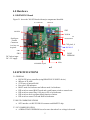
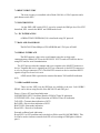
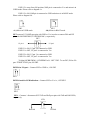
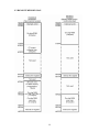
SKP36912G
USER MANUAL
FOR H8/36912F
ON-CHIP FLASH
MICROCONTROLLER
TABLE OF CONTENTS
1.0 INTRODUCTION....................................................................................................2
2.0 KIT CONTENTS......................................................................................................3
2.1 36912G Starter Kit Plus (SKP) Product List.............................. ...................……..3
3.0 SYSTEM REQUIREMENT.....................................................................................3
3.1 Host Computer Requirements................................................................................3
3.2 SKP36912G Board................................................................................................3
3.3 Development Tools...............................................................................................4
3.4 Power Supply........................................................................................................4
3.5 Software Tools…………………….…………………………………………….…….4
4.0 HARDWARE..................................................................................................…......5
4.1 SKP36912G Board.................................................................................…….........5
5.0 SPECIFICATIONS............................................................................……………...5
5.1 General...............................................................................................………….5
5.2 RS-232 Communications.....................................................................………...5
5.3 I2C Communications...............................................................................….…...5
5.4 Power..............................................................................................…………….6
5.5 Low Voltage Detection........................................................................................6
6.0 SKP Functional Blocks............................................................................………......6
7.0 PRINCIPLES OF OPERATION......................................................……………….7
7.1 H8/36912F Microcontroller……….............................................……………...7
7.2 External Low Voltage Detection…………….............................……………….7
7.3 CLOCK CIRCUITRY..........................................................………………….7
7.4 RESET CIRCUITRY..........................................................…………………..8
7.5 NMI CIRCUITRY..........................................................……………………..8
7.6 I2C INTERFACING..........................................................…………………...8
7.7 RAM AND FLASH ROM..........................................................……………...8
7.8 SERIAL INTERFACE..........................................................…………………8
7.9 LEDS and DIP Switches..........................................................………………..8
7.10 EXTERNAL USER INTERFACE.........................................................……..10
8.0 DIP SWITCH & JUMPERS..........................................................………………....10
9.0 APPENDIX..........................................................…………… ........………………12
9.1 BOARD LAYOUT….......................................................…………………12
9.2 EDGE CONNECTOR CN2 PIN OUT................................……………….13
9.3 H8/36912F MEMORY MAP...............................................………..……...14
9.4 SKP36912G SCHEMATICS...............................................……………….15
1
1.0 INTRODUCTION
The H8/36912F Starter Kit Plus (SKP) is a compact system to evaluate MCU
performance for the Renesas H8/300H µTINY family of micro controllers.
The kit also includes sample code, documentation and tutorial to jumpstart development.
It incorporates a programming system for the H8/36912F on-chip FLASH device. It
contains a SOP-32 package H8/36912F microcomputer on the board.
The H8/36912F SKP board adopts the common Hitachi Embedded Workshop (HEW)
version 3.0 that also contains a pure debugger as the user interface.
The diagram below shows the H8/36912F SKP Board:
SKP36912G EVALUATION BOARD
The diagram below shows the physical layout of the SKP: -
2
2.0
Kit Contents
This section describes the contents of the 36912G Starter Kit Plus (SKP) product
package.
When unpacking your kit, please check to see that all products listed below are included.
2.1 36912G Starter Kit Plus (SKP) Product List
Table 2-1 lists the products included in the kit.
Table 2-1 SKP36912G Product List
Product Name Qty Remark
Remark
Product Name
SKP36912G Board
DC jack Male
12mm PCB Spacers
CD-ROM
3.0
Qty
1
1
4
1
H8/36912F Target Board
Jack to connect to power supply
PCB spacers to give balance height for board
a) Manuals –
Quick Start Guide
User Manual
Application Notes
b) H8/36912F Hardware Manual
c) E7 Emulator User manual
d) E7 Emulator connectivity for H8/36912F
manual
e) HEW 3.0 User manual
f) Sample Programs
g) SKP36912G schematic diagram
System Requirement
The following lists the hardware and software products required for using the
SKP36912G.
•
•
•
•
•
Host Computer with available USB port
SKP36912G Board
E7 Emulator
DC Power Supply of 5V ~ 12V
Software Tools (HEW 3.0)
3.1 Host Computer Requirements
The minimum requirement to be able to use the software that comes with the kit is a PC
with an available USB port and Microsoft Windows 98, ME, 2000, or XP operating
system.
3.2 SKP36912G Board
The SKP36912G board provides a compact evaluation and development environment for
the H8/36912F micro controller. It has four switches (pushbutton and DIP), LED’s for
user interface and a 2-pin jumper for current measurement.
3
It also has a low drop out regulator, which regulates up to 12V DC input voltage and
gives 5V output and is capable of supplying output currents up to 300mA, 24C02
EEPROM for RAM backup at low voltage detection and MAX232 for serial
communication.
3.3 Development Tools
E7 Emulator is used as a development tool to execute and debug the user programs on the
SKP.
The diagram below shows how to connect the SKP to a PC using E7 Emulator.
Please see the quick start guide on how to run the SKP using E7 Emulator.
System Configuration with Emulator
3.4 Power Supply
The SKP hardware requires a power supply of +5V DC. Since total power
consumption can vary widely due to external connections, a micro power Low Drop
out Voltage Regulator (LDO) is used with a maximum current rating of 300mA at 5V
DC power supply.
3.5 Software Tools
The High-performance Embedded Workshop (HEW) provides an Integrated
Development Environment (IDE) and Graphical User Interface (GUI) that integrates the
software development tools and provides project management features.
4
4.0 Hardware
4.1 SKP36912G Board
Figure 5-1 shows the 36912G Board with major components identified.
E7 Connector
20K POT
SW2
MAX232
74HC00
JP1 for current
measurement
Serial port
Female
Connector
CN2 pin 4, 6
Low Drop out
Regulator
H8/36912
SW1
Reset Switch SW3
24C02
EEPROM
SW4
DC Jack to input
DC +5V supply
9.8304MHz crystal
LEDs
SKP36912G Board
5.0 SPECIFICATIONS
5.1 GENERAL
• H8/36912F micro controller (using HD64F36912G SOP32 device).
• 8Kbytes of FLASH
• 1536 bytes of internal RAM
• Four user LED indicators.
• BOOT mode Led indicator and a Reset mode Led indicator.
• DIP switch to control BOOT mode and a push button switch to control reset.
• DIP switch to control Port 8 I/O pins as I/O or led indicators.
• DIP switch to check oscillator break function of micon.
• DIP switch to control TxD and RxD led indication.
5.2 RS-232 COMMUNICATIONS
• SCI3 interface via RS-232 DB-9S connector and MAX232 chip.
5.3 I2C COMMUNICATION
• A 2KBit ST24C02 EEPROM is used to store data when Low voltage is detected.
5
5.4 POWER
• 5V DC power supply.
5.5 LOW VOLTAGE DETECTION
• A 20K Pot P1 along with ladder network resistors is used to generate required
voltages for External Low Voltage Detection.
6.0 SKP FUNCTIONAL BLOCKS
The SKP is composed of a H8/36912F single-chip micro-controller, Low Voltage Drop
Out Regulator, 2KBit EEPROM, Serial port, 20K POT for LVD & ADC, Dipswitches for
Oscillator break & Boot/User mode transition, user interface LEDs and E7 Header to
connect with E7 Emulator.
JP1 jumper is used for current measurement of the micon. This jumper is always closed
and opened during current measurement.
The DIP Switch SW1 is used to select the programming mode for the micon i.e., Boot
mode or User mode for programming the FLASH. A reset switch SW3 is also provided
with a reset led indication. SCI3 is used to program the board’s on-chip flash memory
using FDT or it is used for Serial transmission or reception.
6
The DIP Switch SW2 is used to select led indication on OSCBK/PWM1 and
LVD/PWM2 LEDs.
The DIP Switch SW4 is used to connect or disconnect led indication on TxD and RxD
LEDs during serial communication.
Low Voltage Detection is detected using Pot P1 and resistor ladder network. A 2Kbit
EEPROM is used to store data during low voltage detection and recover data stored when
micon operates at normal voltage.
A/D conversion is also carried using the same POT P1. Analog signal is supplied to the
microcontroller by varying POT and digital output is checked on internal registers.
7.0
PRINCIPLES OF OPERATION
The SKP is composed of the following components:
•
•
•
•
•
•
•
•
•
H8/36912F micro controller
External Low Voltage Detection circuitry
Clock circuitry
RESET circuitry
NMI circuitry
I2C Interface
Serial Interface (SCI3)
LED driver
External User Interface
7.1 H8/36912F MICROCONTROLLER
The H8/36912F provides many of the functions required to implement a micro-controller
system on-chip. It has on-chip 8Kbytes of FLASH and 1536 bytes of RAM. It has
additional features of External Low Voltage Detection and Internal RC oscillator backup
on external crystal break.
7.2 EXTERNAL LOW VOLTAGE DETECTION
The External low voltage detection circuitry comprises of a resistor ladder
network. A 20K POT in series with a 1.5K and 3.9K resistors are used to meet the typical
voltage levels for LVD detection at 5V operation.
7.3 CLOCK CIRCUITRY
The clock circuitry comprises the H8/36912F oscillator and a 9.8304MHz
parallel resonating crystal. The system clock output frequency is same as that of internal
RC clock.
A DIP switch SW1.1 is used to indicate the RC oscillator back up on external
crystal break.
7
7.4 RESET CIRCUITRY
The reset circuitry is controlled with a Diode 1N4148, a 0.22uF capacitor and a
push button switch SW3.
7.5 NMI CIRCUITRY
On the SKP a DIP switch SW1.2 is used to control the NMI pin level. For FDT
download, SW1 controls the BOOT and USER mode levels.
7.6 I2C INTERFACING
A 2KBit ST24C02 EEPROM (U4) is interfaced using I2C protocol.
7.7 RAM AND FLASH ROM
The H8/36912F has 8Kbytes of FLASH ROM and 1536 bytes of RAM.
7.8 SERIAL INTERFACE
The SKP supports a three-wire serial channel using the on-chip serial
communications channel (SCI3) on the H8/36912F. SCI3 is used to FLASH the device
using FDT and for serial communication.
The SCI3 port provides the transmit and receive signals to the MAX232 transceiver
device. Transmit and receive signals from SCI3 are connected via the RS232 transceiver
to a 9-way D-type connector (CN3). The MAX232 transceiver device translates RS232
signals to logic levels and vice versa.
A DIP switch SW4 is provided to connect/disconnect TxD and RxD indication
led’s.
7.9 LEDS and DIP Switches
There are four LED’s on the SKP that are available to the user. Led OSCBK /
PWM1 can be driven using Port 84 of the H8/36912F and SW2 pin 1.
Power = Power of Target board indication.
OSCBK/PWM1 LED = Oscillator Break or PWM of Timer W indication.
LVD/PWM2 LED = Low voltage Detection or PWM of Timer W indication.
TxD LED = Transmit data indication of SCI3.
RxD LED = Receive data indication of SCI3.
BOOT LED= Boot mode indication.
Reset LED = Reset level indication.
External oscillator break indication: Keep SW2.1 in OFF condition and write high on P84 to turn ON OSCBK/PWM1. This
led can be used to indicate external clock fail or lit according to PWM pulse width on
port 8.
8
To disconnect OSCBK/PWM1 led indication, turn ON SW2.2 pin 1(i.e., connect SW2.1
pin to GND).
Low Voltage Detection: Turn ON SW2.2 to use LVD/PWM2 led. This led can be used to indicate low voltage
detection or lit according to PWM pulse width on port 8.
To disconnect LVD/PWM2 led indication, turn ON SW2.1 pin 1(i.e., connect SW2.1 pin
to GND).
SCI3: Two led’s TxD and RxD are used to indicate transmit and receive operations of SCI3
during serial communication. Provision to connect/disconnect led indication for these I/O
lines is provided using a DIP Switch SW4.
Turn ON SW4.1 to use RxD led indication. Turn ON SW4.2 to use TxD led indication.
Turn OFF the switch to disconnect the Rx and Tx I/O lines led indication.
LED
Oscbk/PWM1
Oscbk/PWM1
Oscbk/PWM1
Oscbk/PWM1
LVD/PWM 2
LVD/PWM 2
LVD/PWM 2
LVD/PWM 2
SW1.1
Position
ON
OFF
ON
OFF
SW1.1
Position
---------
SW1.2
Position
ON
OFF
BOOT
TxD
RxD
RESET
SW2.2
Position
OFF
OFF
ON
ON
SW2.1
Position
OFF
OFF
ON
ON
SW4.1
Position
--------ON
OFF
SW4.2
Position
ON
OFF
---------
P84
Value
0
1
0/1
0/1
P83
Value
1
0
1/0
1/0
LED
Status
OFF
ON
OFF
OFF
LED
Status
ON
OFF
OFF
OFF
SOP-32
pin
29
29
29
29
SOP-32
pin
28
28
28
28
LED Status
SOP – 32 PIN
ON
OFF
13
13
LED Status
ON
OFF
ON
OFF
SOP – 32
PIN
24
24
23
23
SW3 Position
LED Status
SOP – 32 PIN
0
1
ON
OFF
7
7
9
Pin Function
P84/FTIOD
P84/FTIOD
P84/FTIOD
P84/FTIOD
Pin Function
P83/FTIOC
P83/FTIOC
P83/FTIOC
P83/FTIOC
PIN
FUNCTION
NMI
NMI
PIN
FUNCTION
TxD
TxD
RxD
RxD
PIN
FUNCTION
RES
RES
7.11 EXTERNAL USER INTERFACE
The external user interface makes all H8/36912F signals available to the user
consistent.
The external user interface consists of rows of 12 pin connectors. The diagram indicates
which label refers to which row of pins.
The external user interface consists of a 26-pin connector. Commonly available 2.54mm
(0.100 inch) pitch male headers.
Micon I/O pins are connected to CN2 connector so that I/O lines can be accessed with
ease. Pin numbering for starting and ending pins are given for easy use.
Provision for user to give separate supply to A/D section Avcc pin is provided by pulling
this pin on to I/O expander CN2.Avcc PIN 4 is shorted with Vcc PIN 6 via a 2-pin
jumper. User can remove the jumper and give separate supply to Avcc pin.
Provision for user to measure the current drawn by the micon is provided using jumper
JP1. This jumper is opened when user wants to measure the current. An ammeter is used
to measure the current drawn.
8.0 DIP SWITCH & JUMPER
SW1 contains oscillator break connection and boot mode connection.
SW1
OSC2 pin
NMI pin
SW1.1 connects the OSC2 pin to crystal.
If SW1.1 is towards ON position, OSC2 is connected to crystal and micon is
operating on external crystal. Please refer to diagram 4.a.
If SW1.1 is away from ON position, OSC2 is not connected to crystal. Please
refer to diagram 4.b.
4.a) SW1
External crystal is connected
4.b) SW1
External crystal disconnected
SW1.2 connects the NMI pin to GND or Vcc. It is used for BOOT/USER mode selection.
10
If SW1.2 is away from ON position, NMI pin is connected to Vcc and micon is in
USER mode. Please refer to diagram 4.c.
If SW1.2 is ON, NMI pin is connected to GND and micon is in BOOT mode.
Please refer to diagram 4.d.
SW1
4.c) Micon in USER mode.
SW1
4.d) Micon in BOOT mode.
SW2 connects U5 NAND gate pins with GND or Vcc in order to connect P84 and P83
pins with OSCBK/PWM1, LVD/PWM2 led’s, respectively.
SW2
U5 pin 4
U5 pin 2
If SW2.1 is ON, U5 pin 4 is connected to GND.
If SW2.1 is OFF, U5 pin 4 is connected to Vcc.
If SW2.2 is ON, U5 pin 2 is connected to GND.
If SW2.2 is OFF, U5 pin 2 is connected to Vcc.
To light OSCBK/PWM1, LVD/PWM2 led’s “OFF” SW2. To use P83, P84 as I/O
port/ FTIOD/ FTIOC pin, ON SW2.
P83/P84 as I/O port: - Connect SW2 to GND i.e., ON SW2
SW2
P83/P84 used for LED indication: - Connect SW2 to Vcc i.e., OFF SW2.
SW2
SW4: - Connects / disconnects SCI3 TxD and RxD port pins with TxD and RxD LEDs,
respectively.
SW4
RxD led
TxD led
11
ON
OFF
TxD and RxD led’s connected
TxD and RxD led’s disconnected
JUMPERS
JP1 is a 2-pin jumper, which is placed in series with Vcc path of H8/36912F micro
controller for current measurement.
This jumper is shorted by default. It is opened to measure current drawn by the micro
controller.
9.0 APPENDIX
9.1 BOARD LAYOUT
E7 Connector
20K POT
2-way DIP
switch
MAX232
74HC00
RS-232
D-Type
Connector
Reset switch
I/O Expander
LDO
H8/36912
2-way DIP
switch
24C02
EEPROM
DC JACK
9.8304MHz
crystal
12
LEDs
9.2 EDGE CONNECTOR CN2 PINOUT
Shorted to
give Avcc
reference
voltage of Vcc
13
9.3 H8/36912F MEMORY MAP
14
9.4 SKP 36912G SCHEMATICS
15