1
DEC 3000 300/400/500/600/700
/800/900 AXP Models
System Programmer’s Manual
Order Number: EK–D3SYS–PM. B01
This manual describes the behavior of DEC 3000 AXP architecture as it
pertains to writing system-level software, such as operating systems and
drivers.
This manual describes the behavior of 300, 300L, 300X, 300LX, 400,
400S, 500, 500S, 500X, 600, 600S, 700, 800, 800S, and 900 models.
Revision/Update Information:
This is a revised manual.
First Printing, September 1993
Revised, July 1994
Digital Equipment Corporation makes no representations that the use of its products in the
manner described in this publication will not infringe on existing or future patent rights, nor do
the descriptions contained in this publication imply the granting of licenses to make, use, or sell
equipment or software in accordance with the description.
Possession, use, or copying of the software described in this publication is authorized only pursuant
to a valid written license from Digital or an authorized sublicensor.
© Digital Equipment Corporation 1994. All Rights Reserved.
The following are trademarks of Digital Equipment Corporation: Alpha AXP, AXP, Bookreader,
DEC, DECaudio, DECchip, DECconnect, DEC GKS, DEC PHIGS, DECsound, DECwindows,
DECwindows Motif, DECwindows Mail, DECwrite, DELNI, Digital, OpenVMS, OpenVMS AXP,
RX26, ScriptPrinter, ThinWire, TURBOchannel, ULTRIX, VAX, VAX DOCUMENT, VAXcluster,
VAXstation, and the Digital logo.
Other trademarks are as follows:
ISDN is a registered trademark of Fujitsu Network Switching of America.
All other trademarks and registered trademarks are the property of their respective holders.
FCC Notice: This equipment has been tested and found to comply with the limits for a Class
A digital device, pursuant to Part 15 of the FCC Rules. These limits are designed to provide
reasonable protection against harmful interference when the equipment is operated in a commercial
environment. This equipment generates, uses, and can radiate radio frequency energy and, if not
installed and used in accordance with the instruction manual, may cause harmful interference to
radio communications. Operation of this equipment in a residential area is likely to cause harmful
interference, in which case users will be required to correct the interference at their own expense.
S2652
This document was prepared using VAX DOCUMENT Version 2.1.
Contents
Preface . . . . . . . . . . . . . . . . . . . . . . . . . . . . . . . . . . . . . . . . . . . . . . . . . . . . . . . . . . . .
xiii
1 Introduction to the DEC 3000 Models 300/400/500/600/700/800/900
AXP
.
.
.
.
.
.
.
.
.
.
.
.
.
.
.
.
.
.
.
.
.
.
.
.
.
.
.
.
.
.
.
.
.
.
.
.
.
.
.
.
.
.
.
.
.
.
.
.
.
.
.
.
.
.
.
.
.
.
.
.
.
.
.
.
.
.
1–2
1–6
1–9
1–13
1–16
1–19
Memory Alignment . . . . . . . . . . . . . . . . . . . . . . . . . . . . . . . .
Memory Address Spaces . . . . . . . . . . . . . . . . . . . . . . . . . . . . .
I/O Address Spaces . . . . . . . . . . . . . . . . . . . . . . . . . . . . . . . .
TURBOchannel Interface Bit Decode Map for I/O Addresses .
CPU Registers . . . . . . . . . . . . . . . . . . . . . . . . . . . . . . . . . . . .
ABOX Control Register (ABOX_CTL) . . . . . . . . . . . . . . .
Bus Interface Unit Control Register (BIU_CTL) . . . . . . .
Bcache Tag Space . . . . . . . . . . . . . . . . . . . . . . . . . . . . . . . . . .
.
.
.
.
.
.
.
.
.
.
.
.
.
.
.
.
.
.
.
.
.
.
.
.
.
.
.
.
.
.
.
.
.
.
.
.
.
.
.
.
.
.
.
.
.
.
.
.
.
.
.
.
.
.
.
.
.
.
.
.
.
.
.
.
.
.
.
.
.
.
.
.
.
.
.
.
.
.
.
.
2–2
2–2
2–3
2–7
2–9
2–9
2–11
2–12
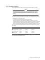
3.1
I/O Interface Register Map (300 Models) . . . . . . . . . . . . . . . . . . . . . . . . . .
3.2
I/O Control and Status Registers (300 Models) . . . . . . . . . . . . . . . . . . . . .
3.2.1
Interrupt Register (IR)—1.E000.0000 . . . . . . . . . . . . . . . . . . . . . . . . .
3.2.2
TURBOchannel Control and Status Register (TCSR)—1.E000.0008 . .
3.2.3
Memory Configuration Register (MCR)—1.E000.0010 . . . . . . . . . . . . .
3.2.3.1
MCR Use and Format . . . . . . . . . . . . . . . . . . . . . . . . . . . . . . . . . .
3.2.3.2
Memory Configuring Using the MCR . . . . . . . . . . . . . . . . . . . . . . .
3.2.4
Diagnostic LED Register (LED)—1.E000.0018 . . . . . . . . . . . . . . . . . . .
3.3
TURBOchannel Interface Registers (400/500/600/700/800/900 Models) . . .
3.3.1
I/O Slot Configuration (IOSLOT) Register—1.C200.0000, 1.C200.0020
(Alternate address) . . . . . . . . . . . . . . . . . . . . . . . . . . . . . . . . . . . . . . . .
3.3.2
TURBOchannel Configuration (TCCONFIG)
Register—1.C200.0008 . . . . . . . . . . . . . . . . . . . . . . . . . . . . . . . . . . . . .
3.3.3
Failing Address Register (FADR)—1.C200.0010 . . . . . . . . . . . . . . . . . .
3.3.4
TURBOchannel Error Register (TCEREG)—1.C200.0018 . . . . . . . . . .
3.3.5
Memory Configuration Registers . . . . . . . . . . . . . . . . . . . . . . . . . . . . .
3.3.6
Interrupt Mask Register (IMR)—1.C240.0000 . . . . . . . . . . . . . . . . . . .
3.3.7
Interrupt Register (IR)—1.D480.0000 . . . . . . . . . . . . . . . . . . . . . . . . .
3.3.8
Scatter/Gather Map . . . . . . . . . . . . . . . . . . . . . . . . . . . . . . . . . . . . . . .
3–1
3–2
3–3
3–4
3–5
3–5
3–5
3–7
3–8
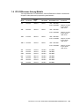
1.1
1.2
1.3
1.4
1.5
1.6
System Description: 300 Models . . .
System Description: 400 Models . . .
System Description: 500 Models . . .
System Description: 600/700 Models
System Description: 800/900 Models
CPU Differences Among Models . . . .
.
.
.
.
.
.
.
.
.
.
.
.
.
.
.
.
.
.
.
.
.
.
.
.
.
.
.
.
.
.
.
.
.
.
.
.
.
.
.
.
.
.
.
.
.
.
.
.
.
.
.
.
.
.
.
.
.
.
.
.
.
.
.
.
.
.
.
.
.
.
.
.
.
.
.
.
.
.
.
.
.
.
.
.
.
.
.
.
.
.
.
.
.
.
.
.
.
.
.
.
.
.
.
.
.
.
.
.
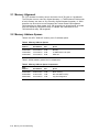
2 Memory and I/O Addressing
2.1
2.2
2.3
2.4
2.5
2.5.1
2.5.2
2.6
3 TURBOchannel I/O Registers
3–10
3–12
3–13
3–14
3–15
3–15
3–17
3–19
iii
3.3.9
TURBOchannel Reset Register (TCRESET)—1.C2A0.0000 . . . . . . . . .
3–19
4 Address ASIC Registers (400/500/600/700/800/900 Models)
4.1
4.1.1
4.1.2
4.1.3
4.1.4
4.2
4.2.1
4.2.2
4.2.3
Memory Configuration Registers . . . . . . . . . . . . . . . . . . . . .
Operation . . . . . . . . . . . . . . . . . . . . . . . . . . . . . . . . . . . .
Boot Time . . . . . . . . . . . . . . . . . . . . . . . . . . . . . . . . . . . .
Improper Configuration . . . . . . . . . . . . . . . . . . . . . . . . .
Disabling Memory . . . . . . . . . . . . . . . . . . . . . . . . . . . . .
Victim Address Register and Counter Register (VAR/VACR)
Initialization . . . . . . . . . . . . . . . . . . . . . . . . . . . . . . . . .
Writing the VACR . . . . . . . . . . . . . . . . . . . . . . . . . . . . .
Reading the VAR . . . . . . . . . . . . . . . . . . . . . . . . . . . . . .
.
.
.
.
.
.
.
.
.
.
.
.
.
.
.
.
.
.
.
.
.
.
.
.
.
.
.
.
.
.
.
.
.
.
.
.
.
.
.
.
.
.
.
.
.
.
.
.
.
.
.
.
.
.
.
.
.
.
.
.
.
.
.
.
.
.
.
.
.
.
.
.
.
.
.
.
.
.
.
.
.
.
.
.
.
.
.
.
.
.
.
.
.
.
.
.
.
.
.
4–2
4–2
4–3
4–4
4–4
4–6
4–6
4–6
4–6
5 Scatter/Gather (Virtual DMA) RAMs (400/500/600/700/800/900 Models)
5.1
5.2
5.3
Scatter/Gather Register Map . . . . . . . . . . . . . . . . . . . . . . . . . . . . . . . . . . .
Organization . . . . . . . . . . . . . . . . . . . . . . . . . . . . . . . . . . . . . . . . . . . . . . .
Writing and Reading Scatter/Gather Map Entries . . . . . . . . . . . . . . . . . . .
5–1
5–2
5–3
6 CXTurbo Graphics Subsystem: 300/500 Models
Comparison of Features . . . . . . . . . . . . . . . . . . . . . . . . . . . . . .
CXTurbo Address Map . . . . . . . . . . . . . . . . . . . . . . . . . . . . . . .
Frame Buffer Control Registers . . . . . . . . . . . . . . . . . . . . . . . .
SFB ASIC Functions . . . . . . . . . . . . . . . . . . . . . . . . . . . . . . . .
Mode Register . . . . . . . . . . . . . . . . . . . . . . . . . . . . . . . . . .
Planemask Register . . . . . . . . . . . . . . . . . . . . . . . . . . . . . .
Raster Op Register . . . . . . . . . . . . . . . . . . . . . . . . . . . . . . .
PixelMask Register . . . . . . . . . . . . . . . . . . . . . . . . . . . . . .
Foreground and Background Registers . . . . . . . . . . . . . . .
PixelShift Register . . . . . . . . . . . . . . . . . . . . . . . . . . . . . . .
Address Register . . . . . . . . . . . . . . . . . . . . . . . . . . . . . . . .
DEEP Register . . . . . . . . . . . . . . . . . . . . . . . . . . . . . . . . . .
START, BCONT, VIDEO_VALID, ENABLE_INTERRUPT,
CLEAR_INTERRUPT Registers . . . . . . . . . . . . . . . . . . . . .
6.4.10
Video Timing Registers . . . . . . . . . . . . . . . . . . . . . . . . . . .
6.4.10.1
Video Refresh Counter Register . . . . . . . . . . . . . . . . . .
6.4.10.2
Video Base Address Register . . . . . . . . . . . . . . . . . . . .
6.4.10.3
Horizontal Setup Register . . . . . . . . . . . . . . . . . . . . . .
6.4.10.4
Vertical Timing Parameters Register . . . . . . . . . . . . . .
6.4.11
TCCLK COUNT, VIDCLK_COUNT Registers . . . . . . . . . .
6.5
Bt459 RAMDAC . . . . . . . . . . . . . . . . . . . . . . . . . . . . . . . . . . . .
6.6
System FEPROM (500 Models) . . . . . . . . . . . . . . . . . . . . . . . .
.
.
.
.
.
.
.
.
.
.
.
.
.
.
.
.
.
.
.
.
.
.
.
.
.
.
.
.
.
.
.
.
.
.
.
.
.
.
.
.
.
.
.
.
.
.
.
.
.
.
.
.
.
.
.
.
.
.
.
.
.
.
.
.
.
.
.
.
.
.
.
.
.
.
.
.
.
.
.
.
.
.
.
.
.
.
.
.
.
.
.
.
.
.
.
.
.
.
.
.
.
.
.
.
.
.
.
.
6–2
6–3
6–5
6–7
6–9
6–12
6–13
6–14
6–14
6–15
6–15
6–15
.
.
.
.
.
.
.
.
.
.
.
.
.
.
.
.
.
.
.
.
.
.
.
.
.
.
.
.
.
.
.
.
.
.
.
.
.
.
.
.
.
.
.
.
.
.
.
.
.
.
.
.
.
.
.
.
.
.
.
.
.
.
.
.
.
.
.
.
.
.
.
.
.
.
.
.
.
.
.
.
.
6–16
6–16
6–17
6–17
6–18
6–18
6–19
6–20
6–24
IOCTL Address Map . . . . . . . . . . . . . . . . . . . . . . . . . . . . . . . . . . . . .
System FEPROM . . . . . . . . . . . . . . . . . . . . . . . . . . . . . . . . . . . . . . . .
IOCTL Registers Address Map . . . . . . . . . . . . . . . . . . . . . . . . . . . . . .
LANCE DMA Pointer Register (LDP)—1.A004.0020/1.E004.0020
Communication Port 1 Transmit DMA
Pointer—1.A004.0030/1.E004.0030 . . . . . . . . . . . . . . . . . . . . . . . .
.
.
.
.
.
.
.
.
.
.
.
.
.
.
.
.
7–3
7–4
7–5
7–7
....
7–7
6.1
6.2
6.3
6.4
6.4.1
6.4.2
6.4.3
6.4.4
6.4.5
6.4.6
6.4.7
6.4.8
6.4.9
7 IOCTL ASIC and System Registers
7.1
7.2
7.3
7.3.1
7.3.2
iv
7.3.3
7.3.4
7.3.5
7.3.6
7.3.7
7.3.8
7.3.9
7.3.10
7.3.11
7.3.12
7.3.13
7.3.14
7.3.15
7.3.16
7.3.17
7.3.18
7.3.19
7.4
7.5
7.6
7.7
7.8
7.8.1
7.8.2
Communication Port 1 Receive DMA
Pointer—1.A004.0040/1.E004.0040 . . . . . . . . . . . . . . . . . . . . . . .
Printer Port Transmit DMA Pointer—NA/ 1.E004.0050 . . . . . . .
Printer Port Receive DMA Pointer—NA/1.E004.0060 . . . . . . . .
ISDN Transmit DMA Pointer—1.A004.0080/1.E004.0080 . . . . .
ISDN Transmit DMA Buffer Pointer—1.A004.0090/1.E004.0090
ISDN Receive DMA Pointer—1.A004.00A0/1.E004.00A0 . . . . . .
ISDN Receive DMA Buffer Pointer—1.A004.00B0/1.E004.00B0 .
Data buffers
3-0—1.A004.00C0-1.A004.00F0/1.E004.00C0-1.E004.00F0 . . . . .
System Support Register—1.A004.0100/1.E004.0100 . . . . . . . . .
System Interrupt Register (SIR)—1.A004.0110/1.E004.0110 . . .
System Interrupt Mask Register—1.A004.0120/1.E004.0120 . . .
System Address Register—1.A004.0130/1.E004.0130 . . . . . . . . .
ISDN Data Transmit Register—1.A004.0140/1.E004.0140 . . . . .
ISDN Data Receive Register—1.A004.0150/1.E004.0150 . . . . . .
LANCE I/O Slot Register—1.A004.0160/1.E004.0160 . . . . . . . . .
SCC-0 DMA Slot Register—1.A004.0180/1.E004.0180 . . . . . . . .
SCC-1 DMA Slot Register—1.A004.0190/1.E004.0190 . . . . . . . .
Ethernet Station Address ROM Addresses . . . . . . . . . . . . . . . . . . . .
LANCE Register Addresses . . . . . . . . . . . . . . . . . . . . . . . . . . . . . . .
SCC Register Addresses . . . . . . . . . . . . . . . . . . . . . . . . . . . . . . . . . .
RTC Register Addresses . . . . . . . . . . . . . . . . . . . . . . . . . . . . . . . . . .
ISDN Register Addresses . . . . . . . . . . . . . . . . . . . . . . . . . . . . . . . . .
ISDN Register Addresses (300 Models) . . . . . . . . . . . . . . . . . . .
ISDN Register Addresses (400/500/600/700/800/900 Models) . . .
.
.
.
.
.
.
.
.
.
.
.
.
.
.
.
.
.
.
.
.
.
.
.
.
.
.
.
.
.
.
.
.
.
.
.
7–7
7–8
7–8
7–8
7–8
7–9
7–9
.
.
.
.
.
.
.
.
.
.
.
.
.
.
.
.
.
.
.
.
.
.
.
.
.
.
.
.
.
.
.
.
.
.
.
.
.
.
.
.
.
.
.
.
.
.
.
.
.
.
.
.
.
.
.
.
.
.
.
.
.
.
.
.
.
.
.
.
.
.
.
.
.
.
.
.
.
.
.
.
.
.
.
.
.
7–9
7–10
7–12
7–15
7–15
7–16
7–16
7–16
7–17
7–17
7–18
7–21
7–21
7–23
7–24
7–24
7–26
...
...
...
8–2
8–3
8–4
...
...
8–7
8–8
...
8–9
...
8–10
.
.
.
.
.
.
.
.
.
.
.
.
8–11
8–12
8–13
8–14
.
.
.
.
.
.
.
.
.
.
.
.
.
.
.
.
.
.
.
.
.
9–2
9–3
9–3
9–3
9–4
9–5
9–5
8 TURBOchannel Dual SCSI ASIC
8.1
8.2
8.2.1
8.2.2
8.2.3
8.2.4
8.2.5
8.2.6
8.3
8.4
8.5
TURBOchannel Dual SCSI Address Map . . . . . . . . . . . . . . . . . . . . . . .
Internal Registers . . . . . . . . . . . . . . . . . . . . . . . . . . . . . . . . . . . . . . . .
Control Interrupt Register (CIR)—1.8004.0000/1.C004.0000 . . . . .
Interrupt Mask Enable Register
(IMER)—1.8004.0004/1.C004.0004 . . . . . . . . . . . . . . . . . . . . . . . . .
SCSI[x] DMA Address Register (SDAx)—1.8004.1x00/1.C004.1x00
SCSI[x] DMA Interrupt Control Register
(DICx0)—1.8004.1x04/1.C004.1x04 . . . . . . . . . . . . . . . . . . . . . . . . .
SCSI[x] DMA Unaligned Data[0]
(DUDx0)—1.8004.1x08/1.C004.1x08 . . . . . . . . . . . . . . . . . . . . . . . .
SCSI[x] DMA Unaligned Data[1]
(DUDx1)—1.8004.1x0C/1.C004.1x0C . . . . . . . . . . . . . . . . . . . . . . .
NCR 53C94 Registers (300/400/500 Models) . . . . . . . . . . . . . . . . . . . . .
NCR 53CF94-2 Registers (600/700/800/900 Models) . . . . . . . . . . . . . . .
DMA buffers . . . . . . . . . . . . . . . . . . . . . . . . . . . . . . . . . . . . . . . . . . . .
9 I/O Programming
9.1
9.2
9.2.1
9.2.2
9.3
9.4
9.4.1
I/O Read and Write Restrictions . . . . . . . . . . . . . . .
DMA . . . . . . . . . . . . . . . . . . . . . . . . . . . . . . . . . . . .
Physical DMA . . . . . . . . . . . . . . . . . . . . . . . . . .
Virtual DMA (400/500/600/700/800/900 Models) .
Interrupt Handling During I/O Operations . . . . . . .
TURBOchannel Usage (System-Specific) . . . . . . . . .
DMA Size . . . . . . . . . . . . . . . . . . . . . . . . . . . . . .
.
.
.
.
.
.
.
.
.
.
.
.
.
.
.
.
.
.
.
.
.
.
.
.
.
.
.
.
.
.
.
.
.
.
.
.
.
.
.
.
.
.
.
.
.
.
.
.
.
.
.
.
.
.
.
.
.
.
.
.
.
.
.
.
.
.
.
.
.
.
.
.
.
.
.
.
.
.
.
.
.
.
.
.
.
.
.
.
.
.
.
.
.
.
.
.
.
.
v
DMA Arbitration . . . . . . . . . . . . . . . . . . . . . . . . . . . . . . . . . . . . . . . .
DMA Arbitration (300 Models) . . . . . . . . . . . . . . . . . . . . . . . . . . .
DMA Arbitration (400/500/600/700/800/900 Models) . . . . . . . . . .
I/O Timeout . . . . . . . . . . . . . . . . . . . . . . . . . . . . . . . . . . . . . . . . . . . .
I/O Conflicts . . . . . . . . . . . . . . . . . . . . . . . . . . . . . . . . . . . . . . . . . . . .
Masked I/O Read Operations . . . . . . . . . . . . . . . . . . . . . . . . . . . . . . .
300 Models: Masked I/O Read Operations with a Non-Zero Byte
Mask . . . . . . . . . . . . . . . . . . . . . . . . . . . . . . . . . . . . . . . . . . . . . .
9.4.5.2
400/500/600/700/800/900 Models: I/O Read Operations with a
Non-Zero Byte Mask . . . . . . . . . . . . . . . . . . . . . . . . . . . . . . . . . .
9.5
JUNKIO Subsystem . . . . . . . . . . . . . . . . . . . . . . . . . . . . . . . . . . . . . . . . .
9.5.1
IOCTL ASIC Overview . . . . . . . . . . . . . . . . . . . . . . . . . . . . . . . . . . . .
9.5.2
I/O Programming and System FEPROM . . . . . . . . . . . . . . . . . . . . . .
9.5.2.1
Ethernet Station Address ROM . . . . . . . . . . . . . . . . . . . . . . . . . .
9.5.2.2
LANCE Interface . . . . . . . . . . . . . . . . . . . . . . . . . . . . . . . . . . . . .
9.5.2.3
LANCE DMA . . . . . . . . . . . . . . . . . . . . . . . . . . . . . . . . . . . . . . . .
9.5.2.4
Serial Communications Controller (SCC) . . . . . . . . . . . . . . . . . . .
9.5.2.5
DMA for Communication Transmit Port and Printer Port . . . . . .
9.5.2.6
DMA for Communication Receive Port and Printer Port . . . . . . .
9.5.2.7
Real-Time Clock (RTC) . . . . . . . . . . . . . . . . . . . . . . . . . . . . . . . . .
9.5.2.8
79C30A (ISDN/audio) Interface . . . . . . . . . . . . . . . . . . . . . . . . . .
9.5.2.9
ISDN DMA . . . . . . . . . . . . . . . . . . . . . . . . . . . . . . . . . . . . . . . . .
9.5.2.10
Diagnostic LEDs (400/500/600/700/800/900 Models) . . . . . . . . . . .
9.6
SCSI Interface . . . . . . . . . . . . . . . . . . . . . . . . . . . . . . . . . . . . . . . . . . . . .
9.6.1
SCSI Interface: Differences Among Models . . . . . . . . . . . . . . . . . . . .
9.6.2
Dual SCSI ASIC Configuration . . . . . . . . . . . . . . . . . . . . . . . . . . . . .
9.6.3
NCR 53C94 Configuration and Programming (300/400/500 Models) . .
9.6.4
53CF94-2 Configuration and Programming (600/700/800/900
Models) . . . . . . . . . . . . . . . . . . . . . . . . . . . . . . . . . . . . . . . . . . . . . . .
9.6.5
Initiation of DMA Transfers . . . . . . . . . . . . . . . . . . . . . . . . . . . . . . . .
9.6.5.1
Unaligned DMA Write Operation . . . . . . . . . . . . . . . . . . . . . . . . .
9.6.5.2
Interrupt Service . . . . . . . . . . . . . . . . . . . . . . . . . . . . . . . . . . . . .
9.6.6
Aborting Transactions . . . . . . . . . . . . . . . . . . . . . . . . . . . . . . . . . . . .
9.4.2
9.4.2.1
9.4.2.2
9.4.3
9.4.4
9.4.5
9.4.5.1
.
.
.
.
.
.
9–5
9–5
9–6
9–6
9–7
9–7
.
9–7
.
.
.
.
.
.
.
.
.
.
.
.
.
.
.
.
.
.
9–7
9–8
9–8
9–9
9–9
9–9
9–10
9–10
9–11
9–12
9–13
9–13
9–14
9–14
9–15
9–15
9–15
9–16
.
.
.
.
.
9–16
9–18
9–19
9–19
9–19
.
.
.
.
.
.
.
.
.
.
10–2
10–4
10–5
10–12
10–14
10–15
10–15
10–16
10–16
10–17
10 Hardware Exceptions and Interrupts
10.1
10.2
10.3
10.4
10.5
10.6
10.7
10.8
10.8.1
10.8.2
vi
Sources of Errors and Interrupts . . . . . . . . . . . . . . . . .
Behavior of System Hardware Under Errors . . . . . . . .
System Error/Interrupt Matrix . . . . . . . . . . . . . . . . . .
Dual SCSI Error/Interrupt Matrix . . . . . . . . . . . . . . . .
Error Insertion for Testing Purposes . . . . . . . . . . . . . .
Assignment of CPU Interrupt Pins . . . . . . . . . . . . . . .
Error Handling and Recovery . . . . . . . . . . . . . . . . . . .
PAL Recovery Algorithms for Selected Errors . . . . . . .
Bcache Tag Error on DMA Read/Write . . . . . . . . . .
Bcache Tag Parity Error on CPU Reference, LDxL,
.....
.....
.....
.....
.....
.....
.....
.....
.....
STxC
.
.
.
.
.
.
.
.
.
.
.
.
.
.
.
.
.
.
.
.
.
.
.
.
.
.
.
.
.
.
.
.
.
.
.
.
.
.
.
.
.
.
.
.
.
.
.
.
.
.
.
.
.
.
.
.
.
.
.
.
.
.
.
.
.
.
.
.
.
.
.
.
.
.
.
.
.
.
.
.
.
.
.
.
.
.
.
.
.
.
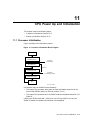
11 CPU Power Up and Initialization
11.1
Processor initialization . . . . . .
11.1.1
Power-On Reset Sequence
11.1.2
SROM Sequence . . . . . . . .
11.1.3
SYSROM Sequence . . . . .
11.2
Bcache Initialization . . . . . . .
.
.
.
.
.
.
.
.
.
.
.
.
.
.
.
.
.
.
.
.
.
.
.
.
.
.
.
.
.
.
.
.
.
.
.
.
.
.
.
.
.
.
.
.
.
.
.
.
.
.
.
.
.
.
.
.
.
.
.
.
.
.
.
.
.
.
.
.
.
.
.
.
.
.
.
.
.
.
.
.
.
.
.
.
.
.
.
.
.
.
.
.
.
.
.
.
.
.
.
.
.
.
.
.
.
.
.
.
.
.
.
.
.
.
.
.
.
.
.
.
.
.
.
.
.
.
.
.
.
.
.
.
.
.
.
.
.
.
.
.
.
.
.
.
.
.
.
.
.
.
.
.
.
.
.
.
.
.
.
.
.
.
.
.
.
.
.
.
.
.
11–1
11–2
11–2
11–2
11–3
Power-Up Initialization Code
the Console . . . . . . . . . . . . . .
Extended Self-Test/Utilities .
PALcode . . . . . . . . . . . . . . . .
the MIPS Emulator . . . . . . .
.
.
.
.
.
.
.
.
.
.
.
.
.
.
.
.
.
.
.
.
.
.
.
.
.
.
.
.
.
.
.
.
.
.
.
.
.
.
.
.
.
.
.
.
.
.
.
.
.
.
.
.
.
.
.
.
.
.
.
.
.
.
.
.
.
.
.
.
.
.
.
.
.
.
.
.
.
.
.
.
.
.
.
.
.
.
.
.
.
.
.
.
.
.
.
.
.
.
.
.
.
.
.
.
.
.
.
.
.
.
.
.
.
.
.
.
.
.
.
.
.
.
.
.
.
12–3
12–4
12–4
12–4
12–5
DEC 3000 AXP Firmware ROM Format . . . . . . . . . . . . . . . . . . . . . . . . . .
System and I/O ROM Contents . . . . . . . . . . . . . . . . . . . . . . . . . . . . . . . . .
System ROM Format . . . . . . . . . . . . . . . . . . . . . . . . . . . . . . . . . . . . . . . . .
13–1
13–1
13–3
12 Firmware: Overview
12.1
12.2
12.3
12.4
12.5
Overview
Overview
Overview
Overview
Overview
of
of
of
of
of
13 DEC 3000 AXP Firmware ROMs
13.1
13.2
13.3
14 Powerup Initialization and Firmware Entry
14.1
14.2
14.3
14.4
14.5
14.5.1
14.5.2
14.5.3
14.5.4
Power-On Initialization Flow . . . . . . . . . . . . . . . . .
Power-On Output . . . . . . . . . . . . . . . . . . . . . . . . . .
Map of Memory Following Power-Up Initialization
Machine State Following Power-Up Initialization .
System Firmware Entry . . . . . . . . . . . . . . . . . . . . .
Restart . . . . . . . . . . . . . . . . . . . . . . . . . . . . . . .
Boot . . . . . . . . . . . . . . . . . . . . . . . . . . . . . . . . .
Halt . . . . . . . . . . . . . . . . . . . . . . . . . . . . . . . . .
Reentry Control . . . . . . . . . . . . . . . . . . . . . . . .
.
.
.
.
.
.
.
.
.
.
.
.
.
.
.
.
.
.
.
.
.
.
.
.
.
.
.
.
.
.
.
.
.
.
.
.
.
.
.
.
.
.
.
.
.
.
.
.
.
.
.
.
.
.
.
.
.
.
.
.
.
.
.
.
.
.
.
.
.
.
.
.
.
.
.
.
.
.
.
.
.
.
.
.
.
.
.
.
.
.
.
.
.
.
.
.
.
.
.
.
.
.
.
.
.
.
.
.
.
.
.
.
.
.
.
.
.
.
.
.
.
.
.
.
.
.
.
.
.
.
.
.
.
.
.
.
.
.
.
.
.
.
.
.
.
.
.
.
.
.
.
.
.
.
.
.
.
.
.
.
.
.
14–1
14–5
14–6
14–7
14–9
14–9
14–9
14–12
14–13
.
.
.
.
.
.
.
.
.
.
.
.
.
.
.
.
.
.
.
.
.
.
.
.
.
.
.
.
.
.
.
.
.
.
.
.
.
.
.
.
.
.
.
.
.
.
.
.
.
.
.
.
.
.
.
.
.
.
.
.
.
.
.
.
.
.
.
.
.
.
.
.
15–2
15–3
15–3
15–6
Console Device . . . . . . . . . . . . . . . . . . . . . . . . . . . . . . . . . . . . . . . . . . . . . .
Capabilities of Built-in Console Terminal: Keyboard . . . . . . . . . . . . . .
Capabilities of Built-in Console Terminal: Display . . . . . . . . . . . . . . .
Attached Terminals . . . . . . . . . . . . . . . . . . . . . . . . . . . . . . . . . . . . . . .
Built-In Terminals . . . . . . . . . . . . . . . . . . . . . . . . . . . . . . . . . . . . . . . .
Console Saved State . . . . . . . . . . . . . . . . . . . . . . . . . . . . . . . . . . . . . . . . . .
Console Program . . . . . . . . . . . . . . . . . . . . . . . . . . . . . . . . . . . . . . . . . . . .
Entering and Exiting From Console Mode . . . . . . . . . . . . . . . . . . . . . .
Console Operation . . . . . . . . . . . . . . . . . . . . . . . . . . . . . . . . . . . . . . . .
Console Commands . . . . . . . . . . . . . . . . . . . . . . . . . . . . . . . . . . . . . . . . . .
BOOT . . . . . . . . . . . . . . . . . . . . . . . . . . . . . . . . . . . . . . . . . . . . . . . . . .
CONTINUE . . . . . . . . . . . . . . . . . . . . . . . . . . . . . . . . . . . . . . . . . . . . .
16–1
16–2
16–2
16–3
16–3
16–4
16–4
16–4
16–5
16–7
16–7
16–9
15 Configuration
15.1
Main Configuration Table . . . . . . . . . . . . . . . . .
15.2
Device Configuration Tables . . . . . . . . . . . . . . . .
15.2.1
Kernel-Resident Device Configuration Table
15.2.2
TURBOchannel Device Configuration Table .
.
.
.
.
.
.
.
.
16 Console
16.1
16.1.1
16.1.2
16.1.3
16.1.4
16.2
16.3
16.3.1
16.3.2
16.4
16.4.1
16.4.2
vii
16.4.3
DEPOSIT . . . . . . . . . . . . . . . . . . . . . . . . . . . . . . .
16.4.4
EXAMINE . . . . . . . . . . . . . . . . . . . . . . . . . . . . . .
16.4.5
HALT . . . . . . . . . . . . . . . . . . . . . . . . . . . . . . . . . .
16.4.6
HELP . . . . . . . . . . . . . . . . . . . . . . . . . . . . . . . . . .
16.4.7
INITIALIZE . . . . . . . . . . . . . . . . . . . . . . . . . . . . .
16.4.8
LOGIN . . . . . . . . . . . . . . . . . . . . . . . . . . . . . . . . .
16.4.9
REPEAT . . . . . . . . . . . . . . . . . . . . . . . . . . . . . . . .
16.4.10
SET[ENV] . . . . . . . . . . . . . . . . . . . . . . . . . . . . . .
16.4.11
SHOW/PRINTENV . . . . . . . . . . . . . . . . . . . . . . .
16.4.12
START . . . . . . . . . . . . . . . . . . . . . . . . . . . . . . . . .
16.4.13
TEST . . . . . . . . . . . . . . . . . . . . . . . . . . . . . . . . . .
16.4.14
! (COMMENT) . . . . . . . . . . . . . . . . . . . . . . . . . . .
16.4.15
Console Security . . . . . . . . . . . . . . . . . . . . . . . . .
16.4.16
Console Password Register . . . . . . . . . . . . . . . . . .
16.4.17
Privileged Console Commands . . . . . . . . . . . . . . .
16.4.18
Forgotten Password . . . . . . . . . . . . . . . . . . . . . . .
16.4.19
Exiting from the Privileged State . . . . . . . . . . . . .
16.5
Console Data Structures . . . . . . . . . . . . . . . . . . . . . .
16.5.1
HWRPB: General Information Portion . . . . . . . . .
16.5.2
HWRPB: Per-CPU Slot Portion . . . . . . . . . . . . . .
16.5.3
HWRPB: Console Terminal Block Portion . . . . . .
16.5.4
HWRPB: Console Routine Block Portion . . . . . . .
16.5.5
HWRPB: Memory Data Descriptor Table Portion .
16.6
Console Service Routine Overview . . . . . . . . . . . . . .
16.6.1
The FIXUP Routine . . . . . . . . . . . . . . . . . . . . . . .
16.6.2
The DISPATCH Routine . . . . . . . . . . . . . . . . . . . .
16.7
Console Service Routine Descriptions . . . . . . . . . . . .
CLOSE . . . . . . . . . . . . . . . . . . . . . . . . . . . . . . . . . . .
FIXUP . . . . . . . . . . . . . . . . . . . . . . . . . . . . . . . . . . . .
GETC . . . . . . . . . . . . . . . . . . . . . . . . . . . . . . . . . . . .
GETENV . . . . . . . . . . . . . . . . . . . . . . . . . . . . . . . . . .
IOCTL . . . . . . . . . . . . . . . . . . . . . . . . . . . . . . . . . . . .
OPEN . . . . . . . . . . . . . . . . . . . . . . . . . . . . . . . . . . . . .
PROCESS_KEYCODE . . . . . . . . . . . . . . . . . . . . . . .
PUTS . . . . . . . . . . . . . . . . . . . . . . . . . . . . . . . . . . . .
READ . . . . . . . . . . . . . . . . . . . . . . . . . . . . . . . . . . . . .
RESETENV . . . . . . . . . . . . . . . . . . . . . . . . . . . . . . .
RESET_TERM . . . . . . . . . . . . . . . . . . . . . . . . . . . . . .
SETENV . . . . . . . . . . . . . . . . . . . . . . . . . . . . . . . . . .
SET_TERM_INTR . . . . . . . . . . . . . . . . . . . . . . . . . . .
TERMCTL . . . . . . . . . . . . . . . . . . . . . . . . . . . . . . . . .
WRITE . . . . . . . . . . . . . . . . . . . . . . . . . . . . . . . . . . . .
.
.
.
.
.
.
.
.
.
.
.
.
.
.
.
.
.
.
.
.
.
.
.
.
.
.
.
.
.
.
.
.
.
.
.
.
.
.
.
.
.
.
.
.
.
.
.
.
.
.
.
.
.
.
.
.
.
.
.
.
.
.
.
.
.
.
.
.
.
.
.
.
.
.
.
.
.
.
.
.
.
.
.
.
.
.
.
.
.
.
.
.
.
.
.
.
.
.
.
.
.
.
.
.
.
.
.
.
.
.
.
.
.
.
.
.
.
.
.
.
.
.
.
.
.
.
.
.
.
.
.
.
.
.
.
.
.
.
.
.
.
.
.
.
.
.
.
.
.
.
.
.
.
.
.
.
.
.
.
.
.
.
.
.
.
.
.
.
.
.
.
.
.
.
.
.
.
.
.
.
.
.
.
.
.
.
.
.
.
.
.
.
.
.
.
.
.
.
.
.
.
.
.
.
.
.
.
.
.
.
.
.
.
.
.
.
.
.
.
.
.
.
.
.
.
.
.
.
.
.
.
.
.
.
.
.
.
.
.
.
.
.
.
.
.
.
.
.
.
.
.
.
.
.
.
.
.
.
.
.
.
.
.
.
.
.
.
.
.
.
.
.
.
.
.
.
.
.
.
.
.
.
.
.
.
.
.
.
.
.
.
.
.
.
.
.
.
.
.
.
.
.
.
.
.
.
.
.
.
.
.
.
.
.
.
.
.
.
.
.
.
.
.
.
.
.
.
.
.
.
.
.
.
.
.
.
.
.
.
.
.
.
.
.
.
.
.
.
.
.
.
.
.
.
.
.
.
.
.
.
.
.
.
.
.
.
.
.
.
.
.
.
.
.
.
.
.
.
.
.
.
.
.
.
.
.
.
.
.
.
.
.
.
.
.
.
.
.
.
.
.
.
.
.
.
.
.
.
.
.
.
.
.
.
.
.
.
.
.
.
.
.
.
.
.
.
.
.
.
.
.
.
.
.
.
.
.
.
.
.
.
.
.
.
.
.
.
.
.
.
.
.
.
.
.
.
.
.
.
.
.
.
.
.
.
.
.
.
.
.
.
.
.
.
.
.
.
.
.
.
.
.
.
.
.
.
.
.
.
.
.
.
.
.
.
.
.
.
.
.
.
.
.
.
.
.
.
.
.
.
.
.
.
.
.
.
.
.
.
.
.
.
.
.
.
.
.
.
.
.
.
.
.
.
.
.
.
.
.
.
.
.
.
.
.
.
.
.
.
.
.
.
.
.
.
.
.
.
.
.
.
.
.
.
.
.
.
.
.
.
.
.
.
.
.
.
.
.
.
.
.
.
.
.
.
.
.
.
.
.
.
.
.
.
.
.
.
.
.
.
.
.
.
.
.
.
.
.
.
.
.
.
.
.
.
.
.
.
.
.
.
.
.
.
.
.
.
.
.
.
.
.
.
.
.
.
.
.
.
.
.
.
.
.
.
.
.
.
.
.
.
.
.
.
.
.
.
.
.
.
.
.
.
.
.
.
.
.
.
.
.
.
16–9
16–14
16–18
16–18
16–18
16–19
16–19
16–20
16–25
16–30
16–30
16–31
16–31
16–31
16–31
16–32
16–32
16–32
16–34
16–38
16–43
16–47
16–50
16–53
16–53
16–54
16–54
16–56
16–57
16–58
16–59
16–60
16–62
16–64
16–65
16–66
16–68
16–69
16–70
16–72
16–73
16–74
.
.
.
.
.
.
.
.
.
.
.
.
.
.
.
.
.
.
.
.
.
.
.
.
.
.
.
.
.
.
.
.
.
.
.
.
.
.
.
.
.
.
.
.
.
.
.
.
.
.
.
.
.
.
.
.
.
.
.
.
.
.
.
.
.
.
.
.
.
.
.
.
.
.
.
.
.
.
.
.
17–1
17–2
17–5
17–5
17–6
17 DEC 3000 AXP PALcode
17.1
17.2
17.3
17.4
17.5
viii
Entering PALcode . . . . . . . . . . . . .
Supported CALL_PAL Instructions
MACHINE_RESET PALcode . . . . .
Machine Check PALcode . . . . . . . .
INTERRUPT PALcode . . . . . . . . . .
.
.
.
.
.
.
.
.
.
.
.
.
.
.
.
.
.
.
.
.
.
.
.
.
.
.
.
.
.
.
.
.
.
.
.
.
.
.
.
.
.
.
.
.
.
.
.
.
.
.
.
.
.
.
.
.
.
.
.
.
.
.
.
.
.
.
.
.
.
.
18 TURBOchannel Support
19 Nonvolatile RAM
19.1
19.2
19.3
19.4
19.5
19.6
19.7
19.8
19.9
19.10
19.11
19.12
19.13
NVR Console Mailbox Register . . . . . . . . . . . . . . . . . .
NVR Console Flags Register (CPFLG) . . . . . . . . . . . . .
NVR Keyboard Type Register . . . . . . . . . . . . . . . . . . . .
NVR Console Device Type Register . . . . . . . . . . . . . . .
Temporary Storage (TEMP) . . . . . . . . . . . . . . . . . . . . .
NVR Battery Check Data (BAT_CHK) . . . . . . . . . . . . .
Ethernet Trigger Password Code (PASSWORD) . . . . . .
NVR Security Flags . . . . . . . . . . . . . . . . . . . . . . . . . . .
NVR Default Boot Flags . . . . . . . . . . . . . . . . . . . . . . . .
NVR SCSI Information 1 . . . . . . . . . . . . . . . . . . . . . . .
NVR SCSI Information 2 (SCSI) . . . . . . . . . . . . . . . . .
Default Boot Device Name Length (BOOT_DEV_LEN)
NVR Boot Device (BOOT_DEV) . . . . . . . . . . . . . . . . . .
.
.
.
.
.
.
.
.
.
.
.
.
.
.
.
.
.
.
.
.
.
.
.
.
.
.
.
.
.
.
.
.
.
.
.
.
.
.
.
.
.
.
.
.
.
.
.
.
.
.
.
.
.
.
.
.
.
.
.
.
.
.
.
.
.
.
.
.
.
.
.
.
.
.
.
.
.
.
.
.
.
.
.
.
.
.
.
.
.
.
.
.
.
.
.
.
.
.
.
.
.
.
.
.
.
.
.
.
.
.
.
.
.
.
.
.
.
.
.
.
.
.
.
.
.
.
.
.
.
.
.
.
.
.
.
.
.
.
.
.
.
.
.
.
.
.
.
.
.
.
.
.
.
.
.
.
.
.
.
.
.
.
.
.
.
.
.
.
.
.
.
.
.
.
.
.
.
.
.
.
.
.
.
.
.
.
.
.
.
.
.
.
.
.
.
19–2
19–3
19–4
19–5
19–6
19–6
19–7
19–7
19–8
19–10
19–10
19–11
19–12
Layout of Dense and Sparse I/O Space . . . . . . . . . . . . . . . . . . . .
Required Number of Transactions . . . . . . . . . . . . . . . . . . . . . . . .
Minimum Granularity . . . . . . . . . . . . . . . . . . . . . . . . . . . . . . . . .
Byte-Masked I/O Read Operations . . . . . . . . . . . . . . . . . . . . . . . .
Effect of Load and Store Instructions in Dense and Sparse Space
Mapping I/O Addresses . . . . . . . . . . . . . . . . . . . . . . . . . . . . . . . .
Performing Read and Write Operations . . . . . . . . . . . . . . . . .
Example of I/O Address Mapping . . . . . . . . . . . . . . . . . . . . . .
.
.
.
.
.
.
.
.
.
.
.
.
.
.
.
.
.
.
.
.
.
.
.
.
.
.
.
.
.
.
.
.
.
.
.
.
.
.
.
.
.
.
.
.
.
.
.
.
.
.
.
.
.
.
.
.
A–2
A–4
A–4
A–4
A–5
A–5
A–6
A–7
.
.
.
.
.
.
.
.
.
.
.
.
.
.
.
.
.
.
.
.
.
.
.
.
.
.
.
.
.
.
.
.
.
.
.
.
.
.
.
.
.
.
.
.
.
.
.
.
.
.
.
.
.
.
.
.
.
.
.
.
.
.
.
.
.
.
.
.
.
.
.
.
.
.
.
.
.
.
.
.
.
.
.
.
.
.
.
.
.
.
.
.
.
.
.
.
.
.
14–5
14–10
16–9
16–11
16–13
16–16
16–18
16–19
16–24
16–26
16–26
16–27
16–28
16–30
A Dense and Sparse Space
A.1
A.2
A.3
A.4
A.5
A.6
A.6.1
A.6.2
Glossary
Index
Examples
1
2
3
4
5
6
7
8
9
10
11
12
13
14
Power-On Output Display . . . . . . . .
System Firmware Entry Code . . . . .
Sample Boot Commands . . . . . . . . .
Indirect Addressing . . . . . . . . . . . . .
Sample Deposit Commands . . . . . . .
Sample Examine Commands . . . . . .
Sample Halt Commands . . . . . . . . .
Sample Help Command . . . . . . . . . .
Sample SET PASSWORD Command
Sample SHOW CONFIG Command .
Sample Show Device Command . . . .
Sample Show Error Command . . . . .
Sample Show Memory Command . . .
Test Command Examples . . . . . . . . .
.
.
.
.
.
.
.
.
.
.
.
.
.
.
.
.
.
.
.
.
.
.
.
.
.
.
.
.
.
.
.
.
.
.
.
.
.
.
.
.
.
.
.
.
.
.
.
.
.
.
.
.
.
.
.
.
.
.
.
.
.
.
.
.
.
.
.
.
.
.
.
.
.
.
.
.
.
.
.
.
.
.
.
.
.
.
.
.
.
.
.
.
.
.
.
.
.
.
.
.
.
.
.
.
.
.
.
.
.
.
.
.
.
.
.
.
.
.
.
.
.
.
.
.
.
.
.
.
.
.
.
.
.
.
.
.
.
.
.
.
.
.
.
.
.
.
.
.
.
.
.
.
.
.
.
.
.
.
.
.
.
.
.
.
.
.
.
.
.
.
.
.
.
.
.
.
.
.
.
.
.
.
.
.
.
.
.
.
.
.
.
.
.
.
.
.
.
.
.
.
.
.
.
.
.
.
.
.
.
.
.
.
.
.
.
.
.
.
.
.
.
.
.
.
.
.
.
.
.
.
.
.
.
.
.
.
.
.
.
.
.
.
.
.
.
.
.
.
.
.
.
.
.
.
.
.
.
.
.
.
.
.
.
.
.
.
ix
Figures
1
2
3
4
5
6
7
8
9
10
11
12
13
14
15
16
17
18
19
20
21
22
23
24
25
26
27
28
29
30
31
32
33
34
35
36
37
38
39
40
41
42
43
44
45
x
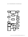
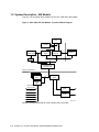
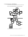
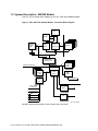
DEC 3000 AXP 300 Models: Functional Block Diagram . . . . .
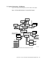
DEC 3000 AXP 400 Models: Functional Block Diagram . . . . .
DEC 3000 AXP 500 Models: Functional Block Diagram . . . . .
DEC 3000 AXP 600/700 Models: Functional Block Diagram . .
DEC 3000 AXP 800/900 Models: Functional Block Diagram . .
ABOX_CTL Register: 300 Models . . . . . . . . . . . . . . . . . . . . . .
ABOX_CTL Register: 400/500/600/700/800/900 Models . . . . . .
DMA byte address from TURBOchannel . . . . . . . . . . . . . . . . .
IOCTL Subsystem . . . . . . . . . . . . . . . . . . . . . . . . . . . . . . . . . .
400/500/600/700/800/900 Models: DMA Arbitration Scheme . .
Interrupt Stack Frame . . . . . . . . . . . . . . . . . . . . . . . . . . . . . . .
Corrected Error (Small) Logout Frame . . . . . . . . . . . . . . . . . .
Machine check (large) logout frame . . . . . . . . . . . . . . . . . . . . .
Processor Initialization Block Diagram . . . . . . . . . . . . . . . . . .
System ROM Header Format . . . . . . . . . . . . . . . . . . . . . . . . . .
Format of a ROM Object . . . . . . . . . . . . . . . . . . . . . . . . . . . . .
Power-On Initialization Flow . . . . . . . . . . . . . . . . . . . . . . . . . .
Map of Memory Following Power-Up Initialization . . . . . . . . .
Initial Boot Address Space . . . . . . . . . . . . . . . . . . . . . . . . . . . .
Configuration Tables . . . . . . . . . . . . . . . . . . . . . . . . . . . . . . . .
Main Configuration Table . . . . . . . . . . . . . . . . . . . . . . . . . . . .
Kernel-Resident Device Configuration Table . . . . . . . . . . . . . .
TURBOchannel Device Configuration Table . . . . . . . . . . . . . . .
Keyboard Menu Prompt . . . . . . . . . . . . . . . . . . . . . . . . . . . . . .
General HWRPB Structure . . . . . . . . . . . . . . . . . . . . . . . . . . .
HWRPB General Information . . . . . . . . . . . . . . . . . . . . . . . . .
HWRPB Per-CPU Slot . . . . . . . . . . . . . . . . . . . . . . . . . . . . . . .
PALcode Revision Quadword . . . . . . . . . . . . . . . . . . . . . . . . . .
Format of a Console Terminal Block (Decimal Values) . . . . . . .
Format of a Console Routine Block . . . . . . . . . . . . . . . . . . . . .
Format of the Memory Data Descriptor Table . . . . . . . . . . . . .
NVR Console Mailbox Register (CPMBX) . . . . . . . . . . . . . . . .
NVR Console Flags (CPFLG) . . . . . . . . . . . . . . . . . . . . . . . . . .
NVR Keyboard Type Register (LK401_ID) . . . . . . . . . . . . . . . .
NVR Console Type Register (CONSOLE_ID) . . . . . . . . . . . . .
NVR Temporary Storage (TEMP) . . . . . . . . . . . . . . . . . . . . . . .
NVR Battery Check Data (BAT_CHK) . . . . . . . . . . . . . . . . . . .
NVR Ethernet Trigger Password Code (PASSWORD) . . . . . . .
NVR Security Flags . . . . . . . . . . . . . . . . . . . . . . . . . . . . . . . . .
NVR Boot Flags . . . . . . . . . . . . . . . . . . . . . . . . . . . . . . . . . . . .
NVR SCSI Information 1 . . . . . . . . . . . . . . . . . . . . . . . . . . . . .
NVR SCSI Information 2 . . . . . . . . . . . . . . . . . . . . . . . . . . . . .
NVR Default Boot Device Name Length (BOOT_DEV_LEN) . .
NVR Default Boot Device (BOOT_DEV) . . . . . . . . . . . . . . . . . .
Dense I/O Space Addressing: 400/500/600/700/800/900 Models
.
.
.
.
.
.
.
.
.
.
.
.
.
.
.
.
.
.
.
.
.
.
.
.
.
.
.
.
.
.
.
.
.
.
.
.
.
.
.
.
.
.
.
.
.
.
.
.
.
.
.
.
.
.
.
.
.
.
.
.
.
.
.
.
.
.
.
.
.
.
.
.
.
.
.
.
.
.
.
.
.
.
.
.
.
.
.
.
.
.
.
.
.
.
.
.
.
.
.
.
.
.
.
.
.
.
.
.
.
.
.
.
.
.
.
.
.
.
.
.
.
.
.
.
.
.
.
.
.
.
.
.
.
.
.
.
.
.
.
.
.
.
.
.
.
.
.
.
.
.
.
.
.
.
.
.
.
.
.
.
.
.
.
.
.
.
.
.
.
.
.
.
.
.
.
.
.
.
.
.
.
.
.
.
.
.
.
.
.
.
.
.
.
.
.
.
.
.
.
.
.
.
.
.
.
.
.
.
.
.
.
.
.
.
.
.
.
.
.
.
.
.
.
.
.
.
.
.
.
.
.
.
.
.
.
.
.
.
.
.
.
.
.
.
.
.
.
.
.
.
.
.
.
.
.
.
.
.
.
.
.
.
.
.
.
.
.
.
.
.
1–3
1–6
1–9
1–13
1–16
2–9
2–10
5–2
7–1
9–6
10–5
10–6
10–6
11–1
13–3
13–5
14–2
14–6
14–11
15–1
15–2
15–4
15–7
16–22
16–33
16–35
16–39
16–42
16–44
16–48
16–51
19–2
19–3
19–4
19–5
19–6
19–6
19–7
19–7
19–8
19–10
19–10
19–11
19–12
A–2
46
47
48
Dense I/O Space Addressing: 300 Models . . . . . . . . . . . . . . . . . . . . . .
Sparse I/O Space Addressing: 400/500/600/700/800/900 Models . . . . . .
Sparse I/O Space Addressing: 300 Models . . . . . . . . . . . . . . . . . . . . . .
A–2
A–3
A–3
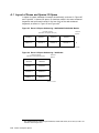
Conventions Used in this Guide . . . . . . . . . . . . . . . . . . . . . . . . . . . . .
Bit Name Conventions Used in this Guide . . . . . . . . . . . . . . . . . . . . .
System Jumpers . . . . . . . . . . . . . . . . . . . . . . . . . . . . . . . . . . . . . . . . .
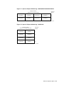
Memory Address Spaces . . . . . . . . . . . . . . . . . . . . . . . . . . . . . . . . . . .
Memory Address Space Components . . . . . . . . . . . . . . . . . . . . . . . . .
300 Model I/O Address Map . . . . . . . . . . . . . . . . . . . . . . . . . . . . . . . .
400/500/600/700/800/900 Models I/O Address Map . . . . . . . . . . . . . . .
I/O Interface Registers (300 Models) . . . . . . . . . . . . . . . . . . . . . . . . .
TURBOchannel Control and Status Registers (300 Models) . . . . . . . .
TURBOchannel Control and Status Registers
(400/500/600/700/800/900) Models . . . . . . . . . . . . . . . . . . . . . . . . . . .
IMR—1.C281.FFFC . . . . . . . . . . . . . . . . . . . . . . . . . . . . . . . . . . . . . .
IR—1.D4C0.0000 . . . . . . . . . . . . . . . . . . . . . . . . . . . . . . . . . . . . . . . .
Scatter/Gather Registers . . . . . . . . . . . . . . . . . . . . . . . . . . . . . . . . . .
CXTurbo Address Map . . . . . . . . . . . . . . . . . . . . . . . . . . . . . . . . . . . .
Frame Buffer and Video Register Map . . . . . . . . . . . . . . . . . . . . . . . .
IOCTL Address Map . . . . . . . . . . . . . . . . . . . . . . . . . . . . . . . . . . . . .
System Address Register (300 Models) . . . . . . . . . . . . . . . . . . . . . . . .
Ethernet Station Address ROM Addresses (400/500/600/700/800/900
Models) . . . . . . . . . . . . . . . . . . . . . . . . . . . . . . . . . . . . . . . . . . . . . . .
Ethernet Station Address ROM Addresses (300 Models) . . . . . . . . . .
LANCE Register Addresses (400/500/600/700/800/900 Models) . . . . .
LANCE Register Addresses (300 Models) . . . . . . . . . . . . . . . . . . . . . .
SCC Register Addresses (300 Models) . . . . . . . . . . . . . . . . . . . . . . . .
SCC Register Addresses (400/500/600/700/800/900 Models) . . . . . . . .
RTC Register Addresses (300 Models) . . . . . . . . . . . . . . . . . . . . . . . .
RTC Register Addresses (400/500/600/700/800/900 Models) . . . . . . . .
ISDN Direct Address Registers (300 Models) . . . . . . . . . . . . . . . . . . .
ISDN Indirect Address Registers (300 Models) . . . . . . . . . . . . . . . . .
ISDN Directly Addressed Registers (400/500/600/700/800/900
Models) . . . . . . . . . . . . . . . . . . . . . . . . . . . . . . . . . . . . . . . . . . . . . . .
ISDN Indirectly Addressed Registers (400/500/600/700/800/900
Models) . . . . . . . . . . . . . . . . . . . . . . . . . . . . . . . . . . . . . . . . . . . . . . .
TURBOchannel Dual SCSI Address Map . . . . . . . . . . . . . . . . . . . . . .
TURBOchannel Dual SCSI ASIC Register Map . . . . . . . . . . . . . . . . .
Baud Rate Programming . . . . . . . . . . . . . . . . . . . . . . . . . . . . . . . . . .
SCC Signal Connections . . . . . . . . . . . . . . . . . . . . . . . . . . . . . . . . . . .
Dual SCSI Interface: Differences Among Models . . . . . . . . . . . . . . . .
Data Transfer Error Coverage . . . . . . . . . . . . . . . . . . . . . . . . . . . . . .
Priority of PAL Entry Points . . . . . . . . . . . . . . . . . . . . . . . . . . . . . . .
System Error/Interrupt Matrix . . . . . . . . . . . . . . . . . . . . . . . . . . . . .
.
.
.
.
.
.
.
.
.
xv
xvi
1–5
2–2
2–2
2–4
2–5
3–1
3–2
.
.
.
.
.
.
.
.
3–8
3–16
3–18
5–1
6–3
6–5
7–3
7–15
.
.
.
.
.
.
.
.
.
.
7–18
7–19
7–21
7–21
7–21
7–21
7–23
7–23
7–24
7–24
.
7–26
.
.
.
.
.
.
.
.
.
7–27
8–2
8–3
9–11
9–12
9–15
10–3
10–4
10–7
Tables
1
2
3
4
5
6
7
8
9
10
11
12
13
14
15
16
18
19
20
21
22
23
24
25
26
27
28
29
30
31
32
33
34
35
36
37
38
xi
39
40
41
42
43
44
45
46
47
48
49
50
51
52
53
54
55
56
59
58
59
60
61
62
63
64
65
66
67
68
69
70
71
72
73
74
75
76
77
78
xii
CPU State Before SCB Routines . . . . . . . . . . . . . . . . . . . . .
Dual SCSI Error/Interrupt Matrix . . . . . . . . . . . . . . . . . . . .
Error Insertion Techniques . . . . . . . . . . . . . . . . . . . . . . . . .
Interrupt Pin Allocation . . . . . . . . . . . . . . . . . . . . . . . . . . . .
Memory Differences . . . . . . . . . . . . . . . . . . . . . . . . . . . . . . .
TURBOchannel Differences . . . . . . . . . . . . . . . . . . . . . . . . .
Diagnostic LED Displays and Locations . . . . . . . . . . . . . . . .
300 Model SROM Power-On Sequence . . . . . . . . . . . . . . . . .
400/500/600/700/800/900 Model SROM Power-On Sequence .
Register Values After Power-Up . . . . . . . . . . . . . . . . . . . . . .
Processor Restart Codes . . . . . . . . . . . . . . . . . . . . . . . . . . . .
Kernel-Resident Device Configuration Table Components . .
TURBOchannel Device Configuration Table Components . .
DEC 3000 AXP Device IDs . . . . . . . . . . . . . . . . . . . . . . . . . .
Console Saved State . . . . . . . . . . . . . . . . . . . . . . . . . . . . . . .
VMS and OSF Device Naming Conventions . . . . . . . . . . . . .
Symbolic Addresses—General . . . . . . . . . . . . . . . . . . . . . . .
Diagnostic Environment Values . . . . . . . . . . . . . . . . . . . . . .
POWERUP_TIME Settings . . . . . . . . . . . . . . . . . . . . . . . . .
Language Selection Codes . . . . . . . . . . . . . . . . . . . . . . . . . .
POWERUP_TIME Settings . . . . . . . . . . . . . . . . . . . . . . . . .
Service Routines accessed by the DISPATCH ROUTINE . . .
Console Service Routines . . . . . . . . . . . . . . . . . . . . . . . . . . .
Environment Variable ID Numbers . . . . . . . . . . . . . . . . . . .
PALcode Entry Points . . . . . . . . . . . . . . . . . . . . . . . . . . . . .
Supported CALL_PAL Instructions . . . . . . . . . . . . . . . . . . .
TURBOchannel Option ROM Base Addresses . . . . . . . . . . .
NVR Storage Allocation . . . . . . . . . . . . . . . . . . . . . . . . . . . .
NVR Console Mailbox Register Fields . . . . . . . . . . . . . . . . .
NVR Console Flags (CPFLG) Fields . . . . . . . . . . . . . . . . . . .
NVR Language Selection Codes . . . . . . . . . . . . . . . . . . . . . .
NVR: Defined Console Devices . . . . . . . . . . . . . . . . . . . . . . .
NVR Security Flags . . . . . . . . . . . . . . . . . . . . . . . . . . . . . . .
NVR SCSI Information 1 fields . . . . . . . . . . . . . . . . . . . . . .
NVR SCSI Information 2 Fields . . . . . . . . . . . . . . . . . . . . . .
Minimum Granularity . . . . . . . . . . . . . . . . . . . . . . . . . . . . .
Effect of Load and Store Instructions in Dense Space . . . . .
Effect of Load and Store Instructions in Sparse Space . . . . .
Writing 32-Byte Blocks to the TURBOchannel Interface . . .
How to Address I/O Registers . . . . . . . . . . . . . . . . . . . . . . .
.
.
.
.
.
.
.
.
.
.
.
.
.
.
.
.
.
.
.
.
.
.
.
.
.
.
.
.
.
.
.
.
.
.
.
.
.
.
.
.
.
.
.
.
.
.
.
.
.
.
.
.
.
.
.
.
.
.
.
.
.
.
.
.
.
.
.
.
.
.
.
.
.
.
.
.
.
.
.
.
.
.
.
.
.
.
.
.
.
.
.
.
.
.
.
.
.
.
.
.
.
.
.
.
.
.
.
.
.
.
.
.
.
.
.
.
.
.
.
.
.
.
.
.
.
.
.
.
.
.
.
.
.
.
.
.
.
.
.
.
.
.
.
.
.
.
.
.
.
.
.
.
.
.
.
.
.
.
.
.
.
.
.
.
.
.
.
.
.
.
.
.
.
.
.
.
.
.
.
.
.
.
.
.
.
.
.
.
.
.
.
.
.
.
.
.
.
.
.
.
.
.
.
.
.
.
.
.
.
.
.
.
.
.
.
.
.
.
.
.
.
.
.
.
.
.
.
.
.
.
.
.
.
.
.
.
.
.
.
.
.
.
.
.
.
.
.
.
.
.
.
.
.
.
.
.
.
.
.
.
.
.
.
.
.
.
.
.
.
.
.
.
.
.
.
.
.
.
.
.
.
.
.
.
.
.
.
.
.
.
.
.
.
.
.
.
.
.
.
.
.
.
.
.
.
.
.
.
.
.
.
.
.
.
.
.
.
.
.
.
10–10
10–12
10–14
10–15
12–1
12–2
12–2
14–3
14–4
14–7
14–13
15–5
15–8
15–8
16–4
16–8
16–12
16–21
16–24
16–28
16–29
16–54
16–54
16–70
17–2
17–2
18–1
19–1
19–2
19–3
19–4
19–5
19–7
19–10
19–10
A–4
A–5
A–5
A–6
A–7
Preface
The DEC 3000 300/400/500/600/700/800/900 AXP Models are a family of highperformance deskside and desktop workstations that use Digital’s DECchip 21064
RISC-style microprocessor. They comprise a family of systems based on the
Digital Alpha AXP architecture, providing a 64-bit computing environment.
Intended Audience
This manual is intended for design engineers and programmers who write such
system-level software as operating systems and drivers. The manual discusses
the format and behavior of specific hardware architecture as it pertains to writing
system-level programs.
Document Contents
The DEC 3000 300/400/500/600/700/800/900 AXP Models System
Programmer’s Manual is divided into 19 chapters, one appendix, one glossary,
and one index:
•
Chapter 1 describes the system and the variations among models.
•
Chapter 2 describes the DEC 3000 AXP systems’ address maps, the methods
of addressing I/O space, and system I/O registers, specifically: memory
alignment, memory address spaces, I/O address space, the TURBOchannel
interface bit decode map for I/O addresses, and address-processing and
Bcache control CPU registers.
•
Chapter 3 discusses I/O interface registers—the 300 models’ I/O control and
status registers and the 400/500/600/700/800/900 models’ TURBOchannel
control and status Registers.
•
Chapter 4 discusses the 400/500/600/700/800/900 models’ address ASIC,
which controls access to each memory configuration register and to the victim
address counter register and victim address register for caching.
•
Chapter 5 discusses the scatter/gather maps used in 400/500/600/700/800/900
models to support virtual DMA—the location, size, and access modes of
scatter/gather registers, their organization, and the performance of read and
write operations on scatter/gather map entries.
•
Chapter 6 discusses the CXTurbo graphics subsystem, and covers these topics:
CXTurbo address map, I/O address map, Frame Buffer Control Register, SFB
ASIC functions, Bt459 RAMDAC, and System FEPROM (400/500/600/700/800
/900 models).
•
Chapter 7 discusses the IOCTL ASIC and system registers—the IOCTL
address map, system FEPROM, and IOCTL registers.
•
Chapter 8 discusses the TURBOchannel Dual SCSI ASIC—address map,
internal registers, 53C94 registers, and DMA buffers.
xiii
•
Chapter 9 describes programming considerations and restrictions for I/O
transactions—I/O read and write restrictions, DMA, interrupt handling
during I/O operations, TURBOchannel usage (system-specific), JUNKIO
subsystem, and the dual SCSI interface.
•
Chapter 10 discusses the behavior of the system under hardware exceptions
and interrupts—sources of errors and interrupts, behavior of system hardware
under errors, system error/interrupt matrix, dual SCSI error/interrupt matrix,
error insertion for testing purposes, assignment of CPU interrupt pins, error
handling and recovery, and PAL recovery algorithms for selected errors.
•
Chapter 11 discusses processor and Bcache initialization.
•
Chapter 12 gives an overview of DEC 3000 AXP firmware.
•
Chapter 13 discusses DEC 3000 AXP firmware ROMs—firmware ROM
format, system and I/O ROM contents, and system ROM format.
•
Chapter 14 discusses firmware power-up initialization and entry—power-on
initialization flow, map of memory following power-up initialization, machine
state following power-up initialization, SROM routines, and system firmware
entry.
•
Chapter 15 discusses configuration information saved by power-up
initialization code—the main configuration table and the device configuration
tables.
•
Chapter 16 discusses the console device, console saved state, console program,
and console data structures, and gives an overview and descriptions of console
service routines.
•
Chapter 17 discusses DEC 3000 AXP PALcode—location, entering PALcode,
supported CALL_PAL instructions, MACHINE_RESET PALcode, machinecheck PALcode, and INTERRUPT PALcode.
•
Chapter 18 discusses TURBOchannel support.
•
Chapter 19 discusses nonvolatile RAM and its data structures.
•
Appendix A discusses the use of dense and sparse space in I/O programming—
the layout of dense and sparse addressing locations, the required number
of transactions to complete operations through dense and sparse space,
minimum read and write granularity of operations through dense and sparse
space, the effect of load and store instructions in dense and sparse space,
byte-masked I/O read operations, and mapping I/O Addresses.
•
A Glossarycontains useful terms and their meaning.
Associated Documents
xiv
•
Alpha Architecture Handbook (EC–H1689–10)
•
Alpha Architecture Reference Manual (EY–L520E–DP)
•
Bt459 RAMDAC Specification
•
DECchip 21064 Microprocessor Chip Data Sheet (EC–F1720–10)
•
DECchip 21064-AA Microprocessor Hardware Reference Manual (EC–N0079–
72)
•
DEC 3000 Model 300/300L/300X/300LX AXP Service Documentation Kit
(EK–PELSV–DK)
•
DEC 3000 Model 400 AXP Workstation Documentation Kit (EK–SNDPR–DK)
•
DEC 3000 Model 400/400S AXP Server Documentation Kit (EK–SNPSV–DK)
•
DEC 3000 Model 500/500S AXP Server Documentation Kit (EK–FLAMI–DK)
•
DEC 3000 Model 500/500S AXP Workstation Kit (EK–FLMNG–DK)
•
DEC 3000 Model 500X AXP Documentation Kit (EK–D5AXP–DK)
•
DEC 3000 Model 600/600S/700 AXP Information Kit (EK–SNDWS–DK)
•
DEC 3000 Model 800/800S/900 AXP Information Kit (EK–FLMWS–DK)
•
NCR 53C94-95-96 Advanced SCSI Controller (1992)
•
NCR 53CF94/96-2 Fast SCSI Controller (1992)
•
TURBOchannel Specification Revision C (EK–TCDEV–DK)
•
AMD79C30A ISDN Chip Specification
Conventions
Table 1 lists the conventions used in this guide.
Table 1 Conventions Used in this Guide
Convention
Description
<x:y>
Represents a bit field or an extent of a set of lines or signals ranging
from x through y. For example, R0<7:4> indicates bits 4 through 7 in the
general purpose register R0.
x..y
Represents a range of bits from x to y.
n, n10
Numbers are hexadecimal unless otherwise marked with a subscript
number. If there is possible ambiguity, the radix is explicitly stated.
1.FFFF.FFFF
Nine digit numbers typically represent 34-bit hexadecimal addresses and
are grouped in four-digit clusters, separated by periods.
Note
A note contains information that might be of special importance to the
user.
Caution
A caution contains information that the user needs to know to avoid
damaging the software or hardware.
Italics
Italics indicate variables in code.
[]
Represents a command parameter, option, or qualifier that is optional.
Note
Direct technical questions regarding these products or this manual to the
Digital Customer Service support telephone line at 1-800-354-9000.
xv
Table 2 lists the conventions for naming bits:
Table 2 Bit Name Conventions Used in this Guide
xvi
Convention
Description
0
Describes a bit that is ignored on write operations and is
read as 0.
1
Describes a bit that is ignored on write operations and is
read as 1.
R/W
Read/write. A bit or field that may be read or written by
software.
RO
A read-only bit that can be read by software. It is written
by hardware. Software writes are ignored.
WO
Write-only. A write-only bit that can be written by
software. It is used by hardware. Reads by software
return unpredictable results.
W
A write bit that can be written by software. It is used by
hardware. Reads by software return a 0.
WC
Write-one-to-clear. Software writes of a 1 cause this bit
to be cleared by hardware. Software writes of a 0 do not
modify the state of the bit.
W0C
Write-zero-to-clear. Software writes of a 0 cause this bit
to be cleared by hardware. Software writes of a 1 do not
modify the state of the bit.
WA
Write-anything. Software writes of any value to the
register cause the bit to be cleared by hardware.
RC
Read-to-clear. The value is written by hardware and
remains unchanged until read by software, at which point
hardware may write a new value into the field.
IGN
These bits or fields are ignored when written.
RAZ
Read-as-zero. These bits or field return a zero when read.
MBZ
Must-be-zero. These bits or fields must never be written
by software with a non-zero value. A reserved operand
exception occurs if a non-zero value in a MBZ fields is
encountered by the processor.
SBZ
Should-be-zero. These bits or fields should be filled by
software with a zero vlue. These fields may be used at
a future time. Nonzero values in SBZ fields produce
unpredictable results.
RES/Reserved
Reserved. These bits or fields are reserved for future
expansion.
X
A don’t-care bit. The value of a don’t-care bit is ignored.
UNDEFINED
Triggered by privileged software, this type of value may
halt the processor or cause it to lose information.
UNPREDICTABLE
Triggered by either privileged or unprivileged software,
this type of result or occurrence does not disrupt the basic
operation of the processor. Unpredictable results may
acquire arbitrary values.
1
Introduction to the DEC 3000 Models
300/400/500/600/700/800/900 AXP
The DEC 3000 Models 300/400/500/600/700/800/900 AXP is a family of
desktop and deskside workstations that support the DECchip 21064–AA CPU
implementation of the Alpha AXP architecture. These models’ I/O system is
TURBOchannel-based and has embedded I/O devices.
This chapter briefly describes the components and functions of each model and
covers the following topics:
•
System description: 300 models (Section 1.1)
•
System description: 400 models (Section 1.2)
•
System description: 500 models (Section 1.3)
•
System description: 600 models (Section 1.4)
•
System description: 700 models (Section 1.4)
•
System description: 800 models (Section 1.5)
•
System description: 900 models (Section 1.5)
•
Differences among Models (Section 1.6)
Introduction to the DEC 3000 Models 300/400/500/600/700/800/900 AXP 1–1
1.1 System Description: 300 Models
Figure 1 is a functional block diagram of the DEC 3000 AXP 300 models.
Numbers along communication lines indicate their bus width.
Major system components are:
•
CPU:
A DECchip 21064–AA CPU, including on-chip 8 KB instruction and 8 KB
data caches, and a 64 KB (8 KB) serial boot ROM. Section 2.5 discusses CPU
registers that must be assigned specific values at startup.
•
Cache:
A module-level write-back backup cache, or Bcache. The Bcache contains 256
KB, 32-byte blocks.
The cache tags are parity-protected, with separate parity bits for the address
and control sections. The control section has a dirty bit and a valid bit. The
valid bit is always set since the Bcache is initialized on power up with all
valid memory blocks. During system operation, the write-update protocol
used during DMA to maintain cache coherency assures that the Bcache blocks
must never be invalidated.
Section 2.6 describes Bcache tag space.
Section 10.1 describes the Bcache as a source of errors and interrupts.
Section 11.2 describes Bcache initialization.
•
Memory Banks:
16 MB - 256 MB system memory, longword-parity protected, consisting of up
to four memory banks, each one of which must be populated by two SIMMS
of the same type. Using 1M x 4 DRAMs, the minimum memory size is 16
MB. Using 4M x 4 DRAMs, the maximum memory size is 256 MB. System
memory is longword parity-protected.
Section 2.2 discusses memory and I/O addressing; Section 3.2.3 discusses the
Memory Configuration Register (MCR).)
•
TURBOchannel Interface:
A 12.5 MHz TURBOchannel interface for I/O, which is controlled by a
TURBOchannel ASIC. Section 3.2 discusses I/O Control and Status Registers.
Section 9.4 discusses TURBOchannel I/O programming. 300 models do not
support block-mode write operations.
•
Graphics Subsystem
An 8-plane (2D) color graphics subsystem, called the CXTurbo, which is
connected to the TURBOchannel. The SFB (smart frame buffer) ASIC
controls this subsystem, which supports an 8-plane color monitor in the
resolution/refresh rate combinations of:
1024 x 768 @ 72 Hz (300L model)
1280 x 1024 @ 72 Hz (300, 300X, and 300LX models)
The CXTurbo is different from other TURBOchannel devices, in that it is
operated at the full TURBOchannel speed of 25 MHz and is accessible only in
dense I/O space. Appendix A discusses the use of dense and sparse I/O space
in the DEC 3000 AXP.
Chapter 6 describes the CXTurbo graphics subsystem.
1–2 Introduction to the DEC 3000 Models 300/400/500/600/700/800/900 AXP
Figure 1 DEC 3000 AXP 300 Models: Functional Block Diagram
Clock
Serial ROM
21064
Data 64
Address 28
Cache
(256KB)
Buffer
Buffer
Memory SIMMs
16-256MB
Memory, CPU
TURBOchannel
Control Logic
Data 64
Buffer
Graphics:
-SFB
-2MB VRAMS
-RAMDAC
-etc
I/O Subsystem:
-Core I/O ASIC
-Ethernet
-ISDN
-Serial
-ROMs
-Audio
-LEDs
Buffer
(Except 300L)
Buffer
2 TURBOchannel
Option Slots
TURBOchannel 32
SCSI
TCDS
N/C
MLO-012116
Introduction to the DEC 3000 Models 300/400/500/600/700/800/900 AXP 1–3
•
TURBOchannel Option Slots:
The 300, 300X, and 300LX models contain two TURBOchannel option slots.
Each slot has 64 MB of I/O address space.
The 300L model contains no option slots.
•
I/O Subsystem:
An interface called the JUNKIO subsystem, which is connected to the
TURBOchannel. The IOCTL ASIC implements this interface. Chapter 7
describes IOCTL ASIC control of the subsystem and Section 9.5 discusses
programming the subsystem, which provides:
A nonvolatile time-of-year clock based on the Dallas Semiconductor DS
1287A Real-Time Clock (RTC)
Three serial lines, through two Zilog SCC (Z85C30) dual UARTS
(universal asynchronous receiver/transmitters)—SCC0 and SCC1
*
Asynchronous for keyboard—Port A of SCC1
*
Asynchronous for mouse—Port A of SCC0
*
CCITT V.24/V.28 19.2 KB/s asynchronous/synchronous 25-pin plug for
communications—Port B of SCC0.
An AMD 79C30A (Revision E) chip, providing both an ISDN-S interface
and voice-quality audio with a usable bandwidth of approximately 100 Hz
- 3000 Hz
The following audio interfaces are supported:
*
The loudspeaker outputs of the 79C30A are connected to a speaker
located inside the system box.
*
The differential ear-out and mic-out signals from 79C30A lead to
an external MJ4 telephone jack located on the rear I/O panel of the
system box. This jack supports connections to a telephone handset or
an operator headset.
Ethernet through the AMD local area network controller for Ethernet
(LANCE) adapter. The external interface to the Ethernet is a 10BaseT
twisted pair connector.
A 32 K x 8 Ethernet address ROM.
768 KB of Flash memory used for system firmware composed of three 256
KB flash memory Devices. Control bits in the System Support Register of
the IOCTL ASIC select the memory devices.
Access to two 4-bit LED displays to display a 2-digit hexadecimal code for
diagnostic purposes. (See
The Ethernet, ISDN, audio, printer, and communications ports have DMA
support.
1–4 Introduction to the DEC 3000 Models 300/400/500/600/700/800/900 AXP
•
SCSI Interface:
A TURBOchannel dual SCSI interface chip (TCDS) is connected to the
TURBOchannel bus, but only one NCR53C94 SCSI controller chip interfaces
to the TCDS ASIC and provides a single-ended, 8-bit, 5 MB/s SCSI port. This
port drives one SCSI drop inside the system box and is also available outside
the box for further expansion.
Chapter 8 discusses the TURBOchannel Dual SCSI ASIC.
Hardware Jumpers
Table 3 lists system jumpers, their possible position, and the correspoding
function.
Table 3 System Jumpers
Jumper
Position
Function
W1
1 to 2
Flash ROM Write Disable
W1
2 to 3
Flash ROM Write Enable
W2
1 to 2
Graphics Monitor as Console
W2
2 to 3
Serial Comm Port as Console
W2
3 to 4
SROM Port as Mini-Console (Digital use only)
W3
1 to 2
Secure console enabled
W3
2 to 3
Secure console disabled
Introduction to the DEC 3000 Models 300/400/500/600/700/800/900 AXP 1–5
1.2 System Description: 400 Models
Figure 2 is a functional block diagram of the DEC 3000 AXP 400 models.
Figure 2 DEC 3000 AXP 400 Models: Functional Block Diagram
CPU
CACHE
156
19
Scatter/
Gather Map
15
ADDR
ASIC
Data
ASICs (4)
312
Memory
28
39
TURBOchannel
Interface ASIC
System Card Module
I/O Module
TC Option
Slots
33
TCDS
ASIC
IOCTL
ASIC
Non-Volatile
Time of Year
Serial Lines
Comm/Printer
ISDN
Audio In/Out
SCSI
SCSI
Ethernet
Boot ROM
Numbers along communication lines indicate their bus width.
1–6 Introduction to the DEC 3000 Models 300/400/500/600/700/800/900 AXP
MLO-012117
System components are:
•
CPU:
A DECchip 21064–AA CPU, including on-chip 8-KB instruction and 8-KB
data caches, and a 64-KB serial boot ROM. A 64-KB stream holds the
primitive boot code for booting the operating system. Jumpers provide for the
selection of up to seven other streams for diagnostic and other purposes. (The
entire UVPROM is 64 K x 8.)
Section 2.5 discusses CPU registers that must be assigned specific values at
startup.
•
Cache:
A module-level write-back cache, or Bcache, consisting of 512 KB, 32-byte
blocks, Single Bit Correction, Double Bit Detection (SBCDBD) ECC protected.
The cache tags are parity-protected, with separate parity bits for the address
and control sections. (There is only one bit of control, a dirty bit.)
Section 2.6 describes Bcache tag space.
Section 10.1 describes the Bcache as a source of errors and interrupts.
Section 11.2 describes Bcache initialization.
•
Scatter/Gather Map:
A 32K-entry scatter/gather map, for virtual DMA. Each entry maps an 8-KB
Alpha AXP/DECchip 21064–AA page. Chapter 5 discusses the scatter/gather
maps.
•
Address Path ASIC:
An address path ASIC.
•
Datapath ASICs
Four datapath ASICs
•
Memory Banks:
32 MB-512 MB system memory, SBCDBD ECC protected, consisting of up to
two physical memory banks, each one of which must be populated by eight
SIMMS of the same type. Using 1M x 4 DRAMs, the minimum memory size
is 32 MB. Using 4M x 4 DRAMs, the maximum memory size is 512 MB.
Section 2.2 gives memory and I/O address spaces; Section 4.1 describes
the format, operation, and proper configuration of Memory Configuration
Registers.
•
TURBOchannel Interface:
A 22.5 MHz TURBOchannel interface for I/O, which is controlled by a
TURBOchannel ASIC. The interface has virtual DMA capability for any
TURBOchannel option, high-speed block I/O write, and parity protection.
Section 3.3 describes TURBOchannel Control and Status Registers.
Section 9.4 discusses TURBOchannel I/O programming.
•
TURBOchannel Option Slots:
Three TURBOchannel option slots. Each slot has 128 MB of I/O address
space.
Introduction to the DEC 3000 Models 300/400/500/600/700/800/900 AXP 1–7
•
JUNKIO Interface:
An interface called the JUNKIO subsystem, which is connected to the
TURBOchannel. The IOCTL ASIC implements this interface. Chapter 7
describes IOCTL ASIC control of the subsystem and Section 9.5 discusses
programming the subsystem, which provides:
A nonvolatile time-of-year clock based on the Dallas Semiconductor DS
1287A Real-Time Clock (RTC)
Four serial lines, through two Zilog SCC (Z85C30) dual UARTS (universal
asynchronous receiver/transmitters)—SCC0 and SCC1.
*
Asynchronous for keyboard
*
Asynchronous for mouse
*
Asynchronous for the printer, through 6-pin MMJ
*
CCITT V.24/V.28 19.2 KB/s asynchronous/synchronous 25-pin plug for
communications
An ISDN-S interface, through an AMD 79C30A (Revision E) chip.
Voice-quality audio I/O through the same AMD 79C30A (Revision E) chip,
with a usable bandwidth of approximately 100-3000 Hz.
The audio lines extend from a connector located on the rear of the
enclosure.
Ethernet through an AMD local area network controller for Ethernet
(LANCE) adapter. Both AUI transceiver (thickwire) and 10Base-T
(twisted-pair) interfaces to Ethernet are provided. A setting in the system
support register of IOCTL ASIC selects the interface.
A 32 byte Ethernet address ROM.
Two 256 KB writable console boot ROMs on the I/O module.
Access to eight LEDs, used to display a hexadecimal code for diagnostic
purposes.
The Ethernet, ISDN, audio, printer, and communications ports have DMA
support.
•
SCSI Interface:
A dual SCSI interface chip (TCDS), which is connected to the TURBOchannel.
Two NCR53C94 SCSI controller chips that interface to the TCDS ASIC
provide two 5 MB/s 8-bit single-ended SCSI buses, with DMA support.
Chapter 8 discusses the TURBOchannel Dual SCSI ASIC.
1–8 Introduction to the DEC 3000 Models 300/400/500/600/700/800/900 AXP
1.3 System Description: 500 Models
Figure 3 is a functional block diagram of the DEC 3000 AXP 500 models.
Figure 3 DEC 3000 AXP 500 Models: Functional Block Diagram
CPU
CACHE
156
19
Scatter/
Gather Map
15
ADDR
ASIC
Data
ASICs (4)
312
Memory
28
39
TURBOchannel
Interface ASIC
33
System Card Module
TC Option
Slots
I/O Module
TC Option
Slots
33
SFB
ASIC
TCDS
ASIC
Video
Out
Flash EPROM
IOCTL
ASIC
Non-Volatile
Time of Year
Serial Lines
Comm/Printer
ISDN
Audio In/Out
256KB
SCSI
SCSI
Ethernet
Boot ROM
MLO-012118
Numbers along communication lines indicate their bus width.
Introduction to the DEC 3000 Models 300/400/500/600/700/800/900 AXP 1–9
System components are:
•
CPU:
A DECchip 21064–AA CPU, including on-chip 8-KB instruction and 8-KB
data caches, and a 64-KB serial boot ROM. A 64-KB stream holds the
primitive boot code for booting the operating system. Jumpers provide for the
selection of up to seven other streams for diagnostic and other purposes. (The
entire UVPROM is 64 K x 8.)
Section 2.5 discusses CPU registers must be assigned specific values at
startup.
•
Cache:
A module-level write-back cache, or Bcache, consisting of 512 KB, 32-byte
blocks, Single Bit Correction, Double Bit Detection (SBCDBD) ECC protected.
The cache tags are parity-protected, with separate parity bits for the address
and control sections. (There is only one bit of control, a dirty bit.)
Section 2.6 describes Bcache tag space.
Section 10.1 describes the Bcache as a source of errors and interrupts.
Section 11.2 describes Bcache initialization.
•
Scatter/Gather Map:
A 32K-entry scatter/gather map, for virtual DMA. Each entry maps an 8 KB
Alpha AXP/DECchip 21064–AA page. Chapter 5 discusses the scatter/gather
maps.
•
Address Path ASIC:
An address path ASIC
•
Datapath ASICs
Four datapath ASICs
•
Memory Banks:
32 MB-1 GB system memory, SBCDBD ECC protected, consisting of up to
four physical memory banks, each one of which must be populated by eight
SIMMS. Using 1M x 4 DRAMs, the minimum memory size is 32 MB. Using
4M x 4 DRAMs, the maximum memory size is 1 GB.
Section 2.2 gives memory and I/O address spaces; Section 4.1 describes
the format, operation, and proper configuration of Memory Configuration
Registers.
•
TURBOchannel Interface:
A 25 MHz TURBOchannel interface for I/O, which is controlled by a
TURBOchannel ASIC. The interface has virtual DMA capability for any
TURBOchannel option, high-speed block I/O write, and parity protection.
Section 3.3 describes TURBOchannel Control and Status Registers.
Section 9.4 discusses TURBOchannel I/O programming.
•
TURBOchannel Option Slots:
Six TURBOchannel option slots. Each slot has 128 MB of I/O address space.
1–10 Introduction to the DEC 3000 Models 300/400/500/600/700/800/900 AXP
•
JUNKIO Interface:
An interface called the JUNKIO subsystem, which is connected to the
TURBOchannel. The IOCTL ASIC implements this interface. Chapter 7
describes IOCTL ASIC control of the subsystem and Section 9.5 discusses
programming the subsystem, which provides:
A nonvolatile time-of-year clock based on the Dallas Semiconductor DS
1287A Real-Time Clock (RTC)
Four serial lines, through two Zilog SCC (Z85C30) dual UARTS (universal
asynchronous receiver/transmitters)—SCC0 and SCC1
*
Asynchronous for keyboard
*
Asynchronous for mouse
*
Asynchronous for the printer, via 6-pin MMJ
*
CCITT V.24/V.28 19.2 KB/s asynchronous/synchronous 25-pin plug for
communications
An ISDN-S interface, via an AMD 79C30A (Revision E) chip.
Voice-quality audio I/O via the same AMD 79C30A (Revision E) chip, with
a usable bandwidth of approximately 100-3000 Hz.
The audio connections provided are:
Jack
Function
MJ
connector
Telephone handset and compatible devices
1/8" stereo
jack
Power speakers, stereo headsets (mono headsets require a stereoto-mono adapter jack, which is a stereo jack wired for mono
operation)
1/8" mono
jack
Microphone in
RCA jack
Line In jack for external device input
Ethernet through an AMD local area network controller for Ethernet
(LANCE) adapter. Both AUI transceiver (thickwire) and 10Base-T
(twisted-pair) interfaces to Ethernet are provided. A setting in the system
support register of IOCTL ASIC selects the interface.
A 32 byte Ethernet address ROM.
256 KB of writable console ROM.
Access to two 7-segment LEDs, used to display a 2-digit hexadecimal code
for diagnostic purposes.
The Ethernet, ISDN, audio, printer, and communications ports have DMA
support.
Introduction to the DEC 3000 Models 300/400/500/600/700/800/900 AXP 1–11
•
Graphics Subsystem
An 8-plane color graphics subsystem, called the CXTurbo, which is connected
to the TURBOchannel. The CXTurbo has 256 KB of writable console
ROM and supports an 8-plane color monitor in the resolution/refresh rate
combinations of:
*
1280 x 1024 @ 72 Hz
*
1280 x 1024 @ 66 Hz
The refresh rate is switch-selectable.
Chapter 6 describes the CXTurbo graphics subsystem.
•
SCSI Interface:
A dual SCSI interface chip (TCDS), which is connected to the TURBOchannel.
Two NCR53C94 SCSI controller chips that interface to the TCDS ASIC
provide two 5 MB/s 8-bit single-ended SCSI buses, with DMA support.
Chapter 8 discusses the TURBOchannel Dual SCSI ASIC.
1–12 Introduction to the DEC 3000 Models 300/400/500/600/700/800/900 AXP
1.4 System Description: 600/700 Models
Figure 4 is a functional block diagram of the DEC 3000 AXP 600/700 models.
Figure 4 DEC 3000 AXP 600/700 Models: Functional Block Diagram
CPU
CACHE
156
Scatter/
Gather
Map
19
ADDR
ASIC
DATA
ASICs (4)
312
Memory
28
15
39
TURBOchannel
Interface ASIC
System Card Module
I/O Module
TC
Option
Slots
IOCTL
ASIC
Non−Volatile
Time of Year
33
TCDS
ASIC
SCSI
SCSI
Serial Lines
Comm/Printer
ISDN
Audio In/Out
Ethernet
Boot ROM
MR−0134−93RAGS
Numbers along communication lines indicate their bus width.
Introduction to the DEC 3000 Models 300/400/500/600/700/800/900 AXP 1–13
System components are:
•
CPU:
A DECchip 21064–AA CPU, including on-chip 8-KB instruction and 8-KB
data caches, and a 64-KB serial boot ROM. A 64-KB stream holds the
primitive boot code for booting the operating system. Jumpers provide for the
selection of up to seven other streams for diagnostic and other purposes. (The
entire UVPROM is 64 K x 8.)
Section 2.5 discusses CPU registers that must be assigned specific values at
startup.
•
Cache:
A module-level write-back cache, or Bcache, consisting of 2 MB, 32-byte
blocks, Single Bit Correction, Double Bit Detection (SBCDBD) ECC protected.
The cache tags are parity-protected, with separate parity bits for the address
and control sections. (There is only one bit of control, a dirty bit.)
Section 2.6 describes Bcache tag space.
Section 10.1 describes the Bcache as a source of errors and interrupts.
Section 11.2 describes Bcache initialization.
•
Scatter/Gather Map:
A 32K-entry scatter/gather map, for virtual DMA. Each entry maps an 8-KB
Alpha AXP/DECchip 21064–AA page. Chapter 5 discusses the scatter/gather
maps.
•
Address Path ASIC:
An address path ASIC
•
Datapath ASICs
Four datapath ASICs
•
Memory Banks:
32 MB-512 MB system memory, SBCDBD ECC protected, consisting of up to
two physical memory banks, each one of which must be populated by eight
SIMMS. Using 1M x 4 DRAMs, the minimum memory size is 32 MB. Using
4M x 4 DRAMs, the maximum memory size is 512 MB.
Section 2.2 gives memory and I/O address spaces; Section 4.1 describes
the format, operation, and proper configuration of Memory Configuration
Registers.
•
TURBOchannel Interface:
A 25 MHz TURBOchannel interface for I/O, which is controlled by a
TURBOchannel ASIC. The interface has virtual DMA capability for any
TURBOchannel option, high-speed block I/O write, and parity protection.
Section 3.3 describes TURBOchannel Control and Status Registers.
Section 9.4 discusses TURBOchannel I/O programming.
•
TURBOchannel Option Slots:
Three TURBOchannel option slots. Each slot has 128 MB of I/O address
space.
1–14 Introduction to the DEC 3000 Models 300/400/500/600/700/800/900 AXP
•
JUNKIO Interface:
An interface called the JUNKIO subsystem, which is connected to the
TURBOchannel. The IOCTL ASIC implements this interface. Chapter 7
describes IOCTL ASIC control of the subsystem and Section 9.5 discusses
programming the subsystem, which provides:
A nonvolatile time-of-year clock based on the Dallas Semiconductor DS
1287A Real-Time Clock (RTC)
Four serial lines, through two Zilog SCC (Z85C30) dual UARTS (universal
asynchronous receiver/transmitters)—SCC0 and SCC1
*
Asynchronous for keyboard
*
Asynchronous for mouse
*
Asynchronous for the printer, through 6-pin MMJ
*
CCITT V.24/V.28 19.2 KB/s asynchronous/synchronous 25-pin plug for
communications
An ISDN-S interface, through an AMD 79C30A (Revision E) chip.
Voice-quality audio I/O through the same AMD 79C30A (Revision E) chip,
with a usable bandwidth of approximately 100-3000 Hz.
The audio lines extend from a connector located on the rear of the
enclosure.
Access to eight LEDs, used to display a hexadecimal code for diagnostic
purposes.
Ethernet through an AMD local area network controller for Ethernet
(LANCE) adapter. Both AUI transceiver (thickwire) and 10Base-T
(twisted-pair) interfaces to Ethernet are provided. A setting in the system
support register of IOCTL ASIC selects the interface.
A 32 byte Ethernet address ROM.
512 KB of writable console ROM.
The Ethernet, ISDN, audio, printer, and communications ports have DMA
support.
•
SCSI Interface:
A dual SCSI interface chip (TCDS), which is connected to the TURBOchannel.
Two NCR53CF94-2 SCSI controller chips that interface to the TCDS ASIC
provides two 10 MB/s 8-bit single-ended SCSI buses, with DMA support.
Chapter 8 discusses the TURBOchannel Dual SCSI ASIC.
Introduction to the DEC 3000 Models 300/400/500/600/700/800/900 AXP 1–15
1.5 System Description: 800/900 Models
Figure 5 is a functional block diagram of the DEC 3000 AXP 800/900 models.
Figure 5 DEC 3000 AXP 800/900 Models: Functional Block Diagram
CPU
CACHE
156
Scatter/
Gather
Map
19
ADDR
ASIC
DATA
ASICs (4)
312
Memory
28
15
39
TURBOchannel
Interface ASIC
33
System Card Module
I/O Module
TC
Option
Slots
33
TCDS
ASIC
TC
Option
Slots
SFB
ASIC
Flash EEPROM
256 KB
IOCTL
ASIC
Non−Volatile
Time of Year
Serial Lines
Comm/Printer
SCSI
ISDN
Audio In/Out
SCSI
Ethernet
Boot ROM
MR−0135−93RAGS
Numbers along communication lines indicate their bus width.
1–16 Introduction to the DEC 3000 Models 300/400/500/600/700/800/900 AXP
System components are:
•
CPU:
A DECchip 21064–AA CPU, including on-chip 8-KB instruction and 8-KB
data caches, and a 64-KB serial boot ROM. A 64-KB stream holds the
primitive boot code for booting the operating system. Jumpers provide for the
selection of up to seven other streams for diagnostic and other purposes. (The
entire UVPROM is 64 K x 8.)
Section 2.5 discusses CPU registers must be assigned specific values at
startup.
•
Cache:
A module-level write-back cache, or Bcache, consisting of 2 MB, 32-byte
blocks, Single Bit Correction, Double Bit Detection (SBCDBD) ECC protected.
The cache tags are parity-protected, with separate parity bits for the address
and control sections. (There is only one bit of control, a dirty bit.)
Section 2.6 describes Bcache tag space.
Section 10.1 describes the Bcache as a source of errors and interrupts.
Section 11.2 describes Bcache initialization.
•
Scatter/Gather Map:
A 32K-entry scatter/gather map, for virtual DMA. Each entry maps an 8 KB
Alpha AXP/DECchip 21064–AA page. Chapter 5 discusses the scatter/gather
maps.
•
Address Path ASIC:
An address path ASIC
•
Datapath ASIC
Four datapath ASICs
•
Memory Banks:
32 MB-1 GB system memory, SBCDBD ECC protected, consisting of up to
four physical memory banks, each one of which must be populated by eight
SIMMS. Using 1M x 4 DRAMs, the minimum memory size is 32 MB. Using
4M x 4 DRAMs, the maximum memory size is 1 GB.
Section 2.2 gives memory and I/O address spaces; Section 4.1 describes
the format, operation, and proper configuration of Memory Configuration
Registers.
•
TURBOchannel Interface:
A 25 MHz TURBOchannel interface for I/O, which is controlled by a
TURBOchannel ASIC. The interface has virtual DMA capability for any
TURBOchannel option, high-speed block I/O write, and parity protection.
Section 3.3 describes TURBOchannel Control and Status Registers.
Section 9.4 discusses TURBOchannel I/O programming.
•
TURBOchannel Option Slots:
Six TURBOchannel option slots. Each slot has 128 MB of I/O address space.
Introduction to the DEC 3000 Models 300/400/500/600/700/800/900 AXP 1–17
•
JUNKIO Interface:
An interface called the JUNKIO subsystem, which is connected to the
TURBOchannel. The IOCTL ASIC implements this interface. Chapter 7
describes IOCTL ASIC control of the subsystem and Section 9.5 discusses
programming the subsystem, which provides:
A nonvolatile time-of-year clock based on the Dallas Semiconductor DS
1287A Real-Time Clock (RTC)
Four serial lines, through two Zilog SCC (Z85C30) dual UARTS (universal
asynchronous receiver/transmitters)—SCC0 and SCC1
*
Asynchronous for keyboard
*
Asynchronous for mouse
*
Asynchronous for the printer, via 6-pin MMJ
*
CCITT V.24/V.28 19.2 KB/s asynchronous/synchronous 25-pin plug for
communications
An ISDN-S interface, via an AMD 79C30A (Revision E) chip.
Voice-quality audio I/O via the same AMD 79C30A (Revision E) chip, with
a usable bandwidth of approximately 100-3000 Hz.
The audio connections provided are:
Jack
Function
MJ
connector
Telephone handset and compatible devices
1/8" stereo
jack
Power speakers, stereo headsets (mono-headsets require a stereo
to mono adapter jack, which is a stereo jack wired for mono
operation)
1/8" mono
jack
Microphone in
RCA jack
Line In jack for external device input
Ethernet through an AMD local area network controller for Ethernet
(LANCE) adapter. Both AUI transceiver (thickwire) and 10Base-T
(twisted-pair) interfaces to Ethernet are provided. A setting in the system
support register of IOCTL ASIC selects the interface.
A 32 byte Ethernet address ROM.
256 KB of writable console ROM.
Access to two 7-segment LEDs, used to display a 2-digit hexadecimal code
for diagnostic purposes.
The Ethernet, ISDN, audio, printer, and communications ports have DMA
support.
•
SCSI Interface:
A dual SCSI interface chip (TCDS), which is connected to the TURBOchannel.
Two NCR53CF94-2 SCSI controller chips that interface to the TCDS ASIC
provide two 10 MB/s 8-bit single-ended SCSI buses, with DMA support.
Chapter 8 discusses the TURBOchannel Dual SCSI ASIC.
1–18 Introduction to the DEC 3000 Models 300/400/500/600/700/800/900 AXP
1.6 CPU Differences Among Models
The next table lists CPU differences. Other differences are listed in discussions
of specific subsystems and programming requirements.
Model
Clock Rate
Cache
Loop
Bus Width
Bandwidth Time
300
150 MHz
26.66 ns
64 bits
read = 300 MB/s
write = 240 MB/s
300L
100 MHz
40.00 ns
64 bits
175 MHz
28.50 ns
64 bits
125 MHz
32.00 ns
64 bits
Require an extra
4-cycle probe
read access
read = 329 MB/s
write = 224 MB/s
300LX
Require an extra
4-cycle probe
read access
read = 200 MB/s
write = 160 MB/s
300X
Comments
Require an extra
4-cycle probe
read access
read = 250 MB/s
write = 200 MB/s
400
133 MHz
37.50 ns
128 bits
427 MB/s
500
150 MHz
33.33 ns
128 bits
480 MB/s
500X
200 MHz
25.00 ns
128 bits
640 MB/s
600
175 MHz
28.57 ns
128 bits
560 MB/s
700
225 MHz
26.67 ns
128 bits
600 MB/s
800
200 MHz
25.00 ns
128 bits
640 MB/s
900
275 MHz
25.45 ns
128 bits
629 MB/s
Require an extra
4-cycle probe
read access
Introduction to the DEC 3000 Models 300/400/500/600/700/800/900 AXP 1–19
2
Memory and I/O Addressing
This chapter describes the DEC 3000 AXP systems’ address maps, the methods of
addressing I/O space, and system I/O registers.
Note
The addresses are 34-bit physical addresses, numbered in hexadecimal
notation.
In all register diagrams, an X in a bit position indicates that the contents
of the bit are ignored when written.
This chapter covers the following topics:
•
Memory alignment (Section 2.1)
•
Memory address spaces (Section 2.2)
•
I/O address spaces (Section 2.3)
•
TURBOchannel interface bit decode map for I/O addresses (Section 2.4)
•
CPU registers (Section 2.5)
•
Bcache tag space (Section 2.6)
Memory and I/O Addressing 2–1
2.1 Memory Alignment
All CPU accesses to memory have a minimum size of 32 bytes or 4 quadwords.
The 32 bytes are on a naturally aligned boundary. A TURBOchannel DMA access
of main memory can start on any naturally aligned longword boundary. A DMA
operation can be as short as one longword but cannot exceed 128 longwords.
DMA operations on data greater than 128 longwords can be performed, provided
that the requesting DMA device drop its request and rearbitrate for the
TURBOchannel every 128 longwords.
2.2 Memory Address Spaces
Table 4 lists DEC 3000 AXP memory and I/O address spaces.
Table 4 Memory Address Spaces
Start
Address
End Address
Size
Space
0.0000.0000
0.FFFF.FFFF
4 GB
Memory
1.0000.0000
1.FFFF.FFFF
4 GB
TURBOchannel I/O space
2.0000.0000
3.FFFF.FFFF
8 GB
Reserved
Table 5 divides memory space into its components.
Table 5 Memory Address Space Components
Start
Address
End Address
Size
Space
0.0000.0000
0.3FFF.FFFF
1 GB
Main memory
0.4000.0000
0.7FFF.FFFF
1 GB
Non-cacheable memory
0.8000.0000
0.FFFF.FFFF
2 GB
Tag store diagnostics
2–2 Memory and I/O Addressing
2.3 I/O Address Spaces
You use Load and Store memory instructions to map and access I/O space.
Note
Accessing nonexistent memory locations and nonexistent I/O registers
in the TURBOchannel address space yield UNPREDICTABLE results.
Accessing a non-existent I/O device on TURBOchannel causes the bus
timeout.
The 4 GB of I/O space is divided into 8 512-MB slots corresponding to I/O ports.
•
Address bits <31:29> select a slot.
•
Slots are further divided into dense and sparse space.
Physical address bit <28> determines whether an address is in dense
(PA<28>=0) or sparse (PA<28>=1) space. Addresses in slots that are allocated
neither to dense nor to sparse space are reserved. (Appendix A discusses
dense and sparse space allocation and the I/O mapping operations it requires.)
The size of the dense and sparse space in a slot varies according to DEC 3000
AXP model:
Model
Dense
Sparse
Remainder
500, 500S, 500X, 800,
900
32 MB
64 MB
Reserved
400, 400S, 600, 700
32 MB
64 MB
Reserved
300, 300L, 300X,
300LX
64 MB
128 MB
Reserved
Table 6 is the I/O address map of the 300 models. Table 7 is the I/O address map
of the 400/500/600/700/800/900 models.
Memory and I/O Addressing 2–3
Table 6 300 Model I/O Address Map
Slot
Number Start Address
End Address
Size
Device
Space
0
1.0000.0000
1.03FF.FFFF
64 MB
TC option
number 0
Dense
1.0400.0000
1.0FFF.FFFF
192 MB
TC option
number 0
Reserved
1.1000.0000
1.17FF.FFFF
128 MB
TC option
number 0
Sparse
1.1800.0000
1.1FFF.FFFF
128 MB
TC option
number 0
Reserved
1.2000.0000
1.23FF.FFFF
64 MB
TC option
number 1
Dense
1.2400.FFFF
1.2FFF.FFFF
192 MB
TC option
number 1
Reserved
1.3000.0000
1.37FF.FFFF
128 MB
TC option
number 1
Sparse
1.3800.0000
1.3FFF.FFFF
128 MB
TC option
number 1
Reserved
2
1.4000.0000
1.5FFF.FFFF
512 MB
Unused
Reserved
3
1.6000.0000
1.7FFF.FFFF
512 MB
Unused
Reserved
4
1.8000.0000
1.83FF.FFFF
64 MB
SCSI port
Dense
1.8300.FFFF
1.8FFF.FFFF
192 MB
SCSI port
Reserved
1.9000.0000
1.97FF.FFFF
128 MB
SCSI port
Sparse
1.9800.0000
1.9FFF.FFFF
128 MB
SCSI port
Reserved
1.A000.0000
1.A3FF.FFFF
64 MB
IOCTL port
Dense
1.A400.FFFF
1.AFFF.FFFF
192 MB
IOCTL port
Reserved
1.B000.0000
1.B7FF.FFFF
128 MB
IOCTL port
Sparse
1.B800.0000
1.BFFF.FFFF
128 MB
IOCTL port
Reserved
1.C000.0000
1.C3FF.FFFF
64 MB
CXTurbo port
Dense
1.C400.FFFF
1.DFFF.FFFF
448 MB
1.E000.0000
1.E3FF.FFFF
64 MB
1.E400.FFFF
1.FFFF.FFFF
448 MB
1
5
6
7
2–4 Memory and I/O Addressing
Reserved
System CSRs
Dense
Reserved
Table 7 400/500/600/700/800/900 Models I/O Address Map
Slot
Number Start Address
End Address
Size
Device
Space
0
1.0000.0000
1.01FF.FFFF
32 MB
TC option
number 0
Dense (500
models only)
0
1.0200.0000
1.0FFF.FFFF
224 MB
Reserved
0
1.1000.0000
1.13FF.FFFF
64 MB
TC option
number 0
0
1.1400.0000
1.1FFF.FFFF
192 MB
Reserved
1
1.2000.0000
1.21FF.FFFF
32 MB
TC option
number 1
1
1.2200.0000
1.2FFF.FFFF
224 MB
Reserved
1
1.3000.0000
1.33FF.FFFF
64 MB
TC option
number 1
1
1.3400.0000
1.3FFF.FFFF
192 MB
Reserved
2
1.4000.0000
1.41FF.FFFF
32 MB
TC option
number 2
2
1.4200.0000
1.4FFF.FFFF
224 MB
Reserved
2
1.5000.0000
1.53FF.FFFF
64 MB
TC option
number 2
2
1.5400.0000
1.5FFF.FFFF
192 MB
Reserved
3
1.6000.0000
1.61FF.FFFF
32 MB
TC option
number 3
(500/800/900
models); TC
option number
0 (400/600/700
models)
3
1.6200.0000
1.6FFF.FFFF
224 MB
Reserved
3
1.7000.0000
1.73FF.FFFF
64 MB
TC option
number 3
(500/800/900
models); TC
option number
0 (400/600/700
models)
3
1.7400.0000
1.7FFF.FFFF
192 MB
Reserved
4
1.8000.0000
1.81FF.FFFF
32 MB
TC option
number 4
(500/800/900
models); TC
option number
1 (400/600/700
models)
Sparse, 500
models only
Dense (500
models only)
Sparse (500
models only)
Dense (500
models only)
Sparse (500
models only)
Dense
Sparse
Dense
(continued on next page)
Memory and I/O Addressing 2–5
Table 7 (Cont.) 400/500/600/700/800/900 Models I/O Address Map
Slot
Number Start Address
End Address
Size
Device
4
1.8200.0000
1.8FFF.FFFF
224 MB
Reserved
4
1.9000.0000
1.93FF.FFFF
64 MB
TC option
number 4
(500/800/900
models); TC
option number
1 (400/600/700
models)
4
1.9400.0000
1.9FFF.FFFF
192 MB
Reserved
5
1.A000.0000
1.A1FF.FFFF
32 MB
TC option
number 5
(500/800/900
models); TC
option number
2 (400/600/700
models)
5
1.A200.0000
1.AFFF.FFFF
224 MB
Reserved
5
1.B000.0000
1.B3FF.FFFF
64 MB
TC option
number 5
(500/800/900
models); TC
option number
2 (400/600/700
models)
5
1.B400.0000
1.BFFF.FFFF
192 MB
Reserved
6
1.C000.0000
1.C1FF.FFFF
32 MB
SCSI interface
Dense
6
1.C200.0000
1.C3FF.FFFF
32 MB
TURBOchannel
number 0 CSRs
Dense
6
1.C400.0000
1.CFFF.FFFF
192 MB
Reserved
6
1.D000.0000
1.D3FF.FFFF
64 MB
SCSI interface
Sparse
6
1.D400.0000
1.D7FF.FFFF
64 MB
TURBOchannel
number 0 CSRs
Sparse
6
1.D800.0000
1.DFFF.FFFF
128 MB
Reserved
7
1.E000.0000
1.E1FF.FFFF
32 MB
IOCTL ASIC
Dense
7
1.E200.0000
1.E3FF.FFFF
32 MB
CXTurbo
Dense (500
models only)
7
1.E400.0000
1.EFFF.FFFF
192 MB
Reserved
7
1.F000.0000
1.F3FF.FFFF
64 MB
IOCTL ASIC
Sparse
7
1.F400.0000
1.F7FF.FFFF
64 MB
CXTurbo
Sparse (500
models)
7
1.F800.0000
1.FFFF.FFFF
128 MB
Reserved
2–6 Memory and I/O Addressing
Space
Sparse
Dense
Sparse
2.4 TURBOchannel Interface Bit Decode Map for I/O Addresses
An I/O address takes on three forms in the system:1
1. Software-generated (by the macroinstruction)
2. CPU chip-logic-generated (to the system module)
3. TURBOchannel-interface generated (on the TURBOchannel)
The following bit decode lists describe physical addresses generated by the CPU.
400/500/600/700/800/900 Models Bit Decode List
•
I/O and memory space split
33 32
0 0
0 1
1 X
− Main Memory
− TURBOchannel
− RESERVED
MR−0052−93RAGS
•
Bit decode map for TURBOchannel
31
0
0
0
0
1
1
1
1
•
29
0
0
1
1
0
0
1
1
0
1
0
1
0
1
0
1
-
Option #0, Model 500/500s/800/800s/900
Option #1, Model 500/500s/800/800s/900
Option #2, Model 500/500s/800/800s/900
Option #3, Model 500/500s (Option #0, Model 400/400s/600/600s/700)
Option #4, Model 500/500s (Option #1, Model 400/400s/600/600s/700)
Option #5, Model 500/500s (Option #2, Model 400/400s 600/600s/700)
SCSI Interface, TC0 Control Registers
IOCTL ASIC, CXTurbo, Model 500
MLO-012119
Dense vs. sparse space
28
0
1
− Dense Space
− Sparce Space
MR−0054−93RAGS
•
When address <31:29> = 110
If Bit<28> = 1:
26
0
1
If Bit<28> = 0:
25
− SCSI Interface
− TC0 Control Registers
0
1
− SCSI Interface
− TC0 Control Registers
MR−0055−93RAGS
•
When address <31:29> = 111
If Bit<28> = 1:
26
0
1
If Bit<28> = 0:
25
− IOCTL ASIC
− CXTurbo, Model 500/500S
0
1
− IOCTL ASIC
− CXTurbo, Model 500/500S
MR−0056−93RAGS
1
These forms are transparent to code executing on the CPU.
Memory and I/O Addressing 2–7
300 Model Bit Decode List
•
I/O and memory space split
33 32
0
0
1
1
−
−
−
−
0
1
0
1
Main Memory
TURBOchannel I/O Space
Diagnostics Only
Diagnostics Only
MR−0057−93RAGS
•
Bit decode map for TURBOchannel I/O space
29
31
0
0
0
0
1
1
1
1
0
0
1
1
0
0
1
1
0
1
0
1
0
1
0
1
−
−
−
−
−
−
−
−
Option #0
Option #1
Unused
Unused
SCSI Interface
IOCTL ASIC and JUNKIO
CXTurbo Interface
System CSRs
MR−0058−93RAGS
•
Dense vs. sparse space
28
0
1
− Dense Space
− Sparce Space
MR−0054−93RAGS
Appendix A discusses dense and sparse space allocation as it pertains to
programming the DEC 3000 AXP.
2–8 Memory and I/O Addressing
2.5 CPU Registers
This section discusses:
•
ABOX control register (Section 2.5.1)
•
The bus interface unit control register (Section 2.5.2)
Both registers must be assigned specific values at startup time, as shown in the
corresponding bit diagrams. Many values must be maintained during operation.
The required values of the registers whose contents affect system hardware are
outlined in this section.1 PALcode initializes them during initial system startup,
unless otherwise noted.
2.5.1 ABOX Control Register (ABOX_CTL)
The ABOX is the address processing and external interface unit internal to the
DECchip 21064 CPU. The ABOX_CTL register contains bits that control ABOX
functions. The ABOX_CTL register is a 64-bit register of which only 6 bits are
used.
•
During normal system operation of 300 models, bits in this register are set,
as shown in Figure 6.
•
During normal system operation of 400/500/600/700/800/900 models, bits in
this register are set as shown in Figure 7.
Figure 6 ABOX_CTL Register: 300 Models
11 10 09 08 07 06 05 04 03 02 01 00
0
1
0
DC_EN
DC_FHIT
1
1
0
WB_DIS
MCHK_EN
CRD_EN
IC_SBUF_EN
MR−0060−93RAGS
1
The DECchip 21064-AA Microprocessor Hardware Reference Manual contains a complete
list of registers.
Memory and I/O Addressing 2–9
Figure 7 ABOX_CTL Register: 400/500/600/700/800/900 Models
11 10 09 08 07 06 05 04 03 02 01 00
0
1
1
DC_EN
DC_FHIT
1
1
0
WB_DIS
MCHK_EN
CRD_EN
IC_SBUF_EN
MR−0061−93RAGS
The ABOX_CTL fields have the following meanings when programmed as above.
Position Field
Function
0
WB_DIS
Clear. CPU write buffer enabled to write.
1
MCHK_EN
Set. Machine checks are enabled.
2
CRD_EN
Set. Correctable ECC errors cause interrupts.
3
IC_SBUF_EN
Clear in 300 models. Icache stream buffer is disabled. Set
in 400/500/600/700/800/900 models. Icache stream buffer is
enabled.
10
DC_EN
Set. Dcache is enabled.
11
DC_FHIT
Set. Dcache is enabled but not set to force hits
2–10 Memory and I/O Addressing
2.5.2 Bus Interface Unit Control Register (BIU_CTL)
The BIU_CTL register is internal to the DECchip 21064 CPU. Only 36 bits of
this 64-bit control register are used during normal system operation. 300 model
register bit settings differ from 400/500/600/700/800/900 register bit settings.
In 300 models, the bits are set:
36 35 34 33 32 31 30 29 28 27 26 25 24 23 22 21 20 19 18 17 16 15 14 13 12 11 10 09 08 07 06 05 04 03 02 01 00
0
1
1
1 0
0 0
0 1
0
0
0 0
0
0
0 0
0
0
0 0
0
1
1
X 0
0
1 1
0 0
1 1
0
1
0 1
BC_EN
ECC
OE
BC_FHIT
BC_RD_SPD
BC_WR_SPD
BC_WE_CTL<15:01>
BC_SIZE
BAD_TCP
BC_PA_DIS
BAD_DP
MR−0062−93RAGS
In 400/500/600/700/800/900 models, the bits are set:
36 35 34 33 32 31 30 29 28 27 26 25 24 23 22 21 20 19 18 17 16 15 14 13 12 11 10 09 08 07 06 05 04 03 02 01 00
0
1
1
1 0
0 0
1 0
0
0
0 0
0
0
0 0
0
0
0 0
0
1
1
X 0
1
0 0
BC_WE_CTL<15:01>
BC_SIZE
BAD_TCP
BC_PA_DIS
BAD_DP
0 1
0 0
0
1
1 1
BC_EN
ECC
OE
BC_FHIT
BC_RD_SPD
BC_WR_SPD
MR−0063−93RAGS
The BIU_CTL fields have the following meanings.
Position Field
Function
0
BCEN
Set. Enables the Bcache.
1
ECC
Clear in 300 models: causes the CPU to expect parity on its
check pins. Set in 400/500/600/700/800/900 models: causes
the CPU to expect ECC on its check pins.
2
OE (output
enable)
Set. Causes the chip enable/output enable (CEOE) lines to
look like OE lines.
3
BC_FHIT
Clear. Prevents forced hits.
7:4
BC_RD_SPD
4-bit field. Clear in 300 models: indicates a 4-cycle Bcache
read. Set in 400/500/600/700/800/900 models: indicates a
5-cycle Bcache read.
11:8
BC_WR_SPD
4-bit field. Clear in 300 models: indicates a 4-cycle Bcache
write. Set in 400/500/600/700/800/900 models: indicates a
5-cycle Bcache write.
27:13
BC_WE_CTL
15-bit field. Set in 300 models: causes a 2-cycle Bcache write.
Clear in 400/500/600/700/800/900 models.
30:28
BC_SIZE
3-bit field. Clear in 300 models: indicates a 256 KB Bcache.
Set in 400/500/600/700/800/900 models: indicates a 512 KB
Bcache.
Memory and I/O Addressing 2–11
Position Field
Function
31
BAD_TCP
Bad tag control parity.
35:32
BC_PA_DIS
4-bit field. Set. Only physical addresses with A<33:32> = 00
can be cached.
36
BAD_DP
Bad data parity.
Note
The 300 model has a faster read/write access to its Bcache than other
models, because the 300 model drives only half as many Bcache RAMs.
2.6 Bcache Tag Space
The Bcache is the system module-level secondary cache. From physical address
0.8000.0000 to address 0.FFFF.FFFF, there are 4096 successive copies of the 16
384 Bcache tags accessible for writes only. These tags are spaced 32 bytes apart.
Thus the tag for block 0 of the Bcache first appears at address 0.8000.0000; the
tag for block 1 of the Bcache first appears at address 0.8000.8020.
Here is a sample Bcache tag for the 300/400/600/700 models. On the 500/800/900
models the ‘‘block to write to’’ fields also covers bits 19 and 20 for a 2 MB cache.
33
31 30 29
0 0 1
19 18
NEW TAG VALUE
05 04
BLOCK TO WRITE TO
00
UNUSED
MR−0064−93RAGS
When a store operation references this address space, the data are ignored. The
tag portion of the address (<29:19>) is used as data for writing the cache tag
specified by <18:5>. <30,4:0> are ignored.
When the tag is written, the control bits associated with the block are set to
indicate that the block is dirty. You can write incorrect parity for a tag during
a tag space write operation, by storing to an offset of 8 bytes from the normal
tag space address. Thus a store to 0.8000.0008 will write incorrect tag parity for
block 0 of the Bcache.
2–12 Memory and I/O Addressing
3
TURBOchannel I/O Registers
This chapter covers the following topics:
•
I/O interface register map (300 models) (Section 3.1)
•
I/O control and status registers (300 models) (Section 3.2)
•
TURBOchannel interface registers (400/500/600/700/800/900 models)
(Section 3.3)
Note
In all register diagrams, an X in a bit position indicates that the contents
of the bit are ignored when written.
All addresses are dense space addresses, except where dense and sparse
space do not map to the same register. To generate the sparse space
equivalents of dense space addresses, set bit [28] and shift bits [27:2] left
by one, dropping overflow bits.
3.1 I/O Interface Register Map (300 Models)
Table 8 lists I/O interface registers for the 300 models.
Table 8 I/O Interface Registers (300 Models)
Address
Register
Discussed In
1.8000.0000
TURBOchannel dual SCSI ASIC
(Application-Specific Integrated
Circuit)
Chapter 8
1.A000.0000
IOCTL ASIC (ApplicationSpecific Integrated Circuit)
system registers
Chapter 7
1.C200.0000
CXTurbo graphics subsystem
Chapter 6
1.E000.0000
TURBOchannel interface
registers
Section 3.2
TURBOchannel I/O Registers 3–1
3.2 I/O Control and Status Registers (300 Models)
All CSRs are quadword-aligned but use only the first longword of the quadword.
Note
The status of unused bits in the CSRs is UNDEFINED and must be
masked out by software.
Table 9 lists TURBOchannel control and status registers:
Table 9 TURBOchannel Control and Status Registers (300 Models)
Start
Address
End
Address
Size
Register
Access Discussed In
1.E000.0000
1.E000.0003
4B
Interrupt register
R
Section 3.2.1
1.E000.0004
1.E000.0007
Reserved
1.E000.0008
1.E000.000B 4 B
TURBOchannel control
and status register
(TCSR)
R
Section 3.2.2
R
Section 3.2.3
W
Section 3.2.4
1.E000.000C 1.E000.000F
Reserved
1.E000.0010
1.E000.0013
4B
Memory configuration
register (MCR)
1.E000.0014
1.E000.0017
4B
Reserved
1.E000.0018
1.E000.001B 4 B
1.E000.001C 1.E000.001F 4 B
3–2 TURBOchannel I/O Registers
Diagnostic LED register
(LED)
Reserved
3.2.1 Interrupt Register (IR)—1.E000.0000
The interrupt register holds the interrupt reasons for machine check interrupts
and I/O interrupts. Its bits are clear on initialization. The register’s format and
contents are:
31 30 29 28 27 26
05 04 03 02 01 00
I S S U U
O C F U U
I I I
T T B
M B C C C
P P T O T
MR−0065−93RAGS
Bit
Access
Description
0
NA
Unused
1
NA
Unused
2
R
Smart frame buffer (SFB) Interrupt. Sets when the SFB applicationsspecific integrated circuit (SFB ASIC) interrupts. Cleared when the
interrupt condition is cleared at the appropriate interrupt bit in the SFB
ASIC.
3
R
SCSI Interrupt. Sets when the TCDS ASIC interrupts on
TURBOchannel. Cleared when the interrupt condition is cleared at
the appropriate interrupt bit in the TCDS ASIC.
4
R
IOCTL Interrupt. Sets when a TURBOchannel option asserts its
interrupt line. This bit is the OR of all interrupts logged in the IOCTL
ASIC’s system interrupt register. The two TURBOchannel option slot
interrupts are part of system interrupt register.
Cleared when the appropriate bit in the system interrupt register OR
TURBOchannel option slot is cleared.
27
R/W1C1
BCTagPE. Sets when a Bcache Tag parity error is detected during
a transaction involving the Bcache. Cleared by writing 1 to this bit.
Initializes to 0.
28
R/W1C1
TC Overrun Err. Sets when a TURBOchannel DMA read or write
transaction crosses an aligned 2K Byte address boundary. The
TURBOchannel slot involved in transaction is stored in TCSR. Cleared
by writing a 1 to this bit. Initializes to zero.
29
R/W1C1
TC Timeout Error. Sets when an I/O access to the TURBOchannel results
in a timeout condition. The timeout duration is approximately 14s. The
number of THE TURBOchannel slot involved in the transaction is stored
in TCSR. Cleared by writing 1 to the bit. Initializes to zero.
30
R/W1C1
Bcache parity error. Sets when a parity error is detected during a
TURBOchannel DMA read that causes data to be returned from cache
rather than memory. The number of the TURBOchannel slot involved
in the transaction is stored in TCSR. Cleared by writing 1 to the bit.
Initializes to zero.
31
R/W1C1
Memory parity error. Sets when a parity error is detected during
TURBOchannel DMA read from memory. It indicates a parity error
in a memory SIMM. The number of TURBOchannel slot involved in
transaction is stored in TCSR. Cleared by writing 1 to the bit. Initializes
to zero.
1 W1C
= Cleared when 1 written.
TURBOchannel I/O Registers 3–3
3.2.2 TURBOchannel Control and Status Register (TCSR)—1.E000.0008
The TURBOchannel control and status register (TCSR) indicates which
TURBOchannel option was involved in a failing transaction. The register’s
format and contents are:
31
05 04 03 02 01 00
T T T T T
C C C C C
4 3 2 1 0
MR−0066−93RAGS
Bit
Access Name
Description
0
R
TC active port[0]
When set along with an error bit in IR, indicates
that TC Option 0 was involved in the failing
transaction. Locked when the error is logged;
released when the error is cleared. Initializes to a
random value.
1
R
TC active port[1]
When set along with an error bit in IR, indicates
that TC Option 1 was involved in the failing
transaction. Locked when the error is logged;
released when the error is cleared. Initializes to a
random value.
2
R
TC active port[2]
When set along with an error bit in IR, indicates
that TC Option 2 was involved in the failing
transaction. Locked when the error is logged;
released when the error is cleared. Initializes to a
random value.
3
R
TC active port[3]
When set along with an error bit in IR, indicates
that TC Option 3 was involved in the failing
transaction. Locked when the error is logged;
released when the error is cleared. Initializes to a
random value.
4
R
TC active port[4]
When set along with an error bit in IR, indicates
that TC Option 4 was involved in the failing
transaction. Locked when the error is logged;
released when the error is cleared. Initializes to a
random value.
3–4 TURBOchannel I/O Registers
3.2.3 Memory Configuration Register (MCR)—1.E000.0010
The following sections discusss:
•
MCR use and format (Section 3.2.3.1)
•
Memory configuring using the MCR (Section 3.2.3.2)
3.2.3.1 MCR Use and Format
This register specifies memory SIMM sizes. It is accessible by the console and by
the operating system through both I/O read and write operations.
The register’s format and contents are:
31
04 03 02 01 00
S S S S
P P P P
3 2 1 0
XXXXX
MR−0067−93RAGS
Bit
Access Description
0
R
SIMMPAIR0 SIZE. When clear, the SIMMPAIR0 SIZE is 16 MB; when
set, the SIMMPAIR0 SIZE is 64 MB. SIMMPAIR0 consists of SIMM0 and
SIMM1.
1
R
SIMMPAIR1 SIZE. When clear, the SIMMPAIR1 SIZE is 16 MB; when set
, the SIMMPAIR1 SIZE is 64 MB. SIMMPAIR1 consists of SIMM2 and
SIMM3.
2
R
SIMMPAIR2 SIZE. When clear, the SIMMPAIR2 SIZE is 16 MB; when
set, the SIMMPAIR2 SIZE is 64 MB. SIMMPAIR2 consists of SIMM4 and
SIMM5.
3
R
SIMMPAIR3 SIZE. When clear, the SIMMPAIR3 SIZE is 16 MB; when
set, the SIMMPAIR3 SIZE is 64 MB. SIMMPAIR3 consists of SIMM6 and
SIMM7.
3.2.3.2 Memory Configuring Using the MCR
The 300 models support two types of memory SIMMs:
•
2Mx36 (8MB) SIMM using 1Mx4 DRAMs.
•
8Mx36 (32MB) SIMM using 4Mx4 DRAMs.
Memory is built using pairs of identically sized SIMMs. The larger SIMM pairs
must be installed in the lower-numbered slots. Hardware maps these SIMMs
automatically. However, firmware and the operating system must ascertain how
memory has been mapped.
The Serial ROM code, which executes first, ascertains the size of memory and
passes this information to the console firmware. Console firmware performs
further memory testing and sets up a bitmap for every valid page in memory.
This information, as well as memory size (placed in the MCR), are available to
the operating system.
TURBOchannel I/O Registers 3–5
To configure memory, perform the following:
1. Read the MCR to determine sizes of memory SIMMPairs. Each bit in the
MCR shows whether a SIMMPair is 16 or 64 MB.1 (See Section 3.2.3.)
2. Read the MCR to find out the possible maximum address of contiguous
memory. For example, if MCR<3:0> = 1111, the maximum amount of
contiguous memory is 256 MB; if MCR<3:0> = 0011, the maximum amount of
contiguous memory is no greater then 160 MB but could be as low as 128 MB.
(See Section 3.2.3.)
If MCR<3:0> have trailing 0s (for example, 1100) memory configuration rules
have been disregarded: the larger SIMMPairs have not been installed in the
lowest-numbered slots and gaps have been left in memory.
3. Determine memory size.
The following steps determine size within 8 MB of accuracy. If you need more
accuracy, use smaller increments in the write/read process.
a. Write unique patterns into memory at every 8-MB address boundary
starting from address 0 to the maximum address number of contiguous
memory. (The smallest size of a bank is 8 MB.)
Because the hardware returns whatever data is located on the system
data bus if an access is performed to a non-existent SIMM, unique write
patterns ensure that the last data pattern left on the bus is not interpeted
as correct data.
b. Read back every written location starting at 0. The separation between
read and write operations ensures that the data is transferred from cache
to memory, rather than remaining in the Bcache.
c.
1
Once accesses reach the maximum address of real memory, read data does
not match written data.
The information on the SIMMPair is not sufficient to determine the presence of memory.
If a SIMMPair is not installed, the MCR bit is nonetheless 0, indicating a 16 MB
SIMMPair. Still, reading the MCR rules out the existence of a 64 MB SIMMPair.
3–6 TURBOchannel I/O Registers
3.2.4 Diagnostic LED Register (LED)—1.E000.0018
These bits turn LEDs on and off. The register’s format and contents are:
31
24 23 22 21 20 19 18 17 16 15
UU
L
E
D
7
L
E
D
6
L
E
D
5
L
E
D
4
L
E
D
3
L
E
D
2
L
E
D
1
L
E
D
0
00
UU
MR−0068−93RAGS
Bit
Access
Name
Description
15:0
-
Unused
UNDEFINED
23:16
W
LED[7:0]
When set, LED is off. When clear, LED is on.
(Bits are cleared on power-up reset.)
31:24
-
Unused
UNDEFINED
TURBOchannel I/O Registers 3–7
3.3 TURBOchannel Interface Registers (400/500/600/700/800/900
Models)
All CSRs are quadword-aligned but use only the first longword of the quadword.
Note
The status of unused bits in the CSRs is UNDEFINED and must be
masked out by software.
All addresses are dense space addresses, except where dense and sparse space do
not map to the same register. To generate the sparse space equivalents of dense
pace addresses, set bit [28] and shift bits [27:2] left by one, dropping any overflow
bits.
The TURBOchannel interface registers of 400/500/600/700/800/900 models reside
in addresses 1.C200.000 through 1.D503.FFFF.
The total memory allocated to the TURBOchannel interface registers is 64 MB
(32 MB dense space + 32 MB sparse space). Table 10 lists the 400/500/600/700
/800/900 models’ TURBOchannel interface address map.
Table 10 TURBOchannel Control and Status Registers (400/500/600/700/800
/900) Models
Start
Address
End
Address
Size
Access
Discussed
In
R/W*
Section 3.3.1
R/W*
Section 3.3.2
R/WU*
Section 3.3.3
R/WU*
Section 3.3.4
IOSLOT register
(alternate address)
R/W*
Section 3.3.1
R/W
Section 4.1
R
Section 3.3.6
RC
Section 3.3.6
Register
Dense space
1.C200.0000
1.C200.0003
4B
1.C200.0004
1.C200.0007
Reserved
1.C200.0008
1.C200.000B 4 B
TCCONFIG register
1.C200.000C 1.C200.000F
IOSLOT register
Reserved
1.C200.0010
1.C200.0013
4B
1.C200.0014
1.C200.0017
Reserved
1.C200.0018
1.C200.001B 4 B
TCEREG register
1.C200.001C 1.C21F.FFFF
FADR register
Reserved
1.C200.0020
1.C200.0023
4B
1.C220.0000
1.C227.FFFF 512
KB
Memory configuration
registers
1.C228.0000
1.C23F.FFFF
Reserved
1.C240.0000
1.C240.0003
1.C240.0004
1.C25F.FFFF
1.C260.0000
1.C260.0003
1.C260.0004
1.C27F.FFFF
4B
Interrupt mask register
Reserved
4B
Interrupt mask register
Reserved
(continued on next page)
3–8 TURBOchannel I/O Registers
Table 10 (Cont.) TURBOchannel Control and Status Registers (400/500/600/700
/800/900) Models
Start
Address
End
Address
Size
Register
Access
Discussed
In
Dense space
1.C280.0000
1.C281.FFFF 128
KB
Scatter/gather map1
R
Chapter 5
1.C280.0000
1.C281.FFFF 128
KB
Interrupt mask register1
W
Section 3.3.6
1.C281.FFFC 1.C281.FFFF 4 B
Interrupt mask register
(by convention)1
W
Section 3.3.6
1.C282.0000
Reserved
W
Section 3.3.9
R
Section 3.3.7
RC
Section 3.3.7
R/W
Chapter 5
1.C3FF.FFFF
1.C2A0.0000 1.C2A0.0003 4 B
TC reset register
1.C2A0.0004 1.C2BF.FFFF
Reserved
Sparse space
1.D480.0000 1.D480.0003 4 B
Interrupt register
1.D4C0.0000 1.D4C0.0003 4 B
Interrupt register
1.D500.0000 1.D503.FFFF 256
KB
Scatter/gather map
1
1 Writing
dense space 1.C280.0000 to 1.2C81.FFFF modifies the interrupt mask register; by
convention, 1.C281.FFFC is used as the address of the interrupt mask register. Writing to the
corresponding sparse space 1.D500.0000 to 1.D503.FFFF modifies the scatter/gather map. Reading
either space reads the scatter/gather map.
TURBOchannel I/O Registers 3–9
3.3.1 I/O Slot Configuration (IOSLOT) Register—1.C200.0000, 1.C200.0020
(Alternate address)
The I/O slot configuration register sets up the characteristics of each
TURBOchannel slot, whether built-in or option.
Each 3-bit register field corresponds to one slot and contains PBS bits. During
initialization, these bits are set to the default 0 for each slot. The meaning of
these bits is:
•
P—Configuration bits for parity enable
When set to 1, a P bit specifies that the option corresponding to this slot
generates and checks parity on the TURBOchannel. This means that the
system checks parity on cycles during which the corresponding option is
driving the bus.1
•
B—Block-mode write
When set to 1, a B bit specifies that the option in this slot can perform
block-mode I/O write operations. This means that the hardware generates
a block-mode I/O write operation to the device, if a dense space I/O write
operation command from the CPU consists of contiguous longwords (as
described by the longword mask written from the CPU). If the longword mask
indicates several noncontiguous sets of longwords, the hardware reverts to
simple I/O writes.
•
S—DMA scatter/gather mode
This bit is set at operating system boot time. When set to 1, a scatter/gathermode bit specifies that the scatter/gather map (virtual DMA) is enabled for
DMA transactions in the option corresponding to this slot. This bit cannot
be changed while a DMA operation to the corresponding slot is in progress.
While the bit can be different for each DMA transaction established by the
CPU, it should be changed only between DMA transactions.
The upper 5 bits of this register are the byte mask bits for I/O read operations.
To read less than a full I/O longword, write the register’s byte mask and set
the valid (V) bit. Once the masked I/O read operation through sparse space is
completed, clear the V bit.
Caution
Disable interrupts and exceptions before performing byte-masked I/O read
operations, since the IOSLOT register is a shared resource; re-enable
interrupts and exceptions after clearing the valid and byte mask bits in
the IOSLOT register.
The register’s format and contents are:
31
V
30
27 26
MASK
24 23
PBS8
21 20
PBS7
18 17
PBS6
15 14
PBS5
12 11
PBS4
09 08
PBS3
06 05
PBS2
03 02
PBS1
00
PBS0
MR−0069−93RAGS
1
The system always generates parity when driving the bus, whether parity is enabled for
the slot or not.
3–10 TURBOchannel I/O Registers
Bits
Access Init.
Description
2:0
R/W
0
PBS bits for TURBOchannel option #0, 500/800/900
models
5:3
R/W
0
PBS bits for TURBOchannel option #1, 500/800/900
models
8:6
R/W
0
PBS bits for TURBOchannel option #2, 500/800/900
models
11:9
R/W
0
PBS bits for TURBOchannel option #3
14:12
R/W
0
PBS bits for TURBOchannel option #4
17:15
R/W
0
PBS bits for TURBOchannel option #5
20:18
R/W
0
PBS bits for SCSI
23:21
R/W
0
PBS bits for IOCTL
26:24
R/W
0
PBS bits for CXTurbo, 500 models
30:27
R
0
Byte mask for masked I/O read operations; read(0)/no
read(1)
31
R
0
Valid bit for masked I/O read operations
Note
The slots labeled 0-2 on a 400/600/700 model are actually TURBOchannel
option slots 3-5 in the hardware.
TURBOchannel I/O Registers 3–11
3.3.2 TURBOchannel Configuration (TCCONFIG) Register—1.C200.0008
The TURBOchannel ASIC configuration register indicates the page size and the
DMA buffer threshold number.
The TCCONFIG register should be written only by powerup code in the console
ROM. It consists of two fields:
•
Bit 8 is the page-size field, specifying 8-KB or 512-byte pages to the hardware.
•
Bits 0-4 specify the DMA buffer threshold for a read operation; after the
transferred data reach the amount specified by this threshold, the hardware
requests more data from the memory.
If the threshold number is too small, incorrect data may be sent to the
TURBOchannel. If the threshold number is too large, data in the DMA buffer
may be overwritten and wrong data may be sent to the TURBOchannel. The
current value is 22.
The register’s format and contents are:
31
09 08 07
0
P
05 04
0
00
MAGIC #
MR−0070−93RAGS
Bits
Access
Init.
Description
4:0
R/W
16
Magic #—DMA holdoff threshold count
0
Reserved
7:5
8
R/W
31:9
3–12 TURBOchannel I/O Registers
0
0
Page size;
Reserved
n 1 = 512 bytes o
0 = 8K bytes
3.3.3 Failing Address Register (FADR)—1.C200.0010
The FADR is the failing address register for DMA and I/O transactions. It holds
the starting longword address of a DMA transaction or the quadword address for
an I/O transaction when a TURBOchannel parity error or ECC error occurs.
The address is the address located on the TURBOchannel address lines, It is is
a longword address, virtual if the scatter/gather map was used to perform the
operation. The address appears as a dense space address, even if the original
reference was to sparse space. It locks on the first error (loads data), and unlocks
on any write operation. Write operations to this register or the TCEREG register
unlock both.
Note
Writing to this register unlocks both FADR and TCEREG. While unlocked,
the contents of this register are UNPREDICTABLE.
The register’s format and contents are:
31
27 26
00
UNP
FAILING ADDRESS
MR−0071−93RAGS
Bits
Access
Init.
Description
26:0
R/WU
UNP
Failing address
31:27
R/WU
UNP
Reserved
TURBOchannel I/O Registers 3–13
3.3.4 TURBOchannel Error Register (TCEREG)—1.C200.0018
The TURBOchannel ASIC error register saves useful state during error
conditions. It locks on the first error (loads data) and unlocks on any write.
Write operations to this register or the FADR register unlock both.
Note
Writing to this register unlocks both TCEREG and FADR. While unlocked,
the contents of this register are UNPREDICTABLE.
The register’s format and contents are:
31 30 29 28 27
D W
0
24 23 22
MASK
0
16 15
SYNDROME
13 12
0
08 07 06
OFFSET
L
04 03
PBS
00
SLOT ID
MR−0072−93RAGS
Bits
Access
Init.
Description
3:0
R/WU
UNP
Slot ID of failing transaction
4
R/WU
UNP
Scatter/gather mode for slot
5
R/WU
UNP
Block mode for slot
6
R/WU
UNP
Parity enable for slot
7
R/WU
0
Lock bit, indicates the error registers are locked
12:8
R/WU
15:13
22:16
R/WU
23
27:24
R/WU
29:28
UNP
Failing DMA address offset (from FADR)
UNP
Reserved
UNP
ECC syndrome saved during ECC errors
UNP
Reserved
UNP
Byte mask for I/O write operations
UNP
Reserved
30
R/WU
UNP
Read vs Write indication; Write(1) / Read(0)
31
R/WU
UNP
DMA vs I/O indication; DMA(1) / IO(0)
3–14 TURBOchannel I/O Registers
3.3.5 Memory Configuration Registers
Memory configuration registers are described in Section 4.1.
3.3.6 Interrupt Mask Register (IMR)—1.C240.0000
The interrupt mask register holds copies of the reasons for machine check
interrupts and the mask for I/O interrupts.
Note
Reading dense space 1.C240.0000 reads the interrupt mask register.
Reading the corresponding sparse space 1.D480.0000 reads the interrupt
register.
Reading the interrupt mask register at address 1.C260.0000 clears the
interrupt register. This should not be done. Read address 1.D4C0.0000 to
clear the interrupt register.
Writing to dense space 1.C280.0000 to 1.2C81.FFFF modifies the interrupt
mask register; by convention, 1.C281.FFFC is used as the address of the
interrupt mask register. Writing to the corresponding sparse space
1.D500.0000 to 1.D503.FFFF modifies the scatter/gather map. Reading
either space reads the scatter/gather map.
The register’s format and contents are:
31 30 29 28 27 26 25 24 23 22 21 20 19 18
D S T T T X D S
P N I T T B B E P C 2 B E
E V A L O E E R E R K F O
09 08
UU
06 05
000
00
INT MASK
MR−0073−93RAGS
Bits
Access
Init.
Description
5:0
R
0
TURBOchannel interrupt mask for the option slots
(0=Enabled, 1=Disabled)
8:6
R
0
Read as zero
18:9
UNP
19
R
0
Second error occured
20
R
0
DMA buffer error (over/under flow)
21
R
0
DMA cross 2K boundary
22
R
0
TURBOchannel reset in progress (status only)
23
R
0
TURBOchannel parity error
24
R
0
DMA tag error
25
R
0
Single-bit error on I/O write or DMA read operation
26
R
0
Double-bit error on I/O write or DMA read operation
27
R
0
TURBOchannel timeout on I/O request
28
R
0
DMA block too long (exceeds 128 LW limit)
29
R
0
Invalid I/O address
30
R
0
Scatter/gather invalid on DMA
Reserved
TURBOchannel I/O Registers 3–15
Bits
Access
Init.
Description
31
R
0
Scatter/gather parity error
Table 11 IMR—1.C281.FFFC
Bits
Access
Init.
Description
5:0
W
0
TURBOchannel interrupt mask for the option slots
(0=Enable, 1=Disable)
31:6
W
IGNORED
Writing the Interrupt Mask Register
The interrupt mask register can be written using any of the dense space
scatter/gather map addresses. By convention, use the address given in
Table 11, 1.C281.FFFC.
3–16 TURBOchannel I/O Registers
3.3.7 Interrupt Register (IR)—1.D480.0000
The interrupt register holds the interrupt reasons for machine check interrupts
and I/O interrupts.
Note
Reading dense space 1.C240.0000 reads the interrupt mask register.
Reading the corresponding sparse space 1.D480.0000 reads the interrupt
register.
The register’s format and contents are:
31 30 29 28 27 26 25 24 23 22 21 20 19 18
D S T T T X D S
P N I T T B B E P C 2 B E
E V A L O E E R E R K F O
09 08
UU
00
TC INT<8:0>
MR−0074−93RAGS
Bits
Access
Init.
Interrupt
Description
8:0
R
0
I/O
TURBOchannel interrupt lines corresponding to
IOSLOT register
18:9
UNP
19
R
0
Uncorrected Second error occurred
20
R
0
Uncorrected DMA buffer error (over/under flow)
21
R
0
Uncorrected DMA cross 2K boundary
22
R
0
Uncorrected TURBOchannel reset in progress (status only)
23
R
0
Uncorrected TURBOchannel parity error
24
R
0
Uncorrected DMA tag error
25
R
0
Corrected
26
R
0
Uncorrected Double-bit error on I/O write or DMA read
operation
27
R
0
Uncorrected TURBOchannel timeout on I/O request
28
R
0
Uncorrected DMA block too long (exceeds 128 LW limit)
29
R
0
Uncorrected Invalid I/O address
30
R
0
Uncorrected Scatter/gather invalid on DMA
31
R
0
Uncorrected Scatter/gather parity error
Reserved
Single-bit error on I/O write or DMA read
operation
TURBOchannel I/O Registers 3–17
Table 12 IR—1.D4C0.0000
Bits
Access
Init.
Interrupt
8:0
R
0
Uncorrected TURBOchannel interrupt lines
corresponding to IOSLOT register
18:9
UNP
19
RC
0
Uncorrected Second error occurred
20
RC
0
Uncorrected DMA buffer error (over/under flow)
21
RC
0
Uncorrected DMA crossed 2K boundary
22
RC
0
Uncorrected TURBOchannel reset in progress
(status only)
23
RC
0
Uncorrected TURBOchannel parity error
24
RC
0
Uncorrected DMA tag error
25
RC
0
Corrected
26
RC
0
Uncorrected Double-bit error on I/O write or DMA
read operation
27
RC
0
Uncorrected TURBOchannel timeout on I/O request
28
RC
0
Uncorrected DMA block too long (exceeds 128 LW
limit)
29
RC
0
Uncorrected Invalid I/O address
30
RC
0
Uncorrected Scatter/gather invalid on DMA
31
RC
0
Uncorrected Scatter/gather parity error
3–18 TURBOchannel I/O Registers
Description
Reserved
Single-bit error on I/O write or DMA
read operation
3.3.8 Scatter/Gather Map
Scatter/gather registers are described in Chapter 5.
3.3.9 TURBOchannel Reset Register (TCRESET)—1.C2A0.0000
Any I/O write operation to the TURBOchannel reset register causes a
full TURBOchannel reset cycle of 250 ms duration. An attempt to access
TURBOchannel I/O space during this time causes the transaction to be delayed
until the reset operation is completed.
This reset affects only the TURBOchannel slots (including CoreIO, SCSI, and
CXTurbo). It does not affect IOSLOT, TCCONFIG, FADR, TCEREG, IR, the SG
map, the MCRs, and the TC state machine. This register should be used only in
an emergency, for example, if a TURBOchannel device is behaving erratically and
not accepting I/O write operations to reset it individually.)
TCRESET does not respond to I/O read operations.
The register’s format and contents are:
Bits
Access
31:0
W
Init.
Description
TURBOchannel reset
TURBOchannel I/O Registers 3–19
4
Address ASIC Registers
(400/500/600/700/800/900 Models)
In 400/500/600/700/800/900 models, the address ASIC controls access to two
regions of I/O space: the region used to read from and write to the memory
configuration registers and the region used either to write to the victim address
counter register or to read the victim address register.1
This chapter covers the following topics:
•
Memory configuration registers (Section 4.1)
•
VAR/VACR victim address register and counter register (Section 4.2)
1
In 300 models, hardware performs mapping, and software can read a single MCR for
fault analysis.
Address ASIC Registers (400/500/600/700/800/900 Models) 4–1
4.1 Memory Configuration Registers
Memory configuration registers (1.C220.0000-1.C227.FFFF) are used to specify
memory SIMM sizes and control which bank of RAMs is accessed on a memory
read or write operation. The registers are accessible by the console and by the
operating system through both I/O read and write operations.
The console must determine the size of each bank and write the correct
information to the MCRs at boot time. After that, the operating system need
read these registers only when errors occur in order to determine the memory
configuration.
RAM banks, which do not have to be located in physically adjacent slots, are
arranged:
Model
Max. Logical
Banks
RAM Size
Bank
Size
Max. Memory
500/500S/500X/800/900
8
256Kx4
8 MB
64 MB
500/500S/500X/800/900
8
1Mx4
32 MB
256 MB
500/500S/500X/800/900
8
4Mx4
128 MB
1 GB
400/400S/600/700
4
256Kx4
8 MB
32 MB
400/400S/600/700
4
1Mx4
32 MB
128 MB
300/300L/300X/300LX
8
1Mx4
8 MB
64 MB
300/300L/300X/300LX
8
4Mx4
32 MB
256 MB
The MCRs (one for each bank) contain information that maps the address
referenced by a memory read or write operation to the appropriate bank. If the
address is identical with a valid address in an MCR, the appropriate bank is
accessed. Only one bank is be accessed at a time.
Regardless of how the banks are positioned physically, they must be positioned
in address space such that the largest banks occupy the low order of the address
space and smaller banks the higher addresses.
4.1.1 Operation
Each MCR has two halves:
•
Compare half (address bits <29:23>
The compare bits represent the base address of a bank and are XNOR’d with
the address. If all the bits are equal, or if a mask bit is set in a position
where the compare failed, the address is identical with a valid address for
that bank.
Stated in logic, this description reads:
Hit =
(A<29> xnor C<29>) * (A<28> xnor C<28>) * (A<27> xnor C<27>) *
(A<26> xnor C<26> + M<26>) * (A<25> xnor C<25> + M<25>) *
(A<24> xnor C<24> + M<24>) * (A<23> xnor C<23> + M<23>)
where: A = address, C = compare, M = mask.
4–2 Address ASIC Registers (400/500/600/700/800/900 Models)
Note
Bits below <23> and above <29> need never be compared: the smallest
bank is 8 MB and the 500/500S/800/900 models are limited to 1 GB
maximum memory.
•
Mask half (address bits <26:23>
The bank size determines the mask bit:
Bank Size
Mask<26:23>
8 MB
0000
32 MB
0011
128 MB
1111
4.1.2 Boot Time
At boot time, the console must assume that all banks are of the largest possible
size (128 MB). It writes the MCRs with that assumption and then performs write
and read operations to memory space to see whether the specified amount of
memory is really there. If there is no memory in a bank, the data read does not
compare with the data written. If there is memory in the bank, but its size is less
than 128 MB, the write wraps within the memory bank.
Note
Due to bus access speed and capacitance, after you perform a write
operation on the test location, perform a read or write operation on
another location before returning to read the contents of the test location.
The following table lists how to write MCRs, assuming the largest possible
memory size:
MCR#
Bank
Size
Compare<29:23>
Mask<26:23>
Address Space
0
128 MB
000xxxx
1111
000 - 127 MB
1
128 MB
001xxxx
1111
128 - 255 MB
2
128 MB
010xxxx
1111
256 - 383 MB
3
128 MB
011xxxx
1111
384 - 511 MB
4
128 MB
100xxxx
1111
512 - 639 MB, 500/500S/800
/900 models
5
128 MB
101xxxx
1111
640 - 767 MB, 500/500S/800
/900 models
6
128 MB
110xxxx
1111
768 - 895 MB, 500/500S/800
/900 models
7
128 MB
111xxxx
1111
896 - 1000 MB, 500/500S/800
/900 models
Address ASIC Registers (400/500/600/700/800/900 Models) 4–3
Once the console has ascertained the size of each bank, it writes the correct
values into the MCRs.
The next table describes a set of sample MCRs, representing a system containing
five banks located in random slots with memory sizes:
128 MB
128 MB
32 MB
32 MB
8 MB
MCR#
Bank
Size
Compare<29:23>
Mask<26:23>
0
0 MB
111xxxx
xxxx
1
0 MB
111xxxx
xxxx
2
32 MB
01000xx
0011
256 - 287 MB
3
32 MB
01001xx
0011
288 - 319 MB
4
8 MB
0101000
0000
320 - 327 MB
5
0 MB
111xxxx
xxxx
6
128 MB
000xxxx
1111
000 - 127 MB
7
128 MB
001xxxx
1111
128 - 255 MB
Address Space
In this case, the console must pass a maximum memory size of 328 MB to the
operating system, so that it never reference banks 0, 1, and 5.
4.1.3 Improper Configuration
If the CPU performs a read operation on a nonexistent bank of memory,
UNPREDICTABLE data are returned.
If the CPU issues a read to a bank of memory whose actual size is smaller than
the MCR register indicates, then the address wraps around in that bank.
4.1.4 Disabling Memory
Memory can be disabled bank-by-bank. If the compare and mask bits indicate
that a bank occupies an area of memory higher than the size recorded by the
operating system, it never accesses that bank.
In the previous table of MCRs, banks 0, 1, and 5 are never accessed because their
address space (<29:27> = <111>) is higher than the largest address (328 MB) that
the operating system will accesses.
The address for a write operation to an MCR is:
33 32 31 30 29 28 27 26 25 24 23 22 21 20 19 18 17 16 15 14 13 12 11 10 09 08 07 06 05 04 03 02 01 00
0 1
C22
0
MCR#
Compare<29:23>
Mask<26:23> X X X X X
MR−0169−93RAGS
4–4 Address ASIC Registers (400/500/600/700/800/900 Models)
The address for a read operation from an MCR is:
33 32 31
0
20 19 18
C22
1
0
16 15
00
MCR#
XXXXX
MR−0075−93RAGS
Bit fields have the following meanings:
Bit
Field
Contents
4:0
Ignored on write operations
15:5
Ignored on read operations; on write operations:
Bit
Field
Contents
8:5
Mask (<26:23>) bits on the data bus are ignored; the data is in the
address bits.
9:15
Compare (<29:23>)
18:16
MCR#; not pertinent to I/O read operations
19
0
31:20
C22 is part of the hexadeimal MCR address
32
1
33
0
The data returned by a read operation from an MCR are:
31
16 15
UNPREDICTABLE
09 08
COMPARE<29:23>
05 04
MASK
<26:23>
00
UNP
MR−0076−93RAGS
Address ASIC Registers (400/500/600/700/800/900 Models) 4–5
4.2 Victim Address Register and Counter Register (VAR/VACR)
The operating system can use the victim address register (VAR) and victim
address counter register (VACR) to identify blocks in the cache that are
thrashing. Those blocks can be remapped to reduce the thrashing and improve
cache performance.
The VAR captures every nth Bcache Victim Address. The N is a programmable
number from 0 to 511 that indicates the maximum count of the victim address
counter register (VACR) before it must reset itself and load a new victim address.
A victim is a dirty cache block which is being swapped out to main memory. The
VAR is readable through I/O space. (I/O space is a subset of the non-memory
region.)
The VACR increments every time a victim is written to main memory. When it
reaches N, it resets itself to zero and loads a new value into the VAR. The N is
writeable through I/O space.
4.2.1 Initialization
Both the VAR and VACR are loaded with undefined values during system startup.
No initialization by the console or operating system is needed to ensure correct
system operation. You need access these registers only if some algorithm is being
used to reduce cache thrashing.
4.2.2 Writing the VACR
The value of the address for a write to the VACR is:1
33 32 31
0
1
20 19 18
C22
1
14 13
XXXXX
05 04
VALUE TO WRITE TO N
<08:00>
00
XXXXX
MR−0077−93RAGS
4.2.3 Reading the VAR
The VAR contains the Bcache index of the victim address that was loaded the
last time the counter reset. The index is address bits<20:5>. The address ASIC
supports cache sizes of 128 KB, 512 KB, and 2 MB. For a cache size of 128
KB, VAR<20:17> is not defined. For a cache size of 512 KB, VAR<20:19> is not
defined.
The value of the address for a read operation from the VAR is:
33 32 31 30 29 28 27 26 25 24 23 22 21 20 19 18 17 16 15 14 13 12 11 10 09 08 07 06 05 04 03 02 01 00
0 1
C22
1
X X X X X X X
X
X X X
X X X X
X X X X
MR−0170−93RAGS
1
Bits on the data bus are ignored on an I/O write operation, since the data resides in the
address bits.
4–6 Address ASIC Registers (400/500/600/700/800/900 Models)
The data returned by a read operation from a VAR is:
31
21 20
UNPREDICTABLE
05 04
VAR<20:5>
00
UNP
MR−0078−93RAGS
Address ASIC Registers (400/500/600/700/800/900 Models) 4–7
5
Scatter/Gather (Virtual DMA) RAMs
(400/500/600/700/800/900 Models)
Scatter/gather registers in the DEC 3000 (400/500/600/700/800/900 models) carry
out an address translation scheme to implement virtual DMA.1
This chapter covers the following topics:
•
Scatter/gather register map (Section 5.1)
•
Organization (Section 5.2)
•
Writing and reading scatter/gather map entries (Section 5.3)
5.1 Scatter/Gather Register Map
The scatter/gather register’s addresses, size, and access modes:
Table 13 Scatter/Gather Registers
Start Address
End Address
Size
Access Mode
1.C280.0000 (dense space)
1.C281.FFFF
128 KB
R
1.D500.0000 (sparse space)
1.D503.FFFF
256 KB
R/W
Note
Reading either dense space 1.C280.0000 to 1.2C81.FFFF or sparse space
1.D500.0000 to 1.D503.FFFF reads the scatter/gather Map.
Writing to sparse space 1.D500.0000 to 1.D503.FFFF modifies the scatter
/gather map.
Writing to the scatter/gather RAMs in dense space (address range
1C280.0000 to 1C281.FFFF) modifies the interrupt mask register.
The scatter/gather RAMs contain 32K entries, each of which is 24 bits wide,
although some bits are unused. Each entry is addressable through a longword in
this I/O space. Entries may be read in either dense or sparse I/O space, but can
only be written to in sparse space.
1
The term ‘‘scatter/gather’’ may also be used to signify a DMA transfer list, each of whose
elements contains a DMA address and the number of dta items to transfer. This is not
the meaning intended in the following sections.
Scatter/Gather (Virtual DMA) RAMs (400/500/600/700/800/900 Models) 5–1
5.2 Organization
Each entry’s format and contents are:
23 22 21 20
04 03
V F P
PPN
00
UNP
MR−0079−93RAGS
Bits
Description
3:0
UNPREDICTABLE. Unused and ignored in the parity calculation.
20:4
Physical page number. Translation of the virtual index: 17 bits.
21
Parity bit. Odd parity bit for the entire entry.
22
Funny bit. When set to 1, forces bad parity into the scatter/gather map for
diagnostic purposes.
23
Valid bit. When set, entry is valid
In Figure 8 a 34-bit virtual DMA byte address received from the TURBOchannel
is transformed using the scatter/gather map into a 30-bit physical DMA byte
address.1
Figure 8 DMA byte address from TURBOchannel
33
28 27
DISCARDED
13 12
VIRTUAL PAGE
00
BYTE WITHIN PAGE
BIT
BUCKET
SCATTER/GATHER MAP
PPN<16:0>
29
13 12
PPN
00
BYTE WITHIN PAGE
PHYSICAL DMA BYTE ADDRESS (SENT TO MEMORY SYSTEM)
MR−0080−93RAGS
The scatter/gather map is indexed with virtual DMA byte address <27:13>. The
read PPN is appended with virtual DMA byte address <12:0> to give a 30-bit
physical DMA byte address. This 30-bit address can reference the maximum
possible memory space.
1
The term virtual DMA byte address is used for the purpose of explanation, although the
TURBOchannel supports longword addresses.
5–2 Scatter/Gather (Virtual DMA) RAMs (400/500/600/700/800/900 Models)
Note
The scatter/gather map acts on a DMA read or write operation, only if the
scatter/gather bit is set for that device in the TURBOchannel interface’s
IOSLOT register (see Section 3.3.1).
5.3 Writing and Reading Scatter/Gather Map Entries
Software must not write to a map entry while DMA is in progress through that
entry. When software writes an entry, it must supply the following data in the
low 24 bits:
23 22 21 20
04 03
V F X
PPN
00
XXXX
MR−0081−93RAGS
Bit
Description
3:0
Discarded and ignored in the parity computation
20:4
Physical page number
21
Discarded because the hardware calculates the parity bit.
22
Funny bit
23
Valid bit
Software can read any scatter/gather map entry while DMA is in progress. When
software reads a scatter/gather map entry, the following bits are returned:
23 22 21 20
04 03
U
V N P
P
PPN
00
UNP
MR−0082−93RAGS
Bit
Description
3:0
UNPREDICTABLE.
20:4
Physical page number
21
Parity bit
22
Funny bit
23
Valid bit
Scatter/Gather (Virtual DMA) RAMs (400/500/600/700/800/900 Models) 5–3
6
CXTurbo Graphics Subsystem: 300/500 Models
The 300 and 500 models feature the CXTurbo graphics subsystem, although small
differences exist between the 300 model and 500 model CXTurbo. The CXTurbo
graphics subsystem provides 8-plane graphics with enhanced hardware features
common to graphics accelerators. The graphics subsystem nonetheless remains
a TURBOchannel subsystem with one ASIC for hardware control. The CXTurbo
graphics system consists of the following components:
•
Smart frame buffer (SFB) ASIC—184-pin PQFP
•
Video RAMs—16 256Kx4 split shifter VRAMs
•
MUXes—connecting VRAMS to RAMDAC
•
RAMDAC with cursor—Bt459 RAMDAC with 256 entry color map
•
Crystal Oscillators:
1280x1024 @ 72 Hz—300, 300X, 300LX models
1024x768 @ 72 Hz—300L model
1280x1024 @ 66 Hz or 72 Hz (user selectable)—500 models
•
System FEPROM—256 KB Flash memory
This chapter covers the following topics:
•
Comparison of features (Section 6.1)
•
CXTurbo address map (Section 6.2)
•
Frame buffer control registers (Section 6.3)
•
SFB (smart frame buffer) ASIC functions (Section 6.4)
•
Bt459 RAMDAC (Section 6.5)
•
System FEPROM (500 Models) (Section 6.6)
CXTurbo Graphics Subsystem: 300/500 Models 6–1
6.1 Comparison of Features
The 300 models feature the same CXTurbo hardware as the 500 models, with
these exceptions:
300 Models
500 Models
Support 1 video oscillator: 1280x1024
@ 72 Hz—300, 300X, 300LX models;
1024x768 @ 72 Hz—300L model.
Support only dense space access of
CXTurbo I/O registers and frame buffer.
Support 2 video oscillators: 1280x1024 @ 66
Hz or 72 Hz (user selectable).
Do not support byte write operations to
CXTurbo.
Support byte write operations to CXTurbo.
Have no system FEPROM connected
to the smart frame buffer. All system
ROMs (Flash Memory) are connected to
IOCTL ASIC.
Have no such limitation.
Support both dense and sparse space accesses.
In the 300 models, the CXTurbo operates differently from other TURBOchannel
devices in the same models. The CXTurbo is operated at the full TURBOchannel
speed of 25 MHz and is accessible only in Dense I/O space. Appendix A discusses
dense and sparse space as they relate to programming I/O.
6–2 CXTurbo Graphics Subsystem: 300/500 Models
6.2 CXTurbo Address Map
The CXTurbo has 16 MB of available I/O address space. However, only 4 MB
is used to implement the 8-plane graphics system. Table 14 lists the CXTurbo
address map for 300 and 500 models
Table 14 CXTurbo Address Map
Start
Address
End Address
Size
Description
Discussed In
300 Models
1.C200.0000
1.C20F.FFFF
1 MB
Reserved, system
FEPROM
1.C210.0000
1.C211.FFFF
128 KB
SFB ASIC control
registers
1.C212.0000
1.C213.FFFF
128 KB
Reserved
1.C214.0000
1.C217.FFFF
256 KB
GP0 - general purpose
output bit 0
1.C218.0000
1.C21B.FFFF
256 KB
GP1 - general purpose
output bit 1
1.C21C.0000
1.C21F.FFFF
256 KB
RAMDAC color map and
registers
1.C220.0000
1.C23F.FFFF
2 MB
Frame buffer address
space
1.C240.0000
1.C25F.FFFF
2 MB
Frame buffer address
space (alternate)
1.C260.0000
1.C27F.FFFF
2 MB
Off-screen buffer
memory
1.C280.0000
1.C29F.FFFF
2 MB
Frame buffer address
space (alternate)
1.C2A0.0000
1.C2BF.FFFF
2 MB
Off-screen buffer
memory (alternate)
1.C2C0.0000
1.C2FF.FFFF
Section 6.3
Section 6.5
Reserved
(continued on next page)
CXTurbo Graphics Subsystem: 300/500 Models 6–3
Table 14 (Cont.) CXTurbo Address Map
Start
Address
End Address
Size
Description
Discussed In
500 Models
1.E200.0000
1.E20F.FFFF
1 MB
Reserved, System
FEPROM
Section 6.6
1.E210.0000
1.E211.FFFF
128 KB
SFB ASIC control
registers
Section 6.3
1.E212.0000
1.E213.FFFF
128 KB
Reserved
1.E214.0000
1.E217.FFFF
256 KB
GP0 - general purpose
output bit 0
1.E218.0000
1.E21B.FFFF
256 KB
GP1 - general purpose
output bit 1
1.E21C.0000
1.E21F.FFFF
256 KB
RAMDAC color map and
registers
1.E220.0000
1.E23F.FFFF
2 MB
Frame buffer address
space
1.E240.0000
1.E25F.FFFF
2 MB
Frame buffer address
space (alternate)
1.E260.0000
1.E27F.FFFF
2 MB
Off-screen buffer
memory
1.E280.0000
1.E29F.FFFF
2 MB
Frame buffer address
space (alternate)
1.E2A0.0000
1.E2BF.FFFF
2 MB
Off-screen buffer
memory (alternate)
1.E2C0.0000
1.E2FF.FFFF
6–4 CXTurbo Graphics Subsystem: 300/500 Models
Reserved
Section 6.5
6.3 Frame Buffer Control Registers
Table 15 lists the addresses, size, and access mode of the frame buffer control
registers:
Table 15 Frame Buffer and Video Register Map
Start
Address
Size
Register
Access
300 Models
1.C210.0000
32 bits
Copy buffer register 0
R/W
1.C210.0004
32 bits
Copy buffer register 1
R/W
1.C210.0008
32 bits
Copy buffer register 2
R/W
1.C210.000C
32 bits
Copy buffer register 3
R/W
1.C210.0010
32 bits
Copy buffer register 4
R/W
1.C210.0014
32 bits
Copy buffer register 5
R/W
1.C210.0018
32 bits
Copy buffer Register 6
R/W
1.C210.001C
32 bits
Copy buffer register 7
R/W
1.C210.0020
32 bits
Foreground
R/W
1.C210.0024
32 bits
Background
R/W
1.C210.0028
32 bits
PlaneMask
R/W
1.C210.002C
32 bits
PixelMask register
R/W
1.C210.0030
3 bits
Mode register
R/W
1.C210.0034
4 bits
Raster op register
R/W
1.C210.0038
4 bits
PixelShift register
R/W
1.C210.003C
32 bits
Address register
R/W
1.C210.0040
32 bits
Bresenham register 1
R/W
1.C210.0044
32 bits
Bresenham register 2
R/W
1.C210.0048
32 bits
Bresenham register 3
R
BCont
W
Deep register
R/W
Start register
W
1.C210.004C
1.C210.0050
4 bits
1.C210.0054
1.C210.0058
Clear interrupt
W
1.C210.0060
10 bits
Video refresh count
R/W
1.C210.0064
28 bits
Video horizontal setup
R/W
1.C210.0068
28 bits
Video vertical setup
R/W
1.C210.006C
9 bits
Video base address
R/W
Video valid
W
W
1.C210.0070
1.C210.0074
1 bit
Enable/disable interrupts
1.C210.0078
8 bits
TCCLK count
R/W
1.C210.007C
10 bits
VIDCLK count
R/W
(continued on next page)
CXTurbo Graphics Subsystem: 300/500 Models 6–5
Table 15 (Cont.) Frame Buffer and Video Register Map
Start
Address
Size
Register
Access
500 Models
1.E210.0000
32 bits
Copy buffer register 0
R/W
1.E210.0004
32 bits
Copy buffer register 1
R/W
1.E210.0008
32 bits
Copy buffer register 2
R/W
1.E210.000C
32 bits
Copy buffer register 3
R/W
1.E210.0010
32 bits
Copy buffer register 4
R/W
1.E210.0014
32 bits
Copy buffer register 5
R/W
1.E210.0018
32 bits
Copy buffer register 6
R/W
1.E210.001C
32 bits
Copy buffer register 7
R/W
1.E210.0020
32 bits
Foreground
R/W
1.E210.0024
32 bits
Background
R/W
1.E210.0028
32 bits
PlaneMask
R/W
1.E210.002C
32 bits
PixelMask register
R/W
1.E210.0030
3 bits
Mode register
R/W
1.E210.0034
4 bits
Raster op register
R/W
1.E210.0038
4 bits
PixelShift register
R/W
1.E210.003C
32 bits
Address register
R/W
1.E210.0040
32 bits
Bresenham register 1
R/W
1.E210.0044
32 bits
Bresenham register 2
R/W
1.E210.0048
32 bits
Bresenham register 3
R
BCont
W
1.E210.004C
1.E210.0050
Deep register
R/W
1.E210.0054
4 bits
Start register
W
1.E210.0058
Clear interrupt
W
R/W
1.E210.0060
10 bits
Video refresh count
1.E210.0064
28 bits
Video horizontal setup
R/W
1.E210.0068
28 bits
Video vertical setup
R/W
1.E210.006C
9 bits
Video base address
R/W
Video valid
W
1.E210.0070
1.E210.0074
1 bit
Enable/disable interrupts
W
1.E210.0078
8 bits
TCCLK count
R/W
1.E210.007C
10 bits
VIDCLK count
R/W
6–6 CXTurbo Graphics Subsystem: 300/500 Models
6.4 SFB ASIC Functions
Software setup of these registers controls the video and functional components of
the SFB ASIC. The following sections describe all registers and their format and
initialization state
Start
Address
Size
Register
Access
Discussed In
300 Models
1.C210.0000
32 bits
Copy buffer register0
R/W
1.C210.0004
32 bits
Copy buffer register1
R/W
1.C210.0008
32 bits
Copy buffer register2
R/W
1.C210.000C
32 bits
Copy buffer register3
R/W
1.C210.0010
32 bits
Copy buffer register4
R/W
1.C210.0014
32 bits
Copy buffer register5
R/W
1.C210.0018
32 bits
Copy buffer register6
R/W
1.C210.001C
32 bits
Copy buffer register7
R/W
1.C210.0020
32 bits
Foreground
R/W
1.C210.0024
32 bits
Background
R/W
1.C210.0028
32 bits
PlaneMask
R/W
1.C210.002C
32 bits
PixelMask register
R/W
1.C210.0030
3 bits
Mode register
R/W
Section 6.4.1
1.C210.0034
4 bits
Raster Op register
R/W
Section 6.4.3
1.C210.0038
4 bits
PixelShift register
R/W
Section 6.4.6
1.C210.003C
32 bits
Address register
R/W
Section 6.4.7
1.C210.0040
32 bits
Bresenham register 1
R/W
Section 6.4.1
1.C210.0044
32 bits
Bresenham register 2
R/W
Section 6.4.1
1.C210.0048
32 bits
Bresenham register 3
R
Section 6.4.1
BCont
W
Section 6.4.9
Deep register
R/W
Section 6.4.8
1.C210.0054
Start register
W
Section 6.4.9
1.C210.0058
Clear Interrupt
W
Section 6.4.9
1.C210.004C
1.C210.0050
4 bits
Section 6.4.4
1.C210.0060
10 bits
Video refresh counter
R/W
Section 6.4.10.1
1.C210.0064
28 bits
Video horizontal setup
R/W
Section 6.4.10.3
1.C210.0068
28 bits
Video vertical setup
R/W
Section 6.4.10.4
1.C210.006C
9 bits
Video base address
R/W
Section 6.4.10.2
1.C210.0070
Video valid
W
Section 6.4.10
1.C210.0074
1 bit
Enable/disable interrupts
W
Section 6.4.9
1.C210.0078
8 bits
TCCLK count
R/W
Section 6.4.11
1.C210.007C
10 bits
VIDCLK count
R/W
Section 6.4.11
CXTurbo Graphics Subsystem: 300/500 Models 6–7
Start
Address
Size
Register
Access
Discussed In
500 Models
1.E210.0000
32 bits
Copy buffer register0
R/W
1.E210.0004
32 bits
Copy buffer register1
R/W
1.E210.0008
32 bits
Copy buffer register2
R/W
1.E210.000C
32 bits
Copy buffer register3
R/W
1.E210.0010
32 bits
Copy buffer register4
R/W
1.E210.0014
32 bits
Copy buffer register5
R/W
1.E210.0018
32 bits
Copy buffer register6
R/W
1.E210.001C
32 bits
Copy buffer register7
R/W
1.E210.0020
32 bits
Foreground
R/W
1.E210.0024
32 bits
Background
R/W
1.E210.0028
32 bits
PlaneMask
R/W
1.E210.002C
32 bits
PixelMask register
R/W
Section 6.4.4
1.E210.0030
3 bits
Mode register
R/W
Section 6.4.1
1.E210.0034
4 bits
Raster op register
R/W
Section 6.4.3
1.E210.0038
4 bits
PixelShift register
R/W
Section 6.4.6
1.E210.003C
32 bits
Address register
R/W
Section 6.4.7
1.E210.0040
32 bits
Bresenham register 1
R/W
Section 6.4.1
1.E210.0044
32 bits
Bresenham register 2
R/W
Section 6.4.1
1.E210.0048
32 bits
Bresenham register 3
R
Section 6.4.1
BCont
W
Section 6.4.9
Deep register
R/W
Section 6.4.8
1.E210.004C
1.E210.0050
4 bits
1.E210.0054
Start register
W
Section 6.4.9
1.E210.0058
Clear interrupt
W
Section 6.4.9
1.E210.0060
10 bits
Video refresh counter
R/W
Section 6.4.10.1
1.E210.0064
28 bits
Video horizontal setup
R/W
Section 6.4.10.3
1.E210.0068
28 bits
Video vertical setup
R/W
Section 6.4.10.4
1.E210.006C
9 bits
Video base address
R/W
Section 6.4.10.2
Video valid
W
Section 6.4.10
Enable/disable Interrupts
W
Section 6.4.9
1.E210.0070
1.E210.0074
1 bit
1.E210.0078
8 bits
TCCLK count
R/W
Section 6.4.11
1.E210.007C
10 bits
VIDCLK count
R/W
Section 6.4.11
6–8 CXTurbo Graphics Subsystem: 300/500 Models
6.4.1 Mode Register
The setting of the MODE field determines what function the ASIC performs when
it receives a write operation to the frame buffer address space.
The register’s format and contents are:
31
03 02
RESERVED
00
MODE
MR−0083−93RAGS
Mode
Definition
000
Simple frame buffer mode
001
Stipple mode—opaque
010
Line draw mode—opaque
011
UNDEFINED
100
UNDEFINED
101
Stipple mode—transparent
110
Line draw mode—transparent
111
Copy mode
Modes behave in this way:
•
Simple frame buffer mode (000)
The ASIC acts like an interface to a simple frame buffer. For simple mode
write operations from the CPU, 4 bytes are written for each operation. The
TURBOchannel byte mask field determines which of the 4 pixels are written
for each simple operation.
•
Stipple modes: opaque (001) and transparent (101)
In both modes, each longword write to this ASIC may write up to 32 pixels
(4 quadwords) in the frame buffer, starting with the 4 pixels in the addressed
longword.
In opaque stipple mode, 1s in the stipple data are expanded into foreground
pixels and 0s are expanded into background pixels. In order to affect fewer
than 32 pixels, the PixelMask Register must be explicitly loaded.
In transparent stipple mode, 1s in the stipple data are expanded into
foreground pixels and 0s are no-ops.
•
Copy mode (111)
Area copy mode may be used to copy up to 32 consecutive pixels from a source
to a destination. Both source and destination must be 64-bit aligned. To
indicate a source or destination in the frame buffer, the CPU performs a write
operation to an address with the control register bits having first been set to
copy mode.
CXTurbo Graphics Subsystem: 300/500 Models 6–9
The SFB ASIC maintains a flag to indicate if this address is a source or
destination. The first write indicates a source; the second write indicates
a destination. The state bit toggles back and forth between the two:
subsequent write addresses supplied to the frame buffer in copy mode
appear alternatively as source and destination addresses. To ascertain the
state of the toggle bit, software performs a write operation to the Pixel Shift
register and resets the copy engine to expect a source address.
Data may be written to the copy buffer from either the CPU or the VRAM.
Data from the VRAM is received one quadword per read, shifted, and then
stored in one of the 4 quadword locations.
The CPU, however, can perform only 1 longword write per operation. To write
a quadword to the buffer, software must therefore write two locations, that
is, copybuffer0 and copybuffer1. On the write operation to copybuffer1, the
data goes through the shift register and is loaded into the buffer. If the copy
buffer is written by the CPU, the flag is set so that the next VRAM operation
in copy mode will be a write to the frame buffer.
•
Line draw modes: opaque (010) and transparent (110)
Line draw mode requires more setup than the other modes. The BRES1,
BRES2, and BRES3 registers must also be written, in addition to the MODE
and TRANSPARENT bits being specified.
BRES1 (Bresenham register 1)
This register contains the address increment and error increment for the
case of a negative error value. This error increment is always positive.
Note
Value at initialization: 0
The register’s format and contents are:
31
16 15
ADDRESS INCREMENT 1
00
ERROR INCREMENT 1
MR−0084−93RAGS
6–10 CXTurbo Graphics Subsystem: 300/500 Models
BRES2 (Bresenham register 2)
This register contains the address increment and error increment for the
case of a non-negative error value. This error increment is a positive
value which is subtracted from the base error value.
Note
Value at initialization: 0
The register’s format and contents are:
31
16 15
ADDRESS INCREMENT 2
00
ERROR INCREMENT 2
MR−0085−93RAGS
BRES3 (Bresenham register 3)
This register contains the initial error value for the Bresenham line
draw algorithm. This value is fed in as a signed value. This initial sign
determines the address increment that is chosen in the next cycle.
This register also contains the initial line length, a 4-bit value that can
write from 1 to 16 pixels for the first line operation. The line length is
0-F (hexadecimal numbering): 1-F specify line lengths 1-15 (decimal);
0 specifies a length of 16 (decimal). At initialization and at the end of
each operation, the LineLength value is reset to 0, for a LineLength of 16
(decimal).
Note
Value at initialization: 0
The register’s format and contents are:
31
15 14
INITIAL ERROR VALUE
04 03
RESERVED
00
LINELENGTH
MR−0086−93RAGS
To start a line write operation, set up the Bresenham registers. Then perform
one of two operations:
Perform a 32-bit aligned VRAM write operation. Bits 16 and 17 in the
data field are used to determine the byte address for the write, because
TURBOchannel addresses are longword addresses only. The remaining
address bits come directly from the TURBOchannel address.
Load the address register with the pixel address of the first line; then
write the BCONT address. The hardware uses the address from the
address register for the first write operation.
CXTurbo Graphics Subsystem: 300/500 Models 6–11
In either case, the line continues for the number of iterations specified in
the LineLength field of BRES3; and the data for the line is taken from the
low order 16 bits of the input data. At the end of the line, the potential next
pixel address for the line is saved and the LineLength is reset to 0. A write
operation to the BCONT register continues this line for 16 more iterations.
6.4.2 Planemask Register
The planemask register dictates which bits in each pixel are going to be written
during a write or read/modify/write operation. In 8 or 16 bits/pixel modes,
software must replicate the planemask across the 32 bits of the planemask
register.
Note
Value at initialization: 0
The register’s format and contents are:
31
00
PLANEMASK
MR−0087−93RAGS
6–12 CXTurbo Graphics Subsystem: 300/500 Models
6.4.3 Raster Op Register
The raster operation register is used in identifying the final value for the
destination pixel. In many cases, it is some logical function such as source pixel
xor destination pixel that gives the final pixel value. By using the raster
operation register, the hardware can identify which operations will be write
operations, rather than performing the entire read/modify/write operation on the
pixel.
Note
Value at initialization: 0
The register’s format and contents are:
31
04 03
RESERVED
00
RASTER OP
MR−0088−93RAGS
The raster operation register is defined next:
Code
Function
0
0
1
src AND dst
2
src AND (NOT dst)
3
src
4
(NOT src) AND dst
5
dst
6
src XOR dst
7
src OR dst
8
(NOT src) AND (NOT dst)
9
(NOT src) XOR dst
A
NOT dst
B
src OR (NOT dst)
C
NOT src
D
(NOT src) OR dst
E
(NOT src) OR (NOT dst)
F
1
CXTurbo Graphics Subsystem: 300/500 Models 6–13
6.4.4 PixelMask Register
The PixelMask Register is used in opaque stipple mode to determine which pixels
are to be operated on. Each bit of the register corresponds to one pixel. If a bit is
set, the corresponding pixel is affected by a stipple operation. If the bit is not set,
the corresponding pixel is unaffected by a stipple operation. At initialization and
at the end of each operation the entire contents of the PixelMask Register are set
to 1s.
The PixelMask Register must be set to all 1s in order to ensure proper operation
in simple mode. The PixelMask Register is not explicitly used in transparent
stipple mode, transparent line mode, opaque line mode, or copy mode.
Note
Value at initialization: FFFF.FFFF
The register’s format and contents are:
31
00
PIXELMASK
MR−0089−93RAGS
6.4.5 Foreground and Background Registers
The foreground and background registers are used in stipple and line modes. The
foreground defines the foreground color for the operation, the background defines
the background color for the operation. In 8 or 16 bits/pixel modes, software
must replicate the foreground and background values across the 32 bits of each
register.
Note
Both values at initialization: 0
The registers’ format and contents are:
31
00
FOREGROUND
31
00
BACKGROUND
MR−0090−93RAGS
6–14 CXTurbo Graphics Subsystem: 300/500 Models
6.4.6 PixelShift Register
The PixelShift value is used in copy mode only. The PixelShift defines which one
of 16 shift values is performed on data before it is written into the copy buffer.
The shift value is either negative or positive, based on the most significant bit of
the PixelShift. A 1 in the most significant bit signifies a negative shift amount
and a negative address increment.
Note
Value at initialization: 0
The register’s format and contents are:
31
04 03
RESERVED
00
PIXELSHIFT
MR−0091−93RAGS
6.4.7 Address Register
The address register is loaded with a start address of any operation. It can be
loaded at any time before its use. When or not the START register address is
written, the first address for that operation is copied from the start register.
Note
Value at initialization: 0
The register’s format and contents are:
31
24 23
RESERVED
00
ADDRESS VALUE
MR−0092−93RAGS
6.4.8 DEEP Register
The DEEP bits are set to determine which type of frame buffer the ASIC is
supporting. The ASIC can potentially support 8-, 16- or 32-plane frame buffers.
The decode for the DEEP register is defined below:
Bits
Frame buffer
00
8-plane
01
8-plane
10
16-plane
11
32-plane
CXTurbo Graphics Subsystem: 300/500 Models 6–15
6.4.9 START, BCONT, VIDEO_VALID, ENABLE_INTERRUPT,
CLEAR_INTERRUPT Registers
When written to, these registers change the ASIC:
•
START causes the address in the ADDRESS register to be used for the next
write operation.
•
BCONT uses a pre-generated address from the former instruction as start
address for the next instruction.
•
VIDEO_VALID signals that the TURBOchannel writes to the video registers
have completed and video operations may begin. VIDEO_VALID can also be
turned off to update video registers.
•
ENABLE_INTERRUPT enables or disables interrupt checking, depending on
the low order bit of the data field.
•
CLEAR_INTERRUPT, if written to, clears an interrupt once it is posted.
6.4.10 Video Timing Registers
There are two clocks in the SFB ASIC.
•
The TURBOchannel clock
This clock controls the TURBOchannel interface, the SFB datapath logic, and
the VRAM read/write/read modify write logic.
•
The video clock
A large part of the video subsystem involves displaying data in the VRAM to
the monitor. This display is controlled by the monitor frequency, which is a
combination of the refresh rate and the resolution.
The RAMDAC receives 4 pixels/read from the VRAM interface. Therefore, the
clock that the video subsystem runs on is 1/4 the frequency of the monitor’s
oscillator. The SFB ASIC uses this clock to count active and blank video
cycles, and provide the synch pulse to the RAMDAC for the correct number of
cycles. These registers are programmable through software, and the values
for different resolution/refresh rates can be found in the manufacturer’s
CXTurbo Design Specification.
At initialization, the BLANK signal is sent to the RAMDAC, since the video
registers do not contain valid data. After values for these counters are written
through the TURBOchannel interface, the VIDEO_VALID register must be
written to start the video logic and serial VRAM output to the RAMDAC.
This VIDEO_VALID register is synchronized to the video clock from the
TURBOchannel clock.
6–16 CXTurbo Graphics Subsystem: 300/500 Models
6.4.10.1 Video Refresh Counter Register
The contents of this register is used to store the interval between refresh reads.
Each VRAM must be accessed within an 8-ms interval. There are 512 VRAM
rows, and the clock used for the refresh count is the video shift clock or 1/4
multiple of the video oscillator frequency. The refresh count is (8 ms / 512) *
((1/interleave) * video oscillator).
Note
Value at initialization: 0
The register’s format and contents are:
31
10 09
00
RESERVED
VIDEO COUNT
MR−0093−93RAGS
6.4.10.2 Video Base Address Register
The register is used to store the base row address for the starting scan line at
initialization and on vertical retrace.
Note
Value at initialization: 0
The register’s format is:
31
09 08
RESERVED
00
VIDEO BASE ROW ADDRESS
MR−0094−93RAGS
CXTurbo Graphics Subsystem: 300/500 Models 6–17
6.4.10.3 Horizontal Setup Register
This register contains all of the timing parameters required for the Video State
machine horizontal control. These counters count in units of four pixels. The
minimum value for these horizontal timing fields is two (giving a minimum of 8
pixel clocks for any field).
Note
Value at initialization: 0
The register’s format and contents are:
31
28 27
0000
21 20
BP
14 13
SYNCH
09 08
FP
00
PIXELS
MR−0095−93RAGS
Bits
Field
Description
8:0
PIXELS
Active video
13:9
BP
Horizontal back porch
20:14
SYNCH
Horizontal synchronization pulse
27:21
FP
Horizontal front porch
31:28
Reserved
6.4.10.4 Vertical Timing Parameters Register
These registers determine video state machine vertical control. These counters
count in scan line units.
31
28 27
0000
22 21
BP
16 15
SYNCH
11 10
FP
00
SLs
MR−0096−93RAGS
Note
Value at initialization: 0
Bits
Field
Description
10:0
SLs
Number of active scan lines
15:11
BP
Vertical back porch
21:16
SYNCH
Vertical synchronization pulse
27:22
FP
Vertical front porch
31:28
Reserved
6–18 CXTurbo Graphics Subsystem: 300/500 Models
6.4.11 TCCLK COUNT, VIDCLK_COUNT Registers
In order to determine which values to load into the video registers, there are
two counters in the SFB ASIC. One counter counts 256 TURBOchannel clock
cycles and the other counts video clock cycles, so that software can determine the
oscillator frequency. Order to do this, software performs these operations:
1. Write the TURBOchannel clock address. This write operation resets the video
clock counter and the TURBOchannel clock counter. The TURBOchannel
clock counter counts 256 TURBOchannel clock cycles and stops itself and the
video clock counter.
2. Read the TURBOchannel clock counter. When it finishes, the register
contains the value FF. If the count is not yet finished, the value is a 0.
3. When the value of the TURBOchannel clock counter is equal to FF, it is legal
to read the video clock counter.
This process can be repeated as necessary, by a write operation to the TCCLK
count register.
CXTurbo Graphics Subsystem: 300/500 Models 6–19
6.5 Bt459 RAMDAC
The CXTurbo option uses the Bt459 RAMDAC in conjunction with a clock
generator chip for sourcing the 8-plane RGB data. Below are details for writing
the RAMDAC color map and control registers. For more information on the
Bt459, see the manufacturer’s Bt459 RAMDAC Specification.
The Bt459 supports a cursor function and three 256x8-bit color maps for its red,
green, and blue video DACs. In addition the Bt459 incorporates testability logic
that allows software to determine if the monitor is connected to the analog RGB
outputs, and if the DAC is functional.
To avoid unplanned signals in the video output, Bt459 is updated only during
the vertical synch period. Hardware does not support the Bt459’s overlay plane
feature; software must disable it.
The Bt459 supports only byte reads and writes. The Bt459 registers are therefore
longword-aligned in the SFB ASIC’s address space.
The Bt459’s register map is:
Address
Register
300 Models
1.C21C.0000
Address register low byte [7:0]
1.C21C.0004
Address register high byte [15:8]
1.C21C.0008
Register addresses by address register
1.C21C.000C
Color map loc addressed by address register
500 Models
1.E21C.0000
Address register low byte [7:0]
1.E21C.0004
Address register high byte [15:8]
1.E21C.0008
Register addresses by address register
1.E21C.000C
Color map loc addressed by address register
The Bt459’s indirectly addressed register map is:
Address
Reg[15:0]
Register
300 Models
020B
Test register
020C
Red signature register
020D
Green signature register
020E
Blue signature register
020F - 02FF
Reserved
0300
Cursor command register
0301
Cursor (x) low register
0302
Cursor (x) high register
0303
Cursor (y) low register
6–20 CXTurbo Graphics Subsystem: 300/500 Models
Address
Reg[15:0]
Register
300 Models
0304
Cursor (y) high register
0305
Window (x) low register
0306
Window (x) high register
0307
Window (y) low register
0308
Window (y) high register
0309
Window width low register
030A
Window width high register
030B
Window height low register
030C
Window height high register
030D - 03FF
Reserved
0400 - 07FF
Cursor RAM
CXTurbo Graphics Subsystem: 300/500 Models 6–21
Address
Reg[15:0]
Register
500 Models
0000 - 00FF
Color map
0100 - 01FF
Overlay color register 0 - 15
0180 - 0184
Cursor color register 1 - 3
0200
ID register (always read as 4A)
0201
Command reg 0
0202
Command reg 1
0203
Command reg 2
0204
Pixel read mask register
0205
Reserved
0206
Pixel blink mask register
02007
Reserved
0208
Overlay read mask register
0209
Overlay blink mask register
020A
Interleave register
020B
Test register
020C
Red signature register
020D
Green signature register
020E
Blue signature register
020F - 02FF
Reserved
0300
Cursor command register
0301
Cursor (x) low register
0302
Cursor (x) high register
0303
Cursor (y) low register
0304
Cursor (y) high register
0305
Window (x) low register
0306
Window (x) high register
0307
Window (y) low register
0308
Window (y) high register
0309
Window width low register
030A
Window width high register
030B
Window height low register
030C
Window height high register
030D - 03FF
Reserved
0400 - 07FF
Cursor RAM
6–22 CXTurbo Graphics Subsystem: 300/500 Models
Updating the Bt459 Color Map
To write the color map, load the Bt459’s address register low byte with the desired
color map entry address (0000...00FF). Write the red, green, and blue values in
three successive RAMDAC write operations to the color map.
After the blue value is written, the Bt459 automatically increments the address
register low byte to the next color map location. The same sequence may be
repeated 256 times to update the color map fully.
Updating the Bt459 Control Registers
To access the Bt459 control registers, load the address register low byte and
address register high byte with the desired control register address, then perform
the read/write I/O operation.
On-Chip Cursor Operation
The Bt459 has an on-chip, three color, 64x64 pixel user-definable cursor. The
cursor pattern is provided by the cursor RAM, which is accessed by the main
processor through the TURBOchannel. The cursor (x,y) register positions the
cursor. For more information about the Bt459 cursor operation, refer to the Bt459
RAMDAC Specification.
CXTurbo Graphics Subsystem: 300/500 Models 6–23
6.6 System FEPROM (500 Models)
Half of system ROM in the 500/500S models is addressable through the SFB ASIC
at Dense I/O space locations 1.E200.0000-1E20F.FFFF. It is also addressable
through Sparse I/O space.
For both read and write operations, each ROM byte is mapped to a longword in
I/O space. For example, to read ROM byte number 1, you must perform a read
operation to Dense I/O space offset 1.E200.0004.
Longword read operations to these addresses return a single byte in the low order
byte. The remaining 3 bytes are UNPREDICTABLE.
For write operations, the low order byte is always the byte that is written to the
ROM. For system ROM write operations, the TURBOchannel bytemask portion of
the address is ignored. Only 1 byte is written to the ROM for one TURBOchannel
write operation.
Write operations to the CXTurbo portion of the system ROM may be disabled by
removing the CXTurbo security jumper.
There is no parity in the system ROM. Since four bytes cannot be packed into
TURBOchannel longwords, ROM code is non-executable, unless a separate
routine packs these bytes into memory before execution. In addition, the code in
ROM may be in compressed form and require uncompression.
6–24 CXTurbo Graphics Subsystem: 300/500 Models
7
IOCTL ASIC and System Registers
The IOCTL ASIC controls the JUNKIO subsystem by moving data between its
16-bit I/O bus and the TURBOchannel. It provides an I/O read and write path
from the CPU to the JUNKIO devices and a DMA path to memory for those
devices that require it.
Figure 9 shows the IOCTL subsystem. (Table 16 lists the IOCTL address map.)
Figure 9 IOCTL Subsystem
Not on 300 Models
Audio
Printer/ALT Console
Mouse
Full Modem
ISDN
Keyboard
Ethernet
(10Base-T)
Ethernet
(Thickwire)
Thickwire
10Base-T
TURBOchannel
32
(No Parity)
79C30A
Audio/ISDN
85C30
SCC
85C30
SCC
IOBUS,HI
8
IOCTL
7990
LANCE
IOBUS,LO
7992
SIA
8
DS1287A
NVR/TOY
Flash
EPROM
ENET ROM
(32 x 8)
MLO-012120
IOCTL ASIC and System Registers 7–1
The IOCTL ASIC services requests from the following:
•
The TURBOchannel (I/O read or write)
•
Local Area Network Controller for Ethernet (LANCE) DMA
•
Integrated Services Digital Network (ISDN) DMA
•
Two possible serial DMA requests
The IOCTL ASIC processes one request at a time granting the requests on a fixed
priority basis. The IOCTL ASIC provides address pointers (for DMA), but no
transfer length information, since transfer length counters already exist in the
peripheral devices. Data is never stored on a long-term basis inside the ASIC;
data buffers are valid only at the time of the transfer.
Note
In the following section, the terms ‘‘transmit’’ and ‘‘receive’’ refer to the
ASIC.
This chapter covers the following topics:
•
IOCTL address map (Section 7.1)
•
System FEPROM (Section 7.2)
•
IOCTL registers (Section 7.3)
•
Ethernet station address ROM addresses (Section 7.4)
•
LANCE register addresses (Section 7.5)
•
SCC register addresses (Section 7.6)
•
RTC register addresses (Section 7.7)
7–2 IOCTL ASIC and System Registers
7.1 IOCTL Address Map
Table 16 lists the I/O space allocation.
Table 16 IOCTL Address Map
Start
Address
End Address
Size
Register
R/W
400/500/600/700/800/900 Models
1.E000.0000
1.E003.FFFF
256 KB
System FEPROM (Section 7.2)
R/W
1.E004.0000
1.E007.FFFF
256 KB
IOCTL registers (Section 7.3)
R/W
1.E008.0000
1.E00B.FFFF
256 KB
Ethernet address ROM
R
1.E00C.0000
1.E00F.FFFF
256 KB
LANCE Ethernet interface
R/W
1.E010.0000
1.E013.FFFF
256 KB
SCC0 (A and B channels)
R/W
1.E014.0000
1.E017.FFFF
1.E018.0000
1.E01B.FFFF
256 KB
SCC1 (A and B channels)
1.E01C.0000
1.E01F.FFFF
1.E020.0000
1.E023.FFFF
256 KB
Dallas RTC chip
R/W
1.E024.0000
1.E027.FFFF
256 KB
AMD 79C30A ISDN/audio chip
R/W
1.E028.0000
1.E1FF.FFFF
Reserved
R/W
Reserved
Reserved
300 Models
1.A000.0000
1.A003.FFFF
256 KB
System ROM space
R/W
1.A004.0000
1.A007.FFFF
256 KB
IOCTL registers
R/W
1.A008.0000
1.A00B.FFFF
256 KB
Ethernet address ROM
R
1.A00C.0000
1.A00F.FFFF
256 KB
Lance Ethernet interface
R/W
1.A010.0000
1.A013.FFFF
256 KB
SCC0 (A and B channels)
R/W
1.A014.0000
1.A017.FFFF
1.A018.0000
1.A01B.FFFF
1.A01C.0000
1.A01F.FFFF
1.A020.0000
1.A023.FFFF
256 KB
Dallas TOY chip
R/W
1.A024.0000
1.A027.FFFF
256 KB
AMD 79C30A ISDN/audio chip
R/W
1.A028.0000
1.A1FF.FFFF
Reserved
256 KB
SCC1 (A and B channels)
R/W
Reserved
Reserved
IOCTL ASIC and System Registers 7–3
7.2 System FEPROM
Depending on the setting of SSR<26>, The IOCTL can perform single-byte read
and write operations or quad-byte read operations with the system ROM.
•
SSR<26>=0
Four read operations are performed on an 8-bit wide ROM. The IOCTL places
the four bytes in one 32-bit word, with the first byte in the least significant
byte position. A longword is returned to the CPU, and software reads the
ROM one longword at a time.
•
SSR<26>=1
A single ROM access is enabled. A read or write operation from or to ROM
space results in a single access to the ROM, with the ‘‘byte’’ signals being
driven with the contents of SSR<25:24>.
Note
Write operations to ROM space are single-access, regardless of SSR<26>’s
setting. This mode is used to modify the FEPROM. The access is
otherwise identical to the generic device access.
7–4 IOCTL ASIC and System Registers
7.3 IOCTL Registers Address Map
IOCTL ASIC registers are located:
Address
Description
Discussed In
400/500/600/700/800/900 Models
1.E004.0000
Reserved
1.E004.0010
Reserved
1.E004.0020
LANCE DMA pointer
Section 7.3.1
1.E004.0030
Serial comminucation transmit
port 1 DMA pointer
Section 7.3.2
1.E004.0040
Serial communication receive
port 1 DMA pointer
Section 7.3.3
1.E004.0050
Printer transmit port DMA
pointer
Section 7.3.4
1.E004.0060
Printer receive port DMA pointer
Section 7.3.5
1.E004.0070
Reserved
1.E004.0080
ISDN transmit DMA pointer
Section 7.3.6
1.E004.0090
ISDN transmit DMA buffer
pointer
Section 7.3.7
1.E004.00A0
ISDN receive DMA pointer
Section 7.3.8
1.E004.00B0
ISDN receive DMA buffer
pointer
Section 7.3.9
1.E004.00C0
System data buffer 0
Section 7.3.10
1.E004.00D0
System data buffer 1
Section 7.3.10
1.E004.00E0
System data buffer 2
Section 7.3.10
1.E004.00F0
System data buffer 3
Section 7.3.10
1.E004.0100
System support register
Section 7.3.11
1.E004.0110
System interrupt register
Section 7.3.12
1.E004.0120
System interrupt mask register
Section 7.3.13
1.E004.0130
System address register
Section 7.3.14
1.E004.0140
ISDN data transmit register
Section 7.3.15
1.E004.0150
ISDN data receive register
Section 7.3.16
1.E004.0160
System LANCE I/O slot
Section 7.3.17
1.E004.0170
Reserved
1.E004.0180
System SCC-0 DMA slot
Section 7.3.18
1.E004.0190
System SCC-1 DMA slot
Section 7.3.19
1.E004.01A0
Reserved
1.E004.01B0
Reserved
1.E004.01C0
Reserved
1.E004.01D0
Reserved
IOCTL ASIC and System Registers 7–5
Address
Description
Discussed In
300 Models
1.A004.0000
Reserved
1.A004.0010
Reserved
1.A004.0020
LANCE DMA Pointer
Section 7.3.1
1.A004.0030
Serial comminucation transmit
port 1 DMA Pointer
Section 7.3.2
1.A004.0040
Serial communication receive
Port 1 DMA Pointer
Section 7.3.3
1.A004.0050
Printer transmit port DMA
pointer
Section 7.3.4
1.A004.0060
Printer receive port DMA pointer
Section 7.3.5
1.A004.0070
Reserved
1.A004.0080
ISDN transmit DMA pointer
Section 7.3.6
1.A004.0090
ISDN transmit DMA buffer
pointer
Section 7.3.7
1.A004.00A0
ISDN receive DMA pointer
Section 7.3.8
1.A004.00B0
ISDN receive DMA buffer
pointer
Section 7.3.9
1.A004.00C0
System data buffer 0
Section 7.3.10
1.A004.00D0
System data buffer 1
Section 7.3.10
1.A004.00E0
System data buffer 2
Section 7.3.10
1.A004.00F0
System data buffer 3
Section 7.3.10
1.A004.0100
System support register
Section 7.3.11
1.A004.0110
System interrupt register
Section 7.3.12
1.A004.0120
System interrupt mask register
Section 7.3.13
1.A004.0130
System address register
Section 7.3.14
1.A004.0140
ISDN data transmit register
Section 7.3.15
1.A004.0150
ISDN data receive register
Section 7.3.16
1.A004.0160
System LANCE I/O slot
Section 7.3.17
1.A004.0170
Reserved
1.A004.0180
System SCC-0 DMA slot
Section 7.3.18
1.A004.0190
System SCC-1 DMA slot
Section 7.3.19
1.A004.01A0
Reserved
1.A004.01B0
Reserved
1.A004.01C0
Reserved
1.A004.01D0
Reserved
Note
In the following register descriptions, the first hexadecimal address
number is the register’s address in 300 models; the second hexadecimal
address number is the register’s address in 400/500/600/700/800/900
models.
7–6 IOCTL ASIC and System Registers
7.3.1 LANCE DMA Pointer Register (LDP)—1.A004.0020/1.E004.0020
The register’s format and contents are:
Bits
Access
Reset
Function
4:0
R/W
UNP
DMA physical address <33:29>
19:5
R/W
UNP
LANCE DMA physical address <16:2>, LANCE
Address <15:1>
31:20
R/W
UNP
DMA physical address <28:17>
Bits
Function
4:0
The upper 5 bits of the pointer that the DMA engine uses to access the
network buffer; can be changed only by writes from the CPU.
19:5
The lower 15 bits of the pointer the DMA engine uses to access the
network buffer (physical address bits <15:2>); this address originated as
<14:1> written by the LANCE before every burst or descriptor access and
then shifted left one position to align the descriptors on word boundaries.
This register may be written to for test reasons; however, subsequent read
operations may not equal the written contents, because LANCE may have
in turn written to the pointer register.
31:20
The middle 12 bits of the pointer used by the DMA engine to access the
network buffer; can be changed only by writes from the CPU.
7.3.2 Communication Port 1 Transmit DMA Pointer—1.A004.0030/1.E004.0030
This pointer points to the word containing the next byte to be transmitted
through communication port 1. The register’s format and contents are:
Bits
Access
Reset
Function
4:0
R/W
UNP
DMA physical address <33:29>
31:5
R/W
UNP
DMA physical address <28:2>
7.3.3 Communication Port 1 Receive DMA Pointer—1.A004.0040/1.E004.0040
This pointer points to the word to contain the next byte to be received from
communication port 1. The register’s format and contents are:
Bits
Access
Reset
Function
4:0
R/W
UNP
DMA physical address <33:29>
31:5
R/W
UNP
DMA physical address <28:2>
IOCTL ASIC and System Registers 7–7
7.3.4 Printer Port Transmit DMA Pointer—NA/ 1.E004.0050
Unused in 300 models. This pointer points to the word containing the next byte
to be transmitted through the printer port. The register’s format and contents
are:
Bits
Access
Reset
Function
4:0
R/W
UNP
DMA physical address <33:29>
31:5
R/W
UNP
DMA physical address <28:2>
7.3.5 Printer Port Receive DMA Pointer—NA/1.E004.0060
Unused in 300 models. This pointer points to the word to contain the next byte to
be received from the printer port. The register’s format and contents are:
Bits
Access
Reset
Function
4:0
R/W
UNP
DMA physical address <33:29>
31:5
R/W
UNP
DMA physical address <28:2>
7.3.6 ISDN Transmit DMA Pointer—1.A004.0080/1.E004.0080
This is the address used by the ISDN DMA when it transmits data from main
memory. The contents of this register are undefined at power up and must be
loaded with the appropriate value before DMA.
The register’s format and contents are:
Bits
Access
Reset
Function
4:0
R/W
UNP
DMA physical address <33:29>
31:5
R/W
UNP
DMA physical address <28:2>
7.3.7 ISDN Transmit DMA Buffer Pointer—1.A004.0090/1.E004.0090
This is the address to be loaded into the ISDN DMA Pointer when the Pointer
reaches a page (4 KB) boundary. This register is undefined at power up and must
be loaded with the appropriate value before DMA.
The register’s format and contents are:
Bits
Access
Reset
Function
4:0
R/W
UNP
DMA physical address <33:29>
31:5
R/W
UNP
DMA physical address <28:2>
7–8 IOCTL ASIC and System Registers
7.3.8 ISDN Receive DMA Pointer—1.A004.00A0/1.E004.00A0
This is the address that the ISDN DMA uses when receiving data intended for
main memory. This register is undefined at power up and must be loaded with
the appropriate value before DMA.
The register’s format and contents are:
Bits
Access
Reset
Function
4:0
R/W
UNP
DMA physical address <33:29>
31:5
R/W
UNP
DMA physical address <28:2>
7.3.9 ISDN Receive DMA Buffer Pointer—1.A004.00B0/1.E004.00B0
This is the address to be loaded into the ISDN DMA Pointer when the Pointer
reaches a page (4 KB) boundary. This register is undefined at power up and must
be loaded with the appropriate value before DMA.
The register’s format and contents are:
Bits
Access
Reset
Function
4:0
R/W
UNP
DMA physical address <33:29>
31:5
R/W
UNP
DMA physical address <28:2>
7.3.10 Data buffers 3-0—1.A004.00C0-1.A004.00F0/1.E004.00C0-1.E004.00F0
The data buffers are general purpose 32-bit read-write registers used by the
IOCTL ASIC. These registers may be read from and written to for test purposes.
A DMA or an access to a peripheral device may overwrite these registers. To
ensure proper testing all DMA engines must be disabled.
The registers’ format and contents are:
Bits
Access
Reset
Function
31:0
R/W
UNP
General purpose
IOCTL ASIC and System Registers 7–9
7.3.11 System Support Register—1.A004.0100/1.E004.0100
The system support register (SSR) can be both read and written. Bits <31:16>
are used inside the IOCTL ASIC. Bits <15:0> generate signals visible outside the
IOCTL ASIC.
The register’s format and contents are:
Bits
Access Reset
Function
3:0
R/W
0
In 300 models, are programmed to provide the byte mask during
read operations on the TURBOchannel. Byte Reads are allowed
only during Sparse Space accesses. Each bit, when 1, masks
out the corresponding byte within the longword being read. In
400/500/600/700/800/900 models, used with SSR<7:4>,<2:0> to
determine the illumination of the diagnostic LEDs.
4
R/W
0
In 300 models, is the I/O read byte mask enable bit; when set,
allows the TURBOchannel interface to use SSR<3:0> as a byte
mask during an I/O Read operation cycle; when clear, SSR<3:0>
are ignored by external logic and no masking occurs. In 400/500
/600/700/800/900 models, used with SSR<7:5,<3:0>> to determine
the illumination of the diagnostic LEDs.
5
R/W
0
In 300 models, when set, asserts the SYSTEM-OK LED located
in the power supply. Should be set only when system tests
have completed successfully. In 400/500/600/700/800/900 models,
used with SSR<7:6>,<4:0> to determine the illumination of the
diagnostic LEDs.
6
R/W
0
Reserved in 300 models. In 400/500/600/700/800/900 models,
used with SSR<7>,<5:0> to determine the illumination of the
diagnostic LEDs.
7
R/W
0
In 300 models, used with bit SSR<9> to select the FEPROM
device. In 500 models, used with SSR<6:0> to determine the
illumination of the diagnostic LEDs.
8
R/W
0
LANCE Reset. (Ethernet active low.) When clear, the LANCE
is placed in a hard reset state . Cleared to 0 at powerup/reset,
resetting the LANCE.
9
R/W
0
In 300/400/600/700 models, used with SSR<7> to select the
FEPROM device. Reserved in 500/800/900 models.
10
R/W
0
RTC Reset. (Active low.) May be Read and written. When clear,
the real-time clock (RTC) controller is placed in a hard reset
state. Cleared at powerup/reset, resetting the RTC. When reset
the RTC looses neither its date nor its 50 bytes of permanent
storage.
11
R/W
0
SCC Reset. (Active low.) May be read and written. When clear,
the SCC UARTs (serial communication controller universal
asynchronous receiver/transmitters) are placed in a hard reset
state; cleared to 0 at powerup/reset, resetting the two SCCs.
12
R/W
0
79C30A (ISDN/audio) Reset. May be read and written. When 0,
the 79C30A (ISDN/audio) is placed in a hard reset state. Cleared
to 0 at powerup/reset, resetting the ISDN/audio.
13
R/W
0
10BaseT/Thickwire select. When set, selects the 10BaseT (twisted
pair) Ethernet port. When clear, selects the thickwire Ethernet
port.
14
R/W
0
Ethernet loopback function. When clear, enables loopback
function allowing a mid- to high-level functional test of the
chip. When set, enables normal functioning.
7–10 IOCTL ASIC and System Registers
Bits
Access Reset
Function
15
R/W
0
10Base-T TPIC Test Mode. For testing purposes. Must be
clear (default) in normal operation. Must be 1, if the 10Base-T
loopback connector is installed.
16
R/W
0
LANCE DMA enable. When set, enables LANCE DMA, so that
the Ethernet can begin functioning; when clear, disables same.
17
Reserved
18
Reserved
19
R/W
0
ISDN receive DMA enable. When set , enables the ISDN receive
DMAs; when clear, disables same.
20
R/W
0
ISDN transmit DMA enable. When set, enables the ISDN
transmit DMAs; when clear, disables same.
21
Reserved
22
Reserved
23
Reserved
24
R/W
0
Byte 0 value for single mode ROM access
25
R/W
0
Byte 1 value for single mode ROM access
26
R/W
0
Single-mode ROM Access. When set, enables single-mode ROM
Access. When clear, an access to the the ROM slot causes four
read operations to be performed. Setting does not affect write
operations to ROM space; they are always single-access.
27
R/W
0
Fast Mode. When clear, places the IOCTL in Fast mode (25
MHz). When set, places the IOCTL in Slow mode (12.5 MHz).
Must be set to 1 for 300 models. On reset, equals 0 and must
not be changed in 400/500/600/700/800/900 models; in 300 models
must be set to 1 again.
28
R/W
0
Unused in 300 models. Printer port receive DMA enable. When
set, enables the printer port to receive DMA from SCC(1); when
clear, disables same.
29
R/W
0
Unused in 300 models. printer port transmit DMA enable. When
set, enables the printer port to transmit DMA to SCC(1)-B; when
clear, disables same.
30
R/W
0
Communication port 1 receive DMA. When set, enables
communication port 1 receive DMA from SCC(0)-B; when clear,
disables same.
31
R/W
0
Communication port 1 transmit DMA. When set, enables
communication port 1 transmit DMA to SCC(0)-B; when clear,
disables same.
IOCTL ASIC and System Registers 7–11
7.3.12 System Interrupt Register (SIR)—1.A004.0110/1.E004.0110
The SIR consists of two sections.
•
Bits <31:16> are set by the DMA engine for various DMA conditions. These
bits are always set by the system and can be cleared by writing a 0 to them.
Writing a 1 has no effect. These Bits are cleared to 0 during system powerup
/reset.
•
Bits <15:0> reflect the status of specific system devices and are read-only. A
few are not usually used as interrupts and should be masked. Bits may or
may not be reset to 0 during system powerup reset, depending on the state of
the interrupting device.
The register’s format and contents are:
All bits are UNPREDICTABLE on reset.
Bits
Access
Function
0
R
In 300 models, reserved for Halt switch debouncer
In 400/500/600/700/800/900 models, reserved
1
R
In 300 models, reserved for Halt switch debouncer
2
R
In 300 models, TURBOchannel option slot 0 interrupt
In 400/500/600/700/800/900 models, reserved
In 400/500/600/700/800/900 models, reserved
3
R
In 300 models, TURBOchannel option slot 1 interrupt
In 400/500/600/700/800/900 models, alternate console indicator
When set, indicates that the alternate console is selected for video
output instead of the monitor. The printer port doubles as an
alternate console port.
4
R
Reserved
5
R
Reserved
6
R
SCC(0) Serial interrupt (communication 1 and mouse)
Generated by SCC(0), which contains both the Communication port
1 (channel B) and the mouse port UART (channel A). Software must
read SCC(0) internal registers to determine the appropriate course of
action.
7
R
SCC(1) Serial interrupt (communication 2 and keyboard)
Generated by SCC(1), which contains both the printer port (channel
B) and the keyboard port UART (channel A). Software must read
SCC(1) internal registers to determine the appropriate course of
action.
8
R
Ethernet interrupt
9
R
Secure console indicator
Records the state of the interrupt from the LANCE.
This bit indicates the position of the secure console jumper. A set
bit indicates to the console code that this is a secure system and a
password must be entered.
10
R
Reserved
11
R
Reserved
12
R
Reserved
7–12 IOCTL ASIC and System Registers
Bits
Access
Function
13
R
ISDN Interrupt
This bit records the state of the interrupt from the ISDN audio chip.
Set when the 79C30A needs interrupt service. Updated every 125 s,
remains active until the ISDN audio chip interrupt register is read or
the ISDN audio chip is reset.
14
R
In 300 models, serial ROM Console Select bit used with bit <14>: 1 =
power up to SROM console; 0 = power up to System ROM console
In 400/500/600/700/800/900 models, reserved
<15:14> Indicate the console device selected:
<15>
<14>
Selected Console
X
1
Mini-console port; Digital use only.
0
0
The system powers up and connects to the graphics
port as the main console.
15
R
In 300 models, console select bit used with bit <14>: 0 = graphics
port, 1 = serial communications port
16
R/W0C
LANCE DMA memory read error
In 400/500/600/700/800/900 models, reserved
This bit is set to 1 and DMA disabled, when the LANCE DMA
encounters a memory read error. The LANCE then times out and
interrupts the processor, which handles the problem. The LPR can
read the address of the error. The bit may be cleared by writing a 0;
writing a 1 has no effect.
17
R/W0C
Reserved
18
R/W0C
Reserved
19
R/W0C
Reserved
20
R/W0C
ISDN DMA memory read or overrun error
This bit is set and DMA disabled, when the buffer pointer is not
reloaded in a timely manner. When set, the bit indicates an overrun
condition, because the data buffer space is exhausted. The bit may be
cleared by writing a 0 to it.
This bit is also set and DMA disabled, when the ISDN DMA
encounters a memory read error while performing a DMA operation.
The bit may be cleared by writing a 0 to it.
21
R/W0C
ISDN DMA receive buffer pointer loaded interrupt
This bit is set whenever the ISDN receive DMA buffer pointer
associated with the ISDN port is loaded into the ISDN receive DMA
pointer register. Software uses this bit at an interrupt to cause a
new buffer pointer to be loaded into the ISDN receive buffer pointer
register. This interrupt is cleared by writing 0.
22
R/W0C
ISDN DMA transmit buffer pointer loaded interrupt
This bit is set whenever the ISDN transmit DMA buffer pointer
associated with the ISDN port is loaded into the ISDN transmit DMA
pointer register. Software uses this bit as an interrupt causing a new
buffer pointer to be loaded into the ISDN transmit buffer pointer
register. The interrupt is cleared by writing a 0.
23
R/W0C
Reserved
IOCTL ASIC and System Registers 7–13
Bits
Access
Function
24
R/W0C
In 300 models, reserved.
In 400/500/600/700/800/900 models, printer port receive DMA overrun
This bit is set and the DMA disabled, as soon as the receive DMA
pointer associated with printer port reaches a page boundary. To
restart, this bit must be cleared by writing a 0; writing a 1 has no
effect. Note that bit <25> is set whenever this bit is set.
25
R/W0C
In 300 models, reserved
In 400/500/600/700/800/900 models, printer port receive half page
interrupt
This bit is set as soon as the receive DMA pointer associated with
printer port reaches a half-page boundary (2 KB). Software must then
disable DMA, load a new pointer, and restart DMA. This bit may
be cleared by writing a 0; Writing a 1 has no effect. Note that this
bit will always be set when bit 24 is set. The setting of this bit is
informational only and does not stop the DMA.
26
R/W0C
In 300 models, reserved
In 400/500/600/700/800/900 models, printer port transmit DMA
memory read error
This bit is set and the DMA disabled, if a parity, page-crossing, or
maximum transfer length error occurs during a Communication
transmit port 2 DMA operation. The DMA pointer contains the
error address. Check the appropriate memory sections for more
information. To restart, software must clear this bit by writing a 0;
writing a 1 has no effect.
27
R/W0C
In 300 models, reserved.
In 400/500/600/700/800/900 models, printer port transmit page end
interrupt
The printer port transmit DMA logic generates this interrupt. When
enabled, the DMA transmitter transmits bytes until the pointer
reaches a page boundary. It then stops DMA and interrupts the
processor. Setting this bit disables DMA. This bit may be cleared by
writing a 0; writing a 1 has no effect. Clearing this bit restarts the
DMA, if the DMA enable is bit is still on.
28
R/W0C
Communication port 1 (SCC0) receive DMA page overrun
This bit is set and DMA disabled, as soon as the receive DMA pointer
associated with communication port 1 reaches a page boundary. To
restart DMA, this bit must be cleared by writing a 0; writing a 1 has
no effect. Note that bit <29> is set, whenever this bit is set.
29
R/W0C
Communication port 1 (SCC0) receive half page interrupt
This bit is set, as soon as the receive DMA pointer associated with
communication port 1 reaches a half page (2 KB) boundary. Software
must disable DMA, load a new pointer, and restart DMA without
being interrupted. This bit may be cleared by writing a 0; writing a
1 has no effect. The setting of this bit is informational only and does
not stop the DMA.
30
R/W0C
Communication port 1 (SCC0) transmit DMA memory read error.
This bit is set and the DMA disabled, if a parity, page-crossing, or
maximum transfer length error occurs during a Communication
transmit port 1 DMA operation. The DMA pointer contains the error
address. Check the memory sections for more information. To restart,
software must clear this bit by writing a 0; writing a 1 has no effect.
7–14 IOCTL ASIC and System Registers
Bits
Access
Function
31
R/W0C
Communication port 1 (SCC0) transmit page end interrupt
When set, disables DMA. When clear, enables DMA. When enabled,
the DMA transmitter transmits bytes until the pointer reaches a 4-KB
page boundary. It then stops DMA and interrupts the processor. To
restart, this bit must be cleared by writing 0; writing 1 has no effect.
7.3.13 System Interrupt Mask Register—1.A004.0120/1.E004.0120
The register’s format and contents are:
Bits
Access
Reset
Function
31:0
R/W
0
Interrupt Mask
Bits
Function
<31:0>
If 0, these bits mask the corresponding interrupt observable in the SIR. Bit
<0> masks SIR<0>, bit <1> masks SIR<1>, and so on. The Mask does not
prevent an interrupt from being flagged in the SIR; rather, it keeps the CPU
from being interrupted. The interrupt mask is set to 0 on powerup, masking
all interrupts. Software must enable interrupts by setting the corresponding
bit to 1.
7.3.14 System Address Register—1.A004.0130/1.E004.0130
The system address register contains a version of the address from the current
I/O read or write transaction. It is readable for test purposes only. Write
operations to this register are not allowed.
The register’s format and contents in 300 models are:
Table 18 System Address Register (300 Models)
Bits
Access
4:0
24:5
Function
Reserved, returns 0 when read
R/W
31:25
TURBOchannel address
Reserved, returns 0 when read
The register’s format and contents in the 400/500/600/700/800/900 models are:
Bits
Access
4:0
31:5
R
Reset
Function
0
Reserved, returns 0 when read
TURBOchannel address
IOCTL ASIC and System Registers 7–15
7.3.15 ISDN Data Transmit Register—1.A004.0140/1.E004.0140
This register contains the data that are transferred from memory during DMA.
The data is loaded into the transmit shift register (see Section 9.5.2.8 for more
detail.)
The register’s format and contents are:
Bits
Access
23:0
R/W
31:24
Reset
Function
UNP
ISDN transmit data
0
Reserved, returns 0 when read
7.3.16 ISDN Data Receive Register—1.A004.0150/1.E004.0150
This register contains the data that was located in the receive shift register when
sfs was asserted (see Section 9.5.2.8).
The register’s format and contents are:
Bits
Access
Reset
Function
23:0
R/W
UNP
ISDN receive data
0
Reserved, returns 0 when read
31:24
7.3.17 LANCE I/O Slot Register—1.A004.0160/1.E004.0160
This register contains the address of the LANCE I/O slot. This and other DMA
slot registers were included in the hardware for future implementations of the
address decoding.
The register’s format and contents are:
Bits
Access
Reset
Function
3:0
R/W
UNP
Chip selects. Control hardware decoding of chip
selects for LANCE I/O. Must be set to 3; otherwise,
LANCE registers cannot be written to.
9:4
R/W
UNP
Hardware address supplied for LANCE I/O read
operations. Must be set to 0.
0
Reserved; returns 0 when read
31:10
7–16 IOCTL ASIC and System Registers
7.3.18 SCC-0 DMA Slot Register—1.A004.0180/1.E004.0180
This and other DMA slot registers were included in the hardware for future
implementations of the address decoding.
The register’s format and contents are:
Bits
Access
Reset
Function
3:0
R/W
UNP
Chip selects. Must be set to 4; otherwise, registers
cannot be written to.
9:4
R/W
UNP
Hardware address supplied for SCC-0 DMA
accesses. Must be set to 1. Control hardware
decoding of addresses supplied for SCC-0 DMA
accesses.
0
Reserved, returns 0 when read
31:10
7.3.19 SCC-1 DMA Slot Register—1.A004.0190/1.E004.0190
This and other DMA slot registers were included in the hardware for future
implementations of the address decoding.
The register’s format and contents are:
Bits
Access
Reset
Function
3:0
R/W
UNP
Chip selects. Must be set to 6; otherwise, they
cannot be written to. Control hardware decoding of
chip selects for SCC-1.
9:4
R/W
UNP
Hardware Address supplied for SCC-1 DMA
accesses. Must be set to 1. Control hardware
decoding of addresses for DMA on SCC-1.
0
Reserved; returns 0 when read
31:10
IOCTL ASIC and System Registers 7–17
7.4 Ethernet Station Address ROM Addresses
The ROM consists of 32 8-bit locations and is longword-aligned. The data is
presented on byte 0 (0-7) of the data bus.
Table 19 lists Ethernet station address ROM addresses for the 400/500/600/700
/800/900 models.
Table 20 lists Ethernet station address ROM addresses for the 300 models.
Table 19 Ethernet Station Address ROM Addresses (400/500/600/700/800/900
Models)
Address
Content
Value
1.E008.0000
Address octet 0
1.E008.0004
Address octet 1
1.E008.0008
Address octet 2
1.E008.000C
Address octet 3
1.E008.0010
Address octet 4
1.E008.0014
Address octet 5
1.E008.0018
Chksum octet 1
1.E008.001C
Chksum octet 2
1.E008.0020
Chksum octet 2
1.E008.0024
Chksum octet 1
1.E008.0028
Address octet 5
1.E008.002C
Address octet 4
1.E008.0030
Address octet 3
1.E008.0034
Address octet 2
1.E008.0038
Address octet 1
1.E008.003C
Address octet 0
1.E008.0040
Address octet 0
1.E008.0044
Address octet 1
1.E008.0048
Address octet 2
1.E008.004C
Address octet 3
1.E008.0050
Address octet 4
1.E008.0054
Address octet 5
1.E008.0058
Chksum octet 1
1.E008.005C
Chksum octet 2
1.E008.0060
TEST Pattern 0
FF
1.E008.0064
TEST Pattern 1
00
1.E008.0068
TEST Pattern 2
55
1.E008.006C
TEST Pattern 3
AA
1.E008.0070
TEST Pattern 4
FF
1.E008.0074
TEST Pattern 5
00
(continued on next page)
7–18 IOCTL ASIC and System Registers
Table 19 (Cont.) Ethernet Station Address ROM Addresses (400/500/600/700/800
/900 Models)
Address
Content
Value
1.E008.0078
TEST Pattern 6
55
1.E008.007C
TEST Pattern 7
AA
Table 20 Ethernet Station Address ROM Addresses (300 Models)
Address
Content
Value
1.A008.0000
Address octet 0
1.A008.0004
Address octet 1
1.A008.0008
Address octet 2
1.A008.000C
Address octet 3
1.A008.0010
Address octet 4
1.A008.0014
Address octet 5
1.A008.0018
Chksum octet 1
1.A008.001C
Chksum octet 2
1.A008.0020
Chksum octet 2
1.A008.0024
Chksum octet 1
1.A008.0028
Address octet 5
1.A008.002C
Address octet 4
1.A008.0030
Address octet 3
1.A008.0034
Address octet 2
1.A008.0038
Address octet 1
1.A008.003C
Address octet 0
1.A008.0040
Address octet 0
1.A008.0044
Address octet 1
1.A008.0048
Address octet 2
1.A008.004C
Address octet 3
1.A008.0050
Address octet 4
1.A008.0054
Address octet 5
1.A008.0058
Chksum octet 1
1.A008.005C
Chksum octet 2
1.A008.0060
TEST Pattern 0
FF
1.A008.0064
TEST Pattern 1
00
1.A008.0068
TEST Pattern 2
55
1.A008.006C
TEST Pattern 3
AA
1.A008.0070
TEST Pattern 4
FF
1.A008.0074
TEST Pattern 5
00
1.A008.0078
TEST Pattern 6
55
(continued on next page)
IOCTL ASIC and System Registers 7–19
Table 20 (Cont.) Ethernet Station Address ROM Addresses (300 Models)
Address
Content
Value
1.A008.007C
TEST Pattern 7
AA
7–20 IOCTL ASIC and System Registers
7.5 LANCE Register Addresses
Table 21 lists LANCE register addresses for the 400/500/600/700/800/900 models.
Table 22 lists LANCE register addresses for the 300 models.
Table 21 LANCE Register Addresses (400/500/600/700/800/900 Models)
Address
Register
1.E00C.0000
LANCE_RDP
1.E00C.0004
LANCE_RAP
Table 22 LANCE Register Addresses (300 Models)
Address
Register
1.A00C.0000
LANCE_RDP
1.A00C.0004
LANCE_RAP
7.6 SCC Register Addresses
Table 23 lists SCC register addresses for the 300 models.
Table 24 lists SCC register addresses for the 400/500/600/700/800/900 models.
Table 23 SCC Register Addresses (300 Models)
Address
Register
1.A010.0000
SCC(0)-B communication port 1 RAP
1.A010.0004
SCC(0)-B communication port 1 data register
1.A010.0008
SCC(0)-A mouse RAP
1.A010.000C
SCC(0)-A mouse port data register
1.A018.0000
SCC(1)-B printer port RAP
1.A018.0004
SCC(1)-B printer port data register
1.A018.0008
SCC(1)-A keyboard RAP
1.A018.000C
SCC(1)-A keyboard port data register
Table 24 SCC Register Addresses (400/500/600/700/800/900 Models)
Address
Register
1.E010.0000
SCC(0)-B communication port 1 RAP
1.E010.0004
SCC(0)-B communication port 1 Data Register
1.E010.0008
SCC(0)-A mouse RAP
1.E010.000C
SCC(0)-A mouse port data register
1.E018.0000
SCC(1)-B printer port RAP
1.E018.0004
SCC(1)-B printer port data register
(continued on next page)
IOCTL ASIC and System Registers 7–21
Table 24 (Cont.) SCC Register Addresses (400/500/600/700/800/900 Models)
Address
Register
1.E018.0008
SCC(1)-A keyboard RAP
1.E018.000C
SCC(1)-A keyboard port data register
7–22 IOCTL ASIC and System Registers
7.7 RTC Register Addresses
Table 25 lists RTC register addresses for the 300 models.
Table 26 lists RTC register addresses for the 400/500/600/700/800/900 models.
Table 25 RTC Register Addresses (300 Models)
Address
Register
Description
Range
1.A020.0000
RTC_SEC
Seconds
0..59
1.A020.0004
RTC_ALMS
Seconds alarm
0..59
1.A020.0008
RTC_MIN
Minutes
0..59
1.A020.000C
RTC_ALMM
Minutes alarm
0..59
1.A020.0010
RTC_HOUR
Hours
0..23
1.A020.0014
RTC_ALMH
Hours alarm
0..23
1.A020.0018
RTC_DOW
Day of week
1..7
1.A020.001C
RTC_DAY
Date of month
1..31
1.A020.0020
RTC_MON
Month
1..12
1.A020.0024
RTC_YEAR
Year
0..99
1.A020.0028
RTC_REGA
Register A
1.A020.002C
RTC_REGB
Register B
1.A020.0030
RTC_REGC
Register C
1.A020.0034
RTC_REGD
Register D
1.A020.0038
RTC_RAM
Base of BBU RAM
Table 26 RTC Register Addresses (400/500/600/700/800/900 Models)
Address
Register
Description
Range
1.E020.0000
RTC_SEC
Seconds
0..59
1.E020.0004
RTC_ALMS
Seconds alarm
0..59
1.E020.0008
RTC_MIN
Minutes
0..59
1.E020.000C
RTC_ALMM
Minutes alarm
0..59
1.E020.0010
RTC_HOUR
Hours
0..23
1.E020.0014
RTC_ALMH
Hours alarm
0..23
1.E020.0018
RTC_DOW
Day of week
1..7
1.E020.001C
RTC_DAY
Date of month
1..31
1.E020.0020
RTC_MON
Month
1..12
1.E020.0024
RTC_YEAR
Year
0..99
1.E020.0028
RTC_REGA
Register A
1.E020.002C
RTC_REGB
Register B
1.E020.0030
RTC_REGC
Register C
1.E020.0034
RTC_REGD
Register D
1.E020.0038
RTC_RAM
Base of BBU RAM
IOCTL ASIC and System Registers 7–23
7.8 ISDN Register Addresses
To read from or write to indirect register, first write an indirect address command
to the command register (CR). One or more data bytes may then be transferred to
or from the selected register through the data register (DR).
Section 7.8.2 lists ISDN register addresses for the 400/500/600/700/800/900
models.
Section 7.8.1 lists ISDN register addresses for the 300 models.
7.8.1 ISDN Register Addresses (300 Models)
The 300 model ISDN register addresses are:
Table 27 ISDN Direct Address Registers (300 Models)
Address
Register
Name
R/W
1.A024.0000
Command register
CR
W
1.A024.0000
Interrupt register
IR
R
1.A024.0004
Data register
DR
W
1.A024.0004
Data register
DR
R
1.A024.0008
D-channel status register
DSR1
R
1.A024.000C
D-channel error register
DER
R
1.A024.0010
D-channel transmit buffer
DCTB
W
1.A024.0010
D-channel receive buffer
DCRB
R
1.A024.0014
Bb channel transmit buffer
BBTB
W
1.A024.0014
Bb channel receive buffer
BBRB
R
1.A024.0018
Bc channel transmit buffer
BCTB
W
1.A024.0018
Bc channel receive buffer
BCRB
R
1.A024.001C
D-channel status register 2
DSR2
R
Name
R/W
2116
INIT
R/W
2016
INIT2
R/W
Table 28 ISDN Indirect Address Registers (300 Models)
Address
Register
A116
LIU status
LSR
R
A216
LIU priority
LPR
R/W
A316
LIU mode register 1
LMR1
R/W
A416
LIU mode register 2
LMR2
R/W
A516
-
Perform 2-4
-
A616
Multiframe
MF
R/W
A716
Multiframe S-bit/status
MFSB
R
A816
Multiframe Q-bit buffer
MFQB
W
(continued on next page)
7–24 IOCTL ASIC and System Registers
Table 28 (Cont.) ISDN Indirect Address Registers (300 Models)
Address
Register
Name
R/W
4116
MUX command register 1
MCR1
R/W
4216
MUX command register 2
MCR2
R/W
4316
MUX command register 3
MCR3
R/W
4416
MUX command register 4
MCR4
R/W
4516
-
Perform 1-4
-
6116
X filter coefficient
X
R/W
6216
R filter coefficient
R
R/W
6316
GX gain coefficient
GX
R/W
6416
GR gain coefficient
GR
R/W
6516
GER gain coefficient
GER
R/W
6616
Sidetone gain coefficient
STGR
R/W
6716
Frequency tone generator 1,2
FTGR1, FTGR2
R/W
6816
Amplitude tone generator 1,2
ATGR1, ATGR2
R/W
6916
MAP mode register 1
MMR1
R/W
6A16
MAP mode register 2
MMR2
R/W
6B16
-
Perform 1-10
-
6C16
MAP mode register 3
MMR3
R/W
6D16
Secondary tone ringer amplitude
STRA
R/W
6E16
Secondary tone ringer frequency
STRF
R/W
8116
First rcvd byte address 1,2,3
FRAR1,2,3
R/W
8216
Second rcvd byte address 1,2,3
SRAR1,2,3
R/W
8316
Transmit address
TAR
R/W
8416
D-channel receive byte limit
DRLR
R/W
8516
D-channel transmit byte count
DTCR
R/W
8616
D-channel mode register 1
DMR1
R/W
8716
D-channel mode register 2
DMR2
R/W
8816
-
Perform 1-7
-
8916
D-channel receive byte count
DRCR
R
8A16
Random number generator
RNGR1 (LSB)
R/W
8B16
Random number generator
RNGR2 (MSB)
R/W
8C16
First rcvd byte addr. reg. 4
FRAR4
R/W
8D16
Second rcvd byte addr. reg. 4
SRAR4
R/W
8E16
D-channel mode register 3
DMR3
R/W
8F16
D-channel mode register 4
DMR4
R/W
9016
-
Perform 12-1
-
9116
Address status register
ASR
R
(continued on next page)
IOCTL ASIC and System Registers 7–25
Table 28 (Cont.) ISDN Indirect Address Registers (300 Models)
Address
Register
Name
R/W
9216
Extended FIFO control
EFCR
R/W
C016
Peripheral port control 1
PPCR1
R/W
C116
Peripheral port status
PPSR
R
C216
Peripheral port int. enable
PPIER
R/W
C316
Monitor transmit data
MTDR
W
C316
Monitor receive data
MRDR
R
C416
C/I transmit data register 0
CITDR0
W
C416
C/I receive data register 0
CIRDR0
R
C516
C/I transmit data register 1
CITDR1
W
C516
C/I receive data register 1
CIRDR1
R
C816
Peripheral port control 2
PPCR2
R/W
7.8.2 ISDN Register Addresses (400/500/600/700/800/900 Models)
The 400/500/600/700/800/900 models ISDN register addresses are:
Table 29 ISDN Directly Addressed Registers (400/500/600/700/800/900 Models)
Address
Register
1.E024.0000
Command register
CR
W
1.E024.0000
Interrupt register
IR
R
1.E024.0004
Data register
DR
W
1.E024.0004
Data register
DR
R
1.E024.0008
D-channel status register
DSR1
R
1.E024.000C
D-channel error register
DER
R
1.E024.0010
D-channel transmit buffer
DCTB
W
1.E024.0010
D-channel receive buffer
DCRB
R
1.E024.0014
Bb channel transmit buffer
BBTB
W
1.E024.0014
Bb channel receive buffer
BBRB
R
1.E024.0018
Bc channel transmit buffer
BCTB
W
1.E024.0018
Bc channel receive buffer
BCRB
R
1.E024.001C
D-channel status register 2
DSR2
R
7–26 IOCTL ASIC and System Registers
Name
R/W
Table 30 ISDN Indirectly Addressed Registers (400/500/600/700/800/900 Models)
Address
Register
Name
R/W
2116
INIT
R/W
2016
INIT2
R/W
A116
LIU status
LSR
R
A216
LIU priority
LPR
R/W
A316
LIU mode register 1
LMR1
R/W
A416
LIU mode register 2
LMR2
R/W
A516
-
Perform 2-4
-
A616
Multiframe
MF
R/W
A716
Multiframe S-bit/status
MFSB
R
A816
Multiframe Q-bit buffer
MFQB
W
4116
MUX command register 1
MCR1
R/W
4216
MUX command register 2
MCR2
R/W
4316
MUX command register 3
MCR3
R/W
4416
MUX command register 4
MCR4
R/W
4516
-
Perform 1-4
-
6116
X filter coefficient
X
R/W
6216
R filter coefficient
R
R/W
6316
GX gain coefficient
GX
R/W
6416
GR gain coefficient
GR
R/W
6516
GER gain coefficient
GER
R/W
6616
Sidetone gain coefficient
STGR
R/W
6716
Frequency tone generator 1,2
FTGR1, FTGR2
R/W
6816
Amplitude tone generator 1,2
ATGR1, ATGR2
R/W
6916
MAP mode register 1
MMR1
R/W
6A16
MAP mode register 2
MMR2
R/W
6B16
-
Perform 1-10
-
6C16
MAP mode register 3
MMR3
R/W
6D16
Secondary tone ringer amplitude
STRA
R/W
6E16
Secondary tone ringer frequenct
STRF
R/W
8116
First rcvd byte address 1,2,3
FRAR1,2,3
R/W
8216
Second rcvd byte address 1,2,3
SRAR1,2,3
R/W
8316
Transmit address
TAR
R/W
8416
D-channel receive byte limit
DRLR
R/W
8516
D-channel transmit byte count
DTCR
R/W
8616
D-channel mode register 1
DMR1
R/W
(continued on next page)
IOCTL ASIC and System Registers 7–27
Table 30 (Cont.) ISDN Indirectly Addressed Registers (400/500/600/700/800/900
Models)
Address
Register
Name
R/W
8716
D-channel mode register 2
DMR2
R/W
8816
-
Perform 1-7
-
8916
D-channel receive byte count
DRCR
R
8A16
Random number generator
RNGR1 (LSB)
R/W
8B16
Random number generator
RNGR2 (MSB)
R/W
8C16
First rcvd byte addr. reg. 4
FRAR4
R/W
8D16
Second rcvd byte addr. Reg. 4
SRAR4
R/W
8E16
D-channel mode register 3
DMR3
R/W
8F16
D-channel mode register 4
DMR4
R/W
9016
-
Perform 12-1
-
9116
Address status register
ASR
R
9216
Extended FIFO control
EFCR
R/W
C016
Peripheral port control 1
PPCR1
R/W
C116
Peripheral port status
PPSR
R
C216
Peripheral port interrupt enable
PPIER
R/W
C316
Monitor transmit data
MTDR
W
C316
Monitor receive data
MRDR
R
C416
C/I transmit data register 0
CITDR0
W
C416
C/I Receive data register 0
CIRDR0
R
C516
C/I Transmit data register 1
CITDR1
W
C516
C/I Receive data register 1
CIRDR1
R
C816
Peripheral port control 2
PPCR2
R/W
7–28 IOCTL ASIC and System Registers
8
TURBOchannel Dual SCSI ASIC
The TURBOchannel Dual SCSI ASIC interfaces the TURBOchannel using
the NCR 53C94 Advanced SCSI Controller in the 300/400/500 models and the
53CF94-2 Advanced SCSI Controller in the 600/700/800/900 models.
•
300 models communicate through channel A only
•
400/500/600/700/800/900 models communicate through two channels, channel
A and Channel B
In the following sections:
•
A DMA read operation refers to a read operation from system main memory
•
A DMA write operation refers to a write operation to system main memory.
•
A DMA transmit operation refers to a transmission of data to the 53C94 or
53CF94-2.
•
DMA receive operation refers to a receive of data from the 53C94 or
53CF94-2.
This chapter covers the following topics:
•
TURBOchannel dual SCSI address map (Section 8.1)
•
Internal registers (Section 8.2)
•
53C94 registers (Section 8.3)
•
53CF94-2 registers (600/700/800/900 Models) (Section 8.4)
•
DMA buffers (Section 8.5)
TURBOchannel Dual SCSI ASIC 8–1
8.1 TURBOchannel Dual SCSI Address Map
Table 31 lists the distribution of I/O space.
Table 31 TURBOchannel Dual SCSI Address Map
Start
Address
End Address
Size
Space
400/500/600/700/800/900 Models
1.C000.0000
1.C003.FFFF
256 KB
FEPROM
1.C004.0000
1.C007.FFFF
256 KB
Internal registers
1.C008.0000
1.C00B.FFFF
256 KB
SCSI registers
1.C00C.0000
1.C00F.FFFF
256 KB
DMA buffers
300 Models
1.8000.0000
1.8003.FFFF
256 KB
FEPROM
1.8004.0000
1.8008.0000
1.8007.FFFF
256 KB
Internal registers
1.800B.FFFF
256 KB
SCSI registers
1.800C.0000
1.800F.FFFF
256 KB
DMA buffers
8–2 TURBOchannel Dual SCSI ASIC
8.2 Internal Registers
The Dual SCSI internal registers control DMA transfers and reflect their status.
The registers are located:
Table 32 TURBOchannel Dual SCSI ASIC Register Map
Start
Address
End Address
Size
Register
R/W
300 Models
1.8004.0000
1.8004.0003
4B
Control interrupt register (Section 8.2.1)
R/W
1.8004.0004
1.8004.0007
4B
1.8004.0008
1.8004.0FFF
Interrupt mask enable Register (Section 8.2.2)
R/W
1.8004.1000
1.8004.1003
4B
SCSI[0] DMA address (Section 8.2.3)
R/W
1.8004.1004
1.8004.1007
4B
SCSI[0] DMA interrupt control
R/W
1.8004.1008
1.8004.100B
4B
SCSI[0] DMA unaligned data[0] (Section 8.2.5)
R
1.8004.100C
1.8004.100F
4B
SCSI[0] DMA unaligned data[1] (Section 8.2.5)
R
1.8004.1010
1.8004.10FF
1.8004.1100
1.8004.1103
4B
SCSI[1] DMA address (Section 8.2.3)
R/W
1.8004.1104
1.8004.1107
4B
SCSI[1] DMA interrupt control
R/W
1.8004.1108
1.8004.110B
4B
SCSI[1] DMA unaligned data[0] (Section 8.2.5)
R
1.8004.110C
1.8004.110F
4B
SCSI[1] DMA unaligned data[1] (Section 8.2.6)
R
Reserved
Reserved
400/500/600/700/800/900 Models
1.C004.0000
1.C004.0003
4B
Control interrupt register (Section 8.2.1)
R/W
1.C004.0004
1.C004.0007
4B
Interrupt mask enable Register (Section 8.2.2)
R/W
1.C004.0008
1.C004.0FFF
1.C004.1000
1.C004.1003
4B
SCSI[0] DMA address (Section 8.2.3)
R/W
1.C004.1004
1.C004.1007
4B
SCSI[0] DMA interrupt control (Section 8.2.4)
R/W
1.C004.1008
1.C004.100B
4B
SCSI[0] DMA unaligned data[0] (Section 8.2.5)
R
1.C004.100C
1.C004.100F
4B
SCSI[0] DMA unaligned data[1] (Section 8.2.6)
R
1.C004.1010
1.C004.10FF
1.C004.1100
1.C004.1103
4B
SCSI[1] DMA address (Section 8.2.3)
R/W
1.C004.1104
1.C004.1107
4B
SCSI[1] DMA interrupt control (Section 8.2.4)
R/W
1.C004.1108
1.C004.110B
4B
SCSI[1] DMA unaligned data[0] (Section 8.2.5)
R
1.C004.110C
1.C004.110F
4B
SCSI[1] DMA unaligned data[1] (Section 8.2.6)
R
Reserved
Reserved
TURBOchannel Dual SCSI ASIC 8–3
8.2.1 Control Interrupt Register (CIR)—1.8004.0000/1.C004.0000
The control interrupt register (CIR) consists of two sections:
•
The most significant 16 bits are the interrupt section. These bits are set by
hardware and can be cleared only by the system writing 0; writing 1 has no
effect.
•
The less significant 16 bits are the control section. Parity test mode forces bad
parity instead of the normal odd-generated parity. SCSI resets terminate the
current DMA transaction. The DMA enable must be cleared before reset is
asserted. Clearing the DMA enable allows a current DMA burst to complete
in an orderly manner before the reset is performed. Reset is asserted when
the bit is clear. SCSI DMA enables allow DMA transactions. If disabled, the
DMA buffers are not filled with data and no TURBOchannel DMA bursts are
initiated. Interrupts from the 53C94/53CF94-2 nonetheless function normally.
The register’s format and contents are:
31
16 15
INTERRUPT
00
CONTROL
MR−0097−93RAGS
Bit
Access
Reset
Description
2:0
R/W
0
General purpose output<2:0>. Reserved.
3
R/W
0
Serial transmit disable
When clear, the EIA driver on the serial lines is
active.
7:4
R
0
8
R/W
0
General purpose input<3:0>. Read as 1111.
SCSI[0] DMA enable, disable(0)/enable(1)
When set, DMA transactions for SCSI[0] can take
place. Cleared if any SCSI[0] DMA error interrupt
is attempting to interrupt the TURBOchannel.
9
R/W
0
SCSI[1] DMA enable(1), disable(0)
When set, DMA transactions for SCSI[1] can take
place. Cleared if any SCSI[1] DMA error interrupt
is attempting to interrupt the TURBOchannel.
10
R/W
0
Enable/disable reset (SCSI[0] )
When clear, active DMA transactions for SCSI[0]
are aborted.
11
R/W
0
SCSI[1] Enable/disable reset (SCSI[1]).
When clear, active DMA transactions for SCSI[1]
are aborted.
8–4 TURBOchannel Dual SCSI ASIC
Bit
Access
Reset
Description
12
R/W
0
In 300 models, Reserved. 300 models do not support
TURBOchannel parity.
In 400/500/600/700/800/900 models, SCSI[0] DMA
buffer parity test mode; when set, bad parity is
written into the SCSI[0] DMA buffer during DMA
receives from the 53C94. During DMA reads, parity
always comes from the TURBOchannel. This allows
bad parity to be asserted on the TURBOchannel
during DMA write data cycles.
13
R/W
0
SCSI[1] In 300 models, Reserved. 300 models do not
support TURBOchannel parity.
In 400/500/600/700/800/900 models, DMA buffer
parity test mode; when set, bad parity is written
into the SCSI[1] DMA buffer during DMA receives
from the 53C94. During DMA reads, parity always
comes from the TURBOchannel. This allows bad
parity to be asserted on the TURBOchannel during
DMA write data cycles.
14
R/W
0
DB parity test mode
When set, bad parity is asserted on the bus to the
53C94s.
15
R/W
0
In 300 models, reserved. 300 models do not support
TURBOchannel parity.
In 400/500/600/700/800/900 models, TURBOchannel
parity test mode; when set, bad parity is asserted on
the TURBOchannel during I/O read data and DMA
address cycles.
16
R/W0C
0
SCSI[0] 53C94 DREQ
Set when the SCSI[0] 53C94 has asserted its DREQ
signal.
17
R/W0C
0
SCSI[1] 53C94 DREQ
Set when the SCSI[1] 53C94 has asserted its DREQ
signal.
18
R/W0C
0
SCSI[0] 53C94/53CF94-2 interrupt
Set when the SCSI[0] 53C94 has asserted its
interrupt signal and any pending DMA transactions
have been completed.
19
R/W0C
0
SCSI[1] 53C94/53CF94-2 interrupt
Set when the SCSI[1] 53C94/53CF94-2 has asserted
its interrupt signal and pending DMA transactions
have completed.
20
R/W0C
0
Reserved. The enable setting for this bit must be
zero.
21
R/W0C
0
Reserved. The enable setting for this bit must be
zero.
22
R/W0C
0
SCSI[0] DMA error
Set when a DMA error occurs for SCSI[0].
23
R/W0C
0
SCSI[1] DMA error
Set when a DMA error occurs for SCSI[1].
TURBOchannel Dual SCSI ASIC 8–5
Bit
Access
Reset
Description
24
R/W0C
0
SCSI[0] DB parity error
Set when a parity error is detected during a 53C94
/53CF94-2 DMA receive data cycle or an I/O read of
the FIFO for SCSI[0].
25
R/W0C
0
SCSI[1] DB parity error
Set when a parity error is detected during a 53C94
/53CF94-2 DMA receive data cycle or an I/O read of
the FIFO buffer for SCSI[1].
26
R/W0C
0
SCSI[0] DMA buffer parity error
Set when a parity error is detected during a read of
the SCSI[0] DMA buffer.
27
R/W0C
0
SCSI[1] DMA buffer parity error
Set when a parity error is detected during a read
operation of the SCSI[1] DMA buffer.
28
R/W0C
0
In 300 models, reserved. 300 models do not support
TURBOchannel parity.
In 400/500/600/700/800/900 models, SCSI[0]
TURBOchannel DMA read data parity error
Set when a parity error is detected during a
TURBOchannel DMA read data cycle for SCSI[0]
29
R/W0C
0
In 300 models, reserved. 300 models do not support
TURBOchannel parity.
In 400/500/600/700/800/900 models, SCSI[1]
TURBOchannel DMA read data parity error
Set when a parity error is detected during a
TURBOchannel DMA read data cycle for SCSI[1]
30
R/W0C
0
In 300 models, reserved. 300 models do not support
TURBOchannel parity.
In 400/500/600/700/800/900 models, TURBOchannel
I/O write data parity error
Set when a parity error is detected during a
TURBOchannel I/O write data cycle.
31
R/W0C
0
In 300 models, reserved. 300 models do not support
TURBOchannel parity.
In 400/500/600/700/800/900 models, TURBOchannel
I/O address parity error
Set when a parity error is detected during a
TURBOchannel I/O address cycle.
8–6 TURBOchannel Dual SCSI ASIC
8.2.2 Interrupt Mask Enable Register (IMER)—1.8004.0004/1.C004.0004
The IMER consists of two 16-bit sections: the 16 most significant bits are the
interrupt mask; the 16 least significant bits are the interrupt enable.
•
The Interrupt Mask Bits (IMER<31:16>) report bits set in the interrupt
register to the TURBOchannel.
When set to 1, a bit enables the corresponding interrupt bits in the CIR
to signal a TURBOchannel interrupt; when cleared to 0, disables the
corresponding interrupt bits in the CIR from signaling a TURBOchannel
interrupt.
•
The Interrupt Enable Bits (IMER<15:00>) set bits in the interrupt register.
Each bit, when set to 1, enables the setting of the corresponding interrupt bit
in the CIR by the various interrupt conditions.
The register’s format and contents are:
31
16 15
00
INTERRUPT MASK
INTERRUPT ENABLE
MR−0098−93RAGS
Bit
Access
Reset
Description
15:0
R/W
0
Interrupt Enable
31:16
R/W
0
Interrupt Mask
Note
In 300 models, TURBOchannel parity is not supported. The TCDS ASIC
must therefore ignore parity errors. For this reason, the parity error
interrupt enable conditions on bits<15:12> must be cleared.
TURBOchannel Dual SCSI ASIC 8–7
8.2.3 SCSI[x] DMA Address Register (SDAx)—1.8004.1x00/1.C004.1x00
The SDAx is the longword DMA address. It increments as data leaves the ASIC
and can be polled to indicate the address of data to be transferred next. At the
end of a transfer, it holds the address of the remaining unaligned data. If another
DMA transfer continues the previous one and the transfer count was a multiple
of four bytes, the address need not be reloaded.
The register’s format and contents are:
31
00
DMA ADDRESS<33:02>
MR−0099−93RAGS
Bit
Access
Reset
Descriptron
31:0
R/W
0
DMA Address<33:02>
8–8 TURBOchannel Dual SCSI ASIC
8.2.4 SCSI[x] DMA Interrupt Control Register (DICx0)—1.8004.1x04/1.C004.1x04
The DICx consists of four 8-bit sections. The lowest byte controls the DMA; the
three high bytes are reserved.
The register’s format and contents are:
31
24 23
16 15
RESERVED
RESERVED
08 07
RESERVED
00
CONTROL
MR−0100−93RAGS
Bit
Access
Reset
Description
0
R/W
0
DMA Address<0> (Valid only in unaligned data
case)
1
R/W
0
DMA Address<1> (Valid only in unaligned data
case)
5:2
R/W
0
Reserved
6
R/W
0
DMA read prefetch, disable(0)/enable(1)
7
R/W
0
DMA direction, read(0)/write(1)
15:8
R
0
Reserved
23:16
R
0
Reserved
31:24
R
0
Reserved
TURBOchannel Dual SCSI ASIC 8–9
8.2.5 SCSI[x] DMA Unaligned Data[0] (DUDx0)—1.8004.1x08/1.C004.1x08
The DUDx0 is the buffer for the first 1-3 bytes of unaligned data for DMA writes
to memory. It must be read if the DMA address<1:0> does not contain 00. The
bytes appear in the correct byte locations. When set to 1, mask bits 0-3 indicate
that the corresponding byte contains valid data. The least significant bit is
always 0.
The register’s format and contents are:
31
24 23
16 15
BYTE[11]
BYTE[10]
08 07
BYTE[01]
04 03
0000
00
MASK
MR−0101−93RAGS
Bit
Access
Reset
Description
0
R
0
Mask bit indicating Byte[01] valid
1
R
0
Mask bit indicating Byte[10] valid
2
R
0
Mask bit indicating Byte[11] valid
7:3
R
0
Reserved, read as zero
15:8
R
0
Byte[01]
23:16
R
0
Byte[10]
31:24
R
0
Byte[11]
8–10 TURBOchannel Dual SCSI ASIC
8.2.6 SCSI[x] DMA Unaligned Data[1] (DUDx1)—1.8004.1x0C/1.C004.1x0C
The DUDx1 is the buffer for the last 1-3 bytes of unaligned data for DMA writes
to memory. It must be read if the transfer did not end on a longword boundary.
The bytes appear in the correct byte locations. When set to 1, mask bits 24-26
indicate that the corresponding byte contains valid data. Bit three is always
clear.
Save Residual Byte
The 53C94/53CF94-2 transfers a single byte at the end of a transfer if
the transfer count was an odd number and if the save residual byte is
not set. If so, the mask indicates an extra valid byte. If that byte filled a
longword, that longword will be part of a DMA burst.
The register’s format and contents are:
31
27 26
0000
24 23
16 15
MASK
BYTE[10]
08 07
BYTE[01]
00
BYTE[00]
MR−0102−93RAGS
Bit
Access
Reset
Description
7:0
R
0
Byte[00]
15:8
R
0
Byte[01]
23:16
R
0
Byte[10]
24
R
0
Mask bit indicating Byte[00] valid
25
R
0
Mask bit indicating Byte[01] valid
26
R
0
Mask bit indicating Byte[10] valid
31:27
R
0
Reserved, read as zero
TURBOchannel Dual SCSI ASIC 8–11
8.3 NCR 53C94 Registers (300/400/500 Models)
The 53C94 registers are accessed as bits<7:0> of the addressed longword. Each
register is addressed by adding the offset listed in the next table to the base
address listed in the next table. Write operations to the remaining bits are
ignored, and read operations are UNPREDICTABLE. The TURBOchannel byte
mask is ignored write operations to these registers.
Use of these registers is described in Section 9.6.3. For further information, refer
to the NCR 53C94-95-96 Advanced SCSI Controller specification.
GPI bit <2> (readable in CIR<6>) reports the SCSI chip oscillator frequency. A
value of 1 indicates that the oscillator is 25 MHz, enabling slow data transfers.
The registers’ location, format, and contents are:
Base Address
Register
400/500 Models
1.C008.0000
SCSI[0] 53C94 registers
1.C008.0100
SCSI[1] 53C94 registers
300 Models
1.8008.0000
SCSI[0] 53C94 registers
1.8008.0100
SCSI[1] 53C94 registers
Offset
Register Read
Register Write
00
Transfer counter LSB
Transfer count
LSB
04
Transfer counter MSB
Transfer count
MSB
08
FIFO
FIFO
0C
Command
Command
10
Status
Destination
bus ID
14
Interrupt
Select/reselect
_& timeout
18
Sequence Step
Synchronous
period
1C
FIFO Flags
Synchronous
offset
20
Configuration 1
Configuration 1
24
Reserved
Clock
conversion
factor
28
Reserved
Test mode
2C
Configuration 2
Configuration 2
30
Configuration 3
Configuration 3
8–12 TURBOchannel Dual SCSI ASIC
8.4 NCR 53CF94-2 Registers (600/700/800/900 Models)
The 600/700/800/900 models use the 53CF94-2 SCSI controller device, which
provides these systems with optional Fast SCSI as defined by the ANSI standard,
which provides a data rate up to 10MB/s in synchronous mode.
GPI bit <2> (readable in CIR<6>) reports the SCSI chip oscillator frequency.
A value of 0 indicates that the oscillator is 40 MHz and that Fast SCSI data
transfers have been enabled through the console.
The 53CF94-2 registers are accessed as bits <7:0> of the addressed longword.
Each register is addressed by adding the offset listed in the next table to the
base address listed in the next table. Write operations to the remaining bits are
ignored, and read operations are UNPREDICTABLE. The TURBOchannel byte
mask is ignored write operations to these registers.
Use of these registers is described in Section 9.6.4. For further information, refer
to the NCR 53CF94/96-2 Fast SCSI Controller specification.
The registers’ location, format, and contents are:
Base Address
Register
600/700/800/900 Models
1.C008.0000
SCSI[0] 53CF94-2 registers
1.C008.0100
SCSI[1] 53CF94-2 registers
OffsetRegister Read
Register Write
00
Transfer counter low
Transfer count low
04
Transfer counter mid
Transfer count mid
08
FIFO
FIFO
0C
Command
Command
10
Status
Destination bus ID
14
Interrupt
Select/reselect _& timeout
18
Sequence Step
Synchronous period
1C
FIFO Flags
Synchronous offset
20
Configuration 1
Configuration 1
24
Reserved
Clock conversion factor
28
Reserved
Test mode
2C
Configuration 2
Configuration 2
30
Configuration 3
Configuration 3
34
Configuration 4
Configuration 4
38
Transfer counter high
_& ID
Transfer count high
3C
Reserved
FIFO bottom
TURBOchannel Dual SCSI ASIC 8–13
8.5 DMA buffers
The DMA buffers are 32 longwords in size for each SCSI. Access to these buffers
is for diagnostic purposes; otherwise, driver software need not access them.
Write operations to these longwords ignore the byte mask: the entire longword is
written. These buffers are cleared when the DMA engine is reset.
The buffers’ location, format, and contents are:
Start
Address
End Address
Size
Register
R/W
400/500/600/700/800/900 Models
1.C00C.0000
1.C004.007F
128 B
SCSI[0] DMA buffer
R/W
1.C00C.0100
1.C004.017F
128 B
SCSI[1] DMA buffer
R/W
300 Models
1.800C.0000
1.8004.007F
128 B
SCSI[0] DMA buffer
R/W
1.800C.0100
1.8004.017F
128 B
SCSI[1] DMA buffer
R/W
8–14 TURBOchannel Dual SCSI ASIC
9
I/O Programming
This chapter describes programming considerations and restrictions for I/O
transactions. It covers the following topics:
•
I/O read and write restrictions (Section 9.1)
•
DMA (Section 9.2)
•
Interrupt handling during I/O operations (Section 9.3)
•
TURBOchannel usage—system-specific (Section 9.4)
•
JUNKIO subsystem (Section 9.5)
•
SCSI interface (Section 9.6)
I/O Programming 9–1
9.1 I/O Read and Write Restrictions
Several restrictions apply to I/O operations.
•
Read operations performed on reserved locations or read operations performed
on write-only bits, result in UNPREDICTABLE data being returned.
•
Write operations performed on reserved locations or write operations
performed on read-only bits result in UNPREDICTABLE data being written
to UNPREDICTABLE locations.
•
The use of both dense and sparse I/O space means that performing a read
operation from a longword register through Dense I/O Space results in two
longword I/O read operations on the TURBOchannel, because you are reading
two I/O locations instead of one.
•
You must not access the CXTurbo in Sparse I/O Space and so cannot perform
byte-masked operations to the CXTurbo, if you are programming I/O for the
300 models.
•
The 300 models TURBOchannel runs at 12.5 MHz. Initialize the register of
a device that requires this information (for example, SSR<28> of the IOCTL
ASIC), before using the device.
•
The 300 models TURBOchannel does not support parity. The drivers of
devices connected to the TURBOchannel must initialize the devices to a
non-parity mode of operation.
•
The 300 models do not support block-mode I/O write operations.
9–2 I/O Programming
9.2 DMA
DMA transactions differ in length requirements according to their source:
•
DMA transactions performed by an adapter may be of any length, for example
a 10-block transfer from a disk. The adapter divides these transfers into
multiple TURBOchannel DMA bursts.
•
Individual DMA bursts on the TURBOchannel can be no longer than 64
longwords (on 300 models) or 128 longwords (on 400/500/600/700/800/900
models) and cannot cross a 2 KB boundary.
9.2.1 Physical DMA
When a TURBOchannel DMA burst occurs without the assistance of the virtual
scatter/gather map, bits <29:0> of the byte DMA address are used to access
system memory. Bits <33:30> are discarded. This behavior presents no problems,
because the maximum supported memory size is 1 GB.
The pages of the adapter DMA transaction must be physically contiguous. A
single TURBOchannel DMA burst cannot cross a 2 KB boundary and cannot be
longer than 64 longwords (on 300 models) or 128 longwords (on 400/500/600/700
/800/900 models).
9.2.2 Virtual DMA (400/500/600/700/800/900 Models)
Note
300 models do not support Virtual DMA, because they do not have a
scatter/gather map.
To initiate a virtual (scatter/gather) adapter DMA stream, software must:
1. Write the appropriate mapping information to the scatter/gather RAMs.
2. Enable virtual DMA for the desired DMA devices through the IOSLOT
register in TC0 I/O space.
3. Load the length and address information in the appropriate adapter. The
address is the virtual address.
4. Initiate DMA on the adapter.
The pages of the adapter DMA transaction may be located anywhere. No single
DMA burst can cross a 2 KB page boundary or be longer than 64 longwords (on
300 models) or 128 longwords (on 400/500/600/700/800/900 models).
The adapter behaves as if performing physical DMA; the system handles page
crossings and performs new translations as needed.
If DMA read data prefetching is enabled, DMA transfers from memory using
virtual DMA must include a guard page after the end of the buffer space
containing data.
Page-crossing conditions cannot occur during an TURBOchannel DMA burst,
because a DECchip 21064 page is 8 KB long and a TURBOchannel DMA burst
cannot cross a 2 KB boundary.
I/O Programming 9–3
9.3 Interrupt Handling During I/O Operations
You may receive unexpected interrupts, because of a race condition between a
Write To Clear an Interrupt (WTCI) instruction and a Read of the Interrupt
Register (RIR) instruction to check for further interrupts. To prevent such
interrupts, insert code between the WTCI and the RIR. Digital recommends the
following code sequence:
1. Write to clear interrupt.
2. Create a memory barrier.
3. Read something from the TURBOchannel, ignoring results—for example,
1.F008.0220—and ensuring that optimization does not do away with the read
operation.
This read operation ensures that the write operation completes before the
read data are returned. An I/O read cycle is sufficiently long to ensure that
the status of the interrupt wires at the input of the CPU chip are stable after
the write to clear them.
4. Create a memory barrier.
The barrier ensures that the read operation completes before further
instructions are executed.
5. Read interrupt register.
In general, if a WTCI exists, code must be added to the operating system and
diagnostic drivers to guarantee that the Clear Interrupt Condition propagates
correctly. The driver must clear the interrupt condition at its source. Before
returning to the operating system interrupt dispatcher, the driver should also
create a memory barrier to force the write operations out of the CPU buffers.
9–4 I/O Programming
9.4 TURBOchannel Usage (System-Specific)
The following sections discuss TURBOchannel usage on 300 models and on
400/500/600/700/800/900 models:
•
DMA size (Section 9.4.1)
•
DMA arbitration (Section 9.4.2)
•
I/O timeout (Section 9.4.3)
9.4.1 DMA Size
The maximum size of DMA transaction bursts on the TURBOchannel varies
according to the model:
Model
Minimum
Burst Size
Maximum Burst Size
300
1 longword
64 longwords
400/500/600/700/800/900
1 longword
128 longwords
If a hardware request exceeds the allowed maximum, the following occurs:
1. An error is signaled to the device.
2. The system aborts the transaction.
3. An Uncorrectible Error interrupt is generated back to the CPU.
As a result, data in the first 128 longwords of the DMA burst request may not
have been transferred correctly.
9.4.2 DMA Arbitration
DMA arbitration is performed differently on the 300 models and the 400/500/600
/700/800/900 models.
•
Section 9.4.2.1 discusses DMA arbitration in 300 models.
•
Section 9.4.2.2 discusses DMA arbitration in 400/500/600/700/800/900 models.
9.4.2.1 DMA Arbitration (300 Models)
DMA Arbitration requires acknowledgement of DMA requests according to their
priority. Possible requestors are:
•
TURBOchannel dual SCSI ASIC (TCDS)
•
TURBOchannel slot 0 (TC0)
•
TURBOchannel slot 1 (TC1)
•
IOCTL ASIC
Requests are arbitrated according to the following priorities:
•
TCDS (or on-board SCSI) has the highest priority.
•
If the arbitrator has already selected a request, no further arbitration takes
place, although the request may not yet have been acknowledged on the
TURBOchannel.
•
DMA requests from the TC0, TC1, and IOCTL follow a round-robin priority
scheme; last serviced requestor goes to the bottom of the queue.
I/O Programming 9–5
•
No timeouts occur during DMA arbitration.
9.4.2.2 DMA Arbitration (400/500/600/700/800/900 Models)
Priority is determined by means of a binary tree of priority selectors. Based on
its own state, each selector (p#) determines which of its two inputs has priority.
Whenever ACK is generated, each selector in the priority path sets its next state
to give priority to the opposite input request.
Request 7 is given highest priority (IOCTL ASIC): although it has a low
bandwidth, it requires low latency because of LANCE chip constraints. Thus
if all devices request DMA transactions at once, devices 0-5 would each get 12.5%
and device 6 (SCSI) would get 25% of the available arbitration slots, after device
7 (IOCTL) has been serviced.
Figure 10 illustrates the arbitration scheme on 400/500/600/700/800/900 models.
In the illustration, rq0-5 stand for requests from options 0-5 and rq6 stands for
requests from the SCSI.
Figure 10 400/500/600/700/800/900 Models: DMA Arbitration Scheme
P3
RQ0
RQ1
P1
P0
P4
RQ2
RQ3
P5
RQ4
RQ5
P2
RQ6
MR−0103−93RAGS
9.4.3 I/O Timeout
The timeout period for I/O transactions on the system varies according to the
model:
•
On the 300 models, the timeout period is 175 80-ns TURBOchannel cycles,
or 14 s. If a device takes longer than 14 s to return data on an I/;O read
operation or to signal its readiness to perform an I/O write operation, the
system logs a tcTimeout error and signals a hard error interrupt to the CPU
on IRQ4.
•
On the 400/500/600/700/800/900 models, the timeout period is 256
TURBOchannel cycles, or 10.24 s. If a device takes longer than 10.24
s to return data on an I/O read operation or to signal its readiness to
perform an I/O write operation, the system logs a Timeout error and signals
an Uncorrectible Error interrupt to the CPU.
9–6 I/O Programming
9.4.4 I/O Conflicts
The TURBOchannel protocol allows a device that cannot handle the current
I/O transaction to signal a conflicted I/O transaction to the system. In this
case, the conflicted I/O transaction is retried until it completes either through
acknowledgment or timeout.
Use the option of signalling a conflicted transaction only to avoid deadlock,
because no other I/O request can be handled until the conflicted one is satisfied.
Use this option only if a device has already been committed to performing a
DMA transfer. If, however, a device cannot acknowledge an I/O transaction
immediately but can still do so within a deterministic time period that is less
than the timeout period, the device must wait until the time has elapsed, instead
of signaling a conflicted transaction.
9.4.5 Masked I/O Read Operations
The following sections discuss masked I/O read operations on the 300 models and
the 400/500/600/700/800/900 models:
•
Section 9.4.5.1 discusses 300 models’ I/O read operations with a non-zero byte
mask.
•
Section 9.4.5.2 discusses 400/500/600/700/800/900 models’ I/O read operations
with a non-zero byte mask.
9.4.5.1 300 Models: Masked I/O Read Operations with a Non-Zero Byte Mask
To read one or more consecutive non-longword masked IO bytes, software must
write the mask and set the IO_Byte_Mask_Read_Enable bit in the IOCTL
SSR<4> (See Section 7.3.11). After the masked IO read(s) have completed,
software must clear this bit.
This feature should be used only while interrupts and exceptions are disabled.
This is PALcode’s responsibility.
PALcode must clear the IO_Byte_Mask_Read_Enable bit on exit, so that longword
I/O reads can proceed as normal.
PALcode error handlers must clear the IO_Byte_Mask_Read_Enable bit on entry,
in case an error occurs during PALcode execution between the setting of the IO_
Byte_Mask_Read_Enable bit for a masked I/O read operation and its clearing on
completion of the read operation(s).
9.4.5.2 400/500/600/700/800/900 Models: I/O Read Operations with a Non-Zero Byte Mask
To read one or more consecutive non-longword masked I/O bytes, software must
write the mask and set the V bit in the IOSLOT register at its alternate address
(see Section A.5 and Section 3.3.1). After the I/O read operation(s) with the
non-zero byte-mask have completed, software must clear the V bit.
This register should be used only while interrupts and exceptions are disabled.
This is the responsibility of PALcode.
PALcode must clear the V bit in the IOSLOT register at its alternate address on
exit, so that longword I/O reads can proceed as normal.
PALcode error handlers must clear the V bit on entry, in case an error occurs
during PALcode execution between the setting of the V bit for I/O read
operations with the non-zero byte-mask and its clearing on completion of the
read operation(s).
I/O Programming 9–7
9.5 JUNKIO Subsystem
The JUNKIO uses the IOCTL ASIC as the bus interface connecting the
TURBOchannel to a 16-bit general purpose I/O bus. This bus services the
following devices:
•
AMD 7990 (LANCE)
•
Zilog Z85C30 (SCC)
•
Dallas Semiconductor DS1287A Real-Time Clock (RTC)
•
AMD 79C30A (ISDN)
•
FEPROMs
300 models: 768 KB
400/500/600/700/800/900 models: 256 KB
All I/O accesses to the devices are identical, except accesses to the Local Area
Network Contoller for Ethernet (LANCE). The other devices use a specialized I/O
access for DMA access. The Integrated Services Digital Network (ISDN) has a
dedicated 4-bit bus for its DMAs. The LANCE uses an asynchronous interface,
asserts its own signals, and has unique DMA timing.
The ASIC’s 27 on-chip registers consist mainly of DMA address pointers. In
addition, there are four data registers and a few system-related registers that
handle interrupts, interrupt masking, system support, and chip configuration.
9.5.1 IOCTL ASIC Overview
The I/O controller is the TURBOchannel system interface to a number of I/O
devices. The I/O controller connects the TURBOchannel to a 16-bit wide I/O
bus and supplies various control signals to the devices that share this bus. The
controller can perform only one task at a time, either I/O or DMA, and contains
a number of registers that serve as DMA address pointers and hold data that is
being transferred.
The TURBOchannel accesses the register file by means of an I/O access. The
same I/O access with a changed adddress is performed to communicate with a
device connected to the I/O bus. An I/O access to a device has at most 16 valid
bits, because the I/O bus is 16 bits wide. However, most devices have 8 data pins,
so only one byte is valid.
DMA transmissions are between one and four longwords in length, depending
on the device. The IOCTL ASIC provides an address pointer for each type of
DMA. The pointer is incremented at the end of each transfer. Various interrupts
are set on pointer-related conditions. The IOCTL ASIC stores the data in the
data registers. The data is read from the registers, divided into 16-bit chunks,
and passed one chunk at a time to the device. Once the transfer completes, the
address pointer is incremented. Interrupt bits are set, if special conditions were
meet during the transfer,
On DMA receives, data is passed from the device to the IOCTL ASIC, which
combines the 16-bit chunks into 32-bit chunks. The IOCTL ASIC writes data to
memory, after which the pointer is incremented.
The SIR and SSR have the following functions in I/O programming:
•
SIR
9–8 I/O Programming
Bits <31:16> reflect various DMA conditions; bits <15:0> reflect the status of
specific system devices and may be individually masked. See Section 7.3.12
for further information.
•
SSR
Bits <31:16> enable DMAs and determine the direction of some types of DMA
transfers. See Section 7.3.11 for further information.
9.5.2 I/O Programming and System FEPROM
JUNKIO FEPROMs differ according to model.
•
300 models contain 768 KB of Flash ROMs, configured as 3 different 256-KB
Flash ROMs. ROMs are selected by setting or clearing bit <27> of the SSR.
A 256-KB FEPROM contains the powerup test, system initialization, and
console software.
•
400/500/600/700/800/900 models have a 256-KB FEPROM containing the
powerup test, system initialization, and console software.
Since the FEPROMs do not contain parity, ROM software should contain a
checksum that is verified during system restart. The IOCTL can perform
single-byte reads and writes or quad-byte reads with the system ROM.
An access to the ROM slot with SSR<26> set to 0 causes four read operations
to be performed on an 8-bit wide ROM. The IOCTL places the four bytes in one
32-bit word, with the first byte in the least significant byte position. A longword
is returned to the CPU, and software reads the ROM one longword at a time.
An access to the ROM slot with SSR<26> set to 1 enables single ROM access. A
read or write operation from or to ROM space results in a single access to the
ROM, with the ‘‘byte’’ signals being driven with the contents of SSR<25:24>.
Note
Write operations to ROM space are always single-access, regardless of the
contents of SSR<26>. This mode is used to modify the Flash ROMs. The
access is otherwise identical to generic device access.
Disabling the hardware jumper W1 disables write operations to the ROM.
9.5.2.1 Ethernet Station Address ROM
The Ethernet Station Address ROM (ESAR) is located at 1.A008.0000 in 300
models and at 1.E008.0000 in 400/500/600/700/800/900 models . The ROM
consists of 32 8-bit locations and is longword-aligned. The data is presented
on byte 0, bits 0 through 7 of the data bus. The ESAR ROM is in a socket.
Section 7.4 describes the ROM.
9.5.2.2 LANCE Interface
The LANCE manages the transmission and reception of packets by means of
a dedicated buffer in main memory. The CPU usually communicates with the
LANCE through this shared buffer.
The LANCE supports 4-longword read and write operations in DMA mode and
word (16-bits) read and write operations in the programmed I/O mode. DMA must
be programmed to start on 4-longword aligned boundaries; otherwise buffers may
be overwritten and/or misaligned.
I/O Programming 9–9
The LANCE registers are 16 bits wide and longword-aligned. For example,
a write operation to a register of 12345678 will write 5678 into that register.
Likewise, if a register contains 5678 then a read operation of that register returns
xxxx5678, where x = UNPREDICTABLE data.
LANCE programmed I/O cannot be performed if incorrect information about the
LANCE I/O slot register is provided to the IOCTL subsystem.
Further information about LANCE registers can be found:
Section 7.3.1 describes the LANCE DMA pointer register.
Section 7.5 lists LANCE register addresses.
Section 7.3.17 describes the LANCE I/O slot register.
9.5.2.3 LANCE DMA
LANCE DMA is performed in four-longword bursts, except at the end of a
transaction (one to four longwords) or at the time the descriptor ring is being
accessed, in which case only the low 16 bits are valid.
The addresses in the descriptor ring must always be octaword-aligned, because
the LANCE tries to burst eight 16-bit quantities and crossing page boundaries is
not allowed during a DMA burst. Because of the way the Ethernet DMA pointer
is constructed, the buffers are not contiguous in memory. The next burst transfer
occurs 4 longwords from the end of the previous transfer. This leaves gaps of 4
longwords every 4 longwords.
For a LANCE DMA transmission, 4 longwords are read from memory and the
IOCTL then passes consecutive 16-bit chunks to the LANCE until the request is
de-asserted or the 4 longwords have been fed to the LANCE.
For a LANCE DMA reception, the I/O controller groups pairs of 16 bits into one
32-bit chunk and stores the chunks in the data registers, beginning with D0. The
data is buffered until the DMA request is deasserted or the eight 16-bit quantities
have been received. The data is then written into memory by DMA.
Fewer than four longwords can be transmitted. The number of longwords in the
transfer equals the number of 16-bit chunks divided by two. If an odd number
of chunks is transmitted, then the upper sixteen bits of the last longword are
invalid. For example, if the LANCE supplied only five 16-bit quantities, then
only three longwords are written and the upper 16 bits of the last longword are
invalid.
The upper and lower bits of the DMA address pointer (see Section 7.3.1) originate
in different sources. The LANCE generates the lower 16 bits; the upper 13 bits
are located in the IOCTL ASIC. Software should initialize the upper bits of the
LANCE pointer register only once, placing the network buffer in memory at some
fixed address.
If an error occurs, DMA is terminated and error information is loaded into the
system interrupt register, as in Section 7.3.12.
9.5.2.4 Serial Communications Controller (SCC)
Two Zilog SCC (Z85C30) dual UARTS support the keyboard, mouse and printer in
workstation configurations; they also support a communication port for optional
serial peripherals. The serial transmitters are doubled-buffered; each receiver
has a 3-byte FIFO buffer. The baud rate of each serial line is programmable
(50-19.2K baud) by the setting of bits in the time-constant register. The following
table lists programming values for common baud rates. They are computed from
the Pclk frequency of 7.3728 MHz.
9–10 I/O Programming
Table 33 Baud Rate Programming
Baud
Divider
Value
19.2 K
1610
10
9600
1610
22
7200
1610
30
4800
1610
46
3600
1610
62
2400
1610
94
2000
1610
113
1800
1610
126
1200
1610
190
600
1610
382
300
1610
766
150
1610
1534
134
1610
1717
110
1610
2093
75
1610
3070
50
1610
4606
The SCC registers are aligned to longwords with data being read and written
from byte 1. For example writing a 0x01234567 to an SCC register sets it to a
value of 45. Reading a register with a value of 45 will return xxxx45xx, where x
= UNPREDICTABLE data.
DMA data is likewise aligned to byte 1. Receive bytes are valid only at the byte 1
position, because bytes are transmitted only from the byte 1 position.
9.5.2.5 DMA for Communication Transmit Port and Printer Port
Two transmit DMA channels are supplied by the IOCTL ASIC:
•
A channel for the communication port (all models)
•
A channel for the printer port (400/500/600/700/800/900 models only)
Each has its own pointer for accessing buffers in main memory. Communication
DMA occurs a byte at a time on longword boundaries and uses only byte 1 of the
longwords.
Software copies data to a buffer in main memory, sets the pointers to index the
buffer, and enables DMA. The pointer must equal the page-end-address minus
four times the number of bytes to be transmitted:
pointer = page-end-address - (4 * number-bytes-to-transmit)
DMA begins with the pointer address and transmits until the last byte in a 4-KB
page is sent. DMA is disabled and an interrupt set indicating that the DMA has
completed.
I/O Programming 9–11
9.5.2.6 DMA for Communication Receive Port and Printer Port
Receive DMA writes a longword containing data in byte 1 of the location specified
by the receive pointer; the pointer is then incremented. When the DMA begins
filling the second half of a 4 KB page, an interrupt is generated to indicate that
the buffer is filling up. Software should disable DMA, allocate a new page buffer,
and update the pointer before restarting DMA.
If an error occurs and ends a DMA, error information is reported in the SIR.
Refer to Section 7.3.1 for information about SCC DMA pointer programming.
The keyboard and mouse ports must not be run at higher than 9600 baud, unless
the duty cycle is sufficiently slow (which is usually the case).
The communication port (SCC-0) implements TX, RX, DTR, DSR, RTS, CTS, CD,
SS, SI, TXC, RXC, and RI control signals and requires no extra signals to support
full modem control. The printer port implements TX, RX (and return), DTR, DSR,
and control signals. Loopback modes are not supported.
Table 34 lists SCC signal connections:
Table 34 SCC Signal Connections
Source
Function
Direction
SCC-Signal
Mouse
TxD
Output
SCC(0)-A TxD
Mouse
RxD
Input
SCC(0)-A RxD
Com
DTR
Output
SCC(0)-A ~DTR
Com
RTS
Output
SCC(0)-A ~RTS
Com
SI
Input
SCC(0)-A ~CTS
Com
RI
Input
SCC(0)-A ~DCD
Com
DSR
Input
SCC(0)-A ~SYNC
Com
TxD
Output
SCC(0)-B TxD
Com
RxD
Input
SCC(0)-B RxD
Com
TRxCB
Input
SCC(0)-B TxC
Com
RTxCB
Input
SCC(0)-B RxC
Com
SS
Output
SCC(0)-B ~RTS
Com
CTS
Input
SCC(0)-B ~CTS
Com
CD
Input
SCC(0)-B ~DCD
Keyboard
TxD
Output
SCC(1)-A TxD
Keyboard
RxD
Input
SCC(1)-A RxD
Printer
DTR
Output
SCC(1)-A ~DTR
Printer
DSR
Input
SCC(1)-A ~SYNC
Printer
TxD
Output
SCC(1)-B TxD
Printer
RxD
Input
SCC(1)-B RxD
The SCC dual UART data register can be read and written directly. Other
register accesses require performing two steps.
1. The register address pointer (RAP) must be written with the address of the
register.
9–12 I/O Programming
2. The next write or read operation to the RAP writes to or reads from the
register pointed to by the RAP. After this operation is completed the RAP
is cleared. (If you are uncertain about the state of the RAP, perform read
operations on it until it returns zeros.)
Section 7.6 lists SCC register addresses.
9.5.2.7 Real-Time Clock (RTC)
The real-time clock (RTC) provides a system clock, battery-backed-up time-ofyear clock, and battery-backed-up 50 bytes of nonvolatile RAM (NVR) for use as
system startup configuration parameters. The battery supplies power to the RTC
and its time-base oscillator while system power is off. When starting from a fully
charged condition, the battery maintains valid time and RAM data in the RTC for
10 years.
Programming considerations are:
•
Each RTC register is a byte wide and longword-aligned (to byte 0).
•
The system clock interrupt rate is programmable from 122 s to 500 ms.
•
Reading from and writing to the NVR are identical operations to any other
generic I/O access operations provided by the IOCTL.
Section 7.7 lists RTC register addresses.
9.5.2.8 79C30A (ISDN/audio) Interface
The primary 79C30A interface uses the private DMA path. Programmed I/O
can also be performed to the 79C30A and is identical to the other generic I/O
transactions.
ISDN has two data registers, receive and transmit. These contain the DMA data
and are connected to the 24-bit shift registers, which provide the ISDN serial
DMA interface. A read operation to the data registers interprets bits 31 to 24
as 0. A write operation to the same registers ignores the high byte. The shift
registers are not visible to the system.
The ISDN registers, like the SCC registers, are longword-aligned; data is read
from and written to byte 1.
Register behavior is:
•
Transmit Register
The transmit register contains the data that has been read from memory and
will be loaded into the transmit shift register. The register is written to by an
ISDN transmit DMA, if enabled. The transmit shift register is loaded, even if
the DMA is disabled.
•
Receive register
The receive register contains the data that was located in the receive shift
register. Even if ISDN receive operations have not been enabled, the receive
data register is always loaded and the data located in this register is driven
onto the TURBOchannel during an ISDN receive DMA access. Bit 0 from the
shift register is shifted from low to high.
See Section 9.5.2.8 for further information.
I/O Programming 9–13
9.5.2.9 ISDN DMA
ISDN has both a receive and a transmit address pointer and address buffer
pointer. These prevent DMA stalling, if software could not load a new address in
a timely manner.
If an ISDN transmit DMA pointer crosses a page boundary, the transmit buffer
pointer is loaded into the transmit pointer, and an interrupt is set. This directs
software to reload the buffer pointer. If the buffer pointer is empty, the DMA is
turned off because an invalid address was loaded into the pointer, and another
interrupt is set signaling overflow. A buffer pointer may be empty because it was
never written to or has not been written to since the last page crossing.
The receive side is identical to the transmit side. See Section 7.3.6 and
Section 7.3.8 for more information.
9.5.2.10 Diagnostic LEDs (400/500/600/700/800/900 Models)
Two 7-segment hexadecimal LEDs are located on the front panel of the 500/800
/900 models. Eight individual LEDs are located on the back panel of the 400
/600/700 models. These LEDs display hexadecimal values from 00-FF. Table 47
lists the execution sequence of SROM code and the corresponding LED codes on
400/500/600/700/800/900 models. Table 46 lists the execution sequence of SROM
code and the corresponding LED codes on 300 models.
Bits <7:0> of the IOCTL ASIC system support register drive these LEDs. An
8-bit value written to these bits appears on the LEDs. See Section 7.3.11.
9–14 I/O Programming
9.6 SCSI Interface
This section, which describes the use of the Dual SCSI ASIC, covers the following
topics:
•
Differences among 300, 400/500, and 600/700/800/900 models (Section 9.6.1)
•
Dual SCSI ASIC configuration (Section 9.6.2)
•
53C94 configuration and programming (Section 9.6.3)
•
53CF94-2 configuration and programming (Section 9.6.4)
•
Initiation of DMA transfers (Section 9.6.5)
•
Aborting Transactions (Section 9.6.6)
9.6.1 SCSI Interface: Differences Among Models
Table 35 lists the differences among 300, 400/500, and 600/700/800/900 models.
Table 35 Dual SCSI Interface: Differences Among Models
600/700/800/900
Models
Feature
300 Models
400/500 Models
SCSI controllers
(1) 53C94 (Channel
A)
(2) 53C94 (Channels
A and B)
(2) 53CF94-2
(Channels A
and B)
Parity support on
TURBOchannel
None. Must be
programmed to
ignore parity on the
TURBOchannel.
Supported.
Supported.
Base I/O address of the
TURBOchannel Dual
SCSI interface
1.8000.0000 (Dense
Space)
1.C000.0000 (Dense
Space)
1.C000.0000
(Dense Space)
Bus Clock
25 MHz
25 MHz
40 MHz
9.6.2 Dual SCSI ASIC Configuration
The Dual SCSI ASIC requires reconfiguration after a hardware reset for
TURBOchannel.
This includes the configuration of the ASIC as well as that of the 53C94 and
53CF94-2. It also includes the initiation of DMA transactions in the ASIC.
It does not include the actions required in the NCR 53C94 Advanced SCSI
Controller or NCR 53CF94-2 Fast SCSI Controller. References to the 53C94 and
53CF94-2 registers must be made in sparse I/O space.
Two registers must be reconfigured:
•
Control interrupt register
CIR <11:8> (the DMA Enable and ~Reset bits) must be set to 1. CIR <31:24>
(parity error masks and enables) must be set when parity is to be checked.
Other masks and enables are cleared to 0.
•
Interrupt mask enable register
IMR <5:0> (the DMA error interrupt mask and enable ) must be set to 1.
I/O Programming 9–15
Determining SCSI Oscillator Frequency
The TURBOchannel Dual SCSI ASIC (TCDS) has four general purpose input
(GPI) bits, which are readable in its CIR register bits <7:4>. GPI bit <2>
(readable in CIR<6> has been reserved to report the SCSI chip oscillator
frequency. A value of 1 indicates that the oscillator is 25 MHz as in the 300
/400/500 models. When this bit is 0 (for the 600/700/800/900 models), there is a
40 MHz oscillator on the SCSI controller chip capable of Fast SCSI data transfers
if so enabled through the console.
This GPI bit allows a common SCSI driver to run on all 300/400/500/600/700
/800/900 models. CIR<6> will be 0 only on those systems capable of Fast SCSI
transfer rates, with a 40 MHz oscillator.
9.6.3 NCR 53C94 Configuration and Programming (300/400/500 Models)
The 53C94 requires reconfiguration after a hardware reset for TURBOchannel or
a software reset for the 53C94. The 53C94 has three configuration registers (see
Section 8.3) that must be configured:
Config 1
07
Config 2
Config 3
00 07
00010BID
00 07
00001PAR
00
XXXXXB00
MR−0104−93RAGS
Field
Value
Description
BID
110
Host bus ID
PAR
111
Parity checking configurations
B
1
Save residual byte
X
Reserved
Save Residual Byte Bit
If this bit (see Section 8.2.6) is clear (0), the last byte sent with an odd
transfer count is transfered with a meaningless byte. However, both bytes
are considered data and the meaningless byte may be included in a DMA
transaction to memory. Set the Save Residual Byte bit to prevent this
inclusion.
9.6.4 53CF94-2 Configuration and Programming (600/700/800/900 Models)
The 600/700/800/900 models use a 40 MHz SCSI oscillator and a new backwards
compatible SCSI chip (NCR 53CF94-2) to replace the 53C94 used on the 300/400
/500 models. On the 600/700/800/900 models, the TCDS’s CIR_GPI<2> general
purpose input bit reads as 0 to indicate a 40 MHz oscillator (reads as a 1 for the
300/400/500 models which use a 25 MHz oscillator). The 600/700/800/900 models
also have active terminators (which are transparent to software).
9–16 I/O Programming
Selection of Fast or Slow SCSI
Provision has been made to allow operator selection of Fast SCSI transfer rates,
through nonvolatile flags setable through the console. Software and Firmware
can inspect these flags, one per SCSI bus, to determine the maximum transfer
rate (5 or 10 MB/s). This is done through the use of the SCSI Synchronous Data
Transfer Rate negotiation. At time of manufacture, the flags will default to Slow
SCSI to ease a system upgrade where existing SCSI devices and cables are to be
used. The operator can enable Fast SCSI once the SCSI bus configuration has
been reviewed and found that it meets Digital’s criteria for operation at that data
rate. The bits in these locations are zeros for the 300/400/500 models.
This feature appears to software simply as one NVR bit per SCSI bus, intended
to be used to provide guidance about SCSI transfer rates when the hardware
supports Fast SCSI. It does not prevent the mandatory update of operating
system SCSI code to support the 40 MHz oscillator.
The 53CF94-2 requires reconfiguration after a hardware reset for TURBOchannel
or a software reset for the 53CF94-2. The 53CF94-2 has four configuration
registers (see Section 8.4) that must be configured:
Config 1
07
Config 2
Config 3
00 07
00010BID
00 07
00001PAR
00
XXXXXB00
MR−0104−93RAGS
Field
Value
Description
BID
110
Host bus ID
PAR
111
Parity checking configurations
B
1
Save residual byte
FF
11
Fast_clk/Fast_SCSI
N
1
Enable_active_negation
T
0
Transfer_count_test_mode
E
1
Back-to-back_transfer_enable
X
Reserved
Save Residual Byte Bit
If this bit (see Section 8.2.6) is clear (0), the last byte send with an odd
transfer count will be transferred with a meaningless byte. However, both
bytes are considered data and the meaningless byte may be included in a
DMA transaction to memory. Set the Save Residual Byte bit to prevent
this inclusion.
The clock conversion factor register in the 53CF94-2 must be written with the
correct value for the appropriate clock speed.
I/O Programming 9–17
00
07
X
X
X
X
X
C
C
F
MR−0184−93RAGS
Field
Value
Description
CCF
101
25 MHz
CCF
000
40 MHz
X
Reserved
DMA transactions require programming of the 53C94 and 53CF94-2. Refer to the
NCR 53C94-95-96 Advanced SCSI Controller or NCR 53CF94/96-2 Fast SCSI
Controllerfor its programming. The ASIC must be programmed before the 53C94
or 53CF94-2.
9.6.5 Initiation of DMA Transfers
Two registers must be written before a transfer begins:
•
The DMA Address Register (Section 8.2.3)
The DMA address register is written with bits <33:02> of the address. This
address increments as data is transferred and need not be rewritten for
continuous, sequential transfers with even address and even transfer counts.
Transfers from memory to a device, which start with odd byte addresses and
finish with a disconnect, require that the DMA address be decremented by
two before the transfer is continued.
•
The DMA interrupt control register (Section 8.2.4)
The DMA interrupt control register is written at the low order byte of the
DMA interrupt control register; the rest of the longword is ignored. The DMA
control register is written:
07
00
DPXXXXAA
MR−0105−93RAGS
Field
Description
D
DMA direction, 0 for a read of main memory, 1 for a write
P
DMA read data prefetch enable, 1 to prefetch
AA
DMA address bits <1:0>
9–18 I/O Programming
9.6.5.1 Unaligned DMA Write Operation
Two registers are provided for unaligned data during DMA writes:
•
DMA unaligned data[0] (Section 8.2.5)
DMA unaligned data[0] contains the unaligned data at the beginning the
transfer. The least significant byte has a mask for writing this data to
memory. The address is the DMA address that was originally written to the
ASIC. This address must be made available to software.
•
DMA unaligned data[1] (Section 8.2.5)
DMA unaligned data[1] contains the unaligned data at the end of the transfer.
The most significant byte has a mask for writing this data to memory. The
address is the address currently in the DMA address register. False data
may appear in this register, if the transfer count was odd and the 53C94 was
configured to send the last byte.
9.6.5.2 Interrupt Service
If interrupt prefetching is enabled (see above), the ASIC will prefetch the three
53C94 (or 53CF94-2) registers, status, fifo flags, and interrupt. It will delay
posting an interrupt until this is done. Prefetching will change the state in the
53C94 (or 53CF94-2). Another interrupt will not be processed until the prefetched
interrupt bit in the control interrupt register is cleared.
9.6.6 Aborting Transactions
Before a transaction can be aborted by the resetting of the 53C94 or 53CF94-2,
DMA enable in the control interrupt register must be cleared. Clearing this
bit allows the current burst to complete but prevents additional bursts from
beginning. The ~Reset bit in the CIR can now be asserted to assert reset to the
53C94 (or 53CF94-2) and reset the DMA engine in the ASIC. Software must keep
~Reset asserted for 500 ns.
I/O Programming 9–19
10
Hardware Exceptions and Interrupts
This chapter discusses the behavior of the system under hardware exceptions
and interrupts. Emphasis is placed on interrupts caused by errors as well as by
exceptions. The chapter also discusses interrupts not caused by errors, such as
interrupts of I/O devices.
The chapter covers the following topics:
•
Sources of errors and interrupts (Section 10.1)
•
Behavior of system hardware under errors (Section 10.2)
•
System error/interrupt matrix (Section 10.3)
•
Dual SCSI error/interrupt matrix (Section 10.4)
•
Error insertion for testing purposes (Section 10.5)
•
Assignment of CPU interrupt pins (Section 10.6)
•
Error handling and recovery (Section 10.7)
•
PAL recovery algorithms for selected errors (Section 10.8)
Hardware Exceptions and Interrupts 10–1
10.1 Sources of Errors and Interrupts
Several functional units are equipped for detecting and reporting errors. These
are:
•
CPU (CPU)—ECC tree built in, plus internal error detection hardware
•
TURBOchannel adapter (TC)—ECC tree for memory bus and parity tree for
scatter/gather map and TURBOchannel
•
Bcache Controller (BCtl)—parity tree for Bcache tags
•
TURBOchannel options—parity trees for TURBOchannel
•
Dual SCSI ASIC (TCDS)—parity trees for SCSI adapters, TURBOchannel
and internal buffers.
•
SCSI adapters (SCSI)—parity trees for TCDS and SCSI BUS data
10–2 Hardware Exceptions and Interrupts
Table 36 lists the available detection of data transfers within the system.
Table 36 Data Transfer Error Coverage
Transfer
Source
Destination
Notes
Address
CPU
Bcache/BCtl
No detection
Data
Bcache
CPU
ECC checked
Bcache Tags
Bcache
CPU
Parity checked
Data
Memory
CPU
ECC checked
Read Address
BCtl
Memory/TC
No detection
Victim Address
BCtl
Memory
No detection
Data
CPU
TC
ECC checked
Data
TC
CPU
ECC checked
DMA Address
TC
Memory
No detection
Bcache Tags on
DMA
Bcache
Bctl
Parity checked
DMA Read Data
Memory
/Bcache
TC
ECC checked
DMA Write Data
TC
Memory/Bcache
ECC stored, not checked
Address/Data
TC
Options with
parity
Parity checked
Address/Data
Option
with
parity
TC
Parity checked
Address/Data
TC
CXT/IOCTL
No detection
Address/Data
CXT
/IOCTL
TC
No detection
Address/Data
TCDS
TC
Parity checked
Address/Data
TC
TCDS
Parity checked
All transfers
Video
RAMS
CXT/RAMDAC
No detection
All transfers
CXT
/RAMDAC
Video RAMS
No detection
All transfers
IOCTL
Devices
No detection
All transfers
Devices
IOCTL
No detection
All transfers
TCDS
SCSI
Parity checked
All transfers
SCSI
TCDS
Parity checked
Address
SG Map
TC
Parity checked
DMA Buffer Data
Buffers
TCDS
Parity checked
Hardware Exceptions and Interrupts 10–3
10.2 Behavior of System Hardware Under Errors
When an exception or interrupt occurs, the CPU empties its execution pipeline,
loads the current PC into the EXC_ADDR IPR, and dispatches to an exception
PAL routine. If multiple exceptions occur, the CPU dispatches to the highest
priority applicable PAL entry point. The PAL entry point is specified as the value
of PAL_BASE IPR plus a condition-specific offset. Table 37 lists the entry points
from highest to lowest priority.
Table 37 Priority of PAL Entry Points
Entry
Name
Offset
Cause
RESET
0000
Initial power-up, double error
MCHK
0020
Uncorrected HW error
ARITH
0060
Arithmetic exception
INTR
00E0
I/O interrupt, CRDs, IntTimr, Halt
DTB_MISS
09E0
Data translation buffer miss
UNALIGN
11E0
DStream unaligned REFERENCE
DTB_
FAULT
01E0
Other DStream memory management errors
ITB_MISS
03E0
Instruction translation buffer miss
ITB_ACV
07E0
IStream ACCVIO
IDPE
0FE0
Icache data parity error
ITPE
0BE0
Icache tag parity error
CALLPAL
2000,40,60-3EF0
256 locations based on instr[7:0]
OPDEC
13E0
Reserved/privileged opcode
FEN
17E0
Floating-point op issued with FP disabled
10–4 Hardware Exceptions and Interrupts
10.3 System Error/Interrupt Matrix
This section discusses interrupts and hardware-caused machine checks.
Exceptions—encompassing faults, arithmetic traps, and synchronous traps—are
not discussed.
All interrupt flows include PALcode’s construction of an interrupt stack frame, as
shown in Figure 11.
Figure 11 Interrupt Stack Frame
63
47
31
15
R2
:SP
R3
:+08
R4
:+10
R5
:+18
R6
:+20
R7
:+28
PC (Program Counter)
:+30
PS (Processor Status)
:+38
MR−0106−93RAGS
Some interrupts cause PALcode to build a corrected error (small) logout frame or
machine check (large) logout frame in memory.
Figure 12 illustrates the format of the corrected error (small) logout frame.
Figure 13 illustrates the format of the machine check (large) logout frame.
Note
Bit 63 of the first quadword is the retry bit.
Hardware Exceptions and Interrupts 10–5
Figure 12 Corrected Error (Small) Logout Frame
63
47
R
SYSTEM OFFSET = [170#16]
31
15
BYTES[1E0#16]
PROCESSOR OFFSET = [118#16]
:+000#16
:+008#16
MACHINE CHECK ERROR CODE
:+010#16
BIU_STAT
BIU_ADDR
DC_STAT
FILL_SYNDROME
FILL_ADDR
BC_TAG
INTR/EXCEP IDENT
:+148#16
MR−0107−93RAGS
Figure 13 Machine check (large) logout frame
63
47
31
R
15
BYTES[1E0#16]
SYSTEM OFFSET = [170#16]
:+000#16
PROCESSOR OFFSET = [118#16]
:+008#16
MACHINE CHECK ERROR CODE
:+010#16
PAL TEMP REGISTERS [31:00]<63:00>
EXC_ADDR
EXC_SUM
EXC_MASK
ICCSR
PAL_BASE
HIER
HIRR
MM_CSR
DC_STAT
DC_ADDR
ABOX_CTL
BIU_STAT
BIU_ADDR
BIU_CTL
FILL_SYNDROME
FILL_ADDR
VA
BC_TAG
INTR/EXCEP IDENT
MCR_STAT
IO_SLOT
TC_CONFIG
F_ADR
TC_EREG
IR (INTRPT REG)
IMR
:+018#16
:+118#16
:+168#16
:+170#16
:+1A8#16
:+1D8#16
:+1E0#16
MR−0108−93RAGS
Note
Bit 63 of the first quadword is the retry bit.
In addition to creating a machine check logout frame and/or exception stack
frame in memory, most error conditions shown in Table 38 set the state shown in
Table 39 before calling to the SCB.
10–6 Hardware Exceptions and Interrupts
Table 38 System Error/Interrupt Matrix
Error
Code
for
Logout
Frame
What Happened,
Who saw it,
What they did,
What is most likely broken,
What else is possibly broken
How
Reported,
PAL
Entry
Point 1
PAL Action
NA
HALT switch pushed
CPU via HALT interrupt
Dispatch to PAL
Nothing
Halt
Interrupt
00E0
06=Rd
07=WR
Bcache TPE during DMA
Cache PALs
DMA abort, See below
Bcache tag store RAM
BC external parity tree
08
SCB
Offset2
IPL
Dispatch to
PAL_BASE
+ 0000
NA
NA
UnCorr
Interrupt
00E0
See
algorithm
below
0660
31
TC parity error on DMA
TC ASIC
DMA abort, See below
TC option
TC ASIC or transceivers
UnCorr
Interrupt
00E0
Build stack
Build large
logout,
R= ~isr.seo
Call OS
0660
31
09=Rd
0A=Wr
S/G parity error on DMA
ELVIS ASIC
DMA abort, see below
S/G RAM
ELVIS ASIC
UnCorr
Interrupt
00E0
Build stack
BUILD large
logout,
R= ~isr.seo
Call OS
0660
31
0B=Rd
0C=Wr
S/G entry Not Valid, DMA
TC PALs
DMA abort, see below
Software
TC option
UnCorr
Interrupt
00E0
Build stack
Build large
logout,
R= ~isr.seo
Call OS
0660
31
0D
TC I/O Read parity error
TC ASIC
I/O error, see below
software
ELVIS ASIC
UnCorr
Interrupt
00E0
Build stack
Build large
logout,
R=~isr.seo
Call OS
0660
31
0E=Rd
0F=Wr
Invalid I/O address
TC ASIC
Invalid I/O address error, see
below
software
ELVIS ASIC
UnCorr
Interrupt
00E0
Build stack
Build large
logout,
R=~isr.seo
Call OS
0660
31
10
DMA burst too big
TC PALs
DMA abort, see below
Software
TC option
UnCorr
Interrupt
00E0
Build stack
Build large
logout,
R=~isr.seo
Call OS
0660
31
11
DMA crossed 2 KB boundary
TC PALs
DMA abort, see below
Software
TC option
UnCorr
Interrupt
00E0
Build stack
Build large
logout,
R=~isr.seo
Call OS
0660
31
1 All
PAL entry points are relative to the contents of the PAL_BASE register.
2 All
SCB entry points are relative to SCBB.
(continued on next page)
Hardware Exceptions and Interrupts 10–7
Table 38 (Cont.) System Error/Interrupt Matrix
Error
Code
for
Logout
Frame
What Happened,
Who saw it,
What they did,
What is most likely broken,
What else is possibly broken
How
Reported,
PAL
Entry
Point 1
12
uncorr ECC error on DMA Rd
TC ASIC
DMA abort, see below
main memory DRAMs
memory connectors
UnCorr
Interrupt
00E0
13
I/O Write Data ECC error
TC ASIC
DMA abort,see below
SLICE ASICs
TC ASIC
14=Rd
15=Wr
SCB
Offset2
IPL
Build stack
Build large
logout,
R=~isr.seo
Call OS
0660
31
UnCorr
Interrupt
00E0
Build stack
Build large
logout,
R=0
Call OS
0660
31
TC I/O timeout
TC ASIC
I/O error, see below
TC option
TC ASIC
UnCorr
Interrupt
00E0
Build stack
Build large
logout,
R=0
Call OS
0660
31
16=Rd
18=Wr
DMA Data Buffer Overflow
TC ASIC
DMA abort, see below
DMA/Memory Controller
TC ASIC
UnCorr
Interrupt
00E0
Build stack
Build large
logout,
R=0
Call OS
0660
31
NA
I/O interrupt
CPU via I/O interrupt
slot logged in TC ASIC
nothing
I/O
Interrupt
00E0
Build stack
Call OS
0800
23
17
DMA read corrected ecc error
TC ASIC
ECC error, see below
main memory DRAMs
memory connectors
Corr
Interrupt
00E0
Build stack
Build small
logout,
R=1
Call OS
0620
20
NA
Interval Timer Interrupt
CPU via Timer Interrupt
Interrupt taken
nothing
Timer
Interrupt
00E0
Build stack
call OS
0600
22
19
CPU Read ECC error
CPU
Machine check
main memory DRAMs
Bcache SRAMs
Machine
Check
0020
See
algorithm
below
0660
31
1A=CPU
Bcache tag parity error
CPU or Cache PALs
Machine Check
Bcache tag SRAMs
CPU or Cache PALs
Machine
Check
0020
See
algorithm
below
0660
31
Tag parity error
CPU or Cache PALs
Machine Check
Bcache tag SRAMs
CPU or Cache PALs
Machine
Check
0020
Build stack
Build large
logout,
R=0
Call OS
0660
31
1C=ext
80
PAL Action
1 All
PAL entry points are relative to the contents of the PAL_BASE register.
2 All
SCB entry points are relative to SCBB.
(continued on next page)
10–8 Hardware Exceptions and Interrupts
Table 38 (Cont.) System Error/Interrupt Matrix
Error
Code
for
Logout
Frame
What Happened,
Who saw it,
What they did,
What is most likely broken,
What else is possibly broken
How
Reported,
PAL
Entry
Point 1
82
Tag control parity error
CPU or Cache PALs
Machine Check
Bcache tag control SRAMs
CPU or Cache PALs
Machine
Check
0020
84
External hard error
CPU
Machine Check
Main Memory DRAMs
CPU or CachePALs
86
SCB
Offset2
IPL
Build stack
Build large
logout,
R=0
Call OS
0660
31
Machine
Check
0020
Build stack
BUILD large
logout,
R=0
Call OS
0660
31
Correctable ECC error
CPU or Cache PALs
Machine Check
Main Memory DRAMs
Bcache SRAMs
Machine
Check
0020
Build stack
Build small
logout,
R=1
Call OS
0630
31
88
Uncorrectable ECC error
CPU or Cache PALs
Machine Check
Main Memory DRAMs
Bcache SRAMs
Machine
Check
0020
Build stack
Build large
logout,
R=0
Call OS
0660
31
8A
Unknown machine check
CPU
Machine Check
Unknown
Machine
Check
0020
Build stack
Build large
logout,
R=0
Call OS
0660
31
8C
CACK soft error
CPU
Machine Check
Main Memory DRAMs
CPU or Cache PALs
Machine
Check
0020
Build stack
Build large
logout,
R=0
Call OS
0660
31
8E
Bugcheck in PALcode
Software
See PAL Action
Unknown
Build stack
Build large
logout,
R=0
Call OS
0660
31
90
OS Bugcheck
Software
PAL call
Unknown
Build stack
Build large
logout,
R=0
Call OS
0660
31
92
Dcache parity error
CPU
Machine check
CPU
Machine
Check
0020
Build stack
Build large
logout,
R=0
Call OS
0660
31
94
Icache parity error
CPU
Machine check
CPU
Machine
Check
0020
Build stack
Build large
logout,
R=0
Call OS
0670
31
PAL Action
1 All
PAL entry points are relative to the contents of the PAL_BASE register.
2 All
SCB entry points are relative to SCBB.
(continued on next page)
Hardware Exceptions and Interrupts 10–9
Table 38 (Cont.) System Error/Interrupt Matrix
Error
Code
for
Logout
Frame
What Happened,
Who saw it,
What they did,
What is most likely broken,
What else is possibly broken
How
Reported,
PAL
Entry
Point 1
NA
Powerup
0000
PAL Action
SCB
Offset2
run
reset
code
1 All PAL entry points are relative to the contents of the PAL_BASE register.
2 All
IPL
31
SCB entry points are relative to SCBB.
Table 39 CPU State Before SCB Routines
Location
Contents
BC_TAG
Result of most recent Bcache tag probe or Bcache tag probe that resulted
in an error
BIU_ADDR
Physical address associated with errors in BIU_STAT[7:0]
BIU_STAT
Status associated with external command errors
DC_STAT
Status associated with internal DCache errors
EXC_ADDR
PC of excepting instruction or current instruction at time of interrupt or
trap
EXC_SUM
Summary of arithmetic traps
FILL_ADDR
Physical address associated with errors in BIU_STAT[14:8]
FILL_
SYNDROME
Syndrome on any fill QW where an ECC error is detected
HIRR
Record of all currently outstanding interrupts
PC
SCB + error-specific offset
PS[CM]
Kernel mode
PS[IPL]
IPL of this error
R2
First QW at SCB location
R3
Second QW at SCB location
R4
Addr (mchk logout frame)
SP
Kernel stack pointer
Individual errors are discussed next. PAL action in the double error case is not
discussed. In the case of a machine check during machine check processing, PAL
is activated at PAL_BASE + 0000 as if HALT were asserted. Operating-system
intervention does not occur in this case, which is handled similarly to Console
Halts in VAX systems.
Table notes
Faults, Arithmetic Traps, ASTs, Data Alignment Traps, other synchronous
traps, and software interrupts do not generate logout frames. They do
vector into the SCB and create stack frames. See the Alpha Architecture
Reference Manual for SCB offsets and further information.
10–10 Hardware Exceptions and Interrupts
•
Actions taken by hardware for a DMA abort:
~err -> option
uncorr interrupt -> CPU
error logged in FADR, TCEREG, and IR
DMA is aborted
•
•
•
Actions taken by hardware for an I/O error:
•
uncorr interrupt -> CPU
•
error logged in FADR, TCEREG, and IR
•
write is aborted, bad read data is returned
Actions taken by hardware for an invalid I/O address error:
•
uncorr interrupt -> CPU
•
error logged in FADR, TCEREG, and IR
•
reads and writes will have UNPREDICTABLE results
Actions taken by hardware for a corrected ECC error:
•
corr interrupt -> CPU
•
error logged in FADR, TCEREG, and IR
•
DMA is continued
The programming requirements on DMA error are:
•
All errors assert Uncorr Interrupt to the CPU. Errors also stop DMA until
the state machines are idle.
•
PALcode is activated, builds frame with r=1 or 0, clearing ISR, unlocking
other registers.
•
Machine check handler wakes up, must put information from ISR, other
DMA-related registers in a slot-specific area of memory that the option-level
driver can interrogate.
•
Machine check handler exits or halts system.
•
Driver can now wake up, since its IPL was lower than machine check handler
•
Driver interrogates option registers, then slot-specific memory area.
•
Driver clears slot-specific memory area, synchronizing access, so that the
driver cannot interrogate the slot-specific area of memory before it is written
by the machine-check handler in the case of errors.
•
SCSI DMA read operations from memory using scatter/gather maps must
include a valid guard page after the end of the actual buffer space if
prefetching of DMA read data is enabled.
•
All option-level I/O drivers must follow the rules outlined in the previous
table note.
Hardware Exceptions and Interrupts 10–11
10.4 Dual SCSI Error/Interrupt Matrix
Table 40 lists and describes interrupts from the Dual SCSI.
Table 40 Dual SCSI Error/Interrupt Matrix
CIR
Error/Interrupt
Hardware Action
Driver Action
16
SCSI[0] 53C94
DREQ
int -> TURBOchannel
disable and clear interrupt
diagnostic use only
17
SCSI[1] 53C94
DREQ
int -> TURBOchannel
disable and clear interrupt
diagnostic use only
18
SCSI[0] 53C94
interrupt
int -> TURBOchannel
normal interrupt handling
19
SCSI[1] 53C94
interrupt
int -> TURBOchannel
normal interrupt handling
20
Reserved
disable and clear interrupt
21
Reserved
disable and clear interrupt
22
SCSI[0] DMA error
DMA disabled
~int -> TURBOchannel
Respond to machine check
logout frame
23
SCSI[1] DMA error
DMA disabled
~int -> TURBOchannel
Respond to machine check
logout frame
24
SCSI[0] adapter bus
parity error
DMA disabled
~int -> TURBOchannel
Mask DMA error interrupts
for SCSI[0]
Clear interrupt and reenable
DMA
Complete transaction
Reset error interrupts
Retry transaction
25
SCSI[1] adapter bus
parity error
DMA disabled
~int -> TURBOchannel
Mask DMA error interrupts
for SCSI[1]
Clear interrupt and reenable
DMA
Complete transaction
Reset error interrupts
retry transaction
26
SCSI[0] DMA buffer
parity error
DMA disabled
~int -> TURBOchannel
Mask DMA error interrupts
for SCSI[0]
Clear interrupt and reenable
DMA
Complete transaction
Reset error interrupts
Retry transaction
27
SCSI[1] DMA buffer
parity error
DMA disabled
~int -> TURBOchannel
Mask DMA error interrupts
for SCSI[1]
Clear interrupt and reenable
DMA
Complete transaction
Reset error interrupts
Retry transaction
(continued on next page)
10–12 Hardware Exceptions and Interrupts
Table 40 (Cont.) Dual SCSI Error/Interrupt Matrix
CIR
Error/Interrupt
Hardware Action
Driver Action
28
SCSI[0] DMA read
data
parity error
DMA disabled
~int -> TURBOchannel
Mask DMA error interrupts
for SCSI[0]
Clear interrupt and reenable
DMA
Complete transaction
Reset error interrupts
Retry transaction
29
SCSI[1] DMA read
data
parity error
DMA disabled
~int -> TURBOchannel
Mask DMA error interrupts
for SCSI[1]
Clear interrupt and reenable
DMA
Complete transaction
Reset error interrupts
Retry transaction
30
I/O write data parity
error
TURBOchannel I/O
timeout
~int -> TURBOchannel
Write aborted,
except to DMA buffer
Log and halt system
31
I/O address parity
error
TURBOchannel I/O
timeout
~int -> TURBOchannel
Read/write aborted
Log and halt system
Hardware Exceptions and Interrupts 10–13
10.5 Error Insertion for Testing Purposes
Certain hardware errors listed is Table 38 may be intentionally inserted in order
to verify the checkers. Table 41 lists error codes and the corresponding errors’
insertion technique, where possible.
Table 41 Error Insertion Techniques
01 - 04
None
06 - 07
Bad tag parity can be written to any Bcache tag by storing the tag to
8(address) in tag space.
08
Test modes in the Dual SCSI ASIC can be configured to cause this.
09 - 0A
Bad S/G entry parity can be written to any S/G entry.
0B - 0C
The S/G valid bit can be set to 0 or 1.
0D
Test mode in the Dual SCSI ASIC can be configured to cause this.
0E - 0F
Software can cause illegal addresses to be generated.
10 - 11
A TURBOchannel option may be able to be configured to cause these.
13
BIU_CTL<BAD_DP> can be set in the CPU to cause this.
12
This can be set up by means of the above mechanism with some cleverness.
14 - 15
This can be caused by referencing a non-existent option.
16 - 18
None
19
BIU_CTL<BAD_DP> can be set in the CPU to cause this.
1A
Bad tag parity can be written to any Bcache tag by storing the tag to
8(address) in tag space.
1B
BIU_CTL<BAD_TCP> can be used to cause this.
1C
Bad tag parity can be written to any Bcache tag by storing the tag to
8(address) in tag space.
10–14 Hardware Exceptions and Interrupts
10.6 Assignment of CPU Interrupt Pins
Six interrupt pins are provided on the CPU. These interrupts are decribed in
Table 42.
Table 42 Interrupt Pin Allocation
IRQ Pin
Definition
IRQ[0]
Unused
IRQ[1]
SysAD.IntTmr—interval timer interrupt
IRQ[2]
SysAD.CorrIntr—correctable interrupt from I/O adapter
IRQ[3]
SysAD.IOIntr— OR of all I/O option interrupt lines
IRQ[4]
SysAD.UnCorrIntr—uncorrectable interrupt from I/O adapter
IRQ[5]
SysAD.Halt—tied to Halt button on enclosure
All interrupt lines, with the exception of HALT and IntTmr, are asserted
synchronously with respect to the CPU’s SysClk1 output and are driven from
latches that must be cleared in order to remove the interrupt request. Refer to
the DECchip 21064-AA Microprocessor Hardware Reference Manual under HIER
and HIRR.
The effective IPL of the five interrupt lines is software-controlled by programming
the HIER internal CPU register.
Note
It is up to software to ensure that some interrupts do not lock out others.
10.7 Error Handling and Recovery
All errors are dispatched through SCB vectors and are handled by service
routines that the operating system must provide, except errors resulting in a
console halt. A halt transfers control directly to a hardware-prescribed address.
Software-driven recovery or retry is not recommended for errors resulting in
console halt.
Hardware Exceptions and Interrupts 10–15
10.8 PAL Recovery Algorithms for Selected Errors
The following sections give examples of PAL recovery algorithms for the following
selected errors:
•
Bcache tag error on DMA read/WRite (Section 10.8.1)
•
Bcache tag parity error on CPU reference, LDxL, STxC (Section 10.8.2)
10.8.1 Bcache Tag Error on DMA Read/Write
DMA write operation tag parity errors may be signalled after data has been
transferred, causing the TCEREG and FADR registers to lock with incorrect data.
The following rules apply to DMA tag errors:
1. A tag parity error on DMA read operations is always recorded correctly; the
contents of the TCEREG and FADR registers are accurate.
2. A tag parity error on a DMA write operation is sometimes recorded correctly.
In particular, if the TCEREG indicates that the error occured as the result of
a DMA write operation, the information in the TCEREG and FADR registers
is accurate.
3. If TCEREG indicates that an I/O operation was in error and IR indicates a
tag parity error, the failure was caused by a DMA write operation, provided
that no second error bit in the IR is set. However, in this case, the contents of
the TCEREG and FADR registers are incorrect.
ABOX_CTL<MCHK_EN> = 0; turn off machine checks
ABOX_CTL<DC_ENA> = 0;
if (block already flushed to mem, tag at index doesn’t match
address in TC register)
or
(tag matches, and dirty bit is set)
or
(isr.seo = 1 second error occurred)
then begin
build stack
build logout, r=0
mchks on
unlock any remaining error regs
ABOX_CTL<DC_ENA> = 1;
call OS
end
else begin
BIU_CTL<BC_ENA> = 0;
read new copy from memory,
causing new tag to be written
tmp = (err_adr);
turn Bcache on again
BIU_CTL<BC_ENA> = 1;
enable DCache again
ABOX_CTL<DC_EN> = 1;
clear errors out
tmp := BIU_ADDR;
enable mchks again
ABOX_CTL<MCHK_EN> = 1;
ABOX_CTL<DC_ENA> = 1;
call OS
end;
10–16 Hardware Exceptions and Interrupts
10.8.2 Bcache Tag Parity Error on CPU Reference, LDxL, STxC
ABOX_CTL<MCHK_EN> = 0; turn off machine checks
ABOX_CTL<DC_ENA> = 0;
turn off DCache
adr = BIU_ADDR;
correctable = !BC_TAG<Dirty>; fatal if block was modified
if correctable
then begin
BIU_CTL<BC_ENA> = 0; shut down Bcache
clear error registers
read adr allocate desired block, write new tag
BIU_CTL<BC_ENA> = 1; turn it on again
read adr
if BIU_STAT<TPERR> is set again hard error in tag
then begin
build stack
build logout, r=0
mchks on
unlock any remaining error registers
ABOX_CTL<DC_ENA> = 1;
call OS
end
else begin soft error in tag was fixed
build stack
build logout, r=1
mchks on
unlock any remaining error registers
ABOX_CTL<DC_ENA> = 1;
call OS
end;
end
else begin
build stack
build logout, r=0
mchks on
unlock any remaining error registers
ABOX_CTL<DC_ENA> = 1;
call OS
end;
Hardware Exceptions and Interrupts 10–17
11
CPU Power Up and Initialization
This chapter covers the following topics:
•
Processor initialization (Section 11.1)
•
Bcache initialization (Section 11.2)
11.1 Processor initialization
Figure 14 shows the initialization process.
Figure 14 Processor Initialization Block Diagram
Power On
CPU, ASICs, PALs
Do Hardware Reset.
Init State A
(For Firmware)
Serial ROM Code
Firmware
System ROM Code
Init State B
(For Operating System)
VMB/Operating System
Halt
MR−0109−93RAGS
Initialization may be divided into the following:
•
The state of the processor after power on reset and before execution of the
Serial ROM (SROM) code (Init State A) (Section 11.1.1)
•
The state of the processor after the SROM code has completed execution (Init
State B).
Loading the SROM takes 64K * 200 ns for the DECchip 21064. By the time
SROM is loaded, all hardware initialization has completed.
CPU Power Up and Initialization 11–1
Pressing the HALT button causes entry into the system ROM code by means of a
PAL halt, which further determines whether a HALT or a Reboot is required.
Note
HALT can be masked out. Refer to the DECchip 21064-AA Microprocessor
Hardware Reference Manual under HIER.
Chapter 13 discusses DEC 3000 firmware ROMs in detail.
11.1.1 Power-On Reset Sequence
Upon assertion of RESET, the ASICs and PALs force their registers into a known
state. RESET also initializes a number of IPRs in the CPU and induces the CPU
to read the contents of a SROM into its Icache. The CPU then executes this code
in the PALcode environment.
11.1.2 SROM Sequence
The SROM code performs the following:
1. Initializes and enables the CPU caches and the external Bcache. However, if
an error is discovered during Bcache set up, SROM code disables the Bcache
and continues with non-cacheable memory references.
2. Determines the amount of memory contained in the system and configures
the memory. (See Section 3.2.3 and Section 4.1.)
3. Check memory until it locates a good contiguous 2 MB portion (8 KB aligned)
to accommodate the system-ROM (SYSROM) code.
4. Test the path to the SYSROM:
In 300/400/600/700 models, it is connected to the IOCTL ASIC.
In 500/800/900 models, half is connected to the SFB ASIC and half to the
IOCTL ASIC.
5. Copy the system ROM (SYSROM) into memory.
6. Transfer control to the SYSROM code.
11.1.3 SYSROM Sequence
The SYSROM code performs the following:
1. Completes initialization not performed by the SROM (for example, CXTurbo
and SCSI).
2. Performs power-on self test—sequential self-test (pin level) of stuck-at faults.
3. Performs console program initialization—set up console I/O
4. Executes console routines:
a. Handle input and output to console device; parse commands and call
appropriate routines
b. Interface with the operating system and Diagnostic firmware
c.
Automatically invoke MIPS interpreter for TURBOchannel options.
5. Starts primitive boot drivers—SCSI controller and LANCE Ethernet
controller
11–2 CPU Power Up and Initialization
6. Polls the Ethernet subsystem for received packets that require servicing—for
example, loop-back and generation of system identification packet
7. Execute PALcode.
8. Execute MIPS emulator.
The last step concludes the initialization by the hardware and firmware. Control
is now directed to the operating system, which performs its own initialization.
11.2 Bcache Initialization
Bcache initialization is performed by the SROM code. The BTAGS are initialized
by means of I/O space writes (see Section 2.6). The Bcache data RAMs are
loaded to a known state using WRITE_BLOCK commands with the BC_EN and
BC_FHIT bits set in the BIU_CTL IPR.
CPU Power Up and Initialization 11–3
12
Firmware: Overview
DEC 3000 firmware consists of these elements:
•
Power-up initialization code (Section 12.1)
•
A console program (Section 12.2)
•
Extended self-test code and utilities (Section 12.3)
•
Privileged architecture library code (PALcode) (Section 12.4)
•
A MIPS Emulator (Section 12.5)
The firmware of all DEC 3000 models conforms to the description in this section
with these differences:
•
Memory Subsytem
Each bank is comprised of one side of two 32-bit data SIMMs.
•
In 300 models, a pair of single-sided SIMMs makes one 64-bit bank, while
a pair of double-sided SIMMs provides two 64-bit banks.
•
In 400/500/600/700/800/900 models, a set of eight single-sided SIMMs
makes one 256-bit bank, while a set of eight double-sided SIMMs yields
two 256-bit banks.
Table 43 lists the memory differences among the models.
Table 43 Memory Differences
System
Max. Logical
Banks
Data Path Width
Protection
300 Models
8
64 bits
Parity
400/600/700
4
256 bits
ECC
500/800/900
8
256 bits
ECC
•
TURBOchannel
Refer to Table 9 and Table 10 for differences in I/O and hardware addresses.
Table 44 lists other TURBOchannel differences.
Firmware: Overview 12–1
Table 44 TURBOchannel Differences
System
TURBOchannel Option Slots
300L
0
300/300X/300LX
2
400/600/700
3
500/800/900
6
500X
5
•
Diagnostic LEDs
Table 45 lists diagnostic LED displays and locations.
Table 45 Diagnostic LED Displays and Locations
System
Display
Location
300, 300L, 300X,
300LX
8 LEDs
Inside, visible through right side louvres
400/600/700
8 LEDs
Back panel
500/800/900
Hexadecimal
display
Front panel
•
FLASH ROM Locations
On the 300 models, FLASH ROMs are located on the system board
accessed through the COREIO ASIC.
On 400/600/700 models, both ROMs are connected to the COREIO ASIC,
on the I/O board.
On 500/800/900 models, one ROM is located on the system board and one
ROM is located on the I/O board.
•
Other differences:
SCSI buses
300 models have only one SCSI channel, SCSI-A; all other models have
two SCSI channels, SCSI-A and SCSI-B.
Network connector
300 models have only a 10BaseT network connector; other models
have both thickwire and 10BaseT connectors, which can be enabled as
described in Table 16.
Graphics engines
300 and 500 models have embedded graphics circuits; other models have
no embedded graphics circuit.
12–2 Firmware: Overview
12.1 Overview of Power-Up Initialization Code
On powerup, the power-up initialization code is loaded from 8 KB of serial ROM
into the Icache of the CPU.
The initialization sequence is:
1. Perform any CPU-specific code.
2. Size the system memory.
3. Write the memory configuration to the bank configuration registers.
4. Find two good megabytes of memory, starting the search at the bottom of
memory.
•
In 300 models, an error detected at this point is fatal. The power-up
sequence traps to the mini-console and the diagnostic LEDs display the
corresponding error number. 1
•
In other models, the current lowest address bank is mapped out if an
error is detected. Memory is reconfigured and testing resumes. If all
banks have been mapped out, the code traps to the mini-console with
memory configured as 8 MB in banks 0 and 6, both mapped to start at
address 0.1
5. Test the backup cache in the system. Map the backup cache to the good
memory found in the previous step. This allows isolation of any failures to
the backup cache.
6. Test the data path to the system FLASH ROMs. If the test fails, the power-up
code traps to the mini-console, and the LEDs display a number corresponding
to the fatal error.1
7. Perform a checksum test on the system FLASH ROMs. If the test fails,
record it in the mailbox passed forward to the console code but proceed with
initialization.
8. Load the contents of the system FLASH ROMs into memory.
9. Perform a self-test on the TURBOchannel interface and COREIO ASICs.
Report errors detected to the SROM TT port; these errors are not considered
fatal; they are not recorded in the mailbox passed to the console, because the
console power-up diagnostics detect and report any of these errors.
10. Jump to the MACHINE_RESET PALcode function for the rest of the
initialization.
11. Decompress the system ROM code, which has been compressed by the build
procedure.
Chapter 14 discusses power-up initialization and firmware entry in greater detail.
1
The mini-console is for Digital use only.
Firmware: Overview 12–3
12.2 Overview of the Console
The console program operates a terminal device that may be one of the following:
•
A terminal connected to a serial port line (for example, the printer port)
•
A workstation display device and LK401 keyboard
•
A remote system connected over the Ethernet using MOP protocol.
Chapter 16 describes the console program, operation, commands, and security
measures.
12.3 Overview of Extended Self-Test/Utilities
Entering the TEST command at the console prompt starts an extended self-test
or a utility. The console passes a list of device numbers and test parameters
to the test command dispatcher. The test dispatcher runs the self-test for each
device number that is passed, until an error occurs or all the tests complete.
The test dispatcher is the code that locates, loads, starts, and receives the status
of a test command. The test dispatcher uses the main configuration table (MCT),
device configuration tables (DCTs), and driver data structures while a self-test
diagnostic runs. Section 15.1 decribes the main configuration table; Section 15.2
describe the device configurations tables.
The test dispatcher performs these steps to run a self-test diagnostic:
•
Use the device number to index into the MCT.
•
Fetch the pointer to the device’s DCT from the MCT.
•
Obtain a pointer to the device’s directory entries in the DCT.
•
Scan all directories for a directory of self-test directory type (= 1).
•
Read the flags field of the DCT to determine if the diagnostic uses a shared
diagnostic driver
•
If the self-test diagnostic uses a shared driver, the dispatcher finds the
directory entry and the pointer to the driver descriptor.
•
Call the device’s self-test function.
•
The device’s self-test function determines which test is run by the test
name(s) that is passed to it.
If you want to test a TURBOchannel option, the test command dispatcher
intercepts the command and calls the MIPS emulator specifying the correct
parameters. The MIPS emulator executes the TURBOchannel option test code.
12.4 Overview of PALcode
The PALcode includes all standard Alpha AXP Privileged Architecture Library
routines, as well as any other required machine-specific PAL routines. The
Alpha Architecture Reference Manual provides further information on PALcode.
Chapter 17 describes DEC 3000 PALcode in greater detail.
12–4 Firmware: Overview
12.5 Overview of the MIPS Emulator
The MIPS emulator creates an environment in which MIPS native instructions
can be executed on the DEC 3000. The MIPS emulator consists of two
components: an instruction emulator and the ROM Executive (REX) environment.
These allow execution of any self-test, boot driver, or console driver that resides
on a TURBOchannel option. Chapter 18 describes TURBOchannel support in
greater detail.
Firmware: Overview 12–5
13
DEC 3000 AXP Firmware ROMs
This chapter covers the following topics:
•
DEC 3000 AXP firmware ROM format (Section 13.1)
•
System and I/O ROM contents (Section 13.2)
•
System ROM format (Section 13.3)
13.1 DEC 3000 AXP Firmware ROM Format
The firmware is contained in three ROMs:
•
64 KB Serial ROM
•
256 KB System ROM (part of the SFB logic) in 500/800/900 systems only
•
256 KB I/O Board ROM
The CPU accesses the Serial ROM (SROM) one bit at a time.
•
In 300 models, the SROM code consists of only one program in a Xylinx 1765
PLCC SROM.
•
In other systems, the SROM is a standard 64 KB ROM (part of the SFB
subsystem), which contains 8 8-KB programs. One is the code that is used in
normal system operation. The others are mainly manufacturing test tools.
The system and I/O ROMs contain header data and code.
•
In 300/400/600/700 models, the contents of both ROMS are read 32 bits at a
time.
•
In 500/800/900 models, the system ROM is presented one byte at a time to
the CPU, while the I/O ROM is presented 32 bits at a time to the CPU.
13.2 System and I/O ROM Contents
These firmware components reside in the system ROM:
•
PALcode (VPP/OSF)
•
Console program
•
Serial communications controller (SCC) driver
•
SCSI Driver
•
Graphics port driver
•
ASIC Self-test
•
NVR Self-test
•
Shareable routines (PROM$ routines)
DEC 3000 AXP Firmware ROMs 13–1
•
Console service routine(s)
•
Device configuration data
•
Ethernet Driver
These firmware components reside in the I/O ROM:
•
SCSI Self-test/utilities
•
Ethernet self-test/utilities
•
ISDN/Audio self-test/utilities
•
CXT Self-test/utilities
•
SCC Self-test
•
Memory self-test
•
MIPS Emulator
13–2 DEC 3000 AXP Firmware ROMs
13.3 System ROM Format
The system ROM is a 256 KB x 8 FLASH ROM that resides on the CXT logic of
the DEC 3000 AXP system board. The I/O ROM is a 256 KB x 8 FLASH ROM
connected to the COREIO chip on the system I/O board. Figure 15 shows the
ROM header format.
Figure 15 System ROM Header Format
ROM Width
ROM Stride
ROM Size
0x5555
0x0000
0x55
0x00
0xAAAA
0xFFFF
0xAA
0xFF
Slot Size
0x55
0x00
0xAA
0xFF
Firmware
0x000
0x004
0x008
0x00C
0x010
0x014
0x018
0x01C
0x020
Revision
0x040
Vendor
Name
0x060
Module
Name
Firmware
0x080
Type
Flags
0x090
0x0A0
ROM Objects
Dynamic Data
Checksum (System ROM)
MR−0138−93RAGS
DEC 3000 AXP Firmware ROMs 13–3
The components of the ROM header are:
Component
Address
Length
Description
ROM Width
Base + 016
1 Byte
The width of the ROM in bytes. The
system ROM width is 1, while the I/O
ROM width is 4.
ROM Stride
Base + 416
1 Byte
The address stride of the ROM. This
must be a 4.
ROM Size
Base + 816
1 Byte
The size of the ROM in bytes divided by
8192.
Slot Size
Base + C16
1 Byte
The minimum TURBOchannel slot size
required by the option module divided by
4 194 304 (4 MB).
Pattern fields
Base + 1016
16
Bytes
Four pattern fields used for test
purposes and also part of a signature
of a ROM header. The patterns are 55,
00, AA, and FF.
Firmware revision
Base +2016
8 Bytes
A field of 8 ASCII characters of version
information. Only graphic ASCII codes
are allowed (0x20-0x7E). Unused
characters must contain the blank
character (2016 ).
Vendor name
Base + 4016
8 Bytes
A field of 8 ASCII characters indicating
the module manufacturer. Only graphic
ASCII codes are allowed (0x20-0x7E).
Unused characters must contain the
blank character (2016 ). The vendor name
will be ‘‘DEC’’ on both the system and
I/O ROMs.
Module name
Base + 6016
8 Bytes
A field of 8 ASCII characters indicating
the module name. Only graphic ASCII
codes are allowed (0x20-0x7E). Unused
characters must contain the blank
character (2016 ). For the 500/800/900
models, the module name of the system
ROM is ‘‘FLAM_SYS’’ and the module
name of the I/O ROM is ‘‘FLAM_IO.’’ For
400/600/700 models the module name
of the system ROM is ‘‘SAND_SYS’’ and
the module name of the I/O ROM is
‘‘SAND_IO.’’ In 300 models, the module
name of the system ROM is ‘‘PELI_SYS’’
and the name of the I/O ROM is ‘‘PELI_
IO.’’
Firmware type
Base + 8016
4 Bytes
A field of 4 ASCII characters indicating
the type of firmware present in the
module ROM. Only graphics ASCII
characters are allowed (0x20-0x7E).
Unused characters must contain the
blank character (2016 ). The firmware
type will be "ALPH" to denote Alpha
AXP code.
13–4 DEC 3000 AXP Firmware ROMs
Component
Address
Length
Description
Flags
Base + 9016
4 Bytes
A 4-byte field with bit<0> indicating
whether this module implements parity.
A 1 in bit<0> means that this option
supports TURBOchannel parity. All
remaining bits are reserved and should
remain zero.
ROM Objects
Base +
A016
Variable
size
The data structures that provide
information about a section of code
or data in the ROM. The first ROM
object in both the System ROM and the
I/O ROM contains all the code that is
present in the ROM. This facilitates the
loading of the system ROM by the serial
ROM on powerup. Subsequent ROM
objects describe areas of the FLASH
ROM that can be written.
Figure 16 shows the format of a ROM object.
Figure 16 Format of a ROM Object
31
18
16
Rgn
12
08
Type
00
Version
Length
0x00
0x04
0x08
Name
Body
0x14
MR−0139−93RAGS
The components of the ROM object are:
Component
Address
Length
Description
Version
ROM object base (bits
<7:0>)
8 bits
Contains the ROM object
version number.
Type
ROM object base (bits
<11:8>)
4 bits
Indicates the object body type.
For the I/O and system ROM
this type value is always 1,
indicating ALPHA code.
Region
ROM object base (bits
<17:16>)
2 bits
This field is unused in the
system and I/O ROMs; it is
used in MIPS TURBOchannel
systems. It contains 0.
DEC 3000 AXP Firmware ROMs 13–5
Component
Address
Length
Description
Length
ROM object base + 4
4 Bytes
Length of the ROM object in
bytes. This length must be a
multiple of 4.
Name
ROM object base + 8
12
Bytes
The name of the object in ASCII.
Only graphic ASCII codes are
allowed. Unused characters
must contain blanks.
Body
ROM object base + 14
Variable
The code and data that make up
this ROM object.
13–6 DEC 3000 AXP Firmware ROMs
14
Powerup Initialization and Firmware Entry
When you power up the DEC 3000 AXP, the serial ROM code is loaded into the
CPU’s 8 KB instruction cache. Serial ROM (SROM) code verifies the functionality
of the hardware required to load and execute the system ROM code, which
contains the PAL machine initialization and console code.
After the Icache is loaded, the SROM data and clock lines are used to establish a
serial-line connection to the CPU. An EIA adapter module provides the interface
to terminal devices. SROM diagnostic output is sent to this serial port and to the
LEDs. Serial-port speed is 19.2K baud in 300 models and 9600 baud in other
models. If the SROM code encounters a fault that would obviate loading and
executing system ROM code, power-on execution is halted and a branch is made
to the SROM mini-console routine.1
This chapter covers the following topics:
•
Power-on initialization flow (Section 14.1)
•
Power-on output (Section 14.2)
•
Map of memory following power-on initialization (Section 14.3)
•
Machine state following power-on initialization (Section 14.4)
•
System firmware entry (Section 14.5)
14.1 Power-On Initialization Flow
Figure 17 shows the power-on initialization flow. Table 47 lists the execution
sequence of SROM code and the corresponding LED codes on 400/500/600/700
/800/900 models. Table 46 lists the execution sequence of SROM code and the
corresponding LED codes on 300 models.
1
The mini-console is for Digital use only.
Powerup Initialization and Firmware Entry 14–1
Figure 17 Power-On Initialization Flow
Power Applied
Serial ROM Code
Decompress Code
PAL Machine Reset
Fixup Linkage Section
Build Up HWRPB,SLOT...
Configure the System
Build up Console Data
Console Determination
Perform Self Tests
Enter the Console PRG
MLO-012121
14–2 Powerup Initialization and Firmware Entry
Table 46 300 Model SROM Power-On Sequence
LED
Activity
Meaning
FF
Power is on, loading SROM code
into the DECchip 21064–AA
CPU, starting the memory sizing
routine.
Several possibilities: CPU’s clock, power,
DCOK, reset, IRQ, icMode, or other primordial
wiring is faulty; blank or unprogrammed
SROM.
FE
SROM is not coded to send FE to
LEDs.
FD
Memory sizing completed
FC
SROM is not coded to send FC to
LEDs.
FB
Initializing the 2 MB test range
of memory to zeroes. Executing
first of three memory tests.
Bcache references off. Dcache
off.
Not coded to stop here.
FA
Completed first of three memory
tests. Executing second of three
memory tests. Bcache references
on. Dcache off.
Memory test failure. Fatal error. Trap to mini
console.
F9
Completed second of three
memory tests. Executing third
of three tests. Bcache references
off. Dcache on.
Memory test failure. Fatal error. Trap to mini
console.
F8
Completed third of three memory
tests. Executing SIR test.
Memory test failure. Fatal error. Trap to mini
console.
F7
SROM is not coded to send F7 to
LEDs.
F6
Appears briefly if an error is
signaled in the SIR. Executing
COREIO register test and init.
Not coded to stop here.
F5
Completed COREIO register test
and init.
Not coded to stop here.
F4
Fetched SYSROM header data.
Loading contents of SYSROM
into memory.
SYSROM header defective, bad data path to
SYSROM, I/O space access error, or blank
/corrupted SYSROM. Trap to mini-console.
(The mini-console is for Digital use only.)
F3
Completed load of SYS ROM
into memory. Fetching IOROM
header data.
Not coded to stop here.
F2
Fetched IOROM header data.
Loading contents of IOROM into
memory.
IOROM header defective, bad data path to
IOROM, I/O space access error, or blank
/corrupted IOROM. Trap to mini-console. (The
mini-console is for Digital use only.)
No memory detected or memory failure. Trap
to miniconsole.
(continued on next page)
Powerup Initialization and Firmware Entry 14–3
Table 46 (Cont.) 300 Model SROM Power-On Sequence
LED
Activity
Meaning
F1
Completed load of IOROM
into memory. Reading state
of jumper to see if SROM code
should trap to the miniconsole
instead of transferring execution
to console code.
Not coded to stop here.
F0
SROM code execution completed
normally. Execution transferred
to console or miniconsole.
Cannot execute console code, or the miniconsole jumper is set. (The mini-console is for
Digital use only.)
20
Machine check
Trap to miniconsole.
Table 47 400/500/600/700/800/900 Model SROM Power-On Sequence
LED
Activity
Meaning
FF
Completed setting all MCRs to
128M. Executing memory sizing
algorithm.
MCR did not read back as expected. Fatal
error.
FE
Failure mapping an MCR.
(Displayed only on error.)
MCR did not read back as expected. Fatal
error.
FD
Memory sizing completed.
Configuring memory.
Memory size = 0, no memory detected, so all
MCRs were mapped out. Fatal error.
FC
Failure mapping an MCR.
Error dump sent to SROM
port. (Displayed only on error.)
MCR did not read back as expected. Fatal
error.
FB
Memory configuration
successfully completed.
Initializing test range of memory
to zeroes. Executing first of
the four memory tests. Bcache
references off. Dcache off.
Should never stop here.
FA
Completed first of four memory
tests. Executing second of four
tests. Bcache references on.
Dcache off.
Should never stop here.
F9
Completed second of four
memory tests. Executing third
of four memory tests. Bcache
references off. Dcache on.
Should never stop here.
F8
Completed third of four memory
tests. Executing fourth of four
memory tests. Bcache references
on. Dcache on.
Should never stop here.
F7
Completed 4th of 4 memory
tests. Executing TC register test
and init.
Memory tests could not find enough memory to
load the console. Fatal error.
F6
Completed TC register test and
init. Executing COREIO register
test and init.
Should never stop here.
(continued on next page)
14–4 Powerup Initialization and Firmware Entry
Table 47 (Cont.) 400/500/600/700/800/900 Model SROM Power-On Sequence
LED
Activity
Meaning
F5
Completed COREIO register test
and init. Initializing all memory
to zeroes followed by fetch of
SYS ROM manufacturing data.
Should never stop here.
F4
Fetched SYS ROM
manufacturing data. Loading
contents of SYS ROM into
memory.
SYS ROM manufacturing data was bad. Fatal
error.
F3
Completed load of SYS ROM
into memory. Fetching IO ROM
manufacturing data.
Should never stop here.
F2
Fetched IO ROM manufacturing
data. Loading contents of IO
ROM into memory.
IO ROM manufacturing data was bad. Fatal
error.
F1
Completed load of IO ROM into
memory.
Should never stop here.
F0
Execution transferred to console
code.
Cannot execute console code.
20
Machine check.
Fatal error.
14.2 Power-On Output
Example 1 is an example of the output the DEC 3000 Model 500 AXP displays at
power on.
Example 1 Power-On Output Display
DEC 3000 - M500
Digital Equipment Corporation
System conducting power up tests
-----------------------------------------------------------Devnam
Devstat
------------CPU
OK KN15-AA - V3.0-S0F0-I080 - sV2.1 - DECchip 21064
OSC
OK 150 MHz
ASIC
OK
MEM
OK 144MB
NVR
OK
CXT
OK
SCC
OK ptr(0) = Present keybd(2) = Present
NI
OK Ethernet Address: 08-00-2B-2A-21-80 , THICK
SCSI
OK
ISDN
OK
TC4
OK - PMAGB-BA
-----------------------------------------------------------System power up OK.
Powerup Initialization and Firmware Entry 14–5
14.3 Map of Memory Following Power-Up Initialization
Thirty-two megabytes of memory are tested on power up: two megabytes of
memory are used for the system firmware and any required data; the remaining
thirty megabytes will be used to load in secondary boot program. The first two
megabytes of memory are always the lowest two megabytes of good memory.
Figure 18 shows a map of this memory:
Figure 18 Map of Memory Following Power-Up Initialization
Bottom of Memory
Virtual REX Memory Region
320 KB
HWRPB Data Structures
PALcode
Rest of the System Firmware
2 MB − 320 KB
PAL Impure Area
Console Data Structures
(Scratch RAM, Dynamic Data, NI Buffer...
Page Tables (This Takes the Most Space)
One Megabyte for Secondary Boot
Rest of Memory (Untested)
Max 8 MB
MEMSIZ−
Balance of Memory
Top Of Memory
MR−0141−93RAGS
14–6 Powerup Initialization and Firmware Entry
Note
The virtual ROM executive (REX) memory region is located at the bottom
of memory, and the TURBOchannel options expect the REX memory
region to reside in that physical location. For this reason the scatter
/gather registers need not be used to perform DMA.
14.4 Machine State Following Power-Up Initialization
Table 48 lists the values of several important registers following power-up
initialization.
Table 48 Register Values After Power-Up
Name
Value
Description
TURBOchannel ASIC Registers
Slot mode
0x00000000
Set up all TURBOchannel option slots to have
parity disabled, block mode disabled, and not
to use scatter/gather map.
Configuration
0x00000014
Page size of 8 KB and DMA magic number set
to 20 (decimal).
Failing address
Don’t care
This register is written to unlock the register.
Error
Don’t care
This register is written to unlock the register.
Interrupt
0x000000XX
This register is read, so bits <31:21> can clear.
The TURBOchannel interrupt lines should also
be 0.
Scatter/Gather map
0x00000000
All registers should be invalid with a PPN of
0.
(continued on next page)
Powerup Initialization and Firmware Entry 14–7
Table 48 (Cont.) Register Values After Power-Up
Name
Value
Description
COREIO ASIC Registers
Ethernet DMA pointer
Unknown
The NI boot driver or NI console driver may
have this pointing to its LANCE buffers whose
address can not be determined.
SCC0 XMIT DMA Ptr
0x00000000
Initialized to 0.
SCC0 RCV DMA Ptr
0x00000000
Initialized to 0.
SCC1 XMIT DMA Ptr
0x00000000
Initialized to 0.
SCC1 RCV DMA Ptr
0x00000000
Initialized to 0.
ISDN XMIT DMA Ptr
0x00000000
Initialized to 0.
ISDN XMIT DMA Bfr
Ptr
0x00000000
Initialized to 0.
ISDN RCV DMA Ptr
0x00000000
Initialized to 0.
ISDN RCV DMA Bfr Ptr
0x00000000
Initialized to 0.
System data buffer 0-3
0x00000000
Initialized to 0.
System support
0x0005D00
Graphics
console
0x0001C00
NI console
All DMAs are disabled except for NI, which
may be enabled if this is the console driver.
Ethernet is selected using NVR bit, serial
transmit drivers are enabled.
System interrupt
0x0000XXXX
Interrupt bits <31:16> are cleared to 0; the
device interrupt bits should also be zero.
System interrupt mask
0x00000000
All interrupts are masked from the CPU.
LANCE I/O slot
0x00000003
LANCE registers can be addressed.
SCC0 DMA slot
0x00000016
SCC0 registers can be addressed.
SCC1 DMA slot
0x00000019
SCC1 registers can be addressed.
SCSI ASIC
Controller interrupt
0x00000000
Interrupts are off.
Interrupt mask enable
0x00000000
Interrupts are masked.
DMA address register 0
0x00000000
DMA address register 1
0x00000000
DMA interrupt control
register 0
0xXXXXXX00
Disable interrupts.
DMA interrupt control
register 1
0xXXXXXX00
Disable interrupts.
(continued on next page)
14–8 Powerup Initialization and Firmware Entry
Table 48 (Cont.) Register Values After Power-Up
Name
Value
Description
I/O Controllers
SCC0, SCC1
Mouse and keyboard port are 4800 baud while
communications and printer port are 9600
baud. All ports have 8-bit character, one stop
bit, parity off.
SCSI
The SCSI controllers are reset by issuing a
Reset Chip command to each controller. The
controller registers are left in the reset state.
Memory
0x00000000
All memory not loaded by the boot code is
initialized to a pattern of 0x00000000.
14.5 System Firmware Entry
System firmware refers to the software loaded from the SYS ROM and I/O ROM
by the software in the SROM. It contains the main console software, PALcode,
and diagnostics.
The system firmware checks for a power-on entry to see if the power-on self-test
should be executed. If system firmware finds no power-on entry, it passes control
to the dispatch code described in Example 2, which uses the halt code set by the
hardware at entry. The halt action fields, restart in progress and bootstrap in
progress bits are stored in the HWRPB.
14.5.1 Restart
The restart operation is restarted at an address specified in the HWRPB. The
HWRPB ‘‘restart in progress’’ flag is used to avoid repeated attempts to restart a
failing operating system. A system restart can occur as the result of a processor
halt. Section 16.5 discusses the HWRPB.
14.5.2 Boot
System firmware can load and start (bootstrap) an operating system. To do so,
it attempts to load the secondary bootstrap code from the device specified in the
BOOT command or from the boot device environment variable, if no device is
entered at the console prompt.
These actions occur when system software is booted:
1. Build a copy of HWRPB data structures for the operating system
2. Map these data structures and the firmware, so they reside in the boot
address space specified by the Alpha Architecture Handbook.
3. Load system software
4. Initialize processor state
5. Transfer control to system software
Powerup Initialization and Firmware Entry 14–9
Example 2 System Firmware Entry Code
if (halt code == powerup)
{
hlt_act = hlt_swx
if (hlt_act == HALT)
halt
else
boot
}
else if (halt code == external halt (HALT button))
halt (enter the console)
else
{
case hlt_act
RESTART:
{
hlt_act = hlt_swx
restart using the address in the HWRPB
}
BOOT:
{
hlt_act = hlt_swx
boot the machine using the default boot device
}
HALT:
{
hlt_act = hlt_swx
halt (enter the console)
}
}
Figure 19 shows the virtual boot address space.
The system software is loaded into region 1 (VA 2000.0000). This region is
large enough to load the system software and three additional pages—one stack
page and two guard pages for the stack. This system software is in most cases
a secondary boot program (APB for VMS) that loads the rest of the operating
system.
The machine is in the following state when control is passed to the system
software:
•
The HWRPB is located at virtual address 1000.0000; its saved data is
initialized:
KSP = the value of the top of the stack page allocated in region 1
ESP, SSP, USP = UNPREDICATABLE values
PTBR = PFN of the level 1 page table created by the console
ASN = 0
FEN = 0
Cycle Counter = 0
ASTSR, ASTEN = 0
•
Additional initialization must be performed by the system software.
14–10 Powerup Initialization and Firmware Entry
Figure 19 Initial Boot Address Space
VA=1000.0000
REGION 0
HWRPB Data Structure
Console Service Routines
Memory BITMAPS
VA=2000.0000
REGION 1
Loaded System Software
XX−No Access−XX
SP:
1 page stack
XX−No Access−XX
VA=4000.0000
REGION 2
Unused
Level 3 PTs to Map Region 0
Unused
Level 3 PTs to Map Region 1
Unused
Level 2/3 PTs
(Maps Itself and Region 2)
MR−0144−93RAGS
Powerup Initialization and Firmware Entry 14–11
14.5.3 Halt
The console (halt) program interprets commands entered at the console terminal
and controls the operation of the main processor. Through the console terminal,
an operator can boot the operating system, a field technician can maintain the
system, and a system user can communicate with running programs.
The processor can halt as the result of an operator command, a serious system
error, a HALT instruction, or a boot failure. The operator might put the system
in an inconsistent state through the use of console commands. The operation of
the processor in such a state is undefined.
(Section 16.4.15 discusses console security.)
Program mode (also called program I/O mode) operation of the system is the
normal operating mode. However, the operating mode may be set to console mode
(also called halt mode) by one of the following methods:
•
Kernel Mode HALT
When the system is running in kernel program mode, the HALT instruction
is issued and the default recovery action is specified to be Halt. If the default
recovery action is set for Boot/Halt, the console mode is entered on a failure of
the boot operation. If the default recovery action is set for Restart/Boot/Halt,
then console mode is entered on failure of both the restart and the boot
operations.
•
Severe Corruption of Operating Environment
The CPU forces a processor restart when it detects one of several events
which it considers to be a severe corruption of its operating environment. The
system firmware treats this like a processor restart caused by a kernel mode
HALT, as described above. Table 49 defines the processor restart codes.
14–12 Powerup Initialization and Firmware Entry
Table 49 Processor Restart Codes
Halt
Code
Description
0
Reserved
1
Powerup has occurred
2
Console operator halted system through halt command (ctrl-P)
3
Console operator requests a system crash
4
Processor executed HALT instruction in kernel mode
5
Processor halted due to Kernel-Stack-Not-Valid interrupt
6
Processor halted due to Double Error abort
7
Invalid SCBB
8
Invalid PTBR
9-FF
Reserved
Other
Implementation-specific
•
Power On
Console mode is entered at power on if the default recovery action is specified
to be Halt. If the default recovery action is set for either Restart/Boot/Halt or
Boot/Halt, Console mode is entered if the boot operation fails.
•
Boot Failure
Console mode is entered, if the boot fails when the system is booted for any
reason.
•
External HALT
Console mode is entered if the Halt button on the system box is pressed at
any time.
14.5.4 Reentry Control
Two flags in HWRPB prevent repeated firmware attempts and failures to
bootstrap or restart the operating system These flags are ‘‘bootstrap in progress’’
and ‘‘restart in progress.’’1 If a system bootstrap or restart would occur
automatically but the corresponding flag is set, the system firmware assumes
that an attempt has been made and failed and does not try the operation again.
System bootstrap can occur as the result of the operator’s entering a BOOT
command, a restart failure, or a processor halt.
1
See Section 16.5.2.
Powerup Initialization and Firmware Entry 14–13
15
Configuration
The power-up initialization code saves information about the devices in the
configuration tables. The power-up initialization code sizes the system and builds
a memory-resident configuration data structure, which is linked together as
shown in Figure 20.
The main configuration table (MCT) contains pointers to the device configuration
tables (DCTs).
This chapter covers the following topics:
•
Main configuration table (Section 15.1)
•
Device configuration tables (Section 15.2)
Figure 20 Configuration Tables
Main
Device
Configuration
Configuration
Table
Table
Device
Configuration
Table
Device
Configuration
Table
MR−0145−93RAGS
Configuration 15–1
15.1 Main Configuration Table
System ROM code loads the MCT into the diagnostic area of main memory, where
it resides as long as power remains on. The system ROM main configuration code
is initialized with all the devices that are part of the system kernel and includes
six extra slots for potential TURBOchannel options. The DCTs associated
with non-TURBOchannel options and a generic TURBOchannel DCT entry are
resident as part of the system ROM code and are preinitialized once they are
loaded to RAM.
The MCT contains a list of the devices in the system and a pointer to the DCT
corresponding to each device. This table gives the TEST command dispatcher
a single interface into the various components of the system. The table has
a maximum length of 36 longwords: 4 contain the header information; the
remaining 32 consist of up to 16 2-longword entries identifying individual devices
and pointing to each device’s DCT address, as shown in Figure 21.
The address of the MCT is dependent on the version of firmware for that system.
To find the MCT location for your system configuration, contact the Digital
Customer Service support line listed in the preface.
Figure 21 Main Configuration Table
31
0
Major Version ID
Minor Version ID
Edit Version ID
Number of Devices
Device Entry 1
Device ID
DCT Address
Device Entry 2
Device ID
DCT Address
Device Entry N
Device ID for TURBOchannel Devices
TURBOchannel DCT Address
MR−0146−93RAGS
15–2 Configuration
The header components of the MCT are:
Component
Address
Length
Description
Major version ID
MCT
4 Bytes
Tracks major changes in the diagnostic
interface.
Minor version ID
MCT +
0416
4 Bytes
Tracks minor changes in the diagnostic
interface.
Edit version ID
MCT +
0816
4 Bytes
Reserved.
Number of devices in
the system
MCT +
0C16
4 Bytes
Number of entries in the MCT table.
The next two fields are device entries, organized as follows and repeated for each
device in the system:
•
Device ID—length 4 bytes (Table 52 lists device IDs)
•
Address of device configuration table—length 4 bytes
15.2 Device Configuration Tables
One device configuration table, containing extended device information,
corresponds to each device in the system. The TEST command dispatcher
and the system test monitor use this data structure to fetch the appropriate
diagnostic code to execute from the ROM or load into RAM to be executed.
There are two types of device configuration tables:
•
One listing information about devices that are part of the kernel (see
Section 15.2.1)
•
One listing information about the TURBOchannel options that may be
present in one of the six option slots (see Section 15.2.2).
15.2.1 Kernel-Resident Device Configuration Table
Figure 22 shows the format of the kernel-resident device configuration table;
Table 50 lists its components.
Configuration 15–3
Figure 22 Kernel-Resident Device Configuration Table
Major Version ID
Minor Version ID
Number of Directories
Device ID
Device Name
TURBOchannel Slot
Self Test Error
Self Test FRU Code
Address of Self Test Extended Status
Address of Extended Configuration
Address of Permanent Memory
Directory Type
Address Code
Directory Type
Address of Code
MR−0147−93RAGS
15–4 Configuration
Table 50 Kernel-Resident Device Configuration Table Components
Component
Address
Length
Description
Major version ID
DCT
4 Bytes
Tracks major changes in the device’s
diagnostic routines.
Minor version ID
DCT + 0416
4 Bytes
Tracks minor changes in the device’s
diagnostic routines.
Number of
directories
DCT + 0816
4 Bytes
Gives the number of directory entries
for this device. A directory entry lists
the location of a particular component of
code for this device.
Device ID
DCT +
0C16
4 Bytes
Device ID. This value is also saved in
the MCT.
Device name
DCT + 1016
8 Bytes
Null-terminated string holding
the device name. The SHOW
CONFIGURATION utility and the
system test read this entry to display
information about this device. The
device name is limited to 7 characters
(plus the null terminator).
TURBOchannel slot
number
DCT + 1816
4 Bytes
The TURBOchannel slot number where
this device resides.
Self-test error
information
DCT +
1C16
8 Bytes
The self-test status consists of two fields:
Field
Contents
Error data
The error code
associated with the
self-test error.
FRU status
The number of the field
replaceable unit thought
to be defective.
The associated error codes are devicedependent. Refer to individual device
specifications for descriptions of the
device’s error data and FRU status
codes.
Pointer to extended
device status
DCT + 2416
4 Bytes
Pointer to any extended information
that is saved by the device’s self-test.
Save the extended device status as a
null-terminated string.
Pointer to extended
configuration data
DCT + 2816
4 Bytes
A pointer to extended configuration
information about the device. For
example, the SCSI self-test code saves a
pointer to information about the devices
connected to the SCSI bus in this field.
The information appears when the user
enters the SHOW CONFIGURATION
command. Save the extended device
status as a null-terminated string.
(continued on next page)
Configuration 15–5
Table 50 (Cont.) Kernel-Resident Device Configuration Table Components
Component
Address
Length
Description
Pointer to allocated
permanent memory
DCT +
2C16
4 Bytes
A pointer to the permanent memory that
has been allocated. This field is filled in
by the diagnostic the first time that it
allocates memory. The diagnostic uses
the same segment of memory for all
subsequent invocations.
The next two fields are replicated once for each directory entry that the device
supports.
Field
Length
Description
Directory type
4 Bytes
Contains the type of directory entry that the previous
elements refer to. The only directory type currently
defined is ‘‘1’’, a self-test directory entry.
Physical address of
the module
4 Bytes
This field contains the offset from the beginning of
the ROM to this component of the code.
15.2.2 TURBOchannel Device Configuration Table
The TURBOchannel device configuration table holds information about
TURBOchannel options present in one of the six option slots.
Figure 23 shows the format of the TURBOchannel device configuration table;
Table 51 lists its components.
15–6 Configuration
Figure 23 TURBOchannel Device Configuration Table
Major Version ID
Minor Version ID
Number of Directories
Device ID
Device Name
TURBOchannel Device Number
Self Test Error
Self Test FRU Code
Address of Self Test Extended Status
Address of Extended Configuration
Address of Permanent Memory
TURBOchannel Directory Type Slot 0
Address of TURBOchannel Directory Type Slot 0
TURBOchannel Directory Type Slot 5
Address of TURBOchannel Directory Type 5
MR−0148−93RAGS
Configuration 15–7
Table 51 TURBOchannel Device Configuration Table Components
Component
Address
Length
Description
Major version ID
TC_DCT
4 Bytes
Major version ID of this data
structure: 1 for DEC 3000 AXP.
Minor version ID
TC_DCT + 416
4 Bytes
Minor Version ID of this data
structure: 0 for DEC 3000 AXP.
Number of
TURBOchannel
option slots
TC_DCT + 816
4 Bytes
Number of TURBOchannel option
slots in the system: up to 6 on the
DEC 3000 AXP.
Device ID
TC_DCT + 1216
4 Bytes
The device ID of the TURBOchannel
bus: 10016 on the DEC 3000 AXP.
Device name
TC_DCT + 1616
8 Bytes
The device name for the
TURBOchannel options: TURBO0
on the DEC 3000 AXP to denote that
this is TURBOchannel bus slot 0.
TURBOchannel
device number
TC_DCT + 1E16
4 Bytes
The TURBOchannel device number
where this device resides.
Self-test error
information
TC_DCT + 2216
8 Bytes
Not applicable for TURBOchannel
options.
Pointer to extended
device status
TC_DCT + 2A16
4 Bytes
Not applicable for TURBOchannel
options.
Pointer to extended
configuration data
TC_DCT + 2E16
4 Bytes
Not applicable for TURBOchannel
options.
Pointer to allocated
permanent memory
TC_DCT + 3216
4 Bytes
Not applicable for TURBOchannel
options.
TURBOchannel
directory type
TC_DCT + 3616
4 Bytes
When set, indicates a TURBOchannel
device.
Address of
TURBOchannel
option descriptor
TC_DCT + 3A16
4 Bytes
A pointer to the TURBOchannel
option descriptor table.
Table 52 lists the device ID values.
Table 52 DEC 3000 AXP Device IDs
Device name
Device ID
ASIC
0x0001
MEM
0x0010
NVR
0x0020
SFB
0x0030
SCC
0x0040
NI
0x0050
SCSI
0x0060
ISDN
0x0070
(continued on next page)
15–8 Configuration
Table 52 (Cont.) DEC 3000 AXP Device IDs
Device name
Device ID
M500 and M400
Reserved
0x0080-0xFF
M300 FEROM
0x0080
M300 Reserved
0x0090 - 0xFF
TURBO0
0x0100
Configuration 15–9
16
Console
This chapter covers the following topics:
•
Console device (Section 16.1)
•
Console saved state (Section 16.2)
•
Console program (Section 16.3)
•
Console commands (Section 16.4)
•
Console data structures (Section 16.5)
•
Console service routine overview (Section 16.6)
•
Console service routine descriptions (Section 16.7)
16.1 Console Device
The console program operates a terminal which may be either the built-in
video/keyboard or an attached terminal connected through the printer port. The
attached terminal may be a video terminal (for example, a VT220), a hardcopy
terminal (for example, an LA34), or a host computer running special software.
Console terminals for the DEC 3000 AXP workstation must support at least
USASCII graphic character encoding. The terminal may optionally support the
DEC Multinational Character Set, which is a superset of USASCII. National
replacement character sets are not supported. Characters normally transmitted
by the Console program are the USASCII graphic characters 2116 (!) through
7E16 (~), the space character 2016 , and control characters 0D16 (<CR>), 0A16
(<LF>), and 0816 (<BS>).
Attached workstation console terminals must support at least USASCII character
encoding. Non-US national replacement character sets are not supported. The
attached terminal is interrogated to see if it supports 8-bit DEC multinational
characters and if it is a CRT or a hardcopy device. This test is made by sending
a Primary Device Attributes Request through the serial port and waiting for an
appropriate Device Attributes Response. The actual characters transmitted are
1B16 , 5C16 , 1B16 , 5B16 , 3416 , 6916 , 1B16 , 5B16 , 6316 (which is <ESC> \ <ESC>[ 4 i
<ESC> [ c).
The response is compared against those of the most popular Digital terminals
to determine these characteristics. On an absent or unknown response, the
firmware assumes that the device is a hardcopy device with no multinational
character support.
An attached terminal must operate at a rate of 9600 baud for both transmission
and receiving. The serial line parameters must be set for 8 bits, no parity, and 1
stop bit.
Console 16–1
16.1.1 Capabilities of Built-in Console Terminal: Keyboard
The LK401 supports 16 national variations. The Console program supports main
array keycode translations for the 16 types. The variation cannot be determined
by querying the keyboard; instead, the user selects the desired keyboard layout
at power-on either through a menu that appears at the first entry to the console
program after NVR failure (see Figure 24) or through the SET LANG command.
The built-in terminal code does not support the top row of function keys, editing
keys, cursor keys, the auxiliary keypad, or the Compose Character key; dead
diacritical keys are muted.
16.1.2 Capabilities of Built-in Console Terminal: Display
The built-in Console display functionality is limited to the following:
Display of USASCII graphic characters 2116 (!) through 7E16 (~)
Display of DEC supplemental graphic characters A016 through FF16
Carriage return, CR, 0D16
Line feed, LF, 0A16
Space, SP, 2016
Backspace, BS, 0816
Tab, HT, 0916 (treated as space)
Any other character is UNDEFINED.
The base system ROM uses 12 x 21 character font, displayed as a 12 x 22
character, for each graphic character in the DEC Multinational Character Set.
This font is used by the base system firmware to display characters on the
graphics output device.
Each glyph in the font is stored as 21 words, where the first word is the top row
of the character and the least significant bit in each word is located in the left
column. Characters are stored in a mirror image to conform with the way the
character appears on the screen.
The glyph for the character 3 (3316 ) is.
.word
.word
.word
.word
.word
.word
.word
.word
.word
.word
.word
.word
.word
.word
.word
.word
.word
.word
.word
.word
.word
16–2 Console
^X0000
^X0000
^X0000
^X0000
^X0000
^X0000
^X0000
^X01F0
^X0208
^X0200
^X0200
^X0200
^X01E0
^X0200
^X0200
^X0200
^X0208
^X01F0
^X0000
^X0000
^X0000
;
;
;
;
;
;
;
;
;
;
;
;
;
;
;
;
;
;
;
;
;
............
............
............
............
............
............
............
...*****....
..*.....*...
..*.........
..*.........
..*.........
...*****....
..*.........
..*.........
..*.........
..*.....*...
...*****....
............
............
............
The first glyph is the space character (2016 ), continuing through successive ASCII
characters to the tilde character (7E16 ); these are followed by the characters A016
through FF16 in the DEC supplemental Character Set. There are glyphs for 95
ASCII characters and 96 DEC Supplemental characters in this table. Undefined
characters are imaged as an error character (a backwards question mark). If the
console device is a TURBOchannel option, it probably uses its own font. This is
out of the control of the firmware.
When it enters and exits console mode, system firmware must ensure that the
console window is displayed correctly.
16.1.3 Attached Terminals
When present, the special attached terminal connected to serial port number 3
must be operable at all times. The console support firmware does not attempt
to alter the state of these terminals or the serial port through which they are
connected. At entry to the console mode, firmware calls the operating system’s
SAVE routine, if supplied. At exit, the operating system’s RESTORE routine is
called, if supplied.
The firmware sends an XON character (1116 ) to the attached terminal at entry to
console mode, in an attempt to eliminate a hung line condition. These include for
the VT200 series: keyboard locked, executing device control string (for example,
ReGIS and SIXEL), Tektronix mode, local mode, set-up, and so on.
16.1.4 Built-In Terminals
If there is no attached terminal, the console firmware uses a console window on
the built-in display hardware, whether it is the smart frame buffer video on the
system board or an optional video. The state of this hardware must be modified
for the console to run.
The LK401 keyboard on serial port number 2 (SCC1 Channel A) and the serial
port characteristics must be operable without changes, so their state is not
altered, except for sending a resume_kbd_xmission command (8B16 ). The
firmware cannot control certain other situations in which the workstation
keyboard must be reset (possibly by cycling power), including:
LK401 test mode
Division six keys (Shift, Ctrl) not set to down/up
Any other division set to down/up
There is no guarantee of reasonable operation of keyboard autorepeat, LEDs,
bell, or keyclick; these features should work as specified, if the LK401 is in its
power-on default state.
Console 16–3
16.2 Console Saved State
Table 53 lists the saved information after console program entry.
Table 53 Console Saved State
Register Name(s)
Meaning
R0-R31
General purpose registers
F0-F31
Floating point registers
PT0-PT31
PAL temporary registers
EXC_ADDR
Exception address
PAL_BASE
PALcode base address
HIRR
Hardware interrupt request register
HIER
Hardware interrupt enable registers
MM_CSR
Memory management CSR
VA
Virtual address register
BIU_ADDR
BIU address register
BIU_STAT
BIU status register
DC_ADDR
Dcache address register
FILL_SYNDROME
ECC syndrome register
BC_TAG
Backup cache tag
CONSOLE_ENTERED
Flag to tell whether data came from console
16.3 Console Program
The ROM code includes console support. This section covers the operator
interface to the console program (also called halt mode). The command line
parser conforms to the commands described in Section 16.4.
The console program operates the built-in video/keyboard terminal or an attached
terminal connected through a serial port, as discussed in Section 16.1,
16.3.1 Entering and Exiting From Console Mode
Normal operation is in program mode (also called program I/O mode). The mode
is set to console mode by one of the methods described in Section 14.5.
The console mode is exited when the operator issues the BOOT, START, or
CONTINUE console commands. If power fails while the DEC 3000 AXP is
operating in console mode, it enters the power-off state and loses the contents of
memory and registers, except those of the nonvolatile RAM.
16–4 Console
16.3.2 Console Operation
Special keys and signals are used by the console program:
•
Ctrl/U
Ignores the current command line. The console prompt appears on the next
line. This key sequence affects only the current line. The console program
echoes this as ‘‘^U.’’ Pressing Ctrl/U while a command is executing does not
abort the command.
•
<x
The Backspace/Delete key deletes single characters within a command
line. On video terminals, the deleted character(s) disappear; hard copy
terminals type a pair of backslash delimiters as the characters are deleted.
For unknown attached console terminals, the console program assumes they
are hard copy terminals.
•
Return
Terminates the command line, so that the console program can execute the
command.
•
Ctrl/S
and
Ctrl/Q
Are equivalent to the corresponding line pacing control characters XOFF and
XON. Characters received between the XOFF/XON pair may be ignored. The
Hold Screen key on the built-in console device is not used for line pacing.
Supported on both the built-in and attached terminals, these keystrokes are
unavailable during system exerciser.
•
Ctrl/C
Aborts the current command, if the console program has not passed control
to another program, such as an operating system or loadable diagnostic. The
console program echoes this as ‘‘^C.’’
These keystrokes are unavailable during system exerciser.
•
Ctrl/O
Causes the console to discard transmissions to the console terminal, until the
next Ctrl/O is entered. Ctrl/O is echoed as ‘‘^O’’ when it disables output, but is
not echoed when it reenables output. Output is reenabled if the console prints
an error message, or prompts for a command from the terminal. Output is
also enabled by entering program I/O mode, and by pressing Ctrl/C .
•
The console program prompt is three ‘‘greater than’’ symbols followed by a
space on a new line.
>>>
The character sequence used is 0D16 , 0A16 , 0D16 , 3E16 , 3E16 , 3E16 , 2016
(which is <CR>, <LF>, <CR>, ’>>>’, <SP>); this character string can be used
by host software executing a binary load operation to the special attached
terminal port to determine when it may respond.
The following rules pertain to terminal input when the system is operating in
console mode:
•
Commands are limited to 80 characters. Characters entered after the 80th
character replace the last character in the buffer. Characters so lost may be
Console 16–5
displayed on the console display, but are not included in the actual command
line.
•
The command interpreter is case-insensitive. The lowercase ASCII characters
‘‘a-z’’ are treated as uppercase characters.
•
The parser rejects characters with codes greater than 7F16 , although these
characters are acceptable in comments.
•
Type-ahead is not supported. Characters received before the Console prompt
is displayed are checked for special characters ( Ctrl/S , Ctrl/Q , Ctrl/C ) but are
otherwise discarded.
•
The default radix of input is hexadecimal, except for the SET LANG
command, which requires a decimal number. The radix of the input can
be changed by using the SET RADIX command or by the use of the radix
introducers %X for hexadecimal or %D for decimal.
•
Options/qualifiers specify information that can or must be supplied in the
command line in addition to the command. You may enter either ‘‘-’’ or ‘‘/’’
to identify an option/qualifier. You must enter options/qualifiers exactly as
shown. Abbreviations are not allowed
Section 16.4 describes console commands.
16–6 Console
16.4 Console Commands
The console program supports these commands:
Command
Description
BOOT
Initiates the bootstrap process.
CONTINUE
Returns operating system from console to program mode.
DEPOSIT
Writes to memory, I/O, and register locations.
EXAMINE
Displays specific memory, I/O, and register locations.
HALT
Halts the current program and places the system from program mode to
console mode.
HELP
Displays basic help file.
LOGIN
Secures the system.
REPEAT
Repeats commands.
SET[ENV]
Sets an environment variable.
SHOW
Shows an environment variable.
START
Starts CPU at a given address.
TEST
Runs diagnostics.
!
Precedes a comment on a command line.
16.4.1 BOOT
The BOOT command bootstraps the operating system.
>>> B[OOT] [device_name] [qualifier]
The firmware initializes the processor, loads a program image from the specified
boot device, and transfers control to that image. If no boot device is specified in
the command line, the default boot device is used.
If a list of devices is specified, a bootstrap is attempted from each device in turn
and then transfers control to the first successfully booted image. In a list network
devices should always be placed last, since network bootstraps only terminate if a
fatal hardware error occurs or an image is successfully loaded
The console qualifies the bootstrap with the -fl option. In the case where no
boot flag option is specified, the corresponding default boot flag value is used.
Explicitly naming either the boot flags or boot device overrides the current
default value for the current boot request, but does not change the corresponding
default value in NVR.
Console 16–7
Parameters/Qualifiers
device_name
A device from which the firmware attempts to boot.
Note
A default boot devices may be specified by using the SET BOOTDEF_DEV
command.
Device Name Identifiers: The following names are supported device identifiers:
VMS Device Identifiers
OSF Device Identifiers
Device Type
DK
RZ
Fixed or removable disk
MK
TZ
Tape
ES
–
Ethernet, MOP protocol
–
EZ
Ethernet, BOOTP protocol
Device Naming Convention:
The device naming convention for the VMS operating system is: ddiunn. The
device naming convention for the OSF operating system is ddui. See Table 54 for
a description of the VMS and OSF device naming conventions.
Table 54 VMS and OSF Device Naming Conventions
VMS Convention
OSF Convention
Description
dd
dd
Device name identifier
i
i
Designates SCSI controller (A/B)
u
u
Designates SCSI ID number
nn
Logical unit number is always 00, LUN must
be two digits.
Note
BOOT commands can either be in VMS or OSF format when the system
is operating under either VMS or OSF. Two command syntaxes matching
current VMS and OSF syntaxes are available.
Qualifiers
16–8 Console
Qualifier
Description
-fl <value>
FLAGS, ASCII string of up to 23 characters
-fi <filename>
Used when booting across a network device to specify the
name of a file to load into the system. The file name must be
enclosed in quotes and typed in upper and lower case exactly
as the system expects.
‘‘slot_number/boot_
device’’
Specifies the the TURBOchannel slot number through which to
boot. Direct the boot class driver to call the MIPS emulator to
execute the device’s boot object.
Example 3 Sample Boot Commands
>>> boot -fl 0,0 esa0
!Performs a MOP boot to device ESA0 with the FLAGS = 0,0
>>> boot
! Performs a boot using the default boot specification
>>> boot dka400
! Performs a boot from device dka400 using the default flag values
>>> boot "2/dka400"
! Performs a boot from TURBOchannel option slot number 2, device dka400
>>> boot "3/esa0" -fi "tmp/vmunix"
! Performs a network boot from a TURBOchannel option
16.4.2 CONTINUE
The CONTINUE command begins operation in program mode if it has not begun
or returns the operating system from the console mode to program mode.
>>> C[ONTINUE]
The processor starts instruction execution at the PC value, which was saved
either when console mode was entered or when the operator entered a DEPOSIT
command.
16.4.3 DEPOSIT
The DEPOSIT command writes a specifed datum to memory, and to I/O and
register locations.
>>> DEPOSIT [qualifier_list]{address}{data}
If no address space or data size options are specified, defaults are the address
space and data size used in the last DEPOSIT or EXAMINE command.
After initialization, the default data size is a longword and the default address is
zero. If conflicting address space or data sizes are specified, the console ignores
the command and issues an error response.
Console 16–9
Options/Qualifiers
access size options
-b
Byte data size
-w
Word data size
-l
Longword data size
-q
Quadword data size
address options
-pm
The address space is physical memory.
-vm
The address space is virtual memory. All access and protection checking occur. If
the access would not be allowed to a program running with the current PS, the
console issues an error message. Virtual space DEPOSIT commands set the PTE
M bit. If memory mapping is not enabled, virtual addresses are equal to physical
addresses.
miscellaneous options
-u
Access to console private memory is allowed. This option also disables virtual
address protection checks. Virtual address write operations do not set the
PTE M bit, if this option is present. This option is not inherited and must be
respecified on each command. This must also be used when accessing I/O space
not mapped by the console.
-n val
Specifies the number of consecutive locations to modify. The console deposits to
the first address, then to the specified number of succeeding addresses.
-s val
Specifies the address increment size. Normally this defaults to the data size,
but is overriden by the presence of this option. This option is not inherited.
address
The address is specified in hexadecimal. A missing address resolves to the
location immediately following the last location referenced in an EXAMINE or
DEPOSIT command. Supported symbolic addresses are:
16–10 Console
*
The location last referenced in an EXAMINE or DEPOSIT command.
+
The location immediately following the last location referenced in an EXAMINE
or DEPOSIT command. For references to physical or virtual memory spaces, the
location referenced is the last address, plus the size of the last reference (1 for
byte, 2 for word, 4 for longword).
-
The location immediately preceding the last location referenced in an EXAMINE
or DEPOSIT command. For references to physical or virtual memory spaces , the
location referenced is the last address, minus the size of the last reference (1 for
byte, 2 for word, 4 for longword).
@
Indirect operation. Take the address specifier and use it as the pointer to the data.
The format of the sequence is actually @address where address can be any valid
address value except another @. If no value is specified, this is treated as the
previous address used in any other console command.
Note
Exercise care when using this address function. The options that may be
accepted apply to the current address while the options from the previous
command is used for the indirect reference.
Example 4 shows how the options are interpreted.
Example 4 Indirect Addressing
>>> DEPOSIT R0 200000
! The value 200000 is stored directly in R0.
>>> DEPOSIT -PM @R0 200000
!
!
!
!
The value 200000 is stored directly into the address pointed to
by R0. Note the use of the -PM option, which tells the parser
that the value in R0 should be treated as a physical reference.
The options at the end of this are set to LONGWORD - PHYSICAL
>>> DEPOSIT R0 20000000
>>> DEPOSIT -VM @R0 20000000
!
!
!
!
The value 20000000 is stored directly into the address pointed
to by R0. Note the use of the -VM option, which tells the parser
to treat the value stored in R0 as a virtual reference.
The options at the end of this are set to LONGWORD - VIRTUAL.
Console 16–11
Table 55 lists supported mnemonic addresses.
Table 55 Symbolic Addresses—General
Symbol
Description
R<n>
General purpose registers (n = a decimal number 0 through 31)
FR<n>
Floating point registers (n = a decimal number 0 through 31)
SP
Stack pointer
PC
Program counter
PS
Program status
ASN
Address space number
ASTEN
AST Enable
ASTSR
AST Summary
AT
Absolute time
FEN
Floating point enable
IPIR
Interprocessor interrupt request. Not implemented.
IPL
Interrupt priority level
MCES
Machine check error summary
PCBB
Privileged context block
PRBR
Processor base register
PTBR
Page table base register
SCBB
System control block base
SIRR
Software interrupt request register
SISR
Software interrupt summary register
TBCHK
Translation buffer check; not implemented
TBIA
Translation buffer invalidate all
TBIAP
Translation buffer invalidate process
TBIS
Translation buffer invalidate single
TBISD
Translation buffer invalidate Dstream
TBISI
Translation buffer invalidate Istream
VPTB
Virtual page table base
WHAMI
Who am I
datum
The datum is specified as a hexadecimal number unless the default radix has
been changed with the SET RADIX command or the %D introducer. A missing
datum is treated as a zero entry.
16–12 Console
Example 5 Sample Deposit Commands
! This example deposits 01234567 into location 00400000 and five
! subsequent locations:
>>> D -PM -N:5 400000 01234567
! This example verifies the deposit operation
>>> E -PM -N:5 400000
! This is the result:
PMEM:
PMEM:
PMEM:
PMEM:
PMEM:
PMEM:
00000000.00400000
00000000.00400004
00000000.00400008
00000000.0040000C
00000000.00400010
00000000.00400014
01234567
01234567
01234567
01234567
01234567
01234567
! This example deposits 0123456789ABCDEF into general purpose
! registers 00-31:
>>> D -N:1F R0 0123456789ABCDEF
! This example verifies the deposit operation.
>>> E -N:1F R0
! This is the result:
GPR:
GPR:
GPR:
GPR:
GPR:
GPR:
GPR:
GPR:
GPR:
GPR:
GPR:
GPR:
GPR:
GPR:
GPR:
GPR:
GPR:
GPR:
GPR:
GPR:
GPR:
GPR:
GPR:
GPR:
GPR:
GPR:
GPR:
GPR:
GPR:
GPR:
GPR:
GPR:
00
01
02
03
04
05
06
07
08
09
0A
0B
0C
0D
0E
0F
10
11
12
13
14
15
16
17
18
19
1A
1B
1C
1D
1E
1F
01234567
01234567
01234567
01234567
01234567
01234567
01234567
01234567
01234567
01234567
01234567
01234567
01234567
01234567
01234567
01234567
01234567
01234567
01234567
01234567
01234567
01234567
01234567
01234567
01234567
01234567
01234567
01234567
01234567
01234567
01234567
01234567
89ABCDEF
89ABCDEF
89ABCDEF
89ABCDEF
89ABCDEF
89ABCDEF
89ABCDEF
89ABCDEF
89ABCDEF
89ABCDEF
89ABCDEF
89ABCDEF
89ABCDEF
89ABCDEF
89ABCDEF
89ABCDEF
89ABCDEF
89ABCDEF
89ABCDEF
89ABCDEF
89ABCDEF
89ABCDEF
89ABCDEF
89ABCDEF
89ABCDEF
89ABCDEF
89ABCDEF
89ABCDEF
89ABCDEF
89ABCDEF
89ABCDEF
89ABCDEF
(continued on next page)
Console 16–13
Example 5 (Cont.) Sample Deposit Commands
! This example deposits 0123456789ABCDEF into floating
! point registers 0-8.
>>> d -n:8 FR0 0123456789abcdef
! This examples verifies the deposit operation:
>>> e -n:1f FR0
! This is the result:
FPR:
FPR:
FPR:
FPR:
FPR:
FPR:
FPR:
FPR:
FPR:
FPR:
FPR:
FPR:
FPR:
FPR:
FPR:
FPR:
FPR:
FPR:
FPR:
FPR:
FPR:
FPR:
FPR:
FPR:
FPR:
FPR:
FPR:
FPR:
FPR:
FPR:
FPR:
FPR:
00
01
02
03
04
05
06
07
08
09
0A
0B
0C
0D
0E
0F
10
11
12
13
14
15
16
17
18
19
1A
1B
1C
1D
1E
1F
01234567
01234567
01234567
01234567
01234567
01234567
01234567
01234567
01234567
00000000
00000000
00000000
00000000
00000000
00000000
00000000
00000000
00000000
00000000
00000000
00000000
00000000
00000000
00000000
00000000
00000000
00000000
00000000
00000000
00000000
00000000
00000000
89ABCDEF
89ABCDEF
89ABCDEF
89ABCDEF
89ABCDEF
89ABCDEF
89ABCDEF
89ABCDEF
89ABCDEF
00000000
00000000
00000000
00000000
00000000
00000000
00000000
00000000
00000000
00000000
00000000
00000000
00000000
00000000
00000000
00000000
00000000
00000000
00000000
00000000
00000000
00000000
00000000
16.4.4 EXAMINE
The EXAMINE command displays the contents of the specific memory locations.
The address specifies the address (or first address) to be read.
>>> E[XAMINE] [qualifier_list] [{address}]
If no address is specified, the next address is determined by the previous address
and the current data size. The display line consists of a single character address
specifier, the hexadecimal physical address to be examined, and the examined
data, also in hexadecimal.
The EXAMINE command, which takes the same options as the DEPOSIT
command, examines the data at the specified address. If no address space or data
size options are specified, defaults are the address space and data size used in the
last DEPOSIT or EXAMINE command.
16–14 Console
After initialization, the default address space is physical memory, the default
data size is a longword, and the default address is 0. If conflicting address space
or data sizes are specified, the console ignores the command and issues an error
message.
Options/Qualifiers
address
access size options
-b
Byte data size
-w
Word data size
-l
Longword data size
-q
Quadword data size
address options
-pm
The address space is physical memory.
-vm
The address space is virtual memory. All access and protection checking occur. If
the access would not be allowed to a program running with the current PSL, the
console issues an error message. Virtual space DEPOSIT commands set the PTE
M bit. If memory mapping is not enabled, virtual addresses are equal to physical
addresses.
miscellaneous options
-u
Access to console private memory is allowed. This option also disables virtual
address protection checks. On virtual address writes, the PTE M bit is not set
if this option is present. This option is not inherited and must be respecified on
each command. This must also be used when accessing I/O space not mapped
by the console.
-n val
Specifies the number of consecutive locations to read. The console reads the
first address, then to the specified number of succeeding addresses.
-s val
Specifies the address increment size. Normally this defaults to the data size,
but is overriden by the presence of this option. This option is not inherited.
display options
-a
Interpret the data as ASCII data and display as such. Non-printing characters are
displayed as a period (.).
In the absence of an access or address option, the previous option is used.
Specification of conflicting options is an error; the command is ignored and an
appropriate error message is displayed.
address
*
The location last referenced in an EXAMINE or DEPOSIT command.
+
The location immediately following the last location referenced in an EXAMINE
or DEPOSIT command. For references to physical or virtual memory spaces, the
location referenced is the last address, plus the size of the last reference (1 for
byte, 2 for word, 4 for longword).
-
The location immediately preceding the last location referenced in an examine
or deposit. For references to physical or virtual memory spaces, the location
referenced is the last address, minus the size of the last reference (1 for byte, 2 for
word, 4 for longword).
Console 16–15
@
Indirect operation. Take the address specifier and use it as the pointer to the data.
The format of the sequence is actually @address where address can be any other
valid address value except another @. If no value is specified, address is treated as
the previous address used in any other console command.
Note
Exercise care when using this address function. The options that may be
accepted apply to the current address while the options from the previous
command are used for the indirect reference. Example 6 shows how the
options are interpreted.
Example 6 Sample Examine Commands
! This example reads a known value that was deposited into
! locations starting at physical memory address 00100000.:
>>> DEPOSIT -PM -N:5 0100000 01234567
>>> EXAMINE -PM -N:5 001000000
! This is the result:
PMEM:
PMEM:
PMEM:
PMEM:
PMEM:
PMEM:
00000000.01000000
00000000.01000004
00000000.01000008
00000000.0100000C
00000000.01000010
00000000.01000014
01234567
01234567
01234567
01234567
01234567
01234567
! This example examines and displays byte data.
>>> E -B 1000000
! Result:
PMEM: 00000000.01000000 00
>>>
! This example examines the word data size option.
>>> E -W 1000000
! Result:
PMEM: 00000000.01000000 0000
>>>
! This example examines the longword at address 1000000:
>>> E -L 1000000
! Result:
PMEM: 00000000.01000000 00000000
>>>
! This example examines the quadword at address 1000000:
>>> E -Q 1000000
Result:
(continued on next page)
16–16 Console
Example 6 (Cont.) Sample Examine Commands
PMEM: 00000000.01000000 00000000 00000000
>>>
! This example examines the next three memory address locations:
>>> E -N:2 1000000
! Result:
PMEM:
PMEM:
PMEM:
>>>
000000.01000000 00000000 00000000
000000.01000008 00000000 00000000
000000.01000010 00000000 00000000
! This example examines physical memory.
>>> E -PM 1000000
! Result:
PMEM:
>>>
000000.01000000 00000000 00000000
! This example examines the physical memory longword.
>>> E -L -PM 1000000
! Result:
PMEM:
>>>
000000.01000000 00000000
! This example examines the contents of the general purpose register 0.
>>> E R0
! Result:
GPR:00
>>>
00000000 00000000
! This example examines the contents of the stack pointer.
>>> E SP
! Result:
GPR: 1E 01234567 89ABCDEF
>>>
Console 16–17
16.4.5 HALT
The HALT command stops the execution of instructions and initiates console
mode.
>>> HA[LT]
A message is displayed indicating that the processor has halted and displaying
the contents of the program counter. If the processor was halted before the HALT
command was issued, the command has no effect.
Note
Pressing the Halt button on the DEC 3000 AXP system performs the
same function as the HALT command.
Example 7 Sample Halt Commands
>>>HA
?2E HLTED
16.4.6 HELP
The HELP command displays a brief list of commands, parameters, and
qualifiers. If a topic is specified, information about only that topic is displayed.
>>> HE[LP] [advanced] [set] [show] [mips_emulator]
Options
none
Get main help screen
advanced
Get help on advanced commands
set
Get help on the SET commands
show
Get help on the SHOW commands
mips_emulator
Get help on using the MIPS emulator
Example 8 shows a sample HELP command display on 600/700/800/900 models.
16.4.7 INITIALIZE
The INITIALIZE command initializes the system.
>>> I[NITIALIZE]
The console program also initializes R0- R30 to 0 and the PC to 20000000, to
guarantee the state of the system.
16–18 Console
Example 8 Sample Help Command
>>> HELP SHOW
! Result:
PRINTENV |
SHOW { AUTO_ACTION
BOOT_RESET
DIAG_LOE
ENABLE_AUDIT
FAST_SCSI_A
LANGUAGE
POWERUP_TIME
SCSI_B
SERVER
>>>
|
|
|
|
|
|
|
|
|
BOOTDEF_DEV
CONFIG
DIAG_QUICK
ETHERNET
FAST_SCSI_B
MEMORY
RADIX
SCSI_RESET
TRIGGER}
|
|
|
|
|
|
|
|
BOOT_OSFLAGS
DEVICE
DIAG_SECTION
ERROR
LANGUAGE
MOP
SCSI_A
SECURE
|
|
|
|
|
|
|
|
16.4.8 LOGIN
The LOGIN command enters the privileged state, if it has been enabled.
>>> LO[GIN]
If the password facility is not enabled (security jumper not present or SECURE
set to off ), the console aborts the command and displays the error message:
?32 PSWD NOTEN
Otherwise, the console prompts for a legal password of 16 hexadecimal characters.
The console does not echo the characters of the password as the password is
entered.
>>> LOGIN
PSWD1> [characters typed after this prompt are NOT ECHOED]
The user-supplied password is then encrypted and compared against the
encrypted password stored in CONS_PSWD<PSWD>. If the two match, the
console enters the privileged state (where privileged commands can be used) by
setting CONS_PSWD<PRV> to 1. If the two do not match, the console aborts the
command by incrementing the error counter CONS_PSWD<PSERR> (up to its
maximum value) and displaying the error message:
?23 ILL CMD
16.4.9 REPEAT
The REPEAT command causes the console program to repeatedly execute any
specified tests.
>>> R[EPEAT] command
To terminate the REPEAT command, press
the system box.
Ctrl/C
or depress the HALT button on
Parameter
The command parameter, which specifies the command to be repeated, can be any
valid console command.
Console 16–19
16.4.10 SET[ENV]
The SETENV command sets the specified environment variable to the indicated
value and displays the results of the setting.
>>> SET[ENV] environment value [value]
The output has the format: environment = value, where environment is the
result of the SETENV entered at the console prompt. The SETENV PASSWORD
command does not conform to this behavior for security reasons.
This command requires that the name of the environment variable be explicitly
entered. The environment variable name cannot be abbreviated.
Predefined Environment Variables
The following are the predefined environment variables and their acceptable
values:
•
AUTO_ACTION
Set the default halt action code. This code specifies the default action that
the console should take for all error halts and power up halts. The default
value is stored in nonvolatile RAM and is retained across power cycles. If the
nonvolatile RAM fails for any reason, the console initializes this field to the
value of HALT. The only acceptable values for this variable are:
•
Restart (RESTART)
•
Boot (BOOT)
•
Halt (HALT)
Table 66 describes action codes corresponding to internally-generated halts.
The variable can be set by entering either the corresponding number or these
values the first two characters of the action name.
•
BOOTDEF_DEV
Set the default boot device. The value must be a valid boot device name
as specified by the BOOT command. The entered names are not validated.
Entering a period (.) resets the boot device to the default value.
The default boot flags can be set up at the same time that the default boot
device is being set up. This eliminates the need for issuing a SET BOOT_
OSFLAGS command to set up the default boot device and default boot flags.
The default flags portion of the command is optional. This value is stored in
nonvolatile RAM and is retained across power cycles.
•
BOOT_OSFLAGS
Set the default boot flags, an ASCII string of up to eight characters. The
string must be enclosed in quotations ("), if it is to be handled without case
conversion or if it contains special characters. (The comma (,) is not a special
character.)
•
BOOT_RESET
If set, causes system reset to be performed before the boot is attempted. It
has the effect of performing an INITIALIZE command before performing the
boot.
16–20 Console
The acceptable values are:
•
0 (OFF)
Do not reset
1 (ON)
Reset the system
DIAG_LOE
If set, the diagnostic loops forever on a diagnostic failure. All output is
suppressed and the user must press the external HALT button to return to
console mode. This feature is available only with loadable diagnostics.
•
DIAG_QUICK
This environment variable determines the diagnostic test mode by
changing the way the startup diagnostics behave. When the DIAG_QUICK
environment variable is set to on, the system tests a subset of the normal
startup tests. The system enters the diagnostic test mode each time the
system is turned on.
The accepted values are:
ON
Perform quick diagnostic tests.
OFF
Perform normal diagnostic tests.
The default setting for the DIAG_QUICK environment variable is off, so that
normal diagnostic tests are performed at each system startup.
•
DIAG_SECTION
Set diagnostic operating environment to the specified value. The value is
reset to POWERUP each time the system is powered down. It is not saved
across power cycles. Table 56 lists diagnostic environment values.
Table 56 Diagnostic Environment Values
Value
Description
0 - POWERUP
Powerup operation. This value applies only when power is first applied
to the system.
1 - USER
Customer mode of operation. This is the default condition each time
the system power is cycled on.
2 - FIELD
Customer service mode. This sets up the diagnostic environment to
enable the customer service mode of operation. In this mode, special
loopbacks may be required to execute tests or utilities.
3 - MFG
Enable manufacturing mode of operating. This mode requires special
loopback connectors as well as writeable medium. Some tests or
utilities may be destructible, and care must be exercised using this
mode of operation.
5
Reserved to Digital.
•
ENABLE_AUDIT
Set to ON if the boot audit trail message is to be displayed; otherwise, set to
OFF.
•
ETHERNET
Set the Ethernet port to either Thickwire (twisted pair)—400/500/600/700/800
/900 models or 10BaseT (300 models) only.
•
FAST_SCSI_A/B
Console 16–21
The FAST_SCSI_A and FAST_SCSI_B environment variables initialize the
SCSI controllers. The variable FAST_SCSI_A is for bus A devices and FAST_
SCSI_B is for bus B devices. When the fast SCSI devices are connected
and FAST_SCSI_A/B is set to on, the SCSI firmware will operate in fast
SCSI mode. If both slow and fast SCSI devices are connected to the same
bus and the FAST_SCSI_A/B environment variable is on, the firmware will
differentiate between devices.
Note that the recommended maximum bus length is 4 meters for slow SCSI
devices and 3 meters for fast SCSI devices. When these limits are exceeded,
the SCSI bus is likely to have errors. If your total bus length, including
internal and external cables, is greater than 3 meters, you must set the
FAST_SCSI_A/B environment variable for that bus to off.
The accepted values are:
ON
Operate in slow and fast SCSI modes, device dependent.
OFF
Operate in slow SCSI mode.
The default settings for FAST_SCSI_A and FAST_SCSI_B environment
variables are off. Therefore, the SCSI controllers will be initialized to operate
in slow SCSI mode.
•
LANGUAGE
Set the console keyboard layout to one of the sixteen supported languages. If
the system is not a workstation, this command is ignored and an appropriate
error message is displayed.
If you fail to enter a value or enter an illegal value, the following is displayed,
and you must specify one. The value 99 is reserved for future use.
Figure 24 Keyboard Menu Prompt
0)
1)
2)
3)
4)
5)
6)
7)
Dansk
Deutsch
Deutsch (Schweiz)
English
English (British/Irish)
Español
Français
Français (Canadien)
8)
9)
10)
11)
12)
13)
14)
15)
Français (Suisse Romande)
Italiano
Nederlands
Norsk
Portugués
Suomi
Svenska
Vlaams
3 >>>
The following environment variables are defined for the DEC 3000 AXP system.
They are part of the optional set of architecture-specific environmental variables.
You can enter either the value as a number or the associated ASCII text.
•
MOP
Set the Network Listener to be enabled or disabled. The only acceptable
values are:
1
ON
0
OFF
The default value after a nonvolatile RAM failure is ON.
•
16–22 Console
RADIX
Set the default input radix to the specified value. Values that can be assigned
to the default radix are:
0
DEFAULT
Use the default radix for the associated command
10
DECIMAL
Use decimal as the default radix. All data entered at the
keyboard must be in decimal.
16
HEXADECIMAL Use hexadecimal as the default radix.
All data must be entered as hexadecimal values. The default input radix can
be changed at any time by the use of the %X and %D introducers. The results
are always displayed in decimal.
•
SCSI_A
Set the host ID to be used for the SCSI_A port. The value must be in the
range 0-7. The only validation performed is verification of the range. The
SCSI channel is not accessed and ID conflicts are not checked. The normal
default value is 7.
•
SCSI_B
On 400/500/600/700/800/900 models only, set the host ID to be used for
the SCSI_B port. The value must be in the range 0-7. The only validation
performed is verification of the range. The SCSI channel is not accessed and
ID conflicts are not checked. The normal default value is 7.
•
SCSI_RESET
Set the amount of time to wait after a reset occurs on the SCSI bus.
Acceptable values are 0-7. This tells the code to wait 2n seconds before
proceeding. A value of 4 is the default. This time suffices for hard disks,
CD–ROMs, and floppy disks. You may need to set a higher value when
booting from a tape.
•
•
SERVER
1 (ON)
Configuration is a server.
0 (OFF)
Default. Configuration is a workstation.
TRIGGER
Enable or disable remote trigger operation, which allows a remote system to
request a local boot of the system. The MOP boot message is honored. Setting
this also allows a remote system to connect to the local system by means of
the MOP console carrier. If the Ethernet self-test has failed, this command
is illegal. The default value for the command on any nonvolatile RAM failure
or any time the nonvolatile RAM is initialized is OFF. Remote trigger is not
allowed. The acceptable values are:
•
1 (ON)
Enable trigger boot
0 (OFF)
Disable trigger boot
PASSWORD
Set the password for remote trigger verification and for entering the
privileged state. This allows a user to set the password that is verified if
a remote trigger request is received by the network listener. The password
must be exactly sixteen hexadecimal characters (0-9, A-F) long. In order for a
new password to be set, the old password must be known, unless it is the first
time that a password is set. If it is, only a new password need be specified.
There is no default for the command and if no password is set, remote trigger
requests are ignored.
Console 16–23
For security reasons there is no corresponding SHOW command: the
password is one-way encrypted and cannot be displayed. Section 16.4.15
describes the DEC 3000 AXP security system.
This command behaves differently than the other SET commands. The
parser does not accept the passwords on the command line. Instead, the user
is prompted for the password data, and the system does not not echo the
input. Example 9 shows the input sequence for a system that has a password
already set. If no password is entered, only two more queries are displayed
before control returns to the console.
Example 9 Sample SET PASSWORD Command
>>> SET PASSWORD
! The system displays:
PSWD0> ENTER_OLD_PASSWORD
! Enter the old password, if one has been set
PSWD0> OLD_PASSWORDXXXX
! The system displays:
PSWD0>ENTER_NEW_PASSWORD
! Enter the new password.
PSWD0> NEW_PASSWORDXXXX
! The system again displays:
PSWD0>ENTER_NEW_PASSWORD
! Enter the new password again to verify it.
PSWD0> NEW_PASSWORDXXXX
•
POWERUP_TIME
The POWERUP_TIME environment variable only affects powerup tests. If
the TEST command is entered at the console, the tests will be run according
to the setting of the DIAG_ENV.
The settings of POWERUP_TIME are shown in Table 59.
Table 59 POWERUP_TIME Settings
Name
Description
POWERUP_TIME
= 1 or MIN
Will only perform system initialization. Same as the INIT
command.
POWERUP_TIME
= 2 or STD
The default setting of DEC 3000 AXP systems
.
(continued on next page)
16–24 Console
Table 59 (Cont.) POWERUP_TIME Settings
Name
Description
POWERUP_TIME
= 3 or MAX
Same as POWERUP_TIME = STD with some additional SCSI and
NI testing. For SCSI: reads from all disk and tape devices. These
tests require that tape drives have written media installed and that
floppy drives have formatted media installed (preferably media that
has been written to). If media is not present, not formatted (floppy),
or not written to (tape), then an error will be reported. For NI: test
for a network connection. If a loopback is installed or if there is no
activity on the network it is connected to, then the test will fail and
an error will be reported.
•
SECURE
Set the security features of the console system. Section 16.4.15 describes the
DEC 3000 AXP security system.
If the console security system is enabled, only a subset of the console
commands are available to the user. In order to enable the complete set
of console commands once the security system is enabled the user must log
into the system using the LOGIN command. As with the SET PASSWORD
command, there is a potential problem here if the user forgets the password.
The acceptable values are:
0
OFF
Disable the security system
1
ON
Enable the security system
16.4.11 SHOW/PRINTENV
The SHOW/PRINTENV command shows the specified environment variable or
variables.
>>> SH[ow]/PR[intenv] [environment variable]
If no environment variable is present, then the system displays all the
environment variables that you can set. The SETENV command sets the
environment variable.
Parameters
•
AUTO_ACTION
Shows the default halt action code.
•
BOOTDEF_DEV
Shows the default boot device.
•
BOOT_OSFLAGS
Displays the default boot flags. If no default flags have been specified, 0,0 is
displayed.
•
BOOT_RESET
Displays the state of the boot_reset variable that determines whether system
reset is to be performed.
•
CONFIG
Console 16–25
Example 10 Sample SHOW CONFIG Command
>>> SHOW CONFIG
DEC 3000 - M500
Digital Equipment Corporation
VPP PAL X5.44-82000101/OSF PAL X1.32-82000201 - Built on 25-JUN-1994 09:52:26.46
TCINFO
------
DEVNAM
-------CPU
OSC
ASIC
MEM
DEVSTAT
-------OK KN15-AA - V3.0-S0F0-I080 - sV2.0 - DECchip 21064 P3.0
OK 150 MHz
OK
OK
8
CXT
OK
NVR
SCC
NI
ISDN
OK
OK
OK
OK
SCSI
TC4
OK
7
6
4-PMAGB-BA
Displays the current system configuration. Example 10 shows a sample
SHOW CONFIG command and resulting display.
•
DEVICE
Displays the current status of all devices on the system. If no device is
specified, displays the configuration of the specified device, for example SCSI.
The device includes any disks, tapes, and so on that are connected to the
SCSI controller. Example 11 shows a sample SHOW DEVICE command.
Example 11 Sample Show Device Command
>>> SHOW DEV
BOOTDEV
------ESA0
DKA100
DKA200
DKA400
DKA500
..HostID..
..HostID..
DKB700
•
ADDR
DEVTYPE
NUMBYTES
----------------08-00-2B-2A-21-80 , THICK
A/1/0
DISK
426.25MB
A/2/0
DISK
209.81MB
A/4/0
RODISK
599.35MB
A/5/0
DISK
......
A/6
INITR
B/6
INITR
B/7/0
DISK
295.42MB
RM/FX
----FX
FX
RM
RM
RM
WP
--
DEVNAM
------
REV
---
WP
WP
RZ25
RZ24
RRD42
RX23
0700
211B
4.3d
0068
RWZ01
2.16
DIAG_SECTION
Displays the current diagnostic environment. Section 16.4.10 lists the values
associated with this command.
•
DIAG_LOE
Displays the current state of loop-on-error operation while tests are running
If the value is OFF and an error is detected, the test completes one pass and
stops. If the value is ON and an error is detected, the test remains in a loop
on the failed subroutine.
16–26 Console
Looping on error is available on loadable diagnostics only.
•
DIAG_QUICK
Displays the current state of quick-mode operation. If the value is OFF,
normal operation of the testing is performed. If the value is ON, fast boot is
selected and not all TURBOchannel diagnostics may be executed.
•
ENABLE_AUDIT
Indicates if the boot audit-trail message generation is enabled.
•
ERRORS
Displays the errors that occurred on the system the last time the self-test
or system test was executed. Example 12 shows a sample SHOW ERROR
command.
Example 12 Sample Show Error Command
>>> show error
?? 576 SCSI 0x005c
T-ERR-SCSI B - snskey = 2 extfru = 0
•
ETHERNET
Displays the hardware Ethernet address. The Ethernet address ROM is
validated and is displayed as ID YY-YY-YY-YY-YY-YY where YY is a valid
two digit hexadecimal number. If the Ethernet address ROM is invalid then
ID XX-XX-XX-XX-XX-XX is displayed to indicate that the Ethernet address
ROM is not valid. The command also displays the current Ethernet selection,
10BaseT or Thickwire.
•
FAST_SCSI_A/B
The FAST_SCSI_A and FAST_SCSI_B environment variables initialize the
SCSI controllers. The variable FAST_SCSI_A is for bus A devices and FAST_
SCSI_B is for bus B devices. When the fast SCSI devices are connected
and FAST_SCSI_A/B is set to on, the SCSI firmware will operate in fast
SCSI mode. If both slow and fast SCSI devices are connected to the same
bus and the FAST_SCSI_A/B environment variable is on, the firmware will
differentiate between devices.
Note that the recommended maximum bus length is 4 meters for slow SCSI
devices and 3 meters for fast SCSI devices. When these limits are exceeded,
the SCSI bus is likely to have errors. If your total bus length, including
internal and external cables, is greater than 3 meters, you must set the
FAST_SCSI_A/B environment variable for that bus to off.
The accepted values are:
ON
Operate in slow and fast SCSI modes, device dependent.
OFF
Operate in slow SCSI mode.
The default settings for FAST_SCSI_A and FAST_SCSI_B environment
variables are off. Therefore, the SCSI controllers will be initialized to operate
in slow SCSI mode.
Console 16–27
•
LANGUAGE
Shows the console keyboard type. The displayed values correspond to
the language selection codes that are specified as part of the SET LANG
command. If the system is not a workstation, this command is ignored.
Table 58 shows the language selection codes:
Table 58 Language Selection Codes
Code
Variant
Language
0
LK401-xA
American
1
LK401-xB
Belgian (Flemish)
2
LK401-xC
Canadian (French)
3
LK401-xD
Danish
4
LK401-xE
British
5
LK401-xF
Finnish
6
LK401-xG
German
7
LK401-xH
Dutch
8
LK401-xI
Italian
9
LK401-xK
Swiss (French)
10
LK401-xL
Swiss (German)
11
LK401-xM
Swedish
12
LK401-xN
Norwegian
13
LK401-xP
French
14
LK401-xS
Spanish
15
LK401-xV
Portuguese
•
MEMORY
Displays information concerning the system memory. Example 13 shows a
sample SHOW MEMORY command.
Example 13 Sample Show Memory Command
>>> SHOW MEM
DEC 3000 - M500 Memory: 144 Mbytes
-----------------------------------------BANK #
MEMORY_SIZE
START_ADDRESS
---------------------------0
008 Mbytes
0x08000000
1
008 Mbytes
0x08800000
2
032 Mbytes
0x00000000
3
032 Mbytes
0x02000000
4
032 Mbytes
0x04000000
5
000 Mbytes
0x00000000
6
032 Mbytes
0x06000000
7
000 Mbytes
0x00000000
•
16–28 Console
MOP
Shows the state of the enable Network Listener bit and the data link counters
associated with the network listener. If the value returned is OFF, the
network listener is disabled; if the value returned is ON, the listener is
enabled. This is displayed as:
•
0 (off)
MOP is disabled
1 (on)
MOP is enabled
POWERUP_TIME
The POWERUP_TIME environment variable only affects powerup tests. If
the TEST command is entered at the console, the tests will be run according
to the setting of the DIAG_ENV.
The settings of POWERUP_TIME are shown in Table 59.
Table 59 POWERUP_TIME Settings
Name
Description
POWERUP_TIME
= 1 or MIN
Will only perform system initialization. Same as the INIT
command.
POWERUP_TIME
= 2 or STD
The default setting of DEC 3000 AXP systems
POWERUP_TIME
= 3 or MAX
Same as POWERUP_TIME = STD with some additional SCSI and
NI testing. For SCSI: reads from all disk and tape devices. These
tests require that tape drives have written media installed and that
floppy drives have formatted media installed (preferably media that
has been written to). If media is not present, not formatted (floppy),
or not written to (tape), then an error will be reported. For NI: test
for a network connection. If a loopback is installed or if there is no
activity on the network it is connected to, then the test will fail and
an error will be reported.
.
•
RADIX
Displays the current default radix value. Values are:
•
0
Use the default radix for the command.
10
Use decimal as the default radix for all input.
16
Use hexadecimal as the default radix for all input.
SCSI_A
Displays the host ID to be used for SCSI_A PORT. The value is in the range
0-7.
•
SCSI_B
Displays the host ID to be used for SCSI_B PORT. The value is in the range
0-7. This keyword is not available on 300 models.
•
SCSI_RESET
Displays the value (n) of SCSI Reset. The driver delays 2n seconds after
issuing a SCSI bus reset.
•
SECURE
Displays the current value of the secure variable. If the console is secure, it
is set to ON: only a subset of the console commands is available to the user.
If the secure variable is set to OFF, all console commands are available.
Console 16–29
•
SERVER
Displays the current value of the server environment variable. The variable
is set to ON if the configuration is a server; otherwise it is set to OFF.
•
TRIGGER
Shows the state of remote trigger enable. If the returned value is 0, remote
triggers are not allowed. If the returned value is 1, remote triggers are
allowed, provided that the remote trigger password is set correctly.
16.4.12 START
The START command starts instruction execution at the specified address.
>>> S[TART] address
The address is treated within the context of the user’s memory management mode
(physical or virtual). The address parameter is required. The START command is
equivalent to a DEPOSIT PC command followed by a CONTINUE command. No
initialization is performed.
16.4.13 TEST
The TEST command provides the user with a means of testing the entire system,
a portion of the system (subsystem), or a specific device.
>>> T[est] [test_device] [opt_param]
If no parameter is specified, a complete system self-test is run. Either all
or a subset of the system self-test is run; the power-up tests invoked are
implementation-dependent.
The TEST command parses test_device to find the matching test or script file to
run. Use the SET command to establish the number of passes desired, whether
to halt, loop, or continue on error, and so on.
Parameters
test_device
Name of the device or subsystem to test. A list of available devices
and subsystems in the system can be obtained by issuing a SHOW
CONFIGURATION command.
opt_param
Optional parameters accepted by particular subsystem tests. These
parameters are subsystem-specific.
Example 14 Test Command Examples
>>> TEST ! Test the complete system
>>> TEST SCSI ! Test the SCSI subsystem
>>>
>>>
>>>
>>>
TEST
TEST
TEST
TEST
NI ? ! List the available NI tests
ASIC,SCC ! Test the ASIC and SCC subsystems
TC1 ! Test the TURBOchannel option at slot 1
CXT PATT -V ! Run the CXT pattern test with user verification switch set
16–30 Console
16.4.14 ! (COMMENT)
Precedes a comment on a command line.
>>> ! comment
>>> command ! comment
The system does not execute input following a comment character on the current
line.
16.4.15 Console Security
The console features a password mechanism that restricts the use of console
commands that might compromise system security. Unsecured workstation
consoles might allow unidentified users to boot and halt a system or to modify
memory and continue privileged operation. Commands that can compromise
system security are known as privileged commands.
When the password feature is enabled (see the description of the SET
PASSWORD command), the console operator must enter the LOGIN command
to enter a privileged state before executing privileged commands. The LOGIN
command requires a previously set and encrypted password. In addition, secure
mode must have been previously set by means of the SET SECURE command
and a jumper on the I/O module must be present to enable the security mode.
16.4.16 Console Password Register
An encrypted password is stored with three other fields in four consecutive NVR
entries. The first three longwords contain the encrypted password and the second
longword contains the security flags. Figure 38 and Figure 39 describe these
registers.
16.4.17 Privileged Console Commands
Privileged console commands are commands that perform one of these:
•
Examine or modify memory and registers, such as SET, EXAMINE, DEPOSIT,
FIND, and SHOW.
•
Transfer control of the CPU from the console monitor to another program
such as BOOT and START.
Privileged commands may be executed only when the console is in a privileged
state. The console is in a privileged state whenever the PRV bit in the Security
Flags is 1 or the password system is not enabled. Attempting to execute a
privileged command when not in the privileged state results in the following error
message:
?23 ILL CMD
Several commands are non-privileged, because their use does not compromise
security. They may be executed by the console at anytime, regardless of the state
of the console. They are:
•
The LOGIN command to enter the privileged state.
•
BOOT command with no parameters.
•
The CONTINUE command, which returns the processor to its context before
the CPU halt. Users who accidentally pressed the Halt button can execute a
CONTINUE command.
Console 16–31
•
The comment character (!), which allows only comments.
16.4.18 Forgotten Password
If a user forgets the password, perform the following actions to recover:
1. Power off the machine.
2. Remove the security jumper from the I/O module, so that the console powers
up to the privileged state.
3. Power up the machine.
4. Enter the following command at the console prompt to clear the password so
the user can set a new password:
>>> D -PM -U -N:2 1E0200088 0
! ZERO OUT THE PASSWORD
5. Issue the SET PASSWORD command to enter a new password.
6. Power down the machine.
7. Reinstall the security jumper on the I/O module.
8. Power up the machine.
16.4.19 Exiting from the Privileged State
When executed while the console is in the privileged state, the following console
commands reset CONS_PSWD<PRV> to 0 before beginning any other operation:
•
BOOT (with any parameters)
•
CONTINUE
•
HALT
•
START
16.5 Console Data Structures
The main CPU data structure used by the console is the Hardware Restart
Parameter Block (HWRPB). The HWRPB is a critical resource during powerfail
recoveries and other machine restarts. Figure 25 shows the general HWRPB
structure.
The size of the HWRPB in bytes can be calculated using the following formula:
SIZE = HWRPB[C8] + [ { (HWRPB[C8]+10) * 7 } + 2 ] * 8
where:
HWRPB[C8] = Memory descriptor offset
HWRPB[C8] contents = Number of memory clusters
The following sections describe each major HWRPB element.
16–32 Console
Figure 25 General HWRPB Structure
General Information
Per−CPU Slots (One CPU on DEC 3000)
Console Terminal Block
Console Routine Block
Memory Data Descriptor Table
MR−0149−93RAGS
Console 16–33
16.5.1 HWRPB: General Information Portion
Figure 26 shows the general information portion of the HWRPB, which contains
general information about the system and information pointing to other HWRPB
portions.
16–34 Console
Figure 26 HWRPB General Information
HWRPB Physical Address
HWRPB
HWRPB in ASCII
+08
HWRPB Revision
+10
HWRPB Size
+18
Primary CPU ID
+20
Page Size
+28
Physical Address Size
+30
Maximum Valid ASM
+38
System Serial Number
+40
System Type
+50
System Variation
+58
System Revision Code
+60
Interval Clock Interrupt Frequency
+68
Cycle Counter Frequency
+70
VPTB_value
+78
Reserved for Architecture Use
+80
TBhint_offset
+88
Number of Per-CPU Slots
+90
Per-CPU Slot Size
+98
Offset to Per-CPU Slot
+A0
CTBcount
+A8
CTBsize
+B0
Offset to Console Terminal Block
+B8
Offset to Console Routine Block
+C0
Offset to Memory Data Descriptor Tables
+C8
Offset to Configuration Data Block
+D0
Offset to FRU Table (if Present)
+D8
Save Terminal State Routine Virtual Address
+E0
Save Terminal State Value
+E8
Restore Terminal State Routine Virtual Address
+F0
Restore Terminal State Value
+F8
Restart Routine Virtual Address
+100
Restart Routine Procedure Value
+108
Reserved for System Software
+110
Reserved for Hardware
+118
HWRPB Checksum
+120
RXRDY Bitmask
+128
TXRDY Bitmask
+130
Offset to DSRDB
+138
TB Hint Block
+149
MLO-012123
Console 16–35
The components of the general portion of the HWRPB are:
16–36 Console
Component
Address
Length
Description
HWRPB
physical address
HWRPB
8 bytes
The starting physical address of the
HWRPB.
HWRPB in
ASCII
HWRPB +
816
8 bytes
Contains the ASCII string
<HWRPB><0><0><0>. This field is used
when validating an existing HWRPB.
HWRPB
revision
HWRPB +
1016
8 bytes
HWRPB version, which allows tracking of
future changes to the HWRPB.
HWRPB size
HWRPB +
1816
8 bytes
Size of HWRPB in bytes.
Primary CPU
ID
HWRPB +
2016
8 bytes
The value of the WHAMI (who-am-i
register) IPR to tell what processor is
the primary processor. This field always
contains 0 on the DEC 3000 AXP.
Page size
HWRPB +
2816
8 bytes
The number of bytes in a page for this
implementation. This field always
contains 200016 (8192 decimal) on the
DEC 3000 AXP to denote an 8 Kb page
size.
Physical
address size
HWRPB +
3016
8 bytes
The size of the physical address space
for this processor implementation. This
field contains 2216 (34 decimal) on the
DEC 3000 AXP to denote a 34 bit physical
address space.
Maximum valid
ASN
HWRPB +
3816
8 bytes
The maximum ASN value allowed by this
implementation. This field contains 1016
(16 decimal).
System serial
number
HWRPB +
4016
16 bytes
This system’s serial number, a 10character ASCII string.
System type
HWRPB +
5016
8 bytes
Identifies the family or platform of the
system. This field contains 4 to denote
400/500/600/700/800/900 models and 7 to
denote a 300 model.
System
variation
HWRPB +
5816
8 bytes
Identifies the subtype variation of the
system.
System revision
code
HWRPB +
6016
8 bytes
The four ASCII characters of the system’s
revision field. The console intializes it
to 0. System or application software
can overwrite this field with the correct
revision code.
Interval clock
interrupt
frequency
HWRPB +
6816
8 bytes
The number of interrupt clock interrupts
per second that can occur in this system
scaled by 4096(10 ).
Cycle counter
frequency
HWRPB +
7016
8 bytes
The number of times the SCC and PCC
get updated per second in this system.
VPTB_value
HWRPB +
7816
8 bytes
Virtual page table base.
Reserved for
architecture use
HWRPB +
8016
24 bytes
TBhint_offset
HWRPB +
8816
8 bytes
Offset to TBhint block.
Component
Address
Length
Description
Number of
per-CPU slots
HWRPB +
9016
8 bytes
The number of per-CPU slots in the
HWRPB. This field contains 1.
Per-CPU slot
size
HWRPB +
9816
8 bytes
The size in bytes of the per-CPU slot
rounded up to the next integer multiple of
128. This field contains 512.
Offset to perCPU slot
HWRPB +
A016
8 bytes
Unsigned offset from the starting address
of the HWRPB; yields a quadword-aligned
address that points to the first per-CPU
slot in the HWRPB.
CTBcount
HWRPC +
A816
8 bytes
Number of CTBs
CTBsize
HWRPC +
B016
8 bytes
CTB size
Offset to console
terminal block
HWRPB +
B816
8 bytes
Unsigned offset from the starting address
of the HWRPB; yields a quadword-aligned
address that points to the first quadword
of the console terminal block (CTB).
Offset to console
routine block
HWRPB +
C016
8 bytes
Unsigned offset from the starting address
of the HWRPB; yields a quadword-aligned
address that points to the first quadword
of the console routine block (CRB).
Offset to
memory data
descriptor tables
HWRPB +
C816
8 bytes
Unsigned offset from the starting address
of the HWRPB; yields a quadword-aligned
address that points to the first quadword
of the memory data descriptor table
(MEMDSC) in the HWRPB.
Offset to
configuration
data block
HWRPB +
D016
8 bytes
Unsigned offset from the starting address
of the HWRPB; yields starting address of
the configuration data block. If the field
contains 0, no configuration data block
exists.
Offset to FRU
table
HWRPB +
D816
8 bytes
Unsigned offset from the starting address
of the HWRPB; yields a quadword-aligned
address that points to the first quadword
of the field replaceable unit table. If this
field is a 0 then this table does not exist.
Save terminal
state routine
virtual address
HWRPB +
E016
8 bytes
The starting virtual address of a routine
that saves the state of the console
terminal before entering the console.
Save terminal
state value
HWRPB +
E816
8 bytes
Save terminal state value.
Restore
terminal state
routine virtual
address
HWRPB +
F016
8 bytes
The starting virtual address of a routine
that restores the state of the console
terminal before system software is
reentered.
Restore
terminal state
value
HWRPB +
F816
8 bytes
Restore terminal state value.
Console 16–37
Component
Address
Length
Description
Restart routine
virtual address
HWRPB +
10016
8 bytes
The starting virtual address of the CPU
restart routine provided by the system
software. The console initializes this
field to 0. When the system software
updates this field, it must recalculate
the checksum of bytes 0016 -C816 of the
HWRPB.
Restart routine
procedure value
HWRPB +
10816
8 bytes
The procedure value of the CPU restart
routine provided by the system software.
The console copies this value into R27
before transferring control to the CPU
restart routine. When the system software
updates this field, it must recalculate the
checksum bytes 0016 -C816 of the HWRPB.
Reserved for
system software
HWRPB +
11016
8 bytes
Reserved for
hardware
HWRPB +
11816
8 bytes
HWRPB
checksum
HWRPB +
12016
8 bytes
Checksum which is the 64-bit 2’s
complement sum (ignoring overflows)
of all the quadwords of HWRPB. The
checksum helps guarantee that a valid
HWRPB can be located.
RXRDY bitmask
HWRPB +
12816
8 bytes
RXRDY bitmask.
TXRDY bitmask
HWRPB +
13016
8 bytes
TXRDY bitmask.
Offset to
HWRPB +
DSRDB
HWRPC +
13816
8 bytes
Offset to HWRPB + DSRDB.
TB hint block
HWRPB +
14916
64 bytes
TB hint block.
16.5.2 HWRPB: Per-CPU Slot Portion
This area contains contiguous slots, one for each processor, and is indexed by the
CPUID. Only one slot is occupied in DEC 3000 AXP workstations. The value in
HWRPB[98] specifies the byte size of a slot rounded up to the nearest multiple
of 128 bytes. The per-CPU slot describing the DEC 3000 AXP is 256 bytes long.
The offset to the per-CPU slots begins at HWRPB[A0].
Figure 27 shows the format of a per-CPU slot on the DEC 3000 AXP. The next
table lists the components of the per-CPU slot portion of the HWRPB. Address
offsets are hexadecimal.
16–38 Console
Figure 27 HWRPB Per-CPU Slot
SLOT
Bootstrap / Restart HWPCB
Per−CPU Slot State Bits
+0
+80
PALcode Memory Space Length
+88
PALcode Scratch Space Length
+90
Physical Address of PALcode Memory Space
+98
Physical Address of PALcode Scratch Space
+A0
PALcode Revision
+A8
Processor Type
+B0
Processor Variation
+B8
Processor Revision
+C0
Processor Serial Number
+C8
Logout Memory Address
+D8
Logout Length
+E0
Halt PCBB
+E8
Halt PC
+F0
Halt PS
+F8
Halt Argument List
+100
Halt Return Address List
+108
Halt Procedure Value
+110
Reason for Halt
+118
Reserved for Software
+120
Reserved
+128
MR−0151−93RAGS
Console 16–39
Component
Address
Length
Description
Bootstrap/Restart
HWPCB
+0
128 bytes
The initial hardware privileged context
block to be owned by the processor. Console
initialization fills the fields of the HWPCB as
shown. HWPCB initial values are:
Per-CPU slot
state bits
16–40 Console
+ 80
8 bytes
Offset
Name
Value
+00
KSP
UNPREDICTABLE;
filled in at boot time
+08
ESP
UNPREDICTABLE
+10
SSP
UNPREDICTABLE
+18
USP
UNPREDICTABLE
+20
PTBR
UNPREDICTABLE;
filled in at boot time
+28
ASN
0
+30
ASTEN
0
ASTSR
0
+38
FEN
0
+40
CC
0
+4878
Scratch
area
UNPREDICTABLE
The current state of the processor. Per-CPU
slot bit definitions are:
Bit
Description
0
Bootstrap in progress (BIP)
1
Restart in progress (RIP)
2
Processor available
3
Processor present
4
User halted
5
Context valid
6
PALcode valid
7
PALcode memory valid
8
PALcode loaded
9
Primary eligible (SMP architectures)
16:23
Halt request
24:63
Reserved - Must be zero
PALcode memory
space length
+ 88
8 bytes
The number of bytes required by the
processor for its PALcode space length.
PALcode scratch
space length
+ 90
8 bytes
The number of bytes required by the
processor for its PALcode scratch space.
Component
Address
Length
Description
Physical address
of PALcode
memory space
+ 98
8 bytes
Starting physical address of the PALcode for
this processor.
Physical address
of PALcode
scratch space
+ A0
8 bytes
Starting physical address of the PALcode
scratch space.
PALcode revision
+ A8
8 bytes
The PALcode revision is broken up as shown
in Figure 28.
Processor type
+ B0
8 bytes
Identifies the type of processor; field contains
2.
Processor
variation
+ B8
8 bytes
Identifies the subtype variation of the
processor. The following table describes
the current variations.
Bit
Description
0 (VAX-FP)
When set indicates that
the processor supports VAX
floating point instructions.
1 (IEEE-FP)
When set, indicates that the
processor supports IEEE
floating point operations and
data types.
63:2
RESERVED
Processor revision
+ C0
8 bytes
Contains the four ASCII characters of this
processor’s revision field.
Processor serial
number
+ C8
16 bytes
Full serial number of this processor.
Logout memory
address
+ D8
8 bytes
Physical address of machine check.
Logout length
+ E0
8 bytes
Length of machine check logout frame in
bytes.
Halt PCBB
+ E8
8 bytes
The value of the PCBB IPR when a HALT
occurs. The console initializes this field
to point to the processor’s HWPCB in this
per-CPU slot portion of the HWRPB.
Halt PC
+ F0
8 bytes
The value of the PC when a HALT occurs.
Console initialization writes a 0 to this field.
Halt PS
+ F8
8 bytes
The value of the PS when a HALT occurs.
The console initializes this field to 0.
Halt argument
list
+ 100
8 bytes
The value of R25 (argument list) when a
processor halt condition is encountered; this
value is cleared to zero at system bootstraps
or secondary processor starts.
Halt return
address list
+ 108
8 bytes
The value of R26 (return address) when a
processor halt condition is encountered; this
value is cleared to zero at system bootstraps
or secondary processor starts.
Console 16–41
Component
Address
Length
Description
Halt procedure
value
+ 110
8 bytes
Value of R26 (procedure value) when a
processor halt condition is encountered; this
value is cleared to zero at system bootstraps
or secondary processor starts.
Reason for halt
+ 118
8 bytes
The value which indicates why the processor
was halted. Legal values are:
Code
Halt Reason
0
Reserved
1
Powerup
2
Console operator halted system
by means of the HALT command
3
Console operator requested a
system crash
4
Processor executed HALT
instruction while in Kernel
mode
5
Processor halted due to KernelStack-Not-Valid fault
6
Processor halted due to Double
Error abort
7
Invalid SCBB
8
Invalid PTBR
9-FF
Reserved
Other
Implementation-dependent
Reserved for
software
+ 120
8 bytes
Reserved for system software. This is
preserved across restarts.
Reserved
+ 128
24 bytes
Reserved for future architectural extensions.
Figure 28 PALcode Revision Quadword
63
31
39
SBZ
Proc_cnt
16
SBZ
08
PALtype
07
00
alph
MR−0152−93RAGS
SBZ = should be zero
Proc_cnt = number of processors that this PALcode supports
PALType is the PALcode type
0 = Standard PALcode
1 = Ultrix Version of PALcode
2-127 = Reserved for DIGITIAL
128-255 = Reserved for non-Digital PALcode
16–42 Console
Alpha = an alphabetic character (a - z)
16.5.3 HWRPB: Console Terminal Block Portion
The console terminal block (CTB) is the primary data structure that indicates
which device is the current console terminal and describes its characteristics. The
CTB is quadword-aligned; its starting address is an offset from the beginning of
the HWRPB; the offset pointer is saved at HWRPB[B8].
During console initialization, the console:
•
Selects a device as the console device
•
Builds a CTB to identify the console device
•
Initializes the console terminal
•
Records the default state in the CTB
•
Places the offset from the beginning of the HWRPB to the CTB at
HWRPB[B8]
Only one CTB can be built at a time; only one console device can be active at a
time. The console does not support multiple console devices and does not allow
the system software to switch the console terminal dynamically. The console
terminal can be switched only before the system software is booted. The operator
issues the SET CONSOLE TERMINAL command to do so.
The CTB consists of two parts:
•
A common formatted segment
•
A device-dependent segment, containing data that varies according to the
console device. The DEC 3000 AXP supports these console types:
Terminal connected to the serial communication controller
Graphics device
Network device
Figure 29 shows the general format of a CTB.
The next table lists the components of a CTB.
Console 16–43
Figure 29 Format of a Console Terminal Block (Decimal Values)
63
31
00
Console Type
CTB
Console Unit Number
+08
Reserved
+16
Length of the Device Dependent Information
+24
Console Device IPL
+32
Console Transmit Interrupt Vector
+40
Console Receive Interrupt Vector
+48
Console Terminal Type
+56
Keyboard Type
+64
Address of the Keyboard Translation Table
+72
Address of the Keyboard Map Table
+80
Keyboard State
+88
Last Key Entered
+96
Address of the US FONT Table
+104
Address of the MCS FONT Table
+112
Font Width
+120
Font Height
+128
Monitor Width
+136
Monitor Height
+144
Monitor Density
+152
Number of Planes
+160
Cursor Width
+168
Cursor Height
+176
Number of Heads
+184
OpWindow Up/Down
+192
Head Offset
+200
TURBOchannel Option PUTCHAR Routine
+208
IO State
+216
Listener State
+224
Address of Extended Information
+232
TURBOchannel Slot Number
+240
Server Offset
+248
Line Parameter
+256
MLO-012122
16–44 Console
Offset
Component
Description
CTB
Console type
Console terminal device type. The device type is 04. CTB
format 04 supports the following as legal console devices: a
graphics device, a terminal or printer off the printer port, or
the network.
+08
Console unit
number
Unit number of the console. This applies only to console
devices that support multiple units. The following table lists
the supported console types on a DEC 3000 AXP.
Terminal Type
Unit Number
Description
Device
0 - Ouput
This will output
the character to the
graphics device.
0 - Input
This will fetch input
characters from a
keyboard connected
to line 2 of the SCC
(translated).
1 - Output
This will output to
the alternate console
device.
1 - Input
This will get input
characters from the
alternate console.
2 - Output
Output to keyboard.
2 - Input
This will get input
characters from a
keyboard connected
to line 2 of the SCC
(untranslated).
0 - Output
This will output
characters to the
alternate console.
0 - Input
This will input
characters from the
alternate console.
2 - Ouput
This means output
goes to the keyboard
line of the SCC.
2 - Input
This means console
input comes from the
LK401 keyboard (no
translation).
3 - Output
Output to the pointing
device. Currently only
implemented on model
300 series.
3 - Input
Get input from
pointing device.
Currently only
implemented on model
300 series.
Alternate Console
Console 16–45
16–46 Console
Offset
Component
Description
+16
Reserved
This field is reserved as specified in the ALPHA SRM.
+24
Length of
the devicedependent
information
The length in bytes of the rest of the Console Terminal Block,
as filled by the MACHINE RESET PALcode.
+32
Console device
IPL
The IPL level at which the console interrupts.
+40
Console
transmit
interrupt
vector
The interrupt vector for transmit interrupts, 80016 .
+48
Console
receive
interrupt
vector
The interrupt vector for receive interrupts; 80016 .
+56
Console
terminal type
The terminal type of the console device. A terminal or printer
connected to the printer port on the SCC is 2; a graphics
device is 3; the network device is C016 .
+64
Keyboard type
The nationality of the keyboard. This field is initialized to the
keyboard type stored in NVR.
+72
Address of
the keyboard
translation
table
The address of the keyboard translation table, which converts
a keycode to an ASCII character.
+80
Address of the
keyboard map
table
The address of the keyboard map table, which converts a key
position into a keycode.
+88
Keyboard
state
The current state of the LK401 keyboard, such as the state of
the Ctrl , Shift , and Autolock keys.
+96
Last key
entered
Saves the last key entered so as to support the METRONOME
character; autorepeats when key is held down.
+104
Address of the
US font table
The address of the tables that contain the USASCII
characters.
+112
Address of
the MCS font
table
The address of the tables that contain the multinational
characters.
+120
Font width
The width of the font in pixels.
+128
Font height
The height of the font in pixels.
+136
Monitor width
The width of the monitor in pixels.
+144
Monitor height
The height of the monitor in pixels.
+152
Monitor
density
The dots per inch of the monitor.
+160
Number of
planes
The number of planes on the graphics device.
+168
Cursor width
The width of the cursor in pixels.
+176
Cursor height
The height of the cursor in pixels.
+184
Number of
heads
The number of heads supported by the graphics console
device.
Offset
Component
Description
+192
Opwindow
up/down
A flag used to determine whether the Opwindow is on the
displayable screen on a graphics console.
+200
Head offset
The offset to the head-specific data.
+208
TURBOchannel The graphics console port driver uses this to output a
option
character when the console device is a TURBOchannel option.
PUTCHAR
pointer
+216
I/O state
Flags to denote things such as CTRL-C, XON and XOFF
states.
+224
Listener state
Flags to help monitor the state of the listener so we can
switch console to the NI when a remote console request is
received.
+232
Address of
the extended
information
The address of extended information such as the address of
the graphics page.
+240
TURBOchannel The TURBOchannel slot number when the terminal type
slot number
is a graphics device. The low longword is used for graphics
output, while the high longword is used for graphic input. A
value of 0 means the kernel hardware is being used. A value
of 1 is slot 0; 2 is slot 1; 3 is slot 2, and so on.
+248
Server offset
The offset to the server-specific data.
+256
Line
parameter
The offset to the line parameter data:
Parity type (default = OFF)
Number of stop bits (default = 1)
Character size (default = 8-bit)
Baud rate (default = 9600)
DEC 3000 AXP systems support these baud rates: 50, 75,
110, 134, 150, 300, 600, 1200, 1800, 2000, 2400, 3600, 4800,
7200, 9600, 19200, and 38400.
+264
Consolespecific data
16.5.4 HWRPB: Console Routine Block Portion
The console routine block (CRB) is a quadword-aligned structure built by the
console; the block’s physical address is determined by an offset from the start of
the HWRPB. This offset is saved at HWRPB[C0]. The CRB describes the location
and mapping of all the console routines and the I/O addresses used by the console
service routines.
Figure 30 shows the format of a console routine block. The next table lists the
components of the CRB.
Console 16–47
Figure 30 Format of a Console Routine Block
63
0
Virtual Address of DISPATCH Routine
:CRB
Physical Address of DISPATCH Routine
+08
Virtual Address of FIXUP Routine
+10
Physical Address of FIXUP Routine
+18
Number of Entries in the Physical/Virtual Table
+20
Number of Pages to be Mapped
+28
Virtual Address of Console Service Routines
+30
Physical Address of Console Service Routines
+38
Size in Pages for Console Service Routines
+40
Virtual Address of the Last Entry
Physical Address of the Last Entry
Size in Pages for the Last Entry
MR−0154−93RAGS
16–48 Console
Component
Address
Length
Description
Virtual address of the
DISPATCH routine
CRB
8 bytes
The virtual address of the procedure
descriptor for the console service
DISPATCH routine. The second
quadword of a procedure descriptor
contains the entry address of the
procedure. The DISPATCH routine
is the common routine that handles
all console service routines. The first
parameter of the DISPATCH routine
is a function code that determines the
function to be executed
Physical address of the
DISPATCH routine
CRB + 8
8 bytes
The physical address of the procedure
descriptor for the console service
DISPATCH routine.
Virtual address of the
FIXUP routine
CRB + 10
8 bytes
The virtual address of the procedure
descriptor for the FIXUP routine. The
FIXUP routine should be called by the
operating system to virtually relocate
all console routines and any I/O space
pages that are in the CRB.
Physical address of the
FIXUP routine
CRB + 18
8 bytes
The physical address of the procedure
descriptor for the FIXUP routine.
Number of entries in the
physical/virtual map
CRB + 20
8 bytes
The number of physical/virtual map
entries in the CRB. The console
service routines are always the first
entries. All subsequent entries are I/O
addresses and data areas that must
be mapped virtually for the console
service routines to run correctly. These
entries include I/O addresses, such
as the SCC registers, color frame
buffer registers, SCSI control registers,
FLASH ROM addresses and CSRs, and
so on.
Number of pages to be
mapped
CRB + 28
8 bytes
The total number of pages to be
mapped. This is the sum of all the
pages to be mapped in the entries.
The general format of a physical/virtual map entry is:
Virtual address
The virtual address of the entry.
Physical address
The physical address of the entry. This address is needed so we can
map this entry.
Page count
The number of 8 KB pages that are to be mapped contiguously
starting at the physical address.
All I/O references made by the firmware must use the I/O addresses contained in
the CRB. This guarantees that any I/O reference works, if the operating system
remaps the console routines. The prom$read_register and prom$write_
register routines must be used to read and write to I/O space, because the I/O
addresses are 33 bits long, while the compiler supports 32 bits .
Console 16–49
16.5.5 HWRPB: Memory Data Descriptor Table Portion
The memory data descriptor table (MEMDSC) contains a description of all
physical memory found during memory sizing. The MEMDSC is quadwordaligned and begins at an offset from the beginning of the HWRPB (HWRPB[C8]).
The data in the MEMDSC consists of memory cluster descriptors.
The memory cluster descriptors are built for each contiguous chunk of memory
that previous testing has found to be good. The cluster descriptors are stored in
the MEMDSC in ascending order: cluster 0 is associated with the lowest portion
of good memory.
Figure 31 shows a memory data descriptor table. The next table lists the
components of the memory data descriptor.
16–50 Console
Figure 31 Format of the Memory Data Descriptor Table
C
L
U
S
T
E
R
#
1
Checksum
MEMDSC
Physical Address of Optional Information
+08
Number of Clusters
+10
Starting PFN
+18
Page Count
+20
Tested Page Count
+28
Virtual Address of Cluster Bitmap
+30
Physical Address of Cluster Bitmap
+38
Bitmap Checksum
+40
Usage
+48
Starting PFN
Page Count
C
L
U
S
T
E
R
#
n
Tested Page Count
Virtual Address of Cluster Bitmap
Physical Address of Cluster Bitmap
Bitmap Checksum
Usage
MR−0155−93RAGS
Console 16–51
Component
Address
Length
Description
Checksum
MEMDSC
8 bytes
A 64-bit 2’s complement sum (ignoring
overflows) of all the quadwords in the
memory data descriptor table, starting
at the second quadword in the table.
Physical address of
optional information
+8
8 bytes
An implementation-dependent field. We
may store the physical address of a table
that contains all the bank configuration
register values in the DEC 3000 AXP.
Number of clusters
+ 10
8 bytes
The number of memory clusters that are
in this table.
Memory cluster
descriptors
+ 18
number
of
clusters
3816
The memory clusters descriptors for each
contiguous section of available memory.
There are at least two clusters in the
system, one for console/PALcode and one
for the operating system.
The next table lists the components of a memory cluster descriptor.
16–52 Console
Component
Address
Length
Description
Starting PFN
Cluster_
address
8 bytes
The PFN of the first page of a cluster.
Page count
+8
8 bytes
The number of 8-KB pages in this
cluster.
Tested page count
+ 10
8 bytes
The number of pages in the cluster that
have been found good. This gives the
operating system a high water mark, if
a complete test of memory has not been
done.
Virtual address of
cluster bitmap
+ 18
8 bytes
The virtual address of the bitmap for
this memory cluster. If this cluster has
not been tested, the field is set to 0.
Physical address of
cluster bitmap
+ 20
8 bytes
The physical address of the bitmap for
this memory cluster. If this cluster has
not been tested, this field is set to 0.
Bitmap checksum
+ 28
8 bytes
If a bitmap address is supplied, a 64-bit
2’s complement sum (ignoring over flows)
of the bitmap is stored here.
Usage
+ 30
8 bytes
This quadword determines who can
use this memory cluster. If bit <0> =
1, the cluster can be used only by the
console and the PALcode. If bit <0> = 0,
the cluster can be used only by system
software. Bits <63:1> must be zero.
16.6 Console Service Routine Overview
The console supplies console service routines that can be used by system software.
These routines provide an architecturally consistent interface to the underlying
hardware. The console routine block contains the interface to the console service
routines.
The FIXUP routine is called when system software needs to virtually relocate all
the console routines and any data or I/O references used by the console service
routine. The DISPATCH routine is called to dispatch to the appropriate console
function.
16.6.1 The FIXUP Routine
System software can use any console service routine that can be accessed through
the DISPATCH routine after control is passed to it. The console ensures that
all necessary setup and virtual mapping in initial boot address space has been
performed. Once the system software has taken over control of the machine, it
may virtually remap and adjust the console service routines to virtual pages other
than the boot address space only once.
The system software must do the following to remap the console service routines:
1. Remap the console service routines.
2. Remap the HWRPB and ensure that all PTEs have been updated and all
appropriate translation buffer entries have been invalidated.
3. Call the FIXUP routine.
The FIXUP routine relocates references in the HWRPB and any other data
stuctures, such as the console function blocks. After the routine completes,
references point to the new virtual address space specified by the system
software.
4. If the FIXUP routine completes succesfully, system software must step
through the CRB in the following fashion:
FOR each map entry in the CRB DO
: Invalidate the PTE entry corresponding to the current value of the
Phys/Vir map entry
: Invalidate the TB entry corresponding to the current value of the
map entry
: Write the new starting virtual address of the map entry
: Remap the physical pages to point to this new starting virtual address
: IF we are mapping the console service routines THEN
: :
Set the pages for Kernel mode RWE Access
: ELSE
: :
Set the pages for Kernel mode RW Access
: ENDIF
: Make sure the Fault On bits are identical to the old PTE
ENDFOR
5. Once these steps are performed, the routines may be used by the system
software.
Console 16–53
16.6.2 The DISPATCH Routine
All console service routines, except the FIXUP routine, are dispatched through
the DISPATCH routine. The DISPATCH routine is passed a hexadecimal function
code and a variable argument list. The routines and their associated function
codes are listed in the next table:
Table 60 Service Routines accessed by the DISPATCH ROUTINE
Code
Function
Description
0116
GETC
Get a character from the console terminal.
0216
PUTS
Put a string to the console terminal.
0316
RESET_TERM
Reset console terminal to default parameters.
0416
SET_TERM_INTR
Enable Console Terminal Interrupts.
0516
TERMCTL
Set console terminal controls.
0616
PROCESS_KEYCODE
Process and translate an LK401 keycode.
0716 0F16
Reserved
Reserved for other console terminal functions.
1016
OPEN
Open an I/O device for access.
1116
CLOSE
Close an I/O device for access.
1216
IOCTL
Perform device-specific operations.
1316
READ
Read an I/O device.
1416
WRITE
Write an I/O device.
1516 1F16
Reserved
2016
SETENV
Set an environment variable.
2116
RESETENV
Reset an environment variable to its default state.
2216
GETENV
Get an environment variable.
2316
SAVEENV
Unimplemented.
Other
Reserved
16.7 Console Service Routine Descriptions
Table 61 lists console service routines and their functions.
Table 61 Console Service Routines
Routine
Description
CLOSE
Close an I/O device to access.
FIXUP
Readjust virtual address references internal to the console service
routines.
GETC
Get a character from the console terminal.
(continued on next page)
16–54 Console
Table 61 (Cont.) Console Service Routines
Routine
Description
GETENV
Get an environment variable from the name space table.
IOCTL
Perform device specific i/o operations Unsupported through
TURBOchannel options.
OPEN
Open an I/O device for access.
PROCESS_
KEYCODE
Translate a LK401 keycode into an ASCII character.
PUTS
Put string to console terminal.
READ
Read from an I/O device.
RESETENV
Resets an environment variable to its default state.
RESET_TERM
Reset the console terminal to a default state.
SETENV
Set an environment variable to the specified value.
SET_TERM_INTR
Set the state of the console terminal interrupts.
TERMCTL
Set up a new console terminal block. This routine is not currently
supported on the DEC 3000 AXP.
WRITE
Write to an I/O device.
Console 16–55
CLOSE
CLOSE
Close an I/O device to access.
Format
status = DISPATCH(CLOSE,
channel_nbr);
Arguments
CLOSE
CLOSE function code (1116 ).
channel_nbr
The channel number of the device to be closed.
Description
This routine closes a device to I/O access by deassigning the device’s channel
number.
Returns:
R0<63> = 0
R0<63> = 1
R0<62:60>
R0<59:32>
R0<31:0>
16–56 Console
Success
Failure
Should be zero
Device-dependent error status (MBZ)
Should be zero
FIXUP
FIXUP
Readjust virtual address references internal to the console service routines.
Format
status = FIXUP (new_base_va,
hwrpb_va);
Arguments
new_base_va
The new starting virtual address for the console service routines and their I/O
pages.
hwrpb_va
The new starting HWRPB virtual address.
Description
The FIXUP routine adjusts the virtual address references in the console service
routines and their I/O pages, in the HWRPB, and in the current information of
the map entries in the CRB.
Note
You can call FIXUP only once after system software is booted.
Returns:
R0<63> = 0
R0<63> =1
Success
Failure
Console 16–57
GETC
GETC
Get a character from the console terminal.
Format
char = DISPATCH(GETC,
UNIT);
Arguments
GETC
The function code for GETC (116 ).
UNIT
The unit number from which to get the character. Section 16.5.3 gives unit
number information.
Description
The GETC console service routine attempts to read one character from the
current console device. If a character is available it is returned in the low 32 bits
of R0. The character is echoed on the console terminal.
Returns:
R0<63:61>
R0<63:61>
R0<63:61>
R0<63:61>
R0<63:61>
R0<60:48>
R0<47:40>
R0<39:32>
R0<31:0>
16–58 Console
=
=
=
=
=
000
001
100
110
111
Success; character received
Success; character received; more to be read
Failure, character not yet ready for reception
Failure, character received with error
Failure, character received with error; more to be read
Device-specific error status
Should be zero
Unit number of device that has information
Value of character read from console terminal
GETENV
GETENV
Get an environment variable from the name space table.
Format
status = DISPATCH(GETENV,
env_id,
buffer_ptr,
buffer_length);
Arguments
GETENV
GETENV function code (2216 ).
env_id
ID number of the environment variable.
buffer_ptr
Virtual address of the buffer to write the environment value.
buffer_length
Length of the buffer.
Description
This routine reads the environment variable from the name space table and
saves it in the buffer pointed to by buffer_ptr. If the buffer is not large enough to
receive the variable’s value, as much of the variable’s byte-stream as possible is
written to the buffer.
Returns:
R0<63:61> = 000
R0<63:61> = 001
R0<63:61> = 110
R0<60:32>
R0<31:0>
Success
Success, truncated byte stream
Failure, absent variable
Should be zero
Length of the returned variable
Console 16–59
IOCTL
IOCTL
Perform device-specific I/O operations; unsupported through TURBOchannel
options.
Format
status = DISPATCH(IOCTL,
channel_nbr,
opt_p1,
opt_p2,
opt_p3,
opt_p4);
Arguments
IOCTL
IOCTL function code (1216 ).
channel_nbr
Channel associated with the device on which to perform the operation.
opt_p1
Optional parameter 1.
For magnetic tape devices, opt_p1 = operation_type , where:
0116
0216
0316
0416
=
=
=
=
SKIP over tape mark
SKIP to next/previous interrecord gap
SKIP to beginning-of-tape mark
WRITE tape mark
opt_p2
Optional parameter 2.
For magnetic tape devices, opt_p2 = count of skips to perform.
opt_p3
Optional parameter 3.
opt_p4
Optional parameter 4.
Description
This routine performs device-specific actions to a particular class of device. The
routine now supports only magnetic tape devices.
16–60 Console
IOCTL
Returns:
R0<63:62> = 00
R0<63:62> = 10
R0<63:62> = 11
R0<61:60>
R0<59:32>
R0<31:0>
Success
Failure, position not found
Hardware failure
Should be zero
Device-dependent error status
Number of skips performed
Console 16–61
OPEN
OPEN
Open an I/O device for access.
Format
status = DISPATCH(OPEN,
device_str,
device_str_length);
Arguments
OPEN
OPEN function code (1016 ).
device_str
Virtual address of a device name string. This string is of the format of the boot_
dev environment variable:
"protocol tc_num tc_slot channel remote_address unit boot_dev_type ctrl_dev_type"
Where:
protocol
tc_num
tc_slot
channel
remote_address
unit
boot_dev_type
ctrl_dev_type
SCSI, MOP, or BOOTP
0
TURBOchannel slot number
SCSI port A or B
0 for disk , Ethernet address for network
ID and LUN for SCSI
0 = disk, 1 = tape, 2 = network
Module type (for example, PMAZ, FLAM-IO...)
device_str_length
Length in bytes of the device string.
Description
This routine prepares an I/O device for use by the READ and WRITE routines.
The OPEN routine assigns a unique channel number to the device; no other
OPEN device has the same number. Two devices minimum can be open at one
time. Eight devices can be supported at one time. OPEN can be used to open
access to SCSI, Ethernet, FLASH ROM, and TURBOchannel devices on the DEC
3000 AXP.
16–62 Console
OPEN
Returns:
R0<63:62> = 00
R0<63:62> = 10
R0<63:62> = 11
R0<61:60>
R0<59:32>
R0<31:0>
Success
Failure, device does not exist
Failure, device can not be accessed or prepared
Should be zero
Device-specific error status
Assigned channel number for this device
Console 16–63
PROCESS_KEYCODE
PROCESS_KEYCODE
Translate a LK401 keycode into an ASCII character.
Format
status = DISPATCH(PROCESS_KEYCODE,
unit,
keycode,
again);
Arguments
PROCESS_KEYCODE
PROCESS_KEYCODE function code (0616 ).
unit
The console terminal unit number found in the CTB data structure.
keycode
The keycode to be translated.
again
This variable is 116 , if a call is made to translate the same keycode; otherwise, it
is a 016 .
Description
PROCESS_KEYCODE translates the passed character to an ASCII character.
It uses the $$language environment variable to determine the type of terminal
keyboard.
Returns:
R0<63:61> = 000
R0<63:61> = 110
R0<63:61> = 101
R0<63:61> = 100
R0<60> = 0
R0<60> = 1
R0<59:32>
R0<31:0>
16–64 Console
Success, character has been translated
Failure, no character translated
Failure, not enough time to translate character (never
returned on DEC 3000 AXP)
Failure, this routine is not supported by this device
Success in correcting severe error
Failure in correcting severe error
Must Be Zero
Translated character
PUTS
PUTS
Put string to console terminal.
Format
count = DISPATCH(PUTS,
unit,
string_ptr,
string_length);
Arguments
PUTS
Put string function code (0216 ).
unit
Unit number of the device to write in a multiunit configuration; otherwise MBZ.
Section 16.5.3 gives unit number information.
string_ptr
Virtual address of the byte string to write.
string_length
Number of bytes in the string.
Description
This routine attempts to output a byte string to the console terminal device.
The string is written, as long as the console device is ready to accept characters.
Once the device becomes unready, the call returns; the number of written bytes is
reported in R0. All bytes are written if the console is a graphics device.
Returns:
R0<63:61>
R0<63:61>
R0<63:61>
R0<63:61>
R0<63:61>
R0<60:48>
R0<48:32>
R0<31:0>
=
=
=
=
=
000
001
100
110
111
Success, all bytes written
Success, some bytes written
Failure, no bytes written because terminal not ready
Failure, no bytes written because error encountered
Failure, some bytes written, terminal error encountered
Device-specific error status
Should be zero
Number of bytes written to the console device
Console 16–65
READ
READ
Read from an I/O device.
Format
status = DISPATCH(READ,
channel_nbr,
byte_count,
buffer_ptr,
block);
Arguments
READ
READ function code (1316 ).
channel_nbr
The channel number of the device to access.
byte_count
The number of bytes to read from the device.
buffer_ptr
The virtual address of the buffer into which the data is read.
block
The location from which to read the data on the device. For a disk device this
argument is a logical block number; for FLASH ROM this argument is a logical
section of FLASH ROM.
Description
This routine reads multiple bytes from an I/O device associated with channel_nbr
and places the read data in the buffer pointed to by buffer_ptr. The number of
bytes read must be a multiple of the device’s record length. If this number is not
a multiple of the record length, the routine rounds the given number down to the
nearest multiple.
For disk devices, READ does not understand the file structure of the device and
reads contiguous physical blocks. For network devices, READ determines if a
network packet addressed specifically to this DEC 3000 AXP has been received.
If so, the routine copies the packet to the user’s buffer. The size of the packet is
device- and protocol-dependent. The entire packet, including header information,
is returned to the caller. The Ethernet source address is inserted into the source
bytes in the packet.
16–66 Console
READ
Returns:
R0<63> = 0
R0<63> = 1
R0<62> = 1
R0<62> = 0
R0<61> = 1
R0<61> = 0
R0<60> = 1
R0<60> = 0
R0<59:32>
R0<31:0>
Success
Failure
END-OF-FILE condition encountered
Otherwise
Illegal record length specified
Otherwise
END-OF-TAPE encountered
Otherwise
Device-dependent status
Number of bytes that were read
Console 16–67
RESETENV
RESETENV
Resets an environment variable to its default state.
Format
status = DISPATCH(RESETENV,
env_id,
value_ptr,
length);
Arguments
RESETENV
RESETENV function code (2116 ).
env_id
ID number of the environment variable.
value_ptr
Starting virtual address of byte stream to contain the default value.
length
Number of bytes in the byte stream.
Description
This routine resets an environment variable associated with env_id to its default
state.
Returns:
R0<63:61>
R0<63:61>
R0<63:61>
R0<63:61>
R0<60:32>
R0<31:0>
16–68 Console
=
=
=
=
000
001
110
111
Success
Success, truncated byte stream
Failure, unrecognized variable
Failure, read-only variable
Should be zero
Count of returned bytes
RESET_TERM
RESET_TERM
Reset the console terminal to a default state.
Format
DISPATCH(RESET_TERM,
UNIT);
Arguments
RESET_TERM
RESET_TERM function code (0316 ).
UNIT
Unit number to reset (only unit 0 supported).
Description
This routine resets the console terminal to its default state. This action resets
the line characteristics for a serial-line type device. This action resets the state of
a graphics-type device, clears the screen, and homes the cursor to Row 0, Column
0.
Returns:
R0<63> = 0
R0<63> = 1
R0<62:0>
Success: terminal has been reset
Failure: terminal is not fully reset
Should be zero
Console 16–69
SETENV
SETENV
Set an environment variable to the specified value.
Format
status = DISPATCH(SETENV,
env_id,
buffer_ptr,
buffer_length);
Arguments
SETENV
SETENV function code (2016 ).
env_id
ID number of the environment variable.
buffer_ptr
Virtual address of the byte stream containing the value.
buffer_length
Length of the byte stream.
Description
This routine causes the environment variable associated with env_id to have the
value passed in by the user. Table 62 lists DEC 3000 AXP-supported environment
variables. If the variable does not already exist in the environment variable name
space, it is added to the list.
Returns:
R0<63:61> = 000
R0<63:61> = 110
R0<63:61> = 100
R0<60:0>
Success
Failure, variable not recognized
Failure, variable read-only
Should be zero
Table 62 Environment Variable ID Numbers
ID-Name
Type
Description
01-$$auto_action
NV
02-$$boot_dev
03-$$bootcmd_dev
NV
NV
04-$$booted_dev
T,R
Specifies the action the console takes on
HALT
Specifies the default boot device or devices
Specifies the boot device or devices from
which booting is to be attempted.
Specifies the device which was last booted
(continued on next page)
16–70 Console
SETENV
Table 62 (Cont.) Environment Variable ID Numbers
ID-Name
Type
Description
05-$$boot_file
T,R
06-$$booted_file
07-$$booted_osflags
08-$$boot_osflags
T,R
T,R
T,R
09-$$boot_reset
NV
0A-$$dump_dev
0b-$$enable_audit
NV
T,NV
0c-$$license
0d-$$char_set
0e-$$language
0f-$$tty_dev
10-3F
40-7F
R
T,NV
T,NV
T,R
The default file name used for primary
bootstrap
The file name used during last boot
Additional parameters used during last boot
Default additional parameters to be used for
boots
If set to 3116 , system performs system reset
before booting system, otherwise no reset is
done
Device where O/S dumps should be done
Enables the generation of audit trail
messages
Specifies the type of license in effect
Indicates character set coding for console
Indicates selected keyboard language
Current console device unit number
Reserved for architecture use
Reserved for implementation use. Values
defined are:
40-op_updown
T,R
OPwindow up
/down
41-op_size
T,R
OPwindow Size
42-scsi_hostids
T,R
SCSI host IDs
Reserved for operator-defined variables
80-FF
Console 16–71
SET_TERM_INTR
SET_TERM_INTR
Set the state of the console terminal interrupts.
Format
DISPATCH(SET_TERM_INTR,
UNIT,
int_mask);
Arguments
SET_TERM_INTR
SET_TERM_INTR function code (0416 ).
UNIT
Unit number to set interrupts on. Section 16.5.3 gives unit number information.
int_mask
Bit-encoded interrupt mask, where:
<1:0>
<1:0>
<1:0>
<9:8>
<9:8>
<9:8>
=
=
=
=
=
=
01
1X
00
01
1X
00
Keep current transmit interrupt setting
Enable transmit interrupts
Disable transmit interrupts
Keep current receive interrupt setting
Enable receive interrupts
Disable receive interrupts
Description
This routine reads, enables, or disables either receive or transmit interrupts.
This routine must be called in kernel mode and above the device IPL of the
console device; otherwise, its exception causes UNDEFINED operation.
Returns:
R0<63> = 0
R0<63> = 1
R0<62:2>
R0<1> = 1
R0<1> = 0
R0<0> = 1
R0<0> = 0
16–72 Console
Success
Failure, operation not supported
Should be zero
Receive interrupts are enabled
Receive interrupts are disabled
Transmit interrupts are enabled
Transmit interrupts are disabled
TERMCTL
TERMCTL
Set up a new console terminal block. This routine is not currently supported on
the DEC 3000 AXP.
Format
DISPATCH(TERMCTL,
unit,
new_ctb);
Arguments
TERMCTL
TERMCTL function code (0516 ).
unit
Unit number of the device.
new_ctb
Virtual address of the new CTB.
Description
This routine changes the characteristics of the console terminal device. The
changes are specified by the fields contained in a new CTB pointed to by new_ctb.
The routine also changes the CTB.
Returns:
R0<63> = 0
R0<63> = 1
R0<31:0>
Success
Failure, operation not supported
Offset to the offending CTB field, if this function fails
Console 16–73
WRITE
WRITE
Write to an I/O device.
Format
status = DISPATCH(WRITE,
channel_nbr,
byte_count,
buffer_ptr,
block);
Arguments
WRITE
WRITE function code (1416 ).
channel_nbr
Channel number of the device to be written.
byte_count
The number of bytes to be written to the device.
buffer_ptr
Virtual address of the buffer from which to fetch the write data.
block
Logical block number of the data to be written. For disks, the physical block
number; for FLASH ROMS, a section of the FLASH ROM.
Description
This routine writes byte_count bytes to the device associated with channel_nbr; it
writes the bytes to the portion of the device associated with block.
The number of bytes to be written to the device should be a multiple of the
device’s record length. If the count is greater than a multiple of the record length,
the byte_count is rounded down to the nearest multiple of the record length.
For tape devices, WRITE does not differentiate between ANSI formatted or
unformatted tapes. The routine writes the number of bytes starting at the
current tape position.
For disk devices, WRITE does not understand the file structure of the device. It
writes the number of bytes to the specified logical block number.
For a network device, WRITE takes the number of bytes and transmits them
over the network using the proper network protocol. The size of the packet is
protocol-dependent. The protocol is selected by the OPEN command.
For a FLASH ROM device, WRITE writes the number of bytes to the portion of
the FLASH ROM specified by the BLOCK.
16–74 Console
WRITE
Returns:
R0<63> = 0
R0<63> = 1
R0<62> = 1
R0<62> = 0
R0<61> = 1
R0<61> = 0
R0<60> = 1
R0<60> = 0
R0<59:32>
R0<31:0>
Success
Failure
END-OF-TAPE or logical end of device encountered
Otherwise
Illegal record length specified
Otherwise
Run off end of tape
Otherwise
Device-dependent error status
Number of bytes written
Console 16–75
17
DEC 3000 AXP PALcode
DEC 3000 AXP system Privileged Architecture Library code (PALcode) includes
standard DECchip 21064 CPU PALcode in both its OpenVMS and DEC OSF/1
version and DEC 3000 AXP-specific PALcode.
PALcode resides in the FLASH ROMs, located as follows:
•
300 Models
Resides in one of the two FLASH ROMs in COREIO space on the system
board
•
400/600/700 Models
Resides in one of the two FLASH ROMs in COREIO space on the I/O board
•
500/800/900 Models
Resides in the FLASH ROM that is part of the SFB design on the system
board
The DEC 3000 AXP serial ROM loads the code from the FLASH ROMs into
memory and enters the PALcode at the RESET entry point.
This chapter covers the following topics:
•
Entering PALcode (Section 17.1)
•
Supported CALL_PAL Instructions (Section 17.2)
•
MACHINE_RESET PALcode (Section 17.3)
•
Machine Check PALcode (Section 17.4)
•
INTERRUPT PALcode (Section 17.5)
17.1 Entering PALcode
PALcode can be entered under one of the following conditions:
•
Power is applied to the system; PALcode is entered at the RESET entry point.
•
An exception or interrupt occurs.
•
A CALL_PAL ALPHA instruction is executed.
DEC 3000 AXP PALcode 17–1
Table 63 lists the PALcode entry points.
Table 63 PALcode Entry Points
Entry Name
Offset
Cause
RESET
0000
Powerup or machine reset being performed.
MCHK
0020
Uncorrectable hardware error.
ARITH
0060
Arithmetic exception.
INTERRUPT
00E0
Interrupt has occurred.
DTB_MISS
09E0
DTB Miss has occurred.
UNALIGN
11E0
Unaligned reference has occurred.
DTB_FAULT
01E0
Remaining Dstream Memory management errors.
ITB_MISS
03E0
ITB Miss has occurred.
ITB_ACV
07E0
Istream Access violation has occurred.
IDPE
0FE0
Istream Cache Data Parity Error ( DECchip 21064–AA
will have no parity on internal cache).
ITPE
0BE0
Istream Cache Tag Parity Error (DECchip 21064–AA
will have no parity on internal cache).
CALLPAL
2000
256 locations based on instructions [7:0].
2040
2060-3EF0
OPCDEC
13E0
Opcode is reserved or privileged.
FEN
17E0
FP operation attempted with FP disabled.
17.2 Supported CALL_PAL Instructions
Table 64 lists CALL_PAL instructions that are supported by the DEC 3000 AXP.
Note
Entries used in symmetric multiprocessing (SMP) implementations are
marked accordingly.
Table 64 Supported CALL_PAL Instructions
Instruction
Description
BPT
Breakpoint Trap
BUGCHK
Bugcheck Trap
CHMK
Change Mode to Kernel
CHME
Change Mode to Executive
CHMS
Change Mode to Supervisor
CHMU
Change Mode to User
IMB
Instruction Memory Barrier
(continued on next page)
17–2 DEC 3000 AXP PALcode
Table 64 (Cont.) Supported CALL_PAL Instructions
Instruction
Description
INSQHIL
Insert into Longword Queue Head Interlocked
INSQHIQ
Insert into Quadword Queue Head Interlocked
INSQTIL
Insert into Longword Queue at Tail Interlocked
INSQTIQ
Insert into Quadword Queue at Tail Interlocked
REMQHIL
Remove from Longword Queue at Head Interlocked
REMQTIL
Remove from Longword Queue at Tail Interlocked
REMQHIQ
Remove from Quadword Queue at Head Interlocked
REMQTIQ
Remove from Quadword Queue at Tail Interlocked
INSQUEL
Insert Entry into Longword Queue
INSQUELD
Insert Entry into Longword Queue Deferred
INSQUEQ
Insert Entry into Quadword Queue
INSQUEQD
Insert Entry into Quadword Queue Deferred
REMQUEL
Remove Entry from Longword Queue
REMQUELD
Remove Entry from Longword Queue Deferred
REMQUEQ
Remove Entry from Quadword Queue
REMQUEQD
Remove Entry from Quadword Queue Deferred
PROBER
Probe for Read Access
PROBEW
Probe for Write Access
RD_PS
Read the PS Register
REI
Return from Interrupt
SWASTEN
Swap AST Enable
WR_PS_SW
Write Processor Status Software Field
CFLUSH
Flush Page from the Cache
DRAINA
Drain Aborts
HALT
HALT the processor
LDQP
Load a Quadword to a Physical Address
STQP
Store a Quadword to a Physical Address
SWPCTX_NEWPC
Swap Privileged Context and Load a New PC
SWPCTX
Swap Privileged Context
(continued on next page)
DEC 3000 AXP PALcode 17–3
Table 64 (Cont.) Supported CALL_PAL Instructions
Instruction
Description
MFPR
Move from processor registers. Supported registers are:
MTPR
17–4 DEC 3000 AXP PALcode
ASN
Address Space Number
AT
Absolute Time
FEN
Floating Point Enable
IPL
Interrupt Priority Level
MCES
Machine Check Enable
PCBB
Privileged Context Block Base Address
PRBR
Processor Base Register (SMP usage)
PTBR
Page Table Base Register
SCBB
System Control Block Base
SISR
Software Interrupt Summary Register
TBCHK
Translation Buffer Check
ESP
Executive Stack Pointer
SSP
Supervisor Stack Pointer
USP
User Stack Pointer
WHAMI
Who-am-I
Move to Processor Registers. Supported registers are:
ASTEN
AST Enable
ASTSR
AST Summary
AT
Absolute Time
FEN
Floating Point Enable
IPIR
Interprocessor Interrupt Request (SMP usage)
IPL
Interrupt Priority Level
MCES
Machine Check Enable
PRBR
Processor Base (SMP usage)
SCBB
System Control Block Base
SIRR
Software Interrupt Request
TBIA
Translation Buffer Invalidate All
TBIAP
Translation Buffer Invalidate All entries with ASM
bit clear
TBIS
Translation Buffer Invalidate Single Entry
ESP
Executive Stack Pointer
SSP
Supervisor Stack Pointer
USP
User Stack Pointer
The PAL functions that include DEC 3000 AXP-specific code are:
•
MACHINE_RESET PALcode
•
MCHK—machine check PALcode
•
INTERRUPT—hardware interrupt PALcode
•
CFLUSH—flush a page from cache PALcode
Refer to the Alpha Architecture Reference Manual for further information on
standard PAL functions.
17.3 MACHINE_RESET PALcode
The algorithm of the MACHINE_RESET PALcode is:
- Save away variables passed in by the SERIAL ROM code
- Set up various internal processor registers and DECchip 21064--AA
machine state
- Run fixup on the system ROM code so it will be able to run at the
address at which it was loaded
- Enter the console
17.4 Machine Check PALcode
A machine check occurs in the following cases:
•
TURBOchannel parity error on an I/O read
•
Invalid I/O address on an I/O write
•
TURBOchannel timeout on an I/O read
•
ECC error on a CPU read
•
Backup cache tag parity error
•
Backup cache CTL parity error
•
Backup cache TAG parity error on LDxL or STxC
When these cases occur, PALcode builds a machine check logout frame (see
Figure 13), places its address in R4, builds an interrupt stack frame on the kernel
stack, and vectors to the address at location 66016 from the start of the system
control block. The format of the system machine may be one of the following:
•
Architecture-specific—PAL temporary registers 0-31
•
Processor-specific—CPU-specific registers that are logged
•
System-specific—platform-specific registers.
Refer to the Alpha Architecture Reference Manual for details on the interrupt
stack frame.
The algorithm for the machine check PALcode is:
DEC 3000 AXP PALcode 17–5
IF a system machine check abort is pending (IRQ4) THEN
check for interrupt bits set in the TC interrupt register
IF one of the bits is set THEN
Save the cause of the error
Go build the machine check log
vector to 660
ELSE
dismiss the interrupt
17.5 INTERRUPT PALcode
The INTERRUPT PALcode will be dispatched to when any correctable,
uncorrectable, or I/O interrupt occurs in the DEC 3000 AXP. The PALcode
performs the following operations:
•
Determines the cause of the interrupts by reading the HIRR register
•
Builds the interrupt stack frame and places it on the kernel stack
•
Determines which SCB vector must be dispatched to and places the vector
address in R2 and the vector parameter in R3
•
Causes data pertaining to the interrupt to be written to R4 and R5
•
Exits the PALcode and enters the interrupt handling routine, whose address
is located in R2
The algorithm of the INTERRUPT PALcode is:
IF HALT interrupt (IRQ5) is set THEN
Enter the console
IF system machine abort (IRQ4) is set THEN
check for cause of interrupt
IF one is really there THEN
build log and vector to 660 off of SCB
IF I/O interrupt (IRQ3) is set THEN
Vector to 800 off of SCB (User’s I/O interrupt handler)
IF interval timer interrupt (IRQ1) THEN
Read TOY/NVR CSRC to clear the pending interrupt
Update the absolute time
Vector to 600 off the SCB (user’s interval timer handler)
IF correctable I/O interrupt is set (IRQ2) THEN
Build machine check log
Vector to 620 off of the SCB
17–6 DEC 3000 AXP PALcode
18
TURBOchannel Support
A MIPS emulator linked with a pseudo-REX environment is used to run
TURBOchannel console, boot, and self-test routines. The system configures the
TURBOchannel bus optional slots on powerup by finding a TURBOchannelformatted ROM in a slot.
Table 65 gives the ROM base address for each option slot on the TURBOchannel.
Table 65 TURBOchannel Option ROM Base Addresses
500/800/900
Models
Slot Number1
400/600/700
Models
Slot Number
300 Models
Slot Number2
Base Address (Sparse Space)
0
0
1.1000.0000
1
1
1.3000.0000
2
1.5000.0000
3
0
1.7000.0000
4
1
1.9000.0000
51
2
1.B000.0000
1 TURBOchannel
2 The
option slot 5 is not available in the 500X model.
300L model has no option slot.
The following algorithm sizes the TURBOchannel option slots and integrates
the header information about existing TURBOchannel options into the main
configuration data structure for retrieval.
FOR TURBOchannel slot 0 to slot 5 DO
:
IF we find a valid ROM at this slot DO
:
:
Put in entry into the Main Configuration Table for this device
:
:
Set the Device ID to 0x10x, where x is the slot number
:
:
Allocate memory for a Device Configuration Table for this device
:
:
Save the Address in the MCT
:
:
Copy the device name,and device ID to the DCT
:
ENDIF
ENDFOR
ROM objects are loaded by the emulated REX environment directly from the
TURBOchannel option ROM as needed.
TURBOchannel Support 18–1
19
Nonvolatile RAM
The DEC 3000 AXP implements its nonvolatile RAM (NVR) using the RTC chip,
as described in Section 9.5.2.7. The chip provides fifty bytes of NVR, each byte
occupying bits <7:0> of 50 successive longwords. The SETENV console command
sets the boot flags, boot device, halt action, and keyboard type.
Note
There is no checksum in the NVR.
Table 66 maps the NVR Storage Allocation.
Table 66 NVR Storage Allocation
Address
Dense I/O Space
Name
Description
See
1.E020.0038
CPMBX
Console mailbox (1 byte)
Section 19.1
1.E020.003C
CPFLG
Console program flags (1
byte)
Section 19.2
1.E020.0040
LK401_ID
Keyboard variation (1
byte)
Section 19.3
1.E020.0044
CONSOLE_ID
Console device type (1
byte)
Section 19.4
1.E020.0048
SERVER
Server configuration (1
byte)
NA
1.E020.004C-0074
TEMP
Reserved by System
Firmware (11 bytes)
Section 19.5
1.E020.0078-0084
BAT_CHK
Battery check data (4
bytes)
Section 19.6
1.E020.0088-0090
PASSWORD
Ethernet Trigger
password code (3 bytes)
Section 19.7
1.E020.0094
SECURITY
Security system flags
Section 19.8
1.E020.0098-00B4
BOOT_FLG
Default boot flags (8
bytes)
Section 19.9
1.E020.00B8
SCSI INFO
Number of pages of
Scratch Ram (1 byte)
NA
1.E020.00BC
SCSI_HOST_
IDS
SCSI (Tape Controller)
port data (1 byte)
Section 19.11
1.E020.00c0
BOOT_DEV_
LEN
Boot device name length
(1 byte)
Section 19.12
(continued on next page)
Nonvolatile RAM 19–1
Table 66 (Cont.) NVR Storage Allocation
Address
Dense I/O Space
Name
Description
See
1.E020.00C4-00FC
BOOT_DEV
Default boot device (15
bytes)
Section 19.13
19.1 NVR Console Mailbox Register
Figure 32 shows the NVR console mailbox register (CPMBX). Table 67 lists its
fields.
Figure 32 NVR Console Mailbox Register (CPMBX)
07
00
TRIG
MOP
HLT_SWX
FAST_
SCSI_B
FAST_
SCSI_A
HLT_ACT
MLO-012124
Table 67 NVR Console Mailbox Register Fields
TRIG
TRIGGER (bit <7>). Indicates that remote triggers are allowed and
that the trigger password can be changed. If set to 1, remote trigger is
allowed and the network trigger password can be set.
MOP
MOP (bit <6>). Enables or disables the MOP listener. If set to 1, all
MOP listener functions are enabled.
HLT_SWX
Halt Switch (bits <5:4>); permanently encodes the action the console
is to take, when internally-generated processor halts occur. Examples
of externally-generated halts are those initiated by a user pressing the
Break or Halt button.
The actions that can be taken on internally-generated halts are:
0
Restart; if that fails, boot; if that fails, halt.
1
Restart; if that fails, boot; if that fails, halt.
2
Boot; if that fails, halt.
3
Halt.
At power on, a restart halt action (HLT_ACT = 0 or 1) is treated as a
Boot request. This field is set to two (Boot/Halt) when a NVR failure is
detected at power on. This field may be inspected and modified using the
SHOW/SET HALT console commands. At entry to the console, this value
is moved to the HLT_ACT field.
FAST_SCSI_B
Fast SCSI (bit<3>) for B bus. When = 1, fast SCSI for B bus is enabled.
FAST_SCSI_A
Fast SCSI (bit<2>) for A bus.
(continued on next page)
19–2 Nonvolatile RAM
Table 67 (Cont.) NVR Console Mailbox Register Fields
HLT_ACT
Halt action (bits<1:0>) temporarily encodes the desired console action
when the next internal processor halt occurs. The action taken is the
same as that described for HLT_SWX.
At power on, a restart halt action (HLT_ACT = 0 or 1) is treated as a
boot request.
This field is copied from the HLT_SWX field at power on and at entry to
the console or when SET or SHOW HALT console commands are issued.
19.2 NVR Console Flags Register (CPFLG)
Figure 33 shows the NVR console flags (CPFLG) storage location. Table 68 lists
its fields.
Figure 33 NVR Console Flags (CPFLG)
00
07
PFILE
LK401
VIDEO
CORRUPT REENTER
MCS
CRT
GUARD
MR−0157−93RAGS
Table 68 NVR Console Flags (CPFLG) Fields
GUARD
Guard bit (bit <0>); used by the console firmware during initialization.
CRT
CRT flag (bit <1>); when set to 1, indicates that the console display is a CRT
display device. This determines the style of delete (CRT or hardcopy). This
field is determined at power on.
MCS
Multinational flag (bit <2>); when set to 1, indicates that the console display
understands the DEC Multinational Character Set. This field is determined
at power on.
REENTER
Reentry flag (bit <3>); used by the console firmware during initialization.
CORRUPT
Corrupted data flag (bit <4>); used by the console firmware during
initialization.
VIDEO
Video flag (bit <5>); when set to 1, indicates that the console display is a
video display device, rather than a terminal. The device type is encoded in
CONSOLE_ID. This field is determined at power on.
LK401
Keyboard type (bit <6>); used by the console firmware during initialization,
indicates whether the LK401 type has been determined. This bit is cleared
in a new system, so that the first user will be led through the keyboard
menu.
PFILE
Parameter file (bit <7>); unused. Cleared when an NVR failure is detected
at power on, so that no parameter file is loaded.
Nonvolatile RAM 19–3
19.3 NVR Keyboard Type Register
Figure 34 shows the NVR keyboard type storage location.
Figure 34 NVR Keyboard Type Register (LK401_ID)
00
07
LK401_ID
MR−0158−93RAGS
This field is ignored if an attached terminal is being used as the console device.
Table 69 lists the language selection codes.
Table 69 NVR Language Selection Codes
Code Variant
Language
0
LK401-xA
American
1
LK401-xB
Belgian (Flemish)
2
LK401-xC
Canadian (French)
3
LK401-xD
Danish
4
LK401-xE
British
5
LK401-xF
Finnish
6
LK401-xG
German
7
LK401-xH
Dutch
8
LK401-xI
Italian
9
LK401-xK
Swiss (French)
10
LK401-xL
Swiss (German)
11
LK401-xM
Swedish
12
LK401-xN
Norwegian
13
LK401-xP
French
14
LK401-xS
Spanish
15
LK401-xV
Portuguese
This field is used only if the console device is built-in. The field is zeroed (to
American) if an NVR failure is detected at power on. If the keyboard type is
unknown or invalid (CPFLG<LK401> is 0 or LK401_ID is out of range) at entry
to the console program, it prompts the operator for the keyboard type (LK401_
ID).
19–4 Nonvolatile RAM
19.4 NVR Console Device Type Register
Figure 35 shows the NVR console type storage location. Table 70 lists defined
console devices.
Figure 35 NVR Console Type Register (CONSOLE_ID)
00
07
CONSOLE_ID
MR−0159−93RAGS
This value indicates the console device type and is determined at power on.
Note
This field is determined at power on and cannot be relied upon to indicate
the presence of hardware.
Table 70 NVR: Defined Console Devices
0
Console is not present
1
Console is service processor
2
Attached terminal on printer port
X3
Console is base system graphics.
Where X is:
0
Graphics device is base system graphics
1
Graphics device at TURBOchannel slot 0
2
Graphics device at TURBOchannel slot 1
3
Graphics device at TURBOchannel slot 2
4
Graphics device at TURBOchannel slot 3
5
Graphics device at TURBOchannel slot 4
6
Graphics device at TURBOchannel slot 5
C0
Console is a remote console connected via Ethernet MOP
Nonvolatile RAM 19–5
19.5 Temporary Storage (TEMP)
Figure 36 shows the temporary storage location.
Figure 36 NVR Temporary Storage (TEMP)
07
00
TEMP1<7:0>
TEMP1<15:8>
TEMP1<23:16>
TEMP1<31:24>
TEMP2<7:0>
TEMP4<31:24>
MR−0160−93RAGS
These 11 bytes are reserved for use by the DEC 3000 AXP system firmware.
19.6 NVR Battery Check Data (BAT_CHK)
Figure 37 shows the NVR battery check data storage location.
Figure 37 NVR Battery Check Data (BAT_CHK)
07
00
BAT_CHK<7:0>
BAT_CHK<15:8>
BAT_CHK<23:16>
BAT_CHK<31:24>
MR−0161−93RAGS
19–6 Nonvolatile RAM
These four bytes are used by the firmware as an additional check on the NVR.
These data are initialized to 5516 , AA16 , 3316 , 0F16 , when an NVR failure is
detected at power on.
19.7 Ethernet Trigger Password Code (PASSWORD)
Figure 38 shows the NVR Ethernet trigger password code (PASSWORD) storage
location.
Figure 38 NVR Ethernet Trigger Password Code (PASSWORD)
07
00
PASSWORD<7:0>
PASSWORD<15:8>
PASSWORD<23:16>
MR−0162−93RAGS
These three bytes are used by the console to verify that a request for trigger
boot from a remote node is valid. For security purposes, the password hashing
algorithm is not published.
19.8 NVR Security Flags
Figure 39 shows the NVR security flags storage location. Table 71 shows the
fields.
Figure 39 NVR Security Flags
07
00
PSE
PRV
POWERUP_TIME<5:4>
PSER
MLO-012125
Table 71 NVR Security Flags
PSERR
This 4-bit field counts password entry failures. The value of PSERR is
left unchanged by console initialization.
(continued on next page)
Nonvolatile RAM 19–7
Table 71 (Cont.) NVR Security Flags
POWERUP_
TIME
POWERUP_TIME = 1 or MIN. Will only perform system initialization.
Same as the INIT command. POWERUP_TIME = 2 or STD. The
default setting of DEC 3000 AXP systems. POWERUP_TIME = 3 or
MAX. Same as POWERUP_TIME = STD with some additional SCSI
and NI testing. For SCSI: reads from all disk and tape devices. These
tests require that tape drives have written media installed and that
floppy drives have formatted media installed (preferably media that
has been written to). If media is not present, not formatted (floppy), or
not written to (tape), then an error will be reported. For NI: test for a
network connection. If a loopback is installed or if there is no activity
on the network it is connected to, then the test will fail and an error
will be reported.
PSE
1-bit flag indicates whether the password feature is enabled. When
set to 1 (TRUE), the new password facility is enabled; when set to 0
(FALSE) the facility is disabled and the console is in a privileged state.
The value of PSE is left unchanged by console initialization and is
initially set to 0 until changed by the operator.
PRV
1-bit flag indicates whether the state of the console is privileged when
the password facility is enabled. When both PSE and PRV are set to
1, the console is in a privileged state; when PSE is 1 and PRV is 0, the
console is in a non-privileged state. Upon console initialization, PRV is
reset to 0.
19.9 NVR Default Boot Flags
Figure 40 shows the NVR default boot flags storage location.
Figure 40 NVR Boot Flags
07
00
BOOT_FLG1
BOOT_FLG2
BOOT_FLG3
BOOT_FLG4
BOOT_FLG5
BOOT_FLG6
BOOT_FLG7
BOOT_FLG8
MR−0164−93RAGS
19–8 Nonvolatile RAM
The console stores the default boot flags in these 8 bytes, whose value is saved
in an environment variable. The primary boot program fetches the boot flags
from this environment variable. This field is zeroed on detection of an NVR
failure at power on. It may be inspected and modified using the SHOW/SET
BOOT_OSFLAGS console commands.
Nonvolatile RAM 19–9
19.10 NVR SCSI Information 1
Figure 41 shows the SCSI information storage location. Table 72 lists the fields.
Figure 41 NVR SCSI Information 1
00
07
fast_EV4
license
enable_a
boot_r
reset_b
reset_seconds
MR−0165−93RAGS
Table 72 NVR SCSI Information 1 fields
reset_seconds
Bits <2:0> determine the number of seconds to wait after SCSI
reset
reset_b
Bit <3> when set, enables resetting of the SCSI bus
boot_r
Bit <4> when set, enables reset on boot
enable_a
Bit <5> when set, displays audit messages on boot
license
Bit <6> can be used to determine software license
fast_EV4
Bit <7>, when set, means that that a 6.6 ns DECchip 21064–AA
CPU is present
19.11 NVR SCSI Information 2 (SCSI)
Figure 42 shows the SCSI information 2 storage location. Table 73 lists the fields
Figure 42 NVR SCSI Information 2
05
07
FBOOT
NI_P
03
HOST_ID_B
02
00
HOST_ID_A
MR−0166−93RAGS
Table 73 NVR SCSI Information 2 Fields
HOST_ID_A/B
3-bit field contains the ID number used for SCSI port host ID during
execution of the ROM-based diagnostics and utilities. It is intended for
use only as a diagnostic aid. This field is set to 6, when an NVR failure
is detected at power on. It may be inspected and modified using the
SHOW/SET SCSI console commands.
(continued on next page)
19–10 Nonvolatile RAM
Table 73 (Cont.) NVR SCSI Information 2 Fields
NI_P
Ethernet port bit: 1 = 10BaseT; 0 = THICKwire
FBOOT
Fast boot; when set to 1, a fast powerup self-test mode is executed.
19.12 Default Boot Device Name Length (BOOT_DEV_LEN)
Figure 43 shows the default boot device name length (BOOT_DEV_LEN) storage
location.
Figure 43 NVR Default Boot Device Name Length (BOOT_DEV_LEN)
00
07
BOOT_DEV LENGTH
MR−0167−93RAGS
This field contains the number of bytes in the default boot device name. The
console uses this value to create a descriptor list of the boot device name to be
passed to the APB program and to determine if a default boot device is present.
This field is cleared, if the battery fails to indicate that there is no default boot
device.
Nonvolatile RAM 19–11
19.13 NVR Boot Device (BOOT_DEV)
Figure 44 shows the boot device (BOOT_DEV) storage location.
Figure 44 NVR Default Boot Device (BOOT_DEV)
07
00
BOOT_DEV0<7:0>
BOOT_DEV1<7:0>
BOOT_DEV2<7:0>
BOOT_DEV3<7:0>
BOOT_DEV4<7:0>
BOOT_DEV14<7:0>
MR−0168−93RAGS
The console stores the boot device name in these 15 bytes. The name is stored
as up to 15 alphanumeric ASCII characters, padded to the right with 0s as
necessary. These data are first copied to a scratch RAM buffer; they are passed
to the APB program as a pointer to an ASCII descriptor list in register R0 when
boot defaults are required. This field is zeroed at detection of an NVR failure at
power on. It may be inspected and modified using the console SHOW/SET BOOT
console commands.
19–12 Nonvolatile RAM
A
Dense and Sparse Space
I/O space is divided into 8 512-MB slots corresponding to I/O ports and further
divided into dense and sparse space.
Caution: Dense and Sparse Space Interaction
If operations that address the same location switch between dense and
sparse space, you must execute memory barriers before changing spaces.
Memory barriers prevent out-of-order accesses to those locations.
Every byte of I/O space is doubly-mapped to a byte in dense I/O space and a
longword in sparse I/O space. A physical address (PA) is located in dense I/O
space if PA<28> = 0, and in sparse I/O space if PA<28> = 1, with two exceptions.
Exceptions
The scatter/gather map (400/500/600/700/800/900 models) may be read
from either dense or sparse I/O space, but can be written to only in
sparse space. Reading dense space 1.C260.0000 reads the interrupt mask
register and clears the interrupt register. Do not perform that operation.
Reading the corresponding sparse space 1.D4C0.0000 reads and clears the
interrupt register.
This appendix discusses the following topics:
•
Layout of dense and sparse I/O space (Section A.1)
•
Required number of transactions (Section A.2)
•
Minimum granularity (Section A.3)
•
Byte-masked I/O read operations (Section A.4)
•
The effect of load and store instructions in dense and sparse space
(Section A.5)
•
Mapping I/O Addresses (Section A.6)
Dense and Sparse Space A–1
A.1 Layout of Dense and Sparse I/O Space
In dense I/O space, addresses increment conventionally, as shown in Figure 45
and Figure 46. In sparse I/O space, I/O locations reside in the even-numbered
longwords and byte masks reside in the low 4 bits of the odd-numbered
longwords, as shown in Figure 47 and Figure 48.1
Figure 45 Dense I/O Space Addressing: 400/500/600/700/800/900 Models
Longword Locations
(Each Row = One System Bus Cycle)
Dense I/O
Byte PA
ADDRESS C
ADDRESS 8
ADDRESS 4
ADDRESS 0
:0
ADDRESS 1C
ADDRESS 18
ADDRESS 14
ADDRESS 10
: 10
MR−0110−93RAGS
Figure 46 Dense I/O Space Addressing: 300 Models
Longword Locations
(Each Row = One System Bus Cycle)
Dense I/O
Byte PA
ADDRESS 4
ADDRESS 0
:0
ADDRESS C
ADDRESS 8
:8
ADDRESS 14
ADDRESS 10
: 10
ADDRESS 1C
ADDRESS 18
: 18
MR−0111−93RAGS
1
The TURBOchannel supports byte-masked I/O reads and writes, and a one (1) in bit <n>
causes a write to byte <n>.
A–2 Dense and Sparse Space
Figure 47 Sparse I/O Space Addressing: 400/500/600/700/800/900 Models
Longword Locations
(Each Row= One System Bus Cycle)
Sparse I/O
Byte PA
BYTE MASK 4
ADDRESS 4
BYTE MASK 0
ADDRESS 0
:0
BYTE MASK C
ADDRESS C
BYTE MASK 8
ADDRESS 8
: 10
MR−0112−93RAGS
Figure 48 Sparse I/O Space Addressing: 300 Models
Longword Locations
(Each Row = One System Bus Cycle)
Sparse I/O
Byte PA
BYTE MASK 0
ADDRESS 0
:0
BYTE MASK 4
ADDRESS 4
:8
BYTE MASK 8
ADDRESS 8
: 10
BYTE MASK C
ADDRESS C
: 18
MR−0113−93RAGS
Dense and Sparse Space A–3
A.2 Required Number of Transactions
The number of required system bus transactions to complete a read operation in
dense I/O space differs from the required number in sparse I/O space. Depending
on how you write the operating system and device drivers, you may incur
more software overhead by formatting data for sparse I/O space read and write
operations than by formatting them for dense I/O space write operations.
•
I/O Write Operations: The CPU chip sends data out from its write buffers
8 longwords at a time. Since the CPU’s data bus is 4 longwords wide
in 400/500/600/700/800/900 models and 2 longwords wide in 300 models,
write operations through dense I/O space allow the CPU card to issue 4
simultaneous longword writes in 400/500/600/700/800/900 models and 2
simultaneous longword writes in 300 models.
In contrast, write operations through sparse I/O space allow at most 2
simultaneous longword writes in 400/500/600/700/800/900 models and 1
longword write in 300 models.
•
I/O Read Operations: You can perform read operations a quadword at a time
through dense I/O space.1
A.3 Minimum Granularity
The minimum granularity of read and write operations in dense I/O space differs
from that of the same operations in sparse I/O space, as shown in Table 74.
Table 74 Minimum Granularity
Function
I/O Space
Granularity
Read
Dense
Quadword
Sparse
Byte
Dense
Longword
Sparse
Byte
Write
A.4 Byte-Masked I/O Read Operations
The TURBOchannel supports byte-masked I/O reads and writes.
You can perform byte-masked I/O read operations only in sparse space (address
bit <28> set). To perform this operation, the TURBOchannel interface logic
fetches 4 bits from the system support register (SSR bits <3:0> ) located in the
IOCTL ASIC. The interface logic uses these bits as the byte-mask field during the
TURBOchannel address cycle for the read operation.
However, the 4 bits are used for byte-masking only when another bit in the
system support register (SSR bit <4>) is set enabling byte-masking. In order to
perform the byte-masked I/O read operation, the programmer must:
1. Write byte-mask and byte-mask-enable bits in SSR in IOCTL.
2. Perform I/O Read (LDL) in sparse space as described before.
1
Although the quadword read operation becomes two longword read operations on the
TURBOchannel, the bandwidth of the read operation through dense I/O space is higher
than it would be through sparse I/O space, only one transaction (rather than two) takes
place on the system bus.
A–4 Dense and Sparse Space
3. Clear byte-mask-enable bit in SSR in IOCTL to disable byte-masking of
future I/O Reads.
A.5 Effect of Load and Store Instructions in Dense and Sparse
Space
Table 75 lists the effect of load and store instructions in dense I/O space; Table 76
lists the effect of load and store instructions in sparse I/O space.
Table 75 Effect of Load and Store Instructions in Dense Space
Instr.
Low Longword
High Longword
LDL
Low longword of quadword being
addressed is sign extended and
loaded1
High longword of quadword being addressed
is sign extended and loaded1
LDQ
Quadword is loaded
NA
STL
Less significant longword
(<31:0>) of CPU register is
stored to low longword of
quadword being addressed
Less significant longword (<31:0>) of CPU
register is stored to high longword of
quadword being addressed
STQ
Quadword is stored
NA
1 Both
high and low longwords of the quadword are read.
Table 76 Effect of Load and Store Instructions in Sparse Space
Instr.
Low Longword
High Longword
LDL
Low longword of quadword being addressed is
sign extended and loaded
NA
LDQ
Low longword of quadword being addressed is
is loaded into both more significant longword
(<63:32>) and less significant longword (<31:0>)
of CPU register
NA
STL
Less significant longword (<31:0>) of CPU
register is stored in low longword of quadword
being addressed
NA
STQ
One to four bytes of less significant longword
(<31:0>) of CPU register are stored using byte
mask in more significant longword (<63:32>) of
the CPU register
NA
A.6 Mapping I/O Addresses
This section discusses how to perform read and write operations from and
to I/O registers (Section A.6.1) and gives an example of I/O address mapping
(Section A.6.2).
Dense and Sparse Space A–5
A.6.1 Performing Read and Write Operations
You can perform block-mode write operations through the TURBOchannel bus
only in dense I/O space.
When you write to a number of I/O registers, the CPU attempts to gather them
in 32-byte blocks, unless you instruct it otherwise with barrier instructions.
Table 77 lists the effects of writing these chunks of data to the TURBOchannel
interface.1
Table 77 Writing 32-Byte Blocks to the TURBOchannel Interface
Space
Block-Mode
I/O Write
Effect
Dense
Enabled for
that slot
CPU collects as many longwords as possible into one
block-mode I/O write. The byte masks supplied to the
TURBOchannel must all be zeros.
Dense
Disabled
CPU writes data longword by longword. The byte masks
supplied to the TURBOchannel must all be zeros.
Sparse
NA
CPU writes data longword by longword using the byte masks
that you specify.
1
The logic starts at the low longword of each chunk and moves toward higher addresses.
Write logic resolves conflicts, which are hidden from the the programmer.
A–6 Dense and Sparse Space
Table 78 summarizes how to perform each operation referencing an I/O register.
Table 78 How to Address I/O Registers
Operation
Steps to Perform
Read 1-3 bytes from a
register.
Disable interrupts and exceptions; the IOSLOT register is a
shared resource.
Load the valid and byte mask bits into the IOSLOT register at
its alternate address (see Section 3.3.1)
Issue an LDL command to the register in its sparse I/O space
location.
Clear the Valid and Byte Mask bits in the IOSLOT register.
Reenable interrupts and exceptions.
Read a longword from
one register.
Issue an LDL command to the register at its sparse I/O space
location.
Read longwords from
two adjacent registers.
Issue an LDQ command to the register at its dense I/O space
location with the lower address.
Write 1-3 bytes to a
register.
Issue an STQ command to that register’s sparse I/O space
location with the appropriate bytemask in the high longword
and the data in the low longword.
Write a longword to one
I/O register.
Issue an STL command to that register’s dense or sparse I/O
space location. You can also write a longword to it via an STQ
to that register’s sparse I/O space location, with a bytemask =
write all 4 bytes (0000).
Write longwords to two
adjacent registers.
Issue an STQ command to the dense I/O space location of the
register with the lower address.
A.6.2 Example of I/O Address Mapping
In the following examples, the user accesses the CXTurbo’s PLANEMASK_
ADDRESS register through both dense and sparse I/O space.
Address Mapping in Dense I/O Space:
The dense I/O space address is 1.E210.0028.
•
To read the register through dense I/O space, issue an LDL command to this
longword address:
33 32 31
0 1
29 28 27 26
7
0
0
03 02 01 00
420005
0
: Longword PA
XX
MR−0114−93RAGS
Bits <1:0> of the dense space address are ignored.
•
To write to the register through dense I/O space, issue an STL command to
the longword at the same address:
33 32 31
0 1
29 28 27 26
7
0
0
03 02 01 00
420005
0
: Longword PA
XX
MR−0114−93RAGS
Dense and Sparse Space A–7
Address Mapping in Sparse I/O Space:
The user shifts bits <26:2> to <27:3>, sets bit <28>, and manipulates bit <2>
accordingly.
•
To read the register through sparse I/O space, issue an LDL command to the
longword at this address:
33 32 31
0 1
29 28 27
7
1
04 03 02 01 00
420005
0
0
: Longword PA
XX
MR−0116−93RAGS
•
To write to the register through sparse I/O space:
Write any combination of 1-4 bytes in this register, by issuing an STQ
command, which causes the the data to be written to the following
address:
33 32 31
0 1
29 28 27
7
1
04 03 02 01 00
420005
0
0
: Longword PA
XX
MR−0116−93RAGS
It also causes byte mask to be written to bits<3:0> of the following:
33 32 31
0 1
29 28 27
7
1
04 03 02 01 00
420005
0
1
: Longword PA
XX
MR−0115−93RAGS
Write exactly one longword to this register by issuing an STL instruction,
writing the data to this longword address:
33 32 31
0 1
29 28 27
7
1
04 03 02 01 00
420005
0
0
XX
: Longword PA
MR−0116−93RAGS
Do not write to this longword address:
33 32 31
0 1
29 28 27
7
1
04 03 02 01 00
420005
0
1
XX
: Longword PA
MR−0115−93RAGS
A–8 Dense and Sparse Space
Glossary
The glossary defines some of the technical terms and abbreviations used in this
manual.
~
Indicates a negation in logic.
A-box
Component of the DECchip 21064 CPU that contains the following major
sections: address translation data path, load silo, write buffer, data cache
interface, external bus interface, and internal processor registers.
ABOX_CTL register
The A-box control register directs the actions of the DECchip 21064 CPU’s A-box
unit.
ASIC
Application-specific integrated circuit.
Assert
To cause a signal to change to its logical true state.
Bcache
The DECchip 21064 CPU’s backup cache; a second, very fast, memory that is
used in combination with slower, large-capacity memories.
Bus interface unit
Logic designed to provide an interface from internal logic, from a module or chip,
to a bus.
BIU_CTL
Bus interface unit control register; directs the actions of the bus interface control
unit.
Byte-masked read/write
A write cycle that updates only one or more selected bytes of a data block.
Dcache
A high-speed memory reserved for the storage of data.
DCT
See device configuation table.
Glossary–1
Device configuation table
A data structure containing extended information about each device connected
to the system. The DEC 3000 AXP contains are two DCTs—the kernel-resident
device configuration table, which lists information about devices that are part
of the kernel, and the TURBOchannel device configuration table, which lists
information about the TURBOchannel options that may be present in one of the
six possible option slots.
Dirty
Used in reference to a cache block in the cache of the system bus node. The cache
block is valid and has been written so that it differs from the copy in system
memory.
Dirty victim
Used in reference to a cache block in the cache of the system bus node. The cache
block is valid but is about to be replaced because of a resource conflict in a cache
block. The data must therefore be written to memory.
Ethernet
A communications concept for local communication networks that employs a
coaxial cable as a passive communications media to interconnect different kinds
of computers and information processing products. Ethernet does not require
switching logic or control by a central computer.
FEPROM
Flash-erasable programmable read-only memory.
Field-replaceable unit
Any system component that the field technician is able to replace on-site.
FRU
See field-replaceable unit.
Granularity
A characteristic of storage systems that defines the amount of data that can
be read, written, or both, with a single instruction, or read, written, or both
independently. For a given storage device, a higher granularity generally yields a
greater throughput.
Hit
Indicates that a valid copy of a memory location is currently in cache.
Icache
Instruction cache; a high-speed memory used for the storage of instructions.
LANCE
Local-area network controller for Ethernet.
Latency
The amount of time it takes for the system to respond to an event.
Glossary–2
Machine check
An operating system action triggered by certain system hardware-detected errors
that can be fatal to system operation. Once triggered, machine-check handler
software analyzes the error.
Masked write
A write cycle that updates only a subset of a data block
Main configuration table
A data structure containing a list of the devices in the system and a pointer to
the device configuration table corresponding to each device. Loaded by system
ROM at initialization.
MCT
See main configuration table.
MIPS
Millions of intructions per second.
Miss
Indicates that a copy of a memory location is not in cache.
Naturally-aligned data
Data stored in memory such that the address of the data is evenly divisible by
the size of the data in bytes. For example, an aligned longword is stored so that
the address of the longword is evenly divisible by 4.
NVRAM
Nonvolatile random-access memory. Memory that retains its information in the
absence of power, such as magnetic tape, drum, or core memory.
PALcode
Alpha AXP privileged architecture library code, written to support Alpha
processors. PALcode implements architecturally defined behavior.
Parity
A method for checking the accuracy of data by calculating the sum of the number
of ones in a piece of binary data. Even parity requires the correct sum to be an
even number. Odd parity requires the correct sum to be an odd number.
PBS bits
A three-bit field in the I/O Slot configuration register (IOSLOT) corresponding to
one slot; the ‘‘P’’ bit is the configuration bit for parity enable; the ‘‘B’’ bit specifies
whether the option supports block-mode write operations; the ‘‘S’’ bit specifies
whether virtual DMA is enabled.
PROM
Programmable read-only memory.
RAMDAC
Random-access memory digital/analog converter.
Glossary–3
REX
ROM executive.
ROM
Read-only memory.
RTC
The system’s real-time clock. It provides a system clock, battery-backed-up
time-of-year clock, and battery-backed-up nonvolatile RAM (NVR) for use as
system startup configuration parameters.
SBCDBB
Single-bit correction, double bit detection.
SCC
Serial communications controller
SCSI
Small computer system interface. An ANSI-standard interface for connecting
disks and other peripheral devices to computer systems.
SFB
Smart frame buffer logic, residing in a dedicated ASIC, controls the graphics
subsystem of 300 and 500 models.
SROM
Serial read-only memory.
TCDS
The dual SCSI interface chip (TCDS), connected to the TURBOchannel. A SCSI
controller chip that interfaces to the TCDS ASIC provides a single-ended, 8-bit, 5
MB/s SCSI port.
Thickwire
An IEEE standard 802.3-compliant Ethernet network made of standard Ethernet
cable.
UART
Universal asynchronous receiver/transmitter.
Victim
Used in reference to a cache block in the cache of a system bus node. The cache
block is valid but is about to be replaced because of a resource conflict in a cache
block.
Write-back
A cache management technique in which data from a write operation to cache
is written into main memory only when the data in cache must be overwritten.
This can result in inconsistencies between cache and main memory.
Glossary–4
Index
*, 16–10
+, 16–10
-, 16–10
-b, 16–10
-fi, 16–8
-fl, 16–8
-l, 16–10
-n, 16–10
-pm, 16–10
-q, 16–10
-s, 16–10
-u, 16–10
-vm, 16–10
-w, 16–10
@, 16–10
A
ABOX_CTL, see ABOX control register
Aborting transactions on dual SCSI, 9–19
ABOX control register, 2–9 to 2–10
fields, 2–10
format and settings in 300 models, 2–9
format and settings in 400/500/600/700/800/900
models, 2–9
300 models
figure, 2–9
400/500/600/700/800/900 models
figure, 2–10
Address ASIC
memory configuration registers (400/500/600
/700/800/900 models), 4–2 to 4–5
victim address register and counter register,
4–6 to 4–7
initialization, 4–6
Address register, SFB ASIC, 6–15
Addresses, symbolic, 16–12
Audio interface, 9–13
AUTO_ACTION keyword, 16–20
B
Backup cache, see Bcache
BIU_CTL, see Bus interface unit control register
Background register, SFB ASIC, 6–14
Baud rate, serial lines, 9–10
Bcache
initialization, 11–3
sample tag, 2–12
tag space, 2–12
BCONT register, SFB ASIC, 6–16
Bit decode map TURBOchannel interface, 2–7 to
2–8
Boot address space, initial (figure), 14–10
BOOT console command, 16–7
parameters, 16–7
qualifiers, 16–7
BOOTDEF_DEV keyword, 16–20
BOOTDEF_OSFLAGS keyword, 16–20
BOOTDEF_RESET keyword, 16–20
Bresenham register 1, 6–10
Bresenham register 2, 6–11
Bresenham register 3, 6–11
Bt459 RAMDAC, 6–20 to 6–23
color map and control registers, 6–20
cursor operation, 6–23
updating color map, 6–23
updating control registers, 6–23
Bus interface unit control register, 2–11 to 2–12
figure, 2–11
meaning of fields, 2–11
300 model format and settings, 2–11
400/500/600/700/800/900 model format and
settings, 2–11
Byte-masked I/O read operations, A–4 to A–5
C
Cache, module-level secondary, see Bcache
CIR, see dual SCSI control interrupt register
53C94
aborting transactions, 9–19
configuration and programming, 9–16
configuration registers, 9–16
unaligned DMA write operation, 9–19
53CF94-2
aborting transactions, 9–19
clock conversion factor register, 9–17
configuration and programming, 9–16 to 9–18
configuration registers, 9–17
initiation of DMA transfers, 9–18 to 9–19
interrupt service, 9–19
Index–1
53CF94-2 (cont’d)
unaligned DMA write operation, 9–19
CLEAR_INTERRUPT register, SFB ASIC, 6–16
Clock conversion factor register, NCR 53CF94-2,
9–17
CLOSE, console service routine, 16–56
Color map
RAMDAC control registers, 6–20
updating, 6–23
Communication port 1
receive DMA pointer, 7–7
transmit DMA pointer, 7–7
Configuration tables, figure, 15–1
Conflicts, I/O, 9–7
Console
commands, 16–7 to 16–32
list, 16–7
data structures, 16–32 to 16–52
HWRPB, 16–34 to 16–38
HWRPB console routine block, 16–47
HWRPB console terminal block, 16–43
HWRPB memory data descriptor table,
16–50
HWRPB per-CPU slot, 16–38
device, 16–1 to 16–3
exiting privileged state, 16–32
forgotten password, 16–32
overview, 12–4
password register, 16–31
privileged commands, 16–31
program, 16–4 to 16–6
routine block, figure, 16–47
saved state, 16–4
security, 16–31
service routines, 16–54 to 17–1
overview, 16–53 to 16–54
terminal block, figure, 16–43
! console character, 16–31
CONTINUE console command, 16–9
Control interrupt register (TURBOchannel dual
SCSI), 8–4
Copy mode, 6–9
Corrected error (small) logout frame, figure, 10–5
CPU state before SCB routines, 10–10
Cursor operation, Bt459 RAMDAC, 6–23
CXTurbo
address map, 6–3 to 6–4
comparison of 300 and 500 models, 6–2 to 6–3
D
DICx0, see SCSI[x] interrupt control register
DUDx0, see SCSI[x] DMA unaligned data[0] buffer
DUDx1, see SCSI[x] DMA unaligned data[1] buffer
Data buffers 3-0, IOCTL ASIC registers, 7–9
Data transfer error coverage, 10–3
Index–2
Decode map TURBOchannel interface, 2–7 to 2–8
Deep register, SFB ASIC, 6–15
Dense I/O space
address mapping, A–7
addressing
300 models, figure, A–2
400/500/600/700/800/900 models, figure,
A–2
Dense/sparse space
allocation map, 2–3
byte-masked I/O read operations, A–4 to A–5
layout, A–2 to A–3
load and store instructions, A–5
performing read and write operations, A–6 to
A–8
read/write minimum granularity, A–4
required number of read/write transactions,
A–4
DEPOSIT console command, 16–9
access size options, 16–10
address options, 16–10
miscellaneous options, 16–10
symbolic addresses, 16–12
Device
configuration table
kernel-resident, 15–3 to 15–6
kernel-resident, figure, 15–3
TURBOchannel, 15–6 to 15–9
TURBOchannel, figure, 15–6
naming conventions, 16–8
Device_name qualifier, 16–8
Diagnostic LED register
300 models, 3–7
Diagnostic LEDs, 9–14
DIAG_LOE keyword, 16–21
DIAG_QUICK keyword, 16–21
DIAG_SECTION keyword, 16–21
DISPATCH, console service routine
overview, 16–54
DMA
arbitration
300 models, 9–5
400/500/600/700/800/900 models, 9–6
arbitration 400/500/600/700/800/900 models,
figure, 9–6
byte address conversion, figure, 5–2
communication receive and printer port, 9–12
communication transmit and printer port, 9–11
dual SCSI buffers, 8–14
initiation of transfers, 9–18 to 9–19
interrupt control register, 9–18
ISDN, 9–14
minimum and maximum sizes, 2–2
physical, programming requirements, 9–3
programming requirements, 9–18 to 9–19
size, 9–5
system requirements, 9–3
unaligned write operation, 9–19
DMA (cont’d)
virtual
programming requirements, 9–3
reading and writing scatter/gather map,
5–3
scatter/gather map format, 5–2 to 5–3
Dual SCSI
aborting transactions, 9–19
address map, 8–2
ASIC required reconfiguration, 9–15
determining oscillator frequency, 9–16
differences among models, 9–15
DMA buffers, 8–14
error/interrupt matrix, 10–12 to 10–13
initiation of DMA transfers, 9–18 to 9–19
internal registers, 8–3 to 8–11
interrupt service, 9–19
unaligned DMA write operation, 9–19
Firmware
system firmware entry (cont’d)
reentry control, 14–13
restart, 14–9
system ROM format, 13–3 to 13–6
system ROM header components, 13–4 to 13–5
FIXUP, console service routine, 16–57
overview, 16–53
Foreground register, SFB ASIC, 6–14
Forgotten console password, 16–32
Frame buffer and video register map, 6–5 to 6–6
Frame buffer control registers, 6–5 to 6–6
G
GETC, console service routine, 16–58
GETENV, console service routine, 16–59
Graphics system, see CXTurbo, 6–2
E
H
ENABLE_AUDIT keyword, 16–21
ENABLE_INTERRUPT register, SFB ASIC, 6–16
Error
Bcache tag error recovery, 10–16
behavior of system hardware under, 10–4
handling and recovery, 10–15
insertion for testing purposes, 10–14
selected PAL recovery algorithms, 10–16 to
10–17
Error/interrupt matrix, 10–5 to 10–11
dual SCSI, 10–12 to 10–13
Errors and interrupts, sources, 10–2 to 10–3
Ethernet
station address ROM, 9–9
station address ROM addresses, 7–18 to 7–20
ETHERNET keyword, 16–21
EXAMINE console command, 16–14
access size options, 16–15
address options, 16–15
miscellaneous options, 16–15
HALT console command, 16–18
HELP console command, 16–18
Horizontal setup register, SFB ASIC video timing
registers, 6–18
HWRPB, 16–34 to 16–52
console routine block, 16–47
console terminal block, 16–43
general information, figure, 16–34
general structure, figure, 16–32
memory data descriptor table, 16–50
per-CPU slot, 16–38
per-CPU slot, figure, 16–38
F
FADR, see failing address register
Failing address register
TURBOchannel interface
400/500/600/700/800/900 models, 3–13
TURBOChannel interface
400/500/600/700/800/900 models, 3–13
FAST_SCSI_A/B keyword, 16–21, 16–27
Firmware
ROM format, 13–1
ROM object components, 13–5
system and I/O ROM contents, 13–1 to 13–2
system firmware entry, 14–9 to 14–13
boot, 14–9
halt, 14–12
I
IMER, see dual SCSI interrupt mask enable
register
IMR, see interrupt mask register
IOSLOT, see I/O slot configuration register
IR, see interrupt register
I/O
address map
300 models, 2–4
400/500/600/700/800/900 models, 2–5
address spaces, 2–3 to 2–6
conflicts, 9–7
control and status registers
300 models, 3–2 to 3–7
interrupt register, 3–3
diagnostic LED register
300 models, 3–7
DMA requirements, 9–3
interface register map
300 models, 3–1
interrupt handling during /O operations, 9–4
masked read operations
300 models, 9–7
Index–3
I/O
masked read operations (cont’d)
400/500/600/700/800/900 models, 9–7
memory configuration register
300 models, 3–5 to 3–6
read and write restrictions, 9–2
slot configuration register
400/500/600/700/800/900 models, 3–10 to
3–11
timeout, 9–6
TURBOchannel control and status register
300 models, 3–4
Initial boot address space, figure, 14–10
Initialization
Bcache, 11–3
flow at power on, 14–1 to 14–5
processor, 11–1 to 11–3
power-on reset, 11–2
SROM sequence, 11–2
SYSROM sequence, 11–2
INITIALIZE console command, 16–18
Interrupt
handling during I/O operations, 9–4
mask register
TURBOchannel interface
400/500/600/700/800/900 models, 3–15
to 3–16
pin assignnment, 10–15
register
300 models, 3–3
TURBOchannel interface
400/500/600/700/800/900 models, 3–17
to 3–18
service, dual SCSI, 9–19
stack frame, figure, 10–5
Interrupt mask enable (TURBOchannel dual
SCSI), 8–7
Interrupt/error matrix, 10–5 to 10–11
dual SCSI, 10–12 to 10–13
Interrupts and errors
sources, 10–2 to 10–3
IOCTL
address map, 7–3
ASIC register address map, 7–5 to 7–6
ASIC registers, 7–5 to 7–17
system FEPROM, 7–4
IOCTL, console service routine, 16–60
ISDN
data receive register, 7–16
data transmit register, 7–16
DMA, 9–14
receive DMA buffer pointer, 7–9
receive DMA pointer, 7–9
register addresses, 7–24 to 7–28
300 models, 7–24
400/500/600/700/800/900 models, 7–26
reading and writing, 7–24
transmit DMA buffer pointer, 7–8
Index–4
ISDN (cont’d)
transmit DMA pointer, 7–8
ISDN/audio interface, 9–13
J
JUNKIO subsystem
DMA for communication receive and printer
port, 9–12
DMA for communication transmit and printer
port, 9–11
Ethernet station address ROM, 9–9
IOCTL ASIC overview, 9–8 to 9–9
ISDN DMA, 9–14
ISDN/audio interface, 9–13
ISDN/diagnostic LEDs, 9–14
LANCE DMA, 9–10
LANCE interface, 9–9
programming requirements, 9–8 to 9–14
real-time clock, 9–13
serial communications controller, 9–10
system FEPROM, 9–9 to 9–14
K
Kernel-resident device configuration table, 15–3
to 15–6
figure, 15–3
Keyboard menu prompt, figure, 16–22
L
LDP, see LANCE DMA pointer register
LANCE
DMA, 9–10
DMA pointer register, 7–7
I/O slot register, 7–16
interface, 9–9
register addresses, 7–21
LANGUAGE keyword, 16–22
LEDs, 9–14
Line draw modes, 6–10
Line write operations, 6–11
LOGIN console command, 16–19
Logout frame corrected error, figure, 10–5
Logout frame machine check, figure, 10–5
M
MCRs, see memory configuration registers
Machine check (large) logout frame, figure, 10–5
Machine state following power-up initialization,
14–7
Main configuration table
figure, 15–2
Main configuration Table, 15–2 to 15–3
Masked
read operations
300 models, 9–7
400/500/600/700/800/900 models, 9–7
Memory
address spaces, 2–2
alignment, 2–2
banks size and MCR, 4–3
configuration register
300 models, 3–5 to 3–6
configuring memory, 3–5 to 3–6
format, 3–5
use and format, 3–5
configuration registers
boot time, 4–3 to 4–4
fields, 4–5
format and operation, 4–2 to 4–3
improper configuration, 4–4
reading and writing, 4–4 to 4–5
TURBOchannel interface
400/500/600/700/800/900 models, 4–2
to 4–5
writing with maximum memory size, 4–3
configuration registers (400/500/600/700/800/900
models), 4–2 to 4–5
data descriptor table, figure, 16–50
disabling, 4–4
map following power-up initialization, figure,
14–6
minimum and maximum size of DMA
operations, 2–2
minimum size of accesses, 2–2
300 models
SIMMs, 3–5
power-up testing, 14–6
table of maximum banks and maximum
memory, 4–2
MIPS emulator, overview, 12–5
Mode register, SFB ASIC, 6–9 to 6–12
300 models
functional diagram, 1–3
system description, 1–2 to 1–5
400 models
functional diagram, 1–6
system description, 1–6 to 1–8
500 models
functional diagram, 1–9
system description, 1–9 to 1–12
600 models
functional diagram, 1–13
system description, 1–15
800 models
system description, 1–18
600/700 models
system description, 1–13
800/900 models
functional diagram, 1–16
system description, 1–16
MOP keyword, 16–22
N
NVR, see nonvolatile RAM
NCR 53C94
aborting transactions, 9–19
configuration and programming, 9–16
configuration registers, 9–16
registers, 8–12
unaligned DMA write operation, 9–19
NCR 53CF94-2
aborting transactions, 9–19
clock conversion factor register, 9–17
configuration and programming, 9–16 to 9–18
configuration registers, 9–17
initiation of DMA transfers, 9–18 to 9–19
interrupt service, 9–19
unaligned DMA write operation, 9–19
NCR 53CF94-2 registers, 8–13
Nonvolatile RAM
battery check data, 19–6 to 19–7
battery check data, figure, 19–6
boot device, 19–12
boot flags, figure, 19–8
console device type register, 19–5
console flags register, 19–3
console flags, figure, 19–3
console mailbox register, 19–2 to 19–3
console mailbox register, figure, 19–2
console type register, figure, 19–5
default boot device name length, 19–11
default boot device name length, figure, 19–11
default boot device, figure, 19–12
default boot flags, 19–8
Ethernet trigger password code, 19–7
Ethernet trigger password code, figure, 19–7
keyboard type register, 19–4
keyboard type register, figure, 19–4
SCSI information, 19–10
SCSI information, figure, 19–10
security flags, 19–7
security flags, figure, 19–7
storage locations, 19–1 to 19–2
temporary storage location, 19–6
temporary storage, figure, 19–6
O
OPEN, console service routine, 16–62
Oscillator, determining frequency, 9–16
Index–5
P
PAL entry point priority, 10–4
PALcode
entering, 17–1 to 17–2
entry points list, 17–2
INTERRUPT, 17–6
machine check, 17–5 to 17–6
MACHINE_RESET, 17–5
overview, 12–4
revision quadword, figure, 16–42
supported CALL_PAL instructions, 17–2 to
17–5
PASSWORD keyword, 16–23
Physical address, CPU-generated, 2–7 to 2–8
Physical DMA, programming requirements, 9–3
Pins, interrupt, 10–15
PixelMask register, SFB ASIC, 6–14
PixelShift register, SFB ASIC, 6–15
Planemask register, SFB ASIC, 6–12
Power on
initialization code overview, 12–3
initialization flow, 14–1 to 14–5
initialization flow, figure, 14–1
Power-on
figure of memory map following initialization,
14–6
POWERUP_TIME keyword, 16–24, 16–29
Predefined environment variables, 16–20 to 16–25
PRINTENV console command, 16–25
Printer port receive DMA pointer, 7–8
Printer port transmit DMA pointer, 7–8
Privileged
console commands, 16–31
console state, exi, 16–32
Processor initialization, 11–1 to 11–3
power-on reset, 11–2
SROM sequence, 11–2
SYSROM sequence, 11–2
Processor initialization block diagram, 11–1
PROCESS_KEYCODE, console service routine,
16–64
PUTS, console service routine, 16–65
R
RTC, see real-time clock
RADIX keyword, 16–22
RAMDAC Bt459, 6–20 to 6–23
color map and control registers, 6–20
cursor operation, 6–23
updating color map, 6–23
updating control registers, 6–23
Raster op register, SFB ASIC, 6–13
READ, console service routine, 16–66
Index–6
Real-time clock, 9–13
Registers, CPU, 2–9 to 2–12
ABOX Control, 2–9 to 2–10
REPEAT console command, 16–19
RESETENV, console service routine, 16–68
RESET_TERM, console service routine, 16–69
ROM object format, figure, 13–5
RTC register addresses, 7–23
S
SCC, see serial communications controller
SCSI, see also dual SCSI
SDAx, see SCSI[x] DMA address register
SYSROM, see system ROM
Save residual byte bit, 9–16, 9–17
Scatter/gather map
DMA byte address conversion, figure, 5–2
format, 5–2 to 5–3
reading and writing, 5–3
SCC
register addresses, 7–21 to 7–22
signal connections, 9–12
SCC-0 DMA slot register, 7–17
SCC-1 DMA slot register, 7–17
SCSI
interface
determining oscillator frequency, 9–16
differences among models, 9–15
dual SCSI ASIC configuration, 9–15
programming requirements, 9–15 to 9–19
selecting fast or slow, 9–17
SCSI[x] DMA address register
TURBOchannel dual SCSI, 8–8
SCSI[x] DMA interrupt control register
TURBOchannel dual SCSI, 8–9
SCSI[x] DMA unaligned data[0] buffer
TURBOchannel dual SCSI, 8–10
SCSI[x] DMA unaligned data[1] buffer
TURBOchannel dual SCSI, 8–11
SCSI_A keyword, 16–23
SCSI_B keyword, 16–23
SCSI_RESET keyword, 16–23
SECURE keyword, 16–25
Security
console, 16–31
console password register, 16–31
exiting privileged state, 16–32
forgotten console password, 16–32
privileged console commands, 16–31
Self-test utilities, overview, 12–4
Serial communications controller, 9–10
Serial line baud rate, 9–10
SERVER keyword, 16–23
SETENV console command, 16–20
SETENV, console service routine, 16–70
SET_TERM_INTR, console service routine, 16–72
SFB ASIC, 6–7 to 6–19
SHOWENV console command, 16–25
Simple frame buffer mode, 6–9
Sparse I/O space
address mapping, A–8
addressing in 300 models, figure, A–3
addressing in 400/500/600/700/800/900 models,
figure, A–3
Sparse/dense space
byte-masked I/O read operation, A–4 to A–5
layout, A–2 to A–3
load and store instructions, A–5
performing read and write operations, A–6 to
A–8
read/write minimum granularity, A–4
required number of read/write transactions,
A–4
SROM sequence in processor initialization, 11–2
START console command, 16–30
START register, SFB ASIC, 6–16
Stipple modes, 6–9
Symbolic addresses, 16–12
SYSROM, sequence in processor initialization,
11–2
System
address register, 7–15
description
300 models, 1–2 to 1–5
400 models, 1–6 to 1–8
500 models, 1–9 to 1–12
600 models, 1–15
800 models, 1–18
600/700 models, 1–13
800/900 models, 1–16
FEPROM (500 Models), 6–24
firmware entry, 14–9 to 14–13
boot, 14–9
halt, 14–12
reentry control, 14–13
restart, 14–9
interrupt mask register, 7–15
interrupt register, 7–12 to 7–15
ROM format, 13–3 to 13–6
ROM header
components, 13–4 to 13–5
figure, 13–4
support register, 7–10 to 7–11
T
TCCONFIG, see TURBOchannel configuration
register
TCEREG, see TURBOchannel error register
TCRESET, see TURBOchannel reset register
TCSR, see TURBOchannel control and status
register
Tag space, Bcache, 2–12
TCCLK COUNT register, SFB ASIC counter
clocks, 6–19
TERMCTL, console service routine, 16–73
TEST console command, 16–30
Testing, error insertion, 10–14
Timeout, I/O, 9–6
TRIGGER keyword, 16–23
TURBOchannel
algorithm for sizing option slots, 18–1
configuration register
400/500/600/800 models, 3–12
400/500/600/700/800/900 models, 3–12
control and status register
300 models, 3–4
device configuration table, 15–6 to 15–9
figure, 15–6
DMA arbitration
300 models, 9–5
400/500/600/700/800/900 models, 9–6
DMA size, 9–5
dual SCSI
address map, 8–2
ASIC register map, 8–3
DMA buffers, 8–14
internal registers, 8–3 to 8–11
NCR 53C94 registers (300/400/500 models),
8–12
NCR 53CF94-2 registers (600/700/800/900
models), 8–13
error register
400/500/600/700/800/900 models, 3–14
interface bit decode map, 2–7 to 2–8
interface registers
memory configuration registers(400/500/600
/700/800/900 models), 4–2 to 4–5
400/500/600/800 models
TURBOchannel configuration register,
3–12
400/500/600/700/800/900 models, 3–8 to
3–19
failing address register, 3–13
I/O slot configuration register, 3–10 to
3–11
interrupt mask register, 3–15 to 3–16
interrupt register, 3–17 to 3–18
TURBOchannel configuration register,
3–12
TURBOchannel error register, 3–14
TURBOchannel reset register, 3–19
option ROM base addresses, 18–1
reset register
400/500/600/700/800/900 models, 3–19
system-specific usage, 9–5 to 9–7
Index–7
V
VACR, see victim address counter register
VAR, see victim address register
Vertical timing parameters register, SFB ASIC
video timing registers, 6–18
Victim address
counter, 4–6 to 4–7
counter register, 4–6
reading, 4–6
writing, 4–6
register, 4–6 to 4–7
VIDCLK_COUNT register, SFB ASIC counter
clocks, 6–19
Index–8
Video
base address register, SFB ASIC video timing
registers, 6–17
refresh counter register, SFB ASIC video timing
registers, 6–17
register map, 6–5 to 6–6
timing registers, SFB ASIC, 6–16 to 6–18
VIDEO_VALID register, SFB ASIC, 6–16
Virtual DMA
reading and writing scatter/gather map, 5–3
scatter/gather map format, 5–2 to 5–3
W
WRITE, console service routine, 16–74
How to Order Additional Documentation
Technical Support
If you need help deciding which documentation best meets your needs, call 800-DIGITAL (800-344-4825)
and press 2 for technical assistance.
Electronic Orders
If you wish to place an order through your account at the Electronic Store, dial 800-234-1998, using a
modem set to 2400- or 9600-baud. You must be using a VT terminal or terminal emulator set at 8 bits, no
parity. If you need assistance using the Electronic Store, call 800-DIGITAL (800-344-4825) and ask for an
Electronic Store specialist.
Telephone and Direct Mail Orders
From
Call
Write
U.S.A.
DECdirect
Phone: 800-DIGITAL
(800-344-4825)
Fax: (603) 884-5597
Digital Equipment Corporation
P.O. Box CS2008
Nashua, NH 03061
Puerto Rico
Phone: (809) 781-0505
Fax: (809) 749-8377
Digital Equipment Caribbean, Inc.
3 Digital Plaza, 1st Street
Suite 200
Metro Office Park
San Juan, Puerto Rico 00920
Canada
Phone: 800-267-6215
Fax: (613) 592-1946
Digital Equipment of Canada Ltd.
100 Herzberg Road
Kanata, Ontario, Canada K2K 2A6
Attn: DECdirect Sales
International
—————
Local Digital subsidiary or
approved distributor
Internal Orders1
(for software
documentation)
DTN: 264-3030
(603) 884-3030
Fax: (603) 884-3960
U.S. Software Supply Business
Digital Equipment Corporation
10 Cotton Road
Nashua, NH 03063-1260
Internal Orders
(for hardware
documentation)
DTN: 264-3030
(603) 884-3030
Fax: (603) 884-3960
U.S. Software Supply Business
Digital Equipment Corporation
10 Cotton Road
Nashua, NH 03063-1260
1 Call
to request an Internal Software Order Form (EN–01740–07).
Reader’s Comments
DEC 3000 300/400/500/600/700/800/900
AXP Models
System Programmer’s Manual
EK–D3SYS–PM. B01
Your comments and suggestions help us improve the quality of our publications.
Thank you for your assistance.
I rate this manual’s:
Excellent
Good
Fair
Accuracy (product works as manual says)
Completeness (enough information)
Clarity (easy to understand)
Organization (structure of subject matter)
Figures (useful)
Examples (useful)
Index (ability to find topic)
Page layout (easy to find information)
I would like to see more/less
What I like best about this manual is
What I like least about this manual is
I found the following errors in this manual:
Page
Description
Additional comments or suggestions to improve this manual:
For software manuals, please indicate which version of the software you are using:
Name/Title
Dept.
Company
Date
Mailing Address
Phone
Poor
d
Do Not Tear – Fold Here and Tape
No Postage
Necessary
if Mailed
in the
United States
TM
BUSINESS REPLY MAIL
FIRST CLASS PERMIT NO. 33 MAYNARD MASS.
POSTAGE WILL BE PAID BY ADDRESSEE
DIGITAL EQUIPMENT CORPORATION
Information Design and Consulting
MRO1–3/K10 JS
200 FOREST STREET
MARLBORO, MA 01752–3011
Do Not Tear – Fold Here