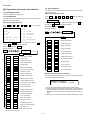
1
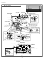
FO-DC600U
SERVICE MANUAL
No. 00ZFDC600USME
FACSIMILE
MODEL FO-DC600
MODEL
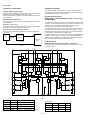
FO-DC600
SELECTION CODE DESTINATION
U
U.S.A./Canada
Chapters 1, 2, 3, 7 and 8 of this manual are omitted because they are partly common to the FO-4400U/
FO-DC500U. Please refer to previous service manual (00ZFO4400USME) / (00ZFODC500SME) for these
chapters.
OPTION
Toner cartridge:
Drum cartridge:
Option memory:
Verification stamp:
Paper cassette:
LAN Network interface kit:
Network printer kit:
Network scanner kit:
Dual line kit:
FO-50ND
FO-47DR
FO-8MK
FO-45VS
FO-CS1
FO-LN1
FO-NP1
FO-NS2
FO-60DL
NOTE:
• FO-NP1 (Network Printer Kit) and FO-60DL (Dual Line Kit) can not
be mounted simultaneously.
• FO-LN1 (LAN Network Interface Kit) and FO-60DL (Dual Line Kit)
can be mounted simultaneously. However, multi-operation of
2 line communication and network scan is not possible.
CAUTION
This laser printer is a class 1 laser product that complies with 21CFR 1040.10 and 1040.11 of the CDRH or IEC60825-1 standard. This
means that this machine does not produce a hazardous laser radiation. The use of controls, adjustments or performance of procedures
other than those specified herein may result in hazardous radiation exposure.
This laser radiation is not a danger to the skin, but when an exact focusing of the laser beam is achieved on the eyes retina, there is
danger of spot damage to the retina.
The following cautions must be observed to avoid exposure of the laser beam to your eyes at the time of servicing.
1) When a problem in the laser optical unit has occurred, the whole optical unit must be exchanged as a unit.
2) Do not look into the machine with the Main Switch turned on after removing the Toner/Developer unit and Drum Cartridge.
3) Do not look into the laser beam exposure slit of the Laser Optical Unit with the connector connected when removing and installing
the Optical Unit.
4) The cover of Laser Printer Unit contains the Safety Interlock Switch.
Do not defeat the safety interlock by inserting wedges or other items into the switch slot.
Laser Wave Length : 770-795 nm
Laser Pulse Times : 51.3 ns
Laser Output Power : 5 mW
Parts marked with " " is important for maintaining the safety of the set. Be sure to replace these parts with specified ones for
maintaining the safety and performance of the set.
SHARP CORPORATION
1-1
This document has been published to be used
for after sales service only.
The contents are subject to change without notice.
FO-DC600U
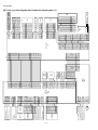
CONTENTS
• CAUTION FOR BATTERY REPLACEMENT
• PRECAUTIONS FOR USING LEAD-FREE SOLDER
CHAPTER 1. GENERAL DESCRIPTION
[1] Specifications . . . . . . . . . . . . . . . . . . . . . . . . . . . . . . . . . . . . . . . . . . . . . . . . . . . . . . . . . . . . . . . . . .
[2] Life of consumable . . . . . . . . . . . . . . . . . . . . . . . . . . . . . . . . . . . . . . . . . . . . . . . . . . . . . . . . . . . . . .
[3] Operation panel . . . . . . . . . . . . . . . . . . . . . . . . . . . . . . . . . . . . . . . . . . . . . . . . . . . . . . . . . . . . . . . .
[4] Refer to the service manual of FO-DC500U.
[5] Refer to the service manual of FO-DC500U.
[6] Refer to the service manual of FO-DC500U.
[7] Installing the Dual Line Kit (FO-60DL) . . . . . . . . . . . . . . . . . . . . . . . . . . . . . . . . . . . . . . . . . . . . . . .
[8] Installing the Third Paper Cassette (FO-CS1) . . . . . . . . . . . . . . . . . . . . . . . . . . . . . . . . . . . . . . . . .
1-1
1-1
1-2
1-4
1-5
CHAPTER 2. ADJUSTMENTS
[1] Adjustments . . . . . . . . . . . . . . . . . . . . . . . . . . . . . . . . . . . . . . . . . . . . . . . . . . . . . . . . . . . . . . . . . . . 2-1
[2] Diagnostics and service soft switches . . . . . . . . . . . . . . . . . . . . . . . . . . . . . . . . . . . . . . . . . . . . . . . 2-2
[3] Refer to the service manual of FO-4400U.
[4] Refer to the service manual of FO-4400U.
[5] Refer to the service manual of FO-4400U.
[6] Refer to the service manual of FO-4400U.
CHAPTER 3. MECHANICAL DESCRIPTION
[1] Refer to the service manual of FO-DC500U.
[2] Refer to the service manual of FO-DC500U.
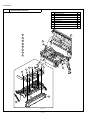
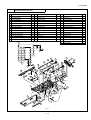
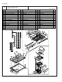
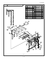
[3] Disassembly and assembly procedures . . . . . . . . . . . . . . . . . . . . . . . . . . . . . . . . . . . . . . . . . . . . . . 3-1
[4] Refer to the service manual of FO-4400U.
CHAPTER 4. DIAGRAMS
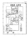
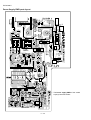
[1] Block diagram . . . . . . . . . . . . . . . . . . . . . . . . . . . . . . . . . . . . . . . . . . . . . . . . . . . . . . . . . . . . . . . . . 4-1
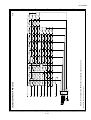
[2] Wiring diagram . . . . . . . . . . . . . . . . . . . . . . . . . . . . . . . . . . . . . . . . . . . . . . . . . . . . . . . . . . . . . . . . . 4-2
[3] Point-to-point diagram and connector signal name . . . . . . . . . . . . . . . . . . . . . . . . . . . . . . . . . . . . . 4-3
CHAPTER 5. CIRCUIT DESCRIPTION
[1] Circuit description . . . . . . . . . . . . . . . . . . . . . . . . . . . . . . . . . . . . . . . . . . . . . . . . . . . . . . . . . . . . . . . 5-1
[2] Circuit description of control PWB . . . . . . . . . . . . . . . . . . . . . . . . . . . . . . . . . . . . . . . . . . . . . . . . . . 5-1
[3] Circuit description of CIS unit . . . . . . . . . . . . . . . . . . . . . . . . . . . . . . . . . . . . . . . . . . . . . . . . . . . . . 5-15
[4] Circuit description of LIU PWB . . . . . . . . . . . . . . . . . . . . . . . . . . . . . . . . . . . . . . . . . . . . . . . . . . . . 5-16
[5] Circuit description of operation panel PWB . . . . . . . . . . . . . . . . . . . . . . . . . . . . . . . . . . . . . . . . . . 5-18
[6] Circuit description of power supply PWB . . . . . . . . . . . . . . . . . . . . . . . . . . . . . . . . . . . . . . . . . . . . 5-19
[7] Circuit description of Dual Line Kit (FO-60DL) . . . . . . . . . . . . . . . . . . . . . . . . . . . . . . . . . . . . . . . . 5-20
CHAPTER 6. CIRCUIT SCHEMATICS AND PARTS LAYOUT
[1] Control PWB circuit . . . . . . . . . . . . . . . . . . . . . . . . . . . . . . . . . . . . . . . . . . . . . . . . . . . . . . . . . . . . . 6-1
[2] LIU PWB circuit . . . . . . . . . . . . . . . . . . . . . . . . . . . . . . . . . . . . . . . . . . . . . . . . . . . . . . . . . . . . . . . 6-18
[3] Printer PWB circuit . . . . . . . . . . . . . . . . . . . . . . . . . . . . . . . . . . . . . . . . . . . . . . . . . . . . . . . . . . . . . 6-21
[4] Power supply PWB circuit . . . . . . . . . . . . . . . . . . . . . . . . . . . . . . . . . . . . . . . . . . . . . . . . . . . . . . . 6-25
[5] Operation panel PWB circuit . . . . . . . . . . . . . . . . . . . . . . . . . . . . . . . . . . . . . . . . . . . . . . . . . . . . . 6-27
[6] LCD Relay PWB circuit . . . . . . . . . . . . . . . . . . . . . . . . . . . . . . . . . . . . . . . . . . . . . . . . . . . . . . . . . 6-31
CHAPTER 7. OPERATION FLOWCHART
[1] Refer to the service manual of FO-4400U.
[2] Refer to the service manual of FO-4400U.
[3] Refer to the service manual of FO-4400U.
CHAPTER 8. OTHERS
[1] Service Tools . . . . . . . . . . . . . . . . . . . . . . . . . . . . . . . . . . . . . . . . . . . . . . . . . . . . . . . . . . . . . . . . . . 8-1
[2] Refer to the service manual of FO-4400U.
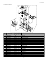
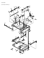
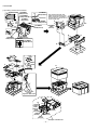
PARTS GUIDE
1–2
FO-DC600U
CAUTION FOR BATTERY REPLACEMENT
(French)
ATTENTION
Il y a danger d’explosion s’ il y a remplacement incorrect
de la batterie. Remplacer uniquement avec une batterie du
même type ou d’un type recommandé par le constructeur.
Mettre au rébut les batteries usagées conformément aux
instructions du fabricant.
(Swedish)
VARNING
Explosionsfare vid felaktigt batteribyte.
Använd samma batterityp eller en ekvivalent
typ som rekommenderas av apparattillverkaren.
Kassera använt batteri enligt fabrikantens
instruktion.
(German)
Achtung
Explosionsgefahr bei Verwendung inkorrekter Batterien.
Als Ersatzbatterien dürfen nur Batterien vom gleichen Typ oder
vom Hersteller empfohlene Batterien verwendet werden.
Entsorgung der gebrauchten Batterien nur nach den vom
Hersteller angegebenen Anweisungen.
(Danish)
ADVARSEL !
Lithiumbatteri-Eksplosionsfare ved fejlagtig håndtering.
Udskiftning må kun ske med batteri af samme fabrikat og type.
Levér det brugte batteri tilbage til leverandoren.
(English)
Caution !
Danger of explosion if battery is incorrectly replaced.
Replace only with the same or equivalent type
recommended by the equipment manufacturer.
Discard used batteries according to manufacturer’s instructions.
(Finnish)
VAROITUS
Paristo voi räjähtää, jos se on virheellisesti asennettu.
Vaihda paristo ainoastaan laitevalmistajan suosittelemaan
tyyppiin. Hävitä käytetty paristo valmistajan ohjeiden mukaisesti.
PRECAUTIONS FOR USING LEAD-FREE SOLDER
1 Employing lead-free solder
The Power supply PWB of this model employs lead-free solder. This is indicated by the “LF” symbol printed on the PWB
and in the service manual.
The suffix letter indicates the alloy type of the solder.
Example:
Indicates lead-free solder of tin, silver and copper.
2 Using lead-free solder
When repairing a PWB with the “LF” symbol, only lead-free solder should be used. (Using normal tin/lead alloy solder may
result in cold soldered joints and damage to printed patterns.)
As the melting point of lead-free solder is approximately 40ºC higher than tin/lead alloy solder, it is recommended that a
dedicated bit is used, and that the iron temperature is adjusted accordingly.
3 Soldering
As the melting point of lead-free solder (Sn-Ag-Cu) is higher and has poorer wettability (flow), to prevent damage to the land
of the PWB, extreme care should be taken not to leave the bit in contact with the PWB for an extended period of time.
Remove the bit as soon as a good flow is achieved.
The high content of tin in lead free solder will cause premature corrosion of the bit.
To reduce wear on the bit, reduce the temperature or turn off the iron when it is not required.
Leaving different types of solder on the bit will cause contamination of the different alloys, which will alter their
characteristics, making good soldering more difficult.
It will be necessary to clean and replace bits more often when using lead-free solder. To reduce bit wear, care should be
taken to clean the bit thoroughly after each use.
1-3
FO-DC600U
CHAPTER 1. GENERAL DESCRIPTION
[1] Specifications
• GENERAL
Applicable telephone line:
Public switched telephone network
Conventional Auto Dialing:
Rapid Key Dialing: 59 numbers
Speed Dialing: 200 numbers
Personal Auto Dial Books: 40 books
(59 Rapid Keys, 16 Speed Dial
numbers per book)
Compatibility:
ITU-T (CCITT) G3 mode, Super G3
mode
Printing resolution:
Horizontal: 406 dots/inch (16 dots/mm)
Vertical: 391 lines/inch (15.4 lines/mm)
600 x 600 dpi (Network Print: FO-NP1)
Memory size* :
16 MB (approx. 1,000 pages)
Optional memory: FO-8MK (8 MB;
approx. 500 pages)
Input document size:
Modem speed:
33,600 bps (max.) with automatic
fallback to lower speeds
Approx. 2 seconds
Automatic dialing:
Effective scanning width:
Automatic feeding:
Width: 5.8 to 10.1” (148 to 256mm)
Length: 5.0 to 14.3” (128 to 364 mm)
Manual feeding:
Width: 5.8 to 11.0” (148 to 279 mm)
Length: 5.0 to 19.0” (128 to 483 mm)
10.1” (256 mm) max.
Initial starter cartridge (included with
fax machine): Approx. 3000 pages
Replacement cartridge (FO-50ND):
Approx. 6000 pages
Initial starter cartridge (included with
fax machine): 20,000 pages (avg.)
Replacement cartridge (FO-47DR):
20,000 pages (avg.)
Effective printing width:
8.0” (203 mm) max.
Printing speed:
16 ppm
Reception modes:
Auto/Manual
Instascan speed:
1.3 sec/page (letter paper; scan time
only, excludes document feeding time)
Full Dual Access:
Yes
Standard: 203 x 98 lines/inch
(8 x 3.85 lines/mm)
Fine/Halftone: 203 x 196 lines/inch
(8 x 7.7 lines/mm)
Super fine: 203 x 391 lines/inch
(8 x 15.4 lines/mm)
Ultra fine: 406 x 391 lines/inch
(16 x 15.4 lines/mm)
Copy function:
Single/Multi/Sort (99 copies/page)
Power requirements:
120 V AC, 60 Hz
Operating temperature:
50 - 86°F(10 - 30°C)
Humidity:
20 to 85 % RH
Power consumption:
Stand-by: 9 W
Stand-by(all options installed: 16W
Maximum: 800 W
Automatic document feeder: Letter paper (20 lb): Max. 50 pages
Legal paper: Max. 20 pages
(Note: 11” x 17” paper must be loaded
one page at a time.)
Dimensions:
Width: 21.5” (546 mm)
Depth: 16.2” (412 mm)
Height: 17.0” (431 mm)
(Not including paper tray or attachments)
Paper capacity:
750 sheets (20 lb)
(500-sheet cassette available as option)
Weight:
Compression scheme:
MMR, MR, MH, Sharp (H2), JBIG
Approx. 48.5 lbs. (22.0 kg)
(Not including supplies paper tray or
attachments)
Transmission time* :
Toner cartridge yield:
(continuous printing,
4% page coverage,
letter paper)
Drum cartridge yield:
Resolution:
Halftone (grayscale):
64 levels
* Based on ITU-T Test Chart #1 at standard resolution, excluding time for
protocol signals (i.e., ITU-T phase C time only).
<IMPORTANT PLEASE READ FIRST>
To avoid problems with supplies, please don’t use supplies from other units. Please use new supplies, when supply changes are required.
[2] Life of consumable
Section
Part
Estimated Life
Replaced by
Toner cartridge
Replacement cartridge
(FO-50ND)
6,000 prints
(at Letter/4% chart)
User
Drum cartridge
Replacement cartridge
(FO-47DR)
20,000 prints
(at Letter/4% chart)
User
Paper feed
Transfer roller (Refer to the P/G No. 10-8)
(0KW4127410302)
50,000 prints
Service Engineer
Fuser
Fusing unit (Refer to the P/G No. 9-14)
(0KW4127035501)
50,000 prints
Service Engineer
Paper transport
Paper transfer roller (Refer to the P/G No. 8-6)
(0KW4127300101)
Cleaning as needed
———————
1–1
FO-DC600U
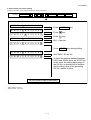
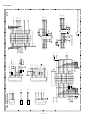
[3] Operation panel (1)
1
2
3
4
5
6
DOCUMENT COMMUNICATION SYSTEM
HALF TONE
ALARM
STANDARD
TONER
FAX1
FINE
FAX2
Network
SUPER FINE
DATA
ON LINE
ULTRA FINE
e-mail
CONTRAST
7
RESOLUTION
ON LINE
9
10
8
02
Q / !
11
03
W / "
12
SYMBOL
21
31
A / |
14
S
Z / <
X / >
Q / !
50
R / $
53
S
B
H / }
When the dual line option is installed, FAX 1 lights when
Line 1 is being used and FAX 2 lights when Line 2 is being
used. When the dual line option is not installed, only FAX 1
lights when the telephone line is being used (the FAX 2
light does not operate).
N / *
18
44
45
T / %
Y / &
54
55
F
19
@
47
U / '
56
21
I / (
7 CONTRAST key
O / )
58
P / =
59
J / [
K / ]
8 E-mail key
L / +
TIMER
COVER SHEET
LIFE
MEM.STATUS
REPORT
DOCUMENT
Caps Lock
Z / <
X / >
C
V
B
N / *
M / ?
@
.com
SHIFT
/ ^
/ / \
; / :
_
-
. / ,
DEL
Space
Press this key to adjust the contrast before sending or
copying a document.
49
LINE
PAGE COUNTER CONFIDENTIAL
When this light is on, the machine can receive data (print
jobs) over the network. The light is turned on or off with the
ON LINE key. (Only available when the network printer
option is installed).
DEL
48
57
H / }
6 ON LINE light
.com
39
. / ,
20
L / +
30
38
-
46
G / {
K / ]
M / ?
This blinks when the machine is receiving a print job over
the network (only when the network printer option is
installed).
P / =
20
29
37
_
17
D
J / [
5 DATA light
10
O / )
19
28
36
Space
09
I / (
18
27
35
16
08
U / '
17
26
V
43
52
A / |
07
G / {
25
15
E / #
51
SYMBOL
16
; / :
42
W / "
15
C
/ / \
41
Y / &
34
11 12 13 14
40
06
T / %
F
24
33
/ ^
05
D
23
32
SHIFT
R / $
13
22
Caps Lock
04
E / #
This displays messages and prompts to help you operate
the machine.
2 TONER indicator
This blinks when the toner cartridge nears empty, and lights
steadily when the toner cartridge needs replacement.
3 ALARM indicator
This blinks when one of the paper sources is empty or the
drum cartridge is near the end of its life (printing is still
possible). This lights steadily when the drum cartridge has
reached the end of its life, all paper sources are empty, the
print compartment cover is open, or a paper jam has
occurred (printing is not possible). A message will appear in
the display to indicate the problem.
4 FAX 1 / FAX 2 lights
11
01
1 Display
Press this key to send a scanned document to an e-mail
recipient. (Only available when the network scanner option
is installed).
9 RESOLUTION key
Press this key to adjust the resolution before sending or
copying a document. An indicator will light next to the
selected setting (HALFTONE, STANDARD, FINE, SUPER
FINE or ULTRA FINE).
22
23
24
JOB STATUS DUPLEX SCAN
ABC
1
GHI
2
4
5
OPER
10 ON LINE key
30
Press this key to select whether the machine is online or
off-line (the ON LINE light is on when the machine is
online). The machine must be online to receive print
jobs over the network. (Only available when the network
printer option is installed).
MENU
UP
COPY/HELP
11 Rapid Dial Keys
SPEED DIAL
6
Z
START/
ENTER
Press one of these keys to dial a fax number automatically,
or specify an e-mail recipient if the network scanner option
is installed. Note that you must attach the Rapid Key labels.
When navigating through the display menu, a Rapid Key
can also be pressed in place of the numeric keys to enter
a two-digit number (for example, you can press Rapid Key
01 to enter the number "01").
A
REDIAL
9
STOP
SPEAKER
0
31
29
3
WXYZ
8
7
BROADCAST
PERSONAL
BOOK
MNO
TUV
PQRS
PRIORITY
DEF
JKL
25 26 27 28
DOWN
32
33 34
35
12 SYMBOL key
36
When entering a name, press this key to enter the symbol
on a letter key (the character to the right of the slash).
Press the key again to turn off symbol entry mode.
13 PAGE COUNTER key
Press this key to include a slash and the total number of
pages after each page number on the pages of a
transmitted document.
14 CONFIDENTIAL key
Press this key to send or print out a confidential document.
1–2
FO-DC600U
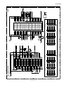
Operation panel (2)
15 TIMER key
30 COPY/HELP key
Press this key to set a fax operation to be performed
automatically at a later time.
When a document is in the feeder, press this key to make a
copy of a document. At any other time, press this key to print
out the Help List, a quick reference guide to the operation of
your fax machine.
16 COVER SHEET key
Press this key to include a cover sheet when sending a fax.
17 LIFE key
Press this key, followed by
START/
ENTER
31 Dial keypad (numeric keys)
, to check the total number of
STOP
pages printed by the fax machine. (Press
data and time display.
to return to the
Use these keys to dial and program fax numbers.
32 REDIAL key
Press this key to automatically redial the last number dialed.
18 MEM. STATUS key
Press this key to check the status of fax transmission jobs,
copy jobs, and fax receptions. This key can also be used to
cancel a job.
33 SPEAKER key
Press this key when transmitting a document by Normal
Dialing to listen to the line and verify the response of the
receiving fax machine.
19 REPORT key
Press this key to print out a report on the most recently
completed transmission or reception.
34 START/ENTER key
Press this key to begin fax transmission when using Speed
Dialing, Direct Keypad Dialing, or Normal Dialing. This key is
also used to select settings in the MENU key menu and
complete entries when storing names and numbers.
20 DOCUMENT key
Press this key to transmit a document directly from the feeder
without reading it into memory.
21 LINE key
35 Left and right arrow keys
When the dual line option has been installed, press this key
before dialing to select the line.
22 JOB STATUS key
Press this key to display the FAX-STATUS screen, which
shows information on the fax job that is currently in progress.
If the dual line option is installed, the fax status will appear
separately for each line. If the network printer option is
installed, the NETWORK PRINT STATUS screen showing
information on current printer activity will appear following
the FAX STATUS screen (note that "IDLE" will appear if a
print job has been executed but is not yet being printed).
To cancel a job that is in progress, display the job in the
STOP
status screen and then press
. To move through each of
the screens and return to the date and time display, press
JOB STATUS
one or more times as needed.
Auto-dial numbers: Press these keys to search for an
auto-dial number when sending a fax.
36 STOP key
Press this key to cancel an operation before it is completed.
23 DUPLEX SCAN key
Press this key to transmit or copy a two-sided document.
24 PRIORITY key
Press this key when you need to transmit a document ahead
of other documents waiting in memory for transmission.
25 BROADCAST key
Press this key to send a document to a group of fax
machines, or to a group of e-mail recipients if the network
scanner option is installed.
26 PERSONAL BOOK
Press this key to use or store an auto-dial number in a
personal book. If the book has a passcode, enter the
passcode; otherwise, select the book with
or
and
ENTER .
press START/
27 SPEED DIAL key
[4] Transmittable documents
Press this key to dial a Speed Dial number.
28 MENU key
Refer to the service manual of FO-DC500U.
Press this key to select special functions and setting.
[5] Installation
29 UP and DOWN arrow keys
Refer to the service manual of FO-DC500U.
Volume setting: Press these keys to change the speaker
volume when the SPEAKER key has been pressed, or the
ringer volume at any other time.
MENU key settings: Press these keys after pressing the
MENU key to scroll through the MENU key settings.
[6] Quick reference guide
Refer to the service manual of FO-DC500U.
1–3
FO-DC600U
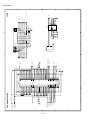
5 a. Attach the LIU board to the metal plate, positioning the modular
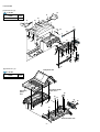
[7] Installing the Dual Line Kit (FO-60DL)
jacks as shown. The bottom edge of the board should fit into the
slots indicated by the arrows. Secure the LIU board with two of the
6 mm screws.
b. Attach the provided metal side plate.
Note: The FO-60DL Dual Line Kit cannot be installed if the FO-NP1
Network Printer Kit is installed.
Important! The following procedure is to be performed only by a qualified service technician. Be sure to turn off the power, unplug the power
cord, and unplug the telephone line before proceeding. In addition, touch
a grounded piece of metal to discharge any static electricity that may be
on your body. Make sure that an extension phone is not connected to
the machine.
Press the cover release to open the print compartment cover.
a
1
b
6 Replace the metal plate and secure with screws in the order shown.
2 Remove 6 screws from the rear cover.
1
(Remember which screw secures the small cover on the left side of
the rear cover, as it must be replaced in the same position).
Remove the small cover, and then remove the screw underneath.
Remove the rear cover.
3
4
2
7 Attach the dual line control board.
a. Insert the bushing into the hole in the dual line control board from
the outer side and secure it with the collar on the inner side.
b. Insert the winged end of the pin spacers into the metal plate, with
wings extended out vertically.
c. Attach the board so that the connector inserts into the connector in
the metal plate. Make sure that the pin spacers go into the holes
in the board. Secure the board with the 18 mm screw (which goes
into the bushing) and the remaining 6 mm screw. Tighten the
screws in the order shown.
3 Remove 6 screws and then remove the metal plate.
b
c
2
4 Remove the screw that holds the small side plate to metal plate that
a
was removed Step 3. Slide the small side plate up and remove it
from the metal plate. (Note: The small side plate is not no longer
needed, however, the screw is used again in “b” of Step 5.)
1
8 Fasten the band to the core as shown and cut off the excess end.
Insert the cable through the core and wind it around the core twice.
1–4
FO-DC600U
9 Connect the cable to the LIU board and the dual line control board.
4 Place the machine on top of the third cassette, and remove the small
Secure the core band with the 10 mm screw.
cover from the rear of the second cassette. Connect the 10-pin cable
as shown, and insert it behind the guide indicated by the white arrow.
F Replace the rear cover.
(Be sure to replace the screw that secures the small cover in the
same position, as it is for plastic.)
5 Change the positions of the connectors on the circuit board of the
third cassette as shown (do not change the connectors on the second cassette). Replace the small cover on the rear of the second
cassette, and attach the provided small cover on the rear of the third
cassette.
For plastic
G Affix the “”LINE 2” label above the new jack.
6 Attach the large support plate and then the small support plate to the
right side of the cassettes. Use 6 mm screws for the holes marked
with “A”, and 10 mm screws for the holes marked with “P”. Secure
the screws in the order indicated by the numbers.
LINE 2
[8] Installing the Third Paper Cassette (FO-CS1)
Important! Be sure to turn off the power and unplug the power cord
before proceeding.
Remove the packing material and tape from the third paper cassette.
Remove the covers from the sides of the second cassette (the cassette already installed on the machine), using a flat-head screwdriver
to pry each of the catches at the bottom of the covers free (2 on the
right cover, 3 on the left cover).
1
2
2
A4
A4
P4
A3
1
P3 A3
A2
A1
7 Attach the support plate to the left side of the cassette. Use 6 mm
screws for holes marked with “A”, and 10 mm screws for holes marked
with “P”, securing the screws in the order indicated by the numbers.
(Note that the top hole on the right does not require a screw.)
3 Insert the green gear into the third cassette as shown. The side of
the gear that has the small thirdly gear should face the inside of the
cassette, and should fit onto the metal shaft. Push the gear in until
the tab on the outer side goes into the slot on the metal shaft. (Note:
The gear is only used in the third cassette.)
A4
A3
P6
P5
A2
1–5
A1
FO-DC600U
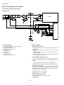
CHAPTER 2. ADJUSTMENTS
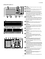
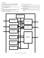
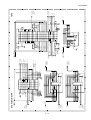
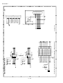
2. IC protectors replacement
[1] Adjustments
ICPs (IC Protectors) are installed to protect the CIS unit, panel PWB
unit, TX motor drive circuit and verification stamp drive circuit. ICPs protect various ICs and electronic circuits from an overcurrent condition.
The location of ICPs are shown below:
General
12
CNLIU1
1
CNPW1
Since the following adjustments and settings are provided for this model,
make adjustments and/or setup as necessary.
1. Adjustments
CONTROL PWB
(TOP SIDE)
Adjustments of output voltage (FACTORY ONLY)
1. Install the power supply unit in the machine.
2. Set the recording paper and document.
3. When the document is loaded, power is supplied to the output lines.
Confirm that outputs are within the limits below.
1
2 CNSP1
1
Output voltage settings
CNSEN1
8
F1
CONTROL PWB
F5
F100
F2 28
2
CNCIS1 CNPN1
10
1 27
1 2 14 1
POWER
SUPPLY
PWB
CNSTP1
CN5
(1)
CN1
12 8
1
CNPW1
CNPRT1
12
8
1
CN1
CN7
1
10
VR51
30
1
30
(2)
(3)
CN1
10
CN4
1
PRINTER PWB
1
(4)
(5)
[DO NOT TOUCH!]
Fig. 1
Connector
No.
Pin No.
1
11
2
10
3
9
4
8
5
7
6
6
7
5
8
4
9
3
10
2
Voltage limits
4.947V~5.25V
23.04V~24.96V
CN4
CN1
+5V
CH LREM
T VR
T MON V
T MON I
B VR
V REM
C MON
MG
+24V
F102
F1/F2/F5:Top side
F100/F101/F102:Bottom side
Fig. 2
1
Output
+5V MAIN
+24V SUB
IC3
CNTXM1
1
HIGH VOLTAGE
PWB
F101
Note
CN5 7pin ↔ 8pin
CN5 1pin ↔ 2pin
Connector
No.
Pin No.
1
2
3
4
5
6
7
8
9
10
11
12
CN5
Connector
No.
Pin No.
1
2
3
4
5
6
7
8
CN1
CNPW1
+24V SUB
MG
MG
MG
+24V MAIN
+24V MAIN
+5V MAIN
DG
DG
DG
+5V MAIN
+5V MAIN
F1 (ICP-S0.5) F2 (ICP-S1.0) is installed in order to protect IC’s from an
overcurrent generated in the CIS unit. If F1 or F2 are open, replace it with a
new one.
F5 (ICP-S1.0) is installed in order to protect IC’s from an overcurrent generated in the panel PWB unit. If F5 is open, replace it with a new one.
F100 (ICP-S1.0) is installed in order to protect IC’s from an overcurrent generated in the verification stamp drive circuit. If F100 is open, replace it with a
new one.
F101 (ICP-S1.8) is installed in order to protect IC’s from an overcurrent generated in the TX motor drive circuit. If F101 is open, replace it with a new one.
F102 (ICP-S0.7) is installed in order to protect IC’s from an overcurrent generated in the LCD drive circuit. If F102 is open, replace it with a new one.
In addition to the replacement of F1, F2, F5, F100, F101 andF102 the factor
causing F1, F2, F5, F100, F101 and F102 to open must also be repaired. If
not, F1, F2, F5, F100, F101 and F102 will open again.
Replacement parts
ICP-S0.5 (Sharp code: VHViCPS05//-1)
ICP-S0.7 (Sharp code: VHViCPS07//-1)
ICP-S1.0 (Sharp code: VHViCPS10//-1)
ICP-S1.8 (Sharp code: VHViCPS18//-1)
3. Settings
(1) Dial mode selector
OPTION SETTING: DIAL MODE (Soft Switch No. SW2 DATA No. 1 for
Line-1 and SW24 DATA No.1 for Line-2 with Optional Dual Line Kit)
Use this to set the fax machine to the type of telephone line you are on.
• The factory setting is "TONE".
(step 1) Select "OPTIONAL SETTING".
MENU
KEY:
4
DISPLAY: 4:OPTIONAL SETTING
ENTER #(01-36, , )
(step 2) Select "DIAL MODE".
KEY:
2 2
<With optional line unit>
DISPLAY: 22: DIAL MODE
1=TONE, 2=PULSE
22: DIAL MODE
1=LINE-1, 2=LINE-2
Select line using "1" or "2"
KEY:
CN7
+24V MAIN
MG
DG
DG
+5V MAIN
+5V MAIN
HEATER ON
H-RELAY OFF
1
DISPLAY: 1: LINE-1
1=TONE, 2=PULSE
KEY:
2
DISPLAY: 2: LINE-2
1=TONE, 2=PULSE
(step 3) Select, using "1" or "2".
KEY:
1
DISPLAY: TONE SELECTED
KEY:
2
DISPLAY: PULSE SELECTED
(step 4) End, using the "STOP" key.
KEY:
2–1
STOP
FO-DC600U
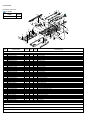
1-2. Print diagnosis
[2] Diagnostics and service soft switches
This diagnosis is concerned with the print which is used for production
and service support.
1. Operating procedure
Entering the diagnostic mode
Two kinds of diagnoses are supported.
9
Press MENU
display will appear.
1-1. Fax diagnosis
This diagnosis is concerned with the main body of fax which is used for
production and service support.
8
1
Line
2nd
Line
: TA70
3rd
Line
F/W version
NIC
:x.xxx
4th
Line
NIC board version
5th
Line
PCL board version
6th
Line
PRN MEMORY SIZE = 16(MB)
7th
Line
Memory size
GAA : ESx
8th
Line
GATE arrayA/B version
9th
Line
GAB : ESx
Enter the mode with the START key.
MENU
key
START key.
(Diag • specifications)
9
MENU
8
7
9
8
6
PCU ROM Ver.:
START
Then press the START key. Select the desired item with the
and the
key or select with the rapid key.
Enter the mode with the
the
(Diag • specifications)
FAX
PRN :xxxx
Then press the START key. Select the desired item with
key and the
key or select with the rapid key.
7 , and the following
st
6 , and the following
PCU ROM VER.:
Entering the diagnostic mode
9
Press MENU
display will appear.
8
TA70
START
01
START
AREA PRINT MODE 1
02
START
CHECK PATTERN 1
03
START
CHECK PATTERN 2
04
START
CHECK PATTERN 3
05
START
CHECK PATTERN 4
06
START
PAPER FEED AGING 1
A
START
SOFT SWITCH MODE
07
START
PAPER FEED AGING 2
B
START
PRINT AREA
08
START
BIAS ADJUST MODE2
C
START
ROM & RAM CHECK
09
START
LIFE SET MODE
D
START
AUTO FEEDER MODE
E
START
AGING MODE
10
START
LIFE ALL CLEAR
F
START
PANEL CHECK MODE
11
START
LIFE ENTRY MODE
12
START
LIFE CLEAR MODE
G
START
OPTICAL ADJUST MODE
H
START
PRODUCT CHECK
I
START
SIGNAL SEND MODE
Memory clear when power is turned on
J
START
COMM. CHECK MODE
K
START
MEMORY CLEAR MODE
Pressing the START and STOP keys, turn on the main power, and the
following message will be displayed.
L
START
FLASH MEMORY CHECK
M
START
ALL FAX/TEL. ENTRY MODE
N
START
DEPT. PASSCODE
O
START
CONF. PASSCODE
P
START
SIGNAL SEND MODE 2
Q
START
MEMORY SET MODE
R
START
STAMP AGING MODE
S
START
DIAL TEST MODE
T
START
COPY DIAG MODE
U
START
LCD CHECK MODE
V
START
PERSONAL BOOK LIST
W
START
FONT LIST PRINT MODE(*)
X
START
NO FUNCTION
MEMORY CLEAR ?
1 = ALL , 2 = IMAGE , 3 = NO
1 = All the data will be deleted including initially registered data.
2 = Delete the image file to be used in transmission. This will delete all
the data related to communication such as reserved transmission or
intercepting. However, the data initially registered will not be deleted.
3 = Memory will not be cleared and the machine enters stand-by mode.
*: FONT LIST PRINT MODE can be used only when the
network function is effective.
2–2
FO-DC600U
•
2. Diagnostic items description
2-1. Fax diagnosis
A) Soft switch mode
•
In this mode, the soft switch are set and the soft switch list is printed.
Soft switch mode screen
SOFT SWITCH MODE
SW01=00000000
Switch 1 2 3 4 5 6 7 8 :DATA No.
No.
Data
1 Switch number selection
•
•
•
Press START key for setting of the next soft switch. If the soft
switch number is the final, pressing START key will exit the soft
switch mode.
Enter two digits of a soft switch number to set the switch number.
If a switch number of nonexistent soft switch is entered, key error
buzzer sounds to reject the input.
ENTER LAST DIGIT
SW1
SOFT SWITCH MODE
SW01=00000000
1
OFF to ON of department control function during use of image
memory.
(Note: In the existing set, the department control function is set
from OFF to ON when the timer communication (including the
batch sending) or the memory hold is set.)
ON to OFF of continuous serial polling function when the continuous serial polling is started.
(Note: In the existing set, "ON to OFF of the continuous serial
polling function when the continuous serial polling is registered"
has been applied, but the conditions are now moderated. However, registration is impossible to the program of the new continuous serial polling when the continuous serial polling function is
OFF.)
In addition, change of all soft switches during communication
B) Print area
According to the size of the specified sheet, the effective printing area is
printed.
C) ROM & RAM check
This is an item to check if the loaded memory device acts normally.
• The memory devices shown in the following table are checked.
• In case that an error occurs in the device check, the alarm buzzer
shown in the table sounds.
SOFT SWITCH MODE
SW16=00010110
6
2 Data number selection
Cursor
Check device and alarm buzzer
The cursor position shows the data to be set.
Pressing # key or → key moves the cursor to the right. If, however,
the cursor is on data number 8, pressing # key or → key shifts the
cursor to data number 1 of the next switch number. If the switch
number is the final, pressing # key or → key will exit the soft switch
mode.
Pressing
key or ← key moves the cursor to the left. If, however,
the cursor is on data number 1, pressing key or ← key shifts the
cursor to data number 1 of the former switch number. If the switch
number is 1, pressing
key or ← key will not move the cursor and
the error buzzer will sound.
No.
Device checked
1
Number of buzzer sound
ROM (PROGRAM FLASH) <Short sound> 1 time
2
SRAM
3
Main D-RAM1 (*1)
4
D-RAM2 (*2)
5
Remarks
<Short sound>:
<Short sounds> 2 times 0.5 sec.ON / 0.5 sec.OFF
<Short sounds> 3 times <Long sounds>:
<Short sounds> 4 times 1.0 sec.ON / 0.5 sec.OFF
—
—
*1: Work memory (SDRAM 8 MB)
*2: Page memory (SDRAM 16 MB)
3 Data setting method
(Example of display) In case that DRAM2 is erroneous.
Press the MENU key, and the data at the position of the cursor will be
reversed to 0 when it is 1, or to 1 when it is 0. (If the soft switch can
be changed at the bit (Refer to .), the error buzzer will sound with
the process not received.)
Display during check
6
Display after check
ROM SRM DRM1 DRM2
ROM SRM DRM1 DRM2
4 Outputting method of soft switch list
•
•
•
P
•
P=PASS
In the soft switch mode, press the REPORT key, and the soft switch
list will be output.
If the recording paper runs out or is clogged, the key error buzzer will
sound with the process not received.
P
P
E=ERROR
• After the check is complete, the result is outputted.
• In case that an NIC and a PCL board are mounted,
5 Storage of data
E
the version
information of the board is also printed on the result.
In the following case, the data of the soft switches set will be stored.
• It is shifted to set the next soft switch by pressing the START
switch.
• It is shifted to set the next soft switch with the [#] key.
• It is shifted to set the last soft switch with the [ ] key.
• It is shifted to set another soft switch by inputting two digits as the
switch number. (When 2 digits are completely input.)
• Output of the soft switch list is started.
D) Auto feeder mode
By executing the document insertion and discharge, the automatic feeding function can be checked. And the document sensor can be checked
as well.
Set the document
Before pressing the “START” key, only the document sensor check is
carried out. And as the document sensor is ON, the document size
(A4/B4) and the sensor information (A4/B4/ORG) are displayed.
1
6 Inhibition of data change
(This is also applicable for the optional setting.)
In the following case, it is inhibited to change the data with the key
error buzzer.
• Switching ON/OFF of ECM during the use of image memory.
• OFF to ON of telephone billing function which is using the image
memory is used (Note: In the existing set, the telephone billing
code function is specified from OFF to ON when the timer system
communication (including the batch communication) is set.)
Here, the memory is usable when the telephone billing code function is on. It can be set from ON to OFF while the memory is
used. However, if setting is practically changed even once, it can
not be returned from OFF to ON.
AUTO FEEDER MODE
(
)
After setup of the document
AUTO FEEDER MODE
B4 (A4 B4 ORG)
Only the sensor which is
activated (fallen down) is displayed.)
The paper sheet size (A4/B4) is
displayed.
2 The automatic feeding starts by pressing the “START” key. This mode
ends when the document ends, and the result is printed.
2–3
FO-DC600U
E) Aging mode
I) Signal send mode
This is a mode to execute the copying action and the check pattern
printing action once every 60 minutes and continue the action until 10
sheets are outputted in total.
The printing action on the 1st sheet starts by pressing down the
“START” key and entering the mode. When document is set at the
time of the mode start-up the copy action is carried out, and when
the document is not set the “check pattern 1” of the print dialog is
printed.
The number of printouts is displayed after printing.
It can be used to check the modem.
When the START key is pressed, silence signal (make loop) will be
executed. The following signals are sent by pressing the START key
thereafter.
[ 1] No signals (make loop)
[ 2] 4800BPS (V. 27ter)
[ 3] 14400BPS (V. 33)
[ 4] 12000BPS (V. 33)
[ 5] 14400BPS (V. 17)
[ 6] 12000BPS (V. 17)
[ 7] 9600BPS (V. 17)
[ 8] 7200BPS (V. 17)
[ 9] 9600BPS (V. 29)
[10] 7200BPS (V. 29)
[11] 4800BPS (V. 29ter)
[12] 2400BPS (V. 29ter)
[13] 300BPS (FLAG)
[14] 2100Hz (CED)
[15] 1100Hz (CNG)
1
2
F) Panel check mode
This is to check that each key acts normally and this is displayed on the
LCD according to the key input. And during execution, the document
reading lamp is ON. After inspection start, the LEDs light on sequentially.
At the mode end with the “STOP” key, all of them go OFF. As to the test
result, it is printed out after the mode end.
When the “NUMERIC” key is pressed during the panel check execution, sending of the DTMF signal corresponding to the key starts,
and when another key is pressed sending of the DTMF signal stops.
(Softswitch change is required. SW80 No.6: 0 →1)
• After inputting all the keys, input the “STOP” key at last, and then the
result is displayed.
a) In case that all the keys are pressed.
1 Turn on the Line Monitor. (SW7 No.7, SW29 No.7)
2 Turn off the Cover Sheet Function. (SW2 No.6, SW24 No.6)
3 Set Line Equivalence at 0 km. (SW8 No.1/No.2, SW30 No.1/No.2)
4 Set the copy cut off mode (SW75 No.2) to “Continue”
5 Set the ringer volume (SW62 No.5/No. 6) to OFF.
J) Comm. check mode
PANEL CHECK MODE
ALL KEY OK !!
After the check, it is necessary to be sure to return the aforementioned
soft switches into the initial state.
(Clear the memory with the diagnosis.)
• Until the STOP key is pressed, all black 4-split sequential display is
performed.
• After the mode end, the test result is printed.
K) Memory clear mode
b) In case that there is a key that is not pressed.
Clear the back-up memory to initialize the soft switches.
The Flash Memory will be initialized. Then, the initialized list be output.
Memory clear is executed.
The result that says initialized is printed.
1
2
PANEL CHECK MODE
KEY ERROR !!
• Until the STOP key is pressed, all black 4-split sequential display is
NOTE: The life counter, and the adjustment values of the top void and
the large LCD contrast are not cleared.
performed.
• After the mode end, the test result is printed.
L) Flash Memory check
G) Optical adjust mode
This is a mode to check that the flash memory acts normally. The flash
memories shown in the following table are checked.
The optical system is adjusted.
• By pressing down the “START” key, the document reading lamp “100%:
ON” is turned ON.
No.
H) Product check
This is a dialog used in the production process and a mode to execute a
specific mode in the series of the flow.
After the mode end, the rest result as to the checked items is printed.
• After moving to the mode, the following actions are sequentially executed.
•
Flash memory
Number of buzzer sound
Remarks
1
NOR-Flash (Standard) <Long sound> 1 time
<Short sound>:
2
NAND-Flash (Standard) <Long sounds> 2 times 0.5 sec.ON / 0.5 sec.OFF
3
NAND-Flash (Option)
4
—
—
5
—
—
<Long sounds> 3 times <Long sounds>:
1.0 sec.ON / 0.5 sec.OFF
NAND-Flash (optional) is valid only when the optional memory is
mounted.
The NOR flash memory test is executed.
1
1 Memory clear (Same as Diagnosis K)
2 Panel check (Same as Diagnosis F)
3 ROM & RAM test check (Same as the Diagnosis C)
4 Test result print
NOR FLASH CHECK
S
——————— E
2 The concerned alarm buzzer sounds only when the error occurs.
3 The NAND flash memory test is executed.
Memory clear printing
Panel check result printing
ROM & RAM test result printing
NAND FLASH CHECK
S
——————— E
4 The concerned alarm buzzer sounds only when the error occurs.
5 The result is printed.
5 Print area (The specification of each item is the same as the specifi
cation of the simple mode.)
NOTE:
• During operation of this diagnosis, dual operation is not possible at all.
• If this is excessively repeated, it will shorten the life of the flash memory.
2–4
FO-DC600U
M) All FAX/TEL. entry mode
Q) Memory set mode
This is a function to copy the FAX and TEL numbers registered in the
one-touch dialing (RAPID) key [01] to the all one-touch dialing (RAPID)
key and the all abbreviated number (SPEED DIAL) to simplify the FAX
and TEL number registration at the time of aging. (Only the E-MAIL can
be used for the network models.)
The set and dump list of the memory content is output.
MEMORY SET MODE
AD = 00000000
Cursor
1 Copy the FAX/TEL number or the E-MAIL stored in the RAPID key
[01] to all RAPID keys.
2 Copy the FAX/TEL number or the E-MAIL stored in the RAPID key
[01] to all SPEED DIAL numbers.
3 If the chain dial is not set for the RAPID key, or RAPID key [01] stores
•
4
•
During data inputting, the address can be moved forward and backward one byte by one byte with " " and "#". (The address prior to the
address 0 is looped as the maximum address.)
•
The Validity of the address is not checked. Accordingly, writing/ reading operations are possible in the address of the memory not assigned, the address of ROM and so on.
(However, as practical, writing is not done, and the data content runs
short each reading.)
Though writing is possible in the flash memory, a little time is required.
It is also necessary to take care that the life of the flash memory is
excessively shortened if much data is written in the flash memory.
Since it may run away depending the written content, take minute
care for the writing address.
•
When the REPORT key is input, the memory dump list is produced
from the displayed address (here, it is limited at the 16-byte boundary address (address with end 0) which does not exceed the specified address and is just in front.). The dump list is output to a maximum of 99 pages. If any data of one page can be repeatedly developed and printed, the list is sufficient. But it is not desired that the
content of plural pages are developed in the memory once and are
then printed. If the STOP key is pressed, it will pass to the diagnosis
after the page which is now being printed is completed printed.
If the address exceeds the maximum address, it will return to the
address 0 and printing will be continued.
MEMORY SET MODE
AD = A02800F6 DATA = 0B
the E-MAIL, the RAPID keys [02] – [59] and all SPEED DIAL numbers are stored in the group number [01].
Enter all registered one-touch send (RAPID) keys and speed dial
numbers (SPEED DIAL) on the personal books [01] - [10].
Following this, set the password registration and the password
setting to ON, and set the TTI setting to OFF.
The call-receiver names and book names are specified as follows:
Rapid
SPEED DIAL
R XX
S XXX
Personal book BOOK XX
The address (8 digits (P) generally including the bank information is
input, and the data of 2 digits is continuously input.
Inputting is done in the hexadecimal mode. The ten-key is used for 0
through 9, and the alphabetic keys A (RAPID 01 through 06) are
used for A through F.
XX : Rapid key send
XXX : Speed dial number
XX : Book number
(The letters after 16th letter of the call-receiver’s name registered in the
one-touch dialing [01] are cut off.)
NOTE: Before entering this mode, a FAX/TEL number or an E-MAIL
must be stored in the RAPID key [01]. (This program will not be
executed if there is no data stored, or otherwise a program or a
group is registered.)
N) Dept. passcode
The department passcode list is printed.
O) Conf. passcode
The confidential passcode list is printed.
Differing from printing of one box alone soon after registration, the confidential passcodes of all boxes are printed.
P) Signal send mode 2
The signals concerned with V.34 & V.8 are checked. It can be used to
check the modem.
When the START key is pressed, silence signal (make loop) will be
executed. The following signals are sent by pressing the START key
thereafter.
[ 1] No signal (make loop)
R) Stamp aging mode
This is a mode to execute the continuous drive aging of the Verification
stamp.
1 Set the document and press down the “START” key and the
continuous drive of the Verification stamp starts.
2 Send the document at the interval of 10 mm and stamp the
[ 2] 33600BPS (V. 34)
Verification stamp continuously. The total number of times of
Verification stamp printing after entering this mode is displayed on
the display.
• Displayed screen during execution
[ 3] 31200BPS (V. 34)
[ 4] 28800BPS (V. 34)
[ 5] 26400BPS (V. 34)
STAMP AGING
[ 6] 24000BPS (V. 34)
TIMES = 13 PAGES = 1
[ 7] 21600BPS (V. 34)
Print total number
of times
[ 8] 19200BPS (V. 34)
Page number
3 By pressing down the “STOP” key during the action, or when no more
[ 9] 16800BPS (V. 34)
document is left, the continuous drive of the Verification stamp stops.
NOTE:
• In case that the document is not set, this cannot be executed.
• The normal action aging that one Verification stamp is pressed on one
sheet of document is executed in the normal copying.
[10] 14400BPS (V. 34)
[11] 12000BPS (V. 34)
[12] 9600BPS (V. 34)
[13] 7200BPS (V. 34)
[14] 4800BPS (V. 34)
[15] 2400BPS (V. 34)
[16] 0 - 300BPS (V. 34)
[17] ANSam
2–5
FO-DC600U
S) Dial test mode
2-2. Print diagnosis
The mode is used to inspect whether dialing is accurate in two kinds of
dial modes . All data which can be dialed in this mode are automatically
called up in both PB mode and DP mode.
[In case that 2 line optional is not mounted.]
Rapid key 01: Area print mode 1
The effective printing area frame is printed in the specified sheet size.
1 Turn on CML, and dial the following in the PB mode.
1, 2, 3, 4, 5, 6, 7, 8, 9, , 0, #
2 Dial the following in the DP mode.
1, 5, 9, 0
3 After dialing, turn off CML.
1
2
3
NOTE:
This mode uses the ordinary auto dial. (Accordingly, the signal sending
time and minimum pause are all the same as ordinary.
The measurement result in this mode is completely all the same as in
the ordinary dial mode.)
4
5
6
7
T) Copy diag mode
8
This mode is for automatic mode selection of copy to reduce the time for
treatment at the time of production.
Set 2 sheets of document. (No problem if there are 2 sheets or
more.)
3 sheet continuous copy: 1st sheet in the FINE AUTO
2nd sheet and after that are copied in the
H-TONE DARK.
1
2
The data pattern used here are as follows and 1 data 30 mm is printed.
1. [Full black pattern]
2. [Intermediate tone 2 pattern]
The left pattern is repeated.
NOTE:
Input of the image quality and the darkness keys is invalid in this mode.
U) LCD check mode
This is an item to check that the LCD acts normally.
The screen for selecting the contrast adjustment mode and the “H”
display mode appears.
1
3. [Intermediate tone 1 pattern]
U:LCD CHECK MODE
1=CONT.ADJ 2=TEST DISP
The left pattern is repeated.
2 Select the mode using the “←” or “→” keys or otherwise dial keys “1”
or “2”.
[When the contrast adjustment mode is selected]
Adjust with the “←” or “→” keys so that both right and left halves of
the “A” can be recognized.
3
CONTRAST=-9
4. [Mesh point pattern]
TEMP=+25
The left pattern is repeated.
A
[When the “H” display mode is selected]
Turn on the backlight so that the whole screen shows “H”.
(26 letters x 9 lines)
3
5. [Longitudinal strip 2 pattern]
Black 2 dot and white 2 dot are repeated in line.
6. [Lateral strip 2 pattern]
Black 2 line and white 2 line are repeated.
HHHHHHHHHHHHHHHHHHHHHHHHHH
HHHHHHHHHHHHHHHHHHHHHHHHHH
HHHHHHHHHHHHHHHHHHHHHHHHHH
HHHHHHHHHHHHHHHHHHHHHHHHHH
HHHHHHHHHHHHHHHHHHHHHHHHHH
HHHHHHHHHHHHHHHHHHHHHHHHHH
HHHHHHHHHHHHHHHHHHHHHHHHHH
HHHHHHHHHHHHHHHHHHHHHHHHHH
HHHHHHHHHHHHHHHHHHHHHHHHHH
7. [Longitudinal strip 1 pattern]
Black 1 dot and white 1 dot are repeated in line.
8. [Full White pattern]
V) Personal book list
The PASSCODE of the personal book 00 to 10 are output.
W) Font list print mode [Only when network function is mounted]
The font list that can be used in the network function is printed.
X) No function
2–6
FO-DC600U
Rapid key 02: Check pattern 1
Rapid key 08: Bias adjust mode
The lateral stripe 2 pattern is printed on one sheet.
(Black 2 line and white 2 line are repeated.)
The mode is used to adjust the printing density of the printed image.
The image printing density is adjustable in seven steps of 1 to 7.
For details, refer to the following table. (For selection, use the keys 1
through 7.)
Rapid key 03: Check pattern 2
The lateral stripe 2 pattern is printed on multiple pages.
Press the STOP key to end the printing.
Image printing density
Rapid key 04: Check pattern 3
The intermediate tone 1 is printed on one sheet.
1
2
3
4
5
6
Outer frame pattern aging mode
In this mode, the outer frame check pattern is repeatedly printed until
the [STOP] key is pressed by the operator. For the outer frame, only
the frame showing the printing area is printed.
Thick
6
7
L I F E = 0 0 1 2 3 0
D R U M
L I F E = 0 0 1 2 3 0
key
L I F E 2 = 0 0 1 2 3 0
L I F E 3 = 0 0 1 2 3 0
F E E D E R
L I F E = 0 0 1 2 3 0
F E E D E R
L I F E = 0 0 1 2 3 0
The cursor blinks at the top data.
Five counters can be selected with the "#" and " " keys.
2 In the state 1, input a desired setting number of 6 digits with the tenkey.
3 After input of 6 digits, shift to another counter with the "#" and " "
keys as necessary. When all necessary counters are completely input, press the START key.
4 "STORED" will be displayed with the set values stored into the
Rapid key 07: Paper feed aging 2
This is a mode that is used for aging related to printing, and there are
following modes. And also as to the print interval 5 sec. – 12 hour can
be set.
1
3
5
M A C H I N E
# key
4% chart aging mode
In this mode, the 4% chart is repeatedly printed until the [STOP] key
is pressed by the operator.
1. Print pattern
Blank paper
5% print pattern
Outer frame check pattern
→
L I F E 1 = 0 0 1 2 3 0
Whole black printing aging mode
In the mode, printing is continued in the whole black (whole black)
printing pattern until the STOP key is pressed by the operator. (In the
printing area)
•
5
is displayed.
Blank paper aging mode
In the mode, printing is continued in the whole white (white paper)
printing pattern until the STOP key is pressed by the operator. (In the
printing area)
5% aging mode
In this mode, the 5% print pattern is repeatedly printed until the [STOP]
key is pressed by the operator.
4
1 When the life counter setting mode is selected, the following will be
The mode is used for aging related to the printing. In this mode, the
following modes are provided.
Blank paper aging mode (ALL WHITE AGING)
Whole black print aging mode (ALL BLACK AGING)
5% printing aging mode (5% AGING)
4% printing aging mode (4% AGING)
Outer frame check pattern
4% check pattern
After selecting the paper-pass aging mode in the print diagnosis mode,
input the number of each mode above with the ten-key, and the mode
will be executed. The detailed specifications of each mode are described
as follows. Here, the operation in each mode is stopped only when the
STOP key is pressed by the operator or a printing-impossible error occurs.
•
3
The mode is used to set the life counter of the printer and the counter of
the auto feeder at desired values. For setting, proceed with the following
procedure.
Rapid key 06: Paper feed aging 1
•
2
Rapid key 09: Life set mode
In this mode, 1 sheet is printed as to the square frame pattern for the
skew measurement.
•
←
1
Default value
Rapid key 05: Check pattern 4
•
Thin
memory. For checking, retry this mode.
NOTE: The counter shows the operational state of the printer (how many
sheets have been printed since start of use?). The ordinary
memory does not reset the counter. Accordingly, it is necessary
to reset this counter in addition to the ordinary memory clear if
the content in the memory on the control PWB is broken because of PWB repair, etc. (In the production stage, it is necessary to execute this in the last process.)
2 All black
4 4% print pattern
6 4% chart pattern
2. Print interval (Time between finishing and starting the printing.)
Settable range: 1 – 300 seconds
3. Number of print repetitions (Number of repetitions.)
Settable range: 125 – 1250 times
4. Number of printouts (Number of serial printings at a time.)
Settable range: 1 – 10 sheets
Rapid key 10: Life all clear
The mode is used to clear the life counter of the printer of the counter
of the auto feeder.
NOTE: The counter shows the operational state of the printer (how many
sheets have been printed since start of use?). The ordinary
memory does not reset the counter. Accordingly, it is necessary
to reset this counter in addition to the ordinary memory clear if
the content in the memory on the control PWB is broken because of PWB repair, etc. (In the production stage, it is necessary to execute this in the last process.)
To execute, enter the above items with the ten keys after selecting the
mode. Refer to “Paper feed aging 1” for the details of print patterns.
In any of the mode, the operation will be interrupted only when the “STOP”
key is pressed by the operator, or an error which makes printing impossible occurs.
2–7
FO-DC600U
2 In the state 1, input the DEL key, and the counter will be respectively
cleared.
3 “CLEARED” is displayed and clearing is complete. After ending one
Rapid key 11: Life entry mode
(For Serviceman temporary counter)
The mode is used to set a desired value for the judgment value (alarm
judgment counter value) of the general purpose life counters 1 through
3 of the printer. If the life of a consumable part (developer, imprinter, etc)
is set, the model which has the error display and RMS function will inform RMS when the counter reaches the set value. For setting, proceed
with the following procedure.
clear, move to another counter to clear with the “#” key, “ ” key, if
necessary. After clearing the necessary counter press down the
“STOP” key.
1 When the life counter setting mode is selected, the following will be
NOTE: The counter shows the operational state of the printer (how many
sheets have been printed since start of use?). The ordinary
memory does not reset the counter. Accordingly, it is necessary
to reset this counter in addition to the ordinary memory clear if
the content in the memory on the control PWB is broken because of PWB repair, etc. (In the production stage, it is necessary to execute this in the last process.)
displayed.
L I F E 1 = 0 0 0 0 0 0
# key
L I F E 2 = 0 0 0 0 0 0
key
L I F E 3 = 0 0 0 0 0 0
The cursor blinks at the top data.
Three counters can be selected with the "#" and " " keys.
2 In the state 1 , input a desired setting number of 6 digits with the
ten-key.
3 After input of 6 digits, shift to another counter with the "#" and " "
keys as necessary. When all necessary counters are completely input, press the START key.
4 "STORED" will be displayed with the set values stored into the
memory. For checking, retry this mode.
NOTE: The counter shows the operational state of the printer (how many
sheets have been printed since start of use?). The ordinary
memory does not reset the counter. Accordingly, it is necessary
to reset this counter in addition to the ordinary memory clear if
the content in the memory on the control PWB is broken because of PWB repair, etc. (In the production stage, it is necessary to execute this in the last process.)
Rapid key 12: Life clear mode
The mode is used to respectively clear the life counter of the printer and
the counter of the auto feeder. For setting, proceed with the following
procedure.
1 When the life counter clearing mode is selected, the following will be
is displayed.
M A C H I N E
L I F E
C L E A R
D R U M
L I F E
C L E A R
L I F E 1
C L E A R
L I F E 2
C L E A R
L I F E 3
C L E A R
F E E D E R
L I F E
C L E A R
T O N E R
L I F E
C L E A R
# key
key
Seven counters can be selected with the "#" and " " keys.
2–8
FO-DC600U
3. How to make soft switch setting
To enter the soft switch mode, make the following key entries in sequence.
Press
MENU
9
8
7
START
A
START
S W 01 = 0 0 0 0 0 0 0 0
Press
MENU
Press
key.
Press
key.
key.
S W 01 = 1 0 0 0 0 0 0 0
S W 01 = 1 0 0 0 0 0 0 0
S W 01 = 1 0 0 0 0 0 0 0
Bit1 - 8 are set.
S W 01 = 1 0 0 0 0 0 0 0
Press START key during setting.
S W 02 = 0 0 0 0 0 0 0 0
Soft SW02 - 99 are set.
S W 99 = 0 0 0 0 0 0 0 0
To finish the settings halfway between
SW01 and SW99, press the STOP key.
In this case, the setting being done to
the SW No. on display will be nullified
while settings done to the preceding
SW No. remain in effect.
The soft switch mode is terminated.
• SW1 to SW22 : For Line-1
• SW23 to SW44 : For Line-2
2–9
FO-DC600U
4. Soft switch description
• Soft switch
SW DATA
NO. NO.
SW1
SW2
SW3
SW4
SW5
1
2
3
4
5
6
7
8
1
2
3
4
5
6
7
8
1
2
3
4
5
6
7
8
1
2
3
4
5
6
7
8
1
2
3
4
5
6
7
8
ITEM
Recall interval
Recall times
Dial mode
Receive mode
ECM mode
Reserved
Polling security
Auto cover sheet
JUNK-FAX function in manual reception
JUNK-FAX function
Number of rings for auto-receive
(0: No ring receive)
Switch setting and function
1
0
Binary input
8 4 2 1
No. =
1 2 3 4 (Data No.)
EX
0 1 0 1
eg. Recall interval is set to 5 min.
Binary input
8 4 2 1
No. =
5 6 7 8 (Data No.)
EX
0 0 1 0
eg. Recall times is set to 2 times.
PULSE
TONE
AUTO
MANUAL
Off
On
On
Off
No
Yes
Yes
No
Yes
No
Binary input
8 4 2 1
No. =
1 2 3 4 (Data No.)
EX
0 0 0 1
eg. Number of rings for auto receive is set to 1 time.
Switch to auto-receive from manual receive
Binary input
8 4 2 1
(0: No switch)
No. =
5 6 7 8 (Data No.)
EX
0 0 0 0
eg. Switch to auto receive is set to disable.
Communication results printout
Printed at Printed at Printed at Not printed Printed
error only error/timer/ transmisevery time
memory sion mode
only
only
No. 1
0
0
0
1
1
No. 2
0
0
1
0
1
No. 3
1
0
0
0
0
Image addition function to the communication On
Off
result table (for memory transmission only)
Reserved
TEL billing code function
On
Off
Billing code position
Before
After
Multi-TTI feature
On
Off
Time display format
24 hours
12 hours-AM/PM
Date display format
Month-Day-Year
Day-Month-Year
Header print
Off
On
Footer print
On
Off
Reserved
Substitute reception
Off
On
Substitute reception conditions
Reception disable without TSI Reception enable without TSI
CSI transmission
Off
On
2 – 10
Initial
setting
0
1
0
1
0
0
1
0
0
1
0
0
1
1
0
0
0
0
0
1
0
0
0
0
Remarks
OPTION
Set to 1~15
OPTION
Set to 0~14
OPTION
OPTION
OPTION
OPTION
OPTION
Set to 0~9
OPTION
Set to 0~9
OPTION
0
0
1
1
0
0
1
0
0
1
0
0
0
0
0
0
OPTION
OPTION
OPTION
OPTION
FO-DC600U
SW DATA
NO. NO.
1
2
3
4
SW6
Switch setting and function
ITEM
JBIG (Joint Bi-level Image Group)
JBIG (Joint Bi-level Image Group) option
MMR
MR
Modem speed
5
6
7
8
1
On
On
On
On
No. 5
No. 6
No. 7
No. 8
Reception speed fixed
1
2
3
0
Initial
setting
Off
Off
Off
Off
V.33
V.17
V. 29
V. 27ter
14400 12000 14400 12000 9600 7200 9600 7200 4800 2400
0
0
1
1
1
1
0
0
0
0
1
1
0
0
0
0
0
0
0
0
0
1
0
1
0
1
0
1
1
0
0
0
0
0
1
1
1
1
0
0
NO
V. 17V. 29- V. 27ter14400bps 9600bps 4800bps
No. 1
0
1
0
1
No. 2
0
1
1
0
Once in NSF reception, twice
in DIS reception
1
0
1
1
1
0
0
0
0
0
0
DIS receive acknowledge during
G3 transmission
Twice
Non-modulated carrier in V.29
transmission mode
CNG send when manual TX
Protocol monitor
Line monitor
Reserved
Compromised equalizer
On
Off
0
On
On
On
Off
Off
Off
1
0
0
0
SW7
4
5
6
7
8
1
2
3
SW8
H2 mode
Signal transmission level
4
5
6
7
8
RECEPTION
No. 1
No. 2
1.8Km
3.6Km
7.2Km
0
1
1
1
0
1
No
Yes
Binary input
16 8 4 2 1
No. =
4 5 6 7 8 (Data No.)
EX
0 1 1 0 1 (For U.S.A.)
EX
0 1 0 0 0 (For Canada)
eg. Signal transmission level is set to -10dBm
CED tone signal interval
SW9
1
2
3
4
5
6
7
8
No. 1
No. 2
Equalizer freeze
Equalizer freeze conditions
CED detection time
Alarm buzzer
Action when RTN received
0Km
0
0
75ms
0
0
On
All
500ms
No. 5
No. 6
Handle to error
2 – 11
3sec
0
0
500ms
750ms
1000ms
0
1
1
1
0
1
Off
7200bps
1000ms
1sec
No BEEP No BEEP
0
1
1
1
0
1
Handle to no error
Remarks
0
0
0
For For
U.S.A. Canada
0
0
1
1
1
0
0
0
1
0
0
0
0
0
0
0
0
0
When 14400bps
MODEM used,
setting to
14400bps is
ignored.
Effective to
international
comm.
Valid when
transmitting
FO-DC600U
SW DATA
NO. NO.
SW10
SW11
SW12
1
2
3
4
5
6
7
8
1
2
3
4
5
6
7
8
1
2
3
4
5
6
7
8
SW13
SW14
1
2
3
4
5
6
7
8
1
2
3
4
5
6
7
8
ITEM
Memory retransmission times
Memory retransmission interval
Switch setting and function
1
0
Binary input
8 4 2 1
No. =
1 2 3 4 (Data No.)
EX
1 0 1 0
eg. Retransmission time set to 10 times.
Binary input
8 4 2 1
No. =
5 6 7 8 (Data No.)
EX
0 0 1 0
V.34 mode transmission speed
Sending speed = 2400 (bps) x (N+1)
Example :
2400 (bps) x 12 = 28800 (bps)
2400 (bps) is set for N=0. 33600 (bps) is set for N=14.
V.34 mode receiving speed
Receiving speed = 2400 (bps) x (N+1)
Example :
2400 (bps) x 12 = 28800 (bps)
2400 (bps) is set for N=0. 33600 (bps) is set for N=14.
V.34 mode function in case of manual communication On
Off
V.34 mode function
On
Off
V.34 control channel communication speed
2400bps
1200bps
EOL detection timer
13sec
25sec
5sec
5sec
No. 4
0
0
1
1
No. 5
0
1
0
1
Processing of DIS reception after DIS
Command A line is Apply to T.30+α
transmission
retransmitting
cut
T.30
No. 6
0
0
1
1
No. 7
0
1
0
1
The change to DB from DP by
Yes
No
DTMF output level (High)
Binary input
16 8 4 2 1
No. =
1 2 3 4 5 (Data No.) n x 0.5dBm
EX
0 1 1 0 0 (For U.S.A.)
EX
0 1 0 0 0 (For Canada)
eg. Signal transmission level is set to -10dBm
Reserved
Reserved
Reserved
DTMF output level (Low)
Binary input
16 8 4 2 1
No. =
1 2 3 4 5 (Data No.) n x 0.5dBm
EX
1 0 0 0 0 (For U.S.A.)
EX
0 1 1 0 0 (For Canada)
eg. Signal transmission level is set to -10dBm
Reserved
Reserved
Reserved
2 – 12
Initial
setting
1
0
1
0
0
0
1
0
1
1
1
0
1
1
1
0
1
1
0
0
0
0
0
0
For For
U.S.A. Canada
0
0
1
1
1
0
0
0
0
0
0
0
0
For For
U.S.A. Canada
1
0
0
1
0
1
0
0
0
0
0
0
0
Remarks
OPTION
OPTION
FO-DC600U
SW DATA
NO. NO.
SW15
SW16
SW17
SW18
SW19
SW20
1
2
3
4
5
6
7
8
1
2
3
4
5
6
7
8
1
2
3
4
5
6
7
8
1
2
3
4
5
6
7
8
1
2
3
4
5
6
7
8
1
2
3
4
5
6
7
8
Switch setting and function
ITEM
Reserved
Reserved
Reserved
Reserved
Cl Signal OFF detect enable time
1
Initial
setting
0
0
0
0
0
(ms)
No. 5
No. 6
No. 7
No. 8
200
0
0
0
0
300
0
0
0
1
No. 5
No. 6
No. 7
No. 8
OFF
0
0
0
0
STD RING1 RING2 RING3 RING4 RING5
0
1
0
1
0
1
0
0
1
1
0
0
0
0
0
0
1
1
1
0
0
0
0
0
Reserved
Reserved
Reserved
Reserved
Distinctive ringing
Reserved
Reserved
Reserved
Reserved
Reserved
Reserved
Reserved
Reserved
Reserved
Reserved
Reserved
Reserved
Reserved
Reserved
Reserved
Reserved
Reserved
Reserved
Reserved
Reserved
Reserved
Reserved
Reserved
Reserved
Reserved
Reserved
Reserved
Reserved
Reserved
Reserved
Reserved
Reserved
2 – 13
350
0
0
1
0
400
0
0
1
1
500
0
1
0
0
700
0
1
0
1
1200
0
1
1
0
0
1
0
1
0
0
0
0
0
0
0
0
0
0
0
0
0
0
0
1
1
0
0
0
1
1
0
0
1
0
0
0
1
0
0
0
0
0
0
0
0
0
0
0
Remarks
FO-DC600U
SW DATA
NO. NO.
1
2
3
SW21
SW22
SW23
SW24
SW25
SW26
SW27
4
5
6
7
8
1
2
3
4
5
6
7
8
1
2
3
4
5
6
7
8
1
2
3
4
5
6
7
8
1
2
3
4
5
6
7
8
1
2
3
4
5
6
7
8
1
2
3
4
5
6
7
8
Switch setting and function
ITEM
1
Reserved
Reserved
Reserved
Busy tone detection frequency
Line-1
No. 1
No. 2
No. 3
Reserved
Reserved
Reserved
Reserved
Reserved
Reserved
Reserved
Reserved
Reserved
Reserved
Reserved
Reserved
Reserved
Dial mode
Receive mode for line-2
Reserved
Reserved
Reserved
Reserved
Reserved
Reserved
Number of rings for auto-receive
(0: No ring receive)
Remarks
0
0
0
No. 4
No. 5
No. 6
Reserved
Reserved
Service condition for line-1
Initial
setting
0
520~640Hz
0
0
0
TX/RX
(AUTO)
0
0
0
PULSE
AUTO
300~600Hz 380~500Hz Reserve
0
0
0
0
1
1
1
0
1
TX/RX
(MANU)
0
0
1
RX only
(AUTO)
0
1
0
RX only
(MANU)
0
1
1
Reserve
1
0
0
Other
Setting
Default
Setting
TONE
MANUAL
Binary input
8 4 2 1
No. =
1 2 3 4 (Data No.)
EX
0 0 0 1
eg. Number of rings for auto receive is set to 1 time.
Reserved
Reserved
Reserved
Reserved
Reserved
Reserved
Reserved
Reserved
Reserved
Reserved
Reserved
Reserved
Reserved
Reserved
Reserved
Reserved
Reserved
Reserved
Reserved
Reserved
2 – 14
0
0
0
0
0
0
0
0
0
1
0
0
0
0
1
0
1
0
0
1
0
0
1
0
0
1
1
0
0
0
0
0
1
0
0
0
0
0
0
1
1
0
0
1
0
0
1
0
0
0
0
0
0
OPTION
Set to 0~9
FO-DC600U
SW DATA
NO. NO.
1
2
3
4
SW28
Switch setting and function
ITEM
JBIG (Joint Bi-level Image Group)
JBIG (Joint Bi-level Image Group) option
MMR
MR
Modem speed
5
6
7
8
1
On
On
On
On
No. 5
No. 6
No. 7
No. 8
Reception speed fixed
1
2
3
Initial
setting
0
Off
Off
Off
Off
V.33
V.17
V. 29
V. 27ter
14400 12000 14400 12000 9600 7200 9600 7200 4800 2400
0
0
1
1
1
1
0
0
0
0
1
1
0
0
0
0
0
0
0
0
0
1
0
1
0
1
0
1
1
0
0
0
0
0
1
1
1
1
0
0
NO
V. 17V. 29- V. 27ter14400bps 9600bps 4800bps
No. 1
0
1
0
1
No. 2
0
1
1
0
Once in NSF reception, twice
in DIS reception
1
0
1
1
1
0
0
0
0
0
0
DIS receive acknowledge during
G3 transmission
Twice
Non-modulated carrier in V.29
transmission mode
CNG send when manual TX
Protocol monitor
Line monitor
Reserved
Compromised equalizer
On
Off
0
On
On
On
Off
Off
Off
1
0
0
0
SW29
4
5
6
7
8
1
2
3
H2 mode
Signal transmission level
SW30
4
5
6
7
8
RECEPTION
No. 1
No. 2
1.8Km
3.6Km
7.2Km
0
1
1
1
0
1
No
Yes
Binary input
16 8 4 2 1
No. =
4 5 6 7 8 (Data No.)
EX
0 1 1 0 1 (For U.S.A.)
EX
0 1 0 0 0 (For Canada)
eg. Signal transmission level is set to -10dBm
CED tone signal interval
SW31
SW32
SW33
1
2
3
4
5
6
7
8
1
2
3
4
5
6
7
8
1
2
3
4
5
6
7
8
No. 1
No. 2
Equalizer freeze
Equalizer freeze conditions
Reserved
Reserved
Reserved
Reserved
Reserved
Reserved
Reserved
Reserved
Reserved
Reserved
Reserved
Reserved
V.34 mode transmission speed
V.34 mode receiving speed
On
All
0Km
0
0
75ms
0
0
500ms
0
1
Off
7200bps
750ms
1
0
1000ms
1
1
Sending speed = 2400 (bps) x (N+1)
Example :
2400 (bps) x 12 = 28800 (bps)
2400 (bps) is set for N=0. 33600 (bps) is set for N=14.
Receiving speed = 2400 (bps) x (N+1)
Example :
2400 (bps) x 12 = 28800 (bps)
2400 (bps) is set for N=0. 33600 (bps) is set for N=14.
2 – 15
Remarks
0
0
0
For For
U.S.A. Canada
0
0
1
1
1
0
0
0
1
0
0
0
0
0
0
0
0
0
1
0
1
0
0
0
1
0
1
1
1
0
1
1
1
0
When 14400bps
MODEM used,
setting to
14400bps is
ignored.
Effective to
international
comm.
Valid when
transmitting
FO-DC600U
SW DATA
NO. NO.
1
2
3
SW34
Switch setting and function
ITEM
Reserved
V.34 mode function
V.34 control channel communication speed
EOL detection timer
1
On
2400bps
4
5
No. 4
No. 5
Processing of DIS reception after DIS
transmission
6
7
8
SW35
SW36
SW37
1
2
3
4
5
6
7
8
1
2
3
4
5
6
7
8
1
2
3
4
5
6
7
8
1
2
3
4
SW38
SW39
5
6
7
8
1
2
3
4
5
6
7
8
No. 6
No. 7
Reserved
DTMF output level (High)
Reserved
Reserved
Reserved
DTMF output level (Low)
Initial
setting
0
Off
1200bps
13sec
25sec
5sec
0
0
1
0
1
0
Command A line is Apply to
retransmitting
cut
T.30
0
0
1
0
1
0
1
1
0
5sec
1
1
T.30+α
1
1
Binary input
16 8 4 2 1
No. =
1 2 3 4 5 (Data No.) n x 0.5dBm
EX
0 1 1 0 0 (For U.S.A.)
EX
0 1 0 0 0 (For Canada)
eg. Signal transmission level is set to -10dBm
Binary input
16 8 4 2 1
No. =
1 2 3 4 5 (Data No.) n x 0.5dBm
EX
1 0 0 0 0 (For U.S.A.)
EX
0 1 1 0 0 (For Canada)
eg. Signal transmission level is set to -10dBm
Reserved
Reserved
Reserved
Reserved
Reserved
Reserved
Reserved
Reserved
Reserved
Reserved
Reserved
Reserved
Reserved
Reserved
Reserved
Distinctive ringing
No. 5
No. 6
No. 7
No. 8
OFF
0
0
0
0
Reserved
Reserved
Reserved
Reserved
Reserved
Reserved
Reserved
Reserved
2 – 16
STD RING1 RING2 RING3 RING4 RING5
0
1
0
1
0
1
0
0
1
1
0
0
0
0
0
0
1
1
1
0
0
0
0
0
0
0
0
0
0
For For
U.S.A. Canada
0
0
1
1
1
0
0
0
0
0
0
0
0
For For
U.S.A. Canada
1
0
0
1
0
1
0
0
0
0
0
0
0
0
0
0
0
0
1
0
1
0
0
0
0
0
0
0
0
0
0
0
0
0
0
0
1
Remarks
FO-DC600U
SW DATA
NO. NO.
SW40
SW41
SW42
SW43
SW44
SW45
1
2
3
4
5
6
7
8
1
2
3
4
5
6
7
8
1
2
3
4
5
6
7
8
1
2
3
4
5
6
7
8
1
2
3
4
5
6
7
8
1
2
3
4
5
6
7
8
Switch setting and function
ITEM
1
Reserved
Reserved
Reserved
Reserved
Reserved
Reserved
Reserved
Reserved
Reserved
Reserved
Reserved
Reserved
Reserved
Reserved
Reserved
Reserved
DTMF detection time
1
0
0
0
1
1
0
0
1
0
0
0
1
0
0
0
No. 1
No. 2
Reserved
Reserved
Reserved
Reserved
Reserved
Reserved
Reserved
Reserved
Reserved
Busy tone detection frequency
No. 4
No. 5
No. 6
Reserved
Reserved
Service condition for line-2
Initial
setting
0
Line-2
No. 1
No. 2
No. 3
75ms
0
0
500ms
0
1
750ms
1
0
520~640Hz 300~600Hz 380~500Hz Reserve
0
0
0
0
0
0
1
1
0
1
0
1
TX/RX
(AUTO)
0
0
0
Reserved
Reserved
Reserved
Reserved
Reserved
Reserved
Reserved
Reserved
Reserved
Reserved
Reserved
Reserved
Reserved
2 – 17
TX only
0
0
1
RX only
(AUTO)
0
1
0
1000ms
1
1
Reserve
1
0
0
0
0
0
0
0
0
0
0
0
0
0
0
0
0
0
0
Other Setting
Default Setting
0
0
0
0
0
0
0
0
0
0
0
0
0
0
1
0
Remarks
FO-DC600U
SW DATA
NO. NO.
SW46
SW47
SW48
SW49
SW50
SW51
1
2
3
4
5
6
7
8
1
2
3
4
5
6
7
8
1
2
3
4
5
6
7
8
1
2
3
4
5
6
7
8
1
2
3
4
5
6
7
8
1
2
3
4
5
6
7
8
ITEM
Switch setting and function
1
Reserved
Reserved
Reserved
Reserved
Reserved
Reserved
Reserved
Reserved
Reserved
Reserved
Reserved
Reserved
Reserved
Reserved
Reserved
Reserved
Reserved
Reserved
Reserved
Reserved
Reserved
Reserved
Reserved
Reserved
Reserved
Reserved
Reserved
Reserved
Reserved
Reserved
Reserved
Reserved
Reserved
Reserved
Reserved
Reserved
Reserved
Reserved
Reserved
Reserved
Reserved
Reserved
Reserved
Reserved
Reserved
Reserved
Reserved
Reserved
0
Initial
setting
0
0
0
0
0
0
0
0
0
0
0
0
1
0
0
1
1
0
0
1
1
0
0
1
1
0
0
1
1
0
0
1
0
0
0
0
0
0
0
1
0
0
0
0
0
0
0
0
2 – 18
Remarks
FO-DC600U
SW DATA
NO. NO.
SW52
SW53
SW54
SW55
SW56
SW57
1
2
3
4
5
6
7
8
1
2
3
4
5
6
7
8
1
2
3
4
5
6
7
8
1
2
3
4
5
6
7
8
1
2
3
4
5
6
7
8
1
2
3
4
5
6
7
8
ITEM
Switch setting and function
1
Reserved
Reserved
Reserved
Reserved
Reserved
Reserved
Reserved
Reserved
Reserved
Reserved
Reserved
Reserved
Reserved
Reserved
Reserved
Reserved
Reserved
Reserved
Reserved
Reserved
Reserved
Reserved
Reserved
Reserved
Reserved
Reserved
Reserved
Reserved
Reserved
Reserved
Reserved
Reserved
Reserved
Reserved
Reserved
Reserved
Reserved
Reserved
Reserved
Reserved
Reserved
Reserved
Reserved
Reserved
Reserved
Reserved
Reserved
Reserved
0
Initial
setting
0
0
0
0
0
0
0
0
0
0
0
0
0
0
0
0
0
0
0
0
0
0
0
0
0
0
0
0
0
0
0
0
0
0
0
0
0
0
0
0
0
0
0
0
0
0
0
0
2 – 19
Remarks
FO-DC600U
SW DATA
NO. NO.
SW58
SW59
SW60
1
2
3
4
5
6
7
8
1
2
3
4
5
6
7
8
1
2
3
4
5
6
7
8
1
2
3
Reserved
Reserved
Reserved
Reserved
Reserved
Reserved
Reserved
Reserved
Reserved
Reserved
Reserved
Reserved
Reserved
Reserved
Reserved
Reserved
Reserved
Reserved
Reserved
Reserved
Reserved
Reserved
Reserved
Reserved
F.A.S.T. (RMS) mode
F.A.S.T. line
Verification stamp
4
Day light saving
Key buzzer volume
SW61
5
6
7
8
SW62
1
2
3
4
5
6
7
8
SW63
1
2
3
4
5
6
7
8
Switch setting and function
ITEM
1
Initial
setting
0
On
Line 2
Yes
0
0
0
0
0
0
0
0
0
0
0
0
0
0
0
0
0
0
0
0
0
0
0
0
0
0
0
Off
Line 1
No
No
Yes
High
0
1
No. 5
No. 6
No. 1
No. 2
High
0
0
High
0
1
Middle
1
0
Low
1
1
No. 5
No. 6
Off
0
0
High
0
1
Middle
1
0
Low
1
1
Reserved
Reserved
Ringer volume
Reserved
Reserved
Backlight setting
No. 1
No. 2
Always Off
0
0
Reserved
Reserved
Reserved
Reserved
Reserved
Reserved
2 – 20
3 min.
0
1
Invalid if not
mounted
1
Off
0
0
Reserved
Reserved
Speaker volume
Remarks
Low
1
0
Low
1
1
10 min.
1
0
15 min.
1
1
1
0
0
0
1
1
1
0
1
1
0
0
OPTION
0
1
0
0
1
0
1
0
FO-DC600U
SW DATA
NO. NO.
1
2
3
Switch setting and function
ITEM
Header registration
Reserved
Continuous serial polling
Time interval for continuous serial polling
1
On
Off
On
Off
SW64
4
5
6
7
8
1
2
The 1st priority cassette
SW65
3
4
5
The 2nd priority cassette
6
7
8
The 3rd priority cassette
1
2
3
SW66
Cassette selection of separate page
4
5
6
7
8
Reserved
Reserved
Reserved
Power save mode
1
2
Density adjustment of print bias
SW67
3
4
5
Drum life detection
6
7
8
SW68
1
2
3
4
5
6
7
8
0 min.
0
0
No. 4
No. 5
Reserved
Reserved
Quick on line function
Cassette selection
Initial
setting
0
0
0
0
30 min.
0
1
60 min.
1
0
No
Manual Auto-1
Auto-2
No. 1
0
0
1
No. 2
0
1
0
None
Tray
1st Cass.
N/A
No. 3
0
0
0
0
No. 4
0
0
1
1
No. 5
0
1
0
1
None
Tray
1st Cass.
N/A
No. 6
0
0
0
0
No. 7
0
0
1
1
No. 8
0
1
0
1
None
Tray
1st Cass.
N/A
No. 1
0
0
0
0
No. 2
0
0
1
1
No. 3
0
1
0
1
None
Tray
1st Cass.
No. 4
0
0
1
No. 5
0
1
0
120 min.
1
1
Yes
Auto-1
1
1
Tray
Other
Combination
Tray
Other
Combination
Tray
Other
Combination
N/A
1
1
ON
OFF
No.1
0
0
No.2
0
1
Binary input
4 2 1
No. =
3 4 5 (Data No.) 1: faint 6: deep
EX
1 0 0
eg. Bias is set to level 4.
No Detection Over only Near and Over Near and Over
No. 6
0
0
1
1
No. 7
0
1
0
1
Reserved
Distinctive ring pattern
U.S.A.
Canada
Australia
0
0
0
1
1
0
No. 1
No. 2
Reserved
Reserved
Reserved
Reserved
Reserved
Reserved
2 – 21
Remarks
0
0
0
0
1
OPTION
When SW64 -No.3
is on, option setting
can be set up
OPTION
0
1
0
1
0
0
1
1
0
1
1
OPTION
It is effective
only when
No.31-1/2 are
set up of manual
OPTION
It is effective
only when
No.31-1/2 are
set up of manual
OPTION
It is effective
only when
No.31-1/2 are
set up of manual
OPTION
0
1
0
0
0
OPTION
0
0
1
0
0
1
1
0
Hong Kong For For
U.S.A. Canada
1
0
0
1
0
1
0
1
0
0
1
0
set to 1~7.
set to 0, is
equal to 4
(100)
FO-DC600U
SW DATA
NO. NO.
SW69
SW70
1
2
3
4
5
6
7
8
1
2
3
4
5
6
7
8
SW71
SW72
SW73
SW74
6
7
8
1
2
3
4
5
6
7
8
1
2
3
4
5
6
7
8
1
2
3
4
5
6
7
8
1
Reserved
Reserved
Reserved
Reserved
Reserved
Reserved
Reserved
Reserved
Reserved
Reserved
Reserved
Reserved
Reserved
Reserved
Reserved
Reserved
The default resolution for copying
1
2
3
4
5
Switch setting and function
ITEM
Initial
setting
0
Remarks
1
0
0
1
0
1
1
0
1
0
1
0
0
0
0
1
No. 1
No. 2
Standard
0
0
Fine
0
1
S-Fine
1
0
U-Fine
1
1
No. 6
No. 7
Standard
0
0
Fine
0
1
S-Fine
1
0
U-Fine
1
1
Reserved
Reserved
Reserved
Picture quality priority mode
Reserved
Reserved
Reserved
Reserved
Reserved
Reserved
Reserved
Reserved
Reserved
Reserved
Reserved
Reserved
Reserved
Reserved
Data reduction
(Except notation: Setting prohibition)
AUTO
100%
No. 6
0
1
Set up to 100% except the
No. 7
0
0
notation
No. 8
0
0
Automatic printing of activity report
Yes (When memory full)
No (First data is cleared when memory full)
Print out of total time and total number of pages on activity report Off
On
Reserved
Department function
On
Off
Department ID digit
Binary input
8 4 2 1
No. =
5 6 7 8 (Data No.)
EX
0 1 0 0
eg. Department ID is set to 4 digits
2 – 22
OPTION
0
1
0
1
0
OPTION
0
0
0
1
0
1
0
0
0
0
0
0
0
0
0
0
0
0
0
0
0
0
0
0
1
0
0
The number in ( ) is
applicable for the
footer print on. Auto
is equivalent to 100%.
OPTION
OPTION
set to 3~9
FO-DC600U
SW DATA
NO. NO.
SW75
1
2
3
4
5
6
7
8
1
2
SW76
SW77
SW78
SW79
SW80
Switch setting and function
ITEM
Copy protect switch
Cut-off mode (when copy mode)
Scanning ratio in memory input
Overseas communication mode selection function
Reserved
Reduce ratio when copy mode
(Except notation: Setting prohibition)
1
On
Continue
1:1
Yes
No. 6
No. 7
No. 8
Reserved
Reserved
Density adjustment (when Fine/STD mode)
3
4
No. 3
No. 4
Density adjustment (when Half-tone mode)
5
6
7
8
1
2
3
MTF correction in half-tone mode
MTF intensity in half-tone mode
Cassette define LTR/A4: Tray
Cassette define LTR/A4: Upper
Cassette define LTR/A4: Lower
4
5
6
7
8
1
2
3
4
5
6
7
8
1
2
Reserved
Reserved
Reserved
Reserved
Reserved
Reserved
Reserved
Reserved
Reserved
Reserved
Reserved
Reserved
Reserved
Secure billing code
Pause with SHIFT key
3
4
5
6
7
8
1
2
3
4
5
6
7
8
Reserved
Z key pause time
(250ms unit)
Separate feature
Reserved
Reserved
Reserved
Addition of header (Sender information)
DTMF sending by the panel test
Power save mode
Ring control for line-2
0
No. 5
No. 6
On
Strong
A4
A4
A4
AUTO
0
0
0
100%
1
0
0
Normal
0
0
Normal
0
0
Faint
0
1
Faint
0
1
Yes
Yes
Off
Cut-off
Reduce
No
0
0
0
0
0
Set up to 100% except the
notation
1
0
0
0
0
Deep
1
0
Deep
1
0
Off
Weak
LTR
LTR
LTR
Deep (when Dark mode)
1
1
Deep (when Dark mode)
1
1
Binary input
16 8 4 2 1
No. =
4 5 6 7 8
EX
0 0 0 0 0
eg. Pause time 250ms
Time=(n+1) x 250ms
On
Off
2 – 23
Off
Off
Timer
OFF
(Data No.)
Remarks
OPTION
Memory scanning
0
0
0
0
1
0
0
0
0
1
1
1
1
1
1
0
0
0
0
0
0
0
0
0
No
No
On
On
Real time
ON
Initial
setting
0
0
0
0
0
0
0
0
0
0
1
0
1
0
When W cassette
Ignore when
W cassette
Only when special
billing code is given.
Only when the
special billing code
is given. The
ordinary pause is
not affected.
FO-DC600U
SW DATA
NO. NO.
SW81
SW82
SW83
SW84
SW85
SW86
SW87
1
2
3
4
5
6
7
8
1
2
3
4
5
6
7
8
1
2
3
4
5
6
7
8
1
2
3
4
5
6
7
8
1
2
3
4
5
6
7
8
1
2
3
4
5
6
7
8
1
2
3
4
5
6
7
8
Switch setting and function
ITEM
Reserved
Reserved
Reserved
Reserved
Reserved
Reserved
Reserved
Reserved
Reserved
Reserved
Reserved
Reserved
Reserved
Reserved
Reserved
Reserved
Reserved
Reserved
Reserved
Reserved
Reserved
Reserved
Reserved
Reserved
Reserved
Reserved
Reserved
Reserved
Reserved
Reserved
Reserved
Reserved
Reserved
Reserved
Reserved
Reserved
Reserved
Reserved
Reserved
Reserved
Reserved
Reserved
Reserved
Reserved
Reserved
Reserved
Reserved
Reserved
File name (Unique identifier)
File name (Session page counter)
File name (Date & Time)
File name (Profile name)
Reserved
Reserved
Reserved
Reserved
1
On
On
On
On
0
Off
Off
Off
Off
2 – 24
Initial
setting
1
0
1
1
1
1
1
1
0
1
0
1
0
0
0
0
0
0
0
0
0
1
0
1
0
0
0
0
1
1
1
1
0
0
0
0
0
0
0
0
0
0
0
0
0
0
0
0
0
0
1
1
0
0
0
0
Remarks
FO-DC600U
SW DATA
NO. NO.
Switch setting and function
ITEM
1
Default file format
SW88
1
2
No. 1
No. 2
3
4
No. 3
No. 4
The default resolution for Network Scanning
SW89
SW90
SW91
SW92
SW93
5
6
7
8
1
2
3
4
5
6
7
8
1
2
3
4
5
6
7
8
1
2
3
4
5
6
7
8
1
2
3
4
5
6
7
8
1
2
3
4
5
6
7
8
No. 5
No. 6
Reserved
Reserved
Reserved
Reserved
Reserved
Reserved
Reserved
Reserved
Reserved
Reserved
Reserved
Reserved
Reserved
Reserved
Reserved
Reserved
Reserved
Reserved
Reserved
Reserved
Reserved
Reserved
Reserved
Reserved
Reserved
Reserved
Reserved
Reserved
Waiting time after dialing
Show receiver’s name
Reserved
Reserved
Reserved
Reserved
Reserved
Reserved
Reserved
Reserved
Reserved
Reserved
Reserved
Reserved
90sec
Yes (Show)
2 – 25
0
TIFF
0
0
G4
1
0
Standard
0
0
TIFF-F
PDF
1
0
0
1
G3-1d
UNCOMPRESSED
0
0
1
0
Fine
S-Fine
U-Fine
0
1
1
1
0
1
The specification of each country is followed
No (Hide)
Initial
setting
0
0
1
0
0
1
0
0
0
0
0
0
0
0
0
1
0
0
1
0
0
1
0
1
0
0
0
0
0
0
0
0
0
1
0
1
0
0
0
0
0
0
0
0
0
0
0
0
Remarks
FO-DC600U
SW DATA
NO. NO.
SW94
SW95
SW96
SW97
SW98
SW99
1
2
3
4
5
6
7
8
1
2
3
4
5
6
7
8
1
2
3
4
5
6
7
8
1
2
3
4
5
6
7
8
1
2
3
4
5
6
7
8
1
2
3
4
5
6
7
8
Switch setting and function
ITEM
Reserved
Reserved
Reserved
Reserved
Reserved
Reserved
Reserved
Reserved
Reserved
Reserved
Reserved
Reserved
Reserved
Reserved
Reserved
Reserved
Network print : Auto continue
Network print : Default paper size
Reserved
Reserved
Reserved
Reserved
Reserved
Reserved
Reserved
Reserved
Reserved
Reserved
Reserved
Reserved
Reserved
Reserved
Reserved
Reserved
Reserved
Reserved
Reserved
Reserved
Reserved
Reserved
Reserved
Reserved
Reserved
Reserved
Reserved
Reserved
1
Value
On/off
Time
A4
0
off
1
on
0s
2 – 26
Initial
setting
0
2
on
10s
3
4
on
on
20s
30s
LETTER
5
on
60s
6
on
90s
7
on
120s
0
0
0
0
0
0
0
0
0
0
0
0
1
1
0
1
0
0
0
0
0
0
0
1
0
0
0
0
0
0
0
0
0
0
0
0
0
0
0
0
0
1
1
0
0
0
1
1
Remarks
FO-DC600U
SW4 No. 1 ~ No. 3 Communication results printout
It is possible to obtain communication results after each transaction.
Normally, the switch is set (No. 1: 0, No. 2: 0, No. 3: 1) so that the
communication result is produced only a communication error is encountered. If No. 1 was set to 1, No. 2 was set to 1 and No. 3 was set to
0, the communication result will be produced every time a communication is done, even if the communication was successful.
• Soft switch function description
SW1 No. 1 ~ No. 4 Recall interval
Choice is made for a recall interval for speed and rapid dial numbers.
Use a binary number to program this. If set to 0 accidentally, 1 will be
assumed.
SW1 No. 5 ~ No. 8 Recall times
Choice is made as to how many recall times should be made. Use a
binary number to program this.
If No. 1 was set to 0, No. 2 to 1 and No. 3 to 0, the communication result
will be produced every transmission.
Setting No. 1 to 1 No. 2 to 0 and No. 3 to 0 will disable this function. No
transaction report will be printed.
SW2 No. 1 Dial mode
Switch the type according to the telephone circuit connected to the facsimile.
If No. 1 was set to 0, No. 2 to 0 and No. 3 to 0, the communication result
is produced only after a timer and memory transmission or when a communication error is encountered.
0: PULSE DIAL
1: TONE DIAL
SW2 No. 2 Receive mode
Auto/manual receiving mode is set.
SW4 No. 4 Image addition function to the communication result
table (for memory transmission only)
Used to set addition of sending image to the communication result table.
SW2 No. 3 ECM mode
Used to determine ECM mode function.
SW4 No. 5 Reserved
Set to "0".
SW2 No. 4 Reserved
Set to "0".
SW4 No. 6 TEL billing code function
When set to "1", the TEL billing code function is enabled.
SW2 No. 5 Polling security
This switch is employed to enable or disable the polling operation using
the ID code verification function, in order to prevent unauthorized polling
operation.
SW4 No. 7 Billing code position
When set to "1", the billing code is delivered before dialing the remote
number. When set to "0", the billing code is delivered after dialing.
SW4 No. 8 Multi-TTI feature
When this switch is set to "1", Multi TTI function is enabled.
SW2 No. 6 Auto cover sheet
When "1" (=YES) is selected, the cover sheet is automatically sent after
transmission of the original to notify the receiver of the number of original sheets transmitted.
SW5 No. 1 Time display format
When this switch is set to "0", time is displayed in 12-hour system.
When set to "1", 24-hour system.
SW2 No. 7 JUNK-FAX function in manual reception
It is set whether JUNK-FAX is functioned in the manual receiving mode
or not.
SW5 No. 2 Date display format
Used to select date display/print formats.
0: DAY-Month-Year
SW2 No. 8 JUNK-FAX function
This function is used to receive data from a specific remote machine
(station registered in entry mode). It is the function that refused a reception in the case that TSI of remote machine matched with fax number of
the station registered.
1: Month-DAY-Year
SW5 No. 3 Header print
When it is set at 0, sender’s name, sending page number and so on are
automatically printed in the recording paper on the receiving side during
transmission. Thus, the sender can be known on the receiving side.
0: No
1: Yes
0: Applied.
SW3 No. 1 ~ No. 4 Number of rings for auto-receive
(0: No ring receive)
When the machine is set in the auto receive mode, the number of rings
before answering can be selected. It may be set from one to nine rings
using a binary number. If the soft switch was set to 1, a direct connection
is made to the facsimile. If it was set to 0 accidentally, receive ring is set
to 1. If it was above 9, receive rings are set to 9.
1: Not applied.
SW5 No. 4 Footer print
When set to "1", the date of reception, the sender machine No., and the
page No. are automatically recorded at the end of reception.
SW5 No. 5 Reserved
Set to "0".
SW3 No. 5 ~ No. 8 Switch to auto-receive from manual receive
(0: No switch)
SW5 No. 6 Substitute reception
Selection of substitute reception in the case of recording paper ex-hausted
or paper jam. If set to "NO", auto receive is disabled even when the
receive memory is ready to receive.
Substitute reception is not performed even during receive operation.
This setting allows machine to switch from manual to Auto Receive mode.
Setting this number to 0 forces machine to stay in Manual receive mode.
Entering the binary number 0 forces the machine to remain in the manual
answer mode. If a number between 1 and 9 is entered, the machine will
go into the answer mode after the given number of rings. However, it can
be used as an ordinary telephone if the handset is taken off the hook
before this programmed number is finished. If entry of a number above 9
by accident, it will be set to 9. In this case, it must be corrected to the
proper number.
SW5 No. 7 Substitute reception conditions
Selection of substitute reception according to existence of TEL number
from transmitting side. Initial setting allows substitute reception without
CSI. If set to "no", the receiver cannot receive any documents
SW5 No. 8 CSI transmission
CSI signal contains the sender’s phone number registered in the machine. If this switch is set to "1", no sender’s name will be printed at the
receiving side.
SW6 No. 1 JBIG (Joint Bi-level Image Group)
An image compression encoding method recommended by ITU-T. It realizes 2-second transmission when the power is turned on.
SW6 No. 2 JBIG (Joint Bi-level Image Group) option
An optional function for JBIG.
SW6 No. 3 MMR
MMR (Modified MR) selects presence of the compression function.
2 – 27
FO-DC600U
SW6 No. 4 MR
MR (Modified READ) selects presence of the compression function.
SW9 No. 4 Equalizer freeze conditions
Setting which specifies SW9 No.3 control only in condition of 7200bps
modem speed.
SW6 No. 5 ~ No. 8 Modem speed
Used to determine the initial modem speed. The default is
14400BPS(V.17). It may be necessary to program it to a slower speed
when frequent line fallback is encountered, in order to save the time
required for the fallback procedure.
SW9 No. 5 CED detection time
The detection time of the CED signal from the called side in the auto
calling mode is set.
SW9 No. 6, No. 7 Alarm buzzer
The length of the buzzer for normal end of operation is set.
SW7 No. 1, No. 2 Reception speed fixed
The transferable speed of modem in the receiving mode is set.
SW9 No. 8 Action when RTN received
The operation is set when the RTN signal is received in the G3 transmission mode.
SW7 No. 3 DIS receive acknowledge during G3 transmission
Used to make a choice of whether reception of NSF (DIS) is acknowledged after receiving two NSFs (DISs) or receiving one NSF (two DISs).
SW10 No. 1 ~ No. 4 Memory retransmission times
The number of memory retransmissions is set.
It may be useful for overseas communication to avoid an echo suppression problem, if set to 1.
SW10 No. 5 ~ No. 8 Memory retransmission interval
The interval between memory retransmissions is set.
SW7 No. 4 Non-modulated carrier in V.29 transmission mode
Though transmission of a non-modulated carrier is not required for transmission by the V29 modem according to the CCITT Recommendation, it
may be permitted to send a non-modulated carrier before the image
signal to avoid an echo suppression problem. It may be useful for overseas communication to avoid an echo suppression problem, if set to 1.
SW11 No. 1 ~ No. 4 V.34 mode transmission speed
Used to determine the initial modem speed when communication method
is V.34 transmission mode.
SW7 No. 5 CNG send when manual TX
CNG signal sending ON/OFF in case of manual transmission is set.
SW11 No. 5 ~ No. 8 V.34 mode receiving speed
Used to determine the initial modem speed when communication method
is V.34 reception mode.
SW7 No. 6 Protocol monitor
Normally set to "0". If set to "1", communication can be checked, in case
of troubles, without using a G3 tester or other tools.
SW12 No. 1 V.34 mode function in case of manual communication
Used to select whether the V.34 mode is made valid when automatically
transmitting/receiving.
When communication FSK data transmission or reception is made, the
data is taken into buffer. When communication is finished, the data
analyzed and printed out. When data is received with the line monitor
(SW7-No. 7) set to "1" the reception level is also printed out.
SW12 No. 2 V.34 mode function
Used to select the V.34 mode for communication when set to “1”, communication method is V.34 mode..
SW12 No. 3 V.34 control channel communication speed
Used to select the control channel communication speed for V.34 mode.
SW7 No. 7 Line monitor
Normally set to "0". If set to "1", the transmission speed and the reception level are displayed on the LCD. Used for line tests.
SW12 No. 4, No. 5 EOL detection timer
Used to make a choice of whether to use the 25-second or 13-second
timer for detection of End of line This is effective to override communication failures with some facsimile models that have longer End of line
detection.
SW7 No. 8 Reserved
Set to "0".
SW8 No. 1, No. 2 Compromised equalizer
The specific line equalizer is inserted.
SW12 No. 6, No. 7 Processing of DIS reception after DIS transmission
When receiving , operation in case of DIS reception after DIS transmission is selected. Retransmitting command: To retransmit DIS in disregard of DIS reception.
Breaking circuit: To break circuit instantly. (Abnormal finish)
T. 30: To operate in accordance with T.30.
T. 30+α: To operate in accordance with T.30+α. (To operate differently
according to cases.)
No. 1 No. 2
0
0
0
1
The line equalizer built in the modem is turned off.
Line equalizer corresponding to 1.8 km
1
0
Line equalizer corresponding to 3.6 km
0
1
Line equalizer corresponding to 7.2 km
SW8 No. 3 H2 mode
Used to determine H2 mode (15sec transmission mode). When set to
OFF, H2 mode is inhibited even though the transmitting machine has
H2 mode.
SW12 No. 8 The change to DB from DP by
When setting to 1, the mode is changed by pressing the
pulse dial mode to the tone dial mode.
key from the
SW8 No. 4 ~ No. 8 Signal transmission level
Used to control the signal transmission level in the range of –0dB to
–31dB.
SW13 No. 1 ~ No. 5 DTMF output level (High)
To set the level to output high group DTMF signals. –15 to 0 dBm (0.5
dBm unit)
SW9 No. 1, No. 2 CED tone signal interval
For international communication, the 2100Hz CED tone may act as an
echo suppresser switch, causing a communication problem. Though this
soft switch is normally set to "0", it should be set to "1" so as to change
the time between CED tone and DIS signal from 75ms to 500ms to
eliminate the communication problem caused by echo.
SW13 No. 6 ~ No. 8 Reserved
Set to "0".
SW9 No. 3 Equalizer freeze
This switch is used to perform reception operation by fixing the equalizer control of modem for the line which is always in an unfavorable
state and picture cannot be received. Usually, the control is executed
according to the state of line where the equalizer setting is changed
always.
SW14 No. 6 ~ No. 8 Reserved
Set to "0".
SW14 No. 1 ~ No. 5 DTMF output level (Low)
To set the level to output low group DTMF signals. –15 to 0 dBm (0.5
dBm unit)
SW15 No. 1 ~ No. 4 Reserved
Set to "0".
SW15 No. 5 ~ No. 8 Cl signal OFF detect enable time
Used to set the continuous detection time during OFF period of Cl signal.
SW16 No. 1 ~ No. 4 Reserved
Set to "0".
2 – 28
FO-DC600U
SW22 No. 1 ~ No. 3 Service condition for line-1
000: Transmission is enabled. Reception mode is auto.
001: Transmission is enabled. Reception mode is manual only.
010: Transmission is disable. Reception mode is auto.
011: Transmission is disable. Reception mode is manual only.
SW22 No. 4 Reserved
Set to "0".
SW16 No. 5 ~ No. 8 Distinctive ringing
When the ringing setting is turned off, all of the CI signal are received.
When any of the standard, and ring patterns 1 through 3 is selected for
the ringing setting, only the selected CI signal is received.
CI signal patterns
The CI signal patterns consists of the standard pattern, and ring patterns 1 through 7. The standard pattern is the conventional one.
2S
SW22 No. 5 Reserved
Set to "1".
4S
SW22 No. 6 ~ No. 8 Reserved
Set to "0".
2S
2S
SW23 No. 1 Reserved
Set to "0".
1.5S
STANDARD
SW23 No. 2 Reserved
Set to "1".
3S
1S
SW23 No. 3 Reserved
Set to "0".
4S
0.5S
1.5S
0.5S
RING
PATTERN 1
for USA
0.8S
0.8S
0.4S
RING
PATTERN 2
for USA
0.3S 1S
0.2S
4S
4S
3S
1S
1S
0.5S
RING
PATTERN 2
for CANADA
0.5S
0.5S
0.5S
0.5S
0.5S
SW24 No. 2 Receive mode for line-2
Auto/manual receiving mode is set.
3.5S
1S
0.5S
0.5S
RING
PATTERN 3
for CANADA
SW23 No. 8 Reserved
Set to "0".
SW24 No. 1 Dial mode
Switch the type according to the telephone circuit connected to the facsimile.
0: PULSE DIAL
1: TONE DIAL
1S
1S
1S
RING
PATTERN 1
for CANADA
SW23 No. 7 Reserved
Set to "1".
0.4S 0.4S 0.8S
0.2S 0.2S
RING
PATTERN 4
for USA
SW23 No. 5, No. 6 Reserved
Set to "0".
4S
0.3S
0.2S
RING
PATTERN 3
for USA
SW23 No. 4 Reserved
Set to "1".
4S
SW24 No. 3, No. 4 Reserved
Set to "0".
3S
1S
0.5S
SW24 No. 5, No. 6 Reserved
Set to "1".
3S
SW24 No. 7, No. 8 Reserved
Set to "0".
SW17 No. 1 ~ No. 7 Reserved
Set to "0".
SW25 No. 1 ~ No. 4 Number of rings for auto-receive
(0: No ring receive)
When the machine is set in the auto receive mode, the number of rings
before answering can be selected. It may be set from one to nine rings
using a binary number. If the soft switch was set to 1, a direct connection
is made to the facsimile. If it was set to 0 accidentally, receive ring is set
to 1. If it was above 9, receive rings are set to 9.
SW17 No. 8 Reserved
Set to "1".
SW18 No. 1 Reserved
Set to "1".
SW18 No. 2 ~ No. 4 Reserved
Set to "0".
SW25 No. 5 ~ No. 8 Reserved
Set to "0".
SW26 No. 1, No. 2 Reserved
Set to "0".
SW18 No. 5 , No. 6 Reserved
Set to "1".
SW18 No. 7 , No. 8 Reserved
Set to "0".
SW26 No. 3, No. 4 Reserved
Set to "1".
SW19 No. 1 Reserved
Set to "1".
SW26 No. 5, No. 6 Reserved
Set to "0".
SW19 No. 2 ~ No. 4 Reserved
Set to "0".
SW26 No. 7 Reserved
Set to "1".
SW19 No. 5 Reserved
Set to "1".
SW26 No. 8 Reserved
Set to "0".
SW19 No. 6 ~ No. 8 Reserved
Set to "0".
SW27 No. 1 Reserved
Set to "0".
SW20 No. 1 ~ No. 8 Reserved
Set to "0".
SW27 No. 2 Reserved
Set to "1".
SW21 No. 1 ~ No. 3 Reserved
Set to "0".
SW27 No. 3 ~ No. 8 Reserved
Set to "0".
SW21 No. 4 ~ No. 6 Busy tone detection frequency
To select frequency range of signals to be detected as Busy Tone.
SW28 No. 1 JBIG (Joint Bi-level Image Group)
An image compression encoding method recommended by ITU-T. It realizes 2-second transmission when the power is turned on.
SW21 No. 7, No. 8 Reserved
Set to "0".
2 – 29
FO-DC600U
SW28 No. 2 JBIG (Joint Bi-level Image Group) option
An optional function for JBIG.
SW31 No. 5 ~ No. 8 Reserved
Set to "0".
SW28 No. 3 MMR
MMR (Modified MR) selects presence of the compression function.
SW32 No. 1 Reserved
Set to "1".
SW28 No. 4 MR
MR (Modified READ) selects presence of the compression function.
SW32 No. 2 Reserved
Set to "0".
SW28 No. 5 ~ No. 8 Modem speed
Used to determine the initial modem speed. The default is
14400BPS(V.17). It may be necessary to program it to a slower speed
when frequent line fallback is encountered, in order to save the time
required for the fallback procedure.
SW32 No. 3 Reserved
Set to "1".
SW32 No. 4 ~ No. 6 Reserved
Set to "0".
SW32 No. 7 Reserved
Set to "1".
SW29 No. 1, No. 2 Reception speed fixed
The transferable speed of modem in the receiving mode is set.
SW32 No. 8 Reserved
Set to "0".
SW29 No. 3 DIS receive acknowledge during G3 transmission
Used to make a choice of whether reception of NSF (DIS) is acknowledged after receiving two NSFs (DISs) or receiving one NSF (two DISs).
SW33 No. 1 ~ No. 4 V.34 mode transmission speed
Used to determine the initial modem speed when communication method
is V.34 transmission mode.
It may be useful for overseas communication to avoid an echo suppression problem, if set to 1.
SW33 No. 5 ~ No. 8 V.34 mode receiving speed
Used to determine the initial modem speed when communication method
is V.34 reception mode.
SW29 No. 4 Non-modulated carrier in V.29 transmission mode
Though transmission of a non-modulated carrier is not required for transmission by the V29 modem according to the CCITT Recommendation,
it may be permitted to send a non-modulated carrier before the image
signal to avoid an echo suppression problem. It may be useful for overseas communication to avoid an echo suppression problem, if set to 1.
SW34 No. 1 Reserved
Set to "1".
SW34 No. 2 V.34 mode function
Used to select the V.34 mode for communication when set to “1”, communication method is V.34 mode..
SW29 No. 5 CNG send when manual TX
CNG signal sending ON/OFF in case of manual transmission is set.
SW34 No. 3 V.34 control channel communication speed
Used to select the control channel communication speed for V.34 mode.
SW29 No. 6 Protocol monitor
Normally set to "0". If set to "1", communication can be checked, in case
of troubles, without using a G3 tester or other tools.
SW34 No. 4, No. 5 EOL detection timer
Used to make a choice of whether to use the 25-second or 13-second
timer for detection of End of line This is effective to override communication failures with some facsimile models that have longer End of line
detection.
When communication FSK data transmission or reception is made, the
data is taken into buffer. When communication is finished, the data
analyzed and printed out. When data is received with the line monitor
(SW7-No. 7) set to "1" the reception level is also printed out.
SW34 No. 6, No. 7 Processing of DIS reception after DIS transmission
When receiving , operation in case of DIS reception after DIS transmission is selected. Retransmitting command: To retransmit DIS in disregard of DIS reception.
Breaking circuit: To break circuit instantly. (Abnormal finish)
T. 30: To operate in accordance with T.30.
T. 30+α: To operate in accordance with T.30+α. (To operate differently
according to cases.)
SW29 No. 7 Line monitor
Normally set to "0". If set to "1", the transmission speed and the reception level are displayed on the LCD. Used for line tests.
SW29 No. 8 Reserved
Set to "0".
SW30 No. 1, No. 2 Compromised equalizer
The specific line equalizer is inserted.
No. 1 No. 2
0
0
The line equalizer built in the modem is turned off.
0
1
Line equalizer corresponding to 1.8 km
1
0
Line equalizer corresponding to 3.6 km
0
1
Line equalizer corresponding to 7.2 km
SW34 No. 8 Reserved
Set to "0".
SW35 No. 1 ~ No. 5 DTMF output level (High)
To set the level to output high group DTMF signals. –15 to 0 dBm (0.5
dBm unit)
SW35 No. 6 ~ No. 8 Reserved
Set to "0".
SW30 No. 3 H2 mode
Used to determine H2 mode (15sec transmission mode). When set to
OFF, H2 mode is inhibited even though the transmitting machine has
H2 mode.
SW36 No. 1 ~ No. 5 DTMF output level (Low)
To set the level to output low group DTMF signals. –15 to 0 dBm (0.5
dBm unit)
SW30 No. 4 ~ No. 8 Signal transmission level
Used to control the signal transmission level in the range of –0dB to
–31dB.
SW36 No. 6 ~ No. 8 Reserved
Set to "0".
SW31 No. 1, No. 2 CED tone signal interval
For international communication, the 2100Hz CED tone may act as an
echo suppresser switch, causing a communication problem. Though this
soft switch is normally set to "0", it should be set to "1" so as to change
the time between CED tone and DIS signal from 75ms to 500ms to
eliminate the communication problem caused by echo.
SW37 No. 1 ~ No. 5 Reserved
Set to "0".
SW31 No. 3 Equalizer freeze
This switch is used to perform reception operation by fixing the equalizer control of modem for the line which is always in an unfavorable
state and picture cannot be received. Usually, the control is executed
according to the state of line where the equalizer setting is changed
always.
SW37 No. 8 Reserved
Set to "1".
SW37 No. 6 Reserved
Set to "1".
SW37 No. 7 Reserved
Set to "0".
SW37 No. 5 ~ No. 8 CI signal off detect enable time
Used to set the continuous detection time during OFF period of CI signal. Normally set to 700ms, where the short ring (500ms: OFF period)
cannot be detected. Therefore, selection of 350ms is allowed.
SW31 No. 4 Equalizer freeze conditions
Setting which specifies SW9 No.3 control only in condition of 7200bps
modem speed.
2 – 30
FO-DC600U
SW38 No. 1 ~ No. 4 Reserved
Set to "0".
SW43 No. 4 ~ No. 6 Busy tone detection frequency
To select frequency range of signals to be detected as Busy Tone.
SW38 No. 5 ~ No. 8 Distinctive ringing
When the ringing setting is turned off, all of the CI signal are received.
When any of the standard, and ring patterns 1 through 3 is selected for
the ringing setting, only the selected CI signal is received.
SW43 No. 7, No. 8 Reserved
Set to "0".
SW44 No. 1 ~ No. 3 Service condition for line-2
000: Transmission is enabled. Reception mode is auto.
001: Transmission is enabled. Reception mode is manual only.
010: Transmission is disable. Reception mode is auto.
SW44 No. 4 ~ No. 8 Reserved
Set to "0".
CI signal patterns
The CI signal patterns consists of the standard pattern, and ring patterns 1 through 7. The standard pattern is the conventional one.
2S
SW45 No. 1 ~ No. 6 Reserved
Set to "0".
4S
2S
SW45 No. 7 Reserved
Set to "1".
2S
SW45 No. 8 Reserved
Set to "0".
1.5S
STANDARD
3S
SW46 No. 1 ~ No. 8 Reserved
Set to "0".
1S
4S
SW47 No. 1 ~ No. 4 Reserved
Set to "0".
0.5S
1.5S
0.5S
RING
PATTERN 1
for USA
0.4S
RING
PATTERN 2
for USA
0.3S 1S
0.2S
0.4S 0.4S 0.8S
4S
1S
0.5S
0.5S
RING
PATTERN 3
for CANADA
0.5S
3S
SW48 No. 4, No. 5 Reserved
Set to "1".
3.5S
SW48 No. 6, No. 7 Reserved
Set to "0".
3S
SW48 No. 8 Reserved
Set to "1".
1S
1S
0.5S
RING
PATTERN 2
for CANADA
SW48 No. 1 Reserved
Set to "1".
SW48 No. 2, No. 3 Reserved
Set to "0".
1S
1S
1S
RING
PATTERN 1
for CANADA
SW47 No. 8 Reserved
Set to "1".
4S
0.2S 0.2S
RING
PATTERN 4
for USA
SW47 No. 6, No. 7 Reserved
Set to "0".
4S
0.3S
0.2S
RING
PATTERN 3
for USA
SW47 No. 5 Reserved
Set to "1".
4S
0.8S
0.8S
0.5S
0.5S
0.5S
0.5S
1S
0.5S
SW49 No. 1 Reserved
Set to "1".
3S
SW49 No. 2, No. 3 Reserved
Set to "0".
SW39 No. 1 ~ No. 7 Reserved
Set to "0".
SW49 No. 4, No. 5 Reserved
Set to "1".
SW39 No. 8 Reserved
Set to "1".
SW40 No. 1 Reserved
Set to "1".
SW49 No. 6, No. 7 Reserved
Set to "0".
SW49 No. 8 Reserved
Set to "1".
SW50 No. 1 ~ No. 7 Reserved
Set to "0".
SW40 No. 2 ~ No. 4 Reserved
Set to "0".
SW40 No. 5, No. 6 Reserved
Set to "1".
SW50 No. 8 Reserved
Set to "1".
SW40 No. 7, No. 8 Reserved
Set to "0".
SW51 No. 1 ~ No. 8 Reserved
Set to "0".
SW41 No. 1 Reserved
Set to "1".
SW52 No. 1 ~ No. 8 Reserved
Set to "0".
SW41 No. 2 ~ No. 4 Reserved
Set to "0".
SW53 No. 1 ~ No. 8 Reserved
Set to "0".
SW41 No. 5 Reserved
Set to "1".
SW54 No. 1 ~ No. 8 Reserved
Set to "0".
SW41 No. 6 ~ No. 8 Reserved
Set to "0".
SW55 No. 1 ~ No. 8 Reserved
Set to "0".
SW42 No. 1, No. 2 DTMF detection time
Used to set detect time of DTMF (Dual Tone Multi Frequency) used in
remote reception (5
). The longer the detection time is, the error
detection is caused by noises.
SW56 No. 1 ~ No. 8 Reserved
Set to "0".
SW57 No. 1 ~ No. 8 Reserved
Set to "0".
SW42 No. 3 ~ No. 8 Reserved
Set to "0".
SW58 No. 1 ~ No. 8 Reserved
Set to "0".
SW43 No. 1 ~ No. 3 Reserved
Set to "0".
2 – 31
FO-DC600U
SW59 No. 1 ~ No. 8 Reserved
Set to "0".
SW65 No. 1, No. 2 Cassette selection
To set selective modes for detail paper cassettes of the printer.
SW60 No. 1 ~ No. 8 Reserved
Set to "0".
00:
Manual
To select detail paper in the first priority cassette in accordance with setting
by SW65 3-8 and SW65 1-3. If the detail paper in the first priority cassette
runs short, the second priority cassette
will be used.
01:
Automatic 1
To automatically select detail paper with
optimum size among the first to third
priority cassettes in accordance with
setting by SW65 3-8 and SW65 1-3.
The optimum paper is selected by every
page. If all the cassettes have the same
size paper, paper will be selected according to the cassette priority.
10:
Automatic 2
To automatically select detail paper with
optimum size among the first to third
priority cassettes in accordance with
setting by SW65 3-8 and SW65 1-3. At
the start of printing, the optimum paper is adopted only for the first page.
Thereafter the same cassette selected
for the first page will be used from the
second page and after. If all the cassettes have the same size paper, paper will be selected according to the
cassette priority.
11:
Except the above
01: the same setting as in the case of
Automatic 1
SW61 No. 1 F.A.S.T. (RMS) mode
Used to determine a function of remote maintenance system (F.A.S.T.).
SW61 No. 2 F.A.S.T. (RMS) line
The line where the F.A.S.T. function is set.
SW61 No. 3 Verification stamp
End stamp:
It is set whether the red round mark is stamped at the bottom margin of
the document of every page in the memory input mode and document
sending mode or not.
SW61 No. 4 Day light saving
The day light saving function ON/OFF is set.
SW61 No. 5, No. 6 Key buzzer volume
Key buzzer volume:
The sound volume of key inputting buzzer and other buzzers is set.
SW61 No. 7, No. 8 Reserved
Set to "0".
SW62 No. 1, No. 2 Speaker volume
Speaker volume:
The sound volume of the speaker in the on-hook mode is set.
SW62 No. 3 Reserved
Set to "1".
SW62 No. 4 Reserved
Set to "0".
SW65 No. 3 ~ No. 5 The 1st priority cassette
To select the first priority cassette.
SW62 No. 5, No. 6 Ringer volume
Ringer volume:
The calling sound volume of CI signal receiving is set.
001:
1st paper feeder (MP-TRAY)
010:
2nd paper feeder
SW62 No. 7, No. 8 Reserved
Set to "0".
011:
3rd paper feeder
Except the above
Printing started from the possible paper feeder
SW63 No. 1, No. 2 Backlight setting
LCD backlight is lit whilst the key operation, etc. is performed. It turns off
after a period of time without any operation. This SW is used to select
the time interval until the backlight turns off.
SW65 No. 6 ~ No. 8 The 2nd priority cassette
To select the second priority cassette.
SW63 No. 2 Reserved
Set to "1".
SW63 No. 3, No. 4 Reserved
Set to "0".
SW63 No. 5 Reserved
Set to "1".
SW63 No. 6 Reserved
Set to "0".
SW63 No. 7 Reserved
Set to "1".
000:
Not used (To set in case of using only paper
feeder that has been set in the first priority
cassette)
001:
1st paper feeder (MP-TRAY)
010:
2nd paper feeder
011:
3rd paper feeder
Except the above
Not used
SW66 No. 1 ~ No. 3 The 3rd priority cassette
To select the second priority cassette.
SW63 No. 8 Reserved
Set to "0".
SW64 No. 1 Header registration
When setting this switch to "1", registering senders is protected.
SW64 No. 2 Reserved
Set to "0".
SW64 No. 3 Continuous serial polling
Turns ON/OFF the continuous polling function.
SW64 No. 4, No. 5 Time interval for continuous serial polling
Used to set the interval time for continuous serial polling. Normally set
to no interval (0 minute).
000:
Not used (To set in case of using only paper
feeder that has been set in the first priority
cassette)
001:
1st paper feeder (MP-TRAY)
010:
2nd paper feeder
011:
3rd paper feeder
Except the above
Not used
SW66 No. 4, No. 5 Cassette selection of separate page
The supply origin of a separate page is set.
SW64 No. 6, No. 7 Reserved
Set to "0".
SW66 No. 6 ~ No. 8 Reserved
Set to "0".
SW64 No. 8 Quick on line function
It is selected whether auto dial call is activated in the memory input
mode when one document is completely read or when all pages are
completely read.
SW67 No.1, No. 2 Power save mode
The heater mode of a printer is set.
2 – 32
FO-DC600U
SW67 No. 3 ~ No. 5 Density adjustment of print bias
The density of printing is set.
SW72 No. 4 ~ No. 8 Reserved
Set to "0".
It can be also set in the print diagnosis mode.
SW73 No. 1 ~ No. 5 Reserved
Set to "0".
SW67 No. 6, No. 7 Drum life detection
The detection mode of Drum life is set.
SW73 No. 6 ~ No. 8 Data reduction
Reduction ratio of receiving is set .
It can be changed even in the optional mode.
To set printing reduction rate of received images.
SW67 No. 8 Reserved
Set to "0".
SW68 No. 1, No. 2 Distinctive ring pattern
The distinctive ring patter is set for country.
SW68 No. 3 Reserved
Set to "0".
SW68 No. 4 Reserved
Set to "1".
000:
Automatic
100:
100%
Except the above
100%
SW74 No. 1 Automatic printing of activity report
This soft switch is used to select; whether or not to produce the activity
report when the memory is full (about 50 items). An activity report can
be produced when the following key entry command is made.
SW68 No. 5, No. 6 Reserved
Set to "0".
SW68 No. 7 Reserved
Set to "1".
"FUNC", "2", "#", "START"
After producing the activity report, all the data in the memory will be
cleared.
SW68 No. 8 Reserved
Set to "0".
When the switch function is set to "0" (NO), the data in memory will be
deleted from the oldest as it reaches the maximum memory capacity
(approx. 50 items).
SW69 No. 1 Reserved
Set to "1".
SW69 No. 2, No. 3 Reserved
Set to "0".
SW74 No. 5 ~ No. 8 Department ID digit
Used to set the department ID digit number .
When set to "D" , the number is "4" .
SW69 No. 4 Reserved
Set to "1".
SW75 No. 1 Copy protect switch
When this switch is set to “1”, copy is for bidden.
SW69 No. 5 Reserved
Set to "0".
SW69 No. 6, No. 7 Reserved
Set to "1".
SW75 No. 2 Cut-off mode (when copy mode)
When in copy, if the scanned data is out of the range of recording, the
operator has one of the choices below using the switch.
SW69 No. 8 Reserved
Set to "0".
0: Continue: Data is printed onto the next page with the last 20mm
also printed at the beginning of the next page.
SW70 No. 1 Reserved
Set to "1".
1: Cut off:
Data scanned out of the limit is cut off (a page is printed.)
SW75 No. 3 Scanning ratio in memory input
In the case of memory transmission, etc., only letter size (A4) documents can be stored in the memory. To input B4 documents into the
memory, therefore, the B4 documents must be reduced to letter size
(A4) or the both ends of the B4 documents will be cut off to input the
center letter-size (A4) portion. This switch provides the selection.
SW70 No. 2 Reserved
Set to "0".
SW70 No. 3 Reserved
Set to "1".
SW70 No. 4 ~ No. 7 Reserved
Set to "0".
0: Reduced to A4 size and inputted.
1: Both ends are cut off and the center portion (A4 size) is inputted.
SW70 No. 8 Reserved
Set to "1".
SW75 No. 4 Overseas communication mode selection function
When this switch is set to "1", the communication is Super G3 mode can
be turned off by pressing the "SPACE" key before sending operation, for
the transmission set after that (including polling).
SW71 No. 1, No. 2 The default resolution for copying
In case of copying without pressing the RESOLUTION key, resolution
will be super fine.
SW75 No. 5 Reserved
Set to "0".
SW71 No. 3 Reserved
Set to "0".
SW75 No. 6 ~ No. 8 Reduce ratio when copy mode
Reduction ratio of copying is set .
It can changed even in the optional mode.
SW71 No. 4 Reserved
Set to "1".
SW71 No. 5 Reserved
Set to "0".
SW76 No. 1, No. 2 Reserved
Set to "0".
SW71 No. 6, No. 7 Picture quality priority mode
Used to set the transmission mode which is automatically selected when
the MODE key is not pressed. In the copy mode, however, the fine mode
is automatically selected unless the MODE key is manually set to another mode.
SW76 No. 3, No. 4 Density adjustment (when Fine/STD mode)
This is used for density adjustment in fine/standard mode. Adjust the
density according to that of frequently used original.
Set to "Dark" for darker reading (either in the auto or the dark mode) of
light original. Set to "Light" for lighter reading (either in the auto or the
dark mode) of dark original.
SW71 No. 8 Reserved
Set to "0".
Set to "Dark only in dark mode" for darker reading only in the dark mode.
SW72 No. 1 Reserved
Set to "1".
SW76 No. 5, No. 6 Density adjustment (when half-tone mode)
This is used for density adjustment in the half tone. Setting procedures
are the same as SW46 No. 3 and No. 4.
SW72 No. 2 Reserved
Set to "0".
SW72 No. 3 Reserved
Set to "1".
2 – 33
FO-DC600U
SW76 No. 7 MTF correction in half-tone mode
In the half tone mode, image area is separated from character area and
processed separately to eliminate unclear character transmission. This
switch is used to change the criteria of judgement of separation. When
"Strong" (= 1) is selected, more area is judged as character area, providing clearer characters.
SW82 No. 2 Reserved
Set to "1".
SW82 No. 3 Reserved
Set to "0".
SW82 No. 4 Reserved
Set to "1".
On the contrary, however, edges of image area may be emphasized.
SW82 No. 5 ~ No. 8 Reserved
Set to "0".
It is advisable to restrict the use of this function only when clear characters must be transmitted, and to use the function of "Weak" (= 0) for
general cases.
SW83 No. 1 ~ No. 5 Reserved
Set to "0".
SW76 No. 8 MTF intensity in half-tone mode
This allows selection of MTF correction (dimness correction) in the half
tone mode. When "NO" (= 1) is selected, the whole image becomes soft
and mild, On the contrary, however, mildness of characters will be reduced. Normally set to "NO" (= 1).
SW83 No. 6 Reserved
Set to "1".
SW83 No. 7 Reserved
Set to "0".
SW77 No. 1 Cassette define LTR / A4:Tray
A4 cassette can be used .
Set "0" or "1" for all of three bits.
Do not change the setting during printing.
SW83 No. 8 Reserved
Set to "1".
SW77 No. 2 Cassette define LTR / A4:Upper
A4 cassette can be used .
Set "0" or "1" for all of three bits.
Do not change the setting during printing.
SW84 No. 5 ~ No. 8 Reserved
Set to "1".
SW84 No. 1 ~ No. 4 Reserved
Set to "0".
SW85 No. 1 ~ No. 8 Reserved
Set to "0".
SW77 No. 3 Cassette define LTR / A4:Upper
A4 cassette can be used .
Set "0" or "1" for all of three bits.
Do not change the setting during printing.
SW86 No. 1 ~ No. 8 Reserved
Set to "0".
SW87 No. 1 File name (Unique identifier)
The file names of the E-MAIL notice and files from the FTP server will be
automatically created from the following elements. By setting the SWs
below, file names with these elements are generated. : A unique number
generated from the machine serial number and the date and time data.
SW77 No. 4 ~ No. 8 Reserved
Set to "1".
SW78 No. 1 Reserved
Set to "1".
SW87 No. 2 File name (Session page counter)
The file names of the E-MAIL notice and files from the FTP server will be
automatically created from the following elements. By setting the SWs
below, file names with these elements are generated. : Counter
SW78 No. 2 ~ No. 8 Reserved
Set to "0".
SW79 No. 1 Secure billing code
When the tel. billing code function is ON, the operation of secure billing
code is enabled .
SW87 No. 3 File name (Date & Time)
The file names of the E-MAIL notice and files from the FTP server will be
automatically created from the following elements. By setting the SWs
below, file names with these elements are generated. : Date and time
data
SW79 No. 2 Pause with SHIFT key
The SHIFT key pause time is set.
SW79 No. 3 Reserved
Set to "0".
SW87 No. 4 File name (Profile name)
The file names of the E-MAIL notice and files from the FTP server will be
automatically created from the following elements. By setting the SWs
below, file names with these elements are generated. : Sender’s name
SW87 No. 5 ~ No. 8 Reserved
Set to "0".
SW79 No. 4 ~ No. 8 Z key pause time (250ms unit)
The Z key pause time is set.
SW80 No. 1 Separate feature
The separate mode ON/OFF is set.
SW80 No. 2 ~ No. 4 Reserved
Set to "0".
SW88 No. 1 ~ No. 4 Default file format
SW setting the default of the compression format and the file type required for generating the image data from network scanned data.
SW80 No. 5 Addition of header (Sender information)
ON/OFF of addition of header (sender information) to various list is set.
SW88 No. 5, No. 6 The default resolution for Network Scanning
SW setting the default resolution on network scanning.
SW80 No. 6 DTMF sending by the panel test
When ten keys are pressed in the Panel Test Mode of the diagnosis, the
corresponding DTMF signals are output.
SW88 No. 7, No. 8 Reserved
Set to "0".
SW89 No. 1 ~ No. 7 Reserved
Set to "0".
SW80 No. 7 Power save mode
To switch power save mode system either to real time or to timer.
SW89 No. 8 Reserved
Set to "1".
SW80 No. 8 Ring control for line-2
The ringer ringing ON/OFF is set when incoming call is received through
the line-2.
SW90 No. 1, No. 2 Reserved
Set to "0".
SW81 No. 1 Reserved
Set to "1".
SW90 No. 3 Reserved
Set to "1".
SW90 No. 4, No. 5 Reserved
Set to "0".
SW81 No. 2 Reserved
Set to "0".
SW81 No. 3 ~ No. 8 Reserved
Set to "1".
SW90 No. 6 Reserved
Set to "1".
SW82 No. 1 Reserved
Set to "0".
SW90 No. 7 Reserved
Set to "0".
2 – 34
FO-DC600U
SW90 No. 8 Reserved
Set to "1".
[3] Troubleshooting
Refer to the service manual of FO-4400U.
SW91 No. 1 ~ No. 8 Reserved
Set to "0".
SW92 No. 1 Reserved
Set to "0".
[4] Error code table
Refer to the service manual of FO-4400U.
SW92 No. 2 Reserved
Set to "1".
SW92 No. 3 Waiting time after dialing
The set up of the call time of the auto dial.
90 sec. or depends on each country’s specifications.
[5] Overseas communication mode
Refer to the service manual of FO-4400U.
SW92 No. 4 Show receiver’s name
This switch is used to note the receiver’s name on the transaction report
and activity report. When this switch is set to “0”, the receiver’s dial
number is printed on the report.
[6] Administrator mode in the personal book
function
SW92 No. 5 ~ No. 8 Reserved
Set to "0".
Refer to the service manual of FO-4400U.
SW93 No. 1 ~ No. 8 Reserved
Set to "0".
SW94 No. 1 ~ No. 8 Reserved
Set to "0".
SW95 No. 1 ~ No. 4 Reserved
Set to "0".
SW95 No. 5, No. 6 Reserved
Set to "1".
SW95 No. 7 Reserved
Set to "0".
SW95 No. 8 Reserved
Set to "1".
SW96 No. 1 ~ No. 3 Network print : Auto continue
When the paper of designated size runs out whilst printing, the unit will
pause until the paper of the selected size is supplied. This function
allows to continue printing with the paper of alternative size, if the paper
of designated size was not supplied even after a period of time. This SW
is for setting ON/OFF of this function, and the ON waiting time.
SW96 No. 4 Network print : Default paper size
When the selected paper size was other than the size that can be set in
this unit (LTR, LGL, A4), an alternative paper size can be set with this
SW.
SW96 No. 5 ~ No. 7 Reserved
Set to "0".
SW96 No. 8 Reserved
Set to "1".
SW97 No. 1 ~ No. 8 Reserved
Set to "0".
SW98 No. 1 ~ No. 8 Reserved
Set to "0".
SW99 No. 1 Reserved
Set to "0".
SW99 No. 2, No. 3 Reserved
Set to "1".
SW99 No. 4 ~ No. 6 Reserved
Set to "0".
SW99 No. 7, No. 8 Reserved
Set to "1".
2 – 35
FO-DC600U
CHAPTER 3. MECHANICAL DESCRIPTION
[1] Mechanical description
Refer to the service manual of FO-DC500U.
[2] Printer description
Refer to the service manual of FO-DC500U.
[3] Disassembly and assembly procedures
•
•
•
•
This chapter mainly describes the disassembly procedures. For the assembly procedures, reverse the disassembly procedures.
Easy and simple disassembly/assembly procedures of some parts and units are omitted. For disassembly and assembly of such parts and units,
refer to the Parts List.
The numbers in the illustration, the parts list and the flowchart in a same section are common to each other.
To assure reliability of the product, the disassembly and the assembly procedures should be performed carefully and deliberately.
Parts list (Fig. 1)
Rear cabinet, 2nd Paper cassette left cabinet,
Joint left angle
1
No.
Qty
No.
1
Main unit
Part name
1
8
Cassette PWB cover 1
2
Screw (3×10)
1
9
Screw (3×10)
2
3
PWB cover
1
10
2nd Paper cassette left cabinet
1
4
Screw (3×10)
6
11
Screw (3×6)
4
5
Rear cabinet
1
12
Screw (3×10)
2
13
Joint left angle
1
6
Connector
1
7
Screw (3×10)
1
Part name
Qty
1
2
6
10
3
7
11
4
8
12
5
9
13
1
6
4
5
3
4
11
12
2
HOOK 4
10
11
4
HOOK
4 HOOK
13
12
11
HOOK
9
4
8
9 HOOK
7
Fig. 1
3–1
FO-DC600U
2
Parts list (Fig. 2)
PWB plate, Rear cabinet,
2nd Paper cassette right cabinet,
Joint right angle 1/2, 2nd Paper cassette unit
No.
Qty
No.
1
Main unit
Part name
1
8
Screw (3×6)
Part name
3
2
Screw (3×6)
6
9
Screw (3×10)
1
3
PWB plate
1
10
Joint right angle 2
1
4
Screw (3×10)
2
11
Screw (3×6)
4
5
Right cabinet
1
12
Screw (3×10)
1
6
Screw (3×10)
2
13
Joint right angle 1
1
7
2nd Paper cassette right cabinet
1
14
2nd Paper cassette unit
1
1
2
6
10
3
7
11
4
8
12
5
9
13
1
Control
PWB
2
14
Printer
PWB
3
14
2
2
1
LIU PWB
HOOK
a
b
4
HOOK
4
a
b
5
10
8
HOOK
9
8
13
HOOK
11
12
HOOK
7
Fig. 2
3–2
6
Qty
FO-DC600U
Parts list (Fig. 3)
Front cabinet
3
No.
Part name
Qty
1
Main unit
1
2
Screw (3×10)
2
3
Screw (3×10)
1
4
Front cabinet
1
1
1
2
3
4
2
2
4
HOOK
HOOK
3
HOOK
HOOK
HOOK
Fig. 3
3–3
FO-DC600U
4
Parts list (Fig. 4)
PWB unit
No.
Part name
Main unit
1
2
Screw (3×6)
7
3
Screw (3×10)
4
Connector
5
LIU PWB unit
6
Control PWB unit
1
7
Printer PWB unit
1
1
21
1
1
2
1
3
4
4
6
5
6
4
7
2
Control PWB
2
4
7
LIU PWB
2
3
2
Control PWB
5
4
4
4
4
4
Printer PWB
Printer PWB
Printer PWB
Fig. 4
3–4
Qty
1
Control PWB
FO-DC600U
5
Parts list (Fig. 5)
Operation panel unit, Upper cover unit
No.
Part name
Main unit
1
2
Screw (3×10)
1
3
Screw (3×6)
6
4
Operation panel unit
1
5
Screw (3×8)
1
6
Upper cover unit
1
3
4
1
2
5
3
6
1
4
3
4
6
1
5
3
3
2
Fig. 5
3–5
Qty
1
FO-DC600U
6
Parts list (Fig. 6)
Front left frame, Paper feed tray
No.
Qty
No.
1
Main unit
1
11
Screw (3×6)
1
2
Screw (3×6)
5
12
Paper feed tray unit
1
3
Screw (3×10)
2
13
Screw (3×10)
1
4
Screw (3×6)
1
14
Tray width guide, front
1
5
Front left frame
1
15
Screw (3×10)
1
6
Screw (3×10)
2
16
Tray width guide, rear
1
7
Speaker holder plate spring
1
17
Connector
2
8
Speaker ass’y
1
18
Sensor
2
9
Inner front cabinet
1
19
Paper feed tray
1
10
Screw (3×10)
2
1
Part name
1
5
2
10
3
11
4
12
17
5
13
18
6
14
19
7
15
8
16
Part name
2
4
2
3
1
9
3
9
7
8
Hook
a
11
12
6
10
Insert the Boss to center of hole.
a
15
13
16
14
19
17
18
18
17
Fig. 6
3–6
2
Qty
FO-DC600U
7
Parts list (Fig. 7)
No.
Rear left frame, Bottom left frame
1
Part name
Qty
1
Main unit
1
2
Screw (3×6)
7
3
Rear left frame
1
4
Screw (3×6)
1
5
Bottom left frame
1
1
2
3
4
2
3
5
5
2
4
2
Fig. 7
8
Parts list (Fig. 8)
No.
Inner left cabinet unit
1
Part name
Qty
1
Main unit
1
2
Screw (3×8)
4
3
Inner left cabinet unit
1
1
2
3
3
2
2
2
2
Fig. 8
3–7
FO-DC600U
9
Parts list (Fig. 9)
Power supply PWB
No.
1 Main unit
Part name
Qty
1
2
Screw (3×6)
3
3
Connector
4
4
Power supply PWB unit
1
5
Screw (3×6)
3
6
Screw (4×6)
1
7
Power supply PWB plate
1
8
Power supply PWB
1
1
1
2
5
3
6
4
7
8
3
2
3
6
5
5
8
4
5
2
2
7
Fig. 9
3–8
FO-DC600U
10
Parts list (Fig. 10)
Scanner frame unit (1/2)
No.
Part name
1 Scanner frame unit
Qty
1
2
Screw (3×8)
3
Operation panel unit
1
1
4
Screw (3×10)
5
5
Screw (3×10)
2
6
Document guide upper
1
7
Stopper
1
8
Left upper cabinet
1
1
3
2
3
2
4
5
6
7
8
4
5
6
4
1
5
4
8
1
7
Fig. 10
3–9
FO-DC600U
11
Scanner frame unit (2/2)
Parts list (Fig. 11)
No.
Qty
No.
Qty
No.
1
Scanner frame unit
Part name
1
15
Scanner feed shaft 2
Part name
1
29
Screw (3×6)
Part name
Qty
2
Transfer bearing
2
16
Screw (3×10)
1
30
Screw (3×10)
1
3
Feed gear (49z)
2
17
Stopper spring
1
31
SD2 earth spring
1
4
DR bearing
2
18
Transfer idler gear
1
32
Verification stamp (FO-45VS)
1
5
Scanner drive roller 2
1
19
Screw (3×10)
3
33
Document sensor switch
1
6
Scanner drive roller 1
1
20
Drive unit
1
34
Transfer sensor switch
1
7
Scanner bearing 1
2
21
Transfer roller
1
35
Front sensor switch
1
8
Feed gear (73z)
1
22
ADF transfer gear
1
36
B4 Front sensor switch
1
1
9
Bearing
1
23
CIS unit
1
37
Document sensor cable
1
10
Scanner feed shaft 1
1
24
CIS cable
1
38
Pinch roller spring
2
11
Scanner feed clutch
1
25
Core
1
39
PO pinch roller
2
12
Scanner feed roller
1
26
CIS spring
2
40
Screw (3×10)
2
13
E type ring (5mm)
1
27
Screw (3×6)
1
41
Scanner support plate
1
14
ADF feed gear
1
28
FD1 earth spring
1
42
Paper earth brush
1
43
Screw (3×10)
2
44
Anti curl piece
2
1
2
16
19
23
20
24
3
9
27
33
17
4
10
28
34
18
5
11
29
35
21
6
12
30
36
22
7
13
31
37
8
14
32
25
15
40
38
41
39
26
20
3
3
4
5
2
43 44
8
12
6
13
24
23
25
15
2
10
11
18
26
30
31
9
7
16 17
21
7
14
26
19
4
42
38
29
27
22
28
39
32
35
Red
1
Yellow
34
44 33 White
41
43
44
40
40
42
Fig. 11
3 – 10
43
36
19
37
FO-DC600U
12
Document guide upper unit,
Operation panel unit
No.
Part name
Parts list (Fig. 12)
Qty
No.
Qty
No.
1
Operation panel unit
1
16
Transfer plate piece
Part name
1
31
Panel cable
2
Screw (3×10)
3
17
Input pressure spring
1
32
Operation panel PWB unit
1
3
Document guide upper unit
1
18
Back sheet
1
33
LCD cable
1
4
Release lever
1
19
Paper brush
1
34
LCD Relay PWB unit
1
5
Release lever spring
1
20
Back guide
1
35
Contrast/e-mail key
1
6
Screw (3×10)
2
21
Back bracket
1
36
Resolution/ON LINE key
1
7
Document upper plate
1
22
Document guide upper
1
37
Direct key
1
8
Brush earth spring
1
23
Screw (3x10)
1
38
10 key
1
9
Separate spring
1
24
LCD support plate
1
39
Start key
1
10
Pinch roller spring 2
4
25
LED Flat cable
1
40
Menu key
1
11
Pinch roller shaft
2
26
LCD Flat cable
1
41
Copy key
1
12
Pinch roller
4
27
Backlight cable
1
42
Stop key
1
13
Separate plate
1
28
LCD panel unit
1
43
Page plate
1
14
Separate gum
1
29
Screw (2×8)
10
44
Operation panel case
1
15
Separate sheet
1
30
Switch cover plate
1
1
6
2
23
32
41
3
24
33
42
4
6
25
34
43
5
7
26
35
44
8
27
36
9
28
37
10 12
8
6
Part name
1
9
10
7
13
14
12
11
15
4
19
22
16
17
18
13
10
29
38
19
14
11
30
39
20
15
12
31
40
21
16
22
17
5
21
20
18
27
2
2
28
26
25
23
43
2
24
3
44
35
38
36
37
1
40
Rib
39
41
Short
27
31
Long
42
25
33
32
29
30
Fig. 12
3 – 11
26
29
34
Qty
FO-DC600U
13
Upper cover
Parts list (Fig. 13)
No.
Part name
Qty
No.
13
Part name
Qty
1
Screw (3×10)
5
2
Screw (3×8)
2
1
3
Upper cover lock spring
1
14
Drum cartridge press spring
2
4
Upper cover lock nail
1
15
Paper exit guide, under
1
2
16
5
Drum cartridge detect
1
16
Paper exit guide, upper
1
17
Pinch roller ass’y
2
17
6
Drum cartridge detect lever
1
18
Screw (3×8)
1
7
Shutter lever
1
19
Pinion gear
1
18
8
Idler gear (32z)
5
20
Hopper spring
1
9
Upper cover roller
1
21
Upper cover lock button
1
10
Idler gear 2 (17Z)
1
22
Hopper guide, left
1
11
Idler gear 1 (50Z)
1
23
Hopper guide, right
1
12
Upper cover gear plate
1
24
Upper cover
1
3
4
5
8
6
9
7
10
lever spring
19
11
20
12
21
13
22
14
23
15
24
Upper cover gear
1
plate spring
23
24
22
9
21
17
8
6
15
20
18
8
5
19
16
7
10
3
1
1
1
14
1
14
13
11
4
2
Fig. 13
3 – 12
2
12
FO-DC600U
14
Parts list (Fig. 14)
No.
Wire treatment
Panel cable
Control PWB
Qty
1
Band (100mm)
6
2
Core (F2125)
2
3
Core (F2124)
3
4
Band
1
5
Screw (3x10)
1
The panel cable pass to the
core 1 time. The LCD cable
not pass to the core.
2
Sensor cable
1
CIS cable
Part name
LCD cable(Not
Motor cable
pass)
LCD cable
CNPW
1
CN15
CN12
Printer PWB
5
Speaker
cable
4
3
2
LIU cable
Panel cable(1
LIU PWB
1
2
1
2nd Paper
cassette unit
The panel cable pass to the
core 1 time. The LCD cable
pass to the core 2 times.
CN1
Control PWB
1
CN8
CN10
CN7
CN4
3 The 2nd cassette cable
3
pass to the core 1 time.
Control PWB
5
3
LIU PWB
Printer CN12 CN5
PWB CN14
CN3
1
CN13
Sensor cable
LIU cable
4
CN15
CN6
CN9
3 times
1
Document sensor
Front sensor
cable:White
cable: Red
Transfer sensor
cable:Yellow
Rib
Rib
Rib
Rib
CIS cable
Rib
Scanner
frame
B4 Front
sensor cable: Black
Rib
Rib
CIS cable
3
3
CN3
CN5
Printer PWB
CN2
2nd Paper cassette PWB
CN11
CN14 CN5
CN3
CN9
CNPW
time)
Rib
2 times
Fig. 14
3 – 13
FO-DC600U
15
High voltage PWB unit (HV1)
16
Main motor (M1)
17
Paper take-up roller
18
Print head unit (PH)
19
Paper empty sensor (PE1)
20
Fusing unit (1/2)
21
Fusing unit (2/2)
Refer to the service manual of FO-DC500U.
[4] How to install the verification stamp (FO-45VS)
Refer to the service manual of FO-4400U.
3 – 14
4–1
Line-2
Dual Line
Control PWB
MODEM(Line2)
FM336Plus
8
16
RTC(Backup)
• Print Data Processor
• Buzzer Clock Generator
(Arbitrator)
• DPO Bus Switch
• GPIO
• Video I/F Switch
• SCI ch1(for PCL)
• SCI ch0(for PCU)
• RTC I/F
("SPIDER")
New ASIC-2
• ECC Code Generator
16
DPO Bus
LAN Network Interface Kit
(LAN Card)
Option (FO-LN1)
Network Printer Kit
(PCL Board)
Option (FO-NP1)
(MINOLTA CPU on board)
Printer PWB
: 406 x 391dpi(Copy/Fax)
: 600 x 600dpi (NT-Print)
MINOLTA NC-L601/16ppm
• FO-LN1 (LAN Network Interface Kit) and FO-60DL (Dual Line Kit) can be mounted simultaneously. However, multi-operation of 2-line communication and network scan is not possible.
16
DPO Bus
PREQ/PACK
SCI & Video
SCI & PCU-input
(PCU Output)
HSYNC,TOD etc
SM8578BV
(Stepping Motor)
• GPIO port
Scan Mechanism
: 203dpi(8pixel/mm)
B4 CIS
Scanner
10.1"/30ppm
• CPU I/F, Mapper
serial
SDRAM 8MB
Page Memory
: Tact SW
Panel PWB
: 4.7" QVGA (B/W)
Operation Panel Unit
Large LCD Module
PC
Power supply Unit
• Motor Controller
• Panel Controller
• Run length Converter
16
Only for Firmware Download from PC
(No Production)
based on LC821033
: up to 400dpi/B4
• Image Processor
• SDRAM Controller
• JBIG CODEC <2ch>
• MMR CODEC<1ch>
("COSMOS")
New ASIC-1
LCD Controller
SED1374F0A
RS-232C
Driver
• FO-NP1 (Network Printer Kit) and FO-60DL (Dual Line Kit) can not be mounted simultaneously.
LIU PWB
Dual Line Kit
FM336Plus
8
8
16
16
external 33MHz
SCIF
+5V/+24V
[1] Block diagram
Option (FO-60DL)
Line-1
MODEM(Line1)
NAND Flash 16MB
Image Memory
8
8
16
16
133MHz
Lithium Battery
CHAPTER 4. DIAGRAMS
LIU PWB
8MB
NAND Flash
Image Memory
Memory PWB
Option (FO-8MK)
SRAM 32KB
Backup Memory
16MB
SDRAM
Working Memory
NOR Flash 4MB
Entry Data Memory
&
Program Memory
Main CPU
SH7706(SH-3)
SANYO IP CORE
USER LOGIC
Control PWB
FO-DC600U
4–2
CNAC
2
CN3
CNPW1
1
H1 HEATER
LAMP
1
S2 INTERLOCK
SWITCH
TS1
THERMOSTAT
1
2
CN2
CN1
8
12
CNOP1
CN5
30
CNPN1
24
M2
COOLING
FAN
MOTOR
M1
MAIN
MOTOR
HV1 HIGH
VOLTAGE PWB
UNIT
PS5B
PAPER
SIZE SENSOR
PS5A RECEIVED
DOCUMENT
TRAY SENSOR
4
6
10
2
2
TH1
THERMISTOR
PS1
PAPER TAKE-UP
SENSOR
2
CN1
CNPRT1
CN8
CN5
CN9
30
CN6
CN4
CN13
2
3
8
5
4
15
3
2
PS4
PAPER OUT
SENSOR
PE1
PAPER EMPTY
SENSOR
SL1 PAPER
TAKE-UP
SOLENOID
PS3
PAPER EXIT
SENSOR
PWB-D
LASER DIODE
DRIVE PWB
M2 POLYGON
MOTOR UNIT
PH PRINT HEAD UNIT
CNPCL2 CNTXM1
3
TX MOTOR
CNSP1
CNCIS1
communication and network scan is not possible.
10
CIS
UNIT
• FO-LN1 (LAN Network Interface Kit) and FO-60DL (Dual Line Kit) can be mounted simultaneously. However, multi-operation of 2-line
CN11
CN12
5
CNPCL1
CONTROL PWB
60
NETWORK PRINTER KIT
(PCL BOARD)
OPTION
FO-NP1
CN3
PRINTER PWB
CN15
CN10
CN2
CN14
CN7
CNNIC1
4
2
60
LAN NETWORK
INTERFACE KIT
(LAN CARD)
OPTION
FO-LN1
TE10/TE100
BASE Ethernet Cable
PWB-G
TONER EMPTY
SENSOR
OPERATION PANEL PWB
CNPNB
CNLEDA
15(FCC)
CNLEDB
LED
PWB
• FO-NP1 (Network Printer Kit) and FO-60DL (Dual Line Kit) can not be mounted simultaneously.
3
POWER SUPPLY PWB
OPTION
FO-8MK
CNOP
MEMORY PWB
CNLCD1
16
2
LCD
UNIT
CNBKL
BACK
LIGHT
UNIT
OPERATION LCD RELAY PWB
PANEL
CNLCDA
UNIT
CNLCDB
20(FCC)
LCD
CNLNC1
CN3
5
2
2
CN2
2
4
5
2
SOLENOID
SPEAKER
TEL LINE-2
TEL LINE-1
PC
REWRITING
VERSION UP
FLASH ROM
SERVICE
USE ONLY
OPTION
FO-45VS
MOTOR
CASSETTE SENSOR
PAPER SIZE SENSOR
SOLENOID
CASSETTE SENSOR
PAPER SIZE SENSOR
OPTION FO-CS1
3RD PAPER
CN12
CASSETTE
PWB
CN4
CN9
CN7
10
LIU PWB
(LINE-2)
LIU PWB
(LINE-1)
5
2ND PAPER CASSETTE UNIT
OPTION
DUAL LINE KIT
FO-60DL
9
CNLIU1
CNRS1
CNSTP1
VERIFICATION
STAMP
TRANSFER
SENSOR
B4 FRONT
SENSOR
FRONT
SENSOR
DOCUMENT
SENSOR
2
2ND PAPER
CN11
CASSETTE
PWB
CN5
CN6 CN8
CN1
2
9
DUAL LINE
CONTROLPWB
60
CNSEN1
8
2
2
2
2
FO-DC600U
[2] Wiring diagram
4–3
S2
INTERLOCK SWITCH
TS1
THERMOSTAT
AC
CORD
H1 HEATER LAMP
HV1
HIGH VOLTAGE
PWB UNIT
+5V
CH LREM
T VR
T MON V
T MON I
B VR
C REM
C MON
GND(MG)
+24V
PS3
PAPER EXIT SENSOR
SL1
PAPER TAKE-UP SOLENOID
CN1
10
9
8
7
6
5
4
3
2
1
1
2
THERMISTER
+5V
TH1
THERMISTER
8
7
6
5
4
3
2
1
M2
POLYGON
MOTOR
/SOS
+5V
LD
POWER LOW
PWB-D
LASER DIODE /LD EN
DRIVE PWB
/SH,N
GND(DG)
/L DATA
+5V
PH
PRINT HEAD
UNIT
M2
COOLING
FAN MOTOR
PE1
PAPER EMPTY SENSOR
PS4
PAPER OUT SENSOR
+24V
/FEED1
THERMISTER
+5V
/SOS
+5V
LD POWER LOW
/LD EN
/SH,N
GND(DG)
/L DATA
+5V
+24V
GND(MG)
/POLYGON.M.REM
/POLYGON.M.LCCK
/POLYGON.M.CLK
+24V SUB
+24V MAIN
HEATER N
N.C.
HEATER L
+5V
CH LREM
T VR
T MON V
T MON I
B VR
C REM
C MON
GND(MG)
+24V
CNAC
1 AC-L
2 FG
3 AC-N
CN2
1
2
3
CN3
1
2
CN4
1
2
3
4
5
6
7
8
9
10
CN8
1 PS3 AN
2 GND(DG)
3 PS3
CN9
1
2
3
4
5
CN5
1
2
3
4
5
6
7
8
CN2
1
2
CN3
1
2
CN13
1 GND(DG)
2 /FAN REM
3 FAN LOCK
4 /FAN CNT
CN12
1 /PS4
2 GND(DG)
3 P EMP1 AN
4 GND(DG)
5 /P EMP1
PRINTER
CONTROL
PWB
(1/2)
CN1
1
2
3
4
5
6
7
8
9
10
11
12
13
14
15
16
17
18
19
20
21
22
23
24
25
26
27
28
29
30
CN15
1
2
3
4
CN7
1
2
3
4
5
6
7
8
TRAY OPEN
GND(DG)
GND(DG)
MP SIZE
+24V MAIN
GND(MG)
GND(DG)
GND(DG)
+5V MAIN
+5V MAIN
/FUSER LAMP
/FUSER RL
POWER
SUPPLY
PWB
CN10
1
2
/PS1
GND(DG)
CN6
+24V
1
2
GND
/MOTOR REM 3
4
/MOTOR LOCK
5
N.C.
6
MOTOR LOW
CN14
+5V
1
TONER LEVEL
2
/TONERLED REM 3
GND(DG)
4
GND(DG)
GND(DG)
GND(DG)
GND(DG)
GND(DG)
/RESET
GND(DG)
GND(DG)
GND(DG)
/HSYNC
/EPRDY
/PRRDY
/TOD
/ETBSY
/STS
/CMD
/CTBSY
/PRINT
/SRCLK
GND(DG)
GND(DG)
/VIDEO
+5V
GND(DG)
+5V
GND(DG)
+5V
/CPRDY
+5V
/TEST
CN1
1
2
3
4
5
6
7
8
+24V MAIN
GND(MG)
GND(DG)
GND(DG)
+5V MAIN
+5V MAIN
HEATER ON
HEATER-RELAY OFF
PS5B
PAPER SIZE SENSOR
PS5A RECEIVED
DOCUMENT
TRAY SENSOR
PS1
PAPER TAKE-UP
SENSOR
M1
MAIN
MOTOR
PWB-G
TONER
EMPTY
SENSOR
+24V SUB
MG
MG
MG
+24V MAIN
+24V MAIN
+5V SUB
DG
DG
DG
+5V MAIN
+5V MAIN
CN5
1
2
3
4
5
6
7
8
9
10
11
12
CNPW1
+24V SUB
1
MG
2
MG
3
MG
4
+24V MAIN
5
+24V MAIN
6
+5V SUB
7
DG
8
DG
9
10 DG
11 +5V MAIN
12 +5V MAIN
CNPRT1
GND(DG)
1
GND(DG)
2
GND(DG)
3
GND(DG)
4
GND(DG)
5
/RESET
6
GND(DG)
7
GND(DG)
8
GND(DG)
9
/HSYNC
10
/EPRDY
11
/PRRDY
12
/TOD
13
/ETBSY
14
/STS
15
/CMD
16
/CTBSY
17
/PRINT
18
/SRCLK
19
GND(DG)
20
GND(DG)
21
/VIDEO
22
+5V
23
GND(DG)
24
+5V
25
GND(DG)
26
+5V
27
/CPRDY
28
+5V
29
/TEST
30
CNPN1
1
GND
2
GND
3
PLTSW
4
LEDEN1
5
SEN7
6
LD5
7
SEN6
8
LD4
9
SEN5
10
LD3
11
SEN4
12
LD2
13
SEN3
14
LD1
15
SEN2
16
LD0
17
SEN1
18
LEDEN2
19
SEN0
20
TH1
21
+5V
TH2(GND) 22
23
/BKLON
24
GND
25
E(N.M.)
26
LD7(N.M.)
27
RS(N.M.)
28
LD6(N.M.)
CONTROL PWB
(1/4)
CNSTP1
1
2
+5V
LED3
LED7
LED4
LED8
LED6
LED9
LED5
LED10
LED2
LED11
LED1
GND
TH1
TH2
+5V
/BKLON
TMA
/TMA
TMB
/TMB
SP+
SP–
SIG
GND
VDD
GND
GND
SI
GND
CLK
GLED
VLED
/FRTS
DG
/ORGS
DG
/B4FRS
DG
ROLSNS
DG
VSTP
/STPON
CNLEDA
1
2
3
4
5
6
7
8
9
10
11
12
13
14
15
CNLIU
RXIN
1
TXOUT
2
CI
3
/EXHS
4
DPON
5
CML
6
+5V
7
DG
8
+24VA
9
CNBKL
1
2
OPERATION
PANEL
PWB
CNLIU1
1
2
3
4
5
6
7
8
9
1
2
3
4
1
2
CNSP1
1
2
CNTXM1
1
2
3
4
1
2
3
4
5
6
7
8
9
10
1
2
3
4
5
6
7
8
1
2
CNCIS1
1
2
3
4
5
6
7
8
9
10
CNPNA
1
GND
2
GND
3
PLTSW
4
LEDEN1
5
SEN7
6
LD5
7
SEN6
8
LD4
9
SEN5
10
LD3
11
SEN4
12
LD2
13
SEN3
14
LD1
15
SEN2
16
LD0
17
SEN1
18
LEDEN2
19
SEN0
20
TH1
21
+5V
22
TH2(GND)
23
/BKLON
24
GND
25
E(N.M.)
26
LD7(N.M.)
27
RS(N.M.)
28
LD6(N.M.)
RXIN
TXOUT
CI
EXHS
DPON
CML
+5V
DG
+24VA
TMA
/TMA
TMB
/TMB
SP+
SP–
SIG
GND
VDD
GND
GND
SI
GND
CLK
GLED
VLED
CNSEN1
1
/FRTS
2
DG
3
/ORGS
4
DG
5
/B4FRS
6
DG
7
ROLSNS
8
DG
VSTP
/STPON
1
2
+5V
/BKLON
CNLEDB
+5V
1
LED3
2
LED7
3
LED4
4
LED8
5
LED6
6
LED9
7
LED5
8
LED10
9
10 LED2
11 LED11
12 LED1
13 GND
14 TH1
15 TH2
LIU PWB
TX MOTOR
SPEAKER
CIS
UNIT
TRANSFER
SENSOR
B4 FRONT
SENSOR
FRONT
SENSOR
DOCUMENT
SENSOR
VERIFICATION
STAMP
BACK LIGHT
UNIT
LED
PWB
OPTION
FO-45VS
FO-DC600U
[3] Point- to-point diagram and connector signal name (1)
4–4
LCD UNIT
CD
RD
TD
DTR
GND
1
2
3
4
5
CNLCDB
1
YD
2
LP
3
VSS
4
XCK
5
VSS
6
M
7
DISP
8
VDD
9
VEE
10 VSS
11 D0
12 D1
13 D2
14 D3
15 N.C.
16 N.C.
17 N.C.
18 N.C.
19 VSS
20 VSS
LCD RELAY
PWB
CNLCDA
VSS
16
VSS
15
D3
14
D2
13
D1
12
D0
11
VSS
10
VEE
9
VDD
8
DISP
7
M
6
VSS
5
XCK
4
VSS
3
LP
2
YD
1
SERVICE USE ONLY
PC
REWRITING
VERSION UP
FLASH ROM
OPTION FO-8MK
MEMORY
PWB
CNOP
DG
1
CLEO
2
DG
3
ALEO
4
DG
5
/WP1
6
+3.3V
7
/NANDWR 8
+3.3V
9
/OPCS
10
+3.3V
11
/BUSYOP
12
R/W
13
/NANDRD
14
/DEN
15
OPD7
16
OPD6
17
OPD5
18
OPD4
19
OPD3
20
OPD2
21
OPD1
22
OPD0
23
MEMDTC0 24
DG
25
MEMDTC1 26
DG
27
DG
28
DG
29
DG
30
CNLCD1
VSS
1
VSS
2
D3
3
D2
4
D1
5
D0
6
VSS
7
VEE
8
VDD
9
10 DISP
11 M
12 VSS
13 XCK
14 VSS
15 LP
16 YD
CNRS1
1 CD
2 RD
3 TD
4 DTR
5 GND
CNOP1
DG
1
CLEO
2
DG
3
ALEO
4
DG
5
/WP1
6
+3.3V
7
/NANDWR
8
+3.3V
9
/OPCS
10
+3.3V
11
/BUSYOP
12
R/W
13
/NANDRD
14
/DEN
15
OPD7
16
OPD6
17
OPD5
18
OPD4
19
OPD3
20
OPD2
21
OPD1
22
OPD0
23
MEMDTC0
24
DG
25
MEMDTC1
26
DG
27
DG
28
DG
29
DG
30
CONTROL PWB
(2/4)
NETWORK PRINTER KIT
(PCL BOARD)
MD15
MD14
MD13
MD12
MD11
MD10
MD9
MD8
MD7
MD6
MD5
MD4
MD3
MD2
MD1
MD0
STSZ
VDATA
CPRDYZ
PRPDYZ
SBSYZ
SCLK
CMDZ
CBSYZ
HSYNCZ
GND
GND
GND
PACK
PREQ
GND
GND
GND
GND
GND
VSYNCZ
ENGRDYZ
NICINTZ
NICCSZ
IOWRZ
WAITZ
MA13
MA14
MA15
MA16
MA17
MA18
MA19
MA20
MA21
MA22
MA23
MA24
MA25
MA26
MA27
MA28
MA29
RSTALLZ
/PCLIN
OPTION FO-NP1
1
2
3
4
5
6
7
8
9
10
11
12
13
14
15
16
17
18
19
20
21
22
23
24
25
26
27
28
29
30
31
32
33
34
35
36
37
38
39
40
41
42
43
44
45
46
47
48
49
50
51
52
53
54
55
56
57
58
59
60
CNPCL1
MD15
1
MD14
2
MD13
3
MD12
4
MD11
5
MD10
6
MD9
7
MD8
8
MD7
9
MD6
10
MD5
11
MD4
12
MD3
13
MD2
14
MD1
15
MD0
16
STSZ
17
VDATA
18
CPRDYZ
19
PRPDYZ
20
SBSYZ
21
SCLK
22
CMDZ
23
CBSYZ
24
HSYNCZ
25
GND
26
GND
27
GND
28
PACK
29
PREQ
30
GND
31
GND
32
GND
33
GND
34
GND
35
VSYNCZ
36
ENGRDYZ
37
NICINTZ
38
NICCSZ
39
IOWRZ
40
WAITZ
41
MA13
42
MA14
43
MA15
44
MA16
45
MA17
46
MA18
47
MA19
48
MA20
49
MA21
50
MA22
51
MA23
52
MA24
53
MA25
54
MA26
55
MA27
56
MA28
57
MA29
58
RSTALLZ
59
/PCLIN
60
CONTROL PWB
(3/4)
CNNIC1
N.C.
1
N.C.
2
N.C.
3
/BRDIN
4
GND
5
/INTPRT2
6
VDD
7
RESERVE
8
GND
9
VDD
10
LVDETECT 11
A16
12
GND
13
/RW
14
RESERVE
15
/OEP
16
A5
17
/CSP1
18
A6
19
/ACK
20
A7
21
/RESET
22
A8
23
A4
24
A9
25
D0
26
A10
27
D1
28
A11
29
D2
30
A12
31
D3
32
A13
33
D4
34
A14
35
D5
36
A15
37
D6
38
D7
39
A0
40
RESERVE
41
A1
42
A2
43
A3
44
GND
45
/INTPRT1
46
D8
47
D9
48
GND
49
D10
50
D11
51
D12
52
GND
53
D13
54
D14
55
D15
56
/CSP2
57
N.C.
58
N.C.
59
N.C.
60
1
2
3
4
5
6
7
8
9
10
11
12
13
14
15
16
17
18
19
20
21
22
23
24
25
26
27
28
29
30
31
32
33
34
35
36
37
38
39
40
41
42
43
44
45
46
47
48
49
50
51
52
53
54
55
56
57
58
59
60
N.C.
N.C.
N.C.
/BRDIN
GND
/INTPRT2
VDD
RESERVE
GND
VDD
LVDETECT
A16
GND
/RW
RESERVE
/OEP
A5
/CSP1
A6
/ACK
A7
/RESET
A8
A4
A9
D0
A10
D1
A11
D2
A12
D3
A13
D4
A14
D5
A15
D6
D7
A0
RESERVE
A1
A2
A3
GND
/INTPRT1
D8
D9
GND
D10
D11
D12
GND
D13
D14
D15
/CSP2
N.C.
N.C.
N.C.
LAN NETWORK
INTERFACE KIT
(LAN CARD)
OPTION FO-LN1
FO-DC600U
Point- to-point diagram and connector signal name (2)
+24V B
PICK3
+5V 3RD
GND
3RD
P EMP3
PAPER
CASSETTE CASSETTE
PWB
3RDBIN
LTR LGL
M3ON
M3CLK
OPTION
FO-CS1
CN7
1
2
3
4
5
6
7
8
9
10
CN6
1
2
3
4
5
6
7
8
9
10
+24V A
PICK3
+5V
GND
P EMP2
CASSETTE
3RDBIN
LTR LGL
M3ON
M3CLK
2ND
PAPER
CASSETTE
PWB
CN1
1
+24V
2
/FEED2
3
/FEED3
4
+5V
5
GND(DG)
2ND/3RD SIZE 6
2ND/3RD SET 7
8
/UNIT
2ND/3RD EMP 9
10
CHECK2
11
/2ND,3RD
12
/M3 ON
13
M3 CLK
14
CHECK0
15
CHECK1
2ND PAPER CASSETTE UNIT
4–5
LIU PWB
(LINE-2)
RXIN
TXOUT
CI
EXHS
DPON
CML
+5V
DG
+24VA
DUAL LINE KIT
CN11
1
+24V
2
/FEED2
3
/FEED3
4
+5V
5
GND(DG)
6
2ND/3RD SIZE
7
2ND/3RD SET
8
/UNIT
9
2ND/3RD EMP
10 CHECK2
11 /2ND,3RD
12 /M3 ON
13 M3 CLK
14 CHECK0
15 CHECK1
PRINTER
CONTROL PWB
(2/2)
CNLIU
1
2
3
4
5
6
7
8
9
CNLIU2
RXIN
1
TXOUT
2
CI
3
EXHS
4
DPON
5
CML
6
+5V
7
DG
8
+24VA
9
DUAL LINE
CONTROL PWB
+3.3V
+3.3V
+3.3V
/CI1
DPON1
CML1
DPMUTE1
ERLY1
TXMUTE1
SPKR2
/MDMRST1
/MDMINT1
/MDMCS1
/IOWR
/IORD
A5
A4
A3
A2
A1
D7
D6
D5
D4
D3
D2
D1
D0
+5V
+5V
+24VA
+24VA
+24VA
DG
DG
DG
DG
/DEN
RD/WR
NC
NC
NC
NC
NC
NC
NC
NC
NC
NC
NC
NC
NC
NC
DG
DG
DG
DG
+5V
+5V
+5V
OPTION FO-60DL
1
2
3
4
5
6
7
8
9
10
11
12
13
14
15
16
17
18
19
20
21
22
23
24
25
26
27
28
29
30
31
32
33
34
35
36
37
38
39
40
41
42
43
44
45
46
47
48
49
50
51
52
53
54
55
56
57
58
59
60
CONTROL PWB
(4/4)
CNLNC1
+3.3V
1
+3.3V
2
+3.3V
3
/CI1
4
DPON1
5
CML1
6
DPMUTE1
7
ERLY1
8
TXMUTE1
9
SPKR2
10
/MDMRST1
11
/MDMINT1
12
/MDMCS1
13
/IOWR
14
/IORD
15
LCBA5
16
LCBA4
17
LCBA3
18
LCBA2
19
LCBA1
20
LCBD7
21
LCBD6
22
LCBD5
23
LCBD4
24
LCBD3
25
LCBD2
26
LCBD1
27
LCBD0
28
+5V
29
+5V
30
+24VA
31
+24VA
32
+24VA
33
DG
34
DG
35
DG
36
DG
37
NC
38
R/W
39
NC
40
NC
41
NC
42
NC
43
NC
44
NC
45
NC
46
NC
47
NC
48
NC
49
NC
50
NC
51
NC
52
NC
53
DG
54
DG
55
DG
56
DG
57
+5V
58
+5V
59
+5V
60
FO-DC600U
Point- to-point diagram and connector signal name (3)
FO-DC600U
2. Description of each block
CHAPTER 5. CIRCUIT DESCRIPTION
(1) Main control block
[1] Circuit description
This block consists of 32 bit RISC microcomputer HD6417706F133 (main
component), flash ROM, 128 Mb SDRAM, Main ASIC, Sub ASIC, etc.
Each device is controlled either by the microcomputer directly or via
Main ASIC.
1. General description
In this machine, the facsimile control block except the printer control is
mainly composed of the units shown in Fig. 1.
2. PWB configuration
This is a microcomputer with a core of 32 bit RISC (Reduced Instructions Set Computer) CPU, which periphery functions are integrated into.
This device is equipped with the following function. The clock inputs
33.1776 MHz from outside and operates at 4-times frequency (approx.
133 MHz) internally.
AC CORD
POWER SUPPLY PWB
CIS
UNIT
LINE-1
1) HD6417706F133 (IC24): pin-176, QFP (main CPU)
Feature
LIU PWB
(LINE-1)
PRINTER
PWB
· Original Hitachi SuperH architecture
· Object code level compatible with SH-1, SH-2 and SH-3
· 32-bit RISC-type instruction set
LAN NETWORK INTERFACE KIT
(NIC OPTION FO-LN1)
CONTROL PWB
DUAL LINE KIT
(OPTION FO-60DL)
PRINTER
UNIT
NETWORK PRINTER KIT
(PCL BOARD OPTION FO-NP1)
— Instruction length: 16-bit fixed length
LINE-2
— Improved code efficiency
LCD RELAY
PWB
OPERATION
PANEL
PWB
— Load-store architecture
— Delayed branch instructions
LCD
— Instruction set oriented for C language
Fig. 1
· Five-stage pipeline
· Instruction execution time: one instruction/cycle for basic instructions
· General-register: Sixteen 32-bit general registers
· Control-register: Eight 32-bit control registers
· System-register: Four 32-bit system registers
· 32-bit internal data bus
· Logical address space: 4 Gbytes
· Space indentifier ASID: 8 bits, 256 logical address space
· Abundant Peripheral Functions
— Memory Management Unit (MMU)
1) Control PWB
The control PWB controls all the other operations except the printing
operation of the printer.
2) CIS unit
CIS UNIT converts the image of the sending or copying draft into the
photoelectric signals and transmits the signals to the control PWB.
3) LIU PWB
— User Break Controller (UBC)
The LIU PWB controls the I/F telephone function of the circuit with the
control signals from the control PWB.
— Bus state Controller (BSC)
— Direct Memory Access Controller (DMAC)
4) Operation panel PWB
— Clock Pulse Generator (CPG)
The operation panel PWB detects the key input, turns on and off LED
and displays LCD according to the control signals from the control PWB.
— Watchdog Timer (WDT)
— Timer Unit (TMU)
— Realtime Clock (RTC)
5) Power supply PWB
— Serial Communication Interface (SCI)
DC voltages (+5V, +24V) are produced from AC120V, and are supplied
to the printer unit and control PWB unit.
— Smartcard Interface
— Serial Communication Interface with FIFO (SCIF)
— 10-bit A/D converter (ADC)
6) Dual Line Kit (FO-60DL)
— 8-bit D/A converter (DAC)
— Hitachi User Debugging Interface (H-UDI)
Dual Line Kit consists of Dual Line Control PWB and LIU PWB (Line-2),
and controls line I/F for Line-2 and FAX communications.
— Advanced User Debugger (AUD)
[2] Circuit description of control PWB
2) LH28F320BFHE-PBTLZA (IC12): pin-48, TSOP (32 Mb
FLASH MEMORY)
1. General description
This is a flash memory writing program and is also used for the registration data, such as telephone directory.
32 Mb area is divided into 2 for every 16 Mb; the lower-order and higherorder address sides are used for the program and for the registration
data, respectively.
The control PWB is composed of the following blocks.
(1) Main control block
(2) Backup memory block
3) MT48LC8M16A2TG or W981216BH (IC25): pin-54, TSOP
(128 Mb SDRAM)
(3) Modem block
(4) Scanner control block
The program stored in the flash memory (IC12) mentioned in the above
item 2) is downloaded to this SDRAM and used as a program execution
memory. It is also used as various work memories and communication
buffers. The devices manufactured by 2 enterprises are acknowledged.
(Former model No.: manufactured by WINBOND, later model No.: manufactured by MICRON)
(5) Speaker amplifier
(6) Page memory block
(7) Drive block
(8) LCD control block
(9) Network I/F block
5–1
FO-DC600U
MMU
UBC
CCN
AUD
CACHE
PERIPHERAL BUS 1
I BUS 1
TLB
L BUS
CPU
SCI
TMU
RTC
BRIDGE
BSC
DMAC
CPG/WDT
CMT
SCIF
ADC
DAC
I/O PORT
EXTERNAL BUS
INTERFACE
Legend:
ADC:
AUD:
BSC:
CACHE:
CCN:
CMT:
CPG/WDT:
CPU:
DAC:
PERIPHERAL BUS 2
INTC
I BUS 2
H-UDI
A/D converter
Advanced user debugger
Bus state controller
Cache memory
Cache memory controller
Compare match timer
Clock pulse generator/watchdog timer
Central processing unit
D/A converter
DMAC:
H-UDI:
INTC:
MMU:
RTC:
SCI:
SCIF:
TLB:
TMU:
UBC:
Direct memory access controller
Hitachi user-debugging interface
Interrupt controller
Memory management unit
Realtime clock
Serial communication interface (with smart card interface)
Serial communication interface (with FIFO)
Address translation buffer
Timer unit
User break controller
Fig. 2 HD6417706F133 BLOCK DIAGRAM
5–2
FO-DC600U
HD6417706F133 (IC24) Terminal description (1/2)
PIN
I/O
PIN
I/O
1
—
Vcc-RTC*1
Name
RTC power supply (1.9 V)
Function
52
O
A5
Name
Address bus
Function
2
O
XTAL2
On-chip RTC crystal oscillator pin
53
O
A6
Address bus
3
I
EXTAL2
On-chip RTC crystal oscillator pin
54
O
A7
Address bus
4
—
Vss-RTC*1
RTC power supply (0 V)
55
O
A8
Address bus
5
I/O
D31/PTB[7]
Data bus/input/output port B
56
O
A9
Address bus
6
I/O
D30/PTB[6]
Data bus/input/output port B
57
O
A10
Address bus
7
I/O
D29/PTB[5]
Data bus/input/output port B
58
O
A11
Address bus
8
I/O
D28/PTB[4]
Data bus/input/output port B
59
O
A12
Address bus
9
I/O
D27/PTB[3]
Data bus/input/output port B
60
O
A13
Address bus
10
I/O
D26/PTB[2]
Data bus/input/output port B
61
—
VssQ
Input/output power supply (0 V)
Address bus
11
—
VssQ
Input/output power supply (0 V)
62
O
A14
12
I/O
D25/PTB[1]
Data bus/input/output port B
63
—
VccQ
Input/output power supply (3.3 V)
13
—
VccQ
Input/output power supply (3.3 V)
64
O
A15
Address bus
14
I/O
D24/PTB[0]
Data bus/input/output port B
65
O
A16
Address bus
15
I/O
D23/PTA[7]
Data bus/input/output port A
66
O
A17
Address bus
16
I/O
D22/PTA[6]
Data bus/input/output port A
67
O
A18
Address bus
17
I/O
D21/PTA[5]
Data bus/input/output port A
68
O
A19
Address bus
18
I/O
D20/PTA[4]
Data bus/input/output port A
69
O
A20
Address bus
19
—
Vss
Internal power supply (0 V)
70
O
A21
Address bus
20
I/O
D19/PTA[3]
Data bus/input/output port A
71
—
Vss
Internal power supply (0 V)
21
—
Vcc
Internal power supply (1.9 V)
72
O
A22
Address bus
22
I/O
D18/PTA[2]
Data bus/input/output port A
73
—
Vcc
Internal power supply (1.9 V)
23
I/O
D17/PTA[1]
Data bus/input/output port A
74
O
A23
Address bus
24
I/O
D16/PTA[0]
Data bus/input/output port A
75
O
A24
Address bus
25
—
VssQ
Input/output power supply (0 V)
76
O
A25
Address bus
26
I/O
D15
Data bus
77
O/ I/O
BS-/PTC[0]
Bus cycle start signal/ input/output port C
27
—
VccQ
Input/output power supply (3.3 V)
78
O
RD-
Read strobe
28
I/O
D14
Data bus
79
O
WE-/DQMLL-
D7-D0 select signal/ DQM (SDRAM)
29
I/O
D13
Data bus
80
O
WE1-/DQMLU-/WE- D15-D8 select signal/DQM (SDRAM)/write strobe (PCMCIA)
30
I/O
D12
Data bus
81
O/O/O/I/O WE2-/DQMUL-/ICIORD/PTC[1] D23-D16 select signal/DQM (SDRAM)/PCMCIA
31
I/O
D11
Data bus
32
I/O
D10
Data bus
82
O/O/O/I/O WE2-/DQMUU-/ICIOWR/PTC[2] D31-D24 select signal/DQM (SDRAM)/PCMCIA
33
I/O
D9
Data bus
34
I/O
D8
Data bus
83
O
RD/WR-
35
I/O
D7
Data bus
84
—
VssQ
Input/output power supply (0 V)
36
I/O
D6
Data bus
85
O
CS0-
Chip select
37
—
VssQ
Input/output power supply (0 V)
86
—
VccQ
Input/output power supply (3.3 V)
38
I/O
D5
Data bus
87
O /I/O
CS2-/PTC[3]
Chip select 2/input/output port C
39
—
VccQ
Input/output power supply (3.3 V)
88
O /I/O
CS3-/PTC[4]
Chip select 3/input/output port C
40
I/O
D4
Data bus
89
O /I/O
CS4-/PTC[5]
Chip select 4/input/output port C
41
I/O
D3
Data bus
90
O/O/I/O CS5-/CE1A/PTC[6]
Chip select 5/CE1 (area 5 PCMCIA)/input/output port C
42
I/O
D2
Data bus
91
O/O/I/O CS6-/CE1B/PTC[7]
Chip select 6/CE1 (area 6 PCMCIA)/input/output port C
43
I/O
D1
Data bus
92
O/ I/O
44
I/O
D0
Data bus
93
—
45
O
A0
Address bus
94
O/ I/O
46
O
A1
Address bus
95
—
47
O
A2
Address bus
96
48
O
A3
Address bus
97
49
—
VssQ
Input/output power supply (0 V)
98
50
O
A4
Address bus
51
—
VccQ
Input/output power supply (3.3 V)
input/output read/ input/output port C
input/output write/ input/output port C
CE2A-/PTD[6]
Read/write
Area 5 PCMCIA CE2/ input/output port D
VssQ
Input/output power supply (0 V)
CE2B-/PTD[7]
Area 6 PCMCIA CE2/ input/output port D
VccQ
Input/output power supply (3.3 V)
O/ I/O
RASL-/PTD[0]
Lower 32 Mbytes address RAS(SDRAM)/input output port D
O/ I/O
RASU-/PTD[1]
Upper 32 Mbytes address RAS(SDRAM)/input output port D
O/ I/O
CASL-/PTD[2]
Lower 32 Mbytes address CAS(SDRAM)/input output port D
99
O/ I/O
CASU-/PTD[3]
Upper 32 Mbytes address CAS(SDRAM)/input output port D
100
O/ I/O
CKE/PTD[4]
CK enable(SDRAM)/input/output port D
5–3
FO-DC600U
HD6417706F133 (IC24) Terminal description (2/2)
PIN
I/O
101
I/I/O
PIN
I/O
IOIS16-/PTD[5]
102
Name
IOIS16(PCMCIA)/input port D
Function
139
—
VccQ
Input/output power supply (3.3 V)
O
BACK-
Bus acknowledge
140
O
TxD0/SCPT[0]
SCI transmit data 0/SC port
103
I
BREQ-
Bus request
141
I/O
SCK0/SCPT[1]
SCI clock 0/SC port
104
i
WAIT-
Hardware wait request
142
O
TxD2/SCPT[2]
SCIF transmit data 2/SC port
105
O/I/O
DACK0/PTE[0]
DMA acknowledge 0/input/output port E
143
I/O
SCK2/SCP[3]
SCIF clock 2/SC port
106
O/I/O
DACK1/PTE[1]
DMA acknowledge 1/input/output port E
144
O/I/O
RTS2-/SCPT[4]
SCIF transmit request 2/SC port
107
O/I/O
DRAK0/PTE[2]
DMA request acknowledge/input/output port E
145
I
RxD0/SCPT[0]
SCI receive data 0/SC port
108
O/I/O
DRAK1/PTE[3]
DMA request acknowledge/input/output port E
146
I
RxD2/SCPT[2]
SCIF receive data 2/SC port
109
I/O
AUDATA[0]/PTF[0] AUD data/ input/output port F
147
I
CTS2-/IRQ5/SCPT[5]
SCIF transmit clear/external interruption request/SC port
110
I/O
AUDATA[1]/PTF[1] AUD data/ input/output port F
148
—
Vss
Internal power supply (0 V)
111
I/O
AUDATA[2]/PTF[2] AUD data/ input/output port F
149
I
RESETM-
Manual reset request
112
I/O
AUDATA[3]/PTF[3] AUD data/ input/output port F
150
—
Vcc
Internal power supply (1.9 V)
113
O/I/O
AUDSYNC-/PTF[4] AUD synchronous/ input/output port F
151
I/I/I/O
IRQ0/IRL0-/PTH[0] External interrupt request/input/output port H
114
I
TDI/PTG[0]
Data input(H-UDI)/input port G
152
I/I/I/O
IRQ1/IRL1-/PTH[1] External interrupt request/input/output port H
115
—
Vss
Internal power supply (0 V)
153
I/I/I/O
IRQ2/IRL2-/PTH[2] External interrupt request/input/output port H
116
I
TCK/PTG[1]
Clock(H-UDI)/input port G
154
I/I/I/O
IRQ3/IRL3-/PTH[3] External interrupt request/input/output port H
117
—
Vcc
Internal power supply (1.9 V)
155
I/I/O
118
I
TMS/PTG[2]
Mode select(H-UDI)/input port G
156
—
119
I
TRST-/PTG[3]
Reset(H-UDI)/input port G
157
I
120
O/I/O
TDO/PTF[5]
Data output(H-UDI)/input/output port F
158
—
121
O/I/O
ASEBRKAK-/PTF[6] ASE break acknowledge(H-UDI)/input/output port F
159
122
I
ASEMD0-* 3
ASE mode(H-UDI)
160
2
Name
Function
IRQ4/PTH[4]
External interrupt request/input/output port H
VssQ
Input/output power supply (0 V)
NMI
Nonmaskable interrupt request
VccQ
Input/output power supply (3.3 V)
I
AUDCK/PTG[4]
AUD clock/input port G
I/I/O
DREQ0-/PTH[5]
DMA request/input/output port H
123
—
Vcc-PLL1*
PLL1 power supply (1.9 V)
161
I/I/O
DREQ1-/PTH[6]
DMA request/input/output port H
124
—
CAP1
PLL1 external capacitance pin
162
I
ADTRG-/PTG[5]
Analog trigger/input port G
125
—
Vss-PLL1*2
PLL1 power supply (0 V)
163
I
MD0
Clock mode setting
126
—
Vss-PLL2*2
PLL2 power supply (0 V)
164
I
MD2
Clock mode setting
127
—
CAP2
PLL2 external capacitance pin
165
I
RESETP-
Power-on reset request
128
—
Vcc-PLL2*2
PLL2 power supply (1.9 V)
166
I
CA
Chip activate/hardware standby request
129
I
MD1
Clock mode setting
167
I
MD3
Area 0 bus width setting
130
—
Vss
Internal power supply (0 V)
168
I
MD4
Area 0 bus width setting
131
O
XTAL
Clock oscillator pin
169
I
MD5
Endian setting
132
I
EXTAL
External clock/crystal oscillator pin
170
—
AVss
Analog power supply (0 V)
133
O/I/O
STATUS0/PTE[4]
Processor status/input/output port E
171
I
AN[0]/PTJ[0]
A/D converter input/input port J
134
O/I/O
STATUS1/PTE[5]
Processor status/input/output port E
172
I
AN[1]/PTJ[1]
A/D converter input/input port J
135
I/O
136
O/I/O
TCLK/PTE[6]
TMU or RTC clock input/output/input/output port E
173
I/O/I
AN2[2]/DA[1]/PTJ[2] A/D converter input/ D/A converter output/ input port J
IRQOUT-/PTE[7]
Interrupt request notification/output/input/output port E
174
I/O/I
137
AN3[3]/DA[0]/PTJ[3] A/D converter input/ D/A converter output/ input port J
—
VssQ
Input/output power supply (0 V)
175
—
138
AVcc
Analog power supply (3.3 V)
I/O
CKIO
System clock input/output
176
—
AVss
Analog power supply (0 V)
Notes: *1 Must be connected to the power supply even when the RTC is not used.
*2 Must be connected to the power supply even when the on-chip PLL circuits are not used.(EXcept in hardware standby mode.)
*3 Must be high level when the user system is used independently without using the emulator or H-UDI.
1. Except in hardware standby mode, all Vcc/Vss pins must be connected to the system power supply. (Supply power constantly.) In hardware
standby mode, power must be supplied at least to Vcc-RTC and Vss-RTC. If power is not supplied to Vcc and Vss pins other than Vcc-RTC
and Vss-RTC, hold the CA pin low.
2. A1, A2, A3, A7, A12, B1, C4, C7, D1, D2, D4, D7, D14, D15, E1, E2, E3, E4, F14, F17, G17, H14, H15, K14, P14, R10, T13, T15, T16, U11,
U15, and U16 must be connected to Vss.
5–4
FO-DC600U
6 CIS control and image processing
4) LC272D0BT-WA6 (IC6): pin-216, QFP (MAIN ASIC)
The block has the following functions. That is control the CIS and A/
D converts the scanning image data from analogue to digital, and
executes the converted image data processing.
The device is the embed-array, which has the following functions.
1 CPU interface
7 Print image processing and output printing data
The block has the following functions.
That is, mapping executed in memory areas CS0 and CS4, that are
generated by main CPU (SH-3), and then wait control and access
control to the peripheral devices.
The block has the following functions. That is, converts the image
data for printing into 400dpi, and applies smoothing processing. And
then, output the printing data, according to /HSYNC signal from PCU.
2 NOR type flash memory interface
8 CODEC
The block has control the protections to each block of a NOR flash
memory. The NOR flash memory is used as two provided blocks;
programming memory block and the entry and history data block.
The block has the following functions. The One, the encoding from
the image data (bit map data) in the page memory to the code data
(MMR/MH) in the system memory. The other, the decoding from the
code data (MMR/MH) in system memory to the image data (bit map
data) in the page memory.
3 NAND type flash memory interface
The block has the following functions. That is, access control to flash
memory (standard setting memory and optional setting memory), and
generates ECC code at accessing NAND flash memory.
9 Page memory (SDRAM) interface
4 DMA request control
SDRAM is used as Page memory. The block has the controller of
SDRAM and the arbiter of the accesses to SDRAM.
F Scanner motor control
The block has the following functions. That is, generate the two internal DMA requests; read request from FIFO buffer for encodes and
write request from FIFO buffer for decodes. And set each request to
the DMA request channels, ch0 and ch1 by setting register.
The block has the following function. That is, controls the PWM current control type stepping motor driver that uses a bipolar drive
scheme.
5 Interrupt request control
G Panel/LCD control
The block has the following functions. That is, encode interrupt request signal code by each generated interrupt priority level. And then
at the each interrupt, set priority level, mask and clear interrupt factor.
The block has I/O port for key sense and LCD control.
CPU INTERFACE
BUS INTERFACE
(BUS OR CIRCUIT)
CLOCK DIVIDER BLOCK
DMA REQUEST
CONTROL BLOCK
DREQ
INTERRUPT REQUEST
CONTROL BLOCK
IREQ
RUN-LENGTH DECODE
FIFO(CH0)BLOCK
PRINTING DATA
PROCESSING BLOCK
JBIG CODEC
(CH0)
PRINTING IMAGE
DATA PROCESSING
BLOCK
RUN-LENGTH DECODE
FIFO(CH0)BLOCK
MMR/MH FIFO
BLOCK
AT DECODE MODE
SDRAM
CONTROLLER
REQ
RUN-LENGTH DECODE
FIFO(CH1)BLOCK
MMR/MH CODEC
JBIG CODEC
(CH1)
MMR/MH FIFO
BLOCK
AT ENCODE MODE
REQ
ARBITER
S/P CONVERSION
& FIFO BLOCK
RUN-LENGTH ENCODE
FIFO(CH1)BLOCK
REQ
SCANNING IMAGE
DATA PROCESSING
BLOCK(INCLUDE ADC)
SCANNER MOTOR
CONTROL BLOCK
PANEL/LCD
CONTROL BLOCK
Fig. 3 LC272D0BT-WA6 BLOCK DIAGRAM
5–5
FO-DC600U
LC272D0BT-WA6 (IC6) Terminal description (1/2)
PIN
1
2
3
4
5
6
7
8
9
10
11
12
13
14
15
16
17
18
19
20
21
22
23
24
25
26
27
28
29
30
31
32
33
34
35
36
37
38
39
40
41
42
43
44
45
46
47
48
49
50
51
52
53
54
I/O
P
B
B
B
B
B
B
B
B
I
I
O
O
O
O
I
I
P
P
O
I
I
O
O
O
O
O
O
O
O
I
I
I
O
O
P
P
I
O
P
I
I
O
I
I
I
I
I
I
I
I
O
O
P
Name
VSS
D7
D6
D5
D4
D3
D2
D1
D0
XCS0
XCS4
XDACK0
XDACK1
XDRAK0
XDRAK1
XDREQ0
XDREQ1
VDD
VSS
XFLCS
XFLSHINTA
XFLSHINTB
XINT0
XINT1
XINT2
XINT3
XPGMCS
XWROUT
XRDOUT
XWAIT
XBUSYDP
XMDMINT1
XMDMINT0
XMDMCS1
XMDMCS0
VDD
VSS
XINPRT
XOUTPRT
VSS
TODB
HSYNC
PDATA
XJBGINT1
XJBGINT0
XSGAINT
XSBGA
JBGDREQ00
JBGDREQ01
JBGDREQ10
JBGDREQ11
XJBGACK1
XJBGACK0
VDD
Function
Ground
Data bus
Data bus
Data bus
Data bus
Data bus
Data bus
Data bus
Data bus
Chip select (Erea 0)
Chip select (Erea 4)
DMA acknowledge (Ch0)
DMA acknowledge (Ch1)
DMA request acknowledge (Ch0)
DMA request acknowledge (Ch1)
DMA request (Ch0)
DMA request (Ch1)
Power supply
Ground
Chip select (Flash memory)
Interrupt request of flash memory
Interrupt request of flash memory
Interrupt request signal
Interrupt request signal
Interrupt request signal
Interrupt request signal
Chip select (Program memory)
Write strobe signal
Read strobe signal
Wait request signal
Busy signal of Dual port RAM
Interrupt request from modem chip 1
Interrupt request from modem chip 0
Chip select (Modem Chip 1)
Chip select (Modem Chip 0)
Power supply
Ground
Print block clock in
Print block clock out
Ground
Top of data
Synchronous signal of horizontal anxious
Print data
Reserved
Reserved
Interrupt request from modem chip 0
Chip select (Sub Gate array)
Reserved
Reserved
Reserved
Reserved
Reserved
Reserved
Power supply
PIN
55
56
57
58
59
60
61
62
63
64
65
66
67
68
69
70
71
72
73
74
75
76
77
78
79
80
81
82
83
84
85
86
87
88
89
90
91
92
93
94
95
96
97
98
99
100
101
102
103
104
105
106
107
108
5–6
I/O
P
O
I
O
O
O
B
B
P
P
B
B
B
B
B
B
B
P
P
B
B
B
B
B
B
B
P
P
O
O
O
O
O
O
O
P
P
O
O
O
O
O
O
O
P
P
O
O
O
O
O
O
O
P
Name
VSS
XNICACK
XNICINT
XNICCS
XJBG1
XJBG0
MAD0
MAD1
VDD
VSS
MAD2
MAD3
MAD4
MAD5
MAD6
MAD7
MAD8
VDD
VSS
MAD9
MAD10
MAD11
MAD12
MAD13
MAD14
MAD15
VDD
VSS
SDCLK
DQMUL
CKE
CASB
RASB
DWEB
XCSDRM0
VDD
VSS
MA0
MA1
MA2
MA3
MA4
MA5
MA6
VDD
VSS
MA7
MA8
MA9
MA10
MA11
MA12
MA13
VDD
Function
Ground
Acknowledge signal for NIC
Interrupt request from NIC board
Chip select (NIC Board)
Reserved
Reserved
Data bus of page memory
Data bus of page memory
Power supply
Ground
Data bus of page memory
Data bus of page memory
Data bus of page memory
Data bus of page memory
Data bus of page memory
Data bus of page memory
Data bus of page memory
Power supply
Ground
Data bus of page memory
Data bus of page memory
Data bus of page memory
Data bus of page memory
Data bus of page memory
Data bus of page memory
Data bus of page memory
Power supply
Ground
Clock of page memory
Data mask of page memory
CK enable of page memory
CAS of page memory
RAS of page memory
Write strobe of page memory
Chip select of page memory
Power supply
Ground
Address bus of page memory
Address bus of page memory
Address bus of page memory
Address bus of page memory
Address bu s of page memory
Address bus of page memory
Address bus of page memory
Power supply
Ground
Address bus of page memory
Address bus of page memory
Address bus of page memory
Address bus of page memory
Address bus of page memory
Address bus of page memory
Address bus of page memory
Power supply
FO-DC600U
LC272D0BT-WA6 (IC6) Terminal description (2/2)
PIN
109
110
111
112
113
114
115
116
117
118
119
120
121
122
123
124
125
126
127
128
129
130
131
132
133
134
135
136
137
138
139
140
141
142
143
144
145
146
147
148
149
150
151
152
153
154
155
156
157
158
159
160
161
162
I/O
P
I
I
I
O
P
O
O
O
O
O
P
P
I
I
I
O
P
P
P
P
O
O
I
I
I
I
I
I
I
I
B
B
B
B
P
P
B
B
B
B
B
B
B
B
B
B
B
B
O
O
O
O
P
Name
VSS
TEST0
TEST1
XINSC
XOUTSC
VSS
TOUT
LININT
SAMP
SH
CLK1
AVDD
AVSS
ADREFL
TEMP
AVO
ATAPH
AVDD
AVSS
VDD
VSS
PLTSW
BKLON
SEN7
SEN6
SEN5
SEN4
SEN3
SEN2
SEN1
SEN0
LD15
LD14
LD13
LD12
VDD
VSS
LD11
LD10
LD9
LD8
LD7
LD6
LD5
LD4
LD3
LD2
LD1
LD0
TXB
TXBI1
TXBI0
TXA
VDD
Function
Ground
Test pin 0
Test pin 1
Image block Clock in
Image block Clock out
Ground
Test pin
Monitor for line interval signal
Monitor for sampling point
Line shift clock (CIS)
Transfor clock (CIS)
Power supply (Analogue)
Analogue Ground
Low reference voltage (ADC)
Temperature detect
Video signal for scanning
High reference voltage (ADC)
Power supply (Analogue)
Analogue Ground
Power supply
Ground
Plate SW detect
Back light on/off control
Key sense signal
Key sense signal
Key sense signal
Key sense signal
Key sense signal
Key sense signal
Key sense signal
Key sense signal
LED
LED
LCD drive signal
LCD drive signal
Power supply
Ground
Reserved
Reserved
Reserved
Reserved
LCD drive
LCD drive
LED/LCD drive
LED/LCD drive
Key matrix select/LED/LCD drive
Key matrix select/LED/LCD drive
Key matrix select/LED/LCD drive
Key matrix select/LED/LCD drive
Current direction (Phase B)
Current control 1 (Phase B)
Current control 0 (Phase B)
Current direction (Phase A)
Power supply
PIN
163
164
165
166
167
168
169
170
171
172
173
174
175
176
177
178
179
180
181
182
183
184
185
186
187
188
189
190
191
192
193
194
195
196
197
198
199
200
201
202
203
204
205
206
207
208
209
210
211
212
213
214
215
216
5–7
I/O
P
O
O
O
O
O
I
O
O
O
O
O
O
O
O
O
I
P
P
I
I
I
I
I
I
I
I
I
I
I
I
I
I
I
I
P
P
I
I
I
I
I
I
B
B
B
B
B
B
B
B
B
B
P
Name
VSS
TXAI1
TXAI0
CRNT0
CRNT1
XLBE
XRESET
XMANRES
XNANDOPCS
XNANDSTDCS
XNANDRD
XNANDWR
XWP0
XWP1
ALEO
CLEO
SHCK
VDD
VSS
RXW
XBS
A25
A24
A23
A22
A21
A20
A13
A12
A11
A10
A9
A8
A7
A6
VDD
VSS
A5
A4
A3
A2
A1
A0
XWE0
XOPDEN
D15
D14
D13
D12
D11
D10
D9
D8
VDD
Function
Ground
Current control 1 (Phase A)
Current contorl 0 (Phase A)
Current change signal 0
Current change signal 1
Low byte(D7-D0) enable signal
System Reset Signal
Manual Reset Signal
Chip select (Optional memory)
Chip select (Standard memory)
Read signal (Nand flash)
Write signal (Nand flash)
Write protect (Standard)
Write protect (Optional)
Address latch enable (Flash memory)
Command latch enable (Flash memory)
CPU Outer bus Clock
Power supply
Ground
Read/Write signal
Bus cycle start signal
Address bus bit25
Address bus bit24
Address bus bit23
Address bus bit22
Address bus bit21
Address bus bit20
Address bus bit13
Address bus bit12
Address bus bit11
Address bus bit10
Address bus bit9
Address bus bit8
Address bus bit7
Address bus bit6
Power supply
Ground
Address bus bit5
Address bus bit4
Address bus bit3
Address bus bit2
Address bus bit1
Address bus bit0
D7-D0 select signal
Bus buffer enable control
Data bus bit15
Data bus bit14
Data bus bit13
Data bus bit12
Data bus bit11
Data bus bit10
Data bus bit9
Data bus bit8
Power supply
FO-DC600U
4 RTC (Real Time Clock) LSI control
5) LC24199B-WJ0-E (IC21): pin-208, QFP (SUB ASIC)
Using serial communication to RTC, the device set and read the time.
The device is the gate-array, which has the following functions.
5 Verification stamp control
1 PCU (Print Control Unit) interface
The software control on/off of the verification stamp. And the control
block has hardware timer instead of the continuous stamp-on status.
The block has the serial communication to PCU, and using this circuitry, controls/detects PCU.
6 Original sensor detect
2 I/O port
The software detects the original sensor. And then the control block
has the generated interrupt circuitry by detecting the sensor signal
risen/fallen.
The block has the following functions; LIU interface, Speaker control
and sensor detect, which are controlled with software.
3 Generator of buzzer’s frequency
The block has the generated buzzer’s frequency by the software.
CPU
INTERFACE BLOCK
16BIT
BUS INTERFACE
(BUS OR CIRCUIT)
PCU(INCLUDE PCL)
INTERFACE BLOCK
INT
GENERATED INTERRUPT
REQUEST BLOCK
NIC BOARD
INTERFACE
RTC LSI
INTERFACE BLOCK
GPIO BLOCK
LIU CH0,CH1 I/F
SPEAKER CONTROL
SENSOR DETECT
VERIFICATION STAMP
CONTROL BLOCK
GENERATED BUZZER'S
FREQUENCY BLOCK
ORG SENSOR
DETECT BLOCK
Fig. 4 LC24199B-WJ0-E BLOCK DIAGRAM
5–8
FO-DC600U
LC24199B-WJ0-E (IC21) Terminal description (1/2)
PIN
1
2
3
4
5
6
7
8
9
10
11
12
13
14
15
16
17
18
19
20
21
22
23
24
25
26
27
28
29
30
31
32
33
34
35
36
37
38
39
40
41
42
43
44
45
46
47
48
49
50
51
52
I/O
P
—
I
O
O
O
O
O
O
I
I
I
O
O
I
P
P
I
I
O
O
O
I
O
I
I
O
O
O
I
O
O
I
P
P
I
O
I
O
I
B
B
B
B
B
B
B
B
B
B
—
P
Name
VSS
N.C
XCI1
ERLY0
GAINC0
DPMUTE0
CML0
TXMUTE0
DPON0
XEXHS0
XCI0
PDATAM
CTBSYB
CPRDYB
ETBSYB
VDD
VSS
PRRDYB
EPRDYB
PDATA
PCURESB
PCLK
PSTS
PCMD
CTBSYPCLB
CPRDYPCLB
ETBSYPCLB
PRRDYPCLB
EPRDYPCLB
PDATAINPCL
PCLRESB
XNICACKP
RXWP
VDD
VSS
PCLKPCL
PSTSPCL
PCMDPCL
PACK
PREQ
DPOPCL0
DPOPCL1
DPOPCL2
DPOPCL3
DPOPCL4
DPOPCL5
DPOPCL6
DPOPCL7
DPOPCL8
DPOPCL9
N.C
VDD
Function
Ground
Not connect
CI detect signal
Reserved for 200V
Reserved for 200V
Reserved for 200V
CML relay control signal
Mute control for TX signal
Active choke control
Hook detect signal for external telephone
CI detect signal
Print data form main
Controller status busy
Controller power ready
Engine status busy
Power supply
Ground
Printer ready
Engine power ready
Video data of printer
PCU reset signal
Serial communication clock
Status data from PCU
Command data to PCU
Controller status busy in PCL mode
Controller power ready in PCL mode
Engine status busy in PCL mode
Printer ready in PCL mode
Engine power ready in PCL mode
Video data from PCL
PCL reset signal
Acknowledge signal for NIC in PCL mode
READ/WRITE signal from PC L
Power supply
Ground
Serial communication clock in PCL mode
Status data from PCU in PCL mode
Command data to PCL in PCL mode
Printing acknowledge signal
Printing request signal
GPO bus for PCL board
GPO bus for PCL board
GPO bus for PCL board
GPO bus for PCL board
GPO bus for PCL board
GPO bus for PCL board
GPO bus for PCL board
GPO bus for PCL board
GPO bus for PCL board
GPO bus for PCL board
Not connect
Power supply
PIN
53
54
55
56
57
58
59
60
61
62
63
64
65
66
67
68
69
70
71
72
73
74
75
76
77
78
79
80
81
82
83
84
85
86
87
88
89
90
91
92
93
94
95
96
97
98
99
100
101
102
103
104
5–9
I/O
P
—
B
B
B
B
B
B
I
I
I
I
I
I
I
P
P
I
I
I
I
I
I
I
I
I
I
I
B
B
B
B
B
P
P
B
B
B
B
B
B
B
B
B
B
B
O
O
O
O
—
P
Name
VSS
N.C
DPOPCL10
DPOPCL11
DPOPCL12
DPOPCL13
DPOPCL14
DPOPCL15
DPAPCL0
DPAPCL1
DPAPCL2
DPAPCL3
DPAPCL4
DPAPCL5
DPAPCL6
VDD
VSS
DPAPCL7
DPAPCL8
DPAPCL9
DPAPCL10
DPAPCL11
DPAPCL12
DPAPCL13
DPAPCL14
DPAPCL15
DPAPCL16
XCSNICP
DPONIC0
DPONIC1
DPONIC2
DPONIC3
DPONIC4
VDD
VSS
DPONIC5
DPONIC6
DPONIC7
DPONIC8
DPONIC9
DPONIC10
DPONIC11
DPONIC12
DPONIC13
DPONIC14
DPONIC15
NICRESB
RXWNIC
XNICACKH
XCSNIC
N.C
VDD
Function
Ground
Not connect
GPO bus for PCL board
GPO bus for PCL board
GPO bus for PCL board
GPO bus for PCL board
GPO bus for PCL board
GPO bus for PCL board
Address bus for NIC board (PCL)
Address bus for NIC board (PCL)
Address bus for NIC board (PCL)
Address bus for NIC board (PCL)
Address bus for NIC board (PCL)
Address bus for NIC board (PCL)
Address bus for NIC board (PCL)
Power supply
Ground
Address bus for NIC board (PCL)
Address bus for NIC board (PCL)
Address bus for NIC board (PCL)
Address bus for NIC board (PCL)
Address bus for NIC board (PCL)
Address bus for NIC board (PCL)
Address bus for NIC board (PCL)
Address bus for NIC board (PCL)
Address bus for NIC board (PCL)
Address bus for NIC board (PCL)
Chip select signal
DPO bus for NIC board
DPO bus for NIC board
DPO bus for NIC board
DPO bus for NIC board
DPO bus for NIC board
Power supply
Ground
DPO bus for NIC board
DPO bus for NIC board
DPO bus for NIC board
DPO bus for NIC board
DPO bus for NIC board
DPO bus for NIC board
DPO bus for NIC board
DPO Bus for NIC Board(*2)
DPO Bus for NIC Board(*2)
DPO Bus for NIC Board(*2)
DPO Bus for NIC Board(*2)
Reset for NIC
R/W signal for NIC
XACK to HOST
Chip Select Signal for NIC
Not connect
Power supply
FO-DC600U
LC24199B-WJ0-E (IC21) Terminal description (2/2)
PIN
105
106
107
108
109
110
111
112
113
114
115
116
117
118
119
120
121
122
123
124
125
126
127
128
129
130
131
132
133
134
135
136
137
138
139
140
141
142
143
144
145
146
147
148
149
150
151
152
153
154
155
156
I/O
P
I
I
I
O
P
O
O
O
O
O
P
P
I
I
I
O
—
P
P
P
O
O
I
I
I
I
I
I
I
I
B
B
B
B
P
P
B
B
B
B
B
B
B
B
B
B
B
B
O
—
P
Name
VSS
SDDCT
DPANIC0
DPANIC1
DPANIC2
DPANIC3
DPANIC4
DPANIC5
DPANIC6
DPANIC7
DPANIC8
DPANIC9
DPANIC10
DPANIC11
DPANIC12
VDD
VSS
N.C
DPANIC13
DPANIC14
DPANIC15
DPANIC16
XCSNICIN
GPIO4
GPIO5
GPIO6
GPIO7
XNICACK
XROLSNS
XORGSNS
XFRSNS
XB4FRS
PLNGON
VDD
VSS
SHCLK
XCS
A16
A15
A14
A13
A12
A11
A10
A9
A8
A7
A6
A5
A4
N.C
VDD
Function
Ground
SD DICT in
Address bus for NIC board
Address bus for NIC board
Address bus for NIC board
Address bus for NIC board
Address bus for NIC board
Address bus for NIC board
Address bus for NIC board
Address bus for NIC board
Address bus for NIC board
Address bus for NIC board
Address bus for NIC board
Address bus for NIC board
Address bus for NIC board
Power supply
Ground
Not connect
Address bus for NIC board
Address bus for NIC board
Address bus for NIC board
Address bus for NIC board
Chip select of NIC in FAX mode
PWSAVE: Powr save control for PS-unit
LEDON: Light ON/OFF for LED in CIS
VPPCN: VPP control of nor flash memory
XWP: Write protect for nor flash memory
Acknowlede signal for NIC
Roller position sensor
Document sensor
Front sensor
B4 width sensor
Plunger contorl signal
Power supply
Ground
External bus Clock(33.3MHz)
Chip select signal
Address bus
Address bus
Address bus
Address bus
Address bus
Address bus
Address bus
Address bus
Address bus
Address bus
Address bus
Address bus
Address bus
Not connect
Power supply
PIN
157
158
159
160
161
162
163
164
165
166
167
168
169
170
171
172
173
174
175
176
177
178
179
180
181
182
183
184
185
186
187
188
189
190
191
192
193
194
195
196
197
198
199
200
201
202
203
204
205
206
207
208
6) SM8578BV (IC22): pin-8, SOP (Real time clock IC)
It is oscillated with the quartz oscillator of 32.768 kHz, and the clock and
calendar functions are provided.
Even if the power supply of the main body is turned off, it is backed up
with lithium battery (BAT1).
This device executes the clock-synchronous type serial communication
with the Sub ASIC, and CPU can know the time and date through the
Sub ASIC.
5 – 10
I/O
P
I
I
I
I
I
I
I
B
B
B
B
B
B
B
P
P
B
B
B
B
B
B
B
B
B
—
O
I
I
O
O
B
P
P
O
O
O
O
O
O
O
O
O
O
O
O
O
O
O
—
P
Name
VSS
A3
A2
A1
A0
XWE
RXW
XRD
D15
D14
D13
D12
D11
D10
D9
VDD
VSS
D8
D7
D6
D5
D4
D3
D2
D1
D0
N.C
INTR
XRESET
TEST
RTCCE
RTCCK
RTCDT
VDD
VSS
XMDMRST1
XMDMRST0
BZCONT
Function
Ground
Address bus
Address bus
Address bus
Address bus
Write strobe signal from COSMOS
Read/Write Signal
Read strobe signal from COSMOS
Data bus
Data bus
Data bus
Data bus
Data bus
Data bus
Data bus
Power supply
Ground
Data bus
Data bus
Data bus
Data bus
Data bus
Data bus
Data bus
Data bus
Data bus
Not connect
Interrupt request signal
Reset signal
Test pin
Chip select (RTC)
Serial communication clock (RTC)
Serial communication data (RTC)
Power supply
Ground
Reset signal for modem chip 1
Reset signal for modem chip 0
Change control of sound source
VOLC
Speaker mute control signal
Speaker volume control signal
VOLB
VOLA
Speaker volume control signal
Speaker volume control signal
BZOUT
GAINC1
ERLY1
Buzzer signal
Reserved for 200V
SPMUTE
DPMUTE1
CML1
Reserved for 200V
Reserved for 200V
CML relay control signal
TXMUTE1
DPON1
MONSEL
N.C
VDD
Mute control for TX signal
Active choke control
Monitor select/DC character measured
Not connect
Power supply
FO-DC600U
(2) Backup memory block
(3) Modem block
This block consists of flash memory for the image memory and 256 Kb
SRAM backed up with a battery.
The image memory has a standard capacity of 16 Mbytes, and it is possible to extend the memory to 24 Mbytes in total by installing the option
memory FO-8MK to the connector CNOP1.
The block is mainly composed of the G3 FAX modem FM336PLus (IC30),
and is provided with the following modem function.
1) G3 FAX modem
The modem satisfies the requirements specified in ITU-T recommendations V.34 half-duplex, V.17, V.33, V.29, V.27 ter, V.21, and meets the
binary signaling requirements of V.8 and T.30 with Annex F.
Internal HDLC support eliminates the need for an external serial input/
output (SIO) device in the DTE for products incorporating error detection and T.30 protocol. The modem can perform HDLC framing per T.30
at all data speeds. CRC generation/checking along with zero insertion/
deletion enhances SDLC/HDLC frame operations. Two FSK (V.21 Ch. 1
and V.21 Ch. 2) flag pattern detectors facilitate FSK detection during
high-speed reception. The modem features a programmable DTMF transmitter/receiver and three programmable tone detectors.
1) TC58128AFT (IC26) ... pin-48, TSOP (128 Mb NAND EEPROM)
This is non-volatile memory whose contents are not deleted even when
the power is turned off. 16 Mbytes are available as an area for storing
the encoded data of the copies or transmitted/received images.
It is controlled via the above-mentioned MAIN ASIC (IC6).
2) BS62LV256SC-70 (IC19) ... pin-28, SOP (256 Kb SRAM)
Operation information before shutting off the power supply, user setting
content and soft switch content are stored. Even if the power supply of
the main body is turned off, it is backed up with a lithium battery (BAT1).
2) Features
· 2-wire half-duplex fax modem modes with send and receive data rates
up to 33.6 kbps.
— V.34 half-duplex, V.17, V.33, V.29, V.27 ter, and V.21 Channel 2
— Short train option in V.17 and V.27 ter
· 2-wire duplex data modem modes
— V.21, V.23 (75 bps TX/1200 bps RX or 1200 bps TX/75 bps RX)
· PSTN session starting
— V.8 and V.8 bis signaling
· HDLC support at all speeds
— Flag generation, 0-bit stuffing, ITU-T CRC-16 or CRC-32
calculation and generation
— Flag detection, 0-bit stuffing, ITU-T CRC-16 or CRC-32 check sum
error detection
— FSK flag pattern detection during high-speed receiving
· Tone modes and features
— Programmable single or dual tone generation
— DTMF receiver
— Tone detection with three programmable tone detectors
· Serial and parallel synchronous data
· Automatic Rate Adaptation (ARA) in V.34 half-duplex
· Auto-dial and auto-answer control
· TTL and CMOS compatible DTE interface
— ITU-T V.24 (EIA/TIA-232-E) (data/control)
— Microprocessor bus (data/configuration/control)
· Receive dynamic range:
— 0 dBm to -43 dBm for V.17, V.33, V.29, V.27 ter and V.21
— -9 dBm to -43 dBm for V.34 half-duplex
· Caller ID Demodulation
· Single tone detection in Data Mode
· ADPCM Voice Mode (Conexant Proprietary)
· Programmable RSLD turn-on and turn-off thresholds
· Programmable transmit level: 0 to -15 dBm
· Adjustable speaker output to monitor received signal
· DMA support for interrupt lines
· Two 16-byte FIFO data buffers for burst data transfer with extension up
to 255 bytes
· Diagnostic capability
· V.21 Channel 1 Flag detect and V.21 Channel 2 Flag detect
· +3.3 V operation with +5 V tolerant inputs
· +5 V analog signal interface
· 100-pin PQFP package
· Typical power consumption
— Normal mode:
VDD1 = 250 mW (+3.3 V for DSP); VDD = 35 mW (+5 V for IA)
— Sleep mode:
VDD1 = 20 mW (+3.3 V for DSP); VDD = 0.1 mW (+5 V for IA)
5 – 11
FO-DC600U
3) Configurations, Signaling Rates, and Data Rates
Configuration
Modulation
Carrier Frequency
(Hz) ± 0.01 %
Data Rate (bps)
± 0.01 %
Symbol Rate
(Symbols/Sec.)
Bits/SymbolData
Bits/SymbolTCM
Constellation
Points
V.90 PCM
PCM
—
56000 R/V.34 rates T
(Note 4)
8000
Dynamic
—
—
V. 34 33600 TCM3
V. 34 31200 TCM3
V. 34 28800 TCM3
V. 34 26400 TCM3
V. 34 24000 TCM3
V. 34 21600 TCM3
V. 34 19200 TCM3
V. 34 16800 TCM3
V. 34 14400 TCM3
V. 34 12000 TCM3
V. 34 9600 TCM3
V. 34 7200 TCM3
V. 34 4800 TCM3
V. 34 2400 TCM3
TCM
TCM
TCM
TCM
TCM
TCM
TCM
TCM
TCM
TCM
TCM
TCM
TCM
TCM
Note 2
Note 2
Note 2
Note 2
Note 2
Note 2
Note 2
Note 2
Note 2
Note 2
Note 2
Note 2
Note 2
Note 2
33600
31200
28800
26400
24000
21600
19200
16800
14400
12000
9600
7200
4800
2400
3429 only
3200 min
3000 min
2800 min
2800 min
2400 min
Note 2
Note 2
Note 2
Note 2
Note 2
Note 2
Note 2
2400 only
Note 2
Note 2
Note 2
Note 2
Note 2
Note 2
Note 2
Note 2
Note 2
Note 2
Note 2
Note 2
Note 2
Note 2
Note 2
Note 2
Note 2
Note 2
Note 2
Note 2
Note 2
Note 2
Note 2
Note 2
Note 2
Note 2
Note 2
Note 2
Note 2
Note 2
Note 2
Note 2
Note 2
Note 2
Note 2
Note 2
Note 2
Note 2
Note 2
Note 2
Note 2
Note 2
V. 32 bis 14400 TCM
V. 32 bis 12000 TCM
V. 32 bis 9600 TCM
V. 32 bis 7200 TCM
V. 32 bis 4800
TCM
TCM
TCM
TCM
QAM
1800
1800
1800
1800
1800
14400
12000
9600
7200
4800
2400
2400
2400
2400
2400
6
5
4
3
2
1
1
1
1
0
128
64
32
16
4
V. 32 9600 TCM
V. 32 9600
V. 32 4800
TCM
QAM
QAM
1800
1800
1800
9600
9600
4800
2400
2400
2400
4
4
2
1
0
0
32
16
4
V. 22 bis 2400
V. 22 bis 1200
QAM
DPSK
1200/2400
1200/2400
2400
1200
600
600
4
2
0
0
16
4
V. 22 1200
V. 22 600
DPSK
DPSK
1200/2400
1200/2400
1200
600
600
600
2
1
0
0
4
4
V. 23 1200/75
FSK
1700/420
1200/75
1200
1
0
—
V. 21
FSK
1080/1750
Up to 300
300
1
0
—
Bell 208 4800
DPSK
1800
4800
1600
3
0
8
Bell 212A
DPSK
1200/2400
1200
600
2
0
4
Bell 103
FSK
1170/2125
Up to 300
300
1
0
—
V. 17 14400 TCM/V.33
V. 17 12000 TCM/V.33
TCM
TCM
1800
1800
14400
12000
2400
2400
6
5
1
1
128
64
V. 17 9600 TCM
V. 17 7200 TCM
TCM
TCM
1800
1800
9600
7200
2400
2400
4
3
1
1
32
16
V. 29 9600
V. 29 7200
V. 29 4800
QAM
QAM
QAM
1700
1700
1700
9600
7200
4800
2400
2400
2400
4
3
2
0
0
0
16
8
4
V. 27 4800
V. 27 2400
DPSK
DPSK
1800
1800
4800
2400
1600
1200
3
2
0
0
8
4
V. 21 Channel 2
FSK
1750
300
300
1
0
—
Notes:
1. Modulation legend: TCM: Trellis-Coded Modulation
QAM: Quadrature Amplitude Modulation PCM: Pulse Coded Modulation
FSK: Frequency Shift Keying
DPSK: Differential Phase Shift Keying
2. Adaptive; established during handshake:
Symbol Rate (Baud)
V. 34 Low Carrier Frequency (Hz)
V. 34 High Carrier Frequency (Hz)
2400
1600
1800
2800
1680
1867
3000
1800
2000
3200
1829
1920
3429
1959
1959
3. For both duplex and half-duplex modes.
4. Maximum data rate.
5 – 12
FO-DC600U
FM336Plus (IC30) Terminal description
PIN
1
2
3
4
5
6
7
8
9
10
11
12
13
14
15
16
17
18
19
20
21
22
23
24
25
26
27
28
29
30
31
32
33
34
35
36
37
38
39
40
41
42
43
44
45
46
47
48
49
50
I/O
—
IA
IA
IA
IA
IA
IA
OA
OA
OA
IA
OA
PWR
—
—
GND
—
IA
OA
—
IA
OA
OA
OA
GND
PWR
O(DF)
O(DD)
O(DD)
MI
MI
I(DA)
AGND
IA
—
—
O(DD)
PWR
—
—
—
IA
IA
IA
IA
IA
IA
—
O(DD)
PWR
Name
RESERVED
RS2
RS3
RS4
/CS
/WR
/RD
/RDCLK
/RLSD
TDCLK
TXD
/CTS
VDD1
RESERVED
RESERVED
VSS
NC
/RESET
SR4OUT
NC
SR4IN
CLK OUT
EYESYNC
EYECLK
MAVSS
MAVDD
SPKR
TXA2
TXA1
VREF
VC
RIN
MAVSS
/POR
RESERVED
RESERVED
/TALK
VDD
RESERVED
RESERVED
NC
M CNTRL SIN
M CLKIN
M TXSIN
M SCK
M RXOUT
M STROBE
RESERVED
OH
VDD
Interface
NC
HOST Interface
HOST Interface
HOST Interface
OHOST Interface
HOST Interface
HOST Interface
DTE Serial Interface
DTE Serial Interface
DTE Serial Interface
DTE Serial Interface
DTE Serial Interface
—
NC
NC
—
NC
Modem Interconnect
Modem Interconnect
NC
Modem Interconnect
Modem Interconnect
Diagnostic Signal
Diagnostic Signal
—
—
Telephone Line Interface
Telephone Line Interface
Telephone Line Interface
Modem Interconnect
Modem Interconnect
Telephone Line Interface
—
Modem Interconnect
NC
NC
Telephone Line Interface
—
NC
NC
NC
Modem Interconnect
Modem Interconnect
Modem Interconnect
Modem Interconnect
Modem Interconnect
Modem Interconnect
NC
Telephone Line Interface
—
PIN
51
52
53
54
55
56
57
58
59
60
61
62
63
64
65
66
67
68
69
70
71
72
73
74
75
76
77
78
79
80
81
82
83
84
85
86
87
88
89
90
91
92
93
94
95
96
97
98
99
100
Notes:
1. I/O types:
I/O
—
GND
GND
—
—
MI
PWR
—
—
—
MI
PWR
PWR
IA
GND
—
OA
IA
PWR
MI
PWR
OA
OA
OA
OA
OA
IA
IA
OA
GND
MI
—
—
PWR
I
O
IA/OB
IA/OB
IA/OB
IA/OB
IA/OB
PWR
IA/OB
IA/OB
IA/OB
IA/OB
IA/OB
PWR
GND
GND
MI:
Modem interconnect
IA, IB: Digital input
I(DA): Analog input
OA, OB: Digital output
2. NC= No external connection required. RESERVED= No external connection allowed.
3. Interface Legend:
HOST= Modem Control Unit (Host)
DET= Data Terminal Equipment
5 – 13
Name
RESERVED
VSUB
VSS
NC
NC
SLEEP
VDD1
NC
RESERVED
RESERVED
SR1IO
VCORE
VDD1
XTCLK
VSS
RESERVED
RXD
/DTR
VDD1
IA SLEEP
VGG
YCLK
XCLK
EYEXY
/DSR
/RI
RINGD
/RTS
IRQ
VSS
GP00
RESERVED
RESERVED
VDD1
XTALI/CLKIN
XTALO
D0
D1
D2
D3
D4
VDD1
D5
D6
D7
RS0
RS1
PLL VDD
VSS
PLL GND
Interface
NC
—
—
NC
NC
Modem Interconnect
—
NC
NC
NC
Modem Interconnect
—
—
DTE Serial Interface
—
NC
DTE Serial Interface
DTE Serial Interface
—
Modem Interconnect
—
Overhead Signal
Overhead Signal
Diagnostic Siganl
DTE Serial Interface
Telephone Line Interface
Telephone Line Interface
DTE Serial Interface
HOST Interface
—
Modem Interconnect
NC
NC
—
Overhead Signal
Overhead Signal
HOST Interface
HOST Interface
HOST Interface
HOST Interface
HOST Interface
—
HOST Interface
HOST Interface
HOST Interface
HOST Interface
HOST Interface
—
—
—
O(DD), O(DF):
Analog input
FO-DC600U
(4) Scanner control block
(5) Speaker amplifier
1) Image signal process block
The speaker amplifier monitors the line under the on-hook mode, outputs the buzzer sound generated by SUB ASIC, ringer sound, DTMF
generated from the modem, and line sound.
The CIS is driven by MAIN ASIC (IC6), and the output video signal from
the CIS is input into IC6 through the amplifying circuit.
The ADC and buffer are provided in IC6, and the digital image processing is performed.
(6) Page memory block
W986416DH or MT48LC4M16A2TG (IC5): pin-54, TSOP
(64 Mb SDRAM)
2) Mechanical control block
The mechanical control block is mainly composed of MAIN ASIC to control the following.
The page memory block is composed of one SDRAM of 64 Mb, being
commonly used as the image memory. The memory is divided into the
page memory for the scanner and the page memory for printing.
This memory is controlled by the MAIN ASIC directly.
(a) Scanner motor control
The revolution speed and timing of the scanner motor are controlled to
output the control signals to the motor driver (IC3).
The page memory for scanner is composed of the partial area of IC5.
The image data of approx. one page (except in the super fine mode) of
the draft read with the scanner can be stored. They are stored until they
are contracted by CODEC function in MAIN ASIC.
(b) Verification stamp and LED lamp control
On/off of the end verification and LED lamp of CIS is controlled with
the software.
CIS
The page memory for printing is composed of the remaining areas of
IC5 and can store approx. one page of the image data decoded by
CODEC function in MAIN ASIC. The data are stored until they are transferred to Printer PWB with the SUB ASIC and printed.
AMPLIFIER
CIRCUIT
VIDEO
SIGNAL
MAIN ASIC
(IC6)
(7) Driver block
CLOCK
Sending motor driver (IC3: LB1845) ---- 28-pin DIP
This IC driver at the sending motor at the constant current with the bipolar, chopper system.
Fig. 5
OUT1B
OUT1A
VBB
OUT2B
OUT2A
6
7
1 14
8
9
VCC 28
OUTPUT
BLOCK
OUTPUT
BLOCK
OUTPUT
BLOCK
OUTPUT
BLOCK
OUTPUT
BLOCK
OUTPUT
BLOCK
OUTPUT
BLOCK
OUTPUT
BLOCK
TSD
–
PHASE1 25
+
–
PHASE2
17 VREF2
VREF1 26
–
+
ENABLE1 24
I11 23
–
+
ONE
SHOT
RC1
12
13
SENSE2
SENSE1
16
+
E2
E1
4 11 15
RC2
27
D-GND
2
GND
3
–
ONE
SHOT
CURRENT CONTROL
BLOCK
–
+
+
CURRENT CONTROL
BLOCK
I01 22
–
Fig. 6
I0
I1
Output Current
L
L
Vref/ (10 x RE) = IOUT
H
L
Vref/ (15 x RE) = IOUT x 2/3
L
18
+
H
[Truth Table]
Vref/ (30 x RE) = IOUT x 1/3
H
H
0
Note: When ENABLE = H or I 0 = I1 = H, the output is in OFF state.
5 – 14
ENABLE
PHASE
OUTA
OUTB
L
H
H
L
L
L
L
H
H
–
OFF
OFF
–
+
19 ENABLE2
–
+
21 I02
–
+
20 I12
FO-DC600U
LB1845 (IC3) Terminal description
Pin name
Pin No.
Pin Description
VBB
1, 14
SENSE1
SENSE2
2
13
Output stage power-supply voltage
Set current detection pins.
Connect these pins, fed back through noise filters, to E1, and E2.
E1
E2
3
12
Current control pins by connecting between this pin and GND.
DGND
4,11
OUT1B
OUT1A
OUT2B
OUT2A
6
7
8
9
Internal diode anode connection
GND
15
Ground
RC1
RC2
27
16
Used to set the output off time for the switched output signals.
The fixed off times are set by the capacitors and resistors connected to these pins. t off
Vref1
Vref2
26
17
Output current settings
The output current is determined by the voltage (in the range 1.5 to 7.5V) input to these pins.
PHASE1
PHASE2
25
18
Output phase switching inputs.
[H] input : OUT A = high, OUT B = low
[L] input : OUT A = low, OUT B = high
ENABLE1
ENABLE2
24
19
Output on/off settings
[H] input : output OFF
[L] input : output ON
I01, I11
I02, I12
22, 23
21, 20
VCC
28
Output pins
CR
Digital inputs that set the output current
The output currents can be set to 1/3, 2/3, or full by setting these pins to appropriate combinations of high and low levels.
Logic block power supply.
(8) LCD control block
(9) Network I/F block
This block consists of the LCD controller and drive voltage generation
circuit.
This block establishes interface to the NIC option (FO-LN1) and PCL
board option (FO-NP1) through SUB ASIC mentioned in the above item
5). The I/F line (DPO-bus) to NIC is shared with the Fax system on the
PCL board, and SUB ASIC assigns a place to connect. The PCU (laser
printer engine) is also shared with the Fax system on the PCL board,
and the printer master is decided by mutual negotiations via SUB ASIC.
The I/F route is as follows:
Fax system to NIC
Makes communication via SUB ASIC.
1) SED1374F0A (IC10): pin-80, QFP (LCD Controller)
The LCD controller SED1374F0A (IC10) conducts direct control to display the bitmap data through the LCD module, which is transferred to
the built-in VRAM by the CPU (IC24).
1
2 Fax system to PCL board
2) Drive voltage generation circuit
The drive voltage of the LCD module is generated by the booster circuit
including the switching regulator S-8358J50MC (IC4).
The CPU monitors the ambient temperature of the LCD module using
the thermistor, and the temperature adjustment of the LCD’s contrast is
performed by controlling the drive voltage.
• Serial Communication: Clock sync serial communication function
• Print Request/Acknowledge: Print request from the PCL board and
response to it
3 NIC to PCL board
Makes communication via SUB ASIC.
4 PCL board to PCU
• Serial Communication: Clock sync serial communication function
• Other signals: The print vertical sync signal (/TOD) and the print
horizontal sync signal (/HSYNC) are connected directly. Signals other
than these are connected via SUB ASIC.
[3] Circuit description of CIS unit
1. CIS
CIS is an image sensor which puts the original paper in close contact
with the full-size sensor for scanning, being a monochromatic type
with the pixel number of 2,048 dots and the main scanning density of
8 dots/mm.
It is composed of sensor, rod lens, LED light source, control circuit
and so on, and the reading line and focus are previously adjusted as
the unit.
Due to the full-size sensor, the focus distance is so short that the set
is changed from the light weight type to the compact type.
2. Waveforms
1.2 ms
Approx. 5 V
CISSI
0V
1.84 MHz
Approx. 5 V
CISCLK
0V
AO
The following clock is supplied from LC272D0BT-WA6 via 74HCT244
on the control board, and AO is output.
1.5 V (TYP)
(White original paper)
Fig. 7
5 – 15
FO-DC600U
[4] Circuit description of LIU PWB
(1) LIU block operational description
1) Block diagram
CONTROL
LIU
TXOUT
LINE
SURGE
PROTECTION
CIRCUIT
HS
DETECTOR
HI
DIODE
BRIDGE
ACTIVE
CHOKE
TXA1
RXIN
LO
EXT.TEL
TXA2
TXOUT
CI
DETECTOR
MODEM
(FM336PLUS)
HI
RXIN
RIN
+5V
LO
VREF
SPKR
CML0
XEXHS0
XCI0
CML0
CML0
XESHS0
XEXHS0
XCI0
XCI0
LO
HI
HI
HI
MONSEL
BZOUTEN
SUB ASIC
LO
BZCONT
LO
SPEAKER
SPMUTE
VOLC
VOLB
VOLA
+5V
+24VA
DG
Fig. 8
2) Circuit description
3) Block description
The LIU PWB is composed of the following 9 blocks.
1. Surge protection circuit
2. On-hook status detection circuit
3. Dial pulse generation circuit
4. CML relay
5. Matching transformer
6. Hybrid circuit
7. Signal selection
8. CI detection circuit
9. Power supply and bias circuit
1. Surge Protection circuit
This circuit protects the circuit from the surge voltage occurring on the
telephone line.
• The AR1 protect the circuit from the 390V or higher line surge
voltages.
• The AR2 and AR3 protect the circuit from the 500V or higher vertical surge voltages.
• The ZD6 and ZD7 control the voltage generated on the secondary
side of matching transformer to 2V.
2. On-hook status detection circuit
The on-hook status detection circuit detects the Status of the push
speaker key, and the status of the hook of a telephone externally connected.
• External telephone hook status detection circuit (XEXHS0)
This circuit comprises the photo-coupler PC3, resistors R13 and R12,
Zener diodes ZD1 and ZD2.
When an external telephone is connected and enters the on-hook
mode, the LED of photo-coupler PC3 emits light and the light receiving element tuns on. The status signal XEXHS0 is input to the pin10
of (SUB ASIC) (IC21: Control PWB).
XEXHS0 LOW : EXT. TEL OFF-HOOK
XEXHS0 HIGH: EXT. TEL ON-HOOK
3. Dial pulse generation circuit
The pulse dial generation circuit comprises CML.
CML ON: Make
CML OFF: Break
5 – 16
FO-DC600U
[SIgnals for status recognition according to input signals]
4. CML relay
The CML relay switches over connection to the matching transformer
T1 while the FAX is being used.
Signal Name
Function
XCI0
5. Matching transformer
The matching transformer performs electrical insulation from the telephone line and impedance matching for transmitting the FAX signal.
Incoming call (CI) detection signal
H: The handset or external telephone is in the
on-hook state.
XEXHS0
6. Hybrid circuit
L: The handset or external telephone in the offhook state.
The hybrid circuit performs 2-wire-to-4-wire conversion using the IC
of operational amplifier, transmits the voice transmission signal to the
line, and feeds back the voice signal to the voice reception circuit as
the side tone.
[Other signals]
7. Signal selection
Signal Name
The following signals are used to control the transmission line of FAX
signal. For details, refer to the signal selector matrix table.
Function
TXOUT
Transmission (DTMF) analog signal output from
modem
RXIN
Reception (DTMF, others) analog signal input into
modem
[Control signals from output port]
Signal Name
Description
Line connecting relay and DP generating relay
CML0
H: Line make
NO
1
L: Line brake
SP MUTE
NO
6
Signal Name(CNLIU)
CML
+5V
Speaker tone mute control signal
2
TXOUT
7
H: Muting (Power down mode)
3
CI
8
DG
L: Muting cancel (Normal operation)
4
EXHS
9
+24VA
5
DPON (N.C.)
Speaker volume control signal
VOL A
VOL B
VOL C
VRSEL1 VRSEL2 matrix
8. CI detection circuit
RING./
VOL A VOL B VOL C Receiving Buzzer DTMF
High
High
L
L
L
–
H
L
L Middle High Middle
L
Low Low Low
L
H
(the circuit is located in
the control PWB.)
BZCONT
Signal Name(CNLIU)
RXIN
The CI detection circuit detects the CI signals of 15.3 Hz to 68 Hz.
A CI signal, which is provided to the photo-coupler PC1 through the
C1 (0.82 uF), R6 (22K), and ZD3 and R5 (13K) when the ring signal is
inputted from the telephone line.
9. Power supply and bias circuits
Speaker output signal switching
The voltages of +5V and +24VA are supplied from the control PWB
unit.
(the circuit is located in L: Buzzer signal output
the control PWB.) H: When monitoring line signal
(Example: Fax signal send)
CONTROL
LIU
TXOUT
LINE
SURGE
PROTECTION
CIRCUIT
HS
DETECTOR
EXT.TEL
HI
DIODE
BRIDGE
ACTIVE
CHOKE
TXA1
RXIN
LO
CI
DETECTOR
TXA2
TXOUT
MODEM
(FM336PLUS)
HI
RXIN
RIN
+5V
LO
VREF
SPKR
CML0
XEXHS0
XCI0
CML0
CML0
XESHS0
XEXHS0
XCI0
XCI0
LO
HI
HI
HI
MONSEL
BZOUTEN
LO
BZCONT
LO
SPEAKER
SPMUTE
VOLC
VOLB
VOLA
+5V
+24VA
DG
Fig. 9
5 – 17
SUB ASIC
FO-DC600U
[5] Circuit description of operation panel PWB
1. Operational description
1) Operation panel PWB
The operation panel PWB includes the ten key scan circuit and the LED
lighting circuit.The LS145 is controlled through LD0~LD3 (4 bits) and
ten key detection is performed. The HC174 is controlled through
LD0~LD5 (6 bits) to provide LED lighting information.
2) LCD (LM046QB1H01)
a. Scope of application
This specification applies to a positive diffusion type monochrome
dot matrix LCD module LM046QB1H01.
Bezel
b. Structure and external shape
Structure: 320 x 240 monographic display module
This dot matrix LCD module consists of an LCD panel, a print PWB
mounting electrical parts, a TCP electrically connecting these units
and bezels fixing them mechanically.
LCD PANEL
(hard coating)
Fig. 10 Module construction plan
2. Block diagram
PLTSW
PAGE PLATE SW
KEY MATRIX(10 x 8)
SEN[7:0]
LD[3:0]
LS145
LD[7:0]
LED PWB
LD[5:0]
+5V
HC174
LEDEN1
+5V
LD[5:0]
HC174
LEDEN2
TH1
RT1
t°
TH2
LCD RELAY PWB
YD
LP
XCK
M
DISP
D[3:0]
LCD
(320 x 240 DOTS LCD)
Fig. 11
5 – 18
TCP
PWB
FO-DC600U
[6] Circuit description of power supply PWB
This unit supply input AC 120 V/60 Hz, +24 V, +5 V as block diagram
shows. (See Fig. 12)
T701
F702
4A/125V
AC-L
NOISE CIRCUIT/
RECTIFICATION AND
SMOOTHING CIRCUIT
F703
4A/125V
SWITCHING
CIRCUIT
+24 V
+24 V CIRCUIT
AC-N
FG
F701
8A/125V
SWITCHING
CIRCUIT
+5 V
CIRCUIT
F704
4A/125V
+5 V
CONTROL
CIRCUIT
CONTROL
CIRCUIT
PC701
GND
PC702
HEATER
HEATER
ON/OFF
CIRCUIT
RL701
Fig. 12
1. Noise/Rectification and smoothing circuit
3. +24 V circuit
Filter part reduces the outgoing noise that generated in the Power Supply unit, and prevents the invasion of the noise from outside. The excessive surge such as the thunder is prevented by Varistor X701.
Rectification and Smoothing circuit is supply DC voltage to switching
part by AC input rectify by Diode D701, D702, D703, D704 and smoothing Capacitor C706.
+24 V Circuit is supplied by Transformer T701 Output Rectification and
Smoothing by Diode D710, Capacitor C715.
4. +5 V circuit
+5 V Output is carry out stabilization by step-down Chopper Circuit that
inputted above +24 V. When MOS FET Q705 ON, this system supply
load energy through L705, and when OFF, accumulated energy in L705
Rectification to load by D715. Control of constant voltage is carry out by
detect +5 V output by Shunt Regulator and put on Feedback.
2. Switching circuit
This circuit is adopt Ringing Choke Converter system that self-excited.
This system supplies power as follows;
AC voltage that supplied by Rectifying and smoothing part is change
high-frequency pulse by NO/OFF repeat of MOS FET Q701. And while
Q701 ON, accumulate energy in primary winding of transformer T701.
And while OFF, eject energy to secondary winding.
Control of constant voltage is carry out by as follows;
Feedback put on control circuit through photo coupler from +24 V Output. Over Current Protection Circuit detect spread of ON period by Output Load is heavy, and extend OFF period by control circuit. And turn
down energy that accumulating in primary winding.
Over Current Protection is make secondary side of output voltage
+24 V’s rising over voltage condition by conducting Zener Diode D711
that between +24 V output and GND. Then protection is carrying out by
Over Current Protection Circuit of Control Circuit working.
5. HEATER ON signal
HEATER ON/OFF is carry out by send a signal through Trigger TR701
of Photo Triac Coupler PC702 by (High/Low).
6. HEATER-RELAY OFF signal
ON/OFF of Relay RL701 is carry out by (High/Low). But when HEATERRELAY OFF Signal change High to Low, Thyristor SR701 keep ON condition. So RL701 keep OFF condition till Power Supply re-inter.
5 – 19
FO-DC600U
[7] Circuit description of Dual Line Kit (Option: FO-60DL)
1) Block diagram
DUAL LINE
CONTROL
LIU (LINE-2)
TXOUT
LINE-2
SURGE
PROTECTION
CIRCUIT
HI
DIODE
BRIDGE
ACTIVE
CHOKE
TXA1
RXIN
LO
CI
DETECTOR
TXA2
TXOUT
RXIN
+5V
HI
RIN
MODEM
(FM336PLUS)
LO
VREF
SPKR
XCI1
CML1
XCI1
CML1
XCI1
CML1
SUB ASIC
Fig. 13
1. Dual Line Control PWB
The circuit structure of Dual Line Control PWB is the same as that of
Modem Block on the Control PWB, and has G3 FAX communication
function which is similar to that function of Line-1.
2) Circuit description
1. Dual Line Control PWB
2. LIU PWB (Line-2)
2. LIU PWB (Line-2)
LIU PWB (Line-2) is the same unit as LIU PWB (Line-1) and has line
I/F function for Line-2.
It is controlled by Control PWB, and the communication data line is
connected to the modem on Dual Line Control PWB.
5 – 20
FO-DC600U
CHAPTER 6. CIRCUIT SCHEMATICS AND PARTS LAYOUT
A
B
C
[1] Main Control PWB circuit
+3.3VSHA
CPU block
C274
C275
C276
C277
C242
DG
R299
20K
SHADG
D6
MC2850
4.7K
4.7K
4.7K
4.7K
R288
R287
( 2-3A)
( 2-4A)
+3.3V
2-3A)
2-3A)
2-3A)
2-3A)
10K
TP2
10K
10K
TP3
1000p
100
TP1
C244
0.1u
SHADG
TXD
C239
C240
C237
C278
1000p
R298
R292
(11-3I)
0
R293
4.7K
+3.3V
TP5
RXD
R359
10K
SHADG
R358
4.7K
1
IC15
C220
0.1u
2
GND
OUT
R29
3
10
33.1776MHz
13
FBINFBOUT
24
CLK
11
14
1G
2G
2
10
15
22
VCC
VCC
VCC
VCC
DG
+3.3V
C222
C225 C224
C223
6
7
18
19
3
R350
R354
R333
R353
DG
12
1Y0
1Y1
1Y2
1Y3
1Y4
3
4
5
8
9
R20
R21
R22
10
10
10
2Y0
2Y1
2Y2
2Y3
21
20
17
16
R28
R30
10
10
AVCC
GND
GND
GND
GND AGND
23
4.7K
4.7K
4.7K
CKSPDR ( 3-1A)
CKCSMS ( 2-3A)
CKLCDC ( 7-3B)
CKSDRL ( 4-2D)
CKSDRU ( 4-5D)
C KICE (11-2D)
R31
R32
N.M.
OE
+3.3V
R356
0
VDD
N.M.
R357
OSC1
4
1
DG
10K
NMI
(11-3D)
C243
+3.3V
C246
2200p
14
2
C248
IC16B
74LV14A
DG
IC16A
1
R262
1K
4
3
4
74LV14A
C17
1u/6.3V
C21
1u/6.3V
C20
1u/6.3V
C25
1u/6.3V
C24
1u/6.3V
C22
1u/6.3V
C19
1u/6.3V
+3.3V
R361
0
DG
R260
TCS1
Q111
KRA102S
VSS-PLL
R261
10K
TCS2
Q110
DG
1
2
3
DG
1u
C11
1u/6.3V
C16
1u/6.3V
C23
1u/6.3V
C13
1u/6.3V
C10
1u/6.3V
Vcc-PLL
C14
1u/6.3V
C236
C15
470p
1u/6.3V
DG
TP505
+3.3V
DG
M/R
SUB
VOUT GND
VCC
DG
0
C238
1u
IC17
PST596
7
7
CE11
22u/16V
<RESOUT>
R259
TP15
Vss-PLL
R258
N.M.
+3.3VSHA
C12
N.M.
DG
1
C245
0.1u
R302
0
(11-3A)
/ICERESOUT
MANRES
SHADG
( 2-3A)
R304
DG
SHADG
4.7K
DG
A
10K
+1.9VD
5
2
0
R297
+5V
+3.3V
14
Vcc-PLL
R454
0
(4-4A)
4.7K
/RESET
+3.3V
+3.3VSHA
R294
R296
N.M.
DG
( 4-2A)
4.7K
+3.3V
+3.3V
N.M.
( 2-3A)( 3-1A)( 4-4A)
( 7-3B)( 8-4H)(11-5H)
R332
DG
+3.3V
R257
C221
DG
R300
R295
C241
0 (1608/2125)
4
+3.3V
10K
LCDVECNT
+3.3V
DG
R301
/DREQ0
/DREQ1
(11-3I)
+1.9VD
100
0
/IRL0
/IRL1
/IRL2
/IRL3
DG
+3.3V
R335
R336
TDI
TCK
TMS
/TRST
AUDCK
( 8-3H)
L101
R256
4.7K
R50
R51
1000p
(12-5E)
(12-5E)
(10-3I)
(10-6E)
R290
R351
MEMDTCT0 N.M. 0
MEMDTCT1 R291
PCLDTCT
NICDTCT
R289
0
R286
0
N.M.
5
(
(
(
(
R343
+3.3V
+1.9VD
N.M.
R355
R334
R352
( 9-2E)
R303
DG
AUDATA0
AUDATA1
AUDATA2
AUDATA3
/ A U D S YNC
TDO
/ASEBRKAK
/ASEMD0
(11-5E)
(11-5E)
(11-5E)
(11-5E)
(11-5E)
(11-5H)
(11-5H)
(11-5E)
(11-5H)
(11-5H)
(11-5H)
(11-5H)
(11-5E)
LCDTH
C219
C218
C217
C235
R360
0
6
D
B
C
6–1
D
1u/6.3V
FO-DC600U
F
G
H
IC24
MAIN CPU
R295
10K
151
152
153
154
155
160
161
IRQ0/IRL0/PTH[0]
IRQ1/IRL1/PTH[1]
IRQ2/IRL2/PTH[2]
IRQ3/IRL3/PTH[3]
IRQ4/PTH[4]
DREQ0/PTH[5]
DREQ1/PTH[6]
171
172
173
174
AN[0]/PTJ[0]
AN[1]/PTJ[1]
AN[2]/DA[1]/PTJ[2]
AN[3]/DA[0]/PTJ[3]
140
141
142
143
144
147
145
146
TxD0/SCPT[0]
SCK0/SCPT[1]
TxD2/SCPT[2]
SCK2/SCPT[3]
RTS2/SCPT[4]
CTS2/IRQ5/SCPT[5]
RxD0/SCPT[0]
RxD2/SCPT[2]
169
168
167
164
129
163
MD5
MD4
MD3
MD2
MD1
MD0
131
132
XTAL
EXTAL
138
CKIO
149
157
165
166
RESETM
NMI
RESETP
CA
TP2
50
51
10K
10K
TP3
TP1
SHADG
R292
0
TP5
R332
4.7K
R294
4.7K
R297
10K
5
6
7
8
9
10
12
14
D23/PTA[7]
D22/PTA[6]
D21/PTA[5]
D20/PTA[4]
D19/PTA[3]
D18/PTA[2]
D17/PTA[1]
D16/PTA[0]
15
16
17
18
20
22
23
24
D15
D14
D13
D12
D11
D10
D9
D8
D7
D6
D5
D4
D3
D2
D1
D0
26
28
29
30
31
32
33
34
35
36
38
40
41
42
43
44
+3.3V
C17
1u/6.3V
C21
1u/6.3V
C20
1u/6.3V
C25
1u/6.3V
C24
1u/6.3V
C22
1u/6.3V
C19
1u/6.3V
C238
1u
C11
1u/6.3V
13
11
27
25
39
37
51
49
63
61
86
84
95
93
139
137
158
156
VccQ1
VssQ1
VccQ2
VssQ2
VccQ3
VssQ3
VccQ4
VssQ4
VccQ5
VssQ5
VccQ6
VssQ6
VccQ7
VssQ7
VccQ8
VssQ8
VccQ9
VssQ9
RD
WE0/DQMLL
WE1/DQMLU/WE
RD/WR
BS/PTC[0]
WE2/DQMUL/ICIORD/PTC[1]
WE3/DQMUU/ICIOWR/PTC[2]
CS0
CS2/PTC[3]
CS3/PTC[4]
CS4/PTC[5]
CS5/CE1A/PTC[6]
CS6/CE1B/PTC[7]
+1.9VD
C16
C23
1u/6.3V
1u/6.3V
C13
1u/6.3V
C10
1u/6.3V
21
19
73
71
117
115
150
148
130
Vcc1
Vss1
Vcc2
Vss2
Vcc3
Vss3
Vcc4
Vss4
Vss
RASL/PTD[0]
RASU/PTD[1]
CASL/PTD[2]
CASU/PTD[3]
CKE/PTD[4]
IOIS16/PTD[5]
CE2A/PTD[6]
CE2B/PTD[7]
96
97
98
99
100
101
92
94
BACK
BREQ
WAIT
102
103
104
DACK0/PTE[0]
DACK1/PTE[1]
DRAK0/PTE[2]
DRAK1/PTE[3]
STATUS0/PTE[4]
STATUS1/PTE[5]
TCLK/PTE[6]
IRQOUT/PTE[7]
105
106
107
108
133
134
135
136
Vcc-PLL
C14
1u/6.3V
C236
C15
470p
1u/6.3V
TP15
LL
123
125
124
128
126
127
+3.3VSHA
C12
1u/6.3V
175
176
170
Vcc-PLL1
Vss-PLL1
CAP1
Vcc-PLL2
Vss-PLL2
CAP2
78
79
80
83
77
81
82
85
87
88
89
90
91
BR34
33 x4
BR35
33 x4
BR36
33 x4
BR37
33 x4
BR38
33 x4
BR39
33 x4
D[31:0]
6
+3.3V
+3.3V
IC16C
BR17
BR16
BR19
33 x4
BR15
33 x4
BR18
33 x4
BR14
33 x4
R453
R449
10
5
+3.3V
IC16D
IC16F
8
74LV14A
+3.3V
9
DEBUG
1 R422
2
JP1
3 R423
/CS0J
0
N.M.
C71
N.M.
DG
R341
R340
R339
R338
33
33
33
33
R61
/RD
/WE0
/WE1
R D /WR
/BS
/DQMUL
/DQMUU
/CS0
/CS2
/CS3
/CS4
0
N.M.
R337
33
/CS6
R346
33
/RASL
R345
33
/CASL
R344
4.7K
33
CKE
+3.3V
CRNT0
CRNT1
R349
4.7K
( 4-2A)( 7-3B)(11-3D)
( 2-2A)( 4-2A)( 7-3B)(11-3A)
( 4-2D)( 7-3B)(11-3D)
( 2-1B)( 3-2A)( 4-5D)( 7-3B)(11-3A)(12-5B)
( 2-3A)( 7-3B)(11-5D)
( 4-4D)(11-3A)
( 4-4D)(11-3D)
(11-4A)
( 4-2A)(11-3A)
( 4-4D)(11-3D)
( 2-3A)(11-4D)
3
( 7-3B)(11-4D)
( 4-4D)(11-3A)
( 4-5D)(11-3A)
( 4-5D)
2
(6-5A)
(6-5A)
+3.3V
+3.3V
10K
( 2-3A)
NORMAL
TP9
TP13
TP14
R342
TP16
4
+3.3V
33
33
33
33
33
R421
R420
R419
R418
13
DG
R426
R425
R427
R450
R424
4.7K
12
74LV14A
TP8
TP12
R348
11
74LV14A
TP7
R347
TP10
TP11
IC16E
5
74LV14A
D23
D22
D21
D20
D19
D18
D17
D16
N.M.
D15
D14
D13
D12
D11
D10
D9
D8
D7
D6
D5
D4
D3
D2
D1
D0
BR20
C247
0.1u
6
D31
D30
D29
D28
D27
D26
D25
D24
BR21
( 2-2A)( 3-2A)( 4-6A)( 5-4A)
( 7-4C)(11-6A)(12-4D)(12-2D)
14
D31/PTB[7]
D30/PTB[6]
D29/PTB[5]
D28/PTB[4]
D27/PTB[3]
D26/PTB[2]
D25/PTB[1]
D24/PTB[0]
A25
A24
A23
A22
A21
A20
A19
A18
A17
A16
A15
A14
A13
A12
A11
A10
A9
A8
A7
A6
A5
A4
A3
A2
A1
A0
7
10K
TDI/PTG[0]
TCK/PTG[1]
TMS/PTG[2]
TRST/PTG[3]
AUDCK/PTG[4]
ADTRG/PTG[5]
33
33
14
R301
114
116
118
119
159
162
AUDATA[0]/PTF[0]
AUDATA[1]/PTF[1]
AUDATA[2]/PTF[2]
AUDATA[3]/PTF[3]
AUDSYNC/PTF[4]
TDO/PTF[5]
ASEBRKAK/PTF[6]
ASEMD0
R451
R452
14
100
0
76
75
74
72
70
69
68
67
66
65
64
62
60
59
58
57
56
55
54
53
52
50
48
47
46
45
7
R335
R336
109
110
111
112
113
120
121
122
A25
A24
A23
A22
A21
A20
A19
A18
A17
A16
A15
A14
A13
A12
A11
A10
A9
A8
A7
A6
A5
A4
A3
A2
A1
A0
XTAL2
EXTAL2
14
2
3
4.7K
1/12
( 2-1A)( 3-1A)( 4-6A)( 5-4A)
( 7-5C)(11-6A)(12-2F)
7
R303
+1.9VD
A[25:0]
7
E
/WAIT
/DACK0
/DACK1
/DRAK0
/DRAK1
100
100
0
0
( 2-3A)( 7-3B)
(
(
(
(
2-3A)
2-4A)
2-3A)
2-4A)
+3.3V
+1.9VD
AVcc1
AVss1
AVss
Vcc-RTC
Vss-RTC
C18
1
4
1u/6.3V
1
HD6417706F133
DG
HADG
E
F
G
6–2
H
FO-DC600U
A
B
C
D
Main ASIC block
A[25:0]
( 1-6H)( 3-2A)
( 4-6A)( 5-4A)
( 7-4C)(11-6A)
(12-4D)(12-2D)
D[31:0]
A25
A24
A23
A22
A21
A20
184
185
186
187
188
189
A13
A12
A11
A10
A9
A8
A7
A6
A5
A4
A3
A2
A1
190
191
192
193
194
195
196
197
200
201
202
203
204
205
A13
A12
A11
A10
A9
A8
A7
A6
A5
A4
A3
A2
A1
A0
168
206
XLBE
XWE0
208
209
210
211
212
213
214
215
2
3
4
5
6
7
8
9
D15
D14
D13
D12
D11
D10
D9
D8
D7
D6
D5
D4
D3
D2
D1
D0
183
182
179
207
169
170
30
XBS
RXW
SHCK
XOPDEN
XRESET
XMANRES
XWAIT
TP17
TP27
( 1-3H)( 4-2A)
( 7-3B)(11-3A)
/WE0
D 15
D 14
D 13
D 12
D 11
D 10
D9
D8
D7
D6
D5
D4
D3
D2
D1
D0
2
( 1-3H)( 7-3B)(11-5D)
( 1-3H)( 3-1A)( 4-5D)( 7-3B)(11-3A)(12-3A)
( 1-4C)
(12-1A)(12-5A)(12-5I)
(12-3A)(12-5A)
( 1-2B)( 3-1A)( 4-4A)( 7-3B)( 8-4H)(11-5H)
( 1-1B)
( 1-2H)( 7-3B)
(
(
(
(
3
1-5B)
1-5B)
1-5B)
1-5B)
( 1-3H)
( 1-2H)(11-4D)
/BS
RD/WR
CKCSMS
/O PDEN
/RESET
MANRES
/WAIT
R 255
N.M.
C 191
/IRL0
/IRL1
/IRL2
/IRL3
DG
/CS0J
/CS4
DG
/DREQ0
/DACK0
/DRAK0
DG
1000p
23
24
25
26
C 234
10
11
C 216
A25
A24
A23
A22
A21
A20
TEST0
TEST1
115
PLTSW
BKLON
130
131
DG
LD15
LD14
LD13
LD12
LD11
LD10
LD9
LD8
LD7
LD6
LD5
LD4
LD3
LD2
LD1
LD0
140
141
142
143
146
147
148
149
150
151
152
153
154
155
156
157
TP19
TP20
TP21
TP22
TP23
TP24
TP25
TP26
SEN0
SEN1
SEN2
SEN3
SEN4
SEN5
SEN6
SEN7
139
138
137
136
135
134
133
132
CRNT1
CRNT0
TXA
TXAI1
TXBI0
TXAI0
TXBI1
TXB
167
166
161
164
160
165
159
158
MA0
MA1
MA2
MA3
MA4
MA5
MA6
MA7
MA8
MA9
MA10
MA11
MA12
MA13
XCS0
XCS4
N.M.
TP38
/DREQ1
/DACK1
/DRAK1
R 274
R 278
R 275
R 279
10K
10K
10K
10K
R 253
R 285
33
33
/PGMCS
/MDMCS0
/MDMCS1
R 276
R 280
R 254
R 221
R 222
10K
10K
33
33
33
/NANDOPCS
/NANDSTDCS
/ N A N D RD
/NANDWR
R 233
R 232
R 224
R 223
33
33
33
33
+3.3V
/IOW R
/ IORD
/NICACKF
TP73
TP76
TP79
TP80
/WP0
/WP1
C LEO
ALEO
/SGACS
R 277
R 246
R 247
R 245
+3.3V
33
10K
10K
33
171
172
173
174
XNANDOPCS
XNANDSTDCS
XNANDRD
XNANDWR
175
176
178
177
47
60
59
58
XWP0
XWP1
CLEO
ALEO
XSBGA
XJBG0
XJBG1
XNICCS
120
126
AVSS
AVSS
121
127
C 214
C 210
C 209
C 207
0.1u
0.1u
0.1u
0.1u
C 206
C 205
C 184
C 183
0.1u
0.1u
0.1u
0.1u
C 143
C 187
C 189
C 148
0.1u
0.1u
0.1u
0.1u
X1
29.4400MHz
1
2
C 188
C 190
C 215
0.1u
0.1u
0.1u
C144
10p
XOUTPRT
SAMP
LININT
CLK1
SH
RA
C 602
0.01u-K
125
122
123
124
TP89
117
116
119
118
TP95
TP98
TP99
TP100
DG
6
R160
R 249
1M
R 161
560
C 145
8p
1M
X3
34.3892MHz
1
2
C 232
15p
DG
DG
DG
B
C
6–3
D
R 250
220
C 213
12p
+3.3V
A
TP41
TP43
TP45
TP46
TP47
TP48
TP50
TP52
TP54
TP55
TP56
TP57
TP59
TP62
TP64
TP67
61
62
65
66
67
68
69
70
71
74
75
76
77
78
79
80
39
XINPRT
XOUTSC
XBUSYDP
XJBGINT0
XJBGINT1
XFLSHINTA
XFLSHINTB
XNICINT
XMDMINT0
XMDMINT1
XSGAINT
38
31
45
44
21
22
57
33
32
46
113
.
10K
DG
C 230
10K
R 252
/BUSYSTD
/BUSY OP
/NICINTF
MDMINT0
MDMINT1
/SGAINT
92
93
94
95
96
97
98
101
102
103
104
105
106
107
AVDD
AVDD
ATAPH
ADREFL
TEMP
AVO
XINSC
10K
10K
10K
41
42
43
84
83
85
86
87
88
89
+3.
112
R 251
R 271
R 272
TP28
TP29
TP30
TP31
TP32
TP33
TP34
TP35
C 146
0.1u
VSS
VSS
VSS
VSS
VSS
VSS
VSS
VSS
VSS
VSS
VSS
VSS
VSS
VSS
VSS
VSS
VSS
R 270
10K
R 212
5
XWROUT
XRDOUT
XNICACK
XJBIGACK0
XJBGACK1
XPGMCS
XMDMCS0
XMDMCS1
XFLCS
+3.3V
+3.3V
R248
10K
( 4-5G)
(12-5E)
(10-3E)
( 5-4E)
(12-3E)
( 3-3A)
MAD0
MAD1
MAD2
MAD3
MAD4
MAD5
MAD6
MAD7
MAD8
MAD9
MAD10
MAD11
MAD12
MAD13
MAD14
MAD15
19
37
55
64
73
82
91
100
109
129
145
163
181
199
1
40
114
( 3-3A)
/NICCSF
XDREQ1
XDACK1
XDRAK1
JBGDREQ00
JBGDREQ01
JBGDREQ10
JBGDREQ11
VDD
VDD
VDD
VDD
VDD
VDD
VDD
VDD
VDD
VDD
VDD
VDD
VDD
VDD
VDD
( 4-5G)
(12-5E)
( 4-5G)(12-6E)
( 4-5G)(12-6E)
( 3-1A)
XDREQ0
XDACK0
XDRAK0
18
36
54
63
72
81
90
99
108
128
144
162
180
198
216
(12-5E)
( 4-5G)
( 4-5G)(12-5E)
( 4-5G)(12-5E)
TP58
N.M.
( 4-4A)
( 5-4A)
( 4-4G)(12-6D)
28
29
56
53
52
27
35
34
20
TP49
+3.3V
4
17
13
15
48
49
50
51
C 208
( 3-1A)( 4-4A)( 5-4A)(12-3E)
( 3-3A)( 4-4A)( 5-4A)(12-3I)
( 3-3A)
C 212
( 1-5B)
( 1-2H)
( 1-1H)
TP37 16
12
14
C 211
( 1-5B)
( 1-2H)
( 1-1H)
111
TOUT
TODB
HSYNC
PDATA
DQMUL
SDCLK
CKE
CASB
RASB
DWEB
XCSDRM0
IC6
MAIN ASIC
LC272D0BT-WA6 (CSMS)
XINT0
XINT1
XINT2
XINT3
110
1
1
2
( 1-6H)( 3-1A)
( 4-6A)( 5-4A)
( 7-5C)(11-6A)
(12-2F)
FO-DC600U
E
F
G
H
2/12
C LK1
SH
(2-5F)
(2-5F)
6
8
2
4
11
13
15
17
MA0
MA1
MA2
MA3
MA4
MA5
MA6
MA7
MA8
MA9
A10
A11
A12
A13
AD0
AD1
AD2
AD3
AD4
AD5
AD6
AD7
AD8
AD9
D10
D11
D12
D13
D14
D15
33
33
0
33
/PDATAF
DQMUL
10K
10K
R 606
1
19
R 607
10K
10K
10K
R600
VCC
1G
2G
GND
14
14
C 229
C186
10
2
0
/TODF
( 9-2I)
/HSYNCP
(10-5E)
/ H SYNC
( 9-6I)
IC14B
74LV14A
4
1
3
IC14A
74LV14A
N.M.
DG
DG
DG
N.M.
+5V
C151
0.1u
+3.3V
2
33
( 3-3E)
( 9-3E)
L D0
L D1
L D2
L D3
L D4
L D5
L D6
L D7
DG
+3.3V
S DCLK
S DCKE
270
270
270
270
270
270
R 226
R 225
20
R273
/C AS
/R AS
/D WE
/ CSDRM0
MA0
MA1
MA2
MA3
MA4
MA5
MA6
MA7
MA8
MA9
MA10
MA11
MA12
MA13
92
93
94
95
96
97
98
101
102
103
104
105
106
107
R 282
0
C231
1000p
DG
DG
M A[13:0]
MD [15:0]
+3.3V
MD0
MD1
MD2
MD3
MD4
MD5
MD6
MD7
MD8
MD9
MD10
MD11
MD12
MD13
MD14
MD15
TP41
TP43
TP45
TP46
TP47
TP48
TP50
TP52
TP54
TP55
TP56
TP57
TP59
TP62
TP64
TP67
61
62
65
66
67
68
69
70
71
74
75
76
77
78
79
80
+3.3VR
C 146
0.1u
VSS
VSS
121
127
33
TP60
MD1
MD2
R192
R193
33
33
TP63
TP65
MD3
MD4
R194
R195
33
33
TP69
TP71
MD5
MD6
R196
R197
33
33
TP74
TP77
MD7
R198
33
TP81
R150
R153
R151
R152
R155
R154
R100
R101
R102
R103
R105
33
33
33
33
0
0
0
0
0
0
0
TP83
TP85
TP87
TP90
TP92
TP93
TP96
+3.3V
0 (1608/2125)
MA13
MA12
MA10
MA0
MA1
MA2
MA3
2
R 164
0
DG
1
2
3
4
5
6
7
8
9
10
11
12
13
14
15
16
17
18
19
20
21
22
23
24
25
26
27
R AG
IC5 SDRAM
MT48LC4M16A2TG-75/
W986416DH-7
TP89
TP95
TP98
TP99
TP100
117
116
119
118
R191
2
C E4
10u/16V
C 602
0.01u-K
125
122
123
124
MD0
L100
1
1
VDD
VDD
MP
INT
LK1
SH
2Y4
2Y3
2Y2
2Y1
1Y1
1Y2
1Y3
1Y4
DG
6-5C)
6-5C)
6-5C)
6-5C)
6-5C)
6-5C)
6-5C)
6-5C)
R 269
R 281
R 204
R 209
R 210
2A4
2A3
2A2
2A1
1A1
1A2
1A3
1A4
LD[7:0]
R 175
R 231
R 230
R 229
R 228
R 227
3
5
7
9
18
16
14
12
3
120
126
APH
EFL
MP
AVO
DG
(
(
(
(
(
(
(
(
N.M.
7
41
42
43
84
83
85
86
87
88
89
( 9-3A)
S EN0
S EN1
S EN2
S EN3
S EN4
S EN5
S EN6
S EN7
R 604
3.3K
3.3K
3.3K
3.3K
3.3K
3.3K
3.3K
3.3K
R 217
R 213
R 218
R 214
R 219
R 215
R 220
R 216
ENA
ENB
TXPA
TXA1
TXB0
TXA0
TXB1
TXPB
R 166
DG
17
15
13
11
2
4
6
8
7
ODB
YNC
ATA
MUL
CLK
CKE
ASB
ASB
WEB
RM0
TP28
TP29
TP30
TP31
TP32
TP33
TP34
TP35
9-2E)
9-2E)
9-1A)
9-1A)
1
+5V
C150
0.1u
10
GND
R 605
167
166
161
164
160
165
159
158
N.M.
20
LDM0
LDM1
LDM2
LDM3
LDM4
LDM5
LDM6
LDM7
10K
NT1
NT0
TXA
AI1
BI0
AI0
BI1
TXB
(
(
(
(
IC7
74HCT244(SOP)
+3.3V
SEN[7:0]
( 9-5D)
( 9-6D)
LEDEN2
LEDEN1
RS
E
DG
10K
139
138
137
136
135
134
133
132
DG
CISCLK
CISSI
0
100
IC2
74HCT244(TSSOP)
R 603
EN0
EN1
EN2
EN3
EN4
EN5
EN6
EN7
L104
R 168
R 167
LD M[7:0]
LDM7
LDM6
LDM5
LDM4
LDM3
LDM2
LDM1
LDM0
470
R 62
DG
10K
TP19
TP20
TP21
TP22
TP23
TP24
TP25
TP26
1G
2G
R 602
140
141
142
143
146
147
148
149
150
151
152
153
154
155
156
157
( 9-2A)
( 6-1G)
R 601
D15
D14
D13
D12
D11
D10
LD9
LD8
LD7
LD6
LD5
LD4
LD3
LD2
LD1
LD0
PLTSW
BKLON
10K
DG
10K
130
131
1
19
R 170
14
12
18
16
9
7
5
3
1Y3
1Y4
1Y1
1Y2
2Y1
2Y2
2Y3
2Y4
VCC
R 55
SW
ON
R 54
115
R 53
OUT
R 52
111
R211
ST1
10K
3.3K
ST0
10K
+3.3V
110
1A3
1A4
1A1
1A2
2A1
2A2
2A3
2A4
CLK1
SH
C179
1u
C182
1u
C181
1u
C178
1u
C180
2.2u (2125)
54
53
52
51
50
49
48
47
46
45
44
43
42
41
40
39
38
37
36
35
34
33
32
31
30
29
28
Vss3
DQ15
VssQ4
DQ14
DQ13
VccQ4
DQ12
DQ11
VssQ3
DQ10
DQ9
VccQ3
DQ8
Vss2
N.C.2
DQMU
CLK
CKE
N.C.1
A11
A9
A8
A7
A6
A5
A4
Vss1
Vcc1
DQ0
VccQ1
DQ1
DQ2
VssQ1
DQ3
DQ4
VccQ2
DQ5
DQ6
VssQ2
DQ7
Vcc2
DQML
WE
CAS
RAS
CS
A13
A12
A10
A0
A1
A2
A3
Vcc3
TP61
R 203
33
MD15
TP66
TP68
R 202
R 201
33
33
MD14
MD13
TP70
TP72
R 200
R 159
33
33
MD12
MD11
TP75
TP78
R 158
R 157
33
33
MD10
MD9
TP82
R 199
33
MD8
TP84
TP86
TP88
TP91
TP97
TP94
TP101
R 156
R 205
R 206
R 207
R 208
R 107
R 106
0
0
0
0
0
0
0
4
MA11
MA9
MA8
MA7
MA6
MA5
MA4
C185
(2-1F)
(2-1F)
C141
2.2u (2125)
C140
1u
C139
1u
C142
1u
N.M.
5
DG
+5VR
C 103
0.1u
8 NC
6
5 NC
1 NC
R 109
0
1M
C 232
15p
-
2
R114
R 113
N.M.
R 112
0
N.M.
+3.3VR
R AG
+5V
+5VR
R 115
R118
( 9-6D)
D 100
DA204K
R AG
C 213
12p
DG
AO
B
Q101
C
X3
34.3892MHz
1
2
D 102
DA204K
R 250
220
+
3
4
R 249
IC1
AD8051A
E
7
+5VR
18p
1.5K
+5VR
6
RAG
R AG
R110
3K
10
0
C 105
0.1u
R 116
C 104
R 111
+
C E1
100u/16V
0
R AG
DG
RAG
E
DG
R AG
F
G
6–4
H
FO-DC600U
A
B
C
D
2
51
54
103
122
155
183
207
Sub ASIC block
/ IORD
/IOW R
/NICCSF
/NICACKF
/SGAINT
NICR/W
NICRES
NIC A16
(10-6A)
165
166
167
168
169
170
171
174
175
176
177
178
179
180
181
182
D15
D14
D13
D12
D11
D10
D9
D8
D7
D6
D5
D4
D3
D2
D1
D0
164
162
127
101
184
100
99
XRD
XWE
XCSNICIN
XNICACKH
INTR
RXWNIC
NICRESB
R 59
R 283
0
TP504
R409
0
R323
0
0
TP118
126
DPANIC16
8
7
6
5
TP121
TP123
TP125
TP127
125
124
123
119
DPANIC15
DPANIC14
DPANIC13
DPANIC12
1
2
3
4
8
7
6
5
TP128
TP129
TP130
TP131
118
117
116
115
DPANIC11
DPANIC10
DPANIC9
DPANIC8
BR3
0 x4
1
2
3
4
8
7
6
5
TP132
TP133
TP135
TP137
114
113
112
111
DPANIC7
DPANIC6
DPANIC5
DPANIC4
NIC A3
NIC A2
NIC A1
NIC A0
BR4
0 x4
1
2
3
4
8
7
6
5
TP138
TP139
TP140
TP141
110
109
108
107
DPANIC3
DPANIC2
DPANIC1
DPANIC0
NICD 15
NICD 14
NICD 13
NICD 12
BR13
100 x4
1
2
3
4
8
7
6
5
TP142
TP143
TP144
TP145
98
97
96
95
NICD 11
NICD 10
NICD9
NICD8
BR12
100 x4
1
2
3
4
8
7
6
5
TP146
TP147
TP148
TP149
94
93
92
91
DPONIC11
DPONIC10
DPONIC9
DPONIC8
NICD7
NICD6
NICD5
NICD4
BR11
100 x4
1
2
3
4
8
7
6
5
TP150
TP151
TP152
TP153
90
89
88
85
DPONIC7
DPONIC6
DPONIC5
DPONIC4
NICD3
NICD2
NICD1
NICD0
BR10
100 x4
1
2
3
4
8
7
6
5
TP154
TP155
TP156
TP157
84
83
82
81
NIC A15
NIC A14
NIC A13
NIC A12
BR2
0 x4
1
2
3
4
NIC A11
NIC A10
NIC A9
NIC A8
BR5
0 x4
NIC A7
NIC A6
NIC A5
NIC A4
P C LA[16:0]
5
(10-5E)
(10-5E)
( 2-5F)
(10-4E)
D 15
D 14
D 13
D 12
D 11
D 10
D9
D8
D7
D6
D5
D4
D3
D2
D1
D0
NICD[15:0]
4
(10-6E)
A16
A15
A14
A13
A12
A11
A10
A9
A8
A7
A6
A5
A4
A3
A2
A1
A0
R 402
100
TP159
79
BR26
100 x4
1
2
3
4
8
7
6
5
TP160
TP161
TP163
TP165
78
77
76
75
PCLA11
PCLA10
PCLA9
PCLA8
BR27
100 x4
1
2
3
4
8
7
6
5
TP168
TP169
TP171
TP173
74
73
72
71
DPAPCL11
DPAPCL10
DPAPCL9
DPAPCL8
PCLA7
PCLA6
PCLA5
PCLA4
BR28
100 x4
1
2
3
4
8
7
6
5
TP176
TP177
TP179
TP181
70
67
66
65
DPAPCL7
DPAPCL6
DPAPCL5
DPAPCL4
PCLA3
PCLA2
PCLA1
PCLA0
BR29
100 x4
1
2
3
4
8
7
6
5
TP184
TP185
TP187
TP189
64
63
62
61
0
102
132
80
C 265
.
DG
C 287
.
106
RTCDT
RTCCK
RTCCE
189
188
187
XMDMRST1
XMDMRST0
PLNGON
XROLSNS
XORGSNS
XFRSNS
XB4FRS
192
193
137
133
134
135
136
BZCONT
SPMUTE
VOLC
VOLB
VOLA
BZOUT
194
195
196
197
198
199
GAINC1
ERLY1
DPMUTE1
CML1
TXMUTE1
DPON1
MONSEL
XCI1
200
201
202
203
204
205
206
3
GAINC0
ERLY0
DPMUTE0
CML0
TXMUTE0
DPON0
XEXHS0
XCI0
5
4
6
7
8
9
10
11
PDATAM
12
CTBSYB
CPRDYB
ETBSYB
13
14
15
PRRDYB
EPRDYB
PDATA
PCURESB
PCLK
PSTS
PCMD
18
19
20
21
22
23
24
CTBSYPCLB
CPRDYPCLB
ETBSYPCLB
25
26
27
R447
0
28
29
R444
R404
0
0
R441
0
PRRDYPCLB
EPRDYPCLB
PDATAINPCL
PCLRESB
PCLKPCL
PSTSPCL
PCMDPCL
PACK
PREQ
XNICACKP
RXWP
DPONIC3
DPONIC2
DPONIC1
DPONIC0
PCLA15
PCLA14
PCLA13
PCLA12
SDDTC
TP105
(PWSAVE)
R325
TP107
TP108
TP109
TP110
TP111
TP112
TP113
TP114
TP115
TP116
C315
N.M.
TP117
TP119
TP120
TP122
TP124
TP126
C313
C312
N.M.
DPONIC15
DPONIC14
DPONIC13
DPONIC12
PCLA16
R 324
/NICCS
/NICACK
/NICCSP
IC21
SUB ASIC
LC24199B-WJ0-E (SPD2)
131
130
129
128
TP134
TP136
R446
0
R487
0
C6
C6
30
31
36
37
38
39
40
32
33
R442
0
R403
0
C309
N.M.
DPAPCL16
DG
DPAPCL15
DPAPCL14
DPAPCL13
DPAPCL12
N.M
41
42
43
44
TP162
TP164
TP166
TP167
1
2
3
4
DPOPCL4
DPOPCL5
DPOPCL6
DPOPCL7
45
46
47
48
TP170
TP172
TP174
TP175
1
2
3
4
49
50
55
56
TP178
TP180
TP182
TP183
1
2
3
4
57
58
59
60
TP186
TP188
TP190
TP191
1
2
3
4
DPOPCL8
DPOPCL9
DPOPCL10
DPOPCL11
DPAPCL3
DPAPCL2
DPAPCL1
DPAPCL0
XCSNIC
XNICACK
XCSNICP
DPOPCL0
DPOPCL1
DPOPCL2
DPOPCL3
DPOPCL12
DPOPCL13
DPOPCL14
DPOPCL15
TEST
R608
10k
3
142
143
144
145
146
147
148
149
150
151
152
153
154
158
159
160
161
GPIO7
GPIO6
GPIO5
GPIO4
DG
C311
C310
C305
C286
0.1u
0.1u
0.1u
0.1u
C262
C263
C264
C233
0.1u
0.1u
0.1u
0.1u
C269
C268
C289
C314
0.1u
0.1u
0.1u
0.1u
186
+3.3V
(10-6A)
A16
A15
A14
A13
A12
A11
A10
A9
A8
A7
A6
A5
A4
A3
A2
A1
A0
D[31:0]
2
( 2-4A)( 4-4A)( 5-4A)(12-3I)
( 2-4A)( 4-4A)( 5-4A)(12-3E)
( 2-5A)
( 2-4A)
( 2-5A)
(10-5E)
(10-4E)
NICA[16:0]
XCS
SHCLK
XRESET
RXW
A[25:0]
GND
GND
GND
GND
GND
GND
GND
GND
GND
GND
GND
GND
( 1-6H)( 2-2A)( 4-6A)( 5-4A)
( 7-4C)(11-6A)(12-4D)(12-2D)
141
140
185
163
17
35
53
69
87
105
121
139
157
173
191
1
( 1-6H)( 2-1A)( 4-6A)( 5-4A)
( 7-5C)(11-6A)(12-2F)
RD/WR
/SGACS
C K SPDR
/RESET
VDD
VDD
VDD
VDD
VDD
VDD
VDD
VDD
VDD
VDD
VDD
VDD
( 1-3H)( 2-1B)( 4-5D)( 7-3B)(11-3A)(12-5B)
( 2-5A)
( 1-4C)
( 1-2B)( 2-3A)( 4-4A)( 7-3B)( 8-4H(11-5H)
16
34
52
68
86
104
120
138
156
172
190
208
1
NC
NC
NC
NC
NC
NC
NC
NC
C290
1000p
DG
DG
6
+3.3V
C 204
0.1u
DG
DG
A
B
C
6–5
D
DG
FO-DC600U
E
F
G
H
3/12
VBAT
( 6-2G)
IC22
R 413
10K
7 DATA
XT
R 414
N.M.
R 326
10K
R325
106
10K
VBAT
+3.3V
R416
4.7K
RTCDT
RTCCK
RTCCE
+3.3V
189
188
187
/MDMRST1
/MDMRST0
STPON
192
193
137
133
134
135
136
(12-3I)
( 5-3A)
( 6-2D)
CLK XTN
2
5
CE VCC
8
1
INTNVSS
4
C292
12p
VBAT
C291
0.1u
N.M.
SM8578BV
DG
DG
R406
10K
R 405
270
/ROLSNS
( 9-3B)
2
ERLY1
DPMUTE1
CML1
TXMUTE1
D PON1
MONSEL
/ CI1
10K
+3.3V
R408
10K
R 407
(12-3E)
(12-3I)
(12-3E)
(12-3I)
(12-3I)
( 5-4H)
(12-3E)
C313
C312
(
(
(
(
(
(
(
(
8
R 328
10K
5-2H)
9-3D)
9-3D)
9-4D)
5-3H)
9-4D)
9-4D)
9-4D)
-
1
+
C 272
0.1u
TP134
TP136
13
14
15
/CTBSYO
/CPRDYO
/ETBSYI
R446
0
R487
0
C 65
C 66
/ P RRDYI
/ EPRDYI
/PDATAO
/PCURESO
/SRCLKO
/STSI
/CMDO
N.M
0
/CTBSYP
/CPRDYP
/ETBSYP
(10-5I)
(10-5E)
(10-5E)
28
29
R444
R404
0
0
/PRRDYP
/EPRDYP
(10-4E)
(10-5I)
0
/PDATAP
PCLRES
/SRCLKP
/STSP
/CMDP
PACK
PREQ
R441
R442
0
R403
0
C309
N.M.
C 68
DG
IC23B
BA10393F
/FRSNS
3
R 56
10K
DG
R 330
10K
6
R411
5
/ORGSNS
R417
1.8K
R 57
10K
C 273
0.1u
DG
DG
DG
R611
+3.3V
N.M.
DG
8
8
7
6
5
BR33
33 x4
P CLD0
P CLD1
P CLD2
P CLD3
45
46
47
48
TP170
TP172
TP174
TP175
1
2
3
4
8
7
6
5
BR32
33 x4
P CLD4
P CLD5
P CLD6
P CLD7
49
50
55
56
TP178
TP180
TP182
TP183
1
2
3
4
8
7
6
5
BR31
33 x4
P CLD8
P CLD9
P CLD10
P CLD11
57
58
59
60
TP186
TP188
TP190
TP191
1
2
3
4
8
7
6
5
BR30
33 x4
IC39B
5
R 610
3
(10-6E)
/NICWAITP
(10-4E)
0
6
PCLD[15:0]
1
2
3
4
4
0
C 67
DG
TP162
TP164
TP166
TP167
( 9-4B)
270
C 270
2200p
(10-4I)
41
42
43
44
( 9-4B)
270
+3.3V
+
DG
(10-5I)
(10-3E)
(10-5I)
(10-5E)
(10-5E)
(10-4E)
(10-4I)
NICR/WP
N.M.
R412
DG
3
C 271
2200p
-
7
9-2I)
9-2I)
9-3F)
9-3F)
9-3F)
9-2I)
9-3F)
R447
R 329
10K
+3.3V
R 327
10K
( 9-4F)
( 9-3F)
( 9-2I)
25
26
27
+3.3V
C 294
0.1u
DG
( 2-3F)
(
(
(
(
(
(
(
R331
5.6K
2
8
/PDATAF
+3.3V
+3.3V
+3.3V
12
( 9-4B)
DG
IC23A
BA10393F
+3.3V
DG
N.M.
/B4FRS
4
GAINC0
ERLY0
DPMUTE0
CML0
TXMUTE0
D PON0
/EXHS0
/ CI0
270
C 267
2200p
DG
N.M.
TP117
TP119
TP120
TP122
TP124
TP126
DG
DG
C315
5
4
6
7
8
9
10
11
5-4H)
5-5H)
5-5H)
5-5H)
5-5H)
5-4H)
4
TP110
TP111
TP112
TP113
TP114
TP115
TP116
(
(
(
(
(
(
R 284
BZCONT
/SPMUTE
VOLC
VOLB
VOLA
BZOUT
TP107
TP108
TP109
200
201
202
203
204
205
206
3
30
31
36
37
38
39
40
32
33
18p
X4
32.768KHz
C 266
2200p
194
195
196
197
198
199
18
19
20
21
22
23
24
3
6
DG
R415
C293
1
TP105
(PWSAVE)
1
+3.3V
( 4-4A)
2
/PGMWP
VPPON
CISLEDON
131
130
129
128
4
N.M.
DG
+3.3V
8
C600
1
5
7
/NICCSP
(2-5A)(10-4E)
2
P CLD12
P CLD13
P CLD14
P CLD15
4
IC39A
N.M.
DG
+3.3V
C 204
0.1u
5
6
9
+3.3V
8
IC14E
74LV14A
11
14
14
IC14D
74LV14A
+3.3V
13
10
IC14F
74LV14A
12
DG
DG
DG
E
DG
DG
7
7
7
6
7
DG
14
14
+3.3V
IC14C
74LV14A
DG
DG
DG
F
G
6–6
H
6–7
1
2
3
4
5
6
VPPON
R18
1K
6
A
IC20D
74LV126A
11
13
10
4
/WE0
/RD
/CS2
IC20C 8
74LV126A
IC20B
74LV126A
( 1-3H)( 2-2A)
(7-3B)(11-3A)
( 1-3H)( 7-3B)
(11-3D)
( 1-3H)(11-3A)
( 1-2B)
TCS1
+3.3V
12
9
5
1
3
R266
R267
VBAT
DG
C9
1000p/25V
+3.3V
DG
GND
VCC
B
A22
A21
A20
A19
A18
A17
A16
A15
A14
A13
A12
A11
A10
A9
A8
A7
A6
A5
A4
A3
A2
A1
A14
A13
A12
A11
A10
A9
A8
A7
A6
A5
A4
A3
A2
A1
A0
DG
DG
10K
100
74LV126A
7
14
IC20E
IC20A
74LV126A
C258
0.1u
2
N.M.
TCS2
R241
0
DG
DG
DG
Q4
2SJ243
0.1u/16V
C8
/PGMCS
/ IOWR
/IO RD
/PGMWP
/RESET R240
C7
0.1u/16V
R16
4.7K
G
A[25:0]
R17
100K
( 2-4A)
( 2-4A)( 3-3A) ( 5-4A)(12-3E)
( 2-4A)( 3-3A) ( 5-4A)(12-3I)
( 3-5A)
( 1-2B)( 2-3A) ( 3-1A)( 7-3B)
( 8-4H)(11-5H)
( 1-1B)
( 2-1E)
( 1-6H)( 2-1A)( 3-1A)( 5-4A)
( 7-5C)(11-6A)(12-2F)
D[31:0]
Memory block
S
D
( 1-6H)( 2-2A)( 3-2A)( 5-4A)
( 7-4C)(11-6A)(12-4D)(12-2D)
C
CE
WE
OE
WP
RST
Vpp
A21
A20
A19
A18
A17
A16
A15
A14
A13
A12
A11
A10
A9
A8
A7
A6
A5
A4
A3
A2
A1
A0
GND
GND
Vcc
Vccq
DQ15
DQ14
DQ13
DQ12
DQ11
DQ10
DQ9
DQ8
DQ7
DQ6
DQ5
DQ4
DQ3
DQ2
DQ1
DQ0
20
22
27
1
26
2
23
21
24
25
3
4
5
6
7
8
9
10
GND
VCC
DQ8
DQ7
DQ6
DQ5
DQ4
DQ3
DQ2
DQ1
14
28
19
18
17
16
15
13
12
11
DG
C
BS62LV256SC-70
N.M.
CS
OE
WE
A14
A13
A12
A11
A10
A9
A8
A7
A6
A5
A4
A3
A2
A1
A0
IC19
SRAM
C226
0.1u
D
( 1-3C)
( 4-3I)
( 1-3H)(11-3A)
( 1-3H)(11-3D)
( 1-2H)(11-3A)
( 1-2H)(11-3A)
( 1-3H)(11-3D)
D
/WE1
CKSDRL
DA[13:0]
/DQMUL
/DQMUU
/CASL
/RASL
/CS3
CKSDRU
( 1-4D)
CKE
( 1-2H)
R D /WR
( 1-3H)( 2-3A)
( 3-2A)( 7-3B)(11-3A)
(12-1A)(12-3A)(12-5A)(12-5I)
( 1-3H)( 7-3B)(11-3D)
VBAT
D7
D6
D5
D4
D3
D2
D1
D0
0.1u
C176
+3.3V
D15
D14
D13
D12
D11
D10
D9
D8
D7
D6
D5
D4
D3
D2
D1
D0
DG
C177
0.1u
27
46
37
47
45
43
41
39
36
34
32
30
44
42
40
38
35
33
31
29
LH28F320BFHE-PBTLZA
26
11
28
14
12
13
9
10
15
16
17
48
1
2
3
4
5
6
7
8
18
19
20
21
22
23
24
25
IC12
FLASH MEMORY
C227
0.1u
C601
B
10K
R244
A
R310
R311
R312
R314
R315
R316
R317
R378
R379
R380
R381
R382
R383
R384
33
33
100
100
100
33
33
36
40
15
39
19
17
18
37
16
38
20
21
35
22
34
33
32
31
30
29
26
25
24
23
36
40
15
39
19
17
18
37
16
38
20
21
35
22
34
33
32
31
30
29
26
25
24
23
VssQ
VssQ
VssQ
VssQ
VccQ
VccQ
VccQ
VccQ
Vss
Vss
Vss
Vcc
Vcc
Vcc
NC
NC
DQML
DQMH
CS
CAS
RAS
CKE
WE
CLK
A13
A12
A11
A10
A9
A8
A7
A6
A5
A4
A3
A2
A1
A0
VssQ
VssQ
VssQ
VssQ
VccQ
VccQ
VccQ
VccQ
Vss
Vss
Vss
Vcc
Vcc
Vcc
DQ15
DQ14
DQ13
DQ12
DQ11
DQ10
DQ9
DQ8
DQ7
DQ6
DQ5
DQ4
DQ3
DQ2
DQ1
DQ0
IC25
SDRAM
NC
NC
DQML
DQMH
CS
CAS
RAS
CKE
WE
CLK
DQ15
DQ14
DQ13
DQ12
DQ11
DQ10
DQ9
DQ8
DQ7
DQ6
DQ5
DQ4
DQ3
DQ2
DQ1
DQ0
IC18
A13
A12
A11
A10
A9
A8
A7
A6
A5
A4
A3
A2
A1
A0
3
9
43
49
C296
1u
6
12
46
52
E
DG
F
C295
1u
DG
C280
1u
BR25
33 x 4
BR24
33 x 4
BR23
33 x 4
+3.3V
D31
D30
D29
D28
D27
D26
D25
D24
D23
D22
D21
D20
D19
D18
D17
D16
C298
1u
C281
1u
D15
D14
D13
D12
D11
D10
D9
D8
D7
D6
D5
D4
D3
D2
D1
D0
+3.3V
( 2-5A)(12-6E)
( 2-5A)(12-6E)
( 2-4A)
( 2-4A)(12-5E)
( 2-4A)(12-5E)
( 2-4A)
( 2-5A)
+3.3V
C297
1u
N.M.
C253 C251
C254 C255
DG
BR22
33 x 4
DG
1
14
27
C279
1u
28
41
54
53
51
50
48
47
45
44
42
13
11
10
8
7
5
4
2
6
12
46
52
3
9
43
49
C250
28
41
54
F
C252
BR6
BR7
BR8
BR9
1
14
27
C249
53
51
50
48
47
45
44
42
13
11
10
8
7
5
4
2
MT48LC8M16A2TG-75/W981216BH-75
R33
R428
R318
R320
R319
R429
R309
DA13
DA12
DA11
DA10
D A9
D A8
D A7
D A6
D A5
D A4
D A3
D A2
D A1
D A0
R307
R306
R265
R264
R263
R305
R308
A15
A14
A13
A12
A11
A10
A9
A8
A7
A6
A5
A4
A3
A2
E
N.M.
A12
G
R373
R390
A2
A1
R389
A3
R388
R387
A4
R386
A6
R385
R377
R376
R375
R374
A5
A7
A8
A9
A10
A11
R372
R371
A14
A13
R370
A15
0
N.M.
for 32bit-BUS
DG
C282
100p
CLEO
ALEO
/NANDSTDCS
/NANDWR
/NA NDRD
/WP0
/BUSYSTD
R612
2.2K
R397
DG
C283
C285
C284
G
R396
R395
R394
R393
R392
R391
R369
R368
R367
R366
R365
R364
R363
R362
0
0
0
0
0
0
0
0
0
0
0
0
0
0
for 16bit-BUS
H
D7
D6
D5
D4
D3
D2
D1
D0
D7
D6
D5
D4
D3
D2
D1
D0
H
D A0
D A1
D A2
D A3
D A4
D A5
D A6
D A7
D A8
D A9
DA10
DA11
DA12
DA13
Vss
Vss
GND
Vcc
Vcc
NC
NC
NC
NC
NC
NC
NC
NC
NC
NC
NC
NC
NC
NC
CLE
ALE
CE
WE
RE
WP
RY/BY
I/O8
I/O7
I/O6
I/O5
I/O4
I/O3
I/O2
I/O1
20
21
22
23
24
25
26
27
28
33
34
35
38
39
40
45
46
47
48
1
22
40
23
44
13
14
15
16
17
28
29
30
31
32
33
34
35
36
37
38
39
13
Vss
36
Vss
6
GND
12
Vcc
37
Vcc
NC
NC
NC
NC
NC
NC
NC
NC
NC
NC
NC
NC
NC
NC
NC
NC
NC
NC
NC
IC26
TSOP
NC
NC
NC
NC
NC
CLE
ALE
CE
WE
RE
WP
RY/BY
NC
NC
NC
NC
NC
NC
NC
NC
NC
NC
IC27
I/O8
I/O7
I/O6
I/O5
I/O4
I/O3
I/O2
I/O1
DA[13:0]
TC58128AFT
1
2
3
4
5
10
11
14
15
16
17
9
18
8
19
7
44
43
42
41
32
31
30
29
6
7
8
9
10
11
12
2
3
43
4
42
5
41
27
26
25
24
21
20
19
18
I
( 4-3D)
DG
C256
0.1
DG
C302
+3.3V
+3.3V
N.M.
C257
C301
0.1
4/12
I
1
2
3
4
5
6
FO-DC600U
1
2
3
4
5
6
( 3-2F)
( 2-5A)
( 2-4A)( 3-3A)
( 4-4A)(12-3I)
( 2-4A)( 3-3A)
( 4-4A)(12-3E)
( 2-4A)
( 1-6H)( 2-1A)
( 3-1A)( 4-6A)
( 7-5C)(11-6A)
(12-2F)
( 1-6H)( 2-2A)
( 3-2A)( 4-6A)
( 7-4C)(11-6A)
(12-4D)(12-2D)
DG
22u/16V
CE14
A
/MDMRST0
B
68
R457
7p
C320
C361
2200p
X5
28.2240MHz
DG
D0
D1
D2
D3
D4
D5
D6
D7
A1
A2
A3
A4
A5
10
R511
10K
MAG
TP200
C319
56p
DG
C360
2200p
R455
/MDMCS0
MDMINT0
100
R508
R510
/ IOWR
68
100
MAG
C395
0.1u
R507
DG
L103
10 (1608/2125)
+5VA
MAG
C333
0.1u
DG
+5V
0.1u
0.1u
0.1u
0.1u
0.1u
0.1u
0.1u
0.1u
0.1u
/IO RD
A[25:0]
D[31:0]
22u/16V
CE13
+3.3V
C358
C359
C365
C362
C318
C321
C390
C389
C363
85
86
52
16
53
65
80
99
43
22
19
44
17
20
39
41
48
34
18
54
55
60
79
21
46
87
88
89
90
91
93
94
95
96
97
2
3
4
7
6
5
62
38
50
71
69
63
13
57
84
92
26
MAG
0
0
R573
R579
C
DG
PLL_GND
PLL_VDD
MAVSS
MAVSS
RESERVED
RESERVED
RESERVED
RESERVED
RESERVED
RESERVED
RESERVED
RESERVED
RESERVED
TXA2
TXA1
RIN
VREF
VC
M_STROBE
EYESYNC
EYECLK
M_SCK
EYEXY
GP00
RDCLK
YCLK
XCLK
SLEEP
IA_SLEEP
RESERVED
RESERVED
RESERVED
M_CNTRL_SIN
SR1IO
DTR
DSR
XTCLK
TDCLK
RTS
CTS
RLSD
TXD
RXD
RINGD
SPKR
RI
OH
TALK
FM336Plus
XTALI
XTALO
VSUB
VSS
VSS
VSS
VSS
VSS
M_CLKIN
CLK_OUT
SR4OUT
M_TXSIN
NC
NC
NC
NC
NC
POR
RESET
NC
NC
NC
IRQ
SR4IN
M_RXOUT
D0
D1
D2
D3
D4
D5
D6
D7
RS0
RS1
RS2
RS3
RS4
RD
WR
CS
VCORE
VDD
VDD
VGG
VDD1
VDD1
VDD1
VDD1
VDD1
VDD1
MAVDD
IC30
MODEM
100
98
33
25
51
1
14
15
58
59
66
82
83
28
29
32
30
31
47
23
24
45
74
81
8
72
73
56
70
35
36
40
42
61
68
75
64
10
78
12
9
11
67
77
27
10K
10K
10K
MAG
TP202
TP201
TP199
TP198
TP197
TP195
TP196
R509
R506
TP192
TP193
TP194
37
76
49
R503
C364
0.1u
C322
0.1u
C391
0.1u
C392
0.1u
DG
+5V
DG
N.M.
+3.3V
N.M.
D
R458
0
DG
2
0 (1608/2125)
L102
CE12
10u/16V
1
CE24
10u/16V
CE22
10u/16V
C329
C330
0.1u/16V-K
1
11
+5VA
DG
R460
10K
13
12 0
C
0
0.1u/16V-K
DG
DG
6
E
INH
VEE
VSS
VDD
DG
7
8
16
C328
0.1u
20K
DG
DG
4
8
6
F
C64
C63
N.M.
0
DG
N.M.
DG
C402
4 -
C400
R459
R463
DG
7
C
DG
E
Q113
B
N.M.
+3.3V
10K
R465
4 C
DG
0
3
G
DG
R581
10K
R578
10K
+5VA
C299
R431
N.M.
C300
0.1u/16V-K
H
GAINC0
EXTSIG
RXIN
TXMUTE0
TXOUT
SPKR2
MONSEL
BZOUT
BZCONT
VOLC
VOLB
VOLA
/SPMUTE
SP-
SP+
DG
0 (1608/2125)
E
/CI
( 3-3E)
( 9-3D)
( 9-4D)
( 3-3E)
( 9-4D)
(12-3E)
( 3-3E)
( 3-3E)
( 3-3E)
( 3-2E)
( 3-2E)
( 3-2E)
( 3-2E)
( 9-5B)
( 9-5B)
( 9-5D)
5/12
H
Z D1
02DZ6.8-Y
0 (1608/2125)
R504
0
Q116
KRC106S
C
B
DG
R564
R569
+5V
C385
1000p
62K
N.M.
R466
5 R430
CE26
100u/16V
9
1
R432
0
20K
DG
8
R613
10K
0 (1608/2012)
C325
1000p
1
5
150K
330p
NJM2113M
R571
IC36
CE18
1u/50V
3 +
2
6
C384
G
IC31C
74LV4053A
0.1u/16V-K
C369
C62
DG
DG
R462
2.2K
C368
E
R515
3.3K
DG
IC32B
NJM2904M
+ 5
-
56K
470p
N.M.
C61
R582
3.3K
+
DG
DG
CE17
4.7u/25V
3K
R570
100K
Q112
KRC106S
C
B
0.01u-K
E
IC32A
NJM2904M
3
1
44.2K-F
-
R577
2
DG
CE19
47u/16V
R572
Q114
KRC106S
C
B
C323
DG
E
Q115
KRC106S
B
DG
330p
20K
DG
C
C386
0.1u
C398
R580
7
+5V
F
0.1u/16V-K
C327
C399
C60
N.M.
R461
DG
R469
33K
R470
1K
R471
1K
R467
470
R514
44.2K-F
+24VA
R513
R576
22K
C59
R468
C397
0.1u/50V
C332
1u
IC31D +3.3V
74LV4053A
C396
10u/16V
CE15
C367
N.M.
N.M.
C366
N.M.
C326
0.1u/16V-K
C331
DG
0.1u/16V-K
DG
R464
10K
10
DG
1K
N.M.
C324
DG
2
C 15
IC31B
74LV4053A
1 1
D105
1SS355
+5VA
R512
DG
14
IC31A
74LV4053A
E
1
2
C72
D
1
2
1
2
Modem block
1
2
C
K
A
1
2
B
1
6–8
2
A
1
2
3
4
5
6
FO-DC600U
1
2
3
4
5
DG
B
Q107
DG
5.6K
BAT1
CR2450
1
2
3
4
5
6
7
8
9
10
11
12
R34
A2
DG
C
C
HRW0202B
D103
2
+3.3V
CE27
33u/16V
DG
K
C403
0.1u
D7
2
3
1
N.M.
R583
7
1
C162
0.1u
+5V
DG
+
(
(
(
(
(
(
(
(
CE16
33u/16V
VBAT
TP222
<VBT>
N.M.
MG
DG
C404
0.1u
+24VA
IC8A
NJM2904M
C407
0.1u/50V
+
-
DG
4
+
CE28
33u/16V
DG
CE29
47u/35V
+24V
DG
+
R176
22k-F
N.M.
C405
10(1/4W)
Q106
KRC106S
R516
B12B-PH-KS
+24VSUB
MG
MG
MG
+24V MAIN
+24V MAIN
+5V MAIN
DG
DG
DG
+5V MAIN
+5V MAIN
CNPW1
CRNT1
KRC106S
B
R177
12K-F
+
-
IC8B
NJM2904M
5
6
8
+5V
A
B
C
DG
+5V
2-2F)
2-2F)
2-3F)
2-3F)
2-3F)
2-2F)
2-2F)
2-2F)
NOTE:
This mark indicates a safety-critical part(s).
( 1-2H)
( 1-2H)
R179
33.0K-F
R180
11.0K-F
CRNT0
DG
+5V
CNPW
1
DG
JP2
TXPA
TXA1
TXA0
TXPB
TXB1
TXB0
ENA
ENB
2
DG
DG
1G
2G
1A1
1A2
1A3
1A4
2A1
2A2
2A3
2A4
GND
VCC
1Y1
1Y2
1Y3
1Y4
2Y1
2Y2
2Y3
2Y4
10
20
18
16
14
12
9
7
5
3
A
C388
0.1u
D
GPP20J
D9
K
2
1
DG
C123
C127
C406
4
1
Vc
Vin
D104
K
C394
0.1u
DG
+5V
C163
0.1u
DG
E
C56
C52
Vadj
Vo
E
4
3
C51
2
DG
DG
N.M.
Vout
1
2
N.M.
R574
1K
R575
510
0.1u
F
0
R104
R149
R619
0
R520
R518
0
+
5
10
15
28
16
17
19
18
20
21
27
26
24
25
23
22
0
0
IC3
DIP
OUT1B
NC
NC
FG4
FG3
FG2
D(Di)GND
D(Di)GND
VBB
VBB
OUT2B
R623
R622
N.M.
N.M.
LB1845
GND
VCC
RC2
Vref2
SENSE2
ENABLE2
PHASE2
E2
I12
I02
OUT2A
RC1
Vref1
SENSE1
ENABLE1
PHASE1
E1
I11
I01
OUT1A
FG1
CE23
47u/16V
+3.3V
N.M.
R621
F
CE20
47u/16V
+1.9VD
DG
C387
DG
C393
0.1u
DG
C124
0.1u
470p
MG
R620
0
+5V
C129
56.0K-F
470p
C125
R135
56.0K-F
R132
IC38
PQ3RD23
D8
DAN202U
A
1SS355
Vc
Vin
3
DG
MG
DG
N.M.
IC37
PQ070XZ5MZ
R60
0
+3.3V
+5V
74HCT244
(TSSOP)
1
19
2
4
6
8
11
13
15
17
IC9
D
C54
C58
6
+
E
E
C53
C57
Driver & Power supply block
A1
3
C
GND
5
C55
GND
3
MG
MG
4
11
1
14
8
9
12
13
6
7
3
2
G
( 2-1F)
( 3-1E)
( 3-2F)
( 9-5B)
G
C126
R2
BKLON
CISLEDON
STPON
1
F101
MG
MG
10k
1k
R130
R129
R128
ICP-S1.8
0.47(1W)
330p
0.47(1W)
330p
VSTP
R134
1K
C128
R1
R133
1K
C122
+
H
B
R108
B
B
MG
Q102
2SC2411KR
470
Q1
2SD1164
TMA
/CISLEDON
/STPON
R131
1M
+24V
/TMB
TMB
/TMA
/BKLON
Q100
2SD1664Q
D101
1SS355
+24V
+24V
100u/50V (SMT)
CE6
MG
2
K
DG
H
ICP-S1.0
F100
0.1u/50V
470
1
MG
2
SR104
K
D4
A
SR104
K
D2
D3
SR104
D1
SR104
K
A
B
C
E
C
A
A
K
A
C
E
+
6–9
E
A
I
( 9-1A)
( 9-5D)
( 9-5B)
( 9-6B)
( 9-6B)
( 9-6B)
( 9-6B)
6/12
I
1
2
3
4
5
6
FO-DC600U
6 – 10
1
2
3
4
5
6
A
5
1
GND
VCC
13
11
DG
IC11F
74LVU04A
IC11E
74LVU04A
IC11C
74LVU04A
IC11A
74LVU04A
IC11G
74LVU04A
7
DG
12
10
6
2
14
C198
0.1u/25V
+3.3V
B
8
IC11D
9
DG
DG
DG
C195
47p
DG
C197
N.M.
R238
33k
74
78
75
79
76
77
2
X2
16MHz
R10
1M
C174
33p
R9
0
R8
C
10
4
74LVU04A
3
IC11B
N.M.
R7
10
D
LCDCLK
+3.3V
(7-3B)
22
51
C196
33
3
4
5
6
7
8
9
11
12
13
14
15
16
17
18
19
53
54
55
56
57
58
59
62
63
64
65
66
67
68
69
70
LCDCLK
C170
R239
D15
D14
D13
D12
D11
D10
D9
D8
D7
D6
D5
D4
D3
D2
D1
D0
A15
A14
A13
A12
A11
A10
A9
A8
A7
A6
A5
A4
A3
A2
A1
A0
D
71
73
C
CKLCDC
/RESET
/CS6
/WE1
/BS
R D /WR
/RD
/WE0
/WAIT
D[31:0]
A[25:0]
74LVU04A
DG
C175
33p
(7-2D)
( 1-3D)
( 1-2B)( 2-3A)( 3-1A)( 4-4A)( 8-4H)(11-5H)
( 1-2H)(11-4D)
( 1-3H)( 4-2D)(11-3D)
( 1-3H)( 2-3A)(11-5D)
( 1-3H)( 2-3A)( 3-a1)( 4-5D)(11-3A)(12-3A)(12-1A)(12-5A)(12-1A)
( 1-3H)( 4-2A)(11-3D)
( 1-3H)( 2-2A)( 4-2A)(11-3A)
( 1-2H)( 2-3A)
( 1-3H)( 2-3A)( 3-a1)( 4-5D)(11-3A)(12-3A)(12-1A)(12-5A)(12-1A)
( 1-6H)( 2-2A)( 3-2A)( 4-6A)( 5-4A)(11-6A)(12-4D)(12-2D)
( 1-6H)( 2-1A)( 3-1A)( 4-6A)( 5-4A)(11-6A)(12-2F)
LCD controller block
B
TESTEN
CNF0
CNF1
CNF2
CNF3
CNF4
DRDY
LCDPWR
FPFRAME
FPLINE
FPSHIFT
FPDAT11
FPDAT10
FPDAT9
FPDAT8
FPDAT7
FPDAT6
FPDAT5
FPDAT4
FPDAT3
FPDAT2
FPDAT1
FPDAT0
VSS
VSS
VSS
VSS
VSS
VSS
VSS
COREVDD
COREVDD
COREVDD
COREVDD
IOVDD
IOVDD
IOVDD
E
SED1374F0A
GPIO0
CLKI
BCLK
RESET-
CSWE1BSRD/WRRDWE0WAIT-
DB15
DB14
DB13
DB12
DB11
DB10
DB9
DB8
DB7
DB6
DB5
DB4
DB3
DB2
DB1
DB0
AB15
AB14
AB13
AB12
AB11
AB10
AB9
AB8
AB7
AB6
AB5
AB4
AB3
AB2
AB1
AB0
IC10
LCD CONTROLLER
E
44
49
48
47
46
45
DG
100
100
R14
R15
42
43
100
220
220
R27
33k
33k
33k
R12
R11
DG
R234
R235
R236
TP203
TP204
TP205
TP206
DG
39
38
28
23
24
25
26
30
31
32
33
34
35
36
37
20
27
40
50
60
72
80
1
21
41
61
10
29
52
0.1u
0.1u
0.1u
0.1u
0.1u
0.1u
0.1u
C194
C192
C167
C169
C193
C166
C168
A
F
N.M.
N.M.
220
220
220
220
R187
0
R189
C6
R26
R25
R24
R23
+3.3V
F
DG
R6
R237
R5
R188
33k
N.M.
33k
0
G
M
DISP
YD
LP
XCK
FPD3
FPD2
FPD1
FPD0
LCDPWR
G
8-4B)
8-4B)
8-4B)
8-4B)
+3.3V
( 8-4B)
( 8-4C)
( 8-5B)
( 8-5B)
( 8-5B)
(
(
(
(
( 8-4H)
H
H
I
7/12
I
1
2
3
4
5
6
FO-DC600U
1
2
3
4
LP
VSS
VSS
D3
D2
D1
D0
VSS
VEE
VDD
DISP
DG
R190
0 (2125)
R148
0 (2125)
DG
C160
C159
13
N.M.
VEE
1
2
LCDDG
N.M.
C173
+LCD5V
FPD3
FPD1
FPD2
5
4
3
2200p (2125)
FPD0
C161
6
7
8
9
10
11
12
C158
(7-4G)
(7-4G)
(7-4G)
(7-4G)
M
XCK
LP
14
15
DG
A
B
C
C172
2
1k (2125)
R147
Q2
2SD1624T
Q104
D5
1SS322
C132
1000p (2125)
D
4
5
2
D
3300p LCDDG
C133
R145
1k
RT1N141M
LCDDG
(7-3G)
LCDDG
47u/16V
+ CE10
LCDDG LCDDG
C
2
CR54-220MC
Q105
FMMT717 L1
1
10k
R146
DISP
R182
10k
DG
F102
ICP-S0,7
+LCD5V
R181
0
C164
2200p (2125)
N.M.
100u/16V
+ CE5
+3.3V
(7-3G)
(7-3G)
(7-3G)
(7-3G)
NOTE:
This mark indicates a safety-critical part(s).
+5V
M
VSS
XCK
VSS
B16B-PHDSS
C NLCD
YD
C5
16
C4
YD
C3
CNLCD1
N.M.
5
C2
6
LCD power control block
B
1
2
3
6 – 11
1
A
NC
3
1
S-8358J50MC
VSS
EXT
VDD VOUT
IC4
0.01u
C131
E
R139
30k
N.M.
R138
LCDDG
Q103
2SC2712GR
E
LCDDG
R136
30k
R137
43k-F
R140
200k -F
C130
220p
LCDDG
R144
F
CE9
Q109
LCDDG
R143
+LCD5V
R186
R142
LCDDG
+
DG
C171
100p
R13
100 (1W)
0 (2125)
N.M.
0
R141
22u/50V
+ CE7
LCDDG
22u/50V
+ CE8
LCDDG
C165
0.22u (3216)
F
LCDDG
G
Q108
RT1N141M
N.M.
R183
0
R184
LCDDG
Q3
2SC2411KR
R185
33k
G
LCDVECNT
/RESET
LCDPWR
H
( 1-5B)
( 1-2B)( 2-3A)
( 3-1A)( 4-4A)
( 7-3B)(11-5H)
( 7-4G)
8/12
H
1
2
3
4
5
6
FO-DC600U
1
2
3
4
5
6
A
B4B-PH-KS
/TMB
TMB
/TMA
SP-
SP+
( 2-1H)
( 2-1H)
( 6-2I)
( 2-1F)
( 2-2F)
DG
8
7
6
5
4
3
2
N.M.
RS
E
DG
CE3
/BKLON
+5V
PLTSW
+
SEN0
SEN1
SEN2
SEN3
SEN4
SEN5
SEN6
SEN7
/ROLSNS
/B4FRS
/ORGSNS
/FRSNS
SP-
1
SP+
1
2
/STPON
2
/TMB
4
VSTP
TMB
1
/TMA
2
TMA
3
1
SEN[7:0]
B8B-PH-KS
DG
ROLSNS
DG
/B4FRS
DG
/ORGS
DG
/FRTS
CNSEN1
B2B-PH-KR
CNSP1
B2B-PH-KS
/STPON
VSTP
CNSTP1
CNSTP
CNSP
CNSEN
TMA
CNTXM1
( 3-2G)
( 3-3G)
( 3-3G)
( 3-3G)
( 5-6H)
( 5-6H)
(6-3I)
(6-3G)
(6-5I)
(6-5I)
(6-6I)
(6-6I)
2200p
2200p
2200p
2200p
2200p
2200p
2200p
2200p
2200p
DG
B
C119
C118
C117
C116
C115
C114
C113
C112
C111
CNTXM
Connector block 1
2
ICP-S1.0
27
25
23
21
19
270
F5
R119
1
15
17
270
13
270
R122
270
11
270
R123
R121
9
270
R124
R120
5
7
270
270
R126
R125
3
1
270
R127
C110
C108
N.M.
SEN7
C
RS
E
/BKLON
+5V
SEN0
SEN1
SEN2
SEN3
SEN4
SEN5
SEN6
SIG
EXTSIG
DPMUTE
E-RLY
+24VA
DG
+5V
CML
DPON
EXHS
CI
TXOUT
RXIN
C NLIU1
10
9
8
7
6
5
4
3
2
1
C101
1
2
28
26
24
22
20
18
16
14
12
10
8
6
4
B24B-PHDSS
27
25
23
21
19
17
15
13
11
9
7
5
3
2
CNPN1
1
LD6
LD7
GND
TH2(GND)
TH1
LEDEN2
LD0
LD1
LD2
LD3
LD4
LD5
LEDEN1
GND
28
26
24
22
20
18
16
14
12
10
8
6
4
2
D
DG
100
R165
DG
EXTSIG
E RLY0
12
0(1/8W)
2
DPMUTE0
1
11
10
9
8
0(1/8W)
F4
CML0
7
DPON0
5
F3
/CI0
/EXHS0
6
4
N.M.
2
3
RXIN
/CI
R566
10K
C100
0.1u
2
+
( 5-2H)
( 3-3E)
( 3-3E)
+24VA
+5V
( 3-3E)
( 3-3E)
( 3-3E)
( 3-3E)
( 5-3H)
( 5-2H)
DG
( 6-2I)
( 2-1H)
( 2-1H)
DG
2
LD6
LD7
LD0
LD1
LD2
LD3
LD4
LD5
0
N.M.
R625
FB1
2
R624
1
CE2
22uF/10V
( 2-6H)
( 5-6H)
MG
/CISLEDON
CISCLK
ICP-S0.5
F1
AO
CI SSI
C106
0.1u
TXOUT
R505
N.M.
2
1
1
F2
ICP-S1.0
C102
1
+3.3V
DG
R529
10K
B10B-PH-KS
VLED
GLED
CLK
GND
SI
GND
GND
VDD
GND
C NCIS1
D
B9B-PH-KS (alternated with B12B-PH-KS)
PLTSW
GND
C
CNC IS
CN LIU
E
E
+24V
LCDTH
LEDEN2
LEDEN1
LD[7:0]
+5V
( 1-6A)
( 2-1H)
( 2-1H)
( 2-2H)
(9-3I)
(9-4I)
(9-2F)
(9-2F)
(9-2F)
3-3E)
3-4E)
3-4E)
3-4E)
F
N.M.
R530
(9-5I)
(9-6I)
(9-6F)
(9-5F)
(9-5F)
( 3-4E)
( 3-3E)
(
(
(
(
+5V
/SRCLK
/CTBSY
/STS
/TOD
/ E P R DY
+5V
F
3.3K
3.3K
3.3K
R536
R534
R532
B
N.M.
6 – 12
C121
C157
C156
C155
C154
C153
C152
C120
C109
C107
R565
0 (3216)
29
27
25
23
21
19
17
15
13
11
9
7
5
+3.3V
100
100
/ PRRDY R499
/ETBSY R498
R490
29
27
25
23
21
19
17
15
13
11
9
7
5
3
2
30
28
26
24
22
20
18
16
14
12
10
8
6
4
GND(DG)
1G
2G
1A1
1A2
1A3
1A4
2A1
2A2
2A3
2A4
GND
VCC
1Y1
1Y2
1Y3
1Y4
2Y1
2Y2
2Y3
2Y4
10
20
18
16
14
12
9
7
5
3
DG
DG
G
N.M.
C349
DG
30
28
26
24
22
20
18
16
14
12
10
8
6
OE
DIR
GND
VCC
B1
B2
B3
B4
B5
B6
B7
B8
IC29
A1
A2
A3
A4
A5
A6
A7
A8
10
20
18
17
16
15
14
13
12
11
TP500
74LV245A
19
1
2
3
4
5
6
7
8
9
DG
+5V
0
0
0
0
0
0
C378
0.1u
R525
R524
R522
R526
R527
R528
N.M.
H
DG
C346
0.1u
R496
R497
R492
R493
R494
R495
+3.3V
68
68
9-5F)
9-5F)
9-6I)
9-5I)
/ P RRDYI
/ETBSYI
( 9-5I)
( 9-5I)
(
(
(
(
( 9-3I)
( 9-3I)
( 9-3I)
(9-2F)
(9-2F)
(2-3H)
( 9-3I)
/EPRDYI
/TODP
/TODF
/STSI
/PDATA
/ CPRDY
/CTBSY
/SRCLK
/PCURES
/CMD
/ C PRDY
/PDATA
/CMD
/ETBSY
/ PRRDY
/ HSYNC
/PCURES
68
33
68
68
+5V
( 3-4E)
( 3-3E)
( 3-4E)
(10-4I)
( 2-2H)
( 3-4E)
9/12
I
H
I
NOTE:
This mark indicates a safety-critical part(s).
74HCT244
(SOP)
1
19
2
4
6
8
11
13
15
17
IC33
2
4
C377
C379
/TEST
/CPRDY
GND(DG)
GND(DG)
/VIDEO
GND(DG)
/PRINT
/CMD
/ETBSY
/PRRDY
/HSYNC
GND(DG)
/RESET
GND(DG)
DHB-PA30-R131N
10K
C348
100
100
100
N.M.
DG
+5V
+5V
+5V
+5V
GND(DG)
/SRCLK
/CTBSY
/STS
/TOD
/EPRDY
GND(DG)
GND(DG)
GND(DG)
GND(DG)
1
CNPRT1
GND(DG)
/ E P R DY R489
/TOD
R488
R58
/STS
DG
C50
C345
C347
/PDATAO
/ C P R D YO
/CTBSYO
/SRCLKO
/PCURESO
/CMDO
DG
1
3
G
1K
2.2K
3.3K
3.3K
4.7K
R614
R537
R535
R533
R531
A
1
2
3
4
5
6
FO-DC600U
6 – 13
1
2
3
4
5
6
( 3-3A)
DG
A
CA6
CA5
NICA[16:0]
N ICD[15:0]
DG
N ICA2
D11
N ICD13
N ICD14
N ICD15
NIC D5
NIC D6
NIC D7
N ICD12
N ICD10
NIC D4
7
9
57
55
53
51
49
47
45
43
41
39
37
35
33
31
29
27
25
23
21
19
17
15
13
4
58
56
54
52
50
48
46
44
42
40
38
36
34
32
30
28
26
24
22
20
18
16
14
12
10
8
6
DG
BRDIN-
NC
CA4
CA3
NC
NC
D15
D13
D12
D10
D9
INTPRT1-
A3
A1
A0
D6
D5
D4
D3
D2
D1
D0
A4
RESET-
ACK-
CSP1-
OEP-
RW-
A16
VDD
RESERVE
INTPRT2-
59
60
DHB-RA60-R131N
NIC D8
NC
CSP2-
D14
GND
N ICD11
B
D8
GND
NIC D2
DG
59
57
55
53
51
49
GND
NIC D3
CA7
45
47
A2
RESERVE
D7
A15
A14
A13
A12
A11
A10
A9
A8
A7
A6
A5
RESERVE
GND
NIC D9
CA8
TP501
TP214
41
43
3
5
2
C N N IC1
1
LVDETECT 11
GND
VDD
GND
NC
NC
NIC D1
NIC D0
TP213
37
39
NICA15
NICD[15:0]
N ICD14
N ICD11
NIC D8
NIC D7
33
35
29
31
NICA11
NICA12
NICA13
27
NICA10
NICA14
23
25
N ICA8
21
N ICA7
N ICA9
17
19
15
13
11
9
7
5
3
1
N ICA5
TP211
TP210
TP207
N ICA6
+3.3V
Connector block 2
( 3-4A)
C
N ICA7
N ICA6
N ICA5
N ICA4
N ICA3
N ICA2
N ICA1
DG
NICA[16:0]
TP503
TP502
N ICD15
N ICD13
N ICD12
N ICD10
NIC D9
C228
CA1
CA2
N ICA3
N ICA1
N ICA0
NIC D6
NIC D5
NIC D4
NIC D3
NIC D2
NIC D1
NIC D0
N ICA4
TP212
NICA16
TP208
TP209
N ICA0
60
58
56
54
52
50
48
46
44
42
40
38
36
34
32
30
28
26
24
22
20
18
16
14
12
10
8
6
4
2
DG
D
NICA16
NICA15
NICA14
NICA13
NICA12
NICA11
NICA10
N ICA9
0
R399
N ICA8
C260
0
/N ICACK
/NIC CS
NIC R/W
/ NICINTP
NICDTCT
DG
/NI CINTF
KRC106S
R617
1k
Q117
C
B N ICRES
+3.3V
R321
0
R609
1k
+3.3V
R401
R400
10k
C259
1000p
N.M.
D
C261
E
C
( 1-5A)
DG
CA11
CA12
( 3-4E)
( 2-5A)
( 3-3A)
( 3-5A)
( 3-5A)
( 3-3A)
(10-4I)
E
E
DG
P CLD7
P CLD6
P CLD5
P CLD4
P CLD3
P CLD2
P CLD1
P CLD0
C
DG
CA9
C343
1000p
N.M.
R486
10k
+3.3V
DG
R618
CA10
PCLD[15:0]
Q118
KRC106S
PCLRES
B
+3.3V
N.M.
DG
C306
/NICWAITP
/N ICCSP
/ P R R D YP
PACK
/HSYN CP
/CMDP
/ETBSYP
/ C P R D YP
/STSP
N.M.
C307
PCLA[16:0]
PCLD[15:0]
DG
R519
10k
( 3-4H)
( 2-5A)( 3-5A)
( 3-4E)
( 3-4E)
( 2-2H)
( 3-4E)
( 3-4E)
( 3-4E)
( 3-4E)
( 3-4A)
( 3-5F)
E
B
F
F
0
PCLD15
PCLD14
PCLD13
PCLD12
PCLD11
PCLD10
P CLD9
P CLD8
PCLA1
DG
CA14
CA13
59
57
53
55
PCLA5
PCLA3
49
51
PCLA9
PCLA7
45
47
PCLA13
43
41
39
37
35
33
31
29
27
25
23
21
19
17
15
PCLA11
DG
N.M.
0
0
PCLA15
R521
C288
R482
R445
P CLD1
13
9
11
P CLD7
P CLD5
P CLD3
7
P CLD9
5
3
PCLD11
1
PCLD15
PCLD13
57
55
53
51
49
47
45
43
41
39
37
35
33
31
29
27
25
23
21
2
58
56
54
52
50
48
46
44
42
40
38
36
34
32
30
28
26
24
22
20
18
16
14
12
10
8
6
4
MD14
MA29
MA27
MA25
MA23
MA21
MA19
MA17
MA15
MA13
IOWRZ
NICINTZ
VSYNCZ
GND
GND
PREQ
GND
GND
CBSYZ
SCLK
PPRDYZ
VDATA
MD0
MD2
MD4
MD6
MD8
MD10
MD12
G
PCLA7
PCLA6
PCLA5
PCLA4
PCLA3
PCLA2
PCLA1
PCLA0
DG
C374
CA16
CA15
PCLA[16:0]
PCLIN59
60
FX2M6B-60S-1.27DSAL
RSTALLZ
MA28
MA26
MA24
MA22
MA20
MA18
MA16
MA14
WAITZ
NICCSZ
ENGRDYZ
GND
GND
GND
PACK
GND
HSYNCZ
CMDZ
SBSYZ
19
17
15
13
11
9
7
5
3
1
CNPCL1
CPRDYZ
STSZ
MD1
MD3
MD5
MD7
MD9
MD11
MD13
MD15
G
2
60
58
56
54
52
50
48
46
44
42
40
38
36
34
32
30
28
26
24
22
20
18
16
14
12
10
8
6
4
PCLA16
68
0
0
0
0
H
PCLA0
PCLA2
PCLA4
PCLA6
PCLA8
PCLA10
PCLA12
PCLA14
N.M.
PCLA16
PCLA15
PCLA14
PCLA13
PCLA12
PCLA11
PCLA10
PCLA9
PCLA8
R480
R485
R483
R481
R443
P CLD0
P CLD2
P CLD4
P CLD6
P CLD8
PCLD10
PCLD12
PCLD14
H
C308
C316
C317
C344
R484
N.M.
B3B-PH-KS
VCC
VCC
VCC
CNPCL2
CNPCL2
A
1
3
2
PREQ
DG
C138
0.1u
PCLDTCT
N ICR/WP
/ NICINTP
N.M.
/TODP
10K
/CTBSYP
/SRCLKP
/E PRDYP
/PDATAP
+5V
DG
DG
I
( 1-5A)
( 3-4E)
(10-5E)
( 9-2I)
( 3-4E)
( 3-4E)
( 3-4E)
( 3-4E)
( 3-4E)
10/12
I
DG
1
2
3
4
5
6
FO-DC600U
6 – 14
1
2
3
4
5
6
A2
A4
C137
1
3
5
7
9
11
13
15
17
19
21
23
25
27
29
31
33
35
37
39
41
43
45
47
49
51
53
55
57
59
61
63
65
67
69
71
73
75
77
79
81
83
85
87
89
91
93
95
97
99
101
103
105
107
109
111
113
115
117
119
C NICE1
2
4
6
8
10
12
14
16
18
20
22
24
26
28
30
32
34
36
38
40
42
44
46
48
50
52
54
56
58
60
62
64
66
68
70
72
74
76
78
80
82
84
86
88
90
92
94
96
98
100
102
104
106
108
110
112
114
116
118
120
C134
A3
A5
R3
/BS
( 1-3H)
( 2-3A)
( 7-3B)
( 1-6B)
1-3H)( 2-2A)
4-2A)( 7-3B)
1-3H)( 4-4D)
1-2H)( 4-5D)
1-2H)( 4-4D)
A
( 1-1B)
( 1-3H)( 4-2A)
(
(
(
(
(
( 1-3H)( 2-3A)( 3-1A)
( 4-5D)( 7-3B)(12-3A)
(12-1A)(12-5I)(12-5A)
DG
( 1-3H)
/ICERESOUT
/CS2
/DQMUL
/CASL
/RASL
/WE0
R D /WR
N.M.
C136
/CS0
B
D28
D30
D20
D22
D24
D26
D12
D14
D16
D18
D4
D6
D8
D10
D0
D2
A22
A24
A0
A14
A16
A18
A20
A6
A8
A10
A12
R4
TVCC11
RESERVE1
A2
A4
GND1
A6
A8
A10
A12
GND3
A14
A16
A18
A20
GND5
A22
A24
A0
CS5
GND7
RESERVE
CS0
D0
D2
GND9
D4
D6
D8
D10
TVCC21
TVCC23
D12
D14
D16
D18
GND11
D20
D22
D24
D26
GND13
D28
D30
RD/WR
WE0
GND15
WE2
CASLL
CASHL
RAS
GND17
CAS2L
CS2
ROMCS1
RSTOUT
GND19
RESERVE5
RESERVE6
ROMCS2
TVCC31
C
TVCC12
BS
A3
A5
GND2
A7
A9
A11
A13
GND4
A15
A17
A19
A21
GND6
A23
A25
A1
CS6
GND8
CS4
RESERVE2
D1
D3
GND10
D5
D7
D9
D11
TVCC22
TVCC24
D13
D15
D17
D19
GND12
D21
D23
D25
D27
GND14
D29
D31
RD
WE1
GND16
WE3
CASLH
CASHH
RAS2
GND18
CAS2H
CS3
NMIIN
NMIOUT
GND20
CKIO
ROMCS3
ROMCS4
TVCC32
C1
D
DG
D29
D31
D21
D23
D25
D27
D13
D15
D17
D19
D5
D7
D9
D11
D1
D3
A23
A25
A1
A15
A17
A19
A21
A7
A9
A11
A13
/CS6
N.M.
C KICE
NMI
/CS3
/DQMUU
/RD
/WE1
/CS4
DG
( 1-3C)
( 1-3C)
( 1-3H)( 4-4D)
( 1-3H)( 4-4D)
E
( 1-3H)( 4-2A)( 7-3B)
( 1-3H)( 4-2D)( 7-3B)
N.M.
C135
( 1-2H)( 2-3A)
( 1-2H)( 7-3B)
( 1-6B)
( 1-5B)
( 1-6B)
( 1-6B)
( 1-6B)
( 1-6B)
F
/ASEMD0
AUDCK
/ A U D S YNC
+3.3V
CD
GND
DTR
TD
RD
F
B5B-PH-KS
CNRS1
C375
0.1u
1
5
4
3
2
DG
17
15
13
11
9
5
7
AUDATA2
3
1
BR40
10K x4
AUDATA3
AUDATA1
AUDATA0
BR41
10K x4
D[31:0]
( 1-6H)( 2-2A)( 3-2A)
( 4-6A)( 5-4A)( 7-4C)
(12-4D)(12-2D)
+3.3V
E
+3.3V
D
( 1-6H)( 2-1A)( 3-1A)
( 4-6A)( 5-4A)( 7-5C)
(12-2F)
A[25:0]
Connector block 3
C
8
7
6
5
1
2
3
4
B
8
7
6
5
1
2
3
4
C NRS
DG
+3.3V
ASEMD0
AUDCK
AUDSYNC
AUDATA3
AUDATA2
AUDATA1
AUDATA0
2
18
16
14
12
10
8
6
4
G
R243
10K
N.M.
R242
+3.3V
DG
B18B-PHDSS
17
15
13
11
9
7
5
3
1
CNJTAG1
G
DG
C201
0.1u
2
18
16
14
12
10
8
6
4
DG
+3.3V
DG
DG
RESET
ASEBRKAK
TDO
TDI
TRST
TMS
TCK
BR42
10K x4
8
7
6
5
14
15
16
12
1
13
8
DG
C376
1000p
TDO
TDI
/TRST
INV
C1+
C1C2+
C2V+
V-
DIN
ROUT
H
10
2
4
5
6
3
7
11
( 1-6B)
11/12
I
C200
C199
C203
0
0.1u
0.1u
0.1u
0.1u
TXD
RXD
DG
( 1-4B)
( 1-4B)
I
( 1-2B)( 2-1B)( 3-1A)( 4-4A)( 7-3B)( 8-4H)
( 1-6B)
( 1-6B)
( 1-6B)
( 1-5B)
( 1-5B)
C202
TP221
9 R268
/RESET
MAX3221
GND
VCC
FCOFF
FCON
EN
DOUT
RIN
TCK
TMS
/ASEBRKAK
H
IC13
1
2
3
4
A
1
2
3
4
5
6
FO-DC600U
6 – 15
1
2
3
4
5
6
( 1-3H)( 2-3A)
( 3-1A)( 4-5D)
( 7-3B)(11-3A)
(12-3A)(12-5I)
(12-5A)
( 2-4A)(12-3I)
(12-6E)
( 1-3H)( 2-3A)
( 3-1A)( 4-5D)
( 7-3B)(11-3A)
(12-1A)(12-5I)
(12-5A)
( 2-3A)(12-5A)
(12-6A)
( 2-1B)
( 1-3H)
( 2-3A)( 3-1A)
( 4-5D)( 7-3B)
(11-3A)(12-1A)
(12-3A)(12-5I)
A
/MDMCS1
R D /WR
MDMD[7:0]
/OPDEN
R D /WR
OPD[7:0]
/OPDEN
R D /WR
MDMD7
MDMD6
MDMD5
MDMD4
MDMD3
MDMD2
MDMD1
MDMD0
MDMD7
MDMD6
MDMD5
MDMD4
MDMD3
MDMD2
MDMD1
MDMD0
OPD0
OPD2
OPD4
OPD6
+3.3V
DG
0.1u
C342
DG
B
C341
C339
C337
C335
C370
C373
OPD[7:0]
N.M.
R545
R544
R543
R542
R541
R540
R539
R538
R472
R473
R474
R475
R476
R477
R478
R479
29
27
25
23
21
19
17
15
13
11
9
7
5
3
1
DG
DG
DG
OPD0
OPD2
OPD4
OPD6
DEN
R/W
+3.3V
+3.3V
+3.3V
DG
DG
DG
3
4
30
28
26
24
22
20
18
16
14
12
10
8
6
19
1
2
3
4
5
6
7
8
9
R551
R552
R553
R554
R555
R556
R557
R558
19
1
2
3
4
5
6
7
8
9
R440
R439
R438
R437
R436
R435
R434
R433
OE
DIR
A1
A2
A3
A4
A5
A6
A7
A8
OPD1
OPD3
OPD5
OPD7
NANDRD
BUSYOP
OPCS
VCC
GND
C
GND
VCC
B1
B2
B3
B4
B5
B6
B7
B8
10
20
18
17
16
15
14
13
12
11
10
20
18
17
16
15
14
13
12
11
DG
DG
MEMDTC1
MEMDTC0
B1
B2
B3
B4
B5
B6
B7
B8
IC34
0
0
0
0
0
0
0
0
OE
DIR
A1
A2
A3
A4
A5
A6
A7
A8
IC28
0
0
0
0
0
0
0
0
WP1
ALEO
CLEO
NANDWR
DHB-PB30-S131N
29
27
25
23
21
19
17
15
13
11
9
7
5
2
CNOP1
1
DG
30
28
26
24
22
20
18
16
14
12
10
8
6
4
2
+3.3V
0
R615
R517
10K
DG
DG
N.M.
C70
+3.3V
C69
+3.3V
C371
C334
C336
C338
C340
(12-4A)
OPD7
OPD1
OPD3
OPD5
N.M.
D7
D6
D5
D4
D3
D2
D1
D0
D7
D6
D5
D4
D3
D2
D1
D0
D
C372
100p
N.M.
Connector block 4
D
D[31:0]
D[31:0]
( 1-5A)
( 1-5A)
( 1-6H)( 2-2A)
( 3-2A)( 4-6A)
( 5-4A)( 7-4C)
(11-6A)(12-4D)
E
(12-2I)
(11-2A)
+3.3V
/CI1
CML1
A[25:0]
10K
R502
E RLY1
SPKR2
MDMINT1
/ IOWR
MDMA[4:0]
MDMD[7:0]
( 1-6H)( 2-1A)( 3-1A)
( 4-6A)( 5-4A)( 7-5C)
(11-6A)
( 3-3E)
( 3-3E)
( 3-2E)
( 5-4H)
( 2-5A)
( 2-4A)( 3-3A)
( 4-4A)( 5-4A)
( 2-4A)( 4-5E)
( 2-5A)
( 2-4A)
( 2-4A)(4-5G)
( 2-5A)
( 2-5A)( 4-5G)
(2-5C)(4-5G)
( 1-6H)( 2-2A)
( 3-2A)( 4-6A)
( 5-4A)( 7-4C)
(11-6A)(12-2D)
MEMDTCT1
MEMDTCT0
/NA NDRD
/BUSYOP
/NANDOPCS
/NANDWR
/WP1
ALEO
CLEO
E
56
22
DG
F
+3.3V
DG
C354
R567
DG
A1
A2
A3
A4
A5
DG
C355
N.M.
+3.3V
R616
16
MDMA4
2
3
4
5
6
7
8
9
19
1
2
4
6
8
10
12
14
18
MDMA2
20
MDMD6
MDMA0
24
MDMD4
28
30
32
34
36
38
40
42
44
46
48
50
52
54
26
N.M.
60
58
MDMD2
R500
0
DG
C381
MDMD0
+5V
+24VA
DG
N.M.
C357
+5V
F
C350
C
+5V
2
4
6
8
10
12
14
16
18
20
22
24
26
28
30
32
34
36
38
40
42
44
46
48
50
52
54
56
58
60
GND
VCC
B1
B2
B3
B4
B5
B6
B7
B8
G
IC35
OE
DIR
A1
A2
A3
A4
A5
A6
A7
A8
+3.3V
CI1
CML1
ERLY1
SPKR2
MDMINT1
IOWR
LCBA5
LCBA3
LCBA1
LCBD6
LCBD4
LCBD2
LCBD0
+5V
+24VA
DG
DG
NC
NC
NC
NC
NC
NC
NC
NC
DG
DG
+5V
DG
10
20
18
17
16
15
14
13
12
11
1
3
5
7
9
11
13
15
17
19
21
23
25
27
29
31
33
35
37
39
41
43
45
47
49
51
53
55
57
59
CNLNC1
G
0
0
0
0
0
C383
N.M.
+3.3V
R546
R547
R548
R549
R550
R563
R562
R561
R560
R559
+3.3V
+3.3V
DPON1
DPMUTE1
TXMUTE1
MDMRST1
MDMCS1
IORD
LCBA4
LCBA2
LCBD7
LCBD5
LCBD3
LCBD1
+5V
+24VA
+24VA
DG
DG
R/W
NC
NC
NC
NC
NC
NC
NC
DG
DG
+5V
59
C356
1
3
5
7
9
11
13
15
17
19
21
23
25
27
29
31
33
35
37
39
41
43
45
47
49
51
53
55
57
DG
DG
H
C352
+3.3V
H
MDMA0
MDMA1
MDMA2
MDMA3
MDMA4
N.M.
C380
B
C351
A
DG
DG
R501
0
MDMA[4:0]
C353
N.M.
MDMA3
MDMA1
MDMD7
MDMD5
MDMD3
MDMD1
+5V
+24VA
N.M.
(12-6E)
DPON1
DPMUTE1
TXMUTE1
/MDMRST1
/MDMCS1
/IO RD
R D/WR
I
( 3-3E)
( 3-3E)
( 3-3E)
( 3-2F)
( 2-4A)( 3-3A)
( 4-4A)( 5-4A)
( 2-4A)(12-1A)
( 1-3H)( 2-3A)
( 3-1A)( 4-5D)
( 7-3B)(11-3A)
(12-3A)(12-1A)
(12-5A)
12/12
I
1
2
3
4
5
6
FO-DC600U
C304
FO-DC600U
Control PWB parts layout (Top side)
F1
F2
F5
6 – 16
FO-DC600U
F102
F101
F100
Control PWB parts layout (Bottom side)
6 – 17
6 – 18
1
2
3
4
5
6
MJ2-4
MJ2-3
MJ1-4
MJ1-3
A
ExRing
ExTiP
RA-501P-C6
PC1B
PC3B
AR3
Ring
RA-391P-V6-2
AR1
TiP
JP2
N.M.
HZ2C1
PC817X
PC814X
N.M.
+24VA
DG
DG
L2
JP(10mm)
L3
JP(10mm)
JP3
ARG
AR2
C7
1000p
C9
1000p
91
B
1SS133
D1
CML1B
OUAZ-SH-124DZ
DG
DG
R13
30
ZD2
N.M.
R12
JP1
RA-501P-C6
N.M.
B
L4
R-5C
JP4
L1
R-5C
[2] LIU PWB circuit
A
ZD1
C
E
Q4
PC814X
PC3A
HZ2C1
DG
C
N.M.
R1
CNLIU-6
CNLIU-3
R5
13k(1W)
CNLIU-4
C1
0.82u/250V(F)
KRC106M
B
Ci
/EXHS
OUAZ-SH-124DZ
CML1A
R4
4.7(1/2W)
C
HZ27-A
ZD3
D2
–
+
S1ZB60
~
~
REC1
D
PC1A
PC817X
1SS133
R6
22k 1/2W
0.01u
C2
D
R7
R2
N.M.
VA3
L5
E
R8
PC2B
C3
R3
JP5
DG
10
R10
Q1
Q2
DG
620
DG
+5VA
+5V
+24VA
+5v
0.022u
C19
R19
750
C12
22k
R22
R17
22k
R16
2SD1200FR
DG
2SD592A
4.7u/50V
C5
ZD5
390
R15
4.7u/50V
C16
0.033u
ZD6
HZ2C1
C11
4.7u/50V
ZD7
HZ2C1
MTZJ8.2B
C8
R9
18k
ZD4
1ZC15
R11
30k
0.033u
F
N.M.
R14
200
470p
+
N.M.
PC2A
R24
10k
NJM2904D
10k
R26
-
IC1A
NJM2904D
22k
Vref
C17
DG
R20
22k
+
-
R18
C15
G
C
E
Q5
IC1B
C18
100u/50V
DG
+5VA
DG
R21
3.3k
DG
B
DG
10
R27
N.M.
R25
DG
+5V
+24VA
C14
RXin
DPON
R23
10
C10
4.7u/50V
DG
Vref
CNLIU-8
CNLIU-7
CNLIU-9
CNLIU-5
N.M.
CNLIU-1
CNLIU-2
1/1
C13
H
F
G
H
NOTE:
This mark indicates a safety-critical part(s).
N.M.
Q3
C4
TRTEP17-0411F
T1
EL0909RR-102K-2
C6
4.7u/50V
E
1
2
3
4
5
6
FO-DC600U
FO-DC600U
LIU PWB parts layout (Top side)
6 – 19
FO-DC600U
LIU PWB parts layout (Bottom side)
6 – 20
6 – 21
1
2
3
4
5
6
(2-2H)
(2-2H)
(2-5E)
(2-4E)
(2-5E)
(2-6E)
(2-5H)
(2-2E)
(2-6E)
(2-6C)
(2-5C)
(2-6E)
(2-6E)
(2-3E)
(2-4C)
(2-6H)
(2-2E)
(2-3E)
A
GND(DG)
13
5
R122
6
12
SN74LS06NS
IC2F
SN74LS06NS
IC2C
MP_SIZE
TRAY_OPEN
+5V
/MOTOR_LOCK
/MOTOR_LOW
/MOTOR_REM
R150
+5V
LD_POWER_LOW
M3_CLK
/POLYGON_M_CLK
/SOS
/HSYNC
/PDATA
/L_DATA
+5V
/SH/H
/FUSER_LAMP
THERMISTER
/FEED3
/POLYGON_M_LOCK
/FUSER_RL
N.M.
4
+5V
GND
VCC
7
14
B
4.7k
47k
N.M.
10k
N.M.
C117
SN74LS06NS
IC2G
R133
R146
R112
RA1
N.M.
GND(DG)
C120
0.01u
C142
C146
GND(DG)
GND(DG)
1000p
1000p
1000p
+5V
N.M.
1000p
1000p
TC74VHC02F
IC3B
E
IC3A
GND
VCC
C3
C155
7
C
C
8
IC1H
C154
(DFFSET)
TP100
22p
9
59
70
50
31
30
9
15
65
7
10
11
16
56
66
55
79
78
GND(DG)
VR1
GND(DG)
GND(DG)
N.M.
C121
R116
0
R149
R148
+5V
R101
5.1k(F)
33
TP104
D
ULN2003ANS
GND
COM
TP105
TP106
TP2
8
GND(MG)
+24V
18
19
20
28
29
41
8
67
33
22p
X1
HC-49/U-S_12.MHz
C153
ULN2003ANS
6
GND(DG)
10k
RA2
39 x 4
IC1F
N.M.
C131
C110
N.M.
C130
C122
GND(DG)
R109
11kF
77
71
E
9
11
R117
R105
10k
R110
2.2kF
GND(DG)
1000p
14
17
68
R100
4.7k(F)
GND(DG)
10k
+5V
C144
10k
IC2D
SN74LS06NS
0.1u
N.M.
1SS355
R123
R124
+5V
C113
0.01u
4.7k
R147
4.7k
Q104
B DTC114YUA
D101
C119
0.01u
N.M.
+5V
14
IC3C
TC74VHC02F
GND(DG)
1.5kF
R115
R145
+5V
GND(DG)
R108
10kF
TC74VHC02F
3
B DTC114YUA
TC74VHC02F
IC3E
Q105
C
R114
0
14
IC1C
ULN2003ANS
GND(DG)
C118
GND(DG)
IC3D
TC74VHC02F
N.M.
C129
C105
C108
C102
C106
GND(DG)
2.2k
0
100
N.M.
R103
R113
2.2k
R130
R129
C128
22p
R121
R120
4.7k
+5V
GND(DG)
3
SN74LS06NS
IC2B
E
Q103
DTC114YUA
C
B
[3] Printer PWB circuit
D
P37
P36
RTP1_P83
P34
P43
AN3_P76
P22
AN7_P62
AN6_P61
AN5_P60
P07
DA3_P80
DA2_P57
DA1_P56
P02
P21
P20
INT0_P42
SCLK1_P46
RXD_P44
TXD_P45
P33
P32
P31
P30
P23
27
57
58
69
60
24
5
38
1
2
3
49
72
12
13
54
39
40
25
21
23
22
61
62
63
64
37
33
53
34
35
36
51
45
46
47
48
4
42
43
52
44
6
26
75
32
76
74
80
73
IC1E
ULN2003ANS
E
GND(DG)
5
12
M38079EFFS_12MHZ(OTP)
M38077MB-AOOFP(MASK)
P51
P50_TOUT
P47
P41
P40
P17
AN0_P73
RTP3_P85
RTP2_P84
P35
RTP0_P82
P06
XOUT
XIN
SCLK2_P72
CNTR0_P54
RTP5_P87
AN1_P74
P27
P03
SIN2_P70
SOUT2_P71
P26
P25
P24
P05
P13
P12
P11
P10
AN4_P77
P16
P15
P04
P14
AN2_P75
CNVSS
AVSS
VSS
DAVREF_P65
ADVREF
CMPVCC
VCC
RESET
INT4_P53
PO0
RTP4_P86
PO1
CMPOUT
CMPIN_AN8_P63
CMPREF_AN9_P64
DA4_P81
P52
CNTR1_P55
IC4
E
N.M.
0
C114
R106
F
N.M.
C107
0.1u
+5V
GND(DG)
C103
GND(DG)
+24V
+5V
R137
10k
+5V
R134
C109
0.1u
C152
C
10k
+5V
R136
R135
R125
R140
Q101
2SA1037
+5V
7
IC1G
TP1
F
C116
C112
C136
TP102
TP101
TP107
GND(DG)
10
1000p
1000p
1000p
IC1D
ULN2003ANS
1000p
0.01u
0.033u
0.01u
(+24V)
(DG)
GND(DG)
N.M.
33
33
33
33
GND(DG)
10k
R111
+24V
C143
33k
R132
R107
N.M.
(+5V)
C138
C124
C115
C150
C126
C137
C127
C104
ULN2003ANS
0.068u
1000p
1000p
(CHK_START)
1000p
1000p
1000p
1000p
1000p
1000p
1000p
C151
C149
C111
C135
C133
C134
B
1000p
1000p
1000p
C145
C147
C148
+5V
GND(DG)
47k
47k
GND(DG)
RA5
4.7k x 4
G
SN74LS06NS
4
G
11
1
13
B
10
2
E
Q100
IC2E
SN74LS06NS
IC2A
C125
C
N.M.
4.7k
R126
R104
4.7k
GND(DG)
4.7k
R144
R102
+24V
DTB114EK
+5V
B
2
1
16
N.M.
C100
ULN2003ANS
10k
10k
10k
H
CHECK0
CHECK1
CHECK2
/LD_EN
2ND/3RD_EMP
2ND/3RD_SIZE
/M3_ON
/FAN_REM
/FAN_CNT
FAN_LOCK
T_MON_V
C_MON
T_MON_I
CH_LREM
2ND/3RD_SET
C_REM
B_VR
T_VR
/TEST
/EPRDY
/PRRDY
/ETBSY
/TOD
/STS
/CMD
/SRCLK
/CTBSY
/CPRDY
/PRINT
/POLYGON_M_REN
D100
RB501V-40TE-17
R118
R128
R119
/P_EMP1
/FEED2
/PS1
PS3
TONER_LEVEL
/2ND/3RD
/UNIT
/PS4
N.M.
C101
/TONERLED_REM
DTD123YK
C
GND(DG)
15
/FEED1
P_EMP1_AN
RA6
820 x 4
PS3_AN
/PCURES
RA4
820 x 4
GND(DG)
ULN2003ANS
H
GND(DG)
E
Q102
IC1B
IC1A
(RESET)
Q106
C
GND(DG)
B
E
TP103
+5V
N.M.
+5V
RA3
4.7k x 4
DTC114YUA
+5V
10k
4.7k
4.7k
4.7k
R143
R142
R131
R127
R141
R138
4.7k
R139
A
(2-2E)
(2-6E)
(2-5H)
(2-6H)
(2-5H)
(2-3H)
(2-3H)
(2-2C)
(2-2C)
(2-2C)
(2-2C)
(2-6H)
(2-2C)
(2-2C)
(2-2C)
(2-5C)
(2-6A)
(2-6C)
(2-6C)
(2-6A)
(2-5A)
(2-6C)
(2-5A)
(2-5A)
(2-5C)
(2-5C)
(2-3H)
(2-5H)
(2-5H)
(2-5H)
(2-1E)
(2-2E)
(2-3H)
(2-5H)
(2-5H)
(2-4H)
(2-4H)
(2-6H)
(2-3C)
(2-4H)
(2-3E)
(2-6C)
I
1/2
I
1
2
3
4
5
6
FO-DC600U
6 – 22
1
2
3
4
5
6
(1-3I)
(1-3I)
(1-4I)
(1-4I)
(1-4I)
A
/SRCLK
29
27
25
23
1-175487-0
10
9
8
7
6
5
4
3
2
1
CN4
175487-2
2
1
CN3
DF3A-2P-2DSA
2
1
CN2
19
/CTBSY
GND(DG)
17
/STS
+5V
15
/TOD
21
11
13
/EPRDY
9
7
5
3
1
+5V
+5V
+5V
+5V
30
28
26
24
22
20
18
16
14
12
10
8
6
4
2
+24V
GND(MG)
C_MON
C_REM
B_VR
T_MON_I
T_MON_V
T_VR
CH_LREM
+5V
FEED1
+24V
+5V
10
9
8
7
6
5
4
3
2
1
2
1
2
1
B
DHB-RA30-R131N
29
27
25
23
21
19
17
15
13
11
9
7
5
3
1
THERMISTER
GND(DG)
/SRCLK
/CTBSY
/STS
/TOD
/EPRDY
GND(DG)
GND(DG)
GND(DG)
GND(DG)
GND(DG)
Printer PWB circuit
B
CN1
30
28
26
24
22
20
18
16
14
12
10
8
6
4
2
+24V
C_MON
C_REM
B_VR
T_MON_I
T_MON_V
T_VR
CH_LREM
+5V
/FEED1
+24V
+5V
THERMISTER
/TEST
/CPRDY
GND(DG)
GND(DG)
/VIDEO
GND(DG)
/PRINT
/CMD
/ETBSY
/PRRDY
/HSYNC
GND(DG)
/RESET
GND(DG)
GND(DG)
GND(MG)
(1-3I)
(1-3I)
(1-3I)
(1-3I)
(1-2I)
(1-3I)
(1-3I)
(1-6I)
(1-6A)
C
/TEST
/CPRDY
/PDATA
/PRINT
/CMD
/ETBSY
/PRRDY
/HSYNC
/PCURES
C
(1-4I)
(1-3I)
(1-4A)
(1-3I)
(1-4I)
(1-4I)
(1-4I)
(1-4A)
(1-6I)
D
53324-0210
2
1
CN10
B5B-PH-K-S
5
4
3
2
1
CN9
3
6-175487-3
2
1
CN8
+5V
SOS
GND(DG)
PS1
PORYGON_M_CLK
PORYGON_M_LOCK
PORYGON_M_REM
GND(MG)
+24V
PS3
GND(DG)
PS3_AN
FUSER_RL
FUSER_LAMP
+5V
+5V
GND(DG)
GND(DG)
GND(MG)
+24V
MOTOR_LOW
MOTOR_CW
MOTOR_LOCK
MOTOR_REM
GND
+24V
+5V
L_DATA
GND(DG)
SH/H
LD_EN
LD_POWEWR_LOW
DF3A-8P-2DSA
8
7
6
5
4
3
2
1
CN7
175487-6
6
5
4
3
2
1
CN6
175487-8
8
7
6
5
4
3
2
1
CN5
D
2
1
5
4
3
2
1
3
2
1
8
7
6
5
4
3
2
1
6
5
4
3
2
1
8
7
6
5
4
3
2
1
+5V
/SOS
/POLYGON_M_REN
E
GND(DG)
/POLYGON_M_CLK
/POLYGON_M_LOCK
/PS1
+24V
+24V
PS3
PS3_AN
/FUSER_RL
/FUSER_LAMP
C2
220u/16V
+24V
/MOTOR_LOW
/MOTOR_LOCK
/MOTOR_REM
+5V
/L_DATA
/SH/H
/LD_EN
LD_POWER_LOW
E
+
A
+
(1-5I)
(1-3A)
(1-6A)
(1-1I)
(1-5I)
(1-6I)
(1-6A)
(1-6A)
C139
C1
(1-3A)
(1-2A)
(1-3A)
(1-5A)
(1-5A)
(1-1I)
(1-3A)
(1-4A)
+5V
N.M.
GND(DG)
F
GND(MG)
N.M.
C140
F
GND(MG)
G
G
B4B-PH-K-R
4
3
2
1
CN15
2-175487-4
4
3
2
1
CN14
175487-4
3
2
1
CN13
5
175487-5
4
3
2
1
CN12
1-175487-5
15
14
13
12
11
10
9
8
7
6
5
4
3
2
1
CN11
+24V
MP_SIZE
GND(DG)
GND(DG)
TRAY_OPEN
GND(DG)
TONERLED_REM
TONER_LEVEL
+5V
FAN_CNT
FAN_LOCK
FAN_REM
GND(DG)
P_EMP1
GND(DG)
P_EMP1_AN
GND(DG)
/PS4
CHECK1
CHECK0
M3_CLK
M3_ON
2ND/3RD
CHECK2
2ND/3RD_EMP
UNIT
2ND/3RD_SET
2ND/3RD_SIZE
GND(DG)
+5V
FEED3
FEED2
1
4
3
2
1
4
3
2
1
4
3
2
1
5
4
3
2
1
15
14
13
12
11
10
9
8
7
6
5
4
3
2
+24V
+5V
/FEED3
/FEED2
H
MP_SIZE
TRAY_OPEN
/TONERLED_REM
TONER_LEVEL
+5V
/FAN_CNT
FAN_LOCK
/FAN_REM
/P_EMP1
P_EMP1_AN
/PS4
CHECK1
CHECK0
M3_CLK
/M3_ON
/2ND/3RD
CHECK2
2ND/3RD_EMP
/UNIT
2ND/3RD_SET
2ND/3RD_SIZE
H
(1-2A)
(1-2A)
(1-4I)
(1-5I)
(1-2I)
(1-2I)
(1-5I)
(1-6I)
(1-5I)
(1-4I)
(1-4I)
(1-3A)
(1-2I)
(1-5I)
(1-4I)
(1-1I)
(1-5I)
(1-3I)
(1-1I)
(1-6A)
(1-5I)
I
GND(DG)
2/2
I
1
2
3
4
5
6
FO-DC600U
FO-DC600U
Printer PWB parts layout (Top side)
6 – 23
FO-DC600U
Printer PWB parts layout (Bottom side)
6 – 24
D
E
F
F
S3
INTERLOCK
SWITCH
G
G
HEATER ON
1/1
H
6
6 – 25
1
1
H
2
HEATER-RELAY OFF
3
2
3
4
C
E
4
B
D
5
A
C
5
6
B
[4] Power Supply PWB circuit
A
FO-DC600U
FO-DC600U
Power Supply PWB parts layout
← The Power supply PWB of this model
employs lead-free solder.
6 – 26
6 – 27
1
2
3
4
5
6
B
DG
33u/16V
C3 +
+5V
2
2
2
2
C6
0.1u
A
B
C
D
2
/SEN4
8
16
15
14
13
12
1
2
3
4
5
6
7
9
10
11
LS145 DECODER
Y0
Y1
Y2
Y3
Y4
VCC Y5
Y6
Y7
Y8
GND Y9
IC1
2
2
/SEN7
PLTSW
2
/SEN6
SW71
*
SW61
7
SW51
4
SW41
1
SW31
SHIFT
SW21
Caps Lock
SW11
SYMBOL
SW1
Q/!
2
2
2
2
2
2
2
2
1
2
SW81
PAGE PLATE
1
1
1
1
1
1
1
1
C
DG
1
1
1
1
1
1
1
1
SW72
0
SW62
8
SW52
5
SW42
2
SW32
~/^
SW22
Z/<
SW12
A/|
SW2
W/"
2
2
2
2
2
2
2
2
1
1
1
1
1
1
1
1
SW73
#
SW63
9
SW53
6
SW43
3
SW33
//\
SW23
X/>
SW13
S
SW3
E/#
2
2
2
2
2
2
2
2
D
SW34
;/:
SW24
C
SW14
D
SW4
R/$
A
B
• NO NUMBER SW36,49,50,59,60,69,70,79,80
C
D
2
2
2
2
1
1
SW74
SPEAKER
SW64
REDIAL
2
2
SW54
SPEED DIAL
1
2
SW44
PERSONAL BOOK
1
2
1
1
1
1
Note: Since the parts of this PWB cannot be supplied, change it as a unit.
LD0
LD1
LD2
LD3
2
/SEN3
2
2
/SEN2
/SEN5
2
2
/SEN1
/SEN0
[5] Operation Panel PWB circuit
A
SW35
SPACE
SW25
V
SW15
F
SW5
T/%
2
2
2
2
2
E
SW75
BROADCAST
1
2
1
SW65
PRIORITY
SW55
DUPLEX SCAN
1
2
SW45
JOB STATUS
1
2
1
1
1
1
E
1
1
1
1
1
1
1
SW76
SW66
SW56
SW46
SW26
B
SW16
G/{
SW6
Y/&
2
2
2
2
2
2
2
F
F
SW47
MENU
SW37
_
SW27
N/*
SW17
H/}
SW7
U/'
2
2
2
2
2
1
SW77
STOP
2
SW67
START/ ENTER
1
2
SW57
COPY/HELP
1
2
1
1
1
1
1
SW38
-
SW28
M/?
SW18
J/[
SW8
I/(
2
2
2
2
SW58
E-mail
2
1
SW78
ON LINE
2
SW68
RESOLUTION
1
2
1
SW48
CONTRAST
1
2
1
1
1
1
G
G
1
1
1
1
SW39
./,
SW29
@
SW19
K/]
SW9
O/)
2
2
2
2
1
1
1
1
H
SW40
DEL
SW30
.com
SW20
L/+
SW10
P/=
2
2
2
2
1/3
H
1
2
3
4
5
6
FO-DC600U
6 – 28
1
2
3
4
5
6
DG
C9
2200P
RS
8
15
12
10
7
5
2
DG
15
12
10
7
5
2
DG
19
17
15
13
11
9
7
5
3
1
27
25
RS
E
/BKLON
+5V
SEN0
SEN1
SEN2
SEN3
SEN4
SEN5
SEN6
SEN7
PLTSW
GND
FLIP-FLOPS
2
28
26
24
22
20
18
16
14
12
10
8
6
4
B28B-PHDD
27
25
23
21
19
17
15
13
11
9
7
5
3
1
CNPNA
TC74HC174AP
VDD GND
CLR
6D
6Q
5D
5Q
4D
4Q
3D
3Q
2D
2Q
1D
1Q
CLK
8
C5
33u/16V
IC3
DG
+
+5V
FLIP-FLOPS
LD6
LD7
GND
TH2(GND)
TH1
LEDEN2
LD0
LD1
LD2
LD3
LD4
LD5
LEDEN1
GND
LED6
LED5
LED4
LED3
LED2
LED1
LED11
LED10
LED9
LED8
LED7
2
28
26
24
22
20
18
16
14
12
10
8
6
4
D
1
1
1
1
LD6
LD7
TH2
TH1
LEDEN2
LD0
LD1
LD2
LD3
LD4
LD5
LEDEN1
A
B
C
D
Note: Since the parts of this PWB cannot be supplied, change it as a unit.
B2B-PH-K-S
C
TC74HC174AP
16
1
14
13
11
6
4
3
9
C7
2200P
VDD GND
CLR
6D
6Q
5D
5Q
4D
4Q
3D
3Q
2D
2Q
1D
1Q
CLK
23
E
1
/SEN0
1
1
/SEN2
/SEN1
1
/SEN3
1
/SEN5
1
1
/SEN6
/SEN4
1
/SEN7
DG
1
1
1
1
1
C13
22u/16V
DG
PLTSW
DG
+
100K
JUMPER
1
1
1
1
R14
16
1
14
13
11
6
4
3
9
IC2
1
2
N.M.
C4
LD5
LD4
LD3
LD2
LD1
LD0
C12
0.1u
R17
LD5
LD4
LD3
LD2
LD1
LD0
DG
C11
22u/16V
+
21
DG
+
DG
DG
C10
0.1u
R16
100K
CNBKL
+5V
+5V
LEDEN1
+5V
LEDEN2
+5V
Operation Panel PWB circuit
B
E
E
E
LD0
LD1
LD2
LD3
LD4
LD5
LD6
LD7
RS
1
1
1
1
F
DG
+
+5V
+5V
C1
33u/16V
DG
• NO NUMBER R15
F
FB1
C2
3
DG
R12
R13
LED3
LED7
LED4
G
DG
10
C8
15
14
13
12
11
LED6
LED8
9
8
7
6
5
4
LED9
LED5
LED10
LED2
LED11
LED1
1
2
TH2
TH1
+
G
TH2
DG
HLW15S-2C7
5V
LED3
LED7
LED4
LED8
LED6
LED9
LED5
LED10
LED2
LED11
LED1
GND
TH1
CNLEDA
CNLED
A
14
9
12
11
10
13
8
7
6
5
4
3
2
1
CNCOG
H
N.M.
20x2 Characters
GND
5V
VO
RS
R/XW
E
LD0
LD1
LD2
LD3
LD4
LD5
LD6
LD7
2/3
H
1
2
3
4
5
6
FO-DC600U
1
2
3
4
5
A
(TO COG)
GND
5V
VO
RS
R/XW
E
LD0
LD1
LD2
LD3
LD4
LD5
LD6
LD7
CNCOGA
1
2
3
4
5
6
7
8
9
10
11
12
13
14
HLW15R-2C7
5V
LED3
LED7
LED4
LED8
LED6
LED9
LED5
LED10
LED2
LED11
LED1
GND
TH1
TH2
CNLED
15
LED9
LED7
LED3
2
2
3
2
1
LED8
LED4
2
2
5
4
LED6
2
2
7
6
LED10
LED5
2
2
9
LED11
LED2
2
2
11
10
8
LED1
2
12
13
14
B
+5V
DG
t
RT1
103CT
14
9
12
11
10
13
8
7
6
5
4
3
2
1
(TO PANEL)
GND
5V
VO
RS
R/XW
E
LD0
LD1
LD2
LD3
LD4
LD5
LD6
LD7
CNCOGB
DG
B
B
B
B
B
B
N.M.
C
COG RELAY PWB
LED6
LED5
LED4
LED3
LED2
LED1
2
LED8
LED7
DG
B
B
Q7 DTC114EUA
C
G
B
B
Q10 DTC114EUA
C
Q11 DTC114EUA
C
LED11
B
Q5 DTC114EUA
C
Q4 DTC114EUA
C
LED10
Q9 DTC114EUA
C
C
Q3 DTC114EUA
LED9
Q8 DTC114EUA
C
F
Q2 DTC114EUA
C
Q1 DTC114EUA
C
R1 150
1 LED1
GL3HD43
E
LED PWB
2
ALARM
TONER
+5V
R2 150
1 LED2
GL3HD43
1
6
CNLED
E
D
Q6 DTC114EUA
C
+5V
F
G
Note: Since the parts of this PWB cannot be supplied, change it as a unit.
E
3/3
H
H
1
2
Operation Panel PWB circuit
D
2
FAX1
E
E
C
R3 150
LED3
GL3HD43
2
FAX2
1
R7
LED7
GL3EG44
B
R4 150
LED4
GL3EG44
2
ON LINE
R6 150
LED6
GL3EG44
1
E
E
1
2
R5 150
1
LED5
GL3EG44
2
DATA
E
E
E
E
E
6 – 29
E
R8
1
2
ULTRA FINE
SUPER FINE
150
R9
LED8
GL3EG44
150
LED9
GL3EG44
1
2
FINE
150
R10
LED10
GL3EG44
1
2
STANDARD
150
R11
150
LED12
GL3EG44
1
2
HALF TONE
A
1
2
3
4
5
6
FO-DC600U
FO-DC600U
Operation panel PWB parts layout
Note: Since the parts of this PWB cannot be supplied,
change it as a unit.
A
No.
DESCRIPTION
PARTS CODE
A
B
Panel PWB unit
LED PWB unit
DCEKP425CXHP2
DCEKP425CXHL3
B
6 – 30
6 – 31
1
DG
1
5
4
3
2
9
A
B
C
D
Note: Since the parts of this PWB cannot be supplied, change it as a unit.
20FLT-SM1-TB
VSS
E
G
F
G
LCD Relay PWB parts layout
F
H
1/1
H
3
4
5
6
1
20
VSS
VSS
NC
NC
NC
NC
D3
D2
D1
D0
VSS
VEE
VDD
DISP
M
VSS
XCK
VSS
LP
YD
CNLCDB(CN9)
E
1
19
VSS
18
17
15
16
15
13
14
FP D2
FP D3
13
14
16
11
12
FP D0
FP D1
11
12
10
9
10
7
8
7
8
VSS
VSS
VSS
DG
N.M.
+VLCD(+21V)
C2
6
DG
N.M.
6
5
4
3
2
+3.3V
D
2
S 16B-PH-K-S
VSS
VSS
D3
D2
D1
D0
VSS
VEE
VDD
DISP
M
VSS
XCK
VSS
LP
YD
CNLCDA(CN8)
C1
C
2
3
4
5
CNLCDA
6
[6] LCD Relay PWB circuit
B
CNLCDB
A
FO-DC600U
FO-DC600U
CHAPTER 7. OPERATION FLOWCHART
Refer to the service manual of FO-4400U.
CHAPTER 8. OTHERS
[1] Service Tools
1.CONNECTION
TX MOTOR CABLE
STAMP CABLE
LCD CABLE
PANEL
CABLE
16
LCD EXTENSION PWB
POWER
SUPPLY
CABLE
CIS
CABLE
SENSOR
CABLE
CNLCDA
CNLCDB
A
CNPN2A
8
1
13
PRINTER
EXTENSION
PWB 2
C
CNPN2B
10
LCD
EXTENSION
CABLE
CNPRT2B
CNPRT2A
SPEAKER
CABLE
14
PANEL
EXTENSION
PWB 2
LIU CABLE
CN1
PRINTER PWB
9
6
7
2
B
D
OPTION
MEMORY
PWB
(FO-8MK)
3
5
11
CNTXM1
CNCIS1
CNSTP1
CNSEN1
CNPN1
CNLCD1
CNSP1
CNPCL2
CNRS1
CNOP1B CNOP1A
CONTROL PWB
CNPCL1
CNLNC1
15 OPTION
CNPW1
MEMORY
EXTENSION PWB
8
(Turns over.)
C
CNPRT1
CNLIU1
DUAL LINE
CONTROL BOARD
LIU-2 BOARD
CNJTAG1
CNPCLA
9
B
CNPRT1A
CNPRT1B
CNLNCA
OPTION
FO-60DL
DUAL LINE KIT
OPTION FO-LN1
LAN NETWORK
INTERFACE KIT
(LAN CARD)
CNNIC1
CNOP1
CNOP
4
18
LNC
EXTENSION
PWB
(Turns over.)
CNLNCB
12
PRINTER
EXTENSION
PWB 1
17
PCL
EXTENSION
PWB
(Turns over.)
CNPCLB
1
A
D
11
OPTION FO-NP1
NETWORK PRINTER KIT
(PCL BOARD)
Fig. 1
2. Extension list
NO.
1
2
3
4
5
6
7
8
9
10
11
12
13
14
15
16
17
18
PARTS CODE
QCNW-4559SCZZ
QCNWN313BSCZZ
QCNWN314BSCZZ
QCNWN315BSCZZ
QCNWN316BSCZZ
QCNWN317BSCZZ
QCNWN290BXHZZ
QCNWN318SCHZZ
QCNWN319BSCZZ
QCNWN311BSCZZ
QCNWN309BSCZZ
DUNT-459CSC01
DUNT-459CSC02
DUNT-459CSC05
DUNT-459CSC03
DUNT-459CSC06
DUNT-459CSC08
DUNT-459CSC07
DESCRIPTION
PRINTER EXTENSION PWB CABLE
TX MOTOR EXTENSION CABLE
CIS EXTENSION CABLE
SPEAKER EXTENSION CABLE
SENSOR EXTENSION CABLE
STAMP EXTENSION CABLE
PANEL EXTENSION CABLE
POWER SUPPLY EXTENSION CABLE
LIU EXTENSION CABLE
LCD EXTENSION CABLE
PCL EXTENSION CABLE
PRINTER EXTENSION PWB 1
PRINTER EXTENSION PWB 2
PANEL EXTENSION PWB 2
OPTION MEMORY EXTENSION PWB
LCD EXTENSION PWB
OPTION NETWOARK PRINTER KIT EXTENSION PWB
OPTION DUAL LINE KIT EXTENSION PWB
[2] Rewriting version up the FLASH ROM
Refer to the service manual of FO-4400U.
8–1
Q’TY
1
1
1
1
1
1
1
1
1
1
1
1
1
1
1
1
1
1
PRICE RANK
FX
AM
AT
AH
AR
AH
BA
AU
AS
AV
AN
CH
CH
CH
CH
CH
CH
CH
FO-DC600U
PARTS GUIDE
MODEL
MODEL
FO-DC600
FO-DC600
SELECTION CODE DESTINATION
U
U.S.A./Canada
No. 7, 8, 9 and 10 of this parts guide are omitted because they are partly common to the FO-DC500U.
Please refer to previous service manual (00ZFODC500SME) for these No.
CONTENTS
1
Exterior, etc. (1)
12
2nd paper cassette (2)
2
Exterior, etc. (2)
13
Packing material & Accessories
3
Exterior, etc. (3)
14
Control PWB unit
4
Operation panel unit
15
LIU PWB unit
5
Document guide upper unit
16
Printer PWB unit
6
Scanner frame unit
17
Power supply PWB unit
7
Frames
(Refer to the service manual FO-DC500U)
18
Operation panel PWB unit
8
Paper transport section
(Refer to the service manual FO-DC500U)
19
LED PWB unit
9
Fusing unit
(Refer to the service manual FO-DC500U)
20
LCD Relay PWB unit
10
Drive/Transfer section
(Refer to the service manual FO-DC500U)
21
High voltage PWB unit
11
2nd paper cassette (1)
22
Toner empty PWB unit
Index
Because parts marked with " " is indispensable for the machine safety maintenance and operation, it must be replaced with the
parts specified to the product specification.
1-1
FO-DC600U
[1] Exterior etc. (1)
*a: FLOIL
B7
PARTS
CODE
UKOG-0238FCZZ
PRICE
RANK
BB
B7
B7
Upper cover unit
B7
B3
48
47
B7
B6
30
27
B6
44
B2
B7
Operation panel unit
B2
43
B2
B2
B2
38
31
B2
B2
41
B2
B2
32
B2
B2
B2
LCD panel unit
B2
*a
7
37
28
B4
4
37
3
*a
6
37
40
5
*a
B6
49
13
19
17 B3
22
2
B3
1
56
45
B2
55
B5
11
B2
35
18
8
51
50
B5
B6
B5
B2
45
25
15
B5
B2
B2
B5
16
14
24
B2
B5
B2
54
Printer unit
B7
62
53
B2
10
B6
20
B2
B5
B5
52
65
B4
21
64
34
B6
23
65
20
B2
B9
C
B5
B5
B9
B7
B1
A
63
B2
B5
B6
B9
B3
B2
B9
B5
B2
36
B2
B
B7
D
36
11
E
42
12
9
10
B7
A
67
B7
39
66
42
2nd Paper cassette unit
26
D
B2
B8
29
B2
61
E
B3
B3
30
C
59
B3
B8
B3
B3
B3
58
B8
60
B
33
57
B3
–1–
FO-DC600U
NO.
PARTS CODE
PRICE
RANK
NEW
MARK
PART
RANK
DESCRIPTION
[1] Exterior etc. (1)
1
1
1
2
3
4
5
6
7
8
9
10
11
12
13
14
15
16
17
18
19
20
21
22
23
24
25
26
27
28
29
30
31
32
33
34
35
36
37
38
39
40
41
42
43
44
45
47
48
49
50
51
52
53
54
55
56
57
58
59
60
61
62
63
64
65
66
67
B1
B2
B3
B4
B5
B6
B7
B8
B9
CCNW-4955XH02
GCABE2411XHSA
NGERH2466XHZZ
NROLP2420XHZZ
QSW-M2324XHZZ
TLABP394EXHZZ
TLABP395EXHZZ
QCNW-4953XHZZ
LPLTM3267XHZZ
QCNWN262BXHZZ
QCNWN263BXHZZ
RDENT2181XHZZ
QCNCW2662SC0B
LPLTP3227XHSA
PGIDM2636XHSA
PGIDM2637XHSA
PGIDM2638XHSA
PSPO-2001XHZZ
PSPO-2013XHZZ
QCNWN268BXHZZ
QSW-M2296XHZZ
TLABH215EXHZZ
DCEKC424CXH01
DCEKC180SXHZZ
DCEKL422CXH01
GCABA2404XHSC
GCABB2405XHSA
GCABC2409XHSA
GCABD2410XHSA
GCOVA2408XHSC
LANGP2848XHZZ
LANGT2849XHZZ
LBNDJ2006XHZZ
LFRM-2233XHZZ
LFRM-2234XHZZ
LHLDW2158SCZZ
LHLDW2183SCZZ
LPLTM3235XHZZ
LPLTM3236XHZZ
MSPRP3055XHFJ
PGIDM2635XHZZ
PLEGP2071XHZZ
PSHEZ3740XHZZ
PSHEZ3743XHZZ
QCNWN274BXHZZ
PSHEZ3410XHZZ
TLABS247FXHZZ
QCNWN269BXHZZ
QCNW-277AXHZZ
QCNWN290BXHZZ
QSW-M2296XHZZ
PCUSS2188XHZZ
LBNDJ2013XHZZ
RCORF2124XHZZ
QCNWN292BXHZZ
GCABD2416XHSA
GCABD2417XHSA
LANGF2850XHZZ
LANGF2851XHZZ
LANGF2857XHZZ
LHLDW2182SCZZ
0KW4127357102
0KW4127357202
0KW4127357302
PSPAZ2269XHZZ
PSPAZ2270XHZZ
LX-BZ2282XHZZ
XHBSD30P06000
XEBSE30P10000
LX-BZ2205XHZZ
LX-BZ2241XHZZ
XEBSD30P10000
XHBSE30P10000
XHBSE30P06000
0KW9739031213
AL
AX
AE
AM
AN
AE
AE
AK
AT
AS
AP
BX
AE
BE
AH
AH
AH
AD
AE
AK
AD
AD
BW
CU
BM
BB
BE
AS
AX
AL
AE
AH
AA
AV
AX
AC
AD
AV
AZ
AD
AQ
AE
AL
AN
AN
AB
AE
AK
AY
BA
AD
AE
AM
AE
AX
AS
AS
AU
AQ
AM
AC
AG
AK
AB
AA
AA
AC
AC
AA
AA
AA
AB
N
N
N
N
N
N
N
N
N
N
N
C
D
C
C
C
D
D
C
C
C
C
E
C
C
C
C
C
C
C
C
B
D
E
E
E
D
D
D
D
C
C
C
C
C
C
C
C
C
C
C
C
C
C
C
C
C
D
C
C
C
B
C
C
B
C
D
D
C
C
C
C
C
C
C
C
C
C
C
C
C
C
C
C
C
C
Speaker ass’y
Left upper cabinet
Idler gear(32Z)
Left cabinet roller
Paper out sensor
Supply guide label 1
Supply guide label 2
CIS cable
Power supply PWB plate
Mechanism connect power supply cable
Power supply cable
Power supply PWB unit
Joint connector
Paper feed tray
Tray width guide,rear
Tray width guide,front
Tray back guide
Tray width sponge
Tray back guide sponge
Paper size sensor cable
Paper size sensor
Paper limit label 1
Printer PWB unit
Control PWB unit(Within ROM)
LIU PWB unit
Front cabinet
Rear cabinet
Inner front cabinet
Right cabinet
ROM cover
LIU-2 angle
NIC angle
Band(100mm)
Front frame,left
Rear frame,left
Wire holder
Clamp
PWB plate
Bottom frame,left
Speaker holder plate spring
Paper press guide
Foot
Paper press guide protect sheet
P/H protect sheet
LIU cable
Jack sheet
FDA label
PS4 sensor cable
Sensor cable
Panel cable
Received document tray sensor
PWB cushion
Band
Core
LCD cable
2nd paper cassette cabinet,right
2nd paper cassette cabinet,left
Joint angle,right 1
Joint angle,left
Joint angle,right 2
Wire holder
Paper guide plate,front
Paper guide plate,rear
Spacer
Cabinet spacer 1
Cabinet spacer 2
Screw(4x6)
Screw(3x6)
Screw(3x10)
Screw(3x8)
Screw(3x6)
Screw(3x10)
Screw(3x10)
Screw(3x6)
Screw(3x12)
–2–
FO-DC600U
[2] Exterior etc. (2)
*a: FLOIL
PARTS
CODE
UKOG-0238FCZZ
19
PRICE
RANK
BB
31
30
29
20
2
*a
25
1
18
1
*a
8
21
24
17
14
14
3
14
22
13
6
B1
10
7
4
*a
10
27
B3
9
23
B3
9
26
*a
B3
B3
11
16
12
B3
28
B2
5
15
B2
[3] Exterior etc. (3)
LCD panel unit
*a: FLOIL
PARTS
CODE
UKOG-0238FCZZ
PRICE
RANK
BB
2
2
Document guide
upper unit
Operation
panel
unit
B1
B1
B1
1
*a
B1
B1
B1
B1
B1
Scanner frame unit
–3–
B1
FO-DC600U
NO.
PARTS CODE
PRICE
RANK
NEW
MARK
PART
RANK
DESCRIPTION
[2] Exterior etc. (2)
1
2
3
4
5
6
7
8
9
10
11
12
13
14
15
16
17
18
19
20
21
22
23
24
25
26
27
28
29
30
31
B1
B2
B3
CROLP2320XH01
GCOVA2460XHSA
JBTN-2376XHSB
LPLTM3228XHZZ
LPLTM3229XHZZ
MLEVP2374XHZZ
MLEVP2376XHZZ
MSPRC3149XHZZ
MSPRC3348XHZZ
MSPRC3350XHZZ
MSPRC3374XHZZ
MSPRC3375XHZZ
MSPRD3091XHZZ
NGERH2466XHZZ
NGERH2602XHZZ
NGERH2603XHZZ
NGERP2318XHZZ
NROLP2421XHZZ
PGIDM2544XHSB
PGIDM2545XHSB
PGIDM2639XHZZ
PGIDM2640XHZZ
PSHEZ3455XHZZ
PSHEZ3741XHSA
PSHEZ3742XHSA
PSPO-2014XHZZ
PSPO-2015XHZZ
PTME-2073XHZZ
PSHEZ3777XHZZ
PSHEZ3778XHZZ
PSHEZ3779XHZZ
LX-BZ2138XHZZ
LX-BZ2205XHZZ
XEBSD30P10000
AZ
BB
AF
AE
AH
AE
AE
AB
AE
AE
AC
AD
AF
AE
AH
AE
AD
AM
AL
AL
AX
AY
AF
AE
AE
AL
AH
AH
AE
AD
AD
AB
AC
AA
C
C
C
C
C
C
C
C
C
C
C
C
C
C
C
C
C
C
C
C
C
C
C
C
C
C
C
C
C
C
C
C
C
C
Pinch roller ass’y
Upper cover
Upper cover lock button
Upper cover stopper
Upper cover gear plate
Drum cartridge detect lever
Shutter lever
Hopper spring
Drum cartridge press spring
Guide press spring
Upper cover lock spring
Upper cover gear plate spring
Drum cartridge detect lever spring
Idler gear(32Z)
Idler gear 1(50Z)
Idler gear 2(17Z)
Pinion gear
Upper cover roller
Hopper guide,right
Hopper guide,left
Paper exit guide,upper
Paper exit guide,under
Reflection sheet
Upper cover sheet,left
Upper cover sheet,right
Upper cover sponge
Upper cover sponge
Upper cover lock nail
Upper cover sheet A
Upper cover sheet B
Hopper right guide,sheet
Screw(3x8)
Screw(3x8)
Screw(3x10)
BH
AE
AA
E
B
C
Drive unit
Core(TRA31)
Screw(3x10)
[3] Exterior etc. (3)
1
1
2
B1
CMOTZ2146XH01
RCORF2125XHZZ
XEBSD30P10000
–4–
FO-DC600U
[4] Operation panel unit
29
902
34
31
3
5
4
2
6
32
32
33
B1
B1
B4
33
28
1
901
15
18
11
23
23
12
19
21
16
10
27
17
13
14
26
9
22
26 24
7
B3
36
8
B2
B2
20 B2
35
B2
[5] Document guide upper unit
4
B2
2
B1
8 12
13
11
8
13
22
9
3
8
12
17
8
19
21
14
20
4
15
10
5
6
7
16
1
18
–5–
FO-DC600U
NO.
PARTS CODE
PRICE
RANK
NEW
MARK
PART
RANK
DESCRIPTION
[4] Operation panel unit
1
1
2
3
4
5
6
7
8
9
10
11
12
13
14
15
16
17
18
19
20
21
22
23
24
26
27
28
29
31
32
33
34
35
36
B1
B2
B3
B4
901
902
GCABA2406XHSA
GCABB2408XHSA
PCUSS2185XHZZ
QCNWN293BXHZZ
QCNWN295BXHZZ
RUNTZ2095SCZZ
DCEKP425CXHP2
QSW-K0005AWZZ
QSW-Z2326SCZZ
GCASP2163XHSC
JBTN-2368XHSA
JBTN-2369XHSA
JBTN-2370XHSA
JBTN-2371XHSA
JBTN-2372XHSA
JBTN-2374XHSA
JBTN-2375XHSA
LPLTP3223XHSA
LPLTP3225XHZZ
LPLTP3226XHZZ
MSPRC3347XHZZ
MSPRP3355XHZZ
PGUMM2201XHZZ
PGUMM2202XHZZ
PSHEZ3752XHSA
QCNWN290BXHZZ
LPLTP3224XHSA
HPNLH2423XHZC
DCEKP425CXHL3
PSHEP3768XHZZ
PCUSS2190XHZZ
RUNTZ2096SCZZ
DCEKD442CXH01
QCNWN292BXHZZ
XEBSE26P08000
XEBSD20P08000
XEBSD30P10000
XEBSE30P10000
(Unit)
CCASP2163XH53
CCABA2406XH03
AP
AQ
AQ
AM
AH
BT
BC
AC
AL
AZ
AN
AP
AE
AE
AG
AH
AH
AH
AE
AE
AE
AH
AF
AE
AF
BA
AH
BD
BB
AF
AG
AX
AS
AX
AA
AA
AA
AA
BR
CE
N
N
N
N
N
D
D
C
C
C
E
E
C
C
D
C
C
C
C
C
C
C
C
C
C
C
C
C
C
C
C
C
D
E
C
C
E
E
C
C
C
C
C
LCD case,upper
LCD case,under
LCD cushion
LCD FCC cable
LED FCC cable
LCD unit
Operation panel PWB unit
Tact switch
Paper plate switch
Operation panel case
10 key
Direct key
Copy key
Stop key
Mode key
Menu key
Start key
Page plate
Friction plate
Switch cover plate
Friction spring 1
Friction spring 2
Friction gum 1
Friction gum 2
Scan width sheet
Panel cable
LCD support plate
Decoration panel
LED PWB unit
LCD blind sheet
LCD cushion
Backlight unit
LCD Relay PWB unit
LCD cable
Screw(2.6x8)
Screw(2x8)
Screw(3x10)
Screw(3x10)
E
E
Operation panel unit
LCD panel unit
C
C
C
C
C
C
C
C
C
C
C
C
C
C
C
C
C
C
C
C
C
C
C
Back bracket
Document guide upper plate
Separator plate
Transfer plate
Document guide stopper
Release lever
Release lever spring
Pinch roller spring 2
Separate spring
Input pressure spring
Brush earth spring
Pinch roller
Pinch roller shaft
Paper brush
Document guide upper
Back guide
Separate rubber
Back sheet
Separate sheet
Blind sheet
Earth cable
Sheet
Screw(3x10)
[5] Document guide upper unit
1
2
3
4
5
6
7
8
9
10
11
12
13
14
15
16
17
18
19
20
21
22
B1
LANGF2819XHZZ
LPLTM3011XHZZ
LPLTP2819XHZZ
LPLTP2821XHZZ
LSTPP2052XHZZ
MLEVP2304XHSB
MSPRC2843XHZZ
MSPRC3126XHZZ
MSPRC3180XHZZ
MSPRD3179XHZZ
MSPRP3083XHZZ
NROLP2334XHZA
NSFTZ2306XHZZ
PBRS-2059XHZZ
PGIDM2539XHZD
PGIDM2540XHZZ
PGUMM2162XHZZ
PSHEZ3418XHZZ
PSHEZ3419XHZZ
PSHEZ3738XHZZ
QCNWN270BXHZZ
PSHEZ3753XHZZ
XEBSD30P10000
AF
AK
AD
AD
AD
AL
AC
AG
AD
AD
AF
AC
AD
AK
AT
AF
AF
AC
AB
AE
AF
AE
AA
N
–6–
[SW]
[SW-A]
FO-DC600U
[6] Scanner frame unit
17
*a
2
*a: FLOIL
PARTS
CODE
UKOG-0238FCZZ
PRICE
RANK
BB
12
5
B1
*a B2
14
23
24
11 10 16
15
E1
11
6
*a 18
6
*a
1
B1
B2
7
*a
13
19
29
18
35
*a
*a
20
*a
12
32
5
34
(FO-45VS)
*a
21
28
17
2
22
33
9
8
30
*a
B1
3
B1
36
27
31
37
B1
B1
a
30
26
B1
4
26
B1
a
B1
25
NO.
PARTS CODE
PRICE
RANK
NEW
MARK
PART
RANK
DESCRIPTION
[6] Scanner frame unit
1
1
2
3
4
5
6
7
8
9
10
11
12
13
14
15
16
17
18
19
20
21
22
23
24
25
26
27
28
29
30
31
32
33
34
35
36
37
B1
B2
E1
CBSHP2079XH02
LBSHP2113XHZZ
LFRM-2201XHZZ
LPLTM3012XHZZ
MSPRC3138XHZZ
MSPRD3086XHZZ
MSPRP2841XHZZ
MSPRP3088XHZZ
MSPRP3087XHZZ
NBRGP2128XHZA
NBRGP2138XHZZ
NBRGP2141XHZZ
NGERH2319XHZZ
NGERH2320XHZZ
NGERH2322XHZZ
NGERH2462XHZZ
NGERH2463XHZZ
NROLP2332XHZZ
NROLR2417XHZZ
NROLR2338XHZZ
NROLR2418XHZZ
NROLR2419XHZZ
NSFTZ2307XHZZ
NSFTZ2308XHZZ
PBRS-2048XHZZ
PTME-2067XHZZ
QCNW-277AXHZZ
QCNW-4953XHZZ
QSW-M2296XHZZ
QSW-M2298XHZZ
QSW-Z2237SCZZ
RCORF2124XHZZ
RUNTZ2104XHB4
PSTM-2015SCZZ
UINK-2009SC01
PGIDM2541XHSD
PSHEZ3764XHZZ
XEBSD30P10000
XHBSD30P06000
XRESJ50-06000
AZ
AH
AL
AL
AE
AH
AC
AF
AF
AE
AD
AH
AD
AD
AC
AC
AC
AD
AH
AK
AL
AK
AK
AL
AD
AK
AY
AK
AD
AE
AE
AE
BW
AX
BA
AP
AB
AA
AA
AA
C
C
C
C
C
C
C
C
C
C
C
C
C
C
C
C
C
C
C
C
C
C
C
C
C
C
C
C
B
C
B
B
E
E
C
C
C
C
C
C
Scanner feed clutch
DR bearing
Scanner frame
Scanner support plate
CIS spring
Pinch roller spring
Stopper spring
SD2 earth spring
FD1 earth spring
Bearing
Scanner bearing 1
Transfer bearing
ADF transfer gear
Transfer idler gear
ADF feed gear
Feed gear(73Z)
Feed gear(49Z)
PO pinch roller
Transfer roller
Scanner feed roller
Scanner drive roller 1
Scanner drive roller 2
Scanner feed shaft 1
Scanner feed shaft 2
Paper earth brush
Anti curl piece
Sensor cable
CIS cable
Transfer sensor
Front sensor/B4 Front sensor
Document sensor
Core
CIS unit
Verification stamp(FO-45VS)
Stamp only(20 pieces)
Document guide under
Sheet
Screw(3x10)
Screw(3x6)
E type ring(5mm)
[7]Frame(Refer to the service manual FO-DC500U.)
[8]Paper transport section(Refer to the service manual FO-DC500U.)
[9]Fusing unit(Refer to the service manual FO-DC500U.)
[10]Drive/Transfer unit(Refer to the service manual FO-DC500U.)
–7–
FO-DC600U
[11] 2nd paper cassette (1)
901
25
5
8
16
19
7
B2
16
4
29
3
B2
4
B2
6
B2
17
B1
B2
18
20
21
10
26
12
27
15
20
B2
20
B3
28
9
14
9
B2
23
28
B3
11
1
22
13
2
B2
NO.
PARTS CODE
PRICE
RANK
NEW
MARK
PART
RANK
DESCRIPTION
[11] 2nd paper cassette (1)
1
2
3
4
5
6
7
8
9
10
11
12
13
14
15
16
17
18
19
20
21
22
23
24
25
26
27
28
29
B1
B2
B3
901
GCASP2164XHSA
LHLDW2238XHZZ
LPLTM3237XHZZ
LPLTP3230XHZZ
LPLTP3231XHZZ
LPLTP3232XHZZ
LPLTP3233XHZZ
LPLTP3234XHZZ
MSPRC3376XHZZ
MSPRD3125XHZZ
MSPRD3377XHZZ
PCAPH2032XHZZ
PCUSG2186XHZA
PGIDM2641XHZZ
PGIDM2642XHZZ
PSHEZ3754XHZZ
PSHEZ3745XHZL
PSHEZ3745XHZR
PSPO-2016XHZZ
PSPO-2008XHZZ
PTME-2064XHZA
PTME-2074XHZZ
PTME-2075XHZZ
PTME-2076XHZZ
TLABH424EXHZZ
TLABH425EXHZA
TLABH426EXHZZ
NROLP2493XHZZ
TLABH292FXHZZ
LX-BZ2205XHZZ
XEBSD30P10000
LX-BZ2291XHZZ
(Unit)
CCASP2164XH01
BG
AE
AZ
AE
AH
AE
AE
AE
AL
AD
AE
AC
AG
AY
AY
AH
AH
AH
AH
AE
AF
AE
AU
AU
AS
AE
AE
AE
AL
AC
AA
AE
BS
N
N
24
C
C
C
C
C
C
C
C
C
C
C
C
C
C
C
D
C
C
C
C
C
C
C
C
D
D
D
C
D
C
C
C
Cassette case
Lock down holder
Cassette push up plate
Cassette push up plate holder
Cassette back guide
Cassette back guide plate
Cassette back rock guide,front
Cassette back rock guide,rear
Cassette push up plate spring
Lock down spring
Lock down spring 2
Separate nail rear cap
Cushion gum
Cassette width guide,front
Cassette width guide,rear
Separate pad
Cassette blind sheet,left
Cassette blind sheet,right
Cassette back guide sponge
Cassette width sponge,front
Lock down piece 1
Lock down piece 2
Separate nail,front
Separate nail,rear
Cassette paper setting label
Cassette paper setting label 2
Paper limit label 2
Slide roller
Paper limit label 3
Screw(3x8)
Screw(3x10)
Cassette special screw
E
Cassette unit
–8–
FO-DC600U
[12] 2nd paper cassette (2)
18 18
18
3
9
27
6
16 29
7
11
42
34
11
4
16
7
8
2
B3
B3
33
10
40
38
15
25
B1
B3
37
21
B3
39
5
5
43
B5
12
B5
B6
B3
20
B4
B1
44
1
41
36
36
30
36
35
24
B4
B3
B3
32
36
22
B2
23
B2
32
19
45
46
B3
17
28
26
–9–
FO-DC600U
NO.
PARTS CODE
PRICE
RANK
NEW
MARK
PART
RANK
DESCRIPTION
[12] 2nd paper cassette (2)
1
1
2
3
4
5
6
7
8
9
10
11
12
15
16
17
18
19
20
21
22
23
24
25
26
27
28
29
30
32
33
34
35
36
37
38
39
40
41
42
43
44
45
46
B1
B2
B3
B4
B5
B6
GCABG2412XHSA
LPLTP3023XHZZ
LPLTP3044XHZZ
MLEVP2309XHZZ
MSPRC3095XHZZ
MSPRD3093XHZZ
NROLP2334XHZA
NSFTZ2309XHZZ
NSFTZ2312XHZZ
CMOTZ2180XH02
CROLR2595XH01
DCEKZ426CXH01
LBSHP2109XHZZ
LBSHP2113XHZA
LHLDZ2239XHZZ
LPINS2032XHZZ
LPLTM3238XHZZ
LPLTM3239XHZZ
LPLTP3242XHZZ
LPLTP3252XHZZ
LRALP2025XHZZ
LRALP2026XHZZ
MLEVP2308XHZZ
MLOK-2008XHZZ
MSPRC3181XHZZ
MSPRC3378XHZZ
NGERH2469XHZZ
NGERH2472XHZZ
NROLP2493XHZZ
NROLR2496XHZZ
NSFTZ2365XHZZ
PGIDM2643XHZZ
GLEGG2082XHZZ
QCNW-4964XHZZ
QCNWN272BXHZZ
QSW-M2323XHZZ
QSW-M2219SCZZ
MSPRD3404XHZZ
LBSHP2147XHZZ
RCORF2124XHZZ
QCNWN264BXHZZ
LBNDJ2006XHZZ
TLABZ462FXHZZ
LX-BZ2205XHZZ
LX-BZ2291XHZZ
XEBSD30P10000
XHBSD30P06000
XHBSD30P10000
XHBSE30P12000
BM
AF
AF
AE
AD
AG
AC
AC
AC
BD
AQ
BK
AF
AE
AE
AF
BD
AR
AE
AE
AL
AL
AD
AC
AD
AE
AC
AA
AE
AU
AS
AL
AE
AF
AH
AQ
AD
AH
AE
AE
AU
AA
AE
AC
AE
AA
AA
AA
AA
N
N
D
C
C
C
C
C
C
C
C
E
C
E
C
C
C
C
C
C
C
C
C
C
C
C
C
C
C
C
C
C
C
C
C
C
C
C
C
C
C
B
C
C
C
C
C
C
C
C
C
Cassette cabinet
Lever joint 1
Lever joint 2
Release lever
Pinch roller spring
Release lever spring
Pinch roller
Pinch roller shaft
Release shaft
Drive system unit
PU roller unit
2nd option cassette PWB unit
Drive bearing
Drive roller bearing
Lock nail holder
Roller pin
Bottom plate
Front support bracket
Sensor guide plate
Lock release plate
Cassette nail,right
Cassette nail,left
Paper sensor lever
Cassette lock piece
Clutch spring
Cassette lock spring
Paper feed clutch gear
Idler gear(30Z)
Slide roller
Drive roller
Cassette up roller shaft
Cassette paper guide
Foot
Paper size cable
Cassette size sensor cable
Paper size sensor
Cassette size sensor
Earth spring
PU roller bearing
Core
2nd cassette cable(15pin)
Band(100mm)
Skid sheet
Screw(3x8)
Cassette special screw
Screw(3x10)
Screw(3x6)
Screw(3x10)
Screw(3x12)
– 10 –
FO-DC600U
[13] Packing material & Accessories
Scanner frame FILAMENT
TAPE(270mm)
17
FILAMENT
18
TAPE(100mm)
20
17
17
18
This Hole must be upper side.
(There are kind of 3 type's hole)
Please note that it is possible to
set either front or reverse side if
a hole is upper side.
Fold down
FILAMENT
TAPE(65mm)
17
FILAMENT
TAPE(100mm)
5
FILAMENT
TAPE(270mm)
Fold
down
FILAMENT
TAPE(270mm)
15
4
FILAMENT
TAPE
(150mm)
19
13
FILAMENT
TAPE(100mm)
FILAMENT
TAPE(100mm) TOP VIEW
FILAMENT
TAPE(180mm)
12
21
T
ON
FR
10
3
2
SH
AR
P
KRAFT
TAPE
1
7
8
KRAFT
TAPE
14
9
Fold
16
Gear side
SH
A
FO RP
-DC
600
6
RP
SHA
0
C60
D
O
F
11
SH
A
FO RP
-DC
600
The Gear part
must be
adjust to add's hole.
22
25
23
TAPE
(100mm)
TAPE
(180mm)
TAPE
TAPE
(100mm)
(100mm)
24
TAPE
TAPE
24 (100mm)
(180mm)
TAPE
(180mm)
2nd Paper cassette unit
– 11 –
RP
SHA
600
C
D
FO-
FO-DC600U
NO.
PARTS CODE
PRICE
RANK
NEW
MARK
PART
RANK
N
D
D
D
S
D
C
C
B
C
D
D
D
D
D
D
S
C
C
D
D
D
D
D
C
C
DESCRIPTION
[13] Packing material & Accessories
1
1
1
2
3
4
5
6
7
8
9
10
11
12
13
14
15
16
17
18
19
20
21
22
23
24
25
TINSE4302XHTB
TLABP391EXHZZ
TLABZ392EXHZZ
DUNT-429CSCZZ
SPAKA344EXHZZ
CPLTP2803XHC4
CPLTP3009XHC5
QACCD2062XHZZ
QCNW-290ASCZZ
SPAKA422DXHZZ
SPAKA423DXHZZ
SPAKA431DXHZZ
SPAKA432DXHZZ
SPAKC430DXHTZ
SPAKP499DXHZZ
DUNT-454BSCZZ
SPAKA293EXHZZ
SPAKA294EXHZZ
SPAKA343EXHZZ
SPAKA345EXHZZ
SPAKA433DXHZZ
SPAKA227EXHZZ
SPAKA228EXHZZ
PSPAZ2271XHZZ
PSPAZ2272XHZZ
AS
AE
AD
BZ
AL
AZ
AY
AQ
AE
AS
AY
AR
AR
AY
AL
CA
AF
AE
AG
AD
AF
AL
AG
AR
AG
N
N
N
N
N
N
N
Operation manual
Paper size labels
Rapid key labels
Toner cartridge(Initial starter cartridge)
Toner cartridge protection
ADF exit tray
Received document tray(with label)
Power cord
Telephone line cord
Packing case,bottom
Packing add.,top
Packing add.,bottom,front
Packing add.,bottom,rear
Packing case,top
Vinyl cover
Drum cartridge(Initial starter cartridge)
Protection sheet
Protection sheet
Toner cartridge protection sheet
LCD protection sheet
Spacer
Cassette protection A
Cassette protection B
Cabinet spacer 3
Cabinet spacer 4
– 12 –
FO-DC600U
NO.
PARTS CODE
PRICE
RANK
NEW
MARK
PART
RANK
DESCRIPTION
[14] Control PWB unit
1
2
3
4
5
6
7
8
9
10
11
12
13
14
15
16
17
18
19
20
21
22
23
24
25
26
27
28
29
30
31
32
33
34
35
36
37
38
39
40
41
42
43
44
45
46
47
48
49
50
51
52
53
54
55
56
57
58
59
60
61
62
63
64
65
66
67
68
69
70
71
72
73
74
75
76
77
78
79
80
UBATL2071XHZZ
RR-TZ3012SC00
RR-TZ3012SC00
RR-TZ3012SC00
RR-TZ3012SC00
RR-TZ3023SCZZ
RR-TZ3023SCZZ
RR-TZ3023SCZZ
RR-TZ3023SCZZ
RR-TZ3016SCZZ
RR-TZ3016SCZZ
RR-TZ3016SCZZ
RR-TZ3016SCZZ
RR-TZ3016SCZZ
RR-TZ3016SCZZ
RR-TZ3016SCZZ
RR-TZ3016SCZZ
RR-TZ3023SCZZ
RR-TZ3023SCZZ
RR-TZ3023SCZZ
RR-TZ3023SCZZ
RR-TZ3016SCZZ
RR-TZ3016SCZZ
RR-TZ3016SCZZ
RR-TZ3016SCZZ
RR-TZ3016SCZZ
RR-TZ3016SCZZ
RR-TZ3016SCZZ
RR-TZ3016SCZZ
RR-TZ3016SCZZ
RR-TZ3016SCZZ
RR-TZ3044SCZZ
RR-TZ3044SCZZ
RR-TZ3044SCZZ
VCKYCZ1CF104Z
VCKYCZ1CF104Z
VCKYCZ1EB102K
VCKYCZ0JF105Z
VCKYCZ0JF105Z
VCKYCZ0JF105Z
VCKYCZ0JF105Z
VCKYCZ0JF105Z
VCKYCZ0JF105Z
VCKYCZ0JF105Z
VCKYCZ0JF105Z
VCKYCZ0JF105Z
VCKYCZ0JF105Z
VCKYCZ0JF105Z
VCKYCZ0JF105Z
VCKYCZ0JF105Z
VCKYCZ0JF105Z
VCKYCZ0JF105Z
VCKYCZ0JF105Z
VCKYCY1EF104Z
VCKYCY1EF104Z
VCCCCY1HH180J
VCKYCY1EF104Z
VCKYCY1EF104Z
VCKYCY1HB222K
VCKYCY1HB222K
VCKYCY1HB222K
VCKYCY1HB222K
VCKYCY1HB222K
VCKYCY1HB222K
VCKYCY1HB222K
VCKYCY1HB222K
VCKYCY1HB222K
VCKYCY1HF104Z
VCKYCY1EF104Z
VCCCCY1HH471J
VCCCCY1HH331J
VCCCCY1HH331J
VCCCCY1HH471J
VCCCCY1HH221J
VCKYCY1HB103K
VCKYTV1HB102K
VCKYCY1HB332K
VCKYCY1EF104Z
VCKYCY1AF105Z
VCKYCY1AF105Z
AL
AB
AB
AB
AB
AC
AC
AC
AC
AA
AA
AA
AA
AA
AA
AA
AA
AC
AC
AC
AC
AA
AA
AA
AA
AA
AA
AA
AA
AA
AA
AD
AD
AD
AB
AB
AA
AC
AC
AC
AC
AC
AC
AC
AC
AC
AC
AC
AC
AC
AC
AC
AC
AA
AA
AA
AA
AA
AA
AA
AA
AA
AA
AA
AA
AA
AA
AA
AA
AA
AB
AB
AA
AA
AA
AA
AA
AA
AC
AC
B
C
C
C
C
C
C
C
C
C
C
C
C
C
C
C
C
C
C
C
C
C
C
C
C
C
C
C
C
C
C
C
C
C
C
C
C
C
C
C
C
C
C
C
C
C
C
C
C
C
C
C
C
C
C
C
C
C
C
C
C
C
C
C
C
C
C
C
C
C
C
C
C
C
C
C
C
C
C
C
Battery(CR2450)
Block resistor(0Ωx4)
Block resistor(0Ωx4)
Block resistor(0Ωx4)
Block resistor(0Ωx4)
Block resistor(100Ωx4)
Block resistor(100Ωx4)
Block resistor(100Ωx4)
Block resistor(100Ωx4)
Block resistor(33Ωx4)
Block resistor(33Ωx4)
Block resistor(33Ωx4)
Block resistor(33Ωx4)
Block resistor(33Ωx4)
Block resistor(33Ωx4)
Block resistor(33Ωx4)
Block resistor(33Ωx4)
Block resistor(100Ωx4)
Block resistor(100Ωx4)
Block resistor(100Ωx4)
Block resistor(100Ωx4)
Block resistor(33Ωx4)
Block resistor(33Ωx4)
Block resistor(33Ωx4)
Block resistor(33Ωx4)
Block resistor(33Ωx4)
Block resistor(33Ωx4)
Block resistor(33Ωx4)
Block resistor(33Ωx4)
Block resistor(33Ωx4)
Block resistor(33Ωx4)
Block resistor(10KΩx4)
Block resistor(10KΩx4)
Block resistor(10KΩx4)
Capacitor(16WV 0.1µF)
Capacitor(16WV 0.1µF)
Capacitor(25WV 1000PF)
Capacitor(6.3WV 1.0µF)
Capacitor(6.3WV 1.0µF)
Capacitor(6.3WV 1.0µF)
Capacitor(6.3WV 1.0µF)
Capacitor(6.3WV 1.0µF)
Capacitor(6.3WV 1.0µF)
Capacitor(6.3WV 1.0µF)
Capacitor(6.3WV 1.0µF)
Capacitor(6.3WV 1.0µF)
Capacitor(6.3WV 1.0µF)
Capacitor(6.3WV 1.0µF)
Capacitor(6.3WV 1.0µF)
Capacitor(6.3WV 1.0µF)
Capacitor(6.3WV 1.0µF)
Capacitor(6.3WV 1.0µF)
Capacitor(6.3WV 1.0µF)
Capacitor(25WV 0.1µF)
Capacitor(25WV 0.1µF)
Capacitor(50WV 18PF)
Capacitor(25WV 0.1µF)
Capacitor(25WV 0.1µF)
Capacitor(50WV 2200PF)
Capacitor(50WV 2200PF)
Capacitor(50WV 2200PF)
Capacitor(50WV 2200PF)
Capacitor(50WV 2200PF)
Capacitor(50WV 2200PF)
Capacitor(50WV 2200PF)
Capacitor(50WV 2200PF)
Capacitor(50WV 2200PF)
Capacitor(50WV 0.1µF)
Capacitor(25WV 0.1µF)
Capacitor(50WV 470PF)
Capacitor(50WV 330PF)
Capacitor(50WV 330PF)
Capacitor(50WV 470PF)
Capacitor(50WV 220PF)
Capacitor(50WV 0.01µF)
Capacitor(50WV 1000PF)
Capacitor(50WV 3300PF)
Capacitor(25WV 0.1µF)
Capacitor(10WV 1µF)
Capacitor(10WV 1µF)
– 13 –
[BAT1]
[BR2]
[BR3]
[BR4]
[BR5]
[BR10]
[BR11]
[BR12]
[BR13]
[BR14]
[BR15]
[BR18]
[BR19]
[BR22]
[BR23]
[BR24]
[BR25]
[BR26]
[BR27]
[BR28]
[BR29]
[BR30]
[BR31]
[BR32]
[BR33]
[BR34]
[BR35]
[BR36]
[BR37]
[BR38]
[BR39]
[BR40]
[BR41]
[BR42]
[C7]
[C8]
[C9]
[C10]
[C11]
[C12]
[C13]
[C14]
[C15]
[C16]
[C17]
[C18]
[C19]
[C20]
[C21]
[C22]
[C23]
[C24]
[C25]
[C100]
[C103]
[C104]
[C105]
[C106]
[C111]
[C112]
[C113]
[C114]
[C115]
[C116]
[C117]
[C118]
[C119]
[C122]
[C124]
[C125]
[C126]
[C128]
[C129]
[C130]
[C131]
[C132]
[C133]
[C138]
[C139]
[C140]
FO-DC600U
NO.
PARTS CODE
PRICE
RANK
NEW
MARK
PART
RANK
DESCRIPTION
[14] Control PWB unit
81
82
83
84
85
86
87
88
89
90
91
92
93
94
95
96
97
98
99
100
101
102
103
104
105
106
107
108
109
110
111
112
113
114
115
116
117
118
119
120
121
122
123
124
125
126
127
128
129
130
131
132
133
134
135
136
137
138
139
140
141
142
143
144
145
146
147
148
149
150
151
152
153
154
155
156
157
158
159
160
VCKYTV1CF225Z
VCKYCY1AF105Z
VCKYCY1EF104Z
VCCCCY1HH100D
VCCCCY1HH8R0D
VCKYCY1EF104Z
VCKYCY1EF104Z
VCKYCY1EF104Z
VCKYCY1EF104Z
VCKYTV1HB222K
VCKYCY1EF104Z
VCKYCY1EF104Z
VCKYCY1HB222K
VCKYTQ1EB224K
VCKYCY1EF104Z
VCKYCY1EF104Z
VCKYCY1EF104Z
VCKYCY1EF104Z
VCCCCY1HH101J
VCCCCY1HH330J
VCCCCY1HH330J
VCKYCY1EF104Z
VCKYCY1EF104Z
VCKYCY1AF105Z
VCKYCY1AF105Z
VCKYTV1CF225Z
VCKYCY1AF105Z
VCKYCY1AF105Z
VCKYCY1EF104Z
VCKYCY1EF104Z
VCKYCY1EF104Z
VCKYCY1EF104Z
VCKYCY1EF104Z
VCKYCY1EF104Z
VCKYCY1HB102K
VCKYCY1EF104Z
VCKYCY1EF104Z
VCKYCY1EF104Z
VCCCCY1HH470J
VCKYCY1EF104Z
VCKYCY1EF104Z
VCKYCY1EF104Z
VCKYCY1EF104Z
VCKYCY1EF104Z
VCKYCY1EF104Z
VCKYCY1EF104Z
VCKYCY1EF104Z
VCKYCY1EF104Z
VCKYCY1EF104Z
VCKYCY1EF104Z
VCKYCY1EF104Z
VCCCCY1HH120J
VCKYCY1EF104Z
VCKYCY1EF104Z
VCKYCY1EF104Z
VCKYCY1EF104Z
VCKYCY1HB102K
VCCCCY1HH150J
VCKYCY1EF104Z
VCCCCY1HH471J
VCKYCY1AF105Z
VCKYCY1HB102K
VCKYCY1HB102K
VCKYCY1EF104Z
VCKYCY1EF104Z
VCKYCY1HB222K
VCKYCY1EF104Z
VCKYCY1AF105Z
VCKYCY1EF104Z
VCKYCY1EF104Z
VCKYCY1HB102K
VCKYCY1EF104Z
VCKYCY1EF104Z
VCKYCY1EF104Z
VCKYCY1HB222K
VCKYCY1HB222K
VCKYCY1EF104Z
VCKYCY1EF104Z
VCKYCY1HB222K
VCKYCY1HB222K
AD
AC
AA
AA
AA
AA
AA
AA
AA
AA
AA
AA
AA
AB
AA
AA
AA
AA
AA
AA
AA
AA
AA
AC
AC
AD
AC
AC
AA
AA
AA
AA
AA
AA
AA
AA
AA
AA
AA
AA
AA
AA
AA
AA
AA
AA
AA
AA
AA
AA
AA
AA
AA
AA
AA
AA
AA
AB
AA
AA
AC
AA
AA
AA
AA
AA
AA
AC
AA
AA
AA
AA
AA
AA
AA
AA
AA
AA
AA
AA
C
C
C
C
C
C
C
C
C
C
C
C
C
C
C
C
C
C
C
C
C
C
C
C
C
C
C
C
C
C
C
C
C
C
C
C
C
C
C
C
C
C
C
C
C
C
C
C
C
C
C
C
C
C
C
C
C
C
C
C
C
C
C
C
C
C
C
C
C
C
C
C
C
C
C
C
C
C
C
C
Capacitor(16WV 2.2µF)
Capacitor(10WV 1µF)
Capacitor(25WV 0.1µF)
Capacitor(50WV 10PF)
Capacitor(50WV 8PF)
Capacitor(25WV 0.1µF)
Capacitor(25WV 0.1µF)
Capacitor(25WV 0.1µF)
Capacitor(25WV 0.1µF)
Capacitor(50WV 2200PF)
Capacitor(25WV 0.1µF)
Capacitor(25WV 0.1µF)
Capacitor(50WV 2200PF)
Capacitor(25WV 0.22µF)
Capacitor(25WV 0.1µF)
Capacitor(25WV 0.1µF)
Capacitor(25WV 0.1µF)
Capacitor(25WV 0.1µF)
Capacitor(50WV 100PF)
Capacitor(50WV 33PF)
Capacitor(50WV 33PF)
Capacitor(25WV 0.1µF)
Capacitor(25WV 0.1µF)
Capacitor(10WV 1µF)
Capacitor(10WV 1µF)
Capacitor(16WV 2.2µF)
Capacitor(10WV 1µF)
Capacitor(10WV 1µF)
Capacitor(25WV 0.1µF)
Capacitor(25WV 0.1µF)
Capacitor(25WV 0.1µF)
Capacitor(25WV 0.1µF)
Capacitor(25WV 0.1µF)
Capacitor(25WV 0.1µF)
Capacitor(50WV 1000PF)
Capacitor(25WV 0.1µF)
Capacitor(25WV 0.1µF)
Capacitor(25WV 0.1µF)
Capacitor(50WV 47PF)
Capacitor(25WV 0.1µF)
Capacitor(25WV 0.1µF)
Capacitor(25WV 0.1µF)
Capacitor(25WV 0.1µF)
Capacitor(25WV 0.1µF)
Capacitor(25WV 0.1µF)
Capacitor(25WV 0.1µF)
Capacitor(25WV 0.1µF)
Capacitor(25WV 0.1µF)
Capacitor(25WV 0.1µF)
Capacitor(25WV 0.1µF)
Capacitor(25WV 0.1µF)
Capacitor(50WV 12PF)
Capacitor(25WV 0.1µF)
Capacitor(25WV 0.1µF)
Capacitor(25WV 0.1µF)
Capacitor(25WV 0.1µF)
Capacitor(50WV 1000PF)
Capacitor(50WV 15PF)
Capacitor(25WV 0.1µF)
Capacitor(50WV 470PF)
Capacitor(10WV 1µF)
Capacitor(50WV 1000PF)
Capacitor(50WV 1000PF)
Capacitor(25WV 0.1µF)
Capacitor(25WV 0.1µF)
Capacitor(50WV 2200PF)
Capacitor(25WV 0.1µF)
Capacitor(10WV 1µF)
Capacitor(25WV 0.1µF)
Capacitor(25WV 0.1µF)
Capacitor(50WV 1000PF)
Capacitor(25WV 0.1µF)
Capacitor(25WV 0.1µF)
Capacitor(25WV 0.1µF)
Capacitor(50WV 2200PF)
Capacitor(50WV 2200PF)
Capacitor(25WV 0.1µF)
Capacitor(25WV 0.1µF)
Capacitor(50WV 2200PF)
Capacitor(50WV 2200PF)
– 14 –
[C141]
[C142]
[C143]
[C144]
[C145]
[C146]
[C148]
[C150]
[C151]
[C161]
[C162]
[C163]
[C164]
[C165]
[C166]
[C167]
[C168]
[C169]
[C171]
[C174]
[C175]
[C176]
[C177]
[C178]
[C179]
[C180]
[C181]
[C182]
[C183]
[C184]
[C187]
[C188]
[C189]
[C190]
[C191]
[C192]
[C193]
[C194]
[C195]
[C198]
[C199]
[C200]
[C201]
[C202]
[C203]
[C204]
[C205]
[C206]
[C207]
[C209]
[C210]
[C213]
[C214]
[C215]
[C220]
[C226]
[C231]
[C232]
[C233]
[C236]
[C238]
[C239]
[C240]
[C244]
[C245]
[C246]
[C247]
[C248]
[C256]
[C258]
[C259]
[C262]
[C263]
[C264]
[C266]
[C267]
[C268]
[C269]
[C270]
[C271]
FO-DC600U
NO.
PARTS CODE
PRICE
RANK
NEW
MARK
PART
RANK
DESCRIPTION
[14] Control PWB unit
161
162
163
164
165
166
167
168
169
170
171
172
173
174
175
176
177
178
179
180
181
182
183
184
185
186
187
188
189
190
191
192
193
194
195
196
197
198
199
200
201
202
203
204
205
206
207
208
209
210
211
212
213
214
215
216
217
218
219
220
221
222
223
224
225
226
227
228
229
230
231
232
233
234
235
236
237
238
239
240
VCKYCY1EF104Z
VCKYCY1EF104Z
VCKYCY1HB102K
VCKYCY1AF105Z
VCKYCY1AF105Z
VCKYCY1AF105Z
VCCCCY1HH101J
VCKYCY1EF104Z
VCKYCY1EF104Z
VCKYCY1HB102K
VCKYCY1EF104Z
VCCCCY1HH120J
VCCCCY1HH180J
VCKYCY1EF104Z
VCKYCY1AF105Z
VCKYCY1AF105Z
VCKYCY1AF105Z
VCKYCY1AF105Z
VCKYCY1CB104K
VCKYCY1EF104Z
VCKYCY1EF104Z
VCKYCY1EF104Z
VCKYCY1EF104Z
VCKYCY1EF104Z
VCKYCY1EF104Z
VCCCCY1HH560J
VCCCCY1HH7R0D
VCKYCY1EF104Z
VCKYCY1EF104Z
VCKYCY1HB103K
VCKYCY1HB102K
VCKYCY1CB104K
VCKYCY1EF104Z
VCKYCY1CB104K
VCKYCY1CB104K
VCKYCY1CB104K
VCKYCY1AF105Z
VCKYCY1EF104Z
VCKYCY1EF104Z
VCKYCY1HB102K
VCKYCY1EF104Z
VCKYCY1EF104Z
VCKYCY1EF104Z
VCKYCY1HB222K
VCKYCY1HB222K
VCKYCY1EF104Z
VCKYCY1EF104Z
VCKYCY1EF104Z
VCKYCY1EF104Z
VCKYCY1CB104K
VRS-CY1JB000J
VCKYCY1CB104K
VCCCCY1HH101J
VCKYCY1EF104Z
VCKYCY1HB102K
VCKYCY1EF104Z
VCCCCY1HH331J
VCKYCY1HB102K
VCKYCY1EF104Z
VCKYCY1EF104Z
VCKYCY1EF104Z
VCKYCY1EF104Z
VCKYCY1EF104Z
VCKYCY1EF104Z
VCKYCY1EF104Z
VCKYCY1EF104Z
VCKYCY1EF104Z
VCKYCY1EF104Z
VCKYCY1CB104K
VCKYCY1HF104Z
VCCCCY1HH331J
VCCCCY1HH471J
VRS-CY1JB000J
VCKYCY1EF104Z
VCKYCY1EF104Z
VCKYCY1HF104Z
VCKYCY1EF104Z
VCKYCY1HB103K
VCEAEA1CW107M
RC-EZ3097XHZZ
AA
AA
AA
AC
AC
AC
AA
AA
AA
AA
AA
AA
AA
AA
AC
AC
AC
AC
AB
AA
AA
AA
AA
AA
AA
AA
AA
AA
AA
AA
AA
AB
AA
AB
AB
AB
AC
AA
AA
AA
AA
AA
AA
AA
AA
AA
AA
AA
AA
AB
AA
AB
AA
AA
AA
AA
AB
AA
AA
AA
AA
AA
AA
AA
AA
AA
AA
AA
AB
AA
AB
AA
AA
AA
AA
AA
AA
AA
AC
AP
C
C
C
C
C
C
C
C
C
C
C
C
C
C
C
C
C
C
C
C
C
C
C
C
C
C
C
C
C
C
C
C
C
C
C
C
C
C
C
C
C
C
C
C
C
C
C
C
C
C
C
C
C
C
C
C
C
C
C
C
C
C
C
C
C
C
C
C
C
C
C
C
C
C
C
C
C
C
C
C
Capacitor(25WV 0.1µF)
Capacitor(25WV 0.1µF)
Capacitor(50WV 1000PF)
Capacitor(10WV 1µF)
Capacitor(10WV 1µF)
Capacitor(10WV 1µF)
Capacitor(50WV 100PF)
Capacitor(25WV 0.1µF)
Capacitor(25WV 0.1µF)
Capacitor(50WV 1000PF)
Capacitor(25WV 0.1µF)
Capacitor(50WV 12PF)
Capacitor(50WV 18PF)
Capacitor(25WV 0.1µF)
Capacitor(10WV 1µF)
Capacitor(10WV 1µF)
Capacitor(10WV 1µF)
Capacitor(10WV 1µF)
Capacitor(16WV 0.1µF)
Capacitor(25WV 0.1µF)
Capacitor(25WV 0.1µF)
Capacitor(25WV 0.1µF)
Capacitor(25WV 0.1µF)
Capacitor(25WV 0.1µF)
Capacitor(25WV 0.1µF)
Capacitor(50WV 56PF)
Capacitor(50WV 7PF)
Capacitor(25WV 0.1µF)
Capacitor(25WV 0.1µF)
Capacitor(50WV 0.01µF)
Capacitor(50WV 1000PF)
Capacitor(16WV 0.1µF)
Capacitor(25WV 0.1µF)
Capacitor(16WV 0.1µF)
Capacitor(16WV 0.1µF)
Capacitor(16WV 0.1µF)
Capacitor(10WV 1µF)
Capacitor(25WV 0.1µF)
Capacitor(25WV 0.1µF)
Capacitor(50WV 1000PF)
Capacitor(25WV 0.1µF)
Capacitor(25WV 0.1µF)
Capacitor(25WV 0.1µF)
Capacitor(50WV 2200PF)
Capacitor(50WV 2200PF)
Capacitor(25WV 0.1µF)
Capacitor(25WV 0.1µF)
Capacitor(25WV 0.1µF)
Capacitor(25WV 0.1µF)
Capacitor(16WV 0.1µF)
Resistor(1/16W 0Ω ±5%)
Capacitor(16WV 0.1µF)
Capacitor(50WV 100PF)
Capacitor(25WV 0.1µF)
Capacitor(50WV 1000PF)
Capacitor(25WV 0.1µF)
Capacitor(50WV 330PF)
Capacitor(50WV 1000PF)
Capacitor(25WV 0.1µF)
Capacitor(25WV 0.1µF)
Capacitor(25WV 0.1µF)
Capacitor(25WV 0.1µF)
Capacitor(25WV 0.1µF)
Capacitor(25WV 0.1µF)
Capacitor(25WV 0.1µF)
Capacitor(25WV 0.1µF)
Capacitor(25WV 0.1µF)
Capacitor(25WV 0.1µF)
Capacitor(16WV 0.1µF)
Capacitor(50WV 0.1µF)
Capacitor(50WV 330PF)
Capacitor(50WV 470PF)
Resistor(1/16W 0Ω ±5%)
Capacitor(25WV 0.1µF)
Capacitor(25WV 0.1µF)
Capacitor(50WV 0.1µF)
Capacitor(25WV 0.1µF)
Capacitor(50WV 0.01µF)
Capacitor(16WV 100µF)
Capacitor(10WV 220µF)
– 15 –
[C272]
[C273]
[C278]
[C279]
[C280]
[C281]
[C282]
[C286]
[C289]
[C290]
[C291]
[C292]
[C293]
[C294]
[C295]
[C296]
[C297]
[C298]
[C300]
[C301]
[C305]
[C310]
[C311]
[C314]
[C318]
[C319]
[C320]
[C321]
[C322]
[C323]
[C325]
[C327]
[C328]
[C329]
[C330]
[C331]
[C332]
[C333]
[C342]
[C343]
[C346]
[C358]
[C359]
[C360]
[C361]
[C362]
[C363]
[C364]
[C365]
[C366]
[C368]
[C369]
[C372]
[C375]
[C376]
[C378]
[C384]
[C385]
[C386]
[C387]
[C388]
[C389]
[C390]
[C391]
[C392]
[C393]
[C394]
[C395]
[C396]
[C397]
[C398]
[C399]
[C400]
[C403]
[C404]
[C407]
[C601]
[C602]
[CE1]
[CE2]
FO-DC600U
NO.
PARTS CODE
PRICE
RANK
NEW
MARK
PART
RANK
DESCRIPTION
[14] Control PWB unit
1
1
1
1
1
1
241
242
243
244
245
246
247
248
249
250
251
252
253
254
255
256
257
258
259
260
261
262
263
264
265
266
267
268
269
270
271
272
273
274
275
276
277
278
279
280
281
282
283
284
285
286
287
288
289
290
291
292
293
294
295
296
297
298
299
300
301
302
303
304
305
306
307
308
309
310
311
312
313
314
315
316
317
318
319
320
VCEAEA1CW106M
VCEAEA1CW107M
RC-EZ3088XHZZ
VCEAEA1HW226M
VCEAEA1HW226M
VCEAEA1CW476M
VCEAEA1CW226M
VCEAEA1CW106M
VCEAEA1CW226M
VCEAEA1CW226M
VCEAEA1CW106M
VCEAEA1CW336M
VCEAEA1EW475M
VCEAEA1HW105M
VCEAEA1CW476M
VCEAEA1CW476M
VCEAEA1CW106M
VCEAEA1CW476M
VCEAEA1CW106M
VCEAEA1CW107M
VCEAEA1CW336M
VCEAEA1CW336M
VCEAEA1VW476M
QCNCM7014SC1J
QCNCM2482SC1H
QCNCM2482SC1F
QCNCM7014SC0I
QCNCM2611SC6J
QCNCW2527SC6J
QCNCM2589SC3J
QCNCW2612SC6J
QCNCM7014SC0C
QCNCM2482SC2D
QCNCM2525SC3J
QCNCM7014SC1B
QCNCM7014SC0E
QCNCM7014SC0H
QCNCM2401SC0B
QCNCM7014SC0B
QCNCM7014SC0D
VHDSR104///-1
VHDSR104///-1
VHDSR104///-1
VHDSR104///-1
VHD1SS322//-1
VHDMC2850++-1
VHDDAN202U/-1
VHDGPP20J//-1
VHDDA204K//-1
VHD1SS355//-1
VHDDA204K//-1
VHDHRW0202B-1
VHD1SS355//-1
VHD1SS355//-1
VHVICPS05//-1
VHVICPS10//-1
VRS-TP2BD000J
VRS-TP2BD000J
VHVICPS10//-1
VHVICPS10//-1
VHVICPS18//-1
VHVICPS07//-1
RH-IX2304XHZZ
RH-IX2239SCZZ
VHILB1845//-1
RH-IX2323XHZZ
RH-IX2296XHZZ
RH-IX2294SCZZ
RH-IX2300XHZZ
VHINJM2904M-2
RH-IX2239SCZZ
RH-IX2172SCZZ
RH-IX2303XHZZ
VHIF032/TA70B
RH-IX2299XHZZ
RH-IX2302XHZZ
RH-IX2302XHZZ
VHIPST596CMT1
RH-IX2235XHZZ
RH-IX2301XHZZ
AC
AC
AK
AB
AB
AA
AA
AC
AA
AA
AC
AB
AA
AC
AA
AA
AC
AA
AC
AC
AB
AB
AH
AC
AE
AF
AB
AX
AV
AP
BA
AA
AB
AH
AD
AB
AB
AA
AD
AB
AF
AF
AF
AF
AC
AE
AB
AE
AC
AB
AC
AD
AB
AB
AA
AG
AA
AA
AG
AG
AE
AA
AX
AG
AY
AP
BG
BZ
AL
AG
AG
BC
AG
N
N
BA
AH
AH
AF
BD
AL
C
C
C
C
C
C
C
C
C
C
C
C
C
C
C
C
C
C
C
C
C
C
C
C
C
C
C
C
C
C
C
C
C
C
C
C
C
C
C
C
B
B
B
B
B
B
B
B
B
B
B
B
B
B
B
B
C
C
B
B
B
A
B
B
B
B
B
B
B
B
B
B
B
B
B
B
B
B
B
B
Capacitor(16WV 10µF)
Capacitor(16WV 100µF)
Capacitor(50WV 100µF)
Capacitor(50WV 22µF)
Capacitor(50WV 22µF)
Capacitor(16WV 47µF)
Capacitor(16WV 22µF)
Capacitor(16WV 10µF)
Capacitor(16WV 22µF)
Capacitor(16WV 22µF)
Capacitor(16WV 10µF)
Capacitor(16WV 33µF)
Capacitor(25WV 4.7µF)
Capacitor(50WV 1µF)
Capacitor(16WV 47µF)
Capacitor(16WV 47µF)
Capacitor(16WV 10µF)
Capacitor(16WV 47µF)
Capacitor(16WV 10µF)
Capacitor(16WV 100µF)
Capacitor(16WV 33µF)
Capacitor(16WV 33µF)
Capacitor(35WV 47µF)
Connector(10pin)
Connector(18pin)
Connector(16pin)
Connector(9pin)
Connector(60pin)
Connector(60pin)
Connector(30pin)
Connector(60pin)
Connector(3pin)
Connector(24pin)
Connector(30pin)
Connector(12pin)
Connector(5pin)
Connector(8pin)
Connector(2pin)
Connector(2pin)
Connector(4pin)
Diode(SR104)
Diode(SR104)
Diode(SR104)
Diode(SR104)
Diode(1SS322)
Diode(MC2850)
Diode(DAN202U)
Diode(GPP20J G23)
Diode(DA204K)
Diode(1SS355)
Diode(DA204K)
Diode(HRW0202B)
Diode(1SS355)
Diode(1SS355)
IC protector(ICP-S0.5)
IC protector(ICP-S1.0)
Resistor(1/8W 0Ω ±5%)
Resistor(1/8W 0Ω ±5%)
IC protector(ICP-S1.0)
IC protector(ICP-S1.0)
IC protector(ICP-S1.8)
IC protector(ICP-S0.7)
IC(AD8051A)
IC(SN74HCT244PWR)
IC(LB1845)
IC(S-8358J50MC)
IC(W986416DH/MT48LC4M16A2TG)
IC(LC272D0BT-WA6)
IC(SN74HCT244NSR)
IC(NJM2904M)
IC(SN74HCT244PWR)
IC(SED1374F0A)
IC(SN74LVU04APWR)
IC,FLASH ROM(32MB)(Ver.:TA70B)(DROM-180SXH01)
IC(MAX3221CPWR)
IC(SN74LV14APWR)
IC(SN74LV14APWR)
IC(PST596)
IC(BS62LV256SC-70)
IC(SN74LV126APWR)
– 16 –
[CE4]
[CE5]
[CE6]
[CE7]
[CE8]
[CE10]
[CE11]
[CE12]
[CE13]
[CE14]
[CE15]
[CE16]
[CE17]
[CE18]
[CE19]
[CE20]
[CE22]
[CE23]
[CE24]
[CE26]
[CE27]
[CE28]
[CE29]
[CNCIS1]
[CNJTAG1]
[CNLCD1]
[CNLIU1]
[CNLNC1]
[CNNIC1]
[CNOP1]
[CNPCL1]
[CNPCL2]
[CNPN1]
[CNPRT1]
[CNPW1]
[CNRS1]
[CNSEN1]
[CNSP1]
[CNSTP1]
[CNTXM1]
[D1]
[D2]
[D3]
[D4]
[D5]
[D6]
[D8]
[D9]
[D100]
[D101]
[D102]
[D103]
[D104]
[D105]
[F1]
[F2]
[F3]
[F4]
[F5]
[F100]
[F101]
[F102]
[IC1]
[IC2]
[IC3]
[IC4]
[IC5]
[IC6]
[IC7]
[IC8]
[IC9]
[IC10]
[IC11]
[IC12]
[IC13]
[IC14]
[IC16]
[IC17]
[IC19]
[IC20]
FO-DC600U
NO.
PARTS CODE
PRICE
RANK
NEW
MARK
PART
RANK
DESCRIPTION
[14] Control PWB unit
321
322
323
324
325
326
327
328
329
330
331
332
333
334
335
336
337
338
339
340
341
342
343
344
345
346
347
348
349
350
351
352
353
354
355
356
357
358
359
360
361
362
363
364
365
366
367
368
369
370
371
372
373
374
375
376
377
378
379
380
381
382
383
384
385
386
387
388
389
390
391
392
393
394
395
396
397
398
399
400
RH-IX2295SCZZ
VHISM8578BV-1
VHIBA10393F-1
RH-IX2293XHZZ
RH-IX2297XHZZ
VHITC58128A-1
VHI74LV245APW
RH-IX2292XHZZ
RH-IX2320XHZZ
VHINJM2904M-2
RH-IX2300XHZZ
VHINJM2113M-1
RH-IX2317XHZZ
RH-IX2340XHZZ
RCILZ1081YCZZ
VRS-CY1JB000J
VRS-CY1JB000J
VRS-CY1JB000J
VRS-CY1JB000J
VRS-CY1JB000J
RCRSC2196XHZZ
VS2SD1164//-1
VSRT1N141M/-1
VS2SC2411KR-1
VS2SJ243///-1
VS2SD1664Q/-1
VS2SC2411KR-1
VS2SC2712GR-1
VS2SD1624T/-1
VSFMMT717//-1
VSKRC106S//-1
VSKRC106S//-1
VSRT1N141M/-1
VSKRA102S//-1
VSKRC106S//-1
VSKRC106S//-1
VSKRC106S//-1
VSKRC106S//-1
VSKRC106S//-1
VSKRC106S//-1
VRS-HT3AAR47J
VRS-HT3AAR47J
VRS-CZ1JB333J
VRS-CZ1JB333J
VRS-CZ1JB100J
VRS-CZ1JB100J
VRS-CZ1JB000J
VRS-CZ1JB105J
VRS-CZ1JB221J
VRS-CZ1JB221J
VRS-HT3AA101J
VRS-CZ1JB101J
VRS-CZ1JB101J
VRS-CZ1JB472J
VRS-CZ1JB104J
VRS-CZ1JB102J
VRS-CZ1JB100J
VRS-CZ1JB100J
VRS-CZ1JB100J
VRS-CZ1JB221J
VRS-CZ1JB221J
VRS-CZ1JB221J
VRS-CZ1JB221J
VRS-CZ1JB101J
VRS-CZ1JB100J
VRS-CZ1JB100J
VRS-CZ1JB100J
VRS-CZ1JB330J
VRD-HT2EY100J
VRS-CZ1JB103J
VRS-CZ1JB103J
VRS-CZ1JB103J
VRS-CZ1JB103J
VRS-CZ1JB103J
VRS-CZ1JB103J
VRS-CZ1JB103J
VRS-CZ1JB103J
VRS-CZ1JB101J
VRS-CZ1JB000J
VRS-CZ1JB000J
BK
AK
AC
BU
BK
BH
AG
BV
AL
AG
AL
AG
AQ
AR
AF
AA
AA
AA
AA
AA
AH
AE
AB
AC
AD
AD
AC
AB
AD
AC
AD
AD
AB
AD
AD
AD
AD
AD
AD
AD
AC
AC
AA
AA
AA
AA
AA
AD
AD
AD
AA
AA
AA
AA
AA
AA
AA
AA
AA
AD
AD
AD
AD
AA
AA
AA
AA
AA
AA
AA
AA
AA
AA
AA
AA
AA
AA
AA
AA
AA
N
B
B
B
B
B
B
B
B
B
B
B
B
B
B
C
C
C
C
C
C
B
B
B
B
B
B
B
B
B
B
B
B
B
B
B
B
B
B
B
B
C
C
C
C
C
C
C
C
C
C
C
C
C
C
C
C
C
C
C
C
C
C
C
C
C
C
C
C
C
C
C
C
C
C
C
C
C
C
C
C
IC(LC24199B-WJ0-E)
IC(SM8578BV)
IC(BA10393F)
IC(HD6417706F133)
IC(MT48LC8M16A2TG-75/W981216BH-75)
IC(TC58128AFT)
(SN74LV245A)
IC(FM336Plus)
IC(SN74LV4053APW)
IC(NJM2904M)
IC(SN74HCT244NSR)
IC(NJM2113M)
IC(PQ070XZ5MZP)
IC(PQ3RD23)
Coil(220µH)
Resistor(1/16W 0Ω ±5%)
Resistor(1/16W 0Ω ±5%)
Resistor(1/16W 0Ω ±5%)
Resistor(1/16W 0Ω ±5%)
Resistor(1/16W 0Ω ±5%)
Crystal(33.1776MHz)
Transistor(2SD1164)
Transistor(RT1N141M)
Transistor(2SC2411KR)
FET(2SJ243)
Transistor(2SD1664Q)
Transistor(2SC2411KR)
Transistor(2SC2712)
Transistor(2SD1624)
Transistor(FMMT717)
Transistor(KRC106S)
Transistor(KRC106S)
Transistor(RT1N141M)
Transistor(KRA102S)
Transistor(KRC106S)
Transistor(KRC106S)
Transistor(KRC106S)
Transistor(KRC106S)
Transistor(KRC106S)
Transistor(KRC106S)
Resistor(1W 0.47Ω ±5%)
Resistor(1W 0.47Ω ±5%)
Resistor(1/16W 33KΩ ±5%)
Resistor(1/16W 33KΩ ±5%)
Resistor(1/16W 10Ω ±5%)
Resistor(1/16W 10Ω ±5%)
Resistor(1/16W 0Ω ±5%)
Resistor(1/16W 1MΩ ±5%)
Resistor(1/16W 220Ω ±5%)
Resistor(1/16W 220Ω ±5%)
Resistor(1W 100Ω ±5%)
Resistor(1/16W 100Ω ±5%)
Resistor(1/16W 100Ω ±5%)
Resistor(1/16W 4.7KΩ ±5%)
Resistor(1/16W 100KΩ ±5%)
Resistor(1/16W 1KΩ ±5%)
Resistor(1/16W 10Ω ±5%)
Resistor(1/16W 10Ω ±5%)
Resistor(1/16W 10Ω ±5%)
Resistor(1/16W 220Ω ±5%)
Resistor(1/16W 220Ω ±5%)
Resistor(1/16W 220Ω ±5%)
Resistor(1/16W 220Ω ±5%)
Resistor(1/16W 100Ω ±5%)
Resistor(1/16W 10Ω ±5%)
Resistor(1/16W 10Ω ±5%)
Resistor(1/16W 10Ω ±5%)
Resistor(1/16W 33Ω ±5%)
Resistor(1/4W 10Ω ±5%)
Resistor(1/16W 10KΩ ±5%)
Resistor(1/16W 10KΩ ±5%)
Resistor(1/16W 10KΩ ±5%)
Resistor(1/16W 10KΩ ±5%)
Resistor(1/16W 10KΩ ±5%)
Resistor(1/16W 10KΩ ±5%)
Resistor(1/16W 10KΩ ±5%)
Resistor(1/16W 10KΩ ±5%)
Resistor(1/16W 100Ω ±5%)
Resistor(1/16W 0Ω ±5%)
Resistor(1/16W 0Ω ±5%)
– 17 –
[IC21]
[IC22]
[IC23]
[IC24]
[IC25]
[IC26]
[IC29]
[IC30]
[IC31]
[IC32]
[IC33]
[IC36]
[IC37]
[IC38]
[L1]
[L100]
[L101]
[L102]
[L103]
[L104]
[OSC1]
[Q1]
[Q2]
[Q3]
[Q4]
[Q100]
[Q102]
[Q103]
[Q104]
[Q105]
[Q106]
[Q107]
[Q108]
[Q111]
[Q112]
[Q114]
[Q115]
[Q116]
[Q117]
[Q118]
[R1]
[R2]
[R5]
[R6]
[R7]
[R8]
[R9]
[R10]
[R11]
[R12]
[R13]
[R14]
[R15]
[R16]
[R17]
[R18]
[R20]
[R21]
[R22]
[R23]
[R24]
[R25]
[R26]
[R27]
[R28]
[R29]
[R30]
[R33]
[R34]
[R50]
[R51]
[R52]
[R53]
[R54]
[R55]
[R56]
[R57]
[R58]
[R59]
[R60]
FO-DC600U
NO.
PARTS CODE
PRICE
RANK
NEW
MARK
PART
RANK
DESCRIPTION
[14] Control PWB unit
401
402
403
404
405
406
407
408
409
410
411
412
413
414
415
416
417
418
419
420
421
422
423
424
425
426
427
428
429
430
431
432
433
434
435
436
437
438
439
440
441
442
443
444
445
446
447
448
449
450
451
452
453
454
455
456
457
458
459
460
461
462
463
464
465
466
467
468
469
470
471
472
473
474
475
476
477
478
479
480
VRS-CZ1JB000J
VRS-CZ1JB101J
VRS-CY1JB000J
VRS-CY1JB000J
VRS-CY1JB000J
VRS-CY1JB000J
VRS-CY1JB000J
VRS-CY1JB000J
VRS-CY1JB000J
VRS-CY1JB000J
VRS-CY1JB471J
VRS-CY1JB000J
VRS-CY1JB302J
VRS-CY1JB152J
VRS-CY1JB000J
VRS-CY1JB100J
VRS-CY1JB000J
VRS-CY1JB000J
VRS-CY1JB271J
VRS-CY1JB271J
VRS-CY1JB271J
VRS-CY1JB271J
VRS-CY1JB271J
VRS-CY1JB271J
VRS-CY1JB271J
VRS-CY1JB271J
VRS-CY1JB271J
VRS-CY1JB471J
VRS-CY1JB102J
VRS-CY1JB103J
VRS-CY1JB105J
VRS-CY1JB563F
VRS-CY1JB102J
VRS-CY1JB102J
VRS-CY1JB563F
VRS-CY1JB303J
VRS-CY1JB433F
VRS-CY1JB303J
VRS-CY1JB204F
VRS-CY1JB000J
VRS-CY1JB102J
VRS-CY1JB103J
VRS-TS2AD102J
VRS-TS2AD000J
VRS-CY1JB000J
VRS-CY1JB330J
VRS-CY1JB330J
VRS-CY1JB330J
VRS-CY1JB330J
VRS-CY1JB000J
VRS-CY1JB000J
VRS-CY1JB000J
VRS-CY1JB330J
VRS-CY1JB330J
VRS-CY1JB330J
VRS-CY1JB105J
VRS-CY1JB561J
VRS-CY1JB000J
VRS-CY1JB101J
VRS-CY1JB471J
VRS-CY1JB271J
VRS-CY1JB223F
VRS-CY1JB123F
VRS-CY1JB333F
VRS-CY1JB113F
VRS-CY1JB000J
VRS-CY1JB103J
VRS-CY1JB000J
VRS-CY1JB333J
VRS-TS2AD000J
VRS-CY1JB000J
VRS-CY1JB000J
VRS-TS2AD000J
VRS-CY1JB330J
VRS-CY1JB330J
VRS-CY1JB330J
VRS-CY1JB330J
VRS-CY1JB330J
VRS-CY1JB330J
VRS-CY1JB330J
AA
AA
AA
AA
AA
AA
AA
AA
AA
AA
AA
AA
AA
AA
AA
AA
AA
AA
AA
AA
AA
AA
AA
AA
AA
AA
AA
AA
AA
AA
AA
AC
AA
AA
AC
AA
AC
AA
AA
AA
AA
AA
AA
AA
AA
AA
AA
AA
AA
AA
AA
AA
AA
AA
AA
AA
AA
AA
AA
AA
AA
AC
AA
AA
AD
AA
AA
AA
AA
AA
AA
AA
AA
AA
AA
AA
AA
AA
AA
AA
C
C
C
C
C
C
C
C
C
C
C
C
C
C
C
C
C
C
C
C
C
C
C
C
C
C
C
C
C
C
C
C
C
C
C
C
C
C
C
C
C
C
C
C
C
C
C
C
C
C
C
C
C
C
C
C
C
C
C
C
C
C
C
C
C
C
C
C
C
C
C
C
C
C
C
C
C
C
C
C
Resistor(1/16W 0Ω ±5%)
Resistor(1/16W 100Ω ±5%)
Resistor(1/16W 0Ω ±5%)
Resistor(1/16W 0Ω ±5%)
Resistor(1/16W 0Ω ±5%)
Resistor(1/16W 0Ω ±5%)
Resistor(1/16W 0Ω ±5%)
Resistor(1/16W 0Ω ±5%)
Resistor(1/16W 0Ω ±5%)
Resistor(1/16W 0Ω ±5%)
Resistor(1/16W 470Ω ±5%)
Resistor(1/16W 0Ω ±5%)
Resistor(1/16W 3KΩ ±5%)
Resistor(1/16W 1.5KΩ ±5%)
Resistor(1/16W 0Ω ±5%)
Resistor(1/16W 10Ω ±5%)
Resistor(1/16W 0Ω ±5%)
Resistor(1/16W 0Ω ±5%)
Resistor(1/16W 270Ω ±5%)
Resistor(1/16W 270Ω ±5%)
Resistor(1/16W 270Ω ±5%)
Resistor(1/16W 270Ω ±5%)
Resistor(1/16W 270Ω ±5%)
Resistor(1/16W 270Ω ±5%)
Resistor(1/16W 270Ω ±5%)
Resistor(1/16W 270Ω ±5%)
Resistor(1/16W 270Ω ±5%)
Resistor(1/16W 470Ω ±5%)
Resistor(1/16W 1KΩ ±5%)
Resistor(1/16W 10KΩ ±5%)
Resistor(1/16W 1.0MΩ ±5%)
Resistor(1/16W 56KΩ ±1%)
Resistor(1/16W 1KΩ ±5%)
Resistor(1/16W 1KΩ ±5%)
Resistor(1/16W 56KΩ ±1%)
Resistor(1/16W 30KΩ ±5%)
Resistor(1/16W 43KΩ ±1%)
Resistor(1/16W 30KΩ ±5%)
Resistor(1/16W 200KΩ ±1%)
Resistor(1/16W 0Ω ±5%)
Resistor(1/16W 1KΩ ±5%)
Resistor(1/16W 10KΩ ±5%)
Resistor(1/10W 1KΩ ±5%)
Resistor(1/10W 0Ω ±5%)
Resistor(1/16W 0Ω ±5%)
Resistor(1/16W 33Ω ±5%)
Resistor(1/16W 33Ω ±5%)
Resistor(1/16W 33Ω ±5%)
Resistor(1/16W 33Ω ±5%)
Resistor(1/16W 0Ω ±5%)
Resistor(1/16W 0Ω ±5%)
Resistor(1/16W 0Ω ±5%)
Resistor(1/16W 33Ω ±5%)
Resistor(1/16W 33Ω ±5%)
Resistor(1/16W 33Ω ±5%)
Resistor(1/16W 1.0MΩ ±5%)
Resistor(1/16W 560Ω ±5%)
Resistor(1/16W 0Ω ±5%)
Resistor(1/16W 100Ω ±5%)
Resistor(1/16W 470Ω ±5%)
Resistor(1/16W 270Ω ±5%)
Resistor(1/16W 22KΩ ±1%)
Resistor(1/16W 12KΩ ±1%)
Resistor(1/16W 33KΩ ±1%)
Resistor(1/16W 11KΩ ±1%)
Resistor(1/16W 0Ω ±5%)
Resistor(1/16W 10KΩ ±5%)
Resistor(1/16W 0Ω ±5%)
Resistor(1/16W 33KΩ ±5%)
Resistor(1/10W 0Ω ±5%)
Resistor(1/16W 0Ω ±5%)
Resistor(1/16W 0Ω ±5%)
Resistor(1/10W 0Ω ±5%)
Resistor(1/16W 33Ω ±5%)
Resistor(1/16W 33Ω ±5%)
Resistor(1/16W 33Ω ±5%)
Resistor(1/16W 33Ω ±5%)
Resistor(1/16W 33Ω ±5%)
Resistor(1/16W 33Ω ±5%)
Resistor(1/16W 33Ω ±5%)
– 18 –
[R61]
[R62]
[R100]
[R101]
[R102]
[R103]
[R104]
[R105]
[R106]
[R107]
[R108]
[R109]
[R110]
[R111]
[R112]
[R115]
[R116]
[R118]
[R119]
[R120]
[R121]
[R122]
[R123]
[R124]
[R125]
[R126]
[R127]
[R128]
[R129]
[R130]
[R131]
[R132]
[R133]
[R134]
[R135]
[R136]
[R137]
[R139]
[R140]
[R141]
[R145]
[R146]
[R147]
[R148]
[R149]
[R150]
[R151]
[R152]
[R153]
[R154]
[R155]
[R156]
[R157]
[R158]
[R159]
[R160]
[R161]
[R164]
[R165]
[R170]
[R175]
[R176]
[R177]
[R179]
[R180]
[R181]
[R182]
[R184]
[R185]
[R186]
[R187]
[R188]
[R190]
[R191]
[R192]
[R193]
[R194]
[R195]
[R196]
[R197]
FO-DC600U
NO.
PARTS CODE
PRICE
RANK
NEW
MARK
PART
RANK
DESCRIPTION
[14] Control PWB unit
481
482
483
484
485
486
487
488
489
490
491
492
493
494
495
496
497
498
499
500
501
502
503
504
505
506
507
508
509
510
511
512
513
514
515
516
517
518
519
520
521
522
523
524
525
526
527
528
529
530
531
532
533
534
535
536
537
538
539
540
541
542
543
544
545
546
547
548
549
550
551
552
553
554
555
556
557
558
559
560
VRS-CY1JB330J
VRS-CY1JB330J
VRS-CY1JB330J
VRS-CY1JB330J
VRS-CY1JB330J
VRS-CY1JB330J
VRS-CY1JB330J
VRS-CY1JB000J
VRS-CY1JB000J
VRS-CY1JB000J
VRS-CY1JB000J
VRS-CY1JB000J
VRS-CY1JB330J
VRS-CY1JB332J
VRS-CY1JB103J
VRS-CY1JB332J
VRS-CY1JB332J
VRS-CY1JB332J
VRS-CY1JB332J
VRS-CY1JB332J
VRS-CY1JB332J
VRS-CY1JB332J
VRS-CY1JB332J
VRS-CY1JB330J
VRS-CY1JB330J
VRS-CY1JB330J
VRS-CY1JB330J
VRS-CY1JB271J
VRS-CY1JB271J
VRS-CY1JB271J
VRS-CY1JB271J
VRS-CY1JB271J
VRS-CY1JB330J
VRS-CY1JB330J
VRS-CY1JB333J
VRS-CY1JB333J
VRS-CY1JB333J
VRS-CY1JB333J
VRS-CY1JB330J
VRS-CY1JB000J
VRS-CY1JB103J
VRS-CY1JB103J
VRS-CY1JB330J
VRS-CY1JB103J
VRS-CY1JB103J
VRS-CY1JB103J
VRS-CY1JB105J
VRS-CY1JB221J
VRS-CY1JB103J
VRS-CY1JB103J
VRS-CY1JB330J
VRS-CY1JB330J
VRS-CY1JB103J
VRS-CY1JB000J
VRS-CY1JB103J
VRS-CY1JB102J
VRS-CY1JB103J
VRS-CY1JB101J
VRS-CY1JB000J
VRS-CY1JB330J
VRS-CY1JB103J
VRS-CY1JB103J
VRS-CY1JB103J
VRS-CY1JB000J
VRS-CY1JB103J
VRS-CY1JB103J
VRS-CY1JB103J
VRS-CY1JB330J
VRS-CY1JB103J
VRS-CY1JB103J
VRS-CY1JB103J
VRS-CY1JB330J
VRS-CY1JB000J
VRS-CY1JB000J
VRS-CY1JB103J
VRS-CY1JB330J
VRS-CY1JB000J
VRS-CY1JB472J
VRS-CY1JB472J
VRS-CY1JB000J
AA
AA
AA
AA
AA
AA
AA
AA
AA
AA
AA
AA
AA
AA
AA
AA
AA
AA
AA
AA
AA
AA
AA
AA
AA
AA
AA
AA
AA
AA
AA
AA
AA
AA
AA
AA
AA
AA
AA
AA
AA
AA
AA
AA
AA
AA
AA
AA
AA
AA
AA
AA
AA
AA
AA
AA
AA
AA
AA
AA
AA
AA
AA
AA
AA
AA
AA
AA
AA
AA
AA
AA
AA
AA
AA
AA
AA
AA
AA
AA
C
C
C
C
C
C
C
C
C
C
C
C
C
C
C
C
C
C
C
C
C
C
C
C
C
C
C
C
C
C
C
C
C
C
C
C
C
C
C
C
C
C
C
C
C
C
C
C
C
C
C
C
C
C
C
C
C
C
C
C
C
C
C
C
C
C
C
C
C
C
C
C
C
C
C
C
C
C
C
C
Resistor(1/16W 33Ω ±5%)
Resistor(1/16W 33Ω ±5%)
Resistor(1/16W 33Ω ±5%)
Resistor(1/16W 33Ω ±5%)
Resistor(1/16W 33Ω ±5%)
Resistor(1/16W 33Ω ±5%)
Resistor(1/16W 33Ω ±5%)
Resistor(1/16W 0Ω ±5%)
Resistor(1/16W 0Ω ±5%)
Resistor(1/16W 0Ω ±5%)
Resistor(1/16W 0Ω ±5%)
Resistor(1/16W 0Ω ±5%)
Resistor(1/16W 33Ω ±5%)
Resistor(1/16W 3.3KΩ ±5%)
Resistor(1/16W 10KΩ ±5%)
Resistor(1/16W 3.3KΩ ±5%)
Resistor(1/16W 3.3KΩ ±5%)
Resistor(1/16W 3.3KΩ ±5%)
Resistor(1/16W 3.3KΩ ±5%)
Resistor(1/16W 3.3KΩ ±5%)
Resistor(1/16W 3.3KΩ ±5%)
Resistor(1/16W 3.3KΩ ±5%)
Resistor(1/16W 3.3KΩ ±5%)
Resistor(1/16W 33Ω ±5%)
Resistor(1/16W 33Ω ±5%)
Resistor(1/16W 33Ω ±5%)
Resistor(1/16W 33Ω ±5%)
Resistor(1/16W 270Ω ±5%)
Resistor(1/16W 270Ω ±5%)
Resistor(1/16W 270Ω ±5%)
Resistor(1/16W 270Ω ±5%)
Resistor(1/16W 270Ω ±5%)
Resistor(1/16W 33Ω ±5%)
Resistor(1/16W 33Ω ±5%)
Resistor(1/16W 33KΩ ±5%)
Resistor(1/16W 33KΩ ±5%)
Resistor(1/16W 33KΩ ±5%)
Resistor(1/16W 33KΩ ±5%)
Resistor(1/16W 33Ω ±5%)
Resistor(1/16W 0Ω ±5%)
Resistor(1/16W 10KΩ ±5%)
Resistor(1/16W 10KΩ ±5%)
Resistor(1/16W 33Ω ±5%)
Resistor(1/16W 10KΩ ±5%)
Resistor(1/16W 10KΩ ±5%)
Resistor(1/16W 10KΩ ±5%)
Resistor(1/16W 1.0MΩ ±5%)
Resistor(1/16W 220Ω ±5%)
Resistor(1/16W 10KΩ ±5%)
Resistor(1/16W 10KΩ ±5%)
Resistor(1/16W 33Ω ±5%)
Resistor(1/16W 33Ω ±5%)
Resistor(1/16W 10KΩ ±5%)
Resistor(1/16W 0Ω ±5%)
Resistor(1/16W 10KΩ ±5%)
Resistor(1/16W 1KΩ ±5%)
Resistor(1/16W 10KΩ ±5%)
Resistor(1/16W 100Ω ±5%)
Resistor(1/16W 0Ω ±5%)
Resistor(1/16W 33Ω ±5%)
Resistor(1/16W 10KΩ ±5%)
Resistor(1/16W 10KΩ ±5%)
Resistor(1/16W 10KΩ ±5%)
Resistor(1/16W 0Ω ±5%)
Resistor(1/16W 10KΩ ±5%)
Resistor(1/16W 10KΩ ±5%)
Resistor(1/16W 10KΩ ±5%)
Resistor(1/16W 33Ω ±5%)
Resistor(1/16W 10KΩ ±5%)
Resistor(1/16W 10KΩ ±5%)
Resistor(1/16W 10KΩ ±5%)
Resistor(1/16W 33Ω ±5%)
Resistor(1/16W 0Ω ±5%)
Resistor(1/16W 0Ω ±5%)
Resistor(1/16W 10KΩ ±5%)
Resistor(1/16W 33Ω ±5%)
Resistor(1/16W 0Ω ±5%)
Resistor(1/16W 4.7KΩ ±5%)
Resistor(1/16W 4.7KΩ ±5%)
Resistor(1/16W 0Ω ±5%)
– 19 –
[R198]
[R199]
[R200]
[R201]
[R202]
[R203]
[R204]
[R205]
[R206]
[R207]
[R208]
[R209]
[R210]
[R211]
[R212]
[R213]
[R214]
[R215]
[R216]
[R217]
[R218]
[R219]
[R220]
[R221]
[R222]
[R223]
[R224]
[R227]
[R228]
[R229]
[R230]
[R231]
[R232]
[R233]
[R234]
[R235]
[R236]
[R238]
[R239]
[R240]
[R243]
[R244]
[R245]
[R246]
[R247]
[R248]
[R249]
[R250]
[R251]
[R252]
[R253]
[R254]
[R256]
[R260]
[R261]
[R262]
[R266]
[R267]
[R268]
[R269]
[R270]
[R271]
[R272]
[R273]
[R274]
[R275]
[R276]
[R277]
[R278]
[R279]
[R280]
[R281]
[R282]
[R283]
[R284]
[R285]
[R286]
[R287]
[R288]
[R289]
FO-DC600U
NO.
PARTS CODE
PRICE
RANK
NEW
MARK
PART
RANK
DESCRIPTION
[14] Control PWB unit
561
562
563
564
565
566
567
568
569
570
571
572
573
574
575
576
577
578
579
580
581
582
583
584
585
586
587
588
589
590
591
592
593
594
595
596
597
598
599
600
601
602
603
604
605
606
607
608
609
610
611
612
613
614
615
616
617
618
619
620
621
622
623
624
625
626
627
628
629
630
631
632
633
634
635
636
637
638
639
640
VRS-CY1JB472J
VRS-CY1JB000J
VRS-CY1JB472J
VRS-CY1JB472J
VRS-CY1JB103J
VRS-CY1JB103J
VRS-CY1JB103J
VRS-CY1JB101J
VRS-CY1JB203J
VRS-CY1JB000J
VRS-CY1JB103J
VRS-CY1JB000J
VRS-CY1JB472J
VRS-CY1JB472J
VRS-CY1JB330J
VRS-CY1JB101J
VRS-CY1JB101J
VRS-CY1JB101J
VRS-CY1JB000J
VRS-CY1JB000J
VRS-CY1JB000J
VRS-CY1JB103J
VRS-CY1JB103J
VRS-CY1JB103J
VRS-CY1JB103J
VRS-CY1JB103J
VRS-CY1JB103J
VRS-CY1JB562J
VRS-CY1JB472J
VRS-CY1JB472J
VRS-CY1JB101J
VRS-CY1JB000J
VRS-CY1JB330J
VRS-CY1JB330J
VRS-CY1JB330J
VRS-CY1JB330J
VRS-CY1JB330J
VRS-CY1JB103J
VRS-CY1JB472J
VRS-CY1JB330J
VRS-CY1JB330J
VRS-CY1JB330J
VRS-CY1JB472J
VRS-CY1JB472J
VRS-CY1JB472J
VRS-CY1JB000J
VRS-CY1JB472J
VRS-CY1JB472J
VRS-CY1JB000J
VRS-CY1JB472J
VRS-CY1JB000J
VRS-CY1JB000J
VRS-CY1JB000J
VRS-CY1JB000J
VRS-CY1JB000J
VRS-CY1JB000J
VRS-CY1JB000J
VRS-CY1JB000J
VRS-CY1JB000J
VRS-CY1JB000J
VRS-CY1JB000J
VRS-CY1JB000J
VRS-CY1JB000J
VRS-CY1JB000J
VRS-CY1JB000J
VRS-CY1JB000J
VRS-CY1JB222J
VRS-CY1JB000J
VRS-CY1JB103J
VRS-CY1JB000J
VRS-CY1JB101J
VRS-CY1JB000J
VRS-CY1JB000J
VRS-CY1JB271J
VRS-CY1JB103J
VRS-CY1JB271J
VRS-CY1JB103J
VRS-CY1JB000J
VRS-CY1JB271J
VRS-CY1JB271J
AA
AA
AA
AA
AA
AA
AA
AA
AA
AA
AA
AA
AA
AA
AA
AA
AA
AA
AA
AA
AA
AA
AA
AA
AA
AA
AA
AA
AA
AA
AA
AA
AA
AA
AA
AA
AA
AA
AA
AA
AA
AA
AA
AA
AA
AA
AA
AA
AA
AA
AA
AA
AA
AA
AA
AA
AA
AA
AA
AA
AA
AA
AA
AA
AA
AA
AA
AA
AA
AA
AA
AA
AA
AA
AA
AA
AA
AA
AA
AA
C
C
C
C
C
C
C
C
C
C
C
C
C
C
C
C
C
C
C
C
C
C
C
C
C
C
C
C
C
C
C
C
C
C
C
C
C
C
C
C
C
C
C
C
C
C
C
C
C
C
C
C
C
C
C
C
C
C
C
C
C
C
C
C
C
C
C
C
C
C
C
C
C
C
C
C
C
C
C
C
Resistor(1/16W 4.7KΩ ±5%)
Resistor(1/16W 0Ω ±5%)
Resistor(1/16W 4.7KΩ ±5%)
Resistor(1/16W 4.7KΩ ±5%)
Resistor(1/16W 10KΩ ±5%)
Resistor(1/16W 10KΩ ±5%)
Resistor(1/16W 10KΩ ±5%)
Resistor(1/16W 100Ω ±5%)
Resistor(1/16W 20KΩ ±5%)
Resistor(1/16W 0Ω ±5%)
Resistor(1/16W 10KΩ ±5%)
Resistor(1/16W 0Ω ±5%)
Resistor(1/16W 4.7KΩ ±5%)
Resistor(1/16W 4.7KΩ ±5%)
Resistor(1/16W 33Ω ±5%)
Resistor(1/16W 100Ω ±5%)
Resistor(1/16W 100Ω ±5%)
Resistor(1/16W 100Ω ±5%)
Resistor(1/16W 0Ω ±5%)
Resistor(1/16W 0Ω ±5%)
Resistor(1/16W 0Ω ±5%)
Resistor(1/16W 10KΩ ±5%)
Resistor(1/16W 10KΩ ±5%)
Resistor(1/16W 10KΩ ±5%)
Resistor(1/16W 10KΩ ±5%)
Resistor(1/16W 10KΩ ±5%)
Resistor(1/16W 10KΩ ±5%)
Resistor(1/16W 5.6KΩ ±5%)
Resistor(1/16W 4.7KΩ ±5%)
Resistor(1/16W 4.7KΩ ±5%)
Resistor(1/16W 100Ω ±5%)
Resistor(1/16W 0Ω ±5%)
Resistor(1/16W 33Ω ±5%)
Resistor(1/16W 33Ω ±5%)
Resistor(1/16W 33Ω ±5%)
Resistor(1/16W 33Ω ±5%)
Resistor(1/16W 33Ω ±5%)
Resistor(1/16W 10KΩ ±5%)
Resistor(1/16W 4.7KΩ ±5%)
Resistor(1/16W 33Ω ±5%)
Resistor(1/16W 33Ω ±5%)
Resistor(1/16W 33Ω ±5%)
Resistor(1/16W 4.7KΩ ±5%)
Resistor(1/16W 4.7KΩ ±5%)
Resistor(1/16W 4.7KΩ ±5%)
Resistor(1/16W 0Ω ±5%)
Resistor(1/16W 4.7KΩ ±5%)
Resistor(1/16W 4.7KΩ ±5%)
Resistor(1/16W 0Ω ±5%)
Resistor(1/16W 4.7KΩ ±5%)
Resistor(1/16W 0Ω ±5%)
Resistor(1/16W 0Ω ±5%)
Resistor(1/16W 0Ω ±5%)
Resistor(1/16W 0Ω ±5%)
Resistor(1/16W 0Ω ±5%)
Resistor(1/16W 0Ω ±5%)
Resistor(1/16W 0Ω ±5%)
Resistor(1/16W 0Ω ±5%)
Resistor(1/16W 0Ω ±5%)
Resistor(1/16W 0Ω ±5%)
Resistor(1/16W 0Ω ±5%)
Resistor(1/16W 0Ω ±5%)
Resistor(1/16W 0Ω ±5%)
Resistor(1/16W 0Ω ±5%)
Resistor(1/16W 0Ω ±5%)
Resistor(1/16W 0Ω ±5%)
Resistor(1/16W 2.2KΩ ±5%)
Resistor(1/16W 0Ω ±5%)
Resistor(1/16W 10KΩ ±5%)
Resistor(1/16W 0Ω ±5%)
Resistor(1/16W 100Ω ±5%)
Resistor(1/16W 0Ω ±5%)
Resistor(1/16W 0Ω ±5%)
Resistor(1/16W 270Ω ±5%)
Resistor(1/16W 10KΩ ±5%)
Resistor(1/16W 270Ω ±5%)
Resistor(1/16W 10KΩ ±5%)
Resistor(1/16W 0Ω ±5%)
Resistor(1/16W 270Ω ±5%)
Resistor(1/16W 270Ω ±5%)
– 20 –
[R290]
[R292]
[R293]
[R294]
[R295]
[R296]
[R297]
[R298]
[R299]
[R300]
[R301]
[R302]
[R303]
[R304]
[R309]
[R318]
[R319]
[R320]
[R321]
[R323]
[R324]
[R325]
[R326]
[R327]
[R328]
[R329]
[R330]
[R331]
[R332]
[R333]
[R335]
[R336]
[R337]
[R338]
[R339]
[R340]
[R341]
[R342]
[R343]
[R344]
[R345]
[R346]
[R347]
[R348]
[R349]
[R351]
[R353]
[R354]
[R356]
[R358]
[R360]
[R361]
[R362]
[R363]
[R364]
[R365]
[R366]
[R367]
[R368]
[R369]
[R391]
[R392]
[R393]
[R394]
[R395]
[R396]
[R397]
[R399]
[R400]
[R401]
[R402]
[R403]
[R404]
[R405]
[R406]
[R407]
[R408]
[R409]
[R411]
[R412]
FO-DC600U
NO.
PARTS CODE
PRICE
RANK
NEW
MARK
PART
RANK
DESCRIPTION
[14] Control PWB unit
641
642
643
644
645
646
647
648
649
650
651
652
653
654
655
656
657
658
659
660
661
662
663
664
665
666
667
668
669
670
671
672
673
674
675
676
677
678
679
680
681
682
683
684
685
686
687
688
689
690
691
692
693
694
695
696
697
698
699
700
701
702
703
704
705
706
707
708
709
710
711
712
713
714
715
716
717
718
719
720
VRS-CY1JB103J
VRS-CY1JB472J
VRS-CY1JB182J
VRS-CY1JB000J
VRS-CY1JB000J
VRS-CY1JB101J
VRS-CY1JB101J
VRS-CY1JB000J
VRS-CY1JB330J
VRS-CY1JB330J
VRS-CY1JB330J
VRS-CY1JB330J
VRS-CY1JB330J
VRS-CY1JB330J
VRS-CY1JB623J
VRS-CY1JB000J
VRS-CY1JB000J
VRS-CY1JB000J
VRS-CY1JB000J
VRS-CY1JB000J
VRS-CY1JB000J
VRS-CY1JB000J
VRS-CY1JB000J
VRS-CY1JB000J
VRS-CY1JB000J
VRS-CY1JB000J
VRS-CY1JB000J
VRS-CY1JB000J
VRS-CY1JB000J
VRS-CY1JB000J
VRS-CY1JB330J
VRS-CY1JB330J
VRS-CY1JB330J
VRS-CY1JB000J
VRS-CY1JB100J
VRS-CY1JB680J
VRS-CY1JB000J
VRS-CY1JB000J
VRS-CY1JB103J
VRS-CY1JB203J
VRS-CY1JB222J
VRS-CY1JB203J
VRS-CY1JB103J
VRS-CY1JB103J
VRS-CY1JB471J
VRS-CY1JB203J
VRS-CY1JB333J
VRS-CY1JB102J
VRS-CY1JB102J
VRS-CY1JB680J
VRS-CY1JB000J
VRS-CY1JB000J
VRS-CY1JB000J
VRS-CY1JB103J
VRS-CY1JB000J
VRS-CY1JB103J
VRS-CY1JB000J
VRS-CY1JB101J
VRS-CY1JB101J
VRS-CY1JB103J
VRS-CY1JB680J
VRS-CY1JB330J
VRS-CY1JB680J
VRS-CY1JB680J
VRS-CY1JB680J
VRS-CY1JB680J
VRS-CY1JB101J
VRS-CY1JB101J
VRS-CY1JB000J
VRS-CY1JB000J
VRS-CY1JB103J
VRS-CY1JB103J
VRS-CY1JB000J
VRS-CY1JB103J
VRS-CY1JB101J
VRS-CY1JB101J
VRS-CY1JB103J
VRS-CY1JB680J
VRS-CY1JB103J
VRS-CY1JB102J
AA
AA
AA
AA
AA
AA
AA
AA
AA
AA
AA
AA
AA
AA
AA
AA
AA
AA
AA
AA
AA
AA
AA
AA
AA
AA
AA
AA
AA
AA
AA
AA
AA
AA
AA
AA
AA
AA
AA
AA
AA
AA
AA
AA
AA
AA
AA
AA
AA
AA
AA
AA
AA
AA
AA
AA
AA
AA
AA
AA
AA
AA
AA
AA
AA
AA
AA
AA
AA
AA
AA
AA
AA
AA
AA
AA
AA
AA
AA
AA
C
C
C
C
C
C
C
C
C
C
C
C
C
C
C
C
C
C
C
C
C
C
C
C
C
C
C
C
C
C
C
C
C
C
C
C
C
C
C
C
C
C
C
C
C
C
C
C
C
C
C
C
C
C
C
C
C
C
C
C
C
C
C
C
C
C
C
C
C
C
C
C
C
C
C
C
C
C
C
C
Resistor(1/16W 10KΩ ±5%)
Resistor(1/16W 4.7KΩ ±5%)
Resistor(1/16W 1.8KΩ ±5%)
Resistor(1/16W 0Ω ±5%)
Resistor(1/16W 0Ω ±5%)
Resistor(1/16W 100Ω ±5%)
Resistor(1/16W 100Ω ±5%)
Resistor(1/16W 0Ω ±5%)
Resistor(1/16W 33Ω ±5%)
Resistor(1/16W 33Ω ±5%)
Resistor(1/16W 33Ω ±5%)
Resistor(1/16W 33Ω ±5%)
Resistor(1/16W 33Ω ±5%)
Resistor(1/16W 33Ω ±5%)
Resistor(1/16W 62KΩ ±5%)
Resistor(1/16W 0Ω ±5%)
Resistor(1/16W 0Ω ±5%)
Resistor(1/16W 0Ω ±5%)
Resistor(1/16W 0Ω ±5%)
Resistor(1/16W 0Ω ±5%)
Resistor(1/16W 0Ω ±5%)
Resistor(1/16W 0Ω ±5%)
Resistor(1/16W 0Ω ±5%)
Resistor(1/16W 0Ω ±5%)
Resistor(1/16W 0Ω ±5%)
Resistor(1/16W 0Ω ±5%)
Resistor(1/16W 0Ω ±5%)
Resistor(1/16W 0Ω ±5%)
Resistor(1/16W 0Ω ±5%)
Resistor(1/16W 0Ω ±5%)
Resistor(1/16W 33Ω ±5%)
Resistor(1/16W 33Ω ±5%)
Resistor(1/16W 33Ω ±5%)
Resistor(1/16W 0Ω ±5%)
Resistor(1/16W 10Ω ±5%)
Resistor(1/16W 68Ω ±5%)
Resistor(1/16W 0Ω ±5%)
Resistor(1/16W 0Ω ±5%)
Resistor(1/16W 10KΩ ±5%)
Resistor(1/16W 20KΩ ±5%)
Resistor(1/16W 2.2KΩ ±5%)
Resistor(1/16W 20KΩ ±5%)
Resistor(1/16W 10KΩ ±5%)
Resistor(1/16W 10KΩ ±5%)
Resistor(1/16W 470Ω ±5%)
Resistor(1/16W 20KΩ ±5%)
Resistor(1/16W 33KΩ ±5%)
Resistor(1/16W 1KΩ ±5%)
Resistor(1/16W 1KΩ ±5%)
Resistor(1/16W 68Ω ±5%)
Resistor(1/16W 0Ω ±5%)
Resistor(1/16W 0Ω ±5%)
Resistor(1/16W 0Ω ±5%)
Resistor(1/16W 10KΩ ±5%)
Resistor(1/16W 0Ω ±5%)
Resistor(1/16W 10KΩ ±5%)
Resistor(1/16W 0Ω ±5%)
Resistor(1/16W 100Ω ±5%)
Resistor(1/16W 100Ω ±5%)
Resistor(1/16W 10KΩ ±5%)
Resistor(1/16W 68Ω ±5%)
Resistor(1/16W 33Ω ±5%)
Resistor(1/16W 68Ω ±5%)
Resistor(1/16W 68Ω ±5%)
Resistor(1/16W 68Ω ±5%)
Resistor(1/16W 68Ω ±5%)
Resistor(1/16W 100Ω ±5%)
Resistor(1/16W 100Ω ±5%)
Resistor(1/16W 0Ω ±5%)
Resistor(1/16W 0Ω ±5%)
Resistor(1/16W 10KΩ ±5%)
Resistor(1/16W 10KΩ ±5%)
Resistor(1/16W 0Ω ±5%)
Resistor(1/16W 10KΩ ±5%)
Resistor(1/16W 100Ω ±5%)
Resistor(1/16W 100Ω ±5%)
Resistor(1/16W 10KΩ ±5%)
Resistor(1/16W 68Ω ±5%)
Resistor(1/16W 10KΩ ±5%)
Resistor(1/16W 1KΩ ±5%)
– 21 –
[R413]
[R416]
[R417]
[R418]
[R419]
[R420]
[R421]
[R423]
[R424]
[R425]
[R426]
[R427]
[R428]
[R429]
[R432]
[R433]
[R434]
[R435]
[R436]
[R437]
[R438]
[R439]
[R440]
[R441]
[R442]
[R443]
[R444]
[R445]
[R446]
[R447]
[R450]
[R451]
[R452]
[R454]
[R455]
[R457]
[R458]
[R459]
[R460]
[R461]
[R462]
[R463]
[R464]
[R465]
[R467]
[R468]
[R469]
[R470]
[R471]
[R480]
[R481]
[R482]
[R483]
[R484]
[R485]
[R486]
[R487]
[R488]
[R489]
[R490]
[R492]
[R493]
[R494]
[R495]
[R496]
[R497]
[R498]
[R499]
[R500]
[R501]
[R502]
[R503]
[R504]
[R506]
[R507]
[R508]
[R509]
[R510]
[R511]
[R512]
FO-DC600U
NO.
PARTS CODE
PRICE
RANK
NEW
MARK
PART
RANK
DESCRIPTION
[14] Control PWB unit
721
722
723
724
725
726
727
728
729
730
731
732
733
734
735
736
737
738
739
740
741
742
743
744
745
746
747
748
749
750
751
752
753
754
755
756
757
758
759
760
761
762
763
764
765
766
767
768
769
770
771
772
773
774
775
776
777
778
779
780
781
782
783
784
785
786
787
788
789
790
791
792
793
794
795
796
797
798
799
VRSCY1JB4422F
VRS-CY1JB332J
VRS-CY1JB562J
VRS-CY1JB103J
VRS-CY1JB000J
VRS-CY1JB103J
VRS-CY1JB000J
VRS-CY1JB000J
VRS-CY1JB000J
VRS-CY1JB000J
VRS-CY1JB000J
VRS-CY1JB000J
VRS-CY1JB000J
VRS-CY1JB000J
VRS-CY1JB103J
VRS-CY1JB472J
VRS-CY1JB332J
VRS-CY1JB332J
VRS-CY1JB332J
VRS-CY1JB332J
VRS-CY1JB332J
VRS-CY1JB222J
VRS-CY1JB000J
VRS-CY1JB000J
VRS-CY1JB000J
VRS-CY1JB000J
VRS-CY1JB000J
VRS-CY1JB000J
VRS-CY1JB000J
VRS-CY1JB000J
VRS-CY1JB000J
VRS-CY1JB000J
VRS-CY1JB000J
VRS-CY1JB000J
VRS-CY1JB000J
VRS-CY1JB000J
VRS-TP2BD000J
VRS-CY1JB103J
VRS-CY1JB000J
VRS-CY1JB104J
VRS-CY1JB154J
VRS-CY1JB302J
VRS-CY1JB000J
VRS-CY1JB102J
VRS-CY1JB511J
VRS-CY1JB223J
VRSCY1JB4422F
VRS-CY1JB103J
VRS-CY1JB000J
VRS-CY1JB563J
VRS-CY1JB103J
VRS-CY1JB332J
VRS-CY1JB103J
VRS-CY1JB103J
VRS-CY1JB103J
VRS-CY1JB103J
VRS-CY1JB103J
VRS-CY1JB103J
VRS-CY1JB103J
VRS-CY1JB103J
VRS-CY1JB103J
VRS-CY1JB102J
VRS-CY1JB000J
VRS-CY1JB000J
VRS-CY1JB000J
VRS-CY1JB103J
VRS-CY1JB102J
VRS-CY1JB000J
VRS-CY1JB102J
VRS-CY1JB000J
VRS-CY1JB000J
VRS-CY1JB2R0J
VRS-CY1JB000J
RCRSP2193XHZZ
RCRMA2010XHZZ
RCRSP2195XHZZ
RCRSP0074AFZZ
RCRSP2194XHZZ
RH-EX2319XHZZ
AC
AA
AA
AA
AA
AA
AA
AA
AA
AA
AA
AA
AA
AA
AA
AA
AA
AA
AA
AA
AA
AA
AA
AA
AA
AA
AA
AA
AA
AA
AA
AA
AA
AA
AA
AA
AA
AA
AA
AA
AA
AA
AA
AA
AA
AA
AC
AA
AA
AA
AA
AA
AA
AA
AA
AA
AA
AA
AA
AA
AA
AA
AA
AA
AA
AA
AA
AA
AA
AA
AA
AD
AA
AL
AG
AL
AE
AL
AE
C
C
C
C
C
C
C
C
C
C
C
C
C
C
C
C
C
C
C
C
C
C
C
C
C
C
C
C
C
C
C
C
C
C
C
C
C
C
C
C
C
C
C
C
C
C
C
C
C
C
C
C
C
C
C
C
C
C
C
C
C
C
C
C
C
C
C
C
C
C
C
C
C
B
B
B
B
B
B
Resistor(1/16W 44.2KΩ ±1%)
Resistor(1/16W 3.3KΩ ±5%)
Resistor(1/16W 5.6KΩ ±5%)
Resistor(1/16W 10KΩ ±5%)
Resistor(1/16W 0Ω ±5%)
Resistor(1/16W 10KΩ ±5%)
Resistor(1/16W 0Ω ±5%)
Resistor(1/16W 0Ω ±5%)
Resistor(1/16W 0Ω ±5%)
Resistor(1/16W 0Ω ±5%)
Resistor(1/16W 0Ω ±5%)
Resistor(1/16W 0Ω ±5%)
Resistor(1/16W 0Ω ±5%)
Resistor(1/16W 0Ω ±5%)
Resistor(1/16W 10KΩ ±5%)
Resistor(1/16W 4.7KΩ ±5%)
Resistor(1/16W 3.3KΩ ±5%)
Resistor(1/16W 3.3KΩ ±5%)
Resistor(1/16W 3.3KΩ ±5%)
Resistor(1/16W 3.3KΩ ±5%)
Resistor(1/16W 3.3KΩ ±5%)
Resistor(1/16W 2.2KΩ ±5%)
Resistor(1/16W 0Ω ±5%)
Resistor(1/16W 0Ω ±5%)
Resistor(1/16W 0Ω ±5%)
Resistor(1/16W 0Ω ±5%)
Resistor(1/16W 0Ω ±5%)
Resistor(1/16W 0Ω ±5%)
Resistor(1/16W 0Ω ±5%)
Resistor(1/16W 0Ω ±5%)
Resistor(1/16W 0Ω ±5%)
Resistor(1/16W 0Ω ±5%)
Resistor(1/16W 0Ω ±5%)
Resistor(1/16W 0Ω ±5%)
Resistor(1/16W 0Ω ±5%)
Resistor(1/16W 0Ω ±5%)
Resistor(1/8W 0Ω ±5%)
Resistor(1/16W 10KΩ ±5%)
Resistor(1/16W 0Ω ±5%)
Resistor(1/16W 100KΩ ±5%)
Resistor(1/16W 150KΩ ±5%)
Resistor(1/16W 3KΩ ±5%)
Resistor(1/16W 0Ω ±5%)
Resistor(1/16W 1KΩ ±5%)
Resistor(1/16W 510Ω ±5%)
Resistor(1/16W 22KΩ ±5%)
Resistor(1/16W 44.2KΩ ±1%)
Resistor(1/16W 10KΩ ±5%)
Resistor(1/16W 0Ω ±5%)
Resistor(1/16W 56KΩ ±5%)
Resistor(1/16W 10KΩ ±5%)
Resistor(1/16W 3.3KΩ ±5%)
Resistor(1/16W 10KΩ ±5%)
Resistor(1/16W 10KΩ ±5%)
Resistor(1/16W 10KΩ ±5%)
Resistor(1/16W 10KΩ ±5%)
Resistor(1/16W 10KΩ ±5%)
Resistor(1/16W 10KΩ ±5%)
Resistor(1/16W 10KΩ ±5%)
Resistor(1/16W 10KΩ ±5%)
Resistor(1/16W 10KΩ ±5%)
Resistor(1/16W 1KΩ ±5%)
Resistor(1/16W 0Ω ±5%)
Resistor(1/16W 0Ω ±5%)
Resistor(1/16W 0Ω ±5%)
Resistor(1/16W 10KΩ ±5%)
Resistor(1/16W 1KΩ ±5%)
Resistor(1/16W 0Ω ±5%)
Resistor(1/16W 1KΩ ±5%)
Resistor(1/16W 0Ω ±5%)
Resistor(1/16W 0Ω ±5%)
Resistor(1/16W 2.0Ω ±5%)
Resistor(1/16W 0Ω ±5%)
Crystal(29.4400MHz)
Crystal(16MHz)
Crystal(34.3892MHz)
Crystal(32.768kHz)
Crystal(28.2240MHz)
Zener diode(02DZ6.8-Y)
– 22 –
[R514]
[R515]
[R516]
[R517]
[R518]
[R519]
[R520]
[R521]
[R522]
[R524]
[R525]
[R526]
[R527]
[R528]
[R529]
[R531]
[R532]
[R533]
[R534]
[R535]
[R536]
[R537]
[R551]
[R552]
[R553]
[R554]
[R555]
[R556]
[R557]
[R558]
[R559]
[R560]
[R561]
[R562]
[R563]
[R564]
[R565]
[R566]
[R569]
[R570]
[R571]
[R572]
[R573]
[R574]
[R575]
[R576]
[R577]
[R578]
[R579]
[R580]
[R581]
[R582]
[R600]
[R601]
[R602]
[R603]
[R604]
[R605]
[R606]
[R607]
[R608]
[R609]
[R610]
[R611]
[R612]
[R613]
[R614]
[R615]
[R617]
[R619]
[R620]
[R624]
[R625]
[X1]
[X2]
[X3]
[X4]
[X5]
[ZD1]
FO-DC600U
NO.
FO-P600A
PARTS CODE
PRICE
RANK
NEW
MARK
PART
RANK
CU
N
E
Control PWB unit(Within ROM)
AE
AG
AG
AB
AG
AA
AA
AA
AA
AA
AA
AA
AA
AA
AA
AA
AA
AA
AP
AB
AA
AA
AG
AC
AC
AD
AH
AC
AE
AK
AE
AD
AD
AC
AB
AA
AA
AA
AA
AA
AA
AA
AA
AA
AA
AA
AA
AA
AA
AA
AA
AA
AA
AA
AC
AH
AA
AA
AB
AC
AC
AA
AA
B
B
B
C
C
C
C
C
C
C
C
C
C
C
C
C
C
C
B
C
B
B
B
C
C
C
C
B
B
B
B
B
B
C
C
C
C
C
C
C
C
C
C
C
C
C
C
C
C
C
C
C
C
C
B
B
B
B
B
B
B
B
B
Varistor(RA-391P-V6-2)
Varistor(RA501P-C6)
Varistor(RA501P-C6)
Earth terminal
Capacitor(250WV 0.82µF)
Capacitor(50WV 0.01µF)
Capacitor(50WV 4.7µF)
Capacitor(50WV 4.7µF)
Capacitor(50WV 1000PF)
Capacitor(50WV 0.033µF)
Capacitor(50WV 1000PF)
Capacitor(50WV 4.7µF)
Capacitor(50WV 4.7µF)
Capacitor(50WV 4.7µF)
Capacitor(50WV 470PF)
Capacitor(50WV 0.033µF)
Capacitor(50WV 100µF)
Capacitor(50WV 0.022µF)
Relay(A5X-24E-95)
Connector(9pin)
Diode(1SS133)
Diode(1SS133)
IC(NJM2904D)
Coil(R-5C)
Coil(R-5C)
Coil(1mH)
Jack
Photo coupler(PC817X4)
Photo coupler(PC814X)
Transistor(2SD592A)
Transistor(2SD1200FR)
Transistor(KRC106M)
Transistor(KRC106M)
Resistor(1/2W 4.7Ω ±5%)
Resistor(1W 13KΩ ±5%)
Resistor(1/2W 22KΩ ±5%)
Resistor(1/4W 18KΩ ±5%)
Resistor(1/4W 10Ω ±5%)
Resistor(1/4W 30KΩ ±5%)
Resistor(1/4W 91Ω ±5%)
Resistor(1/4W 30Ω ±5%)
Resistor(1/4W 200Ω ±5%)
Resistor(1/4W 390Ω ±5%)
Resistor(1/4W 620Ω ±5%)
Resistor(1/4W 22KΩ ±5%)
Resistor(1/4W 22KΩ ±5%)
Resistor(1/4W 750Ω ±5%)
Resistor(1/4W 22KΩ ±5%)
Resistor(1/4W 3.3KΩ ±5%)
Resistor(1/4W 22KΩ ±5%)
Resistor(1/4W 10Ω ±5%)
Resistor(1/4W 10KΩ ±5%)
Resistor(1/4W 10KΩ ±5%)
Resistor(1/4W 10Ω ±5%)
Diode bridge(S1ZB60)
Transformer(TRTEP17-0411F)
Zener diode(HZ2C1)
Zener diode(HZ2C1)
Zener diode(HZ27-1)
Zener diode(1ZC15)
Zener diode(MTZJ8R2B)
Zener diode(HZ2C1)
Zener diode(HZ2C1)
BM
E
LIU PWB unit
AB
AA
AA
AA
AA
AA
AA
AA
AA
C
C
C
C
C
C
C
C
C
Capacitor(16WV 220µF)
Capacitor(50WV 1000PF)
Capacitor(50WV 1000PF)
Capacitor(50WV 1000PF)
Capacitor(25WV 0.1µF)
Capacitor(25WV 0.1µF)
Capacitor(50WV 1000PF)
Capacitor(50WV 1000PF)
Capacitor(50WV 0.01µF)
DESCRIPTION
[14] Control PWB unit
901
(Unit)
DCEKC180SXHZZ
[15] LIU PWB unit
1
1
1
1
2
3
4
5
6
7
8
9
10
11
12
13
14
15
16
17
18
19
20
21
22
23
24
25
26
27
28
29
30
31
32
33
34
35
36
37
38
39
40
41
42
43
44
45
46
47
48
49
50
51
52
53
54
55
56
57
58
59
60
61
62
63
901
VHVRA391PV6-1
VHVRA501PC6-1
VHVRA501PC6-1
QTANZ2042SCZZ
RC-FZ3024SCZZ
VCKYPA1HB103K
VCEAGA1HW475M
VCEAGA1HW475M
VCKYPU1HB102K
VCQYNA1HM333K
VCKYPU1HB102K
VCEAGA1HW475M
VCEAGA1HW475M
VCEAGA1HW475M
VCKYPU1HB471K
VCQYNA1HM333K
VCEAGA1HW107M
VCKYPU1HF223Z
RRLYD3435XHZZ
QCNCM7014SC0I
VHDDSS133//-1
VHDDSS133//-1
VHINJM2904D-1
RFILN2027XHZZ
RFILN2027XHZZ
RCILZ2118SCZZ
QJAKZ2046SCBB
VHPPC817X4/-1
VHPPC814X//-1
VS2SD592A-S-1
VS2SD1200FR-1
VSKRC106M//-1
VSKRC106M//-1
RR-HZ3011SCZZ
VRS-HT3AA133J
VRD-HT2HY223J
VRD-HT2EY183J
VRD-HT2EY100J
VRD-HT2EY303J
VRD-HT2EY910J
VRD-HT2EY300J
VRD-HT2EY201J
VRD-HT2EY391J
VRD-HT2EY621J
VRD-HT2EY223J
VRD-HT2EY223J
VRD-HT2EY751J
VRD-HT2EY223J
VRD-HT2EY332J
VRD-HT2EY223J
VRD-HT2EY100J
VRD-HT2EY103J
VRD-HT2EY103J
VRD-HT2EY100J
RH-DX2007SCZZ
RTRNZ2163SCZZ
VHEHZ2C1///-1
VHEHZ2C1///-1
VHEHZ27-1//-1
VHE1ZC15///-1
VHEMTZJ8R2B-1
VHEHZ2C1///-1
VHEHZ2C1///-1
(Unit)
DCEKL422CXH01
[AR1]
[AR2]
[AR3]
[ARG]
[C1]
[C2]
[C5]
[C6]
[C7]
[C8]
[C9]
[C10]
[C11]
[C12]
[C15]
[C16]
[C18]
[C19]
[CML1]
[CNLIU]
[D1]
[D2]
[IC1]
[L1]
[L4]
[L5]
[MJ1/2]
[PC1]
[PC3]
[Q1]
[Q2]
[Q4]
[Q5]
[R4]
[R5]
[R6]
[R9]
[R10]
[R11]
[R12]
[R13]
[R14]
[R15]
[R16]
[R17]
[R18]
[R19]
[R20]
[R21]
[R22]
[R23]
[R24]
[R26]
[R27]
[REC1]
[T1]
[ZD1]
[ZD2]
[ZD3]
[ZD4]
[ZD5]
[ZD6]
[ZD7]
[16] Printer PWB unit
1
2
3
4
5
6
7
8
9
VCEAGA1CW227M
VCKYCY1HB102K
VCKYCY1HB102K
VCKYCY1HB102K
VCKYCY1EF104Z
VCKYCY1EF104Z
VCKYCY1HB102K
VCKYCY1HB102K
VCKYCY1HB103K
– 23 –
[C2]
[C102]
[C105]
[C106]
[C107]
[C109]
[C111]
[C112]
[C113]
FO-DC600U
NO.
PARTS CODE
PRICE
RANK
NEW
MARK
PART
RANK
DESCRIPTION
[16] Printer PWB unit
10
11
12
13
14
15
16
17
18
19
20
21
22
23
24
25
26
27
28
29
30
31
32
33
34
35
36
37
38
39
40
41
42
43
44
45
46
47
48
49
50
51
52
53
54
55
56
57
58
59
60
61
62
63
64
65
66
67
68
69
70
71
72
73
74
75
76
77
78
79
80
81
82
83
84
85
86
87
88
89
VCKYCY1HB102K
VCKYCY1EB683K
VCKYCY1HB103K
VCKYCY1HB103K
VCKYCY1HB102K
VCKYCY1HB103K
VCKYCY1HB103K
VCCCCY1HH220J
VCKYCY1HB102K
VCKYCY1HB102K
VCKYCY1HB102K
VCKYCY1HB102K
VCKYCY1EB333K
VCKYCY1HB102K
VCKYCY1HB102K
VCKYCY1HB102K
VCKYCY1HB102K
VCKYCY1HB102K
VCKYCY1HB102K
VCKYCY1HB102K
VCKYCY1HB102K
VCKYCY1HB102K
VCKYCY1HB102K
VCKYCY1HB102K
VCCCCY1HH220J
VCCCCY1HH220J
RC-FZ3039XHZZ
QCNCW2527SC3J
QCNCM2484SC0B
QCNCM2584SC0B
QCNCM2584SC1J
QCNCM2584SC0H
QCNCM2584SC0F
QCNCM2484SC0H
QCNCM2656SC0C
QCNCM7014SC0E
QCNCM2498SC0B
QCNCM2584SC1E
QCNCM2584SC0E
QCNCM2584SC0D
QCNCM2585SC0D
QCNCM2401SC0D
RH-DX2308XHZZ
VHD1SS355//-1
VHIULN2003ADR
RH-IX2307XHZZ
VHI74VHC02F-1
RH-IX2291XHZZ
VSDTB114EK/-1
VS2SA1037KS-1
VSDTD123YK/-1
VSDTC114YU/-1
VSDTC114YU/-1
VSDTC114YU/-1
VSDTC114YU/-1
VRS-CY1JB472F
VRS-CY1JB512F
VRS-CY1JB472J
VRS-CY1JB103J
VRS-CY1JB103J
VRS-CY1JB333J
VRS-CY1JB103F
VRS-CY1JB113F
VRS-CY1JB222F
VRS-CY1JB103J
VRS-CY1JB103J
VRS-CY1JB222J
VRS-CY1JB000J
VRS-CY1JB152F
VRS-CY1JB000J
VRS-CY1JB103J
VRS-CY1JB103J
VRS-CY1JB103J
VRS-CY1JB101J
VRS-CY1JB103J
VRS-CY1JB103J
VRS-CY1JB330J
VRS-CY1JB472J
VRS-CY1JB472J
VRS-CY1JB103J
AA
AD
AA
AA
AA
AA
AA
AA
AA
AA
AA
AA
AB
AA
AA
AA
AA
AA
AA
AA
AA
AA
AA
AA
AA
AA
AB
AM
AB
AC
AK
AH
AH
AD
AF
AB
AB
AL
AD
AD
AD
AC
AH
AB
AF
AP
AF
BV
AD
AB
AC
AC
AC
AC
AC
AD
AD
AA
AA
AA
AA
AB
AD
AB
AA
AA
AA
AA
AD
AA
AA
AA
AA
AA
AA
AA
AA
AA
AA
AA
C
C
C
C
C
C
C
C
C
C
C
C
C
C
C
C
C
C
C
C
C
C
C
C
C
C
C
C
C
C
C
C
C
C
C
C
C
C
C
C
C
C
B
B
B
B
B
B
B
B
B
B
B
B
B
C
C
C
C
C
C
C
C
C
C
C
C
C
C
C
C
C
C
C
C
C
C
C
C
C
Capacitor(50WV 1000PF)
Capacitor(25WV 0.068µF)
Capacitor(50WV 0.01µF)
Capacitor(50WV 0.01µF)
Capacitor(50WV 1000PF)
Capacitor(50WV 0.01µF)
Capacitor(50WV 0.01µF)
Capacitor(50WV 22PF)
Capacitor(50WV 1000PF)
Capacitor(50WV 1000PF)
Capacitor(50WV 1000PF)
Capacitor(50WV 1000PF)
Capacitor(25WV 0.033µF)
Capacitor(50WV 1000PF)
Capacitor(50WV 1000PF)
Capacitor(50WV 1000PF)
Capacitor(50WV 1000PF)
Capacitor(50WV 1000PF)
Capacitor(50WV 1000PF)
Capacitor(50WV 1000PF)
Capacitor(50WV 1000PF)
Capacitor(50WV 1000PF)
Capacitor(50WV 1000PF)
Capacitor(50WV 1000PF)
Capacitor(50WV 22PF)
Capacitor(50WV 22PF)
Capacitor(16WV 0.1µF)
Connector(30pin)
Connector(2pin)
Connector(2pin)
Connector(10pin)
Connector(8pin)
Connector(6pin)
Connector(8pin)
Connector(3pin)
Connector(5pin)
Connector(2pin)
Connector(5pin)
Connector(5pin)
Connector(4pin)
Connector(4pin)
Connector(4pin)
Diode(RB501V-40TE-17)
Diode(1SS355)
IC(ULN2003ADR)
IC(SN74LS06NS)
IC(TC74VHC02F)
IC,MASK ROM(M38079EFFP)
Transistor(DTB114EK)
Transistor(2SA1037)
Transistor(DTD123YK)
Transistor(DTC114YUA)
Transistor(DTC114YUA)
Transistor(DTC114YUA)
Transistor(DTC114YUA)
Resistor(1/16W 4.7KΩ ±1%)
Resistor(1/16W 5.1KΩ ±1%)
Resistor(1/16W 4.7KΩ ±5%)
Resistor(1/16W 10KΩ ±5%)
Resistor(1/16W 10KΩ ±5%)
Resistor(1/16W 33KΩ ±5%)
Resistor(1/16W 10KΩ ±1%)
Resistor(1/16W 11KΩ ±1%)
Resistor(1/16W 2.2KΩ ±1%)
Resistor(1/16W 10KΩ ±5%)
Resistor(1/16W 10KΩ ±5%)
Resistor(1/16W 2.2KΩ ±5%)
Resistor(1/16W 0Ω ±5%)
Resistor(1/16W 1.5KΩ ±1%)
Resistor(1/16W 0Ω ±5%)
Resistor(1/16W 10KΩ ±5%)
Resistor(1/16W 10KΩ ±5%)
Resistor(1/16W 10KΩ ±5%)
Resistor(1/16W 100Ω ±5%)
Resistor(1/16W 10KΩ ±5%)
Resistor(1/16W 10KΩ ±5%)
Resistor(1/16W 33Ω ±5%)
Resistor(1/16W 4.7KΩ ±5%)
Resistor(1/16W 4.7KΩ ±5%)
Resistor(1/16W 10KΩ ±5%)
– 24 –
[C115]
[C116]
[C119]
[C120]
[C124]
[C126]
[C127]
[C128]
[C133]
[C134]
[C135]
[C136]
[C137]
[C138]
[C142]
[C144]
[C145]
[C146]
[C147]
[C148]
[C149]
[C150]
[C151]
[C152]
[C153]
[C154]
[C155]
[CN1]
[CN2]
[CN3]
[CN4]
[CN5]
[CN6]
[CN7]
[CN8]
[CN9]
[CN10]
[CN11]
[CN12]
[CN13]
[CN14]
[CN15]
[D100]
[D101]
[IC1]
[IC2]
[IC3]
[IC4]
[Q100]
[Q101]
[Q102]
[Q103]
[Q104]
[Q105]
[Q106]
[R100]
[R101]
[R102]
[R105]
[R106]
[R107]
[R108]
[R109]
[R110]
[R111]
[R112]
[R113]
[R114]
[R115]
[R116]
[R117]
[R118]
[R119]
[R120]
[R123]
[R124]
[R125]
[R126]
[R127]
[R128]
FO-DC600U
NO.
PARTS CODE
PRICE
RANK
NEW
MARK
PART
RANK
DESCRIPTION
[16] Printer PWB unit
90
91
92
93
94
95
96
97
98
99
100
101
102
103
104
105
106
107
108
109
110
111
112
113
114
115
116
901
VRS-CY1JB000J
VRS-CY1JB222J
VRS-CY1JB472J
VRS-CY1JB472J
VRS-CY1JB000J
VRS-CY1JB330J
VRS-CY1JB330J
VRS-CY1JB103J
VRS-CY1JB473J
VRS-CY1JB472J
VRS-CY1JB330J
VRS-CY1JB473J
VRS-CY1JB472J
VRS-CY1JB103J
VRS-CY1JB472J
VRS-CY1JB472J
VRS-CY1JB473J
VRS-CY1JB472J
VRS-CY1JB330J
VRS-CY1JB330J
VRS-CY1JB472J
RR-TZ3045SCZZ
RR-TZ3019SCZZ
RR-TZ3046SCZZ
RR-TZ3019SCZZ
RR-TZ3046SCZZ
RCRSP2197XHZZ
(Unit)
DCEKC424CXH01
AA
AA
AA
AA
AA
AA
AA
AA
AA
AA
AA
AA
AA
AA
AA
AA
AA
AA
AA
AA
AA
AD
AA
AD
AA
AD
AL
C
C
C
C
C
C
C
C
C
C
C
C
C
C
C
C
C
C
C
C
C
C
C
C
C
C
B
Resistor(1/16W 0Ω ±5%)
Resistor(1/16W 2.2KΩ ±5%)
Resistor(1/16W 4.7KΩ ±5%)
Resistor(1/16W 4.7KΩ ±5%)
Resistor(1/16W 0Ω ±5%)
Resistor(1/16W 33Ω ±5%)
Resistor(1/16W 33Ω ±5%)
Resistor(1/16W 10KΩ ±5%)
Resistor(1/16W 47KΩ ±5%)
Resistor(1/16W 4.7KΩ ±5%)
Resistor(1/16W 33Ω ±5%)
Resistor(1/16W 47KΩ ±5%)
Resistor(1/16W 4.7KΩ ±5%)
Resistor(1/16W 10KΩ ±5%)
Resistor(1/16W 4.7KΩ ±5%)
Resistor(1/16W 4.7KΩ ±5%)
Resistor(1/16W 47KΩ ±5%)
Resistor(1/16W 4.7KΩ ±5%)
Resistor(1/16W 33Ω ±5%)
Resistor(1/16W 33Ω ±5%)
Resistor(1/16W 4.7KΩ ±5%)
Block resistor(39Ωx4)
Block resistor(4.7KΩx4)
Block resistor(820Ωx4)
Block resistor(4.7KΩx4)
Block resistor(820Ωx4)
Crystal(12MHz)
BW
E
Printer PWB unit
AD
AD
AD
AD
AD
AQ
AC
AC
AC
AC
AC
AC
AD
AD
AF
AC
AE
AC
AC
AC
AC
AC
AC
AE
AC
AD
AG
AH
AC
AC
AC
AC
AB
AB
AB
AG
AG
AE
AB
AC
AG
AB
AE
AB
AB
AC
AB
AB
AB
C
C
C
C
C
C
C
C
C
C
C
C
C
C
C
C
C
C
C
C
C
C
C
C
C
C
C
C
B
B
B
B
B
B
B
B
B
B
B
B
B
B
B
B
B
B
B
B
B
Capacitor(250WV 0.047µF)
Capacitor(250WV 0.047µF)
Capacitor(2200PF)
Capacitor(2200PF)
Capacitor(2200PF)
Capacitor(200WV 390µF)
Capacitor(1KWV 2200PF)
Capacitor(50WV 0.01µF)
Capacitor(50WV 1000PF)
Capacitor(50WV 1000PF)
Capacitor(50WV 6800PF)
Capacitor(50WV 4700PF)
Capacitor(4700PF)
Capacitor(4700PF)
Capacitor(35WV 560µF)
Capacitor(50WV 0.1µF)
Capacitor(10WV 1000µF)
Capacitor(50WV 1000PF)
Capacitor(50WV 1µF)
Capacitor(50WV 0.1µF)
Capacitor(50WV 0.01µF)
Capacitor(50WV 0.01µF)
Capacitor(50WV 2200PF)
Connector(8pin)
Connector(2pin)
Connector(2pin)
Connector(12pin)
Connector(3pin)
Diode(RL155)
Diode(RL155)
Diode(RL155)
Diode(RL155)
Diode(1SS270ATD)
Diode(1SS270ATD)
Diode(1SS270ATD)
Zener diode(RD18ESAB3)
Diode(SF5LC20U)
Zener diode(RD30FB2)
Diode(1SS270ATD)
Zener diode(RD3.0ESAB2)
Diode(SF5SC4)
Diode(1SS270ATD)
Zener diode(RD6.2FB3)
Diode(1SS270ATD)
Diode(1SS270ATD)
Zener diode(RD33ESAB4)
Diode(1SS270ATD)
Diode(1SS270ATD)
Diode(1SS270ATD)
[R129]
[R130]
[R131]
[R133]
[R134]
[R135]
[R136]
[R137]
[R138]
[R139]
[R140]
[R141]
[R142]
[R143]
[R144]
[R145]
[R146]
[R147]
[R148]
[R149]
[R150]
[RA2]
[RA3]
[RA4]
[RA5]
[RA6]
[X1]
[17] Power supply PWB unit
1
2
3
4
5
6
7
8
9
10
11
12
13
14
15
16
17
18
19
20
21
22
23
24
25
26
27
28
29
30
31
32
33
34
35
36
37
38
39
40
41
42
43
44
45
46
47
48
49
0AV1480000087
0AV1480000087
0AV1690000106
0AV1690000106
0AV1690000106
0AV1390000202
0AV1690000117
0AV1480000088
0AV1480000089
0AV1480000089
0AV1480000090
0AV1480000091
0AV1690000118
0AV1690000118
0AV1390000203
0AV1690000088
0AV1390000181
0AV1480000089
0AV1390000189
0AV1690000088
0AV1480000088
0AV1480000088
0AV1480000092
0AV5030139000
0AV5030036000
0AV5030088000
0AV5030089000
0AV5150006000
0AV3060046000
0AV3060046000
0AV3060046000
0AV3060046000
0AV3050086000
0AV3050086000
0AV3050086000
0AV3070133000
0AV3050100000
0AV3070113000
0AV3050086000
0AV3070126000
0AV3050098000
0AV3050086000
0AV3070134000
0AV3050086000
0AV3050086000
0AV3070135000
0AV3050086000
0AV3050086000
0AV3050086000
– 25 –
[C701]
[C702]
[C703]
[C704]
[C705]
[C706]
[C707]
[C708]
[C709]
[C710]
[C711]
[C712]
[C713]
[C714]
[C715]
[C716]
[C718]
[C719]
[C720]
[C721]
[C722]
[C723]
[C724]
[CN1]
[CN2]
[CN3]
[CN5]
[CNAC]
[D701]
[D702]
[D703]
[D704]
[D705]
[D706]
[D707]
[D708]
[D710]
[D711]
[D713]
[D714]
[D715]
[D716]
[D717]
[D718]
[D719]
[D720]
[D721]
[D722]
[D723]
FO-DC600U
NO.
PARTS CODE
PRICE
RANK
NEW
MARK
PART
RANK
DESCRIPTION
[17] Power supply PWB unit
50
51
52
53
54
55
56
57
58
59
60
61
62
63
64
65
66
67
68
69
70
71
72
73
74
75
76
77
78
79
80
81
82
83
84
85
86
87
88
89
90
91
92
93
94
95
96
97
98
99
100
101
102
103
104
105
106
107
108
109
110
111
112
113
114
115
116
117
118
119
120
121
122
123
124
125
126
127
128
129
0AV3070136000
0AV5060096000
0AV5060097000
0AV5060067000
0AV5060067000
0AV5060097000
0AV5070000016
0AV3090082000
0AV3090082000
0AV4070068000
0AV4070068000
0AV4120015000
0AV4080012000
0AV4050028000
0AV3080421100
0AV3180000005
0AV3043326000
0AV3021741100
0AV3001015500
0AV3001015500
0AV3040303000
0AV3021741100
0AV3001015500
0AV3021815500
0AV3021815500
0AV3001015500
0AV3000933100
0AV2011053020
0AV2011023030
0AV2990092000
0AV2990093000
0AV2990042000
0AV2013913010
0AV2013333010
0AV2013343010
0AV2014733010
0AV2990094000
0AV2990095000
0AV2014723010
0AV2012713010
0AV2013313010
0AV2012733010
0AV2990096000
0AV2990039000
0AV2011013010
0AV2013913010
0AV2014723010
0AV2013323010
0AV2990009000
0AV2990097000
0AV2011033010
0AV2014703010
0AV2011033010
0AV2012223010
0AV2014713010
0AV2011033010
0AV2014723010
0AV2012223010
0AV2990007000
0AV2990046000
0AV2021223040
0AV2012223010
0AV2011033010
0AV2011033010
0AV2012223010
0AV2012223010
0AV2011033010
0AV2011033010
0AV2013303030
0AV2014733010
0AV2016833010
0AV2012713010
0AV2014733010
0AV2011033010
0AV2016823010
0AV5110012000
0AV5110006000
0AV5110004000
0AV5110011000
0AV5110012000
AC
AF
AE
AF
AF
AE
AG
AD
AD
AE
AE
AC
AM
AF
AE
AL
AL
AC
AC
AC
AN
AC
AC
AC
AC
AC
AC
AA
AC
AC
AC
AC
AA
AA
AB
AA
AC
AC
AA
AA
AA
AA
AC
AC
AA
AA
AA
AA
AC
AC
AA
AA
AA
AA
AA
AA
AA
AA
AC
AC
AC
AA
AA
AA
AA
AA
AA
AA
AA
AA
AA
AA
AA
AA
AA
AB
AA
AA
AB
AB
B
A
A
A
A
A
A
B
B
C
C
C
C
C
B
B
B
B
B
B
B
B
B
B
B
B
B
C
C
C
C
C
C
C
C
C
C
C
C
C
C
C
C
C
C
C
C
C
C
C
C
C
C
C
C
C
C
C
C
C
C
C
C
C
C
C
C
C
C
C
C
C
C
C
C
C
C
C
C
C
Zener diode(RD16ESAB2)
Fuse(8A/125V)
Fuse(4A/125V)
Fuse(4A/125V)
Fuse(4A/125V)
Fuse(4A/125V)
Fuse(2A/250V)
IC(KIA431A)
IC(KIA431A)
Coil
Coil
Coil
Coil
Coil
Photo coupler(TLP421GR)
Photo triac coupler(MOC3063T-M)
FET(2SK3326)
Transistor(2SC1741STP)
Transistor(2SA1015)
Transistor(2SA1015)
FET(2SJ303)
Transistor(2SC1741STP)
Transistor(2SA1015)
Transistor(2SC1815)
Transistor(2SC1815)
Transistor(2SA1015)
Transistor(2SA933S-Q)
Resistor(1/4W 1MΩ ±5%)
Resistor(1/2W 1KΩ ±5%)
Resistor(1/6W 300KΩ ±0.5%)
Resistor(1/6W 390KΩ ±0.5%)
Resistor(1/6W 100KΩ ±0.5%)
Resistor(1/6W 390Ω ±5%)
Resistor(1/6W 33KΩ ±5%)
Resistor(1/6W 330KΩ ±5%)
Resistor(1/6W 47KΩ ±5%)
Resistor(1/6W 33KΩ ±0.5%)
Resistor(1/6W 180KΩ ±0.5%)
Resistor(1/6W 4.7KΩ ±5%)
Resistor(1/6W 270Ω ±5%)
Resistor(1/6W 330Ω ±5%)
Resistor(1/6W 27KΩ ±5%)
Resistor(1/6W 4.7KΩ ±0.5%)
Resistor(1/6W 680Ω ±0.5%)
Resistor(1/6W 100Ω ±5%)
Resistor(1/6W 390Ω ±5%)
Resistor(1/6W 4.7KΩ ±5%)
Resistor(1/6W 3.3KΩ ±5%)
Resistor(1/6W 22.1KΩ ±0.5%)
Resistor(1/6W 2.58KΩ ±0.5%)
Resistor(1/6W 10KΩ ±5%)
Resistor(1/6W 4.7Ω ±5%)
Resistor(1/6W 10KΩ ±5%)
Resistor(1/6W 2.2KΩ ±5%)
Resistor(1/6W 470Ω ±5%)
Resistor(1/6W 10KΩ ±5%)
Resistor(1/6W 4.7KΩ ±5%)
Resistor(1/6W 2.2KΩ ±5%)
Resistor(1/6W 2.2KΩ ±0.5%)
Resistor(1/6W 2.26KΩ ±0.5%)
Resistor(1W 1.2KΩ ±5%)
Resistor(1/6W 2.2KΩ ±5%)
Resistor(1/6W 10KΩ ±5%)
Resistor(1/6W 10KΩ ±5%)
Resistor(1/6W 2.2KΩ ±5%)
Resistor(1/6W 2.2KΩ ±5%)
Resistor(1/6W 10KΩ ±5%)
Resistor(1/6W 10KΩ ±5%)
Resistor(1/2W 33Ω ±5%)
Resistor(1/6W 47KΩ ±5%)
Resistor(1/6W 68KΩ ±5%)
Resistor(1/6W 270Ω ±5%)
Resistor(1/6W 47KΩ ±5%)
Resistor(1/6W 10KΩ ±5%)
Resistor(1/6W 6.8KΩ ±5%)
Jumper wire(6mm)
Jumper wire(12.5mm)
Jumper wire(20mm)
Jumper wire(17.5mm)
Jumper wire(6mm)
– 26 –
[D724]
[F701]
[F702]
[F703]
[F704]
[F705]
[F706]
[IC701]
[IC702]
[L701]
[L702]
[L703]
[L704]
[L705]
[PC701]
[PC702]
[Q701]
[Q702]
[Q703]
[Q704]
[Q705]
[Q706]
[Q707]
[Q708]
[Q709]
[Q710]
[Q711]
[R701]
[R702]
[R703]
[R704]
[R705]
[R706]
[R707]
[R708]
[R709]
[R710]
[R711]
[R712]
[R713]
[R714]
[R715]
[R716]
[R717]
[R718]
[R719]
[R720]
[R721]
[R722]
[R723]
[R725]
[R726]
[R727]
[R728]
[R729]
[R730]
[R731]
[R732]
[R733]
[R734]
[R735]
[R736]
[R737]
[R738]
[R739]
[R740]
[R741]
[R742]
[R743]
[R744]
[R745]
[R746]
[R747]
[R748]
[R749]
[RJ701]
[RJ702]
[RJ703]
[RJ704]
[RJ705]
FO-DC600U
PARTS CODE
NO.
PRICE
RANK
NEW
MARK
PART
RANK
DESCRIPTION
[17] Power supply PWB unit
130
131
132
133
134
135
136
137
138
139
140
141
142
143
144
145
146
147
148
149
150
151
152
153
154
155
156
157
158
159
160
161
1
901
0AV5110001000
0AV5110001000
0AV5110001000
0AV5110003000
0AV5110004000
0AV5110018000
0AV5110006000
0AV5110003000
0AV5110006000
0AV5110012000
0AV5110018000
0AV5110001000
0AV5110004000
0AV5110002000
0AV5080009000
0AV5040012000
0AV3170001000
0AV4000137111
0AV5140023000
0AV3160036000
0AV5190002000
0AV5190002000
0AV5190002000
0AV5190025000
0AV5050005000
0AV6113121011
0AV6114128011
0AV6114128111
0AV6114128211
0AV7414138411
0AV8117730314
0AV8117730414
(Unit)
RDENT2181XHZZ
AA
AA
AA
AA
AA
AB
AA
AA
AA
AB
AB
AA
AA
AA
AP
AM
AE
AR
AE
AQ
AF
AF
AF
AK
AA
AH
AF
AF
AF
AD
AB
AB
C
C
C
C
C
C
C
C
C
C
C
C
C
C
B
C
B
B
B
B
B
B
B
B
C
C
C
C
C
D
C
C
Jumper wire(10mm)
Jumper wire(10mm)
Jumper wire(10mm)
Jumper wire(7.5mm)
Jumper wire(20mm)
Jumper wire(22.5mm)
Jumper wire(12.5mm)
Jumper wire(7.5mm)
Jumper wire(12.5mm)
Jumper wire(6mm)
Jumper wire(22.5mm)
Jumper wire(10mm)
Jumper wire(20mm)
Jumper wire(15mm)
Relay(DH1U)
Switch(SDDJE34100)
Thyristor(CR02AM4)
Transformer(N-T01-371)
Thermistor(M5R110T3C)
Triac(BCR16PM-12LP-AA)
Varistor(ENC271D-10A)
Varistor(ENC271D-10A)
Varistor(ENC271D-10A)
Arestor(RA-302M-V7-Y)
Holder
Bracket
Bracket
Terminal
Heat sink
Label
Screw(3x6)
Screw(3x8)
BX
E
Power supply PWB unit
AC
AL
C
C
Tact switch
Paper guide switch
BC
E
Operation panel PWB unit
E
LED PWB unit
AS
E
LCD Relay PWB unit
BN
E
High voltage PWB unit
AY
E
Toner empty PWB unit
[RJ706]
[RJ707]
[RJ708]
[RJ709]
[RJ710]
[RJ711]
[RJ712]
[RJ713]
[RJ714]
[RJ715]
[RJ716]
[RJ717]
[RJ718]
[RJ719]
[RL701]
[S701]
[SR701]
[T701]
[TH701]
[TR701]
[X701]
[X702]
[X703]
[Z701]
[18] Operation panel PWB unit
1
1
2
901
QSW-K0005AWZZ
QSW-Z2326SCZZ
(Unit)
DCEKP425CXHP2
[19] LED PWB unit
901
DCEKP425CXHL3
BB
N
[20] LCD Relay PWB unit
901
DCEKD442CXH01
[21] High voltage PWB unit
901
0KW4127620701
[22] Toner empty PWB unit
901
0KW4127011301
– 27 –
[SW]
[SW-A]
FO-DC600U
Index
PARTS CODE
[C]
CBSHP2079XH02
CCABA2406XH03
CCASP2163XH53
CCASP2164XH01
CCNW-4955XH02
CMOTZ2146XH01
CMOTZ2180XH02
CPLTP2803XHC4
CPLTP3009XHC5
CROLP2320XH01
CROLR2595XH01
[D]
DCEKC180SXHZZ
″
DCEKC424CXH01
″
DCEKD442CXH01
″
DCEKL422CXH01
″
DCEKP425CXHL3
″
DCEKP425CXHP2
″
DCEKZ426CXH01
DUNT-429CSCZZ
DUNT-454BSCZZ
[G]
GCABA2404XHSC
GCABA2406XHSA
GCABB2405XHSA
GCABB2408XHSA
GCABC2409XHSA
GCABD2410XHSA
GCABD2416XHSA
GCABD2417XHSA
GCABE2411XHSA
GCABG2412XHSA
GCASP2163XHSC
GCASP2164XHSA
GCOVA2408XHSC
GCOVA2460XHSA
GLEGG2082XHZZ
[H]
HPNLH2423XHZC
[J]
JBTN-2368XHSA
JBTN-2369XHSA
JBTN-2370XHSA
JBTN-2371XHSA
JBTN-2372XHSA
JBTN-2374XHSA
JBTN-2375XHSA
JBTN-2376XHSB
[L]
LANGF2819XHZZ
LANGF2850XHZZ
LANGF2851XHZZ
LANGF2857XHZZ
LANGP2848XHZZ
LANGT2849XHZZ
LBNDJ2006XHZZ
″
LBNDJ2013XHZZ
LBSHP2109XHZZ
LBSHP2113XHZA
LBSHP2113XHZZ
LBSHP2147XHZZ
LFRM-2201XHZZ
LFRM-2233XHZZ
LFRM-2234XHZZ
LHLDW2158SCZZ
LHLDW2182SCZZ
LHLDW2183SCZZ
LHLDW2238XHZZ
LHLDZ2239XHZZ
LPINS2032XHZZ
LPLTM3011XHZZ
LPLTM3012XHZZ
No.
PRICE NEW PART
RANK MARK RANK
6-1
4-902
4-901
11-901
1-1
3-1
12-10
13-6
13-7
2-1
12-11
AZ
CE
BR
BS
AL
BH
BD
AZ
AY
AZ
AQ
1-24
14-901
1-23
16-901
4-35
20-901
1-25
15-901
4-31
19-901
4-7
18-901
12-12
13-4
13-16
CU
CU
BW
BW
AS
AS
BM
BM
BB
BB
BC
BC
BK
BZ
CA
N
N
1-26
4-1
1-27
4-2
1-28
1-29
1-57
1-58
1-2
12-1
4-10
11-1
1-30
2-2
12-36
BB
AP
BE
AQ
AS
AX
AS
AS
AX
BM
AZ
BG
AL
BB
AE
N
4-29
BD
4-11
4-12
4-13
4-14
4-15
4-16
4-17
2-3
AN
AP
AE
AE
AG
AH
AH
AF
C
C
C
C
C
C
C
C
5-1
1-59
1-60
1-61
1-31
1-32
1-33
12-45
1-54
12-15
12-16
6-2
12-42
6-3
1-34
1-35
1-36
1-62
1-37
11-2
12-17
12-18
5-2
6-4
AF
AU
AQ
AM
AE
AH
AA
AA
AM
AF
AE
AH
AE
AL
AV
AX
AC
AC
AD
AE
AE
AF
AK
AL
C
C
C
C
C
C
C
C
C
C
C
C
C
C
C
C
C
C
C
C
C
C
C
C
N
N
N
N
N
N
N
N
C
E
E
E
C
E
E
C
C
C
C
E
E
E
E
E
E
E
E
E
E
E
E
E
S
S
D
D
D
D
D
D
D
D
D
D
D
C
C
C
C
D
PARTS CODE
LPLTM3228XHZZ
LPLTM3229XHZZ
LPLTM3235XHZZ
LPLTM3236XHZZ
LPLTM3237XHZZ
LPLTM3238XHZZ
LPLTM3239XHZZ
LPLTM3267XHZZ
LPLTP2819XHZZ
LPLTP2821XHZZ
LPLTP3023XHZZ
LPLTP3044XHZZ
LPLTP3223XHSA
LPLTP3224XHSA
LPLTP3225XHZZ
LPLTP3226XHZZ
LPLTP3227XHSA
LPLTP3230XHZZ
LPLTP3231XHZZ
LPLTP3232XHZZ
LPLTP3233XHZZ
LPLTP3234XHZZ
LPLTP3242XHZZ
LPLTP3252XHZZ
LRALP2025XHZZ
LRALP2026XHZZ
LSTPP2052XHZZ
LX-BZ2138XHZZ
LX-BZ2205XHZZ
″
″
″
LX-BZ2241XHZZ
LX-BZ2282XHZZ
LX-BZ2291XHZZ
″
[M]
MLEVP2304XHSB
MLEVP2308XHZZ
MLEVP2309XHZZ
MLEVP2374XHZZ
MLEVP2376XHZZ
MLOK-2008XHZZ
MSPRC2843XHZZ
MSPRC3095XHZZ
MSPRC3126XHZZ
MSPRC3138XHZZ
MSPRC3149XHZZ
MSPRC3180XHZZ
MSPRC3181XHZZ
MSPRC3347XHZZ
MSPRC3348XHZZ
MSPRC3350XHZZ
MSPRC3374XHZZ
MSPRC3375XHZZ
MSPRC3376XHZZ
MSPRC3378XHZZ
MSPRD3086XHZZ
MSPRD3091XHZZ
MSPRD3093XHZZ
MSPRD3125XHZZ
MSPRD3179XHZZ
MSPRD3377XHZZ
MSPRD3404XHZZ
MSPRP2841XHZZ
MSPRP3055XHFJ
MSPRP3083XHZZ
MSPRP3087XHZZ
MSPRP3088XHZZ
MSPRP3355XHZZ
[N]
NBRGP2128XHZA
NBRGP2138XHZZ
NBRGP2141XHZZ
NGERH2319XHZZ
NGERH2320XHZZ
NGERH2322XHZZ
NGERH2462XHZZ
NGERH2463XHZZ
NGERH2466XHZZ
No.
PRICE NEW PART
RANK MARK RANK
2-4
2-5
1-38
1-39
11-3
12-19
12-20
1-9
5-3
5-4
12-2
12-3
4-18
4-28
4-19
4-20
1-14
11-4
11-5
11-6
11-7
11-8
12-21
12-22
12-23
12-24
5-5
2-B1
1-B4
2-B2
11-B1
12-B1
1-B5
1-B1
11-B3
12-B2
AE
AH
AV
AZ
AZ
BD
AR
AT
AD
AD
AF
AF
AH
AH
AE
AE
BE
AE
AH
AE
AE
AE
AE
AE
AL
AL
AD
AB
AC
AC
AC
AC
AC
AB
AE
AE
C
C
C
C
C
C
C
C
C
C
C
C
C
C
C
C
C
C
C
C
C
C
C
C
C
C
C
C
C
C
C
C
C
C
C
C
5-6
12-25
12-4
2-6
2-7
12-26
5-7
12-5
5-8
6-5
2-8
5-9
12-27
4-21
2-9
2-10
2-11
2-12
11-9
12-28
6-6
2-13
12-6
11-10
5-10
11-11
12-41
6-7
1-40
5-11
6-9
6-8
4-22
AL
AD
AE
AE
AE
AC
AC
AD
AG
AE
AB
AD
AD
AE
AE
AE
AC
AD
AL
AE
AH
AF
AG
AD
AD
AE
AH
AC
AD
AF
AF
AF
AH
C
C
C
C
C
C
C
C
C
C
C
C
C
C
C
C
C
C
C
C
C
C
C
C
C
C
C
C
C
C
C
C
C
6-10
6-11
6-12
6-13
6-14
6-15
6-16
6-17
1-3
AE
AD
AH
AD
AD
AC
AC
AC
AE
C
C
C
C
C
C
C
C
C
– 28 –
PARTS CODE
NGERH2466XHZZ
NGERH2469XHZZ
NGERH2472XHZZ
NGERH2602XHZZ
NGERH2603XHZZ
NGERP2318XHZZ
NROLP2332XHZZ
NROLP2334XHZA
″
NROLP2420XHZZ
NROLP2421XHZZ
NROLP2493XHZZ
″
NROLR2338XHZZ
NROLR2417XHZZ
NROLR2418XHZZ
NROLR2419XHZZ
NROLR2496XHZZ
NSFTZ2306XHZZ
NSFTZ2307XHZZ
NSFTZ2308XHZZ
NSFTZ2309XHZZ
NSFTZ2312XHZZ
NSFTZ2365XHZZ
[P]
PBRS-2048XHZZ
PBRS-2059XHZZ
PCAPH2032XHZZ
PCUSG2186XHZA
PCUSS2185XHZZ
PCUSS2188XHZZ
PCUSS2190XHZZ
PGIDM2539XHZD
PGIDM2540XHZZ
PGIDM2541XHSD
PGIDM2544XHSB
PGIDM2545XHSB
PGIDM2635XHZZ
PGIDM2636XHSA
PGIDM2637XHSA
PGIDM2638XHSA
PGIDM2639XHZZ
PGIDM2640XHZZ
PGIDM2641XHZZ
PGIDM2642XHZZ
PGIDM2643XHZZ
PGUMM2162XHZZ
PGUMM2201XHZZ
PGUMM2202XHZZ
PLEGP2071XHZZ
PSHEP3768XHZZ
PSHEZ3410XHZZ
PSHEZ3418XHZZ
PSHEZ3419XHZZ
PSHEZ3455XHZZ
PSHEZ3738XHZZ
PSHEZ3740XHZZ
PSHEZ3741XHSA
PSHEZ3742XHSA
PSHEZ3743XHZZ
PSHEZ3745XHZL
PSHEZ3745XHZR
PSHEZ3752XHSA
PSHEZ3753XHZZ
PSHEZ3754XHZZ
PSHEZ3764XHZZ
PSHEZ3777XHZZ
PSHEZ3778XHZZ
PSHEZ3779XHZZ
PSPAZ2269XHZZ
PSPAZ2270XHZZ
PSPAZ2271XHZZ
PSPAZ2272XHZZ
PSPO-2001XHZZ
PSPO-2008XHZZ
PSPO-2013XHZZ
PSPO-2014XHZZ
PSPO-2015XHZZ
PSPO-2016XHZZ
PSTM-2015SCZZ
No.
PRICE NEW PART
RANK MARK RANK
2-14
12-29
12-30
2-15
2-16
2-17
6-18
5-12
12-7
1-4
2-18
11-28
12-32
6-20
6-19
6-21
6-22
12-33
5-13
6-23
6-24
12-8
12-9
12-34
AE
AC
AA
AH
AE
AD
AD
AC
AC
AM
AM
AE
AE
AK
AH
AL
AK
AU
AD
AK
AL
AC
AC
AS
C
C
C
C
C
C
C
C
C
C
C
C
C
C
C
C
C
C
C
C
C
C
C
C
6-25
5-14
11-12
11-13
4-3
1-53
4-33
5-15
5-16
6-36
2-19
2-20
1-41
1-15
1-16
1-17
2-21
2-22
11-14
11-15
12-35
5-17
4-23
4-24
1-42
4-32
1-47
5-18
5-19
2-23
5-20
1-43
2-24
2-25
1-44
11-17
11-18
4-26
5-22
11-16
6-37
2-29
2-30
2-31
1-66
1-67
13-24
13-25
1-18
11-20
1-19
2-26
2-27
11-19
6-34
AD
AK
AC
AG
AQ
AE
AG
AT
AF
AP
AL
AL
AQ
AH
AH
AH
AX
AY
AY
AY
AL
AF
AF
AE
AE
AF
AB
AC
AB
AF
AE
AL
AE
AE
AN
AH
AH
AF
AE
AH
AB
AE
AD
AD
AG
AK
AR
AG
AD
AE
AE
AL
AH
AH
AX
C
C
C
C
C
C
C
C
C
C
C
C
C
C
C
C
C
C
C
C
C
C
C
C
C
C
C
C
C
C
C
C
C
C
C
C
C
C
C
D
C
C
C
C
C
C
C
C
C
C
C
C
C
C
E
N
N
N
N
N
N
FO-DC600U
PARTS CODE
PTME-2064XHZA
PTME-2067XHZZ
PTME-2073XHZZ
PTME-2074XHZZ
PTME-2075XHZZ
PTME-2076XHZZ
[Q]
QACCD2062XHZZ
QCNCM2401SC0B
QCNCM2401SC0D
QCNCM2482SC1F
QCNCM2482SC1H
QCNCM2482SC2D
QCNCM2484SC0B
QCNCM2484SC0H
QCNCM2498SC0B
QCNCM2525SC3J
QCNCM2584SC0B
QCNCM2584SC0D
QCNCM2584SC0E
QCNCM2584SC0F
QCNCM2584SC0H
QCNCM2584SC1E
QCNCM2584SC1J
QCNCM2585SC0D
QCNCM2589SC3J
QCNCM2611SC6J
QCNCM2656SC0C
QCNCM7014SC0B
QCNCM7014SC0C
QCNCM7014SC0D
QCNCM7014SC0E
″
QCNCM7014SC0H
QCNCM7014SC0I
″
QCNCM7014SC1B
QCNCM7014SC1J
QCNCW2527SC3J
QCNCW2527SC6J
QCNCW2612SC6J
QCNCW2662SC0B
QCNW-277AXHZZ
″
QCNW-290ASCZZ
QCNW-4953XHZZ
″
QCNW-4964XHZZ
QCNWN262BXHZZ
QCNWN263BXHZZ
QCNWN264BXHZZ
QCNWN268BXHZZ
QCNWN269BXHZZ
QCNWN270BXHZZ
QCNWN272BXHZZ
QCNWN274BXHZZ
QCNWN290BXHZZ
″
QCNWN292BXHZZ
″
QCNWN293BXHZZ
QCNWN295BXHZZ
QJAKZ2046SCBB
QSW-K0005AWZZ
″
QSW-M2219SCZZ
QSW-M2296XHZZ
″
″
QSW-M2298XHZZ
QSW-M2323XHZZ
QSW-M2324XHZZ
QSW-Z2237SCZZ
QSW-Z2326SCZZ
″
QTANZ2042SCZZ
[R]
RC-EZ3088XHZZ
RC-EZ3097XHZZ
RC-FZ3024SCZZ
No.
PRICE NEW PART
RANK MARK RANK
11-21
6-26
2-28
11-22
11-23
11-24
AF
AK
AH
AE
AU
AU
C
C
C
C
C
C
13-8
14-278
16-51
14-266
14-265
14-273
16-38
16-43
16-46
14-274
16-39
16-49
16-48
16-42
16-41
16-47
16-40
16-50
14-270
14-268
16-44
14-279
14-272
14-280
14-276
16-45
14-277
14-267
15-20
14-275
14-264
16-37
14-269
14-271
1-13
1-50
6-27
13-9
1-8
6-28
12-37
1-10
1-11
12-44
1-20
1-49
5-21
12-38
1-45
1-51
4-27
1-56
4-36
4-4
4-5
15-27
4-8
18-1
12-40
1-21
1-52
6-29
6-30
12-39
1-5
6-31
4-9
18-2
15-4
AQ
AA
AC
AF
AE
AB
AB
AD
AB
AH
AC
AD
AD
AH
AH
AL
AK
AD
AP
AX
AF
AD
AA
AB
AB
AB
AB
AB
AB
AD
AC
AM
AV
BA
AE
AY
AY
AE
AK
AK
AF
AS
AP
AU
AK
AK
AF
AH
AN
BA
BA
AX
AX
AM
AH
AH
AC
AC
AD
AD
AD
AD
AE
AQ
AN
AE
AL
AL
AB
B
C
C
C
C
C
C
C
C
C
C
C
C
C
C
C
C
C
C
C
C
C
C
C
C
C
C
C
C
C
C
C
C
C
C
C
C
C
C
C
C
C
C
C
C
C
C
C
C
C
C
C
C
C
C
C
C
C
C
B
B
B
C
C
C
B
C
C
C
14-243
14-240
15-5
AK
AP
AG
N
N
N
C
C
C
PARTS CODE
No.
RC-FZ3039XHZZ
RCILZ1081YCZZ
RCILZ2118SCZZ
RCORF2124XHZZ
″
″
RCORF2125XHZZ
RCRMA2010XHZZ
RCRSC2196XHZZ
RCRSP0074AFZZ
RCRSP2193XHZZ
RCRSP2194XHZZ
RCRSP2195XHZZ
RCRSP2197XHZZ
RDENT2181XHZZ
″
RFILN2027XHZZ
″
RH-DX2007SCZZ
RH-DX2308XHZZ
RH-EX2319XHZZ
RH-IX2172SCZZ
RH-IX2235XHZZ
RH-IX2239SCZZ
″
RH-IX2291XHZZ
RH-IX2292XHZZ
RH-IX2293XHZZ
RH-IX2294SCZZ
RH-IX2295SCZZ
RH-IX2296XHZZ
RH-IX2297XHZZ
RH-IX2299XHZZ
RH-IX2300XHZZ
″
RH-IX2301XHZZ
RH-IX2302XHZZ
″
RH-IX2303XHZZ
RH-IX2304XHZZ
RH-IX2307XHZZ
RH-IX2317XHZZ
RH-IX2320XHZZ
RH-IX2323XHZZ
RH-IX2340XHZZ
RR-HZ3011SCZZ
RR-TZ3012SC00
″
″
″
RR-TZ3016SCZZ
″
″
″
″
″
″
″
″
″
″
″
″
″
″
″
″
″
RR-TZ3019SCZZ
″
RR-TZ3023SCZZ
″
″
″
″
″
″
″
RR-TZ3044SCZZ
″
16-36
14-335
15-26
1-55
6-32
12-43
3-2
14-795
14-341
14-797
14-794
14-798
14-796
16-116
1-12
17-901
15-24
15-25
15-55
16-52
14-799
14-312
14-319
14-304
14-311
16-57
14-328
14-324
14-308
14-321
14-307
14-325
14-315
14-309
14-331
14-320
14-316
14-317
14-313
14-303
16-55
14-333
14-329
14-306
14-334
15-34
14-2
14-3
14-4
14-5
14-10
14-11
14-12
14-13
14-14
14-15
14-16
14-17
14-22
14-23
14-24
14-25
14-26
14-27
14-28
14-29
14-30
14-31
16-112
16-114
14-6
14-7
14-8
14-9
14-18
14-19
14-20
14-21
14-32
14-33
– 29 –
PRICE NEW PART
RANK MARK RANK
AB
AF
AD
AE
AE
AE
AE
AG
AH
AE
AL
AL
AL
AL
BX
BX
AC
AC
AC
AH
AE
BC
BD
AG
AG
BV
BV
BU
BZ
BK
BG
BK
BA
AL
AL
AL
AH
AH
AG
AX
AP
AQ
AL
AP
AR
AC
AB
AB
AB
AB
AA
AA
AA
AA
AA
AA
AA
AA
AA
AA
AA
AA
AA
AA
AA
AA
AA
AA
AA
AA
AC
AC
AC
AC
AC
AC
AC
AC
AD
AD
C
C
C
B
B
B
B
B
B
B
B
B
B
B
E
E
C
C
B
B
B
B
B
B
B
B
B
B
B
B
B
B
B
B
B
B
B
B
B
B
B
B
B
B
B
C
C
C
C
C
C
C
C
C
C
C
C
C
C
C
C
C
C
C
C
C
C
C
C
C
C
C
C
C
C
C
C
C
C
C
PRICE NEW PART
RANK MARK RANK
PARTS CODE
No.
RR-TZ3044SCZZ
RR-TZ3045SCZZ
RR-TZ3046SCZZ
″
RRLYD3435XHZZ
RTRNZ2163SCZZ
RUNTZ2095SCZZ
RUNTZ2096SCZZ
RUNTZ2104XHB4
[S]
SPAKA227EXHZZ
SPAKA228EXHZZ
SPAKA293EXHZZ
SPAKA294EXHZZ
SPAKA343EXHZZ
SPAKA344EXHZZ
SPAKA345EXHZZ
SPAKA422DXHZZ
SPAKA423DXHZZ
SPAKA431DXHZZ
SPAKA432DXHZZ
SPAKA433DXHZZ
SPAKC430DXHTZ
SPAKP499DXHZZ
[T]
TINSE4302XHTB
TLABH215EXHZZ
TLABH292FXHZZ
TLABH424EXHZZ
TLABH425EXHZA
TLABH426EXHZZ
TLABP391EXHZZ
TLABP394EXHZZ
TLABP395EXHZZ
TLABS247FXHZZ
TLABZ392EXHZZ
TLABZ462FXHZZ
[U]
UBATL2071XHZZ
UINK-2009SC01
[V]
VCCCCY1HH100D
VCCCCY1HH101J
″
″
VCCCCY1HH120J
″
VCCCCY1HH150J
VCCCCY1HH180J
″
VCCCCY1HH220J
″
″
VCCCCY1HH221J
VCCCCY1HH330J
″
VCCCCY1HH331J
″
″
″
VCCCCY1HH470J
VCCCCY1HH471J
″
″
″
VCCCCY1HH560J
VCCCCY1HH7R0D
VCCCCY1HH8R0D
VCEAEA1CW106M
″
″
″
″
VCEAEA1CW107M
″
″
VCEAEA1CW226M
″
″
VCEAEA1CW336M
14-34
16-111
16-113
16-115
15-19
15-56
4-6
4-34
6-33
AD
AD
AD
AD
AP
AH
BT
AX
BW
C
C
C
C
B
B
E
E
E
13-22
13-23
13-17
13-18
13-19
13-5
13-20
13-10
13-11
13-12
13-13
13-21
13-14
13-15
AL
AG
AF
AE
AG
AL
AD
AS
AY
AR
AR
AF
AY
AL
D
D
C
C
D
D
D
D
D
D
D
D
D
D
13-1
1-22
11-29
11-25
11-26
11-27
13-2
1-6
1-7
1-48
13-3
12-46
AS
AD
AL
AS
AE
AE
AE
AE
AE
AE
AD
AE
14-1
6-35
AL
BA
B
C
14-84
14-99
14-167
14-213
14-132
14-172
14-138
14-56
14-173
16-17
16-34
16-35
14-74
14-100
14-101
14-71
14-72
14-217
14-231
14-119
14-70
14-73
14-140
14-232
14-186
14-187
14-85
14-241
14-248
14-251
14-257
14-259
14-239
14-242
14-260
14-247
14-249
14-250
14-252
AA
AA
AA
AA
AA
AA
AB
AA
AA
AA
AA
AA
AA
AA
AA
AB
AB
AB
AB
AA
AA
AA
AA
AA
AA
AA
AA
AC
AC
AC
AC
AC
AC
AC
AC
AA
AA
AA
AB
C
C
C
C
C
C
C
C
C
C
C
C
C
C
C
C
C
C
C
C
C
C
C
C
C
C
C
C
C
C
C
C
C
C
C
C
C
C
C
N
N
N
N
N
N
N
N
D
D
D
D
D
D
D
D
D
D
D
C
FO-DC600U
PARTS CODE
No.
VCEAEA1CW336M
″
VCEAEA1CW476M
″
″
″
VCEAEA1EW475M
VCEAEA1HW105M
VCEAEA1HW226M
″
VCEAEA1VW476M
VCEAGA1CW227M
VCEAGA1HW107M
VCEAGA1HW475M
″
″
″
″
VCKYCY1AF105Z
″
″
″
″
″
″
″
″
″
″
″
″
″
″
″
″
VCKYCY1CB104K
″
″
″
″
″
″
″
VCKYCY1EB333K
VCKYCY1EB683K
VCKYCY1EF104Z
″
″
″
″
″
″
″
″
″
″
″
″
″
″
″
″
″
″
″
″
″
″
″
″
″
″
″
″
″
″
″
″
″
″
14-261
14-262
14-246
14-255
14-256
14-258
14-253
14-254
14-244
14-245
14-263
16-1
15-17
15-7
15-8
15-12
15-13
15-14
14-79
14-80
14-82
14-104
14-105
14-107
14-108
14-141
14-148
14-164
14-165
14-166
14-175
14-176
14-177
14-178
14-197
14-179
14-192
14-194
14-195
14-196
14-210
14-212
14-229
16-22
16-11
14-54
14-55
14-57
14-58
14-69
14-78
14-83
14-86
14-87
14-88
14-89
14-91
14-92
14-95
14-96
14-97
14-98
14-102
14-103
14-109
14-110
14-111
14-112
14-113
14-114
14-116
14-117
14-118
14-120
14-121
14-122
14-123
14-124
14-125
14-126
PRICE NEW PART
RANK MARK RANK
AB
AB
AA
AA
AA
AA
AA
AC
AB
AB
AH
AB
AA
AA
AA
AA
AA
AA
AC
AC
AC
AC
AC
AC
AC
AC
AC
AC
AC
AC
AC
AC
AC
AC
AC
AB
AB
AB
AB
AB
AB
AB
AB
AB
AD
AA
AA
AA
AA
AA
AA
AA
AA
AA
AA
AA
AA
AA
AA
AA
AA
AA
AA
AA
AA
AA
AA
AA
AA
AA
AA
AA
AA
AA
AA
AA
AA
AA
AA
AA
C
C
C
C
C
C
C
C
C
C
C
C
C
C
C
C
C
C
C
C
C
C
C
C
C
C
C
C
C
C
C
C
C
C
C
C
C
C
C
C
C
C
C
C
C
C
C
C
C
C
C
C
C
C
C
C
C
C
C
C
C
C
C
C
C
C
C
C
C
C
C
C
C
C
C
C
C
C
C
C
PARTS CODE
No.
VCKYCY1EF104Z
″
″
″
″
″
″
″
″
″
″
″
″
″
″
″
″
″
″
″
″
″
″
″
″
″
″
″
″
″
″
″
″
″
″
″
″
″
″
″
″
″
″
″
″
″
″
″
″
″
″
″
″
″
″
″
″
″
″
″
″
VCKYCY1HB102K
″
″
″
″
″
″
″
″
″
″
″
″
″
″
″
″
″
″
14-127
14-128
14-129
14-130
14-131
14-133
14-134
14-135
14-136
14-139
14-144
14-145
14-147
14-149
14-150
14-152
14-153
14-154
14-157
14-158
14-161
14-162
14-168
14-169
14-171
14-174
14-180
14-181
14-182
14-183
14-184
14-185
14-188
14-189
14-193
14-198
14-199
14-201
14-202
14-203
14-206
14-207
14-208
14-209
14-214
14-216
14-219
14-220
14-221
14-222
14-223
14-224
14-225
14-226
14-227
14-228
14-234
14-235
14-237
16-5
16-6
14-115
14-137
14-142
14-143
14-151
14-163
14-170
14-191
14-200
14-215
14-218
16-2
16-3
16-4
16-7
16-8
16-10
16-14
16-18
– 30 –
PRICE NEW PART
RANK MARK RANK
AA
AA
AA
AA
AA
AA
AA
AA
AA
AA
AA
AA
AA
AA
AA
AA
AA
AA
AA
AA
AA
AA
AA
AA
AA
AA
AA
AA
AA
AA
AA
AA
AA
AA
AA
AA
AA
AA
AA
AA
AA
AA
AA
AA
AA
AA
AA
AA
AA
AA
AA
AA
AA
AA
AA
AA
AA
AA
AA
AA
AA
AA
AA
AA
AA
AA
AA
AA
AA
AA
AA
AA
AA
AA
AA
AA
AA
AA
AA
AA
C
C
C
C
C
C
C
C
C
C
C
C
C
C
C
C
C
C
C
C
C
C
C
C
C
C
C
C
C
C
C
C
C
C
C
C
C
C
C
C
C
C
C
C
C
C
C
C
C
C
C
C
C
C
C
C
C
C
C
C
C
C
C
C
C
C
C
C
C
C
C
C
C
C
C
C
C
C
C
C
PARTS CODE
No.
VCKYCY1HB102K
″
″
″
″
″
″
″
″
″
″
″
″
″
VCKYCY1HB103K
″
″
″
″
″
″
″
VCKYCY1HB222K
″
″
″
″
″
″
″
″
″
″
″
″
″
″
″
″
VCKYCY1HB332K
VCKYCY1HF104Z
″
″
VCKYCZ0JF105Z
″
″
″
″
″
″
″
″
″
″
″
″
″
″
″
VCKYCZ1CF104Z
″
VCKYCZ1EB102K
VCKYPA1HB103K
VCKYPU1HB102K
″
VCKYPU1HB471K
VCKYPU1HF223Z
VCKYTQ1EB224K
VCKYTV1CF225Z
″
VCKYTV1HB102K
VCKYTV1HB222K
VCQYNA1HM333K
″
VHDDAN202U/-1
VHDDA204K//-1
″
VHDDSS133//-1
″
VHDGPP20J//-1
16-19
16-20
16-21
16-23
16-24
16-25
16-26
16-27
16-28
16-29
16-30
16-31
16-32
16-33
14-75
14-190
14-238
16-9
16-12
16-13
16-15
16-16
14-59
14-60
14-61
14-62
14-63
14-64
14-65
14-66
14-67
14-93
14-146
14-155
14-156
14-159
14-160
14-204
14-205
14-77
14-68
14-230
14-236
14-38
14-39
14-40
14-41
14-42
14-43
14-44
14-45
14-46
14-47
14-48
14-49
14-50
14-51
14-52
14-53
14-35
14-36
14-37
15-6
15-9
15-11
15-15
15-18
14-94
14-81
14-106
14-76
14-90
15-10
15-16
14-287
14-289
14-291
15-21
15-22
14-288
PRICE NEW PART
RANK MARK RANK
AA
AA
AA
AA
AA
AA
AA
AA
AA
AA
AA
AA
AA
AA
AA
AA
AA
AA
AA
AA
AA
AA
AA
AA
AA
AA
AA
AA
AA
AA
AA
AA
AA
AA
AA
AA
AA
AA
AA
AA
AA
AA
AA
AC
AC
AC
AC
AC
AC
AC
AC
AC
AC
AC
AC
AC
AC
AC
AC
AB
AB
AA
AA
AA
AA
AA
AA
AB
AD
AD
AA
AA
AA
AA
AB
AC
AC
AA
AA
AE
C
C
C
C
C
C
C
C
C
C
C
C
C
C
C
C
C
C
C
C
C
C
C
C
C
C
C
C
C
C
C
C
C
C
C
C
C
C
C
C
C
C
C
C
C
C
C
C
C
C
C
C
C
C
C
C
C
C
C
C
C
C
C
C
C
C
C
C
C
C
C
C
C
C
B
B
B
B
B
B
FO-DC600U
PARTS CODE
No.
VHDHRW0202B-1
VHDMC2850++-1
VHDSR104///-1
″
″
″
VHD1SS322//-1
VHD1SS355//-1
″
″
″
VHEHZ2C1///-1
″
″
″
VHEHZ27-1//-1
VHEMTZJ8R2B-1
VHE1ZC15///-1
VHIBA10393F-1
VHIF032/TA70B
VHILB1845//-1
VHINJM2113M-1
VHINJM2904D-1
VHINJM2904M-2
″
VHIPST596CMT1
VHISM8578BV-1
VHITC58128A-1
VHIULN2003ADR
VHI74LV245APW
VHI74VHC02F-1
VHPPC814X//-1
VHPPC817X4/-1
VHVICPS05//-1
VHVICPS07//-1
VHVICPS10//-1
″
″
VHVICPS18//-1
VHVRA391PV6-1
VHVRA501PC6-1
″
VRD-HT2EY100J
″
″
″
VRD-HT2EY103J
″
VRD-HT2EY183J
VRD-HT2EY201J
VRD-HT2EY223J
″
″
″
VRD-HT2EY300J
VRD-HT2EY303J
VRD-HT2EY332J
VRD-HT2EY391J
VRD-HT2EY621J
VRD-HT2EY751J
VRD-HT2EY910J
VRD-HT2HY223J
VRS-CY1JB000J
″
″
″
″
″
″
″
″
″
″
″
″
″
″
″
″
″
14-292
14-286
14-281
14-282
14-283
14-284
14-285
14-290
14-293
14-294
16-53
15-57
15-58
15-62
15-63
15-59
15-61
15-60
14-323
14-314
14-305
14-332
15-23
14-310
14-330
14-318
14-322
14-326
16-54
14-327
16-56
15-29
15-28
14-295
14-302
14-296
14-299
14-300
14-301
15-1
15-2
15-3
14-389
15-38
15-51
15-54
15-52
15-53
15-37
15-42
15-45
15-46
15-48
15-50
15-41
15-39
15-49
15-43
15-44
15-47
15-40
15-36
14-211
14-233
14-336
14-337
14-338
14-339
14-340
14-403
14-404
14-405
14-406
14-407
14-408
14-409
14-410
14-412
14-415
14-417
PRICE NEW PART
RANK MARK RANK
AD
AE
AF
AF
AF
AF
AC
AB
AB
AB
AB
AA
AA
AA
AA
AB
AC
AC
AC
N
AY
AG
AG
AG
AG
AF
AK
BH
AF
AG
AF
AE
AC
AA
AA
AG
AG
AG
AE
AE
AG
AG
AA
AA
AA
AA
AA
AA
AA
AA
AA
AA
AA
AA
AA
AA
AA
AA
AA
AA
AA
AA
AA
AA
AA
AA
AA
AA
AA
AA
AA
AA
AA
AA
AA
AA
AA
AA
AA
AA
N
B
B
B
B
B
B
B
B
B
B
B
B
B
B
B
B
B
B
B
B
B
B
B
B
B
B
B
B
B
B
B
B
B
B
A
B
B
B
B
B
B
B
C
C
C
C
C
C
C
C
C
C
C
C
C
C
C
C
C
C
C
C
C
C
C
C
C
C
C
C
C
C
C
C
C
C
C
C
C
C
PARTS CODE
VRS-CY1JB000J
″
″
″
″
″
″
″
″
″
″
″
″
″
″
″
″
″
″
″
″
″
″
″
″
″
″
″
″
″
″
″
″
″
″
″
″
″
″
″
″
″
″
″
″
″
″
″
″
″
″
″
″
″
″
″
″
″
″
″
″
″
″
″
″
″
″
″
″
″
″
″
″
″
″
″
″
″
″
″
No.
14-418
14-440
14-445
14-450
14-451
14-452
14-458
14-466
14-468
14-471
14-472
14-488
14-489
14-490
14-491
14-492
14-520
14-534
14-539
14-544
14-553
14-554
14-557
14-560
14-562
14-570
14-572
14-579
14-580
14-581
14-592
14-606
14-609
14-611
14-612
14-613
14-614
14-615
14-616
14-617
14-618
14-619
14-620
14-621
14-622
14-623
14-624
14-625
14-626
14-628
14-630
14-632
14-633
14-638
14-644
14-645
14-648
14-656
14-657
14-658
14-659
14-660
14-661
14-662
14-663
14-664
14-665
14-666
14-667
14-668
14-669
14-670
14-674
14-677
14-678
14-691
14-692
14-693
14-695
14-697
– 31 –
PRICE NEW PART
RANK MARK RANK
AA
AA
AA
AA
AA
AA
AA
AA
AA
AA
AA
AA
AA
AA
AA
AA
AA
AA
AA
AA
AA
AA
AA
AA
AA
AA
AA
AA
AA
AA
AA
AA
AA
AA
AA
AA
AA
AA
AA
AA
AA
AA
AA
AA
AA
AA
AA
AA
AA
AA
AA
AA
AA
AA
AA
AA
AA
AA
AA
AA
AA
AA
AA
AA
AA
AA
AA
AA
AA
AA
AA
AA
AA
AA
AA
AA
AA
AA
AA
AA
C
C
C
C
C
C
C
C
C
C
C
C
C
C
C
C
C
C
C
C
C
C
C
C
C
C
C
C
C
C
C
C
C
C
C
C
C
C
C
C
C
C
C
C
C
C
C
C
C
C
C
C
C
C
C
C
C
C
C
C
C
C
C
C
C
C
C
C
C
C
C
C
C
C
C
C
C
C
C
C
PARTS CODE
VRS-CY1JB000J
″
″
″
″
″
″
″
″
″
″
″
″
″
″
″
″
″
″
″
″
″
″
″
″
″
″
″
″
″
″
″
″
″
″
″
″
″
″
″
VRS-CY1JB100J
″
VRS-CY1JB101J
″
″
″
″
″
″
″
″
″
″
″
″
″
″
″
″
VRS-CY1JB102J
″
″
″
″
″
″
″
″
″
″
″
VRS-CY1JB103F
VRS-CY1JB103J
″
″
″
″
″
″
″
No.
14-709
14-710
14-713
14-725
14-727
14-728
14-729
14-730
14-731
14-732
14-733
14-734
14-743
14-744
14-745
14-746
14-747
14-748
14-749
14-750
14-751
14-752
14-753
14-754
14-755
14-756
14-759
14-763
14-769
14-783
14-784
14-785
14-788
14-790
14-791
14-793
16-77
16-79
16-90
16-94
14-416
14-675
14-459
14-538
14-568
14-576
14-577
14-578
14-591
14-631
14-646
14-647
14-698
14-699
14-707
14-708
14-715
14-716
16-83
14-429
14-433
14-434
14-441
14-536
14-688
14-689
14-720
14-764
14-782
14-787
14-789
16-71
14-430
14-442
14-467
14-495
14-521
14-522
14-524
14-525
PRICE NEW PART
RANK MARK RANK
AA
AA
AA
AA
AA
AA
AA
AA
AA
AA
AA
AA
AA
AA
AA
AA
AA
AA
AA
AA
AA
AA
AA
AA
AA
AA
AA
AA
AA
AA
AA
AA
AA
AA
AA
AA
AA
AA
AA
AA
AA
AA
AA
AA
AA
AA
AA
AA
AA
AA
AA
AA
AA
AA
AA
AA
AA
AA
AA
AA
AA
AA
AA
AA
AA
AA
AA
AA
AA
AA
AA
AB
AA
AA
AA
AA
AA
AA
AA
AA
C
C
C
C
C
C
C
C
C
C
C
C
C
C
C
C
C
C
C
C
C
C
C
C
C
C
C
C
C
C
C
C
C
C
C
C
C
C
C
C
C
C
C
C
C
C
C
C
C
C
C
C
C
C
C
C
C
C
C
C
C
C
C
C
C
C
C
C
C
C
C
C
C
C
C
C
C
C
C
C
FO-DC600U
PARTS CODE
VRS-CY1JB103J
″
″
″
″
″
″
″
″
″
″
″
″
″
″
″
″
″
″
″
″
″
″
″
″
″
″
″
″
″
″
″
″
″
″
″
″
″
″
″
″
″
″
″
″
″
″
″
″
″
″
″
″
″
″
″
″
″
″
″
″
″
″
″
″
″
″
″
″
″
VRS-CY1JB104J
VRS-CY1JB105J
″
″
VRS-CY1JB113F
″
VRS-CY1JB123F
VRS-CY1JB152F
VRS-CY1JB152J
VRS-CY1JB154J
No.
14-526
14-529
14-530
14-533
14-535
14-537
14-541
14-542
14-543
14-545
14-546
14-547
14-549
14-550
14-551
14-555
14-565
14-566
14-567
14-571
14-582
14-583
14-584
14-585
14-586
14-587
14-598
14-629
14-635
14-637
14-641
14-679
14-683
14-684
14-694
14-696
14-700
14-711
14-712
14-714
14-717
14-719
14-724
14-726
14-735
14-758
14-768
14-771
14-773
14-774
14-775
14-776
14-777
14-778
14-779
14-780
14-781
14-786
16-68
16-69
16-74
16-75
16-80
16-81
16-82
16-84
16-85
16-89
16-97
16-103
14-760
14-431
14-456
14-527
14-465
16-72
14-463
16-78
14-414
14-761
PRICE NEW PART
RANK MARK RANK
AA
AA
AA
AA
AA
AA
AA
AA
AA
AA
AA
AA
AA
AA
AA
AA
AA
AA
AA
AA
AA
AA
AA
AA
AA
AA
AA
AA
AA
AA
AA
AA
AA
AA
AA
AA
AA
AA
AA
AA
AA
AA
AA
AA
AA
AA
AA
AA
AA
AA
AA
AA
AA
AA
AA
AA
AA
AA
AA
AA
AA
AA
AA
AA
AA
AA
AA
AA
AA
AA
AA
AA
AA
AA
AD
AD
AA
AD
AA
AA
C
C
C
C
C
C
C
C
C
C
C
C
C
C
C
C
C
C
C
C
C
C
C
C
C
C
C
C
C
C
C
C
C
C
C
C
C
C
C
C
C
C
C
C
C
C
C
C
C
C
C
C
C
C
C
C
C
C
C
C
C
C
C
C
C
C
C
C
C
C
C
C
C
C
C
C
C
C
C
C
PARTS CODE
VRS-CY1JB182J
VRS-CY1JB2R0J
VRS-CY1JB203J
″
″
″
VRS-CY1JB204F
VRS-CY1JB221J
VRS-CY1JB222F
VRS-CY1JB222J
″
″
″
″
VRS-CY1JB223F
VRS-CY1JB223J
VRS-CY1JB271J
″
″
″
″
″
″
″
″
″
″
″
″
″
″
″
″
″
″
VRS-CY1JB302J
″
VRS-CY1JB303J
″
VRS-CY1JB330J
″
″
″
″
″
″
″
″
″
″
″
″
″
″
″
″
″
″
″
″
″
″
″
″
″
″
″
″
″
″
″
″
″
″
″
″
″
″
″
″
No.
14-643
14-792
14-569
14-680
14-682
14-686
14-439
14-528
16-73
14-627
14-681
14-742
16-76
16-91
14-462
14-766
14-419
14-420
14-421
14-422
14-423
14-424
14-425
14-426
14-427
14-461
14-508
14-509
14-510
14-511
14-512
14-634
14-636
14-639
14-640
14-413
14-762
14-436
14-438
14-446
14-447
14-448
14-449
14-453
14-454
14-455
14-474
14-475
14-476
14-477
14-478
14-479
14-480
14-481
14-482
14-483
14-484
14-485
14-486
14-487
14-493
14-504
14-505
14-506
14-507
14-513
14-514
14-519
14-523
14-531
14-532
14-540
14-548
14-552
14-556
14-575
14-593
14-594
14-595
14-596
– 32 –
PRICE NEW PART
RANK MARK RANK
AA
AD
AA
AA
AA
AA
AA
AA
AB
AA
AA
AA
AA
AA
AC
AA
AA
AA
AA
AA
AA
AA
AA
AA
AA
AA
AA
AA
AA
AA
AA
AA
AA
AA
AA
AA
AA
AA
AA
AA
AA
AA
AA
AA
AA
AA
AA
AA
AA
AA
AA
AA
AA
AA
AA
AA
AA
AA
AA
AA
AA
AA
AA
AA
AA
AA
AA
AA
AA
AA
AA
AA
AA
AA
AA
AA
AA
AA
AA
AA
C
C
C
C
C
C
C
C
C
C
C
C
C
C
C
C
C
C
C
C
C
C
C
C
C
C
C
C
C
C
C
C
C
C
C
C
C
C
C
C
C
C
C
C
C
C
C
C
C
C
C
C
C
C
C
C
C
C
C
C
C
C
C
C
C
C
C
C
C
C
C
C
C
C
C
C
C
C
C
C
PARTS CODE
VRS-CY1JB330J
″
″
″
″
″
″
″
″
″
″
″
″
″
″
″
″
″
″
″
VRS-CY1JB332J
″
″
″
″
″
″
″
″
″
″
″
″
″
″
″
VRS-CY1JB333F
VRS-CY1JB333J
″
″
″
″
″
″
VRS-CY1JB433F
VRS-CY1JB471J
″
″
″
VRS-CY1JB472F
VRS-CY1JB472J
″
″
″
″
″
″
″
″
″
″
″
″
″
″
″
″
″
″
″
″
″
″
″
″
″
″
″
″
VRS-CY1JB473J
No.
14-597
14-600
14-601
14-602
14-649
14-650
14-651
14-652
14-653
14-654
14-671
14-672
14-673
14-702
16-86
16-95
16-96
16-100
16-108
16-109
14-494
14-496
14-497
14-498
14-499
14-500
14-501
14-502
14-503
14-722
14-737
14-738
14-739
14-740
14-741
14-772
14-464
14-469
14-515
14-516
14-517
14-518
14-687
16-70
14-437
14-411
14-428
14-460
14-685
16-65
14-558
14-559
14-561
14-563
14-564
14-573
14-574
14-589
14-590
14-599
14-603
14-604
14-605
14-607
14-608
14-610
14-642
14-736
16-67
16-87
16-88
16-92
16-93
16-99
16-102
16-104
16-105
16-107
16-110
16-98
PRICE NEW PART
RANK MARK RANK
AA
AA
AA
AA
AA
AA
AA
AA
AA
AA
AA
AA
AA
AA
AA
AA
AA
AA
AA
AA
AA
AA
AA
AA
AA
AA
AA
AA
AA
AA
AA
AA
AA
AA
AA
AA
AA
AA
AA
AA
AA
AA
AA
AA
AC
AA
AA
AA
AA
AD
AA
AA
AA
AA
AA
AA
AA
AA
AA
AA
AA
AA
AA
AA
AA
AA
AA
AA
AA
AA
AA
AA
AA
AA
AA
AA
AA
AA
AA
AA
C
C
C
C
C
C
C
C
C
C
C
C
C
C
C
C
C
C
C
C
C
C
C
C
C
C
C
C
C
C
C
C
C
C
C
C
C
C
C
C
C
C
C
C
C
C
C
C
C
C
C
C
C
C
C
C
C
C
C
C
C
C
C
C
C
C
C
C
C
C
C
C
C
C
C
C
C
C
C
C
FO-DC600U
PARTS CODE
No.
VRS-CY1JB473J
″
VRS-CY1JB511J
VRS-CY1JB512F
VRS-CY1JB561J
VRS-CY1JB562J
″
VRS-CY1JB563F
″
VRS-CY1JB563J
VRS-CY1JB623J
VRS-CY1JB680J
″
″
″
″
″
″
″
VRS-CZ1JB000J
″
″
″
VRS-CZ1JB100J
″
″
″
″
″
″
″
VRS-CZ1JB101J
″
″
″
″
VRS-CZ1JB102J
VRS-CZ1JB103J
″
″
″
″
″
″
″
VRS-CZ1JB104J
VRS-CZ1JB105J
VRS-CZ1JB221J
″
″
″
″
″
VRS-CZ1JB330J
VRS-CZ1JB333J
″
VRS-CZ1JB472J
VRS-HT3AAR47J
″
VRS-HT3AA101J
VRS-HT3AA133J
VRS-TP2BD000J
″
″
VRS-TS2AD000J
″
″
VRS-TS2AD102J
VRSCY1JB4422F
″
VSDTB114EK/-1
VSDTC114YU/-1
″
″
″
VSDTD123YK/-1
VSFMMT717//-1
VSKRA102S//-1
VSKRC106M//-1
″
16-101
16-106
14-765
16-66
14-457
14-588
14-723
14-432
14-435
14-770
14-655
14-676
14-690
14-701
14-703
14-704
14-705
14-706
14-718
14-367
14-399
14-400
14-401
14-365
14-366
14-377
14-378
14-379
14-385
14-386
14-387
14-372
14-373
14-384
14-398
14-402
14-376
14-390
14-391
14-392
14-393
14-394
14-395
14-396
14-397
14-375
14-368
14-369
14-370
14-380
14-381
14-382
14-383
14-388
14-363
14-364
14-374
14-361
14-362
14-371
15-35
14-297
14-298
14-757
14-444
14-470
14-473
14-443
14-721
14-767
16-58
16-61
16-62
16-63
16-64
16-60
14-350
14-354
15-32
15-33
PRICE NEW PART
RANK MARK RANK
AA
AA
AA
AD
AA
AA
AA
AC
AC
AA
AA
AA
AA
AA
AA
AA
AA
AA
AA
AA
AA
AA
AA
AA
AA
AA
AA
AA
AA
AA
AA
AA
AA
AA
AA
AA
AA
AA
AA
AA
AA
AA
AA
AA
AA
AA
AD
AD
AD
AD
AD
AD
AD
AA
AA
AA
AA
AC
AC
AA
AB
AA
AA
AA
AA
AA
AA
AA
AC
AC
AD
AC
AC
AC
AC
AC
AC
AD
AD
AD
C
C
C
C
C
C
C
C
C
C
C
C
C
C
C
C
C
C
C
C
C
C
C
C
C
C
C
C
C
C
C
C
C
C
C
C
C
C
C
C
C
C
C
C
C
C
C
C
C
C
C
C
C
C
C
C
C
C
C
C
C
C
C
C
C
C
C
C
C
C
B
B
B
B
B
B
B
B
B
B
PRICE NEW PART
RANK MARK RANK
PARTS CODE
No.
VSKRC106S//-1
″
″
″
″
″
″
″
VSRT1N141M/-1
″
VS2SA1037KS-1
VS2SC2411KR-1
″
VS2SC2712GR-1
VS2SD1164//-1
VS2SD1200FR-1
VS2SD1624T/-1
VS2SD1664Q/-1
VS2SD592A-S-1
VS2SJ243///-1
[X]
XEBSD20P08000
XEBSD30P10000
″
″
″
″
″
″
″
XEBSE26P08000
XEBSE30P10000
″
XHBSD30P06000
″
″
XHBSD30P10000
XHBSE30P06000
XHBSE30P10000
XHBSE30P12000
XRESJ50-06000
[0]
0AV1390000181
0AV1390000189
0AV1390000202
0AV1390000203
0AV1480000087
″
0AV1480000088
″
″
0AV1480000089
″
″
0AV1480000090
0AV1480000091
0AV1480000092
0AV1690000088
″
0AV1690000106
″
″
0AV1690000117
0AV1690000118
″
0AV2011013010
0AV2011023030
0AV2011033010
″
″
″
″
″
″
″
0AV2011053020
0AV2012223010
″
″
″
14-351
14-352
14-355
14-356
14-357
14-358
14-359
14-360
14-343
14-353
16-59
14-344
14-347
14-348
14-342
15-31
14-349
14-346
15-30
14-345
AD
AD
AD
AD
AD
AD
AD
AD
AB
AB
AB
AC
AC
AB
AE
AE
AD
AD
AK
AD
B
B
B
B
B
B
B
B
B
B
B
B
B
B
B
B
B
B
B
B
4-B2
1-B6
2-B3
3-B1
4-B3
5-B1
6-B1
11-B2
12-B3
4-B1
1-B3
4-B4
1-B2
6-B2
12-B4
12-B5
1-B8
1-B7
12-B6
6-E1
AA
AA
AA
AA
AA
AA
AA
AA
AA
AA
AA
AA
AA
AA
AA
AA
AA
AA
AA
AA
C
C
C
C
C
C
C
C
C
C
C
C
C
C
C
C
C
C
C
C
17-17
17-19
17-6
17-15
17-1
17-2
17-8
17-21
17-22
17-9
17-10
17-18
17-11
17-12
17-23
17-16
17-20
17-3
17-4
17-5
17-7
17-13
17-14
17-94
17-78
17-100
17-102
17-105
17-112
17-113
17-116
17-117
17-123
17-77
17-103
17-107
17-111
17-114
AE
AC
AQ
AF
AD
AD
AC
AC
AC
AC
AC
AC
AC
AC
AC
AC
AC
AD
AD
AD
AC
AD
AD
AA
AC
AA
AA
AA
AA
AA
AA
AA
AA
AA
AA
AA
AA
AA
C
C
C
C
C
C
C
C
C
C
C
C
C
C
C
C
C
C
C
C
C
C
C
C
C
C
C
C
C
C
C
C
C
C
C
C
C
C
– 33 –
PARTS CODE
0AV2012223010
0AV2012713010
″
0AV2012733010
0AV2013303030
0AV2013313010
0AV2013323010
0AV2013333010
0AV2013343010
0AV2013913010
″
0AV2014703010
0AV2014713010
0AV2014723010
″
″
0AV2014733010
″
″
0AV2016823010
0AV2016833010
0AV2021223040
0AV2990007000
0AV2990009000
0AV2990039000
0AV2990042000
0AV2990046000
0AV2990092000
0AV2990093000
0AV2990094000
0AV2990095000
0AV2990096000
0AV2990097000
0AV3000933100
0AV3001015500
″
″
″
0AV3021741100
″
0AV3021815500
″
0AV3040303000
0AV3043326000
0AV3050086000
″
″
″
″
″
″
″
″
″
0AV3050098000
0AV3050100000
0AV3060046000
″
″
″
0AV3070113000
0AV3070126000
0AV3070133000
0AV3070134000
0AV3070135000
0AV3070136000
0AV3080421100
0AV3090082000
″
0AV3160036000
0AV3170001000
0AV3180000005
0AV4000137111
0AV4050028000
0AV4070068000
″
0AV4080012000
0AV4120015000
0AV5030036000
0AV5030088000
No.
17-115
17-89
17-121
17-91
17-118
17-90
17-97
17-83
17-84
17-82
17-95
17-101
17-104
17-88
17-96
17-106
17-85
17-119
17-122
17-124
17-120
17-110
17-108
17-98
17-93
17-81
17-109
17-79
17-80
17-86
17-87
17-92
17-99
17-76
17-68
17-69
17-72
17-75
17-67
17-71
17-73
17-74
17-70
17-66
17-33
17-34
17-35
17-39
17-42
17-44
17-45
17-47
17-48
17-49
17-41
17-37
17-29
17-30
17-31
17-32
17-38
17-40
17-36
17-43
17-46
17-50
17-64
17-57
17-58
17-149
17-146
17-65
17-147
17-63
17-59
17-60
17-62
17-61
17-25
17-26
PRICE NEW PART
RANK MARK RANK
AA
AA
AA
AA
AA
AA
AA
AA
AB
AA
AA
AA
AA
AA
AA
AA
AA
AA
AA
AA
AA
AC
AC
AC
AC
AC
AC
AC
AC
AC
AC
AC
AC
AC
AC
AC
AC
AC
AC
AC
AC
AC
AN
AL
AB
AB
AB
AB
AB
AB
AB
AB
AB
AB
AG
AG
AC
AC
AC
AC
AE
AC
AG
AE
AC
AC
AE
AD
AD
AQ
AE
AL
AR
AF
AE
AE
AM
AC
AC
AD
C
C
C
C
C
C
C
C
C
C
C
C
C
C
C
C
C
C
C
C
C
C
C
C
C
C
C
C
C
C
C
C
C
B
B
B
B
B
B
B
B
B
B
B
B
B
B
B
B
B
B
B
B
B
B
B
B
B
B
B
B
B
B
B
B
B
B
B
B
B
B
B
B
C
C
C
C
C
C
C
FO-DC600U
PARTS CODE
0AV5030089000
0AV5030139000
0AV5040012000
0AV5050005000
0AV5060067000
″
0AV5060096000
0AV5060097000
″
0AV5070000016
0AV5080009000
0AV5110001000
″
″
″
0AV5110002000
0AV5110003000
″
0AV5110004000
″
″
0AV5110006000
″
″
0AV5110011000
0AV5110012000
″
″
0AV5110018000
″
0AV5140023000
0AV5150006000
0AV5190002000
″
″
0AV5190025000
0AV6113121011
0AV6114128011
0AV6114128111
0AV6114128211
0AV7414138411
0AV8117730314
0AV8117730414
0KW4127011301
0KW4127357102
0KW4127357202
0KW4127357302
0KW4127620701
0KW9739031213
No.
17-27
17-24
17-145
17-154
17-53
17-54
17-51
17-52
17-55
17-56
17-144
17-130
17-131
17-132
17-141
17-143
17-133
17-137
17-127
17-134
17-142
17-126
17-136
17-138
17-128
17-125
17-129
17-139
17-135
17-140
17-148
17-28
17-150
17-151
17-152
17-153
17-155
17-156
17-157
17-158
17-159
17-160
17-161
22-901
1-63
1-64
1-65
21-901
1-B9
PRICE NEW PART
RANK MARK RANK
AG
AE
AM
AA
AF
AF
AF
AE
AE
AG
AP
AA
AA
AA
AA
AA
AA
AA
AA
AA
AA
AA
AA
AA
AB
AB
AB
AB
AB
AB
AE
AH
AF
AF
AF
AK
AH
AF
AF
AF
AD
AB
AB
AY
N
N
N
BN
AB
N
PARTS CODE
No.
C
C
C
C
A
A
A
A
A
A
B
C
C
C
C
C
C
C
C
C
C
C
C
C
C
C
C
C
C
C
B
C
B
B
B
B
C
C
C
C
D
C
C
E
C
C
C
E
C
– 34 –
PRICE NEW PART
RANK MARK RANK
PARTS CODE
No.
PRICE NEW PART
RANK MARK RANK
FO-DC600U
COPYRIGHT © 2003 BY SHARP CORPORATION
ALL RIGHTS RESERVED.
No part of this publication may be reproduced,
stored in a retrieval system, or transmitted in
any form or by any means, electronic, mechanical,
photocopying, recording, or otherwise, without
prior written permission of the publisher.
SHARP CORPORATION
Communication Systems Group
Quality & Reliability Control Center
Higashihiroshima, Hiroshima 739-0192, Japan
Printed in U.S.A.
A0303-1100DS•IS•T