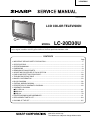
1
LC-20D30U
S26R5LC20D30U
LCD COLOR TELEVISION
MODEL
LC-20D30U
In the interests of user-safety (Required by safety regulations in some countries) the set should be restored
to its original condition and only parts identical to those specified should be used.
CONTENTS
Page
»
»
»
»
»
»
»
»
»
»
»
»
»
IMPORTANT SERVICE SAFETY PRECAUTION .........................................................................................2
SPECIFICATIONS ........................................................................................................................................5
OPERATION MANUAL .................................................................................................................................6
DIMENSIONS ...............................................................................................................................................8
REMOVING OF MAJOR PARTS ..................................................................................................................9
ADJUSTING PROCEDURE OF EACH SECTION ..................................................................................... 13
PUBLIC MODE SETTING PROCEDURE ..................................................................................................38
TROUBLE SHOOTING TABLE ..................................................................................................................44
MAJOR IC INFORMATION .........................................................................................................................50
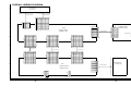
BLOCK DIAGRAM ......................................................................................................................................56
OVERALL WIRING DIAGRAM ...................................................................................................................58
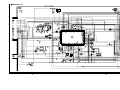
DESCRIPTION OF SCHEMATIC DIAGRAM ............................................................................................. 60
SCHEMATIC DIAGRAM
ËR/C, LED Unit ..........................................................................................................................................61
ËMAIN Unit .................................................................................................................................................62
ËSUB Unit ..................................................................................................................................................78
» PRINTED WIRING BOARD ASSEMBLIES ................................................................................................91
» REPLACEMENT PARTS LIST..................................................................................................................104
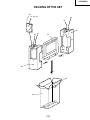
» PACKING OF THE SET ............................................................................................................................ 115
This document has been published to be used for
after sales service only.
The contents are subject to change without notice.
LC-20D30U
IMPORTANT SERVICE SAFETY PRECAUTION
Ë
Service work should be performed only by qualified service technicians who are thoroughly familiar with all safety checks and the servicing guidelines which follow:
• Use an AC voltmeter having with 5000 ohm per volt, or
higher, sensitivity or measure the AC voltage drop
across the resistor.
• Connect the resistor connection to all exposed metal
parts having a return to the chassis (antenna, metal
cabinet, screw heads, knobs and control shafts,
escutcheon, etc.) and measure the AC voltage drop
across the resistor.
All checks must be repeated with the AC cord plug
connection reversed. (If necessary, a nonpolarized
adaptor plug must be used only for the purpose of
completing these checks.)
Any reading of 0.75V peak (this corresponds to 0.5 mA.
peak AC.) or more is excessive and indicates a potential
shock hazard which must be corrected before returning
the monitor to the owner.
WARNING
1. For continued safety, no modification of any circuit
should be attempted.
2. Disconnect AC power before servicing.
A
V
CAUTION: FOR CONTINUED
PROTECTION AGAINST A RISK OF
FIRE REPLACE ONLY WITH SAME
TYPE F7701 (3.15A, 250V) AND
F7702 (5A, 250V) FUSE.
BEFORE RETURNING THE RECEIVER
(Fire & Shock Hazard)
Before returning the receiver to the user, perform
the following safety checks:
1. Inspect all lead dress to make certain that leads are
not pinched, and check that hardware is not lodged
between the chassis and other metal parts in the
receiver.
2. Inspect all protective devices such as non-metallic
control knobs, insulation materials, cabinet backs,
adjustment and compartment covers or shields, isolation
resistor-capacitor networks, mechanical insulators, etc.
3. To be sure that no shock hazard exists, check for
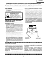
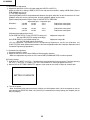
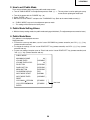
leakage current in the following manner.
• Plug the AC cord directly into a 110~240 volt AC outlet,
and connect the DC power cable into the receiver's DC
jack. (Do not use an isolation transformer for this test).
• Using two clip leads, connect a 1.5k ohm, 10 watt
resistor paralleled by a 0.15µF capacitor in series with
all exposed metal cabinet parts and a known earth
ground, such as electrical conduit or electrical ground
connected to an earth ground.
DVM
AC SCALE
1.5k ohm
10W
0.15 µF
TEST PROBE
TO EXPOSED
METAL PARTS
CONNECT TO
KNOWN EARTH
GROUND
1234567890123456789012345678901212345678901234567890123456789012123456789012345678901234567890121
1234567890123456789012345678901212345678901234567890123456789012123456789012345678901234567890121
1234567890123456789012345678901212345678901234567890123456789012123456789012345678901234567890121
SAFETY NOTICE
and shaded areas in the Replacement Parts Lists and
Schematic Diagrams.
For continued protection, replacement parts must be
identical to those used in the original circuit.
The use of a substitute replacement parts which do not
have the same safety characteristics as the factory
recommended replacement parts shown in this service
manual, may create shock, fire or other hazards.
Many electrical and mechanical parts in LCD television
have special safety-related characteristics.
These characteristics are often not evident from visual
inspection, nor can protection afforded by them be
necessarily increased by using replacement components
rated for higher voltage, wattage, etc.
Replacement parts which have these special safety
characteristics are identified in this manual; electrical
components having such features are identified by " å"
12345678901234567890123456789012123456789012345678901234567890121234567890123456789012345678901212
12345678901234567890123456789012123456789012345678901234567890121234567890123456789012345678901212
12345678901234567890123456789012123456789012345678901234567890121234567890123456789012345678901212
12345678901234567890123456789012123456789012345678901234567890121234567890123456789012345678901212
2
LC-20D30U
PRECAUTIONS A PRENDRE LORS DE LA REPARATION
Ë
Ne peut effectuer la réparation qu' un technicien spécialisé qui s'est parfaitement
accoutumé à toute vérification de sécurité et aux conseils suivants.
• Utiliser un voltmètre CA d'une sensibilité d'au moins
5000Ω/V pour mesurer la chute de tension en travers
de la résistance.
• Toucher avec la sonde d'essai les pièces métalliques
exposées qui présentent une voie de retour au châssis
(antenne, coffret métallique, tête des vis, arbres de
commande et des boutons, écusson, etc.) et mesurer
la chute de tension CA en travers de la résistance.
Toutes les vérifications doivent être refaites après avoir
inversé la fiche du cordon d'alimentation. (Si nécessaire,
une prise d'adpatation non polarisée doit être utilisée
dans le but de terminer ces vérifications.)
La tension de pointe mesurèe ne doit pas dépasser
0.75V (correspondante au courant CA de pointe de
0.5mA). Dans le cas contraire, il y a une possibilité de
choc électrique qui doit être supprimée avant de rendre
le récepteur au client.
AVERTISSEMENT
1. N'entreprendre aucune modification de tout circuit.
C'est dangereux.
2. Débrancher le récepteur avant toute réparation.
A
V
PRECAUTION: POUR LA
PROTECTION CONTINUE
CONTRE LES RISQUES
D'INCENDIE, REMPLACER LE
FUSIBLE PAR UN FUSIBLE DE
MEME TYPE F7701 (3.15A, 250V)
UND F7702 (5A, 250V).
VERIFICATIONS CONTRE L'INCEN-DIE ET
LE CHOC ELECTRIQUE
Avant de rendre le récepteur à l'utilisateur, effectuer
les vérifications suivantes.
1. Inspecter tous les faisceaux de câbles pour s'assurer
que les fils ne soient pas pincés ou qu'un outil ne soit
pas placé entre le châssis et les autres pièces
DVM
métalliques du récepteur.
ECHELLE CA
2. Inspecter tous les dispositifs de protection comme les
boutons de commande non-métalliques, les isolants,
1.5k ohm
10W
le dos du coffret, les couvercles ou blindages de réglage
et de compartiment, les réseaux de résistance-capacité,
les isolateurs mécaniques, etc.
3. S'assurer qu'il n'y ait pas de danger d'électrocution en
vérifiant la fuite de courant, de la facon suivante:
0.15 µF
• Brancher le cordon d'alimentation directem-ent à une
SONDE D'ESSAI
prise de courant de 110-240V. (Ne pas utiliser de
transformateur d'isolation pour cet essai).
• A l'aide de deux fils à pinces, brancher une résistance
AUX PIECES
de 1.5kΩ 10 watts en parallèle avec un condensateur
BRANCHER A UNE
METALLIQUES
TERRE CONNUE
de 0.15µF en série avec toutes les pièces métalliques
EXPOSEES
exposées du coffret et une terre connue comme une
conduite électrique ou une prise de terre branchée à la
terre.
12345678901234567890123456789012123456789012345678901234567890121234567890123456789012345678901212
12345678901234567890123456789012123456789012345678901234567890121234567890123456789012345678901212
12345678901234567890123456789012123456789012345678901234567890121234567890123456789012345678901212
AVIS POUR LA SECURITE
identifiées par la marque " å " et hachurées dans la
De nombreuses pièces, électriques et mécaniques, dans
liste des pièces de remplacement et les diagrammes
les téléviseurs présentent des caractéristiques spéciales
schématiques.
relatives à la sécurité, qui ne sont souvent pas évidentes
Pour assurer la protection, ces pièces doivent être
à vue. Le degré de protection ne peut pas être
identiques à celles utilisées dans le circuit d'origine.
nécessairement augmentée en utilisant des pièces de
L'utilisation de pièces qui n'ont pas les mêmes
remplacement étalonnées pour haute tension,
caractéristiques que les pièces recommandées par
puissance, etc.
l'usine, indiquées dans ce manuel, peut provoquer des
Les pièces de remplacement qui présentent ces
électrocutions, incendies, radiations X ou autres
caractéristiques sont identifiées dans ce manuel; les
accidents.
pièces
électriques
qui
présentent
ces
particularités
sont
12345678901234567890123456789012123456789012345678901234567890121234567890123456789012345678901212
12345678901234567890123456789012123456789012345678901234567890121234567890123456789012345678901212
12345678901234567890123456789012123456789012345678901234567890121234567890123456789012345678901212
12345678901234567890123456789012123456789012345678901234567890121234567890123456789012345678901212
3
LC-20D30U
Precautions for using lead-free solder
1 Employing lead-free solder
"All PWBs" of this model employs lead-free solder. The LF symbol indicates lead-free solder, and is attached on
the PWBs and service manuals. The alphabetical character following LF shows the type of lead-free solder.
Example:
LFa
Indicates lead-free solder of tin, silver and copper.
2 Using lead-free wire solder
When fixing the PWB soldered with the lead-free solder, apply lead-free wire solder. Repairing with conventional
lead wire solder may cause damage or accident due to cracks.
As the melting point of lead-free solder (Sn-Ag-Cu) is higher than the lead wire solder by 40°C, we recommend
you to use a dedicated soldering bit, if you are not familiar with how to obtain lead-free wire solder or soldering bit,
contact our service station or service branch in your area.
3 Soldering
As the melting point of lead-free solder (Sn-Ag-Cu) is about 220°C which is higher than the conventional lead
solder by 40°C, and as it has poor solder wettability, you may be apt to keep the soldering bit in contact with the
PWB for extended period of time. However, Since the land may be peeled off or the maximum heat-resistance
temperature of parts may be exceeded, remove the bit from the PWB as soon as you confirm the steady soldering
condition.
Lead-free solder contains more tin, and the end of the soldering bit may be easily corroded. Make sure to turn on
and off the power of the bit as required.
If a different type of solder stays on the tip of the soldering bit, it is alloyed with lead-free solder. Clean the bit after
every use of it.
When the tip of the soldering bit is blackened during use, file it with steel wool or fine sandpaper.
Be careful when replacing parts with polarity indication on the PWB silk.
Lead-free wire solder for servicing
Part No.
★
Description
ZHNDAi123250E
J
φ0.3mm 250g(1roll)
ZHNDAi126500E
J
φ0.6mm 500g(1roll)
ZHNDAi12801KE
J
φ1.0mm
1kg(1roll)
4
Code
BL
BK
BM
LC-20D30U
SPECIFICATIONS
Items
LCD panel
Number of dots
Video color systems
TV Standard (CCIR)
TV Tuning System
TV function
STEREO
CATV
Y/C FILTER
Brightness
Viewing angles
Audio amplifier
Speakers
INPUT1
INPUT2
INPUT3/OUTPUT
INPUT4
Terminals
INPUT5
Antenna
Headphone
OSD language
Power supply
Power consumption
Display only
Weight
Display with stand
Operating temperature
Model
LC-20D30U
20" Advanced Super View & BLACK TFT LCD
3,147,264 dots WXGA
N358, N443, PAL, PAL-M, PAL-N, SECAM, PAL-60
NTSC/PAL-M/PAL-N
PLL 181 ch.
MTS+SAP
125 ch.
3D Y/C FILTER
480 cd/m2
H: 170° V: 170°
2.1 W × 2
1 37 64 × 4 21 64 in. (4 × 11 cm), 2 pcs.
AUDIO-IN, COMPONENT-IN
AUDIO-IN, VIDEO-IN, S-VIDEO-IN
AUDIO-IN, VIDEO-IN/AUDIO-OUT, VIDEO-OUT
HDMI-IN with HDCP (640 × 480, 480P, 576P, 720P, 1080I )
PC Connector: 15-pin mini D-sub PC AUDIO: Mini-jack for stereo (ø3.5 mm)
F-Type
Mini-jack for stereo (ø3.5 mm)
English/Spanish/French
AC 110-240V, 50/60Hz
77 W (0.6 W standby): AC 120V
15.5 lbs./7.0 kg
/
/
17.5 lbs./7.9 kg
+32°F to +104°F (0°C to +40°C)
Ë As a part of policy of continuous improvement, SHARP reserves the right to make design and specification changes for the LCD TV set
improvement without prior notice. The performance specification figures indicated are nominal values of production units. There may be
some deviations from these values in individual units.
5
6
NOTE
POWER/WAKE UP TIMER indicator
POWER/WAKE UP TIMER indicator lights up green when the power is on,
and red when in the standby mode (the indicator will not light when the main
power is off), and orange when the wake up timer is set (the indicator will light
when in the standby mode).
OPC (Optical Picture Control) indicator
The OPC indicator lights up green when "OPC" is set to "ON".
Headphone jack ( )
Plug the headphone mini-plug into the headphone jack
located on the front of the main unit.
To change the vertical angle of the LCD TV
set, tilt the screen up to 2.5 degrees forward
or 10 degrees backward. Please adjust
the angle so that the LCD TV set can be
watched most comfortably.
Tilt the display by grabbing onto the
carrying handle while securely holding
down the stand with your other hand.
How to adjust the angle
+
Adjust the sound volume using VOL ( )/( – ) on the
remote control.
VOL UME
10
• Headphones are not included in the supplied accessories.
• No sound is heard from the main unit speakers when a headphone mini-plug is connected into the headphone jack.
• Do not set the volume at a high level. Hearing experts advise against extended listening at high volume levels.
NOTE
Headphones
" On-screen display
Ë Plug the headphone mini-plug into the headphone jack located on the front of the main unit.
Listening with Headphones
• INPUT, CH ( )/( ), VOL ( – )/(+) and MENU on the main unit have the same functions as the same buttons on the remote control.
Fundamentally, this operation manual provides a description based on operation using the remote control.
Remote sensor
OPC (Optical Picture
Control) sensor
Speaker
CH ( )/( ) INPUT
POWER
MENU
VOL( )/( )
Upper control panel
Controls
Part Names of the Main Unit
Y
AUDIO (R)
AUDIO (L)
VIDEO
S-VIDEO
AUDIO (R)
AUDIO (L)
PR
PB
How to Fix the Cables
AC INPUT
terminal
INPUT3/OUTPUT
INPUT5
(PC-IN)
INPUT4
ANT. (Antenna terminal)
AUDIO (R)
AUDIO (L)
VIDEO
AUDIO
ANALOG
RGB
HDMI
Round lock for Kensington Security Standard slot*
* Using the Kensington Lock
• This LCD TV set has a Kensington Security Standard slot for use with a Kensington
MicroSaver Security System. Refer to the information that came with the system for
instructions on how to use it to secure the LCD TV set.
Carrying handle
Cable clamp
Secure cables and cords with the supplied cable clamp so that they do not get caught when mounting the cover.
INPUT2
INPUT1
(COMPONENT)
Rear View
Terminals
LC-20D30U
OPERATION MANUAL
VIEW MODE
Selects the screen size.
SLEEP
Sets the sleep timer.
MENU RETURN
Returns to the previous screen.
AV MODE
Selects preferred AV MODE.
VOL ( )/( )
Sets the volume.
AUDIO ONLY
Outputs audio without screen image.
MUTE
Mutes the sound.
MTS
Selects audio settings.
Channel Select
Sets the channel.
POWER
Switches the Liquid Crystal
Television power on or standby.
Part Names of the Remote Control
7
BACKLIGHT
Adjusts the brightness of the screen.
CC
Displays Closed Caption subtitles.
MENU
Displays the menu screen.
/ / / (Cursor control)
Selects a desired item on the screen.
ENTER
Executes a command.
DISPLAY
Displays the receiving channel and
the current time for 10 seconds.
FLASHBACK
Returns to the previous channel.
INPUT
Switches the input source between
INPUT1, INPUT2, INPUT3, INPUT4,
INPUT5 (PC) and TV mode.
CH ( )/( )
Selects a channel.
Installing Batteries in the Remote Control
Caution!
Ë Slide the cover while
pressing the (
)
part.
Open the battery cover.
2
Ë Place batteries with their
terminals corresponding
to the (+) and ( –)
indications in the battery
compartment.
Insert two "AAA" size batteries.
3
Ë Engaging the lower
claw with the remote
control, close the cover.
Close the battery cover.
Ë The remote control may not work properly if the remote sensor
window is in direct sunlight or strong lighting. In such a case,
change the angle of the lighting or main unit, or operate the
remote control closer to the remote sensor window.
Ë Do not install or place the remote control in direct sunlight. The
heat may cause deformation of the unit.
Ë Do not apply shock to the remote control. In addition, do not
expose the remote control to liquids, and do not place it in an area
with high humidity.
Cautions regarding use of the remote control
Ë Use the remote control by pointing it towards the remote sensor
window of the main unit. Objects between the remote control and
sensor window may prevent proper operation.
Using the Remote Control
Ë Improper use of batteries can result in a leakage of chemicals and/or explosion. Be sure to follow the instructions below.
• Place batteries with their terminals corresponding to the (+) and (–) indications.
• Different types of batteries have different characteristics. Do not mix batteries of different types.
• Do not mix old and new batteries. Mixing old and new batteries can shorten the life of new batteries and/or cause old
batteries to leak chemicals.
• Remove batteries as soon as they are depleted. Chemicals that leak from batteries can cause a rash. If chemical
leakage is found, wipe it off with a cloth.
• The batteries supplied with the LCD TV set may have a shorter operating time due to storage conditions.
• If the remote control is not to be used for a long period of time, remove the batteries from the remote control.
Precautions regarding batteries
1
Before using the LCD TV set for the first time, install the two "AAA" size batteries supplied in the remote control. When the
batteries become depleted and the remote control fails to operate, replace the batteries with new "AAA" size batteries.
Preparation
LC-20D30U
LC-20D30U
DIMENSIONS
Unit: inch (mm)
10 31/64 (266)
5 43/64 (144)
15 (381)
2 /8
(66.5)
5
21 15/64 (539)
4 1/32
(102)
16 5/16 (414)
10 31/64 (266)
9 57/64 (251)
15 7/16 (392)
1 45/64
(43)
17 9/64 (435)
17 17/32 (445.2)
9 17/32 (242)
2 9/64
(54)
3 61/64 (100)
3 61/64 (100)
8
LC-20D30U
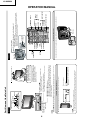
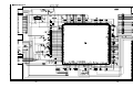
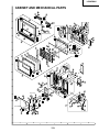
REMOVING OF MAJOR PARTS
1. Remove the stand cover fixing screw (1 pc.).
2. Remove the stand fixing screws (4 pcs.).
3. Remove the carrying handle fixing screws (4 pcs.).
4. Remove the terminal cover.
5. Remove the terminal screws (2 pcs.).
6. Remove the cabinet B fixing screws (5 pcs.).
7. Remove the cabinet B after opening from the direction of an arrow.
8. Remove the stand angle fixing screws (4 pcs.).
9. Disconnect all the connectors from all the PWBs.
Cabinet B
Cabinet A
6
Terminal Cover
5
4
Carrying Handle
3
5
8
7
Stand Angle
8
2
1
Stand Cover
Stand
Main PWB
P1201
9
P7703
9
P2003
P2002
SC5204
P5001
9
R/C, LED PWB
9
9
SC4000
Sub PWB
LC-20D30U
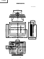
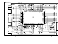
10. Remove the chassis frame fixing screws (3 pcs.).
11. Remove the 2 lock screws from the main PWB. Detach the chassis frame, together with its terminals, from the
main PWB.
12. Remove the 4 lock screws from the sub PWB and the PWB fixing angle. Detach the chassis frame together with
its terminals, from the sub PWB.
13. Remove the R/C, LED PWB fixing screws (2 pcs.).
14. Remove the 4 lock screws each from the right and left speakers and take out both the speakers.
15. Remove the LCD panel module unit fixing screw (4 pcs.).
11
Main PWB
PWB Fixing Angle
12
12
10
10
Chassis Frame
Sub PWB
15
15
13
R/C, LED PWB
Speaker (L)
Speaker (R)
LCD Panel Module Unit
14
14
10
LC-20D30U
» Precautions in handling the LCD panel
1. Handle it in a clean room. (above 50% humidity)
2. The worker must wear an earth band.
3. Be careful not to drop, vibrate and shock the panel.
4. Use an ionizer. (within 30 cm)
16. Remove the 8 lock screws from the panel angle and the panel support angle. And then take out them.
17. Remove the 4 lock screws from the inverter unit angle then detach the inverter unit angle and the inverter PWB.
18. Remove the 4 lock screws then detach the LCD control unit angle and the LCD control PWB.
19. Remove the bezel and the LCD panel unit.
<Note> Do not remove the LCD panel from the panel chassis. Be careful not to touch the LCD panel glass faces,
driver IC, PWB with bare hands (Otherwise defects maybe caused in the production line.)
20. Remove the diffusion sheet (Top), lens sheet, diffusion (Bottom), diffusion plate.
<Note> Fit the diffusion plate and sheets tightly in the backlight casing.
If set out of position, the panel may set cracked.
21. Remove the lamp holder screws (4 pcs).
22. Remove the lamp holder, from the lamp unit.
23. Remove the lamp clip from the reflection sheet and the backlight angle.
24. Remove the reflection sheet from the backlight angle.
Inverter Unit Angle
(LANGK3450TPZZ)
Panel Support Angle
(LANGFA290WJFW)
16
C
16
17
C
Inverter PWB
C
Lamp Holder
(LHLDZ3190TPZZ)
C
Bezel
(LANGK3451TPZZ)
C
(LANGTA279WJFW)
LCD Control Unit Angle
(LANGK3449TPZZ)
LCD Control PWB
Backlight Angle
(LANGK3448TPZZ)
Reflection Sheet
(PREFL2368TPZZ)
Lamp Clip, x5
22
(LHLDZ3192TPZZ)
Holder, x5
(LHLDZ3227TPZZ)
Lamp Unit, x5
Lamp Holder (RLMPC2402TPZZ)
(LHLDZ3190TPZZ)
Diffusion Sheet (Bottom)
(PSLDK2599TPZZ)
Diffusion Sheet (Top)
(PSLDK2600TPZZ)
20" LCD panel Unit
23
19
18 Panel Angle
C
Diffusion Plate
(PSLDK2598TPZZ)
20
16
21
24
Lens Sheet
(POFMA0258TPZZ)
Panel Support Angle
(LANGFA290WJFW)
11
LC-20D30U
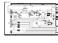
»Precautions in servicing the side-B (backside) of the main PWB unit
1. Remove the lock screws (3 pcs.) from the main PWB, detach the PWB from the chassis frame, and then turn it
over.
2. Connect the service-specific extension FFC (flat cable) (QCNW-D721WJQZ) between the main PWB (SC5201)
and the sub PWB (P5002).
3. Connect the service-specific extension FFC (flat cable) (QCNW-D721WJQZ) between the main PWB (SC5202)
and the sub PWB (P5003).
4. Connect the service-specific extension FFC (flat cable) (QCNW-D721WJQZ) between the main PWB (SC5203)
and the sub PWB (P5004).
1
Main PWB
SC5201
2
Sub PWB
2
P5002
SC5202
3
Main PWB
(Side-B)
SC5203
4
3
P5003
P5004
4
R/C, LED PWB
Step
2
3
4
Part No.
QCNW-D721WJQZ
QCNW-D721WJQZ
QCNW-D721WJQZ
Description
Extension Cable 26-pin Main (SC5201)-Sub (P5002)
Extension Cable 26-pin Main (SC5202)-Sub (P5003)
Extension Cable 26-pin Main (SC5203)-Sub (P5004)
12
LC-20D30U
ADJUSTMENT PROCEDURE OF EACH SECTION
1. Preparations
(1) Plug the power cable in an AC power outlet.
AC 110 V~240V
[1] Adjustment procedure
1-1. Adjusting the checker
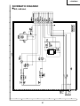
Power on (initialization) → Model number/inch size settings → Model-specified data transfer to E2PROM
(I2C) → EDID data write
1-2. Finish process adjustment
Assembling → Power on → Adjustment process mode (bus connector) → AD converter level, TAMP, and
white balance (cut-off and gain) adjustments
[2] Entering the checker mode and adjustment process mode
2-1. Entering the checker mode
* Set KEY-5 (pin 82 on the microprocessor) to "L" and turn on the power.
KEY-4 KEY-5
Mode shift
H
H
Normal mode (Brand-new data to be written and stored on E2PROM).
L
H
Shift to the adjustment process mode.
H
L
Checker process activated at the applied master ROM value (E2PROM still intact after checking).
L
L
E2PROM initialized and microprocessor's master values written on it (process adjustment values not rewritten).
2-2. Entering the adjustment process mode
There are the following three ways to enter this mode.
* Turn on the power and press the "ADJUST PROCESS" key on the remote controller.
* Set KEY-4 (pin (81) on the microprocessor) to "L" and turn on the power.
* In servicing:1Hold down the INPUT SELECT and VOL (–) keys at once, and turn on the power switch. ("K"
appears at the top left of the screen to indicate the inspection process mode.) → 2Next hold down the CH (Ù)
and VOL (–) keys at once. (The adjustment process mode screen shows up.) To clear this mode, just turn off the
power. (Either the power switch on the set or the remote controller may be used for this purpose.)
[3] Key operation in the adjustment process mode
ËBasic operation
* Use the CH (ù)/(Ù) keys to select a channel.
* Use the INPUT SELECT key to select an input.
* Use the CURSOR UP/DOWN key to select an item to be adjusted. (When the CURSOR DOWN key is pressed at
the bottom item, it comes to the top item on the next page.
When the CURSOR UP key is pressed at the top item, it comes to the bottom item on the previous page.)
* Use the VOL (+)/(–) keys or CURSOR LEFT/RIGHT keys to modify the setting of a selected item.
* Press the MENU key to go to the next item. (When pressed at the bottom item, the top item on the next page is
selected.)
* Press the MANUAL MEMORY key to go back to the top item. (When pressed at the top item, the top item on the
previous page is selected.)
* Press the AUTO PRESET Key to go to the top item on the next page.
ËHierarchical level shift
* When the ENTER key is pressed at any item other than I2C DATA on page 9, the setting page of the item shows
up.
* To get out of the setting page, press the PREVIOUS SCREEN key.
13
LC-20D30U
[4] Initialization
4-1. Get pins (81) and (82) of IC2001 (microprocessor) grounded, and turn on the power.
4-2. Check the MODEL setting (A633). * The MODEL setting can't be modified.
4-3. Check the INCH SIZE setting (20). * The INCH SIZE setting can't be modified.
(Adjustment process menu: Page 1 screen)
0
1
2
7
3
4
5
6
0
1
1
| M O
D
E
L
2
I
N
C
H
3
E
R
R
O
R
4
P
U
B
L
I
C
5
V
-
C
H
I
P
6
E
X
T
C
O
8
9 10 11 12 13 14 15 16 17 18 19 20 21 22 23 24 25 26
A
S
I
Z
N
O
M
6
E
O
R
E
D
E
S
E
3
3
2
0
T
0
O
F
F
1
N
T
R
O
L
O
F
F
7
8
[5] Model-specified data transmitted (Data written on microprocessor E2PROM)
5-1. Model-specified data transmitted
None
5-2. ROM CORRECTION
None
[6] Writing the EDID data
With the set's power off, write the updated-version data from the checker land to the E2PROMs for PC input
(analog: IC401) and HDMI input (digital: IC403).
Write the data before making the HDMI inspection. (Otherwise the adjustment can't be made.)
For the 2006 production write data, refer to the accompanying document. (You are requested to modify the
production year and check sum according to the production year.)
14
LC-20D30U
[7] Adjustment
7-1. AD converter level adjustment
1 D3 input
1) Feeding the D3 75% color bar signal
Instrument used: LEADER LT446 or LEADER LT448
(1) LEADER LT446
Signal name: COLOR BAR 75%
Setting: 01: 1920 x 1080 / 60i
H: 33.72 kHz, V: 29.97 Hz
(2) LEADER LT448
Signal name: COLOR BAR
* Use the LT446-compatible third type out of the 3 color bar patterns.
Setting: 02: 1080i / 59.94 (30sF)
H: 33.72 kHz, V: 29.97 Hz
2) Turn on the AUTO GAIN-OFFSET1 item on Adjustment Process Page 7.
2 PC input
1) Feeding the XGA white 100% signal
Instrument used: LEADER LT448
Signal name: RASTER 100%
Setting: 28: XGA (1024 x 768)
H: 48.36 kHz, V: 60.00 Hz
2) Turn on the AUTO GAIN2 item on Adjustment Process Page 8.
7-2. TAMP adjustment
1) Receive the standard color bar signal.
2) Suppose that the "YDATA" reading on Adjustment Process Page 2 is not as specified in the table below. Adjust
the "NTSC TAMP" setting on the same page to have the "YDATA" reading as specified below.
* Note that the setting may be different from model to model.
3) Make sure that the "PAL-M TAMP" and "PAL-N TAMP" settings are 6 higher than the "NTSC TAMP" setting.
Model
Setting
LC-20D30U
155-158
Reference
(Adjustment process menu: Page 2 screen)
1
2
3
4
5
|
T
A
M
P
2
Y
D
A
T
3
T
A
M
P
H
4
N
T
S
C
T
5
P
A
L
-
6
P
A
L
-
0
0
1
6
7
8
9 10 11 12 13 14 15 16 17 18 19 20 21 22 23 24 25 26
2
L
A
1
5
5
1
5
7
1
5
8
8
5
A
M
P
M
T
A
M
P
9
1
N
T
A
M
P
9
1
7
8
Y Data
(White 75%)
15
LC-20D30U
7-3. White balance adjustment
1) Adjustment procedure (Call the AV input mode with INPUT2 or INPUT3.)
Adjust the white 40% setting at RGB CUTOFF2 first and then the white 80% setting at RGB-GAIN. (Set the
RGB GAMMA level at 0.9.)
(1) Test signal adjustment
[Input signal] Make the DVP-incorporated white balance test signal (white 80% on the left onscreen: 191-level
gradation, white 40% on the right onscreen: 92-level gradation) appear on the screen.
[Specifications] Adjustment Process Page 3: RGB CUTOFF2, RGB-GAIN
Adjustment spec. / Inspection spec.
White 80%
x=0.268
±0.004
±0.01
Radius from center point
y=0.279
±0.004
±0.01
Radius from center point
White 40%
x=0.266
y=0.279
±0.002
±0.002
±0.01
±0.01
Radius from center point
Radius from center point
[Adjustment procedure with the bus]
Cut-off (RGB CUTOFF2) Fix the G CUTOFF2 setting at 0.
Adjustment range ±50
Vary the R/B CUTOFF2 settings accordingly.
Gain (RGB-GAIN) Fix the G-GAIN setting at 0.
Adjustment range ±80
Vary the R/B-GAIN settings accordingly.
(For the adjustment, use Minolta CA-210 at Engineering Department, and for the calibration, use
CH02"TOPCON" mode. Make measurements in the interchangeable mode with Production Department and
Production Engineering Department.)
7-4. Common bias adjustment
1) Generate the built-in signal.
2) Adjust the VR1 on the LCD control PWB until flickering gets minimum.
* Make this adjustment only when the LCD control PWB (CPWBX3335TPZZ) has been replaced.
[8] Factory settings
1) Hold down the "INPUT" and "VOL (–)" buttons of the set at once and turn on the power. Then keep pressing
the "CH (ù)" and "VOL (+)" buttons. (The "SETTING COMPLETE" message appears onscreen.)
2) Make sure that "SETTING COMPLETE" appears at the center of the screen a couple of seconds later.
SETTING COMPLETE
3) Turn off the power.
* Note: Immediately after making the factory settings, turn off the power switch. (At the next power-on, the set
gets started in the EZ SETUP mode. If any extra key-in is made after the factory settings are complete, the set
may run properly.)
16
LC-20D30U
8-2. Initial value of factory settings
Settings & ranges
MENU
PICTURE
AV MODE
STANDARD/DYNAMIC/DYNAMIC(FIXED)/MOVIE/GAME
OPC
BACKLIGHT
ON/OFF
BRIGHT/NORMAL/DARK/VARIABLE
1 (DARK)~9 (NORMAL) ~ 17(BRIGHT)
CONTRAST
0 ~ 60
BRIGHTNESS
COLOR
-30 ~ +30
-30 ~ +30
-30 ~ +30
-10 ~ +10
TINT
SHARPNESS
ADVANCED
COLOR TEMP.
RED
GREEN
BLUE
I/P SETTING
NOISE CLEAN
FILM MODE
QUICK SHOOT
RESET
AUDIO
(INPUT1)
(INPUT2)
(INPUT3)
(INPUT4)
DYNAMIC
DYNAMIC
DYNAMIC
DYNAMIC
(PC)
OFF
OFF
(GAME)
9
30
0
0
VARIABLE
VARIABLE
(STANDARD)
17
30
(DYNAMIC)
17
40
0
(DYNAMIC(FIXED)
17
(MOVIE)
7
40
0
+5
+5
30
0
0
0
0
0
0
0
0
0
0
0
0
(except for PC)
(PC)
USER/HIGH/MIDDLE/LOW
-30 ~ +30
MIDDLE
0
MIDDLE
0
-30 ~ +30
0
0
-30 ~ +30
0
0
INTERLACE/PROGRESSIVE
ON/OFF
PROGRESSIVE
OFF
ON/OFF
ON/OFF
OFF
YES/NO
NO
NO
TREBLE
-10 ~ +10
0
-10 ~ +10
-10 (L)~ +10 (R)
0
0
YES/NO
NO
YES
ENGLISH
CH-SETUP
EZ-SETUP
YES/NO
ENGLISH/ESPANOL/FRANCAIS
ON/OFF
AUTO CLOCK
START
AIR/CABLE
CH SEARCH
CH MEMORY
MTS
CLOCK
SET
AUTO
MANUAL
DST
TIME
TIME DISPLAY
INPUT3 IN/OUT
V-CHIP BLOCK
SECRET No.
MPAA
TV GUIDELINES
G
PG
PG-13
R
NC-17
X
TV-Y
TV-Y7
TV- G
TV-PG
TV-14
TV-MA
BLOCK CONTENT
C
CAN.FRENCH RATINGS
C8+
G
PG
14+
18+
G
D
H-POS.
V-POS.
CLOCK
PHASE
RESET
NO OPERATION OFF
POWER MANAGEMENT
PICTURE FLIP
(Items not on the menu)
EZ SETUP AUTOMATIC STARTUP
LAST CHANNEL
LAST TV/INPUT
FLASH BACK
SKIP DATA_CATV
SKIP DATA_AIR
VOLUME
LINE OUT LEVEL (AT VAO)
EDS CH (FOR AUTO)
Factory settings
ON
2ch
TV
2ch
ALL SKIP
ALL SKIP
20
0
NOT YET FIXED
HOTEL MODE POWER ON FIXED
MAXIMUM VOLUME
VOLUME FIXED
REMOTE CONTROL
USER CONTROL
MENU BUTTON
ON SCREEN DISPLAY
START MODE
INPUT MODE FIXED
VARIABLE
60
Keep "NO" selected to go to the setting screen.
AUTO
OFF
12:00AM
ON
IN
CLEAR
NONE
NONE
NONE
Have the clock setting not yet fixed, and keep the display as shown at left to go to the MANUAL CLOCK setting screen.
NONE
NONE
NONE
NONE
NONE
NONE
NONE
NONE
NONE
BLANK
BLANK
(UN BLOCK)
(UN BLOCK)
BLANK
BLANK
(UN BLOCK)
(UN BLOCK)
BLANK
(UN BLOCK)
(NONE)/BLOCK
(NONE)/BLOCK
NONE
NONE
NONE
NONE
1280×768 (60Hz) / 1024×768 (60Hz) /
800×600 (60Hz) / 640×480(60Hz)
INPUT SIGNAL
Keep "NO" selected to go to the setting screen.
(NONE)/BLOCK
(NONE)/BLOCK
ON/OFF
OFF/CC1/CC2/T1/T2
-90 ~ +90
-15 ~ +15
-90 ~ +90
-15 ~ +16
YES/NO
ENGLISH/ESPANOL/FRANCAIS
SIDE BAR/S. STRETCH/ZOOM/STRETCH
NORMAL/STRETCH
ON/OFF
ON/OFF
OFF/30/60/90/120/150MIN
ON/OFF
12:00AM ~ 11:59PM
CH1 ~ 125/INPUT1 ~ INPUT4
0 ~ 60
ENABLE/DISABLE
ENABLE/DISABLE
ON/OFF
NORMAL/MIRROR/ROTATE/UPSIDE DOWN
VARIABLE
RESPOND
RESPOND
RESPOND
YES
NORMAL
VARIABLE
17
–
–
–
–
–
Keep "NO" selected to go to the setting screen.
(BLANK)/BLOCK
(BLANK)/BLOCK
(BLANK)/BLOCK
(BLANK)/BLOCK
(BLANK)/BLOCK
AUTO/N358/N443/PAL/PAL-M/PAL-N/SECAM/PAL60
(* N358/PAL-M/PAL-N only in the TV mode)
AUTO/RGB/YCbCr
AUTO/ITU601/ITU709
STANDARD/OUT OF STANDARD
ENABLE/DISABLE
Not with PC
With PC
NO SIGNAL OFF
12:00AM ~ 11:59PM
ON/OFF
IN/OUT /OUT×
4-DIGIT INPUT
(NONE)/BLOCK
(NONE)/BLOCK
(NONE)/BLOCK
(NONE)/BLOCK
(NONE)/BLOCK
(NONE)/BLOCK
(NONE)/BLOCK
SIGNAL TYPE
COLOR MATRIX
DYNAMIC RANGE
AUTO VIEW
TIMER
TIME
CHANNEL
VOL.
STEREO
AUTO
(NONE)/BLOCK
(NONE)/BLOCK
(NONE)/BLOCK
LANGUAGE
VIEW MODE
AUDIO ONLY
BLUE SCREEN
SLEEP TIMER
WAKE UP TIMER
–
STEREO/SAP/MONO
AUTO/MANUAL
(NONE)/BLOCK
(NONE)/BLOCK
STATUS
FINE SYNC.
AIR
–
(NONE)/BLOCK
(NONE)/BLOCK
(NONE)/BLOCK
CLOSED CAPTION
PC SETTING
YES
–
(NONE)/BLOCK
(NONE)/BLOCK
8 ans+
13 ans+
16 ans+
18 ans+
COLOR SYSTEM
HDMI SETUP
YES/NO
AIR/CABLE
–
(NONE)/BLOCK
(NONE)/BLOCK
L
S
V
FV
CAN.ENGLISH RATINGS
ON/OFF
ON
ON
AUTO/[2] ~ [69] or [1] ~ [125]
ON/OFF
0
0
(PC)
17 (BRIGHT)
ON
YES/NO
LANGUAGE
CH SETTING
OPTION
(TV)
DYNAMIC
RESET
BASS
BALANCE
RESET
SETUP
Factory settings
(except for PC)
NONE
NONE
NONE
NONE
NONE
NONE
NONE
OFF
OFF
(TV)
N358
AUTO
(INPUT2)
(INPUT3)
AUTO
AUTO
AUTO
STANDARD
ENABLE
1024x768 (60Hz)
0
0
0
0
NO
ENGLISH
(TV)
S. STRETCH
Keep "NO" selected to go to the setting screen.
(INPUT1)
(At SD) S.STRETCH
(At HD)STRETCH
(INPUT2)
(INPUT3)
S. STRETCH
S. STRETCH
OFF
OFF
OFF(CLEAR)
OFF
12:00AM
CH2
20
DISABLE
DISABLE
OFF
NORMAL
Keep "OFF" selected to go to the setting screen.
(INPUT4)
(At SD) S.STRETCH
(At HD)STRETCH
(INPUT5)
NORMAL
LC-20D30U
LIST OF THE ADJUSTMENT PROCESS MODE MENU
For calling the adjustment process mode and keying in this mode, refer back to "ADJUSTING PROCEDURE OF
EACH SECTION".
DEFAULT CHART OF ADJUSTMENT PROCESS 1ST HIERARCHICAL ITEMS
Page No.
Item
Initial
Value
Function
Servicing notes & precautions
MODEL NUMBER (NOT TO CHANGE)
INCH SIZE SELECTION
(NOT TO CHANGE)
UNMODIFIABLE.
USED AT INITIALIZATION.
NOT TO MODIFY IN OTHER CASES.
IF MODIFIED, DATA TO BE WRITTEN AGAIN
AND READJUSTMENT TO BE MADE.
NOT USED
NOT USED
NOT USED
NOT USED
BASIC SETTINGS
1
MODEL
INCH SIZE
A633
20
ERROR NO RESET
0 LAMP ERROR COUNT AND RESET
PUBLIC MODE
OFF HOTEL MODE SETTING
V-CHIP
1 V-CHIP LINE MUTE SETTING
EXT CONTROL
OFF BUS, UART OPEN
THE ROM AND GAIBU VERSION NUMBERS ARE DISPLAYED AT THE BOTTOM.
VIDEO ADJUSTMENT
2
TAMP L
YDATA
TAMP H
NTSC TAMP
PAL-M TAMP
PAL-N TAMP
WHITE BALANCE ADJUSTMENT
RCUTOFF2
3
GCUTOFF2
BCUTOFF2
RGAIN
GGAIN
BGAIN
RGB GAMMA
COMPONENT AD ADJUSTMENT
AUTO GAIN-OFFSET1
7
AD R GAIN
AD G GAIN
AD B GAIN
AD R OFFSET
AD G OFFSET
AD B OFFSET
RGTAR
GGTAR
BGTAR
RGCAL
GGCAL
BGCAL
ROCAL
GOCAL
BOCAL
155
—
158
90
96
96
0
0
0
0
0
0
0.9
OFF
185
185
185
126
94
126
A4
A4
A4
—
—
—
—
—
—
Y LOWER-LIMIT SETTING AT TAMP ADJUSTMENT
DATA READ VALUE AT TAMP ADJUSTMENT
Y UPPER-LIMIT SETTING AT TAMP ADJUSTMENT
TAMP ADJUSTMENT
TAMP ADJUSTMENT
TAMP ADJUSTMENT
NOT USED
SEE ADJUSTMENT PROCEDURE.
NOT USED
SEE ADJUSTMENT PROCEDURE.
SEE ADJUSTMENT PROCEDURE.
SEE ADJUSTMENT PROCEDURE.
RED CUT-OFF ADJUSTMENT2
GREEN CUT-OFF ADJUSTMENT2
BLUE CUT-OFF ADJUSTMENT2
WHITE BALANCE ADJUSTMENT2
WHITE BALANCE ADJUSTMENT2
WHITE BALANCE ADJUSTMENT2
RGB γ COEFFICIENT SETTING
SEE ADJUSTMENT PROCEDURE.
SEE ADJUSTMENT PROCEDURE.
SEE ADJUSTMENT PROCEDURE.
SEE ADJUSTMENT PROCEDURE.
SEE ADJUSTMENT PROCEDURE.
SEE ADJUSTMENT PROCEDURE.
NOT USED
AUTOMATIC ADJUSTMENT OFF/RUN OF AD9883 GAIN AND OFFSET
1125I/750P INPUT RED GAIN ADJUSTMENT
1125I/750P INPUT GREEN GAIN ADJUSTMENT
1125I/750P INPUT BLUE GAIN ADJUSTMENT
1125I/750P INPUT RED OFFSET ADJUSTMENT
1125I/750P INPUT GREEN OFFSET ADJUSTMENT
1125I/750P INPUT BLUE OFFSET ADJUSTMENT
1125I/750P INPUT RED GAIN ADJUSTMENT TARGET
1125I/750P INPUT GREEN GAIN ADJUSTMENT TARGET
1125I/750P INPUT BLUE GAIN ADJUSTMENT TARGET
DISPLAY OF Y LEVEL/CHROMA CALCULATED VALUES
DISPLAY OF Y LEVEL/CHROMA CALCULATED VALUES
DISPLAY OF Y LEVEL/CHROMA CALCULATED VALUES
DISPLAY OF Y LEVEL/WHITE LEVEL CALCULATED VALUES IN CLAMP FIELD
DISPLAY OF Y LEVEL/WHITE LEVEL CALCULATED VALUES IN CLAMP FIELD
DISPLAY OF Y LEVEL/WHITE LEVEL CALCULATED VALUES IN CLAMP FIELD
SEE ADJUSTMENT PROCEDURE.
SEE ADJUSTMENT PROCEDURE.
SEE ADJUSTMENT PROCEDURE.
SEE ADJUSTMENT PROCEDURE.
NOT USED
NOT USED
NOT USED
NOT USED
NOT USED
NOT USED
NOT USED
NOT USED
NOT USED
NOT USED
NOT USED
NOT USED
18
LC-20D30U
Page No.
Initial
Item
Function
Value
Servicing notes & precautions
PCAD ADJUSTMENT
8
AUTO GAIN2
AUTO OFFSET2
PCAD R GAIN
PCAD G GAIN
PCAD B GAIN
PCAD R OFFSET
PCAD G OFFSET
PCAD B OFFSET
OFF
OFF
180
180
180
128
128
128
RGTAR
GGTAR
BGTAR
RGCAL
GGCAL
BGCAL
ROCAL
GOCAL
BOCAL
AUTOMATIC ADJUSTMENT OFF/RUN OF AD9883 GAIN SEE ADJUSTMENT PROCEDURE.
AUTOMATIC ADJUSTMENT OFF/RUN OF AD9883 OFFSET NOT USED
SEE ADJUSTMENT PROCEDURE.
PC INPUT RED GAIN ADJUSTMENT
PC INPUT GREEN GAIN ADJUSTMENT SEE ADJUSTMENT PROCEDURE.
PC INPUT BLUE GAIN ADJUSTMENT
SEE ADJUSTMENT PROCEDURE.
PC INPUT RED OFFSET ADJUSTMENT
NOT USED
PC INPUT GREEN OFFSET ADJUSTMENT NOT USED
PC INPUT BLUE OFFSET ADJUSTMENT NOT USED
E6
E6
E6
—
—
—
—
—
—
PC INPUT RED GAIN ADJUSTMENT TARGET
PC INPUT GREEN GAIN ADJUSTMENT TARGET
PC INPUT BLUE GAIN ADJUSTMENT TARGET
DISPLAY OF Y LEVEL/CHROMA CALCULATED VALUES
DISPLAY OF Y LEVEL/CHROMA CALCULATED VALUES
DISPLAY OF Y LEVEL/CHROMA CALCULATED VALUES
DISPLAY OF Y LEVEL/WHITE LEVEL CALCULATED VALUES IN CLAMP FIELD
DISPLAY OF Y LEVEL/WHITE LEVEL CALCULATED VALUES IN CLAMP FIELD
DISPLAY OF Y LEVEL/WHITE LEVEL CALCULATED VALUES IN CLAMP FIELD
NOT USED
NOT USED
NOT USED
NOT USED
NOT USED
NOT USED
NOT USED
NOT USED
NOT USED
0
WAIT
—
—
—
—
I2C (BUS CONTROL IC) DATA WRITE AND READ
WRITE AND READ EXECUTION
SHIFT TO SOUND ADJUSTMENT PAGE
SHIFT TO DVP ADJUSTMENT PAGE
SHIFT TO TUNER ADJUSTMENT PAGE
SHIFT TO OTHERS ADJUSTMENT PAGE
NOT USED
NOT USED
PRESS ENTER KEY TO GO TO SOUND ADJUSTMENT PAGE.
PRESS ENTER KEY TO GO TO DVP ADJUSTMENT PAGE.
PRESS ENTER KEY TO GO TO TUNER ADJUSTMENT PAGE.
PRESS ENTER KEY TO GO TO OTHERS ADJUSTMENT PAGE.
LIST OF VARIOUS SETTINGS
9
I2C DATA
I2C DATA
SOUND
DVP
TUNER
OTHERS
AUDIO ADJUSTMENT PROCESS DEFAULTS CHART
Page No.
Initial
Item
Value
AUDIO ADJUSTMENT
SOUND1
VOLUME
MSP DATA
MSP DATA
CARRIER MUTE
IGR THR
Function
Servicing notes & precautions
20
0
WAIT
ON
12D
SOUND VOLUME
AUDIO IC MSP DATA WRITE AND READ
WRITE AND READ EXECUTION
AUDIO OUTPUT SETTING WITH TV OUT OF SYNC
IGR THRESHLEVEL
NOT USED
NOT USED
NOT USED
NOT USED
NOT USED
27
31
16
OFF
PRE-SCALE SETTING (EXTERNAL INPUT, MOBILE: LINE OUTPUT)
PRE-SCALE SETTING (TV)
PRE-SCALE SETTING (SOUND THROUGH PARAMETRIC EQUALIZER)
HIGH-PASS FILTER SETTING WITH DOLBY VIRTUAL OFF
NOT USED
NOT USED
NOT USED
NOT USED
-0325
-0325
+0425
+0425
+1175
+1175
-0350
-0350
-0050
-0050
+0250
+0250
-0450
-0450
EQUALIZER SETTING (WITH ANALOG TV INPUT)
EQUALIZER SETTING (WITH OTHER INPUTS THAN ANALOG TV)
EQUALIZER SETTING (WITH ANALOG TV INPUT)
EQUALIZER SETTING (WITH OTHER INPUTS THAN ANALOG TV)
EQUALIZER SETTING (WITH ANALOG TV INPUT)
EQUALIZER SETTING (WITH OTHER INPUTS THAN ANALOG TV)
EQUALIZER SETTING (WITH ANALOG TV INPUT)
EQUALIZER SETTING (WITH OTHER INPUTS THAN ANALOG TV)
EQUALIZER SETTING (WITH ANALOG TV INPUT)
EQUALIZER SETTING (WITH OTHER INPUTS THAN ANALOG TV)
EQUALIZER SETTING (WITH ANALOG TV INPUT)
EQUALIZER SETTING (WITH OTHER INPUTS THAN ANALOG TV)
EQUALIZER SETTING (WITH ANALOG TV INPUT)
EQUALIZER SETTING (WITH OTHER INPUTS THAN ANALOG TV)
NOT USED
NOT USED
NOT USED
NOT USED
NOT USED
NOT USED
NOT USED
NOT USED
NOT USED
NOT USED
NOT USED
NOT USED
NOT USED
NOT USED
AUDIO ADJUSTMENT
SOUND2
PRESCALE SCART
PRESCALE FM/AM-M
PRESCALE I2S1
HPF VDS OFF
AUDIO ADJUSTMENT (EQUALIZER)
SOUND3
BAND1 MIN
BAND1 CNT
BABD1 MAX
BAND2 MIN
BAND2 CNT
BABD2 MAX
BAND3
TV
OTHER
TV
OTHER
TV
OTHER
TV
OTHER
TV
OTHER
TV
OTHER
TV
OTHER
19
LC-20D30U
Page No.
Initial
Item
Function
Value
Servicing notes & precautions
AUDIO ADJUSTMENT (EQUALIZER)
SOUND4
BAND4 MIN
TV
OTHER
TV
OTHER
TV
OTHER
TV
OTHER
TV
OTHER
TV
OTHER
BAND4 CNT
BAND4 MAX
BAND5 MIN
BAND5 CNT
BAND5 MAX
-0375
-0375
-0075
-0075
+0225
+0225
-0725
-0725
+0075
+0075
+0875
+0875
EQUALIZER SETTING (WITH ANALOG TV INPUT)
EQUALIZER SETTING (WITH OTHER INPUTS THAN ANALOG TV)
EQUALIZER SETTING (WITH ANALOG TV INPUT)
EQUALIZER SETTING (WITH OTHER INPUTS THAN ANALOG TV)
EQUALIZER SETTING (WITH ANALOG TV INPUT)
EQUALIZER SETTING (WITH OTHER INPUTS THAN ANALOG TV)
EQUALIZER SETTING (WITH ANALOG TV INPUT)
EQUALIZER SETTING (WITH OTHER INPUTS THAN ANALOG TV)
EQUALIZER SETTING (WITH ANALOG TV INPUT)
EQUALIZER SETTING (WITH OTHER INPUTS THAN ANALOG TV)
EQUALIZER SETTING (WITH ANALOG TV INPUT)
EQUALIZER SETTING (WITH OTHER INPUTS THAN ANALOG TV)
NOT USED
NOT USED
NOT USED
NOT USED
NOT USED
NOT USED
NOT USED
NOT USED
NOT USED
NOT USED
NOT USED
NOT USED
DVP ADJUSTMENT PROCESS DEFAULTS CHART
Page No.
DVP1
DVP3
DVP4
DVP5
DVP6
Item
DVP DATA 0000 F0 ------(----)
DVP TEST PATTERN
VCDOFFSET
VCDWINDOW
READ TEMP±---.--°C
N358 TV CONT
N358 AV CONT
N358 TV BRIGHT
N358 AV BRIGHT
N358 TV COLOR
N358 AV COLOR
N358 TV TINT
N358 AV TINT
N358 TV SHARP V
N358 AV SHARP V
N358 TV SHARP H1
N358 AV SHARP H1
N358 TV SHARP H2
N358 AV SHARP H2
N443 AV CONT
N443 AV BRIGHT
N443 AV COLOR
N443 AV TINT
N443 AV SHARP V
N443 AV SHARP H1
N443 AV SHARP H2
PAL AV CONT
PAL AV BRIGHT
PAL AV COLOR
PAL AV TINT
PAL AV SHARP V
PAL AV SHARP H1
PAL AV SHARP H2
SECAM AV CONT
SECAM AV BRIGHT
SECAM AV COLOR
SECAM AV TINT
SECAM AV SHARP V
SECAM AV SHARP H1
SECAM AV SHARP H2
Initial
Value
—
0
15
30
—
138
138
128
128
48
48
138
138
100
100
200
200
150
160
137
128
48
138
100
200
160
137
128
48
138
100
200
160
137
128
48
138
100
200
160
Function
GENERAL-PURPOSE VARIABLE ADJUSTMENT ITEM FOR DVP REVIEW
TEST PATTERN SELECTION
MINIMUM OSCILLATION CYCLE OF VERTICAL COUNT-DOWN
SYNC RANGE OF VERTICAL COUNT-DOWN
DISPLAY OF TEMPERATURE DATA READING
N358 CONTRAST SETTING (TV)
N358 CONTRAST SETTING (COMPOSITE, S VIDEO)
N358 BRIGHTNESS SETTING (TV)
N358 BRIGHTNESS SETTING (COMPOSITE, S VIDEO)
N358 COLOR DENSITY SETTING (TV)
N358 COLOR DENSITY SETTING (COMPOSITE, S VIDEO)
N358 TINT SETTING (TV)
N358 TINT SETTING (COMPOSITE, S VIDEO)
N358 V SHARPNESS SETTING (TV)
N358 V SHARPNESS SETTING (COMPOSITE, S VIDEO)
N358 H SHARPNESS SETTING 1 (TV)
N358 H SHARPNESS SETTING 1 (COMPOSITE, S VIDEO)
N358 H SHARPNESS SETTING 2 (TV)
N358 H SHARPNESS SETTING 2 (COMPOSITE, S VIDEO)
N443 CONTRAST SETTING (COMPOSITE, S VIDEO)
N443 BRIGHTNESS SETTING (COMPOSITE, S VIDEO)
N443 COLOR DENSITY SETTING (COMPOSITE, S VIDEO)
N443 TINT SETTING (COMPOSITE, S VIDEO)
N443 V SHARPNESS SETTING (COMPOSITE, S VIDEO)
N443 H SHARPNESS SETTING 1 (COMPOSITE, S VIDEO)
N443 H SHARPNESS SETTING 2 (COMPOSITE, S VIDEO)
PAL SHARPNESS SETTING (COMPOSITE, S VIDEO)
PAL CONTRAST SETTING (COMPOSITE, S VIDEO)
PAL COLOR DENSITY SETTING (COMPOSITE, S VIDEO)
PAL TINT SETTING (COMPOSITE, S VIDEO)
PAL V SHARPNESS SETTING (COMPOSITE, S VIDEO)
PAL H SHARPNESS SETTING 1 (COMPOSITE, S VIDEO)
PAL H SHARPNESS SETTING 2 (COMPOSITE, S VIDEO)
SECAM SHARPNESS SETTING (COMPOSITE, S VIDEO)
SECAM CONTRAST SETTING (COMPOSITE, S VIDEO)
SECAM COLOR DENSITY SETTING (COMPOSITE, S VIDEO)
SECAM TINT SETTING (COMPOSITE, S VIDEO)
SECAM V SHARPNESS SETTING (COMPOSITE, S VIDEO)
SECAM H SHARPNESS SETTING 1 (COMPOSITE, S VIDEO)
SECAM H SHARPNESS SETTING 2 (COMPOSITE, S VIDEO)
20
Servicing notes & precautions
NOT USED
SEE TEST PATTERNS IN ADJUSTMENT PROCESS MODE.
NOT USED
NOT USED
NOT USED
NOT USED
NOT USED
NOT USED
NOT USED
NOT USED
NOT USED
NOT USED
NOT USED
NOT USED
NOT USED
NOT USED
NOT USED
NOT USED
NOT USED
NOT USED
NOT USED
NOT USED
NOT USED
NOT USED
NOT USED
NOT USED
NOT USED
NOT USED
NOT USED
NOT USED
NOT USED
NOT USED
NOT USED
NOT USED
NOT USED
NOT USED
NOT USED
NOT USED
NOT USED
NOT USED
LC-20D30U
Page No.
DVP7
DVP8
DVP9
DVP10
Item
PAL60 AV CONT
PAL60 AV BRIGHT
PAL60 AV COLOR
PAL60 AV TINT
PAL60 AV SHARP V
PAL60 AV SHARP H1
PAL60 AV SHARP H2
PAL-M TV CONT
PAL-M AV CONT
PAL-M TV BRIGHT
PAL-M AV BRIGHT
PAL-M TV COLOR
PAL-M AV COLOR
PAL-M TV TINT
PAL-M AV TINT
PAL-M TV SHARP V
PAL-M AV SHARP V
PAL-M TV SHARP H1
PAL-M AV SHARP H1
PAL-M TV SHARP H2
PAL-M AV SHARP H2
PAL-N TV CONT
PAL-N AV CONT
PAL-N TV BRIGHT
PAL-N AV BRIGHT
PAL-N TV COLOR
PAL-N AV COLOR
PAL-N TV TINT
PAL-N AV TINT
PAL-N TV SHARP V
PAL-N AV SHARP V
PAL-N TV SHARP H1
PAL-N AV SHARP H1
PAL-N TV SHARP H2
PAL-N AV SHARP H2
525I CONT
525I BRIGHT
525I COLOR
525I TINT
525I SHARP V
525I SHARP H1
525I SHARP H2
525P CONT
525P BRIGHT
525P COLOR
525P TINT
525P SHARP V
525P SHARP H1
525P SHARP H2
Initial
Value
137
128
48
138
100
200
160
137
137
128
128
48
48
138
138
100
100
200
200
150
160
137
137
128
128
48
48
138
138
100
100
200
200
150
160
138
128
68
130
100
160
160
137
128
64
140
100
120
120
Function
PAL60 SHARPNESS SETTING (COMPOSITE, S VIDEO)
PAL60 CONTRAST SETTING (COMPOSITE, S VIDEO)
PAL60 COLOR DENSITY SETTING (COMPOSITE, S VIDEO)
PAL60 TINT SETTING (COMPOSITE, S VIDEO)
PAL60 V SHARPNESS SETTING (COMPOSITE, S VIDEO)
PAL60 H SHARPNESS SETTING 1 (COMPOSITE, S VIDEO)
PAL60 H SHARPNESS SETTING 2 (COMPOSITE, S VIDEO)
PAL-M CONTRAST SETTING (TV)
PAL-M CONTRAST SETTING (COMPOSITE, S VIDEO)
PAL-M BRIGHTNESS SETTING (TV)
PAL-M BRIGHTNESS SETTING (COMPOSITE, S VIDEO)
PAL-M COLOR DENSITY SETTING (TV)
PAL-M COLOR DENSITY SETTING (COMPOSITE, S VIDEO)
PAL-M TINT SETTING (TV)
PAL-M TINT SETTING (COMPOSITE, S VIDEO)
PAL-M V SHARPNESS SETTING (TV)
PAL-M V SHARPNESS SETTING (COMPOSITE, S VIDEO)
PAL-M H SHARPNESS SETTING 1 (TV)
PAL-M H SHARPNESS SETTING 1 (COMPOSITE, S VIDEO)
PAL-M H SHARPNESS SETTING 2 (TV)
PAL-M H SHARPNESS SETTING 2 (COMPOSITE, S VIDEO)
PAL-N CONTRAST SETTING (TV)
PAL-N CONTRAST SETTING (COMPOSITE, S VIDEO)
PAL-N BRIGHTNESS SETTING (TV)
PAL-N BRIGHTNESS SETTING (COMPOSITE, S VIDEO)
PAL-N COLOR DENSITY SETTING (TV)
PAL-N COLOR DENSITY SETTING (COMPOSITE, S VIDEO)
PAL-N TINT SETTING (TV)
PAL-N TINT SETTING (COMPOSITE, S VIDEO)
PAL-N V SHARPNESS SETTING (TV)
PAL-N V SHARPNESS SETTING (COMPOSITE, S VIDEO)
PAL-N H SHARPNESS SETTING 1 (TV)
PAL-N H SHARPNESS SETTING 1 (COMPOSITE, S VIDEO)
PAL-N H SHARPNESS SETTING 2 (TV)
PAL-N H SHARPNESS SETTING 2 (COMPOSITE, S VIDEO)
525I CONTRAST SETTING (TV)
525I BRIGHTNESS SETTING (TV)
525I COLOR DENSITY SETTING (TV)
525I TINT SETTING (TV)
525I V SHARPNESS SETTING (TV)
525I H SHARPNESS SETTING 1 (TV)
525I H SHARPNESS SETTING 2 (TV)
525P CONTRAST SETTING (COMPOSITE, S VIDEO)
525P BRIGHTNESS SETTING (COMPOSITE, S VIDEO)
525P COLOR DENSITY SETTING (COMPOSITE, S VIDEO)
525P TINT SETTING (COMPOSITE, S VIDEO)
525P V SHARPNESS SETTING (TV)
525P H SHARPNESS SETTING 1 (TV)
525P H SHARPNESS SETTING 2 (TV)
21
Servicing notes & precautions
NOT USED
NOT USED
NOT USED
NOT USED
NOT USED
NOT USED
NOT USED
NOT USED
NOT USED
NOT USED
NOT USED
NOT USED
NOT USED
NOT USED
NOT USED
NOT USED
NOT USED
NOT USED
NOT USED
NOT USED
NOT USED
NOT USED
NOT USED
NOT USED
NOT USED
NOT USED
NOT USED
NOT USED
NOT USED
NOT USED
NOT USED
NOT USED
NOT USED
NOT USED
NOT USED
NOT USED
NOT USED
NOT USED
NOT USED
NOT USED
NOT USED
NOT USED
NOT USED
NOT USED
NOT USED
NOT USED
NOT USED
NOT USED
NOT USED
LC-20D30U
Page No.
DVP11
DVP12
DVP13
Item
625I CONT
625I BRIGHT
625I COLOR
625I TINT
625I SHARP V
625I SHARP H1
625I SHARP H2
625P CONT
625P BRIGHT
625P COLOR
625P TINT
625P SHARP V
625P SHARP H1
625P SHARP H2
1125I CONT
1125I BRIGHT
1125I COLOR
1125I TINT
1125I SHARP V
1125I SHARP H1
1125I SHARP H2
750P CONT
750P BRIGHT
750P COLOR
750P TINT
750P SHARP V
750P SHARP H1
750P SHARP H2
1125I50 CONT
1125I50 BRIGHT
1125I50 COLOR
1125I50 TINT
1125I50 SHARP V
1125I50 SHARP H1
1125I50 SHARP H2
750P50 CONT
750P50 BRIGHT
750P50 COLOR
750P50 TINT
750P50 SHARP V
750P50 SHARP H1
750P50 SHARP H2
Initial
Value
138
128
68
130
100
160
160
137
128
64
140
100
120
120
137
128
64
140
100
100
100
137
128
64
140
100
100
100
137
128
64
140
100
100
100
137
128
64
140
100
100
100
Function
625I CONTRAST SETTING (TV)
625I BRIGHTNESS SETTING (TV)
625I COLOR DENSITY SETTING (TV)
625I TINT SETTING (TV)
625I V SHARPNESS SETTING (TV)
625I H SHARPNESS SETTING 1 (TV)
625I H SHARPNESS SETTING 2 (TV)
625P CONTRAST SETTING (COMPOSITE, S VIDEO)
625P BRIGHTNESS SETTING (COMPOSITE, S VIDEO)
625P COLOR DENSITY SETTING (COMPOSITE, S VIDEO)
625P TINT SETTING (COMPOSITE, S VIDEO)
625P V SHARPNESS SETTING (TV)
625P H SHARPNESS SETTING 1 (TV)
625P H SHARPNESS SETTING 2 (TV)
1125I CONTRAST SETTING (TV)
1125I BRIGHTNESS SETTING (TV)
1125I COLOR DENSITY SETTING (TV)
1125I TINT SETTING (TV)
1125I V SHARPNESS SETTING (TV)
1125I H SHARPNESS SETTING 1 (TV)
1125I H SHARPNESS SETTING 2 (TV)
750P CONTRAST SETTING (COMPOSITE, S VIDEO)
750P BRIGHTNESS SETTING (COMPOSITE, S VIDEO)
750P COLOR DENSITY SETTING (COMPOSITE, S VIDEO)
750P TINT SETTING (COMPOSITE, S VIDEO)
750P V SHARPNESS SETTING (TV)
750P H SHARPNESS SETTING 1 (TV)
750P H SHARPNESS SETTING 2 (TV)
1125I/50Hz CONTRAST SETTING (TV)
1125I/50Hz BRIGHTNESS SETTING (TV)
1125I/50Hz COLOR DENSITY SETTING (TV)
1125I/50Hz TINT SETTING (TV)
1125I/50Hz V SHARPNESS SETTING (TV)
1125I/50Hz H SHARPNESS SETTING 1 (TV)
1125I/50Hz H SHARPNESS SETTING 2 (TV)
750P/50Hz CONTRAST SETTING (COMPOSITE, S VIDEO)
750P/50Hz BRIGHTNESS SETTING (COMPOSITE, S VIDEO)
750P/50Hz COLOR DENSITY SETTING (COMPOSITE, S VIDEO)
750P/50Hz TINT SETTING (COMPOSITE, S VIDEO)
750P/50Hz V SHARPNESS SETTING (TV)
750P/50Hz H SHARPNESS SETTING 1 (TV)
750P/50Hz H SHARPNESS SETTING 2 (TV)
22
Servicing notes & precautions
NOT USED
NOT USED
NOT USED
NOT USED
NOT USED
NOT USED
NOT USED
NOT USED
NOT USED
NOT USED
NOT USED
NOT USED
NOT USED
NOT USED
NOT USED
NOT USED
NOT USED
NOT USED
NOT USED
NOT USED
NOT USED
NOT USED
NOT USED
NOT USED
NOT USED
NOT USED
NOT USED
NOT USED
NOT USED
NOT USED
NOT USED
NOT USED
NOT USED
NOT USED
NOT USED
NOT USED
NOT USED
NOT USED
NOT USED
NOT USED
NOT USED
NOT USED
LC-20D30U
ADJUSTMENT PROCESS OTHERS DEFAULTS CHART
Page No.
Item
Initial
Value
Function
Servicing notes & precautions
BASIC SETTINGS
TUNER1
TUNER2
AFT UP
AFT DOWN
LSYNC
HSYNC
LSYNC2
1.80
1.20
150
162
150
HSYNC2
162
AVSYNC
COMPSYNC
EDS TEST
AFT FARTIME
AFT NEARTIME
AFT NEARTIME
AFT 1STEPTIME
AFT CSYNCTIME
SYNC ON
SYNC WIDTH
1
3
10
50
30
10
10
50
10
1
AFT VOLTAGE REFERENCE LEVEL (ALL BANDS)
AFT VOLTAGE REFERENCE LEVEL (ALL BANDS)
SYNC DETECT THRESHOLD LEVEL (TV)
SYNC DETECT THRESHOLD LEVEL (TV)
SYNC DETECT THRESHOLD LEVEL
(ONLY FOR AFT-EQUIPPED TV CHANNEL SELECTION (1CH) )
SYNC DETECT THRESHOLD LEVEL
(ONLY FOR AFT-EQUIPPED TV CHANNEL SELECTION (1CH) )
SYNC DETECT THRESHOLD LEVEL (EXTERNAL INPUT)
SYNC DETECT THRESHOLD LEVEL (COLOR DIFFERENCE INPUT)
TIME (SEC) UNTIL "NO EDS CLOCK DATA" IS JUDGED
CHANNEL PRESET TIME ADJUSTMENT 1
CHANNEL PRESET TIME ADJUSTMENT 2
CHANNEL PRESET TIME ADJUSTMENT 3
CHANNEL PRESET TIME ADJUSTMENT 4
CHANNEL PRESET TIME ADJUSTMENT 5
CHANNEL PRESET TIME SYNC DETECTION:
NUMBER OF CONTINUOUS MATCHINGS
(↑CH, SEARCH, AIR/CABLE DETECTION,
CLOCK SYNC DETECTION)
CHANNEL PRESET TIME SYNC DETECTION:
THRESHOLD LEVEL (SYNC ON WHEN THE
MAXIMUM-TO-MINIMUM DIFFERENCE GETS
SMALLER THAN THIS)
NOT USED
NOT USED
NOT USED
NOT USED
NOT USED
NOT USED
NOT USED
NOT USED
NOT USED
NOT USED
NOT USED
NOT USED
NOT USED
NOT USED
NOT USED
OTHERS
OTHERS1
OTHERS
OTHERS2
L ERROR WAIT
15s LAMP ERROR DETECT WAIT TIME
L ERROR H TIME
1.0s LAMP ERROR DETECT TIME
TV AUTO GAIN
OFF AUTOMATIC GAIN SETTING FOR TV
PWM FREQ
200 DIMMER FREQUENCY SETTING (UNIT: Hz)
PWM DUTY
0 DIMMER DUTY SETTING
HOTEL POWERFIX
ON HOTEL MODE POWER-ON FIX SETTING
COMP SYSTEM
AUTO IN-PROCESS COMPONENT SIGNAL SELECTION
THE REMOTE CONTROL CODE IS DISPLAYED AT THE BOTTOM.
NOT USED
NOT USED
NOT USED
NOT USED
NOT USED
NOT USED
NOT USED
CLOSED CAPTION
15 CLOSED CAPTION THRESH LEVEL
NOT USED
ON US-DESTINED MODELS, AUTOMATIC LOCK IS DISPLAYED IN LINES 2, 3 AND 4 FROM THE BOTTOM.
23
LC-20D30U
Ë EDID data writing list (for PC)
Address
Description
00
Header
01
02
03
04
05
06
07
08
Manufacturer's name
09
0A
0B
0C
0D
0E
0F
10
11
12
13
14
15
16
17
18
19
1A
Product code
Serial No.
Production week
Production year
EDID version No.
EDID revision No.
Video input
Format
Set to [00h]
Set to [FFh]
Set to [FFh]
Set to [FFh]
Set to [FFh]
Set to [FFh]
Set to [FFh]
Set to [00h]
7bit: Set to 0
6-2bit: First character
1,0,7-5bit: Second character
4-0bit: Third character
[7-0bit]
[15-8bit]
[7-0bit] * when not used. [01h]
[15-8bit] * when not used. [01h]
[23-16bit] * when not used. [01h]
[31-17bit] * when not used. [01h]
0-53 when not used. [00h]
year 1990: ex.2006-1990=16=10h
when not revised. [00h]
7bit: Analog=[0]/Digital=[1]
6, 5bit: Signal level 0.700-0.300(1.000V p-p)=[00]
/0.714-0.286(1.000V p-p)=[01]
/1.000-0.400(1.400V p-p)=[10]
/0.700-0.000(0.700V p-p)=[11]
4bit: Black level setup required=[1]/None=[0]
3bit: Hsync, Vsync support=[1]/None=[0]
2bit: Csync (Hsync line) support=[1]/None=[0]
1bit: Sync signal support for green video signal=[1]/None=[0]
0bit: Csync or Vsync at sync (green video signal);
Sawtooth waveform=[1]/Others=[0]
Maximum horizontal image size 1-255cm when not determined [00h]
Maximum vertical image size 1-255cm when not determined [00h]
Gamma characteristic
(gamma*100)-100
Support
7bit: Video signal; Black level, Standby without Hsync=[1]
(power management)
6bit: Video signal; Black level, Pause without Vsync=[1]
5bit: Video signal; Black level, Off without Hsync and Vsync=[1]
4, 3bit: Monochrome/gray scale display=[00]
/RGB color display=[01]
/Non-RGB multi-color display=[10]
/Not defined=[11]
2, 1, 0bit: Set to [000]
Red/green low-order 2 bits
7,6bit: Red x 1,0bit
5,4bit: Red y 1,0bit
3,2bit: Green x 1,0bit
1,0bit: Green y 1,0bit
Blue/white low-order 2 bits
7,6bit: Blue x 1,0bit
5,4bit: Blue y 1,0bit
3,2bit: White x 1,0bit
1,0bit: White x 1,0bit
24
[S]
[H]
[P]
Code=4040
(US WXGA model)
No.=Not used
week=Not used
year=2006
Version 1
Revision 3
[0]
[ 11 ]
Data
00
FF
FF
FF
FF
FF
FF
00
4D
10
40
40
01
01
01
01
00
10
01
03
68
[0]
[1]
[0]
[0]
[0]
Horizontal size=44cm
Vertical size=25cm
gamma=2.2
[0]
[0]
[1]
[ 01 ]
[000]
[ 11 ]
[ 10 ]
[ 11 ]
[ 11 ]
[ 11 ]
[ 00 ]
[ 10 ]
[ 10 ]
2C
19
78
28
EF
CA
LC-20D30U
1B
1C
1D
1E
1F
20
21
22
23
Red x (9-2bit)
Red y (9-2bit)
Green x (9-2bit)
Green y (9-2bit)
Blue x (9-2bit)
Blue y (9-2bit)
White x (9-2bit)
White y (9-2bit)
Official timing 1
ex. 0.625 1010000000 [A0h]
24
Official timing 2
25
Official timing 3/
manufacturer's timing
26
27
Reference timing ID1
(other than official timing)
28
29
Reference timing ID2
0bit: 1280x1024@75Hz support=[1] / None=[0]
7bit: 1152x870@75Hz support=[1] / None=[0]
6-0bit: Number of original timings, if any,
to be counted up as 1 from 6bit
(Horizontal effective pixels/8)-31: when not used [01h]
7, 6bit: Aspect ratio 1:1=[00]: when not used [01h]
4:3=[01]
5:4=[10]
16:9=[11]
5-0bit: Refresh rate(Hz)-60
Same as Reference timing ID1
2A
2B
Reference timing ID3
Same as Reference timing ID1
2C
2D
Reference timing ID4
Same as Reference timing ID1
2E
2F
Reference timing ID5
Same as Reference timing ID1
30
31
Reference timing ID6
Same as Reference timing ID1
32
33
Reference timing ID7
Same as Reference timing ID1
34
35
Reference timing ID8
Same as Reference timing ID1
9bit: 2-1
8bit: 2-2
:
0bit: 2-10
7bit: 720x400@70Hz support=[1] / None=[0]
6bit: 720x400@88Hz support=[1] / None=[0]
5bit: 640x480@60Hz support=[1] / None=[0]
4bit: 640x480@67Hz support=[1] / None=[0]
3bit: 640x480@72Hz support=[1] / None=[0]
2bit: 640x480@75Hz support=[1] / None=[0]
1bit: 800x600@56Hz support=[1] / None=[0]
0bit: 800x600@60Hz support=[1] / None=[0]
7bit: 800x600@72Hz support=[1] / None=[0]
6bit: 800x600@75Hz support=[1] / None=[0]
5bit: 832x624@75Hz support=[1] / None=[0]
4bit: 1024x768@87Hz support=[1] / None=[0]
3bit: 1024x768@60Hz support=[1] / None=[0]
2bit: 1024x768@70Hz support=[1] / None=[0]
1bit: 1024x768@75Hz support=[1] / None=[0]
25
Red x=0.640
Red y=0.334
Green x=0.281
Green y=0.605
Blue x=0.144
Blue y=0.071
White x=0.280
White y=0.288
[0]
[0]
[ 1 ]VGA/60Hz support
[0]
[0]
[0]
[0]
[ 1 ]SVGA/60Hz support
[0]
[0]
[0]
[0]
[ 1 ]XGA/60Hz support
[0]
[0]
[0]
[0]
No. of timings=
[ 0000000 ]
Horizontal pixels=
Aspect ratio=
Refresh rate=Hz
Horizontal pixels=
Aspect ratio=
Refresh rate=Hz
Horizontal pixels=
Aspect ratio=
Refresh rate=Hz
Horizontal pixels=
Aspect ratio=
Refresh rate=Hz
Horizontal pixels=
Aspect ratio=
Refresh rate=Hz
Horizontal pixels=
Aspect ratio=
Refresh rate=Hz
Horizontal pixels=
Aspect ratio=
Refresh rate=Hz
Horizontal pixels=
Aspect ratio=
Refresh rate=Hz
A3
55
47
9A
24
12
47
49
21
08
00
01
01
01
01
01
01
01
01
01
01
01
01
01
01
01
01
LC-20D30U
36
37
38
39
3A
3B
3C
3D
3E
3F
40
41
42
43
44
45
46
47
48
49
4A
4B
4C
4D
4E
4F
50
51
52
53
54
55
56
57
58
59
5A
5B
5C
5D
5E
5F
60
61
62
63
64
65
66
67
68
69
6A
6B
Details 1/Monitor
Details 2/Monitor
Details
Clock=79.50 Hz
Horizontal pixels=1280 pixels
Horizontal blanking=384 pixels
Vertical lines=768 lines
Vertical blanking=30 lines
Horizontal offset=64 pixels
Horizontal pulse width=128 pixels
Vertical offset=3 lines
Vertical pulse width=7 lines
Horizontal size=
mm
Vertical size=
mm
Horizontal boundary= pixels
Vertical boundary=
lines
Interlace:
Stereo:
Sync signal:
Same as Details 1
FC:Model number
"S"
"H"
"A"
"R"
"P"
" " (space)
"L"
"C"
"D"
"T"
"V"
Details 3/Monitor
0E
1F
00
80
51
00
1E
30
40
80
37
00
00
00
00
00
00
1C
00
00
00
FC
00
53
48
41
52
50
20
4C
43
44
54
56
0A
20
00
00
00
10
00
00
00
00
00
00
00
00
00
00
00
00
00
00
Same as Details 1
26
LC-20D30U
6C
6D
6E
6F
70
71
72
73
74
75
76
77
78
79
7A
7B
7C
7D
7E
7F
Details 4/Monitor
Extension flag
Check sum
[00h]
128 bytes, 00h when all added
27
In the case of year=2006
00
00
00
10
00
00
00
00
00
00
00
00
00
00
00
00
00
00
00
73
LC-20D30U
Ë EDID data writing list (for HDMI)
Address
Description
00
Header
01
02
03
04
05
06
07
08
Manufacturer's name
09
0A
0B
0C
0D
0E
0F
10
11
12
13
14
15
16
17
18
19
1A
Product code
Serial No.
Production week
Production year
EDID version No.
EDID revision No.
Video input
Format
Set to [00h]
Set to [FFh]
Set to [FFh]
Set to [FFh]
Set to [FFh]
Set to [FFh]
Set to [FFh]
Set to [00h]
7bit: Set to 0
6-2bit: First character
1,0,7-5bit: Second character
4-0bit: Third character
[7-0bit]
[15-8bit]
[7-0bit] * when not used. [01h]
[15-8bit] * when not used. [01h]
[23-16bit] * when not used. [01h]
[31-17bit] * when not used. [01h]
0-53 when not used. [01h]
year 1990: ex.2006-1990=15=10h
when not revised. [00h]
7bit: Analog=[0]/Digital=[1]
6, 5bit: Signal level 0.700-0.300(1.000V p-p)=[00]
/0.714-0.286(1.000V p-p)=[01]
/1.000-0.400(1.400V p-p)=[10]
/0.700-0.000(0.700V p-p)=[11]
4bit: Black level setup required=[1]/None=[0]
3bit: Hsync, Vsync support=[1]/None=[0]
2bit: Csync (Hsync line) support=[1]/None=[0]
1bit: Sync signal support for green video signal=[1]/None=[0]
0bit: Csync or Vsync at sync (green video signal);
Sawtooth waveform=[1]/Others=[0]
Maximum horizontal image size 1-255cm when not determined [00h]
Maximum vertical image size 1-255cm when not determined [00h]
Gamma characteristic
(gamma*100)-100
Support
7bit: Video signal; Black level, Standby without Hsync=[1]
(power management)
6bit: Video signal; Black level, Pause without Vsync=[1]
5bit: Video signal; Black level, Off without Hsync and Vsync=[1]
4, 3bit: Monochrome/gray scale display=[00]
/RGB color display=[01]
/Non-RGB multi-color display=[10]
/Not defined=[11]
2bit: sRGB=[0]
1bit: Preferred timing=[0]
0bit: GTF SUPPORT=[0]
Red/green low-order 2 bits
7,6bit: Red x 1,0bit
5,4bit: Red y 1,0bit
3,2bit: Green x 1,0bit
1,0bit: Green y 1,0bit
Blue/white low-order 2 bits
7,6bit: Blue x 1,0bit
5,4bit: Blue y 1,0bit
3,2bit: White x 1,0bit
1,0bit: White x 1,0bit
28
[S]
[H]
[P]
Code=4041
No.=Not used
week=Not used
year=2006
Version 1
Revision 3
[1]
[ 00 ]
Data
00
FF
FF
FF
FF
FF
FF
00
4D
10
41
40
01
01
01
01
00
10
01
03
80
[0]
[0]
[0]
[0]
[0]
Horizontal size=44cm
Vertical size=25cm
gamma=2.2
[0]
[0]
[0]
[ 01 ]
[0]
[1]
[0]
[ 11 ]
[ 10 ]
[ 11 ]
[ 11 ]
[ 11 ]
[ 00 ]
[ 10 ]
[ 10 ]
2C
19
78
0A
EF
CA
LC-20D30U
1B
1C
1D
1E
1F
20
21
22
23
Red x (9-2bit)
Red y (9-2bit)
Green x (9-2bit)
Green y (9-2bit)
Blue x (9-2bit)
Blue y (9-2bit)
White x (9-2bit)
White y (9-2bit)
Official timing 1
ex. 0.625 1010000000 [A0h]
1010001000
0101010101
0011010010
1011001111
0010011010
0001010011
0100101011
0101001010
24
Official timing 2
25
Official timing 3/
manufacturer's timing
26
27
Reference timing ID1
(other than official timing)
28
29
Reference timing ID2
0bit: 1280x1024@75Hz support=[1] / None=[0]
7bit: 1152x870@75Hz support=[1] / None=[0]
6-0bit: Number of original timings, if any,
to be counted up as 1 from 6bit
(Horizontal effective pixels/8)-31: when not used [01h]
7, 6bit: Aspect ratio 1:1=[00]: when not used [01h]
4:3=[01]
5:9=[10]
16:9=[11]
5-0bit: Refresh rate(Hz)-60
Same as Reference timing ID1
2A
2B
Reference timing ID3
Same as Reference timing ID1
2C
2D
Reference timing ID4
Same as Reference timing ID1
2E
2F
Reference timing ID5
Same as Reference timing ID1
30
31
Reference timing ID6
Same as Reference timing ID1
32
33
Reference timing ID7
Same as Reference timing ID1
34
35
Reference timing ID8
Same as Reference timing ID1
9bit: 2-1
8bit: 2-2
:
0bit: 2-10
7bit: 720x400@70Hz support=[1] / None=[0]
6bit: 720x400@88Hz support=[1] / None=[0]
5bit: 640x480@60Hz support=[1] / None=[0]
4bit: 640x480@67Hz support=[1] / None=[0]
3bit: 640x480@72Hz support=[1] / None=[0]
2bit: 640x480@75Hz support=[1] / None=[0]
1bit: 800x600@56Hz support=[1] / None=[0]
0bit: 800x600@60Hz support=[1] / None=[0]
7bit: 800x600@72Hz support=[1] / None=[0]
6bit: 800x600@75Hz support=[1] / None=[0]
5bit: 832x624@75Hz support=[1] / None=[0]
4bit: 1024x768@87Hz support=[1] / None=[0]
3bit: 1024x768@60Hz support=[1] / None=[0]
2bit: 1024x768@70Hz support=[1] / None=[0]
1bit: 1024x768@75Hz support=[1] / None=[0]
29
Red x=0.640
Red y=0.334
Green x=0.281
Green y=0.605
Blue x=0.144
Blue y=0.071
White x=0.280
White y=0.288
[0]
[0]
[0]
[0]
[0]
[0]
[0]
[0]
[0]
[0]
[0]
[0]
[0]
[0]
[0]
[0]
[0]
No. of timings=None
[ 0000000 ]
Horizontal pixels=
[ 01]
Refresh rate=Hz
Horizontal pixels=
Aspect ratio=
Refresh rate=Hz
Horizontal pixels=
Aspect ratio=
Refresh rate=Hz
Horizontal pixels=
Aspect ratio=
Refresh rate=Hz
Horizontal pixels=
Aspect ratio=
Refresh rate=Hz
Horizontal pixels=
Aspect ratio=
Refresh rate=Hz
Horizontal pixels=
Aspect ratio=
Refresh rate=Hz
Horizontal pixels=
Aspect ratio=
Refresh rate=Hz
A3
55
47
9A
24
12
47
49
00
00
00
01
01
01
01
01
01
01
01
01
01
01
01
01
01
01
01
LC-20D30U
36
37
38
39
3A
3B
3C
3D
3E
3F
40
41
Details 1
Pixel clock
No. of horizontal pixels:
Low-order 8 bits
Horizontal blanking:
Low-order 8bits
Horizontal pixels/horizontal
blanking: High-order 4 bits
No. of vertical lines: Low-order 8 bits
Vertical blanking: Low-order 8bits
Vertical lines/vertical blanking:
High-order 4 bits
Horizontal sync offset:
Low-order 8 bits
Horizontal sync pulse width:
Low-order 8 bits
Vertical sync offset/pulse width:
Low-order 4 bits
Horizontal sync offset/pulse width
Vertical sync offset/pulse width:
Pixel clock 10,000 [7-0bit]
[15-8bit]
780h
Clock=74.25MHz
Horizontal pixels=1920
01
1D
80
118h
Horizontal blanking=280
18
7-4bit:Horizontal pixels 11-8bit
3-0bit:Horizontal pixels 11-8bit
21Ch
016h
7-4bit:Vertical lines 11-8bit
3-0bit:Vertical lines 11-8bit
058h
Vertical lines=540
Vertical blanking=22
1C
16
20
Horizontal offset=88
58
02Ch
Horizontal pulse width=44
2C
7-4bit:Offset 3-0bit 02h
3-0bit:Pulse width 3-0bit 05h
7, 6bit:Horizontal sync offset 9, 8bit
5, 4bit:Horizontal sync pulse width 9, 8bit
Vertical offset=2
Vertical pulse width=5
25
00
High-order 2 bits
42
43
44
45
46
47
48
49
4A
4B
4C
4D
4E
4F
50
3, 2bit:Vertical sync offset 5, 4bit
1, 0bit:Vertical sync pulse width 5, 4bit
Horizontal image size: Low-order 8 bits 1B8h
Vertical image size: Low-order 8 bits FAh
Horizontal/vertical image size: 7-4bit:Horizontal image size 11-8bit
High-order 4 bits
3-0bit:Vertical image size 11-8bit
Horizontal boundary
when not available [00h]
Vertical boundary
when not available [00h]
Flag
7bit: Non-interlace=[0]/Interlace=[1]
6, 5, 0bit: Normal display without stereo=[000]
/Field sequential stereo with stereo sync:
1 Right=[010]/Left=[100]
/2-way interleaved stereo even-numbered line
Right=[011]/Left=[101]
/4-way interleaved stereo=[110]
/Side by side interleaved stereo=[111]
4, 3bit: Sync signal analog composite=[00]
/Bipolar analog composite=[01]
/Digital composite=[10]
/Digital Hsync, Vsync=[11]
2bit: 4, 3bit=[00]/[01]/[10];
Sawtooth waveform between Hsync and Vsync=[1]
4, 3bit=[11]; Vsync positive pole=[1]/negative pole=[0]
1bit: 4, 3bit=[00]/[01];
Sync signal for RGB video signal=[1]/G only=[0]
71
Details 2
Pixel clock
No. of horizontal pixels: Low-order 8 bits
Horizontal blanking: Low-order 8bits
Horizontal pixels/horizontal blanking:
High-order 4 bits
No. of vertical lines: Low-order 8 bits
Vertical blanking: Low-order 8bits
Vertical lines/vertical blanking:
High-order 4 bits
Horizontal sync offset:
Low-order 8 bits
4, 3bit=[11]; Hsync positive pole=[1]/negative pole=[0]
Pixel clock/10,000 [7-0bit]
[15-8bit]
500h
172h
7-4bit:Horizontal pixels 11-8bit
3-0bit:Horizontal blanking 11-8bit
2D0h
01Eh
7-4bit:Vertical lines 11-8bit
3-0bit:Vertical blanking 11-8bit
06Eh
30
Horizontal size=440mm
Vertical size=250mm
B8
FA
10
pixels
lines
[1]
[ 000]
00
00
9E
[ 11 ]
[1]
[1]
Clock=74.25MHz
Horizontal pixels=1280
Horizontal blanking=370
01
1D
00
72
51
Vertical lines=720
Vertical blanking=30
D0
1E
20
Horizontal offset=110
6E
LC-20D30U
51
57
58
59
Horizontal sync pulse width:
Low-order 8 bits
Vertical sync offset/pulse width:
Low-order 4 bits
Horizontal sync offset/pulse width
Vertical sync offset/pulse width:
High-order 2 bits
Horizontal image size: Low-order 8 bits
Vertical image size: Low-order 8 bits
Horizontal/vertical image size:
High-order 4 bits
Horizontal image size
Vertical image size
Flag
5A
5B
5C
5D
Monitor details
Flag
Reserve flag
DATA TAG
5E
5F
60
61
62
63
64
65
66
67
68
69
6A
Flag
ASCII String
52
53
54
55
56
6B
6C
6D
6E
6F
70
71
72
Monitor name
Flag
Flag
DATA TAG
Flag
Minimum Vt rate
Maximum Vt rate
028h
Horizontal pulse width=40
28
7-4bit:Offset 3-0bit
05h
3-0bit:Pulse width 3-0bit
05h
7,6bit:Horizontal sync offset 9,8bit
5,4bit:Horizontal sync pulse width 9,8bit
3,2bit:Vertical sync offset 5,4bit
1B8h
FAh
Vertical offset=5
Vertical pulse width=5
55
00
Horizontal size= 440mm
Vertical size= 250mm
0pixels
0lines
Interlace: Non
Stereo : None
Sync : Digital
[00011110]
Flag=[0] (With monitor details in use)
Flag=[0] (With monitor details in use)
Flag=[0] (With monitor details in use)
[FFh]: Monitor serial No.
[FEh]: ASCII data characters
[FDh]: Monitor range limit
Byte5: Minimum vertical rate (integers only)
Byte6: Maximum vertical rate (integers only)
Byte7: Minimum horizontal frequency (integers only)
Byte8: Maximum horizontal frequency (integers only)
Byte9: Maximum support pixel clock MHz/10 (Max. FFh)
Byte10-17: VESA GTF in use
Byte10: GTF not used=[00h]
Byte11: GTF not used=[0Ah]
Byte12-17: GTF not used=[20h]
[FCh]: Monitor name
([0Ah] at end, when blank) [20h]
[FBh]: Color characteristic data added
[FAh]: Standard timing ID added
[F9h-10h]: Not defined
B8
FA
10
00
00
1E
FC
[0Fh-00h]: Manufacturer defined
Flag=[0] (With monitor details in use)
ASCII String=1st character "S"
ASCII String=2nd character H"
ASCII String=3rd character "A"
ASCII String=4th character "R"
ASCII String=5th character "P"
ASCII String=6th character <space>
ASCII String=7th character "H"
ASCII String=8th character "D"
ASCII String=9th character "M"
ASCII String=10th character "I"
ASCII String=11th character <LF>
ASCII String=12th character <space>
00
53
48
41
52
50
20
48
44
4D
49
0A
20
ASCII String=13th character <space>
Flag=[0] (With monitor name in use)
Flag=[0] (With monitor name in use)
Flag=[0] (With monitor name in use)
Same as Monitor details
Flag=[0] (With monitor details in use)
31h
3Dh
20
00
00
00
FD
00
31
3D
31
MIN.V rate=49Hz
MAX.V rate=61Hz
LC-20D30U
73
74
75
76
77
78
79
7A
7B
7C
7D
7E
7F
80
81
82
Minimum horizontal frequency
Maximum horizontal frequency
Maximum support frequency
FOR GTF
1Fh
2Eh
80MHz/10
Set=00h if unused for GTF
Set=00h if unused for GTF (Rev1:Set=0Ah)
Set=00h if unused for GTF (Rev1:Set=20h)
Extension flag
Check sum
CEA extension header
[00h]
128 bytes, 00h when all added
TAG
Revision Number
Detailed Timing Blocks start at Byte
Additional details starting address specified (address-80h)
Native Format (DTV Monitor Support)
7bit(underscan) Underscan supported
6bit(audio) Basic audio supported
5bit(YCbCr 4:4:4) YCbCr other than RGB 4:4:4
4bit(YCbCr 4:2:2) YCbCr other than RGB 4:2:2
Below 3bit:
83
84
CEA Data
Block Collection
85
Video Short Block
Description
Total number of conventional formats with 18-byte detailed description
7-5bit: Video Tag Code
Code [0]:Reserved
[1]:Audio Data Block
[2]:Video Data Block
[3]:Vendor Specific Data Block
[4]:Speaker Allocation Data Block
[5-7]:Reserved
4-0bit: Length
No. of bytes for supporting
Video Codes
[1]:640*480@60p (4:3)
[2]:720*480@60p (4:3)
[3]:720*480@60p (16:9)
[4]:1280*720@60p (16:9)
[5]:1920*1080@60i (16:9)
[6]:720(1440)*480i (4:3)
[7]:720(1440)*480i (16:9)
[8]:720(1440)*240p (4:3)
[9]:720(1440)*240p (16:9)
[10]:(2880)*480@60i (4:3)
[11]:(2880)*480@60i (16:9)
[12]:(2880)*240@60p (4:3)
[13]:(2880)*240@60p (16:9)
[14]:1440*480@60p (4:3)
[15]:1440*480@60p (16:9)
[16]:1920*1080@60p (16:9)
[17]:720*576@50p (4:3)
[18]:720*576@50p (16:9)
[19]:1280*720@50p (16:9)
[20]:1920*1080@50i (16:9)
[21]:720(1440)*576@50i (4:3)
[22]:720(1440)*576@50i (16:9)
[23]:720(1440)*288@50p (4:3)
[24]:720(1440)*288@50p (16:9)
[25]:2880*576@50i (4:3)
32
MIN.H rate=31kHz
MAX.H rate=46kHz
1F
2E
08
00
0A
20
20
20
20
20
20
01
94
02
03
1C
Support
underscan [0]
audio [1]
YCbCr 4:4:4 [1]
YCbCr 4:2:2 [1]
71
Total Format [1]
Code [2]
Length [9]
[00001001]
(Video data
code declared)
[133]
49
85
LC-20D30U
[26]:2880*576@50i (16:9)
[27]:2880*288@50p (4:3)
[28]:2880*288@50p (16:9)
[29]:1440*576@50p (4:3)
[30]:1440*576@50p (16:9)
[31]:1920*1080@50p (16:9)
[32]:1920*1080@24p (16:9)
[33]:1920*1080@25p (16:9)
[33]:1920*1080@30p (16:9)
:
:
:
:
:
:
:
:
:
7bit:native code
(Others below)
86
87
88
89
8A
8B
8C
8D
8E
8F
90
CEA Data
Block Collection
Audio Data Block
Audio Short Block
Description
1 CEA Short Audio Descriptor for uncompressed audio
(Uncompressed audio data)
7bit:Reserved
6-3bit:Audio Format Code = [0001]
2-0bit:Max Number of channels -1
2 CEA Short Audio Descriptor for compressed audio
(Compressed audio data)
7bit:Reserved
6-3bit:Audio Format Code
[0]:Reserved
[1]:Linear PCM (eg.IEC60958)
[2]:AC-3
[3]:MPEG1 (Layers 1&2)
[4]:MP3 (MPEG3 Layer 3)
[5]:MPEG2 (multichannel)
[6]:AAC
[7]:DTC
[8]:ATRAC
[9]:Reserved for audio format 9
:
[14]:Reserved for audio format 14
[15]:Reserved
2-0bit:Max Number of channels -1
Audio Sampling Frequency
7bit: Reserved
6bit: 192kHz
5bit: 176kHz(176.4kHz)
4bit: 96kHz
3bit: 88kHz(88.2kHz)
2bit: 48kHz
1bit: 44kHz(44.1kHz)
0bit: 32kHz
33
[4]
[3]
[2]
[1]
[20]
[19]
[18]
04
03
02
01
14
13
12
[17]
Code [1]
Length [3]
[00100011]
1 [00001001]
PCM
11
23
48kHz [00000111]
44.1kHz
32kHz
07
09
LC-20D30U
91
92
CEA Data
Block Collection
93
Speaker Allocation
Data Block Payload
94
95
96
97
98
99
9A
9B
9C
9D
9E
9F
A0
A1
A2
A3
A4
A5
A6
A7
A8
A9
CEA Data
Block Collection
Vendor Specific
Data Block
1 CEA Short Audio Descriptor for uncompressed audio
(Uncompressed audio data)
7-3bit:Reserved (Shall be 0)
Audio Sample Size
2bit: 24bit
1bit: 20bit
0bit: 16bit
2 CEA Short Audio Descriptor for compressed audio
(Compressed audio data)
7-0bit:Maximum bit rate divided by 8kHz
Speaker Allocation Data Block
Speaker Placement
7bit:Reserved
6bit:RLC/RRC (Rear Left/Right Center)
5bit:FLC/FRC (Front Left/Right Center)
4bit:RC (Rear Center)
3bit:RL/RR (Rear Left/Right)
2bit:FC (Front Center)
1bit:LFE (Low Frequency Effect)
0bit:FL/FR (Front Left/Right)
Reserved (Shall be 0)
Reserved (Shall be 0)
Vendor Specific Data Block
24-bit IEEE Registration Identifier = [0x000C03]
Components of Source Physical Address
Details 3
Pixel clock
No. of horizontal pixels:
Low-order 8 bits
Horizontal blanking: Low-order 8bits
Horizontal pixels/horizontal blanking:
High-order 4 bits
No. of vertical lines: Low-order 8 bits
Pixel clock/10,000 [7-0bit]
[15-8bit]
2D0h
Vertical blanking: Low-order 8bits
Vertical lines/vertical blanking:
High-order 4 bits
Horizontal sync offset:
Low-order 8 bits
Horizontal sync pulse width:
Low-order 8 bits
Vertical sync offset/pulse width:
Low-order 4 bits
1 24bit [00000111]
20Bit
16Bit
07
Code [4]
Length [3]
[10000011]
FL/FR [00000001]
83
Code [3]
Length [5]
[01100101]
7-0bit [03]
15-8bit [0C]
24-16bit [00]
[10]
[00]
Clock=27.00MHz
Horizontal pixels=720
01
65
03
0C
00
10
00
8C
0A
D0
08Ah
7-4bit:Horizontal pixels 11-8bit
Horizontal blanking=138
1E0h
Vertical lines=480
E0
02Dh
7-4bit:Vertical lines 11-8bit
3-0bit:Vertical blanking 11-8bit
010h
Vertical blanking=45
2D
10
Horizontal offset=16
10
03Eh
Horizontal pulse width=62
3E
Vertical offset=9
Vertical pulse width=6
96
09h
06h
3-0bit:Pulse width 3-0bit
Horizontal sync offset/pulse width 7,6bit:Horizontal sync offset 9,8bit
Vertical sync offset/pulse width: 5,4bit:Horizontal sync pulse width 9,8bit
High-order 2 bits
3,2bit:Vertical sync offset 5,4bit
1,0bit:Vertical sync pulse width 5,4bit
Horizontal image size:
1B8h
Low-order 8 bits
Vertical image size:
FAh
Low-order 8 bits
34
8A
20
80
Horizontal size= 440mm
B8
Vertical size= 250mm
FA
LC-20D30U
AA
AB
AC
AD
AE
AF
B0
B1
B2
B3
B4
B5
B6
B7
B8
B9
Horizontal/vertical image size:
High-order 4 bits
Horizontal boundary
Vertical boundary
Flag
Details 4
Pixel clock
No. of horizontal pixels:
Low-order 8 bits
Horizontal blanking:
Low-order 8bits
Horizontal pixels/horizontal blanking:
High-order 4 bits
No. of vertical lines: Low-order 8 bits
Vertical blanking: Low-order 8bits
Vertical lines/vertical blanking:
High-order 4 bits
Horizontal sync offset:
Low-order 8 bits
Horizontal sync pulse width:
Low-order 8 bits
Vertical sync offset/pulse width:
Low-order 4 bits
7-4bit:Horizontal image size 11-8bit
3-0bit:Vertical image size 11-8bit
when not available [00h]
when not available [00h]
7bit: Non-interlace=[0]/Interlace=[1]
6, 5, 0bit: Normal display without stereo=[000]
/Field sequential stereo with stereo sync:
1Right=[010]/Left=[100]
/2-way interleaved stereo even-numbered line
Right=[011]/Left=[101]
/4-way interleaved stereo=[110]
/Side by side interleaved stereo=[111]
4, 3bit: Sync signal analog composite=[00]
/Bipolar analog composite=[01]
/Digital composite=[10]
/Digital Hsync, Vsync=[11]
2bit: 4, 3bit=[00]/[01]/[10];
Sawtooth waveform between Hsync and Vsync=[1]
4, 3bit=[11]; Vsync positive pole=[1]/negative pole=[0]
1bit: 4, 3bit=[00]/[01];
Sync signal for RGB video signal=[1]/G only=[0]
4, 3bit=[11]; Hsync positive pole=[1]/negative pole=[0]
Pixel clock/10,000 [7-0bit]
[15-8bit]
2D0h
090h
[11]
[0]
[0]
Clock=27.00MHz
Horizontal pixels=720
8C
0A
D0
Horizontal blanking=144
90
40
31
20
Horizontal offset=12
0C
40h
Horizontal pulse width=64
40
05h
7-4bit:Offset 3-0bit 05h
3-0bit:Pulse width 3-0bit
Vertical offset=5
Vertical pulse width=5
55
C0
C1
Details 5
Pixel clock
BC
00
00
18
Vertical lines=576
Vertical blanking=49
BD
BE
BF
BB
0pixels
0lines
[0]
[000]
7-4bit:Horizontal pixels 11-8bit
3-0bit:Horizontal blanking 11-8bit
240h
031h
7-4bit:Vertical lines 11-8bit
3-0bit:Vertical blanking 11-8bit
0Ch
Horizontal sync offset/pulse width 7,6bit:Horizontal sync offset 9,8bit
Vertical sync offset/pulse width: 5,4bit: Horizontal sync pulse width 9,8bit
High-order 2 bits
3,2bit:Vertical sync offset 5,4bit
1,0bit:Vertical sync pulse width 5,4bit
Horizontal image size:
1B8h
Low-order 8 bits
Vertical image size:
FAh
Low-order 8 bits
Horizontal/vertical image size: 7-4bit:Horizontal image size 11-8bit
High-order 4 bits
3-0bit: Vertical image size11-8bit
Horizontal boundary
when not available [00h]
Vertical boundary
when not available [00h]
Flag
BA
10
Pixel clock/10,000 [7-0bit]
[15-8bit]
35
20
00
Horizontal size=440mm
B8
Vertical size=250mm
FA
10
pixels
lines
Interlace: Inter
Stereo: None
Sync: Digital
[10011000]
Clock=74.25MHz
00
00
18
01
1D
LC-20D30U
C2
C3
C4
C5
C6
C7
C8
C9
CA
CB
No. of horizontal pixels:
Low-order 8 bits
Horizontal blanking:
Low-order 8bits
Horizontal pixels/horizontal blanking:
High-order 4 bits
No. of vertical lines:
Low-order 8 bits
Vertical blanking: Low-order 8bits
Vertical lines/vertical blanking:
High-order 4 bits
Horizontal sync offset:
Low-order 8 bits
Horizontal sync pulse width:
Low-order 8 bits
Vertical sync offset/pulse width:
Low-order 4 bits
CD
CE
CF
D0
D1
D2
D3
D4
D5
D6
D7
D8
D9
DA
DB
DC
DD
DE
DF
Horizontal pixels=1280
00
2BCh
Horizontal blanking=700
BC
7-4bit:Horizontal pixels 11-8bit
3-0bit:Horizontal blanking 11-8bit
2D0h
Horizontal image size:
Low-order 8 bits
Vertical image size: Low-order 8 bits
Horizontal/vertical image size:
High-order 4 bits
Horizontal boundary
Vertical boundary
Flag
Details 6
Pixel clock
No. of horizontal pixels:
Low-order 8 bits
Horizontal blanking: Low-order 8bits
Horizontal pixels/horizontal blanking:
High-order 4 bits
No. of vertical lines: Low-order 8 bits
Vertical blanking: Low-order 8bits
Vertical lines/vertical blanking:
High-order 4 bits
Horizontal sync offset:
Low-order 8 bits
Horizontal sync pulse width:
Low-order 8 bits
Vertical sync offset/pulse width:
Low-order 4 bits
52
Vertical lines=720
D0
01Eh
7-4bit:Vertical lines 11-8bit
3-0bit:Vertical blanking 11-8bit
1B8h
Vertical blanking=30
1E
20
Horizontal offset=440
B8
028h
Horizontal pulse width=40
28
Vertical offset=5
Vertical pulse width=5
55
05h
7-4bit:Offset 3-0bit 05h
3-0bit:Pulse width 3-0bit
Horizontal sync offset/pulse width 7,6bit:Horizontal sync offset 9,8bit
Vertical sync offset/pulse width:
5,4bit:Horizontal sync pulse width 9,8bit
High-order 2 bits
CC
500h
3,2bit:Vertical sync offset 5,4bit
1,0bit:Vertical sync pulse width 5,4bit
1B8h
FAh
7-4bit:Horizontal image size 11-8bit
3-0bit:Vertical image size 11-8bit
when not available [00h]
when not available [00h]
Pixel clock/10,000 [7-0bit]
[15-8bit]
780h
40
Horizontal size=440mm B8
Vertical size=250mm
FA
10
pixels
lines
Interlace: Non
Stereo: None
Sync: Digital
[00011110]
Clock=74.25MHz
00
00
1E
Horizontal pixels=1920
2D0h
7-4bit:Horizontal pixels 11-8bit
01
1D
80
Horizontal blanking=720
D0
72
21Ch
Vertical lines=540
1C
016h
7-4bit:Vertical lines 11-8bit
3-0bit:Vertical blanking 11-8bit
210h
Vertical blanking=22
16
20
Horizontal offset=528
10
02Ch
Horizontal pulse width=44
2C
Vertical offset=2
Vertical pulse width=5
25
02h
7-4bit:Offset 3-0bit 05h
3-0bit:Pulse width 3-0bit
Horizontal sync offset/pulse width 7,6bit:Horizontal sync offset 9,8bit
Vertical sync offset/pulse width:
5,4bit:Horizontal sync pulse width 9,8bit
High-order 2 bits
3,2bit:Vertical sync offset 5,4bit
1,0bit:Vertical sync pulse width 5,4bit
Horizontal image size:
1B8h
Low-order 8 bits
Vertical image size: Low-order 8 bits FAh
36
80
Horizontal size=440mm
B8
Vertical size=250mm
FA
LC-20D30U
E0
E1
E2
E3
Horizontal/vertical image size:
High-order 4 bits
Horizontal boundary
Vertical boundary
Flag
E4
E5
E6
E7
E8
E9
EA
EB
EC
ED
EE
EF
F0
F1
F2
F3
F4
F5
F6
F7
F8
F9
FA
FB
FC
FD
FE
FF
7-4bit:Horizontal image size 11-8bit
3-0bit:Vertical image size 11-8bit
when not available [00h]
when not available [00h]
Remaining bytes=00
Extension check sum
10
0pixels
0lines
Interlace: Non
Stereo: None
Sync: Digital
[10011110]
00
00
9E
00
00
00
00
00
00
00
00
00
00
00
00
00
00
00
00
00
00
00
00
00
00
00
00
00
00
00
7B
Last padding byte
address 80h~FFh
37
LC-20D30U
PUBLIC MODE SETTING PROCEDURE
1. How to start Public Mode
» There are the following two ways to get the public mode setup screen displayed.
1 In the adjustment process mode, turn on "PUBLIC MODE". Also press the "CH (ù)" and "VOL (+)" keys on
the set at once and turn on the power.
2 1) Press the "INPUT" and "VOL (+)" keys on the set at once and turn on the power.
2) Get the password input screen displayed.
Procedure
» The input starts with the leftmost digit.
» Use the numeric keys [1] thru [9] and [10/0] keys on the remote controller. The other keys are not acceptable.
» With a numeric-key input, "–" will change to " ". The input position
will move one digit to the right.
» With all the 3 digits entered, the password will be verified.
3) The 3-digit password is now verified.
The password [0] [2] [7] provides for the public mode screen. (This screen comes on with whatever
adjustment process settings.)
With any other passwords, the screen changes to the normal mode.
38
LC-20D30U
2. How to exit Public Mode
There are the following ways to quit the public mode setup screen.
» Turn off "PUBLIC MODE" in the adjustment process mode. (✩) ← This way alone is not for quitting the setup
screen, but for quitting the mode itself.
» Turn off the power with the "POWER" key. (★)
» Select "ENTER". (★)
» Move the cursor to "RESET" and press the "FLASHBACK" key. (Back to the normal mode screen)(✩)
★ ... "PUBLIC MODE" stays on in the adjustment process mode.
✩ ... The settings will be back to the factory ones.
3. Public Mode Setting Values
» With the factory settings made, the public mode settings get initialized. (The adjustment process remains intact.)
4. Public Mode Menu
The guidance is not displayed onscreen.
Setup procedure
» To move the cursor up and down, use the "cursor UP/DOWN" key (remote controller) and "CH (ù)/(Ù)" key
(remote controller and set).
» To change the settings, use the "cursor RIGHT/LEFT" key (remote controller) and "VOL (+)/(–)" key (remote
controller and set).
» To save new settings, keep the cursor at "Enter" and use the "cursor RIGHT/LEFT" key (remote controller) and
"VOL (+)/(–)" key (remote controller and set).
PUBLIC MODE
MAXIMUM VOLUME
VOLUME FIXED
VOLUME FIXED LEVEL
RC BUTTON
PANEL BUTTON
MENU BUTTON
ON SCREEN DISPLAY
INPUT MODE START
INPUT MODE FIXED
RESET
COPY MAIN | EEPROM
COPY EEPROM | MAIN
ENTER
[
60
[VARIABLE
[
20
[RESPOND
[RESPOND
[RESPOND
[YES
[NORMAL
[VARIABLE
]
]
]
]
]
]
]
]
]
[STANDBY ]
[STANDBY ]
39
Not Used
LC-20D30U
5. On Setting Items
* "EZ-SETUP" discussed below indicates "EZ-SETUP after the first power-on".
(1) MAXIMUM VOLUME
Adjustment from 1 to 60 (no loop)
Selection
60
Default
Sound volume can not be adjusted higher than the preset value.
Explanation
Limit in Setting » When the sound volume is set lower than 59, only figures are displayed and the sound volume bar is not
displayed.
» The maximum sound volume for ON-timer (Wake up timer) is limited also to the preset value.
Exception
» In the item "VOLUME" of adjustment process, the sound volume can be set freely irrespective of this
setting.
Remarks
» Setting is valid only for the speakers of the unit. (As for the headphone, the sound volume can be set up
to 60 irrespective of the limit.)
» In line output (sound volume variable), the sound volume can be adjusted from -60 to 0 irrespective of
pre-adjusted value.
» When the sound volume is set higher than the MAX setting by the adjusting process or headphone, the
sound volume control operation is prohibited for turn-up and the sound volume should be turned down to
MAX in this state.
(2) VOLUME FIXED
Selection
Selection between "Variable" and "Fixed" (loop provided)
Default
Variable
Sound volume is fixed and made invariable.
Explanation
Limit in Setting » The sound volume for the ON-timer (Wake up timer) is fixed also without display of menu. Besides, the
setting is made impossible. (Basically, the menu is not displayed.)
» The following keys become invalid:
» Sound volume Up/Down (VOL +/-) [for both remote control and the unit]
» Mute (MUTE)
Exception
» In the item "VOLUME" of adjustment process, the sound volume can be set freely irrespective of this
setting.
Remarks
» In "Variable" setting, the sound volume had been conventionally set at 1 but this operation has been
abolished (and follows the last memory).
» The sound volume for the ON-time is not set at 1 either and the sound volume set value of the ON-timer
before executing the hotel mode is held.
» Setting is valid only for the speakers of the unit. (As for the headphone, the sound volume can be set up
to 60 irrespective of the limit.)
» In line output (sound volume variable), the sound volume can be adjusted from -60 to 0 irrespective of
pre-adjusted value.
» As for sound volume fixing and sound volume MAX level, the sound volume fixing has priority.
» Once the sound volume has been changed by adjustment process or headphone, it should be set back to
the sound volume preset by sound volume fixing level when the adjustment process ends or when the
headphone is removed.
40
LC-20D30U
(3) VOLUME FIXED LEVEL
Selection
Default
Explanation
Limit in Setting
Exception
Remarks
Adjustment from 1 to 60 (no loop)
20
The sound volume to be fixed by "Volume fixed" is determined.
None
None
Setting is valid only when "Volume fixed" is selected for "fixed".
This must be confirmed actually by changing also the sound volume in accordance with setting.
(4) R/C BUTTON
Selection
Default
Explanation
Limit in Setting
Exception
Selection between "Respond" , "Limited" and "No respond" (loop provide)
Respond
Keys acceptable by remote control are limited or reception of keys can be prohibited.
1In "limited" setting, only power ON/OFF, sound volume '", tuning '" and BACKLIGHT (brightness
sensor) are accepted.
2In "No respond" setting, all the keys (including the power key) are not accepted.
» Adjustment process, factory setting, inspection process and hotel only keys are valid irrespective of setting.
» All the keys can be used in adjustment process, inspection mode and hotel menu irrespective of setting.
» All the keys can be used also in the initial EZ-Setup after power-ON irrespective of setting.
Remarks
(5) PANEL BUTTON
Selection
Selection between "Respond" and "No respond" (loop provide)
Respond
Default
All the operations by keys (except the power key) of the unit can be invalidated.
Explanation
Limit in Setting
Exception
» Inspection mode and hotel menu mode can be started irrespective of setting.
» All the keys can be used in adjustment process, inspection mode and hotel menu irrespective of setting.
» In U.S.A model, all the keys can be used also in the initial EZ-Setup after power-ON irrespective of
setting.
Remarks
(6) MENU BUTTON
Selection between "Respond" and "No respond" (loop provide)
Respond
In "No respond" setting, the menu operation by the menu key of the remote control and the menu key of the
unit are invalidated.
Limit in Setting » ON-timer (Wakeup Timer) is turned OFF.
» The following keys become invalid.
Wake-up timer and clock setting keys and all of the direct change keys to menu display
Exception
» Inspection mode and hotel menu mode can be started irrespective of setting.
» All the keys can be used in adjustment process, inspection mode and hotel menu irrespective of setting.
» All the keys can be used also in the initial EZ-Setup after power-ON irrespective of setting.
Remarks
Selection
Default
Explanation
41
LC-20D30U
(7) ON SCREEN DISPLAY
Selection between "Yes" , "Limited" (loop provide)
Yes
The following OSD displays are made ineffective.
Displays of menu group, channel call, sound volume bar and direct key call
Limit in Setting » ON-timer (Wake-up timer) is cleared and set to "OFF".
» Set time of the OFF-timer (SLEEP TIMER) is cleared.
» Setting of the no-signal power-OFF (AUTO POWER OFF) is cleared to "OFF".
» Setting of the no-operation power-OFF is cleared to "OFF".
» Keys falling under any of the following items become invalid.
1Appearance of screen changes and the sound changes.
2Personal functions which are hard to restore.
Ex.) Screen display, menu, OFF-timer, ON-timer, AV MODE, screen size switching, clock setting, treble
emphasis, AUDIO ONLY, sound changeover, LANGUAGE, CLOSED CAPTION
Others
» Simple input switching is generated. Those which are restored soon after leaving as they are and may be
requested for change by customer are not prohibited.
Ex.) Brightness sensor (BACKLIGHT) and PIC. FLIP
Exception
» Such a caution which is displayed independently is displayed as it is.
Non-responding signal caution, V-Chip caution and power-ON fixing caution
Remarks
» In "No" setting, the setting of "SOUND ONLY MODE" is changed to "OFF" and selecting operation is
made prohibited.
» When CC has already been ON, CLOSED CAPTION is displayed.
Selection
Default
Explanation
(8) INPUT MODE START
Selection between "Normal" , "TV (CH~)" "COMPONENT" "AV1" and "AV2" (loop provide)
Normal
In power-ON, the input source to be started or channel can be set.
(In standard mode, the operation follows the last memory.)
About options » All the input sources in the model are made selectable.
» When the input/output switchable input source is selected and the input source is set to output, the setting
of input/output switching is changed to input at the execution of hotel menu. In addition, the input/output
switching by menu is prohibited.
» In TV mode, the display of all channels is stopped and it is treated as an input source. At this time, the
channel to be set follows the last memory and the content of the last memory is included in the notation by
options. Ex.) TV (CH2), TV (CH4) etc.
» The order of appearance of options in the hotel menu should agree with the order of toggles by input
switching key.
Limit in Setting » The display of channel setting menu and the channel setting operation are prohibited (except for MCL).
Exception
» In the start by "ON-timer (Wake-up timer)", the channel set by ON-timer (Wake-up timer) has priority.
Remarks
» In setting at "Normal", the setting of "Input mode fixed" is changed to "Variable" and selection should be
prohibited.
Selection
Default
Explanation
42
LC-20D30U
(9) INPUT MODE FIXED
Selection between "Variable" and "Fixed" (loop provide)
– (Variable)
The input mode is fixed at the input source or the channel set at the "Input mode start" in 9 and other input
sources and channels can be made non-selectable.
Limit in Setting » With the execution of hotel mode, the input source is forced to change to that set by "Input mode start"
and the channel switching and input switching are prohibited thereafter.
» ON-timer's (Wake-up timer) channel items are not displayed or the operation is prohibited. (Basically, they
are not displayed.)
» The following keys are invalidated.
CH '", direct tuning button, FLASHBACK, input
~However, the keys (input switching and CH '" keys) of the unit for menu operation remain valid.
None
Exception
Remarks
» In the following case, setting is cancelled and mode is changed to "Variable".
1When the setting of "Input mode start" is set to "Standard (Normal)"
Selection
Default
Explanation
43
Check IC801 and its
peripheral circuits as
well as IC1203 and its
peripheral circuits.
Yes
44
Check IC801 and its
peripheral circuits.
Check the IC801 signal
input line.
No
No
Check the related lines,
IC801 itself and its
peripheral circuits.
Are the waveforms at
pins (105), (91), (103)
and (104)of IC801 as
specified?
No
Are the waveforms at the signal
input pins of IC801 as specified?
TV/Composite … Pin (40)
S Video … Pins (42) and (31)
Component … Pins (21), (33) and
(44)
Yes
Yes
Does the IC801 test pattern appear
properly?
No or Wrong Picture
LC-20D30U
TROUBLE SHOOTING TABLE
45
Check the load of IC2003,
IC2011, IC802 IC8702,
IC8703 and IC7004.
No
Is the output voltage of
IC2003, IC2011, IC802,
IC8702, IC8703 and
IC7004 as specified?
Yes
Are the secondary
outputs of DCDC
converter, IC701, IC702,
IC704 and IC706?
Yes
Is there DC 12V output at
T7701 ?
Yes
Are F7701 as specified?
Yes
No
No
No
Check IC3301(Audio
AMP.), IC1301(Sound
Decoder), IC801(Video
Decoder), IC8701(AD
Converter) and their
peripheral parts.
Check the output circuit
of IC701, IC702, IC704
and IC706.
Check T7701, IC7705
and their peripheral
circuits.
Check the T7701,IC7705
and their peripheral
circuits.
Yes
Disconnect F7701. Is
the load short-circuited?
No
Replace F7701.
Check the INV_VCC
line, or check or replace
the fluorescent lamp.
Yes
Is the pin (187) of IC801
"H" or a pulse?
or, are the pins (2) and
(70) of IC2001 "H" state?
Check its line, IC801,
IC2001 and their
peripheral parts.
No fluorescent lamp light-up
No
Check the microprocessor's adjustment process menu for wrong settings.
No video and audio output (no power)
LC-20D30U
TROUBLE SHOOTING TABLE (Continued)
Are the
input and
output of
IC801 as
specified?
Is the input No Check the
IC801 VIDEO
at pin (40)
line and its
of IC801
peripheral
as
parts.
specified?
Yes
Are the
No Check
input and
IC3402 and
output of
its peripheral
IC3402 as
parts.
specified?
Does the
No Check
test pattern
IC801 and
of IC801
its
come out?
peripheral
circuitry.
Yes
No TV, Input 2 or Input 3
pictures come out.
All pictures do not come out.
No Check the
tuner and its
peripheral
parts.
No Check the
power supply
line.
46
Check the
line in
question.
Yes
Is the
output at
pin (7) of
IC3402 as
specified?
Yes
No Check
IC3402 and
its peripheral
parts.
Is the input No Check the line
in question.
at pin (5) of
IC3402 as
specified?
Yes
Is the output
at pin (17) of
the tuner as
specified?
Are the
voltages at
pins (3), and
(15) of the
tuner as
specified?
Yes
No Input 2 pictures come out.
No Input 3 pictures come out.
Check
IC801 and
its input
line and
peripheral
parts.
No Check
IC3402 and
its peripheral
parts.
Is the input No
at pin (40)
of IC801 as
specified?
Yes
Is the
output at
pin (7) of
IC3402 as
specified?
Yes
Is the input No Check the
line in
at pin (1) of
question.
IC3402 as
specified?
No Check
IC3402 and
its peripheral
parts.
Is the input No Check
IC801 and
at pin (40)
its input
of IC801 as
line and
specified?
peripheral
parts.
Yes
Is the
output at
pin (7) of
IC3402 as
specified?
Yes
Is the input No Check the
line in
at pin (3) of
question.
IC3402 as
specified?
Are the
inputs at
pins (31)
and (40) of
IC801 as
specified?
No Check
IC801 and
its input
line and
peripheral
parts.
No Check
J3406 and
its
peripheral
parts.
No Check the
SY line, SC
line and
peripheral
parts of
J3406.
No S video pictures come out.
Check if the adjustment process menu of the microcomputer is set properly.
No TV pictures come out.
No pictures come out (1/3).
Check IC801 and its
peripheral parts.
Check IC8701 and
its peripheral parts.
Check the input line
and its peripheral
parts.
No
Check the output of IC801,
the input and output of
IC1203 and their
peripheral parts.
Yes
Is the input of IC801 as
specified?
Yes
No Is the output of IC8701
as specified?
No Are the inputs at pins (15),
(17) , (18) and (20) of
IC8701 as specified?
Yes
No Input 1 pictures come out.
LC-20D30U
TROUBLE SHOOTING TABLE (Continued)
47
Check the output of IC801,
the input and output of
IC1203 and their
peripheral parts.
Yes
Is the input of IC801 as
specified?
Yes
Is the output of IC8701
as specified?
No
No
Are the inputs at pins (2), No
(3), (6), (8), (9) and (11)
of IC8701 as specified?
Yes
Check IC801 and
its peripheral parts.
Check IC8701 and
its peripheral parts.
Check the input line
and its peripheral
parts.
No
No
No
Yes
No
Are the waveform at
input pins (108), (109),
(111), (112). (114), (115),
(117), (118), (124), and
(125) as specified?
Yes
Are the waveform at
pins (5), and (6) of
IC8704 as specified?
Are the waveform at pins
(5), and (6) of IC403 as
specified?
Yes
Yes
Is the voltage at pin
(19) of SC402 as
specified?
Check the each
input line.
Check IC8704 and
its peripheral parts.
Check IC403 and
its peripheral parts.
Check the line of
pin (19) of SC402.
No HDMI pictures come out.
No PC pictures come out.
Check if the adjustment process menu of the
microprocessor is set properly.
No pictures come out (3/3).
No pictures come out (2/3).
LC-20D30U
TROUBLE SHOOTING TABLE (Continued)
48
Check the speakers and their peripheral parts.
Yes
Are inputs at pins (2) and (4) as well as outputs
at pins (8) and (12), all of IC3301, as specified?
Yes
Are input and output of IC1301 as specified?
Yes
Is pin (53) of IC2001 at "L"?
Yes
Perform the following checking.
1Is the monitor output set to "Sound Fixed" or
"Sound Variable"?
2Is the sound volume level sufficient?
3Is the muting effect turned off?
4Are the headphones disconnected?
Yes
Do all the input modes (TV, Input 1~5 ) fail to
produce sounds?
No sounds come out from the speakers.
No
No
No
No
No
Check the line in question, IC3301 and
its peripheral parts.
Check IC1301 and its peripheral
parts.
Muting effect is on. Check the SP
MUTE line.
Do the following.
1Set the monitor output to "Sound
Fixed".
2Raise the sound volume level.
3Turn off the muting effect.
4Disconnect the headphones.
Perform the following checking.
1No TV sounds come out: Check the
peripheral parts of Q3411, Q3412 and
the peripheral parts of TU3401.
2No input 2 sounds come out: Perform
checking from J3402 to IC1301.
3No input 3 sounds come out: Perform
checking from J3402 to pins (1), (13),
(14) and (15) of IC3401.
4No input 1 input sounds come out:
Perform checking from J3405 to pins
(46) and (48) of IC3401.
5No HDMI sounds come out: Perform
checking from SC402 to IC8701.
6No PC input sounds come out: Perform
checking from J3406 to IC1301.
Check J3402 and its peripheral parts.
Yes
Are the outputs at pins (14) and (15) of IC3401 as
specified?
Yes
Is pin (43) of IC2001 at "L"?
Yes
Are the inputs at pins (2) and (12) of IC3401 as
specified?
Yes
Is the signal of the collector of Q3403 at "L"?
Yes
Is pin (58) of IC2001 at "L"?
Yes
Is the audio signal outputted from pins (36) (Rch)
and (37) (Lch) of IC1301?
Yes
Perform the following checking.
1Do sounds come out from the speakers?
2Is the monitor output connected properly?
3Is the muting effect turned off?
No sounds come out from the monitor output.
No sounds come out.
No
No
No
No
No
No
No
Check the peripheral parts of IC3401.
Perform checking from Q3404 to
pin (43) of IC2001.
Check the input line and its
peripheral parts.
Check Q3403, Q3401 and Q3402.
Perform checking from Q3403 to pin
(58) of IC2001.
Check the peripheral parts of IC1301.
Do the following.
1Perform checking according to the
steps under "No sounds come out
from the speakers".
2Connect the monitor output
properly.
3Turn off the muting effect.
LC-20D30U
TROUBLE SHOOTING TABLE (Continued)
No input 2,
input 3 colors
come out.
Check IC801 and
its peripheral
circuits.
Yes
Check IC1203, No Does the test
its peripheral
pattern of the
circuitry and the
IC801 come out
LCD panel.
properly?
No TV colors
come out.
No input 1, input 2 colors come out.
Check the SC
line of J3406
and its
peripheral
parts.
Check the output of
IC801, the input
and output of
IC1203 and their
peripheral parts.
Yes
No Is the input at pin
(31) of IC801 as
specified?
Check the
output of
IC801, the
input and
output of
IC1203 and
their
peripheral
parts.
Check the No Is the input
input line
of IC801 as
and its
specified?
peripheral
Yes
parts.
Yes
Check
No Are the
IC8701
inputs and
and its
outputs of
peripheral
IC8701 as
parts.
specified?
Check if the adjustment process menu of the microcomputer is set properly.
No S video colors come out.
No colors come out.
49
Check the output of
IC801, the input
and output of
IC1203 and their
peripheral parts.
Yes
Is the input of
IC801 as
specified?
Yes
Is the output of
IC8701 as
specified?
Yes
No Check IC801
and its
peripheral
parts.
No Check IC8701
and its
peripheral
parts.
Are the inputs at No Check the input
pins (16), (9)
line and its
and (11) of
peripheral
IC8701 as
parts.
specified?
No PC picture colors come out.
LC-20D30U
TROUBLE SHOOTING TABLE (Continued)
LC-20D30U
MAJOR IC INFORMATION
P1_0/D8
P1_1/D8
P1_2/D10
P1_3/D11
P1_4/D12
P1_5/D13/INT3
P1_6/D17/INT4
P1_7/D15/INT5
P2_0/AN2_0A0(/D0/)
P2_1/AN2_1A1(/D1/D0)
P2_2/AN2_2A2(/D2/D1)
P2_3/AN2_3A3(/D3/D2)
P2_4/AN2_4A4(/D4/D3)
P2_5/AN2_5A5(/D5/D4)
P2_6/AN2_6A6(/D6/D5)
P2_7/AN2_7A7(/D7/D6)
VSS
P3_0/A8(/_/D7)
VCC2
P3_1/A9
P3_2/A10
P3_3/A11
P3_4/A12
P3_5/A13
P3_6/A14
P3_7/A15
P3_0/A16
P3_1/A17
P3_2/A18
P3_3/A19
1. IC2001 (RH-iXA633WJN1Q), (RH-iXA633WJZZQ)
1-1.Pin Connections
80 79 78 77 76 75 74 73 72 71 70 69 68 67 66 65 64 63 62 61 60 59 58 57 56 55 54 53 52 51
81
50
82
49
83
48
84
47
85
46
86
45
87
44
88
43
89
RH-IXA633WJN1Q
RH-IXA633WJZZQ
90
91
92
42
41
40
39
93
38
94
37
95
36
96
35
97
34
98
33
99
32
100
31
1
2
3
4
5
6
7
8
9
10 11 12 13 14 15 16 17 18 19 20 21 22 23 24 25 26 27 28 29 30
P9_6/ANEX1/SOUT4
P9_5/ANEX0/CLK4
P9_4/DA1/TB4IN
P9_3/DA0/TB3IN
P9_2/TB2IN/SOUT3
P9_1/TB1IN/SIN3
P9_0/TB0IN/CLK3
BYTE
CNVSS
P8_7/XCIN
P8_XCOUT
RESET
XOUT
VSS
XIN
VCC1
P8_5/NMI
P8_INT2/ZP
P8_3/INT1
P8_2/INT0
P8_1/TA4IN
P8_0/TA4OUT/U
P7_7/TA3IN
P7_6/TA3OUT
P7_5/TA2IN/
P7_4/TA2OUT/W
P7_3/CTS2/RTS2/TA1IN/
P7_2/ACLK2/TA1OUT/V
P7_1/RXD2/SCL2/TA0INTB5IN(Note1)
P7_0/TXD2/SDA2/TA0OUT(Note1)
P0_7/AN0_7/D7
P0_6/AN0_6/D6
P0_5/AN0_5/D5
P0_4/AN0_4/D4
P0_3/AN0_3/D3
P0_2/AN0_2/D2
P0_1/AN0_1/D1
P0_0/AN0_0/D0
P10_7/AN7/KI3
P10_6/AN6/KI2
P10_5/AN5/KI1
P10_4/AN4/KI0
P10_3/AN3
P10_2/AN2
P10_1/AN1
VSS
P10_0/AN0
VREF
AVCC
P9_7/ADTRG/SIN4
Note 1: N channel open drain outputs
Pin Connections (Top View)
50
P4_4/CS0
P4_5/CS1
P4_6/CS2
P4_7/CS3
P5_0/WRL/WR
P5_1/WRH/BHE
P5_2/RD
P5_3/BCLK
P5_4/HLDA
P5_5/HOLD
P5_6/ALE
P5_7/RDY/CLKOUT
P6_0/CTS0/RTS0
P6_1/CLK0
P6_2/RXD0/SCL0
P6_3/TXD0/SDA0
P6_4/CTS1/RTS1/CTS0/CLKS1
P6_5/CLK1
P6_6/RXD1/SCL1
P6_7/TXD1/SDA1
LC-20D30U
1-2. Pin Functions
Pin No. Maker's pin name
I/O
Pin name
Function
1
P96/ANEX1/Sout4
I
AD_INT
Signal change interrupt detection
2
P95/ANEX0/CLK4
O
OFL_DUTY
Backlight dimmer duty ratio output
3
P94/DA1/TB4in
I
PC-H
PC signal HS frequency detection
4
P93/DA0/TB3in
O
5
P92/TB2in/Sout3
I
PC-V
PC signal VS frequency detection
6
P91/TB1in/Sin3
I
CSYNC
Composite sync signal
7
P90/TB0in/CLK3
I
IREM
Remote control signal
8
BYTE
I
BYTE
Connected to GND
9
CNVss
I
CNVss
Connected to GND (connected to Vcc1 because of CNVSS at flash write)
10
P87/Xcin
I
Xcin
32-kHz crystal oscillator (for clock count)
32-kHz crystal oscillator (for clock count)
11
P86/Xcout
O
Xcout
12
RESET
I
RESET
Microprocessor reset when at "L"
13
Xout
O
Xout
System clock output
14
Vss
I
Vss
GND
15
Xin
I
Xin
System clock input
16
Vcc1
I
Vcc1
VDD (+3.3V)
17
P85/NMI
I
NMI
(Connected to Vcc1 because of NMI at flash write)
18
P84/INT2
O
19
P83/INT1
I
PSWin
Main power monitoring
20
P82/INT0
I
VSYNC
VSYNC signal input
21
P81/TA4in
O
22
P80/TA4out
O
AC_Ctrl
AC adaptor power consumption control
23
P77/TA3in
O
AD_RESET
MST3000 series reset output (Reset at H, Normal at L)
24
P76/TA3out
I
SSW
S terminal connected, S terminal selected at "L"
25
P75/TA2in
I/O
SCL1
Serial clock line 1 (other) in 2-line I2C bus status
26
P74/TA2out
I/O
SDA1
Serial data line 1 in 2-line I2C bus status
27
P73/CTS2_/RTS2_/TA1in
I/O
SDA2
Serial data line 2 in 2-line I2C bus status
28
P72/CLK2/TA1out
I/O
SCL2
Serial clock line 2 (EEPROM) in 2-line I2C bus status
29
P71/RxD2/SCL2/TA0in/TB5in
O
30
P70/TxD2/SDA2/TA0out
O
31
P67/TxD1/SDA1
I/O
TxD
Adjustment process UART device connected (TxD at flash write)
32
P66/RxD1/SCL1
I/O
RxD
Adjustment process UART device connected (RxD at flash write)
33
P65/CLK1
O
SCLK
(Clock input at flash write)
34
P64/CTS1/RTS1/CTS0/CLKS1
O
BUSY
(BUSY signal output at flash write)
35
P63/TxD0/SDA0
O
MPWEL
Data signal input (MPWEL) for 4-wire DVP serial line
36
P62/RxD0/SCL0
I
MPOE
Data signal output (MPOE) for 4-wire DVP serial line
37
P61/CLK0
O
MPWEH
Clock (MPWEH) for 4-wire DVP serial line
38
P60/CTS0/RTS0
O
39
P57/RDY/CLKout
O
MAINSW
LED power control
40
P56/ALE
O
41
P55/HOLD
I
POWin(EPM)
DC/DC startup detection (connected to Vss because of EPM at flash write)
42
P54/HLDA
O
43
P53/BCLK
O
S IN/OUT
Audio input/output switching
44
P52/RD
I
DVP15_IN
DVP1.5V power detection
45
P51/WRH/BHE
O
RLED
Red power LED control
46
P50/WRL/WR
I
MRDY(CE)
I2C bus open/closed switching detection (connected to Vcc2 because of CE at flash write)
GLED
Green power LED control
47
P47/CS3
O
48
P46/CS2
O
49
P45/CS1
O
DVP33_CTRL
DVP3.3V power control
50
P44/CS0
O
WPCONT
HDMI EDID write protect control
51
LC-20D30U
Pin No. Maker's pin name
I/O
Pin name
Function
O
HPMUTE
Headphones mute
P41/A17
O
SP MUTE1
Main speakers mute
P40/A16
O
51
P43/A19
O
52
P42/A18
53
54
55
P37/A15
I
HP DET
Headphones detection
56
P36/A14
O
SSTBY
Amplifier power control (1-bit-less model)
57
P35/A13
I
HPD
HDMI connect detection
58
P34/A12
O
LMUTE
Line-out audio mute
59
P33/A11
O
V IN/OUT
Video input/output switching
60
P32/A10
O
SRESET
Audio-related IC reset output
61
P31/A9
O
62
Vcc2
I
Vcc2
Power input
63
P30/A8
O
TCON_OUT_CTL DVP control output control
64
Vss
I
Vss
GND
65
P27/AN27/A7
O
V_SEL
AV select switch
66
P26/AN26/A6
O
TV_SEL
AV select switch
67
P25/AN25/A5
O
BUS SELECT H
DVP I2C/4-wire communication system switching (H: I2C control, L: Serial connection)
68
P24/AN24/A4
O
MPCE
DVP 4-wire serial chip enable (MPCE)/DVP slave address switching
69
P23/AN23/A3
O
OPC_LED
OPC LED light-up
70
P22/AN22/A2
O
INV_POW
Inverter power control
71
P21/AN21/A1
O
AD33_CONT
ADC3.3V power control
72
P20/AN20/A0
O
POWout
DC/DC control output
73
P17/D15/INT5
I
ADPPOW
Adaptor ON/OFF input
74
P16/D14/INT4
O
HPD_CTL
HDMI terminal Hot Plug control
75
P15/D13/INT3
O
76
P14/D12
O
TMP1
Temperature data output 1
77
P13/D11
O
78
P12/D10
O
TMP2
Temperature data output 2
79
P11/D9
O
TMP3
Temperature data output 3
80
P10/D8
O
DDC_RESET
Video-related IC reset output (Renesas DVP)
81
P07/AN07/D7
I
KEY4
Key input 4
82
P06/AN06/D6
I
KEY5
Key input 5
83
P05/AN05/D5
O
84
P04/AN04/D4
O
85
P03/AN03/D3
O
86
P02/AN02/D2
O
SHORT_DET
Over-current protect detection
87
P01/AN01/D1
O
88
P00/AN00/D0
O
89
P107/AN7/KI3
I
AFT
AFT voltage input
90
P106/AN6/KI2
O
91
P105/AN5/KI1
I
KEY1
Key input 1
92
P104/AN4/KI0
I
KEY2
Key input 2
93
P103/AN3
O
94
P102/AN2
I
OPC_IN
OPC sensor level input
95
P101/AN1
O
96
AVss
I
AVss
Connected to GND
97
P100/AN0
O
98
VREF
I
VREF
Connected to +3.3V
99
AVcc
I
AVcc
Connected to +3.3V
100
P97/ADtrg/Sin4
O
52
LC-20D30U
103
104
105
106
107
108
109
110
111
112
113
115
116
117
118
119
120
121
122
123
124
125
126
114
VDDP
SPDIFO
100 MCKO
99 AUMUTE
98 AUWS
97 AUSCK
AUSD
95 NC
94 NC
93 NC
92 VDDC
91 GND
90 VDDP
89 GND
88 VDDP
87 GND
86 VDDP
85 NC
84 NC
83 DATA[0]
82 DATA[1]
81 DATA[2]
80 DATA[3]
79 DATA[4]
78 DATA[5]
77 DATA[6]
76 DATA[7]
75 VDDC
74 GND
73 VDDP
72 FIELD/GPO
71 VSOUT
70 HSOUT
69 SOGOUT/DE
68 DATACK
67 VDDC
66 GND
65 VDDP
1
102
2
101
Pin 1
3
4
5
6
96
7
8
9
10
11
12
13
14
15
16
17
18
19
20
21
22
23
24
MST3385M
XXXXXXXXXXX
XXXXX
25
26
27
28
29
30
31
32
33
34
35
36
37
64
63
62
61
60
59
58
57
56
55
54
53
52
51
50
49
48
47
46
45
44
43
42
41
40
39
38
VDDP
INT
MCL
MDA
DATA[23]
DATA[22]
DATA[21]
DATA[20]
DATA[19]
DATA[18]
DATA[17]
DATA[16]
NC
NC
VDDP
GND
DATA[15]
DATA[14]
DATA[13]
DATA[12]
DATA[11]
DATA[10]
DATA[9]
DATA[8]
NC
NC
VREFN
HSYNC0
VSYNC0
AVDD_ADC
GND
BIN0P
BIN0N
SOGIN0
GIN0P
GIN0N
RIN0P
RIN0N
HSYNC1
VSYNC1
BIN1P
BIN1N
SOGIN1
GIN1P
GIN1N
RIN1P
RIN1N
NC
NC
NC
NC
NC
NC
NC
AVDD_ADC
GND
GND
AVDD_MPLL
XOUT
XIN
HWRESET
A0
SCL
SDA
127
128
VREFP
GND
AVDD_ADC
DDCSDA
DDCSCL
AVDD_PLL
GND
NC
REXT
AVDD_DVI
RXCKP
RXCKN
GND
RX2P
RX2N
AVDD_DVI
RX1P
RX1N
GND
RX0P
RX0N
GND
AVDD_AUPLL
GND
GND
GND
2. IC8701(VHIMST3385M-1Q)
2-1. Pin Connections
Pin Connections (Top View)
53
LC-20D30U
2-2. Pin Functions
CPU Interface
Pin Name
HWRESET
A0
SCL
SDA
INT
Pin Type
Schmitt Trigger Input
w/ 5V-tolerant
Input w/ 5V-tolerant
Input w/ 5V-tolerant
I/O w/ 5V-tolerant
Output w/ Pull-Down
Resistor
Function
Pin
Hardware Reset; Active High
Serial Interface Address Input
2-Wire Serial Bus Clock Input
2-Wire Serial Bus Data I/O
CPU Interrupt Programmable By User
35
36
37
38
40
Function
Positive Internal Reference Voltage Bypass for ADC
Negative Internal Reference Voltage Bypass for ADC
128
1
Horizontal SYNC Input for 1st Analog Interface
2
Vertical SYNC Input for 1st Analog Interface
Blue Input for 1st Analog Interface
Blue Input Reference Ground for 1st Analog Interface
Sync-on-Green Input for 1st Analog Interface
Green Input for 1st Analog Interface
Green Input Reference Ground for 1st Analog Interface
Red Input for 1st Interface
Red Input Reference Ground for 1st Analog Interface
3
6
7
8
9
10
11
12
Horizontal SYNC Input for 2nd Analog Interface
13
Vertical SYNC Input for 2nd Analog Interface
Blue Input for 2nd Analog Interface
Blue Input Reference Ground for 2nd Analog Interface
Sync-on-Green Input for 2nd Analog Interface
Green Input for 2nd Analog Interface
Green Input Reference Ground for 2nd Analog Interface
Red Input for 2nd Analog Interface
Red Input Reference Ground for 2nd Analog Interface
14
15
16
17
18
19
20
21
Function
Negative DVI/HDMI Input for Data Channel 0
Positive DVI/HDMI Input for Data Channel 0
Negative DVI/HDMI Input for Data Channel 1
Positive DVI/HDMI Input for Data Channel 1
Negative DVI/HDMI Input for Data Channel 2
Positive DVI/HDMI Input for Data Channel 2
Negative DVI/HDMI Input for Clock Channel
Positive DVI/HDMI Input for Clock Channel
108
109
111
112
114
115
117
118
Function
Crystal Oscillator Output
Crystal Oscillator Input
HDCP Master Serial Bus Clock
HDCP Master Serial Bus Data I/O
External Resistor 390 Ohm connected to AVDD_DVI
HDCP Slave Serial Bus Clock Input for DVI/HDMI
HDCP Slave Serial Bus Data I/O for DVI/HDMI
33
34
41
42
120
124
125
Analog Interface
Pin Name
VREFP
VREFN
HSYNC0
VSYNC0
BIN0P
BIN0N
SOGIN0
GIN0P
GIN0N
RIN0P
RIN0N
HSYNC1
VSYNC1
BIN1P
BIN1N
SOGIN1
GIN1P
GIN1N
RIN1P
RIN1N
Pin Type
Schmitt Trigger Input
w/ 5V-tolerant
Schmitt Trigger Input
w/ 5V-tolerant
Analog Input
Analog Input
Analog Input
Analog Input
Analog Input
Analog Input
Analog Input
Schmitt Trigger Input
w/ 5V-tolerant
Schmitt Trigger Input
w/ 5V-tolerant
Analog Input
Analog Input
Analog Input
Analog Input
Analog Input
Analog Input
Analog Input
Pin
DVI/HDMI Interface
Pin Name
RX0N
RX0P
RX1N
RX1P
RX2N
RX2P
RXCKN
RXCKP
Pin Type
DVI/HDMI Input
DVI/HDMI Input
DVI/HDMI Input
DVI/HDMI Input
DVI/HDMI Input
DVI/HDMI Input
DVI/HDMI Input
DVI/HDMI Input
Pin
Misc. Interface
Pin Name
XOUT
XIN
MCL
MDA
REXT
DDCSCL
DDCSDA
Pin Type
Output w/ 5V-tolerant
I/O w/ 5V-tolerant
Input w/ 5V-tolerant
I/O w/ 5V-tolerant
54
Pin
LC-20D30U
Output Interface
Pin Name
DATA[23:0]Note
DATACK
SOGOUT/DE
HSOUT
VSOUT
IELD/GPO
Pin Type
Output w/ Pull-Down
Resistor
Output w/ Pull-Down
Resistor
Output w/ Pull-Down
Resistor
Output w/ Pull-Down
Resistor
Output w/ Pull-Down
Resistor
Output w/ Pull-Down
Resistor
Function
Data Output Bit [23:0];4~12 mA Driving
Strength Programmable by User
Clock Output A; 4~12 mA Driving Strength
Programmable by User
Sync-on-Green Slicer Output for Analog
Interface/
Data Enable Output for DVI/HDMI Interface;
4~12 mA Driving Strength Programmable by User
HSYNC Output; 4~12 mA Driving Strength
Programmable by User
VSYNC Output; 4~12 mA Driving Strength
Programmable by User
Frame Indication output During Interlace
Input/
General Purpose output Programmable by User
Pin
43-50, 55-62, 76-83
68
69
70
71
72
Note: Please refer to Output Format Table at the end of this section for details.
Audio Output Interface
Pin Name
AUSD
AUSCK
AUWS
AUMUTE
MCKO
SPDIFO
Pin Type
Output w/ Pull-Down
Resistor
Output w/ Pull-Down
Resistor
Output w/ Pull-Down
Resistor
Output w/ Pull-Down
Resistor
Output w/ pull-Down
Resistor
Output w/ Pull-Down
Resistor
Function
Audio Serial Data Output Bit; 4~12 mA Driving
Strength Programmable by User
Audio Serial Clock Output; 4~12 mA Driving Strength
Programmable by User
Audio Serial Word Select Output; 4~12 mA Driving
Strength Programmable by User
Audio Output Mute Control
Pin
96
97
98
99
Audio Master Clock Output
100
Audio SPDIF Output; 4~12 mA Driving Strength
Programmable by User
101
Power pins
Pin Name
AVDD_ADC
AVDD_DVI
AVDD_MPLL
AVDD_AUPLL
AVDD_PLL
VDDP
Pin Type
3.3V Power
3.3V Power
3.3V Power
2.5V Power
3.3V Power
3.3V Power
ADC Power Supply
DVI Power Supply
Master PLL Power Supply
Audio PLL Power Supply
PLL Power Supply
Digital output Power Supply
VDDC
GND
2.5V Power
Ground
Digital Core Power Supply
System Ground
Function
Pin
4, 29, 126
113, 119
32
106
123
39, 53, 65, 73, 86,
88, 90, 102
67, 75, 92
5, 30, 31, 54, 66, 74,
87, 89, 91,103-105,
107, 110, 116, 122,
127
Function
Pin
22-28, 51, 52, 63, 64,
84, 85, 93-95, 121
No Connects
Pin Name
NC
Pin Type
No connects
55
LC-20D30U
BLOCK DIAGRAM
MAIN
SDA,SCL
EEPROM
IC401
AC_DETECT
IC2010
H
PC_H,PC_V
PC IN
SC401
PC_R/G/B
LED
OPC
IC4000
IR Receiver
RMC4000
IREM
INV_POW,OFL_DAC
LED
D4000/D4001
OPC_LED,POW_LED,TIMER_LED
HP_DET
HP_L/R(IC1303)
HDMI IN
SC402
EEPROM
IC2009
MCU
IC2001
SP_MUTE,HP_MUTE
Schmitt trigger
IC402
TEMP SENSOR
IC2002
I2C
HP JACK
J4000
G
RESET
IC2006
OPC
EEPROM
SDA
SCL
IC403
AC_CTRL,POW
H,V
R/G/B
SDA,SCL
RR1XC/0/1/2-/+
SHORT_DET
SUB
CONTROL
S4051-S4057
KEY1,KEY2,POW2
F
MPWEH,MPWEL,MPOE,MPCE
OFL_PWM
AD CONVERTER
IC8701
AV1 VIDEO IN
J3402
J3406
AV1_V
AD_VSO/HSO/CKO,B/G/RO0-7
AV1_SY,SC
S_SW
Video SW
IC3402
AV2VIDEO V IN/OUT
V IN/OUT
J3402
TV_V
E
TV_SEL,V_SEL,V_IN/OUT
Y,Pb,PR
Buffer
Q803
Q804
Q805
COMP_Y,Pb,Pr
COMPONENT V IN
Buffer
Q8701
Q8702
Q8703
Video Decoder
Scaler
IC801
CVBS
J3404
SDA,SCL
HDCP
EEPROM
IC8704
V IN/OUT SW
Q3416
Q3407
TUNER
TU3401
S_RESET(IC2001)
AFT
S_IF
SIF AMP
Q3411
Q3412
SCL,SDA(5V )
AV1 AUDIO IN
J3402
D
I2S_DA_TO_MSP,I2S_CLK,I2S_WS
AV1_L/R
AV2 AUDIO IN
J3402
S IN/OUT SW
AV2_L/R
IC3401
HP_L/R
Sound Decoder
IC1301
AV2 MUTE
Q3401-Q3403
COMPONENT
AUDIO IN
LV_PCLK,LV_R/G/B
HP AMP
IC1303
S_IN/OUT,L_MUTE
COMP_L/R
LVDS Transmitter
J3405
IC1203
PC AUDIO IN
J3406
C
PC_L/R
MUTE
Q3304
AC_CTRL(IC2001)
AC 110~240V
B
AC/DC
IC7702
IC7703
IC7704
IC7705
D7701
C7703
T7701
L_MUTE
AUDIO AMP
IC3301
DACM_R/L
S_STBY(IC2001)
SP_L/R
DC/DC
IC701
IC702
IC704
IC706
SIG_VCC(12V)
DC/DC
IC7004
INV_VCC(24V)
BU CAP
C5001
8.5V
32V
1.5V
5V
5V Reg
IC2003
3.3V
2.5V Reg
IC8703
3.3V Reg
IC8702
3.3V
3.3V Reg
IC802
3.3V
CLKIN-/+,RIN1/2/3-/+
2.5V
POW(IC2001)
3.3V Reg
IC2011
3.3V
SP
INVERTER
LCD MODULE
LCD MODULE
A
U_D,L_R
LCD CONTROLLER
1
2
3
56
4
5
6
7
8
9
10
11
57
12
1
2
3
58
SR
4
SP_L(-)
4
5
COLD
HOT
LIVE
NEUTRAL
B
1
2
SP_L(+)
3
6
9
7
13
12
11
10
GND
S_IF
SC_IN
SC_VIN
P5004
WA089WJ
AV1_R
SY_IN
23
L_MUTE
20
19
18
17
16
15
14
S_STBY
GND
C/N
GND
D_LINE3/SC_SLOWSW
MON_SW/SC_FB
SDA2
S_SW
F_SEL0
F_SEL1
SDA
SCL2
SCL
GND
21
22
24
L_MUTE2
25
26
V_IN/OUT
S_IN/OUT
V_SEL
14
SP_MUTE
D_SEL
TV_SEL
BS_ERR
AGC
AFT
GND
TO MAIN6(INTERFACE)
GND
DACM_R
MON_L
PC_L
16
15
17
GND
DACM_L
18
19
20
MON_R
GND
AV1_L
CVBS IN
21
22
AV2_R
GND
24
25
26
23
COMP_R
COMP_L
PC_R
AV2_L
COMP_Pr IN/SC_B
COMP_Pb IN/SC_G
COMP_Y IN/SC_R
GND
TO MAIN6(INTERFACE)
Board to Board
8
7
6
5
4
3
2
1
13
12
11
10
9
8
7
6
5
4
3
2
1
P5003
WA089WJ
Board to Board
CN7701
AA003WJ
SP_R(-)
2
KEY1
5VBU
6
19
18
GND
POW
AC_CTRL
GND
9
24
23
22
21
20
COMP_R
AV2_L
AV2_R
AV1_L
AV1_R
SC5203
MA036WJ
20
13
12
11
10
9
8
17
16
D_LINE3/SC_SLOWSW
MON_SW/SC_FB
SDA2
SCL2
SDA
14
15
18
GND
F_SEL1
SCL
C/N
F_SEL0
19
21
GND
7
GND
22
S_STBY
D_SEL
S_SW
23
L_MUTE2
SP_MUTE
TV_SEL
4
6
24
25
26
5
S_IN/OUT
AGC
14
15
16
17
18
L_MUTE
V_SEL
V_IN/OUT
AFT
TO SUB6(INTERFACE)
GND
DACM_R
DACM_L
GND
S_IF
GND
PC_L
MON_L
MON_R
GND
SC_VIN
SC_IN
SY_IN
CVBS IN
GND
COMP_Pr IN/OC_B
COMP_Pb IN/SC_G
BS_ERR
3
2
1
13
12
11
10
9
8
7
6
5
4
3
COMP_Y IN/SC_R
19
25
COMP_L
2
GND
26
PC_R
13
GND
14
KEY1
5VBU
12
1
15
KEY2
B5V
11
TO SUB6(INTERFACE)
16
POW2
B35V
B5V
10
17
20
SHORT_DET
B1.8V
B3.3V
8
21
L_ERR
7
SC5202
MA036WJ
B1.8V
5
GND
GND
GND
GND
6
8
10
12
6
7
GND
VCC
30
25
27
29
NC
VCC
VCC
23
SELLVDS
VCC
26
28
21
19
R/L
U/D
17
RIN0-
24
15
RIN1RIN0+
GND
13
GND
9
11
7
RIN2-
5
CLKIN-
RIN1+
3
RIN3-
RIN2+
1
RIN3+
CLKIN+
22
GND
5
TEMP1
20
GND
18
4
TEMP2
P1201
NA413WJ
3
TEMP3
GND
16
GND
GND
4
14
NC
2
F
TO SP
15
KEY2
B5V
14
16
POW2
B5V
GND
4
22
23
OFL1/OFL_DAC
SIG_VCC
BS_POW
24
OFL2/OFL_PWM
SIG_VCC
3
2
TEST
G
SP_R(+)
AC_CTRL
B35V
17
18
B3.3V
19
20
SHORT_DET
B1.8V
GND
21
L_ERR
B1.8V
POW
22
BS_POW
GND
GND
23
OFL1/OFL_DAC
SIG_VCC
1
FRAME
O/S SET
QCNW-E269WJQZ
1
TS
A
P5001
N0478GE
13
12
11
10
9
8
7
24
OFL2/OFL_PWM
SIG_VCC
25
INV_POW
SIG_VCC
2
26
B8V
GND
1
SC5201
MA036WJ
TO SUB6(INTERFACE)
P2003
N0057CE
QS Controller
H
6
5
4
3
25
26
INV_POW
B8V
D
SIG_VCC
GND
TO MAIN6(INTERFACE)
E
2
1
C
P5002
WA089WJ
LC-20D30U
OVERALL WIRING DIAGRAM
(R1LK200T3LZ10Y)
LCD MODULE
QCNW-E250WJQZ
MAIN
SC5204
DUNTKD672WE03
(QPWBXD672WJ)
SUB
DUNTKD674WE03
(QPWBFD674WJ)
8
WA502WJPZ
TO LCD UNIT
GND
SC4000
NA523WJPZ
TO SUB6
(INTERFACE)
IREM
13
3.3VA
12
POW_LED
11
GND
10
TIMER_LED
9
OPC_LED
8
OPC
7
B3.3V
6
GND
5
HP_R
4
HP_GND
3
HP_L
2
HP_DET
1
B24V
1
B24V
2
B24V
3
B24V
4
B24V
5
GND
6
GND
GND
7
9
GND
10
INV_POW
12
OFL_PWM
OFL_DAC
11
13
N.C.
14
QCNW-E268WJQZ
5
4
3
9
1
IREM
2
3.3VA
3
POW_LED
4
GND
5
TIMER_LED
6
OPC_LED
7
OPC
8
B3.3V
9
GND
10
HP_R
7
1
11
HP_GND
12
HP_L
13
HP_DET
10
59
R/C LED
DUNTKD676WE03
(QPWBSD676WJ)
HP JACK
J4000
JA014WJ
HEADPHONE
6
11
2
Board to Board
P7703
N1478GE
INVERTER UNIT
QCNW-E270WJQZ
(LCD MODULE)
8
SL
AC IN TERMINAL
12
LC-20D30U
DESCRIPTION OF SCHEMATIC DIAGRAM
VOLTAGE MEASUREMENT CONDITION:
1. The voltages at test points are measured on the
stable supply voltage of AC 120V. Signals are fed
by a color bar signal generator for servicing purpose
and the above voltages are measured with a 20k
ohm/V tester.
INDICATION OF RESISTOR & CAPACITOR:
RESISTOR
1. The unit of resistance “Ω” is omitted.
(K=kΩ=1000 Ω, M=MΩ).
2. All resistors are ± 5%, unless otherwise noted.
(K= ± 10%, F= ± 1%, D= ± 0.5%)
3. All resistors are 1/16W, unless otherwise noted.
CAPACITOR
1. All capacitors are µF, unless otherwise noted.
(P=pF=µµF).
2. All capacitors are 50V, unless otherwise noted.
CAUTION:
This circuit diagram is original one, therefore there may be a
slight difference from yours.
SAFETY NOTES:
1.DISCONNECT THE AC PLUG FROM THE AC
OUTLET BEFORE REPLACING PARTS.
2.SEMICONDUCTOR HEAT SINKS SHOULD BE
REGARDED AS POTENTIAL SHOCK HAZARDS
WHEN THE CHASSIS IS OPERATING.
IMPORTANT SAFETY NOTICE:
PARTS MARKED WITH “å” (
) ARE
IMPORTANT FOR MAINTAINING THE SAFETY OF
THE SET. BE SURE TO REPLACE THESE PARTS
WITH SPECIFIED ONES FOR MAINTAINING THE
SAFETY AND PERFORMANCE OF THE SET.
AVIS DE SECURITE IMPORTANT:
LES PIECES MARQUEES “å” (
)SONT
IMPORTANTES POUR MAINTENIR LA SECURITE
DE L'APPAREIL.
NE REMPLACER CES PIEDES QUE PAR DES
PIECES DONT LE NUMERO EST SPECIFIE POUR
MAINTENIR LA SECURITE ET PROTEGER LE BON
FONCTIONNEMENT DE L'APPAREIL.
60
LC-20D30U
SCHEMATIC DIAGRAM
Ë R/C, LED Unit
H
G
F
E
D
C
B
A
1
2
3
4
61
5
6
LC-20D30U
ËMAIN Unit-1/8
H
G
F
E
D
C
B
A
1
2
3
62
4
5
6
7
8
9
10
11
63
12
LC-20D30U
ËMAIN Unit-2/8
H
G
F
E
D
C
B
A
1
2
3
64
4
5
6
7
8
9
10
11
65
12
LC-20D30U
ËMAIN Unit-3/8
H
G
F
E
D
C
B
A
1
2
3
66
4
5
6
7
8
9
10
11
67
12
LC-20D30U
ËMAIN Unit-4/8
H
G
F
E
D
C
B
A
1
2
3
68
4
5
6
7
8
9
10
11
69
12
LC-20D30U
ËMAIN Unit-5/8
H
G
F
E
D
C
B
A
1
2
3
70
4
5
6
7
8
9
10
11
71
12
LC-20D30U
ËMAIN Unit-6/8
H
G
F
E
D
C
B
A
1
2
3
72
4
5
6
7
8
9
10
11
73
12
LC-20D30U
ËMAIN Unit-7/8
H
G
F
E
D
C
B
A
1
2
3
74
4
5
6
7
8
9
10
11
75
12
LC-20D30U
ËMAIN Unit-8/8
H
G
F
E
D
C
B
A
1
2
3
76
4
5
6
7
8
9
10
11
77
12
LC-20D30U
ËSUB Unit-1/7
H
G
F
E
D
C
B
A
1
2
3
78
4
5
6
7
8
9
10
11
79
12
LC-20D30U
ËSUB Unit-2/7
H
G
F
E
D
C
B
A
1
2
3
80
4
5
6
7
8
9
10
11
81
12
LC-20D30U
ËSUB Unit-3/7
H
G
F
E
D
C
B
A
1
2
3
82
4
5
6
7
8
9
10
11
83
12
LC-20D30U
ËSUB Unit-4/7
H
G
F
E
D
C
B
A
1
2
3
84
4
5
6
7
8
9
10
11
85
12
LC-20D30U
ËSUB Unit-5/7
H
G
F
E
D
C
B
A
1
2
3
86
4
5
6
7
8
9
10
11
87
12
LC-20D30U
ËSUB Unit-6/7
H
G
F
E
D
C
B
A
1
2
3
88
4
5
6
7
8
9
10
11
89
12
LC-20D30U
ËSUB Unit-7/7
H
G
F
E
D
C
B
A
1
2
3
4
90
5
6
LC-20D30U
PRINTED WIRING BOARD ASSEMBLIES
H
G
F
R/C, LED Unit (Component Side)
(QPWBSD676WJZZ)
E
RMC4000
R4000
D4000
R4001
Q4000
R4002
R4003
C
C4003
C4000
Q4002
R4006
D4002
R4012
C4001
R4011
Q4001
FB4003
D4003
D4007
C4002
IC4000
SC4000
D4005
FB4002
C4006
D4006
D4001
J4000
FB4001
R4013
D4004
D
R4010
1
R/C, LED Unit (Chip Parts Side)
(QPWBSD676WJZZ)
B
A
1
2
3
4
91
5
6
LC-20D30U
H
G
F
E
D
C
B
A
MAIN Unit (Side-A)
1
2
3
92
4
5
6
7
8
9
10
11
93
12
LC-20D30U
H
SC402
P2003
R2111 R2110
D401
D408
SC401
R401
R406
C8729
R8738
C851
C850
C852
C853
C854
R899
R869
R812
R837
IC801
2
R833
R855
C875
R867
R839
C839
R843 R811
R810
C874
C838
C837
C836
C866 C865
R809
R832
R873
C835
C834
C833
C832
1
C840
FB801
FB2001
R2092
IC2002
C2025
C2028 C2024
R803
R2091
L802
R835
R868
R814
FB804
FB806
C860
L703
C841
R898
X1301
FB805
LUG2001
Q707
C861 FB802
C878
C733
C2010
R2018
R2013
C2012
R2031
R2086
D2008
R2032
R749
R2038
R2040
R2084
C842
C830
C868
C867
D704
C844
C843
X801
C869
C2003 C2016
C845
R876
C872
C862
R2009
R2044
L704
C810
C811
C812
C813
C814
C815
C816
C828
C818
C821
C822
C823
C820
C825
C829
C831
R2041
R2033
C1317
Q708
R804
R2042
R2085
R805
C1306
R2046
C1338
C1301
R2045
Q801
C880
C2017
R2081
C1330
X2001
R2076
C856
Q802
R815
R806
IC8704
C1342
FL2001
IC2001
R2050
C857
R8742
C8752
R8753
R8734
R8732
C2020
R2088
C1337
C855
C8747
R8729
R2053
C1340
R2052
C849
C848
C847
C846
C808
C809
R807
R2089
R2037
C858
R8728
X8701
R2054
C859
C807
R8739
R8740
R808
R2056
R1204
C8719
C801
C802
C803
C804
C805
C806
C8706
R2082
R2051
R1205
C8702
C8734
R8731
L706
C1341
R2074
C8701
C8731
D8701
R2073
C8743
C8742
C1339
R2065
R2090
R2015
R2068
R2063
R2061
R2072
R8702
C8727
R8730
R2070
R2079
R2080
R2075
R2078
Q1201
FB8707
C8730
C8739
C1349
Q1202
R8727
L403
C8726
L404
R8726
VA403
VA404
C8746
C8723
VA405
VA406
R8703
IC8701
R8720
VA408
R8744
R8745
R8746
R8747
R8748
R8749
C8722
D706
D702
Q706
C752
P2002
TP2002
R2012
C2009
R2021
C2027
TP2001
D2007
C2006
SC5204
R2069
R2036
R8750
L702
TP2004
C8721
R8719
C8741
C1347
R2060
B
C8718
R8704
C8745
C2005 C2008
C
R8751
R402
D402
D409
TP2006
TP2005 TP2003
C731
VA410
IC403
R405
R411
R8752
C8755
C8756 C8715
C406
FB403
C405
D701
VA402
R8715
C8724
VA407
P1201
VA409
IC2011
D
R2057
R8718
IC402
R752
TP2008
TP2007
E
R415
Q705
L701
R414
C403
F
R417
R416
VA401
R420
L405
L402
G
LUG2002
C886
FB803
D703
R2022 R2028 R2029
A
MAIN Unit (Chip Parts Side-A)
1
2
3
94
4
5
6
7
8
9
10
11
95
12
LC-20D30U
H
G
F
E
D
C
B
A
MAIN Unit (Side-B)
1
2
3
96
4
5
6
7
8
9
10
11
97
12
1
2
98
3
4
5
6
7
8
R743
C724
R709
9
C725
10
99
R712
11
C2023
C2011
IC2010
Q2023
R2095
R2005
C2021
TL2094
TL2092
IC2003
TL2001
TL2003
C2004
C2026
R2066 R2077
R2039
R2048
C2015
R2016
C2007
R2019
R2020
A
MAIN Unit (Chip Parts Side-B)
12
TL5281 TL5279
TL2072
TL2004
TL2006
C2002
TL2080
R2055
TL5284
TL5285
R2059
R2007
D2002
TL5289
Q2020 TL2093 Q2025 TL5291
R2006
TL5287TL5283
D5201
TL5288
TL5282
TL5290 TL5286 TL5280
R2043
TL2081
TL5275
R2011 C2001
R2106
Q2002
C2018 R2003
TL2073 R2030
Q2019
R2024
C2022
IC2009
R2026
R2002
R2047
R2105
R2062
R2034
R2027
R2096
TL2074
C2019
IC2006
Q2005
R2001
TL2075
TL2090 TL2091 TL2076
R2071
R2010
C704
R716
TL2085 R2035
TL2088
R704
TL2089
R2058
R2008
TL2077
C2014
R2017
C718 R736
C712
C716
R720
FB702
C741
C740
R730
IC704
Q704
C730
TL5276
TL5267 TL5274 TL5272 TL5270
TL5277
TL5273 TL5271
IC702
C723
C720
TL2128
R735
TL5278
TL5268
R728
R722
R707
FB704
R724
C717
R748
FB701
FB705
C703
TL5227
C737
C734
R733
R734
R711
C1303
R703
TL5269
TL5229
R708
R744
Q703
SC5203
TL5231
FB707
C736
R710
R715
R1302
C711
C1310
FB703
R705
R741
R410
D406
IC701
R750
C728
TL2005
C702
R714
C709
C714
C727
D415
D416
D414
TL409
Q701
C707
C701
R713
R737
C721
R706
Q702
R701
R770
C8703
R408
C713
R407
C753
TL2002
C738
C735
R702
C719
C739
L1302
D1307
C715
C1331
IC703
R1304
TL5233
R742
R729
R1313
TL5228
R751
C729
C1325
R725
R719
R1312
TL5237 TL5235
C1329
TL5230
R1305
TL5232
C1345
R1317
C1344
TL5234
IC1303
R721
R747
C1308
C722
IC706
D708
R745
TL5236
C1324
Q1301
D1305
R1311
C1328
R772 R771
Q712
C751
R775
D1306
C1343
C1320
R773
C1319
R1309
R768
C726
R746
R1301
R774
C1334
Q713
R769
IC401
L401
D407
D411
C8716
R717
TL5238
C1318
D1304
R1319
R1315
C1333
L1303
C1348
R1314
C732
C1313
D404
TL5239
C1314
C1321
R1307
R409
C1335
IC1302
C1332
R1306
IC1301
R8736
D1303
C8754
D1302
C1346
C1302
C8736 C8735
R1308 R1316
C402
R8721 C8732
C1336
R8724 C8733
TL8706
C401
D1301
R8725 R2064
TL8707
R8722 C8738
R1310TL1301
R8723 C8740
TL8704
C8714
R1318
TL8701
C8728
D405
C1307
R848
TL8711
C8753 R8743
TL5254
R8714
TL5256
C8720 R8712
TL5258
TL5253 TL8712
R8708
R8711
Q404
TL411
D412
FB402
C404
R419
R418
D413
FB401
FB404
D418
R423
TL5260
R818
TL5255
R8701
C8712
C8711
C8757
TL1224
C8758
TL401
TL402
TL403
TL414
TL404
TL412
TL410
TL416
TL425
R412
TL421TL420
TL423
R425
Q403
TL1225
TL1227
TL1228
TL1230
TL419
TL8713
TL438
Q401
TL1215 TL1229
R422
C407
TL5262
TL5259 TL5257
C8707
Q8702
TL8705
C8710
TL8703
R8710
TL8702
TL1209
TL1226
TL1211
TL1213
TL2105 TL2104 TL2103
D410
D403
TL433
TL427
TL413
TL405
TL406
TL407
TL408
TL436
TL415
TL417
TL418
TL422
TL424
TL430
TL2106
TL2101
TL1221
R2109
TL1220
TL1222
TL2107
TL2102
TL1223
TL1219
TL1218
R403
C1305
L1301
C870
D417
TL5264
R823
TL5261
R8733
TL8710
R8705
SC5202
C8709
C8713
C8704
R8706
Q8703
IC8702
Q8701
R8741
R8707
TL5263
R826
TL5265
R819
TL8708
C8717
R8709
TL8709
FB8704
TL5219
TL5214
Q402
R421
FB8703
TL5225 TL5223 TL5221
C881
TL5218
C8744
C8748
C8749
TL5222 TL5220
TL5217
C1217
C1216
FB8701
R424
FB1301
R882
C824
R821
R851
R827
C826 R824
C819
C817
FB1204
TL1212
TL1210
TL1208
C1215 TL1214
C1214
L1205
TL1207
TL1205
TL1202
TL1217
R404
C1304 C1309
R874
C864
C1219
TL5224
R820
TL5216
R844 R817
R877
R841
C879
Q804
C887 R801
R802
R822
TL5226
Q803
R850
FB8706 R8735
C863
R852
C827
R830
R825
Q805
FB8702
R831
C873 R836
TL5266
C8750
R8713
R8716
C8705
FB1203
L1204
L1202
TL1206
C1218 TL1204
TL1203
C8708
TL804
R883
TL802
TL801
TL5240
TL803
C8751
D801
TL5202
R1203
IC8705
TL2127
TL5204
TL5249 TL5247 TL5245 TL5243 TL5241
TL5251
TL5250 TL5248 TL5246 TL5244 TL5242
SC5201
TL5206
TL5201
R8717
TL5215
R845
TL5208
R863
TL5203
R862
TL5205
R860
TL5210
TL5207
R861
TL5212
R846
TL5209
IC1203
IC804
C8725
TL5211
C1211
R1201
F
TL5213
C877
R847
TL2084
R1202
L1201
L1203
R1206
C876
D
IC802
C1210
TL1216
R1207
TL5252
C
C1209
TL1201
H
R723
B
TL2126
IC8703
TL805
E
FB1202
G
C8737
LC-20D30U
R718
LC-20D30U
H
G
F
E
D
C
B
A
SUB Unit (Wiring Side)
(QPWBFD674WJN1)
1
2
3
100
4
5
6
7
8
9
10
11
101
12
LC-20D30U
TL4051
TL4054
TL3406
R3407
TL5087
TL7712
R6724
R3434
C3303
TL3411
R3302
TL3499
R3413
TL3495
TL3301
TL3302
D3206
R6741
C3310 C3302
TL3410
D3211
D3207
R3406
D3210
R3403
D3208
TL7705
TL3402
C3306
R7725
C7712
C3408
R3405
R3412
R7720
R7709
R6739
C7713
D3209
TL6718
TL3494
TL3403
TL5075
TL7711
TL7713
R3410
R3543
D3401
C3425
C3316
D3402
TL3412
C3405
C3318
C3311
C6720
C3320
R3432
Q3301
D3301 R3309
R3444
R3306
R3301
R7714
TL5093
TL5094
R3308
D3413
C3423
D3414
TL3404
R3542
TL5089
IC3402
TL5084
TL3409
R3547
R3423
R3541
TL5048
TL5092
TL5088 TL5086
TL5091
R3312
R3313 D3302
RJ106
C3317
RJ107
Q3302
RJ103
RJ109
R3419
Q3401
TL5045
RJ17
RJ18
Q3403 RJ201
R3482
R3483
Q3413
R3481
RJ22
R3477
RJ104
R3486
R3484
Q3414
RJ20
R3487
RJ200
C3440
RJ16
R3485
RJ21
R3455
C3427
C3460
TL5046 Q3402
RJ11
R3454
RJ108
C3313
C3417
C3415
C3418
R3457
R3456
TL3306
IC3404
C3421
C3419
RJ12
TL3303
R3305
D3424
R3427 R3424
R3310
C3314
C
R3418
RJ14
RJ15
RJ19
R3303
C3319
TL7706
TL6716
RJ13
Q3304
R3436
RJ105
R3314
D3204
D3205
C6722
R6723
TL6711
C3496
R3402
D3405
R7717
R3411
C3406
C3413
C3410
C3411
C3404
RJ101
R3438
TL5044
TL5055 TL5053 TL5051 TL5049
TL3415
TL3413
R3401
C3422
R7718
C3499
C3407
R3415
R3429 R3446
TL3498
D3406
TL3497
C3503 R3545
TL5095
Q6708
D6710
R3539
D3404
D3408
R3416
TL3414
R3546
R3548
Q3404
TL5085
TL5083
TL7707
TL6717
R3408
C3401
TL5047
Q6707
TL6705
TL3407
TL3408
TL5050
TL5054
TL5090
TL3419
R3492
R3404
R3460
C3403
TL5056
TL7709
D3410
R3443
R3453
R3467
R3466
C3315
D3407
TL5052
C6723
R6725
D6712
R3452
RJ102
Q6713
R6715
R6714
C6713
D3403
R3426
R3440
D3416
R7757 R7755
C6714
TL6719
R3422
R3428
TL5073
IC3401
C3442
R7752
TL3422
D3409
TL3420
Q3407
Q3410
D3415
L3401
R6727
Q6709
R7759
C6726
C6715
R6716
D6707
R6704
C3441
C3443
C7751
TL6700
R3478
C6710
R3437
R7772
TL7732
R3311
R3480
Q3411
R3479
R6713
R6726
TL5071
C3312
Q6706
R3304
Q3412
TL7731
C6712
TL6702
R3540
IC3405
R3488
TL5081 TL5079 TL5077
D6705
Q3408
R3449
Q3416
D3418
TL5082 TL5080 TL5078 TL5076 TL5074 TL5072 TL5070
Q3406
R3461
D3417
R7771
D7751
TL5042
R3307
Q7751
R6709
R6708
Q7756
TL5043 TL5041TL5039TL5037 TL5035 TL5033 TL5031
R6712
TL6701
D6715
Q7755
R6711
D6716
Q3409
C3428
TL5066
TL7001
TL5040 TL5038 TL5036 TL5034 TL5032
R6717
C6711
C3501
R3448 R3431
C7047
R7766
C3414
R3435
R3442
R3450 R3451
TL5057
TL5059
TL7714
C7731
C6717
R6710
TL6708
TL6709
R3420
TL3421
R3425
TL5065 TL5063 TL5061
R3465
C6719
Q6701
TL6706
R6722
D3412
RJ120
C3426
R3471
R3459
C7051
C7043
C3420
C7733
TL5060
R3447
R7061
TL6712
TL7002
C3424
R7054
IC7004
TL6707
R7060
IC7006
Q6700
TL6710
R3433
C3430
R3463
R3470
R3462
C3436
C3431
C3412
TL5062
R7062
R7056
R7046
R7001
TL6703
R3464
R3439
C3434
R3472
R3474
R3473
TL7739
R7002 R7048
E
R3430
C3435
C3438
C3433
R3458
R6705
TL6704
C3437
C3432
TL4059
TL6713
D
R3441
R6720
G
F
TL5029 TL5027 TL5025 TL5023 TL5021
C7039
C6702
D3411
IC3403
C3439
TL5030 TL5028 TL5026 TL5024 TL5022 TL5020 TL5018
R6719
C6701
TL6714
C3495
C3497
TL5064
C7732
C6725
R6701
C6707
TL5096
C6708
TL5100
TL5101
TL5120
C7040
D6701
TL5099 TL5097
C6703
Q6702 R6702
L3406
R3538
R3475
Q7703
R6728
R6703
R3445 C3416
Q3405
Q7702
TL5102
R3421
R3417
D5001
R7726
R7723
D7705
R7703
R7710
TL5107
TL5108
TL5098
D4053
TL5068
TL5118
TL6715
R5010
TL5019
TL5058
TL5106
TL5104
R4056
TL5067
TL7738
TL5103
TL5105
R4055
TL4058
TL5069
D4052
R4053
TL4057
D4051
TL7740
R4052
TL4055
TL4056
TL4052
TL4053
R4051
H
Q5001
R4054
TL5109
TL5119
TL7734
D5002
TL5122 TL5121
D5003
Q5002
R5003
R6743
D6703
TL7703
TL3496
TL3424
B
R3468
R3469
R3414
TL7704
C3446
C3444
C3448
TL7701
TL7702
C3456
LF2
R3315
R3476
C3455
TL5017
TL5015
TL5016
TL3423
TL5014
A
SUB Unit (Chip Parts Side)
(QPWBFD674WJN1)
1
2
3
102
4
5
6
7
8
9
10
11
103
12
LC-20D30U
Ref. No.
Part No.
★
Description
Code
PARTS LIST
Ref. No.
★
Part No.
Description
LISTE DES PIECES
Code
PARTS REPLACEMENT
CHANGE DES PIECES
Replacement parts which have these special safety characteristics identified in this manual ; electrical components having such features are
identified by å and shaded areas in the Replacement Parts Lists and
Schematic Diagrams. The use of a substitute replacement part which
does no have the same safety characteristic as the factory recommended
replacement parts shown in this service manual may create shock, fire
or other hazards.
Les pi`eces de rechange qui pr élelesentent ces caract éleristiques sp
éleciales de s élecurit éle, sont identifi élees dans ce manuel : les pi`eces
élelectriques qui pr élesentent ces particularit éles, sont rep éler élee
par la marque å et sont hachur élees dans les listes de pi`eces et dans
les diagrammes sch élematiques.
La substitution d'une pi`ece de rechange par une autre qui ne pr éLesente
pas les m éoemes caract éLeristiques de s élecurit éle que la pi`ece
recommand élee parl'usine et dans ce manuel de service, peut provoquer
une éLelectrocution, un incendie ou toutautre sinistre.
"HOW TO ORDER REPLACEMENT PARTS"
To have your order filled promptly and correctly, please furnish the following informations.
1. MODEL NUMBER
3. PART NO.
in USA:
Note:
2. REF. NO.
4. DESCRIPTION
Contact your nearest SHARP Parts Distributor to order. For
location of SHARP Parts Distributor, Please call Toll-Free;
1-800-BE-SHARP
* The reference numbers on the PWB are arranged in alphabetical order.
★ MARK: SPARE PARTS-DELIVERY SECTION
Ref. No.
Part No.
★
Description
"COMMENT COMMANDER LES PIECES DE RECHANGE"
Pour que votre commande soit rapidement et correctement remplie,
veuillez fournir les renseignements suivants.
1. NUMERO DU MODELE
2. NO. DE REF
3. NO. DE PIECE
4. DESCRIPTION
in CANADA: Contact SHARP Electronics of Canada Limited
Phone (416) 890-2100
Note:
* Les numéros de référence sur la plaquette de circuit
imprimé sont rangés dans l'ordre alphabétique.
★ MARQUE: SECTION LIVRAISON DES PIECES DERECHANGE
Code
Ref. No.
★
Part No.
Description
PRINTED WIRING BOARD ASSEMBLYS
DUNTKD672FM03
(NOT REPLACEMENT ITEM)
MAIN Unit
DUNTKD672FM03
DUNTKD674FM03
DUNTKD676FM03
CPWBX3335TPZZ
RDENC2228TPZZ
–
–
–
J
J
MAIN Unit
SUB Unit
R/C,LED Unit
LCD Control Unit
Inverter Unit
—
—
—
BR
BK
CAPACITORS
C401
C402
C403
C404
C405
C406
C407
C701
C702
C704
C707
C709
C712
C718
C719
C720
C721
C722
C723
C725
C726
C727
C728
C730
C731
C733
C734
C735
C737
C738
C740
C741
C751
C752
C753
C801
C802
C803
C804
C805
LCD PANEL
NOTE: THE PARTS HERES SHOWN ARE SUPPLIED AS AN
ASSEMBLY BUT NOT INDEPENDENTLY.
R1LK200T3LZ10Y J 20" LCD Panel Module
Unit Ass'y
Code
DZ
104
RC-KZA176WJZZY
VCKYCY1HB103KY
VCCCCY1HH330JY
VCCCCY1HH330JY
VCKYCY1EF104ZY
RC-KZA176WJZZY
VCKYCY1HB103KY
VCKYCY1EB333KY
VCKYCY1EB333KY
VCKYCY1EB333KY
VCCCCY1HH102JY
VCCCCY1HH102JY
VCCCCY1HH331JY
VCCCCY1HH101JY
VCCCCY1HH101JY
VCCCCY1HH101JY
VCCCCY1HH181JY
VCKYCY1EB123KY
VCKYCY1EB123KY
VCKYCY1EB123KY
VCCCCY1HH102JY
VCCCCY1HH102JY
RC-KZA109WJZZY
VCCCCY1HH102JY
RC-KZA109WJZZY
RC-KZA109WJZZY
RC-KZA176WJZZY
RC-KZA176WJZZY
RC-KZA176WJZZY
RC-KZA176WJZZY
RC-KZA176WJZZY
RC-KZA176WJZZY
RC-KZA109WJZZY
RC-KZA215WJZZY
VCKYCY1EF104ZY
VCKYCZ1AB333KY
VCKYCZ1AB333KY
VCKYCZ1AB104KY
VCKYCZ1AB104KY
VCKYCZ1AB104KY
J
J
J
J
J
J
J
J
J
J
J
J
J
J
J
J
J
J
J
J
J
J
J
J
J
J
J
J
J
J
J
J
J
J
J
J
J
J
J
J
10
0.01
33p
33p
0.1
10
0.01
0.033
0.033
0.033
1000p
1000p
330p
100p
100p
100p
180p
0.012
0.012
0.012
1000p
1000p
10
1000p
10
10
10
10
10
10
10
10
10
1
0.1
0.033
0.033
0.1
0.1
0.1
10V
50V
50V
50V
25V
10V
50V
25V
25V
25V
50V
50V
50V
50V
50V
50V
50V
25V
25V
25V
50V
50V
16V
50V
16V
16V
10V
10V
10V
10V
10V
10V
16V
50V
25V
10V
10V
10V
10V
10V
Ceramic
Ceramic
Ceramic
Ceramic
Ceramic
Ceramic
Ceramic
Ceramic
Ceramic
Ceramic
Ceramic
Ceramic
Ceramic
Ceramic
Ceramic
Ceramic
Ceramic
Ceramic
Ceramic
Ceramic
Ceramic
Ceramic
Ceramic
Ceramic
Ceramic
Ceramic
Ceramic
Ceramic
Ceramic
Ceramic
Ceramic
Ceramic
Ceramic
Ceramic
Ceramic
Ceramic
Ceramic
Ceramic
Ceramic
Ceramic
AC
AA
AA
AA
AA
AC
AA
AA
AA
AA
AB
AB
AA
AA
AA
AA
AA
AA
AA
AA
AB
AB
AC
AB
AC
AC
AC
AC
AC
AC
AC
AC
AC
AC
AA
AB
AB
AB
AB
AB
LC-20D30U
Ref. No.
Part No.
★
Description
Code
Ref. No.
AB
AB
AB
AB
AB
AB
AB
AB
AB
AB
AB
AA
AB
AA
AB
AB
AB
AB
AA
AB
AA
AA
AB
AB
AB
AB
AB
AB
AB
AB
AB
AB
AB
AB
AB
AB
AB
AB
AB
AB
AB
AB
AB
AB
AB
AB
AB
AB
AB
AB
AB
AB
AB
AB
AC
AC
AC
AA
AA
AA
AA
AC
AB
AA
AA
AB
AC
AA
AA
AA
AA
C1214
C1215
C1216
C1217
C1218
C1219
C1301
C1302
C1303
C1304
C1305
C1306
C1307
C1308
C1309
C1317
C1319
C1320
C1329
C1330
C1331
C1332
C1333
C1334
C1335
C1336
C1337
C1338
C1340
C1342
C1343
C1344
C1345
C1347
C1348
C1349
C2001
C2002
C2004
C2005
C2006
C2008
C2009
C2010
C2012
C2014
C2015
C2016
C2017
C2018
C2019
C2020
C2021
C2022
C2026
C2027
C2028
C8701
C8704
C8705
C8706
C8707
C8709
C8710
C8711
C8712
C8713
C8714
C8715
C8717
C8718
C8719
C8721
C8722
C8723
DUNTKD672FM03
MAIN Unit (Continued)
C806
C807
C808
C809
C810
C811
C812
C813
C814
C815
C816
C817
C818
C819
C820
C821
C822
C823
C824
C825
C826
C827
C828
C829
C830
C831
C832
C833
C834
C835
C836
C837
C838
C839
C840
C841
C842
C843
C844
C845
C846
C847
C848
C849
C850
C851
C852
C853
C854
C855
C856
C857
C858
C859
C860
C861
C862
C863
C864
C865
C866
C867
C874
C875
C876
C877
C878
C887
C1209
C1210
C1211
VCKYCZ1AB104KY J
VCKYCZ1AB104KY J
VCKYCZ1AB104KY J
VCKYCZ1AB104KY J
VCKYCZ1AB104KY J
VCKYCZ1AB104KY J
VCKYCZ1AB104KY J
VCKYCZ1AB333KY J
VCKYCZ1AB104KY J
VCKYCZ1AB104KY J
VCKYCZ1AB104KY J
VCKYCY1HB104KY J
VCKYCZ1AB104KY J
VCKYCY1HB104KY J
VCKYCZ1AB104KY J
VCKYCZ1AB104KY J
VCKYCZ1AB104KY J
VCKYCZ1AB104KY J
VCKYCY1HB104KY J
VCKYCZ1AB104KY J
VCKYCY1HB104KY J
VCKYCY1HB104KY J
VCKYCZ1AB104KY J
VCKYCZ1AB333KY J
VCKYCZ1AB333KY J
VCKYCZ1AB333KY J
VCKYCZ1AB104KY J
VCKYCZ1AB333KY J
VCKYCZ1AB333KY J
VCKYCZ1AB104KY J
VCKYCZ1AB333KY J
VCKYCZ1AB333KY J
VCKYCZ1AB333KY J
VCKYCZ1AB333KY J
VCKYCZ1AB333KY J
VCKYCZ1AB333KY J
VCKYCZ1AB333KY J
VCKYCZ1AB333KY J
VCKYCZ1AB333KY J
VCKYCZ1AB333KY J
VCKYCZ1AB333KY J
VCKYCZ1AB333KY J
VCKYCZ1AB333KY J
VCKYCZ1AB333KY J
VCKYCZ1AB333KY J
VCKYCZ1AB104KY J
VCKYCZ1AB333KY J
VCKYCZ1AB333KY J
VCKYCZ1AB333KY J
VCKYCZ1AB104KY J
VCKYCZ1AB333KY J
VCKYCZ1AB333KY J
VCKYCZ1AB104KY J
VCKYCZ1AB333KY J
RC-KZA176WJZZY J
RC-KZA176WJZZY J
RC-KZA176WJZZY J
VCKYCY1HB104KY J
VCKYCY1HB104KY J
VCCCCY1HH6R0DY J
VCCCCY1HH6R0DY J
RC-KZA176WJZZY J
VCKYCZ1AB104KY J
VCKYCY1HB103KY J
VCKYCY1HB102KY J
VCKYCY1AB105KY J
RC-KZA176WJZZY J
VCKYCY1HB103KY J
VCKYCY1EF104ZY J
VCKYCY1HB103KY J
VCKYCY1HB103KY J
0.1
0.1
0.1
0.1
0.1
0.1
0.1
0.033
0.1
0.1
0.1
0.1
0.1
0.1
0.1
0.1
0.1
0.1
0.1
0.1
0.1
0.1
0.1
0.033
0.033
0.033
0.1
0.033
0.033
0.1
0.033
0.033
0.033
0.033
0.033
0.033
0.033
0.033
0.033
0.033
0.033
0.033
0.033
0.033
0.033
0.1
0.033
0.033
0.033
0.1
0.033
0.033
0.1
0.033
10
10
10
0.1
0.1
60p
60p
10
0.1
0.01
1000p
1
10
0.01
0.1
0.01
0.01
10V
10V
10V
10V
10V
10V
10V
10V
10V
10V
10V
50V
10V
50V
10V
10V
10V
10V
50V
10V
50V
50V
10V
10V
10V
10V
10V
10V
10V
10V
10V
10V
10V
10V
10V
10V
10V
10V
10V
10V
10V
10V
10V
10V
10V
10V
10V
10V
10V
10V
10V
10V
10V
10V
10V
10V
10V
50V
50V
50V
50V
10V
10V
50V
50V
10V
10V
50V
25V
50V
50V
Ceramic
Ceramic
Ceramic
Ceramic
Ceramic
Ceramic
Ceramic
Ceramic
Ceramic
Ceramic
Ceramic
Ceramic
Ceramic
Ceramic
Ceramic
Ceramic
Ceramic
Ceramic
Ceramic
Ceramic
Ceramic
Ceramic
Ceramic
Ceramic
Ceramic
Ceramic
Ceramic
Ceramic
Ceramic
Ceramic
Ceramic
Ceramic
Ceramic
Ceramic
Ceramic
Ceramic
Ceramic
Ceramic
Ceramic
Ceramic
Ceramic
Ceramic
Ceramic
Ceramic
Ceramic
Ceramic
Ceramic
Ceramic
Ceramic
Ceramic
Ceramic
Ceramic
Ceramic
Ceramic
Ceramic
Ceramic
Ceramic
Ceramic
Ceramic
Ceramic
Ceramic
Ceramic
Ceramic
Ceramic
Ceramic
Ceramic
Ceramic
Ceramic
Ceramic
Ceramic
Ceramic
105
Part No.
★
VCKYCY1EF104ZY J
VCKYCY1HB103KY J
VCKYCY1EF104ZY J
VCKYCY1EF104ZY J
VCKYCY1EF104ZY J
VCKYCY1HB103KY J
VCEASX0JN107MY J
VCCCCY1HH5R0CY J
VCCCCY1HH5R0CY J
VCKYCY1AB105KY J
VCCCCY1HH560JY J
VCEASX1CN106MY J
VCCCCY1HH560JY J
VCKYCY1EF104ZY J
VCKYCY1EF104ZY J
VCEASX0JN107MY J
VCKYCY1EF104ZY J
VCKYCY1AB105KY J
VCKYCY1EF104ZY J
VCEASX1HN335MY J
VCKYCY1HB102KY J
VCKYCY1EB223KY J
VCKYCY1HB222KY J
VCKYCY1HB222KY J
VCKYCY1EB223KY J
VCKYCY1EF104ZY J
VCEASX1CN107MY J
VCEASX1CN106MY J
VCEASX0JN227MY J
VCEASX0JN227MY J
VCKYCY1EF104ZY J
VCKYCY1AB105KY J
VCKYCY1AB105KY J
VCEASX1AN336MY J
VCKYCY1AB105KY J
VCEASX1CN106MY J
VCKYTV1CF105ZY J
VCKYCY1EF104ZY J
RC-KZA176WJZZY J
VCKYCY1EF104ZY J
RC-KZA176WJZZY J
VCKYCY1EF104ZY J
VCKYCY1EF104ZY J
VCKYCY1HB222KY J
VCKYCY1HB222KY J
VCKYCY1EF104ZY J
VCKYTV1CF684ZY J
VCCCCY1HH100DY J
VCCCCY1HH100DY J
RC-KZA176WJZZY J
VCKYCY1EF104ZY J
VCKYCY1HB222KY J
VCKYCY1EF104ZY J
VCKYCY1EF104ZY J
RC-KZA176WJZZY J
RC-KZA176WJZZY J
VCKYCY1EF104ZY J
RC-KZA176WJZZY J
VCKYCY1AB105KY J
RC-KZA176WJZZY J
VCKYCY1EF104ZY J
RC-KZA176WJZZY J
RC-KZA070WJZZY J
VCKYCY1EF104ZY J
VCKYCY1EF104ZY J
VCKYCY1EF104ZY J
VCKYCY1EF104ZY J
VCKYCY1EF104ZY J
VCKYCY1EF104ZY J
RC-KZA176WJZZY J
VCKYCY1EF104ZY J
VCKYCY1EF104ZY J
VCKYCY1CB473KY J
VCKYCY1CB473KY J
VCKYCY1HB102KY J
Description
0.1
0.01
0.1
0.1
0.1
0.01
100
50p
50p
1
56p
10
56p
0.1
0.1
100
0.1
1
0.1
3.3
1000p
0.022
2200p
2200p
0.022
0.1
100
10
220
220
0.1
1
1
33
1
10
1
0.1
10
0.1
10
0.1
0.1
2200p
2200p
0.1
0.68
10p
10p
10
0.1
2200p
0.1
0.1
10
10
0.1
10
1
10
0.1
10
22
0.1
0.1
0.1
0.1
0.1
0.1
10
0.1
0.1
0.047
0.047
1000p
25V
50V
25V
25V
25V
50V
6.3V
50V
50V
10V
50V
16V
50V
25V
25V
6.3V
25V
10V
25V
50V
50V
25V
50V
50V
25V
25V
16V
16V
6.3V
6.3V
25V
10V
10V
10V
10V
16V
16V
25V
10V
25V
10V
25V
25V
50V
50V
25V
16V
50V
50V
10V
25V
50V
25V
25V
10V
10V
25V
10V
10V
10V
25V
10V
6.3V
25V
25V
25V
25V
25V
25V
10V
25V
25V
16V
16V
50V
Ceramic
Ceramic
Ceramic
Ceramic
Ceramic
Ceramic
Electrolytic
Ceramic
Ceramic
Ceramic
Ceramic
Electrolytic
Ceramic
Ceramic
Ceramic
Electrolytic
Ceramic
Ceramic
Ceramic
Electrolytic
Ceramic
Ceramic
Ceramic
Ceramic
Ceramic
Ceramic
Electrolytic
Electrolytic
Electrolytic
Electrolytic
Ceramic
Ceramic
Ceramic
Electrolytic
Ceramic
Electrolytic
Ceramic
Ceramic
Ceramic
Ceramic
Ceramic
Ceramic
Ceramic
Ceramic
Ceramic
Ceramic
Ceramic
Ceramic
Ceramic
Ceramic
Ceramic
Ceramic
Ceramic
Ceramic
Ceramic
Ceramic
Ceramic
Ceramic
Ceramic
Ceramic
Ceramic
Ceramic
Ceramic
Ceramic
Ceramic
Ceramic
Ceramic
Ceramic
Ceramic
Ceramic
Ceramic
Ceramic
Ceramic
Ceramic
Ceramic
Code
AA
AA
AA
AA
AA
AA
AC
AA
AA
AB
AB
AC
AB
AA
AA
AC
AA
AB
AA
AB
AA
AA
AA
AA
AA
AA
AC
AC
AC
AC
AA
AB
AB
AC
AB
AC
AB
AA
AC
AA
AC
AA
AA
AA
AA
AA
AB
AA
AA
AC
AA
AA
AA
AA
AC
AC
AA
AC
AB
AC
AA
AC
AD
AA
AA
AA
AA
AA
AA
AC
AA
AA
AA
AA
AA
LC-20D30U
Ref. No.
★
Part No.
Description
Code
DUNTKD672FM03
MAIN Unit (Continued)
C8724
C8725
C8726
C8727
C8728
C8729
C8730
C8731
C8732
C8733
C8734
C8735
C8736
C8737
C8738
C8739
C8740
C8741
C8742
C8743
C8744
C8745
C8746
C8747
C8748
C8749
C8750
C8752
C8753
VCKYCY1CB473KY
VCKYCY1AB105KY
VCKYCY1CB473KY
VCKYCY1EF104ZY
VCKYCY1CB473KY
VCKYCY1CB473KY
VCKYCY1EF104ZY
VCKYCY1EF104ZY
VCKYCY1CB473KY
VCKYCY1CB473KY
VCKYCY1EF104ZY
VCKYCY1HB102KY
VCCCCY1HH101JY
RC-KZA176WJZZY
VCKYCY1CB473KY
VCKYCY1CB473KY
VCKYCY1CB473KY
VCKYCY1CB473KY
VCKYCY1EF104ZY
VCKYCY1EF104ZY
VCKYCY1EF104ZY
VCCCCY1HH220JY
VCKYCY1EF104ZY
VCCCCY1HH220JY
VCKYCY1EF104ZY
VCKYCY1EF104ZY
RC-KZA176WJZZY
VCKYCY1EF104ZY
VCKYCY1EF104ZY
D406
D407
D411
D412
D414
D415
D701
D702
D704
D706
D801
D1301
D1302
D1303
D1304
D1305
D1306
D1307
D2002
D2007
D5201
D8701
VHDBAS316//-1Y
VHDBAS316//-1Y
VHDBAS316//-1Y
VHDBAS316//-1Y
RH-EX0267TAZZY
RH-EX0267TAZZY
VHDRB051L40-1Y
VHDRB051L40-1Y
VHDRB051L40-1Y
VHDRB160M60-1Y
VHD1PS184++-1Y
RH-EX0267TAZZY
RH-EX0267TAZZY
RH-EX0267TAZZY
RH-EX0267TAZZY
RH-EX0267TAZZY
RH-EX0267TAZZY
RH-EX0267TAZZY
VHD1PS184++-1Y
VHDRB491D++-1Y
RH-EX0267TAZZY
VHDBAS316//-1Y
FB401
FB402
FB403
FB404
FB702
FB703
FB704
FB705
FB707
FB801
FB802
FB803
FB806
FB1202
FB1203
FB1204
RBLN-0060TAZZY
RBLN-0060TAZZY
RBLN-0060TAZZY
RBLN-0060TAZZY
RBLN-0253TAZZY
RBLN-0253TAZZY
RBLN-0253TAZZY
RBLN-0209TAZZY
RBLN-0051TAZZY
RBLN-0083GEZZY
RBLN-0006TAZZY
RBLN-0006TAZZY
RBLN-0006TAZZY
RBLN-A010WJZZY
RBLN-0050TAZZY
RBLN-0050TAZZY
J
J
J
J
J
J
J
J
J
J
J
J
J
J
J
J
J
J
J
J
J
J
J
J
J
J
J
J
J
0.047
1
0.047
0.1
0.047
0.047
0.1
0.1
0.047
0.047
0.1
1000p
100p
10
0.047
0.047
0.047
0.047
0.1
0.1
0.1
22p
0.1
22p
0.1
0.1
10
0.1
0.1
16V
10V
16V
25V
16V
16V
25V
25V
16V
16V
25V
50V
50V
10V
16V
16V
16V
16V
25V
25V
25V
50V
25V
50V
25V
25V
10V
25V
25V
Ceramic
Ceramic
Ceramic
Ceramic
Ceramic
Ceramic
Ceramic
Ceramic
Ceramic
Ceramic
Ceramic
Ceramic
Ceramic
Ceramic
Ceramic
Ceramic
Ceramic
Ceramic
Ceramic
Ceramic
Ceramic
Ceramic
Ceramic
Ceramic
Ceramic
Ceramic
Ceramic
Ceramic
Ceramic
AA
AB
AA
AA
AA
AA
AA
AA
AA
AA
AA
AA
AA
AC
AA
AA
AA
AA
AA
AA
AA
AA
AA
AA
AA
AA
AC
AA
AA
Diode
Diode
Diode
Diode
Zener Diode, 12V
Zener Diode, 12V
Diode
Diode
Diode
Diode
Diode
Zener Diode, 12V
Zener Diode, 12V
Zener Diode, 12V
Zener Diode, 12V
Zener Diode, 12V
Zener Diode, 12V
Zener Diode, 12V
Diode
Diode
Zener Diode, 12V
Diode
Ferrite Bead
Ferrite Bead
Ferrite Bead
Ferrite Bead
Ferrite Bead
Ferrite Bead
Ferrite Bead
Ferrite Bead
Ferrite Bead
Ferrite Bead
Ferrite Bead
Ferrite Bead
Ferrite Bead
Ferrite Bead
Ferrite Bead
Ferrite Bead
★
FB1301
FB2001
FB8703
FB8704
FB8706
FB8707
RBLN-0035TAZZY
RBLN-0050TAZZY
RBLN-0050TAZZY
RBLN-0050TAZZY
RBLN-0067TAZZY
RBLN-0050TAZZY
J
J
J
J
J
J
Description
Ferrite
Ferrite
Ferrite
Ferrite
Ferrite
Ferrite
Bead
Bead
Bead
Bead
Bead
Bead
Code
AB
AA
AA
AA
AC
AA
FILTER
J Filter
AD
INTEGRATED CIRCUITS
AB
AB
AB
AB
AB
AB
AD
AD
AD
AC
AB
AB
AB
AB
AB
AB
AB
AB
AB
AD
AB
AB
IC401
IC402
IC403
IC701
IC702
IC704
IC706
IC801
IC802
IC1203
IC1301
IC1303
IC2001
IC2002
IC2003
IC2006
IC2009
IC2010
IC2011
IC8701
IC8702
IC8703
IC8704
VHiBR24C21F-1Y
VHiNC7WZ14P-1Y
VHiBR24L02F1EY
RH-iXA828WJZZY
RH-iXA828WJZZY
RH-iXA828WJZZY
VHiMM3203B+-1Y
RH-iXB181WJZZQ
VHiPQ200WNA-1Y
VHiV385AGLF-1Y
RH-iX3370CEN2Q
VHiBH3544F+-1Y
RH-iXA633WJN1Q
VHiTMP75ADR-1Y
VHiSi3010KM-1Y
VHiPST3229N1EY
VHiBR24L32F-1Y
VHiPST3229N1EY
VHiPQ1L333M-1Y
VHiMST3385M-1Q
VHiPQ200WNA-1Y
VHiPQ025ENA-1Y
RH-iXB717WJZZY
L401
L402
L403
L404
L405
L701
L702
L704
L706
L1201
L1202
L1203
L1204
L1205
L1301
L1302
L1303
VPCNN220J2R9NY
RCiLFA116WJZZY
RCiLFA116WJZZY
RCiLFA116WJZZY
RCiLFA116WJZZY
RCiLPA154WJZZY
RCiLPA154WJZZY
RCiLPA154WJZZY
RCiLPA051WJZZY
RCiLFA071WJZZY
RCiLFA071WJZZY
RCiLFA071WJZZY
RCiLFA071WJZZY
RCiLFA071WJZZY
VPCNN101J7R7NY
VPCNN4R7J1R2NY
VPCNN101J7R7NY
LUG2001
LUG2002
P1201
P2003
QLUGHA006WJZZY
QLUGHA006WJZZY
QPLGNA413WJZZY
QPLGN0057CEZZY
Q401
Q403
Q404
Q701
Q702
Q704
Q705
Q706
Q708
Q712
Q713
Q801
Q802
Q803
VSKRC104S//-1Y
VSKRC104S//-1Y
VSKRC104S//-1Y
VSUML2N++++-1Y
VSUML2N++++-1Y
VSUML2N++++-1Y
VSRTQ035P02-1Y
VSRTQ035P02-1Y
VSRTQ035P02-1Y
VSFMMT718//-1Y
VSKRC104S//-1Y
VSFMMT718//-1Y
VS2SC3928AR-1Y
VS2SC3928AR-1Y
J
J
J
J
J
J
J
J
J
J
J
J
J
J
J
J
J
J
J
J
J
J
J
BR24C21F-E2
NC7WZ14P6X
BR24L02F-WE2
BD9300FV-FE2
BD9300FV-FE2
BD9300FV-FE2
MM3203BFBE
R8J66607A02FP
PQ200WNA1ZPH
ICSV385AGLFT
MSP3440G-QA-C12
BH3544F-E2
M30626FHPFPU5C
TMP75AIDR
SI-3010KM-TL
PST3229NR
BR24L32F-WE2
PST3229NR
PQ1L333M2SPQ
MST3385M-LF-11
PQ200WNA1ZPH
PQ025ENA1ZPH
3IC100000AA54
AG
AD
AE
AH
AH
AH
AG
BG
AG
AK
AX
AE
BM
AG
AF
AD
AG
AD
AD
BF
AG
AE
AP
COILS
J
J
J
J
J
J
J
J
J
J
J
J
J
J
J
J
J
Peaking 22µH
Coil
Coil
Coil
Coil
Coil
Coil
Coil
Coil
Coil
Coil
Coil
Coil
Coil
Peaking 100µH
Peaking 4.7µH
Peaking 100µH
AB
AE
AE
AE
AE
AE
AE
AE
AD
AD
AD
AD
AD
AD
AB
AB
AB
MISCELLANEOUS PARTS
MISCELLANEOUS PARTS
J
J
J
J
J
J
J
J
J
J
J
J
J
J
J
J
Part No.
FL2001 RFiLZA003WJPZY
DIODES
J
J
J
J
J
J
J
J
J
J
J
J
J
J
J
J
J
J
J
J
J
J
Ref. No.
AB
AB
AB
AB
AA
AA
AA
AB
AC
AB
AB
AB
AB
AB
AA
AA
J
J
J
J
Lug
Lug
Plug, 30-pin
Plug, 7-pin
AC
AC
AH
AD
TRANSISTORS
106
J
J
J
J
J
J
J
J
J
J
J
J
J
J
KRC104S
KRC104S
KRC104S
UML2N
UML2N
UML2N
RTQ035P02
RTQ035P02
RTQ035P02
FMMT718
KRC104S
FMMT718
2SC3928AR
2SC3928AR
AA
AA
AA
AC
AC
AC
AD
AD
AD
AE
AA
AE
AB
AB
LC-20D30U
Ref. No.
★
Part No.
Description
Code
DUNTKD672FM03
R769
R770
R771
R772
R774
R775
R801
R803
R804
R806
R807
R808
R809
R810
R811
R812
R814
R815
R818
R819
R822
R823
R824
R826
R830
R831
R832
R833
R835
R836
R837
R839
R841
R843
R844
R845
R846
R847
R848
R850
R851
R852
R855
R860
R861
R862
R863
R867
R868
R869
R873
R874
R882
R883
R1202
R1203
R1204
R1205
R1207
R1301
R1302
R1304
R1305
R1309
R1310
R1311
R1312
R1313
R1314
R1315
R1317
R1319
R2001
R2002
R2003
MAIN Unit (Continued)
Q804
Q805
Q1201
Q1202
Q1301
Q2002
Q2005
Q2019
Q2020
Q2025
Q8701
Q8702
Q8703
VS2SC3928AR-1Y
VS2SC3928AR-1Y
VSDTC143ZE/-1Y
VSFMMT718//-1Y
VSKRC104S//-1Y
VSKRC104S//-1Y
VSRDTC114YE-1Y
VSKRC102S//-1Y
VS2SA1037KQ-1Y
VSDTC143ZE/-1Y
VS2SC3928AR-1Y
VS2SC3928AR-1Y
VS2SC3928AR-1Y
R401
R402
R403
R404
R405
R406
R407
R408
R409
R410
R411
R412
R414
R415
R416
R417
R418
R419
R421
R423
R424
R701
R702
R704
R705
R706
R707
R708
R711
R712
R713
R714
R716
R717
R718
R720
R721
R722
R724
R725
R728
R730
R733
R734
R736
R737
R741
R742
R744
R745
R748
R749
R750
R751
R752
R768
VRS-TW2HF750JY
VRS-TW2HF750JY
VRS-TW2HF750JY
VRS-CY1JF101JY
VRS-CY1JF101JY
VRS-CY1JF101JY
VRS-CY1JF473JY
VRS-CY1JF103JY
VRS-CH1JF101JY
VRS-CY1JF102JY
VRS-CJ1JF101JY
VRS-CY1JF102JY
VRS-CY1JF102JY
VRS-CY1JF102JY
VRS-CY1JF104JY
VRS-CY1JF271JY
VRS-CY1JF104JY
VRS-CY1JF271JY
VRS-CY1JF000JY
VRS-CY1JF473JY
VRS-CY1JF473JY
VRS-CY1JF333JY
VRS-CY1JF333JY
VRS-CY1JF333JY
VRS-CY1JF104DY
VRS-CY1JF104DY
VRS-CY1JF104DY
VRS-CY1JF104DY
VRS-CY1JF104DY
VRS-CY1JF104DY
VRS-CY1JF223JY
VRS-CY1JF223JY
VRS-CY1JF223JY
VRS-CY1JF223JY
VRS-CY1JF223JY
VRS-CY1JF223JY
VRS-CY1JF333FY
VRS-CY1JF394FY
VRS-CY1JF104FY
VRS-CY1JF105JY
VRS-CY1JF203FY
VRS-CY1JF105JY
VRS-CY1JF104FY
VRS-CY1JF333FY
VRS-CY1JF223FY
VRS-CY1JF562JY
VRS-CY1JF103JY
VRS-CY1JF103JY
VRS-CY1JF103JY
VRS-CY1JF511JY
VRS-CY1JF511JY
VRS-TQ2BD511JY
VRS-TQ2BD511JY
VRS-CY1JF511JY
VRS-TQ2BD511JY
VRS-CY1JF272JY
J
J
J
J
J
J
J
J
J
J
J
J
J
2SC3928AR
2SC3928AR
DTC143ZE
FMMT718
KRC104S
KRC104S
RDTC114YE
KRC102S
2SA1037KQ
DTC143ZE
2SC3928AR
2SC3928AR
2SC3928AR
AB
AB
AB
AE
AA
AA
AA
AA
AA
AB
AB
AB
AB
RESISTORS
J
J
J
J
J
J
J
J
J
J
J
J
J
J
J
J
J
J
J
J
J
J
J
J
J
J
J
J
J
J
J
J
J
J
J
J
J
J
J
J
J
J
J
J
J
J
J
J
J
J
J
J
J
J
J
J
75
75
75
100
100
100
47k
10k
100
1k
100
1k
1k
1k
100k
270
100k
270
0
47k
47k
33k
33k
33k
100k
100k
100k
100k
100k
100k
22k
22k
22k
22k
22k
22k
33k
390k
100k
1M
20k
1M
100k
33k
22k
5.6k
10k
10k
10k
510
510
510
510
510
510
2.7k
1/2W
1/2W
1/2W
1/16W
1/16W
1/16W
1/16W
1/16W
1/16W
1/16W
1/16W
1/16W
1/16W
1/16W
1/16W
1/16W
1/16W
1/16W
1/16W
1/16W
1/16W
1/16W
1/16W
1/16W
1/16W
1/16W
1/16W
1/16W
1/16W
1/16W
1/16W
1/16W
1/16W
1/16W
1/16W
1/16W
1/16W
1/16W
1/16W
1/16W
1/16W
1/16W
1/16W
1/16W
1/16W
1/16W
1/16W
1/16W
1/16W
1/16W
1/16W
1/8W
1/8W
1/16W
1/8W
1/16W
Metal Oxide
Metal Oxide
Metal Oxide
Metal Oxide
Metal Oxide
Metal Oxide
Metal Oxide
Metal Oxide
Metal Oxide
Metal Oxide
Metal Oxide
Metal Oxide
Metal Oxide
Metal Oxide
Metal Oxide
Metal Oxide
Metal Oxide
Metal Oxide
Metal Oxide
Metal Oxide
Metal Oxide
Metal Oxide
Metal Oxide
Metal Oxide
Metal Oxide
Metal Oxide
Metal Oxide
Metal Oxide
Metal Oxide
Metal Oxide
Metal Oxide
Metal Oxide
Metal Oxide
Metal Oxide
Metal Oxide
Metal Oxide
Metal Oxide
Metal Oxide
Metal Oxide
Metal Oxide
Metal Oxide
Metal Oxide
Metal Oxide
Metal Oxide
Metal Oxide
Metal Oxide
Metal Oxide
Metal Oxide
Metal Oxide
Metal Oxide
Metal Oxide
Metal Oxide
Metal Oxide
Metal Oxide
Metal Oxide
Metal Oxide
Ref. No.
AA
AA
AA
AA
AA
AA
AA
AA
AA
AA
AA
AA
AA
AA
AA
AA
AA
AA
AA
AA
AA
AA
AA
AA
AA
AA
AA
AA
AA
AA
AA
AA
AA
AA
AA
AA
AA
AA
AA
AA
AA
AA
AA
AA
AA
AA
AA
AA
AA
AA
AA
AA
AA
AA
AA
AA
107
Part No.
VRS-CY1JF392JY
VRS-CY1JF103FY
VRS-CY1JF124FY
VRS-CY1JF223FY
VRS-CY1JF103JY
VRS-CY1JF103JY
VRS-CY1JF000JY
VRS-TQ2BD000JY
VRS-CY1JF473JY
VRS-CY1JF102JY
VRS-CY1JF473JY
VRS-CY1JF103JY
VRS-CY1JF331JY
VRS-CY1JF101JY
VRS-CY1JF105JY
VRS-CY1JF470JY
VRS-CY1JF000JY
VRS-CY1JF000JY
VRS-CY1JF681JY
VRS-CY1JF000JY
VRS-CY1JF681JY
VRS-CY1JF102JY
VRS-CY1JF000JY
VRS-CY1JF102JY
VRS-CY1JF681JY
VRS-CY1JF223JY
VRS-CY1JF103JY
VRS-CK1JF470JY
VRS-CK1JF470JY
VRS-CY1JF102JY
VRS-CK1JF470JY
VRS-CY1JF220JY
VRS-CY1JF102JY
VRS-CY1JF103JY
VRS-CY1JF102JY
VRS-CY1JF821FY
VRS-CY1JF102FY
VRS-CY1JF182FY
VRS-CJ1JF100JY
VRS-CY1JF470JY
VRS-CY1JF470JY
VRS-CY1JF470JY
VRS-CY1JF102JY
VRS-CY1JF220JY
VRS-CY1JF220JY
VRS-CY1JF220JY
VRS-CY1JF220JY
VRS-CY1JF103JY
VRS-CY1JF103JY
VRS-CY1JF103JY
VRS-CH1JF103JY
VRS-CY1JF223JY
VRS-CY1JF470JY
VRS-CY1JF470JY
VRS-CY1JF000JY
RR-TZ0073CEZZY
VRS-CY1JF103JY
VRS-TW2HF102JY
VRS-CY1JF000JY
VRS-CY1JF105JY
VRS-CJ1JF101JY
VRS-CY1JF101JY
VRS-CY1JF104JY
VRS-CY1JF392JY
VRS-CY1JF000JY
VRS-CY1JF392JY
VRS-TQ2BD470JY
VRS-TQ2BD330JY
VRS-TQ2BD470JY
VRS-TQ2BD330JY
VRS-CY1JF471JY
VRS-CY1JF471JY
VRS-CY1JF103JY
VRS-CY1JF102JY
VRS-CY1JF223JY
★
J
J
J
J
J
J
J
J
J
J
J
J
J
J
J
J
J
J
J
J
J
J
J
J
J
J
J
J
J
J
J
J
J
J
J
J
J
J
J
J
J
J
J
J
J
J
J
J
J
J
J
J
J
J
J
J
J
J
J
J
J
J
J
J
J
J
J
J
J
J
J
J
J
J
J
Description
3.9k
10k
120k
22k
10k
10k
0
0
47k
1k
47k
10k
330
100
1M
47
0
0
680
0
680
1k
0
1k
680
22k
10k
47
47
1k
47
22
1k
10k
1k
820
1k
1.8k
10
47
47
47
1k
22
22
22
22
10k
10k
10k
10k
22k
47
47
0
33
10k
1k
0
1M
100
100
100k
3.9k
0
3.9k
47
33
47
33
470
470
10k
1k
22k
1/16W
1/16W
1/16W
1/16W
1/16W
1/16W
1/16W
1/8W
1/16W
1/16W
1/16W
1/16W
1/16W
1/16W
1/16W
1/16W
1/16W
1/16W
1/16W
1/16W
1/16W
1/16W
1/16W
1/16W
1/16W
1/16W
1/16W
1/16W
1/16W
1/16W
1/16W
1/16W
1/16W
1/16W
1/16W
1/16W
1/16W
1/16W
1/16W
1/16W
1/16W
1/16W
1/16W
1/16W
1/16W
1/16W
1/16W
1/16W
1/16W
1/16W
1/16W
1/16W
1/16W
1/16W
1/16W
1/16W
1/16W
1/2W
1/16W
1/16W
1/16W
1/16W
1/16W
1/16W
1/16W
1/16W
1/8W
1/8W
1/8W
1/8W
1/16W
1/16W
1/16W
1/16W
1/16W
Metal Oxide
Metal Oxide
Metal Oxide
Metal Oxide
Metal Oxide
Metal Oxide
Metal Oxide
Metal Oxide
Metal Oxide
Metal Oxide
Metal Oxide
Metal Oxide
Metal Oxide
Metal Oxide
Metal Oxide
Metal Oxide
Metal Oxide
Metal Oxide
Metal Oxide
Metal Oxide
Metal Oxide
Metal Oxide
Metal Oxide
Metal Oxide
Metal Oxide
Metal Oxide
Metal Oxide
Metal Oxide
Metal Oxide
Metal Oxide
Metal Oxide
Metal Oxide
Metal Oxide
Metal Oxide
Metal Oxide
Metal Oxide
Metal Oxide
Metal Oxide
Metal Oxide
Metal Oxide
Metal Oxide
Metal Oxide
Metal Oxide
Metal Oxide
Metal Oxide
Metal Oxide
Metal Oxide
Metal Oxide
Metal Oxide
Metal Oxide
Metal Oxide
Metal Oxide
Metal Oxide
Metal Oxide
Metal Oxide
Metal Oxide
Metal Oxide
Metal Oxide
Metal Oxide
Metal Oxide
Metal Oxide
Metal Oxide
Metal Oxide
Metal Oxide
Metal Oxide
Metal Oxide
Metal Oxide
Metal Oxide
Metal Oxide
Metal Oxide
Metal Oxide
Metal Oxide
Metal Oxide
Metal Oxide
Metal Oxide
Code
AA
AA
AA
AA
AA
AA
AA
AA
AA
AA
AA
AA
AA
AA
AA
AA
AA
AA
AA
AA
AA
AA
AA
AA
AA
AA
AA
AB
AB
AA
AB
AA
AA
AA
AA
AA
AA
AA
AA
AA
AA
AA
AA
AA
AA
AA
AA
AA
AA
AA
AA
AA
AA
AA
AA
AA
AA
AA
AA
AA
AA
AA
AA
AA
AA
AA
AA
AA
AA
AA
AA
AA
AA
AA
AA
LC-20D30U
Ref. No.
Part No.
★
Description
Code
DUNTKD672FM03
MAIN Unit (Continued)
R2005
R2006
R2007
R2008
R2009
R2010
R2011
R2012
R2013
R2015
R2016
R2017
R2018
R2019
R2020
R2021
R2022
R2024
R2028
R2029
R2030
R2033
R2034
R2035
R2036
R2037
R2038
R2039
R2040
R2041
R2043
R2044
R2045
R2046
R2047
R2048
R2050
R2052
R2053
R2054
R2055
R2056
R2058
R2059
R2060
R2061
R2062
R2063
R2064
R2066
R2068
R2069
R2070
R2071
R2072
R2073
R2074
R2076
R2077
R2078
R2081
R2082
R2084
R2085
R2088
R2089
R2090
R2091
R2092
R2109
R2110
VRS-CY1JF223JY
VRS-CY1JF1R0JY
VRS-CY1JF103JY
VRS-CY1JF102FY
VRS-CY1JF102JY
VRS-CY1JF623FY
VRS-CY1JF433FY
VRS-CY1JF103FY
VRS-CJ1JF101JY
VRS-CY1JF101JY
VRS-CY1JF473FY
VRS-CJ1JF223JY
VRS-CJ1JF102JY
VRS-CY1JF823FY
VRS-CY1JF154FY
VRS-CY1JF274JY
VRS-CY1JF823FY
VRS-CY1JF823JY
VRS-CY1JF154FY
VRS-CY1JF473JY
VRS-CJ1JF223JY
VRS-CY1JF101JY
VRS-CY1JF153JY
VRS-CY1JF223JY
VRS-CY1JF101JY
VRS-CY1JF103JY
VRS-CH1JF101JY
VRS-CY1JF103JY
VRS-CJ1JF000JY
VRS-CY1JF512JY
VRS-CY1JF472JY
VRS-CY1JF101JY
VRS-CY1JF000JY
VRS-CY1JF680JY
VRS-CY1JF103JY
VRS-CY1JF101JY
VRS-CY1JF101JY
VRS-CY1JF101JY
VRS-CY1JF101JY
VRS-CY1JF101JY
VRS-TV2BDR18JY
VRS-CJ1JF101JY
VRS-CJ1JF472JY
VRS-CY1JF104JY
VRS-TV2BDR18JY
VRS-CY1JF101JY
VRS-CY1JF101JY
VRS-CY1JF101JY
VRS-CY1JF101JY
VRS-CY1JF101JY
VRS-CY1JF101JY
VRS-CY1JF223JY
VRS-CJ1JF101JY
VRS-CJ1JF392JY
VRS-CH1JF680JY
VRS-CH1JF101JY
VRS-CJ1JF101JY
VRS-CJ1JF101JY
VRS-CY1JF103JY
VRS-CJ1JF000JY
VRS-CY1JF101JY
VRS-CJ1JF101JY
VRS-CY1JF391JY
VRS-CY1JF101JY
VRS-CY1JF101JY
VRS-CY1JF103JY
VRS-CY1JF101JY
VRS-CJ1JF470JY
VRS-CY1JF472JY
VRS-CH1JF473JY
VRS-CY1JF000JY
J
J
J
J
J
J
J
J
J
J
J
J
J
J
J
J
J
J
J
J
J
J
J
J
J
J
J
J
J
J
J
J
J
J
J
J
J
J
J
J
J
J
J
J
J
J
J
J
J
J
J
J
J
J
J
J
J
J
J
J
J
J
J
J
J
J
J
J
J
J
J
22k
1
10k
1k
1k
62k
43k
10k
100
100
47k
22k
1k
82k
150k
270k
82k
82k
150k
47k
22k
100
15k
22k
100
10k
100
10k
0
5.1k
4.7k
100
0
68
10k
100
100
100
100
100
0.18
100
4.7k
100k
0.18
100
100
100
100
100
100
22k
100
3.9k
68
100
100
100
10k
0
100
100
390
100
100
10k
100
47
4.7k
47k
0
1/16W
1/16W
1/16W
1/16W
1/16W
1/16W
1/16W
1/16W
1/16W
1/16W
1/16W
1/16W
1/16W
1/16W
1/16W
1/16W
1/16W
1/16W
1/16W
1/16W
1/16W
1/16W
1/16W
1/16W
1/16W
1/16W
1/16W
1/16W
1/16W
1/16W
1/16W
1/16W
1/16W
1/16W
1/16W
1/16W
1/16W
1/16W
1/16W
1/16W
1/8W
1/16W
1/16W
1/16W
1/8W
1/16W
1/16W
1/16W
1/16W
1/16W
1/16W
1/16W
1/16W
1/16W
1/16W
1/16W
1/16W
1/16W
1/16W
1/16W
1/16W
1/16W
1/16W
1/16W
1/16W
1/16W
1/16W
1/16W
1/16W
1/16W
1/16W
Metal Oxide
Metal Oxide
Metal Oxide
Metal Oxide
Metal Oxide
Metal Oxide
Metal Oxide
Metal Oxide
Metal Oxide
Metal Oxide
Metal Oxide
Metal Oxide
Metal Oxide
Metal Oxide
Metal Oxide
Metal Oxide
Metal Oxide
Metal Oxide
Metal Oxide
Metal Oxide
Metal Oxide
Metal Oxide
Metal Oxide
Metal Oxide
Metal Oxide
Metal Oxide
Metal Oxide
Metal Oxide
Metal Oxide
Metal Oxide
Metal Oxide
Metal Oxide
Metal Oxide
Metal Oxide
Metal Oxide
Metal Oxide
Metal Oxide
Metal Oxide
Metal Oxide
Metal Oxide
Metal Oxide
Metal Oxide
Metal Oxide
Metal Oxide
Metal Oxide
Metal Oxide
Metal Oxide
Metal Oxide
Metal Oxide
Metal Oxide
Metal Oxide
Metal Oxide
Metal Oxide
Metal Oxide
Metal Oxide
Metal Oxide
Metal Oxide
Metal Oxide
Metal Oxide
Metal Oxide
Metal Oxide
Metal Oxide
Metal Oxide
Metal Oxide
Metal Oxide
Metal Oxide
Metal Oxide
Metal Oxide
Metal Oxide
Metal Oxide
Metal Oxide
AA
AA
AA
AA
AA
AA
AA
AA
AA
AA
AA
AA
AA
AA
AA
AA
AA
AA
AA
AA
AA
AA
AA
AA
AA
AA
AA
AA
AA
AA
AA
AA
AA
AA
AA
AA
AA
AA
AA
AA
AA
AA
AA
AA
AA
AA
AA
AA
AA
AA
AA
AA
AA
AA
AA
AA
AA
AA
AA
AA
AA
AA
AA
AA
AA
AA
AA
AA
AA
AA
AA
Ref. No.
Part No.
★
R2111
R8702
R8703
R8704
R8705
R8708
R8709
R8710
R8711
R8712
R8713
R8714
R8715
R8716
R8717
R8718
R8719
R8720
R8721
R8722
R8723
R8724
R8725
R8726
R8727
R8729
R8730
R8731
R8732
R8733
R8734
R8735
R8736
R8738
R8739
R8740
R8742
R8743
R8744
R8745
R8746
R8747
R8748
R8749
R8750
R8751
R8752
R8753
VRS-CY1JF473JY
VRS-CY1JF220JY
VRS-CY1JF220JY
VRS-CY1JF220JY
VRS-CY1JF101JY
VRS-CY1JF101JY
VRS-CY1JF101JY
VRS-CY1JF681JY
VRS-CY1JF391FY
VRS-CY1JF681JY
VRS-CY1JF821FY
VRS-CY1JF681JY
VRS-CJ1JF220JY
VRS-CY1JF102FY
VRS-CY1JF182FY
VRS-CY1JF680JY
VRS-CY1JF680JY
VRS-CY1JF680JY
VRS-CY1JF470JY
VRS-CY1JF271JY
VRS-CY1JF470JY
VRS-CY1JF680JY
VRS-CY1JF470JY
VRS-CY1JF680JY
VRS-CY1JF680JY
VRS-CY1JF000JY
VRS-CY1JF000JY
VRS-CY1JF103JY
VRS-CY1JF151JY
VRS-CJ1JF220JY
VRS-CY1JF151JY
VRS-CY1JF220JY
VRS-CY1JF103JY
VRS-CK1JF330JY
VRS-CK1JF330JY
VRS-CK1JF330JY
VRS-CJ1JF101JY
VRS-CJ1JF103JY
VRS-CY1JF3R9JY
VRS-CY1JF3R9JY
VRS-CY1JF3R9JY
VRS-CY1JF3R9JY
VRS-CY1JF3R9JY
VRS-CY1JF3R9JY
VRS-CY1JF3R9JY
VRS-CY1JF3R9JY
VRS-CJ1JF101JY
VRS-CY1JF101JY
J
J
J
J
J
J
J
J
J
J
J
J
J
J
J
J
J
J
J
J
J
J
J
J
J
J
J
J
J
J
J
J
J
J
J
J
J
J
J
J
J
J
J
J
J
J
J
J
Description
47k
22
22
22
100
100
100
680
390
680
820
680
22
1k
1.8k
68
68
68
47
270
47
68
47
68
68
0
0
10k
150
22
150
22
10k
33
33
33
100
10k
3.9
3.9
3.9
3.9
3.9
3.9
3.9
3.9
100
100
1/16W
1/16W
1/16W
1/16W
1/16W
1/16W
1/16W
1/16W
1/16W
1/16W
1/16W
1/16W
1/16W
1/16W
1/16W
1/16W
1/16W
1/16W
1/16W
1/16W
1/16W
1/16W
1/16W
1/16W
1/16W
1/16W
1/16W
1/16W
1/16W
1/16W
1/16W
1/16W
1/16W
1/16W
1/16W
1/16W
1/16W
1/16W
1/16W
1/16W
1/16W
1/16W
1/16W
1/16W
1/16W
1/16W
1/16W
1/16W
Metal Oxide
Metal Oxide
Metal Oxide
Metal Oxide
Metal Oxide
Metal Oxide
Metal Oxide
Metal Oxide
Metal Oxide
Metal Oxide
Metal Oxide
Metal Oxide
Metal Oxide
Metal Oxide
Metal Oxide
Metal Oxide
Metal Oxide
Metal Oxide
Metal Oxide
Metal Oxide
Metal Oxide
Metal Oxide
Metal Oxide
Metal Oxide
Metal Oxide
Metal Oxide
Metal Oxide
Metal Oxide
Metal Oxide
Metal Oxide
Metal Oxide
Metal Oxide
Metal Oxide
Metal Oxide
Metal Oxide
Metal Oxide
Metal Oxide
Metal Oxide
Metal Oxide
Metal Oxide
Metal Oxide
Metal Oxide
Metal Oxide
Metal Oxide
Metal Oxide
Metal Oxide
Metal Oxide
Metal Oxide
Code
AA
AA
AA
AA
AA
AA
AA
AA
AA
AA
AA
AA
AA
AA
AA
AA
AA
AA
AA
AA
AA
AA
AA
AA
AA
AA
AA
AA
AA
AA
AA
AA
AA
AB
AB
AB
AA
AA
AA
AA
AA
AA
AA
AA
AA
AA
AA
AA
MISCELLANEOUS PARTS
SC401 QSOCNA101WJZZ J
SC402 QSOCZA117WJZZQ J
SC5201 QCNCMA036WJZZYJ
SC5202 QCNCMA036WJZZYJ
SC5203 QCNCMA036WJZZYJ
SC5204 QCNCWA502WJPZYJ
HDMI(INPUT4)
ANALOG RGB(INPUT5)
Connector, 26-pin
Connector, 26-pin
Connector, 26-pin
Connector, 13-pin
AF
AK
AE
AE
AE
AD
PACKAGED CIRCUITS
X801
X1301
X2001
X8701
108
RCRSCA097WJZZY
RCRSB0250GEZZ
RCRSC0032TAZZY
RCRSC0170TAZZY
J
J
J
J
Crystal, 54MHz
Crystal, 18.432MHz
Crystal, 32.768kHz
Crystal, 14.318MHz
AG
AG
AG
AG
LC-20D30U
Ref. No.
★
Part No.
Description
Ref. No.
Part No.
★
å
å
C7752
C7753
C7758
C7759
RC-EZA499WJZZ
RC-EZA499WJZZ
RC-KZ0104GEZZ
RC-KZ0103GEZZ
J
J
J
J
å
CN7701 QSOCAA003WJZZ J AC INPUT Terminal
Code
DUNTKD674FM03
SUB Unit
CAPACITORS
å
å
å
å
å
C3301
C3302
C3303
C3304
C3305
C3306
C3307
C3308
C3309
C3310
C3311
C3312
C3313
C3314
C3315
C3317
C3401
C3402
C3403
C3405
C3406
C3407
C3408
C3409
C3410
C3411
C3412
C3414
C3416
C3420
C3422
C3423
C3425
C3427
C3428
C3429
C3440
C3441
C3442
C3443
C3444
C3446
C3448
C3455
C3456
C3502
C3503
C5001
C7039
C7040
C7043
C7701
C7702
C7703
C7704
C7707
C7708
C7711
C7712
C7713
C7714
C7715
C7716
C7717
C7733
C7734
C7735
C7736
C7737
C7739
VCESYA1CM107M+
VCKYCY1HB102KY
VCKYCY1HB102KY
VCESYA1HM106M+
VCESYA1HM106M+
VCKYTV1CB105KY
RC-EZA216WJZZ
RC-EZA216WJZZ
RC-EZA216WJZZ
VCKYCY1AB105KY
VCKYCY1AB105KY
RC-KZA030WJZZY
RC-KZA030WJZZY
VCKYCY1HB153KY
VCKYCY1HB153KY
RC-KZA030WJZZY
VCKYCY1AB105KY
VCESYA1HM106M+
VCKYCY1EF104ZY
VCKYCY1AB105KY
VCKYCY1AB105KY
VCKYCY1AB105KY
VCKYCY1AB105KY
VCESYA1HM106M+
RC-KZA030WJZZY
RC-KZA030WJZZY
RC-KZA176WJZZY
RC-KZA176WJZZY
RC-KZA176WJZZY
VCKYCY1EF104ZY
RC-KZA176WJZZY
RC-KZA176WJZZY
VCKYCY1EF104ZY
RC-KZA176WJZZY
VCKYCY1EF104ZY
VCESYA1CM477M+
VCKYCY1HB102KY
VCCCCY1HH330JY
VCCCCY1HH330JY
VCKYCY1EF104ZY
RC-KZA176WJZZY
RC-KZA176WJZZY
RC-KZA176WJZZY
VCKYCY1HF103ZY
VCKYCY1EF104ZY
VCESYA1CM107M+
VCKYCY1AB105KY
RC-EZA559WJZZ
RC-KZA113WJZZY
VCKYTV1CB105KY
RC-KZA109WJZZY
RC-FZA022WJZZ
RC-FZA022WJZZ
RC-EZA733WJQZ
RC-FZA162WJZZ
RC-KZ0103GEZZ
RC-KZ0103GEZZ
RC-KZA273WJZZ
RC-KZA216WJZZY
VCKYCY1HB471KY
VCQYTA1HM104J+
VCEA4A2CN106M+
VCESKA1HM476M+
VCQYTA1HM332J+
VCKYCY1HB332KY
RC-EZA503WJZZ
RC-EZA468WJZZ
RC-EZA503WJZZ
RC-EZA162WJZZ
RC-EZA499WJZZ
J
J
J
J
J
J
J
J
J
J
J
J
J
J
J
J
J
J
J
J
J
J
J
J
J
J
J
J
J
J
J
J
J
J
J
J
J
J
J
J
J
J
J
J
J
J
J
J
J
J
J
J
J
J
J
J
J
J
J
J
J
J
J
J
J
J
J
J
J
J
100
1000p
1000p
10
10
1
1000
1000
1000
1
1
2.2
2.2
0.015
0.015
2.2
1
10
0.1
1
1
1
1
10
2.2
2.2
10
10
10
0.1
10
10
0.1
10
0.1
470
1000p
33p
33p
0.1
10
10
10
0.01
0.1
100
1
0.33F
4.7
1
10
0.22
0.22
220
0.1
1000p
1000p
680p
2.2
470p
0.1
10
47
3300p
3300p
1800
2200
1800
1000
330
16V
50V
50V
50V
50V
16V
16V
16V
16V
10V
10V
10V
10V
50V
50V
10V
10V
50V
25V
10V
10V
10V
10V
50V
10V
10V
10V
10V
10V
25V
10V
10V
25V
10V
25V
16V
50V
50V
50V
25V
10V
10V
10V
50V
25V
16V
10V
5.5V
16V
16V
16V
275V
275V
420V
580V
250V
250V
250V
50V
50V
50V
160V
50V
50V
50V
25V
16V
25V
16V
25V
Electrolytic
Ceramic
Ceramic
Electrolytic
Electrolytic
Ceramic
Electrolytic
Electrolytic
Electrolytic
Ceramic
Ceramic
Ceramic
Ceramic
Ceramic
Ceramic
Ceramic
Ceramic
Electrolytic
Ceramic
Ceramic
Ceramic
Ceramic
Ceramic
Electrolytic
Ceramic
Ceramic
Ceramic
Ceramic
Ceramic
Ceramic
Ceramic
Ceramic
Ceramic
Ceramic
Ceramic
Electrolytic
Ceramic
Ceramic
Ceramic
Ceramic
Ceramic
Ceramic
Ceramic
Ceramic
Ceramic
Electrolytic
Ceramic
Electrolytic
Ceramic
Ceramic
Ceramic
Film
Film
Electrolytic
Film
Ceramic
Ceramic
Ceramic
Ceramic
Ceramic
Mylar
Electrolytic
Electrolytic
Mylar
Ceramic
Electrolytic
Electrolytic
Electrolytic
Electrolytic
Electrolytic
AB
AA
AA
AB
AB
AC
AD
AD
AD
AB
AB
AB
AB
AA
AA
AB
AB
AB
AA
AB
AB
AB
AB
AB
AB
AB
AC
AC
AC
AA
AC
AC
AA
AC
AA
AE
AA
AA
AA
AA
AC
AC
AC
AA
AA
AB
AB
AF
AB
AC
AC
AD
AD
AR
AF
AD
AD
AD
AC
AA
AB
AC
AD
AA
AA
AL
AE
AL
AD
AH
Description
330
330
1500p
1000p
25V
25V
250V
250V
Electrolytic
Electrolytic
Ceramic
Ceramic
Code
AH
AH
AG
AD
MISCELLANEOUS PARTS
AD
DIODES
å
D3301
D3302
D3424
D4051
D4052
D4053
D5001
D7701
D7702
D7703
D7704
D7705
D7706
D7711
D7712
D7713
D7714
D7715
D7716
D7717
D7718
D7732
D7733
VHD1PS184++-1Y
RH-EX0262TAZZY
VHD1PS184++-1Y
RH-EX0267TAZZY
RH-EX0267TAZZY
RH-EX0271TAZZY
VHDRB491D++-1Y
RH-DXA068WJZZS
RH-DXA070WJZZY
RH-DX0490CEZZY
RH-DX0490CEZZY
VHDBAS316//-1Y
RH-DXA070WJZZY
RH-DX0066GEZZY
VHD1SS244//-1Y
RH-EX0640GEZZY
VHD1SS244//-1Y
RH-EX0618GEZZY
VHD1SS244//-1Y
VHD1SS244//-1Y
RH-EX0664GEZZY
RH-DXA090WJZZ
VHDSF30SC6+-1
F7701
F7702
FH7701
FH7702
HM7701
HM7702
HM7706
HM7707
HM7709
HM7712
HM7715
HM7716
HM7717
HM7718
HM7719
HM7720
HM7721
HM7722
HM7723
HM7724
HM7725
HM7726
HM7738
HM7739
HM7740
HM7741
HM7742
HM7743
HM7744
HM7745
HM7746
HM7747
HM7748
HM7749
HM7750
HM7751
HM7752
QFS-C3225CEZZ
QFS-ZA014WJZZ
QFSHD1014CEZZ+
QFSHD1013CEZZ+
LX-GZ3002PEZZ
LX-GZ3002PEZZ
LX-GZ3002PEZZ
LX-GZ3002PEZZ
LX-GZ3002PEZZ
LX-GZ3002PEZZ
LX-GZ3002PEZZ
LX-GZ3002PEZZ
LX-GZ3001PEZZ
LX-GZ3001PEZZ
LX-GZ3001PEZZ
LX-GZ3001PEZZ
LX-GZ3002PEZZ
LX-GZ3002PEZZ
LX-GZ3002PEZZ
LX-GZ3002PEZZ
LX-GZ3002PEZZ
LX-GZ3002PEZZ
LX-GZ3001PEZZ
LX-GZ3001PEZZ
LX-GZ3001PEZZ
LX-GZ3001PEZZ
LX-GZ3001PEZZ
LX-GZ3001PEZZ
LX-GZ3001PEZZ
LX-GZ3001PEZZ
LX-GZ3001PEZZ
LX-GZ3001PEZZ
LX-GZ3001PEZZ
LX-GZ3001PEZZ
LX-GZ3001PEZZ
LX-GZ3001PEZZ
LX-GZ3001PEZZ
J
J
J
J
J
J
J
J
J
J
J
J
J
J
J
J
J
J
J
J
J
J
J
Diode
Zener Diode, 7.5V
Diode
Zener Diode, 12V
Zener Diode, 12V
Zener Diode, 18V
Diode
Zener Diode
Zener Diode
Zener Diode
Zener Diode
Diode
Zener Diode
Zener Diode
Diode
Zener Diode, 12V
Diode
Zener Diode, 6.2V
Diode
Diode
Zener Diode, 24V
Zener Diode
Diode
AB
AB
AB
AB
AB
AB
AD
AE
AE
AC
AC
AB
AE
AC
AB
AA
AB
AB
AB
AB
AB
AH
AH
MISCELLANEOUS PARTS
å
å
J
J
J
J
J
J
J
J
J
J
J
J
J
J
J
J
J
J
J
J
J
J
J
J
J
J
J
J
J
J
J
J
J
J
J
J
J
Fuse, 3.15A/250V
Fuse, 5A/250V
Fuse Holder
Fuse Holder
Screw
Screw
Screw
Screw
Screw
Screw
Screw
Screw
Screw
Screw
Screw
Screw
Screw
Screw
Screw
Screw
Screw
Screw
Screw
Screw
Screw
Screw
Screw
Screw
Screw
Screw
Screw
Screw
Screw
Screw
Screw
Screw
Screw
AC
AD
AC
AC
AB
AB
AB
AB
AB
AB
AB
AB
AB
AB
AB
AB
AB
AB
AB
AB
AB
AB
AB
AB
AB
AB
AB
AB
AB
AB
AB
AB
AB
AB
AB
AB
AB
INTEGRATED CIRCUITS
IC3301 VHiLA4635A+-1S
109
J LA4635A-E
AM
LC-20D30U
Ref. No.
★
Part No.
Description
Code
DUNTKD674FM03
R3403
R3404
R3405
R3406
R3407
R3408
R3409
R3410
R3411
R3412
R3413
R3414
R3415
R3416
R3418
R3419
R3420
R3422
R3423
R3424
R3426
R3427
R3430
R3432
R3434
R3436
R3437
R3439
R3441
R3442
R3443
R3444
R3445
R3446
R3447
R3448
R3449
R3450
R3451
R3452
R3453
R3458
R3459
R3460
R3465
R3467
R3468
R3469
R3476
R3478
R3479
R3480
R3481
R3483
R3485
R3487
R3488
R3538
R3539
R3540
R3541
R3542
R3543
R3545
R3546
R3547
R3548
R4051
R4052
R4053
R4054
R4055
R4056
R5001
R5010
SUB Unit (Continued)
å
å
IC3401
IC3402
IC6700
IC7004
IC7702
IC7703
IC7704
IC7705
VHiTC4053BF1EY
VHiNJM2246M-1Y
VHiKiA431//-1+
VHiPQ200WNA-1Y
RH-FXA003WJZZ
RH-FXA003WJZZ
VHiSE012N//-1
VHiSTRX6768-1
J3402
J3404
J3405
J3406
QJAKLA010WJZZ
QJAKFA042WJZZ
QJAKGA082WJZZ
QTANZA033WJZZ
L3401
L7701
L7702
L7731
L7732
VPCNN220J2R9NY
RCiLFA175WJZZ
RCiLFA175WJZZ
RCiLPA476WJZZ+
RCiLP0184CEZZ+
LUG3401
LUG3402
LUG3403
P5001
P5002
P5003
P5004
P7703
QLUGHA010WJZZ
QLUGHA010WJZZ
QLUGHA010WJZZ
QPLGN0478GEZZ
QCNCWA089WJZZ
QCNCWA089WJZZ
QCNCWA089WJZZ
QPLGN1478GEZZ
Q3301
Q3302
Q3304
Q3401
Q3402
Q3403
Q3404
Q3405
Q3407
Q3408
Q3409
Q3410
Q3411
Q3412
Q3414
Q3416
Q6703
Q7701
Q7702
Q7703
Q7751
VSDTC314TK/-1Y
VSDTC314TK/-1Y
VS2SC3928AR-1Y
VSDTC314TK/-1Y
VSDTC314TK/-1Y
VSKRA104S//-1Y
VSKRC104S//-1Y
VS2SC3928AR-1Y
VS2SC3928AR-1Y
VS2SC3928AR-1Y
VS2SC3928AR-1Y
VSDTC314TK/-1Y
VS2SC3928AR-1Y
VS2SC3928AR-1Y
VSiMZ1A////-1Y
VSUPA606T//-1Y
VS2SA673AC/1E+
VS2SA1013//1E+
VSKRC104S//-1Y
VS2SA1530AR-1Y
VSKRC104S//-1Y
R3301
R3302
R3303
R3304
R3305
R3306
R3308
R3310
R3311
R3312
R3313
R3314
R3401
R3402
VRS-CY1JF122JY
VRS-CY1JF332JY
VRS-CY1JF332JY
VRS-CY1JF222JY
VRS-CY1JF222JY
VRS-CY1JF000JY
VRS-CY1JF123JY
VRS-CY1JF392JY
VRS-CY1JF392JY
VRS-CY1JF183JY
VRS-CY1JF822JY
VRS-CY1JF103JY
VRS-CY1JF101JY
VRS-TQ2BD750JY
J
J
J
J
J
J
J
J
TC4053BF(ELN,F)
NJM2246M(TE1)
KIA431
PQ200WNA1ZPH
PC123Y82
PC123Y82
SE012N
STR-X6768N
AF
AF
AE
AG
AD
AD
AH
AQ
MISCELLANEOUS PARTS
J
J
J
J
AUDIO(L/R)/VIDEO
AUDIO(L/R)
Y/PB/PR
S-VIDEO/AUDIO
AF
AD
AC
AH
COILS
å
å
J
J
J
J
J
Peaking 22µH
Coil
Coil
Coil
Coil
AB
AH
AH
AC
AD
MISCELLANEOUS PARTS
J
J
J
J
J
J
J
J
Lug
Lug
Lug
Plug, 4-pin
Connector, 26-pin
Connector, 26-pin
Connector, 26-pin
Plug
AC
AC
AC
AB
AG
AG
AG
AC
TRANSISTORS
J
J
J
J
J
J
J
J
J
J
J
J
J
J
J
J
J
J
J
J
J
DTC314TK
DTC314TK
2SC3928AR
DTC314TK
DTC314TK
KRA104S
KRC104S
2SC3928AR
2SC3928AR
2SC3928AR
2SC3928AR
DTC314TK
2SC3928AR
2SC3928AR
IMZ1A
UPA606T
2SA673AC
2SA1013
KRC104S
2SA1530AR
KRC104S
AC
AC
AB
AC
AC
AA
AA
AB
AB
AB
AB
AC
AB
AB
AC
AD
AC
AD
AA
AB
AA
RESISTORS
J
J
J
J
J
J
J
J
J
J
J
J
J
J
1.2k
3.3k
3.3k
2.2k
2.2k
0
12k
3.9k
3.9k
18k
8.2k
10k
100
75
1/16W
1/16W
1/16W
1/16W
1/16W
1/16W
1/16W
1/16W
1/16W
1/16W
1/16W
1/16W
1/16W
1/8W
Metal Oxide
Metal Oxide
Metal Oxide
Metal Oxide
Metal Oxide
Metal Oxide
Metal Oxide
Metal Oxide
Metal Oxide
Metal Oxide
Metal Oxide
Metal Oxide
Metal Oxide
Metal Oxide
Ref. No.
AA
AA
AA
AA
AA
AA
AA
AA
AA
AA
AA
AA
AA
AA
110
Part No.
VRS-CY1JF104JY
VRS-TQ2BD750JY
VRS-CY1JF104JY
VRS-CY1JF101JY
VRS-TQ2BD750JY
VRS-CY1JF104JY
VRD-RA2BE000JY
VRS-CY1JF104JY
VRS-CY1JF104JY
VRS-CY1JF101JY
VRS-CY1JF104JY
VRS-CY1JF000JY
VRS-CY1JF101JY
VRS-CY1JF101JY
VRS-CY1JF471JY
VRS-CY1JF471JY
VRS-TQ2BD750JY
VRS-TQ2BD750JY
VRS-CY1JF101JY
VRS-CY1JF562JY
VRS-TQ2BD750JY
VRS-CY1JF153JY
VRS-CY1JF223JY
VRS-CY1JF101JY
VRS-CY1JF104JY
VRS-CY1JF102JY
VRS-CY1JF153JY
VRS-CY1JF103JY
VRS-TQ2BD681JY
VRS-TQ2BD681JY
VRS-TQ2BD681JY
VRS-TQ2BD750JY
VRS-CY1JF101JY
VRS-CY1JF103JY
VRS-CY1JF101JY
VRS-CY1JF101JY
VRS-CY1JF100JY
VRS-CY1JF103JY
VRS-CY1JF223JY
VRS-TQ2BD221JY
VRS-CY1JF101JY
VRS-CY1JF103JY
VRS-CY1JF223JY
VRS-CY1JF104JY
VRS-CY1JF103JY
VRS-CY1JF103JY
VRS-CY1JF331JY
VRS-CY1JF331JY
VRS-TQ2BD000JY
VRS-CY1JF332JY
VRS-CY1JF152JY
VRS-CY1JF331JY
VRS-CY1JF102JY
VRS-CY1JF152JY
VRS-CY1JF561FY
VRS-CY1JF102FY
VRS-CY1JF102JY
VRS-CY1JF000JY
VRS-CY1JF000JY
VRS-CY1JF000JY
VRS-CY1JF105JY
VRS-CY1JF105JY
VRS-CY1JF105JY
VRS-CY1JF000JY
VRS-CY1JF000JY
VRS-CY1JF104JY
VRS-CY1JF104JY
VRS-CY1JF682JY
VRS-CY1JF682JY
VRS-CY1JF472JY
VRS-CY1JF472JY
VRS-CY1JF274JY
VRS-CY1JF823JY
VRD-RM2HD101JY
VRS-CY1JF000JY
★
J
J
J
J
J
J
J
J
J
J
J
J
J
J
J
J
J
J
J
J
J
J
J
J
J
J
J
J
J
J
J
J
J
J
J
J
J
J
J
J
J
J
J
J
J
J
J
J
J
J
J
J
J
J
J
J
J
J
J
J
J
J
J
J
J
J
J
J
J
J
J
J
J
J
J
Description
100k
75
100k
100
75
100k
0
100k
100k
100
100k
0
100
100
470
470
75
75
100
5.6k
75
15k
22k
100
100k
1k
15k
10k
680
680
680
75
100
10k
100
100
10
10k
22k
220
100
10k
22k
100k
10k
10k
330
330
0
3.3k
1.5k
330
1k
1.5k
560
1k
1k
0
0
0
1M
1M
1M
0
0
100k
100k
6.8k
6.8k
4.7k
4.7k
270k
82k
100
0
1/16W
1/8W
1/16W
1/16W
1/8W
1/16W
1/8W
1/16W
1/16W
1/16W
1/16W
1/16W
1/16W
1/16W
1/16W
1/16W
1/8W
1/8W
1/16W
1/16W
1/8W
1/16W
1/16W
1/16W
1/16W
1/16W
1/16W
1/16W
1/8W
1/8W
1/8W
1/8W
1/16W
1/16W
1/16W
1/16W
1/16W
1/16W
1/16W
1/8W
1/16W
1/16W
1/16W
1/16W
1/16W
1/16W
1/16W
1/16W
1/8W
1/16W
1/16W
1/16W
1/16W
1/16W
1/16W
1/16W
1/16W
1/16W
1/16W
1/16W
1/16W
1/16W
1/16W
1/16W
1/16W
1/16W
1/16W
1/16W
1/16W
1/16W
1/16W
1/16W
1/16W
1/2W
1/16W
Metal Oxide
Metal Oxide
Metal Oxide
Metal Oxide
Metal Oxide
Metal Oxide
Carbon
Metal Oxide
Metal Oxide
Metal Oxide
Metal Oxide
Metal Oxide
Metal Oxide
Metal Oxide
Metal Oxide
Metal Oxide
Metal Oxide
Metal Oxide
Metal Oxide
Metal Oxide
Metal Oxide
Metal Oxide
Metal Oxide
Metal Oxide
Metal Oxide
Metal Oxide
Metal Oxide
Metal Oxide
Metal Oxide
Metal Oxide
Metal Oxide
Metal Oxide
Metal Oxide
Metal Oxide
Metal Oxide
Metal Oxide
Metal Oxide
Metal Oxide
Metal Oxide
Metal Oxide
Metal Oxide
Metal Oxide
Metal Oxide
Metal Oxide
Metal Oxide
Metal Oxide
Metal Oxide
Metal Oxide
Metal Oxide
Metal Oxide
Metal Oxide
Metal Oxide
Metal Oxide
Metal Oxide
Metal Oxide
Metal Oxide
Metal Oxide
Metal Oxide
Metal Oxide
Metal Oxide
Metal Oxide
Metal Oxide
Metal Oxide
Metal Oxide
Metal Oxide
Metal Oxide
Metal Oxide
Metal Oxide
Metal Oxide
Metal Oxide
Metal Oxide
Metal Oxide
Metal Oxide
Carbon
Metal Oxide
Code
AA
AA
AA
AA
AA
AA
AA
AA
AA
AA
AA
AA
AA
AA
AA
AA
AA
AA
AA
AA
AA
AA
AA
AA
AA
AA
AA
AA
AA
AA
AA
AA
AA
AA
AA
AA
AA
AA
AA
AA
AA
AA
AA
AA
AA
AA
AA
AA
AA
AA
AA
AA
AA
AA
AA
AA
AA
AA
AA
AA
AA
AA
AA
AA
AA
AA
AA
AA
AA
AA
AA
AA
AA
AA
AA
LC-20D30U
Ref. No.
Part No.
★
Description
Code
SUB Unit (Continued)
R7709
R7710
R7713
R7714
R7715
R7716
R7717
R7718
R7719
R7720
R7723
R7724
VRS-TQ2BD103JY
VRD-RA2BE102JY
VRD-RA2BE223JY
VRS-CY1JF121JY
VRS-CY1JF222JY
VRS-VV3LB122J
VRS-VV3LB122J
VRS-VV3LB122J
VRS-CY1JF392FY
VRS-CY1JF103JY
VRS-CY1JF182FY
VRS-CY1JF563JY
VRS-VV3LB104J
VRS-VV3LB220J
RR-DZA036WJZZ
VRS-TQ2BD222JY
VRS-CY1JF223JY
VRS-SV2HC101J
VRS-TQ2BD000JY
VRD-RA2BE102JY
VRD-RM2HD220JY
VRS-TQ2BD102JY
VRS-TQ2BD562JY
VRD-RM2HD220JY
VRS-TQ2BD222JY
VRS-CY1JF182JY
RR-HZ0048CEZZY
J
J
J
J
J
J
J
J
J
J
J
J
J
J
J
J
J
J
J
J
J
J
J
J
J
J
J
10k
1k
22k
120
2.2k
1.2k
1.2k
1.2k
3.9k
10k
1.8k
56k
100k
22
15k
1/8W
1/8W
1/8W
1/16W
1/16W
3.0W
3.0W
3.0W
1/16W
1/16W
1/16W
1/16W
3.0W
3.0W
2W
2.2k 1/8W
22k 1/16W
100 1/2W
0
1/8W
1k 1/8W
22 1/2W
1k 1/8W
5.6k 1/8W
22 1/2W
2.2k 1/8W
1.8k 1/16W
3.9M 1/2W
R7725 VRS-TQ2BD153JY
R7726 VRS-CY1JF563JY
R7729 RR-HZ0048CEZZY
J 15k 1/8W
J 56k 1/16W
J 3.9M 1/2W
R7732
R7736
R7737
R7752
R7755
R7757
R7758
R7759
R7761
R7767
VRD-RA2BE000JY
VRN-VV3DBR68J
VRN-VV3DBR39J
VRS-CY1JF102JY
VRS-CY1JF103JY
VRS-TV1JD272JY
VRD-RA2BE000JY
VRS-TW2HF102JY
VRD-RA2BE2R7JY
VRD-RA2EE153JY
J
J
J
J
J
J
J
J
J
J
RDA7701
RDA7702
RJ11
RJ12
RJ13
RJ14
RJ15
RJ16
RJ17
RJ18
RJ19
RJ20
RJ21
RJ22
RJ101
RJ102
RJ103
RJ104
RJ105
RJ106
RJ107
RJ108
RJ109
RJ120
RJ200
RJ201
PRDARA310WJFW
PRDARA311WJFW
VRS-TQ2BD000JY
VRS-TQ2BD000JY
VRS-TQ2BD000JY
VRS-TQ2BD000JY
VRS-TQ2BD000JY
VRS-TQ2BD000JY
VRS-TQ2BD000JY
VRS-TQ2BD000JY
VRS-TQ2BD000JY
VRS-TQ2BD000JY
VRS-TQ2BD000JY
VRS-TQ2BD000JY
VRS-CY1JF000JY
VRS-CY1JF000JY
VRS-CY1JF000JY
VRS-CY1JF000JY
VRS-CY1JF000JY
VRS-CY1JF000JY
VRS-CY1JF000JY
VRS-CY1JF000JY
VRS-CY1JF000JY
VRS-CY1JF000JY
VRS-CY1JF000JY
VRS-CY1JF000JY
0
0.68
0.39
1k
10k
2.7k
0
1k
2.7
15k
1/8W
2W
2W
1/16W
1/16W
1/10W
1/8W
1/2W
1/8W
1/4W
Metal Oxide AA
Carbon
AA
Carbon
AA
Metal Oxide AA
Metal Oxide AA
Metal Oxide AB
Metal Oxide AB
Metal Oxide AB
Metal Oxide AA
Metal Oxide AA
Metal Oxide AA
Metal Oxide AA
Metal Oxide AB
Metal Oxide AB
Special
AC
Carbon film
Metal Oxide AA
Metal Oxide AA
Metal Oxide AA
Metal Oxide AA
Carbon
AA
Carbon
AA
Metal Oxide AA
Metal Oxide AA
Carbon
AA
Metal Oxide AA
Metal Oxide AA
Coat-insulated AB
fixed anti-surge
Metal Oxide AA
Metal Oxide AA
Coat-insulated AB
fixed anti-surge
Carbon
AA
Metal Film
AA
Metal Film
AA
Metal Oxide AA
Metal Oxide AA
Metal Oxide AA
Carbon
AA
Metal Oxide AA
Carbon
AA
Carbon
AA
Heat Sink
Heat Sink
0
1/8W
0
1/8W
0
1/8W
0
1/8W
0
1/8W
0
1/8W
0
1/8W
0
1/8W
0
1/8W
0
1/8W
0
1/8W
0
1/8W
0
1/16W
0
1/16W
0
1/16W
0
1/16W
0
1/16W
0
1/16W
0
1/16W
0
1/16W
0
1/16W
0
1/16W
0
1/16W
0
1/16W
Metal Oxide
Metal Oxide
Metal Oxide
Metal Oxide
Metal Oxide
Metal Oxide
Metal Oxide
Metal Oxide
Metal Oxide
Metal Oxide
Metal Oxide
Metal Oxide
Metal Oxide
Metal Oxide
Metal Oxide
Metal Oxide
Metal Oxide
Metal Oxide
Metal Oxide
Metal Oxide
Metal Oxide
Metal Oxide
Metal Oxide
Metal Oxide
S4051
S4052
S4053
S4054
S4055
S4056
S4057
QSW-K0095CEZZ
QSW-K0095CEZZ
QSW-K0095CEZZ
QSW-K0095CEZZ
QSW-K0095CEZZ
QSW-K0095CEZZ
QSW-K0095CEZZ
Description
J
J
J
J
J
J
J
CH(Ù)
MENU
CH(ù)
VOL(+)
INPUT
VOL(–)
POWER
Code
AB
AB
AB
AB
AB
AB
AB
SPARK GAP
SG7703 QSPGCA003WJZZ J Spark Gap
AH
TRANSFORMER
T7701
RTRNWA234WJZZ J Transformer
AQ
THERMISTOR
TH7701 RH-HXA019WJZZ
J Thermistor
AE
TUNER
NOTE: THE PARTS HERES SHOWN ARE SUPPLIED AS AN
ASSEMBLY BUT NOT INDEPENDENTLY.
TU3401 VTU115VUA05AH J Tuner
AZ
VARISTOR
VA7701 RH-VXA022WJZZ
VA7702 RH-VXA018WJN1
J Varistor
J Varistor
AD
AD
MISCELLANEOUS PARTS
XBPS730P10JS0
J Screw, x4
LANGTA199WJFW J AC INLET Angle
LX-BZ3266CEFH
J Screw, x3
MISCELLANEOUS PARTS
J
J
J
J
J
J
J
J
J
J
J
J
J
J
J
J
J
J
J
J
J
J
J
J
J
J
Part No.
SWITCHES
DUNTKD674FM03
R6705
R6706
R6718
R6719
R6720
R6721
R6729
R6730
R7001
R7046
R7048
R7703
R7704
R7705
R7706
★
Ref. No.
AL
AL
AA
AA
AA
AA
AA
AA
AA
AA
AA
AA
AA
AA
AA
AA
AA
AA
AA
AA
AA
AA
AA
AA
AA
AA
111
AA
AE
AB
LC-20D30U
Ref. No.
★
Part No.
Description
Code
DUNTKD676FM03
Ref. No.
CAPACITORS
16V
50V
10V
Electrolytic
Ceramic
Ceramic
AC
AA
AB
DIODES
D4000 RH-PX0421CEZZY J POWER/WAKE UP
TIMER Indicator
D4001 RH-PX0421CEZZY J OPC Indicator
D4006 RH-EX0259TAZZY X Zener Diode, 5.6V
AD
AD
AB
INTEGRATED CIRCUITS
IC4000 VHiMM1616++-1Y
J MM1616XBRE
AF
MISCELLANEOUS PARTS
J4000
QJAKJA014WJZZ
J Headphone Jack
AD
TRANSISTORS
Q4000 VSKRC104S//-1Y
Q4001 VSKRC104S//-1Y
Q4002 VSKRC104S//-1Y
J KRC104S
J KRC104S
J KRC104S
AA
AA
AA
RESISTORS
R4000
R4001
R4002
R4006
R4010
R4011
R4012
VRS-CY1JF331JY
VRS-CY1JF182JY
VRS-CY1JF331JY
VRS-CY1JF101JY
VRS-CY1JF000JY
VRS-CY1JF000JY
VRS-CY1JF000JY
J
J
J
J
J
J
J
330
1.8k
330
100
0
0
0
1/16W
1/16W
1/16W
1/16W
1/16W
1/16W
1/16W
Metal Oxide
Metal Oxide
Metal Oxide
Metal Oxide
Metal Oxide
Metal Oxide
Metal Oxide
AA
AA
AA
AA
AA
AA
AA
å
MISCELLANEOUS PARTS
RMC4000 RRMCUA034WJQZ J R/C Receiver
SC4000 QSOCNA523WJPZ J Socket, 13-pin
★
Description
Code
CABINET AND MECHANICAL PARTS
R/C, LED Unit
C4000 VCEASX1CN106MY J 10
C4001 VCKYCY1HB103KY J 0.01
C4003 RC-KZA069WJZZY J 4.7
Part No.
AE
AD
112
1
1-1
1-2
1-3
1-4
1-5
CCABAB255WJ01
Not Available
HDECQA474WJSA
PSPAHA781WJZZ
PSPAHA782WJZZ
TLABZA635WJZZ
X
–
J
X
X
J
Cabinet A Ass'y
Cabinet A
R/C,LED Cover
Mask Spacer(S), x2
Mask Spacer(L), x2
"EnergyStar" Label
BL
—
AE
2
2-1
2-2
2-3
2-4
2-5
CCABBA720WJ01
Not Available
HiNDPB590WJSA
JBTN-A532WJKA
LANGFA085WJFW
XEBSN30P10000
X
–
X
X
J
J
Cabinet B Ass'y
Cabinet B
Terminal Indication Label
Operation Button
Kensington Angle
Screw, x2
3
3-1
3-2
3-3
3-4
3-5
3-6
CDAi-A249WJ01
GDAi-A249WJKA
GLEGGA051WJZZ
LANGHA004WJFW
MHNG-A134WJFW
XBBS940P16000
XEBS940P08000
X
X
J
J
X
J
J
Stand Ass'y
Stand, Base
Foot, x7
Reinforcement Angle, x2
Tilt Hinge
Screw, x4
Screw, x6
BD
4
4-1
4-2
4-3
4-4
4-5
4-6
4-7
4-8
4-9
4-10
4-11
4-12
4-13
4-14
R1LK200T3LZ10Y
Not Available
LANGK3451TPZZ
PSLDK2600TPZZ
POFMA0258TPZZ
PSLDK2599TPZZ
PSLDK2598TPZZ
LHLDZ3190TPZZ
RLMPC2402TPZZ
LHLDZ3227TPZZ
LHLDZ3192TPZZ
PREFL2368TPZZ
LANGK3448TPZZ
LANGK3450TPZZ
LANGK3449TPZZ
J
–
J
J
J
J
J
J
J
J
J
J
J
J
J
20" LCD Panel Module
20" LCD Panel
Bezel
Diffusion Sheet (Top)
Lens Sheet
Diffusion Sheet (Bottom)
Diffusion Plate
Lamp Holder, x2
Lamp Unit, x5
Holder, x5
Lamp Clip, x5
Reflection Sheet
Backlight Angle
Inverter Unit Angle
LCD Control Unit Angle
DZ
—
AW
AQ
BA
AP
AW
AK
AY
AE
AC
AP
AX
AL
AH
5
5-1
5-2
5-3
5-4
5-5
5-6
5-7
Not Available
LANGTA279WJFW
LHLDFA011WJKZ
LHLDW1008GEZZ
LHLDW1220CEZZ
PSPAGA196WJZZ
PZETKA180WJKZ
LHLDWA045WJZZ
–
X
J
J
J
J
X
J
Panel Angle Ass'y
Panel Angle
PWB Holder, x1
Wire Holder, x1
Wire Holder, x2
PWB Spacer, x9
Insulating Sheet
Wire Holder, x1
—
AX
AC
AA
AD
AC
AK
AD
6
7
8
9
10
11
12
13
14
15
16
17
18
19
20
21
22
23
24
25
26
27
28
29
GCOVAB082WJKF
GCOVAB491WJKA
GCOVAB542WJKA
HiNDPB591WJSA
Not Available
JHNDPA017WJKA
LANGFA289WJFW
LANGFA290WJFW
LANGTA280WJFW
LANGTA281WJFW
LCHSMA285WJKA
LX-BZ3442CEF9
PSLDMA964WJPZ
PSLDMA968WJPZ
PSLDMA969WJPZ
PSPAGA325WJZZ
PZETKA190WJZZ
VSP1104PB038A
XEBSN40P10000
QCNW-E250WJQZ
QCNW-E251WJQZ
QCNW-E268WJQZ
QCNW-E269WJQZ
QCNW-E270WJQZ
X
X
X
X
–
J
X
X
X
X
X
J
X
X
X
X
X
J
J
X
X
X
X
X
Stand Cover
Terminal Cover
Bass-Cone Cover
Model Label
Serial No. Label
Stand Handle
PWB Support Angle, x1
Panel Support Angle, x2
VESA Angle
PWB Fixing Angle
Chassis Frame
Screw, x4
Gasket
Gasket
Gasket, x2
Spacer, x1
Insulating Sheet
Speaker, x2
Screw, x8
Connecting Cord
Connecting Cord
Connecting Cord
Connecting Cord
Connecting Cord
AN
AU
AU
AH
—
AL
AB
AE
AT
AD
AM
AB
AC
AC
AC
AE
AD
AK
AB
AX
AG
AH
AH
AK
AC
BH
—
AC
AA
AB
AE
AX
AB
AB
LC-20D30U
CABINET AND MECHANICAL PARTS
24
H
23
26
B
A
G
1-4
F
24
1-3
B
27
23
1-3
G
5
31
M
1-4
B
1-2
13
5-1
4-13
5-2
5-3
38
5-5
5-5
5-6
5-4
C
39
32
R/C, LED PWB
E
1-5
L
4-12
B
Inverter PWB
1-1
5-4
C
A
5-7
C
D
J
38
31
5-5
1
F
K
4-11
I
4-7
M
13
C
4-10
LCD Control
PWB
4-10
4-5
4-14
4-3
H
4-1
E
4-2
4-8
4-9
C
7
2-3
4-7
38
D
10
31
4-6
2-5
4-4
8
H
9
C
4
A
2
31
11
22
17
12
35
2-2
C
21
35
Main PWB
L
38
6
A
28
15
B
34
2-1
J
35
35
35
33
2-4
29
25
J
E
3-4
14
3-5
I
3-3
3-2
30
Sub PWB
F
K
16
3
3-1
3-6
3-3
36
18
19
D
3-6
20
G
37
20
A
1
2
3
4
113
5
6
LC-20D30U
Ref. No.
★
Part No.
Description
Code
Ref. No.
Part No.
★
Description
CABINET AND MECHANICAL PARTS
SERVICE JIGS
(Continued)
(USE FOR SERVICING)
30
31
32
33
34
35
36
37
38
39
QEARZA097WJZZ
XBBS930P05000
XBBS940P05000
XBBS940P08000
XBBS940P25000
XBPS730P08JS0
XBPS930P08000
XEBS930P08000
XEBS940P16000
XEBSN30P10000
X
J
J
J
J
J
X
J
J
J
Grounding Part
Screw, x6
Screw, x4
Screw, x1
Screw, x4
Screw, x8
Screw, x1
Screw, x2
Screw, x11
Screw, x2
QCNW-D721WJQZ J Extension Cable 26-pin, x3 CH
(SC5201-P5002)
(SC5202-P5003)
(SC5203-P5004)
AB
AA
AB
AB
AB
AB
AA
AA
AB
AA
PACKING PARTS
SUPPLIED ACCESSORIES
å
X1
X2
X3
X4
X5
X6
X7
LHLDWA002WJSB
QACCDA038WJPZ
QCNWGA050WJPZ
RRMCGA381WJSA
TCADEA126WJZZ
TiNS-C219WJZZ
Not Available
J
J
J
X
X
X
–
Cable Clamp, x1
AC Cord
RGB Cable
Remote Control Unit
Questionnaire Card
Operation Manual
"AAA" size Battery, x2
(NOT REPLACEMENT ITEM)
AD
AL
AR
AR
AC
AX
—
S1
S2
S3
S4
S5
SPAKCC420WJZZ
SPAKPA609WJZZ
SPAKXA938WJZZ
SSAKA0101GJZZ
TLABKA009WJZZ
–
–
–
–
–
Packing Case
Wrapping Paper
Buffer Material
Polyethylene Bag
No. Label
Supplied Accessories
AC cord
Remote control unit
X4
X2
X7
RGB cable
X3
Operation manual
Cable clamp
"AAA" size batteries (x2)
Code
X1
X6
114
—
—
—
—
—
LC-20D30U
PACKING OF THE SET
S4
X1, X5, X6
X3
X2
S3
X4
X7
S2
R
L
S3
S5
S1
115
LC-20D30U
COPYRIGHT
©
2006 BY SHARP CORPORATION
ALL RIGHTS RESERVED.
No part of this publication may be reproduced,
stored in a retrieval system, or transmitted in
any form or by any means, electronic, mechanical,
photocopying, recording, or otherwise, without
prior written permission of the publisher.
TQ1991-S
Mar. 2006 Printed in Japan
Design and Production Information
Design
: NSEC
Production : SEMEX
MI. KG
SHARP CORPORATION
AV Systems Group
CS Promotion Center
Yaita, Tochigi 329-2193, Japan