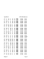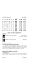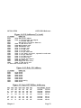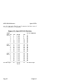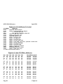
1
brain boxes
Opto DIO
4.0 EDITION Mar 1995
______________
GUARANTEE.
FULL 36 MONTHS GUARANTEE.
BRAIN BOXES guarantee your interface card for a full 36
months from purchase, parts and labour, provided it has been
used in the specified manner. In the unlikely event of failure
return your interface card to BRAIN BOXES or to your Dealer,
with proof of purchase, who will determine whether to repair or
replace this product with an equivalent unit.
_____________
COPYRIGHT.
COPYRIGHT (C) 1988-1995 BRAIN BOXES.
All rights reserved. No part of this hardware, circuitry or
manual may be duplicated, copied, transmitted or reproduced in
any way without the prior written permission of BRAIN
BOXES.
Opto DIO48, Opto DIO16, Opto OUT48, Opto OUT24 and Opto
IN24 are designed, manufactured and supported by
BRAIN BOXES.
______________
_
Unit 3F, Wavertree Boulevard South,
Wavertree Technology Park,
Liverpool, L7, 9PF,
ENGLAND.
Telephone:
0151-220 2500
New Fax No#:
0151-252 0446
_________________________
ACKNOWLEDGEMENTS.
BRAIN BOXES is a trademark of BRAIN BOXES.
IBM, and COMPAQ are trademarks of the relevant companies.
Micro Channel Architecture is a trademark of IBM.
Opto Hardware Reference
Thank You For Buying the
Optically Isolated
Input Output Interface!
We proudly present a range of optically isolated digital
input output cards.
OPTO DIO48 provides 24 high voltage, high current
outputs lines and 24 input lines all with +/-2500 Volts optical
isolation.
OPTO DIO16 provides 8 high voltage, high current outputs
lines and 8 input lines all with +/-2500 Volts optical isolation.
OPTO OUT48 gives the user with 48 high voltage, high
current outputs lines with +/-2500 Volts optical isolation.
OPTO OUT24 gives the user with 24 high voltage, high
current outputs lines with +/-2500 Volts optical isolation.
OPTO IN24 gives the user with 24 input lines with +/-2500
Volts optical isolation.
The optically isolated outputs are high voltage, high current
outputs lines, with +/-2500 Volts optical isolation. Fast TTL
buffers, opto isolators and drivers allow a maximum throughput
of 150kHz. The cards may be fitted with source drivers or with
sink drivers. The on chip current limiting resistors and output
transient suppression diodes have been augmented by on board
higher duty suppression diodes and pull down resistors so
ensuring long term use in an industrial environment.
Cards with these outputs require an external, user supplied,
power input to supply the opto isolators and the i/o drivers. On
board regulation allows the use of unregulated supplies in the
range 17.5-35 Volts. A minimum of 8VA current capability per
8 line source output package is needed. ie OUT24, DIO48
Intro-3
Opto Hardware Reference
requires 25VA power supply, OUT48 requires 50VA power
supply.
The optically isolated inputs are current limited and reverse
polarity protected and provide +/-2500 Volts optical isolation.
Fast TTL buffers, opto isolators and drivers allow a maximum
throughput of 150kHz.
Most of the opto card range have an on board Watchdog
Timer that can be used as a fail safe way to ensure the users
program is running correctly and the PC has not crashed. (Not
available on the DIO16)
The Opto DIO cards are the ideal for high output current
control applications such as driving relays, solenoids, stepper
motors, LED’s or lamps requiring separate logic and load
grounds.
A separate manual "The Interfacing Guide" with a disk full
of worked examples in BASIC, PASCAL, C, Assembler and
FORTRAN ensure that you are up and running with the card
straight away!
Your card is designed and manufactured in England, and
our policy is one of complete support to our dealers and direct
to our users. It is designed ’in house’ and is completely
understood by our staff. Its great strength is the support we give
it. Our intention is to supply the hardware, software and any
technical information you may need to allow you to exercise
complete control the card and i/o devices. After searching the
manuals, do not hesitate to contact us on our HOTLINE number
on Intro Page 2, if you need help.
We trust that if you adhere to the following procedures you
will enjoy many years of useful service from your interface.
Intro-4
Opto Hardware Reference
________________
OPTO
MANUAL.
The Layout Of This Manual.
________________________
_
This manual is a complete description of how to configure
and install the Opto input output range of interface cards.
Information on register maps, programming and wiring up
the is in a companion manual, "The Interfacing Guide".
Chapter 1, Outputs, Inputs, Watchdog & Power,
describes the features common to many of the opto i/o cards.
The topics covered are the external user supplied power supply,
the output drivers types, the input circuit and the watch dog
timer.
Chapter 2, Opto DIO48 Configuration, shows you
how to configure the Opto DIO48 card ready for installation in
an expansion slots of your computer, detailing the address DIP
switches, card jumpers, i/o memory map and connector pinouts.
Chapters 3-6, shows you how to configure the Opto
DIO16, OUT48, OUT24 and IN24 cards respectively.
Chapter 7, Installation In The PC, shows how the
card can be installed an unused PC expansion slot.
The Index covers the complete contents of the manual.
Intro-5
Opto Hardware Reference
Outline Contents._
_______________
Chapter 1. Outputs, Inputs, Watchdog & Power.
Chapter 2. Opto DIO48 Configuration.
Chapter 3. Opto DIO16 Configuration.
Chapter 4. Opto OUT48 Configuration.
Chapter 5. Opto OUT24 Configuration.
Chapter 6. Opto IN24 Configuration.
Chapter 7. Installation Guide.
Cumulative Index.
Intro-6
Opto Hardware Reference
_________
Contents.
Chapter 1. Outputs, Inputs, Watchdog & Power.
_________________________________________
_
Introduction.
Power Supply.
Output Driver Types.
Sink And Source Explained.
UDN2984 ULN2804 Driver Selection.
Source Driver Output Connection.
Source Driver Output Logical Levels.
Sink Driver Output Connection.
Sink Driver Output Logical Levels.
Power Off And Reset Output Levels.
Safety First.
Input Port Schematic.
The Watch Dog.
Watch Dog Enable Register.
Watch Dog Time Out.
Connector Cross Reference.
1
1
2
3
4
4
6
6
8
9
9
10
10
12
12
14
Chapter 1. List Of Figures.
_______________________
_
Figure 1-1. Regulated Power Supply.
Figure 1-2. Unregulated Power Supply.
Figure 1-3. Useless Power Supply.
Figure 1-4. Driver Chip Select.
Figure 1-5. Source Driver Output Port Schematic.
Figure 1-6. Source Driver Output Connections.
Figure 1-7. Logically Inverting The Source Output.
Figure 1-8. Sink Driver Output Port Schematic.
Figure 1-9. Sink Driver Output Connections.
Figure 1-10. Logically Inverting The Sink Output.
Figure 1-11. Sink Versus Source Outputs.
Figure 1-12. Input Port Schematic.
Figure 1-13. Watch Dog Enable Register.
Figure 1-14. 50IDC To 50D Pin Outs.
Figure 1-15. 50D To 50IDC Pin Outs.
1
2
2
4
5
5
6
7
7
8
9
10
11
13
14
Intro-7
Opto Hardware Reference
Chapter 2. Opto DIO48 Configuration.
_________________________________
_
Introduction.
Configuring The Opto DIO48 Card.
Setting The Opto DIO48 I/O Address.
Using More Than One Opto DIO48 Board.
UDN2984 ULN2804 Driver Selection.
Source Driver Output Connection.
Sink Driver Output Connection.
Interrupt Selection.
Watch Dog Selection.
Opto DIO48 Memory Map.
Opto DIO48 Output Specification.
Opto DIO48 Input Specification.
Opto DIO48 Pinouts.
15
15
16
17
20
20
20
22
22
24
25
25
26
Chapter 2. List Of Figures.
_______________________
_
Figure 2-1. Opto DIO48 Card Layout.
Figure 2-2. Opto DIO48 Factory Set DIP Switches.
Figure 2-3. I/O Addresses To Avoid.
Figure 2-4. Likely I/O Address.
Figure 2-5. Opto DIO48 Base Addresses.
Figure 2-6. Driver Chip Select.
Figure 2-7. The IRQ Jumper Block.
Figure 2-8. Watchdog Output Select.
Figure 2-9. Watchdog Output Select.
Figure 2-10. Opto DIO48 Memory Map.
Figure 2-11. Opto DIO48 J2 Pinouts.
Figure 2-12. Opto DIO48 J2 Female 50D Pinout.
16
16
17
17
18
19
21
22
23
24
26
27
Chapter 3. Opto DIO16 Configuration.
_________________________________
_
Introduction.
Configuring The Opto DIO16 Card.
Setting The Opto DIO16 I/O Address.
Using More Than One Opto DIO16 Board.
Intro-8
28
28
28
30
Opto Hardware Reference
UDN2984 ULN2804 Driver Selection.
Source Driver Output Connection.
Sink Driver Output Connection.
Opto DIO16 Memory Map.
OPTO DIO16 Output Specification.
Opto DIO16 Pinouts.
32
32
33
33
34
35
Chapter 3. List Of Figures.
_______________________
_
Figure 3-1. Opto DIO16 Card Layout.
Figure 3-2. Opto DIO16 Factory Set DIP Switches.
Figure 3-3. Likely I/O Address.
Figure 3-4. I/O Addresses To Avoid.
Figure 3-5. Opto DIO16 Base Addresses.
Figure 3-6. Driver Chip Select.
Figure 3-7. Opto DIO16 Memory Map.
Figure 3-8. Opto DIO16 J2 Pinouts.
Figure 3-9. Opto DIO16 J2 Female 50D Pinout.
29
29
29
30
30
32
34
35
36
Chapter 4. Opto OUT48 Configuration.
__________________________________
Introduction.
Configuring The Opto OUT48 Card.
Setting The Opto OUT48 I/O Address.
Using More Than One Opto OUT48 Card.
UDN2984 ULN2804 Driver Selection.
Source Driver Output Connection.
Sink Driver Output Connection.
Interrupt Selection.
Watch Dog Selection.
Opto DIO48 Memory Map.
OPTO OUT48 Output Specification.
Opto OUT48 Pinouts.
37
37
37
42
42
43
43
43
45
46
47
48
Chapter 4. List Of Figures.
_______________________
_
Figure 4-1. Opto OUT48 Card Layout.
38
Intro-9
Opto Hardware Reference
Figure 4-2. Opto OUT48 Factory Set DIP Switches.
Figure 4-4. I/O Addresses To Avoid.
Figure 4-4. Likely I/O Address.
Figure 4-5. Opto OUT48 Base Addresses.
Figure 4-6. Driver Chip Select.
Figure 4-7. The IRQ Jumper Block.
Figure 4-8. Watchdog Output Select.
Figure 4-9. Watchdog Output Select.
Figure 4-10. Opto OUT48 Memory Map.
Figure 4-11. Opto OUT48 J2 Pin Outs.
Figure 4-12. Opto OUT48 J2 Female 50D Pinout.
38
39
39
39
42
44
45
46
47
48
49
Chapter 5. Opto OUT24 Configuration.
__________________________________
Introduction.
Configuring The Opto OUT24 Card.
Setting The Opto OUT24 I/O Address.
Using More Than One Opto OUT24 Card.
UDN2984 ULN2804 Driver Selection.
Source Driver Output Connection.
Sink Driver Output Connection.
Interrupt Selection.
Watch Dog Selection.
Opto OUT24 Memory Map.
Opto OUT24 Output Specification.
Opto OUT24 Pinouts.
50
50
50
56
56
56
57
57
59
60
61
61
Chapter 5. List Of Figures.
_______________________
_
Figure 5-1. Opto OUT24 Card Layout.
Figure 5-2. Opto Out24 Factory Set DIP Switches.
Figure 5-4. I/O Addresses To Avoid.
Figure 5-4. Likely I/O Address.
Figure 5-5. Opto OUT24 Base Addresses.
Figure 5-6. Driver Chip Select.
Figure 5-7. The IRQ Jumper Block.
Figure 5-8. Watchdog Output Select.
Intro-10
51
51
52
52
52
56
58
59
Opto Hardware Reference
Figure 5-9. Watchdog Output Select.
Figure 5-10. Opto OUT24 Memory Map.
Figure 5-11. Opto OUT24 J2 Pin Outs.
Figure 5-12. Opto OUT24 J2 Female 50D Pinout.
60
61
62
63
Chapter 6. Opto IN24 Configuration.
________________________________
Introduction.
Configuring The Opto IN24 Card.
Setting The Opto IN24 I/O Address.
Using More Than One Opto IN24 Card.
Volt Free Contact Whetting Voltage.
Using Volt Free Contacts.
Interrupt Selection.
Watch Dog Selection.
Opto IN24 Memory Map.
Opto IN24 Input Specification.
Opto IN24 Pinouts.
64
64
64
69
70
70
71
71
73
74
75
Chapter 6. List Of Figures.
_______________________
_
Figure 6-1. PC Opto IN24 Card Layout.
Figure 6-2. Opto IN24 Factory Set DIP Switches.
Figure 6-3. Likely I/O Address.
Figure 6-4. I/O Addresses To Avoid.
Figure 6-5. Opto IN24 Base Addresses.
Figure 6-6. Expower Jumpers.
Figure 6-7. Whetting Volt Free Contacts.
Figure 6-8. The IRQ Jumper Block.
Figure 6-9. Watchdog Output Select.
Figure 6-10. Opto In24 Memory Map.
Figure 6-11. Opto IN24 J2 Pin Outs.
Figure 6-12. Opto IN24 J2 Female 50D Pinout.
65
65
65
66
66
70
70
72
73
74
75
76
Intro-11
Opto Hardware Reference
Chapter 7. Installation In PC.
_________________________
_
Installing The Opto Board In The Computer.
Problems!
Screw Terminal Board.
77
79
79
Chapter 7. List Of Figures.
_______________________
_
Figure 7-1. Remove Cover Mounting Screws.
Figure 7-2. Removing The PC Cover.
Figure 7-3. Removing Blanking Cover.
Figure 7-4. Inserting The Opto Card.
______
Index.
Intro-12
77
77
78
78
Read This First.
OPTO DIO Reference
CHAPTER 1
OPTO OUTPUTS,
INPUTS, WATCHDOG,
AND POWER.
____________
Introduction.
This chapter describes the features common to many of the
opto i/o cards. The topics covered are the external user supplied
power supply, the output drivers types, the input circuit and the
watch dog timer.
Power Supply.
____________
_
Those cards that have opto isolated outputs require an
external power input to drive the isolators and the output driver
chips. The external power input is a nominal 24 volts input put.
Figure 1-1. Regulated Power Supply.
_______________________________
_
Either a commercially available DC power supply or a
home made one may be used. The supply can be regulated or un
regulated. The opto cards have on board regulation and reverse
connection protection. Suitable regulated and unregulated supply
circuits are given below. The power supplies range 17.5 to 30
Volts maximum capable of supplying a minimum of 2 Amps at
25 Volts. ie 50 VA rating. (OUT48 4 Amp @ 25 Volt= 100VA)
Chapter 1
Page 1
OPTO DIO Reference
Read This First.
If an unregulated power supply is used ensure that it is
rectified and has sufficient smoothing to kept it above the
absolute minimum of 17 volts.
Figure 1-2. Unregulated Power Supply.
_________________________________
_
Unsuitable power supplies are those that provide only half wave
rectification and those that are unsmoothed. Both these types fall
below the minimum +17 Volts necessary to allow the on board
regulation to work.
Figure 1-3. Useless Power Supply.
_____________________________
Output Driver Types.
__________________
_
Those opto isolated cards that have output lines, Opto
DIO16, Opto DIO48, Opto OUT24 and Opto OUT48 can be
configured to use one of two types of high voltage drive chips.
These types are known as sink drivers and source drivers. The
sink driver chips chips are of type ULN2804 and the source
driver chips are of type UDN 2984 chips.
Page 2
Chapter 1
Read This First.
OPTO DIO Reference
Which type of chip is fitted on the opto card is determined
by the part number used to order the card. The cards are
supplied with the SOURCE drivers UDN2984 fitted as standard,
unless the user specified SINK at the time of ordering. The card
can be easily changed between sink and source specification by
exchanging certain chips and setting a pair of jumpers.
The difference between these two types of driver, their
output current capabilities, their power on reset condition and
optional inverting configuration is explained below.
Sink And Source Explained.
________________________
_
The output ports of the card are optically isolated from the
rest of the PC so that wiring defects or accidental connections to
high voltage or high current devices do not damage the PC. In
addition the outputs are via high voltage, high current driver
chips. The lines of these driver chips are connected by the user
to a load. As the users programs sets the output port lines high
and low the output driver chips attempt to pull the loads to a
high and low voltage.
When current flows out of the driver output terminal and
into the load, the device is said to "source" current. This is a
source driver. Conversely current flows from a load into a "sink"
driver.
Source drivers can pull outputs both up and down.
When the PC is powered off whilst the external power is ON
the port lines are ON.
Sink drivers can only pull an output down to ground,
they cannot pull an output up. When the PC is powered off
whilst the external power is ON the port lines are ON.
With sink drivers the outputs only go high when the external
circuit pulls them high. eg via a resistor attached to a positive
voltage source.
Sink drivers can provide both source and sink functions. Sink
drivers cannot provide source driver functions. However, they
can cope with significantly higher current loads.
Chapter 1
Page 3
OPTO DIO Reference
Read This First.
Figure 1-4. Driver Chip Select.
__________________________
_
ÚÄÄÄ¿
³ÛÛÛ³
³³ÛÛÛ³³
ÀÄÄÄÙ
ÚÄÄÄ¿
³Û³Û Û³Û³
Û³
³ÛÀÄÄÄÙ
FACTORY SET
___________
UDN2984 Source Drivers Selected
ULN2804 Sink Drivers Selected
Optional 10k resistor
networks installed
Remove resistor networks
UDN2984 ULN2804 Driver Selection.
________________________________
The card can be configured to use one of two types of
high voltage drive chips ULN2804 or UDN 2984 chips.
The two jumper pins directly below and just to the left of
the driver chips is used to made the selection. Note the OPTO
DIO is supplied with the UDN2984 fitted as standard, the user
may fit the ULN2804s themselves or order them factory fitted.
Source Driver Output Connection.
_____________________________
_
UDN2984 Drivers.
The UDN2984 chips are high voltage, high current SOURCE
drivers, output voltage range 35 to 80 Volts, these could be
directly replaced by UDN2981 drivers for output voltages in the
range 5 to 50 Volts. Whilst the 2984/81 drivers have built in
output transient suppression diodes, extra diodes are provided on
board the Opto DIO cards for extra protection. The socketed 10k
resistor networks RN14, 16 and 18 etc should be left installed.
The source driver output schematic is shown in Figure 1-5.
Typical output connections are shown in Figure 1-6. Both pull
down and pull up connection schemes work.
Page 4
Chapter 1
Read This First.
OPTO DIO Reference
Figure 1-5. Source Driver Output Port Schematic.
___________________________________________
Figure 1-6. Source Driver Output Connections.
________________________________________
_
Chapter 1
Page 5
OPTO DIO Reference
Read This First.
Source Driver Output Logical Levels.
________________________________
_
The source cards are supplied with non inverting buffer
chips, 74LS541, so that a logical one written to the output
register drives the output high and a logical zero written to the
output port drives the output low. Thus in this normal mode of
operation the voltage level of the output line follows the logic
level in the output register.
The source cards can be fitted with inverting buffer chips,
74LS540, so that a logical one written to the output register
drives the output low and a logical zero written to the output
port drives the output high. See Figure 1-7. Thus in this inverse
mode of operation the voltage level of the output line does the
opposite of the logic level in the output register.
Note since the sink driver chips are inverting and the
source are not the non inverting buffer chips are must be
changed when source and sink drivers are changed.
Figure 1-7. Logically Inverting The Source Output.
____________________________________________
ÚÄÄÄÄÄÄÄÄÂÄÄÄÄÄÄÄÄÄÄÄÄÄÄÄÄÄÄÂÄÄÄÄÄÄÄÄÄÄÄÄÂÄÄÄÄÄÄÄÄÄÄÄÄÂÄÄÄÄÄÄÄÄÄÄÄÄ¿
³ DRIVER ³ýBUFFER USED ³ýPORT DATA ³ýPORT LINESý³ OPERATIONýý³
ÃÄÄÄÄÄÄÄÄÅÄÄÄÄÄÄÄÄÄÄÄÄÄÄÄÄÄÄÅÄÄÄÄÄÄÄÄÄÄÄÄÅÄÄÄÄÄÄÄÄÄÄÄÄÅÄÄÄÄÄÄÄÄÄÄÄÄ´
³ýSOURCE ³ý74LS541 ý ³ý0 = low ³ýOFF = low ³ NORMAL ý³
³ý1 =high ³ýON =high ³ NORMAL ý³
³ýSOURCE ³ý74LS541
³
ý ý ³ý
ý³
ý³
³ý ý³ý
³ýSOURCE ³ý74LS540ýINVERTERS³ý0 = low ³ýON =highý³ INVERSE ý³
³ýSOURCE ³ 74LS540ýINVERTERS³ý1 =high ³ýOFF = low ³ INVERSE ý³
ÀÄÄÄÄÄÄÄÄÁÄÄÄÄÄÄÄÄÄÄÄÄÄÄÄÄÄÄÁÄÄÄÄÄÄÄÄÄÄÄÄÁÄÄÄÄÄÄÄÄÄÄÄÄÁÄÄÄÄÄÄÄÄÄÄÄÄÙ
Note: By default Source driver use 74LS541 non inverting buffers,
74LS540 INVERTING buffers will invert the output signals.
Sink Driver Output Connection._
___________________________
ULN2804 Drivers.
The ULN2804 chips are high voltage, high current NPN
DARLINGTON open collector drivers, output voltage range to
50 Volts. Use ULN2824 chips for output up to 95 Volts. When
changing from 2984 to 2804 drivers note than the 2804 are
INVERTING drivers, thus to produce the same logical output
Page 6
Chapter 1
Read This First.
OPTO DIO Reference
from a bit pattern written to the output port the 74LS541 chips
would have to be replaced by the inverting 74LS540 chips.
Remove the socketed 10k resistor networks.
Figure 1-8. Sink Driver Output Port Schematic.
_________________________________________
Figure 1-9. Sink Driver Output Connections.
______________________________________
_
Chapter 1
Page 7
OPTO DIO Reference
Read This First.
The sink driver output schematic is shown in Figure 1-8.
Typical output connections are shown in Figure 1-9. Note only
the pull down scheme works with sink drivers.
The sink drivers can only pull down the output lines.
Sink Driver Output Logical Levels.
______________________________
_
The sink cards are normally fitted with inverting buffer
chips, 74LS540, so that a logical one written to the output
register drives the output high and a logical zero written to the
output port drives the output low. Thus in this normal mode of
operation the voltage level of the output line follows the logic
level in the output register.
The sink cards can be fitted with non inverting buffer
chips, 74LS541, so that a logical one written to the output
register drives the output low and a logical zero written to the
output port drives the output high. See Figure 1-10. Thus in this
inverse mode of operation the voltage level of the output line
does the opposite of the logic level in the output register.
Note since the sink driver chips are inverting and the
source are not the non inverting buffer chips are must be
changed when source and sink drivers are changed.
Figure 1-10. Logically Inverting The Sink Output.
___________________________________________
ÚÄÄÄÄÄÄÄÄÂÄÄÄÄÄÄÄÄÄÄÄÄÄÄÄÄÄÄÂÄÄÄÄÄÄÄÄÄÄÄÄÂÄÄÄÄÄÄÄÄÄÄÄÄÂÄÄÄÄÄÄÄÄÄÄÄÄ¿
³ýPORT DATA ³ýPORT ýýý³ OPERATIONýý³
³ DRIVER ³ýBUFFER
ý³ýSETTING ý³ýLINESý ý³
ý³
³ ýýýý³ýUSED
ÃÄÄÄÄÄÄÄÄÅÄÄÄÄÄÄÄÄÄÄÄÄÄÄÄÄÄÄÅÄÄÄÄÄÄÄÄÄÄÄÄÅÄÄÄÄÄÄÄÄÄÄÄÄÅÄÄÄÄÄÄÄÄÄÄÄÄ´
³ýSINK ³ 74LS540ýINVERTERS³ý0 = low ³ýOFF = low ³ NORMAL ý³
³ýSINK ³ý74LS540ýINVERTERS³ý1 =high ³ýON =highý³ NORMAL ý³
ý³ý
³ ý ý ³ý
ý³
³ý ý³ý
ý³ý0 = low ³ýON =high ³ INVERSE ý³
³ýSINK ³ý74LS541
ý³ý1 =high ³ýOFF = lowý³ INVERSE ý³
³ýSINK ³ý74LS541
ý³ý
³ ý ý ³ý
ý³
³ý ý³ý
ÀÄÄÄÄÄÄÄÄÁÄÄÄÄÄÄÄÄÄÄÄÄÄÄÄÄÄÄÁÄÄÄÄÄÄÄÄÄÄÄÄÁÄÄÄÄÄÄÄÄÄÄÄÄÁÄÄÄÄÄÄÄÄÄÄÄÄÙ
Note: By default Sink driver, since they are inverting drivers
themselves, use 74LS540 inverting buffers to give a non inverting
output. Using 74LS541 buffers will invert the output signals.
Page 8
Chapter 1
Read This First.
OPTO DIO Reference
Power Off And Reset Output Levels.
_______________________________
_
Due to the difference in the nature of internal circuitry of
the sink and source driver chips there are systematic differences
in the power off and reset voltage levels of the output lines
when using these two driver types.
Typically the the source drivers keep the output lines at
zero when the PC is switched off, whilst the sink drivers allow
the outputs to float to a high voltage level determined by the
external circuit.
Figure 1-11. Sink Versus Source Outputs.
___________________________________
_
ÚÄÄÄÄÄÄÄÄÂÄÄÄÄÄÄÄÄÄÄÄÄÄÂÄÄÄÄÄÄÄÄÄÂÄÄÄÄÄÄÄÄÄÄÄÄÂÄÄÄÄÄÄÄÄÄÄÄÄÂÄÄÄÄÄÄÄÄ¿
³ýPORTýýý³
³ DRIVER ³ PC STATE ³ýEXTERNAL³ýBUFFER ³ýPORT
³ýPOWER ý³ýUSED ý³ýSETTING ý³ýLINESýý³
³ ýýýý³
ÃÄÄÄÄÄÄÄÄÅÄÄÄÄÄÄÄÄÄÄÄÄÄÅÄÄÄÄÄÄÄÄÄÅÄÄÄÄÄÄÄÄÄÄÄÄÅÄÄÄÄÄÄÄÄÄÄÄÄÅÄÄÄÄÄÄÄÄ´
³ýOFF ý³
³ýSOURCE ³ýPOWER OFF ýý³ýON ý³ýEITHER ý³ýN/Aý
³ýSOURCE ³ýPOWER RESETý³ýON ³ýEITHER ý³ýRESET =low ³ýOFF ý³
ý³ýON ³ý74LS541 ý³ý0 =low ³ýOFF ý³
³ýSOURCE ³ýON
ý³ýON ³ý74LS541 ý³ý1 =high ³ýON ý³
³ýSOURCE ³ýON
³ý
ý³ý
³
ý ý ³ý ý³
³ý ý³ý
ý³ýON ³ý74LS540ýINV³ý0 =low ³ýON ý³
³ýSOURCE ³ýON
ý³ýON ³ý74LS540ýINV³ý1 =high ³ýOFF ý³
³ýSOURCE ³ýON
³ý
ý³ý
³
ý ý ³ý ý³
³ý ý³ý
³ý
ý³ý
³
ý ý ³ý ý³
³ý ý³ý
³ýSINK ³ýPOWER OFF ýý³ýON ³ýEITHER ý³ýN/A ý ³ýON ý³
³ýSINK ³ýPOWER RESETý³ýON ³ýEITHER ý³ RESET =low ³ýOFF ý³
ý³ýON ³ý74LS540ýINV³ý0 =low ³ýOFF ý³
³ýSINK ³ýON
ý³ýON ³ý74LS540ýINV³ý1 =high ³ýON ý³
³ýSINK ³ýON
³ý
ý³ý
³
ý ý ³ý ý³
³ý ý³ý
ý³ýON ³ý74LS541 ý³ý0 =low ³ýON ý³
³ýSINK ³ýON
ý³ýON ³ý74LS541 ý³ý1 =high ³ýOFF ý³
³ýSINK ³ýON
ÀÄÄÄÄÄÄÄÄÁÄÄÄÄÄÄÄÄÄÄÄÄÄÁÄÄÄÄÄÄÄÄÄÁÄÄÄÄÄÄÄÄÄÄÄÄÁÄÄÄÄÄÄÄÄÄÄÄÄÁÄÄÄÄÄÄÄÄÙ
Note: By default Source driver use 74LS541 non inverting buffers,
74LS540 INVERTING buffers will invert the output signals.
Note: By default Sink driver, since they are inverting drivers
themselves, use 74LS540 inverting buffers to give a non inverting
output. Using 74LS541 buffers will invert the output signals.
Safety First.
If the power off and power reset state of the output lines is
critical to the safe operation of your circuit, examine Figure 1-11
and check the actual operation of the card when the external
circuit is connected. Perform this check both with and without
Chapter 1
Page 9
OPTO DIO Reference
Read This First.
the external isolated power supply applied.
Do not make any assumptions about the effects of changes
made to the external circuit if the power off and reset conditions
are critical to the safe operation of your system.
Figure 1-12. Input Port Schematic.
______________________________
Input Port Schematic.
___________________
The input port schematic is given in Figure 1-12. The input
port lines are reverse connection protected and current limited.
Input voltages of 0.0 - 2.38 Volts read as input logic low, 0.
Input voltages of 2.4 - 24.00 Volts read as input logic high, 1.
The inputs are current limited by a 3k3 Ohm resistor and
are reverse connection protected by diodes.
The Watch Dog.
______________
The watch dog is a failsafe method of ensuring that the
user’s program is still running correctly. On power up, the watch
dog is disabled. If the user’s program enables the watchdog, an
Page 10
Chapter 1
Read This First.
OPTO DIO Reference
interrupt or reset signal is generated on timeout. Reading the
watchdog register refreshes the timer, postponing timeout for 50
milliseconds. When the watch dog times out an timer expired
output signal is set. On those cards that provide opto isolated
outputs the watchdog timer expired output, in place of Port A
line bit 0, is available on the 50 way edge connector.
The watch dog timer expired output is jumper selectable to one
of four options.
Timer expired jumper selectable output signal options are:i)
a constant high level voltage.
ii) a constant low level voltage.
iii) a goes high then returns low pulse.
iv) a goes low then returns high pulse.
The constant level pulses are suitable as enable lines for stepper
motors or switches etc.
The goes high then returns low pulse is suitable for gating onto
PC interrupt and reset lines. Note many PC reset lines are
outputs only and so the opto cards watchdog pulse will not cause
a PC reset on timeout.
The watch dog is enable by writes to the watchdog register. See
Figure 1-13.
Figure 1-13. Watch Dog Enable Register.
___________________________________
_
ÚÄÄÄÄÄÄÄÄÄÄÄÄÄÄÄÄÄÄÄÄÄÄÄÄÄÄÄÄÄÄÄÄÄÄÄÄÄÄÄÄÄÄÄÄÄÄÄÄÄÄÄÄÄÄÄÄÄÄÄÄÄÄÄÄÄÄÄ¿
³ýýýýýWATCH DOGýENABLE REGISTERýDEFAULTýADDRýAREý030Bý&ý030FýHexýýýý³
³ýýýýýTHISýISýAýREADýWRITEýREGISTERýýýýýýýýýýýýýýýýýýýýýýýýýýýýýýýýý³
ÃÄÄÄÄÄÄÂÄÄÄÄÄÄÂÄÄÄÄÄÄÂÄÄÄÄÄÄÂÄÄÄÄÄÄÄÄÄÂÄÄÄÄÄÄÄÄÄÂÄÄÄÄÄÄÄÄÄÂÄÄÄÄÄÄÄÄÄ´
³ýBITý7³ýBITý6³ýBITý5³ýBITý4³ýBITýý3ýý³ýBITýý2ýý³ýBITýý1ýý³ýBITýý0ýý³
ÃÄÄÄÄÄÄÁÄÄÄÄÄÄÁÄÄÄÄÄÄÁÄÄÄÄÄÄÅÄÄÄÄÄÄÄÄÄÅÄÄÄÄÄÄÄÄÄÅÄÄÄÄÄÄÄÄÄÅÄÄÄÄÄÄÄÄÄ´
³ýWRITE ýDONT CARE ýý ýý³ýGATE ýý³ýGATE ýý³ýGATE ýý³ýGATE ýý³
ý³ýPORT C2ý³ýPORT C2ý³ýJUMPERýý³ýJUMPERýý³
³
ý³ýBIT 3 ýý³ýBIT 0 ýý³ýBUS ýý³ýBUS ýý³
³ READ ALWAYS 0
ý³ýTO IRQýý³ýTO IRQýý³ýTO IRQýý³ýTO RESET³
³
ÃÄÄÄÄÄÄÄÄÄÄÄÄÄÄÄÄÄÄÄÄÄÄÄÄÄÄÄÁÄÄÄÄÄÄÄÄÄÁÄÄÄÄÄÄÄÄÄÁÄÄÄÄÄÄÄÄÄÁÄÄÄÄÄÄÄÄÄ´
ýý³
³ READ OF THIS REGISTER REFRESHES THE WATCH DOG TIMER
³ READ THIS AT LEAST ONCE EVERY 50 MILLI SECONDS TO PREVENT TIMOUTýý³
ÀÄÄÄÄÄÄÄÄÄÄÄÄÄÄÄÄÄÄÄÄÄÄÄÄÄÄÄÄÄÄÄÄÄÄÄÄÄÄÄÄÄÄÄÄÄÄÄÄÄÄÄÄÄÄÄÄÄÄÄÄÄÄÄÄÄÄÄÙ
Note OUT24, OUT48 and DIO16 BIT 3 and BIT 2 ALWAYS = ZERO!
Chapter 1
Page 11
OPTO DIO Reference
Read This First.
Watch Dog Enable Register.
________________________
_
The watch dog enable register is an 8 bit read write
register. Writing the bits enables, gates, various signals onto the
PC expansion bus IRQ or RESET line. Thus allowing an
interrupt or reset to be generated in the PC. On power up all the
bits are cleared to zero. IE No signals are gated through to the
PC bus. The bit map of the Watch Dog register is given below.
Bits 7-4 are always read back as zero, writing them high or low
has no effect. For compatibility with future versions of this card
bits 7-4 should always be written as 0.
Bit 0 when =1 the watch dog BUS jumper signal is gated to PC
bus RESET line. This line causes a power on reset of the
PC when driven high.
NOTE this line is an output only on many PC’s and so
cannot be used to reset the PC.
Bit 1 when =1 the watch dog BUS jumper signal is gated to the
PC bus IRQ line as selected by the IRQ jumper block.
Bit 2
DIO48 and IN24 ONLY
when =1 the Port C2 bit 0 input signal is gated from the
opto isolator to the IRQ selected by the IRQ jumper block.
Low to high transitions generates a PC interrupt.
OUT24, OUT48 and DIO16 BIT 2 ALWAYS = ZERO.
Bit 3
DIO48 and IN24 ONLY
when =1 the Port C2 bit 3 input signal is gated from the
opto isolator to the IRQ line selected by the IRQ jumper
block. Low to high transition generates the PC interrupt.
OUT24, OUT48 and DIO16 BIT 3 ALWAYS = ZERO.
The IRQ handler should check, by reading the watchdog register,
which interrupt is enabled and service the appropriate function,
eg Watch dog timeout or transition of the Port C lines.
Watch Dog Time Out.
___________________
The watch dog times out after 50 milli seconds. The time
out is prevented by a read of the watch dog register, this
refreshes the 50 milli second timeout. Writes to the register do
Page 12
Chapter 1
Read This First.
OPTO DIO Reference
not refresh the timeout. It is necessary to continuously perform a
read of the watch dog register at least 20 times a second. The
watch dog timer may be refreshed more frequently than this, in
fact, as often as the user sees fit. From the end of the last
refresh a 50 millisecond period may elapse before the watch dog
times out. On time out, depending on how the watch dog
options, PA10 output select jumpers and watch dog register
enable bits are set, either output lines are set or software
interrupts or PC reset are caused.
Generally, the watch dog is used as a fail safe method of
ensuring that the users software is running correctly and that the
PC has not crashed.
Figure 1-14. 50IDC To 50D Pin Outs.
________________________________
50D
34
35
19
36
37
21
38
39
23
40
41
25
42
43
27
44
45
29
46
47
31
48
49
33
17
Chapter 1
50IDC
1
3
5
7
9
11
13
15
17
19
21
23
25
27
29
31
33
35
37
39
41
43
45
47
49
ÚÄÄÄÄÄ¿
³ 1 2ý³
³ 3 4ý³
³ 5 6ý³
³ 7 8ý³
³ O Oý³
³ O Oý³
³ O Oý³
³ O Oý³
³ O Oý³
³ O Oý³
³ O Oý³
³ O Oý³
³ O Oý³
³ O Oý³
³ O Oý³
³ O Oý³
³ O Oý³
³ O Oý³
³ O Oý³
³ O Oý³
³ O Oý³
³ O Oý³
³ O Oý³
³47 48³
³49 50³
ÀÄÄÄÄÄÙ
50IDC
2
4
6
8
10
12
14
16
18
20
22
24
26
28
30
32
34
36
38
40
42
44
46
48
50
50D
1
2
18
3
4
20
5
6
22
7
8
24
9
10
26
11
12
28
13
14
30
15
16
32
50
Page 13
OPTO DIO Reference
Read This First.
Connector Cross Reference.
________________________
Figure 1-14 is a cross reference of the 50 IDC connector
to 50 way Female D connector pinouts. Though it may seem like
an arbitrary mapping it is the most logical available as can be
seen from an examination of the pcb tracks. The corresponding
cross reference for the 50D to 50IDC is in Figure 1-15.
Figure 1-15. 50D To 50IDC Pin Outs.
________________________________
50IDC 50D
Row1
2
1
6
4
2
5
8
3
12
10
4
11
14
5
18
16
6
17
20
7
24
22
8
23
26
9
30
28
10
29
32
11
36
34
12
35
38
13
42
40
14
41
44
15
48
46
16
47
49
17
Page 14
50D
Row2
18
19
20
21
22
23
24
25
26
27
28
29
30
31
32
33
ÚÄÄÄÄÄÄÄÄÄÄÄÄÄÄÄÄ¿
³
³
³1
34ý³
³ 18
ý³
³2
35ý³
³ 19
ý³
³3
36ý³
³ 20
ý³
³4
37ý³
³ 21
ý³
³5
38ý³
³ 22
ý³
³6
39ý³
³ 23
ý³
³7
40ý³
³ 24
ý³
³8
41ý³
³ 25
ý³
³9
42ý³
³ 26
ý³
³ 10
43ý³
³ 27
ý³
³ 11
44ý³
³ 28
ý³
³ 12
45ý³
³ 29
ý³
³ 13
46ý³
³ 30
ý³
³ 14
47ý³
³ 31
ý³
³ 15
48ý³
³ 32
ý³
³ 16
49ý³
³ 33
ý³
³ 17
50ý³
ÀÄÄÄÄÄÄÄÄÄÄÄÄÄÄÄÄÙ
50D
Row3
34
50IDC
35
3
36
7
37
9
38
13
39
15
40
19
41
21
42
25
43
27
44
31
45
33
46
37
47
39
48
43
49
45
50
50
1
Chapter 1
Opto DIO48
OPTO DIO Reference
CHAPTER 2
OPTO DIO48
CONFIGURATION.
____________
Introduction.
Read Chapter 1 first. This chapter explains how to
configure the Opto DIO48 card ready to install in a PC. Detailed
instructions are given how to set the address select, the IRQ
jumper block and the output driver select jumper block. The
settings of the watch dog timer output are also explained.
The two thirds size Opto DIO48 card will fit into both
long or short slots, in either 8 bit slots or the longer 16 bit slots.
Configuring The Opto DIO48 Card.
_______________________________
In the state it leaves our factory, Opto DIO48 card is ready
to plug straight into an PC computer.
So, unless you have GOOD REASON, you do not need
to alter its default setting.
However, due to the large variety of add-on cards that may
be present in the PC, your Opto DIO48 card may need adjusting
to suit your setup.
The layout of the Opto DIO48 card is given in Figure 2-1. The
default settings are i/o address 0308Hex, IRQ 7 selected but not
enabled, WATCHDOG VIA PA10 disabled- the PA10 line is
output- and the WATCH DOG OUTPUT OPTIONS, GOODLO
output jumpered to OUT, RESHI output jumpered to BUS. The
source cards have the UDN2984 chips installed and the sink
cards have ULN2803 chips installed.
The Opto DIO48 requires an external power input to power
the output drivers and the isolated side of the opto couplers. On
card power regulation allows the use of external un-regulated
power source, input range 17.5 - 35 Volts. The power supply
input is reverse polarity protected.
Chapter 2
Page 15
OPTO DIO Reference
Opto DIO48
Figure 2-1. Opto DIO48 Card Layout.
________________________________
_
ÚÄÄÄÄÄÄÄÄÄÄÄÄÄÄÄÄÄÄÄÄÄÄÄÄÄÄÄÄÄÄÄÄÄÄÄÄÄÄÄÄÄÄÄÄÄÄÄÄÄÄÄÄÄÄÄÄÄÄÄÄÄÄ¿
³ÚÄ
³
ÛÛ..
PA10 OUT
³³
³
WATCHDOG
ÚÄij³Ä¿
³
³
³ ³³ 50
³
³ ³³ WAY
³WATCH DOG OPTIONS
³ ³³
³ ³³ C
³.. Reslo ¿BUS gated to IRQ or RESET via software
³ÛÛ Reshi
_____ Ù
³ ³³ A
³.. Reshi ¿OUT IO Addr
³ ³³ B
³.. Reslo ³VIA 0308hex
ÛÛ
³ ³³ L
³ÛÛ Goodlo
______ ³PA10 123456
ÛÛ
³ ³³ E
³.. Goodhi Ù æååååæ þþþþþþþþþÛ UDN2984
ÀÄij³ÄÙ
ÚÄÄÙ³
ÀÄÄÄÄÄÄÄÄÄÄÄÄÄÄÄÄÄÄÄÄÄÄÄ¿ Ú¿ IRQ7 å
ÀÄÄÄÄÙÀÄÄÄÄÄÄÄÄÄÄÄÄÄÄÄÄÄÄÄÄÄÄÄÄÄÄÄÄÄÙ ³
Setting The Opto DIO48 I/O Address.
________________________________
_
By referring to the Opto DIO48 card locate the 6 way DIP
switch at the middle left hand corner of the card.
The factory set address, 0308H, is set as shown in Figure
2-2. DIP switches control the base address selected, switches 1-6
correspond to the A3-A8 address lines. The Opto DIO48 card
can reside at one of 64 base addresses on an 8 byte boundary
within the range 0200H-03F8H.
The software controlling the card must know its i/o address.
Figure 2-2. Opto DIO48 Factory Set DIP Switches.
___________________________________________
_
DIP 1-6 I/O Address select
åon
æoff
ÚÄÂÄÂÁÂÄÂÄ¿
³ý³ý³ý³ý³ý³
ÚÄÄÄÄÄÄ¿
³æååååæ³
³ÀÄÄÄÄÄÄÙ
123456³
Opto DIO48 Factory Set Default Address= 0308 Hex, 776 Decimal
The i/o addresses that are likely to be good are in Figure
2-3, addresses to avoid are given in Figure 2-4. Only if the
Page 16
Chapter 2
Opto DIO48
OPTO DIO Reference
particular card is present need the relevant address be avoided.
Figure 2-3. I/O Addresses To Avoid.
_______________________________
___________
I/O
ADDRESS
NORMAL USE.
___________
0201H0201H Game Control Adapter
0278H027FH *** Second Printer Port Adapter
02E1H
*** PC ELITE IEEE Card.
02E1H
IBM/ National Instruments IEEE card.
02F8H02FFH *** COM2 Serial Port
0300H031FH NE2000 Network Card.
0300H030FH 3COM Network Card.
0300H0307H *** PC Proto card
0300H0303H *** PC IEEE Card
0300H0303H *** PC DIO24 Card
0308H030BH *** PC OPTO OUT24 Card
0308H030FH *** Opto OUT48, Opto DIO16, OptoDIO48 & DIO48 Cards
030CH030FH *** PC OPTO IN24 Card
0310H031FH *** PC Timer-DIO Card
0340H0360H *** PC DIO192 Card
0378H037FH *** Printer Port Adapter
03B0H03DFH VGA /SVGA card
03F0H03F7H Floppy Disk Drive Drive.
03F8H03FFH *** COM1 Serial Port.
*** These cards available from us.
Figure 2-4. Likely I/O Address.
___________________________
___________
I/O
ADDRESS
0204H0280H02C8H02E4H0300H0330H0380H03E0H-
0277H
02BFH
02DFH
02F7H
031FH
035FH
03AFH
03EFH
NORMAL USE.
___________
Unused.
Unused.
Unused.
Unused.
Unused.
Unused.
Unused Usually.
Unused.
Using More Than One Opto DIO48 Board.
____________________________________
_
Several Opto DIO cards can be installed at the same time,
allowing each card to control its own set of i/o lines.
The golden rule is:- Ensure that each card is set to a
different i/o address and the ranges do not overlap!
Chapter 2
Page 17
OPTO DIO Reference
Opto DIO48
Figure 2-5. Opto DIO48 Base Addresses.
__________________________________
_
____
DIP1
Off
On
Off
On
____
DIP2
Off
Off
On
On
____
DIP3
Off
Off
Off
Off
____
DIP4
Off
Off
Off
Off
____
DIP5
Off
Off
Off
Off
____
DIP6
Off
Off
Off
Off
Off
On
Off
On
Off
Off
On
On
On
On
On
On
Off
Off
Off
Off
Off
Off
Off
Off
Off
Off
Off
Off
Off
On
Off
On
Off
Off
On
On
Off
Off
Off
Off
On
On
On
On
Off
Off
Off
Off
Off
Off
Off
Off
Off
On
Off
On
Off
Off
On
On
On
On
On
On
On
On
On
On
Off
Off
Off
Off
Off
Off
Off
Off
Off
On
Off
On
Off
Off
On
On
Off
Off
Off
Off
Off
Off
Off
Off
On
On
On
On
Off
Off
Off
Off
Off
On
Off
On
Off
Off
On
On
On
On
On
On
Off
Off
Off
Off
On
On
On
On
Off
Off
Off
Off
Off
On
Off
On
Off
Off
On
On
Off
Off
Off
Off
On
On
On
On
On
On
On
On
Off
Off
Off
Off
Off
On
Off
On
Off
Off
On
On
On
On
On
On
On
On
On
On
On
On
On
On
Off
Off
Off
Off
Off
On
Off
On
Off
Off
On
On
Off
Off
Off
Off
Off
Off
Off
Off
Off
Off
Off
Off
On
On
On
On
Page 18
ææææææ
åæææææ
æåææææ
ååææææ
ææåæææ
åæåæææ
æååæææ
åååæææ
æææåææ
åææåææ
æåæåææ
ååæåææ
ææååææ
åæååææ
æåååææ
ååååææ
ææææåæ
åæææåæ
æåææåæ
ååææåæ
ææåæåæ
åæåæåæ
æååæåæ
åååæåæ
æææååæ
åææååæ
æåæååæ
ååæååæ
ææåååæ
åæåååæ
æååååæ
åååååæ
æææææå
åææææå
æåæææå
ååæææå
Base Address Of Card
_____________________
03F8 Hex
1016 Dec
03F0 Hex
1008 Dec
03E8 Hex
1000 Dec
03E0 Hex
992 Dec
03D8
03D0
03C8
03C0
Hex
Hex
Hex
Hex
984
976
968
960
Dec
Dec
Dec
Dec
03B8
03B0
03A8
03A0
Hex
Hex
Hex
Hex
952
944
936
928
Dec
Dec
Dec
Dec
0398
0390
0388
0380
Hex
Hex
Hex
Hex
920
912
904
896
Dec
Dec
Dec
Dec
0378
0370
0368
0360
Hex
Hex
Hex
Hex
888
880
872
864
Dec
Dec
Dec
Dec
0358
0350
0348
0340
Hex
Hex
Hex
Hex
856
848
840
832
Dec
Dec
Dec
Dec
0338
0330
0328
0320
Hex
Hex
Hex
Hex
824
816
808
800
Dec
Dec
Dec
Dec
0318
0310
0308
0300
Hex
Hex
Hex
Hex
792
784
776
768
Dec
Dec
Deflt
Dec
02F8
02F0
02E8
02E0
Hex
Hex
Hex
Hex
760
752
744
736
Dec
Dec
Dec
Dec
Chapter 2
Opto DIO48
OPTO DIO Reference
Off
On
Off
On
Off
Off
On
On
On
On
On
On
Off
Off
Off
Off
Off
Off
Off
Off
On
On
On
On
Off
On
Off
On
Off
Off
On
On
Off
Off
Off
Off
On
On
On
On
Off
Off
Off
Off
On
On
On
On
Off
On
Off
On
Off
Off
On
On
On
On
On
On
On
On
On
On
Off
Off
Off
Off
On
On
On
On
Off
On
Off
On
Off
Off
On
On
Off
Off
Off
Off
Off
Off
Off
Off
On
On
On
On
On
On
On
On
Off
On
Off
On
Off
Off
On
On
On
On
On
On
Off
Off
Off
Off
On
On
On
On
On
On
On
On
Off
On
Off
On
Off
Off
On
On
Off
Off
Off
Off
On
On
On
On
On
On
On
On
On
On
On
On
Off
On
Off
On
Off
Off
On
On
On
On
On
On
On
On
On
On
On
On
On
On
On
On
On
On
ÚÄÄÄ¿
³ÛÛÛ³
³³ÛÛÛ³³
ÀÄÄÄÙ
ÚÄÄÄ¿
³Û³Û Û³Û³
Û³
³ÛÀÄÄÄÙ
FACTORY SET
___________
ææåææå
åæåææå
æååææå
åååææå
æææåæå
åææåæå
æåæåæå
ååæåæå
ææååæå
åæååæå
æåååæå
ååååæå
ææææåå
åæææåå
æåææåå
ååææåå
ææåæåå
åæåæåå
æååæåå
åååæåå
æææååå
åææååå
æåæååå
ååæååå
ææåååå
åæåååå
æååååå
åååååå
Hex
Hex
Hex
Hex
728
720
712
704
Dec
Dec
Dec
Dec
02B8
02B0
02A8
02A0
Hex
Hex
Hex
Hex
696
688
680
672
Dec
Dec
Dec
Dec
0298
0290
0288
0280
Hex
Hex
Hex
Hex
664
656
648
640
Dec
Dec
Dec
Dec
0278
0270
0268
0260
Hex
Hex
Hex
Hex
632
624
616
608
Dec
Dec
Dec
Dec
0258
0250
0248
0240
Hex
Hex
Hex
Hex
600
592
584
576
Dec
Dec
Dec
Dec
0238
0230
0228
0220
Hex
Hex
Hex
Hex
568
560
552
544
Dec
Dec
Dec
Dec
0218
0210
0208
0200
Hex
Hex
Hex
Hex
536
528
520
512
Dec
Dec
Dec
Dec
Figure 2-6. Driver Chip Select.
__________________________
_
UDN2984 Source Drivers Selected
ULN2804 Sink Drivers Selected
Chapter 2
02D8
02D0
02C8
02C0
RN14, 16 and 18 installed
10K resistor networks
Remove RN14, 16 and 18
Page 19
OPTO DIO Reference
Opto DIO48
UDN2984 ULN2804 Driver Selection.
________________________________
The card can be configured to use one of two types of
high voltage drive chips ULN2804 or UDN 2984 chips. Chapter
1 explains the difference and function of these two driver types.
The two jumper pins directly below and just to the left of
the driver chips is used to made the selection.
Source Driver Output Connection.
_____________________________
_
UDN2984 Drivers.
The UDN2984 chips are high voltage, high current SOURCE
drivers, output voltage range 35 to 80 Volts, these could be
directly replaced by UDN2981 drivers for output voltages in the
range 5 to 50 Volts. Whilst the 2984/81 drivers have built in
output transient suppression diodes, extra diodes are provided on
card the Opto DIO48 card for extra protection. The socketed 10k
resistor networks RN14, 16 and 18 should be left installed.
For normal operation, with UDN2984 chips installed, sockets
U30, U28 and U26 contain non inverting buffers chips 74LS541.
For inverse operation, inverting buffers chips 74LS540 should be
installed in sockets U30, U28 and U26.
Sink Driver Output Connection._
___________________________
ULN2804 Drivers.
The ULN2804 chips are high voltage, high current NPN
DARLINGTON drivers, output voltage range to 50 Volts, these
could be directly replaced by ULN2824 chips for output voltages
up to 95 Volts. The 2804 have open collector outputs. When
changing from 2984 to 2804 drivers note than the 2804 are
INVERTING drivers, thus to produce the same logical output
from a bit pattern written to the output port the 74LS541 chips
would have to be replaced by the inverting 74LS540 chips.
Remove the socketed 10k resistor networks RN14, 16 & 18.
For inverse operation, then the non inverting buffers chips
74LS541 should be installed in sockets U30, U28 and U26.
Page 20
Chapter 2
Opto DIO48
OPTO DIO Reference
Figure 2-7. The IRQ Jumper Block.
______________________________
_
ýý11111
54210234567
ÚÄÄÄÄÄÄÄÄÄÄÄ¿
³þþþþþÛþþþþþ³
ÀÄÄÄÄÄÄÄÄÄÄÄÙ
ÚÄÄÄÄÄÄÄÄÄÄÄ¿
³þþþþþþÛþþþþ³
ÀÄÄÄÄÄÄÄÄÄÄÄÙ
ÚÄÄÄÄÄÄÄÄÄÄÄ¿
³þþþþþþþÛþþþ³
ÀÄÄÄÄÄÄÄÄÄÄÄÙ
ÚÄÄÄÄÄÄÄÄÄÄÄ¿
³þþþþþþþþÛþþ³
ÀÄÄÄÄÄÄÄÄÄÄÄÙ
ÚÄÄÄÄÄÄÄÄÄÄÄ¿
³þþþþþþþþþÛþ³
ÀÄÄÄÄÄÄÄÄÄÄÄÙ
ÚÄÄÄÄÄÄÄÄÄÄÄ¿
³þþþþþþþþþþÛ³
ÀÄÄÄÄÄÄÄÄÄÄÄÙ
ÚÄÄÄÄÄÄÄÄÄÄÄ¿
³þþþþÛþþþþþþ³
ÀÄÄÄÄÄÄÄÄÄÄÄÙ
ÚÄÄÄÄÄÄÄÄÄÄÄ¿
³þþþÛþþþþþþþ³
ÀÄÄÄÄÄÄÄÄÄÄÄÙ
ÚÄÄÄÄÄÄÄÄÄÄÄ¿
³þþÛþþþþþþþþ³
ÀÄÄÄÄÄÄÄÄÄÄÄÙ
ÚÄÄÄÄÄÄÄÄÄÄÄ¿
³Ûþþþþþþþþþþ³
ÀÄÄÄÄÄÄÄÄÄÄÄÙ
NORMAL USE OF INTERRUPT.
________________________
IRQ2 EGA/VGA GRAPHICS CARD, Usually Free
Used by only very few graphics cards.
IRQ3 COM 2- COM 8.
IRQ4 COM 1.
IRQ5 PRINTER PORT#2 OK for DOS & Windows
Avoid for OS/2, Windows NT & Novell
IRQ6 FLOPPY DISK DRIVE, AVOID!.
IRQ7 PRINTER PORT#1 OK for DOS & Windows
Avoid for OS/2, Windows NT & Novell
IRQ10 Usually Free
IRQ11 Usually Free
IRQ12 POINTING DEVICE, Usually Free
Free when mouse is on a COM port.
IRQ15 Usually Free
Note: IRQ0, 1 & 8, timer-keyboard-clock, not on expansion bus.
IRQ9, best left unexplained, is not on expansion bus.
IRQ13, maths coprocessor int, is not on the expansion bus.
IRQ14, Hard Disk drive.
Chapter 2
Page 21
OPTO DIO Reference
Opto DIO48
Interrupt Selection.
_________________
The Opto DIO48 card can produce interrupts from low to
high transitions on three signal lines, Watch Dog timeout, Port
C2 input bit 0 and Port C2 input bit 3.
The IRQ must be ENABLED in software AND the IRQ
jumper must both be set before any IRQ requests are generated.
Thus IRQs can be enabled under program control to suit the
changing needs of the application. The position of the jumper
MUST match the IRQ level set in the software.
The IRQ enable bits in the watch dog register selects
which Opto DIO48 signal generates the interrupt, the IRQ
jumper block selects which PC interrupt line is asserted, and so
which software interrupt service routine is called. Write your
IRQ service routine to patch the appropriate software interrupt.
Watch Dog Selection.
__________________
_
Two sets of jumpers, at the lower left side of the card, are
used to control the Watch Dog output function, this determines
which signals are used to generate an interrupt or reset signal or
are to be patched through to the watch dog output. The watch
dog enable register is an 8 bit read write register, see Chapter 1.
Figure 2-8. Watchdog Output Select.
_______________________________
_
ÚÄÄ¿
³ùù³
³ÛÛ³
ÃÄÄ´
³ùù³
³ùù³
³ÛÛ³
³ùù³
ÀÄÄÙ
FACTORY SET
___________
Page 22
RESLO BUS
RESHI BUS
Approx 1 microsec LOW pulse on timeout
Approx 1 microsec HIGH pulse on timeout
RESHI OUT
RESLO OUT
GOODLO OUT
GOODHI OUT
Approx 1 microsec HIGH pulse on timeout
Approx 1 microsec LOW pulse on timeout
LOW level= not timed out, low 50 milli sec
HIGH level = not timed out, hi 50 milli sec
Chapter 2
Opto DIO48
OPTO DIO Reference
BUS Jumpers.
The top two jumpers, are the BUS jumpers, determine
which pulse is gated onto the PC expansion BUS slots interrupt
and reset lines. To actually drive the PC’s irq and reset lines the
lines must be gated on, under program control, by setting bit 0
for the Reset and bit 1 for the Irq line in the watchdog register.
OUT Jumpers.
The lower four jumpers are the OUT jumpers determining
which signal may be output on the PA10 line. To actually output
this signal the PA10 out jumper must also be set.
OUT Via PA10 Jumpers.
The four pin jumper block at the upper left of the card
determines which signal is output, via an opto isolator, on the
PA10 line. Either the PA10 line or the signal selected by the
Watch Dog OUT jumper may be routed to the edge connector.
Note when using the INVERTING ULN2804 SINK DRIVERS
the Watch Dog signal is also inverted by these drivers, thus the
RESHI/LO and GOODHI/LO legends are the inverted.
Figure 2-9. Watchdog Output Select.
_______________________________
_
ÚÄÄÄÄ¿
³ÛÛ
..³
ÀÄÄÄÄÙ
ÚÄÄÄÄ¿
³ÀÄÄÄÄÙ
.ÛÛ.³
ÚÄÄÄÄ¿
³³....åå³³
³ÀÄÄÄÄÙ
34³
FACTORY SET
___________
PORT A1 Bit 0 Output. Via Pin 34 of 50D, pin 1 of 50IDC.
WatchDog Out Signal Output. Via Pin 34 of 50D, pin1 of 50IDC.
WatchDog Out Signal Output. Attach flylead for use inside PC
Pin 3 = Watch dog signal
NOT OPTICALLY ISOLATED
Pin 4 = PC ground
NOT OPTICALLY ISOLATED
Chapter 2
Page 23
OPTO DIO Reference
Opto DIO48
Opto DIO48 Memory Map.
_______________________
_
The Opto DIO48 has 24 dedicated output lines arranged as
3 eight bit read/write registers, 24 dedicated input lines arranged
as 3 eight bit read only registers and one read/write watchdog
enable/strobe register. Thus the DIO card occupies 7 consecutive
i/o addresses. The output ports are output only, however the
output registers are read/write, writing to them sets the level of
the output lines, reading them provides a read back of the
previously written value. On power up the outputs are zero.
Inputting and outputting data to the Port A, B and C
registers senses and sets the values of the pins at the external
connector. Writes to the watchdog register gate the Port C2 bit 0
and Bit 3 input signals and the signal selected by the BUS
jumper to be gated onto IRQ line or RESET line of the PC.
Reading the watchdog register refreshes the timer and postpones
timeout for another 50milliseconds.
Figure 2-10. Opto DIO48 Memory Map.
__________________________________
_
ÚÄÄÄÄÄÄÄÄÄÄÄÄÂÄÄÄÄÄÄÄÄÄÂÄÄÄÄÄÄÄÄÄÂÄÄÄÄÄÄÄÄÂÄÄÄÄÄÄÄÄÄÄÄÄÄÄÄÄÄÄÄÄÄÄÄÄÄ¿
³BASEýADDRESS³ýDEFAULTý³ýDEFAULTý³ýDIOýýýý³ý ýýýýýýýýýýýýýýýýýýýý³
³OFFSETýýýýýý³ýADDRESSý³ýADDRESSý³ýPORTýýý³ýREGISTERýSELECTEDýýýýýýý³
ÃÄÄÄÄÄÄÄÄÄÄÄÄÅÄÄÄÄÄÄÄÄÄÅÄÄÄÄÄÄÄÄÄÅÄÄÄÄÄÄÄÄÅÄÄÄÄÄÄÄÄÄÄÄÄÄÄÄÄÄÄÄÄÄÄÄÄÄ´
³ý0000ýR/Wýýý³ý0308ýHex³ý776ýDecý³ýPORTý0ý³ýPORTýA#1ýOUTPUTýPORTýAýý³
³ý0001ýR/Wýýý³ý0309ýHex³ý777ýDecý³ýPORTý1ý³ýPORTýB#1ýOUTPUT PORTýBýý³
³ý0002ýR/Wýýý³ý030AýHex³ý778ýDecý³ýPORTý2ý³ýPORTýC#1ýOUTPUT PORTýCýý³
³ý0003ýR/Wýýý³ý030BýHex³ý779ýDecý³ýPORTý3ý³ýWATCH DOG ENABLE REGýýýý³
ýýý³ý
³ý
ý³ý ý³ýREAD TO REFRESH WATCHDOG³
³ý
³ýýýýýýýýýýýý³ýýýýýýýýý³ýýýýýýýýý³ýýýýýýýý³ýýýýýýýýýýýýýýýýýýýýýýýýý³
³ý0004ýREADýý³ý030CýHex³ý780ýDecý³ýPORTý4ý³ýPORTýA#2ýINPUTýPORTýAýýý³
³ý0005ýREADýý³ý030DýHex³ý781ýDecý³ýPORTý5ý³ýPORTýB#2ýINPUTýPORTýBýýý³
³ý0006ýREADýý³ý030EýHex³ý782ýDecý³ýPORTý6ý³ýPORTýC#2ýINPUTýPORTýCýýý³
ÃÄÄÄÄÄÄÄÄÄÄÄÄÁÄÄÄÄÄÄÄÄÄÁÄÄÄÄÄÄÄÄÄÁÄÄÄÄÄÄÄÄÁÄÄÄÄÄÄÄÄÄÄÄÄÄÄÄÄÄÄÄÄÄÄÄÄÄ´
³ýREAD/WRITEýWATCH DOGýENABLE REGISTERýDEFAULTýADDRESSý= 030B Hex ³
ÃÄÄÄÄÄÄÂÄÄÄÄÄÄÂÄÄÄÄÄÄÂÄÄÄÄÄÄÂÄÄÄÄÄÄÄÄÄÂÄÄÄÄÄÄÄÄÄÂÄÄÄÄÄÄÄÄÄÂÄÄÄÄÄÄÄÄÄ´
³ýBITý7³ýBITý6³ýBITý5³ýBITý4³ýBITýý3ýý³ýBITýý2ýý³ýBITýý1ýý³ýBITýý0ýý³
ÃÄÄÄÄÄÄÁÄÄÄÄÄÄÁÄÄÄÄÄÄÁÄÄÄÄÄÄÅÄÄÄÄÄÄÄÄÄÅÄÄÄÄÄÄÄÄÄÅÄÄÄÄÄÄÄÄÄÅÄÄÄÄÄÄÄÄÄ´
³ýWRITE ýDONT CARE ýý ýý³ýGATE ýý³ýGATE ýý³ýGATE ýý³ýGATE ýý³
ý³ýPORT C2ý³ýPORT C2ý³ýJUMPERýý³ýJUMPERýý³
³
ý³ýBIT 3 ýý³ýBIT 0 ýý³ýBUS ýý³ýBUS ýý³
³ READ ALWAYS 0
ý³ýTO IRQýý³ýTO IRQýý³ýTO IRQýý³ýTO RESET³
³
ÀÄÄÄÄÄÄÄÄÄÄÄÄÄÄÄÄÄÄÄÄÄÄÄÄÄÄÄÁÄÄÄÄÄÄÄÄÄÁÄÄÄÄÄÄÄÄÄÁÄÄÄÄÄÄÄÄÄÁÄÄÄÄÄÄÄÄÄÙ
Page 24
Chapter 2
Opto DIO48
OPTO DIO Reference
Opto DIO48 Output Specification._
_____________________________
Number Of Port Output Lines............................................... 24
External Power Voltage Range.......................... 17.5 -35 Volts
Ext Power Supply Reverse Polarity Connection Protected.
Maximum External Power Current
All Outputs High Shorted To All Inputs........1000 mA @ 24V
WHEN SOURCE DRIVER UDN2984 FITTED
Output Voltage....................................................... 0 - 35 Volts
Can with stand Maximum OFF Voltage......................80 Volts
Sustained Simultaneous O/put Current all lines..............50mA
@35V
Max Output Current per 8 line package........................ 500mA
Peak Output Current any one line................................. 350mA
WHEN SINK DRIVER ULN2804 FITTED
Output Voltage....................................................... 6 - 35 Volts
Sustained Simultaneous Output Current on all lines.....375mA
Max Output Current per 8 line package............................... 3A
Peak Output Current any one line................................. 500mA
Opto DIO48 Input Specification.
____________________________
Number Of Port Input Lines..................................................24
Input Logic level HIGH................................... 2.4 - 24.0 Volts
Input Logic level LOW.................................... 0.0 - 2.38 Volts
Maximum Input Current One In Line High.............7.25 mA at
24V
Maximum Input Current All In Lines High..............175 mA at
24V
Absolute Maximum Input Voltage.............................. 35 Volts
PC Power Requirements.............................. 125 mA at 5 Volts
Optical Isolation................................................. +/- 2500 Volts
Length x Height Of Card.................................. 9.75 x 4.2 inch.
All Inputs Reverse Polarity Connection Protected.
Chapter 2
Page 25
OPTO DIO Reference
Opto DIO48
Opto DIO48 Pinouts.
__________________
_
The DIO48 card has either a 50 way IDC or a 50 pin D
connector. The 50 way IDC connector has two rows of 25 pins
on a 0.1 inch pitch. The 50 way D connector has three rows of
17, 16, 17 pins, on a 2.75 mm pitch.
Figure 2-11. Opto DIO48 J2 Pinouts.
_______________________________
_
ÚÄÄÄÄÄ¿
³ ý³
³ ý³
³ ý³
³ ý³
³ ý³
³ ý³
³ ý³
³ ý³
³ ý³
³ ý³
³ ý³
³ ý³
³ ý³
³ ý³
³ ý³
³ ý³
³ ý³
³ ý³
³ ý³
³ ý³
³ ý³
³ ý³
³ ý³
³ ý³
³ ³
ÀÄÄÄÄÄÙ
OUTPUT
INPUT
PIN
Bit
Port 4
Port0 Bit
PIN
1 2
2
0
PA#2
PA#1 0
1
3 4
4
1
1
3
5 6
6
2
2
5
7 8
8
3
3
7
O O
10
4
4
9
O O
12
5
5
11
O O
14
6
6
13
O O
16
7
7
15
-------------------------------------------O O
18
0
Port 5
Port1 0
17
O O
20
1
PB#2
PB#1 1
19
O O
22
2
2
21
O O
24
3
3
23
O O
26
4
4
25
O O
28
5
5
27
O O
30
6
6
29
O O
32
7
7
31
------------------------------------------O O
34
0
Port 6
Port2 0
33
O O
36
1
PC#2
PC#1 1
35
O O
38
2
2
37
O O
40
3
3
39
O O
42
4
4
41
O O
44
5
5
43
O O
46
6
6
45
O O
48
7
7
47
------------------------------------------49 50
50
ISO Ground Input
ISO Power Input
49
Page 26
Chapter 2
Opto DIO48
OPTO DIO Reference
Figure 2-12. Opto DIO48 J2 Female 50D Pinout.
_________________________________________
_
OUTPUT
Signals
PA#1 Bit0
PA#1 Bit2
PA#1 Bit1
50D
Row1
1
50D
Row2
18
2
19
PA#1 Bit3
PA#1 Bit5
PA#1 Bit4
3
20
4
21
PA#1 Bit6
PB#1 Bit0
PA#1 Bit7
5
22
6
23
PB#1 Bit1
PB#1 Bit3
PB#1 Bit2
7
24
8
25
PB#1 Bit4
PB#1 Bit6
PB#1 Bit5
9
26
10
27
PB#1 Bit7
PC#1 Bit1
PC#1 Bit0
11
28
12
29
PC#1 Bit2
PC#1 Bit4
PC#1 Bit3
13
30
14
31
PC#1 Bit5
PC#1 Bit7
PC#1 Bit6
15
32
16
33
ISO POWER IN 17
Chapter 2
ÚÄÄÄÄÄÄÄÄÄÄÄÄÄÄÄÄ¿
³
³
³1
34ý³
³ 18
ý³
³2
35ý³
³ 19
ý³
³3
36ý³
³ 20
ý³
³4
37ý³
³ 21
ý³
³5
38ý³
³ 22
ý³
³6
39ý³
³ 23
ý³
³7
40ý³
³ 24
ý³
³8
41ý³
³ 25
ý³
³9
42ý³
³ 26
ý³
³ 10
43ý³
³ 27
ý³
³ 11
44ý³
³ 28
ý³
³ 12
45ý³
³ 29
ý³
³ 13
46ý³
³ 30
ý³
³ 14
47ý³
³ 31
ý³
³ 15
48ý³
³ 32
ý³
³ 16
49ý³
³ 33
ý³
³ 17
50ý³
ÀÄÄÄÄÄÄÄÄÄÄÄÄÄÄÄÄÙ
50D
Row3
34
35
36
37
38
39
40
41
42
43
44
45
46
47
48
49
50
INPUT
Signals
PA#2 Bit 0
PA#2 Bit 1
PA#2 Bit 2
PA#2 Bit 3
PA#2 Bit 4
PA#2 Bit 5
PA#2 Bit 6
PA#2 Bit 7
PB#2 Bit 0
PB#2 Bit 1
PB#2 Bit 2
PB#2 Bit 3
PB#2 Bit 4
PB#2 Bit 5
PB#2 Bit 6
PB#2 Bit 7
PC#2 Bit 0
PC#2 Bit 1
PC#2 Bit 2
PC#2 Bit 3
PC#2 Bit 4
PC#2 Bit 5
PC#2 Bit 6
PC#2 Bit 7
ISO Ground IN
Page 27
OPTO DIO Reference
Opto DIO16
CHAPTER 3
OPTO DIO16
CONFIGURATION.
____________
Introduction.
Read Chapter 1 first. This chapter shows how to configure
the Opto DIO16 card ready to install in a PC by setting the
address select switch and the output driver select block. There is
no interrupt or Watch Dog capability on the Opto DIO16.
Opto DIO16 will fit into either 8 or 16 bit slots.
Configuring The Opto DIO16 Card.
_______________________________
The Opto DIO16 card is ready to plug straight into a PC.
Unless there is Good Reason, do not alter its default setting.
However, due to the large variety of individual PC
configurations Opto DIO16 may need adjusting to suit the PC.
The card layout is shown in Figure 3-1. The default settings are
i/o address 0308Hex. The source cards have UDN2984 and the
sink cards have ULN2803 chips installed.
The Opto DIO16 requires an external power input to power
the output drivers and the isolated side of the opto couplers. On
card power regulation allows the use of external un-regulated
power source, input range 17.5 - 35 Volts. The power supply
input is reverse polarity protected.
Setting The Opto DIO16 I/O Address.
________________________________
_
By referring to the Opto DIO16 card locate the 6 way DIP
switch at the lower left hand corner of the card.
The factory set address, 0308H, is set as shown in Figure
3-2. DIP switches control the base address selected, switches 1-6
correspond to the A3-A8 address lines. The Opto DIO16 card
can reside at one of 64 base addresses on an 8 byte boundary
Page 28
Chapter 3
Opto DIO16
OPTO DIO Reference
within the range 0200H-03F8H.
The i/o addresses that are likely to be good are in Figure
3-4, addresses to avoid are given in Figure 3-3. Only if the
particular card is present need the relevant address be avoided.
The software controlling the card must know its i/o address.
Figure 3-1. Opto DIO16 Card Layout.
________________________________
_
ÚÄÄÄÄÄÄÄÄÄÄÄÄÄÄÄÄÄÄÄÄÄÄÄÄÄÄÄÄÄÄÄÄÄÄÄÄÄÄÄÄÄÄÄÄ¿
³
³ÚÄ
³
ÚÄij³Ä¿
³
ÛÛ
³ ³³ 50
³
ÛÛ
³ ³³ WAY
³
UDN2984
³ ³³
³
³ ³³ C
³
³ ³³ A
³ IO Addr
³ ³³ B
³ 0308hex
³ ³³ L
³ 123456
³ ³³ E
³ æååååæ
ÀÄij³ÄÙ
ÚÄÄÙ³
ÀÄÄÄÄÄ¿
ÀÄÄÄÄÄÄÄÄÄÄÄÄÄÄÄÄÄÄÄÄÄÄÄÄÄÄÄÄÄÄÄÄÄÄÄÙ ³
Figure 3-2. Opto DIO16 Factory Set DIP Switches.
___________________________________________
_
DIP 1-6 I/O Address select
ÚÄÂÄÂÁÂÄÂÄ¿
³ý³ý³ý³ý³ý³
åon
æoff
ÚÄÄÄÄÄÄ¿
³æååååæ³
³ÀÄÄÄÄÄÄÙ
123456³
Opto DIO16 Factory Set
Default Address=
0308 Hex, 776 Decimal
Figure 3-3. Likely I/O Address.
___________________________
___________
I/O
ADDRESS
0204H0280H02C8H02E4H0300H0330H0380H03E0H-
Chapter 3
0277H
02BFH
02DFH
02F7H
031FH
035FH
03AFH
03EFH
NORMAL USE.
___________
Unused.
Unused.
Unused.
Unused.
Unused.
Unused.
Unused Usually.
Unused.
Page 29
OPTO DIO Reference
Opto DIO16
Figure 3-4. I/O Addresses To Avoid.
_______________________________
___________
I/O
ADDRESS
NORMAL USE.
___________
0201H0201H Game Control Adapter
0278H027FH *** Second Printer Port Adapter
02E1H
*** PC ELITE IEEE Card.
02E1H
IBM/ National Instruments IEEE card.
02F8H02FFH *** COM2 Serial Port
0300H031FH NE2000 Network Card.
0300H030FH 3COM Network Card.
0300H0307H *** PC Proto card
0300H0303H *** PC IEEE Card
0300H0303H *** PC DIO24 Card
0308H030BH *** PC OPTO OUT24 Card
0308H030FH *** Opto OUT48, Opto DIO16, OptoDIO48 & DIO48 Cards
030CH030FH *** PC OPTO IN24 Card
0310H031FH *** PC Timer-DIO Card
0340H0360H *** PC DIO192 Card
0378H037FH *** Printer Port Adapter
03B0H03DFH VGA /SVGA card
03F0H03F7H Floppy Disk Drive Drive.
03F8H03FFH *** COM1 Serial Port.
*** These cards available from us.
Using More Than One Opto DIO16 Board.
____________________________________
_
Several Opto DIO cards can be installed at the same time,
allowing each card to control its own set of i/o lines.
The golden rule is:- Ensure that each card is set to a
different i/o address and the ranges do not overlap!
Figure 3-5. Opto DIO16 Base Addresses.
__________________________________
_
____
DIP1
Off
On
Off
On
____
DIP2
Off
Off
On
On
____
DIP3
Off
Off
Off
Off
____
DIP4
Off
Off
Off
Off
____
DIP5
Off
Off
Off
Off
____
DIP6
Off
Off
Off
Off
Off
On
Off
On
Off
Off
On
On
On
On
On
On
Off
Off
Off
Off
Off
Off
Off
Off
Off
Off
Off
Off
Off
On
Off
Off
Off
Off
On
On
Off
Off
Off
Off
Page 30
ææææææ
åæææææ
æåææææ
ååææææ
ææåæææ
åæåæææ
æååæææ
åååæææ
æææåææ
åææåææ
Base Address Of Card
_____________________
03F8 Hex
1016 Dec
03F0 Hex
1008 Dec
03E8 Hex
1000 Dec
03E0 Hex
992 Dec
03D8
03D0
03C8
03C0
Hex
Hex
Hex
Hex
03B8 Hex
03B0 Hex
984
976
968
960
Dec
Dec
Dec
Dec
952 Dec
944 Dec
Chapter 3
Opto DIO16
OPTO DIO Reference
Off
On
On
On
Off
Off
On
On
Off
Off
Off
Off
Off
On
Off
On
Off
Off
On
On
On
On
On
On
On
On
On
On
Off
Off
Off
Off
Off
Off
Off
Off
Off
On
Off
On
Off
Off
On
On
Off
Off
Off
Off
Off
Off
Off
Off
On
On
On
On
Off
Off
Off
Off
Off
On
Off
On
Off
Off
On
On
On
On
On
On
Off
Off
Off
Off
On
On
On
On
Off
Off
Off
Off
Off
On
Off
On
Off
Off
On
On
Off
Off
Off
Off
On
On
On
On
On
On
On
On
Off
Off
Off
Off
Off
On
Off
On
Off
Off
On
On
On
On
On
On
On
On
On
On
On
On
On
On
Off
Off
Off
Off
Off
On
Off
On
Off
Off
On
On
Off
Off
Off
Off
Off
Off
Off
Off
Off
Off
Off
Off
On
On
On
On
Off
On
Off
On
Off
Off
On
On
On
On
On
On
Off
Off
Off
Off
Off
Off
Off
Off
On
On
On
On
Off
On
Off
On
Off
Off
On
On
Off
Off
Off
Off
On
On
On
On
Off
Off
Off
Off
On
On
On
On
Off
On
Off
On
Off
Off
On
On
On
On
On
On
On
On
On
On
Off
Off
Off
Off
On
On
On
On
Off
On
Off
Off
Off
Off
Off
Off
On
On
On
On
Chapter 3
æåæåææ
ååæåææ
ææååææ
åæååææ
æåååææ
ååååææ
ææææåæ
åæææåæ
æåææåæ
ååææåæ
ææåæåæ
åæåæåæ
æååæåæ
åååæåæ
æææååæ
åææååæ
æåæååæ
ååæååæ
ææåååæ
åæåååæ
æååååæ
åååååæ
æææææå
åææææå
æåæææå
ååæææå
ææåææå
åæåææå
æååææå
åååææå
æææåæå
åææåæå
æåæåæå
ååæåæå
ææååæå
åæååæå
æåååæå
ååååæå
ææææåå
åæææåå
03A8 Hex
03A0 Hex
936 Dec
928 Dec
0398
0390
0388
0380
Hex
Hex
Hex
Hex
920
912
904
896
Dec
Dec
Dec
Dec
0378
0370
0368
0360
Hex
Hex
Hex
Hex
888
880
872
864
Dec
Dec
Dec
Dec
0358
0350
0348
0340
Hex
Hex
Hex
Hex
856
848
840
832
Dec
Dec
Dec
Dec
0338
0330
0328
0320
Hex
Hex
Hex
Hex
824
816
808
800
Dec
Dec
Dec
Dec
0318
0310
0308
0300
Hex
Hex
Hex
Hex
792
784
776
768
Dec
Dec
Deflt
Dec
02F8
02F0
02E8
02E0
Hex
Hex
Hex
Hex
760
752
744
736
Dec
Dec
Dec
Dec
02D8
02D0
02C8
02C0
Hex
Hex
Hex
Hex
728
720
712
704
Dec
Dec
Dec
Dec
02B8
02B0
02A8
02A0
Hex
Hex
Hex
Hex
696
688
680
672
Dec
Dec
Dec
Dec
0298
0290
0288
0280
Hex
Hex
Hex
Hex
664
656
648
640
Dec
Dec
Dec
Dec
0278 Hex
0270 Hex
632 Dec
624 Dec
Page 31
OPTO DIO Reference
Opto DIO16
Off
On
On
On
Off
Off
Off
Off
On
On
On
On
Off
On
Off
On
Off
Off
On
On
On
On
On
On
Off
Off
Off
Off
On
On
On
On
On
On
On
On
Off
On
Off
On
Off
Off
On
On
Off
Off
Off
Off
On
On
On
On
On
On
On
On
On
On
On
On
Off
On
Off
On
Off
Off
On
On
On
On
On
On
On
On
On
On
On
On
On
On
On
On
On
On
ÚÄÄÄ¿
³ÛÛÛ³
³³ÛÛÛ³³
ÀÄÄÄÙ
ÚÄÄÄ¿
³Û³Û Û³Û³
Û³
³ÛÀÄÄÄÙ
FACTORY SET
___________
æåææåå
ååææåå
ææåæåå
åæåæåå
æååæåå
åååæåå
æææååå
åææååå
æåæååå
ååæååå
ææåååå
åæåååå
æååååå
åååååå
0268 Hex
0260 Hex
616 Dec
608 Dec
0258
0250
0248
0240
Hex
Hex
Hex
Hex
600
592
584
576
Dec
Dec
Dec
Dec
0238
0230
0228
0220
Hex
Hex
Hex
Hex
568
560
552
544
Dec
Dec
Dec
Dec
0218
0210
0208
0200
Hex
Hex
Hex
Hex
536
528
520
512
Dec
Dec
Dec
Dec
Figure 3-6. Driver Chip Select.
__________________________
_
UDN2984 Source Drivers Selected
ULN2804 Sink Drivers Selected
RN14 installed
10K resistor networks
Remove RN14
UDN2984 ULN2804 Driver Selection.
________________________________
The card can be configured to use one of two types of
high voltage drive chips ULN2804 or UDN 2984 chips. Chapter
1 explains the difference and function of these two driver types.
Figure 3-1 shows the jumper pins used to make the selection.
Source Driver Output Connection.
_____________________________
_
UDN2984 Drivers.
The UDN2984 chips are high voltage, high current SOURCE
drivers, output voltage range 35 to 80 Volts, these could be
Page 32
Chapter 3
Opto DIO16
OPTO DIO Reference
directly replaced by UDN2981 drivers for output voltages in the
range 5 to 50 Volts. Whilst the 2984 drivers have built in output
transient suppression diodes, extra diodes are provided on card
the Opto DIO16 card for extra protection. The socketed 10k
resistor network RN14 should be left installed.
For normal operation, with UDN2984 chips installed, socket U26
contains an non inverting buffer chip 74LS541.
For inverse operation, an inverting buffer chip 74LS540 should
be installed in socket U26.
Sink Driver Output Connection._
___________________________
ULN2804 Drivers.
The ULN2804 chips are high voltage, high current NPN
DARLINGTON drivers, output voltage range to 50 Volts, these
could be directly replaced by ULN2824 chips for output voltages
up to 95 Volts. The 2804 have open collector outputs. When
changing from 2984 to 2804 drivers note than the 2804 are
INVERTING drivers, thus to produce the same logical output
from a bit pattern written to the output port the 74LS541 chips
would have to be replaced by the inverting 74LS540 chips.
Remove the socketed 10k resistor network RN14.
For inverse operation, then an non inverting buffers chip
74LS541 should be installed in socket U26.
Opto DIO16 Memory Map.
_______________________
_
The Opto DIO16 has 8 dedicated output lines arranged as
one eight bit read/write register, 8 dedicated input lines arranged
as one eight bit read only register. Thus the DIO16 card
occupies 2 consecutive i/o addresses. The output ports is output
only, however the output register is read/write, writing to it sets
the level of the output lines, reading it provides a read back of
the previously written value. On power up the outputs are zero.
Inputting and outputting data to the port registers senses
and sets the values of the pins at the external connector.
Chapter 3
Page 33
OPTO DIO Reference
Opto DIO16
Figure 3-7. Opto DIO16 Memory Map.
_________________________________
_
ÚÄÄÄÄÄÄÄÄÄÄÄÄÂÄÄÄÄÄÄÄÄÄÂÄÄÄÄÄÄÄÄÄÂÄÄÄÄÄÄÄÄÂÄÄÄÄÄÄÄÄÄÄÄÄÄÄÄÄÄÄÄÄÄÄÄÄÄ¿
³BASEýADDRESS³ýDEFAULTý³ýDEFAULTý³ýDIOýýýý³ý ýýýýýýýýýýýýýýýýýýýý³
³OFFSETýýýýýý³ýADDRESSý³ýADDRESSý³ýPORTýýý³ýREGISTERýSELECTEDýýýýýýý³
ÃÄÄÄÄÄÄÄÄÄÄÄÄÅÄÄÄÄÄÄÄÄÄÅÄÄÄÄÄÄÄÄÄÅÄÄÄÄÄÄÄÄÅÄÄÄÄÄÄÄÄÄÄÄÄÄÄÄÄÄÄÄÄÄÄÄÄÄ´
³ý0000ýR/Wýýý³ý0308ýHex³ý776ýDecý³ýPORTý0ý³ýPORTýA#1ýOUTPUTýPORTýAýý³
³ý0001ýREADýý³ý030CýHex³ý780ýDecý³ýPORTý1ý³ýPORTýA#2ýINPUTýPORTýAýýý³
ÀÄÄÄÄÄÄÄÄÄÄÄÄÁÄÄÄÄÄÄÄÄÄÁÄÄÄÄÄÄÄÄÄÁÄÄÄÄÄÄÄÄÁÄÄÄÄÄÄÄÄÄÄÄÄÄÄÄÄÄÄÄÄÄÄÄÄÄÙ
OPTO DIO16 Output Specification.
_______________________________
Number Of Port Output Lines.......................................................... 8
External Power Voltage Range.................................... 17.5 -35 Volts
Ext Power Supply Reverse Polarity Connection Protected.
Maximum External Power Current
All Outputs High Shorted To All Inputs................... 330 mA @ 24V
WHEN SOURCE DRIVER UDN2984 FITTED
Output Voltage.................................................................0 - 35 Volts
Can with stand Maximum OFF Voltage............................... 80 Volts
Sustained Simultaneous O/put Current all lines............50mA @35V
Max Output Current per 8 line package..................................500mA
Peak Output Current any one line........................................... 350mA
WHEN SINK DRIVER ULN2804 FITTED
Output Voltage.................................................................6 - 35 Volts
Sustained Simultaneous Output Current on all lines...............375mA
Max Output Current per 8 line package.........................................3A
Peak Output Current any one line........................................... 500mA
OPTO DIO16 Input Specification.
Number Of Port Input Lines............................................................. 8
Input Logic level HIGH............................................. 2.4 - 24.0 Volts
Input Logic level LOW.............................................. 0.0 - 2.38 Volts
Maximum Input Current One In Line High.............. 7.25 mA at 24V
Maximum Input Current All In Lines High............... 175 mA at 24V
Absolute Maximum Input Voltage........................................35 Volts
PC Power Requirements........................................125 mA at 5 Volts
Optical Isolation.......................................................... +/- 2500 Volts
Length x Height Of Card........................................... 5.00 x 4.2 inch.
All Inputs Reverse Polarity Connection Protected.
Page 34
Chapter 3
Opto DIO16
OPTO DIO Reference
Opto DIO16 Pinouts.
__________________
_
The DIO16 card has either a 50 way IDC or a 50 pin D
connector. The 50 way IDC connector has two rows of 25 pins
on a 0.1 inch pitch. The 50 way D connector has three rows of
17, 16, 17 pins, on a 2.75 mm pitch.
Only Pins 1-16 and 49 and 50 have any connection.
Figure 3-8. Opto DIO16 J2 Pinouts.
______________________________
_
ÚÄÄÄÄÄ¿
³ ý³
³ ý³
³ ý³
³ ý³
³ ý³
³ ý³
³ ý³
³ ý³
³ ý³
³ ý³
³ ý³
³ ý³
³ ý³
³ ý³
³ ý³
³ ý³
³ ý³
³ ý³
³ ý³
³ ý³
³ ý³
³ ý³
³ ý³
³ ý³
³ ³
ÀÄÄÄÄÄÙ
OUTPUT
INPUT
PIN
Bit
Port 4
Port0 Bit
PIN
1 2
2
0
PA#2
PA#1 0
1
3 4
4
1
1
3
5 6
6
2
2
5
7 8
8
3
3
7
O O
10
4
4
9
O O
12
5
5
11
O O
14
6
6
13
O O
16
7
7
15
-------------------------------------------O O
O O
O O
NO
O O
CONNECTIONS
O O
HERE
O O
EITHER
O O
SIDE
O O
------------------------------------------O O
O O
O O
NO
O O
CONNECTIONS
O O
HERE
O O
EITHER
O O
SIDE
O O
------------------------------------------49 50
50
ISO Ground Input
ISO Power Input
49
Chapter 3
Page 35
OPTO DIO Reference
Opto DIO16
Figure 3-9. Opto DIO16 J2 Female 50D Pinout.
________________________________________
_
OUTPUT
Signals
PA#1 Bit0
PA#1 Bit2
PA#1 Bit1
50D
Row1
1
50D
Row2
18
2
19
PA#1 Bit3
PA#1 Bit5
PA#1 Bit4
3
20
4
21
PA#1 Bit6
5
PA#1 Bit7
6
ISO POWER IN 17
ÚÄÄÄÄÄÄÄÄÄÄÄÄÄÄÄÄ¿
³
³
³1
34ý³
³ 18
ý³
³2
35ý³
³ 19
ý³
³3
36ý³
³ 20
ý³
³4
37ý³
³ 21
ý³
³5
38ý³
³ 22
ý³
³6
39ý³
³ 23
ý³
40ý³
³7
ý³
³ 24
41ý³
³8
ý³
³ 25
42ý³
³9
ý³
³ 26
43ý³
³ 10
ý³
³ 27
44ý³
³ 11
ý³
³ 28
45ý³
³ 12
ý³
³ 29
46ý³
³ 13
ý³
³ 30
47ý³
³ 14
ý³
³ 31
48ý³
³ 15
ý³
³ 32
49ý³
³ 16
ý³
³ 33
³ 17
50ý³
ÀÄÄÄÄÄÄÄÄÄÄÄÄÄÄÄÄÙ
50D
Row3
34
35
36
37
INPUT
Signals
PA#2 Bit 0
PA#2 Bit 1
PA#2 Bit 2
PA#2 Bit 3
38
PA#2 Bit 4
PA#2 Bit 5
PA#2 Bit 6
39
PA#2 Bit 7
50
ISO Ground IN
Only Pins 1-6, 18-21, 34-39, 17 and 50 have any connection.
Page 36
Chapter 3
OPTO OUT48
OPTO DIO Reference
CHAPTER 4
OPTO OUT48
CONFIGURATION
____________
Introduction.
Read Chapter 1 first. This chapter explains how to
configure the Opto OUT48 card ready to install into a PC.
Instructions on how to set the address select, the IRQ jumper
block and the output driver select jumper block are given. The
settings of the watch dog timer output are also explained.
The full size Opto OUT48 will fit into 8 or 16 bit slots.
Configuring The Opto OUT48 Card.
_______________________________
_
The Opto OUT48 card is ready to plug straight into a PC.
Unless there is Good Reason, do not alter its default setting.
However, due to the large variety of individual PC
configurations Opto OUT48 may need adjusting to suit the PC.
The default settings are i/o address 0308Hex, IRQ 7
selected but not enabled, WATCHDOG VIA PA10 disabled- the
PA10 line is output- and the WATCH DOG OUTPUT
OPTIONS, GOODLO output jumpered to OUT, RESHI output
jumpered to BUS. The source cards have UDN2984 and the sink
cards have ULN2803 chips installed. See Figure 4-1.
The Opto DIO cards requires an external power input to
power the output drivers and the isolated side of the Opto
couplers. On card power regulation allows the use of external
un-regulated power source, input range 17.5 - 35 Volts. The
power supply input is reverse polarity protected.
Setting The Opto OUT48 I/O Address.
_________________________________
By referring to the Opto OUT48 card locate the 8 way I/O
Address DIP switches at the left hand corner of the card.
Chapter 4
Page 37
OPTO DIO Reference
OPTO OUT48
The factory set address, 0308H, is set as shown in Figure
4-2. DIP switches determine the Opto OUT48 card i/o base
address select, DIP switches 1-7 correspond to the A3-A9
address lines, respectively. DIP switch 8 is not connected.
The Opto OUT48 card can reside at one of 96 base
addresses on an 8 byte boundary within the range 0100H-03F8H.
The factory set default address is 0308hex.
The i/o addresses that are likely to be good in Figure 4-4.
addresses to avoid is given in Figure 4-3. Only if the particular
adapter card is present need the relevant address be avoided.
Figure 4-1. Opto OUT48 Card Layout.
_________________________________
_
ÚÄÄÄÄÄÄÄÄÄÄÄÄÄÄÄÄÄÄÄÄÄÄÄÄÄÄÄÄÄÄÄÄÄÄÄÄÄÄÄÄÄÄÄÄÄÄÄÄÄÄÄÄÄÄÄÄÄÄÄÄÄÄ¿
³
ÛÛùù
³ÚÄ
PA10 OUT
³³
³
WATCHDOG
ÚÄij³Ä¿
³
³
³ ³³ 50
³
³ ³³ WAY
³OUT VIA PA10
³ ³³
³ ³³
³WATCH DOG OPTIONS
³ ³³ C
³ùù Reslo ¿BUS gated to IRQ or RESET via software
³ÛÛ Reshi
_____ Ù
³ ³³ A
³ùù Reshi ¿OUT
IO Addr
³ ³³ B
³ùù Reslo ³VIA
0308hex
ÛÛ
³ ³³ L
³ÛÛ Goodlo
______ ³PA10
12345678
ÛÛ
³ ³³ E
³ùù Goodhi Ù
æååååææX þþþþþþþþþÛ UDN2984 ÀÄij³ÄÙ
ÀÄÄÄÄÄÄÄÄÄÄÄÄÄÄÄÄÄÄÄÄÄÄÄÄÄÄÄÄÄ¿ ÚÄ¿ IRQ7 å ULN2804 ÚÄÄÙ³
ÀÄÄÄÙ ÀÄÄÄÄÄÄÄÄÄÄÄÄÄÄÄÄÄÄÄÄÄÄÄÙ ³
Figure 4-2. Opto OUT48 Factory Set DIP Switches.
____________________________________________
DIP 1-7 I/O Address select
åon
æoff
ÚÄÂÄÂÄÅÄÂÄÂÄ¿
³ý³ý³ý³ý³ý³ý³
ÚÄÄÄÄÄÄÄÄ¿
³æååååææ
X³
³ÀÄÄÄÄÄÄÄÄÙ
12345678³
DIP switch 8 is DON’T CARE
Opto OUT48 Factory Set Default Address= 0308 Hex, 776 Decimal
Page 38
Chapter 4
OPTO OUT48
OPTO DIO Reference
Figure 4-4. I/O Addresses To Avoid.
_______________________________
___________
I/O
ADDRESS
NORMAL USE.
___________
0201H0201H Game Control Adapter
0278H027FH *** Second Printer Port Adapter
02E1H
*** PC ELITE IEEE Card.
02E1H
IBM/ National Instruments IEEE card.
02F8H02FFH *** COM2 Serial Port
0300H031FH NE2000 Network Card.
0300H030FH 3COM Network Card.
0300H0307H *** PC Proto card
0300H0303H *** PC IEEE Card
0300H0303H *** PC DIO24 Card
0308H030BH *** PC Opto OUT24 Card
0308H030FH *** Opto OUT48, Opto DIO16, OptoDIO48 & DIO48 Cards
030CH030FH *** PC Opto IN24 Card
0310H031FH *** PC Timer-DIO Card
0340H0360H *** PC DIO192 Card
0378H037FH *** Printer Port Adapter
03B0H03DFH VGA /SVGA card
03F0H03F7H Floppy Disk Drive Drive.
03F8H03FFH *** COM1 Serial Port.
*** These cards available from us.
Figure 4-4. Likely I/O Address.
___________________________
___________
I/O
ADDRESS
0204H0280H02C8H02E4H0300H0330H0380H03E0H-
0277H
02BFH
02DFH
02F7H
031FH
035FH
03AFH
03EFH
___________
NORMAL
USE.
Unused.
Unused.
Unused.
Unused.
Unused.
Unused.
Unused Usually.
Unused.
Figure 4-5. Opto OUT48 Base Addresses.
___________________________________
_
____
DIP1
Off
On
Off
On
____
DIP2
Off
Off
On
On
____
DIP3
Off
Off
Off
Off
____
DIP4
Off
Off
Off
Off
____
DIP5
Off
Off
Off
Off
____
DIP6
Off
Off
Off
Off
____
DIP7
Off
Off
Off
Off
____________________
Base
Address 300-3F8
03F8 Hex
1016 Dec
03F0 Hex
1008 Dec
03E8 Hex
1000 Dec
03E0 Hex
992 Dec
Off
On
Off
Off
Off
On
On
On
On
Off
Off
Off
Off
Off
Off
Off
Off
Off
Off
Off
Off
03D8 Hex
03D0 Hex
03C8 Hex
Chapter 4
984 Dec
976 Dec
968 Dec
Page 39
OPTO DIO Reference
OPTO OUT48
On
On
On
Off
Off
Off
Off
03C0 Hex
960 Dec
Off
On
Off
On
Off
Off
On
On
Off
Off
Off
Off
On
On
On
On
Off
Off
Off
Off
Off
Off
Off
Off
Off
Off
Off
Off
03B8
03B0
03A8
03A0
Hex
Hex
Hex
Hex
952
944
936
928
Dec
Dec
Dec
Dec
Off
On
Off
On
Off
Off
On
On
On
On
On
On
On
On
On
On
Off
Off
Off
Off
Off
Off
Off
Off
Off
Off
Off
Off
0398
0390
0388
0380
Hex
Hex
Hex
Hex
920
912
904
896
Dec
Dec
Dec
Dec
Off
On
Off
On
Off
Off
On
On
Off
Off
Off
Off
Off
Off
Off
Off
On
On
On
On
Off
Off
Off
Off
Off
Off
Off
Off
0378
0370
0368
0360
Hex
Hex
Hex
Hex
888
880
872
864
Dec
Dec
Dec
Dec
Off
On
Off
On
Off
Off
On
On
On
On
On
On
Off
Off
Off
Off
On
On
On
On
Off
Off
Off
Off
Off
Off
Off
Off
0358
0350
0348
0340
Hex
Hex
Hex
Hex
856
848
840
832
Dec
Dec
Dec
Dec
Off
On
Off
On
Off
Off
On
On
Off
Off
Off
Off
On
On
On
On
On
On
On
On
Off
Off
Off
Off
Off
Off
Off
Off
0338
0330
0328
0320
Hex
Hex
Hex
Hex
824
816
808
800
Dec
Dec
Dec
Dec
Off
On
Off
___
On
Off
Off
On
__
On
On
On
On
__
On
On
On
On
__
On
On
On
On
__
On
Off
Off
Off
___
Off
Off
Off
Off
___
Off
0318 Hex
0310 Hex
0308 Hex
________
0300 Hex
____
DIP1
Off
On
Off
On
____
DIP2
Off
Off
On
On
____
DIP3
Off
Off
Off
Off
____
DIP4
Off
Off
Off
Off
____
DIP5
Off
Off
Off
Off
____
DIP6
On
On
On
On
____
DIP7
Off
Off
Off
Off
____________________
Base
Address 2F8-200
02F8 Hex
760 Dec
02F0 Hex
752 Dec
02E8 Hex
744 Dec
02E0 Hex
736 Dec
Off
On
Off
On
Off
Off
On
On
On
On
On
On
Off
Off
Off
Off
Off
Off
Off
Off
On
On
On
On
Off
Off
Off
Off
02D8
02D0
02C8
02C0
Hex
Hex
Hex
Hex
728
720
712
704
Dec
Dec
Dec
Dec
Off
On
Off
On
Off
Off
On
On
Off
Off
Off
Off
On
On
On
On
Off
Off
Off
Off
On
On
On
On
Off
Off
Off
Off
02B8
02B0
02A8
02A0
Hex
Hex
Hex
Hex
696
688
680
672
Dec
Dec
Dec
Dec
Off
On
Off
Off
On
On
On
On
Off
Off
On
On
Off
Off
0298 Hex
0290 Hex
Page 40
792 Dec
784 Dec
776 Deflt
_________
768 Dec
664 Dec
656 Dec
Chapter 4
OPTO OUT48
OPTO DIO Reference
Off
On
On
On
On
On
On
On
Off
Off
On
On
Off
Off
0288 Hex
0280 Hex
648 Dec
640 Dec
Off
On
Off
On
Off
Off
On
On
Off
Off
Off
Off
Off
Off
Off
Off
On
On
On
On
On
On
On
On
Off
Off
Off
Off
0278
0270
0268
0260
Hex
Hex
Hex
Hex
632
624
616
608
Dec
Dec
Dec
Dec
Off
On
Off
On
Off
Off
On
On
On
On
On
On
Off
Off
Off
Off
On
On
On
On
On
On
On
On
Off
Off
Off
Off
0258
0250
0248
0240
Hex
Hex
Hex
Hex
600
592
584
576
Dec
Dec
Dec
Dec
Off
On
Off
On
Off
Off
On
On
Off
Off
Off
Off
On
On
On
On
On
On
On
On
On
On
On
On
Off
Off
Off
Off
0238
0230
0228
0220
Hex
Hex
Hex
Hex
568
560
552
544
Dec
Dec
Dec
Dec
Off
On
Off
On
Off
Off
On
On
On
On
On
On
On
On
On
On
On
On
On
On
On
On
On
On
Off
Off
Off
Off
0218
0210
0208
0200
Hex
Hex
Hex
Hex
536
528
520
512
Dec
Dec
Dec
Dec
____
DIP1
Off
On
Off
On
____
DIP2
Off
Off
On
On
____
DIP3
Off
Off
Off
Off
____
DIP4
Off
Off
Off
Off
____
DIP5
Off
Off
Off
Off
____
DIP6
Off
Off
Off
Off
____
DIP7
On
On
On
On
___________________
I/O
Address 1F8-100
01F8 Hex
504 Dec
01F0 Hex
496 Dec
01E8 Hex
488 Dec
01E0 Hex
480 Dec
Off
On
Off
On
Off
Off
On
On
On
On
On
On
Off
Off
Off
Off
Off
Off
Off
Off
Off
Off
Off
Off
On
On
On
On
01D8
01D0
01C8
01C0
Hex
Hex
Hex
Hex
472
464
456
448
Dec
Dec
Dec
Dec
Off
On
Off
On
Off
Off
On
On
Off
Off
Off
Off
On
On
On
On
Off
Off
Off
Off
Off
Off
Off
Off
On
On
On
On
01B8
01B0
01A8
01A0
Hex
Hex
Hex
Hex
440
432
424
416
Dec
Dec
Dec
Dec
Off
On
Off
On
Off
Off
On
On
On
On
On
On
On
On
On
On
Off
Off
Off
Off
Off
Off
Off
Off
On
On
On
On
0198
0190
0188
0180
Hex
Hex
Hex
Hex
408
400
392
384
Dec
Dec
Dec
Dec
Off
On
Off
On
Off
Off
On
On
Off
Off
Off
Off
Off
Off
Off
Off
On
On
On
On
Off
Off
Off
Off
On
On
On
On
0178
0170
0168
0160
Hex
Hex
Hex
Hex
376
368
360
352
Dec
Dec
Dec
Dec
Off
Off
On
Off
On
Off
On
0158 Hex
Chapter 4
344 Dec
Page 41
OPTO DIO Reference
OPTO OUT48
On
Off
On
Off
On
On
On
On
On
Off
Off
Off
On
On
On
Off
Off
Off
On
On
On
0150 Hex
0148 Hex
0140 Hex
336 Dec
328 Dec
320 Dec
Off
On
Off
On
Off
Off
On
On
Off
Off
Off
Off
On
On
On
On
On
On
On
On
Off
Off
Off
Off
On
On
On
On
0138
0130
0128
0120
Hex
Hex
Hex
Hex
312
304
296
288
Dec
Dec
Dec
Dec
Off
On
Off
On
Off
Off
On
On
On
On
On
On
On
On
On
On
On
On
On
On
Off
Off
Off
Off
On
On
On
On
0118
0110
0108
0100
Hex
Hex
Hex
Hex
280
272
264
256
Dec
Dec
Deflt
Dec
Using More Than One Opto OUT48 Card.
____________________________________
_
Several Opto DIO cards can be installed at the same time,
allowing each card to control its own set of i/o lines.
The golden rule is:- Ensure that each card is set to a
different i/o address and the ranges do not overlap!
Figure 4-6. Driver Chip Select.
__________________________
_
ÚÄÄ¿
³ÛÛ³
³ÛÛ³
ÀÄÄÙ
ÚÄÄ¿
³ÛÛ³
³ÛÛ³
ÀÄÄÙ
FACTORY SET
___________
UDN2984 Source Drivers Selected
RN3, 5, 13 and
RN7, 9 and 11 installed
10K resistor networks
ULN2804 Sink Drivers Selected
Remove RN3, 5 and 13
Remove RN7, 9 and 11
UDN2984 ULN2804 Driver Selection.
________________________________
The card can be configured to use one of two types of
high voltage drive chips ULN2804 or UDN 2984 chips. Chapter
1 explains the difference between these two types.
The two jumper pins directly below and just to the left of
the driver chips is used to made the selection.
Page 42
Chapter 4
OPTO OUT48
OPTO DIO Reference
Source Driver Output Connection.
_____________________________
_
UDN2984 Drivers.
The UDN2984 chips are high voltage, high current SOURCE
drivers, output voltage range 35 to 80 Volts, these could be
directly replaced by UDN2981 drivers for output voltages in the
range 5 to 50 Volts. Whilst the 2984/81 drivers have built in
output transient suppression diodes, extra diodes are provided on
the card for extra protection. The socketed 10k resistor networks
RN3, 5, 13 and RN7, 9 and 11 should be left installed.
For normal operation, 2984s installed, sockets U26, U28, U30,
U35, U37 and U39 hold non inverting buffers chips 74LS541.
For inverse operation, inverting buffers chips 74LS540 should be
installed in sockets U26, U28, U30, U35, U37 and U39.
Sink Driver Output Connection._
___________________________
ULN2804 Drivers.
The ULN2804 chips are high voltage, high current open
collector NPN DARLINGTON drivers, output voltage range to
50 Volts. These could be directly replaced by ULN2824 chips
for output voltages up to 95 Volts. When changing from 2984 to
2804 drivers note than the 2804 are INVERTING drivers, thus
to produce the same logical output from a bit pattern written to
the output port the 74LS541 chips would have to be replaced by
the inverting 74LS540 chips. Remember to remove the socketed
10k resistor networks RN3, 5, 7, 9, 11 and 13.
For inverse operation, the non inverting buffers chips 74LS541
should be placed in sockets U26, U28, U30, U35, U37 and U39.
Interrupt Selection.
_________________
The Opto OUT48 card can produce interrupts from low to
high transitions on of the Watch Dog timeout line.
The IRQ must be ENABLED in software AND the IRQ jumper
must both be set before any IRQ requests are generated. The
users program sets the IRQ enable bits in the watch dog register
Chapter 4
Page 43
OPTO DIO Reference
OPTO OUT48
to selects which OUT48 signal generates the interrupt, the IRQ
jumper selects which PC interrupt is asserted and so which
software interrupt service routine is called.
Figure 4-7. The IRQ Jumper Block.
______________________________
_
ýý11111
54210234567
ÚÄÄÄÄÄÄÄÄÄÄÄ¿
³þþþþþÛþþþþþ³
ÀÄÄÄÄÄÄÄÄÄÄÄÙ
ÚÄÄÄÄÄÄÄÄÄÄÄ¿
³þþþþþþÛþþþþ³
ÀÄÄÄÄÄÄÄÄÄÄÄÙ
ÚÄÄÄÄÄÄÄÄÄÄÄ¿
³þþþþþþþÛþþþ³
ÀÄÄÄÄÄÄÄÄÄÄÄÙ
ÚÄÄÄÄÄÄÄÄÄÄÄ¿
³þþþþþþþþÛþþ³
ÀÄÄÄÄÄÄÄÄÄÄÄÙ
ÚÄÄÄÄÄÄÄÄÄÄÄ¿
³þþþþþþþþþÛþ³
ÀÄÄÄÄÄÄÄÄÄÄÄÙ
ÚÄÄÄÄÄÄÄÄÄÄÄ¿
³þþþþþþþþþþÛ³
ÀÄÄÄÄÄÄÄÄÄÄÄÙ
ÚÄÄÄÄÄÄÄÄÄÄÄ¿
³þþþþÛþþþþþþ³
ÀÄÄÄÄÄÄÄÄÄÄÄÙ
ÚÄÄÄÄÄÄÄÄÄÄÄ¿
³þþþÛþþþþþþþ³
ÀÄÄÄÄÄÄÄÄÄÄÄÙ
ÚÄÄÄÄÄÄÄÄÄÄÄ¿
³þþÛþþþþþþþþ³
ÀÄÄÄÄÄÄÄÄÄÄÄÙ
ÚÄÄÄÄÄÄÄÄÄÄÄ¿
³Ûþþþþþþþþþþ³
ÀÄÄÄÄÄÄÄÄÄÄÄÙ
Page 44
NORMAL USE OF INTERRUPT.
________________________
IRQ2 EGA/VGA GRAPHICS CARD, Usually Free
Used by only very few graphics cards.
IRQ3 COM 2- COM 8.
IRQ4 COM 1.
IRQ5 PRINTER PORT#2 OK for DOS & Windows
Avoid for OS/2, Windows NT & Novell
IRQ6 FLOPPY DISK DRIVE, AVOID!.
IRQ7 PRINTER PORT#1 OK for DOS & Windows
Avoid for OS/2, Windows NT & Novell
IRQ10 Usually Free
IRQ11 Usually Free
IRQ12 POINTING DEVICE, Usually Free
Free when mouse is on a COM port.
IRQ15 Usually Free
Chapter 4
OPTO OUT48
OPTO DIO Reference
Watch Dog Selection.
__________________
_
Two sets of jumpers, at the lower left side of the card, are
used to control the Watch Dog output function, this determines
which signals are used to generate an interrupt or reset signal or
are to be patched through to the watch dog output. The watch
dog enable register is an 8 bit read write register, see Chapter 1.
Figure 4-8. Watchdog Output Select.
_______________________________
_
ÚÄÄ¿
³ùù³
³ÛÛ³
ÃÄÄ´
³ùù³
³ùù³
³ÛÛ³
³ùù³
ÀÄÄÙ
FACTORY SET
___________
RESLO BUS
RESHI BUS
Approx 1 microsec LOW pulse on timeout
Approx 1 microsec HIGH pulse on timeout
RESHI OUT
RESLO OUT
GOODLO OUT
GOODHI OUT
Approx 1 microsec HIGH pulse on timeout
Approx 1 microsec LOW pulse on timeout
LOW level= not timed out, low 50 milli sec
HIGH level = not timed out, hi 50 milli sec
BUS Jumpers.
The top two jumpers, are the BUS jumpers, determine
which pulse is gated onto the PC expansion BUS slots interrupt
and reset lines. To actually drive the PC’s irq and reset lines the
lines must be gated on, under program control, by setting bit 0
for the Reset and bit 1 for the Irq line in the watchdog register.
OUT Jumpers.
The lower four jumpers are the OUT jumpers determining
which signal may be output on the PA10 line. To actually output
this signal the PA10 out jumper must also be set.
OUT Via PA10 Jumpers.
The four pin jumper block at the upper left of the card
determines which signal is output, via an opto isolator, on the
PA10 line. Either the PA10 line or the signal selected by the
Watch Dog OUT jumper may be routed to the edge connector.
Chapter 4
Page 45
OPTO DIO Reference
OPTO OUT48
Note when using the INVERTING ULN2804 SINK DRIVERS
the Watch Dog signal is also inverted by these drivers, thus the
RESHI/LO and GOODHI/LO legends are the inverted.
Figure 4-9. Watchdog Output Select.
_______________________________
_
ÚÄÄÄÄ¿
³ÛÛ
..³
ÀÄÄÄÄÙ
ÚÄÄÄÄ¿
³ÀÄÄÄÄÙ
.ÛÛ.³
ÚÄÄÄÄ¿
³³....åå³³
³ÀÄÄÄÄÙ
34³
FACTORY SET
___________
PORT A1 Bit 0 Output. Via Pin 34 of 50D, pin 1 of 50IDC.
WatchDog Out Signal Output. Via Pin 34 of 50D, pin1 of 50IDC.
WatchDog Out Signal Output. Attach flylead for use inside PC
Pin 3 = Watch dog signal
NOT OPTICALLY ISOLATED
Pin 4 = PC ground
NOT OPTICALLY ISOLATED
Opto DIO48 Memory Map.
_______________________
_
The Opto OUT48 has 48 dedicated output lines arranged as
6 eight bit read/write registers and one read/write watchdog
enable/strobe register and one unused register. So the OUT48
card occupies 8 consecutive i/o addresses. See Figure 4-10. The
output ports are output only, however the output registers are
read/write, writing to them sets the level of the output lines,
reading them provides a read back of the previously written
value. On power up, all the output lines are reset to zero, low, ie
the output drivers are off.
Writing data to the Port A#1, B#1, C#1, A#2, B#2 or C#2
registers sets the external output line high or low. Reading from
the ports returns the previously set value. Writes to the watchdog
register gate the signal selected by the BUS jumper onto IRQ
line or RESET line of the PC. Reading the watchdog register
refreshes the timer postponing timeout for another 50millisecond.
Page 46
Chapter 4
OPTO OUT48
OPTO DIO Reference
Figure 4-10. Opto OUT48 Memory Map.
___________________________________
ÚÄÄÄÄÄÄÄÄÄÄÄÄÂÄÄÄÄÄÄÄÄÄÂÄÄÄÄÄÄÄÄÄÂÄÄÄÄÄÄÄÄÂÄÄÄÄÄÄÄÄÄÄÄÄÄÄÄÄÄÄÄÄÄÄÄÄÄ¿
³BASEýADDRESS³ýDEFAULTý³ýDEFAULTý³ýDIOýýýý³ý ýýýýýýýýýýýýýýýýýýýý³
³OFFSETýýýýýý³ýADDRESSý³ýADDRESSý³ýPORTýýý³ýREGISTERýSELECTEDýýýýýýý³
ÃÄÄÄÄÄÄÄÄÄÄÄÄÅÄÄÄÄÄÄÄÄÄÅÄÄÄÄÄÄÄÄÄÅÄÄÄÄÄÄÄÄÅÄÄÄÄÄÄÄÄÄÄÄÄÄÄÄÄÄÄÄÄÄÄÄÄÄ´
³ý0000ýR/W ý³ý0308ýHex³ý776ýDecý³ýPORTý1ý³ýPORTýA#1ýOUTPUTýPORTýAýý³
³ý0001ýR/W ý³ý0309ýHex³ý777ýDecý³ýPORTý2ý³ýPORTýB#1ýOUTPUT PORTýBýý³
³ý0002ýR/W ý³ý030AýHex³ý778ýDecý³ýPORTý3ý³ýPORTýC#1 OUTPUT PORTýCýý³
ýýýý³
³ý0003ýR/Wýýý³ý030BýHex³ý779ýDecý³ýPORTý4ý³ýNOT USED
ýýý³ý
³ý
ý³ý ý³ý
³
³ý
³ý0004ýR/W ý³ý030CýHex³ý780ýDecý³ýPORTý5ý³ýPORTýA#2ýOUTPUTýPORTýAýý³
³ý0005ýR/W ý³ý030DýHex³ý781ýDecý³ýPORTý6ý³ýPORTýB#2ýOUTPUT PORTýBýý³
³ý0006ýR/W ³ý030EýHex³ý782ýDecý³ýPORTý7ý³ýPORTýC#2 OUTPUT PORTýCýý³
³ý0007ýR/Wýýý³ý030FýHex³ý783ýDecý³ýPORTý8ý³ýWATCH DOG ENABLE REGýýýý³
ýýý³ý
³ý
ý³ý ý³ýREAD TO REFRESH WATCHDOG³
³ý
ÃÄÄÄÄÄÄÄÄÄÄÄÄÁÄÄÄÄÄÄÄÄÄÁÄÄÄÄÄÄÄÄÄÁÄÄÄÄÄÄÄÄÁÄÄÄÄÄÄÄÄÄÄÄÄÄÄÄÄÄÄÄÄÄÄÄÄÄ´
³ýNOTE: ON RESET ALL OUTPUTS ARE SET TO ZERO, =LOW, =OUTPUTS OFF ýý³
ÀÄÄÄÄÄÄÄÄÄÄÄÄÄÄÄÄÄÄÄÄÄÄÄÄÄÄÄÄÄÄÄÄÄÄÄÄÄÄÄÄÄÄÄÄÄÄÄÄÄÄÄÄÄÄÄÄÄÄÄÄÄÄÄÄÄÄÄÙ
OPTO OUT48 Output Specification.
_______________________________
_
Number Of Port Output Lines........................................................ 48
External Power Voltage Range.................................... 17.5 -35 Volts
Ext Power Supply Reverse Polarity Connection Protected.
Maximum External Power Current
All Outputs High Shorted To All Inputs................. 2000 mA @ 24V
WHEN SOURCE DRIVER UDN2984 FITTED
Output Voltage.................................................................0 - 35 Volts
Can with stand Maximum OFF Voltage............................... 80 Volts
Sustained Simultaneous O/put Current all lines............50mA @35V
Max Output Current per 8 line package..................................500mA
Peak Output Current any one line........................................... 350mA
WHEN SINK DRIVER ULN2804 FITTED
Output Voltage.................................................................6 - 35 Volts
Sustained Simultaneous Output Current on all lines...............375mA
Max Output Current per 8 line package.........................................3A
Peak Output Current any one line........................................... 500mA
PC Power Requirements........................................125 mA at 5 Volts
Optical Isolation.......................................................... +/- 2500 Volts
Length x Height Of Card........................................... 12.7 x 4.2 inch.
Chapter 4
Page 47
OPTO DIO Reference
OPTO OUT48
Opto OUT48 Pinouts.
___________________
The OUT48 card has either a 50 way IDC or a 50 pin D
connector. The 50 way IDC connector has two rows of 25 pins
on a 0.1 inch pitch. The 50 way D connector has three rows of
17, 16, 17 pins, on a 2.75 mm pitch.
Figure 4-11. Opto OUT48 J2 Pin Outs.
_________________________________
ÚÄÄÄÄÄ¿
³ ý³
³ ý³
³ ý³
³ ý³
³ ý³
³ ý³
³ ý³
³ ý³
³ ý³
³ ý³
³ ý³
³ ý³
³ ý³
³ ý³
³ ý³
³ ý³
³ ý³
³ ý³
³ ý³
³ ý³
³ ý³
³ ý³
³ ý³
³ ý³
³ ³
ÀÄÄÄÄÄÙ
OUTPUT
OUTPUT
PIN
BIT
Port 4
Port0 Bit
PIN
1 2
2
0
A#2
A#1
0
1
3 4
4
1
1
3
5 6
6
2
2
5
7 8
8
3
3
7
O O
10
4
4
9
O O
12
5
5
11
O O
14
6
6
13
O O
16
7
7
15
-------------------------------------------O O
18
0
Port 5
Port1 0
17
O O
20
1
B#2
B#1
1
19
O O
22
2
2
21
O O
24
3
3
23
O O
26
4
4
25
O O
28
5
5
27
O O
30
6
6
29
O O
32
7
7
31
------------------------------------------O O
34
0
Port 6
Port2 0
33
O O
36
1
C#2
C#1
1
35
O O
38
2
2
37
O O
40
3
3
39
O O
42
4
4
41
O O
44
5
5
43
O O
46
6
6
45
O O
48
7
7
47
------------------------------------------49 50
50
ISO Ground Input
ISO Power Input
49
Page 48
Chapter 4
OPTO OUT48
OPTO DIO Reference
Figure 4-12. Opto OUT48 J2 Female 50D Pinout.
__________________________________________
OUTPUT
Signals
PA#2 Bit 0
PA#2 Bit 2
PA#2 Bit 1
50D
Row1
1
50D
Row2
18
2
19
PA#2 Bit 3
PA#2 Bit 5
PA#2 Bit 4
3
20
4
21
PA#2 Bit 6
PB#2 Bit 0
PA#2 Bit 7
5
22
6
23
PB#2 Bit 1
PB#2 Bit 3
PB#2 Bit 2
7
24
8
25
PB#2 Bit 4
PB#2 Bit 6
PB#2 Bit 5
9
26
10
27
PB#2 Bit 7
PC#2 Bit 1
PC#2 Bit 0
11
28
12
29
PC#2 Bit 2
PC#2 Bit 4
PC#2 Bit 3
13
30
14
31
PC#2 Bit 5
PC#2 Bit 7
PC#2 Bit 6
15
32
16
33
ISO POWER IN 17
Chapter 4
ÚÄÄÄÄÄÄÄÄÄÄÄÄÄÄÄÄ¿
³
³
³1
34ý³
³ 18
ý³
³2
35ý³
³ 19
ý³
³3
36ý³
³ 20
ý³
³4
37ý³
³ 21
ý³
³5
38ý³
³ 22
ý³
³6
39ý³
³ 23
ý³
³7
40ý³
³ 24
ý³
³8
41ý³
³ 25
ý³
³9
42ý³
³ 26
ý³
³ 10
43ý³
³ 27
ý³
³ 11
44ý³
³ 28
ý³
³ 12
45ý³
³ 29
ý³
³ 13
46ý³
³ 30
ý³
³ 14
47ý³
³ 31
ý³
³ 15
48ý³
³ 32
ý³
³ 16
49ý³
³ 33
ý³
³ 17
50ý³
ÀÄÄÄÄÄÄÄÄÄÄÄÄÄÄÄÄÙ
50D
Row3
34
35
36
37
38
39
40
41
42
43
44
45
46
47
48
49
50
OUTPUT
Signals
PA#1 Bit 0
PA#1 Bit 1
PA#1 Bit 2
PA#1 Bit 3
PA#1 Bit 4
PA#1 Bit 5
PA#1 Bit 6
PA#1 Bit 7
PB#1 Bit 0
PB#1 Bit 1
PB#1 Bit 2
PB#1 Bit 3
PB#1 Bit 4
PB#1 Bit 5
PB#1 Bit 6
PB#1 Bit 7
PC#1 Bit 0
PC#1 Bit 1
PC#1 Bit 2
PC#1 Bit 3
PC#1 Bit 4
PC#1 Bit 5
PC#1 Bit 6
PC#1 Bit 7
ISO Ground IN
Page 49
OPTO DIO Reference
Opto OUT24
CHAPTER 5
OPTO OUT24
CONFIGURATION.
____________
Introduction.
Read Chapter 1 first. This chapter explains how to
configure the Opto OUT24 card ready to install in a PC.
Detailed instructions are given how to set the address select, the
IRQ jumper block and the output driver select jumper block. The
settings of the watch dog timer output are also explained.
The OUT24 card will fit into 8 or 16 bit slots.
Configuring The Opto OUT24 Card.
_______________________________
_
The Opto OUT24 card is ready to plug straight into an PC.
Unless there is Good Reason, do not alter its default setting.
However, due to the large variety of individual PC
configurations Opto OUT24 may need adjusting to suit the PC.
The default settings are i/o address 0308Hex, IRQ 7 selected but
not enabled, WATCHDOG VIA PA10 disabled- the PA10 line is
output- and the WATCH DOG OUTPUT OPTIONS, GOODLO
output jumpered to OUT, RESHI output jumpered to BUS. The
source cards have the UDN2984 chips installed and the sink
cards have ULN2803 chips installed. See Figure 5-1.
The Opto OUT24 requires an external power input to
power the output drivers and the isolated side of the Opto
couplers. On card power regulation allows the use of external
un-regulated power source, input range 17.5 - 35 Volts. The
power supply input is reverse polarity protected.
Setting The Opto OUT24 I/O Address.
_________________________________
By referring to the Opto OUT24 card locate the 8 way I/O
Address DIP switches at the left hand corner of the card. The
Page 50
Chapter 5
Opto OUT24
OPTO DIO Reference
factory set address, 0308H, is set as shown in Figure 5-2. DIP
switches determine the Opto OUT24 card i/o base address select,
DIP switches 1-7 correspond to the A2-A8 address lines,
respectively. DIP switch 8 is not connected.
The Opto OUT24 card can reside at one of 128 base
addresses on an 4 byte boundary within the range 0200H-03F8H.
The factory set default address is 0308hex.
The i/o addresses that are likely to be good in Figure 5-4.
addresses to avoid is given in Figure 5-3. Only if the particular
adapter card is present need the relevant address be avoided.
Figure 5-1. Opto OUT24 Card Layout.
_________________________________
_
ÚÄÄÄÄÄÄÄÄÄÄÄÄÄÄÄÄÄÄÄÄÄÄÄÄÄÄÄÄÄÄÄÄÄÄÄÄÄÄÄÄÄÄÄÄÄÄÄÄÄÄÄÄÄÄÄÄÄÄÄÄÄÄ¿
ÛÛ..
³ÚÄ
³WATCH DOG
PA10 OUT
³³
³þÛþþÛþ
WATCHDOG
ÚÄij³Ä¿
³å å
³ ³³ 50
³ å ÀÙBUS gated to IRQ or RESET via software
³ÀÄÄÙ
³ ³³ WAY
³OUT VIA PA10
³ ³³
³
³ ³³ C
³
³ ³³ A
³IO Addr
³ ³³ B
³0308hex
ÛÛ
³ ³³ L
³12345678
ÛÛ
³ ³³ E
³åæååååæå
þþþþþþþþþÛ
UDN2984
ÀÄij³ÄÙ
ULN2803
ÚÄÄÙ³
ÀÄÄÄÄÄÄÄÄÄÄÄÄÄÄÄÄÄÄÄÄÄÄÄ¿ Ú¿ IRQ7 å
ÀÄÄÄÙÀÄÄÄÄÄÄÄÄÄÄÄÄÄÄÄÄÄÄÄÄÄÄÄÄÄÄÄÄÄÄÙ ³
Figure 5-2. Opto Out24 Factory Set DIP Switches.
___________________________________________
DIP 1-7 I/O Address select
åon
æoff
ÚÄÂÄÂÄÅÄÂÄÂÄ¿
³ý³ý³ý³ý³ý³ý³
ÚÄÄÄÄÄÄÄÄ¿
³åæååååæ
X³
³ÀÄÄÄÄÄÄÄÄÙ
12345678³
DIP switch 8 is DON’T CARE
Opto OUT24 Factory Set Default Address= 0308 Hex, 776 Decimal
Chapter 5
Page 51
OPTO DIO Reference
Opto OUT24
Figure 5-4. I/O Addresses To Avoid.
_______________________________
___________
I/O
ADDRESS
NORMAL USE.
___________
0201H0201H Game Control Adapter
0278H027FH *** Second Printer Port Adapter
02E1H
*** PC ELITE IEEE Card.
02E1H
IBM/ National Instruments IEEE card.
02F8H02FFH *** COM2 Serial Port
0300H031FH NE2000 Network Card.
0300H030FH 3COM Network Card.
0300H0307H *** PC Proto card
0300H0303H *** PC IEEE Card
0300H0303H *** PC DIO24 Card
0308H030BH *** PC Opto OUT24 Card
0308H030FH *** Opto OUT48, Opto DIO16, OptoDIO48 & DIO48 Cards
030CH030FH *** PC Opto IN24 Card
0310H031FH *** PC Timer-DIO Card
0340H0360H *** PC DIO192 Card
0378H037FH *** Printer Port Adapter
03B0H03DFH VGA /SVGA card
03F0H03F7H Floppy Disk Drive Drive.
03F8H03FFH *** COM1 Serial Port.
*** These cards available from us.
Figure 5-4. Likely I/O Address.
___________________________
___________
I/O
ADDRESS
0204H0280H02C8H02E4H0300H0330H0380H03E0H-
0277H
02BFH
02DFH
02F7H
031FH
035FH
03AFH
03EFH
___________
NORMAL
USE.
Unused.
Unused.
Unused.
Unused.
Unused.
Unused.
Unused Usually.
Unused.
Figure 5-5. Opto OUT24 Base Addresses.
___________________________________
_
____
DIP1
Off
On
Off
On
____
DIP2
Off
Off
On
On
____
DIP3
Off
Off
Off
Off
____
DIP4
Off
Off
Off
Off
____
DIP5
Off
Off
Off
Off
____
DIP6
Off
Off
Off
Off
____
DIP7
Off
Off
Off
Off
Base Address 3FC-380
____________________
03FC Hex
1020 Dec
03F8 Hex
1016 Dec
03F4 Hex
1012 Dec
03F0 Hex
1008 Dec
Off
Off
On
Off
Off
Off
Off
03EC Hex
Page 52
1004 Dec
Chapter 5
Opto OUT24
OPTO DIO Reference
On
Off
On
Off
On
On
On
On
On
Off
Off
Off
Off
Off
Off
Off
Off
Off
Off
Off
Off
03E8 Hex
03E4 Hex
03E0 Hex
100 Dec
996 Dec
992 Dec
Off
On
Off
On
Off
Off
On
On
Off
Off
Off
Off
On
On
On
On
Off
Off
Off
Off
Off
Off
Off
Off
Off
Off
Off
Off
03DC
03D8
03D4
03D0
Hex
Hex
Hex
Hex
988
984
980
976
Dec
Dec
Dec
Dec
Off
On
Off
On
Off
Off
On
On
On
On
On
On
On
On
On
On
Off
Off
Off
Off
Off
Off
Off
Off
Off
Off
Off
Off
03CC
03C8
03C4
03C0
Hex
Hex
Hex
Hex
972
968
964
960
Dec
Dec
Dec
Dec
Off
On
Off
On
Off
Off
On
On
Off
Off
Off
Off
Off
Off
Off
Off
On
On
On
On
Off
Off
Off
Off
Off
Off
Off
Off
03BC
03B8
03B4
03B0
Hex
Hex
Hex
Hex
956
952
948
944
Dec
Dec
Dec
Dec
Off
On
Off
On
Off
Off
On
On
On
On
On
On
Off
Off
Off
Off
On
On
On
On
Off
Off
Off
Off
Off
Off
Off
Off
03AC
03A8
03A4
03A0
Hex
Hex
Hex
Hex
940
936
932
928
Dec
Dec
Dec
Dec
Off
On
Off
On
Off
Off
On
On
Off
Off
Off
Off
On
On
On
On
On
On
On
On
Off
Off
Off
Off
Off
Off
Off
Off
039C
0398
0394
0390
Hex
Hex
Hex
Hex
924
920
916
912
Dec
Dec
Dec
Dec
Off
On
Off
On
Off
Off
On
On
On
On
On
On
On
On
On
On
On
On
On
On
Off
Off
Off
Off
Off
Off
Off
Off
038C
0388
0384
0380
Hex
Hex
Hex
Hex
908
904
900
896
Dec
Dec
Dec
Dec
____
DIP1
Off
On
Off
On
____
DIP2
Off
Off
On
On
____
DIP3
Off
Off
Off
Off
____
DIP4
Off
Off
Off
Off
____
DIP5
Off
Off
Off
Off
____
DIP6
On
On
On
On
____
DIP7
Off
Off
Off
Off
____________________
Base
Address 378-300
037C Hex
892 Dec
0378 Hex
888 Dec
0374 Hex
884 Dec
0370 Hex
880 Dec
Off
On
Off
On
Off
Off
On
On
On
On
On
On
Off
Off
Off
Off
Off
Off
Off
Off
On
On
On
On
Off
Off
Off
Off
036C
0368
0364
0360
Hex
Hex
Hex
Hex
876
872
868
864
Dec
Dec
Dec
Dec
Off
On
Off
On
Off
Off
On
On
Off
Off
Off
Off
On
On
On
On
Off
Off
Off
Off
On
On
On
On
Off
Off
Off
Off
035C
0358
0354
0350
Hex
Hex
Hex
Hex
860
856
852
848
Dec
Dec
Dec
Dec
Chapter 5
Page 53
OPTO DIO Reference
Opto OUT24
Off
On
Off
On
Off
Off
On
On
On
On
On
On
On
On
On
On
Off
Off
Off
Off
On
On
On
On
Off
Off
Off
Off
034C
0348
0344
0340
Hex
Hex
Hex
Hex
844
840
836
832
Dec
Dec
Dec
Dec
Off
On
Off
On
Off
Off
On
On
Off
Off
Off
Off
Off
Off
Off
Off
On
On
On
On
On
On
On
On
Off
Off
Off
Off
033C
0338
0334
0330
Hex
Hex
Hex
Hex
828
824
820
816
Dec
Dec
Dec
Dec
Off
On
Off
On
Off
Off
On
On
On
On
On
On
Off
Off
Off
Off
On
On
On
On
On
On
On
On
Off
Off
Off
Off
032C
0328
0324
0320
Hex
Hex
Hex
Hex
812
808
804
800
Dec
Dec
Dec
Dec
Off
On
Off
On
Off
Off
On
On
Off
Off
Off
Off
On
On
On
On
On
On
On
On
On
On
On
On
Off
Off
Off
Off
031C
0318
0314
0310
Hex
Hex
Hex
Hex
796
792
788
784
Dec
Dec
Dec
Dec
Off
On
__
Off
On
Off
___
Off
On
On
On
__
On
On
On
On
__
On
On
On
On
On
__
On
On
On
On
__
On
On
Off
Off
___
Off
Off
030C Hex
0308 Hex
________
0304 Hex
0300 Hex
____
DIP1
Off
On
Off
On
____
DIP2
Off
Off
On
On
____
DIP3
Off
Off
Off
Off
____
DIP4
Off
Off
Off
Off
____
DIP5
Off
Off
Off
Off
____
DIP6
Off
Off
Off
Off
____
DIP7
On
On
On
On
___________________
I/O
Address 2FC-280
02FC Hex
764 Dec
02F8 Hex
760 Dec
02F4 Hex
756 Dec
02F0 Hex
752 Dec
Off
On
Off
On
Off
Off
On
On
On
On
On
On
Off
Off
Off
Off
Off
Off
Off
Off
Off
Off
Off
Off
On
On
On
On
02EC
02E8
02E4
02E0
Hex
Hex
Hex
Hex
748
744
740
736
Dec
Dec
Dec
Dec
Off
On
Off
On
Off
Off
On
On
Off
Off
Off
Off
On
On
On
On
Off
Off
Off
Off
Off
Off
Off
Off
On
On
On
On
02DC
02D8
02D4
02D0
Hex
Hex
Hex
Hex
732
728
724
720
Dec
Dec
Dec
Dec
Off
On
Off
On
Off
Off
On
On
On
On
On
On
On
On
On
On
Off
Off
Off
Off
Off
Off
Off
Off
On
On
On
On
02CC
02C8
02C4
02C0
Hex
Hex
Hex
Hex
716
712
708
704
Dec
Dec
Dec
Dec
Off
On
Off
On
Off
Off
On
On
Off
Off
Off
Off
Off
Off
Off
Off
On
On
On
On
Off
Off
Off
Off
On
On
On
On
02BC
02B8
02B4
02B0
Hex
Hex
Hex
Hex
700
696
692
688
Dec
Dec
Dec
Dec
Page 54
780 Dec
776 Deflt
_________
772 Dec
768 Dec
Chapter 5
Opto OUT24
OPTO DIO Reference
Off
On
Off
On
Off
Off
On
On
On
On
On
On
Off
Off
Off
Off
On
On
On
On
Off
Off
Off
Off
On
On
On
On
02AC
02A8
02A4
02A0
Hex
Hex
Hex
Hex
684
680
676
672
Dec
Dec
Dec
Dec
Off
On
Off
On
Off
Off
On
On
Off
Off
Off
Off
On
On
On
On
On
On
On
On
Off
Off
Off
Off
On
On
On
On
029C
0298
0294
0290
Hex
Hex
Hex
Hex
668
664
660
656
Dec
Dec
Dec
Dec
Off
On
Off
On
Off
Off
On
On
On
On
On
On
On
On
On
On
On
On
On
On
Off
Off
Off
Off
On
On
On
On
028C
0288
0284
0280
Hex
Hex
Hex
Hex
652
648
644
640
Dec
Dec
Dec
Dec
____
DIP1
Off
On
Off
On
____
DIP2
Off
Off
On
On
____
DIP3
Off
Off
Off
Off
____
DIP4
Off
Off
Off
Off
____
DIP5
Off
Off
Off
Off
____
DIP6
On
On
On
On
____
DIP7
On
On
On
On
____________________
Base
Address 278-200
027C Hex
636 Dec
0278 Hex
632 Dec
0274 Hex
628 Dec
0270 Hex
624 Dec
Off
On
Off
On
Off
Off
On
On
On
On
On
On
Off
Off
Off
Off
Off
Off
Off
Off
On
On
On
On
On
On
On
On
026C
0268
0264
0260
Hex
Hex
Hex
Hex
620
616
612
608
Dec
Dec
Dec
Dec
Off
On
Off
On
Off
Off
On
On
Off
Off
Off
Off
On
On
On
On
Off
Off
Off
Off
On
On
On
On
On
On
On
On
025C
0258
0254
0250
Hex
Hex
Hex
Hex
604
600
596
592
Dec
Dec
Dec
Dec
Off
On
Off
On
Off
Off
On
On
On
On
On
On
On
On
On
On
Off
Off
Off
Off
On
On
On
On
On
On
On
On
024C
0248
0244
0240
Hex
Hex
Hex
Hex
588
584
580
576
Dec
Dec
Dec
Dec
Off
On
Off
On
Off
Off
On
On
Off
Off
Off
Off
Off
Off
Off
Off
On
On
On
On
On
On
On
On
On
On
On
On
023C
0238
0234
0230
Hex
Hex
Hex
Hex
572
568
564
560
Dec
Dec
Dec
Dec
Off
On
Off
On
Off
Off
On
On
On
On
On
On
Off
Off
Off
Off
On
On
On
On
On
On
On
On
On
On
On
On
022C
0228
0224
0220
Hex
Hex
Hex
Hex
556
552
548
544
Dec
Dec
Dec
Dec
Off
On
Off
On
Off
Off
On
On
Off
Off
Off
Off
On
On
On
On
On
On
On
On
On
On
On
On
On
On
On
On
021C
0218
0214
0210
Hex
Hex
Hex
Hex
540
536
532
528
Dec
Dec
Dec
Dec
Chapter 5
Page 55
OPTO DIO Reference
Off
On
Off
On
Off
Off
On
On
On
On
On
On
On
On
On
On
On
On
On
On
Opto OUT24
On
On
On
On
On
On
On
On
020C
0208
0204
0200
Hex
Hex
Hex
Hex
524
520
516
512
Dec
Dec
Dec
Dec
Using More Than One Opto OUT24 Card.
____________________________________
_
Several Opto DIO cards can be installed at the same time,
allowing each card to control its own set of i/o lines.
The golden rule is:- Ensure that each card is set to a
different i/o address and the ranges do not overlap!
Figure 5-6. Driver Chip Select.
__________________________
_
ÚÄÄÄ¿
³ÛÛÛ³
³³ÛÛÛ³³
ÀÄÄÄÙ
ÚÄÄÄ¿
³Û³Û Û³Û³
Û³
³ÛÀÄÄÄÙ
FACTORY SET
___________
UDN2984 Source Drivers Selected
RN14, 16 and 18 installed
10K resistor networks
ULN2804 Sink Drivers Selected
Remove RN14, 16 and 18
UDN2984 ULN2804 Driver Selection.
________________________________
The card can be configured to use one of two types of
high voltage drive chips ULN2804 or UDN 2984 chips. Chapter
1 explains the difference and function of these two driver types.
The two jumper pins directly below and just to the left of
the driver chips is used to made the selection.
Source Driver Output Connection.
_____________________________
_
UDN2984 Drivers.
The UDN2984 chips are high voltage, high current SOURCE
drivers, output voltage range 35 to 80 Volts, these could be
directly replaced by UDN2981 drivers for output voltages in the
Page 56
Chapter 5
Opto OUT24
OPTO DIO Reference
range 5 to 50 Volts. Whilst the 2984/81 drivers have built in
output transient suppression diodes, extra diodes are provided on
card the Opto OUT24 card for extra protection. The socketed
10k resistor networks RN14, 16 and 18 should be left installed.
For normal operation, with UDN2984 chips installed, sockets
U30, U28 and U26 contain non inverting buffers chips 74LS541.
For inverse operation, inverting buffers chips 74LS540 should be
installed in sockets U30, U28 and U26.
Sink Driver Output Connection._
___________________________
ULN2804 Drivers.
The ULN2804 chips are high voltage, high current NPN
DARLINGTON drivers, output voltage range to 50 Volts, these
could be directly replaced by ULN2824 chips for output voltages
up to 95 Volts. The 2804 have open collector outputs. When
changing from 2984 to 2804 drivers note than the 2804 are
INVERTING drivers, thus to produce the same logical output
from a bit pattern written to the output port the 74LS541 chips
would have to be replaced by the inverting 74LS540 chips.
Remove the socketed 10k resistor networks RN14, 16 & 18.
For inverse operation, then the non inverting buffers chips
74LS541 should be installed in sockets U30, U28 and U26.
Interrupt Selection.
_________________
The Opto OUT24 card can produce interrupts from low to
high transitions on Watch Dog timeout.
The IRQ must be ENABLED in software AND the IRQ
jumper must both be set before any IRQ requests are generated.
Thus IRQs can be enabled under program control to suit the
changing needs of the application. The position of the jumper
MUST match the IRQ level set in the software.
The IRQ enable bits in the watch dog register selects
which Opto OUT24 signal generates the interrupt, the IRQ
jumper block selects which PC interrupt line is asserted, and so
which software interrupt service routine is called. Write your
Chapter 5
Page 57
OPTO DIO Reference
Opto OUT24
IRQ service routine to patch the appropriate software interrupt.
Figure 5-7. The IRQ Jumper Block.
______________________________
_
ýý11111
54210234567
ÚÄÄÄÄÄÄÄÄÄÄÄ¿
³þþþþþÛþþþþþ³
ÀÄÄÄÄÄÄÄÄÄÄÄÙ
ÚÄÄÄÄÄÄÄÄÄÄÄ¿
³þþþþþþÛþþþþ³
ÀÄÄÄÄÄÄÄÄÄÄÄÙ
ÚÄÄÄÄÄÄÄÄÄÄÄ¿
³þþþþþþþÛþþþ³
ÀÄÄÄÄÄÄÄÄÄÄÄÙ
ÚÄÄÄÄÄÄÄÄÄÄÄ¿
³þþþþþþþþÛþþ³
ÀÄÄÄÄÄÄÄÄÄÄÄÙ
ÚÄÄÄÄÄÄÄÄÄÄÄ¿
³þþþþþþþþþÛþ³
ÀÄÄÄÄÄÄÄÄÄÄÄÙ
ÚÄÄÄÄÄÄÄÄÄÄÄ¿
³þþþþþþþþþþÛ³
ÀÄÄÄÄÄÄÄÄÄÄÄÙ
ÚÄÄÄÄÄÄÄÄÄÄÄ¿
³þþþþÛþþþþþþ³
ÀÄÄÄÄÄÄÄÄÄÄÄÙ
ÚÄÄÄÄÄÄÄÄÄÄÄ¿
³þþþÛþþþþþþþ³
ÀÄÄÄÄÄÄÄÄÄÄÄÙ
ÚÄÄÄÄÄÄÄÄÄÄÄ¿
³þþÛþþþþþþþþ³
ÀÄÄÄÄÄÄÄÄÄÄÄÙ
ÚÄÄÄÄÄÄÄÄÄÄÄ¿
³Ûþþþþþþþþþþ³
ÀÄÄÄÄÄÄÄÄÄÄÄÙ
Page 58
NORMAL USE OF INTERRUPT.
________________________
IRQ2 EGA/VGA GRAPHICS CARD, Usually Free
Used by only very few graphics cards.
IRQ3 COM 2- COM 8.
IRQ4 COM 1.
IRQ5 PRINTER PORT#2 OK for DOS & Windows
Avoid for OS/2, Windows NT & Novell
IRQ6 FLOPPY DISK DRIVE, AVOID!.
IRQ7 PRINTER PORT#1 OK for DOS & Windows
Avoid for OS/2, Windows NT & Novell
IRQ10 Usually Free
IRQ11 Usually Free
IRQ12 POINTING DEVICE, Usually Free
Free when mouse is on a COM port.
IRQ15 Usually Free
Chapter 5
Opto OUT24
OPTO DIO Reference
Watch Dog Selection.
__________________
_
Two sets of jumpers, at the lower left side of the card, are
used to control the Watch Dog output function, this determines
which signals are used to generate an interrupt or reset signal or
are to be patched through to the watch dog output. The watch
dog enable register is an 8 bit read write register, see Chapter 1.
Figure 5-8. Watchdog Output Select.
_______________________________
_
ÚÄÄ¿
³ùù³
³ÛÛ³
ÃÄÄ´
³ùù³
³ùù³
³ÛÛ³
³ùù³
ÀÄÄÙ
FACTORY SET
___________
RESLO BUS
RESHI BUS
Approx 1 microsec LOW pulse on timeout
Approx 1 microsec HIGH pulse on timeout
RESHI OUT
RESLO OUT
GOODLO OUT
GOODHI OUT
Approx 1 microsec HIGH pulse on timeout
Approx 1 microsec LOW pulse on timeout
LOW level= not timed out, low 50 milli sec
HIGH level = not timed out, hi 50 milli sec
BUS Jumpers.
The top two jumpers, are the BUS jumpers, determine
which pulse is gated onto the PC expansion BUS slots interrupt
and reset lines. To actually drive the PC’s irq and reset lines the
lines must be gated on, under program control, by setting bit 0
for the Reset and bit 1 for the Irq line in the watchdog register.
OUT Jumpers.
The lower four jumpers are the OUT jumpers determining
which signal may be output on the PA10 line. To actually output
this signal the PA10 out jumper must also be set.
OUT Via PA10 Jumpers.
The four pin jumper block at the upper left of the card
determines which signal is output, via an Opto isolator, on the
PA10 line. Either the PA10 line or the signal selected by the
Watch Dog OUT jumper may be routed to the edge connector.
Chapter 5
Page 59
OPTO DIO Reference
Opto OUT24
Note when using the INVERTING ULN2804 SINK DRIVERS
the Watch Dog signal is also inverted by these drivers, thus the
RESHI/LO and GOODHI/LO legends are the inverted.
Figure 5-9. Watchdog Output Select.
_______________________________
_
ÚÄÄÄÄ¿
³ÛÛ
..³
ÀÄÄÄÄÙ
ÚÄÄÄÄ¿
³ÀÄÄÄÄÙ
.ÛÛ.³
ÚÄÄÄÄ¿
³³....åå³³
³ÀÄÄÄÄÙ
34³
FACTORY SET
___________
PORT A1 Bit 0 Output. Via Pin 34 of 50D, pin 1 of 50IDC.
WatchDog Out Signal Output. Via Pin 34 of 50D, pin1 of 50IDC.
WatchDog Out Signal Output. Attach flylead for use inside PC
Pin 3 = Watch dog signal
NOT OPTICALLY ISOLATED
Pin 4 = PC ground
NOT OPTICALLY ISOLATED
Opto OUT24 Memory Map.
________________________
The Opto OUT24 has 24 dedicated output lines arranged as
3 eight bit read/write registers and one read/write watchdog
enable/strobe register. Thus the Opto OUT24 card occupies 4
consecutive i/o addresses. See Figure 5-10. The output ports are
output only, however the output registers are read/write, writing
to them sets the level of the output lines, reading them provides
a read back of the previously written value. On power up, all the
output lines are reset to zero, low, ie the output drivers are off.
Outputting data to the Port A, B and C registers sets the
external output line either high or low. Inputting from the ports
returns the previously set value. Writes to the watchdog register
gate the signal selected by the BUS jumper onto IRQ line or
RESET line of the PC. Reading the watchdog register refreshes
the timer and postpones timeout for another 50milliseconds.
Page 60
Chapter 5
Opto OUT24
OPTO DIO Reference
Figure 5-10. Opto OUT24 Memory Map.
___________________________________
ÚÄÄÄÄÄÄÄÄÄÄÄÄÂÄÄÄÄÄÄÄÄÄÂÄÄÄÄÄÄÄÄÄÂÄÄÄÄÄÄÄÄÂÄÄÄÄÄÄÄÄÄÄÄÄÄÄÄÄÄÄÄÄÄÄÄÄÄ¿
³BASEýADDRESS³ýDEFAULTý³ýDEFAULTý³ýDIOýýýý³ý ýýýýýýýýýýýýýýýýýýýý³
³OFFSETýýýýýý³ýADDRESSý³ýADDRESSý³ýPORTýýý³ýREGISTERýSELECTEDýýýýýýý³
ÃÄÄÄÄÄÄÄÄÄÄÄÄÅÄÄÄÄÄÄÄÄÄÅÄÄÄÄÄÄÄÄÄÅÄÄÄÄÄÄÄÄÅÄÄÄÄÄÄÄÄÄÄÄÄÄÄÄÄÄÄÄÄÄÄÄÄÄ´
³ý0000ýWRITEý³ý0308ýHex³ý776ýDecý³ýPORTý1ý³ýPORTýA#1ýOUTPUTýPORTýAýý³
³ý0001ýWRITEý³ý0309ýHex³ý777ýDecý³ýPORTý2ý³ýPORTýB#1ýOUTPUT PORTýBýý³
³ý0002ýWRITEý³ý030AýHex³ý778ýDecý³ýPORTý3ý³ýPORTýC#11OUTPUT PORTýCýý³
³ý0003ýR/Wýýý³ý030BýHex³ý779ýDecý³ýPORTý4ý³ýWATCH DOG ENABLE REGýýýý³
ýýý³ý
³ý
ý³ý ý³ýREAD TO REFRESH WATCHDOG³
³ý
ÃÄÄÄÄÄÄÄÄÄÄÄÄÁÄÄÄÄÄÄÄÄÄÁÄÄÄÄÄÄÄÄÄÁÄÄÄÄÄÄÄÄÁÄÄÄÄÄÄÄÄÄÄÄÄÄÄÄÄÄÄÄÄÄÄÄÄÄ´
³ýNOTE: ON RESET ALL OUTPUTS ARE SET TO ZERO, =LOW, =OUTPUTS OFF ýý³
ÀÄÄÄÄÄÄÄÄÄÄÄÄÄÄÄÄÄÄÄÄÄÄÄÄÄÄÄÄÄÄÄÄÄÄÄÄÄÄÄÄÄÄÄÄÄÄÄÄÄÄÄÄÄÄÄÄÄÄÄÄÄÄÄÄÄÄÄÙ
Opto OUT24 Output Specification.
______________________________
Number Of Port Output Lines........................................................ 24
External Power Voltage Range.................................... 17.5 -35 Volts
Ext Power Supply Reverse Polarity Connection Protected.
Maximum External Power Current
All Outputs High Shorted To All Inputs................. 1000 mA @ 24V
WHEN SOURCE DRIVER UDN2984 FITTED
Output Voltage.................................................................0 - 35 Volts
Can with stand Maximum OFF Voltage............................... 80 Volts
Sustained Simultaneous O/put Current all lines............50mA @35V
Max Output Current per 8 line package..................................500mA
Peak Output Current any one line........................................... 350mA
WHEN SINK DRIVER ULN2804 FITTED
Output Voltage.................................................................6 - 35 Volts
Sustained Simultaneous Output Current on all lines...............375mA
Max Output Current per 8 line package.........................................3A
Peak Output Current any one line........................................... 500mA
PC Power Requirements........................................125 mA at 5 Volts
Optical Isolation.......................................................... +/- 2500 Volts
Length x Height Of Card............................................. 7.5 x 4.2 inch.
Opto OUT24 Pinouts.
___________________
The OUT24 card has either a 50 way IDC or a 50 pin D
connector. The 50 way IDC connector has two rows of 25 pins
Chapter 5
Page 61
OPTO DIO Reference
Opto OUT24
on a 0.1 inch pitch. The 50 way D connector has three rows of
17, 16, 17 pins, on a 2.75 mm pitch.
Figure 5-11. Opto OUT24 J2 Pin Outs.
_________________________________
ÚÄÄÄÄÄ¿
³ ý³
³ ý³
³ ý³
³ ý³
³ ý³
³ ý³
³ ý³
³ ý³
³ ý³
³ ý³
³ ý³
³ ý³
³ ý³
³ ý³
³ ý³
³ ý³
³ ý³
³ ý³
³ ý³
³ ý³
³ ý³
³ ý³
³ ý³
³ ý³
³ ³
ÀÄÄÄÄÄÙ
OUTPUT
NC = NO CONNECTION
PIN
Port0 Bit
PIN
1 2
2
NC
Port A 0
1
3 4
4
NC
1
3
5 6
6
NC
2
5
7 8
8
NC
3
7
O O
10
NC
4
9
O O
12
NC
5
11
O O
14
NC
6
13
O O
16
NC
7
15
-------------------------------------------O O
18
NC
Port1 0
17
O O
20
NC
Port B 1
19
O O
22
NC
2
21
O O
24
NC
3
23
O O
26
NC
4
25
O O
28
NC
5
27
O O
30
NC
6
29
O O
32
NC
7
31
------------------------------------------O O
34
NC
Port2 0
33
O O
36
NC
Port C 1
35
O O
38
NC
2
37
O O
40
NC
3
39
O O
42
NC
4
41
O O
44
NC
5
43
O O
46
NC
6
45
O O
48
NC
7
47
------------------------------------------49 50
50
ISO Ground Input
ISO Power Input
49
Page 62
Chapter 5
Opto OUT24
OPTO DIO Reference
Figure 5-12. Opto OUT24 J2 Female 50D Pinout.
__________________________________________
NC=No Connection
Signals
50D
Row1
NC
1
NC
NC
2
50D
Row2
18
19
NC
NC
NC
3
20
4
21
NC
NC
NC
5
22
6
23
NC
NC
NC
7
24
8
25
NC
NC
NC
9
26
10
27
NC
NC
NC
11
28
12
29
NC
NC
NC
13
30
14
31
NC
NC
NC
15
32
16
33
ISO POWER IN 17
Chapter 5
ÚÄÄÄÄÄÄÄÄÄÄÄÄÄÄÄÄ¿
³
³
³1
34ý³
³ 18
ý³
³2
35ý³
³ 19
ý³
³3
36ý³
³ 20
ý³
³4
37ý³
³ 21
ý³
³5
38ý³
³ 22
ý³
³6
39ý³
³ 23
ý³
³7
40ý³
³ 24
ý³
³8
41ý³
³ 25
ý³
³9
42ý³
³ 26
ý³
³ 10
43ý³
³ 27
ý³
³ 11
44ý³
³ 28
ý³
³ 12
45ý³
³ 29
ý³
³ 13
46ý³
³ 30
ý³
³ 14
47ý³
³ 31
ý³
³ 15
48ý³
³ 32
ý³
³ 16
49ý³
³ 33
ý³
³ 17
50ý³
ÀÄÄÄÄÄÄÄÄÄÄÄÄÄÄÄÄÙ
50D
Row3
34
35
36
37
38
39
40
41
42
43
44
45
46
47
48
49
50
OUTPUT
Signals
Port A Bit 0
Port A Bit 1
Port A Bit 2
Port A Bit 3
Port A Bit 4
Port A Bit 5
Port A Bit 6
Port A Bit 7
Port B Bit 0
Port B Bit 1
Port B Bit 2
Port B Bit 3
Port B Bit 4
Port B Bit 5
Port B Bit 6
Port B Bit 7
Port C Bit 0
Port C Bit 1
Port C Bit 2
Port C Bit 3
Port C Bit 4
Port C Bit 5
Port C Bit 6
Port C Bit 7
ISO Ground IN
Page 63
OPTO DIO Reference
Opto IN24
CHAPTER 6
Opto IN24
CONFIGURATION
____________
Introduction.
Read Chapter 1 first. This chapter explains how to
configure the Opto IN24 card ready to install in a PC. Detailed
instructions are given how to set the address select, the IRQ
jumper block and the output driver select jumper block. The
settings of the watch dog timer output are also explained.
The IN24 card will fit into 8 or 16 bit slots.
Configuring The Opto IN24 Card.
_____________________________
_
The Opto IN24 card is ready to plug straight into an PC.
Unless there is Good Reason, do not alter its default setting.
However, due to the large variety of individual PC
configurations Opto IN24 may need adjusting to suit the PC.
The default settings are i/o address 030CHex, IRQ 7 selected but
not enabled, and the Watch Dog output options, RESHI output
jumpered to BUS. Whetting voltage disabled. See Figure 6-1.
The Opto IN24 does not require any external power.
Setting The Opto IN24 I/O Address.
_______________________________
By referring to the Opto IN24 card locate the 8 way I/O
Address DIP switches at the left hand corner of the card. The
factory set address, 030CH, is set as shown in Figure 6-2. DIP
switches determine the Opto IN24 card i/o base address select,
DIP switches 1-7 correspond to the A2-A8 address lines,
respectively. DIP switch 8 is not connected.
The Opto IN24 card can reside at one of 128 base
addresses on an 4 byte boundary within the range 0200H-03F8H.
The factory set default address is 030Chex.
Page 64
Chapter 6
Opto IN24
OPTO DIO Reference
The i/o addresses that are likely to be good in Figure 6-3.
addresses to avoid is given in Figure 6-4. Only if the particular
adapter card is present need the relevant address be avoided.
Figure 6-1. PC Opto IN24 Card Layout.
__________________________________
_
ÚÄÄÄÄÄÄÄÄÄÄÄÄÄÄÄÄÄÄÄÄÄÄÄÄÄÄÄÄÄÄÄÄÄÄÄÄÄÄÄÄÄÄÄÄÄÄÄÄÄÄ¿
EXPOWER
³ÚÄ
³WATCH DOG
Ûþ
³³
³ùù Reslo ¿BUS
Not å
ÚÄij³Ä¿
³ÛÛ Reshi Ù
Connected ³ ³³ 50
³ å BUS gated to IRQ
³ ÀÄÄÄor RESET via software
³ ³³ WAY
³
³ ³³
³
³ ³³ C
³
³ ³³ A
³IO Addr
³ ³³ B
³030Chex
³ ³³ L
³12345678
³ ³³ E
³ææååååæå
þþþþþþþþþÛ
ÀÄij³ÄÙ
IRQ7 å
ÚÄÄÙ³
À¿
ÚÄ¿
ÀÄÄÄÄÄÄÄÄÄÄÄÄÄÄÄÄÙ ÀÄÄÄÄÄÄÄÄÄÄÄÄÄÄÄÄÄÄÄÄÄÄÄÄÄÄÄÙ ³
Figure 6-2. Opto IN24 Factory Set DIP Switches.
_________________________________________
_
DIP 1-7 I/O Address select
ÚÄÂÄÂÄÅÄÂÄÂÄ¿
³ý³ý³ý³ý³ý³ý³
åon
æoff
ÚÄÄÄÄÄÄÄÄ¿
³ææååååæ
X³
³ÀÄÄÄÄÄÄÄÄÙ
12345678³
DIP switch 8 is DON’T CARE
PC Opto IN24 Factory Set Default Address= 030C Hex, 776 Decimal
Figure 6-3. Likely I/O Address.
___________________________
___________
I/O
ADDRESS
0204H0280H02C8H02E4H0300H0330H0380H03E0H-
Chapter 6
0277H
02BFH
02DFH
02F7H
031FH
035FH
03AFH
03EFH
NORMAL USE.
___________
Unused.
Unused.
Unused.
Unused.
Unused.
Unused.
Unused Usually.
Unused.
Page 65
OPTO DIO Reference
Opto IN24
Figure 6-4. I/O Addresses To Avoid.
_______________________________
___________
I/O
ADDRESS
NORMAL USE.
___________
0201H0201H Game Control Adapter
0278H027FH *** Second Printer Port Adapter
02E1H
*** PC ELITE IEEE Card.
02E1H
IBM/ National Instruments IEEE card.
02F8H02FFH *** COM2 Serial Port
0300H031FH NE2000 Network Card.
0300H030FH 3COM Network Card.
0300H0307H *** PC Proto card
0300H0303H *** PC IEEE Card
0300H0303H *** PC DIO24 Card
0308H030BH *** PC Opto OUT24 Card
0308H030FH *** Opto OUT48, Opto DIO16, OptoDIO48 & DIO48 Cards
030CH030FH *** PC Opto IN24 Card
0310H031FH *** PC Timer-DIO Card
0340H0360H *** PC DIO192 Card
0378H037FH *** Printer Port Adapter
03B0H03DFH VGA /SVGA card
03F0H03F7H Floppy Disk Drive Drive.
03F8H03FFH *** COM1 Serial Port.
*** These cards available from us.
Figure 6-5. Opto IN24 Base Addresses.
_________________________________
____
DIP1
Off
On
Off
On
____
DIP2
Off
Off
On
On
____
DIP3
Off
Off
Off
Off
____
DIP4
Off
Off
Off
Off
____
DIP5
Off
Off
Off
Off
____
DIP6
Off
Off
Off
Off
____
DIP7
Off
Off
Off
Off
____________________
Base
Address 3FC-380
03FC Hex
1020 Dec
03F8 Hex
1016 Dec
03F4 Hex
1012 Dec
03F0 Hex
1008 Dec
Off
On
Off
On
Off
Off
On
On
On
On
On
On
Off
Off
Off
Off
Off
Off
Off
Off
Off
Off
Off
Off
Off
Off
Off
Off
03EC
03E8
03E4
03E0
Hex
Hex
Hex
Hex
1004 Dec
100 Dec
996 Dec
992 Dec
Off
On
Off
On
Off
Off
On
On
Off
Off
Off
Off
On
On
On
On
Off
Off
Off
Off
Off
Off
Off
Off
Off
Off
Off
Off
03DC
03D8
03D4
03D0
Hex
Hex
Hex
Hex
988
984
980
976
Dec
Dec
Dec
Dec
Off
On
Off
On
Off
Off
On
On
On
On
On
On
On
On
On
On
Off
Off
Off
Off
Off
Off
Off
Off
Off
Off
Off
Off
03CC
03C8
03C4
03C0
Hex
Hex
Hex
Hex
972
968
964
960
Dec
Dec
Dec
Dec
Off
On
Off
Off
Off
Off
Off
Off
On
On
Off
Off
Off
Off
03BC Hex
03B8 Hex
Page 66
956 Dec
952 Dec
Chapter 6
Opto IN24
OPTO DIO Reference
Off
On
On
On
Off
Off
Off
Off
On
On
Off
Off
Off
Off
03B4 Hex
03B0 Hex
948 Dec
944 Dec
Off
On
Off
On
Off
Off
On
On
On
On
On
On
Off
Off
Off
Off
On
On
On
On
Off
Off
Off
Off
Off
Off
Off
Off
03AC
03A8
03A4
03A0
Hex
Hex
Hex
Hex
940
936
932
928
Dec
Dec
Dec
Dec
Off
On
Off
On
Off
Off
On
On
Off
Off
Off
Off
On
On
On
On
On
On
On
On
Off
Off
Off
Off
Off
Off
Off
Off
039C
0398
0394
0390
Hex
Hex
Hex
Hex
924
920
916
912
Dec
Dec
Dec
Dec
Off
On
Off
On
Off
Off
On
On
On
On
On
On
On
On
On
On
On
On
On
On
Off
Off
Off
Off
Off
Off
Off
Off
038C
0388
0384
0380
Hex
Hex
Hex
Hex
908
904
900
896
Dec
Dec
Dec
Dec
____
DIP1
Off
On
Off
On
____
DIP2
Off
Off
On
On
____
DIP3
Off
Off
Off
Off
____
DIP4
Off
Off
Off
Off
____
DIP5
Off
Off
Off
Off
____
DIP6
On
On
On
On
____
DIP7
Off
Off
Off
Off
____________________
Base
Address 378-300
037C Hex
892 Dec
0378 Hex
888 Dec
0374 Hex
884 Dec
0370 Hex
880 Dec
Off
On
Off
On
Off
Off
On
On
On
On
On
On
Off
Off
Off
Off
Off
Off
Off
Off
On
On
On
On
Off
Off
Off
Off
036C
0368
0364
0360
Hex
Hex
Hex
Hex
876
872
868
864
Dec
Dec
Dec
Dec
Off
On
Off
On
Off
Off
On
On
Off
Off
Off
Off
On
On
On
On
Off
Off
Off
Off
On
On
On
On
Off
Off
Off
Off
035C
0358
0354
0350
Hex
Hex
Hex
Hex
860
856
852
848
Dec
Dec
Dec
Dec
Off
On
Off
On
Off
Off
On
On
On
On
On
On
On
On
On
On
Off
Off
Off
Off
On
On
On
On
Off
Off
Off
Off
034C
0348
0344
0340
Hex
Hex
Hex
Hex
844
840
836
832
Dec
Dec
Dec
Dec
Off
On
Off
On
Off
Off
On
On
Off
Off
Off
Off
Off
Off
Off
Off
On
On
On
On
On
On
On
On
Off
Off
Off
Off
033C
0338
0334
0330
Hex
Hex
Hex
Hex
828
824
820
816
Dec
Dec
Dec
Dec
Off
On
Off
On
Off
Off
On
On
On
On
On
On
Off
Off
Off
Off
On
On
On
On
On
On
On
On
Off
Off
Off
Off
032C
0328
0324
0320
Hex
Hex
Hex
Hex
812
808
804
800
Dec
Dec
Dec
Dec
Off
Off
Off
On
On
On
Off
031C Hex
Chapter 6
796 Dec
Page 67
OPTO DIO Reference
Opto IN24
On
Off
On
Off
On
On
Off
Off
Off
On
On
On
On
On
On
On
On
On
Off
Off
Off
0318 Hex
0314 Hex
0310 Hex
792 Dec
788 Dec
784 Dec
___
Off
On
Off
On
Off
___
Off
On
On
On
__
On
On
On
On
__
On
On
On
__
On
On
On
On
__
On
On
On
On
___
Off
Off
Off
Off
________
030C
Hex
0308 Hex
0304 Hex
0300 Hex
_________
780
Deflt
776 Dec
772 Dec
768 Dec
____
DIP1
Off
On
Off
On
____
DIP2
Off
Off
On
On
____
DIP3
Off
Off
Off
Off
____
DIP4
Off
Off
Off
Off
____
DIP5
Off
Off
Off
Off
____
DIP6
Off
Off
Off
Off
____
DIP7
On
On
On
On
I/O Address 2FC-280
___________________
02FC Hex
764 Dec
02F8 Hex
760 Dec
02F4 Hex
756 Dec
02F0 Hex
752 Dec
Off
On
Off
On
Off
Off
On
On
On
On
On
On
Off
Off
Off
Off
Off
Off
Off
Off
Off
Off
Off
Off
On
On
On
On
02EC
02E8
02E4
02E0
Hex
Hex
Hex
Hex
748
744
740
736
Dec
Dec
Dec
Dec
Off
On
Off
On
Off
Off
On
On
Off
Off
Off
Off
On
On
On
On
Off
Off
Off
Off
Off
Off
Off
Off
On
On
On
On
02DC
02D8
02D4
02D0
Hex
Hex
Hex
Hex
732
728
724
720
Dec
Dec
Dec
Dec
Off
On
Off
On
Off
Off
On
On
On
On
On
On
On
On
On
On
Off
Off
Off
Off
Off
Off
Off
Off
On
On
On
On
02CC
02C8
02C4
02C0
Hex
Hex
Hex
Hex
716
712
708
704
Dec
Dec
Dec
Dec
Off
On
Off
On
Off
Off
On
On
Off
Off
Off
Off
Off
Off
Off
Off
On
On
On
On
Off
Off
Off
Off
On
On
On
On
02BC
02B8
02B4
02B0
Hex
Hex
Hex
Hex
700
696
692
688
Dec
Dec
Dec
Dec
Off
On
Off
On
Off
Off
On
On
On
On
On
On
Off
Off
Off
Off
On
On
On
On
Off
Off
Off
Off
On
On
On
On
02AC
02A8
02A4
02A0
Hex
Hex
Hex
Hex
684
680
676
672
Dec
Dec
Dec
Dec
Off
On
Off
On
Off
Off
On
On
Off
Off
Off
Off
On
On
On
On
On
On
On
On
Off
Off
Off
Off
On
On
On
On
029C
0298
0294
0290
Hex
Hex
Hex
Hex
668
664
660
656
Dec
Dec
Dec
Dec
Off
On
Off
On
Off
Off
On
On
On
On
On
On
On
On
On
On
On
On
On
On
Off
Off
Off
Off
On
On
On
On
028C
0288
0284
0280
Hex
Hex
Hex
Hex
652
648
644
640
Dec
Dec
Dec
Dec
Page 68
Chapter 6
Opto IN24
OPTO DIO Reference
____
DIP1
Off
On
Off
On
____
DIP2
Off
Off
On
On
____
DIP3
Off
Off
Off
Off
____
DIP4
Off
Off
Off
Off
____
DIP5
Off
Off
Off
Off
____
DIP6
On
On
On
On
____
DIP7
On
On
On
On
____________________
Base
Address 278-200
027C Hex
636 Dec
0278 Hex
632 Dec
0274 Hex
628 Dec
0270 Hex
624 Dec
Off
On
Off
On
Off
Off
On
On
On
On
On
On
Off
Off
Off
Off
Off
Off
Off
Off
On
On
On
On
On
On
On
On
026C
0268
0264
0260
Hex
Hex
Hex
Hex
620
616
612
608
Dec
Dec
Dec
Dec
Off
On
Off
On
Off
Off
On
On
Off
Off
Off
Off
On
On
On
On
Off
Off
Off
Off
On
On
On
On
On
On
On
On
025C
0258
0254
0250
Hex
Hex
Hex
Hex
604
600
596
592
Dec
Dec
Dec
Dec
Off
On
Off
On
Off
Off
On
On
On
On
On
On
On
On
On
On
Off
Off
Off
Off
On
On
On
On
On
On
On
On
024C
0248
0244
0240
Hex
Hex
Hex
Hex
588
584
580
576
Dec
Dec
Dec
Dec
Off
On
Off
On
Off
Off
On
On
Off
Off
Off
Off
Off
Off
Off
Off
On
On
On
On
On
On
On
On
On
On
On
On
023C
0238
0234
0230
Hex
Hex
Hex
Hex
572
568
564
560
Dec
Dec
Dec
Dec
Off
On
Off
On
Off
Off
On
On
On
On
On
On
Off
Off
Off
Off
On
On
On
On
On
On
On
On
On
On
On
On
022C
0228
0224
0220
Hex
Hex
Hex
Hex
556
552
548
544
Dec
Dec
Dec
Dec
Off
On
Off
On
Off
Off
On
On
Off
Off
Off
Off
On
On
On
On
On
On
On
On
On
On
On
On
On
On
On
On
021C
0218
0214
0210
Hex
Hex
Hex
Hex
540
536
532
528
Dec
Dec
Dec
Dec
Off
On
Off
On
Off
Off
On
On
On
On
On
On
On
On
On
On
On
On
On
On
On
On
On
On
On
On
On
On
020C
0208
0204
0200
Hex
Hex
Hex
Hex
524
520
516
512
Dec
Dec
Dec
Dec
Using More Than One Opto IN24 Card.
__________________________________
_
Several Opto DIO cards can be installed at the same time,
allowing each card to control its own set of i/o lines.
The golden rule is:- Ensure that each card is set to a
different i/o address and the ranges do not overlap!
Chapter 6
Page 69
OPTO DIO Reference
Opto IN24
Volt Free Contact Whetting Voltage.
_______________________________
_
An on card isolated power supply provides 12 volts at 2
Watts as a whetting voltage source for volt free contacts. This
isolated 12 Volt source, with it isolated ground, can be drawn
out through the edge connector on IDC pins 49 and 50, 50D
pins 17 and 50, when the EXPOWER jumpers are set correctly.
Figure 6-6. Expower Jumpers.
__________________________
ÚÄÄÄ¿
³ÛÛù³
³³ÛÛù³³
ÀÄÄÄÙ
ÚÄÄÄ¿
³ÛÛÛ³
³³ÛÛÛ³³
ÀÄÄÄÙ ___________________________________
Figure 6-7. Whetting Volt Free Contacts.
On board ISO +12V power NOT output via edge connector.
FACTORY SET
___________
On board +12V power output via edge connector.
Using Volt Free Contacts.
______________________
Users often need to know whether a switch has been
opened or closed by an operator. Switches, or any other volt free
Page 70
Chapter 6
Opto IN24
OPTO DIO Reference
contacts, do not necessarily have their own power source. So a
switch by itself connected to the Opto IN24 card will not drive
the input circuitry no matter if it is open or closed. When the
ISO+12 volts is taken from the IN24 card, passed through the
switch and then back to the input port pin a current can flow
when the switch is closed. The current is limited by the 3k3
Ohm resistor on board the IN24 and so no more than 12
Volts/3300 Ohms = 3.6 milli amps is drawn. The power used is
W= VI= 44 milli Watts. Thus if all 24 inputs are driven by the
isolated +12 whetting voltage the total power consumed would
be 1.047 Watts. This is about half the capacity the on board
converter can supply.
Interrupt Selection.
_________________
The Opto IN24 card can produce interrupts from low to
high transitions on three signal lines, Watch Dog timeout, Port
C2 input bit 0 and Port C2 input bit 3.
The IRQ must be ENABLED in software AND the IRQ
jumper must both be set before any IRQ requests are generated.
Thus IRQs can be enabled under program control to suit the
changing needs of the application. The position of the jumper
MUST match the IRQ level set in the software.
The IRQ enable bits in the watch dog register selects
which Opto IN24 signal generates the interrupt, the IRQ jumper
block selects which PC interrupt line is asserted, and so which
software interrupt service routine is called. Write your IRQ
service routine to patch the appropriate software interrupt.
Watch Dog Selection.
__________________
_
One set of jumpers, at the upper left side of the card, are
used to control the Watch Dog output function, this determines
which signal is used to generate an interrupt or reset signal. The
watch dog enable register is an 8 bit read write register, see
Chapter 1.
Chapter 6
Page 71
OPTO DIO Reference
Opto IN24
Figure 6-8. The IRQ Jumper Block.
______________________________
_
ýý11111
54210234567
ÚÄÄÄÄÄÄÄÄÄÄÄ¿
³þþþþþÛþþþþþ³
ÀÄÄÄÄÄÄÄÄÄÄÄÙ
ÚÄÄÄÄÄÄÄÄÄÄÄ¿
³þþþþþþÛþþþþ³
ÀÄÄÄÄÄÄÄÄÄÄÄÙ
ÚÄÄÄÄÄÄÄÄÄÄÄ¿
³þþþþþþþÛþþþ³
ÀÄÄÄÄÄÄÄÄÄÄÄÙ
ÚÄÄÄÄÄÄÄÄÄÄÄ¿
³þþþþþþþþÛþþ³
ÀÄÄÄÄÄÄÄÄÄÄÄÙ
ÚÄÄÄÄÄÄÄÄÄÄÄ¿
³þþþþþþþþþÛþ³
ÀÄÄÄÄÄÄÄÄÄÄÄÙ
ÚÄÄÄÄÄÄÄÄÄÄÄ¿
³þþþþþþþþþþÛ³
ÀÄÄÄÄÄÄÄÄÄÄÄÙ
ÚÄÄÄÄÄÄÄÄÄÄÄ¿
³þþþþÛþþþþþþ³
ÀÄÄÄÄÄÄÄÄÄÄÄÙ
ÚÄÄÄÄÄÄÄÄÄÄÄ¿
³þþþÛþþþþþþþ³
ÀÄÄÄÄÄÄÄÄÄÄÄÙ
ÚÄÄÄÄÄÄÄÄÄÄÄ¿
³þþÛþþþþþþþþ³
ÀÄÄÄÄÄÄÄÄÄÄÄÙ
ÚÄÄÄÄÄÄÄÄÄÄÄ¿
³Ûþþþþþþþþþþ³
ÀÄÄÄÄÄÄÄÄÄÄÄÙ
Page 72
NORMAL USE OF INTERRUPT.
________________________
IRQ2 EGA/VGA GRAPHICS CARD, Usually Free
Used by only very few graphics cards.
IRQ3 COM 2- COM 8.
IRQ4 COM 1.
IRQ5 PRINTER PORT#2 OK for DOS & Windows
Avoid for OS/2, Windows NT & Novell
IRQ6 FLOPPY DISK DRIVE, AVOID!.
IRQ7 PRINTER PORT#1 OK for DOS & Windows
Avoid for OS/2, Windows NT & Novell
IRQ10 Usually Free
IRQ11 Usually Free
IRQ12 POINTING DEVICE, Usually Free
Free when mouse is on a COM port.
IRQ15 Usually Free
Chapter 6
Opto IN24
OPTO DIO Reference
Figure 6-9. Watchdog Output Select.
_______________________________
_
ÚÄÄ¿
³ùù³
³ÛÛ³
ÀÄÄÙ
FACTORY SET
___________
RESLO BUS
RESHI BUS
Approx 1 microsec LOW pulse on timeout
Approx 1 microsec HIGH pulse on timeout
BUS Jumpers.
The top two jumpers, are the BUS jumpers, determine
which pulse is gated onto the PC expansion BUS slots interrupt
and reset lines. To actually drive the PC’s irq and reset lines the
lines must be gated on, under program control, by setting bit 0
for the Reset and bit 1 for the Irq line in the watchdog register.
Opto IN24 Memory Map.
______________________
The Opto OUT24 has 24 dedicated input lines arranged as
3 eight bit read only registers and one read/write watchdog
enable/strobe register. Thus the Opto IN24 card occupies 4
consecutive i/o addresses, the base address plus 3 other
addresses. See Figure 6-10
The exact I/O base address is set by the DIP switches on
the card, see above. Inputting data from the Port A, B and C
registers senses the values of the pins at the external connector.
Writes to the watchdog register gate the Port C bit 0 and Bit 3
input signals and the signal selected by the BUS jumper to be
gated onto IRQ line or RESET line of the PC. Reading the
watchdog register refreshes the timer and postpones timeout for
another 50milliseconds.
Chapter 6
Page 73
OPTO DIO Reference
Opto IN24
Figure 6-10. Opto In24 Memory Map.
________________________________
_
ÚÄÄÄÄÄÄÄÄÄÄÄÄÂÄÄÄÄÄÄÄÄÄÂÄÄÄÄÄÄÄÄÄÂÄÄÄÄÄÄÄÄÂÄÄÄÄÄÄÄÄÄÄÄÄÄÄÄÄÄÄÄÄÄÄÄÄÄ¿
³BASEýADDRESS³ýDEFAULTý³ýDEFAULTý³ýIN24ýýý³ý ýýýýýýýýýýýýýýýýýýýý³
³OFFSETýýýýýý³ýADDRESSý³ýADDRESSý³ýPORTýýý³ýREGISTERýSELECTEDýýýýýýý³
ÃÄÄÄÄÄÄÄÄÄÄÄÄÅÄÄÄÄÄÄÄÄÄÅÄÄÄÄÄÄÄÄÄÅÄÄÄÄÄÄÄÄÅÄÄÄÄÄÄÄÄÄÄÄÄÄÄÄÄÄÄÄÄÄÄÄÄÄ´
³ý0000ýREADýý³ý030CýHex³ý780ýDecý³ýPORTý0ý³ýPORTýAýINPUTýPORTýAýýýýý³
³ý0001ýREADýý³ý030DýHex³ý781ýDecý³ýPORTý1ý³ýPORTýBýINPUTýPORTýBýýýýý³
³ý0002ýREADýý³ý030EýHex³ý782ýDecý³ýPORTý2ý³ýPORTýCýINPUTýPORTýCýýýýý³
³ý0003ýR/Wýýý³ý030FýHex³ý783ýDecý³ýPORTý3ý³ýWATCH DOG ENABLE REGýýýý³
ýýý³ý
³ý
ý³ý ý³ýREAD TO REFRESH WATCHDOG³
³ý
ÀÄÄÄÄÄÄÄÄÄÄÄÄÁÄÄÄÄÄÄÄÄÄÁÄÄÄÄÄÄÄÄÄÁÄÄÄÄÄÄÄÄÁÄÄÄÄÄÄÄÄÄÄÄÄÄÄÄÄÄÄÄÄÄÄÄÄÄÙ
Opto IN24 Input Specification.
__________________________
_
Number Of Port Input Lines........................................................... 24
Input Logic level HIGH............................................. 2.4 - 24.0 Volts
Input Logic level LOW.............................................. 0.0 - 2.38 Volts
Absolute Maximum Input Voltage........................................35 Volts
Maximum Input Current One In Line High.............. 7.25 mA at 24V
Maximum Input Current All In Lines High............... 175 mA at 24V
PC Power Requirements................................................ 80 mA at 5V
Optical Isolation.......................................................... +/- 2500 Volts
Length x Height Of Card............................................. 6.2 x 4.2 inch.
All Inputs Reverse Polarity Connection Protected.
Page 74
Chapter 6
Opto IN24
OPTO DIO Reference
Opto IN24 Pinouts.
________________
_
The IN24 card has either a 50 way IDC or a 50 pin D
connector. The 50 way IDC connector has two rows of 25 pins
on a 0.1 inch pitch. The 50 way D connector has three rows of
17, 16, 17 pins, on a 2.75 mm pitch.
Figure 6-11. Opto IN24 J2 Pin Outs.
_______________________________
ÚÄÄÄÄÄ¿
³ ý³
³ ý³
³ ý³
³ ý³
³ ý³
³ ý³
³ ý³
³ ý³
³ ý³
³ ý³
³ ý³
³ ý³
³ ý³
³ ý³
³ ý³
³ ý³
³ ý³
³ ý³
³ ý³
³ ý³
³ ý³
³ ý³
³ ý³
³ ý³
³ ³
ÀÄÄÄÄÄÙ
NC=No Connection
INPUTS
PIN
Bit
Port 0
PIN
1 2
2
0
Port A
NC
1
3 4
4
1
NC
3
5 6
6
2
NC
5
7 8
8
3
NC
7
O O
10
4
NC
9
O O
12
5
NC
11
O O
14
6
NC
13
O O
16
7
NC
15
-------------------------------------------O O
18
0
Port 1
NC
17
O O
20
1
Port B
NC
19
O O
22
2
NC
21
O O
24
3
NC
23
O O
26
4
NC
25
O O
28
5
NC
27
O O
30
6
NC
29
O O
32
7
NC
31
------------------------------------------O O
34
0
Port 2
NC
33
O O
36
1
Port C
NC
35
O O
38
2
NC
37
O O
40
3
NC
39
O O
42
4
NC
41
O O
44
5
NC
43
O O
46
6
NC
45
O O
48
7
NC
47
------------------------------------------49 50
50
ISO Ground Input
ISO +12V OUT
49
OR
ISO Ground Output
NOTE:
If the EXPOWER jumpers are set, see Figure 6-6
and Figure 6-7, then the isolated power +12 Volt whetting
voltage and its associated isolated ground return path are output
to a users external contacts via pins 49 and 50.
Chapter 6
Page 75
OPTO DIO Reference
Opto IN24
Figure 6-12. Opto IN24 J2 Female 50D Pinout.
________________________________________
INPUT
Signals
50D
Row1
Port A Bit 0 1
Port A Bit 2
Port A Bit 1 2
50D
Row2
18
19
Port A Bit 3 3
Port A Bit 5
Port A Bit 4 4
20
21
Port A Bit 6 5
Port B Bit 0
Port A Bit 7 6
22
23
Port B Bit 1 7
Port B Bit 3
Port B Bit 2 8
24
25
Port B Bit 4 9
Port B Bit 6
Port B Bit 5 10
26
27
Port B Bit 7 11
Port C Bit 1
Port C Bit 0 12
28
29
Port C Bit 2 13
Port C Bit 4
Port C Bit 3 14
30
31
Port C Bit 5 15
Port C Bit 7
Port C Bit 6 16
32
33
ISO +12 OUT
17
ÚÄÄÄÄÄÄÄÄÄÄÄÄÄÄÄÄ¿
³
³
³1
34ý³
³ 18
ý³
³2
35ý³
³ 19
ý³
³3
36ý³
³ 20
ý³
³4
37ý³
³ 21
ý³
³5
38ý³
³ 22
ý³
³6
39ý³
³ 23
ý³
³7
40ý³
³ 24
ý³
³8
41ý³
³ 25
ý³
³9
42ý³
³ 26
ý³
³ 10
43ý³
³ 27
ý³
³ 11
44ý³
³ 28
ý³
³ 12
45ý³
³ 29
ý³
³ 13
46ý³
³ 30
ý³
³ 14
47ý³
³ 31
ý³
³ 15
48ý³
³ 32
ý³
³ 16
49ý³
³ 33
ý³
³ 17
50ý³
ÀÄÄÄÄÄÄÄÄÄÄÄÄÄÄÄÄÙ
NC = NO CONNECTION
50D
Row3
34
NC
35
36
37
38
39
40
41
42
43
44
45
46
47
48
49
50
OR
NC
NC
NC
NC
NC
NC
NC
NC
NC
NC
NC
NC
NC
NC
NC
NC
NC
NC
NC
NC
NC
NC
NC
ISO Ground IN
ISO Grnd OUT
NOTE:
If the EXPOWER jumpers are set, see Figure 6-6
and Figure 6-7, then the isolated power +12 Volt whetting
voltage and its associated isolated ground return path are output
to a users external contacts via pins 17 and 50.
Page 76
Chapter 6
Installation
OPTO DIO Reference
CHAPTER 7
INSTALLATION.
Installing The Opto Board In The Computer.
______________________________________
_
______ Always turn the computer OFF before installing or
NOTE:
removing any interface board..!!!
After having made sure that the i/o address is correctly set,
now is the time to insert the Opto board into the i/o connector
slots in the computer.
STEP 1 Before the Opto board can be installed the power
to the PC MUST be switched OFF!
Figure 7-1. Remove Cover Mounting Screws.
______________________________________
_
STEP 2 Then using
a screw driver,
remove the cover
mounting screws on
the back panel of
the PC system unit.
Figure 7-2. Removing The PC Cover.
________________________________
STEP 3 Next, remove the PC’s cover by sliding it forward and
up. It usually helps to disconnect the keyboard from the PC
since it tends to get in the way when the case is removed.
Chapter 7
Page 77
OPTO DIO Reference
Installation
Figure 7-3. Removing Blanking Cover.
_________________________________
STEP 4 Choose an empty
expansion slot. The Opto card
will fit either a full length or a
short slot, a 8 bit PC type slot
or a 16 bit AT type slot. In
general it is wise to leave the
larger slots free for those
boards that insist on greater
room. Remove the blanking
cover protecting the slot on the
PC back panel. KEEP the
blanking cover screw safely
for later.
Figure 7-4. Inserting The Opto Card.
________________________________
STEP 5 Now insert the Opto
card in the slot. Be careful to
ensure that the gold plated pcb
fingers fits neatly into the i/o
expansion connector. Press
down firmly but evenly on the
top of the Opto card.
STEP 6 The 50 way IDC
connector should fit neatly
through the slot’s aperture to
the outside world.
Use the screw kept back from the blanking cover to screw the
Opto retaining bracket into the PC back panel housing.
Page 78
Chapter 7
Installation
OPTO DIO Reference
STEP 7 Now replace the system units cover by carefully sliding
it down and over the system unit. Replace the cover screws.
STEP 8 After attaching all the monitor and keyboard cables,
power up the PC. Do not forget the mains power cable!
The PC should power on in the normal way.
_________
Problems!
If the system fails to power up check the following.
i.)
Ensure that the Opto card is installed correctly.
ii.) Ensure that other cards in the PC have not been upset.
iii.) Ensure the power is connected and the PC is switched ON!
iv.) Ensure the Opto card i/o address is set correctly. Defaults
are Opto DIO48, Opto DIO16, Opto OUT24 and Opto
OUT48 all at 0308h, the Opto IN24 at 030C hex.
If all these have been checked and the PC still does not
power up then there is probably a conflict of i/o address between
the Opto board and another board in the PC. Ask your dealer to
check this or contact the HELP line as given on Intro page 2.
Screw Terminal Board.
____________________
_
The easiest and tidiest way to connect your i/o card to
your rig is via the Screw Terminal Board.
The Screw Terminal Board converts from both 50 IDC
ribbon or 50D cable to screw terminals. The screw terminals can
take wire up to 2.5mm, 0.1 inch diameter. The 50IDC entry is a
latching connector, the 50D has screw locks to ensure hold fast
connections. The Screw Terminal Board comes complete with a
VERO box and removal lid, ready for mounting inside.
Power taken from the PC via the cards PWR=LNK jumper
is fed through a removable fuse and LED. Decoupling capacitors
are provided.
Each screw terminal, is clearly identified by IDC pin
number, and Opto DIO signal name, it can also take an optional
LED to show signal logic state. A handy cable grip clamps the
wires to ensure a robust, tidy layout. Order one now!
Chapter 7
Page 79
Opto Hardware Reference
_____
Index
2500.................................. 25, 34, 47, 61, 74
50 IDC.............................. 14, 79
50D................................... 13-14, 23, 27, 36, 46, 49, 60, 63, 70,
76, 79
Buffer................................6, 8, 33
Circuit............................... 1, 3, 9, 10
Current..............................3-4, 6, 10, 20, 25, 32-34, 43, 47, 56,
57, 61, 71, 74
Darlington.........................6, 20, 33, 43, 57
Dip switch.........................16, 28, 38, 51, 64, 65
External power..................1, 3, 15, 25, 28, 34, 37, 47, 50, 61, 64
Function............................12, 20, 22, 32, 45, 56, 59, 71
I/o address.........................15-17, 28-30, 37-39, 41-42, 50-52, 54,
56, 64-66, 68-69, 77, 79
IDC connector .................. 14, 26, 35, 48, 61, 75, 78
Input..................................1, 10, 12, 15, 22, 24-28, 33-37, 48, 50,
62, 71, 73-76
Inputting data....................73
Interrupt............................ 11-12, 21-23, 28, 43-45, 57-59, 71-73
Irq jumper block............... 12, 15, 21-2, 37, 44, 50, 57-8, 64, 71-2
Isolation............................ 25, 34, 47, 61, 74
Out.................................... 3, 11-13, 15-16, 22-23, 37-38, 45-46,
50-51, 59-60, 70, 75-76
Output............................... 1-9, 11-13, 15, 20, 22-28, 32-37, 43,
45-50, 56-57, 59-64, 70-73, 75-76
Outputting data................. 24, 33, 60
Power................................1-3, 9-10, 12, 15, 24-28, 33-37, 46-50,
60-64, 70-77, 79
Power supply.................... 1-2, 10, 15, 25, 28, 34, 37, 47, 50, 61,
Index-1
Opto Hardware Reference
70
Power up...........................10, 12, 24, 33, 46, 60, 79
Protection..........................1, 4, 20, 33, 43, 57
Pull down/up.....................4, 8
Read..................................10-13, 15, 22, 24, 28, 33, 37, 45-46,
50, 59-60, 64, 71, 73
Regulation.........................1, 2, 15, 28, 37, 50
Reset................................. 3, 9, 10-13, 16, 22-24, 38, 45-47, 51,
59-61, 65, 71, 73
Resistor network...............33
Schematic ......................... 4, 5, 7, 8, 10
Screw terminal..................79
Screw terminals................ 79
Short................................. 15, 78
Sink/ Source......................2-4, 6-9, 15, 19-20, 23, 25, 28, 32-34,
37, 42-43, 46-47, 50, 56-57, 60-1, 70-1
Specification.....................3, 25, 34, 47, 61, 74
Timeout.............................11-3, 22-4, 43, 45-6, 57, 59-60, 71, 73
Volts................................. 1-2, 4, 6, 10, 15, 20, 25, 28, 32-34, 37,
43, 47, 50, 56-57, 61, 70-71, 74
Watch dog.........................1, 10-13, 15, 22-24, 28, 37-38, 43, 456, 50-51, 57, 59-60, 64, 71, 73
Index-2