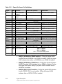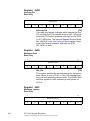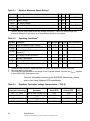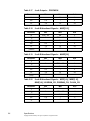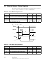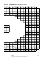
1
TECHNICAL
MANUAL
LSISAS1064 PCI-X
to 4-Port Serial Attached
SCSI/SATA Controller
October 2005
Version 3.2
®
DB14-000274-05
This document contains proprietary information of LSI Logic Corporation. The
information contained herein is not to be used by or disclosed to third parties
without the express written permission of an officer of LSI Logic Corporation.
LSI Logic products are not intended for use in life-support appliances, devices,
or systems. Use of any LSI Logic product in such applications without written
consent of the appropriate LSI Logic officer is prohibited.
Purchase of I2C components of LSI Logic Corporation, or one of its sublicensed
Associated Companies, conveys a license under the Philips I2C Patent Rights to
use these components in an I2C system, provided that the system conforms to
the I2C standard Specification as defined by Philips.
Document DB14-000274-05, Version 3.2 (October 2005)
This document describes the LSI Logic Corporation’s LSISAS1064 Serial
Attached SCSI Controller and will remain the official reference source for all
revisions/releases of this product until rescinded by an update.
LSI Logic Corporation reserves the right to make changes to any products herein
at any time without notice. LSI Logic does not assume any responsibility or
liability arising out of the application or use of any product described herein,
except as expressly agreed to in writing by LSI Logic; nor does the purchase or
use of a product from LSI Logic convey a license under any patent rights,
copyrights, trademark rights, or any other of the intellectual property rights of
LSI Logic or third parties.
Copyright © 2003–2005 by LSI Logic Corporation. All rights reserved.
TRADEMARK ACKNOWLEDGMENT
LSI Logic, the LSI Logic logo design, Fusion-MPT, Gflx, GigaBlaze,
Integrated Mirroring, Integrated RAID, and Integrated Striping are trademarks or
registered trademarks of LSI Logic Corporation. ARM, ARM9, ARM966E-S, and
Multi-ICE are trademarks or registered trademarks of ARM Ltd., used under
license. All other brand and product names may be trademarks of their respective
companies.
JM
To receive product literature, visit us at http://www.lsilogic.com.
For a current list of our distributors, sales offices, and design resource
centers, view our web page located at
http://www.lsilogic.com/contacts/index.html
ii
Copyright © 2003–2005 by LSI Logic Corporation. All rights reserved.
Preface
This book is the primary reference and technical manual for the
LSISAS1064 PCI-X to 4-Port Serial Attached SCSI/SATA Controller. It
contains a complete functional description for the LSISAS1064, as well
as the physical and electrical specifications for the LSISAS1064.
Audience
This document assumes that you are familiar with microprocessors and
related support devices. The people who benefit from this book are:
•
Engineers and managers who are evaluating the LSISAS1064 for
use in a system
•
Engineers who are designing the LSISAS1064 into a system
Organization
This document has the following chapters and appendixes:
•
Chapter 1, Introduction, provides an overview of the LSISAS1064
features and capabilities.
•
Chapter 2, Functional Description, provides a detailed functional
description of the LSISAS1064 operation. This chapter describes the
LSISAS1064 implementations of the PCI, PCI-X, and SAS
specifications.
•
Chapter 3, Signal Description, provides a detailed signal
description for the LSISAS1064.
•
Chapter 4, PCI Host Register Description, provides a bit level
description of the host interface registers.
•
Chapter 5, Specifications, provides the electrical and physical
specifications for the LSISAS1064.
LSISAS1064 PCI-X to 4-Port Serial Attached SCSI/SATA Controller
Copyright © 2003–2005 by LSI Logic Corporation. All rights reserved.
iii
•
Appendix A, Register Summary, provides a register map for the
LSISAS1064.
Related Publications
LSI Logic Documents
Fusion-MPT™ Device Management User’s Guide, Version 2.0,
DB15-000186-02
LSI Logic World Wide Web Home Page
www.lsilogic.com
ANSI
11 West 42nd Street
New York, NY 10036
(212) 642-4900
InterNational Committee on Information Technology Standards
(INCITIS) T10 Technical Committee
http://www.t10.org
Global Engineering Documents
15 Inverness Way East
Englewood, CO 80112
(800) 854-7179 or (303) 397-7956 (outside U.S.) FAX (303) 397-2740
PCI Special Interest Group
2575 N. E. Katherine
Hillsboro, OR 97214
(800) 433-5177; (503) 693-6232 (International); FAX (503) 693-8344
Serial ATA Working Group
http://www.serialata.org
Email: [email protected]
Philips I2C Bus Specification
http://www.semiconductors.philips.com
SFF-8485 Serial GPIO Bus Specification
http://www.sffcommittee.org
iv
Preface
Copyright © 2003–2005 by LSI Logic Corporation. All rights reserved.
Conventions Used in This Manual
The word assert means to drive a signal true or active. The word
deassert means to drive a signal false or inactive. Signals that are active
LOW end with a “/.”
Hexadecimal numbers are indicated by the prefix “0x” —for example,
0x32CF. Binary numbers are indicated by the prefix “0b” —for example,
0b0011.0010.1100.1111.
Revision History
Revision
Date
Remarks
Final Version 3.2
9/2005
Updated external memory diagrams. Removed references to Serial
EEPROM as it is not supported with this device.
Final Version 3.1
3/2005
Added I2C and SFF-8485 specifications to the list of references.
Updated IR wording in Chapter 1.
Added SAS version 1.1 feature compliance statement to Chapter 1.
Updated Section 2.8, “Multi-ICE Test Interface,” by removing the
TST_RST/ signal from the test header pinout.
Corrected a typo in Table 4.1.
Added a footnote to Table 5.2.
Final Version 3.0
11/2004 Added 2 kV ESD information.
Preliminary Version 2.0 11/2004 Updated
Updated
Updated
Updated
Updated
Updated
PCI and Power Management specification revision numbers.
PCI 5 V tolerance information.
ZCR information.
REFCLK_B signal description.
operating conditions data.
signal power data.
Advance Version 0.3
1/2004
Updated Table 4.5, the PCI-X Command register default value, and the
PCI-X Status register default value.
Advance Version 0.2
12/2003 Initial release of document.
Preface
Copyright © 2003–2005 by LSI Logic Corporation. All rights reserved.
v
vi
Preface
Copyright © 2003–2005 by LSI Logic Corporation. All rights reserved.
Contents
Chapter 1
Chapter 2
Introduction
1.1
General Description
1.2
Benefits of SAS
1.3
Benefits of the Fusion-MPT Architecture
1.4
Benefits of PCI-X
1.5
Benefits of GigaBlaze® Transceivers
1.6
Summary of LSISAS1064 Features
1.6.1
SAS Features
1.6.2
SATA Features
1.6.3
PCI Performance
1.6.4
Integration
1.6.5
Usability
1.6.6
Flexibility
1.6.7
Reliability
1.6.8
Testability
1-1
1-4
1-5
1-6
1-7
1-7
1-7
1-8
1-8
1-9
1-10
1-10
1-10
1-11
Functional Description
2.1
Block Diagram Description
2.1.1
Host Interface Module Description
2.1.2
Quad Port
2.1.3
Context RAM
2.2
Fusion-MPT Architecture Overview
2.3
PCI Functional Description
2.3.1
PCI Addressing
2.3.2
PCI Commands and Functions
2.3.3
PCI Arbitration
2.3.4
PCI Cache Mode
2.3.5
PCI Interrupts
2.3.6
Power Management
2-2
2-3
2-6
2-7
2-7
2-8
2-9
2-10
2-15
2-15
2-16
2-16
LSISAS1064 PCI-X to 4-Port Serial Attached SCSI/SATA Controller
Copyright © 2003–2005 by LSI Logic Corporation. All rights reserved.
vii
2.4
2.5
2.6
2.7
2.8
Chapter 3
Chapter 4
Chapter 5
viii
SAS Functional Description
External Memory Interface
2.5.1
Memory Requirements
2.5.2
Flash ROM Controller
2.5.3
NVSRAM Controller
Zero Channel RAID
Universal Asynchronous Receiver/Transmitter (UART)
Multi-ICE Test Interface
2-17
2-19
2-19
2-20
2-22
2-23
2-24
2-25
Signal Description
3.1
Signal Organization
3.2
PCI Signals
3.2.1
PCI System Signals
3.2.2
PCI Address and Data Signals
3.2.3
PCI Interface Control Signals
3.2.4
PCI Arbitration Signals
3.2.5
PCI Error Reporting Signals
3.2.6
PCI Interrupt Signals
3.3
PCI-Related Signals
3.4
Compact PCI Signals
3.5
SAS Signals
3.6
Memory Interface Signals
3.7
Communication Signals
3.8
Configuration and General Purpose Signals
3.9
JTAG and Test Signals
3.10 Power Signals
3.11 Power-On Sense Pins Description
3.12 Internal Pull-Ups and Pull-Downs
3-1
3-4
3-4
3-4
3-5
3-5
3-5
3-6
3-6
3-7
3-7
3-8
3-9
3-10
3-11
3-12
3-13
3-16
PCI Host Register Description
4.1
PCI Configuration Space Register Description
4.2
PCI I/O Space and Memory Space Register Description
4-1
4-32
Specifications
5.1
DC Characteristics
5.2
AC Characteristics
5.3
External Memory Timing Diagrams
5-1
5-8
5-10
Contents
Copyright © 2003–2005 by LSI Logic Corporation. All rights reserved.
5.4
5.5
Appendix A
Pinout
Package Drawings
5-12
5-20
Register Summary
Index
Customer Feedback
Contents
Copyright © 2003–2005 by LSI Logic Corporation. All rights reserved.
ix
x
Contents
Copyright © 2003–2005 by LSI Logic Corporation. All rights reserved.
Figures
1.1
1.2
2.1
2.2
2.3
2.4
2.5
2.6
2.7
3.1
5.1
5.2
5.3
5.4
5.5
5.6
5.7
5.8
5.9
LSISAS1064 Direct-Connect Example Application
LSISAS1064 Controller and LSISASx12 Expander
Example Application
LSISAS1064 Controller Block Diagram
Transceivers within a Phy
Narrow and Wide Links
SSP, STP, and SMP Protocol Usage
Flash ROM Block Diagram
NVSRAM Block Diagram
ZCR Circuit Diagram for the LSISAS1064
LSISAS1064 Functional Signal Grouping
External Clock
Reset Input
Interrupt Output
Flash Write
Flash Read
NV Read
NV Write
LSISAS1064 472-Pin BGA Top View
472-Pin EPBGA-T (UO) Mechanical Drawing
(Sheet 1 of 3)
Contents
Copyright © 2003–2005 by LSI Logic Corporation. All rights reserved.
1-3
1-3
2-3
2-17
2-18
2-19
2-21
2-23
2-24
3-3
5-8
5-9
5-9
5-10
5-11
5-11
5-12
5-18
5-21
xi
xii
Contents
Copyright © 2003–2005 by LSI Logic Corporation. All rights reserved.
Tables
2.1
2.2
2.3
3.1
3.2
3.3
3.4
3.5
3.6
3.7
3.8
3.9
3.10
3.11
3.12
3.13
3.14
3.15
3.16
4.1
4.2
4.3
4.4
4.5
4.6
4.7
4.8
4.9
5.1
5.2
5.3
5.4
5.5
5.6
PCI/PCI-X Bus Commands and Encodings
Flash ROM Signature Value
ARM Multi-ICE Header Pinout
PCI System Signals
PCI Address and Data Signals
PCI Interface Control Signals
PCI Arbitration Signals
PCI Error Reporting Signals
PCI Interrupt Signals
PCI-Related Signals
CompactPCI Signals
SAS Interface Signals
Memory Interface Signals
UART and I2C Signals
Configuration and General Purpose Signals
Test and JTAG Signals
Power and Ground Signals
Power-On Sense Pin Definitions
Pull-Up and Pull-Down Conditions
LSISAS1064 PCI Configuration Space Address Map
Multiple Message Enable Field Bit Encoding
BIR Field Definitions
Maximum Outstanding Split Transactions
Maximum Memory Read Count
PCI I/O Space Address Map
PCI Memory [0] Address Map
PCI Memory [1] Address Map
Interrupt Signal Routing
Absolute Maximum Stress Ratings
Operating Conditions
GigaBlaze Transmitter Voltage Characteristics –
TX[3:0]
GigaBlaze Receiver Voltage Characteristics – RX[3:0]
GigaBlaze Transceiver Rise/Fall Characteristics –
TX[3:0], RX[3:0]
PCI-X Input Signals – CLK, RST/, GNT/, IDSEL,
ALT_GNT/, CPCI64_EN/
Contents
Version 3.1
2-10
2-21
2-25
3-4
3-4
3-5
3-5
3-5
3-6
3-6
3-7
3-7
3-8
3-9
3-10
3-11
3-12
3-14
3-16
4-2
4-21
4-26
4-28
4-29
4-33
4-33
4-33
4-40
5-2
5-2
5-2
5-3
5-3
5-3
xiii
Copyright © 2003–2005 by LSI Logic Corporation. All rights reserved.
5.7
5.8
5.9
5.10
5.11
5.12
5.13
5.14
5.15
5.16
5.17
5.18
5.19
5.20
5.21
5.22
5.23
5.24
5.25
5.26
5.27
5.28
5.29
5.30
5.31
5.32
A.1
A.2
A.3
xiv
PCI-X Output Signals – REQ/, INTA/, ALT_INTA/
PCI-X Bidirectional Signals – AD[63:0], C_BE[7:0]/,
CPCI_ENUM/, PAR, PAR64, ACK64/, REQ64/, FRAME/,
IRDY/, TRDY/, DEVSEL/, STOP/, PERR/, SERR/
Inputs – ZCR_EN/, CPCI_EN/, TN/, UART_RX
Inputs – CPCI_SWITCH, MODE[5:0], SCAN_ENABLE,
SCAN_MODE
Schmitt Trigger Inputs – TST_RST/, TCK, TRST/, TDI,
TMS, TCK_ICE, TRST_ICE/, TDI_ICE, TMS_ICE
Schmitt Trigger Inputs – REFCLK_B, FSELA
10 mA, 3-State Outputs – CPCI_LED/, HB_LED/,
FAULT_LED[3:0]/, ACTIVE_LED[3:0]/
5 mA, 3-State Outputs – TDO, TDO_ICE, RTCK_ICE
8 mA Outputs – MCLK, ADSC/, ADV/
5 mA Outputs – UART_TX
4 mA Outputs – PROCMON
8 mA Bidirectional Signals – MAD[31:0]
8 mA Bidirectional Signals – MADP[3:0]
8 mA Bidirectional Signals – MOE[1:0]/, MWE[1:0]/,
BWE[3:0]/, NVSRAM_CS/, PSBRAM_CS/, FLASH_CS/
5 mA Bidirectional Signals – SERIAL_CLK,
SERIAL_DATA, ISTWI_CLK, ISTWI_DATA, GPIO[3:0],
TMUX_SPARE[7:0]
PECL Buffer Signals – REFCLK_P, REFCLK_N
Capacitance
External Clock
Reset Input
Interrupt Output
Flash Write Timing Parameters
Flash Read Timing Parameters
NVRAM Read Timing Parameters
NVRAM Write Timing Parameters
Listing by Signal Name
Listing by Pin Number
LSISAS1064 PCI Configuration Space Registers
LSISAS1064 PCI I/O Space Registers
LSISAS1064 PCI Memory [0] Space Registers
Contents
Version 3.1
Copyright © 2003–2005 by LSI Logic Corporation. All rights reserved.
5-3
5-3
5-4
5-4
5-4
5-5
5-5
5-5
5-5
5-5
5-6
5-6
5-6
5-6
5-7
5-7
5-7
5-8
5-9
5-9
5-10
5-10
5-11
5-12
5-13
5-15
A-1
A-3
A-4
Chapter 1
Introduction
The LSISAS1064 is a four-port 3.0 Gbit/s SAS/SATA controller that is
compliant with the Fusion-MPT™ architecture, provides a PCI-X
interface, and supports the Integrated RAID™ solution. This chapter
contains the following sections:
1.1
•
Section 1.1, “General Description”
•
Section 1.2, “Benefits of SAS”
•
Section 1.3, “Benefits of the Fusion-MPT Architecture”
•
Section 1.4, “Benefits of PCI-X”
•
Section 1.5, “Benefits of GigaBlaze® Transceivers”
•
Section 1.6, “Summary of LSISAS1064 Features”
General Description
The LSISAS1064 controller brings 3.0-Gbit/s SAS performance to host
adapter, workstation, and server designs, making it easy to add a SAS
interface to any PCI or PCI-X1 system. The LSISAS1064 integrates four
high-performance SAS/SATA phys and a 64-bit, 133 MHz PCI-X bus
master DMA core. Each of the four phys on the LSISAS1064 is capable
of 3.0 Gbit/s and 1.5 Gbit/s SAS link rates, and 3.0 Gbit/s and 1.5 Gbit/s
SATA link rates. The LSISAS1064 supports the SAS protocol as
described in the Serial Attached SCSI Standard, version 1.0, as well as
SAS 1.1 features, such as support for the BROADCAST (SES) primitive
and support for SATA port selectors. The controller also supports the
Serial ATA (SATA) protocol defined by the Serial ATA specification,
1. In some instances, this manual references PCI-X explicitly. References to the PCI bus may
be inclusive of both the PCI specification and PCI-X addendum, or may only refer to the PCI
bus depending on the operating mode of the device.
LSISAS1064 PCI-X to 4-Port Serial Attached SCSI/SATA Controller
Copyright © 2003–2005 by LSI Logic Corporation. All rights reserved.
1-1
version 1.0a. SATA II is an extension to SATA 1.0a. LSI Logic SAS/SATA
controllers also support the following SATA II features:
•
3.0 Gbit/s SATA
•
Staggered spin-up
•
Hot Plug
•
Native Command Queuing
•
Activity and fault indicators per phy
•
Port Selector (for dual-port drives)
Supporting both the SAS and SATA interfaces, the LSISAS1064 is a
versatile controller that provides the backbone of both server and highend workstation environments. LSI Logic produces the LSISAS1064
using the Gflx™ process technology.
Each port on the LSISAS1064 supports SAS and SATA devices using the
SAS Serial SCSI Protocol (SSP), Serial Management Protocol (SMP),
Serial Tunneling Protocol (STP), and SATA. The SSP protocol enables
communication with other SAS devices. SATA enables the LSISAS1064
to communicate with other SATA devices. The SMP protocol
communicates topology management information directly with an
attached SAS expander device, such as the LSISASx12. STP enables
the LSISAS1064 to communicate with a SATA device through an
attached expander.
The LSISAS1064 supports a 133 MHz, 64-bit PCI-X bus. With the
exception that the PCI interface is not tolerant of 5 V PCI, the interface
is backward compatible with all revisions of the PCI/PCI-X bus. The
LSISAS1064 supports PCI-X split completion cycles and 32-bit or 64-bit
data bursts with variable burst length. The LSISAS1064 supports the
PCI-X Addendum to the Peripheral Components Interface Specification,
Revision 2.0, and the Peripheral Components Interface Specification,
Revision 3.0.
Figure 1.1 shows a direct-connect configuration. Figure 1.2 provides an
example of the LSISAS1064 configured with an LSISASx12 expander.
1-2
Introduction
Copyright © 2003–2005 by LSI Logic Corporation. All rights reserved.
Figure 1.1
LSISAS1064 Direct-Connect Example Application
Tx , Rx
SAS/SATA Device
Tx , Rx
SAS/SATA Device
Tx , Rx
SAS/SATA Device
32-bit Memory
Address/Data
Bus
LSISAS1064
64-Bit, 133 MHz
PCI-X
Controller
Flash ROM/
PSBRAM/
NVSRAM
I2C
Interface
I2C
Tx , Rx
SAS/SATA Device
PCI/PCI-X Interface
Figure 1.2
LSISAS1064 Controller and LSISASx12 Expander
Example Application
PCI/PCI-X Interface
32-bit Memory
Address/Data
Bus
LSISAS1064
I2C
Interface
LSISASx12
SAS/SATA
Drives
Flash ROM/
PSBRAM/
NVSRAM
I2C
LSISASx12
SAS/SATA
Drives
SAS/SATA
Drives
SAS/SATA
Drives
The LSISAS1064 employs an ARM926 processor to meet the data
transfer flexibility requirements of the host interface PCI-X specifications.
General Description
Copyright © 2003–2005 by LSI Logic Corporation. All rights reserved.
1-3
The LSISAS1064 is based on the Fusion-MPT (Message Passing
Technology) architecture, which features a performance based message
passing protocol that off loads the host CPU by completely managing all
I/Os and minimizes system bus overhead by coalescing interrupts. The
Fusion-MPT architecture requires only a thin, easy to develop device
drivers that is independent of the I/O bus. LSI Logic provides these
device drivers.
The LSISAS1064 supports a 32-bit external memory bus. The external
memory controller block provides an interface for Flash ROM, NVSRAM,
and PSBRAM devices. Most configurations use a Flash ROM to store
firmware, configuration information, and persistent data information.
The LSISAS1064 supports the Integrated RAID solution, which is a
highly integrated, low cost RAID implementation. It is designed for
systems requiring redundancy and high availability, but not needing a fullfeatured RAID implementation. The Integrated RAID solution includes
Integrated Mirroring™ (IM) technology and Integrated Striping™ (IS)
technology. IM technology provides physical mirroring of eight physical
drives. IM technology requires an NVSRAM to support write journaling.
IS technology enables data striping across up to eight physical drives.
The Integrated RAID solution is OS independent, easy to install and
configure, supports up to eight drives at RAID Level 0, and does not
require a special driver. The runtime operation of the Integrated RAID
solution is transparent to the operating system. A single firmware build
supports all Integrated RAID capabilities. The LSISAS1064 also provides
Zero Channel RAID (ZCR) support.
The IR firmware requires a configuration mechanism, which enables
configuration of the mirroring attributes during initial setup or
reconfiguration after hardware failures or changes in the system
environment. Use the LSI Logic BIOS Configuration Utility or the IM DOS
Configuration Utility to configure the IR firmware attributes. Host based
status software monitors the state of the mirrored drives and reports
error conditions as they arise.
1.2
Benefits of SAS
SAS is a serial, point-to-point, enterprise-level device interface that
leverages the proven SCSI protocol set. SAS is a convergence of the
1-4
Introduction
Copyright © 2003–2005 by LSI Logic Corporation. All rights reserved.
advantages of SATA, SCSI, and FC, and is the future mainstay of the
enterprise and high-end workstation storage markets. SAS offers a
higher bandwidth per pin than parallel SCSI, and improves signal and
data integrity.
The SAS interface uses the proven SCSI command set to ensure reliable
data transfers, while providing the connectivity and flexibility of point-topoint serial data transfers. The serial transmission of SCSI commands
eliminates clock skew challenges. The SAS interface provides improved
performance, simplified cabling, smaller connectors, lower pin count, and
lower power requirements when compared to parallel SCSI.
SAS controllers leverage a common electrical and physical connection
interface that is compatible with Serial ATA technology. The SAS and
SATA protocols use a thin, 7-wire connector instead of the 68-wire SCSI
cable or 26-wire ATA cable. The SAS/SATA connector and cable are
easier to manipulate, allow connections to smaller devices, and do not
inhibit airflow. The point-to-point SATA architecture eliminates inherent
difficulties created by the legacy ATA master-slave architecture, while
maintaining compatibility with existing ATA firmware.
The LSISAS1064 can function as an SSP initiator, an SSP target, an
SMP initiator, an STP initiator, or a SATA initiator. The LSISAS1064 uses
SSP to communicate with other SAS devices, and uses SMP to
communicate topology management information with other SAS devices.
STP communicates with SATA devices by tunneling through SAS
expanders directly to the SATA device or by using the SATA protocol to
communicate directly with the SATA device.
1.3
Benefits of the Fusion-MPT Architecture
The Fusion-MPT architecture provides an open architecture that is ideal
for SAS, SATA, SCSI, Fibre Channel, and other emerging interfaces. The
I/O interface is interchangeable at the system and application level;
embedded software uses the same device interface for different bus
implementations, just as application software uses the same storage
management interfaces for different bus implementations. LSI Logic
provides Fusion-MPT device drivers that are binary compatible between
SAS, SATA, Fibre Channel, and Ultra320 SCSI interfaces.
Benefits of the Fusion-MPT Architecture
Copyright © 2003–2005 by LSI Logic Corporation. All rights reserved.
1-5
The Fusion-MPT architecture improves overall system performance by
requiring only a thin device driver, which off loads the intensive work of
managing I/Os from the system processor to the LSISAS1064. The use
of thin, easy to develop, common OS device drivers accelerates time to
market by reducing device driver development and certification times.
The Fusion-MPT architecture provides an interrupt coalescing feature.
Interrupt coalescing allows an I/O controller to send multiple reply
messages in a single interrupt to the host processor. Sending multiple
reply messages per interrupt reduces context switching of the host
processor and maximizes the host processor efficiency, which results in
a significant improvement of system performance. To use the interrupt
coalescing feature, the host processor must be able to accept and
manage multiple replies per interrupt.
The Fusion-MPT architecture also provides built-in device driver stability
since the device driver need not change for each revision of the
LSISAS1064 silicon or firmware. This architecture is a reliable, constant
interface between the host device driver and the LSISAS1064. Changes
within the LSISAS1064 are transparent to the host device driver,
operating system, and user. The Fusion-MPT architecture also saves the
user significant development and maintenance effort since it is not
necessary to alter or redevelop the device driver when a revision of the
LSISAS1064 device or firmware occurs.
1.4
Benefits of PCI-X
PCI-X doubles the maximum clock frequency of the conventional PCI
bus. The PCI-X Addendum to the PCI Local Bus Specification,
Revision 2.0, defines enhancements to the proven PCI Local Bus
Specification, Revision 3.0. PCI-X provides more efficient data transfers
by enabling registered inputs and outputs, improves buffer management
by including transaction information with each data transfer, and reduces
bus overhead by restricting the use of wait states and disconnects. PCI-X
also reduces host processor overhead by providing a wide range of error
recovery implementations.
The LSISAS1064 supports up to a 133 MHz, 64-bit PCI-X bus and is
backwards compatible with previous versions of the PCI/PCI-X
specification. Per the PCI-X addendum, the LSISAS1064 includes
1-6
Introduction
Copyright © 2003–2005 by LSI Logic Corporation. All rights reserved.
transaction information with all PCI-X transactions to enable more
efficient buffer management schemes. Each PCI-X transaction contains
a transaction sequence identifier (Tag), the identity of the initiator, and
the number of bytes in the sequence. The LSISAS1064 clocks PCI-X
data directly into and out of registers, which creates a more efficient data
path. The LSISAS1064 increases bus efficiency since it does not insert
wait states after the initial data phase when acting as a PCI-X target and
never inserts wait states when acting as a PCI-X initiator.
1.5
Benefits of GigaBlaze® Transceivers
The GigaBlaze transceivers provide the physical layer for the
LSISAS1064 controller and are a proven component of LSI Logic
semiconductor expertise. The Gflx GigaBlaze transceivers are the fifth
generation of the LSI Logic GigaBlaze core. The GigaBlaze transceivers
provide full-duplex, point-to-point communications channels that can
operate at 3.0/1.5 Gbits/s SAS/SATA transfer rates.
The integrated GigaBlaze transceivers perform the 8b/10b conversion
that is necessary for SAS and SATA transfers, without burdening either
the LSISAS1064 ARM® processor or the host interface. The transmitter
accepts parallel data, serializes it, and transmits it on the differential
TX+/TX- signals. The receiver recovers the clock and deserializes the
data from the bitstream that it receives on the RX+/RX- signals. Because
the transceiver and receiver operate independently, the GigaBlaze
transceivers can send and receive data simultaneously, which maximizes
system performance. The GigaBlaze transceivers also provide integrated
internal termination.
1.6
Summary of LSISAS1064 Features
This section provides a summary of the LSISAS1064 features and
benefits. It contains information on SAS Features, SATA Features, PCI
Performance, Integration, Usability, Flexibility, Reliability, and Testability.
1.6.1
SAS Features
This section describes the SAS features.
Benefits of GigaBlaze® Transceivers
Copyright © 2003–2005 by LSI Logic Corporation. All rights reserved.
1-7
1.6.2
•
Provides 4 fully independent phys
•
Each phy supports 3.0 Gbits/s and 1.5 Gbits/s SAS data transfers
•
Supports SSP to enable communication with other SAS devices
•
Supports SMP to communicate topology management information
•
Provides a serial, point-to-point, enterprise-level storage interface
•
Simplifies cabling between devices
•
Provides a scalable interface that supports up to 128 devices through
multiple expanders
•
Supports wide ports consisting of 2, 3, or 4 phys
•
Supports narrow ports consisting of a single phy
•
Transfers data using SCSI information units
SATA Features
This section describes the SATA features.
1.6.3
•
Supports SATA data transfers of 3.0 Gbit/s and 1.5 Gbits/s
•
Supports STP data transfers of 3.0 Gbits/s and 1.5 Gbits/s
•
Provides a serial, point-to-point storage interface
•
Simplifies cabling between devices
•
Eliminates the Master-Slave construction used in parallel ATA
•
Allows addressing of multiple SATA targets through an expander
•
Allows multiple initiators to address a single target (in a fail-over
configuration) through an expander
PCI Performance
The LSISAS1064 supports these PCI features:
•
1-8
133 MHz, 64-bit PCI/PCI-X interface that:
–
Operates up to 133 MHz PCI-X
–
Operates at 33 MHz or 66 MHz PCI
–
Supports 32-bit or 64-bit data transfers
Introduction
Copyright © 2003–2005 by LSI Logic Corporation. All rights reserved.
1.6.4
–
Supports 32-bit or 64-bit addressing through Dual Address
Cycles (DAC)
–
Provides a theoretical 1066 Mbytes/s PCI bandwidth
–
Supports 3.3 V PCI, and is not 5 V PCI tolerant
–
Complies with the PCI Local Bus Specification, Revision 3.0
–
Complies with the PCI-X Addendum to the PCI Local Bus
Specification, Revision 2.0
–
Complies with the PCI Power Management Interface
Specification, Revision 1.2
–
Complies with the PC2001 Specification
•
Provides unequaled performance through the Fusion-MPT
architecture
•
Provides high throughput and low CPU utilization to off load the host
processor
•
Uses a dedicated ARM926 processor
•
Presents a single electrical load to the PCI Bus
•
Reduces Interrupt Service Routine (ISR) overhead with interrupt
coalescing
•
Supports Message Signaled Interrupts (MSI) and MSI-X
•
Supports 32-bit or 64-bit data bursts with variable burst lengths
•
Supports the PCI Cache Line Size register
•
Supports the PCI Memory Write and Invalidate, Memory Read Line,
and Memory Read Multiple commands
•
Supports the PCI-X Memory Read Dword, Split Completion, Memory
Read Block, Memory Write Block commands
•
Supports up to 16 PCI-X Split Transaction cycles
Integration
These features make the LSISAS1064 easy to integrate:
•
Supports backwards compatibility with previous revisions of the PCI
specification, with the exception that the LSISAS1064 does not
support 5 V PCI
Summary of LSISAS1064 Features
Copyright © 2003–2005 by LSI Logic Corporation. All rights reserved.
1-9
1.6.5
•
Provides a full 32-bit or 64-bit PCI-X DMA bus master
•
Reduces time to market with the Fusion-MPT architecture
–
Single driver binary for SAS/SATA, SCSI, and Fibre Channel
products
–
One firmware build supports all Integrated RAID capabilities
–
Thin, easy to develop drivers
–
Reduced integration and certification effort
Usability
This section describes the usability features.
1.6.6
•
Simplifies cabling with point-to-point, serial architecture
•
Smaller, thinner cables do not restrict airflow
•
Provides drive spin-up sequencing control
•
Provides up to two LED signals for each phy to indicate link activity
and faults
•
Provides an Inter-IC (I2C) interface for enclosure management
Flexibility
These features increase the flexibility of the LSISAS1064:
1.6.7
•
Supports a Flash ROM interface, a nonvolatile RAM (NVSRAM)
interface, and a pipelined synchronous burst SRAM (PSBRAM)
interface
•
Offers a flexible programming interface to tune I/O performance
•
Allows mixed connections to SAS or SATA targets
•
Leverages compatible connectors for SAS and SATA connections
•
Allows grouping of up to 4 phys to form a wide port
•
Allows programming of the World Wide Name
Reliability
These features enhance the reliability of the LSISAS1064:
•
1-10
Uses proven GigaBlaze transceivers
Introduction
Copyright © 2003–2005 by LSI Logic Corporation. All rights reserved.
1.6.8
•
Isolates the power and ground of I/O pads and internal chip logic
•
Provides 2 kV ESD protection
•
Provides latch-up protection
•
Has a high proportion of power and ground pins
•
Integrated RAID solution provides Integrated Mirroring technology
and Integrated Striping technology
•
Supports Zero Channel RAID
Testability
These features enhance the testability of the LSISAS1064:
•
Offers JTAG boundary scan
•
Provides a UART interface for debugging
•
Offers ARM Multi-ICE® technology for debugging the ARM9™
processor
•
Offers I2C port to output debug information
Summary of LSISAS1064 Features
Copyright © 2003–2005 by LSI Logic Corporation. All rights reserved.
1-11
1-12
Introduction
Copyright © 2003–2005 by LSI Logic Corporation. All rights reserved.
Chapter 2
Functional Description
This chapter provides a subsystem level overview of the LSISAS1064, a
discussion of the Fusion-MPT architecture, and a functional description
of the LSISAS1064 interfaces. This chapter contains the following
sections:
•
Section 2.1, “Block Diagram Description”
•
Section 2.2, “Fusion-MPT Architecture Overview”
•
Section 2.3, “PCI Functional Description”
•
Section 2.4, “SAS Functional Description”
•
Section 2.5, “External Memory Interface”
•
Section 2.6, “Zero Channel RAID”
•
Section 2.6, “Zero Channel RAID”
•
Section 2.7, “Universal Asynchronous Receiver/Transmitter (UART)”
•
Section 2.8, “Multi-ICE Test Interface”
The LSISAS1064 is a four port 3.0 Gbit/s SAS controller that is compliant
with the Fusion-MPT architecture, provides a PCI-X interface, and
supports Integrated RAID solution. The LSISAS1064 supports version
3.0 of the PCI Local Bus Specification, revision 2.0 of the PCI-X
Addendum to the PCI Local Bus Specification, version 1.0 of the ANSI
Serial Attached SCSI standard, and version 1.0a of the Serial ATA
standard.
The LSISAS1064 employs the LSI Logic Fusion-MPT architecture to
ensure robust system performance, to provide binary compatibility of
host software between the LSI Logic SAS/SATA, SCSI, and Fibre
Channel products, and to significantly reduce software development time.
Refer to the Fusion-MPT Device Management User’s Guide for more
information on the Fusion-MPT architecture.
LSISAS1064 PCI-X to 4-Port Serial Attached SCSI/SATA Controller
Copyright © 2003–2005 by LSI Logic Corporation. All rights reserved.
2-1
2.1
Block Diagram Description
The LSISAS1064 consists of two major modules and a context RAM.
The two major modules are the host interface module and the Quad Port
module. The modules consist of the following components:
•
•
•
Host Interface Module
–
PCI/PCI-X Interface
–
System Interface
–
IOP (ARM926 processor)
–
PCI Timer and Configuration
–
Timer and Configuration
–
DMA Arbiter
–
External Memory Interface
–
I2C
–
UART
Quad Port
–
Queue Manager
–
SATA Engine
–
Four Transport Modules
–
Port Layer Connection Management and Switch
–
Four SAS Links and four SAS Phys
Context RAM
Figure 2.1 illustrates the relationship between these modules. The
following sections describe each submodule.
2-2
Functional Description
Copyright © 2003–2005 by LSI Logic Corporation. All rights reserved.
Figure 2.1
LSISAS1064 Controller Block Diagram
Quad Port
Host Interface
PCI/PCI-X
Interface
DMA Arbiter
Queue
Manager
AHB
Bridge
Primary AHB Bus
PCI
TimerConfig
PCI-X 133MHz
SATA Engine
AHB Interface
SECONDARY
System Interface
AHB Interface
CONTEXT
Transport Module
IOP
(ARM926
Processor)
AHB Arbiter
IRQ Controller
GPIO/LED
TimerConfig
XMEM Bus
External Memory
I2C
Quad Port Context AHB Bus
ICE I/F
Quad Port
DMA Arbiter
Port Layer Connection
Management and Switch
SAS Link
SAS Link
SAS Link
SAS Link
SAS Phy
SAS Phy
SAS Phy
SAS Phy
I2C
UART
UART
2.1.1
Context RAM
Host Interface Module Description
The host interface module provides an interface between the host driver
and the Quad Port. The host interface module controls system DMA
transfers and the host side of the LSI Logic Fusion-MPT architecture.
The host interface module contains the PCI/PCI-X interface, system
interface, PCI timer and configuration, DMA arbiter, IOP, I2C,
TimerConfig, UART, and external memory blocks. This section provides
a detailed explanation of the host interface submodules.
Block Diagram Description
Copyright © 2003–2005 by LSI Logic Corporation. All rights reserved.
2-3
2.1.1.1
PCI/PCI-X Interface
The LSISAS1064 provides a PCI-X interface that supports up to a 64-bit,
133 MHz PCI-X bus. The LSISAS1064 PCI interface is backward
compatible with previous implementations of the PCI specification, with
the exception that the LSISAS1064 does not support 5 V PCI. For more
information on the PCI interface, refer to Section 2.3, “PCI Functional
Description.”
2.1.1.2
System Interface
In combination with the IOP, the system interface supports the
Fusion-MPT architecture. The system interface efficiently passes
messages between the LSISAS1064 and the host using a highperformance, packetized mailbox architecture. The LSISAS1064 system
interface coalesces PCI interrupts to minimize traffic on the PCI bus and
maximize system performance. The system interface contains five
hardware FIFOs for the message queuing lists: Request Free FIFO,
Request Post FIFO, Reply Free FIFO, Reply Post FIFO, and High Priority
Request FIFO. The LSISAS1064 contains control logic for the FIFOs,
while the messages are stored in the context RAM or in external
memory.
All host accesses to the IOP, external memory, and timer and
configuration subsystems pass through the system interface and use the
primary bus. The host system initiates data transactions on the primary
bus with the system interface registers. PCI Memory Space [0] and the
PCI I/O Base Address registers identify the location of the system
interface register set. Chapter 4, “PCI Host Register Description,”
provides a bit level description of the system interface register set.
2.1.1.3
IOP
The LSISAS1064 I/O processor controls the system interface and
manages the host side of the Fusion-MPT architecture without host
processor intervention, which frees the host processor for other tasks.
The LSISAS1064 I/O processor (IOP) is a 32-bit ARM926 RISC
processor that provides instruction and data requests to streamline
operations and increase performance.
2-4
Functional Description
Copyright © 2003–2005 by LSI Logic Corporation. All rights reserved.
2.1.1.4
PCI Timer and Configuration
This PCI Timer and Configuration module supports the PCI configuration
register space, an industry-standard and a power-on reset (POR).
2.1.1.5
Timer and Configuration
This block supports the LSISAS1064 LED and GPIO interfaces. There
are a total of nine LED signals on the LSISAS1064. Each of the four phys
has an LED signal to indicate activity on the link and an LED signal to
indicate an error on the link. The GPIO interface contains four
independent GPIO signals. The LED signals can also be configured as
GPIO signals. This block provides an firmware heartbeat LED. This block
also supports internal timing adjustments and power-on sense
configuration options.
2.1.1.6
DMA Arbiter
The LSISAS1064 provides the ability to transfer system memory blocks
to and from local memory through the descriptor-based DMA arbiter and
router.
2.1.1.7
External Memory
The external memory controller block provides an interface for Flash
ROM, NVSRAM, and PSBRAM devices. The external memory bus
provides a 32-bit memory bus, parity checking, and chip select signals
for PSBRAM, NVSRAM, and Flash ROM.
Typical system configurations require a Flash ROM to store firmware,
configuration information, and persistent data information.
2.1.1.8
I2C
The LSISAS1064 contains an Inter-IC (I2C) interface that communicates
with peripherals. This interface is also referred to as an industry standard
2-wire interface (ISTWI). The I2C block operates as either a master or a
slave on the bus and sustains data rates up to 400 Kbits/s. The I2C block
accomplishes byte-wise bidirectional data transfers by using either an
interrupt or a polling handshake at the completion of each byte. The style
and operation of this interface closely follows the de facto standard for a
Block Diagram Description
Copyright © 2003–2005 by LSI Logic Corporation. All rights reserved.
2-5
two-wire serial interface chip. The I2C block controls all bus timing and
performs bus-specific sequences.
2.1.1.9
UART
The UART provides test and debug access to the LSISAS1064.
2.1.2
Quad Port
The Quad Port module in the LSISAS1064 implements the SSP, SMP,
and STP/SATA protocols, and manages the four SAS/SATA PHYs. The
following subsections describe the Quad Port module. Refer to
Section 2.4, “SAS Functional Description,” for an operational description
of the LSISAS1064 SAS ports.
2.1.2.1
Transport Module
The transport modules transmit frames to and from the port layer and
implement the STP, SSP, and SMP protocols. There are four instances of
the transport module, one for each SAS/SATA phy on the LSISAS1064.
2.1.2.2
Queue Manager
The queue manager is responsible for managing various queue
structures that support the SSP, SMP, and STP protocols. The queue
structures are the primary means for the IOP to initiate I/Os to the
hardware, and for the hardware to notify the IOP of I/O status.
2.1.2.3
SATA Engine
The SATA engine provides information to the transport modules to enable
handling of SATA commands. The SATA engine tracks queued
commands per device and provides these tags to the SATA transport
layer blocks.
2.1.2.4
Port Layer Connection Manager and Switch
The port layer connection monitor and switch manages transmission
requests from the transport modules and originates connection requests
to the SAS links. It is also responsible for handling SAS wide port
configurations.
2-6
Functional Description
Copyright © 2003–2005 by LSI Logic Corporation. All rights reserved.
2.1.2.5
SAS Link and Phy
The LSISAS1064 uses the Gflx GigaBlaze transceivers to implement the
SAS link. The SAS link layer manages SAS connections between initiator
and target ports, data clocking, and CRC checking on received data. The
SAS link is also responsible for starting a link reset sequence.
The SAS phys interface to the physical layer, perform serial-to-parallel
conversion of received data and parallel-to-serial conversion of transmit
data, manage phy reset sequences, and perform 8b/10b encoding.
2.1.2.6
Quad Port DMA Arbiter
The quad port arbiter interfaces with the host interface DMA arbiter and
determines bus priority between each of the four ports for DMA transfers.
2.1.3
Context RAM
The context RAM is a memory that is shared between the host interface
module and the quad port module. The context RAM contains the
message frames, the FIFOs, and a portion of the firmware.
2.2
Fusion-MPT Architecture Overview
The Fusion-MPT architecture provides two I/O methods for the host
system to communicate with the IOP: the system interface doorbell and
the message queues.
The system interface doorbell is a simple message passing mechanism
that allows the PCI host system and IOP to exchange single 32-bit
Dword messages. When the host system writes to the doorbell, the
LSISAS1064 hardware generates a maskable interrupt to the IOP, which
can then read the doorbell value and take the appropriate action. When
the IOP writes a value to the doorbell, the LSISAS1064 hardware
generates a maskable interrupt to the host system. The host system can
then read the doorbell value and take the appropriate action.
There are two, 32-bit message queues: the request message queue and
the reply message queue. The host uses the request queue to request
an action by the LSISAS1064, and the LSISAS1064 uses the reply
queue to return status information to the host. The request message
Fusion-MPT Architecture Overview
Copyright © 2003–2005 by LSI Logic Corporation. All rights reserved.
2-7
queue consists of the request post FIFO. The reply message queue
consists of both the reply post FIFO and the reply free FIFO. The context
RAM contains the message queues. The Fusion-MPT architecture also
provides a High Priority Request FIFO to provide high priority request
free messages to the host on reads and to accept high priority request
post messages from the host on writes.
Communication using the message queues occurs through request
messages and reply messages. Request message frame descriptors are
pointers to the request message frames and are passed through the
request post FIFO. The request message frame data structure is up to
128 bytes in length and includes a message header and a payload. The
header uniquely identifies the message. The payload contains
information that is specific to the request. Reply message frame
descriptors have one of two formats and are passed through the reply
post FIFO. When indicating the successful completion of a SCSI I/O, the
IOP writes the reply message frame descriptor using the Context Reply
format, which is a message context. If a SCSI I/O does not complete
successfully, the IOP uses the Address Reply format. In this case, the
IOP pops a reply message frame from the reply free FIFO, generates a
reply message describing the error, writes the reply message to system
memory, and writes the address of the reply message frame to the reply
post FIFO. The host can then read the reply message and take the
appropriate action.
The doorbell mechanism provides both a communication path that
interrupts the host system device driver and an alternative
communication path to the message queues. Since data transport
through the system doorbell occurs a single Dword at a time, use the
LSISAS1064 message queues for normal operation and data transport.
2.3
PCI Functional Description
The host PCI interface complies with the PCI Local Bus Specification,
Version 3.0 and the PCI-X Addendum to the PCI Local Bus Specification,
Revision 2.0. The LSISAS1064 supports a 133 MHz, 64-bit PCI-X bus.
The LSISAS1064 provides support for 64-bit addressing with Dual
Address Cycle (DAC). The LSISAS1064 does not support 5 V PCI
signaling.
2-8
Functional Description
Copyright © 2003–2005 by LSI Logic Corporation. All rights reserved.
2.3.1
PCI Addressing
The three physical address spaces the PCI specification defines are:
•
PCI Configuration Space
•
PCI I/O Space for operating registers
•
PCI Memory Space for operating registers
The following sections describe the PCI address spaces.
2.3.1.1
PCI Configuration Space
The PCI Configuration Space is a contiguous 256 x 8-bit set of
addresses. The system BIOS initializes the configuration registers using
PCI configuration cycles. The LSISAS1064 decodes C_BE[3:0]/ to
determine if a PCI cycle intends to access the configuration register
space. The IDSEL signal behaves as a chip select signal that enables
access to the configuration register space only. The LSISAS1064 ignores
configuration read/write cycles when IDSEL is not asserted.
Bits AD[10:8] address the PCI Function Configuration Space (AD[10:8] =
0b000). The LSISAS1064 does not respond to any other encodings of
AD[10:8]. Bits AD[7:2] select one of the 64 Dword registers in the
device’s PCI Configuration Space. Bits AD[1:0] determine if the
configuration command is a Type 0 Configuration Command (AD[1:0] =
0b00) or a Type 1 Configuration Command (AD[1:0] = 0b01). Since the
LSISAS1064 is not a PCI Bridge device, all PCI Configuration
Commands designated for the LSISAS1064 must be Type 0. C_BE[3:0]/
address the individual bytes within each Dword and determine the type
of access to perform.
2.3.1.2
PCI I/O Space
The PCI specification defines I/O Space as a contiguous 32-bit I/O
address that all system resources share, including the LSISAS1064. The
I/O Base Address register determines the 256-byte PCI I/O area that the
PCI device occupies.
PCI Functional Description
Copyright © 2003–2005 by LSI Logic Corporation. All rights reserved.
2-9
2.3.1.3
PCI Memory Space
The LSISAS1064 contains two PCI memory spaces: PCI Memory
Space [0] and PCI Memory Space [1]. PCI Memory Space [0] supports
normal memory accesses while PCI Memory Space [1] supports
diagnostic memory accesses. The LSISAS1064 requires 64 Kbytes of
memory space.
The PCI specification defines memory space as a contiguous 64-bit
memory address that all system resources share. The Memory [0] Low
and Memory [0] High registers determine which 64 Kbyte memory area
PCI Memory Space [0] occupies. The Memory [1] Low and Memory [1]
High registers determine which 64 Kbyte memory area PCI Memory
Space [1] occupies.
2.3.2
PCI Commands and Functions
Bus commands indicate to the target the type of transaction the master
is requesting. The master encodes the bus commands on the C_BE[3:0]/
lines during the address phase. The PCI bus command encodings
appear in Table 2.1.
Table 2.1
PCI/PCI-X Bus Commands and Encodings1
C_BE[3:0]/ PCI Command
PCI-X Command
Interrupt Acknowledge
Supports
as Master
Supports
as Slave
No
No
0b0000
Interrupt Acknowledge
0b0001
Special Cycle
Special Cycle
No
No
0b0010
I/O Read
I/O Read
Yes
Yes
0b0011
I/O Write
I/O Write
Yes
Yes
0b0100
Reserved
Reserved
N/A
N/A
0b0101
Reserved
Reserved
N/A
N/A
0b0110
Memory Read
Memory Read Dword
Yes
Yes
0b0111
Memory Write
Memory Write
Yes
Yes
0b1000
Reserved
Alias to
Memory Read Block
PCI: N/A
PCI-X: No
PCI: N/A
PCI-X: Yes
0b1001
Reserved
Alias to
Memory Write Block
PCI: N/A
PCI-X: No
PCI: N/A
PCI-X: Yes
0b1010
Configuration Read
Configuration Read
No
Yes
0b1011
Configuration Write
Configuration Write
No
Yes
2-10
Functional Description
Copyright © 2003–2005 by LSI Logic Corporation. All rights reserved.
Table 2.1
PCI/PCI-X Bus Commands and Encodings1 (Cont.)
C_BE[3:0]/ PCI Command
PCI-X Command
Supports
as Master
Supports
as Slave
Split Completion
Yes
Yes2
0b1100
Memory Read Multiple
0b1101
Dual Address Cycle
Dual Address Cycle
Yes
Yes
0b1110
Memory Read Line
Memory Read Block
Yes
Yes2
0b1111
Memory Write and Invalidate
Memory Write Block
Yes
Yes3
1. The LSISAS1064 ignores reserved commands as a slave and never generates them as a master.
2. When acting as a slave in the PCI mode, the LSISAS1064 supports this command as the PCI
Memory Read command.
3. When acting as a slave in the PCI mode, the LSISAS1064 supports this command as the PCI
Memory Write command.
The following sections describe how the LSISAS1064 implements these
commands.
2.3.2.1
Interrupt Acknowledge Command
The LSISAS1064 ignores this command as a slave and never generates
it as a master.
2.3.2.2
Special Cycle Command
The LSISAS1064 ignores this command as a slave and never generates
it as a master.
2.3.2.3
I/O Read Command
The I/O Read command reads data from an agent mapped in the I/O
address space. When decoding I/O commands, the LSISAS1064
decodes the lower 32 address bits and ignores the upper 32 address
bits. The LSISAS1064 supports this command when operating in either
the PCI or PCI-X bus mode.
2.3.2.4
I/O Write Command
The I/O Write command writes data to an agent mapped in the I/O
address space. When decoding I/O commands, the LSISAS1064
decodes the lower 32 address bits and ignores the upper 32 address
bits. The LSISAS1064 supports this command when operating in either
the PCI or PCI-X bus mode.
PCI Functional Description
Copyright © 2003–2005 by LSI Logic Corporation. All rights reserved.
2-11
2.3.2.5
Memory Read Command
The LSISAS1064 uses the Memory Read command to read data from
an agent mapped in the memory address space. The target can perform
an anticipatory read if such a read produces no side effects. The
LSISAS1064 supports this command when operating in the PCI bus
mode.
2.3.2.6
Memory Read Dword Command
The Memory Read Dword command reads up to a single Dword of data
from an agent mapped in the memory address space and can only be
initiated as a 32-bit transaction. The target can perform an anticipatory
read if such a read produces no side effects. The LSISAS1064 supports
this command when operating in the PCI-X bus mode.
2.3.2.7
Memory Write Command
The Memory Write command writes data to an agent mapped in the
memory address space. The target assumes responsibility for data
coherency when it returns “ready.” The LSISAS1064 supports this
command when operating in either the PCI or PCI-X bus mode.
2.3.2.8
Alias to Memory Read Block Command
This command is reserved for future implementations of the PCI
specification. The LSISAS1064 never generates this command as a
master. When a slave, the LSISAS1064 supports this command using
the Memory Read Block command.
2.3.2.9
Alias to Memory Write Block Command
This command is reserved for future implementations of the PCI
specification. The LSISAS1064 never generates this command as a
master. When a slave, the LSISAS1064 supports this command using
the Memory Write Block command.
2.3.2.10
Configuration Read Command
The Configuration Read command reads the configuration space of a
device. The LSISAS1064 never generates this command as a master,
but does respond to it as a slave. A device on the PCI bus selects the
2-12
Functional Description
Copyright © 2003–2005 by LSI Logic Corporation. All rights reserved.
LSISAS1064 by asserting its IDSEL signal when AD[1:0] equal 0b00.
During the address phase of a configuration cycle, AD[7:2] address one
of the 64 Dword registers in the configuration space of each device.
C_BE[3:0]/ address the individual bytes within each Dword register and
determine the type of access to perform. Bits AD[10:8] address the PCI
function Configuration Space (AD[10:8] = 0b000). The LSISAS1064
treats AD[63:11] as logical don’t cares.
2.3.2.11
Configuration Write Command
The Configuration Write command writes the configuration space of a
device. The LSISAS1064 never generates this command as a master,
but does respond to it as a slave. A device on the PCI bus selects the
LSISAS1064 by asserting its IDSEL signal when bits AD[1:0] equal 0b00.
During the address phase of a configuration cycle, bits AD[7:2] address
one of the 64 Dword registers in the configuration space of each device.
C_BE[3:0]/ address the individual bytes within each Dword register and
determine the type of access to perform. Bits AD[10:8] decode the PCI
function Configuration Space (AD[10:8] = 0b000). The LSISAS1064
treats AD[63:11] as logical don’t cares.
2.3.2.12
Memory Read Multiple Command
The Memory Read Multiple command is identical to the Memory Read
command, except it additionally indicates that the master intends to fetch
multiple cache lines before disconnecting. The LSISAS1064 supports
PCI Memory Read Multiple functionality when operating in the PCI mode
and determines when to issue a Memory Read Multiple command
instead of a Memory Read command.
Burst Size Selection – The Read Multiple command reads multiple
cache lines of data during a single bus ownership. The number of cache
lines the LSISAS1064 reads is a multiple of the cache line size, which
Revision 3.0 of the PCI specification provides. The LSISAS1064 selects
the largest multiple of the cache line size based on the amount of data
to transfer.
2.3.2.13
Split Completion Command
Split transactions in PCI-X replace the delayed transactions in
conventional PCI. The LSISAS1064 supports up to 16 outstanding split
PCI Functional Description
Copyright © 2003–2005 by LSI Logic Corporation. All rights reserved.
2-13
transactions when operating in the PCI-X mode. A split transaction
consists of at least two separate bus transactions: a split request, which
the requester initiates, and one or more split completion commands,
which the completer initiates. Revision 2.0 of the PCI-X addendum
permits split transaction completion for the Memory Read Block, Alias to
Memory Read Block, Memory Read Dword, Interrupt Acknowledge,
I/O Read, I/O Write, Configuration Read, and Configuration Write
commands. When operating in the PCI-X mode, the LSISAS1064
supports the Split Completion command for all of these commands
except the Interrupt Acknowledge command, which the LSISAS1064
neither responds to nor generates.
2.3.2.14
Dual Address Cycles (DAC) Command
The LSISAS1064 performs Dual Address Cycles (DAC), per the PCI
Local Bus Specification, Version 3.0. The LSISAS1064 supports this
command when operating in either the PCI or PCI-X bus mode.
2.3.2.15
Memory Read Line Command
This command is identical to the Memory Read command except it
additionally indicates that the master intends to fetch a complete cache
line. The LSISAS1064 supports this command when operating in the PCI
mode.
2.3.2.16
Memory Read Block Command
The LSISAS1064 uses this command to read from memory. The
LSISAS1064 supports this command when operating in the PCI-X mode.
2.3.2.17
Memory Write and Invalidate Command
The Memory Write and Invalidate command is identical to the Memory
Write command, except it additionally guarantees a minimum transfer of
one complete cache line. The master uses this command when it intends
to write all bytes within the addressed cache line in a single PCI
transaction unless interrupted by the target. This command requires
implementation of the PCI Cache Line Size register. The LSISAS1064
determines when to issue a Write and Invalidate command instead of a
Memory Write command and supports this command when operating in
the PCI bus mode.
2-14
Functional Description
Copyright © 2003–2005 by LSI Logic Corporation. All rights reserved.
Alignment – The LSISAS1064 uses the calculated line size value to
determine if the current address aligns to the cache line size. If the
address does not align, the LSISAS1064 bursts data using a noncache
command. If the starting address aligns, the LSISAS1064 issues a
Memory Write and Invalidate command using the cache line size as the
burst size.
Multiple Cache Line Transfers – The Memory Write and Invalidate
command can write multiple cache lines of data in a single bus
ownership. The LSISAS1064 issues a burst transfer as soon as it
reaches a cache line boundary. The PCI Local Bus specification states
that the transfer size must be a multiple of the cache line size. The
LSISAS1064 selects the largest multiple of the cache line size based on
the transfer size. When the DMA buffer contains less data than the value
Cache Line Size register specifies, the LSISAS1064 issues a Memory
Write command on the next cache boundary to complete the data
transfer.
2.3.2.18
Memory Write Block Command
The LSISAS1064 uses this command to burst data to memory. The
LSISAS1064 supports this command when operating in the PCI-X bus
mode.
2.3.3
PCI Arbitration
The LSISAS1064 contains an independent bus mastering function. The
system interface bus mastering function manages DMA operations as
well as the request and reply message frames.
2.3.4
PCI Cache Mode
The LSISAS1064 supports an 8-bit Cache Line Size register. The Cache
Line Size register provides the ability to sense and react to nonaligned
addresses corresponding to cache line boundaries. The LSISAS1064
determines when to issue a PCI cache command (Memory Read Line,
Memory Read Multiple, and Memory Write and Invalidate), or PCI
noncache command (Memory Read or Memory Write command).
PCI Functional Description
Copyright © 2003–2005 by LSI Logic Corporation. All rights reserved.
2-15
2.3.5
PCI Interrupts
The LSISAS1064 signals an interrupt to the host processor either using
PCI interrupt pins (INTA/ and ALT_INTA/), or Message Signaled
Interrupts (MSI and MSI-X). The Interrupt Request Routing Mode bits in
the Host Interrupt Mask register configure the routing of each interrupt to
either the INTA/ and/or the ALT_INTA/ pin.
MSI is an optional feature that enables a device to signal an interrupt by
writing to a specified address. MSI-X is an extension of the MSI that
increases the number of available message vectors, allows software
aliasing of message vectors, and allows each message vector to use an
independent address and data value. If using MSI or MSI-X, the
LSISAS1064 does not signal interrupts on INTA/ or ALT_INTA/. Note that
enabling MSI or MSI-X to mask PCI interrupts is a violation of the PCI
specification. The LSISAS1064 implements its own MSI and MSI-X
register sets. The MSI functionality is managed through the MSI register
set, and the MSI-X functionality is managed through the MSI-X register
set. The PCI specification prohibits system software from simultaneously
enabling MSI and MSI-X.
The Host Interrupt Mask register also prevents the assertion of a PCI
interrupt to the host processor by selectively masking reply interrupts and
system doorbell interrupts. This register masks both pin-based and MSIbased interrupts.
2.3.6
Power Management
The LSISAS1064 complies with the PCI Power Management Interface
Specification, Revision 1.2, and the PC2001 System Design Guide. The
LSISAS1064 supports the D0, D1, D2, D3hot, and D3cold power states.
D0 is the maximum power state, and D3 is the minimum power state.
Power State D3 is further categorized as D3hot or D3cold. Powering the
device off places it in the D3cold Power State.
2-16
Functional Description
Copyright © 2003–2005 by LSI Logic Corporation. All rights reserved.
2.4
SAS Functional Description
The LSISAS1064 provides four SAS/SATA phys. Each phy can form one
side of the physical link in a connection with a phy on a different
SAS/SATA device. The physical link contains four wires that form two
differential signal pairs. One differential pair transmits signals, while the
other differential pair receives signals. Both differential pairs operate
simultaneously, and allow concurrent data transmission in both the
receive and the transmit directions. Figure 2.2 shows two phys that are
attached with a physical link.
Figure 2.2
Transceivers within a Phy
Phy
Phy
Transceiver
Transceiver
TXreceiver
transmitter
TX+
RX-
transmitter
receiver
RX+
Phys are contained within ports. A port can contain a single phy or can
contain multiple phys. A narrow port contains a single phy, while a wide
port contains multiple phys. The LSISAS1064 supports wide ports that
contain up to four phys. Any of the LSISAS1064 ports can combine to
form a wide port. Since each phy within a wide port can transmit data at
3.0 Gbit/s SAS, increasing the number of phys in a port increases the
data transfer rate. Combining the four phys on the LSISAS1064 into a
wide port enables bandwidths of up to 12.0 Gbits/s.
A link between two narrow ports is a narrow link. A link between two wide
ports is a wide link. Figure 2.3 illustrates a narrow link and a wide link.
The wide link contains three phys in each port.
SAS Functional Description
Copyright © 2003–2005 by LSI Logic Corporation. All rights reserved.
2-17
Figure 2.3
Narrow and Wide Links
a. Narrow Link Containing One Phy in each Port
Narrow Port
Phy
Narrow Port
TX
Phy
RX
b. Wide Link Containing Three Phys in each Port
Wide Port
Phy
Wide Port
TX
Phy
RX
Phy
TX
Phy
RX
Phy
TX
Phy
RX
Each phy on the LSISAS1064 can function as an SSP Initiator, an SSP
target, an SMP initiator, an STP initiator, or a SATA Initiator. A phy can
function in only one role during a connection, but function in different
roles during different connections. The LSISAS1064 uses SSP to
communicate with other SAS devices, and uses SMP to communicate
management information with other SAS devices. STP communicates
with SATA devices in a SAS domain by tunneling through SAS expanders
to the SATA device. The LSISAS1064 can also use SATA to
communicate with other SATA devices.
Figure 2.4 illustrates the uses of the SSP, STP, and SMP protocols.
2-18
Functional Description
Copyright © 2003–2005 by LSI Logic Corporation. All rights reserved.
Figure 2.4
SAS
Initiator
SSP, STP, and SMP Protocol Usage
SMP
Initiator
SAS
Initiator
SAS
Initiator
STP
SMP
SSP
SATA
SAS
Expander
SATA
SAS
Target
2.5
SMP
Target
SATA
Target
SATA
Target
External Memory Interface
The external memory control block provides a direct slave interface
between the internal primary AHB bus and an external 32-bit memory
interface. This interface is for accessing external Flash ROM and
NVSRAM devices. Because the LSISAS1064 uses a 32-bit multiplexed
address/data bus, designs using the LSISAS1064 do not require latches
or CPLD devices to construct memory addresses.
2.5.1
Memory Requirements
The memory requirements for the LSISAS1064 depend on the board
design and application. Several board design possibilities and their
respective memory requirements are presented as follows.
•
•
System board implementation
–
If the system uses the firmware download boot procedure,
external memory may be required depending on the system
implementation.
–
If the system does not use the firmware download boot
procedure, then the LSISAS1064 requires only a Flash ROM.
Host Bus Adapter (HBA) implementation
–
•
The LSISAS1064 requires only a Flash ROM.
Intelligent IOP implementation
External Memory Interface
Copyright © 2003–2005 by LSI Logic Corporation. All rights reserved.
2-19
–
•
The LSISAS1064 has no memory requirements in this
configuration, assuming that the intelligent IOP can download the
firmware image to the LSISAS1064 and store the persistent data.
Integrated RAID implementation
–
The LSISAS1064 requires a Flash ROM for Integrated RAID
implementations.
–
The LSISAS1064 requires an NVSRAM for all Integrated
Mirroring implementations.
The LSISAS1064 does not require a PSBRAM for any board design or
application.
2.5.2
Flash ROM Controller
The LSISAS1064 Flash ROM interface provides access to nonvolatile
code and parameter storage for both the embedded ARM core and the
host system. An 8-bit wide Flash ROM is optional if the LSISAS1064 is
not the boot device, and a suitable driver exists to initialize the
LSISAS1064 and download its code. The Flash ROM interface:
•
uses an 8-bit data bus
•
reads 4 bytes from the Flash ROM and returns the resulting 32-bit
Dword for each Dword read request
•
writes a single data byte/word for each Flash ROM write request
Byte lane 3 of the LSISAS1064 external memory bus (MAD[31:24])
connects to the 8-bit data bus on the Flash ROM. BWE[3]/ provides the
write enable signal for the Flash ROM. MOE[1]/ enables the Flash ROM
to drive data.
The LSISAS1064 determines the Flash ROM addressable space during
the Power-On Sense configuration. If the Flash ROM addressable space
is 64 Kbytes or less, then the LSISAS1064 defines only the middle
(MAD[15:8]) and lower (MAD[7:0]) address ranges during a read or write.
If the Flash ROM addressable space is 128 Kbytes or greater, then the
LSISAS1064 defines the upper (MAD[23:16]), middle (MAD[15:8]), and
lower (MAD[7:0]) address ranges.
The firmware requirements for the Flash ROM are:
•
2-20
1 Mbyte (1 Mbit x 8) or larger Flash ROM size
Functional Description
Copyright © 2003–2005 by LSI Logic Corporation. All rights reserved.
•
Uniform sector and/or boot block sector
•
64 Kbyte maximum sector size
•
Intel/Sharp extended command set and/or AMD/Fujitsu extended
command set programming algorithms
The Fusion-MPT firmware for the LSISAS1064 supports all CFI Flash
parts and a limited set of non-CFI Flash parts. Contact the LSI Logic or
OEM representative for a current list of supported non-CFI Flash parts.
Figure 2.5 provides a diagram of a Flash ROM configuration.
Flash ROM Block Diagram
Upper Address
MAD[23:16]
Middle Address
MAD[15:8]
XM_Address[23:16]
XM_Address[15:8]
Lower Address
MAD[7:0]
XM_Address[7:0]
MAD[31:24]
XM_Data[7:0]
FLASH_CS/
CE/
MOE[1]/
OE/
BWE[3]/
WE/
Flash ROM (up to 4M x 8)
Figure 2.5
Flash Signature Recognition – The LSISAS1064 implements a Flash
ROM signature recognition mechanism to determine whether the Flash
ROM contains a valid image. The Flash ROM can be present and not
contain a valid image either before its initial programming or during board
testing.
The first access to the Flash ROM is a 16-byte burst read beginning at
Flash ROM address 0x000000. The LSISAS1064 compares the values
read to the Flash ROM signature values in Table 2.2. If the signature
values match, the LSISAS1064 performs the instruction located at Flash
ROM address 0x000000. If the signature values do not match, the
LSISAS1064 records an error and ignores the Flash ROM instruction.
The Flash ROM signature does not include the first 3 bytes of Flash
ROM memory because these bytes contain a branch offset instruction.
Table 2.2
Flash ROM Signature Value
Flash ROM Address
Bytes [3:0]
Flash ROM Signature Values
0xEA
XX
External Memory Interface
Copyright © 2003–2005 by LSI Logic Corporation. All rights reserved.
XX
XX
2-21
Table 2.2
Flash ROM Signature Value (Cont.)
Flash ROM Address
2.5.3
Flash ROM Signature Values
Bytes [7:4]
0x5A
0xEA
0xA5
0x5A
Bytes [11:8]
0xA5
0x5A
0xEA
0xA5
Bytes [15:12]
0x5A
0xA5
0x5A
0xEA
NVSRAM Controller
The LSISAS1064 provides a NVSRAM interface that supports write
journaling in Integrated Mirroring applications or provides memory space
for firmware code overflow.
This interface provides up to 24 address bits to address an NVSRAM;
however, the LSISAS1064 supports NVSRAM capacities of up to
128 Kbytes. The NVSRAM interface:
•
uses an 8-bit data bus
•
writes a Dword, word, or byte according to the write cycle
•
reads 4 bytes from the NVSRAM and returns the resulting 32-bit
Dword for each AHB Dword read request
Byte lane 3 of the LSISAS1064 external memory bus (MAD[31:24])
connects to the 8-bit data bus of the NVSRAM. BWE[2]/ provides the
write enable signal for the NVSRAM. The MOE[0]/ signal enables the
attached NVSRAM to drive data. Figure 2.6 provides an example
NVSRAM configuration.
2-22
Functional Description
Copyright © 2003–2005 by LSI Logic Corporation. All rights reserved.
Figure 2.6
NVSRAM Block Diagram
Upper Address
MAD[23:16]
MAD[15:8]
XM_Address[15:8]
Lower Address
MAD[7:0]
MAD[31:24]
2.6
XM_Address[7:0]
XM_Data[7:0]
NVSRAM_CS/
CE/
MOE[0]/
OE/
BWE[2]/
WE/
NVSRAM (up to 4M x 8)
XM_Address[23:16]
Middle Address
Zero Channel RAID
Zero channel RAID (ZCR) capabilities enable the LSISAS1064 to
respond to accesses from a PCI RAID controller card or chip that is able
to generate ZCR cycles. The LSISAS1064’s ZCR functionality is
controlled through the ZCR_EN/ and the ALT_GNT/ signals. Both of
these signals have internal pull-ups and are active LOW.
The ZCR_EN/ signal enables ZCR support on the LSISAS1064. Pulling
ZCR_EN/ HIGH disables ZCR support on the LSISAS1064 and causes
the LSISAS1064 to behave as a normal PCI-X to SAS controller. When
ZCR is disabled, the ALT_GNT/ signal has no effect on the LSISAS1064
operation.
Pulling ZCR_EN/ LOW enables ZCR operation. When ZCR is enabled,
the LSISAS1064 responds to PCI configuration cycles when the
ALT_GNT/ signal is asserted. Connect the ALT_GNT/ pin on the
LSISAS1064 to the PCI GNT/ signal of the external I/O processor. This
allows the I/O processor to perform PCI configuration cycles to the
LSISAS1064 when the I/O processor is granted the PCI bus. This
configuration also prevents the system processor from accessing the
LSISAS1064 PCI configuration registers.
Figure 2.7 illustrates how to connect the LSISAS1064 to enable ZCR.
Notice that the LSISAS1064 does not require the 2:1 mux.
Zero Channel RAID
Copyright © 2003–2005 by LSI Logic Corporation. All rights reserved.
2-23
Figure 2.7
ZCR Circuit Diagram for the LSISAS1064
ZCR PCI
Slot
Vdd
Int A/ (A6)
Int B/ (B7)
Int C/ (A7)
Int D/ (B8)
0.1 kΩ
Vdd
Vdd
4.7 kΩ
4.7 kΩ
LSISAS1064
TDI (A4)
GNT/ (A17)
ALT_INTA/
IDSEL (A26)
AD21 (B29)
ZCR_EN/
ALT_GNT/
Vdd
0.1 kΩ
IDSEL
Host System
Int A/
Int B/
Int C/
Int D/
AD21
220 Ω
AD19
Note: To maintain proper interrupt mapping, select the address line for use as IDSEL on the LSISAS1064 to be +2
address lines above IDSEL on ZCR slot.
2.7
Universal Asynchronous Receiver/Transmitter (UART)
The LSISAS1064 provides an industry standard UART interface. The
UART performs serial-to-parallel conversion on data characters received
from a peripheral device or modem, and parallel-to-serial conversion on
data characters received from the CPU. The CPU has access to UART
status at any time during functional operation. The status information
includes the type and condition of the transfer operations being
performed by the UART, and any error conditions such as parity, overrun,
framing, or break interrupt.
The LSISAS1064 UART is compatible with the standard 16550 UART,
with the following exceptions:
•
2-24
Uses speed sense logic to automatically determine the speed of a
connected modem.
Functional Description
Copyright © 2003–2005 by LSI Logic Corporation. All rights reserved.
2.8
•
Does not support 5-bit and 6-bit characters
•
Does not support 1.5 stop bits
•
Provides additional registers to support the speed sense logic
•
Provides a synchronous interface to allow access to internal registers
and FIFOs
Multi-ICE Test Interface
Include a 20-pin header to access the ARM Multi-ICE signals through the
ICE JTAG post. The header has a 100 mil spacing between posts. The
connector is a 20-way header that mates with IDC sockets that are
mounted on a ribbon cable. This header enables LSI Logic to debug the
board design. Table 2.3 provides the header pinout. If it is not possible
to include a header, route the ARM Multi-ICE signals to through-holes.
LSI Logic considers access to the ARM Multi-ICE signals essential
to all board designs.
Include pull-up resistors on the signals that require a pull-up
(TRST_ICE/, TDI_ICE, TMS_ICE, TCK_ICE) and on pin 15. In addition,
include GND and VDD_33.
Table 2.3
ARM Multi-ICE Header Pinout
Pin
Signal
Pin
Signal
1
VDD (3.3 V)
2
VDD (3.3 V)
1
3
TRST_ICE/
5
1
4
VSS
6
VSS
TDI_ICE
1
7
TMS_ICE
8
VSS
9
TCK_ICE1
10
VSS
11
RTCK_ICE
12
VSS
13
TDO_ICE
14
VSS
15
NC
1
16
VSS
17
NC
18
VSS
19
NC
20
VSS
1. Connect a 4.7 kΩ resistor between this pin and 3.3 V.
Multi-ICE Test Interface
Copyright © 2003–2005 by LSI Logic Corporation. All rights reserved.
2-25
2-26
Functional Description
Copyright © 2003–2005 by LSI Logic Corporation. All rights reserved.
Chapter 3
Signal Description
This chapter describes the input and output signals of the LSISAS1064,
and consists of the following sections:
•
Section 3.1, “Signal Organization”
•
Section 3.2, “PCI Signals”
•
Section 3.3, “PCI-Related Signals”
•
Section 3.4, “Compact PCI Signals”
•
Section 3.5, “SAS Signals”
•
Section 3.6, “Memory Interface Signals”
•
Section 3.7, “Communication Signals”
•
Section 3.8, “Configuration and General Purpose Signals”
•
Section 3.9, “JTAG and Test Signals”
•
Section 3.10, “Power Signals”
•
Section 3.11, “Power-On Sense Pins Description”
•
Section 3.12, “Internal Pull-Ups and Pull-Downs”
A slash (/) at the end of a signal indicates that the signal is active LOW.
When the slash is absent, the signal is active HIGH. NC designates a
No Connect signal.
3.1
Signal Organization
The LSISAS1064 has eight major interfaces:
•
PCI Bus Interface
•
PCI-Related Interface
•
Compact PCI Interface
LSISAS1064 PCI-X to 4-Port Serial Attached SCSI/SATA Controller
Copyright © 2003–2005 by LSI Logic Corporation. All rights reserved.
3-1
•
SAS Interface
•
Memory Interface
•
Communication Interface
•
Configuration and GPIO Interface
•
JTAG and Test Interface
There are five signal types:
I
Input, a standard input-only signal
O
Output, a standard output driver (typically a Totem Pole output)
I/O
Input and output (bidirectional)
P
Power
G
Ground
Figure 3.1 contains the functional signal groupings of the LSISAS1064.
Figure 5.8 on page 5-18 provides a diagram of the LSISAS1064 472 Ball
Grid Array (BGA). Table 5.31 and Table 5.32 on page 5-13 and
page 5-15 provide alphabetical and alphanumeric pin listings for the
LSISAS1064.
The following subsections provide the signal descriptions for the
LSISAS1064.
3-2
Signal Description
Copyright © 2003–2005 by LSI Logic Corporation. All rights reserved.
Figure 3.1
LSISAS1064 Functional Signal Grouping
LSISAS1064
CLK
RST/
System
PCI/PCI-X Bus
Interface
Address
and Data
AD[63:0]
C_BE[7:0]/
PAR
PAR64
Interface
Control
ACK64/
REQ64/
FRAME/
IRDY/
TRDY/
DEVSEL/
STOP/
IDSEL
Arbitration
REQ/
GNT/
Error
Reporting
PERR/
SERR/
INTA/
Interrupt
ALT_INTA/
ALT_GNT/
PCI
Related Signals
Compact PCI
Interface
Memory
Interface
CPCI_EN/
CPCI_SWITCH
CPCI_ENUM/
CPCI64_EN/
CPCI_LED/
MCLK
ADSC/
ADV/
MAD[31:0]
MADP[3:0]
MOE[1:0]/
MWE[1:0]/
BWE[3:0]/
NVSRAM_CS/
PSBRAM_CS/
FLASH_CS/
TX[3:0]+
TX[3:0]RX[3:0]+
RX[3:0]TST_RST/
FSELA
MODE[5:0]
GPIO[3:0]
HB_LED/
FAULT_LED[3:0]/
ACTIVE_LED[3:0]/
TCK
TRST/
TDI
TDO
TMS
TCK_ICE
RTCK_ICE
TRST_ICE/
TDI_ICE
TDO_ICE
TMS_ICE
IDDTN
TN/
PROCMON
SCAN_ENABLE
SCAN_MODE
T_DIODE_P
T_DIODE_N
TMUX_SPARE[7:0]
SERIAL_CLK
SERIAL_DATA
ISTW_CLK
ISTW_DATA
SAS
Interface
Configuration and
GPIO Interface
JTAG and Test
Interface
Communication
Interface
UART_RX
UART_TX
REFCLK
Signal Organization
Copyright © 2003–2005 by LSI Logic Corporation. All rights reserved.
3-3
3.2
PCI Signals
This section describes the PCI signals.
3.2.1
PCI System Signals
Table 3.1 describes the PCI system signals.
Table 3.1
PCI System Signals
Signal Name
BGA Position
Type
Description
CLK
Y4
I
RST/
W5
I
Refer to the PCI Local Bus Specification, Version 3.0, and
the PCI-X Addendum to the PCI Local Bus Specification,
Version 2.0, for complete signal descriptions.
3.2.2
PCI Address and Data Signals
Table 3.1 describes the PCI address and data signals.
Table 3.2
PCI Address and Data Signals
Signal Name
BGA Position
AD[63:0]
I/O
AF19, AF20, AC19, AF21, AE23,
AE22, AF23, AF22, AD23, AD22,
AB19, AF24, AE24, AE25, AA19,
AC23, AD25, AA20, AC20, AB21,
AF25, AD24, Y20, AC24, AC25,
AB25, W20, Y22, AA23, AD26, AC26,
AB24, AD1, V5, AC1, AB2, AE1,
AA4, AA5, Y7, AE3, AB3, Y8, Y6,
AE4, AD4, AE5, AF4, AF5, AD10,
AF9, AB10, AB12, AE9, AF11, AF10,
AE11, AF12, AF16, AF13, AF15,
AD14, AE17, AF14
C_BE[7:0]/
AE19, AF17, AD19, AF18, AD2, AD6, I/O
AC8, AE10
PAR
AD9
I/O
PAR64
AB17
I/O
3-4
Type
Description
Refer to the PCI Local Bus
Specification, Version 3.0, and the
PCI-X Addendum to the PCI Local
Bus Specification, Version 2.0, for
complete signal descriptions.
Signal Description
Copyright © 2003–2005 by LSI Logic Corporation. All rights reserved.
3.2.3
PCI Interface Control Signals
Table 3.3 describes the PCI interface control signals.
Table 3.3
PCI Interface Control Signals
Signal Name
BGA Position Type
Description
ACK64/
AE18
I/O
REQ64/
AD18
I/O
Refer to the PCI Local Bus Specification, Version 3.0, and
the PCI-X Addendum to the PCI Local Bus Specification,
Version 2.0, for complete signal descriptions.
FRAME/
AB7
I/O
IRDY/
AF6
I/O
TRDY/
AA9
I/O
DEVSEL/
AD5
I/O
STOP/
AE6
I/O
IDSEL
AD3
I
3.2.4
PCI Arbitration Signals
Table 3.4 describes the PCI arbitration signals.
Table 3.4
PCI Arbitration Signals
Signal Name
BGA Position Type
Description
REQ/
AB1
O
GNT/
AA1
I
Refer to the PCI Local Bus Specification, Version 3.0, and
the PCI-X Addendum to the PCI Local Bus Specification,
Version 2.0, for complete signal descriptions.
3.2.5
PCI Error Reporting Signals
Table 3.5 describes the PCI error reporting signals.
Table 3.5
PCI Error Reporting Signals
Signal Name
BGA Position Type
Description
PERR/
AF7
I/O
SERR/
AF3
I/O
Refer to the PCI Local Bus Specification, Version 3.0, and
the PCI-X Addendum to the PCI Local Bus Specification,
Version 2.0, for complete signal descriptions.
PCI Signals
Copyright © 2003–2005 by LSI Logic Corporation. All rights reserved.
3-5
3.2.6
PCI Interrupt Signals
Table 3.6 describes the PCI interrupt signals.
Table 3.6
PCI Interrupt Signals
Signal Name
BGA Position Type
Description
INTA/
V3
Refer to the PCI Local Bus Specification, Version 3.0, and
the PCI-X Addendum to the PCI Local Bus Specification,
Version 2.0, for complete signal descriptions.
3.3
O
PCI-Related Signals
Table 3.7 describes the PCI-related signals.
Table 3.7
PCI-Related Signals
Signal Name
BGA Position Type
Description
ALT_INTA/
U3
The PCI device asserts active LOW Alternate Interrupt
A to request service from the host device driver. This
signal is disabled when ZCR is disabled. ALT_INTA/ is an
open drain signal.
O
The interrupt request routing mode bits, bits [9:8] in the
PCI Host Interrupt Mask register, control the routing of
interrupt signals to INTA/ and/or ALT_INTA/.
ALT_GNT/
T5
I
Active LOW Alternate Grant signal provides a grant
signal for ZCR implementations.
ZCR_EN/
T1
–
The active LOW ZCR enable input configures the
LSISAS1064 for Zero Channel RAID operation. When this
input is asserted, the standard PCI signals INTA/ and
GNT/ are not used, and the alternate signals ALT_INTA/
and ALT_GNT/ are used. When this input is deasserted,
the chip is configured for standard PCI operation.
BZR_SET
V21
–
This signal provides the reference resistor node for the
PCI-X impedance controller.
BZVDD
AA24
–
This signal provides the reference resistor node for the
PCI-X impedance controller.
3-6
Signal Description
Copyright © 2003–2005 by LSI Logic Corporation. All rights reserved.
3.4
Compact PCI Signals
Table 3.8 describes the CompactPCI signals.
Table 3.8
CompactPCI Signals
Signal Name
BGA Position Type Description
CPCI_EN/
R1
I
Asserting active LOW CompactPCI Enable configures the
LSISAS1064 for the CompactPCI protocol.
CPCI_SWITCH P1
I
The active HIGH CompactPCI Switch signal indicates to the
LSISAS1064 that a change in the system configuration is
imminent. The CompactPCI device insertion/removal
mechanism controls the assertion of this signal.
CPCI_ENUM/
U1
I/O
This signal informs the system of a board removal or insertion.
This signal remains asserted until the host driver services the
hot-swapped board.
CPCI64_EN/
U2
I
The active LOW Enable 64-bit Compact PCI signal indicates
the width of the CompactPCI bus.
CPCI_LED/
M5
O
The active LOW CompactPCI Blue LED signal provides the
CompactPCI status LED. Asserting this signal drives the
CompactPCI blue LED. This is a 3.3 V output.
3.5
SAS Signals
Table 3.9 describes the SAS interface signals.
Table 3.9
SAS Interface Signals
Signal Name BGA Position
Type Description
RX[3:0]+
A13, B16, B21, B24 I
RX[3:0]-
A14, C16, C21, B25
TX[3:0]+
A10, B13, A20, A24 O
TX[3:0]-
A9, C13, A19, A23
REFCLK_P,
REFCLK_N
F26,
J22
I
These signals are the Differential Receiver signals for
each phy.
These signals are the Differential Transmitter signals for
each phy.
The Reference Clock signals provide the serial differential
clock. Connect a 75 MHz oscillator with an accuracy of at
least 50ppm to these pins.
To use a single-ended crystal, tie the crystal to REFCLK_P
and tie REFCLK_N to a resistor termination.
RTRIM
C9
–
This pin provides the analog resistor reference for the
GigaBlaze transceivers.
Compact PCI Signals
Copyright © 2003–2005 by LSI Logic Corporation. All rights reserved.
3-7
3.6
Memory Interface Signals
Table 3.10 describes the memory interface signals.
Table 3.10
Memory Interface Signals
Signal Name BGA Position
Type Description
MCLK
N26
O
All synchronous RAM control/data signals reference the
rising edge of the Memory Clock signal. MOE[1:0]/ are
asynchronous inputs and do not reference this clock.
ADSC/
P23
O
Asserting the active LOW Address-Strobe-Controller
signal initiates read, write, or chip deselect cycles.
ADV/
U26
O
Asserting the active LOW Advance signal increments the
burst address counter of the selected synchronous SRAM.
MAD[31:0]
AB26, AA25, R22, I/O
W26, V24, V25,
AA26, U24, T22,
Y26, R23, U25,
R26, T24, T26, V26,
H24, K24, H23,
H21, D23, C26,
E25, D25, D24,
D26, E24, C24,
C25, G23, F23, B26
The Multiplexed Address/Data bus signals provide the
address and data bus to the PSBRAM, Flash ROM, and
NVSRAM.
MADP[3:0]
W23, P26, J26, G21 I/O
The Multiplexed Address/Data Parity signals provide
parity checking for MAD[31:0]. MADP[3] provides parity
protection for the high-order byte (MAD[31:24]). while
MADP[0] provides parity protection for low-order byte
(MADP[7:0]).
MOE[1:0]/
E26, M22
O
Asserting the active LOW Memory Output Enable signals
enable the selected PSBRAM, Flash ROM, or NVSRAM
device to drive data. MOE[1]/ enables Flash ROM devices.
MOE[0]/ enables NVSRAM devices. MOE[1:0]/ allow
interleaved PSBRAM configurations.
MWE[1:0]/
H25, L26
O
The LSISAS1064 uses the active LOW Memory Bank
Write Enable signals for interleaved PSBRAM
configurations.
BWE[3:0]/
N25, J25, M26, N22 O
NVSRAM_CS/ G26
3-8
O
These signals also provide Power-On Sense configuration
functions to the LSISAS1064. Section 3.11, “Power-On
Sense Pins Description,” describe the Power-On sense
configuration options.
Provide both pull-down and pull-up resistors for these pins.
Asserting the active LOW Byte-lane Write Enable signals
enable partial word writes to the PSBRAM. BWE[3]/ and
BWE[2]/ enable partial word writes to the Flash ROM
and/or the NVSRAM if FLASH_CS/ or NVSRAM_CS/ are
asserted.
Asserting the active LOW NVSRAM Chip Select signal
selects the NVSRAM.
Signal Description
Copyright © 2003–2005 by LSI Logic Corporation. All rights reserved.
Table 3.10
Memory Interface Signals (Cont.)
Signal Name BGA Position
Type Description
PSBRAM_CS/ J24
O
Asserting the active LOW RAM Chip Select signal selects
the PSBRAMs. The LSISAS1064 supports up to four
PSBRAMs in an interleaved and depth-expanded
configuration.
FLASH_CS/
O
Asserting the active LOW Flash Chip Select signal selects
the Flash ROM. The LSISAS1064 maps the Flash ROM
address space into system memory.
3.7
H26
Communication Signals
Table 3.11 describes the UART and I2C signals.
Table 3.11
UART and I2C Signals
Signal Name
BGA Position Type
Description
ISTWI_CLK
F22
I/O
The I2C Clock pin provides the I2C clock signal.
ISTWI_DATA
F21
I/O
The I2C Data pin provides the I2C data signal.
UART_RX
F8
I
This signal is the UART Receive signal.
UART_TX
A6
O
This signal is the UART Transmit signal.
Communication Signals
Copyright © 2003–2005 by LSI Logic Corporation. All rights reserved.
3-9
3.8
Configuration and General Purpose Signals
Table 3.12 describes the configuration and general purpose signals.
Table 3.12
Configuration and General Purpose Signals
Signal Name
BGA Position Type Description
TST_RST/
G7
I
Asserting the Test Reset signal forces the chip into a
Power-On-Reset state. The LSISAS1064 does not contain
an internal power-on reset circuit. This signal must be
supplied by a power-on reset circuit on the board.
REFCLK_B
D3
I
This pin provides the ARM reference clock.
MODE[5:0]
C2, F4, D1, E3, I
E2, F3
The Mode Select bus defines the operational and test
modes for the chip. For normal operation, pull these signals
to 0b000000.
GPIO[3:0]
K2, L3, K3, J2 I/O
These pins provide general purpose input/output signals.
These pins have internal pull-ups and default to input mode
upon device reset.
FAULT_LED[3:0]/
F1, J5, E1, F2 O
The active LOW Fault LED signals are nominally configured
to indicate a SAS link fault for each respective phy.
ACTIVE_LED[3:0]/ L5, H1, G1, H4 O
The active LOW Activity LED signals are nominally
configured to indicate SAS link activity.
HB_LED/
J3
O
The active LOW Heart Beat LED signal is nominally
configured to intermittently assert, which indicates that the
IOP is operational.
FSELA
G5
I
The Frequency Select signal supports clocking
configuration options for internal clocks. This signal is
reserved for diagnostic purposes.
3-10
Signal Description
Copyright © 2003–2005 by LSI Logic Corporation. All rights reserved.
3.9
JTAG and Test Signals
Table 3.13 describes the test and JTAG signals.
Table 3.13
Test and JTAG Signals
Signal Name
BGA Position Type
Description
TCK
L2
I
JTAG Debug Clock.
TRST/
L1
I
JTAG Debug Reset.
TDI
J1
I
JTAG Debug Test Data In.
TDO
K1
O
JTAG Debug Test Data Out.
TMS
P2
I
JTAG Debug Test Mode Select.
TCK_ICE
B5
I
Multi-ICE Debug Clock.
RTCK_ICE
A5
O
Multi-ICE Debug Return Clock.
TRST_ICE/
C5
I
Multi-ICE Debug Reset.
TDI_ICE
F7
I
Multi-ICE Debug Test Data In.
TDO_ICE
B4
O
Multi-ICE Debug Test Data Out.
TMS_ICE
A4
I
Multi-ICE Debug Test Mode Select.
IDDTN
N1
I
Reserved for LSI Logic factory test.
TN/
P5
I
Reserved for LSI Logic factory test.
PROCMON
M1
O
Process Monitor Test output driver.
TDIODE_P
M23
I
Anode connection of the thermal diode.
TDIODE_N
K26
O
Cathode connection of the thermal diode.
SCAN_ENABLE
B2
I
Reserved for LSI Logic factory test.
SCAN_MODE
H7
I
Reserved for LSI Logic factory test.
TMUX_SPARE[7:0]
F6, C3, B3, D4, I/O
C4, E6, A2, A3
Reserved for LSI Logic factory test.
RESERVED
V4, W3
Reserved for LSI Logic factory test. These signals
must be left unconnected.
O
JTAG and Test Signals
Copyright © 2003–2005 by LSI Logic Corporation. All rights reserved.
3-11
3.10 Power Signals
Table 3.14 describes the power and ground signals.
Table 3.14
Power and Ground Signals
Signal Name
BGA Position
Type Description
REFPLL_VDD
D2
P
These signals provide 1.2 V power.
REFPLL_VSS
C1
G
These signals provide ground.
PLL_VDD
AC4
P
These signals provide 1.2 V power.
PLL_VSS
AC3
G
These signals provide ground.
VDD2
C11, C12, D10, M13, M15, N12, P
N14, P13, P15, R12, R14
These signals provide 1.2 V core power.
VDDIO33
C6, C7, E4, E5, E22, F24, G3, P
G24, H3, K23, L4, L24, M3, M24,
N3, P24, R3, R24, T3, T23, U4
These signals provide 3.3 V I/O power.
VDDIO33PCIX
W24, Y3, Y24, AA3, AB5, AB22, P
AB23, AC5, AC11, AC17, AD7,
AD8, AD12, AD13, AD15, AD16,
AD20, AD21
These signals provide 3.3 V PCI I/O power.
VDDIO5PCIX
V1, W1, Y23, AA6, AA21, AB14, P
AB18, AB20, AC2, AC6, AC12,
AD17, AF8
These signals provide the bias reference for
PCI pads. Connect this signal to 3.3 V. The
LSISAS1064 does not support 5 V PCI.
VSS2
A25, B1, B6, B7, B11, B12, B14, G
B15, B19, B20, D5, D11, D17,
E21, E23, F5, F25, G2, G8, G25,
H2, H20, K4, L23, L25, M2, M12,
M14, M25, N2, N13, N15, P12,
P14, P25, R2, R13, R15, R25,
T2, T4, U23, W7, W25, Y2, Y19,
Y25, AA2, AA22, AB4, AB6,
AC10, AC16, AC22, AE7, AE8,
AE12, AE13, AE15, AE16,
AE20, AE21, AE26, AF2
These signals provide ground.
RX_VSS[3:0]
E12, B17, F18, F20
G
RXB_VSS[3:0]
D13, B18, E20, G20
G
These signals provide ground for the
GigaBlaze core of each respective phy.
TX_VSS[3:0]
E11, A15, D18, D20
G
TXB_VSS[3:0]
C10, A17, D19, D21
G
3-12
Signal Description
Copyright © 2003–2005 by LSI Logic Corporation. All rights reserved.
Table 3.14
Power and Ground Signals (Cont.)
Signal Name
BGA Position
Type Description
RX_VDD[3:0]
A12, E14, A22, C23
P
RXB_VDD[3:0]
D12, C17, E19, G19
P
TX_VDD[3:0]
B9, E13, C18, C22
P
TXB_VDD[3:0]
B10, A18, E18, F19
P
NC
A11, A16, A21, B8, B22, B23,
C8, C14, C15, C19, C20, D6,
D7, D8, D9, D14, D15, D16,
D22, E7, E8, E9, E10, E15, E16,
E17, F9, G4, G6, G22, H5, H6,
H22, J4, J6, J21, J23, K5, K22,
K25, L22, M4, M23, N4, N5,
N23, N24, P3, P4, P22, R4, R5,
T25, U5, U22, V2, V6, V22, V23,
W2, W4, W6, W21, W22, Y1, Y5,
Y21, AA7, AA8, AA18, AB8,
AB9, AB11, AB13, AB15, AB16,
AC7, AC9, AC13, AC14, AC15,
AC18, AC21, AD11, AE2, AE14
These signals provide 1.2 V power for the
GigaBlaze core.
No connect.
3.11 Power-On Sense Pins Description
This section discusses the power-on sense pin configuration options. For
setting global operating conditions, the LSISAS1064 uses power-on
sense register bits that source their data from the state of the memory
address/data bus (MAD[31:0]) during the device boot up sequence. The
MAD signals are 3-stated and read continuously during PCI reset, and
are latched upon removal of the PCI reset signal. Each of these pins
contains an internal pull-down resistor and senses the presence of an
external 4.7 kΩ pull-up resistor that is tied to 3.3 V Vdd power.
Provide both pull-up and pull-down options for all MAD[31:0] bus signals.
Pull all reserved MAD bus signals LOW. Table 3.15 describes the poweron sense options.
Power-On Sense Pins Description
Copyright © 2003–2005 by LSI Logic Corporation. All rights reserved.
3-13
Table 3.15
Signal
Power-On Sense Pin Definitions
Ball Function
Pulled LOW (Default)
MAD[31]
AB26 NVSRAM/SRAM
Installed
MAD[30]
AA25 NVSRAM or SRAM SRAM Installed
Select
MAD[29]
MAD[28:17]
R22 SGPIO CPLD
–
Pulled HIGH
No NVSRAM/SRAM installed NVSRAM/SRAM installed
SGPIO CPLD not installed
NVSRAM installed
SGPIO CPLD installed
Reserved
MAD[16]
V26 PCI-X Mode
Enables PCI-X mode support Disables PCI-X mode support
MAD[15]
H24 133 MHz PCI-X
Enables 133 MHz PCI-X bus Disables 133 MHz PCI-X bus
MAD[14]
K24 64-bit PCI
Configures a 64-bit PCI bus
Configures a 32-bit PCI bus
MAD[13]
H23 66 MHz PCI
Enables 66 MHz PCI bus
Disables 66 MHz PCI bus
MAD[12:11]
–
MAD[10]
C26
MAD[9]
–
Reserved
MSI-X
Enables MSI-X operation
Disables MSI-X operation
Reserved
MAD[8]
D25 PCI Hot Swap
Disables PCI Hot Swap
MAD[7]
D24 IOP Boot Enable
Enables the IOP at power-up Disables the IOP at power-up
MAD[6]
MAD[5]
MAD[4]
–
Reserved
E24 Subsystem ID
–
C25 Device ID
MAD[2:1]
G23; Flash ROM Size
F23
3-14
Subsystem ID bit [15] = 0b0 Subsystem ID bit [15] = 0b1
Reserved
MAD[3]
MAD[0]
Enables PCI Hot Swap
–
Device ID bit [0] = 0b0
Device ID bit [0] = 0b1
0b00 = 1 Mbyte
0b01 = 2 Mbytes
0b10 = 4 Mbytes
0b11 = No Flash ROM present
Reserved
•
MAD[31] NVSRAM or SRAM Installed – Pulling this signal HIGH
indicates that an NVSRAM or an SRAM is installed. Pulling this signal
LOW indicates that neither an NVSRAM nor an SRAM is installed.
•
MAD[30] NVSRAM or SRAM Select – Pulling this signal LOW when
MAD[31] is pulled HIGH indicates that an SRAM is installed. Pulling
this signal HIGH when MAD[31] is pulled HIGH indicates that an
NVSRAM is installed.
•
MAD[29] SGPIO CPLD Installed – Pulling this signal LOW indicates
that an SGPIO CPLD is not installed. Pulling this signal HIGH
indicates that an SGPIO CPLD is installed.
Signal Description
Copyright © 2003–2005 by LSI Logic Corporation. All rights reserved.
•
MAD[28:17], Reserved.
•
MAD[16], PCI-X Operation – Pulling this signal LOW enables the
PCI-X operation. Pulling this signal HIGH disables PCI-X operation.
•
MAD[15], 133 MHz PCI-X Operation – Pulling this signal LOW
enables 133 MHz PCI-X operation. Pulling this signal HIGH disables
133 MHz PCI-X operation.
•
MAD[14], 64-bit PCI Operation – Pulling this signal LOW enables
64-bit PCI operation. Pulling this signal HIGH disables 64-bit PCI
operation.
•
MAD[13], 66 MHz PCI Operation – Pulling this signal LOW enables
66 MHz PCI operation. Pulling this signal HIGH disables the 66 MHz
PCI operation.
•
MAD[12:11], Reserved.
•
MAD[10], MSI-X – Pulling this signal LOW enables MSI-X operation.
Pulling this signal HIGH disables MSI-X operation.
•
MAD[9], Reserved.
•
MAD[8], PCI Hot Swap – Pulling this signal LOW indicates that PCI
Hot Swap is not implemented on the board. Pulling this signal HIGH
indicates that PCI Hot Swap is implemented on the board.
•
MAD[7], IOP Boot Sequence – Pulling downs to pull this signal
LOW enables the IOP boot sequence following a reset. Pulling this
signal HIGH disables the IOP boot sequence.
•
MAD[6], Reserved.
•
MAD[5], Subsystem Device ID Control – Pulling this signal LOW
programs bit 15 of the Subsystem Device ID register to 0b0. Pulling
this signal HIGH programs bit 15 of the Subsystem Device ID
register to 0b1. Refer to Subsystem ID register description on
page 4-13 for more information.
•
MAD[4], Reserved.
•
MAD[3], Device ID Control – Pulling this signal LOW programs bit
0 of the Device ID register to 0b0. Pulling this signal HIGH programs
bit 0 of the Device ID register to 0b1.
•
MAD[2:1], Flash ROM Size – These pins configure the Flash ROM
size.
Power-On Sense Pins Description
Copyright © 2003–2005 by LSI Logic Corporation. All rights reserved.
3-15
3.12 Internal Pull-Ups and Pull-Downs
Table 3.16 describes the pull-up and pull-down signals for the LSISAS1064.
Table 3.16
Pull-Up and Pull-Down Conditions
Signal Name
BGA Position
Pull Type
MODE[5:0]
C2, F4, D1, E3, E2, F3
Internal Pull-down.
MAD[31:0]
AB26, AA25, R22, W26, V24, V25,
Internal Pull-down.
AA26, U24, T22, Y26, R23, U25, R26,
T24, T26, V26, H24, K24, H23, H21,
D23, C26, E25, D25, D24, D26, E24,
C24, C25, G23, F23, B26
MADP[3:0]
W23, P26, J26, G21
Internal Pull-up.
SERIAL_DATA,
SERIAL_CLK
A7, A8
Internal Pull-up.
GPIO[3:0]
K2, L3, K3, J2
Internal Pull-up.
TRST/
L1
Internal Pull-up.
TCK, TDI, TMS
L2, J1, P2
Internal Pull-up.
TRST_ICE/, TCK_ICE,
TDI_ICE, TMS_ICE
C5, B5, F7, A4
Internal Pull-up.
SCAN_ENABLE,
SCAN_MODE, IDDTN
B2, H7, N1
Internal Pull-down.
TN/
P5
Internal Pull-up.
ZCR_EN/
T1
Internal Pull-up.
CPCI_EN/
R1
Internal Pull-up.
CPCI_SWITCH
P1
Internal Pull-down.
ISTWI_CLK, ISTWI_DATA F22, F21
Internal Pull-up.
REFCLK_B
D3
Internal Pull-down.
FSELA
G5
Internal Pull-down.
TST_RST/
G7
Internal Pull-up.
3-16
Signal Description
Copyright © 2003–2005 by LSI Logic Corporation. All rights reserved.
Chapter 4
PCI Host Register
Description
This chapter describes the PCI host register space. This chapter consists
of the following sections:
•
Section 4.1, “PCI Configuration Space Register Description”
•
Section 4.2, “PCI I/O Space and Memory Space Register Description”
The register map at the beginning of each register description provides
the default bit settings for the register. Shading indicates a reserved bit
or register. Do not access the reserved address areas.
The PCI System Address space consists of three regions: Configuration
Space, Memory Space, and I/O Space. PCI Configuration Space
supports the identification, configuration, initialization and error
management functions for the LSISAS1064 PCI function.
PCI Memory Space [0] and Memory Space [1] form the PCI Memory
Space. PCI Memory Space [0] provides normal system accesses to
memory and PCI Memory Space [1] provides diagnostic memory
accesses. PCI I/O Space provides normal system access to memory.
4.1
PCI Configuration Space Register Description
This section provides bit level descriptions of the PCI Configuration
Space registers. Table 4.1 defines the PCI Configuration Space registers.
The LSISAS1064 enables, orders, and locates the PCI extended
capability register structures (Power Management, Messaged Signaled
Interrupts, MSI-X, and PCI-X) to optimize device performance. The
LSISAS1064 does not hard code the location and order of the PCI
extended capability structures. The address and location of the PCI
extended capability structures are subject to change. To access a PCI
extended capability structure, follow the pointers held in the Capability
LSISAS1064 PCI-X to 4-Port Serial Attached SCSI/SATA Controller
Copyright © 2003–2005 by LSI Logic Corporation. All rights reserved.
4-1
Pointer registers and identify the extended capability structure with the
Capability ID register for the given structure.
Table 4.1
LSISAS1064 PCI Configuration Space Address Map
31
16 15
Device ID
Status
Reserved
Class Code
Header Type
Latency Timer
I/O Base Address
Memory [0] Low
Memory [0] High
Memory [1] Low
Memory [1] High
Reserved
Subsystem ID
Maximum Latency
0 Offset
Vendor ID
Command
Revision ID
Cache Line Size
Subsystem Vendor ID
Expansion ROM Base Address
Reserved
Capabilities Pointer
Interrupt Pin
Interrupt Line
Reserved
Power Management Capabilities
PM Next Pointer
PM Capability ID
PM Data
PM BSE
Power Management Control/Status
Reserved
MSI Message Control
MSI Next Pointer
MSI Capability ID
MSI Message Lower Address
MSI Message Upper Address
Reserved
MSI Message Data
MSI Mask Bits
MSI Pending Bits
Reserved
MSI-X Message Control
MSI-X Next Pointer
MSI-X Capability ID
MSI-X Table Offset
MSI-X PBA Offset
Reserved
PCI-X Command
PCI-X Next Pointer
PCI-X Capability ID
PCI-X Status
Reserved
4-2
Minimum Grant
PCI Host Register Description
Copyright © 2003–2005 by LSI Logic Corporation. All rights reserved.
0x00
0x04
0x08
0x0C
0x10
0x14
0x18
0x1C
0x20
0x24
0x28
0x2C
0x30
0x34
0x38
0x3C
0x40–
0xFF
Page
4-3
4-3
4-7
4-8
4-9
4-10
4-10
4-11
4-11
–
–
4-12
4-13
4-14
–
4-15
–
4-17
4-18
–
4-20
4-22
4-23
4-23
4-24
4-24
–
4-24
4-26
4-27
–
4-28
4-30
–
Register: 0x00–0x01
Vendor ID
Read Only
15
8
7
0
Vendor ID
0
0
0
1
0
0
0
0
0
0
0
0
0
0
0
0
Vendor ID
[15:0]
This 16-bit register identifies the manufacturer of the
device. The Vendor ID is 0x1000.
Register: 0x02–0x03
Device ID
Read Only
15
8
7
0
Device ID
0
0
0
0
0
0
0
0
0
1
0
1
0
0
0
0
Device ID
[15:0]
This 16-bit register identifies the particular device. The
default Device ID for the LSISAS1064 is 0x0050.
Register: 0x04–0x05
Command
Read/Write
15
8
7
0
Command
0
0
0
0
0
0
0
0
0
0
0
0
0
0
0
0
The Command register provides coarse control over the PCI function’s
ability to generate and respond to PCI cycles. Writing a zero to this
register logically disconnects the LSISAS1064 PCI function from the PCI
bus for all accesses except configuration accesses.
Reserved
This field is reserved.
PCI Configuration Space Register Description
Copyright © 2003–2005 by LSI Logic Corporation. All rights reserved.
[15:11]
4-3
Interrupt Disable
10
Clearing this bit enables the PCI function to assert its
interrupt signal (INTA/). Setting this bit disables the PCI
function from asserting its interrupt signal.
Fast Back-to-Back Enable
9
This bit determines if the master can perform fast backto-back transactions to different devices. Clearing this bit
indicates that fast back-to-back transactions are permitted to only the same device. Setting this bit indicates that
the master can perform fast back-to-back transactions to
different devices. To set this bit, all devices on the PCI
bus must support fast back-to-back transactions.
SERR/ Enable
8
Setting this bit enables the LSISAS1064 to activate the
SERR/ driver. Clearing this bit disables the SERR/ driver.
Reserved
This bit is reserved.
7
Enable Parity Error Response
6
Setting this bit enables the LSISAS1064 PCI function to
detect parity errors on the PCI bus and report these
errors to the system. Clearing this bit causes the
LSISAS1064 PCI function to set the Detected Parity Error
bit, bit 15 in the PCI Status register, but not assert PERR/
when the PCI function detects a parity error. This bit only
affects parity checking. The PCI function always
generates parity for the PCI bus.
Reserved
This bit is reserved.
5
Write and Invalidate Enable
4
Setting this bit enables the PCI function to generate write
and invalidate commands on the PCI bus when operating
in the conventional PCI mode.
Reserved
This bit is reserved.
3
Enable Bus Mastering
2
Setting this bit allows the PCI function to behave as a PCI
bus master. Clearing this bit disables the PCI function
from generating PCI bus master accesses.
4-4
PCI Host Register Description
Copyright © 2003–2005 by LSI Logic Corporation. All rights reserved.
Enable Memory Space
1
This bit controls the ability of the PCI function to respond
to Memory Space accesses. Setting this bit allows the
LSISAS1064 to respond to Memory Space accesses at
the address range specified by the Memory [0] Low,
Memory [0] High, Memory [1] Low, Memory [1] High, and
the Expansion ROM Base Address registers. Clearing
this bit disables the PCI function’s response to PCI Memory Space accesses.
Enable I/O Space
0
This bit controls the LSISAS1064 PCI function’s response
to I/O Space accesses. Setting this bit enables the PCI
function to respond to I/O Space accesses at the address
range the PCI Configuration Space I/O Base Address
register specifies. Clearing this bit disables the PCI
function’s response to I/O Space accesses.
Register: 0x06–0x07
Status
Read/Write
15
8
7
0
Status
0
0
0
0
0
0
1
0
0
0
1
1
0
0
0
0
Reads to this register behave normally. To clear a bit location that is
currently set, write the bit to one (1). For example, to clear bit 15 when
it is set and not affect any other bits, write 0x8000 to the register.
Detected Parity Error (from Slave)
15
This bit is set per the PCI Local Bus Specification,
Version 3.0, and PCI-X Addendum to the PCI Local Bus
Specification, Revision 2.0.
Signaled System Error
The LSISAS1064 PCI function sets this bit when
asserting the SERR/ signal.
14
Received Master Abort (from Master)
13
A master device sets this bit when a Master Abort
command terminates its transaction (except for Special
Cycle).
PCI Configuration Space Register Description
Copyright © 2003–2005 by LSI Logic Corporation. All rights reserved.
4-5
Received Target Abort (from Master)
A master device sets this bit when a Target Abort
command terminates its transaction.
12
Signaled Target Abort
11
The target device must set this bit when it terminates a
transaction with a target abort command.
DEVSEL/ Timing
[10:9]
These two read only bits encode the timing of DEVSEL/
and indicate the slowest time that a device asserts
DEVSEL/ for any bus command except Configuration
Read and Configuration Write. The LSISAS1064 only
supports medium DEVSEL/ timing. The possible timing
values are:
0b00
Fast
0b01
Medium
0b10
Slow
0b11
Reserved
Data Parity Error Reported
8
This bit is set per the PCI Local Bus Specification,
Revision 3.0, and PCI-X Addendum to the PCI Local Bus
Specification, Revision 2.0. Refer to bit 0 of the PCI-X
Command register for more information.
Reserved
This field is reserved.
[7:6]
66 MHz Capable
5
The MAD[13] Power-On Sense pin controls this bit.
Allowing the internal pull-down to pull MAD[13] LOW sets
this bit and indicates to the host system that the
LSISAS1064 PCI function is capable of operating at
66 MHz. Pulling MAD[13] HIGH clears this bit and
indicates to the host system that the LSISAS1064 PCI
function is not configured to operate at 66 MHz. Refer to
Section 3.11, “Power-On Sense Pins Description,” for
more information.
4-6
PCI Host Register Description
Copyright © 2003–2005 by LSI Logic Corporation. All rights reserved.
New Capabilities
4
The LSISAS1064 PCI function sets this read only bit to
indicate a list of PCI extended capabilities such as PCI
Power Management, MSI, MSI-X, and PCI-X support.
Interrupt Status
3
This bit reflects the status of the INTA/ (or ALT_INTA/)
signal.
Reserved
This field is reserved.
[2:0]
Register: 0x08
Revision ID
Read/Write
7
0
Revision ID
x
x
x
x
x
x
x
x
Revision ID
[7:0]
This register indicates the current revision level of the
device.
Register: 0x09–0x0B
Class Code
Read Only
23
16 15
8
7
0
0
0
Class Code
0
0
0
0
0
0
0
1
0
0
0
0
0
0
0
0
0
0
0
0
0
0
Class Code
[23:0]
This 24-bit register identifies the generic function of the
device. The upper byte of this register is a base class
code, the middle byte is a subclass code, and the lower
byte identifies a specific register-level programming
interface. The value of this register is 0x010000, which
identifies a SCSI controller.
PCI Configuration Space Register Description
Copyright © 2003–2005 by LSI Logic Corporation. All rights reserved.
4-7
Register: 0x0C
Cache Line Size
Read/Write
7
0
Cache Line Size
0
0
0
0
0
0
0
0
Cache Line Size
[7:3]
This register specifies the system cache line size in units
of 32-bit words. In the conventional PCI mode, the
LSISAS1064 PCI function uses this register to determine
whether to use Write and Invalidate or Write commands
for performing write cycles. Programming this register to
a number other than a nonzero power of two disables the
the use of the PCI performance commands to execute
data transfers. The PCI function ignores this register
when operating in the PCI-X mode.
Reserved
This field is reserved.
[2:0]
Register: 0x0D
Latency Timer
Read/Write
7
0
Latency Timer
0
X
0
0
0
0
0
0
Latency Timer
[7:4]
The Latency Timer register specifies, in units of PCI bus
clocks, the value of the Latency Timer for this PCI bus
master. If the LSISAS1064 initializes in the PCI mode, the
default value of this register is 0x00. If the LSISAS1064
initializes in the PCI-X mode, the default value of this register is 0x40.
Reserved
This field is reserved.
4-8
PCI Host Register Description
Copyright © 2003–2005 by LSI Logic Corporation. All rights reserved.
[3:0]
Register: 0x0E
Header Type
Read Only
7
0
Header Type
0
0
0
0
0
0
0
0
Header Type
[7:0]
This 8-bit register identifies the layout of bytes 0x10
through 0x3F in configuration space and also indicates if
the device is a single function or multifunction PCI device.
Since the LSISAS1064 is a single function PCI device,
bit 7 is cleared.
Register: 0x0F
Reserved
7
0
Reserved
0
0
0
0
0
0
0
0
Reserved
This register is reserved.
[7:0]
Register: 0x10–0x13
I/O Base Address
Read/Write
31
24 23
16 15
8
7
0
0
0
I/O Base Address
0
0
0
0
0
0
0
0
0
0
0
0
0
0
0
0
0
0
0
0
0
0
0
0
0
0
0
0
0
1
This base address register maps the operating register set into I/O
Space. The LSISAS1064 requires 256 bytes of I/O Space for this base
address register. Hardware sets bit 0 to 0b1. Bit 1 is reserved and
returns 0b0 on all reads.
I/O Base Address
This field contains the I/O Base address.
PCI Configuration Space Register Description
Copyright © 2003–2005 by LSI Logic Corporation. All rights reserved.
[31:2]
4-9
Reserved
This field is reserved.
[1:0]
Register: 0x14–0x17
Memory [0] Low
Read/Write
31
24 23
16 15
8
7
0
0
0
Memory [0] Low
0
0
0
0
0
0
0
0
0
0
0
0
0
0
0
0
0
0
0
0
0
0
0
0
0
0
0
1
0
0
The Memory [0] Low register and the Memory [0] High register map
SCSI operating registers into Memory Space [0]. This register contains
the lower 32 bits of the Memory Space [0] base address. Hardware
programs bits [9:0] to 0b0000000100, which indicates that the Memory
Space [0] base address is 64 bits wide and that the memory data is not
prefetchable. The LSISAS1064 requires 1024 bytes of memory space.
Memory [0] Low
This field contains the Memory [0] Low address.
[31:0]
Register: 0x18–0x1B
Memory [0] High
Read/Write
31
24 23
16 15
8
7
0
0
0
Memory [0] High
0
0
0
0
0
0
0
0
0
0
0
0
0
0
0
0
0
0
0
0
0
0
0
0
0
0
0
0
0
0
The Memory [0] High register and the Memory [0] Low register map
SCSI operating registers into Memory Space [0]. This register contains
the upper 32 bits of the Memory Space [0] base address. The
LSISAS1064 requires 1024 bytes of memory space.
Memory [0] High
[31:0]
This field contains the Memory [0] High address.
4-10
PCI Host Register Description
Copyright © 2003–2005 by LSI Logic Corporation. All rights reserved.
Register: 0x1C–0x1F
Memory [1] Low
Read/Write
31
24 23
16 15
8
7
0
0
0
Memory [1] Low
0
0
0
0
0
0
0
0
0
0
0
0
0
0
0
0
0
0
0
0
0
0
0
0
0
0
0
1
0
0
The Memory [1] Low register and the Memory [1] High register map the
RAM into Memory Space [1]. This register contains the lower 32 bits of
the Memory Space [1] base address. Hardware programs bits [12:0] to
0b0000000000100, which indicates that the Memory Space [1] base
address is 64 bits wide and that the memory data is not prefetchable.
The LSISAS1064 requires 64 Kbytes of memory for Memory Space [1].
Memory [1] Low
This field contains the Memory [1] Low address.
[31:0]
Register: 0x20–0x23
Memory [1] High
Read/Write
31
24 23
16 15
8
7
0
0
0
Memory [1] High
0
0
0
0
0
0
0
0
0
0
0
0
0
0
0
0
0
0
0
0
0
0
0
0
0
0
0
0
0
0
The Memory [1] High register and the Memory [1] Low register map the
RAM into Memory Space [1]. This register contains the upper 32 bits of
the Memory Space [1] base address. The LSISAS1064 requires
64 Kbytes of memory for Memory Space [1].
Memory [1] High
[31:0]
This field contains the Memory [1] High address.
PCI Configuration Space Register Description
Copyright © 2003–2005 by LSI Logic Corporation. All rights reserved.
4-11
Register: 0x24–0x27
Reserved
31
24 23
16 15
8
7
0
0
0
Reserved
0
0
0
0
0
0
0
0
0
0
0
0
0
0
0
0
0
0
0
0
0
0
0
0
0
0
0
0
Reserved
This register is reserved.
0
0
[31:0]
Register: 0x28–0x2B
Reserved
31
24 23
16 15
8
7
0
0
0
Reserved
0
0
0
0
0
0
0
0
0
0
0
0
0
0
0
0
0
0
0
0
0
0
0
0
0
0
0
0
Reserved
This register is reserved.
0
0
[31:0]
Register: 0x2C–0x2D
Subsystem Vendor ID
Read Only
15
8
7
0
Subsystem Vendor ID
x
x
x
x
x
x
x
x
x
x
x
x
x
x
x
x
Subsystem Vendor ID
[15:0]
This 16-bit register uniquely identifies the vendor that
manufactures the add-in board or subsystem where the
LSISAS1064 resides. This register provides a mechanism for an add-in card vendor to distinguish their cards
from another vendor’s cards, even if the cards use the
same PCI controller (and have the same Vendor ID and
Device ID).
4-12
PCI Host Register Description
Copyright © 2003–2005 by LSI Logic Corporation. All rights reserved.
Register: 0x2E–0x2F
Subsystem ID
Read Only
15
8
7
0
Subsystem ID
x
x
x
x
x
x
x
x
x
x
x
x
x
x
x
x
Subsystem ID
[15:0]
This 16-bit register uniquely identifies the add-in board or
subsystem where this PCI device resides. This register
provides a mechanism for an add-in card vendor to
distinguish their cards from one another even if the cards
use the same PCI controller (and have the same Vendor
ID and Device ID). The board designer can store a
vendor specific, 16-bit value in the NVData image. By
default, the LSISAS1064 loads this register from the
NVData image at power up.
The Subsystem Device ID Control Power-On Sense pin
(MAD[5]) can control the value of bit [15] of this register.
Allowing the Subsystem Device ID Control pin to remain
internally pulled LOW has no effect on this register. Pulling this pin HIGH sets bit [15] of this register. Pulling the
ID Control pin HIGH takes precedence over all other
settings for bit [15].
• If the ID Control pin is pulled LOW, this register contains 0x1000.
• If the ID Control pin is pulled HIGH, this register contains 0x9000.
Refer to Section 3.11, “Power-On Sense Pins Description,” for additional information.
Register: 0x30–0x33
Expansion ROM Base Address
Read/Write
31
24 23
16 15
8
7
0
0
0
Expansion ROM Base Address
0
0
0
0
0
0
0
0
0
0
0
0
0
0
0
0
0
0
0
0
0
0
PCI Configuration Space Register Description
Copyright © 2003–2005 by LSI Logic Corporation. All rights reserved.
0
0
0
0
0
0
0
0
4-13
This four-byte register contains the base address and size information for
the expansion ROM.
Expansion ROM Base Address
[31:11]
These bits correspond to the upper 21 bits of the
expansion ROM base address. The host system detects
the size of the external memory by first writing
0xFFFFFFFF to this register and then reading the
register back. The LSISAS1064 responds with zeros in all
don’t care locations. The least significant one (1) that
remains represents the binary version of the external
memory size. For example, to indicate an external
memory size of 32 Kbytes, this register returns ones in
the upper 17 bits when written with 0xFFFFFFFF and
read back.
Reserved
This field is reserved.
[10:1]
Expansion ROM Enable
0
This bit controls if the device accepts accesses to its
expansion ROM. Setting this bit enables address
decoding. Depending on the system configuration, the
device can optionally use an expansion ROM. Note that
to access the expansion ROM, the user must also set
bit 1 in the PCI Command register.
Register: 0x34
Capabilities Pointer
Read Only
7
0
Capabilities Pointer
x
x
x
x
x
x
x
x
Capabilities Pointer
[7:0]
This register indicates the location of the first extended
capabilities register in PCI Configuration Space. The
value of this register varies according to system
configuration.
4-14
PCI Host Register Description
Copyright © 2003–2005 by LSI Logic Corporation. All rights reserved.
Register: 0x35–0x37
Reserved
23
16 15
8
7
0
0
0
Reserved
0
0
0
0
0
0
0
0
0
0
0
0
0
0
0
0
0
0
0
0
Reserved
This register is reserved.
0
0
[23:0]
Register: 0x38–0x3B
Reserved
31
24 23
16 15
8
7
0
0
0
Reserved
0
0
0
0
0
0
0
0
0
0
0
0
0
0
0
0
0
0
0
0
0
0
0
0
0
0
Reserved
This register is reserved.
0
0
0
0
[31:0]
Register: 0x3C
Interrupt Line
Read/Write
7
0
Interrupt Line
0
0
0
0
0
0
0
0
Interrupt Line
[7:0]
This register communicates interrupt line routing
information. Power-On-Self-Test (POST) software writes
the routing information into this register as it configures
the system. This register indicates the system interrupt
controller input to which this PCI function’s interrupt pin
connects. System architecture determines the values in
this register.
PCI Configuration Space Register Description
Copyright © 2003–2005 by LSI Logic Corporation. All rights reserved.
4-15
Register: 0x3D
Interrupt Pin
Read Only
7
0
Interrupt Pin
0
0
0
0
0
0
0
1
Interrupt Pin
[7:0]
This read only register indicates which interrupt pin the
PCI function uses. This register is set to 0x01, which indicates that PCI function presents interrupts on the INTA/
or ALT_INTA/ pins. The Interrupt Request Routing Mode
bits, bits [9:8] in the Host Interrupt Mask register, determine if the function presents interrupts on INTA/,
ALT_INTA/, or both.
Register: 0x3E
Minimum Grant
Read Only
7
0
Minimum Grant
0
1
0
0
0
0
0
0
Min_Gnt
[7:0]
This register specifies the desired settings for the latency
timer values in units of 0.25 µs. Min_Gnt specifies how
long of a burst period the device needs. The LSISAS1064
sets this register to 0x40 indicating a burst period of
16.0 µs.
Register: 0x3F
Maximum Latency
Read Only
7
0
Maximum Latency
0
4-16
0
0
0
1
PCI Host Register Description
Copyright © 2003–2005 by LSI Logic Corporation. All rights reserved.
0
1
0
Max_Lat
[7:0]
This register specifies the desired settings for the latency
timer values in units of 0.25 µs. Max_Lat specifies how
often the device needs to gain access to the PCI bus.
The LSISAS1064 sets this register to 0x0A since it
requires the PCI bus every 2.5 µs.
Register: 0xXX
Power Management Capability ID
Read Only
7
0
Power Management Capability ID
0
0
0
0
0
0
0
1
Power Management Capability ID
[7:0]
This register indicates the type of the current data
structure. It is set to 0x01 to indicate the Power
Management Data Structure.
Register: 0xXX
Power Management Next Pointer
Read Only
7
0
Power Management Next Pointer
x
x
x
x
x
x
x
x
Power Management Next Pointer
[7:0]
This register contains the pointer to the next item in the
PCI function’s extended capabilities list. The value of this
register varies according to system configuration.
Register: 0xXX
Power Management Capabilities
Read Only
15
8
7
0
Power Management Capabilities
0
0
0
0
0
1
1
0
0
PCI Configuration Space Register Description
Copyright © 2003–2005 by LSI Logic Corporation. All rights reserved.
0
0
0
0
0
1
0
4-17
PME_Support
[15:11]
These bits define the power management states in which
the device asserts the Power Management Event (PME)
pin. The LSISAS1064 clears these bits since the
LSISAS1064 does not provide a PME signal.
D2_Support
10
The PCI function sets this bit since the LSISAS1064
supports power management state D2.
D1_Support
The PCI function sets this bit since the LSISAS1064
supports power management state D1.
9
Aux_Current
[8:6]
The PCI function clears this field since the LSISAS1064
does not support Aux_Current.
Device Specific Initialization
5
The PCI function clears this bit since no special initialization is required before a generic class device driver can
use it.
Reserved
This bit is reserved.
4
PME Clock
3
The LSISAS1064 clears this bit since the chip does not
provide a PME pin.
Version
[2:0]
The PCI function programs these bits to 0b010 to indicate
that the LSISAS1064 complies with the PCI Power
Management Interface Specification, Revision 1.2.
Register: 0xXX
Power Management Control/Status
Read/Write
15
8
7
0
Power Management Control/Status
0
4-18
0
0
0
0
0
0
0
0
PCI Host Register Description
Copyright © 2003–2005 by LSI Logic Corporation. All rights reserved.
0
0
0
0
0
0
0
PME_Status
15
The PCI function clears this bit since the LSISAS1064
does not support PME signal generation from D3cold.
Data_Scale
[14:13]
The PCI function clears these bits since the LSISAS1064
does not support the Power Management Data register.
Data_Select
[12:9]
The PCI function clears these bits since the LSISAS1064
does not support the Power Management Data register.
PME_Enable
8
The PCI function clears this bit since the LSISAS1064 does
not provide a PME signal and disables PME assertion.
Reserved
This field is reserved.
[7:2]
Power State
[1:0]
These bits determine the current power state of the
LSISAS1064. Power states are:
0b00
D0
0b01
D1
0b10
D2
0b11
D3hot
Register: 0xXX
Power Management Bridge Support Extensions
Read Only
7
0
Power Management Bridge Support Extensions
0
0
0
0
0
0
0
0
Power Management Bridge Support Extensions [7:0]
This register indicates PCI Bridge specific functionality.
The LSISAS1064 always returns 0x00 in this register.
PCI Configuration Space Register Description
Copyright © 2003–2005 by LSI Logic Corporation. All rights reserved.
4-19
Register: 0xXX
Power Management Data
Read Only
7
0
Power Management Data
0
0
0
0
0
0
0
0
Power Management Data
[7:0]
This register provides an optional mechanism for the PCI
function to report state-dependent operating data. The
LSISAS1064 always returns 0x00 in this register.
Register: 0xXX
MSI Capability ID
Read Only
7
0
MSI Capability ID
0
0
0
0
0
1
0
1
MSI Capability ID
[7:0]
This register indicates the type of the current data
structure. This register always returns 0x05, indicating
Message Signaled Interrupts (MSI).
Register: 0xXX
MSI Next Pointer
Read Only
7
0
MSI Next Pointer
x
x
x
x
x
x
x
x
MSI Next Pointer
[7:0]
This register points to the next item in the PCI function’s
extended capabilities list. The value of this register varies
according to system configuration.
4-20
PCI Host Register Description
Copyright © 2003–2005 by LSI Logic Corporation. All rights reserved.
Register: 0xXX
MSI Message Control
Read/Write
15
8
7
0
MSI Message Control
0
0
0
0
0
0
0
X
1
0
0
0
0
0
0
Reserved
This field is reserved.
0
[15:9]
Per-Vector Masking Capable
8
If this bit is set, the device supports MSI per-vector masking. If this bit is cleared, the function does not support
MSI per-vector masking. This bit is read only.
64-Bit Address Capable
The PCI function sets this read only bit to indicate
support of a 64-bit message address.
7
Multiple Message Enable
[6:4]
These read/write bits indicate the number of messages
that the host allocates to the LSISAS1064. The host
system software allocates all or a subset of the requested
messages by writing to this field. The number of allocated
request messages must align to a power of two. Table 4.2
provides the bit encoding of this field.
Table 4.2
Multiple Message Enable Field Bit Encoding
Bits [6:4] Encoding
Number of Allocated Messages
0b000
1
0b001
2
0b010
4
0b011
8
0b100
16
0b101
32
0b110
Reserved
0b111
Reserved
PCI Configuration Space Register Description
Copyright © 2003–2005 by LSI Logic Corporation. All rights reserved.
4-21
Multiple Message Capable
[3:1]
These read only bits indicate the number of messages
that the LSISAS1064 requests from the host. The host
system software reads this field to determine the number
of requested messages. The number of requested
messages must align to a power of two. The LSISAS1064
sets this field to 0b000 to request one message. All other
encodings of this field are reserved.
MSI Enable
0
System software sets this bit to enable MSI. To enable
MSI, the MSI-X bit in the MSI-X Message Control register
must also be cleared (‘0’). Setting this bit enables the
device to use MSI to interrupt the host and request service. Setting this bit prohibits the LSISAS1064 from using
the INTA/ or ALT_INTA/ pins to request service from the
host. Setting this bit to mask interrupts on the INTA/ or
ALT_INTA/ pins is a violation of the PCI specification.
Register: 0xXX
MSI Message Lower Address
Read/Write
31
24 23
16 15
8
7
0
0
0
MSI Message Address
0
0
0
0
0
0
0
0
0
0
0
0
0
0
0
0
0
0
0
0
0
0
0
0
0
0
0
0
0
0
MSI Message Address
[31:2]
This register contains message address bits [31:2] for the
MSI memory write transaction. The host system specifies
and Dword aligns the message address. During the
address phase, the LSISAS1064 drives Message
Address[1:0] to 0b00.
Reserved
This field is reserved.
4-22
PCI Host Register Description
Copyright © 2003–2005 by LSI Logic Corporation. All rights reserved.
[1:0]
Register: 0xXX
MSI Message Upper Address
Read/Write
31
24 23
16 15
8
7
0
0
0
MSI Message Upper Address
0
0
0
0
0
0
0
0
0
0
0
0
0
0
0
0
0
0
0
0
0
0
0
0
0
0
0
0
0
0
MSI Message Upper Address
[31:0]
The LSISAS1064 supports 64-bit MSI message. This
register contains the upper 32 bits of the 64-bit message
address, which the system specifies. The host system
software can program this register to 0x0000 to force the
PCI function to generate 32-bit message addresses.
Register: 0xXX
MSI Message Data
Read/Write
15
8
7
0
MSI Message Data
0
0
0
0
0
0
0
0
0
0
0
0
0
0
0
0
MSI Message Data
[15:0]
System software initializes this register by writing to it.
The LSISAS1064 sends an interrupt message by writing
a Dword to the address held in the MSI Message Lower
Address and MSI Message Upper Address registers. This
register forms bits [15:0] of the Dword message that the
PCI function passes to the host. The PCI function drives
bits [31:16] of this message to 0x0000.
PCI Configuration Space Register Description
Copyright © 2003–2005 by LSI Logic Corporation. All rights reserved.
4-23
Register: 0xXX
MSI Mask Bits
Read/Write
31
24 23
16 15
8
7
0
0
0
MSI Mask Bits
0
0
0
0
0
0
0
0
0
0
0
0
0
0
0
0
0
0
0
0
0
0
0
0
0
0
0
0
0
0
MSI Mask Bits
[31:0]
For each mask bit that is set, the device is prohibited
from sending an associated message. Refer to the PCI
specification for a complete description of this register.
Register: 0xXX
MSI Pending Bits
Read Only
31
24 23
16 15
8
7
0
0
0
MSI Pending Bits
0
0
0
0
0
0
0
0
0
0
0
0
0
0
0
0
0
0
0
0
0
0
0
0
0
0
0
0
0
0
MSI Pending Bits
[31:0]
For each Pending bit that is set, the function has a pending associated message. Refer to the PCI specification
for a complete description of this register.
Register: 0xXX
MSI-X Capability ID
Read Only
7
0
MSI-X Capability ID
0
0
0
1
0
0
0
1
MSI-X Capability ID
[7:0]
This register indicates the type of the current data
structure. This register always returns 0x11, indicating
MSI-X.
4-24
PCI Host Register Description
Copyright © 2003–2005 by LSI Logic Corporation. All rights reserved.
Register: 0xXX
MSI-X Next Pointer
Read Only
7
0
MSI-X Next Pointer
x
x
x
x
x
x
x
x
MSI-X Next Pointer
[7:0]
This register points to the next item in the extended capabilities list. The value of this register varies according to
system configuration.
Register: 0xXX
MSI-X Message Control
Read/Write
15
8
7
0
MSI-X Message Control
0
0
0
0
0
x
x
x
x
x
x
x
x
x
x
x
MSI-X Enable
15
Setting this bit enables the device to use MSI-X to
request service from the host. To enable MSI-X, the MSI
Enable bit in the MSI Message Control register must be
cleared (‘0’). Setting this bit also prohibits the device from
using the INTA/ or ALT_INTA/ pins to request service
from the host. Setting this bit to mask interrupts on the
INTA/ or ALT_INTA/ pins is a violation of the PCI specification.
Function Mask
14
Setting this bit masks all of the reset vectors that are
associated with the function. This bit overrides the pervector mask bit settings. Clearing this bit enables the pervector mask bit to determine if a vector is masked.
Reserved
This field is reserved.
[13:11]
Table Size
[10:0]
Host software reads this field to determine the MSI-X
table size.
PCI Configuration Space Register Description
Copyright © 2003–2005 by LSI Logic Corporation. All rights reserved.
4-25
Register: 0xXX
MSI-X Table Offset
Read Only
31
24 23
16 15
8
7
x
x
0
MSI-X Table Offset
x
x
x
x
x
x
x
x
x
x
x
x
x
x
x
x
x
x
x
x
x
x
x
x
x
x
x
x
x
x
MSI-X Table Offset
[31:3]
This field provides an offset from the address held in the
base address registers of the device to the base of the
MSI-X table.
Table BIR
[2:0]
This field indicates which of the base address registers of
the device, which are located at 0x10 in PCI Configuration Space, maps the MSI-X table into memory. Table 4.3
provides the BIR field definitions.
Table 4.3
4-26
BIR Field Definitions
BIR Value
Base Address Register
0
0x10
1
0x14
2
0x18
3
0x1C
4
0x20
5
0x24
6
Reserved
7
Reserved
PCI Host Register Description
Copyright © 2003–2005 by LSI Logic Corporation. All rights reserved.
Register: 0xXX
MSI-X PBA Offset
Read Only
31
24 23
16 15
8
7
x
x
0
MSI-X PBA Offset
x
x
x
x
x
x
x
x
x
x
x
x
x
x
x
x
x
x
x
x
x
x
x
x
x
x
x
x
x
x
MSI-X PBA Offset
[31:3]
This field contains an offset from one of the base address
registers of the device that points to the MSI-X PBA. The
lower 3 bits of this register are cleared (‘0’) for a 32-bit
aligned offset.
PBA BIR
[2:0]
This field indicates which of the base address registers of
the device, which are located at 0x10 in PCI Configuration Space, maps the MSI-X PBA into memory. Table 4.3
provides the BIR field definitions.
Register: 0xXX
PCI-X Capability ID
Read Only
7
0
PCI-X Capability ID
0
0
0
0
0
1
1
1
PCI-X Capability ID
[7:0]
This register indicates the type of the current data
structure. This register returns 0x07, indicating the PCI-X
Data Structure.
PCI Configuration Space Register Description
Copyright © 2003–2005 by LSI Logic Corporation. All rights reserved.
4-27
Register: 0xXX
PCI-X Next Pointer
Read Only
7
0
PCI-X Next Pointer
x
x
x
x
x
x
x
x
PCI-X Next Capabilities Pointer
[7:0]
This register points to the next item in the device’s
capabilities list. The value of this register varies according
to system configuration.
Register: 0xXX
PCI-X Command
Read/Write
15
8
7
0
PCI-X Command
0
0
0
1
0
0
0
0
0
1
1
0
0
Reserved
This field is reserved.
0
0
0
[15:7]
Maximum Outstanding Split Transactions
[6:4]
These bits indicate the maximum number of split
transactions the LSISAS1064 can have outstanding at
one time. The LSISAS1064 uses the most recent value
of this register each time it prepares a new sequence.
Note that if the LSISAS1064 prepares a sequence before
the setting of this field changes, the PCI function initiates
the prepared sequence with the previous setting.
Table 4.4 provides the bit encodings for this field.
Table 4.4
Bits [6:4]
Encoding
4-28
Maximum Outstanding Split Transactions
Maximum Outstanding
Split Transactions
0b000
1
0b001
2
0b010
3
PCI Host Register Description
Copyright © 2003–2005 by LSI Logic Corporation. All rights reserved.
Table 4.4
Bits [6:4]
Encoding
0b011
Maximum Outstanding Split Transactions (Cont.)
Maximum Outstanding
Split Transactions
4
0b100
8
0b101
12
0b110
16
0b111
Reserved
Maximum Memory Read Byte Count
[3:2]
These bits indicate the maximum byte count the
LSISAS1064 uses when initiating a sequence with one of
the burst memory read commands. Table 4.5 provides
the bit encodings for this field.
Table 4.5
Bits [3:2]
Encoding
Maximum Memory Read Count
Maximum Memory Read Byte Count
0b00
512
0b01
1024
0b10
2048
0b11
Reserved
Reserved
This bit is reserved.
1
Data Parity Error Recovery Enable
0
The host device driver sets this bit to allow the
LSISAS1064 to attempt to recover from data parity
errors. If the user clears this bit and the LSISAS1064 is
operating in the PCI-X mode, the LSISAS1064 asserts
SERR/ whenever the Master Data Parity Error bit in the
PCI Status register is set.
PCI Configuration Space Register Description
Copyright © 2003–2005 by LSI Logic Corporation. All rights reserved.
4-29
Register: 0xXX
PCI-X Status
Read/Write
31
24 23
16 15
8
7
x
x
0
PCI-X Status
0
0
0
1
0
0
1
1
0
1
0
0
0
0
1
1
x
x
x
x
x
x
Reserved
This field is reserved.
x
x
x
x
x
x
x
x
[31:30]
Received Split Completion Error Message
29
The LSISAS1064 sets this bit upon receipt of a split
completion message if the split completion error attribute
bit is set. Write a one (1) to this bit to clear it.
Designed Maximum Cumulative Read Size
[28:26]
These read only bits indicate a number greater than or
equal to the maximum cumulative size of all outstanding
burst memory read transactions for the LSISAS1064 PCI
device. The PCI function must report the smallest value
that correctly indicates its capability. The LSISAS1064
reports 0b100 in this field to indicate a designed
maximum cumulative read size of 16 Kbytes.
Designed Maximum Outstanding
Split Transactions
[25:23]
These read only bits indicate a number greater than or
equal to the maximum number of all outstanding split
transactions for the LSISAS1064 PCI device. The PCI
function must report the smallest value that correctly
indicates its capability. The LSISAS1064 reports 0b110 in
this field to indicate that the designed maximum number
of outstanding split transactions is sixteen.
Designed Maximum Memory Read
Byte Count
[22:21]
These read only bits indicate a number greater than or
equal to the maximum byte count for the LSISAS1064
device. The PCI function uses this count to initiate a
sequence with one of the burst memory read commands.
The PCI function must report the smallest value that
correctly indicates its capability. The LSISAS1064 reports
4-30
PCI Host Register Description
Copyright © 2003–2005 by LSI Logic Corporation. All rights reserved.
0b10 in this field to indicate that the designed maximum
memory read bytes count is 2048.
Device Complexity
20
The PCI function clears this read only bit to indicate that
the LSISAS1064 is a simple device.
Unexpected Split Completion
19
The PCI function sets this read only bit when it receives
an unexpected split completion. Once set, this bit
remains set until software clears it. Write a one (1) to this
bit to clear it.
Split Completion Discarded
18
The PCI function sets this read only bit when it discards
a split completion. Once set, this bit remains set until
software clears it. Write a one (1) to this bit to clear it.
133 MHz Capable
17
The MAD[15] Power-On Sense pin controls this read only
bit. Allowing the internal pull-downs to pull MAD[15] LOW
sets this bit and enables 133 MHz operation of the PCI
bus. Pulling MAD[15] HIGH clears this bit and disables
133 MHz operation of the PCI bus. Refer to Section 3.11,
“Power-On Sense Pins Description,” for more information
concerning the Power-On Sense pins.
64-Bit Device
16
The MAD[14] Power-On Sense pin controls this read only
bit. Allowing the internal pull-downs to pull MAD[14] LOW
sets this bit and indicates a 64-bit PCI Address/Data bus.
Pulling MAD[14] HIGH clears this bit and indicates a
32-bit PCI Address/Data bus. If using the LSISAS1064 on
an add-in card, this bit must indicate the size of the card’s
PCI Address/Data bus. Refer to Section 3.11, “Power-On
Sense Pins Description,” for more information concerning
the Power-On Sense pins.
Bus Number
[15:8]
These read only bits indicate the number of the
LSISAS1064 bus segment. The PCI function uses this
number as part of its Requester ID and Completer ID.
This field is read for diagnostic purposes only.
PCI Configuration Space Register Description
Copyright © 2003–2005 by LSI Logic Corporation. All rights reserved.
4-31
Device Number
[7:3]
These read only bits indicate the device number of the
LSISAS1064. The PCI function uses this number as part
of its Requester ID and Completer ID. This field is read
for diagnostic purposes only.
Function Number
[2:0]
These read only bits indicate the number in the Function
Number field (AD[10:8]) of a Type 0 PCI configuration
transaction. The PCI function uses this number as part of
its Requester ID and Completer ID. This field is read for
diagnostic purposes only.
4.2
PCI I/O Space and Memory Space Register Description
This section describes the host interface registers in the PCI I/O Space
and PCI Memory Space. These address spaces contain the Fusion-MPT
interface register set. PCI Memory Space [0] and PCI Memory Space [1]
form the PCI Memory Space. PCI Memory [0] supports normal memory
accesses while PCI Memory Space [1] supports diagnostic memory
accesses. For all registers except the Diagnostic Read/Write Data and
Diagnostic Read/Write Address registers, access the address offset
through either PCI I/O Space or PCI Memory Space [0]. Access to the
Diagnostic Read/Write Data and Diagnostic Read/Write Address
registers is only through PCI I/O Space. Table 4.6 defines the PCI I/O
Space address map.
4-32
PCI Host Register Description
Copyright © 2003–2005 by LSI Logic Corporation. All rights reserved.
Table 4.6
31
PCI I/O Space Address Map
16 15
System Doorbell
Write Sequence
Host Diagnostic
Test Base Address
Diagnostic Read/Write Data
Diagnostic Read/Write Address
Reserved
Host Interrupt Status
Host Interrupt Mask
Reserved
Request Queue
Reply Queue
High Priority Request MFA Queue
Reserved
0
Offset
0x0000
0x0004
0x0008
0x000C
0x0010
0x0014
0x0018–0x002F
0x0030
0x0034
0x0038–0x003F
0x0040
0x0044
0x0048
0x004C–0x007F
Page
4-34
4-34
4-35
4-37
4-37
4-38
–
4-38
4-39
–
4-40
4-41
4-41
–
Table 4.7 defines the PCI Memory Space [0] address map.
Table 4.7
31
PCI Memory [0] Address Map
16 15
System Doorbell
Write Sequence
Host Diagnostic
Test Base Address
Reserved
Host Interrupt Status
Host Interrupt Mask
Reserved
Request Queue
Reply Queue
High Priority Request MFA Queue
Reserved
Shared Memory
0
Offset
0x0000
0x0004
0x0008
0x000C
0x0010–0x002F
0x0030
0x0034
0x0038–0x003F
0x0040
0x0044
0x0048
0x004C–0x007F
0x0080–
0x(Sizeof(Mem0)−1)
Page
4-34
4-34
4-35
4-37
–
4-38
4-39
–
4-40
4-41
4-41
–
–
Table 4.8 defines the PCI Memory Space [1] address map.
Table 4.8
31
PCI Memory [1] Address Map
16 15
Diagnostic Memory
0
0x0000–
0x(Sizeof(Mem1)−1)
A bit level description of the PCI Memory and PCI I/O Spaces follows.
PCI I/O Space and Memory Space Register Description
Copyright © 2003–2005 by LSI Logic Corporation. All rights reserved.
4-33
Register: 0x00
System Doorbell
Read/Write
31
24 23
16 15
8
7
0
0
0
System Doorbell
0
0
0
0
0
0
0
0
0
0
0
0
0
0
0
0
0
0
0
0
0
0
0
0
0
0
0
0
0
0
The System Doorbell register is a simple message passing mechanism
that allows the system to pass single word messages to the embedded
IOP processor and vice versa.
When a host system PCI master writes to the Host Registers->Doorbell
register, the LSISAS1064 generates a maskable interrupt to the IOP. The
value written by the host system is available for the IOP to read in the
System Interface Registers->Doorbell register. The IOP clears the
interrupt status after reading the value.
Conversely, when the IOP processor writes to the System Interface
Registers->Doorbell register, the LSISAS1064 generates a maskable
interrupt to the PCI system. The host system can read the value written
by the IOP in the Host Registers->Doorbell register. The host system
clears the interrupt status bit and interrupt pin by writing any value to the
Host Registers->Interrupt Status register.
Host Doorbell Value
[31:0]
During a write, this register contains the doorbell value
that the host system passes to the IOP. During a read,
this register contains the doorbell value that the IOP
passes to the host system.
Register: 0x04
Write Sequence
Read/Write
31
24 23
16 15
8
7
0
0
0
Write Sequence
0
0
0
0
0
0
0
0
0
0
0
0
0
0
0
0
0
0
0
0
0
0
0
0
0
0
1
0
1
1
The Write Sequence register provides a protection mechanism against
inadvertent writes to the Host Diagnostic register.
4-34
PCI Host Register Description
Copyright © 2003–2005 by LSI Logic Corporation. All rights reserved.
Reserved
This field is reserved.
[31:4]
Write I/O Key
[3:0]
To enable write access to the Diagnostic Read/Write Data,
Diagnostic Read/Write Address, and Host Diagnostic register, perform five data-specific writes to the Write I/O Key.
Writing an incorrect value to the Write I/O Key invalidates
the key sequence and the host must rewrite the entire
sequence. The Write I/O Key sequence is: 0x00FF,
0x0004, 0x000B, 0x0002, 0x0007, and 0x000D. To disable
write access to the Diagnostic Read/Write Data, Diagnostic Read/Write Address, and Host Diagnostic registers,
perform a write of any value, except the Write I/O Key
sequence, to the Write Sequence register. The Diagnostic
Write Enable bit, bit 7 in the Host Diagnostic register, indicates the write access status.
Register: 0x08
Host Diagnostic
Read/Write
31
24 23
16 15
8
7
0
0
0
Host Diagnostic
0
0
0
0
0
0
0
0
0
0
0
0
0
0
0
0
0
0
0
0
0
0
0
0
1
0
0
0
X
0
The Host Diagnostic register contains diagnostic controls and status
information. This register can only be written when bit 7 of this register
is set. This bit is set by writing the correct key sequence to the Write
Sequence register.
Reserved
This field is reserved.
[31:11]
Clear Flash Bad Signature
10
Writing a one (1) to this bit clears the Flash Bad Signature
setting within the LSISAS1064. This bit is self-clearing.
Prevent IOC Boot
9
Setting this bit prevents the IOP from rebooting after a
reset.
Reserved
This field is reserved.
PCI I/O Space and Memory Space Register Description
Copyright © 2003–2005 by LSI Logic Corporation. All rights reserved.
8
4-35
Diagnostic Write Enable
7
The LSISAS1064 sets this read only bit when the host
writes the correct Write I/O Key to the Write Sequence
register. The LSISAS1064 clears this bit when the host
writes a value other than the Write I/O Key to the Write
Sequence register.
Flash Bad Signature
6
The LSISAS1064 sets this bit if the IOP ARM966E-S™
processor encounters a bad Flash signature when
booting from Flash ROM. The LSISAS1064 also sets the
DisARM bit (bit 1 in this register) to hold the IOP ARM
processor in a reset state. The LSISAS1064 maintains
this state until the PCI host clears both the Flash Bad
Signature and DisARM bits.
Reset History
5
The LSISAS1064 sets this bit if it experiences a Power
On Reset (POR), PCI Reset, or TestReset/.
Diagnostic Read/Write Enable
4
Setting this bit enables access to the Diagnostic
Read/Write Data and Diagnostic Read/Write Address
registers.
TTL Interrupt
3
Setting this bit configures PCI INTA/ as a TTL output.
Clearing this bit configures PCI INTA/ as an open-drain
output. Use this bit for test purposes only.
Reset Adapter
2
Setting this write only bit causes a hard reset within the
LSISAS1064. The bit self-clears after eight PCI clock
periods. After deasserting this bit, the IOP ARM
processor executes from its default reset vector.
DisARM
Setting this bit disables the ARM processor.
1
Diagnostic Memory Enable
0
Setting this bit enables diagnostic memory accesses
through PCI Memory Space [1]. Clearing this bit disables
diagnostic memory accesses to PCI Memory Space [1]
and returns 0xFFFF on reads.
4-36
PCI Host Register Description
Copyright © 2003–2005 by LSI Logic Corporation. All rights reserved.
Register: 0x0C
Test Base Address
Read/Write
31
24 23
16 15
8
7
0
0
0
Test Base Address
0
0
0
0
0
0
0
0
0
0
0
0
0
0
0
0
0
0
0
0
0
0
0
0
0
0
0
0
0
0
The Test Base Address register specifies the base address for Memory
Space [1] accesses.
Test Base Address
[31:10]
The number of significant bits is determined by the size
of the PCI Memory Space [1] in the NVData image.
Reserved
This field is reserved.
[9:0]
Register: 0x10
Diagnostic Read/Write Data
Read/Write
31
24 23
16 15
8
7
0
0
0
Diagnostic Read/Write Data
0
0
0
0
0
0
0
0
0
0
0
0
0
0
0
0
0
0
0
0
0
0
0
0
0
0
0
0
0
0
This register reads or writes Dword locations on the LSISAS1064 internal
bus. This register is only accessible through PCI I/O Space and returns
0xFFFFFFFF if read through PCI Memory Space. The host can enable
write access to this register by writing the correct Write I/O Key to the
Write Sequence register and setting bit 4, the Diagnostic Write Enable
bit, of the Host Diagnostic register. A write of any value other than the
correct Write I/O Key to the Write Sequence register disables write
access to this register.
Diagnostic Read/Write Data
[31:0]
Using this register, the LSISAS1064 reads/writes data at
the address that the Diagnostic Read/Write Address
register specifies.
PCI I/O Space and Memory Space Register Description
Copyright © 2003–2005 by LSI Logic Corporation. All rights reserved.
4-37
Register: 0x14
Diagnostic Read/Write Address
Read/Write
31
24 23
16 15
8
7
0
0
0
Diagnostic Read/Write Address
0
0
0
0
0
0
0
0
0
0
0
0
0
0
0
0
0
0
0
0
0
0
0
0
0
0
0
0
0
0
The Diagnostic Read/Write Address register specifies a Dword location
on the internal bus. The address increments by a Dword whenever the
host system accesses the Diagnostic Read/Write Address register. This
register is only accessible through PCI I/O Space and returns
0xFFFFFFFF if read through PCI Memory Space. The host can enable
write access to this register by writing the correct Write I/O Key to the
Write Sequence register and setting bit 4, the Diagnostic Write Enable
bit, of the Host Diagnostic register. A write of any value other than the
correct Write I/O Key to the Write Sequence register disables write
access to this register.
Diagnostic Read/Write Address
[31:0]
This register holds the address that the Diagnostic
Read/Write Data register writes data to or reads data from.
Register: 0x30
Host Interrupt Status
Read/Write
31
24 23
16 15
8
7
x
x
0
Host Interrupt Status
0
x
x
x
x
x
x
x
x
x
x
x
x
x
x
x
x
x
x
x
x
x
x
x
x
x
0
x
x
0
The Host Interrupt Status register provides read only interrupt status
information to the PCI Host. A write to this register of any value clears
the associated System Doorbell interrupt.
IOP Doorbell Status
31
The LSISAS1064 sets this bit when the IOP receives a
message from the system doorbell but has yet to process
it. The IOP processes the System Doorbell message then
clears the corresponding system request interrupt.
4-38
PCI Host Register Description
Copyright © 2003–2005 by LSI Logic Corporation. All rights reserved.
Reserved
This field is reserved.
[30:4]
Reply Interrupt
3
The LSISAS1064 sets this bit when the Reply Post FIFO
is not empty. The LSISAS1064 generates a PCI interrupt
when this bit is set and the corresponding mask bit in the
Host Interrupt Mask register is cleared.
Reserved
This field is reserved.
[2:1]
System Doorbell Interrupt
0
The LSISAS1064 sets this bit when the IOP writes a
value to the System Doorbell. The host can clear this bit
by writing any value to this register. The LSISAS1064
generates a PCI interrupt when this bit is set and the
corresponding mask bit in the Host Interrupt Mask
register is cleared.
Register: 0x34
Host Interrupt Mask
Read/Write
31
24 23
16 15
8
7
0
x
0
Host Interrupt Mask
x
x
x
x
x
x
x
x
x
x
x
x
x
x
x
x
x
x
x
x
x
x
0
x
x
x
1
x
x
1
The Host Interrupt Mask register masks and/or routes the interrupt
conditions that the Host Interrupt Status register reports.
Reserved
This field is reserved.
[31:10]
Interrupt Request Routing Mode
[9:8]
This field routes PCI interrupts to the INTA/ or ALT_INTA/
pins according to the bit encodings in Table 4.9. If the
host system enables MSI or MSI-X, the LSISAS1064
does not signal PCI interrupts on the INTA/ or ALT_INTA/
pins.
PCI I/O Space and Memory Space Register Description
Copyright © 2003–2005 by LSI Logic Corporation. All rights reserved.
4-39
Table 4.9
Interrupt Signal Routing
Bits [9:8] Encodings Interrupt Signal Routing
0b00
INTA/ and ALT_INTA/
0b01
INTA/ Only
0b10
ALT_INTA/ Only
0b11
INTA/ and ALT_INTA/
Reserved
This field is reserved.
[7:4]
Reply Interrupt Mask
3
Setting this bit masks reply interrupts and prevents the
assertion of a PCI interrupt for all reply interrupt conditions.
Reserved
This field is reserved.
[2:1]
Doorbell Interrupt Mask
0
Setting this bit masks System Doorbell interrupts and
prevents the assertion of a PCI interrupt for all System
Doorbell interrupt conditions.
Register: 0x40
Request Queue
Read/Write
31
24 23
16 15
8
7
1
1
0
Request Queue
1
1
1
1
1
1
1
1
1
1
1
1
1
1
1
1
1
1
1
1
1
1
1
1
1
1
1
1
1
1
The Request Queue accepts Request Post MFAs from the host system
on writes.
Request Queue
[31:0]
For reads, this register contains 0xFFFFFFFF. For writes,
the register contains the Request Post MFA.
4-40
PCI Host Register Description
Copyright © 2003–2005 by LSI Logic Corporation. All rights reserved.
Register: 0x44
Reply Queue
Read/Write
31
24 23
16 15
8
7
1
1
0
Reply Queue
1
1
1
1
1
1
1
1
1
1
1
1
1
1
1
1
1
1
1
1
1
1
1
1
1
1
1
1
1
1
The Reply Queue provides Reply Post MFAs to the host system on reads
and accepts Reply Free MFAs from the host system on writes.
Reply FIFO
[31:0]
For reads, this register contains the Reply Post MFA. For
writes, the register contains the Reply Free MFA.
Register: 0x48
High Priority Request MFA Queue
Read/Write
31
24 23
16 15
8
7
1
1
0
High Priority Request MFA Queue
1
1
1
1
1
1
1
1
1
1
1
1
1
1
1
1
1
1
1
1
1
1
1
1
1
1
1
1
1
1
The High Priority Request Queue accepts High Priority Request Post
MFAs from the host on writes. The High Priority Request Post Queue is
similar to the Request Post Queue, except that the LSISAS1064
processes requests from the High Priority Request Post FIFO before
processing requests from the Request Post Queue.
High Priority Request MFA
[31:0]
For reads, this register contains 0xFFFFFFFF. For writes,
the register contains the High Priority Request Post MFA.
PCI I/O Space and Memory Space Register Description
Copyright © 2003–2005 by LSI Logic Corporation. All rights reserved.
4-41
4-42
PCI Host Register Description
Copyright © 2003–2005 by LSI Logic Corporation. All rights reserved.
Chapter 5
Specifications
This chapter specifies the LSISAS1064 electrical and mechanical
characteristics. It is divided into the following sections:
•
Section 5.1, “DC Characteristics”
•
Section 5.2, “AC Characteristics”
•
Section 5.3, “External Memory Timing Diagrams”
•
Section 5.4, “Pinout”
•
Section 5.5, “Package Drawings”
Please refer to the PCI Local Bus Specification, the PCI-X Addendum to
the PCI Local Bus Specification, and the Serial Attached SCSI Standard
for timing information. The LSISAS1064 timings conform to the
information that these specifications provide.
5.1
DC Characteristics
This section of the manual describes the LSISAS1064
DC characteristics. Tables 5.1 through 5.23 give current and voltage
specifications.
LSISAS1064 PCI-X to 4-Port Serial Attached SCSI/SATA Controller
Copyright © 2003–2005 by LSI Logic Corporation. All rights reserved.
5-1
Table 5.1
Symbol
TSTG
VDD-Core
VDD-IO
ILP
ESDHBM
1.
Absolute Maximum Stress Ratings1
Parameter
Min Max Unit Test Conditions
Storage Temperature
−65 150
°C
–
Supply Voltage
-0.3 2.0
V
–
I/O Supply Voltage
-0.3 3.96
V
–
Latch-up Current
150 –
mA
EIA/JESD78
Electrostatic Discharge -Human Body Model (HBM)
–
V
JESD-A114-B
2 kV
Stresses beyond those listed above can damage the device. These are stress ratings only;
functional operation of the device at or beyond these values is not implied.
Table 5.2
Operating Conditions1
Symbol Parameter
Min Nominal Max Unit
VDD-Core Core and Analog Supply Voltage
1.14
1.2
1.26
V
–
2.97
3.3
3.63
V
–
Core and Analog Supply Current
(dynamic)2
–
–
1.3
A
–
I/O Supply Current (dynamic)3
–
–
1.0
A
–
Tj
Junction Temperature
–
–
115
°C
–
TA
Operating Free Air
–
–
70
°C
–
θJA
Thermal Resistance (junction to ambient
air)
–
17.5
–
VDD-IO
I/O Supply Voltage
IDD-Core
IDD-I/O
1.
2.
3.
Test Conditions
°C/W 0 Linear Feet/Minute
Conditions that exceed the operating limits can cause the device to function incorrectly.
Core and analog supply only.
These numbers are specified for the design of the I/O power network. Not all of the IDD-I/O supplied
to the LSISAS1064 dissipates on-chip.
For more information concerning the SAS/SATA transceivers, please
refer to the Serial Attached SCSI specification.
Table 5.3
GigaBlaze Transmitter Voltage Characteristics – TX[3:0]
Speed and Technology
Parameter
Min Vp-p
Inside EYE
Max Vp-p
Outside EYE
Unit
SAS - 1.5 Gbit/s
Peak-to-Peak Voltage (Vp-p)
1050
1180
mV
SAS - 3.0 Gbit/s
Vp-p
1658
1780
mV
SATA - 1.5 Gbit/s
Vp-p
476
620
mV
SATA - 3.0 Gbit/s
Vp-p
505
694
mV
5-2
Specifications
Copyright © 2003–2005 by LSI Logic Corporation. All rights reserved.
Table 5.4
GigaBlaze Receiver Voltage Characteristics – RX[3:0]
Parameter
Min
Max
Unit
Condition
Vp-p – OOB
150
–
mV
inside the EYE
Vp-p – normal
operation
275
–
mV
inside the EYE
Table 5.5
GigaBlaze Transceiver Rise/Fall Characteristics –
TX[3:0], RX[3:0]
Speed and
Technology
Nominal Rise Nominal Fall
Time
Time
Specified
Range
Unit
SAS - 1.5 Gbit/s
141
153
67 - 273
psec
SAS - 3.0 Gbit/s
129
125
67 - 137
psec
SATA - 1.5 Gbit/s
141
141
100 - 273
psec
SATA - 3.0 Gbit/s
112
112
66.6 - 136.6
psec
Table 5.6
PCI-X Input Signals – CLK, RST/, GNT/, IDSEL,
ALT_GNT/, CPCI64_EN/
Parameter
Min
Max
Unit
Vil
-0.5
0.35 × VDDIO
V
Vih
0.5 × VDDIO
VDDIO + 0.5
V
Iin
-10
10
µA
Table 5.7
PCI-X Output Signals – REQ/, INTA/, ALT_INTA/
Parameter
Min
Max
Unit
Condition
Vol
–
0.1 × VDDIO
V
Iout = 1500 µA
Voh
0.9 × VDDIO
–
V
Iout = -500 µA
Ioz
-10
10
µA
–
Table 5.8
PCI-X Bidirectional Signals – AD[63:0], C_BE[7:0]/,
CPCI_ENUM/, PAR, PAR64, ACK64/, REQ64/, FRAME/,
IRDY/, TRDY/, DEVSEL/, STOP/, PERR/, SERR/
Parameter
Min
Max
Unit
Condition
Vil
-0.5
0.35 × VDDIO
V
–
Vih
0.5 × VDDIO
VDDIO + 0.5
V
–
DC Characteristics
Copyright © 2003–2005 by LSI Logic Corporation. All rights reserved.
5-3
Table 5.8
Parameter
Min
Max
Unit
Condition
Vol
–
0.1 × VDDIO
V
Iout = 1500 µA
Voh
0.9 × VDDIO
–
V
Iout = -500 µA
Ioz
-10
10
µA
–
Table 5.9
Inputs – ZCR_EN/, CPCI_EN/, TN/, UART_RX
Parameter
Min
Max
Unit
Vil
VSS - 0.5
0.8
V
Vih
2
VDD + 0.3
V
Iin
-10
10
µA
Ipull-up
70
200
µA
Table 5.10
Inputs – CPCI_SWITCH, MODE[5:0], SCAN_ENABLE,
SCAN_MODE
Parameter
Min
Max
Unit
Vil
VSS - 0.5
0.8
V
Vih
2
VDD + 0.3
V
Iin
-10
10
µA
Ipull-down
70
350
µA
Table 5.11
5-4
PCI-X Bidirectional Signals – AD[63:0], C_BE[7:0]/,
CPCI_ENUM/, PAR, PAR64, ACK64/, REQ64/, FRAME/,
IRDY/, TRDY/, DEVSEL/, STOP/, PERR/, SERR/ (Cont.)
Schmitt Trigger Inputs – TST_RST/, TCK, TRST/, TDI,
TMS, TCK_ICE, TRST_ICE/, TDI_ICE, TMS_ICE
Parameter
Min
Nom
Max
Unit
VT+
–
1.6
2
V
VT-
1
1.2
–
V
Hysteresis
0.3
0.4
–
V
Iin
-10
–
10
µA
Ipull-up
70
105
200
µA
Specifications
Copyright © 2003–2005 by LSI Logic Corporation. All rights reserved.
Table 5.12
Schmitt Trigger Inputs – REFCLK_B, FSELA
Parameter
Min
Nom
Max
Units
VT+
–
1.6
2
V
VT-
1
1.2
–
V
Hysteresis
0.3
0.4
–
V
Iin
-10
–
10
µA
Ipull-down
70
140
350
µA
Table 5.13
10 mA, 3-State Outputs – CPCI_LED/, HB_LED/,
FAULT_LED[3:0]/, ACTIVE_LED[3:0]/
Parameter
Min
Max
Unit
Vol
–
0.4
V
Voh
2.4
–
V
Ioz
-10
10
µA
Table 5.14
5 mA, 3-State Outputs – TDO, TDO_ICE, RTCK_ICE
Parameter
Min
Max
Unit
Vol
–
0.4
V
Voh
2.4
–
V
Ioz
-10
10
µA
Table 5.15
8 mA Outputs – MCLK, ADSC/, ADV/
Parameter
Min
Max
Unit
Vol
–
0.4
V
Voh
2.4
–
V
Ioz
-10
10
µA
Min
Max
Unit
Table 5.16
5 mA Outputs – UART_TX
Parameter
Vol
–
0.4
V
Voh
2.4
–
V
Ioz
-10
10
µA
DC Characteristics
Copyright © 2003–2005 by LSI Logic Corporation. All rights reserved.
5-5
Table 5.17
Parameter
Min
Max
Unit
Vol
–
0.4
V
Voh
2.4
–
V
Ioz
-10
10
µA
Table 5.18
8 mA Bidirectional Signals – MAD[31:0]
Parameter
Min
Max
Unit
Vil
VSS - 0.5
0.8
V
Vih
2
VDD + 0.3
V
Vol
–
0.4
V
Voh
2.4
–
V
Ioz
-10
10
µA
Ipull-down
70
350
µA
Table 5.19
8 mA Bidirectional Signals – MADP[3:0]
Parameter
Min
Max
Unit
Vil
VSS - 0.5
0.8
V
Vih
2
VDD + 0.3
V
Vol
–
0.4
V
Voh
2.4
–
V
Ioz
-10
10
µA
Ipull-up
70
200
µA
Table 5.20
5-6
4 mA Outputs – PROCMON
8 mA Bidirectional Signals – MOE[1:0]/, MWE[1:0]/,
BWE[3:0]/, NVSRAM_CS/, PSBRAM_CS/, FLASH_CS/
Parameter
Min
Max
Unit
Vil
VSS - 0.5
0.8
V
Vih
2
VDD + 0.3
V
Vol
–
0.4
V
Voh
2.4
–
V
Ioz
-10
10
µA
Specifications
Copyright © 2003–2005 by LSI Logic Corporation. All rights reserved.
Table 5.21
5 mA Bidirectional Signals – SERIAL_CLK,
SERIAL_DATA, ISTWI_CLK, ISTWI_DATA, GPIO[3:0],
TMUX_SPARE[7:0]
Parameter
Min
Max
Unit
Vil
VSS - 0.5
0.8
V
Vih
2
VDD + 0.3
V
Vol
–
0.4
V
Voh
2.4
–
V
Ioz
-10
10
µA
Ipull-up
70
200
µA
Table 5.22
Parameter
Min
Nominal
Max
Unit
Vin_cm
1.6
2.0
2.4
V
Vin_diff_pp
0.6
–
2.0
V
Vil
0.6
–
2.1
V
Vih
1.9
–
3.4
V
Iin
-10
–
10
µA
Table 5.23
1.
PECL Buffer Signals – REFCLK_P, REFCLK_N
Capacitance1
Capacitance
Value
Cin
3.5 pF
Cout
3.5 pF
Cio (PCI-X pads)
5 pF
Capacitance values do not include package capacitance.
DC Characteristics
Copyright © 2003–2005 by LSI Logic Corporation. All rights reserved.
5-7
5.2
AC Characteristics
The AC characteristics described in this section apply over the entire
range of operating conditions (refer to Section 5.1, “DC Characteristics.”)
Chip timing is based on simulation at worst case voltage, temperature,
and processing. Timing was developed with a load capacitance of 50 pF,
which does not include the PCI/PCI-X pads. The PCI/PCI-X pads are
specified as 10 pF loads. Figure 5.1 and Table 5.24 provide external
clock timing data.
Figure 5.1
External Clock
t1
t3
CLK, SCLK 1.4 V
t2
t4
Table 5.24
External Clock
133 MHz
PCI-X
Symbol Parameter
2.
5-8
66 MHz
PCI
33 MHz
PCI
Min
Max
Min
Max
Min
Max
Min
Max
Unit
PCI Bus clock
period1
7.5
20
15
20
15
30
30
250
ns
t2
PCI CLK LOW
time2
3
–
6
–
6
–
11
–
ns
t3
PCI CLK HIGH time
t4
PCI CLK slew rate
t1
1.
66 MHz
PCI-X
3
–
6
–
6
–
11
–
ns
1.5
4
1.5
4
1.5
4
1
4
V/ns
For frequencies above 33 MHz, the clock frequency can not be changed beyond the spread
spectrum limits except while RST/ is asserted.
Duty cycle not to exceed 60/40.
Specifications
Copyright © 2003–2005 by LSI Logic Corporation. All rights reserved.
Figure 5.2 and Table 5.25 provide reset input timing data.
Figure 5.2
Reset Input
CLK
t2
t1
RST/
t3
t4
Valid
Data
MAD*
*When enabled
Table 5.25
Reset Input
Symbol Parameter
Min
Max
Unit
10
–
ns
t1
Reset pulse width
t2
Reset deasserted setup to CLK HIGH
0
–
ns
t3
MAD setup time to CLK HIGH (for configuring the MAD bus only)
20
–
ns
t4
MAD hold time from CLK HIGH (for configuring the MAD bus only)
20
–
ns
Figure 5.3 and Table 5.26 provide Interrupt Output timing data.
Figure 5.3
Interrupt Output
t2
t3
t1
IRQ/
CLK
Table 5.26
Symbol
Interrupt Output
Parameter
Min
Max
Unit
t1
CLK HIGH to IRQ/ LOW
2
11
ns
t2
CLK HIGH to IRQ/ HIGH
2
11
ns
t3
IRQ/ deassertion time
3
–
CLK
AC Characteristics
Copyright © 2003–2005 by LSI Logic Corporation. All rights reserved.
5-9
5.3
External Memory Timing Diagrams
This section provides timing information and examples for the external
memory options available for use with the LSISAS1064.
Table 5.27
Symbol
Flash Write Timing Parameters
Parameter
Min
Max
Unit
20
–
ns
t4
Flash Address Setup to FLASH_CS/ (Write)
t5
Flash Address Setup to BWE/ (Write Enables)
10
–
ns
t6
FLASH_CS/ Width (Write)
60
400
ns
t7
Flash Write Recover
40
–
ns
–
Flash ROM Write Cycle Time
120
460
ns
Min
Max
Unit
Figure 5.4
Flash Write
MA[23:0]
A
MD[31:24]
Dx
D0
t6
FLASH_CS/
t4
t7
MOE1/
t5
BWE3/
Table 5.28
Symbol
5-10
Flash Read Timing Parameters
Parameter
t1
Flash Address Setup to FLASH_CS/ (Read)
10
–
ns
t2
FLASH_CS/ Width (Read)
60
400
ns
t3
Flash Read Recover (back-to-back access)
10
–
ns
–
Flash ROM Read Cycle Time
70
420
ns
Specifications
Copyright © 2003–2005 by LSI Logic Corporation. All rights reserved.
Figure 5.5
Flash Read
MA
A(00)
A(01)
MD[31:24]
D0
A(10)
A(11)
D3
D2
D1
A=4(00)
t1
t2
FLASHCS/
t3
MOE1/
BWE3/
Table 5.29
Symbol
NVRAM Read Timing Parameters
Parameter
Min
Max
Unit
t1
NVRAM Address Setup to NVRAM_CS/ (Read)
10
–
ns
t2
NVRAM_CS/ Width (Read)
15
400
ns
t3
NVRAM Read Recover (back-to-back access)
10
–
ns
–
NVRAM Read Cycle Time
25
420
ns
Figure 5.6
NV Read
MA
A(00)
A(01)
MD[31:24]
D0
A(10)
D1
A(11)
D2
A=4(00)
D3
t1
t2
NVRAMCS/
t3
MOE0/
BWE2/
External Memory Timing Diagrams
Copyright © 2003–2005 by LSI Logic Corporation. All rights reserved.
5-11
Table 5.30
Symbol
NVRAM Write Timing Parameters
Parameter
Min
Max
Unit
10
–
ns
t4
NVRAM Address Setup to NVRAM_CS/ (Write)
t5
NVRAM Address Setup to BWE/ (Write Enables)
10
–
ns
t6
NVRAM_CS/ Width (Write)
15
400
ns
t7
NVRAM Write Recover
0
40
ns
–
NVRAM Write Cycle Time
25
460
ns
Figure 5.7
NV Write
MA
A(00)
MD[31:24]
A(01)
D0
t4
A(10)
D2
D1
t4
A(11)
A=4(00)
D3
t6
NVRAMCS/
t5
t5
t7
BWE2/
MOE/
5.4
Pinout
Table 5.31 provides the signal listing by signal name. Table 5.32 provides
the BGA pin listing. Figure 5.8 provides a BGA diagram.
5-12
Specifications
Copyright © 2003–2005 by LSI Logic Corporation. All rights reserved.
Table 5.31
Listing by Signal Name
SignalPin
ACK64/
ACTIVE_LED[0]/
ACTIVE_LED[1]/
ACTIVE_LED[2]/
ACTIVE_LED[3]/
AD[0]
AD[1]
AD[2]
AD[3]
AD[4]
AD[5]
AD[6]
AD[7]
AD[8]
AD[9]
AD[10]
AD[11]
AD[12]
AD[13]
AD[14]
AD[15]
AD[16]
AD[17]
AD[18]
AD[19]
AD[20]
AD[21]
AD[22]
AD[23]
AD[24]
AD[25]
AD[26]
AD[27]
AD[28]
AD[29]
AD[30]
AD[31]
AD[32]
AD[33]
AD[34]
AD[35]
AD[36]
AD[37]
AD[38]
AD[39]
AD[40]
AD[41]
AD[42]
AD[43]
AD[44]
AD[45]
AD[46]
AD[47]
AD[48]
AD[49]
AD[50]
AD[51]
AD[52]
AD[53]
AD[54]
SignalPin
AE18
H4
G1
H1
L5
AF14
AE17
AD14
AF15
AF13
AF16
AF12
AE11
AF10
AF11
AE9
AB12
AB10
AF9
AD10
AF5
AF4
AE5
AD4
AE4
Y6
Y8
AB3
AE3
Y7
AA5
AA4
AE1
AB2
AC1
V5
AD1
AB24
AC26
AD26
AA23
Y22
W20
AB25
AC25
AC24
Y20
AD24
AF25
AB21
AC20
AA20
AD25
AC23
AA19
AE25
AE24
AF24
AB19
AD22
AD[55]
AD[56]
AD[57]
AD[58]
AD[59]
AD[60]
AD[61]
AD[62]
AD[63]
ADSC/
ADV/
ALT_GNT/
ALT_INTA/
BWE[0]/
BWE[1]/
BWE[2]/
BWE[3]/
BZR_SET
BZVDD
C_BE[0]/
C_BE[1]/
C_BE[2]/
C_BE[3]/
C_BE[4]/
C_BE[5]/
C_BE[6]/
C_BE[7]/
CLK
CPCI64_EN/
CPCI_LED/
CPCI_EN/
CPCI_ENUM/
CPCI_SWITCH
DEVSEL/
FAULT_LED[0]/
FAULT_LED[1]/
FAULT_LED[2]/
FAULT_LED[3]/
FLASH_CS/
FRAME/
FSELA
GNT/
GPIO[0]
GPIO[1]
GPIO[2]
GPIO[3]
HB_LED/
IDDTN
IDSEL
INTA/
IRDY/
ISTW_CLK
ISTW_DATA
MAD[0]
MAD[1]
MAD[2]
MAD[3]
MAD[4]
MAD[5]
MAD[6]
SignalPin
AD23
AF22
AF23
AE22
AE23
AF21
AC19
AF20
AF19
P23
U26
T5
U3
N22
M26
J25
N25
V21
AA24
AE10
AC8
AD6
AD2
AF18
AD19
AF17
AE19
Y4
U2
M5
R1
U1
P1
AD5
F2
E1
J5
F1
H26
AB7
G5
AA1
J2
K3
L3
K2
J3
N1
AD3
V3
AF6
F22
F21
B26
F23
G23
C25
C24
E24
D26
MAD[7]
MAD[8]
MAD[9]
MAD[10]
MAD[11]
MAD[12]
MAD[13]
MAD[14]
MAD[15]
MAD[16]
MAD[17]
MAD[18]
MAD[19]
MAD[20]
MAD[21]
MAD[22]
MAD[23]
MAD[24]
MAD[25]
MAD[26]
MAD[27]
MAD[28]
MAD[29]
MAD[30]
MAD[31]
MADP[0]
MADP[1]
MADP[2]
MADP[3]
MCLK
MODE[0]
MODE[1]
MODE[2]
MODE[3]
MODE[4]
MODE[5]
MOE[0]/
MOE[1]/
MWE[0]/
MWE[1]/
N/C
N/C
N/C
N/C
N/C
N/C
N/C
N/C
N/C
N/C
N/C
N/C
N/C
N/C
N/C
N/C
N/C
N/C
N/C
N/C
SignalPin
D24
D25
E25
C26
D23
H21
H23
K24
H24
V26
T26
T24
R26
U25
R23
Y26
T22
U24
AA26
V25
V24
W26
R22
AA25
AB26
G21
J26
P26
W23
N26
F3
E2
E3
D1
F4
C2
M22
E26
L26
H25
A11
A16
A21
B8
B22
B23
C8
C14
C15
C19
C20
D6
D7
D8
D9
D14
D15
D16
D22
E7
N/C
N/C
N/C
N/C
N/C
N/C
N/C
N/C
N/C
N/C
N/C
N/C
N/C
N/C
N/C
N/C
N/C
N/C
N/C
N/C
N/C
N/C
N/C
N/C
N/C
N/C
N/C
N/C
N/C
N/C
N/C
N/C
N/C
N/C
N/C
N/C
N/C
N/C
N/C
N/C
N/C
N/C
N/C
N/C
N/C
N/C
N/C
N/C
N/C
N/C
N/C
N/C
N/C
N/C
N/C
N/C
N/C
N/C
N/C
E8
E9
E10
E15
E16
E17
F9
G4
G6
G22
H5
H6
H22
J4
J6
J21
J23
K5
K22
K25
L22
M4
N4
N5
N23
N24
P3
P4
P22
R4
R5
T25
U5
U22
V2
V4
V6
V22
V23
W2
W3
W4
W6
W21
W22
Y1
Y5
Y21
AA7
AA8
AA18
AB8
AB9
AB11
AB13
AB15
AB16
AC7
AC9
Note: NC pins are not connected.
Pinout
Copyright © 2003–2005 by LSI Logic Corporation. All rights reserved.
5-13
Table 5.31
Listing by Signal Name (Cont.)
SignalPin
N/C
N/C
N/C
N/C
N/C
N/C
N/C
N/C
NVSRAM_CS/
PAR
PAR64
PERR/
PLL_VDD
PLL_VSS
PROCMON
PSBRAM_CS/
REFCLK_B
REFCLK_N
REFCLK_P
REFPLL_VDD
REFPLL_VSS
REQ/
REQ64/
RST/
RTCK_ICE
RTRIM
RXB_VDD0
RXB_VDD1
RXB_VDD2
RXB_VDD3
RXB_VSS0
RXB_VSS1
RXB_VSS2
RXB_VSS3
RX0−
RX1−
RX2−
RX3−
RX0+
RX1+
RX2+
RX3+
RX_VDD0
RX_VDD1
RX_VDD2
RX_VDD3
RX_VSS0
RX_VSS1
RX_VSS2
RX_VSS3
SCAN_ENABLE
SCAN_MODE
SERIAL_CLK
SERIAL_DATA
SERR/
STOP/
TCK
TCK_ICE
SignalPin
AC13
AC14
AC15
AC18
AC21
AD11
AE2
AE14
G26
AD9
AB17
AF7
AC4
AC3
M1
J24
D3
J22
F26
D2
C1
AB1
AD18
W5
A5
C9
G19
E19
C17
D12
G20
E20
B18
D13
B25
C21
C16
A14
B24
B21
B16
A13
C23
A22
E14
A12
F20
F18
B17
E12
B2
H7
A8
A7
AF3
AE6
L2
B5
TDI
TDI_ICE
TDIODE_P
TDIODE_N
TDO
TDO_ICE
TMS
TMS_ICE
TMUX_SPARE[0]
TMUX_SPARE[1]
TMUX_SPARE[2]
TMUX_SPARE[3]
TMUX_SPARE[4]
TMUX_SPARE[5]
TMUX_SPARE[6]
TMUX_SPARE[7]
TN/
TRDY/
TRST_ICE/
TRST/
TST_RST/
TXB_VDD0
TXB_VDD1
TXB_VDD2
TXB_VDD3
TXB_VSS0
TXB_VSS1
TXB_VSS2
TXB_VSS3
TX0−
TX1−
TX2−
TX3−
TX0+
TX1+
TX2+
TX3+
TX_VDD0
TX_VDD1
TX_VDD2
TX_VDD3
TX_VSS0
TX_VSS1
TX_VSS2
TX_VSS3
UART_RX
UART_TX
VDD2
VDD2
VDD2
VDD2
VDD2
VDD2
VDD2
VDD2
VDD2
VDD2
VDD2
SignalPin
J1
F7
M23
K26
K1
B4
P2
A4
A3
A2
E6
C4
D4
B3
C3
F6
P5
AA9
C5
L1
G7
F19
E18
A18
B10
D21
D19
A17
C10
A23
A19
C13
A9
A24
A20
B13
A10
C22
C18
E13
B9
D20
D18
A15
E11
F8
A6
C11
C12
D10
M13
M15
N12
N14
P13
P15
R12
R14
VDDIO33
VDDIO33
VDDIO33
VDDIO33
VDDIO33
VDDIO33
VDDIO33
VDDIO33
VDDIO33
VDDIO33
VDDIO33
VDDIO33
VDDIO33
VDDIO33
VDDIO33
VDDIO33
VDDIO33
VDDIO33
VDDIO33
VDDIO33
VDDIO33
VDDIO33PCIX
VDDIO33PCIX
VDDIO33PCIX
VDDIO33PCIX
VDDIO33PCIX
VDDIO33PCIX
VDDIO33PCIX
VDDIO33PCIX
VDDIO33PCIX
VDDIO33PCIX
VDDIO33PCIX
VDDIO33PCIX
VDDIO33PCIX
VDDIO33PCIX
VDDIO33PCIX
VDDIO33PCIX
VDDIO33PCIX
VDDIO33PCIX
VDDIO5PCIX
VDDIO5PCIX
VDDIO5PCIX
VDDIO5PCIX
VDDIO5PCIX
VDDIO5PCIX
VDDIO5PCIX
VDDIO5PCIX
VDDIO5PCIX
VDDIO5PCIX
VDDIO5PCIX
VDDIO5PCIX
VDDIO5PCIX
VSS2
VSS2
VSS2
VSS2
VSS2
VSS2
Note:NC pins are not connected.
5-14
Specifications
Copyright © 2003–2005 by LSI Logic Corporation. All rights reserved.
SignalPin
C6
C7
E4
E5
E22
F24
G3
G24
H3
K23
L4
L24
M3
M24
N3
P24
R3
R24
T3
T23
U4
W24
Y3
Y24
AA3
AB5
AB22
AB23
AC5
AC11
AC17
AD7
AD8
AD12
AD13
AD15
AD16
AD20
AD21
V1
W1
Y23
AA6
AA21
AB14
AB18
AB20
AC2
AC6
AC12
AD17
AF8
A25
B1
B6
B7
B11
B12
VSS2
VSS2
VSS2
VSS2
VSS2
VSS2
VSS2
VSS2
VSS2
VSS2
VSS2
VSS2
VSS2
VSS2
VSS2
VSS2
VSS2
VSS2
VSS2
VSS2
VSS2
VSS2
VSS2
VSS2
VSS2
VSS2
VSS2
VSS2
VSS2
VSS2
VSS2
VSS2
VSS2
VSS2
VSS2
VSS2
VSS2
VSS2
VSS2
VSS2
VSS2
VSS2
VSS2
VSS2
VSS2
VSS2
VSS2
VSS2
VSS2
VSS2
VSS2
VSS2
VSS2
VSS2
VSS2
VSS2
VSS2
VSS2
ZCR_EN/
B14
B15
B19
B20
D5
D11
D17
E21
E23
F5
F25
G2
G8
G25
H2
H20
K4
L23
L25
M2
M12
M14
M25
N2
N13
N15
P12
P14
P25
R2
R13
R15
R25
T2
T4
U23
W7
W25
Y2
Y19
Y25
AA2
AA22
AB4
AB6
AC10
AC16
AC22
AE7
AE8
AE12
AE13
AE15
AE16
AE20
AE21
AE26
AF2
T1
Table 5.32
Listing by Pin Number
SignalPin
SignalPin
SignalPin
SignalPin
A2
A3
A4
A5
A6
A7
A8
A9
A10
A11
A12
A13
A14
A15
A16
A17
A18
A19
A20
A21
A22
A23
A24
A25
B1
B2
B3
B4
B5
B6
B7
B8
B9
B10
B11
B12
B13
B14
B15
B16
B17
B18
B19
B20
B21
B22
B23
B24
B25
B26
C1
C2
C3
C4
C5
C6
C7
C8
C9
C10
C11
C12
C13
C14
C15
C16
C17
C18
C19
C20
C21
C22
C23
C24
C25
C26
D1
D2
D3
D4
D5
D6
D7
D8
D9
D10
D11
D12
D13
D14
D15
D16
D17
D18
D19
D20
D21
D22
D23
D24
D25
D26
E1
E2
E3
E4
E5
E6
E7
E8
E9
E10
E11
E12
E13
E14
E15
E16
E17
E18
E19
E20
E21
E22
E23
E24
E25
E26
F1
F2
F3
F4
F5
F6
F7
F8
F9
F18
F19
F20
F21
F22
F23
F24
F25
F26
G1
G2
G3
G4
G5
G6
G7
G8
G19
G20
G21
G22
G23
G24
G25
G26
H1
H2
H3
H4
H5
H6
H7
H20
H21
H22
H23
H24
H25
H26
J1
J2
J3
J4
J5
J6
J21
J22
J23
J24
J25
J26
K1
K2
K3
K4
K5
K22
K23
K24
K25
K26
L1
L2
L3
L4
L5
L22
L23
L24
L25
L26
M1
M2
M3
M4
M5
M12
M13
M14
M15
M22
M23
M24
M25
M26
N1
N2
N3
N4
N5
N12
N13
N14
N15
N22
N23
N24
N25
N26
P1
P2
P3
P4
P5
P12
P13
P14
TMUX_SPARE[1]
TMUX_SPARE[0]
TMS_ICE
RTCK_ICE
UART_TX
SERIAL_DATA
SERIAL_CLK
TX3−
TX3+
N/C
RX_VDD3
RX3+
RX3−
TX_VSS2
N/C
TXB_VSS2
TXB_VDD2
TX1−
TX1+
N/C
RX_VDD1
TX0−
TX0+
VSS2
VSS2
SCAN_ENABLE
TMUX_SPARE[5]
TDO_ICE
TCK_ICE
VSS2
VSS2
N/C
TX_VDD3
TXB_VDD3
VSS2
VSS2
TX2+
VSS2
VSS2
RX2+
RX_VSS2
RXB_VSS2
VSS2
VSS2
RX1+
N/C
N/C
RX0+
RX0−
MAD[0]
REFPLL_VSS
MODE[5]
TMUX_SPARE[6]
TMUX_SPARE[3]
TRST_ICE/
VDDIO33
VDDIO33
N/C
RTRIM
TXB_VSS3
VDD2
VDD2
TX2−
N/C
N/C
RX2−
RXB_VDD2
TX_VDD1
N/C
N/C
RX1−
TX_VDD0
RX_VDD0
MAD[4]
MAD[3]
MAD[10]
MODE[3]
REFPLL_VDD
REFCLK_B
TMUX_SPARE[4]
VSS2
N/C
N/C
N/C
N/C
VDD2
VSS2
RXB_VDD3
RXB_VSS3
N/C
N/C
N/C
VSS2
TX_VSS1
TXB_VSS1
TX_VSS0
TXB_VSS0
N/C
MAD[11]
MAD[7]
MAD[8]
MAD[6]
FAULT_LED[1]/
MODE[1]
MODE[2]
VDDIO33
VDDIO33
TMUX_SPARE[2]
N/C
N/C
N/C
N/C
TX_VSS3
RX_VSS3
TX_VDD2
RX_VDD2
N/C
N/C
N/C
TXB_VDD1
RXB_VDD1
RXB_VSS1
VSS2
VDDIO33
VSS2
MAD[5]
MAD[9]
MOE[1]/
FAULT_LED[3]/
FAULT_LED[0]/
MODE[0]
MODE[4]
VSS2
TMUX_SPARE[7]
TDI_ICE
UART_RX
N/C
RX_VSS1
TXB_VDD0
RX_VSS0
ISTW_DATA
ISTW_CLK
MAD[1]
VDDIO33
VSS2
REFCLK_P
ACTIVE_LED[1]/
VSS2
VDDIO33
N/C
FSELA
N/C
TST_RST/
VSS2
RXB_VDD0
RXB_VSS0
MADP[0]
N/C
MAD[2]
VDDIO33
VSS2
NVSRAM_CS/
ACTIVE_LED[2]/
VSS2
VDDIO33
ACTIVE_LED[0]/
N/C
N/C
SCAN_MODE
VSS2
MAD[12]
N/C
MAD[13]
MAD[15]
MWE[1]/
FLASH_CS/
TDI
GPIO[0]
HB_LED/
N/C
FAULT_LED[2]/
N/C
N/C
REFCLK_N
N/C
PSBRAM_CS/
BWE[2]/
MADP[1]
TDO
GPIO[3]
GPIO[1]
VSS2
N/C
N/C
VDDIO33
MAD[14]
N/C
TDIODE_N
TRST/
TCK
GPIO[2]
VDDIO33
ACTIVE_LED[3]/
N/C
VSS2
VDDIO33
VSS2
MWE[0]/
PROCMON
VSS2
VDDIO33
N/C
CPCI_LED/
VSS2
VDD2
VSS2
VDD2
MOE[0]/
TDIODE_P
VDDIO33
VSS2
BWE[1]/
IDDTN
VSS2
VDDIO33
N/C
N/C
VDD2
VSS2
VDD2
VSS2
BWE[0]/
N/C
N/C
BWE[3]/
MCLK
CPCI_SWITCH
TMS
N/C
N/C
TN/
VSS2
VDD2
VSS2
Note: NC pins are not connected.
Pinout
Copyright © 2003–2005 by LSI Logic Corporation. All rights reserved.
5-15
Table 5.32
Listing by Pin Number (Cont.)
SignalPin
SignalPin
SignalPin
SignalPin
P15
P22
P23
P24
P25
P26
R1
R2
R3
R4
R5
R12
R13
R14
R15
R22
R23
R24
R25
R26
T1
T2
T3
T4
T5
T22
T23
T24
T25
T26
U1
U2
U3
U4
U5
U22
U23
U24
U25
U26
V1
V2
V3
V4
V5
V6
V21
V22
V23
V24
V25
V26
W1
W2
W3
W4
W5
W6
W7
W20
W21
W22
W23
W24
W25
W26
Y1
Y2
Y3
Y4
Y5
Y6
Y7
Y8
Y19
Y20
Y21
Y22
Y23
Y24
Y25
Y26
AA1
AA2
AA3
AA4
AA5
AA6
AA7
AA8
AA9
AA18
AA19
AA20
AA21
AA22
AA23
AA24
AA25
AA26
AB1
AB2
AB3
AB4
AB5
AB6
AB7
AB8
AB9
AB10
AB11
AB12
AB13
AB14
AB15
AB16
AB17
AB18
AB19
AB20
AB21
AB22
AB23
AB24
AB25
AB26
AC1
AC2
AC3
AC4
AC5
AC6
AC7
AC8
AC9
AC10
AC11
AC12
AC13
AC14
AC15
AC16
AC17
AC18
AC19
AC20
AC21
AC22
AC23
AC24
AC25
AC26
AD1
AD2
AD3
AD4
AD5
AD6
AD7
AD8
AD9
AD10
AD11
AD12
AD13
AD14
AD15
AD16
AD17
AD18
AD19
AD20
AD21
AD22
AD23
AD24
AD25
AD26
AE1
AE2
AE3
AE4
AE5
AE6
AE7
AE8
AE9
AE10
AE11
AE12
AE13
AE14
AE15
AE16
AE17
AE18
AE19
AE20
AE21
AE22
AE23
AE24
AE25
AE26
AF2
AF3
AF4
AF5
AF6
AF7
AF8
AF9
AF10
AF11
AF12
AF13
AF14
AF15
AF16
AF17
AF18
AF19
AF20
AF21
AF22
AF23
AF24
AF25
VDD2
N/C
ADSC/
VDDIO33
VSS2
MADP[2]
CPCI_EN/
VSS2
VDDIO33
N/C
N/C
VDD2
VSS2
VDD2
VSS2
MAD[29]
MAD[21]
VDDIO33
VSS2
MAD[19]
ZCR_EN/
VSS2
VDDIO33
VSS2
ALT_GNT/
MAD[23]
VDDIO33
MAD[18]
N/C
MAD[17]
CPCI_ENUM/
CPCI64_EN/
ALT_INTA/
VDDIO33
N/C
N/C
VSS2
MAD[24]
MAD[20]
ADV/
VDDIO5PCIX
N/C
INTA/
N/C
AD[30]
N/C
BZR_SET
N/C
N/C
MAD[27]
MAD[26]
MAD[16]
VDDIO5PCIX
N/C
N/C
N/C
RST/
N/C
VSS2
AD[37]
N/C
N/C
MADP[3]
VDDIO33PCIX
VSS2
MAD[28]
N/C
VSS2
VDDIO33PCIX
CLK
N/C
AD[20]
AD[24]
AD[21]
VSS2
AD[41]
N/C
AD[36]
VDDIO5PCIX
VDDIO33PCIX
VSS2
MAD[22]
GNT/
VSS2
VDDIO33PCIX
AD[26]
AD[25]
VDDIO5PCIX
N/C
N/C
TRDY/
N/C
AD[49]
AD[46]
VDDIO5PCIX
VSS2
AD[35]
BZVDD
MAD[30]
MAD[25]
REQ/
AD[28]
AD[22]
VSS2
VDDIO33PCIX
VSS2
FRAME/
N/C
N/C
AD[12]
N/C
AD[11]
N/C
VDDIO5PCIX
N/C
N/C
PAR64
VDDIO5PCIX
AD[53]
VDDIO5PCIX
AD[44]
VDDIO33PCIX
VDDIO33PCIX
AD[32]
AD[38]
MAD[31]
AD[29]
VDDIO5PCIX
PLL_VSS
PLL_VDD
VDDIO33PCIX
VDDIO5PCIX
N/C
C_BE[1]/
N/C
VSS2
VDDIO33PCIX
VDDIO5PCIX
N/C
N/C
N/C
VSS2
VDDIO33PCIX
N/C
AD[61]
AD[45]
N/C
VSS2
AD[48]
AD[40]
AD[39]
AD[33]
AD[31]
C_BE[3]/
IDSEL
AD[18]
DEVSEL/
C_BE[2]/
VDDIO33PCIX
VDDIO33PCIX
PAR
AD[14]
N/C
VDDIO33PCIX
VDDIO33PCIX
AD[2]
VDDIO33PCIX
VDDIO33PCIX
VDDIO5PCIX
REQ64/
C_BE[5]/
Note: NC pins are not connected.
5-16
Specifications
Copyright © 2003–2005 by LSI Logic Corporation. All rights reserved.
VDDIO33PCIX
VDDIO33PCIX
AD[54]
AD[55]
AD[42]
AD[47]
AD[34]
AD[27]
N/C
AD[23]
AD[19]
AD[17]
STOP/
VSS2
VSS2
AD[10]
C_BE[0]/
AD[7]
VSS2
VSS2
N/C
VSS2
VSS2
AD[1]
ACK64/
C_BE[7]/
VSS2
VSS2
AD[58]
AD[59]
AD[51]
AD[50]
VSS2
VSS2
SERR/
AD[16]
AD[15]
IRDY/
PERR/
VDDIO5PCIX
AD[13]
AD[8]
AD[9]
AD[6]
AD[4]
AD[0]
AD[3]
AD[5]
C_BE[6]/
C_BE[4]/
AD[63]
AD[62]
AD[60]
AD[56]
AD[57]
AD[52]
AD[43]
(This page left intentionally blank.)
Pinout
Copyright © 2003–2005 by LSI Logic Corporation. All rights reserved.
5-17
Figure 5.8
A2
LSISAS1064 472-Pin BGA Top View
A3
TMUX_
SPARE[1]
B1
B2
B3
SCAN_
ENABLE
VSS2
C1
C2
REFPLL_
VSS
D1
E2
FAULT_
LED[1]/
F1
G1
G2
VSS2
H2
ACTIVE_
LED[2]/
J1
GPIO[0]
K2
GPIO[3]
L2
TRST/
M1
PROCMON
N1
VSS2
N2
VSS2
P2
R1
CPCI_EN/
T1
VSS2
T2
ZCR_EN/
U1
VSS2
U2
CPCI_
ENUM/
V1
V2
W1
Y1
Y2
AA1
VSS2
AA2
GNT/
AB1
AB2
REQ/
AC1
AD[29]
AD1
AD[31]
AE1
AD2
VSS2
PLL_VDD
AD4
AD[18]
AE4
AD[23]
SERR/
N/C
Y6
AD[25]
AD[20]
AA6
VDDIO33PCIX
AD5
DEVSEL/
AE5
AA7
AB6
VSS2
N/C
FRAME/
N/C
C_BE[2]/
VDDIO33PCIX
STOP/
AF6
PERR/
N/C
C_BE[1]/
N/C
VSS2
AF8
VDDIO5PCIX
VSS2
AD10
PAR
AE9
AD[10]
AF9
AD[13]
Specifications
Copyright © 2003–2005 by LSI Logic Corporation. All rights reserved.
AB11
AD[12]
AC10
AD9
VDDIO33PCIX
VSS2
AB10
AC9
AE8
AF7
IRDY/
N/C
AD8
AE7
TRDY/
AB9
AC8
AD7
AE6
AA9
N/C
AB8
AC7
VDDIO5PCIX
AD6
AD[21]
AA8
AB7
AC6
AD[17]
AD[15]
Y8
AD[24]
VDDIO5PCIX
VDDIO33PCIX
AC5
VSS2
Y7
N/C
AF5
AD[16]
W7
RST/
AD[19]
AF4
N/C
W6
AB5
AC4
AF3
VSS2
5-18
AD[22]
N/C
AF2
AD[30]
AD[26]
IDSEL
VSS2
V6
AA5
AB4
AE3
VDD2
N/C
CLK
AA4
PLL_VSS
VDD2
R13
ALT_GNT/
Y5
VDDIO33PCIX
C_BE[3]/
AE2
AD[27]
Y4
AD3
VSS2
N/C
N/C
AC3
VSS2
P13
R12
W5
N/C
AD[28]
VDDIO5PCIX
VDD2
TN/
N/C
VDDIO33PCIX
VDD2
N13
P12
V5
W4
AB3
AC2
N/C
VDDIO33
INTA/
AA3
VSS2
N12
U5
V4
Y3
N/C
VSS2
U4
W3
M13
VSS2
T5
VDDIO33
N/C
M12
CPCI_LED/
N/C
T4
N/C
W2
VDDIO5PCIX
N/C
R5
VDDIO33
ALT_INTA/
SCAN_
MODE
N/C
N/C
R4
V3
VDDIO5PCIX
VSS2
P5
N/C
U3
CPCI64_
EN/
TST_RST/
ACTIVE_
LED[3]/
N/C
P4
T3
TX_VDD2
N/C
N5
VDDIO33
R3
UART_RX
M5
N/C
N4
TMS
R2
RX_VSS3
F9
G8
N/C
FAULT_
LED[2]/
VDDIO33
VDDIO33
P3
CPCI_
SWITCH
TX_VSS3
RXB_VSS3
E13
L5
M4
N3
IDDTN
P1
GPIO[2]
M3
N/C
RXB_VDD3
E12
J6
VSS2
L4
TCK
M2
VSS2
TX2−
D13
K5
GPIO[1]
L3
N/C
VDD2
D12
E11
TX2+
C13
H7
N/C
N/C
K4
N/C
H6
J5
HB_LED/
K3
TDO
L1
J4
TDI_ICE
G7
FSELA
H5
ACTIVE_
LED[0]/
VDDIO33
J3
TDI
K1
N/C
H4
G6
N/C
F8
VSS2
C12
VDD2
VDD2
RX3+
B13
VSS2
D11
E10
A13
RX_VDD3
B12
C11
TXB_VSS3
N/C
E9
N/C
TXB_VDD3
D10
N/C
E8
F7
TMUX_
SPARE[7]
VSS2
G5
VDDIO33
VSS2
J2
F6
MODE[4]
G4
H3
VDDIO33
F5
RTRIM
A12
N/C
B11
C10
D9
N/C
E7
TMUX_
SPARE[2]
TX_VDD3
N/C
D8
A11
TX3+
B10
C9
VDDIO33
N/C
E6
N/C
C8
D7
VSS2
VDDIO33
MODE[0]
VDDIO33
A10
TX3−
B9
VSS2
C7
D6
E5
F4
G3
TRST_ICE
A9
SERIAL_
CLK
B8
VSS2
C6
D5
A8
SERIAL_
DATA
B7
TCK_ICE
TMUX_
SPARE[4]
MODE[2]
A7
UART_TX
B6
C5
TMUX_
SPARE[3]
E4
F3
FAULT_
LED[0]/
ACTIVE_
LED[1]/
H1
REFCLK_B
MODE[1]
F2
FAULT_
LED[3]/
TDO_ICE
D4
E3
A6
RTCK_ICE
B5
C4
D3
REFPLL_
VDD
MODE[3]
B4
TMUX_
SPARE[6]
MODE[5]
A5
TMS_ICE
TMUX_
SPARE[5]
C3
D2
E1
A4
TMUX_
SPARE[0]
N/C
AC11
AD11
C_BE[0]/
AF10
AD[8]
N/C
AD[7]
AF11
AD[9]
N/C
AC13
VDDIO5PCIX
AD12
AE11
AB13
AD[11]
AC12
VDDIO33PCIX
AD[14]
AE10
AB12
VDDIO33PCIX
AE12
VSS2
AF12
AD[6]
N/C
AD13
VDDIO33PCIX
AE13
VSS2
AF13
AD[4]
Figure 5.8
A14
A15
RX3−
B14
A16
VSS2
VSS2
B17
RX2+
N/C
D15
C17
RX2−
RXB_VDD2
N/C
RX_VDD2
E17
N/C
TX_VSS1
N/C
N/C
TXB_VSS1
E19
TXB_VDD1
F18
RXB_VDD1
TX_VSS0
TXB_VDD0
RXB_VDD0
VSS2
F21
G21
RXB_VSS0
H20
VSS2
N/C
H22
N/C
J22
N/C
MAD[2]
MAD[13]
J23
REFCLK_N
K22
N/C
K23
N/C
L22
VDDIO33
M15
VSS2
N14
M22
VDD2
MOE[0]/
N15
VDD2
P14
N22
VSS2
VSS2
P22
VSS2
ADSC/
R23
MAD[29]
T22
MAD[21]
MAD[23]
U22
VDDIO33
N/C
V21
V22
BZR_SET
W20
W21
Y20
VSS2
AA18
AA19
N/C
AB14
AB15
VDDIO5PCIX
AC14
AB16
N/C
AC15
N/C
AD14
AD[2]
N/C
VDDIO33PCIX
AE15
N/C
AF14
AD[0]
N/C
PAR64
AC16
AD15
AE14
AB17
VSS2
AF15
AD[3]
AC17
VSS2
AD17
VDDIO33PCIX
VSS2
AF16
AD[5]
VDDIO5PCIX
AE17
AD[1]
AF17
C_BE[6]/
AD[49]
AB19
VDDIO5PCIX
AC18
VDDIO33PCIX
AD16
AE16
AB18
AD[53]
AC19
N/C
AD18
REQ64/
AE18
ACK64/
AF18
C_BE[4]/
AD[61]
AD19
C_BE[5]/
AE19
C_BE[7]/
AF19
AD[63]
N/C
Y21
AD[46]
AB20
VDDIO5PCIX
AC20
N/C
AA21
AB21
VDDIO33PCIX
AE20
VSS2
AF20
AD[62]
AD[36]
VSS2
AB22
AD[44]
AC21
VDDIO33PCIX
AC22
N/C
AD21
VDDIO33PCIX
AE21
VSS2
AF21
AD[60]
MADP[3]
Y23
AA22
VDDIO5PCIX
AD[45]
AD20
N/C
Y22
AD[41]
AA20
N/C
W23
VSS2
AD22
AD[54]
AE22
AD[58]
AF22
AD[56]
Pinout
Copyright © 2003–2005 by LSI Logic Corporation. All rights reserved.
AA23
AD[35]
AB23
VDDIO33PCIX
AC23
AD[48]
AD23
AD[55]
AE23
AD[59]
AF23
AD[57]
VSS2
N/C
BZVDD
AB24
AD[32]
AC24
AD[40]
AD24
AD[42]
AE24
AD[51]
AF24
AD[52]
MAD[17]
U26
MAD[20]
ADV/
V26
MAD[26]
W25
MAD[16]
W26
VSS2
Y25
AA24
MAD[19]
T26
U25
VDDIO33PCIX
VDDIO33PCIX
MADP[2]
R26
V25
Y24
VDDIO5PCIX
VSS2
R25
MAD[18]
MAD[27]
MCLK
P26
T25
W24
BWE[1]/
N26
BWE[3]/
VDDIO33
MAD[24]
MWE[0]/
M26
VSS2
VDDIO33
V24
N/C
W22
AD[37]
Y19
VSS2
V23
VSS2
P25
U24
TDIODE_N
L26
N25
T24
U23
N/C
VDDIO33
N/C
MADP[1]
K26
M25
R24
T23
BWE[2]/
VDDIO33
P24
FLASH_
CS/
J26
L25
N/C
N/C
R22
MWE[1]/
MAD[14]
N24
P23
VDD2
R15
VDD2
TDIODE_P
N23
NVSRAM_
CS/
H26
K25
M24
BWE[0]/
P15
R14
VSS2
M23
VSS2
J25
PSBRAM_
CS/
REFCLK_P
G26
H25
L24
N/C
M14
VSS2
VDDIO33
MAD[15]
MOE[1]/
F26
G25
K24
L23
MAD[9]
VDDIO33
J24
MAD[6]
E26
F25
H24
MAD[10]
D26
MAD[8]
MAD[5]
G24
H23
MAD[12]
J21
MAD[1]
G23
MAD[3]
E25
F24
MAD[0]
C26
D25
MAD[7]
VSS2
ISTW_CLK
MADP[0]
MAD[4]
E24
F23
RX0−
C25
D24
MAD[11]
VDDIO33
G22
H21
RX_VDD0
E23
F22
ISTW_
DATA
RX_VSS0
N/C
E22
B26
RX0+
C24
D23
TXB_VSS0
RXB_VSS1
G20
TX_VDD0
VSS2
B25
N/C
C23
D22
E21
F20
G19
RX1−
A25
TX0+
B24
N/C
C22
D21
E20
F19
RX_VSS1
N/C
D20
A24
TX0−
B23
RX1+
C21
N/C
D19
A23
RX_VDD1
B22
VSS2
C20
TX_VDD1
A22
N/C
B21
VSS2
C19
E18
A21
TX1+
B20
RXB_VSS2
D18
VSS2
E16
A20
TX1−
B19
C18
D17
N/C
E15
A19
TXB_VDD2
B18
RX_VSS2
D16
N/C
A18
TXB_VSS2
C16
N/C
E14
N/C
B16
C15
D14
A17
TX_VSS2
B15
C14
LSISAS1064 472-Pin BGA Top View (Cont.)
MAD[28]
Y26
VSS2
AA25
MAD[30]
AB25
AD[38]
AC25
AD[39]
AD25
AD[47]
AE25
AD[50]
MAD[22]
AA26
MAD[25]
AB26
MAD[31]
AC26
AD[33]
AD26
AD[34]
AE26
VSS2
AF25
AD[43]
5-19
5.5
Package Drawings
The LSISAS1064 is packaged in a 472-EPBGA-T package with a
27 mm x 27 mm footprint and 1.0 mm ball pitch. The package code is
UO. The package drawing number is JZ02-000015-00. Figure 5.9
provides the package diagram for the LSISAS1064.
5-20
Specifications
Copyright © 2003–2005 by LSI Logic Corporation. All rights reserved.
Figure 5.9
472-Pin EPBGA-T (UO) Mechanical Drawing (Sheet 1 of 3)
Important:
This drawing may not be the latest version. For board layout and manufacturing, obtain the
most recent engineering drawings from your LSI Logic marketing representative by
requesting the outline drawing for package code UO.
Package Drawings
Copyright © 2003–2005 by LSI Logic Corporation. All rights reserved.
5-21
Figure 5.9
472-Pin EPBGA-T (UO) Mechanical Drawing (Sheet 2 of 3) (Cont.)
Important:
This drawing may not be the latest version. For board layout and manufacturing, obtain the
most recent engineering drawings from your LSI Logic marketing representative by
requesting the outline drawing for package code UO.
5-22
Specifications
Copyright © 2003–2005 by LSI Logic Corporation. All rights reserved.
Figure 5.9
472-Pin EPBGA-T (UO) Mechanical Drawing (Sheet 3 of 3) (Cont.)
Important:
This drawing may not be the latest version. For board layout and manufacturing, obtain the
most recent engineering drawings from your LSI Logic marketing representative by
requesting the outline drawing for package code UO.
Package Drawings
Copyright © 2003–2005 by LSI Logic Corporation. All rights reserved.
5-23
5-24
Specifications
Copyright © 2003–2005 by LSI Logic Corporation. All rights reserved.
Appendix A
Register Summary
Tables A.1, A.2, and A.3 provide a register summary.
Table A.1
LSISAS1064 PCI Configuration Space Registers
Register Name
Offset1
Read/Write
Page
Vendor ID
0x00–0x01
Read Only
4-3
Device ID
0x02–0x03
Read Only
4-3
Command
0x04–0x05
Read/Write
4-3
Status
0x06–0x07
Read/Write
4-5
Revision ID
0x08
Read/Write
4-7
Class Code
0x09–0x0B
Read Only
4-7
Cache Line Size
0x0C
Read/Write
4-8
Latency Timer
0x0D
Read/Write
4-8
Header Type
0x0E
Read Only
4-9
Reserved
0x0F
Reserved
4-9
I/O Base Address
0x10–0x13
Read/Write
4-9
Memory [0] Low
0x14–0x17
Read/Write
4-10
Memory [0] High
0x18–0x1B
Read/Write
4-10
Memory [1] Low
0x1C–0x1F
Read/Write
4-11
Memory [1] High
0x20–0x23
Read/Write
4-11
Reserved
0x24–0x27; 0x28–0x2B
Reserved
4-12
Subsystem Vendor ID
0x2C–0x2D
Read Only
4-12
Subsystem ID
0x2E–0x2F
Read Only
4-13
LSISAS1064 PCI-X to 4-Port Serial Attached SCSI/SATA Controller
Copyright © 2003–2005 by LSI Logic Corporation. All rights reserved.
A-1
Table A.1
LSISAS1064 PCI Configuration Space Registers (Cont.)
Register Name
Offset1
Read/Write
Page
Expansion ROM Base Address
0x30–0x33
Read/Write
4-13
Capabilities Pointer
0x34
Read Only
4-14
Reserved
0x35–0x37; 0x38–0x3B
Reserved
4-15
Interrupt Line
0x3C
Read/Write
4-15
Interrupt Pin
0x3D
Read Only
4-16
Minimum Grant
0x3E
Read Only
4-16
Maximum Latency
0x3F
Read Only
4-16
Power Management Capability ID
–
Read Only
4-17
Power Management Next Pointer
–
Read Only
4-17
Power Management Capabilities
–
Read Only
4-17
Power Management Control/Status
–
Read/Write
4-18
Power Management Bridge Support Extensions –
Read Only
4-19
Power Management Data
–
Read Only
4-20
MSI Capability ID
–
Read Only
4-20
MSI Next Pointer
–
Read Only
4-20
MSI Message Control
–
Read/Write
4-21
MSI Message Lower Address
–
Read/Write
4-22
MSI Message Upper Address
–
Read/Write
4-23
MSI Message Data
–
Read/Write
4-23
MSI Mask Bits
–
Read/Write
4-24
MSI Pending Bits
–
Read Only
4-24
MSI-X Capability ID
–
Read Only
4-24
MSI-X Next Pointer
–
Read Only
4-25
MSI-X Message Control
–
Read/Write
4-25
A-2
Register Summary
Copyright © 2003–2005 by LSI Logic Corporation. All rights reserved.
Table A.1
LSISAS1064 PCI Configuration Space Registers (Cont.)
Register Name
Offset1
Read/Write
Page
MSI-X Table Offset
–
Read Only
4-26
MSI-X PBA Offset
–
Read Only
4-27
PCI-X Capability ID
–
Read Only
4-27
PCI-X Next Pointer
–
Read Only
4-28
PCI-X Command
–
Read/Write
4-28
PCI-X Status
–
Read/Write
4-30
1. The offset of the PCI extended capabilities registers can vary. Access these registers through the
Next Pointer and Capability ID registers.
Table A.2
LSISAS1064 PCI I/O Space Registers
Register Name
Offset
Read/Write
Page
System Doorbell
0x00
Read/Write
4-34
Write Sequence
0x04
Read/Write
4-34
Host Diagnostic
0x08
Read/Write
4-35
Test Base Address
0x0C
Read/Write
4-37
Diagnostic Read/Write Data
0x10
Read/Write
4-37
Diagnostic Read/Write Address
0x14
Read/Write
4-38
Reserved
0x18–0x2F
Reserved
–
Host Interrupt Status
0x30
Read/Write
4-38
Host Interrupt Mask
0x34
Read/Write
4-39
Reserved
0x38–0x3F
Reserved
–
Request Queue
0x40
Read/Write
4-40
Reply Queue
0x44
Read/Write
4-41
High Priority Request MFA Queue
0x48
Read/Write
4-41
A-3
Copyright © 2003–2005 by LSI Logic Corporation. All rights reserved.
Table A.3
LSISAS1064 PCI Memory [0] Space Registers
Register Name
Offset
Read/Write
Page
System Doorbell
0x00
Read/Write
4-34
Write Sequence
0x04
Read/Write
4-34
Host Diagnostic
0x08
Read/Write
4-35
Test Base Address
0x0C
Read/Write
4-37
Reserved
0x10–0x2F
Reserved
–
Host Interrupt Status
0x30
Read/Write
4-38
Host Interrupt Mask
0x34
Read/Write
4-39
Reserved
0x38–0x3F
Reserved
–
Request Queue
0x40
Read/Write
4-40
Reply Queue
0x44
Read/Write
4-41
High Priority Request MFA Queue
0x48
Read/Write
4-41
A-4
Register Summary
Copyright © 2003–2005 by LSI Logic Corporation. All rights reserved.
Index
Numerics
B
133 MHz capable bit 4-31
133 MHz PCI-X 1-1, 3-14, 3-15, 5-8
133 MHz PCI-X bit 4-31
16550 UART 2-24
33 MHz PCI 5-8
64-bit address capable bit 4-21
64-bit device bit 4-31
64-bit PCI 1-1, 3-14, 3-15
66 MHz capable bit 4-6
66 MHz PCI 3-14, 3-15, 5-8
66 MHz PCI-X 5-8
ball grid array 5-18, 5-19
base address register
I/O 2-4, 4-9
memory [0] 4-10
memory [1] 4-11
BGA top view 5-18, 5-19
BIOS 2-9
BIR 4-26
bit
133 MHz capable 4-31
64-bit address capable 4-21
64-bit device 4-31
66 MHz capable 4-6
aux current 4-18
bus number 4-31
D1 support 4-18
D2 support 4-18
data parity error recovery enable 4-29
data parity error reported 4-6
data scale 4-19
data select 4-19
designed maximum cumulative read size 4-30
designed maximum memory read byte count
4-30
designed maximum outstanding split transactions 4-30
detected parity error (from slave) 4-5
device complexity 4-31
device number 4-32
device specific initialization 4-18
DEVSEL/ timing 4-6
diagnostic memory enable 4-36
diagnostic read/write enable 4-36
diagnostic write enable 4-35, 4-36, 4-38
DisARM 4-36
doorbell interrupt mask 4-40
A
absolute maximum stress ratings 5-2
AC characteristics 5-8
ACK64/ 3-5, 5-3
active LOW 3-1
ACTIVE_LED[3:0]/ 3-10, 5-5
AD[63:0] 3-4, 5-3
address
diagnostic read/write 4-38
address reply 2-8
address/data bus 3-13, 4-31
ADSC/ 3-8, 5-5
ADV/ 3-8, 5-5
air temperature 5-2
alias to memory read block 2-10, 2-12, 2-14
alias to memory write block 2-10, 2-12
alignment 2-15
ALT_GNT/ 2-23, 3-6, 5-3
ALT_INTA/ 2-16, 3-6, 4-22, 4-25, 4-39, 5-3
analog voltage 5-2
arbitration 2-15
ARM966E-S 1-3, 2-4, 4-36
aux_current bit 4-18
LSISAS1064 PCI-X to 4-Port Serial Attached SCSI/SATA Controller
Copyright © 2003–2005 by LSI Logic Corporation. All rights reserved.
IX-1
enable bus mastering 4-4
enable I/O 4-5
enable memory space 4-5
enable parity error response 4-4
expansion ROM enable 4-14
flash ROM bad signature 4-36
function number 4-32
interrupt request routing mode 4-39
IOP doorbell status 4-38
MSI enable 4-22
multiple message 4-22
new capabilities 4-7
per-vector masking capable 4-21
PME clock 4-18
PME enable 4-19
PME status 4-19
PME support 4-18
power management version 4-18
power state 4-19
received master abort (from master) 4-5
received split completion error message 4-30
received target abort (from master) 4-6
reply interrupt 4-39
reply interrupt mask 4-40
reset adapter 4-36
reset history 4-36
SERR/ enable 4-4
signalled system error 4-5
system doorbell interrupt 4-39
table BIR 4-26
TTL interrupt 4-36
unexpected split completion 4-31
write and invalidate enable 4-4
burst size selection 2-13
bus
number 4-31
PCI commands 2-10
BWE[3:0]/ 3-8, 5-6
BZR_SET 3-6
BZVDD 3-6
C
C_BE[3:0]/ 2-9, 2-10, 2-13
C_BE[7:0]/ 3-4, 5-3
cache line size 2-13, 2-15, 4-8
alignment 2-15
register 2-15, 4-8
capabilities pointer register 4-14
IX-2
capability ID 4-2
MSI 4-20, 4-24
PCI-X 4-27
power management 4-17
capacitance 5-7
class code register 4-7
CLK 3-4, 5-3
clock
EEPROM 3-16
external 5-8
PCI 5-8
PME 4-18
CLS 4-8
CLS alignment 2-15
command register 4-3
completer ID 4-31, 4-32
configuration
read command 2-9, 2-10, 2-12, 2-14, 4-6
space 2-9, 4-1
write command 2-9, 2-10, 2-13, 2-14, 4-6
configuration space 2-9, 4-1
C_BE[3:0]/ 2-10
context RAM 2-8
core voltage 5-2
CPCI_EN/ 3-7, 3-16, 5-3, 5-4
CPCI_ENUM/ 3-7, 5-3
CPCI_LED/ 3-7, 5-5
CPCI_SWITCH 3-7, 3-16, 5-4
CPCI64_EN/ 3-7
CPLD 3-14
current
I/O supply 5-2
latch-up 5-2
D
D0 2-16, 4-19
D1 2-16, 4-19
D1 support bit 4-18
D2 2-16, 4-19
D2 support bit 4-18
D3 2-16, 4-19
DAC 2-8, 2-11, 2-14
data
diagnostic read/write 4-37
parity error recovery enable bit 4-29
parity error reported bit 4-6
scale bit 4-19
select bit 4-19
Index
Copyright © 2003–2005 by LSI Logic Corporation. All rights reserved.
DC characteristics 5-1
designed maximum cumulative read size bit 4-30
designed maximum memory read byte count bit
4-30
designed maximum outstanding split transactions
bit 4-30
detected parity error (from slave) bit 4-5
device complexity bit 4-31
device driver stability 1-6
device ID configuration 3-14, 3-15
device ID register 4-3
device number bit 4-32
device specific initialization bit 4-18
DEVSEL/ 3-5, 5-3
DEVSEL/ timing bit 4-6
diagnostic memory 4-32
diagnostic memory enable bit 4-36
diagnostic read/write address register 4-35, 4-36,
4-38
diagnostic read/write data register 4-35, 4-36,
4-37, 4-38
diagnostic read/write enable bit 4-36
diagnostic write enable bit 4-35, 4-36, 4-38
DisARM bit 4-36
DMA 2-15
doorbell 2-7, 2-8
host 4-34
interrupt mask bit 4-40
status bit 4-38
system 4-34, 4-38
system interface 2-7
system interrupt bit 4-39
drawing
package 5-18, 5-19
dual address cycles command 2-8, 2-11, 2-14
expansion ROM base address 4-5
expansion ROM base address register 4-13
expansion ROM enable bit 4-14
external
clock 5-8
memory interface 2-19
memory interface timing diagrams 5-10
E
HB_LED/ 3-10, 5-5
header type register 4-9
high priority request FIFO 2-4
high priority request MFA 4-41
host diagnostic register 4-35, 4-38
host doorbell value 4-34
host interface module 2-2, 2-3
host interrupt mask register 2-16, 3-6, 4-39
host interrupt status register 4-38, 4-39
host system 2-7
hot swap enable 3-14, 3-15
electrostatic discharge 5-2
enable
bus mastering bit 4-4
diagnostic memory bit 4-36
diagnostic write bit 4-36
I/O space bit 4-5
memory space bit 4-5
MSI bit 4-22
parity error response bit 4-4
write and invalidate bit 4-4
ESD 5-2
F
FAULT_LED[3:0]/ 3-10, 5-5
FIFO 2-4
reply free 2-8
reply post 2-8, 4-39
request post 2-8
flash ROM
bad signature bit 4-36
signature recognition 2-21
size 3-14
flash ROM size 3-15
FLASH_CS/ 3-9, 5-6
FRAME/ 3-5, 5-3
frames
reply message 2-8, 2-15
request message 2-8, 2-15
FSELA 3-10, 3-16, 5-5
function number bit 4-32
Fusion-MPT 1-1, 1-4, 1-5, 2-1, 2-3, 2-7, 4-32
G
general description 1-1
GNT/ 2-23, 3-5, 5-3
GPIO[3:0] 3-10, 5-7
GPIO[7:0] 3-16
H
Index
Copyright © 2003–2005 by LSI Logic Corporation. All rights reserved.
IX-3
I
I/O
base address 4-5
base address register 2-4, 2-9, 4-9
key 4-35, 4-36, 4-38
processor 2-4, 2-23
read command 2-10, 2-11, 2-14
space 2-9, 4-1, 4-32
supply voltage 5-2
write command 2-10, 2-11, 2-14
I/O supply current 5-2
ICE 2-25
ID control 4-13
IDD-Core 5-2
IDD-I/O 5-2
IDDTN 3-11, 3-16
IDSEL 2-9, 3-5, 5-3
input
reset 5-9
INTA/ 2-16, 3-6, 4-22, 4-25, 4-36, 4-39, 5-3
integrated RAID 1-1, 1-4
interface
external memory 2-19
interrupt 2-16
acknowledge command 2-10, 2-11, 2-14
ALT_INTA/ 2-16
doorbell mask bit 4-40
INTA/ 2-16
line register 4-15
message signaled 2-16
output 5-9
PCI 2-16
pin register 4-16
pins 2-16
reply 2-16
reply bit 4-39
reply mask bit 4-40
request routing mode bits 4-39
signal routing 4-40
system doorbell 2-16, 4-38
system doorbell bit 4-39
TTL bit 4-36
IOP 2-4, 2-7, 2-8, 4-34, 4-36, 4-38
IOP boot enable 3-14, 3-15
IOP doorbell status bit 4-38
IRDY/ 3-5, 5-3
ISTW_CLK 3-9
IX-4
ISTW_DATA 3-9
ISTWI_CLK 3-16, 5-7
ISTWI_DATA 3-16, 5-7
J
junction temperature 5-2
K
key
I/O 4-35, 4-36, 4-38
L
latch-up current 5-2
latency timer 4-8
latency timer register 4-8
M
MAD[10] 4-13
MAD[13] 4-6
MAD[14] 4-31
MAD[15:0] 3-16
MAD[15] 4-31
MAD[31:0] 3-8, 3-13, 5-6
MADP[1:0] 3-16
MADP[3:0] 3-8, 5-6
master abort 4-5
master data parity error 4-29
max_lat 4-17
maximum latency register 4-16
maximum memory read byte count bits 4-29
maximum outstanding split transactions bits 4-28
maximum stress ratings 5-2
MCLK 3-8, 5-5
memory
alias to read block 2-12, 2-14
alias to write block 2-10, 2-12
read block command 2-11, 2-12, 2-14
read command 2-10, 2-12, 2-13, 2-14, 2-15
read dword command 2-10, 2-12, 2-14
read line command 2-11, 2-14, 2-15
read multiple command 2-11, 2-13, 2-15
space 2-10, 4-1, 4-32
space description 4-32
write and invalidate command 2-11, 2-14, 2-15
write block command 2-11, 2-12, 2-15
write command 2-10, 2-12, 2-14, 2-15
memory [0] high 4-5, 4-10
Index
Copyright © 2003–2005 by LSI Logic Corporation. All rights reserved.
memory [0] low 4-5, 4-10
memory [1] high 4-5, 4-11
memory [1] low 4-5, 4-11
memory read 4-30
memory requirements 2-19
memory space 2-10, 4-32
message passing technology 2-1
message queues 2-7, 2-8
message signaled interrupts 2-16
MFA
high priority request 4-41
reply 4-41
minimum grant register 4-16
MODE[5:0] 3-10, 3-16, 5-4
MOE[1:0]/ 3-8, 5-6
MSI 2-16, 4-39
capability ID register 4-20
enable bit 4-22
mask bits 4-24
message address 4-22
message data 4-23
message upper address register 4-23
multiple message 4-22
next pointer register 4-20
pending bits 4-24
MSI mask bits register 4-24
MSI message address register 4-22
MSI message control register 4-21
MSI message data register 4-23
MSI message upper address register 4-23
MSI pending bits register 4-24
MSI-X 2-16, 4-39
capability ID register 4-24
next pointer register 4-25
PBA offset 4-27
table offset 4-26
MSI-X enable 3-14, 3-15
MSI-X message control register 4-25
MSI-X PBA offset register 4-27
MSI-X table offset register 4-26
multi-ICE 2-25
multiple cache line transfers 2-15
multiple message capable 4-22
multiple message enable 4-21
MWE[1:0]/ 3-8, 5-6
N
narrow port 2-17
NC 3-1, 3-13
new capabilities bit 4-7
no connect 3-1
NVSRAM 2-22
NVSRAM or SRAM select 3-14
NVSRAM/SRAM installed 3-14
NVSRAM_CS/ 3-8, 5-6
O
operating conditions 5-2
operating free air temperature 5-2
P
package drawing 5-18, 5-19, 5-20
PAR 3-4, 5-3
PAR64 3-4, 5-3
parity error 4-6
PBA offset 4-27
PC2001 system design guide 2-16
PCI 2-7, 2-8
33 MHz 5-8
64-bit 3-14, 3-15
66 MHz 3-14, 3-15, 5-8
66 MHz capable bit 4-6
address/data bus 3-13, 4-31
addressing 2-9
alias to memory read block command 2-12,
2-14
alias to memory write block command 2-12
arbitration 2-15
arbitration signals 3-5
benefits 1-6
bus commands 2-10
cache line size register 2-14
cache mode 2-15
CLK 5-8
command 2-10
configuration read 2-9, 2-10, 2-12
configuration write 2-9, 2-10, 2-13
dual address cycle 2-14
dual address cycles 2-8
I/O read 2-10, 2-11
I/O write 2-10
I/O write command 2-11
interrupt acknowledge 2-10, 2-11
memory read 2-10
memory read block 2-11, 2-12, 2-14
Index
Copyright © 2003–2005 by LSI Logic Corporation. All rights reserved.
IX-5
memory read command 2-12
memory read dword 2-10
memory read dword command 2-12
memory read line 2-11, 2-14
memory read multiple 2-11, 2-13
memory write 2-10, 2-12
memory write and invalidate 2-11, 2-14
memory write block 2-11, 2-15
memory write command 2-12
register 4-14
special cycle 2-10, 2-11
split completion 2-11, 2-13
command register 4-3
configuration read command 2-10, 2-12, 2-14,
4-6
configuration space 2-9, 4-1
address map 4-2
C_BE[3:0]/ 2-9, 2-10
configuration write command 2-10, 2-13, 2-14,
4-6
DAC 2-8, 2-11, 2-14
device complexity bit 4-31
device ID configuration 3-14, 3-15
dual address cycles command 2-11, 2-14
encoding 2-10
error reporting signals 3-5
functional description 2-8
hot swap enable 3-14, 3-15
I/O read command 2-10, 2-11, 2-14
I/O space 2-9, 4-1, 4-32
I/O space address map 4-33
I/O space and memory space 4-32
I/O write command 2-10, 2-11, 2-14
interrupt acknowledge command 2-10, 2-11,
2-14
interrupt signals 3-6
interrupts 2-16, 4-39, 4-40
memory [0] address map 4-33
memory [1] address map 4-33
memory read block command 2-14
memory read command 2-10, 2-12, 2-13, 2-14,
2-15
memory read dword command 2-12, 2-14
memory read line command 2-11, 2-14, 2-15
memory read multiple command 2-11, 2-13,
2-15
memory space 2-9, 2-10, 4-1
memory space [0] 2-4, 2-10, 4-1
IX-6
memory space [1] 2-10, 4-1
memory write and invalidate command 2-11,
2-14, 2-15
memory write block command 2-12, 2-15
memory write command 2-10, 2-14, 2-15
new capabilities bit 4-7
power management 2-16
power management interface specification
2-16
related signals 3-6
reset 4-36
special cycle command 2-10, 2-11, 4-5
split completion command 2-13
subsystem ID configuration 3-14, 3-15
system address space 4-1
PCI-X 2-8
133 MHz 3-14, 3-15, 5-8
133 MHz capable bit 4-31
64-bit device bit 4-31
66 MHz 5-8
alias to memory read block command 2-10
alias to memory write block command 2-10
benefits 1-6
bus commands 2-10
bus number 4-31
capability ID register 4-27
command register 4-28
commands 2-10
data parity error recovery enable bit 4-29
designed maximum cumulative read size bit
4-30
designed maximum memory read byte count
bit 4-30
designed maximum outstanding split transactions bit 4-30
device complexity bit 4-31
device number bit 4-32
function number bit 4-32
maximum memory read byte count bits 4-29
maximum outstanding split transactions bits
4-28
memory read block command 2-11
memory read dword command 2-10
memory write block command 2-11
next pointer register 4-28
received split completion error message bit
4-30
split completion command 2-11
Index
Copyright © 2003–2005 by LSI Logic Corporation. All rights reserved.
split completion discarded bit 4-31
status register 4-30
unexpected split completion bit 4-31
PCI-X mode 3-14, 3-15
pending bits 4-24
PERR/ 3-5, 5-3
per-vector masking capable bit 4-21
phys 2-17
PLL_VDD 3-12
PLL_VSS 3-12
PME 4-18, 4-19
clock bit 4-18
enable bit 4-19
status bit 4-19
support bits 4-18
POR 4-36
port 2-17
POST 4-15
power management 2-16
aux_current bit 4-18
bridge support extensions register 4-19
capabilities register 4-17
capability ID register 4-17
control/status register 4-18
D0 4-19
D1 4-19
D1 support bit 4-18
D2 4-19
D2 support bit 4-18
D3 4-19
data register 4-20
data scale bit 4-19
data select bit 4-19
device specific initialization bit 4-18
event 4-18
next pointer register 4-17
PME clock bit 4-18
PME enable bit 4-19
PME status bit 4-19
power state bit 4-19
support bits 4-18
version bit 4-18
power state
D0 2-16
D1 2-16
D2 2-16
D3 2-16, 4-19
power state bit 4-19
power-on reset 4-36
power-on sense pins 3-13
PROCMON 3-11, 5-6
PSBRAM_CS/ 3-9, 5-6
pull-ups and pull-downs 3-16
Q
queue
message 2-8
reply 4-41
reply message 2-7
request 4-40
request message 2-7
R
RAID 1-1, 2-23
zero channel 2-23
received master abort (from master) bit 4-5
received split completion error message bit 4-30
received target abort (from master) bit 4-6
REFCLK 3-7
REFCLK_B 3-10, 3-16, 5-5
REFCLK_N 5-7
REFCLK_P 5-7
REFPLL_VDD 3-12
REFPLL_VSS 3-12
register
cache line size 4-8
capabilities pointer 4-14
class code 4-7
command 4-3
device ID 4-3
diagnostic read/write address 4-38
diagnostic read/write data 4-37
expansion ROM base address 4-13
header type 4-9
host diagnostic 4-35
host interrupt mask 2-16, 3-6, 4-39
host interrupt status 4-38
I/O base address 4-9
interrupt line 4-15
interrupt pin 4-16
latency timer 4-8
maximum latency 4-16
memory [0] high 4-10
memory [0] low 4-10
memory [1] high 4-11
Index
Copyright © 2003–2005 by LSI Logic Corporation. All rights reserved.
IX-7
memory [1] low 4-11
minimum grant 4-16
MSI capability ID 4-20
MSI mask bits 4-24
MSI message address 4-22
MSI message control 4-21
MSI message data 4-23
MSI message upper address 4-23
MSI next pointer 4-20
MSI pending bits 4-24
MSI-X capability ID 4-24
MSI-X message control 4-25
MSI-X next pointer 4-25
MSI-X PBA offset 4-27
MSI-X table offset 4-26
PCI memory [0] address map 4-33
PCI memory [1] address map 4-33
PCI-X capability ID 4-27
PCI-X command 4-28
PCI-X next pointer 4-28
PCI-X status 4-30
power management bridge support extensions
4-19
power management capabilities 4-17
power management capability ID 4-17
power management control/status 4-18
power management data 4-20
power management next pointer 4-17
reply queue 4-41
request queue 4-40
revision ID 4-7
status 4-5
subsystem ID 4-13
subsystem vendor ID 4-12
system doorbell 4-34
test base address 4-37
vendor ID 4-3
write sequence 4-34
register map A-1
PCI configuration space 4-2
PCI I/O space 4-33
reply free FIFO 2-4, 2-8
reply interrupt 2-16
reply interrupt bit 4-39
reply interrupt mask bit 4-40
reply message 2-8, 2-15, 4-41
reply message queue 2-8
reply MFA 4-41
IX-8
reply post FIFO 2-4, 2-8, 4-39
reply queue 2-7
reply queue register 4-41
REQ/ 3-5, 5-3
REQ64/ 3-5, 5-3
request free FIFO 2-4
request message frames 2-8, 2-15
request message queue 2-7
request messages 2-8
request post FIFO 2-4, 2-8
request post MFA 4-40
request queue register 4-40
requester ID 4-31, 4-32
reset adapter bit 4-36
reset history bit 4-36
reset input 5-9
revision ID register 4-7
ROM expansion enable bit 4-14
ROM size 3-14, 3-15
RST/ 3-4, 5-3, 5-8
RTCK_ICE 3-11, 5-5
RTRIM 3-7
RX[3:0] 5-3
RX[3:0]- 3-7
RX[3:0]+ 3-7
RX_VDD[3:0] 3-13
RX_VSS[3:0] 3-12
RXB_VDD[3:0] 3-13
RXB_VSS[3:0] 3-12
S
SATA 2-18
SCAN_ENABLE 3-11, 5-4
SCAN_MODE 3-11, 5-4
SCANEN 3-16
SCANMODE 3-16
serial EEPROM 4-37
SERIAL_CLK 3-16, 5-7
SERIAL_DATA 3-16, 5-7
SERR/ 3-5, 4-29, 5-3
SERR/ enable bit 4-4
SGPIO CPLD 3-14
signal
grouping 3-3
no connect 3-1
types 3-2
signal descriptions 3-8
ACK64/ 3-5
Index
Copyright © 2003–2005 by LSI Logic Corporation. All rights reserved.
ACTIVE_LED[3:0]/ 3-10
AD[63:0] 3-4
ADSC/ 3-8
ADV/ 3-8
ALT_GNT/ 3-6
ALT_INTA/ 3-6
BWE[3:0]/ 3-8
BZR_SET 3-6
BZVDD 3-6
C_BE[7:0]/ 3-4
CLK 3-4
CPCI_EN/ 3-7
CPCI_ENUM/ 3-7
CPCI_LED/ 3-7
CPCI_SWITCH 3-7
CPCI64_EN/ 3-7
DEVSEL/ 3-5
FAULT_LED[3:0]/ 3-10
FLASH_CS/ 3-9
FRAME/ 3-5
FSELA 3-10
GNT/ 3-5
GPIO[3:0] 3-10
HB_LED/ 3-10
IDDTN 3-11
IDSEL 3-5
INTA/ 3-6
IRDY/ 3-5
ISTW_CLK 3-9
ISTW_DATA 3-9
MAD[31:0] 3-8, 3-13
MADP[3:0] 3-8
MCLK 3-8
MODE[5:0] 3-10
MOE[1:0]/ 3-8
NC 3-1, 3-13
NVSRAM_CS/ 3-8
PAR 3-4
PAR64 3-4
PERR/ 3-5
PLL_VDD 3-12
PLL_VSS 3-12
power-on sense 3-13
PROCMON 3-11
PSBRAM_CS/ 3-9
REFCLK 3-7
REFCLK_B 3-10
REFPLL_VDD 3-12
REFPLL_VSS 3-12
REQ/ 3-5
REQ64/ 3-5
RST/ 3-4
RTCK_ICE 3-11
RTRIM 3-7
RX[3:0]- 3-7
RX[3:0]+ 3-7
RX_VDD[3:0] 3-13
RX_VSS[3:0] 3-12
RXB_VDD[3:0] 3-13
RXB_VSS[3:0] 3-12
SCAN_ENABLE 3-11
SCAN_MODE 3-11
SERR/ 3-5
STOP/ 3-5
TCK 3-11
TCK_ICE 3-11
TDI 3-11
TDI_ICE 3-11
TDIODE_N 3-11
TDIODE_P 3-11
TDO 3-11
TDO_ICE 3-11
TMS 3-11
TMS_ICE 3-11
TMUX_SPARE[7:0] 3-11
TN/ 3-11
TRDY/ 3-5
TRST/ 3-11
TRST_ICE/ 3-11
TST_RST/ 3-10
TX[3:0]- 3-7
TX[3:0]+ 3-7
TX_VDD[3:0] 3-13
TX_VSS[3:0] 3-12
TXB_VDD[3:0] 3-13
TXB_VSS[3:0] 3-12
UART_RX 3-9
UART_TX 3-9
VDD2 3-12
VDDIO33 3-12
VDDIO33PCIX 3-12
VDDIO5PCIX 3-12
VSS2 3-12
ZCR_EN/ 3-6
signalled system error bit 4-5
signals
Index
Copyright © 2003–2005 by LSI Logic Corporation. All rights reserved.
IX-9
PCI arbitration 3-5
PCI error reporting 3-5
PCI interrupt 3-6
PCI-related 3-6
power-on sense 3-13
pull-ups and pull-downs 3-16
signature recognition
flash ROM 2-21
slew rate 5-8
SMP 1-2, 2-18
special cycle command 2-10, 2-11, 4-5
split completion command 2-11, 2-13
split completion discarded bit 4-31
split completion error 4-30
split completion received error message 4-30
split completion unexpected 4-31
split transaction 4-30
SSP 1-2, 2-18
standards
PCI 1-2
PCI-X addendum 1-2
status
IOP doorbell bit 4-38
register 4-5, 4-29
STOP/ 3-5, 5-3
STP 1-2, 2-18
stress ratings 5-2
subsystem ID configuration 3-14, 3-15
subsystem ID register 4-13
subsystem vendor ID register 4-12
supply current 5-2
supply voltage 5-2
system address space 4-1
system BIOS 2-9
system doorbell 2-16, 4-38
system doorbell interrupt bit 4-39
system doorbell register 4-34
system interface
bus mastering function 2-15
doorbell 2-7
TDI 3-11, 3-16, 5-4
TDI_ICE 3-11, 3-16, 5-4
TDIODE_N 3-11
TDIODE_P 3-11
TDO 3-11, 5-5
TDO_ICE 3-11, 5-5
temperature
junction 5-2
operating free air 5-2
storage 5-2
test base address register 4-37
TestReset/ 4-36
thermal resistance 5-2
timing
external memory 5-10
interrupt output 5-9
PCI and PCI-X 5-8
power-up 5-10
reset 5-9
timing diagrams 5-10
Tj 5-2
TMS 3-11, 3-16, 5-4
TMS_ICE 3-11, 3-16, 5-4
TMUX_SPARE[7:0] 3-11, 5-7
TN 3-16
TN/ 3-11, 5-4
TRDY/ 3-5, 5-3
TRST/ 3-11, 5-4
TRST_ICE/ 3-11, 3-16, 5-4
TST_RST/ 3-10, 3-16, 5-4
TTL interrupt bit 4-36
TX[3:0] 5-2, 5-3
TX[3:0]- 3-7
TX[3:0]+ 3-7
TX_VDD[3:0] 3-13
TX_VSS[3:0] 3-12
TXB_VDD[3:0] 3-13
TXB_VSS[3:0] 3-12
T
UART_RX 3-9, 5-4
UART_TX 3-9, 5-5
Ultra320 SCSI
functional description 2-17
unexpected split completion bit 4-31
Ta 5-2
table BIR 4-26
table offset 4-26
target abort 4-6
TCK 3-11, 3-16, 5-4
TCK_ICE 3-11, 3-16, 5-4
IX-10
U
Index
Copyright © 2003–2005 by LSI Logic Corporation. All rights reserved.
V
VDD_IO 5-2
VDD2 3-12
VDDC 5-2
VDDIO33 3-12
VDDIO33PCIX 3-12
VDDIO5PCIX 3-12
vendor ID register 4-3
version bit 4-18
voltage
analog 5-2
core 5-2
I/O 5-2
supply 5-2
VSS2 3-12
W
wide
write
write
write
port 2-17
and invalidate enable bit 4-4
I/O key 4-35, 4-36, 4-38
sequence register 4-34, 4-36, 4-38
Z
ZCR 2-23, 2-24
ZCR_EN/ 2-23, 3-6, 3-16, 5-4
zero channel RAID 2-23, 2-24
Index
Copyright © 2003–2005 by LSI Logic Corporation. All rights reserved.
IX-11
IX-12
Index
Copyright © 2003–2005 by LSI Logic Corporation. All rights reserved.
Customer Feedback
We would appreciate your feedback on this document. Please copy the
following page, add your comments, and fax it to us at the number
shown.
If appropriate, please also fax copies of any marked-up pages from this
document.
Important:
Please include your name, phone number, fax number, and
company address so that we may contact you directly for
clarification or additional information.
Thank you for your help in improving the quality of our documents.
LSISAS1064 PCI-X to 4-Port Serial Attached SCSI/SATA Controller
Copyright © 2003–2005 by LSI Logic Corporation. All rights reserved.
Reader’s Comments
Fax your comments to:
LSI Logic Corporation
Technical Publications
M/S AF-198
Fax: 408.433.4333
Please tell us how you rate this document: LSISAS1064 PCI-X to 4-Port
Serial Attached SCSI/SATA Controller, Version 3.2. Place a check mark
in the appropriate blank for each category.
Excellent Good Average
Completeness of information
Clarity of information
Ease of finding information
Technical content
Usefulness of examples and
illustrations
Overall manual
Fair
Poor
____
____
____
____
____
____
____
____
____
____
____
____
____
____
____
____
____
____
____
____
____
____
____
____
____
____
____
____
____
____
What could we do to improve this document?
If you found errors in this document, please specify the error and page
number. If appropriate, please fax a marked-up copy of the page(s).
Please complete the information below so that we may contact you
directly for clarification or additional information.
Name
Telephone
Title
Date
Fax
Department
Company Name
Street
City, State, Zip
Customer Feedback
Copyright © 2003–2005 by LSI Logic Corporation. All rights reserved.
Mail Stop