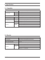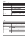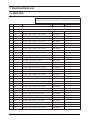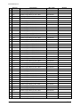
1
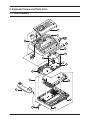
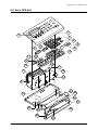
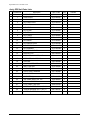
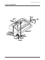
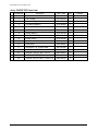
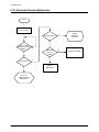
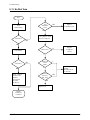
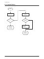
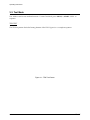
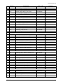
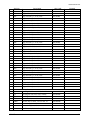
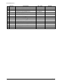
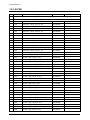
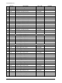
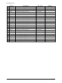
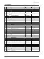
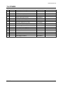
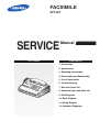
FACSIMILE
SF150T
SERVICE
FACSIMILE
Manual
CONTENTS
1. Precautions
2. Specification
3. Operating Instructions
4. Disassembly and Reassembly
000
0000000
0000
00000000
5. Circuit Description
6. Troubleshooting
7. Electrical Parts List
8. Exploded Views and Parts List
9. PCB Diagrams
10. Block Diagram
11. Wiring Diagram
12. Schematic Diagrams
1 Precautions
Follow these safety, ESD, and servicing precautions to prevent personal injury and equipment damage.
1-1 Safety Precautions
1. Be sure that all built-in protective devices are
in place. Restore any missing protective
shields.
2. Make sure there are no cabinet openings
through which people- particularly childrenmight insert fingers or objects and contact
moving parts or dangerous voltages.
3. When re-installing chassis and assemblies, be
sure to restore all protective devices, including
control knobs and compartment covers.
4. Design Alteration Warning:
Never alter or add to the mechanical or
electrical design of this equipment, such as
auxiliary connectors, etc. Such alterations and
modifications will void the manufacturer's
warranty.
5
7. Product Safety Notice:
Some electrical and mechanical parts have
special safety-related characteristics which
might not be obvious from visual inspection.
These safety features and the protection they
provide could be lost if a replacement
component differs from the original. This
holds true, even though the replacement may
be rated for higher voltage, wattage, etc.
8. Components critical for safety are indicated in
the parts list with symbols
. Use only
replacement components that have the same
ratings, especially for flame resistance and
dielectric specifications. A replacement part
that does not have the same safety
characteristics as the original may create
shock, fire, or other safety hazards.
Components, parts, and wiring that appear to
have overheated or are otherwise damaged
should be replaced with parts which meet the
original specifications. Always determine the
cause of damage or overheating, and correct
any potential hazards.
6. Observe the original lead dress, especially near
sharp edges, AC, and high voltage power
supplies. Always inspect for pinched, out-ofplace, or frayed wiring. Do not change the
spacing between components and the printed
circuit board.
SF150T
1-1
Precautions
1-2 ESD Precautions
Certain semiconductor devices can be easily damaged by static electricity. Such components are commonly
called "Electrostatically Sensitive (ES) Devices", or ESDs. Examples of typical ESDs are: integrated circuits,
some field effect transistors, and semiconductor "chip" components.
The techniques outlined below should be followed to help reduce the incidence of component damage
caused by static electricity.
CAUTION: Be sure no power is applied to the chassis or circuit, and observe all other safety precautions.
1. Immediately before handling a semiconductor
component or semiconductor-equipped
assembly, drain off any electrostatic charge on
your body by touching a known earth ground.
Alternatively, employ a commercially
available wrist strap device, which should be
removed for your personal safety reasons prior to
applying power to the unit under test.
2. After removing an electrical assembly
equipped with ESDs, place the assembly on a
conductive surface, such as aluminum or
copper foil, or conductive foam, to prevent
electrostatic charge buildup in the vicinity of
the assembly.
3. Use only a grounded-tip soldering iron to
solder or desolder ESDs.
4. Use only an "anti-static" solder removal device.
Some solder removal devices not classified as
"anti-static" can generate electrical charges
sufficient to damage ESDs.
6. Do not remove a replacement ESD from its
protective packaging until immediately before
installing it. Most replacement ESDs are
packaged with all leads shorted together by
conductive foam, aluminum foil, or a
comparable conductive material.
7. Immediately before removing the protective
shorting material from the leads of a
replacement ESD, touch the protective material
to the chassis or circuit assembly into which
the device will be installed.
8. Maintain continuous electrical contact between
the ESD and the assembly into which it will be
installed, until completely plugged or soldered
into the circuit.
9. Minimize bodily motions when handling
unpackaged replacement ESDs. Normal
motions, such as the brushing together of
clothing fabric and lifting one's foot from a
carpeted floor, can generate static electricity
sufficient to damage an ESD.
5. Do not use Freon-propelled chemicals. When
sprayed, these can generate electrical charges
sufficient to damage ESDs.
1-3 Lithium Battery Precautions
1. Exercise caution when replacing a Lithium
battery. There could be a danger of explosion
and subsequent operator injury and/or
equipment damage if incorrectly installed.
3. Lithium batteries contain toxic substances and
should not be opened, crushed, or burned for
disposal.
2. Be sure to replace the battery with the same or
equivalent type recommended by the
manufacturer.
1-2
SF150T
8. Exploded Views and Parts Lists
8-1. Total Assembly
1
3
2
S3
S4
4
S1
5
6
7
S1
8
9
10
11
S2
12
SF150T
S2
8-1
Exploded Views and Parts Lists
Total Assembly Parts Lists
Location No.
8-2
Description
SEC. Code
Q'ty
1
ASS'Y-OPE UNIT
JF96-01296A
1
2
ASS’Y-TOP COVER
JF96-01297A
1
3
SPACER
JF72-40611A
1
4
GUIDE-TX
JF72-41122Z
1
5
PBA-LIU
JF92-00843Q
1
6
REAR-BRKT
JF70-10681A
1
7
PBA-MAIN
JF92-00842E
1
8
SMPS-V2, AC/DC
JF44-10059A
1
9
ASS’Y-BASE UNIT
JF96-01298A
1
10
ASS’Y-MAIN CHASSIS UNIT
JF96-01253A
1
11
ASS’Y-HANDSET
JF96-01262A
1
12
CURL-CORD
JF39-60075A
1
S1
SCREW, TAPTITE, BH, +, M3, L8
6003-000015
11
S2
SCREW, TAPTITE, BH, +, M3, L6
6003-000261
2
S3
SCREW, TAPTITE, BH, +, M3, L6
6003-000115
2
Remark
SF150T
Exploded Views and Parts Lists
8-2. Ass'y OPE Unit
1
2
3
4
5
9
8
7
6
14
11
12
10
16
13
17
18
15
S1
27
20
19
26
S2
21
S3
22
23
24
25
SF150T
8-3
Exploded Views and Parts Lists
Ass'y OPE Unit Parts Lists
Location No.
8-4
Description
SEC. Code
Q'ty
ASS'Y-OPE UNIT
JF96-01296A
1
1
OPE COVER
JF72-42016Z
1
2
LCD-WINDOW
JF75-11004F
1
3
KEY-ONETOUCH
JF72-42021A
1
4
KEY-OHD
JF72-42022A
1
5
KEY-STOP
JF72-42029A
1
6
KEY-START
JF72-42028A
1
7
KEY-TEL
JF72-42026A
1
8
KEY-TAD(A)
JF72-42056A
1
9
KEY-TAD(B)
JF72-42057A
1
10
KEY-MENU
JF72-42020A
1
11
KEY-RESOLUTION
JF72-42018B
1
12
KEY-RECEIVE
JF72-42017B
1
13
KEY-ANSWER
JF72-42019M
1
14
RUBBER-CONTACT
JF73-40521A
1
15
DISPLAY-LCD
JF07-20061A
1
16
CBF-WIRE, MAIN-OPE, 18 P
JF39-41081A
1
17
CBF-WIRE, LIU-OPE, 7 P
JF39-40957A
1
18
PBA-OPE
JF92-00844B
1
19
CHASSIS OPE UNIT
JF70-10863A
1
20
BRKT-TPH UNIT
JF70-10861B
1
21
GUIDE-TPH(R)
JF70-10679A
1
22
PRINT HEAD-THERMAL
JF47-30069B
1
23
PBA-P.EMPTY
JF92-00704B
1
24
GUIDE-TPH(L)
JF70-10679B
1
25
CBF-WIRE, MAIN-TPH, 14P
JF39-40955A
1
26
BRUSH-ANTISTATIC
JF75-10650A
1
27
FLAT CABLE, OPE-LCD
JF39-41018A
1
S1
SCREW, TAPTITE, PWH, +, B, M2.
6003-000193
11
S2
SCREW-MACHINE, BH, +, M3, L4
6001-000125
4
S3
SCREW, TAPTITE, BH, +, B, M3, L
6003-000015
2
Remark
SF150T
Exploded Views and Parts Lists
8-3. Ass'y COVER TOP
4
3
S1
5
S2
2
1
6
7
8
9
11
10
S3
12
S3
SF150T
8-5
Exploded Views and Parts Lists
Ass'y COVER TOP Parts Lists
Location No.
8-6
Description
SEC. Code
Q'ty
ASSEMBLY-COVER TOP
JF96-01297A
1
1
TOP COVER
JF72-42015A
1
2
HINGE-OPE(R)
JF70-10676A
1
3
COVER-SPRING(R)
JF70-40562A
1
4
HINGE-BRKT(R)
JF70-10677A
1
5
BATTERY-COVER
JF72-42027A
1
6
HINGE-BRKT(L)
JF70-10677B
1
7
COVER-SPRING(L)
JF70-40562B
1
8
HINGE-OPE(L)
JF70-10676B
1
9
SWITCH-HOOK, 48 V, 200 mA
3409-000117
1
10
PBA-HOOK
JF92-00845C
1
11
SPEAKER, 1 W, 8 OHM, 83dB
3001-001044
1
12
UNIT-FIXING BRKT
GB70-10500A
1
S1
SCREW, TAPTITE, BH, +, M3, L6
6003-000261
3
S2
SCREW, TAPTITE, BH, +, M3, L8
6003-000015
2
S3
SCREW, TAPTITE, PWH, +, B, M2.5, L6
6003-000193
2
Remark
SF150T
Exploded Views and Parts Lists
8-4. Ass’y Handset
3
1
S1
9
2
4
5
6
7
8
SF150T
8-7
Exploded Views and Parts Lists
Ass’y Handset Parts Lists
Location No.
SEC. Code
Q'ty
ASS'Y-HANDSET
JF96-01262A
1
1
HANDSET-LOWER
JF72-42014A
1
2
AUDIO-RECEIVER, 160 OHM
3009-001001
1
3
HOLD-DUMMY
GB72-40792A
1
4
RUBBER-MIC
JF73-40501A
1
5
PBA-H/S MIC
JF92-00625A
1
6
CBF-HARNESS
JF39-40834A
1
7
WEIGHT-BALANCE
JF70-10864A
1
8
HANDSET-UPPER
JF72-42013A
1
9
RING-OP, ID17, OD35
6044-000138
1
SCREW, TAPTITE, PH, +, B, M3,
6003-000168
1
S1
8-8
Description
Remark
SF150T
Exploded Views and Parts Lists
8-5. Ass'y Base
1
4
2
3
9
10
5
7
8
S1
SF150T
6
8-9
Exploded Views and Parts Lists
Ass'y Base Parts Lists
Location No.
8-10
Description
SEC. Code
Q'ty
ASS'Y-BASE
JF96-01298A
1
1
CBF-WIRE, MAIN-CIS/MODE
JF39-41062A
1
2
MICRO-SWITCH
3405-000166
1
3
STEP-MOTER, 7.5 DEG, 24 V
3101-000171
1
4
ASS’Y-MAIN CHASSIS UNIT
JF96-01253A
1
5
BASE
JF72-42025A
1
6
PBA-D’DET
JF92-00888A
1
7
CBF-WIRE, HANDSET-LIU
JF39-41066A
1
8
RUBBER-FOOT
JF73-10002A
2
9
MIC-CONDENSOR
3003-000120
1
10
MIC-ADAPTER
GB72-40770A
1
S1
SCREW, TAPTITE, BH, +, M3, L6
6003-000261
2
Remark
SF150T
Exploded Views and Parts Lists
8-6. Harness
1
2
3
14'
9
11
3'
5
4
4'
6
4''
13
15
14
8
11'
8'
10
7
2'
1'
6'
10'
5'
12
SF150T
7'
8-11
Exploded Views and Parts Lists
Harness Parts Lists
Location No.
8-12
Description
SEC. Code
1
CBF-WIRE, MAIN-TPH, 14 P
JF39-40955A
2
CBF-WIRE, MAIN-OPE, 18 P
JF39-41081A
3
CBF-WIRE, LIU-OPE, 7 P
JF39-40957A
4
CBF-WIRE, MAIN-LIU, 22 P
JF39-41063A
5
CBF-WIRE, LIU-HANDSET
JF39-41066A
6
CBF-WIRE, MAIN-CIS/MODE
JF39-41062A
7
CBF-WIRE, MAIN-D.DET, MIC, 5 P
JF39-41078A
8
STEP-MOTER, 7.5 DEG, 24 V
3101-000171
9
CBF-WIRE, LIU-HOOK
JF39-41080A
10
CBF-WIRE, POWER-MOTOR
JF39-40963B
11
CBF-WIRE, POWER-TOP COVER
JF39-40962B
12
CURL CORD
JF39-60075A
13
CABLE CLAMP
6502-001026
14
CBF-WIRE, MAIN-BATTERY, 2 P
JF39-41082A
15
CBF-WIRE, MAIN-SPEAKER, 2 P
JF39-41079A
Q'ty
Remark
SF150T
6. Troubleshooting
6-1. Initial Checkout and Overall Troubleshooting Flow
Plug in the power
cord
Start
System
initialized ?
Y
Power Supply
OK ?
N
N
See Section 6-3
Load document in
feeder
Document feed ?
Y
Push 'START' Key
See Section 6-2
Y
N
Y
OGM Recording
OGM play back ?
See Section 6-7
Y
Call machine from
another phone
N
See Section 6-5
N
Y
See Section 6-5
N
Auto Answer
OK ?
CIS ON ?
N
See Section 6-4
Copy OK ?
Y
See Section 6-6
Y
ICM Recording ?
N
See Section 6-8
Y
Manual
operation OK ?
N
See Section 6-9
Y
RX OK ?
Y
N
See Section 6-10
A
SF150T
6-1
Troubleshooting
A
Lift Handset
off hook
Dial tone OK ?
N
See Section 6-11
6-2
Y
TX OK ?
Y
End
N
See Section 6-12
SF150T
Troubleshooting
6-2. Check Power Supply
Power cord
connected ?
Start
Y
Check AC socket
voltage
N
N
Replace Cord
Y
Fuse OK ?
N
Replace Fuse
Y
N
Connect as required
Check
Power Cord
Continuity
220 - 240 VAC?
END
Y
Q1 OK ?
N
Replace Q1
Notify customer
R5 changed
value ?
Y
N
End
Remove short
SF150T
6-3
Troubleshooting
6-2-1 No + 5 V
Start
output shorted ?
N
Y
Y
N
Check U2 ?
N
Check
U2 Input voltage
Y
Remove short
DC 6 V
D4 Open or
Shorted ?
Replace D4
Y
Check CON 1
N
D5 Open or
Shorted ?
End
N
Check PCB Pattern
Replace U2
6-2-2 No -12 V
output shorted ?
Start
Y
N
Check PCB Pattern
6-4
Y
U1 Output ?
Check
U1 Input voltage
Y
Remove short
-15 VDC
N
Replace D5
Y
Check CON1
End
N
Replace U1
SF150T
Troubleshooting
6-2-3 No + 24 V
Start
output shorted ?
N
Y
N
Restart
Y
Q3 OK ?
N
OVP operation
Y
Remove short
Check
OVP operation
D3 Open or
Shorted ?
Replace D3
Y
End
Check CON1
N
Replace Q3
6-2-4 + 24 V TPH Doesn't output
Start
Check
C/S port short ?
Y
Remove short
N
Q5 OK ?
Y
Check CON1
N
Replace Q5
End
SF150T
6-5
Troubleshooting
6-3. System Not Initialized
Start
Check
Vcc ³ 4.75 V
P1-4 (+5V)
P1-3 (GND5)
N
See Section 6-2-2
Y
Check
U3 Pin 5
= "High"
N
Check U3 Pin 6
(above +2.25 V)
N
Replace U3
Y
Step motor driving
Y
N
Check
P5 Harness or OPE
PBA
NG
Replace P5 Harness
or OPE PBA
NG
Replace
X2 XTAL
OK
Replace U7
Fax Engine IC
Check 12 MHz
Clock U7-37
NG
Check 24 MHz
Clock U7-129
OK
Y
Replace U14
Motor Driver
O.K ?
Y
End
N
Replace U7
Fax Engine IC
O.K ?
Y
End
N
Replace Main PBA
6-6
SF150T
Troubleshooting
6-4 Document Not Loading
Insert Document
Start
P7-1 "L" ?
N
Replace D-DET PBA
or P7 Harness
P6-1, 2, 3, 4
Motor Strobe
OK
Y
Check 24 V
P6-5, 6 ?
Y
N
See Section 6-2
Replace Motor
NG
U7-49, 50, 51, 52
Motor Strobe
OK
END
NG
Replace U14
Replace U7
SF150T
6-7
Troubleshooting
6-5 No Copy Mode Operation
Start
TPH Test O.K ?
Y
N
CIS Test O.K ?
Y
N
Y
N
Y
Check +24 V
P1-8, 9 ?
Y
P2-4, 6, 8, 10
TPH strobe
N
Replace U5
Y
Reload Document
Replace Main PBA
N
Replace U7
P2-7, 11, 12
Check P1-10
"L"
Y
N
B
Check U7-55
"H"
Is Memory Clear ?
Y
N
See Section 6-2
Replace U7
Replace TPH
N
Replace U5
O.K ?
Y
Restart
N
Replace U7
O.K ?
Y
Restart
N
Replace Main PBA
6-8
SF150T
Troubleshooting
6-5 Continued
B
CIS LED on ?
Y
Check P3-8
CLK1: 300 kHz
NG
N
Replace U7
Check P3-9
CLED ² 1 V
Y
Replace CIS
H
Replace Q2
OK
Check P3-6
START Signal
OK
P3-4
- 12 V ?
Y
NG
Replace U7
See Section 6-2
Replace CIS
N
U7-87
"H"
L
Replace U7
SF150T
6-9
Troubleshooting
6-6. OGM Not Playing Back
Start
OGM Play Back ?
Y
End
N
Speaker On
N
Check
Mic signal from
P7-4, 5
Y
Check
signal from
U3-16 ?
Replace main
board
N
Y
Check
P7 Harness ?
N
Y
Replace Mic.
End
N
Y
End
Check
signal from
U3-29, 31 ?
N
Replace U3
Y
Replace speaker
End
6-10
SF150T
Troubleshooting
6-7. ICM Not Recording
Start
Call machine
from other phone
ICM
Recording
mode ?
N
Check LIU board
Y
ICM Playback ?
N
Y
OK ?
N
Y
Replace main
board
Replace LIU
board
End
SF150T
6-11
Troubleshooting
6-8. Malfunction in Auto Answer
Start
Call machine from
another phone
Auto answer ?
Y
N
Check signal
P4-16
+5V
0V
?
Y
Replace U7
N
Replace LIU board
END
6-12
SF150T
Troubleshooting
6-9. Malfunction in Manual Receiving
Start
Lift handset
Press START
Machine goes
on-line ?
Y
N
Check U7-45
(Hook Event)
OK ?
Y
Check LIU board
N
OK ?
N
Replace LIU board
Y
Replace U7
Replace main
board
End
SF150T
6-13
Troubleshooting
6-10. Automatic Receive Malfunction
Start
Call fax machine
Receiving Data ?
Y
Return
Machine to
Customer
N
Rings exceed
ÒRings To AnswerÓ
Setting ?
N
Main Board
P4-18, 19
TX/RX
Y
N
Replace LIU Board
Y
Auto Answer ?
N
Y
Replace:
Main Board
Go To 6-9
ÒManual Receive
MalfunctionÓ
6-14
SF150T
Troubleshooting
6-11. No Dial Tone
Start
Test
Telephone
Cord
Press
OHD/V.REQ.
NG
Replace
Telephone Cord
OK
Use a phone to check
service at wall jack
Dial tone ?
NG
OK
Service OK ?
N
Lift Handset
Request
Telephone
Service
Y
Dial tone ?
NG
Check / Replace:
Handset cord
Handset
Hook Switch
LIU U201
LIU Board
OK
Main PCB
U7-54
CML1
L
Check/Replace:
Speaker
Main Board U14
P4, 205, 206
H
Main PCB
U3-29, 31
SPK_OUT
OK
NG
Replace U3
Return
machine to
Customer
SF150T
6-15
Troubleshooting
6-12. Transmit Failure
Start
Load document
Dial Receiving
Machine
Feed OK ?
Transmit
Begin ?
N
Chart 6-4
Document
Not Loading
Y
Y
N
Replace:
LIU board
Main Board
Return
Machine to
Customer
6-16
SF150T
5. Circuit Description
5-1 General
The main circuit board controls the machine, and consists of Super Fax Chip (KS16118), External memory,
CODEC circuit with modem-TX and RX signal path and some parts of the Line Interface Unit, Digital TAD
circuit with DSP amd DRAM, witch controls the system.
5-2 System Control Section
This circuit consists of the EP-ROM and SRAM, external Real Time Clock crystal, RTC and memory back-up
circuitry, and the Super Fax Chip (KS16118).
The KS16118 Super Fax Chip is an integrated 9600 bps modem, image processor, 8-bit MPU, peripheral
controller, and analog front end circuit on a single-chip.
Peripheral functions inculde 2-channel SI0, 3-channel DMA, 6-bit Half flash A/D converter, scanner and
video processor units, TPH interface, CODEC unit, and tone generator.
Modem is a 9600 bps, half duplex monolithic device incorporating digital filters, a Samsung SSP1600 digital
signal processor and CPU-Interface logic.
5-2-1 Memory Map
The external memory of the CPU is devided into, 1 byte(FF00H) DSP chip select, 32kbyte SRAM (0000H
through 7FFFH) and 128kbyte EP-ROM (0100H through 1FFFH).
1FFFH
DSP /CS
PCS1
/PMS
Peripheral
PCS0
(EP-ROM)
FFFFH
FF80H
FF7FH
FF00H
FEFFH
/DMS
0100H
00FFH
(SRAM)
Interrupt
Vectors
0000H
0000H
[ Program Memory ]
[ Data Memory ]
Figure 5-1: KS16118 External Memory Map
SF150T
5-1
Circuit Description
5-2-2 lExternal Chip Control
KS16118 internal logic generates chip select signals for both memory chips and peripherals.
To support external access, from one to three wait cycles can be inserted under program control during
external access.
A chip select signal line goes active (low) whenever its corresponding device is accessed over the external
interface. The peripheral addresses are located in data memory space.
/DMS : SRAM chip select active (low)
/PMS : EP-ROM chip select active (low)
/PCSn : Peripheral chip select active (low)
D0 - D7 : 8 bit data bus
A0 - A15 : address bus
5-2-3 System Clock
The 12 MHz internal system clock frequency is generated by dividing the 24 MHz clock.
OP00-OP06
XIN
LED_CTL
OPERATING
PANEL
LCD_EN
XOUT
RTC
CRYSTAL
OPI0-OPI3
STB 0-3
PRINTER DATA
CONTROL AND
SENSORS
/DMS
PDAT
PCLK
/RD /WR
PLAT
D0~D7
THADI
A0~A14
DATA
MEMORY
KS16118
/RD
MOTOR
D0~D7
SM0-SM3
A0~A15
DRIVER
MODE
A16
PROGRAM
MEMORY
/PMS
(MOTOR)
SI
CLK1
SCANNER
CONTROL
AND
PROCESSING
GENERAL
PURPOSE I/ 0
Vin
+Vref
/RESET
RESTOUT
-Vref
Figure 5-2: XFC Hardware Interface Signals
5-2
SF150T
Circuit Description
5-2-4 Real Time Clock (RTC)
5-2-5 Print Control
This circuit receives clock pulses from an external
32.768 kHz crystal, which it divides into hours,
minutes, seconds, year, month, and day.
A battery maintains operation when power is off.
KS16118 can up-track 100 years, begining with
1992.
The PCLK and PDATA signals synchronize serial
print data to the TPH.
PLAT latches TPH serial print data to the TPH
from a shift register through PDATA.
STB0 - STB3 enable TPH printing in four steps.
This system has a 10ms/line printing format and
sets STB High/Low enable status
according to the STBPOL signal.
PDATA
PCLK
PLAT
STB0
STB1
STB2
STBWID
[0:11]
STB0FF
[0:11]
STB3
Figure 5-4: Printer Timing
5-2-6. A/D Converter (Scanner & TPH
Temperature)
Using a half-flash conversion technique, the 6-bit
A/D converter supports a 0.8µs peak conversion
time and dissipates only 7mA, maximum.
The half-flash unit uses 16 comparators, a most
significant 3-bit ADC, and a least significant 3-bit
ADC.
If the analog input voltage is greater than +Vref,
the A/D conversion result is 3FH.
If the analog input voltage is less than -Vref, the
A/D conversion result is 00H.
A/D conversion register, ADCON (19H), is used
to select an internal or external source for the A/D
converter, to enable or disable the converter, and
to select the operating mode (H: ADin 1 (Scanner),
L: ADin 0 (TPH)).
SF150T
+5V
R4
THD1
TPH
Thermistor
Rth
(T)
R5
GND5
Figure 5-6: THD Connection Circuit
5-3
Circuit Description
5-2-7 Operation Panel Control
Communication
5-2-9 CIS Input Processor
The Operation Panel is controlled by the Port 1,
Port2, and Port 5 registers.
Port 1 (E2H) is a 4-bit general output port for LCD
display data.
This port can be configured for normal data (P1.4P1.7) or alternately as internal MODEM V.24
interface output signals (P1.0-P1.3).
Port 2 (E4H) is an 8-bit port with both input and
I/O pins.
P2.0-P2.3 are input ports for OPE key scan data,
and P2.6-P2.7 are not used for SF150T.
Port 5 (EAH) is an 8-bit port with both output and
I/O pins.
P5.0 and P5.4 are used for LED control and LCD
enable.
To process the B/W input signal, maximum (+Vref)
and minimum (-Vref) values of the CIS input signal
are adjusted by calibrating KS16118 in the high state
for maximum level, and setting them to earth for
minimum level.
Shading correction uses a multiplier composed of a
9-bit sequential adder for simple H/W Logic.
5-2-10 CIS Driver
The CIS driver clock (CLK1) frequency is 250 kHz.
A 75% low duty cycle lengthens the charging time.
A start signal (SI) is provided every 10 ms to
match the line scanning time.
Actual image signal (VIN) is provided in less than
6.8 ms, based on A4 paper size using the 250 kHz
clock.
5-2-8 Image Sensor
The shading wave is formed by scanning the white
roller prior to a document.
The slice level is determined by the shading wave,
and compensates for shading distortion according
to the CIS characteristics.
The wave format from the CIS is converted into a 6
bit digital value in the KS16118 image processor,
and processed in B/W or intermediate mode.
250 KHZ (L:DUTY 75%)
CLOCK
SI
SIG
1 LINE
Figure 5-10: CIS Driver Clock Timing
5-4
SF150T
Circuit Description
5-2-11 I/O Port Table
Pin No. Port Name
Circuit Symbol
I/O
High
Low
34
P0.0
A16
O
High Bank Memory
Low Bank Memory
35
P0.1
/DSP_CS
PCS
DSP Inactive
DSP Active
45
P2.4
IRXD
I
DATA = 1
DATA = 0
46
P2.5
ITXD
O
DATA = 1
DATA = 0
49
P3.0
MOTOR A
O
Active
Inactive
50
P3.1
MOTOR /A
O
Active
Inactive
51
P3.2
MOTOR B
O
Active
Inactive
52
P3.3
MOTOR /B
O
Active
Inactive
53
P3.4
/CML2
O
-
-
54
P3.5
/CML1
O
Active
Inactive
55
P3.6
/24VCTL
O
Active
Inactive
93
P4.1
DSPRST
O
DSP Reset
Normal
92
P4.2
DSPHL
O
DSP High Byte
DSP Low Byte
90
P4.4
/LOWBAT
I
Normal
Low Battery
89
P4.5
DSPACK
O
Normal
DSP Response Mode
87
P4.6
/GLED
O
CIS LED On
Off
88
P4.7
-
O
High
Low
126
P5.0
LEDCTL
O
OPE LED On
OPE LED Off
96
P5.3
/NOBAT
I
Normal
No Barttery
137
P5.5
SCLK
O
138
P5.6
SDATS
O
CODEC Serial Clock
CODEC Serial Data
139
P5.7
/SDEN
I
Normal
59
P6.1
/HOOK DET2
I
-
-
60
P6.2
MODE
I
Open
Closed
61
P6.3
P_EMPTY
I
No Paper
Paper Exist
62
P6.4
D_DET
I
No Document
Document Exist
63
P6.5
RING_DET
I
Normal
Incomming Ring
116
P6.6
/DSPFLAG
I
Normal
Active DSP Data Transfer
SF150T
CODEC Enable
5-5
Circuit Description
5-2-12 Motor Controller
5-2-14 Reset
This facsimile machine perform sending, receving,
and printing functions utilising a single 24 volt
motor with a 120 ohm winding resistance.
Four drive strobe pulses operate the motor.
To initialize the chipÕs internal logic, the reset
input (/RESET) must be held to 0 Volt for at least
22 CPU clocks. During this time, Vdd must be
greater than 3 Volt.
The watchdog timer can also invoke a system
reset.
When the reset input is released, the reset
condition continues for about 209.7 ms.
While the KS16118 is in this state, 0 Volt is applied
to the /RSTOUT pin.
Motor Function
Drive Strobe Pulse
Phase
Swing Gear Control
100 pps
2
Document Out
100pps
2
Super Fine Mode
100pps
1-2
Other
100pps
2
Table 5-1: Motor Functions
5-2-13 Serial communication Signals
The KS16118 have two full-duplex serial
communication port.
One port is used for I-LIU communication on LIU
PBA, and is a standart UART (Universal
Asynchronous Receiver/Transmitter).
Another port, not used, may be configured for
UART or SRT (Synchronous
Receiver/Transmitter) operation.
[ +5V Power Monitoring ]
If 5 volt power to MX93000AFCÕs pin 6 (VPOW)
drops to between 4.6V and 4.4V (typically 4.5V),
power failure is indicated and the output of
MX93000AFCÕs pin 5 (/POWB) will go `lowÕ(GND5).
This causes the KS16118 to become active (low=reset).
The KS16118 reset causes the /REST0 terminal to be
reset.
5-3 Memory
System memory consists of 128 kB EP-ROM and 32 kB SRAM. All of SRAM is backed up.
ROM and SRAM are selected by chip select lines, and data is accessed by the units position of the byte.
ROM has two banks. One Bank is as low bank that address range is 0100H-FFFFH.
Another bank is as high bank 10000H-1FFFFH. ROMÕs bank is selected port 0 (bit 0) of the KS16118.
5V power is applied to SRAM through VB. This model facsimile machine uses a Lithium battery.
A 1 kohm resistor in series with the positive battery terminal is for battery protection.
5-4 CODEC circuit with Modem-TX and RX signal path
This has PCB CODEC which has ablity that converts voice signal to A/D and is able to store is DRAM and convert
to voice signal passing through D/A transmission after scanning from voice digital stored in DRAM by DSP.
This has PRE-PGA(Programmable Gain Amplifier) that is able to amplift selectively among Mic input, remot
signal, rx signal.
This has ALC(Automatic Level Control) circuit has maximum 42dB gain to be convenient for recording using Mic.
This have two comparator having 1.25V reference voltage and two universal opamp.
This has 1 W speaker drive amplifir that is able to drive 8 ohm speaker.
Because MX93000AFCÕs control uses synchronous communication port, that is fast in action is convenient.
5-6
SF150T
Circuit Description
1) TX CIRCUIT
The output signal coming from internal modem
KS16118 enters MX93000AFC through AUX2
terminal after amplfied by OP AMP U1.
That signal passes through internal switch, is
amplified by LIN-DRV amplfier and is sent to LIU
board through LOUT terminal.
2) RX CIRCUIT
The signal goming into LIU terminal through LIU
board is amplified by MX93000AFC's PRE-PGA,
passes through internal switch and goes into FILT
terminal.
After the singal is diminished by OP AMP U1, it
enters internal modem of KS16118.
5-5 TAD
TAD circuit consists of a voice coprocessor to record and play voice messages and voice memory.
5-5-1 DSP
5-5-3 Play Path
This circuit consists of host interface, memory
interface, CODEC interface.
receives data to the compressed voice data to and
from KS16118.
Memory interface sends and receives data to the
compressed voice data to and from DRAM to play
back and record voice data.
DSP communicates with host KS16118 through host
interface.
The signal stored in DRAM is decomressed in DSP
and enters into MX93000AFC.
Input signal is converted to D/A again and is
amplified by LIU-DRV amplifier and comes into
LOUT terminal through or comes into terminal
after being attanuated by ATT (Electronic Volume)
or SPK-DRV.
5-5-2 Recording Path
The voltage is supplied with MIC as using the
MX93000AFC's Vref Voltage (2.25V), and the voltage
entering into MIC is trasmitted to electric signal and
enters into MX93000AFC's MIC terminal.
Input signal is amplified by MX93000AFC's ALC
until maximum 26dB (Max. 3VP-P) according to
signal size.
The signal enters into PCM CODEC that converts to
D/A and compresses in the DSP Chip and stores in
DRAM.
SF150T
5-5-4 Voice Backup
+5V is supplied for DSP or voice memory through
VBT when power is on.
When power is off, +5V is supplied from the 9V
backup battery.
When supply voltage is "ON", U9(5V Voltage
Regulator) makes 5V Supply Voltage.
The signal is supplied with DSP or DRAM and it
caused that the data is protected.
When supply voltage is "OFF", U9 makes 5V Voltage
as using the 9V Battery.
And then the voltage is used to "backup supply
voltage" in DSP or DRAM.
If the supply voltage were "OFF" as using the full
charged 9V Battery, voice data is usually protected
for twenty hours.
5-7
Circuit Description
5-6 LIU PBA
The LIU (Line Interface Unit) interfaces the MODEM and telephone to the telephone line. The FAX and
telephone portions of the LIU are active with machine power on. When machine power is off, only the
telephone circuitry operates, powered by telephone line voltage. The FAX portion of LIU consists of the
interface between MODEM and telephone line; and the circuits for DC loop feeding, DP signal, loop current
and ring detect. The telephone portion is divided into ringer, dialling, and speech circuits. Refer to the
schematic and connection diagram sections of this manual.
5-6-1 FAX section
artificial ring.
MF DIAL (Same as telephone section)
MODEM/LINE INTERFACE
This is the path for data and control signals.
¥ CML201 relay: switches telephone line between
FAX and telephone circuits.
¥ U201 pin 3 TIT: single-ended input for
transformer T202.
¨ TIT: Transmit Input from Transformer
¥ U201 pin 40 ROT : Output for driving a
transformer T203 with an AC impedance
exceeding 10Kohm.
¨ ROT: Receive Output Transformer
¥ C212: DTMF and CNG detect path to T201
20Kohm winding under idle conditons; and DC
blocking for 20Kohm winding.
¥ AC impedance: the AC impedance of U201 (ILIU) is set at 1000ohm by external capacitor
C228 at U201 pin 8 CI (Complex Impedance
input) port. With an external resistor (R244) at
U201 pin 34 ACI port it can be programmed to
600ohm. And U201 pin 35 CS (Current Shunt
control output) port is N-channel open drain
output to control the external high power shunt
transistor for synthesizing AC and DC
impedance.
¥ DC conditions : normal operating mode is from
15mA to 100mA. An operating mode with
reduced performance is from 5mA to 15mA. In
the line hold range from 0mA to 5mA the device
is in a power down mode and the voltage at
U201 pin 37 LI (Line Input) port is reduced to a
maximum of 3.5V. The DC characteristic is
determined by the voltage at U201 pin 37 LI port
and a R215 resistor between U201 pin 37 LI and
pin 39 LS port. It can be calculated by the
following equation : VLS = VLI + ILINE X R215.
RING DETECT
¥ U201 pin 28(MO) is ring melody output port and
this signal drive the Q207 which drive the
FET201 which drive Photo coupler U204 for
5-8
¥ U201 pin 2 DMS(Dial Mode Selection) port is set
to VDD by R227 It is M/B ratio 33:66, and no
power operation mode conducts only DP.
¥ MF signal appears (tone level of low group :
typical -14dBm) at U201 pin 4 MFO(DTMF
Generator Output). This signal is leveled by
R226, R225 and C239, then to amplier U201 pin 9
MFI(DTMF Amplier Input).
¥ Line dial signals appear at U201 pin 39 LS(Line
Current Sense Input).
DP DIAL (Same as Telephone section)
¥ U201 pin 2(DMS) is set to Vdd(33/67) or
VSS(40/60) by R227 or R228 resistor.
¥ Dial pulses originate at U201 pin 27(DPn), which
toggles Q205, which drives Q201. The resulting
intermittent voltage interrupts the telephone
line.
¥ Pulse M/B ratio is set by U201 pin 2 MDS port.
Vdd = 33/66, and Vss = 40/60.
¥ U201 pin 35 CS port : Modulation of line voltage
and shorting the line during make period of
pulse dialling.
LLC (Line Loss Compensation) / LOOP
CURRENT DETECT
¥ When the LLC pin option. it is activated, the
transmit and receive gains for both I/O are
decreased 6dB at line currents above 20mA
when the U201 pin 31 LLC is connected to
AGND, and from 75mA when this pin is
connected to VDD. The LLC is deactivated
when LLC pin is connected to VSS.
¥ When CML201 or Hook Switch switches to
telephone line, U201 on the LIU board and CPU
(U1) on the Main board begin communication.
U201 sends an <Ack> message containing the
line current information to recognize a parallel
phone.
SF150T
Circuit Description
Serial interface
Speech Circuit
¥ U201 pin 11 RXD: Schmitt trigger input
(threshold = 2.5V) to serial interface.
¥ U201 pin 29 TXD: Open drain output from serial
interface.
¥ The communication is standard UART :
Baud Rate 9600
Start Bit 1
Stop Bit 1
Data Bits 8
¥ U201 (STI9510) and associated components.
¥ Handset transmitting circuit: Handset
transmitter audio (Condensor MIC.) is filtered
by R240, C232, C224, C225, C226, C227, C229 and
C230, and then amplified by U201 pin 32 and 33
(M1, M2).
¥ Handset receiving circuit: Handset receiver
(Dynamic unit) is filtered by R229, C241, C209,
C203 and C231, and then applied to U201 pin 1
(ROH) and VSS.
¥ U201 pin 39 (LS) is audio output to telephone
line.
Parity Bit None
LSB is transferred prior to MSB.
5-6-2 Telephone Section
RINGER CIRCUIT
¥ When a ringing signal is applied to the line, Vdd
of U201 (I-LIU) is charged via an external path.
After Vdd has reached the operating voltage the
oscillator starts and U201 detects the ring
frequency.
After a valid ring frequency is applied to the
U201 pin 25 RFD (Ring Frequency
Discrimination) port, the ring melody generator
of U201 sends out a 3-tone melody via U201 pin
28 MO (Ring Melody Output) port.
¥ U201: I-LIU and associated components.
¥ Ring frequency passes through DC blocking
capacitor C206 (C205 for Switzerland or Austria)
and Zener-diode ZD205 (ZD209 for Switzerland
or Austria) to U201 pin 25 RFD port.
¥ Line ring voltage passes through DC blocking
capacitor C201, current limit resistor R205,
bridge diode BD201, CML relay, and Hook
Switch to FET201 (BS170) pin 3, C214, ZD203
and R246.
¥ The ring frequency discriminator of U201
assures that only signals with a frequency
between 13Hz and 70Hz are regarded as valid
ring signals.
¥ When a valid ring signal is present for at least
73ms, the ring melody generator (pin 28, MO) is
activated and remains active as long as a valid
ring signal is present.
¥ U201 filters the ring signals and output is pin 28
(MO).
¥ The 3 basic melody frequencies are : F1 = 880 Hz,
F2 = 1067 Hz, and F3 = 1333 Hz. The repetition
rate is set to 4 which means that the sequence of
F!, F2, F3, F1, F2, F3 is repeated 4 times within a
second.
SF150T
Sidetone Circuit
¥ Sidetone audio characteristics are controlled by
R238, R235, R237, R239, and C202 connected to
U201 pin 7 STB.
5-9
5-7 OPE PBA
OPE PBA serves as the Machine-User interface.
The OPE operates on a time-sharing basis. As shown below, OPE keys and LED control are divided into
key scanning, LED displaytime and display time. On each 2ms interrupt rising edge, OPE line turns off
after 125µsec initial delay, and after 1 CPUCLK cycle, LEDCTL-LOW makes LED turn off. During the next
128 CPUCLK cycles, OPE KEY STROBE is maintained and during the next 1 CPUCLK KEY, INPUT is
scanned and stored in KEY buffer.
After key scanning, through the OPO0-3 port the upper and lower nibble data are transferred to the LCD
module as LCDCTL goes high.
After key displaying DATA on LCD, LED lamps turn on with LEDCTL-ON.
OPO0-4 : Used as key board strobe or LCD, LED driver
OPO5-7 : Used as key board strobe.
OPI0-3 : Key scanning ports from key matrix.
C2MS
125µsec
7
0
1
2
3
4
5
6
7
0
OPO0
LED0 LED0
LED0 LED0 LED0 LED0 LED0 LED0 LED0 LED0
OPO1
LED1 LED1
LED1 LED1 LED1 LED1 LED1 LED1 LED1 LED1
OPO2
LED2 LED2
LED2 LED2 LED2 LED2 LED2 LED2 LED2 LED2
OPO7
LED7 LED7
LED7 LED7 LED7 LED7 LED7 LED7 LED7 LED7
LEDCTL
LCDCS
IRQ2MS
OPI0
LCD DB0H LCD DB0L
LED0
OPI1
LCD DB1H LCD DB1L
LED1
OPI2
LCD DB2H LCD DB2L
LED2
LED7
OPI7
OPI[3:0]
LEDCTL
LCDCS
LCD H
(3)
(1)
LCD L
(7)
(1)
IRQ2MS
LED
OFF
(7)
KB STROBE
LCD HI
LCD LO
(128)
(12)
(16)
(1)
LED
ON
(7)
(1)
[X] = Time Interval of TSTCLK's
5-10
SF150T
4. Disassembly and Reassembly
Note: Make sure power is OFF by removing the power cord from the wall outlet.
4-1 Tx Guide
¥ Open the operating panel assembly.
TX Guide
¥ Carefully lift the TX guide, as shown in the figure.
OPE Cover
Figure 4-1
4-2 Top Cover
¥ Loosen the 5 screws fastening the top cover.
2
¥ Carefully lift the top cover.
1
1
¥ Remove the wire harness from the base, as
shown in the figure.
3
3
3
3
3
Figure 4-2
SF150T
4-1
Disassembly Instruction
4-3. OPE Unit
¥ Loosen the 2 screws fastening the top cover.
¥ Carefully lift the OPE assembly, as shown by
the arrow.
OPE Unit
Top Cover
Figure 4-3
4-4. OPE Cover
¥ Loosen the 2 screws fastening the OPE chassis.
OPE Cover
¥ Remove the Paper Empty sensor connector
from the OPE board.
¥ Remove the OPE unit from the OPE chassis, as
shown by the arrows.
OPE Chassis
Figure 4-4
4-2
SF150T
Disassembly Instruction
4-5. TPH
¥ Remove the TPH assembly from the OPE unit.
¥ Remove the TPH from the TPH assembly.
OPE Cover
¥ Remove the TPH harness from the TPH
connector.
¥ Remove the TPH guide from the TPH.
TPH Bracket
TPH Guide
TPH
Figure 4-5
4-6. Main Frame
¥ Lift the white roller assembly.
Main chassis Ass'y
¥ Loosen the 2 E-rings fastening the main chassis
assembly.
¥ Remove the spring-lock.
¥ Loosen the 2 screws fastening the main chassis
assembly.
¥ Lift the CIS assembly.
¥ Remove the document guide from the CIS
assembly (2 screws).
¥ Remove the CIS guide from the CIS (2 screws).
Base Ass'y
Figure 4-6
SF150T
4-3
Disassembly Instruction
4-7. CIS
¥ Lift the white roller assembly.
¥ Loosen the 2 E-rings fastening the main chassis
assembly.
¥ Remove the spring-lock.
¥ Loosen the 3 screws fastening the main chassis
assembly.
¥ Lift the CIS assembly.
¥ Remove the document guide from the CIS
assembly (2 screws).
¥ Remove the CIS guide from the CIS (2 screws).
Figure 4-7
4-8. BOARDS & POWER SUPPLY
¥ Remove the handset modular harness from the
LIU board.
¥ Loosen the screw fastening the LIU board and
carefully lift the LIU board as shown by the
arrow.
LIU PBA
POWER
MAIN PBA
¥ Loosen the 3 screws connecting the main and
daughter boards. Lift the rear bracket.
¥ Loosen the screw fastening the daughter board
to the base. Lift the daughter board.
¥ Loosen the 2 screws fastening the power supply
to the base. Lift the power supply and the main
board to remove them.
BASE
¥ Lift the modular jack and the earth spring.
Figure 4-7
4-4
SF150T
3. Operating Instructions
3-1 Service Mode
In Service Mode, the technician can check the machine and perform various tests to isolate a machine
malfunction.
To enter Service Mode, press ÔMENU, #, 1, 9, 3, 4Õ in sequence, and ' T ' will be displayed in the LCD to
confirm that the machine has entered Service Mode. While in Service Mode, the machine still performs all
normal operations. To return to normal User Mode, press 'MENU, #, 1, 9, 3, 4' in sequence again, or turn
the power off, then on by unplugging and replugging the power cord.
3-2 Changing Options
3-2-1 Selectable Options
CONFIRMATION REPORT
CALLER ID
Select whether a confirmation report prints each
time a user sends a fax.
This is the number of the person faxing you.
YES: The machine prints a report automatically
after each fax sent.
ERROR : The machine prints a report only when
there is an error.
NO: The machine does not print a report
automatically. User can print the list on
demand.
DIAL TYPE
Choose YES to turn on Caller ID display.
Choose NO to disable.
REMOTE RECEIVE CODE
This code can be used only with a phone extension
connected to the FAX machine. The user can
initiate FAX receive mode by entering a remote
receiving code on the extension phone. The code is
factory preset to
9
, and the middle character
may be changed to any digit between 0 and 9.
Select the type of dial system to which the machine
is connected.
AUTO PRINT
Select MF if connected to a tone dial system.
Select DP if connected to a pulse dial system.
Use ^ or v buttons to select, then press Start.
The machine prints a TX/RX journal automatically
after every 20 fax sessions.
RING COUNT
MODEM SPEED
Select the number of rings the machine allows
before it answers a call in automatic receiving
mode.
Select baud rate of 9600, or 4800 bps. The lower the
baud rate, the larger the acceptable error rate. T30
protocol has a fixed speed of 300 bps in the
protocol mode. When the TX speed is set to 9600
bps, the RX speed will be V.29. When the TX
speed is set to 4800 bps, the RX speed will be V.27
ter.
SF150T
3-1
Operating Instructions
CALL TRANSFERRING
REMOTE PASSWORD
This feature allows the fax machine to transfer
incoming caller's message to a specified remote
location.
You can change the three-character password used
to access your machine from a remote phone. The
password is preset to "#139#" (pound one three
nine pound) at the factory. The first and the last #'s
are fixed, but you can change the middle numbers
from 0 to 9.
Choose YES to turn on this feature. The LCD
display asks to enter the telephone number you
want to be transferred.
Choose NO to turn off the feature.
Enter the characters you want to use, then press
Start.
CALL MONITORING
This feature enables you to hear callers leaving
messages on the machine.
BATTERY ALARM
Choose YES to turn on this feature.
Choose NO to turn off this feature.
You can turn on the battery alarm feature. With
this feature on, the machine displays the low
battery message in the LCD and sounds beeps to
alert you low battery condition.
CHARGE SAVER
Choose YES to turn on the battery alarm feature.
Choose NO to turn off the battery alarm feature.
This feature lets the user dial into this machine
from a remote phone and check whether anyone
has left a message without being charged for a
charge call. When toll saver is on and there are
messages waiting to be heard, the machine
answers on the number of rings you specify in the
ring count option. If there are no messages, the
machine answers on the second ring after the
number specified. This gives the user time to hang
up the phone before the machine answers - and
saves the price of the call.
Choose YES to turn on charge saver.
Choose NO to turn off charge saver.
MESSAGE RECORDING TIME
You can select the maximum time allowed for
caller messages and memos.
If you choose YES, the LCD display shows you the
time limits available : 0 second, 30 seconds, 60
seconds or 90 seconds. Choose the proper time. If
you choose 0, it allows callers to hear the greeting
message but doesn't permit them to leave
messages.
3-2
TAD SILENCE CHECK
In TAD mode, The machine decides the next
action when detected a silence of 10 seconds.
The actions are:
RX : Swiches to receive mode.
REC : Keeps the recording the silence.
CUT : Disconnect the line and returns to standby
mode.
TX LEVEL
From -9 dBm to -15 dBm is acceptable. You can set
the transmission level to between 0 and -15 dBm
in 1dB steps using the control panel keypad.
Accuracy is + 0 / -3 dBm.
CABLE EQUALIZER
Copper telephone wire attenuates low frequencies
less than high frequencies. The longer a cable is,
the more pronounced the effect. To compensate for
this attenuation you may need to set the machine
to match the cable length currently used. Select
short or long.
SF150T
Operating Instructions
LINE MONITOR
MH/MR CODING
Allows you to monitor line signals through the
speaker.
Selection the coding method used for picture
detail
MR = Use MR and MH coding.
MH = Use only MH coding.
RX LEVEL
Reception level may be too low due to cable losses.
If set to - 43 dBm, reception sensitivity will be
between 0 and - 43 dBm.
If set to - 48 dBm, reception sensitivity will be
between -5 and -48 dBm.
BUSY TONE DETECTION LEVEL
While checking tone in ANS/FAX mode, If any
signal which is great than set level is detected for a
few seconds the machine will disconnect the line.
BUSY ON DROP OUT TIME
While checking busy on time, if any signal noise is
detected, the machine will ignore the signal noise
unless it is greater than a specified time.
RING ON CHECK TIME
The machine must receive a ring signal with a
specified active time from a telephone exchange in
automatic reception mode. The detection time that
the machine considers valid is adjustable via this
option. If the active time of the ring signal is less
than the set value of the Ring On Check Time, the
machine will not consider it a ring signal.
RING OFF CHECK TIME
The machine must receive a ring signal with a
specified inactive time, as well as an active time. If
the inactive time of the ring signal is longer than
the value of the Ring Off Check Time, the machine
will not consider it a valid ring signal.
3-2-2 Changing Options
BUSY OFF DROP OUT TIME
While checking busy off time, if any signal noise is
detected, the machine will ignore the signal noise
unless it is greater than a specified time.
Press ÔMENU, 3, Start/COPYÕ in sequence. Press
^ or v to select the desired option item.
When the desired item appears, press Start and
use ^ or v to change the status of the selected
option.
PAUSE TIME
Adjust the period of pause time to wait for a
second dial tone in a PABX or mobile paging
system. You can adjust the time from 0 sec to 9 sec
(0 to 9).
RECALL TIME
When a call comes in and you want to connect it to
another party, you can transfer the call by using a
timed-break recall funtion.
This funtion must make a properly timed break
authorized by the country. The machine can select
times of 100, 280, or 600 msat an accuracy of ± 10
ms of the setting.
SF150T
3-3
Operating Instructions
3-3 Test Mode
Test Mode is used to test machine functions. To enter Test Mode, press ÔMENU, 0, START/COPYÕ in
sequence.
TPH TEST
The TPH test pattern checks the heating element of the TPH. Figure 3-1 is a sample test pattern.
Figure 3-1: TPH Test Pattern
3-4
SF150T
Operating Instructions
MODEM TEST
ROM TEST
The modem will transmit send various signals on
the telephone line to check the following:
Tests machine ROM (Read Only Memory). The
result and the software version appear in the LCD
in the following format:
¥ FSK Test
¥ Tone Test: 1100 Hz, 1650 Hz, 1850 Hz, 2100 Hz
¥ G3 training: 9600, 4800 bps
¥ RX Loop Test
¥ DTMF Test
CHKSUM= VXX/XX, OK
ALL MEMORY CLEAR
Erases contents of RAM. When memory is cleared,
the machine returns to default settings.
3-4 Report Printout
A number of useful reports can be printed in Service Mode. One of these lists is the protocol list, which
contains detailed information which may be required when contacting technical support. To print this list,
press MENU, 4, START/COPY in sequence.
When a report name appears in the display, scroll through the list of reports by pressing ^ or v. When a
desired report is selected, press START/COPY.
CONFIRMATION REPORT
PROTOCOL LIST
Shows the last transmission result.
This list is available in Service Mode only, and
shows the sequence of the CCITT group 3 T.30
protocol during the most recent TX or RX
operation. You can check for send and receive
errors with this list.
TX/RX JOURNAL
Shows information about faxes sent and received.
SYSTEM DATA LIST
If a communication error occurs while the machine
is in Service Mode, the protocol list will print
automatically.
Shows all option settings.
HELP LIST
TEL. NUMBER LIST
Lists all numbers stored in the machine's OneTouch and Speed-Dialling memory.
SF150T
This report illustrates the machine's basic
functions and commands. Use as a quick reference
guide.
To print this list, press HELP (#).
3-5
Operating Instructions
3-5 LCD Display
3-5-1 During communication
In User Mode, the LCD shows the remote
machine's TTI number, communication type, (send
or receive), and page number.
In Service Mode, the display shows the
communication type, abbreviations for the CCITT
Group 3 T.30 protocol as they occur, the protocol
type (G3), coding type (MH), baud rate in kbps,
and line time.
3-5-2 If a communication problem
occurs:
In User Mode, the display shows one of the
following reasons: CAM JAM, COMM. ERROR,
CHECK DOCUMENT.
In Service Mode, the display shows all error
messages available in User Mode, as well as
additional error messages not available in User
Mode.
Error messages shown only in Service Mode are:
PRE-MESSAGE ERROR:
problem occurred during phase B of session
MESSAGE ERROR:
problem occurred during phase C of session
POST-MESSAGE ERROR:
problem occurred during phase D of session
LINE ERROR:
machine cannot connect or has lost connection
with the remote machine
Additional messages, not shown above, will
appear in the TX/RX journals printed in Service
Mode.
3-6
SF150T
2 Specification
2-1 Transmitter
Parameter
Document Size
Specification
Normal
210 x 297 mm
Max.
216 x 1500 mm
Min.
152 x 76 mm
Document Thickness
0.085 x 0.115 mm
Scan Line Length
Horizontal
A4 paper,1728 scan elements along 216 line length
Effective Scanning Width
Vertical
216 mm
Scanning Method
Horizontal
Flat-bed scanning using CIS
Vertical
Stepping motor
Horizontal
8 dots/mm
Resolution
Vertical
Standard:
3.85 lines/mm
Fine:
7.7 lines/mm
Super Fine: 15.4 lines/mm
2-2 Receiver
Parameter
Specification
Coding Scheme
MH (Modified Huffman)/MR (Modified READ)
Recording Paper Size
216 mm x 30 m; core diametre: 12.7 mm
Effective Recording Width
210 mm
Recording Method
Solid state Thermal Printing Head
Horizontal
Resolution
Vertical
8 dots/mm
Standard:
3.85 lines/mm
Fine:
7.7 lines/mm
Super Fine: 15.4 lines/mm
SF150T
2-1
Specifications
2-3 Line Control Blockk
Parameter
Specification
Communication Facility
Public Switched Telephone Network (PSTN)
Line Coupling
Direct
Transmission Speed
9600, 7200, 4800, 2400 bps
Modem
QAM, DPSK and FSK
(V.29, V.27ter with fall back function and V.21)
Carrier Frequency
1700 Hz (9600/7200 bps)
1800 Hz (4800/2400 bps)
Control Signal
1100 Hz (CNG)
2100 Hz (CED)
300 bps (FSK)
Output Level
0 dBm to - 15 dBm +0.0 / -3 dBm, adjustable in 1 dB steps
Input Sensitivity
0 dBm to - 48 dBm in two ranges
Input & Output Impedance
600 ohm
2-4 Others
Parameter
Specification
Dialling Signal
DP/DTMF
Dialling Method
Manual; Memory dialling; Last Number Redialling
Memory Capacity
34 memory dial (power on)
Power Requirement
Check power label attached near the power cord connection.
Power Consumption
Stand-by
7 Watt
In use
Max. 115 Watt
Temperature
5 °C to 45 °C
Relative Humidity
20 to 80 % RH (Non-Condensing)
Dimension
2-2
Width
278 mm
Depth
211 mm
Height
107 mm
Weight
2.5 kg
SF150T
7 Electrical Parts List
7-1 MAIN PBA
Capacitor / Resistor tolerance:
D: 0.5 %, F: 1 %, G: 2 %, J: 5 %, K: 10 %, M: 20 %, Z: +80 %, -20 %
Ref. No.
Description
PBA, PCB Assembly, MAIN
SEC Code
Remark
JF92-00842E
- Capacitors C1
Ceramic, Chip, 100 pF, J, 50 V, 2012
2203-000239
C2
Ceramic, Chip, 100 nF, Z, 50 V, 2012
2203-000192
C3
Ceramic, Chip, 100 pF, J, 50 V, 2012
2203-000239
C4
Ceramic, Chip, 100 pF, J, 50 V, 2012
2203-000239
C5
Ceramic, Chip, 100 nF, Z, 50 V, 2012
2203-000192
C7
Ceramic, Chip, 100 nF, Z, 50 V, 2012
2203-000192
C8
Ceramic, Chip, 100 nF, Z, 50 V, 2012
2203-000192
C9
Ceramic, Chip, 100 nF, Z, 50 V, 2012
2203-000192
C10
Ceramic, Chip, 100 nF, Z, 50 V, 2012
2203-000192
C11
Ceramic, Chip, 33 nF, K, 50 V, 2012
2203-000802
C12
Ceramic, Chip, 33 nF, K, 50 V, 2012
2203-000802
C13
Ceramic, Chip, 100 nF, Z, 50 V, 2012
2203-000192
C14
TA, Chip, 1 µF, M, 10 V, 3216
2404-000291
C15
Ceramic, Chip, 100 nF, Z, 50 V, 2012
2203-000192
C16
Ceramic, Chip, 100 nF, Z, 50 V, 2012
2203-000192
C17
Ceramic, Chip, 100 nF, Z, 50 V, 2012
2203-000192
C18
Ceramic, Chip, 100 nF, Z, 50 V, 2012
2203-000192
C19
Ceramic, Chip, 100 nF, Z, 50 V, 2012
2203-000192
C20
Ceramic, Chip, 100 nF, Z, 50 V, 2012
2203-000192
C21
Ceramic, Chip, 100 nF, Z, 50 V, 2012
2203-000192
C22
Ceramic, Chip, 100 pF, J, 50 V, 2012
2203-000239
C23
Ceramic, Chip, 100 nF, Z, 50 V, 2012
2203-000192
C24
Ceramic, Chip, 10 pF, 0.05 pF, 50 V
2203-000281
C25
Ceramic, Chip, 100 nF, Z, 50 V, 2012
2203-000192
C26
Ceramic, Chip, 100 nF, Z, 50 V, 2012
2203-000192
C27
Ceramic, Chip, 18 pF, J, 50 V, 2012
2203-000429
C28
Ceramic, Chip, 1 nF, K, 50 V, 2012
2203-000444
C29
Ceramic, Chip, 1 nF, K, 50 V, 2012
2203-000444
C30
Ceramic, Chip, 100 nF, Z, 50 V, 2012
2203-000192
C31
Ceramic, Chip, 39 pF, J, 50 V, 2012
2203-000858
C32
Ceramic, Chip, 100 nF, Z, 50 V, 2012
2203-000192
C33
Ceramic, Chip, 100 nF, Z, 50 V, 2012
2203-000192
C34
Ceramic, Chip, 100 nF, Z, 50 V, 2012
2203-000192
SF150T
7-1
Electrical Parts List
Ref. No.
7-2
Description
SEC Code
C35
Ceramic, Chip, 1 nF, K, 50 V, 2012
2203-000444
C36
Ceramic, Chip, 18 pF, J, 50 V, 2012
2203-000429
C37
Ceramic, Chip, 100 nF, Z, 50 V, 2012
2203-000192
C38
TA, Chip, 1 µF, M, 10 V, 3216
2404-000291
C39
TA, Chip, 1 µF, M, 10 V, 3216
2404-000291
C40
Ceramic, Chip, 100 nF, Z, 50 V, 2012
2203-000192
C43
Ceramic, Chip, 1 nF, K, 50 V, 2012
2203-000444
C44
Ceramic, Chip, 1 nF, K, 50 V, 2012
2203-000444
C45
Ceramic, Chip, 1 nF, K, 50 V, 2012
2203-000444
C46
Ceramic, Chip, 1 nF, K, 50 V, 2012
2203-000444
C47
Ceramic, Chip, 100 nF, Z, 50 V, 2012
2203-000192
C48
Ceramic, Chip, 100 pF, J, 50 V, 2012
2203-000239
C49
Ceramic, Chip, 100 nF, Z, 50 V, 2012
2203-000192
C50
Ceramic, Chip, 100 nF, Z, 50 V, 2012
2203-000192
C51
Ceramic, Chip, 1 nF, K, 50 V, 2012
2203-000444
C52
Ceramic, Chip, 10 pF, 0.5 pF, 50 V, 2012
2203-000281
C53
Ceramic, Chip, 100 nF, Z, 50 V, 2012
2203-000192
C54
Ceramic, Chip, 100 nF, Z, 50 V, 2012
2203-000192
C55
Ceramic, Chip, 100 nF, Z, 50 V, 2012
2203-000192
C56
Ceramic, Chip, 100 nF, Z, 50 V, 2012
2203-000192
C57
Ceramic, Chip, 100 nF, Z, 50 V, 2012
2203-000192
C58
Ceramic, Chip, 100 nF, Z, 50 V, 2012
2203-000192
C59
Ceramic, Chip, 100 nF, Z, 50 V, 2012
2203-000192
C60
Ceramic, Chip, 100 nF, Z, 50 V, 2012
2203-000192
C62
Ceramic, Chip, 100 nF, Z, 50 V, 2012
2203-000192
C63
Ceramic, Chip, 100 nF, Z, 50 V, 2012
2203-000192
C64
Ceramic, Chip, 100 nF, Z, 50 V, 2012
2203-000192
C65
Ceramic, Chip, 100 nF, Z, 50 V, 2012
2203-000192
C66
Ceramic, Chip, 1 nF, K, 50 V, 2012
2203-000444
C67
Ceramic, Chip, 1 nF, K, 50 V, 2012
2203-000444
C68
Ceramic, Chip, 1 nF, K, 50 V, 2012
2203-000444
C69
Ceramic, Chip, 1 nF, K, 50 V, 2012
2203-000444
C70
Ceramic, Chip, 100 nF, Z, 50 V, 2012
2203-000192
C71
Ceramic, Chip, 1 nF, K, 50 V, 2012
2203-000444
C72
Ceramic, Chip, 1 nF, K, 50 V, 2012
2203-000444
C73
Ceramic, Chip, 100 pF, J, 50 V, 2012
2203-000239
C74
Ceramic, Chip, 100 nF, Z, 50 V, 2012
2203-000192
C75
Ceramic, Chip, 100 pF, J, 50 V, 2012
2203-000239
C76
Ceramic, Chip, 100 nF, Z, 50 V, 2012
2203-000192
C77
Ceramic, Chip, 100 nF, Z, 50 V, 2012
2203-000192
C78
Ceramic, Chip, 100 nF, Z, 50 V, 2012
2203-000192
C79
Ceramic, Chip, 100 pF, J, 50 V, 2012
2203-000239
Remark
SF150T
Electrical Parts List
Ref. No.
Description
SEC Code
C80
Ceramic, Chip, 100 pF, J, 50 V, 2012
2203-000239
C81
Ceramic, Chip, 100 pF, J, 50 V, 2012
2203-000239
C82
Ceramic, Chip, 100 pF, J, 50 V, 2012
2203-000239
C83
Ceramic, Chip, 100 pF, J, 50 V, 2012
2203-000239
C84
Ceramic, Chip, 100 pF, J, 50 V, 2012
2203-000239
C85
Ceramic, Chip, 100 nF, Z, 50 V, 2012
2203-000192
C87
Electrolytic, 10 µF, M, 25 V
2401-000448
C88
Electrolytic, 10 µF, M, 25 V
2401-000448
C89
Electrolytic, 22 µF, M, 25 V
2401-000943
C90
Electrolytic, 10 µF, M, 25 V
2401-000448
C91
Electrolytic, 10 µF, M, 25 V
2401-000448
C93
Electrolytic, 3.3 µF, M, 50 V, BP
2401-001014
C94
Electrolytic, 10 µF, M, 25 V
2401-000448
C95
Electrolytic, 10 µF, M, 25 V
2401-000448
C97
Ceramic, Chip, 220 nF, K, 50 V, 2012
2203-000609
Remark
- Connectors P1
Header, 1 Wall, 10 P, 1R, 2.5 mm, STR
3711-002034
P2
Header, Box, 14 P, 1R, 2 mm, STR
3711-002815
P3
Header, Box, 12 P, 1R, 2 mm, STR
3711-002813
P4
Header, 22 P, 2R, 2 mm, STR
3711-002002
P5
Header, 18 P, 2R, 2 mm, STR
3711-002000
P6
Header, 3 Wall, 6 P, 1R, 2 mm, STR
3711-000496
P7
Header, 3 Wall, 5 P, 1R, 2 mm, STR
3711-000484
P8
Header, 3 Wall, 2 P, 1R, 2 mm, STR
3711-000444
P9
Header, 3 Wall, 2 P, 1R, 2 mm, STR
3711-000443
SOK1
Socket-IC, 32 P, DIP, 2.54 mm
3704-000255
- Diodes D3
Switching, 100 V, 200 mA, 225 mW, 4 ns
0401-000116
D4
Switching, 100 V, 200 mA, 225 mW, 4 ns
0401-000116
D5
Switching, 100 V, 200 mA, 225 mW, 4 ns
0401-000116
D6
Switching, 100 V, 200 mA, 225 mW, 4 ns
0401-000116
D7
Switching, 100 V, 200 mA, 225 mW, 4 ns
0401-000116
D8
Switching, 100 V, 200 mA, 225 mW, 4 ns
0401-000116
ZD1
Zener, PTZ5.1B, 5.1V-5.7V, 1W
0403-000464
ZD2
Zener, PTZ12B, 5.1 V, 12.0V-13.5V, 1W
0403-001142
ZD3
Zener, 3.9 V, 5 %, 1 W, 1N4730
0403-000521
ZD4
Zener, 3.9 V, 5 %, 1 W, 1N4730
0403-000521
- ICs U1
4558, SOP, 8P
1201-000189
U2
74HC32, OR Gate, SOP, 14 P
0801-000410
U3
MX93000A, QFP, 44 P
1205-001333
U4
SRAM, 62256, 32k x 8 bit, DIP, 28 P
1106-001037
SF150T
7-3
Electrical Parts List
Ref. No.
Description
SEC Code
U5
EPROM, 27010, 128k x 8 bit, DIP, 32 P
1102-000191
U6
44C1000, 1M x 4 bit, SOJ, 20 P
1105-000133
U7
Micro Computer
JF09-10053A
U8
6305, 16 bit, QFP, 80 P
0904-001068
U9
Reset, 78L05, SOT-89, 3 P
1203-001037
U10
74HC245, Transceiver, SOP, 20 P
0801-000696
U11
Photo-Coupler, PC817, 200 mW, DIP-4
0604-000119
U12
Photo-Coupler, PC817, 200 mW, DIP-4
0604-000119
U14
TR-Array, UL2003L, NPN, SOP-16, ST
0506-000182
Remark
- Resistors -
7-4
R1
Chip, 20 kohm, J, 1/10 W, 2012
2007-000546
R2
Chip, 205 kohm, F, 1/10 W, 2012
2007-007434
R3
Chip, 15 kohm, J, 1/10 W, 2012
2007-000409
R4
Chip, 75 kohm, J, 1/10 W, 2012
2007-000002
R5
Chip, 46.4 kohm, F, 1/10 W, 2012
2007-000917
R6
Chip, 18 kohm, J, 1/10 W, 2012
2007-000457
R8
Chip, 390 kohm, F, 1/10 W, 2012
2007-001663
R9
Chip, 150 kohm, F, 1/10 W, 2012
2007-000392
R10
Chip, 2.2 kohm, J, 1/10 W, 2012
2007-000493
R11
Chip, 330 kohm, J, 1/10 W, 2012
2007-000757
R12
Chip, 4.7 kohm, J, 1/10 W, 2012
2007-000872
R13
Chip, 470 ohm, J, 1/10 W, 2012
2007-000931
R14
Chip, 330 kohm, J, 1/10 W, 2012
2007-000757
R15
Chip, 470 ohm, J, 1/10 W, 2012
2007-000931
R16
Chip, 470 ohm, J, 1/10 W, 2012
2007-000931
R17
Chip, 10 kohm, J, 1/10 W, 2012
2007-000300
R18
Chip, 100 ohm, J, 1/10 W, 2012
2007-000290
R19
Chip, 100 ohm, J, 1/10 W, 2012
2007-000290
R20
Chip, 10 kohm, J, 1/10 W, 2012
2007-000300
R21
Chip, 100 ohm, J, 1/10 W, 2012
2007-000290
R22
Chip, 51 ohm, J, 1/10 W, 2012
2007-007162
R23
Chip, 10 kohm, J, 1/10 W, 2012
2007-000300
R24
Chip, 1 kohm, J, 1/10 W, 2012
2007-000468
R25
Chip, 118 kohm, F, 1/10 W, 2012
2007-000325
R26
Chip, 86.6 kohm, F, 1/10 W, 2012
2007-001220
R27
Chip, 86.6 kohm, F, 1/10 W, 2012
2007-001220
R28
Chip, 34.8 kohm, G, 1/10 W, 2012
2007-000784
R29
Chip, 34.8 kohm, G, 1/10 W, 2012
2007-000784
R30
Chip, 86.6 kohm, F, 1/10 W, 2012
2007-001220
R31
Chip, 300 ohm, J, 1/10 W, 2012
2007-000728
R32
Chip, 787 kohm, F, 1/10 W, 2012
2007-002888
R33
Chip, 300 ohm, J, 1/10 W, 2012
2007-000728
SF150T
Electrical Parts List
Ref. No.
Description
SEC Code
R34
Chip, 46.4 kohm, F, 1/10 W, 2012
2007-000917
R35
Chip, 1 kohm, J, 1/10 W, 2012
2007-000468
R36
Chip, 150 ohm, J, 1/10 W, 2012
2007-000401
R38
Chip, 1 Mohm, J, 1/10 W, 2012
2007-000477
R39
Chip, 3 kohm, J, 1/10 W, 2012
2007-000844
R40
Chip, 10 kohm, J, 1/10 W, 2012
2007-000300
R41
Chip, 10 kohm, J, 1/10 W, 2012
2007-000300
R42
Chip, 100 kohm, J, 1/10 W, 2012
2007-000282
R43
Chip, 20 ohm, J, 1/10 W, 2012
2007-001289
R44
Chip, 10 kohm, J, 1/10 W, 2012
2007-000300
R45
Chip, 4.7 kohm, J, 1/10 W, 2012
2007-000872
R46
Chip, 470 ohm, J, 1/10 W, 2012
2007-000931
R47
Chip, 470 ohm, J, 1/10 W, 2012
2007-000931
R48
Chip, 470 ohm, J, 1/10 W, 2012
2007-000931
R49
Chip, 4.7 kohm, J, 1/10 W, 2012
2007-000872
R50
Chip, 34.8 kohm, G, 1/10 W, 2012
2007-000784
R51
Chip, 0 ohm, J, 1/10 W, 2012
2007-000029
R52
Chip, 34.8 kohm, G, 1/10 W, 2012
2007-000784
R53
Chip, 0 ohm, J, 1/10 W, 2012
2007-000029
R54
Chip, 10 kohm, J, 1/10 W, 2012
2007-000300
R55
Chip, 470 ohm, J, 1/10 W, 2012
2007-000931
R56
Chip, 470 ohm, J, 1/10 W, 2012
2007-000931
R57
Chip, 470 ohm, J, 1/10 W, 2012
2007-000931
R58
Chip, 470 ohm, J, 1/10 W, 2012
2007-000931
R59
Chip, 470 ohm, J, 1/10 W, 2012
2007-000931
R60
Chip, 470 ohm, J, 1/10 W, 2012
2007-000931
R61
Chip, 470 ohm, J, 1/10 W, 2012
2007-000931
R62
Chip, 470 ohm, J, 1/10 W, 2012
2007-000931
R63
Chip, 470 ohm, J, 1/10 W, 2012
2007-000931
R64
Chip, 470 ohm, J, 1/10 W, 2012
2007-000931
R65
Chip, 470 ohm, J, 1/10 W, 2012
2007-000931
R68
220 ohm, J, 1/4 W
2001-000034
R69
Chip, 15 kohm, J, 1/10 W, 2012
2007-000409
Remark
- Miscellaneous Q1
Small Signal, KSA1182, PNP, 150mW
0501-000279
Q2
Small Signal, KSC5019, NPN, 750mW
0501-000385
Q3
Small Signal, KSC1623, NPN, 200mW
0501-000342
ARR2
Varistor, 600 V, 500 A, 7.0 x 3.3 mm, TP
1405-001009
ARR3
Varistor, 600 V, 500 A, 7.0 x 3.3 mm, TP
1405-001009
L1
Inductor, Chip, 3.3 µH, 5 %
2703-000185
L2
Inductor, Chip, 3.3 µH, 5 %
2703-000185
L3
Coil-Filter, 60 µH, 50 Mohm, 18 T
JF27-60051A
SF150T
7-5
Electrical Parts List
Ref. No.
7-6
Description
SEC Code
L4
Coil-Filter, 60 µH, 50 Mohm, 18 T
JF27-60051A
L7
Coil-Filter, 60 µH, 50 mohm, 18 T
JF27-60051A
L8
Coil-Filter, 60 µH, 50 mohm, 18 T
JF27-60051A
L9
Coil-Filter, 60 µH, 50 mohm, 18 T
JF27-60051A
MJ1
Modular-Jack, 6P/6C, Ivory
3722-000255
X1
Crystal, 32.768 kHz, 5 ppm
2801-001498
X2
Crystal, 24.00014 MHz, 50 ppm
2801-001528
X3
Crystal, 29.4912 MHz, 50 ppm
2801-001530
BAT
Battery-LI, 3V, 210mAH, Button
4301-000108
BUZ1
Buzzer, 81 dB, 1.5 V, 70 mA, 2.731kHz
3002-000126
JP1
Wire, Jumper, 52 mm, AWG22
JP6
Wire, Jumper, 52 mm, AWG22
PCB
PCB, MAIN, Blank
Remark
SF150T
Electrical Parts List
7-2. LIU PBA
Ref. No.
Description
PBA, PCB Assembly, LIU
SEC Code
Remark
JF92-00843A
- Capacitors C201
Electrolytic, 1 µF, M, 50 V, GP
2401-000597
C202
Electrolytic, 100 µF, M, 25 V, GP
2401-000310
C203
Electrolytic, 330 nF, M, 50 V, GP
2401-001087
C206
Film, MPEF, 1 µF, K, 250 V
2305-000505
C207
Electrolytic, 100 µF, M, 25 V, GP
2401-000310
C208
Electrolytic, 470 µF, M, 16 V, GP
2401-001368
C209
Electrolytic, 22 µF, M, 50 V, GP
2401-000966
C210
Electrolytic, 10 µF, M, 50 V, GP
2401-000486
C212
Film, MPEF, 15 nF, M, 630 V
2305-000199
C214
Electrolytic, 10 µF, M, 50 V, GP
2401-000486
C216
Film, PEF, 47 nF, K, 50 V
2301-000278
C217
Electrolytic, 1 µF, M, 50 V, GP
2401-000597
C218
Electrolytic, 100 nF, M, 50 V, GP
2401-000217
C220
Ceramic, Chip, 2.2 nF, K, 50 V
2203-000499
C221
Ceramic, Chip, 100 pF, J, 50 V
2203-000242
C222
Ceramic, Chip, 100 pF, J, 50 V
2203-000242
C223
Ceramic, Chip, 1 nF, J, 50 V
2203-000457
C225
Ceramic, Chip, 33 nF, K, 50 V
2203-000805
C226
Ceramic, Chip, 10 nF, K, 50 V
2203-000262
C227
Ceramic, Chip, 1 nF, J, 50 V
2203-000457
C228
Ceramic, Chip, 15 nF, K, 50 V
2203-000376
C229
Ceramic, Chip, 33 nF, K, 50 V
2203-000805
C230
Ceramic, Chip, 1 nF, J, 50 V
2203-000457
C231
Ceramic, Chip, 100 nF, K, 50 V
2203-001450
C232
Ceramic, Chip, 10 nF, K, 50 V
2203-000262
C233
Ceramic, Chip, 10 nF, K, 50 V
2203-000262
C234
Ceramic, Chip, 1 nF, J, 50 V
2203-000457
C235
Ceramic, Chip, 1 nF, J, 50 V
2203-000457
C236
Ceramic, Chip, 100 pF, J, 50 V
2203-000242
C239
Ceramic, Chip, 3.3 nF, K, 50 V
2203-000717
C240
TA, Chip, 1 µF, M, 10 V
2404-000291
C241
Ceramic, Chip, 1 nF, J, 50 V
2203-000457
C242
Ceramic, Chip, 10 nF, K, 50 V
2203-000262
C243
Ceramic, Chip, 15 nF, K, 50 V
2203-000376
C244
Ceramic, Chip, 100 pF, K, 50 V
2203-000242
C247
Ceramic, Chip, 100 pF, K, 50 V
2203-000242
C248
Ceramic, Chip, 100 pF, K, 50 V
2203-000242
C249
Ceramic, Chip, 68 nF, K, 50 V
2203-001145
SF150T
7-7
Electrical Parts List
Ref. No.
Description
PBA, PCB Assembly, LIU
SEC Code
Remark
JF92-00843A
- Capacitors C201
Electrolytic, 1 µF, M, 50 V, GP
2401-000597
C202
Electrolytic, 100 µF, M, 25 V, GP
2401-000310
C203
Electrolytic, 330 nF, M, 50 V, GP
2401-001087
C206
Film, MPEF, 1 µF, K, 250 V
2305-000505
C207
Electrolytic, 100 µF, M, 25 V, GP
2401-000310
C208
Electrolytic, 470 µF, M, 16 V, GP
2401-001368
C209
Electrolytic, 22 µF, M, 50 V, GP
2401-000966
C210
Electrolytic, 10 µF, M, 50 V, GP
2401-000486
C212
Film, MPEF, 15 nF, M, 630 V
2305-000199
C214
Electrolytic, 10 µF, M, 50 V, GP
2401-000486
C216
Film, PEF, 47 nF, K, 50 V
2301-000278
C217
Electrolytic, 1 µF, M, 50 V, GP
2401-000597
C218
Electrolytic, 100 nF, M, 50 V, GP
2401-000217
C220
Ceramic, Chip, 2.2 nF, K, 50 V
2203-000499
C221
Ceramic, Chip, 100 pF, J, 50 V
2203-000242
C222
Ceramic, Chip, 100 pF, J, 50 V
2203-000242
C223
Ceramic, Chip, 1 nF, J, 50 V
2203-000457
C225
Ceramic, Chip, 33 nF, K, 50 V
2203-000805
C226
Ceramic, Chip, 10 nF, K, 50 V
2203-000262
C227
Ceramic, Chip, 1 nF, J, 50 V
2203-000457
C228
Ceramic, Chip, 15 nF, K, 50 V
2203-000376
C229
Ceramic, Chip, 33 nF, K, 50 V
2203-000805
C230
Ceramic, Chip, 1 nF, J, 50 V
2203-000457
C231
Ceramic, Chip, 100 nF, K, 50 V
2203-001450
C232
Ceramic, Chip, 10 nF, K, 50 V
2203-000262
C233
Ceramic, Chip, 10 nF, K, 50 V
2203-000262
C234
Ceramic, Chip, 1 nF, J, 50 V
2203-000457
C235
Ceramic, Chip, 1 nF, J, 50 V
2203-000457
C236
Ceramic, Chip, 100 pF, J, 50 V
2203-000242
C239
Ceramic, Chip, 3.3 nF, K, 50 V
2203-000717
C240
TA, Chip, 1 µF, M, 10 V
2404-000291
C241
Ceramic, Chip, 1 nF, J, 50 V
2203-000457
C242
Ceramic, Chip, 10 nF, K, 50 V
2203-000262
C243
Ceramic, Chip, 15 nF, K, 50 V
2203-000376
C244
Ceramic, Chip, 100 pF, K, 50 V
2203-000242
C247
Ceramic, Chip, 100 pF, K, 50 V
2203-000242
C248
Ceramic, Chip, 100 pF, K, 50 V
2203-000242
C249
Ceramic, Chip, 68 nF, K, 50 V
2203-001145
Ref. No.
C250
7-8
Description
Ceramic, Chip, 100 pF, K, 50 V
SEC Code
Remark
2203-000242
SF150T
Electrical Parts List
Ref. No.
Description
PBA, PCB Assembly, LIU
SEC Code
Remark
JF92-00843A
- Capacitors C201
Electrolytic, 1 µF, M, 50 V, GP
2401-000597
C202
Electrolytic, 100 µF, M, 25 V, GP
2401-000310
C203
Electrolytic, 330 nF, M, 50 V, GP
2401-001087
C206
Film, MPEF, 1 µF, K, 250 V
2305-000505
C207
Electrolytic, 100 µF, M, 25 V, GP
2401-000310
C208
Electrolytic, 470 µF, M, 16 V, GP
2401-001368
C209
Electrolytic, 22 µF, M, 50 V, GP
2401-000966
C210
Electrolytic, 10 µF, M, 50 V, GP
2401-000486
C212
Film, MPEF, 15 nF, M, 630 V
2305-000199
C214
Electrolytic, 10 µF, M, 50 V, GP
2401-000486
C216
Film, PEF, 47 nF, K, 50 V
2301-000278
C217
Electrolytic, 1 µF, M, 50 V, GP
2401-000597
C218
Electrolytic, 100 nF, M, 50 V, GP
2401-000217
C220
Ceramic, Chip, 2.2 nF, K, 50 V
2203-000499
C221
Ceramic, Chip, 100 pF, J, 50 V
2203-000242
C222
Ceramic, Chip, 100 pF, J, 50 V
2203-000242
C223
Ceramic, Chip, 1 nF, J, 50 V
2203-000457
C225
Ceramic, Chip, 33 nF, K, 50 V
2203-000805
C226
Ceramic, Chip, 10 nF, K, 50 V
2203-000262
C227
Ceramic, Chip, 1 nF, J, 50 V
2203-000457
C228
Ceramic, Chip, 15 nF, K, 50 V
2203-000376
C229
Ceramic, Chip, 33 nF, K, 50 V
2203-000805
C230
Ceramic, Chip, 1 nF, J, 50 V
2203-000457
C231
Ceramic, Chip, 100 nF, K, 50 V
2203-001450
C232
Ceramic, Chip, 10 nF, K, 50 V
2203-000262
C233
Ceramic, Chip, 10 nF, K, 50 V
2203-000262
C234
Ceramic, Chip, 1 nF, J, 50 V
2203-000457
C235
Ceramic, Chip, 1 nF, J, 50 V
2203-000457
C236
Ceramic, Chip, 100 pF, J, 50 V
2203-000242
C239
Ceramic, Chip, 3.3 nF, K, 50 V
2203-000717
C240
TA, Chip, 1 µF, M, 10 V
2404-000291
C241
Ceramic, Chip, 1 nF, J, 50 V
2203-000457
C242
Ceramic, Chip, 10 nF, K, 50 V
2203-000262
C243
Ceramic, Chip, 15 nF, K, 50 V
2203-000376
C244
Ceramic, Chip, 100 pF, K, 50 V
2203-000242
C247
Ceramic, Chip, 100 pF, K, 50 V
2203-000242
C248
Ceramic, Chip, 100 pF, K, 50 V
2203-000242
C249
Ceramic, Chip, 68 nF, K, 50 V
2203-001145
Ref. No.
C250
SF150T
Description
Ceramic, Chip, 100 pF, K, 50 V
SEC Code
Remark
2203-000242
7-9
Electrical Parts List
Ref. No.
Description
PBA, PCB Assembly, LIU
SEC Code
Remark
JF92-00843A
- Capacitors -
7-10
C201
Electrolytic, 1 µF, M, 50 V, GP
2401-000597
C202
Electrolytic, 100 µF, M, 25 V, GP
2401-000310
C203
Electrolytic, 330 nF, M, 50 V, GP
2401-001087
C206
Film, MPEF, 1 µF, K, 250 V
2305-000505
C207
Electrolytic, 100 µF, M, 25 V, GP
2401-000310
C208
Electrolytic, 470 µF, M, 16 V, GP
2401-001368
C209
Electrolytic, 22 µF, M, 50 V, GP
2401-000966
C210
Electrolytic, 10 µF, M, 50 V, GP
2401-000486
C212
Film, MPEF, 15 nF, M, 630 V
2305-000199
C214
Electrolytic, 10 µF, M, 50 V, GP
2401-000486
C216
Film, PEF, 47 nF, K, 50 V
2301-000278
C217
Electrolytic, 1 µF, M, 50 V, GP
2401-000597
C218
Electrolytic, 100 nF, M, 50 V, GP
2401-000217
C220
Ceramic, Chip, 2.2 nF, K, 50 V
2203-000499
C221
Ceramic, Chip, 100 pF, J, 50 V
2203-000242
C222
Ceramic, Chip, 100 pF, J, 50 V
2203-000242
C223
Ceramic, Chip, 1 nF, J, 50 V
2203-000457
C225
Ceramic, Chip, 33 nF, K, 50 V
2203-000805
C226
Ceramic, Chip, 10 nF, K, 50 V
2203-000262
SF150T
Electrical Parts List
7-3. OPE PBA
Ref. No.
Description
ASSEMBLY, OPE
SEC Code
Remark
JF92-00844A
- Capacitors C301
Ceramic, Chip, 100 pF, J, 50 V
2203-000242
C302
Ceramic, Chip, 100 nF, K, 50 V
2203-000208
- Diodes D301
Switching, MMSD914T1
0401-000116
D302
Switching, MMSD914T1
0401-000116
D303
Switching, MMSD914T1
0401-000116
D304
Switching, MMSD914T1
0401-000116
D305
Switching, MMSD914T1
0401-000116
D306
Switching, MMSD914T1
0401-000116
LED301
LED, Chip, Red, 60 mW, 2 V
0601-000208
LED302
LED, Chip, Red, 60 mW, 2 V
0601-000208
LED303
LED, Chip, Red, 60 mW, 2 V
0601-000208
- Resistors R301
Chip, 300 ohm, J, 1/8 W
2007-000730
R302
Chip, 10 kohm, J, 1/8 W
2007-000303
R303
Chip, 300 ohm, J, 1/8 W
2007-000730
R306
Chip, 10 kohm, J, 1/8 W
2007-000303
R307
Chip, 10 kohm, J, 1/8 W
2007-000303
R308
Chip, 10 kohm, J, 1/8 W
2007-000303
R309
Chip, 10 kohm, J, 1/8 W
2007-000303
R310
Chip, 200 ohm, J, 1/8 W
2007-000542
R311
Chip, 300 ohm, J, 1/8 W
2007-000730
R312
Chip, 10 kohm, J, 1/8 W
2007-000303
- Miscellanceous J301
Resister, Chip, 0 ohm, J, 1/8 W
2007-000033
J302
Resister, Chip, 0 ohm, J, 1/8 W
2007-000033
J303
Resister, Chip, 0 ohm, J, 1/8 W
2007-000033
J304
Resister, Chip, 0 ohm, J, 1/8 W
2007-000033
P301
CBF, LIU-OPE Harness
JF39-40957A
P302
CBF, MAIN-OPE Harness
JF39-41081A
P303
CBF, MAIN-OPE Harness
JF39-41081A
P304
Connector, Header, Box, 3 P
3711-000906
P305
CBF, OPE-LCD Harness, FFC
JF39-41018A
Q301
Small Signal, NPN, KSC1623-Y
0501-000342
LCD
Display-LCD
JF07-20061A
SF150T
7-11
Electrical Parts List
7-4. HOOK PBA
Ref. No.
Description
Assembly, HOOK
SEC Code
Remark
JF92-00845C
PCB
PCB, Blank, HOOK
SW1
Switch, Hook, SPPY43-B-S-01
3409-000117
P1
CBF, LIU-HOOK Harness
JF39-41080A
7-5. D.DET PBA
Ref. No.
Description
Assembly, D.DET
SEC Code
Remark
JF39-40956A
PCB
PCB, Blank, D.DET
SEN1
Photo-Interrupter
0604-000230
P1
Harness, Main-D.DET
JF39-40956A
7-6. P.EMPTY PBA
Ref. No.
Description
Assembly, P.EMPTY
PCB
SEC Code
Remark
JF92-00704B
PCB, Blank
Photo-Reflect Sensor, TLP908(LB)
0604-000246
Harness, P,EMPRY-Main
JF39-40960A
7-7. HANDSET PBA
Ref. No.
7-12
Description
SEC Code
ASSEMBLY, HANDSET PCB
JF92-00625A
PCB
PCB, Blank, Handset
ZD1
Diode, Zener, 1N4736A
0403-000142
MIC
Mic, Condensor
3003-000103
Remark
SF150T
Electrical Parts List
7-8. OTHERS
Ref. No.
SF150T
Description
SEC Code
Display-LCD
JF07-20061A
LCD Harness
JF39-41018A
Harness, Main-OPE, RED
JF39-41064A
Harness, Main-OPE, BK/RD
JF39-40957A
Harness, Main-TPH
JF39-40955A
Thermal Print Head (TPH)
JF47-30069A
Earth Wire, Motor-Power, GRN
JF39-40963B
Harness, Main-CIS
JF39-4106A
Contact Image Sensor (CIS)
0609-001059
Motor-Step, 24V, 200 pps
3101-000143
Switch-Micro, 16V, 1A, SPST
3405-000166
Cord-Power
GA39-10100A
Cord-Curl
JF39-50054B
Cord-Tel Line
JF39-50079A
Power Supply, AC220 V
JF44-10059A
Remark
7-13
Samsung Electronics Co.,Ltd. Mar. 1998.
Printed in Korea.
JF68-60936A