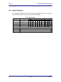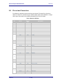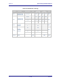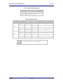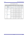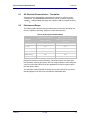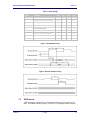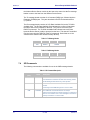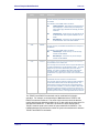
1
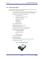
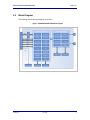
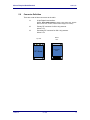
Product Specification 802.11b/g High Performance Enterprise Device Server Revision: 1.1 August 2009 File name: databook wlng dp500 family.doc Document Number: 100-8080-110 Airborne Enterprise Module Databook Quatech, Inc. <Page Intentionally Left Blank> 2 8/11/2009 100-8080-110 Airborne Enterprise Module Databook Quatech, Inc. Quatech Confidential Copyright © 2009 QUATECH ® Inc. ALL RIGHTS RESERVED. No part of this publication may be copied in any form, by photocopy, microfilm, retrieval system, or by any other means now known or hereafter invented without the prior written permission of QUATECH ® Inc.. This document may not be used as the basis for manufacture or sale of any items without the prior written consent of QUATECH Inc.. QUATECH Inc. is a registered trademark of QUATECH Inc.. Airborne™ is a trademark of QUATECH Inc.. All other trademarks used in this document are the property of their respective owners. Disclaimer The information in the document is believed to be correct at the time of print. The reader remains responsible for the system design and for ensuring that the overall system satisfies its design objectives taking due account of the information presented herein, the specifications of other associated equipment, and the test environment. QUATECH ® Inc. has made commercially reasonable efforts to ensure that the information contained in this document is accurate and reliable. However, the information is subject to change without notice. No responsibility is assumed by QUATECH for the use of the information or for infringements of patents or other rights of third parties. This document is the property of QUATECH ® Inc. and does not imply license under patents, copyrights, or trade secrets. Quatech, Inc. Headquarters ® QUATECH Inc.. 5675 Hudson Industrial Parkway Hudson, OH 44236 USA Telephone: 330-655-9000 Toll Free (USA): 800-553-1170 Fax: 330-655-9010 Technical Support: 714-899-7543 / [email protected] Web Site: www.quatech.com 100-8080-110 8/11/2009 3 Airborne Enterprise Module Databook Quatech, Inc. <Page Intentionally Left Blank> 4 8/11/2009 100-8080-110 Airborne Enterprise Module Databook Quatech, Inc. Contents 1.0 Conventions ......................................................................................................................... 7 1.1 1.2 1.3 1.4 2.0 3.0 4.0 5.0 Terminology ..................................................................................................................... 7 Notes ............................................................................................................................... 7 Caution ............................................................................................................................ 7 File Format....................................................................................................................... 7 Product Description ............................................................................................................. 8 Block Diagram ..................................................................................................................... 9 Model Numbers ................................................................................................................. 10 Pin out and Connectors ..................................................................................................... 11 5.1 5.2 5.3 5.4 5.5 5.6 6.0 Digital UART Ports......................................................................................................... 13 Ethernet PHY Port ......................................................................................................... 13 Serial Peripheral Interface (SPI) .................................................................................... 14 Debug/Console Port ...................................................................................................... 14 General Purpose Input/Output (GPIO) .......................................................................... 14 Connector Definition ...................................................................................................... 15 Electrical & RF Specification ............................................................................................. 16 AC Electrical Characteristics – Transmitter ................................................................... 21 Performance/Range....................................................................................................... 21 6.1 6.2 7.0 SPI Interface ...................................................................................................................... 22 7.1 7.2 7.3 7.4 8.0 Pinout ............................................................................................................................. 22 SPI AC Characteristics .................................................................................................. 22 SPI Protocol ................................................................................................................... 23 SPI Commands.............................................................................................................. 24 Antenna ............................................................................................................................. 26 8.1 8.2 8.3 8.4 8.5 8.6 9.0 10.0 11.0 Antenna Selection.......................................................................................................... 26 Host Board Mounted Antenna ....................................................................................... 26 Host Chassis Mounted Antenna .................................................................................... 27 Embedded Antenna ....................................................................................................... 27 Antenna Location ........................................................................................................... 28 Performance .................................................................................................................. 29 RESET Function ................................................................................................................ 31 Mechanical Outline ............................................................................................................ 32 Certification & Regulatory Approvals ................................................................................. 33 11.1 11.2 11.3 11.4 11.5 12.0 13.0 FCC Statement .............................................................................................................. 33 FCC RF Exposure Statement ........................................................................................ 33 Information for Canadian Users (IC Notice) .................................................................. 33 FCC/IOC Modular Approval ........................................................................................... 34 Regulatory Test Mode Support ...................................................................................... 35 Physical & Environmental Approvals ................................................................................. 36 Change Log ....................................................................................................................... 37 100-8080-110 8/11/2009 5 Airborne Enterprise Module Databook Quatech, Inc. Figures Figure 1- WLNG-AN-DP500 Module Example ................................................................................ 8 Figure 2 - WLNG-SE/SP/AN/ET-DP500 Block Diagram ................................................................. 9 Figure 3 - SPI Read/Write Timing.................................................................................................. 23 Figure 4 - SPI Clock and Select Timing ........................................................................................ 23 Figure 5 - Power on RESET Timing .............................................................................................. 31 Figure 6 - RESET Timing .............................................................................................................. 31 Tables Table 1 - Model Numbers .............................................................................................................. 10 Table 2 – Module Pin Definition ..................................................................................................... 11 Table 3 - UART Pin Definition ....................................................................................................... 13 1 Table 4- Absolute Maximum Values ............................................................................................ 16 Table 5 – Operating Conditions & DC Specification ...................................................................... 16 Table 6 - RF Characteristics – 802.11b/g ...................................................................................... 18 Table 7 - Supported Data Rates by Band ..................................................................................... 19 Table 8 - Operating Channels ....................................................................................................... 19 Table 9 - RF Characteristics – 802.11b/g ...................................................................................... 20 Table 10 - Radio Typical Performance Range .............................................................................. 21 Table 11 - SPI Pinout Details ........................................................................................................ 22 Table 12 - SPI Signal Descriptions ................................................................................................ 22 Table 13 - SPI AC Timings ............................................................................................................ 23 Table 14 - Tx Message Header ..................................................................................................... 24 Table 15 - Rx Message Header ..................................................................................................... 24 Table 16 - SPI Command Description ........................................................................................... 24 Table 17 - Embedded Antenna Options ........................................................................................ 27 Table 18 - RESET Timing .............................................................................................................. 31 Table 19 - Regulatory Approvals ................................................................................................... 33 Table 20 - Mechanical Approvals .................................................................................................. 36 6 8/11/2009 100-8080-110 Airborne Enterprise Module Databook 1.0 Quatech, Inc. Conventions The following section outlines the conventions used within the document, where convention is deviated from the deviation takes precedence and should be followed. If you have any question related to the conventions used or clarification of indicated deviation please contact Quatech Sales or Wireless Support. 1.1 Terminology Airborne Enterprise Device Server and AirborneDirect Enterprise Device Server is used in the opening section to describe the devices detailed in this document, after this section the term module will be used to describe the devices. 1.2 Notes A note contains information that requires special attention. The following convention will be used. The area next to the indicator will identify the specific information and make any references necessary. 1.3 The area next to the indicator will identify the specific information and make any references necessary. Caution A caution contains information that, if not followed, may cause damage to the product or injury to the user. The shaded area next to the indicator will identify the specific information and make any references necessary. 1.4 The area next to the indicator will identify the specific information and make any references necessary. File Format These documents are provided as Portable Document Format (PDF) files. To read them, you need Adobe Acrobat Reader 4.0.5 or higher. For your convenience, Adobe Acrobat Reader is provided on the Radio Evaluation Kit CD. Should you not have the CD, for the latest version of Adobe Acrobat Reader, go to the Adobe Web site (www.adobe.com). 100-8080-110 8/11/2009 7 Airborne Enterprise Module Databook Quatech, Inc. 2.0 Product Description The WLNG-AN-DP500 family is the latest generation of 802.11 wireless device servers from Quatech. The radio features the following: 802.11b/g WiFi Radio with 32bit ARM9 CPU (128Mb SDRAM, 64Mb Flash) Supports WEP, WPA, WPA2 and 802.1x Supplicant, with Certificates. The wireless device server includes integrated: 802.11b/g radio driver TCP/IP stack, UDP, telnet, FTP server Data bridging and buffering Command Line Interface Web interface WPA Supplicant 802.11 Radio Driver Supports antenna diversity Operating Temperature (-40°C to 85°C) Storage temp (-50°C to 125°C) 36 pin high density SMT connector (Hirose DF12-36) Dual (2) Hirose U.FL RF connector for RF antenna Multiple host interfaces supported: Dual UART (960K BAUD) Serial (RS232/422/485) SPI 10/100 Ethernet PHY Advanced Low power modes Rugged mounting options. No host driver required Small form factor module (Dimensions: 29mm x 21mm x 6.0mm) Worldwide Regulatory Support Figure 1- WLNG-AN-DP500 Module Example 8 8/11/2009 100-8080-110 Airborne Enterprise Module Databook 3.0 Quatech, Inc. Block Diagram The following outlines the block diagram of the radio: Figure 2 - WLNG-SE/SP/AN/ET-DP500 Block Diagram 100-8080-110 8/11/2009 9 Airborne Enterprise Module Databook Quatech, Inc. 4.0 Model Numbers The following table identifies the model numbers associated with the device server family. Please contact Quatech sales for details, quotes and availability. Table 1 - Model Numbers Model Number Description Interface WiFi 802.11b/g UART RS232 RS485 WLNG-SE-DP501 802.11b/g, UART Interface with RS232/422/485 Driver Control l l l l WLNG-SP-DP501 802.11b/g, SPI Interface l WLNG-AN-DP501 802.11b/g, UART Interface l l l l WLNG-ET-DP501 802.11b/g, 10/100 Ethernet Interface l SPI Security Ethernet l l RoHS GPIO WEP WPA WPA2 EAP l l l l l l l l l l l l l l l l l l l l l l l l Eval Kit 10 WLNG-EK-DP501 802.11b/g Enterprise Class Serial Device Server Module Eval Kit (inc. WLNG-SE/AN-DP501) l WLNG-EK-DP502 802.11b/g Enterprise Class SPI Device Server Module Eval Kit (inc. WLNG-SP-DP501) l WLNG-EK-DP503 802.11b/g Enterprise Class Ethernet Bridge Module Eval Kit (inc. WLNG-ET-DP501) l 8/11/2009 100-8080-110 Airborne Enterprise Module Databook 5.0 Quatech, Inc. Pin out and Connectors Pin definition is dependent upon the device type selected. The specific pin function is defined in Table 2 for each device type. Where multiple options are available for a single device type, these options are software selectable by the device firmware. Table 2 – Module Pin Definition Pin Name Device Type 1 GND All Digital Ground 2 TDI All JTAG: Test data in 3 VDD All 3.3VDC 4 VDD All 3.3VDC 5 RTCK All JTAG: Return Test Clock 6 DTXD All DOUT Debug 7 /RESET All Module RESET 8 DRXD All DIN Debug RXD2 UART DIN UART2 RXD2 Serial DIN UART2 RXD2 SPI DIN UART2 RXD2 Ethernet DIN UART2 G6 All GPIO 10 TDO All JTAG: Test data out 11 /FRESET All Factory RESET CTS1 UART Clear-to-Send UART1 CTS Serial Clear-to-Send /SPI_SEL SPI CTS1 Ethernet F5 All NC UART No Connect NC Serial No Connect NC SPI No Connect RX+ Ethernet NC UART No Connect NC Serial No Connect NC SPI No Connect RX- Ethernet Ethernet RX- GND All Digital Ground Digital Ground 9 12 13 14 15 16 17 18 100-8080-110 Description SPI Select Clear-to-Send UART1 GPIO Ethernet RX+ GND All RTS2 UART Ready-to-Send UART2 /TXEN Serial Line Driver Tx enable RTS2 SPI Ready-to-Send UART2 RTS2 Ethernet Ready-to-Send UART2 G2 All RTS1 UART Ready-to-Send UART1 RTS Serial Ready-to-Send SPI_CLK SPI SPI Clock Input RTS1 Ethernet GPIO Ready-to-Send UART1 8/11/2009 11 Airborne Enterprise Module Databook Quatech, Inc. Pin 19 20 21 22 23 24 25 26 27 Device Type Description F4 All CTS2 UART GPIO Clear-to-Send UART2 RXEN Serial Line driver Rx enable CTS2 SPI Clear-to-Send UART2 CTS2 Ethernet Clear-to-Send UART2 G1 All GPIO TCK All JTAG: Test clock TXD2 UART DOUT UART2 TXD2 Serial DOUT UART2 TXD2 SPI DOUT UART2 TXD2 Ethernet DOUT UART2 G7 All GPIO G0 UART GPIO SER_MODE Serial Serial interface type selection (RS232/422/485) SPI_INT SPI G0 Ethernet LED_CON F6 All SPI Interrupt GPIO Valid TCP/IP Connection Indicator GPIO RXD1 UART DIN UART1 RXD1 Serial DIN UART1 MOSI SPI RXD1 Ethernet F7 All LED_POST F0 LED_WLN_CFG F3 LED_RF_LINK F2 All All All DIN SPI DIN UART1 GPIO POST Status Indicator GPIO Module TCP/IP Configuration Indicator GPIO Module RF Link Status Indicator GPIO TXD1 UART DOUT UART1 TXD Serial DOUT MISO SPI TXD1 Ethernet F1 All NC UART No Connect NC Serial No Connect NC SPI No Connect TX- Ethernet Ethernet TX- NC UART No Connect NC Serial No Connect NC SPI No Connect TX+ Ethernet 31 NTRST All JTAG: Test RESET signal 32 TMS All JTAG: Test mode select 33 VDD All 3.3VDC 34 VDD All 3.3VDC 35 LED_RF_ACT All Radio Status Indicator, driven by the radio. 36 GND All Digital Ground 28 29 30 12 Name DOUT SPI DOUT UART1 GPIO Ethernet TX+ 8/11/2009 100-8080-110 Airborne Enterprise Module Databook 5.1 Quatech, Inc. Digital UART Ports The units supports two digital UART ports, use of these ports is determined by the device type choice made in firmware. The details of the ports can be seen in Table 3. The availability of UART2 for these device types is selected in firmware. Table 3 - UART Pin Definition Device Type UART Serial All UART1 Pin UART2 Pin UART1 Pin UART2 Pin Debug Data out (DOUT) 28 21 28 21 6 Data In (DIN) 24 9 24 9 8 Clear-to-Send (CTS) 12 19 12 Ready-to-Send (RTS) 18 17 18 Pin Definition Transmit Enable (/TXEN) 17 Receive Enable (/RXEN) 19 Serial Mode (SER_MOD) 22 The primary UART supports a 4-wire interface; the secondary port supports 4wire interface except when being used with the Serial Device type, in which case it is reduced to a 2-wire only. The primary digital UART can be used as the primary connection for the Serial device type. This type supports a 7-wire interface to allow the definition of the serial interface type (RS232/3422/485) and the data transfer direction. Definitions of this interface can be seen in Table 3. The UART1 and UART2 interfaces support the following configurations: 5.2 BAUD: 300, 600, 1200, 2400, 4800, 9600, 14400, 19200, 28800, 38400, 57600, 115200, 230400, 460800, 921600 Flow Control: None, Hardware (CTS/RTS), Software (XON/XOFF) Default settings: 9600, 8, N, 1, No Flow Control. Ethernet PHY Port A 10/100 Ethernet PHY interface is supported when the Ethernet device type is selected in firmware. This interface is a 10/100Mbps interface that supports auto negotiation and cross-over cabling. The interface also supports both half and full duplex for 10Mbps and 100Mbps. The interface uses a Broadcom BCM5241A Ethernet PHY, please refer to the manufacturers datasheet for interface details and appropriate design guidelines. 100-8080-110 8/11/2009 13 Airborne Enterprise Module Databook Quatech, Inc. 5.3 Serial Peripheral Interface (SPI) Please refer to section 7.0 for details on this interface. 5.4 Debug/Console Port A debug/console port is supported by a 2-wire serial interface defined in Table 3. This port is a bidirectional serial port intended for debug of the unit only, it does not support data transfer. It is recommended that a connection to this port be supported via test points or a two pin header. The default settings for the debug port are 115200, 8, N 1, No Flow Control. 5.5 CAUTION: Do not use the debug port without contacting Quatech Technical Support first. Potential damage to the module may occur. General Purpose Input/Output (GPIO) A number of the interface pins support multiple functional definitions. Those defined as alternately GPIO pins can be selected as such via device firmware. The GPIO pins are digital I/O capable of supporting up to a 16mA drive current at 3.3VDC. 14 8/11/2009 100-8080-110 Airborne Enterprise Module Databook 5.6 Quatech, Inc. Connector Definition There are a total of three connectors to the radio: J1: 36 pin Digital Host interface. Hirose: DF12-36DP-0.5V(XX) (0.50mm (.020") Pitch Plug, Surface Mount, Dual Row, Vertical, 4.00mm Stack Height, 36 Circuits) J2: Primary RF connector for 802.11b/g antenna. Hirose U.FL J3: Secondary RF connector for 802.11b/g antenna. Hirose U.FL. Bottom View Top View J3 J2 Component Area RF Shield J1 100-8080-110 8/11/2009 15 Airborne Enterprise Module Databook Quatech, Inc. 6.0 Electrical & RF Specification Table 4- Absolute Maximum Values1 Parameter Min Max Unit Maximum Supply Voltage -0.3 4.0 VDC Power Dissipation 2.00 Operating Temperature Range -40 Storage Temperature -50 W 85 o C 125 o C Note: 1. Values are absolute ratings, exceeding these values may cause permanent damage to the device. Table 5 – Operating Conditions & DC Specification Symbol Parameter Min Typ Max Units VDD Supply Voltage 3.00 3.30 3.60 V VIL Input Low Level Voltage -0.3 0.8 VIH Input High Level Voltage 2.0 VDD + 0.3 VOL Output Low Level Voltage VOH Output High Level Voltage ICCTXG Operating Current – UART Data In (802.11g) 0.4 VDD - 0.4 340 360 mA 480 490 mA 340 360 mA 480 490 mA 470 500 mA 520 560 mA Transmitting @ 54Mb/s UART 100% Duty Cycle @ 920K BAUD ICCRXG Operating Current – UART Data Out (802.11g) Receiving valid packets @ 54Mb/s UART 100% Duty Cycle@ 920K BAUD ICCTXB Operating Current – UART Data In (802.11b) Transmitting @ 11Mb/s UART 100% Duty Cycle @ 920K BAUD ICCRXB Operating Current – UART Data Out (802.11b) Receiving valid packets @ 11MB/s UART 100% Duty Cycle @ 920K BAUD ICCTXG_ETH Operating Current – Ethernet Data In (802.11g) Transmitting @ 54Mb/s 10/100 Ethernet 100% Duty Cycle ICCRXG_ETH Operating Current – Ethernet Data Out (802.11g) Receiving @ 54Mb/s 10/100 Ethernet 100% Duty Cycle 16 8/11/2009 100-8080-110 Airborne Enterprise Module Databook Quatech, Inc. Symbol Parameter Min ICCTXB_ETH Operating Current – Ethernet Data In (802.11b) Typ Max Units 520 560 mA 500 530 mA Transmitting @ 11Mb/s 10/100 100% Duty Cycle ICCRXB_ETH Operating Current – Ethernet Data Out (802.11b) Receiving @ 11Mb/s 10/100 Ethernet 100% Duty Cycle ICCU Radio and CPU on. No data traffic (UART) 340 360 mA ICCE Radio and CPU on. No data traffic (Ethernet) 330 350 mA ISBU0 Radio off (UART) 350 360 mA 360 370 mA 210 mA CPU Idle, radio off (f/w control) ISBE0 Radio off (Ethernet) CPU Idle, radio off (f/w control) ISB1 Doze Mode 140 IEEE PSPoll mode, Associated, Idle, Beacon Interval = 100ms CPU Idle, wake on UART or Network traffic ISB3U Sleep Mode – UART/Serial 102 mA 95 mA Radio in Deep Sleep (disassociated) CPU Idle, wake on UART traffic ISB3E Sleep Mode – Ethernet Radio in Deep Sleep (disassociated) CPU Idle, wake on pm-mode 100-8080-110 8/11/2009 17 Airborne Enterprise Module Databook Quatech, Inc. Table 6 - RF Characteristics – 802.11b/g Symbol Parameter POUTB Transmit Power Output 802.11b POUTG PRSENB PRSENG FRANGEBG 18 Transmit Power Output 802.11g Receive Sensitivity 802.11b Receive Sensitivity 802.11g Average dBm / mW Peak dBm / mW 11, 5.5, 2, 1 15.0 31.6 20.0 100 48, 54 12.7 18.6 17.7 58.9 24, 36 15.0 31.6 20.0 100 12, 18 15.9 38.9 20.9 123 6, 9 16.0 39.8 21.0 125.9 Rate (Mb/s) Min 11 -82 1 -91 54 -68 36 -78 18 -80 6 -86 Frequency Range 2412 8/11/2009 Units dBm dBm dBm dBm 2484 MHz 100-8080-110 Airborne Enterprise Module Databook Quatech, Inc. Table 7 - Supported Data Rates by Band Band Supported Data Rates (Mb/s) 802.11b 11, 5.5, 2, 1 802.11g 54, 48, 36, 24, 18, 12, 9, 6 Table 8 - Operating Channels Band 802.11b 802.11g Region Freq Range (GHz) No. of Channels Channels US/Canada 2.401 - 2.473 11 1 – 11 Europe 2.401 - 2.483 13 1 – 13 France 2.401 - 2.483 4 10 – 13 Japan 2.401 - 2.495 14 1 – 14 US/Canada 2.401 - 2.473 11 1 – 11 Europe 2.401 - 2.483 13 1 – 13 France 2.446 - 2.483 4 10 – 13 Japan 2.401 - 2.483 13 1 – 13 100-8080-110 1. Only channels 1, 6 and 11 are non-overlapping. 8/11/2009 19 Airborne Enterprise Module Databook Quatech, Inc. Table 9 - RF Characteristics – 802.11b/g Min dBm Transmit Power Output 802.11b 11, 5.5, 2, 1 Transmit Power Output 802.11g 6, 9,12,18, 24, 36, 48, 54 Parameter POUTB POUTG PRSENB PRSENG FRANGEBG 20 Rate (Mb/s) Symbol Receive Sensitivity 802.11b Receive Sensitivity 802.11g Frequency Range Average dBm / mW Peak dBm / mW 13 15 31.6 19.3 85.1 dBm/mW 10 12 15.9 21.5 141.3 dBm/mW 11 -84 5.5 -85 2 -86 1 -86 54 -69 48 -70 36 -74 24 -78 18 -81 12 -83 9 -85 6 -86 2412 8/11/2009 Units dBm dBm 2484 MHz 100-8080-110 Airborne Enterprise Module Databook 6.1 Quatech, Inc. AC Electrical Characteristics – Transmitter Transmit power is automatically managed by the device for minimum power consumption. The MAXIMUM transmit power at the RF connector is typically +15dBm 2 dB for B-Mode (all rates) and +12dBm+/-2dB for G-Mode (all rates). 6.2 Performance/Range The following table illustrates the typical data rates, performance and range the device is capable of providing using an omni directional antenna. Table 10 - Radio Typical Performance Range Data Rate Typical Outdoor Distance Typical Outdoor Distance (Unity gain antenna) (2dBi antenna gain on each end for B/G mode) 1.0 Mb/s 240m 380m 11.0 Mb/s 135m 215m 6Mb/s 802.11g 135m 215m 6Mb/s 802.11a 49m 155m 54Mb/s 802.11g 12m 19m 54Mb/s 802.11a 4.5m 14m Ranges are based on receiver sensitivity, Transmitter power, free-space path loss estimates, antenna gain factors, and link margin estimates. Actual range will vary from those stated. Non-line-of-site applications will result in typical values less than shown above. The Data Rate is the supported connection rate for the wireless link, the actual data throughput for the link will be less than the stated data rates. 100-8080-110 8/11/2009 21 Airborne Enterprise Module Databook Quatech, Inc. 7.0 SPI Interface The following section details the SPI interface specification for both hardware timing and SPI protocol. The device is a SPI slave and requires a compatible SPI master for operation. 7.1 Pinout When the SPI interface is enabled, through the CLI or web interface, the following pins are assigned for communication. Table 11 - SPI Pinout Details Pin Definition SPI UART2 Pin Debug Data In (RxD2, DTXD) 9 8 Data out (TxD2, DRXD) 21 6 Ready-to-Send (RTS2) 17 Clear-to-Send (CTS2) 19 Master In Slave Out (MISO) 28 Master Out Slave In (MOSI) 24 SPI Interrupt (SPI_INT) 22 SPI Clock (SPI_CLK) 18 SPI Select (/SPI_SEL) 12 Table 12 - SPI Signal Descriptions Pin Definition 7.2 Description Master In Slave Out (MISO) Serial Data OUT; must be connected to the serial data in of the master. Master Out Slave In (MOSI) Serial Data IN; Must be connected to the serial data out of the master. SPI Interrupt (SPI_INT) Interrupt signal driver by slave see Table 16 for details of operation. SPI Clock (SPI_CLK) SPI clock sourced from the master. SPI Select (/SPI_SEL) Enable the SPI slave, sourced from the master. Active low signal. SPI AC Characteristics The following specification identifies the required hardware timing to successfully implement a SPI interface with the Airborne Device Server module. 22 8/11/2009 100-8080-110 Airborne Enterprise Module Databook Quatech, Inc. Table 13 - SPI AC Timings Symbol Parameter Min Typ Max Units fMAX Maximum Clock Frequency 8.00 MHz tCS SPI Select Low to Clock Rising Edge 100 ns tCH Clock High 62.5 ns tCL Clock Low 62.5 ns tDA Clock High to Data Out tDS Clock Low to Data In Valid Set-up time 14 ns tDH Clock Low to Data Valid Hold time 2 ns tCSH Clock Falling Edge to SPI Select High 100 ns tDELAY SPI Select High to SPI Select Low 40 ns 60 ns Figure 3 - SPI Read/Write Timing Figure 4 - SPI Clock and Select Timing 7.3 SPI Protocol A SPI message is composed of a 4 byte header followed by 0 or more bytes of data. The header data is full-duplex. That is, the Tx message header is sent to 100-8080-110 8/11/2009 23 Airborne Enterprise Module Databook Quatech, Inc. the Airborne Device Server module by the host at the same time the Rx message header is sent to the host from the Airborne Device Server. The Tx message header consists of a Command (CMD) byte, followed by three Parameter (PARM) bytes. They are described in the SPI Commands section (7.4) below. The Rx message header consists of a Rx Data Available field, and a Tx Buffer Available field. The Rx Data Available field indicates the number of data bytes the Device Server has available for the host. They can be received by the RXDATA command. The Tx Buffer Available field indicates how many data bytes the Device Server is able to accept from the host. This data is to be shifted in by the host using the TXDATA (Table 16) command. Both fields are 16 bit values and are stored in little-endian format (LSB first). Table 14 - Tx Message Header 0 1 CMD PARAM1 2 3 PARAM2 Table 15 - Rx Message Header 0 1 Rx Data Available 7.4 2 3 Tx Buffer Available SPI Commands The following commands are available for use in the CMD message header. Table 16 - SPI Command Description Command (Hex) Name 0x00 NOP Description The NOP command does nothing. It is intended to be used when the host wants to simply retrieve the Rx Message Header without any other operation. 0x04 BREAK The BREAK command will issue a break sequence to the module. It is analogous to the BREAK signal on a common UART. 0x08 TXINTCLR The TXINTCLR command will clear the Tx interrupt. Use this command when the module is issuing a Tx interrupt but there is no more data to send. This is analogous to the reset Tx interrupt command on a common UART. 24 8/11/2009 100-8080-110 Airborne Enterprise Module Databook Quatech, Inc. Command (Hex) Name Description 0x10 INTENA The INTENA command will enable interrupts from the module. For this command, the PARM1 field will define the interrupts to be enabled. The definition of the PARM1 field is as follows: 0x20 INTDIS B7 Interrupt Sense – Determines the asserted state of the interrupt pin. If this bit is set, the interrupt pin will be active high, otherwise the interrupt pin will be active low. B1 TX Interrupt – If this bit is set, the interrupt pin will be asserted when there is space available in the Tx buffer. B0 RX Interrupt – If this bit is set, the interrupt pin will be asserted when there is Rx data available. The INTDIS command will disable interrupts from the module. For this command, the PARM1 field will define the interrupts to be disabled. The definition of the PARM1 field is as follows: 0x40 TXDATA B1 TX Interrupt – If this bit is set, The Tx interrupt function will be disabled. B0 RX Interrupt – If this bit is set, the Rx interrupt function will be disabled. The TXDATA command is used to send data to the module to be transmitted on the wireless link. The host may send at most the number of bytes indicated by the Tx Buffer Available field in the Rx Message Header. The actual length sent by the host is determined by the 16 bit value in PARM2. The value in PARM2 is little-endian (LSB first) and must be less than or equal to the number in the Tx Buffer Available field. Any bytes sent in excess of this number will be ignored. 0x80 RXDATA The RXDATA command is used to receive data from the module that has been received on the wireless link. The host may receive at most the number of bytes indicated by the Rx Data Available field in the Rx Message Header. The actual number of bytes received by the host is determined by the 16 bit value in PARM2. The value in PARM2 is little-endian (LSB first) and must be less than or equal to the number in the Rx Data Available field. If additional clock cycles are sent to the module beyond this number, meaningless data will be returned. The TXDATA and RXDATA commands can be combined for full-duplex operation. For example, a command byte of 0xC0 would be a TXDATA and RXDATA command combined. The result of this command would be that the module would accept data being shifted in as Tx data, while at the same time, Rx data would be shifted out. In this case, the number of bytes transferred for TXDATA must be equal to the number of bytes transferred for RXDATA. The PARM2 parameter will indicate the number of bytes to be transferred for both the TXDATA and RXDATA commands. 100-8080-110 8/11/2009 25 Airborne Enterprise Module Databook Quatech, Inc. 8.0 Antenna The unit supports antenna connection through a single Hirose U.FL connector, located on the top surface of the radio next to the RF shielding. Any antenna used with the system must be designed for operation within the 2.4GHz ISM band and specifically must support the 2.412GHz to 2.482GHz for 802.11b/g operation. They are required to have a VSWR of 2:1 maximum referenced to a 50 system impedance. 8.1 Antenna Selection The Airborne radio supports a number of antenna options, all of which require connection to the U.FL connectors on the radio. Ultimately the antenna option selected will be determined by a number of factors, these include consideration of the application, mechanical construction and desired performance. Since the number of possible combinations is endless we will review some of the more common solutions in this section. If your application is not covered during this discussion please contact Technical Support for more specific answers. The available antenna connections include: Host board mounted antenna Host Chassis mounted antenna Embedded antenna In addition to the above options, location and performance need to be considered, the following sections discuss these items. 8.2 Host Board Mounted Antenna Host board mounted requires that an antenna connection is physically mounted to the host system board. It also requires that the host board include a U.FL connector (two (2) if diversity is being used) to allow a U.FL to U.FL coaxial lead to connect from the radio to the host board. It will then require 50 matched PCB traces to be routed from the U.FL connector to the antenna mount. There are several sources for the U.FL to U.FL coaxial cable these include Hirose, Sunridge and IPEX. Please contact Quatech for further part numbers and supply assistance. This approach can simplify assembly but does require that the host system configuration can accommodate an antenna location that is determined by the host PCB. There are also limitations on the ability to seal the enclosure when using this approach. This approach also restricts the selection of available antenna. When using this approach, antennas that screw or press fit to the PCB mount connector must be used. There are many options for the antenna connector type, however if you wish to utilize the FCC/IOC modular approval the connector choice must comply 26 8/11/2009 100-8080-110 Airborne Enterprise Module Databook Quatech, Inc. with FCC regulations, these state a non-standard connector is required e.g. TNC/SMA are not allowed, RP-TNC/RP-SMA are allowed. 8.3 Host Chassis Mounted Antenna Host Chassis mounted antennas require no work on the host PCB. They utilize an antenna type called ‘flying lead’. There are two types of flying leads; one which provides a bulkhead mounted antenna connector and one which provides a bulk head mounted antenna. The type you choose will be determined by the application. A flying lead system connects a U.FL coaxial lead to the radio’s U.FL connector, the other end of the coax is attached to either a bulkhead mounted antenna connector or directly to an antenna that has an integrated bulkhead mount. In either of the two cases, the use of this approach significantly reduces the antenna system development effort and provides for greater flexibility in the available antenna types and placement in the host system chassis. When using the flying lead antenna (integrated bulk head mounting), there are no connector choice restrictions for use with the FCC/IOC modular certification. However if the flying lead connector is used, the same restrictions as identified for the Host Mounted Antenna apply. There are many suppliers of flying lead antenna and connectors; Quatech’s Airborne Antenna product line offers a range of antenna solutions. 8.4 Embedded Antenna Use of Embedded antenna can be the most interesting approach for M2M, industrial and medical applications. Their small form factor and absence of any external mounting provides a very compelling argument for their use. There is a downside to this antenna type and it comes with performance. Antenna performance for all of the embedded options will, in most cases, be less that that achievable with external antenna. This does not make them unusable; it will impact choice of antenna type and requires more focus on placement. The three main embedded antenna types are PCB embedded, chip (PCB mounted) and flying lead; each has its advantages and disadvantages (See Table 17). Table 17 - Embedded Antenna Options Antenna Type Cost Size Availability Performance Lowest Largest Custom Poor Chip Low Small Standard Poor Flying Lead Low Small Standard Fair PCB Embedded 100-8080-110 Features 8/11/2009 27 Airborne Enterprise Module Databook Quatech, Inc. PCB Embedded – This approach embeds an antenna design into the host PCB. This approach is very common with add-in WiFi card (CF, PCMCIA, SDIO, etc.) as it requires no external connections and is the cheapest production approach. The lower production cost requires significant development cost and lack of performance and flexibility. Chip – The integration of a chip antenna is simple and requires a relatively small footprint on the host system, however, it does suffer from the same limitations of flexibility and performance seen with the PCB embedded approach. There are relatively large numbers of suppliers of this type of antenna; there is also a range of configuration and performance options. Flying Lead – This approach is similar to the flying lead solution for external antennas, the difference is that the form factors are smaller and provide a range of chassis and board mounting options, all for internal use. This approach suffers less from the performance and flexibility limitations of the other approaches, since the location of the antenna it not determined by the host PCB design. The assembly of a system using this approach maybe slightly more complex since the antenna is not necessarily mounted on the host PCBA. 8.5 Antenna Location The importance of this design choice cannot be over stressed; it can in fact be the determining factor between success and failure of the WiFi implementation. There are several factors that need to be considered when determining location: Distance of Antenna from radio Location of host system Proximity to RF blocking or absorbing materials Proximity to potential noise or interference Position relative to infrastructure (Access Points or Laptops) Orientation of host system relative to infrastructure Is it known Is it static To minimize the impact of the factors above the following things need to be considered during the development process: 28 Minimize the distance between the radio and the location of the antenna. The coaxial cable between the two impacts the Transmit Power and Receive Sensitivity negatively. Quatech recommends using 1.32-1.37mm outer diameter U.FL coaxial cables. Minimize the locations where metal surfaces come into contact or are close to the location of the antenna. Avoid locations where RF noise, close to or over lapping the ISM bands, may occur. This would include microwave ovens and wireless telephone systems in the 2.4GHz and 5.0GHz frequency range. Mount the antenna as high on the equipment as possible. 8/11/2009 100-8080-110 Airborne Enterprise Module Databook Quatech, Inc. Locate the antenna where there is a minimum of obstruction between the antenna and the location of the Access Points. Typically Access Points are located in the ceiling or high on walls. Keep the main antenna’s polarization vertical, or in-line with the antenna of the Access Points. 802.11 systems utilize vertical polarization and aligning both transmit and receive antenna maximizes the link quality. Even addressing all of the above factors, does not guarantee a perfect connection, however with experimentation an understanding of the best combination will allow a preferred combination to be identified. 8.6 Performance Performance is difficult to define as the appropriate metric changes with each application or may indeed be a combination of parameters and application requirements. The underlying characteristic that, in most cases, needs to be observed is the link quality. This can be defined as the bandwidth available over which communication, between the two devices, can be performed, the lower the link quality the less likely the devices can communicate. Measurement of link quality can be made in several ways; Bit Error Rate (BER), Signal to Noise (SNR) ratio, Signal Strength and may also include the addition of distortion. The link quality is used by the radio to determine the link rate, generally as the link quality for a given link rate drops below a predefined limit, the radio will drop to the next lowest link rate and try to communicate using it. The reciprocal is also true, if the radio observes good link quality at one rate it will try to move up to the next rate to see if communication can be sustained using it. It is important to note that for a given position the link quality improves as the link rate is reduced. This is because as the link rate drops the radios Transmit power and Receive sensitivity improve. From this it can be seen that looking at the link rate is an indirect way of assessing the quality of the link between the device and an Access Point. You should strive to make the communication quality as good as possible in order to support the best link rate. However be careful not to over specify the link rate. Consider your applications bandwidth requirements and tailor your link rate to optimize the link quality e.g. the link quality for a location at 6Mb/s is better than it would be for 54Mb/s, if the application only needs 2Mb/s of data throughput, the 6Mb/s rate would provide a better link quality. Aside from the radio performance, there are a number of other things that contribute to the link quality; these include the items discussed earlier and choices made when looking at the overall antenna gain. The antenna gain contributes to the Equivalent Isotropically Radiated Power (EIRP) of the system. This is part of an overall measurement of the link quality called link margin. 100-8080-110 8/11/2009 29 Airborne Enterprise Module Databook Quatech, Inc. Link Margin provides a measure of all the parts of the RF path that impact the ability of two systems to communicate. The basic equation looks like this: EIRP (dB) = TxP + TxA – TxC Link Margin (dB) = EIRP – FPL + (RxS + RxA – RxC) Where: TxP = Transmitter output power (dBm) TxA = Transmitter antenna gain (dBi) TxC = Transmitter to Antenna coax cable loss (dB) FPL = Free Path Loss (dB) RxS = Receiver receive sensitivity (dBm) RxA = Receiver antenna gain (dBi) RxC = Receiver to Antenna coax cable loss (dB) This is a complex subject and requires more information than is presented here, Quatech recommends at reviewing the subject and evaluating any system at a basic level. It is then possible, with a combination of the above items and an understanding of the application demands, to achieve a link quality optimized for the application and host design. It is important to note that this is established with a combination of hardware selection, design choices and configuration of the radio. 30 8/11/2009 100-8080-110 Airborne Enterprise Module Databook 9.0 Quatech, Inc. RESET Function For correct operation of the on-board Power-on RESET (POR) and internal RESET controllers, the RESET pin on the WLNG-XX-DP500 family must obey the following timing and signal conditions. Figure 5 - Power on RESET Timing Figure 6 - RESET Timing Table 18 - RESET Timing Symbol Parameter tPURST Valid VDD to RESET valid tRLRV RESET Valid to RESET Low tRPWI Valid VDD to Internal RESET completed tRPW RESET Pulse Width 100-8080-110 Min Typ Max Units 200 ms 0 ms 200 100 ms µs For Hardware revisions Rev C2 and earlier additional timing constraints apply. Please contact Quatech Technical Support for details. 8/11/2009 31 Airborne Enterprise Module Databook Quatech, Inc. 10.0 Mechanical Outline 2.75 [0.11] 2.25 [0.09] Part# Hirose U.FL-R SMT Coaxial Antenna Connector (2X) 16.02 [0.63] 16.00 [0.63] 16.00 [0.63] 10.50 [0.41] 10.50 [0.41] 40.60 [1.60] MAX 29.60 [1.17] MAX 1.84 [0.07] 12.37 [0.49] MAX 18.27 [0.72] MIN 30.70 [1.21] MIN Part# Hirose DF12-36DS-0.5V Not available for mounting 35 1 36 2 15.90 [0.63] 3X Ø2.00 [Ø0.08] 3X Ø1.00 [Ø0.04] Dimensions mm [inches] Tolerance ± 1.27 [0.05] unless noted Radio Connector: DF12-36DS-0.5V(XX) (Hirose) Hirose: 0.50mm (.020") Pitch Plug, Surface Mount, Dual Row, Vertical, 4.00mm Stack Height, 36 Circuits Board Connector: DF12-36DP-0.5V(XX) (Hirose) Hirose: 0.50mm (.020") Pitch Plug, Surface Mount, Dual Row, Vertical, 4.00mm Stack Height, 36 Circuits RF Connector: U.FL Hirose: Ultra Small Surface Mount Coaxial Connector Mounting Screw: 3/8 inch length, 0-42 thread Zinc Plated Steel Tri-P Torx Thread-Form Screw for plastic McMaster-Carr: 99512A117 (Zinc Plated Steel) McMaster-Carr: 96001A107 (Stainless Steel) 32 8/11/2009 100-8080-110 Airborne Enterprise Module Databook Quatech, Inc. 11.0 Certification & Regulatory Approvals The unit complies with the following agency approvals: Table 19 - Regulatory Approvals Country Standard Status FCC Part 15 North America (US & Canada) Sec. 15.107, 15.109, 15.207, 15.209, 15.247 Granted Modular Approval CISPR 16-1 :1993 Europe ETSI EN 300 328 Part 1 V1.2.2 (2000-07) Completed ETSI EN 300 328 Part 2 V1.1.1 (2000-07) ARIB STD-T71 v1.0, 14 (Dec 2000) Japan ARIB RCR STD-T33 (June 19, 1997) Pending ARIB STD-T66 v2.0 (March 28, 2002) 11.1 FCC Statement This equipment has been tested and found to comply with the limits for a Class B digital device, pursuant to Part 15 of the FCC Rules. These limits are designed to provide reasonable protection against harmful interference in a residential installation. This equipment generates uses and can radiate radio frequency energy and if not installed and used in accordance with the instructions, may cause harmful interference to radio communications. However, there is no guarantee that interference will not occur in a particular installation. If this equipment does cause harmful interference to radio or television reception, which can be determined by turning the equipment off and on, the user is encouraged to try to correct the interference by one or more of the following measures: 11.2 Reorient or relocate the receiving antenna. Increase the separation between the equipment and receiver. Connect the equipment to an outlet on a circuit different from that to which the receiver is connected. Consult the dealer or an experienced radio/TV technician for assistance. FCC RF Exposure Statement To satisfy RF exposure requirements, this device and its antenna must operate with a separation distance of a least 20 cm from all persons and must not be colocated or operating in conjunction with any other antenna or transmitter. 11.3 Information for Canadian Users (IC Notice) This device has been designed to operate with an antenna having a maximum gain of 5dBi for 802.11b/g band. An antenna having a higher gain is strictly 100-8080-110 8/11/2009 33 Airborne Enterprise Module Databook Quatech, Inc. prohibited per regulations of Industry Canada. The required antenna impedance is 50 ohms. To reduce potential radio interference to other users, the antenna type and its gain should be so chosen that the equivalent isotropically radiated power (EIRP) is not more than required for successful communication. Operation is subject to the following two conditions: (1) this device may not cause interference, and (2) this device must accept any interference, including interference that may cause undesired operation of the device. 11.4 FCC/IOC Modular Approval This document describes the Airborne WLN FCC modular approval and the guidelines for use as outlined in FCC Public Notice (DA-00-1407A1). The WLRG-RA-DP101 is covered by the following modular grants: Country Standard Grant FCC Part 15 North America (US) Sec. 15.107, 15.109, 15.207, 15.209, 15.247 F4AWLNG1 Modular Approval Canada RSS 210 39139A-WLNG1 Modular Approval By providing FCC modular approval on the Airborne WLN modules, the customers are relieved of any need to perform FCC part15 subpart C Intentional Radiator testing and certification, except where they wish to use an antenna that is not already certified. Quatech supports a group of pre-approved antenna; use of one of these antennas eliminates the need to do any further subpart C testing or certification. If an antenna is not on the list, it is a simple process to add it to the pre-approved list without having to complete a full set of emissions testing. Please contact Quatech Technical support for details of our qualification processes. Please note that as part of the FCC requirements for the use of the modular approval, the installation of any antenna must require a professional installer. This is to prevent any non-authorized antenna being used with the radio. There are ways to support this requirement but the most popular is to utilize a nonstandard antenna connector, this designation includes the reverse polarity versions of the most popular RF antenna types (SMA, TNC, etc.). For more details please contact Quatech. The following documents are associated with this applications note: 34 FCC Part 15 – Radio Frequency Devices FCC Public Notice – DA-00-1407A1 (June 26 , 2000) th 8/11/2009 100-8080-110 Airborne Enterprise Module Databook Quatech, Inc. Quatech recommends that during the integration of the radio, into the customers system, that any design guidelines be followed. Please contact Quatech Technical Support if you have any concerns regarding the hardware integration. Contact Quatech Technical support for a copy of the FCC and IOC grant certificates, the test reports and updated approved antenna list. 11.5 Regulatory Test Mode Support The Airborne Device Server includes support for all FCC, IC and ETSI test modes required to perform regulatory compliance testing on the module, please contact Quatech Technical Support for details on enabling and using these modes. 100-8080-110 8/11/2009 35 Airborne Enterprise Module Databook Quatech, Inc. 12.0 Physical & Environmental Approvals The device has passed the following primary physical and environmental tests. The test methods referenced are defined in SAE J1455 Aug1994. Table 20 - Mechanical Approvals Test Temperature Range (Operational) Reference Conditions Table 1B, Type 2b -40°C to +85°C Temperature Range (NonOperational) -50°C to +125°C 0-95%RH @ 38°C condensing Humidity Sect 4.2.3 Altitude Sect 4.8 Vibration Sect 4.9 Shock Sect 4.10 Operational: 20Gs MAX, 11ms half-sine pulse Product Drop Sect 4.10.3.1 1m onto concrete, any face or corner, 1 drop Packaging Drop Sect 4.10.2.1 Accelerated Life Test MIL-STD-883 Method 1015 Fig 4a – 8 hours active humidity cycle Operational: 0-12,000ft (62 KPa absolute pressure) Non-operational: 0-40,000ft (18.6 KPa absolute pressure) Operational: 2.4 Grms, 10-1K Hz, 1hr per axis Non-operational: 5.2 Grms, 10-1K Hz, 1hr per axis 32 inches onto concrete on each face and corner. Packaged in ‘for transit’ configuration. 1000hrs @ 125°C, static bias Test reports are available from Quatech Technical Support, please contact directly for the latest documentation. 36 8/11/2009 100-8080-110 Airborne Enterprise Module Databook Quatech, Inc. 13.0 Change Log The following table indicates all changes made to this document: Version Date Section 1.0 04/16/2009 - 1.1 08/11/2009 Change Description Author Initial Release ACR 3.0 Updated block diagram with SPI interface. ACR 5.0 Table 2: Removed reference to GPIO on pin 35 5.3 Added section 5.3 SPI interface section. 6.0 Table 4.0: Changed maximum voltage to 4.0VDC Table 5.0: Updated Power state labels and values 100-8080-110 7.0 Added section 7.0 SPI interface specification. 11.5 Added reference to Regulatory Test Mode Support in module 12.0 Table 16: Removed reference to Salt Spray environmental test. 8/11/2009 37